Embed Size (px)
Citation preview

© 2003 Xilinx, Inc. All Rights ReservedFor Academic Use Only
Xilinx Design FlowFPGA Design Flow Workshop
Xilinx Design Flow 3 - 2 © 2003 Xilinx, Inc. All Rights ReservedFor Academic Use Only
Objectives
After completing this module, you will be able to:• List the steps of the Xilinx design process• Implement an FPGA design by using default software options
Xilinx Design Flow 3 - 3 © 2003 Xilinx, Inc. All Rights ReservedFor Academic Use Only
Outline
• Overview• ISE• Summary
Xilinx Design Flow 3 - 4 © 2003 Xilinx, Inc. All Rights ReservedFor Academic Use Only
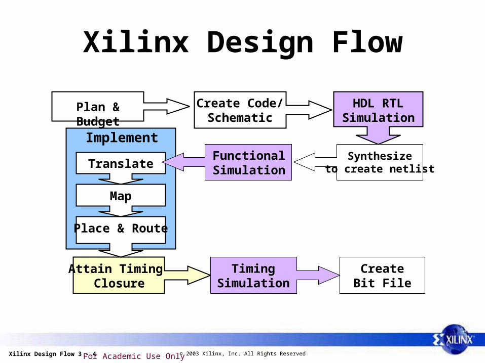
Translate
Map
Place & Route
Xilinx Design Flow
Plan & Budget HDL RTLSimulation
Synthesizeto create netlist
FunctionalSimulation
CreateBit File
Attain Timing Closure
TimingSimulation
Implement
Create Code/Schematic
Xilinx Design Flow 3 - 5 © 2003 Xilinx, Inc. All Rights ReservedFor Academic Use Only
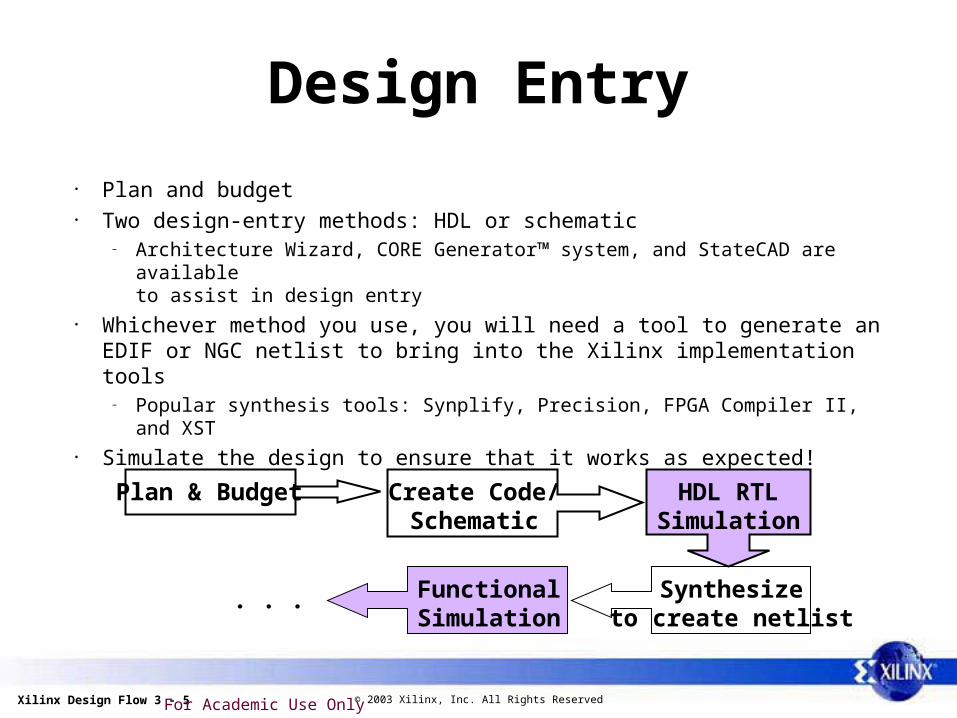
Design Entry
• Plan and budget• Two design-entry methods: HDL or schematic
– Architecture Wizard, CORE Generator™ system, and StateCAD are available to assist in design entry
• Whichever method you use, you will need a tool to generate an EDIF or NGC netlist to bring into the Xilinx implementation tools
– Popular synthesis tools: Synplify, Precision, FPGA Compiler II, and XST• Simulate the design to ensure that it works as expected!
Plan & Budget Create Code/Schematic
HDL RTLSimulation
Synthesizeto create netlist
FunctionalSimulation
. . .
Xilinx Design Flow 3 - 6 © 2003 Xilinx, Inc. All Rights ReservedFor Academic Use Only
Xilinx Implementation
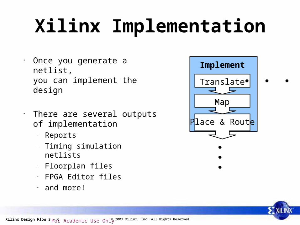
• Once you generate a netlist, you can implement the design
• There are several outputs of implementation
– Reports– Timing simulation netlists– Floorplan files– FPGA Editor files– and more!
Translate
Map
Place & Route
Implement
. . .
.
.
.
Xilinx Design Flow 3 - 7 © 2003 Xilinx, Inc. All Rights ReservedFor Academic Use Only
What is Implementation?
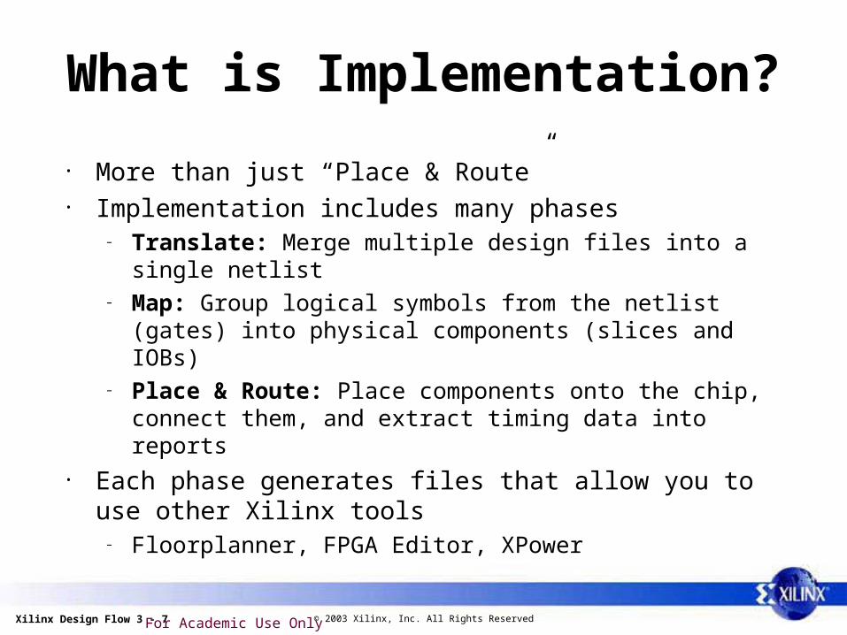
• More than just “Place & Route”• Implementation includes many phases
– Translate: Merge multiple design files into a single netlist– Map: Group logical symbols from the netlist (gates) into physical
components (slices and IOBs)– Place & Route: Place components onto the chip, connect them, and
extract timing data into reports• Each phase generates files that allow you to use other Xilinx tools
– Floorplanner, FPGA Editor, XPower
Xilinx Design Flow 3 - 8 © 2003 Xilinx, Inc. All Rights ReservedFor Academic Use Only
Timing Closure
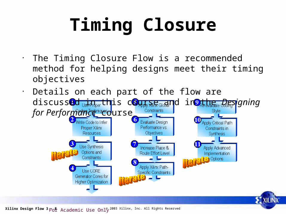
• The Timing Closure Flow is a recommended method for helping designs meet their timing objectives
• Details on each part of the flow are discussed in this course and in the Designing for Performance course
Xilinx Design Flow 3 - 9 © 2003 Xilinx, Inc. All Rights ReservedFor Academic Use Only
Download
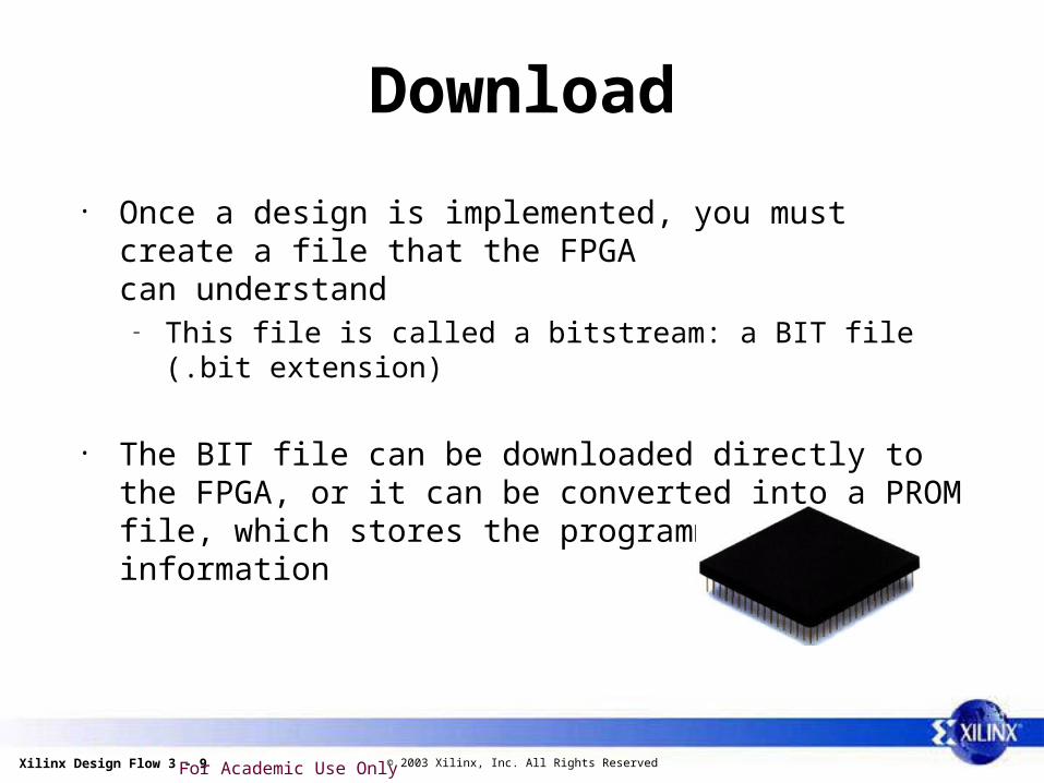
• Once a design is implemented, you must create a file that the FPGA can understand
– This file is called a bitstream: a BIT file (.bit extension)
• The BIT file can be downloaded directly to the FPGA, or it can be converted into a PROM file, which stores the programming information
Xilinx Design Flow 3 - 10 © 2003 Xilinx, Inc. All Rights ReservedFor Academic Use Only
Outline
• Overview• ISE• Summary
Xilinx Design Flow 3 - 11 © 2003 Xilinx, Inc. All Rights ReservedFor Academic Use Only
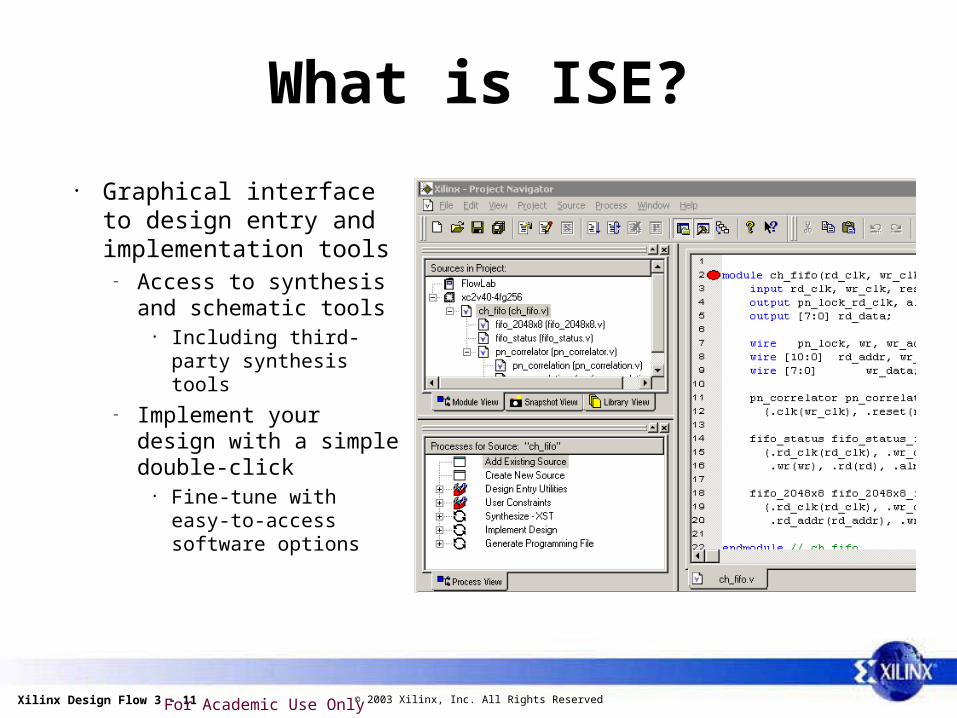
What is ISE?
• Graphical interface to design entry and implementation tools
– Access to synthesis and schematic tools
• Including third-party synthesis tools
– Implement your design with a simple double-click
• Fine-tune with easy-to-access software options
Xilinx Design Flow 3 - 12 © 2003 Xilinx, Inc. All Rights ReservedFor Academic Use Only
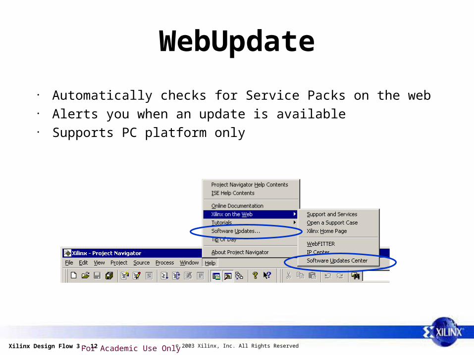
WebUpdate
• Automatically checks for Service Packs on the web• Alerts you when an update is available• Supports PC platform only
Xilinx Design Flow 3 - 13 © 2003 Xilinx, Inc. All Rights ReservedFor Academic Use Only
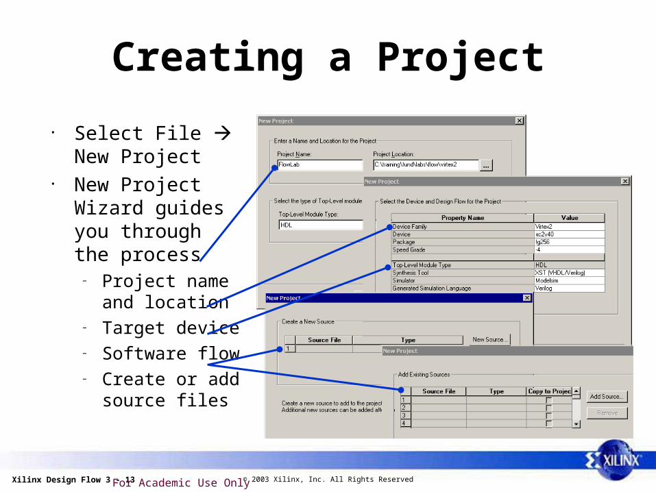
Creating a Project
• Select File New Project
• New Project Wizard guides you through the process
– Project name and location
– Target device– Software flow– Create or add
source files
Xilinx Design Flow 3 - 14 © 2003 Xilinx, Inc. All Rights ReservedFor Academic Use Only
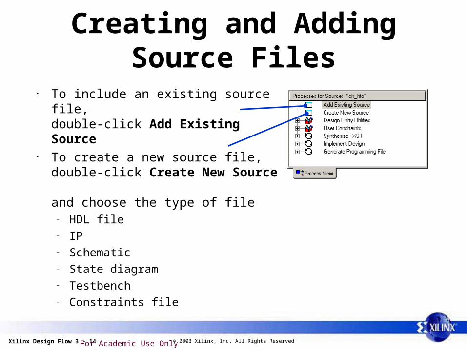
Creating and AddingSource Files
• To include an existing source file, double-click Add Existing Source
• To create a new source file, double-click Create New Source and choose the type of file
– HDL file– IP– Schematic– State diagram– Testbench– Constraints file
Xilinx Design Flow 3 - 15 © 2003 Xilinx, Inc. All Rights ReservedFor Academic Use Only
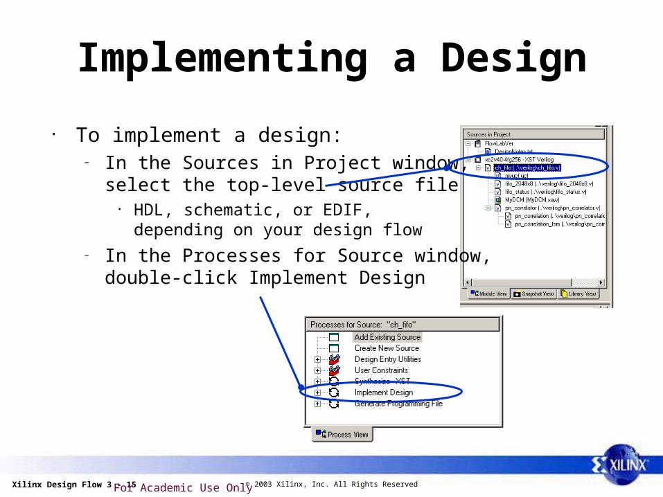
Implementing a Design
• To implement a design:– In the Sources in Project window,
select the top-level source file • HDL, schematic, or EDIF,
depending on your design flow– In the Processes for Source window,
double-click Implement Design
Xilinx Design Flow 3 - 16 © 2003 Xilinx, Inc. All Rights ReservedFor Academic Use Only
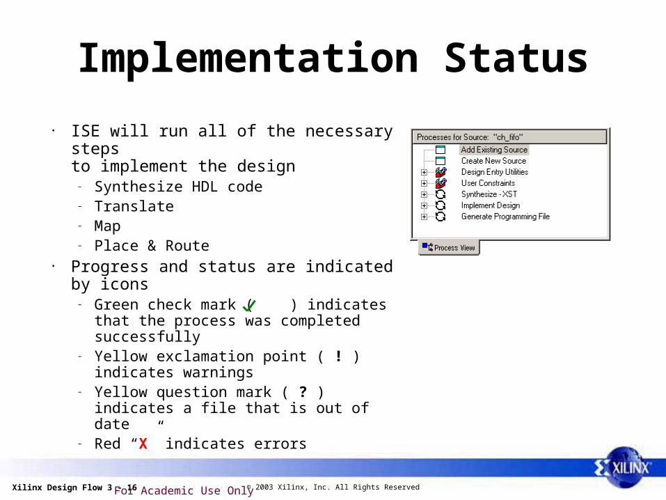
Implementation Status
• ISE will run all of the necessary steps to implement the design
– Synthesize HDL code– Translate– Map– Place & Route
• Progress and status are indicated by icons– Green check mark ( ) indicates that the
process was completed successfully– Yellow exclamation point ( ! ) indicates
warnings– Yellow question mark ( ? ) indicates a file
that is out of date– Red “X” indicates errors
Xilinx Design Flow 3 - 17 © 2003 Xilinx, Inc. All Rights ReservedFor Academic Use Only
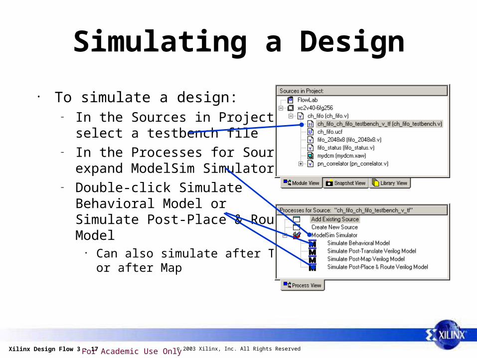
Simulating a Design
• To simulate a design:– In the Sources in Project window,
select a testbench file – In the Processes for Source window,
expand ModelSim Simulator – Double-click Simulate
Behavioral Model or Simulate Post-Place & Route Model
• Can also simulate after Translate or after Map
Xilinx Design Flow 3 - 18 © 2003 Xilinx, Inc. All Rights ReservedFor Academic Use Only
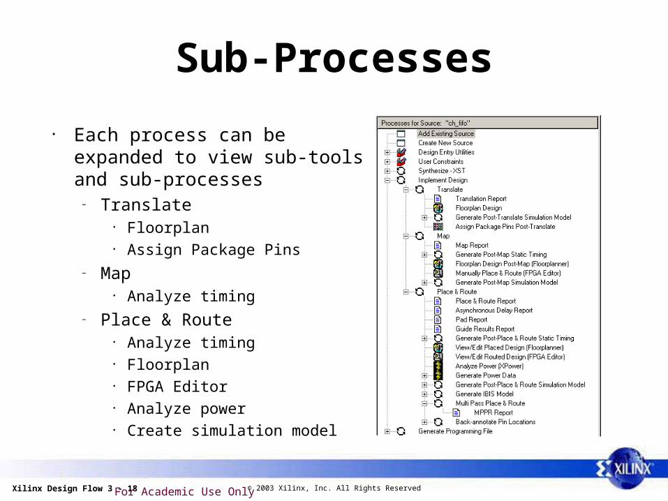
Sub-Processes
• Each process can be expanded to view sub-tools and sub-processes
– Translate• Floorplan• Assign Package Pins
– Map• Analyze timing
– Place & Route• Analyze timing• Floorplan • FPGA Editor• Analyze power• Create simulation model
Xilinx Design Flow 3 - 19 © 2003 Xilinx, Inc. All Rights ReservedFor Academic Use Only
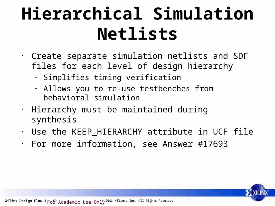
Hierarchical Simulation Netlists
• Create separate simulation netlists and SDF files for each level of design hierarchy
– Simplifies timing verification– Allows you to re-use testbenches from behavioral simulation
• Hierarchy must be maintained during synthesis• Use the KEEP_HIERARCHY attribute in UCF file• For more information, see Answer #17693
Xilinx Design Flow 3 - 20 © 2003 Xilinx, Inc. All Rights ReservedFor Academic Use Only
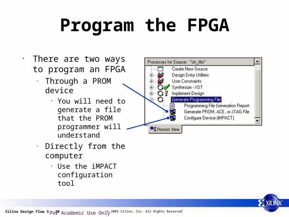
Program the FPGA
• There are two ways to program an FPGA
– Through a PROM device• You will need to generate
a file that the PROM programmer will understand
– Directly from the computer• Use the iMPACT
configuration tool
Xilinx Design Flow 3 - 21 © 2003 Xilinx, Inc. All Rights ReservedFor Academic Use Only
Outline
• Overview• ISE• Summary
Xilinx Design Flow 3 - 22 © 2003 Xilinx, Inc. All Rights ReservedFor Academic Use Only
Review Questions
• What are the phases of the Xilinx design flow?
• What are the components of implementation, and what happens at each step?
• What are two methods used to program an FPGA?
Xilinx Design Flow 3 - 23 © 2003 Xilinx, Inc. All Rights ReservedFor Academic Use Only
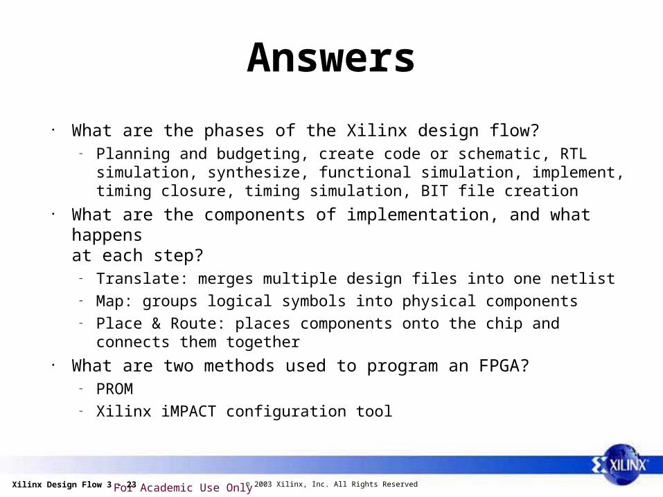
Answers
• What are the phases of the Xilinx design flow?– Planning and budgeting, create code or schematic, RTL simulation,
synthesize, functional simulation, implement, timing closure, timing simulation, BIT file creation
• What are the components of implementation, and what happens at each step?
– Translate: merges multiple design files into one netlist– Map: groups logical symbols into physical components– Place & Route: places components onto the chip and connects them together
• What are two methods used to program an FPGA?– PROM– Xilinx iMPACT configuration tool
Xilinx Design Flow 3 - 24 © 2003 Xilinx, Inc. All Rights ReservedFor Academic Use Only
Summary
• Implementation means more than place & route
• Xilinx provides a simple “pushbutton” tool to help you through the Xilinx design process
Xilinx Design Flow 3 - 25 © 2003 Xilinx, Inc. All Rights ReservedFor Academic Use Only
Where Can I Learn More?
• Complete design flow tutorials– http://support.xilinx.com Documentation Tutorials
• On the phases of implementation– http://support.xilinx.com Software Manuals Development System
Reference Guide• On hierarchical simulation netlists
– http://support.xilinx.com Answer #17693• Configuration Problem Solver
– http://support.xilinx.com Problem Solvers Configuration Problem Solver