Embed Size (px)
DESCRIPTION
24Mhz
Citation preview
Monolithic Reconfigurable SC Power Converter with Adaptive Gain Control and On-Chip Capacitor Sizing
Ling Su Dongsheng Ma
Student Member Senior Member
IDT The University of Arizona 5670 N kolb, Tucson, AZ 1230 E Speedway, Tucson, AZ, 85721
[email protected] [email protected]
Abstract -- This paper presents a monolithic reconfigurable step-down switched-capacitor (SC) power converter for self-powered microsystems. The design features an efficient step-down SC power stage with adaptive gain control and on-chip capacitor sizing. The adaptive gain control helps the converter maintain high efficiency continuously. Meanwhile, the size-adjustable pumping capacitors allow the output voltage to be regulated at different desired levels, even with a constant by 50% duty ratio. The monolithic implementation effectively suppresses the switching noises and glitches caused by parasitic components resulting from traditional bonding, packaging, and PCB wiring. The design has been sent for fabrication with a 180-nm CMOS process. Post-layout fully-transistor based simulations show that the converter is capable of precisely providing a variable power supply Vout from 0.9 to 1.65 V. It achieves a maximum efficiency of 89%, when Vout is regulated at 1.65 V and at a switching frequency of 4 MHz.
Index Terms— Reconfigurable, Adaptive gain control, on-chip capacitor sizing, switched-capacitor power converter.
I. INTRODUCTION Self-powered sensing devices and implantable medical
microsystems have been proliferating in recent years. Such a device usually operates at ultra-low power level with assistance of a specially designed power management system. To achieve long operation lifetime and low system profile, monolithic system integration is rising to become very attractive in this scenario.
However, there are certain new design challenges in such a power system due to its unique operation environment and design specifications. Firstly, due to the instability of self-harvesting energy sources, such a device is mandated to operate under a wide input/output voltage range. As a result, it is much more difficult to maintain high efficiency than traditional designs with fixed input and output voltages [1-4]. Secondly, while microelectronics technology can be further explored for system miniaturization, fully on-chip power management designs still face numerous technical difficulties. Thirdly, almost all the power conversion circuits for these applications are switching converters. Although these converters provide high efficiencies and flexible power conversions, they generate severe EMI noise and have bulky system profile, due to the employment of inductive components. Linear regulators are not preferred here because it is difficult to maintain high efficiency and stability over a large drop-out range. As potentially the best alternative to these applications, SC converters become very appealing.
However, similar to their switch mode counterparts, new architectures and control methods should be investigated in order to adapt to the new design challenges associated with variable output, large dynamic transient, and low noise.
In this paper, as a reference solution to the new design challenges, we propose a monolithic reconfigurable step-down SC power converter with adaptive gain control and on-chip capacitor sizing. The rest of the paper is organized as follows. In Section II, we address the details of system architecture and design strategy. Section III verifies our design ideas with transistor-based HSPICE simulations. Finally, we conclude this research in Section IV.
II. SYSTEM ARCHITECTURE & DESIGN STRATEGY Ideally, if we assume there exists no power loss in the
controller and power stage of a SC power converter, its efficiency can be computed as
%100×⋅
=in
out
VG
Vη (1)
Here, Vin and Vout are the respective input and output voltages. G represents the conversion gain. Eqn. (1) reveals that if Vout is much lower than GVin, the efficiency is very low, even in the ideal case. This proves that if Vin or/and Vout need to vary within certain voltage ranges, it could be difficult to preserve high efficiency with a fixed conversion gain. For example, for a SC power converter with Vin = 1.8 V and Vout = 1.2 V, if Vout drops to 0.8 V and the converter maintains the original topology for the conversion gain of 2/3, the highest possible efficiency would be 66.67%! We thus propose the adaptive gain control and on-chip capacitor sizing techniques to overcome this problem. The details are addressed as follows.
A. Adaptive Gain Control Scheme The power stage of the proposed SC power converter is
shown in Fig. 1(a), which operates with a pair of complementary phases − ɸ and . Instead of using large capacitors and switches for a single fixed conversion gain implementation, we employ 4 pumping capacitors C1, C2, C3, and C4 and 20 switches. This allows the converter to be reconfigured with 5 different conversion gains. For instance, as depicted in Fig. 1(b), with a fixed input Vin, if
2713U.S. Government work not protected by U.S. copyright
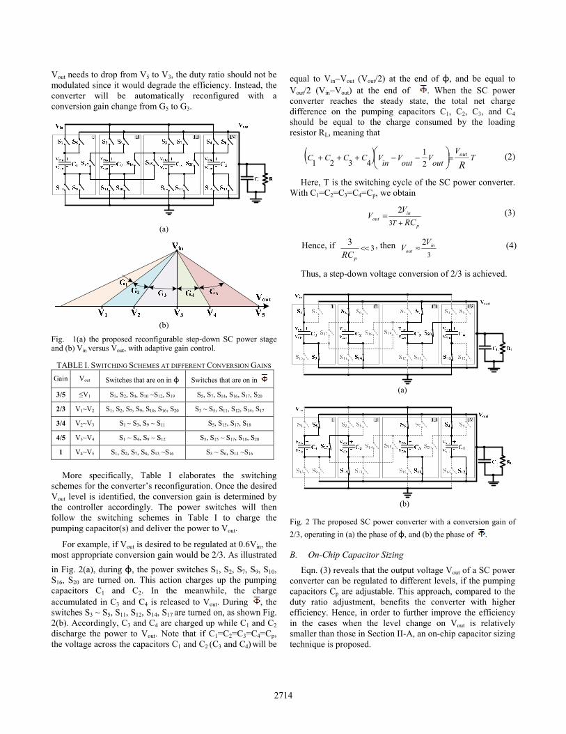
Vout needs to drop from V5 to V3, the duty ratio should not be modulated since it would degrade the efficiency. Instead, the converter will be automatically reconfigured with a conversion gain change from G5 to G3.
(a)
(b)
Fig. 1(a) the proposed reconfigurable step-down SC power stage and (b) Vin versus Vout, with adaptive gain control.
TABLE I. SWITCHING SCHEMES AT DIFFERENT CONVERSION GAINS Gain Vout Switches that are on in ɸ Switches that are on in
3/5 ≤V1 S1, S2, S4, S10 ~S12, S19 S5, S7, S14, S16, S17, S20
2/3 V1~V2 S1, S2, S7, S9, S10, S16, S20 S3 ~ S5, S11, S12, S14, S17
3/4 V2~V3 S1 ~ S3, S9 ~ S11 S5, S15, S17, S18
4/5 V3~V4 S1 ~ S4, S9 ~ S12 S5, S15 ~ S17, S18, S20
1 V4~V5 S1, S2, S7, S8, S13 ~S16 S3 ~ S6, S13 ~S16
More specifically, Table I elaborates the switching schemes for the converter’s reconfiguration. Once the desired Vout level is identified, the conversion gain is determined by the controller accordingly. The power switches will then follow the switching schemes in Table I to charge the pumping capacitor(s) and deliver the power to Vout.
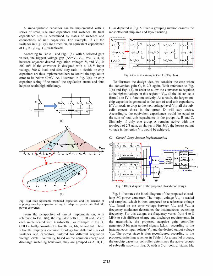
For example, if Vout is desired to be regulated at 0.6Vin, the most appropriate conversion gain would be 2/3. As illustrated in Fig. 2(a), during ɸ, the power switches S1, S2, S7, S9, S10, S16, S20 are turned on. This action charges up the pumping capacitors C1 and C2. In the meanwhile, the charge accumulated in C3 and C4 is released to Vout. During , the switches S3 ~ S5, S11, S12, S14, S17 are turned on, as shown Fig. 2(b). Accordingly, C3 and C4 are charged up while C1 and C2 discharge the power to Vout. Note that if C1=C2=C3=C4=Cp, the voltage across the capacitors C1 and C2 (C3 and C4) will be
equal to Vin−Vout (Vout/2) at the end of ɸ, and be equal to Vout/2 (Vin−Vout) at the end of . When the SC power converter reaches the steady state, the total net charge difference on the pumping capacitors C1, C2, C3, and C4 should be equal to the charge consumed by the loading resistor RL, meaning that
( ) TV
outVoutVinVCCCCRout=−−+++ ⎟
⎠⎞
⎜⎝⎛
21
4321 (2)
Here, T is the switching cycle of the SC power converter. With C1=C2=C3=C4=Cp, we obtain
p
inout RC
VV
T +=
3
2 (3)
Hence, if 33
<<pRC
, then 3
2 inout
VV ≈ (4)
Thus, a step-down voltage conversion of 2/3 is achieved.
(a)
(b)
Fig. 2 The proposed SC power converter with a conversion gain of 2/3, operating in (a) the phase of ɸ, and (b) the phase of .
B. On-Chip Capacitor Sizing
Eqn. (3) reveals that the output voltage Vout of a SC power converter can be regulated to different levels, if the pumping capacitors Cp are adjustable. This approach, compared to the duty ratio adjustment, benefits the converter with higher efficiency. Hence, in order to further improve the efficiency in the cases when the level change on Vout is relatively smaller than those in Section II-A, an on-chip capacitor sizing technique is proposed.
2714
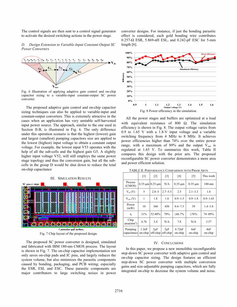
A size-adjustable capacitor can be implemented with a series of small size unit capacitors and switches. Its final capacitance size is determined by status of switches and connections of unit capacitors. For example, if all the switches in Fig. 3(a) are turned on, an equivalent capacitance of C1a+C1b+C1c+C1d is achieved.
According to Table 1 and Fig. 1(b), with 5 selected gain values, the biggest voltage gap (ΔV=Vi -Vi-1, i=2, 3, 4, 5) between adjacent desired regulation voltages Vi and Vi-1 is 200 mV if the converter is designed with a 1.8-V input voltage, 800-Ω load, and 50% duty ratio. 4 sizable on-chip capacitors are thus implemented here to control the regulation error to be below 50mV. As illustrated in Fig. 3(a), on-chip capacitor sizing “fine tunes” the regulation errors and thus helps to retain high efficiency.
(a)
Ca, Cb
Ca, Cb, C
c
Ca, Cb, C
c, Cd
(b)
Fig. 3(a) Size-adjustable switched capacitor, and (b) scheme of applying on-chip capacitor sizing to adaptive gain controlled SC power converter.
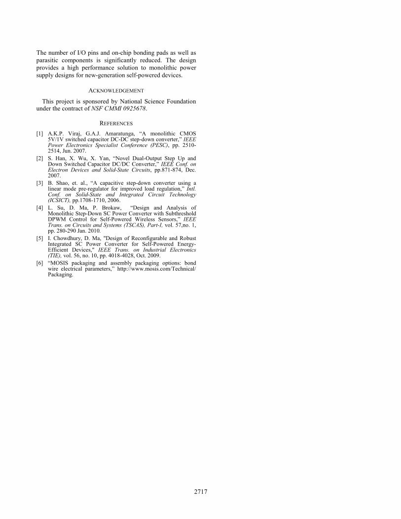
From the perspective of circuit implementation, with reference to Fig. 1(b), the regulator cells I, II, III and IV are each implemented with 4 sub-cells. For example in Fig. 4, Cell I actually consists of sub-cells I-a, I-b, I-c and I-d. These sub-cells employ a common topology but different sizes of switches and capacitors, tailored for different regulation voltage levels. Eventually, based on the common charge and discharge switching behaviors, they are grouped as A, B, C,
D, as depicted in Fig. 5. Such a grouping method ensures the most efficient chip area and layout routing.
Fig. 4 Capacitor sizing in Cell I of Fig. 1(a).
To illustrate the design idea, we consider the case when
the conversion gain G2 is 2/3 again. With reference to Fig. 3(b) and Eqn. (3), in order to allow the converter to regulate at the highest voltage in this region − V23, all the 16 sub-cells from I-a to IV-d function actively. As a result, the largest on-chip capacitor is generated as the sum of total unit capacitors. If Vout needs to drop to the next voltage level V22, all the sub-cells except those in the group D will stay active. Accordingly, the equivalent capacitance would be equal to the sum of total unit capacitance in the groups A, B and C. Similarly, if only one group A remains active with the topology of 2/3 gain, as shown in Fig. 3(b), the lowest output voltage in the region V20 would be achieved.
C. Closed- Loop System Implementation
Fig. 5 Block diagram of the proposed closed-loop design.
Fig. 5 illustrates the block diagram of the proposed closed-loop SC power converter. The output voltage Vout is scaled and sampled, which is then compared to a reference voltage Vref. Based on the error voltage between Vout and Vref, a frequency modulator determines the instantaneous switching frequency. For this design, the frequency varies from 4 to 8 MHz to suit different charge and discharge requirements. In the meanwhile, the proposed adaptive gain controller generates 3-bit gain control signals k3k2k1, according to the instantaneous input voltage Vin and the desired output voltage Vref. The power stage is then reconfigured according to the proposed switching schemes in Table I. As a parallel process, the on-chip capacitor controller determines the active groups of sub-cells shown in Fig. 5, with a 2-bit control signal l2l1.
2715
The control signals are then sent to a control signal generator to activate the desired switching actions in the power stage.
D. Design Extension to Variable-Input Constant-Output SC Power Converters
Fig. 6 Illustration of applying adaptive gain control and on-chip capacitor sizing to a variable-input constant-output SC power converter.
The proposed adaptive gain control and on-chip capacitor
sizing techniques can also be applied to variable-input and constant-output converters. This is extremely attractive in the cases when an application has very unstable self-harvested input power source. The approach, similar to the one used in Section II-B, is illustrated in Fig. 6. The only difference under this operation scenario is that the highest (lowest) gain and largest (smallest) pumping capacitors size are applied to the lowest (highest) input voltage to obtain a constant output voltage. For example, the lowest input V53 operates with the help of all the sub-cells and the highest gain G5. A slightly higher input voltage V52, will still employs the same power stage topology and thus the conversion gain, but all the sub-cells in the group D would be shut down to reduce the total on-chip capacitance
III. SIMULATION RESULTS
Fig. 7 Chip layout of the proposed design.
The proposed SC power converter is designed, simulated
and fabricated with IBM 180-nm CMOS process. The layout is shown in Fig. 7. The on-chip capacitor implementation not only saves on-chip pads and IC pins, and largely reduces the system volume, but also minimizes the parasitic components caused by bonding, packaging, and PCB wiring; especially the ESR, ESL and ESC. These parasitic components are major contributors to large switching noises in power
converter designs. For instance, if just the bonding parasitic effect is considered, each gold bonding wire contributes 0.257-Ω ESR, 5.869-nH ESL, and 0.242-pF ESC for 5-mm length [6].
0%
10%
20%
30%
40%
50%
60%
70%
80%
90%
100%
0.9 1 1.1 1.2 1.3 1.4 1.5 1.6
Ideal efficiency
Simulated efficiency
Output voltage (V) Fig. 8 Power efficiency in the simulation.
All the power stages and buffers are optimized at a load
with equivalent resistance of 800 Ω. The simulation efficiency is shown in Fig. 8. The output voltage varies from 0.9 to 1.65 V with a 1.8-V input voltage and a variable switching frequency from 4 MHz to 8 MHz. It achieves power efficiencies higher than 74% over the entire power range, with a maximum of 89% and the output Vout is regulated at 1.65 V. To summarize this work, Table II compares this design with the prior arts. The proposed reconfigurable SC power converter demonstrates a more area and power efficient solution.
TABLE II. PERFORMANCE COMPARISON WITH PRIOR ARTS
[1] [2] [3] [4] [5] This work
Process (CMOS) 0.35-μm 0.25-μm N/A 0.35-μm 0.35-μm 180-nm
Vin (V) 5 2.8~5 2.7~5.5 2.5 2.1~3.3 1.8
Vout (V) 1 1.8 1.8 0.9~1.5 0.9~1.8 0.9~1.65
Power (mW) 10 360 450 0.4~7.5 39 1.4~3.8
η 31% 52-80% 70% ≤66.7% ≤76% 74~89%
Chip area(mm2) 6.76 3.4 N/A 7.8 N/A 3.57
Pumping capacitance
1.2nF on-chip
2μF off-chip
2μF off-chip
6.72nF on-chip
6nF on-chip
4nF on-chip
IV. CONCLUSIONS In this paper, we propose a new monolithic reconfigurable
step-down SC power converter with adaptive gain control and on-chip capacitor sizing. The design features an efficient step-down SC power converter with multiple conversion gains and size-adjustable pumping capacitors, which are fully integrated on-chip to decrease the system volume and noise.
2716
The number of I/O pins and on-chip bonding pads as well as parasitic components is significantly reduced. The design provides a high performance solution to monolithic power supply designs for new-generation self-powered devices.
ACKNOWLEDGEMENT
This project is sponsored by National Science Foundation under the contract of NSF CMMI 0925678.
REFERENCES [1] A.K.P. Viraj, G.A.J. Amaratunga, “A monolithic CMOS
5V/1V switched capacitor DC-DC step-down converter,” IEEE Power Electronics Specialist Conference (PESC), pp. 2510-2514, Jun. 2007.
[2] S. Han, X. Wu, X. Yan, “Novel Dual-Output Step Up and Down Switched Capacitor DC/DC Converter,” IEEE Conf. on Electron Devices and Solid-State Circuits, pp.871-874, Dec. 2007.
[3] B. Shao, et. al., “A capacitive step-down converter using a linear mode pre-regulator for improved load regulation,” Intl. Conf. on Solid-State and Integrated Circuit Technology (ICSICT), pp.1708-1710, 2006.
[4] L. Su, D. Ma, P. Brokaw, “Design and Analysis of Monolithic Step-Down SC Power Converter with Subthreshold DPWM Control for Self-Powered Wireless Sensors,” IEEE Trans. on Circuits and Systems (TSCAS), Part-I, vol. 57,no. 1, pp. 280-290 Jan. 2010.
[5] I. Chowdhury, D. Ma, "Design of Reconfigurable and Robust Integrated SC Power Converter for Self-Powered Energy-Efficient Devices," IEEE Trans. on Industrial Electronics (TIE), vol. 56, no. 10, pp. 4018-4028, Oct. 2009.
[6] “MOSIS packaging and assembly packaging options: bond wire electrical parameters,” http://www.mosis.com/Technical/ Packaging.
2717


![arXiv:2005.13949v1 [physics.app-ph] 25 May 20207.5 MHz F4 6.5 MHz F5 F6 7.5 MHz F7 F8 6.5 MHz F14 9.5 MHz F15 NA F16 8.5 MHz F17 NA F18 NA F19 7.5 MHz F11 6.5 MHz F20 NA F21 8.5 MHz](https://img.pdfslide.net/doc/110x75/5f758878eb2d114487007824/arxiv200513949v1-25-may-2020-75-mhz-f4-65-mhz-f5-f6-75-mhz-f7-f8-65-mhz.jpg)


![PVCPR11 Edital 3.5 GHz v03.ppt [Modo de Compatibilidade]...2011/06/09 · 35 MHz 35 MHz 10 MHz 10 MHz 10 MHz 10 MHz 10 MHz 10 MHz 3.400,00 MHz 3.600,00 MHz 10 MHz 35 MHz 10 MHz 10](https://img.pdfslide.net/doc/110x75/5f7286506e7f433bb4685297/pvcpr11-edital-35-ghz-v03ppt-modo-de-compatibilidade-20110609-35-mhz.jpg)