Embed Size (px)
Citation preview
BWW
13
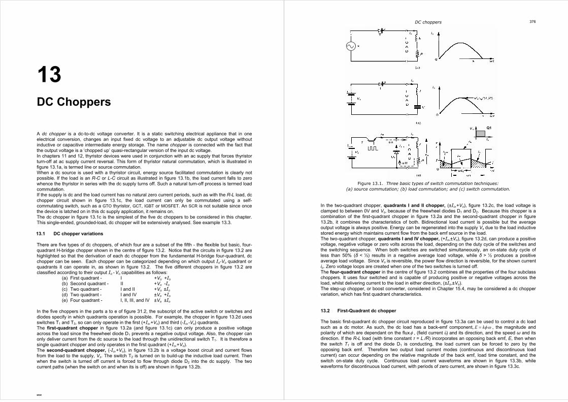
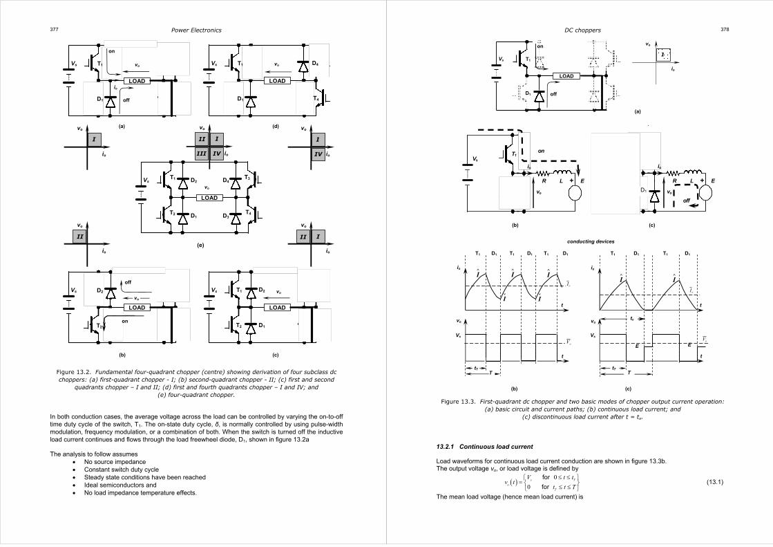
DC Choppers A dc chopper is a dc-to-dc voltage converter. It is a static switching electrical appliance that in one electrical conversion, changes an input fixed dc voltage to an adjustable dc output voltage without inductive or capacitive intermediate energy storage. The name chopper is connected with the fact that the output voltage is a ‘chopped up’ quasi-rectangular version of the input dc voltage. In chapters 11 and 12, thyristor devices were used in conjunction with an ac supply that forces thyristor turn-off at ac supply current reversal. This form of thyristor natural commutation, which is illustrated in figure 13.1a, is termed line or source commutation. When a dc source is used with a thyristor circuit, energy source facilitated commutation is clearly not possible. If the load is an R-C or L-C circuit as illustrated in figure 13.1b, the load current falls to zero whence the thyristor in series with the dc supply turns off. Such a natural turn-off process is termed load commutation. If the supply is dc and the load current has no natural zero current periods, such as with the R-L load, dc chopper circuit shown in figure 13.1c, the load current can only be commutated using a self-commutating switch, such as a GTO thyristor, GCT, IGBT or MOSFET. An SCR is not suitable since once the device is latched on in this dc supply application, it remains on. The dc chopper in figure 13.1c is the simplest of the five dc choppers to be considered in this chapter. This single-ended, grounded-load, dc chopper will be extensively analysed. See example 13.3. 13.1 DC chopper variations There are five types of dc choppers, of which four are a subset of the fifth - the flexible but basic, four-quadrant H-bridge chopper shown in the centre of figure 13.2. Notice that the circuits in figure 13.2 are highlighted so that the derivation of each dc chopper from the fundamental H-bridge four-quadrant, dc chopper can be seen. Each chopper can be categorized depending on which output Io-Vo quadrant or quadrants it can operate in, as shown in figure 13.2. The five different choppers in figure 13.2 are classified according to their output Io - Vo capabilities as follows:
(a) First quadrant - I +Vo +Io (b) Second quadrant - II +Vo -Io (c) Two quadrant - I and II +Vo ±Io (d) Two quadrant - I and IV ±Vo +Io (e) Four quadrant - I, II, III, and IV ±Vo ±Io
In the five choppers in the parts a to e of figure 31.2, the subscript of the active switch or switches and diodes specify in which quadrants operation is possible. For example, the chopper in figure 13.2d uses switches T1 and T3, so can only operate in the first (+Io,+Vo) and third (-Io,-Vo) quadrants. The first-quadrant chopper in figure 13.2a (and figure 13.1c) can only produce a positive voltage across the load since the freewheel diode D1 prevents a negative output voltage. Also, the chopper can only deliver current from the dc source to the load through the unidirectional switch T1. It is therefore a single quadrant chopper and only operates in the first quadrant (+Io,+Vo). The second-quadrant chopper, (-Io,+Vo), in figure 13.2b is a voltage boost circuit and current flows from the load to the supply, Vs. The switch T2 is turned on to build-up the inductive load current. Then when the switch is turned off current is forced to flow through diode D2 into the dc supply. The two current paths (when the switch on and when its is off) are shown in figure 13.2b.
DC choppers 376
Io
V o
T
i o
i o
i o
i o
i o
o n
o f f
i o
Q1
Figure 13.1. Three basic types of switch commutation techniques: (a) source commutation; (b) load commutation; and (c) switch commutation.
In the two-quadrant chopper, quadrants I and II chopper, (±Io,+Vo), figure 13.2c, the load voltage is clamped to between 0V and Vs, because of the freewheel diodes D1 and D2. Because this chopper is a combination of the first-quadrant chopper in figure 13.2a and the second-quadrant chopper in figure 13.2b, it combines the characteristics of both. Bidirectional load current is possible but the average output voltage is always positive. Energy can be regenerated into the supply Vs due to the load inductive stored energy which maintains current flow from the back emf source in the load. The two-quadrant chopper, quadrants I and IV chopper, (+Io,±Vo), figure 13.2d, can produce a positive voltage, negative voltage or zero volts across the load, depending on the duty cycle of the switches and the switching sequence. When both switches are switched simultaneously, an on-state duty cycle of less than 50% (δ < ½) results in a negative average load voltage, while δ > ½ produces a positive average load voltage. Since Vo is reversible, the power flow direction is reversible, for the shown current io. Zero voltage loops are created when one of the two switches is turned off. The four-quadrant chopper in the centre of figure 13.2 combines all the properties of the four subclass choppers. It uses four switched and is capable of producing positive or negative voltages across the load, whilst delivering current to the load in either direction, (±Io,±Vo). The step-up chopper, or boost converter, considered in Chapter 15.4, may be considered a dc chopper variation, which has first quadrant characteristics. 13.2 First-Quadrant dc chopper The basic first-quadrant dc chopper circuit reproduced in figure 13.3a can be used to control a dc load such as a dc motor. As such, the dc load has a back-emf component, E kφω= , the magnitude and polarity of which are dependant on the fluxφ , (field current if) and its direction, and the speed ω and its direction. If the R-L load (with time constant τ = L /R) incorporates an opposing back emf, E, then when the switch T1 is off and the diode D1 is conducting, the load current can be forced to zero by the opposing back emf. Therefore two output load current modes (continuous and discontinuous load current) can occur depending on the relative magnitude of the back emf, load time constant, and the switch on-state duty cycle. Continuous load current waveforms are shown in figure 13.3b, while waveforms for discontinuous load current, with periods of zero current, are shown in figure 13.3c.
Power Electronics 377
Figure 13.2. Fundamental four-quadrant chopper (centre) showing derivation of four subclass dc choppers: (a) first-quadrant chopper - I; (b) second-quadrant chopper - II; (c) first and second
quadrants chopper – I and II; (d) first and fourth quadrants chopper – I and IV; and (e) four-quadrant chopper.
In both conduction cases, the average voltage across the load can be controlled by varying the on-to-off time duty cycle of the switch, T1. The on-state duty cycle, δ, is normally controlled by using pulse-width modulation, frequency modulation, or a combination of both. When the switch is turned off the inductive load current continues and flows through the load freewheel diode, D1, shown in figure 13.2a The analysis to follow assumes
• No source impedance • Constant switch duty cycle • Steady state conditions have been reached • Ideal semiconductors and • No load impedance temperature effects.
I
vo
io
vo
io
II
vo
io IV
I
vo
io
I II
LOAD
Vs
T2
D2
LOAD
Vs
T2
T1
D2
D1
LOAD
Vs
D1
T1
T4
D4
LOAD
Vs
D1
T1
LOAD
Vs
T2
T1
T4
T3 D2
D1
D4
D3
vo
io
II I
III IV
(a)
(b) (c)
(d)
io
vo
on
on
off
off
(e)
vo
vo
vo
vo
DC choppers 378
Figure 13.3. First-quadrant dc chopper and two basic modes of chopper output current operation:
(a) basic circuit and current paths; (b) continuous load current; and (c) discontinuous load current after t = tx.
13.2.1 Continuous load current Load waveforms for continuous load current conduction are shown in figure 13.3b. The output voltage vo, or load voltage is defined by
( ) 0
0
≤ ≤ = ≤ ≤
for
fors T
o
T
V t tv t
t t T (13.1)
The mean load voltage (hence mean load current) is
LOAD
Vs
D1
T1
I
vo
io
on
off
(a)
t
t t
t
tx
T
I∧
I∨
T
vo
iℓ
tT tT
iℓ
Vs
vo
I∧ I
∧
I∧ I
∧
I∨
Vs
E E
conducting devices
T1 D1 T1 D1 T1 D1 T1 D1 T1 D1
(b) (c)
io io
on
(a)
vo
Vs
R L + E
T1
io
Vs
(b)
vo
R L + E
D2
io
off
(b) (c)
oV oV
oI
oI
D1
Power Electronics 379
( )
0 0
1 1
δ
= =
−= = =
∫ ∫whence
T Tt t
o o s
T oos s
V v t dt V dtT Tt V EV V I RT
(13.2)
where the switch on-state duty cycle δ = tT /T is defined in figure 13.3b. The rms load voltage is
( )
½ ½
2 2
0 0
1 1T Tt t
rms o s
Ts s
V v t dt V dtT T
tV V
Tδ
= =
= =
∫ ∫ (13.3)
The output ac ripple voltage is
( ) ( ) ( )
2 2
2 21
r rms o
s s s
V V V
V V Vδ δ δ δ
= −
= − = − (13.4)
The maximum rms ripple voltage in the output occurs when δ = ½ giving an rms ripple voltage of ½Vs. The output voltage ripple factor is
2
2
1
1 11 1
δ δδ δ δ
= = −
−= − = − =
rmsr
o o
s
s
VVRF
V V
V
V
(13.5)
Thus as the duty cycle 1δ → , the ripple factor tends to zero, consistent with the output being dc, that is Vr = 0. Steady-state time domain analysis of first-quadrant chopper
- with load back emf and continuous output current
The time domain load current can be derived in a number of ways. • First, from the Fourier coefficients of the output voltage, the current can be
found by dividing by the load impedance at each harmonic frequency. • Alternatively, the various circuit currents can be found from the time domain
load current equations. i. Fourier coefficients: The Fourier coefficients of the load voltage are independent of the circuit and load parameters and are given by
( )
sin 2
1 cos 2 1
π δπ
π δπ
=
= − ≥ for
sn
sn
Va n
n
Vb n nn
(13.6)
Thus the peak magnitude and phase of the nth harmonic are given by
2 2
1tan
n n n
nn
n
c a b
abφ −
= +
=
Substituting expressions from equation (13.6) yields
1
2sin
sin 2tan ½
1 cos2
sn
n
Vc nn
nn
n
π δππ δφ π π δπ δ
−
=
= = −−
(13.7)
where ( )sinn n nv c n tω φ= + (13.8)
such that
( ) ( )1
sin ω φ∞
== + +∑o o n n
n
v t V c n t (13.9)
The load current is given by
( ) ( )0 1 1
sin ω φ∞ ∞ ∞
= = =
−= = + = +∑ ∑ ∑ n no on
o n
n nn n n
c n tvV Vi t i
R Z R Z (13.10)
DC choppers 380
1
¾
Ipp ½Vs / R
¼
0
0 ¼ ½ ¾ 1 δ
on-state duty cycle
T / τ
25
5
2
1
½
0 ¼ ½ ¾ 1
on-state duty cycle δ
1 ¾
½
¼ 0
pu dc output
mean
1st harmonic
2nd harmonic
3rd harmonic
ha
rmo
nic
rms
as
%
of
dc
sup
ply
V
s
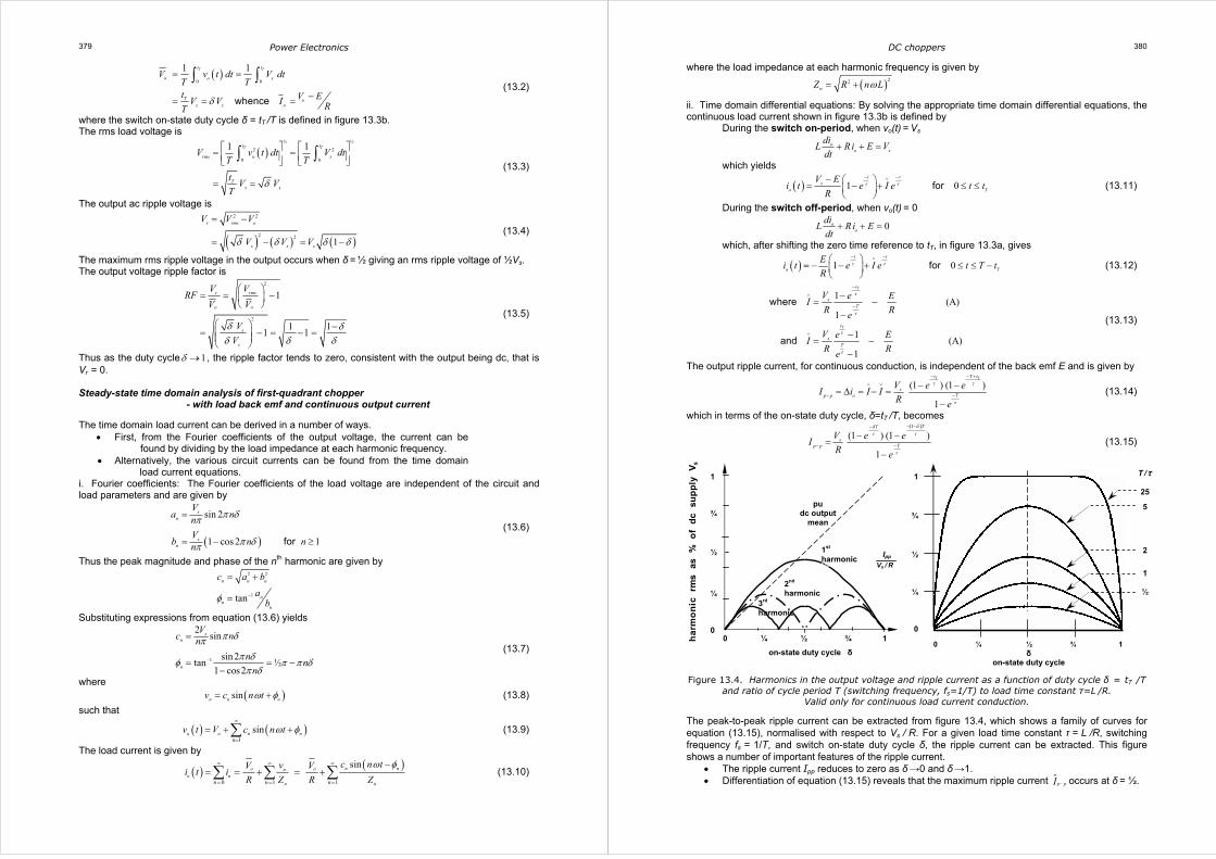
where the load impedance at each harmonic frequency is given by
( )22 ω= +nZ R n L
ii. Time domain differential equations: By solving the appropriate time domain differential equations, the continuous load current shown in figure 13.3b is defined by
During the switch on-period, when vo(t) = Vs
oo s
diL Ri E Vdt
+ + =
which yields
( ) 1 0τ τ− −∨− = − + ≤ ≤
for
t ts
o T
V Ei t e I e t t
R (13.11)
During the switch off-period, when vo(t) = 0
0oo
diL Ri Edt
+ + =
which, after shifting the zero time reference to tT, in figure 13.3a, gives
( ) 1 0τ τ− −∧ = − − + ≤ ≤ −
for
t t
o T
Ei t e I e t T t
R (13.12)
1(A)
1
1(A)
1
T
T
t
sT
t
sT
V e EI
R Re
V e EI
R Re
τ
τ
τ
τ
−
∧
−
∨
−= −
−
−= −
−
where
and
(13.13)
The output ripple current, for continuous conduction, is independent of the back emf E and is given by
(1 ) (1 )
1
T Tt T t
sTp p o
V e eI i I I
R e
τ τ
τ
− − +
∧ ∨
−−
− −= ∆ = − =
− (13.14)
which in terms of the on-state duty cycle, δ=tT /T, becomes
( )1
(1 ) (1 )
1
TT
sTp p
V e eI
R e
δδτ τ
τ
− −−
−−
− −=
− (13.15)
Figure 13.4. Harmonics in the output voltage and ripple current as a function of duty cycle δ = tT /T
and ratio of cycle period T (switching frequency, fs=1/T) to load time constant τ=L /R. Valid only for continuous load current conduction.
The peak-to-peak ripple current can be extracted from figure 13.4, which shows a family of curves for equation (13.15), normalised with respect to Vs / R. For a given load time constant τ = L /R, switching frequency fs = 1/T, and switch on-state duty cycle δ, the ripple current can be extracted. This figure shows a number of important features of the ripple current.
• The ripple current Ipp reduces to zero as δ →0 and δ →1. • Differentiation of equation (13.15) reveals that the maximum ripple current p pI − occurs at δ = ½.
Power Electronics 381
• The longer the load L /R time constant, τ, the lower the output ripple current Ip-p. • The higher the switching frequency, 1/T, the lower the output ripple.
If the switch conducts continuously (δ = 1), then substitution of tT=T into equations (13.11) to (13.13) gives a load voltage Vs and a dc load current is
(A)∧ ∨ − − = = = = =
os
oo
V E V Ei I I I
R R (13.16)
The mean output current with continuous load current is found by integrating the load current over two consecutive periods, the switch conduction given by equation (13.11) and diode conduction given by equation (13.12), which yields
( ) ( )
( )
0
1
(A)
T o
o o
s
V Ei t dtI RT
V ER
δ
−= =
−=
∫ (13.17)
The input and output powers are related such that
( )
( ) ( )
0
2 2
1
in out
siin s S
T
out o o
soo rms o rms
P P
V EP V I V I I
R T
P v t i t dtT
V EI IR EI R E
R
δ τ
δ
∧ ∨
=
− = = − −
=
− = =+ +
∫ (13.18)
from which the average input current can be evaluated. Alternatively, the average input current, which is the average switch current, switchI , can be derived by integrating the switch current which is given by equation (13.11), that is
( )
( )
0
0
1
11
T
T
t
i switch o
t tts
s
II i t dtT
V Ee I e dt
T R
V EI I
R T
τ τ
δ τ
− −∨
∧ ∨
= =
− = − +
− = − −
∫
∫ (13.19)
The term p pII I∧ ∨
−− = is the peak-to-peak ripple current, which is given by equation (13.15). By Kirchhoff’s current law, the average diode current diodeI is the difference between the average output current oI and the average input current, iI , that is
( ) ( )
( )1
diode o i
ss
I I I
V EV EI IR R T
EI I
T R
δ τδ
δτ
∧ ∨
∧ ∨
= −
−− = − + −
− = − −
(13.20)
Alternatively, the average diode current can be found by integrating the diode current given in equation (13.12), as follows
( )
0
11
1
Tt tT t
diode
EI e I e dt
T R
EI I
T R
τ τ
δτ
− −∧−
∧ ∨
= − − +
− = − −
∫ (13.21)
If E represents motor back emf, then the electromagnetic energy conversion efficiency is given by
oo
in is
EI EI
P V Iη = = (13.22)
The chopper effective (dc) input impedance at the dc source is given by
sin
i
VZ
I= (13.23)
For an R-L load without a back emf, set E = 0 in the foregoing equations. The discontinuous load current analysis to follow is not valid for an R-L, with E=0 load, since the load current never reaches zero, but at best asymptotes towards zero during the off-period of the switch.
DC choppers 382
13.2.2 Discontinuous load current With an opposing emf E in the load, the load current can reach zero during the off-time, at a time tx shown in figure 13.3c. The time tx can be found by • deriving an expression for I
∧ from equation (13.11), setting t = tT,
• this equation is substituted into equation (13.12) which is equated to zero, having substituted for t = tx: yielding
ln 1 1 (s)Tt
sx T
V Et t e
Eττ− − = + + −
(13.24)
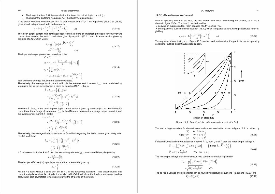
This equation shows that tx > tT. Figure 13.5 can be used to determine if a particular set of operating conditions involves discontinuous load current.
Figure 13.5. Bounds of discontinuous load current with E>0.
The load voltage waveform for discontinuous load current conduction shown in figure 13.3c is defined by
( ) 0
0
s T
o T x
x
V t t
v t t t t
E t t T
≤ ≤ = ≤ ≤ ≤ ≤
for
for
for
(13.25)
If discontinuous load current exists for a period T - tx, from tx until T, then the mean output voltage is
( )
0
10
(V) δ
−= + + =
−= + ≥
∫ ∫ ∫ thence
for
T x
T x
t t T
ooo st t
xo s x T
V EV V dt dt Edt I RTT t
V V E t tT
(13.26)
The rms output voltage with discontinuous load current conduction is given by
( )
½
2 2 2
0
2 2
10
(V)
T x
T x
t t T
rms st t
xs
V V dt d E dtT
T tV E
Tδ
= + +
−= +
∫ ∫ ∫ (13.27)
The ac ripple voltage and ripple factor can be found by substituting equations (13.26) and (13.27) into
2 2
r rms oV V V= − (13.28)
1
¾
½ E / Vs
¼
0 0 ¼ ½ ¾ 1
δ switch on-state duty
T/τ 0 1 2 5 10 ?
notpossib
le
contin
uousdisco
ntinuous
∞
E / Vs
δ
Power Electronics 383
and
2
1
= = −
r rms
o o
VVRF
V V (13.29)
Steady-state time domain analysis of first-quadrant chopper
- with load back emf and discontinuous output current i. Fourier coefficients: The load current can be derived indirectly by using the output voltage Fourier series. The Fourier coefficients of the load voltage are
( )
sin 2 sin 2
1 cos 2 1 cos 2 1
π δ ππ π
π δ ππ π
= −
= − − − ≥
s xn
s xn
V E ta n n Tn nV E tb n n nTn n
(13.30)
which using
2 2
1tan
n n n
nn
n
c a b
abφ −
= +
=
give
( ) ( )1
sinoo n nn
v t V c n tω φ∞
=
= + +∑ (13.31)
The appropriate division by ( )22
nZ R n Lω= + yields the output current. ii. Time domain differential equations: For discontinuous load current, 0.I
∨
= Substituting this condition into the time domain equations (13.11) to (13.14) yields equations for discontinuous load current, specifically:
During the switch on-period, when vo(t) = Vs,
( ) 1 0τ−− = − ≤ ≤
for
ts
o T
V Ei t e t t
R (13.32)
During the switch off-period, when vo(t) = 0, after shifting the zero time reference to tT,
( ) 1 0τ τ− −∧ = − − + ≤ ≤ −
for
t t
o x T
Ei t e I e t t t
R (13.33)
where from equation (13.32), with t = tT,
1 (A)Tt
sV EI e
Rτ−∧ − = −
(13.34)
After tx, vo(t) = E and the load current is zero, that is ( ) 0= ≤ ≤foro xi t t t T (13.35)
The output ripple current, for discontinuous conduction, is dependent of the back emf E and is given by equation (13.34), that is
1Tt
sp p
V EI I e
Rτ−∧
−
− = = −
(13.36)
Since 0I∨
= , the mean output current for discontinuous conduction, is
( )
( )
-
0 0 0
1 11 1
x T x Tt t tt t t t
so o
o
V E EI i t dt e dt e I e dtR RT T
V ER
τ τ τ− − −∧− − = = − + − +
−=
∫ ∫ ∫
1
(A)
x xs s
o
t tV E V ET E TIRR R
δ δ + − − = − = (13.37)
The input and output powers are related such that
2
= = =+ oiin s out in outo rmsP V I P I P PR EI (13.38)
from which the average input current can be evaluated.
DC choppers 384
Alternatively the average input current, which is the switch average current, is given by
( )
0
0
1
11
1
T
T
T
t
i switch o
tts
ts s
II i t dtT
V Ee dt
T R
V E V Ee I
R T R T
τ
ττ τδ δ
−
−
= =
− = −
− − = − − = −
∫
∫ (13.39)
The average diode current diodeI is the difference between the average output current oI and the average input current, iI , that is
diode o i
x
I I I
tET
IT R
δτ ∧
= −
− = −
(13.40)
Alternatively, the average diode current can be found by integrating the diode current given in equation (13.33), as follows
0
11
x Tt tt t
diode
x
EI e I e dt
T R
tET
IT R
τ τ
δτ
− −∧−
∧
= − − +
− = −
∫ (13.41)
If E represents motor back emf, then electromagnetic energy conversion efficiency is given by
oo
in is
E I E I
P V Iη = = (13.42)
The chopper effective input impedance is given by
sin
i
VZ
I= (13.43)
Example 13.1: DC chopper (first quadrant) with load back emf A first-quadrant dc-to-dc chopper feeds an inductive load of 10 ohms resistance, 50mH inductance, and back emf of 55V dc, from a 340V dc source. If the chopper is operated at 200Hz with a 25% on-state duty cycle, determine, with and without (rotor standstill, E = 0) the back emf:
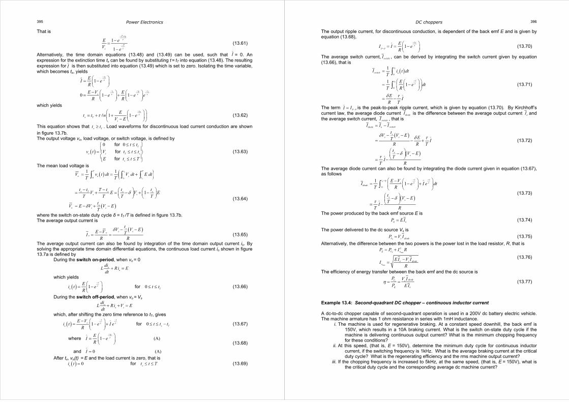
i. the load average and rms voltages; ii. the rms ripple voltage, hence ripple factor; iii. the maximum and minimum output current, hence the peak-to-peak output ripple in the current; iv. the current in the time domain; v. the average load output current, average switch current, and average diode current; vi. the input power, hence output power and rms output current; vii. effective input impedance, (and electromagnetic efficiency for E > 0); and viii. sketch the output current and voltage waveforms.
Solution The main circuit and operating parameters are
• on-state duty cycle δ = ¼ • period T = 1/fs = 1/200Hz = 5ms • on-period of the switch tT = 1.25ms • load time constant τ = L /R = 0.05mH/10Ω = 5ms
Figure Example 13.1. Circuit diagram.
R L E
T1
10Ω 50mH
+
D1 55V
340V
Vs
δ=¼ T=5ms
Power Electronics 385
i. From equations (13.2) and (13.3), assuming continuous load current, the average and rms output voltages are both independent of the back emf, namely
= ¼×340V = 85V
To s s
tV V V
Tδ= =
¼ 240V = 120V
δ= =
= × rms
Tr s s
tV V V
T
ii. The rms ripple voltage hence ripple factor are given by equations (13.4) and (13.5), that is
( )
( )
2 2 1
= 340V ¼ 1 - ¼ 147.2V
δ δ= − = −
× = ac
r rms o sV V V V
and
11
1 - 1 3 1.732
¼
r
o
VRF
V δ= = −
= = =
No back emf, E = 0
iii. From equation (13.13), with E = 0, the maximum and minimum currents are
-1.25ms
5ms
-5ms
5ms
1 340V 111.90A
101 1
Tt
sT
V e eI
R e e
τ
τ
−
∧
−
− −= = × =
Ω− −
1
4
1
1 340V 15.62A
10 11
Tt
sT
V e eI
R ee
τ
τ
∨ − −= = × =
Ω −−
The peak-to-peak ripple in the output current is therefore
=11.90A - 5.62A = 6.28A
p pI I I∧ ∨
− = −
Alternatively the ripple can be extracted from figure 13.4 using T/τ =1 and δ = ¼. iv. From equations (13.11) and (13.12), with E = 0, the time domain load current equations are
( ) 5 5ms
5ms
1
34 1 5.62
34 28.38 (A) 0 1.25ms
τ τ− −∨
− −
−
= − + = × − + ×
= − × ≤ ≤for
t ts
o
t t
mso
t
Vi e I e
R
i t e e
e t
( ) 5ms11.90 (A) 0 3.75ms
τ−∧
−
=
= × ≤ ≤for
t
o
t
o
i I e
i t e t
v. The average load current from equation (13.17), with E = 0, is
85V= = 8.5A10Ωo
oVIR=
The average switch current, which is the average supply current, is
( )
( ) ( )¼ 340V - 0 5ms
- 11.90A - 5.62A = 2.22A10Ω 5ms
si switch
V EII I I
R T
δ τ ∧ ∨− = = − −
×= ×
The average diode current is the difference between the average load current and the average input current, that is
DC choppers 386
= 8.50A - 2.22A = 6.28A
diode o iI I I= −
vi. The input power is the dc supply voltage multiplied by the average input current, that is
=340V×2.22A = 754.8W
754.8Wiin s
out in
P V I
P P
== =
From equation (13.18) the rms load current is given by
754.8W
= = 8.7A rms10Ω
rms
outo
PI
R=
vii. The chopper effective input impedance is
340V
= = 153.2 Ω2.22A
sin
i
VZ
I=
Load back emf, E = 55V
i. and ii. The average output voltage (85V), rms output voltage (120V rms), ac ripple voltage (147.2V ac), and ripple factor (1.732) are independent of back emf, provided the load current is continuous. The earlier answers for E = 0 are applicable.
iii. From equation (13.13), the maximum and minimum load currents are
-1.25ms
5ms
-5ms
5ms
1 340V 1 55V- = 6.40A
10 10Ω1 1
Tt
sT
V e E eI
R Re e
τ
τ
−
∧
−
− −= − = ×
Ω− −
1
1 340V 1 55V0.12A
10 1 101
Tt
sT
V e E eI
R R ee
τ
τ
∨ − −= − = × − =
Ω − Ω−
14
The peak-to-peak ripple in the output current is therefore
= 6.4A - 0.12A = 6.28A
∧ ∨
− = −p pI I I
The ripple value is the same as the E = 0 case, which is as expected since ripple current is independent of back emf with continuous output current. Alternatively the ripple can be extracted from figure 13.4 using T/τ = 1 and δ = ¼. iv. The time domain load current is defined by
( ) 5 5ms
5ms
1
28.5 1 0.12
28.5 28.38 (A) 0 1.25ms
τ τ− −∨
− −
−
− = − + = × − +
= − ≤ ≤for
t ts
o
t t
mso
t
V Ei e I e
R
i t e e
e t
( ) 5ms 5
5ms
1
5.5 1 6.4
5.5 11.9 (A) 0 3.75ms
τ τ− −∧
− −
−
= − − + = − × − +
= − + ≤ ≤for
t t
o
t t
mso
t
Ei e I e
R
i t e e
e t
v. The average load current from equation (13.37) is
85V-55V= = 3A10Ω
ooV EI
R−=
Power Electronics 387
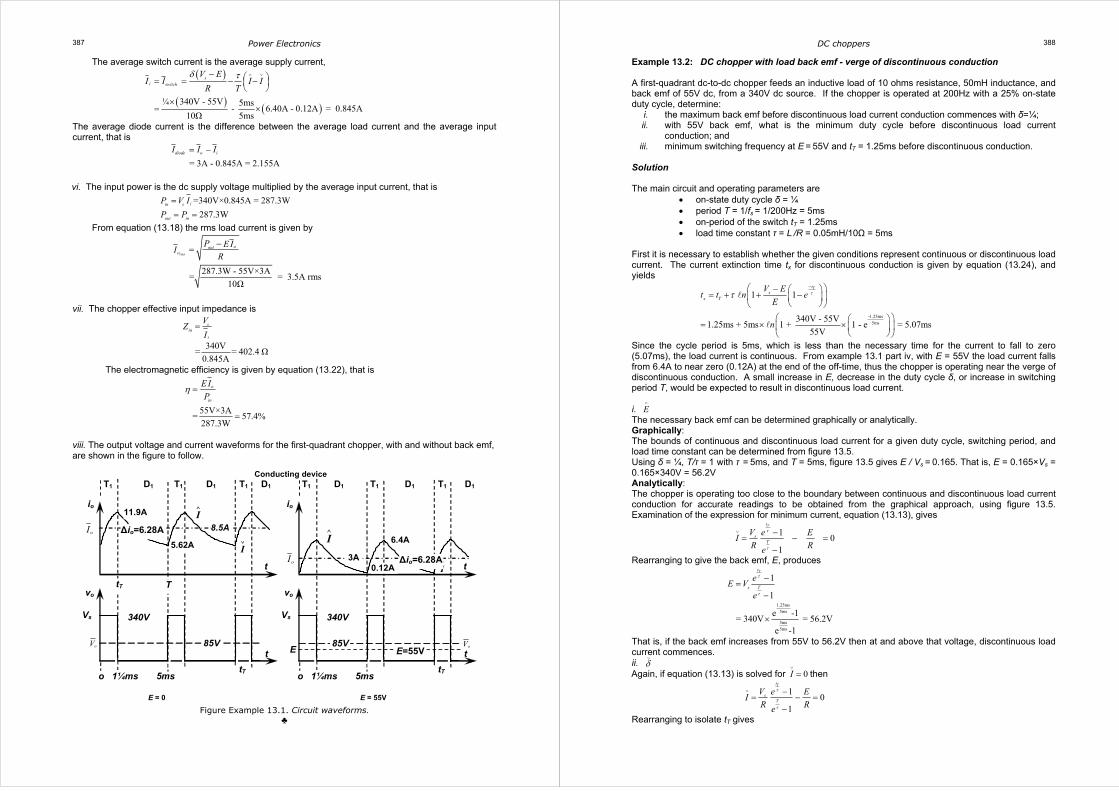
E = 0 E = 55V
I∨
Conducting device T1 D1 T1 D1 T1 D1 T1 D1 T1 D1 T1 D1
I∧
tT
t
io
Vs 340V
o 1¼ms 5ms
t
vo
tT
t
io
Vs 340V
o 1¼ms 5ms
t
vo
I∧
I∨
E E=55V
T tT
oI
oI
11.9A
8.5A
5.62A 6.4A
0.12A 3A
oV oV85V 85V
∆io=6.28A
∆io=6.28A
The average switch current is the average supply current,
( )
( ) ( )¼ 340V - 55V 5ms
- 6.40A - 0.12A = 0.845A10Ω 5ms
si switch
V EII I I
R T
δ τ ∧ ∨− = = − −
×= ×
The average diode current is the difference between the average load current and the average input current, that is
= 3A - 0.845A = 2.155A
diode o iI I I= −
vi. The input power is the dc supply voltage multiplied by the average input current, that is
=340V×0.845A = 287.3W
287.3Wiin s
out in
P V I
P P
== =
From equation (13.18) the rms load current is given by
287.3W - 55V×3A
= = 3.5A rms10Ω
rms
oouto
P E II
R
−=
vii. The chopper effective input impedance is
340V
= = 402.4 Ω0.845A
sin
i
VZ
I=
The electromagnetic efficiency is given by equation (13.22), that is
55V×3A
= 57.4%287.3W
o
in
E I
Pη =
=
viii. The output voltage and current waveforms for the first-quadrant chopper, with and without back emf, are shown in the figure to follow.
Figure Example 13.1. Circuit waveforms.
♣
DC choppers 388
Example 13.2: DC chopper with load back emf - verge of discontinuous conduction A first-quadrant dc-to-dc chopper feeds an inductive load of 10 ohms resistance, 50mH inductance, and back emf of 55V dc, from a 340V dc source. If the chopper is operated at 200Hz with a 25% on-state duty cycle, determine:
i. the maximum back emf before discontinuous load current conduction commences with δ=¼; ii. with 55V back emf, what is the minimum duty cycle before discontinuous load current
conduction; and iii. minimum switching frequency at E = 55V and tT = 1.25ms before discontinuous conduction.
Solution The main circuit and operating parameters are
• on-state duty cycle δ = ¼ • period T = 1/fs = 1/200Hz = 5ms • on-period of the switch tT = 1.25ms • load time constant τ = L /R = 0.05mH/10Ω = 5ms
First it is necessary to establish whether the given conditions represent continuous or discontinuous load current. The current extinction time tx for discontinuous conduction is given by equation (13.24), and yields
-1.25ms
5ms
1 1
340V - 55V1.25ms + 5ms 1 + 1 - e = 5.07ms
55V
Tts
x T
V Et t n e
E
n
ττ− − = + + −
= × ×
Since the cycle period is 5ms, which is less than the necessary time for the current to fall to zero (5.07ms), the load current is continuous. From example 13.1 part iv, with E = 55V the load current falls from 6.4A to near zero (0.12A) at the end of the off-time, thus the chopper is operating near the verge of discontinuous conduction. A small increase in E, decrease in the duty cycle δ, or increase in switching period T, would be expected to result in discontinuous load current. i. E
∧
The necessary back emf can be determined graphically or analytically. Graphically: The bounds of continuous and discontinuous load current for a given duty cycle, switching period, and load time constant can be determined from figure 13.5. Using δ = ¼, T/τ = 1 with τ = 5ms, and T = 5ms, figure 13.5 gives E / Vs = 0.165. That is, E = 0.165×Vs = 0.165×340V = 56.2V Analytically: The chopper is operating too close to the boundary between continuous and discontinuous load current conduction for accurate readings to be obtained from the graphical approach, using figure 13.5. Examination of the expression for minimum current, equation (13.13), gives
1
01
Tt
sT
V e EI
R Re
τ
τ
∨ −= − =
−
Rearranging to give the back emf, E, produces
1.25ms
5ms
5ms
5ms
1
1
e -1= 340V = 56.2V
e -1
Tt
Ts
eE V
e
τ
τ
−=
−
×
That is, if the back emf increases from 55V to 56.2V then at and above that voltage, discontinuous load current commences. ii. δ
∨
Again, if equation (13.13) is solved for 0I∨
= then
1
01
Tt
sT
V e EI
R Re
τ
τ
∨ −= − =
−
Rearranging to isolate tT gives
Power Electronics 389
5ms
5ms
1 1
55V= 5ms 1 + e - 1
340V
= 1.226ms
T
T
s
Et n e
V
n
ττ = + −
×
If the switch on-state period is reduced by 0.024ms, from 1.250ms to 1.226ms (δ = 24.52%), operation is then on the verge of discontinuous conduction. iii. T
∧
If the switching frequency is decreased such that T = tx, then the minimum period for discontinuous load current is given by equation (13.24). That is,
-1.25ms
5ms
1 1
340V - 55V1.25ms + 5ms 1 + 1 - e = 5.07ms
55V
Tts
x T
V Et T t n e
E
T n
ττ− − = = + + −
= × ×
Discontinuous conduction operation occurs if the period is increased by more than 0.07ms. In conclusion, for the given load, for continuous conduction to cease, the following operating conditions can be changed
• increase the back emf E from 55V to 56.2V • decrease the duty cycle δ from 25% to 24.52% (tT decreased from 1.25ms to 1.226ms) • increase the switching period T by 0.07ms, from 5ms to 5.07ms (from 200Hz to 197.2Hz), with
the switch on-time, tT, unchanged from 1.25ms. Appropriate simultaneous smaller changes in more than one parameter would suffice.
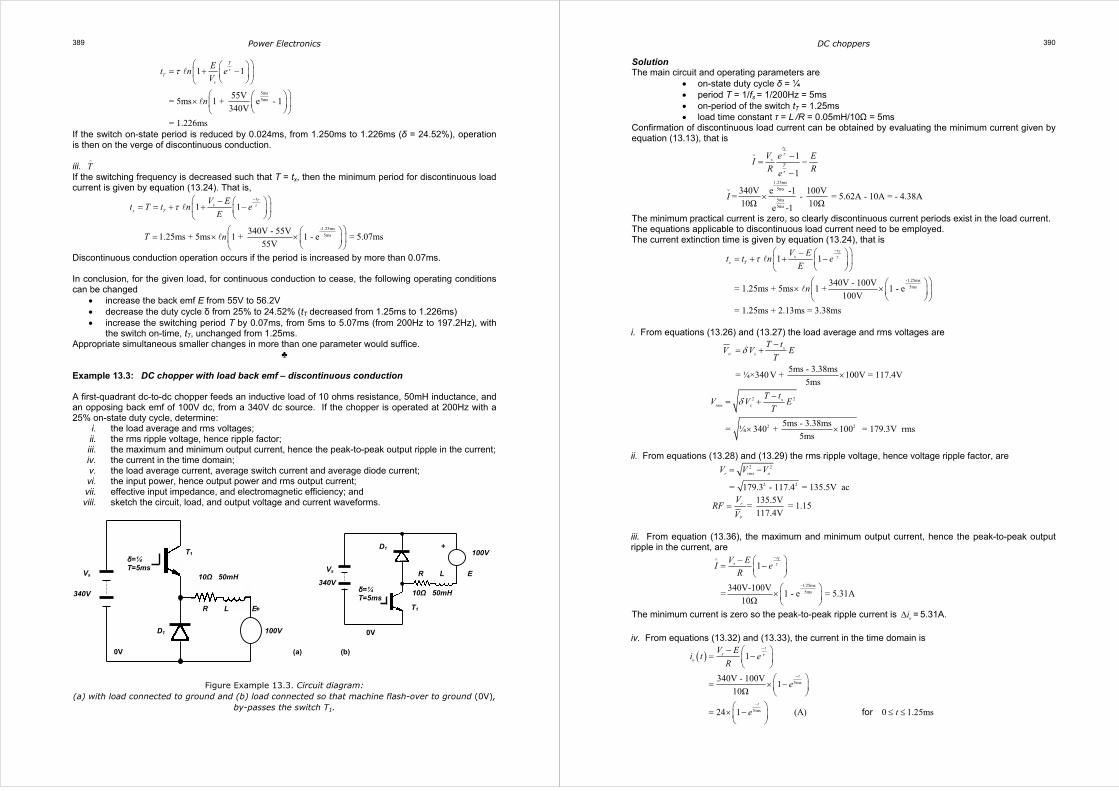
♣ Example 13.3: DC chopper with load back emf – discontinuous conduction A first-quadrant dc-to-dc chopper feeds an inductive load of 10 ohms resistance, 50mH inductance, and an opposing back emf of 100V dc, from a 340V dc source. If the chopper is operated at 200Hz with a 25% on-state duty cycle, determine:
i. the load average and rms voltages; ii. the rms ripple voltage, hence ripple factor; iii. the maximum and minimum output current, hence the peak-to-peak output ripple in the current; iv. the current in the time domain; v. the load average current, average switch current and average diode current; vi. the input power, hence output power and rms output current; vii. effective input impedance, and electromagnetic efficiency; and viii. sketch the circuit, load, and output voltage and current waveforms.
Figure Example 13.3. Circuit diagram: (a) with load connected to ground and (b) load connected so that machine flash-over to ground (0V),
by-passes the switch T1.
R L E
T1
10Ω 50mH
+
D1 100V
340V
Vs
δ=¼ T=5ms
R L E
T1
10Ω 50mH
+ D1 100V
340V
Vs
δ=¼ T=5ms
(a) (b)
0V
0V
DC choppers 390
Solution The main circuit and operating parameters are
• on-state duty cycle δ = ¼ • period T = 1/fs = 1/200Hz = 5ms • on-period of the switch tT = 1.25ms • load time constant τ = L /R = 0.05mH/10Ω = 5ms
Confirmation of discontinuous load current can be obtained by evaluating the minimum current given by equation (13.13), that is
1
1
Tt
sT
V e EI
R Re
τ
τ
∨ −= −
−
1.25ms
5ms
5ms
5ms
340V e -1 100V= - = 5.62A - 10A = - 4.38A
10Ω 10Ωe -1I∨
×
The minimum practical current is zero, so clearly discontinuous current periods exist in the load current. The equations applicable to discontinuous load current need to be employed. The current extinction time is given by equation (13.24), that is
-1.25ms
5ms
1 1
340V - 100V= 1.25ms + 5ms 1 + 1 - e
100V
= 1.25ms + 2.13ms = 3.38ms
Tts
x T
V Et t n e
E
n
ττ− − = + + −
× ×
i. From equations (13.26) and (13.27) the load average and rms voltages are
5ms - 3.38ms
= ¼×340V + 100V = 117.4V5ms
xo s
T tV V E
Tδ
−= +
×
2 2
2 25ms - 3.38ms= ¼ 340 + 100 = 179.3V rms
5ms
xrms s
T tV V E
Tδ −
= +
× ×
ii. From equations (13.28) and (13.29) the rms ripple voltage, hence voltage ripple factor, are
2 2
2 2= 179.3 - 117.4 = 135.5V ac
r rms oV V V= −
135.5V
= = 1.15117.4V
r
o
VRF
V=
iii. From equation (13.36), the maximum and minimum output current, hence the peak-to-peak output ripple in the current, are
-1.25ms
5ms
1
340V-100V= 1 - e = 5.31A
10Ω
TtsV E
I eR
τ−∧ − = −
×
The minimum current is zero so the peak-to-peak ripple current is oi∆ = 5.31A.
iv. From equations (13.32) and (13.33), the current in the time domain is
( )
5ms
5ms
1
340V - 100V1
10Ω
24 1 (A) 0 1.25ms
τ−
−
−
− = −
= × −
= × − ≤ ≤
for
ts
o
t
t
V Ei t e
R
e
e t
Power Electronics 391
( )
5ms 5ms
5ms
1
100V1 5.31
10Ω
15.31 10 (A) 0 2.13ms
τ τ− −∧
− −
−
= − − +
= − × − +
= × − ≤ ≤for
t t
o
t t
t
Ei t e I e
R
e e
e t
( ) 0 3.38ms 5ms= ≤ ≤foroi t t
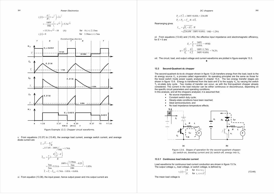
Figure Example 13.3. Chopper circuit waveforms. v. From equations (13.37) to (13.40), the average load current, average switch current, and average diode current are
117.4V - 100V= = 1.74A10Ω
ooV EI
R−=
3.38ms
100V - 0.255ms 5ms
×5.31A - = 1.05A5ms 10Ω
x
diode
tETI I
T R
δτ ∧
− = −
× =
=1.74A - 1.05A = 0.69Ai o diodeI I I= −
vi. From equation (13.38), the input power, hence output power and rms output current are
C o n d u c t in g d e v ic e T D T D T
v o
i o
i D
i T
v T
0 1 .2 5 3 .3 7 5 6 .2 5 8 . 3 7 1 0 1 1 . 2 5 t im e (m s ) t
5 .3 1 A
V s = 3 4 0 V
E = 1 0 0 V
2 4 0 VV s = 3 4 0 V
5 .3 1 A
5 .3 1 A
117.4V E=100VoV
oI
1.05A DI
0.69A TI
1.74A
DC choppers 392
2
340V×0.69A = 234.6Wiin s
oin out o rms
P V I
P P I R EI
= =
= = +
Rearranging gives
/
= 234.6W - 100V×0.69A / 10Ω = 1.29A
rmsoo inI P REI= −
vii. From equations (13.42) and (13.43), the effective input impedance and electromagnetic efficiency, for E > 0 are
340V
= 493Ω0.69A
sin
i
VZ
I= =
100V×1.74A
= = 74.2%340V×0.69A
oo
in is
E I E I
P V Iη = =
viii. The circuit, load, and output voltage and current waveforms are plotted in figure example 13.3.
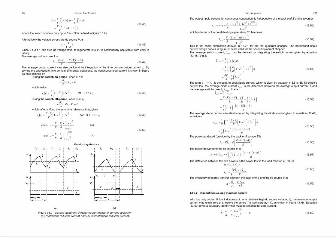
♣ 13.3 Second-Quadrant dc chopper The second-quadrant dc-to-dc chopper shown in figure 13.2b transfers energy from the load, back to the dc energy source Vs, a process called regeneration. Its operating principles are the same as those for the boost switch mode power supply analysed in chapter 15.4. The two energy transfer stages are shown in figure 13.6. Energy is transferred from the back emf E to the supply Vs, by varying the switch T2 on-state duty cycle. Two modes of transfer can occur, as with the first-quadrant chopper already considered. The current in the load inductor can be either continuous or discontinuous, depending on the specific circuit parameters and operating conditions. In this analysis, and all the choppers analysed, it is assumed that:
• No source impedance; • Constant switch duty cycle; • Steady-state conditions have been reached; • Ideal semiconductors; and • No load impedance temperature effects.
Figure 13.6. Stages of operation for the second-quadrant chopper: (a) switch-on, boosting current and (b) switch-off, energy into Vs.
13.3.1 Continuous load inductor current Load waveforms for continuous load current conduction are shown in figure 13.7a. The output voltage vo, load voltage, or switch voltage, is defined by
( )0 0
≤ ≤ = ≤ ≤
for
forT
o
s T
t tv t
V t t T (13.44)
The mean load voltage is
(a) (b)
R L
R L
Vs
T2
D2 ioff
ion
+ +
E E vo
io io
Vo
Io
II
Power Electronics 393
( )
( )
0
1 1
1
T
T T
o o st
Ts s
V v t dt V dtT TT t
V VT
δ
= =
−= = −
∫ ∫ (13.45)
where the switch on-state duty cycle δ = tT /T is defined in figure 13.7a. Alternatively the voltage across the dc source Vs is
1
1osV V
δ=
− (13.46)
Since 0 ≤ δ ≤ 1, the step-up voltage ratio, to regenerate into Vs, is continuously adjustable from unity to infinity. The average output current is
( )1o s
o
E VE VI
R R
δ− −−= = (13.47)
The average output current can also be found by integration of the time domain output current io. By solving the appropriate time domain differential equations, the continuous load current io shown in figure 13.7a is defined by
During the switch on-period, when vo = 0
oo
diL Ri Edt
+ =
which yields
( ) 1 0τ τ− −∨ = − + ≤ ≤
for
t t
o T
Ei t e I e t t
R (13.48)
During the switch off-period, when vo = Vs
oo s
diL Ri V Edt
+ + =
which, after shifting the zero time reference to tT, gives
( ) 1 0τ τ− −∧− = − + ≤ ≤ −
for
t ts
o T
E Vi t e I e t T t
R (13.49)
where (A)1
1and (A)
1
T
T
t T
sT
T t
sT
E V e eI
R R e
E V eI
R R e
τ τ
τ
τ
τ
− −
∧
−
− +
∨
−
−= −
−
−= −
−
(13.50)
Figure 13.7. Second-quadrant chopper output modes of current operation: (a) continuous inductor current and (b) discontinuous inductor current.
t
t
T tT
io
Vs
vo
E E
I∧
t
t
T
I∨
vo
io
tT
I∧
I∨
Vs
I∧ I
∧
I∧
tx
(a) (b)
Conducting devices
T2 D2 T2 D2 T2 D2 T2 D2 T2 D2
oV oV
oI
oI
DC choppers 394
The output ripple current, for continuous conduction, is independent of the back emf E and is given by
(1 ) ( )
1
T TT t T t
sTp p
V e e eI I I
R e
τ τ τ
τ
− − − +
∧ ∨
−−
+ − += − =
− (13.51)
which in terms of the on-state duty cycle, δ = tT / T, becomes
(1 ) (1 )
1
T T
sTp p
V e eI
R e
δτ τ
τ
− −
−−
− +=
− (13.52)
This is the same expression derived in 13.2.1 for the first-quadrant chopper. The normalised ripple current design curves in figure 13.3 are valid for the second-quadrant chopper. The average switch current, switchI , can be derived by integrating the switch current given by equation (13.48), that is
( )
0
0
1
11
T
T
t
switch o
t tt
I i t dtT
Ee I e dt
T R
EI I
R T
τ τ
δ τ
− −∨
∧ ∨
=
= − +
= − −
∫
∫ (13.53)
The term p pII I∧ ∨
−− = is the peak-to-peak ripple current, which is given by equation (13.51). By Kirchhoff’s current law, the average diode current diodeI is the difference between the average output current oI and the average switch current, switchI , that is
( )
( )( )
1
1
switchdiode o
s
s
I I I
E V EI I
R R T
V EI I
T R
δ δ τ
δτ
∧ ∨
∧ ∨
= −
− − = − + −
− − = − −
(13.54)
The average diode current can also be found by integrating the diode current given in equation (13.49), as follows
( )( )
0
11
1
Tt tT t
sdiode
s
E VI e I e dt
T R
V EI I
T R
τ τ
δτ
− −∧−
∧ ∨
− = − + − − = − −
∫ (13.55)
The power produced (provide) by the back emf source E is
( )1s
oE
E VP EI E
R
δ − −= =
(13.56)
The power delivered to the dc source Vs is
( )( )1s
V s sdiodes
V EP V I V I I
T R
δτ ∧ ∨ − − = = − −
(13.57)
The difference between the two powers is the power lost in the load resistor, R, that is
2
rms
rms
E V os
o s diodeo
P P I R
EI V II
R
= +
−=
(13.58)
The efficiency of energy transfer between the back emf E and the dc source Vs is
sdiodeV s
oE
P V I
P EIη = = (13.59)
13.3.2 Discontinuous load inductor current With low duty cycles, δ, low inductance, L, or a relatively high dc source voltage, Vs, the minimum output current may reach zero at tx, before the period T is complete (tx < T), as shown in figure 13.7b. Equation (13.50) gives a boundary identity that must be satisfied for zero current,
1
01
TT t
sT
E V eI
R R e
τ
τ
−
∨
−
−= − =
− (13.60)
Power Electronics 395
That is
1
1
TT t
T
s
E e
V e
τ
τ
− +
−
−=
− (13.61)
Alternatively, the time domain equations (13.48) and (13.49) can be used, such that ∨
I = 0. An expression for the extinction time tx can be found by substituting t = tT into equation (13.48). The resulting expression for I
∧ is then substituted into equation (13.49) which is set to zero. Isolating the time variable,
which becomes tx, yields
1
0 1 1
T
x xT
t
t tts
EI e
R
E V Ee e e
R R
τ
τ τ τ
−
− −−
= − − = − + −
which yields
1 1Tt
x T
s
Et t n e
V Eττ− = + + − −
(13.62)
This equation shows that x Tt t≥ . Load waveforms for discontinuous load current conduction are shown
in figure 13.7b. The output voltage vo, load voltage, or switch voltage, is defined by
( )0 0
≤ ≤ = ≤ ≤ ≤ ≤
for
for
for
T
o s T x
x
t t
v t V t t t
E t t T
(13.63)
The mean load voltage is
( ) ( )
0
1 1 x
T x
T t T
o o st t
V v t dt V dt E dtT T
= = +∫ ∫ ∫
( )
1x T x x xs s
xo s s
t t T t t tV E V E
T T T T
tV E V V E
T
δ
δ
− − = + = − + −
= − + −
(13.64)
where the switch on-state duty cycle δ = tT /T is defined in figure 13.7b. The average output current is
( )x
s soo
tV V EE V TI
R R
δ − −−= = (13.65)
The average output current can also be found by integration of the time domain output current io. By solving the appropriate time domain differential equations, the continuous load current io shown in figure 13.7a is defined by
During the switch on-period, when vo = 0
oo
diL Ri Edt
+ =
which yields
( ) 1 0τ− = − ≤ ≤
for
t
o T
Ei t e t t
R (13.66)
During the switch off-period, when vo = Vs
oo s
diL Ri V Edt
+ + =
which, after shifting the zero time reference to tT, gives
( ) 1 0τ τ− −∧− = − + ≤ ≤ −
for
t ts
o x T
E Vi t e I e t t t
R (13.67)
1 (A)
0 (A)
τ−∧
∨
= −
=
where
and
TtEI e
R
I
(13.68)
After tx, vo(t) = E and the load current is zero, that is ( ) 0= ≤ ≤foro xi t t t T (13.69)
DC choppers 396
The output ripple current, for discontinuous conduction, is dependent of the back emf E and is given by equation (13.68),
1Tt
p p
EI I e
Rτ−∧
−
= = −
(13.70)
The average switch current, switchI , can be derived by integrating the switch current given by equation (13.66), that is
( )
0
0
1
11
T
T
t
switch o
tt
I i t dtT
Ee dt
T R
EI
R T
τ
δ τ
−
∧
=
= −
= −
∫
∫ (13.71)
The term p pII∧
−= is the peak-to-peak ripple current, which is given by equation (13.70). By Kirchhoff’s current law, the average diode current diodeI is the difference between the average output current oI and the average switch current, switchI , that is
( )
( )
switchdiode o
xs s
xs
I I I
tV V E ET I
R R Tt
V ET
IT R
δ δ τ
δτ
∧
∧
= −
− −= − +
− − = −
(13.72)
The average diode current can also be found by integrating the diode current given in equation (13.67), as follows
( )
0
11
x Tt tt t
sdiode
xs
E VI e I e dt
T R
tV E
TI
T R
τ τ
δτ
− −∧−
∧
− = − +
− − = −
∫ (13.73)
The power produced by the back emf source E is
oEP E I= (13.74)
The power delivered to the dc source Vs is
V s diodesP V I= (13.75)
Alternatively, the difference between the two powers is the power lost in the load resistor, R, that is
2
rms
rms
E V os
o s diodeo
P P I R
EI V II
R
= +
−=
(13.76)
The efficiency of energy transfer between the back emf and the dc source is
sdiodeV s
oE
P V I
P EIη = = (13.77)
Example 13.4: Second-quadrant DC chopper – continuous inductor current A dc-to-dc chopper capable of second-quadrant operation is used in a 200V dc battery electric vehicle. The machine armature has 1 ohm resistance in series with 1mH inductance.
i. The machine is used for regenerative braking. At a constant speed downhill, the back emf is 150V, which results in a 10A braking current. What is the switch on-state duty cycle if the machine is delivering continuous output current? What is the minimum chopping frequency for these conditions?
ii. At this speed, (that is, E = 150V), determine the minimum duty cycle for continuous inductor current, if the switching frequency is 1kHz. What is the average braking current at the critical duty cycle? What is the regenerating efficiency and the rms machine output current?
iii. If the chopping frequency is increased to 5kHz, at the same speed, (that is, E = 150V), what is the critical duty cycle and the corresponding average dc machine current?
Power Electronics 397
Solution The main circuit operating parameters are
• Vs = 200V • E = 150V • load time constant τ = L /R = 1mH/1Ω = 1ms
Figure Example 13.4. Circuit diagram and waveforms. i. The relationship between the dc supply Vs and the dc machine back emf E is given by equation
(13.47), that is
( )
( )
1
150V - 200V 1 - δ10A =
1Ω
= 0.3 30% and = 140V
δ
δ
− −−= =
×
≡
that is
o so
o
E VE VI
R R
V
The expression for the average dc machine output current is based on continuous armature inductance current. Therefore the switching period must be shorter than the time tx predicted by equation (13.62) for the current to reach zero, before the next switch on-period. That is, for tx = T and δ = 0.3
1 1Tt
x T
s
Et t n e
V Eττ− = + + − −
This simplifies to
0.3
1ms
0.7 0.3
1ms 150V1 0.3 1 1
200V - 150V
4 3
T
T T
n eT
e e
−
−
= + + −
= −
Iteratively solving this transcendental equation gives T = 0.4945ms. That is the switching frequency must be greater than fs =1/T = 2.022kHz, else machine output current discontinuities occur, and equation (13.47) is invalid. The switching frequency can be reduced if the on-state duty cycle is increased as in the next part of this example. ii. The operational boundary condition giving by equation (13.61), using T=1/ fs =1/1kHz = 1ms, yields
( )-1 ×1ms
1ms
-1ms
1ms
1
1
150V 1 - e
200V 1 - e
TT t
T
s
E e
V e
τ
τ
δ
− +
−
−=
−
=
Solving gives δ = 0.357. That is, the on-state duty cycle must be at least 35.7% for continuous machine output current at a switching frequency of 1kHz.
R L
Vs = 200V
T2
D2
1Ω 1mH +150V
io
I∨
vo
io
I∧
I∨
Vs =200V
t
t
T tT
Conducting devices
T2 D2 T2 D2 T2 D2
=0 =0
vo
io
II
E=150V
oI
oV
DC choppers 398
For continuous inductor current, the average output current is given by equation (13.47), that is
( )
( )
1
150V - 200V× 1 - 0.357150V - = = = 21.4A
1Ω 1Ω
=150V - 21.4A×1Ω = 128.6V
o so
o
o
E VE VI
R R
V
V
δ− −−= =
The average machine output current of 21.4A is split between the switch and the diode (which is in series with Vs). The diode current is given by equation (13.54)
( )( )1
switchdiode o
s
I I I
V EI I
T R
δτ ∧ ∨
= −
− − = − −
The minimum output current is zero while the maximum is given by equation (13.68).
-0.357×1ms
1ms150V
1 1 - e = 45.0A1Ω
TtEI e
Rτ−∧ = − = ×
Substituting into the equation for the average diode current gives
( ) ( ) ( )ms
ms
200V - 150V 1 - 0.3571= 45.0A - 0A - = 12.85A
1 1ΩdiodeI
××
The power delivered by the dc machine back emf E is = 150V×21.4A = 3210WoEP EI=
while the power delivered to the 200V battery source Vs is
200V×12.85A = 2570Ws
diodeV sP V I= =
The regeneration transfer efficiency is
2570W
= = 80.1%3210W
sV
E
P
Pη =
The energy generated deficit, 640W (3210W - 2570W)), is lost in the armature resistance, as I2R heat dissipation. The output rms current is
640W
= = 25.3A rms1Ωrmso
PI
R=
iii. At an increased switching frequency of 5kHz, the duty cycle would be expected to be much lower
than the 35.7% as at 1kHz. The operational boundary between continuous and discontinuous armature inductor current is given by equation (13.61), that is
( )-1+δ 0.2ms
1ms
-0.2ms
1ms
1
1
150V 1 - e=
200V 1 - e
TT t
T
s
E e
V e
τ
τ
− +
−
×
−=
−
which yields δ = 26.9% . The machine average output current is given by equation (13.47)
( )
( )
1
150V - 200V× 1 - 0.269150V= 3.8A
1 1Ω
o so
o
E VE VI
R R
V
δ− −−= =
−= =
Ω
such that the average output voltage oV is 146.2V.
♣
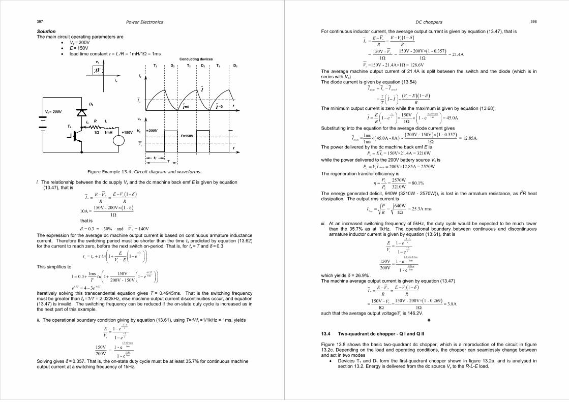
13.4 Two-quadrant dc chopper - Q I and Q II Figure 13.8 shows the basic two-quadrant dc chopper, which is a reproduction of the circuit in figure 13.2c. Depending on the load and operating conditions, the chopper can seamlessly change between and act in two modes
• Devices T1 and D1 form the first-quadrant chopper shown in figure 13.2a, and is analysed in section 13.2. Energy is delivered from the dc source Vs to the R-L-E load.
Power Electronics 399
• Devices T2 and D2 form the second-quadrant chopper shown in figure 13.2b, which is analysed in section 13.3. Energy is delivered from the generating load dc source E, to the dc source Vs.
The two independent choppers can be readily combined as shown in figure 13.8a. The average output voltage oV and the instantaneous output voltage vo are never negative, whilst the average source current of Vs can be positive (Quadrant I) or negative (Quadrant II). If the two choppers are controlled to operate independently, with the constraint that T1 and T2 do not conduct simultaneously, then the analysis in sections 13.2 and 13.3 are valid. Alternately, it is not uncommon the unify the operation of the two choppers, as follows.
Figure 13.8. Two-quadrant (I and II) dc chopper circuit where vo > 0: (a) basic two-quadrant dc chopper; (b) operation and waveforms for quadrant I; and (c) operation
and waveforms for quadrant II, regeneration into Vs.
0
0
0o
I
I
I
∨
<
<
<
(b) (c)
Vs
I∨
t
vo
io
is
t
t
Vs
E
I∨
I∨
I∧
I∧
oV
oV
oI
sIsI
E
I∧
I∧
t
t
t
o
o
o
o
o
o
Conducting devices D2 T1 D1 T2 D2 T1 D2 T2 D2 T2
oI
I∨
tT T
txT txD
tT T
on T1
vo
Vs
R L + E
D1
off
D2
vo
Vs
R L + E
T2
on
off
I
Vo
Io
Vo
Io
II
T1 D2
vo
Vs
R L + E
Q I io
Q II io
T2 D1
(a)
Vo
Io
I II
0
0
0o
I
I
I
∨
>
<
>
DC choppers 400
If the chopper is operated such that the switches T1 and T2 act in a complementary manner, that is either T1 or T2 is on, then some of the independent flexibility offered by each chopper is lost. Essentially the consequence of complementary switch operation is that no extended zero current periods exist in the output, as shown in figures 13.8a and b. Thus the equations describing the features of the first-quadrant chopper in section 13.2.1, for continuous load current, are applicable to this chopper, with slight modification to account for the fact that both the minimum and maximum currents can be negative. The analysis for continuous inductor current in section 13.2 is valid, but the minimum current is not restricted to zero. Consequently four possible output modes can occur, depending on the relative polarity of the maximum and minimum currents shown in figure 18.8b and c. i. I
∨> 0, I
∧> 0 and oI > 0
When the minimum current (hence average output current) is greater than zero, the chopper is active in the first-quadrant. Typical output voltage and current waveforms are shown in figure 13.3a. The switch T2 and diode D2 do not conduct during any portion of the operating period.
ii. I∨
< 0, I∧
> 0 and oI > 0 When the minimum current is negative but the maximum positive current is larger in absolute magnitude, then for a highly inductive load, the average output current is greater than zero, and the chopper operates in the first-quadrant. If the load is not highly inductive the boundary is determined by the average output current oI > 0. The various circuit waveforms are shown in figure 13.8b.
iii. I∨
< 0, I∧
> 0 and oI < 0 For a highly inductive load, if the magnitude of the negative peak is greater than the positive maximum, the average is less than zero and the chopper is operating in the regenerative mode, quadrant II. If the load is not highly inductive the boundary is determined by the average output current oI < 0.
iv. I∨
< 0, I∧
< 0 and oI < 0 When the maximum current and the average current are both negative, the chopper is operational in the second-quadrant. Since the load current never goes positive, switch T1 and diode D1 never conduct, as shown in figure 13.8c.
In all cases the average output voltage is solely determined by the switch T1 on-time duty cycle, since when this switch is turned on the supply Vs is impressed across the load, independent of the direction of the load current. When io > 0, switch T1 conducts while if io < 0, the diode in parallel to switch T1, namely D1 conducts, clamping the load to Vs. The output voltage, which is independent of the load, is described by
( ) 0
0
≤ ≤ = ≤ ≤
for
fors T
o
T
V t tv t
t t T (13.78)
Thus
0
1 TtT
o s s s
tV V dt V V
T Tδ= = =∫ (13.79)
The rms output voltage is also determined solely by the duty cycle,
½
2
0
1 Tt
rms s
s
V V dtT
Vδ
=
=
∫ (13.80)
The output ac ripple voltage, hence voltage ripple factor are given by equations (13.3) and (13.5), and are independent of the load:
( )2 2 1r rms o sV V V V δ δ= − = − (13.81)
and
1 1
1δ
δ δ−
= = − =r
o
VRF
V (13.82)
The Fourier series for the load voltage can be used to determine the load current at each harmonic frequency as described by equations (13.6) to (13.10). The time domain differential equations from section 13.2.1 are also valid, where there is no zero restriction on the minimum load current value.
In a positive voltage loop, when vo(t) = Vs and Vs is impressed across the load, the load circuit condition is described by
( ) 1 0τ τ− −∨− = − + ≤ ≤
for
t ts
o T
V Ei t e I e t t
R (13.83)
Power Electronics 401
During the switch off-period, when vo = 0, forming a zero voltage loop
( ) 1 for 0t t
o T
Ei t e I e t T t
Rτ τ− −∧ = − − + ≤ ≤ −
(13.84)
where
1(A)
1
1(A)
1
τ
τ
τ
τ
−
∧
−
∨
−= −
−
−= −
−
where
and
T
T
t
sT
t
sT
V e EI
R Re
V e EI
R Re
(13.85)
The peak-to-peak ripple current is independent of E,
( )1
(1 ) (1 )
1
TT
sTp p
V e eI
R e
δδτ τ
τ
− −−
−−
− −=
− (13.86)
The average output current, oI , may be positive or negative and is given by
( ) ( )
( )
0
1
(A)
T o
o o
s
V Ei t dtI RT
V ER
δ
−= =
−=
∫ (13.87)
The direction of the net power flow between E and Vs determines the chopper operating quadrant. If oV > E then average power flow is to the load, as shown in figure 13.8b, while if oV < E, the average
power flow is back into the source Vs, as shown in figure 13.8c.
2
rms oss oV I R EII = ± + (13.88)
Thus the sign of oI determines the direction of net power flow, hence quadrant of operation. Calculation of individual device average currents in the time domain is complicated by the fact that the energy may flow between the dc source Vs and the load via the switch T1 (energy to the load) or diode D2 (energy from the load). It is therefore necessary to ascertain the zero current crossover time, when I
∧and I
∨have opposite signs, which will then specify the necessary bounds of integration.
Equations (13.83) and (13.84) are equated to zero and solved for the time at zero crossover, txT and txD, respectively, shown in figure 13.8b.
1 0
1
τ
τ
∨ = − = −
= + =
with respect to
with respect to
xT
s
xD T
I Rt n t
V E
IRt n t t
E
(13.89)
The necessary integration for each device can then be determined with the aid of the device conduction information in the parts of figure 13.8 and Table 13.1.
Table 13.1 Device average current ratings
Device and integration bounds, a to b 0, 0I I∧ ∨
> > 0, 0I I∧ ∨
> < 0, 0I I∧ ∨
< <
1
11 τ τ
− −∨− = − + ∫
t tbs
Ta
V EI e I e dt
T R 0 to Tt toxT Tt t 0 0to
1 0
11 τ τ
− −∨− = − + ∫
t tbs
D
V EI e I e dt
T R 0 0to 0 to xTt 0 to Tt
2
11 τ τ
− −∧ = − − + ∫
t tb
Ta
EI e I e dt
T R 0 0to -toxD Tt T t 0 -to TT t
2 0
11 τ τ
− −∧ = − − + ∫
t tb
D
EI e I e dt
T R 0 -to TT t 0 to xDt 0 0to
DC choppers 402
T1 D2
vo
Vs=340V
δ=¼ T=5ms
T2 D1
10Ω 50mH +100V
δ=¾ T=5ms
R L +E
vo
io
I
II
The electromagnetic energy transfer efficiency is determined from
> 0
< 0
η
η
=
=
for
for
oo
is
iso
o
EII
V I
V II
EI
(13.90)
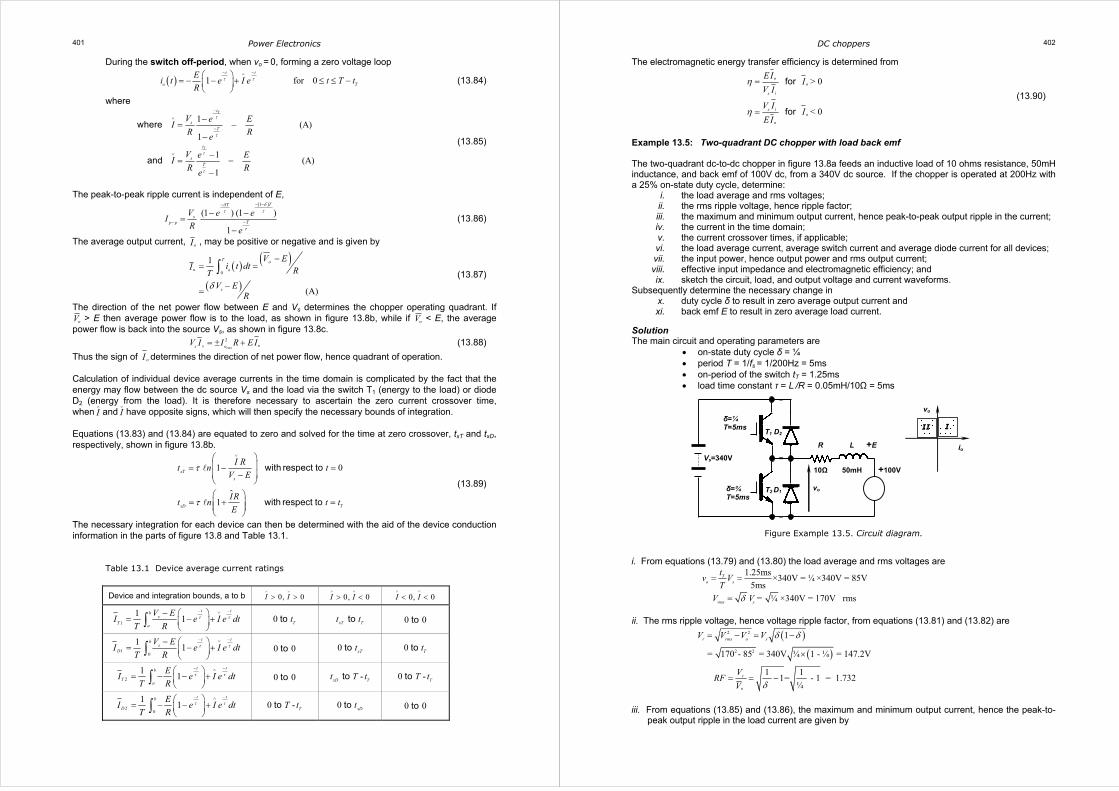
Example 13.5: Two-quadrant DC chopper with load back emf The two-quadrant dc-to-dc chopper in figure 13.8a feeds an inductive load of 10 ohms resistance, 50mH inductance, and back emf of 100V dc, from a 340V dc source. If the chopper is operated at 200Hz with a 25% on-state duty cycle, determine:
i. the load average and rms voltages; ii. the rms ripple voltage, hence ripple factor; iii. the maximum and minimum output current, hence peak-to-peak output ripple in the current; iv. the current in the time domain; v. the current crossover times, if applicable; vi. the load average current, average switch current and average diode current for all devices; vii. the input power, hence output power and rms output current; viii. effective input impedance and electromagnetic efficiency; and ix. sketch the circuit, load, and output voltage and current waveforms.
Subsequently determine the necessary change in x. duty cycle δ to result in zero average output current and xi. back emf E to result in zero average load current.
Solution The main circuit and operating parameters are
• on-state duty cycle δ = ¼ • period T = 1/fs = 1/200Hz = 5ms • on-period of the switch tT = 1.25ms • load time constant τ = L /R = 0.05mH/10Ω = 5ms
Figure Example 13.5. Circuit diagram.
i. From equations (13.79) and (13.80) the load average and rms voltages are
1.25ms
×340V = ¼ ×340V = 85V5ms
To s
tv V
T= =
= ¼ ×340V = 170V rmsrms sV Vδ= ii. The rms ripple voltage, hence voltage ripple factor, from equations (13.81) and (13.82) are
( )
( )
2 2
2 2
1
= 170 - 85 = 340V ¼ 1 - ¼ = 147.2V
r rms o sV V V V δ δ= − = −
×
1 1
1= - 1 = 1.732¼
r
o
VRF
V δ= = −
iii. From equations (13.85) and (13.86), the maximum and minimum output current, hence the peak-to-
peak output ripple in the load current are given by

Power Electronics 403
-1.25ms5ms
-5ms5ms
1.25ms5ms
5ms5ms
1 340V 1 - e 100V= × - = 1.90A
10Ω 10Ω1 1 - e
1 340V e - 1 100V= × - = - 4.38A
10Ω 10Ω1 e - 1
τ
τ
τ
τ
∧
∨
−
−
−= −
−
−= −
−
T
s
T
s
t
T
t
T
V e EI
R Re
V e EI
R Re
The peak-to-peak ripple current is therefore oi∆ = 1.90A - - 4.38A = 6.28A p-p.
iv. The current in the time domain is given by equations (13.83) and (13.84)
( )- -
5ms 5ms
- -5 5ms
-5ms
1
340V-100V= × 1- - 4.38×
10Ω
= 24× 1- - 4.38×
= 24 - 28.38 0 1.25ms
τ τ− −∨− = − +
× ≤ ≤for
t ts
o
t t
t tms
t
V Ei t e I e
R
e e
e e
e t
( )
5ms 5ms
5ms 5ms
5ms
1
1001 1.90
10
10 1 1.90
10 11.90 0 3.75ms
τ τ− −∧
− −
− −
−
= − − +
= − × − + × Ω = − × − + ×
= − + × ≤ ≤for
t t
o
t t
t t
t
Ei t e I e
R
Ve e
e e
e t
v. Since the maximum current is greater than zero (1.9A) and the minimum is less that zero (- 4.38A), the current crosses zero during the switch on-time and off-time. The time domain equations for the load current are solved for zero to give the cross over times txT and txD, as given by equation (13.89), or solved from the time domain output current equations as follows. During the switch on-time
( )
-5ms 24 - 28.38 0 0 1.25ms
28.38= 5ms× = 0.838ms
24
= × = ≤ = ≤whereo xT
xT
t
i t e t t
t n
During the switch off-time
( ) 5ms10 11.90 0 0 3.75ms
11.90=5ms× = 0.870ms
10(1.250ms + 0.870ms = 2.12ms )
−
= − + × = ≤ = ≤
1
where
with respect to switch T turn - on
o xD
xD
t
i t e t t
t n
vi. The load average current, average switch current, and average diode current for all devices;
( ) ( )
( )85V - 100V= -1.5A10Ω
o so
V E V EI R R
δ− −= =
When the output current crosses zero current, the conducting device changes. Table 13.1 gives the necessary current equations and integration bounds for the condition 0, 0I I
∧ ∨
> < . Table 13.1 shows that all four semiconductors are involved in the output current cycle.
1
1.25ms
0.838ms
-5ms
11
124 - 28.38 0.081A
5ms
τ τ∨− −− = − +
= × =
∫
∫
T
xT
ts
Tt
t t
t
V EI e I e dt
T R
e dt
DC choppers 404
1 0
- 0.84ms5ms
0
11
124 - 28.38 0.357A
5ms
τ τ− −∨− = − +
= × = −
∫
∫
xTt tt
sD
t
V EI e I e dt
T R
e dt
-
2
3.75ms5ms
0870ms
11
110 11.90 1.382A
5ms
τ τ− −∧
−
= − − +
= − + × = −
∫
∫
T
xD
t tT t
Tt
t
EI e I e dt
T R
e dt
2 0
0.8705ms
0
11
110 11.90 0.160A
5ms
τ τ− −∧
−
= − − +
= − + × =
∫
∫
xDt tt
D
tms
EI e I e dt
T R
e dt
Check 1 1 2 2 - 1.5A + 0.080A - 0.357A - 1.382A + 0.160A = 0o T D T DI I I I I+ + + + = vii. The input power, hence output power and rms output current;
( )
( )1 1
340V× 0.080A - 0.357A = -95.2W, ( )
= = = +
= charging
si T Din V s s
s
P P V I V I I
V
( )100V -1.5A = -150W, 150Woout EP P EI= = = × that is generating From
2
150W - 92.5W2.34A rms
10Ω
rms
rms
os s o
out ino
V I I R EI
P PI
R
= +
−= = =
Figure Example 13.5. Circuit waveforms
I∨
I∧
t
t
t
1.9A
vo
io
is
-4.38A
I∧
txD oI -1.5A
340V
o
E 100V
oV 85V
-0.28A sI
I∨
o
o
Conducting devices D2 T1 D1 T2 D2 T1 D1 T2
tT T
txT
-4.38A
1.9A
=1.25ms =5ms
=0.383ms
2.12ms
=0.87ms
Power Electronics 405
viii. Since the average output current is negative, energy is being transferred from the back emf E to the dc voltage source Vs, the electromagnetic efficiency of conversion is given by
< 0
95.2W= = 63.5%
150W
η = foriso
o
V II
EI
The effective input impedance is
1 1
340V= -1214Ω
0.080A - 0.357As s
ini T D
V VZ
I I I= = =
+
ix. The circuit, load, and output voltage and current waveforms are sketched in the figure for example
13.5. x. Duty cycle δ to result in zero average output current can be determined from the expression for the
average output current, equation (13.87), that is
0so
V EI
R
δ −= =
that is
100V
= 29.4%340Vs
E
Vδ = =
xi. As in part x, the average load current equation can be rearranged to give the back emf E that results
in zero average load current
0so
V EI
R
δ −= =
that is ¼×340V = 85VsE Vδ= =
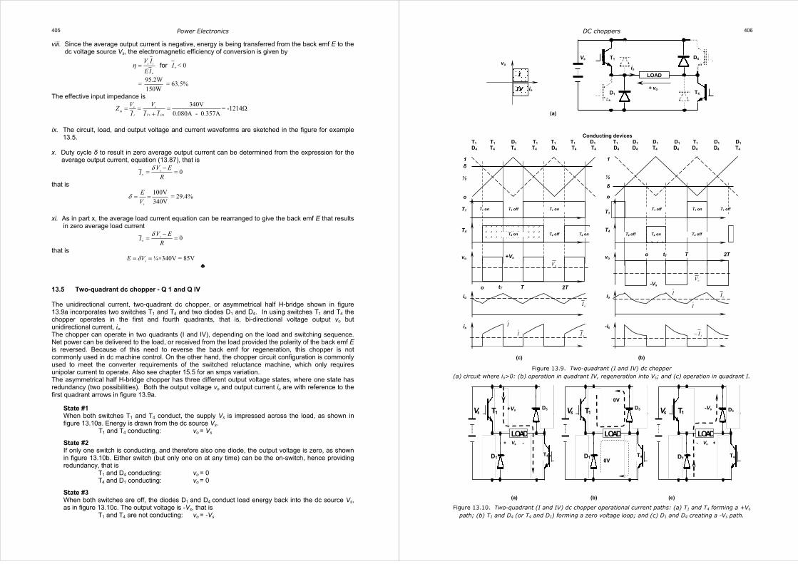
♣ 13.5 Two-quadrant dc chopper - Q 1 and Q IV The unidirectional current, two-quadrant dc chopper, or asymmetrical half H-bridge shown in figure 13.9a incorporates two switches T1 and T4 and two diodes D1 and D4. In using switches T1 and T4 the chopper operates in the first and fourth quadrants, that is, bi-directional voltage output vo but unidirectional current, io. The chopper can operate in two quadrants (I and IV), depending on the load and switching sequence. Net power can be delivered to the load, or received from the load provided the polarity of the back emf E is reversed. Because of this need to reverse the back emf for regeneration, this chopper is not commonly used in dc machine control. On the other hand, the chopper circuit configuration is commonly used to meet the converter requirements of the switched reluctance machine, which only requires unipolar current to operate. Also see chapter 15.5 for an smps variation. The asymmetrical half H-bridge chopper has three different output voltage states, where one state has redundancy (two possibilities). Both the output voltage vo and output current io are with reference to the first quadrant arrows in figure 13.9a.
State #1 When both switches T1 and T4 conduct, the supply Vs is impressed across the load, as shown in figure 13.10a. Energy is drawn from the dc source Vs.
T1 and T4 conducting: vo = Vs
State #2 If only one switch is conducting, and therefore also one diode, the output voltage is zero, as shown in figure 13.10b. Either switch (but only one on at any time) can be the on-switch, hence providing redundancy, that is
T1 and D4 conducting: vo = 0 T4 and D1 conducting: vo = 0
State #3 When both switches are off, the diodes D1 and D4 conduct load energy back into the dc source Vs, as in figure 13.10c. The output voltage is -Vs, that is
T1 and T4 are not conducting: vo = -Vs
DC choppers 406
Figure 13.9. Two-quadrant (I and IV) dc chopper (a) circuit where io>0: (b) operation in quadrant IV, regeneration into Vs; and (c) operation in quadrant I.
Figure 13.10. Two-quadrant (I and IV) dc chopper operational current paths: (a) T1 and T4 forming a +Vs
path; (b) T1 and D4 (or T4 and D1) forming a zero voltage loop; and (c) D1 and D4 creating a -Vs path.
oV
I∧
I∨
oV
I∨
I∧
1δ
½
o
T1
T4
vo
io
is
1
½
δ
o
T1
T4
vo
io
-is
tT o
+Vs
T
o tT T
2T
2T
-Vs
oIoI
sI sI−
(c) (b)
T1 on T1 on
T4 on T4 onT4 off
T1 off T1 off T1 on
T4 off T4 off T4 on
T1 off
LOAD
Vs
D1
T1
T4
D4 vo
io IV
I
(a)
Conducting devices T1 T1 D1 T1 T1 T1 D1 T1 D1 D1 D1 T1 D1 D1 D4 T4 T4 T4 D4 T4 T4 D4 D4 T4 D4 D4 D4 T4
io
+ vo
L OA D
V s
D 2
T 1
T 3
D 4
L O A D
V s
D 2
T 1
T 3
D 4
L O A D
V s
D 2
T 1
T 3
D 4
(a) (b) (c)
+Vs
0V
-Vs
0V D3 D3 D3
T4 T4 T4
+ Vs - - Vs +
D1 D1 D1
Power Electronics 407
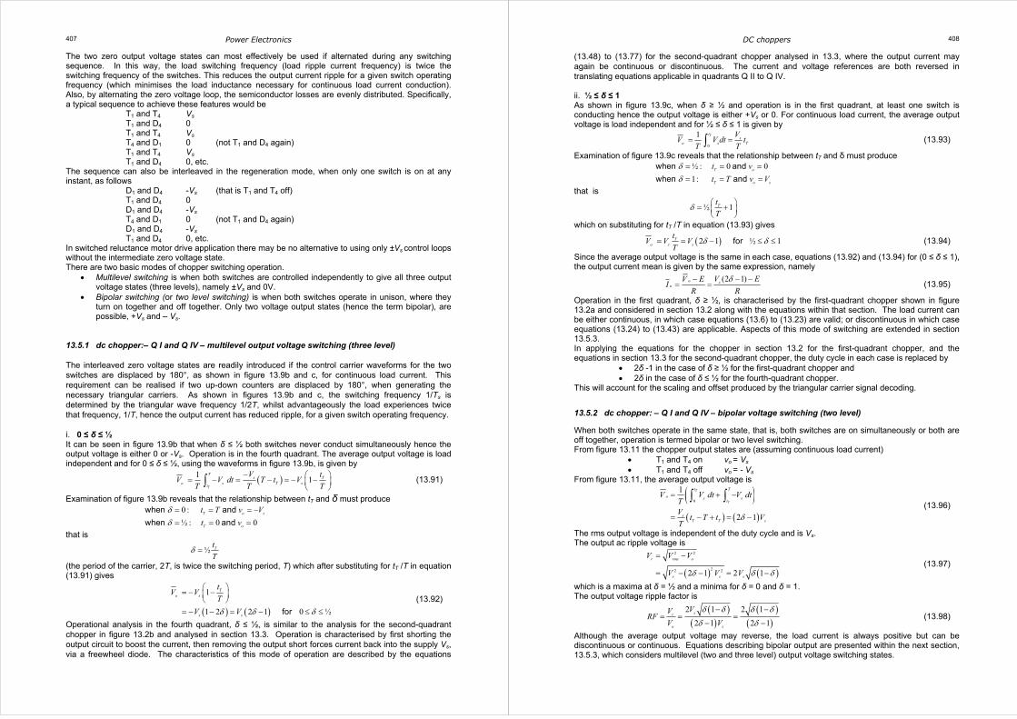
The two zero output voltage states can most effectively be used if alternated during any switching sequence. In this way, the load switching frequency (load ripple current frequency) is twice the switching frequency of the switches. This reduces the output current ripple for a given switch operating frequency (which minimises the load inductance necessary for continuous load current conduction). Also, by alternating the zero voltage loop, the semiconductor losses are evenly distributed. Specifically, a typical sequence to achieve these features would be
T1 and T4 Vs T1 and D4 0 T1 and T4 Vs T4 and D1 0 (not T1 and D4 again) T1 and T4 Vs T1 and D4 0, etc.
The sequence can also be interleaved in the regeneration mode, when only one switch is on at any instant, as follows
D1 and D4 -Vs (that is T1 and T4 off) T1 and D4 0 D1 and D4 -Vs T4 and D1 0 (not T1 and D4 again) D1 and D4 -Vs T1 and D4 0, etc.
In switched reluctance motor drive application there may be no alternative to using only ±Vs control loops without the intermediate zero voltage state. There are two basic modes of chopper switching operation.
• Multilevel switching is when both switches are controlled independently to give all three output voltage states (three levels), namely ±Vs and 0V.
• Bipolar switching (or two level switching) is when both switches operate in unison, where they turn on together and off together. Only two voltage output states (hence the term bipolar), are possible, +Vs and – Vs.
13.5.1 dc chopper:– Q I and Q IV – multilevel output voltage switching (three level) The interleaved zero voltage states are readily introduced if the control carrier waveforms for the two switches are displaced by 180°, as shown in figure 13.9b and c, for continuous load current. This requirement can be realised if two up-down counters are displaced by 180°, when generating the necessary triangular carriers. As shown in figures 13.9b and c, the switching frequency 1/Ts is determined by the triangular wave frequency 1/2T, whilst advantageously the load experiences twice that frequency, 1/T, hence the output current has reduced ripple, for a given switch operating frequency. i. 0 ≤ δ ≤ ½ It can be seen in figure 13.9b that when δ ≤ ½ both switches never conduct simultaneously hence the output voltage is either 0 or -Vs. Operation is in the fourth quadrant. The average output voltage is load independent and for 0 ≤ δ ≤ ½, using the waveforms in figure 13.9b, is given by
( )
11
T
Ts T
s T sot
V tV V dt T t V
T T T
− = − = − = − − ∫ (13.91)
Examination of figure 13.9b reveals that the relationship between tT and δ must produce
0 :
½ : 0 0
δδ= = = −= = =
when and
when andT o s
T o
t T v V
t v
that is
½ Tt
Tδ =
(the period of the carrier, 2T, is twice the switching period, T) which after substituting for tT /T in equation (13.91) gives
( ) ( )
1
1 2 2 1 0 ½δ δ δ
= − −
= − − = − ≤ ≤for
Tso
s s
tV V
T
V V
(13.92)
Operational analysis in the fourth quadrant, δ ≤ ½, is similar to the analysis for the second-quadrant chopper in figure 13.2b and analysed in section 13.3. Operation is characterised by first shorting the output circuit to boost the current, then removing the output short forces current back into the supply Vs, via a freewheel diode. The characteristics of this mode of operation are described by the equations
DC choppers 408
(13.48) to (13.77) for the second-quadrant chopper analysed in 13.3, where the output current may again be continuous or discontinuous. The current and voltage references are both reversed in translating equations applicable in quadrants Q II to Q IV. ii. ½ ≤ δ ≤ 1 As shown in figure 13.9c, when δ ≥ ½ and operation is in the first quadrant, at least one switch is conducting hence the output voltage is either +Vs or 0. For continuous load current, the average output voltage is load independent and for ½ ≤ δ ≤ 1 is given by
0
1 Tts
s To
VV V dt t
T T= =∫ (13.93)
Examination of figure 13.9c reveals that the relationship between tT and δ must produce
½ : 0 0
1:
δδ= = == = =
when and
when andT o
T o s
t v
t T v V
that is
½ 1Tt
Tδ = +
which on substituting for tT /T in equation (13.93) gives
( )2 1 ½ 1δ δ= = − ≤ ≤for Ts so
tV V V
T (13.94)
Since the average output voltage is the same in each case, equations (13.92) and (13.94) for (0 ≤ δ ≤ 1), the output current mean is given by the same expression, namely
(2 1)δ − −−
= =o so
V EV EI
R R (13.95)
Operation in the first quadrant, δ ≥ ½, is characterised by the first-quadrant chopper shown in figure 13.2a and considered in section 13.2 along with the equations within that section. The load current can be either continuous, in which case equations (13.6) to (13.23) are valid; or discontinuous in which case equations (13.24) to (13.43) are applicable. Aspects of this mode of switching are extended in section 13.5.3. In applying the equations for the chopper in section 13.2 for the first-quadrant chopper, and the equations in section 13.3 for the second-quadrant chopper, the duty cycle in each case is replaced by
• 2δ -1 in the case of δ ≥ ½ for the first-quadrant chopper and • 2δ in the case of δ ≤ ½ for the fourth-quadrant chopper.
This will account for the scaling and offset produced by the triangular carrier signal decoding.
13.5.2 dc chopper: – Q I and Q IV – bipolar voltage switching (two level) When both switches operate in the same state, that is, both switches are on simultaneously or both are off together, operation is termed bipolar or two level switching. From figure 13.11 the chopper output states are (assuming continuous load current)
• T1 and T4 on vo = Vs • T1 and T4 off vo = - Vs
From figure 13.11, the average output voltage is
( )( ) ( )
0
1
2 1
T
T
t T
o s st
sT T s
V V dt V dtTVt T t V
Tδ
= + −
= − + = −
∫ ∫ (13.96)
The rms output voltage is independent of the duty cycle and is Vs. The output ac ripple voltage is
( ) ( )
2 2
22 22 1 2 1δ δ δ
= −
= − − = −
r rms o
s s s
V V V
V V V (13.97)
which is a maxima at δ = ½ and a minima for δ = 0 and δ = 1. The output voltage ripple factor is
( )
( )( )
( )2 1 2 1
2 1 2 1
sr
o s
VVRF
V V
δ δ δ δ
δ δ
− −= = =
− − (13.98)
Although the average output voltage may reverse, the load current is always positive but can be discontinuous or continuous. Equations describing bipolar output are presented within the next section, 13.5.3, which considers multilevel (two and three level) output voltage switching states.

Power Electronics 409
Figure 13.11. Two-quadrant (I and IV) dc chopper operation in the bipolar output mode: (a) circuit showing load components and (b) chopper output waveforms.
13.5.3 Multilevel output voltage states, dc chopper In switched reluctance machine drives it is not uncommon to operate the asymmetrical half H-bridge shown in figure 13.9 such that
• both switches operate in the on-state together to form +V voltage loops; • switches operate independently the give zero voltage loops; and • both switches are simultaneously off, forming –V voltage output loops.
The control objective is to generate a current output pulse that tracks a reference shape which starts from zero, rises to maintain a fixed current level, with hysteresis, then the current falls back to zero. The waveform shown in figure 13.12 fulfils this specification. The switching strategy to produce the current waveform in figure 13.12 aims at:
• For rising current:- use +V loops (and zero volt loops only if necessary) • For near constant current:- use zero voltage loops (and ±V loops only if necessary to increase
or decrease the current) • For falling current:- use – V loops (and zero volts loops only if necessary to reduce the fall rate)
Operation is further characterised by continuous load current during the pulse. Energy is supplied to the load from the source during +V loops, and returned to the supply during –V loop periods. The chopper output current during each period is described by equations previously derived in this chapter, but reproduced as follows. In a positive voltage loop, (T1 and T4 are both on), when vo(t) = Vs and Vs is impressed across the load, the load circuit condition is described by
oo s
diL Ri E Vdt
+ + =
which yields
(a)
L O A D
V s
D1
T1
T4
D4
R L + E
vo
io
(b)
t I∨
vo
io I∧
I∨
Vs
t
T
tT
Conducting devices
T1 D1 T1 D1 T1 D1
T4 D4 T4 D4 T4 D4
o
-Vs
oVo
oI
DC choppers 410
( ) 1 0τ τ− −∨
+− = − + ≤ ≤
fort t
so
V Ei t e I e t t
R (13.99)
During the first switching cycle the current starts from zero, so I∨
= 0. Otherwise I∨
is the lower reference, I
−, from the end of the previous cycle.
The current at the end of the positive voltage loop period is the reference level I+, whilst the time to rise to I+ is derived by equating equation (13.99) to I+ and solving for time t+ at the end of the period. Solving io(t
+) = I+ for t+ , gives
ln s
s
V E I Rt
V E I Rτ
∨
++
− − =− −
(13.100)
Figure 13.12. Two-quadrant (I and IV) dc chopper operation in a multilevel output voltage mode.
In a zero voltage loop, when vo(t) = 0, such as circuit loops involving T1 and D4 (or T4 and D1), the circuit equation is given by
0oo
diL Ri Edt
+ + =
which gives
( ) 1 0τ τ− −∧ = − − + ≤ ≤
for
t to
o
Ei t e I e t t
R (13.101)
where I∧
equals the reference current level, I+ from the previous switching period. The current at the end of the period is the reference level I
−, whilst the time to fall to I
− is given by
equating equation (13.101) to I− and solving for time, to at the end of the period.
o E I Rt n
E I Rτ
∧
−
+ = +
(13.102)
In a negative voltage loop, when both switches T1 and T4 are off, the current falls rapidly and the circuit equation, when vo(t) = -Vs, is
oo s
diL Ri E Vdt
+ + = −
which gives
Conducting devices T1 T1 T1 D1 T1 T1 T1 D1 T4 D4 T4 T4 T4 D4 T4 D4
Vs
t
t
t
is
-Vs
vo
io
o
oI
oI
oI−
oI∨
I+
I-
o
o
o
o
o
energy recovered
t o t + t o t + t o t +
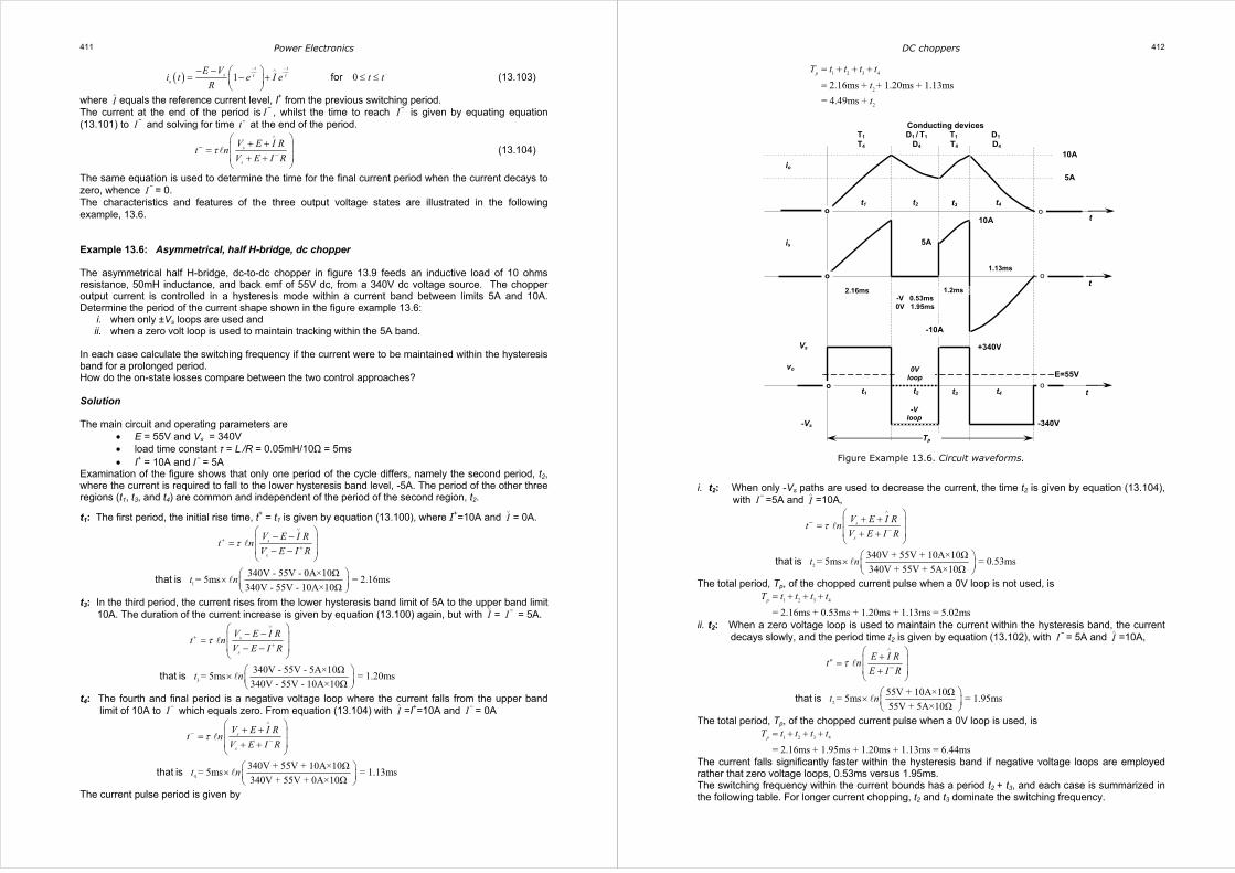
Power Electronics 411
( ) 1 0τ τ− −∧
−− − = − + ≤ ≤
fort t
so
E Vi t e I e t t
R (13.103)
where I∧
equals the reference current level, I+ from the previous switching period. The current at the end of the period is I
−, whilst the time to reach I
− is given by equating equation
(13.101) to I− and solving for time t − at the end of the period.
s
s
V E I Rt n
V E I Rτ
∧
−−
+ + = + +
(13.104)
The same equation is used to determine the time for the final current period when the current decays to zero, whence I
−= 0.
The characteristics and features of the three output voltage states are illustrated in the following example, 13.6. Example 13.6: Asymmetrical, half H-bridge, dc chopper The asymmetrical half H-bridge, dc-to-dc chopper in figure 13.9 feeds an inductive load of 10 ohms resistance, 50mH inductance, and back emf of 55V dc, from a 340V dc voltage source. The chopper output current is controlled in a hysteresis mode within a current band between limits 5A and 10A. Determine the period of the current shape shown in the figure example 13.6:
i. when only ±Vs loops are used and ii. when a zero volt loop is used to maintain tracking within the 5A band.
In each case calculate the switching frequency if the current were to be maintained within the hysteresis band for a prolonged period. How do the on-state losses compare between the two control approaches? Solution The main circuit and operating parameters are
• E = 55V and Vs = 340V • load time constant τ = L /R = 0.05mH/10Ω = 5ms • I+ = 10A and I
−= 5A
Examination of the figure shows that only one period of the cycle differs, namely the second period, t2, where the current is required to fall to the lower hysteresis band level, -5A. The period of the other three regions (t1, t3, and t4) are common and independent of the period of the second region, t2.
t1: The first period, the initial rise time, t+ = t1 is given by equation (13.100), where I+=10A and I∨
= 0A.
τ∨
++
− − = − −
s
s
V E I Rt n
V E I R
1
340V - 55V - 0A×10Ω = 5ms = 2.16ms
340V - 55V - 10A×10Ωt n
×
that is
t3: In the third period, the current rises from the lower hysteresis band limit of 5A to the upper band limit 10A. The duration of the current increase is given by equation (13.100) again, but with I
∨= I
− = 5A.
3
340V - 55V - 5A×10Ω = 5ms = 1.20ms
340V - 55V - 10A×10Ω
τ∨
++
− − = − −
×
that is
s
s
V E I Rt n
V E I R
t n
t4: The fourth and final period is a negative voltage loop where the current falls from the upper band limit of 10A to I
− which equals zero. From equation (13.104) with I
∧=I+=10A and I
−= 0A
4
340V + 55V + 10A×10Ω = 5ms = 1.13ms
340V + 55V + 0A×10Ω
τ∧
−−
+ + = + +
×
that is
s
s
V E I Rt n
V E I R
t n
The current pulse period is given by
DC choppers 412
1 2 3 4
2
2
2.16ms + + 1.20ms + 1.13ms
= 4.49ms +
pT t t t t
t
t
= + + +
=
Figure Example 13.6. Circuit waveforms. i. t2: When only -Vs paths are used to decrease the current, the time t2 is given by equation (13.104),
with I−=5A and I
∧=10A,
2
340V + 55V + 10A×10Ω = 5ms = 0.53ms
340V + 55V + 5A×10Ω
τ∧
−−
+ + = + +
×
that is
s
s
V E I Rt n
V E I R
t n
The total period, Tp, of the chopped current pulse when a 0V loop is not used, is
1 2 3 4
= 2.16ms + 0.53ms + 1.20ms + 1.13ms = 5.02mspT t t t t= + + +
ii. t2: When a zero voltage loop is used to maintain the current within the hysteresis band, the current decays slowly, and the period time t2 is given by equation (13.102), with I
−= 5A and I
∧=10A,
2
55V + 10A×10Ω = 5ms = 1.95ms
55V + 5A×10Ω
τ∧
−
+ = +
×
that is
o E I Rt n
E I R
t n
The total period, Tp, of the chopped current pulse when a 0V loop is used, is
1 2 3 4
= 2.16ms + 1.95ms + 1.20ms + 1.13ms = 6.44mspT t t t t= + + +
The current falls significantly faster within the hysteresis band if negative voltage loops are employed rather that zero voltage loops, 0.53ms versus 1.95ms. The switching frequency within the current bounds has a period t2 + t3, and each case is summarized in the following table. For longer current chopping, t2 and t3 dominate the switching frequency.
10A
5A
Conducting devices T1 D1 / T1 T1 D1 T4 D4 T4 D4
Vs
t
t
t
is
-Vs
vo
io
o
o
o
o
o
o
t1 t2 t3 t4
t1 t2 t3 t4
5A
10A
+340V
-340V
E=55V
-10A
-V 0.53ms 0V 1.95ms
1.13ms
1.2ms 2.16ms
Tp
0V loop
-V loop
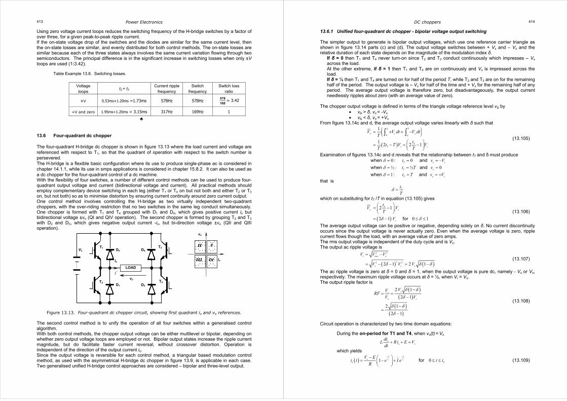
Power Electronics 413
Using zero voltage current loops reduces the switching frequency of the H-bridge switches by a factor of over three, for a given peak-to-peak ripple current. If the on-state voltage drop of the switches and the diodes are similar for the same current level, then the on-state losses are similar, and evenly distributed for both control methods. The on-state losses are similar because each of the three states always involves the same current variation flowing through two semiconductors. The principal difference is in the significant increase in switching losses when only ±V loops are used (1:3.42).
Table Example 13.6. Switching losses.
Voltage loops
t2 + t3 Current ripple
frequency Switch
frequency Switch loss
ratio
±V 0.53ms+1.20ms =1.73ms 578Hz 578Hz 578
169= 3.42
+V and zero 1.95ms+1.20ms = 3.15ms 317Hz 169Hz 1
♣ 13.6 Four-quadrant dc chopper The four-quadrant H-bridge dc chopper is shown in figure 13.13 where the load current and voltage are referenced with respect to T1, so that the quadrant of operation with respect to the switch number is persevered. The H-bridge is a flexible basic configuration where its use to produce single-phase ac is considered in chapter 14.1.1, while its use in smps applications is considered in chapter 15.8.2. It can also be used as a dc chopper for the four-quadrant control of a dc machine. With the flexibility of four switches, a number of different control methods can be used to produce four-quadrant output voltage and current (bidirectional voltage and current). All practical methods should employ complementary device switching in each leg (either T1 or T4 on but not both and either T2 or T3 on, but not both) so as to minimise distortion by ensuring current continuity around zero current output. One control method involves controlling the H-bridge as two virtually independent two-quadrant choppers, with the over-riding restriction that no two switches in the same leg conduct simultaneously. One chopper is formed with T1 and T4 grouped with D1 and D4, which gives positive current io but bidirectional voltage ±vo (QI and QIV operation). The second chopper is formed by grouping T2 and T3
with D2 and D3, which gives negative output current -io, but bi-direction voltage ±vo (QII and QIII operation).
Figure 13.13. Four-quadrant dc chopper circuit, showing first quadrant io and vo references. The second control method is to unify the operation of all four switches within a generalised control algorithm. With both control methods, the chopper output voltage can be either multilevel or bipolar, depending on whether zero output voltage loops are employed or not. Bipolar output states increase the ripple current magnitude, but do facilitate faster current reversal, without crossover distortion. Operation is independent of the direction of the output current io. Since the output voltage is reversible for each control method, a triangular based modulation control method, as used with the asymmetrical H-bridge dc chopper in figure 13.9, is applicable in each case. Two generalised unified H-bridge control approaches are considered – bipolar and three-level output.
LOAD
Vs
T2
T1
T4
T3 D2
D1
D4
D3
vo
io
II
I
III
IV
vo
I−
io
DC choppers 414
13.6.1 Unified four-quadrant dc chopper - bipolar voltage output switching The simpler output to generate is bipolar output voltages, which use one reference carrier triangle as shown in figure 13.14 parts (c) and (d). The output voltage switches between + Vs and – Vs and the relative duration of each state depends on the magnitude of the modulation index δ.
If δ = 0 then T1 and T4 never turn-on since T2 and T3 conduct continuously which impresses – Vs across the load. At the other extreme, if δ = 1 then T1 and T4 are on continuously and Vs is impressed across the load. If δ = ½ then T1 and T4 are turned on for half of the period T, while T2 and T3 are on for the remaining half of the period. The output voltage is – Vs for half of the time and + Vs for the remaining half of any period. The average output voltage is therefore zero, but disadvantageously, the output current needlessly ripples about zero (with an average value of zero).
The chopper output voltage is defined in terms of the triangle voltage reference level v∆ by
• v∆ > δ, vo = -Vs • v∆ < δ, vo = +Vs
From figure 13.14c and d, the average output voltage varies linearly with δ such that
( )( )
T
0
1
12 2 1
T
T
t
o s st
TT s s
V V dt V dtT
tt T V V
T T
= + + −
= − = −
∫ ∫ (13.105)
Examination of figures 13.14c and d reveals that the relationship between tT and δ must produce
0 : 0
½ : ½ 0
1:
δδδ
= = = −= = == = = +
when and
when and
when and
T o s
T o
T o s
t v V
t T v
t T v V
that is
Tt
Tδ =
which on substituting for tT /T in equation (13.105) gives
( )
2 1
2 1 0 1δ δ
= −
= − ≤ ≤for
Tso
s
tV V
T
V
(13.106)
The average output voltage can be positive or negative, depending solely on δ. No current discontinuity occurs since the output voltage is never actually zero. Even when the average voltage is zero, ripple current flows though the load, with an average value of zero amps. The rms output voltage is independent of the duty cycle and is Vs. The output ac ripple voltage is
( ) ( )
2 2
22 22 1 2 1δ δ δ
= −
= − − = −
r rms o
s s s
V V V
V V V (13.107)
The ac ripple voltage is zero at δ = 0 and δ = 1, when the output voltage is pure dc, namely - Vs or Vs, respectively. The maximum ripple voltage occurs at δ = ½, when Vr = Vs. The output ripple factor is
( )( )
( )( )
2 1
2 1
2 1
2 1
sr
o s
VVRF
V V
δ δδ
δ δδ
−= =
−
−=
−
(13.108)
Circuit operation is characterized by two time domain equations:
During the on-period for T1 and T4, when vo(t) = Vs
oo s
diL Ri E Vdt
+ + =
which yields
( ) 1 0τ τ− −∨− = − + ≤ ≤
for
t ts
o T
V Ei t e I e t t
R (13.109)
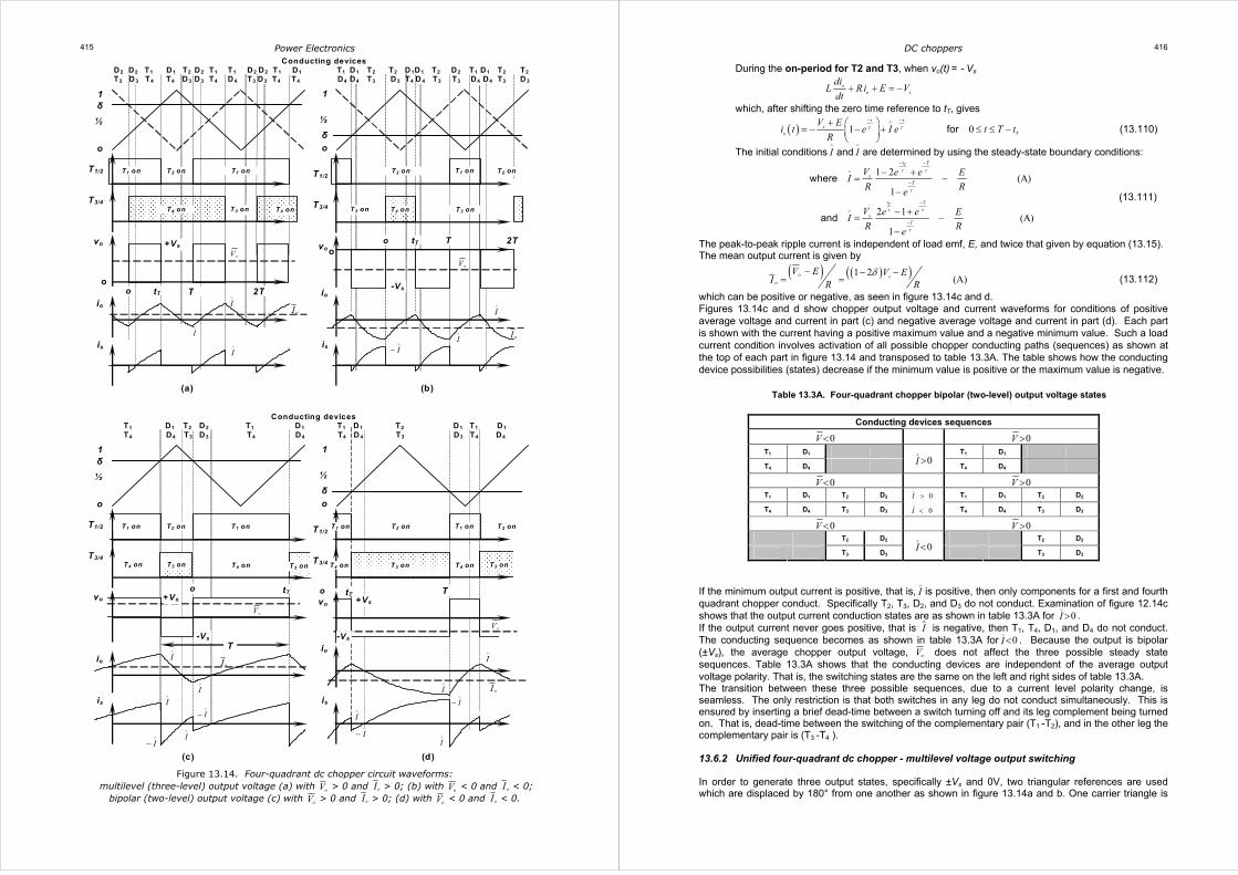
Power Electronics 415
Conducting devices T1
D1 T2 D2 T1 D1 T1 D1 T2 D1 T1 D1 T4 D4 T3 D3 T4 D4 T4 D4 T3 D3 T4 D4
(c) (d)
1
δ
½
o
T1/2
T3/4
vo
io
is
1
½
δ
o
T1/2
T3/4
vo
io
is
I∧
I∨
I∧
+Vs
T
T1 on T1 on
T4 on T4 on T3 on
T2 on
T3 on
-Vs
I∧
−
I∨
−
I∨
oV
o tT
I∨
I∧
I∧
o tT T
-Vs
T2 on T1 on
T4 onT4 on T3 on
T2 on
+Vs
T1 on
T3 on
I∨
oV
I∧
−
I∨
−
oI
oI
(a) (b)
1
δ
½
o
T1/2
T3/4
vo
io
is
1
½
δ
o
T1/2
T3/4
vo
io
is
oV
I∧
I∨
I∧
Conducting devices D2 D2 T1
D1 T2 D2 T1 T1 D2 D2 T1 D1 T1 D1 T2 T2 D1D1 T2 D2 T1 D1 T2 T2
T3 D3 T4 T4 D3 D3 T4 D4 T3 D3 T4 T4 D4 D4 T3 D3 T4 D 4 T3 T3 D4 D4 T3 D3
tT o
+Vs
T
o tT T
2T
2T
-Vs
T1 on T1 on
T4 on T4 on T3 on
T2 on T1 on
T3 on T3 on T4 on
T2 on T2 on
oV
I∨
I∧
I∨
−
oI
oI
o
o
Figure 13.14. Four-quadrant dc chopper circuit waveforms: multilevel (three-level) output voltage (a) with oV > 0 and oI > 0; (b) with oV < 0 and oI < 0;
bipolar (two-level) output voltage (c) with oV > 0 and oI > 0; (d) with oV < 0 and oI < 0.
DC choppers 416
During the on-period for T2 and T3, when vo(t) = - Vs
oo s
diL R i E Vdt
+ + = −
which, after shifting the zero time reference to tT, gives
( ) 1 0τ τ− −∧+ = − − + ≤ ≤ −
for
t ts
o T
V Ei t e I e t T t
R (13.110)
The initial conditions I∧
and I∨
are determined by using the steady-state boundary conditions:
1 2(A)
1
2 1(A)
1
T
T
t T
sT
t T
sT
V e e EI
R Re
V e e EI
R Re
τ τ
τ
τ τ
τ
− −
∧
−
−
∨
−
− += −
−
− += −
−
where
and
(13.111)
The peak-to-peak ripple current is independent of load emf, E, and twice that given by equation (13.15). The mean output current is given by
( ) ( )( )1 2
(A)o s
o
V E V EI R R
δ− − −= = (13.112)
which can be positive or negative, as seen in figure 13.14c and d. Figures 13.14c and d show chopper output voltage and current waveforms for conditions of positive average voltage and current in part (c) and negative average voltage and current in part (d). Each part is shown with the current having a positive maximum value and a negative minimum value. Such a load current condition involves activation of all possible chopper conducting paths (sequences) as shown at the top of each part in figure 13.14 and transposed to table 13.3A. The table shows how the conducting device possibilities (states) decrease if the minimum value is positive or the maximum value is negative.
Table 13.3A. Four-quadrant chopper bipolar (two-level) output voltage states
Conducting devices sequences
0V < 0V > T1 D1 T1 D1 T4 D4
0I∨>
T4 D4
0V < 0V > T1 D1 T2 D2 T1 D1 T2 D2
T4 D4 T3 D3 0
0
I
I
∧
∨
>
<
T4 D4 T3 D3
0V < 0V > T2 D2 T2 D2
T3 D3 0I
∧<
T3 D3
If the minimum output current is positive, that is, I
∨is positive, then only components for a first and fourth
quadrant chopper conduct. Specifically T2, T3, D2, and D3 do not conduct. Examination of figure 12.14c shows that the output current conduction states are as shown in table 13.3A for 0I
∨> .
If the output current never goes positive, that is I is negative, then T1, T4, D1, and D4 do not conduct. The conducting sequence becomes as shown in table 13.3A for 0I
∧< . Because the output is bipolar
(±Vs), the average chopper output voltage, oV does not affect the three possible steady state sequences. Table 13.3A shows that the conducting devices are independent of the average output voltage polarity. That is, the switching states are the same on the left and right sides of table 13.3A. The transition between these three possible sequences, due to a current level polarity change, is seamless. The only restriction is that both switches in any leg do not conduct simultaneously. This is ensured by inserting a brief dead-time between a switch turning off and its leg complement being turned on. That is, dead-time between the switching of the complementary pair (T1 -T2), and in the other leg the complementary pair is (T3 -T4 ). 13.6.2 Unified four-quadrant dc chopper - multilevel voltage output switching In order to generate three output states, specifically ±Vs and 0V, two triangular references are used which are displaced by 180° from one another as shown in figure 13.14a and b. One carrier triangle is
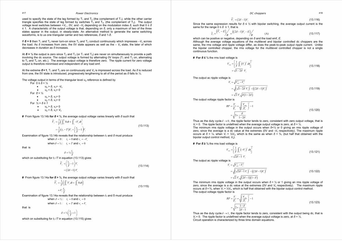
Power Electronics 417
used to specify the state of the leg formed by T1 and T2 (the complement of T1), while the other carrier triangle specifies the state of leg formed by switches T3 and T4, (the complement of T3). The output voltage level switches between +Vs , 0V, and –Vs depending on the modulation index δ, such that 0 ≤ δ ≤ 1. A characteristic of the output voltage is that, depending on δ, only a maximum of two of the three states appear in the output, in steady-state. An alternative method to generate the same switching waveforms, is to us one triangular carrier and two references, δ and 1-δ. If δ = 0 then T1 and T4 never turn-on since T2 and T3 conduct continuously which impresses –Vs across the load. As δ increases from zero, the 0V state appears as well as the – Vs state, the later of which decreases in duration as δ increases. At δ = ½ the output is zero since T2 and T3 (or T1 and T4) are never on simultaneously to provide a path involving the dc source. The output voltage is formed by alternating 0V loops (T1 and T3 on, alternating to T2 and T4 on, etc.). The average output voltage is therefore zero. The ripple current for zero voltage output is therefore minimised and independent of any load emf. At the extreme δ = 1, T1 and T4 are on continuously and Vs is impressed across the load. As δ is reduced from one, the 0V state is introduced, progressively lengthening to all of the period as δ falls to ½. The voltage output in terms of the triangular level v∆ reference is defined by
For 0 ≤ δ < ½ • v∆ > δ, vo= -Vs • v∆ < δ, vo= 0
For δ = ½ • v∆ > δ, vo= 0 • v∆ < δ, vo= 0
For ½ > δ ≥ 1 • v∆ > δ, vo= 0 • v∆ < δ, vo= Vs
# From figure 13.14b for δ < ½, the average output voltage varies linearly with δ such that
( )( )
T
0
10
11
T
T
t
o st
TT s s
V dt V dtT
tt T V V
T T
= + −
= − = −
∫ ∫ (13.113)
Examination of figure 13.14b reveals that the relationship between tT and δ must produce 0 : 0
½ : 0
δδ= = = −= = =
when and
when andT o s
T o
t v V
t T v
that is
½ Tt
Tδ =
which on substituting for tT /T in equation (13.113) gives
( )
1
2 1
Tso
s
tV V
T
Vδ
= −
= − (13.114)
# From figure 13.14a for δ > ½, the average output voltage varies linearly with δ such that
( ) T
0
10
T
T
t
o st
Ts
V V dt dtTt
VT
= +
=
∫ ∫ (13.115)
Examination of figure 13.14a reveals that the relationship between tT and δ must produce ½ : 0 0
1:
δδ= = == = =
when and
when andT o
T o s
t v
t T v V
that is
½ 1Tt
Tδ = +
which on substituting for tT /T in equation (13.115) gives
DC choppers 418
( )2 1 soV Vδ= − (13.116)
Since the same expression results for δ ≤ ½ with bipolar switching, the average output current is the same for the range 0 ≤ δ ≤ 1, that is
( ) ( )( )2 1
(A)o s
o
V E V EI R R
δ− − −= = (13.117)
which can be positive or negative, depending on δ and the load emf, E. Although the average voltage equations of the multilevel and bipolar controlled dc choppers are the same, the rms voltage and ripple voltage differ, as does the peak-to-peak output ripple current. Unlike the bipolar controlled chopper, the rms voltage for the multilevel controlled chopper is not a single continuous function. # For δ ≤ ½ the rms load voltage is
( )
½ 2
1
1 2
T
T
rms st
s
V V dtT
Vδ
=
= −
∫ (13.118)
The output ac ripple voltage is
( ) ( )( )( )
2 2
2 2
1 2 2 1
2 1 2
r rms o
s s
s
V V V
V V
V
δ δ
δ δ
= −
= − − −
= −
(13.119)
The output voltage ripple factor is
2
1
21 2
δδ
= = −
= ×−
rmsr
o o
VVRF
V V (13.120)
Thus as the duty cycle 0δ → , the ripple factor tends to zero, consistent with zero output voltage, that is Vr = 0. The ripple factor is undefined when the average output voltage is zero, at δ = ½. The minimum rms ripple voltage in the output occurs when δ=½ or 0 giving an rms ripple voltage of zero, since the average is a dc value at the extremes (0V and -Vs respectively). The maximum ripple occurs at δ = ¼, when Vr = ½Vs, which is the same as when δ = ¾, (but half that obtained with the bipolar output control method, Vs). # For δ ≥ ½ the rms load voltage is
( )
½ 2
1
2 1
T
T
rms st
s
V V dtT
Vδ
= −
= −
∫ (13.121)
The output ac ripple voltage is
( ) ( )( )( )( )
2 2
2 2
2 1 2 1
2 2 1 1
r rms o
s s
s
V V V
V V
V
δ δ
δ δ
= −
= − − −
= − −
(13.122)
The minimum rms ripple voltage in the output occurs when δ = ½ or 1 giving an rms ripple voltage of zero, since the average is a dc value at the extremes (0V and Vs respectively). The maximum ripple occurs at δ = ¾, when Vr = ½Vs, which is half that obtained with the bipolar output control method. The output voltage ripple factor is
2
1
12
2 1
r rms
o o
V VRF
V V
δδ
= = −
−= ×
−
(13.123)
Thus as the duty cycle 1δ → , the ripple factor tends to zero, consistent with the output being dc, that is Vr = 0. The ripple factor is undefined when the average output voltage is zero, at δ = ½. Circuit operation is characterized by three time domain equations.
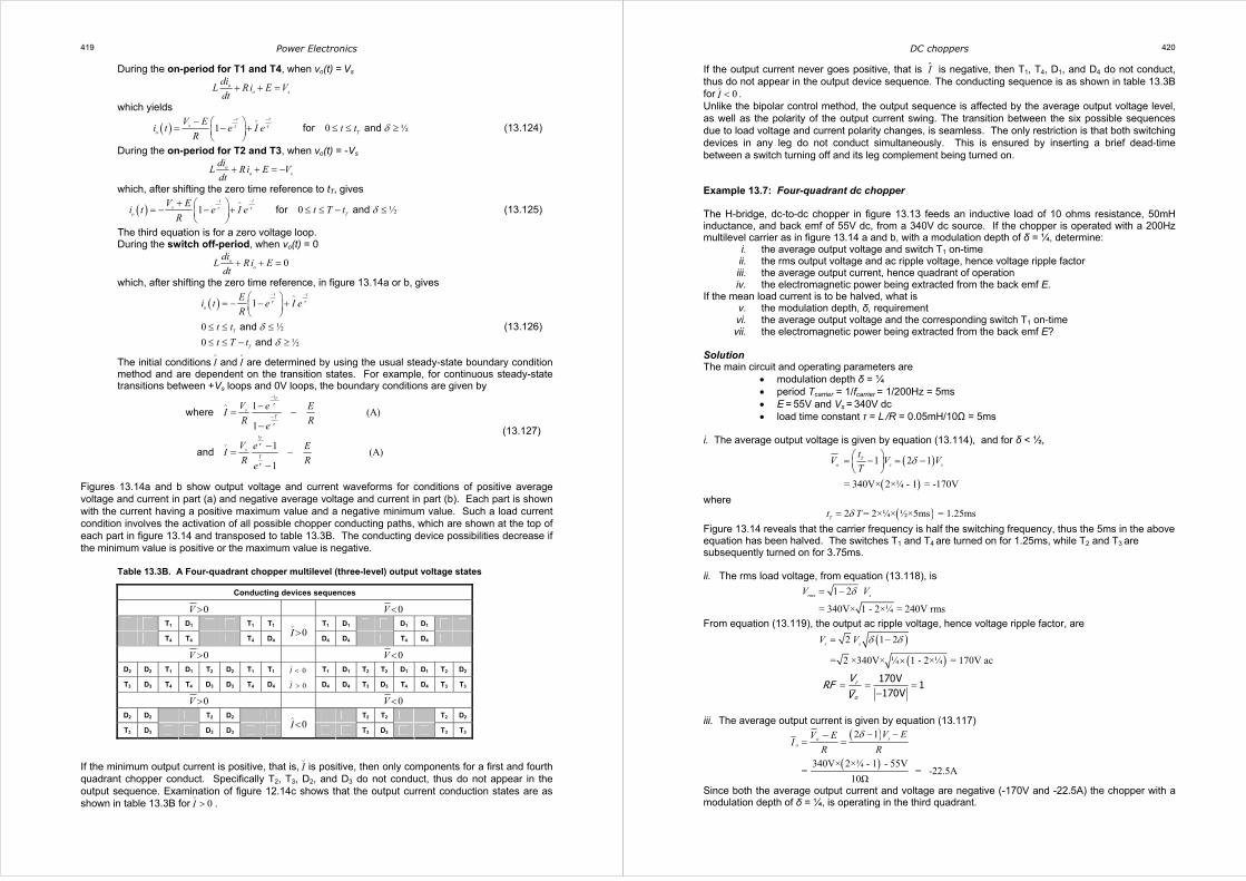
Power Electronics 419
During the on-period for T1 and T4, when vo(t) = Vs
oo s
diL Ri E Vdt
+ + =
which yields
( ) 1 0 ½τ τ δ− −∨− = − + ≤ ≤ ≥
for and
t ts
o T
V Ei t e I e t t
R (13.124)
During the on-period for T2 and T3, when vo(t) = -Vs
oo s
diL Ri E Vdt
+ + = −
which, after shifting the zero time reference to tT, gives
( ) 1 0 ½τ τ δ− −∧+ = − − + ≤ ≤ − ≤
for and
t ts
o T
V Ei t e I e t T t
R (13.125)
The third equation is for a zero voltage loop. During the switch off-period, when vo(t) = 0
0oo
diL Ri Edt
+ + =
which, after shifting the zero time reference, in figure 13.14a or b, gives
( ) 1
0 ½
0 ½
t t
o
T
T
Ei t e I e
R
t t
t T t
τ τ
δδ
− −∧ = − − +
≤ ≤ ≤≤ ≤ − ≥
and
and
(13.126)
The initial conditions I∧
and I∨
are determined by using the usual steady-state boundary condition method and are dependent on the transition states. For example, for continuous steady-state transitions between +Vs loops and 0V loops, the boundary conditions are given by
1(A)
1
1(A)
1
T
T
t
sT
t
sT
V e EI
R Re
V e EI
R Re
τ
τ
τ
τ
−
∧
−
∨
−= −
−
−= −
−
where
and
(13.127)
Figures 13.14a and b show output voltage and current waveforms for conditions of positive average voltage and current in part (a) and negative average voltage and current in part (b). Each part is shown with the current having a positive maximum value and a negative minimum value. Such a load current condition involves the activation of all possible chopper conducting paths, which are shown at the top of each part in figure 13.14 and transposed to table 13.3B. The conducting device possibilities decrease if the minimum value is positive or the maximum value is negative.
Table 13.3B. A Four-quadrant chopper multilevel (three-level) output voltage states
Conducting devices sequences
0V > 0V <
T1 D1 T1 T1 T1 D1 D1 D1
T4 T4 T4 D4 0I
∨>
D4 D4 T4 D4
0V > 0V < D2 D2 T1 D1 T2 D2 T1 T1 T1 D1 T2 T2 D1 D1 T2 D2
T3 D3 T4 T4 D3 D3 T4 D4
0
0
I
I
∨
∧
<
>
D4 D4 T3 D3 T4 D4 T3 T3
0V > 0V < D2 D2 T2 D2 T2 T2 T2 D2
T3 D3 D3 D3 0I
∧<
T3 D3 T3 T3
If the minimum output current is positive, that is, I∨
is positive, then only components for a first and fourth quadrant chopper conduct. Specifically T2, T3, D2, and D3 do not conduct, thus do not appear in the output sequence. Examination of figure 12.14c shows that the output current conduction states are as shown in table 13.3B for 0I
∨> .
DC choppers 420
If the output current never goes positive, that is I is negative, then T1, T4, D1, and D4 do not conduct, thus do not appear in the output device sequence. The conducting sequence is as shown in table 13.3B for 0I
∧< .
Unlike the bipolar control method, the output sequence is affected by the average output voltage level, as well as the polarity of the output current swing. The transition between the six possible sequences due to load voltage and current polarity changes, is seamless. The only restriction is that both switching devices in any leg do not conduct simultaneously. This is ensured by inserting a brief dead-time between a switch turning off and its leg complement being turned on. Example 13.7: Four-quadrant dc chopper The H-bridge, dc-to-dc chopper in figure 13.13 feeds an inductive load of 10 ohms resistance, 50mH inductance, and back emf of 55V dc, from a 340V dc source. If the chopper is operated with a 200Hz multilevel carrier as in figure 13.14 a and b, with a modulation depth of δ = ¼, determine:
i. the average output voltage and switch T1 on-time ii. the rms output voltage and ac ripple voltage, hence voltage ripple factor iii. the average output current, hence quadrant of operation iv. the electromagnetic power being extracted from the back emf E.
If the mean load current is to be halved, what is v. the modulation depth, δ, requirement vi. the average output voltage and the corresponding switch T1 on-time vii. the electromagnetic power being extracted from the back emf E?
Solution The main circuit and operating parameters are
• modulation depth δ = ¼ • period Tcarrier = 1/fcarrier = 1/200Hz = 5ms • E = 55V and Vs = 340V dc • load time constant τ = L /R = 0.05mH/10Ω = 5ms
i. The average output voltage is given by equation (13.114), and for δ < ½,
( )
( )
1 2 1
= 340V× 2×¼ - 1 = -170V
Ts so
tV V V
Tδ = − = −
where ( )2 = 2×¼× ½×5ms = 1.25msTt Tδ=
Figure 13.14 reveals that the carrier frequency is half the switching frequency, thus the 5ms in the above equation has been halved. The switches T1 and T4 are turned on for 1.25ms, while T2 and T3 are subsequently turned on for 3.75ms. ii. The rms load voltage, from equation (13.118), is
1 2
= 340V× 1 - 2×¼ = 240V rms
rms sV Vδ= −
From equation (13.119), the output ac ripple voltage, hence voltage ripple factor, are
( )
( )
2 1 2
= 2 ×340V× ¼ 1 - 2×¼ = 170V ac
r sV V δ δ= −
×
170V
1170V
r
o
VRF
V= = =
−
iii. The average output current is given by equation (13.117)
( )
( )
2 1
340V× 2×¼ - 1 - 55V= = -22.5A
10Ω
soo
V EV EI
R R
δ − −−= =
Since both the average output current and voltage are negative (-170V and -22.5A) the chopper with a modulation depth of δ = ¼, is operating in the third quadrant.
Power Electronics 421
iv. The electromagnetic power developed by the back emf E is given by
( )55V× -22.5A = -1237.5WoEP EI= =
v. The average output current is given by
( ) ( )( )2 1o s
o
V E V EI R R
δ− − −= =
when the mean current is -11.25A, δ = 0.415, as derived in part vi. vi. Then, if the average current is halved to -11.25A
=55V - 11.25A×10Ω = -57.5V
ooV E RI= +
The average output voltage rearranged in terms of the modulation depth δ gives
½ 1
-57.5V= ½× 1 + = 0.415
340V
o
s
V
Vδ
= +
The switch on-time when δ < ½ is given by ( )2 = 2×0.415× ½×5ms = 2.07msTt Tδ=
From figure 13.14b both T1 and T4 are turned on for 2.07ms, although, from table 13.3B, for negative load current, oI = -11.25A, the parallel connected freewheel diodes D2 and D3 conduct alternately, rather than the switches (assuming 0oI
∧< ). The switches T1 and T4 are turned on for 1.25ms, while T2 and T3
are subsequently turned on for 2.93ms. vii. The electromagnetic power developed by the back emf E is halved and is given by
( )55V× -11.25A = -618.75WoEP EI= =
♣ Reading list Dewan, S. B. and Straughen, A., Power Semiconductor Circuits,
John Wiley & Sons, New York, 1975. Dubey, G.K., Power Semiconductor Controlled Drives,
Prentice-Hall International, 1989. Mohan, N., Undeland, T. M., & Robbins, W.P., Power Electronics: Converters, Applications & Design,
John Wiley & Sons, New York, 2003. Problems 13.1. The dc GTO thyristor chopper shown in figure 13.1c operates at 1 kHz and supplies a series 5 Ω
and 10 mH load from an 84 V dc battery source. Derive general expressions for the mean load voltage and current, and the load rms voltage at an on-time duty cycle of δ. Evaluate these parameters for δ = 0.25.
[21 V, 4.2 A; 42 V] 13.2. The dc chopper in figure 13.1c controls a load of R = 10 Ω, L = 10 mH and 40 V battery. The
supply is 340 V dc and the chopping frequency is 5 kHz. Calculate (a) the peak-to-peak load ripple current, (b) the average load current, (c) the rms load current, (d) the effective input resistance, and (e) the rms switch current.
DC choppers 422
Blank