Embed Size (px)
Citation preview

10 Gigabit Ethernet Subsystem v3.1
LogiCORE IP Product Guide
Vivado Design Suite
PG157 October 4, 2017
10Gb Ethernet v3.1 2PG157 October 4, 2017 www.xilinx.com
Table of ContentsChapter 1: Overview
Feature Summary. . . . . . . . . . . . . . . . . . . . . . . . . . . . . . . . . . . . . . . . . . . . . . . . . . . . . . . . . . . . . . . . . . 8Applications . . . . . . . . . . . . . . . . . . . . . . . . . . . . . . . . . . . . . . . . . . . . . . . . . . . . . . . . . . . . . . . . . . . . . . 9Unsupported Features. . . . . . . . . . . . . . . . . . . . . . . . . . . . . . . . . . . . . . . . . . . . . . . . . . . . . . . . . . . . . 10Licensing and Ordering . . . . . . . . . . . . . . . . . . . . . . . . . . . . . . . . . . . . . . . . . . . . . . . . . . . . . . . . . . . . 10
Chapter 2: Product SpecificationStandards . . . . . . . . . . . . . . . . . . . . . . . . . . . . . . . . . . . . . . . . . . . . . . . . . . . . . . . . . . . . . . . . . . . . . . . 13Performance. . . . . . . . . . . . . . . . . . . . . . . . . . . . . . . . . . . . . . . . . . . . . . . . . . . . . . . . . . . . . . . . . . . . . 13Resource Utilization. . . . . . . . . . . . . . . . . . . . . . . . . . . . . . . . . . . . . . . . . . . . . . . . . . . . . . . . . . . . . . . 13Latency . . . . . . . . . . . . . . . . . . . . . . . . . . . . . . . . . . . . . . . . . . . . . . . . . . . . . . . . . . . . . . . . . . . . . . . . . 13Port Descriptions . . . . . . . . . . . . . . . . . . . . . . . . . . . . . . . . . . . . . . . . . . . . . . . . . . . . . . . . . . . . . . . . . 15Register Space . . . . . . . . . . . . . . . . . . . . . . . . . . . . . . . . . . . . . . . . . . . . . . . . . . . . . . . . . . . . . . . . . . . 50
Chapter 3: Designing with the SubsystemClocking. . . . . . . . . . . . . . . . . . . . . . . . . . . . . . . . . . . . . . . . . . . . . . . . . . . . . . . . . . . . . . . . . . . . . . . . . 89Resets . . . . . . . . . . . . . . . . . . . . . . . . . . . . . . . . . . . . . . . . . . . . . . . . . . . . . . . . . . . . . . . . . . . . . . . . . . 897 Series Clocking and Shared Logic . . . . . . . . . . . . . . . . . . . . . . . . . . . . . . . . . . . . . . . . . . . . . . . . . . . 90UltraScale Device Clocking and Shared Logic Using the RX Elastic Buffer . . . . . . . . . . . . . . . . . . . . 92UltraScale Device Clocking and Shared Logic Omitting the RX Elastic Buffer . . . . . . . . . . . . . . . . . 97Shared Logic for 7 Series IEEE 1588 Support . . . . . . . . . . . . . . . . . . . . . . . . . . . . . . . . . . . . . . . . . . . 99Ethernet Protocol Description. . . . . . . . . . . . . . . . . . . . . . . . . . . . . . . . . . . . . . . . . . . . . . . . . . . . . . 101Connecting the Data Interfaces. . . . . . . . . . . . . . . . . . . . . . . . . . . . . . . . . . . . . . . . . . . . . . . . . . . . . 107IEEE 1588 Timestamping . . . . . . . . . . . . . . . . . . . . . . . . . . . . . . . . . . . . . . . . . . . . . . . . . . . . . . . . . . 130Connecting the Management Interface . . . . . . . . . . . . . . . . . . . . . . . . . . . . . . . . . . . . . . . . . . . . . . 139IEEE 802.3 Flow Control . . . . . . . . . . . . . . . . . . . . . . . . . . . . . . . . . . . . . . . . . . . . . . . . . . . . . . . . . . . 144Priority Flow Control . . . . . . . . . . . . . . . . . . . . . . . . . . . . . . . . . . . . . . . . . . . . . . . . . . . . . . . . . . . . . 151Receiver Termination. . . . . . . . . . . . . . . . . . . . . . . . . . . . . . . . . . . . . . . . . . . . . . . . . . . . . . . . . . . . . 160Special Design Considerations . . . . . . . . . . . . . . . . . . . . . . . . . . . . . . . . . . . . . . . . . . . . . . . . . . . . . 160
Chapter 4: Design Flow StepsCustomizing and Generating the Subsystem . . . . . . . . . . . . . . . . . . . . . . . . . . . . . . . . . . . . . . . . . . 167Constraining the Subsystem . . . . . . . . . . . . . . . . . . . . . . . . . . . . . . . . . . . . . . . . . . . . . . . . . . . . . . . 175Simulation . . . . . . . . . . . . . . . . . . . . . . . . . . . . . . . . . . . . . . . . . . . . . . . . . . . . . . . . . . . . . . . . . . . . . 177
Send Feedback
10Gb Ethernet v3.1 3PG157 October 4, 2017 www.xilinx.com
Synthesis and Implementation . . . . . . . . . . . . . . . . . . . . . . . . . . . . . . . . . . . . . . . . . . . . . . . . . . . . . 177
Chapter 5: Example DesignShared Logic and the Support Layer . . . . . . . . . . . . . . . . . . . . . . . . . . . . . . . . . . . . . . . . . . . . . . . . . 184
Chapter 6: Test Bench
Appendix A: UpgradingMigrating to the Vivado Design Suite. . . . . . . . . . . . . . . . . . . . . . . . . . . . . . . . . . . . . . . . . . . . . . . . 189Upgrading in the Vivado Design Suite . . . . . . . . . . . . . . . . . . . . . . . . . . . . . . . . . . . . . . . . . . . . . . . 189
Appendix B: DebuggingFinding Help on Xilinx.com . . . . . . . . . . . . . . . . . . . . . . . . . . . . . . . . . . . . . . . . . . . . . . . . . . . . . . . . 193Debug Tools . . . . . . . . . . . . . . . . . . . . . . . . . . . . . . . . . . . . . . . . . . . . . . . . . . . . . . . . . . . . . . . . . . . . 194Hardware Debug . . . . . . . . . . . . . . . . . . . . . . . . . . . . . . . . . . . . . . . . . . . . . . . . . . . . . . . . . . . . . . . . 195
Appendix C: Additional Resources and Legal NoticesXilinx Resources . . . . . . . . . . . . . . . . . . . . . . . . . . . . . . . . . . . . . . . . . . . . . . . . . . . . . . . . . . . . . . . . . 202Documentation Navigator and Design Hubs . . . . . . . . . . . . . . . . . . . . . . . . . . . . . . . . . . . . . . . . . . 202References . . . . . . . . . . . . . . . . . . . . . . . . . . . . . . . . . . . . . . . . . . . . . . . . . . . . . . . . . . . . . . . . . . . . . 202Revision History . . . . . . . . . . . . . . . . . . . . . . . . . . . . . . . . . . . . . . . . . . . . . . . . . . . . . . . . . . . . . . . . . 203Please Read: Important Legal Notices . . . . . . . . . . . . . . . . . . . . . . . . . . . . . . . . . . . . . . . . . . . . . . . 204
Send Feedback
10Gb Ethernet v3.1 4PG157 October 4, 2017 www.xilinx.com Product Specification
‘‘
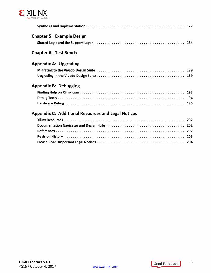
IntroductionThe 10 Gigabit Ethernet subsytem provides a 10 Gigabit Ethernet MAC and PCS/PMA in 10GBASE-R/KR modes to provide a 10 Gigabit Ethernet port. The transmit and receive data interfaces use AXI4-Stream interfaces. An optional AXI4-Lite interface is used for the control interface to internal registers.
Features• Designed to 10 Gigabit Ethernet specification
IEEE Standard 802.3-2012
• AXI4-Stream protocol support on client TX and RX interfaces. 64-bit AXI4-Stream is available for all permutations. For 10GBASE-R in supported devices, 32-bit AXI4-Stream is available to provide lower latency and utilization.
• Configured and monitored through an optional AXI4-Lite Management Data interface or using status and configuration vectors
• Supports 10GBASE-SR, -LR and -ER optical links in Zynq-7000, UltraScale™, Virtex-7, and Kintex-7 devices (LAN mode only)
• Supports 10GBASE-KR backplane linksincluding Auto-Negotiation (AN), Training and Forward Error Correction (FEC)
• Supports Deficit Idle Count • Comprehensive statistics gathering• Supports 802.3 and 802.1Qbb flow control• Supports VLAN and jumbo frames• Custom Preamble mode• Independent TX and RX Maximum
Transmission Unit (MTU) frame length• Supports high accuracy IEEE Standard
1588-2008 1-step and 2-step timestamping on a 10GBASE-R network interface
IP Facts
Facts Table
Subsystem SpecificsSupported DeviceFamily(1) (2)
10GBASE-R: UltraScale™Zynq®-7000 All Programmable SoC
Virtex®-7, Kintex®-7(3)
10GBASE-KR: UltraScale™,Virtex-7(4)
Supported UserInterfaces AXI4-Lite, AXI4-Stream
Resources Performance and Resource Utilization web page
Provided with SubsystemDesign Files Encrypted RTL
Example Design Verilog
Test Bench Verilog
Constraints File Xilinx Design Constraint (XDC)
SimulationModel Verilog or VHDL source HDL Model
SupportedS/W Driver Linux
Tested Design Flows(5)
Design Entry Vivado® Design Suite
Simulation For supported simulators, see theXilinx Design Tools: Release Notes Guide.
Synthesis Vivado Synthesis
SupportProvided by Xilinx at the Xilinx Support web page
Notes: 1. For a complete list of supported devices, see the Vivado IP
catalog. For new designs in the UltraScale/UltraScale+™ portfolio, see the 10G/25G Ethernet Subsystem webpage.
2. For the listed 7 series families, only a -2 speed grade or faster is supported.
3. -2, -2L or -3.4. GTHE2 transceivers only.
5. For the supported versions of the tools, see theXilinx Design Tools: Release Notes Guide.
Send Feedback
10Gb Ethernet v3.1 5PG157 October 4, 2017 www.xilinx.com
Chapter 1
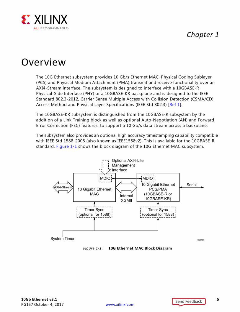
OverviewThe 10G Ethernet subsystem provides 10 Gb/s Ethernet MAC, Physical Coding Sublayer (PCS) and Physical Medium Attachment (PMA) transmit and receive functionality over an AXI4-Stream interface. The subsystem is designed to interface with a 10GBASE-R Physical-Side Interface (PHY) or a 10GBASE-KR backplane and is designed to the IEEE Standard 802.3-2012, Carrier Sense Multiple Access with Collision Detection (CSMA/CD) Access Method and Physical Layer Specifications (IEEE Std 802.3) [Ref 1].
The 10GBASE-KR subsystem is distinguished from the 10GBASE-R subsystem by the addition of a Link Training block as well as optional Auto-Negotiation (AN) and Forward Error Correction (FEC) features, to support a 10 Gb/s data stream across a backplane.
The subsystem also provides an optional high accuracy timestamping capability compatible with IEEE Std 1588-2008 (also known as IEEE1588v2). This is available for the 10GBASE-R standard. Figure 1-1 shows the block diagram of the 10G Ethernet MAC subsystem.
X-Ref Target - Figure 1-1
Figure 1-1: 10G Ethernet MAC Block Diagram
10 Gigabit Ethernet MAC
10 Gigabit Ethernet PCS/PMA
(10GBASE-R or 10GBASE-KR)
Timer Sync (optional for 1588)
Timer Sync (optional for 1588)
InternalXGMII
System Timer
SerialAXI4-Stream
X13598
Optional AXI4-LiteManagementInterface
Send Feedback
10Gb Ethernet v3.1 6PG157 October 4, 2017 www.xilinx.com
Chapter 1: Overview
10G Ethernet MAC
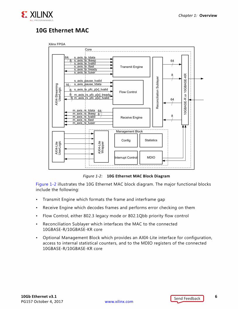
Figure 1-2 illustrates the 10G Ethernet MAC block diagram. The major functional blocks include the following:
• Transmit Engine which formats the frame and interframe gap
• Receive Engine which decodes frames and performs error checking on them
• Flow Control, either 802.3 legacy mode or 802.1Qbb priority flow control
• Reconciliation Sublayer which interfaces the MAC to the connected 10GBASE-R/10GBASE-KR core
• Optional Management Block which provides an AXI4-Lite interface for configuration, access to internal statistical counters, and to the MDIO registers of the connected 10GBASE-R/10GBASE-KR core
X-Ref Target - Figure 1-2
Figure 1-2: 10G Ethernet MAC Block Diagram
Send Feedback
10Gb Ethernet v3.1 7PG157 October 4, 2017 www.xilinx.com
Chapter 1: Overview
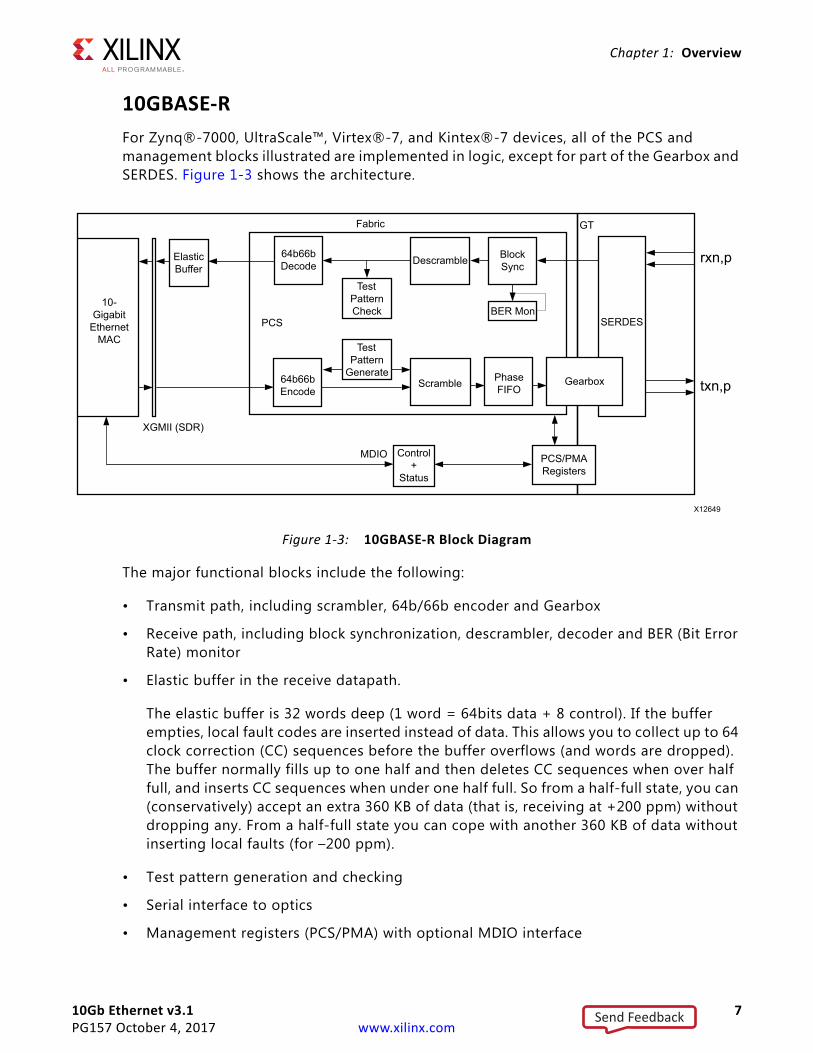
10GBASE-RFor Zynq®-7000, UltraScale™, Virtex®-7, and Kintex®-7 devices, all of the PCS and management blocks illustrated are implemented in logic, except for part of the Gearbox and SERDES. Figure 1-3 shows the architecture.
The major functional blocks include the following:
• Transmit path, including scrambler, 64b/66b encoder and Gearbox
• Receive path, including block synchronization, descrambler, decoder and BER (Bit Error Rate) monitor
• Elastic buffer in the receive datapath.
The elastic buffer is 32 words deep (1 word = 64bits data + 8 control). If the buffer empties, local fault codes are inserted instead of data. This allows you to collect up to 64 clock correction (CC) sequences before the buffer overflows (and words are dropped). The buffer normally fills up to one half and then deletes CC sequences when over half full, and inserts CC sequences when under one half full. So from a half-full state, you can (conservatively) accept an extra 360 KB of data (that is, receiving at +200 ppm) without dropping any. From a half-full state you can cope with another 360 KB of data without inserting local faults (for –200 ppm).
• Test pattern generation and checking
• Serial interface to optics
• Management registers (PCS/PMA) with optional MDIO interface
X-Ref Target - Figure 1-3
Figure 1-3: 10GBASE-R Block Diagram
64b66bDecode Descramble Block
Sync
BER Mon
TestPatternCheck
Scramble
PCS
X12649
10-Gigabit
Ethernet MAC
XGMII (SDR)
Fabric
ElasticBuffer
SERDES
rxn,p
txn,p
Control+
Status
PCS/PMARegisters
MDIO
GT
Gearbox
TestPattern
Generate64b66bEncode
PhaseFIFO
Send Feedback
10Gb Ethernet v3.1 8PG157 October 4, 2017 www.xilinx.com
Chapter 1: Overview
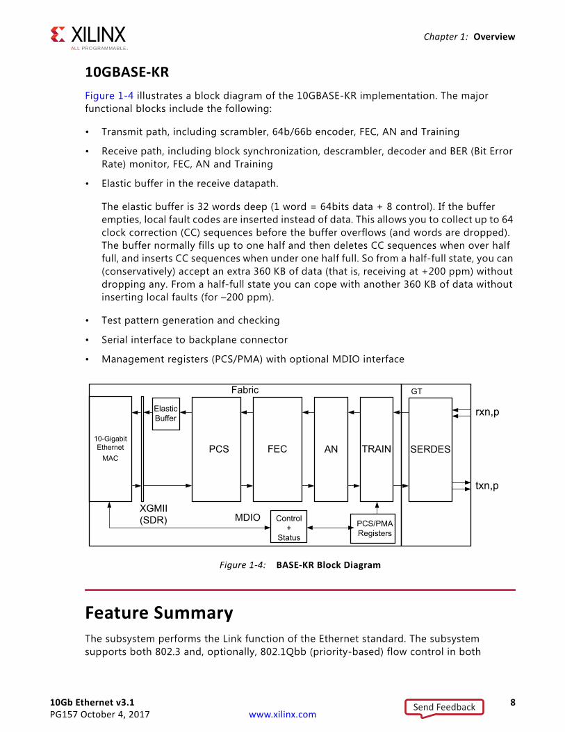
10GBASE-KRFigure 1-4 illustrates a block diagram of the 10GBASE-KR implementation. The major functional blocks include the following:
• Transmit path, including scrambler, 64b/66b encoder, FEC, AN and Training
• Receive path, including block synchronization, descrambler, decoder and BER (Bit Error Rate) monitor, FEC, AN and Training
• Elastic buffer in the receive datapath.
The elastic buffer is 32 words deep (1 word = 64bits data + 8 control). If the buffer empties, local fault codes are inserted instead of data. This allows you to collect up to 64 clock correction (CC) sequences before the buffer overflows (and words are dropped). The buffer normally fills up to one half and then deletes CC sequences when over half full, and inserts CC sequences when under one half full. So from a half-full state, you can (conservatively) accept an extra 360 KB of data (that is, receiving at +200 ppm) without dropping any. From a half-full state you can cope with another 360 KB of data without inserting local faults (for –200 ppm).
• Test pattern generation and checking
• Serial interface to backplane connector
• Management registers (PCS/PMA) with optional MDIO interface
Feature SummaryThe subsystem performs the Link function of the Ethernet standard. The subsystem supports both 802.3 and, optionally, 802.1Qbb (priority-based) flow control in both
X-Ref Target - Figure 1-4
Figure 1-4: BASE-KR Block Diagram
Fabric
10-Gigabit Ethernet
MAC
XGMII (SDR)
ElasticBuffer
SERDES
rxn,p
txn,p
Control+
Status
PCS/PMARegisters
MDIO
GT
FEC AN TRAINPCS
Send Feedback
10Gb Ethernet v3.1 9PG157 October 4, 2017 www.xilinx.com
Chapter 1: Overview
transmit and receive directions. The transmit side of the subsystem modifies the interframe gap (IFG), using Deficit Idle Count as described in IEEE Std 802.3 [Ref 1] to maintain the effective data rate.
The optional statistics counters collect statistics on the success and failure of various operations. These are accessed through the AXI4-Lite Management interface.
The subsystem also supports the following IEEE Std 1588-2008 support features:
• IEEE 1588-compatible hardware timestamping at full 10 Gb Ethernet line rate on both transmit and receive paths. Timestamp accuracy is better than ± 5 ns under all operating conditions.
• IEEE 1588 hardware timestamping for a 1-step and 2-step operation on 10GBASE-R network interfaces using 7 series GTXE2 and GTHE2 transceivers.
• The system timer provided to the subsystem and the consequential timestamping taken from it are available in one of two formats which are selected during subsystem generation.
° Time-of-Day (ToD) format: IEEE 1588-2008 format consisting of an unsigned 48-bit second field and a 32-bit nanosecond field.
° Correction Field format: IEEE 1588-2008 numerical format consisting of a 64-bit signed field representing nanoseconds multiplied by 216 (see IEEE 1588 clause 13.3.2.7). This timer should count from 0 through the full range up to 264 -1 before wrapping around.
• In-band and out-of-band control of timestamp behavior.
• In-band and out-of-band reporting of receive-side timestamps.
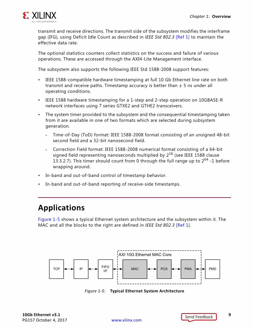
ApplicationsFigure 1-5 shows a typical Ethernet system architecture and the subsystem within it. The MAC and all the blocks to the right are defined in IEEE Std 802.3 [Ref 1].
X-Ref Target - Figure 1-5
Figure 1-5: Typical Ethernet System Architecture
Send Feedback
10Gb Ethernet v3.1 10PG157 October 4, 2017 www.xilinx.com
Chapter 1: Overview
Unsupported FeaturesThe following features are not supported in this release of the subsystem.
• IEEE 1588 unsupported features:
° 10G Ethernet PHY types other than 10GBASE-R.
° Configuration/Status vector.
° Transmit-side in-band FCS passing for 1-step timestamped frames.
• WAN mode
While the Training Protocol is supported natively by the subsystem, no logic is provided that controls the far-end transmitter adaptation based on analysis of the received signal quality. This is because extensive testing has shown that to be unnecessary.
However, a training interface is provided on the subsystem that allows access to all subsystem registers and to the DRP port on the transceiver. You can employ this interface to implement your own Training Algorithm for 10GBASE-KR, if required.
Licensing and Ordering
License CheckersIf the IP requires a license key, the key must be verified. The Vivado design tools have several license check points for gating licensed IP through the flow. If the license check succeeds, the IP can continue generation. Otherwise, generation halts with error. License checkpoints are enforced by the following tools:
• Vivado Synthesis
• Vivado Implementation
• write_bitstream (Tcl command)
IMPORTANT: IP license level is ignored at checkpoints. The test confirms a valid license exists. It does not check IP license level.
License TypeThis Xilinx module is provided under the terms of the Xilinx Core License Agreement. The module is shipped as part of the Vivado Design Suite. For full access to all subsystem functionalities in simulation and in hardware, you must purchase a license for the 10G
Send Feedback
10Gb Ethernet v3.1 11PG157 October 4, 2017 www.xilinx.com
Chapter 1: Overview
Ethernet MAC and, if using, the 10GBASE-KR core. Purchase of a 10G Ethernet MAC license enables 10G/25G Ethernet MAC plus BASE-R in the 10G/25G Ethernet Subsystem. Purchase of a 10GBASE-KR license enables 10G/25GBASE-KR/CR in the 10G/25G Ethernet Subsystem. Contact your local Xilinx sales representative for information about pricing and availability.
For more information, visit the 10G Ethernet with 1588 Subsystem product web page and the 10G/25G Ethernet Subsystem product web page.
Information about this and other Xilinx modules is available at the Xilinx Intellectual Property page. For information on pricing and availability of other Xilinx modules and tools, contact your local Xilinx sales representative.
Send Feedback
10Gb Ethernet v3.1 12PG157 October 4, 2017 www.xilinx.com
Chapter 2
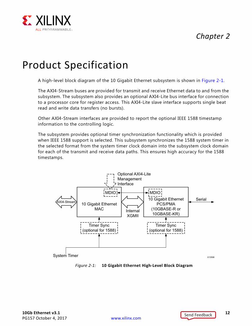
Product SpecificationA high-level block diagram of the 10 Gigabit Ethernet subsystem is shown in Figure 2-1.
The AXI4-Stream buses are provided for transmit and receive Ethernet data to and from the subsystem. The subsystem also provides an optional AXI4-Lite bus interface for connection to a processor core for register access. This AXI4-Lite slave interface supports single beat read and write data transfers (no bursts).
Other AXI4-Stream interfaces are provided to report the optional IEEE 1588 timestamp information to the controlling logic.
The subsystem provides optional timer synchronization functionality which is provided when IEEE 1588 support is selected. This subsystem synchronizes the 1588 system timer in the selected format from the system timer clock domain into the subsystem clock domain for each of the transmit and receive data paths. This ensures high accuracy for the 1588 timestamps.
X-Ref Target - Figure 2-1
Figure 2-1: 10 Gigabit Ethernet High-Level Block Diagram
10 Gigabit Ethernet MAC
10 Gigabit Ethernet PCS/PMA
(10GBASE-R or 10GBASE-KR)
Timer Sync (optional for 1588)
Timer Sync (optional for 1588)
InternalXGMII
System Timer
SerialAXI4-Stream
X13598
Optional AXI4-LiteManagementInterface
Send Feedback
10Gb Ethernet v3.1 13PG157 October 4, 2017 www.xilinx.com
Chapter 2: Product Specification
StandardsThe 10 Gigabit Ethernet Subsystem is compatible with the following IEEE standards:
• IEEE 802.3-2012 10-Gigabit Ethernet specification [Ref 1].
• IEEE 1588-2008, version 2 of the Precision Time Protocol (PTP) standard [Ref 2].
• IEEE Standard 802.1Qbb- Priority-based Flow Control [Ref 3].
The 10GBASE-R/KR part of the subsystem is designed to the standard specified in clauses 45, 49, 72, 73 and 74 of the 10-Gigabit Ethernet specification IEEE Std. 802.3-2012.
The 10Gig Ethernet MAC part of the subsystem is designed to the standard specified in clauses 3,4,31,45 and 46 of IEEE Std. 802.3-2012.
PerformanceThe 10 Gigabit Ethernet Subsystem operates at full line-rate in a 10 Gigabit Ethernet system.
Resource UtilizationFor details about resource utilization, visit Performance and Resource Utilization.
LatencyThese measurements are for the core only; they do not include the latency through the transceiver. The latency through the transceiver can be obtained from the relevant User Guide.
32-bit Datapath
Transmit Path Latency
For UltraScale™ devices, as measured from the input port tx_axis_tdata of the AXI4-Stream transmit interface until the data appears on gt_txd on the transceiver interface, the latency in the transmit direction is 13 clock periods at 312.5 MHz (41.6 ns).
Send Feedback
10Gb Ethernet v3.1 14PG157 October 4, 2017 www.xilinx.com
Chapter 2: Product Specification
For UltraScale devices, the only exception to the above figures is when 1-Step IEEE 1588 hardware timestamping support is included when using the Correction Field Timer format. In this case the transmit latency increases to 26 clock periods at 312.5 MHz (83.2 ns).
For 7 Series and Zynq-7000 devices, as measured from the input port tx_axis_tdata of the AXI4-Stream transmit interface until the data appears on gt_txd on the transceiver interface, the latency in the transmit direction is 19 clock periods at 312.5 MHz (60.8 ns).
Receive Path Latency
For UltraScale devices when the RX elastic buffer is excluded, as measured from the gt_rxd from the transceiver until data appears on the rx_axis_tdata port of the receiver side AXI4-Stream interface, the latency in the receive direction is 11 clock periods at 312.5 MHz (35.2 ns).
For UltraScale devices when the RX elastic buffer is included and for 7 series and Zynq-7000 devices, latency in the receive direction is variable and depends on the fill level of the RX elastic buffer. Nominally, this is equal to 47.6 clock cycles at 312.5 MHz (152.32 ns), increasing to 75 clock cycles (240 ns) when the elastic buffer is at its fullest possible level.
64-bit Datapath
Transmit Path Latency
For UltraScale devices, as measured from the input port tx_axis_tdata of the AXI4-Stream transmit interface until the data appears on gt_txd on the transceiver interface, the latency in the transmit direction is 13 clock periods at 156.25 MHz (83.2 ns).
For 7 series and Zynq-7000 devices, as measured from the input port tx_axis_tdata of the AXI4-Stream transmit interface until the data appears on gt_txd on the transceiver interface, the latency in the transmit direction is 27 clock periods at 156.25 MHz (172.8 ns).
For all devices, when the optional FEC functionality is included in the core and enabled, the transmit latency increases by an extra 6 clock periods (38.4 ns).
For all devices, when 1-Step IEEE 1588 hardware timestamping support is included when using the Correction Field Timer format, the transmit latency increases by an extra 5 clock periods (32 ns).
Receive Path Latency
When the RX elastic buffer is excluded, as measured from the gt_rxd from the transceiver until data appears on the rx_axis_tdata port of the receiver side AXI4-Stream interface, the latency in the receive direction is 12 clock periods (or 76.8 ns) of the rxrecclk_out clock.
Send Feedback
10Gb Ethernet v3.1 15PG157 October 4, 2017 www.xilinx.com
Chapter 2: Product Specification
For UltraScale devices when the RX elastic buffer is included and for 7 series and Zynq-7000 devices, latency in the receive direction is variable and depends on the fill level of the RX elastic buffer. Nominally, this is equal to 32.75 clock cycles (or 209.6 ns) of the txusrclk2/txusrclk2_out clock, increasing to 46.26 clock cycles (or 296 ns) when the elastic buffer is at its fullest possible level.
When the optional FEC functionality is included in the core, there is always an extra single cycle of latency (6.4 ns) and this increases by 70 cycles (448 ns) when FEC is enabled and if error reporting to the PCS layer is enabled, there is an extra 66 cycles (422.4 ns) latency.
Port DescriptionsAXI4-Stream Transmit InterfaceThe AXI4-Stream transmit interface signals are shown in Table 2-1. See Connecting the Data Interfaces for details on connecting to the transmit interface. When the 32-bit datapath option is selected the AXI4-Stream interface becomes 32-bits wide rather than 64.
AXI4-Stream Receive InterfaceThe AXI4-Stream receive interface signals are shown in Table 2-2. See Connecting the Data Interfaces for details on connecting to the receive interface. When the 32-bit datapath option is selected the AXI4-Stream interface becomes 32-bits wide rather than 64.
Table 2-1: AXI4-Stream Interface Ports – Transmit
Name Direction Description
tx_axis_aresetn In AXI4-Stream active-Low reset for transmit path
s_axis_tx_tdata[63 or 31:0] In AXI4-Stream data to core. Bus width depends on 64-bit or 32-bit selection.
s_axis_tx_tkeep[7 or 3:0] In AXI4-Stream data control to core. Bus width depends on 64-bit or 32-bit selection.
s_axis_tx_tvalid In AXI4-Stream data valid input to core
s_axis_tx_tuser[0:0](1) InAXI4-Stream user signal used to signal explicit underrun. This is a vector of length 1 rather than a single bit to allow for future expansion.
tx_ifg_delay[7:0] In Configures Interframe Gap adjustment between packets
s_axis_tx_tlast In AXI4-Stream signal to core indicating End of Ethernet Packet
s_axis_tx_tready Out AXI4-Stream acknowledge signal from core to indicate the start of a data transfer
Notes: 1. s_axis_tx_tuser is [0:0) when not using 1588; it is [127:0] when using the 1588 option.
Send Feedback
10Gb Ethernet v3.1 16PG157 October 4, 2017 www.xilinx.com
Chapter 2: Product Specification
Flow Control Interface (IEEE 802.3)The flow control interface is used to initiate the transmission of flow control frames from the core. The ports associated with this interface are shown in Table 2-3.
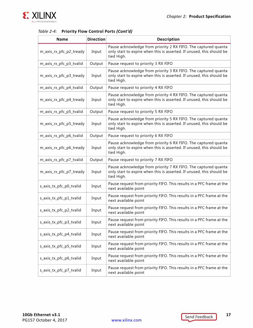
Priority Flow Control Interface (802.1Qbb)The Priority Flow Control (PFC) interface is used to initiate the transmission of PFC frames from the core. The ports associated with this interface are shown in Table 2-4. This interface is only present when priority-based flow control is enabled at the core customization stage.
Table 2-2: AXI4-Stream Interface Ports – Receive
Name Direction Description
rx_axis_aresetn In AXI4-Stream active-Low reset for receive path
m_axis_rx_tdata[63 or 31:0] Out AXI4-Stream data from core to upper layer. Bus width depends on 64-bit or 32-bit selection.
m_axis_rx_tkeep[7 or 3:0] Out AXI4-Stream data control from core to upper layer. Bus width depends on 64-bit or 32-bit selection.
m_axis_rx_tvalid Out AXI4-Stream Data Valid from core
m_axis_rx_tuser OutAXI4-Stream User signal from core0 indicates that a bad packet has been received.1 indicates that a good packet has been received.
m_axis_rx_tlast Out AXI4-Stream signal from core indicating the end of a packet
Table 2-3: Flow Control (IEE802.3) Interface Ports
Name Direction Description
s_axis_pause_tvalid In Request that a flow control frame is sent from the core.
s_axis_pause_tdata[15:0] In Pause value field for flow control frame to be sent when s_axis_pause_tvalid asserted.
Table 2-4: Priority Flow Control Ports
Name Direction Description
m_axis_rx_pfc_p0_tvalid Output Pause request to priority 0 RX FIFO
m_axis_rx_pfc_p0_tready InputPause acknowledge from priority 0 RX FIFO. The captured quanta only start to expire when this is asserted. If unused, this should be tied High.
m_axis_rx_pfc_p1_tvalid Output Pause request to priority 1 RX FIFO
m_axis_rx_pfc_p1_tready InputPause acknowledge from priority 1 RX FIFO. The captured quanta only start to expire when this is asserted. If unused, this should be tied High.
m_axis_rx_pfc_p2_tvalid Output Pause request to priority 2 RX FIFO
Send Feedback
10Gb Ethernet v3.1 17PG157 October 4, 2017 www.xilinx.com
Chapter 2: Product Specification
m_axis_rx_pfc_p2_tready InputPause acknowledge from priority 2 RX FIFO. The captured quanta only start to expire when this is asserted. If unused, this should be tied High.
m_axis_rx_pfc_p3_tvalid Output Pause request to priority 3 RX FIFO
m_axis_rx_pfc_p3_tready InputPause acknowledge from priority 3 RX FIFO. The captured quanta only start to expire when this is asserted. If unused, this should be tied High.
m_axis_rx_pfc_p4_tvalid Output Pause request to priority 4 RX FIFO
m_axis_rx_pfc_p4_tready InputPause acknowledge from priority 4 RX FIFO. The captured quanta only start to expire when this is asserted. If unused, this should be tied High.
m_axis_rx_pfc_p5_tvalid Output Pause request to priority 5 RX FIFO
m_axis_rx_pfc_p5_tready InputPause acknowledge from priority 5 RX FIFO. The captured quanta only start to expire when this is asserted. If unused, this should be tied High.
m_axis_rx_pfc_p6_tvalid Output Pause request to priority 6 RX FIFO
m_axis_rx_pfc_p6_tready InputPause acknowledge from priority 6 RX FIFO. The captured quanta only start to expire when this is asserted. If unused, this should be tied High.
m_axis_rx_pfc_p7_tvalid Output Pause request to priority 7 RX FIFO
m_axis_rx_pfc_p7_tready InputPause acknowledge from priority 7 RX FIFO. The captured quanta only start to expire when this is asserted. If unused, this should be tied High.
s_axis_tx_pfc_p0_tvalid Input Pause request from priority FIFO. This results in a PFC frame at the next available point
s_axis_tx_pfc_p1_tvalid Input Pause request from priority FIFO. This results in a PFC frame at the next available point
s_axis_tx_pfc_p2_tvalid Input Pause request from priority FIFO. This results in a PFC frame at the next available point
s_axis_tx_pfc_p3_tvalid Input Pause request from priority FIFO. This results in a PFC frame at the next available point
s_axis_tx_pfc_p4_tvalid Input Pause request from priority FIFO. This results in a PFC frame at the next available point
s_axis_tx_pfc_p5_tvalid Input Pause request from priority FIFO. This results in a PFC frame at the next available point
s_axis_tx_pfc_p6_tvalid Input Pause request from priority FIFO. This results in a PFC frame at the next available point
s_axis_tx_pfc_p7_tvalid Input Pause request from priority FIFO. This results in a PFC frame at the next available point
Table 2-4: Priority Flow Control Ports (Cont’d)
Name Direction Description
Send Feedback
10Gb Ethernet v3.1 18PG157 October 4, 2017 www.xilinx.com
Chapter 2: Product Specification
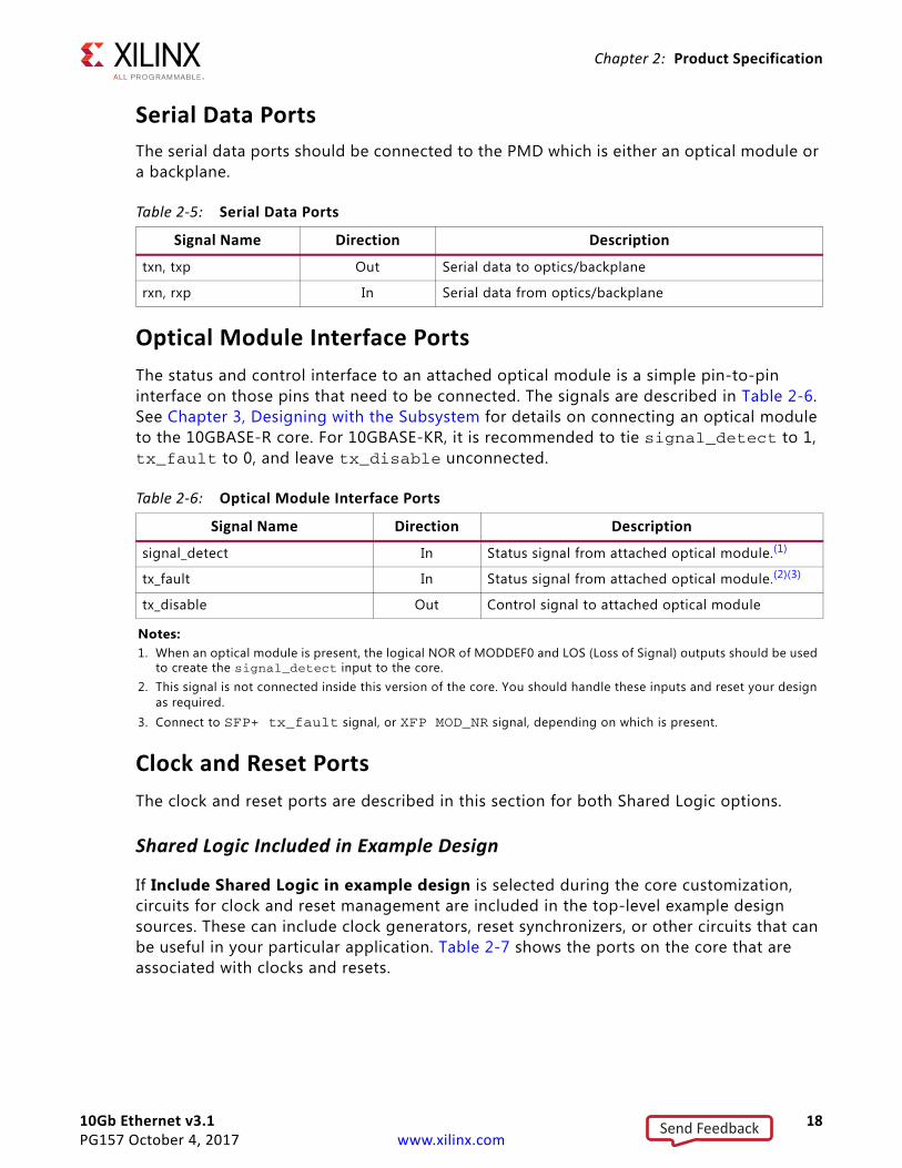
Serial Data PortsThe serial data ports should be connected to the PMD which is either an optical module or a backplane.
Optical Module Interface PortsThe status and control interface to an attached optical module is a simple pin-to-pin interface on those pins that need to be connected. The signals are described in Table 2-6. See Chapter 3, Designing with the Subsystem for details on connecting an optical module to the 10GBASE-R core. For 10GBASE-KR, it is recommended to tie signal_detect to 1, tx_fault to 0, and leave tx_disable unconnected.
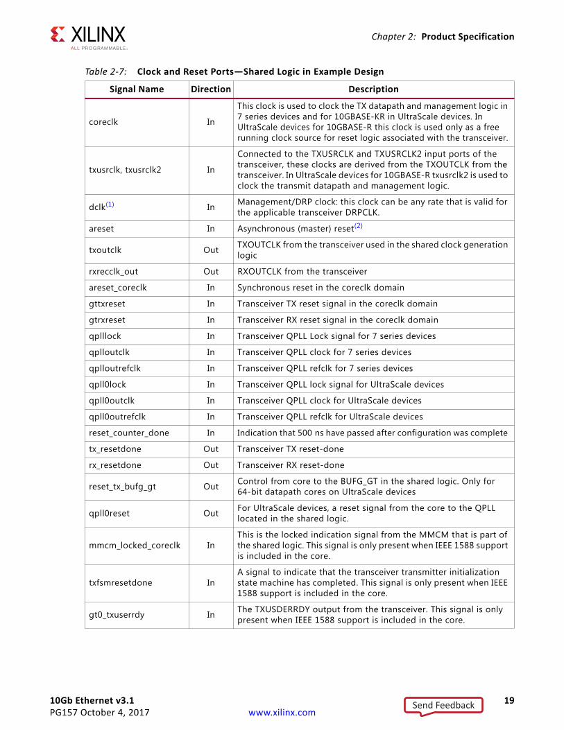
Clock and Reset PortsThe clock and reset ports are described in this section for both Shared Logic options.
Shared Logic Included in Example Design
If Include Shared Logic in example design is selected during the core customization, circuits for clock and reset management are included in the top-level example design sources. These can include clock generators, reset synchronizers, or other circuits that can be useful in your particular application. Table 2-7 shows the ports on the core that are associated with clocks and resets.
Table 2-5: Serial Data Ports
Signal Name Direction Description
txn, txp Out Serial data to optics/backplane
rxn, rxp In Serial data from optics/backplane
Table 2-6: Optical Module Interface Ports
Signal Name Direction Description
signal_detect In Status signal from attached optical module.(1)
tx_fault In Status signal from attached optical module.(2)(3)
tx_disable Out Control signal to attached optical module
Notes: 1. When an optical module is present, the logical NOR of MODDEF0 and LOS (Loss of Signal) outputs should be used
to create the signal_detect input to the core.2. This signal is not connected inside this version of the core. You should handle these inputs and reset your design
as required.3. Connect to SFP+ tx_fault signal, or XFP MOD_NR signal, depending on which is present.
Send Feedback
10Gb Ethernet v3.1 19PG157 October 4, 2017 www.xilinx.com
Chapter 2: Product Specification
Table 2-7: Clock and Reset Ports—Shared Logic in Example Design
Signal Name Direction Description
coreclk In
This clock is used to clock the TX datapath and management logic in 7 series devices and for 10GBASE-KR in UltraScale devices. In UltraScale devices for 10GBASE-R this clock is used only as a free running clock source for reset logic associated with the transceiver.
txusrclk, txusrclk2 In
Connected to the TXUSRCLK and TXUSRCLK2 input ports of the transceiver, these clocks are derived from the TXOUTCLK from the transceiver. In UltraScale devices for 10GBASE-R txusrclk2 is used to clock the transmit datapath and management logic.
dclk(1) In Management/DRP clock: this clock can be any rate that is valid for the applicable transceiver DRPCLK.
areset In Asynchronous (master) reset(2)
txoutclk Out TXOUTCLK from the transceiver used in the shared clock generation logic
rxrecclk_out Out RXOUTCLK from the transceiver
areset_coreclk In Synchronous reset in the coreclk domain
gttxreset In Transceiver TX reset signal in the coreclk domain
gtrxreset In Transceiver RX reset signal in the coreclk domain
qplllock In Transceiver QPLL Lock signal for 7 series devices
qplloutclk In Transceiver QPLL clock for 7 series devices
qplloutrefclk In Transceiver QPLL refclk for 7 series devices
qpll0lock In Transceiver QPLL lock signal for UltraScale devices
qpll0outclk In Transceiver QPLL clock for UltraScale devices
qpll0outrefclk In Transceiver QPLL refclk for UltraScale devices
reset_counter_done In Indication that 500 ns have passed after configuration was complete
tx_resetdone Out Transceiver TX reset-done
rx_resetdone Out Transceiver RX reset-done
reset_tx_bufg_gt Out Control from core to the BUFG_GT in the shared logic. Only for 64-bit datapath cores on UltraScale devices
qpll0reset Out For UltraScale devices, a reset signal from the core to the QPLL located in the shared logic.
mmcm_locked_coreclk InThis is the locked indication signal from the MMCM that is part of the shared logic. This signal is only present when IEEE 1588 support is included in the core.
txfsmresetdone InA signal to indicate that the transceiver transmitter initialization state machine has completed. This signal is only present when IEEE 1588 support is included in the core.
gt0_txuserrdy In The TXUSDERRDY output from the transceiver. This signal is only present when IEEE 1588 support is included in the core.
Send Feedback
10Gb Ethernet v3.1 20PG157 October 4, 2017 www.xilinx.com
Chapter 2: Product Specification
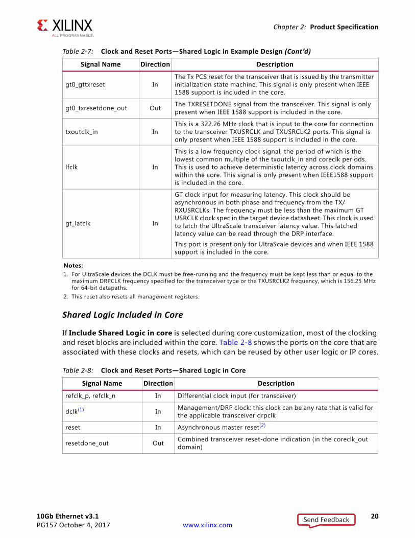
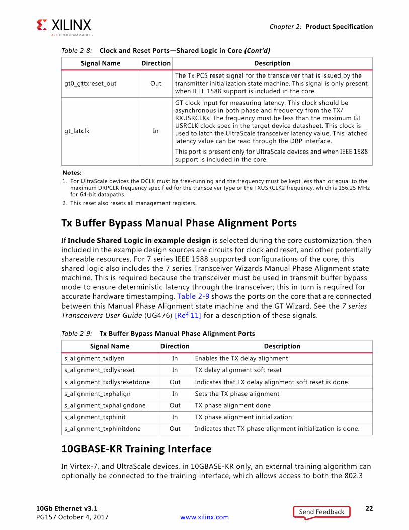
Shared Logic Included in Core
If Include Shared Logic in core is selected during core customization, most of the clocking and reset blocks are included within the core. Table 2-8 shows the ports on the core that are associated with these clocks and resets, which can be reused by other user logic or IP cores.
gt0_gttxreset InThe Tx PCS reset for the transceiver that is issued by the transmitter initialization state machine. This signal is only present when IEEE 1588 support is included in the core.
gt0_txresetdone_out Out The TXRESETDONE signal from the transceiver. This signal is only present when IEEE 1588 support is included in the core.
txoutclk_in InThis is a 322.26 MHz clock that is input to the core for connection to the transceiver TXUSRCLK and TXUSRCLK2 ports. This signal is only present when IEEE 1588 support is included in the core.
lfclk In
This is a low frequency clock signal, the period of which is the lowest common multiple of the txoutclk_in and coreclk periods. This is used to achieve deterministic latency across clock domains within the core. This signal is only present when IEEE1588 support is included in the core.
gt_latclk In
GT clock input for measuring latency. This clock should be asynchronous in both phase and frequency from the TX/RXUSRCLKs. The frequency must be less than the maximum GT USRCLK clock spec in the target device datasheet. This clock is used to latch the UltraScale transceiver latency value. This latched latency value can be read through the DRP interface.
This port is present only for UltraScale devices and when IEEE 1588 support is included in the core.
Notes: 1. For UltraScale devices the DCLK must be free-running and the frequency must be kept less than or equal to the
maximum DRPCLK frequency specified for the transceiver type or the TXUSRCLK2 frequency, which is 156.25 MHz for 64-bit datapaths.
2. This reset also resets all management registers.
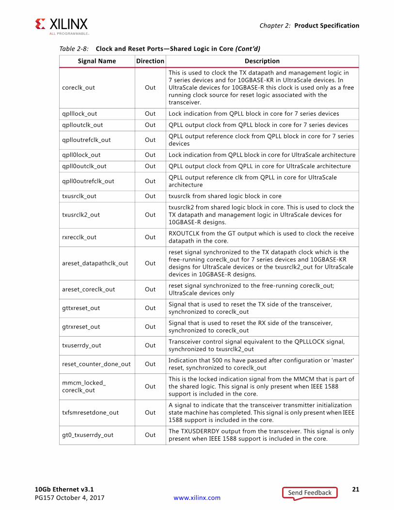
Table 2-8: Clock and Reset Ports—Shared Logic in Core
Signal Name Direction Description
refclk_p, refclk_n In Differential clock input (for transceiver)
dclk(1) In Management/DRP clock: this clock can be any rate that is valid for the applicable transceiver drpclk
reset In Asynchronous master reset(2)
resetdone_out Out Combined transceiver reset-done indication (in the coreclk_out domain)
Table 2-7: Clock and Reset Ports—Shared Logic in Example Design (Cont’d)
Signal Name Direction Description
Send Feedback
10Gb Ethernet v3.1 21PG157 October 4, 2017 www.xilinx.com
Chapter 2: Product Specification
coreclk_out Out
This is used to clock the TX datapath and management logic in 7 series devices and for 10GBASE-KR in UltraScale devices. In UltraScale devices for 10GBASE-R this clock is used only as a free running clock source for reset logic associated with the transceiver.
qplllock_out Out Lock indication from QPLL block in core for 7 series devices
qplloutclk_out Out QPLL output clock from QPLL block in core for 7 series devices
qplloutrefclk_out Out QPLL output reference clock from QPLL block in core for 7 series devices
qpll0lock_out Out Lock indication from QPLL block in core for UltraScale architecture
qpll0outclk_out Out QPLL output clock from QPLL in core for UltraScale architecture
qpll0outrefclk_out Out QPLL output reference clk from QPLL in core for UltraScale architecture
txusrclk_out Out txusrclk from shared logic block in core
txusrclk2_out Outtxusrclk2 from shared logic block in core. This is used to clock the TX datapath and management logic in UltraScale devices for 10GBASE-R designs.
rxrecclk_out Out RXOUTCLK from the GT output which is used to clock the receive datapath in the core.
areset_datapathclk_out Out
reset signal synchronized to the TX datapath clock which is the free-running coreclk_out for 7 series devices and 10GBASE-KR designs for UltraScale devices or the txusrclk2_out for UltraScale devices in 10GBASE-R designs.
areset_coreclk_out Out reset signal synchronized to the free-running coreclk_out; UltraScale devices only
gttxreset_out Out Signal that is used to reset the TX side of the transceiver, synchronized to coreclk_out
gtrxreset_out Out Signal that is used to reset the RX side of the transceiver, synchronized to coreclk_out
txuserrdy_out Out Transceiver control signal equivalent to the QPLLLOCK signal, synchronized to txusrclk2_out
reset_counter_done_out Out Indication that 500 ns have passed after configuration or 'master' reset, synchronized to coreclk_out
mmcm_locked_coreclk_out Out
This is the locked indication signal from the MMCM that is part of the shared logic. This signal is only present when IEEE 1588 support is included in the core.
txfsmresetdone_out OutA signal to indicate that the transceiver transmitter initialization state machine has completed. This signal is only present when IEEE 1588 support is included in the core.
gt0_txuserrdy_out Out The TXUSDERRDY output from the transceiver. This signal is only present when IEEE 1588 support is included in the core.
Table 2-8: Clock and Reset Ports—Shared Logic in Core (Cont’d)
Signal Name Direction Description
Send Feedback
10Gb Ethernet v3.1 22PG157 October 4, 2017 www.xilinx.com
Chapter 2: Product Specification
Tx Buffer Bypass Manual Phase Alignment PortsIf Include Shared Logic in example design is selected during the core customization, then included in the example design sources are circuits for clock and reset, and other potentially shareable resources. For 7 series IEEE 1588 supported configurations of the core, this shared logic also includes the 7 series Transceiver Wizards Manual Phase Alignment state machine. This is required because the transceiver must be used in transmit buffer bypass mode to ensure deterministic latency through the transceiver; this in turn is required for accurate hardware timestamping. Table 2-9 shows the ports on the core that are connected between this Manual Phase Alignment state machine and the GT Wizard. See the 7 series Transceivers User Guide (UG476) [Ref 11] for a description of these signals.
10GBASE-KR Training InterfaceIn Virtex-7, and UltraScale devices, in 10GBASE-KR only, an external training algorithm can optionally be connected to the training interface, which allows access to both the 802.3
gt0_gttxreset_out OutThe Tx PCS reset signal for the transceiver that is issued by the transmitter initialization state machine. This signal is only present when IEEE 1588 support is included in the core.
gt_latclk In
GT clock input for measuring latency. This clock should be asynchronous in both phase and frequency from the TX/RXUSRCLKs. The frequency must be less than the maximum GT USRCLK clock spec in the target device datasheet. This clock is used to latch the UltraScale transceiver latency value. This latched latency value can be read through the DRP interface.
This port is present only for UltraScale devices and when IEEE 1588 support is included in the core.
Notes: 1. For UltraScale devices the DCLK must be free-running and the frequency must be kept less than or equal to the
maximum DRPCLK frequency specified for the transceiver type or the TXUSRCLK2 frequency, which is 156.25 MHz for 64-bit datapaths.
2. This reset also resets all management registers.
Table 2-9: Tx Buffer Bypass Manual Phase Alignment Ports
Signal Name Direction Description
s_alignment_txdlyen In Enables the TX delay alignment
s_alignment_txdlysreset In TX delay alignment soft reset
s_alignment_txdlysresetdone Out Indicates that TX delay alignment soft reset is done.
s_alignment_txphalign In Sets the TX phase alignment
s_alignment_txphaligndone Out TX phase alignment done
s_alignment_txphinit In TX phase alignment initialization
s_alignment_txphinitdone Out Indicates that TX phase alignment initialization is done.
Table 2-8: Clock and Reset Ports—Shared Logic in Core (Cont’d)
Signal Name Direction Description
Send Feedback
10Gb Ethernet v3.1 23PG157 October 4, 2017 www.xilinx.com
Chapter 2: Product Specification
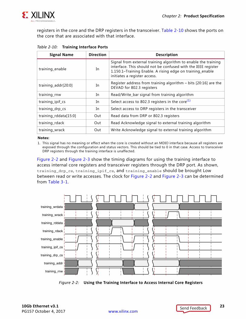
registers in the core and the DRP registers in the transceiver. Table 2-10 shows the ports on the core that are associated with that interface.
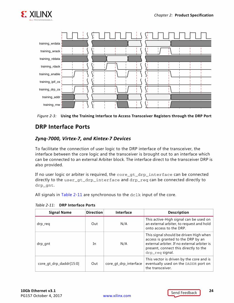
Figure 2-2 and Figure 2-3 show the timing diagrams for using the training interface to access internal core registers and transceiver registers through the DRP port. As shown, training_drp_cs, training_ipif_cs, and training_enable should be brought Low between read or write accesses. The clock for Figure 2-2 and Figure 2-3 can be determined from Table 3-1.
Table 2-10: Training Interface Ports
Signal Name Direction Description
training_enable In
Signal from external training algorithm to enable the training interface. This should not be confused with the IEEE register 1.150.1–Training Enable. A rising edge on training_enable initiates a register access.
training_addr[20:0] In Register address from training algorithm – bits [20:16] are the DEVAD for 802.3 registers
training_rnw In Read/Write_bar signal from training algorithm
training_ipif_cs In Select access to 802.3 registers in the core(1)
training_drp_cs In Select access to DRP registers in the transceiver
training_rddata[15:0] Out Read data from DRP or 802.3 registers
training_rdack Out Read Acknowledge signal to external training algorithm
training_wrack Out Write Acknowledge signal to external training algorithm
Notes: 1. This signal has no meaning or effect when the core is created without an MDIO interface because all registers are
exposed through the configuration and status vectors. This should be tied to 0 in that case. Access to transceiver DRP registers through the training interface is unaffected.
X-Ref Target - Figure 2-2
Figure 2-2: Using the Training Interface to Access Internal Core Registers
Send Feedback
10Gb Ethernet v3.1 24PG157 October 4, 2017 www.xilinx.com
Chapter 2: Product Specification
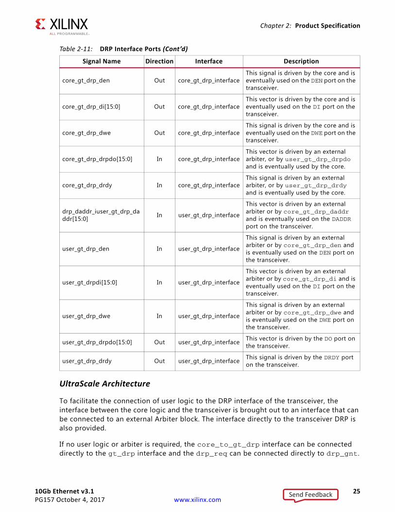
DRP Interface Ports
Zynq-7000, Virtex-7, and Kintex-7 Devices
To facilitate the connection of user logic to the DRP interface of the transceiver, the interface between the core logic and the transceiver is brought out to an interface which can be connected to an external Arbiter block. The interface direct to the transceiver DRP is also provided.
If no user logic or arbiter is required, the core_gt_drp_interface can be connected directly to the user_gt_drp_interface and drp_req can be connected directly to drp_gnt.
All signals in Table 2-11 are synchronous to the dclk input of the core.
X-Ref Target - Figure 2-3
Figure 2-3: Using the Training Interface to Access Transceiver Registers through the DRP Port
Table 2-11: DRP Interface Ports
Signal Name Direction Interface Description
drp_req Out N/AThis active-High signal can be used on an external arbiter, to request and hold onto access to the DRP.
drp_gnt In N/A
This signal should be driven High when access is granted to the DRP by an external arbiter. If no external arbiter is present, connect this directly to the drp_req signal.
core_gt_drp_daddr[15:0] Out core_gt_drp_interfaceThis vector is driven by the core and is eventually used on the DADDR port on the transceiver.
Send Feedback
10Gb Ethernet v3.1 25PG157 October 4, 2017 www.xilinx.com
Chapter 2: Product Specification
UltraScale Architecture
To facilitate the connection of user logic to the DRP interface of the transceiver, the interface between the core logic and the transceiver is brought out to an interface that can be connected to an external Arbiter block. The interface directly to the transceiver DRP is also provided.
If no user logic or arbiter is required, the core_to_gt_drp interface can be connected directly to the gt_drp interface and the drp_req can be connected directly to drp_gnt.
core_gt_drp_den Out core_gt_drp_interfaceThis signal is driven by the core and is eventually used on the DEN port on the transceiver.
core_gt_drp_di[15:0] Out core_gt_drp_interfaceThis vector is driven by the core and is eventually used on the DI port on the transceiver.
core_gt_drp_dwe Out core_gt_drp_interfaceThis signal is driven by the core and is eventually used on the DWE port on the transceiver.
core_gt_drp_drpdo[15:0] In core_gt_drp_interfaceThis vector is driven by an external arbiter, or by user_gt_drp_drpdo and is eventually used by the core.
core_gt_drp_drdy In core_gt_drp_interfaceThis signal is driven by an external arbiter, or by user_gt_drp_drdy and is eventually used by the core.
drp_daddr_iuser_gt_drp_daddr[15:0] In user_gt_drp_interface
This vector is driven by an external arbiter or by core_gt_drp_daddr and is eventually used on the DADDR port on the transceiver.
user_gt_drp_den In user_gt_drp_interface
This signal is driven by an external arbiter or by core_gt_drp_den and is eventually used on the DEN port on the transceiver.
user_gt_drpdi[15:0] In user_gt_drp_interface
This vector is driven by an external arbiter or by core_gt_drp_di and is eventually used on the DI port on the transceiver.
user_gt_drp_dwe In user_gt_drp_interface
This signal is driven by an external arbiter or by core_gt_drp_dwe and is eventually used on the DWE port on the transceiver.
user_gt_drp_drpdo[15:0] Out user_gt_drp_interface This vector is driven by the DO port on the transceiver.
user_gt_drp_drdy Out user_gt_drp_interface This signal is driven by the DRDY port on the transceiver.
Table 2-11: DRP Interface Ports (Cont’d)
Signal Name Direction Interface Description
Send Feedback
10Gb Ethernet v3.1 26PG157 October 4, 2017 www.xilinx.com
Chapter 2: Product Specification
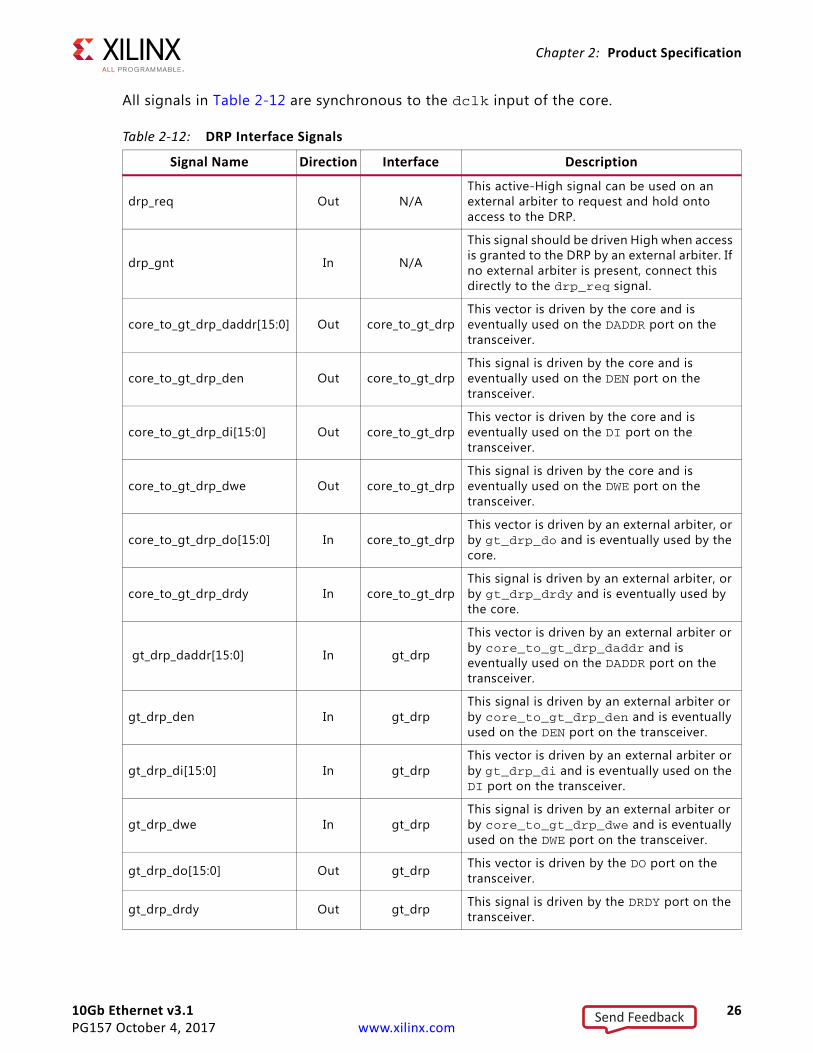
All signals in Table 2-12 are synchronous to the dclk input of the core.
Table 2-12: DRP Interface Signals
Signal Name Direction Interface Description
drp_req Out N/AThis active-High signal can be used on an external arbiter to request and hold onto access to the DRP.
drp_gnt In N/A
This signal should be driven High when access is granted to the DRP by an external arbiter. If no external arbiter is present, connect this directly to the drp_req signal.
core_to_gt_drp_daddr[15:0] Out core_to_gt_drpThis vector is driven by the core and is eventually used on the DADDR port on the transceiver.
core_to_gt_drp_den Out core_to_gt_drpThis signal is driven by the core and is eventually used on the DEN port on the transceiver.
core_to_gt_drp_di[15:0] Out core_to_gt_drpThis vector is driven by the core and is eventually used on the DI port on the transceiver.
core_to_gt_drp_dwe Out core_to_gt_drpThis signal is driven by the core and is eventually used on the DWE port on the transceiver.
core_to_gt_drp_do[15:0] In core_to_gt_drpThis vector is driven by an external arbiter, or by gt_drp_do and is eventually used by the core.
core_to_gt_drp_drdy In core_to_gt_drpThis signal is driven by an external arbiter, or by gt_drp_drdy and is eventually used by the core.
gt_drp_daddr[15:0] In gt_drp
This vector is driven by an external arbiter or by core_to_gt_drp_daddr and is eventually used on the DADDR port on the transceiver.
gt_drp_den In gt_drp This signal is driven by an external arbiter or by core_to_gt_drp_den and is eventually used on the DEN port on the transceiver.
gt_drp_di[15:0] In gt_drp This vector is driven by an external arbiter or by gt_drp_di and is eventually used on the DI port on the transceiver.
gt_drp_dwe In gt_drp This signal is driven by an external arbiter or by core_to_gt_drp_dwe and is eventually used on the DWE port on the transceiver.
gt_drp_do[15:0] Out gt_drp This vector is driven by the DO port on the transceiver.
gt_drp_drdy Out gt_drp This signal is driven by the DRDY port on the transceiver.
Send Feedback
10Gb Ethernet v3.1 27PG157 October 4, 2017 www.xilinx.com
Chapter 2: Product Specification
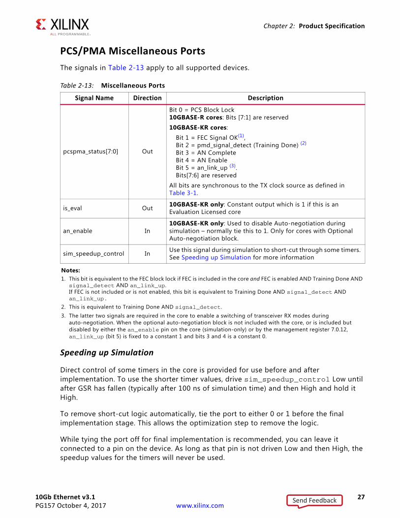
PCS/PMA Miscellaneous PortsThe signals in Table 2-13 apply to all supported devices.
Speeding up Simulation
Direct control of some timers in the core is provided for use before and after implementation. To use the shorter timer values, drive sim_speedup_control Low until after GSR has fallen (typically after 100 ns of simulation time) and then High and hold it High.
To remove short-cut logic automatically, tie the port to either 0 or 1 before the final implementation stage. This allows the optimization step to remove the logic.
While tying the port off for final implementation is recommended, you can leave it connected to a pin on the device. As long as that pin is not driven Low and then High, the speedup values for the timers will never be used.
Table 2-13: Miscellaneous Ports
Signal Name Direction Description
pcspma_status[7:0] Out
Bit 0 = PCS Block Lock10GBASE-R cores: Bits [7:1] are reserved
10GBASE-KR cores:
Bit 1 = FEC Signal OK(1), Bit 2 = pmd_signal_detect (Training Done) (2)
Bit 3 = AN CompleteBit 4 = AN EnableBit 5 = an_link_up (3). Bits[7:6] are reserved
All bits are synchronous to the TX clock source as defined in Table 3-1.
is_eval Out 10GBASE-KR only: Constant output which is 1 if this is an Evaluation Licensed core
an_enable In10GBASE-KR only: Used to disable Auto-negotiation during simulation – normally tie this to 1. Only for cores with Optional Auto-negotiation block.
sim_speedup_control In Use this signal during simulation to short-cut through some timers. See Speeding up Simulation for more information
Notes: 1. This bit is equivalent to the FEC block lock if FEC is included in the core and FEC is enabled AND Training Done AND
signal_detect AND an_link_up. If FEC is not included or is not enabled, this bit is equivalent to Training Done AND signal_detect AND an_link_up.
2. This is equivalent to Training Done AND signal_detect.3. The latter two signals are required in the core to enable a switching of transceiver RX modes during
auto-negotiation. When the optional auto-negotiation block is not included with the core, or is included but disabled by either the an_enable pin on the core (simulation-only) or by the management register 7.0.12, an_link_up (bit 5) is fixed to a constant 1 and bits 3 and 4 is a constant 0.
Send Feedback
10Gb Ethernet v3.1 28PG157 October 4, 2017 www.xilinx.com
Chapter 2: Product Specification
The timer that is speeded up with this control is the transceiver RX reset timer. This delays the assertion of RXUSERRDY which is reduced from 37 million UI to 50,000 UI. Also, for BASE-KR cores, the auto-negotiation Break Link Timer value is reduced from around 67 ms to just 6.4 μs.
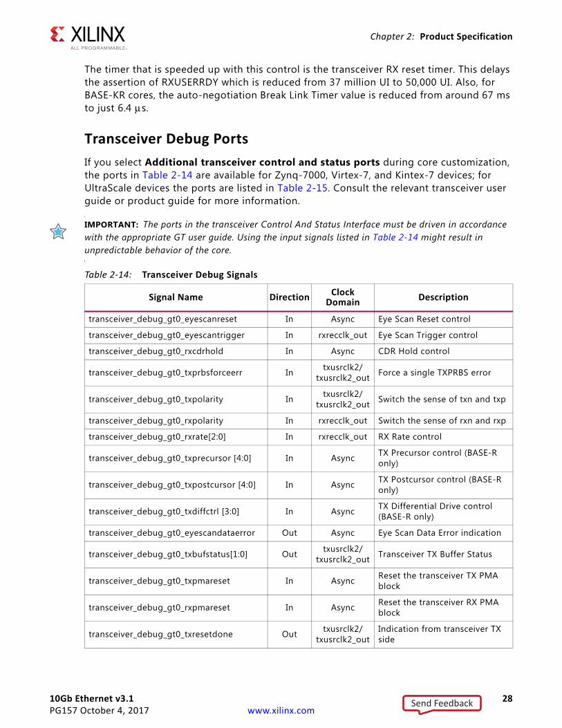
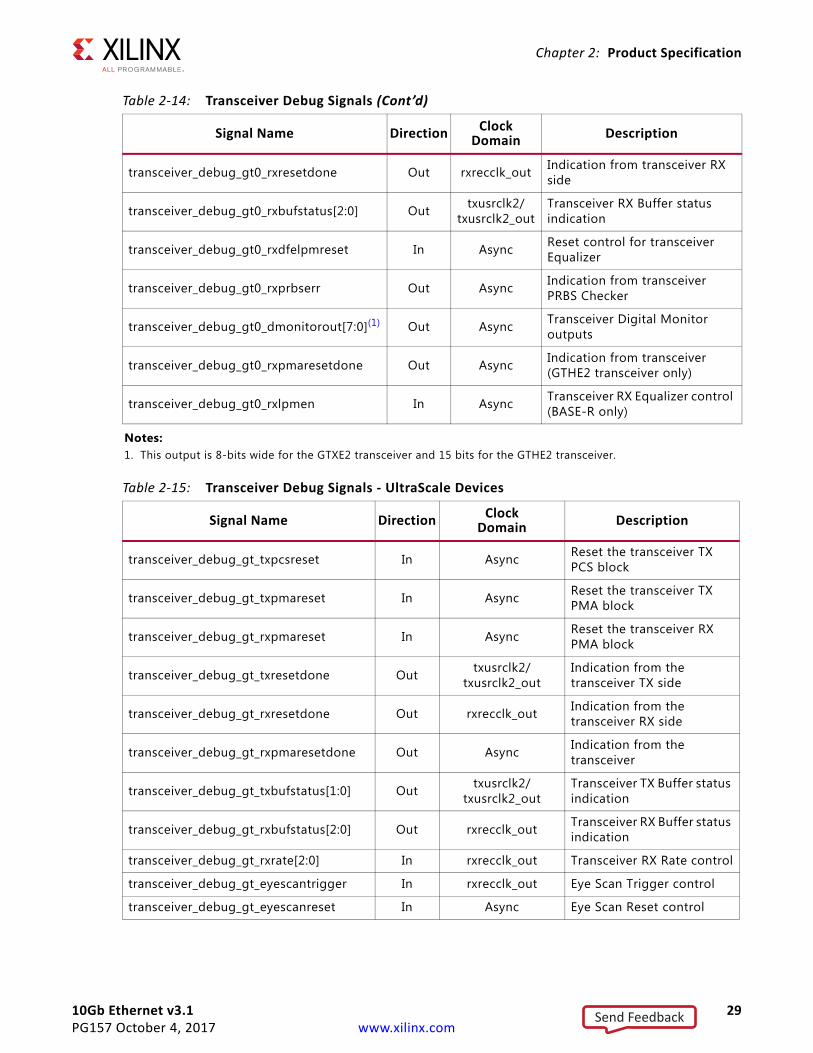
Transceiver Debug PortsIf you select Additional transceiver control and status ports during core customization, the ports in Table 2-14 are available for Zynq-7000, Virtex-7, and Kintex-7 devices; for UltraScale devices the ports are listed in Table 2-15. Consult the relevant transceiver user guide or product guide for more information.
IMPORTANT: The ports in the transceiver Control And Status Interface must be driven in accordance with the appropriate GT user guide. Using the input signals listed in Table 2-14 might result in unpredictable behavior of the core.
Table 2-14: Transceiver Debug Signals
Signal Name Direction ClockDomain Description
transceiver_debug_gt0_eyescanreset In Async Eye Scan Reset control
transceiver_debug_gt0_eyescantrigger In rxrecclk_out Eye Scan Trigger control
transceiver_debug_gt0_rxcdrhold In Async CDR Hold control
transceiver_debug_gt0_txprbsforceerr In txusrclk2/txusrclk2_out Force a single TXPRBS error
transceiver_debug_gt0_txpolarity In txusrclk2/txusrclk2_out Switch the sense of txn and txp
transceiver_debug_gt0_rxpolarity In rxrecclk_out Switch the sense of rxn and rxp
transceiver_debug_gt0_rxrate[2:0] In rxrecclk_out RX Rate control
transceiver_debug_gt0_txprecursor [4:0] In Async TX Precursor control (BASE-R only)
transceiver_debug_gt0_txpostcursor [4:0] In Async TX Postcursor control (BASE-R only)
transceiver_debug_gt0_txdiffctrl [3:0] In Async TX Differential Drive control (BASE-R only)
transceiver_debug_gt0_eyescandataerror Out Async Eye Scan Data Error indication
transceiver_debug_gt0_txbufstatus[1:0] Out txusrclk2/txusrclk2_out Transceiver TX Buffer Status
transceiver_debug_gt0_txpmareset In Async Reset the transceiver TX PMA block
transceiver_debug_gt0_rxpmareset In Async Reset the transceiver RX PMA block
transceiver_debug_gt0_txresetdone Out txusrclk2/txusrclk2_out
Indication from transceiver TX side
Send Feedback
10Gb Ethernet v3.1 29PG157 October 4, 2017 www.xilinx.com
Chapter 2: Product Specification
transceiver_debug_gt0_rxresetdone Out rxrecclk_out Indication from transceiver RX side
transceiver_debug_gt0_rxbufstatus[2:0] Out txusrclk2/txusrclk2_out
Transceiver RX Buffer status indication
transceiver_debug_gt0_rxdfelpmreset In Async Reset control for transceiver Equalizer
transceiver_debug_gt0_rxprbserr Out Async Indication from transceiver PRBS Checker
transceiver_debug_gt0_dmonitorout[7:0](1) Out Async Transceiver Digital Monitor outputs
transceiver_debug_gt0_rxpmaresetdone Out Async Indication from transceiver (GTHE2 transceiver only)
transceiver_debug_gt0_rxlpmen In Async Transceiver RX Equalizer control (BASE-R only)
Notes: 1. This output is 8-bits wide for the GTXE2 transceiver and 15 bits for the GTHE2 transceiver.
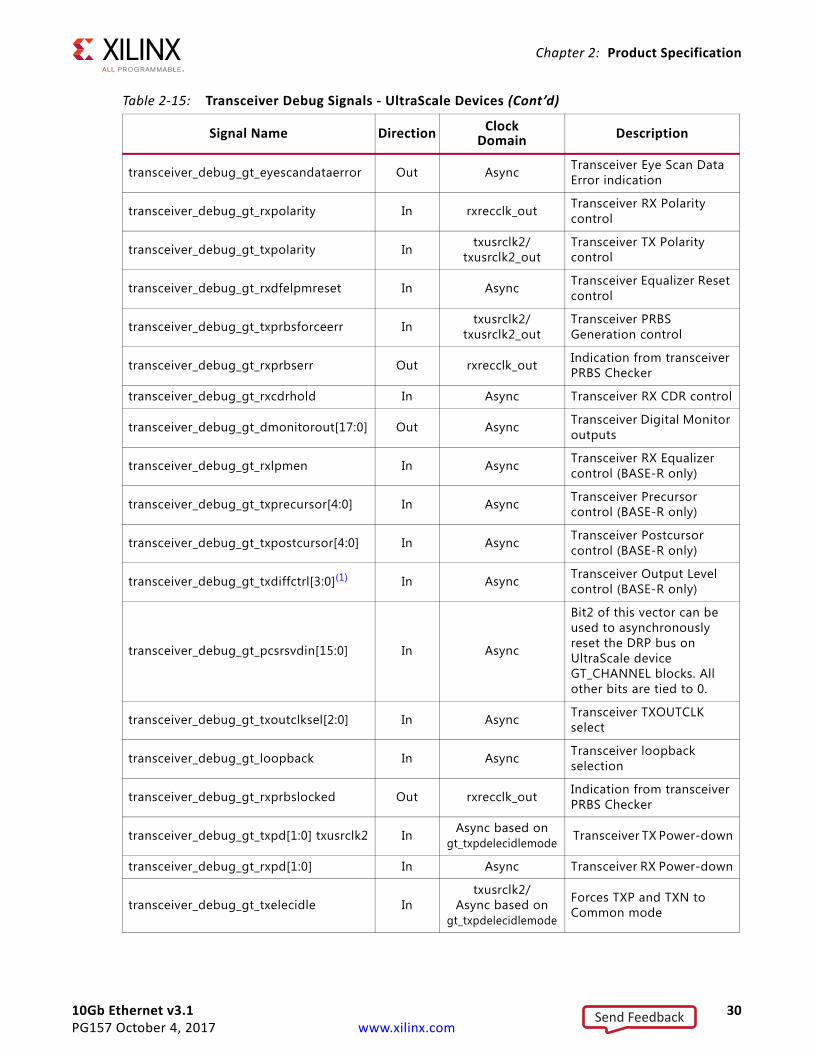
Table 2-15: Transceiver Debug Signals - UltraScale Devices
Signal Name Direction ClockDomain Description
transceiver_debug_gt_txpcsreset In Async Reset the transceiver TX PCS block
transceiver_debug_gt_txpmareset In Async Reset the transceiver TX PMA block
transceiver_debug_gt_rxpmareset In Async Reset the transceiver RX PMA block
transceiver_debug_gt_txresetdone Out txusrclk2/txusrclk2_out
Indication from the transceiver TX side
transceiver_debug_gt_rxresetdone Out rxrecclk_out Indication from the transceiver RX side
transceiver_debug_gt_rxpmaresetdone Out Async Indication from the transceiver
transceiver_debug_gt_txbufstatus[1:0] Out txusrclk2/txusrclk2_out
Transceiver TX Buffer status indication
transceiver_debug_gt_rxbufstatus[2:0] Out rxrecclk_out Transceiver RX Buffer status indication
transceiver_debug_gt_rxrate[2:0] In rxrecclk_out Transceiver RX Rate control
transceiver_debug_gt_eyescantrigger In rxrecclk_out Eye Scan Trigger control
transceiver_debug_gt_eyescanreset In Async Eye Scan Reset control
Table 2-14: Transceiver Debug Signals (Cont’d)
Signal Name Direction ClockDomain Description
Send Feedback
10Gb Ethernet v3.1 30PG157 October 4, 2017 www.xilinx.com
Chapter 2: Product Specification
transceiver_debug_gt_eyescandataerror Out Async Transceiver Eye Scan Data Error indication
transceiver_debug_gt_rxpolarity In rxrecclk_out Transceiver RX Polarity control
transceiver_debug_gt_txpolarity In txusrclk2/txusrclk2_out
Transceiver TX Polarity control
transceiver_debug_gt_rxdfelpmreset In Async Transceiver Equalizer Reset control
transceiver_debug_gt_txprbsforceerr In txusrclk2/txusrclk2_out
Transceiver PRBS Generation control
transceiver_debug_gt_rxprbserr Out rxrecclk_out Indication from transceiver PRBS Checker
transceiver_debug_gt_rxcdrhold In Async Transceiver RX CDR control
transceiver_debug_gt_dmonitorout[17:0] Out Async Transceiver Digital Monitor outputs
transceiver_debug_gt_rxlpmen In Async Transceiver RX Equalizer control (BASE-R only)
transceiver_debug_gt_txprecursor[4:0] In Async Transceiver Precursor control (BASE-R only)
transceiver_debug_gt_txpostcursor[4:0] In Async Transceiver Postcursor control (BASE-R only)
transceiver_debug_gt_txdiffctrl[3:0](1) In Async Transceiver Output Level control (BASE-R only)
transceiver_debug_gt_pcsrsvdin[15:0] In Async
Bit2 of this vector can be used to asynchronously reset the DRP bus on UltraScale device GT_CHANNEL blocks. All other bits are tied to 0.
transceiver_debug_gt_txoutclksel[2:0] In Async Transceiver TXOUTCLK select
transceiver_debug_gt_loopback In Async Transceiver loopback selection
transceiver_debug_gt_rxprbslocked Out rxrecclk_out Indication from transceiver PRBS Checker
transceiver_debug_gt_txpd[1:0] txusrclk2 In Async based on gt_txpdelecidlemode Transceiver TX Power-down
transceiver_debug_gt_rxpd[1:0] In Async Transceiver RX Power-down
transceiver_debug_gt_txelecidle Intxusrclk2/
Async based on gt_txpdelecidlemode
Forces TXP and TXN to Common mode
Table 2-15: Transceiver Debug Signals - UltraScale Devices (Cont’d)
Signal Name Direction ClockDomain Description
Send Feedback
10Gb Ethernet v3.1 31PG157 October 4, 2017 www.xilinx.com
Chapter 2: Product Specification
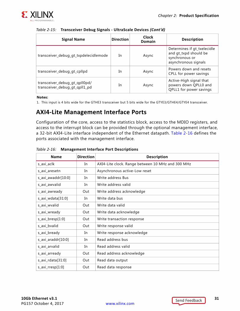
AXI4-Lite Management Interface PortsConfiguration of the core, access to the statistics block, access to the MDIO registers, and access to the interrupt block can be provided through the optional management interface, a 32-bit AXI4-Lite interface independent of the Ethernet datapath. Table 2-16 defines the ports associated with the management interface.
transceiver_debug_gt_txpdelecidlemode In Async
Determines if gt_txelecidle and gt_txpd should be synchronous or asynchronous signals
transceiver_debug_gt_cpllpd In Async Powers down and resets CPLL for power savings
transceiver_debug_gt_qpll0pd/transceiver_debug_gt_qpll1_pd In Async
Active-High signal that powers down QPLL0 and QPLL1 for power savings
Notes: 1. This input is 4 bits wide for the GTHE3 transceiver but 5 bits wide for the GTYE3/GTHE4/GTYE4 transceiver.
Table 2-16: Management Interface Port Descriptions
Name Direction Description
s_axi_aclk In AXI4-Lite clock. Range between 10 MHz and 300 MHz
s_axi_aresetn In Asynchronous active-Low reset
s_axi_awaddr[10:0] In Write address Bus
s_axi_awvalid In Write address valid
s_axi_awready Out Write address acknowledge
s_axi_wdata[31:0] In Write data bus
s_axi_wvalid Out Write data valid
s_axi_wready Out Write data acknowledge
s_axi_bresp[1:0] Out Write transaction response
s_axi_bvalid Out Write response valid
s_axi_bready In Write response acknowledge
s_axi_araddr[10:0] In Read address bus
s_axi_arvalid In Read address valid
s_axi_arready Out Read address acknowledge
s_axi_rdata[31:0] Out Read data output
s_axi_rresp[1:0] Out Read data response
Table 2-15: Transceiver Debug Signals - UltraScale Devices (Cont’d)
Signal Name Direction ClockDomain Description
Send Feedback
10Gb Ethernet v3.1 32PG157 October 4, 2017 www.xilinx.com
Chapter 2: Product Specification
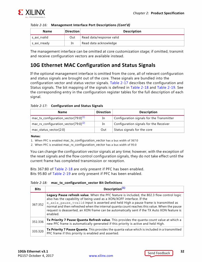
The management interface can be omitted at core customization stage; if omitted, transmit and receive configuration vectors are available instead.
10G Ethernet MAC Configuration and Status SignalsIf the optional management interface is omitted from the core, all of relevant configuration and status signals are brought out of the core. These signals are bundled into the configuration vector and status vector signals. Table 2-17 describes the configuration and Status signals. The bit mapping of the signals is defined in Table 2-18 and Table 2-19. See the corresponding entry in the configuration register tables for the full description of each signal.
You can change the configuration vector signals at any time; however, with the exception of the reset signals and the flow control configuration signals, they do not take effect until the current frame has completed transmission or reception.
Bits 367:80 of Table 2-18 are only present if PFC has been enabled. Bits 95:80 of Table 2-19 are only present if PFC has been enabled.
s_axi_rvalid Out Read data/response valid
s_axi_rready In Read data acknowledge
Table 2-17: Configuration and Status Signals
Name Direction Description
mac_tx_configuration_vector[79:0](1) In Configuration signals for the Transmitter
mac_rx_configuration_vector[79:0](2) In Configuration signals for the Receiver
mac_status_vector[2:0] Out Status signals for the core
Notes: 1. When PFC is enabled mac_tx_configuration_vector has a bus width of 367:02. When PFC is enabled mac_rx_configuration_vector has a bus width of 95:0
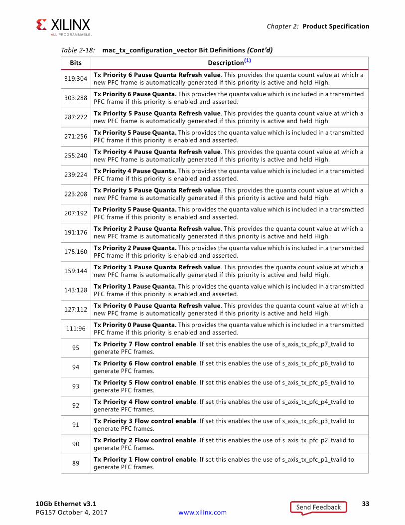
Table 2-18: mac_tx_configuration_vector Bit Definitions
Bits Description(1)
367:352
Legacy Pause refresh value. When the PFC feature is included, the 802.3 flow control logic also has the capability of being used as a XON/XOFF interface. If the s_axis_pause_tvalid input is asserted and held High a pause frame is transmitted as normal and then refreshed when the internal quanta count reaches this value. When the pause request is deasserted, an XON frame can be automatically sent if the TX Auto XON feature is enabled.
351:336 Tx Priority 7 Pause Quanta Refresh value. This provides the quanta count value at which a new PFC frame is automatically generated if this priority is active and held High.
335:320 Tx Priority 7 Pause Quanta. This provides the quanta value which is included in a transmitted PFC frame if this priority is enabled and asserted.
Table 2-16: Management Interface Port Descriptions (Cont’d)
Name Direction Description
Send Feedback
10Gb Ethernet v3.1 33PG157 October 4, 2017 www.xilinx.com
Chapter 2: Product Specification
319:304 Tx Priority 6 Pause Quanta Refresh value. This provides the quanta count value at which a new PFC frame is automatically generated if this priority is active and held High.
303:288 Tx Priority 6 Pause Quanta. This provides the quanta value which is included in a transmitted PFC frame if this priority is enabled and asserted.
287:272 Tx Priority 5 Pause Quanta Refresh value. This provides the quanta count value at which a new PFC frame is automatically generated if this priority is active and held High.
271:256 Tx Priority 5 Pause Quanta. This provides the quanta value which is included in a transmitted PFC frame if this priority is enabled and asserted.
255:240 Tx Priority 4 Pause Quanta Refresh value. This provides the quanta count value at which a new PFC frame is automatically generated if this priority is active and held High.
239:224 Tx Priority 4 Pause Quanta. This provides the quanta value which is included in a transmitted PFC frame if this priority is enabled and asserted.
223:208 Tx Priority 5 Pause Quanta Refresh value. This provides the quanta count value at which a new PFC frame is automatically generated if this priority is active and held High.
207:192 Tx Priority 5 Pause Quanta. This provides the quanta value which is included in a transmitted PFC frame if this priority is enabled and asserted.
191:176 Tx Priority 2 Pause Quanta Refresh value. This provides the quanta count value at which a new PFC frame is automatically generated if this priority is active and held High.
175:160 Tx Priority 2 Pause Quanta. This provides the quanta value which is included in a transmitted PFC frame if this priority is enabled and asserted.
159:144 Tx Priority 1 Pause Quanta Refresh value. This provides the quanta count value at which a new PFC frame is automatically generated if this priority is active and held High.
143:128 Tx Priority 1 Pause Quanta. This provides the quanta value which is included in a transmitted PFC frame if this priority is enabled and asserted.
127:112 Tx Priority 0 Pause Quanta Refresh value. This provides the quanta count value at which a new PFC frame is automatically generated if this priority is active and held High.
111:96 Tx Priority 0 Pause Quanta. This provides the quanta value which is included in a transmitted PFC frame if this priority is enabled and asserted.
95 Tx Priority 7 Flow control enable. If set this enables the use of s_axis_tx_pfc_p7_tvalid to generate PFC frames.
94 Tx Priority 6 Flow control enable. If set this enables the use of s_axis_tx_pfc_p6_tvalid to generate PFC frames.
93 Tx Priority 5 Flow control enable. If set this enables the use of s_axis_tx_pfc_p5_tvalid to generate PFC frames.
92 Tx Priority 4 Flow control enable. If set this enables the use of s_axis_tx_pfc_p4_tvalid to generate PFC frames.
91 Tx Priority 3 Flow control enable. If set this enables the use of s_axis_tx_pfc_p3_tvalid to generate PFC frames.
90 Tx Priority 2 Flow control enable. If set this enables the use of s_axis_tx_pfc_p2_tvalid to generate PFC frames.
89 Tx Priority 1 Flow control enable. If set this enables the use of s_axis_tx_pfc_p1_tvalid to generate PFC frames.
Table 2-18: mac_tx_configuration_vector Bit Definitions (Cont’d)
Bits Description(1)
Send Feedback
10Gb Ethernet v3.1 34PG157 October 4, 2017 www.xilinx.com
Chapter 2: Product Specification
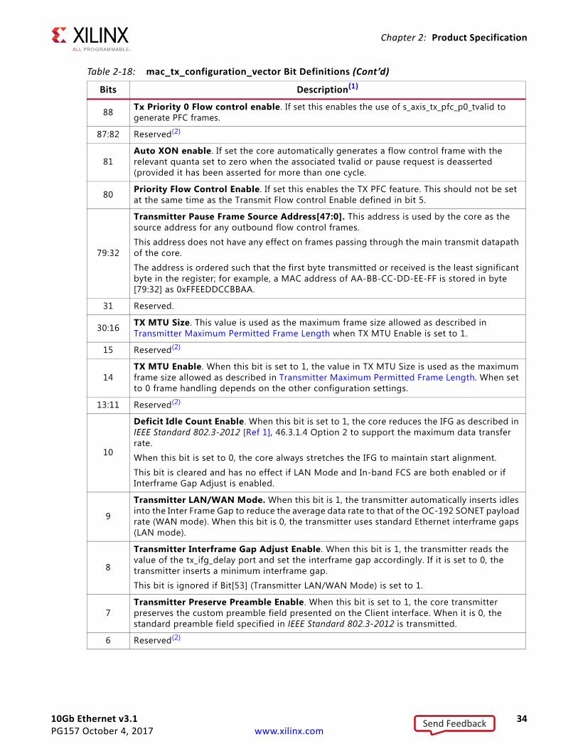
88 Tx Priority 0 Flow control enable. If set this enables the use of s_axis_tx_pfc_p0_tvalid to generate PFC frames.
87:82 Reserved(2)
81Auto XON enable. If set the core automatically generates a flow control frame with the relevant quanta set to zero when the associated tvalid or pause request is deasserted (provided it has been asserted for more than one cycle.
80 Priority Flow Control Enable. If set this enables the TX PFC feature. This should not be set at the same time as the Transmit Flow control Enable defined in bit 5.
79:32
Transmitter Pause Frame Source Address[47:0]. This address is used by the core as the source address for any outbound flow control frames.
This address does not have any effect on frames passing through the main transmit datapath of the core.
The address is ordered such that the first byte transmitted or received is the least significant byte in the register; for example, a MAC address of AA-BB-CC-DD-EE-FF is stored in byte [79:32] as 0xFFEEDDCCBBAA.
31 Reserved.
30:16 TX MTU Size. This value is used as the maximum frame size allowed as described in Transmitter Maximum Permitted Frame Length when TX MTU Enable is set to 1.
15 Reserved(2)
14TX MTU Enable. When this bit is set to 1, the value in TX MTU Size is used as the maximum frame size allowed as described in Transmitter Maximum Permitted Frame Length. When set to 0 frame handling depends on the other configuration settings.
13:11 Reserved(2)
10
Deficit Idle Count Enable. When this bit is set to 1, the core reduces the IFG as described in IEEE Standard 802.3-2012 [Ref 1], 46.3.1.4 Option 2 to support the maximum data transfer rate.
When this bit is set to 0, the core always stretches the IFG to maintain start alignment.
This bit is cleared and has no effect if LAN Mode and In-band FCS are both enabled or if Interframe Gap Adjust is enabled.
9
Transmitter LAN/WAN Mode. When this bit is 1, the transmitter automatically inserts idles into the Inter Frame Gap to reduce the average data rate to that of the OC-192 SONET payload rate (WAN mode). When this bit is 0, the transmitter uses standard Ethernet interframe gaps (LAN mode).
8
Transmitter Interframe Gap Adjust Enable. When this bit is 1, the transmitter reads the value of the tx_ifg_delay port and set the interframe gap accordingly. If it is set to 0, the transmitter inserts a minimum interframe gap.
This bit is ignored if Bit[53] (Transmitter LAN/WAN Mode) is set to 1.
7Transmitter Preserve Preamble Enable. When this bit is set to 1, the core transmitter preserves the custom preamble field presented on the Client interface. When it is 0, the standard preamble field specified in IEEE Standard 802.3-2012 is transmitted.
6 Reserved(2)
Table 2-18: mac_tx_configuration_vector Bit Definitions (Cont’d)
Bits Description(1)
Send Feedback
10Gb Ethernet v3.1 35PG157 October 4, 2017 www.xilinx.com
Chapter 2: Product Specification
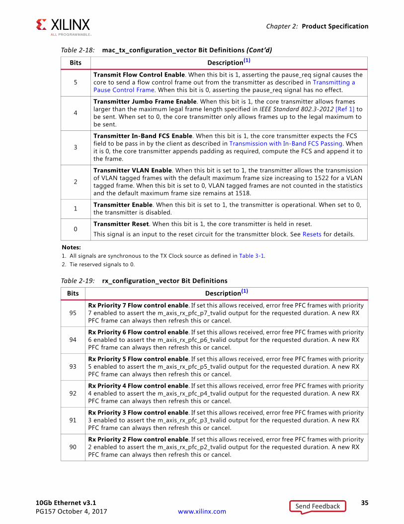
5Transmit Flow Control Enable. When this bit is 1, asserting the pause_req signal causes the core to send a flow control frame out from the transmitter as described in Transmitting a Pause Control Frame. When this bit is 0, asserting the pause_req signal has no effect.
4
Transmitter Jumbo Frame Enable. When this bit is 1, the core transmitter allows frames larger than the maximum legal frame length specified in IEEE Standard 802.3-2012 [Ref 1] to be sent. When set to 0, the core transmitter only allows frames up to the legal maximum to be sent.
3
Transmitter In-Band FCS Enable. When this bit is 1, the core transmitter expects the FCS field to be pass in by the client as described in Transmission with In-Band FCS Passing. When it is 0, the core transmitter appends padding as required, compute the FCS and append it to the frame.
2
Transmitter VLAN Enable. When this bit is set to 1, the transmitter allows the transmission of VLAN tagged frames with the default maximum frame size increasing to 1522 for a VLAN tagged frame. When this bit is set to 0, VLAN tagged frames are not counted in the statistics and the default maximum frame size remains at 1518.
1 Transmitter Enable. When this bit is set to 1, the transmitter is operational. When set to 0, the transmitter is disabled.
0Transmitter Reset. When this bit is 1, the core transmitter is held in reset.
This signal is an input to the reset circuit for the transmitter block. See Resets for details.
Notes: 1. All signals are synchronous to the TX Clock source as defined in Table 3-1.2. Tie reserved signals to 0.
Table 2-19: rx_configuration_vector Bit Definitions
Bits Description(1)
95Rx Priority 7 Flow control enable. If set this allows received, error free PFC frames with priority 7 enabled to assert the m_axis_rx_pfc_p7_tvalid output for the requested duration. A new RX PFC frame can always then refresh this or cancel.
94Rx Priority 6 Flow control enable. If set this allows received, error free PFC frames with priority 6 enabled to assert the m_axis_rx_pfc_p6_tvalid output for the requested duration. A new RX PFC frame can always then refresh this or cancel.
93Rx Priority 5 Flow control enable. If set this allows received, error free PFC frames with priority 5 enabled to assert the m_axis_rx_pfc_p5_tvalid output for the requested duration. A new RX PFC frame can always then refresh this or cancel.
92Rx Priority 4 Flow control enable. If set this allows received, error free PFC frames with priority 4 enabled to assert the m_axis_rx_pfc_p4_tvalid output for the requested duration. A new RX PFC frame can always then refresh this or cancel.
91Rx Priority 3 Flow control enable. If set this allows received, error free PFC frames with priority 3 enabled to assert the m_axis_rx_pfc_p3_tvalid output for the requested duration. A new RX PFC frame can always then refresh this or cancel.
90Rx Priority 2 Flow control enable. If set this allows received, error free PFC frames with priority 2 enabled to assert the m_axis_rx_pfc_p2_tvalid output for the requested duration. A new RX PFC frame can always then refresh this or cancel.
Table 2-18: mac_tx_configuration_vector Bit Definitions (Cont’d)
Bits Description(1)
Send Feedback
10Gb Ethernet v3.1 36PG157 October 4, 2017 www.xilinx.com
Chapter 2: Product Specification
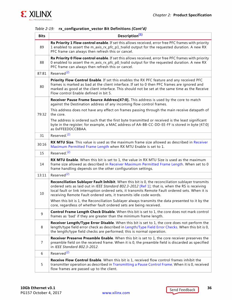
89Rx Priority 1 Flow control enable. If set this allows received, error free PFC frames with priority 1 enabled to assert the m_axis_rx_pfc_p1_tvalid output for the requested duration. A new RX PFC frame can always then refresh this or cancel.
88Rx Priority 0 Flow control enable. If set this allows received, error free PFC frames with priority 0 enabled to assert the m_axis_rx_pfc_p0_tvalid output for the requested duration. A new RX PFC frame can always then refresh this or cancel.
87:81 Reserved(2)
80
Priority Flow Control Enable. If set this enables the RX PFC feature and any received PFC frames is marked as bad at the client interface. If set to 0 then PFC frames are ignored and marked as good at the client interface. This should not be set at the same time as the Receive Flow control Enable defined in bit 5.
79:32
Receiver Pause Frame Source Address[47:0]. This address is used by the core to match against the Destination address of any incoming flow control frames.
This address does not have any effect on frames passing through the main receive datapath of the core.
The address is ordered such that the first byte transmitted or received is the least significant byte in the register; for example, a MAC address of AA-BB-CC-DD-EE-FF is stored in byte [47:0] as 0xFFEEDDCCBBAA.
31 Reserved.(2)
30:16 RX MTU Size. This value is used as the maximum frame size allowed as described in Receiver Maximum Permitted Frame Length when RX MTU Enable is set to 1.
15 Reserved.(2)
14RX MTU Enable. When this bit is set to 1, the value in RX MTU Size is used as the maximum frame size allowed as described in Receiver Maximum Permitted Frame Length. When set to 0 frame handling depends on the other configuration settings.
13:11 Reserved(2)
10
Reconciliation Sublayer Fault Inhibit. When this bit is 0, the reconciliation sublayer transmits ordered sets as laid out in IEEE Standard 802.3-2012 [Ref 1]; that is, when the RS is receiving local fault or link interruption ordered sets, it transmits Remote Fault ordered sets. When it is receiving Remote Fault ordered sets, it transmits idle code words.
When this bit is 1, the Reconciliation Sublayer always transmits the data presented to it by the core, regardless of whether fault ordered sets are being received.
9 Control Frame Length Check Disable. When this bit is set to 1, the core does not mark control frames as 'bad' if they are greater than the minimum frame length.
8Receiver Length/Type Error Disable. When this bit is set to 1, the core does not perform the length/type field error check as described in Length/Type Field Error Checks. When this bit is 0, the length/type field checks are performed; this is normal operation.
7Receiver Preserve Preamble Enable. When this bit is set to 1, the core receiver preserves the preamble field on the received frame. When it is 0, the preamble field is discarded as specified in IEEE Standard 802.3-2012.
6 Reserved(2)
5Receive Flow Control Enable. When this bit is 1, received flow control frames inhibit the transmitter operation as described in Transmitting a Pause Control Frame. When it is 0, received flow frames are passed up to the client.
Table 2-19: rx_configuration_vector Bit Definitions (Cont’d)
Bits Description(1)
Send Feedback
10Gb Ethernet v3.1 37PG157 October 4, 2017 www.xilinx.com
Chapter 2: Product Specification
4Receiver Jumbo Frame Enable. When this bit is 0, the receiver does not pass frames longer than the maximum legal frame size specified in IEEE Standard 802.3-2012 [Ref 1]. When it is 1, the receiver does not have an upper limit on frame size.
3Receiver In-Band FCS Enable. When this bit is 1, the core receiver passes the FCS field up to the client as described in Reception with In-Band FCS Passing. When it is 0, the core receiver does not pass the FCS field. In both cases, the FCS field is verified on the frame.
2
Receiver VLAN Enable. When this bit is set to 1, the receiver allows the reception of VLAN tagged frames with the default maximum frame size increasing to 1522 for a VLAN tagged frame. When this bit is set to 0, VLAN tagged frames are not counted in the statistics and the default maximum frame size remains at 1518.
1 Receiver Enable. When this bit is set to 1, the receiver is operational. When set to 0, the receiver is disabled.
0Receiver Reset. When this bit is 1, the core receiver is held in reset.
This signal is an input to the reset circuit for the receiver block. See Resets for details.
Notes: 1. All signals are synchronous to the RX Clock source as defined in Table 3-1.2. Tie reserved signals to 0.
Table 2-20: status_vector Bit Definitions
Bits Description(1)
2 Link Interruption Detected. If this bit is 1, then the RS layer is receiving link interruption sequence ordered sets. Read-only.
1 Remote Fault Received. If this bit is 1, the RS layer is receiving remote fault sequence ordered sets. Read-only.
0 Local Fault Received. If this bit is 1, the RS layer is receiving local fault sequence ordered sets. Read-only.
Notes: 1. All signals are synchronous to the RX Clock source as defined in Table 3-1.
Table 2-19: rx_configuration_vector Bit Definitions (Cont’d)
Bits Description(1)
Send Feedback
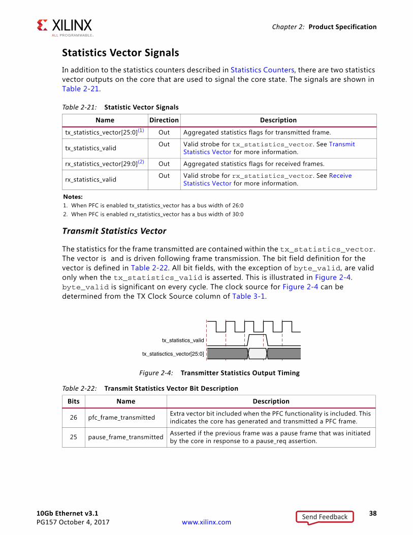
10Gb Ethernet v3.1 38PG157 October 4, 2017 www.xilinx.com
Chapter 2: Product Specification
Statistics Vector SignalsIn addition to the statistics counters described in Statistics Counters, there are two statistics vector outputs on the core that are used to signal the core state. The signals are shown in Table 2-21.
Transmit Statistics Vector
The statistics for the frame transmitted are contained within the tx_statistics_vector. The vector is and is driven following frame transmission. The bit field definition for the vector is defined in Table 2-22. All bit fields, with the exception of byte_valid, are valid only when the tx_statistics_valid is asserted. This is illustrated in Figure 2-4. byte_valid is significant on every cycle. The clock source for Figure 2-4 can be determined from the TX Clock Source column of Table 3-1.
Table 2-21: Statistic Vector Signals
Name Direction Description
tx_statistics_vector[25:0](1) Out Aggregated statistics flags for transmitted frame.
tx_statistics_valid Out Valid strobe for tx_statistics_vector. See Transmit Statistics Vector for more information.
rx_statistics_vector[29:0](2) Out Aggregated statistics flags for received frames.
rx_statistics_valid Out Valid strobe for rx_statistics_vector. See Receive Statistics Vector for more information.
Notes: 1. When PFC is enabled tx_statistics_vector has a bus width of 26:02. When PFC is enabled rx_statistics_vector has a bus width of 30:0
X-Ref Target - Figure 2-4
Figure 2-4: Transmitter Statistics Output Timing
Table 2-22: Transmit Statistics Vector Bit Description
Bits Name Description
26 pfc_frame_transmitted Extra vector bit included when the PFC functionality is included. This indicates the core has generated and transmitted a PFC frame.
25 pause_frame_transmitted Asserted if the previous frame was a pause frame that was initiated by the core in response to a pause_req assertion.
Send Feedback
10Gb Ethernet v3.1 39PG157 October 4, 2017 www.xilinx.com
Chapter 2: Product Specification
Receive Statistics Vector
The statistics for the frame received are contained within the rx_statistics_vector. The vector is driven following frame reception. The bit field definition for the vector is defined in Table 2-23.
All bit fields, with the exception of bytes_valid, are valid only when rx_statistics_valid is asserted. This is illustrated in Figure 2-5. bytes_valid is significant on every rx_clk0 cycle.
For any given received frame, rx_statistics_valid is High with or before the corresponding m_axis_rx_tlast assertion.
The clock source for Figure 2-5 can be determined from the RX Clock Source column of Table 3-1.
24:21 bytes_valid
The number of MAC frame bytes transmitted on the last clock cycle (DA to FCS inclusive). This can be between 0 and 8. This is valid on every clock cycle, it is not validated by tx_statistics_valid.The information for the bytes_valid field is sampled at a different point in the transmitter pipeline than the rest of the tx_statistics_vector bits.
20 vlan_frame Asserted if the previous frame contained a VLAN identifier in the length/type field and transmitter VLAN operation is enabled.
19:5 frame_length_count
The length of the previously transmitted frame in bytes. The count stays at 32,767 for any jumbo frames larger than this value. Otherwise this provides the size of the frame seen on the PHY interface (including any padding and FCS fields).
4 control_frame Asserted if the previous frame had the special MAC Control Type code 88-08 in the length/type field.
3 underrun_frame Asserted if the previous frame transmission was terminated due to an underrun error.
2 multicast_frame Asserted if the previous frame contained a multicast address in the destination address field.
1 broadcast_frame Asserted if the previous frame contained the broadcast address in the destination address field.
0 successful_frame Asserted if the previous frame was transmitted without error.
X-Ref Target - Figure 2-5
Figure 2-5: Receiver Statistics Output Timing
Table 2-22: Transmit Statistics Vector Bit Description (Cont’d)
Bits Name Description
Send Feedback
10Gb Ethernet v3.1 40PG157 October 4, 2017 www.xilinx.com
Chapter 2: Product Specification
PCS/PMA Configuration and Status SignalsIf the 10GBASE-R/KR core is generated without an MDIO interface, the key configuration and status information is carried on simple bit vectors, described in Table 2-24. Neither vector is completely populated so the actual number of pins required is much lower than
Table 2-23: Receive Statistics Vector Description
Bits Name Description
30 pfc_frame Extra vector bit included when the PFC functionality is included. This indicates that the core has received a valid PFC frame.
29 Length/Type Outof Range
Asserted if the length/type field contained a length value that did not match the number of MAC client data bytes received. Also High if the length/type field indicated that the frame contained padding but the number of client data bytes received was not equal to 64 bytes (minimum frame size).
28 bad_opcodeAsserted if the previous frame was error free, contained the special Control Frame identifier in the length/type field but contained an opcode that is unsupported by the core (any opcode other than Pause).
27 flow_control_frame
Asserted if the previous frame was error free, contained the Control Frame type identifier 88-08 in the length/type field, contained a destination address that matched either the MAC Control multicast address or the configured source address of the core, contained the Pause opcode and was acted on by the core.
26:23 bytes_valid
The number of MAC frame bytes received on the last clock cycle (DA to FCS inclusive). This can be between 0 and 8. This is valid on every clock cycle, it is not validated by rx_statistics_valid.The information for the bytes_valid field is sampled at a different point in the transmitter pipeline than the rest of the rx_statistics_vector bits.
22 vlan_frame Asserted if the previous frame contained a VLAN tag in the length/type field and VLAN operation was enabled in the receiver.
21 out_of_boundsAsserted if the previous frame exceeded the maximum frame size as defined in Receiver Maximum Permitted Frame Length. This is only asserted if jumbo frames are disabled.
20 control_frame Asserted if the previous frame contained the MAC Control Frame identifier 88-08 in the length/type field.
19:5 frame_length_count The length in bytes of the previous received frame. The count stays at 32,767 for any Jumbo frames larger than this value.
4 multicast_frame Asserted if the previous frame contained a multicast address in the destination address field.
3 broadcast_frame Asserted if the previous frame contained the broadcast address in the destination address field.
2 fcs_error Asserted if the previous frame received had an incorrect FCS value or the core detected error codes during frame reception.
1 bad_frame Asserted if the previous frame received contained errors.
0 good_frame Asserted if the previous frame received was error free.
Send Feedback
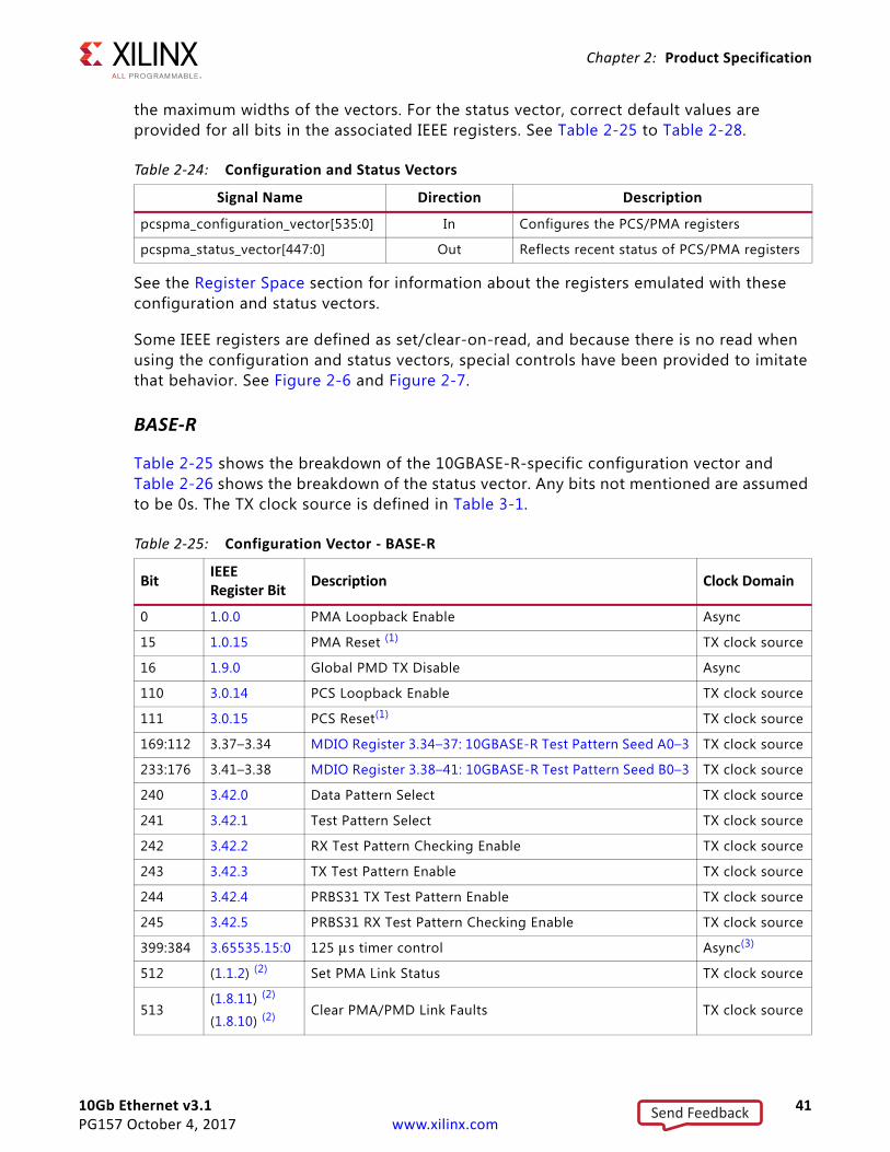
10Gb Ethernet v3.1 41PG157 October 4, 2017 www.xilinx.com
Chapter 2: Product Specification
the maximum widths of the vectors. For the status vector, correct default values are provided for all bits in the associated IEEE registers. See Table 2-25 to Table 2-28.
See the Register Space section for information about the registers emulated with these configuration and status vectors.
Some IEEE registers are defined as set/clear-on-read, and because there is no read when using the configuration and status vectors, special controls have been provided to imitate that behavior. See Figure 2-6 and Figure 2-7.
BASE-R
Table 2-25 shows the breakdown of the 10GBASE-R-specific configuration vector and Table 2-26 shows the breakdown of the status vector. Any bits not mentioned are assumed to be 0s. The TX clock source is defined in Table 3-1.
Table 2-24: Configuration and Status Vectors
Signal Name Direction Description
pcspma_configuration_vector[535:0] In Configures the PCS/PMA registers
pcspma_status_vector[447:0] Out Reflects recent status of PCS/PMA registers
Table 2-25: Configuration Vector - BASE-R
Bit IEEERegister Bit Description Clock Domain
0 1.0.0 PMA Loopback Enable Async
15 1.0.15 PMA Reset (1) TX clock source
16 1.9.0 Global PMD TX Disable Async
110 3.0.14 PCS Loopback Enable TX clock source
111 3.0.15 PCS Reset(1) TX clock source
169:112 3.37–3.34 MDIO Register 3.34–37: 10GBASE-R Test Pattern Seed A0–3 TX clock source
233:176 3.41–3.38 MDIO Register 3.38–41: 10GBASE-R Test Pattern Seed B0–3 TX clock source
240 3.42.0 Data Pattern Select TX clock source
241 3.42.1 Test Pattern Select TX clock source
242 3.42.2 RX Test Pattern Checking Enable TX clock source
243 3.42.3 TX Test Pattern Enable TX clock source
244 3.42.4 PRBS31 TX Test Pattern Enable TX clock source
245 3.42.5 PRBS31 RX Test Pattern Checking Enable TX clock source
399:384 3.65535.15:0 125 μs timer control Async(3)
512 (1.1.2) (2) Set PMA Link Status TX clock source
513(1.8.11) (2)
(1.8.10) (2) Clear PMA/PMD Link Faults TX clock source
Send Feedback
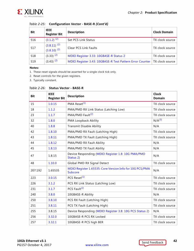
10Gb Ethernet v3.1 42PG157 October 4, 2017 www.xilinx.com
Chapter 2: Product Specification
516 (3.1.2) (2) Set PCS Link Status TX clock source
517(3.8.11) (2)
(3.8.10) (2) Clear PCS Link Faults TX clock source
518 (3.33) (2) MDIO Register 3.33: 10GBASE-R Status 2 TX clock source
519 (3.43) (2) MDIO Register 3.43: 10GBASE-R Test Pattern Error Counter TX clock source
Notes: 1. These reset signals should be asserted for a single clock tick only.2. Reset controls for the given registers.3. Typically constant.
Table 2-26: Status Vector - BASE-R
Bit IEEERegister Bit Description Clock
Domain
15 1.0.15 PMA Reset(1) TX clock source
18 1.1.2 PMA/PMD RX Link Status (Latching Low) TX clock source
23 1.1.7 PMA/PMD Fault(2) TX clock source
32 1.8.0 PMA Loopback Ability N/A(3)
40 1.8.8 Transmit Disable Ability N/A
42 1.8.10 PMA/PMD RX Fault (Latching High) TX clock source
43 1.8.11 PMA/PMD TX Fault (Latching High) TX clock source
44 1.8.12 PMA/PMD RX Fault Ability N/A
45 1.8.13 PMA/PMD TX Fault Ability N/A
47 1.8.15 Device Responding (MDIO Register 1.8: 10G PMA/PMD Status 2) N/A
48 1.10.0 Global PMD RX Signal Detect TX clock source
207:192 1.65535 MDIO Register 1.65535: Core Version Info for 10G PCS/PMA Subcore N/A
223 3.0.15 PCS Reset(1) TX clock source
226 3.1.2 PCS RX Link Status (Latching Low) TX clock source
231 3.1.7 PCS Fault(2) TX clock source
240 3.8.0 10GBASE-R Ability N/A
250 3.8.10 PCS RX Fault (Latching High) TX clock source
251 3.8.11 PCS TX Fault (Latching High) TX clock source
255 3.8.15 Device Responding (MDIO Register 3.8: 10G PCS Status 2) N/A
256 3.32.0 10GBASE-R PCS RX Locked TX clock source
257 3.32.1 10GBASE-R PCS high BER TX clock source
Table 2-25: Configuration Vector - BASE-R (Cont’d)
Bit IEEERegister Bit Description Clock Domain
Send Feedback
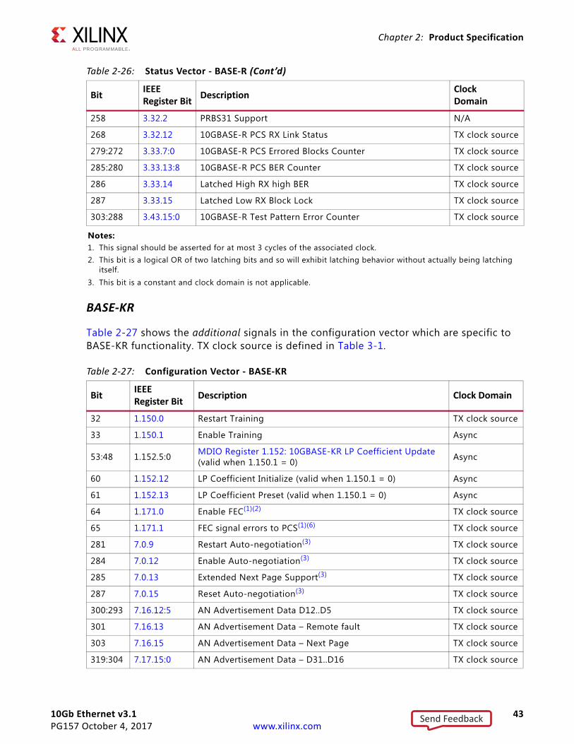
10Gb Ethernet v3.1 43PG157 October 4, 2017 www.xilinx.com
Chapter 2: Product Specification
BASE-KR
Table 2-27 shows the additional signals in the configuration vector which are specific to BASE-KR functionality. TX clock source is defined in Table 3-1.
258 3.32.2 PRBS31 Support N/A
268 3.32.12 10GBASE-R PCS RX Link Status TX clock source
279:272 3.33.7:0 10GBASE-R PCS Errored Blocks Counter TX clock source
285:280 3.33.13:8 10GBASE-R PCS BER Counter TX clock source
286 3.33.14 Latched High RX high BER TX clock source
287 3.33.15 Latched Low RX Block Lock TX clock source
303:288 3.43.15:0 10GBASE-R Test Pattern Error Counter TX clock source
Notes: 1. This signal should be asserted for at most 3 cycles of the associated clock.2. This bit is a logical OR of two latching bits and so will exhibit latching behavior without actually being latching
itself.3. This bit is a constant and clock domain is not applicable.
Table 2-27: Configuration Vector - BASE-KR
Bit IEEERegister Bit Description Clock Domain
32 1.150.0 Restart Training TX clock source
33 1.150.1 Enable Training Async
53:48 1.152.5:0 MDIO Register 1.152: 10GBASE-KR LP Coefficient Update(valid when 1.150.1 = 0) Async
60 1.152.12 LP Coefficient Initialize (valid when 1.150.1 = 0) Async
61 1.152.13 LP Coefficient Preset (valid when 1.150.1 = 0) Async
64 1.171.0 Enable FEC(1)(2) TX clock source
65 1.171.1 FEC signal errors to PCS(1)(6) TX clock source
281 7.0.9 Restart Auto-negotiation(3) TX clock source
284 7.0.12 Enable Auto-negotiation(3) TX clock source
285 7.0.13 Extended Next Page Support(3) TX clock source
287 7.0.15 Reset Auto-negotiation(3) TX clock source
300:293 7.16.12:5 AN Advertisement Data D12..D5 TX clock source
301 7.16.13 AN Advertisement Data – Remote fault TX clock source
303 7.16.15 AN Advertisement Data – Next Page TX clock source
319:304 7.17.15:0 AN Advertisement Data – D31..D16 TX clock source
Table 2-26: Status Vector - BASE-R (Cont’d)
Bit IEEERegister Bit Description Clock
Domain
Send Feedback
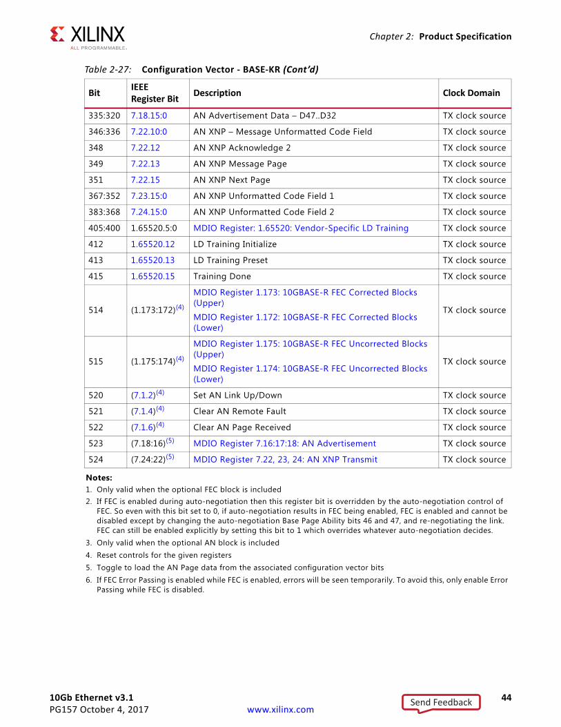
10Gb Ethernet v3.1 44PG157 October 4, 2017 www.xilinx.com
Chapter 2: Product Specification
335:320 7.18.15:0 AN Advertisement Data – D47..D32 TX clock source
346:336 7.22.10:0 AN XNP – Message Unformatted Code Field TX clock source
348 7.22.12 AN XNP Acknowledge 2 TX clock source
349 7.22.13 AN XNP Message Page TX clock source
351 7.22.15 AN XNP Next Page TX clock source
367:352 7.23.15:0 AN XNP Unformatted Code Field 1 TX clock source
383:368 7.24.15:0 AN XNP Unformatted Code Field 2 TX clock source
405:400 1.65520.5:0 MDIO Register: 1.65520: Vendor-Specific LD Training TX clock source
412 1.65520.12 LD Training Initialize TX clock source
413 1.65520.13 LD Training Preset TX clock source
415 1.65520.15 Training Done TX clock source
514 (1.173:172)(4)
MDIO Register 1.173: 10GBASE-R FEC Corrected Blocks (Upper)
MDIO Register 1.172: 10GBASE-R FEC Corrected Blocks (Lower)
TX clock source
515 (1.175:174)(4)
MDIO Register 1.175: 10GBASE-R FEC Uncorrected Blocks (Upper)
MDIO Register 1.174: 10GBASE-R FEC Uncorrected Blocks (Lower)
TX clock source
520 (7.1.2)(4) Set AN Link Up/Down TX clock source
521 (7.1.4)(4) Clear AN Remote Fault TX clock source
522 (7.1.6)(4) Clear AN Page Received TX clock source
523 (7.18:16)(5) MDIO Register 7.16:17:18: AN Advertisement TX clock source
524 (7.24:22)(5) MDIO Register 7.22, 23, 24: AN XNP Transmit TX clock source
Notes: 1. Only valid when the optional FEC block is included2. If FEC is enabled during auto-negotiation then this register bit is overridden by the auto-negotiation control of
FEC. So even with this bit set to 0, if auto-negotiation results in FEC being enabled, FEC is enabled and cannot be disabled except by changing the auto-negotiation Base Page Ability bits 46 and 47, and re-negotiating the link. FEC can still be enabled explicitly by setting this bit to 1 which overrides whatever auto-negotiation decides.
3. Only valid when the optional AN block is included4. Reset controls for the given registers5. Toggle to load the AN Page data from the associated configuration vector bits6. If FEC Error Passing is enabled while FEC is enabled, errors will be seen temporarily. To avoid this, only enable Error
Passing while FEC is disabled.
Table 2-27: Configuration Vector - BASE-KR (Cont’d)
Bit IEEERegister Bit Description Clock Domain
Send Feedback
10Gb Ethernet v3.1 45PG157 October 4, 2017 www.xilinx.com
Chapter 2: Product Specification
Table 2-28 shows the additional signals in the status vector which are specific to BASE-KR functionality.
Table 2-28: Status Vector - BASE-KR
Bit IEEERegister Bit Description Clock Domain
41 1.8.9 Extended Abilities N/A(1)
67:64 1.151.3:0 MDIO Register 1.151: 10GBASE-KR PMD Status TX clock source
85:80 1.153.5:0 MDIO Register 1.153: 10GBASE-KR LP Status TX clock source
95 1.153.15 LP Status Report Training Complete TX clock source
101:96 1.152.5:0 MDIO Register 1.152: 10GBASE-KR LP Coefficient Update TX clock source
108 1.152.12 LP Coefficient Initialize TX clock source
109 1.152.13 LP Coefficient Preset TX clock source
117:112 1.155.5:0 MDIO Register 1.155: 10GBASE-KR LD Status TX clock source
127 1.155.15 LD Status Report Training Complete TX clock source
159:128 1.173:172
MDIO Register 1.173: 10GBASE-R FEC Corrected Blocks (Upper)(2)
MDIO Register 1.172: 10GBASE-R FEC Corrected Blocks (Lower)(2)
TX clock source
191:160 1.175:174
MDIO Register 1.175: 10GBASE-R FEC Uncorrected Blocks (Upper)(2)
MDIO Register 1.174: 10GBASE-R FEC Uncorrected Blocks (Lower)(2)
TX clock source
319 7.0.15 AN Reset(3) TX clock source
320 7.1.0 LP AN Capable(3) TX clock source
322 7.1.2 AN Link Up/Down (latching Low)(3) TX clock source
323 7.1.3 AN Ability(3) N/A
324 7.1.4 AN Remote Fault (latching High)(3) TX clock source
325 7.1.5 AN Complete(3) TX clock source
326 7.1.6 AN Page Received (latching High)(3) TX clock source
327 7.1.7 AN Extended Next Page Used(3) TX clock source
383:336 7.21:19 MDIO Register 7.19, 20, 21: AN LP Base Page Ability(3) TX clock source
394:384 7.25.10:0 AN LP XNP – Message Unformatted Code Field(3) TX clock source
395 7.25.11 AN LP XNP – Toggle(3) TX clock source
396 7.25.12 AN LP XNP – Acknowledge2(3) TX clock source
397 7.25.13 AN LP XNP – Message Page(3) TX clock source
399 7.25.15 AN LP XNP – Next Page(3) TX clock source
415:400 7.26.15:0 AN LP XNP – Unformatted Code Field 1(3) TX clock source
431:416 7.27.15:0 AN LP XNP – Unformatted Code Field 2(3) TX clock source
Send Feedback
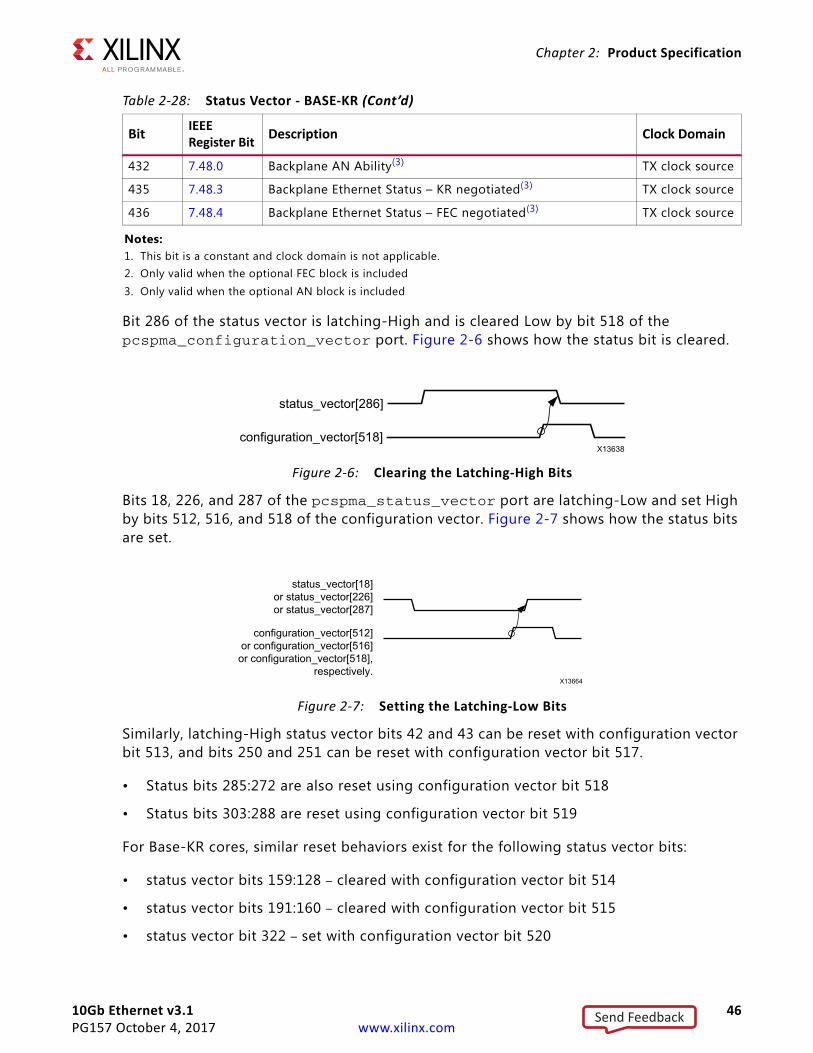
10Gb Ethernet v3.1 46PG157 October 4, 2017 www.xilinx.com
Chapter 2: Product Specification
Bit 286 of the status vector is latching-High and is cleared Low by bit 518 of the pcspma_configuration_vector port. Figure 2-6 shows how the status bit is cleared.
Bits 18, 226, and 287 of the pcspma_status_vector port are latching-Low and set High by bits 512, 516, and 518 of the configuration vector. Figure 2-7 shows how the status bits are set.
Similarly, latching-High status vector bits 42 and 43 can be reset with configuration vector bit 513, and bits 250 and 251 can be reset with configuration vector bit 517.
• Status bits 285:272 are also reset using configuration vector bit 518
• Status bits 303:288 are reset using configuration vector bit 519
For Base-KR cores, similar reset behaviors exist for the following status vector bits:
• status vector bits 159:128 – cleared with configuration vector bit 514
• status vector bits 191:160 – cleared with configuration vector bit 515
• status vector bit 322 – set with configuration vector bit 520
432 7.48.0 Backplane AN Ability(3) TX clock source
435 7.48.3 Backplane Ethernet Status – KR negotiated(3) TX clock source
436 7.48.4 Backplane Ethernet Status – FEC negotiated(3) TX clock source
Notes: 1. This bit is a constant and clock domain is not applicable.2. Only valid when the optional FEC block is included3. Only valid when the optional AN block is included
X-Ref Target - Figure 2-6
Figure 2-6: Clearing the Latching-High Bits
X-Ref Target - Figure 2-7
Figure 2-7: Setting the Latching-Low Bits
Table 2-28: Status Vector - BASE-KR (Cont’d)
Bit IEEERegister Bit Description Clock Domain
status_vector[286]
configuration_vector[518]X13638
status_vector[18]or status_vector[226]or status_vector[287]
configuration_vector[512]or configuration_vector[516]or configuration_vector[518],
respectively.X13664
Send Feedback
10Gb Ethernet v3.1 47PG157 October 4, 2017 www.xilinx.com
Chapter 2: Product Specification
• status vector bit 324 – cleared with configuration vector bit 521
• status vector bit 326 – cleared with configuration vector bit 522
Finally, configuration vector bits 335:293 and 383:336 each implement three registers which are normally latched into the core when the lower register is written, keeping the data coherent. Because there is no need for this behavior when the entire vector is exposed, these bits are latched into the core whenever configuration register bits 523 and 524 respectively are toggled High.
Interrupt SignalThe Interrupt output signal is shown in Table 2-29. See Interrupt Output Registers for more details.
IEEE 1588 Transmitted Timestamp PortsFor IEEE 1588 support, the captured timestamp and tag are presented on a dedicated AXI4-Stream interface. The signal definition and timing diagram are shown in Table 2-30 and Figure 2-8. The clock source for Figure 2-8 can be determined from the TX Clock Source column of Table 3-1.
Table 2-29: Interrupt Output Port Description
Name Direction Description
xgmacint Out Interrupt output.
Send Feedback
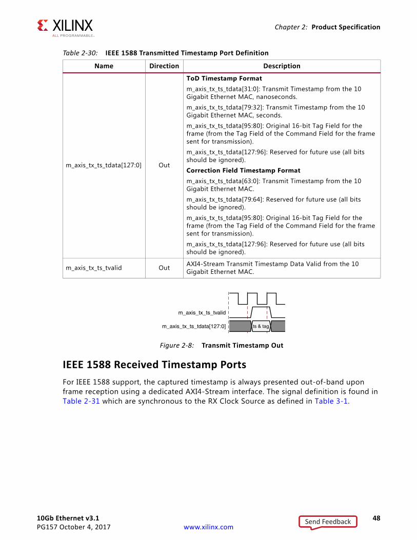
10Gb Ethernet v3.1 48PG157 October 4, 2017 www.xilinx.com
Chapter 2: Product Specification
IEEE 1588 Received Timestamp PortsFor IEEE 1588 support, the captured timestamp is always presented out-of-band upon frame reception using a dedicated AXI4-Stream interface. The signal definition is found in Table 2-31 which are synchronous to the RX Clock Source as defined in Table 3-1.
Table 2-30: IEEE 1588 Transmitted Timestamp Port Definition
Name Direction Description
m_axis_tx_ts_tdata[127:0] Out
ToD Timestamp Formatm_axis_tx_ts_tdata[31:0]: Transmit Timestamp from the 10 Gigabit Ethernet MAC, nanoseconds.
m_axis_tx_ts_tdata[79:32]: Transmit Timestamp from the 10 Gigabit Ethernet MAC, seconds.
m_axis_tx_ts_tdata[95:80]: Original 16-bit Tag Field for the frame (from the Tag Field of the Command Field for the frame sent for transmission).
m_axis_tx_ts_tdata[127:96]: Reserved for future use (all bits should be ignored).
Correction Field Timestamp Formatm_axis_tx_ts_tdata[63:0]: Transmit Timestamp from the 10 Gigabit Ethernet MAC.
m_axis_tx_ts_tdata[79:64]: Reserved for future use (all bits should be ignored).
m_axis_tx_ts_tdata[95:80]: Original 16-bit Tag Field for the frame (from the Tag Field of the Command Field for the frame sent for transmission).
m_axis_tx_ts_tdata[127:96]: Reserved for future use (all bits should be ignored).
m_axis_tx_ts_tvalid Out AXI4-Stream Transmit Timestamp Data Valid from the 10 Gigabit Ethernet MAC.
X-Ref Target - Figure 2-8
Figure 2-8: Transmit Timestamp Out
Send Feedback
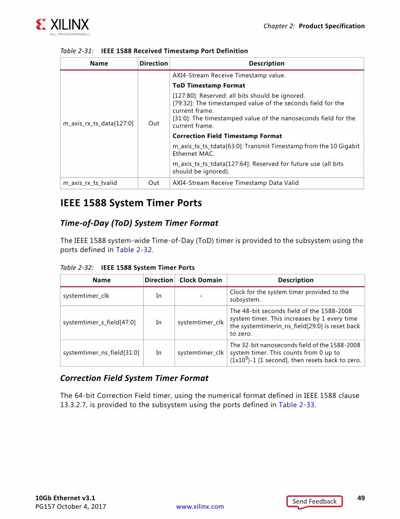
10Gb Ethernet v3.1 49PG157 October 4, 2017 www.xilinx.com
Chapter 2: Product Specification
IEEE 1588 System Timer Ports
Time-of-Day (ToD) System Timer Format
The IEEE 1588 system-wide Time-of-Day (ToD) timer is provided to the subsystem using the ports defined in Table 2-32.
Correction Field System Timer Format
The 64-bit Correction Field timer, using the numerical format defined in IEEE 1588 clause 13.3.2.7, is provided to the subsystem using the ports defined in Table 2-33.
Table 2-31: IEEE 1588 Received Timestamp Port Definition
Name Direction Description
m_axis_rx_ts_data[127:0] Out
AXI4-Stream Receive Timestamp value.
ToD Timestamp Format[127:80]: Reserved: all bits should be ignored.[79:32]: The timestamped value of the seconds field for the current frame.[31:0]: The timestamped value of the nanoseconds field for the current frame.
Correction Field Timestamp Formatm_axis_tx_ts_tdata[63:0]: Transmit Timestamp from the 10 Gigabit Ethernet MAC.
m_axis_tx_ts_tdata[127:64]: Reserved for future use (all bits should be ignored).
m_axis_rx_ts_tvalid Out AXI4-Stream Receive Timestamp Data Valid
Table 2-32: IEEE 1588 System Timer Ports
Name Direction Clock Domain Description
systemtimer_clk In - Clock for the system timer provided to the subsystem.
systemtimer_s_field[47:0] In systemtimer_clk
The 48-bit seconds field of the 1588-2008 system timer. This increases by 1 every time the systemtimerin_ns_field[29:0] is reset back to zero.
systemtimer_ns_field[31:0] In systemtimer_clkThe 32-bit nanoseconds field of the 1588-2008 system timer. This counts from 0 up to (1x10⁹)-1 [1 second], then resets back to zero.
Send Feedback
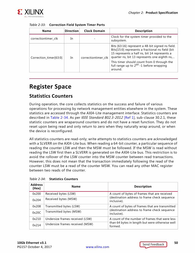
10Gb Ethernet v3.1 50PG157 October 4, 2017 www.xilinx.com
Chapter 2: Product Specification
Register SpaceStatistics CountersDuring operation, the core collects statistics on the success and failure of various operations for processing by network management entities elsewhere in the system. These statistics are accessed through the AXI4-Lite management interface. Statistics counters are described in Table 2-34. As per IEEE Standard 802.3-2012 [Ref 1], sub-clause 30.2.1, these statistic counters are wraparound counters and do not have a reset function. They do not reset upon being read and only return to zero when they naturally wrap around, or when the device is reconfigured.
All statistics counters are read-only; write attempts to statistics counters are acknowledged with a SLVERR on the AXI4-Lite bus. When reading a 64-bit counter, a particular sequence of reading the counter LSW and then the MSW must be followed. If the MSW is read without reading the LSW first then a SLVERR is generated on the AXI4-Lite bus. This restriction is to avoid the rollover of the LSW counter into the MSW counter between read transactions. However, this does not mean that the transaction immediately following the read of the counter LSW must be a read of the counter MSW. You can read any other MAC register between two reads of the counter.
Table 2-33: Correction Field System Timer Ports
Name Direction Clock Domain Description
correctiontimer_clk In - Clock for the system timer provided to the subsystem.
Correction_timer[63:0] In correctiontimer_clk
Bits [63:16] represent a 48-bit signed ns field. Bits[15:0] represents a fractional ns field (bit 15 represents a half ns, bit 14 represents a quarter ns, bit 13 represents one eighth ns,...
This timer should count from 0 through the full range up to 264 -1 before wrapping around.
Table 2-34: Statistics Counters
Address(Hex) Name Description
0x200 Received bytes (LSW) A count of bytes of frames that are received (destination address to frame check sequence inclusive).0x204 Received bytes (MSW)
0x208 Transmitted bytes (LSW) A count of bytes of frames that are transmitted (destination address to frame check sequence inclusive).0x20C Transmitted bytes (MSW)
0x210 Undersize frames received (LSW) A count of the number of frames that were less than 64 bytes in length but were otherwise well formed.0x214 Undersize frames received (MSW)
Send Feedback
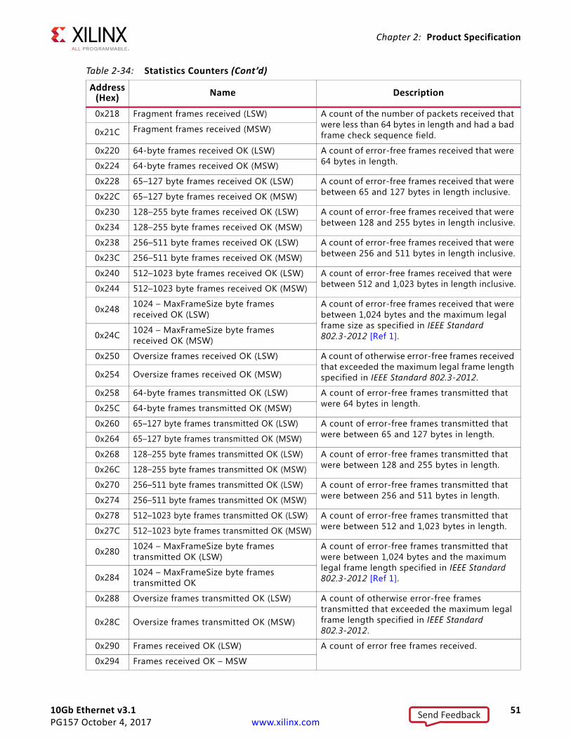
10Gb Ethernet v3.1 51PG157 October 4, 2017 www.xilinx.com
Chapter 2: Product Specification
0x218 Fragment frames received (LSW) A count of the number of packets received that were less than 64 bytes in length and had a bad frame check sequence field.0x21C Fragment frames received (MSW)
0x220 64-byte frames received OK (LSW) A count of error-free frames received that were 64 bytes in length.0x224 64-byte frames received OK (MSW)
0x228 65–127 byte frames received OK (LSW) A count of error-free frames received that were between 65 and 127 bytes in length inclusive.0x22C 65–127 byte frames received OK (MSW)
0x230 128–255 byte frames received OK (LSW) A count of error-free frames received that were between 128 and 255 bytes in length inclusive.0x234 128–255 byte frames received OK (MSW)
0x238 256–511 byte frames received OK (LSW) A count of error-free frames received that were between 256 and 511 bytes in length inclusive.0x23C 256–511 byte frames received OK (MSW)
0x240 512–1023 byte frames received OK (LSW) A count of error-free frames received that were between 512 and 1,023 bytes in length inclusive.0x244 512–1023 byte frames received OK (MSW)
0x248 1024 – MaxFrameSize byte framesreceived OK (LSW)
A count of error-free frames received that were between 1,024 bytes and the maximum legal frame size as specified in IEEE Standard 802.3-2012 [Ref 1].0x24C 1024 – MaxFrameSize byte frames
received OK (MSW)
0x250 Oversize frames received OK (LSW) A count of otherwise error-free frames received that exceeded the maximum legal frame length specified in IEEE Standard 802.3-2012.0x254 Oversize frames received OK (MSW)
0x258 64-byte frames transmitted OK (LSW) A count of error-free frames transmitted that were 64 bytes in length.0x25C 64-byte frames transmitted OK (MSW)
0x260 65–127 byte frames transmitted OK (LSW) A count of error-free frames transmitted that were between 65 and 127 bytes in length.0x264 65–127 byte frames transmitted OK (MSW)
0x268 128–255 byte frames transmitted OK (LSW) A count of error-free frames transmitted that were between 128 and 255 bytes in length.0x26C 128–255 byte frames transmitted OK (MSW)
0x270 256–511 byte frames transmitted OK (LSW) A count of error-free frames transmitted that were between 256 and 511 bytes in length.0x274 256–511 byte frames transmitted OK (MSW)
0x278 512–1023 byte frames transmitted OK (LSW) A count of error-free frames transmitted that were between 512 and 1,023 bytes in length.0x27C 512–1023 byte frames transmitted OK (MSW)
0x280 1024 – MaxFrameSize byte frames transmitted OK (LSW)
A count of error-free frames transmitted that were between 1,024 bytes and the maximum legal frame length specified in IEEE Standard 802.3-2012 [Ref 1].0x284 1024 – MaxFrameSize byte frames
transmitted OK
0x288 Oversize frames transmitted OK (LSW) A count of otherwise error-free frames transmitted that exceeded the maximum legal frame length specified in IEEE Standard 802.3-2012.
0x28C Oversize frames transmitted OK (MSW)
0x290 Frames received OK (LSW) A count of error free frames received.
0x294 Frames received OK – MSW
Table 2-34: Statistics Counters (Cont’d)
Address(Hex) Name Description
Send Feedback
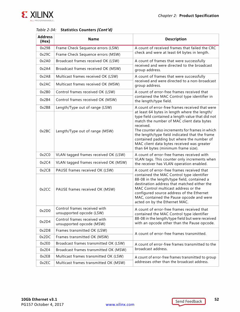
10Gb Ethernet v3.1 52PG157 October 4, 2017 www.xilinx.com
Chapter 2: Product Specification
0x298 Frame Check Sequence errors (LSW) A count of received frames that failed the CRC check and were at least 64 bytes in length.0x29C Frame Check Sequence errors (MSW)
0x2A0 Broadcast frames received OK (LSW) A count of frames that were successfully received and were directed to the broadcast group address.0x2A4 Broadcast frames received OK (MSW)
0x2A8 Multicast frames received OK (LSW) A count of frames that were successfully received and were directed to a non-broadcast group address.0x2AC Multicast frames received OK (MSW)
0x2B0 Control frames received OK (LSW) A count of error-free frames received that contained the MAC Control type identifier in the length/type field.0x2B4 Control frames received OK (MSW)
0x2B8 Length/Type out of range (LSW) A count of error-free frames received that were at least 64 bytes in length where the length/type field contained a length value that did not match the number of MAC client data bytes received.The counter also increments for frames in which the length/type field indicated that the frame contained padding but where the number of MAC client data bytes received was greater than 64 bytes (minimum frame size).
0x2BC Length/Type out of range (MSW)
0x2C0 VLAN tagged frames received OK (LSW) A count of error-free frames received with VLAN tags. This counter only increments when the receiver has VLAN operation enabled.0x2C4 VLAN tagged frames received OK (MSW)
0x2C8 PAUSE frames received OK (LSW) A count of error-free frames received that contained the MAC Control type identifier 88-08 in the length/type field, contained a destination address that matched either the MAC Control multicast address or the configured source address of the Ethernet MAC, contained the Pause opcode and were acted on by the Ethernet MAC.
0x2CC PAUSE frames received OK (MSW)
0x2D0 Control frames received with unsupported opcode (LSW)
A count of error-free frames received that contained the MAC Control type identifier 88-08 in the length/type field but were received with an opcode other than the Pause opcode.0x2D4 Control frames received with
unsupported opcode (MSW)
0x2D8 Frames transmitted OK (LSW)A count of error-free frames transmitted.
0x2DC Frames transmitted OK (MSW)
0x2E0 Broadcast frames transmitted OK (LSW) A count of error-free frames transmitted to the broadcast address.0x2E4 Broadcast frames transmitted OK (MSW)
0x2E8 Multicast frames transmitted OK (LSW) A count of error-free frames transmitted to group addresses other than the broadcast address.0x2EC Multicast frames transmitted OK (MSW)
Table 2-34: Statistics Counters (Cont’d)
Address(Hex) Name Description
Send Feedback
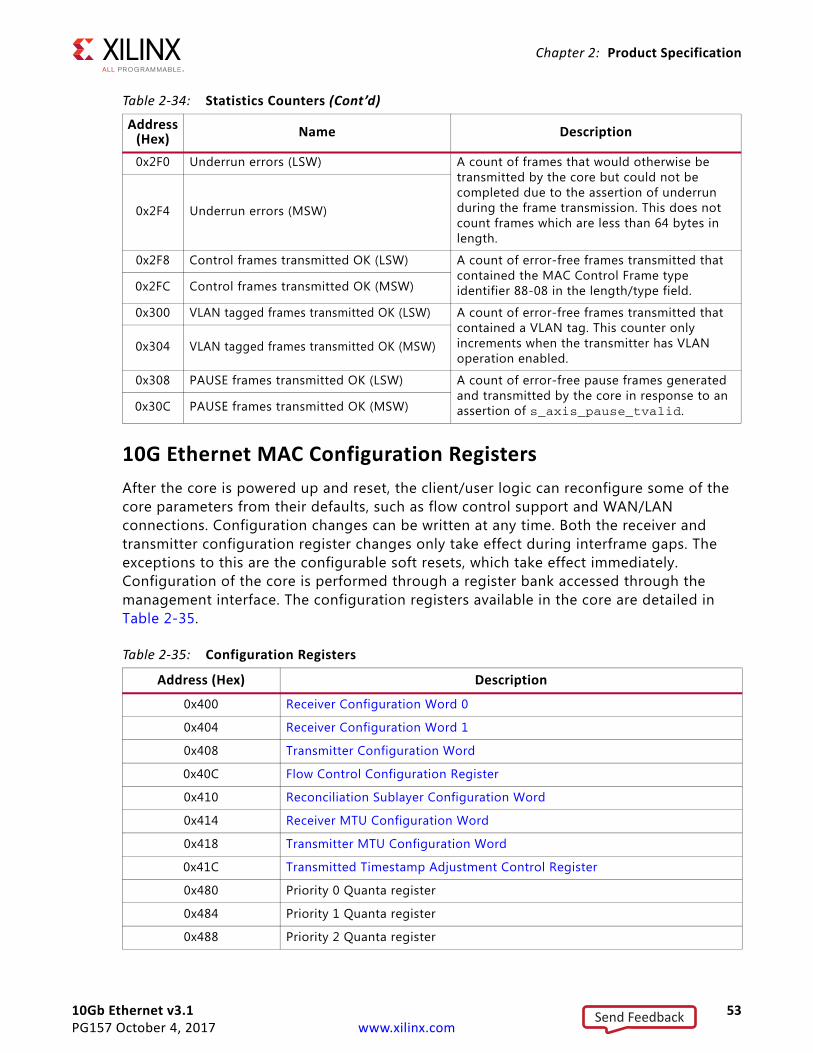
10Gb Ethernet v3.1 53PG157 October 4, 2017 www.xilinx.com
Chapter 2: Product Specification
10G Ethernet MAC Configuration RegistersAfter the core is powered up and reset, the client/user logic can reconfigure some of the core parameters from their defaults, such as flow control support and WAN/LAN connections. Configuration changes can be written at any time. Both the receiver and transmitter configuration register changes only take effect during interframe gaps. The exceptions to this are the configurable soft resets, which take effect immediately. Configuration of the core is performed through a register bank accessed through the management interface. The configuration registers available in the core are detailed in Table 2-35.
0x2F0 Underrun errors (LSW) A count of frames that would otherwise be transmitted by the core but could not be completed due to the assertion of underrun during the frame transmission. This does not count frames which are less than 64 bytes in length.
0x2F4 Underrun errors (MSW)
0x2F8 Control frames transmitted OK (LSW) A count of error-free frames transmitted that contained the MAC Control Frame type identifier 88-08 in the length/type field.0x2FC Control frames transmitted OK (MSW)
0x300 VLAN tagged frames transmitted OK (LSW) A count of error-free frames transmitted that contained a VLAN tag. This counter only increments when the transmitter has VLAN operation enabled.
0x304 VLAN tagged frames transmitted OK (MSW)
0x308 PAUSE frames transmitted OK (LSW) A count of error-free pause frames generated and transmitted by the core in response to an assertion of s_axis_pause_tvalid.0x30C PAUSE frames transmitted OK (MSW)
Table 2-35: Configuration Registers
Address (Hex) Description
0x400 Receiver Configuration Word 0
0x404 Receiver Configuration Word 1
0x408 Transmitter Configuration Word
0x40C Flow Control Configuration Register
0x410 Reconciliation Sublayer Configuration Word
0x414 Receiver MTU Configuration Word
0x418 Transmitter MTU Configuration Word
0x41C Transmitted Timestamp Adjustment Control Register
0x480 Priority 0 Quanta register
0x484 Priority 1 Quanta register
0x488 Priority 2 Quanta register
Table 2-34: Statistics Counters (Cont’d)
Address(Hex) Name Description
Send Feedback
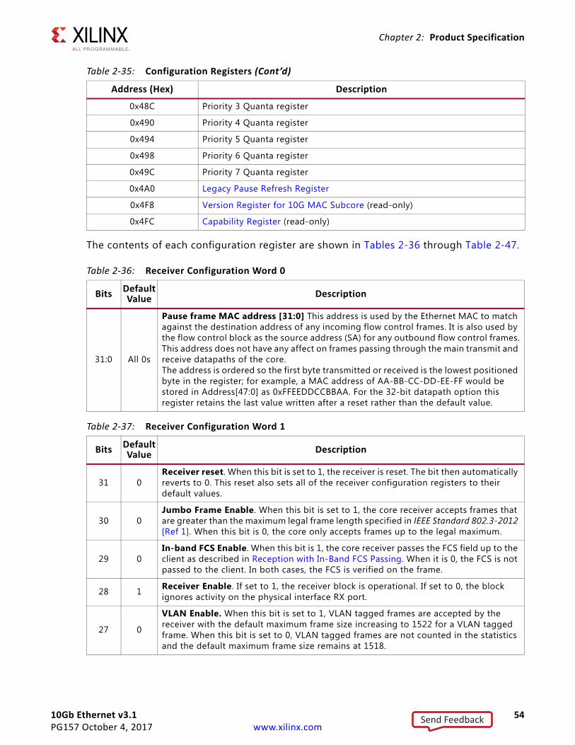
10Gb Ethernet v3.1 54PG157 October 4, 2017 www.xilinx.com
Chapter 2: Product Specification
The contents of each configuration register are shown in Tables 2-36 through Table 2-47.
0x48C Priority 3 Quanta register
0x490 Priority 4 Quanta register
0x494 Priority 5 Quanta register
0x498 Priority 6 Quanta register
0x49C Priority 7 Quanta register
0x4A0 Legacy Pause Refresh Register
0x4F8 Version Register for 10G MAC Subcore (read-only)
0x4FC Capability Register (read-only)
Table 2-36: Receiver Configuration Word 0
Bits DefaultValue Description
31:0 All 0s
Pause frame MAC address [31:0] This address is used by the Ethernet MAC to match against the destination address of any incoming flow control frames. It is also used by the flow control block as the source address (SA) for any outbound flow control frames.This address does not have any affect on frames passing through the main transmit and receive datapaths of the core.The address is ordered so the first byte transmitted or received is the lowest positioned byte in the register; for example, a MAC address of AA-BB-CC-DD-EE-FF would be stored in Address[47:0] as 0xFFEEDDCCBBAA. For the 32-bit datapath option this register retains the last value written after a reset rather than the default value.
Table 2-37: Receiver Configuration Word 1
Bits DefaultValue Description
31 0Receiver reset. When this bit is set to 1, the receiver is reset. The bit then automatically reverts to 0. This reset also sets all of the receiver configuration registers to their default values.
30 0Jumbo Frame Enable. When this bit is set to 1, the core receiver accepts frames that are greater than the maximum legal frame length specified in IEEE Standard 802.3-2012 [Ref 1]. When this bit is 0, the core only accepts frames up to the legal maximum.
29 0In-band FCS Enable. When this bit is 1, the core receiver passes the FCS field up to the client as described in Reception with In-Band FCS Passing. When it is 0, the FCS is not passed to the client. In both cases, the FCS is verified on the frame.
28 1 Receiver Enable. If set to 1, the receiver block is operational. If set to 0, the block ignores activity on the physical interface RX port.
27 0
VLAN Enable. When this bit is set to 1, VLAN tagged frames are accepted by the receiver with the default maximum frame size increasing to 1522 for a VLAN tagged frame. When this bit is set to 0, VLAN tagged frames are not counted in the statistics and the default maximum frame size remains at 1518.
Table 2-35: Configuration Registers (Cont’d)
Address (Hex) Description
Send Feedback
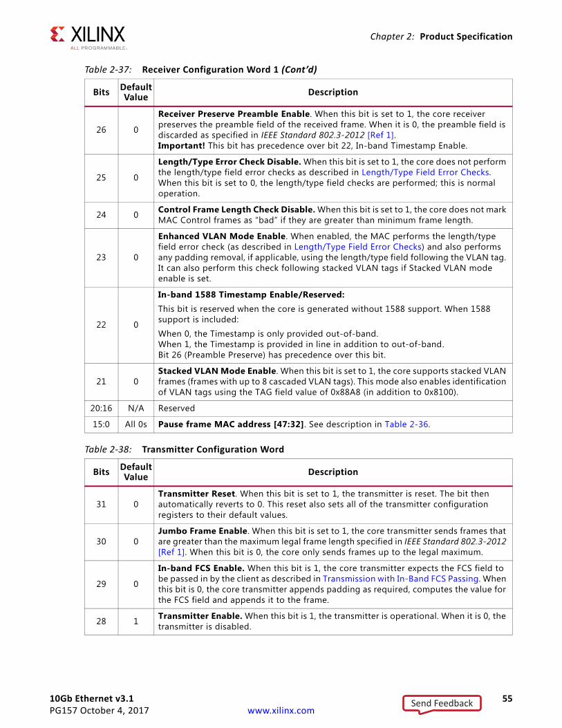
10Gb Ethernet v3.1 55PG157 October 4, 2017 www.xilinx.com
Chapter 2: Product Specification
26 0
Receiver Preserve Preamble Enable. When this bit is set to 1, the core receiver preserves the preamble field of the received frame. When it is 0, the preamble field is discarded as specified in IEEE Standard 802.3-2012 [Ref 1].Important! This bit has precedence over bit 22, In-band Timestamp Enable.
25 0
Length/Type Error Check Disable. When this bit is set to 1, the core does not perform the length/type field error checks as described in Length/Type Field Error Checks.When this bit is set to 0, the length/type field checks are performed; this is normal operation.
24 0 Control Frame Length Check Disable. When this bit is set to 1, the core does not mark MAC Control frames as “bad” if they are greater than minimum frame length.
23 0
Enhanced VLAN Mode Enable. When enabled, the MAC performs the length/type field error check (as described in Length/Type Field Error Checks) and also performs any padding removal, if applicable, using the length/type field following the VLAN tag. It can also perform this check following stacked VLAN tags if Stacked VLAN mode enable is set.
22 0
In-band 1588 Timestamp Enable/Reserved:This bit is reserved when the core is generated without 1588 support. When 1588 support is included:
When 0, the Timestamp is only provided out-of-band.When 1, the Timestamp is provided in line in addition to out-of-band.Bit 26 (Preamble Preserve) has precedence over this bit.
21 0Stacked VLAN Mode Enable. When this bit is set to 1, the core supports stacked VLAN frames (frames with up to 8 cascaded VLAN tags). This mode also enables identification of VLAN tags using the TAG field value of 0x88A8 (in addition to 0x8100).
20:16 N/A Reserved
15:0 All 0s Pause frame MAC address [47:32]. See description in Table 2-36.
Table 2-38: Transmitter Configuration Word
Bits Default Value Description
31 0Transmitter Reset. When this bit is set to 1, the transmitter is reset. The bit then automatically reverts to 0. This reset also sets all of the transmitter configuration registers to their default values.
30 0Jumbo Frame Enable. When this bit is set to 1, the core transmitter sends frames that are greater than the maximum legal frame length specified in IEEE Standard 802.3-2012 [Ref 1]. When this bit is 0, the core only sends frames up to the legal maximum.
29 0
In-band FCS Enable. When this bit is 1, the core transmitter expects the FCS field to be passed in by the client as described in Transmission with In-Band FCS Passing. When this bit is 0, the core transmitter appends padding as required, computes the value for the FCS field and appends it to the frame.
28 1 Transmitter Enable. When this bit is 1, the transmitter is operational. When it is 0, the transmitter is disabled.
Table 2-37: Receiver Configuration Word 1 (Cont’d)
Bits DefaultValue Description
Send Feedback
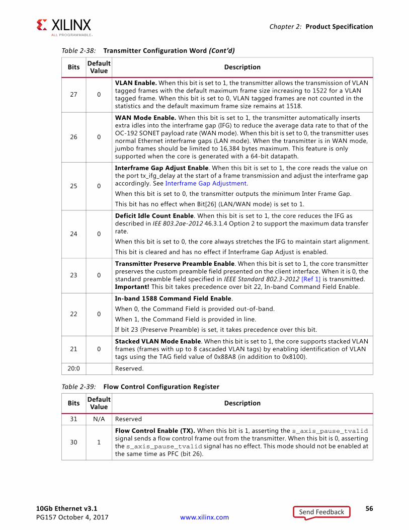
10Gb Ethernet v3.1 56PG157 October 4, 2017 www.xilinx.com
Chapter 2: Product Specification
27 0
VLAN Enable. When this bit is set to 1, the transmitter allows the transmission of VLAN tagged frames with the default maximum frame size increasing to 1522 for a VLAN tagged frame. When this bit is set to 0, VLAN tagged frames are not counted in the statistics and the default maximum frame size remains at 1518.
26 0
WAN Mode Enable. When this bit is set to 1, the transmitter automatically inserts extra idles into the interframe gap (IFG) to reduce the average data rate to that of the OC-192 SONET payload rate (WAN mode). When this bit is set to 0, the transmitter uses normal Ethernet interframe gaps (LAN mode). When the transmitter is in WAN mode, jumbo frames should be limited to 16,384 bytes maximum. This feature is only supported when the core is generated with a 64-bit datapath.
25 0
Interframe Gap Adjust Enable. When this bit is set to 1, the core reads the value on the port tx_ifg_delay at the start of a frame transmission and adjust the interframe gap accordingly. See Interframe Gap Adjustment.
When this bit is set to 0, the transmitter outputs the minimum Inter Frame Gap.
This bit has no effect when Bit[26] (LAN/WAN mode) is set to 1.
24 0
Deficit Idle Count Enable. When this bit is set to 1, the core reduces the IFG as described in IEE 803.2ae-2012 46.3.1.4 Option 2 to support the maximum data transfer rate.
When this bit is set to 0, the core always stretches the IFG to maintain start alignment.
This bit is cleared and has no effect if Interframe Gap Adjust is enabled.
23 0
Transmitter Preserve Preamble Enable. When this bit is set to 1, the core transmitter preserves the custom preamble field presented on the client interface. When it is 0, the standard preamble field specified in IEEE Standard 802.3-2012 [Ref 1] is transmitted. Important! This bit takes precedence over bit 22, In-band Command Field Enable.
22 0
In-band 1588 Command Field Enable.
When 0, the Command Field is provided out-of-band.
When 1, the Command Field is provided in line.
If bit 23 (Preserve Preamble) is set, it takes precedence over this bit.
21 0Stacked VLAN Mode Enable. When this bit is set to 1, the core supports stacked VLAN frames (frames with up to 8 cascaded VLAN tags) by enabling identification of VLAN tags using the TAG field value of 0x88A8 (in addition to 0x8100).
20:0 Reserved.
Table 2-39: Flow Control Configuration Register
Bits DefaultValue Description
31 N/A Reserved
30 1
Flow Control Enable (TX). When this bit is 1, asserting the s_axis_pause_tvalid signal sends a flow control frame out from the transmitter. When this bit is 0, asserting the s_axis_pause_tvalid signal has no effect. This mode should not be enabled at the same time as PFC (bit 26).
Table 2-38: Transmitter Configuration Word (Cont’d)
Bits Default Value Description
Send Feedback
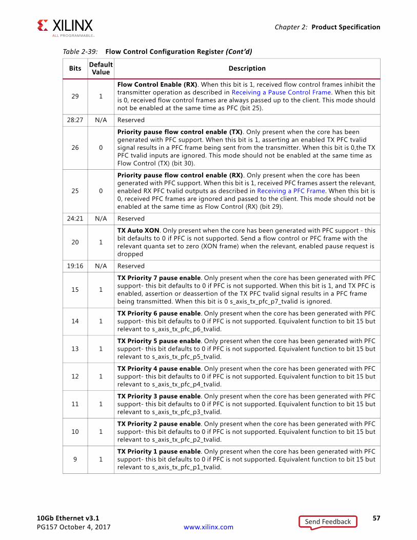
10Gb Ethernet v3.1 57PG157 October 4, 2017 www.xilinx.com
Chapter 2: Product Specification
29 1
Flow Control Enable (RX). When this bit is 1, received flow control frames inhibit the transmitter operation as described in Receiving a Pause Control Frame. When this bit is 0, received flow control frames are always passed up to the client. This mode should not be enabled at the same time as PFC (bit 25).
28:27 N/A Reserved
26 0
Priority pause flow control enable (TX). Only present when the core has been generated with PFC support. When this bit is 1, asserting an enabled TX PFC tvalid signal results in a PFC frame being sent from the transmitter. When this bit is 0,the TX PFC tvalid inputs are ignored. This mode should not be enabled at the same time as Flow Control (TX) (bit 30).
25 0
Priority pause flow control enable (RX). Only present when the core has been generated with PFC support. When this bit is 1, received PFC frames assert the relevant, enabled RX PFC tvalid outputs as described in Receiving a PFC Frame. When this bit is 0, received PFC frames are ignored and passed to the client. This mode should not be enabled at the same time as Flow Control (RX) (bit 29).
24:21 N/A Reserved
20 1
TX Auto XON. Only present when the core has been generated with PFC support - this bit defaults to 0 if PFC is not supported. Send a flow control or PFC frame with the relevant quanta set to zero (XON frame) when the relevant, enabled pause request is dropped
19:16 N/A Reserved
15 1
TX Priority 7 pause enable. Only present when the core has been generated with PFC support- this bit defaults to 0 if PFC is not supported. When this bit is 1, and TX PFC is enabled, assertion or deassertion of the TX PFC tvalid signal results in a PFC frame being transmitted. When this bit is 0 s_axis_tx_pfc_p7_tvalid is ignored.
14 1TX Priority 6 pause enable. Only present when the core has been generated with PFC support- this bit defaults to 0 if PFC is not supported. Equivalent function to bit 15 but relevant to s_axis_tx_pfc_p6_tvalid.
13 1TX Priority 5 pause enable. Only present when the core has been generated with PFC support- this bit defaults to 0 if PFC is not supported. Equivalent function to bit 15 but relevant to s_axis_tx_pfc_p5_tvalid.
12 1TX Priority 4 pause enable. Only present when the core has been generated with PFC support- this bit defaults to 0 if PFC is not supported. Equivalent function to bit 15 but relevant to s_axis_tx_pfc_p4_tvalid.
11 1TX Priority 3 pause enable. Only present when the core has been generated with PFC support- this bit defaults to 0 if PFC is not supported. Equivalent function to bit 15 but relevant to s_axis_tx_pfc_p3_tvalid.
10 1TX Priority 2 pause enable. Only present when the core has been generated with PFC support- this bit defaults to 0 if PFC is not supported. Equivalent function to bit 15 but relevant to s_axis_tx_pfc_p2_tvalid.
9 1TX Priority 1 pause enable. Only present when the core has been generated with PFC support- this bit defaults to 0 if PFC is not supported. Equivalent function to bit 15 but relevant to s_axis_tx_pfc_p1_tvalid.
Table 2-39: Flow Control Configuration Register (Cont’d)
Bits DefaultValue Description
Send Feedback
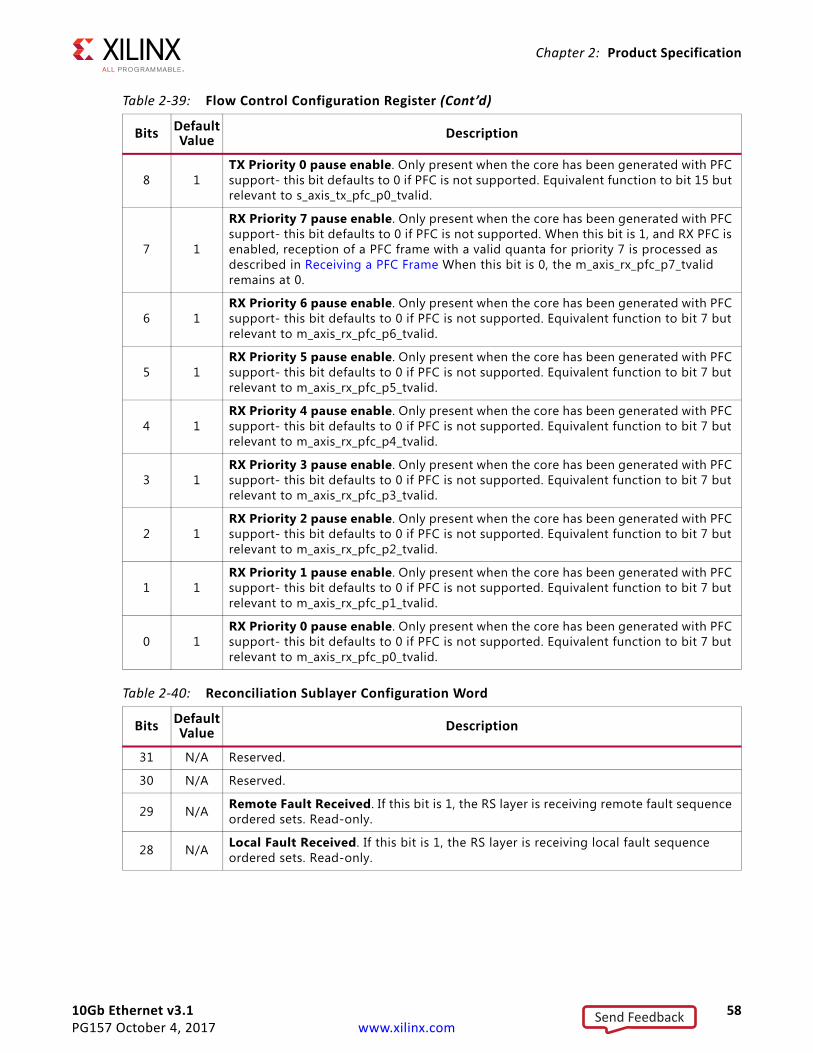
10Gb Ethernet v3.1 58PG157 October 4, 2017 www.xilinx.com
Chapter 2: Product Specification
8 1TX Priority 0 pause enable. Only present when the core has been generated with PFC support- this bit defaults to 0 if PFC is not supported. Equivalent function to bit 15 but relevant to s_axis_tx_pfc_p0_tvalid.
7 1
RX Priority 7 pause enable. Only present when the core has been generated with PFC support- this bit defaults to 0 if PFC is not supported. When this bit is 1, and RX PFC is enabled, reception of a PFC frame with a valid quanta for priority 7 is processed as described in Receiving a PFC Frame When this bit is 0, the m_axis_rx_pfc_p7_tvalid remains at 0.
6 1RX Priority 6 pause enable. Only present when the core has been generated with PFC support- this bit defaults to 0 if PFC is not supported. Equivalent function to bit 7 but relevant to m_axis_rx_pfc_p6_tvalid.
5 1RX Priority 5 pause enable. Only present when the core has been generated with PFC support- this bit defaults to 0 if PFC is not supported. Equivalent function to bit 7 but relevant to m_axis_rx_pfc_p5_tvalid.
4 1RX Priority 4 pause enable. Only present when the core has been generated with PFC support- this bit defaults to 0 if PFC is not supported. Equivalent function to bit 7 but relevant to m_axis_rx_pfc_p4_tvalid.
3 1RX Priority 3 pause enable. Only present when the core has been generated with PFC support- this bit defaults to 0 if PFC is not supported. Equivalent function to bit 7 but relevant to m_axis_rx_pfc_p3_tvalid.
2 1RX Priority 2 pause enable. Only present when the core has been generated with PFC support- this bit defaults to 0 if PFC is not supported. Equivalent function to bit 7 but relevant to m_axis_rx_pfc_p2_tvalid.
1 1RX Priority 1 pause enable. Only present when the core has been generated with PFC support- this bit defaults to 0 if PFC is not supported. Equivalent function to bit 7 but relevant to m_axis_rx_pfc_p1_tvalid.
0 1RX Priority 0 pause enable. Only present when the core has been generated with PFC support- this bit defaults to 0 if PFC is not supported. Equivalent function to bit 7 but relevant to m_axis_rx_pfc_p0_tvalid.
Table 2-40: Reconciliation Sublayer Configuration Word
Bits DefaultValue Description
31 N/A Reserved.
30 N/A Reserved.
29 N/A Remote Fault Received. If this bit is 1, the RS layer is receiving remote fault sequence ordered sets. Read-only.
28 N/A Local Fault Received. If this bit is 1, the RS layer is receiving local fault sequence ordered sets. Read-only.
Table 2-39: Flow Control Configuration Register (Cont’d)
Bits DefaultValue Description
Send Feedback
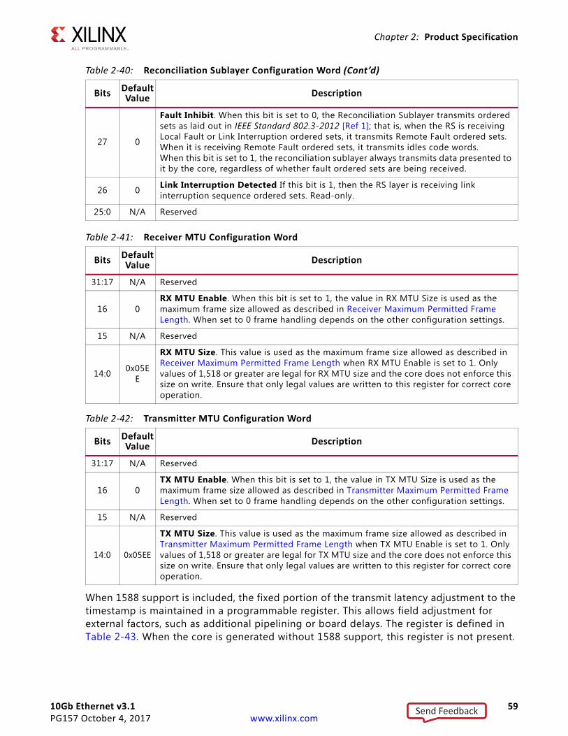
10Gb Ethernet v3.1 59PG157 October 4, 2017 www.xilinx.com
Chapter 2: Product Specification
When 1588 support is included, the fixed portion of the transmit latency adjustment to the timestamp is maintained in a programmable register. This allows field adjustment for external factors, such as additional pipelining or board delays. The register is defined in Table 2-43. When the core is generated without 1588 support, this register is not present.
27 0
Fault Inhibit. When this bit is set to 0, the Reconciliation Sublayer transmits ordered sets as laid out in IEEE Standard 802.3-2012 [Ref 1]; that is, when the RS is receiving Local Fault or Link Interruption ordered sets, it transmits Remote Fault ordered sets. When it is receiving Remote Fault ordered sets, it transmits idles code words.When this bit is set to 1, the reconciliation sublayer always transmits data presented to it by the core, regardless of whether fault ordered sets are being received.
26 0 Link Interruption Detected If this bit is 1, then the RS layer is receiving link interruption sequence ordered sets. Read-only.
25:0 N/A Reserved
Table 2-41: Receiver MTU Configuration Word
Bits DefaultValue Description
31:17 N/A Reserved
16 0RX MTU Enable. When this bit is set to 1, the value in RX MTU Size is used as the maximum frame size allowed as described in Receiver Maximum Permitted Frame Length. When set to 0 frame handling depends on the other configuration settings.
15 N/A Reserved
14:0 0x05EE
RX MTU Size. This value is used as the maximum frame size allowed as described in Receiver Maximum Permitted Frame Length when RX MTU Enable is set to 1. Only values of 1,518 or greater are legal for RX MTU size and the core does not enforce this size on write. Ensure that only legal values are written to this register for correct core operation.
Table 2-42: Transmitter MTU Configuration Word
Bits DefaultValue Description
31:17 N/A Reserved
16 0TX MTU Enable. When this bit is set to 1, the value in TX MTU Size is used as the maximum frame size allowed as described in Transmitter Maximum Permitted Frame Length. When set to 0 frame handling depends on the other configuration settings.
15 N/A Reserved
14:0 0x05EE
TX MTU Size. This value is used as the maximum frame size allowed as described in Transmitter Maximum Permitted Frame Length when TX MTU Enable is set to 1. Only values of 1,518 or greater are legal for TX MTU size and the core does not enforce this size on write. Ensure that only legal values are written to this register for correct core operation.
Table 2-40: Reconciliation Sublayer Configuration Word (Cont’d)
Bits DefaultValue Description
Send Feedback
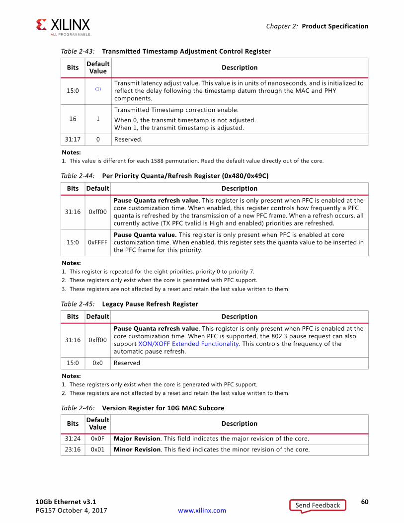
10Gb Ethernet v3.1 60PG157 October 4, 2017 www.xilinx.com
Chapter 2: Product Specification
Table 2-43: Transmitted Timestamp Adjustment Control Register
Bits DefaultValue Description
15:0 (1)Transmit latency adjust value. This value is in units of nanoseconds, and is initialized to reflect the delay following the timestamp datum through the MAC and PHY components.
16 1Transmitted Timestamp correction enable.
When 0, the transmit timestamp is not adjusted.When 1, the transmit timestamp is adjusted.
31:17 0 Reserved.
Notes: 1. This value is different for each 1588 permutation. Read the default value directly out of the core.
Table 2-44: Per Priority Quanta/Refresh Register (0x480/0x49C)
Bits Default Description
31:16 0xff00
Pause Quanta refresh value. This register is only present when PFC is enabled at the core customization time. When enabled, this register controls how frequently a PFC quanta is refreshed by the transmission of a new PFC frame. When a refresh occurs, all currently active (TX PFC tvalid is High and enabled) priorities are refreshed.
15:0 0xFFFFPause Quanta value. This register is only present when PFC is enabled at core customization time. When enabled, this register sets the quanta value to be inserted in the PFC frame for this priority.
Notes: 1. This register is repeated for the eight priorities, priority 0 to priority 7.2. These registers only exist when the core is generated with PFC support.3. These registers are not affected by a reset and retain the last value written to them.
Table 2-45: Legacy Pause Refresh Register
Bits Default Description
31:16 0xff00
Pause Quanta refresh value. This register is only present when PFC is enabled at the core customization time. When PFC is supported, the 802.3 pause request can also support XON/XOFF Extended Functionality. This controls the frequency of the automatic pause refresh.
15:0 0x0 Reserved
Notes: 1. These registers only exist when the core is generated with PFC support.2. These registers are not affected by a reset and retain the last value written to them.
Table 2-46: Version Register for 10G MAC Subcore
Bits DefaultValue Description
31:24 0x0F Major Revision. This field indicates the major revision of the core.
23:16 0x01 Minor Revision. This field indicates the minor revision of the core.
Send Feedback
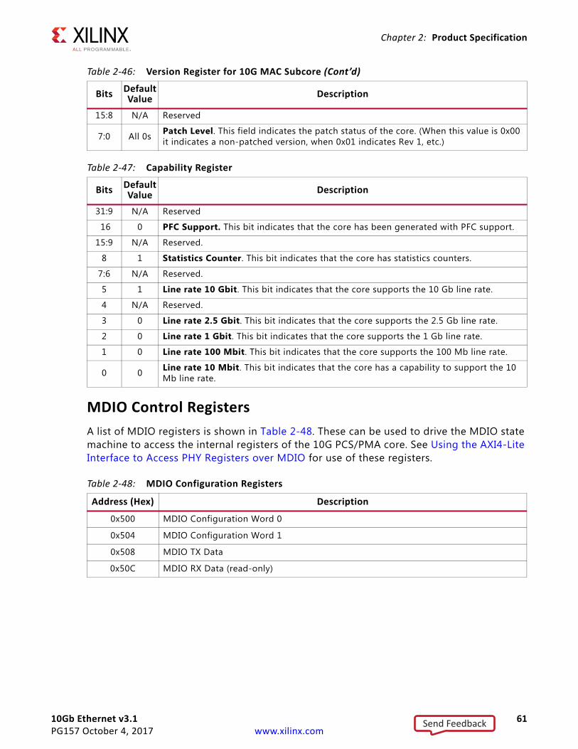
10Gb Ethernet v3.1 61PG157 October 4, 2017 www.xilinx.com
Chapter 2: Product Specification
MDIO Control RegistersA list of MDIO registers is shown in Table 2-48. These can be used to drive the MDIO state machine to access the internal registers of the 10G PCS/PMA core. See Using the AXI4-Lite Interface to Access PHY Registers over MDIO for use of these registers.
15:8 N/A Reserved
7:0 All 0s Patch Level. This field indicates the patch status of the core. (When this value is 0x00 it indicates a non-patched version, when 0x01 indicates Rev 1, etc.)
Table 2-47: Capability Register
Bits DefaultValue Description
31:9 N/A Reserved
16 0 PFC Support. This bit indicates that the core has been generated with PFC support.
15:9 N/A Reserved.
8 1 Statistics Counter. This bit indicates that the core has statistics counters.
7:6 N/A Reserved.
5 1 Line rate 10 Gbit. This bit indicates that the core supports the 10 Gb line rate.
4 N/A Reserved.
3 0 Line rate 2.5 Gbit. This bit indicates that the core supports the 2.5 Gb line rate.
2 0 Line rate 1 Gbit. This bit indicates that the core supports the 1 Gb line rate.
1 0 Line rate 100 Mbit. This bit indicates that the core supports the 100 Mb line rate.
0 0 Line rate 10 Mbit. This bit indicates that the core has a capability to support the 10 Mb line rate.
Table 2-48: MDIO Configuration Registers
Address (Hex) Description
0x500 MDIO Configuration Word 0
0x504 MDIO Configuration Word 1
0x508 MDIO TX Data
0x50C MDIO RX Data (read-only)
Table 2-46: Version Register for 10G MAC Subcore (Cont’d)
Bits DefaultValue Description
Send Feedback
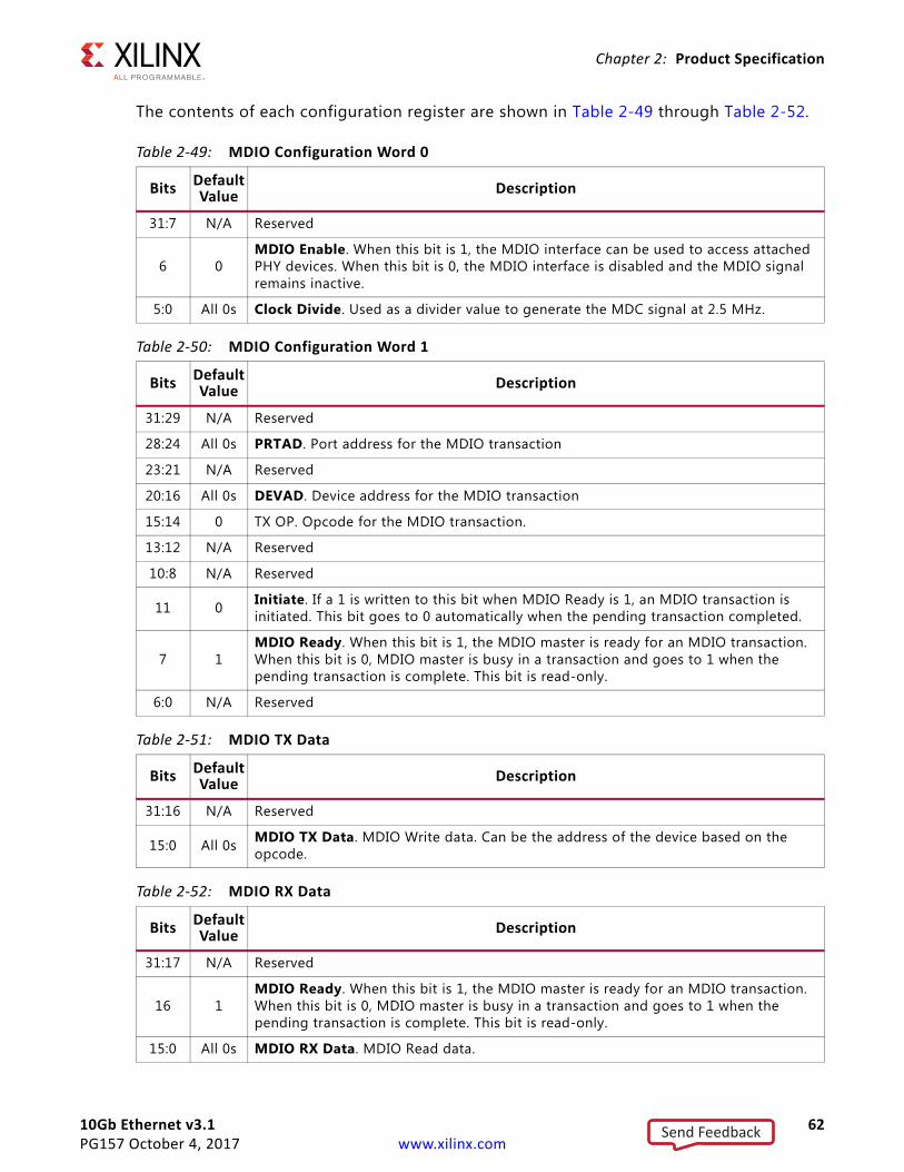
10Gb Ethernet v3.1 62PG157 October 4, 2017 www.xilinx.com
Chapter 2: Product Specification
The contents of each configuration register are shown in Table 2-49 through Table 2-52.
Table 2-49: MDIO Configuration Word 0
Bits Default Value Description
31:7 N/A Reserved
6 0MDIO Enable. When this bit is 1, the MDIO interface can be used to access attached PHY devices. When this bit is 0, the MDIO interface is disabled and the MDIO signal remains inactive.
5:0 All 0s Clock Divide. Used as a divider value to generate the MDC signal at 2.5 MHz.
Table 2-50: MDIO Configuration Word 1
Bits DefaultValue Description
31:29 N/A Reserved
28:24 All 0s PRTAD. Port address for the MDIO transaction
23:21 N/A Reserved
20:16 All 0s DEVAD. Device address for the MDIO transaction
15:14 0 TX OP. Opcode for the MDIO transaction.
13:12 N/A Reserved
10:8 N/A Reserved
11 0 Initiate. If a 1 is written to this bit when MDIO Ready is 1, an MDIO transaction is initiated. This bit goes to 0 automatically when the pending transaction completed.
7 1MDIO Ready. When this bit is 1, the MDIO master is ready for an MDIO transaction. When this bit is 0, MDIO master is busy in a transaction and goes to 1 when the pending transaction is complete. This bit is read-only.
6:0 N/A Reserved
Table 2-51: MDIO TX Data
Bits Default Value Description
31:16 N/A Reserved
15:0 All 0s MDIO TX Data. MDIO Write data. Can be the address of the device based on the opcode.
Table 2-52: MDIO RX Data
Bits Default Value Description
31:17 N/A Reserved
16 1MDIO Ready. When this bit is 1, the MDIO master is ready for an MDIO transaction. When this bit is 0, MDIO master is busy in a transaction and goes to 1 when the pending transaction is complete. This bit is read-only.
15:0 All 0s MDIO RX Data. MDIO Read data.
Send Feedback
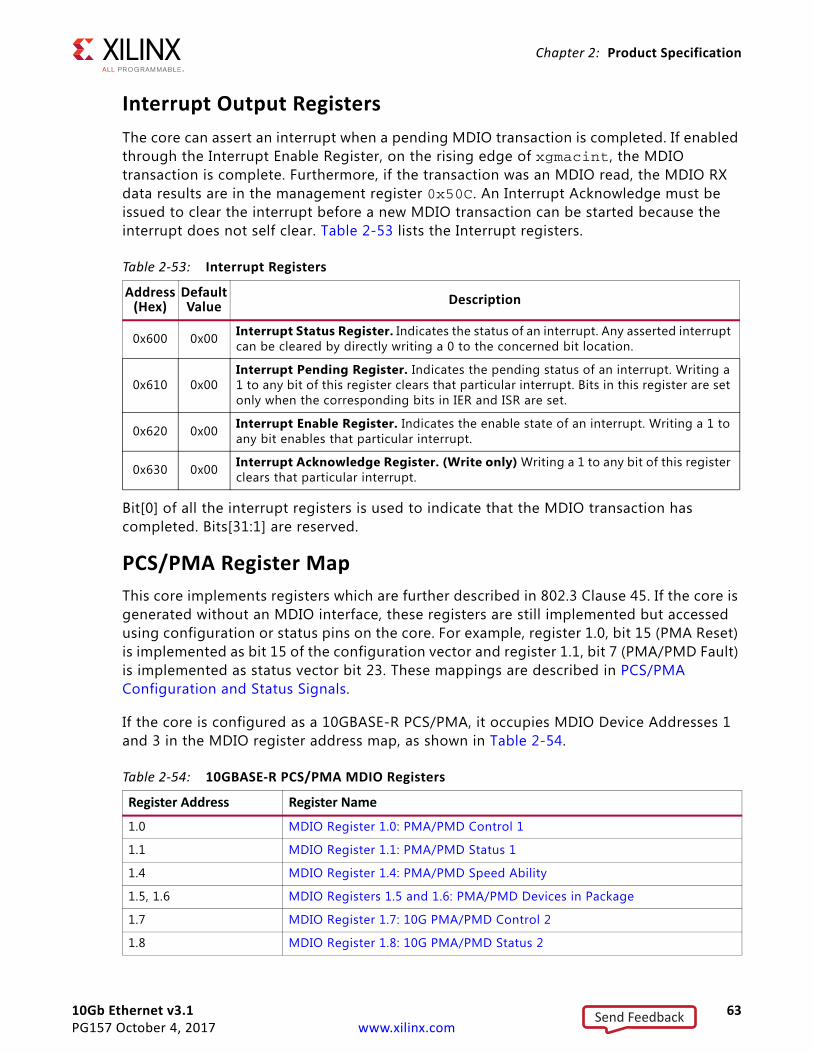
10Gb Ethernet v3.1 63PG157 October 4, 2017 www.xilinx.com
Chapter 2: Product Specification
Interrupt Output RegistersThe core can assert an interrupt when a pending MDIO transaction is completed. If enabled through the Interrupt Enable Register, on the rising edge of xgmacint, the MDIO transaction is complete. Furthermore, if the transaction was an MDIO read, the MDIO RX data results are in the management register 0x50C. An Interrupt Acknowledge must be issued to clear the interrupt before a new MDIO transaction can be started because the interrupt does not self clear. Table 2-53 lists the Interrupt registers.
Bit[0] of all the interrupt registers is used to indicate that the MDIO transaction has completed. Bits[31:1] are reserved.
PCS/PMA Register MapThis core implements registers which are further described in 802.3 Clause 45. If the core is generated without an MDIO interface, these registers are still implemented but accessed using configuration or status pins on the core. For example, register 1.0, bit 15 (PMA Reset) is implemented as bit 15 of the configuration vector and register 1.1, bit 7 (PMA/PMD Fault) is implemented as status vector bit 23. These mappings are described in PCS/PMA Configuration and Status Signals.
If the core is configured as a 10GBASE-R PCS/PMA, it occupies MDIO Device Addresses 1 and 3 in the MDIO register address map, as shown in Table 2-54.
Table 2-53: Interrupt Registers
Address(Hex)
DefaultValue Description
0x600 0x00 Interrupt Status Register. Indicates the status of an interrupt. Any asserted interrupt can be cleared by directly writing a 0 to the concerned bit location.
0x610 0x00Interrupt Pending Register. Indicates the pending status of an interrupt. Writing a 1 to any bit of this register clears that particular interrupt. Bits in this register are set only when the corresponding bits in IER and ISR are set.
0x620 0x00 Interrupt Enable Register. Indicates the enable state of an interrupt. Writing a 1 to any bit enables that particular interrupt.
0x630 0x00 Interrupt Acknowledge Register. (Write only) Writing a 1 to any bit of this register clears that particular interrupt.
Table 2-54: 10GBASE-R PCS/PMA MDIO Registers
Register Address Register Name
1.0 MDIO Register 1.0: PMA/PMD Control 1
1.1 MDIO Register 1.1: PMA/PMD Status 1
1.4 MDIO Register 1.4: PMA/PMD Speed Ability
1.5, 1.6 MDIO Registers 1.5 and 1.6: PMA/PMD Devices in Package
1.7 MDIO Register 1.7: 10G PMA/PMD Control 2
1.8 MDIO Register 1.8: 10G PMA/PMD Status 2
Send Feedback
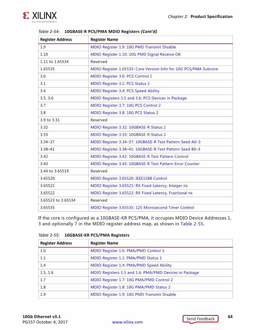
10Gb Ethernet v3.1 64PG157 October 4, 2017 www.xilinx.com
Chapter 2: Product Specification
If the core is configured as a 10GBASE-KR PCS/PMA, it occupies MDIO Device Addresses 1, 3 and optionally 7 in the MDIO register address map, as shown in Table 2-55.
1.9 MDIO Register 1.9: 10G PMD Transmit Disable
1.10 MDIO Register 1.10: 10G PMD Signal Receive OK
1.11 to 1.65534 Reserved
1.65535 MDIO Register 1.65535: Core Version Info for 10G PCS/PMA Subcore
3.0 MDIO Register 3.0: PCS Control 1
3.1 MDIO Register 3.1: PCS Status 1
3.4 MDIO Register 3.4: PCS Speed Ability
3.5, 3.6 MDIO Registers 3.5 and 3.6: PCS Devices in Package
3.7 MDIO Register 3.7: 10G PCS Control 2
3.8 MDIO Register 3.8: 10G PCS Status 2
3.9 to 3.31 Reserved
3.32 MDIO Register 3.32: 10GBASE-R Status 1
3.33 MDIO Register 3.33: 10GBASE-R Status 2
3.34–37 MDIO Register 3.34–37: 10GBASE-R Test Pattern Seed A0–3
3.38–41 MDIO Register 3.38–41: 10GBASE-R Test Pattern Seed B0–3
3.42 MDIO Register 3.42: 10GBASE-R Test Pattern Control
3.43 MDIO Register 3.43: 10GBASE-R Test Pattern Error Counter
3.44 to 3.65519 Reserved
3.65520 MDIO Register 3.65520: IEEE1588 Control
3.65521 MDIO Register 3.65521: RX Fixed Latency, Integer ns
3.65522 MDIO Register 3.65522: RX Fixed Latency, Fractional ns
3.65523 to 3.65534 Reserved
3.65535 MDIO Register 3.65535: 125 Microsecond Timer Control
Table 2-55: 10GBASE-KR PCS/PMA Registers
Register Address Register Name
1.0 MDIO Register 1.0: PMA/PMD Control 1
1.1 MDIO Register 1.1: PMA/PMD Status 1
1.4 MDIO Register 1.4: PMA/PMD Speed Ability
1.5, 1.6 MDIO Registers 1.5 and 1.6: PMA/PMD Devices in Package
1.7 MDIO Register 1.7: 10G PMA/PMD Control 2
1.8 MDIO Register 1.8: 10G PMA/PMD Status 2
1.9 MDIO Register 1.9: 10G PMD Transmit Disable
Table 2-54: 10GBASE-R PCS/PMA MDIO Registers (Cont’d)
Register Address Register Name
Send Feedback
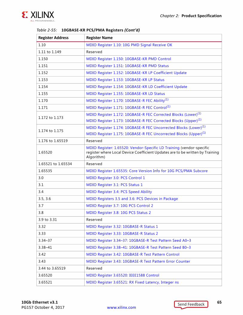
10Gb Ethernet v3.1 65PG157 October 4, 2017 www.xilinx.com
Chapter 2: Product Specification
1.10 MDIO Register 1.10: 10G PMD Signal Receive OK
1.11 to 1.149 Reserved
1.150 MDIO Register 1.150: 10GBASE-KR PMD Control
1.151 MDIO Register 1.151: 10GBASE-KR PMD Status
1.152 MDIO Register 1.152: 10GBASE-KR LP Coefficient Update
1.153 MDIO Register 1.153: 10GBASE-KR LP Status
1.154 MDIO Register 1.154: 10GBASE-KR LD Coefficient Update
1.155 MDIO Register 1.155: 10GBASE-KR LD Status
1.170 MDIO Register 1.170: 10GBASE-R FEC Ability(1)
1.171 MDIO Register 1.171: 10GBASE-R FEC Control(1)
1.172 to 1.173MDIO Register 1.172: 10GBASE-R FEC Corrected Blocks (Lower)(1)
MDIO Register 1.173: 10GBASE-R FEC Corrected Blocks (Upper)(1)
1.174 to 1.175MDIO Register 1.174: 10GBASE-R FEC Uncorrected Blocks (Lower)(1)
MDIO Register 1.175: 10GBASE-R FEC Uncorrected Blocks (Upper)(1)
1.176 to 1.65519 Reserved
1.65520MDIO Register: 1.65520: Vendor-Specific LD Training (vendor-specific register where Local Device Coefficient Updates are to be written by Training Algorithm)
1.65521 to 1.65534 Reserved
1.65535 MDIO Register 1.65535: Core Version Info for 10G PCS/PMA Subcore
3.0 MDIO Register 3.0: PCS Control 1
3.1 MDIO Register 3.1: PCS Status 1
3.4 MDIO Register 3.4: PCS Speed Ability
3.5, 3.6 MDIO Registers 3.5 and 3.6: PCS Devices in Package
3.7 MDIO Register 3.7: 10G PCS Control 2
3.8 MDIO Register 3.8: 10G PCS Status 2
3.9 to 3.31 Reserved
3.32 MDIO Register 3.32: 10GBASE-R Status 1
3.33 MDIO Register 3.33: 10GBASE-R Status 2
3.34–37 MDIO Register 3.34–37: 10GBASE-R Test Pattern Seed A0–3
3.38–41 MDIO Register 3.38–41: 10GBASE-R Test Pattern Seed B0–3
3.42 MDIO Register 3.42: 10GBASE-R Test Pattern Control
3.43 MDIO Register 3.43: 10GBASE-R Test Pattern Error Counter
3.44 to 3.65519 Reserved
3.65520 MDIO Register 3.65520: IEEE1588 Control
3.65521 MDIO Register 3.65521: RX Fixed Latency, Integer ns
Table 2-55: 10GBASE-KR PCS/PMA Registers (Cont’d)
Register Address Register Name
Send Feedback
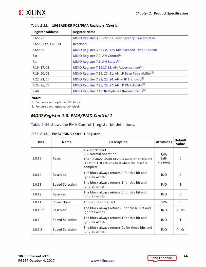
10Gb Ethernet v3.1 66PG157 October 4, 2017 www.xilinx.com
Chapter 2: Product Specification
MDIO Register 1.0: PMA/PMD Control 1
Table 2-56 shows the PMA Control 1 register bit definitions.
3.65522 MDIO Register 3.65522: RX Fixed Latency, Fractional ns
3.65523 to 3.65534 Reserved
3.65535 MDIO Register 3.65535: 125 Microsecond Timer Control
7.0 MDIO Register 7.0: AN Control(2)
7.1 MDIO Register 7.1: AN Status(2)
7.16, 17, 18 MDIO Register 7.16:17:18: AN Advertisement(2)
7.19, 20, 21 MDIO Register 7.19, 20, 21: AN LP Base Page Ability(2)
7.22, 23, 24 MDIO Register 7.22, 23, 24: AN XNP Transmit(2)
7.25, 26, 27 MDIO Register 7.25, 26, 27: AN LP XNP Ability(2)
7.48 MDIO Register 7.48: Backplane Ethernet Status(2)
Notes: 1. For cores with optional FEC block2. For cores with optional AN block
Table 2-56: PMA/PMD Control 1 Register
Bits Name Description Attributes DefaultValue
1.0.15 Reset
1 = Block reset0 = Normal operation
The 10GBASE-R/KR block is reset when this bit is set to 1. It returns to 0 when the reset is complete.
R/WSelf-
clearing0
1.0.14 Reserved The block always returns 0 for this bit and ignores writes. R/O 0
1.0.13 Speed Selection The block always returns 1 for this bit and ignores writes. R/O 1
1.0.12 Reserved The block always returns 0 for this bit and ignores writes. R/O 0
1.0.11 Power down This bit has no effect. R/W 0
1.0.10:7 Reserved The block always returns 0 for these bits and ignores writes. R/O All 0s
1.0.6 Speed Selection The block always returns 1 for this bit and ignores writes. R/O 1
1.0.5:2 Speed Selection The block always returns 0s for these bits and ignores writes. R/O All 0s
Table 2-55: 10GBASE-KR PCS/PMA Registers (Cont’d)
Register Address Register Name
Send Feedback
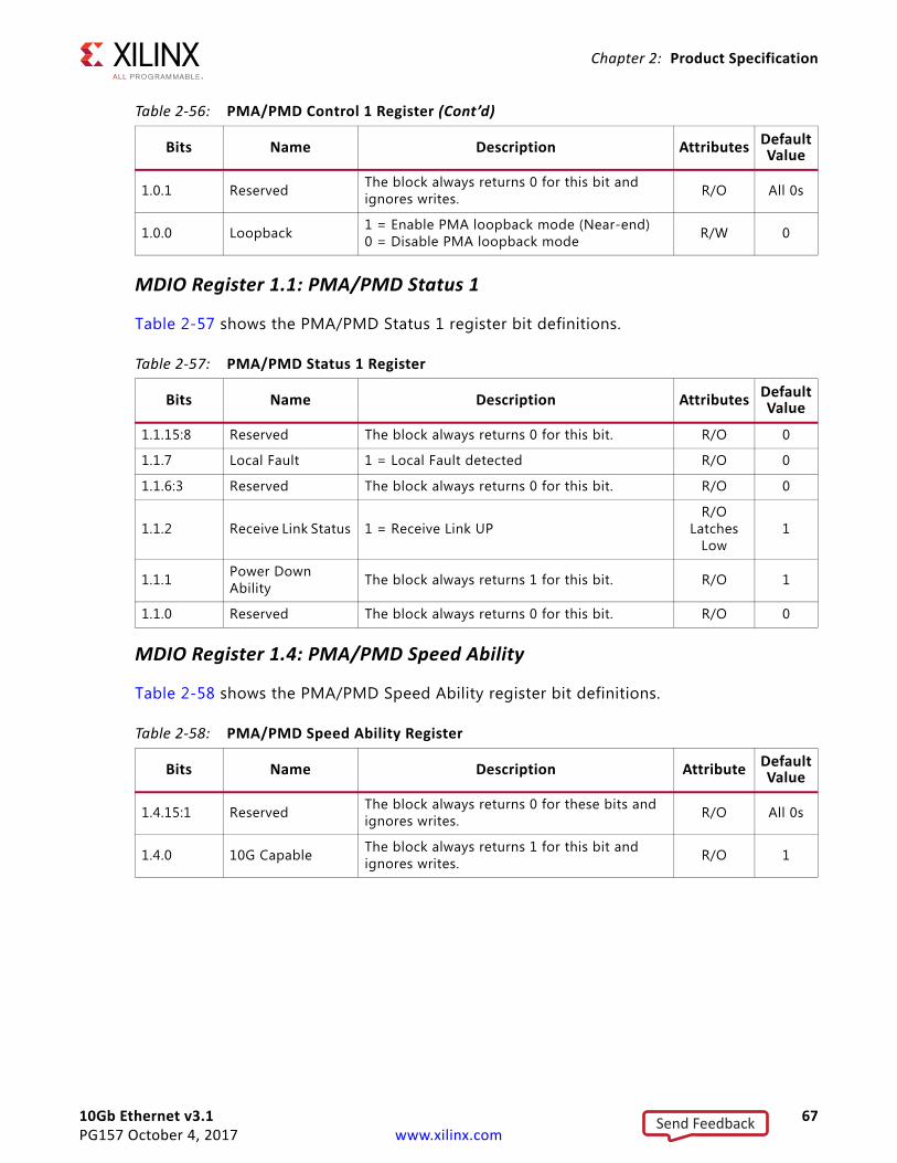
10Gb Ethernet v3.1 67PG157 October 4, 2017 www.xilinx.com
Chapter 2: Product Specification
MDIO Register 1.1: PMA/PMD Status 1
Table 2-57 shows the PMA/PMD Status 1 register bit definitions.
MDIO Register 1.4: PMA/PMD Speed Ability
Table 2-58 shows the PMA/PMD Speed Ability register bit definitions.
1.0.1 Reserved The block always returns 0 for this bit and ignores writes. R/O All 0s
1.0.0 Loopback 1 = Enable PMA loopback mode (Near-end)0 = Disable PMA loopback mode R/W 0
Table 2-57: PMA/PMD Status 1 Register
Bits Name Description Attributes Default Value
1.1.15:8 Reserved The block always returns 0 for this bit. R/O 0
1.1.7 Local Fault 1 = Local Fault detected R/O 0
1.1.6:3 Reserved The block always returns 0 for this bit. R/O 0
1.1.2 Receive Link Status 1 = Receive Link UPR/O
LatchesLow
1
1.1.1 Power Down Ability The block always returns 1 for this bit. R/O 1
1.1.0 Reserved The block always returns 0 for this bit. R/O 0
Table 2-58: PMA/PMD Speed Ability Register
Bits Name Description Attribute Default Value
1.4.15:1 Reserved The block always returns 0 for these bits and ignores writes. R/O All 0s
1.4.0 10G Capable The block always returns 1 for this bit and ignores writes. R/O 1
Table 2-56: PMA/PMD Control 1 Register (Cont’d)
Bits Name Description Attributes DefaultValue
Send Feedback
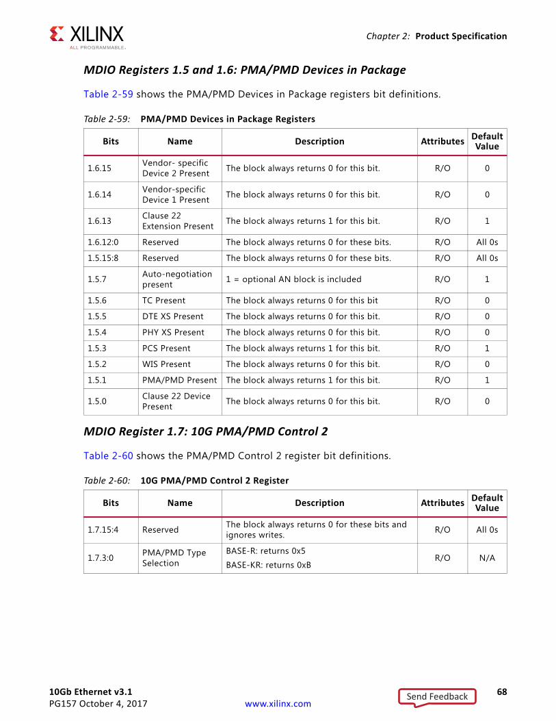
10Gb Ethernet v3.1 68PG157 October 4, 2017 www.xilinx.com
Chapter 2: Product Specification
MDIO Registers 1.5 and 1.6: PMA/PMD Devices in Package
Table 2-59 shows the PMA/PMD Devices in Package registers bit definitions.
MDIO Register 1.7: 10G PMA/PMD Control 2
Table 2-60 shows the PMA/PMD Control 2 register bit definitions.
Table 2-59: PMA/PMD Devices in Package Registers
Bits Name Description Attributes Default Value
1.6.15 Vendor- specificDevice 2 Present The block always returns 0 for this bit. R/O 0
1.6.14 Vendor-specificDevice 1 Present The block always returns 0 for this bit. R/O 0
1.6.13 Clause 22Extension Present The block always returns 1 for this bit. R/O 1
1.6.12:0 Reserved The block always returns 0 for these bits. R/O All 0s
1.5.15:8 Reserved The block always returns 0 for these bits. R/O All 0s
1.5.7 Auto-negotiationpresent 1 = optional AN block is included R/O 1
1.5.6 TC Present The block always returns 0 for this bit R/O 0
1.5.5 DTE XS Present The block always returns 0 for this bit. R/O 0
1.5.4 PHY XS Present The block always returns 0 for this bit. R/O 0
1.5.3 PCS Present The block always returns 1 for this bit. R/O 1
1.5.2 WIS Present The block always returns 0 for this bit. R/O 0
1.5.1 PMA/PMD Present The block always returns 1 for this bit. R/O 1
1.5.0 Clause 22 DevicePresent The block always returns 0 for this bit. R/O 0
Table 2-60: 10G PMA/PMD Control 2 Register
Bits Name Description Attributes Default Value
1.7.15:4 Reserved The block always returns 0 for these bits and ignores writes. R/O All 0s
1.7.3:0 PMA/PMD Type Selection
BASE-R: returns 0x5
BASE-KR: returns 0xBR/O N/A
Send Feedback
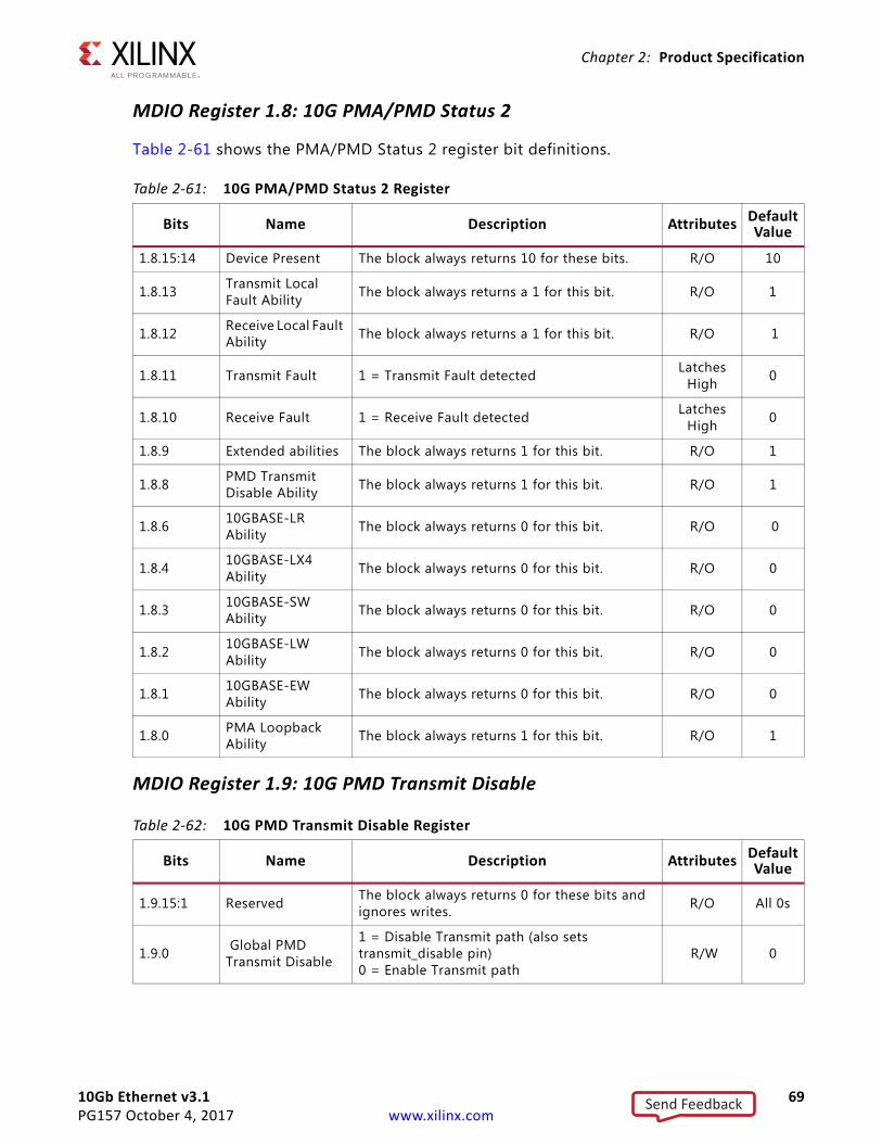
10Gb Ethernet v3.1 69PG157 October 4, 2017 www.xilinx.com
Chapter 2: Product Specification
MDIO Register 1.8: 10G PMA/PMD Status 2
Table 2-61 shows the PMA/PMD Status 2 register bit definitions.
MDIO Register 1.9: 10G PMD Transmit Disable
Table 2-61: 10G PMA/PMD Status 2 Register
Bits Name Description Attributes Default Value
1.8.15:14 Device Present The block always returns 10 for these bits. R/O 10
1.8.13 Transmit Local Fault Ability The block always returns a 1 for this bit. R/O 1
1.8.12 Receive Local Fault Ability The block always returns a 1 for this bit. R/O 1
1.8.11 Transmit Fault 1 = Transmit Fault detected Latches High 0
1.8.10 Receive Fault 1 = Receive Fault detected Latches High 0
1.8.9 Extended abilities The block always returns 1 for this bit. R/O 1
1.8.8 PMD Transmit Disable Ability The block always returns 1 for this bit. R/O 1
1.8.6 10GBASE-LR Ability The block always returns 0 for this bit. R/O 0
1.8.4 10GBASE-LX4 Ability The block always returns 0 for this bit. R/O 0
1.8.3 10GBASE-SW Ability The block always returns 0 for this bit. R/O 0
1.8.2 10GBASE-LW Ability The block always returns 0 for this bit. R/O 0
1.8.1 10GBASE-EW Ability The block always returns 0 for this bit. R/O 0
1.8.0 PMA Loopback Ability The block always returns 1 for this bit. R/O 1
Table 2-62: 10G PMD Transmit Disable Register
Bits Name Description Attributes Default Value
1.9.15:1 Reserved The block always returns 0 for these bits and ignores writes. R/O All 0s
1.9.0 Global PMD Transmit Disable
1 = Disable Transmit path (also sets transmit_disable pin) 0 = Enable Transmit path
R/W 0
Send Feedback
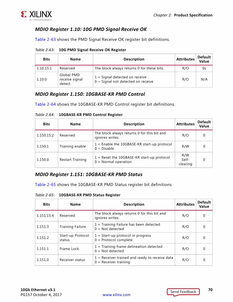
10Gb Ethernet v3.1 70PG157 October 4, 2017 www.xilinx.com
Chapter 2: Product Specification
MDIO Register 1.10: 10G PMD Signal Receive OK
Table 2-63 shows the PMD Signal Receive OK register bit definitions.
MDIO Register 1.150: 10GBASE-KR PMD Control
Table 2-64 shows the 10GBASE-KR PMD Control register bit definitions.
MDIO Register 1.151: 10GBASE-KR PMD Status
Table 2-65 shows the 10GBASE-KR PMD Status register bit definitions.
Table 2-63: 10G PMD Signal Receive OK Register
Bits Name Description Attributes Default Value
1.10.15:1 Reserved The block always returns 0 for these bits. R/O 0s
1.10.0Global PMD receive signal detect
1 = Signal detected on receive0 = Signal not detected on receive R/O N/A
Table 2-64: 10GBASE-KR PMD Control Register
Bits Name Description Attributes Default Value
1.150.15:2 Reserved The block always returns 0 for this bit and ignores writes. R/O 0
1.150.1 Training enable 1 = Enable the 10GBASE-KR start-up protocol0 = Disable R/W 0
1.150.0 Restart Training 1 = Reset the 10GBASE-KR start-up protocol0 = Normal operation
R/WSelf-
clearing0
Table 2-65: 10GBASE-KR PMD Status Register
Bits Name Description Attributes Default Value
1.151.15:4 Reserved The block always returns 0 for this bit and ignores writes. R/O 0
1.151.3 Training Failure 1 = Training Failure has been detected0 = Not detected R/O 0
1.151.2 Start-up Protocol status
1 = Start-up protocol in progress0 = Protocol complete R/O 0
1.151.1 Frame Lock 1 = Training frame delineation detected0 = Not detected R/O 0
1.151.0 Receiver status 1 = Receiver trained and ready to receive data0 = Receiver training R/O 0
Send Feedback
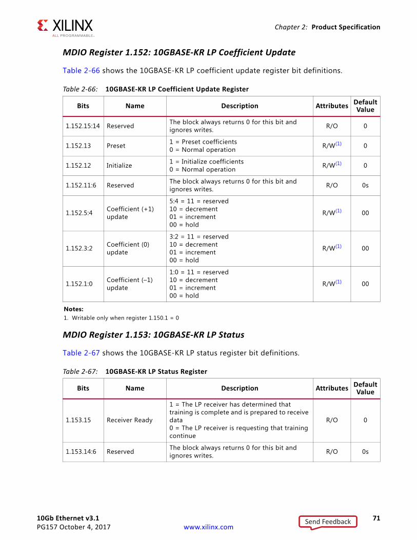
10Gb Ethernet v3.1 71PG157 October 4, 2017 www.xilinx.com
Chapter 2: Product Specification
MDIO Register 1.152: 10GBASE-KR LP Coefficient Update
Table 2-66 shows the 10GBASE-KR LP coefficient update register bit definitions.
MDIO Register 1.153: 10GBASE-KR LP Status
Table 2-67 shows the 10GBASE-KR LP status register bit definitions.
Table 2-66: 10GBASE-KR LP Coefficient Update Register
Bits Name Description Attributes Default Value
1.152.15:14 Reserved The block always returns 0 for this bit and ignores writes. R/O 0
1.152.13 Preset 1 = Preset coefficients0 = Normal operation R/W(1) 0
1.152.12 Initialize 1 = Initialize coefficients0 = Normal operation R/W(1) 0
1.152.11:6 Reserved The block always returns 0 for this bit and ignores writes. R/O 0s
1.152.5:4 Coefficient (+1) update
5:4 = 11 = reserved10 = decrement01 = increment00 = hold
R/W(1) 00
1.152.3:2 Coefficient (0) update
3:2 = 11 = reserved10 = decrement01 = increment00 = hold
R/W(1) 00
1.152.1:0 Coefficient (–1) update
1:0 = 11 = reserved10 = decrement01 = increment00 = hold
R/W(1) 00
Notes: 1. Writable only when register 1.150.1 = 0
Table 2-67: 10GBASE-KR LP Status Register
Bits Name Description Attributes Default Value
1.153.15 Receiver Ready
1 = The LP receiver has determined that training is complete and is prepared to receive data0 = The LP receiver is requesting that training continue
R/O 0
1.153.14:6 Reserved The block always returns 0 for this bit and ignores writes. R/O 0s
Send Feedback
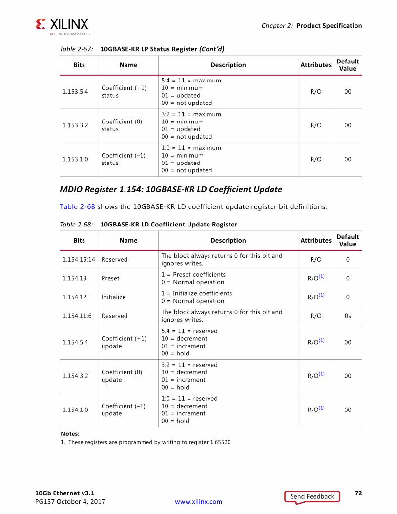
10Gb Ethernet v3.1 72PG157 October 4, 2017 www.xilinx.com
Chapter 2: Product Specification
MDIO Register 1.154: 10GBASE-KR LD Coefficient Update
Table 2-68 shows the 10GBASE-KR LD coefficient update register bit definitions.
1.153.5:4 Coefficient (+1) status
5:4 = 11 = maximum10 = minimum01 = updated00 = not updated
R/O 00
1.153.3:2 Coefficient (0) status
3:2 = 11 = maximum10 = minimum01 = updated00 = not updated
R/O 00
1.153.1:0 Coefficient (–1) status
1:0 = 11 = maximum10 = minimum01 = updated00 = not updated
R/O 00
Table 2-68: 10GBASE-KR LD Coefficient Update Register
Bits Name Description Attributes Default Value
1.154.15:14 Reserved The block always returns 0 for this bit and ignores writes. R/O 0
1.154.13 Preset 1 = Preset coefficients0 = Normal operation R/O(1) 0
1.154.12 Initialize 1 = Initialize coefficients0 = Normal operation R/O(1) 0
1.154.11:6 Reserved The block always returns 0 for this bit and ignores writes. R/O 0s
1.154.5:4 Coefficient (+1) update
5:4 = 11 = reserved10 = decrement01 = increment00 = hold
R/O(1) 00
1.154.3:2 Coefficient (0) update
3:2 = 11 = reserved10 = decrement01 = increment00 = hold
R/O(1) 00
1.154.1:0 Coefficient (–1) update
1:0 = 11 = reserved10 = decrement01 = increment00 = hold
R/O(1) 00
Notes: 1. These registers are programmed by writing to register 1.65520.
Table 2-67: 10GBASE-KR LP Status Register (Cont’d)
Bits Name Description Attributes Default Value
Send Feedback
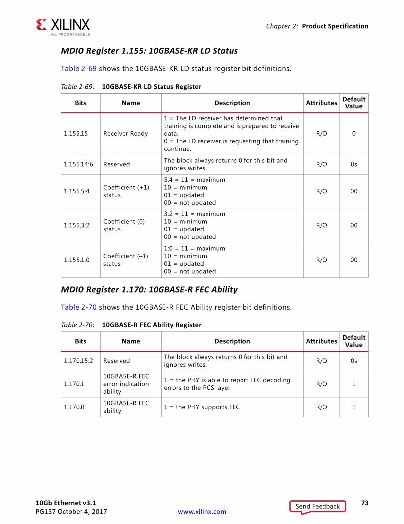
10Gb Ethernet v3.1 73PG157 October 4, 2017 www.xilinx.com
Chapter 2: Product Specification
MDIO Register 1.155: 10GBASE-KR LD Status
Table 2-69 shows the 10GBASE-KR LD status register bit definitions.
MDIO Register 1.170: 10GBASE-R FEC Ability
Table 2-70 shows the 10GBASE-R FEC Ability register bit definitions.
Table 2-69: 10GBASE-KR LD Status Register
Bits Name Description Attributes Default Value
1.155.15 Receiver Ready
1 = The LD receiver has determined that training is complete and is prepared to receive data.0 = The LD receiver is requesting that training continue.
R/O 0
1.155.14:6 Reserved The block always returns 0 for this bit and ignores writes. R/O 0s
1.155.5:4 Coefficient (+1) status
5:4 = 11 = maximum10 = minimum01 = updated00 = not updated
R/O 00
1.155.3:2 Coefficient (0) status
3:2 = 11 = maximum10 = minimum01 = updated00 = not updated
R/O 00
1.155.1:0 Coefficient (–1) status
1:0 = 11 = maximum10 = minimum01 = updated00 = not updated
R/O 00
Table 2-70: 10GBASE-R FEC Ability Register
Bits Name Description Attributes Default Value
1.170.15:2 Reserved The block always returns 0 for this bit and ignores writes. R/O 0s
1.170.110GBASE-R FEC error indication ability
1 = the PHY is able to report FEC decoding errors to the PCS layer R/O 1
1.170.0 10GBASE-R FEC ability 1 = the PHY supports FEC R/O 1
Send Feedback
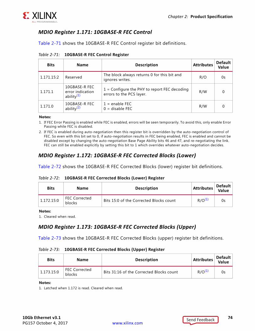
10Gb Ethernet v3.1 74PG157 October 4, 2017 www.xilinx.com
Chapter 2: Product Specification
MDIO Register 1.171: 10GBASE-R FEC Control
Table 2-71 shows the 10GBASE-R FEC Control register bit definitions.
MDIO Register 1.172: 10GBASE-R FEC Corrected Blocks (Lower)
Table 2-72 shows the 10GBASE-R FEC Corrected Blocks (lower) register bit definitions.
MDIO Register 1.173: 10GBASE-R FEC Corrected Blocks (Upper)
Table 2-73 shows the 10GBASE-R FEC Corrected Blocks (upper) register bit definitions.
Table 2-71: 10GBASE-R FEC Control Register
Bits Name Description Attributes Default Value
1.171.15:2 Reserved The block always returns 0 for this bit and ignores writes. R/O 0s
1.171.110GBASE-R FEC error indication ability(1)
1 = Configure the PHY to report FEC decoding errors to the PCS layer. R/W 0
1.171.0 10GBASE-R FEC ability(2)
1 = enable FEC 0 = disable FEC R/W 0
Notes: 1. If FEC Error Passing is enabled while FEC is enabled, errors will be seen temporarily. To avoid this, only enable Error
Passing while FEC is disabled.2. If FEC is enabled during auto-negotiation then this register bit is overridden by the auto-negotiation control of
FEC. So even with this bit set to 0, if auto-negotiation results in FEC being enabled, FEC is enabled and cannot be disabled except by changing the auto-negotiation Base Page Ability bits 46 and 47, and re-negotiating the link. FEC can still be enabled explicitly by setting this bit to 1 which overrides whatever auto-negotiation decides.
Table 2-72: 10GBASE-R FEC Corrected Blocks (Lower) Register
Bits Name Description Attributes Default Value
1.172.15:0 FEC Corrected blocks Bits 15:0 of the Corrected Blocks count R/O(1) 0s
Notes: 1. Cleared when read.
Table 2-73: 10GBASE-R FEC Corrected Blocks (Upper) Register
Bits Name Description Attributes Default Value
1.173.15:0 FEC Corrected blocks Bits 31:16 of the Corrected Blocks count R/O(1) 0s
Notes: 1. Latched when 1.172 is read. Cleared when read.
Send Feedback
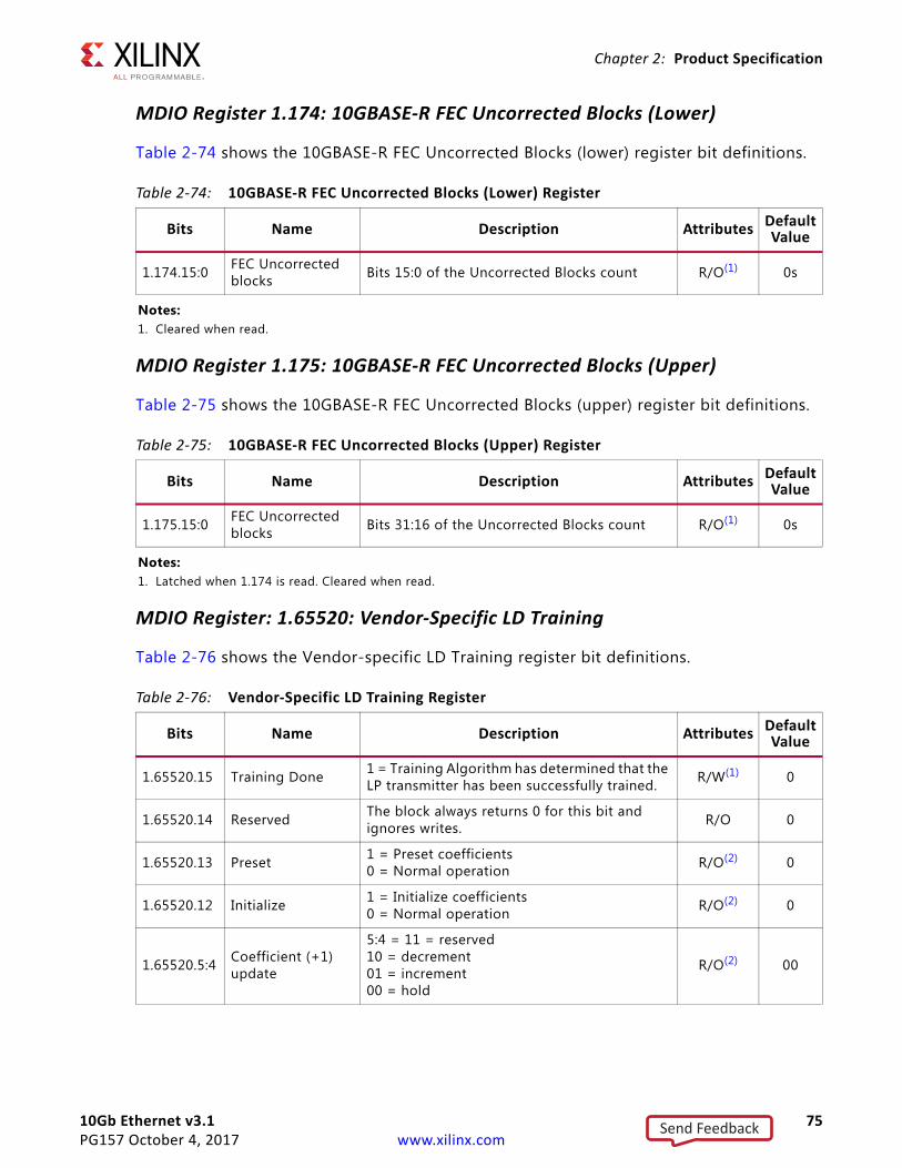
10Gb Ethernet v3.1 75PG157 October 4, 2017 www.xilinx.com
Chapter 2: Product Specification
MDIO Register 1.174: 10GBASE-R FEC Uncorrected Blocks (Lower)
Table 2-74 shows the 10GBASE-R FEC Uncorrected Blocks (lower) register bit definitions.
MDIO Register 1.175: 10GBASE-R FEC Uncorrected Blocks (Upper)
Table 2-75 shows the 10GBASE-R FEC Uncorrected Blocks (upper) register bit definitions.
MDIO Register: 1.65520: Vendor-Specific LD Training
Table 2-76 shows the Vendor-specific LD Training register bit definitions.
Table 2-74: 10GBASE-R FEC Uncorrected Blocks (Lower) Register
Bits Name Description Attributes Default Value
1.174.15:0 FEC Uncorrected blocks Bits 15:0 of the Uncorrected Blocks count R/O(1) 0s
Notes: 1. Cleared when read.
Table 2-75: 10GBASE-R FEC Uncorrected Blocks (Upper) Register
Bits Name Description Attributes Default Value
1.175.15:0 FEC Uncorrected blocks Bits 31:16 of the Uncorrected Blocks count R/O(1) 0s
Notes: 1. Latched when 1.174 is read. Cleared when read.
Table 2-76: Vendor-Specific LD Training Register
Bits Name Description Attributes Default Value
1.65520.15 Training Done 1 = Training Algorithm has determined that the LP transmitter has been successfully trained. R/W(1) 0
1.65520.14 Reserved The block always returns 0 for this bit and ignores writes. R/O 0
1.65520.13 Preset 1 = Preset coefficients0 = Normal operation R/O(2) 0
1.65520.12 Initialize 1 = Initialize coefficients0 = Normal operation R/O(2) 0
1.65520.5:4 Coefficient (+1) update
5:4 = 11 = reserved10 = decrement01 = increment00 = hold
R/O(2) 00
Send Feedback
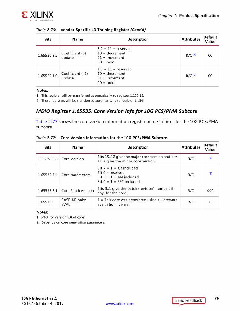
10Gb Ethernet v3.1 76PG157 October 4, 2017 www.xilinx.com
Chapter 2: Product Specification
MDIO Register 1.65535: Core Version Info for 10G PCS/PMA Subcore
Table 2-77 shows the core version information register bit definitions for the 10G PCS/PMA subcore.
1.65520.3:2 Coefficient (0) update
3:2 = 11 = reserved10 = decrement01 = increment00 = hold
R/O(2) 00
1.65520.1:0 Coefficient (–1) update
1:0 = 11 = reserved10 = decrement01 = increment00 = hold
R/O(2) 00
Notes: 1. This register will be transferred automatically to register 1.155.15.2. These registers will be transferred automatically to register 1.154.
Table 2-77: Core Version Information for the 10G PCS/PMA Subcore
Bits Name Description Attributes Default Value
1.65535.15:8 Core Version Bits 15..12 give the major core version and bits 11..8 give the minor core version. R/O (1)
1.65535.7:4 Core parameters
Bit 7 = 1 = KR includedBit 6 – reservedBit 5 = 1 = AN includedBit 4 = 1 = FEC included
R/O (2)
1.65535.3:1 Core Patch Version Bits 3..1 give the patch (revision) number, if any, for the core. R/O 000
1.65535.0 BASE-KR only: EVAL
1 = This core was generated using a Hardware Evaluation license R/O 0
Notes: 1. x'60' for version 6.0 of core2. Depends on core generation parameters
Table 2-76: Vendor-Specific LD Training Register (Cont’d)
Bits Name Description Attributes Default Value
Send Feedback
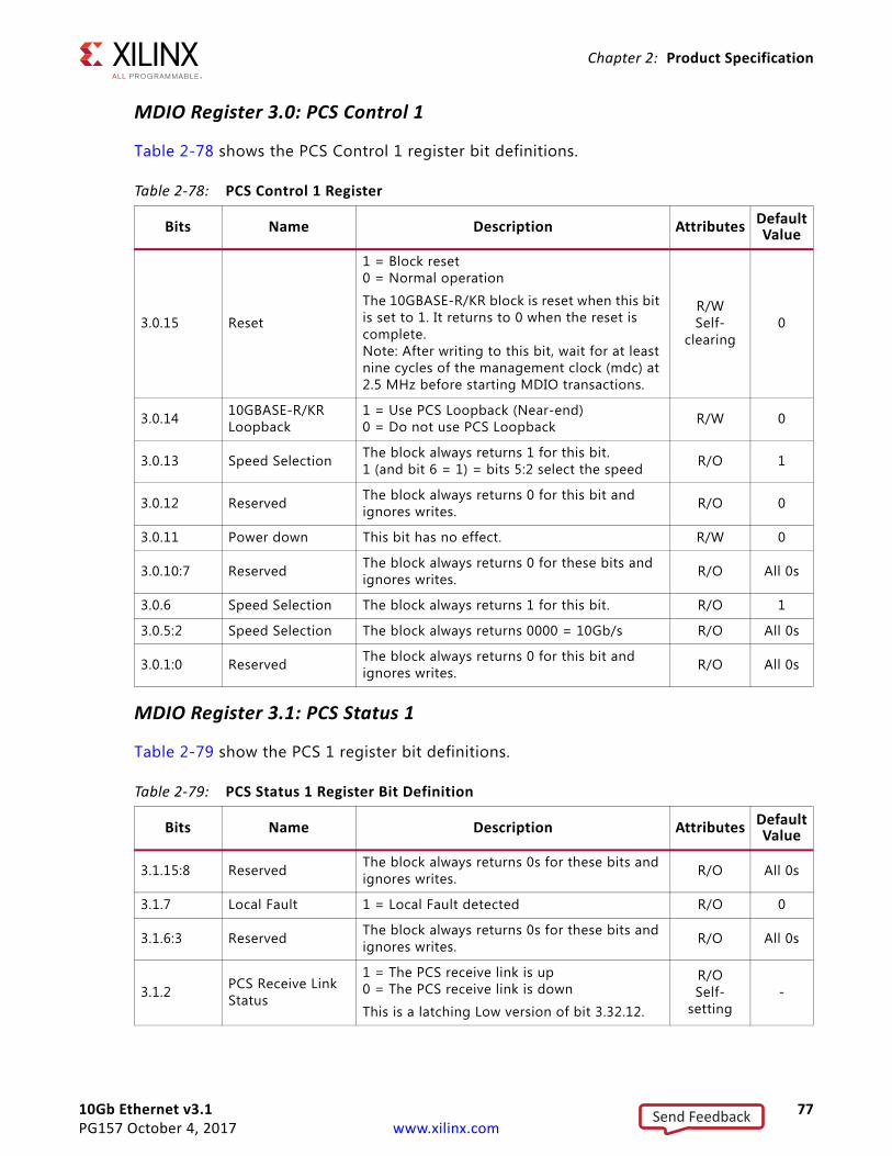
10Gb Ethernet v3.1 77PG157 October 4, 2017 www.xilinx.com
Chapter 2: Product Specification
MDIO Register 3.0: PCS Control 1
Table 2-78 shows the PCS Control 1 register bit definitions.
MDIO Register 3.1: PCS Status 1
Table 2-79 show the PCS 1 register bit definitions.
Table 2-78: PCS Control 1 Register
Bits Name Description Attributes Default Value
3.0.15 Reset
1 = Block reset0 = Normal operation
The 10GBASE-R/KR block is reset when this bit is set to 1. It returns to 0 when the reset is complete. Note: After writing to this bit, wait for at least nine cycles of the management clock (mdc) at 2.5 MHz before starting MDIO transactions.
R/WSelf-
clearing0
3.0.14 10GBASE-R/KR Loopback
1 = Use PCS Loopback (Near-end)0 = Do not use PCS Loopback R/W 0
3.0.13 Speed Selection The block always returns 1 for this bit.1 (and bit 6 = 1) = bits 5:2 select the speed R/O 1
3.0.12 Reserved The block always returns 0 for this bit and ignores writes. R/O 0
3.0.11 Power down This bit has no effect. R/W 0
3.0.10:7 Reserved The block always returns 0 for these bits and ignores writes. R/O All 0s
3.0.6 Speed Selection The block always returns 1 for this bit. R/O 1
3.0.5:2 Speed Selection The block always returns 0000 = 10Gb/s R/O All 0s
3.0.1:0 Reserved The block always returns 0 for this bit and ignores writes. R/O All 0s
Table 2-79: PCS Status 1 Register Bit Definition
Bits Name Description Attributes Default Value
3.1.15:8 Reserved The block always returns 0s for these bits and ignores writes. R/O All 0s
3.1.7 Local Fault 1 = Local Fault detected R/O 0
3.1.6:3 Reserved The block always returns 0s for these bits and ignores writes. R/O All 0s
3.1.2 PCS Receive Link Status
1 = The PCS receive link is up0 = The PCS receive link is down
This is a latching Low version of bit 3.32.12.
R/OSelf-
setting-
Send Feedback
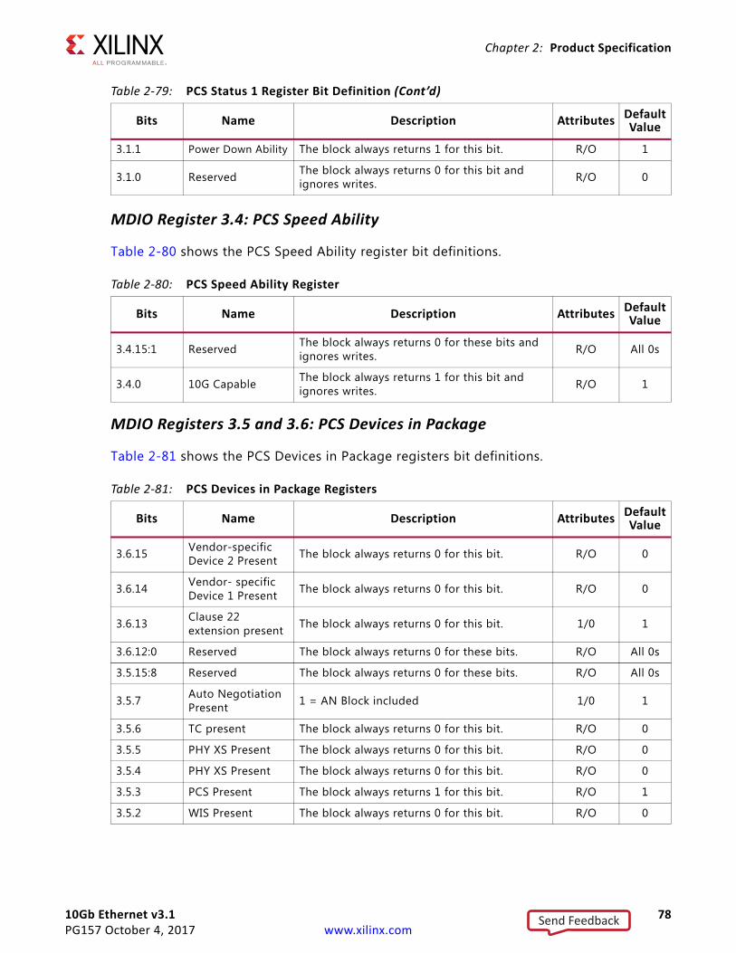
10Gb Ethernet v3.1 78PG157 October 4, 2017 www.xilinx.com
Chapter 2: Product Specification
MDIO Register 3.4: PCS Speed Ability
Table 2-80 shows the PCS Speed Ability register bit definitions.
MDIO Registers 3.5 and 3.6: PCS Devices in Package
Table 2-81 shows the PCS Devices in Package registers bit definitions.
3.1.1 Power Down Ability The block always returns 1 for this bit. R/O 1
3.1.0 Reserved The block always returns 0 for this bit and ignores writes. R/O 0
Table 2-80: PCS Speed Ability Register
Bits Name Description Attributes Default Value
3.4.15:1 Reserved The block always returns 0 for these bits and ignores writes. R/O All 0s
3.4.0 10G Capable The block always returns 1 for this bit and ignores writes. R/O 1
Table 2-81: PCS Devices in Package Registers
Bits Name Description Attributes Default Value
3.6.15 Vendor-specific Device 2 Present The block always returns 0 for this bit. R/O 0
3.6.14 Vendor- specific Device 1 Present The block always returns 0 for this bit. R/O 0
3.6.13 Clause 22 extension present The block always returns 0 for this bit. 1/0 1
3.6.12:0 Reserved The block always returns 0 for these bits. R/O All 0s
3.5.15:8 Reserved The block always returns 0 for these bits. R/O All 0s
3.5.7 Auto Negotiation Present 1 = AN Block included 1/0 1
3.5.6 TC present The block always returns 0 for this bit. R/O 0
3.5.5 PHY XS Present The block always returns 0 for this bit. R/O 0
3.5.4 PHY XS Present The block always returns 0 for this bit. R/O 0
3.5.3 PCS Present The block always returns 1 for this bit. R/O 1
3.5.2 WIS Present The block always returns 0 for this bit. R/O 0
Table 2-79: PCS Status 1 Register Bit Definition (Cont’d)
Bits Name Description Attributes Default Value
Send Feedback
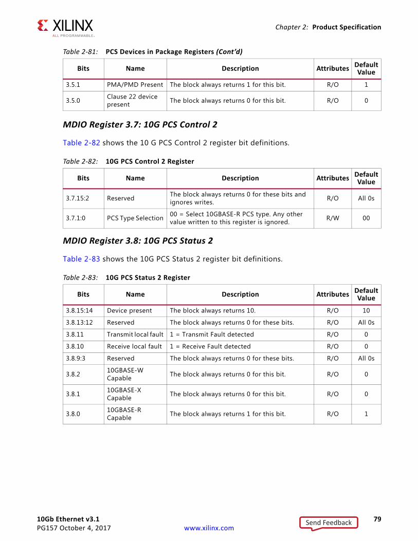
10Gb Ethernet v3.1 79PG157 October 4, 2017 www.xilinx.com
Chapter 2: Product Specification
MDIO Register 3.7: 10G PCS Control 2
Table 2-82 shows the 10 G PCS Control 2 register bit definitions.
MDIO Register 3.8: 10G PCS Status 2
Table 2-83 shows the 10G PCS Status 2 register bit definitions.
3.5.1 PMA/PMD Present The block always returns 1 for this bit. R/O 1
3.5.0 Clause 22 device present The block always returns 0 for this bit. R/O 0
Table 2-82: 10G PCS Control 2 Register
Bits Name Description Attributes Default Value
3.7.15:2 Reserved The block always returns 0 for these bits and ignores writes. R/O All 0s
3.7.1:0 PCS Type Selection 00 = Select 10GBASE-R PCS type. Any other value written to this register is ignored. R/W 00
Table 2-83: 10G PCS Status 2 Register
Bits Name Description Attributes Default Value
3.8.15:14 Device present The block always returns 10. R/O 10
3.8.13:12 Reserved The block always returns 0 for these bits. R/O All 0s
3.8.11 Transmit local fault 1 = Transmit Fault detected R/O 0
3.8.10 Receive local fault 1 = Receive Fault detected R/O 0
3.8.9:3 Reserved The block always returns 0 for these bits. R/O All 0s
3.8.2 10GBASE-W Capable The block always returns 0 for this bit. R/O 0
3.8.1 10GBASE-X Capable The block always returns 0 for this bit. R/O 0
3.8.0 10GBASE-R Capable The block always returns 1 for this bit. R/O 1
Table 2-81: PCS Devices in Package Registers (Cont’d)
Bits Name Description Attributes Default Value
Send Feedback
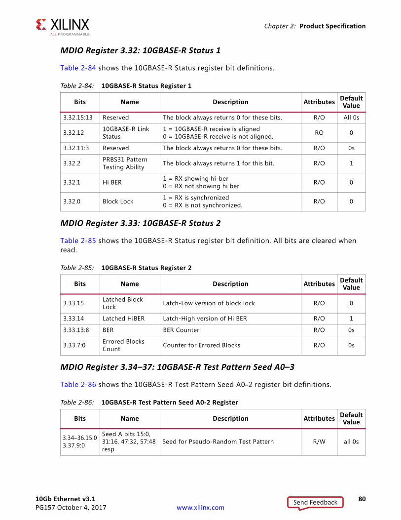
10Gb Ethernet v3.1 80PG157 October 4, 2017 www.xilinx.com
Chapter 2: Product Specification
MDIO Register 3.32: 10GBASE-R Status 1
Table 2-84 shows the 10GBASE-R Status register bit definitions.
MDIO Register 3.33: 10GBASE-R Status 2
Table 2-85 shows the 10GBASE-R Status register bit definition. All bits are cleared when read.
MDIO Register 3.34–37: 10GBASE-R Test Pattern Seed A0–3
Table 2-86 shows the 10GBASE-R Test Pattern Seed A0–2 register bit definitions.
Table 2-84: 10GBASE-R Status Register 1
Bits Name Description Attributes Default Value
3.32.15:13 Reserved The block always returns 0 for these bits. R/O All 0s
3.32.12 10GBASE-R Link Status
1 = 10GBASE-R receive is aligned0 = 10GBASE-R receive is not aligned. RO 0
3.32.11:3 Reserved The block always returns 0 for these bits. R/O 0s
3.32.2 PRBS31 Pattern Testing Ability The block always returns 1 for this bit. R/O 1
3.32.1 Hi BER 1 = RX showing hi-ber0 = RX not showing hi ber R/O 0
3.32.0 Block Lock 1 = RX is synchronized0 = RX is not synchronized. R/O 0
Table 2-85: 10GBASE-R Status Register 2
Bits Name Description Attributes Default Value
3.33.15 Latched Block Lock Latch-Low version of block lock R/O 0
3.33.14 Latched HiBER Latch-High version of Hi BER R/O 1
3.33.13:8 BER BER Counter R/O 0s
3.33.7:0 Errored Blocks Count Counter for Errored Blocks R/O 0s
Table 2-86: 10GBASE-R Test Pattern Seed A0-2 Register
Bits Name Description Attributes Default Value
3.34–36.15:03.37.9:0
Seed A bits 15:0, 31:16, 47:32, 57:48 resp
Seed for Pseudo-Random Test Pattern R/W all 0s
Send Feedback
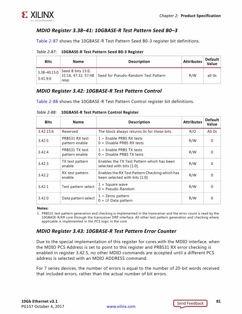
10Gb Ethernet v3.1 81PG157 October 4, 2017 www.xilinx.com
Chapter 2: Product Specification
MDIO Register 3.38–41: 10GBASE-R Test Pattern Seed B0–3
Table 2-87 shows the 10GBASE-R Test Pattern Seed B0–3 register bit definitions.
MDIO Register 3.42: 10GBASE-R Test Pattern Control
Table 2-88 shows the 10GBASE-R Test Pattern Control register bit definitions.
MDIO Register 3.43: 10GBASE-R Test Pattern Error Counter
Due to the special implementation of this register for cores with the MDIO interface, when the MDIO PCS Address is set to point to this register and PRBS31 RX error checking is enabled in register 3.42.5, no other MDIO commands are accepted until a different PCS address is selected with an MDIO ADDRESS command.
For 7 series devices, the number of errors is equal to the number of 20-bit words received that included errors, rather than the actual number of bit errors.
Table 2-87: 10GBASE-R Test Pattern Seed B0-3 Register
Bits Name Description Attributes Default Value
3.38–40.15:0
3.41.9:0
Seed B bits 15:0, 31:16, 47:32, 57:48 resp
Seed for Pseudo-Random Test Pattern R/W all 0s
Table 2-88: 10GBASE-R Test Pattern Control Register
Bits Name Description Attributes Default Value
3.42.15:6 Reserved The block always returns 0s for these bits. R/O All 0s
3.42.5 PRBS31 RX test pattern enable
1 = Enable PRBS RX tests0 = Disable PRBS RX tests R/W 0
3.42.4 PRBS31 TX test pattern enable
1 = Enable PRBS TX tests0 = Disable PRBS TX tests R/W 0
3.42.3 TX test pattern enable
Enables the TX Test Pattern which has been selected with bits [1:0]. R/W 0
3.42.2 RX test pattern enable
Enables the RX Test Pattern Checking which has been selected with bits [1:0] R/W 0
3.42.1 Test pattern select 1 = Square wave0 = Pseudo-Random R/W 0
3.42.0 Data pattern select 1 = Zeros pattern0 = LF Data pattern R/W 0
Notes: 1. PRBS31 test pattern generation and checking is implemented in the transceiver and the error count is read by the
10GBASE-R/KR core through the transceiver DRP interface. All other test pattern generation and checking where applicable is implemented in the PCS logic in the core
Send Feedback
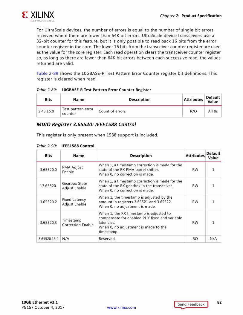
10Gb Ethernet v3.1 82PG157 October 4, 2017 www.xilinx.com
Chapter 2: Product Specification
For UltraScale devices, the number of errors is equal to the number of single bit errors received where there are fewer than 64K bit errors. UltraScale device transceivers use a 32-bit counter for this feature, but it is only possible to read back 16 bits from the error counter register in the core. The lower 16 bits from the transceiver counter register are used as the value for the core register. Each read operation clears the transceiver counter register so, as long as there are fewer than 64K bit errors between each successive read, the values returned are valid.
Table 2-89 shows the 10GBASE-R Test Pattern Error Counter register bit definitions. This register is cleared when read.
MDIO Register 3.65520: IEEE1588 Control
This register is only present when 1588 support is included.
Table 2-89: 10GBASE-R Test Pattern Error Counter Register
Bits Name Description Attributes Default Value
3.43.15:0 Test pattern error counter Count of errors R/O All 0s
Table 2-90: IEEE1588 Control
Bits Name Description Attributes DefaultValue
3.65520.0 PMA Adjust Enable
When 1, a timestamp correction is made for the state of the RX PMA barrel shifter. When 0, no correction is made.
RW 1
13.65520. Gearbox State Adjust Enable
When 1, a timestamp correction is made for the state of the RX gearbox in the transceiver. When 0, no correction is made.
RW 1
3.65520.2 Fixed Latency Adjust Enable
When 1, the timestamp is adjusted by the amount in registers 3.65521 and 3.65522. When 0, no adjustment is made.
RW 1
3.65520.3 Timestamp Correction Enable
When 1, the RX timestamp is adjusted to compensate for enabled PHY fixed and variable latencies. When 0, no adjustment is made to the timestamp.
RW 1
3.65520.15:4 N/A Reserved. RO N/A
Send Feedback
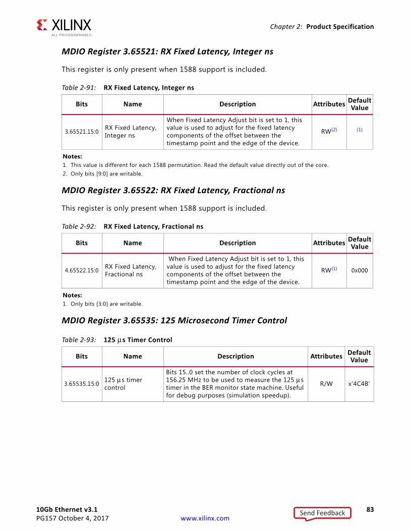
10Gb Ethernet v3.1 83PG157 October 4, 2017 www.xilinx.com
Chapter 2: Product Specification
MDIO Register 3.65521: RX Fixed Latency, Integer ns
This register is only present when 1588 support is included.
MDIO Register 3.65522: RX Fixed Latency, Fractional ns
This register is only present when 1588 support is included.
MDIO Register 3.65535: 125 Microsecond Timer Control
Table 2-91: RX Fixed Latency, Integer ns
Bits Name Description Attributes Default Value
3.65521.15:0 RX Fixed Latency,Integer ns
When Fixed Latency Adjust bit is set to 1, this value is used to adjust for the fixed latency components of the offset between the timestamp point and the edge of the device.
RW(2) (1)
Notes: 1. This value is different for each 1588 permutation. Read the default value directly out of the core.2. Only bits [9:0] are writable.
Table 2-92: RX Fixed Latency, Fractional ns
Bits Name Description Attributes Default Value
4.65522.15:0 RX Fixed Latency,Fractional ns
When Fixed Latency Adjust bit is set to 1, this value is used to adjust for the fixed latency components of the offset between the timestamp point and the edge of the device.
RW(1) 0x000
Notes: 1. Only bits [3:0] are writable.
Table 2-93: 125 μs Timer Control
Bits Name Description Attributes Default Value
3.65535.15:0 125 μs timer control
Bits 15..0 set the number of clock cycles at 156.25 MHz to be used to measure the 125 μs timer in the BER monitor state machine. Useful for debug purposes (simulation speedup).
R/W x'4C4B'
Send Feedback
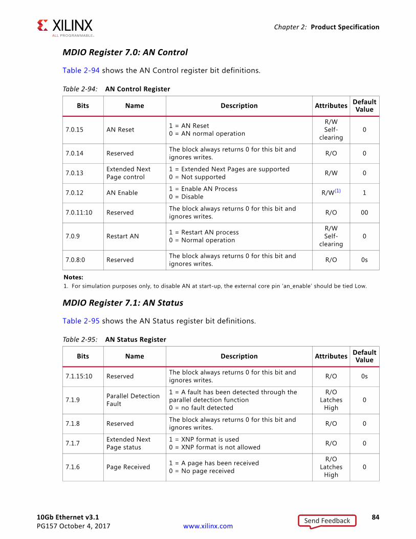
10Gb Ethernet v3.1 84PG157 October 4, 2017 www.xilinx.com
Chapter 2: Product Specification
MDIO Register 7.0: AN Control
Table 2-94 shows the AN Control register bit definitions.
MDIO Register 7.1: AN Status
Table 2-95 shows the AN Status register bit definitions.
Table 2-94: AN Control Register
Bits Name Description Attributes Default Value
7.0.15 AN Reset 1 = AN Reset0 = AN normal operation
R/WSelf-
clearing0
7.0.14 Reserved The block always returns 0 for this bit and ignores writes. R/O 0
7.0.13 Extended Next Page control
1 = Extended Next Pages are supported0 = Not supported R/W 0
7.0.12 AN Enable 1 = Enable AN Process0 = Disable R/W(1) 1
7.0.11:10 Reserved The block always returns 0 for this bit and ignores writes. R/O 00
7.0.9 Restart AN 1 = Restart AN process0 = Normal operation
R/WSelf-
clearing0
7.0.8:0 Reserved The block always returns 0 for this bit and ignores writes. R/O 0s
Notes: 1. For simulation purposes only, to disable AN at start-up, the external core pin ‘an_enable’ should be tied Low.
Table 2-95: AN Status Register
Bits Name Description Attributes Default Value
7.1.15:10 Reserved The block always returns 0 for this bit and ignores writes. R/O 0s
7.1.9 Parallel Detection Fault
1 = A fault has been detected through the parallel detection function0 = no fault detected
R/OLatches
High0
7.1.8 Reserved The block always returns 0 for this bit and ignores writes. R/O 0
7.1.7 Extended Next Page status
1 = XNP format is used0 = XNP format is not allowed R/O 0
7.1.6 Page Received 1 = A page has been received0 = No page received
R/OLatches
High0
Send Feedback
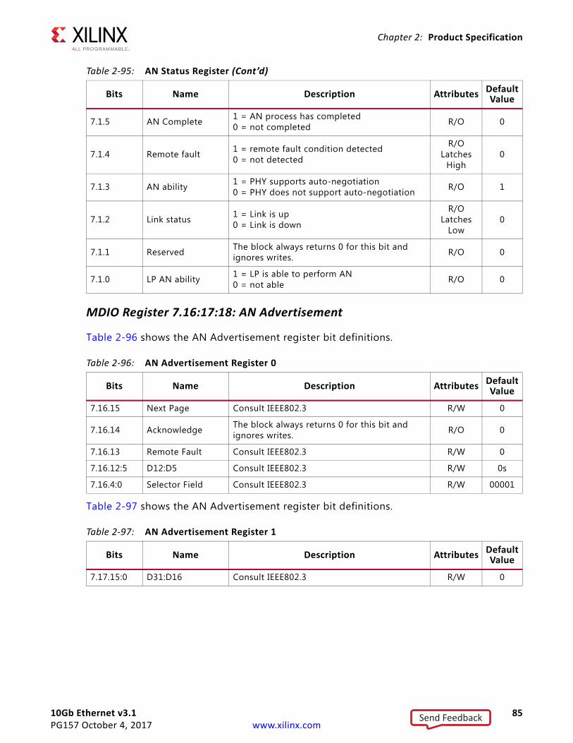
10Gb Ethernet v3.1 85PG157 October 4, 2017 www.xilinx.com
Chapter 2: Product Specification
MDIO Register 7.16:17:18: AN Advertisement
Table 2-96 shows the AN Advertisement register bit definitions.
Table 2-97 shows the AN Advertisement register bit definitions.
7.1.5 AN Complete 1 = AN process has completed0 = not completed R/O 0
7.1.4 Remote fault 1 = remote fault condition detected0 = not detected
R/OLatches
High0
7.1.3 AN ability 1 = PHY supports auto-negotiation0 = PHY does not support auto-negotiation R/O 1
7.1.2 Link status 1 = Link is up0 = Link is down
R/OLatches
Low0
7.1.1 Reserved The block always returns 0 for this bit and ignores writes. R/O 0
7.1.0 LP AN ability 1 = LP is able to perform AN0 = not able R/O 0
Table 2-96: AN Advertisement Register 0
Bits Name Description Attributes Default Value
7.16.15 Next Page Consult IEEE802.3 R/W 0
7.16.14 Acknowledge The block always returns 0 for this bit and ignores writes. R/O 0
7.16.13 Remote Fault Consult IEEE802.3 R/W 0
7.16.12:5 D12:D5 Consult IEEE802.3 R/W 0s
7.16.4:0 Selector Field Consult IEEE802.3 R/W 00001
Table 2-97: AN Advertisement Register 1
Bits Name Description Attributes Default Value
7.17.15:0 D31:D16 Consult IEEE802.3 R/W 0
Table 2-95: AN Status Register (Cont’d)
Bits Name Description Attributes Default Value
Send Feedback
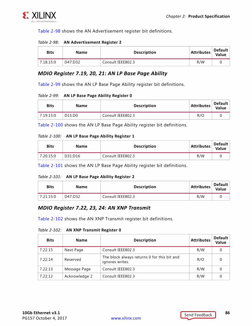
10Gb Ethernet v3.1 86PG157 October 4, 2017 www.xilinx.com
Chapter 2: Product Specification
Table 2-98 shows the AN Advertisement register bit definitions.
MDIO Register 7.19, 20, 21: AN LP Base Page Ability
Table 2-99 shows the AN LP Base Page Ability register bit definitions.
Table 2-100 shows the AN LP Base Page Ability register bit definitions.
Table 2-101 shows the AN LP Base Page Ability register bit definitions.
MDIO Register 7.22, 23, 24: AN XNP Transmit
Table 2-102 shows the AN XNP Transmit register bit definitions.
Table 2-98: AN Advertisement Register 2
Bits Name Description Attributes Default Value
7.18.15:0 D47:D32 Consult IEEE802.3 R/W 0
Table 2-99: AN LP Base Page Ability Register 0
Bits Name Description Attributes Default Value
7.19.15:0 D15:D0 Consult IEEE802.3 R/O 0
Table 2-100: AN LP Base Page Ability Register 1
Bits Name Description Attributes Default Value
7.20.15:0 D31:D16 Consult IEEE802.3 R/W 0
Table 2-101: AN LP Base Page Ability Register 2
Bits Name Description Attributes Default Value
7.21.15:0 D47:D32 Consult IEEE802.3 R/W 0
Table 2-102: AN XNP Transmit Register 0
Bits Name Description Attributes Default Value
7.22.15 Next Page Consult IEEE802.3 R/W 0
7.22.14 Reserved The block always returns 0 for this bit and ignores writes. R/O 0
7.22.13 Message Page Consult IEEE802.3 R/W 0
7.22.12 Acknowledge 2 Consult IEEE802.3 R/W 0
Send Feedback
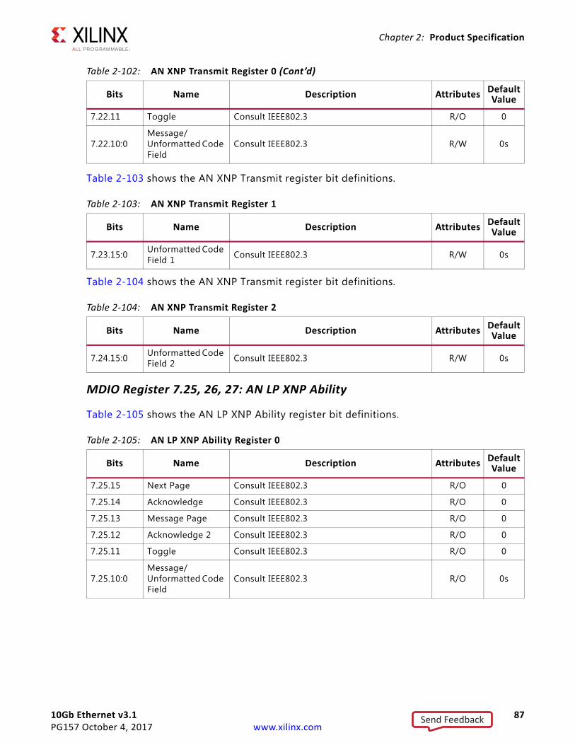
10Gb Ethernet v3.1 87PG157 October 4, 2017 www.xilinx.com
Chapter 2: Product Specification
Table 2-103 shows the AN XNP Transmit register bit definitions.
Table 2-104 shows the AN XNP Transmit register bit definitions.
MDIO Register 7.25, 26, 27: AN LP XNP Ability
Table 2-105 shows the AN LP XNP Ability register bit definitions.
7.22.11 Toggle Consult IEEE802.3 R/O 0
7.22.10:0Message/Unformatted Code Field
Consult IEEE802.3 R/W 0s
Table 2-103: AN XNP Transmit Register 1
Bits Name Description Attributes Default Value
7.23.15:0 Unformatted Code Field 1 Consult IEEE802.3 R/W 0s
Table 2-104: AN XNP Transmit Register 2
Bits Name Description Attributes Default Value
7.24.15:0 Unformatted Code Field 2 Consult IEEE802.3 R/W 0s
Table 2-105: AN LP XNP Ability Register 0
Bits Name Description Attributes Default Value
7.25.15 Next Page Consult IEEE802.3 R/O 0
7.25.14 Acknowledge Consult IEEE802.3 R/O 0
7.25.13 Message Page Consult IEEE802.3 R/O 0
7.25.12 Acknowledge 2 Consult IEEE802.3 R/O 0
7.25.11 Toggle Consult IEEE802.3 R/O 0
7.25.10:0Message/Unformatted Code Field
Consult IEEE802.3 R/O 0s
Table 2-102: AN XNP Transmit Register 0 (Cont’d)
Bits Name Description Attributes Default Value
Send Feedback
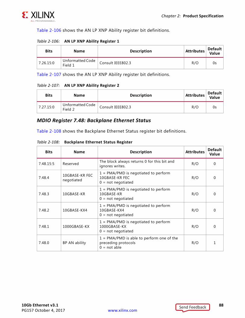
10Gb Ethernet v3.1 88PG157 October 4, 2017 www.xilinx.com
Chapter 2: Product Specification
Table 2-106 shows the AN LP XNP Ability register bit definitions.
Table 2-107 shows the AN LP XNP Ability register bit definitions.
MDIO Register 7.48: Backplane Ethernet Status
Table 2-108 shows the Backplane Ethernet Status register bit definitions.
Table 2-106: AN LP XNP Ability Register 1
Bits Name Description Attributes Default Value
7.26.15:0 Unformatted Code Field 1 Consult IEEE802.3 R/O 0s
Table 2-107: AN LP XNP Ability Register 2
Bits Name Description Attributes Default Value
7.27.15:0 Unformatted Code Field 2 Consult IEEE802.3 R/O 0s
Table 2-108: Backplane Ethernet Status Register
Bits Name Description Attributes Default Value
7.48.15:5 Reserved The block always returns 0 for this bit and ignores writes. R/O 0
7.48.4 10GBASE-KR FEC negotiated
1 = PMA/PMD is negotiated to perform 10GBASE-KR FEC0 = not negotiated
R/O 0
7.48.3 10GBASE-KR1 = PMA/PMD is negotiated to perform 10GBASE-KR0 = not negotiated
R/O 0
7.48.2 10GBASE-KX41 = PMA/PMD is negotiated to perform 10GBASE-KX40 = not negotiated
R/O 0
7.48.1 1000GBASE-KX1 = PMA/PMD is negotiated to perform 1000GBASE-KX0 = not negotiated
R/O 0
7.48.0 BP AN ability1 = PMA/PMD is able to perform one of the preceding protocols0 = not able
R/O 1
Send Feedback
10Gb Ethernet v3.1 89PG157 October 4, 2017 www.xilinx.com
Chapter 3
Designing with the SubsystemThis chapter includes guidelines and additional information to facilitate designing with the subsystem.
ClockingAll data interfaces (including s_axis_tx, s_axis_pause, m_axis_rx, m_axis_tx_ts, m_axis_rx_ts) are synchronous to clock sources generated within the support layer of the integrated 10 Gigabit Ethernet PCS/PMA core and depends on the subsystem options as shown in Table 3-1.
The management interface s_axi is associated with the s_axi_aclk input.
ResetsThe reset input provides an active-High global asynchronous reset input that resets everything in the design, including the transceiver and associated PLLs.
Each of the interface resets (s_axi_aresetn, tx_axis_aresetn and rx_axis_aresetn), apply local resets to sub-blocks of the overall design. These resets should not be required in normal operation or implementation.
Table 3-1: Transmit and Receive Clock Sources
Family Shared Logic TX Clock Source RX Clock Source
7 SeriesIn core coreclk_out coreclk_out
In example design coreclk coreclk
UltraScaleDevices
10GBASE-R
In core txusrclk2_out txusrclk2_out when the RX elastic buffer is present.
In example design txusrclk2 txusrclk2 when the RX elastic buffer is present.
In either core orexample design N/A rxrecclk_out when the RX elastic
buffer is omitted.
10GBASE-KRIn core coreclk_out coreclk_out
In example design coreclk coreclk
Send Feedback
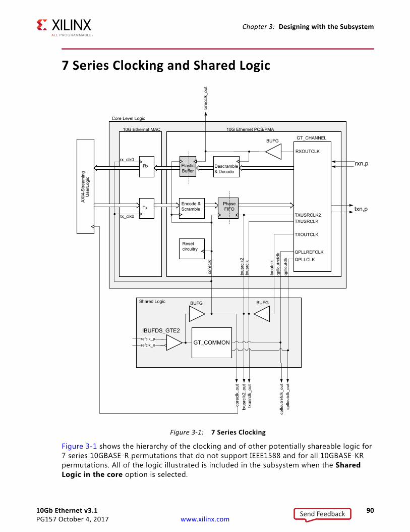
10Gb Ethernet v3.1 90PG157 October 4, 2017 www.xilinx.com
Chapter 3: Designing with the Subsystem
7 Series Clocking and Shared Logic
Figure 3-1 shows the hierarchy of the clocking and of other potentially shareable logic for 7 series 10GBASE-R permutations that do not support IEEE1588 and for all 10GBASE-KR permutations. All of the logic illustrated is included in the subsystem when the Shared Logic in the core option is selected.
X-Ref Target - Figure 3-1
Figure 3-1: 7 Series Clocking
Descramble& Decode
Encode &Scramble
ElasticBuffer
GT_CHANNEL
rxn,p
txn,pPhaseFIFO
Rx
Tx
10G Ethernet MAC
BUFG
refclk_prefclk_n
BUFG
10G Ethernet PCS/PMA
BUFGShared Logic
qpllo
utcl
k
qpllo
utre
fclk
Core Level Logic
qpllo
utre
fclk
_out
qpllo
utcl
k_ou
t
Reset circuitry
tx_clk0
rx_clk0
Send Feedback
10Gb Ethernet v3.1 91PG157 October 4, 2017 www.xilinx.com
Chapter 3: Designing with the Subsystem
If, however, the Shared Logic in example design option is selected, then the level of the core boundary moves down to the shaded level of hierarchy in the upper half of Figure 3-1 labeled as Core Level Logic. In this case, the Shared logic level of hierarchy is now delivered as part of the example design.
Shared LogicThe shared logic itself is shown in the rectangle in the lower half of the figure. This is logic can potentially be shared by up to four 10G Ethernet Subsystem cores if they are all placed in the same GT Quad. The shared logic contains a differential input clock buffer which connects to the GT_COMMON block. When using the 64-bit datapath, the frequency of this clock must be 156.25 MHz; when using the 32-bit datapath, this frequency must be 312.5 MHz.
coreclk/coreclk_out must be created from the transceiver differential reference clock to keep the user logic and transceiver interface synchronous. Therefore, the differential clock is also connected to a global clock buffer (BUFG), as illustrated, to provide this clock. The frequency of coreclk/coreclk_out is the same as that of the differential clock source.
The final BUFG in the shared logic is sourced from the TXOUTCLK of a GT_CHANNEL. This is routed back to the connected GT_CHANNELs to provide the transceiver TX user clocks (TXUSRCLK and TXUSERCLK2). The frequency of this clock is 322.265625 MHz.
Core Level LogicLogic included in the Core Level Logic is required for a single core and is not shareable. For example, the receiver clock BUFG, derived from the RXOUTCLK port of the transceiver GT_CHANNEL, is unique for each transceiver. The frequency of this clock is 322.265625 MHz, synchronized to the input serial data, and the clock is available through the rxrecclk_out port of the core.
When interfacing to the core using the transmitter and receiver AXI4-Stream interfaces, user logic must be synchronous to coreclk/coreclk_out as illustrated. As previously described, this clock is 156.25 MHz when using the 64-bit datapath, or 312.5 MHz when using the 32-bit datapath. Internal to the core, the Phase FIFO and the Elastic Buffer modules take care of translating the TX and RX datapaths respectively between the coreclk/coreclk_out clock domain and the separate 322.265625 MHz clock domains derived from the TXOUTCLK and RXOUTCLK ports of the transceiver.
Send Feedback
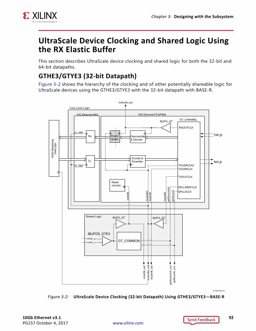
10Gb Ethernet v3.1 92PG157 October 4, 2017 www.xilinx.com
Chapter 3: Designing with the Subsystem
UltraScale Device Clocking and Shared Logic Using the RX Elastic BufferThis section describes UltraScale device clocking and shared logic for both the 32-bit and 64-bit datapaths.
GTHE3/GTYE3 (32-bit Datapath)Figure 3-2 shows the hierarchy of the clocking and of other potentially shareable logic for UltraScale devices using the GTHE3/GTYE3 with the 32-bit datapath with BASE-R. X-Ref Target - Figure 3-2
Figure 3-2: UltraScale Device Clocking (32-bit Datapath) Using GTHE3/GTYE3—BASE-R
Descramble& Decode
Encode &Scramble
ElasticBuffer
GT_CHANNEL
rxn,p
txn,p
Rx
Tx
10G Ethernet MAC
BUFG_GT
refclk_prefclk_n
10G Ethernet PCS/PMA
Shared Logic
qpll0
outc
lk
qpll0
outr
efcl
kqp
ll0ou
tref
clk_
out
qpll0
outc
lk_o
ut
Reset circuitry
tx_clk0
rx_clk0
BUFG_GTBUFG_GT
Core Level Logic
Send Feedback
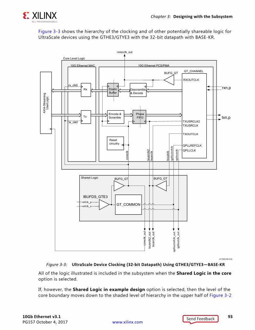
10Gb Ethernet v3.1 93PG157 October 4, 2017 www.xilinx.com
Chapter 3: Designing with the Subsystem
Figure 3-3 shows the hierarchy of the clocking and of other potentially shareable logic for UltraScale devices using the GTHE3/GTYE3 with the 32-bit datapath with BASE-KR.
All of the logic illustrated is included in the subsystem when the Shared Logic in the core option is selected.
If, however, the Shared Logic in example design option is selected, then the level of the core boundary moves down to the shaded level of hierarchy in the upper half of Figure 3-2
X-Ref Target - Figure 3-3
Figure 3-3: UltraScale Device Clocking (32-bit Datapath) Using GTHE3/GTYE3—BASE-KR
Descramble& Decode
Encode &Scramble
ElasticBuffer
GT_CHANNEL
rxn,p
txn,pPhaseFIFO
Rx
Tx
10G Ethernet MAC
BUFG_GT
refclk_prefclk_n
BUFG_GT
10G Ethernet PCS/PMA
BUFG_GTShared Logicqp
llout
clk
qpllo
utre
fclk
Core Level Logic
qpllo
utre
fclk
_out
qpllo
utcl
k_ou
t
Reset circuitry
tx_clk0
rx_clk0
Send Feedback
10Gb Ethernet v3.1 94PG157 October 4, 2017 www.xilinx.com
Chapter 3: Designing with the Subsystem
and Figure 3-3 labeled as Core Level Logic. In this case, the Shared logic level of hierarchy is now delivered as part of the example design.
Shared Logic
The shared logic itself is shown in the rectangle in the lower half of the figure. This logic can potentially be shared by up to four 10G Ethernet Subsystem cores if they are all placed in the same GT Quad. The shared logic contains a differential input clock buffer which connects to the GT_COMMON block. The frequency of this clock is selectable from the Vivado IDE and can be one of 156.25 MHz, 161.1328125 MHz, 312.5 MHz or 322.265625 MHz.
coreclk/coreclk_out is created from the transceiver differential reference clock using a clock buffer (BUFG_GT) as shown in Figure 3-2. The frequency of coreclk/coreclk_out is the same as that of the differential clock source. In UltraScale devices, this clock plays a lesser role than in 7 series devices. In UltraScale devices, this clock, which is free running, is used only for transceiver reset/initialization logic.
The final BUFG_GT in the shared logic is sourced from the TXOUTCLK of a GT_CHANNEL. This is routed back to the connected GT_CHANNELs to provide the transceiver TX user clocks (TXUSRCLK and TXUSERCLK2). The frequency of this clock is 156.25 MHz when using the 64-bit datapath, or 312.5 MHz when using the 32-bit datapath. These clock frequencies are made possible due to the use of the 64/66 Asynchronous Gearbox capability of the transceiver.
Core Level Logic
Logic included in the Core Level Logic block is required for a single core and is not shareable. For example, the receiver clock BUFG_GT, derived from the RXOUTCLK port of the transceiver GT_CHANNEL, is unique for each transceiver. The frequency of this clock is 156.25 MHz when using the 64-bit datapath, or 312.5 MHz when using the 32-bit datapath, synchronized to the input serial data. These clock frequencies are made possible due to the use of the 64/66 Asynchronous Gearbox capability of the transceiver, and the clock is available through the rxrecclk_out port of the core.
When interfacing to the core using the transmitter and receiver AXI4-Stream interfaces, user logic must be synchronous to txusrclk2/txusrclk2_out as illustrated. As previously described, this clock is 156.25 MHz when using the 64-bit datapath, or 312.5 MHz when using the 32-bit datapath. Internal to the core, the entire transmit datapath is synchronous to txusrclk2/txusrclk2_out. And on the receive path, the RX Elastic Buffer modules take care of translating the receive data path from rxrecclk_out onto the txusrclk2/txusrclk2_out domain.
Send Feedback
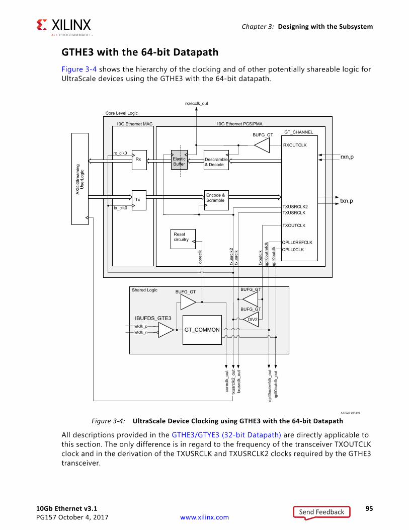
10Gb Ethernet v3.1 95PG157 October 4, 2017 www.xilinx.com
Chapter 3: Designing with the Subsystem
GTHE3 with the 64-bit DatapathFigure 3-4 shows the hierarchy of the clocking and of other potentially shareable logic for UltraScale devices using the GTHE3 with the 64-bit datapath.
All descriptions provided in the GTHE3/GTYE3 (32-bit Datapath) are directly applicable to this section. The only difference is in regard to the frequency of the transceiver TXOUTCLK clock and in the derivation of the TXUSRCLK and TXUSRCLK2 clocks required by the GTHE3 transceiver.
X-Ref Target - Figure 3-4
Figure 3-4: UltraScale Device Clocking using GTHE3 with the 64-bit Datapath
Descramble& Decode
Encode &Scramble
ElasticBuffer
GT_CHANNEL
rxn,p
txn,p
Rx
Tx
10G Ethernet MAC
BUFG_GT
refclk_prefclk_n
10G Ethernet PCS/PMA
Shared Logic
qpll0
outc
lk
qpll0
outr
efcl
kqp
ll0ou
tref
clk_
out
qpll0
outc
lk_o
ut
Reset circuitry
tx_clk0
rx_clk0
BUFG_GTBUFG_GT
BUFG_GT
Core Level Logic
DIV2
Send Feedback
10Gb Ethernet v3.1 96PG157 October 4, 2017 www.xilinx.com
Chapter 3: Designing with the Subsystem
When used in this configuration, the GTHE3 uses an internal 32-bit interface running at 312.25 MHz even when using a 64-bit interface to the FPGA general interconnect at 156.25 MHz. TXOUTCLK is therefore provided at a frequency of 312.2 5MHz and this is connected to our first BUFG_GT to create the 312.25 MHz clock required for the GTHE3 TXUSRCLK input. A second BUFG_GT, configured to divide down the clock frequency by 2, is also connected as shown in Figure 3-4 to create the 156.25 MHz clock source for the core and for the GTHE3 TXUSRCLK2 input.
Send Feedback
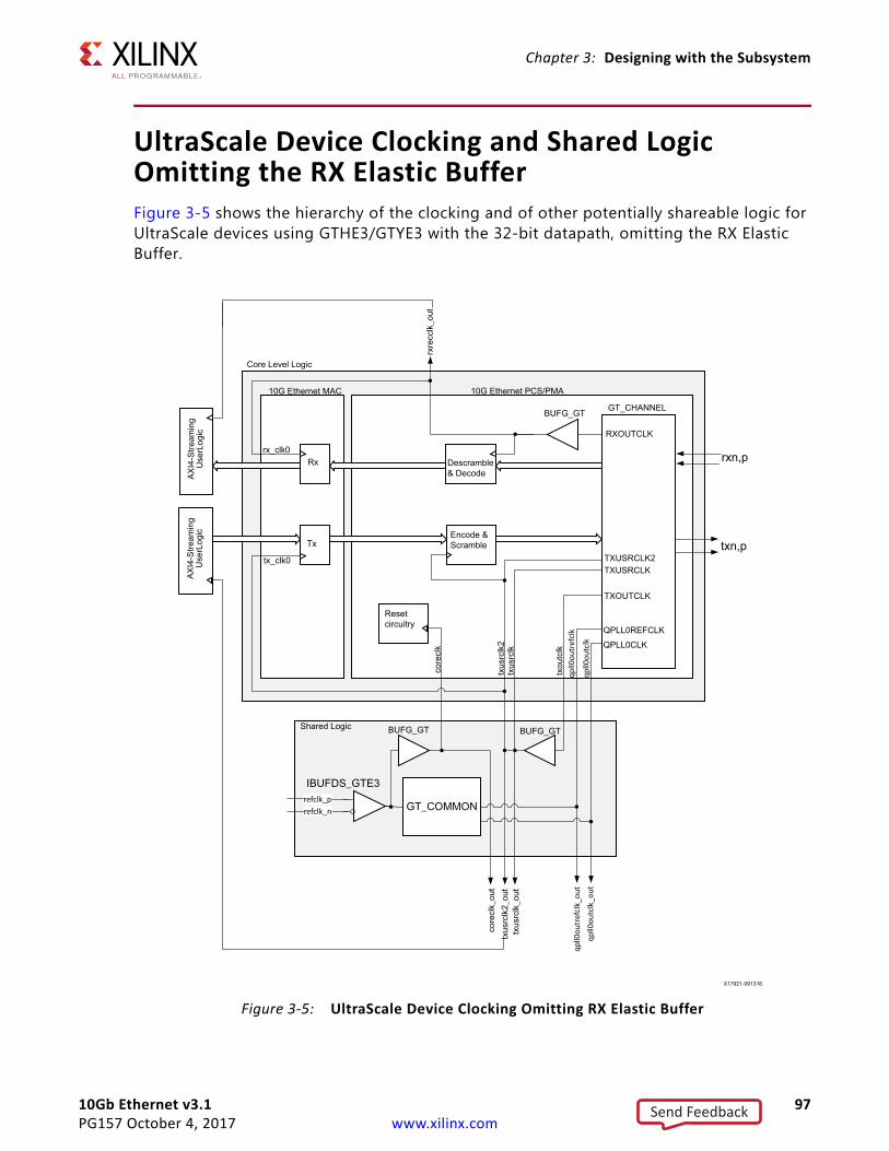
10Gb Ethernet v3.1 97PG157 October 4, 2017 www.xilinx.com
Chapter 3: Designing with the Subsystem
UltraScale Device Clocking and Shared Logic Omitting the RX Elastic BufferFigure 3-5 shows the hierarchy of the clocking and of other potentially shareable logic for UltraScale devices using GTHE3/GTYE3 with the 32-bit datapath, omitting the RX Elastic Buffer.
X-Ref Target - Figure 3-5
Figure 3-5: UltraScale Device Clocking Omitting RX Elastic Buffer
Descramble& Decode
Encode &Scramble
GT_CHANNEL
rxn,p
txn,p
Rx
Tx
10G Ethernet MAC
BUFG_GT
refclk_prefclk_n
10G Ethernet PCS/PMA
Shared Logic
qpll0
outc
lk
qpll0
outr
efcl
k
Core Level Logic
qpll0
outr
efcl
k_ou
tqp
ll0ou
tclk
_out
Reset circuitry
tx_clk0
rx_clk0
BUFG_GTBUFG_GT
Send Feedback
10Gb Ethernet v3.1 98PG157 October 4, 2017 www.xilinx.com
Chapter 3: Designing with the Subsystem
All of the logic illustrated is included in the subsystem when the Shared Logic in the core option is selected.
If, however, the Shared Logic in example design option is selected, then the level of the core boundary moves down to the shaded level of hierarchy in the upper half of Figure 3-5 labelled as Core Level Logic. In this case, the Shared logic level of hierarchy is now delivered as part of the example design.
Note: For GTHE3 64-bit permutations omitting the RX Elastic Buffer, the only difference to the description in this section is in the derivation of the transceiver TXUSRCLK and TXUSRCLK2 clocks (see GTHE3 with the 64-bit Datapath to understand this difference).
Shared LogicThe shared logic itself is shown in the rectangle in the lower half of Figure 3-5. This logic can potentially be shared by up to four 10G Ethernet Subsystem cores if they are all placed in the same GT Quad. The shared logic contains a differential input clock buffer which connects to the GT_COMMON block. The frequency of this clock is selectable from the Vivado IDE and can be one of 156.25 MHz, 161.1328125 MHz, 312.5 MHz or 322.265625 MHz.
coreclk/coreclk_out is created from the transceiver differential reference clock using a clock buffer (BUFG_GT) as illustrated. The frequency of coreclk/coreclk_out is the same as that of the differential clock source. In UltraScale devices, this clock plays a lesser role than in 7 series devices. In UltraScale architecture, this clock, which is free running, is used only for transceiver reset/initialization logic.
The final BUFG_GT in the shared logic is sourced from the TXOUTCLK of a GT_CHANNEL. This is routed back to the connected GT_CHANNELs to provide the transceiver TX user clocks (TXUSRCLK and TXUSERCLK2). The frequency of this clock is 156.25 MHz when using the 64-bit datapath, or 312.5 MHz when using the 32-bit datapath. These clock frequencies are made possible due to the use of the 64/66 Asynchronous Gearbox capability of the transceiver.
Core Level LogicLogic included in the Core Level Logic block is required for a single core and is not shareable. For example, the receiver clock BUFG_GT, derived from the RXOUTCLK port of the transceiver GT_CHANNEL, is unique for each transceiver. The frequency of this clock is 156.25 MHz when using the 64-bit datapath, or 312.5 MHz when using the 32-bit datapath, synchronized to the input serial data. These clock frequencies are made possible due to the use of the 64/66 Asynchronous Gearbox capability of the transceiver, and the clock is available through the rxrecclk_out port of the core.
Send Feedback
10Gb Ethernet v3.1 99PG157 October 4, 2017 www.xilinx.com
Chapter 3: Designing with the Subsystem
When interfacing to the core:
• User logic connecting to the transmitter AXI4-Stream interface must be synchronous to txusrclk2/txusrclk2_out as shown in Figure 3-5. This clock is 156.25 MHz when using the 64-bit datapath, or 312.5 MHz when using the 32-bit datapath. Internal to the core, the entire transmit datapath is synchronous to this clock source.
• User logic connecting to the receiver AXI4-Stream interface must be synchronous to the rxrecclk_out clock as shown in Figure 3-5. As previously described, this is nominally 156.25 MHz when using the 64-bit datapath, or 312.5 MHz when using the 32-bit datapath, synchronized to the input serial data. Internal to the core, the entire receive datapath is synchronous to this clock source.
Shared Logic for 7 Series IEEE 1588 SupportFigure 3-6 shows the hierarchy of the clocking and of other potentially shareable logic for the core when configured with IEEE 1588 support in 7 series devices. The logic illustrated within the <component_name>_support level of hierarchy is included in the 10GBASE-R subcore when the Shared Logic in the core option is selected.
If, however, the Shared Logic in example design option is selected, then the level of the core boundary moves down to the shaded level of hierarchy in Figure 3-6. In this case, the <component_name>_support level of hierarchy is now delivered as part of the core example design.
IMPORTANT: The clocking for UltraScale devices with IEEE 1588 support is identical to that described in UltraScale Device Clocking and Shared Logic Using the RX Elastic Buffer and UltraScale Device Clocking and Shared Logic Omitting the RX Elastic Buffer.
Send Feedback
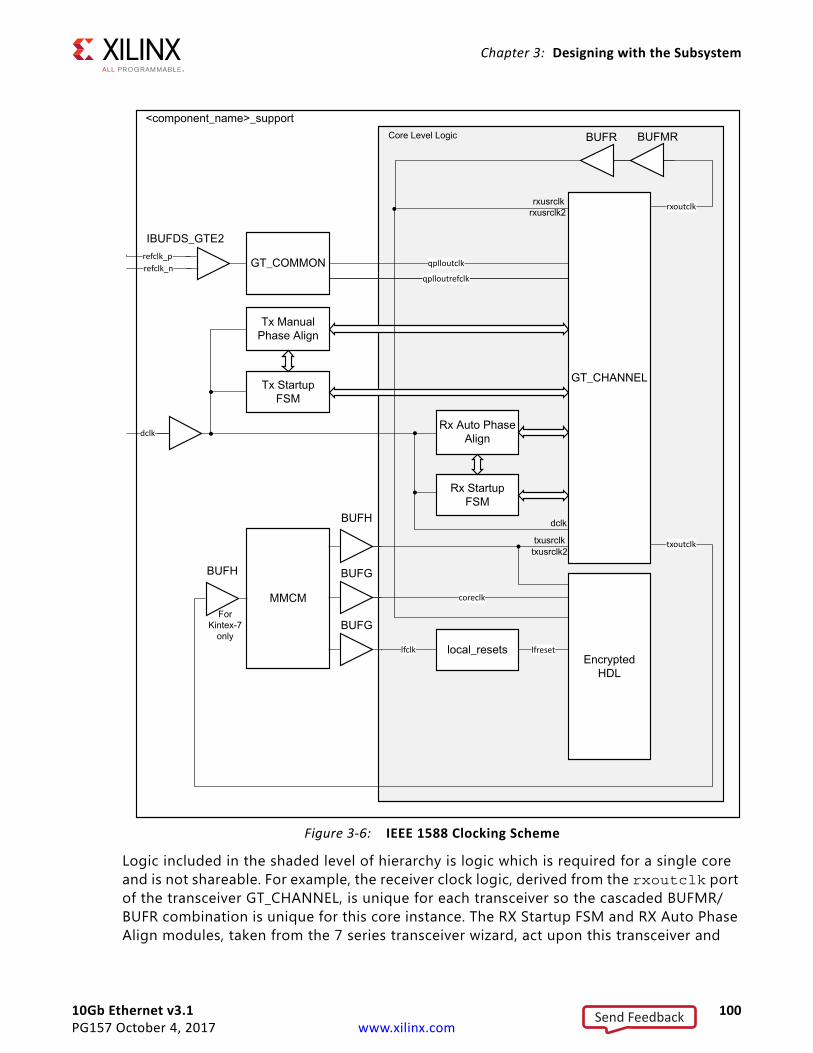
10Gb Ethernet v3.1 100PG157 October 4, 2017 www.xilinx.com
Chapter 3: Designing with the Subsystem
Logic included in the shaded level of hierarchy is logic which is required for a single core and is not shareable. For example, the receiver clock logic, derived from the rxoutclk port of the transceiver GT_CHANNEL, is unique for each transceiver so the cascaded BUFMR/BUFR combination is unique for this core instance. The RX Startup FSM and RX Auto Phase Align modules, taken from the 7 series transceiver wizard, act upon this transceiver and
X-Ref Target - Figure 3-6
Figure 3-6: IEEE 1588 Clocking Scheme
refclk_prefclk_n
qplllock
qplloutclk
qplloutrefclk
rxoutclk
txoutclk
lfclk lfreset
coreclk
dclk
Core Level Logic
Send Feedback
10Gb Ethernet v3.1 101PG157 October 4, 2017 www.xilinx.com
Chapter 3: Designing with the Subsystem
phase align the rxoutclk clock to enable the RX buffer within the transceiver to be bypassed, and so are also unique to this core instance.
Logic illustrated in the <component_name>_support level of hierarchy is logic that can be shareable across multiple core instances under certain conditions. For example, the GT_COMMON block is common to a group of four GT_COMMON channels (see the 7 Series FPGAs GTX/GTH Transceivers User Guide (UG476) [Ref 11]). The blocks, consisting of the TX Manual Phase Align and the TX Startup FSM (taken from the 7 series transceiver wizard), and the MMCM with associated clock buffers, might all be required per core instance for cases where each core needs to be able to operate fully independently. Or, with modifications, these blocks can be shareable across two or more core instances if the design requirements allow all cores to be coupled to the same transmitter reset logic and reset signals. For more information about sharing the Manual Phase Align and the TX Startup FSM, see the 7 Series FPGAs Transceivers Wizard LogiCORE IP Product Guide (PG168) [Ref 14]. For more information about sharing the QPLL among serial transceiver channels within the same Quad see the 7 Series FPGAs GTX/GTH Transceivers User Guide (UG476) [Ref 11].
It is essential for correct core operation that timing paths between the three output clock buffers from the MMCM meet timing. Should timing fail, try constraining the core logic using a Pblock (physical block) in Vivado. Alternatively, timing closure is eased if all clock buffers are converted to BUFGs.
IMPORTANT: Never add false_path constraints between these clocks.
For the 7 series 1588 permutations, dclk must be a free running clock (it cannot be derived from any of the transceiver clocks). As illustrated, dclk is used to clock reset, initialization and buffer bypass phase alignment state machines in the transceiver.
Ethernet Protocol DescriptionThis section gives an overview of where the core fits into an Ethernet system and provides a description of some basic Ethernet terminology.
Ethernet Sublayer ArchitectureFigure 3-7illustrates the relationship between the Open Systems Interconnection (OSI) reference model and the core. The grayed-in layers show the functionality that the core handles. Figure 3-7 also shows where the supported physical interfaces fit into the architecture.
Send Feedback
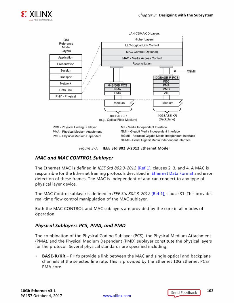
10Gb Ethernet v3.1 102PG157 October 4, 2017 www.xilinx.com
Chapter 3: Designing with the Subsystem
MAC and MAC CONTROL Sublayer
The Ethernet MAC is defined in IEEE Std 802.3-2012 [Ref 1], clauses 2, 3, and 4. A MAC is responsible for the Ethernet framing protocols described in Ethernet Data Format and error detection of these frames. The MAC is independent of and can connect to any type of physical layer device.
The MAC Control sublayer is defined in IEEE Std 802.3-2012 [Ref 1], clause 31. This provides real-time flow control manipulation of the MAC sublayer.
Both the MAC CONTROL and MAC sublayers are provided by the core in all modes of operation.
Physical Sublayers PCS, PMA, and PMD
The combination of the Physical Coding Sublayer (PCS), the Physical Medium Attachment (PMA), and the Physical Medium Dependent (PMD) sublayer constitute the physical layers for the protocol. Several physical standards are specified including:
• BASE-R/KR – PHYs provide a link between the MAC and single optical and backplane channels at the selected line rate. This is provided by the Ethernet 10G Ethernet PCS/PMA core.
X-Ref Target - Figure 3-7
Figure 3-7: IEEE Std 802.3-2012 Ethernet Model
Send Feedback
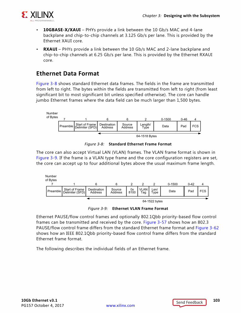
10Gb Ethernet v3.1 103PG157 October 4, 2017 www.xilinx.com
Chapter 3: Designing with the Subsystem
• 10GBASE-X/XAUI – PHYs provide a link between the 10 Gb/s MAC and 4-lane backplane and chip-to-chip channels at 3.125 Gb/s per lane. This is provided by the Ethernet XAUI core.
• RXAUI – PHYs provide a link between the 10 Gb/s MAC and 2-lane backplane and chip-to-chip channels at 6.25 Gb/s per lane. This is provided by the Ethernet RXAUI core.
Ethernet Data FormatFigure 3-8 shows standard Ethernet data frames. The fields in the frame are transmitted from left to right. The bytes within the fields are transmitted from left to right (from least significant bit to most significant bit unless specified otherwise). The core can handle jumbo Ethernet frames where the data field can be much larger than 1,500 bytes.
The core can also accept Virtual LAN (VLAN) frames. The VLAN frame format is shown in Figure 3-9. If the frame is a VLAN type frame and the core configuration registers are set, the core can accept up to four additional bytes above the usual maximum frame length.
.
Ethernet PAUSE/flow control frames and optionally 802.1Qbb priority-based flow control frames can be transmitted and received by the core. Figure 3-57 shows how an 802.3 PAUSE/flow control frame differs from the standard Ethernet frame format and Figure 3-62 shows how an IEEE 802.1Qbb priority-based flow control frame differs from the standard Ethernet frame format.
The following describes the individual fields of an Ethernet frame.
X-Ref Target - Figure 3-8
Figure 3-8: Standard Ethernet Frame Format
X-Ref Target - Figure 3-9
Figure 3-9: Ethernet VLAN Frame Format
Send Feedback
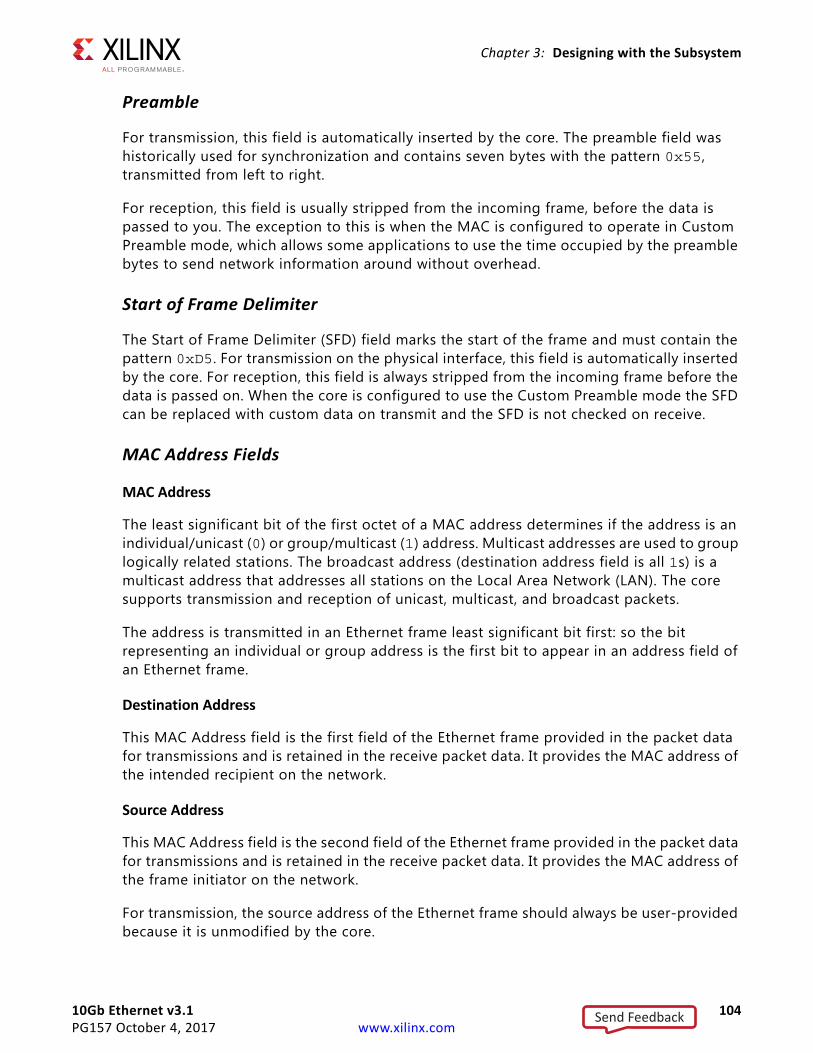
10Gb Ethernet v3.1 104PG157 October 4, 2017 www.xilinx.com
Chapter 3: Designing with the Subsystem
Preamble
For transmission, this field is automatically inserted by the core. The preamble field was historically used for synchronization and contains seven bytes with the pattern 0x55, transmitted from left to right.
For reception, this field is usually stripped from the incoming frame, before the data is passed to you. The exception to this is when the MAC is configured to operate in Custom Preamble mode, which allows some applications to use the time occupied by the preamble bytes to send network information around without overhead.
Start of Frame Delimiter
The Start of Frame Delimiter (SFD) field marks the start of the frame and must contain the pattern 0xD5. For transmission on the physical interface, this field is automatically inserted by the core. For reception, this field is always stripped from the incoming frame before the data is passed on. When the core is configured to use the Custom Preamble mode the SFD can be replaced with custom data on transmit and the SFD is not checked on receive.
MAC Address Fields
MAC Address
The least significant bit of the first octet of a MAC address determines if the address is an individual/unicast (0) or group/multicast (1) address. Multicast addresses are used to group logically related stations. The broadcast address (destination address field is all 1s) is a multicast address that addresses all stations on the Local Area Network (LAN). The core supports transmission and reception of unicast, multicast, and broadcast packets.
The address is transmitted in an Ethernet frame least significant bit first: so the bit representing an individual or group address is the first bit to appear in an address field of an Ethernet frame.
Destination Address
This MAC Address field is the first field of the Ethernet frame provided in the packet data for transmissions and is retained in the receive packet data. It provides the MAC address of the intended recipient on the network.
Source Address
This MAC Address field is the second field of the Ethernet frame provided in the packet data for transmissions and is retained in the receive packet data. It provides the MAC address of the frame initiator on the network.
For transmission, the source address of the Ethernet frame should always be user-provided because it is unmodified by the core.
Send Feedback
10Gb Ethernet v3.1 105PG157 October 4, 2017 www.xilinx.com
Chapter 3: Designing with the Subsystem
Length/Type
The value of this field determines if it is interpreted as a length or a type field, as defined by IEEE Std 802.3-2012 [Ref 1]. A value of 1,536 decimal or greater is interpreted by the core as a type field.
When used as a length field, the value in this field represents the number of bytes in the following data field. This value does not include any bytes that can be inserted in the pad field following the data field.
A length/type field value of 0x8100 indicates that the frame is a VLAN frame, and a value of 0x8808 indicates a PAUSE MAC control frame.
For transmission, the core does not perform any processing of the length/type field.
For reception, if this field is a length field, the core receive engine interprets this value and removes any padding in the pad field (if necessary). If the field is a length field and length/type checking is enabled, the core compares the length against the actual data field length and flags an error if a mismatch occurs. If the field is a type field, the core ignores the value and passes it along with the packet data with no further processing. The length/type field is always retained in the receive packet data.
Data
The data field can vary from 0 to 1,500 bytes in length for a normal frame. The core can handle jumbo frames of any length.
This field is always provided in the packet data for transmissions and is always retained in the receive packet data.
Pad
The pad field can vary from 0 to 46 bytes in length. This field is used to ensure that the frame length is at least 64 bytes in length (the preamble and SFD fields are not considered part of the frame for this calculation), which is required for successful CSMA/CD operation. The values in this field are used in the frame check sequence calculation but are not included in the length field value, if it is used. The length of this field and the data field combined must be at least 46 bytes. If the data field contains 0 bytes, the pad field is 46 bytes. If the data field is 46 bytes or more, the pad field has 0 bytes.
For transmission, this field can be inserted automatically by the core or can be supplied by you. If the pad field is inserted by the core, the FCS field is calculated and inserted by the core. If the pad field is supplied by you, the FCS can be either inserted by the core or provided by you, as indicated by a configuration register bit.
Send Feedback
10Gb Ethernet v3.1 106PG157 October 4, 2017 www.xilinx.com
Chapter 3: Designing with the Subsystem
For reception, if the length/type field has a length interpretation, any pad field in the incoming frame is not passed to you, unless the core is configured to pass the FCS field on to you.
FCS
The value of the FCS field is calculated over the destination address, source address, length/type, data, and pad fields using a 32-bit Cyclic Redundancy Check (CRC), as defined in IEEE Std 802.3-2012 para. 3.2.9:
G(x) = x32 + x26 + x23 + x22 + x16 + x12 + x11 + x10 + x8 + x7 + x5 + x4 + x2 + x1 + x0
The CRC bits are placed in the FCS field with the x31 term in the left-most bit of the first byte, and the x0 term is the right-most bit of the last byte (that is, the bits of the CRC are transmitted in the order x31, x30,..., x1, x0).
For transmission, this field can be either inserted automatically by the core or supplied by you, as indicated by a configuration register bit.
For reception, the incoming FCS value is verified on every frame. If an incorrect FCS value is received, the core indicates to you that it has received a bad frame. The FCS field can either be passed on to you or be dropped by the core, as indicated by a configuration register bit.
Frame Transmission and Interframe GapFrames are transmitted over the Ethernet medium with an interframe gap of 96-bit times (9.6 ns for 10 Gb/s), as specified by the IEEE Std 802.3-2012. This value is a minimum value and can be increased, but with a resulting decrease in throughput.
After the last bit of an Ethernet MAC frame transmission, the core starts the interframe gap timer and defers transmissions until the IFG count completes. The core then places the Start ordered set code of the next frame on the next available 4-byte boundary in the data stream. This can be further delayed if IFG Adjustment feature of the core is used.
Deficit Idle Count
In addition to the interframe gap setting described above, the IEEE 802.3-2012 standard also permits a feature called Deficit Idle Count. This allows periodic shortening of the transmitted interframe gap below 12 to satisfy the Start ordered set alignment rules, as long as a mean value of 12 is maintained over a long period of time. This feature is controlled in the core by a configuration bit.
f
Send Feedback
10Gb Ethernet v3.1 107PG157 October 4, 2017 www.xilinx.com
Chapter 3: Designing with the Subsystem
Connecting the Data InterfacesThis section describes how to connect to the data interfaces of the subsystem.
Transmit AXI4-Stream InterfaceThe client-side interface on the transmit side of the core supports an AXI4-Stream interface. This is available with an interface width choice of 64-bits or 32-bits (in supported families). An example design which includes source code for a FIFO with an AXI4-Stream interface is provided with the core generated by the Vivado IP catalog. Table 3-2 defines the signals. The ports defined in Table 3-2 are synchronous to the transmit datapath clock as defined by TX Clock Source in Table 3-1.
When connecting this interface in IP integrator, the signals of Table 3-2 (with the exception of tx_axis_aresetn) are shown and can be connected as a single bus. This bus is called s_axis_tx.
IMPORTANT: The signal names in Figure 3-10 to Figure 3-33 use generic AXI4-Stream names and are therefore abbreviated from their full names, defined in Table 3-2, by omitting the s_axis_tx_ prefix.
For transmit data s_axis_tx_tdata, the port is logically divided into lane 0 to lane 3, for the 32-bit interface (see Table 3-3), or lane 0 to lane 7 for the 64-bit interface (see Table 3-4) with the corresponding bit of the s_axis_tx_tkeep word signifying valid data on s_axis_tx_tdata.
Table 3-2: Transmit Client-Side Interface Port Description
Name Direction Description
tx_axis_aresetn In AXI4-Stream active-Low reset for the TX path
s_axis_tx_tdata[63/31:0] In AXI4-Stream data (64-bit/32-bit interface)
s_axis_tx_tkeep[7/3:0] In AXI4-Stream Data Control (64-bit/32-bit interface)
s_axis_tx_tvalid In AXI4-Stream Data Valid input
s_axis_tx_tuser[0:0] In AXI4-Stream user signal used to indicate explicit underrun
s_axis_tx_tlast In AXI4-Stream signal indicating End of Ethernet Packet
s_axis_tx_tready Out AXI4-Stream acknowledge signal to indicate to start the Data transfer
tx_ifg_delay[7:0] In Configures Interframe Gap adjustment between packets.
Table 3-3: s_axis_tx_tdata Lanes–32-bits
Lane/s_axis_tx_tkeep Bit s_axis_tx_tdata Bits
0 7:0
1 15:8
Send Feedback
10Gb Ethernet v3.1 108PG157 October 4, 2017 www.xilinx.com
Chapter 3: Designing with the Subsystem
The definitions of the abbreviations used in the timing diagrams are described in Table 3-5.
Normal Frame Transmission
The timing of a normal frame transfer is shown in Figure 3-10 and Figure 3-11. When the client wants to transmit a frame, it asserts the s_axis_tx_tvalid and places the data and control in s_axis_tx_tdata and s_axis_tx_tkeep in the same clock cycle. When this data is accepted by the core, indicated by s_axis_tx_tready being asserted, the client must provide the next cycle of data. If s_axis_tx_tready is not asserted by the core then the client must hold the current valid data value until it is. The end of packet is indicated to the core by s_axis_tx_tlast asserted for 1 cycle. The bits of s_axis_tx_tkeep are set appropriately to indicate the number of valid bytes in the final data transfer. For example, in Figure 3-10, the first packet ends at Lane 1 and any data after that is ignored.
After s_axis_tx_tlast is deasserted, any data and control is deemed invalid until s_axis_tx_tvalid is next asserted. The clock source for Figure 3-10 and Figure 3-11 can be determined from the TX Clock Source column of Table 3-1.Deasserting TVALID in the
2 23:16
3 31:24
Table 3-4: s_axis_tx_tdata Lanes–64-bits
Lane/s_axis_tx_tkeep Bit s_axis_tx_tdata Bits
0 7:0
1 15:8
2 23:16
3 31:24
4 39:32
5 47:40
6 55:48
7 63:56
Table 3-5: Abbreviations Used in Timing Diagrams
Abbreviation Definition
DA Destination address
SA Source address
L/T Length/type field
FCS Frame check sequence (CRC)
Table 3-3: s_axis_tx_tdata Lanes–32-bits (Cont’d)
Lane/s_axis_tx_tkeep Bit s_axis_tx_tdata Bits
Send Feedback
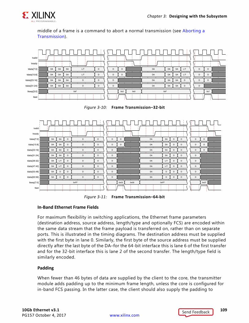
10Gb Ethernet v3.1 109PG157 October 4, 2017 www.xilinx.com
Chapter 3: Designing with the Subsystem
middle of a frame is a command to abort a normal transmission (see Aborting a Transmission).
In-Band Ethernet Frame Fields
For maximum flexibility in switching applications, the Ethernet frame parameters (destination address, source address, length/type and optionally FCS) are encoded within the same data stream that the frame payload is transferred on, rather than on separate ports. This is illustrated in the timing diagrams. The destination address must be supplied with the first byte in lane 0. Similarly, the first byte of the source address must be supplied directly after the last byte of the DA–for the 64-bit interface this is lane 6 of the first transfer and for the 32-bit interface this is lane 2 of the second transfer. The length/type field is similarly encoded.
Padding
When fewer than 46 bytes of data are supplied by the client to the core, the transmitter module adds padding up to the minimum frame length, unless the core is configured for in-band FCS passing. In the latter case, the client should also supply the padding to
X-Ref Target - Figure 3-10
Figure 3-10: Frame Transmission–32-bit
X-Ref Target - Figure 3-11
Figure 3-11: Frame Transmission–64-bit
Send Feedback
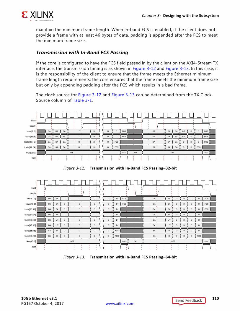
10Gb Ethernet v3.1 110PG157 October 4, 2017 www.xilinx.com
Chapter 3: Designing with the Subsystem
maintain the minimum frame length. When in-band FCS is enabled, if the client does not provide a frame with at least 46 bytes of data, padding is appended after the FCS to meet the minimum frame size.
Transmission with In-Band FCS Passing
If the core is configured to have the FCS field passed in by the client on the AXI4-Stream TX interface, the transmission timing is as shown in Figure 3-12 and Figure 3-13. In this case, it is the responsibility of the client to ensure that the frame meets the Ethernet minimum frame length requirements; the core ensures that the frame meets the minimum frame size but only by appending padding after the FCS which results in a bad frame.
The clock source for Figure 3-12 and Figure 3-13 can be determined from the TX Clock Source column of Table 3-1.
X-Ref Target - Figure 3-12
Figure 3-12: Transmission with In-Band FCS Passing–32-bit
X-Ref Target - Figure 3-13
Figure 3-13: Transmission with In-Band FCS Passing–64-bit
Send Feedback
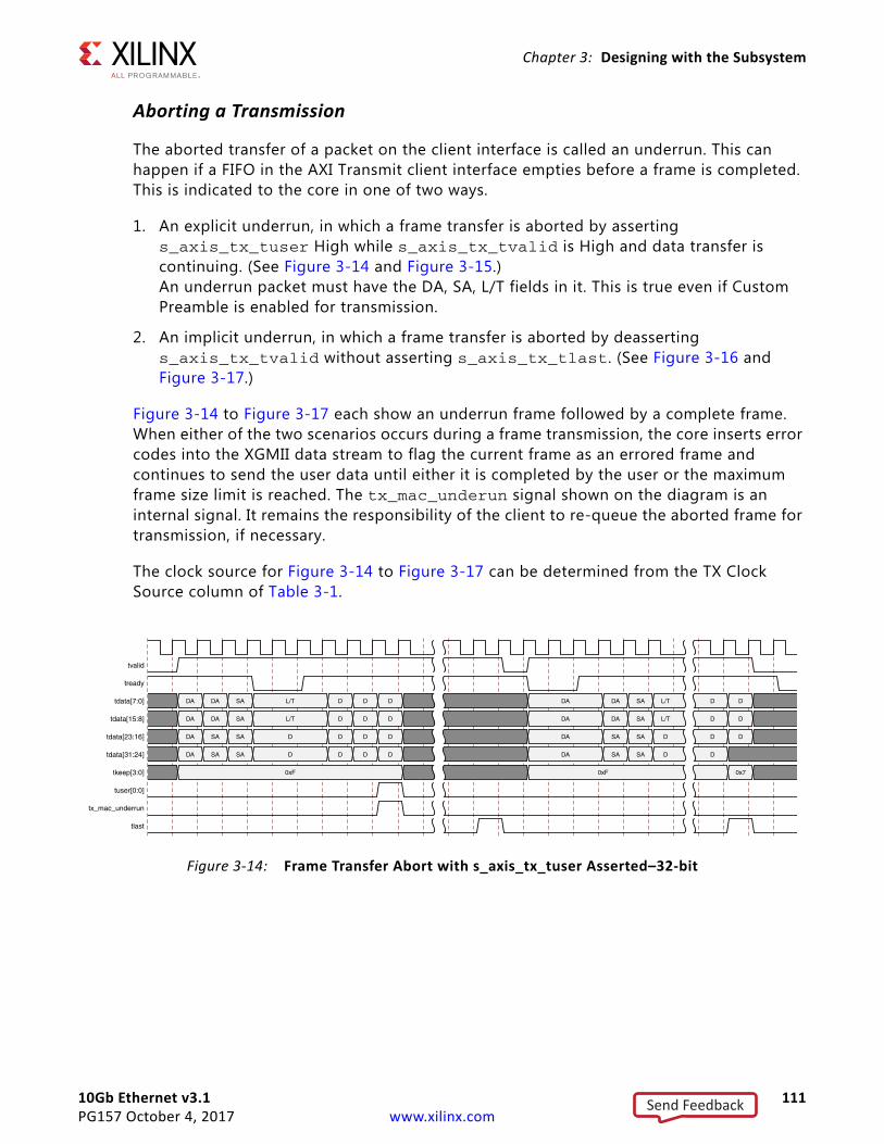
10Gb Ethernet v3.1 111PG157 October 4, 2017 www.xilinx.com
Chapter 3: Designing with the Subsystem
Aborting a Transmission
The aborted transfer of a packet on the client interface is called an underrun. This can happen if a FIFO in the AXI Transmit client interface empties before a frame is completed. This is indicated to the core in one of two ways.
1. An explicit underrun, in which a frame transfer is aborted by asserting s_axis_tx_tuser High while s_axis_tx_tvalid is High and data transfer is continuing. (See Figure 3-14 and Figure 3-15.) An underrun packet must have the DA, SA, L/T fields in it. This is true even if Custom Preamble is enabled for transmission.
2. An implicit underrun, in which a frame transfer is aborted by deasserting s_axis_tx_tvalid without asserting s_axis_tx_tlast. (See Figure 3-16 and Figure 3-17.)
Figure 3-14 to Figure 3-17 each show an underrun frame followed by a complete frame. When either of the two scenarios occurs during a frame transmission, the core inserts error codes into the XGMII data stream to flag the current frame as an errored frame and continues to send the user data until either it is completed by the user or the maximum frame size limit is reached. The tx_mac_underun signal shown on the diagram is an internal signal. It remains the responsibility of the client to re-queue the aborted frame for transmission, if necessary.
The clock source for Figure 3-14 to Figure 3-17 can be determined from the TX Clock Source column of Table 3-1.
X-Ref Target - Figure 3-14
Figure 3-14: Frame Transfer Abort with s_axis_tx_tuser Asserted–32-bit
Send Feedback
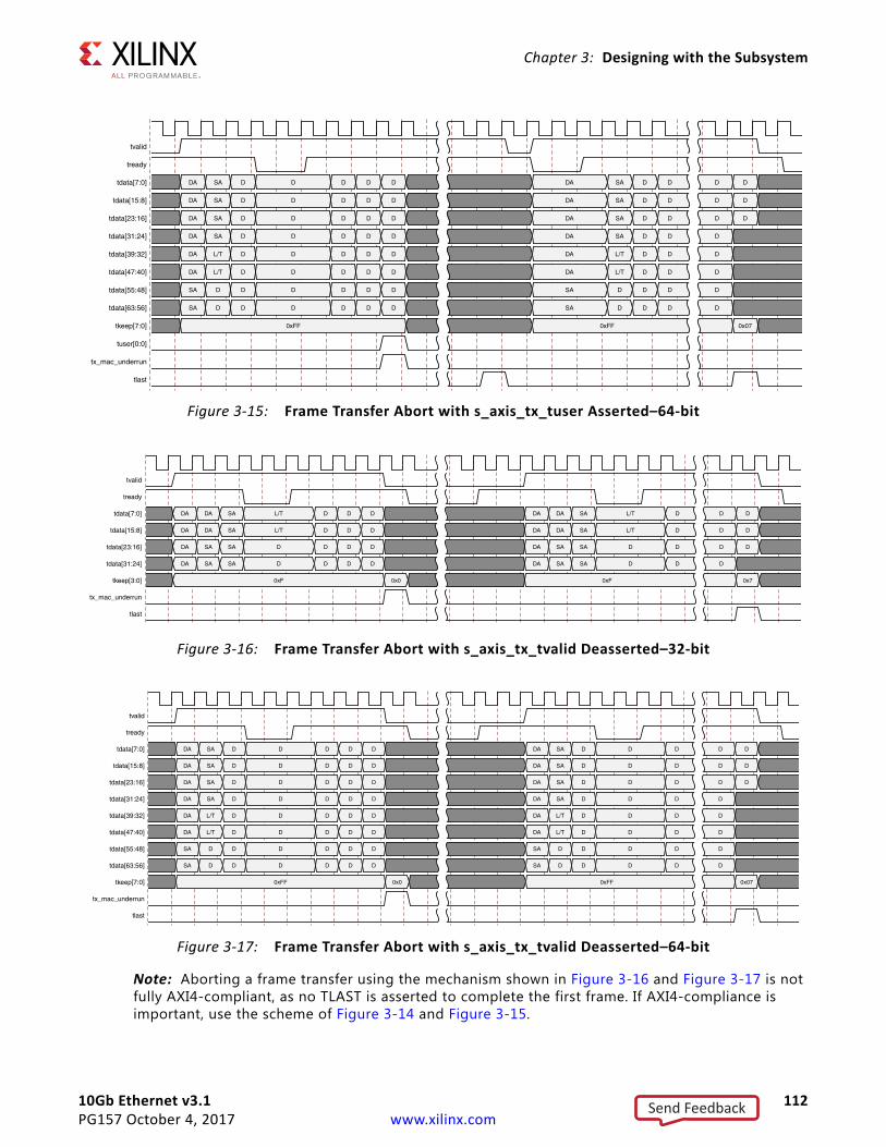
10Gb Ethernet v3.1 112PG157 October 4, 2017 www.xilinx.com
Chapter 3: Designing with the Subsystem
Note: Aborting a frame transfer using the mechanism shown in Figure 3-16 and Figure 3-17 is not fully AXI4-compliant, as no TLAST is asserted to complete the first frame. If AXI4-compliance is important, use the scheme of Figure 3-14 and Figure 3-15.
X-Ref Target - Figure 3-15
Figure 3-15: Frame Transfer Abort with s_axis_tx_tuser Asserted–64-bit
X-Ref Target - Figure 3-16
Figure 3-16: Frame Transfer Abort with s_axis_tx_tvalid Deasserted–32-bit
X-Ref Target - Figure 3-17
Figure 3-17: Frame Transfer Abort with s_axis_tx_tvalid Deasserted–64-bit
Send Feedback
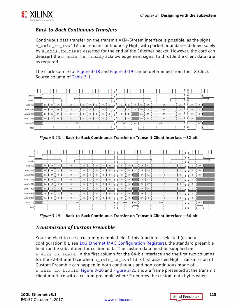
10Gb Ethernet v3.1 113PG157 October 4, 2017 www.xilinx.com
Chapter 3: Designing with the Subsystem
Back-to-Back Continuous Transfers
Continuous data transfer on the transmit AXI4-Stream interface is possible, as the signal s_axis_tx_tvalid can remain continuously High, with packet boundaries defined solely by s_axis_tx_tlast asserted for the end of the Ethernet packet. However, the core can deassert the s_axis_tx_tready acknowledgement signal to throttle the client data rate as required.
The clock source for Figure 3-18 and Figure 3-19 can be determined from the TX Clock Source column of Table 3-1.
Transmission of Custom Preamble
You can elect to use a custom preamble field. If this function is selected (using a configuration bit, see 10G Ethernet MAC Configuration Registers), the standard preamble field can be substituted for custom data. The custom data must be supplied on s_axis_tx_tdata in the first column for the 64-bit interface and the first two columns for the 32-bit interface when s_axis_tx_tvalid is first asserted High. Transmission of Custom Preamble can happen in both continuous and non-continuous mode of s_axis_tx_tvalid. Figure 3-20 and Figure 3-21 show a frame presented at the transmit client interface with a custom preamble where P denotes the custom data bytes when
X-Ref Target - Figure 3-18
Figure 3-18: Back-to-Back Continuous Transfer on Transmit Client Interface—32-bit
X-Ref Target - Figure 3-19
Figure 3-19: Back-to-Back Continuous Transfer on Transmit Client Interface—64-bit
Send Feedback
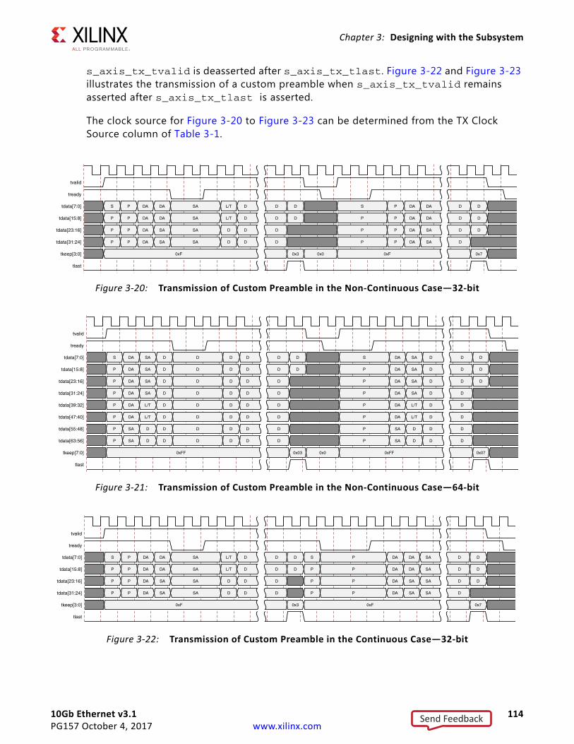
10Gb Ethernet v3.1 114PG157 October 4, 2017 www.xilinx.com
Chapter 3: Designing with the Subsystem
s_axis_tx_tvalid is deasserted after s_axis_tx_tlast. Figure 3-22 and Figure 3-23 illustrates the transmission of a custom preamble when s_axis_tx_tvalid remains asserted after s_axis_tx_tlast is asserted.
The clock source for Figure 3-20 to Figure 3-23 can be determined from the TX Clock Source column of Table 3-1.
X-Ref Target - Figure 3-20
Figure 3-20: Transmission of Custom Preamble in the Non-Continuous Case—32-bit
X-Ref Target - Figure 3-21
Figure 3-21: Transmission of Custom Preamble in the Non-Continuous Case—64-bit
X-Ref Target - Figure 3-22
Figure 3-22: Transmission of Custom Preamble in the Continuous Case—32-bit
Send Feedback
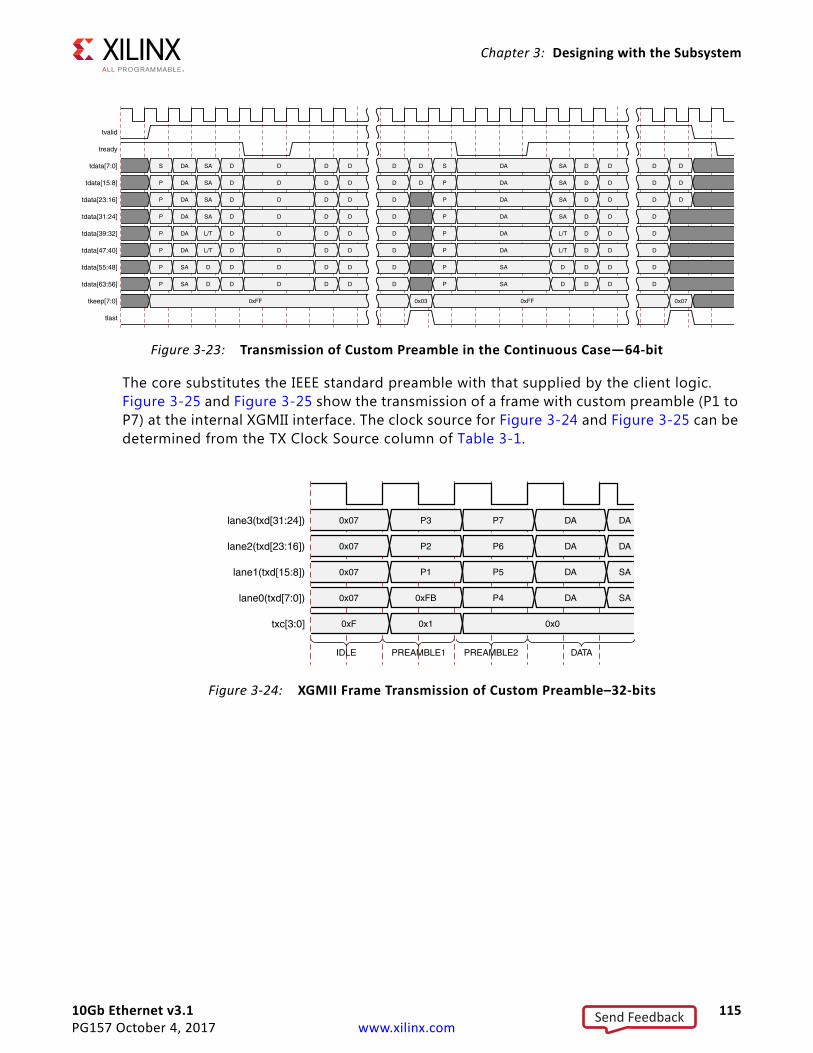
10Gb Ethernet v3.1 115PG157 October 4, 2017 www.xilinx.com
Chapter 3: Designing with the Subsystem
The core substitutes the IEEE standard preamble with that supplied by the client logic. Figure 3-25 and Figure 3-25 show the transmission of a frame with custom preamble (P1 to P7) at the internal XGMII interface. The clock source for Figure 3-24 and Figure 3-25 can be determined from the TX Clock Source column of Table 3-1.
X-Ref Target - Figure 3-23
Figure 3-23: Transmission of Custom Preamble in the Continuous Case—64-bit
X-Ref Target - Figure 3-24
Figure 3-24: XGMII Frame Transmission of Custom Preamble–32-bits
Send Feedback
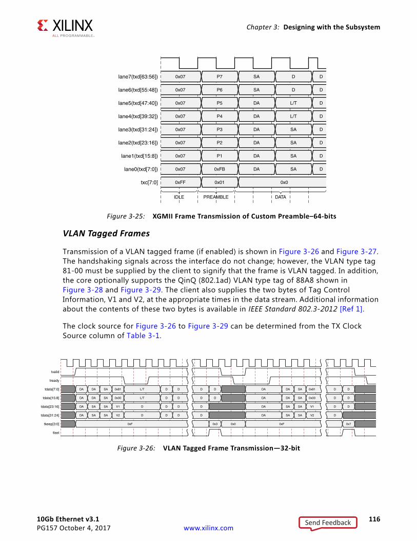
10Gb Ethernet v3.1 116PG157 October 4, 2017 www.xilinx.com
Chapter 3: Designing with the Subsystem
X-Ref Target - Figure 3-25.
VLAN Tagged Frames
Transmission of a VLAN tagged frame (if enabled) is shown in Figure 3-26 and Figure 3-27. The handshaking signals across the interface do not change; however, the VLAN type tag 81-00 must be supplied by the client to signify that the frame is VLAN tagged. In addition, the core optionally supports the QinQ (802.1ad) VLAN type tag of 88A8 shown in Figure 3-28 and Figure 3-29. The client also supplies the two bytes of Tag Control Information, V1 and V2, at the appropriate times in the data stream. Additional information about the contents of these two bytes is available in IEEE Standard 802.3-2012 [Ref 1].
The clock source for Figure 3-26 to Figure 3-29 can be determined from the TX Clock Source column of Table 3-1.
Figure 3-25: XGMII Frame Transmission of Custom Preamble–64-bits
X-Ref Target - Figure 3-26
Figure 3-26: VLAN Tagged Frame Transmission—32-bit
Send Feedback
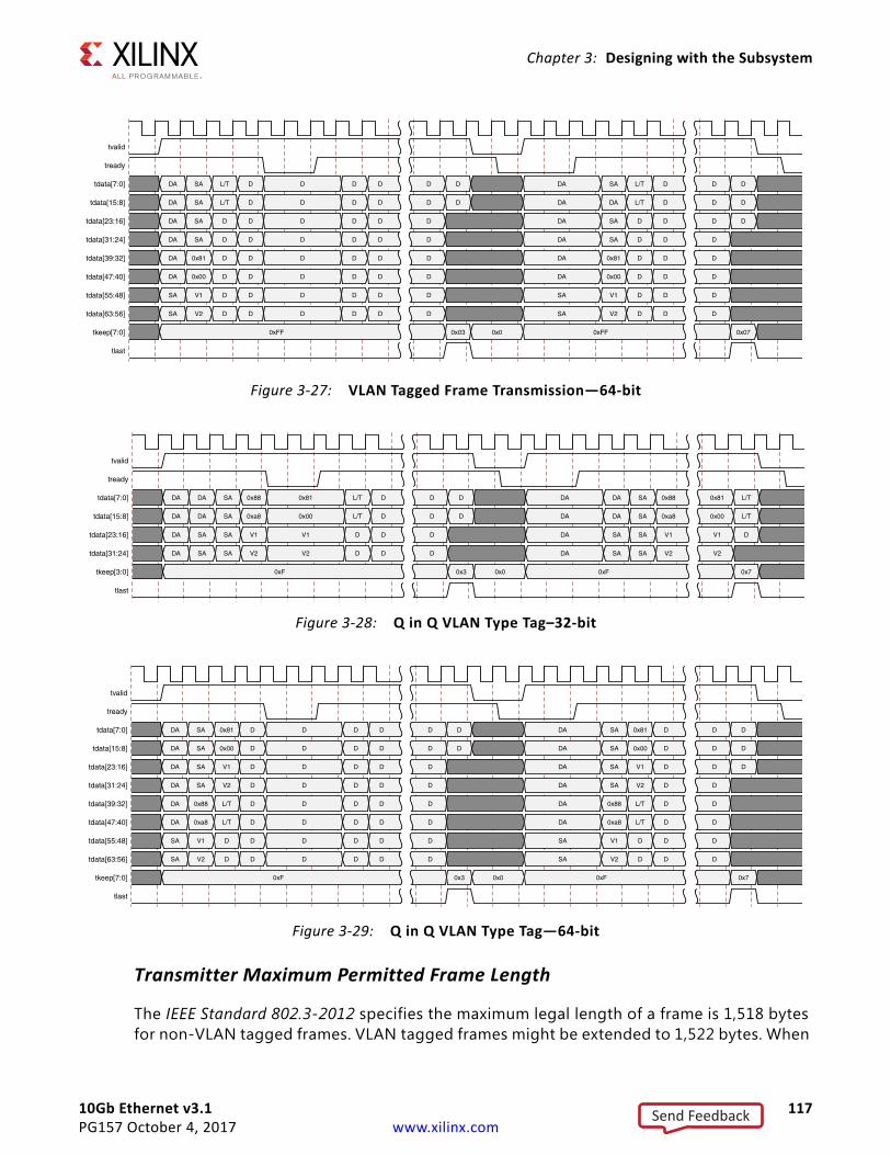
10Gb Ethernet v3.1 117PG157 October 4, 2017 www.xilinx.com
Chapter 3: Designing with the Subsystem
Transmitter Maximum Permitted Frame Length
The IEEE Standard 802.3-2012 specifies the maximum legal length of a frame is 1,518 bytes for non-VLAN tagged frames. VLAN tagged frames might be extended to 1,522 bytes. When
X-Ref Target - Figure 3-27
Figure 3-27: VLAN Tagged Frame Transmission—64-bit
X-Ref Target - Figure 3-28
Figure 3-28: Q in Q VLAN Type Tag–32-bit
X-Ref Target - Figure 3-29
Figure 3-29: Q in Q VLAN Type Tag—64-bit
Send Feedback
10Gb Ethernet v3.1 118PG157 October 4, 2017 www.xilinx.com
Chapter 3: Designing with the Subsystem
jumbo frame handling is disabled and the client attempts to transmit a frame which exceeds the maximum legal length, the core inserts an error code to corrupt the current frame and the frame is truncated to the maximum legal length. When jumbo frame handling is enabled, frames which are longer than the legal maximum are transmitted error free.
If required, a custom Maximum Transmission Unit (MTU) can be programmed into the core. This allows the transmission of frames up to the programmed MTU size by the core, rather than the 1,518/1,522 byte limit. The programmed MTU ≥ 1,518 bytes.
Any Frame transmitted greater than the MTU Frame Size, if Jumbo Frame is disabled, is signaled as a bad frame; error codes are inserted and the frame is truncated. For details on enabling and disabling jumbo frame handling, see 10G Ethernet MAC Configuration Registers.
IMPORTANT: There are interactions between the configuration bits affecting frame length handling that you should be aware of. Firstly, if Jumbo Enable and MTU Frame Transfer Enable are enabled at the same time, the Jumbo Enable takes precedence. Secondly, if VLAN Enable and MTU Frame Transfer Enable are both turned on, then MTU frame length rules apply.
Interframe Gap Adjustment
You can elect to vary the length of the interframe gap. If this function is selected (using a configuration bit, see 10G Ethernet MAC Configuration Registers), the core exerts back pressure to delay the transmission of the next frame until the requested number of XGMII columns has elapsed. The number of XGMII columns is controlled by the value on the tx_ifg_delay port. The minimum interframe gap of three XGMII columns (12 bytes) is always maintained. Figure 3-30 and Figure 3-31 shows the core operating in this mode.
The clock source for Figure 3-30 and Figure 3-31 can be determined from the TX Clock Source column of Table 3-1.
X-Ref Target - Figure 3-30
Figure 3-30: Interframe Gap Adjustment—32-bit
Send Feedback
10Gb Ethernet v3.1 119PG157 October 4, 2017 www.xilinx.com
Chapter 3: Designing with the Subsystem
Deficit Idle Count (DIC)
The Transmit side supports Interframe Gap obtained through Deficit Idle Count to maintain the maximum effective data rate as described in IEEE Standard 802.3-2012 [Ref 1]. This feature is supported even when the AXI4-Stream sends Ethernet packets with In-band FCS or without FCS. It is also supported when Custom Preamble is enabled for transmission. However, the transmit streaming interface requires that s_axis_tx_tvalid must be maintained continuously High to maintain the maximum effective data rate through the IFG adjustment with DIC.
The clock source for Figure 3-32 and Figure 3-33 can be determined from the TX Clock Source column of Table 3-1.
X-Ref Target - Figure 3-31
Figure 3-31: Interframe Gap Adjustment—64-bit
X-Ref Target - Figure 3-32
Figure 3-32: Back-to-Back Continuous Transfer on Transmit XGMII Interface—32-bit
Send Feedback
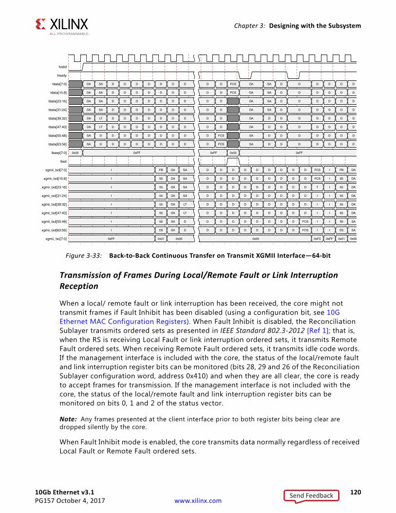
10Gb Ethernet v3.1 120PG157 October 4, 2017 www.xilinx.com
Chapter 3: Designing with the Subsystem
Transmission of Frames During Local/Remote Fault or Link Interruption Reception
When a local/ remote fault or link interruption has been received, the core might not transmit frames if Fault Inhibit has been disabled (using a configuration bit, see 10G Ethernet MAC Configuration Registers). When Fault Inhibit is disabled, the Reconciliation Sublayer transmits ordered sets as presented in IEEE Standard 802.3-2012 [Ref 1]; that is, when the RS is receiving Local Fault or link interruption ordered sets, it transmits Remote Fault ordered sets. When receiving Remote Fault ordered sets, it transmits idle code words. If the management interface is included with the core, the status of the local/remote fault and link interruption register bits can be monitored (bits 28, 29 and 26 of the Reconciliation Sublayer configuration word, address 0x410) and when they are all clear, the core is ready to accept frames for transmission. If the management interface is not included with the core, the status of the local/remote fault and link interruption register bits can be monitored on bits 0, 1 and 2 of the status vector.
Note: Any frames presented at the client interface prior to both register bits being clear are dropped silently by the core.
When Fault Inhibit mode is enabled, the core transmits data normally regardless of received Local Fault or Remote Fault ordered sets.
X-Ref Target - Figure 3-33
Figure 3-33: Back-to-Back Continuous Transfer on Transmit XGMII Interface—64-bit
Send Feedback
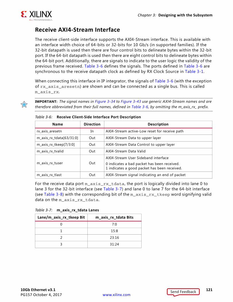
10Gb Ethernet v3.1 121PG157 October 4, 2017 www.xilinx.com
Chapter 3: Designing with the Subsystem
Receive AXI4-Stream InterfaceThe receive client-side interface supports the AXI4-Stream interface. This is available with an interface width choice of 64-bits or 32-bits for 10 Gb/s (in supported families). If the 32-bit datapath is used then there are four control bits to delineate bytes within the 32-bit port. If the 64-bit datapath is used then there are eight control bits to delineate bytes within the 64-bit port. Additionally, there are signals to indicate to the user logic the validity of the previous frame received. Table 3-6 defines the signals. The ports defined in Table 3-6 are synchronous to the receive datapath clock as defined by RX Clock Source in Table 3-1.
When connecting this interface in IP integrator, the signals of Table 3-6 (with the exception of rx_axis_aresetn) are shown and can be connected as a single bus. This is called m_axis_rx.
IMPORTANT: The signal names in Figure 3-34 to Figure 3-43 use generic AXI4-Stream names and are therefore abbreviated from their full names, defined in Table 3-6, by omitting the m_axis_rx_ prefix.
For the receive data port m_axis_rx_tdata, the port is logically divided into lane 0 to lane 3 for the 32-bit interface (see Table 3-7) and lane 0 to lane 7 for the 64-bit interface (see Table 3-8) with the corresponding bit of the m_axis_rx_tkeep word signifying valid data on the m_axis_rx_tdata.
Table 3-6: Receive Client-Side Interface Port Description
Name Direction Description
rx_axis_aresetn In AXI4-Stream active-Low reset for receive path
m_axis_rx_tdata[63/31:0] Out AXI4-Stream Data to upper layer
m_axis_rx_tkeep[7/3:0] Out AXI4-Stream Data Control to upper layer
m_axis_rx_tvalid Out AXI4-Stream Data Valid
m_axis_rx_tuser OutAXI4-Stream User Sideband interface
0 indicates a bad packet has been received.1 indicates a good packet has been received.
m_axis_rx_tlast Out AXI4-Stream signal indicating an end of packet
Table 3-7: m_axis_rx_tdata Lanes
Lane/m_axis_rx_tkeep Bit m_axis_rx_tdata Bits
0 7:0
1 15:8
2 23:16
3 31:24
Send Feedback
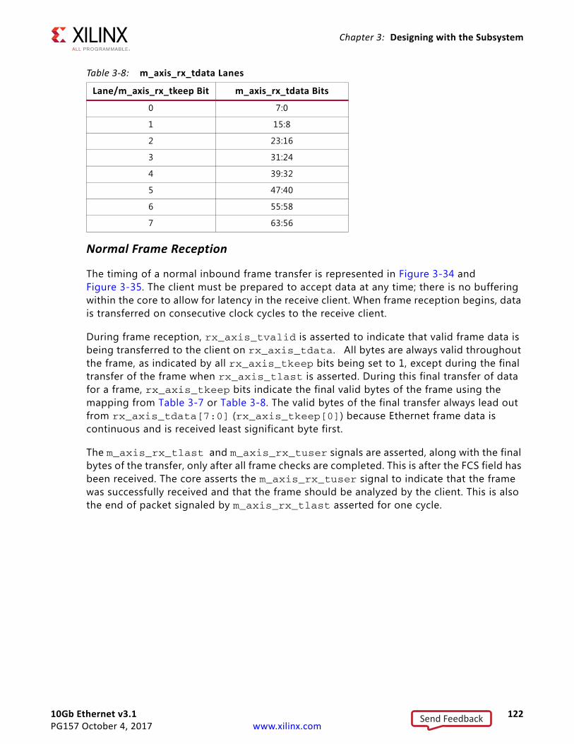
10Gb Ethernet v3.1 122PG157 October 4, 2017 www.xilinx.com
Chapter 3: Designing with the Subsystem
Normal Frame Reception
The timing of a normal inbound frame transfer is represented in Figure 3-34 and Figure 3-35. The client must be prepared to accept data at any time; there is no buffering within the core to allow for latency in the receive client. When frame reception begins, data is transferred on consecutive clock cycles to the receive client.
During frame reception, rx_axis_tvalid is asserted to indicate that valid frame data is being transferred to the client on rx_axis_tdata. All bytes are always valid throughout the frame, as indicated by all rx_axis_tkeep bits being set to 1, except during the final transfer of the frame when rx_axis_tlast is asserted. During this final transfer of data for a frame, rx_axis_tkeep bits indicate the final valid bytes of the frame using the mapping from Table 3-7 or Table 3-8. The valid bytes of the final transfer always lead out from rx_axis_tdata[7:0] (rx_axis_tkeep[0]) because Ethernet frame data is continuous and is received least significant byte first.
The m_axis_rx_tlast and m_axis_rx_tuser signals are asserted, along with the final bytes of the transfer, only after all frame checks are completed. This is after the FCS field has been received. The core asserts the m_axis_rx_tuser signal to indicate that the frame was successfully received and that the frame should be analyzed by the client. This is also the end of packet signaled by m_axis_rx_tlast asserted for one cycle.
Table 3-8: m_axis_rx_tdata Lanes
Lane/m_axis_rx_tkeep Bit m_axis_rx_tdata Bits
0 7:0
1 15:8
2 23:16
3 31:24
4 39:32
5 47:40
6 55:58
7 63:56
Send Feedback
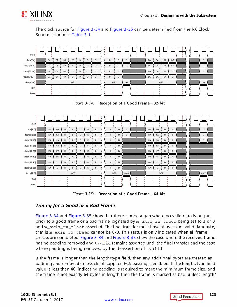
10Gb Ethernet v3.1 123PG157 October 4, 2017 www.xilinx.com
Chapter 3: Designing with the Subsystem
The clock source for Figure 3-34 and Figure 3-35 can be determined from the RX Clock Source column of Table 3-1.
Timing for a Good or a Bad Frame
Figure 3-34 and Figure 3-35 show that there can be a gap where no valid data is output prior to a good frame or a bad frame, signaled by m_axis_rx_tuser being set to 1 or 0 and m_axis_rx_tlast asserted. The final transfer must have at least one valid data byte, that is m_axis_rx_tkeep cannot be 0x0. This status is only indicated when all frame checks are completed. Figure 3-34 and Figure 3-35 show the case where the received frame has no padding removed and tvalid remains asserted until the final transfer and the case where padding is being removed by the deassertion of tvalid.
If the frame is longer than the length/type field, then any additional bytes are treated as padding and removed unless client supplied FCS passing is enabled. If the length/type field value is less than 46, indicating padding is required to meet the mimimum frame size, and the frame is not exactly 64 bytes in length then the frame is marked as bad, unless length/
X-Ref Target - Figure 3-34
Figure 3-34: Reception of a Good Frame—32-bit
X-Ref Target - Figure 3-35
Figure 3-35: Reception of a Good Frame—64-bit
Send Feedback
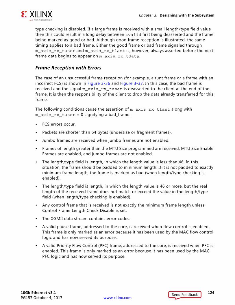
10Gb Ethernet v3.1 124PG157 October 4, 2017 www.xilinx.com
Chapter 3: Designing with the Subsystem
type checking is disabled. If a large frame is received with a small length/type field value then this could result in a long delay between tvalid first being deasserted and the frame being marked as good or bad. Although good frame reception is illustrated, the same timing applies to a bad frame. Either the good frame or bad frame signaled through m_axis_rx_tuser and m_axis_rx_tlast is, however, always asserted before the next frame data begins to appear on m_axis_rx_tdata.
Frame Reception with Errors
The case of an unsuccessful frame reception (for example, a runt frame or a frame with an incorrect FCS) is shown in Figure 3-36 and Figure 3-37. In this case, the bad frame is received and the signal m_axis_rx_tuser is deasserted to the client at the end of the frame. It is then the responsibility of the client to drop the data already transferred for this frame.
The following conditions cause the assertion of m_axis_rx_tlast along with m_axis_rx_tuser = 0 signifying a bad_frame:
• FCS errors occur.
• Packets are shorter than 64 bytes (undersize or fragment frames).
• Jumbo frames are received when jumbo frames are not enabled.
• Frames of length greater than the MTU Size programmed are received, MTU Size Enable Frames are enabled, and jumbo frames are not enabled.
• The length/type field is length, in which the length value is less than 46. In this situation, the frame should be padded to minimum length. If it is not padded to exactly minimum frame length, the frame is marked as bad (when length/type checking is enabled).
• The length/type field is length, in which the length value is 46 or more, but the real length of the received frame does not match or exceed the value in the length/type field (when length/type checking is enabled).
• Any control frame that is received is not exactly the minimum frame length unless Control Frame Length Check Disable is set.
• The XGMII data stream contains error codes.
• A valid pause frame, addressed to the core, is received when flow control is enabled. This frame is only marked as an error because it has been used by the MAC flow control logic and has now served its purpose.
• A valid Priority Flow Control (PFC) frame, addressed to the core, is received when PFC is enabled. This frame is only marked as an error because it has been used by the MAC PFC logic and has now served its purpose.
Send Feedback
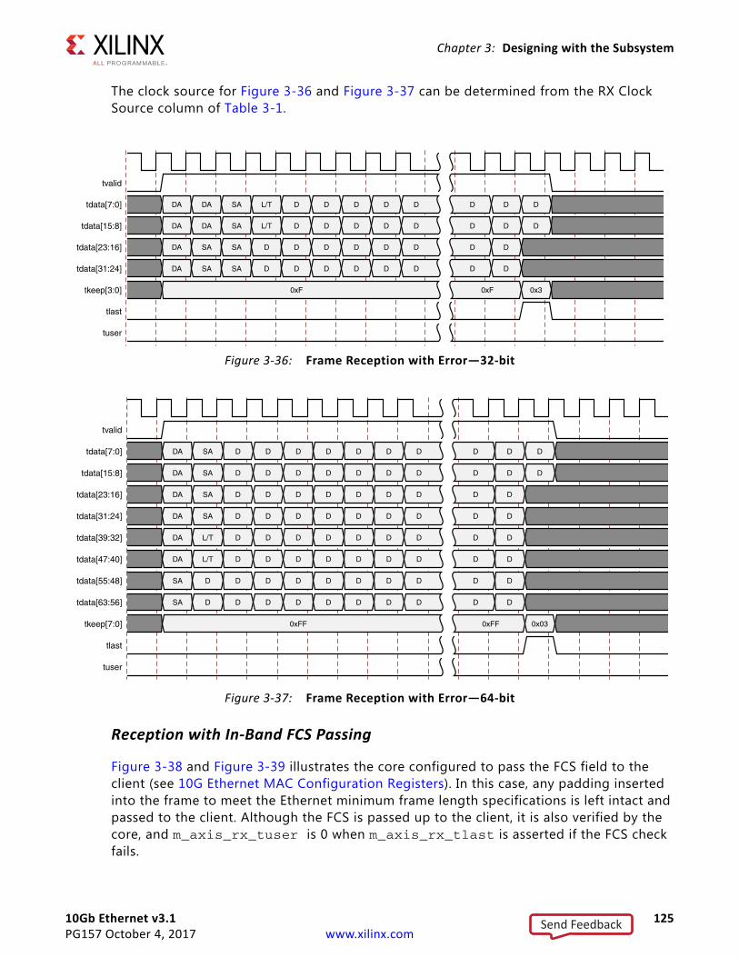
10Gb Ethernet v3.1 125PG157 October 4, 2017 www.xilinx.com
Chapter 3: Designing with the Subsystem
The clock source for Figure 3-36 and Figure 3-37 can be determined from the RX Clock Source column of Table 3-1.
Reception with In-Band FCS Passing
Figure 3-38 and Figure 3-39 illustrates the core configured to pass the FCS field to the client (see 10G Ethernet MAC Configuration Registers). In this case, any padding inserted into the frame to meet the Ethernet minimum frame length specifications is left intact and passed to the client. Although the FCS is passed up to the client, it is also verified by the core, and m_axis_rx_tuser is 0 when m_axis_rx_tlast is asserted if the FCS check fails.
X-Ref Target - Figure 3-36
Figure 3-36: Frame Reception with Error—32-bit
X-Ref Target - Figure 3-37
Figure 3-37: Frame Reception with Error—64-bit
Send Feedback
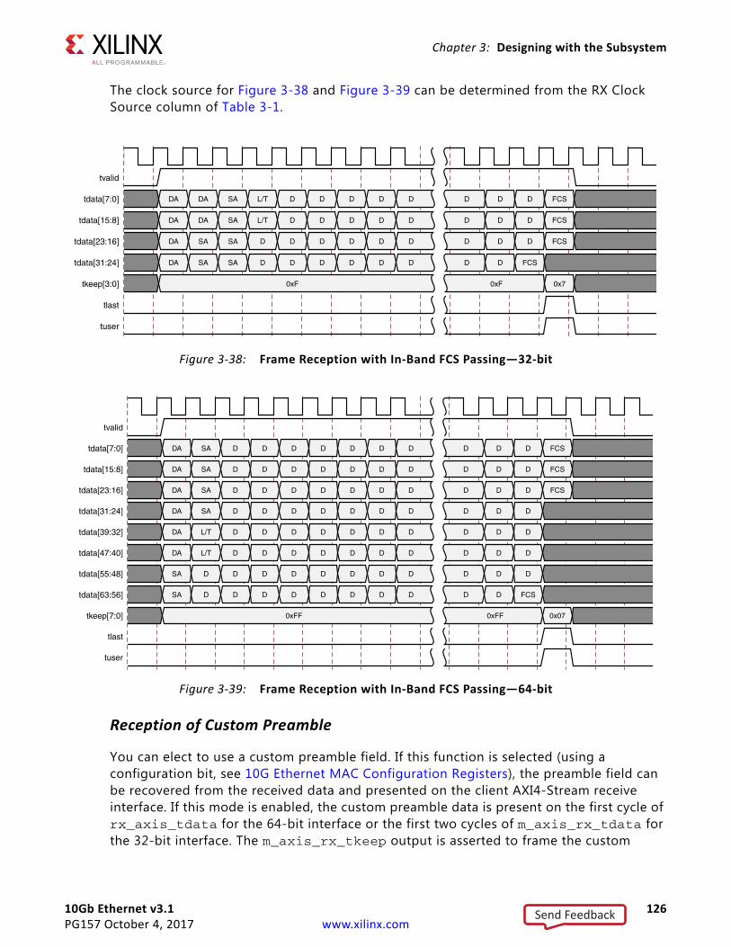
10Gb Ethernet v3.1 126PG157 October 4, 2017 www.xilinx.com
Chapter 3: Designing with the Subsystem
The clock source for Figure 3-38 and Figure 3-39 can be determined from the RX Clock Source column of Table 3-1.
Reception of Custom Preamble
You can elect to use a custom preamble field. If this function is selected (using a configuration bit, see 10G Ethernet MAC Configuration Registers), the preamble field can be recovered from the received data and presented on the client AXI4-Stream receive interface. If this mode is enabled, the custom preamble data is present on the first cycle of rx_axis_tdata for the 64-bit interface or the first two cycles of m_axis_rx_tdata for the 32-bit interface. The m_axis_rx_tkeep output is asserted to frame the custom
X-Ref Target - Figure 3-38
Figure 3-38: Frame Reception with In-Band FCS Passing—32-bit
X-Ref Target - Figure 3-39
Figure 3-39: Frame Reception with In-Band FCS Passing—64-bit
Send Feedback
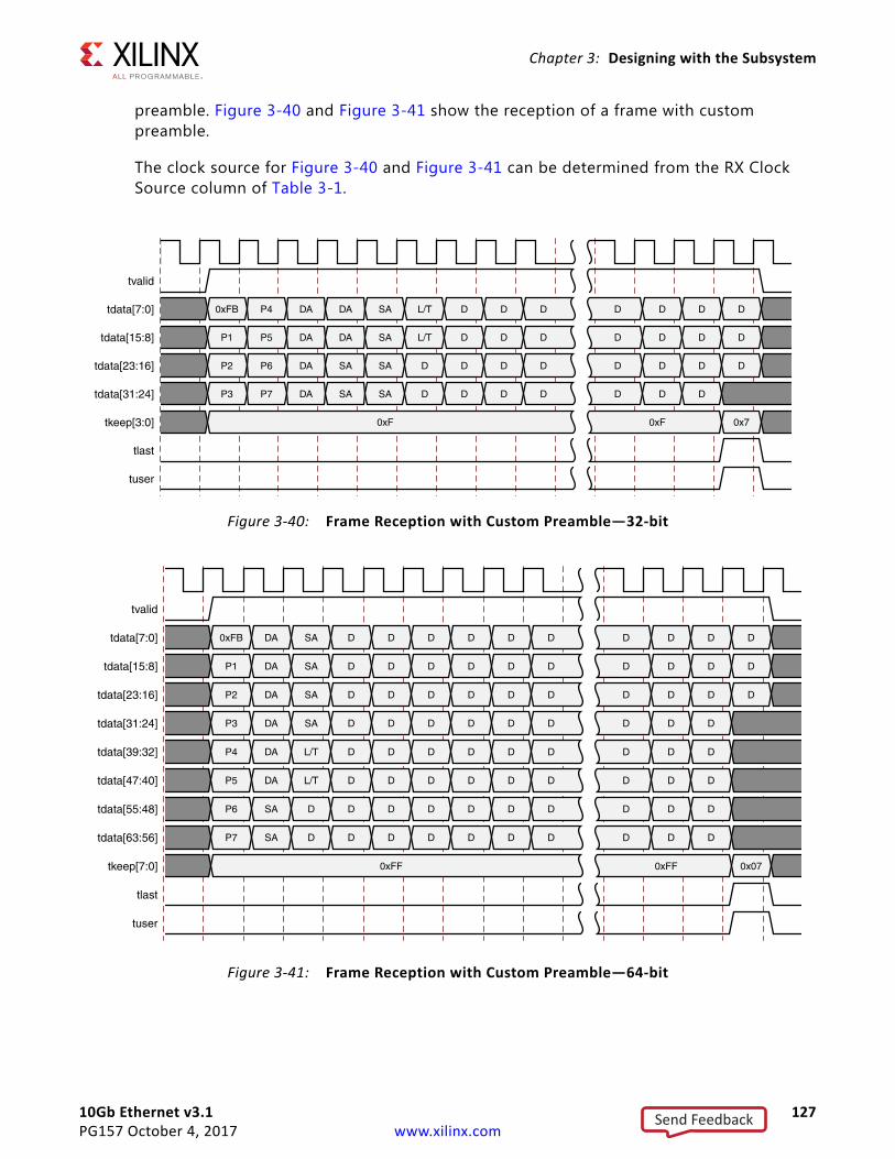
10Gb Ethernet v3.1 127PG157 October 4, 2017 www.xilinx.com
Chapter 3: Designing with the Subsystem
preamble. Figure 3-40 and Figure 3-41 show the reception of a frame with custom preamble.
The clock source for Figure 3-40 and Figure 3-41 can be determined from the RX Clock Source column of Table 3-1.
X-Ref Target - Figure 3-40
Figure 3-40: Frame Reception with Custom Preamble—32-bit
X-Ref Target - Figure 3-41
Figure 3-41: Frame Reception with Custom Preamble—64-bit
Send Feedback
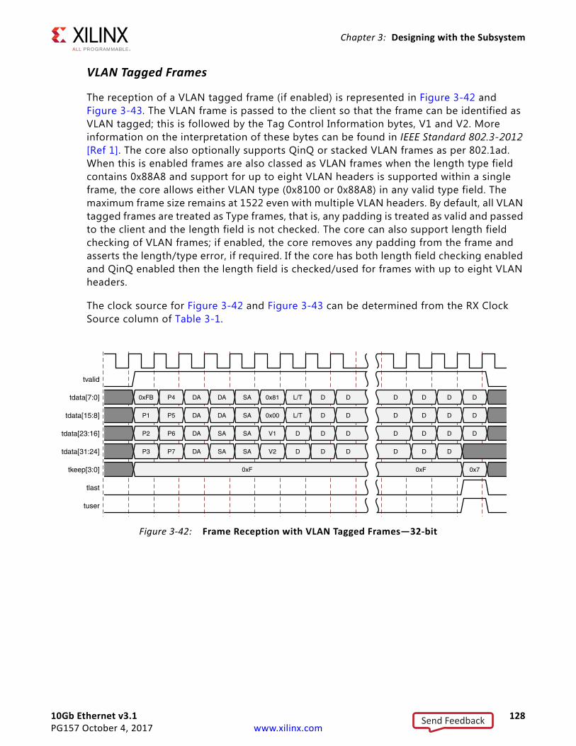
10Gb Ethernet v3.1 128PG157 October 4, 2017 www.xilinx.com
Chapter 3: Designing with the Subsystem
VLAN Tagged Frames
The reception of a VLAN tagged frame (if enabled) is represented in Figure 3-42 and Figure 3-43. The VLAN frame is passed to the client so that the frame can be identified as VLAN tagged; this is followed by the Tag Control Information bytes, V1 and V2. More information on the interpretation of these bytes can be found in IEEE Standard 802.3-2012 [Ref 1]. The core also optionally supports QinQ or stacked VLAN frames as per 802.1ad. When this is enabled frames are also classed as VLAN frames when the length type field contains 0x88A8 and support for up to eight VLAN headers is supported within a single frame, the core allows either VLAN type (0x8100 or 0x88A8) in any valid type field. The maximum frame size remains at 1522 even with multiple VLAN headers. By default, all VLAN tagged frames are treated as Type frames, that is, any padding is treated as valid and passed to the client and the length field is not checked. The core can also support length field checking of VLAN frames; if enabled, the core removes any padding from the frame and asserts the length/type error, if required. If the core has both length field checking enabled and QinQ enabled then the length field is checked/used for frames with up to eight VLAN headers.
The clock source for Figure 3-42 and Figure 3-43 can be determined from the RX Clock Source column of Table 3-1.
X-Ref Target - Figure 3-42
Figure 3-42: Frame Reception with VLAN Tagged Frames—32-bit
Send Feedback
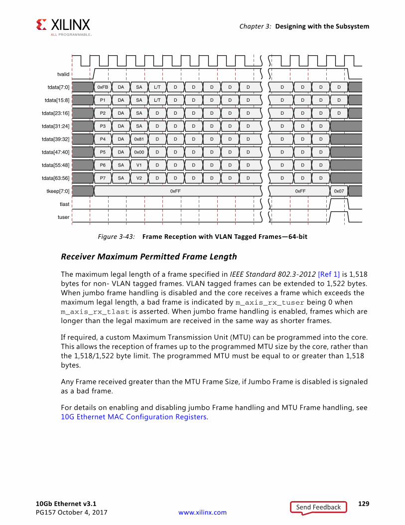
10Gb Ethernet v3.1 129PG157 October 4, 2017 www.xilinx.com
Chapter 3: Designing with the Subsystem
Receiver Maximum Permitted Frame Length
The maximum legal length of a frame specified in IEEE Standard 802.3-2012 [Ref 1] is 1,518 bytes for non- VLAN tagged frames. VLAN tagged frames can be extended to 1,522 bytes. When jumbo frame handling is disabled and the core receives a frame which exceeds the maximum legal length, a bad frame is indicated by m_axis_rx_tuser being 0 when m_axis_rx_tlast is asserted. When jumbo frame handling is enabled, frames which are longer than the legal maximum are received in the same way as shorter frames.
If required, a custom Maximum Transmission Unit (MTU) can be programmed into the core. This allows the reception of frames up to the programmed MTU size by the core, rather than the 1,518/1,522 byte limit. The programmed MTU must be equal to or greater than 1,518 bytes.
Any Frame received greater than the MTU Frame Size, if Jumbo Frame is disabled is signaled as a bad frame.
For details on enabling and disabling jumbo Frame handling and MTU Frame handling, see 10G Ethernet MAC Configuration Registers.
X-Ref Target - Figure 3-43
Figure 3-43: Frame Reception with VLAN Tagged Frames—64-bit
Send Feedback
10Gb Ethernet v3.1 130PG157 October 4, 2017 www.xilinx.com
Chapter 3: Designing with the Subsystem
Length/Type Field Error Checks
Enabled
Default operation is with the length/type error checking enabled (see 10G Ethernet MAC Configuration Registers). In this mode the following checks are made on all received, non VLAN-tagged, frames. If either of these checks fail, the frame is marked as bad. If a frame is a control frame or has a VLAN tag and enhanced VLAN support is not enabled, this check is not performed.
• A value in the length/type field which is ≥ decimal 46, but less than 1,536, is checked against the actual data length received.
• A value in the length/type field that is less than decimal 46, (a length interpretation), the frame data length is checked to see if it has been padded to exactly 46 bytes (so that the resultant total frame length is 64 bytes).
Furthermore, if padding is indicated (the length/type field is less than decimal 46) and client-supplied FCS passing is disabled, the length value in the length/type field is used to deassert m_axis_rx_tvalid after the indicated number of data bytes so that the padding bytes are removed from the frame. See Reception with In-Band FCS Passing.
Disabled
When the length/type error checking is disabled and the length/type field has a length interpretation, the core does not check the length value against the actual data length received as detailed previously. A frame containing only this error is marked as good. However, if the length/type field is less than decimal 46, the core marks a frame as bad if it is not the minimum frame size of 64 bytes.
If padding is indicated and client-supplied FCS passing is disabled, then a length value in the length/type field is not used to deassert m_axis_rx_tkeep[]. Instead, m_axis_rx_tkeep[] is deasserted before the start of the FCS field, and any padding is not removed from the frame.
IEEE 1588 TimestampingIEEE 1588 defines a protocol for performing timing synchronization across a network. A 1588 network has a single master clock timing reference, usually selected through a best master clock algorithm. Periodically, this master samples its system timer reference counter, and transmits this sampled time value across the network using defined packet formats. This timer should be sampled (a timestamp) when the start of a 1588 timing packet is transmitted. Therefore, to achieve high synchronization accuracy over the network, accurate timestamps are required. If this sampled timer value, the timestamp, is placed into the packet that triggered the timestamp, then this is known as 1-step operation.
Send Feedback
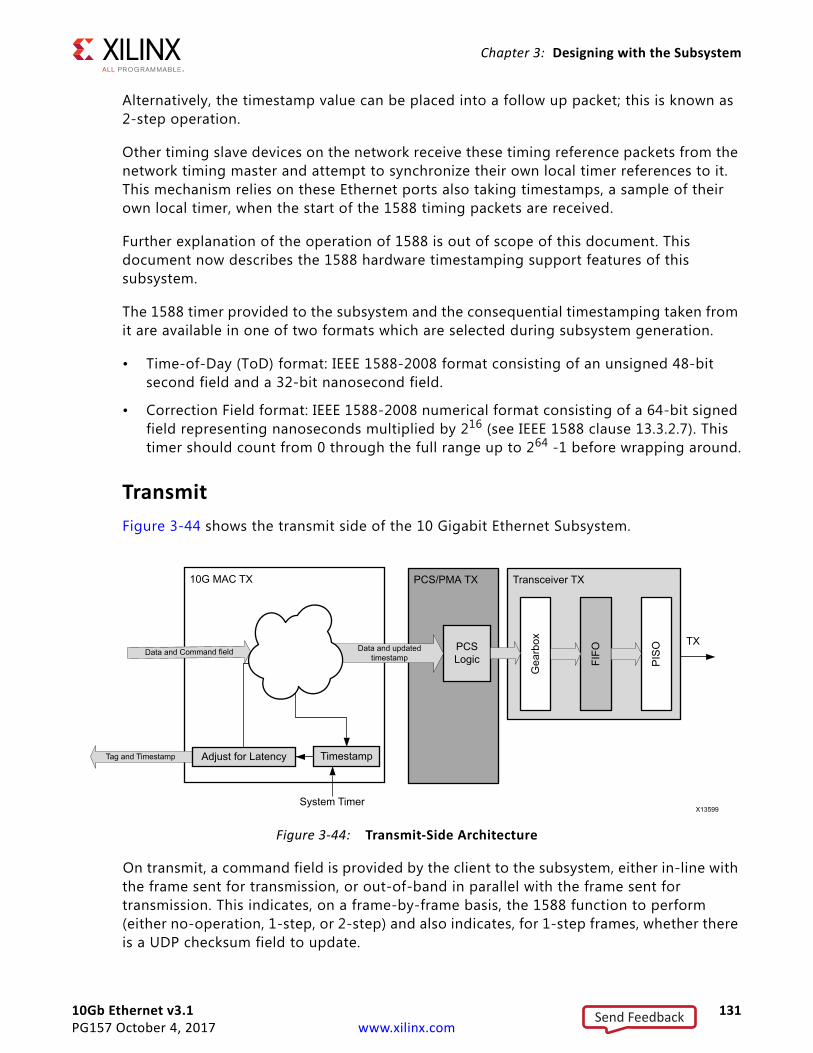
10Gb Ethernet v3.1 131PG157 October 4, 2017 www.xilinx.com
Chapter 3: Designing with the Subsystem
Alternatively, the timestamp value can be placed into a follow up packet; this is known as 2-step operation.
Other timing slave devices on the network receive these timing reference packets from the network timing master and attempt to synchronize their own local timer references to it. This mechanism relies on these Ethernet ports also taking timestamps, a sample of their own local timer, when the start of the 1588 timing packets are received.
Further explanation of the operation of 1588 is out of scope of this document. This document now describes the 1588 hardware timestamping support features of this subsystem.
The 1588 timer provided to the subsystem and the consequential timestamping taken from it are available in one of two formats which are selected during subsystem generation.
• Time-of-Day (ToD) format: IEEE 1588-2008 format consisting of an unsigned 48-bit second field and a 32-bit nanosecond field.
• Correction Field format: IEEE 1588-2008 numerical format consisting of a 64-bit signed field representing nanoseconds multiplied by 216 (see IEEE 1588 clause 13.3.2.7). This timer should count from 0 through the full range up to 264 -1 before wrapping around.
TransmitFigure 3-44 shows the transmit side of the 10 Gigabit Ethernet Subsystem.
On transmit, a command field is provided by the client to the subsystem, either in-line with the frame sent for transmission, or out-of-band in parallel with the frame sent for transmission. This indicates, on a frame-by-frame basis, the 1588 function to perform (either no-operation, 1-step, or 2-step) and also indicates, for 1-step frames, whether there is a UDP checksum field to update.
X-Ref Target - Figure 3-44
Figure 3-44: Transmit-Side Architecture
10G MAC TX Transceiver TXPCS/PMA TX
PIS
O
Gea
rbox
FIFO
TXPCS Logic
Data and updated timestamp
Data and Command field
Tag and Timestamp TimestampAdjust for Latency
System TimerX13599
Send Feedback
10Gb Ethernet v3.1 132PG157 October 4, 2017 www.xilinx.com
Chapter 3: Designing with the Subsystem
If using the ToD format, then for both 1-step and 2-step operation, the full captured 80-bit ToD timestamp is returned to the client logic using the additional ports defined in Table 2-30. If using the Correction Field format, then for both 1-step and 2-step operation, the full captured 64-bit timestamp is returned to the client logic using the additional ports defined in Table 2-30 (with the upper bits of data set to zero as defined in the table).
If using the ToD format, then for 1-step operation, the full captured 80-bit ToD timestamp is inserted into the frame. If using the Correction Field format, then for 1-step operation, the captured 64-bit timestamp is summed with the existing Correction Field contained within the frame and the summed result is overwritten into the original Correction Field of the frame. Supported frame types for 1-step timestamping are:
• Raw Ethernet
• UDP/IPv4
• UDP/IPv6
For 1-step UDP frame types, the UDP checksum is updated in accordance with IETF RFC 1624.
For all 1-step frames, the Ethernet Frame Check Sequence (FCS) field is calculated after all frame modifications have been completed.
For 2-step transmit operation, all Precision Time Protocol (PTP) frame types are supported.
Frame-by-Frame Timestamping OperationThe Ethernet frame sent to the MAC contains a command field. The format of the command field is defined in the following list. The information contained within the command field indicates one of the following on a frame-by-frame basis.
• No operation: the frame is not a PTP frame and no timestamp action should be taken.
• Two-step operation is required and a tag value (user-sequence ID) is provided as part of the command field; the frame should be timestamped, and the timestamp made available to the client logic, along with the provided tag value for the frame. The additional MAC transmitter ports (defined in Table 3-10) provide this function.
• 1-step operation is required
° For the ToD timer and timestamp format a timestamp offset value is provided as part of the command field; the frame should be timestamped, and the timestamp should be inserted into the frame at the provided offset (number of bytes) into the frame.
° For the Correction Field format, a Correction Field offset value is provided as part of the command field; the frame should be timestamped, and the captured 64-bit Timestamp is summed with the existing Correction Field contained within the frame and the summed result is overwritten into original Correction Field of the frame.
Send Feedback
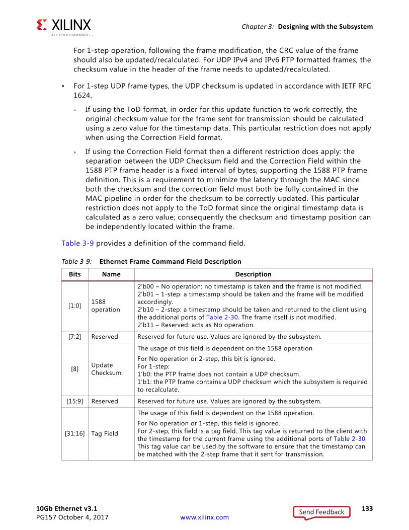
10Gb Ethernet v3.1 133PG157 October 4, 2017 www.xilinx.com
Chapter 3: Designing with the Subsystem
For 1-step operation, following the frame modification, the CRC value of the frame should also be updated/recalculated. For UDP IPv4 and IPv6 PTP formatted frames, the checksum value in the header of the frame needs to updated/recalculated.
• For 1-step UDP frame types, the UDP checksum is updated in accordance with IETF RFC 1624.
° If using the ToD format, in order for this update function to work correctly, the original checksum value for the frame sent for transmission should be calculated using a zero value for the timestamp data. This particular restriction does not apply when using the Correction Field format.
° If using the Correction Field format then a different restriction does apply: the separation between the UDP Checksum field and the Correction Field within the 1588 PTP frame header is a fixed interval of bytes, supporting the 1588 PTP frame definition. This is a requirement to minimize the latency through the MAC since both the checksum and the correction field must both be fully contained in the MAC pipeline in order for the checksum to be correctly updated. This particular restriction does not apply to the ToD format since the original timestamp data is calculated as a zero value; consequently the checksum and timestamp position can be independently located within the frame.
Table 3-9 provides a definition of the command field.
Table 3-9: Ethernet Frame Command Field Description
Bits Name Description
[1:0] 1588operation
2’b00 – No operation: no timestamp is taken and the frame is not modified.2’b01 – 1-step: a timestamp should be taken and the frame will be modified accordingly.2’b10 – 2-step: a timestamp should be taken and returned to the client using the additional ports of Table 2-30. The frame itself is not modified.2’b11 – Reserved: acts as No operation.
[7:2] Reserved Reserved for future use. Values are ignored by the subsystem.
[8] UpdateChecksum
The usage of this field is dependent on the 1588 operation
For No operation or 2-step, this bit is ignored.For 1-step:1’b0: the PTP frame does not contain a UDP checksum.1’b1: the PTP frame contains a UDP checksum which the subsystem is required to recalculate.
[15:9] Reserved Reserved for future use. Values are ignored by the subsystem.
[31:16] Tag Field
The usage of this field is dependent on the 1588 operation.
For No operation or 1-step, this field is ignored.For 2-step, this field is a tag field. This tag value is returned to the client with the timestamp for the current frame using the additional ports of Table 2-30. This tag value can be used by the software to ensure that the timestamp can be matched with the 2-step frame that it sent for transmission.
Send Feedback
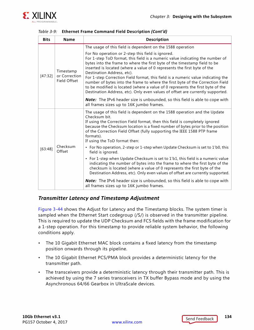
10Gb Ethernet v3.1 134PG157 October 4, 2017 www.xilinx.com
Chapter 3: Designing with the Subsystem
Transmitter Latency and Timestamp Adjustment
Figure 3-44 shows the Adjust for Latency and the Timestamp blocks. The system timer is sampled when the Ethernet Start codegroup (/S/) is observed in the transmitter pipeline. This is required to update the UDP Checksum and FCS fields with the frame modification for a 1-step operation. For this timestamp to provide reliable system behavior, the following conditions apply.
• The 10 Gigabit Ethernet MAC block contains a fixed latency from the timestamp position onwards through its pipeline.
• The 10 Gigabit Ethernet PCS/PMA block provides a deterministic latency for the transmitter path.
• The transceivers provide a deterministic latency through their transmitter path. This is achieved by using the 7 series transceivers in TX buffer Bypass mode and by using the Asynchronous 64/66 Gearbox in UltraScale devices.
[47:32]Timestampor CorrectionField Offset
The usage of this field is dependent on the 1588 operation
For No operation or 2-step this field is ignored.For 1-step ToD format, this field is a numeric value indicating the number of bytes into the frame to where the first byte of the timestamp field to be inserted is located (where a value of 0 represents the first byte of the Destination Address, etc). For 1-step Correction Field format, this field is a numeric value indicating the number of bytes into the frame to where the first byte of the Correction Field to be modified is located (where a value of 0 represents the first byte of the Destination Address, etc). Only even values of offset are currently supported.
Note: The IPv6 header size is unbounded, so this field is able to cope with all frames sizes up to 16K jumbo frames.
[63:48] ChecksumOffset
The usage of this field is dependent on the 1588 operation and the Update Checksum bit.If using the Correction Field format, then this field is completely ignored because the Checksum location is a fixed number of bytes prior to the position of the Correction Field Offset (fully supporting the IEEE 1588 PTP frame formats).If using the ToD format then:
• For No operation, 2-step or 1-step when Update Checksum is set to 1’b0, this field is ignored.
• For 1-step when Update Checksum is set to 1’b1, this field is a numeric value indicating the number of bytes into the frame to where the first byte of the checksum is located (where a value of 0 represents the first byte of the Destination Address, etc). Only even values of offset are currently supported.
Note: The IPv6 header size is unbounded, so this field is able to cope with all frames sizes up to 16K jumbo frames.
Table 3-9: Ethernet Frame Command Field Description (Cont’d)
Bits Name Description
Send Feedback
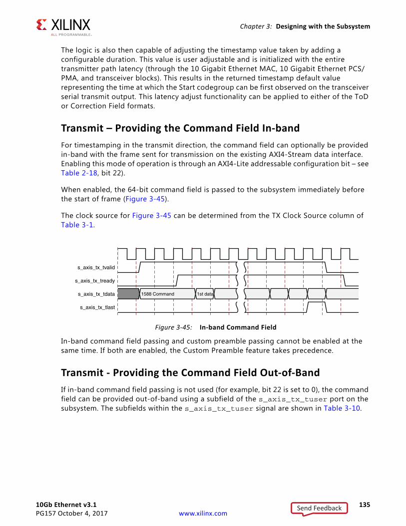
10Gb Ethernet v3.1 135PG157 October 4, 2017 www.xilinx.com
Chapter 3: Designing with the Subsystem
The logic is also then capable of adjusting the timestamp value taken by adding a configurable duration. This value is user adjustable and is initialized with the entire transmitter path latency (through the 10 Gigabit Ethernet MAC, 10 Gigabit Ethernet PCS/PMA, and transceiver blocks). This results in the returned timestamp default value representing the time at which the Start codegroup can be first observed on the transceiver serial transmit output. This latency adjust functionality can be applied to either of the ToD or Correction Field formats.
Transmit – Providing the Command Field In-bandFor timestamping in the transmit direction, the command field can optionally be provided in-band with the frame sent for transmission on the existing AXI4-Stream data interface. Enabling this mode of operation is through an AXI4-Lite addressable configuration bit – see Table 2-18, bit 22).
When enabled, the 64-bit command field is passed to the subsystem immediately before the start of frame (Figure 3-45).
The clock source for Figure 3-45 can be determined from the TX Clock Source column of Table 3-1.
In-band command field passing and custom preamble passing cannot be enabled at the same time. If both are enabled, the Custom Preamble feature takes precedence.
Transmit - Providing the Command Field Out-of-BandIf in-band command field passing is not used (for example, bit 22 is set to 0), the command field can be provided out-of-band using a subfield of the s_axis_tx_tuser port on the subsystem. The subfields within the s_axis_tx_tuser signal are shown in Table 3-10.
X-Ref Target - Figure 3-45
Figure 3-45: In-band Command Field
Send Feedback
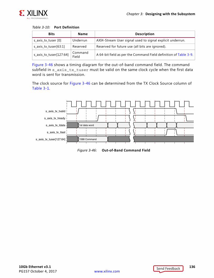
10Gb Ethernet v3.1 136PG157 October 4, 2017 www.xilinx.com
Chapter 3: Designing with the Subsystem
Figure 3-46 shows a timing diagram for the out-of-band command field. The command subfield in s_axis_tx_tuser must be valid on the same clock cycle when the first data word is sent for transmission.
The clock source for Figure 3-46 can be determined from the TX Clock Source column of Table 3-1.
Table 3-10: Port Definition
Bits Name Description
s_axis_tx_tuser [0] Underrun AXI4-Stream User signal used to signal explicit underrun.
s_axis_tx_tuser[63:1] Reserved Reserved for future use (all bits are ignored).
s_axis_tx_tuser[127:64] Command Field A 64-bit field as per the Command Field definition of Table 3-9.
X-Ref Target - Figure 3-46
Figure 3-46: Out-of-Band Command Field
Send Feedback
10Gb Ethernet v3.1 137PG157 October 4, 2017 www.xilinx.com
Chapter 3: Designing with the Subsystem
ReceiveFigure 3-47 shows the receive side of the 10 Gigabit Ethernet Subsystem.
On the receive side, all frames are timestamped with a captured 80-bit ToD timestamp. The full 80-bit timestamp is provided to the client logic out of band using additional ports defined in Table 2-31. In addition, a 64-bit timestamp can optionally be provided in line with the received frame. This 64-bit timestamp consists of the lower 32 bits from the 1588 timers seconds field, plus all 32 bits of the nanoseconds field. For the Correction Field format, the full 64-bit timestamp is provided to the client logic out of band using additional ports defined in Table 2-31. In addition, the 64-bit timestamp can optionally be provided in line with the received frame.
Receiver Latency and Timestamp AdjustmentFigure 3-47 shows the Timestamp and Adjust for Latency blocks. This indicates the timestamp point in the receiver pipeline when the Start codegroup is observed. This timestamp is performed in the 10 Gigabit Ethernet PCS/PMA, prior to any variable length latency logic.
• The transceivers provides deterministic latency through their receiver path. This is achieved by using the 7 series transceivers in RX buffer Bypass mode and by using the Asynchronous 64/66 Gearbox in UltraScale devices.
• The 10 Gigabit Ethernet PCS/PMA block provides fixed latency for the receiver path up until the timestamp point.
X-Ref Target - Figure 3-47
Figure 3-47: Receive-Side Architecture
PCS/PMA RX10G MAC RX
Transceiver RX
SIP
O
Gea
rbox
FIFO
RX
Adjust for LatencyFI
FO
PCS Logic
Timestamp
System Timer
X13600
Send Feedback
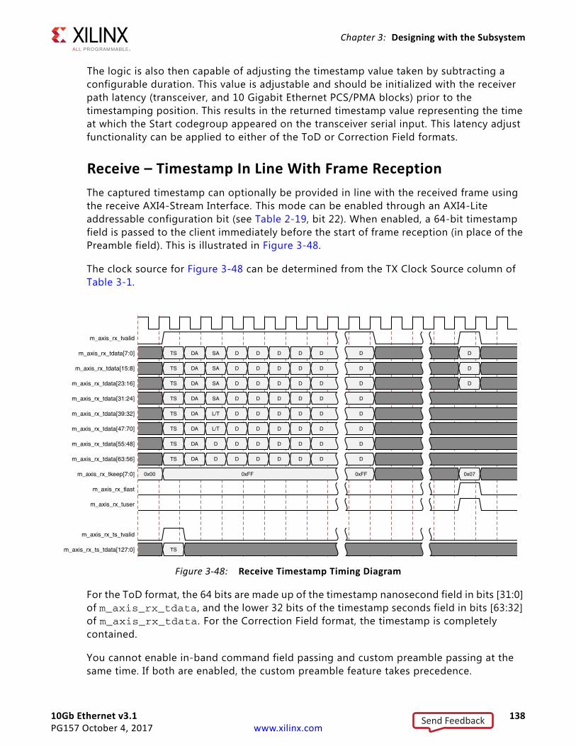
10Gb Ethernet v3.1 138PG157 October 4, 2017 www.xilinx.com
Chapter 3: Designing with the Subsystem
The logic is also then capable of adjusting the timestamp value taken by subtracting a configurable duration. This value is adjustable and should be initialized with the receiver path latency (transceiver, and 10 Gigabit Ethernet PCS/PMA blocks) prior to the timestamping position. This results in the returned timestamp value representing the time at which the Start codegroup appeared on the transceiver serial input. This latency adjust functionality can be applied to either of the ToD or Correction Field formats.
Receive – Timestamp In Line With Frame ReceptionThe captured timestamp can optionally be provided in line with the received frame using the receive AXI4-Stream Interface. This mode can be enabled through an AXI4-Lite addressable configuration bit (see Table 2-19, bit 22). When enabled, a 64-bit timestamp field is passed to the client immediately before the start of frame reception (in place of the Preamble field). This is illustrated in Figure 3-48.
The clock source for Figure 3-48 can be determined from the TX Clock Source column of Table 3-1.
For the ToD format, the 64 bits are made up of the timestamp nanosecond field in bits [31:0] of m_axis_rx_tdata, and the lower 32 bits of the timestamp seconds field in bits [63:32] of m_axis_rx_tdata. For the Correction Field format, the timestamp is completely contained.
You cannot enable in-band command field passing and custom preamble passing at the same time. If both are enabled, the custom preamble feature takes precedence.
X-Ref Target - Figure 3-48
Figure 3-48: Receive Timestamp Timing Diagram
Send Feedback
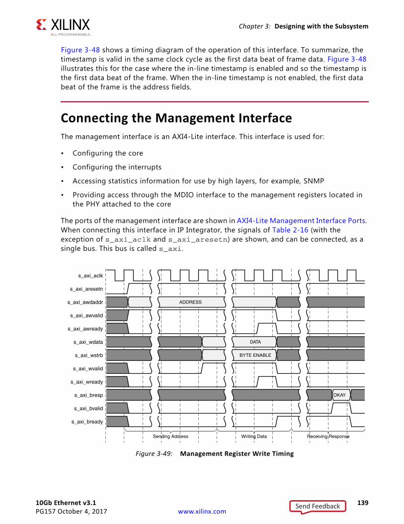
10Gb Ethernet v3.1 139PG157 October 4, 2017 www.xilinx.com
Chapter 3: Designing with the Subsystem
Figure 3-48 shows a timing diagram of the operation of this interface. To summarize, the timestamp is valid in the same clock cycle as the first data beat of frame data. Figure 3-48 illustrates this for the case where the in-line timestamp is enabled and so the timestamp is the first data beat of the frame. When the in-line timestamp is not enabled, the first data beat of the frame is the address fields.
Connecting the Management InterfaceThe management interface is an AXI4-Lite interface. This interface is used for:
• Configuring the core
• Configuring the interrupts
• Accessing statistics information for use by high layers, for example, SNMP
• Providing access through the MDIO interface to the management registers located in the PHY attached to the core
The ports of the management interface are shown in AXI4-Lite Management Interface Ports. When connecting this interface in IP Integrator, the signals of Table 2-16 (with the exception of s_axi_aclk and s_axi_aresetn) are shown, and can be connected, as a single bus. This bus is called s_axi.
X-Ref Target - Figure 3-49
Figure 3-49: Management Register Write Timing
Send Feedback
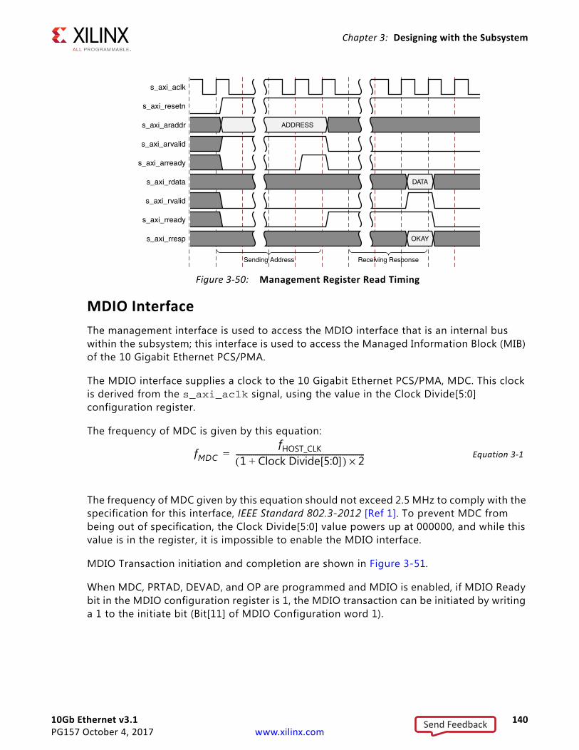
10Gb Ethernet v3.1 140PG157 October 4, 2017 www.xilinx.com
Chapter 3: Designing with the Subsystem
MDIO InterfaceThe management interface is used to access the MDIO interface that is an internal bus within the subsystem; this interface is used to access the Managed Information Block (MIB) of the 10 Gigabit Ethernet PCS/PMA.
The MDIO interface supplies a clock to the 10 Gigabit Ethernet PCS/PMA, MDC. This clock is derived from the s_axi_aclk signal, using the value in the Clock Divide[5:0] configuration register.
The frequency of MDC is given by this equation:
Equation 3-1
The frequency of MDC given by this equation should not exceed 2.5 MHz to comply with the specification for this interface, IEEE Standard 802.3-2012 [Ref 1]. To prevent MDC from being out of specification, the Clock Divide[5:0] value powers up at 000000, and while this value is in the register, it is impossible to enable the MDIO interface.
MDIO Transaction initiation and completion are shown in Figure 3-51.
When MDC, PRTAD, DEVAD, and OP are programmed and MDIO is enabled, if MDIO Ready bit in the MDIO configuration register is 1, the MDIO transaction can be initiated by writing a 1 to the initiate bit (Bit[11] of MDIO Configuration word 1).
X-Ref Target - Figure 3-50
Figure 3-50: Management Register Read Timing
fMDCfHOST_CLK
1 Clock Divide[5:0]+( ) 2×--------------------------------------------------------------------=
Send Feedback
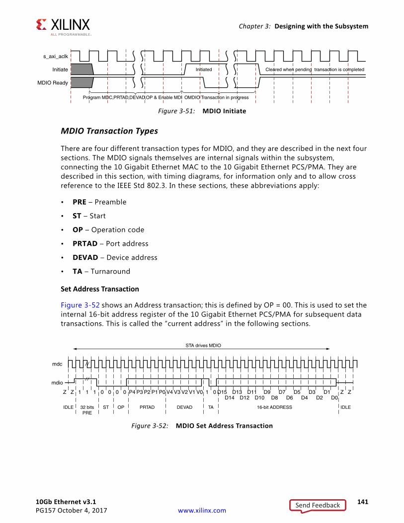
10Gb Ethernet v3.1 141PG157 October 4, 2017 www.xilinx.com
Chapter 3: Designing with the Subsystem
MDIO Transaction Types
There are four different transaction types for MDIO, and they are described in the next four sections. The MDIO signals themselves are internal signals within the subsystem, connecting the 10 Gigabit Ethernet MAC to the 10 Gigabit Ethernet PCS/PMA. They are described in this section, with timing diagrams, for information only and to allow cross reference to the IEEE Std 802.3. In these sections, these abbreviations apply:
• PRE – Preamble
• ST – Start
• OP – Operation code
• PRTAD – Port address
• DEVAD – Device address
• TA – Turnaround
Set Address Transaction
Figure 3-52 shows an Address transaction; this is defined by OP = 00. This is used to set the internal 16-bit address register of the 10 Gigabit Ethernet PCS/PMA for subsequent data transactions. This is called the “current address” in the following sections.
X-Ref Target - Figure 3-51
Figure 3-51: MDIO Initiate
X-Ref Target - Figure 3-52
Figure 3-52: MDIO Set Address Transaction
Send Feedback
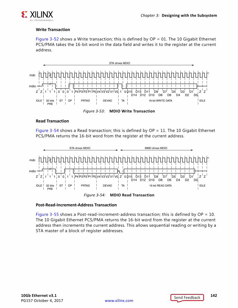
10Gb Ethernet v3.1 142PG157 October 4, 2017 www.xilinx.com
Chapter 3: Designing with the Subsystem
Write Transaction
Figure 3-52 shows a Write transaction; this is defined by OP = 01. The 10 Gigabit Ethernet PCS/PMA takes the 16-bit word in the data field and writes it to the register at the current address.
Read Transaction
Figure 3-54 shows a Read transaction; this is defined by OP = 11. The 10 Gigabit Ethernet PCS/PMA returns the 16-bit word from the register at the current address.
Post-Read-Increment-Address Transaction
Figure 3-55 shows a Post-read-increment-address transaction; this is defined by OP = 10. The 10 Gigabit Ethernet PCS/PMA returns the 16-bit word from the register at the current address then increments the current address. This allows sequential reading or writing by a STA master of a block of register addresses.
X-Ref Target - Figure 3-53
Figure 3-53: MDIO Write Transaction
X-Ref Target - Figure 3-54
Figure 3-54: MDIO Read Transaction
Send Feedback
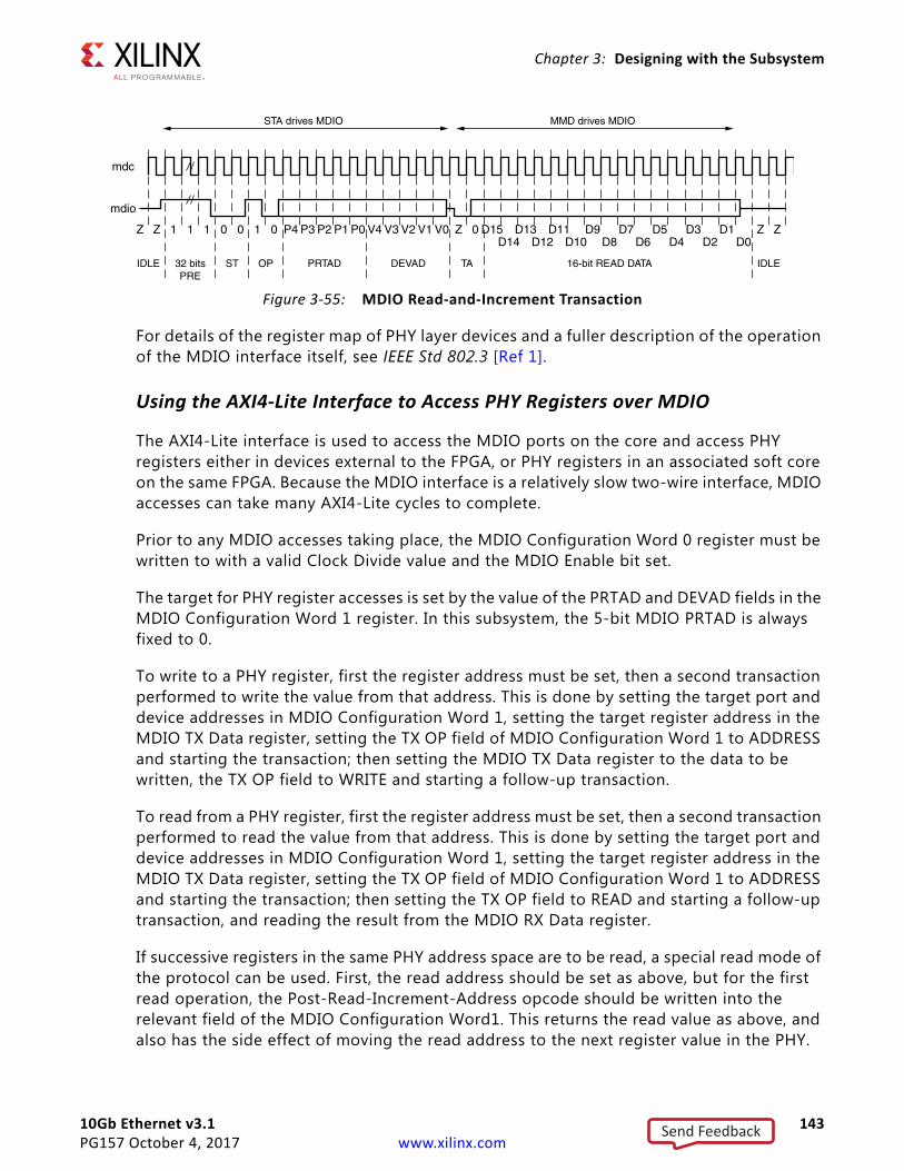
10Gb Ethernet v3.1 143PG157 October 4, 2017 www.xilinx.com
Chapter 3: Designing with the Subsystem
For details of the register map of PHY layer devices and a fuller description of the operation of the MDIO interface itself, see IEEE Std 802.3 [Ref 1].
Using the AXI4-Lite Interface to Access PHY Registers over MDIO
The AXI4-Lite interface is used to access the MDIO ports on the core and access PHY registers either in devices external to the FPGA, or PHY registers in an associated soft core on the same FPGA. Because the MDIO interface is a relatively slow two-wire interface, MDIO accesses can take many AXI4-Lite cycles to complete.
Prior to any MDIO accesses taking place, the MDIO Configuration Word 0 register must be written to with a valid Clock Divide value and the MDIO Enable bit set.
The target for PHY register accesses is set by the value of the PRTAD and DEVAD fields in the MDIO Configuration Word 1 register. In this subsystem, the 5-bit MDIO PRTAD is always fixed to 0.
To write to a PHY register, first the register address must be set, then a second transaction performed to write the value from that address. This is done by setting the target port and device addresses in MDIO Configuration Word 1, setting the target register address in the MDIO TX Data register, setting the TX OP field of MDIO Configuration Word 1 to ADDRESS and starting the transaction; then setting the MDIO TX Data register to the data to be written, the TX OP field to WRITE and starting a follow-up transaction.
To read from a PHY register, first the register address must be set, then a second transaction performed to read the value from that address. This is done by setting the target port and device addresses in MDIO Configuration Word 1, setting the target register address in the MDIO TX Data register, setting the TX OP field of MDIO Configuration Word 1 to ADDRESS and starting the transaction; then setting the TX OP field to READ and starting a follow-up transaction, and reading the result from the MDIO RX Data register.
If successive registers in the same PHY address space are to be read, a special read mode of the protocol can be used. First, the read address should be set as above, but for the first read operation, the Post-Read-Increment-Address opcode should be written into the relevant field of the MDIO Configuration Word1. This returns the read value as above, and also has the side effect of moving the read address to the next register value in the PHY.
X-Ref Target - Figure 3-55
Figure 3-55: MDIO Read-and-Increment Transaction
Send Feedback
10Gb Ethernet v3.1 144PG157 October 4, 2017 www.xilinx.com
Chapter 3: Designing with the Subsystem
Thus, repeating the same opcode sequentially returns data from consecutive register addresses in the PHY. Table 3-11 provides an example of a PHY register write using MDIO, to a 10GBASE-R PCS on port 0.
Table 3-12 provides an example of a PHY register read using MDIO, to a 10GBASE-R PCS on port 0.
PCS/PMA Configuration and Status Vectors
IEEE 802.3 Flow ControlThis section describes the operation of the flow control logic of the core. The flow control block is designed to clause 31 of the IEEE 802.3-2012 standard. The core can be configured to transmit pause requests and to act on their reception; these modes of operation can be independently enabled or disabled. See 10G Ethernet MAC Configuration Registers. If PFC functionality is included, the core should be configured for either IEEE 802.3 pause frames or PFC frames but not both as they are considered mutually exclusive modes of operation.
Table 3-11: Example of a PHY Register Write Transaction Using MDIO
Register Access Value Activity
MDIO TX Data Write 0x0000002A Address of 10GBASE-R test control register.
MDIO Configuration Word 1 Write 0x00030800 Initiate the Address transaction by setting theDEVAD (3), PRTAD (0), OP(00) and Initiate bit.
MDIO Configuration Word 1 Read 0x00030080 Poll bit 7 (MDIO Ready) until it becomes 1. The Initiate bit returns to 0.
MDIO TX Data Write 0x00000030 Turn on transmit and receive PRBS test pattern.
MDIO Configuration Word 1 Write 0x00034800 Initiate the Write transaction by setting theDEVAD (3), PRTAD (0), OP(01) and Initiate bit.
MDIO Configuration Word 1 Read 0x00054080 Initiate the Write transaction by setting theDEVAD (3), PRTAD (0), OP(01) and Initiate bit.
Table 3-12: Example of a PHY Register Read Transaction Using MDIO
Register Access Value Activity
MDIO TX Data Write 0x00000001 Address of PCS status 1 register.
MDIO Configuration Word 1 Write 0x00030800 Initiate the Address transaction by setting the DEVAD (3), PRTAD (0), OP(00) and Initiate bit.
MDIO Configuration Word 1 Read 0x00030080 Poll bit 7 (MDIO Ready) until it becomes 1. The Initiate bit returns to 0.
MDIO Configuration Word 1 Write 0x0003C800 Initiate the Read transaction by setting the DEVAD (5), PRTAD (0), OP(11) and Initiate bit.
MDIO Configuration Word 1 Read 0x0003C080 Poll bit 7 (MDIO Ready) until it becomes 1. The Initiate bit returns to 0.
MDIO RX Data Read 0x00000006 Read the status value back from the RX data register.
Send Feedback
10Gb Ethernet v3.1 145PG157 October 4, 2017 www.xilinx.com
Chapter 3: Designing with the Subsystem
Flow Control RequirementFigure 3-56 illustrates the requirement for Flow Control. The Ethernet MAC at the right side of the figure has a reference clock slightly faster than the standard frequency, and the Ethernet MAC at the left side of the figure has a reference clock slightly slower. This results in the Ethernet MAC on the left not being able to match the full line rate of the Ethernet MAC on the right (due to clock tolerances). The left MAC is shown in a loopback implementation, which results in the FIFO filling up over time. Without Flow Control, this FIFO eventually fills and overflows, resulting in the corruption or loss of Ethernet frames. Flow Control is one solution to this issue.
Flow Control BasicsA MAC can transmit a pause control frame to request that its link partner cease transmission for a defined period of time. For example, the Ethernet MAC at the left side of Figure 3-56 can initiate a pause request when its client FIFO (illustrated) reaches a nearly full state.
A MAC should respond to received pause control frames by ceasing transmission of frames for the period of time defined in the received pause control frame. For example, the Ethernet MAC at the right side of Figure 3-56 might cease transmission after receiving the pause control frame transmitted by the left-hand MAC. In a well designed system, the right MAC would cease transmission before the client FIFO of the left MAC overflowed. This provides time for the FIFO to be emptied to a safe level before normal operation resumes and safeguards the system against FIFO overflow conditions and frame loss.
X-Ref Target - Figure 3-56
Figure 3-56: Requirement for Flow Control
Send Feedback
10Gb Ethernet v3.1 146PG157 October 4, 2017 www.xilinx.com
Chapter 3: Designing with the Subsystem
IEEE 802.3 Pause Control FramesControl frames are a special type of Ethernet frame defined in clause 31 of the IEEE 802.3-2012 standard. Control frames are identified from other frame types by a defined value placed into the length/type field (the MAC Control Type code). Control frame format is illustrated in Figure 3-57.
A pause control frame is a special type of control frame, identified by a defined value placed into the MAC Control OPCODE field.
Note: MAC Control OPCODES other than for Pause (Flow Control) frames have recently been defined for Ethernet Passive Optical Networks.
The MAC Control Parameter field of the pause control frame contains a 16-bit field which contains a binary value directly relating to the duration of the pause. This defines the number of pause_quantum (512-bit times of the particular implementation). For 10 Gigabit Ethernet, a single pause_quantum corresponds to 51.2 ns.
Transmitting a Pause Control Frame
Core-Initiated Pause Request
If the core is configured to support transmit flow control, you can initiate a pause control frame by asserting the s_axis_pause_tvalid signal with the pause parameter set to the value on s_axis_pause_tdata in the cycle when s_axis_pause_tvalid was asserted. This does not disrupt any frame transmission in progress but does take priority over any pending frame transmission. This frame is transmitted even if the transmitter is in the paused state itself. Figure 3-58 displays this timing. The clock source for Figure 3-58 can be determined from the TX Clock Source column of Table 3-1.
X-Ref Target - Figure 3-57
Figure 3-57: MAC Control Frame Format
Send Feedback
10Gb Ethernet v3.1 147PG157 October 4, 2017 www.xilinx.com
Chapter 3: Designing with the Subsystem
This action causes the core to construct and transmit a pause control frame on the link with the MAC Control frame parameters (see Figure 3-57):
• The destination address used is an IEEE 802.3-2012 globally assigned multicast address (which any Flow Control capable MAC responds to).
• The source address used is the configurable Pause Frame MAC Address (see 10G Ethernet MAC Configuration Registers).
• The value sampled from the s_axis_pause_tdata[15:0] port at the time of the s_axis_pause_tvalid assertion is encoded into the MAC control parameter field to select the duration of the pause (in units of pause_quantum).
If the transmitter is currently inactive at the time of the pause request, then this pause control frame is transmitted immediately. If the transmitter is currently busy, the current frame being transmitted is allowed to complete; the pause control frame then follows in preference to any pending client supplied frame.
A pause control frame initiated by this method is transmitted even if the transmitter itself has ceased transmission in response to receiving an inbound pause request.
IMPORTANT: Only a single pause control frame request is stored by the transmitter. If the s_axis_pause_tvalid signal is asserted numerous times in a short time period (before the control pause frame transmission has had a chance to begin), then only a single pause control frame is transmitted. The pause_val[15:0] value used is the most recent value sampled.
XON/XOFF Extended Functionality
If the core has been generated with PFC functionality included but configured for IEEE 802.3 functionality then the core supports XON/XOFF functionality. If, as shown in Figure 3-59, the s_axis_pause_tvalid signal is asserted, the core generates a new pause frame. If it is subsequently held High for more than one clock cycle then the core automatically generates a new pause frame each time the internal quanta count of the core reaches the number of quanta, specified by the legacy refresh value (in either the register or the configuration vector). This is shown as an XOFF refresh frame in Figure 3-59. When the s_axis_pause_tvalid is deasserted, an XON frame (standard pause frame with the pause quanta forced to zero) is automatically generated if the auto XON feature is enabled; this functionality is shown in Figure 3-59. If auto XON is not enabled then the remaining quanta are left to expire naturally at the link partner.
X-Ref Target - Figure 3-58
Figure 3-58: Pause Request Timing
Send Feedback
10Gb Ethernet v3.1 148PG157 October 4, 2017 www.xilinx.com
Chapter 3: Designing with the Subsystem
Client-Initiated Pause Request
For maximum flexibility, flow control logic can be disabled in the core (see 10G Ethernet MAC Configuration Registers) and alternatively implemented in the client logic connected to the core. Any type of control frame can be transmitted through the core through the client interface using the same transmission procedure as a standard Ethernet frame (see Normal Frame Transmission).
IMPORTANT: To enable Auto XON after a single pause request ensure that the spacing between the two pause requests is at least equal to “End of current frame” + IFG + “Pause frame duration for the single pause”.
Receiving a Pause Control Frame
Core-Initiated Response to a Pause Request
An error-free control frame is a received frame matching the format of Figure 3-57. It must pass all standard receiver frame checks (for example, FCS field checking); in addition, the control frame received must be exactly 64 bytes in length (from destination address through to the FCS field inclusive: this is minimum legal Ethernet MAC frame size and the defined size for control frames) or the Control Frame length check disable bit must be set. See 10G Ethernet MAC Configuration Registers.
Any control frame received that does not conform to these checks contains an error, and it is passed to the receiver client with the m_axis_rx_tuser deasserted when m_axis_rx_tlast is asserted to indicate a bad frame.
• Pause Frame Reception Disabled
When pause control reception is disabled (see 10G Ethernet MAC Configuration Registers), an error free control frame is received through the client interface with the m_axis_rx_tuser asserted when m_axis_rx_tlast is asserted to indicate a good frame. In this way, the frame is passed to the client logic for interpretation (see Client-Initiated Response to a Pause Request).
• Pause Frame Reception Enabled
X-Ref Target - Figure 3-59
Figure 3-59: XON/XOFF Frame Transmission
Send Feedback
10Gb Ethernet v3.1 149PG157 October 4, 2017 www.xilinx.com
Chapter 3: Designing with the Subsystem
When pause control reception is enabled (see 10G Ethernet MAC Configuration Registers) and an error-free frame is received by the core, the frame decoding functions are performed:
a. The destination address field is matched against the IEEE 802.3-2012 globally assigned multicast address or the configurable Pause Frame MAC Address (see 10G Ethernet MAC Configuration Registers).
b. The length/type field is matched against the MAC Control Type code.
c. The opcode field contents are matched against the Pause opcode.
If any of these checks are false, the frame is ignored by the flow control logic and passed up to the client logic for interpretation by marking it with m_axis_rx_tuser asserted. It is then the responsibility of the MAC client logic to decode, act on (if required) and drop this control frame.
If all these checks are true, the 16-bit binary value in the MAC Control Parameters field of the control frame is then used to inhibit transmitter operation for the required number of pause_quantum. This inhibit is implemented by delaying the assertion of tx_ack at the transmitter client interface until the requested pause duration has expired. Because the received pause frame has been acted upon, it is passed to the client with m_axis_rx_tuser deasserted to indicate to the client that can now be dropped. The frame is still marked good in the statistics vector and counters.
IMPORTANT: Any frame in which the length/type field contains the MAC Control Type code should be dropped by the receiver client logic. All control frames are indicated by rx_statistic_vector bit 20 (see Receive Statistics Vector).
Client-Initiated Response to a Pause Request
For maximum flexibility, flow control logic can be disabled in the core (see 10G Ethernet MAC Configuration Registers) and alternatively implemented in the client logic connected to the core. Any type of error free control frame is then passed through the core with the m_axis_rx_tuser signal asserted. In this way, the frame is passed to the client for interpretation. It is then the responsibility of the client to drop this control frame and to act on it by ceasing transmission through the core, if applicable.
Flow Control Implementation ExampleThis explanation is intended to describe a simple (but crude) example of a Flow Control implementation to introduce the concept.
Consider the system illustrated in Figure 3-56. The Ethernet MAC on the left-hand side of the figure cannot match the full line rate of the right-hand Ethernet MAC due to clock tolerances. Over time, the FIFO illustrated fills and overflows. The aim is to implement a
Send Feedback
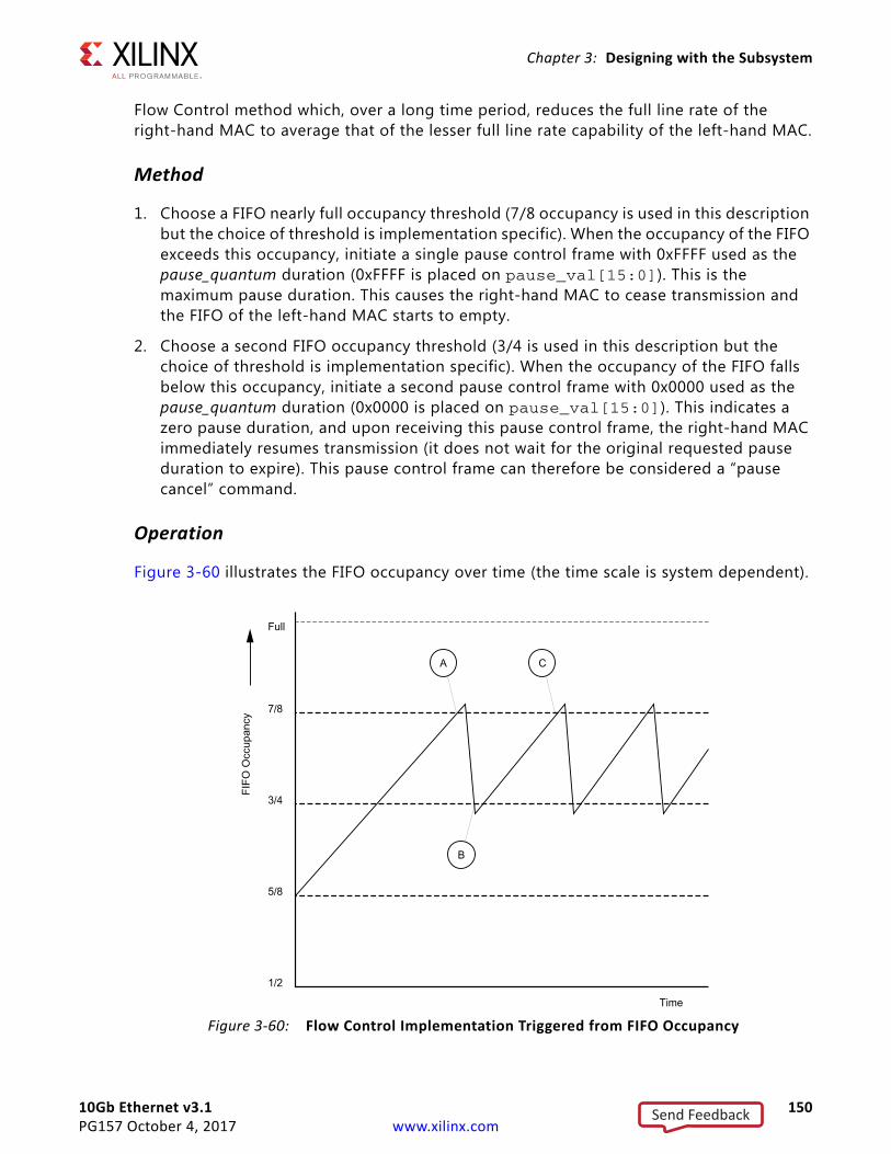
10Gb Ethernet v3.1 150PG157 October 4, 2017 www.xilinx.com
Chapter 3: Designing with the Subsystem
Flow Control method which, over a long time period, reduces the full line rate of the right-hand MAC to average that of the lesser full line rate capability of the left-hand MAC.
Method
1. Choose a FIFO nearly full occupancy threshold (7/8 occupancy is used in this description but the choice of threshold is implementation specific). When the occupancy of the FIFO exceeds this occupancy, initiate a single pause control frame with 0xFFFF used as the pause_quantum duration (0xFFFF is placed on pause_val[15:0]). This is the maximum pause duration. This causes the right-hand MAC to cease transmission and the FIFO of the left-hand MAC starts to empty.
2. Choose a second FIFO occupancy threshold (3/4 is used in this description but the choice of threshold is implementation specific). When the occupancy of the FIFO falls below this occupancy, initiate a second pause control frame with 0x0000 used as the pause_quantum duration (0x0000 is placed on pause_val[15:0]). This indicates a zero pause duration, and upon receiving this pause control frame, the right-hand MAC immediately resumes transmission (it does not wait for the original requested pause duration to expire). This pause control frame can therefore be considered a “pause cancel” command.
Operation
Figure 3-60 illustrates the FIFO occupancy over time (the time scale is system dependent).
X-Ref Target - Figure 3-60
Figure 3-60: Flow Control Implementation Triggered from FIFO Occupancy
Send Feedback
10Gb Ethernet v3.1 151PG157 October 4, 2017 www.xilinx.com
Chapter 3: Designing with the Subsystem
1. The average FIFO occupancy of the left-hand MAC gradually increases over time due to the clock tolerances. At point A, the occupancy has reached the threshold of 7/8 occupancy. This triggers the maximum duration pause control frame request.
2. Upon receiving the pause control frame, the right-hand MAC ceases transmission.
3. After the right-hand MAC ceases transmission, the occupancy of the FIFO attached to the left-hand MAC rapidly empties. The occupancy falls to the second threshold of 3/4 occupancy at point B. This triggers the zero duration pause control frame request (the pause cancel command).
4. Upon receiving this second pause control frame, the right-hand MAC resumes transmission.
5. Normal operation resumes and the FIFO occupancy again gradually increases over time. At point C, this cycle of Flow Control repeats.
Priority Flow ControlThis section describes the operation of the priority flow control logic of the core. Priority-based flow control is defined in the IEEE Standard 802.1Qbb [Ref 3]. The core can be configured to transmit and receive priority-based flow control requests; these modes of operation can be independently enabled or disabled. See 10G Ethernet MAC Configuration Registers. Operation of the MAC with both PFC and 802.3 flow control enabled is not supported as these modes of operation are mutually exclusive.
Priority Flow Control RequirementAs described in IEEE 802.3 Flow Control the basic requirement for flow control is to avoid dropping frames if a receiving port cannot process frames at the rate at which they are being provided. IEEE 802.3 pause frames operate on the entire link which is not ideal when there are multiple priority queues awaiting transmission with each queue originating from a separate FIFO. In this case the transmission of one or more specific queues (up to eight) can be inhibited using priority-based flow control with the eight frame priorities as defined by IEEE 802.1p. Figure 3-61 illustrates an implementation of two different priority queues.
Send Feedback
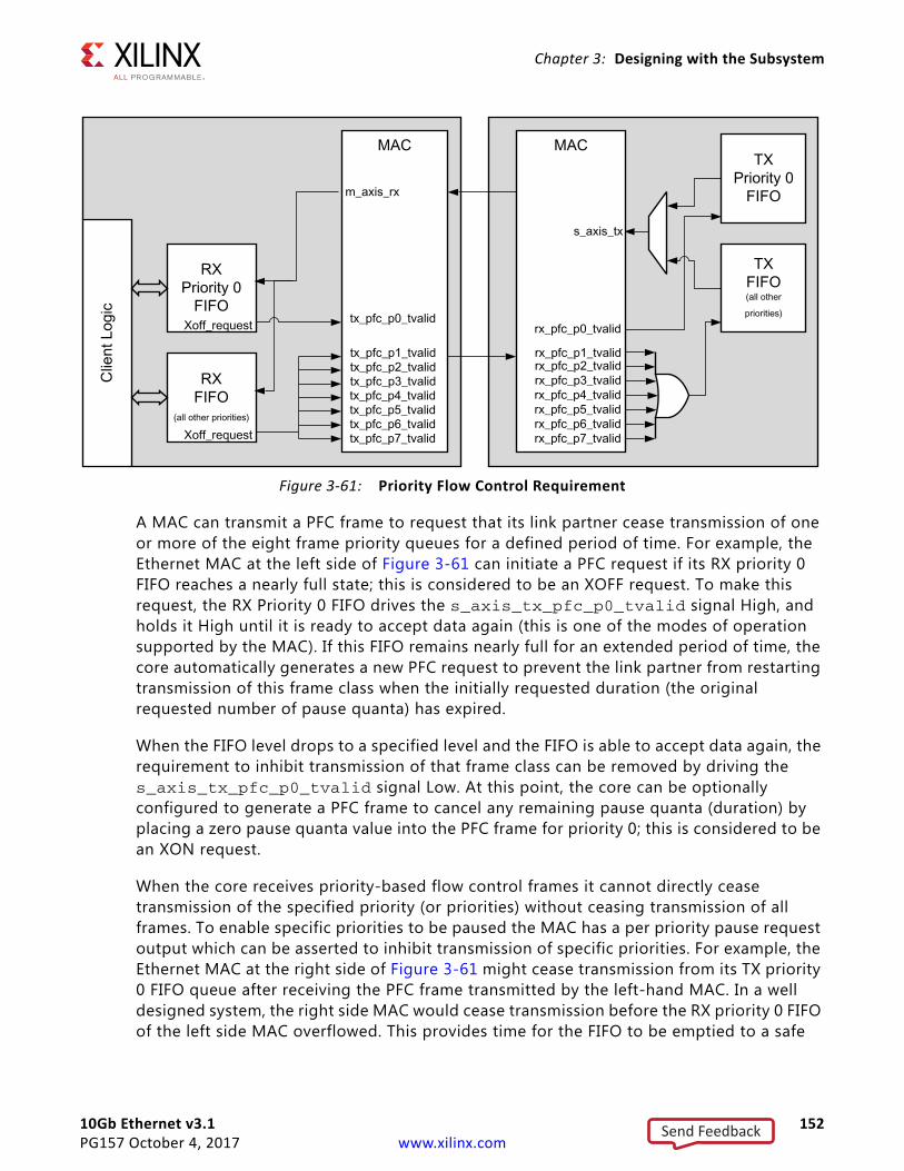
10Gb Ethernet v3.1 152PG157 October 4, 2017 www.xilinx.com
Chapter 3: Designing with the Subsystem
A MAC can transmit a PFC frame to request that its link partner cease transmission of one or more of the eight frame priority queues for a defined period of time. For example, the Ethernet MAC at the left side of Figure 3-61 can initiate a PFC request if its RX priority 0 FIFO reaches a nearly full state; this is considered to be an XOFF request. To make this request, the RX Priority 0 FIFO drives the s_axis_tx_pfc_p0_tvalid signal High, and holds it High until it is ready to accept data again (this is one of the modes of operation supported by the MAC). If this FIFO remains nearly full for an extended period of time, the core automatically generates a new PFC request to prevent the link partner from restarting transmission of this frame class when the initially requested duration (the original requested number of pause quanta) has expired.
When the FIFO level drops to a specified level and the FIFO is able to accept data again, the requirement to inhibit transmission of that frame class can be removed by driving the s_axis_tx_pfc_p0_tvalid signal Low. At this point, the core can be optionally configured to generate a PFC frame to cancel any remaining pause quanta (duration) by placing a zero pause quanta value into the PFC frame for priority 0; this is considered to be an XON request.
When the core receives priority-based flow control frames it cannot directly cease transmission of the specified priority (or priorities) without ceasing transmission of all frames. To enable specific priorities to be paused the MAC has a per priority pause request output which can be asserted to inhibit transmission of specific priorities. For example, the Ethernet MAC at the right side of Figure 3-61 might cease transmission from its TX priority 0 FIFO queue after receiving the PFC frame transmitted by the left-hand MAC. In a well designed system, the right side MAC would cease transmission before the RX priority 0 FIFO of the left side MAC overflowed. This provides time for the FIFO to be emptied to a safe
X-Ref Target - Figure 3-61
Figure 3-61: Priority Flow Control Requirement
Send Feedback
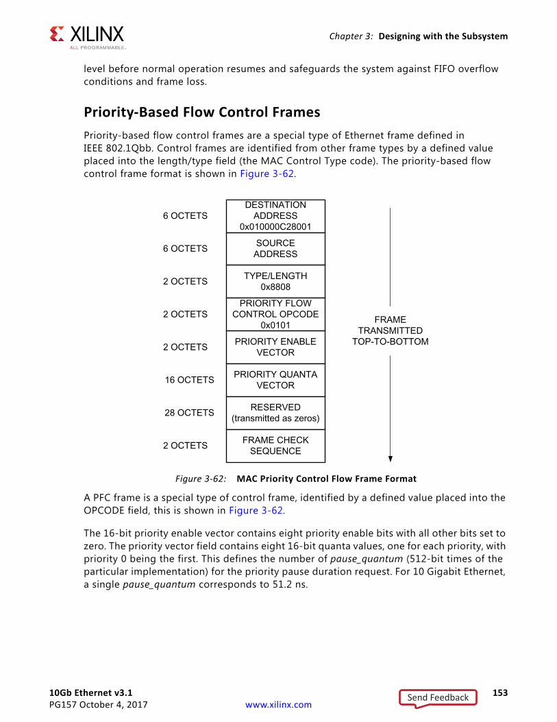
10Gb Ethernet v3.1 153PG157 October 4, 2017 www.xilinx.com
Chapter 3: Designing with the Subsystem
level before normal operation resumes and safeguards the system against FIFO overflow conditions and frame loss.
Priority-Based Flow Control FramesPriority-based flow control frames are a special type of Ethernet frame defined in IEEE 802.1Qbb. Control frames are identified from other frame types by a defined value placed into the length/type field (the MAC Control Type code). The priority-based flow control frame format is shown in Figure 3-62.
A PFC frame is a special type of control frame, identified by a defined value placed into the OPCODE field, this is shown in Figure 3-62.
The 16-bit priority enable vector contains eight priority enable bits with all other bits set to zero. The priority vector field contains eight 16-bit quanta values, one for each priority, with priority 0 being the first. This defines the number of pause_quantum (512-bit times of the particular implementation) for the priority pause duration request. For 10 Gigabit Ethernet, a single pause_quantum corresponds to 51.2 ns.
X-Ref Target - Figure 3-62
Figure 3-62: MAC Priority Control Flow Frame Format
Send Feedback
10Gb Ethernet v3.1 154PG157 October 4, 2017 www.xilinx.com
Chapter 3: Designing with the Subsystem
Transmitting a PFC Frame
Core-Initiated Request
There are three methods of generating a PFC frame, all of which assume that TX PFC is enabled and any actively used priority has the relevant TX priority enable set to 1.
1. Assert one or more of the eight s_axis_tx_pfc_p[0-7]_tvalid signals. If the s_axis_tx_pfc_p[0-7]_tvalid signal is asserted for more than a single cycle then this is considered to be an XOFF request and the MAC refreshes the relevant quanta at the link partner whenever a new PFC frame is transmitted until the s_axis_tx_pfc_p[0-7]_tvalid is deasserted. If s_axis_tx_pfc_p[0-7]_tvalid is asserted for a single cycle then it is assumed that any required refresh is directly controlled by a subsequent reassertion of the respective tvalid as required.
2. Hold a s_axis_tx_pfc_p[0-7]_tvalid signal High and the internal quanta count of the Ethernet MAC reaches the pre-programmed refresh value for that priority. On reaching this refresh value, the MAC “refreshes” the priority pause request by resending a new PFC frame with the pre-programmed pause value for the given priority. For each of the eight priorities, there is a configuration register that contains both the pause duration and the refresh value (see Table 2-44 in 10G Ethernet MAC Configuration Registers.)
3. Hold a s_axis_tx_pfc_p[0-7]_tvalid High for more than one cycle; then deassert this signal and the TX auto XON feature is enabled. This results in a new PFC frame with the relevant priorities quanta being both enabled and forced to zero. This is considered to be an XON request for that priority.
When any new PFC frame is transmitted it also resends the quanta for any currently active, enabled priority, effectively refreshing each priority quanta at the link partner. This also restarts the internal quanta count.
The eight s_axis_tx_pfc_p[0-7]_tvalid signals are synchronous to the TX Clock source as defined in Table 3-1. The various transmit methods can be seen in Figure 3-63. In Figure 3-63 the s_axis_tx_pfc_p0_tvalid is asserted and held High. This results in a PFC frame with only the P0 quanta enabled (set to 0xFFFF). A number of cycles later s_axis_tx_pfc_p2_tvalid is asserted for a single cycle and this results in a new PFC frame with both the P0 and P2 quantas enabled (and restarts the internal quanta count). The internal quanta count subsequently reaches the programmed refresh value for Priority 0 and a refresh PFC frame is sent with only the P0 quanta enabled (as all other tvalid requests are Low). s_axis_tx_pfc_p6_tvalid is asserted and held High and this also results in a new PFC frame (P6 XOFF), with both P0 and P6 quantas enabled. Finally in Figure 3-63, s_axis_tx_pfc_p0_tvalid is deasserted resulting in another PFC frame (P0 XON); this has both the P0 and P6 quantas enabled with the P0 quanta set to 0x0.
Send Feedback
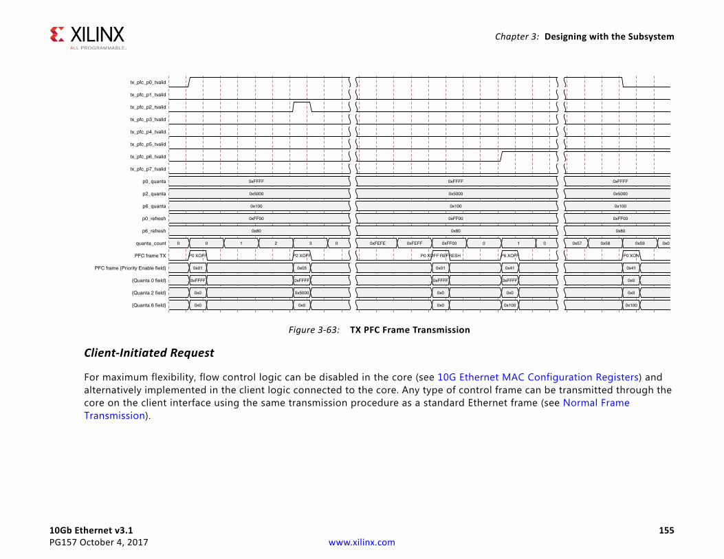
Chapter 3: Designing with the Subsystem
10Gb Ethernet v3.1 155PG157 October 4, 2017 www.xilinx.com
Client-Initiated Request
For maximum flexibility, flow control logic can be disabled in the core (see 10G Ethernet MAC Configuration Registers) and alternatively implemented in the client logic connected to the core. Any type of control frame can be transmitted through the core on the client interface using the same transmission procedure as a standard Ethernet frame (see Normal Frame Transmission).
X-Ref Target - Figure 3-63
Figure 3-63: TX PFC Frame Transmission
10Gb Ethernet v3.1 156PG157 October 4, 2017 www.xilinx.com
Chapter 3: Designing with the Subsystem
Receiving a PFC Frame
Core-Initiated Response to a PFC request
An error-free control frame is a received frame matching the format of Figure 3-62. It must pass all standard receiver frame checks (for example, FCS field checking); in addition, the control frame received must be exactly 64 bytes in length (from destination address through to the FCS field inclusive (this is the minimum legal Ethernet MAC frame size and the defined size for control frames) or the Control Frame Length Check Disable must be set.
Any control frame received that does not conform to these checks contains an error, and is passed to the receiver client with the m_axis_rx_tuser signal deasserted on the cycle that m_axis_rx_tlast is asserted.
PFC Frame Reception Disabled
When PFC reception is disabled (see 10G Ethernet MAC Configuration Registers), an error free control frame is received through the client interface with the m_axis_rx_tuser signal asserted. In this way, the frame is passed to the client logic for interpretation (see Client-Initiated Response to a Pause Request).
Pause Frame Reception Enabled
When pause control reception is enabled (see 10G Ethernet MAC Configuration Registers) and an error-free frame is received by the core, the frame decoding functions are performed:
• The destination address field is matched against the MAC control multicast address or the configured source address for the core (see 10G Ethernet MAC Configuration Registers).
• The length/type field is matched against the MAC Control type code, 88-08
• The opcode field contents are matched against the priority-based flow control opcode
If any of these checks are FALSE or the MAC receiver PFC is disabled, the frame is ignored by the PFC logic and passed up to the client.
If the frame passes all of these checks, is of minimum legal size, or the Control Frame Length Check Disable is set, and the MAC receiver PFC is enabled, then the priority enable field and per priority quanta values are extracted from the frame. If a particular priority is enabled in the frame with a non-zero pause quanta value, then the respective m_axis_rx_pfc_p[0-7]_tvalid output is asserted and the requested quanta value loaded into the control logic for that priority. This control logic consists of a counter which is loaded with the requested pause quanta value, and decrements down to zero. The m_axis_rx_pfc_p[0-7]_tvalid remains asserted while the local quanta counter is non zero. The local quanta counter does not start to decrement until
Send Feedback
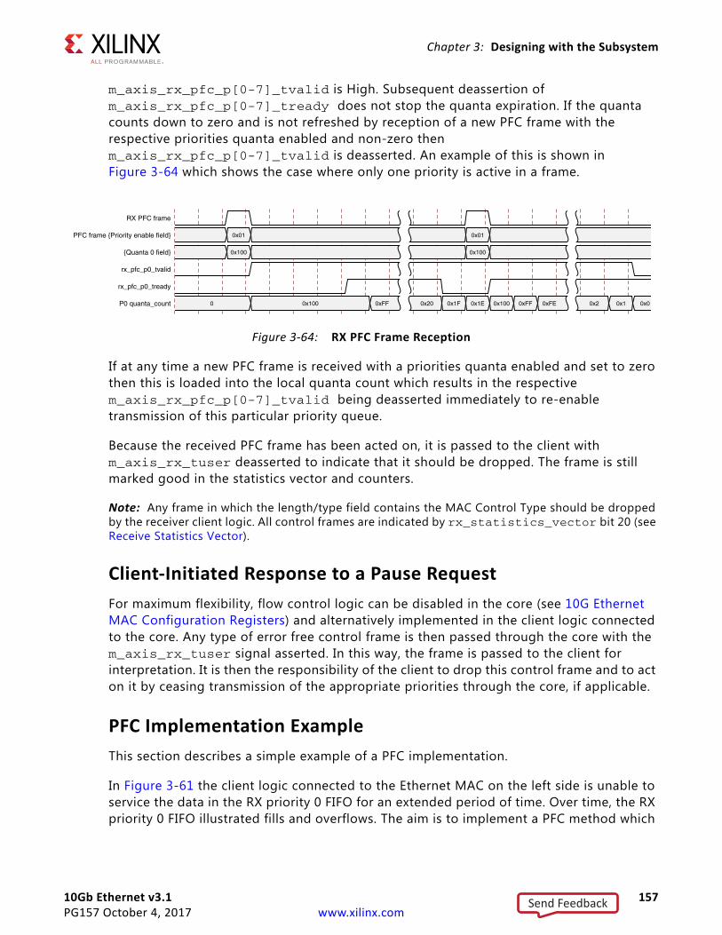
10Gb Ethernet v3.1 157PG157 October 4, 2017 www.xilinx.com
Chapter 3: Designing with the Subsystem
m_axis_rx_pfc_p[0-7]_tvalid is High. Subsequent deassertion of m_axis_rx_pfc_p[0-7]_tready does not stop the quanta expiration. If the quanta counts down to zero and is not refreshed by reception of a new PFC frame with the respective priorities quanta enabled and non-zero then m_axis_rx_pfc_p[0-7]_tvalid is deasserted. An example of this is shown in Figure 3-64 which shows the case where only one priority is active in a frame.
If at any time a new PFC frame is received with a priorities quanta enabled and set to zero then this is loaded into the local quanta count which results in the respective m_axis_rx_pfc_p[0-7]_tvalid being deasserted immediately to re-enable transmission of this particular priority queue.
Because the received PFC frame has been acted on, it is passed to the client with m_axis_rx_tuser deasserted to indicate that it should be dropped. The frame is still marked good in the statistics vector and counters.
Note: Any frame in which the length/type field contains the MAC Control Type should be dropped by the receiver client logic. All control frames are indicated by rx_statistics_vector bit 20 (see Receive Statistics Vector).
Client-Initiated Response to a Pause RequestFor maximum flexibility, flow control logic can be disabled in the core (see 10G Ethernet MAC Configuration Registers) and alternatively implemented in the client logic connected to the core. Any type of error free control frame is then passed through the core with the m_axis_rx_tuser signal asserted. In this way, the frame is passed to the client for interpretation. It is then the responsibility of the client to drop this control frame and to act on it by ceasing transmission of the appropriate priorities through the core, if applicable.
PFC Implementation ExampleThis section describes a simple example of a PFC implementation.
In Figure 3-61 the client logic connected to the Ethernet MAC on the left side is unable to service the data in the RX priority 0 FIFO for an extended period of time. Over time, the RX priority 0 FIFO illustrated fills and overflows. The aim is to implement a PFC method which
X-Ref Target - Figure 3-64
Figure 3-64: RX PFC Frame Reception
Send Feedback
10Gb Ethernet v3.1 158PG157 October 4, 2017 www.xilinx.com
Chapter 3: Designing with the Subsystem
applies back pressure on only the priority 0 traffic to ensure no frames are dropped while allowing the other priority queues to continue.
Method
1. Choose an RX priority 0 FIFO nearly-full occupancy threshold (7/8 occupancy is used in this example). When the FIFO exceeds this occupancy, assert the XOFF request signal to initiate a PFC frame with priority 0 enabled and 0xFFFF used as the priority 0 pause_quantum duration (0xFFFF is the default value of the priority 0 quanta register). This is the maximum pause duration. This causes the left-hand MAC to transmit a PFC frame, which in turn causes the right-hand MAC to assert its m_axis_rx_pfc_p0_tvalid to request that the TX priority 0 FIFO on the right-hand side stops transmission. If the client logic of the left-hand MAC continues to be unable to service the RX priority 0 FIFO then the left-hand Ethernet MAC automatically re-sends the PFC frame each time 0xFF00 quanta has expired (this is the default value of the priority 0 refresh), that is, before the previously sent quanta has expired.
2. Choose a second RX priority 0 FIFO occupancy threshold (3/4 is used in this example). When the occupancy of the FIFO falls below this occupancy, send an XON request by deasserting the s_axis_tx_pfc_p0_tvalid signal. If the TX auto XON feature is enabled this initiates a PFC frame with priority 0 enabled and the priority 0 quanta set to 0x0000. This indicates a zero pause duration (XON), and upon receiving this PFC frame, the right-hand MAC deasserts the m_axis_rx_pfc_p0_tvalid allowing the TX priority 0 FIFO on the right to resume transmission (it does not wait for the original requested quantum duration to expire). If the TX auto XON feature is not enabled then no PFC frame is sent and transmission does not restart until the requested quantum duration has expired.
Send Feedback
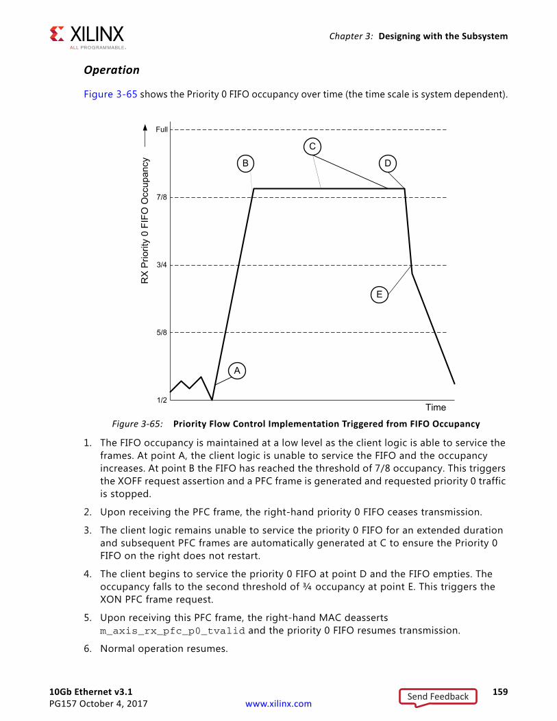
10Gb Ethernet v3.1 159PG157 October 4, 2017 www.xilinx.com
Chapter 3: Designing with the Subsystem
Operation
Figure 3-65 shows the Priority 0 FIFO occupancy over time (the time scale is system dependent).
1. The FIFO occupancy is maintained at a low level as the client logic is able to service the frames. At point A, the client logic is unable to service the FIFO and the occupancy increases. At point B the FIFO has reached the threshold of 7/8 occupancy. This triggers the XOFF request assertion and a PFC frame is generated and requested priority 0 traffic is stopped.
2. Upon receiving the PFC frame, the right-hand priority 0 FIFO ceases transmission.
3. The client logic remains unable to service the priority 0 FIFO for an extended duration and subsequent PFC frames are automatically generated at C to ensure the Priority 0 FIFO on the right does not restart.
4. The client begins to service the priority 0 FIFO at point D and the FIFO empties. The occupancy falls to the second threshold of ¾ occupancy at point E. This triggers the XON PFC frame request.
5. Upon receiving this PFC frame, the right-hand MAC deasserts m_axis_rx_pfc_p0_tvalid and the priority 0 FIFO resumes transmission.
6. Normal operation resumes.
X-Ref Target - Figure 3-65
Figure 3-65: Priority Flow Control Implementation Triggered from FIFO Occupancy
Send Feedback
10Gb Ethernet v3.1 160PG157 October 4, 2017 www.xilinx.com
Chapter 3: Designing with the Subsystem
Receiver TerminationThe receiver termination for all devices must be set correctly. See the 7 Series Transceivers User Guide (UG476) [Ref 11]. For UltraScale architecture, see the UltraScale Architecture GTH Transceivers User Guide (UG576) [Ref 12].
Special Design ConsiderationsThis section describes considerations that can apply in particular design cases.
Connecting Multiple Subsystem Instances (No IEEE 1588 Support)The example design provided with the subsystem shows the use of a single subsystem but it is possible to use this and the support layer code to create a design with multiple instances of the subsystem. Use of the support layer simplifies the integration of multiple subsystems. Inside the support layer, it is possible to replicate the block (subsystem) level instances, which each include their subsystem-specific transceiver, clock and reset logic. It is possible to share the rest of the logic in the support layer between multiple subsystems.
The GT Common block can be used to supply the reference clock to up to four transceivers, depending on their relative placements. The shared clock and reset block can be similarly shared between multiple subsystems. Where multiple subsystems are to share that block, only one txoutclk signal needs to be connected from a single subsystem instance to that shared clock and reset block. The txoutclk outputs from the other subsystems can be left dangling.
IMPORTANT: The information about sharing txoutclk is applicable for 7 series 10GBASE-R/KR cores and UltraScale 10GBASE-R cores. However, for an UltraScale 10GBASE-KR core, each core should use its own txoutclk. In the UltraScale 10GBASE-KR core the frequency of txoutclk changes. The GT is initially configured to have the asynchronous gearbox disabled and txoutclk set to 161 MHz for the 64-bit interface and 322 MHz for the 32-bit interface. After link training and auto-negotiation is completed the frequency of txoutclk is set to 156 MHz for the 64-bit interface and 312 MHz for the 32-bit interface. Therefore txoutclk cannot be shared for UltraScale 10GBASE-KR cores.
When creating a design with multiple subsystem instances, you need to take care to replicate the correct items and not to replicate items which should be shared. There is logic in the support layer which combines the synchronized TX and RX resetdone signals to create a single resetdone signal. When multiple instances of the subsystem are required, the synchronized TX and RX resetdone signals from each subsystem should be included in this combined signal.
Send Feedback
10Gb Ethernet v3.1 161PG157 October 4, 2017 www.xilinx.com
Chapter 3: Designing with the Subsystem
The subsystem PMA reset issues gttxreset and gtrxreset signals to the transceivers. The gttxreset to the transceiver results in txresetdone going Low and the txoutclk output from the transceiver being lost. This affects all subsystems that have a shared txoutclk.
Zynq-7000, Virtex-7, and Kintex-7 Devices
Where multiple subsystems are required, you should generate one subsystem with Include Shared Logic in core selected, and up to three further subsystem (to share a GT Quad) with the Include Shared Logic in example design selected.
The Include Shared Logic in core instance, named axi_10g_ethernet_0 in Figure 3-66, can then be used to provide the clocks and control signals required by the other subsystem instances (axi_10g_ethernet_1 and axi_10g_ethernet_2 in Figure 3-66).
Figure 3-66 is a screenshot taken from the Vivado IP integrator tool and shows the shared logic connectivity between three subsystems when using GTHE2 7 series transceivers.
Send Feedback
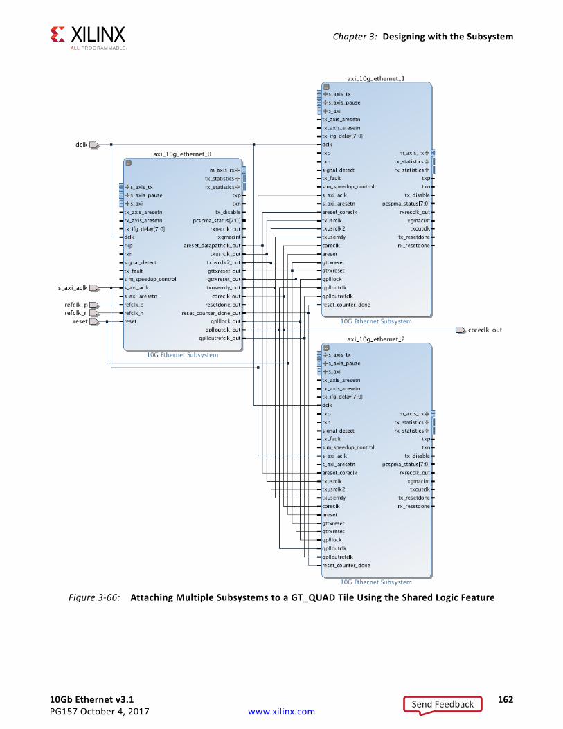
10Gb Ethernet v3.1 162PG157 October 4, 2017 www.xilinx.com
Chapter 3: Designing with the Subsystem
X-Ref Target - Figure 3-66
Figure 3-66: Attaching Multiple Subsystems to a GT_QUAD Tile Using the Shared Logic Feature
Send Feedback
10Gb Ethernet v3.1 163PG157 October 4, 2017 www.xilinx.com
Chapter 3: Designing with the Subsystem
UltraScale Devices
Where multiple subsystems are required, you should generate one subsystem with Include Shared Logic in core selected, and up to three further subsystem (to share a GT Quad) with the Include Shared Logic in example design selected.
The Include Shared Logic in core instance, named axi_10g_ethernet_0 in Figure 3-67, can then be used to provide the clocks and control signals required by the other subsystem instances (axi_10g_ethernet_1 and axi_10g_ethernet_2 in Figure 3-67).
Figure 3-67 is a screenshot taken from the Vivado IP integrator tool and shows the shared logic connectivity between three subsystems when using GTHE3 UltraScale transceivers.
Send Feedback
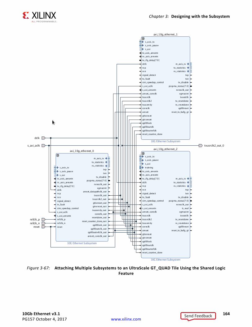
10Gb Ethernet v3.1 164PG157 October 4, 2017 www.xilinx.com
Chapter 3: Designing with the Subsystem
X-Ref Target - Figure 3-67
Figure 3-67: Attaching Multiple Subsystems to an UltraScale GT_QUAD Tile Using the Shared Logic Feature
Send Feedback

10Gb Ethernet v3.1 165PG157 October 4, 2017 www.xilinx.com
Chapter 3: Designing with the Subsystem
Using Training and Auto-Negotiation with the Management InterfaceThis section applies to Virtex®-7 and UltraScale™ devices.
When a Base KR subsystem is created with the optional Management interface and with the optional AutoNegotiation block, there are extra steps that you must take when bringing the subsystem up in a link.
Firstly you need to write to the MDIO registers to disable Training (register bit 1.150.1), and then set the Training Restart bit (register bit 1.150.0, which will self-clear).
Then you need to monitor either the core_status[5] output from the subsystem, or register bit 7.1.2 (which latches Low and clears on read), to wait for the AN Link Up indication which is set in the AN_GOOD_CHECK state. Now you need to Enable Training (1.150.1) and then immediately Restart Training (1.150.0).
Training must complete within 500 ms in order for Auto-Negotiation to also complete and set AN Complete. The Training block automatically disables itself if it does get to the Training Done state.
RECOMMENDED: Xilinx recommends setting the Training Done bit – register bit 1.65520.15. This means that the subsystem will not attempt to train the far-end device but can still be trained by the far-end device.
If Training does not complete within the time allowed by AutoNegotiation, then you must manually disable Training (register 1.150.1) and restart Training (1.150.0) to allow AutoNegotiation to restart the process.
Using Training and Auto-Negotiation with No Management Interface This section applies to Virtex-7 devices and UltraScale architecture.
When a Base KR subsystem is created with no Management interface, logic in the block level can be used to control the interaction between Auto-Negotiation and Training.
When Auto-Negotiation is not included with the subsystem, or when it is present and it reaches AN Link Up, the Training block is automatically enabled (if the Configuration vector bit 33 to enable Training is also set) and restarted. If Auto-Negotiation needs to restart, Training is automatically disabled until Auto-Negotiation again reaches AN Link Up.
If Training is disabled using the Configuration vector bit 33, Training will never be run. If Auto-Negotiation is either not included with the subsystem, or is disabled by Configuration vector bit 284, Training can still be used by programming the Configuration bits to drive the process.
Send Feedback
10Gb Ethernet v3.1 166PG157 October 4, 2017 www.xilinx.com
Chapter 3: Designing with the Subsystem
Using FEC in the Subsystem with Auto-NegotiationIMPORTANT: When the FEC feature is recognized in the AutoNegotiation Advertisement (Base Page Ability) data from another 10GBaseKR device, and FEC is requested by the far end, FEC in the subsystem will not be automatically enabled. It is up to you to enable FEC as required.
The FEC Request bit is in register bit 7.21.15, or on status vector bit 383 if there is no MDIO interface.
Using FIFOs in IP IntegratorIn IP integrator, the AXI4-Stream Data FIFO IP core connected to the Ethernet AXI4-Stream TX port needs to have the Enable Packet Mode option checked in the Vivado IDE. This generates the FIFO in packet store-forward mode, so it stores an entire packet before starting to transmit it, ensuring that the FIFO does not run empty part way through the packet transmission. When used in this option, the AXI FIFO must be in synchronous mode, so it cannot be used to cross a clock domain. If you need to cross a clock domain, instantiate two AXI4-Stream Data FIFO IP cores back to back (the first to cross the clock domain, the second to operate in packet mode).
On the RX side, in IP integrator, if you add an AXI4-Stream Data FIFO IP core it does not remove bad packets. To have the facility to remove bad packets, use the example design FIFO provided with the subsystem instead. This FIFO is store forward and can handle different clock domains in a single FIFO, and bad packets will also be dropped on the RX path.
Send Feedback
10Gb Ethernet v3.1 167PG157 October 4, 2017 www.xilinx.com
Chapter 4
Design Flow StepsThis chapter describes customizing and generating the subsystem, constraining the subsystem, and the simulation, synthesis and implementation steps that are specific to this subsystem. More detailed information about the standard Vivado® design flows and the IP integrator can be found in the following Vivado Design Suite user guides:
• Vivado Design Suite User Guide: Designing IP Subsystems using IP Integrator (UG994) [Ref 4]
• Vivado Design Suite User Guide: Designing with IP (UG896) [Ref 5]
• Vivado Design Suite User Guide: Getting Started (UG910) [Ref 6]
• Vivado Design Suite User Guide: Logic Simulation (UG900) [Ref 7]
Customizing and Generating the SubsystemThis section includes information about using the Vivado® Design Suite to customize and generate the subsystem.
If you are customizing and generating the subsystem in the Vivado IP integrator, see the Vivado Design Suite User Guide: Designing IP Subsystems using IP Integrator (UG994) [Ref 4] for detailed information. IP integrator might auto-compute certain configuration values when validating or generating the design. To check whether the values do change, see the description of the parameter in this chapter. To view the parameter value you can run the validate_bd_design command in the Tcl console.
You can customize the IP for use in your design by specifying values for the various parameters associated with the subsystem using the following steps:
1. Select the IP from the IP catalog.
2. Double-click the selected IP, or select the Customize IP command from the toolbar or right-click menu.
For details, see the Vivado Design Suite User Guide: Designing with IP (UG896) [Ref 5] and the Vivado Design Suite User Guide: Getting Started (UG910)[Ref 6].
Note: Figures in this chapter are illustrations of the Vivado Integrated Design Environment (IDE). This layout might vary from the current version.
Send Feedback
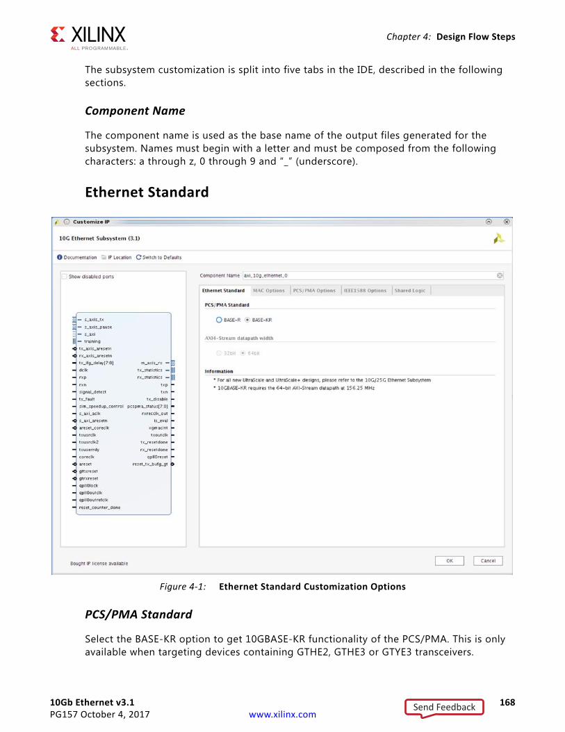
10Gb Ethernet v3.1 168PG157 October 4, 2017 www.xilinx.com
Chapter 4: Design Flow Steps
The subsystem customization is split into five tabs in the IDE, described in the following sections.
Component Name
The component name is used as the base name of the output files generated for the subsystem. Names must begin with a letter and must be composed from the following characters: a through z, 0 through 9 and “_” (underscore).
Ethernet Standard
PCS/PMA Standard
Select the BASE-KR option to get 10GBASE-KR functionality of the PCS/PMA. This is only available when targeting devices containing GTHE2, GTHE3 or GTYE3 transceivers.
X-Ref Target - Figure 4-1
Figure 4-1: Ethernet Standard Customization Options
Send Feedback
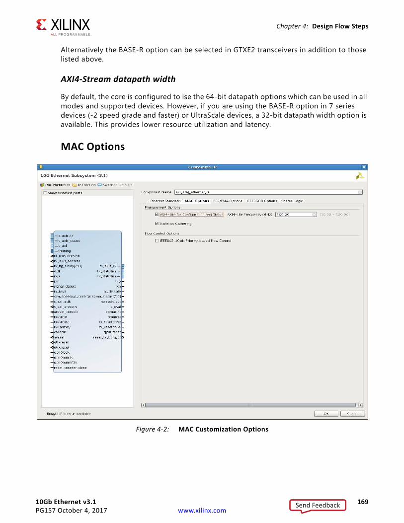
10Gb Ethernet v3.1 169PG157 October 4, 2017 www.xilinx.com
Chapter 4: Design Flow Steps
Alternatively the BASE-R option can be selected in GTXE2 transceivers in addition to those listed above.
AXI4-Stream datapath width
By default, the core is configured to ise the 64-bit datapath options which can be used in all modes and supported devices. However, if you are using the BASE-R option in 7 series devices (-2 speed grade and faster) or UltraScale devices, a 32-bit datapath width option is available. This provides lower resource utilization and latency.
MAC OptionsX-Ref Target - Figure 4-2
Figure 4-2: MAC Customization Options
Send Feedback
10Gb Ethernet v3.1 170PG157 October 4, 2017 www.xilinx.com
Chapter 4: Design Flow Steps
AXI4-Lite for Configuration and Status
Select this option to include the AXI4-Lite Management interface in the generated subsystem. The PCS/PMA is then configured through MDIO interface. Deselect this option to remove the Management Interface and expose simple bit vectors to manage the MAC and PCS/PMA. The default is to have the AXI4-Lite interface included.
AXI4-Lite Frequency (MHz)This specifies the frequency (in MHz) of the AXI4-Lite interface. This is used to provide a default frequency value for out-of-context synthesis.
Statistics Gathering
This checkbox selects whether the statistics counters are included in the generated subsystem. This option is only available if the AXI4-Lite interface option is selected. The default is to have statistics counters included.
IEEE802.1Qbb Priority-based Flow Control
Select this option to include Priority Flow control support in the subsystem. When included, circuitry to generate PFC frames on transmit and interpret PFC frame on receive is included as well as enhanced XON/XOFF support for IEEE 802.3 pause requests. The default is for this to be disabled.
Send Feedback
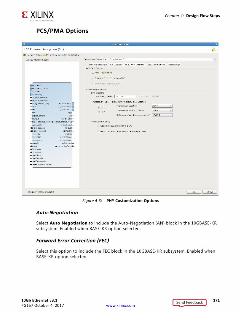
10Gb Ethernet v3.1 171PG157 October 4, 2017 www.xilinx.com
Chapter 4: Design Flow Steps
PCS/PMA Options
Auto-Negotiation
Select Auto Negotiation to include the Auto-Negotiation (AN) block in the 10GBASE-KR subsystem. Enabled when BASE-KR option selected.
Forward Error Correction (FEC)
Select this option to include the FEC block in the 10GBASE-KR subsystem. Enabled when BASE-KR option selected.
X-Ref Target - Figure 4-3
Figure 4-3: PHY Customization Options
Send Feedback
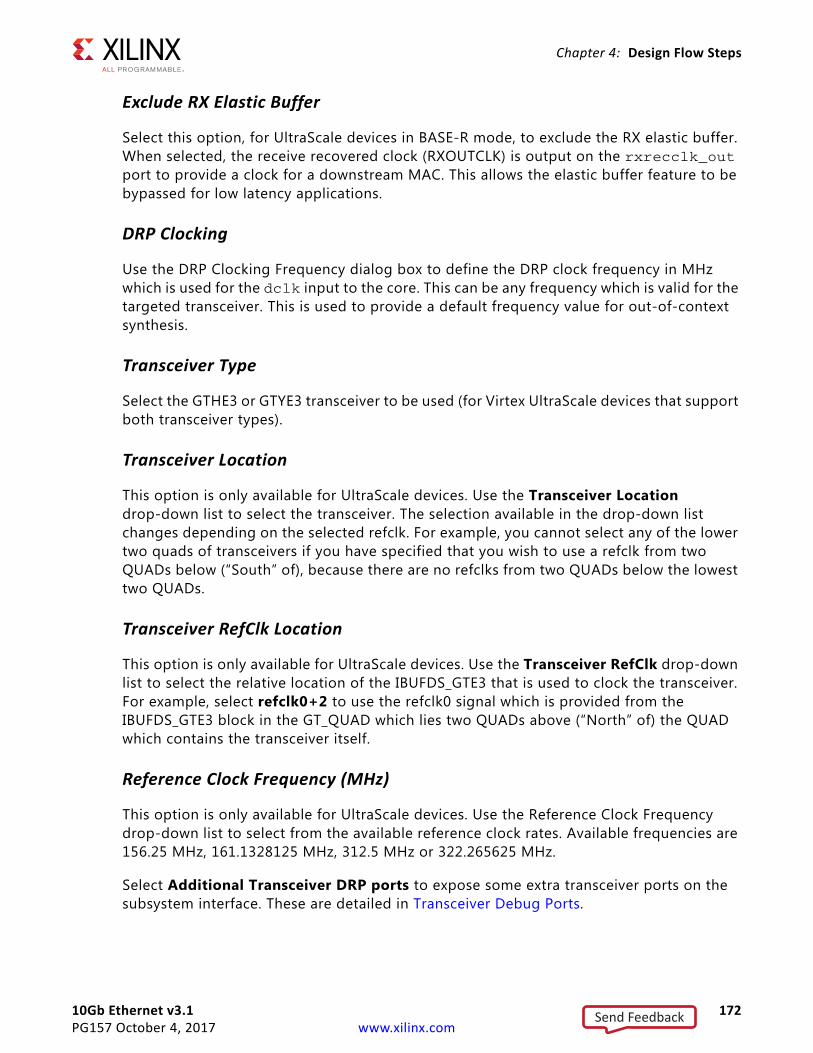
10Gb Ethernet v3.1 172PG157 October 4, 2017 www.xilinx.com
Chapter 4: Design Flow Steps
Exclude RX Elastic Buffer
Select this option, for UltraScale devices in BASE-R mode, to exclude the RX elastic buffer. When selected, the receive recovered clock (RXOUTCLK) is output on the rxrecclk_out port to provide a clock for a downstream MAC. This allows the elastic buffer feature to be bypassed for low latency applications.
DRP Clocking
Use the DRP Clocking Frequency dialog box to define the DRP clock frequency in MHz which is used for the dclk input to the core. This can be any frequency which is valid for the targeted transceiver. This is used to provide a default frequency value for out-of-context synthesis.
Transceiver Type
Select the GTHE3 or GTYE3 transceiver to be used (for Virtex UltraScale devices that support both transceiver types).
Transceiver Location
This option is only available for UltraScale devices. Use the Transceiver Location drop-down list to select the transceiver. The selection available in the drop-down list changes depending on the selected refclk. For example, you cannot select any of the lower two quads of transceivers if you have specified that you wish to use a refclk from two QUADs below (“South” of), because there are no refclks from two QUADs below the lowest two QUADs.
Transceiver RefClk Location
This option is only available for UltraScale devices. Use the Transceiver RefClk drop-down list to select the relative location of the IBUFDS_GTE3 that is used to clock the transceiver. For example, select refclk0+2 to use the refclk0 signal which is provided from the IBUFDS_GTE3 block in the GT_QUAD which lies two QUADs above (“North” of) the QUAD which contains the transceiver itself.
Reference Clock Frequency (MHz)
This option is only available for UltraScale devices. Use the Reference Clock Frequency drop-down list to select from the available reference clock rates. Available frequencies are 156.25 MHz, 161.1328125 MHz, 312.5 MHz or 322.265625 MHz.
Select Additional Transceiver DRP ports to expose some extra transceiver ports on the subsystem interface. These are detailed in Transceiver Debug Ports.
Send Feedback
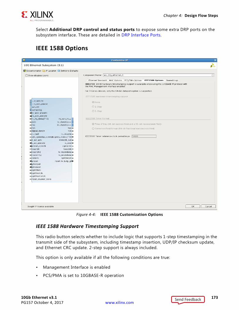
10Gb Ethernet v3.1 173PG157 October 4, 2017 www.xilinx.com
Chapter 4: Design Flow Steps
Select Additional DRP control and status ports to expose some extra DRP ports on the subsystem interface. These are detailed in DRP Interface Ports.
IEEE 1588 Options
IEEE 1588 Hardware Timestamping Support
This radio button selects whether to include logic that supports 1-step timestamping in the transmit side of the subsystem, including timestamp insertion, UDP/IP checksum update, and Ethernet CRC update. 2-step support is always included.
This option is only available if all the following conditions are true:
• Management Interface is enabled
• PCS/PMA is set to 10GBASE-R operation
X-Ref Target - Figure 4-4
Figure 4-4: IEEE 1588 Customization Options
Send Feedback
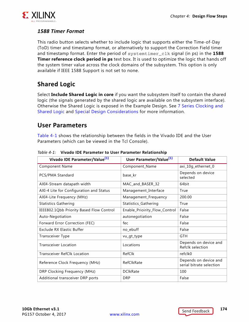
10Gb Ethernet v3.1 174PG157 October 4, 2017 www.xilinx.com
Chapter 4: Design Flow Steps
1588 Timer Format
This radio button selects whether to include logic that supports either the Time-of-Day (ToD) timer and timestamp format, or alternatively to support the Correction Field timer and timestamp format. Enter the period of systemtimer_clk signal (in ps) in the 1588 Timer reference clock period in ps text box. It is used to optimize the logic that hands off the system timer value across the clock domains of the subsystem. This option is only available if IEEE 1588 Support is not set to none.
Shared LogicSelect Include Shared Logic in core if you want the subsystem itself to contain the shared logic (the signals generated by the shared logic are available on the subsystem interface). Otherwise the Shared Logic is exposed in the Example Design. See 7 Series Clocking and Shared Logic and Special Design Considerations for more information.
User ParametersTable 4-1 shows the relationship between the fields in the Vivado IDE and the User Parameters (which can be viewed in the Tcl Console).
Table 4-1: Vivado IDE Parameter to User Parameter RelationshipVivado IDE Parameter/Value(1) User Parameter/Value(1) Default Value
Component Name Component_Name axi_10g_ethernet_0
PCS/PMA Standard base_kr Depends on device selected
AXI4-Stream datapath width MAC_and_BASER_32 64bit
AXI-4 Lite for Configuration and Status Management_Interface True
AXI4-Lite Frequency (MHz) Management_Frequency 200.00
Statistics Gathering Statistics_Gathering True
IEEE802.1Qbb Priority Based Flow Control Enable_Prioirity_Flow_Control False
Auto-Negotiation autonegotiation False
Forward Error Correction (FEC) fec False
Exclude RX Elastic Buffer no_ebuff False
Transceiver Type vu_gt_type GTH
Transceiver Location Locations Depends on device and Refclk selection
Transceiver RefClk Location RefClk refclk0
Reference Clock Frequency (MHz) RefClkRate Depends on device and serial bitrate selection
DRP Clocking Frequency (MHz) DClkRate 100
Additional transceiver DRP ports DRP False
Send Feedback
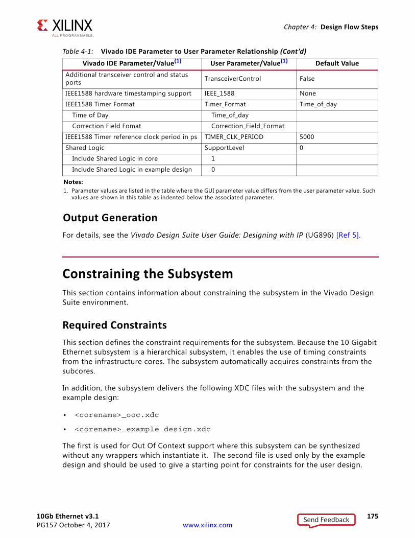
10Gb Ethernet v3.1 175PG157 October 4, 2017 www.xilinx.com
Chapter 4: Design Flow Steps
Output GenerationFor details, see the Vivado Design Suite User Guide: Designing with IP (UG896) [Ref 5].
Constraining the SubsystemThis section contains information about constraining the subsystem in the Vivado Design Suite environment.
Required ConstraintsThis section defines the constraint requirements for the subsystem. Because the 10 Gigabit Ethernet subsystem is a hierarchical subsystem, it enables the use of timing constraints from the infrastructure cores. The subsystem automatically acquires constraints from the subcores.
In addition, the subsystem delivers the following XDC files with the subsystem and the example design:
• <corename>_ooc.xdc
• <corename>_example_design.xdc
The first is used for Out Of Context support where this subsystem can be synthesized without any wrappers which instantiate it. The second file is used only by the example design and should be used to give a starting point for constraints for the user design.
Additional transceiver control and status ports TransceiverControl False
IEEE1588 hardware timestamping support IEEE_1588 None
IEEE1588 Timer Format Timer_Format Time_of_day
Time of Day Time_of_day
Correction Field Fomat Correction_Field_Format
IEEE1588 Timer reference clock period in ps TIMER_CLK_PERIOD 5000
Shared Logic SupportLevel 0
Include Shared Logic in core 1
Include Shared Logic in example design 0
Notes: 1. Parameter values are listed in the table where the GUI parameter value differs from the user parameter value. Such
values are shown in this table as indented below the associated parameter.
Table 4-1: Vivado IDE Parameter to User Parameter Relationship (Cont’d)
Vivado IDE Parameter/Value(1) User Parameter/Value(1) Default Value
Send Feedback
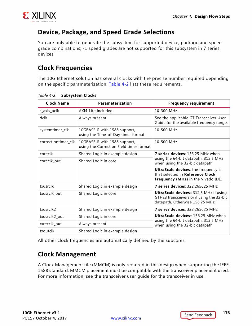
10Gb Ethernet v3.1 176PG157 October 4, 2017 www.xilinx.com
Chapter 4: Design Flow Steps
Device, Package, and Speed Grade SelectionsYou are only able to generate the subsystem for supported device, package and speed grade combinations; -1 speed grades are not supported for this subsystem in 7 series devices.
Clock FrequenciesThe 10G Ethernet solution has several clocks with the precise number required depending on the specific parameterization. Table 4-2 lists these requirements.
All other clock frequencies are automatically defined by the subcores.
Clock ManagementA Clock Management tile (MMCM) is only required in this design when supporting the IEEE 1588 standard. MMCM placement must be compatible with the transceiver placement used. For more information, see the transceiver user guide for the transceiver in use.
Table 4-2: Subsystem Clocks
Clock Name Parameterization Frequency requirement
s_axis_aclk AXI4-Lite included 10-300 MHz
dclk Always present See the applicable GT Transceiver User Guide for the available frequency range.
systemtimer_clk 10GBASE-R with 1588 support, using the Time-of-Day timer format
10-500 MHz
correctiontimer_clk 10GBASE-R with 1588 support, using the Correction Field timer format
10-500 MHz
coreclk Shared Logic in example design 7 series devices: 156.25 MHz when using the 64-bit datapath; 312.5 MHz when using the 32-bit datapath.
UltraScale devices: the frequency is that selected in Reference Clock Frequency (MHz) in the Vivado IDE.
coreclk_out Shared Logic in core
txusrclk Shared Logic in example design 7 series devices: 322.265625 MHz
UltraScale devices:: 312.5 MHz if using GTHE3 transceivers or if using the 32-bit datapath. Otherwise 156.25 MHz
txusrclk_out Shared Logic in core
txusrclk2 Shared Logic in example design 7 series devices: 322.265625 MHz
UltraScale devices:: 156.25 MHz when using the 64-bit datapath; 312.5 MHz when using the 32-bit datapath.
txusrclk2_out Shared Logic in core
rxrecclk_out Always present
txoutclk Shared Logic in example design
Send Feedback
10Gb Ethernet v3.1 177PG157 October 4, 2017 www.xilinx.com
Chapter 4: Design Flow Steps
Clock PlacementReference clock placement must be compatible with the transceiver placement used. For more information, see the transceiver user guide for the transceiver in use.
BankingThis section is not applicable for this subsystem.
Transceiver PlacementTransceivers should be given location constraints appropriate to your design. An example of these LOC constraints can be found in the example design XDC file.
I/O Standard and PlacementAll ports should be given I/O Standard and Location constraints appropriate to your design.
SimulationFor comprehensive information about Vivado Design Suite simulation components, as well as information about using supported third-party tools, see the Vivado Design Suite User Guide: Logic Simulation (UG900) [Ref 7].
IMPORTANT: For cores targeting 7 series or Zynq-7000 devices, UNIFAST libraries are not supported. Xilinx IP is tested and qualified with UNISIM libraries only.
Synthesis and ImplementationFor details about synthesis and implementation, see the Vivado Design Suite User Guide: Designing with IP (UG896) [Ref 5].
Send Feedback
10Gb Ethernet v3.1 178PG157 October 4, 2017 www.xilinx.com
Chapter 5
Example DesignThis chapter contains information about the example design provided in the Vivado® Design Suite, including a description of the file groups, the contents of the example HDL wrappers, and the operation of the demonstration test bench.
To generate the Example Design for the 10G Ethernet core:
• In the Vivado Design Suite: Right click on the core and select Open IP Example Design
• From the TCL command line:
open_example_project -force -dir <directory_to_put_project> [get_ips <IP_Name>]
The example design includes a basic state machine which, through the AXI4-Lite interface, brings up the PCS/PMA PHY and the MAC to allow basic frame transfer. A simple Frame Generator and Frame Checker are also included which can be used to turn a suitable board into a packet generator with any received data optionally being checked.
Three modes of operation are provided:
• Frames generated by the generator module are inserted into the TX FIFO. Data is transmitted on the serial link.
• FIFO side loopback where frames from the RX FIFO are inserted into TX FIFO. Data is transmitted on the serial link.
• PCS loopback where frames generated by the generator module are inserted into the TX FIFO. No data is present on the serial link.
Basic control of the state machine, allowing configuration changes in the subsystem, is achieved using simple input control signals. These are designed so that they could potentially be connected to push buttons or DIP switches if the design is targeted to a suitable board.
Send Feedback
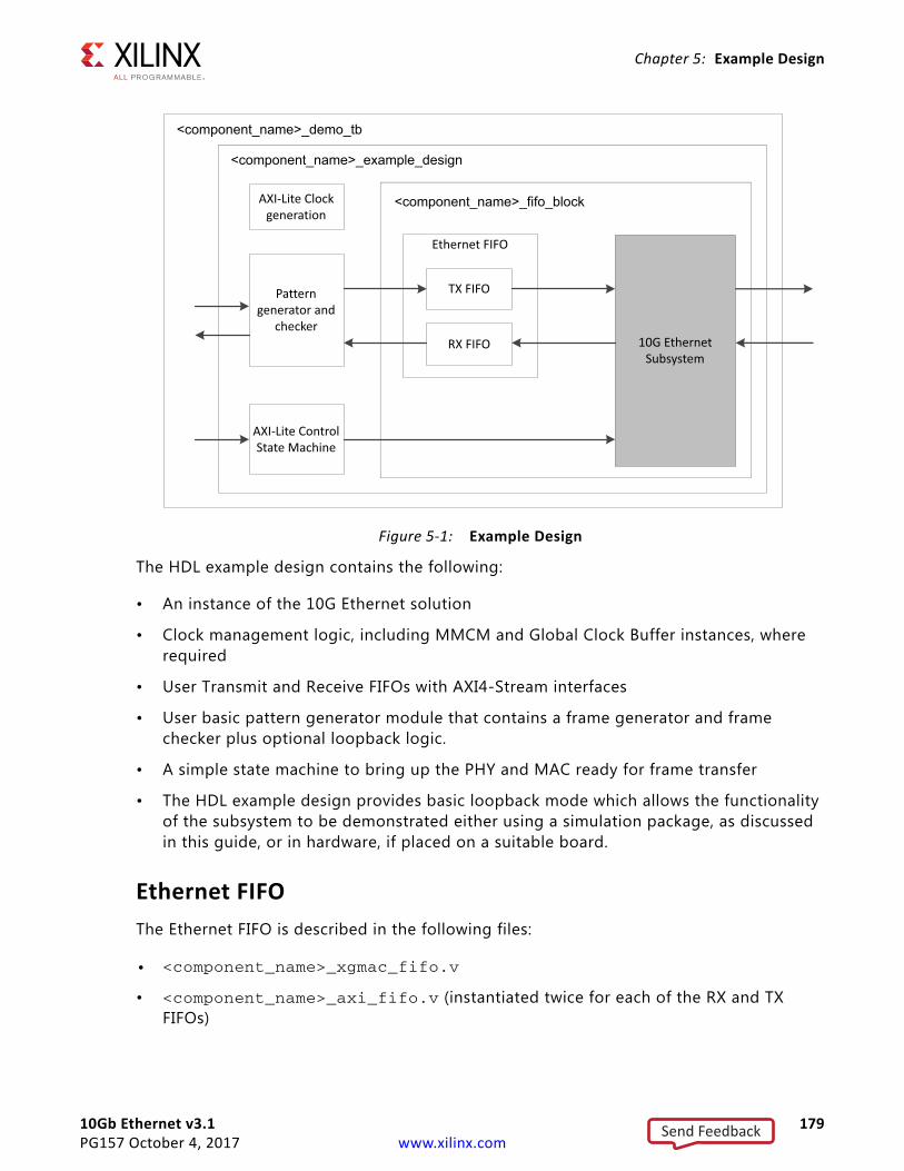
10Gb Ethernet v3.1 179PG157 October 4, 2017 www.xilinx.com
Chapter 5: Example Design
The HDL example design contains the following:
• An instance of the 10G Ethernet solution
• Clock management logic, including MMCM and Global Clock Buffer instances, where required
• User Transmit and Receive FIFOs with AXI4-Stream interfaces
• User basic pattern generator module that contains a frame generator and frame checker plus optional loopback logic.
• A simple state machine to bring up the PHY and MAC ready for frame transfer
• The HDL example design provides basic loopback mode which allows the functionality of the subsystem to be demonstrated either using a simulation package, as discussed in this guide, or in hardware, if placed on a suitable board.
Ethernet FIFOThe Ethernet FIFO is described in the following files:
• <component_name>_xgmac_fifo.v
• <component_name>_axi_fifo.v (instantiated twice for each of the RX and TX FIFOs)
X-Ref Target - Figure 5-1
Figure 5-1: Example Design
10G Ethernet Subsystem
<component_name>_fifo_block
<component_name>_example_design
Pattern generator and
checker
Pattern generator and
checker
AXI-Lite ControlState Machine
AXI-Lite Control State Machine
TX FIFOTX FIFO
RX FIFORX FIFO
Ethernet FIFOEthernet FIFO
<component_name>_demo_tb
AXI-Lite Clockgeneration
AXI-Lite Clock generation
Send Feedback
10Gb Ethernet v3.1 180PG157 October 4, 2017 www.xilinx.com
Chapter 5: Example Design
The Ethernet FIFO contains an instance of a tx_client_fifo to connect to the TX AXI4-Stream interface, and an instance of the rx_client_fifo to connect to the RX AXI4-Stream interface. Both transmit and receive FIFO components implement an AXI4-Stream user interface, through which the frame data can be transmitted and received.
RX FIFO
The rx_client_fifo is built around a Dual Port Inferred RAM, giving a total memory capacity of up to 16,384bytes. The memory capacity is set by a local parameter FIFO_SIZE which by default is set to 1024. The receive FIFO receives frame data from the subsystem. If the frame is not errored, that frame is presented on the AXI4-Stream FIFO interface for reading (in this case by the Frame Checker module). If the frame is errored, that frame is dropped by the receive FIFO.
If the receive FIFO memory overflows, the frame currently being received is dropped, regardless of whether it is a good or bad frame, and the signal rx_overflow is asserted. Situations in which the memory can overflow are:
• The FIFO size set by FIFO_SIZE parameter limits the size of the frames that it can store without error. If a frame is larger than the parameter size in bytes, the FIFO can overflow and data is then lost. It is therefore recommended that the example design is not used with the MAC solution in jumbo frame mode for frames of larger than the number of bytes specified by FIFO_SIZE parameter.
• The FIFO will eventually overflow if data is being written into it faster than data is being read out. For example, if the loopback path is set from the RX FIFO to the TX FIFO, then overflow occurs if the receiver clock is running at a faster rate than the transmitter clock or if the inter-packet gap between the received frames is smaller than the inter-packet gap between the transmitted frames. If this is the case, the TX FIFO is not able to read data from the RX FIFO as fast as it is being received.
TX FIFO
The tx_client_fifo is built around a Dual Port Inferred RAM, giving a total memory capacity of up to 16,384 bytes. The memory capacity is set by a local parameter FIFO_SIZE which by default is set to 1024. When a full frame has been written into the transmit FIFO, the FIFO presents data to the MAC transmitter. The MAC uses tx_axis_mac_tready to throttle the data until it has control of the medium. If the FIFO memory fills up, the tx_axis_fifo_tready signal is used to halt the AXI4-Stream interface writing in data, until space becomes available in the FIFO. If the FIFO memory fills up but no full frames are available for transmission. For example, if a frame is larger than the parameter in bytes, the FIFO asserts the tx_overflow signal and continues to accept the rest of the frame from connected logic; however, this large overflow frame is dropped by the FIFO. This ensures that the AXI4-Stream FIFO interface does not lock up.
Send Feedback
10Gb Ethernet v3.1 181PG157 October 4, 2017 www.xilinx.com
Chapter 5: Example Design
CAUTION! Ensure that the length of the frame being presented at the TX FIFO AXI4-Stream interface does not exceed the FIFO capacity. Frames whose length exceed the FIFO capacity will result in corrupted frame being sent out.
Basic Pattern Generator ModuleThe basic pattern generator is described in the following files:
• <component_name>_gen_check_wrapper.v
• <component_name>_axi_pat_gen.v
• <component_name>_axi_pat_check.v
• <component_name>_axi_mux.v
• <component_name>_address_swap.v
The gen_check_wrapper has two main functional modes: generator and loopback, configured by the enable_pat_gen signal input of the example design. In loopback, the data from the RX FIFO is passed to the address swap module and passed from there to the TX FIFO. In generator mode the TX data is provided by the pattern generator, with RX data being optionally checked by the pattern checker.
Address Swap
The address swap module can be optionally enabled for use on the loopback path. By default the address swap functionality is bypassed. In loopback mode, when enabled, the address swap module waits until both the Destination Address (DA) and Source Address (SA) fields have been received before starting to send data on to the TX FIFO. Then the module swaps the DA and SA of each frame. This ensures that the outgoing frame DA matches the SA of the link partner. When disabled, the DA and SA fields are left untouched.
Pattern Generator
The pattern generator can be enabled/disabled using the enable_pat_gen signal input of the example design. When enabled the data from the RX FIFO is flushed and the pat_gen module drives the address_swap module inputs. The pattern generator uses vectors to allow user modification of the destination address and source address, insertion of custom preamble and VLAN fields plus control of minimum frame size and maximum frame size. When enabled, it starts with the configured minimum frame size and after each frame is sent, increments the frame size until the maximum value is reached; it then starts again at the minimum frame size. Example design inputs provide direct control of custom preamble and VLAN field insertion. If targeting a suitable board, these configuration inputs could be connected to DIP switches.
In all cases the pattern generator frame is constructed as follows:
Send Feedback
10Gb Ethernet v3.1 182PG157 October 4, 2017 www.xilinx.com
Chapter 5: Example Design
• Customer preamble data (if enabled), DA, SA, and VLAN field (if enabled) values are as provided by vector values specified upon instantiation of the module in the example design.
• The Type/Length field is set according to packet size
• The frame data is a decrementing count starting from the value in the type/length field. This should mean that the final data byte in all frames is 0x01 or 0x00.
In a loopback scenario (using a second targeted board as the loopback), the ppm difference between the oscillators on the two boards can cause overflows in the slower board, resulting in errors. This is normally observed when the slower board is operating as the loopback board. To avoid this issue the data rate provided by the pattern generator is throttled to just below the selected line rate.
The pat_gen module has error insertion functionality which is directly controlled by the insert_error signal input of the example design (which could be connected to a pushbutton on a suitable board).
The pattern generator also provides a simple activity monitor. This toggles the gen_active_flash signal output, which could be connected to flash as LED on a suitable board, to indicate that data is being transmitted.
Pattern Checker
The pat_check module provides a simple sanity check that data is being received correctly. It uses the same input data and control vectors as the pat_gen module and therefore expects the same frame contents and frame size increments. Because the frame data can or cannot have the DA and SA swapped the pattern checker allows either value to be in either location.
When enabled, using the enable_pat_check signal input of the example design, the output from the RX_FIFO is monitored. The first step is to identify where in the frame sequence the data is, this is done by capturing the value in the type/length field of the first complete frame seen. After this is done the following frame is expected to be incrementally bigger (unless you happen to be at the wrap point).
If an error is detected an error flag is raised on the byte or bytes which mismatch and the error condition is sampled and output to the frame_error signal output of the example design (which could be displayed using an LED on a suitable board). The pattern checker state machine then re-synchronizes to the incoming data. The reset_error signal input of the example design, if asserted, will clear the frame_error signal, enabling a feel for the frequency of errors (if any).
The pattern checker also provides a simple activity monitor. This toggles the check_active_flash dedicated output of the example design, which can be used to flash an LED of a suitable board. This can indicate that RX data is being received correctly. This ensures that the lack of a detected error is not just due to all frames being dropped.
Send Feedback
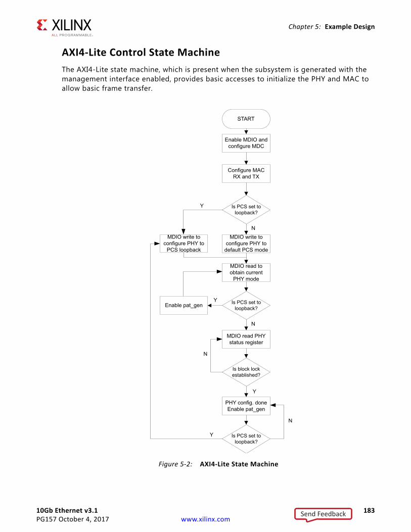
10Gb Ethernet v3.1 183PG157 October 4, 2017 www.xilinx.com
Chapter 5: Example Design
AXI4-Lite Control State MachineThe AXI4-Lite state machine, which is present when the subsystem is generated with the management interface enabled, provides basic accesses to initialize the PHY and MAC to allow basic frame transfer.
X-Ref Target - Figure 5-2
Figure 5-2: AXI4-Lite State Machine
START
MDIO write to configure PHY to default PCS mode
MDIO read to obtain current
PHY mode
N
Enable MDIO and configure MDC
Configure MAC RX and TX
Is PCS set to loopback?
MDIO write to configure PHY to
PCS loopback
Y
Is PCS set to loopback?Enable pat_gen
Y
N
MDIO read PHY status register
Is block lock established?
N
PHY config. doneEnable pat_gen
Y
Is PCS set to loopback?
N
Y
Send Feedback
10Gb Ethernet v3.1 184PG157 October 4, 2017 www.xilinx.com
Chapter 5: Example Design
Figure 5-2 shows the accesses performed by the state machine. After a reset, and allowing settling time for internal resets to complete, the state machine first writes to the MAC to enable the MDIO and to configure the MDIO clock (this assumes an s_axi_aclk running at 125 MHz, which is provided by default from the example design and demo_tb). Following that the RX and TX side of the MAC are configured. The PHY can then be set into two modes by using the pcs_loopback signal input of the example design: PCS loopback (data looped back within the 10GBASE-R or 10GBASE-KR) or default transmit/receive mode. A value to the appropriate PHY MDIO register is written to accordingly. Then an MDIO read is performed on a status register to verify the programmed mode. In case of the PCS loopback mode the PHY configuration is now complete and frame transmission is allowed to start by enabling the pattern generator. If default transmit/receive mode is selected, then a second status register is to be read from that indicates if the PHY has come out of reset and block lock has been established. If block lock is not established, this MDIO status register will be polled until block lock is detected. Once successful, the PHY is configured and frame transmission can start by enabling the pattern generator. The exit conditions for this state are reset or enablement of PCS loopback.
Shared Logic and the Support LayerDepending on the selection made for shared logic in the subsystem customization Vivado IDE, the Support Layer can either itself be the subsystem top-level (Include Shared Logic in core) or can simply contain the subsystem top-level (Include Shared Logic in example design).
The difference is subtle but selecting Include Shared Logic in the core produces a subsystem that includes all the shared logic and has outputs for clocks and control signals that can be shared between multiple 10GBASE-R/KR IP subsystems.
Selecting Include Shared Logic in the Example Design allows you to access the shared logic.
Typically in a multi-subsystem design, you can create one subsystem, subsystem A with Shared Logic included in the subsystem, and one subsystem, subsystem B with the opposite setting. A single instance of subsystem A then provides the clocks for several instances of subsystem B. See Special Design Considerations for more information.
Send Feedback
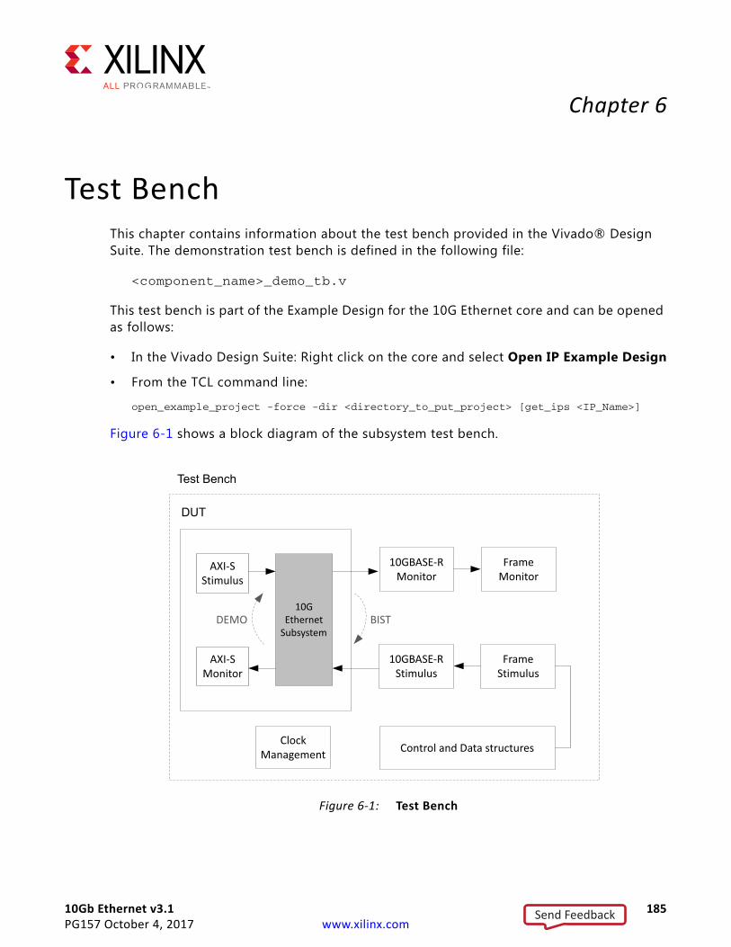
10Gb Ethernet v3.1 185PG157 October 4, 2017 www.xilinx.com
Chapter 6
Test BenchThis chapter contains information about the test bench provided in the Vivado® Design Suite. The demonstration test bench is defined in the following file:
<component_name>_demo_tb.v
This test bench is part of the Example Design for the 10G Ethernet core and can be opened as follows:
• In the Vivado Design Suite: Right click on the core and select Open IP Example Design
• From the TCL command line:
open_example_project -force -dir <directory_to_put_project> [get_ips <IP_Name>]
Figure 6-1 shows a block diagram of the subsystem test bench.
X-Ref Target - Figure 6-1
Figure 6-1: Test Bench
DUT
Frame StimulusFrame
Stimulus
Frame MonitorFrame
Monitor
Test Bench
10GBASE-RStimulus
10GBASE-RStimulus
10GBASE-RMonitor
10GBASE-RMonitor
ClockManagement
ClockManagement Control and Data structuresControl and Data structures
10G Ethernet
SubsystemBISTDEMO
AXI-S Stimulus
AXI-SMonitor
Send Feedback
10Gb Ethernet v3.1 186PG157 October 4, 2017 www.xilinx.com
Chapter 6: Test Bench
The demonstration test bench is a simple program to exercise the example design and the subsystem itself. It has two modes of operation, DEMO and Built-in Self Test (BIST), with DEMO being the default mode.
The test bench consists of the following:
• Clock generators
• DEMO - A Frame Stimulus block that is suitably encoded and scrambled to connect to the serial receiver interface of the example design.
• DEMO - A Frame Monitor block to check the data returned through the serial transmitter interface (after suitable descrambling and decoding).
• A CRC engine (not illustrated) that is used both by the stimulus and monitor blocks.
• BIST - A simple loopback path (not illustrated) can be connected from the serial transmit interface to the serial receiver.
DEMO ModeThe demonstration test bench performs the following tasks:
• Input clock signals are generated.
• Address swap is enabled; pattern generator and checker are disabled
• Receive data is looped back into transmit path on the AXI4-Stream interface
• A reset is applied to the example design.
• Wait until PCS/PMA block lock is established
• Four frames are pushed into the serial receiver interface
° The first frame is a minimum length frame.
° The second frame is a type frame.
° The third frame is an errored frame.
° The fourth frame is a padded frame.
• As each frame is pushed into the receiver interface a CRC is calculated over the applicable frame fields and appended to the end of the frame.
• Frames are then 64b/66b encoded, and then scrambled
• The frames received at the serial transmitter interface are de-scrambled, and decoded
• Frames are then passed to the monitor process which calculates the CRC as the frame is being observed. It then checks the validity of the CRC by comparing its own calculated CRC value with the last four bytes of the frame.
• Transmitted frames are counted
Send Feedback
10Gb Ethernet v3.1 187PG157 October 4, 2017 www.xilinx.com
Chapter 6: Test Bench
BIST ModeThe demonstration test bench performs the following tasks:
• Input clock signals are generated.
• A reset is applied to the example design.
• Wait until PCS/PMA block lock is established
• The pattern generator and checker are enabled.
• The frames received at the serial transmitter interface are de-scrambled and decoded
• Frames are then passed to the monitor process which calculates the CRC as the frame is being observed. It then checks the validity of the CRC by comparing its own calculated CRC value with the last four bytes of the frame.
• Transmitted frames are counted
• The serial receiver link is connected to the transmitter link, so that transmitted frames are looped back to the receiver path of the subsystem.
• The frames read out from the RX FIFO are checked by the checker module inside of the example design. The test bench monitors any errors that the checker module detects.
Changing the Test BenchThe Demonstration test bench defaults to DEMO mode for all implementations.
The mode is set using the TB_MODE parameter in the <component_name>_demo_tb.v. To change the mode, set the parameter value to BIST.
Changing Frame Data in Demo Mode
The contents of the frame data passed into the serial receiver can be changed by editing the DATA fields for each frame defined in the test bench. The test bench automatically calculates the new FCS field to pass into the MAC. Further frames can be added by defining a new frame of data.
Changing Frame Length
There are two ways to change the frame lengths of the stimulus frames. The predefined frames within the test bench can be directly edited to change the frame contents and size. Alternatively, the test bench contains a quicker method that allows blocks of data within the predefined frames to be repeated a given number of times. The block of data which can be repeated is inclusive from the beginning of the TYPE/LENGTH field to the end of the final full XGMII column of data payload. The FRAME_GEN_MULTIPLIER constant provides the information for the number of times to repeat this block of data.
Send Feedback
10Gb Ethernet v3.1 188PG157 October 4, 2017 www.xilinx.com
Chapter 6: Test Bench
For example, if the index of the last complete control (ctrl) column (for example, ctrl column[14] = 4'b0000) then the block size is (14 + 1) - 3 = 12. That means that 12 x 4 = 48 bytes are contained in one block. If FRAME_GEN_MULTIPLIER is set to 2 then 2 x 12 x 4 = 96 bytes are sent after the SA/DA and the same 48 byte block repeating pattern is sent twice.
If using a LENGTH field rather than a TYPE field for the TYPE/LENGTH field of the defined frame, then the LENGTH value must be manually edited. The general formula for LENGTH/TYPE field is as follows:
[[(index of last complete ctrl column+1) - 3] x4 x FRAME_GEN_MULTIPLIER] - 2 + (1, 2 or 3 depending from the value of the ctrl column after the last complete ctrl column).
The multiplier constant is applied to every frame inserted into RX; therefore the L/T field has to be set appropriately for every frame unless the frame is a type or a control frame.
Changing Frame Error Status
Errors can be inserted into any of the pre-defined frames by changing the error field to 1 in any column of that frame. The error currently written into the third frame can be removed by setting the error field for the frame to 0.
Send Feedback
10Gb Ethernet v3.1 189PG157 October 4, 2017 www.xilinx.com
Appendix A
UpgradingThis appendix contains information about migrating a design from the ISE® Design Suite to the Vivado® Design Suite, and for upgrading to a more recent version of the subsystem. For customers upgrading in the Vivado Design Suite, important details (where applicable) about any port changes and other impact to user logic are included.
Migrating to the Vivado Design SuiteFor information about migrating to the Vivado Design Suite, see the ISE to Vivado Design Suite Migration Guide (UG911) [Ref 8].
Upgrading in the Vivado Design SuiteThis section provides information about any changes to the user logic or port designations that take place when you upgrade to a more current version of this subsystem in the Vivado Design Suite.
Parameter Changes None.
Port Changes in Version 2.0Table A-1 shows the ports that were added to the v2.0 subsystem for older subsystem versions that are being upgraded. These were added to support the new shared logic option and to allow an independent clock to be used for dclk.
Send Feedback
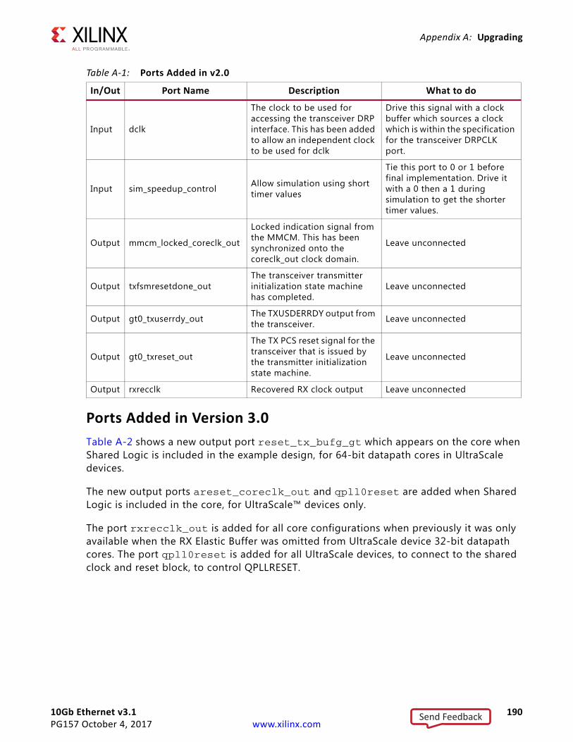
10Gb Ethernet v3.1 190PG157 October 4, 2017 www.xilinx.com
Appendix A: Upgrading
Ports Added in Version 3.0Table A-2 shows a new output port reset_tx_bufg_gt which appears on the core when Shared Logic is included in the example design, for 64-bit datapath cores in UltraScale devices.
The new output ports areset_coreclk_out and qpll0reset are added when Shared Logic is included in the core, for UltraScale™ devices only.
The port rxrecclk_out is added for all core configurations when previously it was only available when the RX Elastic Buffer was omitted from UltraScale device 32-bit datapath cores. The port qpll0reset is added for all UltraScale devices, to connect to the shared clock and reset block, to control QPLLRESET.
Table A-1: Ports Added in v2.0
In/Out Port Name Description What to do
Input dclk
The clock to be used for accessing the transceiver DRP interface. This has been added to allow an independent clock to be used for dclk
Drive this signal with a clock buffer which sources a clock which is within the specification for the transceiver DRPCLK port.
Input sim_speedup_control Allow simulation using short timer values
Tie this port to 0 or 1 before final implementation. Drive it with a 0 then a 1 during simulation to get the shorter timer values.
Output mmcm_locked_coreclk_out
Locked indication signal from the MMCM. This has been synchronized onto the coreclk_out clock domain.
Leave unconnected
Output txfsmresetdone_outThe transceiver transmitter initialization state machine has completed.
Leave unconnected
Output gt0_txuserrdy_out The TXUSDERRDY output from the transceiver. Leave unconnected
Output gt0_txreset_out
The TX PCS reset signal for the transceiver that is issued by the transmitter initialization state machine.
Leave unconnected
Output rxrecclk Recovered RX clock output Leave unconnected
Send Feedback
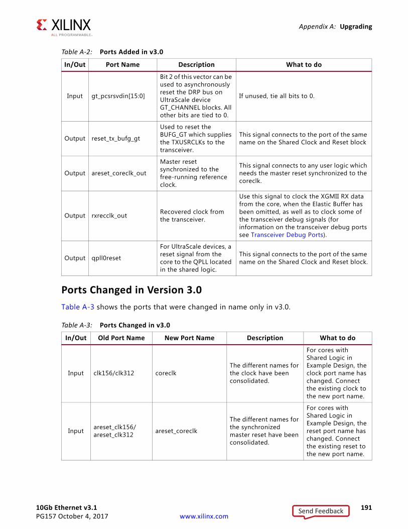
10Gb Ethernet v3.1 191PG157 October 4, 2017 www.xilinx.com
Appendix A: Upgrading
Ports Changed in Version 3.0Table A-3 shows the ports that were changed in name only in v3.0.
Table A-2: Ports Added in v3.0
In/Out Port Name Description What to do
Input gt_pcsrsvdin[15:0]
Bit 2 of this vector can be used to asynchronously reset the DRP bus on UltraScale device GT_CHANNEL blocks. All other bits are tied to 0.
If unused, tie all bits to 0.
Output reset_tx_bufg_gt
Used to reset the BUFG_GT which supplies the TXUSRCLKs to the transceiver.
This signal connects to the port of the same name on the Shared Clock and Reset block
Output areset_coreclk_out
Master reset synchronized to the free-running reference clock.
This signal connects to any user logic which needs the master reset synchronized to the coreclk.
Output rxrecclk_out Recovered clock from the transceiver.
Use this signal to clock the XGMII RX data from the core, when the Elastic Buffer has been omitted, as well as to clock some of the transceiver debug signals (for information on the transceiver debug ports see Transceiver Debug Ports).
Output qpll0reset
For UltraScale devices, a reset signal from the core to the QPLL located in the shared logic.
This signal connects to the port of the same name on the Shared Clock and Reset block.
Table A-3: Ports Changed in v3.0
In/Out Old Port Name New Port Name Description What to do
Input clk156/clk312 coreclkThe different names for the clock have been consolidated.
For cores with Shared Logic in Example Design, the clock port name has changed. Connect the existing clock to the new port name.
Input areset_clk156/areset_clk312 areset_coreclk
The different names for the synchronized master reset have been consolidated.
For cores with Shared Logic in Example Design, the reset port name has changed. Connect the existing reset to the new port name.
Send Feedback
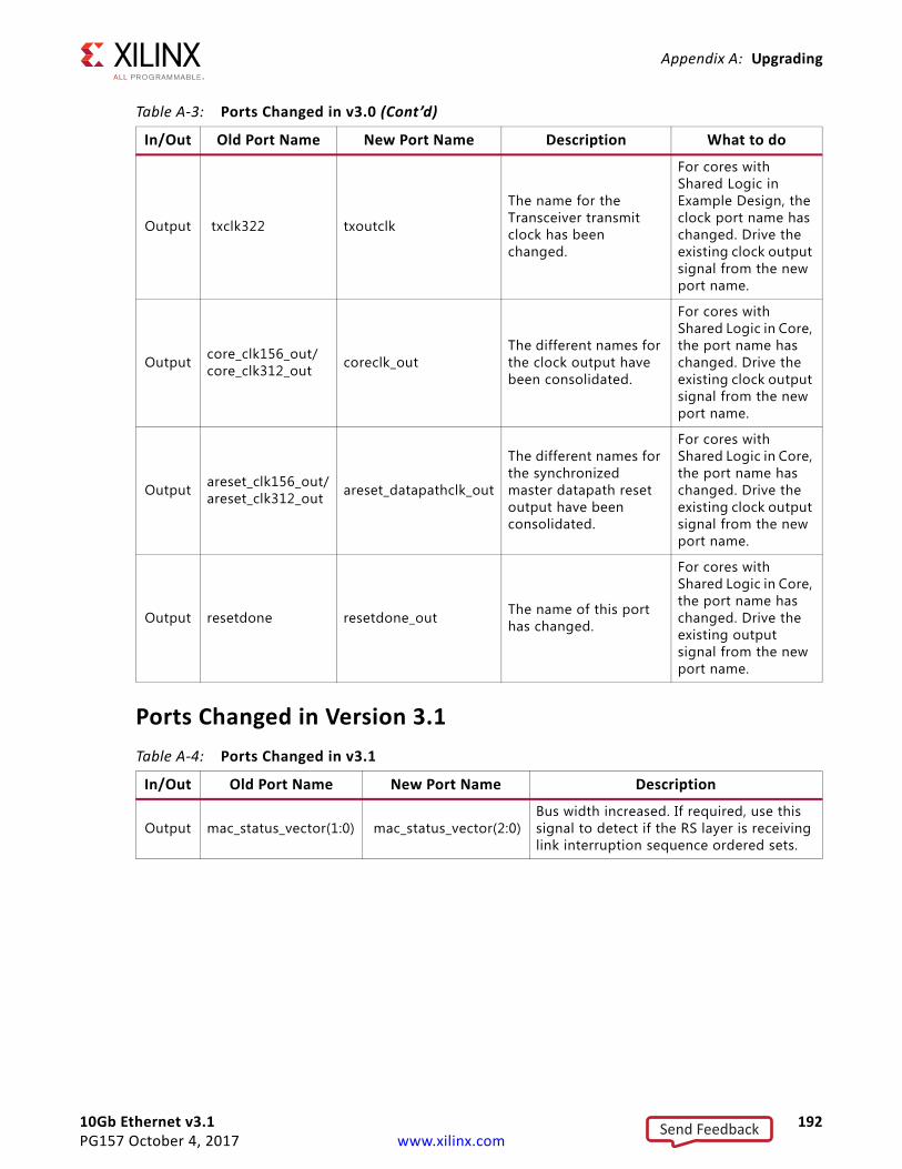
10Gb Ethernet v3.1 192PG157 October 4, 2017 www.xilinx.com
Appendix A: Upgrading
Ports Changed in Version 3.1
Output txclk322 txoutclk
The name for the Transceiver transmit clock has been changed.
For cores with Shared Logic in Example Design, the clock port name has changed. Drive the existing clock output signal from the new port name.
Output core_clk156_out/core_clk312_out coreclk_out
The different names for the clock output have been consolidated.
For cores with Shared Logic in Core, the port name has changed. Drive the existing clock output signal from the new port name.
Output areset_clk156_out/areset_clk312_out areset_datapathclk_out
The different names for the synchronized master datapath reset output have been consolidated.
For cores with Shared Logic in Core, the port name has changed. Drive the existing clock output signal from the new port name.
Output resetdone resetdone_out The name of this port has changed.
For cores with Shared Logic in Core, the port name has changed. Drive the existing output signal from the new port name.
Table A-4: Ports Changed in v3.1
In/Out Old Port Name New Port Name Description
Output mac_status_vector(1:0) mac_status_vector(2:0)Bus width increased. If required, use this signal to detect if the RS layer is receiving link interruption sequence ordered sets.
Table A-3: Ports Changed in v3.0 (Cont’d)
In/Out Old Port Name New Port Name Description What to do
Send Feedback
10Gb Ethernet v3.1 193PG157 October 4, 2017 www.xilinx.com
Appendix B
DebuggingThis appendix includes details about resources available on the Xilinx Support website and debugging tools.
TIP: If the IP generation halts with an error, there may be a license issue. See License Checkers in Chapter 1 for more details.
Finding Help on Xilinx.comTo help in the design and debug process when using the 10G Ethernet, the Xilinx Support web page contains key resources such as product documentation, release notes, answer records, information about known issues, and links for obtaining further product support.
DocumentationThis product guide is the main document associated with the 10G Ethernet subsystem. This guide, along with documentation related to all products that aid in the design process, can be found on the Xilinx Support web page or by using the Xilinx Documentation Navigator.
Download the Xilinx Documentation Navigator from the Downloads page. For more information about this tool and the features available, open the online help after installation.
Solution CentersSee the Xilinx Solution Centers for support on devices, software tools, and intellectual property at all stages of the design cycle. Topics include design assistance, advisories, and troubleshooting tips.
The Solution Center specific to the 10G Ethernet subsystem is listed below.
• Xilinx Ethernet IP Solution Center
Send Feedback
10Gb Ethernet v3.1 194PG157 October 4, 2017 www.xilinx.com
Appendix B: Debugging
Answer RecordsAnswer Records include information about commonly encountered problems, helpful information on how to resolve these problems, and any known issues with a Xilinx product. Answer Records are created and maintained daily ensuring that users have access to the most accurate information available.
Answer Records for this subsystem can be located by using the Search Support box on the main Xilinx support web page. To maximize your search results, use keywords such as
• Product name
• Tool message(s)
• Summary of the issue encountered
A filter search is available after results are returned to further target the results.
Master Answer Record for the 10G Ethernet
AR: 57358
Technical SupportXilinx provides technical support in the Xilinx Support web page for this product when used as described in the product documentation. Xilinx cannot guarantee timing, functionality, or support if you do any of the following:
• Implement the solution in devices that are not defined in the documentation.
• Customize the solution beyond that allowed in the product documentation.
• Change any section of the design labeled DO NOT MODIFY.
To contact Xilinx Technical Support, navigate to the Xilinx Support web page.
Debug ToolsThere are many tools available to address 10G Ethernet design issues. It is important to know which tools are useful for debugging various situations.
Vivado Design Suite Debug FeatureThe Vivado® Design Suite debug feature inserts logic analyzer and virtual I/O cores directly into your design. The debug feature also allows you to set trigger conditions to capture application and integrated block port signals in hardware. Captured signals can then be
Send Feedback
10Gb Ethernet v3.1 195PG157 October 4, 2017 www.xilinx.com
Appendix B: Debugging
analyzed. This feature in the Vivado IDE is used for logic debugging and validation of a design running in Xilinx devices.
The Vivado logic analyzer is used with the logic debug IP cores, including:
• ILA 2.0 (and later versions)
• VIO 2.0 (and later versions)
See the Vivado Design Suite User Guide: Programming and Debugging (UG908) [Ref 9].
Hardware DebugHardware issues can range from link bring-up to problems seen after hours of testing. This section provides debug steps for common issues. The debug feature is a valuable resource to use in hardware debug. The signal names mentioned in the following individual sections can be probed using the debug feature for debugging the specific problems.
Many of these common issues can also be applied to debugging design simulations.
General ChecksEnsure that all the timing constraints for the subsystem were properly incorporated and that all constraints were met during implementation.
• Does it work in post-place and route timing simulation? If problems are seen in hardware but not in timing simulation, this could indicate a PCB issue. Ensure that all clock sources are active and clean.
• If using MMCMs in the design, ensure that all MMCMs have obtained lock by monitoring the LOCKED port.
• If your outputs go to 0 after operating normally for several hours, check your licensing.
What Can Cause a Local or Remote Fault?Local Fault and Remote Fault codes both start with the sequence TXD/RXD=0x9C, TXC/RXC=1 in XGMII lane 0. Fault conditions can also be detected by looking at the status vector or MDIO registers. The Local Fault and Link Status are defined as both immediate and latching error indicators by the IEEE specification.
IMPORTANT: This means that the latching Local Fault and Link Status bits in the status vector or MDIO registers must be cleared with the associated Reset bits in the Configuration vector or by reading the MDIO registers, or by issuing a PMA or PCS reset.
Send Feedback
10Gb Ethernet v3.1 196PG157 October 4, 2017 www.xilinx.com
Appendix B: Debugging
Local Fault
The receiver outputs a local fault when the receiver is not up and operational. This RX local fault is also indicated in the status and MDIO registers. The most likely causes for an RX local fault are:
• The transceiver has not locked or the receiver is being reset.
• The block lock state machine has not completed.
• The BER monitor state machine indicates a high BER.
• The elastic buffer has over/underflowed.
Remote Fault
Remote faults are only generated in the MAC reconciliation layer in response to a Local Fault message. When the receiver receives a remote fault, this means that the link partner is in a local fault condition.
When the MAC reconciliation layer receives a remote fault, it silently drops any data being transmitted and instead transmits IDLEs to help the link partner resolve its local fault condition. When the MAC reconciliation layer receives a local fault, it silently drops any data being transmitted and instead transmits a remote fault to inform the link partner that it is in a fault condition. Be aware that the Xilinx 10G Ethernet MAC core has an option to disable remote fault transmission.
Link Bring Up – Basic
High Level Link Up (10GBASE-R or 10GBASE-KR with Auto-Negotiation + Training Disabled)
The following link initialization stages describe a possible scenario of the Link coming up between device A and device B.
Stage 1: Device A Powered Up, but Device B Powered Down
1. Device A is powered up and reset.
2. Device B powered down.
3. Device A detects a fault because there is no signal received. The Device A 10Gb PCS/PMA core indicates an RX local fault.
4. The Device A MAC reconciliation layer receives the local fault. This triggers the MAC reconciliation layer to silently drop any data being transmitted and instead transmit a remote fault.
5. RX Link Status = 0 (link down) in Device A.
Send Feedback
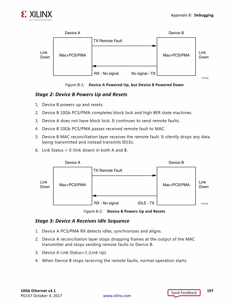
10Gb Ethernet v3.1 197PG157 October 4, 2017 www.xilinx.com
Appendix B: Debugging
Stage 2: Device B Powers Up and Resets
1. Device B powers up and resets.
2. Device B 10Gb PCS/PMA completes block lock and high BER state machines.
3. Device A does not have block lock. It continues to send remote faults.
4. Device B 10Gb PCS/PMA passes received remote fault to MAC.
5. Device B MAC reconciliation layer receives the remote fault. It silently drops any data being transmitted and instead transmits IDLEs.
6. Link Status = 0 (link down) in both A and B.
Stage 3: Device A Receives Idle Sequence
1. Device A PCS/PMA RX detects idles, synchronizes and aligns.
2. Device A reconciliation layer stops dropping frames at the output of the MAC transmitter and stops sending remote faults to Device B.
3. Device A Link Status=1 (Link Up)
4. When Device B stops receiving the remote faults, normal operation starts.
X-Ref Target - Figure B-1
Figure B-1: Device A Powered Up, but Device B Powered Down
X-Ref Target - Figure B-2
Figure B-2: Device B Powers Up and Resets
Send Feedback
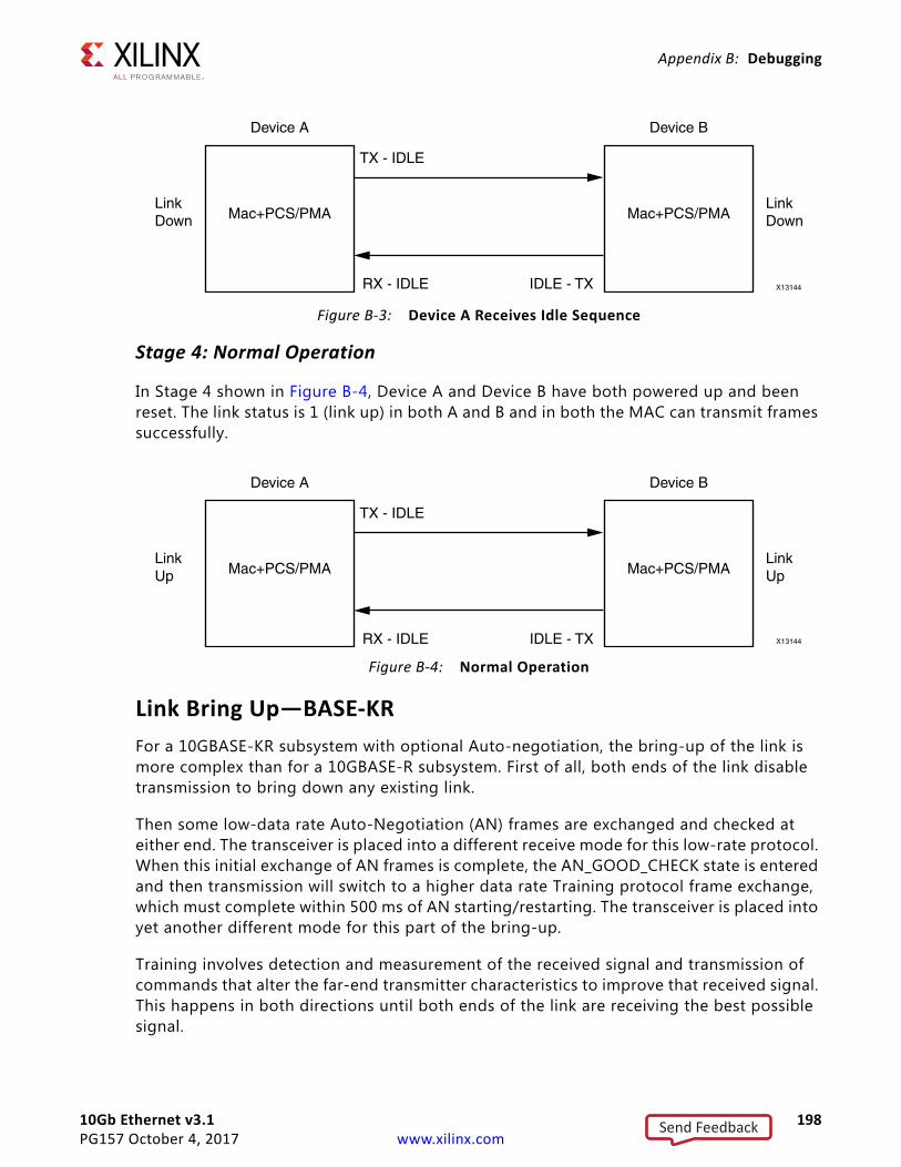
10Gb Ethernet v3.1 198PG157 October 4, 2017 www.xilinx.com
Appendix B: Debugging
Stage 4: Normal Operation
In Stage 4 shown in Figure B-4, Device A and Device B have both powered up and been reset. The link status is 1 (link up) in both A and B and in both the MAC can transmit frames successfully.
Link Bring Up—BASE-KRFor a 10GBASE-KR subsystem with optional Auto-negotiation, the bring-up of the link is more complex than for a 10GBASE-R subsystem. First of all, both ends of the link disable transmission to bring down any existing link.
Then some low-data rate Auto-Negotiation (AN) frames are exchanged and checked at either end. The transceiver is placed into a different receive mode for this low-rate protocol. When this initial exchange of AN frames is complete, the AN_GOOD_CHECK state is entered and then transmission will switch to a higher data rate Training protocol frame exchange, which must complete within 500 ms of AN starting/restarting. The transceiver is placed into yet another different mode for this part of the bring-up.
Training involves detection and measurement of the received signal and transmission of commands that alter the far-end transmitter characteristics to improve that received signal. This happens in both directions until both ends of the link are receiving the best possible signal.
X-Ref Target - Figure B-3
Figure B-3: Device A Receives Idle Sequence
X-Ref Target - Figure B-4
Figure B-4: Normal Operation
Send Feedback
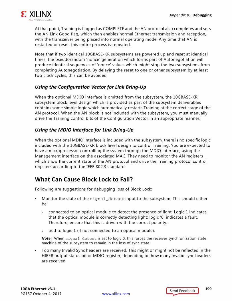
10Gb Ethernet v3.1 199PG157 October 4, 2017 www.xilinx.com
Appendix B: Debugging
At that point, Training is flagged as COMPLETE and the AN protocol also completes and sets the AN Link Good flag, which then enables normal Ethernet transmission and reception, with the transceiver being placed into normal operating mode. Any time that AN is restarted or reset, this entire process is repeated.
Note that if two identical 10GBASE-KR subsystems are powered up and reset at identical times, the pseudorandom 'nonce' generation which forms part of Autonegotiation will produce identical sequences of 'nonce' values which might stop the two subsystems from completing Autonegotiation. By delaying the reset to one or other subsystem by at least two clock cycles, this can be avoided.
Using the Configuration Vector for Link Bring-Up
When the optional MDIO interface is omitted from the subsystem, the 10GBASE-KR subsystem block level design which is provided as part of the subsystem deliverables contains some simple logic which automatically restarts Training at the correct stage of the AN protocol. When the AN block is not included with the subsystem, you must manually drive the Training control bits of the Configuration Vector in an appropriate manner.
Using the MDIO interface for Link Bring-Up
When the optional MDIO interface is included with the subsystem, there is no specific logic included with the 10GBASE-KR block level design to control Training. You are expected to have a microprocessor controlling the system through the MDIO interface, using the Management interface on the associated MAC. They need to monitor the AN registers which show the current state of the AN protocol and drive the Training protocol control registers according to the IEEE 802.3 standard.
What Can Cause Block Lock to Fail?Following are suggestions for debugging loss of Block Lock:
• Monitor the state of the signal_detect input to the subsystem. This should either be:
° connected to an optical module to detect the presence of light. Logic 1 indicates that the optical module is correctly detecting light; logic '0' indicates a fault. Therefore, ensure that this is driven with the correct polarity.
° tied to logic 1 (if not connected to an optical module).
Note: When signal_detect is set to logic 0, this forces the receiver synchronization state machine of the subsystem to remain in the loss of sync state.
• Too many Invalid Sync headers are received. This might or might not be reflected in the HIBER output status bit or MDIO register, depending on how many invalid sync headers are received.
Send Feedback
10Gb Ethernet v3.1 200PG157 October 4, 2017 www.xilinx.com
Appendix B: Debugging
Transceiver-Specific:
• Ensure that the polarities of the txn/txp and rxn/rxp lines are not reversed. If they are, these can be fixed by using the TXPOLARITY and RXPOLARITY ports of the transceiver.
• Check that the transceiver is not being held in reset or still being initialized. The RESETDONE outputs from the transceiver indicate when the transceiver is ready.
What Can Cause the 10Gb PCS/PMA Core to Insert Errors?On the receive path the 10Gb PCS/PMA core receive state machine can insert block errors RXD=FE, RXC=1. The RX block error happens any time the RX_E state is entered into. It could happen if C, S, D, T are seen out of order. Or it could also happen if an /E/ block type is received, (which is defined in IEEE802.3, Section 49.2.13.2.3 as a 66-bit code with a bad sync header or a control word (C S or T) with no matching translation for the block type field.)
If the RX Elastic Buffer underflows, the core inserts an /E/ block, followed by /L/ blocks.
When FEC is enabled in register bit 1.170.0 and FEC Error Passing is enabled in register bit 1.170.1, any uncorrectable FEC errors cause the FEC block to set the two sync header bits to the same value, creating a bad sync header, which the RX PCS Decoder decodes as an /E/ block.
Transceiver Specific Checks• Place the transceiver into parallel or serial near-end loopback.
• If correct operation is seen in the transceiver serial loopback, but not when loopback is performed through an optical cable, it might indicate a faulty optical module.
• If the subsystem exhibits correct operation in the transceiver parallel loopback but not in serial loopback, this might indicate a transceiver issue.
• A mild form of bit error rate might be solved by adjusting the transmitter Pre-Emphasis and Differential Swing Control attributes of the transceiver.
Link TrainingThere is currently no Link training algorithm included with the subsystem so it is left up the customers to implement what they need.
It has been noted in hardware testing that the RX DFE logic in the Xilinx transceivers is usually capable of adapting to almost any link so far-end training might not be required at all and the Training Done register/configuration bit can be set as default.
When you decide to implement your own Training Algorithm, that should not only include hardware to monitor the received data signal integrity and provide the inc/dec/preset/initialize commands to send to the far end device, but also must follow the protocol of
Send Feedback
10Gb Ethernet v3.1 201PG157 October 4, 2017 www.xilinx.com
Appendix B: Debugging
sending a command until 'updated' is seen on return, and then sending 'hold' until 'not updated' is seen on return.
IMPORTANT: The priority of commands defined in IEEE 802.3 must be adhered to, such as never transmitting 'Preset' with 'Initialize'.
The 10GBASE-KR subsystem does include logic that allows it to be trained by a far-end device without user-interaction.
Send Feedback

10Gb Ethernet v3.1 202PG157 October 4, 2017 www.xilinx.com
Appendix C
Additional Resources and Legal Notices
Xilinx ResourcesFor support resources such as Answers, Documentation, Downloads, and Forums, see Xilinx Support.
Documentation Navigator and Design HubsXilinx® Documentation Navigator provides access to Xilinx documents, videos, and support resources, which you can filter and search to find information. To open the Xilinx Documentation Navigator (DocNav):
• From the Vivado® IDE, select Help > Documentation and Tutorials.
• On Windows, select Start > All Programs > Xilinx Design Tools > DocNav.
• At the Linux command prompt, enter docnav.
Xilinx Design Hubs provide links to documentation organized by design tasks and other topics, which you can use to learn key concepts and address frequently asked questions. To access the Design Hubs:
• In the Xilinx Documentation Navigator, click the Design Hubs View tab.
• On the Xilinx website, see the Design Hubs page.
Note: For more information on Documentation Navigator, see the Documentation Navigator page on the Xilinx website.
ReferencesThese documents provide supplemental material useful with this product guide.
1. IEEE Standard 802.3-2012, “Carrier Sense Multiple Access with Collision Detection (CSMA/CD) Access Method and Physical Layer Specifications” (standards.ieee.org/findstds/standard/802.3-2012.html)
Send Feedback
10Gb Ethernet v3.1 203PG157 October 4, 2017 www.xilinx.com
Appendix C: Additional Resources and Legal Notices
2. IEEE Standard 1588-2008, “IEEE Standard for a Precision Clock Synchronization Protocol for Networked Measurement and Control Systems” (standards.ieee.org/findstds/standard/1588-2008.html)
3. IEEE Standard 802.1Qbb, “IEEE Standard for Local and Metropolitan Area Networks—Virtual Bridged Local Area Networks—Amendment: Priority-based Flow Control” (standards.ieee.org/findstds/standard/802.1Qbb-2011.html)
4. Vivado Design Suite User Guide: Designing IP Subsystems using IP Integrator (UG994)
5. Vivado Design Suite User Guide: Designing with IP (UG896)
6. Vivado Design Suite User Guide: Getting Started (UG910)
7. Vivado Design Suite User Guide: Logic Simulation (UG900)
8. ISE to Vivado Design Suite Migration Guide (UG911)
9. Vivado Design Suite User Guide: Programming and Debugging (UG908)
10. Vivado Design Suite AXI Reference Guide (UG1037)
11. 7 Series FPGAs GTX/GTH Transceivers User Guide (UG476)
12. UltraScale Architecture GTH Transceivers User Guide (UG576)
13. UltraScale Architecture GTY Transceivers User Guide (UG578)
14. 7 Series FPGAs Transceivers Wizard LogiCORE IP Product Guide (PG168)
Revision HistoryThe following table shows the revision history for this document.
Date Version Revision
10/04/2017 3.1 • Updated signal connections in Figure 3-67.
10/05/2016 3.1 • 10GBASE-KR in UltraScale devices always requires RX elastic buffer.
• Power-down signals added to transceiver debug interface.
04/06/2016 3.1 • Link interruption added.
• UltraScale+ device support removed.
11/18/2015 3.0 UltraScale+ device support added.
09/30/2015 3.0 • Minor updates to document.
04/01/2015 3.0 • Added support for 32-bit datapath width 10GBASE-R permutations.
• Added support for UltraScale 1588 permutations
• Improved clocking descriptions
• Added extra Vivado IDE options for selecting clock frequencies.
Send Feedback
10Gb Ethernet v3.1 204PG157 October 4, 2017 www.xilinx.com
Appendix C: Additional Resources and Legal Notices
Please Read: Important Legal NoticesThe information disclosed to you hereunder (the “Materials”) is provided solely for the selection and use of Xilinx products. To the maximum extent permitted by applicable law: (1) Materials are made available “AS IS” and with all faults, Xilinx hereby DISCLAIMS ALL WARRANTIES AND CONDITIONS, EXPRESS, IMPLIED, OR STATUTORY, INCLUDING BUT NOT LIMITED TO WARRANTIES OF MERCHANTABILITY, NON-INFRINGEMENT, OR FITNESS FOR ANY PARTICULAR PURPOSE; and (2) Xilinx shall not be liable (whether in contract or tort, including negligence, or under any other theory of liability) for any loss or damage of any kind or nature related to, arising under, or in connection with, the Materials (including your use of the Materials), including for any direct, indirect, special, incidental, or consequential loss or damage (including loss of data, profits, goodwill, or any type of loss or damage suffered as a result of any action brought by a third party) even if such damage or loss was reasonably foreseeable or Xilinx had been advised of the possibility of the same. Xilinx assumes no obligation to correct any errors contained in the Materials or to notify you of updates to the Materials or to product specifications. You may not reproduce, modify, distribute, or publicly display the Materials without prior written consent. Certain products are subject to the terms and conditions of Xilinx's limited warranty, please refer to Xilinx's Terms of Sale which can be viewed at https://www.xilinx.com/legal.htm#tos; IP cores may be subject to warranty and support terms contained in a license issued to you by Xilinx. Xilinx products are not designed or intended to be fail-safe or for use in any application requiring fail-safe performance; you assume sole risk and liability for use of Xilinx products in such critical applications, please refer to Xilinx's Terms of Sale which can be viewed at https://www.xilinx.com/legal.htm#tos.AUTOMOTIVE APPLICATIONS DISCLAIMERAUTOMOTIVE PRODUCTS (IDENTIFIED AS “XA” IN THE PART NUMBER) ARE NOT WARRANTED FOR USE IN THE DEPLOYMENT OF AIRBAGS OR FOR USE IN APPLICATIONS THAT AFFECT CONTROL OF A VEHICLE (“SAFETY APPLICATION”) UNLESS THERE IS A SAFETY CONCEPT OR REDUNDANCY FEATURE CONSISTENT WITH THE ISO 26262 AUTOMOTIVE SAFETY STANDARD (“SAFETY DESIGN”). CUSTOMER SHALL, PRIOR TO USING OR DISTRIBUTING ANY SYSTEMS THAT INCORPORATE PRODUCTS, THOROUGHLY TEST SUCH SYSTEMS FOR SAFETY PURPOSES. USE OF PRODUCTS IN A SAFETY APPLICATION WITHOUT A SAFETY DESIGN IS FULLY AT THE RISK OF CUSTOMER, SUBJECT ONLY TO APPLICABLE LAWS AND REGULATIONS GOVERNING LIMITATIONS ON PRODUCT LIABILITY.© Copyright 2013–2017 Xilinx, Inc. Xilinx, the Xilinx logo, Artix, ISE, Kintex, Spartan, Virtex, Vivado, Zynq, and other designated brands included herein are trademarks of Xilinx in the United States and other countries. AMBA, AMBA Designer, ARM, ARM1176JZ-S, CoreSight, Cortex, PrimeCell, and MPCore are trademarks of ARM in the EU and other countries. All other trademarks are the property of their respective owners.
10/01/2014 2.0 • Added support for 10GBASE-R permutations without 1588 support
• Added support for 10GBASE-KR permutations
• Added support for UltraScale devices
• Added example design and demonstration test bench
04/02/2014 1.2 Added support for IEEE 1588 Correction Field modification using the alternative Correction Field formatted system timer.
12/18/2013 1.1 Added support for GTHE2 transceivers. Corrected default values for the IEEE 1588 control register.
10/02/2013 1.0 Initial Xilinx release.
Date Version Revision
Send Feedback