Embed Size (px)
Citation preview
[AP1163]
018002684-E-00 2018/05 - 1 -
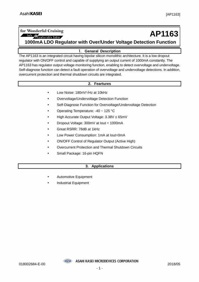
1. Genaral Description The AP1163 is an integrated circuit having bipolar silicon monolithic architecture. It is a low dropout regulator with ON/OFF control and capable of supplying an output current of 1000mA constantly. The AP1163 has regulator output voltage monitoring function, enabling to detect overvoltage and undervoltage. Self-diagnose function can detect a fault operation of overvoltage and undervoltage detections. In addition, overcurrent protection and thermal shutdown circuits are integrated.
2. Feartures
Low Noise: 180nV/√Hz at 10kHz
Overvoltage/Undervoltage Detection Function
Self-Diagnose Function for Overvoltage/Undervoltage Detection
Operating Temperature: -40 ~ 125 °C
High Accurate Output Voltage: 3.38V ± 65mV
Dropout Voltage: 300mV at Iout = 1000mA
Great RSRR: 78dB at 1kHz
Low Power Consumption: 1mA at Iout=0mA ON/OFF Control of Regulator Output (Active High)
Overcurrent Protection and Thermal Shutdown Circuits
Small Package: 16-pin HQFN
3. Applications Automotive Equipment
Industrial Equipment
1000mA LDO Regulator with Over/Under Voltage Detection Function
AP1163
[AP1163]
018002684-E-00 2018/05 - 2 -
4. Table of Contents
1. Genaral Description ............................................................................................................................ 1 2. Feartures ............................................................................................................................................. 1 3. Applications ......................................................................................................................................... 1 4. Table of Contents ................................................................................................................................ 2 5. Block Diagram and Functions ............................................................................................................. 3 6. Pin Configurations and Functions ....................................................................................................... 4
6.1 Pin Layout .................................................................................................................................... 4 6.2 Pin Function ................................................................................................................................. 4
7. Absolute Maximum Ratings ................................................................................................................ 5 8. Recommended Operating Conditions ................................................................................................ 6 9. Electrical Characteristics..................................................................................................................... 6 10. Functional Descriptions....................................................................................................................... 8
10.1 ON/OFF Control of Regulator Output .......................................................................................... 8 10.2 Protection Functions .................................................................................................................... 8 10.3 Self-Diagnose Function................................................................................................................ 9
11. Characteristic Examples ................................................................................................................... 10 12. Recommended External Circuits ...................................................................................................... 12
12.1. External Circuit Example ........................................................................................................... 12 12.2 Recommended board layout example ....................................................................................... 13
13. Package ............................................................................................................................................ 14 13.1 Outline Dimensions .................................................................................................................... 14 13.2 Marking ...................................................................................................................................... 14
14. Ordering Guide.................................................................................................................................. 15 15. Revision History ................................................................................................................................ 15 IMPORTANT NOTICE .............................................................................................................................. 16
[AP1163]
018002684-E-00 2018/05 - 3 -
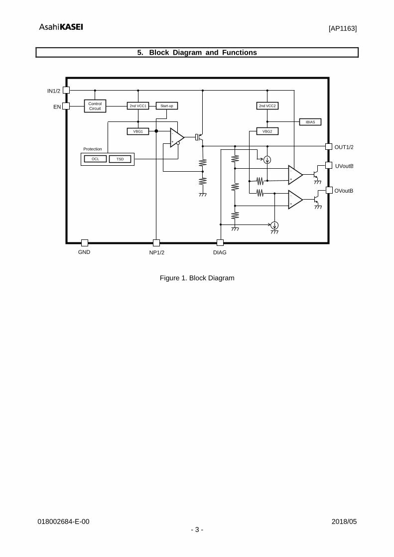
5. Block Diagram and Functions
OUT1/2 Protection
IN1/2
EN Control Circuit
OCL
TSD
NP1/2 GND DIAG
-
+
-
+
UVoutB
OVoutB
2nd VCC2
VBG2
IBIAS
Start-up
-
+
2nd VCC1
VBG1
Figure 1. Block Diagram
[AP1163]
018002684-E-00 2018/05 - 4 -
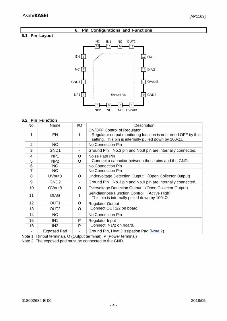
6. Pin Configurations and Functions 6.1 Pin Layout
EN
NC
GND1
NP1
OUT1
DIAG
OVoutB
GND2
1
2
3
4 9
10
11
12
Exposed Pad
OUT2 NC IN1 IN2
NP2 NC NC UVoutB 5 8 6 7
16 13 15 14
6.2 Pin Function No. Name I/O Description
1 EN I ON/OFF Control of Regulator
Regulator output monitoring function is not turned OFF by this setting. This pin is internally pulled down by 100kΩ.
2 NC - No Connection Pin 3 GND1 - Ground Pin No.3 pin and No.9 pin are internally connected. 4 NP1 O Noise Path Pin
Connect a capacitor between these pins and the GND. 5 NP2 O 6 NC - No Connection Pin 7 NC - No Connection Pin 8 UVoutB O Undervoltage Detection Output (Open Collector Output) 9 GND2 - Ground Pin No.3 pin and No.9 pin are internally connected. 10 OVoutB O Overvoltage Detection Output (Open Collector Output)
11 DIAG I Self-diagnose Function Control (Active High) This pin is internally pulled down by 100kΩ.
12 OUT1 O Regulator Output Connect OUT1/2 on board. 13 OUT2 O
14 NC - No Connection Pin 15 IN1 P Regulator Input
Connect IN1/2 on board. 16 IN2 P - Exposed Pad - Ground Pin, Heat Dissipation Pad (Note 2)
Note 1. I (Input terminal), O (Output terminal), P (Power terminal) Note 2. The exposed pad must be connected to the GND.
[AP1163]
018002684-E-00 2018/05 - 5 -
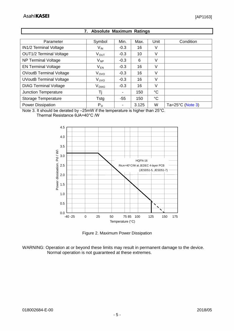
7. Absolute Maximum Ratings
Parameter Symbol Min. Max. Unit Condition IN1/2 Terminal Voltage VIN -0.3 16 V OUT1/2 Terminal Voltage VOUT -0.3 10 V NP Terminal Voltage VNP -0.3 6 V EN Terminal Voltage VEN -0.3 16 V OVoutB Terminal Voltage VOVO -0.3 16 V UVoutB Terminal Voltage VUVO -0.3 16 V DIAG Terminal Voltage VDIAG -0.3 16 V Junction Temperature Tj - 150 °C Storage Temperature Tstg -55 150 °C Power Dissipation PD - 3.125 W Ta=25°C (Note 3) Note 3. It should be derated by ‒25mW if the temperature is higher than 25°C.
Thermal Resistance θJA=40°C /W
-40 -25 0 25 50 75 85 100 125 150 175
4.5 4.0 3.5 3.0 2.5 2.0 1.5 1.0 0.5 0.0
Temperature (°C)
Pow
er d
issi
patio
n, P
d ( W
)
HQFN-16 RθJA=40°C/W at JEDEC 4-layer PCB
(JESD51-5, JESD51-7)
Figure 2. Maximum Power Dissipation WARNING: Operation at or beyond these limits may result in permanent damage to the device.
Normal operation is not guaranteed at these extremes.
[AP1163]
018002684-E-00 2018/05 - 6 -
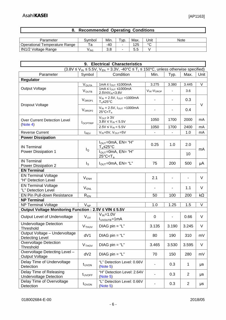
8. Recommended Operating Conditions
Parameter Symbol Min. Typ. Max. Unit Note Operational Temperature Range Ta -40 - 125 °C IN1/2 Voltage Range VIN1 3.8 - 5.5 V
9. Electrical Characteristics (3.8V ≤ VIN ≤ 5.5V, VEN = 3.3V, -40°C ≤ Tj ≤ 150°C, unless otherwise specified)
Parameter Symbol Condition Min. Typ. Max. Unit Regulator
Output Voltage VOUTA 1mA ≤ IOUT ≤1000mA 3.275 3.380 3.445 V VOUTB
1mA ≤ IOUT ≤1000mA 2.5V≤V IN<3.8V VIN-VDROP - 3.6
Dropout Voltage VDROP1
VIN = 2.5V, IOUT =1000mA Ta≤25°C - - 0.3
V VDROP2
VIN = 2.5V, IOUT =1000mA 25°C<Ta - - 0.4
Over Current Detection Level (Note 4) IOCPTRIP
VOUT ≥ 3V 3.8V ≤ V IN < 5.5V 1050 1700 2000 mA
2.5V ≤ V IN < 5.5V 1050 1700 2400 mA Reverse Current IREV VIN=0V, VOUT=5V - - 1.0 mA Power Dissipation
IN Terminal Power Dissipation 1 IQ
IOUT=0mA, EN= “H” Ta≤25°C 0.25 1.0 2.0
mA IOUT=0mA, EN= “H” 25°C<Ta
10
IN Terminal Power Dissipation 2 IS IOUT=0mA, EN= “L” 75 200 500 μA
EN Terminal EN Terminal Voltage “H” Detection Level VENH 2.1 - - V
EN Terminal Voltage ”L” Detection Level VENL - - 1.1 V
EN Pin Pull-down Resistance REN 50 100 200 kΩ NP Terminal NP Terminal Voltage VNP 1.0 1.25 1.5 V Output Voltage Monitoring Function : 2.5V ≤ VIN ≤ 5.5V
Output Level of Undervoltage VUV VIN=1.0V IUVOUTB=1mA 0 - 0.66 V
Undervoltage Detection Threshold VTHUV DIAG pin = “L” 3.135 3.190 3.245 V
Output Voltage ‒ Undervoltage Detecting Level dV1 DIAG pin = “L” 80 190 310 mV
Overvoltage Detection Threshold VTHOV DIAG pin = “L” 3.465 3.530 3.595 V
Overvoltage Detecting Level ‒ Output Voltage dV2 DIAG pin = “L” 70 150 280 mV
Delay Time of Undervoltage Detection tUVON “L” Detection Level: 0.66V
(Note 5) - 0.3 1 μs
Delay Time of Releasing Undervoltage Detection tUVOFF “H” Detection Level: 2.64V
(Note 5) - 0.3 2 μs
Delay Time of Overvoltage Detection tOVON “L” Detection Level: 0.66V
(Note 5) - 0.3 2 μs
[AP1163]
018002684-E-00 2018/05 - 7 -
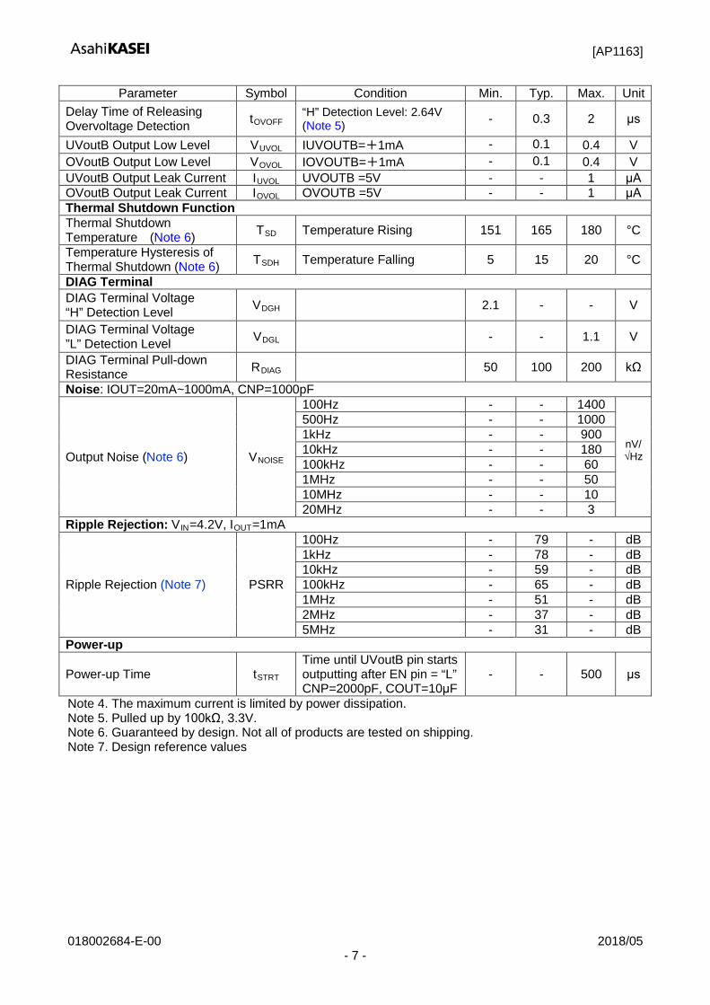
Parameter Symbol Condition Min. Typ. Max. Unit Delay Time of Releasing Overvoltage Detection tOVOFF “H” Detection Level: 2.64V
(Note 5) - 0.3 2 μs
UVoutB Output Low Level VUVOL IUVOUTB=+1mA - 0.1 0.4 V OVoutB Output Low Level VOVOL IOVOUTB=+1mA - 0.1 0.4 V UVoutB Output Leak Current IUVOL UVOUTB =5V - - 1 μA OVoutB Output Leak Current IOVOL OVOUTB =5V - - 1 μA Thermal Shutdown Function Thermal Shutdown Temperature (Note 6) TSD Temperature Rising 151 165 180 °C
Temperature Hysteresis of Thermal Shutdown (Note 6) TSDH Temperature Falling 5 15 20 °C
DIAG Terminal DIAG Terminal Voltage “H” Detection Level VDGH 2.1 - - V
DIAG Terminal Voltage ”L” Detection Level VDGL - - 1.1 V
DIAG Terminal Pull-down Resistance RDIAG 50 100 200 kΩ
Noise: IOUT=20mA~1000mA, CNP=1000pF
Output Noise (Note 6) VNOISE
100Hz - - 1400
nV/ √Hz
500Hz - - 1000 1kHz - - 900 10kHz - - 180 100kHz - - 60 1MHz - - 50 10MHz - - 10 20MHz - - 3
Ripple Rejection: VIN=4.2V, IOUT=1mA
Ripple Rejection (Note 7) PSRR
100Hz - 79 - dB 1kHz - 78 - dB 10kHz - 59 - dB 100kHz - 65 - dB 1MHz - 51 - dB 2MHz - 37 - dB 5MHz - 31 - dB
Power-up
Power-up Time tSTRT Time until UVoutB pin starts outputting after EN pin = “L” CNP=2000pF, COUT=10μF
- - 500 μs
Note 4. The maximum current is limited by power dissipation. Note 5. Pulled up by 100kΩ, 3.3V. Note 6. Guaranteed by design. Not all of products are tested on shipping. Note 7. Design reference values
[AP1163]
018002684-E-00 2018/05 - 8 -
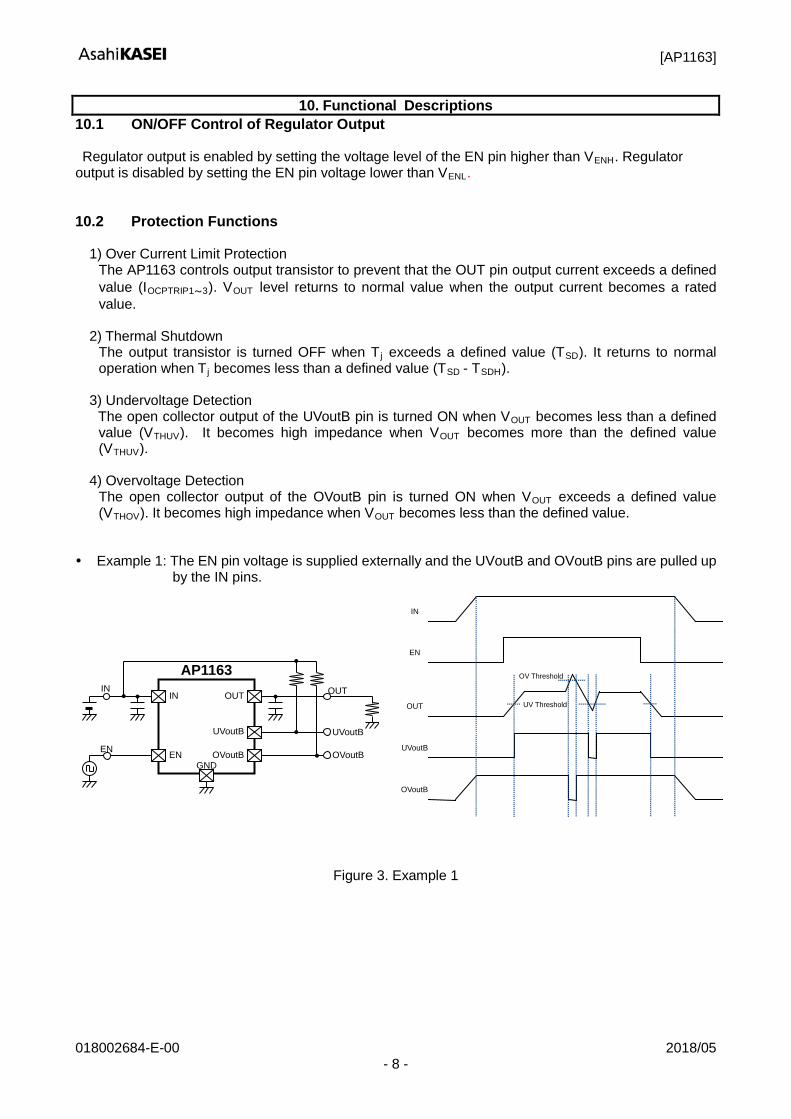
10. Functional Descriptions 10.1 ON/OFF Control of Regulator Output Regulator output is enabled by setting the voltage level of the EN pin higher than VENH. Regulator output is disabled by setting the EN pin voltage lower than VENL. 10.2 Protection Functions
1) Over Current Limit Protection The AP1163 controls output transistor to prevent that the OUT pin output current exceeds a defined value (IOCPTRIP1~3). VOUT level returns to normal value when the output current becomes a rated value.
2) Thermal Shutdown
The output transistor is turned OFF when Tj exceeds a defined value (TSD). It returns to normal operation when Tj becomes less than a defined value (TSD - TSDH).
3) Undervoltage Detection
The open collector output of the UVoutB pin is turned ON when VOUT becomes less than a defined value (VTHUV). It becomes high impedance when VOUT becomes more than the defined value (VTHUV).
4) Overvoltage Detection
The open collector output of the OVoutB pin is turned ON when VOUT exceeds a defined value (VTHOV). It becomes high impedance when VOUT becomes less than the defined value.
Example 1: The EN pin voltage is supplied externally and the UVoutB and OVoutB pins are pulled up
by the IN pins.
IN
AP1163
GND EN
OUT
UVoutB
OVoutB
IN
EN OVoutB
UVoutB
OUT
IN
EN
OUT
UVoutB
OVoutB
UV Threshold
OV Threshold
Figure 3. Example 1
[AP1163]
018002684-E-00 2018/05 - 9 -
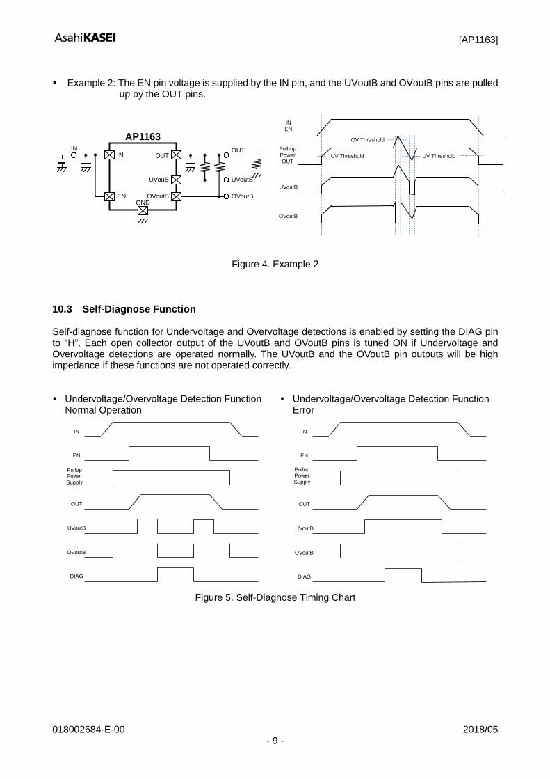
Example 2: The EN pin voltage is supplied by the IN pin, and the UVoutB and OVoutB pins are pulled
up by the OUT pins.
IN
AP1163
GND EN
OUT
UVouB
OVoutB
IN
OVoutB
UVoutB
OUT
IN EN
Pull-up Power OUT
UVoutB
OVoutB
OV Threshold
UV Threshold UV Threshold
Figure 4. Example 2 10.3 Self-Diagnose Function Self-diagnose function for Undervoltage and Overvoltage detections is enabled by setting the DIAG pin to “H”. Each open collector output of the UVoutB and OVoutB pins is tuned ON if Undervoltage and Overvoltage detections are operated normally. The UVoutB and the OVoutB pin outputs will be high impedance if these functions are not operated correctly. Undervoltage/Overvoltage Detection Function
Normal Operation Undervoltage/Overvoltage Detection Function
Error
IN
EN
Pullup Power Supply
OUT
UVoutB
OVoutB
DIAG
IN
EN
Pullup Power Supply
OUT
UVoutB
OVoutB
DIAG
Figure 5. Self-Diagnose Timing Chart
[AP1163]
018002684-E-00 2018/05 - 10 -
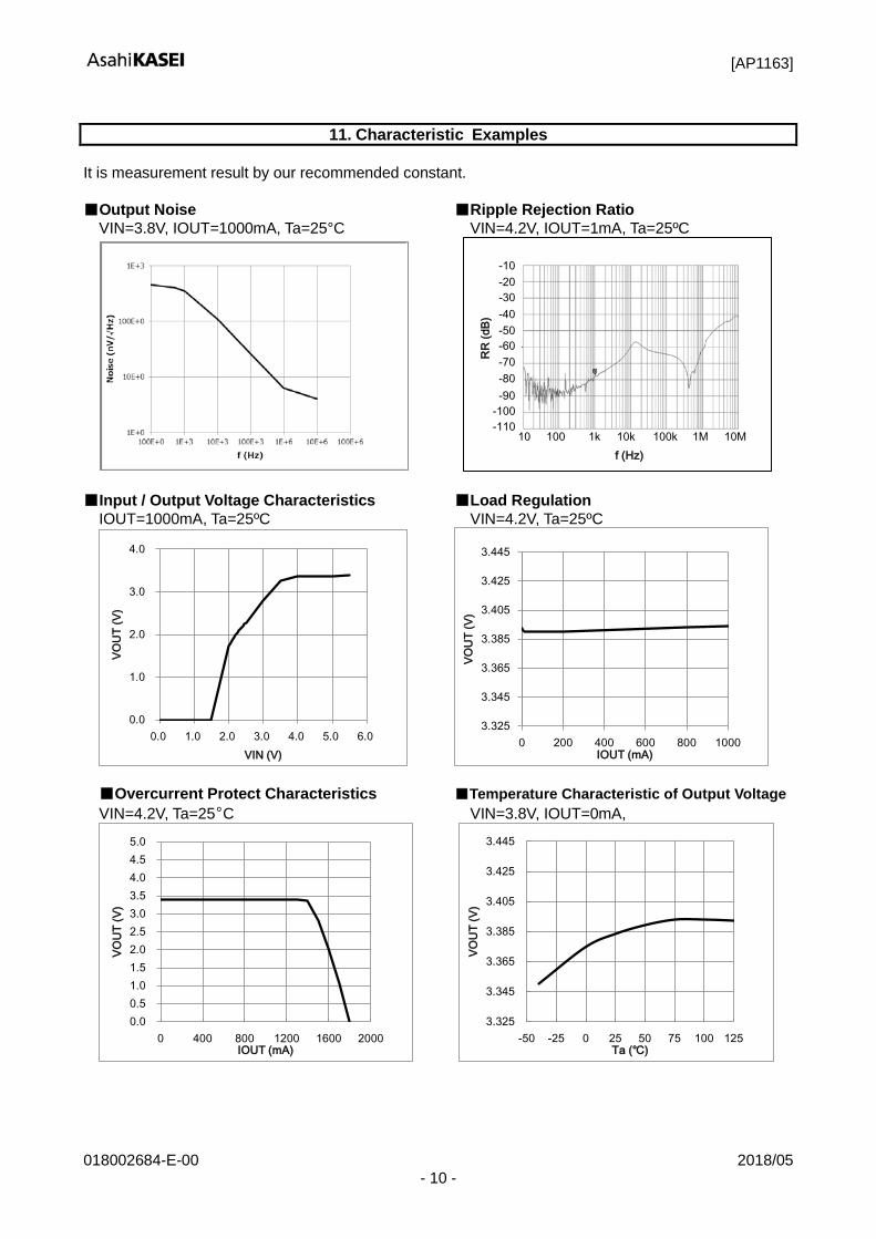
11. Characteristic Examples
It is measurement result by our recommended constant. ■Output Noise ■Ripple Rejection Ratio
VIN=3.8V, IOUT=1000mA, Ta=25°C VIN=4.2V, IOUT=1mA, Ta=25ºC
■Input / Output Voltage Characteristics ■Load Regulation
IOUT=1000mA, Ta=25ºC VIN=4.2V, Ta=25ºC
■Overcurrent Protect Characteristics ■Temperature Characteristic of Output Voltage VIN=4.2V, Ta=25ºC VIN=3.8V, IOUT=0mA,
-10-20-30-40-50-60-70-80-90
-100-110
100 10k 1M10 10M100k1kf (Hz)
RR
(dB)
0.0
1.0
2.0
3.0
4.0
0.0 1.0 2.0 3.0 4.0 5.0 6.0
VOU
T (V
)
VIN (V)
3.325
3.345
3.365
3.385
3.405
3.425
3.445
0 200 400 600 800 1000
VOU
T(V
)
IOUT (mA)
0.00.51.01.52.02.53.03.54.04.55.0
0 400 800 1200 1600 2000
VOU
T (V
)
IOUT (mA)
3.325
3.345
3.365
3.385
3.405
3.425
3.445
-50 -25 0 25 50 75 100 125
VOU
T(V
)
Ta (℃)
[AP1163]
018002684-E-00 2018/05 - 11 -
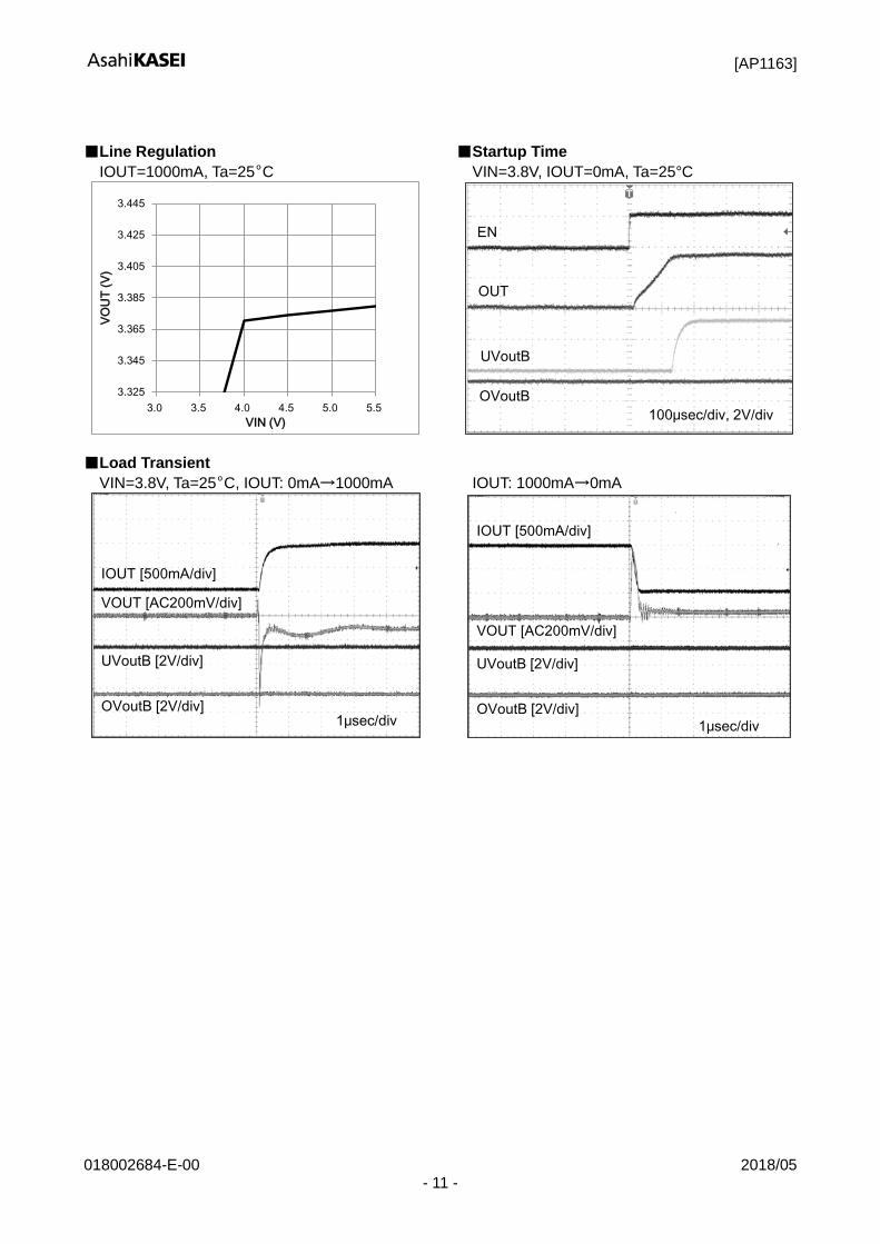
■Line Regulation ■Startup Time IOUT=1000mA, Ta=25ºC VIN=3.8V, IOUT=0mA, Ta=25°C
■Load Transient
VIN=3.8V, Ta=25ºC, IOUT: 0mA→1000mA IOUT: 1000mA→0mA
3.325
3.345
3.365
3.385
3.405
3.425
3.445
3.0 3.5 4.0 4.5 5.0 5.5
VOU
T (V
)
VIN (V)
EN
OUT
UVoutB
OVoutB100μsec/div, 2V/div
IOUT [500mA/div]
VOUT [AC200mV/div]
UVoutB [2V/div]
OVoutB [2V/div]1μsec/div
IOUT [500mA/div]
VOUT [AC200mV/div]
UVoutB [2V/div]
OVoutB [2V/div]1μsec/div
[AP1163]
018002684-E-00 2018/05 - 12 -
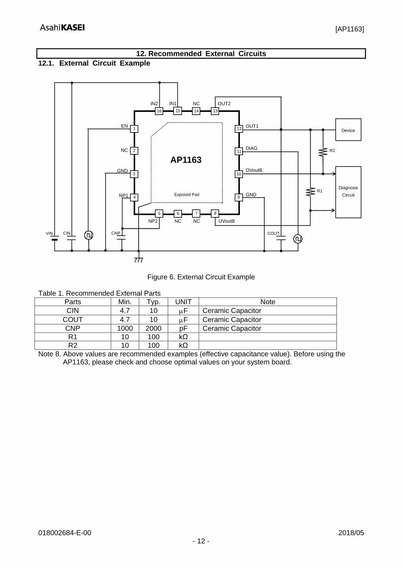
12. Recommended External Circuits 12.1. External Circuit Example
CNP
EN
NC
GND
NP1
OUT1
DIAG
OVoutB
GND
1
2
3
4 9
10
11
12
Exposed Pad
OUT2 NC IN1 IN2
NP2 NC NC UVoutB
16 13 15 14
VIN CIN
5 8 6 7
AP1163
Device
COUT
R1
Diagnosis Circuit
R2
Figure 6. External Circuit Example
Table 1. Recommended External Parts
Parts Min. Typ. UNIT Note CIN 4.7 10 µF Ceramic Capacitor
COUT 4.7 10 µF Ceramic Capacitor CNP 1000 2000 pF Ceramic Capacitor R1 10 100 kΩ R2 10 100 kΩ
Note 8. Above values are recommended examples (effective capacitance value). Before using the AP1163, please check and choose optimal values on your system board.
[AP1163]
018002684-E-00 2018/05 - 13 -
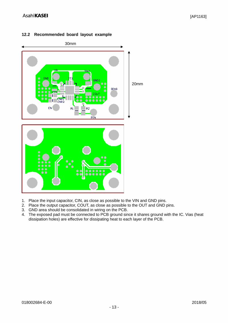
12.2 Recommended board layout example
1. Place the input capacitor, CIN, as close as possible to the VIN and GND pins. 2. Place the output capacitor, COUT, as close as possible to the OUT and GND pins. 3. GND area should be consolidated in wiring on the PCB. 4. The exposed pad must be connected to PCB ground since it shares ground with the IC. Vias (heat
dissipation holes) are effective for dissipating heat to each layer of the PCB.
20mm
30mm
[AP1163]
018002684-E-00 2018/05 - 14 -
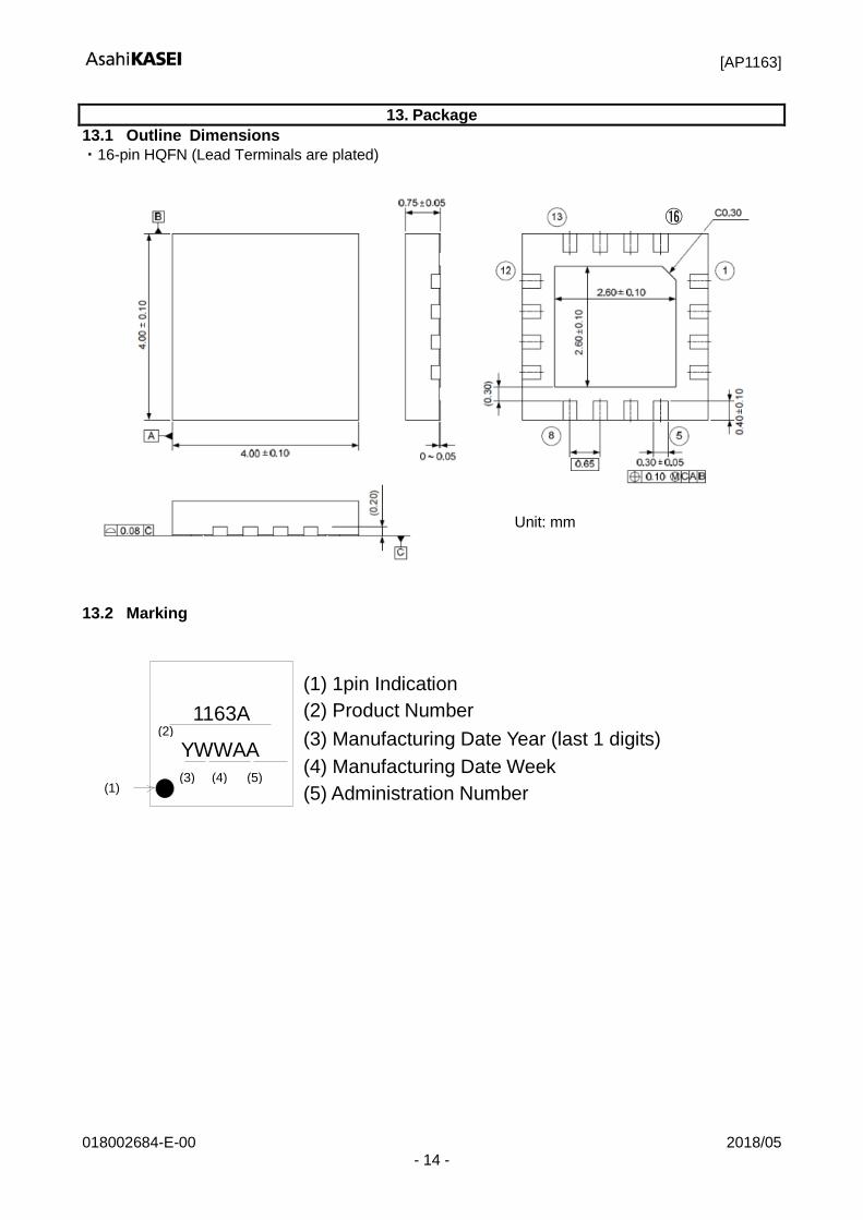
13. Package 13.1 Outline Dimensions ・16-pin HQFN (Lead Terminals are plated)
13.2 Marking
YWWAA
(1) 1pin Indication (2) Product Number (3) Manufacturing Date Year (last 1 digits) (4) Manufacturing Date Week (5) Administration Number
(1)
1163A
(3)
(2)
(4) (5)
Unit: mm
⑯
[AP1163]
018002684-E-00 2018/05 - 15 -
14. Ordering Guide
AP1163ABN -40 ~125°C 16-pin HQFN
15. Revision History Date (Y/M/D) Revision Reason Page Contents 18/05/30 00 First Edition
[AP1163]
018002684-E-00 2018/05 - 16 -
IMPORTANT NOTICE
0. Asahi Kasei Microdevices Corporation (“AKM”) reserves the right to make changes to the information contained in this document without notice. When you consider any use or application of AKM product stipulated in this document (“Product”), please make inquiries the sales office of AKM or authorized distributors as to current status of the Products.
1. All information included in this document are provided only to illustrate the operation and application examples of AKM Products. AKM neither makes warranties or representations with respect to the accuracy or completeness of the information contained in this document nor grants any license to any intellectual property rights or any other rights of AKM or any third party with respect to the information in this document. You are fully responsible for use of such information contained in this document in your product design or applications. AKM ASSUMES NO LIABILITY FOR ANY LOSSES INCURRED BY YOU OR THIRD PARTIES ARISING FROM THE USE OF SUCH INFORMATION IN YOUR PRODUCT DESIGN OR APPLICATIONS.
2. The Product is neither intended nor warranted for use in equipment or systems that require extraordinarily high levels of quality and/or reliability and/or a malfunction or failure of which may cause loss of human life, bodily injury, serious property damage or serious public impact, including but not limited to, equipment used in nuclear facilities, equipment used in the aerospace industry, medical equipment, equipment used for automobiles, trains, ships and other transportation, traffic signaling equipment, equipment used to control combustions or explosions, safety devices, elevators and escalators, devices related to electric power, and equipment used in finance-related fields. Do not use Product for the above use unless specifically agreed by AKM in writing.
3. Though AKM works continually to improve the Product’s quality and reliability, you are responsible for complying with safety standards and for providing adequate designs and safeguards for your hardware, software and systems which minimize risk and avoid situations in which a malfunction or failure of the Product could cause loss of human life, bodily injury or damage to property, including data loss or corruption.
4. Do not use or otherwise make available the Product or related technology or any information contained in this document for any military purposes, including without limitation, for the design, development, use, stockpiling or manufacturing of nuclear, chemical, or biological weapons or missile technology products (mass destruction weapons). When exporting the Products or related technology or any information contained in this document, you should comply with the applicable export control laws and regulations and follow the procedures required by such laws and regulations. The Products and related technology may not be used for or incorporated into any products or systems whose manufacture, use, or sale is prohibited under any applicable domestic or foreign laws or regulations.
5. Please contact AKM sales representative for details as to environmental matters such as the RoHS compatibility of the Product. Please use the Product in compliance with all applicable laws and regulations that regulate the inclusion or use of controlled substances, including without limitation, the EU RoHS Directive. AKM assumes no liability for damages or losses occurring as a result of noncompliance with applicable laws and regulations.
6. Resale of the Product with provisions different from the statement and/or technical features set forth in this document shall immediately void any warranty granted by AKM for the Product and shall not create or extend in any manner whatsoever, any liability of AKM.
7. This document may not be reproduced or duplicated, in any form, in whole or in part, without prior written consent of AKM.