Embed Size (px)
Citation preview

January 2015 Rev. 1.4 www.microsemi.com 1
© 2015 Microsemi Corporation- Analog Mixed Signal
1.5A Three Terminal Adjustable Voltage Regulator
Schematic Diagram
Figure 1 · Block Diagram
Features Adjustable Output Down to 1.25V
1% Output Voltage Tolerance
0.01%/V Line Regulation
0.3% Load Regulation
Min. 1.5A Output Current
Typical 80dB Ripple Rejection
Available in Hermetic TO-257
High Reliability Features – SG117A/SG117 Available to MIL-STD-883, ¶1.2.1
MSC-AMS level "S" Processing Available
Available to DSCC
– Standard Microcircuit Drawing (SMD)
MIL-M-38510/7703405XA SG117AT-JAN
MIL-M-38510/7703405YA SG117AK-JAN
Description The SG117 and SG117A are 3-terminal positive
adjustable voltage regulators which offer improved
performance over the original 117 design. A major
feature of the SG117A is a reference voltage tolerance
guaranteed within ± 1%, allowing an overall power
supply tolerance to be better than 3% using
inexpensive 1% resistors. Line and load regulation
performance has been improved as well.
Moreover, the SG117A reference voltage is guaranteed
not to exceed 2% when operating over the full load, line
and power dissipation conditions. The SG117A
adjustable regulators offer an improved solution for all
positive voltage regulator requirements with load
currents up to 1.5A.
In addition to replacing many fixed regulators, the
SG117/A can be used in a variety of other applications
due to its ‘floating’ design as long as the input-to-output
differential maximum is not exceeded, such as a
current source. A higher voltage version is available
the SG117AHV and SG117HV which offers input
voltage up to 60V.
SG117A/SG117

1.5A 3-Terminal Adjustable Voltage Regulator
2
Connection Diagrams and Ordering Information
Ambient
Temperature Type Package Part Number
Packaging
Type Connection Diagram
-55°C to
125°C K
3-TERMINAL
METAL CAN
SG117AK
TO-3
SG117AK-883B
SG117AK-DESC
SG117K
SG117K-883B
SG117K-DESC
SG117K-JAN
-55°C to
125°C T
3-TERMINAL
METAL CAN
SG117AT
TO-39
SG117AT-883B
SG117AT-DESC
SG117T
SG117T-883B
SG117T-DESC
SG117T-JAN
-55°C to
125°C IG
3-Pin
HERMETIC
Package
(Isolated)
SG117AIG
TO-257
Case is Isolated
SG117AIG-883B
SG117AIG-DESC
SG117IG
SG117IG-883B
SG117IG-DESC
-55°C to
125°C G
3-Pin
HERMETIC
Package
SG117AG
TO-257
Case is VOUT
SG117AG-883B
SG117AG-DESC
SG117G
SG117G-883B
SG117G-DESC
ADJUSTMENT
VIN
1
2
VIN
VOUT
ADJUST
VIN
VOUT
ADJUST
1
2 3
VIN
ADJUST VOUT

Connection Diagrams and Ordering Information
3
Connection Diagrams and Ordering Information
Ambient
Temperature Type Package Part Number
Packaging
Type Connection Diagram
-55°C to
125°C L
20-Pin
Ceramic
SG117AL
CLCC
SG117AL-883B
SG117AL-DESC
SG117L
SG117L-883B
SG117L-DESC
Notes: 1. Contact factory for JAN and DESC part availability.
2. All parts are viewed from the top.
3. For devices with multiple inputs and outputs both must be externally connected together at the device terminals.
4. For normal operation, the SENSE pin must be externally connected to the load.
5. These Hermetic Packages use Sn63/Pb37 hot solder dip lead finish, contact factory for availability of RoHS versions.
1.5A 3-Terminal Adjustable Voltage Regulator
4
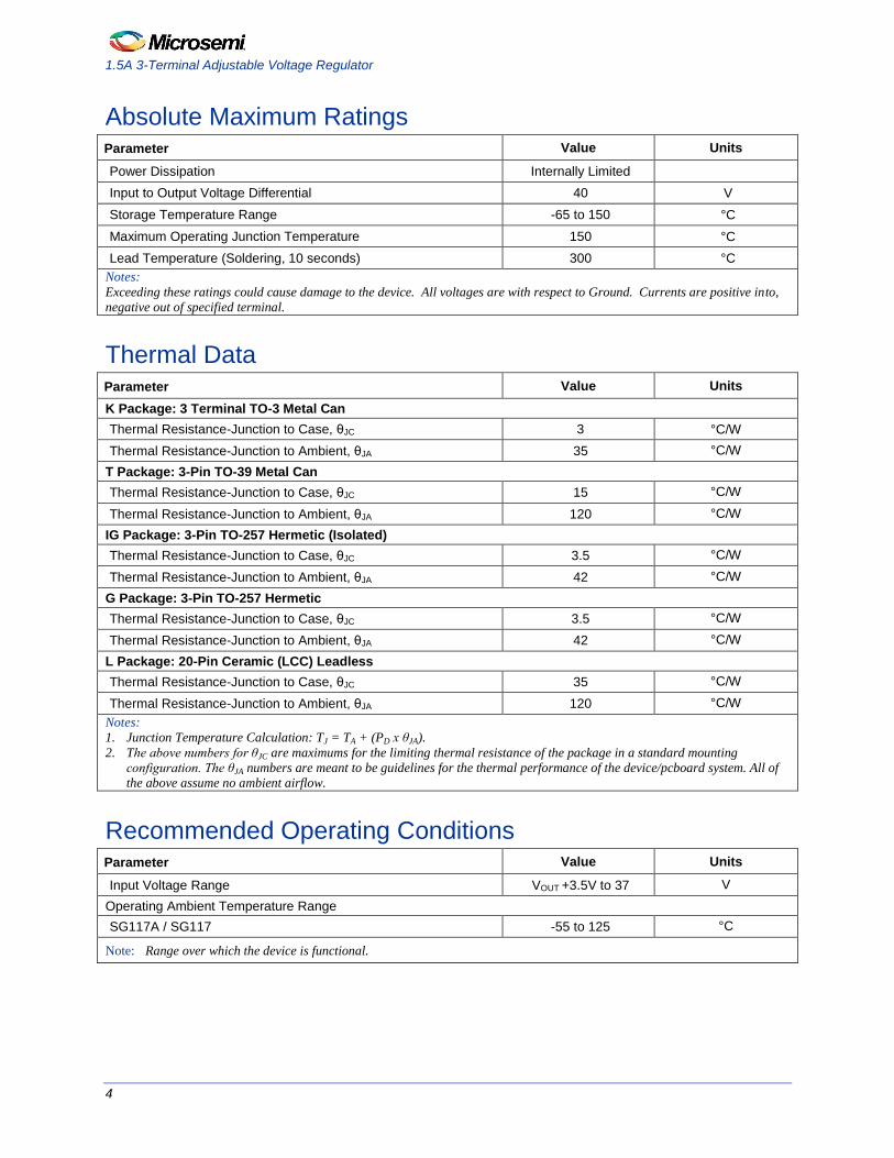
Absolute Maximum Ratings Parameter Value Units
Power Dissipation Internally Limited
Input to Output Voltage Differential 40 V
Storage Temperature Range -65 to 150 °C
Maximum Operating Junction Temperature 150 °C
Lead Temperature (Soldering, 10 seconds) 300 °C
Notes: Exceeding these ratings could cause damage to the device. All voltages are with respect to Ground. Currents are positive into,
negative out of specified terminal.
Thermal Data Parameter Value Units
K Package: 3 Terminal TO-3 Metal Can
Thermal Resistance-Junction to Case, θJC 3 °C/W
Thermal Resistance-Junction to Ambient, θJA 35 °C/W
T Package: 3-Pin TO-39 Metal Can
Thermal Resistance-Junction to Case, θJC 15 °C/W
Thermal Resistance-Junction to Ambient, θJA 120 °C/W
IG Package: 3-Pin TO-257 Hermetic (Isolated)
Thermal Resistance-Junction to Case, θJC 3.5 °C/W
Thermal Resistance-Junction to Ambient, θJA 42 °C/W
G Package: 3-Pin TO-257 Hermetic
Thermal Resistance-Junction to Case, θJC 3.5 °C/W
Thermal Resistance-Junction to Ambient, θJA 42 °C/W
L Package: 20-Pin Ceramic (LCC) Leadless
Thermal Resistance-Junction to Case, θJC 35 °C/W
Thermal Resistance-Junction to Ambient, θJA 120 °C/W
Notes: 1. Junction Temperature Calculation: TJ = TA + (PD x θJA).
2. The above numbers for θJC are maximums for the limiting thermal resistance of the package in a standard mounting
configuration. The θJA numbers are meant to be guidelines for the thermal performance of the device/pcboard system. All of
the above assume no ambient airflow.
Recommended Operating Conditions Parameter Value Units
Input Voltage Range VOUT +3.5V to 37 V
Operating Ambient Temperature Range
SG117A / SG117 -55 to 125 °C
Note: Range over which the device is functional.

Electrical Characteristics
5
Electrical Characteristics Unless otherwise specified, these characteristics apply over the full operating ambient temperature for the
SG117A / SG117 with -55°C < TA < 125°C, VIN – VOUT = 5.0V and for IOUT = 500mA (K, G, and IG) and IOUT =
100mA (T, and L packages). Although power dissipation is internally limited, these specifications are
applicable for power dissipations of 2W for the T, and L packages, and 20W for the K, G, and IG packages.
IMAX is 1.5A for the K, G, and IG packages and 500mA for the T, and L packages. Low duty cycle pulse
testing techniques are used which maintains junction and case temperatures equal to the ambient
temperature.
Parameter Test Condition
SG117A SG117
Units
Min Typ Max Min Typ Max
Reference Section
Reference Voltage
IOUT = 10mA, TA = 25°C 1.238 1.250 1.262
V 3V ≤ (VIN – VOUT ) ≤ 40V, P ≤ PMAX 1.225 1.250 1.270 1.20 1.25 1.30 10mA ≤ IOUT ≤ IMAX
Output Section
Line Regulation¹
3V ≤ (VIN – VOUT) ≤ 40V, IL = 10mA
TA = 25°C 0.005 0.01 0.01 0.02 %/V
TA = TMIN to TMAX 0.01 0.02 0.02 0.05
Load Regulation¹
10mA ≤ IOUT ≤ IMAX
VOUT ≤ 5V, TA = 25°C 5 15 5 15 mV
VOUT > 5V, TA = 25°C 0.1 0.3 0.1 0.3 %
VOUT ≤ 5V 20 50 20 50 mV
VOUT > 5V 0.3 1 0.3 1 %
Thermal Regulation² TA = 25°C, 20ms pulse 0.002 0.02 0.03 0.07 %/W
Ripple Rejection VOUT = 10V, f = 120Hz
CADJ = 1µF, TA = 25°C 65 65 dB
CADJ = 10µF 66 80 66 80
Minimum Load Current (VIN – VOUT) = 40V 3.5 5 3.5 5 mA
Current Limit (VIN – VOUT) ≤ 15V
K, P, G, IG Packages 1.5 2.2 1.5 2.2 A
T, L Packages 0.5 0.8 0.5 0.8
(VIN – VOUT) = 40V, TJ = 25°C
K, P, G, IG Packages 0.3 0.4 0.3 0.4 A
T, L Packages 0.15 0.2 0.15 0.2
Temperature Stability² 1 2 1
% Long Term Stability² TA = 125°C, 1000 Hours 0.3 1 0.3 1
RMS Output Noise (% of VOUT)²
TA = 25°C, 10Hz ≤ f ≤ 10kHz 0.001 0.001
Adjust Section
Adjust Pin Current 50 100 50 100
µA Adjust Pin Current Change
10mA < IOUT < IMAX,
2.5V < (VIN – VOUT) < 40V 0.2 5 0.2 5
¹Regulation is measured at constant junction temperature, using pulse testing with low duty cycle. Changes in output voltage
due to heating effects are covered under the specification for thermal regulation.
²These parameters, although guaranteed, are not tested in production.

1.5A 3-Terminal Adjustable Voltage Regulator
6
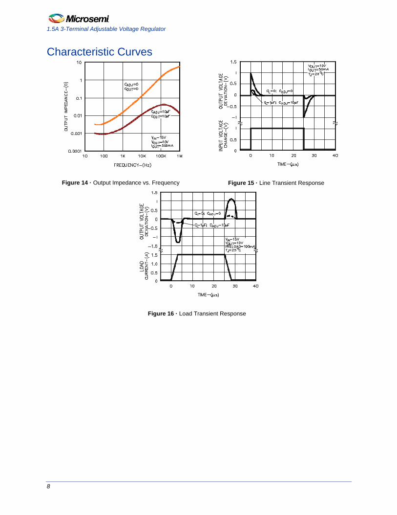
Characteristic Curves
Figure 2 · Output Voltage Deviation vs. Temperature
Figure 3 · Output Current vs. Input / Output Differential
Figure 4 · Adjust Current vs. Temperature
Figure 5 · Input / Output Differential vs. Temperature
Figure 6 · Reference Voltage vs. Temperature
Figure 7 · Quiescent Current vs. Input /Output
Differential
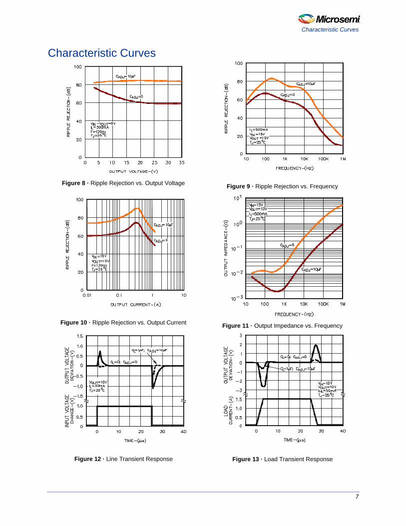
Characteristic Curves
7
Characteristic Curves
Figure 8 · Ripple Rejection vs. Output Voltage
Figure 9 · Ripple Rejection vs. Frequency
Figure 10 · Ripple Rejection vs. Output Current
Figure 11 · Output Impedance vs. Frequency
Figure 12 · Line Transient Response
Figure 13 · Load Transient Response
1.5A 3-Terminal Adjustable Voltage Regulator
8
Characteristic Curves
Figure 14 · Output Impedance vs. Frequency
Figure 15 · Line Transient Response
Figure 16 · Load Transient Response

Application Information
9
Application Information General
The SG117A develops a 1.25V reference voltage between the output (OUT) and the adjust (ADJ) terminals (see Basic Regulator Circuit). By placing a resistor, R1 between these two terminals, a constant current is caused to flow through R1 and down through R2 to set the overall output voltage. Normally this current is the specified minimum load current of 5mA or 10mA. It is important to maintain this minimum output load current requirement otherwise the device may fail to regulate, and the output voltage may rise.
2ADJ
1
2
REFOUTRI
R
R1VV
Figure 17 · Basic Regulator Circuit
The IADJ current does add an error to the output divider ratio, however because IADJ is very small and constant when compared with the current through R1, it represents a small error and can often be ignored.
It is easily seen from the above equation, that even if the resistors were of exact value, the accuracy of the output is limited by the accuracy of VREF. With a guaranteed 1% reference, a 5V power supply design, using ±2% resistors, would have a worse case manufacturing tolerance of ± 4%. If 1% resistors were used, the tolerance would drop to ± 2.5%. A plot of the worst case output voltage tolerance as a function of resistor tolerance is shown below.
Figure 18 · Voltage Tolerance vs. Resistor Tolerance
Bypass Capacitors
Input bypassing using a 0.1 μF ceramic or 1μF solid tantalum is recommended, and especially when any input filter capacitors are more than 5 inches from the device. A 0.1µF bypass capacitor on the ADJ pin is required if the load current varies by more than 1A/µsec. Improved ripple rejection (80dB) can be accomplished by adding a 10μF capacitor from the ADJ pin to ground.
Figure 19 · Improving Ripple Rejection
1.5A 3-Terminal Adjustable Voltage Regulator
10
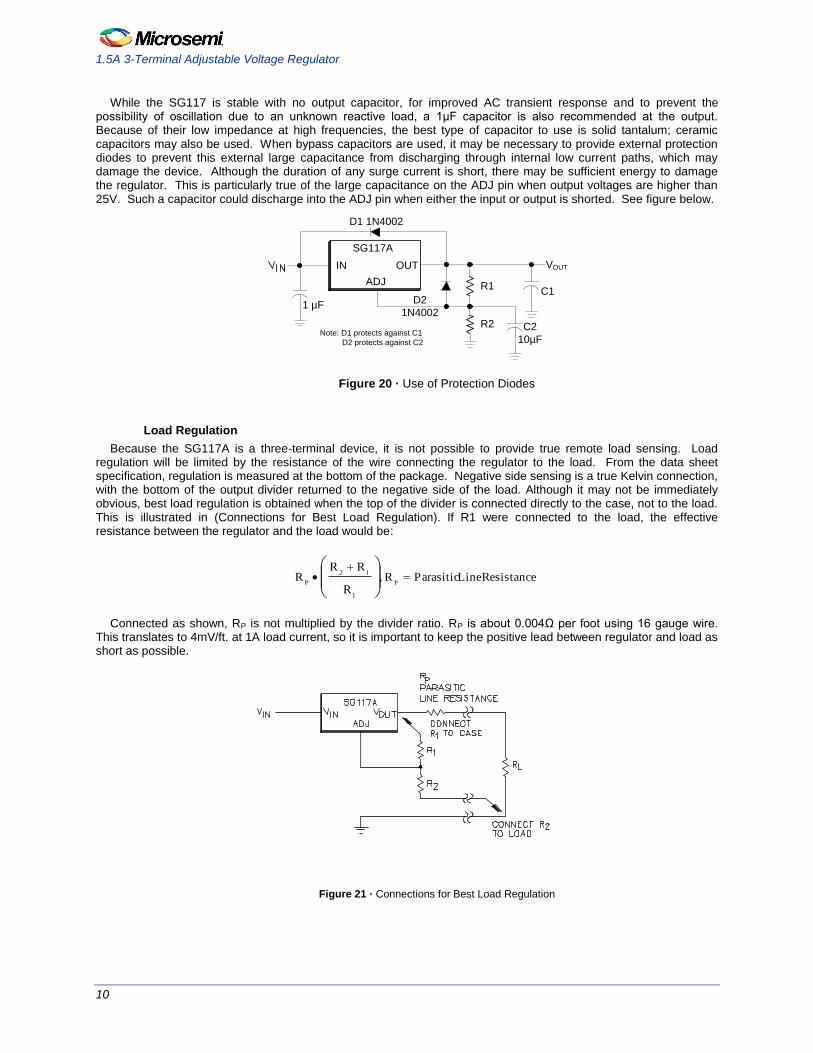
While the SG117 is stable with no output capacitor, for improved AC transient response and to prevent the possibility of oscillation due to an unknown reactive load, a 1μF capacitor is also recommended at the output. Because of their low impedance at high frequencies, the best type of capacitor to use is solid tantalum; ceramic capacitors may also be used. When bypass capacitors are used, it may be necessary to provide external protection diodes to prevent this external large capacitance from discharging through internal low current paths, which may damage the device. Although the duration of any surge current is short, there may be sufficient energy to damage the regulator. This is particularly true of the large capacitance on the ADJ pin when output voltages are higher than 25V. Such a capacitor could discharge into the ADJ pin when either the input or output is shorted. See figure below.
Figure 20 · Use of Protection Diodes
Load Regulation
Because the SG117A is a three-terminal device, it is not possible to provide true remote load sensing. Load regulation will be limited by the resistance of the wire connecting the regulator to the load. From the data sheet specification, regulation is measured at the bottom of the package. Negative side sensing is a true Kelvin connection, with the bottom of the output divider returned to the negative side of the load. Although it may not be immediately obvious, best load regulation is obtained when the top of the divider is connected directly to the case, not to the load. This is illustrated in (Connections for Best Load Regulation). If R1 were connected to the load, the effective resistance between the regulator and the load would be:
Resistance Line ParasiticR,R
RRR
P
1
12
P
Connected as shown, RP is not multiplied by the divider ratio. RP is about 0.004Ω per foot using 16 gauge wire. This translates to 4mV/ft. at 1A load current, so it is important to keep the positive lead between regulator and load as short as possible.
Figure 21 · Connections for Best Load Regulation
SG117A
OUT
ADJ
IN VOUT
R1
R2
D2
1N4002
C1
1 µF
D1 1N4002
C2
10µFNote: D1 protects against C1
D2 protects against C2

Application Information
11
Current Limit
As outlined in the Electrical Characteristics the current limit will activate whenever the output current exceeds the specified levels. It is also important to bear in mind that the regulator includes a foldback-current characteristic that limits the current at higher VIN to VOUT differential voltages. This power limiting characteristic will prevent the regulator from providing full output current depending on the VIN to V= differential. Also if during a short circuit situation the regulator was presented with a voltage that exceeds the Absolute Maximum Rating of 40V (e.g. VIN > 40V, VOUT = 0V) the device may fail, or be permanently damaged.
Typical Applications
Figure 22 · 1.2V – 25V Adjustable Regulator
Figure 23 · 5V Regulator with Shut Down
Figure 24 ·
Figure 25 · Programmable Current Limiter
SG117A
OUT
ADJ
IN IOUT = VREF/R1*
* 0.8Ω ≤ R1 ≤ 120Ω
R1
1.5A 3-Terminal Adjustable Voltage Regulator
12
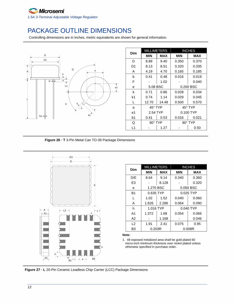
PACKAGE OUTLINE DIMENSIONS Controlling dimensions are in inches, metric equivalents are shown for general information.
Q
α k
k1
e
e1
A
D1
D
b
b1
L
F
L1
Dim MILLIMETERS INCHES
MIN MAX MIN MAX
D 8.89 9.40 0.350 0.370
D1 8.13 8.51 0.320 0.335
A 4.19 4.70 0.165 0.185
b 0.41 0.48 0.016 0.019
F - 1.02 - 0.040
e 5.08 BSC 0.200 BSC
k 0.71 0.86 0.028 0.034
k1 0.74 1.14 0.029 0.045
L 12.70 14.48 0.500 0.570
α 45° TYP 45° TYP
e1 2.54 TYP 0.100 TYP
b1 0.41 0.53 0.016 0.021
Q 90° TYP 90° TYP
L1 - 1.27 - 0.50
Figure 26 · T 3-Pin Metal Can TO-39 Package Dimensions
D
E3
LL2
B1e B3A2
A1
A
1
3
8
13
18
h
E
Dim MILLIMETERS INCHES
MIN MAX MIN MAX
D/E 8.64 9.14 0.340 0.360
E3 - 8.128 - 0.320
e 1.270 BSC 0.050 BSC
B1 0.635 TYP 0.025 TYP
L 1.02 1.52 0.040 0.060
A 1.626 2.286 0.064 0.090
h 1.016 TYP 0.040 TYP
A1 1.372 1.68 0.054 0.066
A2 - 1.168 - 0.046
L2 1.91 2.41 0.075 0.95
B3 0.203R 0.008R
Note:
1. All exposed metalized area shall be gold plated 60 micro-inch minimum thickness over nickel plated unless otherwise specified in purchase order.
Figure 27 · L 20-Pin Ceramic Leadless Chip Carrier (LCC) Package Dimensions

PACKAGE OUTLINE DIMENSIONS
13
PACKAGE OUTLINE DIMENSIONS
e A2
E
V
b
P
Z
H
A
A1
L
D1
D
J
O
Dim MILLIMETERS INCHES
MIN MAX MIN MAX
A 4.70 5.21 0.185 0.205
A1 0.89 1.14 0.035 0.045
A2 2.92 3.18 0.115 0.125
b 0.71 .081 0.027 0.032
D 16.38 16.76 0.645 0.660
D1* 10.41 10.92 0.410 0.430
e 2.54 BSC 0.100 BSC
E* 10.41 10.67 0.410 0.420
H
0.50
0.020
L 12.70 0.500
O 13.39 13.64 0.527 0.537
P 3.56 3.81 0.140 0.150
J
0.10
0.004
V 5.13 5.38 0.202 0.212
Z 1.40 TYP 0.055 TYP
*Excludes Weld Fillet Around Lid.
Figure 28 · G/IG 3-Pin Hermetic TO-257 Package Dimensions
D
A
L
F
e1
q
S
b
R
e
R1
Dim MILLIMETERS INCHES
MIN MAX MIN MAX
A 6.86 7.62 0.270 0.300
q 29.90 30.40 1.177 1.197
b 0.97 1.09 0.038 0.043
D 19.43 19.68 0.765 0.775
S 16.64 17.14 0.655 0.675
e 10.67 11.18 0.420 0.440
E1 5.21 5.72 0.205 0.225
F 1.52 2.03 0.060 0.080
R1 3.84 4.09 0.151 0.161
L 10.79 12.19 0.425 0.480
R 12.57 13.34 0.495 0.525
Figure 29 · K 3-Pin TO-3 Package Dimensions
SG117 1.4/01.15
Microsemi Corporation (Nasdaq: MSCC) offers a comprehensive portfolio of semiconductor
and system solutions for communications, defense & security, aerospace and industrial
markets. Products include high-performance and radiation-hardened analog mixed-signal
integrated circuits, FPGAs, SoCs and ASICs; power management products; timing and
synchronization devices and precise time solutions, setting the world’s standard for time; voice
processing devices; RF solutions; discrete components; security technologies and scalable
anti-tamper products; Power-over-Ethernet ICs and midspans; as well as custom design
capabilities and services. Microsemi is headquartered in Aliso Viejo, Calif., and has
approximately 3,400 employees globally. Learn more at www.microsemi.com.
Microsemi makes no warranty, representation, or guarantee regarding the information contained herein or
the suitability of its products and services for any particular purpose, nor does Microsemi assume any
liability whatsoever arising out of the application or use of any product or circuit. The products sold
hereunder and any other products sold by Microsemi have been subject to limited testing and should not
be used in conjunction with mission-critical equipment or applications. Any performance specifications are
believed to be reliable but are not verified, and Buyer must conduct and complete all performance and
other testing of the products, alone and together with, or installed in, any end-products. Buyer shall not
rely on any data and performance specifications or parameters provided by Microsemi. It is the Buyer’s
responsibility to independently determine suitability of any products and to test and verify the same. The
information provided by Microsemi hereunder is provided “as is, where is” and with all faults, and the
entire risk associated with such information is entirely with the Buyer. Microsemi does not grant, explicitly
or implicitly, to any party any patent rights, licenses, or any other IP rights, whether with regard to such
information itself or anything described by such information. Information provided in this document is
proprietary to Microsemi, and Microsemi reserves the right to make any changes to the information in this
document or to any products and services at any time without notice.
© 2015 Microsemi Corporation. All rights reserved. Microsemi and the Microsemi logo are trademarks of Microsemi Corporation. All other trademarks and service marks are the property of their respective owners.
Microsemi Corporate Headquarters One Enterprise, Aliso Viejo, CA 92656 USA Within the USA: +1 (800) 713-4113 Outside the USA: +1 (949) 380-6100 Sales: +1 (949) 380-6136 Fax: +1 (949) 215-4996
E-mail: [email protected]