Embed Size (px)
Citation preview
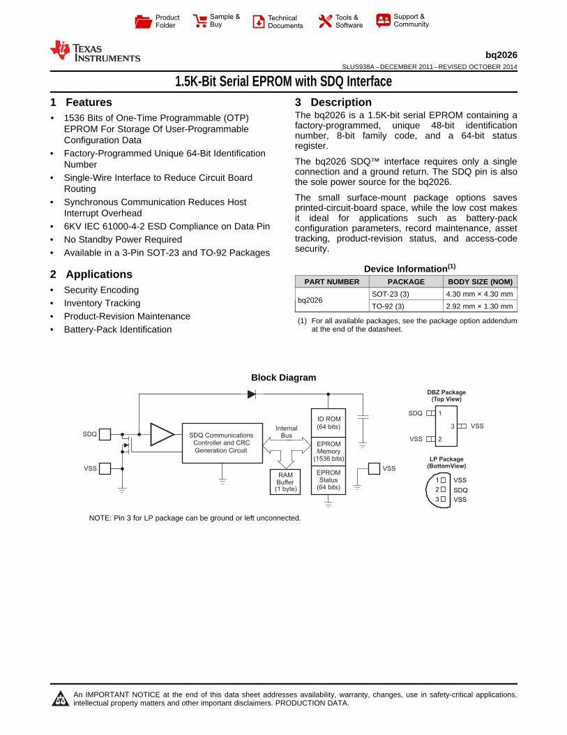
DBZ Package(Top View)
LP Package(BottomView)
ID ROM
(64 bits)
EPROMMemory
(1536 bits)
EPROMStatus
(64 bits)
SDQ CommunicationsController and CRC
Generation Circuit
InternalBus
RAMBuffer(1 byte)
SDQ
VSS VSS
VSS
SDQ
VSS
1
2
3
1
VSS
2
3
VSS
SDQ
Product
Folder
Sample &Buy
Technical
Documents
Tools &
Software
Support &Community
bq2026SLUS938A –DECEMBER 2011–REVISED OCTOBER 2014
1.5K-Bit Serial EPROM with SDQ Interface1 Features 3 Description
The bq2026 is a 1.5K-bit serial EPROM containing a1• 1536 Bits of One-Time Programmable (OTP)
factory-programmed, unique 48-bit identificationEPROM For Storage Of User-Programmablenumber, 8-bit family code, and a 64-bit statusConfiguration Data register.
• Factory-Programmed Unique 64-Bit IdentificationThe bq2026 SDQ™ interface requires only a singleNumberconnection and a ground return. The SDQ pin is also• Single-Wire Interface to Reduce Circuit Board the sole power source for the bq2026.
RoutingThe small surface-mount package options saves• Synchronous Communication Reduces Host printed-circuit-board space, while the low cost makesInterrupt Overhead it ideal for applications such as battery-pack
• 6KV IEC 61000-4-2 ESD Compliance on Data Pin configuration parameters, record maintenance, assettracking, product-revision status, and access-code• No Standby Power Requiredsecurity.• Available in a 3-Pin SOT-23 and TO-92 Packages
Device Information(1)2 Applications
PART NUMBER PACKAGE BODY SIZE (NOM)• Security Encoding SOT-23 (3) 4.30 mm × 4.30 mm
bq2026• Inventory Tracking TO-92 (3) 2.92 mm × 1.30 mm• Product-Revision Maintenance (1) For all available packages, see the package option addendum
at the end of the datasheet.• Battery-Pack Identification
Block Diagram
NOTE: Pin 3 for LP package can be ground or left unconnected.
1
An IMPORTANT NOTICE at the end of this data sheet addresses availability, warranty, changes, use in safety-critical applications,intellectual property matters and other important disclaimers. PRODUCTION DATA.
bq2026SLUS938A –DECEMBER 2011–REVISED OCTOBER 2014 www.ti.com
Table of Contents1 Features .................................................................. 1 7 Detailed Description .............................................. 5
7.1 Overview ................................................................... 52 Applications ........................................................... 17.2 Functional Block Diagram ......................................... 53 Description ............................................................. 17.3 Feature Description................................................... 54 Revision History..................................................... 27.4 Device Functional Modes.......................................... 65 Pin Configuration and Functions ......................... 3
8 Device and Documentation Support.................. 156 Specifications......................................................... 38.1 Trademarks ............................................................. 156.1 Absolute Maximum Ratings ...................................... 38.2 Electrostatic Discharge Caution.............................. 156.2 Handling Ratings....................................................... 38.3 Glossary .................................................................. 156.3 Electrical Characteristics: DC ................................... 4
9 Mechanical, Packaging, and Orderable6.4 Switching Characteristcs: AC.................................... 4Information ........................................................... 15
4 Revision History
Changes from Original (April 2013) to Revision A Page
• Changed document format to latest data sheet standards .................................................................................................... 1• Added Handling Rating table, Feature Description, Device Functional Modes, Device and Documentation Support,
and Mechanical, Packaging, and Orderable Information sections ......................................................................................... 1• Added note to front page diagram ......................................................................................................................................... 1• Changed pin 3 (VSS) description for LP package.................................................................................................................. 3
2 Submit Documentation Feedback Copyright © 2011–2014, Texas Instruments Incorporated
Product Folder Links: bq2026
1
VSS
2
3
VSS
SDQ
VSS
SDQ
VSS
1
2
3
bq2026www.ti.com SLUS938A –DECEMBER 2011–REVISED OCTOBER 2014
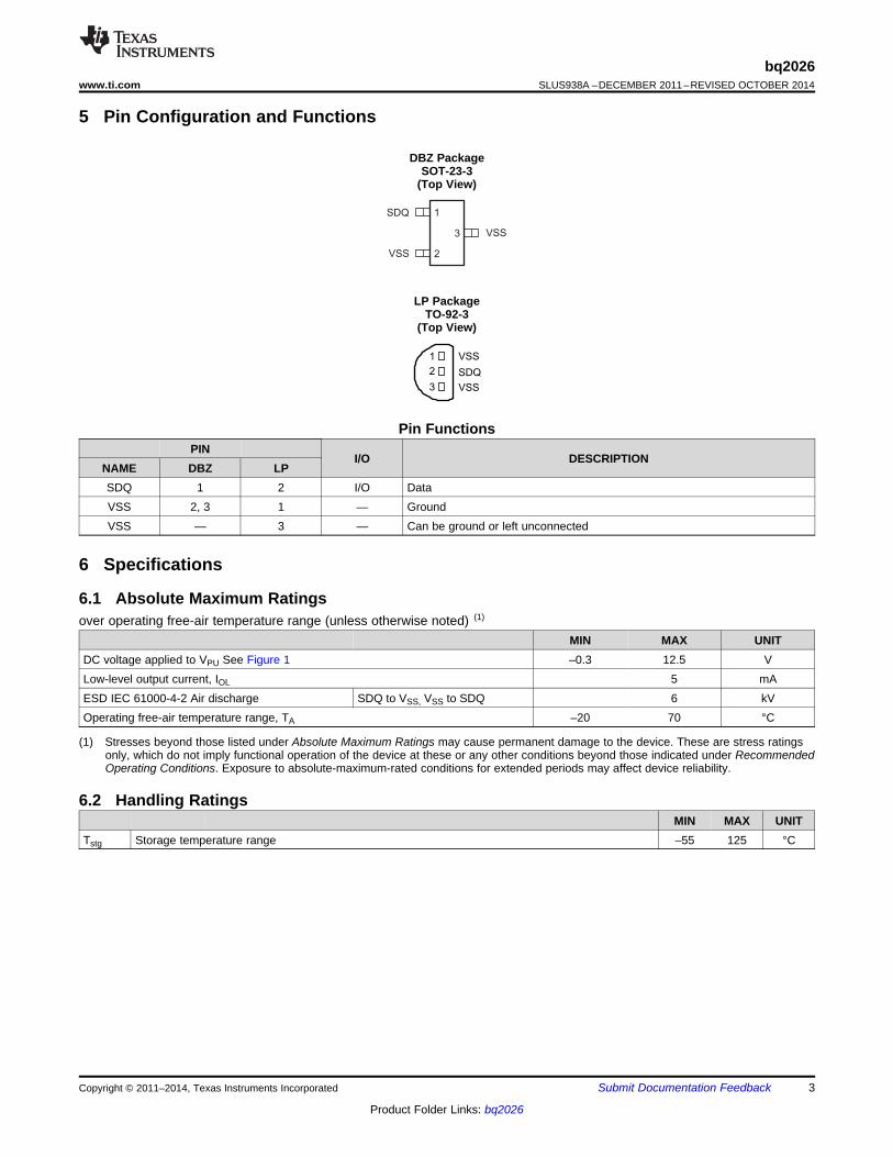
5 Pin Configuration and Functions
DBZ PackageSOT-23-3
(Top View)
LP PackageTO-92-3
(Top View)
Pin FunctionsPIN
I/O DESCRIPTIONNAME DBZ LPSDQ 1 2 I/O DataVSS 2, 3 1 — GroundVSS — 3 — Can be ground or left unconnected
6 Specifications
6.1 Absolute Maximum Ratingsover operating free-air temperature range (unless otherwise noted) (1)
MIN MAX UNITDC voltage applied to VPU See Figure 1 –0.3 12.5 VLow-level output current, IOL 5 mAESD IEC 61000-4-2 Air discharge SDQ to VSS, VSS to SDQ 6 kVOperating free-air temperature range, TA –20 70 °C
(1) Stresses beyond those listed under Absolute Maximum Ratings may cause permanent damage to the device. These are stress ratingsonly, which do not imply functional operation of the device at these or any other conditions beyond those indicated under RecommendedOperating Conditions. Exposure to absolute-maximum-rated conditions for extended periods may affect device reliability.
6.2 Handling RatingsMIN MAX UNIT
Tstg Storage temperature range –55 125 °C
Copyright © 2011–2014, Texas Instruments Incorporated Submit Documentation Feedback 3
Product Folder Links: bq2026
bq2026SLUS938A –DECEMBER 2011–REVISED OCTOBER 2014 www.ti.com
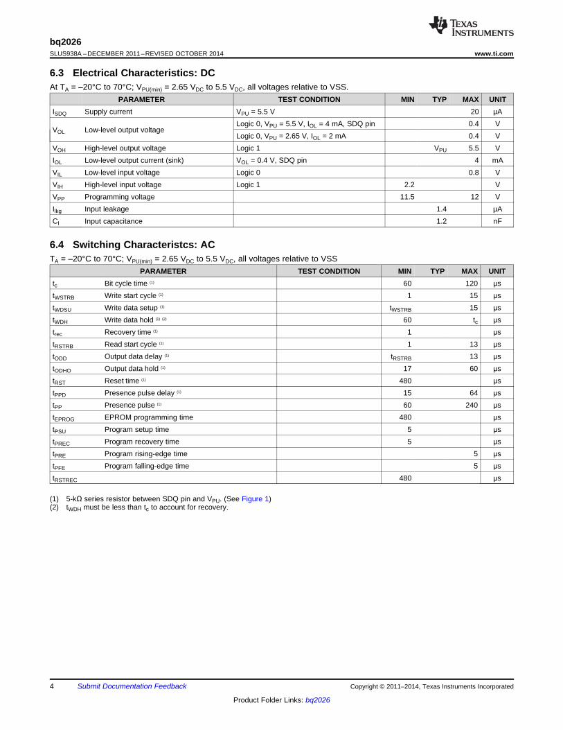
6.3 Electrical Characteristics: DCAt TA = –20°C to 70°C; VPU(min) = 2.65 VDC to 5.5 VDC, all voltages relative to VSS.
PARAMETER TEST CONDITION MIN TYP MAX UNITISDQ Supply current VPU = 5.5 V 20 μA
Logic 0, VPU = 5.5 V, IOL = 4 mA, SDQ pin 0.4 VVOL Low-level output voltage
Logic 0, VPU = 2.65 V, IOL = 2 mA 0.4 VVOH High-level output voltage Logic 1 VPU 5.5 VIOL Low-level output current (sink) VOL = 0.4 V, SDQ pin 4 mAVIL Low-level input voltage Logic 0 0.8 VVIH High-level input voltage Logic 1 2.2 VVPP Programming voltage 11.5 12 VIlkg Input leakage 1.4 µACI Input capacitance 1.2 nF
6.4 Switching Characteristcs: ACTA = –20°C to 70°C; VPU(min) = 2.65 VDC to 5.5 VDC, all voltages relative to VSS
PARAMETER TEST CONDITION MIN TYP MAX UNITtc Bit cycle time (1) 60 120 μstWSTRB Write start cycle (1) 1 15 μstWDSU Write data setup (1) tWSTRB 15 μstWDH Write data hold (1) (2) 60 tc μstrec Recovery time (1) 1 μstRSTRB Read start cycle (1) 1 13 μstODD Output data delay (1) tRSTRB 13 μstODHO Output data hold (1) 17 60 μstRST Reset time (1) 480 μstPPD Presence pulse delay (1) 15 64 μstPP Presence pulse (1) 60 240 μstEPROG EPROM programming time 480 μstPSU Program setup time 5 μstPREC Program recovery time 5 μstPRE Program rising-edge time 5 μstPFE Program falling-edge time 5 μstRSTREC 480 μs
(1) 5-kΩ series resistor between SDQ pin and VPU. (See Figure 1)(2) tWDH must be less than tc to account for recovery.
4 Submit Documentation Feedback Copyright © 2011–2014, Texas Instruments Incorporated
Product Folder Links: bq2026
ID ROM
(64 bits)
EPROMMemory
(1536 bits)
EPROMStatus
(64 bits)
SDQ CommunicationsController and CRC
Generation Circuit
InternalBus
RAMBuffer(1 byte)
SDQ
VSS VSS
bq2026www.ti.com SLUS938A –DECEMBER 2011–REVISED OCTOBER 2014
7 Detailed Description
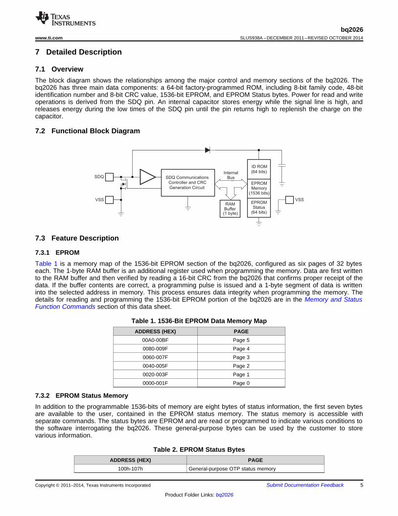
7.1 OverviewThe block diagram shows the relationships among the major control and memory sections of the bq2026. Thebq2026 has three main data components: a 64-bit factory-programmed ROM, including 8-bit family code, 48-bitidentification number and 8-bit CRC value, 1536-bit EPROM, and EPROM Status bytes. Power for read and writeoperations is derived from the SDQ pin. An internal capacitor stores energy while the signal line is high, andreleases energy during the low times of the SDQ pin until the pin returns high to replenish the charge on thecapacitor.
7.2 Functional Block Diagram
7.3 Feature Description
7.3.1 EPROMTable 1 is a memory map of the 1536-bit EPROM section of the bq2026, configured as six pages of 32 byteseach. The 1-byte RAM buffer is an additional register used when programming the memory. Data are first writtento the RAM buffer and then verified by reading a 16-bit CRC from the bq2026 that confirms proper receipt of thedata. If the buffer contents are correct, a programming pulse is issued and a 1-byte segment of data is writteninto the selected address in memory. This process ensures data integrity when programming the memory. Thedetails for reading and programming the 1536-bit EPROM portion of the bq2026 are in the Memory and StatusFunction Commands section of this data sheet.
Table 1. 1536-Bit EPROM Data Memory MapADDRESS (HEX) PAGE
00A0-00BF Page 50080-009F Page 40060-007F Page 30040-005F Page 20020-003F Page 10000-001F Page 0
7.3.2 EPROM Status MemoryIn addition to the programmable 1536-bits of memory are eight bytes of status information, the first seven bytesare available to the user, contained in the EPROM status memory. The status memory is accessible withseparate commands. The status bytes are EPROM and are read or programmed to indicate various conditions tothe software interrogating the bq2026. These general-purpose bytes can be used by the customer to storevarious information.
Table 2. EPROM Status BytesADDRESS (HEX) PAGE
100h-107h General-purpose OTP status memory
Copyright © 2011–2014, Texas Instruments Incorporated Submit Documentation Feedback 5
Product Folder Links: bq2026
SDQI
SDQO
VSS
Communications
ControllerCPU
HOST
bq2026
VPU
2
1
3
VSS
SDQ
bq2026SLUS938A –DECEMBER 2011–REVISED OCTOBER 2014 www.ti.com
7.3.3 Error CheckingImplement error checking by comparing the 16-bit CRC values transmitted by the bq2026. If the two CRC valuesmatch, the transmission is error-free. Details are found in the CRC Generation section.
7.4 Device Functional Modes
7.4.1 Customizing the bq2026The 64-bit ID identifies each bq2026 device. The 48-bit serial number is unique and programmed by TexasInstruments. The default 8-bit family code is 09h; however, a different value can be reserved on an individualcustomer basis. Contact your Texas Instruments sales representative for more information.
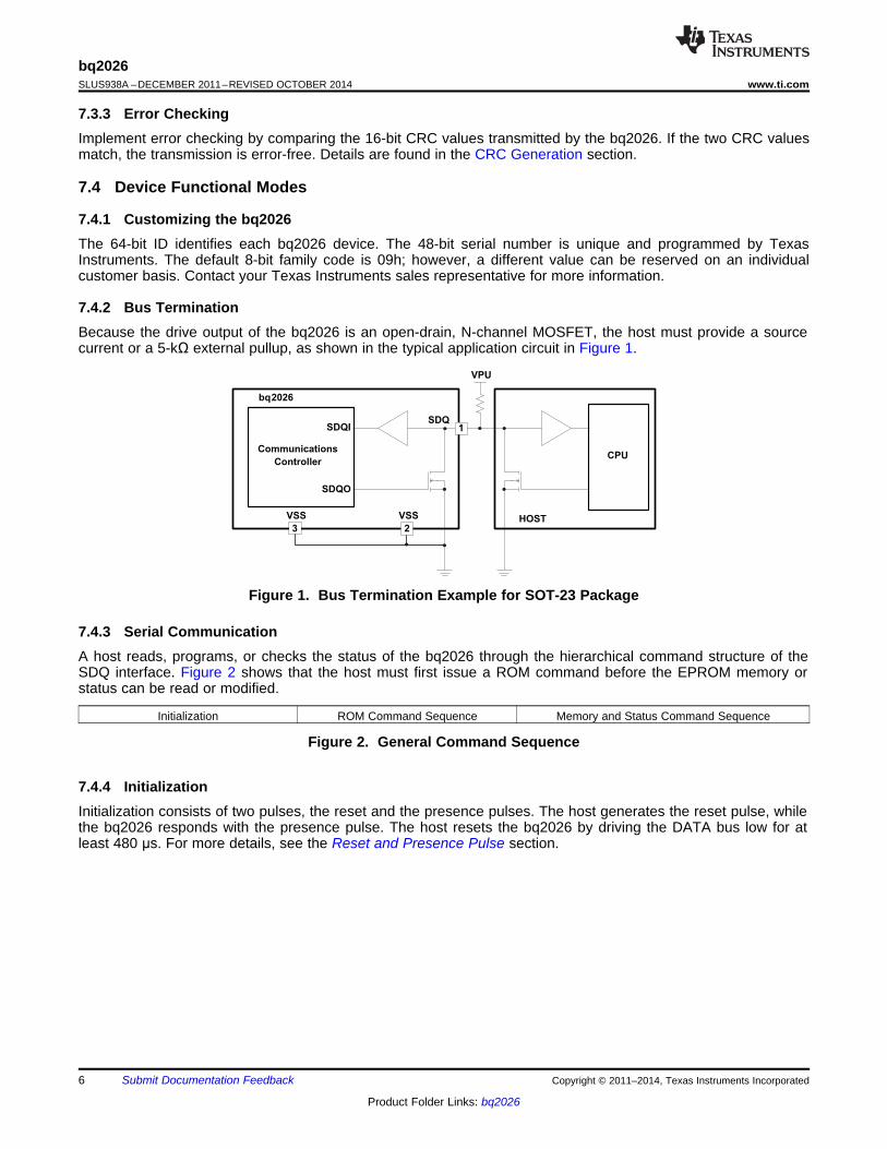
7.4.2 Bus TerminationBecause the drive output of the bq2026 is an open-drain, N-channel MOSFET, the host must provide a sourcecurrent or a 5-kΩ external pullup, as shown in the typical application circuit in Figure 1.
Figure 1. Bus Termination Example for SOT-23 Package
7.4.3 Serial CommunicationA host reads, programs, or checks the status of the bq2026 through the hierarchical command structure of theSDQ interface. Figure 2 shows that the host must first issue a ROM command before the EPROM memory orstatus can be read or modified.
Initialization ROM Command Sequence Memory and Status Command Sequence
Figure 2. General Command Sequence
7.4.4 InitializationInitialization consists of two pulses, the reset and the presence pulses. The host generates the reset pulse, whilethe bq2026 responds with the presence pulse. The host resets the bq2026 by driving the DATA bus low for atleast 480 μs. For more details, see the Reset and Presence Pulse section.
6 Submit Documentation Feedback Copyright © 2011–2014, Texas Instruments Incorporated
Product Folder Links: bq2026
1 00 0 1 10
Resetand
PresenceSignals
Skip ROM (CCh)
1
1 10 0 01 1CRC (1 BYTE)
0
Resetand
PresenceSignals
Match ROM (55h) Family Code and IdentificationNumber (7 BYTES)
011 00011 CRC (1 BYTE)
Resetand
PresenceSignals
Read ROM (33h) Family Code and IdentificationNumber (7 BYTES)
bq2026www.ti.com SLUS938A –DECEMBER 2011–REVISED OCTOBER 2014
7.4.5 ROM Commands
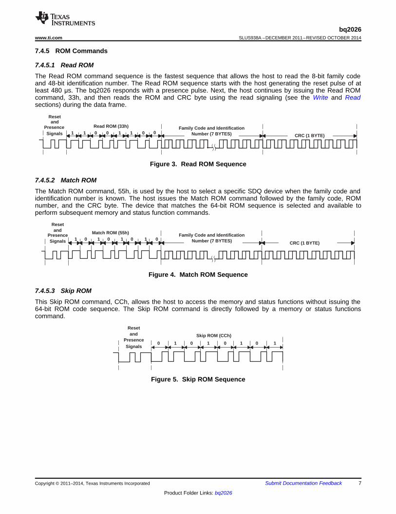
7.4.5.1 Read ROMThe Read ROM command sequence is the fastest sequence that allows the host to read the 8-bit family codeand 48-bit identification number. The Read ROM sequence starts with the host generating the reset pulse of atleast 480 μs. The bq2026 responds with a presence pulse. Next, the host continues by issuing the Read ROMcommand, 33h, and then reads the ROM and CRC byte using the read signaling (see the Write and Readsections) during the data frame.
Figure 3. Read ROM Sequence
7.4.5.2 Match ROMThe Match ROM command, 55h, is used by the host to select a specific SDQ device when the family code andidentification number is known. The host issues the Match ROM command followed by the family code, ROMnumber, and the CRC byte. The device that matches the 64-bit ROM sequence is selected and available toperform subsequent memory and status function commands.
Figure 4. Match ROM Sequence
7.4.5.3 Skip ROMThis Skip ROM command, CCh, allows the host to access the memory and status functions without issuing the64-bit ROM code sequence. The Skip ROM command is directly followed by a memory or status functionscommand.
Figure 5. Skip ROM Sequence
Copyright © 2011–2014, Texas Instruments Incorporated Submit Documentation Feedback 7
Product Folder Links: bq2026
bq2026SLUS938A –DECEMBER 2011–REVISED OCTOBER 2014 www.ti.com
7.4.6 Memory and Status Function CommandsFour memory and status function commands allow read and modification of the 1536-bit EPROM data memoryor the 7-byte EPROM status memory. There is a Read Memory and Field CRC command, plus the WriteMemory, Read Status, and Write Status commands. The bq2026 responds to memory and status functioncommands only after a device is selected by a ROM command.
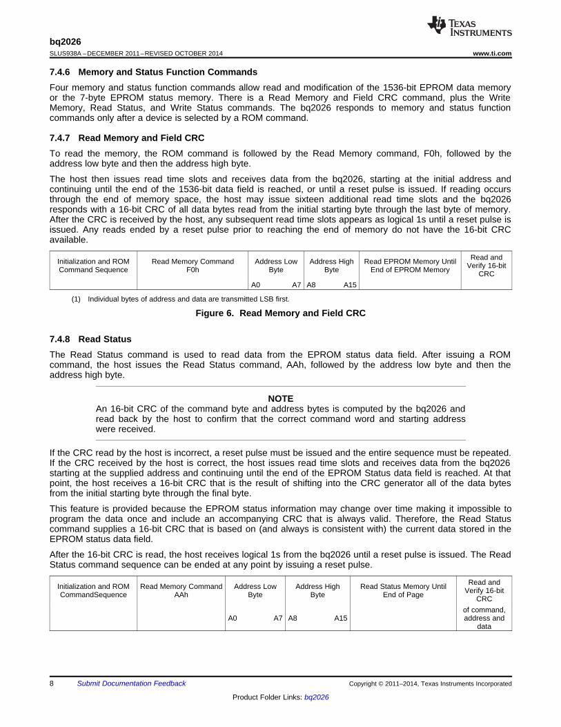
7.4.7 Read Memory and Field CRCTo read the memory, the ROM command is followed by the Read Memory command, F0h, followed by theaddress low byte and then the address high byte.
The host then issues read time slots and receives data from the bq2026, starting at the initial address andcontinuing until the end of the 1536-bit data field is reached, or until a reset pulse is issued. If reading occursthrough the end of memory space, the host may issue sixteen additional read time slots and the bq2026responds with a 16-bit CRC of all data bytes read from the initial starting byte through the last byte of memory.After the CRC is received by the host, any subsequent read time slots appears as logical 1s until a reset pulse isissued. Any reads ended by a reset pulse prior to reaching the end of memory do not have the 16-bit CRCavailable.
Read andInitialization and ROM Read Memory Command Address Low Address High Read EPROM Memory Until Verify 16-bitCommand Sequence F0h Byte Byte End of EPROM Memory CRCA0 A7 A8 A15
(1) Individual bytes of address and data are transmitted LSB first.
Figure 6. Read Memory and Field CRC
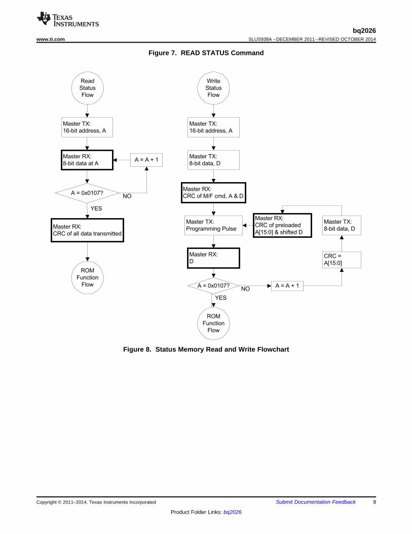
7.4.8 Read StatusThe Read Status command is used to read data from the EPROM status data field. After issuing a ROMcommand, the host issues the Read Status command, AAh, followed by the address low byte and then theaddress high byte.
NOTEAn 16-bit CRC of the command byte and address bytes is computed by the bq2026 andread back by the host to confirm that the correct command word and starting addresswere received.
If the CRC read by the host is incorrect, a reset pulse must be issued and the entire sequence must be repeated.If the CRC received by the host is correct, the host issues read time slots and receives data from the bq2026starting at the supplied address and continuing until the end of the EPROM Status data field is reached. At thatpoint, the host receives a 16-bit CRC that is the result of shifting into the CRC generator all of the data bytesfrom the initial starting byte through the final byte.
This feature is provided because the EPROM status information may change over time making it impossible toprogram the data once and include an accompanying CRC that is always valid. Therefore, the Read Statuscommand supplies a 16-bit CRC that is based on (and always is consistent with) the current data stored in theEPROM status data field.
After the 16-bit CRC is read, the host receives logical 1s from the bq2026 until a reset pulse is issued. The ReadStatus command sequence can be ended at any point by issuing a reset pulse.
Read andInitialization and ROM Read Memory Command Address Low Address High Read Status Memory Until Verify 16-bitCommandSequence AAh Byte Byte End of Page CRCof command,
A0 A7 A8 A15 address anddata
8 Submit Documentation Feedback Copyright © 2011–2014, Texas Instruments Incorporated
Product Folder Links: bq2026
Master TX:
16-bit address, A
Master RX:
8-bit data at AA = A + 1
A = 0x0107?
YES
Master RX:
CRC of all data transmitted
NO
Read
Status
Flow
ROM
Function
Flow
Master TX:
16-bit address, A
Master TX:
8-bit data, D
Master RX:
D
A = 0x0107? A = A + 1
Master TX:
8-bit data, D
Master RX:
CRC of preloaded
A[15:0] & shifted D
YES
CRC =
A[15:0]
ROM
Function
Flow
Write
Status
Flow
Master RX:
CRC of M/F cmd, A & D
NO
Master TX:
Programming Pulse
bq2026www.ti.com SLUS938A –DECEMBER 2011–REVISED OCTOBER 2014
Figure 7. READ STATUS Command
Figure 8. Status Memory Read and Write Flowchart
Copyright © 2011–2014, Texas Instruments Incorporated Submit Documentation Feedback 9
Product Folder Links: bq2026
bq2026SLUS938A –DECEMBER 2011–REVISED OCTOBER 2014 www.ti.com
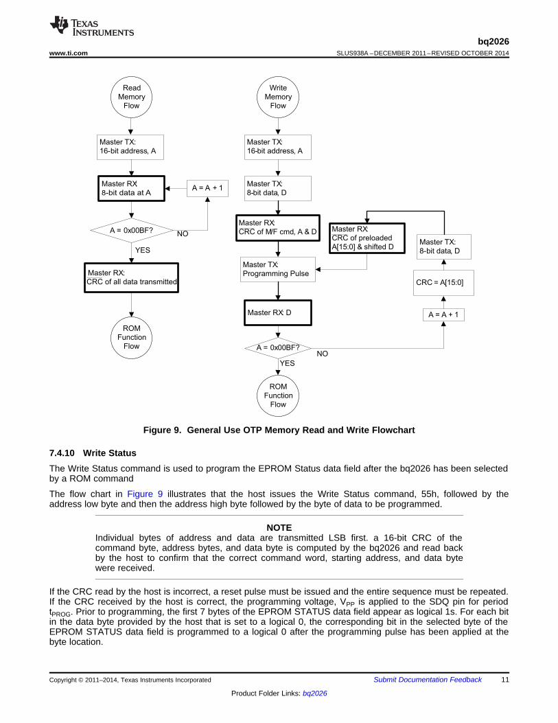
7.4.9 Write MemoryThe Write Memory command is used to program the 1536-bit EPROM memory field. The 1536-bit memory fieldis programmed in 1-byte segments. Data is first written into an 1-byte RAM buffer. The contents of the RAMbuffer is then ANDed with the contents of the EPROM memory field when the programming command is issued.
Figure 9 illustrates the sequence of events for programming the EPROM memory field. After issuing a ROMcommand, the host issues the Write Memory command, 0Fh, followed by the low byte and then the high byte ofthe starting address. The host then transmits 1 byte of data to the bq2026.
a 16-bit CRC is calculated and transmitted based on the command, address and data. If this CRC agrees withthe CRC calculated by the host, the host applies the programming voltage for at least 480 μs or tEPROG.
If at any time during the Write Memory process, the CRC read by the host is incorrect, a reset pulse must beissued, and the entire sequence must be repeated.
The Write Data Memory command sequence can be terminated at any point by issuing a reset pulse exceptduring the program pulse period tPROG.
NOTEThe bq2026 responds with the data from the selected EPROM address sent leastsignificant-bit first. This response should be checked to verify the programmed byte. If theprogrammed byte is incorrect, then the host must reset the part and begin the writesequence again.
For both of these cases, the decision to continue programming is made entirely by the host, because the bq2026is not able to determine if the 16-bit CRC calculated by the host agrees with the 16-bit CRC calculated by thebq2026.
Prior to programming, bits in the 1536-bit EPROM data field appear as logical 1s.
10 Submit Documentation Feedback Copyright © 2011–2014, Texas Instruments Incorporated
Product Folder Links: bq2026
Master TX:
16-bit address, A
Master RX:
8-bit data at AA = A + 1
A = 0x00BF?
YES
Master RX:
CRC of all data transmitted
NO
Read
Memory
Flow
ROM
Function
Flow
Master TX:
16-bit address, A
Master TX:
8-bit data, D
Master RX: D
A = 0x00BF?
A = A + 1
Master TX:
8-bit data, D
Master RX:
CRC of preloaded
A[15:0] & shifted D
YES
CRC = A[15:0]
ROM
Function
Flow
Write
Memory
Flow
Master RX:
CRC of M/F cmd, A & D
NO
Master TX:
Programming Pulse
bq2026www.ti.com SLUS938A –DECEMBER 2011–REVISED OCTOBER 2014
Figure 9. General Use OTP Memory Read and Write Flowchart
7.4.10 Write StatusThe Write Status command is used to program the EPROM Status data field after the bq2026 has been selectedby a ROM command
The flow chart in Figure 9 illustrates that the host issues the Write Status command, 55h, followed by theaddress low byte and then the address high byte followed by the byte of data to be programmed.
NOTEIndividual bytes of address and data are transmitted LSB first. a 16-bit CRC of thecommand byte, address bytes, and data byte is computed by the bq2026 and read backby the host to confirm that the correct command word, starting address, and data bytewere received.
If the CRC read by the host is incorrect, a reset pulse must be issued and the entire sequence must be repeated.If the CRC received by the host is correct, the programming voltage, VPP is applied to the SDQ pin for periodtPROG. Prior to programming, the first 7 bytes of the EPROM STATUS data field appear as logical 1s. For each bitin the data byte provided by the host that is set to a logical 0, the corresponding bit in the selected byte of theEPROM STATUS data field is programmed to a logical 0 after the programming pulse has been applied at thebyte location.
Copyright © 2011–2014, Texas Instruments Incorporated Submit Documentation Feedback 11
Product Folder Links: bq2026
bq2026SLUS938A –DECEMBER 2011–REVISED OCTOBER 2014 www.ti.com
After the programming pulse is applied and the data line returns to VPU, the host issues eight read time slots toverify that the appropriate bits have been programmed. The bq2026 responds with the data from the selectedEPROM STATUS address sent least significant bit first. This response should be checked to verify theprogrammed byte. If the programmed byte is incorrect, then the host must reset the device and begin the writesequence again. If the bq2026 EPROM data byte programming was successful, the bq2026 automaticallyincrements its address counter to select the next byte in the STATUS MEMORY data field. The least significantbyte of the new two-byte address is also loaded into the 16-bit CRC generator as a starting value. The hostissues the next byte of data using eight write time slots.
As the bq2026 receives this byte of data into the RAM buffer, it also shifts the data into the CRC generator thathas been preloaded with the LSB of the current address and the result is a 16-bit CRC of the new data byte andthe new address. After supplying the data byte, the host reads this 16-bit CRC from the bq2026 with eight readtime slots to confirm that the address incremented properly and the data byte was received correctly. If the CRCis incorrect, a Reset Pulse must be issued and the Write Status command sequence must be restarted. If theCRC is correct, the host issues a programming pulse and the selected byte in memory is programmed.
NOTEThe initial write of the Write Status command, generates a 16-bit CRC value that is theresult of shifting the command byte into the CRC generator, followed by the two-addressbytes, and finally the data byte. Subsequent writes within this Write Status command dueto the bq2026 automatically incrementing its address counter generates a 16-bit CRC thatis the result of loading (not shifting) the LSB of the new (incremented) address into theCRC generator and then shifting in the new data byte.
For both of these cases, the decision to continue programming the EPROM Status registers is made entirely bythe host, because the bq2026 is not able to determine if the 16-bit CRC calculated by the host agrees with the16-bit CRC calculated by the bq2026. If an incorrect CRC is ignored and a program pulse is applied by the host,incorrect programming could occur within the bq2026. Also note that the bq2026 always increments its internaladdress counter after the receipt of the eight read time slots used to confirm the programming of the selectedEPROM byte. The decision to continue is again made entirely by the host, therefore if the EPROM data bytedoes not match the supplied data byte but the master continues with the Write Status command, incorrectprogramming could occur within the bq2026. The Write Status command sequence can be ended at any point byissuing a reset pulse.
Table 3. Command Code SummaryCOMMAND DESCRIPTION CATEGORY(HEX)
33h Read serialization ROM and CRC55h Match serialization ROM ROM Commands Available in Command Level ICCh Skip serialization ROMF0h Read memory and field CRCAAh Read EPROM status Memory Function Commands
Available in Command Level II0Fh Write memory55h Write EPROM status
7.4.11 SDQ SignalingAll SDQ signaling begins with initializing the device, followed by the host driving the bus low to write a 1 or 0, orto begin the start frame for a bit read. Figure 10 shows the initialization timing, whereas Figure 11 and Figure 12show that the host initiates each bit by driving the data bus low for the start period, tWSTRB / tRSTRB. After the bit isinitiated, either the host continues controlling the bus during a write, or the bq2026 responds during a read.
12 Submit Documentation Feedback Copyright © 2011–2014, Texas Instruments Incorporated
Product Folder Links: bq2026
VPP
VPU
VSS
tPRECtPSUtEPROG
tPRE tPFE
tRSTRBtODD
tODHO
tREC
VPU VIHVIL
Read ”1”
Read ”0”
t WSTRBtWDSU
tWDH
t rec
VPU VIHVIL
Write ”1”
Write ”0”
VPUVIH
VIL
tRSTtPPD tPP
RESET(Sent by Host)
Presence Pulse(Sent by bq2026)
tRSTREC
bq2026www.ti.com SLUS938A –DECEMBER 2011–REVISED OCTOBER 2014
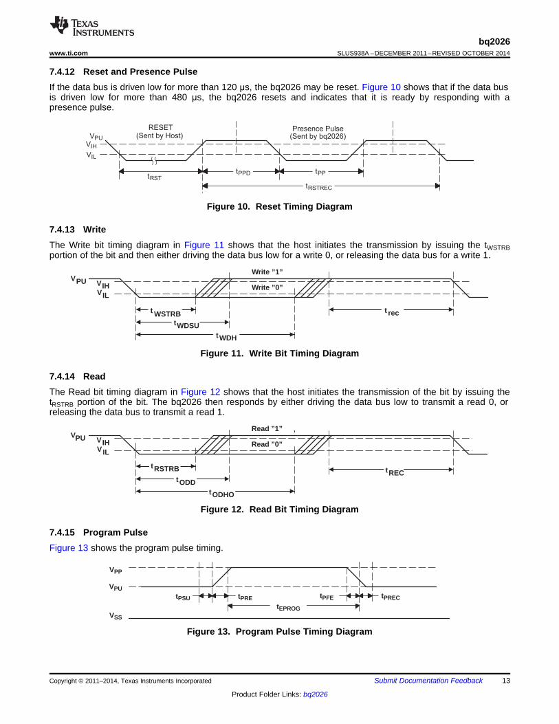
7.4.12 Reset and Presence PulseIf the data bus is driven low for more than 120 μs, the bq2026 may be reset. Figure 10 shows that if the data busis driven low for more than 480 μs, the bq2026 resets and indicates that it is ready by responding with apresence pulse.
Figure 10. Reset Timing Diagram
7.4.13 WriteThe Write bit timing diagram in Figure 11 shows that the host initiates the transmission by issuing the tWSTRBportion of the bit and then either driving the data bus low for a write 0, or releasing the data bus for a write 1.
Figure 11. Write Bit Timing Diagram
7.4.14 ReadThe Read bit timing diagram in Figure 12 shows that the host initiates the transmission of the bit by issuing thetRSTRB portion of the bit. The bq2026 then responds by either driving the data bus low to transmit a read 0, orreleasing the data bus to transmit a read 1.
Figure 12. Read Bit Timing Diagram
7.4.15 Program PulseFigure 13 shows the program pulse timing.
Figure 13. Program Pulse Timing Diagram
Copyright © 2011–2014, Texas Instruments Incorporated Submit Documentation Feedback 13
Product Folder Links: bq2026
CLK
DAT
R
D Q
R
D Q
R
D Q
R
D Q
R
D Q
R
D Q
R
D Q
R
D Q
R
D Q
R
D Q
R
D Q
R
D Q
R
D Q
R
D Q
R
D Q
R
D Q
CLK
DAT
R
D Q
R
D Q
R
D Q
R
D Q
R
D Q
R
D Q
R
D Q
R
D Q++ +
bq2026SLUS938A –DECEMBER 2011–REVISED OCTOBER 2014 www.ti.com
7.4.16 IdleIf the bus is high, the bus is in the idle state. Bus transactions can be suspended by leaving the data bus in idle.Bus transactions can resume at any time from the idle state.
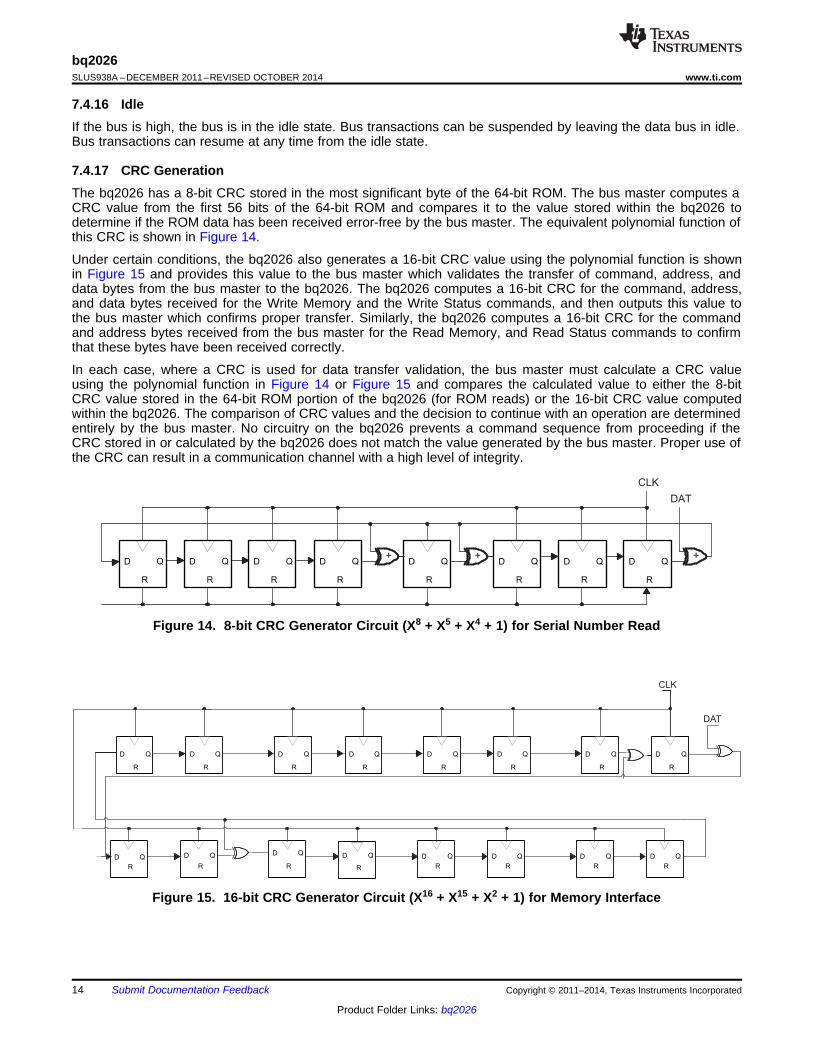
7.4.17 CRC GenerationThe bq2026 has a 8-bit CRC stored in the most significant byte of the 64-bit ROM. The bus master computes aCRC value from the first 56 bits of the 64-bit ROM and compares it to the value stored within the bq2026 todetermine if the ROM data has been received error-free by the bus master. The equivalent polynomial function ofthis CRC is shown in Figure 14.
Under certain conditions, the bq2026 also generates a 16-bit CRC value using the polynomial function is shownin Figure 15 and provides this value to the bus master which validates the transfer of command, address, anddata bytes from the bus master to the bq2026. The bq2026 computes a 16-bit CRC for the command, address,and data bytes received for the Write Memory and the Write Status commands, and then outputs this value tothe bus master which confirms proper transfer. Similarly, the bq2026 computes a 16-bit CRC for the commandand address bytes received from the bus master for the Read Memory, and Read Status commands to confirmthat these bytes have been received correctly.
In each case, where a CRC is used for data transfer validation, the bus master must calculate a CRC valueusing the polynomial function in Figure 14 or Figure 15 and compares the calculated value to either the 8-bitCRC value stored in the 64-bit ROM portion of the bq2026 (for ROM reads) or the 16-bit CRC value computedwithin the bq2026. The comparison of CRC values and the decision to continue with an operation are determinedentirely by the bus master. No circuitry on the bq2026 prevents a command sequence from proceeding if theCRC stored in or calculated by the bq2026 does not match the value generated by the bus master. Proper use ofthe CRC can result in a communication channel with a high level of integrity.
Figure 14. 8-bit CRC Generator Circuit (X8 + X5 + X4 + 1) for Serial Number Read
SPACER
Figure 15. 16-bit CRC Generator Circuit (X16 + X15 + X2 + 1) for Memory Interface
14 Submit Documentation Feedback Copyright © 2011–2014, Texas Instruments Incorporated
Product Folder Links: bq2026
bq2026www.ti.com SLUS938A –DECEMBER 2011–REVISED OCTOBER 2014
8 Device and Documentation Support
8.1 TrademarksSDQ is a trademark of Texas Instruments.All other trademarks are the property of their respective owners.
8.2 Electrostatic Discharge CautionThis integrated circuit can be damaged by ESD. Texas Instruments recommends that all integrated circuits be handled withappropriate precautions. Failure to observe proper handling and installation procedures can cause damage.
ESD damage can range from subtle performance degradation to complete device failure. Precision integrated circuits may be moresusceptible to damage because very small parametric changes could cause the device not to meet its published specifications.
8.3 GlossarySLYZ022 — TI Glossary.
This glossary lists and explains terms, acronyms, and definitions.
9 Mechanical, Packaging, and Orderable InformationThe following pages include mechanical, packaging, and orderable information. This information is the mostcurrent data available for the designated devices. This data is subject to change without notice and revision ofthis document. For browser-based versions of this data sheet, refer to the left-hand navigation.
Copyright © 2011–2014, Texas Instruments Incorporated Submit Documentation Feedback 15
Product Folder Links: bq2026
PACKAGE OPTION ADDENDUM
www.ti.com 25-Sep-2014
Addendum-Page 1
PACKAGING INFORMATION
Orderable Device Status(1)
Package Type PackageDrawing
Pins PackageQty
Eco Plan(2)
Lead/Ball Finish(6)
MSL Peak Temp(3)
Op Temp (°C) Device Marking(4/5)
Samples
BQ2026DBZR ACTIVE SOT-23 DBZ 3 3000 Green (RoHS& no Sb/Br)
CU NIPDAU Level-1-260C-UNLIM -20 to 70 WAIS
BQ2026LPR ACTIVE TO-92 LP 3 2000 Pb-Free(RoHS)
CU SN N / A for Pkg Type -20 to 70 BQ2026
(1) The marketing status values are defined as follows:ACTIVE: Product device recommended for new designs.LIFEBUY: TI has announced that the device will be discontinued, and a lifetime-buy period is in effect.NRND: Not recommended for new designs. Device is in production to support existing customers, but TI does not recommend using this part in a new design.PREVIEW: Device has been announced but is not in production. Samples may or may not be available.OBSOLETE: TI has discontinued the production of the device.
(2) Eco Plan - The planned eco-friendly classification: Pb-Free (RoHS), Pb-Free (RoHS Exempt), or Green (RoHS & no Sb/Br) - please check http://www.ti.com/productcontent for the latest availabilityinformation and additional product content details.TBD: The Pb-Free/Green conversion plan has not been defined.Pb-Free (RoHS): TI's terms "Lead-Free" or "Pb-Free" mean semiconductor products that are compatible with the current RoHS requirements for all 6 substances, including the requirement thatlead not exceed 0.1% by weight in homogeneous materials. Where designed to be soldered at high temperatures, TI Pb-Free products are suitable for use in specified lead-free processes.Pb-Free (RoHS Exempt): This component has a RoHS exemption for either 1) lead-based flip-chip solder bumps used between the die and package, or 2) lead-based die adhesive used betweenthe die and leadframe. The component is otherwise considered Pb-Free (RoHS compatible) as defined above.Green (RoHS & no Sb/Br): TI defines "Green" to mean Pb-Free (RoHS compatible), and free of Bromine (Br) and Antimony (Sb) based flame retardants (Br or Sb do not exceed 0.1% by weightin homogeneous material)
(3) MSL, Peak Temp. - The Moisture Sensitivity Level rating according to the JEDEC industry standard classifications, and peak solder temperature.
(4) There may be additional marking, which relates to the logo, the lot trace code information, or the environmental category on the device.
(5) Multiple Device Markings will be inside parentheses. Only one Device Marking contained in parentheses and separated by a "~" will appear on a device. If a line is indented then it is a continuationof the previous line and the two combined represent the entire Device Marking for that device.
(6) Lead/Ball Finish - Orderable Devices may have multiple material finish options. Finish options are separated by a vertical ruled line. Lead/Ball Finish values may wrap to two lines if the finishvalue exceeds the maximum column width.
Important Information and Disclaimer:The information provided on this page represents TI's knowledge and belief as of the date that it is provided. TI bases its knowledge and belief on informationprovided by third parties, and makes no representation or warranty as to the accuracy of such information. Efforts are underway to better integrate information from third parties. TI has taken andcontinues to take reasonable steps to provide representative and accurate information but may not have conducted destructive testing or chemical analysis on incoming materials and chemicals.TI and TI suppliers consider certain information to be proprietary, and thus CAS numbers and other limited information may not be available for release.
PACKAGE OPTION ADDENDUM
www.ti.com 25-Sep-2014
Addendum-Page 2
In no event shall TI's liability arising out of such information exceed the total purchase price of the TI part(s) at issue in this document sold by TI to Customer on an annual basis.
TAPE AND REEL INFORMATION
*All dimensions are nominal
Device PackageType
PackageDrawing
Pins SPQ ReelDiameter
(mm)
ReelWidth
W1 (mm)
A0(mm)
B0(mm)
K0(mm)
P1(mm)
W(mm)
Pin1Quadrant
BQ2026DBZR SOT-23 DBZ 3 3000 179.0 8.4 3.15 2.95 1.22 4.0 8.0 Q3
PACKAGE MATERIALS INFORMATION
www.ti.com 3-Aug-2017
Pack Materials-Page 1
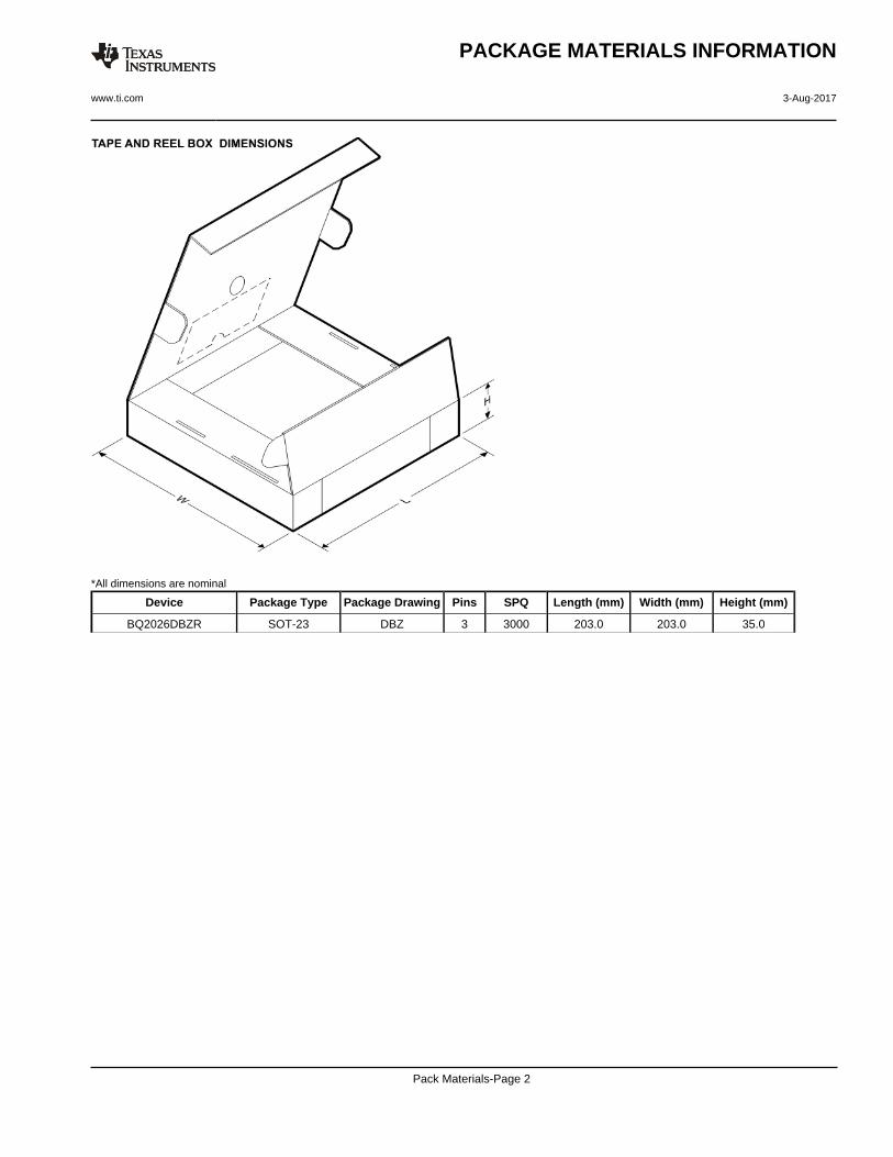
*All dimensions are nominal
Device Package Type Package Drawing Pins SPQ Length (mm) Width (mm) Height (mm)
BQ2026DBZR SOT-23 DBZ 3 3000 203.0 203.0 35.0
PACKAGE MATERIALS INFORMATION
www.ti.com 3-Aug-2017
Pack Materials-Page 2
www.ti.com
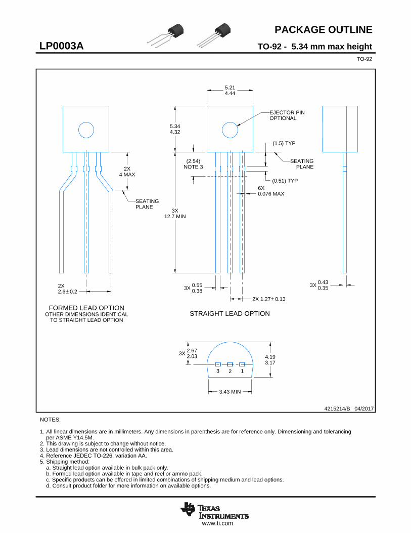
PACKAGE OUTLINE
3X 2.672.03
5.214.44
5.344.32
3X12.7 MIN
2X 1.27 0.13
3X 0.550.38
4.193.17
3.43 MIN
3X 0.430.35
(2.54)NOTE 3
2X2.6 0.2
2X4 MAX
SEATINGPLANE
6X0.076 MAX
(0.51) TYP
(1.5) TYP
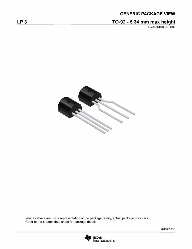
TO-92 - 5.34 mm max heightLP0003ATO-92
4215214/B 04/2017
NOTES: 1. All linear dimensions are in millimeters. Any dimensions in parenthesis are for reference only. Dimensioning and tolerancing per ASME Y14.5M.2. This drawing is subject to change without notice.3. Lead dimensions are not controlled within this area.4. Reference JEDEC TO-226, variation AA.5. Shipping method: a. Straight lead option available in bulk pack only. b. Formed lead option available in tape and reel or ammo pack. c. Specific products can be offered in limited combinations of shipping medium and lead options. d. Consult product folder for more information on available options.
EJECTOR PINOPTIONAL
PLANESEATING
STRAIGHT LEAD OPTION
3 2 1
SCALE 1.200
FORMED LEAD OPTIONOTHER DIMENSIONS IDENTICAL
TO STRAIGHT LEAD OPTION
SCALE 1.200
www.ti.com
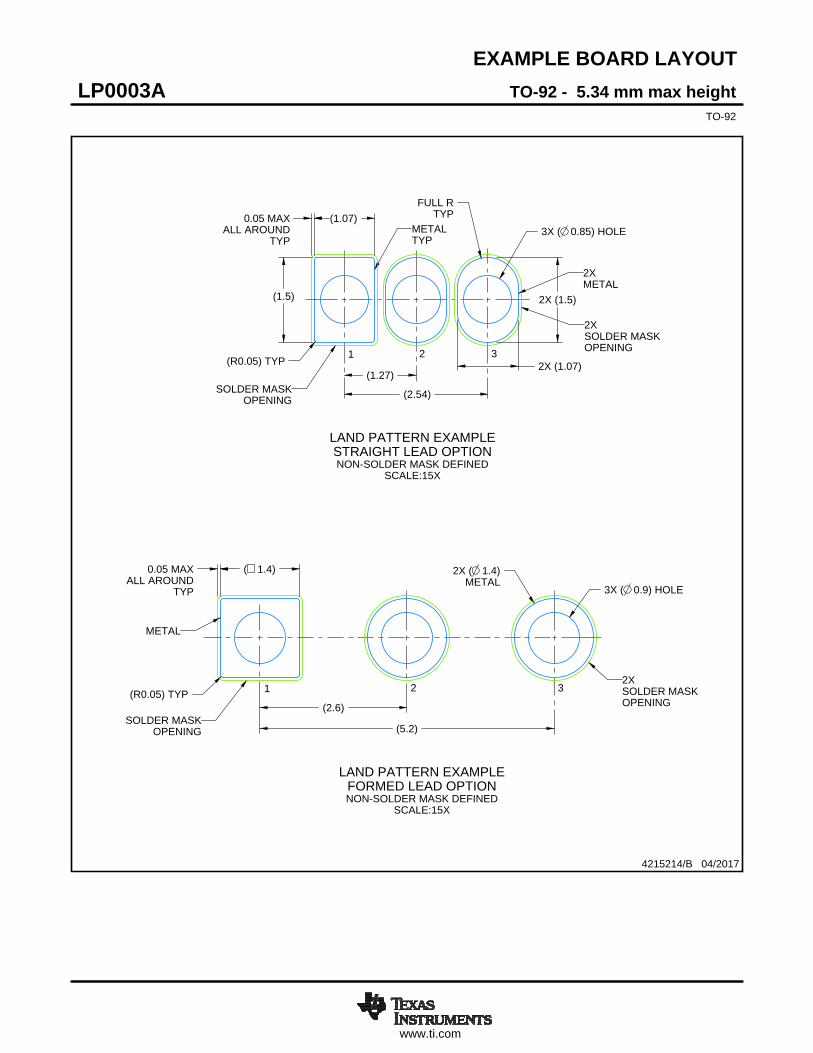
EXAMPLE BOARD LAYOUT
0.05 MAXALL AROUND
TYP
(1.07)
(1.5) 2X (1.5)
2X (1.07)(1.27)
(2.54)
FULL RTYP
( 1.4)0.05 MAXALL AROUND
TYP
(2.6)
(5.2)
(R0.05) TYP
3X ( 0.9) HOLE
2X ( 1.4)METAL
3X ( 0.85) HOLE
(R0.05) TYP
4215214/B 04/2017
TO-92 - 5.34 mm max heightLP0003ATO-92
LAND PATTERN EXAMPLEFORMED LEAD OPTIONNON-SOLDER MASK DEFINED
SCALE:15X
SOLDER MASKOPENING
METAL
2XSOLDER MASKOPENING
1 2 3
LAND PATTERN EXAMPLESTRAIGHT LEAD OPTIONNON-SOLDER MASK DEFINED
SCALE:15X
METALTYP
SOLDER MASKOPENING
2XSOLDER MASKOPENING
2XMETAL
1 2 3
www.ti.com
TAPE SPECIFICATIONS
19.017.5
13.711.7
11.08.5
0.5 MIN
TYP-4.33.7
9.758.50
TYP2.92.4
6.755.95
13.012.4
(2.5) TYP
16.515.5
3223
4215214/B 04/2017
TO-92 - 5.34 mm max heightLP0003ATO-92
FOR FORMED LEAD OPTION PACKAGE
4203227/C
www.ti.com
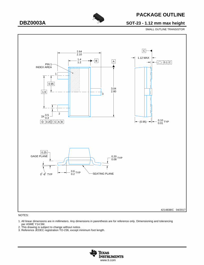
PACKAGE OUTLINE
C
TYP0.200.08
0.25
2.642.10
1.12 MAX
TYP0.100.01
3X 0.50.3
TYP0.60.2
1.9
0.95
TYP-80
A
3.042.80
B1.41.2
(0.95)
SOT-23 - 1.12 mm max heightDBZ0003ASMALL OUTLINE TRANSISTOR
4214838/C 04/2017
NOTES: 1. All linear dimensions are in millimeters. Any dimensions in parenthesis are for reference only. Dimensioning and tolerancing per ASME Y14.5M.2. This drawing is subject to change without notice.3. Reference JEDEC registration TO-236, except minimum foot length.
0.2 C A B
1
3
2
INDEX AREAPIN 1
GAGE PLANE
SEATING PLANE
0.1 C
SCALE 4.000
www.ti.com
EXAMPLE BOARD LAYOUT
0.07 MAXALL AROUND
0.07 MINALL AROUND
3X (1.3)
3X (0.6)
(2.1)
2X (0.95)
(R0.05) TYP
4214838/C 04/2017
SOT-23 - 1.12 mm max heightDBZ0003ASMALL OUTLINE TRANSISTOR
NOTES: (continued) 4. Publication IPC-7351 may have alternate designs. 5. Solder mask tolerances between and around signal pads can vary based on board fabrication site.
SYMM
LAND PATTERN EXAMPLESCALE:15X
PKG
1
3
2
SOLDER MASKOPENINGMETAL UNDER
SOLDER MASK
SOLDER MASKDEFINED
METALSOLDER MASKOPENING
NON SOLDER MASKDEFINED
(PREFERRED)
SOLDER MASK DETAILS
www.ti.com
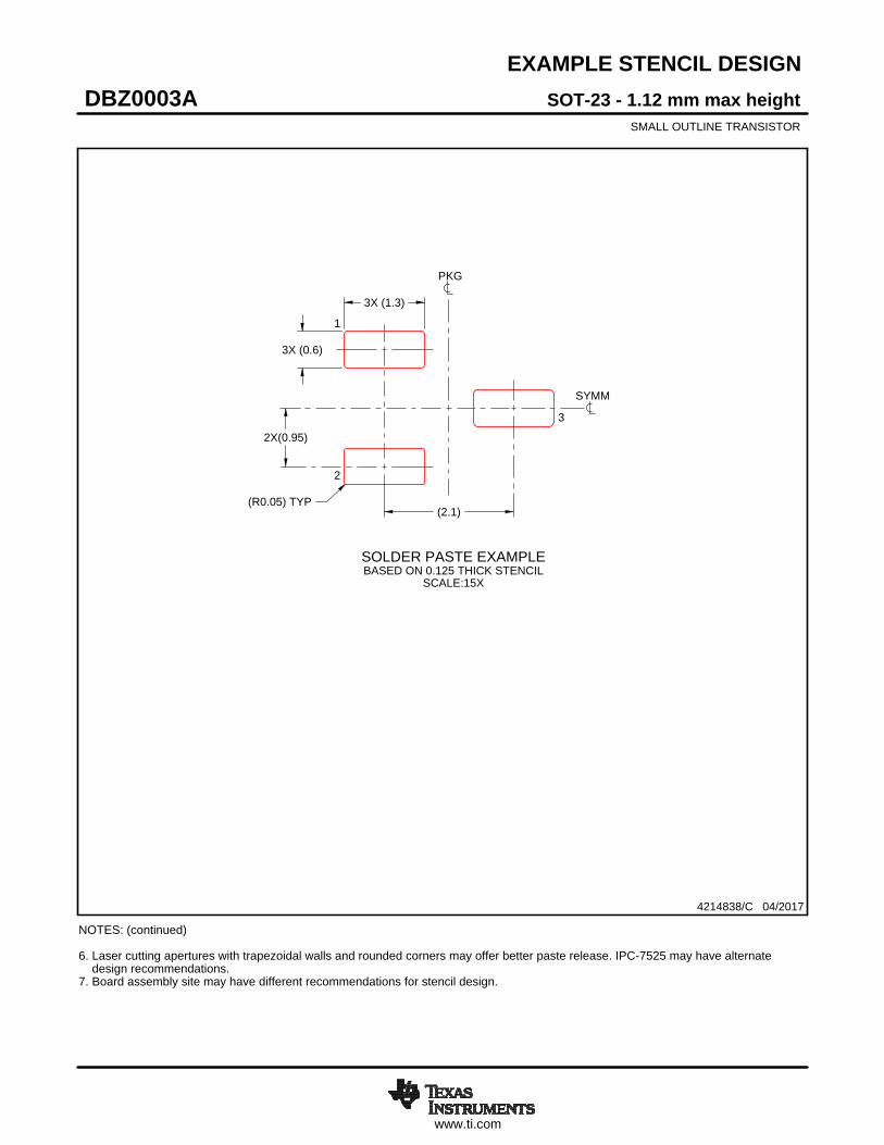
EXAMPLE STENCIL DESIGN
(2.1)
2X(0.95)
3X (1.3)
3X (0.6)
(R0.05) TYP
SOT-23 - 1.12 mm max heightDBZ0003ASMALL OUTLINE TRANSISTOR
4214838/C 04/2017
NOTES: (continued) 6. Laser cutting apertures with trapezoidal walls and rounded corners may offer better paste release. IPC-7525 may have alternate design recommendations. 7. Board assembly site may have different recommendations for stencil design.
SOLDER PASTE EXAMPLEBASED ON 0.125 THICK STENCIL
SCALE:15X
SYMM
PKG
1
3
2
IMPORTANT NOTICE
Texas Instruments Incorporated (TI) reserves the right to make corrections, enhancements, improvements and other changes to itssemiconductor products and services per JESD46, latest issue, and to discontinue any product or service per JESD48, latest issue. Buyersshould obtain the latest relevant information before placing orders and should verify that such information is current and complete.TI’s published terms of sale for semiconductor products (http://www.ti.com/sc/docs/stdterms.htm) apply to the sale of packaged integratedcircuit products that TI has qualified and released to market. Additional terms may apply to the use or sale of other types of TI products andservices.Reproduction of significant portions of TI information in TI data sheets is permissible only if reproduction is without alteration and isaccompanied by all associated warranties, conditions, limitations, and notices. TI is not responsible or liable for such reproduceddocumentation. Information of third parties may be subject to additional restrictions. Resale of TI products or services with statementsdifferent from or beyond the parameters stated by TI for that product or service voids all express and any implied warranties for theassociated TI product or service and is an unfair and deceptive business practice. TI is not responsible or liable for any such statements.Buyers and others who are developing systems that incorporate TI products (collectively, “Designers”) understand and agree that Designersremain responsible for using their independent analysis, evaluation and judgment in designing their applications and that Designers havefull and exclusive responsibility to assure the safety of Designers' applications and compliance of their applications (and of all TI productsused in or for Designers’ applications) with all applicable regulations, laws and other applicable requirements. Designer represents that, withrespect to their applications, Designer has all the necessary expertise to create and implement safeguards that (1) anticipate dangerousconsequences of failures, (2) monitor failures and their consequences, and (3) lessen the likelihood of failures that might cause harm andtake appropriate actions. Designer agrees that prior to using or distributing any applications that include TI products, Designer willthoroughly test such applications and the functionality of such TI products as used in such applications.TI’s provision of technical, application or other design advice, quality characterization, reliability data or other services or information,including, but not limited to, reference designs and materials relating to evaluation modules, (collectively, “TI Resources”) are intended toassist designers who are developing applications that incorporate TI products; by downloading, accessing or using TI Resources in anyway, Designer (individually or, if Designer is acting on behalf of a company, Designer’s company) agrees to use any particular TI Resourcesolely for this purpose and subject to the terms of this Notice.TI’s provision of TI Resources does not expand or otherwise alter TI’s applicable published warranties or warranty disclaimers for TIproducts, and no additional obligations or liabilities arise from TI providing such TI Resources. TI reserves the right to make corrections,enhancements, improvements and other changes to its TI Resources. TI has not conducted any testing other than that specificallydescribed in the published documentation for a particular TI Resource.Designer is authorized to use, copy and modify any individual TI Resource only in connection with the development of applications thatinclude the TI product(s) identified in such TI Resource. NO OTHER LICENSE, EXPRESS OR IMPLIED, BY ESTOPPEL OR OTHERWISETO ANY OTHER TI INTELLECTUAL PROPERTY RIGHT, AND NO LICENSE TO ANY TECHNOLOGY OR INTELLECTUAL PROPERTYRIGHT OF TI OR ANY THIRD PARTY IS GRANTED HEREIN, including but not limited to any patent right, copyright, mask work right, orother intellectual property right relating to any combination, machine, or process in which TI products or services are used. Informationregarding or referencing third-party products or services does not constitute a license to use such products or services, or a warranty orendorsement thereof. Use of TI Resources may require a license from a third party under the patents or other intellectual property of thethird party, or a license from TI under the patents or other intellectual property of TI.TI RESOURCES ARE PROVIDED “AS IS” AND WITH ALL FAULTS. TI DISCLAIMS ALL OTHER WARRANTIES ORREPRESENTATIONS, EXPRESS OR IMPLIED, REGARDING RESOURCES OR USE THEREOF, INCLUDING BUT NOT LIMITED TOACCURACY OR COMPLETENESS, TITLE, ANY EPIDEMIC FAILURE WARRANTY AND ANY IMPLIED WARRANTIES OFMERCHANTABILITY, FITNESS FOR A PARTICULAR PURPOSE, AND NON-INFRINGEMENT OF ANY THIRD PARTY INTELLECTUALPROPERTY RIGHTS. TI SHALL NOT BE LIABLE FOR AND SHALL NOT DEFEND OR INDEMNIFY DESIGNER AGAINST ANY CLAIM,INCLUDING BUT NOT LIMITED TO ANY INFRINGEMENT CLAIM THAT RELATES TO OR IS BASED ON ANY COMBINATION OFPRODUCTS EVEN IF DESCRIBED IN TI RESOURCES OR OTHERWISE. IN NO EVENT SHALL TI BE LIABLE FOR ANY ACTUAL,DIRECT, SPECIAL, COLLATERAL, INDIRECT, PUNITIVE, INCIDENTAL, CONSEQUENTIAL OR EXEMPLARY DAMAGES INCONNECTION WITH OR ARISING OUT OF TI RESOURCES OR USE THEREOF, AND REGARDLESS OF WHETHER TI HAS BEENADVISED OF THE POSSIBILITY OF SUCH DAMAGES.Unless TI has explicitly designated an individual product as meeting the requirements of a particular industry standard (e.g., ISO/TS 16949and ISO 26262), TI is not responsible for any failure to meet such industry standard requirements.Where TI specifically promotes products as facilitating functional safety or as compliant with industry functional safety standards, suchproducts are intended to help enable customers to design and create their own applications that meet applicable functional safety standardsand requirements. Using products in an application does not by itself establish any safety features in the application. Designers mustensure compliance with safety-related requirements and standards applicable to their applications. Designer may not use any TI products inlife-critical medical equipment unless authorized officers of the parties have executed a special contract specifically governing such use.Life-critical medical equipment is medical equipment where failure of such equipment would cause serious bodily injury or death (e.g., lifesupport, pacemakers, defibrillators, heart pumps, neurostimulators, and implantables). Such equipment includes, without limitation, allmedical devices identified by the U.S. Food and Drug Administration as Class III devices and equivalent classifications outside the U.S.TI may expressly designate certain products as completing a particular qualification (e.g., Q100, Military Grade, or Enhanced Product).Designers agree that it has the necessary expertise to select the product with the appropriate qualification designation for their applicationsand that proper product selection is at Designers’ own risk. Designers are solely responsible for compliance with all legal and regulatoryrequirements in connection with such selection.Designer will fully indemnify TI and its representatives against any damages, costs, losses, and/or liabilities arising out of Designer’s non-compliance with the terms and provisions of this Notice.
Mailing Address: Texas Instruments, Post Office Box 655303, Dallas, Texas 75265Copyright © 2017, Texas Instruments Incorporated


![A High-Speed 64-Bit Binary Comparator€¦ · A high-speed 64-bit binary comparator 39 | Page III. EXISTING 64-BIT BINARY COMPARATOR DESIGN 64-bit comparator in reference [8], [9],](https://img.pdfslide.net/doc/110x75/5eac1a458d19873e777698b4/a-high-speed-64-bit-binary-comparator-a-high-speed-64-bit-binary-comparator-39-.jpg)