Embed Size (px)
Citation preview
APCPCWM_4828539:WP_0000001WP_0000001
APC
PCW
M_4
8285
39:W
P_00
0000
1WP_
0000
001
Rev 1.0 /Aug. 2010 1
ReleaseH27UAG8T2B Series
16Gb (2048M x 8bit) NAND Flash
16Gb NAND FlashH27UAG8T2B
*58b7d520-e522* B26798/177.179.157.212/2010-08-06 17:39
APCPCWM_4828539:WP_0000001WP_0000001
APC
PCW
M_4
8285
39:W
P_00
0000
1WP_
0000
001
ReleaseH27UAG8T2B Series
16Gb (2048M x 8bit) NAND Flash
Document Title16Gbit (2048 M x 8 bit) NAND Flash Memory
Revision History
Revision No.
History Draft Date Remark
0.0 Initial Draft. Feb. 25. 2010 Preliminary
0.1 Draft version Release Mar. 08. 2010 Preliminary
1.0 Final version ReleaseSpec. change : tWHR ( before : 80ns min / after : 100ns min)
Aug. 06. 2010 Release
Rev 1.0 / Aug. 2010 2
*58b7d520-e522* B26798/177.179.157.212/2010-08-06 17:39
APCPCWM_4828539:WP_0000001WP_0000001
APC
PCW
M_4
8285
39:W
P_00
0000
1WP_
0000
001
ReleaseH27UAG8T2B Series
16Gb (2048M x 8bit) NAND Flash
1. SUMMARY DESCRIPTION
■ Multilevel Cell technology
■ Supply Voltage - 3.3V device : Vcc = 2.7 V ~ 3.6 V Vcc = 2.7 V ~ 3.6 V
■ Organization - Page size : 8,640 Bytes(8,192+448 bytes) - Block size : 256 pages(2M+112K bytes) - Plane size : 512 blocks
■ Page Read Time - Random Access: 200 ㎲ (Max.) - Sequential Access : 25 ㎱ (Min.)
■ Write Time - Page program : 1600 ㎲ (Typ.) - Block erase : 2.5 ㎳ (Typ.)
■ Operating Current - Read - Program - Erase - Standby
■ Hardware Data Protection - Program/Erase locked during power transitions
■ Endurance - 3,000 P/E cycles (with 24 bit/ 1,024byte ECC)
■ Data Retention - 10 Years
■ Package - TSOP (12x20), 48Pin - Wafer (Bare Die)
■ Unique ID for copyright protection
Rev 1.0 / Aug. 2010 3
*58b7d520-e522* B26798/177.179.157.212/2010-08-06 17:39
APCPCWM_4828539:WP_0000001WP_0000001
APC
PCW
M_4
8285
39:W
P_00
0000
1WP_
0000
001
ReleaseH27UAG8T2B Series
16Gb (2048M x 8bit) NAND Flash
1. SUMMARY DESCRIPTION
The H27UAG8T2B is a single 3.3V 16Gbit NAND flash memory. The Device contains 2 planes in a single die. Each plane is made up of the 512 blocks. Each block consists of 256 programmable pages. Each page contains 8,640 bytes. The pages are subdivided into an 8,192-bytes main data storage area with a spare 448-byte district.
Page program operation can be performed in typical 1,600us, and a single block can be erased in typical 2.5ms. On-chip control logic unit automates erase and program operations to maximize cycle endurance. E/W endurance is stipu-lated at 3,000 cycles when using relevant ECC and Error management.
The H27UAG8T2B is a best solution for applications requiring large nonvolatile storage memory.
1.1. Product List
Table 1
PART NUMBER ORGANIZATION Vcc RANGE PACKAGE
H27UAG8T2B X8 2.7V ~ 3.6V 48 - TSOP1
Rev 1.0 / Aug. 2010 4
*58b7d520-e522* B26798/177.179.157.212/2010-08-06 17:39
APCPCWM_4828539:WP_0000001WP_0000001
APC
PCW
M_4
8285
39:W
P_00
0000
1WP_
0000
001
ReleaseH27UAG8T2B Series
16Gb (2048M x 8bit) NAND Flash
1.2. Packaging Information
■ Figure 1. 48-TSOP1 Contact, x8 Device
■ Figure 1-1. 48-TSOP1 - 48-lead Plastic Thin Small Outline, 12 x 20mm, Package Outline
Symbolmillimeters
Min Typ Max
A 1.200
A1 0.050 0.150
A2 0.980 1.030
B 0.170 0.250
C 0.100 0.200
CP 0.100
D 11.910 12.000 12.120
E 19.900 20.000 20.100
NC
NC
NC
NC
NC
NC
R/B
RE
CE
NC
NC
Vcc
Vss
NC
NC
CLE
ALE
WE
WP
NC
NC
NC
NC
NC
NC
NC
NC
NC
I/O7
I/O6
I/O5
I/O4
NC
NC
NC
VccQVssQ
NC
NC
NC
I/O3
I/O2
I/O1
I/O0
NC
NC
NC
NC
1213
3736
25
481
24
NAND FlashTSOP1
(x8)
Rev 1.0 / Aug. 2010 5
*58b7d520-e522* B26798/177.179.157.212/2010-08-06 17:39
APCPCWM_4828539:WP_0000001WP_0000001
APC
PCW
M_4
8285
39:W
P_00
0000
1WP_
0000
001
ReleaseH27UAG8T2B Series
16Gb (2048M x 8bit) NAND Flash
48-TSOP1 - 48-lead Plastic Thin Small Outline, 12 x 20mm, Package Mechanical Data
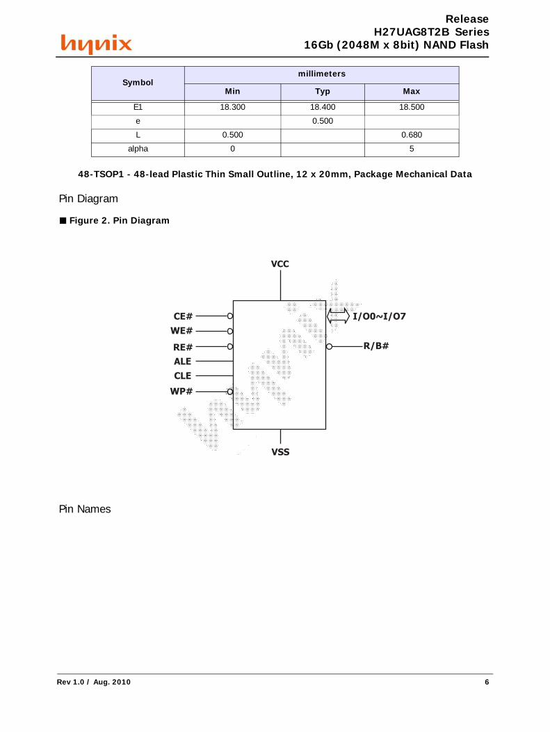
Pin Diagram
■ Figure 2. Pin Diagram
Pin Names
E1 18.300 18.400 18.500
e 0.500
L 0.500 0.680
alpha 0 5
Symbolmillimeters
Min Typ Max
VCC
VSS
WP#
CLE
ALE
RE#
WE#
CE# I/O0~I/O7
R/B#
Rev 1.0 / Aug. 2010 6
*58b7d520-e522* B26798/177.179.157.212/2010-08-06 17:39
APCPCWM_4828539:WP_0000001WP_0000001
APC
PCW
M_4
8285
39:W
P_00
0000
1WP_
0000
001
ReleaseH27UAG8T2B Series
16Gb (2048M x 8bit) NAND Flash
1.3. PIN DESCRIPTION
Pin Name Description
I/O0-I/O7
DATA INPUTS/OUTPUTSThe I/O pins are used to COMMAND LATCH cycle, ADDRESS INPUT cycle, and DATA in-out cycles during read / write operations. The I/O pins float to High-Z when the device is deselected or the outputs are disabled.
CLECOMMAND LATCH ENABLEThis input activates the latching of the I/O inputs inside the Command Register on the Rising edge of Write Enable (WE#).
ALEADDRESS LATCH ENABLEThis input activates the latching of the I/O inputs inside the Address Register on the Rising edge of Write Enable (WE#).
CE#
CHIP ENABLEThis input controls the selection of the device. When the device is busy, CE# low does not deselect the memory. The device goes into Stand-by mode when CE# goes High during 10us in Ready state. The CE# signal is ignored when device is in Busy state, and will not enter Standby mode even if the CE# goes high.
WE#WRITE ENABLEThis input acts as clock to latch Command, Address and Data. The I/O inputs are latched on the rise edge of WE#.
RE#
READ ENABLEThe RE# input is the serial data-out control, and when active drives the data onto the I/O bus. Data is valid tREA after the falling edge of RE# which also increments the internal column address counter by one.
WP#
WRITE PROTECTThe WP# pin, when Low, provides a hardware protection against undesired write operations. Hardware Write Protection is activated when the Write Protect pin is low. In this condition modify operation do not start and the content of the memory is not altered. Write Protect pin is not latched by Write Enable to ensure the protection even during the power up phases.
R/B# READY / BUSYThe Ready/Busy output is an Open Drain pin that signals the state of the memory.
Vcc SUPPLY VOLTAGEThe VCC supplies the power for all the operations. (Read, Write, and Erase).
Vss GROUNDNC NO CONNECTED
I/O7~I/O0 Data Input / OutputsCLE Command Latch EnableALE Address Latch EnableCE# Chip EnableRE# Read EnableR/B# Ready / BusyWE# Write EnableWP# Write ProtectVCC Power SupplyVSS GroundNC No Connection
Rev 1.0 / Aug. 2010 7
*58b7d520-e522* B26798/177.179.157.212/2010-08-06 17:39
APCPCWM_4828539:WP_0000001WP_0000001
APC
PCW
M_4
8285
39:W
P_00
0000
1WP_
0000
001
ReleaseH27UAG8T2B Series
16Gb (2048M x 8bit) NAND Flash
Notes:A 0.1uF capacitor should be connected between the Vcc Supply Voltage pin and the Vss Ground pin to decouple the current surgesfrom the power supply. The PCB track widths must be sufficient to carry the currents required during program and erase operations.
1.4. Block Diagram
■ Figure 3. Block diagram
X DecoderAddressregister
ALECLECE#
WE# RE#
WP#
CommandInterface Logic
Program/EraseController
HV generation
Y DecoderAddressregister
Commandregister
IO Buffer & latch
X
DECODER
NAND FLASH
Memory Array
1 Device =
(8,192 + 448) bytes x 256pages x 1024 blocks
= 17,694,720 kbits
Data Register & Sense Amp
Column Decoder
VccVss
Global data
bufferOutput Driver
A14-A31
A0-A13
I/O<7:0>
Rev 1.0 / Aug. 2010 8
*58b7d520-e522* B26798/177.179.157.212/2010-08-06 17:39
APCPCWM_4828539:WP_0000001WP_0000001
APC
PCW
M_4
8285
39:W
P_00
0000
1WP_
0000
001
ReleaseH27UAG8T2B Series
16Gb (2048M x 8bit) NAND Flash
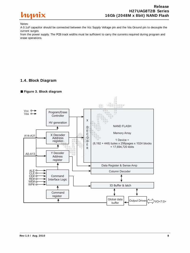
1.5. Array Organization
■ Figure 4. Array organization
1.6. Addressing
Notes: 1. L must be set to Low. 2. The device ignores any additional address input cycle than required. 3. The Address consists of column address (A0~A13), page address (A14 ~ A21), plane address (A22), and block address (A23 ~ the last address).
Bus cycle I/O0 I/O1 I/O2 I/O3 I/O4 I/O5 I/O6 I/O7
1st Cycle A0 A1 A2 A3 A4 A5 A6 A7
2nd Cycle A8 A9 A10 A11 A12 A13 L(1) L(1)
3rd Cycle A14 A15 A16 A17 A18 A19 A20 A21
4th Cycle A22 A23 A24 A25 A26 A27 A28 A29
5th Cycle A30 A31 L(1) L(1) L(1) L(1) L(1) L(1)
8,640 bytes 8,640 bytes
8,192
8,192
8,192
8,192
448
448 448
448
1 Block 1 Block
Plane 0 Plane 1
512 blocks/plane1024 blocks/device
I/O 0
I/O 7
1 Page = (8,192 + 488 bytes)1 block = (8,192 + 488) bytes x 256 pages = (2M + 112K) bytes1 Device = (8,192 + 488) bytes x 256 pages x 1024 block = 17,694,720 kbits
Rev 1.0 / Aug. 2010 9
*58b7d520-e522* B26798/177.179.157.212/2010-08-06 17:39
APCPCWM_4828539:WP_0000001WP_0000001
APC
PCW
M_4
8285
39:W
P_00
0000
1WP_
0000
001
ReleaseH27UAG8T2B Series
16Gb (2048M x 8bit) NAND Flash
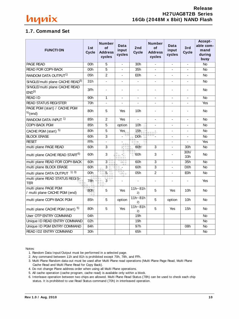
1.7. Command Set
Notes: 1. Random Data Input/Output must be performed in a selected page. 2. Any command between 11h and 81h is prohibited except 70h, 78h, and FFh. 3. Multi Plane Random data-out must be used after Multi Plane read operations (Multi Plane Page Read, Multi Plane Cache Read and Multi Plane Read for Copy Back). 4. Do not change Plane address order when using all Multi Plane operations. 5. All cache operation (cache program, cache read) is available only within a block. 6. Interleave operation between two chips are allowed. Multi Plane Read Status (78h) can be used to check each chip status. It is prohibited to use Read Status command (70h) in interleaved operation.
FUNCTION 1st Cycle
Number of
Address cycles
Data input cycles
2ndCycle
Number of
Address cycles
Data input cycles
3rdCycle
Accept-able com-
mand during busy
PAGE READ 00h 5 - 30h - - - NoREAD FOR COPY-BACK 00h 5 - 35h - - - No
RANDOM DATA OUTPUT1) 05h 2 - E0h - - - No
SINGLE/multi plane CACHE READ5) 31h - - - - - - No
SINGLE/multi plane CACHE READ END5) 3Fh - - - - - - No
READ ID 90h 1 - - - - - NoREAD STATUS REGISTER 70h - - - - - - YesPAGE PGM (start) / CACHE PGM 5)(end)
80h 5 Yes 10h - - - No
RANDOM DATA INPUT 1) 85h 2 Yes - - - - No
COPY-BACK PGM 85h 5 option 10h - - - No
CACHE PGM (start) 5) 80h 5 Yes 15h - - - No
BLOCK ERASE 60h 3 - D0h - - - NoRESET FFh - - - - - Yesmulti plane PAGE READ 60h 3 - 60h 3 - 30h No
multi plane CACHE READ START5) 60h 3 - 60h 3 - 30h/33h No
multi plane READ FOR COPY-BACK 60h 3 - 60h 3 - 35h Nomulti plane BLOCK ERASE 60h 3 - 60h 3 - D0h No
multi plane DATA OUTPUT 1) 3) 00h 5 - 05h 2 - E0h No
multi plane READ STATUS REGIS-TER 78h 3 - - - - - Yes
multi plane PAGE PGM/ multi plane CACHE PGM (end) 80h 5 Yes 11h~81h
2)5 Yes 10h No
multi plane COPY-BACK PGM 85h 5 option 11h~81h2)
5 option 10h No
multi plane CACHE PGM (start) 5) 80h 5 Yes 11h~81h2)
5 Yes 15h No
User OTP ENTRY COMMAND 04h 19h NoUnique ID READ ENTRY COMMAND 02h 19h NoUnique ID PGM ENTRY COMMAND 84h 97h 08h NoREAD ID2 ENTRY COMMAND 30h 65h No
Rev 1.0 / Aug. 2010 10
*58b7d520-e522* B26798/177.179.157.212/2010-08-06 17:39
APCPCWM_4828539:WP_0000001WP_0000001
APC
PCW
M_4
8285
39:W
P_00
0000
1WP_
0000
001
ReleaseH27UAG8T2B Series
16Gb (2048M x 8bit) NAND Flash
Caution: 1. Any undefined command inputs are prohibited except for above command set. 2. Multi Plane page read, Multi Plane cache read, and Multi Plane read for copy-back must be used after Multi Plane programmed page, Multi Plane cache program, and Multi Plane copy-back program.
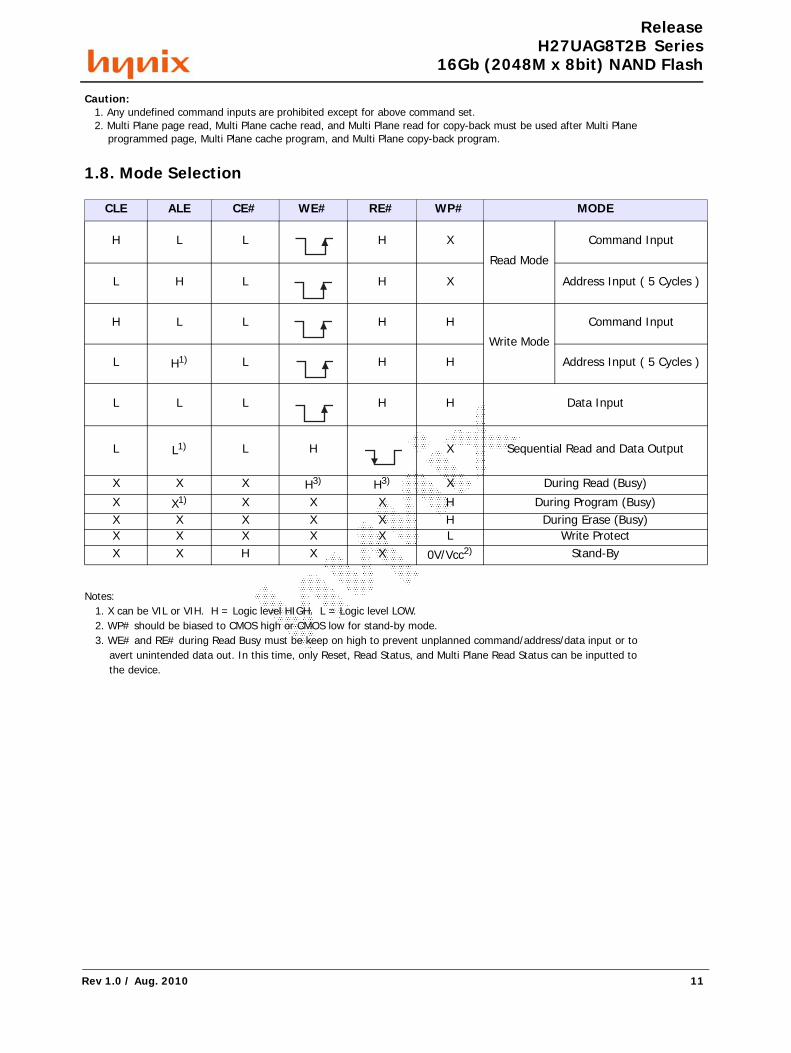
1.8. Mode Selection
Notes: 1. X can be VIL or VIH. H = Logic level HIGH. L = Logic level LOW. 2. WP# should be biased to CMOS high or CMOS low for stand-by mode. 3. WE# and RE# during Read Busy must be keep on high to prevent unplanned command/address/data input or to avert unintended data out. In this time, only Reset, Read Status, and Multi Plane Read Status can be inputted to the device.
CLE ALE CE# WE# RE# WP# MODE
H L L H X
Read Mode
Command Input
L H L H X Address Input ( 5 Cycles )
H L L H H
Write Mode
Command Input
L H1) L H H Address Input ( 5 Cycles )
L L L H H Data Input
L L1) L H X Sequential Read and Data Output
X X X H3) H3) X During Read (Busy)
X X1) X X X H During Program (Busy)X X X X X H During Erase (Busy)X X X X X L Write ProtectX X H X X 0V/Vcc2) Stand-By
Rev 1.0 / Aug. 2010 11
*58b7d520-e522* B26798/177.179.157.212/2010-08-06 17:39
APCPCWM_4828539:WP_0000001WP_0000001
APC
PCW
M_4
8285
39:W
P_00
0000
1WP_
0000
001
ReleaseH27UAG8T2B Series
16Gb (2048M x 8bit) NAND Flash
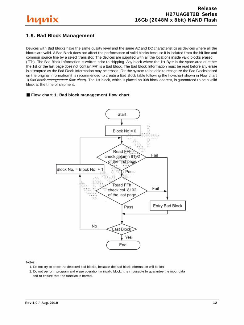
1.9. Bad Block Management
Devices with Bad Blocks have the same quality level and the same AC and DC characteristics as devices where all the blocks are valid. A Bad Block does not affect the performance of valid blocks because it is isolated from the bit line and common source line by a select transistor. The devices are supplied with all the locations inside valid blocks erased (FFh). The Bad Block Information is written prior to shipping. Any block where the 1st Byte in the spare area of either the 1st or the last page does not contain FFh is a Bad Block. The Bad Block Information must be read before any erase is attempted as the Bad Block Information may be erased. For the system to be able to recognize the Bad Blocks based on the original information it is recommended to create a Bad Block table following the flowchart shown in Flow chart 1(Bad block management flow chart). The 1st block, which is placed on 00h block address, is guaranteed to be a valid block at the time of shipment.
■ Flow chart 1. Bad block management flow chart
Notes: 1. Do not try to erase the detected bad blocks, because the bad block information will be lost. 2. Do not perform program and erase operation in invalid block, it is impossible to guarantee the input data and to ensure that the function is normal.
Start
Block No = 0
Read FFh
check column 8192
of the first page
Last Block
End
Entry Bad Block
Fail
Fail
Pass
Yes
Block No. = Block No. + 1Pass
No
Read FFh
check col. 8192
of the last page
Rev 1.0 / Aug. 2010 12
*58b7d520-e522* B26798/177.179.157.212/2010-08-06 17:39
APCPCWM_4828539:WP_0000001WP_0000001
APC
PCW
M_4
8285
39:W
P_00
0000
1WP_
0000
001
ReleaseH27UAG8T2B Series
16Gb (2048M x 8bit) NAND Flash
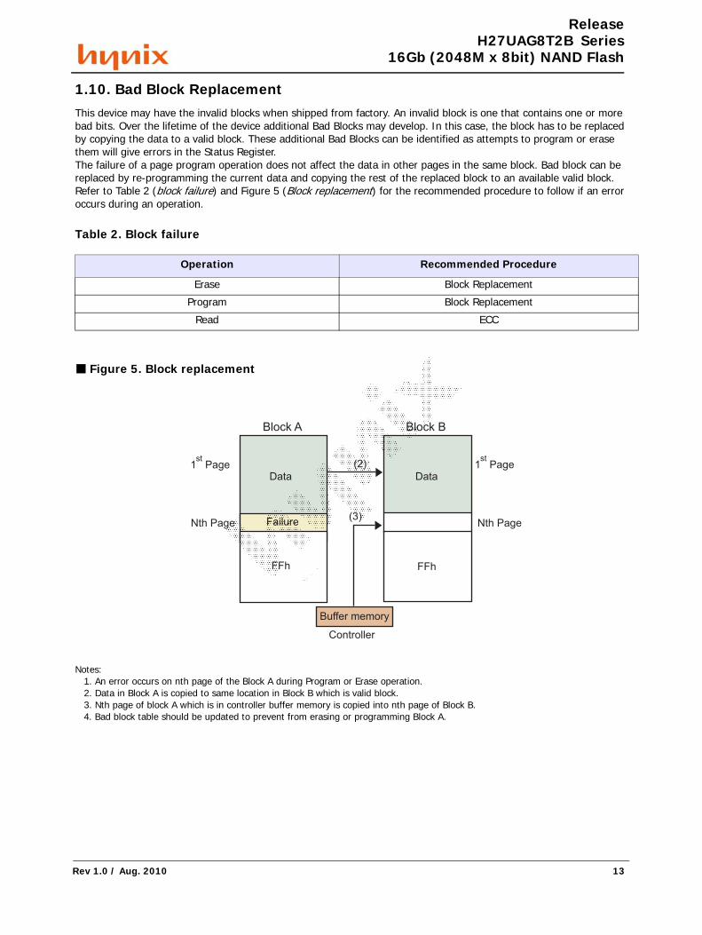
1.10. Bad Block ReplacementThis device may have the invalid blocks when shipped from factory. An invalid block is one that contains one or more bad bits. Over the lifetime of the device additional Bad Blocks may develop. In this case, the block has to be replaced by copying the data to a valid block. These additional Bad Blocks can be identified as attempts to program or erase them will give errors in the Status Register.The failure of a page program operation does not affect the data in other pages in the same block. Bad block can be replaced by re-programming the current data and copying the rest of the replaced block to an available valid block. Refer to Table 2 (block failure) and Figure 5 (Block replacement) for the recommended procedure to follow if an error occurs during an operation.
Table 2. Block failure
■ Figure 5. Block replacement
Notes: 1. An error occurs on nth page of the Block A during Program or Erase operation. 2. Data in Block A is copied to same location in Block B which is valid block. 3. Nth page of block A which is in controller buffer memory is copied into nth page of Block B. 4. Bad block table should be updated to prevent from erasing or programming Block A.
Operation Recommended Procedure
Erase Block Replacement
Program Block Replacement
Read ECC
Block A Block B
Data Data
Failure
FFh FFh
Buffer memory
Controller
1 Pagest
1 Pagest
Nth Page Nth Page
(2)
(3)
Rev 1.0 / Aug. 2010 13
*58b7d520-e522* B26798/177.179.157.212/2010-08-06 17:39
APCPCWM_4828539:WP_0000001WP_0000001
APC
PCW
M_4
8285
39:W
P_00
0000
1WP_
0000
001
ReleaseH27UAG8T2B Series
16Gb (2048M x 8bit) NAND Flash
2. Electrical Characteristics
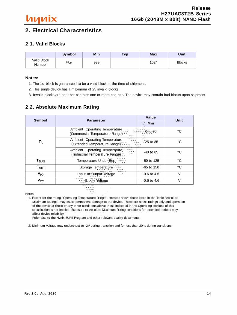
2.1. Valid Blocks
Notes: 1. The 1st block is guaranteed to be a valid block at the time of shipment.
2. This single device has a maximum of 25 invalid blocks.
3. Invalid blocks are one that contains one or more bad bits. The device may contain bad blocks upon shipment.
2.2. Absolute Maximum Rating
Notes: 1. Except for the rating "Operating Temperature Range", stresses above those listed in the Table "Absolute Maximum Ratings" may cause permanent damage to the device. These are stress ratings only and operation of the device at these or any other conditions above those indicated in the Operating sections of this specification is not implied. Exposure to Absolute Maximum Rating conditions for extended periods may affect device reliability. Refer also to the Hynix SURE Program and other relevant quality documents.
2. Minimum Voltage may undershoot to -2V during transition and for less than 20ns during transitions.
Symbol Min Typ Max Unit
Valid Block Number
NVB 999 1024 Blocks
Symbol ParameterValue
UnitMin
TA
Ambient Operating Temperature(Commercial Temperature Range) 0 to 70 °C
Ambient Operating Temperature(Extended Temperature Range) -25 to 85 °C
Ambient Operating Temperature(Industrial Temperature Range) -40 to 85 °C
TBIAS Temperature Under Bias -50 to 125 °C
TSTG Storage Temperature -65 to 150 °C
VIO Input or Output Voltage -0.6 to 4.6 V
VCC Supply Voltage -0.6 to 4.6 V
Rev 1.0 / Aug. 2010 14
*58b7d520-e522* B26798/177.179.157.212/2010-08-06 17:39
APCPCWM_4828539:WP_0000001WP_0000001
APC
PCW
M_4
8285
39:W
P_00
0000
1WP_
0000
001
ReleaseH27UAG8T2B Series
16Gb (2048M x 8bit) NAND Flash
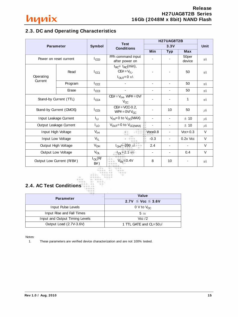
2.3. DC and Operating Characteristics
2.4. AC Test Conditions
Notes: 1. These parameters are verified device characterization and are not 100% tested.
Parameter Symbol TestConditions
H27UAG8T2BUnit3.3V
Min Typ Max
Power on reset current ICC0FFh command input
after power on - - 50perdevice ㎃
OperatingCurrent
Read ICC1
tRC= tRC(min),CE#=VIL, IOUT=0 ㎃
- - 50 ㎃
Program ICC2 - - - 50 ㎃
Erase ICC3 - - - 50 ㎃
Stand-by Current (TTL) ICC4CE#=VIH, WP#=0V/
VCC- - 1 ㎃
Stand-by Current (CMOS) ICC5CE#=VCC-0.2, WP#=0V/VCC
- 10 50 ㎂
Input Leakage Current ILI VIN=0 to VCC(MAX) - - ± 10 ㎂
Output Leakage Current ILO VOUT=0 to VCC(MAX) - - ± 10 ㎂
Input High Voltage VIH - Vccx0.8 - Vcc+0.3 V
Input Low Voltage VIL - -0.3 - 0.2x Vcc V
Output High Voltage VOH IOH=-200 ㎂ 2.4 - - V
Output Low Voltage VOL IOL=2.1 ㎃ - - 0.4 V
Output Low Current (R/B#)IOL(R/B#)
VOL=0.4V 8 10 - ㎃
ParameterValue
2.7V ≤ Vcc ≤ 3.6V
Input Pulse Levels 0 V to VCC
Input Rise and Fall Times 5 ㎱
Input and Output Timing Levels Vcc /2Output Load (2.7V-3.6V) 1 TTL GATE and CL=50㎊
Rev 1.0 / Aug. 2010 15
*58b7d520-e522* B26798/177.179.157.212/2010-08-06 17:39
APCPCWM_4828539:WP_0000001WP_0000001
APC
PCW
M_4
8285
39:W
P_00
0000
1WP_
0000
001
ReleaseH27UAG8T2B Series
16Gb (2048M x 8bit) NAND Flash
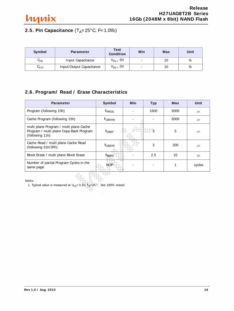
2.5. Pin Capacitance (TA=25°C, F=1.0㎒)
2.6. Program/ Read / Erase Characteristics
Notes: 1. Typical value is measured at VCC=3.3V, TA=25℃. Not 100% tested.
Symbol Parameter TestCondition Min Max Unit
CIN Input Capacitance VIN = 0V - 10 ß‹
CI/O Input/Output Capacitance VIN = 0V - 10 ß‹
Parameter Symbol Min Typ Max Unit
Program (following 10h) tPROG - 1600 5000 ㎲
Cache Program (following 15h) tCBSYW - - 5000 ㎲
multi plane Program / multi plane Cache Program / multi plane Copy-Back Program (following 11h)
tDBSY - 3 5 ㎲
Cache Read / multi plane Cache Read (following 31h/3Fh)
tCBSYR - 3 200 ㎲
Block Erase / multi plane Block Erase tBERS - 2.5 10 ㎳
Number of partial Program Cycles in the same page NOP - - 1 cycles
Rev 1.0 / Aug. 2010 16
*58b7d520-e522* B26798/177.179.157.212/2010-08-06 17:39
APCPCWM_4828539:WP_0000001WP_0000001
APC
PCW
M_4
8285
39:W
P_00
0000
1WP_
0000
001
ReleaseH27UAG8T2B Series
16Gb (2048M x 8bit) NAND Flash
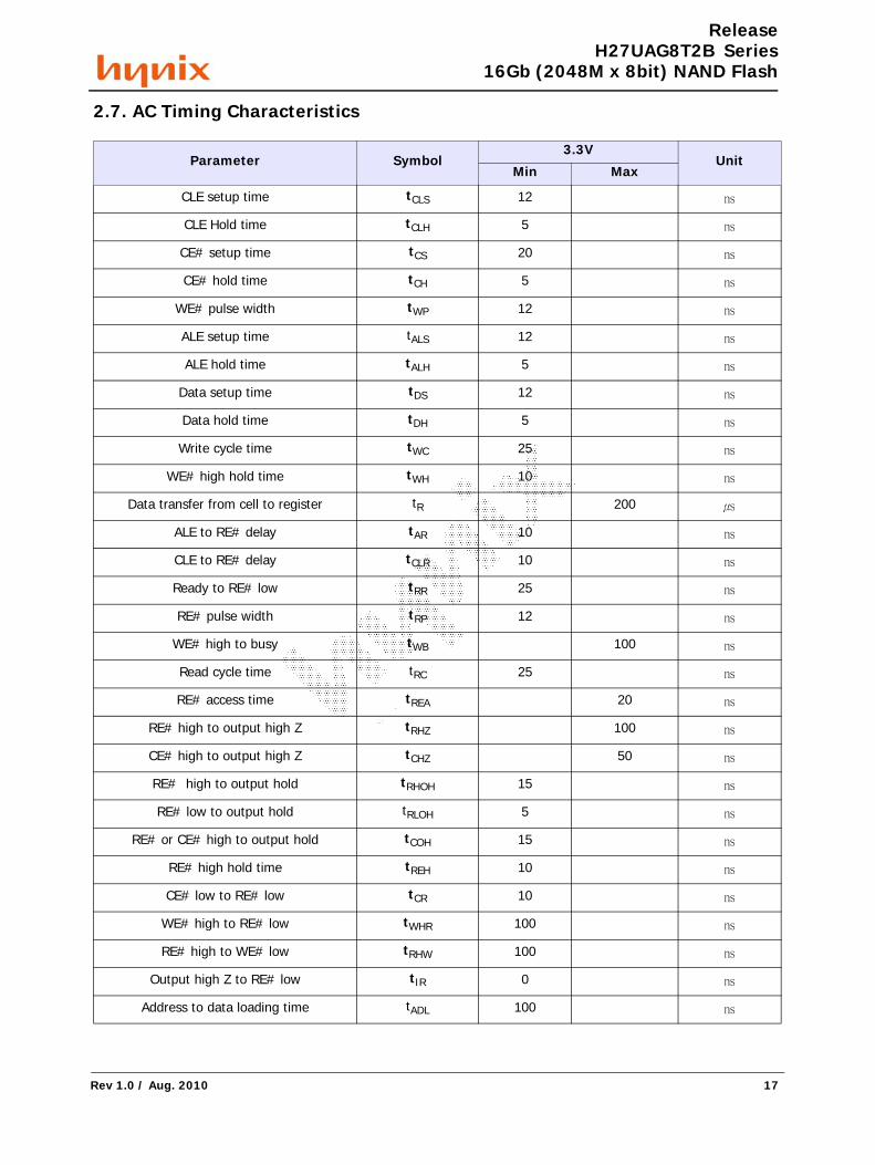
2.7. AC Timing Characteristics
Parameter Symbol3.3V
UnitMin Max
CLE setup time tCLS 12 ㎱
CLE Hold time tCLH 5 ㎱
CE# setup time tCS 20 ㎱
CE# hold time tCH 5 ㎱
WE# pulse width tWP 12 ㎱
ALE setup time tALS 12 ㎱
ALE hold time tALH 5 ㎱
Data setup time tDS 12 ㎱
Data hold time tDH 5 ㎱
Write cycle time tWC 25 ㎱
WE# high hold time tWH 10 ㎱
Data transfer from cell to register tR 200 ㎲
ALE to RE# delay tAR 10 ㎱
CLE to RE# delay tCLR 10 ㎱
Ready to RE# low tRR 25 ㎱
RE# pulse width tRP 12 ㎱
WE# high to busy tWB 100 ㎱
Read cycle time tRC 25 ㎱
RE# access time tREA 20 ㎱
RE# high to output high Z tRHZ 100 ㎱
CE# high to output high Z tCHZ 50 ㎱
RE# high to output hold tRHOH 15 ㎱
RE# low to output hold tRLOH 5 ㎱
RE# or CE# high to output hold tCOH 15 ㎱
RE# high hold time tREH 10 ㎱
CE# low to RE# low tCR 10 ㎱
WE# high to RE# low tWHR 100 ㎱
RE# high to WE# low tRHW 100 ㎱
Output high Z to RE# low tIR 0 ㎱
Address to data loading time tADL 100 ㎱
Rev 1.0 / Aug. 2010 17
*58b7d520-e522* B26798/177.179.157.212/2010-08-06 17:39
APCPCWM_4828539:WP_0000001WP_0000001
APC
PCW
M_4
8285
39:W
P_00
0000
1WP_
0000
001
ReleaseH27UAG8T2B Series
16Gb (2048M x 8bit) NAND Flash
Notes: 1. If Reset Command (FFh) is written at Ready state, the device goes into Busy for maximum 5us. 2. Program / Erase Enable Operation: WP# high to WE# High. Program / Erase Disable Operation: WP# Low to WE# High. 3. The transition of the corresponding control pins must occur only while WE# is held low. 4. tADL is the time from the WE# rising edge of final address cycle to the WE# rising edge of first data cycle.
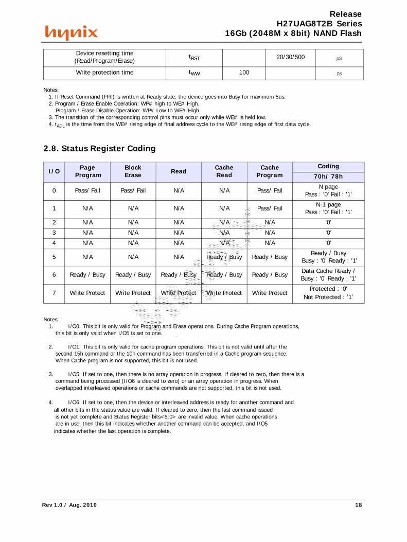
2.8. Status Register Coding
Notes: 1. I/O0: This bit is only valid for Program and Erase operations. During Cache Program operations, this bit is only valid when I/O5 is set to one.
2. I/O1: This bit is only valid for cache program operations. This bit is not valid until after the second 15h command or the 10h command has been transferred in a Cache program sequence. When Cache program is not supported, this bit is not used.
3. I/O5: If set to one, then there is no array operation in progress. If cleared to zero, then there is a command being processed (I/O6 is cleared to zero) or an array operation in progress. When overlapped interleaved operations or cache commands are not supported, this bit is not used.
4. I/O6: If set to one, then the device or interleaved address is ready for another command and all other bits in the status value are valid. If cleared to zero, then the last command issued is not yet complete and Status Register bits<5:0> are invalid value. When cache operations are in use, then this bit indicates whether another command can be accepted, and I/O5 indicates whether the last operation is complete.
Device resetting time (Read/Program/Erase)
tRST 20/30/500 ㎲
Write protection time tWW 100 ㎱
I/O Page Program
Block Erase Read Cache
ReadCache
ProgramCoding
70h/ 78h
0 Pass/ Fail Pass/ Fail N/A N/A Pass/ Fail N pagePass : '0' Fail : '1'
1 N/A N/A N/A N/A Pass/ Fail N-1 pagePass : '0' Fail : '1'
2 N/A N/A N/A N/A N/A '0'
3 N/A N/A N/A N/A N/A '0'
4 N/A N/A N/A N/A N/A '0'
5 N/A N/A N/A Ready / Busy Ready / Busy Ready / Busy Busy : '0' Ready : '1'
6 Ready / Busy Ready / Busy Ready / Busy Ready / Busy Ready / Busy Data Cache Ready / Busy : '0' Ready : '1'
7 Write Protect Write Protect Write Protect Write Protect Write ProtectProtected : '0'
Not Protected : '1'
Rev 1.0 / Aug. 2010 18
*58b7d520-e522* B26798/177.179.157.212/2010-08-06 17:39
APCPCWM_4828539:WP_0000001WP_0000001
APC
PCW
M_4
8285
39:W
P_00
0000
1WP_
0000
001
ReleaseH27UAG8T2B Series
16Gb (2048M x 8bit) NAND Flash
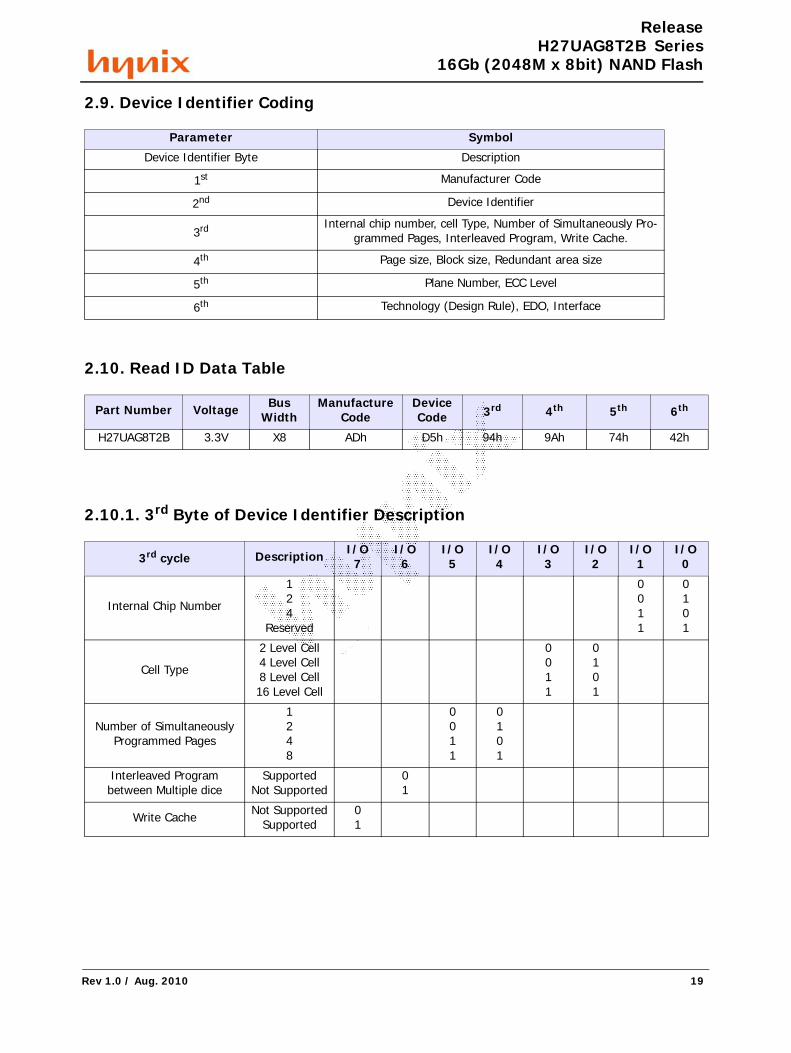
2.9. Device Identifier Coding
2.10. Read ID Data Table
2.10.1. 3rd Byte of Device Identifier Description
Parameter Symbol
Device Identifier Byte Description
1st Manufacturer Code
2nd Device Identifier
3rd Internal chip number, cell Type, Number of Simultaneously Pro-grammed Pages, Interleaved Program, Write Cache.
4th Page size, Block size, Redundant area size
5th Plane Number, ECC Level
6th Technology (Design Rule), EDO, Interface
Part Number Voltage Bus Width
Manufacture Code
Device Code 3rd 4th 5th 6th
H27UAG8T2B 3.3V X8 ADh D5h 94h 9Ah 74h 42h
3rd cycle Description I/O7
I/O6
I/O5
I/O4
I/O3
I/O2
I/O1
I/O0
Internal Chip Number
124
Reserved
0011
0101
Cell Type
2 Level Cell4 Level Cell8 Level Cell16 Level Cell
0011
0101
Number of Simultaneously Programmed Pages
1248
0011
0101
Interleaved Program between Multiple dice
SupportedNot Supported
01
Write Cache Not SupportedSupported
01
Rev 1.0 / Aug. 2010 19
*58b7d520-e522* B26798/177.179.157.212/2010-08-06 17:39
APCPCWM_4828539:WP_0000001WP_0000001
APC
PCW
M_4
8285
39:W
P_00
0000
1WP_
0000
001
ReleaseH27UAG8T2B Series
16Gb (2048M x 8bit) NAND Flash
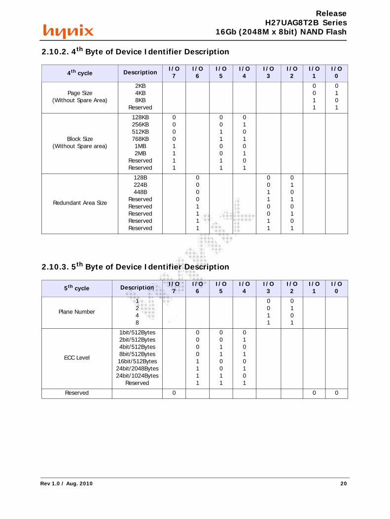
2.10.2. 4th Byte of Device Identifier Description
2.10.3. 5th Byte of Device Identifier Description
4th cycle Description I/O7
I/O6
I/O5
I/O4
I/O3
I/O2
I/O1
I/O0
Page Size(Without Spare Area)
2KB4KB8KB
Reserved
0011
0101
Block Size(Without Spare area)
128KB256KB512KB768KB1MB2MB
ReservedReserved
00001111
00110011
01010101
Redundant Area Size
128B224B448B
ReservedReservedReservedReservedReserved
00001111
00110011
01010101
5th cycle Description I/O7
I/O6
I/O5
I/O4
I/O3
I/O2
I/O1
I/O0
Plane Number
1248
0011
0101
ECC Level
1bit/512Bytes2bit/512Bytes4bit/512Bytes8bit/512Bytes16bit/512Bytes24bit/2048Bytes24bit/1024Bytes
Reserved
00001111
00110011
01010101
Reserved 0 0 0
Rev 1.0 / Aug. 2010 20
*58b7d520-e522* B26798/177.179.157.212/2010-08-06 17:39
APCPCWM_4828539:WP_0000001WP_0000001
APC
PCW
M_4
8285
39:W
P_00
0000
1WP_
0000
001
ReleaseH27UAG8T2B Series
16Gb (2048M x 8bit) NAND Flash
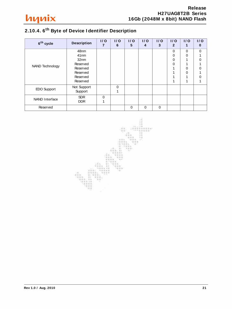
2.10.4. 6th Byte of Device Identifier Description
6th cycle Description I/O7
I/O6
I/O5
I/O4
I/O3
I/O2
I/O1
I/O0
NAND Technology
48nm41nm32nm
ReservedReservedReservedReservedReserved
00001111
00110011
01010101
EDO Support Not SupportSupport
01
NAND Interface SDRDDR
01
Reserved 0 0 0
Rev 1.0 / Aug. 2010 21
*58b7d520-e522* B26798/177.179.157.212/2010-08-06 17:39
APCPCWM_4828539:WP_0000001WP_0000001
APC
PCW
M_4
8285
39:W
P_00
0000
1WP_
0000
001
ReleaseH27UAG8T2B Series
16Gb (2048M x 8bit) NAND Flash
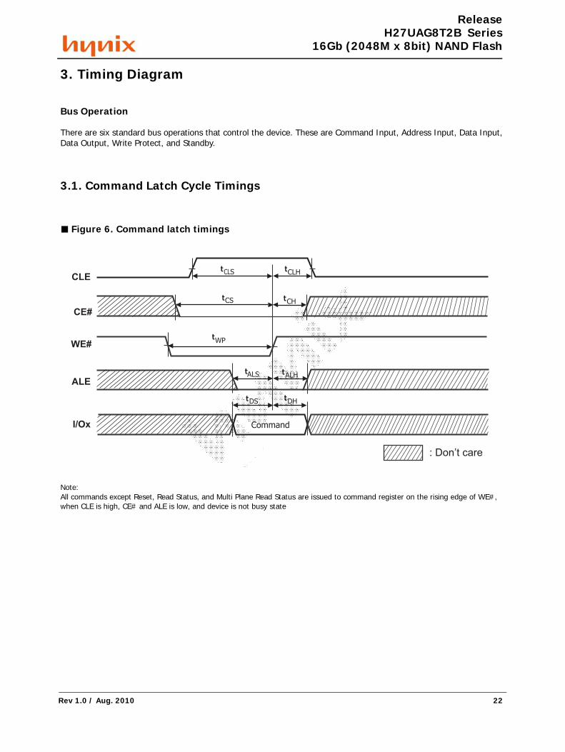
3. Timing Diagram
Bus Operation
There are six standard bus operations that control the device. These are Command Input, Address Input, Data Input, Data Output, Write Protect, and Standby.
3.1. Command Latch Cycle Timings
■ Figure 6. Command latch timings
Note:All commands except Reset, Read Status, and Multi Plane Read Status are issued to command register on the rising edge of WE#, when CLE is high, CE# and ALE is low, and device is not busy state
CLS
CS
WP
Command
CLE
CE#
WE#
ALE
I/Ox
DH DS
ALS
CLH
CH
: Don’t care
t t
t t
t
t
t t
ALHt
Rev 1.0 / Aug. 2010 22
*58b7d520-e522* B26798/177.179.157.212/2010-08-06 17:39
APCPCWM_4828539:WP_0000001WP_0000001
APC
PCW
M_4
8285
39:W
P_00
0000
1WP_
0000
001
ReleaseH27UAG8T2B Series
16Gb (2048M x 8bit) NAND Flash
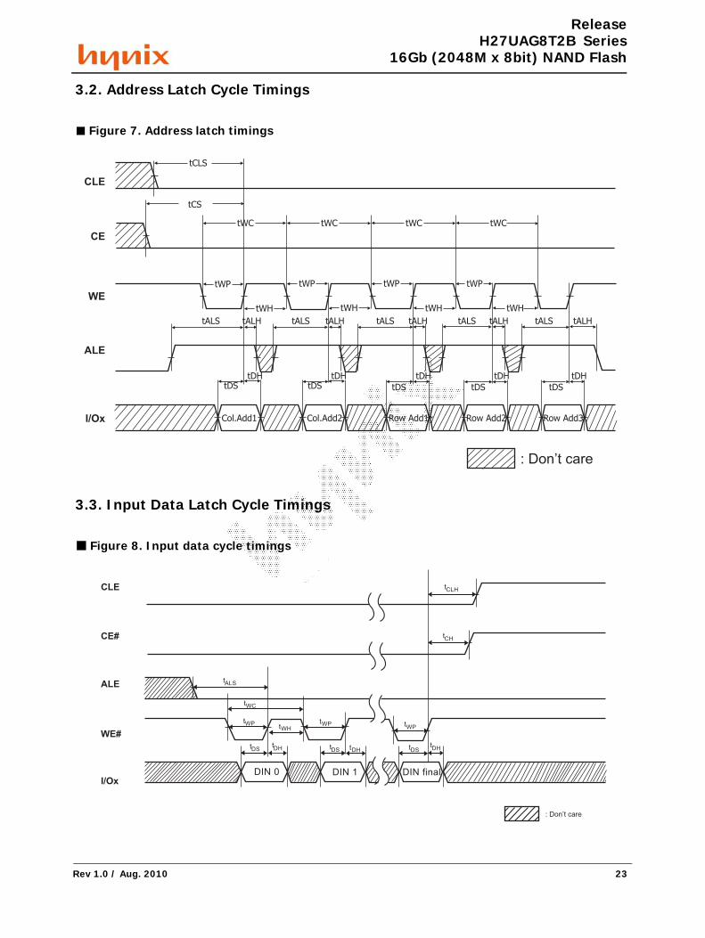
3.2. Address Latch Cycle Timings
■ Figure 7. Address latch timings
3.3. Input Data Latch Cycle Timings
■ Figure 8. Input data cycle timings
tCLS
tCS
tWC
tALS tALS tALS tALS tALS tALHtALHtALHtALHtALH
tWC tWC tWC
tWP tWP
tWH
tWP tWP
tWH tWH tWH
tDS
Col.Add1
CLE
CE
WE
ALE
I/Ox Col.Add2 Row Add1 Row Add2 Row Add3
tDS tDS tDS tDS
tDHtDHtDHtDHtDH
: Don’t care
WC
CLH
CH
WPWH
DIN 1 DIN final
DH DH DH DS DS DS
WPWP
CLE
ALE
CE#
I/Ox
WE#
ALS
DIN 0
t
t
tt
t
tt
t
tt
t
t
t
t
: Don’t care
Rev 1.0 / Aug. 2010 23
*58b7d520-e522* B26798/177.179.157.212/2010-08-06 17:39
APCPCWM_4828539:WP_0000001WP_0000001
APC
PCW
M_4
8285
39:W
P_00
0000
1WP_
0000
001
ReleaseH27UAG8T2B Series
16Gb (2048M x 8bit) NAND Flash
Note: Data Input cycle is accepted to data register on the rising edge of WE#, when CLE and CE# and ALE are low, and device is not Busy state.
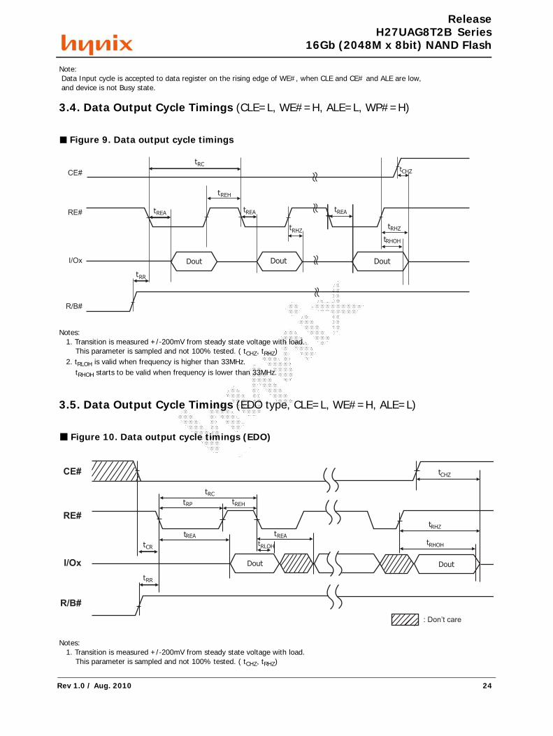
3.4. Data Output Cycle Timings (CLE=L, WE#=H, ALE=L, WP#=H)
■ Figure 9. Data output cycle timings
Notes: 1. Transition is measured +/-200mV from steady state voltage with load. This parameter is sampled and not 100% tested. ( tCHZ, tRHZ) 2. tRLOH is valid when frequency is higher than 33MHz. tRHOH starts to be valid when frequency is lower than 33MHz.
3.5. Data Output Cycle Timings (EDO type, CLE=L, WE#=H, ALE=L)
■ Figure 10. Data output cycle timings (EDO)
Notes: 1. Transition is measured +/-200mV from steady state voltage with load. This parameter is sampled and not 100% tested. ( tCHZ, tRHZ)
REH
REA
RC
RR
CHZ
RHZ
RHOH
DoutDout
CE#
RE#
I/Ox
R/B#
Dout
REA
RHZ
REA
t
t
t
t
t
t
t
t
t
t
RR
CHZ
RHZ
RHOH
Dout
CE#
RE#
I/Ox
R/B#
REA
Dout
RLOH
REA
RP REH
RCt
t t
t
t
t
t
t
t
t
: Don’t care
CRt
Rev 1.0 / Aug. 2010 24
*58b7d520-e522* B26798/177.179.157.212/2010-08-06 17:39
APCPCWM_4828539:WP_0000001WP_0000001
APC
PCW
M_4
8285
39:W
P_00
0000
1WP_
0000
001
ReleaseH27UAG8T2B Series
16Gb (2048M x 8bit) NAND Flash
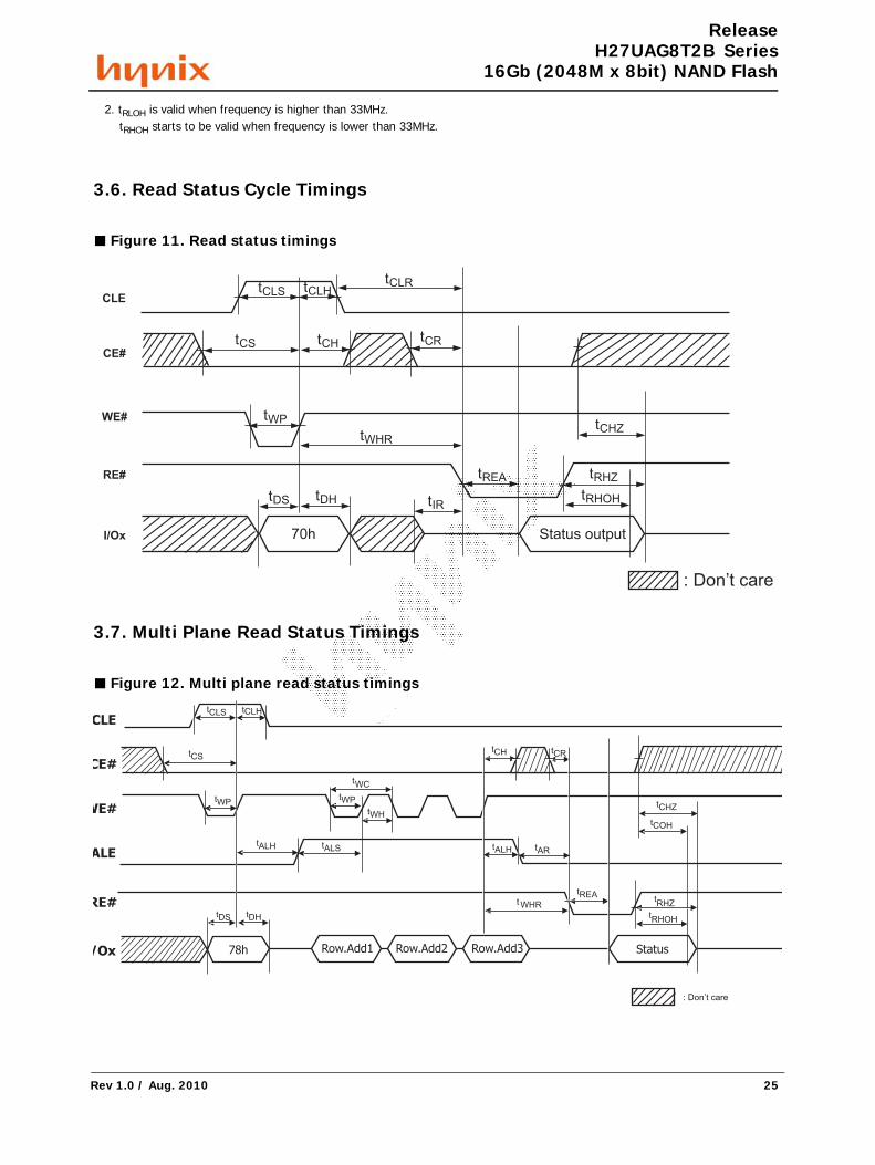
2. tRLOH is valid when frequency is higher than 33MHz. tRHOH starts to be valid when frequency is lower than 33MHz.
3.6. Read Status Cycle Timings
■ Figure 11. Read status timings
3.7. Multi Plane Read Status Timings
■ Figure 12. Multi plane read status timings
CLE
CE#
RE#
I/Ox
WE#
70h Status output
CLSt CLHt
CSt
CLRt
CHt CRt
CHZt
RHZt
RHOHt
WPt
WHRt
DSt DHtIRt
REAt
: Don’t care
tCLS tCLH
tCS
tWP
tCH tCR
tCHZ
tCOH
t WHR
tALH tAR
tREAtRHZ
tRHOH
tDS tDH
tALH tALS
WC
tWP
tWH
t
: Don’t care
CLE
CE#
WE#
ALE
RE#
/Ox 78h Row.Add1 Row.Add2 Row.Add3 Status
Rev 1.0 / Aug. 2010 25
*58b7d520-e522* B26798/177.179.157.212/2010-08-06 17:39
APCPCWM_4828539:WP_0000001WP_0000001
APC
PCW
M_4
8285
39:W
P_00
0000
1WP_
0000
001
ReleaseH27UAG8T2B Series
16Gb (2048M x 8bit) NAND Flash
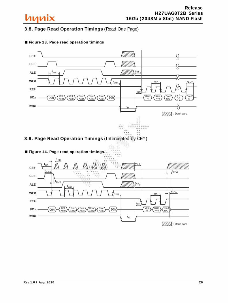
3.8. Page Read Operation Timings (Read One Page)
■ Figure 13. Page read operation timings
3.9. Page Read Operation Timings (Intercepted by CE#)
■ Figure 14. Page read operation timings
CE#
CLE
ALE
WE#
RE#
I/Ox 00hCol.
Add1Col.
Add2Row.
Add1
Row.
Add2
Row.
Add330h
Dout
N
Dout
N+1Dout
N+2
R/B#
tAR
tRC
tR
tWB
tRR
tWC
: Don’t care
tRHZ
Dout
M
CE#
CLE
ALE
WE#
RE#
I/Ox 00hCol.
Add1Col.
Add2Row.
Add1
Row.
Add2
Row.
Add330h
Dout
N
Dout
N+1Dout
N+2
R/B#
tAR
tRC
tR
tWB
tRR
tWC
: Don’t care
tCLR
tCHZ
tCOH
tCS
tCH
tCLS
tCLH
Rev 1.0 / Aug. 2010 26
*58b7d520-e522* B26798/177.179.157.212/2010-08-06 17:39
APCPCWM_4828539:WP_0000001WP_0000001
APC
PCW
M_4
8285
39:W
P_00
0000
1WP_
0000
001
ReleaseH27UAG8T2B Series
16Gb (2048M x 8bit) NAND Flash
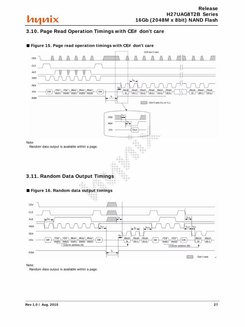
3.10. Page Read Operation Timings with CE# don't care
■ Figure 15. Page read operation timings with CE# don't care
Note: Random data output is available within a page.
3.11. Random Data Output Timings
■ Figure 16. Random data output timings
Note: Random data output is available within a page.
Rev 1.0 / Aug. 2010 27
*58b7d520-e522* B26798/177.179.157.212/2010-08-06 17:39
APCPCWM_4828539:WP_0000001WP_0000001
APC
PCW
M_4
8285
39:W
P_00
0000
1WP_
0000
001
ReleaseH27UAG8T2B Series
16Gb (2048M x 8bit) NAND Flash
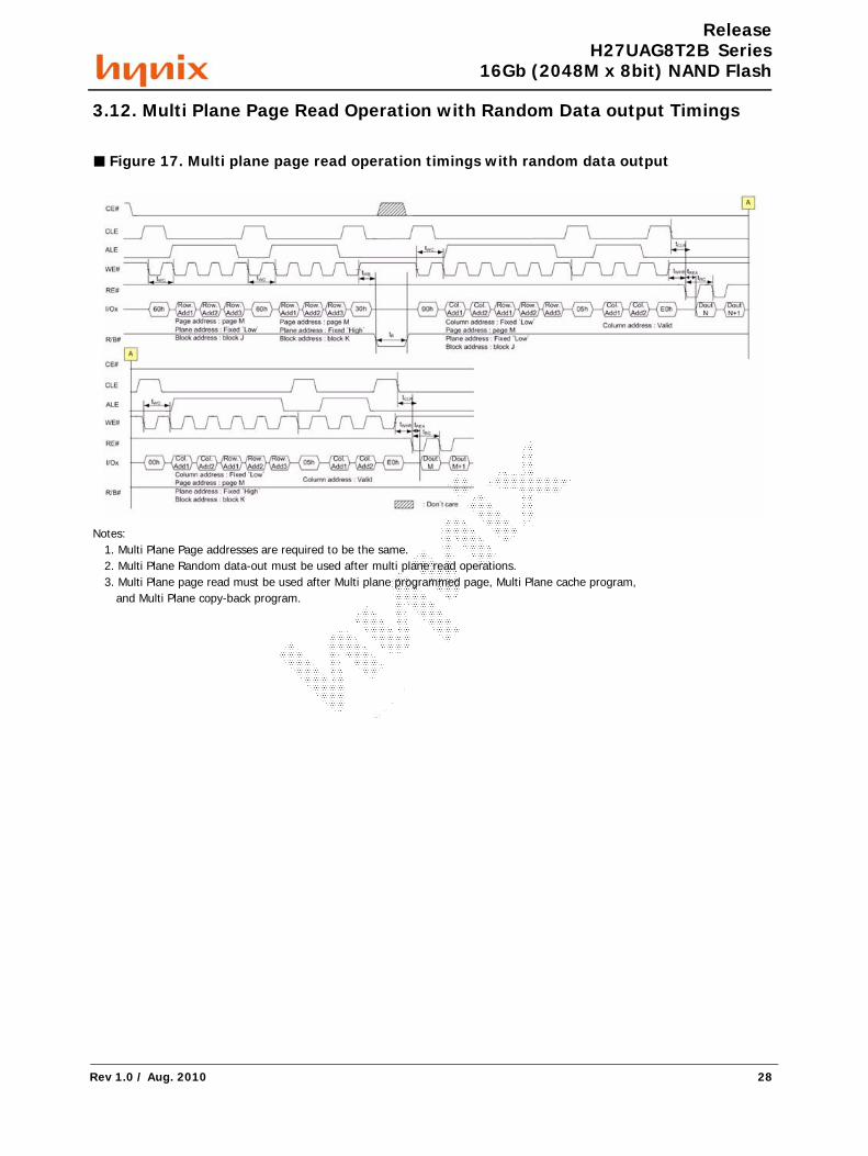
3.12. Multi Plane Page Read Operation with Random Data output Timings
■ Figure 17. Multi plane page read operation timings with random data output
Notes: 1. Multi Plane Page addresses are required to be the same. 2. Multi Plane Random data-out must be used after multi plane read operations. 3. Multi Plane page read must be used after Multi plane programmed page, Multi Plane cache program, and Multi Plane copy-back program.
Rev 1.0 / Aug. 2010 28
*58b7d520-e522* B26798/177.179.157.212/2010-08-06 17:39
APCPCWM_4828539:WP_0000001WP_0000001
APC
PCW
M_4
8285
39:W
P_00
0000
1WP_
0000
001
ReleaseH27UAG8T2B Series
16Gb (2048M x 8bit) NAND Flash
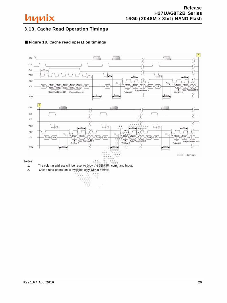
3.13. Cache Read Operation Timings
■ Figure 18. Cache read operation timings
Notes: 1. The column address will be reset to 0 by the 31h/3Fh command input. 2. Cache read operation is available only within a block.
Rev 1.0 / Aug. 2010 29
*58b7d520-e522* B26798/177.179.157.212/2010-08-06 17:39
APCPCWM_4828539:WP_0000001WP_0000001
APC
PCW
M_4
8285
39:W
P_00
0000
1WP_
0000
001
ReleaseH27UAG8T2B Series
16Gb (2048M x 8bit) NAND Flash
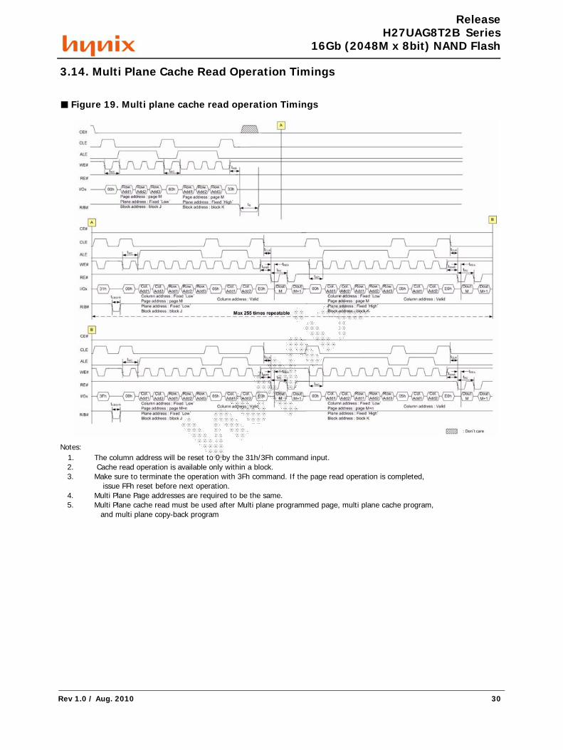
3.14. Multi Plane Cache Read Operation Timings
■ Figure 19. Multi plane cache read operation Timings
Notes: 1. The column address will be reset to 0 by the 31h/3Fh command input. 2. Cache read operation is available only within a block. 3. Make sure to terminate the operation with 3Fh command. If the page read operation is completed, issue FFh reset before next operation. 4. Multi Plane Page addresses are required to be the same. 5. Multi Plane cache read must be used after Multi plane programmed page, multi plane cache program, and multi plane copy-back program
Rev 1.0 / Aug. 2010 30
*58b7d520-e522* B26798/177.179.157.212/2010-08-06 17:39
APCPCWM_4828539:WP_0000001WP_0000001
APC
PCW
M_4
8285
39:W
P_00
0000
1WP_
0000
001
ReleaseH27UAG8T2B Series
16Gb (2048M x 8bit) NAND Flash
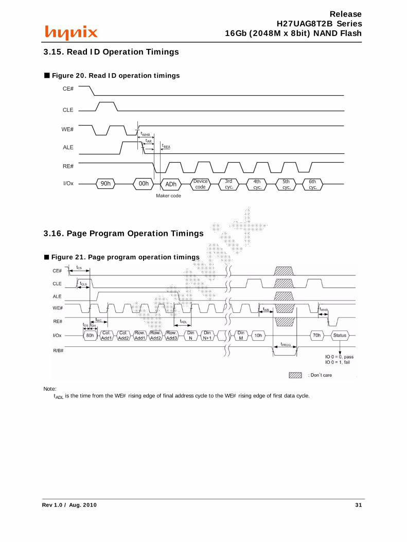
3.15. Read ID Operation Timings
■ Figure 20. Read ID operation timings
3.16. Page Program Operation Timings
■ Figure 21. Page program operation timings
Note: tADL is the time from the WE# rising edge of final address cycle to the WE# rising edge of first data cycle.
Devicecode
3rdcyc.
4thcyc.
90h
CE#
CLE
WE#
ALE
RE#
I/Ox 00h ADh
AR
WHR
REA
5thcyc.
6thcyc.
Maker code
t
tt
Rev 1.0 / Aug. 2010 31
*58b7d520-e522* B26798/177.179.157.212/2010-08-06 17:39
APCPCWM_4828539:WP_0000001WP_0000001
APC
PCW
M_4
8285
39:W
P_00
0000
1WP_
0000
001
ReleaseH27UAG8T2B Series
16Gb (2048M x 8bit) NAND Flash
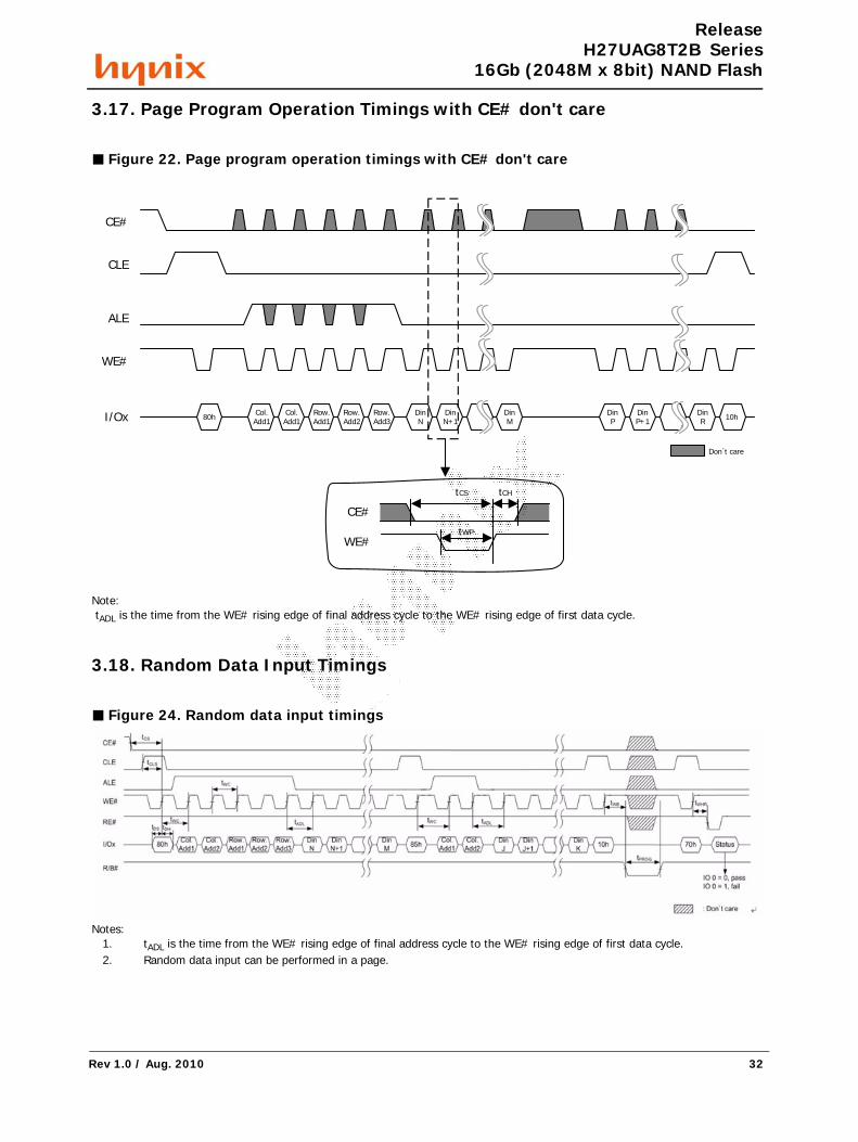
3.17. Page Program Operation Timings with CE# don't care
■ Figure 22. Page program operation timings with CE# don't care
Note: tADL is the time from the WE# rising edge of final address cycle to the WE# rising edge of first data cycle.
3.18. Random Data Input Timings
■ Figure 24. Random data input timings
Notes: 1. tADL is the time from the WE# rising edge of final address cycle to the WE# rising edge of first data cycle. 2. Random data input can be performed in a page.
80h Col.Add1
Col.Add1
Row.Add1
Row.Add2
Row.Add3
DinN
DinN+1
DinM
DinP
DinP+1
DinR 10h
Don’t care
CE#
CLE
ALE
WE#
I/Ox
tCS tCH
tWP
CE#
WE#
Rev 1.0 / Aug. 2010 32
*58b7d520-e522* B26798/177.179.157.212/2010-08-06 17:39
APCPCWM_4828539:WP_0000001WP_0000001
APC
PCW
M_4
8285
39:W
P_00
0000
1WP_
0000
001
ReleaseH27UAG8T2B Series
16Gb (2048M x 8bit) NAND Flash
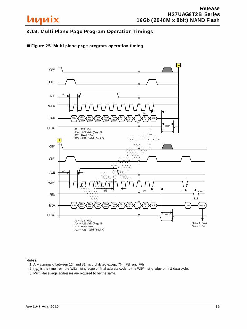
3.19. Multi Plane Page Program Operation Timings
■ Figure 25. Multi plane page program operation timing
Notes: 1. Any command between 11h and 81h is prohibited except 70h, 78h and FFh 2. tADL is the time from the WE# rising edge of final address cycle to the WE# rising edge of first data cycle. 3. Multi Plane Page addresses are required to be the same.
80h Col.Add1
Col.Add2
RowAdd1
RowAdd2
RowAdd3
DINN
DINN+1
DINM 11h
A
A
81h Col.Add1
Col.Add2
RowAdd1
RowAdd2
RowAdd3
DINN
DINN+1
DINM 10h 70h Status
CE#
CLE
ALE
WE#
I/Ox
CE#
CLE
ALE
WE#
RE#
I/Ox
R/B#
A0 ~ A13 : ValidA14 ~ A21 Valid (Page M)A22 : Fixed LOWA23 ~ A31 : Valid (Block J)
A0 ~ A13 : ValidA14 ~ A21 Valid (Page M)A22 : Fixed HighA23 ~ A31 : Valid (Block K)
R/B#
tWC
tWB
tDBSY
tWB
tPROG
tADLtWHR
IO 0 = 0, passIO 0 = 1, fail
tWC
Rev 1.0 / Aug. 2010 33
*58b7d520-e522* B26798/177.179.157.212/2010-08-06 17:39
APCPCWM_4828539:WP_0000001WP_0000001
APC
PCW
M_4
8285
39:W
P_00
0000
1WP_
0000
001
ReleaseH27UAG8T2B Series
16Gb (2048M x 8bit) NAND Flash
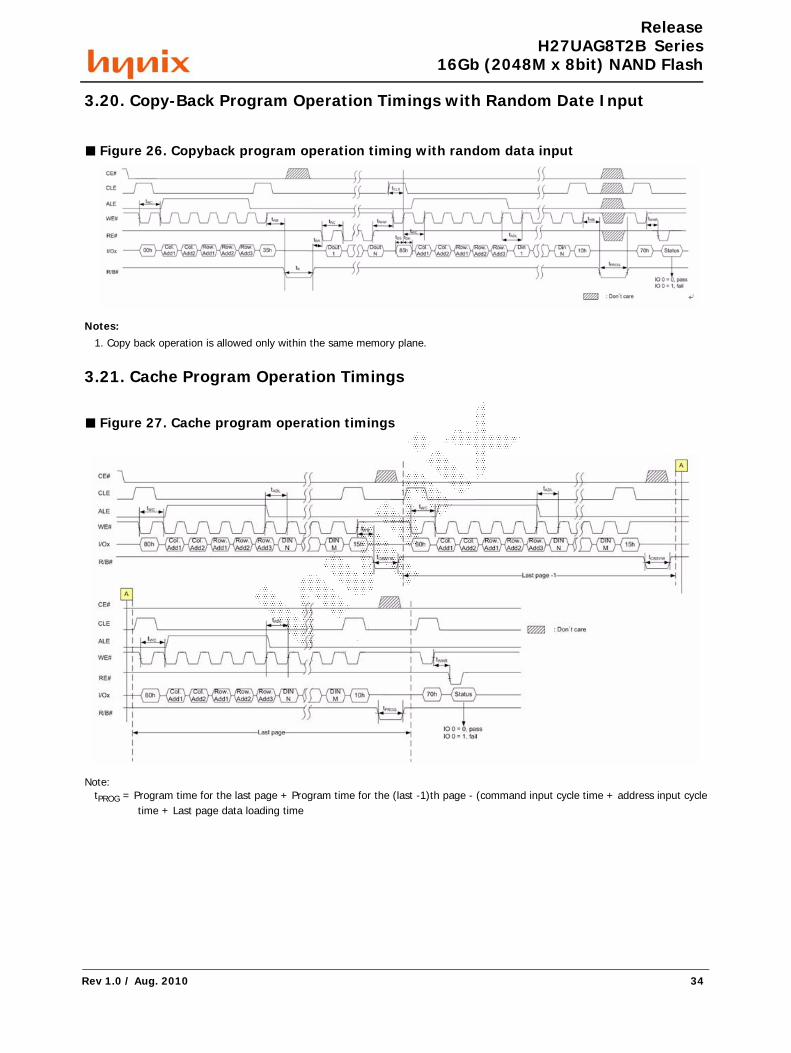
3.20. Copy-Back Program Operation Timings with Random Date Input
■ Figure 26. Copyback program operation timing with random data input
Notes: 1. Copy back operation is allowed only within the same memory plane.
3.21. Cache Program Operation Timings
■ Figure 27. Cache program operation timings
Note: tPROG = Program time for the last page + Program time for the (last -1)th page - (command input cycle time + address input cycle time + Last page data loading time
Rev 1.0 / Aug. 2010 34
*58b7d520-e522* B26798/177.179.157.212/2010-08-06 17:39
APCPCWM_4828539:WP_0000001WP_0000001
APC
PCW
M_4
8285
39:W
P_00
0000
1WP_
0000
001
ReleaseH27UAG8T2B Series
16Gb (2048M x 8bit) NAND Flash
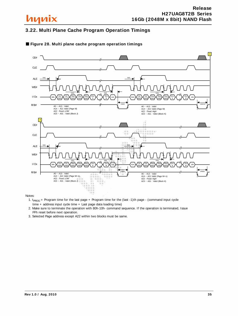
3.22. Multi Plane Cache Program Operation Timings
■ Figure 28. Multi plane cache program operation timings
Notes: 1. tPROG = Program time for the last page + Program time for the (last -1)th page - (command input cycle time + address input cycle time + Last page data loading time) 2. Make sure to terminate the operation with 80h-10h- command sequence. If the operation is terminated, Issue FFh reset before next operation. 3. Selected Page address except A22 within two blocks must be same.
80h Col.Add1
Col.Add2
RowAdd1
RowAdd2
RowAdd3
DINN
DINM 11h
A
CE#
CLE
ALE
WE#
I/Ox
A0 ~ A13 : ValidA14 ~ A21 Valid (Page M)A22 : Fixed LOWA23 ~ A31 : Valid (Block J)
R/B#
tWC
tWB
tDBSY
81h Col.Add1
Col.Add2
RowAdd1
RowAdd2
RowAdd3
DINN
DINM 15h
tADL
tWC
tADL
tCBSYW
A0 ~ A13 : ValidA14 ~ A21 Valid (Page M)A22 : Fixed HighA23 ~ A31 : Valid (Block K)
80h Col.Add1
Col.Add2
RowAdd1
RowAdd2
RowAdd3
DINN
DINM 11h
CE#
CLE
ALE
WE#
I/Ox
A0 ~ A13 : ValidA14 ~ A21 Valid (Page M+n)A22 : Fixed LOWA23 ~ A31 : Valid (Block J)
R/B#
tWC
tWB
tDBSY
81h Col.Add1
Col.Add2
RowAdd1
RowAdd2
RowAdd3
DINN
DINM 10h
tADL
tWC
tADL
tPROG
A0 ~ A13 : ValidA14 ~ A21 Valid (Page M+n)A22 : Fixed HighA23 ~ A31 : Valid (Block K)
A
Rev 1.0 / Aug. 2010 35
*58b7d520-e522* B26798/177.179.157.212/2010-08-06 17:39
APCPCWM_4828539:WP_0000001WP_0000001
APC
PCW
M_4
8285
39:W
P_00
0000
1WP_
0000
001
ReleaseH27UAG8T2B Series
16Gb (2048M x 8bit) NAND Flash
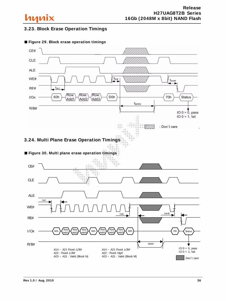
3.23. Block Erase Operation Timings
■ Figure 29. Block erase operation timings
3.24. Multi Plane Erase Operation Timings
■ Figure 30. Multi plane erase operation timings
60h RowAdd1
RowAdd2
RowAdd3 60h
CE#
CLE
ALE
WE#
I/Ox
A14 ~ A21 Fixed LOWA22 : Fixed LOWA23 ~ A31 : Valid (Block N)
RE#
tWC
tBERS
70hRowAdd1
RowAdd2
RowAdd3 D0h Status
A14 ~ A21 Fixed LOWA22 : Fixed HighA23 ~ A31 : Valid (Block M)
IO 0 = 0, passIO 0 = 1, fail
Don’t care
R/B#
tWB tWHR
Rev 1.0 / Aug. 2010 36
*58b7d520-e522* B26798/177.179.157.212/2010-08-06 17:39
APCPCWM_4828539:WP_0000001WP_0000001
APC
PCW
M_4
8285
39:W
P_00
0000
1WP_
0000
001
ReleaseH27UAG8T2B Series
16Gb (2048M x 8bit) NAND Flash
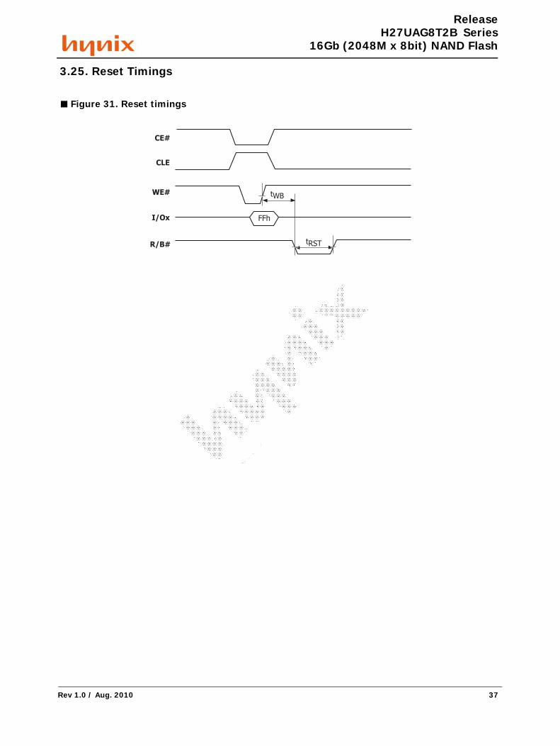
3.25. Reset Timings
■ Figure 31. Reset timings
FFh
tRST
CE#
CLE
WE#
I/Ox
R/B#
tWB
Rev 1.0 / Aug. 2010 37
*58b7d520-e522* B26798/177.179.157.212/2010-08-06 17:39
APCPCWM_4828539:WP_0000001WP_0000001
APC
PCW
M_4
8285
39:W
P_00
0000
1WP_
0000
001
ReleaseH27UAG8T2B Series
16Gb (2048M x 8bit) NAND Flash
4. DEVICE OPERATION
4.1. Page Read
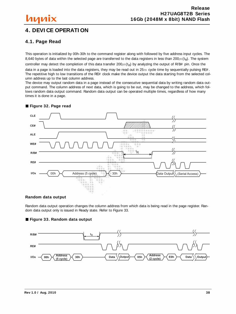
This operation is initialized by 00h-30h to the command register along with followed by five address input cycles. The 8,640 bytes of data within the selected page are transferred to the data registers in less than 200㎲(tR). The system controller may detect the completion of this data transfer 200㎲(tR) by analyzing the output of R/B# pin. Once the data in a page is loaded into the data registers, they may be read out in 25㎱ cycle time by sequentially pulsing RE#. The repetitive high to low transitions of the RE# clock make the device output the data starting from the selected col-umn address up to the last column address.The device may output random data in a page instead of the consecutive sequential data by writing random data out-put command. The column address of next data, which is going to be out, may be changed to the address, which fol-lows random data output command. Random data output can be operated multiple times, regardless of how many times it is done in a page.
■ Figure 32. Page read
Random data output
Random data output operation changes the column address from which data is being read in the page register. Ran-dom data output only is issued in Ready state. Refer to Figure 33.
■ Figure 33. Random data output
CLE
ALE
CE#
I/Ox
WE#
R/B#
RE#
00h Address (5 cycle) 30h Data Output (Serial Access)
tR
I/Ox
R/B#
RE#
00h Data
tR
OutputAddress
(5 cycle)30h Data Output 05h
Address
(2 cycle)E0h
Rev 1.0 / Aug. 2010 38
*58b7d520-e522* B26798/177.179.157.212/2010-08-06 17:39
APCPCWM_4828539:WP_0000001WP_0000001
APC
PCW
M_4
8285
39:W
P_00
0000
1WP_
0000
001
ReleaseH27UAG8T2B Series
16Gb (2048M x 8bit) NAND Flash
4.2. Cache Read (available only within a block)
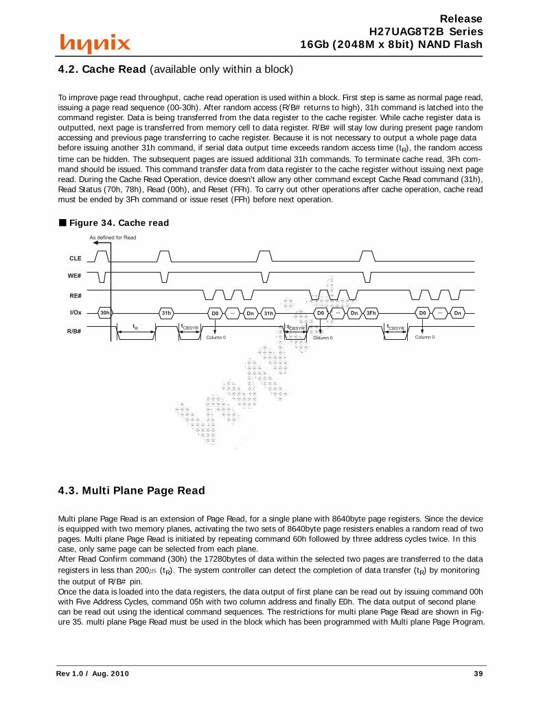
To improve page read throughput, cache read operation is used within a block. First step is same as normal page read, issuing a page read sequence (00-30h). After random access (R/B# returns to high), 31h command is latched into the command register. Data is being transferred from the data register to the cache register. While cache register data is outputted, next page is transferred from memory cell to data register. R/B# will stay low during present page random accessing and previous page transferring to cache register. Because it is not necessary to output a whole page data before issuing another 31h command, if serial data output time exceeds random access time (tR), the random access time can be hidden. The subsequent pages are issued additional 31h commands. To terminate cache read, 3Fh com-mand should be issued. This command transfer data from data register to the cache register without issuing next page read. During the Cache Read Operation, device doesn't allow any other command except Cache Read command (31h), Read Status (70h, 78h), Read (00h), and Reset (FFh). To carry out other operations after cache operation, cache read must be ended by 3Fh command or issue reset (FFh) before next operation.
■ Figure 34. Cache read
4.3. Multi Plane Page Read
Multi plane Page Read is an extension of Page Read, for a single plane with 8640byte page registers. Since the device is equipped with two memory planes, activating the two sets of 8640byte page resisters enables a random read of two pages. Multi plane Page Read is initiated by repeating command 60h followed by three address cycles twice. In this case, only same page can be selected from each plane.After Read Confirm command (30h) the 17280bytes of data within the selected two pages are transferred to the data registers in less than 200㎲ (tR). The system controller can detect the completion of data transfer (tR) by monitoring the output of R/B# pin.Once the data is loaded into the data registers, the data output of first plane can be read out by issuing command 00h with Five Address Cycles, command 05h with two column address and finally E0h. The data output of second plane can be read out using the identical command sequences. The restrictions for multi plane Page Read are shown in Fig-ure 35. multi plane Page Read must be used in the block which has been programmed with Multi plane Page Program.
30h 31h D0 ... Dn 31h D0 ... Dn 3Fh D0 ... Dn
CLE
WE#
RE#
I/Ox
R/B#
As defined for Read
tR
tCBSYR
Column 0
tCBSYR
Column 0
tCBSYR
Column 0
Rev 1.0 / Aug. 2010 39
*58b7d520-e522* B26798/177.179.157.212/2010-08-06 17:39
APCPCWM_4828539:WP_0000001WP_0000001
APC
PCW
M_4
8285
39:W
P_00
0000
1WP_
0000
001
ReleaseH27UAG8T2B Series
16Gb (2048M x 8bit) NAND Flash
■ Figure 35. Multi plane page read
4.4. Multi Plane Cache Read (available only within a block)
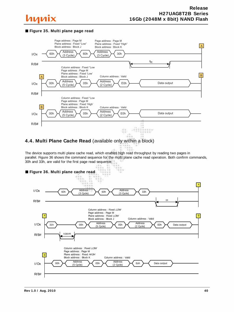
The device supports multi plane cache read, which enables high read throughput by reading two pages in parallel. Figure 36 shows the command sequence for the multi plane cache read operation. Both confirm commands, 30h and 33h, are valid for the first page read sequence.
■ Figure 36. Multi plane cache read
60h
tR
A
I/Ox
R/B#
A
Address
(3 Cycle)
Page address : Page M
Plane address : Fixed “Low”
Block address : Block J
Column address : Fixed “Low
Page address : Page M
Plane address : Fixed ‘Low’
Block address : Block J Column address : Valid
Address
(3 Cycle)60h 30h
Page address : Page M
Plane address : Fixed “High”
Block address : Block K
B
I/Ox
R/B#
00hAddress
(5 Cycle)
Address
(2 Cycle)05h E0h Data output
I/Ox
R/B#
B
Column address : Fixed “Low
Page address : Page M
Plane address : Fixed ‘High’
Block address : Block K Column address : Valid
00hAddress
(5 Cycle)
Address
(2 Cycle)05h E0h Data output
tR
60h Address(3 Cycle) 60h Address
(3 Cycle) 33h
31h 00h Address(5 Cycle) 05h Address
(2 Cycle) E0h Data output
tCBSYR
A
BA
00h Address(5 Cycle) 05h Address
(2 Cycle) Eoh
Column address : Fixed LOWPage address : Page MPlane address : Fixed LOWBlock address : Block J Column address : Valid
Data output
I/Ox
R/B#
I/Ox
R/B#
I/Ox
R/B#
B
Column address : Fixed LOWPage address : Page MPlane address : Fixed HIGHBlock address : Block K Column address : Valid
Rev 1.0 / Aug. 2010 40
*58b7d520-e522* B26798/177.179.157.212/2010-08-06 17:39
APCPCWM_4828539:WP_0000001WP_0000001
APC
PCW
M_4
8285
39:W
P_00
0000
1WP_
0000
001
ReleaseH27UAG8T2B Series
16Gb (2048M x 8bit) NAND Flash
Notes: 1. Plane 0 and plane 1 should be selected within the same chip 2. Only one block should be selected from the each Plane. 3. Multi Plane cache read is available only within a block per plane. 4. Selected Page address except for A22 within two blocks must be same. 5. The operation has to be terminated with "3Fh" command.
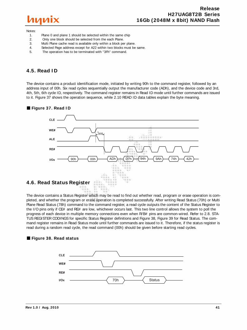
4.5. Read ID
The device contains a product identification mode, initiated by writing 90h to the command register, followed by an address input of 00h. Six read cycles sequentially output the manufacturer code (ADh), and the device code and 3rd, 4th, 5th, 6th cycle ID, respectively. The command register remains in Read ID mode until further commands are issued to it. Figure 37 shows the operation sequence, while 2.10 READ ID data tables explain the byte meaning.
■ Figure 37. Read ID
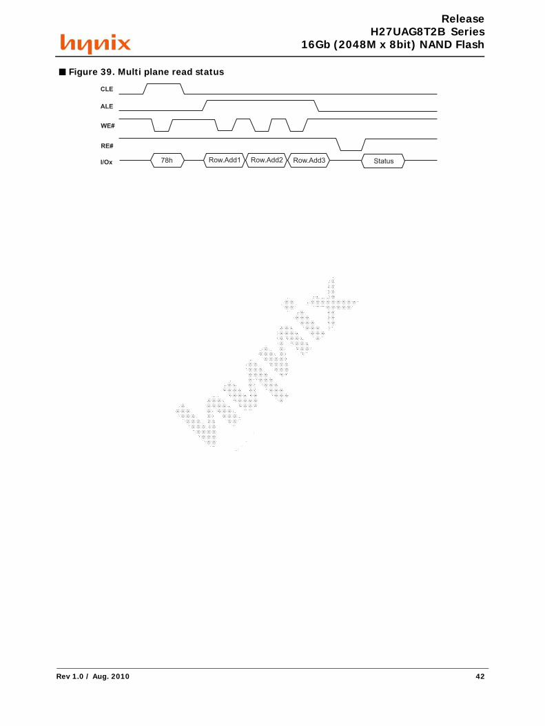
4.6. Read Status Register
The device contains a Status Register which may be read to find out whether read, program or erase operation is com-pleted, and whether the program or erase operation is completed successfully. After writing Read Status (70h) or Multi Plane Read Status (78h) command to the command register, a read cycle outputs the content of the Status Register to the I/O pins only if CE# and RE# are low, whichever occurs last. This two line control allows the system to poll the progress of each device in multiple memory connections even when R/B# pins are common-wired. Refer to 2.8. STA-TUS REGISTER CODINGS for specific Status Register definitions and Figure 38, Figure 39 for Read Status. The com-mand register remains in Read Status mode until further commands are issued to it. Therefore, if the status register is read during a random read cycle, the read command (00h) should be given before starting read cycles.
■ Figure 38. Read status
90h
CLE
WE#
ALE
RE#
I/Ox 00h ADh D7h 74h 42h9Ah
WHR
94h
t
70h Status
CLE
WE#
RE#
I/Ox
Rev 1.0 / Aug. 2010 41
*58b7d520-e522* B26798/177.179.157.212/2010-08-06 17:39
APCPCWM_4828539:WP_0000001WP_0000001
APC
PCW
M_4
8285
39:W
P_00
0000
1WP_
0000
001
ReleaseH27UAG8T2B Series
16Gb (2048M x 8bit) NAND Flash
■ Figure 39. Multi plane read status
CLE
ALE
WE#
RE#
I/Ox 78h Row.Add1 Row.Add3Row.Add2 Status
Rev 1.0 / Aug. 2010 42
*58b7d520-e522* B26798/177.179.157.212/2010-08-06 17:39
APCPCWM_4828539:WP_0000001WP_0000001
APC
PCW
M_4
8285
39:W
P_00
0000
1WP_
0000
001
ReleaseH27UAG8T2B Series
16Gb (2048M x 8bit) NAND Flash
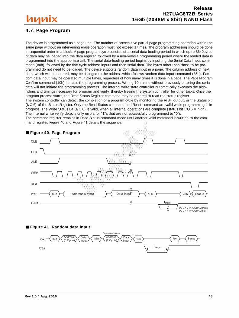
4.7. Page Program
The device is programmed as a page unit. The number of consecutive partial page programming operation within the same page without an intervening erase operation must not exceed 1 times. The program addressing should be done in sequential order in a block. A page program cycle consists of a serial data loading period in which up to 8640bytes of data may be loaded into the data register, followed by a non-volatile programming period where the loaded data is programmed into the appropriate cell. The serial data-loading period begins by inputting the Serial Data Input com-mand (80h), followed by the five cycle address inputs and then serial data. The bytes other than those to be pro-grammed do not need to be loaded. The device supports random data input in a page. The column address of next data, which will be entered, may be changed to the address which follows random data input command (85h). Ran-dom data input may be operated multiple times, regardless of how many times it is done in a page. The Page Program Confirm command (10h) initiates the programming process. Writing 10h alone without previously entering the serial data will not initiate the programming process. The internal write state controller automatically executes the algo-rithms and timings necessary for program and verify, thereby freeing the system controller for other tasks. Once the program process starts, the Read Status Register command may be entered to read the status register.The system controller can detect the completion of a program cycle by monitoring the R/B# output, or the Status bit (I/O 6) of the Status Register. Only the Read Status command and Reset command are valid while programming is in progress. The Write Status Bit (I/O 0) is valid, when all internal operations are complete (status bit I/O 6 = high).The internal write verify detects only errors for "1"s that are not successfully programmed to "0"s.The command register remains in Read Status command mode until another valid command is written to the com-mand register. Figure 40 and Figure 41 details the sequence.
■ Figure 40. Page Program
■ Figure 41. Random data input
80h Address 5 cycle Data Input Status70h10h
CLE
PROG t
I/O 0 = 0 PROGRAM Pass
I/O 0 = 1 PROGRAM Fail
CE#
ALE
WE#
RE#
I/Ox
R/B#
I/Ox
R/B#
Column address
80hAddress
(5 Cycle)
Address
(2 Cycle)Data
Input85h Data
Input70h Status10h
PROGt
Rev 1.0 / Aug. 2010 43
*58b7d520-e522* B26798/177.179.157.212/2010-08-06 17:39
APCPCWM_4828539:WP_0000001WP_0000001
APC
PCW
M_4
8285
39:W
P_00
0000
1WP_
0000
001
ReleaseH27UAG8T2B Series
16Gb (2048M x 8bit) NAND Flash
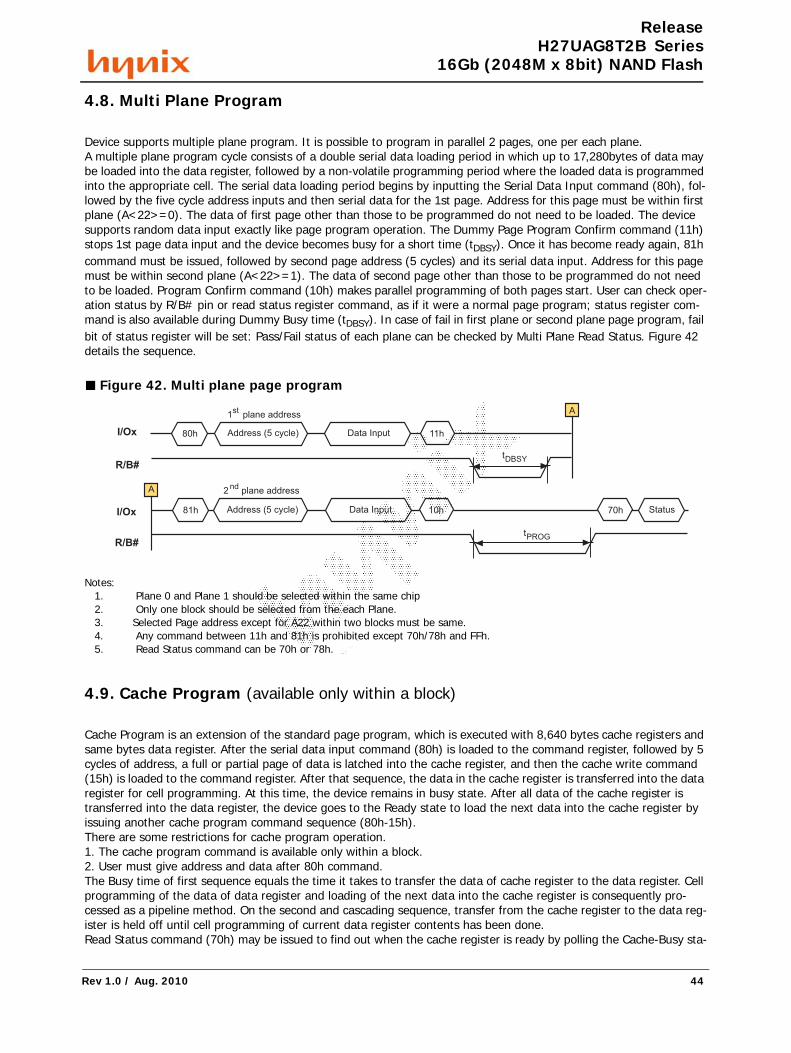
4.8. Multi Plane Program
Device supports multiple plane program. It is possible to program in parallel 2 pages, one per each plane.A multiple plane program cycle consists of a double serial data loading period in which up to 17,280bytes of data may be loaded into the data register, followed by a non-volatile programming period where the loaded data is programmed into the appropriate cell. The serial data loading period begins by inputting the Serial Data Input command (80h), fol-lowed by the five cycle address inputs and then serial data for the 1st page. Address for this page must be within first plane (A<22>=0). The data of first page other than those to be programmed do not need to be loaded. The device supports random data input exactly like page program operation. The Dummy Page Program Confirm command (11h) stops 1st page data input and the device becomes busy for a short time (tDBSY). Once it has become ready again, 81h command must be issued, followed by second page address (5 cycles) and its serial data input. Address for this page must be within second plane (A<22>=1). The data of second page other than those to be programmed do not need to be loaded. Program Confirm command (10h) makes parallel programming of both pages start. User can check oper-ation status by R/B# pin or read status register command, as if it were a normal page program; status register com-mand is also available during Dummy Busy time (tDBSY). In case of fail in first plane or second plane page program, fail bit of status register will be set: Pass/Fail status of each plane can be checked by Multi Plane Read Status. Figure 42 details the sequence.
■ Figure 42. Multi plane page program
Notes: 1. Plane 0 and Plane 1 should be selected within the same chip 2. Only one block should be selected from the each Plane. 3. Selected Page address except for A22 within two blocks must be same. 4. Any command between 11h and 81h is prohibited except 70h/78h and FFh. 5. Read Status command can be 70h or 78h.
4.9. Cache Program (available only within a block)
Cache Program is an extension of the standard page program, which is executed with 8,640 bytes cache registers and same bytes data register. After the serial data input command (80h) is loaded to the command register, followed by 5 cycles of address, a full or partial page of data is latched into the cache register, and then the cache write command (15h) is loaded to the command register. After that sequence, the data in the cache register is transferred into the data register for cell programming. At this time, the device remains in busy state. After all data of the cache register is transferred into the data register, the device goes to the Ready state to load the next data into the cache register by issuing another cache program command sequence (80h-15h).There are some restrictions for cache program operation.1. The cache program command is available only within a block.2. User must give address and data after 80h command.The Busy time of first sequence equals the time it takes to transfer the data of cache register to the data register. Cell programming of the data of data register and loading of the next data into the cache register is consequently pro-cessed as a pipeline method. On the second and cascading sequence, transfer from the cache register to the data reg-ister is held off until cell programming of current data register contents has been done.Read Status command (70h) may be issued to find out when the cache register is ready by polling the Cache-Busy sta-
80h Address (5 cycle) 11h
tDBSY
Data Input
A
81h Address (5 cycle) 10h
tPROG
Data InputI/Ox
R/B#
70h Status
1 plane addressst
2 plane addressndA
I/Ox
R/B#
Rev 1.0 / Aug. 2010 44
*58b7d520-e522* B26798/177.179.157.212/2010-08-06 17:39
APCPCWM_4828539:WP_0000001WP_0000001
APC
PCW
M_4
8285
39:W
P_00
0000
1WP_
0000
001
ReleaseH27UAG8T2B Series
16Gb (2048M x 8bit) NAND Flash
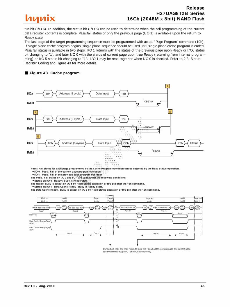
tus bit (I/O 6). In addition, the status bit (I/O 5) can be used to determine when the cell programming of the current data register contents is complete. Pass/fail status of only the previous page (I/O 1) is available upon the return to Ready state.The last page of the target programming sequence must be programmed with actual “Page Program” command (10h). If single plane cache program begins, single plane sequence should be used until single plane cache program is ended. Pass/fail status is available in two steps. I/O 1 returns with the status of the previous page upon Ready or I/O6 status bit changing to "1", and later I/O 0 with the status of current page upon true Ready (returning from internal program-ming) or I/O 5 status bit changing to "1". I/O 1 may be read together when I/O 0 is checked. Refer to 2.8. Status Register Coding and Figure 43 for more details.
■ Figure 43. Cache program
80h Address (5 cycle) 15h
tCBSYW
Data Input
A
80h Address (5 cycle) 15h
tCBSYW
Data Input
B
I/Ox
R/B#
80h Address (5 cycle) 10h
tPROG
Data InputI/Ox
R/B#
70h Status
A
B
I/Ox
R/B#
R/B# Pin
Data Cache Ready /Bysy
(I/O6)
I/O 1 =>
I/O 0 =>
Invalid
Invalid
Page1
Invalid
Page1
Page2
Page N-2
Invalid
Invalid
Invalid
Page N-1
Page N
Data Cache Ready /Bysy
(I/O5)
70hSR
OUT 70hSR
OUT80h-add-data-15h 80h-add-data-15h 70h
SR
OUT80h-add-data-15h 70h
SR
OUT80h-add-data-15h 70h
SR
OUT70h SR
OUT
Page 1 Page 2 Page N-1 Page N
Page 1 Page 2 Page N-1 Page N
During both I/O6 and I/O5 return to high, the Pass/Fail for previous page and current page
can be shown through I/O1 and I/O0 concurrently.
PROGtCBSYWtCBSYWtCBSYWt
Pass / Fail status for each page programmed by the Cache Program operation can be detected by the Read Status operation.
I/O 0 : Pass / Fail of the current page program operation.
I/O 1 : Pass / Fail of the previous page program operation.
The Pass / Fail status on I/O 0 and I/O 1 are valid under the following conditions.
Status on I/O 0 : Ready / Busy is Ready state.
The Ready/ Busy is output on I/O 5 by Read Status operation or R/B pin after the 10h command.
Status on I/O 1 : Data Cache Ready / Busy is Ready State.
The Data Cache Ready / Busy is output on I/O 6 by Read Status operation or R/B pin after the 15h command.
Rev 1.0 / Aug. 2010 45
*58b7d520-e522* B26798/177.179.157.212/2010-08-06 17:39
APCPCWM_4828539:WP_0000001WP_0000001
APC
PCW
M_4
8285
39:W
P_00
0000
1WP_
0000
001
ReleaseH27UAG8T2B Series
16Gb (2048M x 8bit) NAND Flash
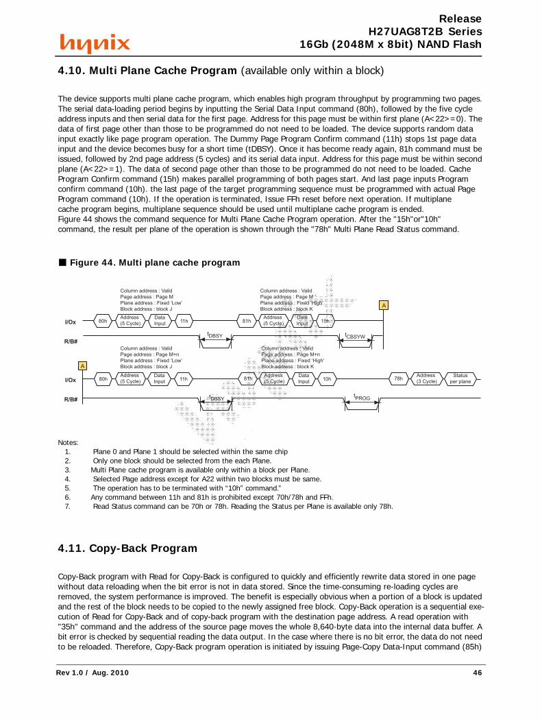
4.10. Multi Plane Cache Program (available only within a block)
The device supports multi plane cache program, which enables high program throughput by programming two pages. The serial data-loading period begins by inputting the Serial Data Input command (80h), followed by the five cycle address inputs and then serial data for the first page. Address for this page must be within first plane (A<22>=0). The data of first page other than those to be programmed do not need to be loaded. The device supports random data input exactly like page program operation. The Dummy Page Program Confirm command (11h) stops 1st page data input and the device becomes busy for a short time (tDBSY). Once it has become ready again, 81h command must be issued, followed by 2nd page address (5 cycles) and its serial data input. Address for this page must be within second plane (A<22>=1). The data of second page other than those to be programmed do not need to be loaded. Cache Program Confirm command (15h) makes parallel programming of both pages start. And last page inputs Program confirm command (10h). the last page of the target programming sequence must be programmed with actual Page Program command (10h). If the operation is terminated, Issue FFh reset before next operation. If multiplane cache program begins, multiplane sequence should be used until multiplane cache program is ended. Figure 44 shows the command sequence for Multi Plane Cache Program operation. After the "15h"or"10h"command, the result per plane of the operation is shown through the "78h" Multi Plane Read Status command.
■ Figure 44. Multi plane cache program
Notes: 1. Plane 0 and Plane 1 should be selected within the same chip 2. Only one block should be selected from the each Plane. 3. Multi Plane cache program is available only within a block per Plane. 4. Selected Page address except for A22 within two blocks must be same. 5. The operation has to be terminated with “10h” command.” 6. Any command between 11h and 81h is prohibited except 70h/78h and FFh. 7. Read Status command can be 70h or 78h. Reading the Status per Plane is available only 78h.
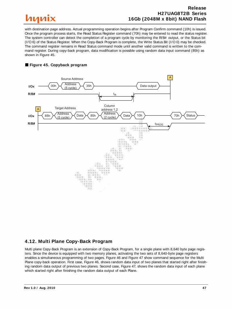
4.11. Copy-Back Program
Copy-Back program with Read for Copy-Back is configured to quickly and efficiently rewrite data stored in one page without data reloading when the bit error is not in data stored. Since the time-consuming re-loading cycles are removed, the system performance is improved. The benefit is especially obvious when a portion of a block is updated and the rest of the block needs to be copied to the newly assigned free block. Copy-Back operation is a sequential exe-cution of Read for Copy-Back and of copy-back program with the destination page address. A read operation with "35h" command and the address of the source page moves the whole 8,640-byte data into the internal data buffer. A bit error is checked by sequential reading the data output. In the case where there is no bit error, the data do not need to be reloaded. Therefore, Copy-Back program operation is initiated by issuing Page-Copy Data-Input command (85h)
80h
tCBSYW
A
80h 81hI/Ox
R/B#
A
Address
(5 Cycle)
Data
Input11h
Address
(5 Cycle)
Data
Input11h 81h
Address
(5 Cycle)
Data
Input15h
tDBSY
Address
(5 Cycle)
Data
Input10h 78h
Address
(3 Cycle)
Status
per plane
Column address : Valid
Page address : Page M
Plane address : Fixed ‘Low’
Block address : block J
Column address : Valid
Page address : Page M
Plane address : Fixed ‘High’
Block address : block K
Column address : Valid
Page address : Page M+n
Plane address : Fixed ‘Low’
Block address : block J
Column address : Valid
Page address : Page M+n
Plane address : Fixed ‘High’
Block address : block K
I/Ox
R/B#
tPROGtDBSY
Rev 1.0 / Aug. 2010 46
*58b7d520-e522* B26798/177.179.157.212/2010-08-06 17:39
APCPCWM_4828539:WP_0000001WP_0000001
APC
PCW
M_4
8285
39:W
P_00
0000
1WP_
0000
001
ReleaseH27UAG8T2B Series
16Gb (2048M x 8bit) NAND Flash
with destination page address. Actual programming operation begins after Program Confirm command (10h) is issued. Once the program process starts, the Read Status Register command (70h) may be entered to read the status register.The system controller can detect the completion of a program cycle by monitoring the R/B# output, or the Status bit (I/O 6) of the Status Register. When the Copy-Back Program is complete, the Write Status Bit (I/O 0) may be checked. The command register remains in Read Status command mode until another valid command is written to the com-mand register. During copy-back program, data modification is possible using random data input command (85h) as shown in Figure 45.
■ Figure 45. Copyback program
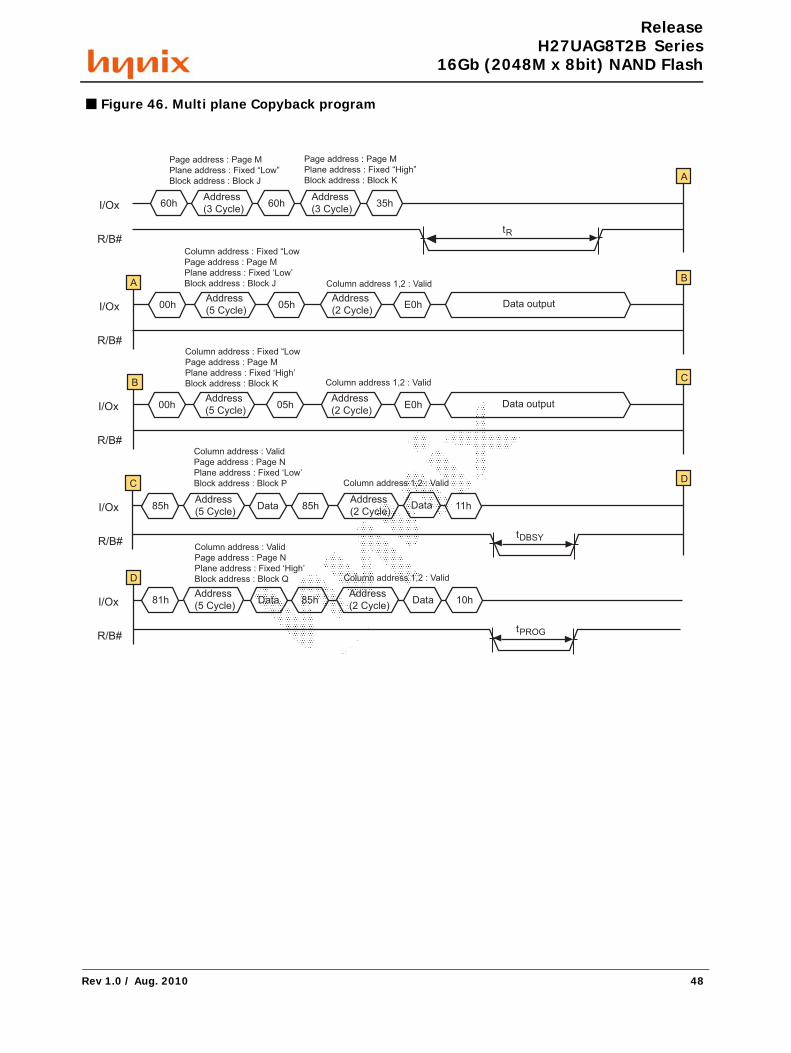
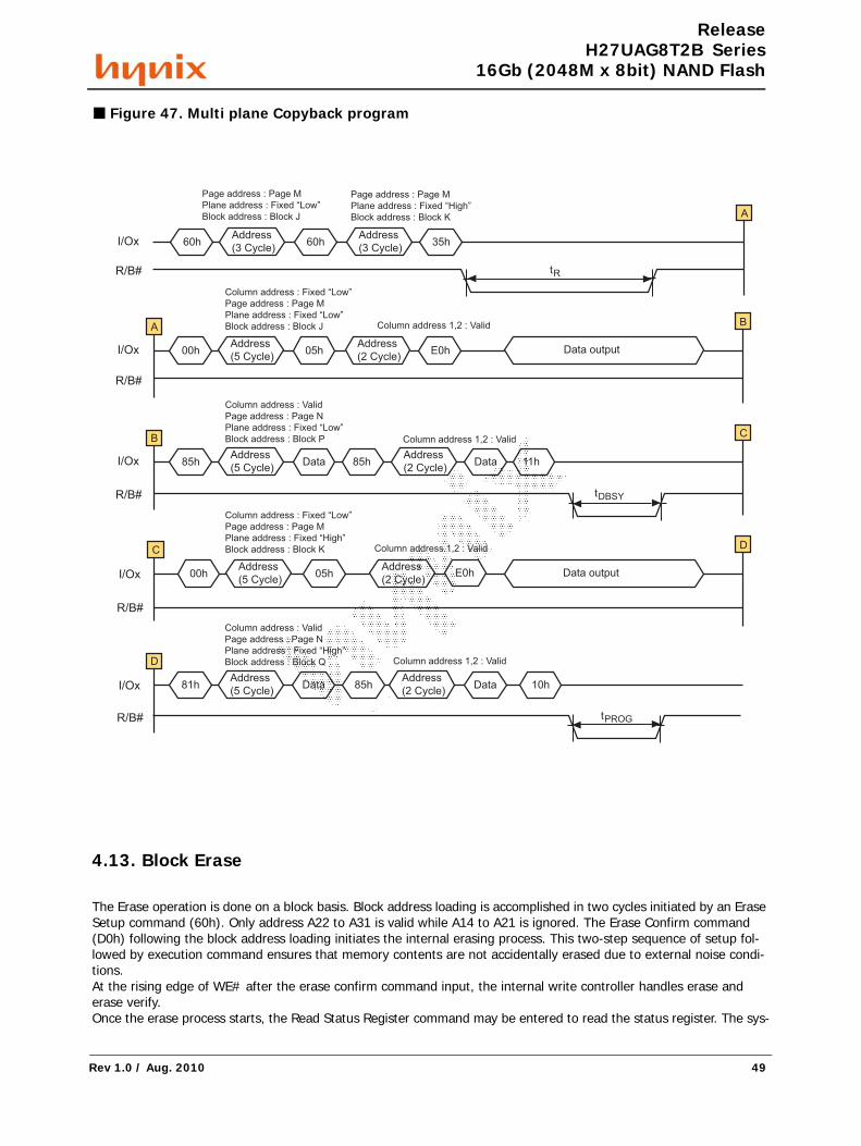
4.12. Multi Plane Copy-Back ProgramMulti plane Copy-Back Program is an extension of Copy-Back Program, for a single plane with 8,640 byte page regis-ters. Since the device is equipped with two memory planes, activating the two sets of 8,640-byte page registers enables a simultaneous programming of two pages. Figure 46 and Figure 47 show command sequence for the Multi Plane copy-back operation. First case, Figure 46, shows random data input of two planes that started right after finish-ing random data output of previous two planes. Second case, Figure 47, shows the random data input of each plane which started right after finishing the random data output of each Plane.
00hAddress
(5 cycle)35h Data output
tR
85hAddress
(5 cycle)Data
tPROG
I/Ox
R/B#
Target Address
85hAddress
(2 cycle)Data 10h 70h Status
Column
address 1,2
I/Ox
R/B#
Source AddressA
A
Rev 1.0 / Aug. 2010 47
*58b7d520-e522* B26798/177.179.157.212/2010-08-06 17:39
APCPCWM_4828539:WP_0000001WP_0000001
APC
PCW
M_4
8285
39:W
P_00
0000
1WP_
0000
001
ReleaseH27UAG8T2B Series
16Gb (2048M x 8bit) NAND Flash
■ Figure 46. Multi plane Copyback program
60h
tR
A
I/Ox
R/B#
A
Address
(3 Cycle)
Page address : Page M
Plane address : Fixed “Low”
Block address : Block J
Column address : Fixed “Low
Page address : Page M
Plane address : Fixed ‘Low’
Block address : Block J Column address 1,2 : Valid
Address
(3 Cycle)60h 35h
Page address : Page M
Plane address : Fixed “High”
Block address : Block K
B
I/Ox
R/B#
00hAddress
(5 Cycle)
Address
(2 Cycle)05h E0h Data output
I/Ox
R/B#
B
Column address : Valid
Page address : Page N
Plane address : Fixed ‘Low’
Block address : Block P Column address 1,2 : Valid
C
85hAddress
(5 Cycle)
Address
(2 Cycle)Data 11h
I/Ox
R/B#
D Column address 1,2 : Valid
81hAddress
(5 Cycle)Data 10h
Data85h
Address
(2 Cycle)85h Data
tPROG
I/Ox
R/B#
C
Column address : Fixed “Low
Page address : Page M
Plane address : Fixed ‘High’
Block address : Block K Column address 1,2 : Valid
D
00hAddress
(5 Cycle)
Address
(2 Cycle)05h E0h Data output
Column address : Valid
Page address : Page N
Plane address : Fixed ‘High’
Block address : Block Q
tDBSY
Rev 1.0 / Aug. 2010 48
*58b7d520-e522* B26798/177.179.157.212/2010-08-06 17:39
APCPCWM_4828539:WP_0000001WP_0000001
APC
PCW
M_4
8285
39:W
P_00
0000
1WP_
0000
001
ReleaseH27UAG8T2B Series
16Gb (2048M x 8bit) NAND Flash
■ Figure 47. Multi plane Copyback program
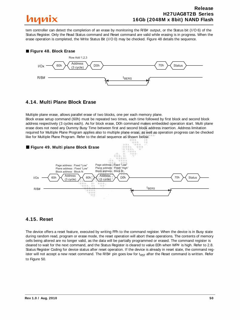
4.13. Block Erase
The Erase operation is done on a block basis. Block address loading is accomplished in two cycles initiated by an Erase Setup command (60h). Only address A22 to A31 is valid while A14 to A21 is ignored. The Erase Confirm command (D0h) following the block address loading initiates the internal erasing process. This two-step sequence of setup fol-lowed by execution command ensures that memory contents are not accidentally erased due to external noise condi-tions.At the rising edge of WE# after the erase confirm command input, the internal write controller handles erase and erase verify.Once the erase process starts, the Read Status Register command may be entered to read the status register. The sys-
60h
tR
A
I/Ox
R/B#
A
Address
(3 Cycle)
Page address : Page M
Plane address : Fixed “Low”
Block address : Block J
Column address : Fixed “Low”
Page address : Page M
Plane address : Fixed “Low”
Block address : Block J Column address 1,2 : Valid
Address
(3 Cycle)60h 35h
Page address : Page M
Plane address : Fixed “High”
Block address : Block K
B
I/Ox
R/B#
00hAddress
(5 Cycle)
Address
(2 Cycle)05h E0h Data output
I/Ox
R/B#
B
Column address : Valid
Page address : Page N
Plane address : Fixed “Low”
Block address : Block P Column address 1,2 : ValidC
85hAddress
(5 Cycle)
Address
(2 Cycle)Data Data
I/Ox
R/B#
C
Column address : Fixed “Low”
Page address : Page M
Plane address : Fixed “High”
Block address : Block K Column address 1,2 : Valid D
00hAddress
(5 Cycle)
Address
(2 Cycle)
I/Ox
R/B#
D
Column address : Valid
Page address : Page N
Plane address : Fixed “High”
Block address : Block Q Column address 1,2 : Valid
81hAddress
(5 Cycle)Data 10h
E0h05h
Address
(2 Cycle)85h Data
tPROG
85h 11h
tDBSY
Data output
Rev 1.0 / Aug. 2010 49
*58b7d520-e522* B26798/177.179.157.212/2010-08-06 17:39
APCPCWM_4828539:WP_0000001WP_0000001
APC
PCW
M_4
8285
39:W
P_00
0000
1WP_
0000
001
ReleaseH27UAG8T2B Series
16Gb (2048M x 8bit) NAND Flash
tem controller can detect the completion of an erase by monitoring the R/B# output, or the Status bit (I/O 6) of the Status Register. Only the Read Status command and Reset command are valid while erasing is in progress. When the erase operation is completed, the Write Status Bit (I/O 0) may be checked. Figure 48 details the sequence.
■ Figure 48. Block Erase
4.14. Multi Plane Block Erase
Multiple plane erase, allows parallel erase of two blocks, one per each memory plane.Block erase setup command (60h) must be repeated two times, each time followed by first block and second block address respectively (3 cycles each). As for block erase, D0h command makes embedded operation start. Multi plane erase does not need any Dummy Busy Time between first and second block address insertion. Address limitation required for Multiple Plane Program applies also to multiple plane erase, as well as operation progress can be checked like for Multiple Plane Program. Refer to the detail sequence as shown below.
■ Figure 49. Multi plane Block Erase
4.15. Reset
The device offers a reset feature, executed by writing FFh to the command register. When the device is in Busy state during random read, program or erase mode, the reset operation will abort these operations. The contents of memory cells being altered are no longer valid, as the data will be partially programmed or erased. The command register is cleared to wait for the next command, and the Status Register is cleared to value E0h when WP# is high. Refer to 2.8. Status Register Coding for device status after reset operation. If the device is already in reset state, the command reg-ister will not accept a new reset command. The R/B# pin goes low for tRST after the Reset command is written. Refer to Figure 50.
60h 70hAddress
(3 cycle)D0h Status
tBERS
I/Ox
R/B#
Row Add 1,2,3
60h 70hAddress
(3 cycle)60h Status
tBERS
Address
(3 cycle)D0h
Page address : Fixed “Low”
Plane address : Fixed “Low”
Block address : Block N
I/Ox
R/B#
Page address : Fixed “Low”
Plane address : Fixed “High”
Block address : Block M
Rev 1.0 / Aug. 2010 50
*58b7d520-e522* B26798/177.179.157.212/2010-08-06 17:39
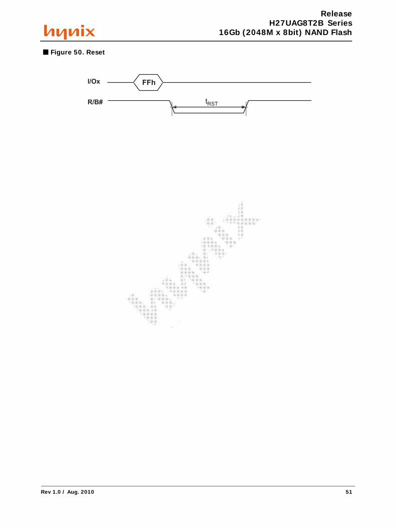
APCPCWM_4828539:WP_0000001WP_0000001
APC
PCW
M_4
8285
39:W
P_00
0000
1WP_
0000
001
ReleaseH27UAG8T2B Series
16Gb (2048M x 8bit) NAND Flash
■ Figure 50. Reset
I/Ox
R/B#
FFh
RSTt
Rev 1.0 / Aug. 2010 51
*58b7d520-e522* B26798/177.179.157.212/2010-08-06 17:39
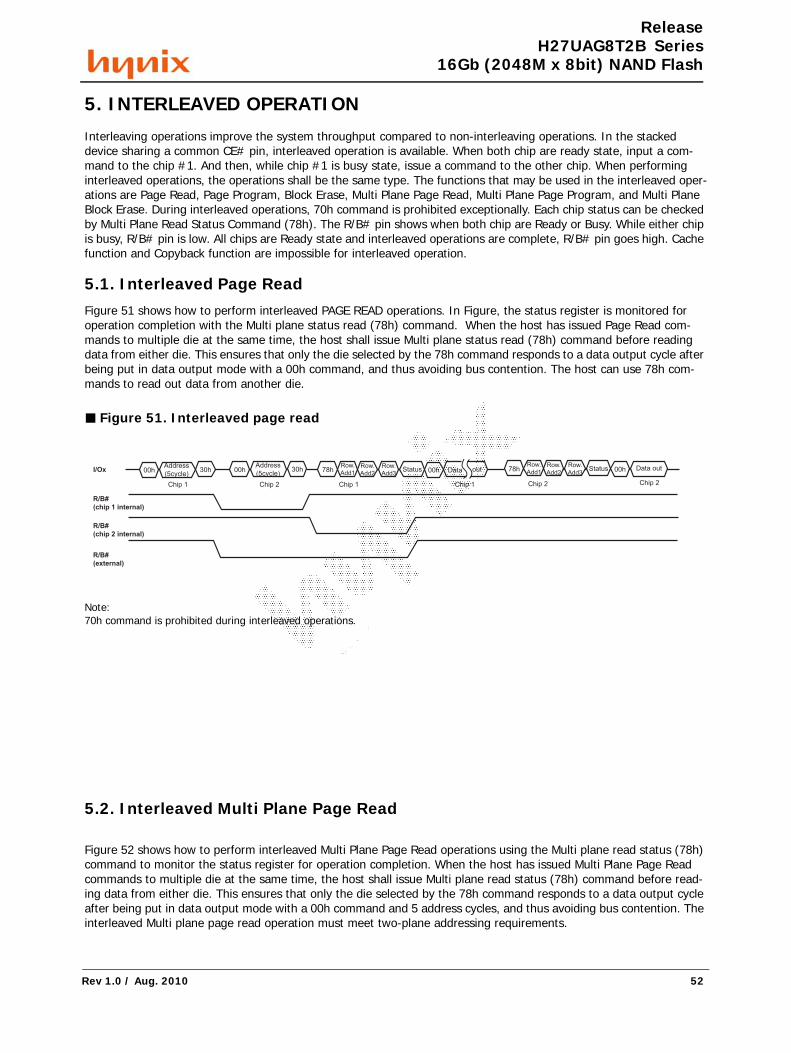
APCPCWM_4828539:WP_0000001WP_0000001
APC
PCW
M_4
8285
39:W
P_00
0000
1WP_
0000
001
ReleaseH27UAG8T2B Series
16Gb (2048M x 8bit) NAND Flash
5. INTERLEAVED OPERATION
Interleaving operations improve the system throughput compared to non-interleaving operations. In the stacked device sharing a common CE# pin, interleaved operation is available. When both chip are ready state, input a com-mand to the chip #1. And then, while chip #1 is busy state, issue a command to the other chip. When performing interleaved operations, the operations shall be the same type. The functions that may be used in the interleaved oper-ations are Page Read, Page Program, Block Erase, Multi Plane Page Read, Multi Plane Page Program, and Multi Plane Block Erase. During interleaved operations, 70h command is prohibited exceptionally. Each chip status can be checked by Multi Plane Read Status Command (78h). The R/B# pin shows when both chip are Ready or Busy. While either chip is busy, R/B# pin is low. All chips are Ready state and interleaved operations are complete, R/B# pin goes high. Cache function and Copyback function are impossible for interleaved operation.
5.1. Interleaved Page ReadFigure 51 shows how to perform interleaved PAGE READ operations. In Figure, the status register is monitored for operation completion with the Multi plane status read (78h) command. When the host has issued Page Read com-mands to multiple die at the same time, the host shall issue Multi plane status read (78h) command before reading data from either die. This ensures that only the die selected by the 78h command responds to a data output cycle after being put in data output mode with a 00h command, and thus avoiding bus contention. The host can use 78h com-mands to read out data from another die.
■ Figure 51. Interleaved page read
Note: 70h command is prohibited during interleaved operations.
5.2. Interleaved Multi Plane Page Read
Figure 52 shows how to perform interleaved Multi Plane Page Read operations using the Multi plane read status (78h) command to monitor the status register for operation completion. When the host has issued Multi Plane Page Read commands to multiple die at the same time, the host shall issue Multi plane read status (78h) command before read-ing data from either die. This ensures that only the die selected by the 78h command responds to a data output cycle after being put in data output mode with a 00h command and 5 address cycles, and thus avoiding bus contention. The interleaved Multi plane page read operation must meet two-plane addressing requirements.
Data out00hStatusRow.
Add378h
Row.
Add2
Row.
Add100h 30h00h 30h
Address
(5cycle)
Address
(5cycle)00hStatus
Row.
Add378h
Row.
Add2
Row.
Add1Data out
Chip 2Chip 1 Chip 1 Chip 1 Chip 2 Chip 2
I/Ox
R/B#
(chip 1 internal)
R/B#
(chip 2 internal)
R/B#
(external)
Rev 1.0 / Aug. 2010 52
*58b7d520-e522* B26798/177.179.157.212/2010-08-06 17:39
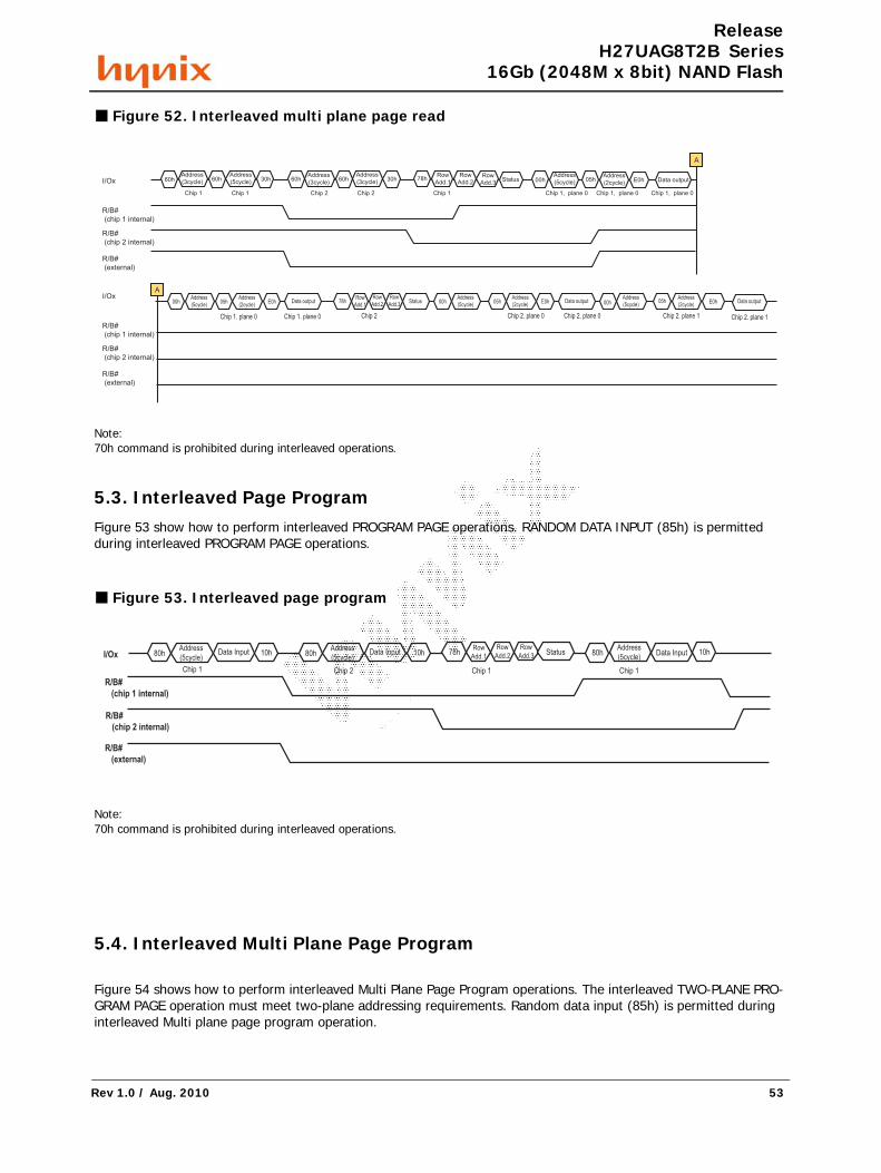
APCPCWM_4828539:WP_0000001WP_0000001
APC
PCW
M_4
8285
39:W
P_00
0000
1WP_
0000
001
ReleaseH27UAG8T2B Series
16Gb (2048M x 8bit) NAND Flash
■ Figure 52. Interleaved multi plane page read
Note: 70h command is prohibited during interleaved operations.
5.3. Interleaved Page ProgramFigure 53 show how to perform interleaved PROGRAM PAGE operations. RANDOM DATA INPUT (85h) is permitted during interleaved PROGRAM PAGE operations.
■ Figure 53. Interleaved page program
Note: 70h command is prohibited during interleaved operations.
5.4. Interleaved Multi Plane Page Program
Figure 54 shows how to perform interleaved Multi Plane Page Program operations. The interleaved TWO-PLANE PRO-GRAM PAGE operation must meet two-plane addressing requirements. Random data input (85h) is permitted during interleaved Multi plane page program operation.
A
00hAddress
(5cycle)78h
Row
Add.1
Row
Add.2
Row
Add.3Status 05h
Address
(2cycle)E0h
Chip 2
05hAddress
(2cycle)E0h 00h
Address
(5cycle)Data output
Chip 2. plane 0 Chip 2. plane 0 Chip 2. plane 1
Data output 00hAddress
(5cycle)05h
Address
(2cycle)E0h Data output
Chip 1. plane 0 Chip 1. plane 0 Chip 2. plane 1
A
60h 60h 60h 60h 30h 78h 00h 05h E0hAddress
(3cycle)
Address
(5cycle) 30hAddress
(3cycle)
Address
(3cycle)Row
Add.1
Row
Add.2Row
Add.3Status
Address
(5cycle)Address
(2cycle) Data output
Chip 1 Chip 1 Chip 2 Chip 2 Chip 1 Chip 1, plane 0 Chip 1, plane 0 Chip 1, plane 0
I/Ox
R/B#
(chip 1 internal)
R/B#
(chip 2 internal)
R/B#
(external)
I/Ox
R/B#
(chip 1 internal)
R/B#
(chip 2 internal)
R/B#
(external)
R/B#
(chip 1 internal)
I/Ox 80hAddress
(5cycle)Data Input 10h 80h
Address
(5cycle)Data Input 10h
Row
Add.1
Row
Add.2
Row
Add.3Status 80h
Address
(5cycle)Data Input 10h
Chip 1 Chip 2 Chip 1 Chip 1
R/B#
(chip 2 internal)
R/B#
(external)
78h
Rev 1.0 / Aug. 2010 53
*58b7d520-e522* B26798/177.179.157.212/2010-08-06 17:39
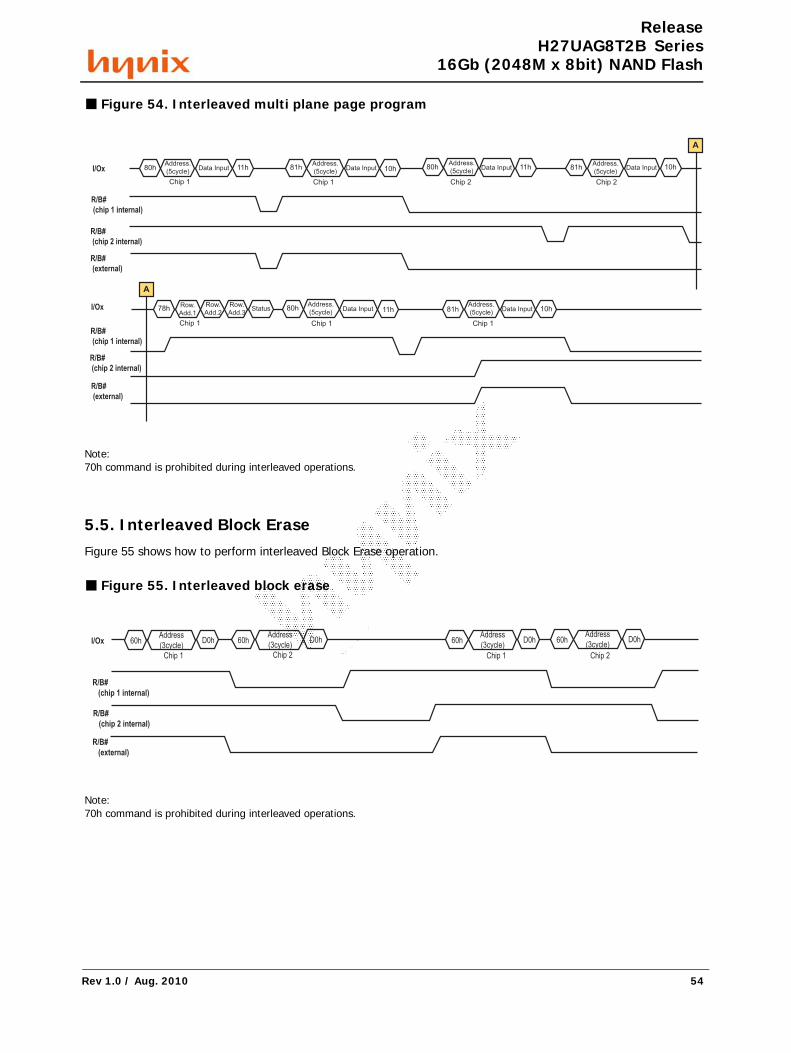
APCPCWM_4828539:WP_0000001WP_0000001
APC
PCW
M_4
8285
39:W
P_00
0000
1WP_
0000
001
ReleaseH27UAG8T2B Series
16Gb (2048M x 8bit) NAND Flash
■ Figure 54. Interleaved multi plane page program
Note: 70h command is prohibited during interleaved operations.
5.5. Interleaved Block EraseFigure 55 shows how to perform interleaved Block Erase operation.
■ Figure 55. Interleaved block erase
Note: 70h command is prohibited during interleaved operations.
R/B#
(chip 1 internal)
I/Ox
R/B#
(chip 2 internal)
R/B#
(external)
R/B#
(chip 1 internal)
I/Ox
R/B#
(chip 2 internal)
R/B#
(external)
A
A
Row.
Add.1
Row.
Add.2
Row.
Add.378h 80hStatus
Address.
(5cycle)Data Input 11h 81h
Address.
(5cycle)Data Input 10h
80hAddress.
(5cycle)Data Input 11h 81h
Address.
(5cycle)Data Input 10h 80h
Address.
(5cycle)Data Input 11h 81h
Address.
(5cycle)Data Input 10h
Chip 1 Chip 1 Chip 2 Chip 2
Chip 1 Chip 1 Chip 1
R/B#
(chip 1 internal)
I/Ox 60h
Chip 1 Chip 2 Chip 1
R/B#
(chip 2 internal)
R/B#
(external)
Address
(3cycle)D0h 60h
Address
(3cycle)D0h 60h
Address
(3cycle)D0h 60h
Address
(3cycle)D0h
Chip 2
Rev 1.0 / Aug. 2010 54
*58b7d520-e522* B26798/177.179.157.212/2010-08-06 17:39
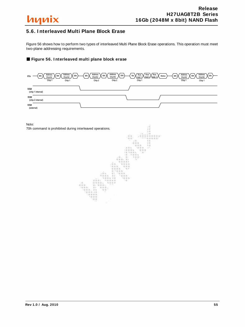
APCPCWM_4828539:WP_0000001WP_0000001
APC
PCW
M_4
8285
39:W
P_00
0000
1WP_
0000
001
ReleaseH27UAG8T2B Series
16Gb (2048M x 8bit) NAND Flash
5.6. Interleaved Multi Plane Block Erase
Figure 56 shows how to perform two types of interleaved Multi Plane Block Erase operations. This operation must meet two-plane addressing requirements.
■ Figure 56. Interleaved multi plane block erase
Note: 70h command is prohibited during interleaved operations.
R/B#
(chip 1 internal)
I/Ox 60h
Chip 1 Chip 1 Chip 2
R/B#
(chip 2 internal)
R/B#
(external)
Address
(3cycle)60h
Address
(3cycle)D0h
Chip 2
60hAddress
(3cycle)60h
Address
(3cycle)D0h 78h
Row.
Add 1.60h
Address
(3cycle)60h
Address
(3cycle)D0h
Row.
Add 2.
Row.
Add. 3Status
Chip 1 Chip 1 Chip 1
Rev 1.0 / Aug. 2010 55
*58b7d520-e522* B26798/177.179.157.212/2010-08-06 17:39
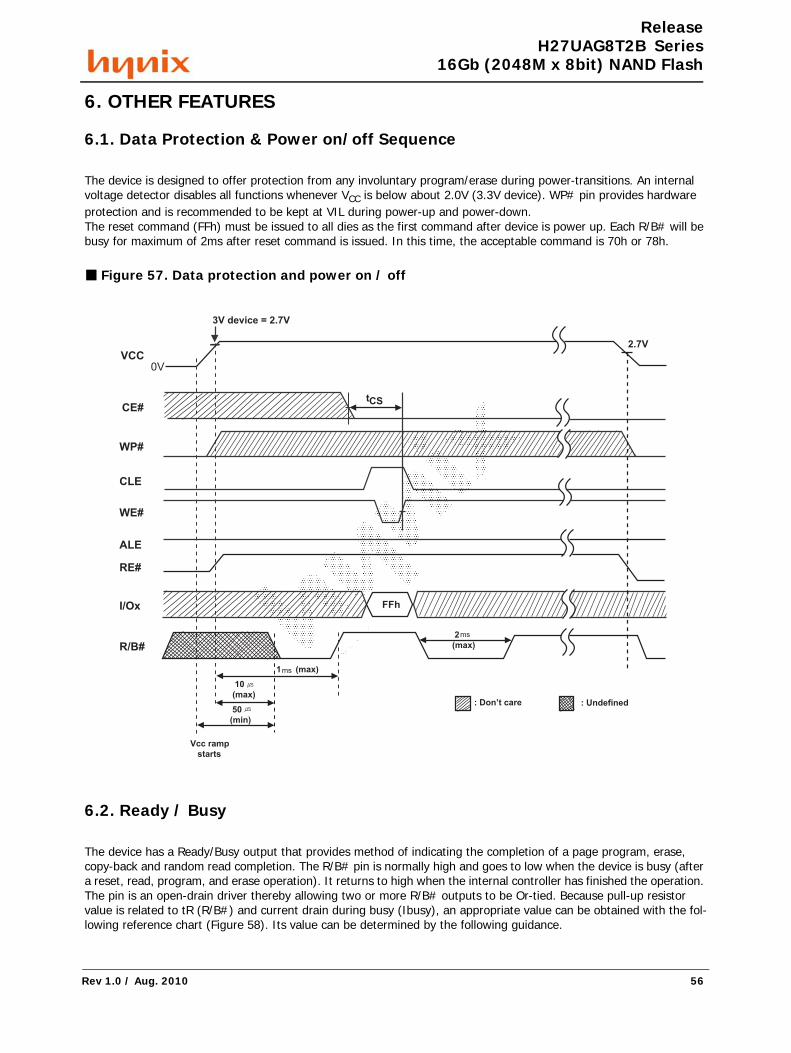
APCPCWM_4828539:WP_0000001WP_0000001
APC
PCW
M_4
8285
39:W
P_00
0000
1WP_
0000
001
ReleaseH27UAG8T2B Series
16Gb (2048M x 8bit) NAND Flash
6. OTHER FEATURES
6.1. Data Protection & Power on/off Sequence
The device is designed to offer protection from any involuntary program/erase during power-transitions. An internal voltage detector disables all functions whenever VCC is below about 2.0V (3.3V device). WP# pin provides hardware protection and is recommended to be kept at VIL during power-up and power-down. The reset command (FFh) must be issued to all dies as the first command after device is power up. Each R/B# will be busy for maximum of 2ms after reset command is issued. In this time, the acceptable command is 70h or 78h.
■ Figure 57. Data protection and power on / off
6.2. Ready / Busy
The device has a Ready/Busy output that provides method of indicating the completion of a page program, erase, copy-back and random read completion. The R/B# pin is normally high and goes to low when the device is busy (after a reset, read, program, and erase operation). It returns to high when the internal controller has finished the operation. The pin is an open-drain driver thereby allowing two or more R/B# outputs to be Or-tied. Because pull-up resistor value is related to tR (R/B#) and current drain during busy (Ibusy), an appropriate value can be obtained with the fol-lowing reference chart (Figure 58). Its value can be determined by the following guidance.
3V device = 2.7V
tCS
FFh
2.7V
1 (max)ms
10
(max)
50
(min)
2
(max)
ms
Vcc ramp
starts
: Don’t care : Undefined
VCC0V
CE#
WP#
CLE
WE#
ALE
RE#
I/Ox
R/B#
Rev 1.0 / Aug. 2010 56
*58b7d520-e522* B26798/177.179.157.212/2010-08-06 17:39
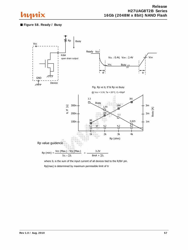
APCPCWM_4828539:WP_0000001WP_0000001
APC
PCW
M_4
8285
39:W
P_00
0000
1WP_
0000
001
ReleaseH27UAG8T2B Series
16Gb (2048M x 8bit) NAND Flash
■ Figure 58. Ready / Busy
Rp value guidence
Rp (min) = =
where IL is the sum of the input current of all devices tied to the R/B# pin.
Rp(max) is determined by maximum permissible limit of tr
@ Vcc = 3.3V, Ta = 25°C, CL=50pF
Fig. Rp vs tr, tf & Rp vs ibusy
Vcc (Max.) - VOL (Max.) 3.2V
LIOL + L
Rp ibusy
Rp (ohm)
ibusy
ibusy
[A]
tr, tf
[s
]
tf
3.3 381
2901.65
96
1891.1
0.825
4.2 4.2 4.2 4.2
Busy
Ready Vcc
VOH
trtf
VOL
VOL : 0.4V, VOH : 2.4V
Vcc
300n 3m
1k 2k 3k 4k
200n 2m
100n 1m
GND
Device
open drain output
R/B#
Rev 1.0 / Aug. 2010 57
*58b7d520-e522* B26798/177.179.157.212/2010-08-06 17:39
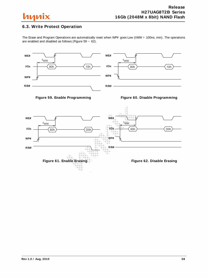
APCPCWM_4828539:WP_0000001WP_0000001
APC
PCW
M_4
8285
39:W
P_00
0000
1WP_
0000
001
ReleaseH27UAG8T2B Series
16Gb (2048M x 8bit) NAND Flash
6.3. Write Protect Operation
The Erase and Program Operations are automatically reset when WP# goes Low (tWW = 100ns, min). The operations are enabled and disabled as follows (Figure 59 ~ 62).
Figure 59. Enable Programming Figure 60. Disable Programming
Figure 61. Enable Erasing Figure 62. Disable Erasing
80h 10h
WE#
I/Ox
WP#
R/B#
WWt
80h 10h
WE#
I/Ox
WP#
R/B#
WWt
60h D0h
WE#
I/Ox
WP#
R/B#
WWt
60h D0h
WE#
I/Ox
WP#
R/B#
WWt
Rev 1.0 / Aug. 2010 58
*58b7d520-e522* B26798/177.179.157.212/2010-08-06 17:39
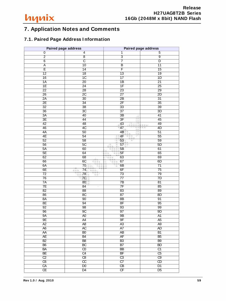
APCPCWM_4828539:WP_0000001WP_0000001
APC
PCW
M_4
8285
39:W
P_00
0000
1WP_
0000
001
ReleaseH27UAG8T2B Series
16Gb (2048M x 8bit) NAND Flash
7. Application Notes and Comments
7.1. Paired Page Address Information
Paired page address Paired page address0 4 1 52 8 3 96 C 7 DA 10 B 11E 14 F 1512 18 13 1916 1C 17 1D1A 20 1B 211E 24 1F 2522 28 23 2926 2C 27 2D2A 30 2B 312E 34 2F 3532 38 33 3936 3C 37 3D3A 40 3B 413E 44 3F 4542 48 43 4946 4C 47 4D4A 50 4B 514E 54 4F 5552 58 53 5956 5C 57 5D5A 60 5B 615E 64 5F 6562 68 63 6966 6C 67 6D6A 70 6B 716E 74 6F 7572 78 73 7976 7C 77 7D7A 80 7B 817E 84 7F 8582 88 83 8986 8C 87 8D8A 90 8B 918E 94 8F 9592 98 93 9996 9C 97 9D9A A0 9B A19E A4 9F A5A2 A8 A3 A9A6 AC A7 ADAA B0 AB B1AE B4 AF B5B2 B8 B3 B9B6 BC B7 BDBA C0 BB C1BE C4 BF C5C2 C8 C3 C9C6 CC C7 CDCA D0 CB D1CE D4 CF D5
Rev 1.0 / Aug. 2010 59
*58b7d520-e522* B26798/177.179.157.212/2010-08-06 17:39
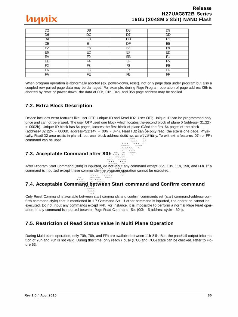
APCPCWM_4828539:WP_0000001WP_0000001
APC
PCW
M_4
8285
39:W
P_00
0000
1WP_
0000
001
ReleaseH27UAG8T2B Series
16Gb (2048M x 8bit) NAND Flash
When program operation is abnormally aborted (ex. power-down, reset), not only page data under program but also a coupled row paired page data may be damaged. For example, during Page Program operation of page address 05h is aborted by reset or power down, the data of 00h, 01h, 04h, and 05h page address may be spoiled.
7.2. Extra Block Description
Device includes extra features like user OTP, Unique ID and Read ID2. User OTP, Unique ID can be programmed only once and cannot be erased. The user OTP used one block which locates the second block of plane 0 (address<31:22> = 0002h). Unique ID block has 64 pages, locates the first block of plane 0 and the first 64 pages of the block (address<32:22> = 0000h, address<21:14> = 00h ~ 3Fh). Read ID2 can be only read, the size is one page. Physi-cally, ReadID2 area exists in plane1, but user block address does not care internally. To exit extra features, 07h or FFh command can be used.
7.3. Acceptable Command after 80h
After Program Start Command (80h) is inputted, do not input any command except 85h, 10h, 11h, 15h, and FFh. If a command is inputted except these commands, the program operation cannot be executed.
7.4. Acceptable Command between Start command and Confirm command
Only Reset Command is available between start commands and confirm commands set (start command-address-con-firm command style) that is mentioned in 1.7 Command Set. If other command is inputted, the operation cannot be executed. Do not input any commands except FFh. For instance, it is impossible to perform a normal Page Read oper-ation, if any command is inputted between Page Read Command Set (00h - 5 address cycle - 30h).
7.5. Restriction of Read Status Value in Multi Plane Operation
During Multi plane operation, only 70h, 78h, and FFh are available between 11h-81h. But, the pass/fail output informa-tion of 70h and 78h is not valid. During this time, only ready / busy (I/O6 and I/O5) state can be checked. Refer to Fig-ure 63.
D2 D8 D3 D9D6 DC D7 DDDA E0 DB E1DE E4 DF E5E2 E8 E3 E9E6 EC E7 EDEA F0 EB F1EE F4 EF F5F2 F8 F3 F9F6 FC F7 FDFA FE FB FF
Rev 1.0 / Aug. 2010 60
*58b7d520-e522* B26798/177.179.157.212/2010-08-06 17:39
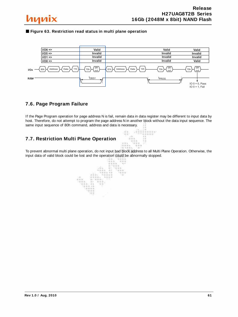
APCPCWM_4828539:WP_0000001WP_0000001
APC
PCW
M_4
8285
39:W
P_00
0000
1WP_
0000
001
ReleaseH27UAG8T2B Series
16Gb (2048M x 8bit) NAND Flash
■ Figure 63. Restriction read status in multi plane operation
7.6. Page Program Failure
If the Page Program operation for page address N is fail, remain data in data register may be different to input data by host. Therefore, do not attempt to program the page address N in another block without the data input sequence. The same input sequence of 80h command, address and data is necessary.
7.7. Restriction Multi Plane Operation
To prevent abnormal multi plane operation, do not input bad block address to all Multi Plane Operation. Otherwise, the input data of valid block could be lost and the operation could be abnormally stopped.
80hI/Ox
R/B#
Address Data
I/O6 =>
I/O5 =>
I/O1 =>
I/O0 =>
Valid
Invalid
Invalid
Invalid
11h 70hSR
out 81h Address Data 10h 70hSR
out
Valid
Invalid
Invalid
Invalid
Valid
Invalid
Invalid
Valid
70hSR
out
tPROGtDBSY
IO 0 = 0, Pass
IO 0 = 1, Fail
Rev 1.0 / Aug. 2010 61
*58b7d520-e522* B26798/177.179.157.212/2010-08-06 17:39