Embed Size (px)
Citation preview
US 20140078104A1
(19) United States (12) Patent Application Publication (10) Pub. No.: US 2014/0078104 A1
LEE et al. (43) Pub. Date: Mar. 20, 2014
(54) DISPLAY DEVICE AND METHOD OF (30) Foreign Application Priority Data DRIVING THE SAME
Feb. 27, 2013 (KR) ........................ 10-2013-0021423 (71) Applicant: Samsung Display Co., Ltd., Yongin-city Feb. 27, 2013 (KR). ... 10-2013-0021426
(KR) May 16, 2013 (KR) ........................ 10-2013-0055845
(72) Inventors: KANGWON LEE, Seoul (KR): Incheol Publication Classification Kim, Goyang-si (KR); Ung Choi, Asan-si (KR); Won-ki Hong, Suwon-si (51) Int. Cl. (KR); Seungho Nam, Seongnam-si G06F 3/044 (2006.01) (KR); Jihong Park, Suwon-si (KR): (52) U.S. Cl. Chul Kim, Hwaseong-si (KR); Hojin CPC ...................................... G06F 3/044 (2013.01) Byun, Suwon-si (KR); Kiseok Cha, USPC .......................................................... 345/174 Yongin-si (KR)
(57) ABSTRACT (73) Assignee: Samsung Display Co., Ltd., Yongin-city A display device includes a display panel and a touch panel.
(KR) The touch panel calculates coordinate information of an input position by an electrostatic capacitive method in a first mode
(21) Appl. No.: 14/024,241 and calculates the coordinate information of the input posi tion by an electromagnetic induction method in a second
(22) Filed: Sep. 11, 2013 mode. The touch panel includes scan line groups and source line groups, which are operated as touch electrodes or touch
O O coils on the basis of the operating mode thereof. In addition, Related U.S. Application Data the touch panel includes touch electrodes and touch coils,
(60) Provisional application No. 61/701,100, filed on Sep. which are individually operated on the basis of the operating 14, 2012. mode thereof.
1OO
RGB Signal CS Controller
Data Driver
MSS
TS1 (TS2
DR2 MSS Second Driver
SS1 fSS2 - Touch SensOr -600
US 2014/0078104 A1 Mar. 20, 2014 Sheet 1 of 89 Patent Application Publication
SSW 007
009
S
I ?!!!
S W
| HCl
ZHO
Je || O || !UOO | euÔ | S
SO
Patent Application Publication Mar. 20, 2014 Sheet 2 of 89 US 2014/0078104 A1
Fig. 2
LCL
Patent Application Publication Mar. 20, 2014 Sheet 3 of 89 US 2014/0078104 A1
Fig. 3
LDP
TL1
TL9
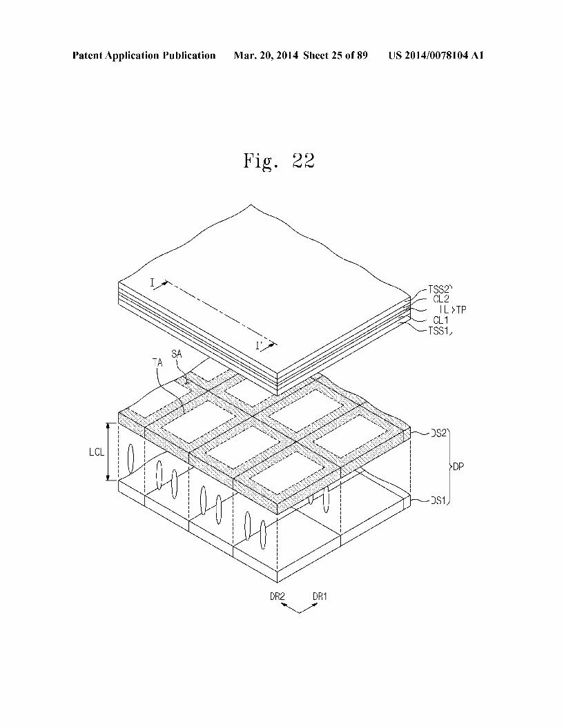
DR2 RL1 } e RL1 O
-
US 2014/0078104 A1 Mar. 20, 2014 Sheet 4 of 89 Patent Application Publication
„I | || || I - - - - - -9HO
|SO| {{[\S
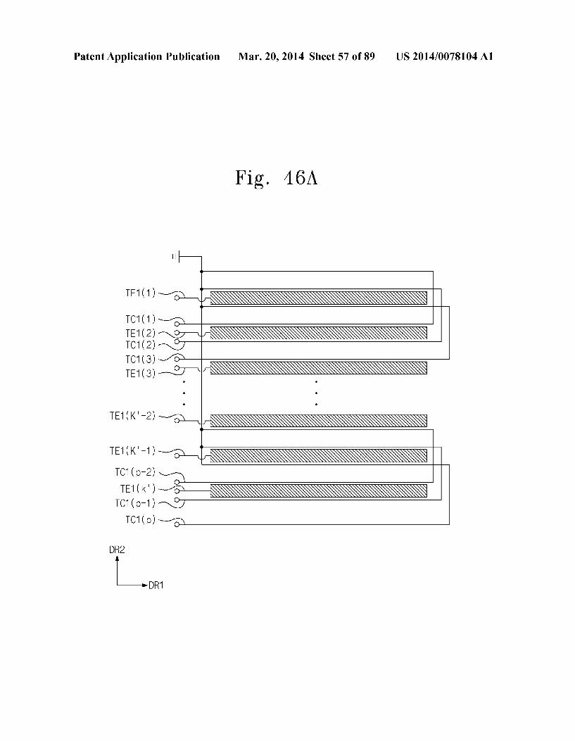
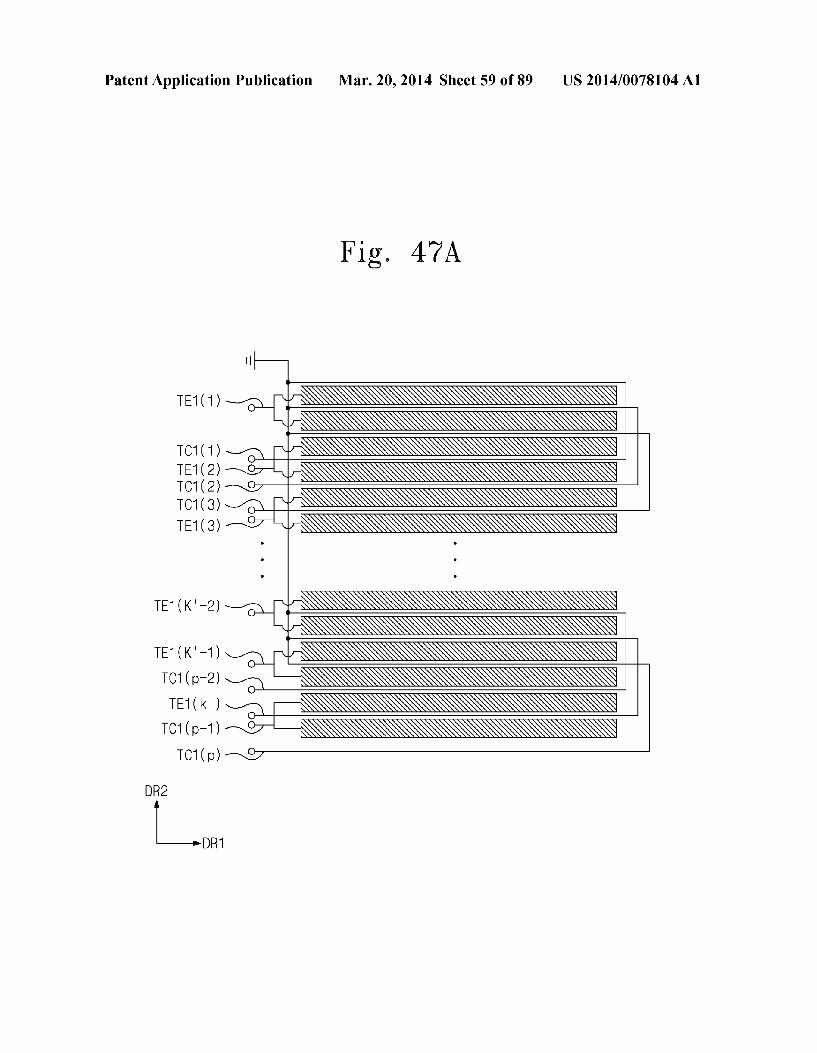
|---| |- | - 0|| ~|~ || || |
Patent Application Publication Mar. 20, 2014 Sheet 5 of 89 US 2014/0078104 A1
Fig. 5
TOUCh SensOr 600
CNL 1
HHHHHHHHHHHHA 7 HIH-fu-TLG H H TLG3) TG1 O HHHHH-TLG2
s HHH H TL36 t t HHH
\ RL1 RL36
CNL2 RLG1 RLG3 RLG2 RG20 RG30 RG40 DR2 RG10
-
Patent Application Publication Mar. 20, 2014 Sheet 6 of 89 US 2014/0078104 A1
Fig. 6
SS1-1 SS1-2 SS1-3 SS1-4 pp. A
TLG1
H22, H22222222 H2
ZZZZZZZZZ ZZZZZZZZ 2
22 Z
la
T G 3 O
DR2 RG1 O
-
Patent Application Publication Mar. 20, 2014 Sheet 7 of 89 US 2014/0078104 A1
Fig. 7A
TS2–1 -> —
E. TS2-2 -o 2
TS2-3->-6- F(x-xx-x-xx-x-x 4 N-TG30
TS2-4-D-G- E EXEEXEEXEEXEEXEEXEEXEEXH 4 N-TG40
DR2
-
US 2014/0078104 A1 Mar. 20, 2014 Sheet 8 of 89 Patent Application Publication
Fig. 7B
4. SS2 3 SS2 2 SS2 1 SS2
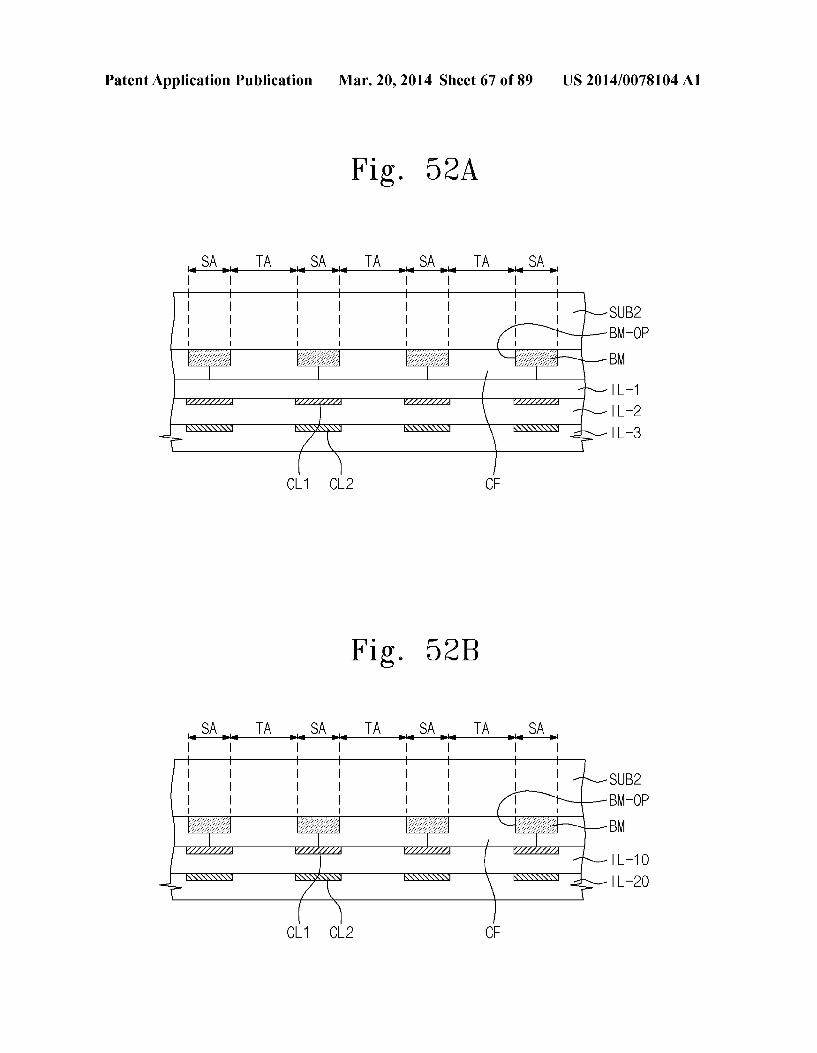
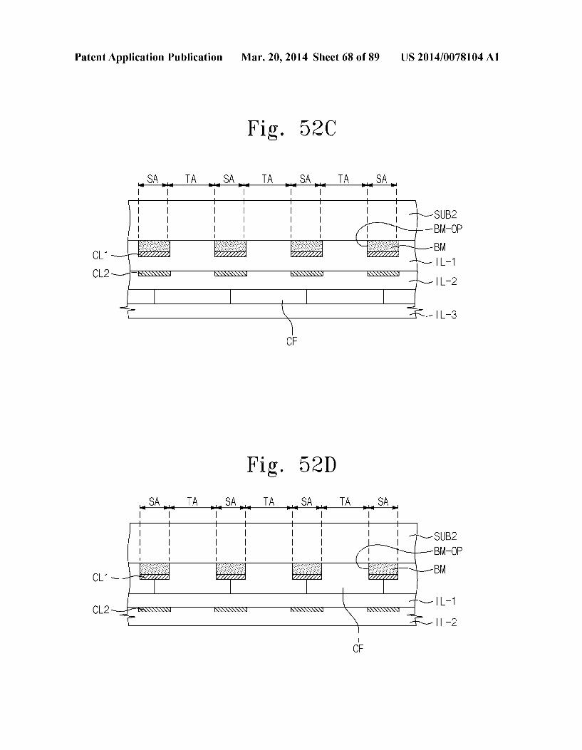
| KNNNN
N N ` NNNNNNN SN
N N SRN NOEN NOES
RG30 RG40 RLG1 RLG3 RLG2
RG1 O DR2
-
Patent Application Publication Mar. 20, 2014 Sheet 9 of 89 US 2014/0078104 A1
3. 2 5. . . 3.
Patent Application Publication Mar. 20, 2014 Sheet 10 of 89 US 2014/0078104 A1
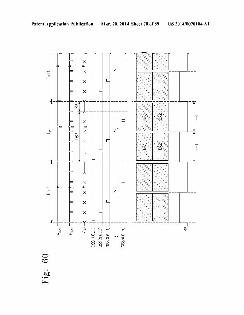
MSS
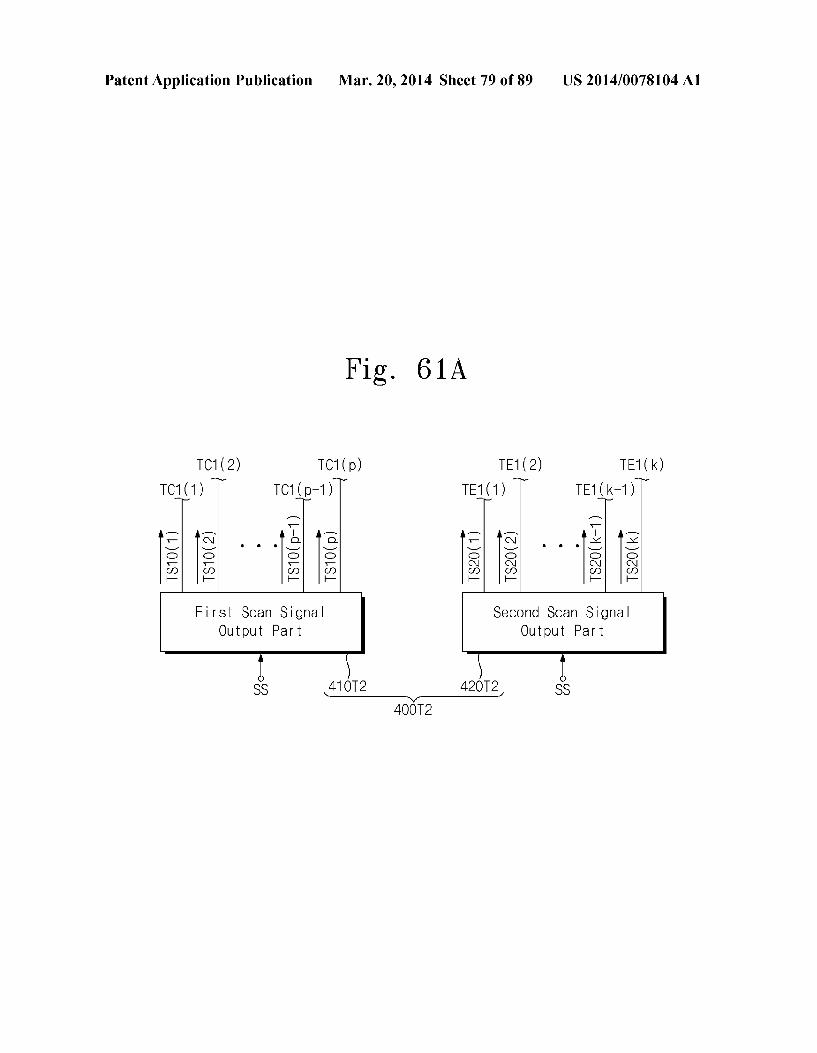
4N-TG1 O
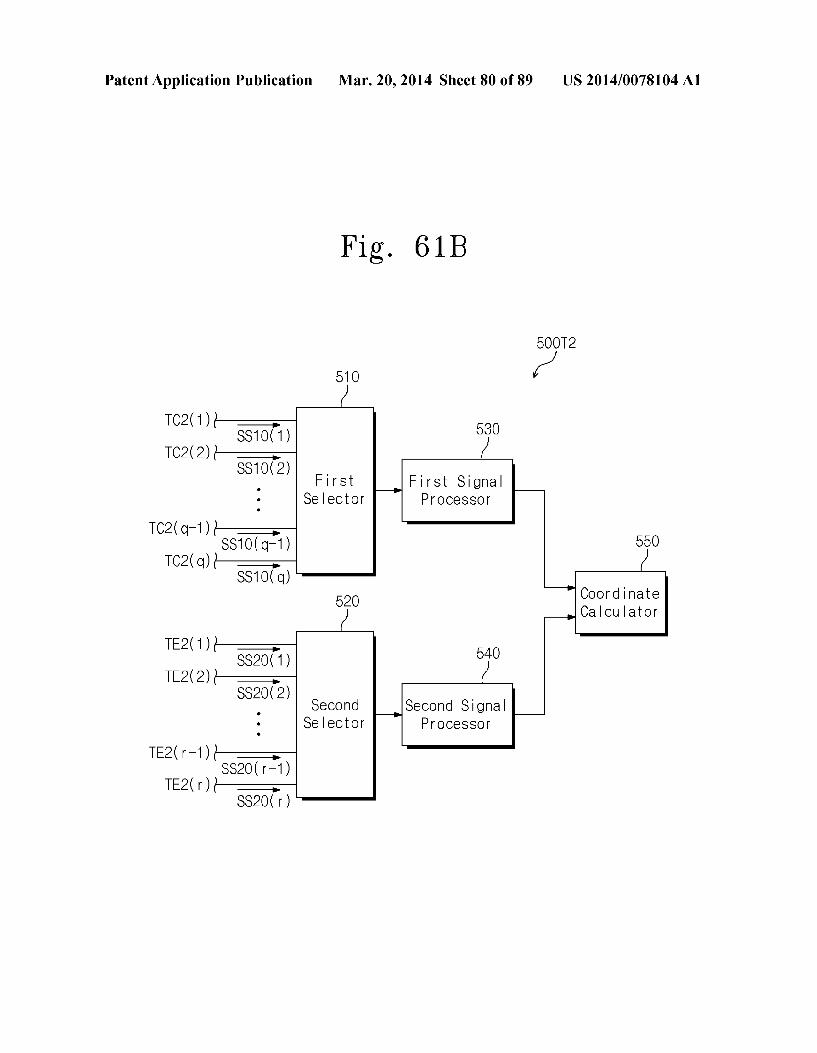
4. Nu-TG20
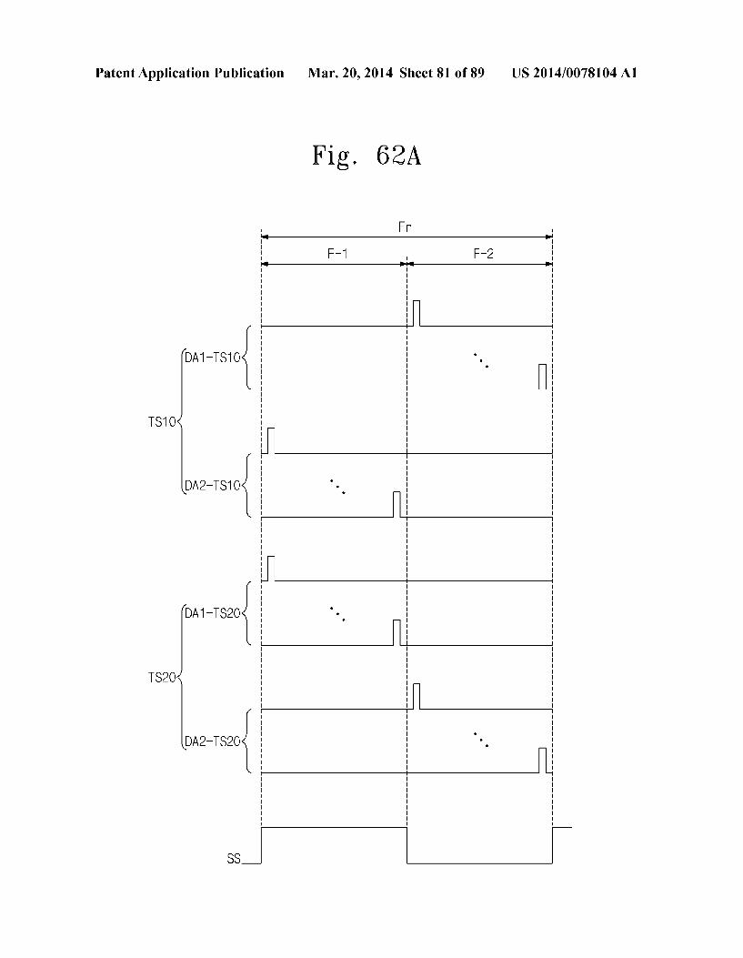
MSS
4N-TG3O
US 2014/0078104 A1 Mar. 20, 2014 Sheet 11 of 89 Patent Application Publication
US 2014/0078104 A1 Mar. 20, 2014 Sheet 12 of 89 Patent Application Publication
SSW
US 2014/0078104 A1 Mar. 20, 2014 Sheet 13 of 89 Patent Application Publication
f.
| –ZSS SSW 1 4
| — | SS
US 2014/0078104 A1 Mar. 20, 2014 Sheet 14 of 89 Patent Application Publication
US 2014/0078104 A1 Mar. 20, 2014 Sheet 15 of 89 Patent Application Publication
- - - - - -9HO |SO| {{[\S- | | | | | | -
Tld
Patent Application Publication Mar. 20, 2014 Sheet 16 of 89 US 2014/0078104 A1
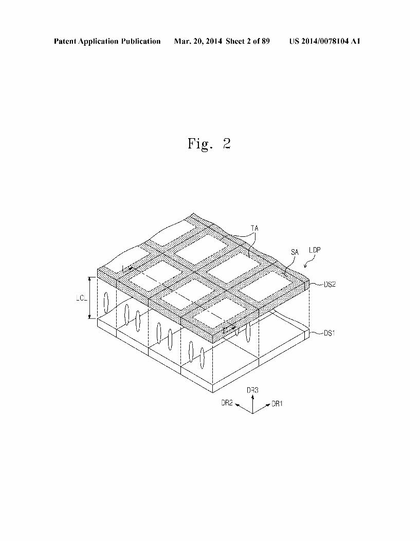
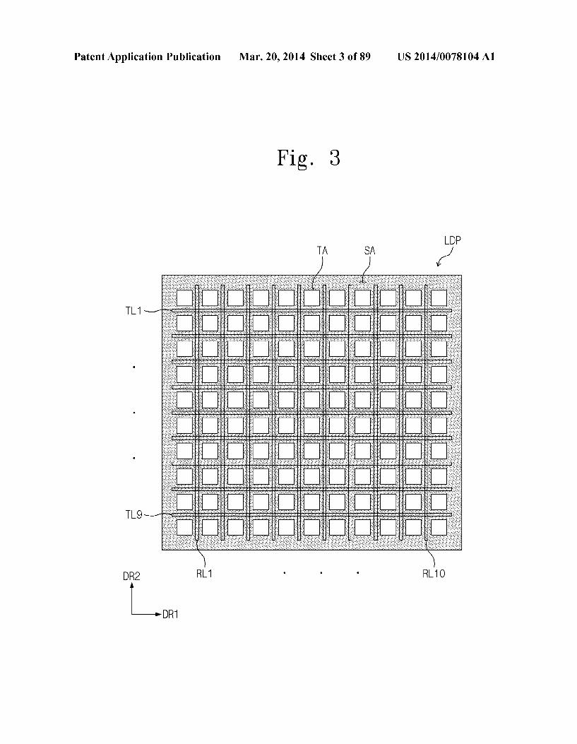
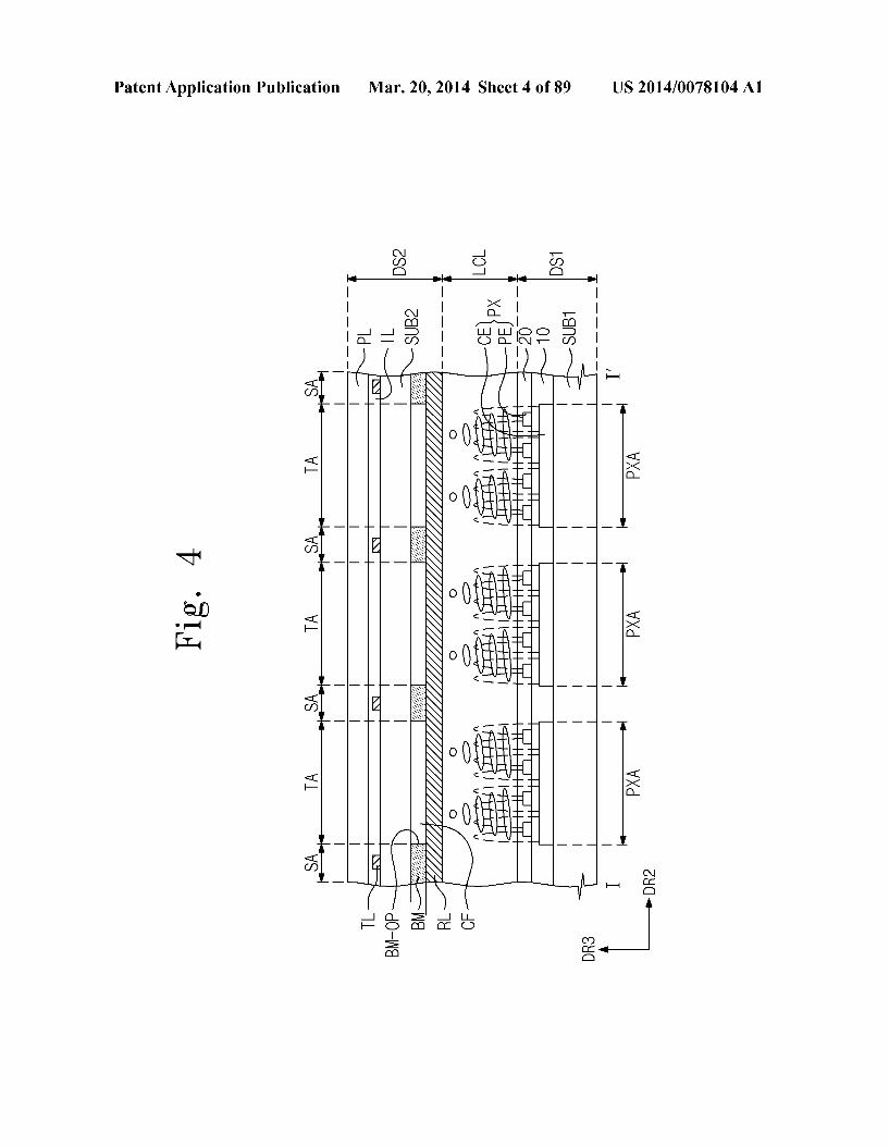
Fig. 15A
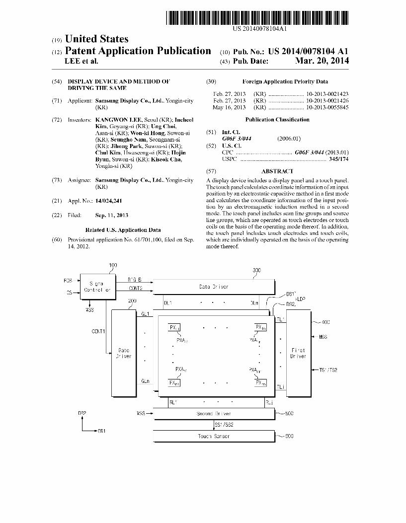
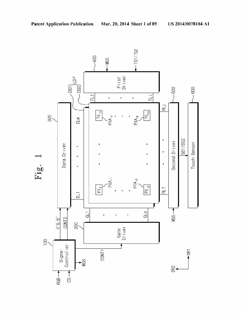
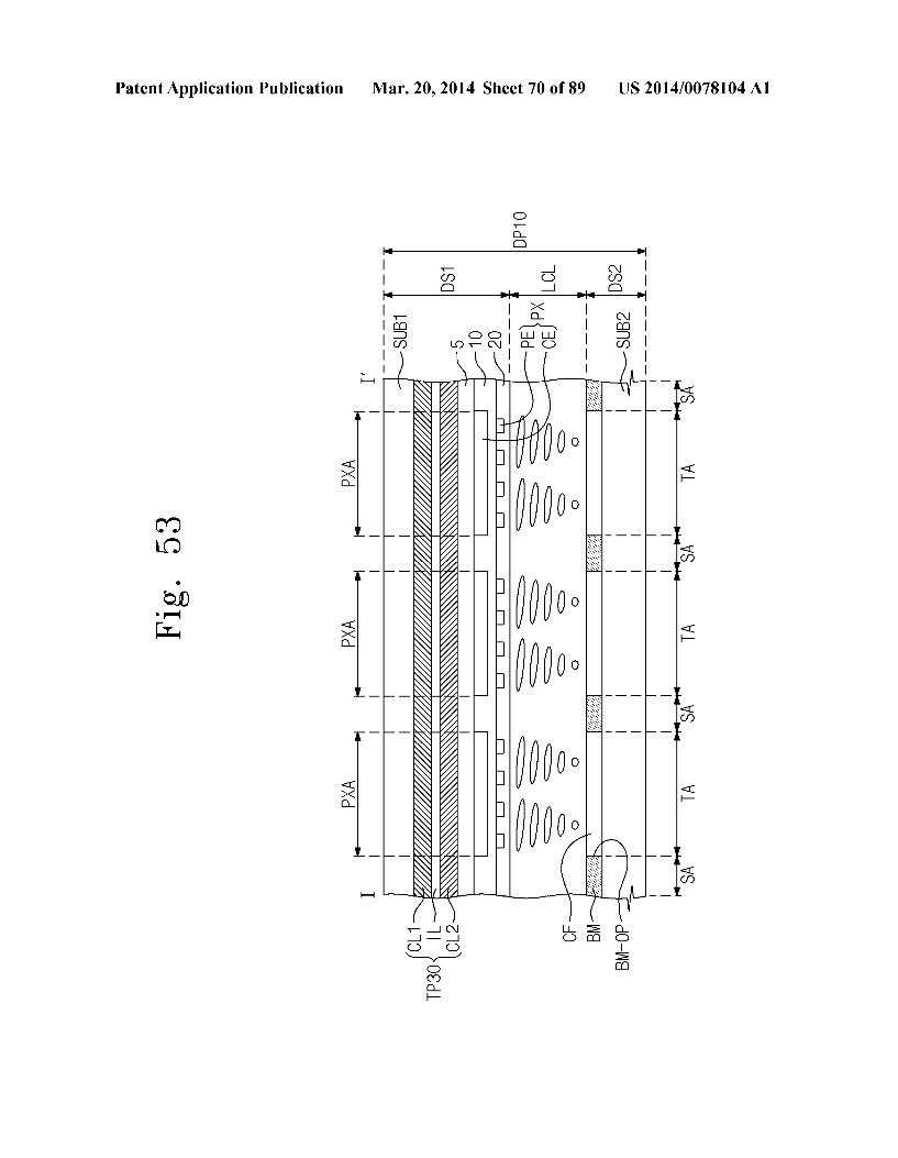
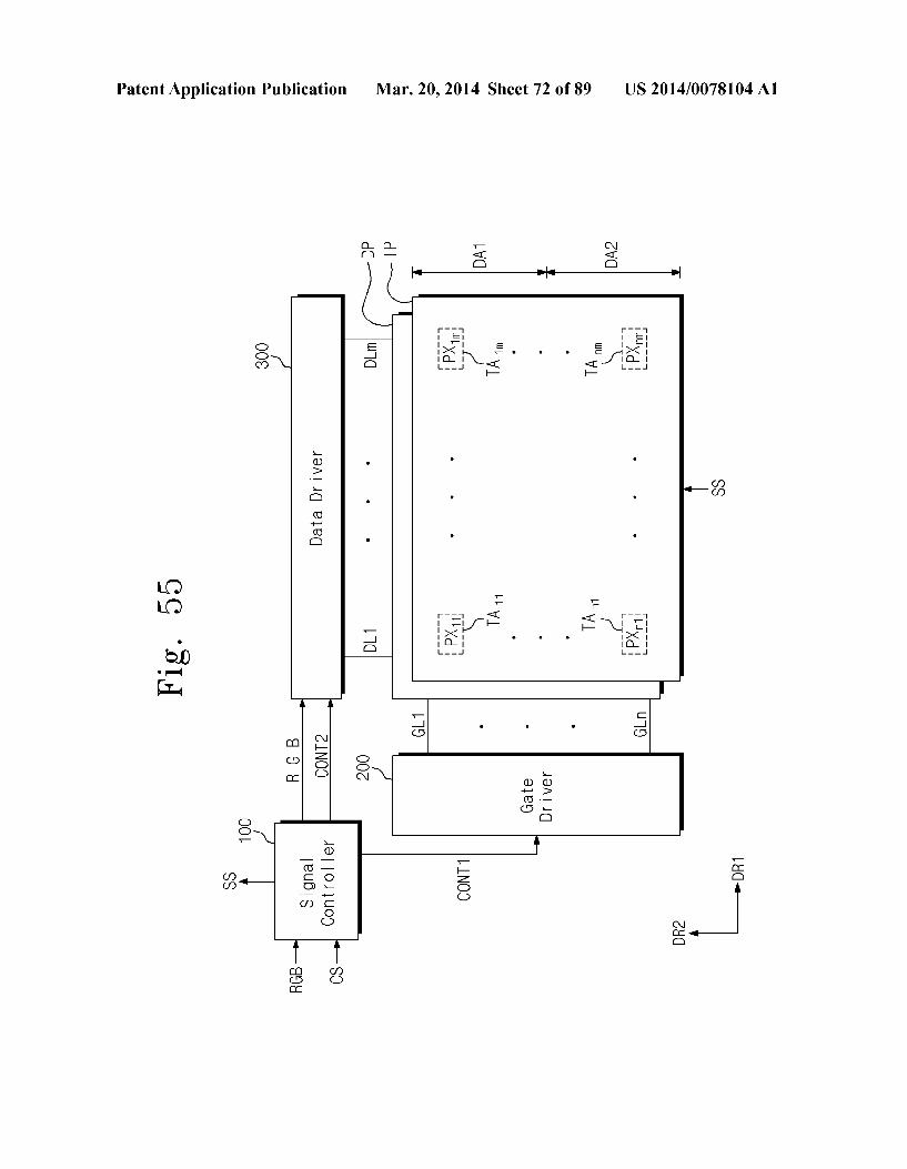
LDP SSE1 SA TA -
TL1
TL9
DR2
-
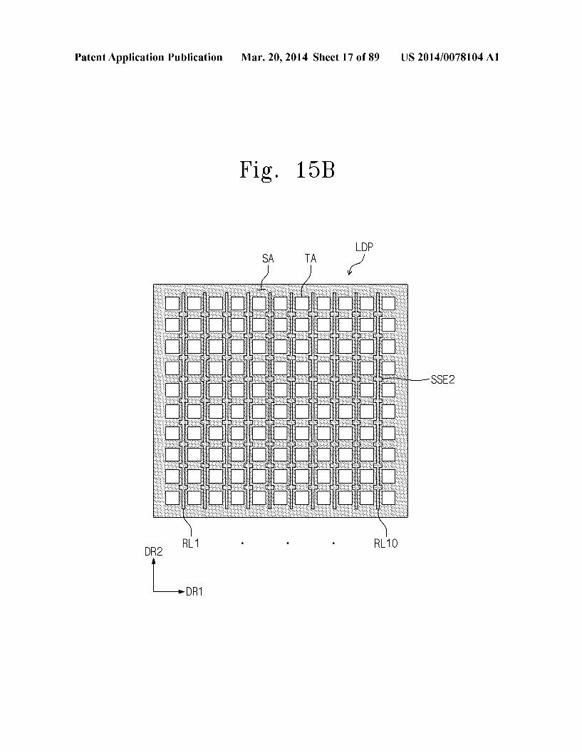
Patent Application Publication Mar. 20, 2014 Sheet 17 of 89 US 2014/0078104 A1
Fig. 15B
LDP
SSE2
DR2 RL1 s 4. 4. RL10
-
US 2014/0078104 A1 Mar. 20, 2014 Sheet 18 of 89 Patent Application Publication
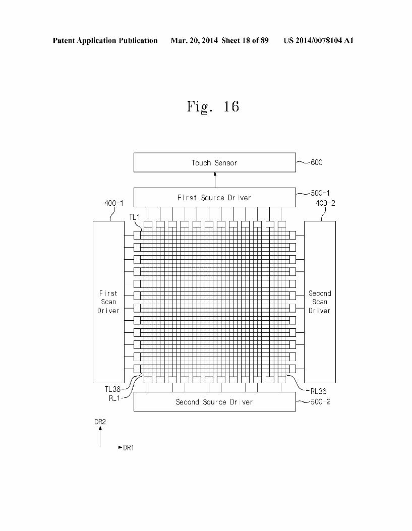
Fig. 16
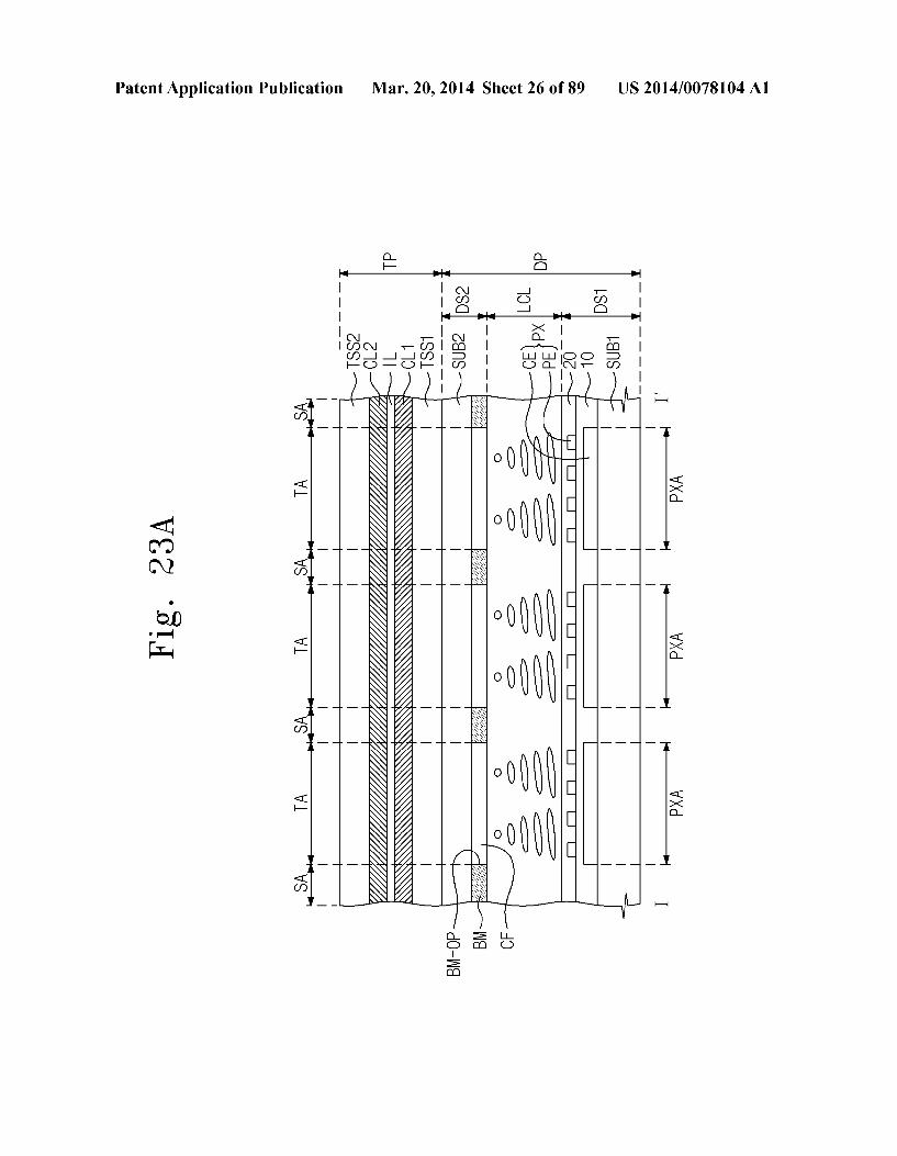
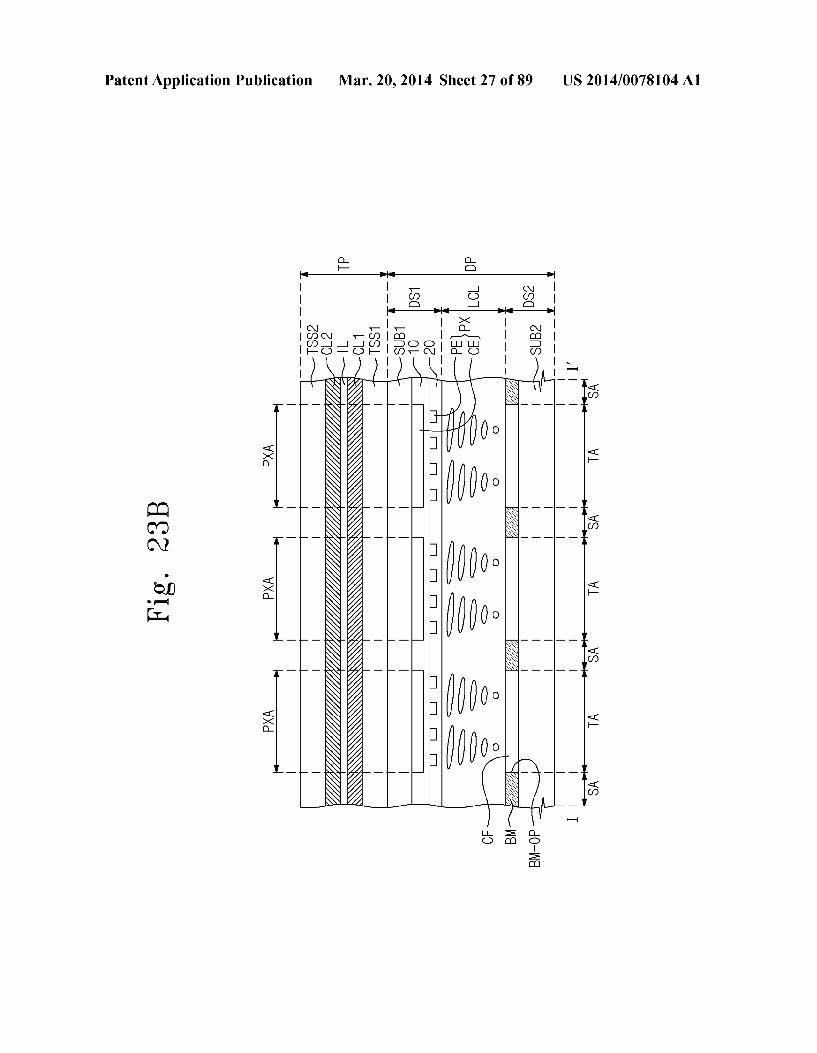
400-2 + CO CC) COL (O
Touch SensOr
First Source Driver
RL36 5OO-2
JE Second Sour Ce Dr Ver
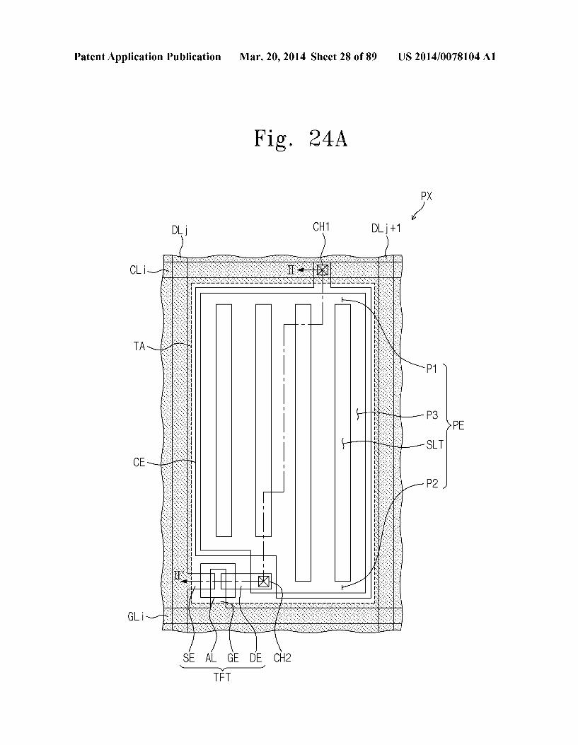
TL36 RL1
DR2
-
US 2014/0078104 A1 Mar. 20, 2014 Sheet 19 of 89 Patent Application Publication
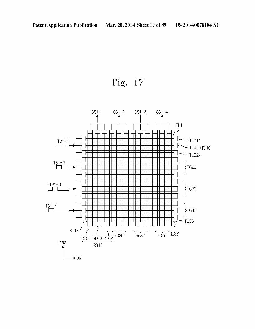
Fig. 17
SS1-2 SS1-3 SS1-4 SS1-1
h h TL1
TLG1
TLG3TG10 TLG2
RGAO RL36
TS1-1
TS1-2
H —DH H
RL1
TS1-3
TS1-4
RLG1 RLG8 RLG20 RG10 DR2
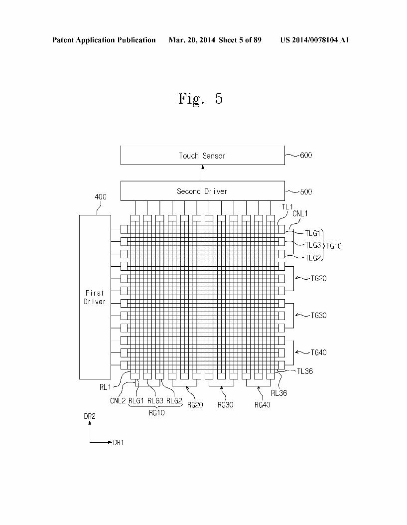
-
Patent Application Publication Mar. 20, 2014 Sheet 20 of 89 US 2014/0078104 A1
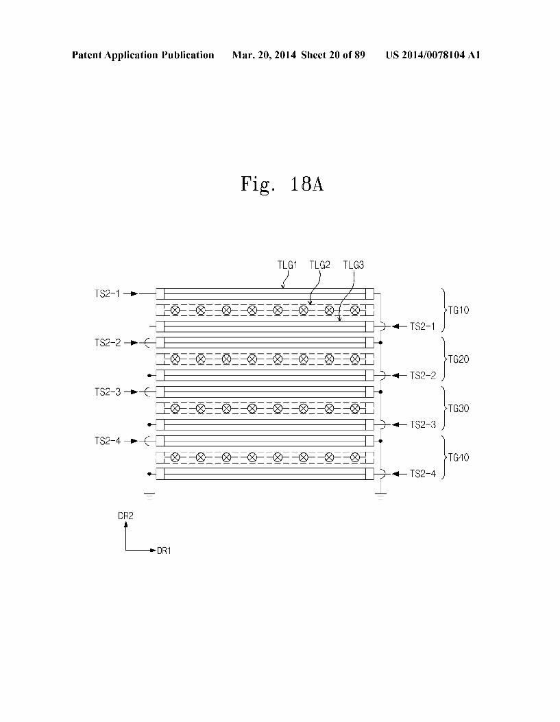
Fig. 18A
TLG1 TLG2 TLG3
Exx-xx-xxxx - E HG---TS2-2
TS2-3-D-G-P-
TS2-4-D-G-P-
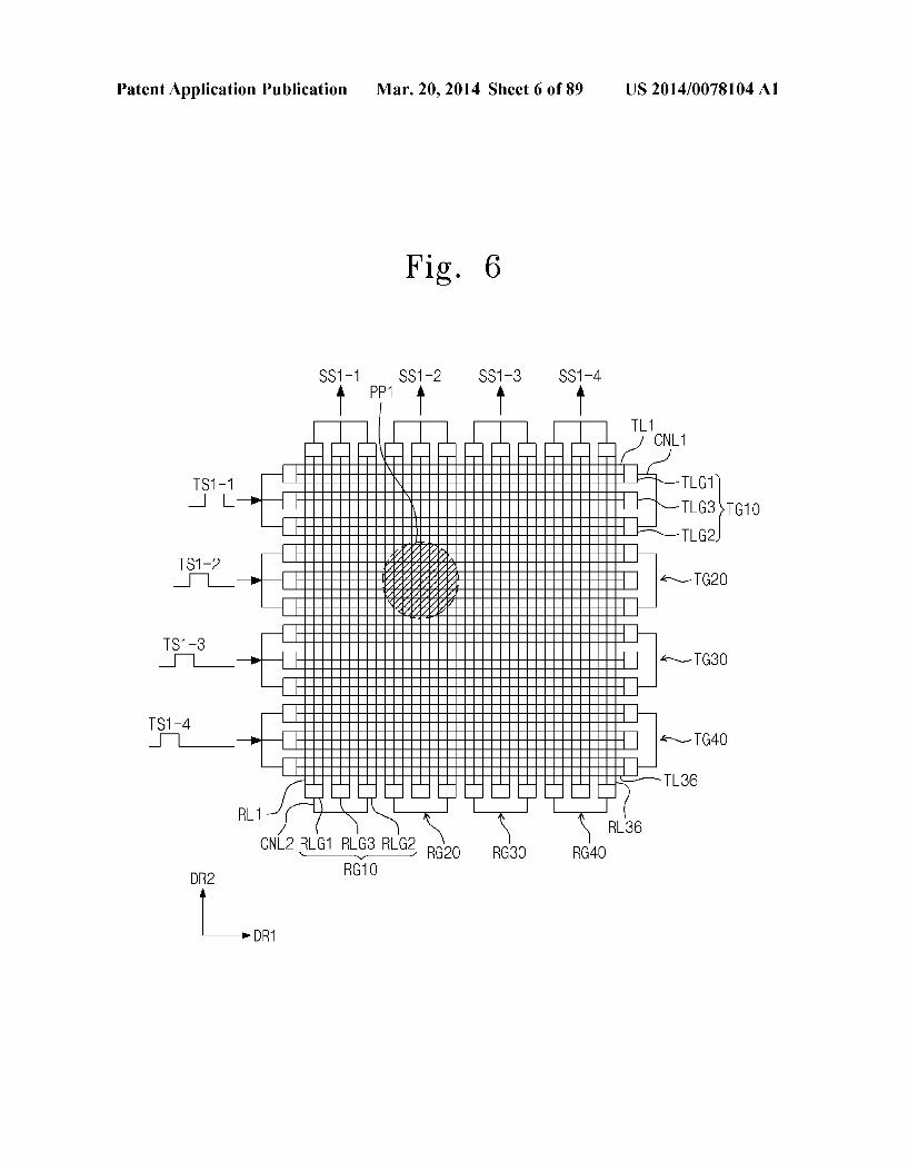
.
US 2014/0078104 A1 Mar. 20, 2014 Sheet 21 of 89 Patent Application Publication
Fig. 18B
SS2-4
4. t;
SS2-3
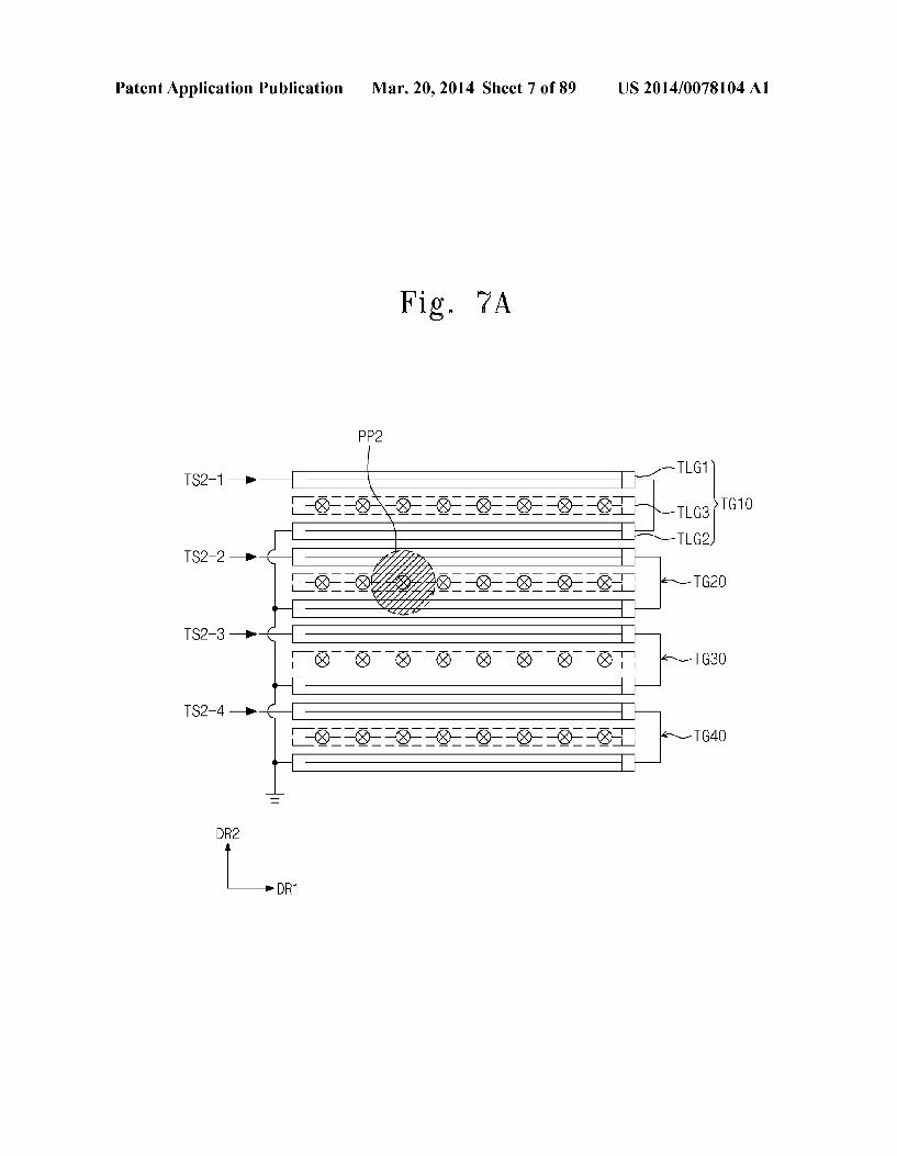
3 ".
SS2-2
si
SS2-1
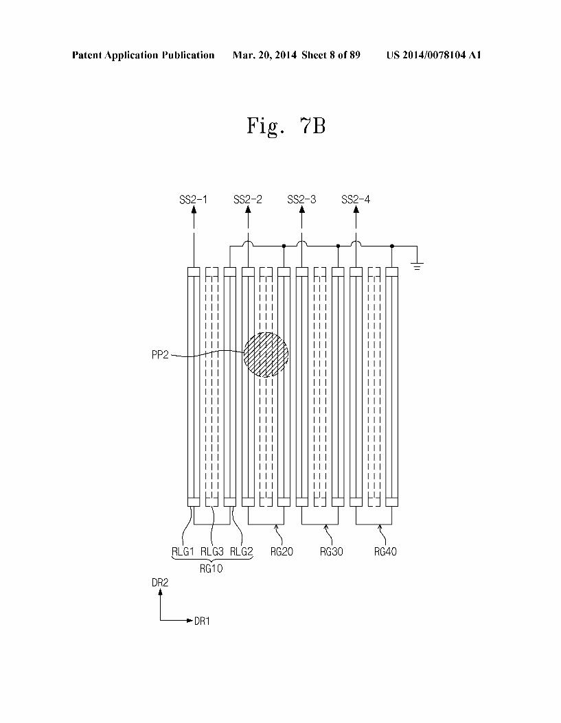
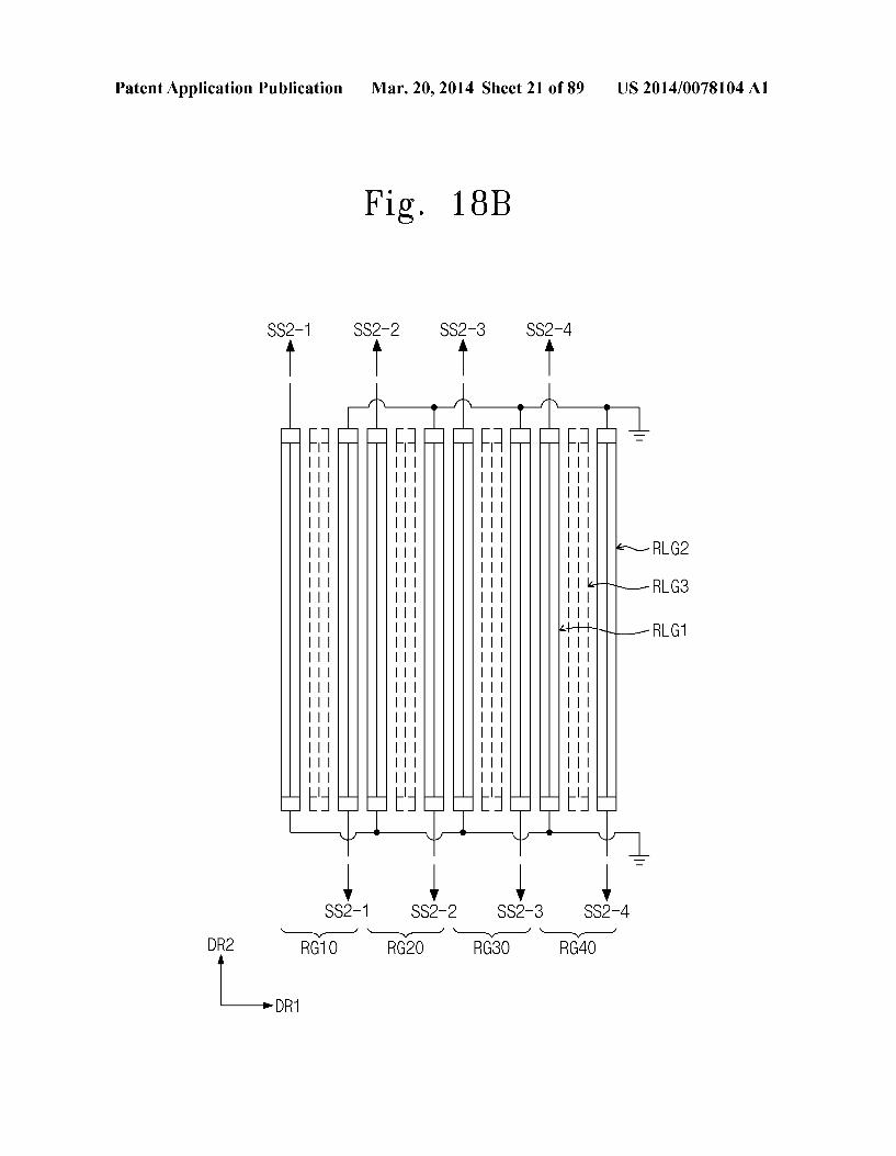
RG30
si
DR2 RG40 RG20 RG1 O
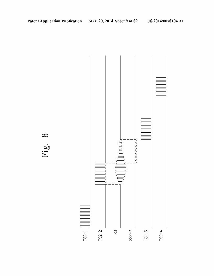
-
Patent Application Publication Mar. 20, 2014 Sheet 22 of 89 US 2014/0078104 A1
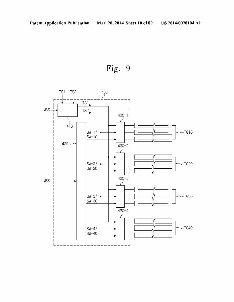
TLG1-1 a
TG10KTLG3 - a
TLG2 -- a
TG4O -- a
&les
F TS2-1 F TS2-4
Patent Application Publication Mar. 20, 2014 Sheet 23 of 89 US 2014/0078104 A1
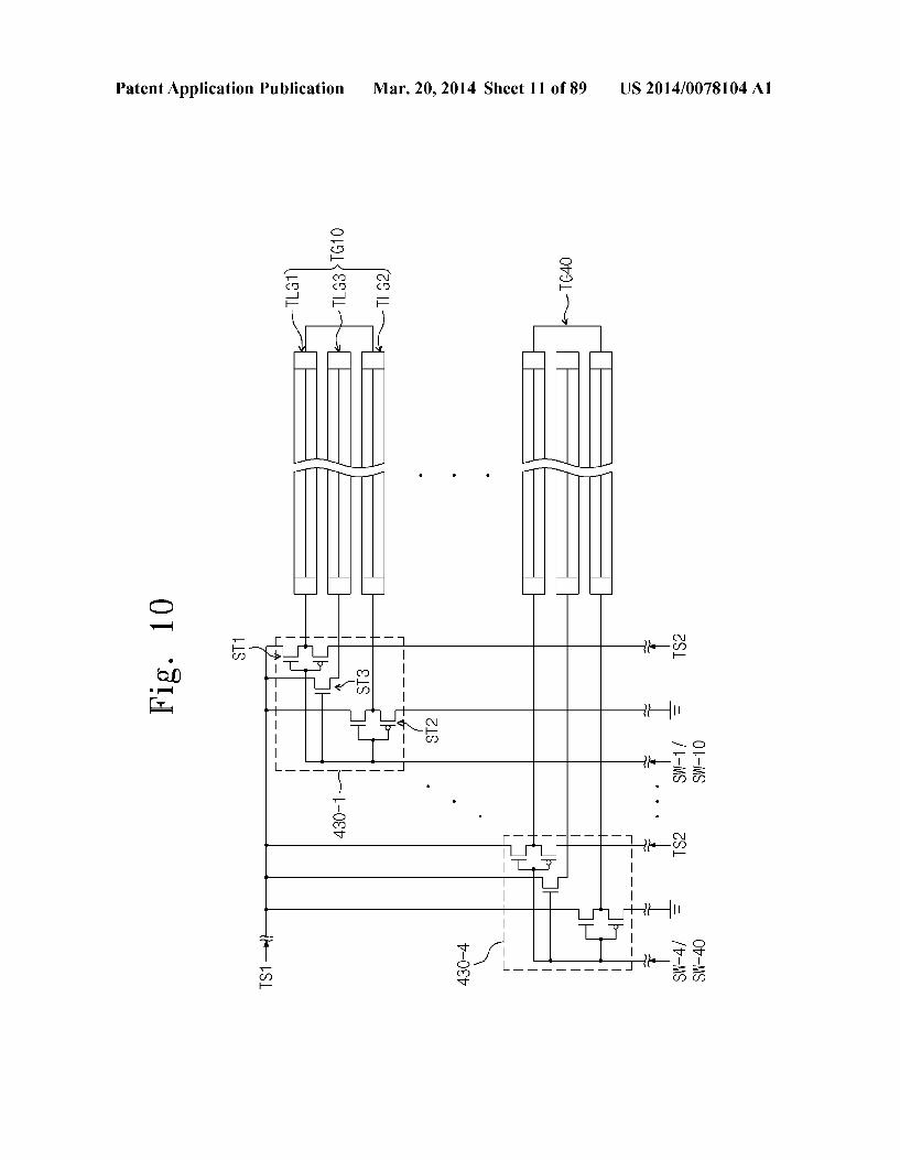
Fig. 20
RG10 -n- RLG1 RLG3 RLG2
500-2
* l -) Szo-si
| ST1000 - - - - - - - - - - -
| HCl
SSW
ZHO
US 2014/0078104 A1 Mar. 20, 2014 Sheet 24 of 89
Je || O J? UOOSO
Patent Application Publication
CfO CfO s
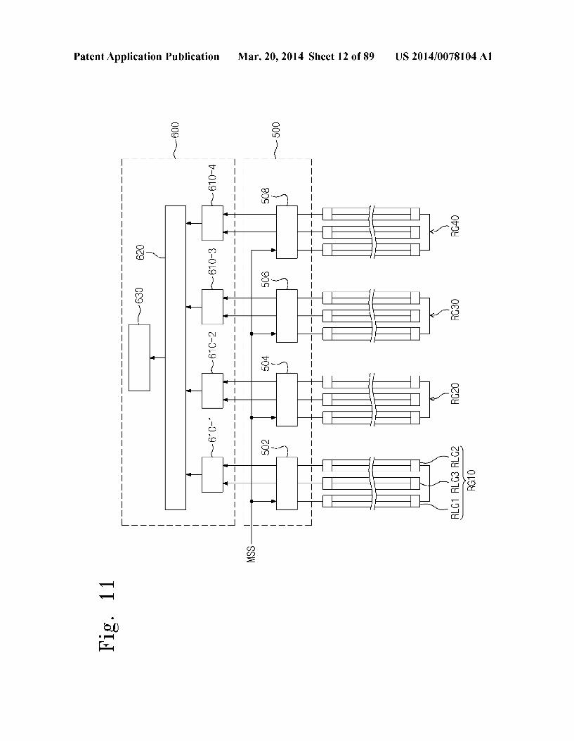
Patent Application Publication Mar. 20, 2014 Sheet 25 of 89 US 2014/0078104 A1
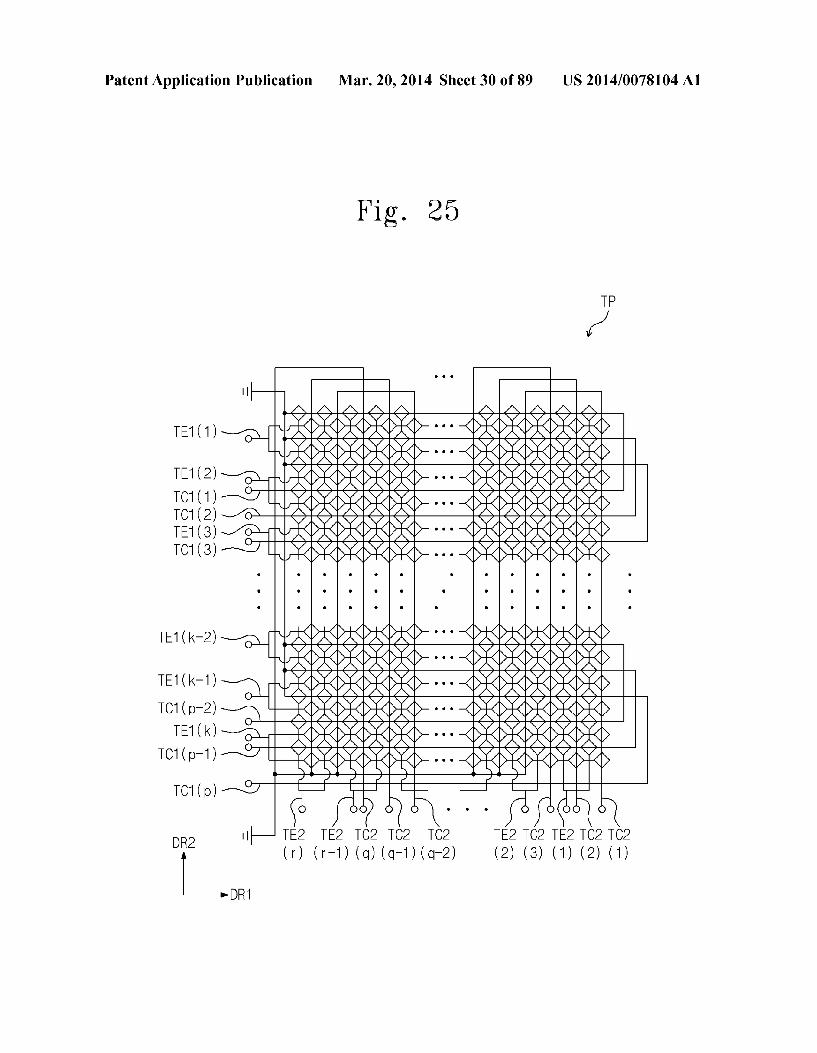
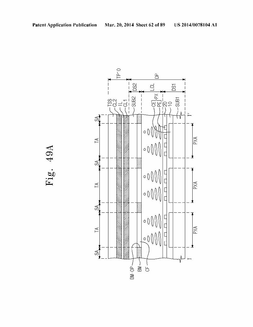
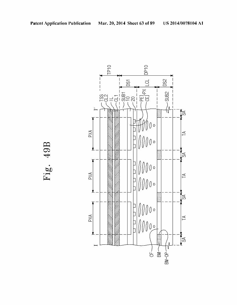
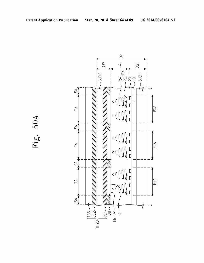
Fig. 22
TSS2 CL2 |LXTP
CL1 TSS1
LCL DP
US 2014/0078104 A1 Mar. 20, 2014 Sheet 26 of 89 Patent Application Publication
Vg2 f5\\
US 2014/0078104 A1 Mar. 20, 2014 Sheet 27 of 89 Patent Application Publication
US 2014/0078104 A1 Mar. 20, 2014 Sheet 28 of 89 Patent Application Publication
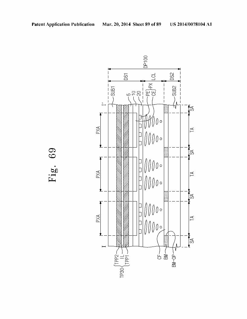
Fig. 24A
PX
DLj+1 CH1
CE
GL
SE AL GE DE CH2
TFT
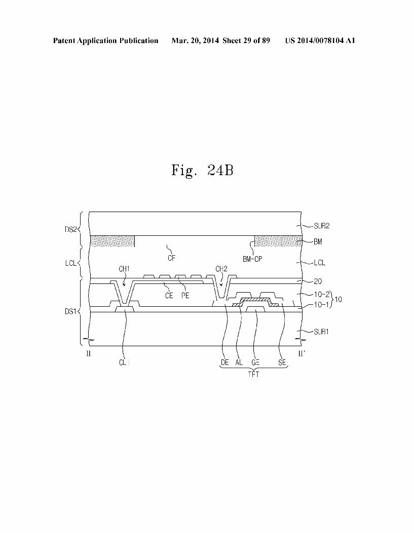
Patent Application Publication Mar. 20, 2014 Sheet 29 of 89 US 2014/0078104 A1
Fig. 24B
DS2 SUB2
BM
LCL CF BM-OP LCL CH1 CH2
is in 2O CE PE YZZZZZZZY 10-2 Al Az Zr, (i) to DS1 A
SUB1
I II' CL DE AL GE SE
N-N-1 TET
US 2014/0078104 A1 Mar. 20, 2014 Sheet 30 of 89 Patent Application Publication
Fig. 25
AL
) SUZ KOR SUZ
NÓRNYÓRY ARY/RYAN XÒ¿? SUZ
( TE2 TC2 TE2 TC2 TC2 (2) (3) (1) (2) (1)
TE2 TE2 TC2 TC2 TC2 (r) (r-1) (d) (d-1) (C-2)
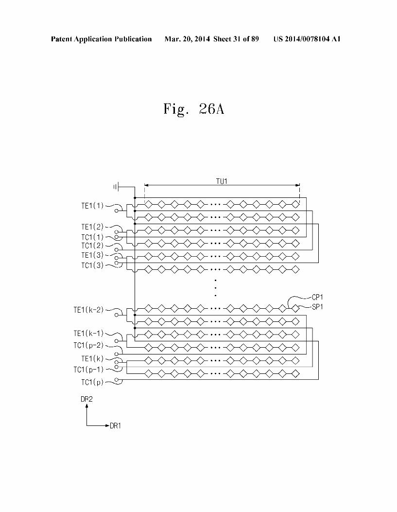
Patent Application Publication Mar. 20, 2014 Sheet 31 of 89 US 2014/0078104 A1
Fig. 26A
TU1 |
TE1(1)- . . . . . . . {X-O-C-C-C- - - - -C-C-O-O-O-O (2)
1 1882 --C-O-O-O-O-...-O-O-O-O-O-O. (3) (3)
Patent Application Publication Mar. 20, 2014 Sheet 32 of 89 US 2014/0078104 A1
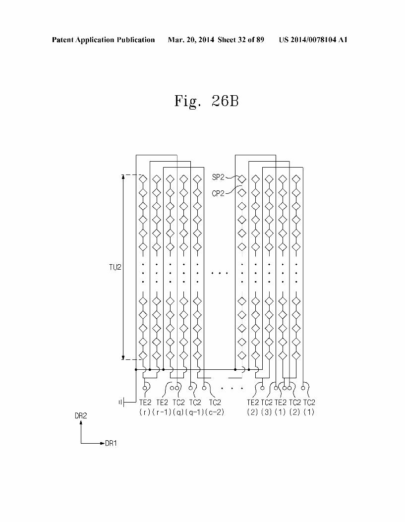
Fig. 26B
A
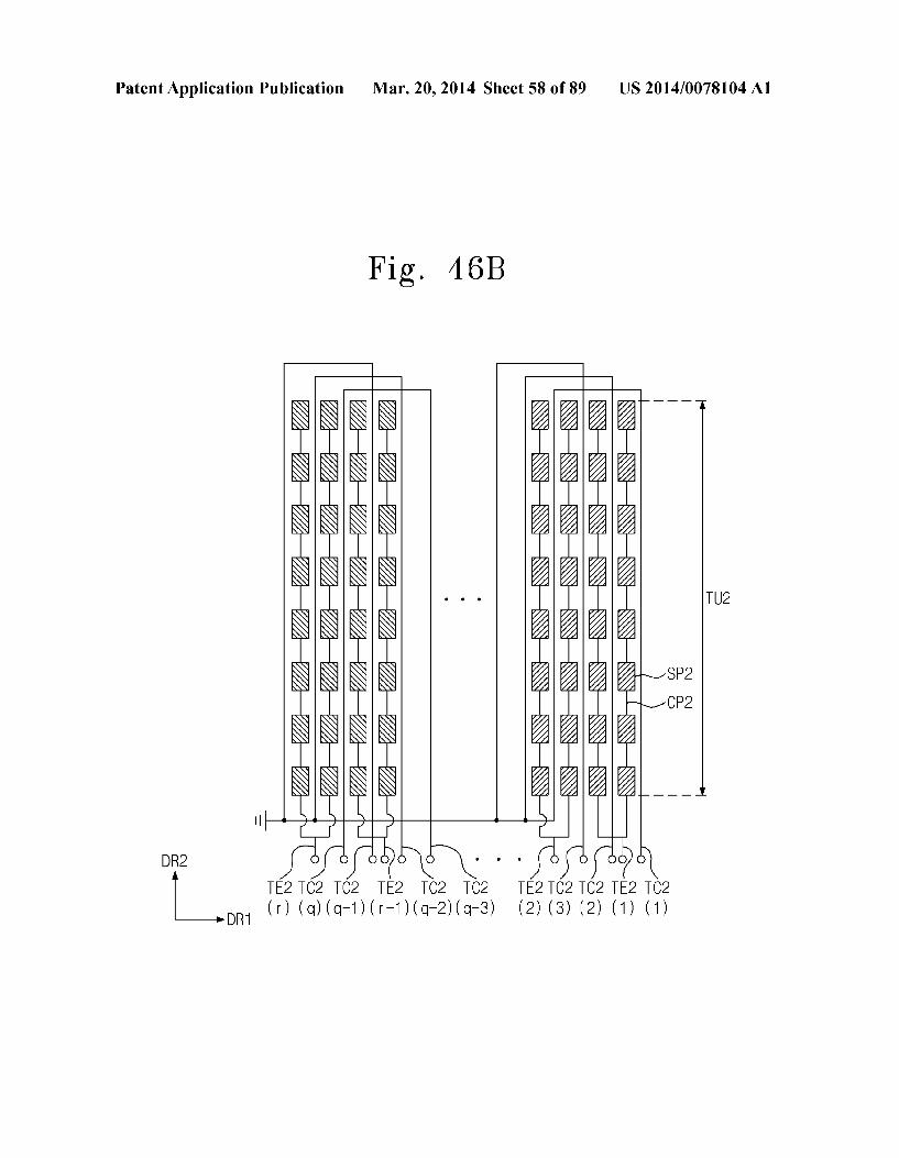
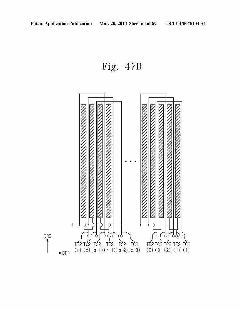
TU2
|IH TE2 TE2 TC2 TC2 TC2 TE2 TC2 TE2 TC2 TC2 DR2 (r) (r-1) (d) (q-1) (G-2) (2) (3) (1) (2) (1)
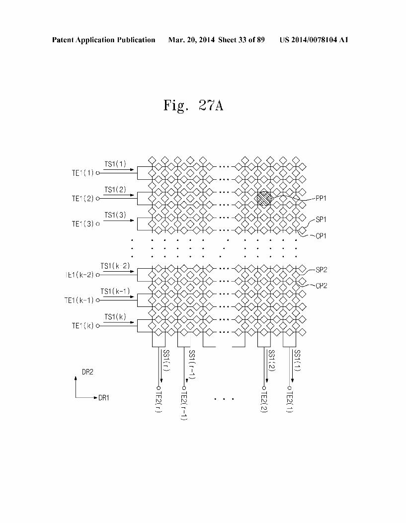
Patent Application Publication Mar. 20, 2014 Sheet 33 of 89 US 2014/0078104 A1
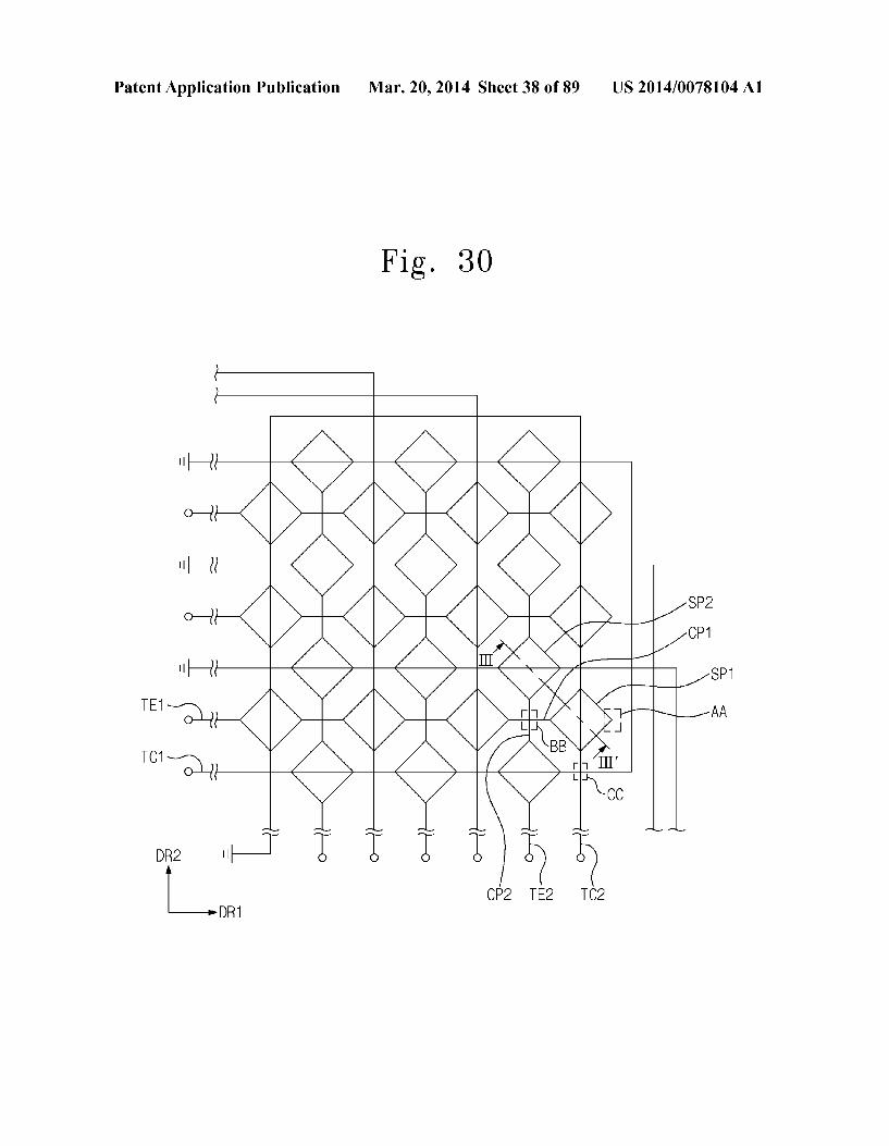
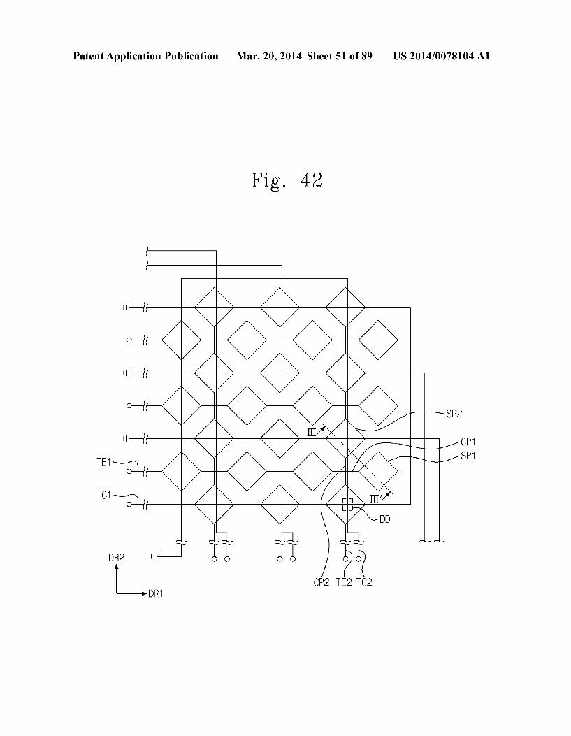
PP1
SP1
CP1
SP2
CP2
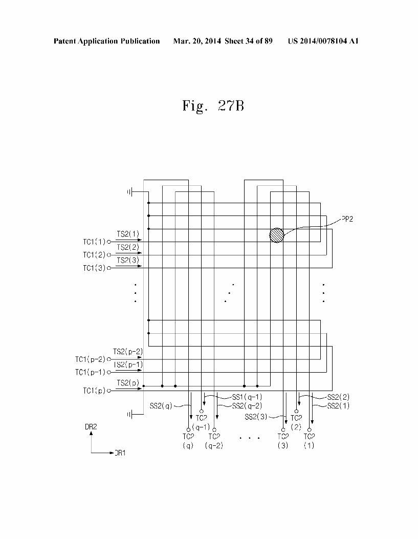
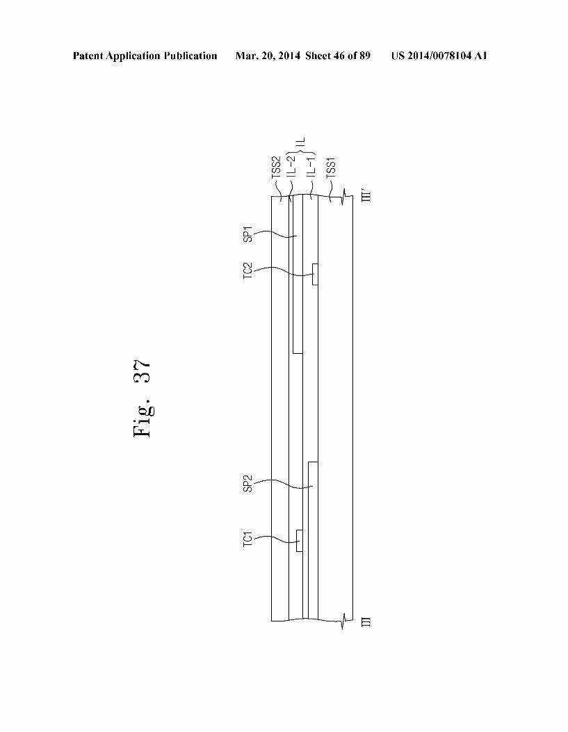
Patent Application Publication Mar. 20, 2014 Sheet 34 of 89 US 2014/0078104 A1
Fig. 27B
Wu
Y
Patent Application Publication Mar. 20, 2014 Sheet 35 of 89 US 2014/0078104 A1
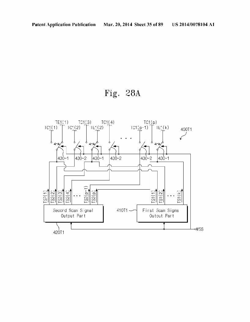
Fig. 28A
TE1 (1) TC1 (3) TC1 (4) TC1 (p) 1) TC1(1) TC1(2) TE1(2) TC1 (p- TE1(k) 400T1
Second SCan Signal First SCan Signal Output Part Output Part
42OT1 oMSS
Patent Application Publication Mar. 20, 2014 Sheet 36 of 89 US 2014/0078104 A1
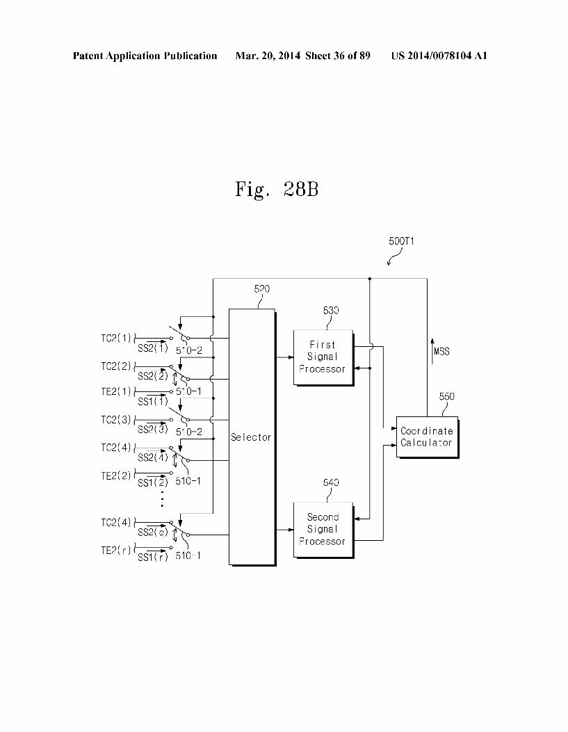
Fig. 28B
5OOT1
Fr St Signal
TC2(2) Processor
Coordinate Selector Calculator
TC2(4) -e-Q s Processor
Patent Application Publication Mar. 20, 2014 Sheet 37 of 89 US 2014/0078104 A1
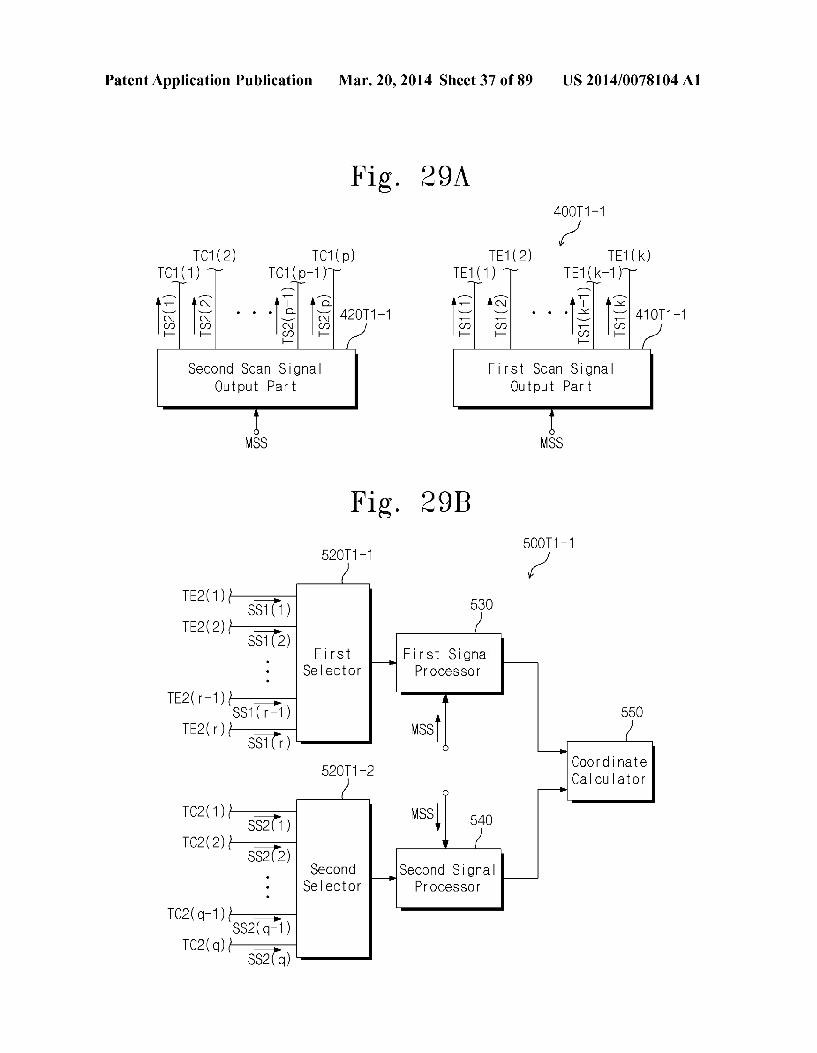
Fig. 29A 4OOT1-1
TC1(2) TC1 (p) TE1(2) TE1(k) TC1 (1) TC1 (p-1) TE1 (1) TE1 (k-1)
AQ T a QC Aca T - ". ". s 42OT1-1 ". 's 41 OT1-1 ?o ?o 2 IA- ?? I? 2 A -
Second SCan Signal First SCan Signal Output Part Output Part
MSS MSS
Fig. 29B 500T1-1
52OT1-1 -
TE2(1)
TE2(2) First First Signal
Selector Processor
TE2(r-1)
TE2(r)
COOrdinate 52OT1-2 Calculator
TC2(1)
TC2(2) Second Second Signal
Selector Processor
TC2(d) SS2(d)
Patent Application Publication Mar. 20, 2014 Sheet 39 of 89 US 2014/0078104 A1
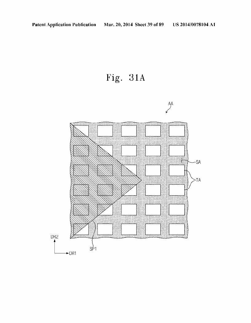
Fig. 31 A
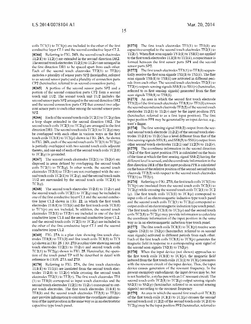
N
Y S
Patent Application Publication Mar. 20, 2014 Sheet 40 of 89 US 2014/0078104 A1
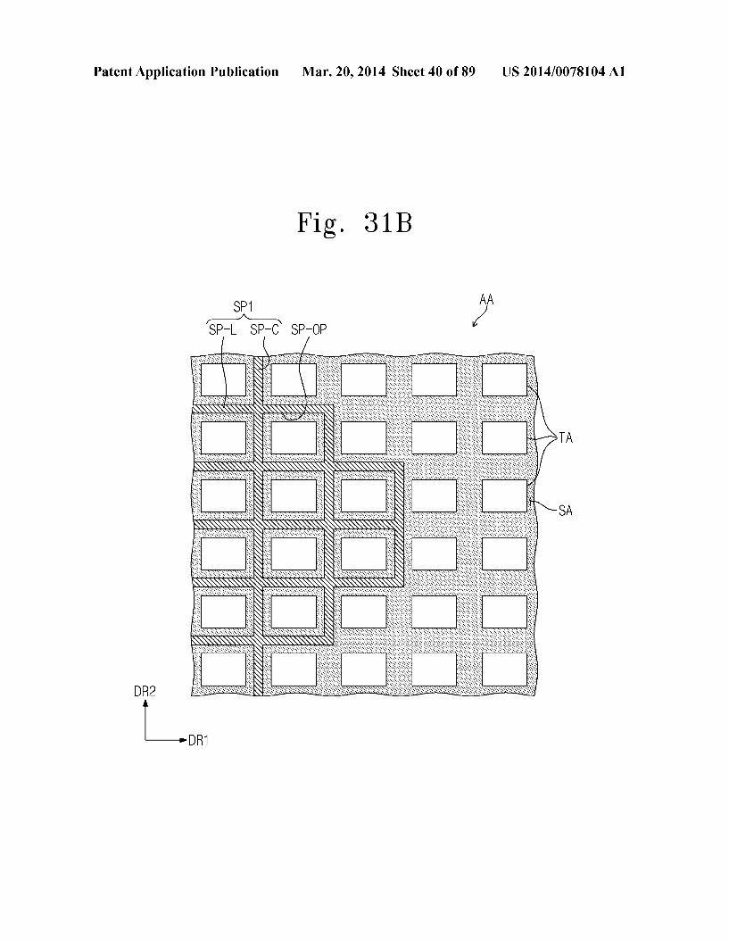
Fig. 31B
SP1 ^ SP-L SP-C SP-OP
Patent Application Publication Mar. 20, 2014 Sheet 41 of 89 US 2014/0078104 A1
-- CN, CN - -- CfO - CfO CO ?h CO H - - CfO H
E
CN CD 8-N-
(N) CY
g
CD
2.
CD 5-N
E
Patent Application Publication Mar. 20, 2014 Sheet 42 of 89 US 2014/0078104 A1
Fig. 33
CP2 -1N CP-C1 CP-C2
CH4 BE1 CH3 DR1
Patent Application Publication Mar. 20, 2014 Sheet 43 of 89 US 2014/0078104 A1
CP-C1 CP-C2 N-N-1
CP2
Patent Application Publication Mar. 20, 2014 Sheet 44 of 89 US 2014/0078104 A1
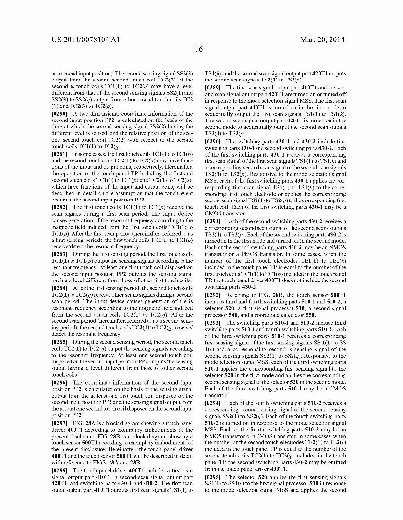
Fig. 35
TC2
TC-C1 TC-C2 5
TC-L1
TC1
TC-L2
TA
SA
CH6 BE2 CH5 DR1
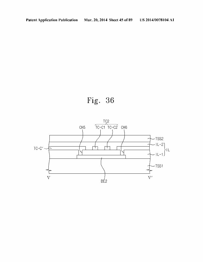
Patent Application Publication Mar. 20, 2014 Sheet 45 of 89 US 2014/0078104 A1
Fig. 36
TC2 -1-
CH5 TC-C1 TC-C2 CH6
BE2
Patent Application Publication Mar. 20, 2014 Sheet 46 of 89 US 2014/0078104 A1
- 2 2
E
&
s
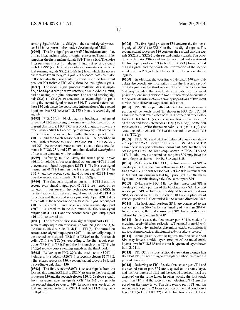
Patent Application Publication Mar. 20, 2014 Sheet 47 of 89 US 2014/0078104 A1
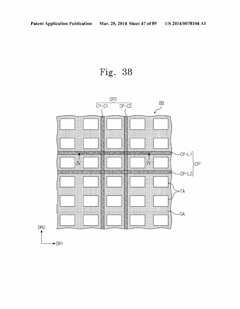
Fig. 38
CP2 -1- CP-C1 CP-C2 -
CP-L1
CP1
CP-L2
TA
SA
Patent Application Publication Mar. 20, 2014 Sheet 48 of 89 US 2014/0078104 A1
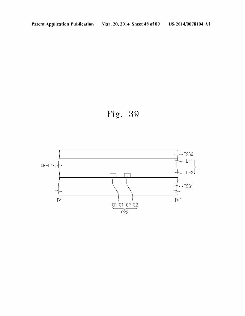
Fig. 39
TSS2 IL-1
L L-2
TSS1
CP-C1 CP-C2 N--
CP2
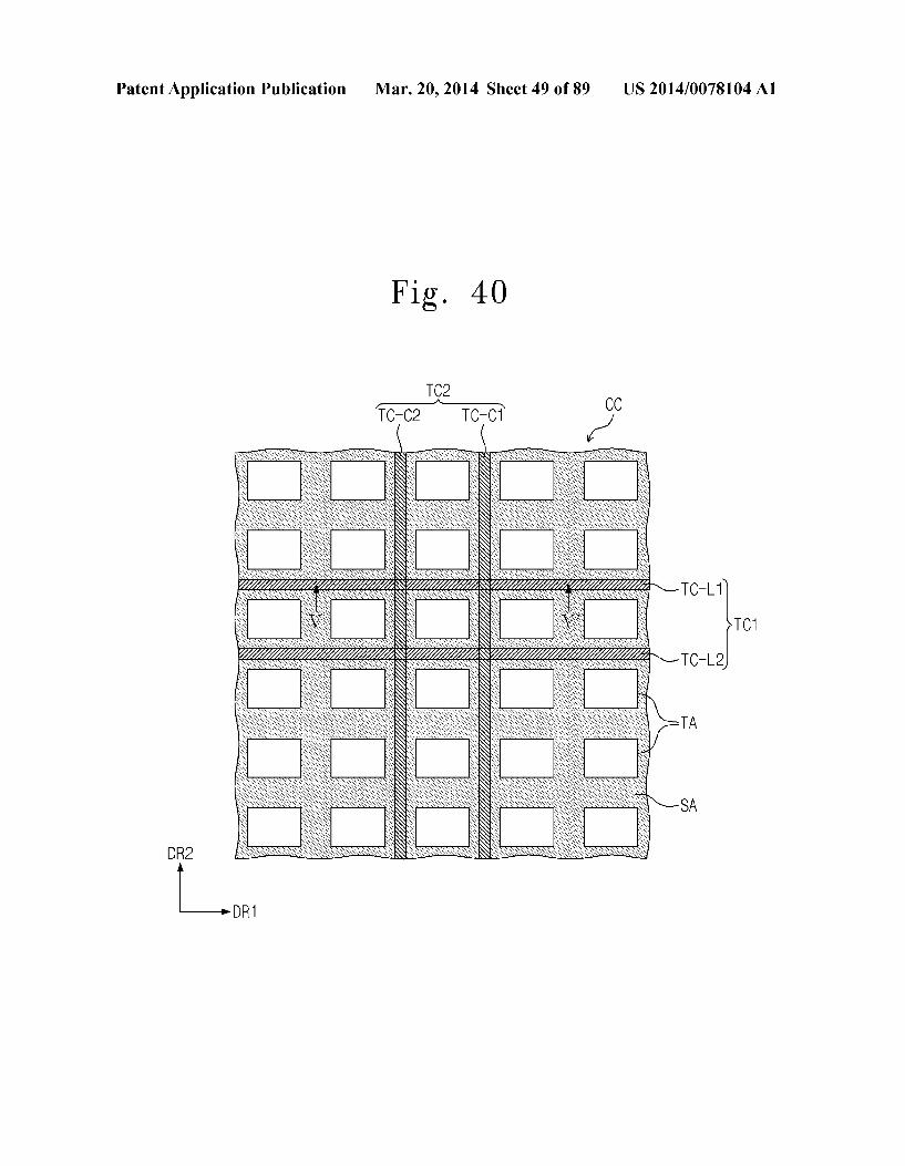
Patent Application Publication Mar. 20, 2014 Sheet 49 of 89 US 2014/0078104 A1
Fig. 40
TC2 -N- TC-C2 TC-C1
TC-L1
TC1
TC-L2
TA
SA
Patent Application Publication Mar. 20, 2014 Sheet 50 of 89 US 2014/0078104 A1
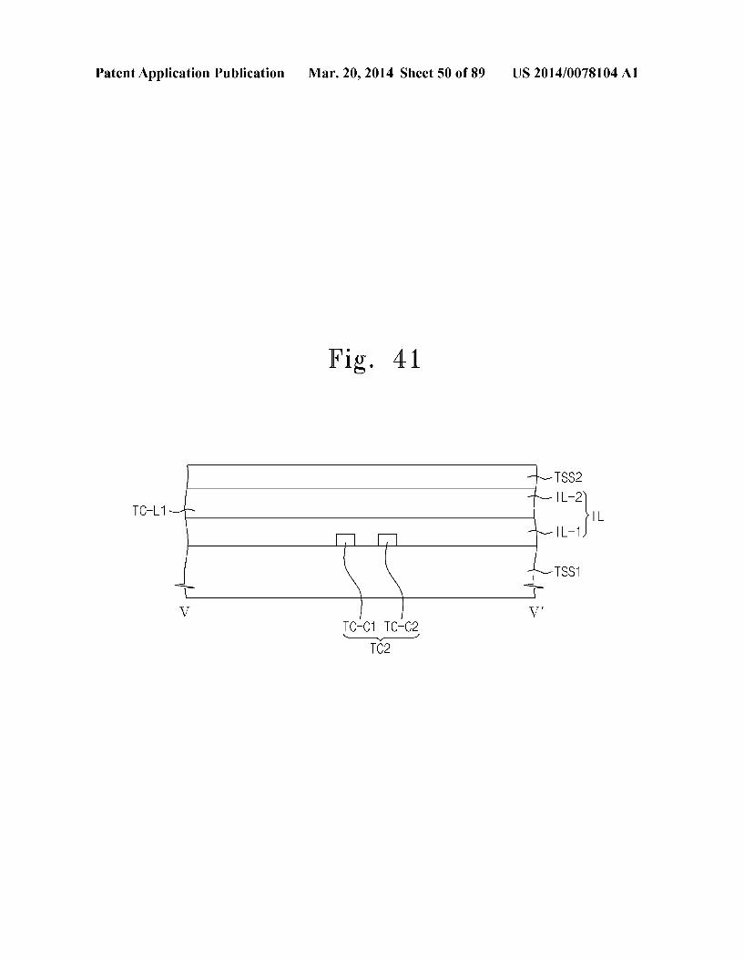
Fig. 41
TSS2 L-2 TC-L1 l
, , IL-1
TSS1
V V TC-C1 TC-C2 N--
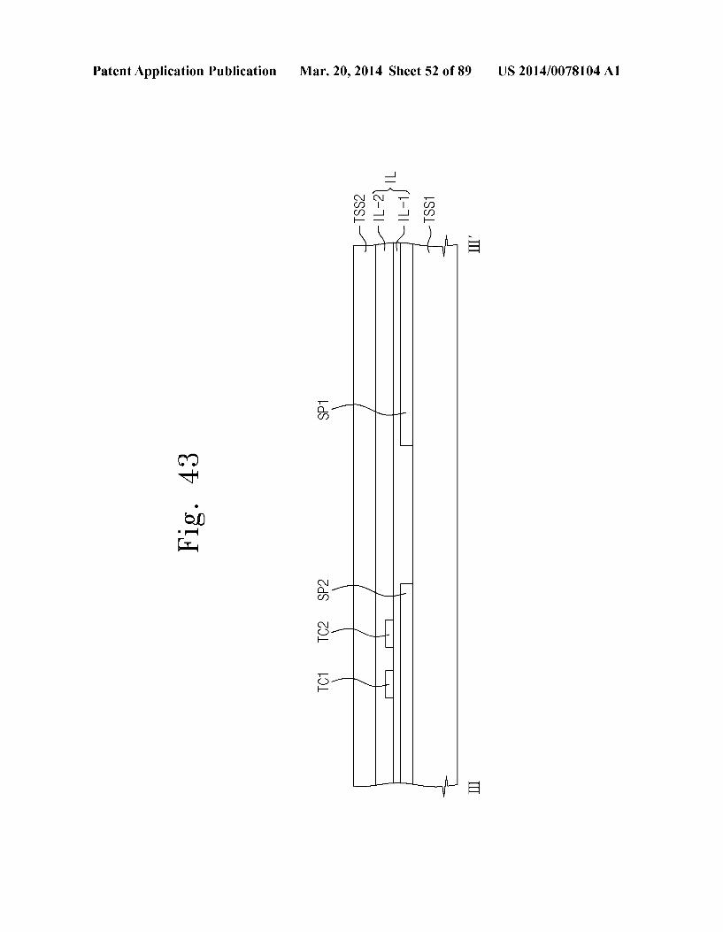
Patent Application Publication Mar. 20, 2014 Sheet 52 of 89 US 2014/0078104 A1
-
--- CN, CN - - CfO CfO CO CO H - - H.
E
s
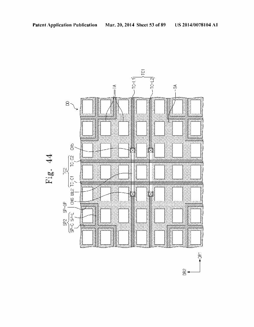
Patent Application Publication Mar. 20, 2014 Sheet 53 of 89 US 2014/0078104 A1
--
C -
-N- CN - I CD CD C
t H H CfO
&
Patent Application Publication Mar. 20, 2014 Sheet 54 of 89 US 2014/0078104 A1
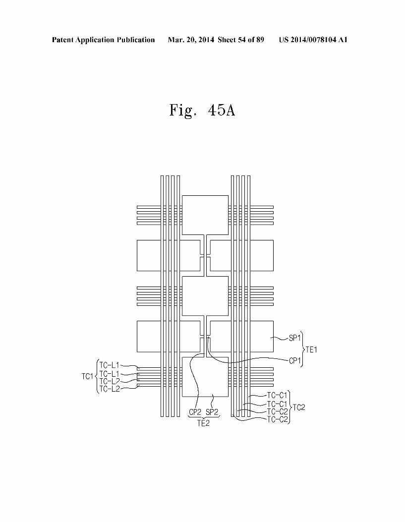
Fig. 45A
US 2014/0078104 A1 Mar. 20, 2014 Sheet 55 of 89 Patent Application Publication
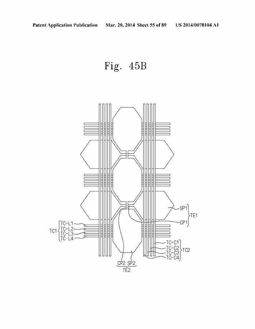
Fig. 45B
P1 TE1
P1
CP2 SP2 TE2
US 2014/0078104 A1 Mar. 20, 2014 Sheet 56 of 89 Patent Application Publication
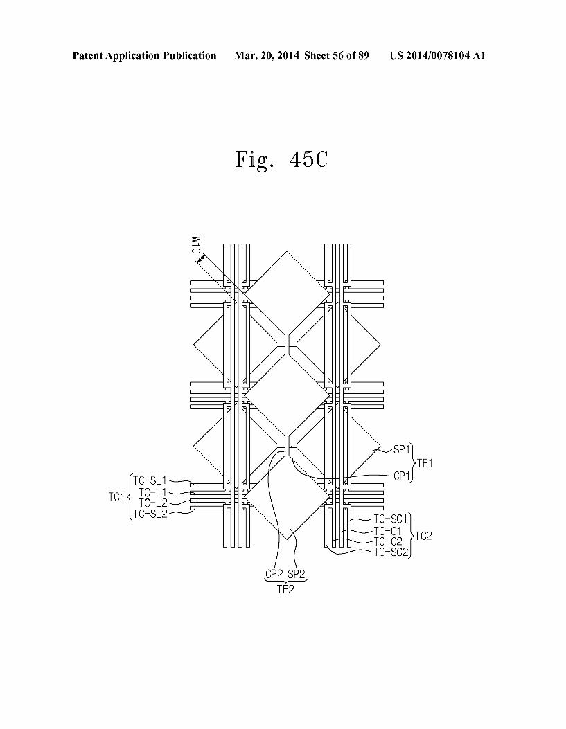
Fig. 45C
--
O
|
:,: CP2 SP2 TE2
Patent Application Publication Mar. 20, 2014 Sheet 57 of 89 US 2014/0078104 A1
TE1 (K-2)
Fig. 46A
of Š Š
OA-S
on N
N
US 2014/0078104 A1 Mar. 20, 2014 Sheet 58 of 89 Patent Application Publication
Fig. 46B
TU2
SP2
CP2
| |
Ø Ø
(296 TE2 TC2 TC2 TE2 TC2 (2) (3) (2) (1) (1)
TE2 TC2 TC2 TE2 TC2 TC2
(r)(a)(q-1) (r-1) (G-2) (q-3)
DR2
Patent Application Publication Mar. 20, 2014 Sheet 59 of 89 US 2014/0078104 A1
Fig. 47A
TE1(1) - Y N TC1(1) UN N
IS 3 Š TE1 (3) S
US 2014/0078104 A1 Mar. 20, 2014 Sheet 60 of 89 Patent Application Publication
Fig. 47B
N ||Š N N N ||| No. N N N DR2
TE2 TC2 TC2 TE2 TC2 TC2 TE2 TC2 TC2 TE2 TC2
(r) (a)(q-1) (r-1)(q-2)(q-3) (2)(3) (2) (1) (1)
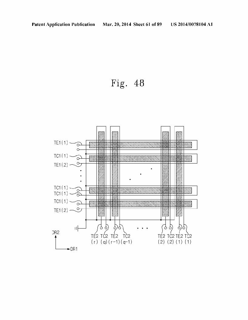
Patent Application Publication Mar. 20, 2014 Sheet 61 of 89 US 2014/0078104 A1
Fig. 48
R%R % 3 n % N3 W
2 2 2 2. TC1 (1) N&S&N&SN&SN
7
TC1 (1 3SN3 S3RN3.
to 15- rst r TE1 (2) -N97 2 2 Ž Ž
| O O OO O O OO
TE2 TC2 TE2 TC2 TE2 TC2 TE2 TC2 (r) (d) (r-1) (C-1) (2) (2) (1) (1)
DR1
L?O:N Mar. 20, 2014 Sheet 62 of 89 Patent Application Publication
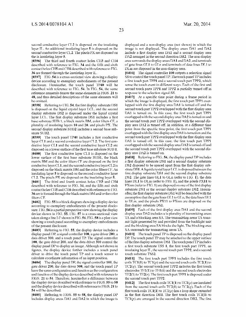
US 2014/0078104 A1 Mar. 20, 2014 Sheet 63 of 89 Patent Application Publication
US 2014/0078104 A1
W? |TO
Mar. 20, 2014 Sheet 64 of 89 Patent Application Publication
US 2014/0078104 A1 Mar. 20, 2014 Sheet 65 of 89 Patent Application Publication
US 2014/0078104 A1 Mar. 20, 2014 Sheet 66 of 89
I g *? ?I
Patent Application Publication
Patent Application Publication Mar. 20, 2014 Sheet 67 of 89 US 2014/0078104 A1
Fig. 52A
SUB2 BM-OP
BM
IL-1
| za za z \ z U
CL1 CL2 CF
CL1 CL2 CF
Patent Application Publication Mar. 20, 2014 Sheet 68 of 89 US 2014/0078104 A1
Fig. 52C
Fig. 52D
SUB2 BM-OP
BM
IL-1
L-2 N N N
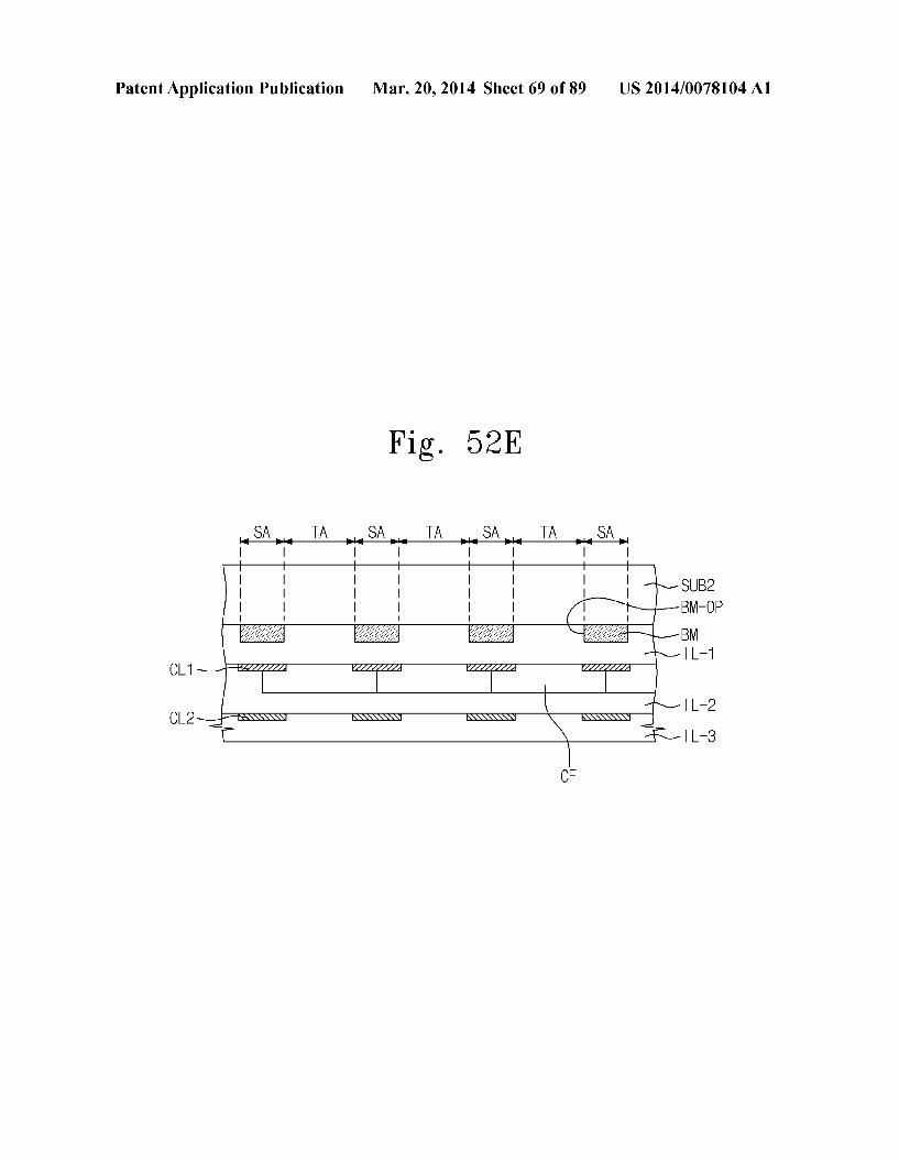
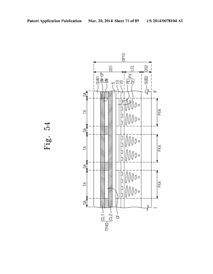
Patent Application Publication Mar. 20, 2014 Sheet 69 of 89 US 2014/0078104 A1
Fig. 52E
SUB2 BM-OP
2 CL1 2 2 2
CF
L-2
L-3 CL2
US 2014/0078104 A1
W? H0
Mar. 20, 2014 Sheet 70 of 89 Patent Application Publication
US 2014/0078104 A1 Mar. 20, 2014 Sheet 71 of 89 Patent Application Publication
US 2014/0078104 A1 Mar. 20, 2014 Sheet 72 of 89 Patent Application Publication
| HCl
SS
ZHO
ZWO
009
00|| SS
Patent Application Publication Mar. 20, 2014 Sheet 73 of 89 US 2014/0078104 A1
Fig. 56
DS1
LCL DP
DS2
US 2014/0078104 A1 Mar. 20, 2014 Sheet 74 of 89
dlT |
Patent Application Publication
NNNNNNN
US 2014/0078104 A1 Mar. 20, 2014 Sheet 75 of 89 Patent Application Publication
Fig. 58
TE1 (2)
1
p-2 TE1
TC1 (p-1
TC1 (p)
TE1
TE1 (
TC1 (
C
TE2 (1)
- DR2
Patent Application Publication Mar. 20, 2014 Sheet 76 of 89 US 2014/0078104 A1
Fig. 59A
TPP1
Patent Application Publication Mar. 20, 2014 Sheet 77 of 89 US 2014/0078104 A1
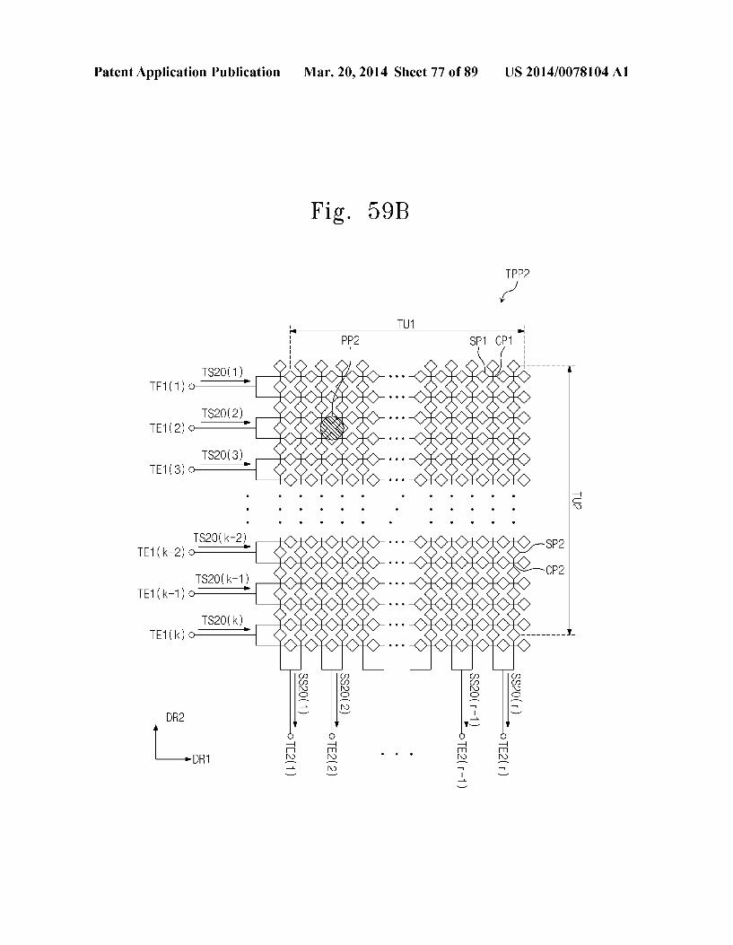
Fig. 59B
TU1
s
SP2
CP2
Patent Application Publication Mar. 20, 2014 Sheet 78 of 89 US 2014/0078104 A1
E
3. 9 - 1 a -sa CfO S. c. CfO
sc C 5 C5 C5 c. 5
- CN cy) CfO CO CO CfO CfO of CO CO CD CD CD CD
Patent Application Publication Mar. 20, 2014 Sheet 79 of 89 US 2014/0078104 A1
Fig. 61A
TE1 (2) TE1(k) TE1 (1) TE1 (k-1)
Second SCan Signal Output Part
First SCan Signal Output Part
4OOT2
Patent Application Publication Mar. 20, 2014 Sheet 80 of 89 US 2014/0078104 A1
Fig. 61B
5OOT2
51O -
TC2(1)
TC2(2) Fr St First Signal
Selector ProCeSSOr
Coordinate Cal Culator
TE2(1)
TE2(2) SeCond Second Signal
Selector Processor
TE2(r-1)
TE2(r)
US 2014/0078104 A1 Mar. 20, 2014 Sheet 81 of 89 Patent Application Publication
Fig. 62A
F-2 F-1
A1 s
s
D
TS2O
DA2
SS
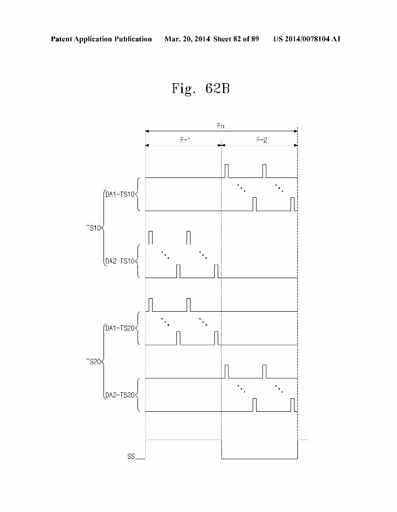
US 2014/0078104 A1 Mar. 20, 2014 Sheet 82 of 89 Patent Application Publication
Fig. 62B
Fn
: F-2 F-1
SS
Patent Application Publication Mar. 20, 2014 Sheet 83 of 89 US 2014/0078104 A1
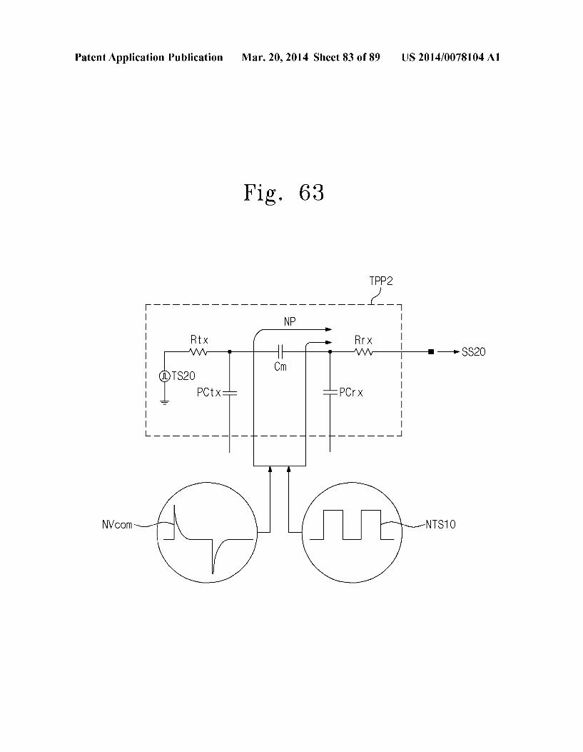
Fig. 63
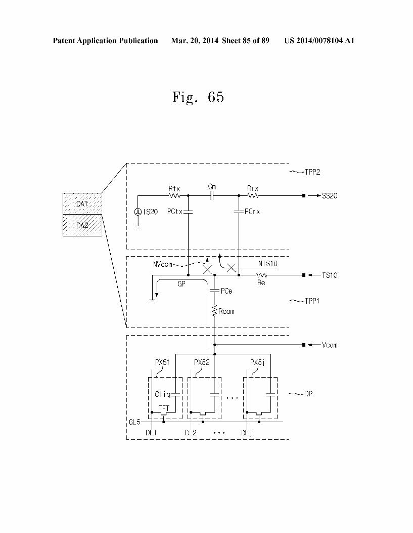
-> SS2O
NVCOm NTS10
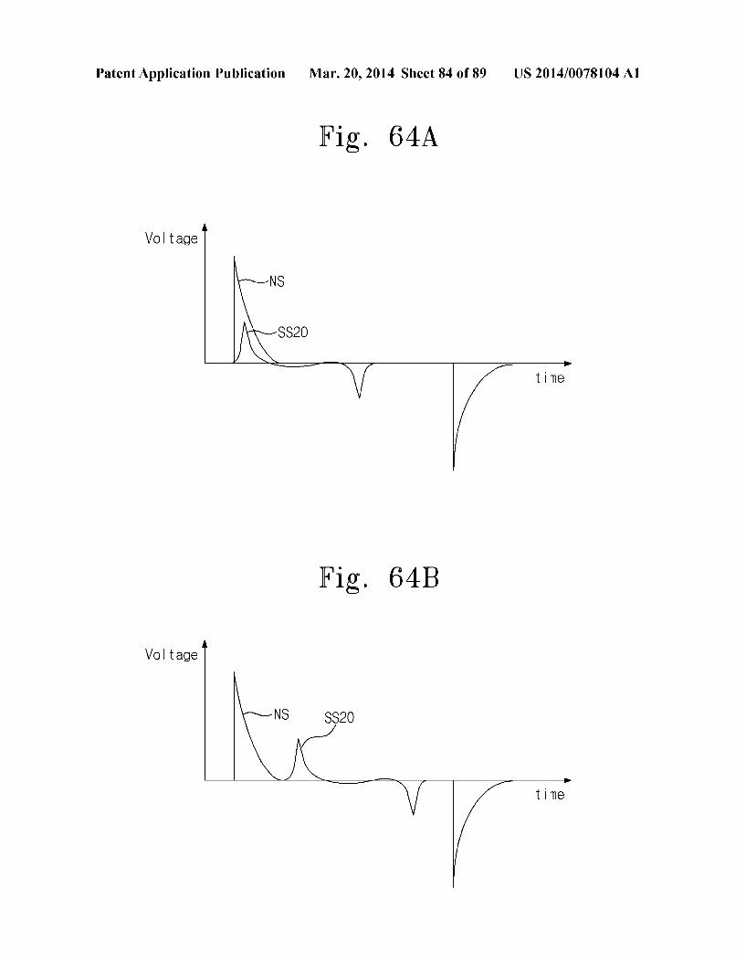
Patent Application Publication Mar. 20, 2014 Sheet 84 of 89 US 2014/0078104 A1
Fig. 64A
Voltage
NS
SS2O
time
Fig. 64B
Voltage
NS SS2O
time
Patent Application Publication Mar. 20, 2014 Sheet 85 of 89 US 2014/0078104 A1
Fig. 65
--TS10
-N-TPP1
-HWCOm
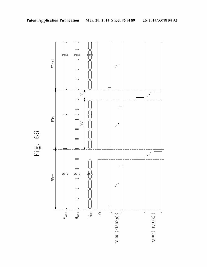
Patent Application Publication Mar. 20, 2014 Sheet 86 of 89 US 2014/0078104 A1
i
i
EE
are- P-Set N-- N --
US 2014/0078104 A1 Mar. 20, 2014 Sheet 87 of 89 Patent Application Publication
US 2014/0078104 A1 Mar. 20, 2014 Sheet 88 of 89 Patent Application Publication
US 2014/0078104 A1 Mar. 20, 2014 Sheet 89 of 89 Patent Application Publication
69 · 5 I,J
US 2014/0078104 A1
DISPLAY DEVICE AND METHOD OF DRIVING THE SAME
CROSS REFERENCE TO RELATED APPLICATION
0001. This U.S. non-provisional patent application claims priority from and the benefit of U.S. Provisional Patent Appli cation No. 61/701,100, filed on Sep. 14, 2012, Korean Patent Application No. 10-2013-0021423, filed on Feb. 27, 2013, Korean Patent Application No. 10-2013-0021426, filed on Feb. 27, 2013, and Korean Patent Application No. 10-2013 0055845, filed on May 16, 2013, which are hereby incorpo rated by reference for all purposes as if fully set forth herein.
BACKGROUND
0002 1. Field 0003 Exemplary embodiments of the present disclosure relate to a display device capable of sensing a touch event and a method of driving the display device. 0004 2. Discussion of the Background 0005. In general, a touch panel may acquire coordinate information of an input position at which a touch event occurs and provides the coordinate information to a display panel. The touch panel may be used to replace an input device. Such as a keyboard, a mouse, etc. 0006 The display panel displays an image corresponding
to the coordinate information provided from the touch panel. The touch panel may be separately manufactured and then attached to the display panel. The touch panel may be classi fied into a resistive film type of touch panel, k capacitive type of touch panel, and an electromagnetic type of touch panel depending on its operational principle. The display device may include various types of touch panels.
SUMMARY
0007 Exemplary embodiments of the present disclosure provide a display device having a touch panel operated in two modes. 0008 Exemplary embodiments of the present disclosure provide a display device having a touch panel that senses touch events in different ways according to areas of the dis play device where it senses the touch events. 0009 Exemplary embodiments of the present disclosure provide a method of driving the display device, which is capable of reducing a noise that exerts influences on touch sensitivity. 0010 Additional features of the present disclosure will be set forth in the description which follows, and in part will be apparent from the description, or may be learned by practice of the disclosed subject matter. 0011 Exemplary embodiments of the present disclosure disclose a display device is including a display panel, Scan line groups, source line groups, a first driver, a second driver, and a touch sensor. The display panel includes a first display Substrate and a second display Substrate facing the first dis play Substrate. Each scan line group includes a first scan line Sub-group, a second Scanline Sub-group connected to the first Scanline Sub-group, and a third scan line Sub-group disposed between the first Scanline Sub-group and the second Scanline Sub-group. Each source line group includes a first source line Sub-group, a second source line Sub-group connected to the first source line Sub-group, and a third source line Sub-group disposed between the first source line Sub-group and the
Mar. 20, 2014
second source line Sub-group. The first driver is configured to provide first scan signals to the Scanline groups in a first mode and to provide second scan signals to the scan line groups in a second mode. A magnetic field is induced by a current path formed by the first scan line Sub-group and the second scan line Sub-group. The second driver is configured to provide first sensing signals corresponding to a variation in a capaci tance from the Source line groups in the first mode, and to provide second sensing signals according to a resonant fre quency associated with an input device. The second sensing signals are provided from the source line groups in the second mode. The touch sensor is configured to receive the first sensing signals and the second sensing signals and to deter mine coordinate information of an input position based on the first sensing signals and the second sensing signals. 0012 Exemplary embodiments of the present disclosure disclose a display device including a display panel, Scan line groups, source line groups, a first driver, a second driver, and a touch sensor. The display panel includes a first display Substrate and a second display Substrate facing the first dis play Substrate. Each scan line group includes a first scan line Sub-group, a second scan line Sub-group, and a third Scanline Sub-group disposed between the first Scanline Sub-group and the second scan line Sub-group. Each Source line group includes a first is source line Sub-group, a second source line Sub-group, and a third source line Sub-group disposed between the first source line Sub-group and the second source line sub-group. The first driver is configured to provide first Scan signals to the Scan line groups in a first mode and to provide second scan signals to the first scan line Sub-group and the second scan line Sub-group of the scan line groups in a second mode. A magnetic field is induced by currents flow ing through the first scan line Sub-group and the second scan line Sub-group in opposite directions to each other. The sec ond driver is configured to provide a first sensing signal corresponding to a variation in a capacitance from the Source line groups in the first mode, and to provide, from the source line groups in the second mode, a second sensing signal according to a resonant frequency associated with an input device. The touch sensor is configured to receive the first sensing signal and the second sensing signal, and to deter mine coordinate information of an input position based on the first sensing signal and the second sensing signal. 0013 Exemplary embodiments of the present disclosure disclose a display device including a display panel and a touch panel. The display panel includes a first display Sub strate and a second display Substrate facing the first Substrate. The display panel is divided into a blocking area and a plu rality of transmitting areas. The touch panel includes a plu rality of first touch electrodes, a plurality of second touch electrodes, a plurality of first touch coils, and a plurality of second touch coils. The touch panel includes a first conduc tive layer and a second conductive layer insulated from the first conductive layer. The touch panel is disposed on one of the first display substrate or the second display substrate that is provided with an input surface. The plurality of first touch electrodes is configured to receive first scan signals. The plurality of second touch electrodes cross the first touch elec trodes and is configured to provide first sensing signals according to a variation in capacitance. The plurality of first touch coils overlaps with is the blocking area and is config ured to receive second scan signals. The plurality of second touch coils overlaps with the blocking area and crosses the first touch coils. The plurality of second touch coils is con
US 2014/0078104 A1
figured to provide second sensing signals according to a reso nant frequency associated with an input device. The first conductive layer includes the first touch electrodes and one of the second touch electrodes and the first touch coils.
0014 Exemplary embodiments of the present disclosure disclose a display device including a display panel and a touch panel. The display panel includes a first area, a second area, and a plurality of pixels. The display panel is configured to provide an image during a frame period. The touch panel includes a first touch part and a second touch part. The first touch part includes first touch coils and second touch coils. The second touch coils are insulated from the first touch coils and cross the first touch coils. The second touch part includes first touch electrodes disposed on the first touch part and second touch electrodes. The second touch electrodes are insulated from the first touch electrodes and cross the first touch electrodes. Corresponding second scan signals of the second scan signals are applied to the first touch electrodes disposed in the first area when corresponding first scan sig nals of the first scan signals are applied to the first touch coils disposed in the second area during a first period of the frame period. The second touch coils are configured to provide first sensing signals according to a resonant frequency of an input device. The second touch electrodes are configured to provide second sensing signals according to a variation in capaci tance.
00.15 Exemplary embodiments of the present disclosure disclose a method of driving a display device comprising a display panel generating an image during a frame period and a touch panel comprising input coils, output coils, input elec trodes, and output electrodes. The method includes activating pixels disposed in a first area of the display panel during a first period of the is frame period; providing first scan signals to the input coils disposed in a second area adjacent to the first area; providing second scan signals to the input electrodes disposed in the first area of the display panel; and determining coordinate information of an input position from at least one of first sensing signals provided based on a resonant fre quency of an input device and output from the output coils, and a second sensing signal provided based on a variation in capacitance and output from the output electrodes. 0016 Exemplary embodiments of the present disclosure disclose a display device including a display panel and a touch panel. The display panel includes a plurality of pixels and is configured to provide an image during a frame period. The frame period includes a display period and a non-display period. The touch panel includes a first touch part and a second touch part. The first touch part includes first touch coils and second touch coils. The second touch coils are insulated from the first touch coils and cross the first touch coils. The second touch part includes first touch electrodes disposed on the first touch part and second touch electrodes. The second touch electrodes are insulated from the first touch electrodes and cross the first touch electrodes. First scan signals are provided to the first touch coils during the display period, and second scan signals are provided to the first touch electrodes during the non-display period. The second touch coils are configured to provide first sensing signals according to a resonant frequency of an input device, and the second touch electrodes are configured to provide second sensing signals according to a variation in capacitance. 0017. It is to be understood that both the foregoing general description and the following detailed description are exem
Mar. 20, 2014
plary and explanatory and are intended to provide further explanation of the disclosed subject matter as claimed.
BRIEF DESCRIPTION OF THE DRAWINGS
0018. The accompanying drawings, which are included to provide a further understanding of the disclosed Subject mat ter and are incorporated in and constitute a part of this speci fication, illustrate exemplary embodiments of the disclosed Subject matter, and together with the description serve to explain the principles of the disclosed subject matter. 0019 FIG. 1 is a block diagram showing a display device according to exemplary embodiments of the present disclo SUC.
0020 FIG. 2 is a perspective view showing a display panel shown in FIG. 1 according to exemplary embodiments of the present disclosure. 0021 FIG.3 is a plan view showing a display panel shown in FIG.2 according to exemplary embodiments of the present disclosure. 0022 FIG. 4 is a cross-sectional view taken along a line I-I' shown in FIG.2 according to exemplary embodiments of the present disclosure. 0023 FIG. 5 is a block diagram showing a touch panel according to exemplary embodiments of the present disclo SUC.
0024 FIG. 6 is a view showing a touch panel operated in a first mode according to exemplary embodiments of the present disclosure. 0025 FIGS. 7A and 7B are views showing a touch panel operated in a second mode according to exemplary embodi ments of the present disclosure. 0026 FIG. 8 is a timing diagram showing signals gener ated in the second mode according to exemplary embodi ments of the present disclosure. 0027 FIG. 9 is a block diagram showing a first driver shown in FIG.5 according to exemplary embodiments of the present disclosure. 0028 FIG. 10 is a circuit diagram showing a switching part shown in FIG.9 according to exemplary embodiments of the present disclosure. 0029 FIG. 11 is a block diagram showing a second driver and a touch sensor shown in FIG. 5 according to exemplary embodiments of the present disclosure. 0030 FIG. 12 is a circuit diagram showing a sensing sig nal output part shown in FIG. 11 according to exemplary embodiments of the present disclosure. 0031 FIG. 13 is a cross-sectional view showing a display panel according to exemplary embodiments of the present disclosure. 0032 FIG. 14 is a cross-sectional view showing a display panel according to exemplary embodiments of the present disclosure. 0033 FIGS. 15A and 15B are plan views showing display panels according to exemplary embodiments of the present disclosure. 0034 FIG. 16 is a block diagram showing a touch panel according to exemplary embodiments of the present disclo SUC.
0035 FIG. 17 is a view showing a touch panel operated in a first mode according to exemplary embodiments of the present disclosure. 0036 FIGS. 18A and 18B are views showing touchpanels operated in a second mode according to exemplary embodi ments of the present disclosure.
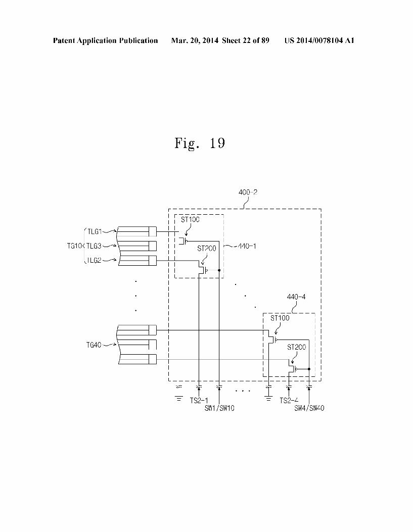
US 2014/0078104 A1
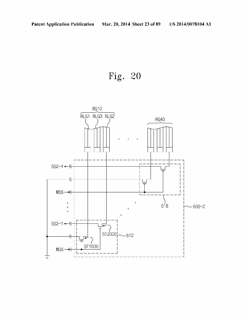
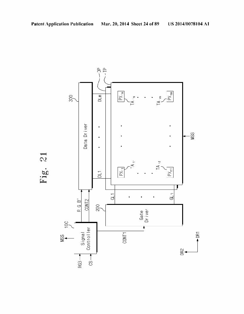
0037 FIG. 19 is a bock diagram showing a second scan driver according to exemplary embodiments of the present disclosure. 0038 FIG. 20 is a block diagram showing a second source driver according to exemplary embodiments of the present disclosure. 0039 FIG.21 is a block diagram showing a display device according to exemplary is embodiments of the present dis closure. 0040 FIG. 22 is a partial perspective view showing a display paneland a touchpanel shown in FIG.21 according to exemplary embodiments of the present disclosure. 0041 FIGS. 23A and 23B are cross-sectional views taken along a line I-I" shown in FIG. 22 according to exemplary embodiments of the present disclosure. 0042 FIG.24A is a plan view showing a pixel of a display panel according to exemplary embodiments of the present disclosure.
0043 FIG.24B is a cross-sectional view taken along a line II-II' shown in FIG. 24A according to exemplary embodi ments of the present disclosure. 0044 FIG.25 is a plan view showing a touchpanel accord ing to exemplary embodiments of the present disclosure. 0045 FIG. 26A is a plan view showing first touch elec trodes and first touch coils shown in FIG. 25 according to exemplary embodiments of the present disclosure. 0046 FIG. 26B is a plan view showing second touch elec trodes and second touch coils shown in FIG. 25 according to exemplary embodiments of the present disclosure. 0047 FIG. 27A is a plan view showing first touch elec trodes and first touch coils shown in FIG. 25 according to exemplary embodiments of the present disclosure. 0048 FIG. 27B is a plan view showing second touch elec trodes and second touch coils shown in FIG. 25 according to exemplary embodiments of the present disclosure. 0049 FIG. 28A is a block diagram showing a touch panel driver according to exemplary embodiments of the present disclosure.
0050 FIG. 28B is a block diagram showing a touch sensor according to exemplary embodiments of the present disclo SU
0051 FIG. 29A is a block diagram showing a touch panel driver according to exemplary embodiments of the present disclosure.
0052 FIG. 29B is a block diagram showing a touch sensor according to exemplary embodiments of the present disclo SU
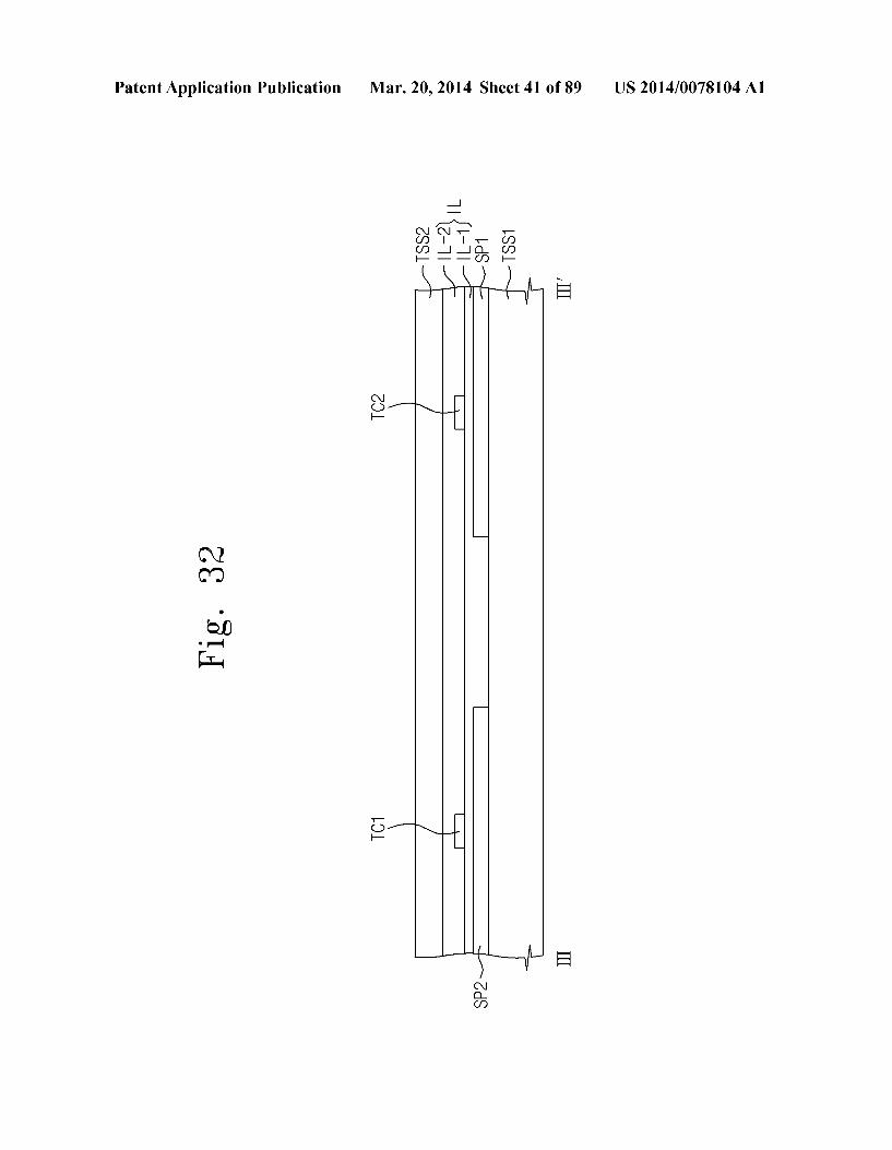
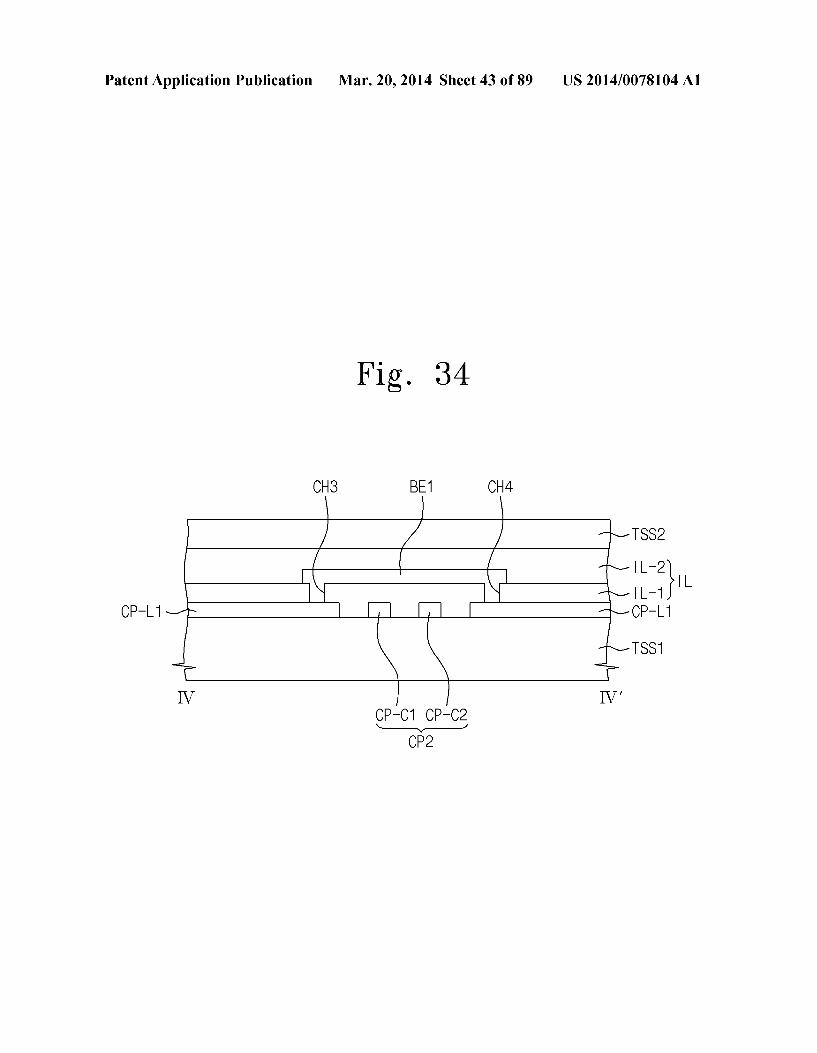
0053 FIG. 30 is a partially enlarged plan view showing a portion of the touch panel shown in FIG. 25 according to exemplary embodiments of the present disclosure. 0054 FIGS. 31A and 31B are enlarged plan views show ing a portion 'AA' shown in FIG.30 according to exemplary embodiments of the present disclosure. 0055 FIG. 32 is a cross-sectional view taken along a line III-III of FIG.10 according to exemplary embodiments of the present disclosure. 0056 FIG.33 is a partially enlarged plan view showing a portion “BB” shown in FIG. 30 according to exemplary embodiments of the present disclosure. 0057 FIG. 34 is a cross-sectional view taken along a line IV-IV' shown in FIG. 33 according to exemplary embodi ments of the present disclosure.
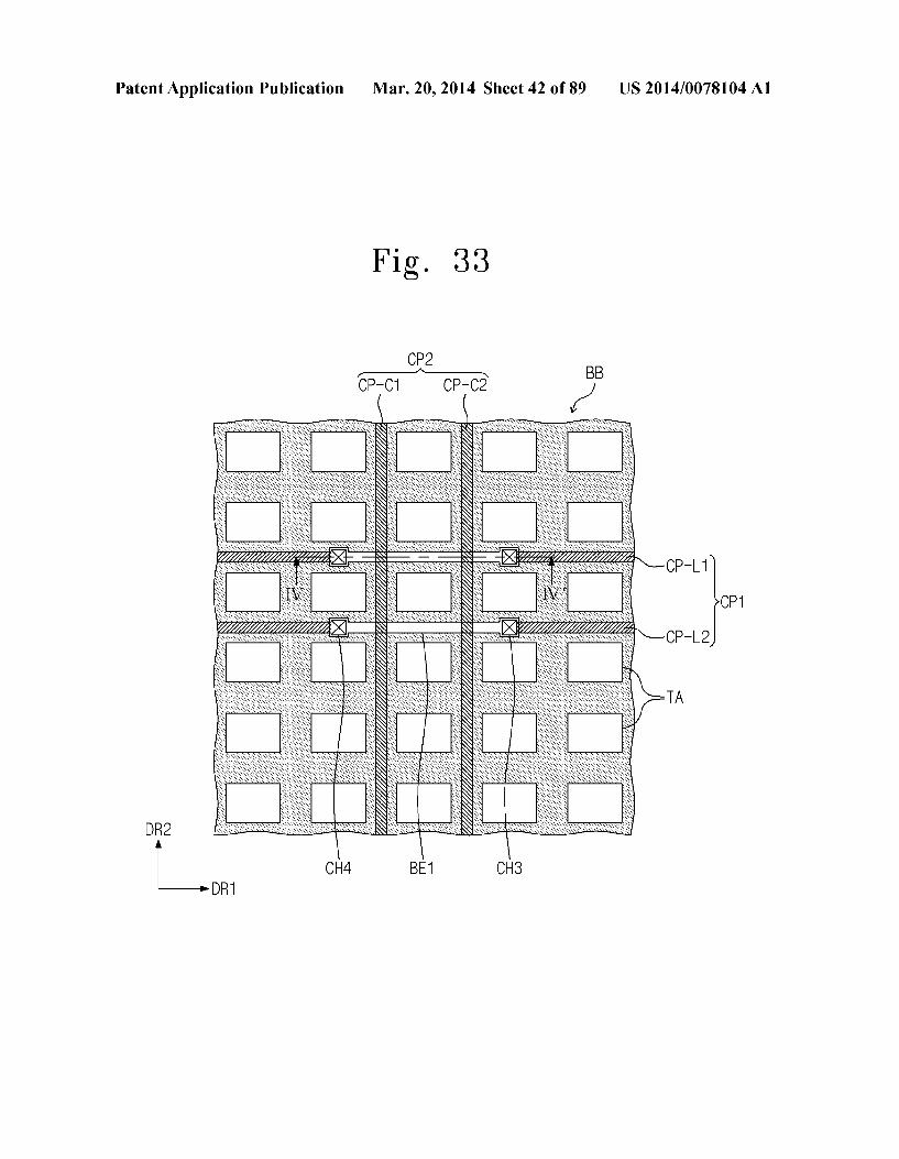
Mar. 20, 2014
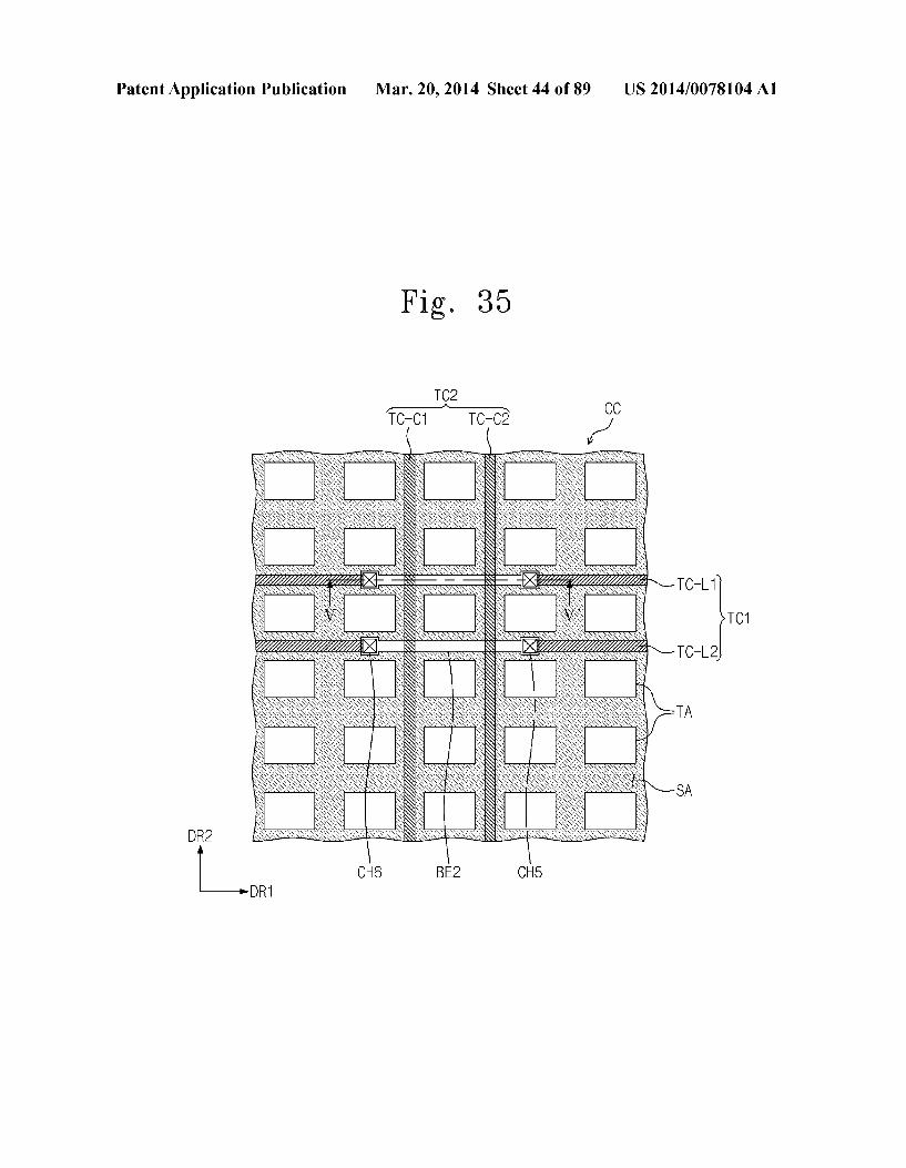
0.058 FIG. 35 is a partially enlarged plan view showing a portion “CC' shown in FIG. 30 according to exemplary embodiments of the present disclosure. 0059 FIG. 36 is a cross-sectional view taken along a line V-V shown in FIG.35 according to exemplary embodiments of the present disclosure. 0060 FIG. 37 is a cross-sectional view taken along a line III-III' shown in FIG. 30 according to exemplary embodi ments of the present disclosure. 0061 FIG. 38 is a partially enlarged plan view showing a portion “BB” shown in FIG. 30 according to exemplary embodiments of the present disclosure. 0062 FIG. 39 is a cross-sectional view taken along a line IV-IV' shown in FIG. 38 is according to exemplary embodi ments of the present disclosure. 0063 FIG. 40 is a partially enlarged plan view showing a portion “CC' shown in FIG. 30 according to exemplary embodiments of the present disclosure. 0064 FIG. 41 is a cross-sectional view taken along a line V-V shown in FIG. 40 according to exemplary embodiments of the present disclosure. 0065 FIG. 42 is a partially enlarged plan view showing a portion of the touch panel shown in FIG. 25 according to exemplary embodiments of the present disclosure. 0.066 FIG. 43 is a cross-sectional view taken along a line III-III' shown in FIG. 42 according to exemplary embodi ments of the present disclosure. 0067 FIG. 44 is a partially enlarged plan view showing a portion “DD” shown in FIG. 42 according to exemplary embodiments of the present disclosure. 0068 FIGS. 45A to 45C are enlarged plan views showing touch panels according to exemplary embodiments of the present disclosure. 0069 FIG. 46A is a plan view showing first touch elec trodes and first touch coils according to exemplary embodi ments of the present disclosure. 0070 FIG. 46B is a plan view showing second touch elec trodes and second touch coils according to exemplary embodiments of the present disclosure. 0071 FIG. 47A is a plan view showing first touch elec trodes and first touch coils according to exemplary embodi ments of the present disclosure. 0072 FIG. 47B is a plan view showing second touch elec trodes and second touch coils according to exemplary embodiments of the present disclosure. 0073 FIG. 48 is a plan view showing a touchpanel accord ing to exemplary embodiments of the present disclosure. 0074 FIGS. 49A and 49B are cross-sectional views show ing a touch panel according to exemplary embodiments of the present disclosure. 0075 FIGS.50A and 50B are cross-sectional views show ing a touch panel according to exemplary embodiments of the present disclosure. 0076 FIG. 51 is a cross-sectional view showing a display device according to exemplary embodiments of the present disclosure.
0.077 FIGS. 52A, 52B, 52C, 52D, and 52E are cross sectional views showing a touch panel according to exem plary embodiments of the present disclosure. 0078 FIG. 53 is a cross-sectional view showing a display device according to exemplary embodiments of the present disclosure.
US 2014/0078104 A1
007.9 FIG. 54 is a cross-sectional view showing a display device according to exemplary embodiments of the present disclosure. 0080 FIG.55 is a block diagram showing a display device according to exemplary embodiments of the present disclo SUC.
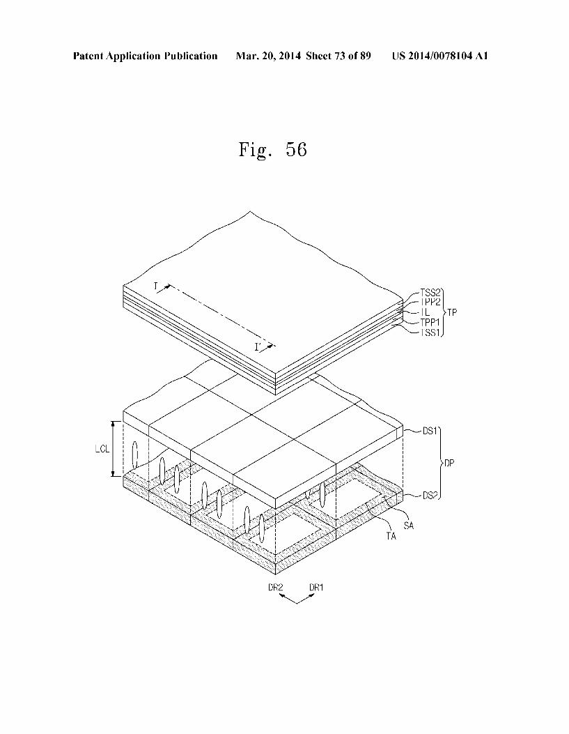
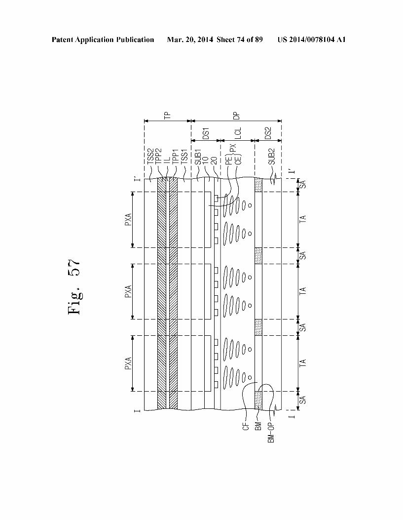
0081 FIG. 56 is a partial perspective view showing the display device shown in FIG. 55 according to exemplary embodiments of the present disclosure. 0082 FIG. 57 is a cross-sectional view taken along a line
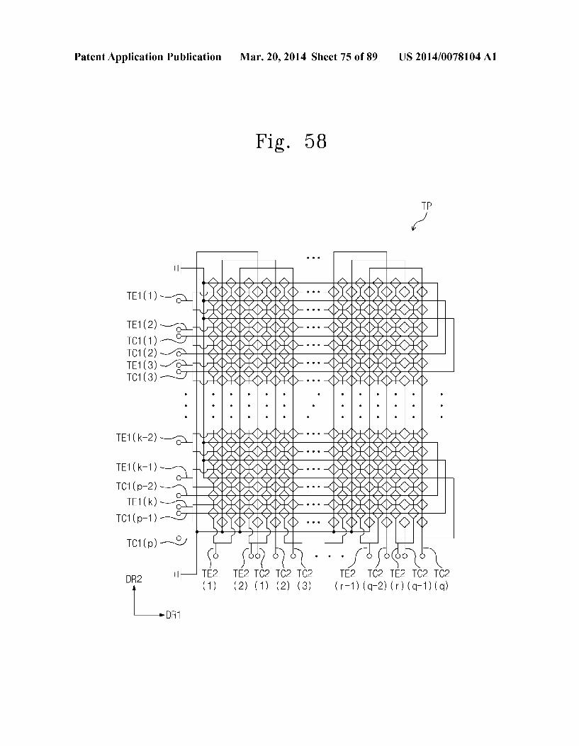
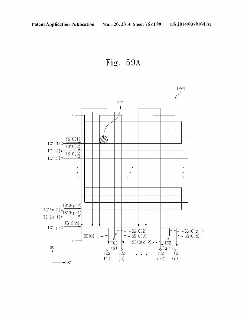
I-I" shown in FIG.56 according to exemplary embodiments of the present disclosure. 0083 FIG.58 is a plan view showing a touchpanel accord ing to exemplary embodiments of the present disclosure. 0084 FIG. 59A is a plan view showing a first touch part shown in FIG.58 according to exemplary embodiments of the present disclosure. 0085 FIG.59B is a plan view showing a second touch part shown in FIG.58 according is to exemplary embodiments of the present disclosure. I0086 FIG. 60 is a timing diagram showing signals applied to a display device according to exemplary embodiments of the present disclosure. 0087 FIG. 61A is a block diagram showing a touch panel driver according to exemplary embodiments of the present disclosure. 0088 FIG. 61B is a block diagram showing a touch sensor according to exemplary embodiments of the present disclo SC.
0089 FIGS. 62A and 62B are timing diagrams showing scan signals according to exemplary embodiments of the present disclosure. 0090 FIG. 63 is an equivalent diagram showing a path through which a noise is generated, which exerts an influence on a second touch sensor, according to exemplary embodi ments of the present disclosure. 0091 FIGS. 64A and 64B are graphs showing a relation between the noise and the detection signal according to exem plary embodiments of the present disclosure. 0092 FIG. 65 is an equivalent diagram showing a path through which a noise is removed in a display device accord ing to exemplary embodiments of the present disclosure. 0093 FIG. 66 is a timing diagram showing signals applied to a display device according to exemplary embodiments of the present disclosure. 0094 FIGS. 67, 68, and 69 are cross-sectional views showing display devices according to exemplary embodi ments of the present disclosure.
DETAILED DESCRIPTION OF THE ILLUSTRATED EMBODIMENTS
0095. The disclosed subject matter is described more fully hereinafter with reference to is the accompanying drawings, in which exemplary embodiments of the disclosed subject matter are shown. This disclosed subject matter may, how ever, be embodied in many different forms and should not be construed as limited to the exemplary embodiments set forth herein. Rather, these exemplary embodiments are provided so that this disclosure is thorough, and will fully convey the scope of the disclosed subject matter to those skilled in the art. In the drawings, the size and relative sizes of layers and regions may be exaggerated for clarity. Like reference numer als in the drawings denote like elements.
Mar. 20, 2014
0096. It will be understood that when an element or layer is referred to as being “on”, “connected to’, or “coupled to another element or layer, it can be directly on, connected, or coupled to the other element or layer or intervening elements or layers may be present. In contrast, when an element is referred to as being “directly on.” “directly connected to’, or “directly coupled to another element or layer, there are no intervening elements or layers present. As used herein, the term “and/or includes any and all combinations of one or more of the associated listed items. It may also be understood that for the purposes of this disclosure, “at least one of X, Y, and Z' can be construed as X only, Y only, Z only, or any combination of two or more items X, Y, and Z (e.g., XYZ. XYYYZ, ZZ). 0097. It will be understood that, although the terms first, second, etc. may be used herein to describe various elements, components, regions, layers, and/or sections, these elements, components, regions, layers, and/or sections should not be limited by these terms. These terms are only used to distin guish one element, component, region, layer, or section from another region, layer, or section. Thus, a first element, com ponent, region, layer, or section discussed below could be termed a second element, component, region, layer, or section without departing from the teachings of the present disclo SUC.
(0098 Spatially relative terms, such as “beneath', “below”, “lower”, “above”, “upper”, and the like, may be used herein for ease of description to describe one element or feature's relationship to another element(s) or feature(s) as illustrated in the figures. It will be understood that the spa tially relative terms are intended to encompass different ori entations of the device in use or operation in addition to the orientation depicted in the figures. For example, if the device in the figures is turned over, elements described as “below' or “beneath other elements or features would then be oriented “above' the other elements or features. Thus, the exemplary term “below can encompass both an orientation of above and below. The device may be otherwise oriented (rotated 90 degrees or at other orientations) and the spatially relative descriptors used herein interpreted accordingly. 0099. The terminology used herein is for the purpose of describing particular embodiments only and is not intended to be limiting of the disclosed subject matter. As used herein, the singular forms, “a”, “an', and “the are intended to include the plural forms as well, unless the context clearly indicates otherwise. It will be further understood that the terms “includes and/or “including, when used in this specifica tion, specify the presence of Stated features, integers, steps, operations, elements, and/or components, but do not preclude the presence or addition of one or more other features, inte gers, steps, operations, elements, components, and/or groups thereof.
0100 Exemplary embodiments of the disclosed subject matter are described herein with reference to cross-section illustrations that are schematic illustrations of idealized embodiments (and intermediate structures) of the disclosed Subject matter. As such, variations from the shapes of the illustrations as a result, for example, of manufacturing tech niques and/or tolerances, are to be expected. Thus, exemplary embodiments of the disclosed subject matter should not be construed as limited to the particular shapes of regions illus trated herein but are to include deviations in shapes that result, for example, from manufacturing.
US 2014/0078104 A1
0101 Unless otherwise defined, all terms (including tech nical and Scientific terms) used herein have the same meaning as commonly understood by one of ordinary skill in the art to which this disclosure belongs. It will be further understood that terms, such as those defined in commonly used dictio naries, should be interpreted as having a meaning that is consistent with their meaning in the context of the relevant art and will not be interpreted in an idealized or overly formal sense unless expressly so defined herein. 0102 Hereinafter, the exemplary embodiments of present disclosure will be explained in detail with reference to the accompanying drawings. 0103 FIG. 1 is a block diagram showing a display device according to exemplary embodiments of the present disclo Sure. FIG. 2 is a perspective view showing a display panel shown in FIG.1. FIG.3 is a plan view showing a display panel shown in FIG. 2. FIG. 4 is a cross-sectional view taken along a line I-I" shown in FIG. 2. 0104. The display device includes a display panel LDP, a signal controller 100, a gate driver 200, a data driver 300, and a touch panel. The touch panel includes a plurality of scan lines TL1 to TLi (“i' is any whole number greater than 1), a plurality of source lines RL1 to RL ('' is any whole number greater than 1), a first driver 400, a second driver 500, and a touch sensor 600. The signal controller 100, the gate driver 200, and the data driver 300 control the display panel LDP to generate an image. The first driver 400 and the second driver 500 control the touch panel, and the touch sensor 600 calcu lates coordinate information of input positions. 0105 Various display panels, such as a liquid crystal dis play panel, an organic light emitting display panel, an elec trophoretic display panel, an electrowetting display panel, etc., is may be used as the display panel LDP. According to exemplary embodiments of the present disclosure, in some cases, the display panel LDP may be a liquid crystal display panel, as described below. 0106. A liquid crystal display (LCD) may also include a backlight unit (not shown) to Supply a light to the liquid crystal display panel and a pair of polarizing plates (not shown). In addition, the liquid crystal display panel may include a vertical alignment mode panel, a patterned vertical alignment mode panel, an in-plane Switching mode panel, a fringe-field Switching mode panel, or a plane to line Switching mode panel. 0107 The display panel LDP includes a first display sub strate DS1 and a second display substrate DS2, which are disposed to be spaced apart from each other. One of the first display substrate DS1 and the second display substrate DS2, which is disposed at a relatively upper position, provides an input device with an input Surface. 0108. The display panel LDP includes a plurality of gate lines GL1 to GLn (“n” is any whole number greater than 1), a plurality of data lines DL1 to DLm (“m is any whole number greater than 1), and a plurality of pixels PX11 to PXnm. Both of the gate lines GL1 to GLn and the data lines DL1 to DLm are disposed on either the first display substrate DS1 or on the second display substrate DS2. In FIG. 1, the gatxe lines GL1 to GLn and the data lines DL1 to DLmare disposed on the first display substrate DS1. 0109 The gate lines GL1 to GLn are extended in a first direction DR1 and arranged in a second direction DR2 sub stantially perpendicular to the first direction DR1. The data lines DL1 to DLm are extended in the second direction DR2 and arranged in the first direction DR1. The data lines DL1 to
Mar. 20, 2014
DLm are insulated from the gate lines GL1 to GLn while crossing the gate lines GL1 to GLn. The gate lines GL1 to GLn are connected to the gate driver 200, and the data is lines DL1 to DLm are connected to the data driver 300.
0110. The pixels PX11 to PXnm are arranged in a matrix form. The pixels PX11 to PXnm are arranged in pixel areas PXA11 to PXAnm, respectively. Each of the pixels PX11 to PXnm is connected to a corresponding gate line of the gate lines GL1 to GLn and a corresponding data line of the data lines DL1 to DLm.
0111. The scan lines TL1 to TLi and the source lines RL1 to RL are disposed on the substrate that provides the input surface. The scanlines TL1 to TLiand the source lines RL1 to RL may be disposed on first display substrate DS1 or the second display substrate DS2. FIG. 3 shows nine scan lines TL1 to TL9 and ten source lines RL1 to RL10, and FIG. 4 shows a few scanlines TL of the scanlines TL1 to TL and one source line RL of the source lines RL1 to RLj. 0112 The scan lines TL1 to TLi are disposed on a layer different from a layer on which the source lines RL1 to RL are disposed. The scan lines TL1 to TL are extended in the first direction DR1 and arranged in the second direction DR2. The source lines RL1 to RL are extended in the second direction DR2 and arranged in the first direction DR1. The scanlines TL1 to TLi are connected to the first driver 400 and the source lines RL1 to RL are connected to the second driver SOO.
0113. The scan lines TL1 to TLi and the source lines RL1 to RL are formed of a transparent conductive material. In addition, the scan lines TL1 to TLi and the source lines RL1 to RL may be formed of a metal material having a low reflectance.
0114. The gate driver 200 and the data driver 300 may be disposed on the first display substrate DS1, and the first driver 400 and the second driver 500 may be disposed on the second display substrate DS2. The signal controller 100 and the touch sensor 600 are disposed on a is circuit board connected to the display panel LDP. 0.115. Hereinafter, arrangements of the display panel LDP. the scan lines TL1 to TL9, and the source lines RL1 to RL10 will be described in detail with reference to FIGS. 2, 3, and 4. 0116. The second display substrate DS2 includes a plural ity of transmitting areas TA and a blocking area SA. The blocking area SA Surrounds the transmitting areas TA. The transmitting areas TA transmit light generated by and pro vided from the backlight unit and the blocking area SAblocks the light. The transmitting areas TA are arranged in a matrix form. The display device generates an image by combining the light transmitting through the transmitting areas TA. 0117 Referring to FIG. 3, the scan lines TL1 to TL9 and the source lines RL1 to RL10 are disposed in the blocking area SA. Among the scan lines TL1 to TL9, two scan lines adjacent to each other are disposed to be spaced apart from each other while interposing the transmitting areas TA arranged in the second direction DR2. Among the source lines RL1 to RL10, two source lines adjacent to each other are disposed to be spaced apart from each other while interposing the transmitting areas TA arranged in the first direction DR1. The scan lines TL1 to TL9 and the Source lines RL1 to RL10 are disposed to overlap with the blocking area SA. The scan lines TL1 to TL9 and the source lines RL1 to RL10 are not perceived to a user.
US 2014/0078104 A1
0118 Referring to FIG. 4, the first display substrate DS1 includes a first base substrate SUB 1, a plurality of insulating layers 10 and 20, and a plurality of conductive layers CE and PE. 0119 FIG. 4 shows the plane to line switching mode panel, but the structure of the display panel should not be limited thereto or thereby. 0120 Common electrodes CE are disposed on the first base substrate SUB1. A first insulating layer 10 is disposed on the first base substrate SUB1 to cover the common electrodes CE. Pixel electrodes PE are disposed on the first insulating layer 10. A second insulating layer 20 is disposed on the first insulating layer 10 to cover the pixel electrodes PE. 0121 Each of the first and second insulating layers 10 and 20 is configured to include at least one organic layer and/or at least one inorganic layer. The gate lines GL1 to GLn (refer to FIG. 1) and the data lines DL1 to DLn(refer to FIG. 1) have not been shown in FIG. 4. 0122) The pixel areas PXA are defined in the first display substrate DS1 and the pixels PX are disposed on the first display substrate DS1. The pixel areas PXA are overlapped with the transmitting areas TA, respectively. As an example, FIG. 4 shows three pixel areas PXA. 0123. Each of the pixels PX includes a corresponding common electrode of the common electrodes CE and a cor responding pixel electrode of the pixel electrodes PE. In addition, each of the pixels PX further includes a thin film transistor connected to a corresponding data line of the data lines DL1 to DLm, a corresponding gate line of the gate lines GL1 to GLn, and a corresponding pixel electrode of the pixel electrodes PE. 0.124. The thin film transistor receives a pixel voltage from the pixel electrode PE. The common electrodes CE receive a common Voltage. The common electrodes CE and the pixel electrodes PE form an electric field, and thus orientation arrangements of directors (e.g., liquid crystal molecules) included in the liquid crystal layer LCL are changed by the electric field. For example, in some cases, the common elec trodes CE and the pixel electrodes PE form a horizontal electric field, and thus orientation arrangements of the liquid crystal molecules in the liquid crystal layer LCL are changed by the horizontal electric field. 0.125. As shown in FIG. 4, the second display substrate DS2 includes a second base substrate SUB2, a black matrix BM, and a plurality of color filters CF. The black matrix BM includes a plurality of openings BM-OP formed there through. The scan lines TL and the source is lines RL are disposed on the second base substrate SUB2. FIG. 4 shows four scan lines TL and one source line RL. In FIG. 4, the one source line RL is presented to explain a layer structure of the second display substrate DS2. Practically, the one source line RL does not be overlapped with the plurality of openings BM-OP, and the one source line RL is overlapped with black matrix BM. 0126 The black matrix BM is disposed on a lower surface of the second base substrate SUB2. The transmitting areas TA are defined by the openings BM-OP. In addition, the blocking area SA corresponds to an area in which the black matrix BM is disposed. 0127. The color filters CF are disposed to overlap with the openings BM-OP, respectively. The color filters CF are respectively inserted into the openings BM-OP. The color filters CF include color filters having different colors from each other. For example, a portion of the color filters has a red
Mar. 20, 2014
color, another portion of the color filters has agreen color, and the other portion of the color filters has a blue color. I0128. The scan lines TL are disposed on the second base substrate SUB2. The scan lines TL may be directly disposed on the second base substrate SUB2. An insulating layer IL is disposed on the second base substrate SUB2 to cover the scan lines TL. A protection layer PL is disposed on the insulating layer IL. The insulating layer IL may be, but not limited to, an adhesive layer. The protection layer PL may be an optical member, e.g., a polarizing plate. I0129. The source line RL is disposed under the second base substrate SUB2. The source line RL is overlapped with the black matrix BM. The source line RL may be directly disposed on a lower surface of the second base substrate SUB2. In this case, the black matrix BM covers the source line RL. In some cases, the positions of the Scanlines TL and the source line RL may be switched. I0130 Referring to FIG. 1, the signal controller 100 receives input image signals RGB and converts the input image signals RGB to image data R'G'B' corresponding to an operating mode of the display panel LDP. In addition, the signal controller 100 receives various control signals CS, Such as a vertical synchronizing signal, a horizontal synchro nizing signal, a main clock signal, a data enable signal, etc., and outputs first and second control signals CONT1 and CONT2 and a mode selection signal MSS. I0131 The mode selection signal MSS determines the operating mode of the gate driver 200 and the touch panel. The touch panel may operate in an electrostatic capacitive mode (hereinafter, referred to as a first mode) or an electro magnetic induction mode (hereinafter, referred to as a second mode). 0.132. The mode selection signal MSS may be generated on the basis of the image displayed in the display panel LDP. The mode selection signal MSS may have different levels according to the operating modes. For instance, when the display panel LDP displays a keypad image, the mode selec tion signal MSS is output as a signal to activate the first mode, and when the display panel LDP displays a game image, the mode selection signal MSS is output as a signal to activate the second mode. In some cases, the mode selection signal MSS may be input by the user. For instance, the mode selection signal MSS is generated corresponding to an information inputted to a keypad by the user. The user may touch a first mode activating button. I0133. The gate driver 200 applies gate signals to the gate lines GL1 to GLn in response to the first control signal CONT1. The first control signal CONT1 includes a vertical start signal to control and start an operation of the gate driver 200, a gate clock signal to determine an output timing of a gate Voltage, and an output enable signal that controls an ON-pulse width of the gate voltage. I0134. The data driver 300 receives the second control sig nal CONT2 and the image data R'G'B'. The data driver 300 converts the image data R'G'B' to data voltages and applies the data voltages to the data lines DL1 to DLm. 0.135 The second control signal CONT2 includes a hori Zontal start signal to control and start an operation of the data driver 300, an inverting signal to invert a polarity of the data Voltages, and an output indicating signal that controls an output timing of the data voltages from the data driver 300. 0.136. The first driver 400 receives the mode selection signal MSS. The first driver 400 receives first scan signals TS1 and second scan signals TS2, and applies the first scan
US 2014/0078104 A1
signals TS1 or the second scan signals TS2 to the scan lines TL1 to TLi in response to the mode selection signal MSS. The first driver 400 outputs the first scan signals TS1 in the first mode and outputs the second scan signals TS2 in the second mode. 0.137 The second driver 500 receives the mode selection signal MSS. The second driver 500 outputs sensing signals SS 1 (hereinafter, referred to as first sensing signals) that repre sent a variation in capacitance of the Source lines RL1 to RL during the first mode. The second driver 500 outputs sensing signals SS2 (hereinafter, referred to as second sensing sig nals) according to a resonant frequency of the input device during the second mode. The input device may be, but is not limited to, a stylus pen with an inductor-capacitor (LC) reso nant circuit. 0.138. The touch sensor 600 receives the first sensing sig nals SS1 and the second sensing signals SS2. The touch sensor 600 calculates the coordinate information of an input position based on the first sensing signals SS1 and the second sensing signals SS2. The input position in the first mode may be a position on the second display substrate DS2 at which a touch of the input device is detected. In addition, the input position in the second mode may be a is position on the second display Substrate DS2 at which a touch oran approach by the input device is detected. 0139 FIG. 5 is a block diagram showing a touch panel according to exemplary embodiments of the present disclo sure. FIG. 5 shows thirty-six scan lines TL1 to TL36 and thirty-six source lines RL1 to RL36. 0140. Referring to FIG. 5, the thirty-six scan lines TL1 to TL36 are grouped into four scan line groups TG10, TG20. TG30, and TG40 (hereinafter, referred to first, second, third, and fourth scan line groups, respectively) and the thirty-six source lines RL1 to RL36 are grouped into four source line groups. RG10, RG20, RG30, and RG40 (hereinafter, referred to first, second, third, and fourth source line groups, respec tively). Each of the first to fourth scan line groups TG10. TG20, TG30, and TG40 includes a first scan line sub-group TLG1, a second scan line Sub-group TLG2, and a third scan line sub-group TLG3. Each of the first scan line sub-group TLG1, the second scan line sub-group TLG2, and the third scan line Sub-group TLG3 includes at least one scan line. 0141. The first scan line sub-group TLG1, the second scan line sub-group TLG2, and the third scanline sub-group TLG3 include the same number of scan lines. For example, in FIG. 5, each scan line Sub-group includes three scan lines. First ends of the three scan lines are connected to each other and the second ends of the three scan lines are connected to each other. It should be understood that various numbers of scan lines may be included in each scan line Sub-group. 0142. The first scan line sub-group TLG1, the second scan line sub-group TLG2, and the third scanline sub-group TLG3 are arranged in the second direction DR2. The third scan line sub-group TLG3 is disposed between the first scan line sub group TLG1 and the second is scan line sub-group TLG2. The first scan line Sub-group TLG1 and the second scan line Sub-group TLG2 are connected to each other by a first con nection line CNL1. Accordingly, the first scan line Sub-group TLG1 and the second scan line sub-group TLG2 form one loop. 0143. Each of the first to fourth source line groups RG10. RG20, RG30, and RG40 includes a first source line sub-group RLG1, a second source line sub-group RLG2, and a third source line sub-group RLG3. Each of the first source line
Mar. 20, 2014
Sub-group RLG1, the second source line Sub-group RLG2. and the third source line sub-group RLG3 includes at least one source line. 0144. The first source line sub-group RLG1, the second source line sub-group RLG2, and the third source line sub group RLG3 include the same number of source lines. For example, in FIG. 5, each source line sub-group includes three source lines. First ends of the three source lines are connected to each other and second ends of the three source lines are connected to each other. It should be understood that various numbers of Source lines may be included in each source line Sub-group. 0145 The first source line sub-group RLG1, the second source line sub-group RLG2, and the third source line sub group RLG3 are arranged in the first direction DR1. The third source line sub-group RLG3 is disposed between the first Source line Sub-group RLG1 and the second source line Sub group RLG2. The first source line sub-group RLG1 and the second source line Sub-group RLG2 are connected to each other by a second connection line CNL2. 0146 FIG. 6 is a view showing the touch panel operated in the first mode. FIGS. 7A and 7B are views showing the touch panel operated in the second mode, and FIG. 8 is a timing diagram showing signals generated in the second mode. Hereinafter, the operation of the touch panel will be described in detail with reference to FIGS. 6, 7A, 7B, and 8. 0147 The touch panel operated in the first mode and shown in FIG. 6 calculates the is coordinate information of the input position in the same way as an electrostatic capaci tive type touch panel. The first to fourth scan line groups TG10, TG20, TG30, and TG40 correspond to input touch electrodes of the electrostatic capacitive type touch panel, and the first to fourth source line groups. RG10, RG20, RG30, and RG40 correspond to output touch electrodes of the electro static capacitive type touch panel. (0.148. The first to fourth scan line groups TG10, TG20, TG30, and TG40 are capacitive-coupled to the first to fourth sourceline groups. RG10, RG20, RG30, and RG40. Due to the capacitive coupling, capacitors are formed between the first to fourth scan line groups TG10, TG20, TG30, and TG40 and the first to fourth source line groups. RG10, RG20, RG30, and RG40.
0149. The first to fourth scan line groups TG10, TG20, TG30, and TG40 receive scan signals TS1-1 to TS1-4 (here inafter, referred to as first scan signals), respectively, in dif ferent periods from each other. The first to fourth scan line groups TG10, TG20, TG30, and TG40 sequentially receive the first scan signalsTS1-1 to TS1-4. The first to fourth source line groups RG10, RG20, RG30, and RG40 output sensing signals SS1-1 to SS1-4 (hereinafter, referred to as first sensing signals), respectively. 0150. An area in which the second scan line group TG20 crosses the second source line group RG20 may be the input position PP1 (hereinafter, referred to as first input position). The first sensing signal SS 1-2 output from the second source line group RG20 may then have a level different from a level of the first sensing signals SS1-1, SS1-3, and SS1-4 of other source line groups RG10, RG30, and RG40. 0151. The touch sensor 600 calculates a two-dimensional coordinate information of the first input position PP1 based on a time at which the first sensing signal SS 1-2 having the is different level is sensed and a relative position of the second source line group RG20 with respect to the first to fourth source line groups RG10, RG20, RG30, and RG40.
US 2014/0078104 A1
0152 The touch panel operated in the second mode (shown in FIGS. 7A and 7B) calculates the coordinate infor mation of the input position in the same way as an electro magnetic induction type touch panel. The first to fourth scan line groups TG10, TG20, TG30, and TG40 correspond to input coils of the electromagnetic induction type touch panel, and the first to fourth source line groups RG10, RG20, RG30, and RG40 correspond to output coils of the electromagnetic induction type touch panel. 0153. Referring to FIG. 7A, the first to fourth scan line groups TG10, TG20, TG30, and TG40 receive scan signals TS2-1 to TS2-4 (hereinafter, referred to as second scan sig nals), respectively, in different periods. The second scan sig nals TS2-1 to TS2-4 are respectively applied to the first ends of the first scan line sub-groups TLG 1 of the first to fourth scan line groups TG10, TG20, TG30, and TG40. The first end of the second scan line sub-group TLG2 of each of the first to fourth scan line groups TG10, TG20, TG30, and TG40 is grounded. The first end of the third scan line sub-group TLG3 of each of the first to fourth scan line groups TG10, TG20. TG30, and TG40 is floated without receiving any voltage. 0154 Therefore, the first scan line sub-group TLG1 and the second scan line Sub-group TLG2 form a current path. A magnetic field is induced by the current path formed by the first scan line Sub-group TLG1 and the second scan line sub-group TLG2. That is, the first scan line sub-group TLG1 and the second Scanline Sub-group TLG2 form one input coil. Since the first to fourth scan line groups TG10, TG20, TG30, and TG40 receive the second scan signals TS2-1 to TS2-4 in different periods, the magnetic field is induced in different periods. 0155. When the input device (not shown) approaches the
first to fourth scanline groups TG10, TG20, TG30, and TG40, the magnetic field induced from the first to fourth scan line groups TG10, TG20, TG30, and TG40 resonates with the resonant circuit of the input device. Thus, the input device generates the resonant frequency. 0156 Referring to FIG. 7B, the first to fourth source line groups RG10, RG20, RG30, and RG40 output sensing sig nals SS2-1 to SS2-4 (hereinafter, referred to as second sens ing signals), respectively, according to the resonant frequency of the input device. The second sensing signals SS2-1 to SS2-4 are output from the first ends of the first source line sub-groups RGL1 of the first to fourth source line groups RG10, RG20, RG30, and RG40. The first end of the second source line sub-group RLG2 of each of the first to fourth source line groups. RG10, RG20, RG30, and RG40 is grounded. The first end of the third source line sub-group RLG3 of each of the first to fourth source line groups. RG10. RG20, RG30, and RG40 is floated without receiving any Voltage. (O157 An input position PP2 (hereinafter, referred to as second input position) may correspond to an area in which the second scan line group TG20 crosses the second source line group RG20. The second sensing signal SS2-2 output from the second source line group RG20 has a level different from a level of the second sensing signals SS2-1, SS2-3, and SS2-4 of other source line groups. RG10, RG30, and RG40. 0158. The touch sensor 600 calculates a two-dimensional coordinate information of the second input position PP2 based on a time at which the second sensing signal SS2-2 having the different level is sensed and a relative position of the second source line group RG20 with respect to the first to fourth source line groups RG10, RG20, RG30, and RG40.
Mar. 20, 2014
0159 Referring to FIGS. 7A, 7B, and 8, the second scan signals TS2-1 to TS2-4 are sequentially applied to the first scan line sub-groups TLG 1 of the first to fourth scan line groups TG10, TG20, TG30, and TG40. An induction signal RS is generated from the input device disposed at the second input position PP2. 0160. After the second scan signal TS2-2 applied to the second scan line group TG20 is deactivated, the induction signal RS is gradually decreased during a predetermined period. The input device generates a frequency corresponding to the induction signal RS that is gradually decreased. The frequency generated by the input device generates the second sensing signal SS2-2 of the second source line group RG20. 0.161 FIG. 9 is a block diagram showing the first driver 400 shown in FIG. 5. FIG. 10 is a circuit diagram showing switching parts 430-1 to 430-4 shown in FIG. 9. Hereinafter, the first driver 400 will be described in detail with reference to FIGS. 9 and 10.
0162 The first driver 400 includes a scan signal output part 410, a selection part 420, and switching parts 430-1 to 430-4. FIG. 9 shows four switching parts 430-1 to 430-4 (hereinafter, referred to as first to fourth switching parts, respectively). 0163 The scan signal output part 410 receives the mode selection signal MSS, the first scan signal TS1, and the second scan signal TS2. The first and second scan signals TS1 and TS2 may be provided from an external circuit, e.g., a scan signal generating circuit. The scan signal output part 410 selectively outputs the first scan signal TS1 and the second scan signal TS2 in response to the mode selection signal MSS.
0164. The selection part 420 switches the first to fourth switching parts 430-1 to 430-4. 0.165. The selection part 420 receives the mode selection signal MSS and outputs switching control signals SW-1 to SW-4 and SW-10 to SW-40 having different turn-on periods. The selection part 420 outputs first Switching control signals SW-1 to SW-4 in the first mode and outputs second switching control signals SW-10 to SW-40 in the second mode. The second switching control is signals SW-10 to SW-40 have phases opposite to those of the first Switching control signals SW-1 to SW-4.
0166 Each of the first to fourth switching parts 430-1 to 430-4 receives the first scan signal TS1 from the scan signal output part 410 in the first mode and receives the second scan signal TS2 from the scan signal output part 410 in the second mode. The first to fourth switching parts 430-1 to 430-4 respectively receive the first switching control signals SW-1 to SW-4 in the first mode and respectively receive the second switching control signals SW-10 to SW-40 in the second mode.
0167. In the first mode, the first to fourth switching parts 430-1 to 430-4 apply the first scan signal TS1 to the first to fourth scan line groups TG10, TG20, TG30, and TG40 in response to the first switching control signals SW-1 to SW-4. In the second mode, the first to fourth switching parts 430-1 to 430-4 apply the second scan signal TS2 to the first to fourth scan line groups TG10, TG20, TG30, and TG40 in response to the second switching control signals SW-10 to SW-40. (0168 Referring to FIG. 10, each of the first to fourth switching parts 430-1 to 430-4 includes a first switch ST1, a second switch ST2, and a third switch ST3. Hereafter, the first switch 430-1 will be described as a representative example.
US 2014/0078104 A1
0169. The first switch ST1 applies the first scan signal TS1 to the first scan line sub-group TLG1 in the first mode and applies the second scan signal TS2 to the first scan line Sub group TLG1 in the second mode. (0170 The first switch ST1 may be, but is not limited to, a Complementary Metal-Oxide Semiconductor (CMOS) tran sistor. The CMOS transistor includes an n-type transistor and a p-type transistor. Control electrodes of the n-type transistor and the p-type transistor are is commonly connected to each other to receive the first switching control signal SW-1 and the second Switching control signal SW-10. In some cases, the first switching control signal SW-1 has a high level in the turn-on period and the second Switching control signal SW-10 has a low level in the turn-on period. 0171 An input electrode of the n-type transistor receives the first scan signal TS1 and an input electrode of the p-type transistor receives the second scan signal TS2. An output electrode of the n-type transistor and an output electrode of the p-type transistor are commonly connected to the first scan line sub-group TLG1. 0172. The second switch ST2 applies the first scan signal TS1 to the second scan line sub-group TLG2 in the first mode and applies the second scan signal TS2 to the second scan line Sub-group TLG2 in the second mode. 0173 The second switch ST2 may be, but is not limited to, a CMOS transistor. Control electrodes of an n-type transistor and a p-type transistor of the second Switch ST2 are com monly connected to each other to receive the first Switching control signal SW-1 and the second switching control signal SW-10. 0.174. An input electrode of the n-type transistor receives the first scan signal TS1 and an input electrode of the p-type transistor receives a ground Voltage. An output electrode of the n-type transistor and an output electrode of the p-type transistor are commonly connected to the second scan line sub-group TLG2. 0.175. The n-type transistor of each of the first and second switches ST1 and ST2, which are turned on in the first mode, applies the first scan signal TS1 to the first and second scan line sub-groups TLG1 and TLG2. The p-type transistor of each of the first and second switches ST1 and ST2, which are turned on in the second mode, forms a current path in the first scan signal TS1 to the first and second scan line Sub-groups TLG1 and TLG2. 0176 The third switch ST3 applies the first scan signal TS1 to the third scan line sub-group TLG3 in the first mode and floats the third scan line sub-group TLG3 in the second mode. (0177. The third switch ST3 may be, but is not limited to, an n-channel MOS (NMOS) transistor. A control electrode of the NMOS transistor receives the first switching control signal SW-1 and the second switching control signal SW-10. An input electrode of the NMOS transistor receives the first scan signal TS1 and an output electrode of the NMOS transistor is connected to the third scan line sub-group TLG3. In the second mode, the third switch ST3 is turned off by the second switching control signal SW-10 having the low level, and thus the third scan line sub-group TLG3 is floated. 0178. In some cases, the n-type transistor and the p-type transistor of the CMOS transistor may be switched. In such cases, the third switch ST3 may beap-channel MOS (PMOS) transistor. 0179 FIG. 11 is a block diagram showing the second driver 500 and the touch sensor shown 600 in FIG.5, and FIG.
Mar. 20, 2014
12 is a circuit diagram showing a sensing signal output part shown in FIG. 11. Hereinafter, the second driver 500 and the touch sensor 600 will be described in detail with reference to FIGS. 11 and 12. 0180 Referring to FIG. 11, the second driver 500 includes a plurality of sensing signal output parts 502, 504,506, and 508. FIG. 11 shows four sensing signal output parts 502,504, 506, and 508 (hereinafter, referred to as first to fourth sensing signal output parts, respectively). 0181. The first to fourth sensing signal output parts 502, 504,506, and 508 are connected to the first to fourth source line groups RG10, RG20, RG30, and RG40, respectively. Each of the first to fourth sensing signal output parts 502,504, 506, and 508 receives a control signal. The control signal may be the mode selection signal MSS. In some cases, the control signal may be another signal having the same phase as the mode selection signal MSS. 0182. In the first mode, the first to fourth sensing signal output parts 502, 504, 506, and 508 output the first sensing signals SS1-1 to SS1-4 (refer to FIG. 6) from the first to fourth source line groups RG10, RG20, RG30, and RG40. In the second mode, the first to fourth sensing signal output parts 502, 504, 506, and 508 output the second sensing signals SS2-1 to SS2-4 (refer to FIG. 7B) from the first to fourth source line groups RG10, RG20, RG30, and RG40. 0183 Referring to FIG. 12, each of the first to fourth sensing signal output parts 502,504,506, and 508 includes a first Switch ST10, a second switch ST20, and a third switch ST30. Hereinafter, the first sensing signal output part 502 will be described as a representative example. 0.184 The first switch ST10 outputs the first sensing signal SS1-1 from the first end of the first source line sub-group RLG1 in the first mode and outputs the second sensing signal SS2-1 from the first end of the first source line sub-group RLG1 in the second mode. The first switch ST10 may be, but is not limited to, a CMOS transistor. 0185. The CMOS transistor includes an n-type transistor and a p-type transistor. Control electrodes of the n-type tran sistor and the p-type transistor are commonly connected to each other to receive the mode selection signal MSS. The mode selection signal MSS has a high level in the first mode and a low level in the second mode. 0186. An input electrode of the n-type transistor is con nected to the first source line sub-group RLG1 and an output electrode of the n-type transistor is connected to the touch sensor 600. An input electrode of the p-type transistor is connected to the first source line Sub-group RLG1 and an output electrode of the p-type transistor is connected to the touch sensor 600. The is output electrode of the n-type tran sistor applies the first sensing signal SS1-1 to the touch sensor 600 and the output electrode of the p-type transistor applies the second sensing signal SS2-1 to the touch sensor 600. 0187. The second switch ST20 outputs the first sensing signal SS1-1 from the first end of the second source line Sub-group RLG2 in the first mode and grounds the second Source line Sub-group RLG2 in the second mode. The second switch ST20 may be, but is not limited to, a CMOS transistor. 0188 Control electrodes of the n-type transistor and the p-type transistor of the second switch ST20 are commonly connected to each other to receive the mode selection signal MSS. An input electrode of the n-type transistor is connected to the second source line Sub-group RLG2 and an output electrode of the n-type transistor is connected to the touch sensor 600. An input electrode of the p-type transistor is
US 2014/0078104 A1
connected to the second source line Sub-group RLG2 and an output electrode of the p-type transistor receives the ground Voltage. 0189 The third switch ST30 outputs the first sensing sig nal SS1-1 to the touch sensor 600 in the first mode and floats the third source line sub-group RLG3 in the second mode. (0190. The third switch ST30 may be, but is not limited to, an NMOS transistor. A control electrode of the NMOS tran sistor receives the mode selection signal MSS. An input elec trode of the NMOS transistor is connected to the third source line sub-group RLG3 and an output electrode of the NMOS transistoris connected to the touch sensor 600. In some cases, the n-type transistor and the p-type transistor of the CMOS may be switched. In such cases, the third switch ST30 may be a PMOS transistor.
0191 Referring to FIG. 11 again, the touch sensor 600 includes signal processors 610-1 to 610-4 (hereinafter, referred to as first to fourth signal processing parts, respec tively), a is multiplexer 620, and a coordinate calculator 630. 0.192 The first to fourth signal processors 610-1 to 610-4 respectively receive the first sensing signals SS1-1 to SS1-4 (refer to FIG. 6) from the first to fourth sensing signal output parts 502,504,506, and 508 in the first mode and respectively receive the second sensing signals SS2-1 to SS2-4 (refer to FIG. 7B) from the first to fourth sensing signal output parts 502,504,506, and 508 in the second mode. Each of the first to fourth signal processors 610-1 to 610-4 includes a first modesignal processor (not shown) to process the first sensing signals SS 1-1 to SS1-4 and a second modesignal processor (not shown) to process the second sensing signals SS2-1 to SS2-4.
0193 The first mode signal processor includes an ampli fier, a noise filter, and an analog-to-digital converter. The amplifier amplifies the first sensing signals SS1-1 to SS1-4. The noise filter removes noises from the amplified first sens ing signals SS 1-1 to SS 1-4. The analog-to-digital converter converts the first sensing signals SS1-1 to SS1-4 from which the noises are removed to first digital signals. 0194 The second mode signal processor includes an amplifier, a band-pass filter, a wave detector, a sample-hold circuit, and an analog-to-digital converter. The second sens ing signals SS2-1 to SS2-4 are converted to second digital signals using the second mode signal processor. (0195 The multiplexer 620 selectively applies the first and second digital signals from the first to fourth signal proces sors 610-1 to 610-4 to the coordinate calculator 630. The coordinate calculator 630 compares the first and second digi tal signals to a reference value to sense the output touch electrode or the output coil in which the external input occurs. The coordinate calculator 630 calculates the coordinate infor mation of the first input position PP1 is (refer to FIG. 6) from the first digital signals and calculates the coordinate informa tion of the second input position PP2 (refer to FIG. 7B) from the second digital signals. 0.196 FIGS. 13 and 14 are cross-sectional views showing display panels according to exemplary embodiments of the present disclosure. In FIGS. 13 and 14, the same reference numerals denote the same elements in FIGS. 1 to 3, and thus detailed descriptions of the same elements will be omitted. (0197) Referring to FIGS. 13 and 14, the scan lines TL and the source lines RL are disposed on or under the second base substrate SUB2. In FIG. 13, the scan lines TL and the source lines RL are disposed under the second base substrate SUB2.
Mar. 20, 2014
In FIG. 14, the scan lines TL and the source lines RL are disposed on the second base substrate SUB2. (0198 Referring to FIG. 13, a black matrix BM including a plurality of openings BM-OP is disposed on a lower surface of the second base substrate SUB2 of the display panel LDP10. Color filters CF are disposed in the openings BM-OP. The scan lines TL and the source lines RL are disposed to overlap, at least partially, with the black matrix BM. 0199 The scan lines TL are disposed on a lower surface of the black matrix BM. A third insulating layer IL-1 is disposed on the black matrix BM and the color filters CF to cover the scan lines TL. The third insulating layer IL-1 provides a flat Surface thereon. A fourth insulating layer IL-2 is disposed on the third insulating layer IL-1 to cover the source lines RL. Each of the third insulating layer IL-1 and the fourth insulat ing layer IL-2 includes at least one organic layer and/or at least one inorganic layer. 0200 Referring to FIG. 14, a black matrix BM including a plurality of openings BM-OP is disposed on a lower surface of the second base substrate SUB2 of the display panel LDP20. Color filters CF are disposed in the openings BM-OP. The Source lines RL are disposed on an is upper Surface of the second base substrate SUB2 to overlap, at least partially, with the black matrix BM.
0201 A third insulating layer IL-1 is disposed on the upper surface of the second base substrate SUB to cover the source lines RL. The third insulating layer IL-1 provides a flat surface thereon. The scan lines TL are disposed on the third insulating layer IL-1. A fourth insulating layer IL-2 is dis posed on the third insulating layer IL-1 to cover the Scanlines TL. A protection layer PL is disposed on the fourth insulating layer IL-2. In some cases, the positions of the scan lines TL and the source lines RL may be switched. (0202 FIGS. 15A and 15B are plan views showing display panels according to exemplary embodiments of the present disclosure. In FIGS. 15A and 15B, the same reference numer als denote the same elements in FIGS. 1 to 3, and thus detailed descriptions of the same elements will be omitted. (0203 Referring to FIGS. 15A and 15B, a plurality of scan lines TL1 to TL9 and a plurality of source lines RL1 to RL10 are disposed in the blocking area SA. Each of the scan lines TL1 to TL9 further includes first sensing electrodes SSE1 disposed at positions in which each of the scan lines TL1 to TL9 crosses the source lines RL1 to RL10. In addition, each of the source lines RL1 to RL9 further includes second sens ing electrodes SSE2 disposed at positions in which each of the source lines RL1 to RL9 crosses the scan lines TL1 to TL9.
0204 The first sensing electrodes SSE1 are overlapped with the second sensing electrodes SSE2. The overlap areas between the scan lines TL1 to TL9 and the source lines RL1 to RL10 are increased by the first sensing electrodes SSE1 and the second sensing electrodes SSE2. Accordingly, the capacitance variation of capacitors formed between the scan lines TL1 to TL9 and the source lines RL1 to RL10 becomes large. Therefore, touch sensitivity in the first is mode may be improved. In some cases, either the first sensing electrodes SSE1 or the second sensing electrodes SSE2 may be omitted. 0205 FIG. 16 is a block diagram showing a touch panel according to exemplary embodiments of the present disclo sure, FIG. 17 is a view showing a touch panel operated in a first mode. FIGS. 18A and 18B are views showing touch panels operated in a second mode. In FIGS. 16, 17, 18A, and