Embed Size (px)
Citation preview
2 A, Low VIN, Low Dropout Linear Regulator
Data Sheet ADP1740/ADP1741
FEATURES Maximum output current: 2 A Input voltage range: 1.6 V to 3.6 V Low shutdown current: 2 µA Low dropout voltage: 160 mV at 2 A load Initial accuracy: ±1% Accuracy over line, load, and temperature: ±2% 7 fixed output voltage options with soft start:
0.75 V to 2.5 V (ADP1740) Adjustable output voltage options with soft start:
0.75 V to 3.3 V (ADP1741) High PSRR
65 dB at 1 kHz 65 dB at 10 kHz 54 dB at 100 kHz
23 μV rms at 0.75 V output Stable with small 4.7 µF ceramic output capacitor Excellent load and line transient response Current-limit and thermal overload protection Power-good indicator Logic-controlled enable Reverse current protection
APPLICATIONS Server computers Memory components Telecommunications equipment Network equipment DSP/FPGA/microprocessor supplies Instrumentation equipment/data acquisition systems
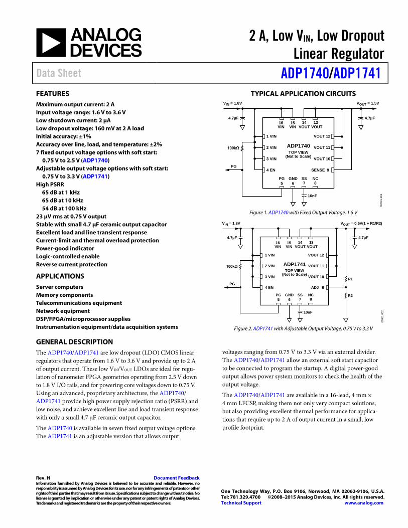
TYPICAL APPLICATION CIRCUITS
TOP VIEW(Not to Scale)
ADP1740
1
2
3
4
VIN
VIN100kΩ
4.7µF 4.7µF
VIN = 1.8V VOUT = 1.5V
VIN
EN
12
11
10
9
VOUT
VOUT
VOUT
SENSE
5 6 7 8PG GND SS NC
PG
16 15 14 13VIN VIN VOUT VOUT
10nF
0708
1-00
1
Figure 1. ADP1740 with Fixed Output Voltage, 1.5 V
TOP VIEW(Not to Scale)
ADP1741
1
2
3
4
VIN
VIN100kΩ
4.7µF 4.7µF
VIN = 1.8V VOUT = 0.5V(1 + R1/R2)
VIN
EN
12
11
10
9
VOUT
VOUT
VOUT
ADJ
5 6 7 8PG GND SS NC
PG
16 15 14 13VIN VIN VOUT VOUT
10nF
R2
R1
0708
1-00
2
Figure 2. ADP1741 with Adjustable Output Voltage, 0.75 V to 3.3 V
GENERAL DESCRIPTION The ADP1740/ADP1741 are low dropout (LDO) CMOS linear regulators that operate from 1.6 V to 3.6 V and provide up to 2 A of output current. These low VIN/VOUT LDOs are ideal for regu-lation of nanometer FPGA geometries operating from 2.5 V down to 1.8 V I/O rails, and for powering core voltages down to 0.75 V. Using an advanced, proprietary architecture, the ADP1740/ ADP1741 provide high power supply rejection ratio (PSRR) and low noise, and achieve excellent line and load transient response with only a small 4.7 µF ceramic output capacitor.
The ADP1740 is available in seven fixed output voltage options. The ADP1741 is an adjustable version that allows output
voltages ranging from 0.75 V to 3.3 V via an external divider. The ADP1740/ADP1741 allow an external soft start capacitor to be connected to program the startup. A digital power-good output allows power system monitors to check the health of the output voltage.
The ADP1740/ADP1741 are available in a 16-lead, 4 mm × 4 mm LFCSP, making them not only very compact solutions, but also providing excellent thermal performance for applica-tions that require up to 2 A of output current in a small, low profile footprint.
Rev. H Document Feedback Information furnished by Analog Devices is believed to be accurate and reliable. However, no responsibility is assumed by Analog Devices for its use, nor for any infringements of patents or other rights of third parties that may result from its use. Specifications subject to change without notice. No license is granted by implication or otherwise under any patent or patent rights of Analog Devices. Trademarks and registered trademarks are the property of their respective owners.
One Technology Way, P.O. Box 9106, Norwood, MA 02062-9106, U.S.A. Tel: 781.329.4700 ©2008–2015 Analog Devices, Inc. All rights reserved. Technical Support www.analog.com
ADP1740/ADP1741 Data Sheet
TABLE OF CONTENTS Features .............................................................................................. 1 Applications ....................................................................................... 1 Typical Application Circuits ............................................................ 1 General Description ......................................................................... 1 Revision History ............................................................................... 2 Specifications ..................................................................................... 3
Input and Output Capacitor, Recommended Specifications .. 4 Absolute Maximum Ratings ............................................................ 5
Thermal Data ................................................................................ 5 Thermal Resistance ...................................................................... 5 ESD Caution .................................................................................. 5
Pin Configurations and Function Descriptions ........................... 6 Typical Performance Characteristics ............................................. 7 Theory of Operation ...................................................................... 11
Soft Start Function ..................................................................... 11 Adjustable Output Voltage (ADP1741) ................................... 12 Enable Feature ............................................................................ 12 Power-Good Feature .................................................................. 12 Reverse Current Protection Feature ........................................ 13
Applications Information .............................................................. 14 Capacitor Selection .................................................................... 14 Undervoltage Lockout ............................................................... 15 Current-Limit and Thermal Overload Protection ................. 15 Thermal Considerations ............................................................ 15 PCB Layout Considerations ...................................................... 17
Outline Dimensions ....................................................................... 19 Ordering Guide .......................................................................... 19
REVISION HISTORY 1/15—Rev. G to Rev. H
Changes to Ordering Guide .......................................................... 19
4/14—Rev. F to Rev. G
Changes to Figure 1 and Figure 2 ................................................... 1 Changes to Figure 3 and Figure 4 ................................................... 6 Updated Outline Dimensions ....................................................... 19 Changes to Ordering Guide .......................................................... 19
8/13—Rev. E to Rev. F
Changes to Ordering Guide .......................................................... 19
6/13—Rev. D to Rev. E
Changed Adjustable Output Voltage Option with Soft Start (ADP1755) from 0.75 V to 3.0 V to 0.75 V to 3.3 V (Throughout) .................................................................................... 1 Updated Outline Dimensions ....................................................... 19
12/12—Rev. C to Rev. D
Added Junction Temperature of 150°C, Table 3 ........................... 5 Changes to Ordering Guide .......................................................... 19
9/12—Rev. B to Rev. C
Changes to Table 3 ............................................................................ 5 Changes to Ordering Guide .......................................................... 19
2/10—Rev. A to Rev. B
Changes to Table 4 ............................................................................ 5 Changes to Ordering Guide .......................................................... 19
4/09—Rev. 0 to Rev. A
Changes to Table 3 ............................................................................ 5
10/08—Revision 0: Initial Version
Rev. H | Page 2 of 20
Data Sheet ADP1740/ADP1741
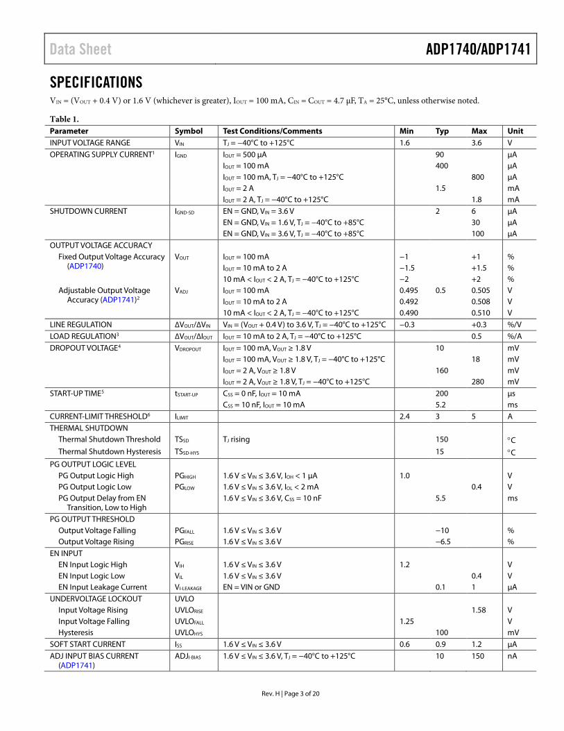
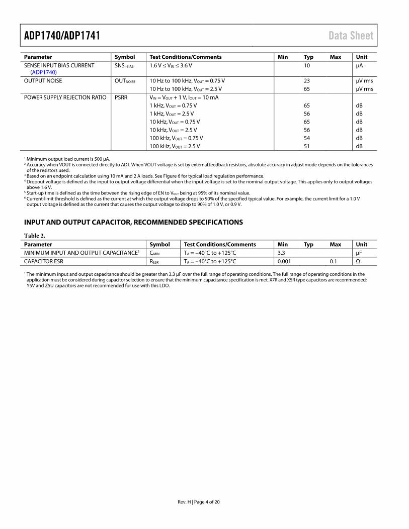
SPECIFICATIONS VIN = (VOUT + 0.4 V) or 1.6 V (whichever is greater), IOUT = 100 mA, CIN = COUT = 4.7 µF, TA = 25°C, unless otherwise noted.
Table 1. Parameter Symbol Test Conditions/Comments Min Typ Max Unit INPUT VOLTAGE RANGE VIN TJ = −40°C to +125°C 1.6 3.6 V OPERATING SUPPLY CURRENT1 IGND IOUT = 500 µA 90 µA IOUT = 100 mA 400 µA IOUT = 100 mA, TJ = −40°C to +125°C 800 µA IOUT = 2 A 1.5 mA IOUT = 2 A, TJ = −40°C to +125°C 1.8 mA SHUTDOWN CURRENT IGND-SD EN = GND, VIN = 3.6 V 2 6 µA EN = GND, VIN = 1.6 V, TJ = −40°C to +85°C 30 µA EN = GND, VIN = 3.6 V, TJ = −40°C to +85°C 100 µA OUTPUT VOLTAGE ACCURACY
Fixed Output Voltage Accuracy (ADP1740)
VOUT IOUT = 100 mA −1 +1 % IOUT = 10 mA to 2 A −1.5 +1.5 % 10 mA < IOUT < 2 A, TJ = −40°C to +125°C −2 +2 %
Adjustable Output Voltage Accuracy (ADP1741)2
VADJ IOUT = 100 mA 0.495 0.5 0.505 V IOUT = 10 mA to 2 A 0.492 0.508 V 10 mA < IOUT < 2 A, TJ = −40°C to +125°C 0.490 0.510 V
LINE REGULATION ∆VOUT/∆VIN VIN = (VOUT + 0.4 V) to 3.6 V, TJ = −40°C to +125°C −0.3 +0.3 %/V LOAD REGULATION3 ∆VOUT/∆IOUT IOUT = 10 mA to 2 A, TJ = −40°C to +125°C 0.5 %/A DROPOUT VOLTAGE4 VDROPOUT IOUT = 100 mA, VOUT ≥ 1.8 V 10 mV IOUT = 100 mA, VOUT ≥ 1.8 V, TJ = −40°C to +125°C 18 mV IOUT = 2 A, VOUT ≥ 1.8 V 160 mV IOUT = 2 A, VOUT ≥ 1.8 V, TJ = −40°C to +125°C 280 mV START-UP TIME5 tSTART-UP CSS = 0 nF, IOUT = 10 mA 200 µs CSS = 10 nF, IOUT = 10 mA 5.2 ms CURRENT-LIMIT THRESHOLD6 ILIMIT 2.4 3 5 A THERMAL SHUTDOWN
Thermal Shutdown Threshold TSSD TJ rising 150 °C Thermal Shutdown Hysteresis TSSD-HYS 15 °C
PG OUTPUT LOGIC LEVEL PG Output Logic High PGHIGH 1.6 V ≤ VIN ≤ 3.6 V, IOH < 1 µA 1.0 V PG Output Logic Low PGLOW 1.6 V ≤ VIN ≤ 3.6 V, IOL < 2 mA 0.4 V PG Output Delay from EN
Transition, Low to High 1.6 V ≤ VIN ≤ 3.6 V, CSS = 10 nF 5.5 ms
PG OUTPUT THRESHOLD Output Voltage Falling PGFALL 1.6 V ≤ VIN ≤ 3.6 V −10 % Output Voltage Rising PGRISE 1.6 V ≤ VIN ≤ 3.6 V −6.5 %
EN INPUT EN Input Logic High VIH 1.6 V ≤ VIN ≤ 3.6 V 1.2 V EN Input Logic Low VIL 1.6 V ≤ VIN ≤ 3.6 V 0.4 V EN Input Leakage Current VI-LEAKAGE EN = VIN or GND 0.1 1 µA
UNDERVOLTAGE LOCKOUT UVLO Input Voltage Rising UVLORISE 1.58 V Input Voltage Falling UVLOFALL 1.25 V Hysteresis UVLOHYS 100 mV
SOFT START CURRENT ISS 1.6 V ≤ VIN ≤ 3.6 V 0.6 0.9 1.2 µA ADJ INPUT BIAS CURRENT
(ADP1741) ADJI-BIAS 1.6 V ≤ VIN ≤ 3.6 V, TJ = −40°C to +125°C 10 150 nA
Rev. H | Page 3 of 20
ADP1740/ADP1741 Data Sheet
Parameter Symbol Test Conditions/Comments Min Typ Max Unit SENSE INPUT BIAS CURRENT
(ADP1740) SNSI-BIAS 1.6 V ≤ VIN ≤ 3.6 V 10 µA
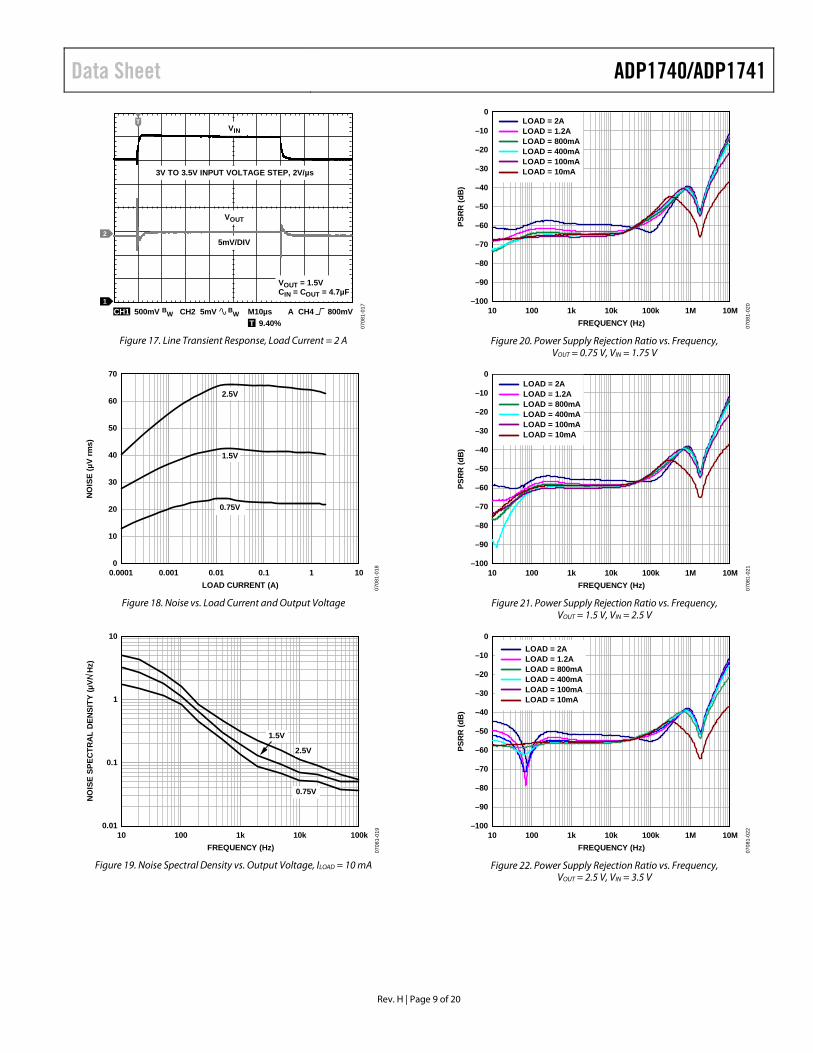
OUTPUT NOISE OUTNOISE 10 Hz to 100 kHz, VOUT = 0.75 V 23 µV rms 10 Hz to 100 kHz, VOUT = 2.5 V 65 µV rms POWER SUPPLY REJECTION RATIO PSRR VIN = VOUT + 1 V, IOUT = 10 mA 1 kHz, VOUT = 0.75 V 65 dB 1 kHz, VOUT = 2.5 V 56 dB 10 kHz, VOUT = 0.75 V 65 dB 10 kHz, VOUT = 2.5 V 56 dB 100 kHz, VOUT = 0.75 V 54 dB 100 kHz, VOUT = 2.5 V 51 dB
1 Minimum output load current is 500 μA. 2 Accuracy when VOUT is connected directly to ADJ. When VOUT voltage is set by external feedback resistors, absolute accuracy in adjust mode depends on the tolerances
of the resistors used. 3 Based on an endpoint calculation using 10 mA and 2 A loads. See Figure 6 for typical load regulation performance. 4 Dropout voltage is defined as the input to output voltage differential when the input voltage is set to the nominal output voltage. This applies only to output voltages
above 1.6 V. 5 Start-up time is defined as the time between the rising edge of EN to VOUT being at 95% of its nominal value. 6 Current-limit threshold is defined as the current at which the output voltage drops to 90% of the specified typical value. For example, the current limit for a 1.0 V
output voltage is defined as the current that causes the output voltage to drop to 90% of 1.0 V, or 0.9 V.
INPUT AND OUTPUT CAPACITOR, RECOMMENDED SPECIFICATIONS
Table 2. Parameter Symbol Test Conditions/Comments Min Typ Max Unit MINIMUM INPUT AND OUTPUT CAPACITANCE1 CMIN TA = –40°C to +125°C 3.3 µF CAPACITOR ESR RESR TA = –40°C to +125°C 0.001 0.1 Ω
1 The minimum input and output capacitance should be greater than 3.3 µF over the full range of operating conditions. The full range of operating conditions in the application must be considered during capacitor selection to ensure that the minimum capacitance specification is met. X7R and X5R type capacitors are recommended; Y5V and Z5U capacitors are not recommended for use with this LDO.
Rev. H | Page 4 of 20
Data Sheet ADP1740/ADP1741
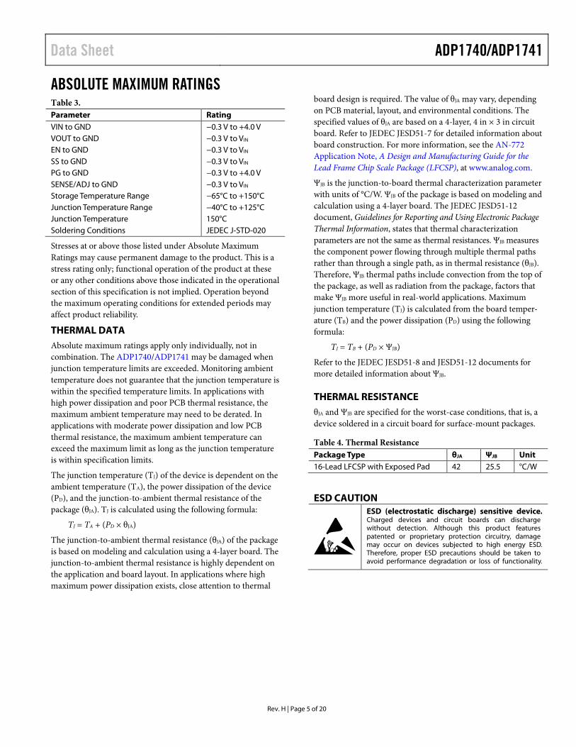
ABSOLUTE MAXIMUM RATINGS Table 3. Parameter Rating VIN to GND −0.3 V to +4.0 V VOUT to GND −0.3 V to VIN EN to GND −0.3 V to VIN SS to GND −0.3 V to VIN PG to GND −0.3 V to +4.0 V SENSE/ADJ to GND −0.3 V to VIN Storage Temperature Range −65°C to +150°C Junction Temperature Range −40°C to +125°C Junction Temperature 150°C Soldering Conditions JEDEC J-STD-020
Stresses at or above those listed under Absolute Maximum Ratings may cause permanent damage to the product. This is a stress rating only; functional operation of the product at these or any other conditions above those indicated in the operational section of this specification is not implied. Operation beyond the maximum operating conditions for extended periods may affect product reliability.
THERMAL DATA Absolute maximum ratings apply only individually, not in combination. The ADP1740/ADP1741 may be damaged when junction temperature limits are exceeded. Monitoring ambient temperature does not guarantee that the junction temperature is within the specified temperature limits. In applications with high power dissipation and poor PCB thermal resistance, the maximum ambient temperature may need to be derated. In applications with moderate power dissipation and low PCB thermal resistance, the maximum ambient temperature can exceed the maximum limit as long as the junction temperature is within specification limits.
The junction temperature (TJ) of the device is dependent on the ambient temperature (TA), the power dissipation of the device (PD), and the junction-to-ambient thermal resistance of the package (θJA). TJ is calculated using the following formula:
TJ = TA + (PD × θJA)
The junction-to-ambient thermal resistance (θJA) of the package is based on modeling and calculation using a 4-layer board. The junction-to-ambient thermal resistance is highly dependent on the application and board layout. In applications where high maximum power dissipation exists, close attention to thermal
board design is required. The value of θJA may vary, depending on PCB material, layout, and environmental conditions. The specified values of θJA are based on a 4-layer, 4 in × 3 in circuit board. Refer to JEDEC JESD51-7 for detailed information about board construction. For more information, see the AN-772 Application Note, A Design and Manufacturing Guide for the Lead Frame Chip Scale Package (LFCSP), at www.analog.com.
ΨJB is the junction-to-board thermal characterization parameter with units of °C/W. ΨJB of the package is based on modeling and calculation using a 4-layer board. The JEDEC JESD51-12 document, Guidelines for Reporting and Using Electronic Package Thermal Information, states that thermal characterization parameters are not the same as thermal resistances. ΨJB measures the component power flowing through multiple thermal paths rather than through a single path, as in thermal resistance (θJB). Therefore, ΨJB thermal paths include convection from the top of the package, as well as radiation from the package, factors that make ΨJB more useful in real-world applications. Maximum junction temperature (TJ) is calculated from the board temper-ature (TB) and the power dissipation (PD) using the following formula:
TJ = TB + (PD × ΨJB)
Refer to the JEDEC JESD51-8 and JESD51-12 documents for more detailed information about ΨJB.
THERMAL RESISTANCE θJA and ΨJB are specified for the worst-case conditions, that is, a device soldered in a circuit board for surface-mount packages.
Table 4. Thermal Resistance Package Type θJA ΨJB Unit 16-Lead LFCSP with Exposed Pad 42 25.5 °C/W
ESD CAUTION
Rev. H | Page 5 of 20
ADP1740/ADP1741 Data Sheet
Rev. H | Page 6 of 20
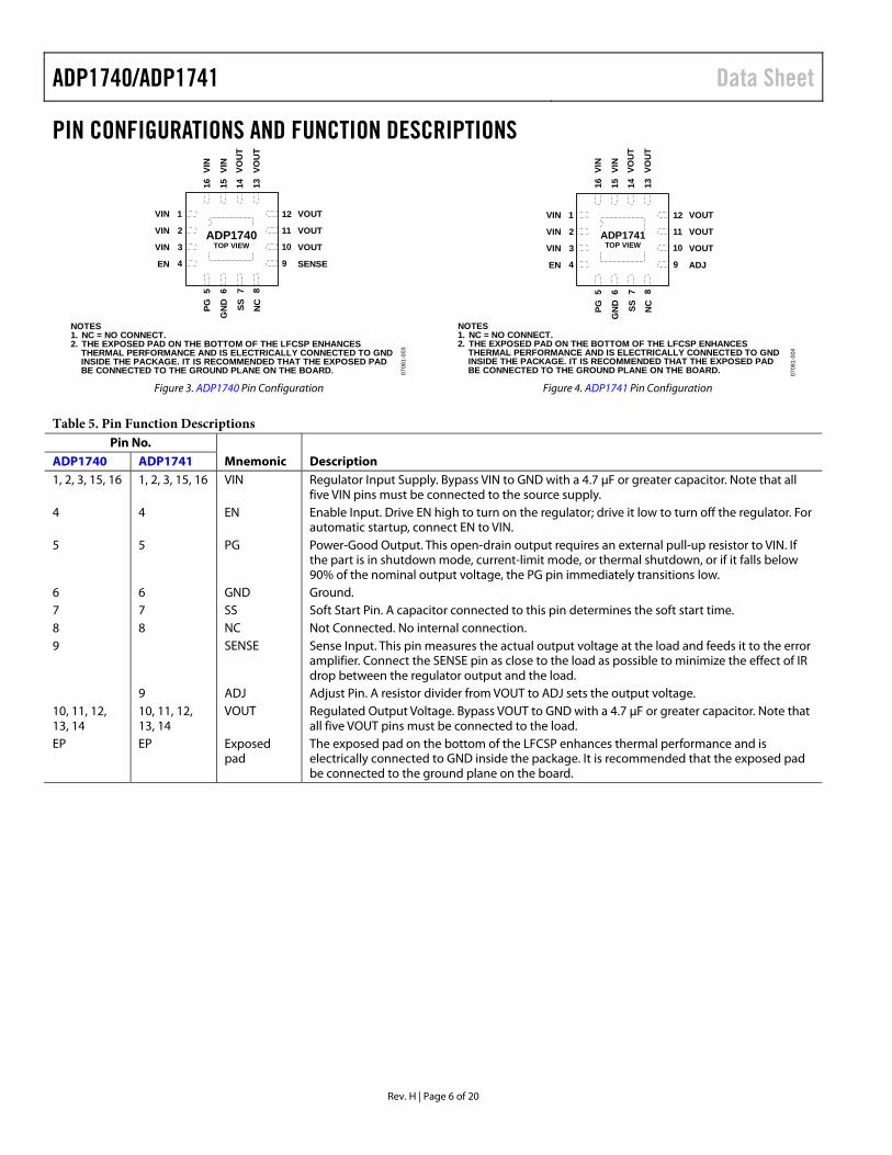
PIN CONFIGURATIONS AND FUNCTION DESCRIPTIONS
NOTES1. NC = NO CONNECT.2. THE EXPOSED PAD ON THE BOTTOM OF THE LFCSP ENHANCES
THERMAL PERFORMANCE AND IS ELECTRICALLY CONNECTED TO GNDINSIDE THE PACKAGE. IT IS RECOMMENDED THAT THE EXPOSED PADBE CONNECTED TO THE GROUND PLANE ON THE BOARD. 07
081-
003
12
11
10
1
3
4 9
265 7 8
16 15 14 13
VIN
VIN
VIN
EN
VOUT
VOU
T
VOU
T
VIN
VIN
VOUT
VOUT
SENSE
PG
GN
D SS NC
ADP1740TOP VIEW
NOTES1. NC = NO CONNECT.2. THE EXPOSED PAD ON THE BOTTOM OF THE LFCSP ENHANCES
THERMAL PERFORMANCE AND IS ELECTRICALLY CONNECTED TO GNDINSIDE THE PACKAGE. IT IS RECOMMENDED THAT THE EXPOSED PADBE CONNECTED TO THE GROUND PLANE ON THE BOARD. 07
081-
004
12
11
10
1
3
4 9
2
65 7 8
16 15 14 13
VIN
VIN
VIN
EN
VOUT
VOU
T
VOU
T
VIN
VIN
VOUT
VOUT
ADJ
PG
GN
D SS NC
ADP1741TOP VIEW
Figure 3. ADP1740 Pin Configuration Figure 4. ADP1741 Pin Configuration
Table 5. Pin Function Descriptions Pin No.
Mnemonic Description ADP1740 ADP1741 1, 2, 3, 15, 16 1, 2, 3, 15, 16 VIN Regulator Input Supply. Bypass VIN to GND with a 4.7 μF or greater capacitor. Note that all
five VIN pins must be connected to the source supply. 4 4 EN Enable Input. Drive EN high to turn on the regulator; drive it low to turn off the regulator. For
automatic startup, connect EN to VIN. 5 5 PG Power-Good Output. This open-drain output requires an external pull-up resistor to VIN. If
the part is in shutdown mode, current-limit mode, or thermal shutdown, or if it falls below 90% of the nominal output voltage, the PG pin immediately transitions low.
6 6 GND Ground. 7 7 SS Soft Start Pin. A capacitor connected to this pin determines the soft start time. 8 8 NC Not Connected. No internal connection. 9 SENSE Sense Input. This pin measures the actual output voltage at the load and feeds it to the error
amplifier. Connect the SENSE pin as close to the load as possible to minimize the effect of IR drop between the regulator output and the load.
9 ADJ Adjust Pin. A resistor divider from VOUT to ADJ sets the output voltage. 10, 11, 12, 13, 14
10, 11, 12, 13, 14
VOUT Regulated Output Voltage. Bypass VOUT to GND with a 4.7 μF or greater capacitor. Note that all five VOUT pins must be connected to the load.
EP EP Exposed pad
The exposed pad on the bottom of the LFCSP enhances thermal performance and is electrically connected to GND inside the package. It is recommended that the exposed pad be connected to the ground plane on the board.
Data Sheet ADP1740/ADP1741
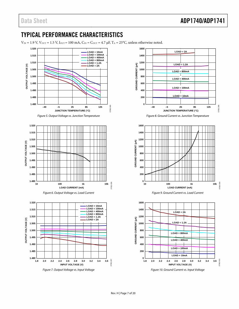
TYPICAL PERFORMANCE CHARACTERISTICS VIN = 1.9 V, VOUT = 1.5 V, IOUT = 100 mA, CIN = COUT = 4.7 µF, TA = 25°C, unless otherwise noted.
1.520
1.515
1.510
1.505
1.500
1.495
1.490
1.485
1.480–40 –5 25 85 125
OU
TPU
T VO
LTA
GE
(V)
JUNCTION TEMPERATURE (°C) 0708
1-00
5
LOAD = 10mALOAD = 100mALOAD = 400mALOAD = 800mALOAD = 1.2ALOAD = 2A
Figure 5. Output Voltage vs. Junction Temperature
1.520
1.515
1.505
1.495
1.510
1.500
1.490
1.485
1.48010 100 1k 10k
OU
TPU
T VO
LTA
GE
(V)
LOAD CURRENT (mA) 0708
1-00
6
Figure 6. Output Voltage vs. Load Current
1.8 3.63.43.23.02.82.62.42.22.0INPUT VOLTAGE (V)
LOAD = 10mALOAD = 100mALOAD = 400mALOAD = 800mALOAD = 1.2ALOAD = 2A
0708
1-00
7
1.520
1.515
1.510
1.505
1.500
1.495
1.490
1.485
1.480
OU
TPU
T VO
LTA
GE
(V)
Figure 7. Output Voltage vs. Input Voltage
1600
0
200
400
600
800
1000
1200
1400
–40 –5 25 85 125
GR
OU
ND
CU
RR
ENT
(µA
)
JUNCTION TEMPERATURE (°C)
LOAD = 10mA
LOAD = 100mA
LOAD = 400mA
LOAD = 800mA
LOAD = 1.2A
LOAD = 2A
0708
1-00
8
Figure 8. Ground Current vs. Junction Temperature
1600
1400
1200
1000
800
600
400
200
010 100 1k 10k
GR
OU
ND
CU
RR
ENT
(µA
)
LOAD CURRENT (mA) 0708
1-00
9
Figure 9. Ground Current vs. Load Current
1600
1400
1200
1000
800
600
400
200
01.8 3.63.43.23.02.82.62.42.22.0
GR
OU
ND
CU
RR
ENT
(µA
)
INPUT VOLTAGE (V)
LOAD = 10mA
LOAD = 100mA
LOAD = 400mA
LOAD = 800mA
LOAD = 1.2A
LOAD = 2A
0708
1-01
0
Figure 10. Ground Current vs. Input Voltage
Rev. H | Page 7 of 20
ADP1740/ADP1741 Data Sheet
100
90
70
80
60
50
40
30
20
10
0–40 85603510–15
SHU
TDO
WN
CU
RR
ENT
(µA
)
TEMPERATURE (°C)
1.9V2.0V2.4V2.6V3.0V3.6V
0708
1-01
1
Figure 11. Shutdown Current vs. Temperature at Various Input Voltages
0.25
0.20
0.15
0.10
0.05
01 10 100 1k 10k
DR
OPO
UT
VOLT
AG
E (V
)
LOAD CURRENT (mA) 0708
1-01
2
1.6V
2.5V
Figure 12. Dropout Voltage vs. Load Current, VOUT = 1.6 V, 2.5 V
2.50
2.35
2.45
2.40
2.30
2.25
2.20
2.15
2.102.3 2.5 2.72.4 2.6 2.8
OU
TPU
T VO
LTA
GE
(V)
INPUT VOLTAGE (V)
LOAD = 10mALOAD = 100mALOAD = 400mALOAD = 800mALOAD = 1.2ALOAD = 2A
0708
1-01
3
Figure 13. Output Voltage vs. Input Voltage (in Dropout), VOUT = 2.5 V
4500
2500
4000
3500
3000
2000
1500
1000
500
02.3 2.5 2.72.4 2.6 2.8
GR
OU
ND
CU
RR
ENT
(µA
)
INPUT VOLTAGE (V)
LOAD = 10mALOAD = 100mALOAD = 400mALOAD = 800mALOAD = 1.2ALOAD = 2A
0708
1-01
4
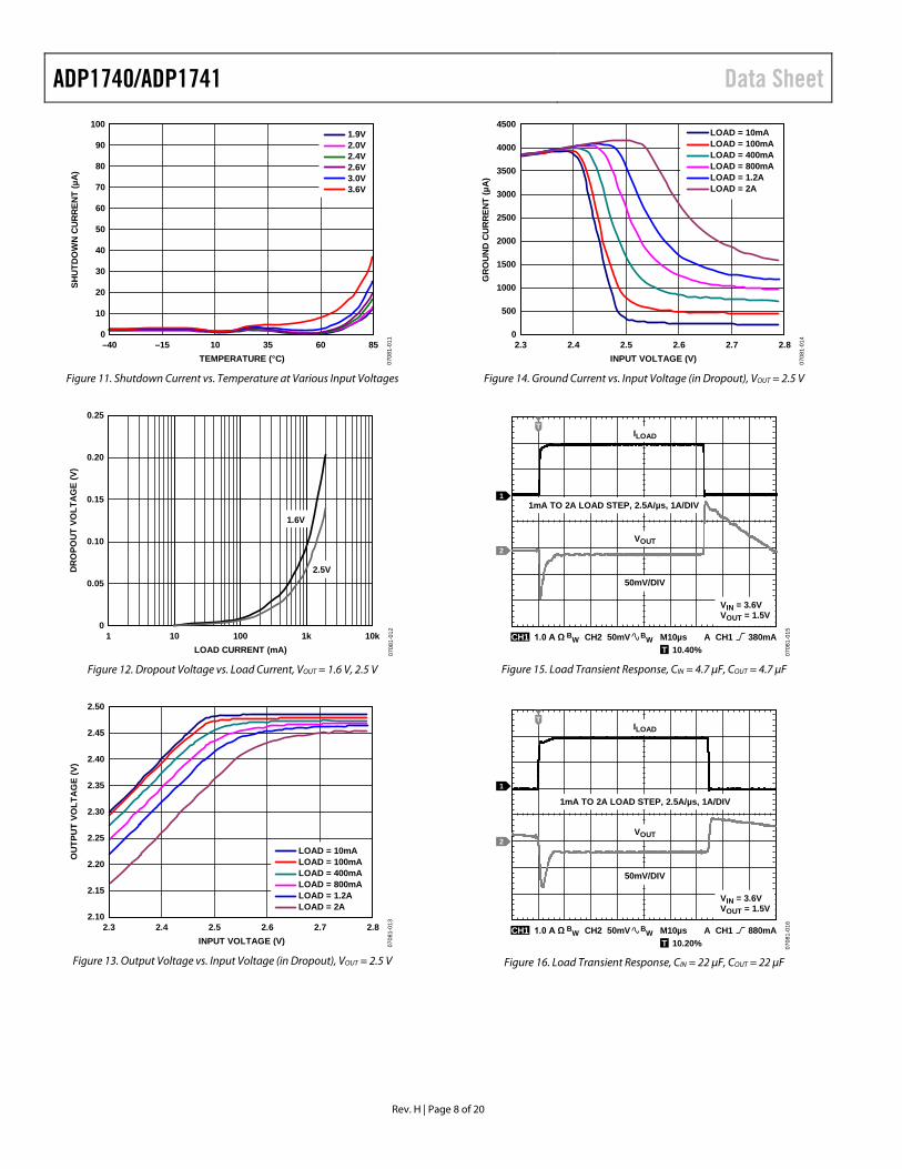
Figure 14. Ground Current vs. Input Voltage (in Dropout), VOUT = 2.5 V
CH1 1.0 A Ω BW CH2 50mV BW M10µs A CH1 380mA
1
2
T 10.40%
T
0708
1-01
5
ILOAD
1mA TO 2A LOAD STEP, 2.5A/µs, 1A/DIV
VOUT
50mV/DIV
VIN = 3.6VVOUT = 1.5V
Figure 15. Load Transient Response, CIN = 4.7 µF, COUT = 4.7 µF
CH1 1.0 A Ω BW CH2 50mV BW M10µs A CH1 880mA
1
2
T 10.20%
T
0708
1-01
6
ILOAD
1mA TO 2A LOAD STEP, 2.5A/µs, 1A/DIV
VOUT
50mV/DIV
VIN = 3.6VVOUT = 1.5V
Figure 16. Load Transient Response, CIN = 22 µF, COUT = 22 µF
Rev. H | Page 8 of 20
Data Sheet ADP1740/ADP1741
1
2
T
0708
1-01
7
CH1 500mV BW CH2 5mV BW M10µs A CH4 800mVT 9.40%
VIN
3V TO 3.5V INPUT VOLTAGE STEP, 2V/µs
VOUT
5mV/DIV
VOUT = 1.5VCIN = COUT = 4.7µF
Figure 17. Line Transient Response, Load Current = 2 A
70
0
10
20
30
40
50
60
0.0001 0.001 0.01 0.1 1 10
NO
ISE
(µV
rms)
LOAD CURRENT (A) 0708
1-01
8
0.75V
1.5V
2.5V
Figure 18. Noise vs. Load Current and Output Voltage
10
1
0.1
0.0110 100 1k 10k 100k
NO
ISE
SPEC
TRA
L D
ENSI
TY (µ
V/ H
z)
FREQUENCY (Hz) 0708
1-01
9
0.75V
1.5V
2.5V
Figure 19. Noise Spectral Density vs. Output Voltage, ILOAD = 10 mA
0
–100
–90
–80
–70
–60
–50
–40
–30
–20
–10
10 100 1k 10k 100k 1M 10M
PSR
R (d
B)
FREQUENCY (Hz)
LOAD = 2A LOAD = 1.2A LOAD = 800mA LOAD = 400mA LOAD = 100mA LOAD = 10mA
0708
1-02
0
Figure 20. Power Supply Rejection Ratio vs. Frequency,
VOUT = 0.75 V, VIN = 1.75 V
10 100 1k 10k 100k 1M 10M
PSR
R (d
B)
FREQUENCY (Hz) 0708
1-02
1
0
–100
–90
–80
–70
–60
–50
–40
–30
–20
–10 LOAD = 2A LOAD = 1.2A LOAD = 800mA LOAD = 400mA LOAD = 100mA LOAD = 10mA
Figure 21. Power Supply Rejection Ratio vs. Frequency,
VOUT = 1.5 V, VIN = 2.5 V
0
–100
–90
–80
–70
–60
–50
–40
–30
–20
–10
10 100 1k 10k 100k 1M 10M
PSR
R (d
B)
FREQUENCY (Hz) 0708
1-02
2
LOAD = 2ALOAD = 1.2ALOAD = 800mALOAD = 400mALOAD = 100mALOAD = 10mA
Figure 22. Power Supply Rejection Ratio vs. Frequency,
VOUT = 2.5 V, VIN = 3.5 V
Rev. H | Page 9 of 20
ADP1740/ADP1741 Data Sheet
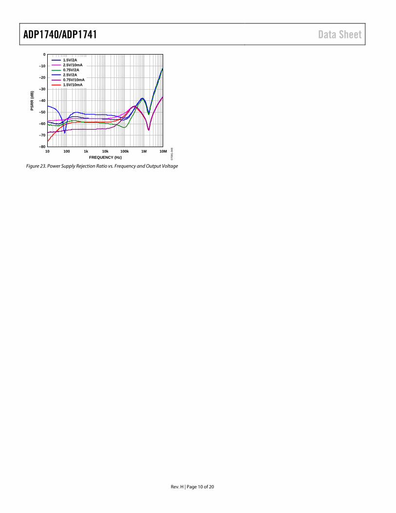
0
–80
–70
–60
–50
–40
–30
–20
–10
10 100 1k 10k 100k 1M 10M
PSR
R (d
B)
FREQUENCY (Hz)
1.5V/2A 2.5V/10mA 0.75V/2A 2.5V/2A 0.75V/10mA 1.5V/10mA
0708
1-04
8
Figure 23. Power Supply Rejection Ratio vs. Frequency and Output Voltage
Rev. H | Page 10 of 20
Data Sheet ADP1740/ADP1741
THEORY OF OPERATION The ADP1740/ADP1741 are low dropout linear regulators that use an advanced, proprietary architecture to provide high power supply rejection ratio (PSRR) and excellent line and load transient response with only a small 4.7 µF ceramic output capac-itor. Both devices operate from a 1.6 V to 3.6 V input rail and provide up to 2 A of output current. Supply current in shutdown mode is typically 2 µA.
UVLO
VOUTVIN
SENSE
SS
SHORT-CIRCUITAND THERMALPROTECTION
R1
0.5VREF R2
SHUTDOWNEN
PG
GND
ADP1740 REVERSE POLARITYPROTECTION
PGDETECT
0.9µA
0708
1-02
3
Figure 24. ADP1740 Internal Block Diagram
UVLO
VOUTVIN
ADJ
SS
SHORT-CIRCUITAND THERMALPROTECTION
0.5VREF
SHUTDOWNEN
PG
GND
ADP1741 REVERSE POLARITYPROTECTION
PGDETECT
0.9µA
0708
1-02
4
Figure 25. ADP1741 Internal Block Diagram
Internally, the ADP1740/ADP1741 consist of a reference, an error amplifier, a feedback voltage divider, and a PMOS pass transistor. Output current is delivered via the PMOS pass transistor, which is controlled by the error amplifier. The error amplifier compares the reference voltage with the feedback voltage from the output and amplifies the difference. If the feed-back voltage is lower than the reference voltage, the gate of the PMOS device is pulled lower, allowing more current to pass and increasing the output voltage. If the feedback voltage is higher than the reference voltage, the gate of the PMOS device is pulled higher, allowing less current to pass and decreasing the output voltage.
The ADP1740 is available in seven fixed output voltage options from 0.75 V to 2.5 V. The ADP1740 allows for connection of an external soft start capacitor, which controls the output voltage ramp during startup. The ADP1741 is an adjustable version with an output voltage that can be set to a value from 0.75 V to 3.3 V by an external voltage divider. Both devices are controlled by an enable pin (EN).
SOFT START FUNCTION For applications that require a controlled startup, the ADP1740/ ADP1741 provide a programmable soft start function. The programmable soft start is useful for reducing inrush current upon startup and for providing voltage sequencing. To implement soft start, connect a small ceramic capacitor from SS to GND. Upon startup, a 0.9 µA current source charges this capacitor. The ADP1740/ADP1741 start-up output voltage is limited by the voltage at SS, providing a smooth ramp-up to the nominal output voltage. The soft start time is calculated as follows:
tSS = VREF × (CSS/ISS) (1)
where: tSS is the soft start period. VREF is the 0.5 V reference voltage. CSS is the soft start capacitance from SS to GND. ISS is the current sourced from SS (0.9 µA).
When the ADP1740/ADP1741 are disabled (using the EN pin), the soft start capacitor is discharged to GND through an internal 100 Ω resistor.
2.50
0
0.25
0.50
0.75
1.00
1.25
1.50
1.75
2.00
2.25
0 2 4 6 8 10
VOLT
AG
E (V
)
TIME (ms)
EN
1nF
4.7nF
10nF
0708
1-02
5
Figure 26. VOUT Ramp-Up with External Soft Start Capacitor
Rev. H | Page 11 of 20
ADP1740/ADP1741 Data Sheet
CH1 2.0V BW CH2 500mV BW M40µs A CH1 920mV
1
2
T 9.8%
T
0708
1-02
6
EN
VOUT
500mV/DIVVOUT = 1.5VCIN = COUT = 4.7µF
Figure 27. VOUT Ramp-Up with Internal Soft Start
ADJUSTABLE OUTPUT VOLTAGE (ADP1741) The output voltage of the ADP1741 can be set over a 0.75 V to 3.3 V range. The output voltage is set by connecting a resistive voltage divider from VOUT to ADJ. The output voltage is calcu-lated using the following equation:
VOUT = 0.5 V × (1 + R1/R2) (2)
where: R1 is the resistor from VOUT to ADJ. R2 is the resistor from ADJ to GND.
The maximum bias current into ADJ is 150 nA, so to achieve less than 0.5% error due to the bias current, use values less than 60 kΩ for R2.
ENABLE FEATURE The ADP1740/ADP1741 use the EN pin to enable and disable the VOUT pins under normal operating conditions. As shown in Figure 28, when a rising voltage on EN crosses the active threshold, VOUT turns on. When a falling voltage on EN crosses the inactive threshold, VOUT turns off.
2
CH1 500mV BW CH2 500mV BW M2.0ms A CH1 1.05V
1
T 29.6%
T
0708
1-02
7
EN
VOUT
500mV/DIVVOUT = 1.5VCIN = COUT = 4.7µF
Figure 28. Typical EN Pin Operation
As shown in Figure 28, the EN pin has hysteresis built in. This hysteresis prevents on/off oscillations that can occur due to noise on the EN pin as it passes through the threshold points.
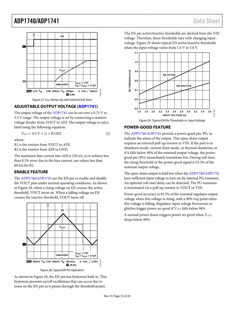
The EN pin active/inactive thresholds are derived from the VIN voltage. Therefore, these thresholds vary with changing input voltage. Figure 29 shows typical EN active/inactive thresholds when the input voltage varies from 1.6 V to 3.6 V.
1.1
0.5
0.6
0.7
0.8
0.9
1.0
1.6 1.8 2.0 2.2 2.4 2.6 2.8 3.0 3.2 3.4 3.6
EN T
HR
ESH
OLD
(V)
INPUT VOLTAGE (V)
EN ACTIVE
EN INACTIVE
0708
1-02
8
Figure 29. Typical EN Pin Thresholds vs. Input Voltage
POWER-GOOD FEATURE The ADP1740/ADP1741 provide a power-good pin, PG, to indicate the status of the output. This open-drain output requires an external pull-up resistor to VIN. If the part is in shutdown mode, current-limit mode, or thermal shutdown, or if it falls below 90% of the nominal output voltage, the power-good pin (PG) immediately transitions low. During soft start, the rising threshold of the power-good signal is 93.5% of the nominal output voltage.
The open-drain output is held low when the ADP1740/ADP1741 have sufficient input voltage to turn on the internal PG transistor. An optional soft start delay can be detected. The PG transistor is terminated via a pull-up resistor to VOUT or VIN.
Power-good accuracy is 93.5% of the nominal regulator output voltage when this voltage is rising, with a 90% trip point when this voltage is falling. Regulator input voltage brownouts or glitches trigger power no-good if VOUT falls below 90%.
A normal power-down triggers power no-good when VOUT drops below 90%.
Rev. H | Page 12 of 20
Data Sheet ADP1740/ADP1741
22
CH1 1.0V BWCH3 1.0V BW
CH2 500mV BW M40.0µs A CH3 900mV
1
T 50.40%
T
0708
1-02
9
VIN1V/DIV
VOUT500mV/DIV
PG1V/DIV
VOUT = 1.5VCIN = COUT = 4.7µF
Figure 30. Typical PG Behavior vs. VOUT, VIN Rising (VOUT = 1.5 V)
22
CH1 1.0V BWCH3 1.0V BW
CH2 500mV BW M40.0µs A CH3 900mV
1
T 50.40%
T
0708
1-03
0
VIN1V/DIV
VOUT500mV/DIV
PG1V/DIV
VOUT = 1.5VCIN = COUT = 4.7µF
Figure 31. Typical PG Behavior vs. VOUT, VIN Falling (VOUT = 1.5 V)
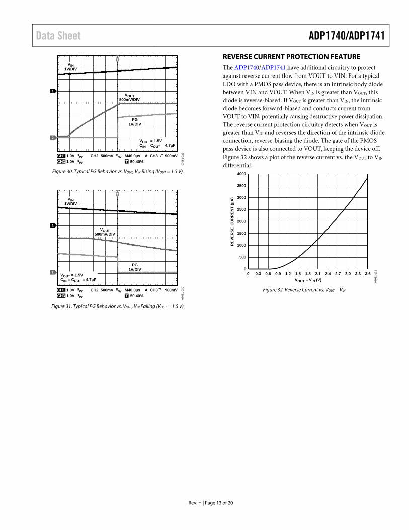
REVERSE CURRENT PROTECTION FEATURE The ADP1740/ADP1741 have additional circuitry to protect against reverse current flow from VOUT to VIN. For a typical LDO with a PMOS pass device, there is an intrinsic body diode between VIN and VOUT. When VIN is greater than VOUT, this diode is reverse-biased. If VOUT is greater than VIN, the intrinsic diode becomes forward-biased and conducts current from VOUT to VIN, potentially causing destructive power dissipation. The reverse current protection circuitry detects when VOUT is greater than VIN and reverses the direction of the intrinsic diode connection, reverse-biasing the diode. The gate of the PMOS pass device is also connected to VOUT, keeping the device off. Figure 32 shows a plot of the reverse current vs. the VOUT to VIN differential.
4000
3500
3000
2500
2000
1500
1000
500
00 0.3 0.6 0.9 1.2 1.5 1.8 2.1 2.4 2.7 3.0 3.3 3.6
REV
ERSE
CU
RR
ENT
(µA
)
VOUT – VIN (V) 0708
1-13
2
Figure 32. Reverse Current vs. VOUT − VIN
Rev. H | Page 13 of 20
ADP1740/ADP1741 Data Sheet
APPLICATIONS INFORMATION CAPACITOR SELECTION Output Capacitor
The ADP1740/ADP1741 are designed for operation with small, space-saving ceramic capacitors, but they function with most commonly used capacitors as long as care is taken with regard to the effective series resistance (ESR) value. The ESR of the output capacitor affects the stability of the LDO control loop. A minimum of 3.3 µF capacitance with an ESR of 100 mΩ or less is recommended to ensure the stability of the ADP1740/ADP1741. Transient response to changes in load current is also affected by output capacitance. Using a larger value of output capacitance improves the transient response of the ADP1740/ADP1741 to large changes in load current. Figure 33 and Figure 34 show the transient responses for output capacitance values of 4.7 µF and 22 µF, respectively.
2
CH1 1.0A Ω BW CH2 50.0mV BW M1.0µs A CH1 380mA
1
T 10.80%
T
0708
1-03
2
ILOAD1A/DIV
1mA TO 2A LOAD STEP, 2.5A/µs
VOUT50mV/DIV
VIN = 3.6V, VOUT = 1.5VCIN = COUT = 4.7µF
Figure 33. Output Transient Response, COUT = 4.7 µF
2
CH1 1.0A Ω BW CH2 50.0mV BW M1.0µs A CH1 880mA
1
T 11.80%
T
0708
1-03
3
ILOAD1A/DIV
1mA TO 2A LOAD STEP, 2.5A/µs
VOUT50mV/DIV
VIN = 3.6V, VOUT = 1.5VCIN = COUT = 22µF
Figure 34. Output Transient Response, COUT = 22 µF
Input Bypass Capacitor
Connecting a 4.7 µF capacitor from the VIN pin to GND reduces the circuit sensitivity to printed circuit board (PCB) layout, especially when long input traces or high source impedance are encountered. If output capacitance greater than 4.7 µF is required, it is recommended that the input capacitor be increased to match it.
Input and Output Capacitor Properties
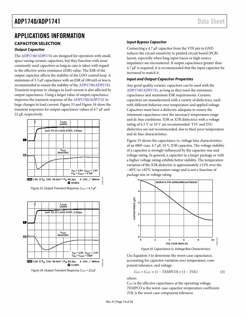
Any good quality ceramic capacitors can be used with the ADP1740/ADP1741, as long as they meet the minimum capacitance and maximum ESR requirements. Ceramic capacitors are manufactured with a variety of dielectrics, each with different behavior over temperature and applied voltage. Capacitors must have a dielectric adequate to ensure the minimum capacitance over the necessary temperature range and dc bias conditions. X5R or X7R dielectrics with a voltage rating of 6.3 V or 10 V are recommended. Y5V and Z5U dielectrics are not recommended, due to their poor temperature and dc bias characteristics.
Figure 35 shows the capacitance vs. voltage bias characteristics of an 0805 case, 4.7 μF, 10 V, X5R capacitor. The voltage stability of a capacitor is strongly influenced by the capacitor size and voltage rating. In general, a capacitor in a larger package or with a higher voltage rating exhibits better stability. The temperature variation of the X5R dielectric is approximately ±15% over the −40°C to +85°C temperature range and is not a function of package size or voltage rating.
5
4
3
2
1
00 2 4 6 8 10
CA
PAC
ITA
NC
E (µ
F)
VOLTAGE BIAS (V)
MURATA P/N GRM219R61A475KE34
0708
1-13
3
Figure 35. Capacitance vs. Voltage Bias Characteristics
Use Equation 3 to determine the worst-case capacitance, accounting for capacitor variation over temperature, com-ponent tolerance, and voltage.
CEFF = COUT × (1 − TEMPCO) × (1 − TOL) (3)
where: CEFF is the effective capacitance at the operating voltage. TEMPCO is the worst-case capacitor temperature coefficient. TOL is the worst-case component tolerance.
Rev. H | Page 14 of 20
Data Sheet ADP1740/ADP1741 In this example, the worst-case temperature coefficient (TEMPCO) over −40°C to +85°C is assumed to be 15% for an X5R dielectric. The tolerance of the capacitor (TOL) is assumed to be 10%, and COUT = 4.46 μF at 1.8 V, as shown in Figure 35.
Substituting these values in Equation 3 yields
CEFF = 4.46 μF × (1 − 0.15) × (1 − 0.1) = 3.41 μF
Therefore, the capacitor chosen in this example meets the minimum capacitance requirement of the LDO over temper-ature and tolerance at the chosen output voltage.
To guarantee the performance of the ADP1740/ADP1741, it is imperative that the effects of dc bias, temperature, and tolerances on the behavior of the capacitors be evaluated for each application.
UNDERVOLTAGE LOCKOUT The ADP1740/ADP1741 have an internal undervoltage lockout circuit that disables all inputs and the output when the input voltage is less than approximately 1.58 V. This ensures that the ADP1740/ADP1741 inputs and the output behave in a predict-able manner during power-up.
CURRENT-LIMIT AND THERMAL OVERLOAD PROTECTION The ADP1740/ADP1741 are protected against damage due to excessive power dissipation by current-limit and thermal overload protection circuits. The ADP1740/ADP1741 are designed to reach current limit when the output load reaches 3 A (typical). When the output load exceeds 3 A, the output voltage is reduced to maintain a constant current limit.
Thermal overload protection is included, which limits the junction temperature to a maximum of 150°C (typical). Under extreme conditions (that is, high ambient temperature and power dissipation) when the junction temperature begins to rise above 150°C, the output is turned off, reducing the output current to zero. When the junction temperature drops below 135°C (typical), the output is turned on again and output current is restored to its nominal value.
Consider the case where a hard short from VOUT to ground occurs. At first, the ADP1740/ADP1741 reach current limit so that only 3 A is conducted into the short. If self-heating of the junction becomes great enough to cause its temperature to rise above 150°C, thermal shutdown activates, turning off the output and reducing the output current to zero. As the junction temper-ature cools and drops below 135°C, the output turns on and conducts 3 A into the short, again causing the junction temper-ature to rise above 150°C. This thermal oscillation between 135°C and 150°C causes a current oscillation between 3 A and 0 A that continues as long as the short remains at the output.
Current-limit and thermal overload protections are intended to protect the device against accidental overload conditions. For reliable operation, device power dissipation should be externally limited so that junction temperatures do not exceed 125°C.
THERMAL CONSIDERATIONS To guarantee reliable operation, the junction temperature of the ADP1740/ADP1741 must not exceed 125°C. To ensure that the junction temperature stays below this maximum value, the user needs to be aware of the parameters that contribute to junction temperature changes. These parameters include ambient tem-perature, power dissipation in the power device, and thermal resistance between the junction and ambient air (θJA). The θJA value is dependent on the package assembly compounds used and the amount of copper to which the GND pin and the exposed pad (EP) of the package are soldered on the PCB. Table 6 shows typical θJA values for the 16-lead LFCSP for various PCB copper sizes. Table 7 shows typical ΨJB values for the 16-lead LFCSP.
Table 6. Typical θJA Values Copper Size (mm2) θJA (°C/W), LFCSP 01 130 100 80 500 69 1000 54 6400 42 1 Device soldered to minimum size pin traces.
Table 7. Typical ΨJB Values Copper Size (mm2) ΨJB (°C/W) at 1 W 100 32.7 500 31.5 1000 25.5
The junction temperature of the ADP1740/ADP1741 can be calculated from the following equation:
TJ = TA + (PD × θJA) (4)
where: TA is the ambient temperature. PD is the power dissipation in the die, given by
PD = [(VIN − VOUT) × ILOAD] + (VIN × IGND) (5)
where: VIN and VOUT are the input and output voltages, respectively. ILOAD is the load current. IGND is the ground current.
Power dissipation due to ground current is quite small and can be ignored. Therefore, the junction temperature equation can be simplified as follows:
TJ = TA + [(VIN − VOUT) × ILOAD] × θJA (6)
As shown in Equation 6, for a given ambient temperature, input-to-output voltage differential, and continuous load current, a minimum copper size requirement exists for the PCB to ensure that the junction temperature does not rise above 125°C. Figure 36 through Figure 41 show junction temperature calculations for different ambient temperatures, load currents, VIN to VOUT differentials, and areas of PCB copper.
Rev. H | Page 15 of 20
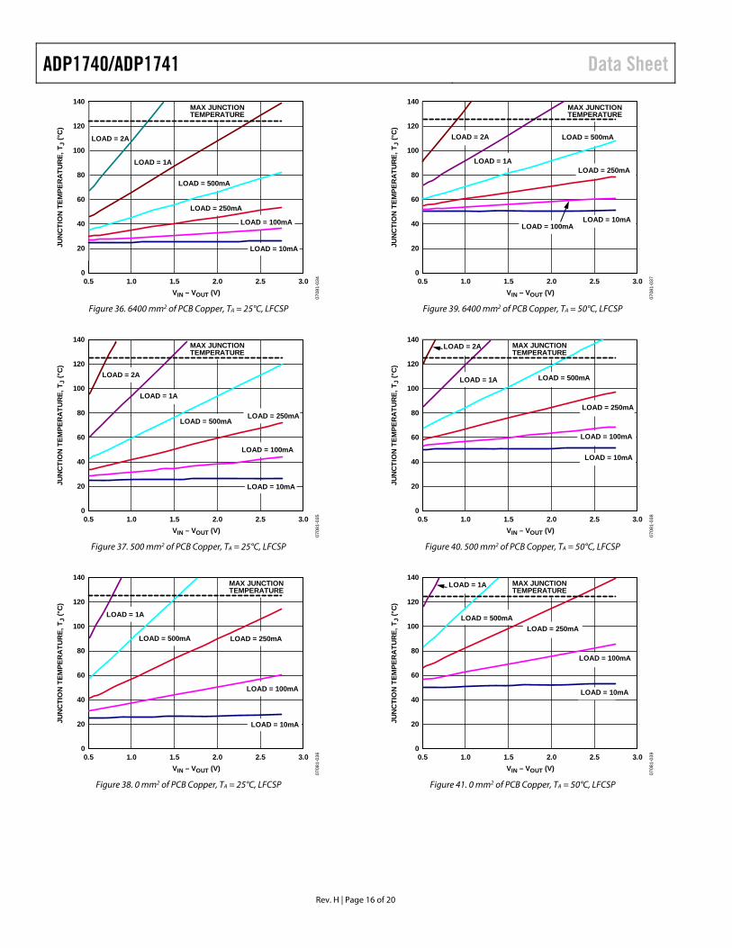
ADP1740/ADP1741 Data Sheet
Rev. H | Page 16 of 20
140
120
100
80
60
40
20
00.5 1.0 1.5 2.0 2.5 3.0
JUN
CTI
ON
TEM
PER
ATU
RE,
TJ
(°C
)
VIN – VOUT (V)
MAX JUNCTIONTEMPERATURE
LOAD = 10mA
LOAD = 100mA
LOAD = 250mA
LOAD = 500mA
LOAD = 1A
LOAD = 2A
0708
1-03
4Figure 36. 6400 mm2 of PCB Copper, TA = 25°C, LFCSP
140
120
100
80
60
40
20
00.5 1.0 1.5 2.0 2.5 3.0
JUN
CTI
ON
TEM
PER
ATU
RE,
TJ
(°C
)
VIN – VOUT (V)
MAX JUNCTIONTEMPERATURE
LOAD = 10mA
LOAD = 100mA
LOAD = 250mALOAD = 500mA
LOAD = 1A
LOAD = 2A
0708
1-03
5
Figure 37. 500 mm2 of PCB Copper, TA = 25°C, LFCSP
140
120
100
80
60
40
20
00.5 1.0 1.5 2.0 2.5 3.0
JUN
CTI
ON
TEM
PER
ATU
RE,
TJ
(°C
)
VIN – VOUT (V)
MAX JUNCTIONTEMPERATURE
LOAD = 10mA
LOAD = 100mA
LOAD = 250mALOAD = 500mA
LOAD = 1A
0708
1-03
6
Figure 38. 0 mm2 of PCB Copper, TA = 25°C, LFCSP
140
120
100
80
60
40
20
00.5 1.0 1.5 2.0 2.5 3.0
JUN
CTI
ON
TEM
PER
ATU
RE,
TJ
(°C
)
VIN – VOUT (V)
MAX JUNCTIONTEMPERATURE
LOAD = 10mALOAD = 100mA
LOAD = 250mA
LOAD = 500mA
LOAD = 1A
LOAD = 2A
0708
1-03
7
Figure 39. 6400 mm2 of PCB Copper, TA = 50°C, LFCSP
140
120
100
80
60
40
20
00.5 1.0 1.5 2.0 2.5 3.0
JUN
CTI
ON
TEM
PER
ATU
RE,
TJ
(°C
)
VIN – VOUT (V)
MAX JUNCTIONTEMPERATURE
LOAD = 10mA
LOAD = 100mA
LOAD = 250mA
LOAD = 500mALOAD = 1A
LOAD = 2A
0708
1-03
8
Figure 40. 500 mm2 of PCB Copper, TA = 50°C, LFCSP
140
120
100
80
60
40
20
00.5 1.0 1.5 2.0 2.5 3.0
JUN
CTI
ON
TEM
PER
ATU
RE,
TJ
(°C
)
VIN – VOUT (V)
MAX JUNCTIONTEMPERATURE
LOAD = 10mA
LOAD = 100mA
LOAD = 250mALOAD = 500mA
LOAD = 1A
0708
1-03
9
Figure 41. 0 mm2 of PCB Copper, TA = 50°C, LFCSP
Data Sheet ADP1740/ADP1741
Rev. H | Page 17 of 20
In cases where the board temperature is known, the thermal characterization parameter, ΨJB, can be used to estimate the junction temperature rise. Maximum junction temperature (TJ) is calculated from the board temperature (TB) and the power dissipation (PD) using the following formula:
TJ = TB + (PD × ΨJB) (7)
Figure 42 through Figure 45 show junction temperature calculations for different board temperatures, load currents, VIN to VOUT differentials, and areas of PCB copper.
140
120
100
80
60
40
20
00.25 0.75 1.25 1.75 2.25 2.75
JUN
CTI
ON
TEM
PER
ATU
RE,
TJ
(°C
)
VIN – VOUT (V)
MAX JUNCTIONTEMPERATURE
LOAD = 10mALOAD = 100mA
LOAD = 250mA
LOAD = 500mA
LOAD = 1A
LOAD = 2A
0708
1-04
0
Figure 42. 500 mm2 of PCB Copper, TB = 25°C, LFCSP
140
120
100
80
60
40
20
00.25 0.75 1.25 1.75 2.25 2.75
JUN
CTI
ON
TEM
PER
ATU
RE,
TJ
(°C
)
VIN – VOUT (V)
MAX JUNCTIONTEMPERATURE
LOAD = 10mALOAD = 100mA
LOAD = 250mA
LOAD = 500mA
LOAD = 1A
LOAD = 2A
0708
1-04
1
Figure 43. 500 mm2 of PCB Copper, TB = 50°C, LFCSP
140
120
100
80
60
40
20
00.25 0.75 1.25 1.75 2.25 2.75
JUN
CTI
ON
TEM
PER
ATU
RE,
TJ
(°C
)
VIN – VOUT (V)
MAX JUNCTIONTEMPERATURE
LOAD = 10mA
LOAD = 250mA
LOAD = 500mA
LOAD = 1ALOAD = 2A
LOAD = 100mA
0708
1-04
2
Figure 44. 1000 mm2 of PCB Copper, TB = 25°C, LFCSP
140
120
100
80
60
40
20
00.25 0.75 1.25 1.75 2.25 2.75
JUN
CTI
ON
TEM
PER
ATU
RE,
TJ
(°C
)
VIN – VOUT (V)
MAX JUNCTIONTEMPERATURE
LOAD = 10mA
LOAD = 250mA
LOAD = 500mA
LOAD = 1A
LOAD = 100mA
0708
1-04
3
LOAD = 2A
Figure 45. 1000 mm2 of PCB Copper, TB = 50°C, LFCSP
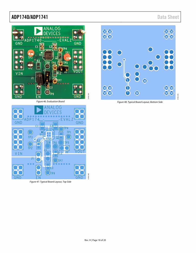
PCB LAYOUT CONSIDERATIONS Heat dissipation from the package can be improved by increasing the amount of copper attached to the pins of the ADP1740/ ADP1741. However, as shown in Table 6, a point of diminishing returns is eventually reached, beyond which an increase in the copper size does not yield significant heat dissipation benefits.
Here are a few general tips when designing PCBs:
Place the input capacitor as close as possible to the VIN and GND pins.
Place the output capacitor as close as possible to the VOUT and GND pins.
Place the soft start capacitor close to the SS pin. Connect the load as close as possible to the VOUT and
SENSE pins (ADP1740) or to the VOUT and ADJ pins (ADP1741).
Use of 0603 or 0805 size capacitors and resistors achieves the smallest possible footprint solution on boards where area is limited.
ADP1740/ADP1741 Data Sheet
Rev. H | Page 18 of 20
0708
1-04
4
Figure 46. Evaluation Board
0708
1-04
5
Figure 47. Typical Board Layout, Top Side
0708
1-04
6
Figure 48. Typical Board Layout, Bottom Side
Data Sheet ADP1740/ADP1741
Rev. H | Page 19 of 20
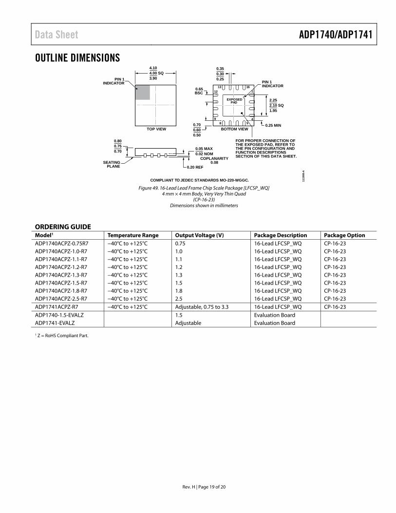
OUTLINE DIMENSIONS
COMPLIANT TO JEDEC STANDARDS MO-220-WGGC. 1119
08-A
10.65BSC
BOTTOM VIEWTOP VIEW
16
589
1213
4
EXPOSEDPAD
PIN 1INDICATOR
4.104.00 SQ3.90
0.700.600.50
SEATINGPLANE
0.800.750.70 0.05 MAX
0.02 NOM
0.20 REF
0.25 MIN
COPLANARITY0.08
PIN 1INDICATOR
0.350.300.25
2.252.10 SQ1.95
FOR PROPER CONNECTION OFTHE EXPOSED PAD, REFER TOTHE PIN CONFIGURATION ANDFUNCTION DESCRIPTIONSSECTION OF THIS DATA SHEET.
Figure 49. 16-Lead Lead Frame Chip Scale Package [LFCSP_WQ]
4 mm × 4 mm Body, Very Very Thin Quad (CP-16-23)
Dimensions shown in millimeters
ORDERING GUIDE Model1 Temperature Range Output Voltage (V) Package Description Package Option ADP1740ACPZ-0.75R7 −40°C to +125°C 0.75 16-Lead LFCSP_WQ CP-16-23 ADP1740ACPZ-1.0-R7 −40°C to +125°C 1.0 16-Lead LFCSP_WQ CP-16-23 ADP1740ACPZ-1.1-R7 −40°C to +125°C 1.1 16-Lead LFCSP_WQ CP-16-23 ADP1740ACPZ-1.2-R7 −40°C to +125°C 1.2 16-Lead LFCSP_WQ CP-16-23 ADP1740ACPZ-1.3-R7 −40°C to +125°C 1.3 16-Lead LFCSP_WQ CP-16-23 ADP1740ACPZ-1.5-R7 −40°C to +125°C 1.5 16-Lead LFCSP_WQ CP-16-23 ADP1740ACPZ-1.8-R7 −40°C to +125°C 1.8 16-Lead LFCSP_WQ CP-16-23 ADP1740ACPZ-2.5-R7 −40°C to +125°C 2.5 16-Lead LFCSP_WQ CP-16-23 ADP1741ACPZ-R7 −40°C to +125°C Adjustable, 0.75 to 3.3 16-Lead LFCSP_WQ CP-16-23 ADP1740-1.5-EVALZ 1.5 Evaluation Board ADP1741-EVALZ Adjustable Evaluation Board 1 Z = RoHS Compliant Part.
ADP1740/ADP1741 Data Sheet
NOTES
©2008–2015 Analog Devices, Inc. All rights reserved. Trademarks and registered trademarks are the property of their respective owners. D07081-0-1/15(H)
Rev. H | Page 20 of 20