Embed Size (px)
Citation preview
2011 International Conference on Compound Semiconductor Manufacturing Technology
May 16th - 19th, 2011 Register Online at
www.CSMANTECH.org
Hyatt Grand Champions Resort, Villas and Spa, Indian Wells, California, U.S.A.
™
™
2 2011 Compound Semiconductor MANTECH
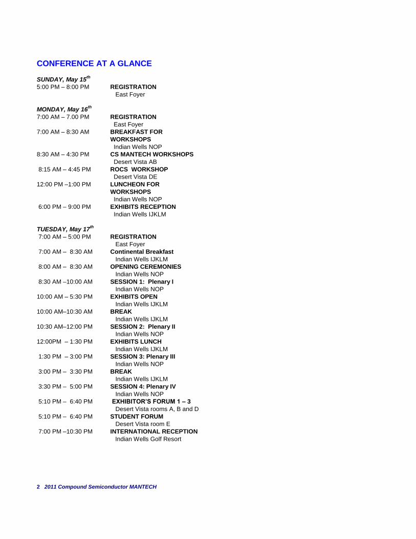
CONFERENCE AT A GLANCE SUNDAY, May 15
th
5:00 PM – 8:00 PM REGISTRATION
East Foyer
MONDAY, May 16th
7:00 AM – 7.00 PM REGISTRATION
East Foyer
7:00 AM – 8:30 AM BREAKFAST FOR
WORKSHOPS
Indian Wells NOP
8:30 AM – 4:30 PM CS MANTECH WORKSHOPS
Desert Vista AB
8:15 AM – 4:45 PM ROCS WORKSHOP
Desert Vista DE
12:00 PM –1:00 PM LUNCHEON FOR
WORKSHOPS
Indian Wells NOP
6:00 PM – 9:00 PM EXHIBITS RECEPTION
Indian Wells IJKLM
TUESDAY, May 17th
7:00 AM – 5:00 PM REGISTRATION
East Foyer
7:00 AM – 8:30 AM Continental Breakfast
Indian Wells IJKLM
8:00 AM – 8:30 AM OPENING CEREMONIES
Indian Wells NOP
8:30 AM –10:00 AM SESSION 1: Plenary I
Indian Wells NOP
10:00 AM – 5:30 PM EXHIBITS OPEN
Indian Wells IJKLM
10:00 AM–10:30 AM BREAK
Indian Wells IJKLM
10:30 AM–12:00 PM SESSION 2: Plenary II
Indian Wells NOP
12:00PM – 1:30 PM EXHIBITS LUNCH
Indian Wells IJKLM
1:30 PM – 3:00 PM SESSION 3: Plenary III
Indian Wells NOP
3:00 PM – 3:30 PM BREAK
Indian Wells IJKLM
3:30 PM – 5:00 PM SESSION 4: Plenary IV
Indian Wells NOP
5:10 PM – 6:40 PM EXHIBITOR’S FORUM 1 – 3
Desert Vista rooms A, B and D
5:10 PM – 6:40 PM STUDENT FORUM
Desert Vista room E
7:00 PM –10:30 PM INTERNATIONAL RECEPTION
Indian Wells Golf Resort
3 2011 Compound Semiconductor MANTECH
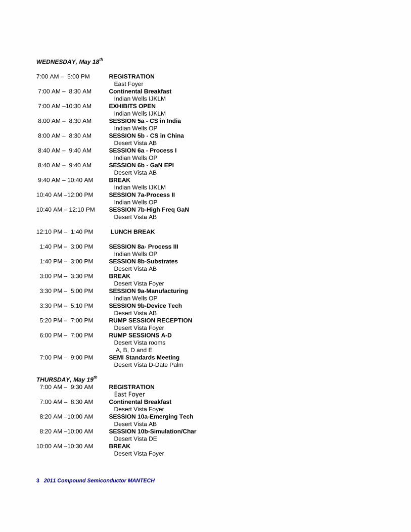
WEDNESDAY, May 18th
7:00 AM – 5:00 PM REGISTRATION
East Foyer
7:00 AM – 8:30 AM Continental Breakfast
Indian Wells IJKLM
7:00 AM –10:30 AM EXHIBITS OPEN
Indian Wells IJKLM
8:00 AM – 8:30 AM SESSION 5a - CS in India
Indian Wells OP
8:00 AM – 8:30 AM SESSION 5b - CS in China
Desert Vista AB
8:40 AM – 9:40 AM SESSION 6a - Process I
Indian Wells OP
8:40 AM – 9:40 AM SESSION 6b - GaN EPI
Desert Vista AB
9:40 AM – 10:40 AM BREAK
Indian Wells IJKLM
10:40 AM –12:00 PM SESSION 7a-Process II
Indian Wells OP
10:40 AM – 12:10 PM SESSION 7b-High Freq GaN
Desert Vista AB
12:10 PM – 1:40 PM LUNCH BREAK
1:40 PM – 3:00 PM SESSION 8a- Process III
Indian Wells OP
1:40 PM – 3:00 PM SESSION 8b-Substrates
Desert Vista AB
3:00 PM – 3:30 PM BREAK
Desert Vista Foyer
3:30 PM – 5:00 PM SESSION 9a-Manufacturing
Indian Wells OP
3:30 PM – 5:10 PM SESSION 9b-Device Tech
Desert Vista AB
5:20 PM – 7:00 PM RUMP SESSION RECEPTION
Desert Vista Foyer
6:00 PM – 7:00 PM RUMP SESSIONS A-D
Desert Vista rooms
A, B, D and E
7:00 PM – 9:00 PM SEMI Standards Meeting
Desert Vista D-Date Palm
THURSDAY, May 19th
7:00 AM – 9:30 AM REGISTRATION
East Foyer 7:00 AM – 8:30 AM Continental Breakfast
Desert Vista Foyer
8:20 AM –10:00 AM SESSION 10a-Emerging Tech
Desert Vista AB
8:20 AM –10:00 AM SESSION 10b-Simulation/Char
Desert Vista DE
10:00 AM –10:30 AM BREAK
Desert Vista Foyer
4 2011 Compound Semiconductor MANTECH
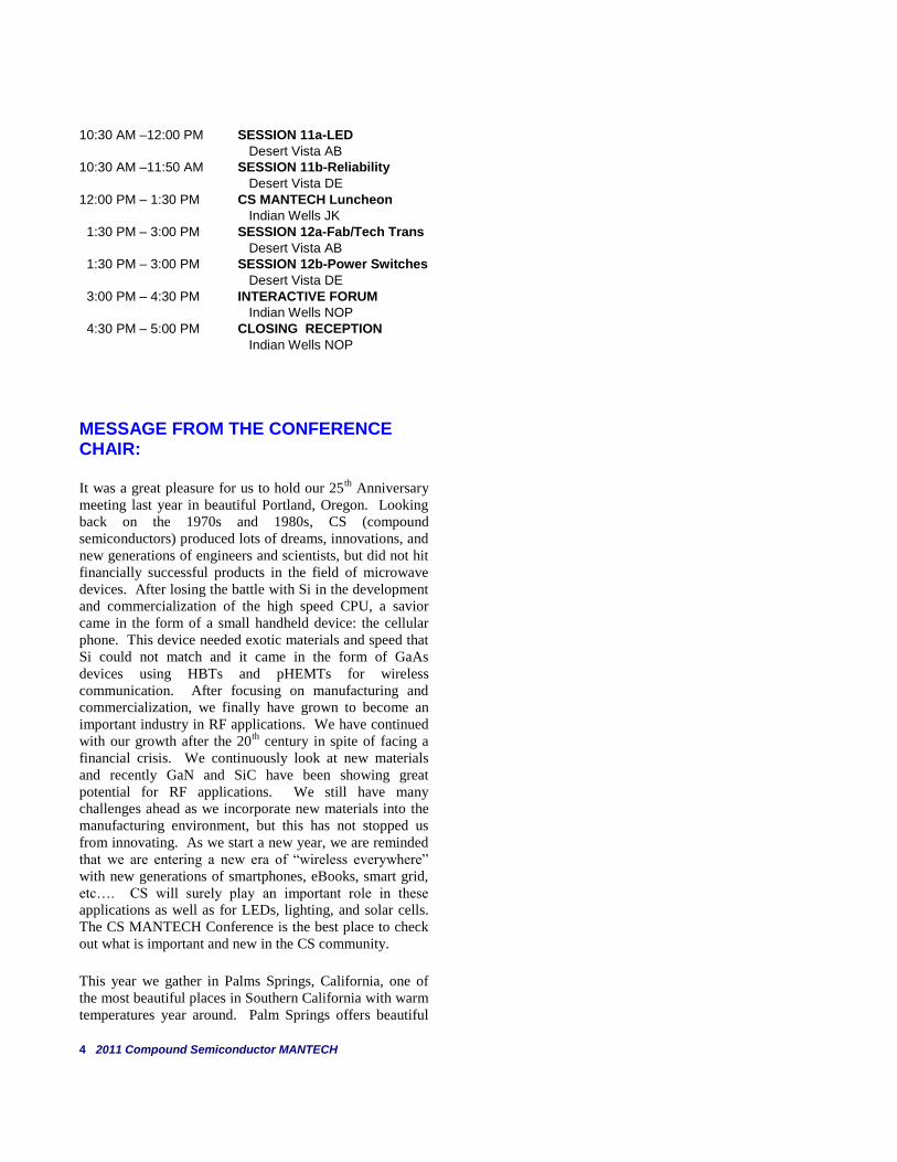
10:30 AM –12:00 PM SESSION 11a-LED
Desert Vista AB
10:30 AM –11:50 AM SESSION 11b-Reliability
Desert Vista DE
12:00 PM – 1:30 PM CS MANTECH Luncheon
Indian Wells JK
1:30 PM – 3:00 PM SESSION 12a-Fab/Tech Trans
Desert Vista AB
1:30 PM – 3:00 PM SESSION 12b-Power Switches
Desert Vista DE
3:00 PM – 4:30 PM INTERACTIVE FORUM
Indian Wells NOP
4:30 PM – 5:00 PM CLOSING RECEPTION
Indian Wells NOP
MESSAGE FROM THE CONFERENCE CHAIR:
It was a great pleasure for us to hold our 25th
Anniversary
meeting last year in beautiful Portland, Oregon. Looking
back on the 1970s and 1980s, CS (compound
semiconductors) produced lots of dreams, innovations, and
new generations of engineers and scientists, but did not hit
financially successful products in the field of microwave
devices. After losing the battle with Si in the development
and commercialization of the high speed CPU, a savior
came in the form of a small handheld device: the cellular
phone. This device needed exotic materials and speed that
Si could not match and it came in the form of GaAs
devices using HBTs and pHEMTs for wireless
communication. After focusing on manufacturing and
commercialization, we finally have grown to become an
important industry in RF applications. We have continued
with our growth after the 20th
century in spite of facing a
financial crisis. We continuously look at new materials
and recently GaN and SiC have been showing great
potential for RF applications. We still have many
challenges ahead as we incorporate new materials into the
manufacturing environment, but this has not stopped us
from innovating. As we start a new year, we are reminded
that we are entering a new era of “wireless everywhere”
with new generations of smartphones, eBooks, smart grid,
etc…. CS will surely play an important role in these
applications as well as for LEDs, lighting, and solar cells.
The CS MANTECH Conference is the best place to check
out what is important and new in the CS community.
This year we gather in Palms Springs, California, one of
the most beautiful places in Southern California with warm
temperatures year around. Palm Springs offers beautiful
5 2011 Compound Semiconductor MANTECH
landscapes, fine dining, shopping, or simply relaxation.
And if you are into more active pursuits, Palm Springs has
some of the best golf courses in the world.
The purpose of CS MANTECH is very clear. We strive to
contribute to the overall CS industry from manufacturing
to market information. We help provide a venue where
ideas can be exchanged freely with expanded
communication among participants from academia,
industry, and government. I am very excited that you can
join our family, and I welcome any ideas that would help
enrich our experience.
There will be a broad array of educational opportunities
including our Monday workshops. From the last
conference in 2010, the ROCS (Reliability of Compound
Semiconductors) Workshop started co-locating with CS
MANTECH. You can choose the MANTECH workshop
and/or ROCS on Monday.
Students can also interact with potential employers.
Industry veterans can keep contact with old friends, meet
new ones, and take the pulse of the industry. The technical
sessions will offer the current state of the art in materials,
processing, reliability, and device technology across the
compound semiconductor spectrum.
This is the annual event where our industry comes
together. Come join us!
Yohei Otoki
Hitachi Cable America Chairman, 2011 CS MANTECH Conference
6 2011 Compound Semiconductor MANTECH
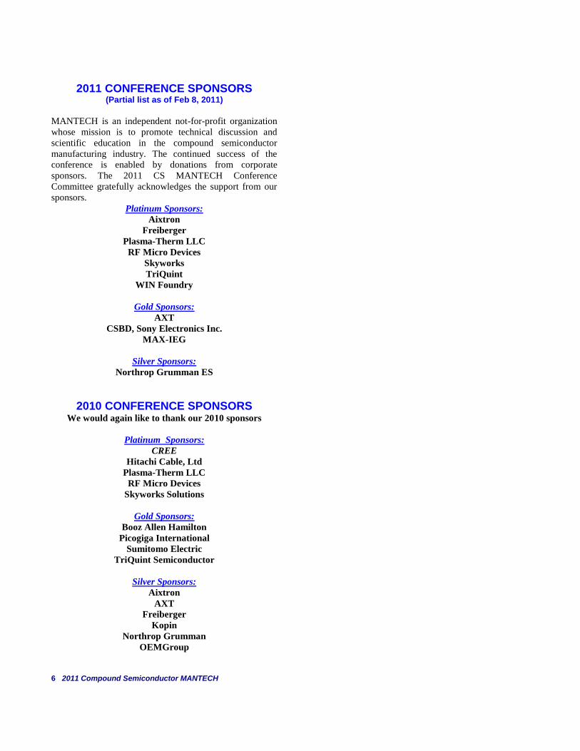
2011 CONFERENCE SPONSORS (Partial list as of Feb 8, 2011)
MANTECH is an independent not-for-profit organization
whose mission is to promote technical discussion and
scientific education in the compound semiconductor
manufacturing industry. The continued success of the
conference is enabled by donations from corporate
sponsors. The 2011 CS MANTECH Conference
Committee gratefully acknowledges the support from our
sponsors.
Platinum Sponsors:
Aixtron
Freiberger
Plasma-Therm LLC
RF Micro Devices
Skyworks
TriQuint
WIN Foundry
Gold Sponsors:
AXT
CSBD, Sony Electronics Inc.
MAX-IEG
Silver Sponsors:
Northrop Grumman ES
2010 CONFERENCE SPONSORS We would again like to thank our 2010 sponsors
Platinum Sponsors:
CREE
Hitachi Cable, Ltd
Plasma-Therm LLC
RF Micro Devices
Skyworks Solutions
Gold Sponsors:
Booz Allen Hamilton
Picogiga International
Sumitomo Electric
TriQuint Semiconductor
Silver Sponsors:
Aixtron
AXT
Freiberger
Kopin
Northrop Grumman
OEMGroup
7 2011 Compound Semiconductor MANTECH
2011 CONFERENCE HIGHLIGHTS The 2011 CS MANTECH program begins on Monday
May 16th
with a series of tutorial workshops. This year’s
workshops will focus on device/process simulation,
modeling, high frequency measurement and
characterization, passive and EM simulation and design kit
infrastructures. The workshop theme is “From Process to
Product”. In addition, this year CS MANTECH will host
the internationally acclaimed ROCS Workshop (Reliability
of Compound Semiconductors) which will be held on the
opening day (Mon 5/16). The ROCS Workshop will
present the latest results and new developments in all
phases of Compound Semiconductor Reliability (see
http://www.jedec.org/home/gaas/ for details).
On Monday evening the Exhibits open at 6:00 pm with the
traditional Exhibits Reception. The CS MANTECH
exhibits are an excellent opportunity to view suppliers of
materials, services and tools from around the globe. This
is a great time to renew old relationships and establish new
ones while enjoying the fine food and libations of Indian
Wells (Palm Springs).
The CS MANTECH Conference formally opens on
Tuesday morning with a brief overview of the conference
and the awards presentation for the best papers from the
2010 conference. This is immediately followed by the two
Plenary Sessions which will cover topics ranging from the
latest in RF module technology to the newest in high
frequency devices.
After lunch, we’ll see an analysis of our business and
technology trends, followed by a session covering 3G/4G
and LTE requirements for wireless systems and the role
compound semiconductor devices play in meeting these
requirements.
The Tuesday technical session will conclude with our
Exhibitor’s Forum. Also, in parallel will be our Student
Forum, which is designed to be an interactive session
between students and the industry that is destined to hire
them. As Tuesday evening approaches, we will walk out
of the Hyatt Grand Champions to Indian Wells Golf Resort
where we’ll eat, drink, and enjoy a 9-hole putting contest
with old and new friends.
The Sessions on Wednesday morning will start with two
parallel invited talks describing the Future of Compound
Semiconductor Technologies in India and in China. Then
we start the parallel sessions with world class technical
papers on the compound semiconductor industry. One side
of Wednesday’s two parallel sessions focuses on emerging
8 2011 Compound Semiconductor MANTECH
wide band-gap technologies, and the other on
manufacturing practices and processing. These are topics
for which CS MANTECH is well known.
In order to allow additional opportunity to interact with the
Exhibitors before the Exhibits close, this year we will have
a longer one hour break during the morning session to take
place in the exhibit hall.
Wednesday evening features the popular Rump Sessions.
Eat, drink, and debate! Attendees may join any or all (if
you move quickly) of the four parallel topics, where
moderators will encourage informal, lively, and highly
interactive discussions.
The Sessions on Thursday morning will start a little later
and the day will proceed with parallel sessions. The
morning continues with excellent technical papers on
Emerging Technologies, LEDs, simulation &
characterization, and reliability. Following this session
lunch will be sponsored by CS MANTECH. Thursday
afternoon will include our closing two sessions on fab
management/technology transfer and power switches
followed by the Interactive Forum poster session. This
poster session includes new papers on a diverse range of
topics, as well as poster versions of all the papers presented
earlier in the technical program. Attendees will have the
opportunity to meet with authors to discuss their papers in
detail. Attendees of the Interactive Forum will vote for
the best poster, and the winning author will receive the
Best Poster Award.
The Conference Closing Reception will follow the
Interactive Forum. In a warped and hopefully humorous
manner we will be holding a Haiku contest with CS
MANTECH as the theme for the writings. In English,
Haiku most often takes the form of three lines with a 5,
then 7, then 5 syllable format. Limit of one submission per
person, please. Our closing reception will also feature a
drawing for an iPod. All those who completed and
submitted their Feedback Forms will have a chance to win!
9 2011 Compound Semiconductor MANTECH
CS MANTECH WORKSHOPS Traditionally CS MANTECH offers Monday workshops
featuring topics of interest to the compound semiconductor
community. Workshop attendees get the opportunity to
expand their knowledge beyond their own specialties, as
industry experts share their knowledge and valuable
experiences in a tutorial manner. Past programs have
offered many interesting topics ranging from materials and
processing, test and characterization, applications and
market analysis, to engineering management and
intellectual property rights. This year’s Workshop theme
is “From Process to Product”. CS MANTECH is pleased
to offer a series of talks to cover device/process simulation,
modeling, high frequency measurements and
characterization, passive and EM simulation and design kit
infrastructures. These invited talks are intended to provide
the Workshop attendees with an opportunity to appreciate
what product/circuit designers care about at the circuit
level and how processing information is used in the
realization of products by other groups. This allows
process development and sustaining teams to have a better
understanding of how product and circuit level needs
translate to process technology requirements. The planned
tutorials deliver a good overview for those just wanting to
learn more, but will also provide sufficient breadth of
topics and detail that even those in the field will learn
something new.
Our workshops will begin with a talk by Dr. Charlie Fields
from HRL Laboratories, LLC. His presentation covers the
use of process simulation tools to assist the development of
compound semiconductor devices and circuits. He will
discuss the capability of qualitative and quantitative
analysis of device and circuit cross-sections to uncover
potential device/circuit failures and reliability issues by
simulation tools. He will share simulation results that
allow verification of process design rules with the goal of
design for manufacturability. His talk highlights the
benefits of using process simulation tools to design a
fabrication process that is robust and high yield in the
process development stage. As we know, a robust and high
yield process reduces the expense of IC failure analysis as
well as the overall product cost. Dr. Fields has a Ph.D.
from the University of California at Berkeley and is a
Senior Project Manager and the Trusted Foundry Program
Manager at HRL. His current research work involves
photolithography for advanced III-V devices and circuits,
process simulation, and high frequency device
characterization and modeling.
10 2011 Compound Semiconductor MANTECH
The second talk will be presented by Dr. Pete Zampardi
from Skyworks Solutions, Inc. His talk will focus on
“Modeling for Process”. This tutorial discusses the overall
strategy for developing and implementing simple physics-
based models, including statistics, for the design of RF
circuits in GaAs HBT or BiFET technology. While the
examples used target the development of handset power
amplifiers, the general principle is applicable to other
devices and technologies (the analogies for some other
technologies will be discussed). Key features of this
approach are: the idea of “unified” models where devices
share parameters if they are constructed from the same
physical process layers, the use of Design-of-Experiments
(DOE) to define the variations and minimize the required
number of simulation runs, and the idea of a “device-up”
approach that uses basic device physics and process
information to define the factors and determine model
parameter correlation using experimental DOE. Using this
approach, the links between process parameters, model
parameters, and circuit performance become much clearer
than using curve-fitting. This approach can also be used to
enhance already existing models with a few simple
modifications. Specific examples of GaAs HBTs and
GaAs MESFETs from a BiFET process will be presented. Dr. Zampardi has a Ph.D. from the University of California
at Los Angeles and currently is a Technical Director for
Device Design, Modeling, and Characterization at
Skyworks.
The next talk is an Electronic Design Automation (EDA)
tutorial focused on FET and pHEMT Modeling and
Characterization. Mr. Paul Litzenberg of TriQuint
Semiconductor will briefly explore pHEMT small signal
and noise models, and then focus primarily on large signal
(nonlinear) pHEMT models. Different bias regions of
pHEMT operation and the “compact” model equation sets
commonly used to model behavior in these respective
regions will be described. The process of pHEMT
characterization, model parameter extraction, and model
verification will be presented. The accuracy of several
large signal models, including Angelov, EEHEMT and
TOM4, will be illustrated through comparison of simulated
and measured device characteristics. Finally, advanced
pHEMT modeling topics will be discussed including
temperature variation, process (manufacturing) variation,
and size scaling. Mr. Litzenberg is the Commercial
Foundry Engineering Director at TriQuint Semiconductor
in Hillsboro Oregon. He leads a team of engineers and
technicians who develop and maintain the Process
Development Kits (PDK’s) for all TriQuint 150 mm GaAs
IC process technologies, FET and HBT technologies,
including device characterization, model development,
model parameter extraction, model verification, layout
11 2011 Compound Semiconductor MANTECH
macros and layout verification. Mr. Litzenberg earned an
MSEE degree from Arizona State University and a BSEE
degree from the University of Illinois.
Dr. Marcel Tutt from Freescale will give a tutorial on “RF
and Low Noise Measurements for III-V Devices”. III-V
Devices have applications in frequencies ranging from RF
to millimeter wave. These applications include low noise
amplifiers, power amplifiers, frequency conversion
devices, and sources. In order to determine the suitability
of a device for a given application or the performance of a
III-V circuit, specialized measurement techniques are
required. Dr. Tutt’s talk will explain the key measurement
techniques used, including S-parameters, load pull, and
noise parameter determination. Measurement theory,
principles, and interpretation will be covered. Dr. Tutt
received his Ph.D. from the University of Michigan. His
research dealt with noise properties of HEMT’s and GaAs
HBT’s. He has worked in the areas of microwaves and
millimeter waves (mmW) for over 20 years. When he
joined Freescale he developed the modeling process for
their III-V HBT’s for handset PA applications. Later, he
managed Freescale’s III-V device modeling and
characterization group and has supervised the development
of on-wafer mmW test systems for the characterization of
mmW devices and circuits at Freescale.
The fifth talk by Mr. Michael Thompson of Agilent
Technologies will share the methods and practical
examples of passive and EM simulations. From High
Speed Digital applications to RF and microwave frequency
boards, modules, and ICs these simulation techniques are a
cornerstone in the design of current electrical systems.
But, in spite of advances in analysis techniques and the
development of faster and more capable computer systems,
the designer still cannot analyze every physical detail of a
design and must make judgments about what areas of the
design to analyze, and in how much detail. Mr.
Thompson’s talk reviews the more popular analysis
method, but focuses mainly on the trade-offs required by
the designer to model critical portions of the design while
still meeting design and development time lines. Mr.
Thompson received a BSEE and a ME, Microwave
Engineering Option, from Cal Poly, Pomona, in 1982 and
1986 respectively, followed by post graduate work in
Electro Magnetics and Antenna Theory at USC. He joined
HP in 1997 and has remained within the EEsof Division
throughout the spin-off from HP to Agilent where he was
an Application Engineer (AE) from 1997 to 2008 and is
currently the Western US AE District Manger.
Last but not least, our final talk will be presented by Dr.
Hongxiao Shao from Skyworks Solutions, Inc. Dr. Shao
12 2011 Compound Semiconductor MANTECH
will explore the objectives and methods of developing and
implementing Electronic Design Automation (EDA) and
process design kits (PDK) infrastructure with special
considerations for a high volume manufacturing
environment. His presentation will demonstrate one of the
few PDKs for compound semiconductor process
technologies with a complete implementation of electrical /
physical / electricomagnetic and statistical yield /
manufacturability functionalities, emphasizing large signal
RF MMIC applications. The underlying EDA solutions
and automation opportunities between design,
manufacturing, and industrial engineering will also be
discussed. The problems a PDK addresses will be
elaborated for two somewhat opposite aspects of a
semiconductor process. One end of the spectrum is the
application – focusing on the total cost of product
development, especially the pains experienced by
designers, while the other is the process development –
focusing on the application support and releases, especially
the migration of a product from one generation technology
to the next. Clear distinctions will be made for PDK
implementation considerations for mature technologies,
and ones in development, for applications of technology to
initial and derivative product development. Dr. Hongxiao
Shao received his Ph.D. in Computational Condensed
Matter Physics from Rutgers University, and currently he
is a Senior Engineering Manager in charge of Design Kit
and Design Environment development for
Semiconductor/Package Process Technologies at
Skyworks.
Please visit our website, www.csmantech.org, for more
information, including extended Workshop abstracts and
biographies of Workshop Speakers.
ROCS WORKSHOP
The 26th
annual ROCS Workshop - formerly known as the
GaAs Rel Workshop - will be held in conjunction with the
CS MANTECH on Monday. The ROCS Workshop brings
together researchers, manufacturers, and users of
compound semiconductor materials, devices, and circuits.
Papers presenting latest results, including work-in-
progress, and new developments in all aspects of
compound semiconductor reliability are presented.
13 2011 Compound Semiconductor MANTECH
INDUSTRY EXHIBITS
The CS MANTECH Exhibits are the premier opportunity
for participating companies to showcase their products and
services to the CS community.
Exhibiting companies will gain excellent visibility to a
wide range of CS focused participants from around the
globe and be able to ensure their prominence and market
positioning within the CS field.
The Exhibits will kick off on Monday evening with the
Exhibits Reception. Food and drinks will be available and
this will provide a great opportunity to catch up with
friends, colleagues, suppliers, even competitors on the first
full evening of the conference. It represents an excellent
networking opportunity and a window to meet and greet
the assembling conference attendees.
The Exhibits will open on Tuesday morning with a
continental breakfast in the Exhibits Hall at 7.00am. The
extended coffee breaks and buffet style Lunch on Tuesday
will also both be served in the Exhibits Hall.
The popular Exhibitor’s Forums will return and are
scheduled for Tuesday afternoon. These allow participating
companies to introduce or highlight new products in a
short presentation.
The Exhibits will open again on Wednesday morning with
a continental breakfast at 7.00am. The Wednesday
morning session provides an ideal opportunity for both
conference attendees and participating Exhibitors to follow
up on interest generated earlier, both in the technical
conference and at the Exhibitor Forums.
To reserve Exhibit space please, visit our web site at
www.csmantech.org, and click on the Exhibitors link.
Further details, including the sign up sheet, link to the
Exhibitors kit and sign up for the Exhibitors Forum, can
also be found on the Web Site. Please note Forum Slots
are on a first come, first served basis and the number of
slots are limited!
For any questions related to Exhibiting at CS MANTECH,
please contact the 2011 Exhibits Chair, Paul Cooke, (732)
271-5990 email: [email protected]
14 2011 Compound Semiconductor MANTECH
INTERNATIONAL RECEPTION
The 2011 CS MANTECH International Reception will be
held at the Indian Wells Golf Resort. This is a 36-hole
public golf facility with both courses on Golfweek’s Top
20 "Best Courses You Can Play" in California. We will be
having a putting contest on the site’s 9-hole natural grass
putting green. Show your skills and win prizes. Dinner
and drinks will be served on their outside patio
overlooking the greens. You will have the opportunity to
play, eat, and drink in any order you choose. The site is
within walking distance of the Hyatt Grand Champions for
your convenience. MANTECH extends an invitation to
family and friends that may be accompanying you at the
Conference to join us at this special event Tuesday night.
Guest tickets are $50 each. We strongly encourage you to
purchase guest tickets at the time of your registration to
ensure space at the reception.
2010 BEST PAPER AWARDS
CS MANTECH tradition is to formally recognize the
authors of the best paper and best student paper of the
previous conference, as determined from the conference
attendee votes tallied from your feedback forms. These
awards will be presented during the conference
introductions on Tuesday, May 17th
.
The conference Best Paper Award is named in honor of Dr.
He Bong Kim, the founder of the International Conference
on Compound Semiconductor MANufacturing
TECHnology. The He Bong Kim award winners for the
2010 Conference are Martin Kuball, Nicole Killat, Athikom
Manoi, and James W. Pomeroy from the University of
Bristol for Benchmarking of Thermal Boundary
Resistance of GaN-SiC Interfaces for AlGaN/GaN
HEMTs: US, European and Japanese Suppliers.
The conference would also like to recognize the following
paper Ultra-Thin Barrier Layers for mm Wave
Frequencies in III-N HEMT Technologies as an
Honorable Mention for the He Bong Kim award. The
authors are J. K. Gillespie1, A. Crespo
1, K. Chabak
1 M.
Kossler1, V. Trimble
1, M. Trejo
1, G. D. Via
1, B.
Winningham1, B. Poling
2 and D. Walker, Jr.
2,
1Air Force
Research Lab, 2 Wyle Labs.
15 2011 Compound Semiconductor MANTECH
The Best Student Paper voting for the 2010 Conference
resulted in co awards:
Enhancement-mode Pseudomorphic In0.22Ga0.78As-
channel MOSFETs with InAlP Native Oxide Gate
Dielectric
Xiu Xing and Patrick J. Fay, University of Notre Dame
High Performance InAlN/GaN HEMTs on SiC
Substrates Han Wang
1, Jinwook W. Chung
1, Xiang Gao
2, Shiping
Guo2, Tomas Palacios
1,
1Massachusetts Institute of
Technology, 2 IQE RF
Ultra-Low Ohmic Contacts to N-Polar GaN HEMTs by
In(Ga)-Based Source-Drain Regrowth by Plasma MBE
S. Dasgupta, Nidhi,, D.F. Brown
, T. E. Mates, S. Keller,
J.S. Speck, U.K. Mishra, University of California, Santa
Barbara
The principal student authors of each paper will receive a
special cash award of $1000.
Congratulations to these award winning teams for their fine
work!
SEMI STANDARDS MEETING
The SEMI Standards meeting is scheduled for Wednesday,
May 18th
, from 7:00 pm to 9:00 p.m. (immediately
following the Rump Sessions) in the Desert Vista D-Date
Palm. The SEMI Compound Semiconductor (GaAs, InP
and SiC) Committee invites CS MANTECH Conference
attendees interested in the development of internationally
approved standards for wafer specifications to attend this
meeting. Topics being addressed are GaAs, InP, and SiC
dimensions/orientations and electrical properties, epitaxial
layer specifications (which properties should be specified,
and how they are to be verified), and non-destructive test
methods.
Based in San Jose, CA, SEMI is an international trade
association serving more than 2,400 companies
participating in the semiconductor and flat panel display
equipment and materials markets. SEMI maintains offices
in Brussels, Moscow, Tokyo, Seoul, Hsinchu, Beijing,
Singapore, Austin, Boston, and Washington, DC. For
additional information, please contact: Co-Chair: James
Oliver of Northrop Grumman at 410-765-0117 or
[email protected], Co-Chair: Russ Kremer of Freiberger
Compound Materials at 937-291-2899 or russ@fcm-
us.com, or SEMI Standards Engineer Ian McLeod at 408-
943-6996 or [email protected].
16 2011 Compound Semiconductor MANTECH
HAIKU COMPETITION
In a warped and hopefully humorous manner we will be
holding a Haiku contest with CS MANTECH as the theme
for the writings. In English, a Haiku most often takes the
form of three lines with 5, then 7, then 5 syllable format.
Here is a wonderful example from our TPC member Jim
Crites:
As spring always comes
Technology must advance
MANTECH can assist
Write your CS MANTECH Haiku (limit of one submission
per person), print it along with your contact information
and pin it to our Haiku board. Attendees will cast the
second vote of the day and the winner of the Haiku contest
will surely welcome an E-Book reader.
CONFERENCE CLOSING RECEPTION
The Conference Closing Reception will bring to an end
the 2011 edition of CS MANTECH. It will immediately
follow the Interactive Forum. Drinks and snacks will be
provided to foster a congenial final opportunity to
exchange business cards, ideas, and experiences.
Returning this year is a Feedback Form Raffle. Your
opinion on the Feedback Form is very valuable to the CS
MANTECH committees in structuring the conference and
programs year-to-year and in choosing the best paper
awards. This year, when you turn in your Feedback Form
you enter a raffle for an iPod Touch. It’s as simple as that.
The drawing will be held at the Conference Closing
Reception, though you need not be present to win. In
addition, votes will be tallied and the Best Poster
presentation and best Haiku award winners will be
announced.
17 2011 Compound Semiconductor MANTECH
2011 EXECUTIVE COMMITTEE
Conference Chair Yohei Otoki, Hitachi Cable Ltd.
Secretary
Alex Smith, Brewer Science
Treasurer Chris Santana, RF Micro Devices
Technical Program Chair Mariam Sadaka, Soitec USA
Publication Chair
Karen Renaldo, Northrop Grumman ES
Local Arrangements Chair Celicia Della-Morrow, TriQuint Semiconductor
Exhibits Chair
Paul Cooke, IQE RF plc
Workshop Chair Mike Sun, Skyworks Solutions, Inc.
Publicity Chair
Nick Kolarich, Kopin Corp.
Sponsorship Chair Scott Sheppard, Cree, Inc.
University Liaison
Peter Ersland, M/A – Com Technology Solutions
Local Arrangements Vice-Chair Mike Barsky, Northrop Grumman AS
Web Chair
Andreas Eisenbach, IQE plc
International Liaison Ruediger Schreiner, Aixtron AG
Registration Chair
Drew Hanser, SRI International
Information Chair Russ Kremer, Freiberger Compound Materials USA
Committee Members
Patrick Fay, University of Notre Dame Chang-Hwang Hua, WIN Semiconductors Corp
Kevin Stevens, Kopin Corp Oded Tal, Max IEG
Glenn “Dave” Via, Air Force Research Laboratory
Executive Advisory Board Marty Brophy, Avago Technologies Steve Mahon, Cascade Microtech
Scott Davis, Sumitomo Electric
Chairman Emeritus He Bong Kim, GaAstronics
18 2011 Compound Semiconductor MANTECH
TECHNICAL PROGRAM COMMITTEE Jon Abrokwah, Avago Technologies
Travis Abshere, TriQuint Semiconductor
Kamal Alavi, Raytheon
Hani Badawi, AXT Inc.
Zaher Bardai, IMN.Epiphany.com
Tom Bird, Veeco Compound Semiconductor, Inc.
John Blevins, AFRL/RYD
Karlheinz Bock, Fraunhofer Institute
Michelle Bourke, Kilbrydon Consulting
Karim Boutros, HRL Laboritories
Arnold Chen, Infinera
Mike Clausen, The Centre for Process Innovation
Suzanne Combe, TriQuint Semiconductor
Jim Crites, Cobham
Monte Drinkwine, Cobham
Chuck Duncan, RF Micro Devices
Milton Feng, University of Illinois
Joyce Ferrante, Marubeni America
Pat Fowler, Anadigics
Allen Hanson, M/A-COM Technology Solutions
Quesnell Hartmann, EpiWorks
George Henry, Northrop Grumman ES
Yung-Chung Kao, IntelliEPI
Hidetoshi Kawasaki, Sony
Judy Kronwasser, NOVASiC
Martin Kuball, University of Bristol
Chun-Lim Lau, Booz Allen Hamilton
Amy Liu, IQE Inc.
Tom Low, Agilent Technologies
Earl Lum, EJL Wireless Research
David Meyer , Naval Research Lab
Miro Micovic, HRL
Eizo Mitani, Sumitomo Electric Device Innovations, Inc
Chanh Nguyen, Teledyne Scientific
Yogi Ota, Panasonic Corporation
Paul Pinsukanjana, IntelliEPI
Thomas Roedle, NXP Semiconductors
Robert Sadler, Nitronex Corporation
Thorsten Saeger, TriQuint Semiconductor
Keith Salzman, TriQuint Semiconductor Texas
Shyh-Chiang Shen, Georgia Tech
Andy Souzis, II-VI, Incorporated
Joerg Splettstoesser, United Monolithic Semiconductor
Andrew Stoltz, US Army, Night Vision Laboratory
Shiban Tiku, WIN Semiconductors Corp
Kevin Vargason, IntelliEPI
David Wang, Global Communication Semiconductors
Russ Westerman, Plasma-Therm, LLC
Victoria Williams, Cree
Sharon Woodruff, Northrop Grumman ES
Chris Youtsey, Microlink Devices
Guoliang Zhou, Skyworks Solutions
19 2011 Compound Semiconductor MANTECH
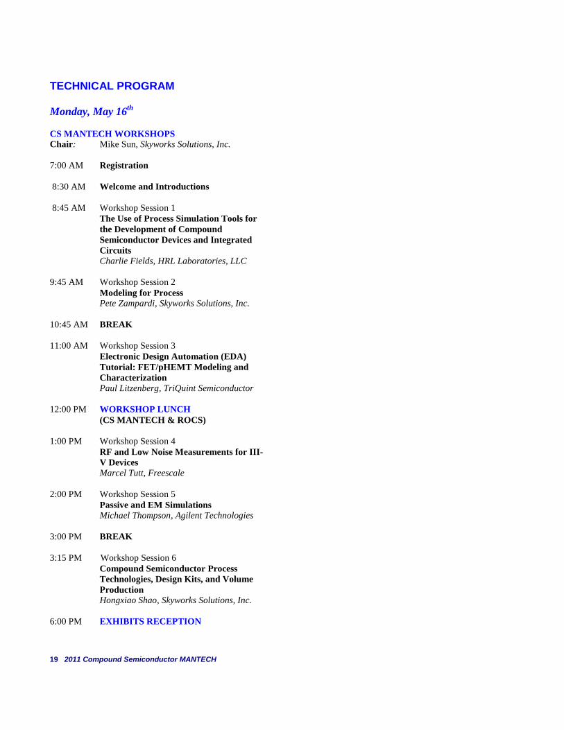
TECHNICAL PROGRAM
Monday, May 16th
CS MANTECH WORKSHOPS
Chair: Mike Sun, Skyworks Solutions, Inc.
7:00 AM Registration
8:30 AM Welcome and Introductions
8:45 AM Workshop Session 1
The Use of Process Simulation Tools for
the Development of Compound
Semiconductor Devices and Integrated
Circuits
Charlie Fields, HRL Laboratories, LLC
9:45 AM Workshop Session 2
Modeling for Process Pete Zampardi, Skyworks Solutions, Inc.
10:45 AM BREAK
11:00 AM Workshop Session 3
Electronic Design Automation (EDA)
Tutorial: FET/pHEMT Modeling and
Characterization Paul Litzenberg, TriQuint Semiconductor
12:00 PM WORKSHOP LUNCH
(CS MANTECH & ROCS)
1:00 PM Workshop Session 4
RF and Low Noise Measurements for III-
V Devices Marcel Tutt, Freescale
2:00 PM Workshop Session 5
Passive and EM Simulations Michael Thompson, Agilent Technologies
3:00 PM BREAK
3:15 PM Workshop Session 6
Compound Semiconductor Process
Technologies, Design Kits, and Volume
Production
Hongxiao Shao, Skyworks Solutions, Inc.
6:00 PM EXHIBITS RECEPTION
20 2011 Compound Semiconductor MANTECH
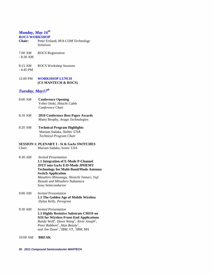
Monday, May 16th
ROCS WORKSHOP
Chair: Peter Ersland, M/A-COM Technology
Solutions
7:00 AM ROCS Registration
- 8:30 AM 8:15 AM ROCS Workshop Sessions - 4:45 PM
12:00 PM WORKSHOP LUNCH
(CS MANTECH & ROCS)
Tuesday, May17th
8:00 AM Conference Opening
Yohei Otoki, Hitachi Cable
Conference Chair
8:10 AM 2010 Conference Best Paper Awards
Marty Brophy, Avago Technologies
8:20 AM Technical Program Highlights
Mariam Sadaka, Soitec USA Technical Program Chair
SESSION 1: PLENARY I - Si & GaAs SWITCHES Chair: Mariam Sadaka, Soitec USA
8:30 AM Invited Presentation
1.1 Integration of E-Mode P-Channel
JFET into GaAs E/D-Mode JPHEMT
Technology for Multi-Band/Mode Antenna
Switch Application
Masahiro Mitsunaga, Shinichi Tamari, Yuji
Ibusuki and Mitsuhiro Nakamura
Sony Semiconductor
9:00 AM Invited Presentation
1.2 The Golden Age of Mobile Wireless
Dylan Kelly, Peregrine
9:30 AM Invited Presentation
1.3 Highly Resistive Substrate CMOS on
SOI for Wireless Front-End Applications Randy Wolf
1, Dawn Wang
2, Alvin Joseph
1,
Peter Rabbeni2, Alan Botula
1,
and Jim Dunn1 ,1IBM, VT,
2IBM, MA
10:00 AM BREAK
21 2011 Compound Semiconductor MANTECH
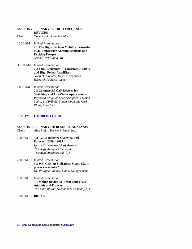
SESSION 2: PLENARY II: HIGH FREQENCY
DEVICES
Chair: Yohei Otoki, Hitachi Cable
10:30 AM Invited Presentation
2.1 The High‐Electron Mobility Transistor
at 30: Impressive Accomplishments and
Exciting Prospects
Jesús A. del Alamo, MIT
11:00 AM Invited Presentation
2.2 THz Electronics: Transistors, TMICs,
and High Power Amplifiers
John D. Albrecht, Defense Advanced
Research Projects Agency
11:30 AM Invited Presentation
2.3 Commercial GaN Devices for
Switching and Low‐Noise Applications
Raymond Pengelly, Scott Sheppard, Thomas
Smith, Bill Pribble, Simon Wood and Carl
Platis, Cree Inc.
12:00 PM EXHIBITS LUNCH
SESSION 3: PLENARY III: BUSINESS ANALYSIS
Chair: Alex Smith, Brewer Science, Inc.
1:30 PM 3.2 GaAs Industry Overview and
Forecast: 2009 – 2014
Eric Higham1 and Asif Anwar2
1Strategy Analytics Inc, USA
2Strategy Analytics Ltd., UK
2:00 PM Invited Presentation
3.3 Will GaN-on-Si displace Si and SiC in
power electronics?
Dr. Philippe Roussel, Yole Développement
2:30 PM Invited Presentation
3.1 Mobile Device RF Front-End TAM
Analysis and Forecast N. Quinn Bolton, Needham & Company,LLC
3:00 PM BREAK
22 2011 Compound Semiconductor MANTECH
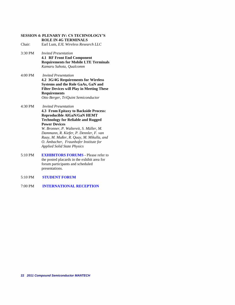
SESSION 4: PLENARY IV: CS TECHNOLOGY’S
ROLE IN 4G TERMINALS
Chair: Earl Lum, EJL Wireless Research LLC
3:30 PM Invited Presentation
4.1 RF Front End Component
Requirements for Mobile LTE Terminals Kamaru Sahota, Qualcomm
4:00 PM Invited Presentation
4.2 3G/4G Requirements for Wireless
Systems and the Role GaAs, GaN and
Filter Devices will Play in Meeting These
Requirements
Otto Berger, TriQuint Semiconductor
4:30 PM Invited Presentation
4.3 From Epitaxy to Backside Process:
Reproducible AlGaN/GaN HEMT
Technology for Reliable and Rugged
Power Devices W. Bronner, P. Waltereit, S. Müller, M.
Dammann, R. Kiefer, P. Dennler, F. van
Raay, M. Mußer, R. Quay, M. Mikulla, and
O. Ambacher, Fraunhofer Institute for
Applied Solid State Physics
5:10 PM EXHIBITORS FORUMS - Please refer to
the posted placards in the exhibit area for
forum participants and scheduled
presentations.
5:10 PM STUDENT FORUM
7:00 PM INTERNATIONAL RECEPTION
23 2011 Compound Semiconductor MANTECH
Wednesday May 18th
SESSION 5a: COMPOUND SEMICONDUCTORS IN
INDIA
Chair: Yohei Otoki, Hitachi Cable
8:00 AM Invited Presentation
5a.1 Perspectives, Opportunities and
Future of Compound Semiconductor
Technologies in India
Dhrubes Biswas, Indian Institute of
Technology
SESSION 5b: COMPOUND SEMICONDUCTORS IN
CHINA
Chair: Mariam Sadaka, Soitec USA
8:00 AM Invited Presentation
5b.1 China’s Fast Growing Role in the
Future of Compound Semiconductor
Technology and Manufacturing
Morris Young, AXT, Inc.
SESSION 6a: PROCESS I-PLASMA PROCESSING
Chair: Russ Westerman, Plasma-Therm, LLC
8:40 AM 6a.1 Optimized PECVD Chamber Clean
for Improved Film Deposition Capability Ronald R. Hess, RFMD
9:00 AM 6a.2 Advanced Statistical Process Control
of Critical PECVD SiNx Thin Films D. Wolfe, F. Li, M. Chen, Y. Yang, D. Wang,
D. Hou and F. Monzon, Global
Communication Semiconductors, Inc
9:20 AM 6a.3 Dry Etch Induced Surface Damage
and its Impacts on GaAs Schottky Diodes Hong Shen, Peter Dai, and Ravi
Ramanathan, Skyworks Solution, Inc.
9:40 AM BREAK
24 2011 Compound Semiconductor MANTECH
SESSION 6b: GaN EPITAXY
Chair: Victoria Williams, CREE
Andy Souzis, II-VI Inc.
8:40 AM 6b.1 Study of AlGaN/GaN HEMT
Uniformity with Various Buffer and
Barrier Structures Xiang Gao, Daniel Gorka, Songponn
Vatanapradit, Ming Pan, and Shiping Guo
IQE RF LLC
9:00 AM 6b.2 Development of III-Nitride HEMTs
on CVD Diamond Substrates F. Faili
1, D.I. Babić
1, D. Francis
1, F.
Ejeckam1, J.D. Blevins
2,
1Group4 Labs, LLC
2Air Force Research Laboratory
9:20 AM 6b.3 Rapid Characterization of Vertical
Threading Dislocations in GaN Using
Dedicated Scanning Transmission Electron
Microscopy Chunzhi Jitty Gu, Mike Salmon, Jim Vitarelli
Evans Analytical Group
9:40 AM BREAK
SESSION 7a: PROCESS II - METALS
Chair: Travis Abshere, TriQuint Semiconductor
10:40 AM 7a.1 Plating Showerhead System for
Improved Backside Wafer Plating Jens Riege, Heather Knoedler, Shiban Tiku,
Nercy Ebrahimi, Skyworks Solutions, Inc.
11:00 AM 7a.2 Overall Equipment Efficiency
Improvement for GaAs Fab Evaporators Jesus Teran, Daniel Weaver, Heather
Knoedler, Lam Luu, Richard Bingle, Brian
Alvarez, Joshua Doria, David Holzman, Juan
Velasquez, Skyworks Solutions, Inc.
11:20 AM Student Presentation
7a.3 Type-II DHBTs Microwave
Characterization and Metallization Issues Kuang-Yu (Donald) Cheng and Milton Feng
University of Illinois at Urbana-Champaign
11:40 AM 7a.4 Collector Contact Optimization in
GaAs HBT Manufacturing Lam Luu-Henderson, Daniel Weaver,
Heather Knoedler, Shiban Tiku
Skyworks Solutions, Inc.
25 2011 Compound Semiconductor MANTECH
SESSION 7b: HIGH FREQUENCY GaN DEVICES
Chairs: David Meyer, Naval Research Lab Robert Sadler, Nitronex Corporation
10:40 AM Invited Presentation
7b.1 High-Speed AlInN/GaN HEMTs on
SiC and (111) HR-Silicon C.R. Bolognesi
1, H.F. Sun
1, S. Tirelli
1, A.R.
Alt1, D. Marti
1, H. Benedickter
1 J.-F Carlin
2,
E. Feltin2, M. Gonschorek
2, M. Py
2, N.
Grandjean2, 1
Millimeter-Wave Electronics
Group, ETHZ, 2Institute of Condensed
Matter Physics, EPFL
11:10 AM Student Presentation
7b.2 Characterization of Coplanar
Waveguides on AlGaN/GaN HEMT on
Silicon Buffer Layers up to 110 GHz Diego Marti
1, Mathias Vetter
1, Liang Liu
1,
Andreas R. Alt1, Hansruedi Benedickter
1, E.
Piner2and C. R. Bolognesi
1, 1Millimeter-Wave
Electronics Group, ETHZ, 2Nitronex
Corporation (now at Texas State University
11:30 AM 7b.3 Performance of Strained
AlInN/AlN/GaN HEMTs with Si3N4 and
Ultra-Thin Al203 Passivation
K.D. Chabak1, D.E. Walker Jr.
1, A. Crespo
1,
M. Trejo1, M. Kossler
1, J.K. Gillespie
1, R.
Gilbert1, B. Poling
1, G.D. Via
1, J. Yang
2, and
R. Gaska2,
1Air Force Research Laboratory,
2Sensor Electronic Technology
11:50 AM 7b.4 Effects of Via Layout on AlGaN/GaN
HEMTs at Ka-band K. Matsushita, H. Sakurai, J. Shim, K.
Takagi, H. Kawasaki, Y. Takada, M. Hirose,
and K. Tsuda, Toshiba Corp.
SESSION 8a: PROCESS III – LITHOGRAPHY/BCB Chairs: Chris Youtsey, Microlink Devices
1:40 PM 8a.1 A New Method for Creating Sloped
Resist Profiles Using Mask Structures Jens Riege, Samuel Mony, Nercy Ebrahimi
Skyworks Solutions, Inc.
2:00 PM 8a.2 Improved T-Gate Yield Using E-
Beam Trilayer Resist Process Huatang Chen, Andrew Ketterson, Marcus
King, Keith Salzman, Vicki Milam, James
Halvorson, Jan Campbell, TriQuint
Semiconductor, TX
26 2011 Compound Semiconductor MANTECH
2:20 PM 8a.3 Optimization and Characterization of
the Photo Definable BCB for HV3S and
HVHBT Technologies
Jerry Brown and Amy Zhou, TriQuint
Semiconductor, TX
2:40 PM 8a.4 Characterization of BCB
Planarization of Isolated and Dense
Features in a High-Topography HBT
Process Tom Dungan, Avago Technologies
3:00 PM BREAK
SESSION 8b: SUBSTRATES
Chair: John Blevins, Air Force Research Lab
Judy Kronwasser, NOVASiC
1:40 PM 8b.1 Considerations towards a Nitride
Semiconductor Substrate Roadmap
E. Preble, R. Metzger, T. Paskova, G.
Mulholland, N. Biswas, and K. Evans,
Kyma Technologies, Inc.
2:00 PM 8b.2 Challenges in AlN Crystal Growth
and Prospects of the AlN-based
Technology
B. Moody2, S. Craft
2, R. Schlesser
2, R.
Dalmau2, J. Xie
1, T. Rice
1, J. Tweedy
1, R.
Collazo1, Z. Sitar
1
1 North Carolina State University
2 HexaTech, Inc.,
2:20 PM 8b.3 Advances in SiC Substrates for
Power and Energy Applications M.J. Loboda, G. Chung, E. Carlson, R.
Drachev, D. Hansen, E. Sanchez, J. Wan, J.
Zhang, Dow Corning Corporation
2:40 PM 8b.4 Development of a Manufacturing
Process for Large Diameter
Semi-Insulating Silicon Carbide Substrates J.D. Blevins
2, A.K. Gupta
1, I. Zwieback
1, E.
Emorhokpor1, A. Souzis
1, T. Anderson
1, C.
Avvisato3,
1. II-VI Inc.,
2. Air Force Research
Laboratory, 3. Sparta dba Cobham Analytic
Solutions
3:00 PM BREAK
27 2011 Compound Semiconductor MANTECH
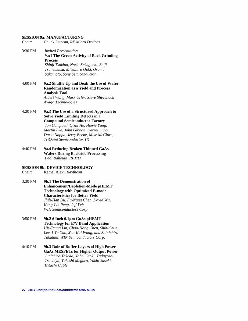
SESSION 9a: MANUFACTURING
Chair: Chuck Duncan, RF Micro Devices
3:30 PM Invited Presentation
9a:1 The Green Activity of Back Grinding
Process Shinji Tsukino, Norio Sakaguchi, Seiji
Tsunematsu, Mitsuhiro Ooki, Osamu
Sakamoto, Sony Semiconductor
4:00 PM 9a.2 Shuffle Up and Deal: the Use of Wafer
Randomization as a Yield and Process
Analysis Tool
Albert Wang, Mark Urfer, Steve Shevenock
Avago Technologies
4:20 PM 9a.3 The Use of a Structured Approach to
Solve Yield Limiting Defects in a
Compound Semiconductor Factory
Jan Campbell, Qizhi He, Howie Yang,
Martin Ivie, John Gibbon, Darrel Lupo,
Dario Nappa, Jerry Beene, Mike McClure,
TriQuint Semiconductor,TX
4:40 PM 9a.4 Reducing Broken Thinned GaAs
Wafers During Backside Processing
Fadi Bahouth, RFMD
SESSION 9b: DEVICE TECHNOLOGY Chair: Kamal Alavi, Raytheon
3:30 PM 9b.1 The Demonstration of
Enhancement/Depletion-Mode pHEMT
Technology with Optimized E-mode
Characteristics for Better Yield Jhih-Han Du, Fu-Nung Chen, David Wu,
Kang-Lin Peng, Jeff Yeh
WIN Semiconductors Corp
3:50 PM 9b.2 6 Inch 0.1μm GaAs pHEMT
Technology for E/V Band Application His-Tsung Lin, Chao-Hong Chen, Shih-Chun,
Lee, I-Te Cho,Wen-Kai Wang, and Shinichiro
Takatani, WIN Semiconductors Corp.
4:10 PM 9b.3 Role of Buffer Layers of High Power
GaAs MESFETs for Higher Output Power
Junichiro Takeda, Yohei Otoki, Tadayoshi
Tsuchiya, Takeshi Meguro, Yukio Sasaki,
Hitachi Cable
28 2011 Compound Semiconductor MANTECH
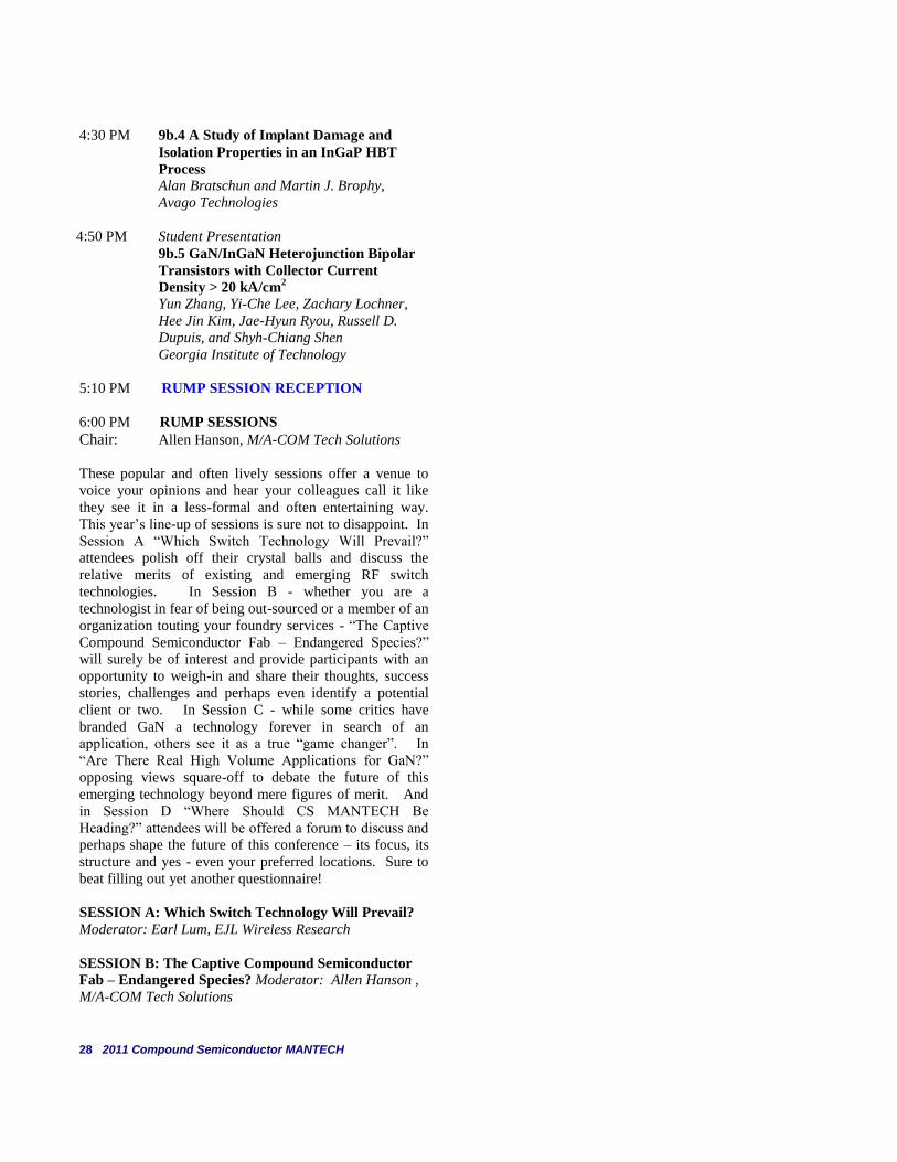
4:30 PM 9b.4 A Study of Implant Damage and
Isolation Properties in an InGaP HBT
Process Alan Bratschun and Martin J. Brophy,
Avago Technologies
4:50 PM Student Presentation
9b.5 GaN/InGaN Heterojunction Bipolar
Transistors with Collector Current
Density > 20 kA/cm2
Yun Zhang, Yi-Che Lee, Zachary Lochner,
Hee Jin Kim, Jae-Hyun Ryou, Russell D.
Dupuis, and Shyh-Chiang Shen
Georgia Institute of Technology
5:10 PM RUMP SESSION RECEPTION
6:00 PM RUMP SESSIONS
Chair: Allen Hanson, M/A-COM Tech Solutions
These popular and often lively sessions offer a venue to
voice your opinions and hear your colleagues call it like
they see it in a less-formal and often entertaining way.
This year’s line-up of sessions is sure not to disappoint. In
Session A “Which Switch Technology Will Prevail?”
attendees polish off their crystal balls and discuss the
relative merits of existing and emerging RF switch
technologies. In Session B - whether you are a
technologist in fear of being out-sourced or a member of an
organization touting your foundry services - “The Captive
Compound Semiconductor Fab – Endangered Species?”
will surely be of interest and provide participants with an
opportunity to weigh-in and share their thoughts, success
stories, challenges and perhaps even identify a potential
client or two. In Session C - while some critics have
branded GaN a technology forever in search of an
application, others see it as a true “game changer”. In
“Are There Real High Volume Applications for GaN?”
opposing views square-off to debate the future of this
emerging technology beyond mere figures of merit. And
in Session D “Where Should CS MANTECH Be
Heading?” attendees will be offered a forum to discuss and
perhaps shape the future of this conference – its focus, its
structure and yes - even your preferred locations. Sure to
beat filling out yet another questionnaire!
SESSION A: Which Switch Technology Will Prevail?
Moderator: Earl Lum, EJL Wireless Research
SESSION B: The Captive Compound Semiconductor
Fab – Endangered Species? Moderator: Allen Hanson ,
M/A-COM Tech Solutions
29 2011 Compound Semiconductor MANTECH
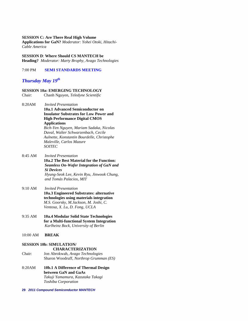
SESSION C: Are There Real High Volume
Applications for GaN? Moderator: Yohei Otoki, Hitachi-
Cable America
SESSION D: Where Should CS MANTECH be
Heading? Moderator: Marty Brophy, Avago Technologies
7:00 PM SEMI STANDARDS MEETING
Thursday May 19th
SESSION 10a: EMERGING TECHNOLOGY
Chair: Chanh Nguyen, Teledyne Scientific
8:20AM Invited Presentation
10a.1 Advanced Semiconductor on
Insulator Substrates for Low Power and
High Performance Digital CMOS
Applications Bich-Yen Nguyen, Mariam Sadaka, Nicolas
Daval, Walter Schwarzenbach, Cecile
Aulnette, Konstantin Bourdelle, Christophe
Maleville, Carlos Mazure
SOITEC
8:45 AM Invited Presentation
10a.2 The Best Material for the Function:
Seamless On-Wafer Integration of GaN and
Si Devices Hyung-Seok Lee, Kevin Ryu, Jinwook Chung,
and Tomás Palacios, MIT
9:10 AM Invited Presentation
10a.3 Engineered Substrates: alternative
technologies using materials integration
M.S. Goorsky, M.Jackson, M. Joshi, C.
Ventosa, X. Lu, D. Fong, UCLA
9:35 AM 10a.4 Modular Solid State Technologies
for a Multi-functional System Integration Karlheinz Bock, University of Berlin
10:00 AM BREAK
SESSION 10b: SIMULATION/
CHARACTERIZATION
Chair: Jon Abrokwah, Avago Technologies
Sharon Woodruff, Northrop Grumman (ES)
8:20AM 10b.1 A Difference of Thermal Design
between GaN and GaAs Takuji Yamamura, Kazutaka Takagi
Toshiba Corporation
30 2011 Compound Semiconductor MANTECH
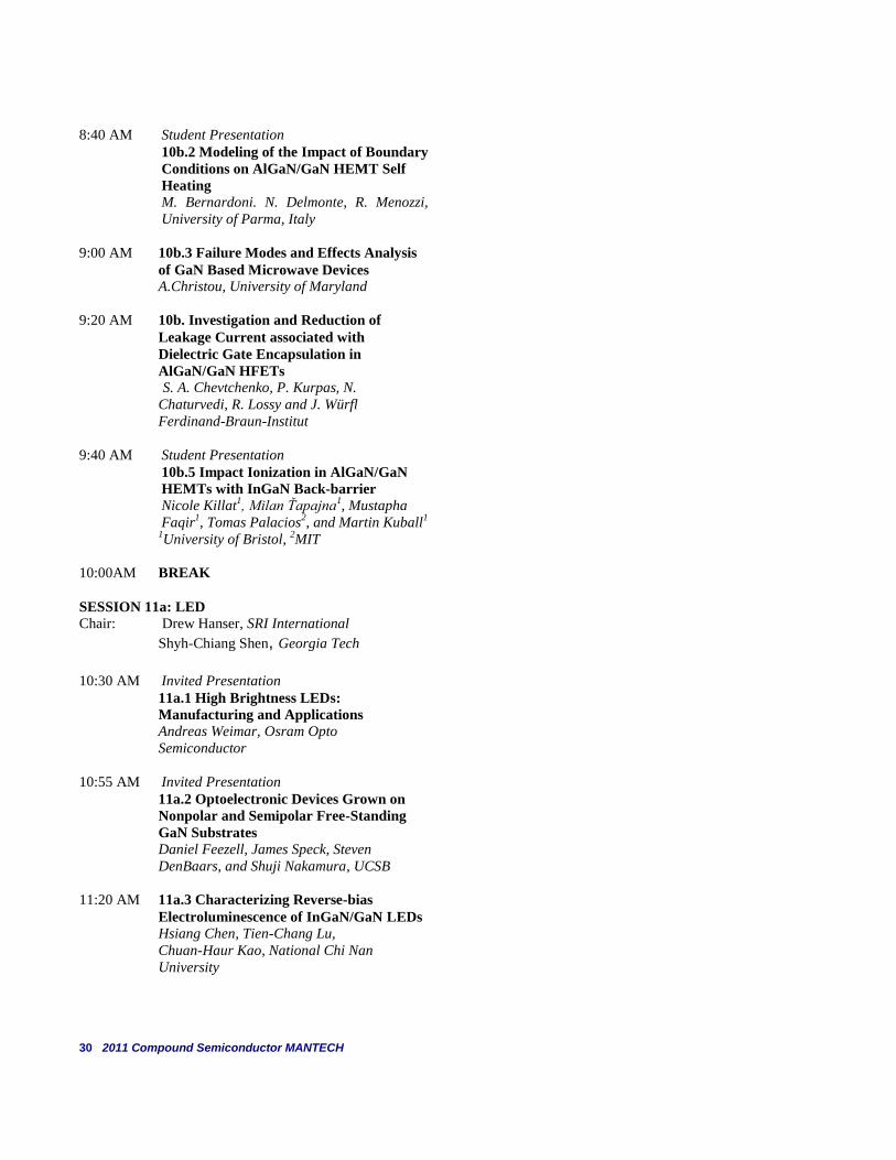
8:40 AM Student Presentation
10b.2 Modeling of the Impact of Boundary
Conditions on AlGaN/GaN HEMT Self
Heating M. Bernardoni. N. Delmonte, R. Menozzi,
University of Parma, Italy
9:00 AM 10b.3 Failure Modes and Effects Analysis
of GaN Based Microwave Devices A.Christou, University of Maryland
9:20 AM 10b. Investigation and Reduction of
Leakage Current associated with
Dielectric Gate Encapsulation in
AlGaN/GaN HFETs S. A. Chevtchenko, P. Kurpas, N.
Chaturvedi, R. Lossy and J. Würfl
Ferdinand-Braun-Institut
9:40 AM Student Presentation
10b.5 Impact Ionization in AlGaN/GaN
HEMTs with InGaN Back-barrier Nicole Killat
1, Milan Ťapajna
1, Mustapha
Faqir1, Tomas Palacios
2, and Martin Kuball
1
1University of Bristol,
2MIT
10:00AM BREAK
SESSION 11a: LED
Chair: Drew Hanser, SRI International
Shyh-Chiang Shen, Georgia Tech 10:30 AM Invited Presentation
11a.1 High Brightness LEDs:
Manufacturing and Applications
Andreas Weimar, Osram Opto
Semiconductor
10:55 AM Invited Presentation
11a.2 Optoelectronic Devices Grown on
Nonpolar and Semipolar Free-Standing
GaN Substrates
Daniel Feezell, James Speck, Steven
DenBaars, and Shuji Nakamura, UCSB
11:20 AM 11a.3 Characterizing Reverse-bias
Electroluminescence of InGaN/GaN LEDs Hsiang Chen, Tien-Chang Lu,
Chuan-Haur Kao, National Chi Nan
University
31 2011 Compound Semiconductor MANTECH
11:40 AM Student Presentation
11a.4 Investigation of Low-Temperature
Optical Characteristics of InGaN/GaN
Based Nanorod Light Emitting Arrays Chun-Hsiang Chang, Liang-Yi Chen, Ying-
Yuan Huang, and JianJang Huang
National Taiwan University
12:00 PM LUNCH by CS MANTECH
SESSION 11b: RELIABILITY
Chair: Peter Ersland, M/A-COM Technology
Solutions
Chang-Hwang Hua, WIN Semiconductors
Corp.
10:30 AM 11b.1 Reliability Qualification Challenges
of a pHEMT-HBT Hybrid Process
Dorothy June M. Hamada and William J.
Roesch, TriQuint Semiconductor Inc,.OR
10:50 AM 11b.2 Balancing Electrical and Thermal
Device Characteristics: Thru Wafer Vias
vs. Backside Thermal Vias Cristian Cismaru, Hal Banbrook, Hong Shen
and Peter J. Zampardi, Skyworks Solutions
11:10 AM 11b.3The Study of Heterojunction Bipolar
Transistors for High Ruggedness
Performance
Szu-Ju Li, Cheng-Kuo Lin, Shu-Hsiao Tsai,
Bing-San Hong, Dennis William, and Yu-Chi
Wang, WIN Semiconductors Corp.
11:30 AM Student Presentation
11b. Evaluation of Existing GaAs MIM-
Capacitor Processes for Use with High-
Voltage GaN MMIC Technologies
Philipp Leber1, Marc Hollmer
1, Dominik
Schrade-Köhn1, James Thorpe
2, Reza
Behtash2, Hervé Blanck
2, Hermann
Schumacher1,
1University of Ulm
2United Monolithic Semiconductors GmbH
12:00 PM LUNCH by CS MANTECH
32 2011 Compound Semiconductor MANTECH
SESSION 12a: FAB MANAGEMENT &
TECHNOLOGY TRANSFER
Chair: Arnold Chen, Infinera
1:30 PM Invited Presentation
12a.1 Relocation of Cobham’s MMIC
Wafer Fab M. Drinkwine, J. Crites, Cobham
2:00 PM 12a.2 Successful Transfer of 12V PHEMT
Technology
Jason Fender1, Monica De Baca
1, Jenn Hwa
Huang1, Monte Miller
1, Jose Suarez
1, Iris
Hsieh2, Y.C. Wang
2,
1 Freescale
Semiconductor Inc., 2 WIN Semiconductors
Corp.
2:20 PM 12a.3 Managing Process Diversity for Opto
Wafer Fabrication in a Photonics Foundry S. Wang, P. Chen, J. Chen, D. Kumar, P.
Lao, J. Pepper, P. Tran, M. Chen, D. Hou, F.
Monzon, and D. Wang
Global Communication Semiconductors, Inc.
2:40 PM 12a.4 Waste Minimization, Pollution
Prevention and Resource Recovery at a
GaAs Manufacturer Erich Burke, RFMD
SESSION 12b: POWER SWITCHES
Chair: Scott Sheppard, CREE
1:30 PM Invited Presentation
12b.1 SiC Power Devices - Lessons
Learned and Prospects After 10 Years of
Commercial Availability Peter Friedrichs, SiCED Electronics
Development GmbH & Co.
1:55 PM Invited Presentation
12b.2 Which are the Future GaN Power
Devices for Automotive Applications,
Lateral Structures or Vertical Structures?
Tsutomu Uesugi and Tetsu Kachi
Toyota Central R&D Laboratories, Inc.
33 2011 Compound Semiconductor MANTECH
2:20 PM Student Presentation
12b.3 2.5-Ampere AlGaN/GaN HFETs on
Si Substrates with Breakdown Voltage >
1250V Tsung-Ting Kao
1, Cheng-Yin Wang
1, and
Shyh-Chiang Shen1, Dev Alok Girdhar
2, and
Francois Hebert2,
1 Georgia Institute of
Technology, 2Intersil Corporation
2:40 PM 12b.4 Commercially Available Cree
Silicon Carbide Power Devices:
Historical Success of JBS Diodes and
Future Power Switch Prospects Mrinal K. Das, Cree
SESSION 13: INTERACTIVE FORUM
Chairs: Thorsten Saeger, TriQuint Semiconductor
Thomas Roedle, NXP Semiconductors Suzanne Combe, TriQuint Semiconductor
3:00 PM - 13.1 Improving Corrosion
4:30 PM Resistance of Plasma Etch Reactors
Testing Anodize Coatings and Cleaning
Methods
K. Mackenzie, K. Pizzo, E. Scott
Plasma‐Therm
13.2 Atomic Level InP/Si Wafer-Scale
Direct Bonding in Low Temperature
Xuan Xiong Zhang1,2
, Tian Chun Ye1, Songlin
Zhuang2,
1 Chinese Academy of Sciences, Beijing
2 University of Shanghai for Science and
Technology
13.3 Anisotropies of Nonpolar a-plane
GaN LEDs in Electrical and Optical
Properties
Soohwan Jang1, Kwang Hyeon Baik
2, Sung-
Min Hwang2, S. J. Pearton
3, and F. Ren
4
1Dankook University, Korea,
2Korea
Electronics Technology Institute,3 Dept. of
Materials Sci &Eng, University of Florida,
Gainesville, 4 Dept. of Chem Eng., University
of Florida, Gainesville
34 2011 Compound Semiconductor MANTECH
13.4 Thin Film Power Source Integrated
with a-Si:H/a-SiGe:H Thin Film
MOSFETs on Flexible Substrates T. Martin
3, Aris Christou
1,3, Martin
Peckerar2,
1Dept. of Materials Sci & Eng.
2Dept. Electrical Eng.,
3Dept. of Mech Eng.
University of Maryland
13.5 Development of a Novel Small Pitch
Flip‐Chip Indium Bump Process for
Infrared Focal Plane Arrays J. K. Markunas
1, E. Schulte
1, P.J. Smith
1, and
J.W. Pattison2,
1 U. S. Army RDECOM,
CERDEC Night Vision, 2U. S. Army Research
Laboratory
Student Presentation 13.6 Self-aligned In0.53Ga0.47As /InP
Vertical Tunnel FET Guangle Zhou
1, Yeqing Lu
1, Rui Li
1, Qingmin
Liu1, Paul Pinsukanjana
2, George Wang
2,
Tom Kosel1, Mark Wistey
1, Patrick Fay
1,
Alan Seabaugh1, and Huili (Grace) Xing
1,
1University of Notre Dame,
2IntelliEPI
13.7 Material Studies of GaN on Diamond Sergey Zaitsev, Frank Lowe, Daniel Francis,
Firooz Faili, and Felix Ejeckam.
Group4 Labs, Inc.
13.8 Implementation of Value Added
Kaizens (VAK) in a GaAs Manufacturing
Facility
Jan Campbell, Rick Cobo, David Beene,
Jerry Beene, Joel Peterson
TriQuint Semiconductor, TX
Student Presentation
13.9 Characterizations of Low-
Temperature Electroluminescence from n-
ZnO Nanowire/p-GaN Light Emitting
Diodes
Tzu-Chun Lu1 , Min-Yung Ke
1, Sheng-Chieh
Yang1, Yun-Wei Cheng
1, Liang-Yi Chen
1 ,
Guan-Jhong Lin1, Yu-Hsin Lu
2, Jr-Hau He
1
Hao-Chung Kuo2 and JianJang Huang
1,
1National Taiwan University,
2National
Chiao Tung University
35 2011 Compound Semiconductor MANTECH
13.10 Electron Radiation as an Indicator of
Gold Nodule Defect during E-beam
Evaporation
Kezia Cheng, Skyworks Solutions Inc.
Student Presentation
13.11 The Effect of Interdigitated Layout
Design on the Improvement of Optical
Output and GHz Modulation Bandwidth
of Tilted-Charge Light-Emitting Diodes
Mong-Kai Wu1, Chao-Hsin Wu
1, Gabriel
Walter2, and Milton Feng
1,
1University of
Illinois, 2Quantum Electro Opto Systems
13.12 An Introduction to the PETEC
Flexible Electronics Centre and Current
Technology Challenges Mike Clausen, Bela Green, Martin
Walkinshaw, PETEC
Student Presentation
13.13 TCAD Modeling and Simulation of a
Field Plated GaN MOSFET for High
Voltage Applications
K. Bothe1, M. Johnson
2, D. Barlage
1 ,
1University of Alberta
2University of North Carolina
13.14 Growth of GaN Layer for LED
Manufacturing: Investigations on Growth
Conditions using a “Hotwall” MOCVD
System
R.Schreiner1, B. Schineller
1, D. Fahle
2 ,
M.Heuken1,2
, G.Strauch1
1AIXTRON,
2Aachen University
13.15 Backside Processing Steps
Elimination and Cost Reduction by Multi
Beam Full Cut Laser Dicing Rogier Evertsen, Rene Hendriks
ALSI
13.16 In-Situ Measurement of GaN
Surface Temperature, Effects of Changes
in Carrier Gas and Satellite Rotation
Speed on Temperature Profiles
K. Haberland 1, B. Henninger
1, D. Brien
2,
H. Silva 2, M. Dauelsberg
2, F. Brunner
3, V.
Hoffmann 3, M. Weyers
3, R. Sarcia
1
1LayTec GmbH,
2Aixtron AG,
3Ferdinand-
Braun-Institut
36 2011 Compound Semiconductor MANTECH
Student Presentation
13.17 A Comprehensive Correlation
between Lattice Strain and Quantum Well
Thickness of MBE Grown
AlGaAs/InGaAs/GaAs Pseudomorphic
HEMT with Device Performance for
Transconductance and Linearity
Partha Mukhopadhyay1, Palash Das
1,
Saptarshi Pathak1, Edward Y. Chang
2
and Dhrubes Biswas1
1Indian Institute of Technology,
2National
Chiao Tung University
4.30 PM CONFERENCE CLOSING RECEPTION
37 2011 Compound Semiconductor MANTECH
TECHNICAL SESSIONS
SESSION 1: PLENARY I - RF SWITCHES
Chair: Mariam Sadaka, Soitec USA
We live in an increasingly wireless world, filled with an
ever expanding variety of smart phones, W-LANs,
WWANs, GPS, and a host of other wireless appliances.
Applications of RF technologies continue spreading into
new systems like smart grids and e-books and even into
entertainment systems and toys. At the core of these
wireless systems are RF modules which are powered and
enabled primarily by semiconductor devices. Front end
module specifications have been made more complex with
ongoing evolution of new Cellular standards and band
frequencies. Multi-Mode and Multi-Band operation of PA
modules is becoming a reality.
Switching and tunable output matching networks can play
a pivotal role in this area. Performance requirements such
as low insertion loss and high isolation, power handling,
and linearity have historically motivated the selection of
GaAs. But recently, Silicon-on-sapphire (SOS) and high
resistivity Silicon-on-Insulator (SOI) technologies have
also been evaluated for RF switch applications.
This year’s plenary session addresses both Compound
Semiconductor and CMOS-based RF switches. Our first
paper by Mitsuhiro Nakamura from Sony describes the
integration of E-Mode P-Channel JFETs into their GaAs
E/D-Mode JPHEMT technology for multi-band/mode
antenna switch applications. This technology enables
fabrication of low power consumption GaAs logic circuits
and low loss antenna switches on a single chip. Next paper
by Dylan Kelly from Peregrine discusses the golden age of
mobile wireless driven by the explosive growth of mobile
wireless data traffic. He explains how UltraCMOS on
Silicon-on-sapphire (SOS) technology is addressing the
challenges. The session concludes with Randy Wolf of
IBM describing a highly resistive substrate CMOS on SOI
technology for wireless front-end applications, which
shows a comparable performance to GaAs pHEMT and to
SOS technologies.
38 2011 Compound Semiconductor MANTECH
SESSION 2: PLENARY II - RF MODULES
Chair: Yohei Otoki, Hitachi Cable America
One of the strongest features of CS-devices is having high
performance at GHz frequencies. This has greatly
contributed to realizing the wireless mass information
transfer era. This Session introduces the latest state of art
devices with high frequency from GHz up to THz! First of
all, Prof. Jesús A. del Alamo from MIT reviews the history
and present topics on HEMTs (High Electron Mobility
Transistors), which is a historical invention of CS devices
used to achieve new wireless systems with high frequency
performance like satellite broadcast, cellular phones, etc.
30 years have passed after the first HEMT, and you will
learn how it has progressed.
Then, development of very high frequency, over 1 THz,
electronics - sub-millimeter wave devices - is presented by
John D. Albrecht of DARPA. These devices have
incredibly high data resolution, leading to ultra-fine image
sensors, radars, and higher speed communication in the
near future. You will see the new “image” world. These
devices generally use GaAs-,and InP-related materials, but
innovations with wide bandgap materials like GaN have
come up recently and are showing up in “fast and tough”
devices. These devices have been used for the high power
amplifiers, but now they are getting into new fields of
switching and Low noise application. Raymond Pengelly
of Cree, one of the leading companies for GaN devices,
presents recent results of development. You will see an
“all GaN module” of Switch and LNA, used at GHz
frequencies with very high power in commercial use.
SESSION 3: PLENARY III - BUSINESS ANALYSIS
Chair: Alex Smith, Brewer Science, Inc.
Do you know anyone that does not have some type of
mobile device? We are in an amazing industry with
products that are changing the world. This session
includes three excellent speakers to address a variety of
topics of the Compound Semiconductor industry. Eric
Higham of Strategic Analytics will provide an overview of
the GaAs Industry from 2009-2014. His paper discusses
the history, future drivers, market share leaders, and the
competitive threats to GaAs. A question that many in the
industry are asking is whether GaN on Silicon will displace
Silicon and SiC in power electronics. Dr. Philippe Rousel
from Yole Development will provide his company’s
insight on this question and talk about the GaN market in
the next four years. The final talk in the session by Quinn
Bolton of Needham & Company, will give a run down on
front-end TAM analysis and forecast for the mobile RF
devices as driven by the demand for data services.
39 2011 Compound Semiconductor MANTECH
SESSION4: PLENARY IV - CS TECHNOLOGY’S
ROLE IN 4G TERMINALS
Chair: Earl Lum, EJL Wireless Research LLC
While smartphones such as the Apple iPhone and
Motorola’s DROID are changing mobile social behavior,
they have been successful due to the reliance on mobile
broadband data connections via 3G technologies such as
WCDMA/HSPA and EVDO Rev. A in providing access to
the Internet. 3G technologies today can offer downlink
data rates up to 42Mbps. Next generation 4G LTE
technology promises downlink data rates up to 100Mbps
and beyond.
Compound semiconductors such as GaAs have played a
pivotal role in the transmit and receive functions of mobile
data modem devices as well as mobile phones. Two of the
invited papers in this session (from TriQuint
Semiconductor and Qualcomm) focus specifically on the
component requirements of 4G LTE terminals including
the power amplifier, the LNA receiver as well as switching
functions and filters in the front end.
Each generation of wireless technology pushes the
envelope for performance in terms of linearity, and RF
power output as well as the continuous need for better and
better efficiencies. Will GaAs be able to support 4G LTE
terminals or will another compound semiconductor
technology be required?
The final paper in this session will focus on a complete end
to end GaN/SiC HEMT MOCVD process technology
solution developed by the Fraunhofer Institute for power
devices up to 20GHz.
SESSION 5a: COMPOUND SEMICONDUCTORS IN
INDIA
Chair: Yohei Otoki, Hitachi Cable
This session includes one talk by professor Dhrubes
Biswas from the Department of Electronics and Electrical
Communication Engineering, and Rajendra Mishra School
of Engineering Entrepreneurship at the Indian Institute of
Technology. The presentation will cover the perspectives,
opportunities, and future of compound semiconductor
technologies in India.
40 2011 Compound Semiconductor MANTECH
SESSION 5b: COMPOUND SEMICONDUCTORS IN
CHINA
Chair: Mariam Sadaka, Soitec USA
This session includes one talk by Dr. Morris Young, CEO
of AXT, Inc. Dr. Young will talk about China’s fast
growing role in the future of compound semiconductor
technology and manufacturing. The presentation will focus
on the key activities supporting the growth, such as
contributions of the private and public sectors and the role
played by technical institutions and universities.
Furthermore, different segments and geographic
distribution of the compound semiconductor industry in
China will be reviewed along with some details of the
growth projections for the coming 5 years.
SESSION 6a: PROCESS I –PLASMA PROCESSING
Chairs: Russ Westerman, Plasma-Therm, LLC
Papers in this section focus on improving the
manufacturing performance of plasma deposition and etch
processes used in compound semiconductor
manufacturing. The first paper of the session by RF Micro
Devices discusses optimization of an in-situ clean used in
conjunction with a plasma enhanced chemical vapor
deposition (PECVD) process. Recipe changes applied to
the in-situ clean process improved both tool up time as
well as stabilizing wafer deposition uniformities between
cleans. The second paper in the session from Global
Communication Semiconductors also looks at
improvements to a PECVD process. This paper correlates
PECVD silicon nitride (SiN) film properties to metal-
insulator-metal (MIM) capacitor performance. The paper
also discusses improvements that more than doubled the
process capability (Cpk) of the deposition. The last paper
of the session, by Skyworks Solutions, examines damage
mechanisms from plasma etching thin films on gallium
arsenide (GaAs). The Skyworks work uses electrical
measurements of a Schottky diode structure to explore the
damage responses of typical plasma recipe parameters.
The paper also examines post-process approaches that can
be used to mitigate plasma induced damage downstream of
the etch.
SESSION 6b: GaN Epi
Chairs: Victoria Williams, CREE
Andy Souzis, II-VI Inc.
The GaN epi session will present a selection of papers
addressing different challenges within GaN epi
technology. The first paper by Guo, et. al from IQE RF
LLC will describe a study of AlGaN/GaN HEMT
uniformity using different buffer and barrier layer
41 2011 Compound Semiconductor MANTECH
structures. The effects of two different types of back
barrier layers, AlGaN and InGaN, as well as different
substrate sizes, substrate polytypes, and barrier/cap
structures deposited after the 2DEG, will be described as
part of this study. The second paper, contributed by Faili,
et. al from Group4 Labs, LLC and Air Force Research
Laboratory will present results from the fabrication of GaN
on diamond HEMTs by transfer and bonding of an
AlGaN/GaN epitaxial layer on a CVD diamond substrate.
Diamond substrates are predicted to improve heat
spreading in the gate region, increasing the potential for
GaN to reach its performance limits. Progress and
technological challenges of this technology will be
discussed in detail. The third paper, by Gu, et. al. of Evans
Analytical Group, concludes the session with a description
of a method for rapid characterization of vertical threading
dislocations in GaN. Scanning transmission electron
microscopy (STEM) was used to reduce the complexity of
this type of analysis and to identify the type and density of
the dislocations.
SESSION 7a: PROCESS II - METAL
Chair: Travis Abshere, TriQuint Semiconductor
It seems that every year the diversity in topics, materials,
and technologies presented at CS MANTECH grows.
However, it is heartening to see that the emphasis on
manufacturing technology continues to be supported both
within CS MANTECH and by the quality of papers
submitted by the industry. As in years past Skyworks
Solutions has a strong showing in the Metals session,
starting off with a study of backside wafer plating
uniformity improvements from optimization of the anode
design. The work was part of a 4” to 6” conversion, but
the combined optimization of equipment and process
involved in scaling up this technology provides excellent
material to anyone interested in improved electroplating.
The second paper moves us over to evaporated metals with
an emphasis on applying a broad based group of
improvement techniques to increase both tool availability
and product yields. The concepts of continuous process
improvement and the value of cross functional
improvement teams are clear winners in this effort to
relieve pressure on a capacity limited toolset. The third
paper is one of the excellent student papers submitted this
year. From the University of Illinois (Urbana-Champaign)
we have a topic that explores the complexity associated
with clearing the area beneath an air bridge when dealing
with the multiple epitaxial layers of an HBT. Our fourth
and final paper continues with HBTs but brings us back to
Skyworks Solutions in an exploration of Collector contact
optimization. This paper brings home one of the
fundamental realities of compound semiconductor
42 2011 Compound Semiconductor MANTECH
manufacturing today – our industry is maturing and the
low hanging fruit of the past is being replaced by
incremental improvements with contributions from
suppliers, materials, and improved understanding of the
interactions between process steps.
SESSION 7b: HIGH-FREQUENCY GaN DEVICES
Chairs: David Meyer, Naval Research Lab Robert Sadler, Nitronex Corporation
In recent years, there has been an increasing interest in
developing GaN transistor technology for millimeter-wave
applications such as monolithic microwave integrated
circuits (MMICs). In order to achieve the high operating
frequencies necessary for millimeter-wave amplification,
novel device designs with laterally and vertically-scaled
geometric dimensions are currently being investigated on a
variety of substrates. Potentially offering the most
financially viable solution, devices fabricated out of
heterostructures grown on low-cost silicon substrates have
begun to demonstrate performance metrics that rival
transistors made on traditional substrates. This session
contains reports on GaN high electron mobility transistors
(HEMTs) that operate at frequencies above 30 GHz. We
start with an invited talk by Prof. Colombo Bolognesi,
chair of the Millimeter-Wave Electronics Group at the
Swiss Federal Institute of Technology (ETH) in Zurich.
Prof. Bolognesi will survey recent results for lattice-
matched AlInN/GaN HEMTs that enable the very thin
barrier layers required for <100-nm gate lengths. These
devices have demonstrated the highest bandwidths yet
attained for nitride transistors, with fT = 205 GHz on SiC
substrates and 143 GHz on high-resistivity (HR) silicon
substrates. Prof. Bolognesi will compare this performance
with results achieved for recessed-gate AlGaN/GaN
HEMTs on HR-Si substrates. This will be immediately
followed by a paper from the same group covering the RF
characterization of coplanar waveguides (CPWs) on
AlGaN/GaN heterostructures on HR-silicon substrates, at
frequencies up to 110 GHz. The characterization shows
that CPW’s on GaN/Si exhibit performance comparable to
those on semi-insulating GaAs or InP, clearly
demonstrating the suitability of GaN/Si technology for
mm-wave MMIC applications. The next paper in this
session, contributed by Chabak and co-workers from the
Air Force Research Laboratory and Sensor Electronic
Technology, will showcase electrical results from a study
investigating submicron T-gate AlInN/AlN/GaN HEMTs
on SiC. By using a 6 nm-thick, strained (15% In fraction)
AlInN barrier, Chabak et al. were able to demonstrate
devices with high fT-LG product and low access resistance.
This presentation will discuss the effects of post-gate
passivation with PECVD Si3N4 and ALD-deposited Al2O3
43 2011 Compound Semiconductor MANTECH
on the small- and large-signal properties of this novel
device. The last paper in this session will be presented by
Matsushita and co-workers from Toshiba Corporation and
will discuss the effects of via layout on parasitic source
inductance and frequency performance of GaN HEMT
devices. Matsushita will also discuss Ka-band load-pull
measurements of a four via-hole configuration that has
produced saturated output power of 32.6 dBm (4.5W/mm),
linear gain of 7.3 dB, and PAE of 41%.
SESSION 8a: PROCESS III- LITHOGRAPHY/BCB
Chairs: Chris Yousey, MicroLink Devices, Inc
Presentations in this section, from several leading GaAs IC
manufacturers, describe a range of practical challenges
associated with device lithography, planarization and the
novel solutions that were developed to improve process
yield and robustness.
The first paper of the session from Skyworks Solutions
presents a new method to create sloped resist profiles by
exposing with patterns that incorporate microstructures
below the stepper optical resolution limit. This enables
partial exposure of the resist around the designed features
and localized control over the development rate. Sloped
resist profiles are an important method in device
fabrication to minimize abrupt step height changes. This
presentation discusses the advantages of the new technique
compared with conventional approaches such as thermal
reflow or exposure defocusing.
The following paper from TriQuint Semiconductor
presents a new trilayer resist electron beam lithography
process used to form T-gates for GaAs pHEMT devices.
The new process improves process yield by reducing metal
liftoff “stringer” defects encountered when using the
conventional bilayer resist. Cross-sectional FIB-SEM
images clarify the mechanism for defect formation, and
DC and final visual yield data validate the process
improvements.
Next TriQuint Semiconductor presents a critical process
issue encountered when using photo-definable BCB to
encapsulate HBT and pHEMT GaAs MMIC circuits.
Intermittent wrinkling of the BCB dielectric was solved
through a DOE that clarified proper exposure, development
and baking parameters.
The final paper from Avago Technologies discusses the
challenges of using BCB to planarize over topologies with
widely varying pattern density. Local variations in BCB
thickness can lead to shorts as well as incomplete metal via
formation. Optical profiler measurements of BCB film
44 2011 Compound Semiconductor MANTECH
thickness over a complex circuit structure are compared
with predictions from a model that is incorporated into a
design-rule checker. Electrical test structures are also
described that are used to characterize the process
limitations.
SESSION 8b: SUBSTRATES
Chairs: John Blevins, Air Force Research Lab
Judy Kronwasser, NOVASiC
This session reviews recent progress in the development of
wide bandgap substrates for high power RF amplification,
power switching and light emitting diodes. Kyma will
provide a comparison of many wide bandgap materials,
both bulk and template, for nitride device applications,
particularly LEDs. Hexatech will explore recent
technological advances associated with bulk AlN growth
and device fabrication. Dow Corning will highlight
advances in scaling and quality improvement for their
100mm 4H-SiC substrates. The last paper of the session
describes the success of the II-VI / Air Force Research
Laboratory / Missile Defense Agency joint initiative.
Improvements in 6H-SiC diameter, crystal quality, and
producibility will be discussed.
SESSION 9a: MANUFACTURING
Chair: Chuck Duncan, RF Micro Devices
Compound semiconductors offer nearly limitless structural
and elemental combinations which often create competitive
advantage over existing scaled solutions. Although these
advantages can create significant market opportunities,
companies must be able to demonstrate capable
manufacturing solutions with an eye toward continuous
improvement in cycle time, performance, yield and cost.
Increased circuit complexity and integration demand
improvements in basic manufacturing capabilities just to
maintain historic yields. Manufacturing improvements are
keys to the continued growth and sustainability of our
industry and allow companies to maintain or even increase
their competitive advantage once performance gaps begin
to close.
This session includes a presentation on the reduction of
manufacturing waste and environmental impact as well as
three papers highlighting yield improvement solutions and
techniques. The first presentation in the session highlights
efforts at Sony Semiconductor Kyushu Corporation to
reduce the waste and by-products associated with their
wafer grinding process and to reduce the environmental
impact of the GaAs grinding activities. The presentation
will outline efforts to reuse waste water from the grinding
process reducing demands on the factory high purity water
45 2011 Compound Semiconductor MANTECH
systems. It will also address efforts to reduce consumable
components in the grinding equipment. In our second
presentation from Avago Technologies, the presenter will
outline strategies for the use of wafer randomizers to
trouble shoot wafer yield issues. Borrowing from
techniques implemented in high volume silicon
manufacturing, wafer randomization techniques in use at
Avago help identify trends within single lots or lot to lot.
They also outline methods for identifying concerns in
multi-chamber tools. Representatives of TriQuint
Semiconductor manufacturing facility will present an
overview of techniques employed to reduce yield loss in
their production process. While their resulting yield
improvements are significant, the methodologies and
problem solving approaches outlined are equally valuable
as they demonstrate a solid framework and foundation for
most any yield improvement effort. In the final
presentation of the session, RFMD will describe efforts to
reduce wafers broken during the backside processing of
thinned wafers. Numerous process variables were
explored to understand their impact on wafer breakage in a
team investigation and problem solving environment.
SESSION 9b: DEVICE TECHNOLOGY
Chair: Kamal Alavi, Raytheon
The device technology session has four regular papers and
one student paper, all having practical and relevant
information for device engineers. The first paper, from
WIN semiconductor, discusses how to compensate for
natural variations in an epitaxial layer structure through
utilizing gate metal sinking in an E/D mode pHEMT
process and thus achieve better consistency of pinchoff
voltage of the EFETs. The second paper, also from WIN,
details a 0.1 um pHEMT foundry process on 6” wafer for
V band applications. The process features Imax of 720
mA/mm, Vp of -0.9 V, fT of 135 GHz, Pmax of 850
mW/mm at Vdd=4 V, gain of 8-9 dB at 70-90 GHz, and
Fmin of 0.8 dB at 40 GHz. The third paper, from Hitachi
Cable, shows the methodology used to optimize buffer
layer structure of high power MESFETs used in power
amplifiers. The fourth paper, from Avago Technologies,
details the optimization of Boron isolation implant doses
and energies for a GaAs HBT device so that low junction
leakage and high isolation resistance are achieved
simultaneously. The last paper is a student paper from
Georgia Tech. It shows exciting device results for a GaN
HBT process. Collector current density of 19.8 kA/cm2 is
achieved with a BVceo of 110V and knee voltage of <
2.1V.
46 2011 Compound Semiconductor MANTECH
SESSION 10a: EMERGING TECHNOLOGIES
Chair: Chanh Nguyen, Teledyne Scientific
The common theme of this session is “Beyond CMOS” or
“More-than-Moore”. We have four presentations
describing novel approaches to extend performance and
functionality over and above the traditional scaling of Si
CMOS by incorporating compound semiconductors. The
invited paper from SOITEC reviews the latest
developments in substrate engineering to integrate III-
V/Ge on Si, device architecture and challenges of this
heterogeneous integration on the CMOS platform.
Integration of GaN and Si to form a hybrid wafer by wafer
bonding technology is the subject of the invited paper from
MIT. Devices, circuits, and systems exploiting GaN/Si
hybrid wafers will be discussed. The next invited paper
from UCLA presents two alternative approaches to
substrate engineering for compound semiconductor
applications: the transfer of III-V templates and porous
semiconductors for epi growth and device layer transfer.
The last presentation from University of Berlin discusses
the integration of different technologies from the
perspective of modular multi-functional technology
development.
SESSION 10b: SIMULATION AND
CHARACTERIZATION
Chair: Jon Abrokwah, Avago Technologies
Sharon Woodruff, Northrop Grumman (ES)
This session features five papers describing simulation and
characterization research on GaN devices. The first paper
by Takuji Yamamura and Kazutaka Takagi of Toshiba
Corporation reports on the difference in thermal design of
GaN and GaAs FETs. Simulations and measurements
show that while GaAs device thermal resistance depends
on total gate geometry, pitch and substrate thickness, GaN
FETs fabricated on SiC have much less dependence, due to
the 6X greater thermal conductivity of SiC compared to
GaAs. Thermal resistance of AlGaN/GaN HEMTS
depends mostly on die size.
The second paper by M Bernardino et al. of University of
Parma, Italy discusses modeling of the impact of boundary
conditions on AlGaN/GaN HEMT self-heating. The effects
include die-attach, finite backside heat-sinking, thermal
boundaries between GaN and SiC and the thermal
boundaries of the top metallization.
After that A. Christou of University of Maryland describes
using FMEA (Failure Modes and Analysis), to review the
primary failure modes of GaN based microwave devices,
indicating that trapping is the dominant mechanism for
47 2011 Compound Semiconductor MANTECH
device degradation and failure. They discuss effects of
piezoelectric charges, tensile strain, and defect formation.
In addition, models to predict electrical behavior, such as
current collapse, power soak, DC and RF degradation are
discussed. Next by S. A. Chevtchenko et al, of Ferdinand-
Braun-Institute, Germany, discuss their investigation and
reduction of gate leakage in AlGaN/GaN HFETs through
optimization of the process of the first and second SiN
passivation dielectric to reduce stress.
Finally, N. Killat et al. of University of Bristol and MIT
present a lucid description of electroluminescence
capacitance measurements and simulation to show impact
ionization phenomenon in InGaN/GaN HEMTs.
SESSION 11a: LED
Chair: Drew Hanser, SRI International
Shyh-Chiang Shen, Georgia Tech
This session will start with an invited presentation
describing the manufacturing and applications of the high-
brightness InGaN and AlInGaP light-emitting diodes
(LEDs) by Osram Opto Semiconductors. This presentation
will provide an overview of these technologies and discuss
key challenges of low-cost manufacturing. Another invited
talk will follow with a focus on optoelectronic devices
grown on nonpolar and semipolar free-standing (FS) GaN
substrates. In this talk, researchers from the University of
California at Santa-Barbara will present a summary of
material and device developments for laser diodes and
LEDs on several orientations of non-polar and semipolar
free-standing GaN. In the second half of the session, a
paper concerning the characterization of reverse-biased
electroluminescence of InGaN/GaN LEDs and a student
paper on InGaN/GaN nano-rod LEDs using a top-down
etching processes will be presented.
SESSION 11b: RELIABILITY Chair: Peter Ersland, M/A-COM Technology Solutions
Chang-Hwang Hua, WIN Semiconductors Corp
This year’s reliability session includes papers on both
active and passive circuit elements, with relevance to both
high volume consumer applications, and leading edge high
voltage technologies. Our first paper discusses approaches
for the reliability qualification of a Bi-HEMT process at
TriQuint. Since the failure mechanisms for HBTs and
pHEMTs may be quite different, qualifying a technology
that incorporates both device types requires careful
planning and development of structures to investigate not
only each device type individually, but the interaction of
48 2011 Compound Semiconductor MANTECH
these two process technologies on a single wafer. The
authors review the wafer scale reliability tests performed,
and describe the results of these tests. Our second paper
addresses a topic of importance to both reliability and
design engineers – thermal performance. A variety of
design and process options are investigated by these
authors from Skyworks, including different top side metal
thicknesses, the location of both through wafer vias and
backside thermal vias, and various materials choices.
Tradeoffs are described between optimizing thermal
performance and minimizing parasitic capacitance for
these devices. The third paper in this session describes
work performed at WIN Semiconductor to assess the
impact of collector design and layout on HBT ruggedness.
The authors’ results show not only the impact of these
factors on Safe Operating Area (SOA), but on device
electrical performance as well, and indicate the importance
of characterizing SOA on large transistor cells. Our fourth
and final paper addresses the effect of layout, dielectric
thickness, and the nitride deposition process on capacitor
reliability, particularly for use in GaN MMICs. The
authors from the University of Ulm and United Monolithic
Semiconductors (UMS) present ramped voltage reliability
test results that indicate a significant difference in the
predicted life time of the three different nitride deposition
processes assessed in this study.
SESSION 12a: FAB MANAGEMENT &
TECHNOLOGY TRANSFER
Chair: Arnold Chen, Infinera
This year the fab manufacturing and technology session
will have two papers that focus on process transfers and
two papers that discuss factory management. The session
will begin with an invited talk from Cobham Sensor
Systems in which they discuss the unenviable task of
shutting down and physically relocating their entire MMIC
wafer fab operation. How they managed to go from shut
down to resuming production in a mere eight months
you’ll have to attend the talk to find out. The second talk
in the session is from Freescale Semiconductor (in
partnership with WIN Semiconductor), where they will
discuss the methodology they used and the challenges
encountered transferring their 12V PHEMT technology
from their internal fab to WIN Semiconductor’s foundry
service. In the third paper of the session, we will learn
from the experiences of GCS concerning how they have
successfully managed to run optoelectronic devices on a
qualified RFIC manufacturing line. One of the more
interesting challenges they solved is how they managed to
run a single line with multiple wafer sizes. Last year’s
plenary session included talks on “green” manufacturing.
49 2011 Compound Semiconductor MANTECH
It’s only fitting that we continue this trend this year. In the
session’s last talk, RFMD discusses the results of a several
green initiatives. These include reclaiming precious metals,
recycling or reclaiming solvents as well as reducing the use
of ultra pure water.
SESSION 12b: POWER SWITCHES
Chair: Scott Sheppard, CREE
The Power Switch session contains two invited, one
student and one regular paper. Each paper addresses
different aspects of the use of wide bandgap compound
semiconductors for high-power devices. The session
begins with an invited paper. Peter Friedrichs of SiCED
Electronics Development gives a survey on SiC power
device development and prospects of commercialization
over the past 10 years. The second paper will be a student
presentation by Tsung-Ting Kao of Georgia Tech who
reports the high voltage device performance of
AlGaN/GaN Heterojunction Field Effect Transistors
(HFETs) grown on Si substrates with low specific on-
resistance and high breakdown voltage. Next in an invited
talk, Tsutomu Uesugi of Toyota central R&D Laboratories,
Inc. will compare the lateral structures and the vertical
structures of the GaN on Si power devices and discuss their
application to future power devices. Finally, Mrinal Das of
Cree, Inc. gives a very comprehensive overview of
commercially available silicon carbide power devices. It
will include a treatise on SiC JBS diodes and future power
switching commercial devices in SiC.
SESSION 13: INTERACTIVE FORUM
Chairs: Thorsten Saeger, TriQuint Semiconductor
Thomas Roedle, NXP Semiconductors Suzanne Combe, TriQuint Semiconductor
Following the tradition initiated in 1994, the Interactive
Forum is a session devoted to promoting the open
exchange of ideas and information. This session allows for
discussions and face-to-face meetings between the authors
and conference attendees. During the Interactive Forum, all
authors of presented papers will be available to answer
questions and further discuss their technical results. All
your questions you did not dare or manage to ask during
the oral sessions can now be discussed with the authors in
an informal setting.
In addition, this Forum will be the only time at the
conference where papers that have been selected for the
50 2011 Compound Semiconductor MANTECH
Interactive Forum only will be displayed. These papers
demonstrate in a beautiful way the true nature of CS
MANTECH as the integrative conference in compound
semiconductors: participants from industry and academia;
from Asia, Europe and North America; presenting their
valuable results generated from a broad range of compound
semiconductor materials as InP, GaN, GaAs, SiGe, SiC
and Diamond. Topics as diverse as optics, microelectronics
and equipment-engineering are covered from an
experimental as well as simulation viewpoint. In short: CS
MANTECH at its best!
Attendees of the Interactive Forum will vote for the best
poster, and the winning author will receive the Best Poster
Award in form of a mini LED projector.
The 2011 International Conference on Compound
Semiconductor MANufacturing TECHnology cordially
invites all attendees to visit this session, enjoy the
refreshments, and meet your colleagues!
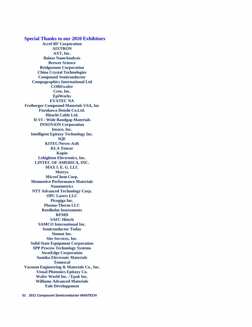
51 2011 Compound Semiconductor MANTECH
Special Thanks to our 2010 Exhibitors Accel-RF Corporation
AIXTRON
AXT, Inc.
Balazs NanoAnalysis
Brewer Science
Bridgestone Corporation
China Crystal Technologies
Compound Semiconductor
Compugraphics International Ltd
COREwafer
Cree, Inc.
EpiWorks
EVATEC NA
Freiberger Compound Materials USA, Inc
Furukawa Denshi Co.Ltd.
Hitachi Cable Ltd.
II-VI : Wide Bandgap Materials
INNOViON Corporation
Insaco, Inc.
Intelligent Epitaxy Technology Inc.
IQE
KITEC/Neves-AxR
KLA Tencor
Kopin
Lehighton Electronics, Inc.
LINTEC OF AMERICA, INC.
MAX I. E. G. LLC
Metryx
MicroChem Corp.
Momentive Performance Materials
Nanometrics
NTT Advanced Technology Corp.
OPC Lasers LLC
Picogiga Inc.
Plasma-Therm LLC
Reedholm Instruments
RFMD
SAFC Hitech
SAMCO International Inc.
Semiconductor Today
Sinmat Inc.
Site Services, Inc.
Solid State Equipment Corporation
SPP Process Technology Systems
StratEdge Corporation
Sumika Electronic Materials
Temescal
Vacuum Engineering & Materials Co., Inc.
Visual Photonics Epitaxy Co.
Wafer World Inc. / Epak Inc.
Williams Advanced Materials
Yole Développment
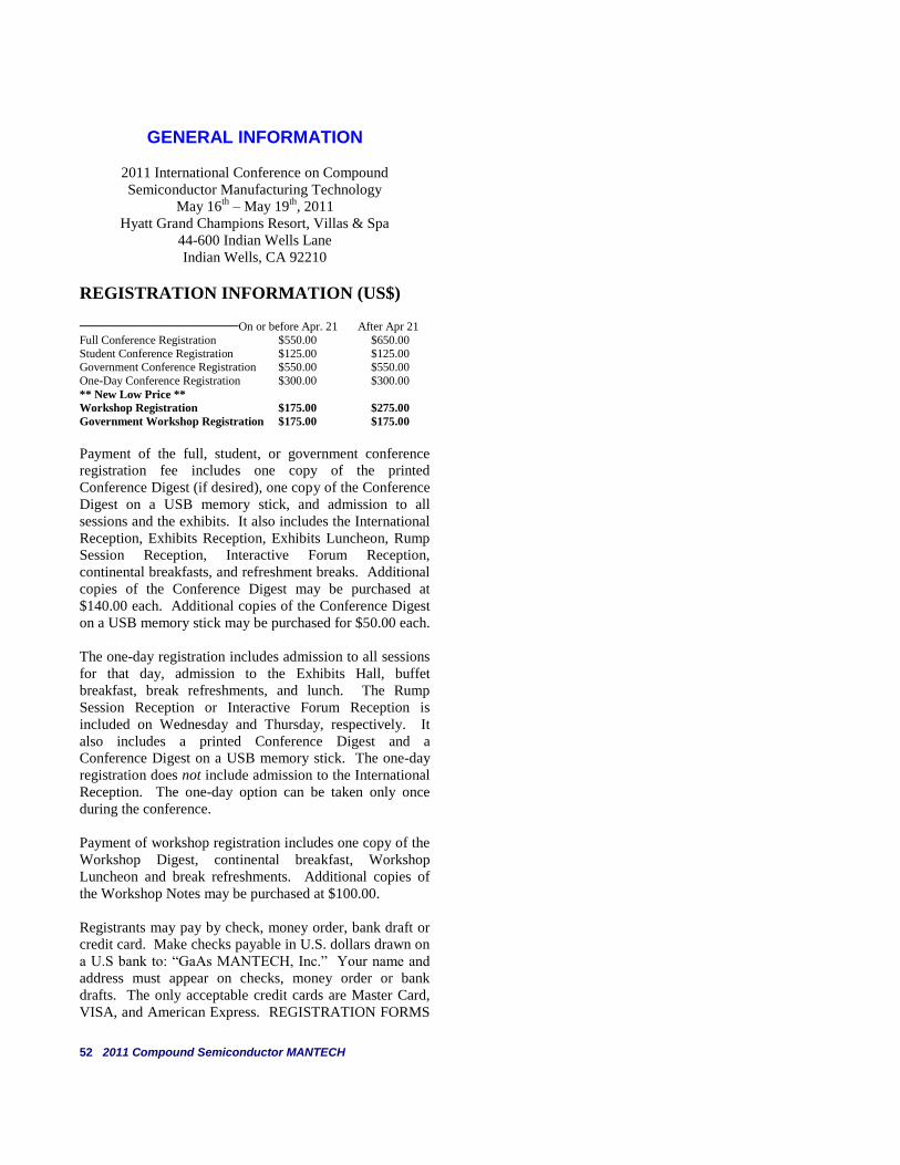
52 2011 Compound Semiconductor MANTECH
GENERAL INFORMATION
2011 International Conference on Compound
Semiconductor Manufacturing Technology
May 16th
– May 19th
, 2011
Hyatt Grand Champions Resort, Villas & Spa
44-600 Indian Wells Lane
Indian Wells, CA 92210
REGISTRATION INFORMATION (US$) On or before Apr. 21 After Apr 21 Full Conference Registration $550.00 $650.00
Student Conference Registration $125.00 $125.00
Government Conference Registration $550.00 $550.00
One-Day Conference Registration $300.00 $300.00
** New Low Price **
Workshop Registration $175.00 $275.00
Government Workshop Registration $175.00 $175.00
Payment of the full, student, or government conference
registration fee includes one copy of the printed
Conference Digest (if desired), one copy of the Conference
Digest on a USB memory stick, and admission to all
sessions and the exhibits. It also includes the International
Reception, Exhibits Reception, Exhibits Luncheon, Rump
Session Reception, Interactive Forum Reception,
continental breakfasts, and refreshment breaks. Additional
copies of the Conference Digest may be purchased at
$140.00 each. Additional copies of the Conference Digest
on a USB memory stick may be purchased for $50.00 each.
The one-day registration includes admission to all sessions
for that day, admission to the Exhibits Hall, buffet
breakfast, break refreshments, and lunch. The Rump
Session Reception or Interactive Forum Reception is
included on Wednesday and Thursday, respectively. It
also includes a printed Conference Digest and a
Conference Digest on a USB memory stick. The one-day
registration does not include admission to the International
Reception. The one-day option can be taken only once
during the conference.
Payment of workshop registration includes one copy of the
Workshop Digest, continental breakfast, Workshop
Luncheon and break refreshments. Additional copies of
the Workshop Notes may be purchased at $100.00.
Registrants may pay by check, money order, bank draft or
credit card. Make checks payable in U.S. dollars drawn on
a U.S bank to: “GaAs MANTECH, Inc.” Your name and
address must appear on checks, money order or bank
drafts. The only acceptable credit cards are Master Card,
VISA, and American Express. REGISTRATION FORMS
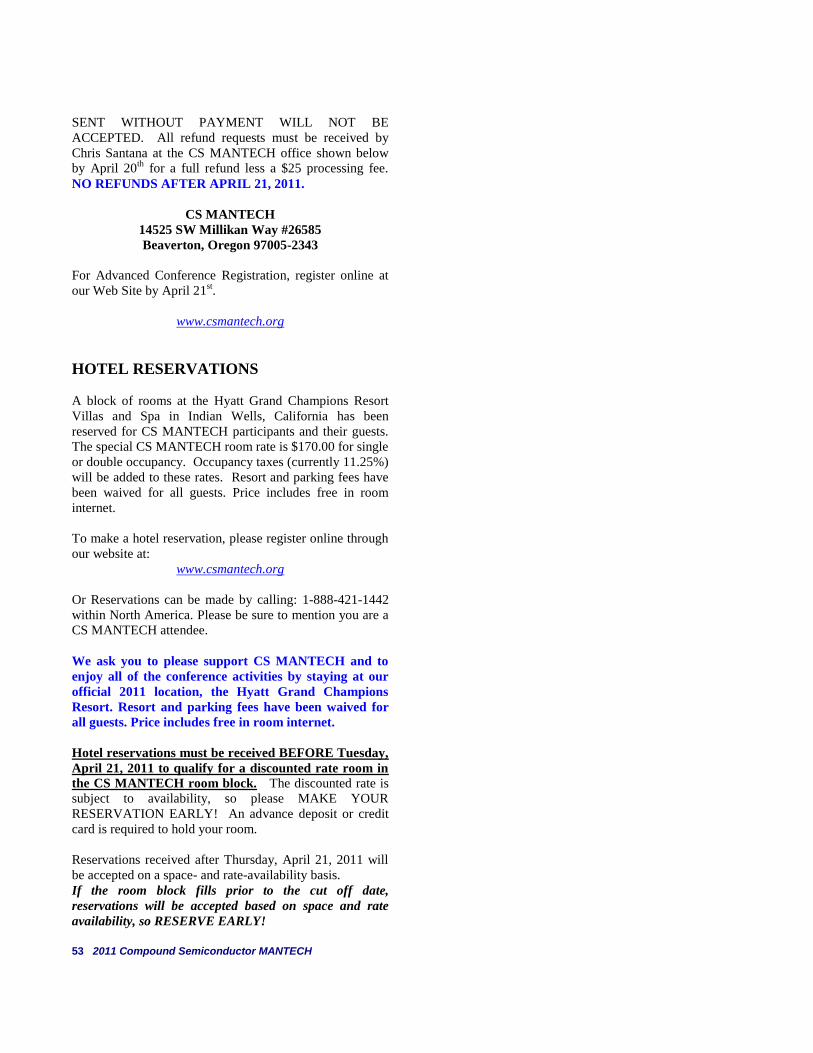
53 2011 Compound Semiconductor MANTECH
SENT WITHOUT PAYMENT WILL NOT BE
ACCEPTED. All refund requests must be received by
Chris Santana at the CS MANTECH office shown below
by April 20th
for a full refund less a $25 processing fee.
NO REFUNDS AFTER APRIL 21, 2011.
CS MANTECH
14525 SW Millikan Way #26585
Beaverton, Oregon 97005-2343
For Advanced Conference Registration, register online at
our Web Site by April 21st.
www.csmantech.org
HOTEL RESERVATIONS
A block of rooms at the Hyatt Grand Champions Resort
Villas and Spa in Indian Wells, California has been
reserved for CS MANTECH participants and their guests.
The special CS MANTECH room rate is $170.00 for single
or double occupancy. Occupancy taxes (currently 11.25%)
will be added to these rates. Resort and parking fees have
been waived for all guests. Price includes free in room
internet.
To make a hotel reservation, please register online through
our website at:
www.csmantech.org
Or Reservations can be made by calling: 1-888-421-1442
within North America. Please be sure to mention you are a
CS MANTECH attendee.
We ask you to please support CS MANTECH and to
enjoy all of the conference activities by staying at our
official 2011 location, the Hyatt Grand Champions
Resort. Resort and parking fees have been waived for
all guests. Price includes free in room internet.
Hotel reservations must be received BEFORE Tuesday,
April 21, 2011 to qualify for a discounted rate room in
the CS MANTECH room block. The discounted rate is
subject to availability, so please MAKE YOUR
RESERVATION EARLY! An advance deposit or credit
card is required to hold your room.
Reservations received after Thursday, April 21, 2011 will
be accepted on a space- and rate-availability basis.
If the room block fills prior to the cut off date,
reservations will be accepted based on space and rate
availability, so RESERVE EARLY!
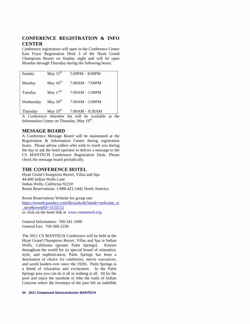
54 2011 Compound Semiconductor MANTECH
CONFERENCE REGISTRATION & INFO
CENTER Conference registration will open in the Conference Center
East Foyer Registration Desk 3 of the Hyatt Grand
Champions Resort on Sunday night and will be open
Monday through Thursday during the following hours:
Sunday May 15
th 5:00PM – 8:00PM
Monday May 16th
7:00AM – 7:00PM
Tuesday May 17th
7:00AM – 5:00PM
Wednesday May 18th
7:00AM – 5:00PM
Thursday May 19th
7:00AM – 9:30AM
A Conference Attendee list will be available at the
Information Center on Thursday, May 19th
.
MESSAGE BOARD A Conference Message Board will be maintained at the
Registration & Information Center during registration
hours. Please advise callers who wish to reach you during
the day to ask the hotel operator to deliver a message to the
CS MANTECH Conference Registration Desk. Please
check the message board periodically.
THE CONFERENCE HOTEL Hyatt Grand Champions Resort, Villas and Spa
44-600 Indian Wells Lane
Indian Wells, California 92210
Room Reservations: 1-888-421-1442 North America
Room Reservations Website for group rate:
https://resweb.passkey.com/Resweb.do?mode=welcome_ei
_new&eventID=3155112
or click on the hotel link at www.csmantech.org.
General Information: 760-341-1000
General Fax: 760-568-2236
The 2011 CS MANTECH Conference will be held at the
Hyatt Grand Champions Resort, Villas and Spa in Indian
Wells, California (greater Palm Springs). Known
throughout the world for its special brand of relaxation,
style, and sophistication, Palm Springs has been a
destination of choice for celebrities, movie executives,
and world leaders ever since the 1920s. Palm Springs is
a blend of relaxation and excitement. In the Palm
Springs area you can do it all or nothing at all. Sit by the
pool and enjoy the sunshine or hike the trails of Indian
Canyons where the footsteps of the past left an indelible
55 2011 Compound Semiconductor MANTECH
impression. Golf, tennis, sunning, hiking, biking, and
swimming top the list of leisure activities in Palm
Springs, and these blend easily with the abundance and
variety of shopping, museums, restaurants, spas and
casinos.
Indulge yourself, and surrender to luxury at Hyatt Grand
Champions Resort, Villas and Spa. A 45-acre oasis of
lush gardens and shimmering fountains awaits you.
Discover the impeccable service and amenities of our
elegant yet family-friendly Palm Springs resort. Relax in
the award-winning spa, play a round of championship
golf or swim in one of seven inviting pools. Get your
exercise on our pro hard surface tennis courts or play
Badminton. Truly inspired menus make dining a
decided pleasure.
For more detailed information on the Hyatt Grand
Champions Resort, visit http://grandchampions.hyatt.com/hyatt/hotels/index.jsp
For more information on Palm Springs activities, visit
http://visitpalmsprings.com
TRANSPORTATION TO THE HOTEL
Palm Springs Airport- PSP (15miles)
Turn left on El Cielo Rd.. Turn left on Ramon until
you reach Interstate 10 traveling East. Turn right on
Cook Street. Turn Left on Hwy 111. Turn Left on
Indian Wells Lane.
Los Angeles Airport- LAX
As you exit the terminal turn right, take the 105 Fwy
East. Exit 605 Fwy North. Exit Hwy 60 East to I-10
East. Exit on Cook, turn right. Turn left on Hwy. 111.
Left on Indian Wells Lane.
Ontario Airport- ONT
Take Archibald Avenue to I-10 East. Exit on Cook,
turn right. Left on Hwy. 111. Left on Indian Wells
Lane.
**This hotel does not provide shuttle service.
Estimated taxi fare: $65.00 (one way) from PSP
FINANCIAL ASSISTANCE
CS MANTECH strongly encourages and supports
participation from academic delegates. Students and
University Professors seeking financial assistance should
contact Peter Ersland, the 2011 University Liaison, by
email at [email protected].
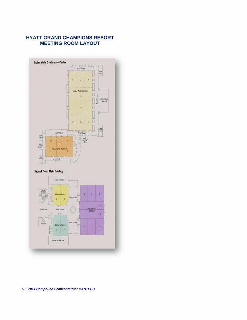
56 2011 Compound Semiconductor MANTECH
HYATT GRAND CHAMPIONS RESORT MEETING ROOM LAYOUT