Embed Size (px)
Citation preview
IS43/46LR16800G
11www.issi.com - [email protected]. B | 03/27/2017
2M x 16Bits x 4Banks Mobile DDR SDRAM
Description
The IS43/46LR16800G is 134,217,728 bits CMOS Mobile Double Data Rate Synchronous DRAM organized as 4 banks of 2,097,152 words x
16 bits. This product uses a double-data-rate architecture to achieve high-speed operation. The Data Input/ Output signals are transmitted
on a 16-bit bus. The double data rate architecture is essentially a 2N prefetch architecture with an interface designed to transfer two data
words per clock cycle at the I/O pins. This product offers fully synchronous operations referenced to both rising and falling edges of the clock.
The data paths are internally pipelined and 2n-bits prefetched to achieve very high bandwidth. All input and output voltage levels are
compatible with LVCMOS.
Features
• JEDEC standard 1.8V power supply.
• VDD = 1.8V, VDDQ = 1.8V
• Four internal banks for concurrent operation
• MRS cycle with address key programs
- CAS latency 2, 3 (clock)
- Burst length (2, 4, 8, 16)
- Burst type (sequential & interleave)
• Fully differential clock inputs (CK, /CK)
• All inputs except data & DM are sampled at the rising
edge of the system clock
• Data I/O transaction on both edges of data strobe
• Bidirectional data strobe per byte of data (DQS)
• DM for write masking only
• Edge aligned data & data strobe output
• Center aligned data & data strobe input
• 64ms refresh period (4K cycle)
• Auto & self refresh
• Concurrent Auto Precharge
• Maximum clock frequency up to 166MHZ
• Maximum data rate up to 333Mbps/pin
• Power Saving support
- PASR (Partial Array Self Refresh)
- Auto TCSR (Temperature Compensated Self Refresh)
- Deep Power Down Mode
- Programmable Driver Strength Control by Full Strength
or ¾, ½, ¼ , ⅛ of Full Strength
• LVCMOS compatible inputs/outputs
• 60-Ball FBGA package
Copyright © 2017 Integrated Silicon Solution, Inc. All rights reserved. ISSI reserves the right to make changes to this specification and its
products at any time without notice. ISSI assumes no liability arising out of the application or use of any information, products or services
described herein. Customers are advised to obtain the latest version of this device specification before relying on any published information
and before placing orders for products.
Integrated Silicon Solution, Inc. does not recommend the use of any of its products in life support applications where the failure or
malfunction of the product can reasonably be expected to cause failure of the life support system or to significantly affect its safety or
effectiveness. Products are not authorized for use in such applications unless Integrated Silicon Solution, Inc. receives written assurance to
its satisfaction, that:
a.) the risk of injury or damage has been minimized;
b.) the user assume all such risks; and
c.) potential liability of Integrated Silicon Solution, Inc is adequately protected under the circumstances
2Rev. B | 03/27/2017 www.issi.com - [email protected]
IS43/46LR16800G
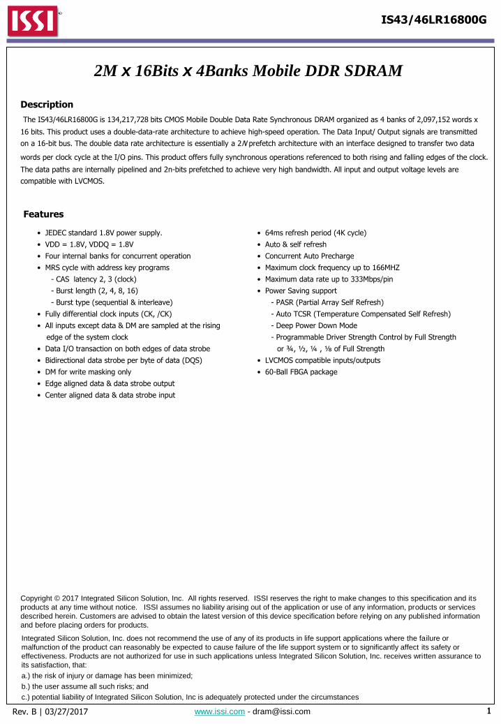
Figure1: 60Ball FBGA Ball Assignment
A
B
C
D
E
F
G
H
J
K
1 2 3 4 5 6 7 8 9
VSS DQ15 VSSQ
VDDQ DQ13 DQ14
VSSQ DQ11 DQ12
VDDQ DQ9 DQ10
VSS UDM NC
CKE CK /CK
A9 A11 NC
A6 A7 A8
VSS A4 A5
VDDQ DQ0 VDD
DQ1 DQ2 VSSQ
DQ3 DQ4 VDDQ
DQ5 DQ6 VSSQ
NC LDM VDD
/WE /CAS /RAS
/CS BA0 BA1
A10 A0 A1
A2 A3 VDD
VSSQ UDQS DQ8 DQ7 LDQS VDDQ
[Top View]

3Rev. B | 03/27/2017 www.issi.com - [email protected]
IS43/46LR16800G
Table2 : Pin Descriptions
Symbol Type Function Descriptions
CK, /CK Input System Clock
The system clock input. CK and /CK are differential clockinputs. All address and control input signals are registered on the crossing of the rising edge of CK and falling edge of /CK. Input and output data is referenced to the crossing of CK and /CK.
CKE Input Clock Enable
CKE is clock enable controls input. CKE HIGH activates, and CKE LOW deactivates internal clock signals, and device input buffers and output drivers. CKE is synchronous for all functions except for SELF REFRESH EXIT, which is achieved asynchronously.
/CS Input Chip Select
/CS enables (registered Low) and disables (registered High) the command decoder. All commands are masked when /CS IS REGISTERED high. /CS provides for external bank selection on systems with multiple banks. /CS is considered part of the command code.
BA0, BA1 Input Bank Address
BA0 and BA1 define to which bank an ACTIVE, READ, WRITE, or PRECHARGE command is being applied. BA0 and BA1 also determine which mode register (standard mode register or extended mode register) is loaded during a LOAD MODE REGISTER command.
A0~A11 Input AddressRow Address : RA0~RA11Column Address : CA0~CA8Auto Precharge : A10
/RAS, /CAS, /WE Input
Row Address Strobe,
Column Address Strobe,
Write Enable
/RAS, /CAS and /WE define the operation.Refer function truth table for details.
LDM, UDM Input Data Input Mask
DM is an input mask signal for write data. Input datais masked when DM is sampled HIGH along with that input data during a WRITE access. DM is sampled on both edges of DQS. Although DM balls are input-only.
DQ0~DQ15 In/Output Data Input/Output Data input/output pin.
LDQS, UDQS In/OutputData Input/Output Strobe
Output with read data, input with write data. DQS is edge-aligned with read data, centered in write data. Data strobe is used to capture data.
VDD Supply Power Supply Power supply
VSS Supply Ground Ground
VDDQ Supply DQ Power Supply Power supply for DQ
VSSQ Supply DQ Ground Ground for DQ
NC NC No Connection No connection.

4Rev. B | 03/27/2017 www.issi.com - [email protected]
IS43/46LR16800G
Figure2 : Functional Block Diagram
ExtendedMode
Register
Self refreshLogic & timer
Internal RowCounter
RowPre
Decoder
ColumnPre
Decoder
Column AddCounter
AddressRegister
Mode Register Data Out Control
BurstCounter
Addre
ss Buffe
rsSta
te M
ach
ine
Row
Deco
ders
Row
Deco
ders
Row
Deco
ders
Row
Deco
ders
2Mx16 BANK 1
2Mx16 BANK 0
MemoryCell
Array
Column Decoders
2Mx16 BANK 2
2Mx16 BANK 3
Write Data Register2-bit Prefetch Unit
Sense
AM
P&
I/O G
ate
Outp
ut B
uffe
r & L
ogic
DQ0.......
DQ15
Data StrobeTransmitter
Data StrobeReceiver
Input B
uffe
r & L
ogic
|
|
16|
|
|
|
32|
|
DS
UDQS,LDQS
DS
X16
X32
PASR
Row Active
Refresh
Column Active
Bank Select
Burst
Length
CASLatency
---------A0
A1
A11
BA0
BA1
LDM/UDM
/WE
/CAS
/RAS
/CS
CKE
CK
/CK

5Rev. B | 03/27/2017 www.issi.com - [email protected]
IS43/46LR16800G
Figure3 : Simplified State Diagram
Power On
PrechargeAll Banks
MRSEMRS
ActivePowerDown
Deep PowerDown
IdleAll Banks
Precharged
SelfRefresh
AutoRefresh
Row Active
PrechargePREALL
WRITE
WRITE A
READ
READ A
BurstStop
PrechargePowerDown
DPDS
Power
Applied
DPDSX
MRSREFA
REFS
REFSX
ACT
CKEH
CKEL
PRE
CKEL
CKEH
WRITE READBST
PRE
PRE PRE
WRITE A
WRITE READ
READ A
READ
WRITE A READ A
Automatic sequence
ACT = Active
BST = Burst
CKEL = Enter Power- Down
CKEH = Exit Power-Down
DPDS = Enter Deep Power-Down
DPDSX = Exit Deep Power- Down
EMRS = Ext. Mode Reg. Set
MRS = Mode Register Set
PRE = Precharge
PREALL= Precharge All Banks
REFA = Auto Refresh
REFS = Enter Self Refresh
REFSX = Exit Self Refresh
READ = Read w/o Auto Precharge
READ A = Read with Auto Precharge
WRITE = Write w/o Auto Precharge
WRITE A = Write with Auto Precharge

6Rev. B | 03/27/2017 www.issi.com - [email protected]
IS43/46LR16800G
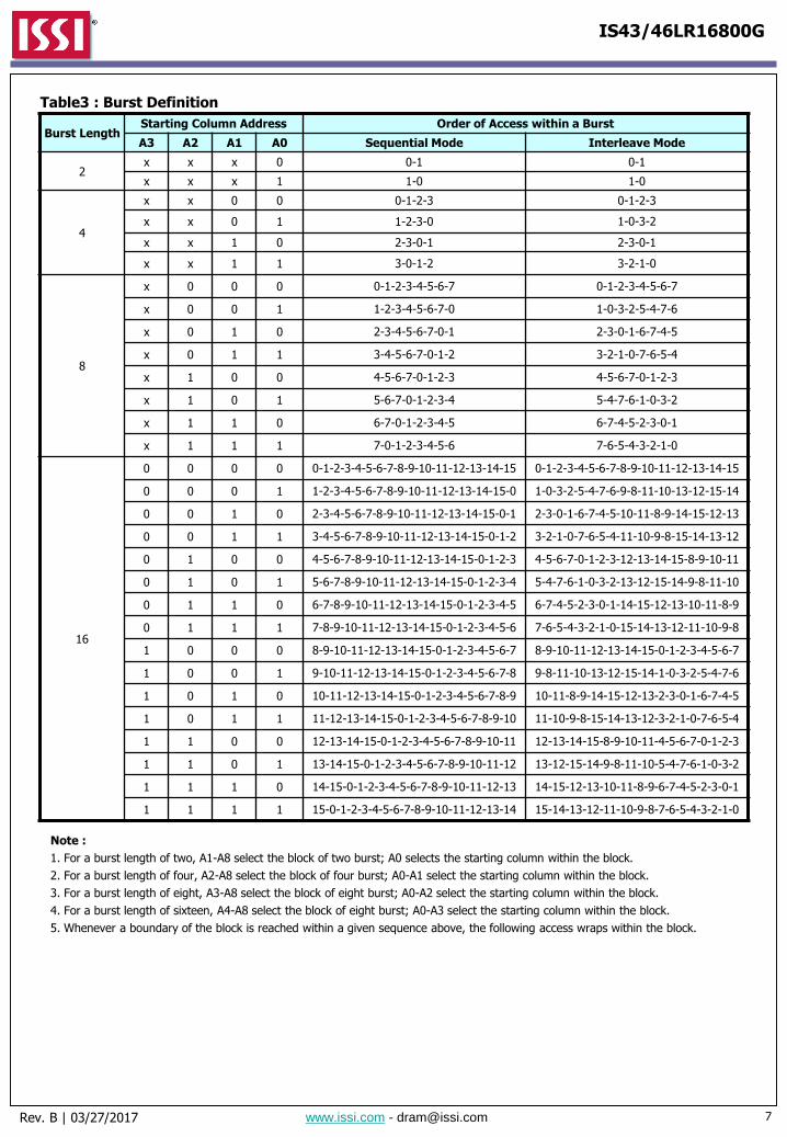
Burst Type
Accesses within a given burst may be programmed to be either sequential or interleaved; this is referred to as the burst type and is
selected via bit M3. The ordering of accesses within a burst is determined by the burst length, the burst type and the starting column
address, as shown in Table 3.
M3 Burst Type
0 Sequential
1 Interleave
M6 M5 M4 CAS Latency
0 0 0 Reserved
0 0 1 Reserved
0 1 0 2
0 1 1 3
1 0 0 Reserved
1 0 1 Reserved
1 1 0 Reserved
1 1 1 Reserved
M2 M1 M0Burst Length
M3 = 0 M3 = 1
0 0 0 Reserved Reserved
0 0 1 2 2
0 1 0 4 4
0 1 1 8 8
1 0 0 16 16
1 0 1 Reserved Reserved
1 1 0 Reserved Reserved
1 1 1 Reserved Reserved
Address Bus
A0A1A2A3A4A5A6A7A8A9A10A11
Figure4 : Mode Register Set (MRS) Definition
BA0BA1
13 12 11 10 9 8 7 6 5 4 3 2 1 0
0 0 0 0 0 0 0 CAS Latency BT Burst Length
Note: M13(BA1) and M12(BA0) must be set to “0” to select Mode Register (vs. the Extended Mode Register)
Mode Register (Mx)
7Rev. B | 03/27/2017 www.issi.com - [email protected]
IS43/46LR16800G
Table3 : Burst Definition
Burst LengthStarting Column Address Order of Access within a Burst
A3 A2 A1 A0 Sequential Mode Interleave Mode
2x x x 0 0-1 0-1
x x x 1 1-0 1-0
4
x x 0 0 0-1-2-3 0-1-2-3
x x 0 1 1-2-3-0 1-0-3-2
x x 1 0 2-3-0-1 2-3-0-1
x x 1 1 3-0-1-2 3-2-1-0
8
x 0 0 0 0-1-2-3-4-5-6-7 0-1-2-3-4-5-6-7
x 0 0 1 1-2-3-4-5-6-7-0 1-0-3-2-5-4-7-6
x 0 1 0 2-3-4-5-6-7-0-1 2-3-0-1-6-7-4-5
x 0 1 1 3-4-5-6-7-0-1-2 3-2-1-0-7-6-5-4
x 1 0 0 4-5-6-7-0-1-2-3 4-5-6-7-0-1-2-3
x 1 0 1 5-6-7-0-1-2-3-4 5-4-7-6-1-0-3-2
x 1 1 0 6-7-0-1-2-3-4-5 6-7-4-5-2-3-0-1
x 1 1 1 7-0-1-2-3-4-5-6 7-6-5-4-3-2-1-0
16
0 0 0 0 0-1-2-3-4-5-6-7-8-9-10-11-12-13-14-15 0-1-2-3-4-5-6-7-8-9-10-11-12-13-14-15
0 0 0 1 1-2-3-4-5-6-7-8-9-10-11-12-13-14-15-0 1-0-3-2-5-4-7-6-9-8-11-10-13-12-15-14
0 0 1 0 2-3-4-5-6-7-8-9-10-11-12-13-14-15-0-1 2-3-0-1-6-7-4-5-10-11-8-9-14-15-12-13
0 0 1 1 3-4-5-6-7-8-9-10-11-12-13-14-15-0-1-2 3-2-1-0-7-6-5-4-11-10-9-8-15-14-13-12
0 1 0 0 4-5-6-7-8-9-10-11-12-13-14-15-0-1-2-3 4-5-6-7-0-1-2-3-12-13-14-15-8-9-10-11
0 1 0 1 5-6-7-8-9-10-11-12-13-14-15-0-1-2-3-4 5-4-7-6-1-0-3-2-13-12-15-14-9-8-11-10
0 1 1 0 6-7-8-9-10-11-12-13-14-15-0-1-2-3-4-5 6-7-4-5-2-3-0-1-14-15-12-13-10-11-8-9
0 1 1 1 7-8-9-10-11-12-13-14-15-0-1-2-3-4-5-6 7-6-5-4-3-2-1-0-15-14-13-12-11-10-9-8
1 0 0 0 8-9-10-11-12-13-14-15-0-1-2-3-4-5-6-7 8-9-10-11-12-13-14-15-0-1-2-3-4-5-6-7
1 0 0 1 9-10-11-12-13-14-15-0-1-2-3-4-5-6-7-8 9-8-11-10-13-12-15-14-1-0-3-2-5-4-7-6
1 0 1 0 10-11-12-13-14-15-0-1-2-3-4-5-6-7-8-9 10-11-8-9-14-15-12-13-2-3-0-1-6-7-4-5
1 0 1 1 11-12-13-14-15-0-1-2-3-4-5-6-7-8-9-10 11-10-9-8-15-14-13-12-3-2-1-0-7-6-5-4
1 1 0 0 12-13-14-15-0-1-2-3-4-5-6-7-8-9-10-11 12-13-14-15-8-9-10-11-4-5-6-7-0-1-2-3
1 1 0 1 13-14-15-0-1-2-3-4-5-6-7-8-9-10-11-12 13-12-15-14-9-8-11-10-5-4-7-6-1-0-3-2
1 1 1 0 14-15-0-1-2-3-4-5-6-7-8-9-10-11-12-13 14-15-12-13-10-11-8-9-6-7-4-5-2-3-0-1
1 1 1 1 15-0-1-2-3-4-5-6-7-8-9-10-11-12-13-14 15-14-13-12-11-10-9-8-7-6-5-4-3-2-1-0
Note :
1. For a burst length of two, A1-A8 select the block of two burst; A0 selects the starting column within the block.
2. For a burst length of four, A2-A8 select the block of four burst; A0-A1 select the starting column within the block.
3. For a burst length of eight, A3-A8 select the block of eight burst; A0-A2 select the starting column within the block.
4. For a burst length of sixteen, A4-A8 select the block of eight burst; A0-A3 select the starting column within the block.
5. Whenever a boundary of the block is reached within a given sequence above, the following access wraps within the block.

8Rev. B | 03/27/2017 www.issi.com - [email protected]
IS43/46LR16800G
Figure5 : Extended Mode Set (EMRS) Register
Address Bus
Extended Mode Register (Ex)
A0A1A2A3A4A5A6A7A8A9A10A11
E2 E1 E0 Self Refresh Coverage
0 0 0 Four Banks
0 0 1 Two Bank (BA1=0)
0 1 0 One Bank (BA1=BA0=0)
0 1 1 Reserved
1 0 0 Reserved
1 0 1One Eighth of Total Bank
(BA1 = BA0 = Row Address MSB=0)
1 1 0One Sixteenth of Total Bank
(BA1 = BA0 = Row Address 2 MSBs=0)
1 1 1 Reserved
E7 E6 E5Driver
Strength
0 0 0 Full Strength
0 0 1 ½ Strength
0 1 0 ¼ Strength
0 1 1 ⅛ Strength
1 0 0 ¾ Strength
1 0 1 Reserved
1 1 0 Reserved
1 1 1 Reserved
BA0BA1
13 12 11 10 9 8 7 6 5 4 3 2 1 0
1 0 0 0 0 0 DS 0 0 PASR
Note: E13(BA1)=1 and E12(BA0)=0 to select Extended Mode Register (vs. the base Mode Register)

9Rev. B | 03/27/2017 www.issi.com - [email protected]
IS43/46LR16800G
The 128Mb Mobile DDR SDRAM is a high-speed CMOS, dynamic random-access memory containing 134,271,728-bits. It is internally
configured as a quad-bank DRAM. The 128Mb Mobile DDR SDRAM uses a double data rate architecture to achieve high speed operation.
The double data rate architecture is essentially a 2n-prefetch architecture, with an interface designed to transfer two data words per clock
cycle at the I/O balls, single read or write access for the 128Mb Mobile DDR SDRAM consists of a single 2n-bit wide, one-clock-cycle data
transfer at the internal DRAM core and two corresponding n-bit wide, one-half-clock-cycle data transfers at the I/O balls.
Read and Write accesses to the Mobile DDR SDRAM are burst oriented; accesses start at a selected location and continue for a programmed
number of locations in a programmed sequence. Accesses begin with the registration of an ACTIVE command, which is then followed by a
READ or WRITE command. The address bits registered coincident with the ACTIVE command are used to select the bank and row to be
accessed (BA0, BA1 select the bank; A0–A11 select the row). The address bits registered coincident with the READ or WRITE command are
used to select the starting column location for the burst access.
It should be noted that the DLL signal that is typically used on standard DDR devices is not necessary on the Mobile DDR SDRAM. It has
been omitted to save power.
Prior to normal operation, the Mobile DDR SDRAM must be powered up and initialized. The following sections provide detailed information
covering device initialization, register definition, command descriptions and device operation.
Power up and Initialization
Mobile DDR SDRAM must be powered up and initialized in a predefined manner. Power must be applied to VDD and VDDQ (simultaneously).
After power up, an initial pause of 200 usec is required. And a precharge all command will be issued to the Mobile DDR. Then, 2 or more
Auto refresh cycles will be provided. After the Auto refresh cycles are completed, a Mode Register Set(MRS) command will be issued to
program the specific mode of operation (Cas Latency, Burst length, etc.) And a Extended Mode Register Set(EMRS) command will be issued
to Partial Array Self Refresh(PASR). The following these cycles, the Mobile DDR SDRAM is ready for normal operation. To ensure device
functionality, there is a predefined sequence that must occur at device power up or if there is any interruption of device power.
To properly initialize the Mobile DDR SDRAM, this sequence must be followed:
1. To prevent device latch-up, it is recommended the core power (VDD) and I/O power (VDDQ) be from the same power source and brought
up simultaneously. If separate power sources are used, VDD must lead VDDQ.
2. Once power supply voltages are stable and the CKE has been driven HIGH, it is safe to apply the clock.
3. Once the clock is stable, a 200μs (minimum) delay is required by the Mobile DDR SDRAM prior to applying an executable command.
During this time, NOP or DESELECT commands must be issued on the command bus.
4. Issue a PRECHARGE ALL command.
5. Issue NOP or DESELECT commands for at least tRP time.
6. Issue an AUTO REFRESH command followed by NOP or DESELECT commands for at least tRFC time. Issue a second AUTO REFRESH
command followed by NOP or DESELECT commands for at least tRFC time. As part of the individualization sequence, two AUTO REFRESH
commands must be issued. Typically, both of these commands are issued at this stage as described above.
7. Using the LOAD MODE REGISTER command, load the standard mode register as desired.
8. Issue NOP or DESELECT commands for at least tMRD time.
9. Using the LOAD MODE REGISTER command, load the extended mode register to the desired operating modes. Note that the order in
which the standard and extended mode registers are programmed is not critical.
10. Issue NOP or DESELECT commands for at least tMRD time.
11. The Mobile DDR SDRAM has been properly initialized and is ready to receive any valid command.
Functional Description

10Rev. B | 03/27/2017 www.issi.com - [email protected]
IS43/46LR16800G
Notes:
1. PCG = PRECHARGE command, MRS = LOAD MODE REGISTER command, AREF = AUTOREFRESH command, ACT = ACTIVE command, RA = Row address, BA = Bank address.
2. NOP or DESELECT commands are required for at least 200μs.
3. Other valid commands are possible.
4. NOPs or DESELECTs are required during this time.
Figure6 : Power up sequence
ACT
BABA0=L,BA1=H
BA0=L,BA1=L
All Banks
MRSMRSAREFAREFPCGNOPNOP2
NOP3
CLK
/CLK
CKE
T0
Command1
T1 Ta0
tCL
DM
A0~A9, A11
Tb0 Tc0 Td0 Te0 Tf0
tCK
LVCMOSHIGH LEVEL
A10
BA0, BA1
DQS, DQ High-Z
T = 200 µs
tIS
RACODECODE
tIS tIH
RACODECODE
tIS tIH
tIS tIH
tRP4 tRFC4 tRFC4 tMRD4 tMRD4
tIH
VDDQ
VDD
tIS tIH
Load Standard Mode Register
Load Extended Mode Register
Power-up: VDD and CLK stable Don’ t care

11Rev. B | 03/27/2017 www.issi.com - [email protected]
IS43/46LR16800G
Mode Register
The mode register is used to define the specific mode of operation of the Mobile DDR SDRAM. This definition includes the selection of a
burst length, a burst type, a CAS latency. The mode register is programmed via the LOAD MODE REGISTER command and will retain the
stored information until programmed again, the device goes into deep power-down mode, or the device loses power.
Mode register bits A0-A2 specify the burst length, A3 specifies the type of burst (sequential or interleaved), A4-A6 specify the CAS latency,
and A7-A11 should be set to zero. BA0 and BA1 must be zero to access the mode register.
The mode register must be loaded when all banks are idle, and the controller must wait the specified time before initiating the subsequent
operation. Violating either of these requirements will result in unspecified operation.
Burst Length
Read and write accesses to the Mobile DDR SDRAM are burst oriented, with the burst length being programmable, as shown in Figure
(Mode Register Set Definition). The burst length determines the maximum number of column locations that can be accessed for a given
READ or WRITE command. Burst lengths of 2, 4,8 or 16 are available for both the sequential and the interleaved burst types.
Reserved states should not be used, as unknown operation or incompatibility with future versions may result. When a READ or WRITE
command is issued, a block of columns equal to the burst length is effectively selected. All accesses for that burst take place within this
block, meaning that the burst will wrap within the block if a boundary is reached. The block is uniquely selected by A1-A8 when the burst
length is set to two; by A2-A8 when the burst length is set to four; by A3-A8 when the burst length is set to eight; and by A4-A8 when the
burst length is set to sixteen. The remaining (least significant) address bit(s) is (are) used to select the starting location within the block.
The programmed burst length applies to both READ and WRITE bursts.
CAS Latency
The CAS latency is the delay, in clock cycles, between the registration of a READ command and the availability of the first bit of output
data. The latency can be set to 2, 3 clocks, as shown in Figure (Standard Mode Register Definition).
For CL = 3, if the READ command is registered at clock edge n, then the data will be available at (n + 2 clocks + tAC). For CL = 2, if the
READ command is registered at clock edge n, then the data will be available at (n + 1 clock + tAC).
Figure7 : CAS Latency (BL=4)
/C K
C K
Command
T0 T1 T2 T3T1n T2n T3n
READ NOP NOP NOP
DQS
DQ
tAC
CL=3
DOUT
n+1
tRPRE
2tCK
T4 T4n
NOP
tRPST
DOUT
nDOUT
n+2DOUT
n+3
Don ’t care
DQS
DQ
tAC
CL=2
DOUT
n+1
tRPRE
1tCK
tRPST
DOUT
n
DOUT
n+2
DOUT
n+3
L
L

12Rev. B | 03/27/2017 www.issi.com - [email protected]
IS43/46LR16800G
Extended Mode Register
The Extended Mode Register controls the functions beyond those controlled by the Mode Register. These additional functions are special
features of the Mobile DDR SDRAM. They include Partial Array Self Refresh (PASR) and Driver Strength (DS).
The Extended Mode Register is programmed via the Mode Register Set command (BA0=0, BA1=1) and retains the stored information until
programmed again, the device goes into deep power-down mode, or the device loses power.
The Extended Mode Register must be programmed with A8 through A11 set to “0”. The Extended Mode Register must be loaded when all
banks are idle and no bursts are in progress, and the controller must wait the specified time before initiating any subsequent operation.
Violating either of these requirements results in unspecified operation.
Partial Array Self Refresh
For further power savings during SELF REFRESH, the PASR feature allows the controller to select the amount of memory that will be
refreshed during SELF REFRESH. The refresh options are as follows:
• Full array: banks 0, 1, 2, and 3
• Half array: banks 0 and 1
• Quarter array: bank 0
• One eighth array: half of bank 0
• One sixteenth array: quarter of bank 0
WRITE and READ commands can still occur during standard operation, but only the selected banks will be refreshed during SELF REFRESH.
Data in banks that are disabled will be lost.
Output Driver Strength
Because the Mobile DDR SDRAM is designed for use in smaller systems that are mostly point to point, an option to control the drive
strength of the output buffers is available. Drive strength should be selected based on the expected loading of the memory bus. Bits A5 and
A6 of the extended mode register can be used to select the driver strength of the DQ outputs. There are four allowable settings for the
output drivers.
Temperature Compensated Self Refresh
In the Mobile DDR SDRAM, a temperature sensor is implemented for automatic control of the self refresh oscillator on the device.
Temperature Compensated Self Refresh allows the controller to program the Refresh interval during SELF REFRESH mode, according to the
case temperature of the Mobile SDRAM device. This allows great power savings during SELF REFRESH during most operating temperature
ranges. Only during extreme temperatures would the controller have to select a TCSR level that will guarantee data during SELF REFRESH.
Every cell in the DRAM requires refreshing due to the capacitor losing its charge over time. The refresh rate is dependent on temperature.
At higher temperatures a capacitor loses charge quicker than at lower temperatures, requiring the cells to be refreshed more often.
Historically, during Self Refresh, the refresh rate has been set to accommodate the worst case, or highest temperature range expected.
Thus, during ambient temperatures, the power consumed during refresh was unnecessarily high, because the refresh rate was set to
accommodate the higher temperatures.
This temperature compensated refresh rate will save power when the DRAM is operating at normal temperatures. It is not supported for
any temperature grade with TA above +85°C.
13Rev. B | 03/27/2017 www.issi.com - [email protected]
IS43/46LR16800G
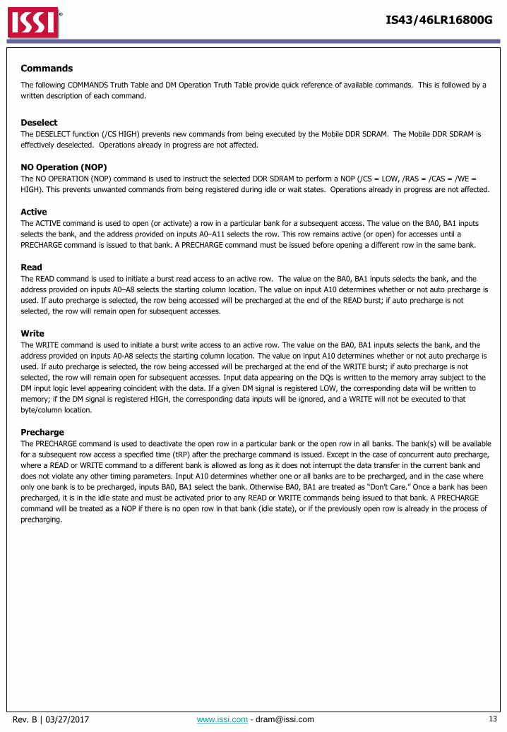
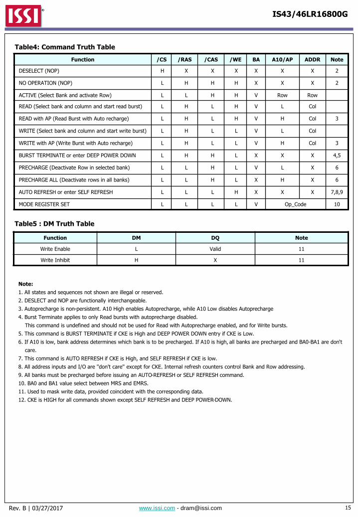
Commands
The following COMMANDS Truth Table and DM Operation Truth Table provide quick reference of available commands. This is followed by a
written description of each command.
Deselect
The DESELECT function (/CS HIGH) prevents new commands from being executed by the Mobile DDR SDRAM. The Mobile DDR SDRAM is
effectively deselected. Operations already in progress are not affected.
NO Operation (NOP)
The NO OPERATION (NOP) command is used to instruct the selected DDR SDRAM to perform a NOP (/CS = LOW, /RAS = /CAS = /WE =
HIGH). This prevents unwanted commands from being registered during idle or wait states. Operations already in progress are not affected.
Active
The ACTIVE command is used to open (or activate) a row in a particular bank for a subsequent access. The value on the BA0, BA1 inputs
selects the bank, and the address provided on inputs A0–A11 selects the row. This row remains active (or open) for accesses until a
PRECHARGE command is issued to that bank. A PRECHARGE command must be issued before opening a different row in the same bank.
Read
The READ command is used to initiate a burst read access to an active row. The value on the BA0, BA1 inputs selects the bank, and the
address provided on inputs A0–A8 selects the starting column location. The value on input A10 determines whether or not auto precharge is
used. If auto precharge is selected, the row being accessed will be precharged at the end of the READ burst; if auto precharge is not
selected, the row will remain open for subsequent accesses.
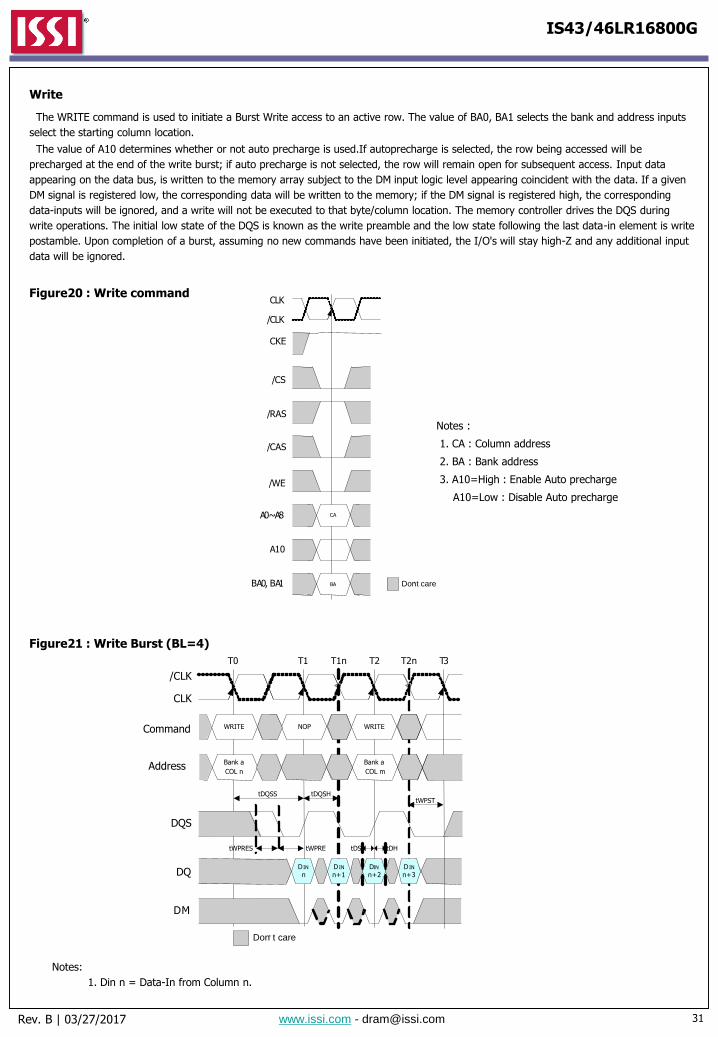
Write
The WRITE command is used to initiate a burst write access to an active row. The value on the BA0, BA1 inputs selects the bank, and the
address provided on inputs A0-A8 selects the starting column location. The value on input A10 determines whether or not auto precharge is
used. If auto precharge is selected, the row being accessed will be precharged at the end of the WRITE burst; if auto precharge is not
selected, the row will remain open for subsequent accesses. Input data appearing on the DQs is written to the memory array subject to the
DM input logic level appearing coincident with the data. If a given DM signal is registered LOW, the corresponding data will be written to
memory; if the DM signal is registered HIGH, the corresponding data inputs will be ignored, and a WRITE will not be executed to that
byte/column location.
Precharge
The PRECHARGE command is used to deactivate the open row in a particular bank or the open row in all banks. The bank(s) will be available
for a subsequent row access a specified time (tRP) after the precharge command is issued. Except in the case of concurrent auto precharge,
where a READ or WRITE command to a different bank is allowed as long as it does not interrupt the data transfer in the current bank and
does not violate any other timing parameters. Input A10 determines whether one or all banks are to be precharged, and in the case where
only one bank is to be precharged, inputs BA0, BA1 select the bank. Otherwise BA0, BA1 are treated as “Don’t Care.” Once a bank has been
precharged, it is in the idle state and must be activated prior to any READ or WRITE commands being issued to that bank. A PRECHARGE
command will be treated as a NOP if there is no open row in that bank (idle state), or if the previously open row is already in the process of
precharging.
14Rev. B | 03/27/2017 www.issi.com - [email protected]
IS43/46LR16800G
Auto Precharge
Auto precharge is a feature which performs the same individual-bank precharge function described above, but without requiring an explicit
command. This is accomplished by using A10 to enable auto precharge in conjunction with a specific READ or WRITE command. A
precharge of the bank/row that is addressed with the READ or WRITE command is automatically performed upon completion of the READ or
WRITE burst. Auto precharge is nonpersistent in that it is either enabled or disabled for each individual READ or WRITE command. This
device supports concurrent auto precharge if the command to the other bank does not interrupt the data transfer to the current bank. Auto
precharge ensures that the precharge is initiated at the earliest valid stage within a burst. This “earliest valid stage” is determined as if an
explicit PRECHARGE command was issued at the earliest possible time, without violating tRAS (MIN). The user must not issue another
command to the same bank until the precharge time (tRP) is completed.
Burst Terminate
The BURST TERMINATE command is used to truncate READ bursts (with auto precharge disabled). The most recently registered READ
command prior to the BURST TERMINATE command will be truncated. The open page which the READ burst was terminated from remains
open.
Auto Refresh
AUTO REFRESH is used during normal operation of the Mobile DDR SDRAM and is analogous to /CAS-BEFORE-/RAS (CBR) REFRESH in
FPM/EDO DRAMs. This command is nonpersistent, so it must be issued each time a refresh is required. The addressing is generated by the
internal refresh controller. This makes the address bits a “Don’t Care” during an AUTO REFRESH command. The 128Mb Mobile DDR SDRAM
requires AUTO REFRESH cycles at an average interval of tREFI (maximum). To allow for improved efficiency in scheduling and switching
between tasks, some flexibility in the absolute refresh interval is provided.
Although not a JEDEC requirement, to provide for future functionality features, CKE must be active (HIGH) during the auto refresh period.
The auto refresh period begins when the AUTO REFRESH command is registered and ends tRFC later.
Self Refresh
The SELF REFRESH command can be used to retain data in the Mobile DDR SDRAM, even if the rest of the system is powered down. When
in the self refresh mode, the Mobile DDR SDRAM retains data without external clocking. The SELF REFRESH command is initiated like an
AUTO REFRESH command except CKE is disabled (LOW). All command and address input signals except CKE are “Don’t Care” during SELF
REFRESH.
During SELF REFRESH, the device is refreshed as identified in the external mode register (see PASR setting). For a the full array refresh, all
four banks are refreshed simultaneously with the refresh frequency set by an internal self refresh oscillator. This oscillator changes due to
the temperature sensors input. As the case temperature of the Mobile DDR SDRAM increases, the oscillation frequency will change to
accommodate the change of temperature. This happens because the DRAM capacitors lose charge faster at higher temperatures. To ensure
efficient power dissipation during self refresh, the oscillator will change to refresh at the slowest rate possible to maintain the devices data.
The procedure for exiting SELF REFRESH requires a sequence of commands. First, Clock must be stable prior to CKE going back HIGH. Once
CKE is HIGH, the Mobile DDR SDRAM must have NOP commands issued for tXSR is required for the completion of any internal refresh in
progress. The self refresh command is not applicable for operation with TA > 85C
Deep Power-down
Deep Power Down is an operating mode to achieve maximum power reduction by eliminating the power of the whole memory array of the
devices. Data will not be retained once the device enters Deep Power Down Mode.
This mode is entered by having all banks idle then /CS and /WE held low with /RAS and /CAS held high at the rising edge of the clock, while
CKE is low. This mode is exited by asserting CKE high. After applying NOP commands for 200µs, the power up and initialization sequence
must be followed. This mode is not applicable for operation with TA > 85C.
15Rev. B | 03/27/2017 www.issi.com - [email protected]
IS43/46LR16800G
Note:
1. All states and sequences not shown are illegal or reserved.
2. DESLECT and NOP are functionally interchangeable.
3. Autoprecharge is non-persistent. A10 High enables Autoprecharge, while A10 Low disables Autoprecharge
4. Burst Terminate applies to only Read bursts with autoprecharge disabled.
This command is undefined and should not be used for Read with Autoprecharge enabled, and for Write bursts.
5. This command is BURST TERMINATE if CKE is High and DEEP POWER DOWN entry if CKE is Low.
6. If A10 is low, bank address determines which bank is to be precharged. If A10 is high, all banks are precharged and BA0-BA1 are don‘t
care.
7. This command is AUTO REFRESH if CKE is High, and SELF REFRESH if CKE is low.
8. All address inputs and I/O are ''don't care'' except for CKE. Internal refresh counters control Bank and Row addressing.
9. All banks must be precharged before issuing an AUTO-REFRESH or SELF REFRESH command.
10. BA0 and BA1 value select between MRS and EMRS.
11. Used to mask write data, provided coincident with the corresponding data.
12. CKE is HIGH for all commands shown except SELF REFRESH and DEEP POWER-DOWN.
Function /CS /RAS /CAS /WE BA A10/AP ADDR Note
DESELECT (NOP) H X X X X X X 2
NO OPERATION (NOP) L H H H X X X 2
ACTIVE (Select Bank and activate Row) L L H H V Row Row
READ (Select bank and column and start read burst) L H L H V L Col
READ with AP (Read Burst with Auto recharge) L H L H V H Col 3
WRITE (Select bank and column and start write burst) L H L L V L Col
WRITE with AP (Write Burst with Auto recharge) L H L L V H Col 3
BURST TERMINATE or enter DEEP POWER DOWN L H H L X X X 4,5
PRECHARGE (Deactivate Row in selected bank) L L H L V L X 6
PRECHARGE ALL (Deactivate rows in all banks) L L H L X H X 6
AUTO REFRESH or enter SELF REFRESH L L L H X X X 7,8,9
MODE REGISTER SET L L L L V Op_Code 10
Function DM DQ Note
Write Enable L Valid 11
Write Inhibit H X 11
Table5 : DM Truth Table
Table4: Command Truth Table
16Rev. B | 03/27/2017 www.issi.com - [email protected]
IS43/46LR16800G
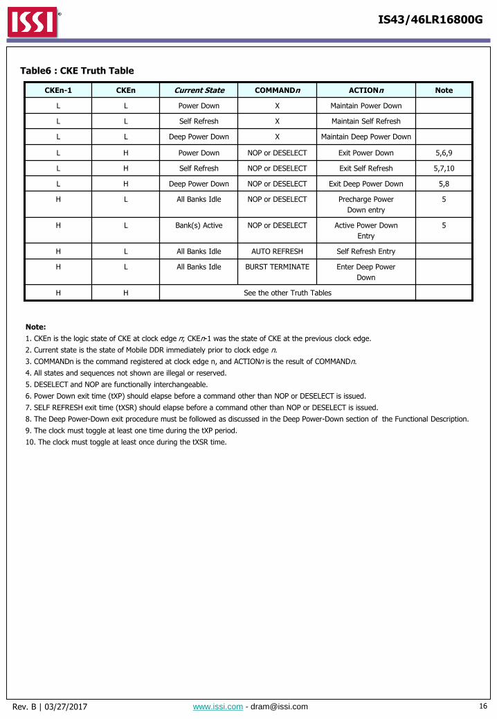
Note:
1. CKEn is the logic state of CKE at clock edge n; CKEn-1 was the state of CKE at the previous clock edge.
2. Current state is the state of Mobile DDR immediately prior to clock edge n.
3. COMMANDn is the command registered at clock edge n, and ACTIONn is the result of COMMANDn.
4. All states and sequences not shown are illegal or reserved.
5. DESELECT and NOP are functionally interchangeable.
6. Power Down exit time (tXP) should elapse before a command other than NOP or DESELECT is issued.
7. SELF REFRESH exit time (tXSR) should elapse before a command other than NOP or DESELECT is issued.
8. The Deep Power-Down exit procedure must be followed as discussed in the Deep Power-Down section of the Functional Description.
9. The clock must toggle at least one time during the tXP period.
10. The clock must toggle at least once during the tXSR time.
See the other Truth TablesHH
Enter Deep Power
Down
BURST TERMINATEAll Banks IdleLH
Self Refresh EntryAUTO REFRESHAll Banks IdleLH
5Active Power Down
Entry
NOP or DESELECTBank(s) ActiveLH
5Precharge Power
Down entry
NOP or DESELECTAll Banks IdleLH
5,8Exit Deep Power DownNOP or DESELECTDeep Power DownHL
5,7,10Exit Self RefreshNOP or DESELECTSelf RefreshHL
5,6,9Exit Power DownNOP or DESELECTPower DownHL
Maintain Deep Power DownXDeep Power DownLL
Maintain Self RefreshXSelf RefreshLL
Maintain Power DownXPower DownLL
NoteACTIONnCOMMANDnCurrent StateCKEnCKEn-1
Table6 : CKE Truth Table

17Rev. B | 03/27/2017 www.issi.com - [email protected]
IS43/46LR16800G
Note:
1. The table applies when both CKEn-1 and CKEn are HIGH, and after tXSR or tXP has been met if the previous state was Self Refresh or
Power Down.
2. DESELECT and NOP are functionally interchangeable.
3. All states and sequences not shown are illegal or reserved.
4. This command may or may not be bank specific. If all banks are being precharged, they must be in a valid state for precharging.
5. A command other than NOP should not be issued to the same bank while a READ or WRITE Burst with auto precharge is enabled.
6. The new Read or Write command could be auto precharge enabled or auto precharge disabled.
7. Current State Definitions:
Idle: The bank has been precharged, and tRP has been met.
Row Active: A row in the bank has been activated, and tRCD has been met.
No data bursts/accesses and no register accesses are in progress.
Read: A READ burst has been initiated, with AUTO PRECHARGE disabled, and has not yet terminated or been terminated.
Write: a WRITE burst has been initiated, with AUTO PRECHARGE disabled, and has not yet terminated or been terminated.
8. The following states must not be interrupted by a command issued to the same bank.
DESELECT or NOP commands or allowable commands to the other bank should be issued on any clock edge occurring during these
states. Allowable commands to the other bank are determined by its current state and Truth Table3, and according to Truth Table 4.
• Precharging: Starts with the registration of a PRECHARGE command and ends when tRP is met.
Once tRP is met, the bank will be in the idle state.
• Row Activating: Starts with registration of an ACTIVE command and ends when tRCD is met.
Once tRCD is met, the bank will be in the ''row active'' state.
• Read with AP Enabled: Starts with the registration of the READ command with AUTO PRECHARGE enabled and ends when tRP has
been met. Once tRP has been met, the bank will be in the idle state.
• Write with AP Enabled: Starts with registration of a WRITE command with AUTO PRECHARGE enabled and ends when tRP has been
met. Once tRP is met, the bank will be in the idle state.
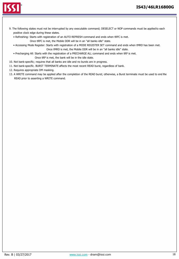
Table7 : Current State BANKn Truth Table(COMMAND TO BANK n)
Current StateCommand
Action Note/CS /RAS /CAS /WE Description
Any H X X X DESELECT(NOP) Continue previous Operation
L H H H NOP Continue previous Operation
Idle
L L H H ACTIVE Select and activate row
L L L H AUTO REFRESH Auto refresh 10
L L L LMODE REGISTER SET
Mode register set 10
L L H H PRECHARGE No action if bank is idle
Row Active
L H L H READ Select Column & start read burst
L H L L WRITE Select Column & start write burst
L L H L PRECHARGE Deactivate Row in bank (or banks) 4
Read
(without Auto
recharge)
L H L H READ Truncate Read & start new Read burst 5,6
L H L L WRITE Truncate Read & start new Write burst 5,6,13
L L H L PRECHARGE Truncate Read, start Precharge
L H H L BURST TERMINATE Burst terminate 11
Write
(without Auto
precharge)
L H L H READ Truncate Write & start new Read burst 5,6,12
L H L L WRITE Truncate Write & start new Write burst 5,6
L L H L PRECHARGE Truncate Write, start Precharge 12
18Rev. B | 03/27/2017 www.issi.com - [email protected]
IS43/46LR16800G
9. The following states must not be interrupted by any executable command; DESELECT or NOP commands must be applied to each
positive clock edge during these states.
• Refreshing: Starts with registration of an AUTO REFRESH command and ends when tRFC is met.
Once tRFC is met, the Mobile DDR will be in an ''all banks idle'' state.
• Accessing Mode Register: Starts with registration of a MODE REGISTER SET command and ends when tMRD has been met.
Once tMRD is met, the Mobile DDR will be in an ''all banks idle'' state.
• Precharging All: Starts with the registration of a PRECHARGE ALL command and ends when tRP is met.
Once tRP is met, the bank will be in the idle state.
10. Not bank-specific; requires that all banks are idle and no bursts are in progress.
11. Not bank-specific. BURST TERMINATE affects the most recent READ burst, regardless of bank.
12. Requires appropriate DM masking.
13. A WRITE command may be applied after the completion of the READ burst; otherwise, a Burst terminate must be used to end the
READ prior to asserting a WRITE command.
19Rev. B | 03/27/2017 www.issi.com - [email protected]
IS43/46LR16800G
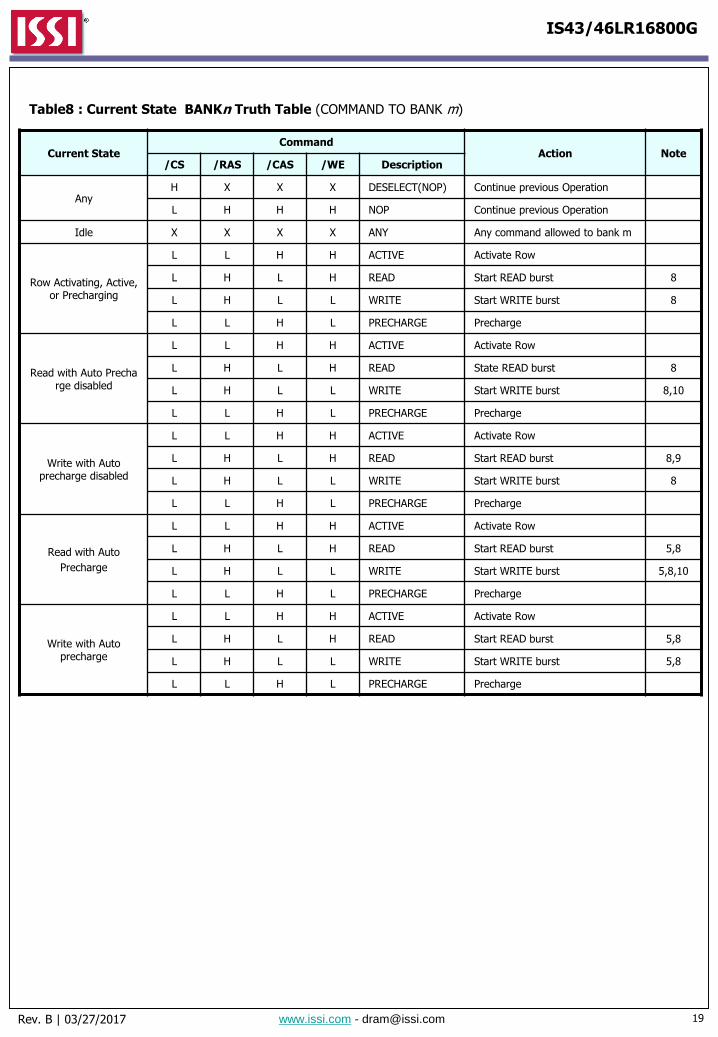
Table8 : Current State BANKn Truth Table (COMMAND TO BANK m)
Current StateCommand
Action Note/CS /RAS /CAS /WE Description
Any H X X X DESELECT(NOP) Continue previous Operation
L H H H NOP Continue previous Operation
Idle X X X X ANY Any command allowed to bank m
Row Activating, Active,or Precharging
L L H H ACTIVE Activate Row
L H L H READ Start READ burst 8
L H L L WRITE Start WRITE burst 8
L L H L PRECHARGE Precharge
Read with Auto Precharge disabled
L L H H ACTIVE Activate Row
L H L H READ State READ burst 8
L H L L WRITE Start WRITE burst 8,10
L L H L PRECHARGE Precharge
Write with Auto precharge disabled
L L H H ACTIVE Activate Row
L H L H READ Start READ burst 8,9
L H L L WRITE Start WRITE burst 8
L L H L PRECHARGE Precharge
Read with Auto
Precharge
L L H H ACTIVE Activate Row
L H L H READ Start READ burst 5,8
L H L L WRITE Start WRITE burst 5,8,10
L L H L PRECHARGE Precharge
Write with Auto precharge
L L H H ACTIVE Activate Row
L H L H READ Start READ burst 5,8
L H L L WRITE Start WRITE burst 5,8
L L H L PRECHARGE Precharge
20Rev. B | 03/27/2017 www.issi.com - [email protected]
IS43/46LR16800G
Note:
1. The table applies when both CKEn-1 and CKEn are HIGH, and after tXSR or tXP has been met if the previous state was Self Refresh or
Power Down.
2. DESELECT and NOP are functionally interchangeable.
3. All states and sequences not shown are illegal or reserved.
4. Current State Definitions:
Idle: The bank has been precharged, and tRP has been met.
Row Active: A row in the bank has been activated, and tRCD has been met. No data bursts/accesses and no register accesses are in
progress.
Read: A READ burst has been initiated, with AUTO PRECHARGE disabled, and has not yet terminated or been terminated.
Write: a WRITE burst has been initiated, with AUTO PRECHARGE disabled, and has not yet terminated or been terminated.
5. Read with AP enabled and Write with AP enabled: The read with Autoprecharge enabled or Write with Autoprecharge enabled states
can be broken into two parts: the access period and the precharge period. For Read with AP, the precharge period is defined as if the
same burst was executed with Auto Precharge disabled and then followed with the earliest possible PRECHARGE command that still
accesses all the data in the burst.
For Write with Auto precharge, the precharge period begins when tWR ends, with tWR measured as if Auto Precharge was disabled.
The access period starts with registration of the command and ends where the precharge period (or tRP) begins.
During the precharge period, of the Read with Autoprecharge enabled or Write with Autoprecharge enabled states, ACTIVE,
PRECHARGE, READ, and WRITE commands to the other bank may be applied; during the access period, only ACTIVE and PRECHARGE
commands to the other banks may be applied. In either case, all other related limitations apply
(e.g. contention between READ data and WRITE data must be avoided).
6. AUTO REFRESH, SELF REFRESH, and MODE REGISTER SET commands may only be issued when all bank are idle.
7. A BURST TERMINATE command cannot be issued to another bank;
It applies to the bank represented by the current state only.
8. READs or WRITEs listed in the Command column include READs and WRITEs with AUTO PRECHARGE enabled and READs and WRITEs
with AUTO PRECHARGE disabled.
9. Requires appropriate DM masking.
10. A WRITE command may be applied after the completion of data output, otherwise a BURST TERMINATE command must be issued to
end the READ prior to asserting a WRITE command.

21Rev. B | 03/27/2017 www.issi.com - [email protected]
IS43/46LR16800G
Table9 : Absolute Maximum Rating
Parameter Symbol Rating Unit
Storage Temperature TSTG -55 ~ 150 C
Voltage on Any Pin relative to VSS VIN, VOUT -0.3 ~ 2.7 V
Voltage on VDD relative to VSS VDD, VDDQ -0.3 ~ 2.7 V
Short Circuit Output Current IOS 50 mA
Power Dissipation PD 0.7 W
Note :
Stresses greater than those listed under “Absolute Maximum Ratings” may cause permanent damage to the device. This is a stress
rating only, and functional operation of the device at these or any other conditions above those indicated in the operational sections of
this specification is not implied. Exposure to absolute maximum rating conditions for extended periods may affect reliability.
Table10 : Operating Temperature
Parameter Symbol Min Typ Max Unit Note
Power Supply Voltage VDD 1.7 1.8 1.95 V
Power Supply Voltage VDDQ 1.7 1.8 1.95 V 2
Input High Voltage VIH (DC) 0.7 x VDDQ VDDQ + 0.3 V
Input Low Voltage VIL (DC) -0.3 0.3 x VDDQ V
Input Differential Voltage, for
CK, /CK inputsVID (DC) 0.4 x VDDQ VDDQ + 0.6 V 3
Output High Voltage VOH (DC) 0.9 x VDDQ - V IOH=-0.1mA
Output Low Voltage VOL (DC) - 0.1 x VDDQ V IOL=0.1mA
Input Leakage Current ILI -2 2 uA
Output Leakage Current ILO -5 5 uA
Input High Voltage, all inputs VIH (AC) 0.8 x VDDQ VDDQ + 0.3 V
Input Low Voltage, all inputs VIL (AC) -0.3 0.2 x VDDQ V
Input Differential Voltage, for C
K, /CK inputsVID(AC) 0.6 x VDDQ VDDQ + 0.6 V 3
Input Differential Crosspoint
Voltage for CK and /CK inputsVIX(AC) 0.4 x VDDQ 0.6 x VDDQ V 4
Table11 : AC/DC Operating Conditions (1)
Notes :
1. All Voltages are referenced to VSS = 0V
2. VDD and VDDQ must track each other, and VDDQ must not exceed the level of VDD.
3. The magnitude of difference between input level on CK and input level on /CK.
4. The value of VIX is expected to equal 0.5*VDDQ of the transmitting device and must track variations in the DC level of the same.
Parameter Symbol Rating Unit
Ambient Temperature (Automotive, A2)
TA
-40 ~ 105
CAmbient Temperature (Automotive, A1) -40 ~ 85
Ambient Temperature (Industrial) -40 ~ 85
Ambient Temperature (Commercial) 0 ~ 70

22Rev. B | 03/27/2017 www.issi.com - [email protected]
IS43/46LR16800G
Table13 : AC Operating Test Condition
Parameter Symbol Value Unit
AC Input High/Low Level Voltage VIH / VIL 0.8 x VDDQ / 0.2 x VDDQ V
Input Timing Measurement Reference Level Voltage VTRIP 0.5 x VDDQ V
Input Rise / Fall Time tR / tF 1 / 1 ns
Output Timing Measurement Reference Level Voltage VOUTREF 0.5 x VDDQ V
Output Load Capacitance for Access Time Measurement CL 20 pF
Figure9 : Output load circuit
Table12 : Capacitance (TA=25C, f=1MHz, VDD=1.8V)
Parameter Pin Symbol Min Max Unit
Input Capacitance
CK, /CK CI1 1.5 3.5 pF
A0~A11, BA0~BA1, CKE, /CS, /RAS, /CAS, /WE
CI2 1.5 3.0 pF
LDM, UDM CI3 2 4.5 pF
Data & DQS Input/Output Capacitance DQ0~DQ15, LDQS, UDQS CIO 2 4.5 pF
Table14 : AC Overshoot/Undershoot Specification
Parameter Specification
Maximum Peak Amplitude allowed for Overshoot Area 0.9V
Maximum Peak Amplitude allowed for Undershoot Area 0.9V
Maximum Overshoot Area above VDD/VDDQ 3V-ns
Maximum Undershoot Area below VSS/VSSQ 3V-ns
Figure10 : AC Overshoot/Undershoot Definition
Maximum Amplitude
VDD/VDDQ
VSS/VSSQVoltage [V]
Maximum Amplitude
Time [ns]
Overshoot Area
Undershoot Area
Output
10.6K
13.9K
VDDQ
20pF
Output
20pF
50
VTT=0.5 x VDDQ
Z0=50
DC Output Load Circuit AC Output Load Circuit

23Rev. B | 03/27/2017 www.issi.com - [email protected]
IS43/46LR16800G
Table15 : DC Characteristic (DC operating conditions unless otherwise noted)
Note : 1. Measured with outputs open2. Refresh period is 64ms, applicable for TA < 85C 3. IDD6 value applicable for application with TA < 85C
4. Typical value at room temperature
Parameter Symbol Test ConditionSpeed
Unit Note-6 -75
Operating one bank active-precharge current
IDD0tRC = tRC(min), tCK = tCK(min), CKE is HIGH, /CS is HIGH between valid commands, address inputs are SWITCHING, data bus inputs are STABLE
50 45 mA 1
Precharge power-down standby current
IDD2PAll banks idle, CKE is LOW, /CS is HIGH, tCK = tCK(min), address and control inputs are SWITCHING, data bus inputs are STABLE
300 A
Precharge power-down standby current with clock stop
IDD2PSAll banks idle, CKE is LOW, /CS is HIGH, CK = LOW, /CK = HIGH, address and control inputs are SWITCHING, data bus inputs are STABLE
300 A
Precharge non power-down standby current
IDD2NAll banks idle, CKE is HIGH, /CS is HIGH, tCK = tCK(min) , address and control inputs are SWITCHING, data bus inputs are STABLE
10 mA
Precharge non power-down standby current with clock stop
IDD2NSAll banks idle, CKE is HIGH, /CS is HIGH, CK = LOW, /CK = HIGH, address and control inputs are SWITCHING, data bus inputs are STABLE
4 mA
Active power-down standby current
IDD3POne bank active, CKE is LOW, /CS is HIGH, tCK = tCK(min), address and control inputs are SWITCHING, data bus inputs are STABLE
1 mA
Active power-down standby current with clock stop
IDD3PSOne bank active, CKE is LOW, /CS is HIGH, CK = LOW,/CK = HIGH, address and control inputs are SWITCHING, data bus inputs are STABLE
1 mA
Active non power-downstandby current
IDD3NOne bank active, CKE is HIGH, /CS is HIGH, tCK = tCK(min), address and control inputs are SWITCHING, data bus inputs are STABLE
20 mA
Active non power-downstandby current with clockstop
IDD3NSOne bank active, CKE is HIGH, /CS is HIGH, CK = LOW, /CK = HIGH, address and control inputs are SWITCHING, data bus inputs are STABLE
10 mA
Operating burst read current IDD4R
One bank active, BL=4, CL=3, tCK = tCK(min), continuous read bursts, IOUT=0mA,address inputs are SWITCHING, 50% data change each burst transfer
80 70 mA 1
Operating burst write currentIDD4W
One bank active, BL=4, tCK=tCK(min), continuous write bursts, address inputs are SWITCHING, 50% data change each burst transfer
40 35 mA 1
Auto Refresh Current IDD5tRC=tRFC(min), tCK=tCK(min), burst refresh,CKE is HIGH, address and control inputs are SWITCHING, data bus inputs are STABLE
70 mA 2
Self Refresh Current
PASR TCSR
IDD6
CKE is LOWCK=LOW, /CK=HIGHtCK=tCK(min)Extended Mode Register set to all 0's, address and control inputs are STABLE, data bus inputs are STABLE
A 3
4 banks85C 300
45C 230
2 Banks85C 250
45C 200
1 Bank85C 220
45C 180
Half Bank
85C 200
45C 160
Quarter Bank
85C 180
45C 140
Standby Current inDeep Power Down Mode
IDD8Address and control inputs are STABLE, data bus inputs are STABLE
10 A 4

24Rev. B | 03/27/2017 www.issi.com - [email protected]
IS43/46LR16800G
Parameter Symbol-6 -75
Unit NoteMin Max Min Max
System Clock Cycle timeCL=3
tCK6 1000 7.5 1000 ns 1
CL=2 10 10 ns 1
DQ Output access time from CK, /CKCL=3
tAC2.0 5.5 2.0 6.0 ns
CL=2 2.0 8.0 2.0 8.0
Clock High pulse width tCH 0.45 0.55 0.45 0.55 tCK
Clock Low pulse width tCL 0.45 0.55 0.45 0.55 tCK
CKE min. pulse width (High/Low pulse width) tCKE 1 1 tCK
DQ and DM Input Setup time tDS 0.6 0.9 ns 2, 3, 4
DQ and DM Input Hold time tDH 0.6 0.9 ns 2, 3, 4
DQ and DM Input Pulse width tDIPW 1.8 2.0 ns 5
Address and Control Input Setup time tIS 1.0 1.3 ns 4, 6, 7
Address and Control Input Hold time tIH 1.0 1.3 ns 4, 6, 7
Address and Control Input Pulse Width tIPW 2.7 3.0 ns 5
DQ & DQS Low-impedance time from CK, /CK tLZ 1.0 1.0 ns 8
DQ & DQS High-impedance time from CK, /CK tHZ 5.5 6 ns 8
DQS - DQ Skew tDQSQ 0.5 0.6 ns 9
Half Clock Period tHP tCH, tCL tCH, tCL ns
Data Hold Skew Factor tQHS 0.65 0.75 ns
DQ / DQS Output Hold time from DQS tQH tHP-tQHS tHP-tQHS ns
Write Command to first DQS Latching Transition tDQSS 0.75 1.25 0.75 1.25 tCK
DQS Input High pulse Width tDQSH 0.35 0.6 0.4 0.6 tCK
DQS Input Low pulse Width tDQSL 0.35 0.6 0.4 0.6 tCK
DQS Falling Edge to CK Setup Time tDSS 0.2 0.2 tCK
DQS Falling Edge Hold Time From CK tDSH 0.2 0.2 tCK
Access Window of DQS from CK, /CKCL=3
tDQSCK2.0 5.5 2.0 6.0 ns
CL=2 2.0 8.0 2.0 8.0 ns
ACTIVE to PRECHARGE Command Period tRAS 42 45 ns
ACTIVE to ACTIVE Command Period tRC 60 75 ns
Mode Register Set command cycle time tMRD 2 2 tCK
Refresh Period tREF 64 64 ms 15
Average periodic refresh interval tREFI 15.6 15.6 us 10,15
Auto Refresh Period tRFC 70 70 ns
Active to Read or Write delay tRCD 18 22.5 ns
Precharge command period tRP 18 22.5 ns
Active Bank A to Active Bank B Delay tRRD 12 15 ns
Write Recovery time tWR 15 15 ns
Auto Precharge Write Recovery + Precharge time tDAL (tWR/tCK) + (tRP/tCK)
Internal Write to Read Command Delay tWTR 1 1 tCK
DQS Read preambleCL=3
tRPRE0.9 1.1 0.9 1.1 tCK 11
CL=2 0.5 1.1 0.5 1.1 tCK 11
DQS Read postamble tRPST 0.4 0.6 0.4 0.6 tCK
DQS Write preamble tWPRE 0.25 0.25 tCK
DQS Write preamble setup time tWPRES 0 0 ns 12
DQS Write postamble tWPST 0.4 0.6 0.4 0.6 tCK 13
Exit Power Down to next valid command Delay tXP 1 1 tCK 14
Self Refresh Exit to next valid Command Delay tXSR 120 120 ns
Table16: AC Characteristic (AC operation conditions unless otherwise noted)

25Rev. B | 03/27/2017 www.issi.com - [email protected]
IS43/46LR16800G
Note :
1. The clock frequency must remain constant (stable clock is defined as a signal cycling within timing constraints specified for the
clock pin) during access or precharge states (READ, WRITE, including tDPL, and PRECHARGE commands). CKE may be used to
reduce the data rate.
2. The transition time for DQ, DM and DQS inputs is measured between VIL(DC) to VIH(AC) for rising input signals, and VIH(DC) to VIL(AC
) for falling input signals.
3. DQS, DM and DQ input slew rate is specified to prevent double clocking of data and preserve setup and hold times. Signal transitions thr
ough the DC region must be monotonic.
4. Input slew rate ≥ 0.5V/ns and < 1.0V/ns.
5. These parameters guarantee device timing but they are not necessarily tested on each device.
6. The transition time for address and command inputs is measured between VIH and VIL.
7. A CK,/CK slew rate must be ≥ 1.0V/ns (2.0V/ns if measured differentially) is assumed for this parameter.
8. tHZ and tLZ transitions occur in the same access time windows as valid data transitions. These parameters are not referred to a specific
voltage level, but specify when the device is no longer driving (HZ), or begins driving (LZ).
9. tDQSQ consists of data pin skew and output pattern effects, and p-channel to n-channel variation of the output drivers for any given cyc
le.
10. A maximum of eight Refresh commands can be posted to any given Low-Power DDR SDRAM, meaning that the maximum absolute inte
rval between any Refresh command and the next Refresh command is 8*tREFI.
11. A low level on DQS may be maintained during High-Z states (DQS drivers disabled) by adding a weak pull-down element in the system.
It is recommended to turn off the weak pull-down element during read and write bursts (DQS drivers enabled).
12. The specific requirement is that DQS be valid (HIGH, LOW, or some point on a valid transition) on or before this CK edge. A valid transi
tion is defined as monotonic and meeting the input slew rate specifications of the device. When no writes were previously in progress o
n the bus, DQS will be transitioning from Hi-Z to logic LOW. If a previous write was in progress, DQS could be HIGH, LOW, or transitioni
ng from HIGH to LOW at this time, depending on tDQSS.
13. The maximum limit for this parameter is not a device limit. The device operates with a greater value for this parameter, but system per
formance (bus turnaround) will degrade accordingly.
14. At least one clock pulse is required during tXP.
15. The specifications in the table for TREF and TREFI are applicable for all temperature grades with TA < +85C. Only A2 temperature grade
supports operation with TA > 85C, and these values must be further constrained with TREF max of 32ms, and TREFI max of 7.8µs.
Input setup/hold slew rate [V/ns] ∆tDS/∆tIS [ps] ∆tDH/∆tIH [ps]
1.0 0 0
0.5 +150 +150
CK,/CK setup/hold slew rate [V/ns] ∆tDS/∆tIS [ps] ∆tDH/∆tIH [ps]
1.0 0 0

26Rev. B | 03/27/2017 www.issi.com - [email protected]
IS43/46LR16800G
Timing Diagram
Bank/row Activation
The Active command is used to activate a row in particular bank for a subsequent Read or Write access. The value of the BA0,BA1 inputs
selects the bank, and the address provided on A0-A11(or the highest address bit) selects the row.
Before any READ or WRITE commands can be issued to a bank within the Mobile DDR SDRAM, a row in that bank must be opened. This
is accomplished via the ACTIVE command, which selects both the bank and the row to be activated. The row remains active until a
PRECHARGE (or READ with AUTO PRECHARGE or WRITE with AUTO PRECHARGE) command is issued to the bank.
A PRECHARGE (or READ with AUTO PRECHARGE or WRITE with AUTO PRECHARGE) command must be issued before opening a different
row in the same bank.
Figure11 : tRCD, tRRD, tRC
Once a row is Open(with an ACTIVE command) a READ or WRITE command may be issued to that row, subject to the tRCD specification.
tRCD(min) should be divided by the clock period and rounded up to the next whole number to determine the earliest clock edge after the
ACTIVE command on which a READ or WRITE command can be entered.
A subsequent ACTIVE command to a different row in the same bank can only be issued after the previous active row has been
closed(precharge). The minimum time interval between successive ACTIVE commands to the same bank is defined by tRC. A subsequent
ACTIVE command to another bank can be issued while the first bank is being accessed, which results in a reduction of total row-access
overhead. The minimum time interval between successive ACTIVE commands to different banks is defined by tRRD.
Figure10 : Active command
Notes :
1. RA : Row address
2. BA : Bank address
CLK
/CLK
CKE
/CS
/RAS
/CAS
/WE
RA
BA
A0~A11
BA0, BA1 Don’t care
RD/WTwith AP
ACTNOPNOPNOP
Bank a
ROW
ACT NOP
/CLK
CLK
Command
T0 T1 T2 T3
A0-A11
BA0, BA1
COL
Bank a
T4 Ta0 Ta1
tRCD
Don’ t care
ROW
Bank b
tRRD
Bank a
ROW
ACT
tRC
Ta2
tCH tCLtIS tIH tCK

27Rev. B | 03/27/2017 www.issi.com - [email protected]
IS43/46LR16800G
Read
The READ command is used to initiate a Burst Read to an active row. The value of BA0 and BA1 selects the bank and address inputs select
the starting column location.
The value of A10 determines whether or not auto-precharge is used. If auto-precharge is selected, the row being accessed will be
precharged at the end of the read burst; if auto precharge is not selected, the row will remain open for subsequent access. The valid data-
out elements will be available CAS latency after the READ command is issued.
The Mobile DDR drives the DQS during read operations. The initial low state of the DQS is known as the read preamble and the last data-
out element is coincident with the read postamble. DQS is edge-aligned with read data. Upon completion of a burst, assuming no new READ
commands have been initiated, the I/O's will go high-Z.
Figure12 : Read command
Notes :
1. CA : Column address
2. BA : Bank address
3. A10=High : Enable Auto precharge
A10=Low : Disable Auto precharge
Figure13 : Read Data out timing (BL=4)
Notes:
1. BL=4
2. Shown with nominal tAC, tDQSCK and tDQSQ
CLK
/CLK
CKE
/CS
/RAS
/CAS
/WE
CAA0~A8
A10
BABA0, BA1 Don’t care
Bank a
COL n
/CLK
CLK
Command
T0 T1 T2 T3T1n T2n T3n
READ NOP NOP NOP
DQS
DQ
CL=3
DOUT
n+1
tRPRE
T4 T4n
NOP
tRPST
DOUT
n
DOUT
n+2
DOUT
n+3
Don’t care
Address
tAC tDQSCK
tQHtLZ tHZ
tDQSQ
DQS
DQ
CL=2
DOUT
n+1DOUT
nDOUT
n+2DOUT
n+3
tRPRE
tAC tRPST
28Rev. B | 03/27/2017 www.issi.com - [email protected]
IS43/46LR16800G
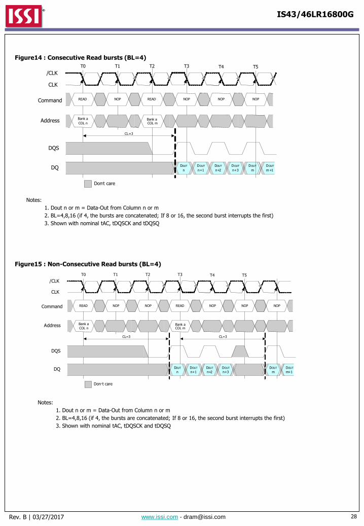
Figure14 : Consecutive Read bursts (BL=4)
Figure15 : Non-Consecutive Read bursts (BL=4)
Notes:
1. Dout n or m = Data-Out from Column n or m
2. BL=4,8,16 (if 4, the bursts are concatenated; If 8 or 16, the second burst interrupts the first)
3. Shown with nominal tAC, tDQSCK and tDQSQ
Notes:
1. Dout n or m = Data-Out from Column n or m
2. BL=4,8,16 (if 4, the bursts are concatenated; If 8 or 16, the second burst interrupts the first)
3. Shown with nominal tAC, tDQSCK and tDQSQ
DOUT
m
Bank a COL m
Bank a
COL n
NOPREAD NOP NOPNOPREAD
T0 T1 T2 T3
Address
T4 T5
/CLK
CLK
DQ
CL=3
Command
DQS
Don’t care
DOUT
n+1
DOUT
n
DOUT
n+2
DOUT
n+3
DOUT
m+1
Bank a COL m
Bank a
COL n
NOPREAD NOP NOPNOPREAD
T0 T1 T2 T3
Address
T4 T5
/CLK
CLK
DQ
CL=3
Command
DQS
Don’t care
DOUT
n+1
DOUT
n
DOUT
n+2
DOUT
n+3
CL=3
NOP
DOUT
m
DOUT
m+1

29Rev. B | 03/27/2017 www.issi.com - [email protected]
IS43/46LR16800G
Figure17 : Read Burst terminate (BL=4,8 or 16)
Truncated Reads
Data from any READ burst may be truncated with a BURST TERMINATE command, as shown in Figure16. The BURST TERMINATE
latency is equal to the READ (CAS) latency, i.e., the BURST TERMINATE command should be issued x cycles after the READ command,
where x equals the number of desired data element pairs (pairs are required by the 2n-prefetch architecture).
Data from any READ burst must be completed or truncated before a subsequent WRITE command can be issued. If truncation is
necessary, the BURST TERMINATE command must be used.
A READ burst may be followed by, or truncated with, a PRECHARGE command to the same bank provided that auto precharge was not
activated. The PRECHARGE command should be issued x cycles after the READ command, where x equals the number of desired data
element pairs (pairs are required by the n-prefetch architecture). This is shown in Figure (READ to PRECHARGE). Following the
PRECHARGE command, a subsequent command to the same bank cannot be issued until tRP is met.
Figure16 : Random Read access
Notes:
1. Dout n or m,p,q = Data-Out from Column n or m,p,q
2. BL=2,4,8,16 (if 4,8 or 16, the following burst interrupts the previous)
3. Reads are to an Active row in any bank.
4. Shown with nominal tAC, tDQSCK and tDQSQ
Notes:
1. Dout n = Data-Out from Column n
2. CKE=high
3. Shown with nominal tAC, tDQSCK and tDQSQ
Bank a COL m
Bank a COL p
DOUT
p
Bank a COL q
Bank a
COL n
READREAD READ NOPNOPREAD
T0 T1 T2 T3
Address
T4 T5
/CLK
CLK
DQ
CL=3
Command
DQS
Don’t care
DOUT
n+1
DOUT
n
DOUT
m
DOUT
m+1
NOP
DOUT
q
DOUT
q+1
DOUT
p+1
Bank a
COL n
NOPREAD BST NOPNOP
T0 T1 T2 T3
Address
T4
/CLK
CLK
DQ
CL=3
Command
DQS
Don’ t care
D OUTn+1
DOUTn

30Rev. B | 03/27/2017 www.issi.com - [email protected]
IS43/46LR16800G
Figure19 : Read to Precharge (BL=4)
Figure18 : Read to write terminate (BL=4,8 or 16)
Notes:
1. Dout n = Data-Out from Column n , Din m = Data-In from Column m.
2. CKE=high
3. Shown with nominal tAC, tDQSCK and tDQSQ
Notes:
1. Dout n = Data-Out from Column n.
2. Read to Precharge equals 2 tCK, which allows 2 data pairs of Data-Out.
3. Shown with nominal tAC, tDQSCK and tDQSQ
Bank a
COL m
NOP
Bank a
COL n
NOPREAD BST WRITENOP
T0 T1 T2 T3
Address
T4
/CLK
CLK
DQ
CL = 3
Command
DQS
Don’t care
D OUT
n+1
DOUT
n
tDQSS
(NOM )
DIN
m
D IN
m +1
T5
Bank a
(a, or all )
Bank a
COL n
PCGREAD NOP ACTNOPNOP
T0 T1 T2 T3
ADDRESS
T4 T5
/CLK
CLK
DQ
CL =3
Command
DQS
Bank a
Row
tRP
Don’ t care
D OUTn+ 1
D OUTn
D OUTn+2
D OUTn+3
31Rev. B | 03/27/2017 www.issi.com - [email protected]
IS43/46LR16800G
Figure21 : Write Burst (BL=4)
Write
The WRITE command is used to initiate a Burst Write access to an active row. The value of BA0, BA1 selects the bank and address inputs
select the starting column location.
The value of A10 determines whether or not auto precharge is used.If autoprecharge is selected, the row being accessed will be
precharged at the end of the write burst; if auto precharge is not selected, the row will remain open for subsequent access. Input data
appearing on the data bus, is written to the memory array subject to the DM input logic level appearing coincident with the data. If a given
DM signal is registered low, the corresponding data will be written to the memory; if the DM signal is registered high, the corresponding
data-inputs will be ignored, and a write will not be executed to that byte/column location. The memory controller drives the DQS during
write operations. The initial low state of the DQS is known as the write preamble and the low state following the last data-in element is write
postamble. Upon completion of a burst, assuming no new commands have been initiated, the I/O's will stay high-Z and any additional input
data will be ignored.
Figure20 : Write command
Notes :
1. CA : Column address
2. BA : Bank address
3. A10=High : Enable Auto precharge
A10=Low : Disable Auto precharge
Notes:
1. Din n = Data-In from Column n.
CLK
/CLK
CKE
/CS
/RAS
/CAS
/WE
CAA0~A8
A10
BABA0, BA1 Don’ t care
Bank a
COL m
Bank a
COL n
WRITE NOP WRITE
/CLK
CLK
T0 T1 T2 T3T1n T2n
DQ
tDQSStWPST
Don’ t care
DQS
tWPRES tWPRE tDHtDS
DM
D IN
nD IN
n+1DIN
n+2D IN
n+3
Address
Command
tDQSH

32Rev. B | 03/27/2017 www.issi.com - [email protected]
IS43/46LR16800G
Figure22 : Consecutive Write to write (BL=4)
Figure23 : Non-Consecutive Write to write (BL=4)
Notes:
1. Din n = Data-In from Column n.
2. Each Write command may be to any banks.
Notes:
1. Din n = Data-In from Column n.
2. Each Write command may be to any banks.
WRITE WRITE NOPNOPNOPNOP
Bank a
COL n
D IN
m
Bank a
COL m
T0 T1 T2 T3
Address
T4 T5
/CLK
CLK
DQS
DQ
tDQSS
(NOM )
Command
DM
DIN
n
D IN
n+ 1
DIN
n+2
D IN
n+ 3
DIN
m+ 1
D IN
m +2
DIN
m+3
Don’t care
NOPWRITE NOPNOPWRITENOP
Bank a
COL n
D IN
m
T0 T1 T2 T3
Address
T4 T5
/CLK
CLK
DQS
DQ
tDQSS
(NOM )
Command
DM
D IN
n
D IN
n+1
D IN
n+2
D IN
n+3
DIN
m+1
D IN
m +2
DIN
m+3
Don’t care
Bank a
COL m
tDQSS
(NOM )
NOP
33Rev. B | 03/27/2017 www.issi.com - [email protected]
IS43/46LR16800G
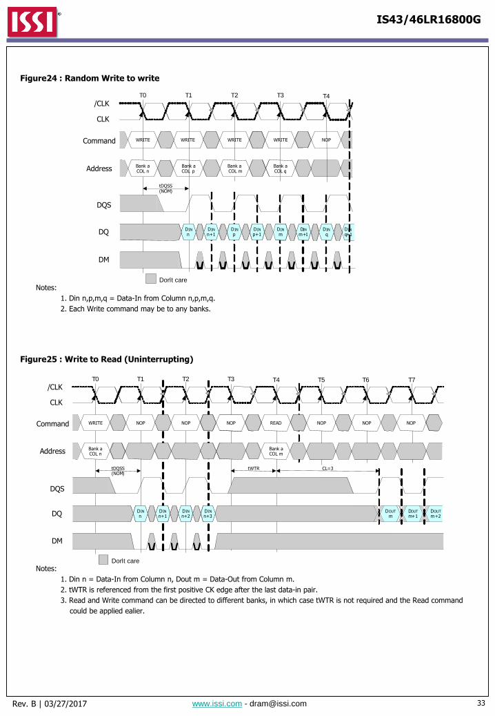
Figure24 : Random Write to write
Figure25 : Write to Read (Uninterrupting)
Notes:
1. Din n,p,m,q = Data-In from Column n,p,m,q.
2. Each Write command may be to any banks.
Notes:
1. Din n = Data-In from Column n, Dout m = Data-Out from Column m.
2. tWTR is referenced from the first positive CK edge after the last data-in pair.
3. Read and Write command can be directed to different banks, in which case tWTR is not required and the Read command
could be applied ealier.
DIN
q+1
Bank a COL q
Bank a COL p
WRITEWRITEWRITE WRITE NOP
Bank a COL n
DIN
m
Bank a COL m
T0 T1 T2 T3
Address
T4
/CLK
CLK
DQS
DQ
tDQSS(NOM)
Command
DM
DIN
nDIN
n+1D IN
pDIN
p+1DIN
m+1DIN
q
Don’t care
NOPWRITE
Bank a COL m
NOPNOP READNOP
Bank a COL n
T0 T1 T2 T3
Address
T4 T5
/CLK
CLK
DQS
DQ
tDQSS(NOM)
Command
DM
DIN
nDIN
n+1DIN
n+2DIN
n+3
Don’t care
CL=3
NOPNOP
DOUT
m+1DOUT
m
tWTR
DOUT
m+2
T6 T7

34Rev. B | 03/27/2017 www.issi.com - [email protected]
IS43/46LR16800G
Figure26 : Write to Read (Interrupting)
Figure27 : Write to Read (Odd number of data Interrupting)
Notes:
1. Din n = Data-In from Column n, Dout m = Data-Out from Column m.
2. tWTR is referenced from the first positive CK edge after the last data-in pair.
Notes:
1. Din n = Data-In from Column n, Dout m = Data-Out from Column m.
2. tWTR is referenced from the first positive CK edge after the last data-in pair.
WRITE NOP
T6 T7
NOPNOPREADNOP
Bank a COL n
T0 T1 T2 T3
Address
T4 T5
/CLK
CLK
DQS
DQ
tDQSS(NOM)
Command
DM
DIN
nDIN
n+1
Don ’ t care
Bank a COL m
CL=3
NOPNOP
DOUT
m+1DOUT
mDOUT
m+2DOUT
m+3
tWTR
T6 T7T0 T1 T2 T3 T4 T5
DQS
DQ
tDQSS(NOM)
DM
DIN
n
Don’t care
CL=3
DOUT
m+1DOUT
mDOUT
m+2DOUT
m+3
tWTR
WRITE NOP NOPNOPREADNOP
Bank a
COL nAddress
/CLK
CLK
Command
Bank a
COL m
NOPNOP

35Rev. B | 03/27/2017 www.issi.com - [email protected]
IS43/46LR16800G
Figure28 : Write to Precharge (Uninterrupting)
Figure29 : Write to Precharge (Interrupting)
Notes:
1. Din n = Data-In from Column n.
2. tWR is referenced from the first positive CK edge after the last data-in pair.
3. Read and Write command can be directed to different banks, in which case tWR is not required and the Read command
could be applied ealier.
Notes:
1. Din n = Data-In from Column n.
2. tWR is referenced from the first positive CK edge after the last data-in pair.
3. Read and Write command can be directed to different banks, in which case tWR is not required and the Read command
could be applied ealier.
PCGNOPWRITE NOP NOPNOP
Bank a COL n
T0 T1 T2 T3
Address
T4 T5
/CLK
CLK
DQS
DQ
tDQSS
(NOM)
Command
DM
DIN
n
DIN
n+1
DIN
n+2
DIN
n+3
Don’ t care
tWR
NOPWRITE NOP NOPPCGNOP
Bank a COL n
T0 T1 T2 T3
Address
T4 T5
/CLK
CLK
DQS
DQ
tDQSS(NOM)
Command
DM
DIN
nDIN
n+1
tWR
Don’ t care
36Rev. B | 03/27/2017 www.issi.com - [email protected]
IS43/46LR16800G
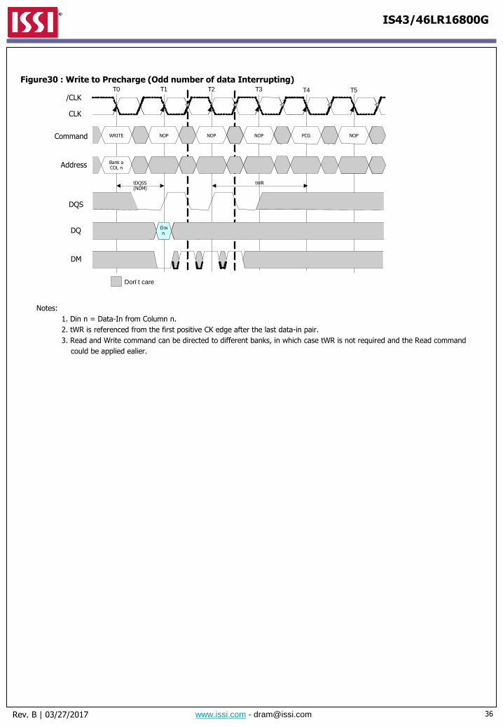
Figure30 : Write to Precharge (Odd number of data Interrupting)
Notes:
1. Din n = Data-In from Column n.
2. tWR is referenced from the first positive CK edge after the last data-in pair.
3. Read and Write command can be directed to different banks, in which case tWR is not required and the Read command
could be applied ealier.
Don’ t care
NOPWRITE NOP NOPPCGNOP
Bank a COL n
T0 T1 T2 T3
Address
T4 T5
/CLK
CLK
DQS
DQ
tDQSS(NOM)
Command
DM
D IN
n
tWR
37Rev. B | 03/27/2017 www.issi.com - [email protected]
IS43/46LR16800G
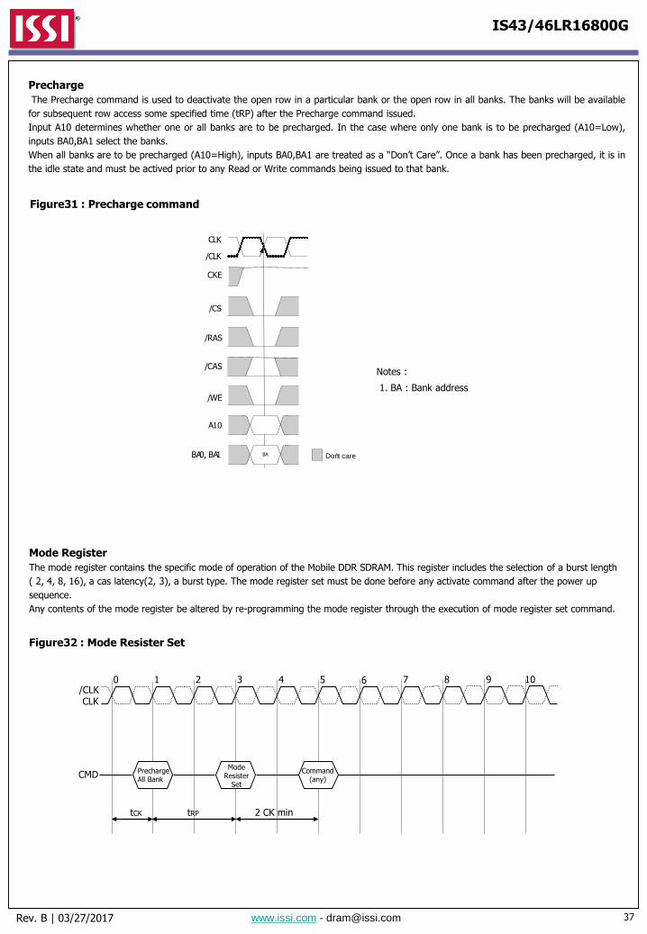
Precharge
The Precharge command is used to deactivate the open row in a particular bank or the open row in all banks. The banks will be available
for subsequent row access some specified time (tRP) after the Precharge command issued.
Input A10 determines whether one or all banks are to be precharged. In the case where only one bank is to be precharged (A10=Low),
inputs BA0,BA1 select the banks.
When all banks are to be precharged (A10=High), inputs BA0,BA1 are treated as a “Don’t Care”. Once a bank has been precharged, it is in
the idle state and must be actived prior to any Read or Write commands being issued to that bank.
Figure31 : Precharge command
Notes :
1. BA : Bank address
Mode Register
The mode register contains the specific mode of operation of the Mobile DDR SDRAM. This register includes the selection of a burst length
( 2, 4, 8, 16), a cas latency(2, 3), a burst type. The mode register set must be done before any activate command after the power up
sequence.
Any contents of the mode register be altered by re-programming the mode register through the execution of mode register set command.
tCK 2 CK min
0 1 2 3 4 5 6 7 8/CLKCLK
9 10
CMD
tRP
Precharge All Bank
Mode Resister
Set
Command (any)
Figure32 : Mode Resister Set
CLK
/CLK
CKE
/CS
/RAS
/CAS
/WE
BA
A10
BA0, BA1 Don’t care
38Rev. B | 03/27/2017 www.issi.com - [email protected]
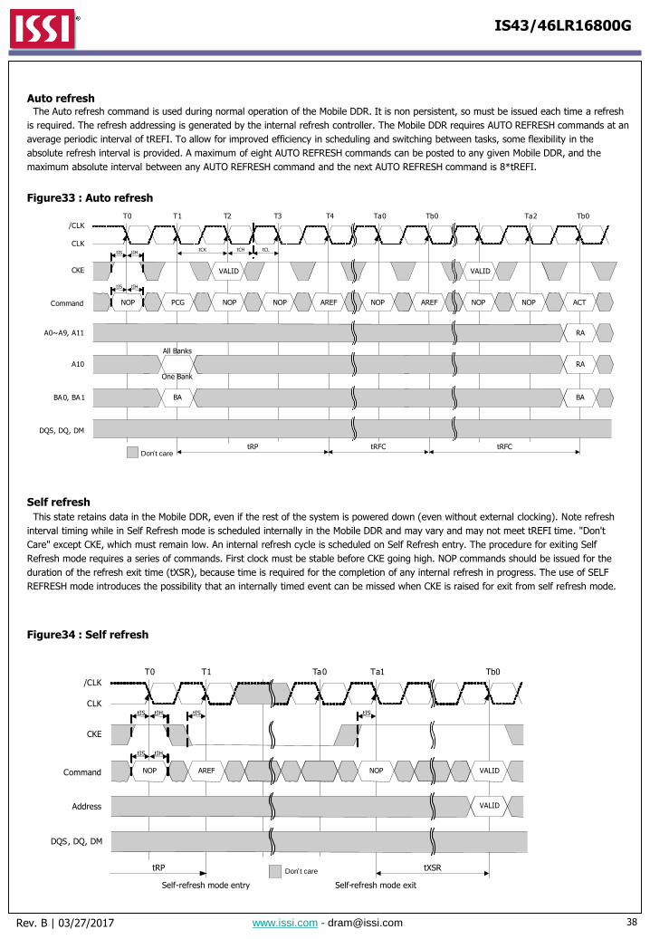
IS43/46LR16800G
Figure34 : Self refresh
Self refresh
This state retains data in the Mobile DDR, even if the rest of the system is powered down (even without external clocking). Note refresh
interval timing while in Self Refresh mode is scheduled internally in the Mobile DDR and may vary and may not meet tREFI time. "Don't
Care" except CKE, which must remain low. An internal refresh cycle is scheduled on Self Refresh entry. The procedure for exiting Self
Refresh mode requires a series of commands. First clock must be stable before CKE going high. NOP commands should be issued for the
duration of the refresh exit time (tXSR), because time is required for the completion of any internal refresh in progress. The use of SELF
REFRESH mode introduces the possibility that an internally timed event can be missed when CKE is raised for exit from self refresh mode.
Figure33 : Auto refresh
Auto refreshThe Auto refresh command is used during normal operation of the Mobile DDR. It is non persistent, so must be issued each time a refresh
is required. The refresh addressing is generated by the internal refresh controller. The Mobile DDR requires AUTO REFRESH commands at an
average periodic interval of tREFI. To allow for improved efficiency in scheduling and switching between tasks, some flexibility in the
absolute refresh interval is provided. A maximum of eight AUTO REFRESH commands can be posted to any given Mobile DDR, and the
maximum absolute interval between any AUTO REFRESH command and the next AUTO REFRESH command is 8*tREFI.
AREFNOPNOP NOPAREFPCGNOP
/CLK
CLK
CKE
T0
Command
T1 T3
tCH tCL
DQS, DQ, DM
Tb0
tIS tIH
A10
tCK
T2 T4 Ta0
tRPDon’t care
VALID
A0~A9, A11
All Banks
One Bank
BABA0, BA1
ACTNOP
Tb0
RA
Ta2
BA
RA
NOP
VALID
tRFC tRFC
tIS tIH
VALIDNOPAREFNOP
/CLK
CLK
CKE
T0
Command
T1 Ta0
DQS, DQ, DM
Tb0
tIS tIH
Ta1
tRP Don’t care
Address
tXSR
tIS tIH tIS tIS
VALID
Self-refresh mode entry Self-refresh mode exit
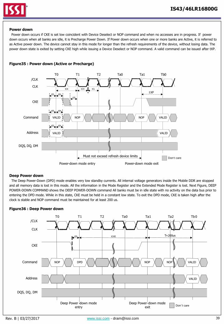
39Rev. B | 03/27/2017 www.issi.com - [email protected]
IS43/46LR16800G
Figure35 : Power down (Active or Precharge)
Figure36 : Deep Power down
Power down
Power down occurs if CKE is set low coincident with Device Deselect or NOP command and when no accesses are in progress. If power
down occurs when all banks are idle, it is Precharge Power Down. If Power down occurs when one or more banks are Active, it is referred to
as Active power down. The device cannot stay in this mode for longer than the refresh requirements of the device, without losing data. The
power down state is exited by setting CKE high while issuing a Device Deselect or NOP command. A valid command can be issued after tXP.
Deep Power down
The Deep Power-Down (DPD) mode enables very low standby currents. All internal voltage generators inside the Mobile DDR are stopped
and all memory data is lost in this mode. All the information in the Mode Register and the Extended Mode Register is lost. Next Figure, DEEP
POWER-DOWN COMMAND shows the DEEP POWER-DOWN command All banks must be in idle state with no activity on the data bus prior to
entering the DPD mode. While in this state, CKE must be held in a constant low state. To exit the DPD mode, CKE is taken high after the
clock is stable and NOP command must be maintained for at least 200 us.
VALIDNOPNOPVALID
/CLK
CLK
CKE
T0
Command
T1 Ta0
tCH tCL
DQS, DQ, DM
tIS tIH
VALIDAddress
tCK
VALID
tIS
tIS tIH
tIS tIH
T2 Ta1 Tb0
Must not exceed refresh device limitsDon’t care
Power-down mode entry Power-down mode exit
t XP
VALIDNOPNOPDPDNOP
/CLK
CLK
CKE
T0
Command
T1 Ta0
DQS, DQ, DM
Tb0
Address
tCKE
VALID
tIS
T2 Ta1 Ta2
Don ’t careDeep Power -down mode
entry Deep Power-down mode
exit
T=200us

40Rev. B | 03/27/2017 www.issi.com - [email protected]
IS43/46LR16800G
Clock Stop Mode
Clock stop mode is a feature supported by Mobile DDR SDRAM devices. It reduces clock-related power consumption during idle periods of
the device.
Conditions: the Mobile DDR SDRAM supports clock stop in case:
• The last access command (ACTIVE, READ, WRITE, PRECHARGE, AUTO REFRESH or MODE REGISTER SET) has executed to completion,
including any data-out during read bursts; the number of required clock pulses per access command depends on the device's AC timing
parameters and the clock frequency;
• The related timing condition (tRCD, tWR, tRP, tRFC, tMRD) has been met;
• CKE is held HIGH.
When all conditions have been met, the device is either in ''idle'' or ''row active'' state, and clock stop mode may be entered with CK held
LOW and /CK held HIGH. Clock stop mode is exited when the clock is restarted. NOPs command have to be issued for at least one clock
cycle before the next access command may be applied. Additional clock pulses might be required depending on the system characteristics.
Figure37 illustrates the clock stop mode:
• Initially the device is in clock stop mode;
• The clock is restarted with the rising edge of T0 and a NOP on the command inputs;
• With T1 a valid access command is latched; this command is followed by NOP commands in order to allow for clock stop as soon as this
access command has completed;
• Tn is the last clock pulse required by the access command latched with T1.
• The timing condition of this access command is met with the completion of Tn; therefore Tn is the last clock pulse required by this
command and the clock is then stopped.
Figure 37 : Clock Stop Mode
DQ,DQS(High – Z)
Exit ClockStop Mode
Enter ClockStop Mode
Vail Command
CKE
T0 T1 T2 Tn/CLKCLK
ADD
Timing Condition
CMD
Clockstopped
Don’t Care
NOP CMD NOP NOP NOP
Valide
High
41Rev. B | 03/27/2017 www.issi.com - [email protected]
IS43/46LR16800G
Ordering Information – VDD = 1.8V
Commercial Range: (0oC to +70oC)
Configuration Frequency (MHz)
Speed (ns)
Order Part No. Package
8Mx16 166 6 IS43LR16800G-6BLI 60-ball BGA, Lead-free
Industrial Range: (-40oC to +85oC)
Note: The -6 speed option supports -75 timing specifications.
Automotive Range, A1: (-40oC to +85oC)
Automotive Range, A2: (-40oC to +105oC)
Configuration Frequency (MHz)
Speed (ns)
Order Part No. Package
8Mx16 166 6 IS46LR16800G-6BLA1 60-ball BGA, Lead-free
Configuration Frequency (MHz)
Speed (ns)
Order Part No. Package
8Mx16 166 6 IS46LR16800G-6BLA2 60-ball BGA, Lead-free
Configuration Frequency (MHz)
Speed (ns)
Order Part No. Package
8Mx16 166 6 IS43LR16800G-6BL 60-ball BGA, Lead-free