Embed Size (px)
Citation preview
Ž .Sensors and Actuators 73 1999 14–23
3D microfabrication by combining microstereolithography and thickresist UV lithography
A. Bertsch ), H. Lorenz, P. Renaud( )Swiss Federal Institute of Technology EPFL , DMT-IMS, CH-1015 Lausanne, Switzerland
Received 16 April 1998; accepted 7 October 1998
Abstract
A new approach for the realization of true 3D polymer structures is presented in this paper. It consists in adding, in a post-processingmicrostereolithography step, 3D polymer microstructures on top of a micropart patterned by means of planar processes such as thin films,
Ž .bulk silicon etching or high aspect ratio structuration LIGA, RIE, thick resist . In this way, some shape limitations of the planartechnologies can be overcome for new functional applications. Moreover, the direct processing of microstereolithography on predefinedstructures eliminates manipulations which are associated with micro-assembly of separated parts. To demonstrate this combination ofmicrostructuration processes, an example showing a conical axle added by microstereolithography on a SU-8 piece of gearing ispresented. q 1999 Elsevier Science S.A. All rights reserved.
Keywords: Microstereolithography; SU-8; 3D-microfabrication; Combination of technologies; Photopolymerization
1. Introduction
Conventional silicon-based microfabrication technolo-gies allow the manufacturing of many different micromechanical components such as micro-gears, micro-mo-
Žtors, micro-actuators, sensors accelerometers, gyroscopes,. w xpressure sensors, etc. 1 . Most of these components have
a very simple two-dimensional geometry, or are made ofjust a few superimposed layers, because they are patternedby means of planar processes such as thin films, bulk
Žsilicon etching or high aspect ratio structuration LIGA,.RIE, thick resist UV photolithography . It is still difficult
to manufacture true 3D parts by these techniques.The microstereolithography process allows the building
of 3D, complex in shape, polymer structures. The processhas not emerged from the microelectronics technologies,but from the rapid prototyping industry. Microstereolithog-raphy was, up to recently, a minor technology in the fieldof microstructuration, mostly because of the limited resolu-tion and the problems associated with the manipulationand assembling of the obtained polymer structures.
) Corresponding author. Tel.: q41-21-693-66-06; Fax: q41-693-59-50; E-mail: [email protected]
A new approach of this technology, the study of ‘in-tegral’ microstereolithography processes, opened the wayto the manufacturing of more complex and more interest-ing micro objects. Combining microstereolithography andconventional microstructuration technologies opens the wayto integrate new functions on planar structures. Moreover,the direct processing of 3D, complex in shape, polymermicrostructures by microstereolithography on top of mi-croparts patterned by silicon-based technologies eliminatesthe manipulations that are associated with microassem-bling separate components.
2. Microstereolithography
Improving the resolution of the stereolithography pro-cess which has been used by industry for 15 years as arapid prototyping technology, has led to the design of
w xdifferent microstereolithography processes 2 . All of themare based on the layer-by-layer light-induced polymeriza-tion of a liquid resin.
Most microstereolithography processes developed up tonow, were based on a vector-by-vector tracing of eachlayer, obtained by moving a focused light beam on the
w xsurface of a photopolymerizable liquid 3–5 . Recently,another kind of process has been imagined, an ‘integral’process, in which a complete layer is built in one irradia-
0924-4247r99r$ - see front matter q 1999 Elsevier Science S.A. All rights reserved.Ž .PII: S0924-4247 98 00249-0
( )A. Bertsch et al.rSensors and Actuators 73 1999 14–23 15
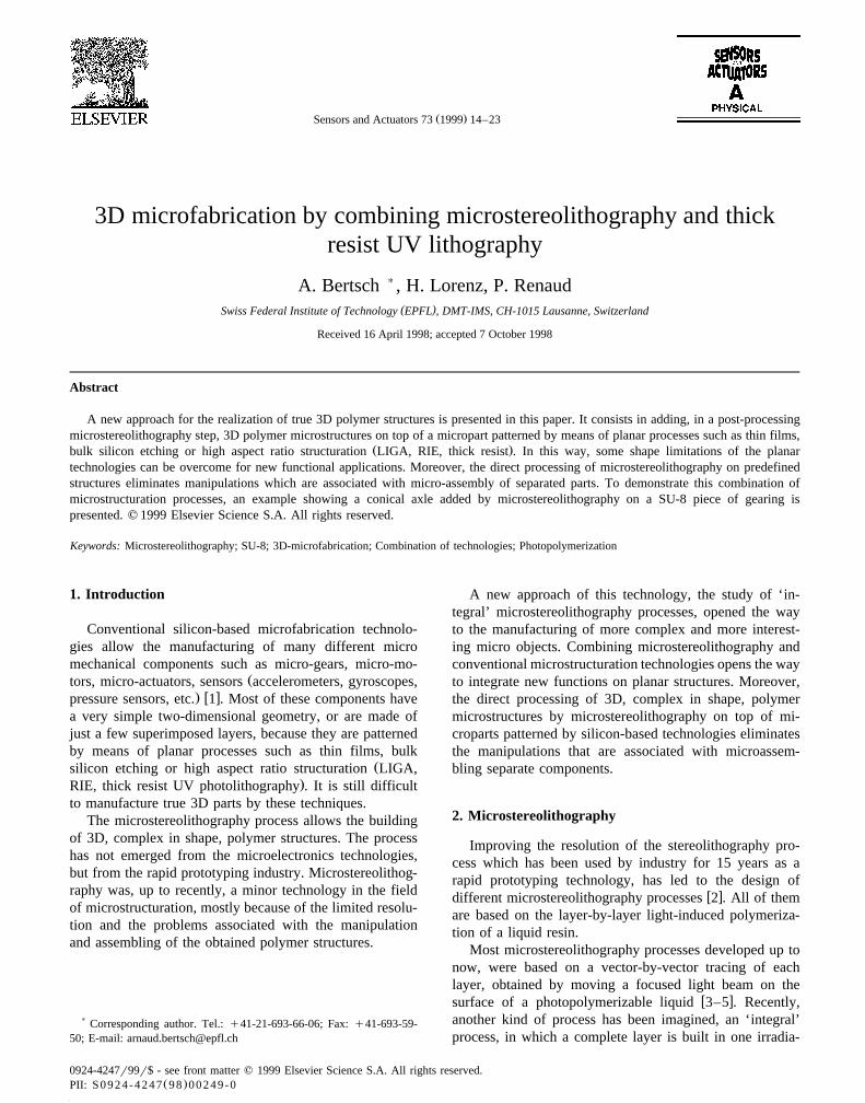
Fig. 1. Diagram of a microstereolithography apparatus using a dynamicmask-generator.
w xtion only 6,7 . To benefit from the many advantages ofthis method, the high-resolution stereolithography appara-tus built for the applications presented in this article anddescribed below uses the integral process.
2.1. Principle of the apparatus
The microstereolithography apparatus shown in Fig. 1,uses a dynamic pattern generator in an open layer surfaceprocess.
In this apparatus, one complete layer is built in oneirradiation only, whatever its shape may be. The beamcoming from the light source is shaped by the dynamicalpattern generator, so that it contains the image of the layerto be built. This light beam is then reduced with an opticalsystem and the image it carries is focused on the surface ofa photopolymerizable medium. The irradiated areas areselectively polymerized whereas the non-irradiated onesremain liquid. When the liquid has been irradiated longenough for the phototransformation to occur, an electrome-chanical shutter stops the beam.
The part being manufactured is held by and fixed to ametal grid. It is immersed deep enough in the reactivemedium to be completely covered by it. It is then lifted bya certain height, such that, between the last polymerizedlayer and the surface there is a layer of fresh resin. Thisnew layer is then selectively irradiated with a new pattern,to create the next layer of the object, and so on.
Once all the layers of the object have been built, thepolymerized part is taken out of the photoreactor andwashed with the appropriate solvent. No post processing isrequired.
Even though the resolution of microstereolithography isnot as good as conventional microfabrication processes,this technique has nevertheless many advantages; the man-ufactured micro parts are complex in shape, really three
Ždimensional and made of a large number of layers up to.1000 or even more . The manufacturing times are short,
typically an integral process can produce from one to fivelayers per minute, and the time needed to build one layer isthe same whatever its pattern may be.
2.2. Characteristics of the mirostereolithography appara-tus used in this study
A high resolution stereolithography tabletop machinehas been built with which liquid layers of 5 mm arepolymerized by projection of an ‘active mask’ with aprojected pixel size of 5=5 mm2. The irradiation field iscurrently limited to about 2.5=2.5 mm2, but an imagefield of 20=20 mm2 will be reached with the nextprototype. Real 3D objects can be manufactured through
Žthe structuration of a large number of layers up to 1000.and more . Curved and conical surfaces can be obtained as
well as hollow volumes.A typical exposure time of 1 s per layer is needed with
this setup. The total fabrication time is nevertheless limitedby the recoating of the liquid, leading to a typical fabrica-tion time of 1 mm per hour in the vertical direction.
In this apparatus the method used to create a new layeris the free surface technique. The part being manufacturedis immersed deeply in the reactive medium, and then liftedup to almost the surface of the medium. Before the irradia-tion of the next layer, a certain time is spent waiting forthe gravity forces to level the surface. Since the timenecessary to obtain a horizontal fresh layer depends on therheological properties of the resin, low viscosity monomersshould be used whenever possible.
To spread evenly the chemical medium on the surfaceof the part being manufactured, different authors haveinvestigated other solutions. Among them, the polymeriza-tion through a glass window is probably the most widely
w xspread 3,4 . This solution allows a better control of thethickness of the liquid layer than the free surface tech-nique, but has a major disadvantage: the formed polymersometimes sticks to the glass window, which can result inpartial or total destruction of the part during its manufac-
w xture 8 . In the case of the integral microstereolithographyapparatus designed in this study, the surface of the poly-merized layer is wide in general, which increases the riskof sticking. That is the reason why the free surface tech-nique has been preferred up to now.
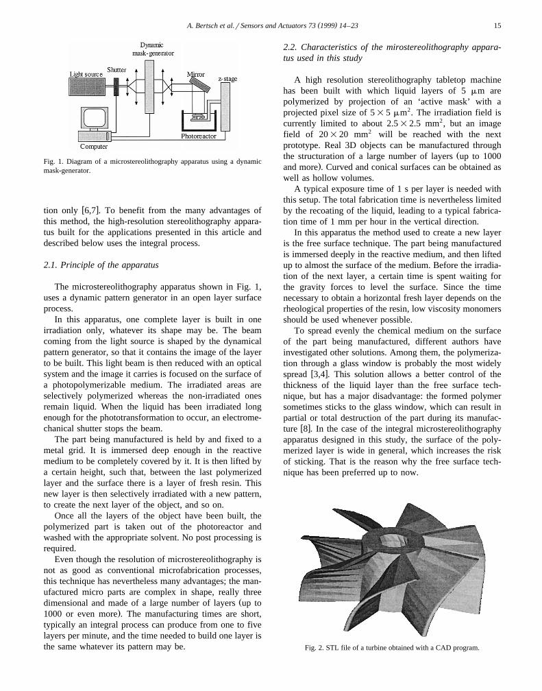
Fig. 2. STL file of a turbine obtained with a CAD program.
( )A. Bertsch et al.rSensors and Actuators 73 1999 14–2316
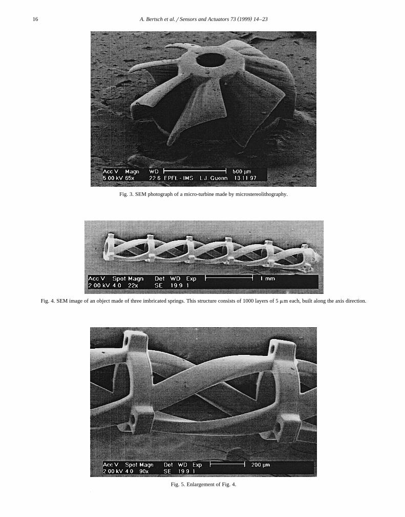
Fig. 3. SEM photograph of a micro-turbine made by microstereolithography.
Fig. 4. SEM image of an object made of three imbricated springs. This structure consists of 1000 layers of 5 mm each, built along the axis direction.
Fig. 5. Enlargement of Fig. 4.
( )A. Bertsch et al.rSensors and Actuators 73 1999 14–23 17
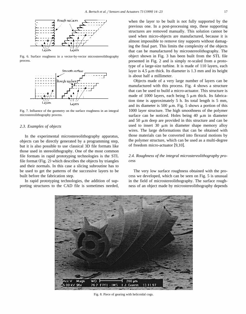
Fig. 6. Surface roughness in a vector-by-vector microstereolithographyprocess.
Fig. 7. Influence of the geometry on the surface roughness in an integralmicrostereolithography process.
2.3. Examples of objects
In the experimental microstereolithography apparatus,objects can be directly generated by a programming step,but it is also possible to use classical 3D file formats likethose used in stereolithography. One of the most commonfile formats in rapid prototyping technologies is the STL
Ž .file format Fig. 2 which describes the objects by trianglesand their normals. In this case a slicing subroutine has tobe used to get the patterns of the successive layers to bebuilt before the fabrication step.
In rapid prototyping technologies, the addition of sup-porting structures to the CAD file is sometimes needed,
when the layer to be built is not fully supported by theprevious one. In a post-processing step, these supportingstructures are removed manually. This solution cannot beused when micro-objects are manufactured, because it isalmost impossible to remove tiny supports without damag-ing the final part. This limits the complexity of the objectsthat can be manufactured by microstereolithography. Theobject shown in Fig. 3 has been built from the STL filepresented in Fig. 2 and is simply re-scaled from a proto-type of a large-size turbine. It is made of 110 layers, eachlayer is 4.5 mm thick. Its diameter is 1.3 mm and its heightis about half a millimeter.
Objects made of a very large number of layers can bemanufactured with this process. Fig. 4 shows a structurethat can be used to build a micro-actuator. This structure ismade of 1000 layers, each being 5 mm thick. Its fabrica-tion time is approximately 5 h. Its total length is 5 mm,and its diameter is 500 mm. Fig. 5 shows a portion of this1000 layer structure. The high smoothness of the polymersurface can be noticed. Holes being 40 mm in diameterand 50 mm deep are provided in this structure and can beused to insert 30 mm in diameter shape memory alloywires. The large deformations that can be obtained withthose materials can be converted into flexural motions bythe polymer structure, which can be used as a multi-degree
w xof freedom micro-actuator 9,10 .
2.4. Roughness of the integral microstereolithography pro-cess
The very low surface roughness obtained with the pro-cess we developed, which can be seen on Fig. 5 is unusualin the field of microstereolithography. The surface rough-ness of an object made by microstereolithography depends
Fig. 8. Piece of gearing with helicoidal cogs.
( )A. Bertsch et al.rSensors and Actuators 73 1999 14–2318
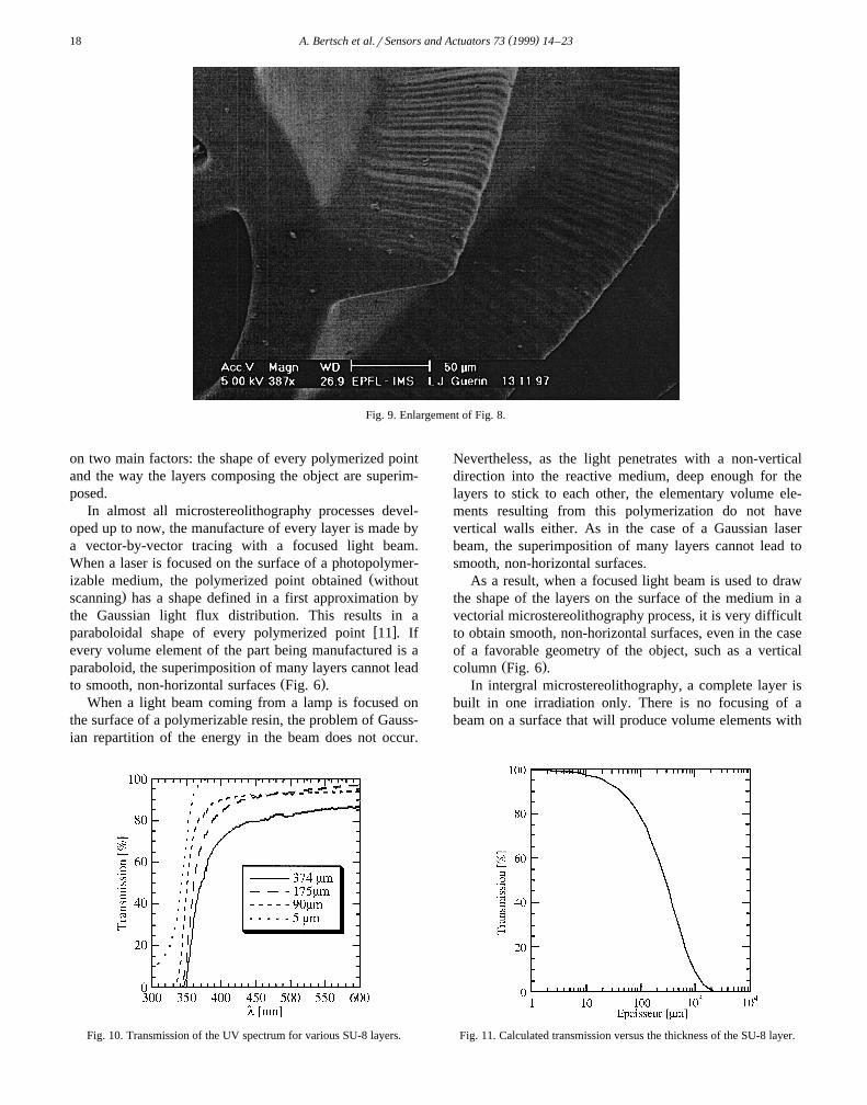
Fig. 9. Enlargement of Fig. 8.
on two main factors: the shape of every polymerized pointand the way the layers composing the object are superim-posed.
In almost all microstereolithography processes devel-oped up to now, the manufacture of every layer is made bya vector-by-vector tracing with a focused light beam.When a laser is focused on the surface of a photopolymer-
Žizable medium, the polymerized point obtained without.scanning has a shape defined in a first approximation by
the Gaussian light flux distribution. This results in aw xparaboloidal shape of every polymerized point 11 . If
every volume element of the part being manufactured is aparaboloid, the superimposition of many layers cannot lead
Ž .to smooth, non-horizontal surfaces Fig. 6 .When a light beam coming from a lamp is focused on
the surface of a polymerizable resin, the problem of Gauss-ian repartition of the energy in the beam does not occur.
Fig. 10. Transmission of the UV spectrum for various SU-8 layers.
Nevertheless, as the light penetrates with a non-verticaldirection into the reactive medium, deep enough for thelayers to stick to each other, the elementary volume ele-ments resulting from this polymerization do not havevertical walls either. As in the case of a Gaussian laserbeam, the superimposition of many layers cannot lead tosmooth, non-horizontal surfaces.
As a result, when a focused light beam is used to drawthe shape of the layers on the surface of the medium in avectorial microstereolithography process, it is very difficultto obtain smooth, non-horizontal surfaces, even in the caseof a favorable geometry of the object, such as a vertical
Ž .column Fig. 6 .In intergral microstereolithography, a complete layer is
built in one irradiation only. There is no focusing of abeam on a surface that will produce volume elements with
Fig. 11. Calculated transmission versus the thickness of the SU-8 layer.
( )A. Bertsch et al.rSensors and Actuators 73 1999 14–23 19
Fig. 12. The masters in SU-8 before electroplating.
non-vertical walls, but projection of the image of a com-plete layer on the surface of the reactive medium. Thisimage is very large in comparison to a focused light beamand since a big depth of focus is used, the light penetratesalmost vertically in the reactive medium. Because the lightbeam has a homogeneous energetic repartition, the poly-merized walls are almost vertical in this kind of configura-tion.
In this case, the roughness in the objects obtained bymicrostereolithography depends mostly on their geometryand is directly related to the angle between the surface and
Ž .the vertical direction Fig. 7 . Of course, the non-verticaland non-horizontal surfaces are smoother if the polymer-ized depth is smaller, because the pile of solidified slicescomposing the object will have a larger number of sec-tions.
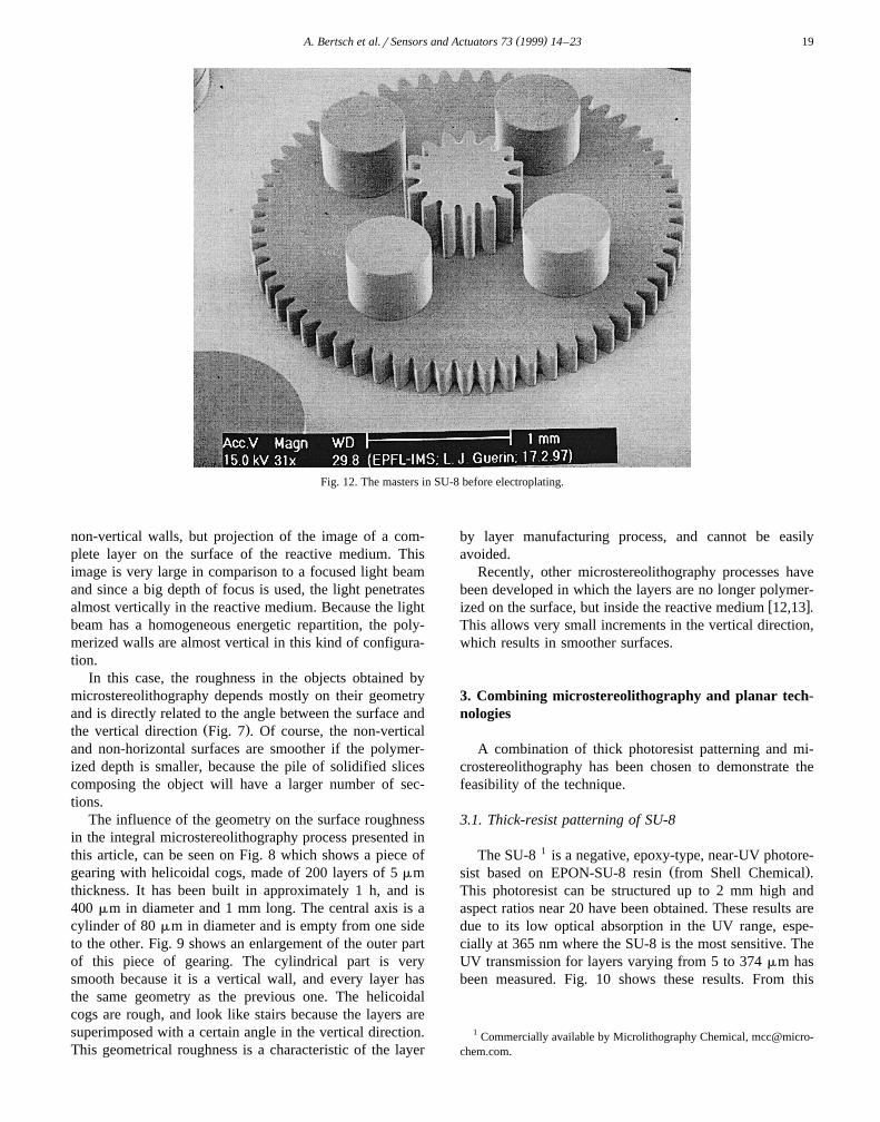
The influence of the geometry on the surface roughnessin the integral microstereolithography process presented inthis article, can be seen on Fig. 8 which shows a piece ofgearing with helicoidal cogs, made of 200 layers of 5 mmthickness. It has been built in approximately 1 h, and is400 mm in diameter and 1 mm long. The central axis is acylinder of 80 mm in diameter and is empty from one sideto the other. Fig. 9 shows an enlargement of the outer partof this piece of gearing. The cylindrical part is verysmooth because it is a vertical wall, and every layer hasthe same geometry as the previous one. The helicoidalcogs are rough, and look like stairs because the layers aresuperimposed with a certain angle in the vertical direction.This geometrical roughness is a characteristic of the layer
by layer manufacturing process, and cannot be easilyavoided.
Recently, other microstereolithography processes havebeen developed in which the layers are no longer polymer-
w xized on the surface, but inside the reactive medium 12,13 .This allows very small increments in the vertical direction,which results in smoother surfaces.
3. Combining microstereolithography and planar tech-nologies
A combination of thick photoresist patterning and mi-crostereolithography has been chosen to demonstrate thefeasibility of the technique.
3.1. Thick-resist patterning of SU-8
The SU-8 1 is a negative, epoxy-type, near-UV photore-Ž .sist based on EPON-SU-8 resin from Shell Chemical .
This photoresist can be structured up to 2 mm high andaspect ratios near 20 have been obtained. These results aredue to its low optical absorption in the UV range, espe-cially at 365 nm where the SU-8 is the most sensitive. TheUV transmission for layers varying from 5 to 374 mm hasbeen measured. Fig. 10 shows these results. From this
1 Commercially available by Microlithography Chemical, [email protected].
( )A. Bertsch et al.rSensors and Actuators 73 1999 14–2320
Fig. 13. Plastic injected watch gear, total height: 1.4 mm.
experiment, the coefficient of absorption for ls365 nmhas been measured.
Concerning the transmission of the UV light at 365 nm,plotted on Fig. 11, a total absorption of the light is reachedat 2 mm which should be the theoretical limit for thisresist. The fundamentals of the SU-8 technology have been
w xpreviously reported 14,15 . This photoresist has beenspecifically developed for MEMS applications such asmicrofluidic, packaging, sensors, rapid prototyping andUV-LIGA.
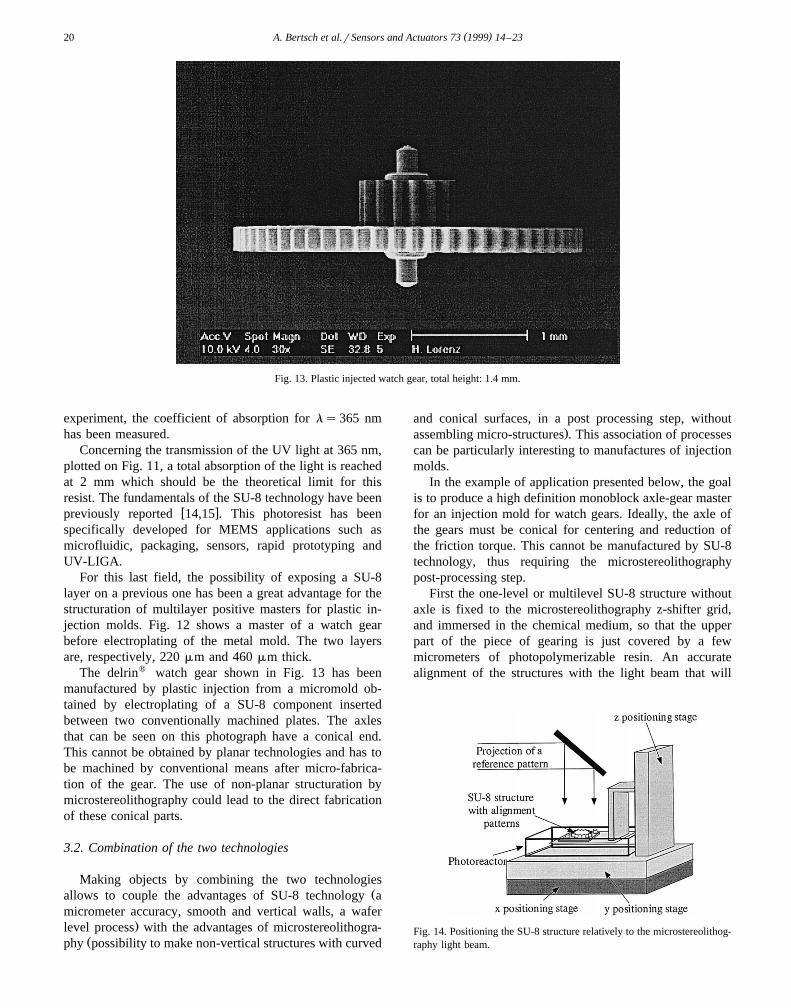
For this last field, the possibility of exposing a SU-8layer on a previous one has been a great advantage for thestructuration of multilayer positive masters for plastic in-jection molds. Fig. 12 shows a master of a watch gearbefore electroplating of the metal mold. The two layersare, respectively, 220 mm and 460 mm thick.
The delrinw watch gear shown in Fig. 13 has beenmanufactured by plastic injection from a micromold ob-tained by electroplating of a SU-8 component insertedbetween two conventionally machined plates. The axlesthat can be seen on this photograph have a conical end.This cannot be obtained by planar technologies and has tobe machined by conventional means after micro-fabrica-tion of the gear. The use of non-planar structuration bymicrostereolithography could lead to the direct fabricationof these conical parts.
3.2. Combination of the two technologies
Making objects by combining the two technologiesŽallows to couple the advantages of SU-8 technology a
micrometer accuracy, smooth and vertical walls, a wafer.level process with the advantages of microstereolithogra-
Žphy possibility to make non-vertical structures with curved
and conical surfaces, in a post processing step, without.assembling micro-structures . This association of processes
can be particularly interesting to manufactures of injectionmolds.
In the example of application presented below, the goalis to produce a high definition monoblock axle-gear masterfor an injection mold for watch gears. Ideally, the axle ofthe gears must be conical for centering and reduction ofthe friction torque. This cannot be manufactured by SU-8technology, thus requiring the microstereolithographypost-processing step.
First the one-level or multilevel SU-8 structure withoutaxle is fixed to the microstereolithography z-shifter grid,and immersed in the chemical medium, so that the upperpart of the piece of gearing is just covered by a fewmicrometers of photopolymerizable resin. An accuratealignment of the structures with the light beam that will
Fig. 14. Positioning the SU-8 structure relatively to the microstereolithog-raphy light beam.
( )A. Bertsch et al.rSensors and Actuators 73 1999 14–23 21
Fig. 15. Conical axle added by microstereolithography on a one-level SU-8 micro-gear.
induce the phototransformation is then required. This isachieved by projecting a reference pattern on the resinwith an intensity low enough such that the thresholdneeded to begin the photopolymerization process is notreached. The photoreactor is then moved with an x–ypositioning stage, to make the alignment between theprojected reference pattern and some alignment patterns on
Ž .the SU-8 structure Fig. 14 . An alignment accuracy of afew micrometers is achieved with the current set-up.
When this operation is done, the microsterolithographyprocess can be started; the axle grows layer by layer on theSU-8 surface. No micro-assembly step is needed.
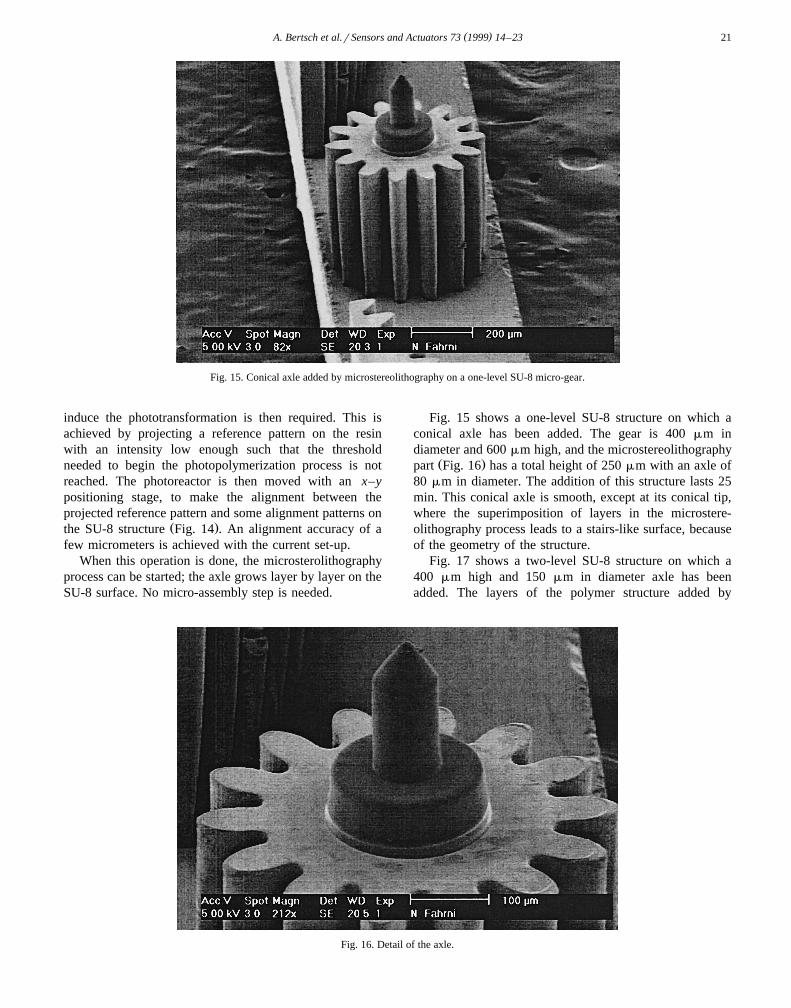
Fig. 15 shows a one-level SU-8 structure on which aconical axle has been added. The gear is 400 mm indiameter and 600 mm high, and the microstereolithography
Ž .part Fig. 16 has a total height of 250 mm with an axle of80 mm in diameter. The addition of this structure lasts 25min. This conical axle is smooth, except at its conical tip,where the superimposition of layers in the microstere-olithography process leads to a stairs-like surface, becauseof the geometry of the structure.
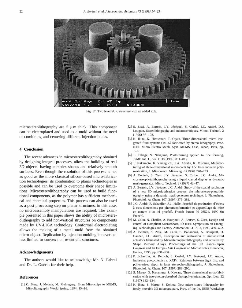
Fig. 17 shows a two-level SU-8 structure on which a400 mm high and 150 mm in diameter axle has beenadded. The layers of the polymer structure added by
Fig. 16. Detail of the axle.
( )A. Bertsch et al.rSensors and Actuators 73 1999 14–2322
Fig. 17. Two level SU-8 structure with an added axle.
microstereolithography are 5 mm thick. This componentcan be electroplated and used as a mold without the needof combining and centering different injection plates.
4. Conclusion
The recent advances in microstereolithography obtainedby designing integral processes, allow the building of real3D objects, having complex shapes and relatively smoothsurfaces. Even though the resolution of this process is notas good as the more classical silicon-based micro-fabrica-tion technologies, its combination to planar technologies ispossible and can be used to overcome their shape limita-tions. Microstereolithography can be used to build func-tional components, as the polymer has sufficient mechani-cal and chemical properties. This process can also be usedas a post-processing step on planar structures, in this case,no microassembly manipulations are required. The exam-ple presented in this paper shows the ability of microstere-olithography to add non-vertical structures on componentsmade by UV-LIGA technology. Conformal electroplatingallows the making of a metal mold from the obtainedmicro-object. Replication by injection molding is neverthe-less limited to convex non re-entrant structures.
Acknowledgements
The authors would like to acknowledge Mr. N. Fahrniand Dr. L. Guerin for their help.´
References
w x1 C. Bang, J. Melzak, M. Mehregany, From Microchips to MEMS,Microlithography World Spring, 1994, 15–16.
w x2 S. Zissi, A. Bertsch, J.Y. Jezequel, S. Corbel, J.C. Andre, D.J.´ ´ ´Lougnot, Stereolithography and microtechniques, Micro. Technol. 2Ž .1996 97–102.
w x3 K. Ikuta, K. Hirowatari, T. Ogata, Three dimensional micro inte-Ž .grated fluid systems MIFS fabricated by stereo lithography, Proc.
IEEE Micro Electro Mech. Syst. MEMS, Oiso, Japan, 1994, pp.1–6.
w x4 T. Takagi, N. Nakajima, Photoforming applied to fine forming,Ž .JSME Int. J., Ser. C 38 1995 811–817.
w x5 T. Nakamoto, K. Yamaguchi, P.A. Abraha, K. Mishima, Manufac-turing of three-dimensional micro-parts by UV laser induced poly-
Ž .merization, J. Micromech. Microeng. 6 1996 240–253.w x6 A. Bertsch, S. Zissi, J.Y. Jezequel, S. Corbel, J.C. Andre, Mi-´ ´ ´
crostereophotolithography using a liquid crystal display as dynamicŽ .mask-generator, Micro. Technol. 3 1997 42–47.
w x7 A. Bertsch, J.Y. Jezequel, J.C. Andre, Study of the spatial resolution´ ´ ´of a new 3D microfabrication process: the microstereo-photolith-ography using a dynamic mask-generator technique, J. Photochem.
Ž .Photobiol. A: Chem. 107 1997 275–281.w x8 J.C. Andre, P. Schaeffer, J.L. Helle, Procede de production d’objets´ ´ ´
a trois dimensions par phototransformation et appareillage de mise`Žen oeuvre d’un tel procede. French Patent 90 03521, 1990 in´ ´
.French .w x9 M. Calin, N. Chaillet, A. Bourjault, A. Bertsch, S. Zissi, Design and
control of Compliant Microrobots, 5th IEEE Symposium on Emerg-ing Technologies and Factory Automation ETFA, 2, 1996, 489–492.
w x10 A. Bertsch, S. Zissi, M. Calin, S. Ballandras, A. Bourjault, D.Hauden, J.C. Andre, Conception and realization of miniaturized´actuators fabricated by Microstereophotolithography and actuated byShape Memory Alloys, Proceedings of the 3rd France–JapanCongress and 1st Europe–Asia Congress on Mechatronics, Besancon,France, 1996, pp. 631–634.
w x11 P. Schaeffer, A. Bertsch, S. Corbel, J.Y. Jezequel, J.C. Andre,´ ´ ´Industrial photochemistry: XXIV. Relations between light flux andpolymerized depth in laser stereophotolithography, J. Photochem.
Ž .Photobiol. A: Chem. 107 1997 283–290.w x12 S. Maruo, O. Nakamura, S. Kawata, Three dimensional microfabri-
cation with two-photon-absorbed photopolymerization, Opt. Lett. 22Ž .1997 132–134.
w x13 K. Ikuta, S. Maruo, S. Kojima, New micro stereo lithography forfreely movable 3D microstructure, Proc. of the Int. IEEE Workshop
( )A. Bertsch et al.rSensors and Actuators 73 1999 14–23 23
on Micro Electro Mechanical Systems, Heidelberg, Germany, 1998,pp. 290–295.
w x14 M. Despont, H. Lorenz, N. Fahrni, J. Brugger, P. Renaud, P.Vettiger, High-Aspect-ratio, Ultrathick, Negative-tone Near-UV pho-toresist for MEMS applications, Proc. of the Int. IEEE Workshop onMicro Electro Mechanical Systems, Nagoya, Japan, 1997, pp. 518–522.
w x15 H. Lorenz, M. Despont, N. Fahrni, J. Brugger, P. Renaud, P.Vettiger, High-aspect-ratio, ultrathick negative-tone near-UV pho-toresist and its applications for MEMS, Sensors and Actuators A 64Ž .1998 33–39.
Arnaud Bertsch received an engineer degree in chemical engineeringfrom the Ecole Nationale Superieure des Industries Chimiques de NancyŽ .ENSIC , France, in 1991. He received a PhD in process engineering in
Ž .1996 from the Institut National Polytechnique de Lorraine INPL inNancy, France, working on a new microstereolithography process using adynamic mask-generator. He is currently pursuing researches on themicrostereolithography process as post-doctoral fellow at the Swiss Fed-
Ž .eral Institute of Technology in Lausanne EPFL , Switzerland.
Hubert Lorenz was born in Lausanne in 1966. He received his MScdegree in microtechnology in 1992 from the Swiss Federal Institute of
Ž .Technology in Lausanne EPFL . In 1992 he joined the Institute ofMicrosystems of this school. In 1998 he achieved a PhD in the field ofmicromechanics. From 1992 to 1995 he worked on the conception andthe fabrication of a microreducer integrating the motor and the gear boxfor a watch application. Since 1996 he participated to the developmentand the characterization of the SU-8 thick resist technology. He used thisphotoresist for the fabrication of micromolds for the plastic injection oflow-cost microparts. He is now working on the commercialization ofthese micromolds.
Philippe Renaud received a Dipl. Phys. From the University of Neuchatel,and a PhD in solid-state physics from the University of Lausanne. In1988–1989 he was a post-doctoral fellow, working on superconductivityand STM, at the University of California, Berkeley. In 1990–1991 heconducted research at IBM Zurich Laboratory with Dr. H. Rohrer. In1992–1993 he was a scientific collaborator in the Sensor and actuatorteam of CSEM, Neuchatel. Since 1993, he has been a professor at theMicrosystem Institute, Department of Microengineering, EPFL.