Embed Size (px)
Citation preview
MOSA MS6714 4 Stereo Inputs / 1 Stereo Output Audio Processor
REV 3 1/18 www.mosanalog.com
4 Stereo Inputs and 1 Stereo Output
Volume, Tone, Balance, Loudness and
Selectable Input Gain
FEATURES
•Operation range : 2.7V~6.5V
•4 stereo inputs with selectable input gain
•2 independent speaker controls for balance
•Tone controls (treble and bass)
•Loudness and independent mute function
•Volume control in 1.25 dB/step
•I2C interface
•Components less and good PSRR
•Housed in SOP28, SSOP28 package
APPLICATIONS
•Portable audio device
•Car stereo audio
•Hi-Fi audio system
DESCRIPTION
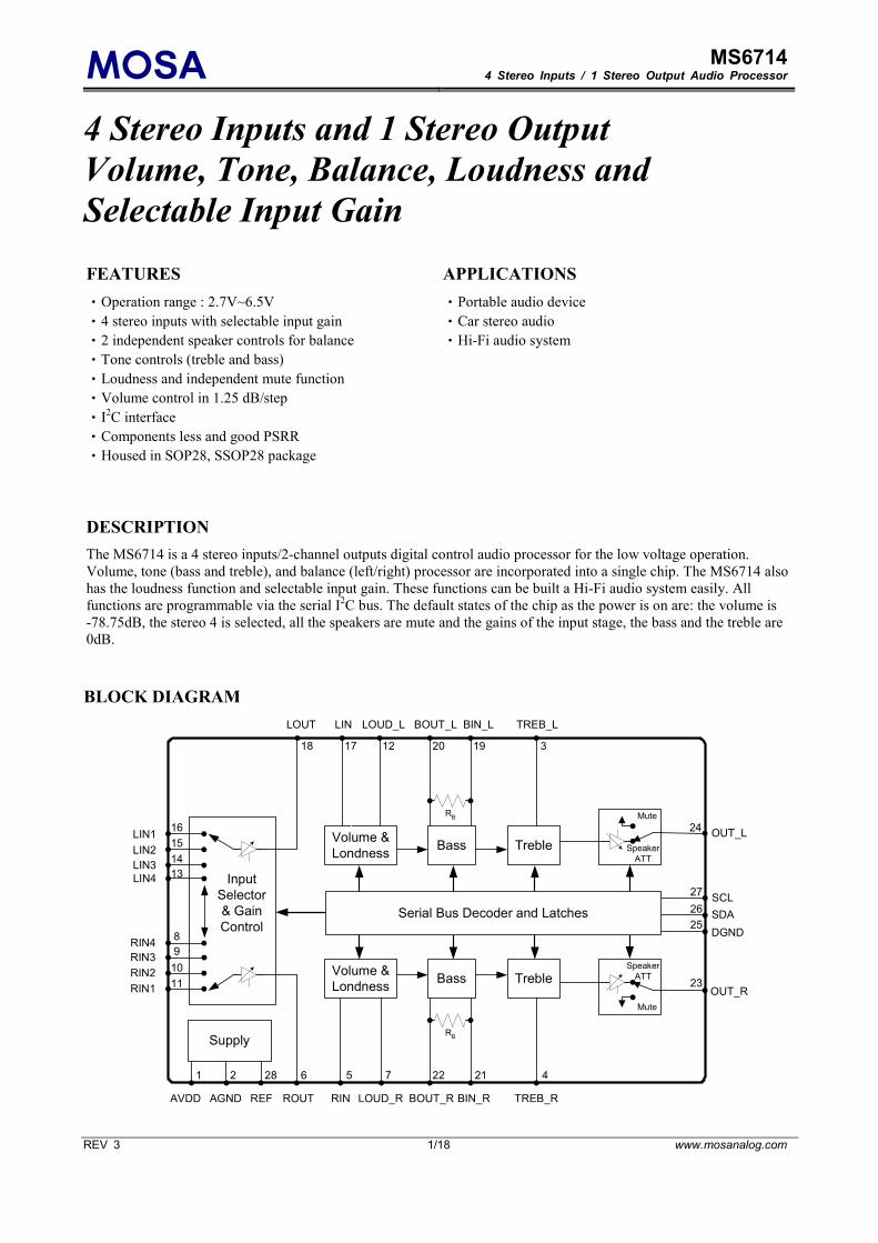
The MS6714 is a 4 stereo inputs/2-channel outputs digital control audio processor for the low voltage operation.
Volume, tone (bass and treble), and balance (left/right) processor are incorporated into a single chip. The MS6714 also
has the loudness function and selectable input gain. These functions can be built a Hi-Fi audio system easily. All
functions are programmable via the serial I2C bus. The default states of the chip as the power is on are: the volume is
-78.75dB, the stereo 4 is selected, all the speakers are mute and the gains of the input stage, the bass and the treble are
0dB.
BLOCK DIAGRAM
RIN2
RIN1TrebleBass
Volume &
Londness
Volume &
LondnessBass Treble
LIN1
LIN2
LIN3
RIN3
REF
RB
RB
Input
Selector
& Gain
Control
LOUD_RROUT RIN TREB_RBOUT_R BIN_R
LOUD_LLOUT LIN TREB_LBOUT_L BIN_L
28 6 7
9
3
45
14
15
16
10
11
12 20
2122
1718 19
Supply
AVDD AGND
1 2
Speaker
ATT
Mute
Speaker
ATT
Mute
SCL
SDA
DGND
OUT_L
OUT_R
25
26
24
23
27
Serial Bus Decoder and Latches
LIN4
RIN48
13
MOSA MS6714 4 Stereo Inputs / 1 Stereo Output Audio Processor
REV 3 2/18 www.mosanalog.com
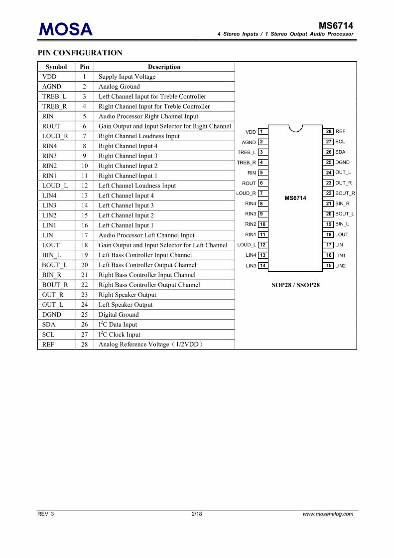
PIN CONFIGURATION
Symbol Pin Description
LIN
LIN1
LIN2LIN3
LIN4
LOUD_L
RIN1
27
26
25
28
2
3
4
1
SCL
SDA
DGND
OUT_L
REFVDD
AGND
TREB_L
OUT_R
BOUT_R
BIN_R
BOUT_L
BIN_L
LOUT
RIN2
RIN3
LOUD_R
ROUT
RIN
TREB_R
23
22
21
24
6
7
8
5
19
18
17
20
10
11
12
9
15
16
14
13
MS6714RIN4
SOP28 / SSOP28
VDD 1 Supply Input Voltage
AGND 2 Analog Ground
TREB_L 3 Left Channel Input for Treble Controller
TREB_R 4 Right Channel Input for Treble Controller
RIN 5 Audio Processor Right Channel Input
ROUT 6 Gain Output and Input Selector for Right Channel
LOUD_R 7 Right Channel Loudness Input
RIN4 8 Right Channel Input 4
RIN3 9 Right Channel Input 3
RIN2 10 Right Channel Input 2
RIN1 11 Right Channel Input 1
LOUD_L 12 Left Channel Loudness Input
LIN4 13 Left Channel Input 4
LIN3 14 Left Channel Input 3
LIN2 15 Left Channel Input 2
LIN1 16 Left Channel Input 1
LIN 17 Audio Processor Left Channel Input
LOUT 18 Gain Output and Input Selector for Left Channel
BIN_L 19 Left Bass Controller Input Channel
BOUT_L 20 Left Bass Controller Output Channel
BIN_R 21 Right Bass Controller Input Channel
BOUT_R 22 Right Bass Controller Output Channel
OUT_R 23 Right Speaker Output
OUT_L 24 Left Speaker Output
DGND 25 Digital Ground
SDA 26 I2C Data Input
SCL 27 I2C Clock Input
REF 28 Analog Reference Voltage(1/2VDD)
MOSA MS6714 4 Stereo Inputs / 1 Stereo Output Audio Processor
REV 3 3/18 www.mosanalog.com
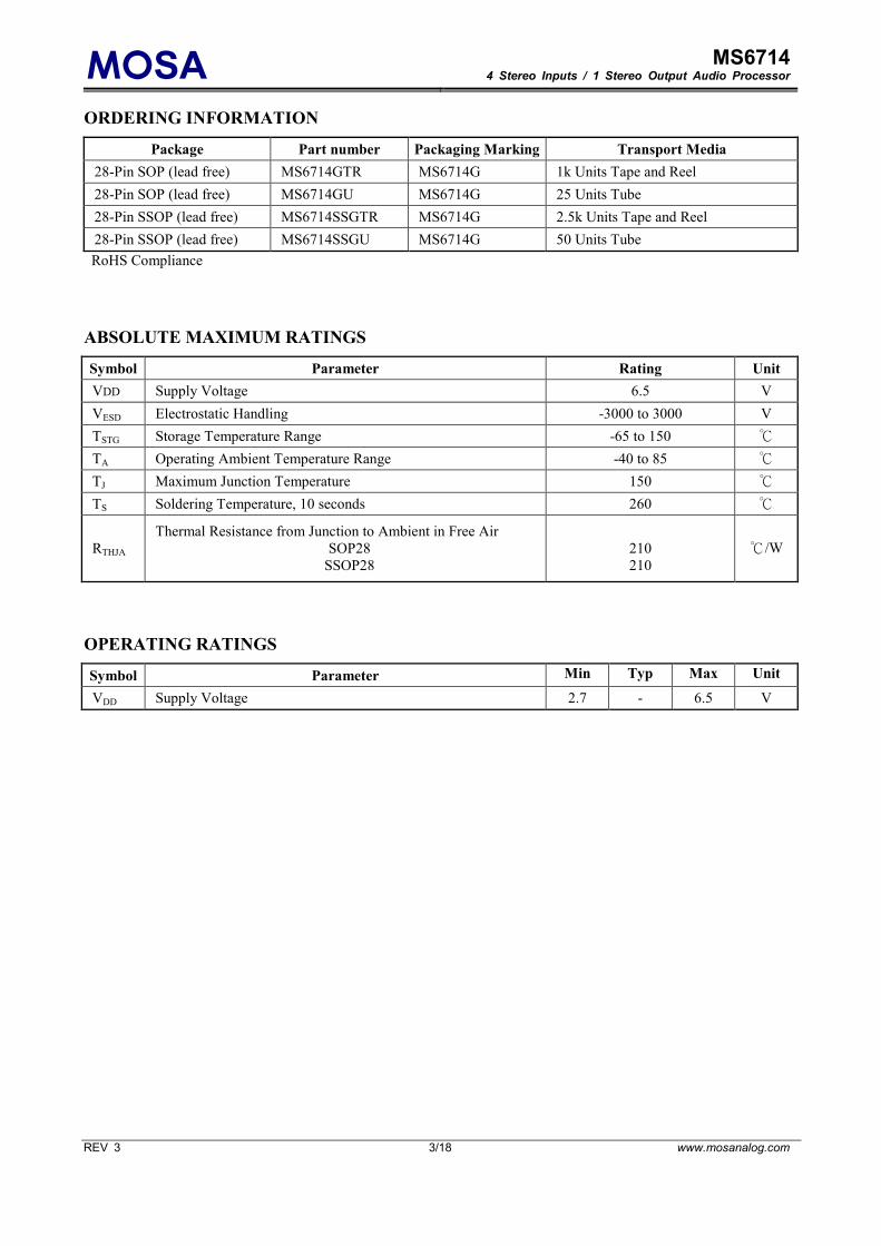
ORDERING INFORMATION
Package Part number Packaging Marking Transport Media
28-Pin SOP (lead free) MS6714GTR MS6714G 1k Units Tape and Reel
28-Pin SOP (lead free) MS6714GU MS6714G 25 Units Tube
28-Pin SSOP (lead free) MS6714SSGTR MS6714G 2.5k Units Tape and Reel
28-Pin SSOP (lead free) MS6714SSGU MS6714G 50 Units Tube
RoHS Compliance
ABSOLUTE MAXIMUM RATINGS
Symbol Parameter Rating Unit
VDD Supply Voltage 6.5 V
VESD Electrostatic Handling -3000 to 3000 V
TSTG Storage Temperature Range -65 to 150 ℃
TA Operating Ambient Temperature Range -40 to 85 ℃
TJ Maximum Junction Temperature 150 ℃
TS Soldering Temperature, 10 seconds 260 ℃
RTHJA
Thermal Resistance from Junction to Ambient in Free Air
SOP28
SSOP28
210
210
℃/W
OPERATING RATINGS
Symbol Parameter Min Typ Max Unit
VDD Supply Voltage 2.7 - 6.5 V
MOSA MS6714 4 Stereo Inputs / 1 Stereo Output Audio Processor
REV 3 4/18 www.mosanalog.com
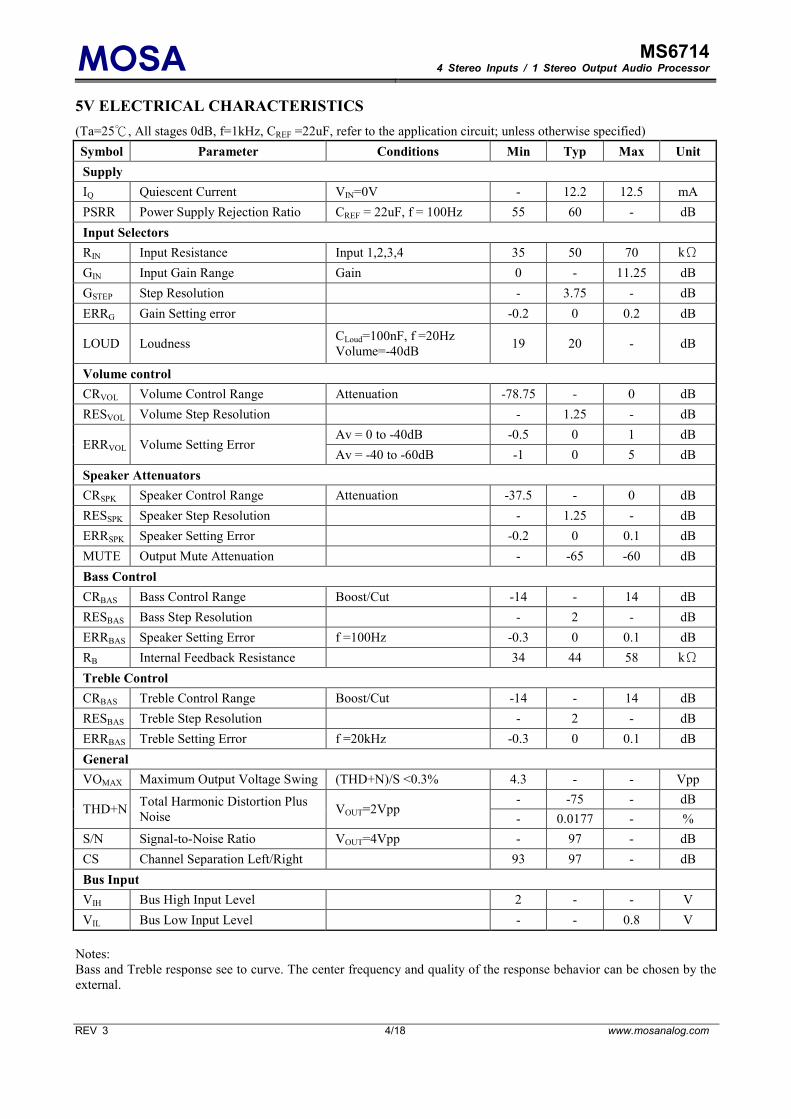
5V ELECTRICAL CHARACTERISTICS
(Ta=25℃, All stages 0dB, f=1kHz, CREF =22uF, refer to the application circuit; unless otherwise specified)
Symbol Parameter Conditions Min Typ Max Unit
Supply
IQ Quiescent Current VIN=0V - 12.2 12.5 mA
PSRR Power Supply Rejection Ratio CREF = 22uF, f = 100Hz 55 60 - dB
Input Selectors
RIN Input Resistance Input 1,2,3,4 35 50 70 kΩ
GIN Input Gain Range Gain 0 - 11.25 dB
GSTEP Step Resolution - 3.75 - dB
ERRG Gain Setting error -0.2 0 0.2 dB
LOUD Loudness CLoud=100nF, f =20Hz
Volume=-40dB 19 20 - dB
Volume control
CRVOL Volume Control Range Attenuation -78.75 - 0 dB
RESVOL Volume Step Resolution - 1.25 - dB
ERRVOL Volume Setting Error Av = 0 to -40dB -0.5 0 1 dB
Av = -40 to -60dB -1 0 5 dB
Speaker Attenuators
CRSPK Speaker Control Range Attenuation -37.5 - 0 dB
RESSPK Speaker Step Resolution - 1.25 - dB
ERRSPK Speaker Setting Error -0.2 0 0.1 dB
MUTE Output Mute Attenuation - -65 -60 dB
Bass Control
CRBAS Bass Control Range Boost/Cut -14 - 14 dB
RESBAS Bass Step Resolution - 2 - dB
ERRBAS Speaker Setting Error f =100Hz -0.3 0 0.1 dB
RB Internal Feedback Resistance 34 44 58 kΩ
Treble Control
CRBAS Treble Control Range Boost/Cut -14 - 14 dB
RESBAS Treble Step Resolution - 2 - dB
ERRBAS Treble Setting Error f =20kHz -0.3 0 0.1 dB
General
VOMAX Maximum Output Voltage Swing (THD+N)/S <0.3% 4.3 - - Vpp
THD+N Total Harmonic Distortion Plus
Noise VOUT=2Vpp
- -75 - dB
- 0.0177 - %
S/N Signal-to-Noise Ratio VOUT=4Vpp - 97 - dB
CS Channel Separation Left/Right 93 97 - dB
Bus Input
VIH Bus High Input Level 2 - - V
VIL Bus Low Input Level - - 0.8 V
Notes:
Bass and Treble response see to curve. The center frequency and quality of the response behavior can be chosen by the
external.
MOSA MS6714 4 Stereo Inputs / 1 Stereo Output Audio Processor
REV 3 5/18 www.mosanalog.com
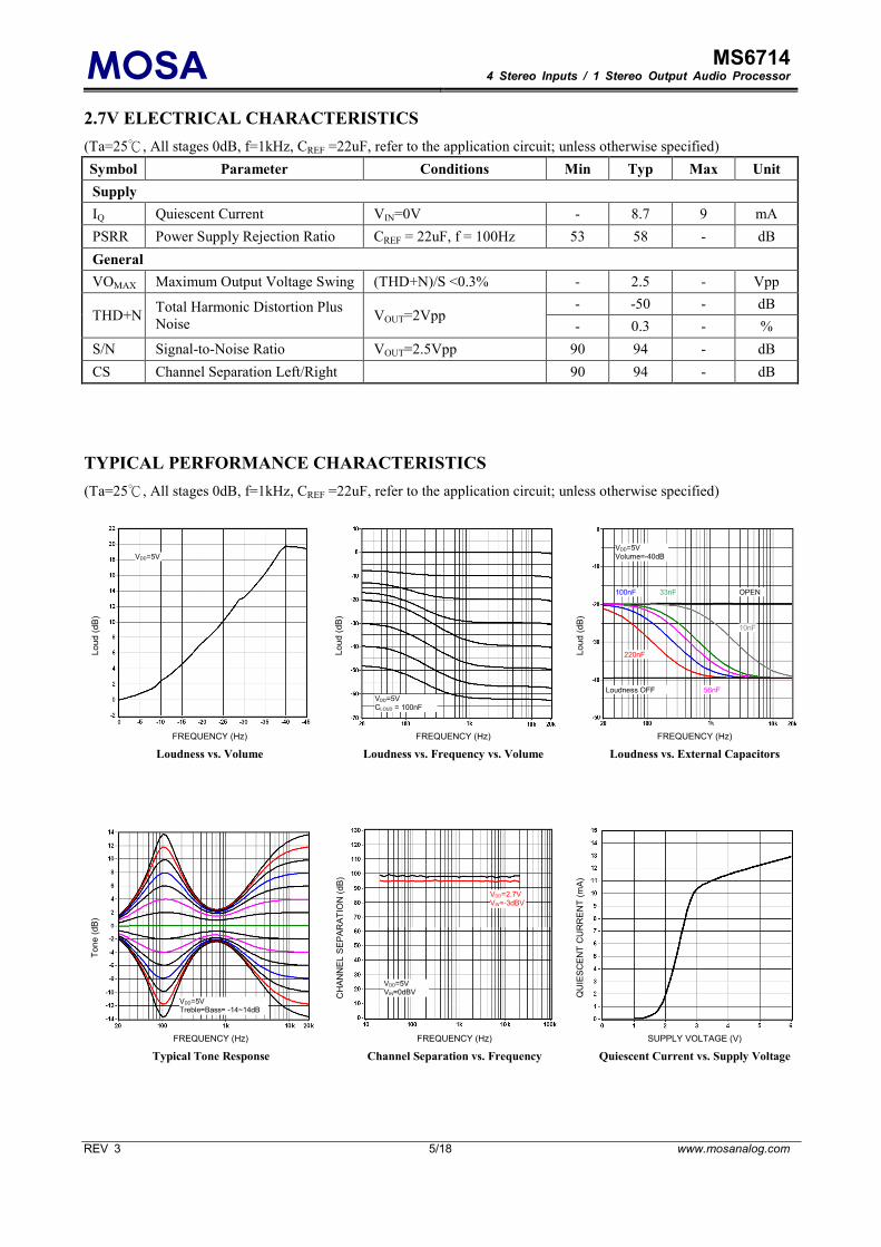
2.7V ELECTRICAL CHARACTERISTICS
(Ta=25℃, All stages 0dB, f=1kHz, CREF =22uF, refer to the application circuit; unless otherwise specified)
Symbol Parameter Conditions Min Typ Max Unit
Supply
IQ Quiescent Current VIN=0V - 8.7 9 mA
PSRR Power Supply Rejection Ratio CREF = 22uF, f = 100Hz 53 58 - dB
General
VOMAX Maximum Output Voltage Swing (THD+N)/S <0.3% - 2.5 - Vpp
THD+N Total Harmonic Distortion Plus
Noise VOUT=2Vpp
- -50 - dB
- 0.3 - %
S/N Signal-to-Noise Ratio VOUT=2.5Vpp 90 94 - dB
CS Channel Separation Left/Right 90 94 - dB
TYPICAL PERFORMANCE CHARACTERISTICS
(Ta=25℃, All stages 0dB, f=1kHz, CREF =22uF, refer to the application circuit; unless otherwise specified)
Loud (dB)
FREQUENCY (Hz)
Loud (dB)
FREQUENCY (Hz)
Loud (dB)
FREQUENCY (Hz)
Loudness vs. Volume Loudness vs. Frequency vs. Volume Loudness vs. External Capacitors
Tone (dB)
FREQUENCY (Hz)
CHANNEL SEPARATION (dB)
FREQUENCY (Hz)
QUIESCENT CURRENT (mA)
SUPPLY VOLTAGE (V)
Typical Tone Response Channel Separation vs. Frequency Quiescent Current vs. Supply Voltage
VDD=5V CLOUD = 100nF
220nF
OPEN
VDD=5V VIN=0dBV
VDD=5V Treble=Bass= -14~14dB
VDD=5V VDD=5V Volume=-40dB
56nF
100nF
Loudness OFF
33nF
10nF
VDD=2.7V VIN=-3dBV
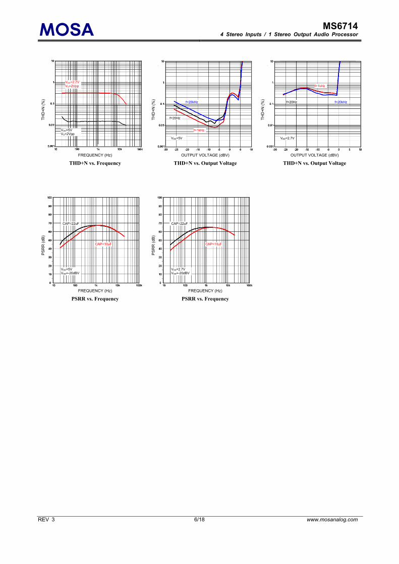
MOSA MS6714 4 Stereo Inputs / 1 Stereo Output Audio Processor
REV 3 6/18 www.mosanalog.com
THD+N (%)
FREQUENCY (Hz)
THD+N (%)
OUTPUT VOLTAGE (dBV)
THD+N (%)
OUTPUT VOLTAGE (dBV)
THD+N vs. Frequency THD+N vs. Output Voltage THD+N vs. Output Voltage
PSRR (dB)
FREQUENCY (Hz)
PSRR (dB)
FREQUENCY (Hz)
PSRR vs. Frequency PSRR vs. Frequency
VDD=5V VO=2Vpp
VDD=5V f=1kHz
f=20Hz
f=20kHz
VDD=2.7V VO=2Vpp
VDD=2.7V
f=1kHz
f=20Hz f=20kHz
CAP=22uF
CAP=10uF
VDD=5V VRR=-20dBV
CAP=22uF
CAP=10uF
VDD=2.7V VRR=-20dBV
MOSA MS6714 4 Stereo Inputs / 1 Stereo Output Audio Processor
REV 3 7/18 www.mosanalog.com
I2C BUS DESCRIPTION
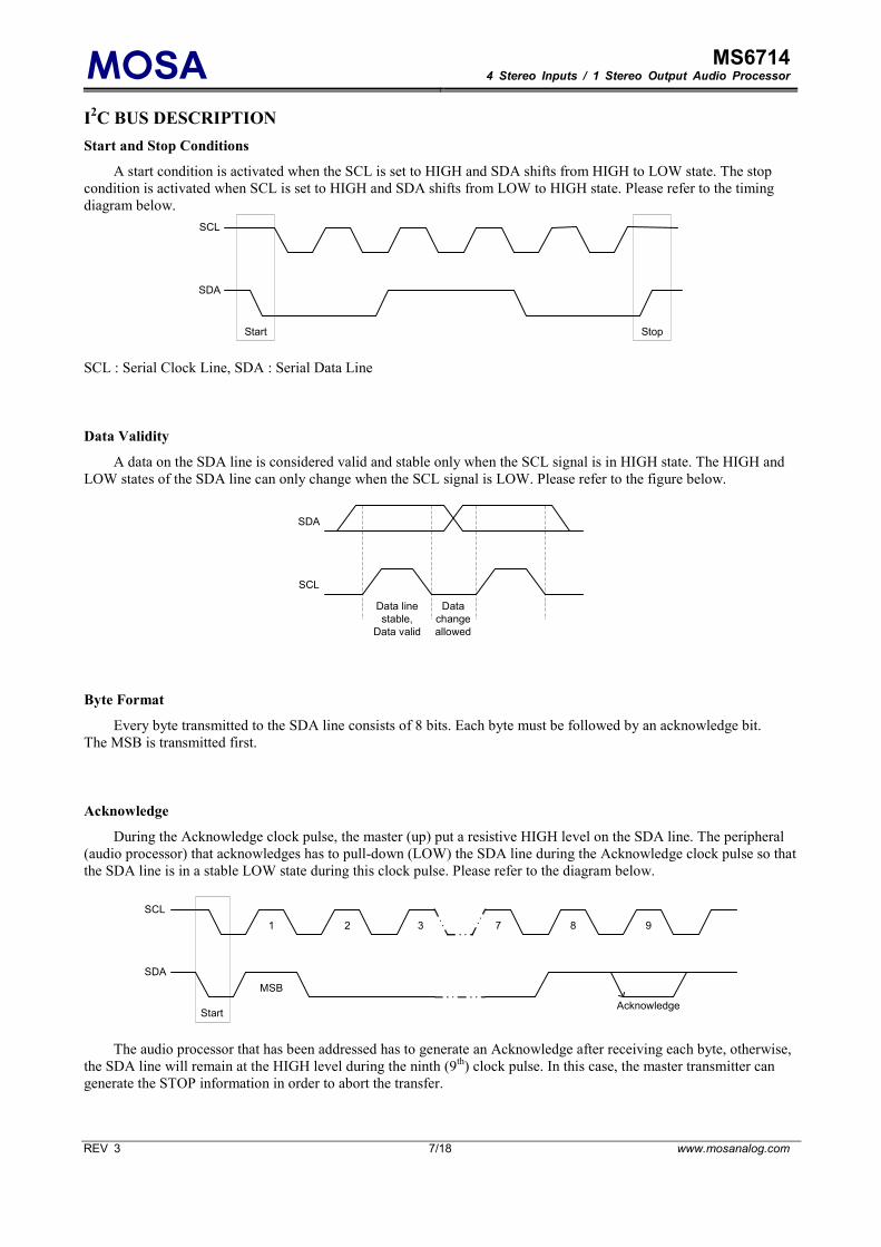
Start and Stop Conditions
A start condition is activated when the SCL is set to HIGH and SDA shifts from HIGH to LOW state. The stop
condition is activated when SCL is set to HIGH and SDA shifts from LOW to HIGH state. Please refer to the timing
diagram below.
SDA
SCL
Start Stop
SCL : Serial Clock Line, SDA : Serial Data Line
Data Validity
A data on the SDA line is considered valid and stable only when the SCL signal is in HIGH state. The HIGH and
LOW states of the SDA line can only change when the SCL signal is LOW. Please refer to the figure below.
SDA
SCL
Data line
stable,
Data valid
Data
change
allowed
Byte Format
Every byte transmitted to the SDA line consists of 8 bits. Each byte must be followed by an acknowledge bit.
The MSB is transmitted first.
Acknowledge
During the Acknowledge clock pulse, the master (up) put a resistive HIGH level on the SDA line. The peripheral
(audio processor) that acknowledges has to pull-down (LOW) the SDA line during the Acknowledge clock pulse so that
the SDA line is in a stable LOW state during this clock pulse. Please refer to the diagram below.
SCL
SDA
MSB
Acknowledge
1 2 3 7 8 9
Start
The audio processor that has been addressed has to generate an Acknowledge after receiving each byte, otherwise,
the SDA line will remain at the HIGH level during the ninth (9th) clock pulse. In this case, the master transmitter can
generate the STOP information in order to abort the transfer.
MOSA MS6714 4 Stereo Inputs / 1 Stereo Output Audio Processor
REV 3 8/18 www.mosanalog.com
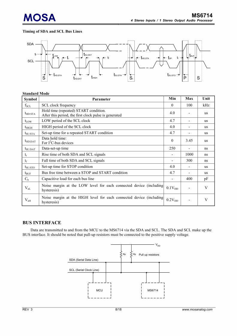
Timing of SDA and SCL Bus Lines
tf
S
tLOW
tHD;STA
tr
tHD;DAT
tSU;DATtf
tHIGH
tHD;STA
tSU;STASr SP
tSP
tSU;STO
trtBUF
SDA
SCL
Standard Mode
Symbol Parameter Min Max Unit
fSCL SCL clock frequency 0 100 kHz
tHD:STA Hold time (repeated) START condition.
After this period, the first clock pulse is generated 4.0 - us
tLOW LOW period of the SCL clock 4.7 - us
tHIGH HIGH period of the SCL clock 4.0 - us
tSU:STA Set-up time for a repeated START condition 4.7 - us
tHD:DAT Data hold time:
For I2C-bus devices
0
3.45
us
tSU:DAT Data-set-up time 250 - ns
tr Rise time of both SDA and SCL signals - 1000 ns
tf Fall time of both SDA and SCL signals - 300 ns
tSU:STO Set-up time for STOP condition 4.0 - us
tBUF Bus free time between a STOP and START condition 4.7 - us
Cb Capacitive load for each bus line - 400 pF
VnL Noise margin at the LOW level for each connected device (including
hysteresis) 0.1VDD - V
VnH Noise margin at the HIGH level for each connected device (including
hysteresis) 0.2VDD - V
BUS INTERFACE
Data are transmitted to and from the MCU to the MS6714 via the SDA and SCL. The SDA and SCL make up the
BUS interface. It should be noted that pull-up resistors must be connected to the positive supply voltage.
SDA (Serial Data Line)
Rp Rp
SCL (Serial Clock Line)
Pull up resistors
VDD
MCU MS6714
MOSA MS6714 4 Stereo Inputs / 1 Stereo Output Audio Processor
REV 3 9/18 www.mosanalog.com
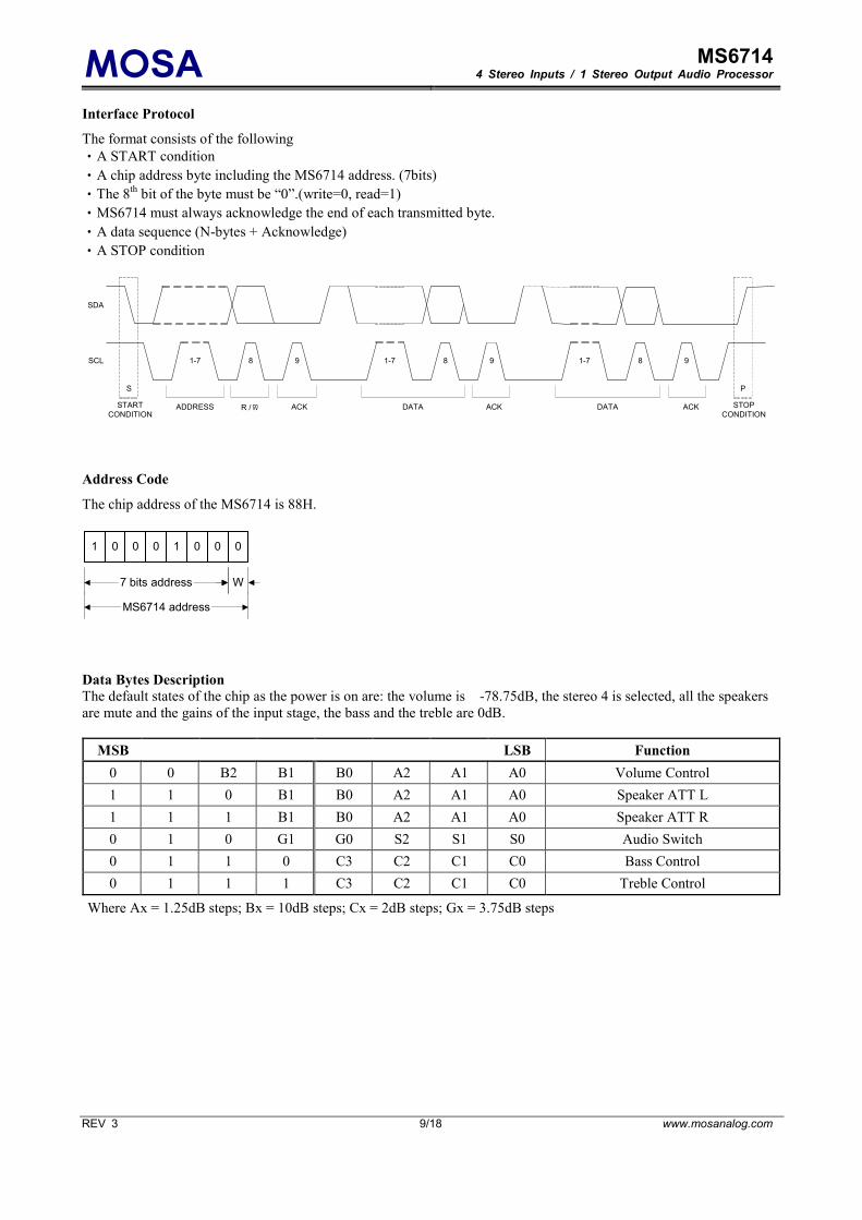
Interface Protocol
The format consists of the following
•A START condition
•A chip address byte including the MS6714 address. (7bits)
•The 8th bit of the byte must be “0”.(write=0, read=1)
•MS6714 must always acknowledge the end of each transmitted byte.
•A data sequence (N-bytes + Acknowledge)
•A STOP condition
SCL
SDA
1-7 8 9 1-7 8 9 981-7
S P
ADDRESS R /W-- ACK ACK ACKDATA DATASTART
CONDITION
STOP
CONDITION
Address Code
The chip address of the MS6714 is 88H.
1 0 0 0 0 01 0
7 bits address
MS6714 address
W
Data Bytes Description
The default states of the chip as the power is on are: the volume is -78.75dB, the stereo 4 is selected, all the speakers
are mute and the gains of the input stage, the bass and the treble are 0dB.
MSB LSB Function
0 0 B2 B1 B0 A2 A1 A0 Volume Control
1 1 0 B1 B0 A2 A1 A0 Speaker ATT L
1 1 1 B1 B0 A2 A1 A0 Speaker ATT R
0 1 0 G1 G0 S2 S1 S0 Audio Switch
0 1 1 0 C3 C2 C1 C0 Bass Control
0 1 1 1 C3 C2 C1 C0 Treble Control
Where Ax = 1.25dB steps; Bx = 10dB steps; Cx = 2dB steps; Gx = 3.75dB steps
MOSA MS6714 4 Stereo Inputs / 1 Stereo Output Audio Processor
REV 3 10/18 www.mosanalog.com
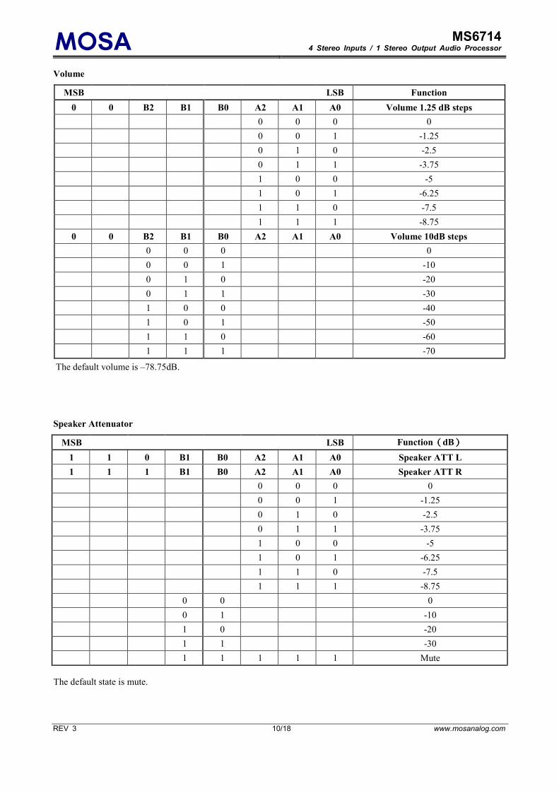
Volume
MSB LSB Function
0 0 B2 B1 B0 A2 A1 A0 Volume 1.25 dB steps
0 0 0 0
0 0 1 -1.25
0 1 0 -2.5
0 1 1 -3.75
1 0 0 -5
1 0 1 -6.25
1 1 0 -7.5
1 1 1 -8.75
0 0 B2 B1 B0 A2 A1 A0 Volume 10dB steps
0 0 0 0
0 0 1 -10
0 1 0 -20
0 1 1 -30
1 0 0 -40
1 0 1 -50
1 1 0 -60
1 1 1 -70
The default volume is –78.75dB.
Speaker Attenuator
MSB LSB Function((((dB))))
1 1 0 B1 B0 A2 A1 A0 Speaker ATT L
1 1 1 B1 B0 A2 A1 A0 Speaker ATT R
0 0 0 0
0 0 1 -1.25
0 1 0 -2.5
0 1 1 -3.75
1 0 0 -5
1 0 1 -6.25
1 1 0 -7.5
1 1 1 -8.75
0 0 0
0 1 -10
1 0 -20
1 1 -30
1 1 1 1 1 Mute
The default state is mute.
MOSA MS6714 4 Stereo Inputs / 1 Stereo Output Audio Processor
REV 3 11/18 www.mosanalog.com
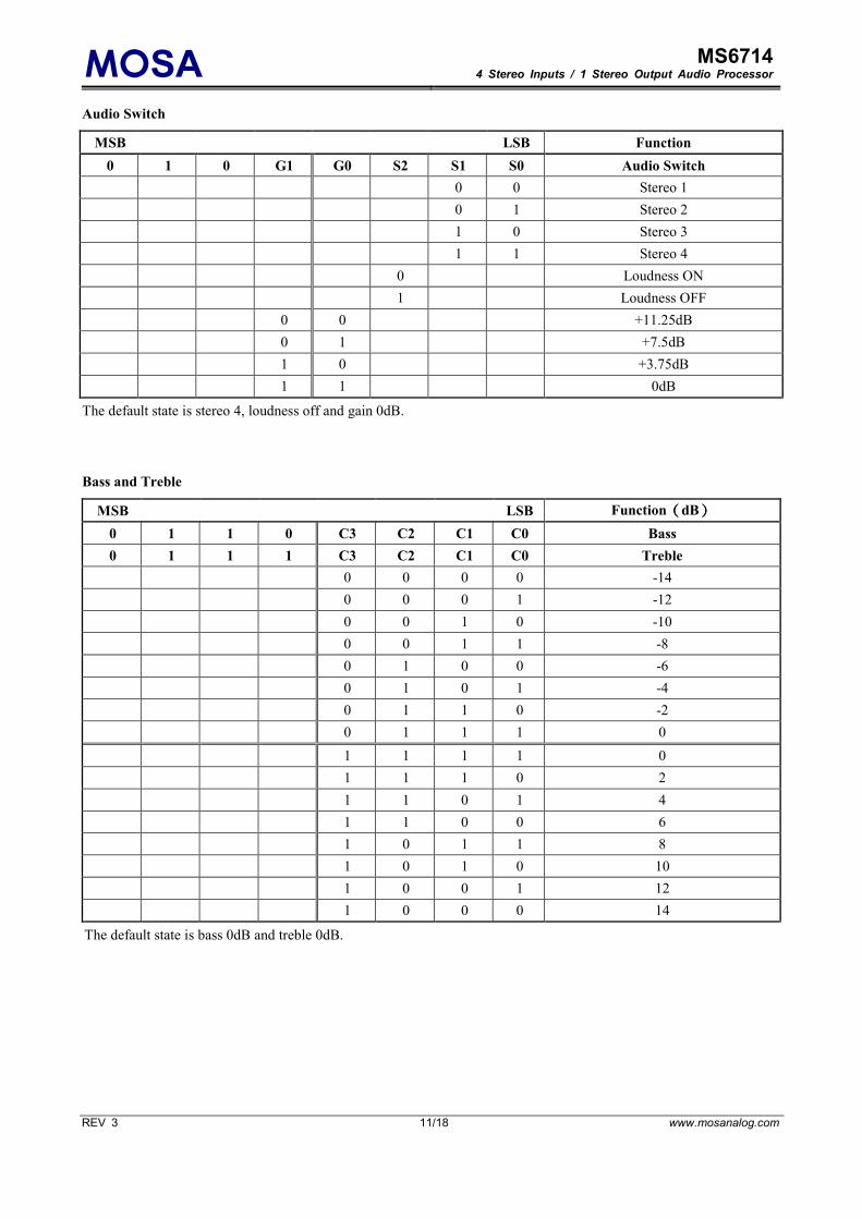
Audio Switch
MSB LSB Function
0 1 0 G1 G0 S2 S1 S0 Audio Switch
0 0 Stereo 1
0 1 Stereo 2
1 0 Stereo 3
1 1 Stereo 4
0 Loudness ON
1 Loudness OFF
0 0 +11.25dB
0 1 +7.5dB
1 0 +3.75dB
1 1 0dB
The default state is stereo 4, loudness off and gain 0dB.
Bass and Treble
MSB LSB Function((((dB))))
0 1 1 0 C3 C2 C1 C0 Bass
0 1 1 1 C3 C2 C1 C0 Treble
0 0 0 0 -14
0 0 0 1 -12
0 0 1 0 -10
0 0 1 1 -8
0 1 0 0 -6
0 1 0 1 -4
0 1 1 0 -2
0 1 1 1 0
1 1 1 1 0
1 1 1 0 2
1 1 0 1 4
1 1 0 0 6
1 0 1 1 8
1 0 1 0 10
1 0 0 1 12
1 0 0 0 14
The default state is bass 0dB and treble 0dB.
MOSA MS6714 4 Stereo Inputs / 1 Stereo Output Audio Processor
REV 3 12/18 www.mosanalog.com
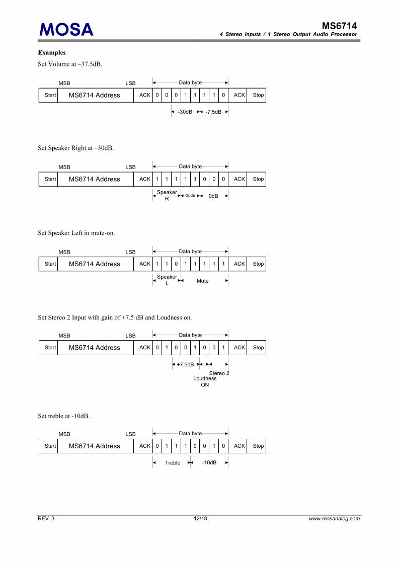
Examples
Set Volume at –37.5dB.
MSB
ACKStart 0 0 0 1 1 01 1MS6714 Address
LSB
StopACK
-30dB -7.5dB
Data byte
Set Speaker Right at –30dB.
MSB
ACKStart 1 1 1 1 0 01 0MS6714 Address
LSB
StopACK
-30dB 0dBSpeaker
R
Data byte
Set Speaker Left in mute-on.
MSB
ACKStart 1 1 0 1 1 11 1MS6714 Address
LSB
StopACK
Speaker
L Mute
Data byte
Set Stereo 2 Input with gain of +7.5 dB and Loudness on.
MSB
ACKStart 0 1 0 0 0 11 0MS6714 Address
LSB
StopACK
+7.5dB
Stereo 2Loudness
ON
Data byte
Set treble at -10dB.
MSB
ACKStart 0 1 1 1 1 00 0MS6714 Address
LSB
StopACK
Treble -10dB
Data byte
MOSA MS6714 4 Stereo Inputs / 1 Stereo Output Audio Processor
REV 3 13/18 www.mosanalog.com
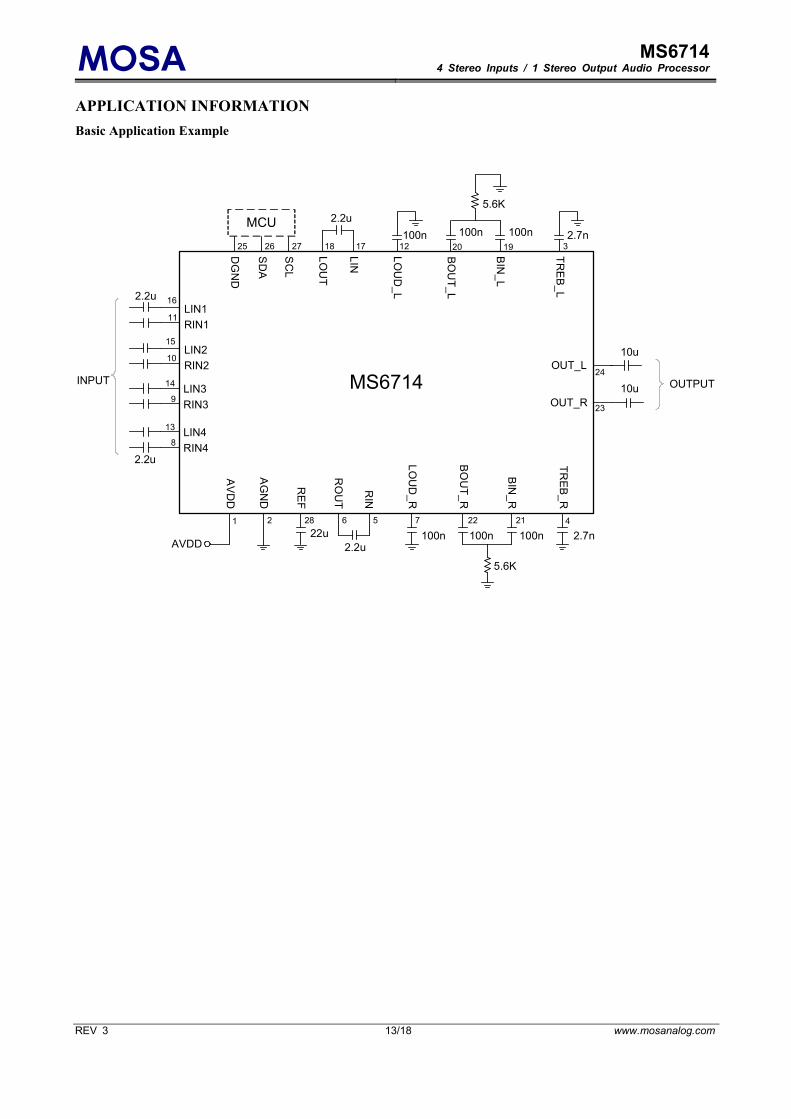
APPLICATION INFORMATION
Basic Application Example
MCU
MS6714
REF
SDA
AVDD
AGND
LOUD_R
ROUT
RIN
TREB_R
BOUT_R
BIN_R
LOUD_L
LOUT
LIN
TREB_L
BOUT_L
BIN_L
281 2 6 5
25 26 27
SCL
DGND
18 17 12
2.2u
2.2uAVDD22u
7
100n
22
100n
21
100n
5.6K
4
2.7n
20
100n
19
5.6K
100n100n3
2.7n
OUT_L
OUT_R
24
23
10u
10u OUTPUT
RIN2
RIN1
LIN1
LIN2
LIN3
RIN39
14
15
16
10
11
2.2u
INPUT
LIN4
RIN48
13
2.2u
MOSA MS6714 4 Stereo Inputs / 1 Stereo Output Audio Processor
REV 3 14/18 www.mosanalog.com
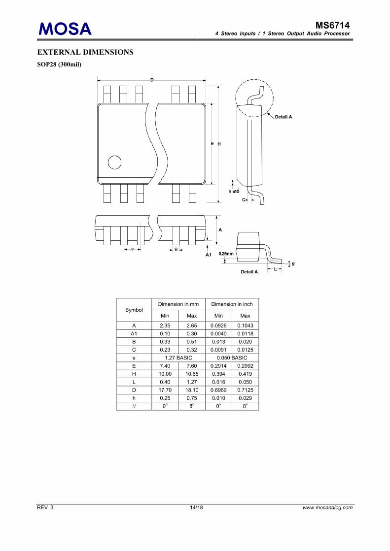
EXTERNAL DIMENSIONS
SOP28 (300mil)
H
h x45
C
Detail A
0.25mm
Detail AL
θθθθ
E
A1
e B
A
D
Symbol Dimension in mm Dimension in inch
Min Max Min Max
A 2.35 2.65 0.0926 0.1043
A1 0.10 0.30 0.0040 0.0118
B 0.33 0.51 0.013 0.020
C 0.23 0.32 0.0091 0.0125
e 1.27 BASIC 0.050 BASIC
E 7.40 7.60 0.2914 0.2992
H 10.00 10.65 0.394 0.419
L 0.40 1.27 0.016 0.050
D 17.70 18.10 0.6969 0.7125
h 0.25 0.75 0.010 0.029
θ 0o 8
o 0
o 8
o
MOSA MS6714 4 Stereo Inputs / 1 Stereo Output Audio Processor
REV 3 15/18 www.mosanalog.com
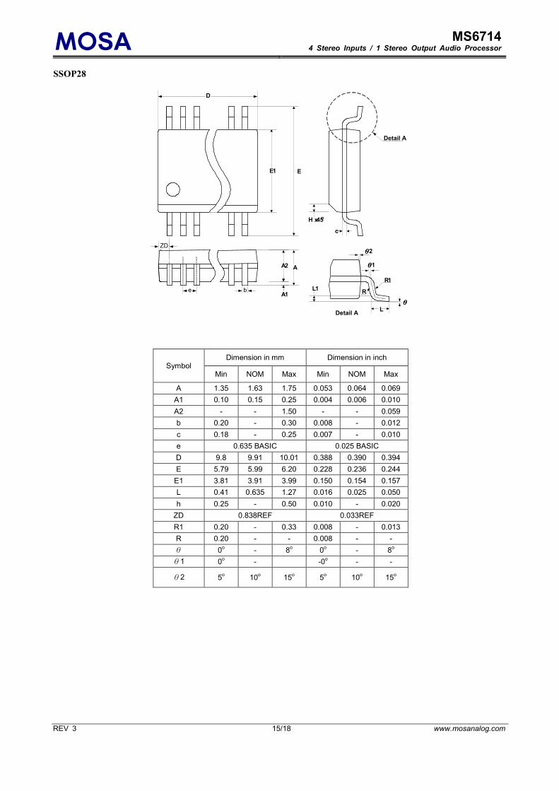
SSOP28
AA2
A1
E1 E
L1
Detail AL
θθθθ2
θθθθ1
R1
R
θθθθ
Detail A
H x45
c
D
ZD
e b
Symbol Dimension in mm Dimension in inch
Min NOM Max Min NOM Max
A 1.35 1.63 1.75 0.053 0.064 0.069
A1 0.10 0.15 0.25 0.004 0.006 0.010
A2 - - 1.50 - - 0.059
b 0.20 - 0.30 0.008 - 0.012
c 0.18 - 0.25 0.007 - 0.010
e 0.635 BASIC 0.025 BASIC
D 9.8 9.91 10.01 0.388 0.390 0.394
E 5.79 5.99 6.20 0.228 0.236 0.244
E1 3.81 3.91 3.99 0.150 0.154 0.157
L 0.41 0.635 1.27 0.016 0.025 0.050
h 0.25 - 0.50 0.010 - 0.020
ZD 0.838REF 0.033REF
R1 0.20 - 0.33 0.008 - 0.013
R 0.20 - - 0.008 - -
θ 0o - 8
o 0
o - 8
o
θ1 0o - -0
o - -
θ2 5o 10
o 15
o 5
o 10
o 15
o
MOSA MS6714 4 Stereo Inputs / 1 Stereo Output Audio Processor
REV 3 16/18 www.mosanalog.com
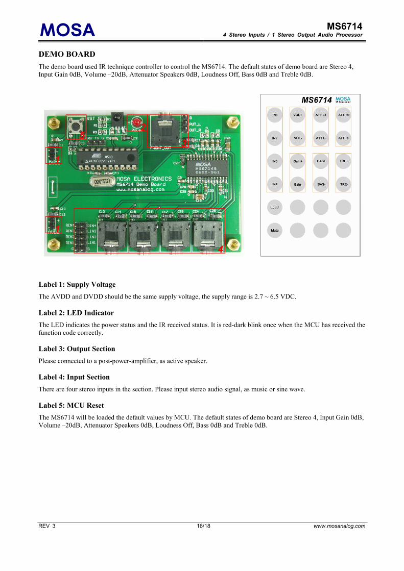
DEMO BOARD
The demo board used IR technique controller to control the MS6714. The default states of demo board are Stereo 4,
Input Gain 0dB, Volume –20dB, Attenuator Speakers 0dB, Loudness Off, Bass 0dB and Treble 0dB.
Label 1: Supply Voltage
The AVDD and DVDD should be the same supply voltage, the supply range is 2.7 ~ 6.5 VDC.
Label 2: LED Indicator
The LED indicates the power status and the IR received status. It is red-dark blink once when the MCU has received the
function code correctly.
Label 3: Output Section
Please connected to a post-power-amplifier, as active speaker.
Label 4: Input Section
There are four stereo inputs in the section. Please input stereo audio signal, as music or sine wave.
Label 5: MCU Reset
The MS6714 will be loaded the default values by MCU. The default states of demo board are Stereo 4, Input Gain 0dB,
Volume –20dB, Attenuator Speakers 0dB, Loudness Off, Bass 0dB and Treble 0dB.
1
2
3
1
4
5
MOSA MS6714 4 Stereo Inputs / 1 Stereo Output Audio Processor
REV 3 17/18 www.mosanalog.com
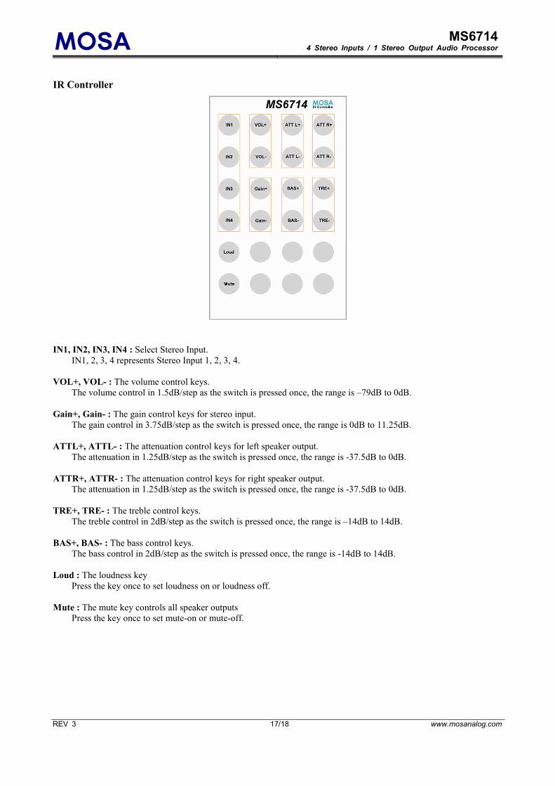
IR Controller
IN1, IN2, IN3, IN4 : Select Stereo Input.
IN1, 2, 3, 4 represents Stereo Input 1, 2, 3, 4.
VOL+, VOL- : The volume control keys.
The volume control in 1.5dB/step as the switch is pressed once, the range is –79dB to 0dB.
Gain+, Gain- : The gain control keys for stereo input.
The gain control in 3.75dB/step as the switch is pressed once, the range is 0dB to 11.25dB.
ATTL+, ATTL- : The attenuation control keys for left speaker output.
The attenuation in 1.25dB/step as the switch is pressed once, the range is -37.5dB to 0dB.
ATTR+, ATTR- : The attenuation control keys for right speaker output.
The attenuation in 1.25dB/step as the switch is pressed once, the range is -37.5dB to 0dB.
TRE+, TRE- : The treble control keys.
The treble control in 2dB/step as the switch is pressed once, the range is –14dB to 14dB.
BAS+, BAS- : The bass control keys.
The bass control in 2dB/step as the switch is pressed once, the range is -14dB to 14dB.
Loud : The loudness key
Press the key once to set loudness on or loudness off.
Mute : The mute key controls all speaker outputs
Press the key once to set mute-on or mute-off.
MOSA MS6714 4 Stereo Inputs / 1 Stereo Output Audio Processor
REV 3 18/18 www.mosanalog.com
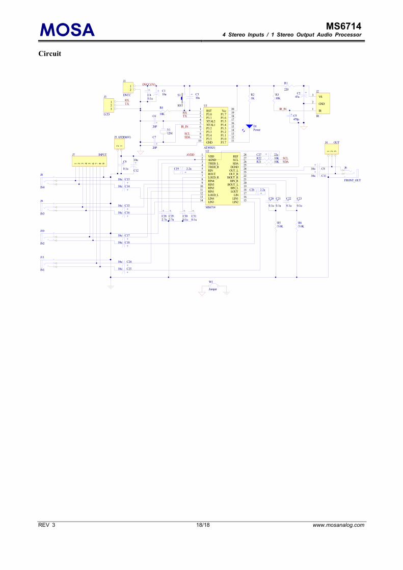
Circuit
Y112M
RST1
P3.02
P3.13
XTAL24
XTAL15
P3.26
P3.37
P3.48
P3.59
GND10
Vcc20
P1.719
P1.618
P1.517
P1.416
P1.315
P1.214
P1.113
P1.012
P3.711
U1
AT89X51
12
J1
DVCC
R4
10K
S1
RST
IR_IN
+ C310u
+
C6
20P
+
C7
20P
DVCC(3V)
VS3
IR1
GND2
J2
IR
R310K
+ C5470p
+C247u
IR_IN
R1
220
SDASCL
VDD1
AGND2
TREB_L3
TREB_R4
RIN5
ROUT6
LOUD_R7
RIN48
RIN39
RIN210
RIN111
LOUD_L12
LIN413
LIN314
LIN215
LIN116
LIN17
LOUT18
BIN_L19
BOUT_L20
BIN_R21
BOUT_R22
OUT_R23
OUT_L24
DGND25
SDA26
SCL27
REF28
U2
MS6714
12
J5 AVDD(6V)
+
C1310u
+
C1410u
+
C1510u
+
C1610u
+
C1710u
+
C1810u
+C27 22u
+
C19 2.2u
+
C810u
+
C1110u
+
C2510u
+
C2410u
+
C26 2.2u
R55.6K
R65.6K
+C23
0.1u
+C22
0.1u
+C21
0.1u
+C20
0.1u
+
C310.1u
+
C300.1u
+
C292.7n
+
C282.7n
+C9
0.1u
SDASCL
AVDD
W1
Jumper
J6
FRONT_OUT
J11
IN1
J8
IN4
J9
IN3
J10
IN2
1 2 3 4 5 6 7 8 9
J7 INPUT
1 2 3
J4 OUT
123
J3
LCDRXTX
RXTX
+
C40.1u
+ C110u
+
C12
10u
R21K
D1Power
R22 10KR21 10K