Embed Size (px)
Citation preview
403
Single-Walled14. Single-Walled Carbon Nanotube Sensor Concepts
Cosmin Roman, Thomas Helbling, Christofer Hierold
Carbon nanotubes are nanocomponents par excel-lence that offer unique properties to be exploitedin next-generation devices. Sensing applicationsare perhaps the class that has most to gain fromsingle-walled carbon nanotubes (SWNTs); virtuallyany property of SWNTs (e.g., electronic, electri-cal, mechanical, and optical) can result or hasalready resulted in sensor concept demonstra-tors. The basic questions that this chapter willattempt to address are: why use SWNTs, and howcan SWNTs be used in sensing applications? A tourthrough the gallery of basic nanotube properties isused to reveal the richness and uniqueness of thismaterial’s intrinsic properties. Together with ex-amples from the literature showing performanceof SWNT-based sensors at least comparable to (andsometimes surpassing) that of state-of-the-artmicro- or macrodevices, these nanotube proper-ties should explain why so much effort is currentlybeing invested in this field. Because nanotubes,like any other nanoobject, are not easy to probe,a versatile strategy for accessing their properties,via the carbon nanotube field-effect transistor(CNFET) concept, will be described in this chapter.Fabricating CNFET devices, together with exam-ples of SWNT sensor demonstrators utilizing theCNFET principle, will outline a proposal for hownanotubes can be utilized in sensors.
In Sect. 14.1 design considerations for SWNTsensors are brought into attention, starting with
14.1 Design Considerations for SWNT Sensors . 40414.1.1 CNT Properties for Sensing ............. 40514.1.2 Carbon Nanotube FET Structures ..... 40914.1.3 Sensor Characterization................. 411
14.2 Fabrication of SWNT Sensors .................. 41214.2.1 Methods for SWNT Production ........ 41214.2.2 Strategies for SWNT Assembly
into Devices................................. 413
14.3 ExampleState-of-the-Art Applications................ 41614.3.1 Chemical and Biochemical Sensors . 41614.3.2 Piezoresistive Sensors ................... 41814.3.3 Resonant Sensors ......................... 420
14.4 Concluding Remarks ............................. 421
References .................................................. 421
a brief survey of SWNT properties useful for sens-ing. The CNFET is introduced in Sect. 14.1.2 asa platform enabling access to individual SWNTproperties during the sensing process. The cur-rent status of CNFET-based sensor characterizationis captured in Sect. 14.1.3. Methods for fabricat-ing, or supporting the fabrication of, SWNT FETsare reviewed in Sect. 14.2. Finally, Sect. 14.3 willbe devoted to examples of CNT-based sensors,encompassing three main case studies, namely(bio)chemical, piezoresistive, and resonatorsensors.
Sensors are only one possible application of SWNTs.Other notable applications include field-emission de-vices, energy storage, composites, and nanoelectron-ics [14.1]. For example, in nanoelectronics, CNTshave been assessed by the International TechnologyRoadmap for Semiconductors 2007 (ITRS), editedby a group of scientists from all major semiconduc-
tor manufacturers and academic institutions, to havegreater potential for post-complementary metal–oxide–semiconductor (CMOS) device concepts than any otheron the horizon (e.g., molecular electronic devices, fer-romagnetic logic devices, and spin transistors). Forsensing devices, carbon nanotubes present several keyadvantages, including:
PartB
14
404 Part B MEMS/NEMS and BioMEMS/NEMS
1. Nanometer feature size: useful for building highlylocalized sensing units (active spots) and for large-scale integration (sensor arrays)
2. High sensitivity to stimuli: from their unique struc-tural and electronic properties (Sect. 14.1.1) andhigh surface-to-volume ratio
3. Low power consumption: whether operating as tran-sistors or mechanical resonators, the power used toexcite or probe a SWNT is on the order of 10 nW.
Because of these and other advantages, at rela-tively short time after their discovery, SWNTs haveresulted in sensor device demonstrators fueling opti-
mism worldwide. Many of these investigations havebeen published in prestigious research journals. Thereare, however, still some challenges to overcome beforebroader acceptance in industrial product developmentactivities will be observed. In fact, carbon nanotubesare today at the crossroads between basic science andengineering. CNT device demonstrators and theoreticalextrapolations surpass in performance state-of-the-artdevices, more than motivating any future attempts tosolve the remaining issues. Based on the steep evolu-tion slope experienced so far, it may not take long untilcarbon-nanotube-based sensors will appear on deviceand product roadmaps.
14.1 Design Considerations for SWNT Sensors
The range of sensing schemes involving carbon nano-tubes is already impressive considering the recentnessof this material. A rough classification of CNT-basedsensors can be made according to: material, input, andoutput. The carbon nanotube material utilized in sen-sors can vary from individual SWNTs, multi-wallednanotubes (MWNTs) and bundles, to CNT networksand composites, and even to bulk (forests) CNT material(Table 14.1). Sensors based on nanotubes can respondto a wide range of inputs, including (bio)chemical(molecules), mechanical (deformation), optical (radi-ation), and electrical (fields due to charges). Alsodifferent transduction mechanisms have been employedin CNT sensors to generate outputs such as elec-
Table 14.1 Nonexhaustive catalog of CNT-based sensors with references
Sensor type Sensor input Sensor output CNT material
Chemical sensors[14.2–4]
Gas molecules (i. e., NO2,NH3, O2); organic vapor
Conductance change;CNFETs: shift of gate threshold
Individual SWNT
Chemical sensors[14.5, 6]
Gas molecules, organic vapor Conductance change;CNFETs: shift of gate threshold
CNT networks;functionalization
Biochemical sensors[14.7]
Biomolecules (liquid phase) Conductance change;CNFETs: shift of gate threshold
Individual SWNT,CNT networks
Electromechanicalsensors [14.8–12]
Pressure, displacement,strain
Conductance change Individual SWNT
Pressure sensors [14.13] Pressure Conductance change CNT block
Resonant cantilevers[14.14, 15]
Molecules (mass loading) Resonance frequency change,readout via field emission
MWNT, DWNT
Doubly clampedresonators [14.16–18]
Molecules (mass loading),strain
Resonance frequency change;readout via conductance change
Individual SWNT
Optical sensors[14.19, 20]
Photons, light Photocurrent Individual SWNT
trical (conductive, capacitive), mechanical (resonancefrequency), and optical (luminescence). A nonexhaus-tive CNT sensor catalog with references is given inTable 14.1.
For reasons of clarity and concreteness, in thischapter the discussion will be restricted to a particularclass of CNT sensors, namely carbon nanotube field-effect transistor (CNFET) sensors. This class refers toFET configurations with an individual single-walledcarbon nanotube channel that transforms input stim-uli of different origin into electrical signals at theoutput. The CNFET is one of the simplest meansto probe the properties of an individual SWNT, andat the same time perhaps the most versatile building
PartB
14.1
Single-Walled Carbon Nanotube Sensor Concepts 14.1 Design Considerations for SWNT Sensors 405
block available for engineering sensing devices. Fur-thermore, most of the knowledge gained in studying therich variety of SWNT FET sensors is transferable tomore complex devices involving MWNTs, bundles ornetworks.
In the next subsection, some of the most importantSWNT properties and property modulation mechanismsuseful for sensing are listed and exemplified. The op-eration and particularities of CNFETs are reviewed inSect. 14.1.2, whereas in Sect. 14.1.3 the current statusof sensor characterization is briefly discussed.
14.1.1 CNT Properties for Sensing
SWNTs have many interesting properties for nanode-vices in general, and nanosensors in particular. Theproperties of SWNTs are discussed in many text-books [14.22–24] and are also surveyed in Chap. 3 of
a)
c)
–π/T 0(11,0)
DOS (arb. units)+π/T
Ch = na1 + ma2
E (eV)
θ
a1
a2
k
8
4
0
–4
–8
d)
–π/T 0(6,6)
DOS (arb. units)+π/T
E (eV)
k
8
4
0
–4
–8
b)
–π/T 0(8,4)
DOS (arb. units)+π/T
E (eV)
k
8
4
0
–4
–8
Fig. 14.1a–d Structural and electronic properties of SWNTs. (a) The unfolded unit cell of a chiral (8,4) CNT show-ing chiral vector Ch, chiral angle θ, and 2-D graphene lattice vectors a1,2 (in inset). (b) The folded (8,4) structure,electronic band structure, and density of states (DOS). Bands are obtained via the zone-folding procedure applied totight-binding dispersion relations [14.21]. (c,d) Band structure and DOS for zigzag (11,0) and armchair (6,6) nanotubes,respectively
this book. In the following, we condense the most rele-vant SWNT properties, supported by examples of howthese have been employed in sensor devices.
SWNTs as Nanometer-Thin Semiconductingor Metallic Wires
Structurally, SWNTs are molecular cylinders withmonoatomic-thick walls, resembling a honeycomb lat-tice of carbon atoms (graphene) rolled into a tube(Fig. 14.1). The structure of a SWNT is uniquely iden-tified by its chiral indices (n, m) that give the so-calledchiral vector Ch = na1 +ma2 determining the circum-ference of the nanotube upon rolling [a1,2 are thetwo-dimensional (2-D) graphene lattice vectors as inFig. 14.1a]. The (n, m) indices can be interchangedwith (dt, θ), where dt is the nanotube diameter givenby dt ≈ (a/π)
√n2 +m2 +nm [nm] and θ is the chi-
ral angle defined by tan θ = √3m/(2n + m) (where
PartB
14.1
406 Part B MEMS/NEMS and BioMEMS/NEMS
a = 0.249 nm is the graphene lattice constant). SWNTscan be classified with the help of θ into zigzag (θ = 0;m = 0), armchair (θ = π
6 ; n = m) or chiral (0 < θ < π6 ;
n �= m �= 0). In practice, SWNTs have diameters rang-ing from 0.4 to 3 nm, and lengths of around a fewmicrometers, although tubes almost a centimeter inlength have been produced [14.25].
From the electronic point of view, depending onthe chiral indices (n, m), SWNTs can be either semi-conducting or metallic (hereon labeled s-SWNT orm-SWNT). A simple model for the electronic struc-ture of SWNTs (zone folding of graphene tight-bindingπ bands) [14.21] predicts that those tubes for whichp ≡ (n − m) mod 3 = 0 are metallic (a third of allSWNTs), the rest (p = ±1) being semiconducting (two-thirds of all SWNTs). Structure, bands, and densitiesof states for three selected SWNTs (a chiral, a zigzag,and an armchair tube) are displayed in Fig. 14.1b–d. Asfor any one-dimensional (1-D) structure, the density ofstates of SWNTs is singular at energies correspondingto subband extrema (van Hove singularities). A roughestimation for the electronic band gap of s-SWNTs isEg ≈ (2at0)/(
√3dt) [eV] [14.21] (where t0 = 2.6 eV is
the so-called hopping tight-binding parameter for π or-bitals). More accurate electronic structure calculations,taking into account the surface curvature of nanotubes,revealed that in fact only armchair (n = m) SWNTs aretruly metallic, whereas other tubes with p = 0 actuallyhave a small bandgap Eg ≈ 40/d2
t [meV] [14.26]; thesetubes are labeled small-gap semiconducting (SGS)-SWNTs.
The mentioned structural and electronic propertieshave resulted in a few SWNT sensor concepts. For ex-ample, FETs based on s-SWNTs have been utilized ascharge detectors in flow meters [14.27] or (bio)chemicalsensors [14.2,7] (see Sect. 14.3.1 for more details). Thehigh curvature (dt ≈ 1 nm) of carbon nanotubes (bothtips and bodies) has been exploited, for example, ingas ionization sensors [14.28] and capacitance gas sen-sors [14.29].
SWNTs as Diamond-Stiff, Ultralight StringsThe basic inertial and mechanical properties ofSWNTs are: linear mass density ρL = 2.33dt [zg/nm](1 zg = 10−21 g, and dt is the tube diameter in nm,as given above), Young’s modulus E in the range of≈ 1.25 TPa [14.30], maximum tensile strain of 6%, andstrength of ≈ 45 GPa [14.31, 32]. These properties pro-mote carbon nanotubes as ideal nanosized beams formechanical sensors. For example, consider a straight,doubly clamped SWNT. Assuming that the SWNT can
ω0
a) Doubly clamped SWNT
ω
ω
ω
δz
ω0
b)
Δω
δz
ω0Δω
δzc)
δz
Attached masses
Tension
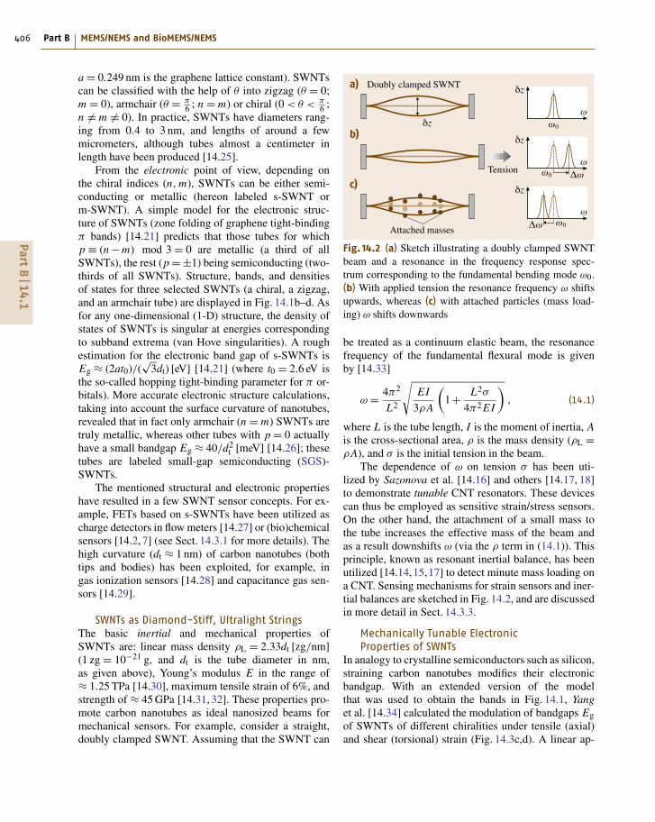
Fig. 14.2 (a) Sketch illustrating a doubly clamped SWNTbeam and a resonance in the frequency response spec-trum corresponding to the fundamental bending mode ω0.(b) With applied tension the resonance frequency ω shiftsupwards, whereas (c) with attached particles (mass load-ing) ω shifts downwards
be treated as a continuum elastic beam, the resonancefrequency of the fundamental flexural mode is givenby [14.33]
ω = 4π2
L2
√EI
3ρA
(1+ L2σ
4π2 EI
), (14.1)
where L is the tube length, I is the moment of inertia, Ais the cross-sectional area, ρ is the mass density (ρL =ρA), and σ is the initial tension in the beam.
The dependence of ω on tension σ has been uti-lized by Sazonova et al. [14.16] and others [14.17, 18]to demonstrate tunable CNT resonators. These devicescan thus be employed as sensitive strain/stress sensors.On the other hand, the attachment of a small mass tothe tube increases the effective mass of the beam andas a result downshifts ω (via the ρ term in (14.1)). Thisprinciple, known as resonant inertial balance, has beenutilized [14.14,15,17] to detect minute mass loading ona CNT. Sensing mechanisms for strain sensors and iner-tial balances are sketched in Fig. 14.2, and are discussedin more detail in Sect. 14.3.3.
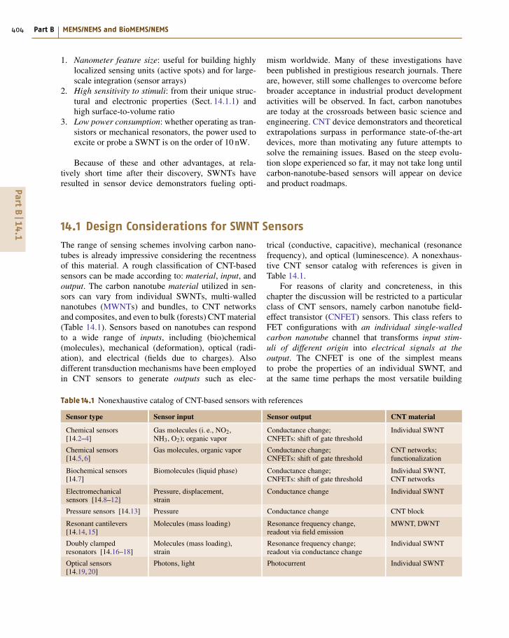
Mechanically Tunable ElectronicProperties of SWNTs
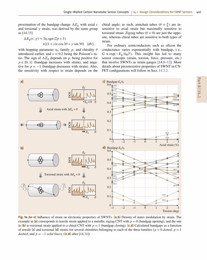
In analogy to crystalline semiconductors such as silicon,straining carbon nanotubes modifies their electronicbandgap. With an extended version of the modelthat was used to obtain the bands in Fig. 14.1, Yanget al. [14.34] calculated the modulation of bandgaps Egof SWNTs of different chiralities under tensile (axial)and shear (torsional) strain (Fig. 14.3c,d). A linear ap-
PartB
14.1
Single-Walled Carbon Nanotube Sensor Concepts 14.1 Design Considerations for SWNT Sensors 407
proximation of the bandgap change ΔEg with axial ε
and torsional γ strain, was derived by the same groupas [14.35]
ΔEg(ε, γ ) ≈ 3t0 sgn (2p+1)
× [(1+ν)ε cos 3θ +γ sin 3θ] [eV] ,
with hopping parameter t0, family p, and chirality θ
introduced earlier, and ν = 0.2 being the Poisson’s ra-tio. The sign of ΔEg depends on p, being positive forp ∈ {0, 1} (bandgap increases with strain), and nega-tive for p = −1 (bandgap decreases with strain). Also,the sensitivity with respect to strain depends on the
a)
–3
Axial strain with ΔEg > 0
DO
S
Eg
EF
E
DO
S
Eg = 0
EF
E
b)
Torsional strain with ΔEg < 0
DO
S
Eg
EF
E
DO
S
Eg
EF
E
–2
(8,0)
(8,0)
(7,2)
(7,2)
(9,1)
(9,1)
(6,4)
(6,4)
(8,3)
(8,3)
(8,2)
(8,1)
(8,1)
(5,4)
(5,4)
(6,5)
(6,5)
(10,0)
(10,0)
(5,5)
(8,2)
(5,5)
–1 0 1 2 3
c) Bandgap Eg/t0
Axial strain (%)
0.6
0.5
0.4
0.3
0.2
0.1
0
–3 –2 –1 0 1 2 3
d) Bandgap Eg/t0
Torsion (deg)
0.6
0.5
0.4
0.3
0.2
0.1
0
Fig. 14.3a–d Influence of strain on electronic properties of SWNTs. (a,b) Density of states modulation by strain. Theexample in (a) corresponds to tensile strain applied to a metallic zigzag CNT with p = 0 (bandgap opening), and the onein (b) to torsional strain applied to a chiral CNT with p = 1 (bandgap closing). (c,d) Calculated bandgaps as a functionof tensile (c) and torsional (d) strain, for several chiralities belonging to each of the three families (p = 0 dotted, p = 1dashed, and p = −1 solid lines). ((c,d) after [14.34])
chiral angle; as such, armchair tubes (θ = π6 ) are in-
sensitive to axial strain but maximally sensitive totorsional strain. Zigzag tubes (θ = 0) are just the oppo-site, whereas chiral tubes are sensitive to both types ofstrain.
For ordinary semiconductors such as silicon theconductance varies exponentially with bandgap, i. e.,G ∝ exp(−Eg/kBT ). This insight has led to manysensor concepts (strain, torsion, force, pressure, etc.)that involve SWNTs as strain gauges [14.8–12]. Moredetails about piezoresistive properties of SWNT in CN-FET configurations will follow in Sect. 14.3.2.
PartB
14.1
408 Part B MEMS/NEMS and BioMEMS/NEMS
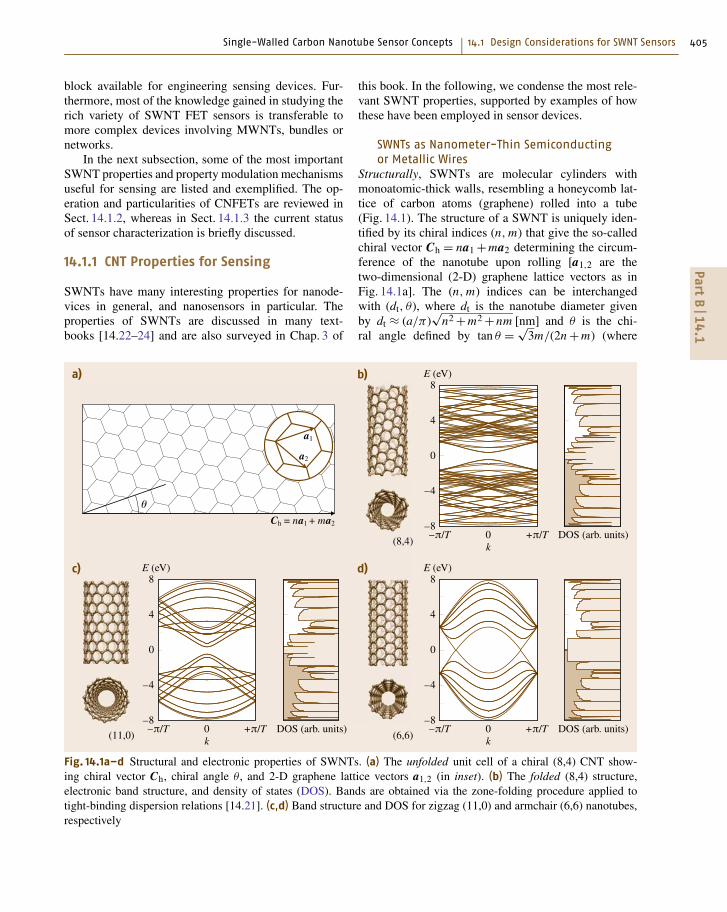
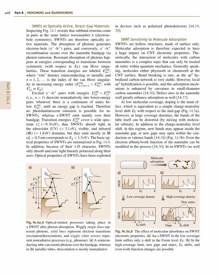
SWNTs as Optically Active, Direct-Gap MaterialsInspecting Fig. 14.1 reveals that subband extrema comein pairs at the same lattice wavenumber k (electron–hole symmetry). SWNTs are therefore optically ac-tive materials. The absorption of photons generateselectron–hole (e−–h+) pairs, and conversely, e−–h+recombination occurs over the nanotube bandgap viaphoton emission. Resonant absorption of photons hap-pens at energies corresponding to transitions betweensymmetric (with respect to EF) van Hove singu-larities. These transition energies are labeled Es/m
nn ,where “s/m” denotes semiconducting or metallic andn = 1, 2, . . . is the index of the van Hove singular-ity in increasing energy order (Es/m
n+1n+1 > Es/mnn , with
Es11 ≡ Eg).
Excited e−–h+ pairs with energies Es/mnn > Es/m
11(i. e., n > 1) deexcite nonradiatively into lower-energypairs whenever there is a continuum of states be-low Es/m
nn , until an energy gap is reached. Thereforeno photoluminescent emission is possible for m-SWNTs, whereas s-SWNT emit mainly over theirbandgap. Transition energies Es/m
nn cover a wide spec-trum (⊂ (−9, 9) eV), thus SWNTs absorb light inthe ultraviolet (UV) (> 3.1 eV), visible, and infrared(IR) (< 1.8 eV) domains, but they emit mostly in IR(dt > 0.5 nm corresponds to Eg < 1.5 eV). The basic op-tical properties of SWNTs are summarized in Fig. 14.4.In addition, because of their 1-D character, SWNTsonly absorb and emit light linearly polarized along theiraxes. Optical properties of SWNTs have been exploited
a) b)
EF
Em22
Em11
EF
E s33
E s22
E s11
Fig. 14.4a,b Optical-related processes taking place ina SWNT after photon absorption. Wiggly single lines rep-resent photons, solid lines represent electron transitions(excitation/deexcitation), and wiggly white arrows repre-sent nonradiative processes (e.g., phonons). (a) A semicon-ducting tube can reemit photons over the bandgap, whereasin (b) metallic tubes, deexcitation is mostly nonradiative
in devices such as polarized photodetectors [14.19,20].
SWNT Sensitivity to Molecule AdsorptionSWNTs are hollow structures, made of surface only.Molecular adsorption is therefore expected to havea huge impact on CNT electronic properties. The-oretically, the interaction of molecules with carbonnanotubes is a complex topic that can only be treatedab initio within quantum mechanics. Generally speak-ing, molecules either physisorb or chemisorb at theCNT surface. Bond breaking is rare, as the sp2 hy-bridized carbon network is very stable. However, localsp3 hybridization is possible, and this adsorption mech-anism is enhanced by curvature in small-diametercarbon nanotubes [14.36]. Defect sites in the nanotubewall greatly enhance adsorption as well [14.37].
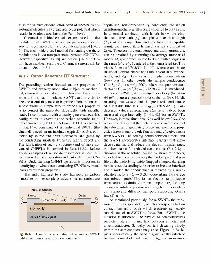
At low molecular coverage, doping is the main ef-fect, which is equivalent to a simple charge-neutralitylevel shift EF with respect to the mid-gap (Fig. 14.5a).However, at large coverage densities, the bands of thetube itself can be distorted (by mixing with molecu-lar orbitals). In addition to the charge-neutrality levelshift, in this regime, new bands may appear inside thenanotube gap, or new gaps may open within the con-duction or valence bands [14.38] (Fig. 14.5b). Even theelectron affinity/work function of the nanotube can bemodified in the process [14.36]. In m-SWNTs (as well
a) b)
High coverage density
New states
Gaps
Moleculeadsorption
DO
S
EF E
Low coverage density
EF E
DO
S
EF shiftE
EF shiftE
Fig. 14.5a,b The effect of molecular adsorbates on SWNTelectronic properties. (a) An s-SWNT in the low-coveragelimit suffers only a shift in the Fermi level EF. (b) In thehigh-coverage limit, new gaps and states, EF shifts, andeven work function changes are possible
PartB
14.1
Single-Walled Carbon Nanotube Sensor Concepts 14.1 Design Considerations for SWNT Sensors 409
as in the valence or conduction band of s-SWNTs) ad-sorbing molecules may create a disorder potential whichresults in bandgap opening at the Fermi level.
Chemical and biochemical sensors based on themodulation of SWNT electronic properties upon expo-sure to target molecules have been demonstrated [14.2,7]. The most widely used method for reading out thesemodulations is via transport measurements (CNFETs).However, capacitive [14.29] and optical [14.39] detec-tion have also been employed. Chemical sensors will betreated in Sect. 14.3.1.
14.1.2 Carbon Nanotube FET Structures
The preceding section focused on the properties ofSWNTs and property modulation subject to mechani-cal, chemical or optical stimuli. However, these prop-erties are intrinsic to isolated SWNTs, and in order tobecome useful they need to be probed from the macro-scopic world. A simple way to probe CNT propertiesis to contact the nanotube electrically with metallicleads. In combination with a nearby gate electrode thisconfiguration is known as the carbon nanotube field-effect transistor (CNFET). A basic CNFET is sketchedin Fig. 14.6, consisting of an individual SWNT (thechannel) placed on an insulator (typically SiO2), con-tacted by source and drain electrodes, and gated bythe conducting substrate (typically highly doped Si).The fabrication of such a structure (and of more ad-vanced CNFETs) is covered in Sect. 14.2.2. Beforegiving examples of sensor demonstrators in Sect. 14.3we review the basic operation and particularities of CN-FETs. Understanding CNFET operation is important inidentifying to what extent contacting SWNTs by metalleads affects their properties.
The right frameset to study transport in carbonnanotubes is mesoscopic physics, since nanotubes are
Metal electrodes
SWNT (channel)
DrainSource
SiO2 (oxide)
Doped Si (back gate)
VdVs
Vg
Fig. 14.6 Schematic representation of a simple SWNTfield-effect transistor in cross-sectional view
crystalline, low-defect-density conductors for whichquantum-mechanical effects are expected to play a role.In a general conductor with length below the elas-tic mean free path (e) and phase relaxation length(Lϕ), at low temperature and low bias (quasiequilib-rium), each mode (Bloch wave) carries a current of2e/h. Therefore, the total source and drain current Isd,can be obtained by summing the average number ofmodes M, going from source to drain, with energies inthe range (eVs, eVd) centered at the Fermi level EF. Thisyields Isd = (2e2/h)MVsd [14.40], where e and h arethe usual electron charge and Planck’s constant, respec-tively, and Vsd = Vs − Vd is the applied source–drain(low) bias. In other words, the sample conductanceG = Isd/Vsd is simply MG0, where the quantum con-ductance G0 = (2e2/h) = (1/12.9) kΩ−1 is introduced.
For a m-SWNT, at any energy close to EF (to within±1 eV), there are precisely two subbands (Fig. 14.1d),meaning that M = 2 and the predicted conductanceof a metallic tube is G = 2G0 (= 1/6.5 kΩ−1). Con-ductance values approaching 2G0 have indeed beenmeasured experimentally [14.41, 42] for m-SWNTs.However, in most situations, G is well below 2G0. Onereason for this is that the metallic leads used to contactthe tube differ in geometry, lattice, and electronic prop-erties (most notably work function and effective mass)from SWNTs. The heterojunction between a metal andthe SWNT incorporates interface barriers that intro-duce scattering and reduce the electron transfer rates.Another reason for reduced conductance G < 2G0 isdisorder in the nanotube, caused by structural defects,adsorbed molecules or simply the random potential pro-file of the underlying oxide (trapped charges, danglingbonds, etc.). Accordingly, in order to include interfaceand disorder, the conductance is reduced by a multi-plicative factor T (G → T 2G0), describing the averagetransmission probability for an electron to propagatefrom source to drain. At room temperature, for longenough nanotubes, phonon scattering leads to incoher-ent, classically diffusive transport, respecting Ohm’slaw (T ∝ 1
L ).As mentioned previously, for m-SWNTs the trans-
mission T can approach 1, which corresponds to thincontact barriers through which electrons can easilytunnel, and clean SWNT surfaces. For s-SWNTs, thesituation is different. The physics of heterostructurespredicts that, at the interface between a metal anda semiconductor, Schottky barriers decaying slowlywithin the semiconductor may arise. Figure 14.7a de-picts schematically the band diagram at the interfacebetween a metal of work function φm, and an intrinsic
PartB
14.1
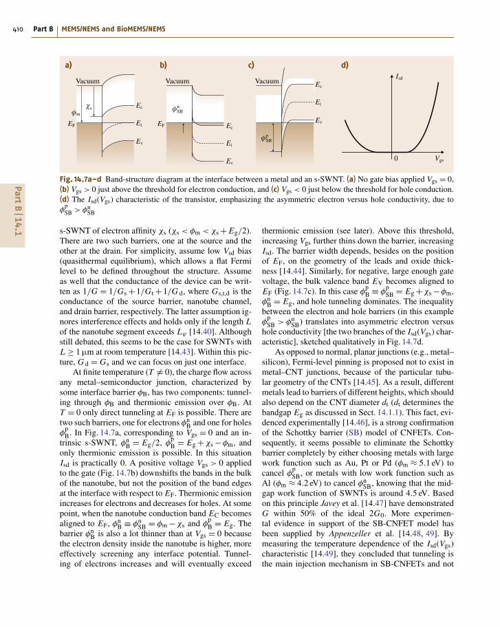
410 Part B MEMS/NEMS and BioMEMS/NEMS
a) b) c) d)
Vacuum
EF
Ecφm
�s
Ei
Ev
Vacuum
EF Ec
φnSB
φpSBEi
Ev
Vacuum
0
Ec
Isd
Vgs
Ei
Ev
Fig. 14.7a–d Band-structure diagram at the interface between a metal and an s-SWNT. (a) No gate bias applied Vgs = 0,(b) Vgs > 0 just above the threshold for electron conduction, and (c) Vgs < 0 just below the threshold for hole conduction.(d) The Isd(Vgs) characteristic of the transistor, emphasizing the asymmetric electron versus hole conductivity, due toφ
pSB > φn
SB
s-SWNT of electron affinity χs (χs < φm < χs + Eg/2).There are two such barriers, one at the source and theother at the drain. For simplicity, assume low Vsd bias(quasithermal equilibrium), which allows a flat Fermilevel to be defined throughout the structure. Assumeas well that the conductance of the device can be writ-ten as 1/G = 1/Gs +1/G t +1/G d, where Gs,t,d is theconductance of the source barrier, nanotube channel,and drain barrier, respectively. The latter assumption ig-nores interference effects and holds only if the length Lof the nanotube segment exceeds Lϕ [14.40]. Althoughstill debated, this seems to be the case for SWNTs withL ≥ 1 μm at room temperature [14.43]. Within this pic-ture, G d = Gs and we can focus on just one interface.
At finite temperature (T �= 0), the charge flow acrossany metal–semiconductor junction, characterized bysome interface barrier φB, has two components: tunnel-ing through φB and thermionic emission over φB. AtT = 0 only direct tunneling at EF is possible. There aretwo such barriers, one for electrons φn
B and one for holesφ
pB. In Fig. 14.7a, corresponding to Vgs = 0 and an in-
trinsic s-SWNT, φnB = Eg/2, φ
pB = Eg +χs −φm, and
only thermionic emission is possible. In this situationIsd is practically 0. A positive voltage Vgs > 0 appliedto the gate (Fig. 14.7b) downshifts the bands in the bulkof the nanotube, but not the position of the band edgesat the interface with respect to EF. Thermionic emissionincreases for electrons and decreases for holes. At somepoint, when the nanotube conduction band EC becomesaligned to EF, φn
B ≡ φnSB = φm −χs and φ
pB = Eg. The
barrier φnB is also a lot thinner than at Vgs = 0 because
the electron density inside the nanotube is higher, moreeffectively screening any interface potential. Tunnel-ing of electrons increases and will eventually exceed
thermionic emission (see later). Above this threshold,increasing Vgs further thins down the barrier, increasingIsd. The barrier width depends, besides on the positionof EF, on the geometry of the leads and oxide thick-ness [14.44]. Similarly, for negative, large enough gatevoltage, the bulk valence band EV becomes aligned toEF (Fig. 14.7c). In this case φ
pB ≡ φ
pSB = Eg +χs −φm,
φnB = Eg, and hole tunneling dominates. The inequality
between the electron and hole barriers (in this exampleφ
pSB > φn
SB) translates into asymmetric electron versushole conductivity [the two branches of the Isd(Vgs) char-acteristic], sketched qualitatively in Fig. 14.7d.
As opposed to normal, planar junctions (e.g., metal–silicon), Fermi-level pinning is proposed not to exist inmetal–CNT junctions, because of the particular tubu-lar geometry of the CNTs [14.45]. As a result, differentmetals lead to barriers of different heights, which shouldalso depend on the CNT diameter dt (dt determines thebandgap Eg as discussed in Sect. 14.1.1). This fact, evi-denced experimentally [14.46], is a strong confirmationof the Schottky barrier (SB) model of CNFETs. Con-sequently, it seems possible to eliminate the Schottkybarrier completely by either choosing metals with largework function such as Au, Pt or Pd (φm ≈ 5.1 eV) tocancel φ
pSB, or metals with low work function such as
Al (φm ≈ 4.2 eV) to cancel φnSB, knowing that the mid-
gap work function of SWNTs is around 4.5 eV. Basedon this principle Javey et al. [14.47] have demonstratedG within 50% of the ideal 2G0. More experimen-tal evidence in support of the SB-CNFET model hasbeen supplied by Appenzeller et al. [14.48, 49]. Bymeasuring the temperature dependence of the Isd(Vgs)characteristic [14.49], they concluded that tunneling isthe main injection mechanism in SB-CNFETs and not
PartB
14.1
Single-Walled Carbon Nanotube Sensor Concepts 14.1 Design Considerations for SWNT Sensors 411
thermionic emission. However, the work function aloneis not enough, as for example Pt (φm ≈ 5.6 eV) yieldspoor contacts, likely due to poor wetting or native-oxidetunnel barriers [14.50].
For certain CNFET sensor devices, the Schottkybarrier FET model is essential in understanding the de-vice operation and sensing mechanism. This is the caseof (bio)chemical sensors to be discussed in Sect. 14.3.1.In other devices, Schottky barriers, if present at all, con-tribute only to the contact resistance, which to a firstapproximation is constant during the sensing process,and can be thus factored out from the sensing mech-anism. This is the case with piezoresistive gauges andresonators as presented in Sects. 14.3.2 and 14.3.3,respectively. For these devices, the transport picture in-troduced in this section, in terms of thermionic emissionand tunneling, is still useful for explaining their opera-tion. The only difference is that potential barriers forelectrons and holes will be found on the nanotube andnot only at the interface (Fig. 14.14c,d). Further insightinto the physics of CNFETs in different regimes (large-bias, low-temperature phenomena such as Luttingerliquid, Coulomb blockade or orbital Kondo effects, etc.)have also been described [14.51–53].
14.1.3 Sensor Characterization
Sensor characterization refers to assessing the perfor-mance metrics for a certain sensing technology. Someof the most important performance metrics are sen-sitivity, signal-to-noise ratio (SNR), limit-of-detection(LoD), cross-sensitivity/selectivity, signal rise/fall time(speed), repeatability, offset/sensitivity, drift, hysteresis,and lifetime/robustness. So far, mainly sensitivity anddynamic properties, e.g., signal rise/fall time, have beentargeted by the CNT sensor community (Sect. 14.3).This is a natural situation, considering that the tech-nology for fabricating individual SWNT FETs is notyet scalable (Sect. 14.2). Efforts have then been focusedon demonstrating that CNT nanosensors are superior toexisting devices, to motivate and justify future invest-ment. On the other hand, the lack of batch fabricationprocesses has hindered gathering statistical informationabout the characteristics of CNT sensors in operation;most publications on individual SWNT sensors (in par-ticular FET devices) refer to data obtained from justa few fabricated samples. Therefore the reproducibilityof sensor characteristics has been ignored, or marginallyaddressed.
To better illustrate matters, consider the story ofchemical CNFET sensors. In 2000 Kong et al. [14.2]
first reported detection of NO2 and NH3 with individualSWNT FETs. In 2008 Cho et al. (in collaboration withKong) published the first results for a hybrid CNT chem-ical sensor with a CMOS interface chip [14.54]. Thefabrication of CNT sensor arrays is still far from scal-able, yet by this approach the interface captures signalsfrom up to 24 CNFETs in parallel, further multiplexedand sent to analysis. The authors manage to measure414 devices, which results in a histogram of the distribu-tion of resistance, spread over six orders of magnitude.This large dispersion is the result of varying numberand type of CNTs in the devices, which is not con-trolled during fabrication. Dispersion is also visible inthe recorded sensor response on the measurand. Thiskind of platform is a first step towards capturing deviceperformance statistics, a prerequisite for process controland optimization.
Acquiring sensor signal-to-noise ratio is currently inprogress. Electronic noise in CNFETs has received a lotof attention lately. Collins et al. [14.55] were the firstto measure 1/ f noise in SWNTs, both individual tubesand mats. The noise spectrum was found to agree withthe classical noise power formula SV( f ) = (A/ f β)V 2,where A is the noise amplitude, f is the frequency,β ≈ 1, and V is the bias voltage. Furthermore, thenoise amplitude seems to obey the empirical Hoogelaw A = αH/N , where αH is the Hooge constant andN is the number of carriers in the channel, becauseon average A decreases with the number of tubes inthe sample [14.55]. Interestingly, the SV( f ) formulais expected to hold for classically diffusive transport,which is questionable for CNFETs. However, Appen-zeller et al. [14.56] have calculated the average numberof carriers inside SWNT ballistic FETs, for differentcontact metals, and found the Hooge law to be valideven in this regime, with a fitted αH value of ≈ 2 × 10⁻³
(the same as for bulk silicon). Upon closer examina-tion, it has been observed by Tersoff [14.57] that theHooge law is not accurate in the subthreshold regionof a CNFET. He proposed adding a phenomenologicalterm to the noise power, proportional to (dIsd/dVgs)2,to account for gating of the CNFET by fluctuatingcharges in the vicinity of the tube. This model has re-cently been confirmed experimentally [14.58]. Overall,regardless of the model utilized, the noise in CNFETsis found to be significant, which limits the SNR ofCNT sensors. The fact that noise is proposed to bemainly extrinsic [14.56], i. e., caused by external fluc-tuations, is however encouraging since it sets cleartechnical objectives in achieving better control of theCNT environment.
PartB
14.1
412 Part B MEMS/NEMS and BioMEMS/NEMS
14.2 Fabrication of SWNT Sensors
Fabrication of CNT devices involves many different as-pects that can be grouped into two main tasks, namelysynthesis of SWNTs and assembly of nanotubes intodevices. Synthesis is concerned with the productionof SWNTs with controlled properties such as diam-eter, chirality, length, and defect densities. Sometimessynthesis is followed by postsynthesis methods forCNT purification, sorting, and most importantly func-tionalization. On the other hand, assembly refers totechniques and methods for placing SWNTs at prede-fined locations on a substrate with controlled numberof nanotubes, orientation, and slack (straightness). Postassembly, other processing steps such as nanotube elec-trical contacting or device encapsulation may follow.The development of complete processes for the fabrica-tion of micro- and nanosystems that integrate nanotubedevices/sensors with acceptable yield is currently one ofthe key topics in CNT research. This section attemptsto survey some of the available methods and processesaimed at controlled diameter, chirality, location, andorientation.
As discussed in Sect. 14.1, most of the intrinsicproperties and property modulations of SWNTs dependon their diameter dt. For example, the bandgap Eg ofan s-SWNT is inversely proportional to dt, as are theSchottky barriers φ
n/pSB in CNFETs (Sect. 14.1.2). Other
properties, most notably piezoresistance, depend as wellon chirality θ. Since dt and θ of a SWNT are definedduring synthesis (production), methods for nanotubeproduction are briefly surveyed in Sect. 14.2.1. Locationand orientation control during assembly are importantfor building complex structures, for developing batchfabrication processes, and for large-scale device inte-gration (sensor arrays). Section 14.2.2 will thus reviewprocesses for the assembly of SWNTs into devices,together with some general strategies for achieving lo-cation and orientation control.
14.2.1 Methods for SWNT Production
Carbon nanotube production methods can be classi-fied into two categories, namely high temperature (arcdischarge and laser ablation; T = 1200–3000 ◦C) andmedium temperature (catalytic chemical vapor depo-sition, CCVD; T = 400–1100 ◦C). Details about eachmethod can be obtained from textbooks [14.22, 24] andalso Chap. 3 of this book. Here, only those aspectswhich are relevant for CNT devices and integration arediscussed.
Because of higher production temperature (poten-tial defect annealing), arc discharge and laser ablationare believed to produce better crystalline SWNTs. How-ever, with these methods it is not possible to produceSWNTs directly on the target substrate for devicefabrication; only postsynthesis assembly is possible.Typically as-produced nanotubes are first dispersed ina liquid that can be subsequently utilized to depositSWNTs on the target substrate (Sect. 14.2.2). Also, thedistribution of diameters is difficult to control with thesemethods during SWNT production. Nevertheless, af-ter dispersing nanotubes in liquid, different techniquescan be employed to separate (semiconducting frommetallic) and sort (by diameter) CNTs, as explainedbelow.
In catalytic chemical vapor deposition, SWNTsare synthesized from metallic catalyst particles froma carbon-containing gas feedstock. Since CCVD isa catalytic process, patterning of a catalyst-containinglayer can be utilized to grow nanotubes at selectedlocations directly on preprocessed silicon chips (seeSect. 14.2.2 for more details). The key observation forCCVD is that the size of the catalyst particle correlateswith the SWNT diameter [14.59], and the catalyst par-ticle density determines the final CNT density [14.60].In [14.59] Cheung et al. prepared Fe nanoparticles,with narrow diameter distributions centered around 3,9, and 13 nm, on SiO2. The grown CNT diameterdistribution mirrors the initial particle size distribu-tion, with a standard deviation of roughly 30% ofthe average. However, 3 nm particles produce SWNTswith double-walled CNTs (DWNT), 9 nm particles pro-duce D/MWNT with just a few SWNTs, and 13 nmparticles produce only MWNTs, showing that a par-ticle size < 3 nm is required for CCVD synthesis ofSWNTs. For SWNT-based FETs, a good compromisebetween low contact resistance (low φ
n/pSB ) and large
gap Eg (large on/off ratio) would correspond to diam-eters in the range 1.5–2 nm [14.46]. Obtaining suchsmall catalyst nanoparticles, while keeping a narrowsize distribution, is challenging. Li et al. [14.61] havedemonstrated SWNT diameter distributions of either(1.5±0.4) nm or (3.0±0.9) nm (again standard devi-ation/average ≈ 30%). Their method involved loadingthe hollow cavity of the iron-storage protein ferritin(internal cavity diameter 8 nm) with Fe, followed by de-position on a substrate and calcination of the proteinshell. Particle size was controlled by the iron loadingtime.
PartB
14.2
Single-Walled Carbon Nanotube Sensor Concepts 14.2 Fabrication of SWNT Sensors 413
Currently, much activity is going into trying toachieve SWNTs with acceptable diameter distributions.For CCVD-grown tubes, the most promising approachseems to remain improving particle size distribution.Post synthesis, for SWNT dispersed in solution, re-gardless of their origin (arc discharge, laser ablationor CCVD), several methods have been proposed tonarrow down the diameter distribution. For exam-ple, Tromp et al. [14.62] have recently demonstrateddiameter separation of SWNTs by noncovalent func-tionalization with anchor molecules optimally attachingto specific tube diameters (1.2 nm). This functionaliza-tion improves solubility of the selected tubes, whichare subsequently separated from the insoluble bulk viasonication and centrifugation. By using DNA wrappingand density gradient ultracentrifugation (DGU), Arnoldet al. [14.63] have shown good separation by diameter,for SWNTs with diameters below 1 nm. Soon after-wards, the same group [14.64] extended the techniqueto surfactants, and managed to isolate narrow distribu-tions of SWNTs with > 97% within a 0.02 nm-diameterrange, with, e.g., 84% of the tubes being of (6,5) chiralindices. Furthermore, by using mixtures of surfactants,they were able to produce predominantly semiconduct-ing or metallic SWNTs. Combined with the recentlyproposed continued growth [14.65] the DGU methodmight one day achieve macroquantities of essentiallysingle-chirality SWNTs. However, to date, achievingSWNTs with a single chirality remains the key chal-lenge in CNT production.
14.2.2 Strategies for SWNT Assemblyinto Devices
Perhaps the simplest way to survey SWNT assemblystrategies is to split the discussion into two parts by con-sidering the nanotube source: liquid suspension (laser,arc or CCVD SWNTs dispersed in liquid) or in situgrowth (CCVD SWNTs grown directly on the targetsubstrate). In-depth reviews of the various assemblystrategies can be found elsewhere [14.66, 67]. Here,we focus only on those techniques resulting directly inCNFET device structures or that have some relevanceto this topic. Regarding liquid suspension or in situgrowth, there is an ongoing debate as to which oneproduces best results. Table 14.2 compares the two inseveral aspects, showing a good balance of advantagesand disadvantages. In general, fluid-dispersed tubes of-fer better SWNTs (because of laser or arc productionand separation techniques), but assembly is more com-plex than for in situ growth.
Liquid Suspension Assembly MethodsHistorically liquid suspension assembly methods werethe first to appear. The very first CNFETs, demonstratedin 1998 [14.68,69], were built through a similar, simpleprocess. In [14.69] laser-ablation SWNTs were dis-persed by sonication in dichloroethane and then spreadover Au electrodes predefined using electron-beamlithography (EBL) on a doped Si wafer substrate cov-ered by a thick gate oxide film (SiO2). The Si substrateserved as a back gate to all devices. A schematic cross-
Table 14.2 A comparison between liquid suspension andin situ growth assembly methods
SWNT source Liquid In sitususpensiona growthb
CNT qualityc + +/− d
Average diameter controle − f + g
Diameter standard deviationh + −Chirality controli − −FET performancej − k +Alignment precision −/+ l +Ease of integration +/− m + n
a CNTs as produced by arc discharge or laser ablationb In situ growth mainly by CCVD (Sect. 14.2.1)c SWNT quality is attributed to crystallinity and defect density:Arc discharge or laser ablation SWNTs are still considered toproduce better CNTs (Sect. 14.2.1)d Progress in CCVD leads to constant increase in CNT quality.Measures include post annealing, H2 treatmente Average SWNT diameters determine Schottky barrier heightsin CNFETs (Sect. 14.1.2)f The average diameter of arc discharge and laser ablationSWNTs is between 1.2 and 1.5 nm and is difficult to controlg The average diameter of SWNTs correlates with catalyst par-ticle size and growth conditions and can be tuned (Sect. 14.2.1)h A small diameter standard deviation should reduce perfor-mance variations in CNFET sensor devicesi Functionalization of SWNTs, sonication and centrifugationpost synthesis narrows diameter distribution. Individual chiral-ities may be selected (Sect. 14.2.1). Only applicable to SWNTsassembled from liquid suspensionj FET performance for sensing applications refers to low con-tact resistance, low noise, and high on/off ratiok Liquid suspension involves CNT surface treatment by(strongly binding) surfactants, sonication, and centrifugation.These steps may degrade the CNFET performancel Localized surface functionalization and dielectrophoresisincreases the alignment precision. However, bundling of indi-vidual CNTs is still an issue in these processesm Wet processing is more compatible with CMOS integratedcircuit (IC) substrates, but wet processing may influence theSWNTs’ electronic propertiesn In situ growth is compatible with MEMS substrates in-cluding suspended MEMS and nanoelectromechanical systems(NEMS) structures
PartB
14.2
414 Part B MEMS/NEMS and BioMEMS/NEMS
2
Pt
Si back gate
Pt
PtPt
CA B
PtSiO2
SiO2
SiO2
3
200 nm
1
a)
b)
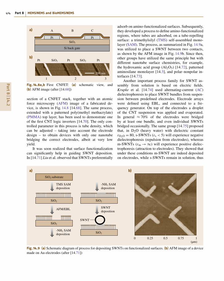
Fig. 14.8a,b First CNFET: (a) schematic view, and(b) AFM image (after [14.68])
section of a CNFET stack, together with an atomicforce microscopy (AFM) image of a fabricated de-vice, is shown in Fig. 14.8 [14.68]. The same process,extended with a patterned poly(methyl methacrylate)(PMMA) top layer, has been used to demonstrate oneof the first CNT logic inverters [14.70]. The only con-trolled parameter in this process is tube density, whichcan be adjusted – taking into account the electrodedesign – to obtain devices with only one nanotubebridging the correct electrodes, albeit at very lowyield.
It was soon realized that surface functionalizationcan significantly help in guiding SWNT deposition.In [14.71] Liu et al. observed that SWNTs preferentially
a) b)
TMS SAMdeposition
0 0.25 0.5 0.75 1(µm)
SiO2 substrate
AFM/EBL
SiO2
-NH2 SAMdeposition
SiO2
SWNTdeposition
SWNT
SiO2
-NH2 SAMdeposition
SiO2
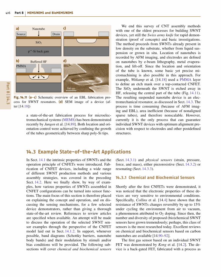
Fig. 14.9 (a) Schematic diagram of process for depositing SWNTs on functionalized surfaces. (b) AFM image of a devicemade on Au electrodes (after [14.71])
adsorb on amino-functionalized surfaces. Subsequently,they developed a process to define amino-functionalizedregions, where tubes are adsorbed, on a tube-repellingsurface: a trimethylsilyl (TMS) self-assembled mono-layer (SAM). The process, as summarized in Fig. 14.9a,was utilized to place a SWNT between two contacts,as shown by the AFM image in Fig. 14.9b. Since then,other groups have utilized the same principle but withdifferent nanotube surface chemistries, for example,the hydroxamic acid group (Al2O3) [14.72], patternedaminosilane monolayer [14.3], and polar–nonpolar in-terfaces [14.73].
Another important process family for SWNT as-sembly from solution is based on electric fields.Krupke et al. [14.74] used alternating-current (AC)dielectrophoresis to place SWNT bundles from suspen-sion between predefined electrodes. Electrode arrayswere defined using EBL, and connected to a fre-quency generator. On top of the electrodes a dropletof the CNT suspension was applied and evaporated.In general ≈ 70% of the electrodes were bridgedby at least one bundle, and even individual SWNTsbridged occasionally. The same group [14.75] proposedthat, in D2O (heavy water) with dielectric constantεD2O = 80, s-SWNTs (εs < 5) will experience negativedielectrophoresis (repulsion from electrodes), whereasm-SWNTs (εm → ∞) will experience positive dielec-trophoresis (attraction to electrodes). They showed thatunder these conditions m-SWNT are indeed depositedon electrodes, while s-SWNTs remain in solution, thus
PartB
14.2

Single-Walled Carbon Nanotube Sensor Concepts 14.2 Fabrication of SWNT Sensors 415
providing a basic method to separate metallic fromsemiconducting tubes.
In Situ Growth Assembly MethodsThe second major class of assembly methods is basedon in situ growth (via CCVD) of SWNTs directlyonto silicon chips/wafers. CCVD has one major ad-vantage over liquid suspension deposition regardinglocation control, namely that the catalyst can be pat-terned [14.77]. A first process for fabricating CNFETsusing CCVD has been proposed by Soh et al. [14.78].EBL was first used to pattern wells, into which cata-lyst was deposited. A resist lift-off left isolated catalystislands, from which SWNTs were grown by CCVD.Metal electrodes are defined on top of the catalyst is-lands by EBL, contacting some of the grown tubes.The location of tubes is thus approximately controlled,but not the orientation nor the number of nanotubesbetween two electrodes, although by changing the cat-alyst particle density and tuning the growth parametersthe yield can be improved. Nevertheless, considerableprogress has been made lately in catalyst depositionand patterning. Javey and Dai [14.79] have developeda method that allows positioning of individual catalystparticles with EBL resolution. Furthermore tube-to-particle number ratio approaching 1/1, i. e., close to100% SWNT growth yield, was achieved.
Since nanotube location control can be achievedby catalyst patterning, a lot of work has focused sub-sequently on orienting CCVD growth. Field-directedgrowth has been pioneered by Zhang et al. [14.76], ex-ploiting the large anisotropic polarizability of SWNTs.Elevated polysilicon structures were first defined ontoa quartz substrate by optical lithography, with a cat-
a) b) c)Poly-Si
Poly-Si Catalyst
Carbon nanotube
5 µm 10 µm
Quartz
Quartz
Quartz
Electrode
Fig. 14.10 (a) Schematic diagram of the process flow for electric-field-directed growth of SWNTs. (b,c) SEM imagesof SWNTs, grown in various fields. At zero field, tubes grow randomly (b), whereas alignment is seen in 0.5 V/μm(c) (after [14.76])
alyst layer on top, transferred by contact printing.Electric fields were applied during growth via outerpoly-Si pads contacted by metal leads (electrodes). Fig-ure 14.10 shows both the process flow and growthresults, with and without applied fields. Field-directedgrowth was subsequently demonstrated on flat sur-faces as well [14.80], and catalyst patterning andfield-directed growth have been combined to build CN-FETs by Dittmer et al. [14.81]. Another approachfor orienting CNT growth was proposed in [14.82],where a strong correlation between nanotube orienta-tion and feedstock gas flow direction was observed.Finally, numerous recent studies show that surface-directed growth is also possible on substrates such asA- and R-planes of sapphire [14.83] or miscut C-planesapphire [14.84]. The oriented SWNTs on sapphirehave been contacted into FET configurations by Liuet al. [14.85].
As discussed in Sect. 14.1.1, SWNTs have interest-ing electromechanical properties, which often requirefree-standing (suspended) nanotube segments in orderto manifest. Assembly of SWNTs into suspended mi-crostructures tends to be easier with in situ growththan liquid suspension, because of complications aris-ing from capillary forces. Directed growth of SWNTsfrom predefined silicon towers was first shown by Cas-sell et al. [14.86, 87], via a process that preceded thefield-directed growth shown in Fig. 14.10. Basic elec-tromechanical structures were presented later by thesame group, with a process involving patterned CCVDgrowth directly from the surface of Mo, a refrac-tory metal capable of withstanding CCVD temperatures(≈ 900 ◦C) [14.88] and inhibiting catalyst particle dif-fusion. Integration of CCVD nanotube growth into
PartB
14.2
416 Part B MEMS/NEMS and BioMEMS/NEMS
a)
b)
c)
d)
SiO2
p++-Si back gate
Source
PMMA
Drain
Nanotube
Buffered HF
500 nm
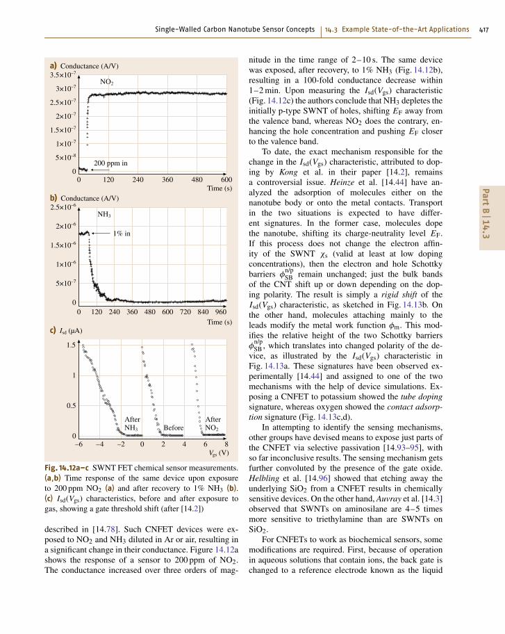
Fig. 14.11 (a–c) Schematic overview of an EBL fabrication pro-cess for SWNT resonators. (d) SEM image of a device (af-ter [14.18])
a state-of-the-art fabrication process for microelec-tromechanical systems (MEMS) has been demonstratedrecently by Jungen et al. [14.89]. Both location and ori-entation control were achieved by confining the growthof the tubes geometrically between sharp poly-Si tips.
We end this survey of CNT assembly methodswith one of the oldest processes for building SWNTdevices, yet still the Swiss army knife for rapid demon-stration (proof of concepts) and basic investigations.The method proceeds from SWNTs already present inlow density on the substrate, whether from liquid sus-pension or grown in situ. Location of nanotubes isrecorded by AFM imaging, and electrodes are definedon nanotubes by e-beam lithography, metal evapora-tion, and lift-off. Since the location and orientationof the tube is known, some basic yet precise mi-cromachining is also possible in this approach. Forexample, Witkamp et al. [14.18] used a PMMA layerto define an etch mask over a top-contacted CNFET.The SiO2 underneath the SWNT is etched away inHF, releasing the central part of the tube (Fig. 14.11).The resulting suspended nanotube device is an elec-tromechanical resonator, as discussed in Sect. 14.3. Theprocess is time consuming (because of AFM imag-ing and EBL), area inefficient (because of nonalignedsparse tubes), and therefore nonscalable. However,currently it is the only process that can guaranteeindividual SWNT devices with optimum alignment pre-cision with respect to electrodes and other postdefinedstructures.
14.3 Example State-of-the-Art Applications
In Sect. 14.1 the intrinsic properties of SWNTs and theoperation principle of CNFETs were introduced. Fab-rication of CNFET devices, including a wide rangeof different SWNT production methods and variousassembly strategies, was covered in the precedingSect. 14.2. Here we finally show, by way of exam-ples, how various properties of SWNTs assembled inCNFET configurations can be turned into sensor func-tions. The main focus of this section is therefore placedon explaining the concept and operation, and on dis-cussing the sensing mechanisms, for a few selecteddevice demonstrators, rather than giving a thoroughstate-of-the-art review. References to review articlesare specified when available. An attempt will be madeto discuss the operation of the selected SWNT sen-sor examples through the perspective of the CNFETmodel laid out in Sect. 14.1.2. In support, wheneverpossible, band diagrams (Schottky barriers, nanotubebody bands) and their modulation by stimuli and/orbias conditions will be provided. The following sub-sections will cover chemical and biochemical sensors
(Sect. 14.3.1) and physical sensors (strain, pressure,force, and mass), either piezoresistive (Sect. 14.3.2) orresonating (Sect. 14.3.3).
14.3.1 Chemical and Biochemical Sensors
Shortly after the first CNFETs were demonstrated, itwas noticed that the electronic properties of these de-vices are very sensitive to environmental conditions.Specifically, Collins et al. [14.4] have shown that theresistance of SWNTs changes reversibly by up to 15%under cycling the environment from air to vacuum,a phenomenon attributed to O2 doping. Since then, thenumber and diversity of proposed (bio)chemical SWNTsensors have grown tremendously; perhaps, this class ofsensors is the most researched today. Excellent reviewson chemical and biochemical sensors based on carbonnanotubes are available [14.90–92].
The first gas sensor based on an individual SWNTFET was demonstrated by Kong et al. [14.2]. The de-vice is a back-gated FET, fabricated with a process as
PartB
14.3
Single-Walled Carbon Nanotube Sensor Concepts 14.3 Example State-of-the-Art Applications 417
0
200 ppm in
NO2
120 240 360 480 600
a) Conductance (A/V)
Time (s)
3.5×10⁻⁷
3×10⁻⁷
2.5×10⁻⁷
2×10⁻⁷
1.5×10⁻⁷
1×10⁻⁷
5×10⁻⁸
0
0 120 240 360 480 600 720 840 960
1% in
NH3
b) Conductance (A/V)
Time (s)
2.5×10⁻⁶
2×10⁻⁶
1.5×10⁻⁶
1×10⁻⁶
5×10⁻⁷
0
–6 –4 –2 0 2 4 6
AfterNH3 Before
AfterNO2
8
c) Isd (µA)
Vgs (V)
1.5
1
0.5
0
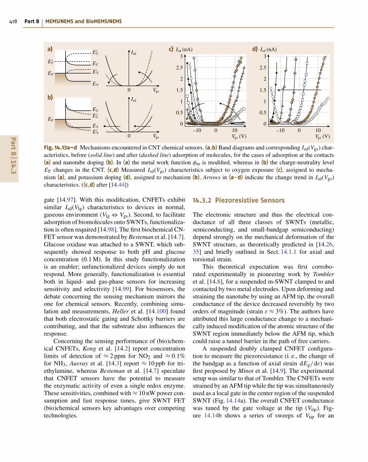
Fig. 14.12a–c SWNT FET chemical sensor measurements.(a,b) Time response of the same device upon exposureto 200 ppm NO2 (a) and after recovery to 1% NH3 (b).(c) Isd(Vgs) characteristics, before and after exposure togas, showing a gate threshold shift (after [14.2])
described in [14.78]. Such CNFET devices were ex-posed to NO2 and NH3 diluted in Ar or air, resulting ina significant change in their conductance. Figure 14.12ashows the response of a sensor to 200 ppm of NO2.The conductance increased over three orders of mag-
nitude in the time range of 2–10 s. The same devicewas exposed, after recovery, to 1% NH3 (Fig. 14.12b),resulting in a 100-fold conductance decrease within1–2 min. Upon measuring the Isd(Vgs) characteristic(Fig. 14.12c) the authors conclude that NH3 depletes theinitially p-type SWNT of holes, shifting EF away fromthe valence band, whereas NO2 does the contrary, en-hancing the hole concentration and pushing EF closerto the valence band.
To date, the exact mechanism responsible for thechange in the Isd(Vgs) characteristic, attributed to dop-ing by Kong et al. in their paper [14.2], remainsa controversial issue. Heinze et al. [14.44] have an-alyzed the adsorption of molecules either on thenanotube body or onto the metal contacts. Transportin the two situations is expected to have differ-ent signatures. In the former case, molecules dopethe nanotube, shifting its charge-neutrality level EF.If this process does not change the electron affin-ity of the SWNT χs (valid at least at low dopingconcentrations), then the electron and hole Schottkybarriers φ
n/pSB remain unchanged; just the bulk bands
of the CNT shift up or down depending on the dop-ing polarity. The result is simply a rigid shift of theIsd(Vgs) characteristic, as sketched in Fig. 14.13b. Onthe other hand, molecules attaching mainly to theleads modify the metal work function φm. This mod-ifies the relative height of the two Schottky barriersφ
n/pSB , which translates into changed polarity of the de-
vice, as illustrated by the Isd(Vgs) characteristic inFig. 14.13a. These signatures have been observed ex-perimentally [14.44] and assigned to one of the twomechanisms with the help of device simulations. Ex-posing a CNFET to potassium showed the tube dopingsignature, whereas oxygen showed the contact adsorp-tion signature (Fig. 14.13c,d).
In attempting to identify the sensing mechanisms,other groups have devised means to expose just parts ofthe CNFET via selective passivation [14.93–95], withso far inconclusive results. The sensing mechanism getsfurther convoluted by the presence of the gate oxide.Helbling et al. [14.96] showed that etching away theunderlying SiO2 from a CNFET results in chemicallysensitive devices. On the other hand, Auvray et al. [14.3]observed that SWNTs on aminosilane are 4–5 timesmore sensitive to triethylamine than are SWNTs onSiO2.
For CNFETs to work as biochemical sensors, somemodifications are required. First, because of operationin aqueous solutions that contain ions, the back gate ischanged to a reference electrode known as the liquid
PartB
14.3
418 Part B MEMS/NEMS and BioMEMS/NEMS
–10 0 10
0
E'F
EF
EC
EV
E'C
E'V
Vgs (V)
Vgs
3
2.5
2
1.5
1
0.5
0–10 0 10
Vgs (V)
3
2.5
2
1.5
1
0.5
0
c) Isd (nA) d) Isd (nA)a)
b)
Isd
0
EF
EC
EV
E'C
E'VVgs
Isd
Fig. 14.13a–d Mechanisms encountered in CNT chemical sensors. (a,b) Band diagrams and corresponding Isd(Vgs) char-acteristics, before (solid line) and after (dashed line) adsorption of molecules, for the cases of adsorption at the contacts(a) and nanotube doping (b). In (a) the metal work function φm is modified, whereas in (b) the charge-neutrality levelEF changes in the CNT. (c,d) Measured Isd(Vgs) characteristics subject to oxygen exposure (c), assigned to mecha-nism (a), and potassium doping (d), assigned to mechanism (b). Arrows in (a–d) indicate the change trend in Isd(Vgs)characteristics. ((c,d) after [14.44])
gate [14.97]. With this modification, CNFETs exhibitsimilar Isd(Vlg) characteristics to devices in normal,gaseous environment (Vlg ⇔ Vgs). Second, to facilitateadsorption of biomolecules onto SWNTs, functionaliza-tion is often required [14.98]. The first biochemical CN-FET sensor was demonstrated by Besteman et al. [14.7].Glucose oxidase was attached to a SWNT, which sub-sequently showed response to both pH and glucoseconcentration (0.1 M). In this study functionalizationis an enabler; unfunctionalized devices simply do notrespond. More generally, functionalization is essentialboth in liquid- and gas-phase sensors for increasingsensitivity and selectivity [14.99]. For biosensors, thedebate concerning the sensing mechanism mirrors theone for chemical sensors. Recently, combining simu-lation and measurements, Heller et al. [14.100] foundthat both electrostatic gating and Schottky barriers arecontributing, and that the substrate also influences theresponse.
Concerning the sensing performance of (bio)chem-ical CNFETs, Kong et al. [14.2] report concentrationlimits of detection of ≈ 2 ppm for NO2 and ≈ 0.1%for NH3, Auvray et al. [14.3] report ≈ 10 ppb for tri-ethylamine, whereas Besteman et al. [14.7] speculatethat CNFET sensors have the potential to measurethe enzymatic activity of even a single redox enzyme.These sensitivities, combined with ≈ 10 nW power con-sumption and fast response times, give SWNT FET(bio)chemical sensors key advantages over competingtechnologies.
14.3.2 Piezoresistive Sensors
The electronic structure and thus the electrical con-ductance of all three classes of SWNTs (metallic,semiconducting, and small-bandgap semiconducting)depend strongly on the mechanical deformation of theSWNT structure, as theoretically predicted in [14.26,35] and briefly outlined in Sect. 14.1.1 for axial andtorsional strain.
This theoretical expectation was first corrobo-rated experimentally in pioneering work by Tombleret al. [14.8], for a suspended m-SWNT clamped to andcontacted by two metal electrodes. Upon deforming andstraining the nanotube by using an AFM tip, the overallconductance of the device decreased reversibly by twoorders of magnitude (strain ε ≈ 3%). The authors haveattributed this large conductance change to a mechani-cally induced modification of the atomic structure of theSWNT region immediately below the AFM tip, whichcould raise a tunnel barrier in the path of free carriers.
A suspended doubly clamped CNFET configura-tion to measure the piezoresistance (i. e., the change ofthe bandgap as a function of axial strain dEg/dε) wasfirst proposed by Minot et al. [14.9]. The experimentalsetup was similar to that of Tombler. The CNFETs werestrained by an AFM tip while the tip was simultaneouslyused as a local gate in the center region of the suspendedSWNT (Fig. 14.14a). The overall CNFET conductancewas tuned by the gate voltage at the tip (Vtip). Fig-ure 14.14b shows a series of sweeps of Vtip for an
PartB
14.3
Single-Walled Carbon Nanotube Sensor Concepts 14.3 Example State-of-the-Art Applications 419
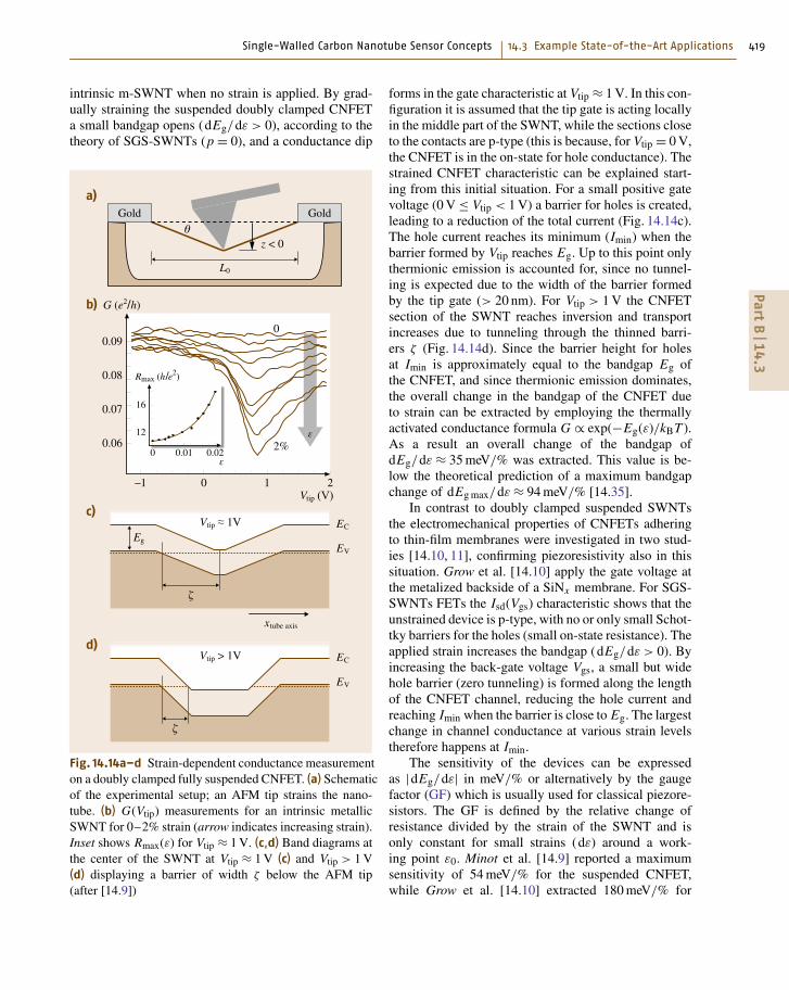
intrinsic m-SWNT when no strain is applied. By grad-ually straining the suspended doubly clamped CNFETa small bandgap opens (dEg/dε > 0), according to thetheory of SGS-SWNTs (p = 0), and a conductance dip
�
�
Gold Gold
Vtip ≈ 1V
L0
z < 0θ
EC
EV
c)
Vtip > 1V
xtube axis
EC
Eg
EV
d)
a)
–1 0 1
2%
Rmax (h/e2)
0
2
b) G (e2/h)
Vtip (V)
0.09
0.08
0.07
0.060 0.01 0.02
ε
ε
16
12
Fig. 14.14a–d Strain-dependent conductance measurementon a doubly clamped fully suspended CNFET. (a) Schematicof the experimental setup; an AFM tip strains the nano-tube. (b) G(Vtip) measurements for an intrinsic metallicSWNT for 0–2% strain (arrow indicates increasing strain).Inset shows Rmax(ε) for Vtip ≈ 1 V. (c,d) Band diagrams atthe center of the SWNT at Vtip ≈ 1 V (c) and Vtip > 1 V(d) displaying a barrier of width ζ below the AFM tip(after [14.9])
forms in the gate characteristic at Vtip ≈ 1 V. In this con-figuration it is assumed that the tip gate is acting locallyin the middle part of the SWNT, while the sections closeto the contacts are p-type (this is because, for Vtip = 0 V,the CNFET is in the on-state for hole conductance). Thestrained CNFET characteristic can be explained start-ing from this initial situation. For a small positive gatevoltage (0 V ≤ Vtip < 1 V) a barrier for holes is created,leading to a reduction of the total current (Fig. 14.14c).The hole current reaches its minimum (Imin) when thebarrier formed by Vtip reaches Eg. Up to this point onlythermionic emission is accounted for, since no tunnel-ing is expected due to the width of the barrier formedby the tip gate (> 20 nm). For Vtip > 1 V the CNFETsection of the SWNT reaches inversion and transportincreases due to tunneling through the thinned barri-ers ζ (Fig. 14.14d). Since the barrier height for holesat Imin is approximately equal to the bandgap Eg ofthe CNFET, and since thermionic emission dominates,the overall change in the bandgap of the CNFET dueto strain can be extracted by employing the thermallyactivated conductance formula G ∝ exp(−Eg(ε)/kBT ).As a result an overall change of the bandgap ofdEg/dε ≈ 35 meV/% was extracted. This value is be-low the theoretical prediction of a maximum bandgapchange of dEg max/dε ≈ 94 meV/% [14.35].
In contrast to doubly clamped suspended SWNTsthe electromechanical properties of CNFETs adheringto thin-film membranes were investigated in two stud-ies [14.10, 11], confirming piezoresistivity also in thissituation. Grow et al. [14.10] apply the gate voltage atthe metalized backside of a SiNx membrane. For SGS-SWNTs FETs the Isd(Vgs) characteristic shows that theunstrained device is p-type, with no or only small Schot-tky barriers for the holes (small on-state resistance). Theapplied strain increases the bandgap (dEg/dε > 0). Byincreasing the back-gate voltage Vgs, a small but widehole barrier (zero tunneling) is formed along the lengthof the CNFET channel, reducing the hole current andreaching Imin when the barrier is close to Eg. The largestchange in channel conductance at various strain levelstherefore happens at Imin.
The sensitivity of the devices can be expressedas |dEg/dε| in meV/% or alternatively by the gaugefactor (GF) which is usually used for classical piezore-sistors. The GF is defined by the relative change ofresistance divided by the strain of the SWNT and isonly constant for small strains (dε) around a work-ing point ε0. Minot et al. [14.9] reported a maximumsensitivity of 54 meV/% for the suspended CNFET,while Grow et al. [14.10] extracted 180 meV/% for
PartB
14.3
420 Part B MEMS/NEMS and BioMEMS/NEMS
a SGS-SWNT adhering to a substrate. For a metallicSWNT a sensitivity of 340–430 meV/% was re-ported [14.11]. Such high sensitivities of CNFETs incontact with the substrate may be explained by ad-ditional mechanical distortions of the SWNTs due tointeraction with the dielectric substrate. The maximumreported GF for a membrane-based unstrained CN-FET is 856 [14.10], and in a prestrained suspendedmetallic SWNT with ε0 ≈ 0.4% a GF of 2900 wasshown [14.12].
In general the piezoresistive effect of SWNTs hasbeen experimentally manifested in CNFETs by loadingthe tubes with axial strain. Piezoresistive CNFETs ex-cel in terms of their very high sensitivity even at smallstrain (< 0.2%), nanoscale size, and low power con-sumption (nW), in stark contrast to the mW of classicalpiezoresistors.
14.3.3 Resonant Sensors
Along with piezoresistive sensors, resonant sensors areuseful for measuring mechanical stimuli such as strainand stress. In addition, resonators can be utilized tomeasure inertial properties (mainly mass), in whichcase they are known as inertial balances. The coreprinciple, briefly explained in Sect. 14.1.1, exploits thedependence of the resonant frequency (typically thefundamental flexural mode) of a SWNT beam on quan-tities such as tension σ and mass density ρ, ω = ω(σ, ρ).
W
L
δz
–4 –2 0 2
Gate
4
b) Frequency (MHz) a)
Vgs (V)
90
70
50
30
Source Drain
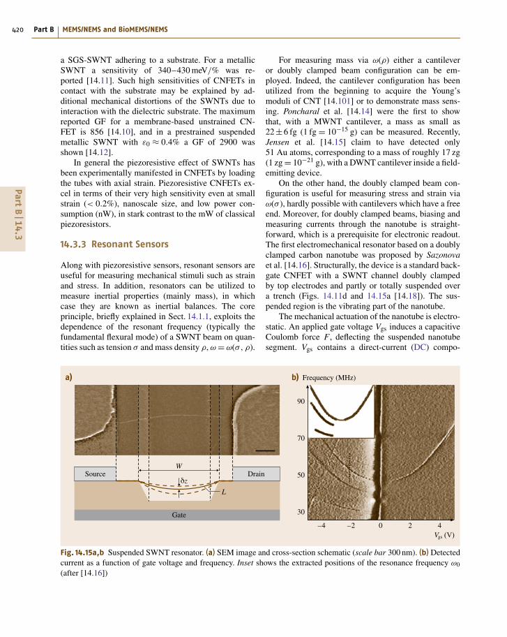
Fig. 14.15a,b Suspended SWNT resonator. (a) SEM image and cross-section schematic (scale bar 300 nm). (b) Detectedcurrent as a function of gate voltage and frequency. Inset shows the extracted positions of the resonance frequency ω0
(after [14.16])
For measuring mass via ω(ρ) either a cantileveror doubly clamped beam configuration can be em-ployed. Indeed, the cantilever configuration has beenutilized from the beginning to acquire the Young’smoduli of CNT [14.101] or to demonstrate mass sens-ing. Poncharal et al. [14.14] were the first to showthat, with a MWNT cantilever, a mass as small as22±6 fg (1 fg = 10−15 g) can be measured. Recently,Jensen et al. [14.15] claim to have detected only51 Au atoms, corresponding to a mass of roughly 17 zg(1 zg = 10−21 g), with a DWNT cantilever inside a field-emitting device.
On the other hand, the doubly clamped beam con-figuration is useful for measuring stress and strain viaω(σ ), hardly possible with cantilevers which have a freeend. Moreover, for doubly clamped beams, biasing andmeasuring currents through the nanotube is straight-forward, which is a prerequisite for electronic readout.The first electromechanical resonator based on a doublyclamped carbon nanotube was proposed by Sazonovaet al. [14.16]. Structurally, the device is a standard back-gate CNFET with a SWNT channel doubly clampedby top electrodes and partly or totally suspended overa trench (Figs. 14.11d and 14.15a [14.18]). The sus-pended region is the vibrating part of the nanotube.
The mechanical actuation of the nanotube is electro-static. An applied gate voltage Vgs induces a capacitiveCoulomb force F, deflecting the suspended nanotubesegment. Vgs contains a direct-current (DC) compo-
PartB
14.3
Single-Walled Carbon Nanotube Sensor Concepts References 421
nent to prestrain the nanotube (σ �= 0), and a harmonicat frequency ω to excite the nanotube beam vibra-tion. At frequencies close to the fundamental flexuralmode ω0, the nanotube behaves like a forced clas-sical beam [14.102], oscillating with an amplitudeδz that follows a classical Lorentzian centered at ω0(Fig. 14.2).
Readout of the nanotube displacement is done viathe channel conductance. For a CNFET the conductanceG depends on both the gate voltage Vgs and the dis-tance of the nanotube from the gate z through the gatecapacity Cgs. This is so because the conductance is pro-portional to the free-carrier concentration in the channel(G ∝ Q = CgsVgs). At frequencies close to ω0, the os-cillation amplitude δz becomes important, resulting ina detectable conductance oscillation δG(t). Theoreti-cally, δG(t) is as easy to read as applying a source–drainvoltage Vsd and measuring the current Isd. However, be-cause f0 = ω0/(2π) > 10 MHz, Sazonova et al. [14.16]have proposed using the CNFET as a mixer to downcon-vert δG(t) from ω to Δω, conveniently chosen at around
10 kHz. In Fig. 14.15b, an intensity map of the currentamplitude δIsd(Vgs, ω) is shown [14.16]. As expected,ω0 increases with Vgs, since the static gate voltagechanges the tension σ in the nanotube. Branches visi-ble below the fundamental ω0 in this map are due toinitial slack. Indeed, Witkamp et al. [14.18] have shownthat, for straight tubes (no slack), the modes below thefundamental are suppressed.
As for sensing capabilities of CNT resonators,Sazonova et al. [14.16] have estimated the force sensi-tivity to be around 1 fN/
√Hz (1 fN = 10−15 N), within
a factor of ten of the best measured sensitivities at roomtemperature. In [14.17], Peng et al. have loaded a CN-FET resonator with thermally evaporated Fe. Assuminga uniform coating of 2 nm of Fe (≈ 3.5 × 10⁻¹⁷ g), theyextrapolate a minimum detectable mass on the order of1 ag (10−18 g). One of the limiting factors so far forboth inertial balances and force sensors has been thequality factor Q, which in all reports has not exceeded300 [14.16–18]. However Q optimization has not beenaddressed so far.
14.4 Concluding Remarks
Since CNTs are at the crossroads between fundamentalscience and engineering, transdisciplinary developmentin this field is highly demanded. Concerning devicefabrication, synthetic chemists and process engineersstill have challenges ahead of them in trying to de-velop strategies for controlling nanotube electronicproperties and local integration into functional sys-tems. Even if chirality control is not yet here, thisdoes not mean that technology transfer in the midtermis not possible. In fact, the sensor concepts presentedin Sect. 14.3 (excepting piezoresistive gauges) do notrequire chirality control, but bandgap control (diam-eter and metallic versus semiconducting separation).With state-of-the-art methods for SWNT synthesis, sep-
aration, and sorting, and CCVD, catalyst control, andin situ growth, bandgap control is almost here. Actu-ally, one should not rule out even piezoresistive gauges,since calibration, tuning, and performance character-ization, as usually done for sensors, may result inacceptable product yield. Nanosystem technology maybecome the first user of SWNTs because, in contrastto mainstream technologies (CMOS logic, memories)for which ultralarge-scale integration (ULSI) is thegoal, sensors will require the integration of individ-ual and just a few structures on the wafer level, only.An ideal platform for exploring new sensing devicesis the CNFET sensor tool box as presented in thischapter.
References
14.1 R.H. Baughman, A.A. Zakhidov, W.A. de Heer: Car-bon nanotubes – The route toward applications,Science 297, 787–792 (2002)
14.2 J. Kong, N.R. Franklin, C. Zhou, M.G. Chapline,S. Peng, K. Cho, H. Dai: Nanotube molecularwires as chemical sensors, Science 287, 622–625(2000)
14.3 S. Auvray, V. Derycke, M. Goffman, A. Filoramo,O. Jost, J.-P. Bourgoin: Chemical optimization ofself-assembled carbon nanotube transistors, NanoLett. 5, 451–455 (2005)
14.4 P.G. Collins, K. Bradley, M. Ishigami, A. Zettl: Ex-treme oxygen sensitivity of electronic properties ofcarbon nanotubes, Science 287, 1801–1804 (2000)
PartB
14
422 Part B MEMS/NEMS and BioMEMS/NEMS
14.5 J. Li, Y. Lu, Q. Ye, M. Cinke, J. Han, M. Meyyappan:Carbon nanotube sensors for gas and organic vapordetection, Nano Lett. 3, 929–933 (2003)
14.6 Q.F. Pengfei, O. Vermesh, M. Grecu, A. Javey,Q. Wang, H. Dai, S. Peng, K.J. Cho: Toward large ar-rays of multiplex functionalized carbon nanotubesensors for highly sensitive and selective moleculardetection, Nano Lett. 3, 347–351 (2003)
14.7 K. Besteman, J.O. Lee, F.G.M. Wiertz, H.A. Heering,C. Dekker: Enzyme-coated carbon nanotubes assingle-molecule biosensors, Nano Lett. 3, 727–730(2003)
14.8 T.W. Tombler, C. Zhou, L. Alexeyev, J. Kong, H. Dai,W. Liu, C.S. Jayanthi, M. Tang, S.Y. Wu: Reversibleelectromechanical characteristics of carbon nano-tubes under local-probe manipulation, Nature405, 769–772 (2000)
14.9 E.D. Minot, Y. Yaish, V. Sazonova, J.Y. Park,M. Brink, P.L. McEuen: Tuning carbon nanotubeband gaps with strain, Phys. Rev. Lett. 90, 156401–1–156401–4 (2003)
14.10 R.J. Grow, Q. Wang, J. Cao, D. Wang, H. Dai:Piezoresistance of carbon nanotubes on de-formable thin-film membranes, Appl. Phys. Lett.86, 093104–1–093104–3 (2005)
14.11 C. Stampfer, T. Helbling, D. Obergfell, B. Schoberle,M.K. Tripp, A. Jungen, S. Roth, V.M. Bright,C. Hierold: Fabrication of single-walled carbon-nanotube-based pressure sensors, Nano Lett. 6,233–237 (2006)
14.12 C. Stampfer, A. Jungen, R. Linderman, D. Obergfell,S. Roth, C. Hierold: Nano-electromechanicaldisplacement sensing based on single-walledcarbon nanotubes, Nano Lett. 6, 1449–1453(2006)
14.13 V.L. Pushparaj, L. Ci, S. Sreekala, A. Kumar, S. Ke-sapragada, D. Gall, O. Nalamasu, A.M. Pulickel,J. Suhr: Effects of compressive strains on elec-trical conductivities of a macroscale carbonnanotube block, Appl. Phys. Lett. 91, 153116–3(2007)
14.14 P. Poncharal, Z.L. Wang, D. Ugarte, W.A. deHeer: Electrostatic deflections and electromechan-ical resonances of carbon nanotubes, Science 283,1513–1516 (1999)
14.15 K. Jensen, K. Kim, A. Zettl: An atomic-resolutionnanomechanical mass sensor, Nat. Nanotechnol.3, 533–537 (2008)
14.16 V. Sazonova, Y. Yaish, H. Üstünel, D. Roundy,T.A. Arias, P.L. McEuen: A tunable carbon nanotubeelectromechanical oscillator, Nature 431, 284–287(2004)
14.17 H.B. Peng, C.W. Chang, S. Aloni, T.D. Yuzvinsky,A. Zettl: Ultrahigh frequency nanotube resonators,Phys. Rev. Lett. 97, 087203–1–087203–4 (2006)
14.18 B. Witkamp, M. Poot, H.S.J. van der Zant:Bending-mode vibration of a suspended nanotuberesonator, Nano Lett. 6, 2904–2908 (2006)
14.19 M. Freitag, Y. Martin, J.A. Misewich, R. Mar-tel, P. Avouris: Photoconductivity of single carbonnanotubes, Nano Lett. 3, 1067–1071 (2003)
14.20 X. Qiu, M. Freitag, V. Perebeinos, P. Avouris: Photo-conductivity spectra of single-carbon nanotubes:Implications on the nature of their excited states,Nano Lett. 5, 749–752 (2005)
14.21 C.T. White, J.W. Mintmire: Density of states reflectsdiameter in nanotubes, Nature 394, 29–30 (1998)
14.22 M.S. Dresselhaus, G. Dresselhaus, P. Avouris: Car-bon Nanotubes: Synthesis, Structure, Propertiesand Applications (Springer, Berlin, Heidelberg2001)
14.23 R. Saito, G. Dresselhaus, M.S. Dresselhaus: PhysicalProperties of Carbon Nanotubes (Imperial CollegePress, London 2001)
14.24 A. Jorio, G. Dresselhaus, M.S. Dresselhaus: Car-bon Nanotubes: Advanced Topics in the Synthesis,Structure, Properties and Applications (Springer,Berlin, Heidelberg 2008)
14.25 S. Li, Z. Yu, C. Rutherglen, P.J. Burke: Electricalproperties of 0.4 cm long single-walled carbonnanotubes, Nano Lett. 4, 2003–2007 (2004)
14.26 A. Kleiner, S. Eggert: Curvature, hybridization, andSTM images of carbon nanotubes, Phys. Rev. B 64,113402–1–113402–4 (2001)
14.27 B. Bourlon, J. Wong, C. Mikó, L. Forró, M. Bockrath:A nanoscale probe for fluidic and ionic transport,Nat. Nanotechnol. 2, 104–107 (2006)
14.28 A. Modi, N. Koratkar, E. Lass, B. Wei, P.M. Ajayan:Miniaturized gas ionization sensors using carbonnanotubes, Nature 424, 171–174 (2003)
14.29 E.S. Snow, F.K. Perkins, E.J. Houser, S.C. Badescu,T.L. Reinecke: Chemical detection with a single-walled carbon nanotube capacitor, Science 307,1942–1945 (2005)
14.30 A. Krishnan, E. Dujardin, T.W. Ebbesen, P.N. Yian-ilos, M.M.J. Treacy: Young’s modulus of single-walled nanotubes, Phys. Rev. B 58, 14013 (1998)
14.31 D.A. Walters, L.M. Ericson, M.J. Casavant, J. Liu,D.T. Colbert, K.A. Smith, R.E. Smalley: Elastic strainof freely suspended single-wall carbon nanotuberopes, Appl. Phys. Lett. 74, 3803–3805 (1999)
14.32 M.-F. Yu, B.S. Files, S. Arepalli, R.S. Ruoff: Tensileloading of ropes of single wall carbon nanotubesand their mechanical properties, Phys. Rev. Lett.84, 5552–5555 (2000)
14.33 H.W.C. Postma, I. Kozinsky, A. Husain, M.L. Roukes:Dynamic range of nanotube- and nanowire-basedelectromechanical systems, Appl. Phys. Lett. 86,223105–1–223105–3 (2005)
14.34 L. Yang, M.P. Anantram, J. Han, J.P. Lu: Band-gap change of carbon nanotubes: Effect of smalluniaxial and torsional strain, Phys. Rev. B 60,13874–13878 (1999)
14.35 L. Yang, J. Han: Electronic structure of deformedcarbon nanotubes, Phys. Rev. Lett. 85, 154–157(2000)
PartB
14
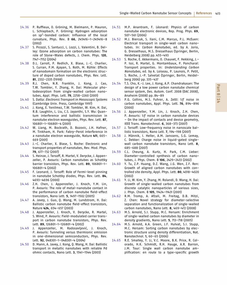
Single-Walled Carbon Nanotube Sensor Concepts References 423
14.36 P. Ruffieux, O. Gröning, M. Bielmann, P. Mauron,L. Schlapbach, P. Gröning: Hydrogen adsorptionon sp2-bonded carbon: Influence of the localcurvature, Phys. Rev. B 66, 245416–1–245416–8(2002)
14.37 S. Picozzi, S. Santucci, L. Lozzi, L. Valentini, B. Del-ley: Ozone adsorption on carbon nanotubes: Therole of Stone–Wales defects, J. Chem. Phys. 120,7147–7152 (2004)
14.38 D.L. Carroll, P. Redlich, X. Blase, J.-C. Charlier,S. Curran, P.M. Ajayan, S. Roth, M. Rühle: Effectsof nanodomain formation on the electronic struc-ture of doped carbon nanotubes, Phys. Rev. Lett.81, 2332–2335 (1998)
14.39 R.J. Chen, N.R. Franklin, J. Kong, J. Cao,T.W. Tombler, Y. Zhang, H. Dai: Molecular pho-todesorption from single-walled carbon nano-tubes, Appl. Phys. Lett. 79, 2258–2260 (2001)
14.40 S. Datta: Electronic Transport in Mesoscopic Systems(Cambridge Univ. Press, Cambridge 1997)
14.41 J. Kong, E. Yenilmez, T.W. Tombler, W. Kim, H. Dai,R.B. Laughlin, L. Liu, C.S. Jayanthi, S.Y. Wu: Quan-tum interference and ballistic transmission innanotube electron waveguides, Phys. Rev. Lett. 87,106801–1–106801–4 (2001)
14.42 W. Liang, M. Bockrath, D. Bozovic, J.H. Hafner,M. Tinkham, H. Park: Fabry–Perot interference ina nanotube electron waveguide, Nature 411, 665–669 (2001)
14.43 J.-C. Charlier, X. Blase, S. Roche: Electronic andtransport properties of nanotubes, Rev. Mod. Phys.79, 677–732 (2007)
14.44 S. Heinze, J. Tersoff, R. Martel, V. Derycke, J. Appen-zeller, P. Avouris: Carbon nanotubes as Schottkybarrier transistors, Phys. Rev. Lett. 89, 106801–1–106801–4 (2002)
14.45 F. Leonard, J. Tersoff: Role of Fermi-level pinningin nanotube Schottky diodes, Phys. Rev. Lett. 84,4693–4696 (2000)
14.46 Z.H. Chen, J. Appenzeller, J. Knoch, Y.M. Lin,P. Avouris: The role of metal-nanotube contact inthe performance of carbon nanotube field-effecttransistors, Nano Lett. 5, 1497–1502 (2005)
14.47 A. Javey, J. Guo, Q. Wang, M. Lundstrom, H. Dai:Ballistic carbon nanotube field-effect transistors,Nature 424, 654–657 (2003)
14.48 J. Appenzeller, J. Knoch, V. Derycke, R. Martel,S. Wind, P. Avouris: Field-modulated carrier trans-port in carbon nanotube transistors, Phys. Rev.Lett. 89, 126801–1–126801–4 (2002)
14.49 J. Appenzeller, M. Radosavljevic, J. Knoch,P. Avouris: Tunneling versus thermionic emissionin one-dimensional semiconductors, Phys. Rev.Lett. 92, 048301–1–048301–4 (2004)
14.50 D. Mann, A. Javey, J. Kong, Q. Wang, H. Dai: Ballistictransport in metallic nanotubes with reliable Pdohmic contacts, Nano Lett. 3, 1541–1544 (2003)
14.51 M.P. Anantram, F. Léonard: Physics of carbonnanotube electronic devices, Rep. Prog. Phys. 69,507–561 (2006)
14.52 M.J. Biercuk, S. Ilani, C.M. Marcus, P.L. McEuen:Electrical transport in single-wall carbon nano-tubes. In: Carbon Nanotubes, ed. by A. Jorio,G. Dresselhaus, M.S. Dresselhaus (Springer, Berlin,Heidelberg 2008) pp. 455–493
14.53 S. Roche, E. Akkermans, O. Chauvet, F. Hekking, J.-P. Issi, R. Martel, G. Montambaux, P. Poncharal:Transport properties. In: Understanding CarbonNanotubes, ed. by A. Loiseau, P. Launois, P. Petit,S. Roche, J.-P. Salvetat (Springer, Berlin, Heidel-berg 2006) pp. 335–437
14.54 T.S. Cho, K.-J. Lee, J. Kong, A.P. Chandrakasan: Thedesign of a low power carbon nanotube chemicalsensor system, Des. Autom. Conf. 2008 (DAC 2008),Anaheim (2008) pp. 84–89
14.55 P.G. Collins, M.S. Fuhrer, A. Zettl: 1/f noise incarbon nanotubes, Appl. Phys. Lett. 76, 894–896(2000)
14.56 J. Appenzeller, Y.M. Lin, J. Knoch, Z.H. Chen,P. Avouris: 1/f noise in carbon nanotube devices– On the impact of contacts and device geometry,IEEE Trans. Nanotechnol. 6, 368–373 (2007)
14.57 J. Tersoff: Low-frequency noise in nanoscale bal-listic transistors, Nano Lett. 7, 194–198 (2007)
14.58 J. Männik, I. Heller, A.M. Janssens, S.G. Lemay,C. Dekker: Charge noise in liquid-gated single-wall carbon nanotube transistors, Nano Lett. 8,685–688 (2007)
14.59 C.L. Cheung, A. Kurtz, H. Park, C.M. Lieber:Diameter-controlled synthesis of carbon nano-tubes, J. Phys. Chem. B 106, 2429–2433 (2002)
14.60 Y. Tu, Z.P. Huang, D.Z. Wang, J.G. Wen, Z.F. Ren:Growth of aligned carbon nanotubes with con-trolled site density, Appl. Phys. Lett. 80, 4018–4020(2002)
14.61 Y. Li, W. Kim, Y. Zhang, M. Rolandi, D. Wang, H. Dai:Growth of single-walled carbon nanotubes fromdiscrete catalytic nanoparticles of various sizes,J. Phys. Chem. B 105, 11424–11431 (2001)
14.62 R.M. Tromp, A. Afzali, M. Freitag, D.B. Mitzi,Z. Chen: Novel strategy for diameter-selectiveseparation and functionalization of single-walledcarbon nanotubes, Nano Lett. 8, 469–472 (2008)
14.63 M.S. Arnold, S.I. Stupp, M.C. Hersam: Enrichmentof single-walled carbon nanotubes by diameter indensity gradients, Nano Lett. 5, 713–718 (2005)
14.64 M.S. Arnold, A.A. Green, J.F. Hulvat, S.I. Stupp,M.C. Hersam: Sorting carbon nanotubes by elec-tronic structure using density differentiation, Nat.Nanotechnol. 1, 60–65 (2006)
14.65 R.E. Smalley, Y. Li, V.C. Moore, B.K. Price, R. Col-orado, H.K. Schmidt, R.H. Hauge, A.R. Barron,J.M. Tour: Single wall carbon nanotube am-plification: en route to a type-specific growth
PartB
14
424 Part B MEMS/NEMS and BioMEMS/NEMS
mechanism, J. Am. Chem. Soc. 128, 15824–15829(2006)
14.66 E. Joselevich, H. Dai, J. Liu, K. Hata, A.H. Windle:Carbon nanotube synthesis and organization. In:Carbon Nanotubes, ed. by A. Jorio, G. Dresselhaus,M.S. Dresselhaus (Springer, Berlin, Heidelberg2008) pp. 101–164
14.67 Y. Yan, M.B. Chan-Park, Q. Zhang: Advances incarbon-nanotube assembly, Small 3, 24–42 (2007)
14.68 S.J. Tans, A.R.M. Verschueren, C. Dekker: Room-temperature transistor based on a single carbonnanotube, Nature 393, 49–52 (1998)
14.69 R. Martel, T. Schmidt, H.R. Shea, T. Hertel,P. Avouris: Single- and multi-wall carbon nano-tube field-effect transistors, Appl. Phys. Lett. 73,2447–2449 (1998)
14.70 V. Derycke, R. Martel, J. Appenzeller, P. Avouris:Carbon nanotube inter- and intramolecular logicgates, Nano Lett. 1, 453–456 (2001)
14.71 J. Liu, M.J. Casavant, M. Cox, D.A. Walters, P. Boul,W. Lu, A.J. Rimberg, K.A. Smith, D.T. Colbert,R.E. Smalley: Controlled deposition of individ-ual single-walled carbon nanotubes on chemicallyfunctionalized templates, Chem. Phys. Lett. 303,125–129 (1999)
14.72 C. Klinke, J.B. Hannon, A. Afzali, P. Avouris: Field-effect transistors assembled from functionalizedcarbon nanotubes, Nano Lett. 6, 906–910 (2006)
14.73 S.G. Rao, L. Huang, W. Setyawan, S. Hong: Nano-tube electronics: Large-scale assembly of carbonnanotubes, Nature 425, 36–37 (2003)
14.74 R. Krupke, F. Hennrich, H.B. Weber, M.M. Kappes,H. von Löhneysen: Simultaneous deposition ofmetallic bundles of single-walled carbon nano-tubes using AC-dielectrophoresis, Nano Lett. 3,1019–1023 (2003)
14.75 R. Krupke, F. Hennrich, H. von Löhneysen,M.M. Kappes: Separation of metallic from semicon-ducting single-walled carbon nanotubes, Science301, 344–347 (2003)
14.76 Y. Zhang, A. Chang, J. Cao, Q. Wang, W. Kim,Y. Li, N. Morris, E. Yenilmez, J. Kong, H. Dai:Electric-field-directed growth of aligned single-walled carbon nanotubes, Appl. Phys. Lett. 79,3155–3157 (2001)
14.77 J. Kong, H.T. Soh, A.M. Cassell, C. Quate, H. Dai: Syn-thesis of individual single-walled carbon nano-tubes on patterned silicon wafers, Nature 395,878–881 (1998)
14.78 H.T. Soh, A. Morpurgo, J. Kong, C. Marcus, C. Quate,H. Dai: Integrated nanotube circuits: Controlledgrowth and ohmic contacting of single-walledcarbon nanotubes, Appl. Phys. Lett. 75, 627–629(1999)
14.79 A. Javey, H. Dai: Regular arrays of 2 nm metalnanoparticles for deterministic synthesis of nano-materials, J. Am. Chem. Soc. 127, 11942–11943 (2005)
14.80 E. Joselevich, C.M. Lieber: Vectorial growth ofmetallic and semiconducting single-wall carbonnanotubes, Nano Lett. 2, 1137–1141 (2002)
14.81 S. Dittmer, J. Svensson, E.E.B. Campbell: Elec-tric field aligned growth of single-walled carbonnanotubes, Curr. Appl. Phys. 4, 595–598 (2004)
14.82 S. Huang, X. Cai, J. Liu: Growth of millimeter-longand horizontally aligned single-walled carbonnanotubes on flat substrates, J. Am. Chem. Soc.125, 5636–5637 (2003)
14.83 S. Han, X. Liu, C. Zhou: Template-free directionalgrowth of single-walled carbon nanotubes on a-and r-plane sapphire, J. Am. Chem. Soc. 127, 5294–5295 (2005)
14.84 A. Ismach, L. Segev, E. Wachtel, E. Joselevich:Atomic-step-templated formation of single wallcarbon nanotube patterns, Angew. Chem. Int. Ed.43, 6140–6143 (2004)
14.85 X. Liu, S. Han, C. Zhou: Novel nanotube-on-insulator (NOI) approach toward single-walledcarbon nanotube devices, Nano Lett. 6, 34–39(2005)
14.86 A.M. Cassell, N.R. Franklin, T.W. Tombler,E.M. Chan, J. Han, H. Dai: Directed growth of free-standing single-walled carbon nanotubes, J. Am.Chem. Soc. 121, 7975–7976 (1999)
14.87 N.R. Franklin, H. Dai: An enhanced CVD approach toextensive nanotube networks with directionality,Adv. Mater. 12, 890–894 (2000)
14.88 N.R. Franklin, Q. Wang, T.W. Tombler, A. Javey,M. Shim, H. Dai: Integration of suspended car-bon nanotube arrays into electronic devices andelectromechanical systems, Appl. Phys. Lett. 81,913–915 (2002)
14.89 A. Jungen, S. Hofmann, J.C. Meyer, C. Stampfer,S. Roth, J. Robertson, C. Hierold: Synthesis of in-dividual single-walled carbon nanotube bridgescontrolled by support micromachining, J. Mi-cromech. Microeng. 17, 603–608 (2007)
14.90 T. Zhang, S. Mubeen, N.V. Myung, M.A. Deshusses:Recent progress in carbon nanotube-based gassensors, Nanotechnology 19, 332001 (2008)
14.91 S.N. Kim, J.F. Rusling, F. Papadimitrakopoulos:Carbon nanotubes for electronic and electrochem-ical detection of biomolecules, Adv. Mater. 19,3214–3228 (2007)
14.92 N. Sinha, J. Ma, J.T.W. Yeow: Carbon nanotube-based sensors, J. Nanosci. Nanotechnol. 6, 573–590(2006)
14.93 K. Bradley, J.C.P. Gabriel, A. Star, G. Gruner: Short-channel effects in contact-passivated nanotubechemical sensors, Appl. Phys. Lett. 83, 3821–3823(2003)
14.94 J. Zhang, A. Boyd, A. Tselev, M. Paranjape, P. Bar-bara: Mechanism of NO2 detection in carbonnanotube field effect transistor chemical sensors,Appl. Phys. Lett. 88, 123112–1–123112–3 (2006)
PartB
14
Single-Walled Carbon Nanotube Sensor Concepts References 425
14.95 X.L. Liu, Z.C. Luo, S. Han, T. Tang, D.H. Zhang,C.W. Zhou: Band engineering of carbon nanotubefield-effect transistors via selected area chemicalgating, Appl. Phys. Lett. 86, 243501–1–243501–3(2005)
14.96 T. Helbling, R. Pohle, L. Durrer, C. Stampfer, C. Ro-man, A. Jungen, M. Fleischer, C. Hierold: SensingNO2 with individual suspended single-walled car-bon nanotubes, Sens. Actuators B 132, 491–497(2008)
14.97 M. Krüger, M.R. Buitelaar, T. Nussbaumer, C. Schö-nenberger, L. Forró: Electrochemical carbon nano-tube field-effect transistor, Appl. Phys. Lett. 78,1291–1293 (2001)
14.98 R.J. Chen, Y. Zhang, D. Wang, H. Dai: Non-covalent sidewall functionalization of single-walled carbon nanotubes for protein immo-
bilization, J. Am. Chem. Soc. 123, 3838–3839(2001)
14.99 K. Balasubramanian, M. Burghard: Chemicallyfunctionalized carbon nanotubes, Small 1, 180–192(2005)
14.100 I. Heller, A.M. Janssens, J. Männik, E.D. Minot,S.G. Lemay, C. Dekker: Identifying the mechanismof biosensing with carbon nanotube transistors,Nano Lett. 8, 591–595 (2008)
14.101 M.M.J. Treacy, T.W. Ebbesen, J.M. Gibson: Ex-ceptionally high Young’s modulus observed forindividual carbon nanotubes, Nature 381, 678–680(1996)
14.102 D. Garcia-Sanchez, A. San Paulo, M.J. Esplandiu,F. Perez-Murano, L. Forró, A. Aguasca, A. Bach-told: Mechanical detection of carbon nanotuberesonator vibrations, Phys. Rev. Lett. 99, 085501–1–085501–4 (2007)
PartB
14


![Jordan Journal of Physics - journals.yu.edu.jojournals.yu.edu.jo/jjp/JJPIssues/Vol11No1pdf2018/3.pdf · a single-walled carbon nanotube was discovered [4]. Carbon nanotube fibers](https://img.pdfslide.net/doc/110x75/5f95bce17a6a860faf755f09/jordan-journal-of-physics-a-single-walled-carbon-nanotube-was-discovered-4.jpg)