Embed Size (px)
Citation preview
4.25 Gbps 40 × 40 Digital Crosspoint Switch
Data Sheet ADN4605
FEATURES DC to 4.25 Gbps per port NRZ data rate Adjustable receive equalization 3 dB, 6 dB, or 12 dB boost Compensates over 40 inches of FR4 at 4.25 Gbps Adjustable transmit preemphasis/deemphasis Programmable boost and output level Compensates over 40 inches of FR4 at 4.25 Gbps Low power 105 mW per channel at 2.5 V (400 mV p-p differential
output level swing) 40 × 40, fully differential, nonblocking array Double rank connection programming with dual maps Low jitter, typically <25 ps Flexible 2.5 V to 3.3 V supply range DC- or ac-coupled differential PECL/CML inputs Differential CML outputs Per-lane polarity inversion for routing ease 50 Ω on-chip I/O termination with disable feature Supports 8b10b, scrambled or uncoded NRZ data Serial (IC slave or SPI) control interface Parallel control interface
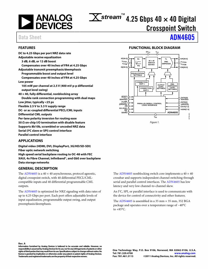
FUNCTIONAL BLOCK DIAGRAM
EQ
Rx TxPRE-
EMPHASIS40 × 40
SWITCHMATRIX
CONNECTIONMAP 1
CONNECTIONMAP 0
PARALLEL/SERIAL CONTROLLOGIC INTERFACE
PRE-EMPHASIS
LEVELSETTINGS
OUTPUTLEVEL
SETTINGS
ADN4605
VCC
VEE
DVCC
OP[39:0]
VTTOA,VTTOBON[39:0]
IP[39:0]VTTIA,VTTIB
IN[39:0]
I2C/SPI(UPDATE)
SDI/RE
SCL/SCK/WE
RESETSER/PAR
CS
EQUALIZATIONSETTINGS
DATA[1](UPDATE)
DATA[0]/SDA/SDO
DATA[7:2]ADDR[7:0]
0979
6-00
1
Figure 1.
APPLICATIONS Digital video (HDMI, DVI, DisplayPort, 3G/HD/SD-SDI) Fiber optic network switching High speed serial backplane routing to OC-48 with FEC XAUI, 4x Fibre Channel, Infiniband®, and GbE over backplane Data storage networks
GENERAL DESCRIPTION The ADN4605 is a 40 × 40 asynchronous, protocol agnostic, digital crosspoint switch, with 40 differential PECL/CML-compatible inputs and 40 differential programmable CML outputs.
The ADN4605 is optimized for NRZ signaling with data rates of up to 4.25 Gbps per port. Each port offers adjustable levels of input equalization, programmable output swing, and output preemphasis/deemphasis.
The ADN4605 nonblocking switch core implements a 40 × 40 crossbar and supports independent channel switching through serial and parallel control interfaces. The ADN4605 has low latency and very low channel-to-channel skew.
An I2C, SPI, or parallel interface is used to communicate with the device for control of connectivity and other features.
The ADN4605 is assembled in a 35 mm × 35 mm, 352 BGA package and operates over a temperature range of −40°C to +85°C.
Rev. A Information furnished by Analog Devices is believed to be accurate and reliable. However, no responsibility is assumed by Analog Devices for its use, nor for any infringements of patents or other rights of third parties that may result from its use. Specifications subject to change without notice. No license is granted by implication or otherwise under any patent or patent rights of Analog Devices. Trademarks and registered trademarks are the property of their respective owners.
One Technology Way, P.O. Box 9106, Norwood, MA 02062-9106, U.S.A. Tel: 781.329.4700 www.analog.com Fax: 781.461.3113 ©2011 Analog Devices, Inc. All rights reserved.
ADN4605 Data Sheet
Rev. A | Page 2 of 56
TABLE OF CONTENTS Features .............................................................................................. 1 Functional Block Diagram .............................................................. 1 Applications ....................................................................................... 1 General Description ......................................................................... 1 Revision History ............................................................................... 2 Specifications ..................................................................................... 3
Electrical Specifications ............................................................... 3 I2C Timing Specifications ............................................................ 5 SPI Timing Specifications ........................................................... 5 Parallel Mode Specifications ....................................................... 6
Absolute Maximum Ratings ............................................................ 7 ESD Caution .................................................................................. 7
Pin Configuration and Function Descriptions ............................. 8 Typical Performance Characteristics ........................................... 18 Theory of Operation ...................................................................... 24
Introduction ................................................................................ 24 Receivers ...................................................................................... 25 Polarity Inversion ....................................................................... 26 Switch Core ................................................................................. 27 Reset ............................................................................................. 28
Transmitters ................................................................................ 29 Termination ................................................................................. 32
I2C Serial Control Interface ........................................................... 33 I2C Data Write ............................................................................. 33 I2C Data Read .............................................................................. 34
SPI Serial Control Interface .......................................................... 35 Parallel Control Interface .............................................................. 38
Address Inputs: ADDR[7:0] ...................................................... 38 Data Inputs/Outputs: DATA[7:0]............................................. 38 Write Operation.......................................................................... 38 Read Operation........................................................................... 38
Register Map ................................................................................... 39 Applications Information .............................................................. 49
Supply Sequencing ..................................................................... 51 Power Dissipation....................................................................... 51 Output Compliance ................................................................... 51 TX/XPT HEADROOM ............................................................. 51 Printed Circuit Board (PCB) Layout Guidelines ................... 54
Outline Dimensions ....................................................................... 55 Ordering Guide ............................................................................... 55
REVISION HISTORY 11/11—Rev. 0 to Rev. A
Changes to Printed Circuit Board (PCB) Layout Guidelines ........................................................................................ 54 Removed Figure 55, Renumbered Sequentially.......................... 54
6/11—Revision 0: Initial Version
Data Sheet ADN4605
Rev. A | Page 3 of 56
SPECIFICATIONS ELECTRICAL SPECIFICATIONS VCC = 2.5 V, VTTIx = 2.5 V, VTTOx = 2.5 V, DVCC = 3.3 V, VEE = 0 V, RL = 50 Ω, output level (OLEV) = 4 (16 mA), preemphasis (PE) = 0 (0 dB), equalizer (EQ) = 1 (3 dB), data rate = 4.25 Gbps (PRBS7 data pattern), ac-coupled inputs and outputs, differential input swing = 800 mV p-p, TA = 25°C, unless otherwise noted.
Table 1.
Parameter Conditions Min Typ Max Unit DYNAMIC PERFORMANCE
Data Rate (DR) per Channel (NRZ) dc 4.25 Gbps Deterministic Jitter Data rate ≤ 4.25 Gbps, no channel 20 ps p-p
Random Jitter RMS, no channel 0.8 ps rms Residual Deterministic Jitter with
Receive Equalization Data rate = 4.25 Gbps, 20 in. FR4, EQ boost = 12 dB 14 ps p-p Data rate = 4.25 Gbps, 30 in. FR4, EQ boost = 12 dB 15 ps p-p
Data rate = 4.25 Gbps, 40 in. FR4, EQ boost = 12 dB 25 ps p-p Residual Deterministic Jitter with
Transmit Preemphasis Data rate = 4.25 Gbps, 20 in. FR4, PE boost = 5.6 dB 22 ps p-p Data rate = 4.25 Gbps, 30 in. FR4, PE boost = 6.8 dB 28 ps p-p
Data rate = 4.25 Gbps, 40 in. FR4, PE boost = 9.5 dB 32 ps p-p Propagation Delay Input to output 920 ps Channel-to-Channel Skew Earliest input/output lane to latest input/output lane 200 ps Switching Time Update logic switching to 50% output data 20 ns Output Rise/Fall Time 20% to 80% 108 ps
INPUT CHARACTERISTICS Minimum Differential Input
Voltage Swing1 VICM = VCC − 0.6 V 50 mV p-p diff
Maximum Differential Input Voltage Swing1
VICM = VCC − 0.6 V 2000 mV p-p diff
Input Voltage Range Single-ended absolute voltage level, VL VEE + 1.0 V Single-ended absolute voltage level, VH VCC + 0.3 V
OUTPUT CHARACTERISTICS Output Voltage Swing Differential, PE boost = 0 dB, default output level, at dc 670 800 875 mV p-p diff Output Voltage Range Single-ended absolute voltage level, VL VCC – 1.4 V
Single-ended absolute voltage level, VH VCC + 0.3 V Per-Port Output Current PE boost = 0 dB, default output level 16 mA
PE boost = 6 dB, default output level 32 mA TERMINATION CHARACTERISTICS
Resistance Differential, VCC = VMIN to VMAX, TA = TMIN to TMAX 88 100 114 Ω Temperature Coefficient 0.015 Ω/°C
POWER SUPPLY Operating Range
VCC VEE = 0 V 2.25 2.5 3.6 V DVCC VEE = 0 V 3.0 3.3 3.6 V VTTIA, VTTIB VEE = 0 V 2.5 VCC + 0.3 V VTTOA, VTTOB VEE = 0 V 2.5 VCC + 0.3 V
Supply Current Inputs/outputs disabled (reset condition) ICC 55 64 mA IDVCC 0.3 1.1 mA ITTIA + ITTIB Inputs floating 0 1.5 mA ITTOA+ ITTOB Outputs floating 0 1.5 mA
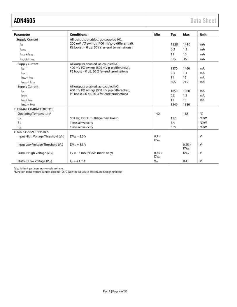
ADN4605 Data Sheet
Rev. A | Page 4 of 56
Parameter Conditions Min Typ Max Unit Supply Current All outputs enabled, ac-coupled I/O,
200 mV I/O swings (400 mV p-p differential), PE boost = 0 dB, 50 Ω far-end terminations
ICC 1320 1410 mA IDVCC 0.3 1.1 mA ITTIA + ITTIB 11 15 mA ITTOA+ ITTOB 335 360 mA
Supply Current All outputs enabled, ac-coupled I/O, 400 mV I/O swings (800 mV p-p differential), PE boost = 0 dB, 50 Ω far-end terminations
ICC 1370 1460 mA IDVCC 0.3 1.1 mA ITTIA + ITTIB 11 15 mA ITTOA + ITTOB 665 715 mA
Supply Current All outputs enabled, ac-coupled I/O, 400 mV I/O swings (800 mV p-p differential), PE boost = 6 dB, 50 Ω far-end terminations
ICC 1850 1960 mA IDVCC 0.3 1.1 mA ITTIA+ ITTIB 11 15 mA ITTOA + ITTOB 1340 1380
THERMAL CHARACTERISTICS Operating Temperature2 −40 +85 °C θJA Still air; JEDEC multilayer test board 11.6 °C/W θJB 1 m/s air velocity 5.4 °C/W θJC 1 m/s air velocity 0.72 °C/W
LOGIC CHARACTERISTICS Input High Voltage Threshold (VIH) DVCC = 3.3 V 0.7 ×
DVCC V
Input Low Voltage Threshold (VIL) DVCC = 3.3 V 0.25 × DVCC
V
Output High Voltage (VOH) IOH = −3 mA (I2C/SPI mode only) 0.75 × DVCC
DVCC V
Output Low Voltage (VOL) IOL = +3 mA VEE 0.4 V
1VICM is the input common-mode voltage. 2Junction temperature cannot exceed 125°C (see the Absolute Maximum Ratings section).
Data Sheet ADN4605
Rev. A | Page 5 of 56
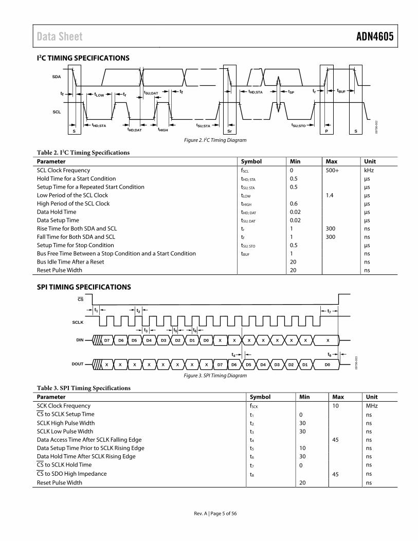
I2C TIMING SPECIFICATIONS
SDA
SCL
tf tLOW
tHD;STA
tr
tHD;DAT tHIGH
tSU;DAT tf
tSU;STA
tHD;STA tSP
tSU;STO
tr tBUF
SPSrS 0979
6-00
2
Figure 2. I2C Timing Diagram
Table 2. I2C Timing Specifications Parameter Symbol Min Max Unit SCL Clock Frequency fSCL 0 500+ kHz Hold Time for a Start Condition tHD; STA 0.5 µs Setup Time for a Repeated Start Condition tSU; STA 0.5 µs Low Period of the SCL Clock tLOW 1.4 µs High Period of the SCL Clock tHIGH 0.6 µs Data Hold Time tHD; DAT 0.02 µs Data Setup Time tSU; DAT 0.02 µs Rise Time for Both SDA and SCL tr 1 300 ns Fall Time for Both SDA and SCL tf 1 300 ns Setup Time for Stop Condition tSU; STO 0.5 µs Bus Free Time Between a Stop Condition and a Start Condition tBUF 1 ns Bus Idle Time After a Reset 20 ns Reset Pulse Width 20 ns
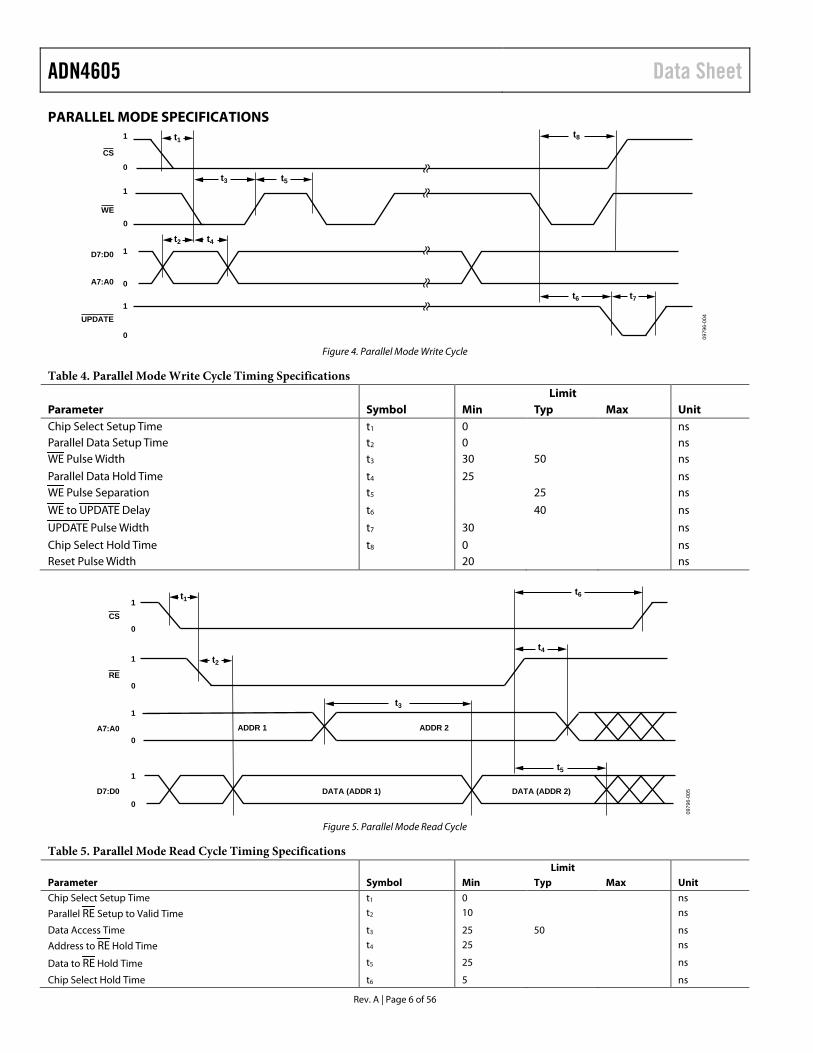
SPI TIMING SPECIFICATIONS
t1 t2
t3 t5 t6
t4
t7
t8
D7
CS
SCLK
DIN
DOUT
D6 D5 D4 D3 D2 D1 D0 X X X X X X X X
X X X X X X X X D7 D6 D5 D4 D3 D2 D1 D0
0979
6-00
3
Figure 3. SPI Timing Diagram
Table 3. SPI Timing Specifications Parameter Symbol Min Max Unit SCK Clock Frequency fSCK 10 MHz CS to SCLK Setup Time t1 0 ns SCLK High Pulse Width t2 30 ns SCLK Low Pulse Width t3 30 ns Data Access Time After SCLK Falling Edge t4 45 ns Data Setup Time Prior to SCLK Rising Edge t5 10 ns Data Hold Time After SCLK Rising Edge t6 30 ns CS to SCLK Hold Time t7 0 ns
CS to SDO High Impedance t8 45 ns
Reset Pulse Width 20 ns
ADN4605 Data Sheet
Rev. A | Page 6 of 56
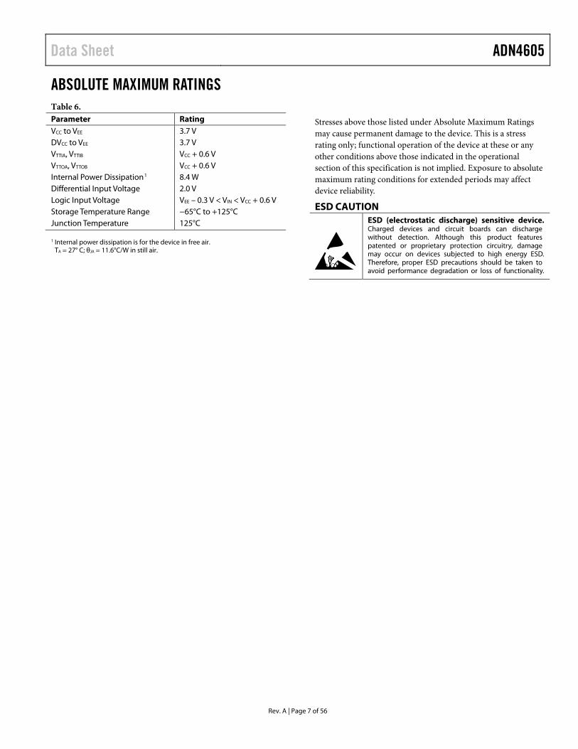
PARALLEL MODE SPECIFICATIONS
UPDATE
1
0WE
D7:D0
A7:A0
1
0
CS
1
0
0
1t6
t8
t3 t5
t1
t2 t4
t7
0979
6-00
4
Figure 4. Parallel Mode Write Cycle
Table 4. Parallel Mode Write Cycle Timing Specifications Limit Parameter Symbol Min Typ Max Unit Chip Select Setup Time t1 0 ns Parallel Data Setup Time t2 0 ns WE Pulse Width t3 30 50 ns
Parallel Data Hold Time t4 25 ns WE Pulse Separation t5 25 ns
WE to UPDATE Delay t6 40 ns
UPDATE Pulse Width t7 30 ns
Chip Select Hold Time t8 0 ns Reset Pulse Width 20 ns
1
0RE
CS
1
0D7:D0 DATA (ADDR 1)
ADDR 1
1
0
ADDR 2A7:A0
1
0
DATA (ADDR 2)
t1
t2
t6
t5
t3
t4
0979
6-00
5
Figure 5. Parallel Mode Read Cycle
Table 5. Parallel Mode Read Cycle Timing Specifications Limit Parameter Symbol Min Typ Max Unit
Chip Select Setup Time t1 0 ns
Parallel RE Setup to Valid Time t2 10 ns
Data Access Time t3 25 50 ns
Address to RE Hold Time t4 25 ns
Data to RE Hold Time t5 25 ns
Chip Select Hold Time t6 5 ns
Data Sheet ADN4605
Rev. A | Page 7 of 56
ABSOLUTE MAXIMUM RATINGS Table 6. Parameter Rating VCC to VEE 3.7 V DVCC to VEE 3.7 V VTTIA, VTTIB VCC + 0.6 V VTTOA, VTTOB VCC + 0.6 V Internal Power Dissipation1 8.4 W Differential Input Voltage 2.0 V Logic Input Voltage VEE – 0.3 V < VIN < VCC + 0.6 V Storage Temperature Range −65°C to +125°C Junction Temperature 125°C 1 Internal power dissipation is for the device in free air.
TA = 27° C; θJA = 11.6°C/W in still air.
Stresses above those listed under Absolute Maximum Ratings may cause permanent damage to the device. This is a stress rating only; functional operation of the device at these or any other conditions above those indicated in the operational section of this specification is not implied. Exposure to absolute maximum rating conditions for extended periods may affect device reliability.
ESD CAUTION
ADN4605 Data Sheet
Rev. A | Page 8 of 56
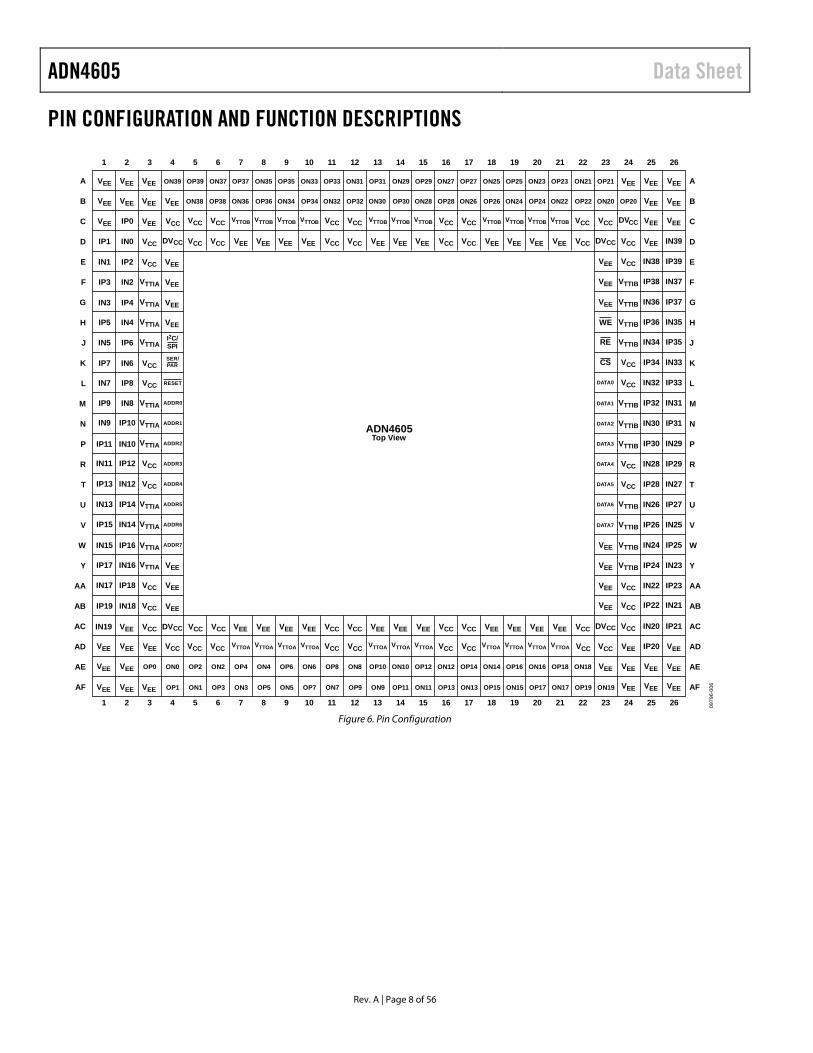
PIN CONFIGURATION AND FUNCTION DESCRIPTIONS
1 2 3 4 5 6 7 8 9 10 11 12 13 14 15 16 17 18 19 20 21 22 23 24 25 26
1 2 3 4 5 6 7 8 9 10 11 12 13 14 15 16 17 18 19 20 21 22 23 24 25 26
A
B
C
D
E
F
G
H
J
K
L
M
N
P
R
T
U
V
W
Y
AA
AB
AC
AD
AE
AF
A
B
C
D
E
F
G
H
J
K
L
M
N
P
R
T
U
V
W
Y
AA
AB
AC
AD
AE
AF
VEE VEE VEE VEE VEE VEEON39 OP39 ON37 OP37 ON35 OP35 ON33 OP33 ON31 OP31 ON29 OP29 ON27 OP27 ON25 OP25 ON23 OP23 ON21 OP21
ON38 OP38 ON36 OP36 ON34 OP34 ON32 OP32 ON30 OP30 ON28 OP28 ON26 OP26 ON24 OP24 ON22 OP22
VTTOBVTTOBVTTOBVTTOBVTTOBVTTOBVTTOBVTTOB VTTOBVTTOBVTTOB
ON20 OP20VEE VEE VEE VEE
VEEDVCC
DVCC
VCC
VCC
VCC
VTTIB
VTTIB
VTTIB
VTTIB
VCCCS
RE
WE
VCC
VCC
VCC
VCCVCC
VCCVCC
VCCVCC
VCCVCCIP0
IN0IP1
IP2IN1
IN2IP3
IP4IN3
IN4IP5
IP6IN5
IN6IP7
IP8IN7
IN8IP9
IP10IN9
IP12IN11
IN12IP13
IN10IP11
IN14IP15
IP14IN13
IN16IP17
IN18IP19
IP16IN15
IP18IN17
IN19
VCCVCCVCC
VCC
VCC
VCC
VCC
VCC
VCC
VCC VCC VCC VCC
VCC VCC VCC VCCVCCVCC VCC
VCC
VCC
VEE
VEE
VEE
VEE VEE VEE VEE VCC VCC VEE VEE VEE VEEVEE VEE VEEDVCCVEE
VTTIA
VTTIA
VTTIA
VTTIA
VTTIA
VTTIA
VTTIA
VTTIA
VTTIA
VTTIA
VTTIA
VCCVCCVCC
DVCC VEE
IN38 IP39
IP38
IN36
IP36
IN37
IP37
IN34
IP34
IN35
IP35
IN32
IP32
IN33
IP33
IN30
IP30
IN31
IP31
VEE
VEE
VEE
IN39
IN28 IP29
IP28
IN26
IP26
IN27
IP27
IN24
IP24
IN25
IP25
IN22
IP22
IN23
IP23
IN20
IP20
IN21
IP21
IN29
VEE
VEEVCC
DVCC
VCC
VCC
VEE
VEE VEEVEE
ON19
VEE
VEEVEE
VEE
VEE
DATA7
DATA6
DATA5
DATA4
DATA3
DATA2
DATA1
DATA0
VTTIB
VTTIB
VTTIB
VTTIB
VTTIB
VTTIB
VTTIB
VEE
VEE
VCC
VCC
VCC
VCC
VCC
VEE
VEE
VEE VEE
VEE VEE VEE
OP0 ON0
OP1 ON1
OP2 ON2
OP3 ON3
OP4 ON4
OP5 ON5
OP6 ON6
OP7 ON7
OP8 ON8
OP9 ON9
OP10 ON10
OP11 ON11
OP12 ON12
OP13 ON13
OP14 ON14
OP15 ON15
OP16 ON16
OP17 ON17
OP18 ON18
OP19VEE VEE VEE
VEE VEE
VEE
VEE
VEE
VEE
VEE
VEE VEE VEEVEE VEE VEE VEEVEE VEE VEE VEE
ADDR7
VTTOA VTTOA VTTOA VTTOA VTTOA VTTOA VTTOA VTTOA VTTOA VTTOA VTTOA
ADDR6
ADDR5
ADDR4
ADDR3
ADDR2
ADDR1
ADDR0
RESET
SER/PAR
I2C/SPI
ADN4605Top View
0979
6-00
6
Figure 6. Pin Configuration
Data Sheet ADN4605
Rev. A | Page 9 of 56
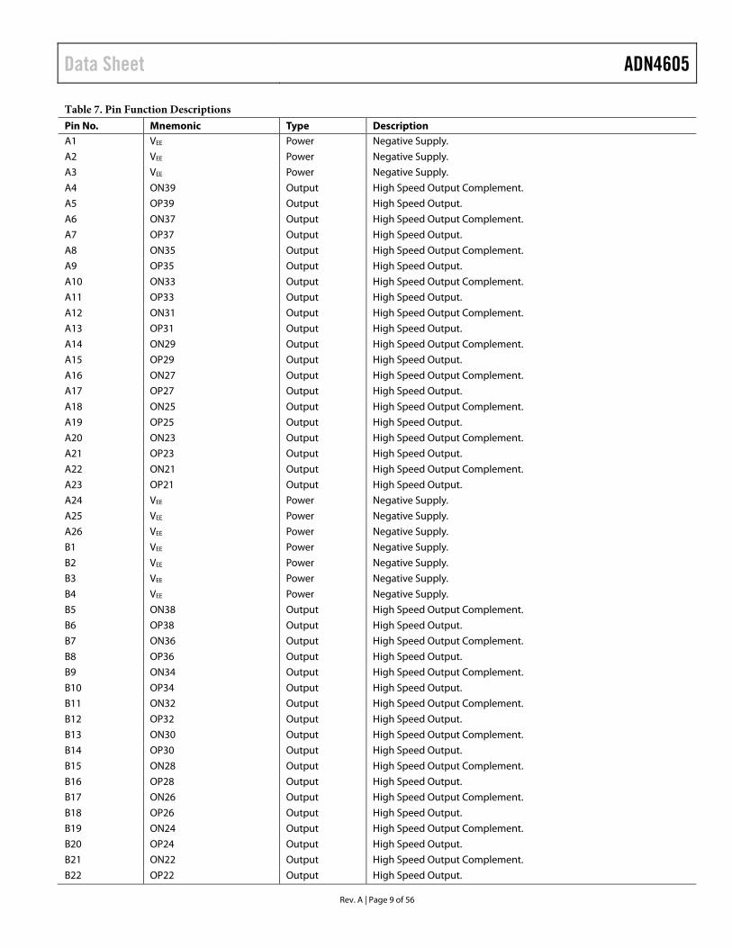
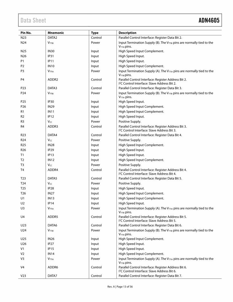
Table 7. Pin Function Descriptions Pin No. Mnemonic Type Description A1 VEE Power Negative Supply.
A2 VEE Power Negative Supply.
A3 VEE Power Negative Supply.
A4 ON39 Output High Speed Output Complement.
A5 OP39 Output High Speed Output.
A6 ON37 Output High Speed Output Complement.
A7 OP37 Output High Speed Output.
A8 ON35 Output High Speed Output Complement.
A9 OP35 Output High Speed Output.
A10 ON33 Output High Speed Output Complement.
A11 OP33 Output High Speed Output.
A12 ON31 Output High Speed Output Complement.
A13 OP31 Output High Speed Output.
A14 ON29 Output High Speed Output Complement.
A15 OP29 Output High Speed Output.
A16 ON27 Output High Speed Output Complement.
A17 OP27 Output High Speed Output.
A18 ON25 Output High Speed Output Complement.
A19 OP25 Output High Speed Output.
A20 ON23 Output High Speed Output Complement.
A21 OP23 Output High Speed Output.
A22 ON21 Output High Speed Output Complement.
A23 OP21 Output High Speed Output.
A24 VEE Power Negative Supply.
A25 VEE Power Negative Supply.
A26 VEE Power Negative Supply.
B1 VEE Power Negative Supply.
B2 VEE Power Negative Supply.
B3 VEE Power Negative Supply.
B4 VEE Power Negative Supply.
B5 ON38 Output High Speed Output Complement.
B6 OP38 Output High Speed Output.
B7 ON36 Output High Speed Output Complement.
B8 OP36 Output High Speed Output.
B9 ON34 Output High Speed Output Complement.
B10 OP34 Output High Speed Output.
B11 ON32 Output High Speed Output Complement.
B12 OP32 Output High Speed Output.
B13 ON30 Output High Speed Output Complement.
B14 OP30 Output High Speed Output.
B15 ON28 Output High Speed Output Complement.
B16 OP28 Output High Speed Output.
B17 ON26 Output High Speed Output Complement.
B18 OP26 Output High Speed Output.
B19 ON24 Output High Speed Output Complement.
B20 OP24 Output High Speed Output.
B21 ON22 Output High Speed Output Complement.
B22 OP22 Output High Speed Output.
ADN4605 Data Sheet
Rev. A | Page 10 of 56
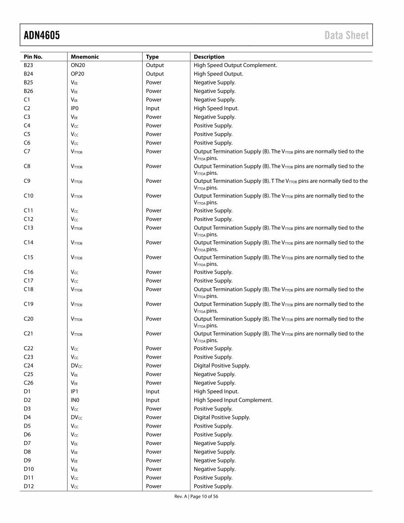
Pin No. Mnemonic Type Description B23 ON20 Output High Speed Output Complement.
B24 OP20 Output High Speed Output.
B25 VEE Power Negative Supply.
B26 VEE Power Negative Supply.
C1 VEE Power Negative Supply.
C2 IP0 Input High Speed Input.
C3 VEE Power Negative Supply.
C4 VCC Power Positive Supply.
C5 VCC Power Positive Supply.
C6 VCC Power Positive Supply.
C7 VTTOB Power Output Termination Supply (B). The VTTOB pins are normally tied to the VTTOA pins.
C8 VTTOB Power Output Termination Supply (B). The VTTOB pins are normally tied to the VTTOA pins.
C9 VTTOB Power Output Termination Supply (B). T The VTTOB pins are normally tied to the VTTOA pins.
C10 VTTOB Power Output Termination Supply (B). The VTTOB pins are normally tied to the VTTOA pins.
C11 VCC Power Positive Supply.
C12 VCC Power Positive Supply.
C13 VTTOB Power Output Termination Supply (B). The VTTOB pins are normally tied to the VTTOA pins.
C14 VTTOB Power Output Termination Supply (B). The VTTOB pins are normally tied to the VTTOA pins.
C15 VTTOB Power Output Termination Supply (B). The VTTOB pins are normally tied to the VTTOA pins.
C16 VCC Power Positive Supply.
C17 VCC Power Positive Supply.
C18 VTTOB Power Output Termination Supply (B). The VTTOB pins are normally tied to the VTTOA pins.
C19 VTTOB Power Output Termination Supply (B). The VTTOB pins are normally tied to the VTTOA pins.
C20 VTTOB Power Output Termination Supply (B). The VTTOB pins are normally tied to the VTTOA pins.
C21 VTTOB Power Output Termination Supply (B). The VTTOB pins are normally tied to the VTTOA pins.
C22 VCC Power Positive Supply.
C23 VCC Power Positive Supply.
C24 DVCC Power Digital Positive Supply.
C25 VEE Power Negative Supply.
C26 VEE Power Negative Supply.
D1 IP1 Input High Speed Input.
D2 IN0 Input High Speed Input Complement.
D3 VCC Power Positive Supply.
D4 DVCC Power Digital Positive Supply.
D5 VCC Power Positive Supply.
D6 VCC Power Positive Supply.
D7 VEE Power Negative Supply.
D8 VEE Power Negative Supply.
D9 VEE Power Negative Supply.
D10 VEE Power Negative Supply.
D11 VCC Power Positive Supply.
D12 VCC Power Positive Supply.
Data Sheet ADN4605
Rev. A | Page 11 of 56
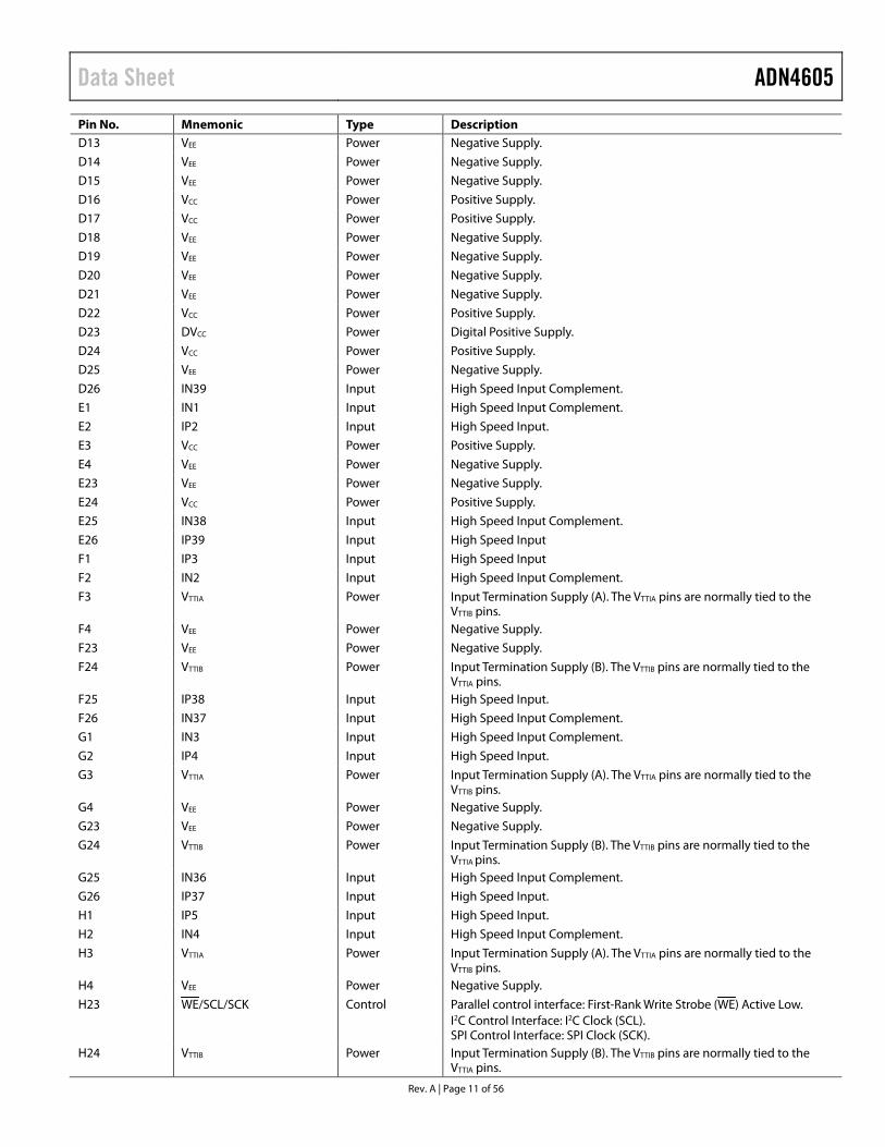
Pin No. Mnemonic Type Description D13 VEE Power Negative Supply.
D14 VEE Power Negative Supply.
D15 VEE Power Negative Supply.
D16 VCC Power Positive Supply.
D17 VCC Power Positive Supply.
D18 VEE Power Negative Supply.
D19 VEE Power Negative Supply.
D20 VEE Power Negative Supply.
D21 VEE Power Negative Supply.
D22 VCC Power Positive Supply.
D23 DVCC Power Digital Positive Supply.
D24 VCC Power Positive Supply.
D25 VEE Power Negative Supply.
D26 IN39 Input High Speed Input Complement.
E1 IN1 Input High Speed Input Complement.
E2 IP2 Input High Speed Input.
E3 VCC Power Positive Supply.
E4 VEE Power Negative Supply.
E23 VEE Power Negative Supply.
E24 VCC Power Positive Supply.
E25 IN38 Input High Speed Input Complement.
E26 IP39 Input High Speed Input
F1 IP3 Input High Speed Input
F2 IN2 Input High Speed Input Complement.
F3 VTTIA Power Input Termination Supply (A). The VTTIA pins are normally tied to the VTTIB pins.
F4 VEE Power Negative Supply.
F23 VEE Power Negative Supply.
F24 VTTIB Power Input Termination Supply (B). The VTTIB pins are normally tied to the VTTIA pins.
F25 IP38 Input High Speed Input.
F26 IN37 Input High Speed Input Complement.
G1 IN3 Input High Speed Input Complement.
G2 IP4 Input High Speed Input.
G3 VTTIA Power Input Termination Supply (A). The VTTIA pins are normally tied to the VTTIB pins.
G4 VEE Power Negative Supply.
G23 VEE Power Negative Supply.
G24 VTTIB Power Input Termination Supply (B). The VTTIB pins are normally tied to the VTTIA pins.
G25 IN36 Input High Speed Input Complement.
G26 IP37 Input High Speed Input.
H1 IP5 Input High Speed Input.
H2 IN4 Input High Speed Input Complement.
H3 VTTIA Power Input Termination Supply (A). The VTTIA pins are normally tied to the VTTIB pins.
H4 VEE Power Negative Supply.
H23 WE/SCL/SCK Control Parallel control interface: First-Rank Write Strobe (WE) Active Low. I2C Control Interface: I2C Clock (SCL). SPI Control Interface: SPI Clock (SCK).
H24 VTTIB Power Input Termination Supply (B). The VTTIB pins are normally tied to the VTTIA pins.
ADN4605 Data Sheet
Rev. A | Page 12 of 56
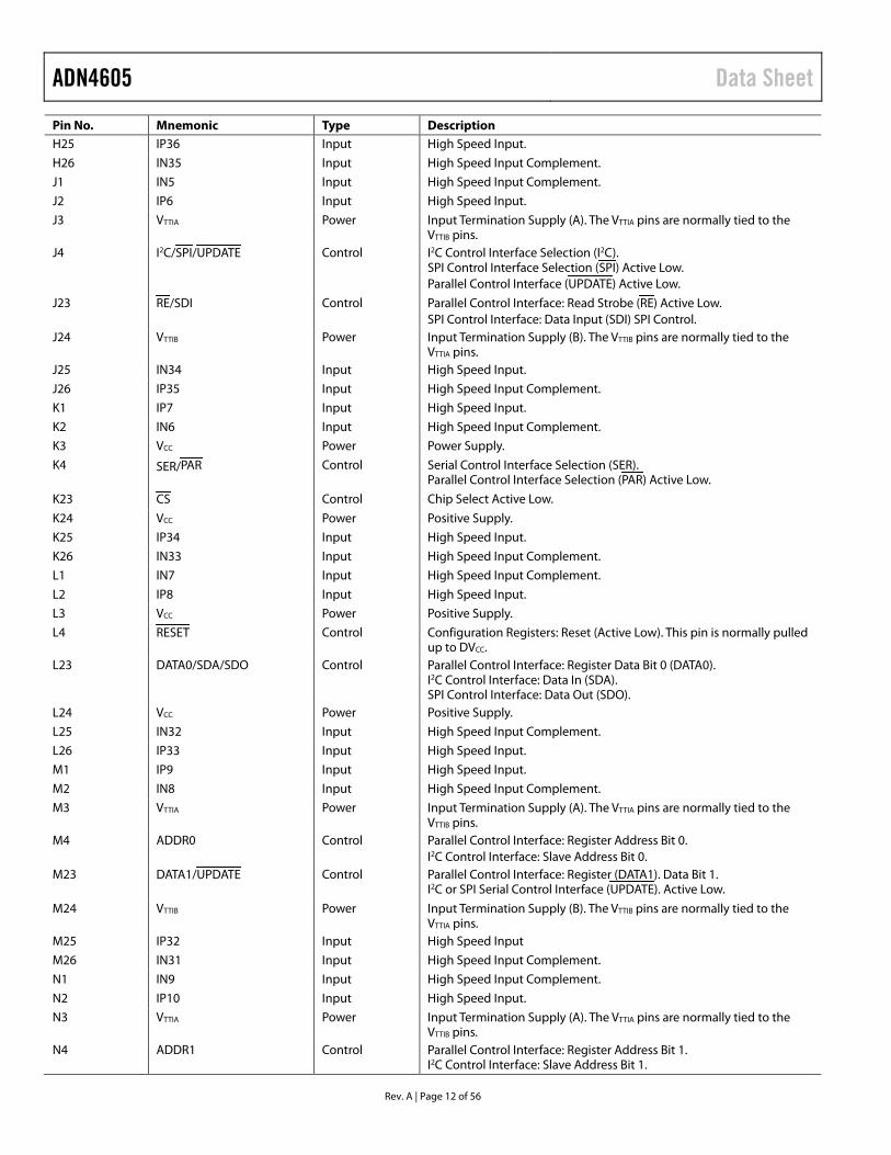
Pin No. Mnemonic Type Description H25 IP36 Input High Speed Input.
H26 IN35 Input High Speed Input Complement.
J1 IN5 Input High Speed Input Complement.
J2 IP6 Input High Speed Input.
J3 VTTIA Power Input Termination Supply (A). The VTTIA pins are normally tied to the VTTIB pins.
J4 I2C/SPI/ UPDATE Control I2C Control Interface Selection (I2C). SPI Control Interface Selection (SPI) Active Low. Parallel Control Interface (UPDATE) Active Low.
J23 RE/SDI Control Parallel Control Interface: Read Strobe (RE) Active Low. SPI Control Interface: Data Input (SDI) SPI Control.
J24 VTTIB Power Input Termination Supply (B). The VTTIB pins are normally tied to the VTTIA pins.
J25 IN34 Input High Speed Input.
J26 IP35 Input High Speed Input Complement.
K1 IP7 Input High Speed Input.
K2 IN6 Input High Speed Input Complement.
K3 VCC Power Power Supply.
K4 SER/PAR Control Serial Control Interface Selection (SER). Parallel Control Interface Selection (PAR) Active Low.
K23 CS Control Chip Select Active Low.
K24 VCC Power Positive Supply.
K25 IP34 Input High Speed Input.
K26 IN33 Input High Speed Input Complement.
L1 IN7 Input High Speed Input Complement.
L2 IP8 Input High Speed Input.
L3 VCC Power Positive Supply.
L4 RESET Control Configuration Registers: Reset (Active Low). This pin is normally pulled up to DVCC.
L23 DATA0/SDA/SDO Control Parallel Control Interface: Register Data Bit 0 (DATA0). I2C Control Interface: Data In (SDA). SPI Control Interface: Data Out (SDO).
L24 VCC Power Positive Supply.
L25 IN32 Input High Speed Input Complement.
L26 IP33 Input High Speed Input.
M1 IP9 Input High Speed Input.
M2 IN8 Input High Speed Input Complement.
M3 VTTIA Power Input Termination Supply (A). The VTTIA pins are normally tied to the VTTIB pins.
M4 ADDR0 Control Parallel Control Interface: Register Address Bit 0. I2C Control Interface: Slave Address Bit 0.
M23 DATA1/UPDATE Control Parallel Control Interface: Register (DATA1). Data Bit 1. I2C or SPI Serial Control Interface (UPDATE). Active Low.
M24 VTTIB Power Input Termination Supply (B). The VTTIB pins are normally tied to the VTTIA pins.
M25 IP32 Input High Speed Input
M26 IN31 Input High Speed Input Complement.
N1 IN9 Input High Speed Input Complement.
N2 IP10 Input High Speed Input.
N3 VTTIA Power Input Termination Supply (A). The VTTIA pins are normally tied to the VTTIB pins.
N4 ADDR1 Control Parallel Control Interface: Register Address Bit 1. I2C Control Interface: Slave Address Bit 1.
Data Sheet ADN4605
Rev. A | Page 13 of 56
Pin No. Mnemonic Type Description N23 DATA2 Control Parallel Control Interface: Register Data Bit 2.
N24 VTTIB Power Input Termination Supply (B). The VTTIB pins are normally tied to the VTTIA pins.
N25 IN30 Input High Speed Input Complement.
N26 IP31 Input High Speed Input.
P1 IP11 Input High Speed Input.
P2 IN10 Input High Speed Input Complement.
P3 VTTIA Power Input Termination Supply (A). The VTTIA pins are normally tied to the VTTIB pins.
P4 ADDR2 Control Parallel Control Interface: Register Address Bit 2. I2C Control Interface: Slave Address Bit 2.
P23 DATA3 Control Parallel Control Interface: Register Data Bit 3.
P24 VTTIB Power Input Termination Supply (B). The VTTIB pins are normally tied to the VTTIA pins.
P25 IP30 Input High Speed Input.
P26 IN29 Input High Speed Input Complement.
R1 IN11 Input High Speed Input Complement.
R2 IP12 Input High Speed Input.
R3 VCC Power Positive Supply.
R4 ADDR3 Control Parallel Control Interface: Register Address Bit 3. I2C Control Interface: Slave Address Bit 3.
R23 DATA4 Control Parallel Control Interface: Register Data Bit 4.
R24 VCC Power Positive Supply.
R25 IN28 Input High Speed Input Complement.
R26 IP29 Input High Speed Input.
T1 IP13 Input High Speed Input.
T2 IN12 Input High Speed Input Complement.
T3 VCC Power Positive Supply.
T4 ADDR4 Control Parallel Control Interface: Register Address Bit 4. I2C Control Interface: Slave Address Bit 4.
T23 DATA5 Control Parallel Control Interface: Register Data Bit 5.
T24 VCC Power Positive Supply.
T25 IP28 Input High Speed Input.
T26 IN27 Input High Speed Input Complement.
U1 IN13 Input High Speed Input Complement.
U2 IP14 Input High Speed Input.
U3 VTTIA Power Input Termination Supply (A). The VTTIA pins are normally tied to the VTTIB pins.
U4 ADDR5 Control Parallel Control Interface: Register Address Bit 5. I2C Control Interface: Slave Address Bit 5.
U23 DATA6 Control Parallel Control Interface: Register Data Bit 6.
U24 VTTIB Power Input Termination Supply (B). The VTTIB pins are normally tied to the VTTIA pins.
U25 IN26 Input High Speed Input Complement.
U26 IP27 Input High Speed Input.
V1 IP15 Input High Speed Input.
V2 IN14 Input High Speed Input Complement.
V3 VTTIA Power Input Termination Supply (A). The VTTIA pins are normally tied to the VTTIB pins.
V4 ADDR6 Control Parallel Control Interface: Register Address Bit 6. I2C Control Interface: Slave Address Bit 6.
V23 DATA7 Control Parallel Control Interface: Register Data Bit 7.
ADN4605 Data Sheet
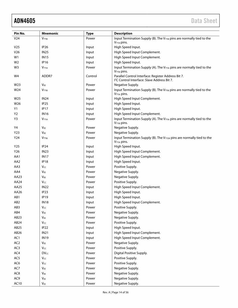
Rev. A | Page 14 of 56
Pin No. Mnemonic Type Description V24 VTTIB Power Input Termination Supply (B). The VTTIB pins are normally tied to the
VTTIA pins. V25 IP26 Input High Speed Input.
V26 IN25 Input High Speed Input Complement.
W1 IN15 Input High Speed Input Complement.
W2 IP16 Input High Speed Input.
W3 VTTIA Power Input Termination Supply (A). The VTTIA pins are normally tied to the VTTIB pins.
W4 ADDR7 Control Parallel Control Interface: Register Address Bit 7. I2C Control Interface: Slave Address Bit 7.
W23 VEE Power Negative Supply.
W24 VTTIB Power Input Termination Supply (B). The VTTIB pins are normally tied to the VTTIA pins.
W25 IN24 Input High Speed Input Complement.
W26 IP25 Input High Speed Input.
Y1 IP17 Input High Speed Input.
Y2 IN16 Input High Speed Input Complement.
Y3 VTTIA Power Input Termination Supply (A). The VTTIA pins are normally tied to the VTTIB pins.
Y4 VEE Power Negative Supply.
Y23 VEE Power Negative Supply.
Y24 VTTIB Power Input Termination Supply (B). The VTTOB pins are normally tied to the VTTIA pins.
Y25 IP24 Input High Speed Input.
Y26 IN23 Input High Speed Input Complement.
AA1 IN17 Input High Speed Input Complement.
AA2 IP18 Input High Speed Input.
AA3 VCC Power Positive Supply.
AA4 VEE Power Negative Supply.
AA23 VEE Power Negative Supply.
AA24 VCC Power Positive Supply.
AA25 IN22 Input High Speed Input Complement.
AA26 IP23 Input High Speed Input.
AB1 IP19 Input High Speed Input.
AB2 IN18 Input High Speed Input Complement.
AB3 VCC Power Positive Supply.
AB4 VEE Power Negative Supply.
AB23 VEE Power Negative Supply.
AB24 VCC Power Positive Supply.
AB25 IP22 Input High Speed Input.
AB26 IN21 Input High Speed Input Complement.
AC1 IN19 Input High Speed Input Complement.
AC2 VEE Power Negative Supply.
AC3 VCC Power Positive Supply.
AC4 DVCC Power Digital Positive Supply.
AC5 VCC Power Positive Supply.
AC6 VCC Power Positive Supply.
AC7 VEE Power Negative Supply.
AC8 VEE Power Negative Supply.
AC9 VEE Power Negative Supply.
AC10 VEE Power Negative Supply.
Data Sheet ADN4605
Rev. A | Page 15 of 56
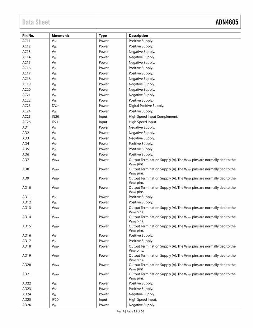
Pin No. Mnemonic Type Description AC11 VCC Power Positive Supply.
AC12 VCC Power Positive Supply.
AC13 VEE Power Negative Supply.
AC14 VEE Power Negative Supply.
AC15 VEE Power Negative Supply.
AC16 VCC Power Positive Supply.
AC17 VCC Power Positive Supply.
AC18 VEE Power Negative Supply.
AC19 VEE Power Negative Supply.
AC20 VEE Power Negative Supply.
AC21 VEE Power Negative Supply.
AC22 VCC Power Positive Supply.
AC23 DVCC Power Digital Positive Supply.
AC24 VCC Power Positive Supply.
AC25 IN20 Input High Speed Input Complement.
AC26 IP21 Input High Speed Input.
AD1 VEE Power Negative Supply.
AD2 VEE Power Negative Supply.
AD3 VEE Power Negative Supply.
AD4 VCC Power Positive Supply.
AD5 VCC Power Positive Supply.
AD6 VCC Power Positive Supply.
AD7 VTTOA Power Output Termination Supply (A). The VTTOA pins are normally tied to the VTTOB pins.
AD8 VTTOA Power Output Termination Supply (A). The VTTOA pins are normally tied to the VTTOB pins.
AD9 VTTOA Power Output Termination Supply (A). The VTTOA pins are normally tied to the VTTOB pins.
AD10 VTTOA Power Output Termination Supply (A). The VTTOA pins are normally tied to the VTTOB pins.
AD11 VCC Power Positive Supply.
AD12 VCC Power Positive Supply.
AD13 VTTOA Power Output Termination Supply (A). The VTTOA pins are normally tied to the VTTOB pins.
AD14 VTTOA Power Output Termination Supply (A). The VTTOA pins are normally tied to the VTTOB pins.
AD15 VTTOA Power Output Termination Supply (A). The VTTOA pins are normally tied to the VTTOB pins.
AD16 VCC Power Positive Supply.
AD17 VCC Power Positive Supply.
AD18 VTTOA Power Output Termination Supply (A). The VTTOA pins are normally tied to the VTTOB pins.
AD19 VTTOA Power Output Termination Supply (A). The VTTOA pins are normally tied to the VTTOB pins.
AD20 VTTOA Power Output Termination Supply (A). The VTTOA pins are normally tied to the VTTOB pins.
AD21 VTTOA Power Output Termination Supply (A). The VTTOA pins are normally tied to the VTTOB pins.
AD22 VCC Power Positive Supply.
AD23 VCC Power Positive Supply.
AD24 VEE Power Negative Supply.
AD25 IP20 Input High Speed Input.
AD26 VEE Power Negative Supply.
ADN4605 Data Sheet
Rev. A | Page 16 of 56
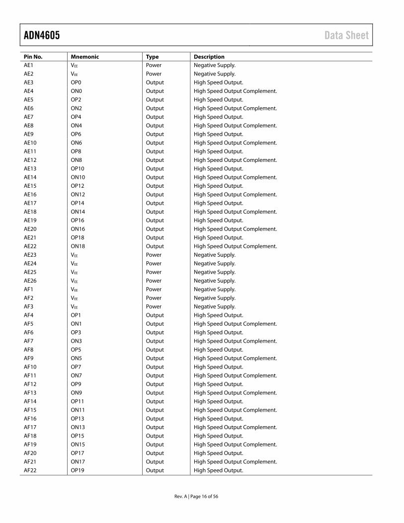
Pin No. Mnemonic Type Description AE1 VEE Power Negative Supply.
AE2 VEE Power Negative Supply.
AE3 OP0 Output High Speed Output.
AE4 ON0 Output High Speed Output Complement.
AE5 OP2 Output High Speed Output.
AE6 ON2 Output High Speed Output Complement.
AE7 OP4 Output High Speed Output.
AE8 ON4 Output High Speed Output Complement.
AE9 OP6 Output High Speed Output.
AE10 ON6 Output High Speed Output Complement.
AE11 OP8 Output High Speed Output.
AE12 ON8 Output High Speed Output Complement.
AE13 OP10 Output High Speed Output.
AE14 ON10 Output High Speed Output Complement.
AE15 OP12 Output High Speed Output.
AE16 ON12 Output High Speed Output Complement.
AE17 OP14 Output High Speed Output.
AE18 ON14 Output High Speed Output Complement.
AE19 OP16 Output High Speed Output.
AE20 ON16 Output High Speed Output Complement.
AE21 OP18 Output High Speed Output.
AE22 ON18 Output High Speed Output Complement.
AE23 VEE Power Negative Supply.
AE24 VEE Power Negative Supply.
AE25 VEE Power Negative Supply.
AE26 VEE Power Negative Supply.
AF1 VEE Power Negative Supply.
AF2 VEE Power Negative Supply.
AF3 VEE Power Negative Supply.
AF4 OP1 Output High Speed Output.
AF5 ON1 Output High Speed Output Complement.
AF6 OP3 Output High Speed Output.
AF7 ON3 Output High Speed Output Complement.
AF8 OP5 Output High Speed Output.
AF9 ON5 Output High Speed Output Complement.
AF10 OP7 Output High Speed Output.
AF11 ON7 Output High Speed Output Complement.
AF12 OP9 Output High Speed Output.
AF13 ON9 Output High Speed Output Complement.
AF14 OP11 Output High Speed Output.
AF15 ON11 Output High Speed Output Complement.
AF16 OP13 Output High Speed Output.
AF17 ON13 Output High Speed Output Complement.
AF18 OP15 Output High Speed Output.
AF19 ON15 Output High Speed Output Complement.
AF20 OP17 Output High Speed Output.
AF21 ON17 Output High Speed Output Complement.
AF22 OP19 Output High Speed Output.

Data Sheet ADN4605
Rev. A | Page 17 of 56
Pin No. Mnemonic Type Description AF23 ON19 Output High Speed Output Complement.
AF24 VEE Power Negative Supply.
AF25 VEE Power Negative Supply.
AF26 VEE Power Negative Supply.
ADN4605 Data Sheet
Rev. A | Page 18 of 56
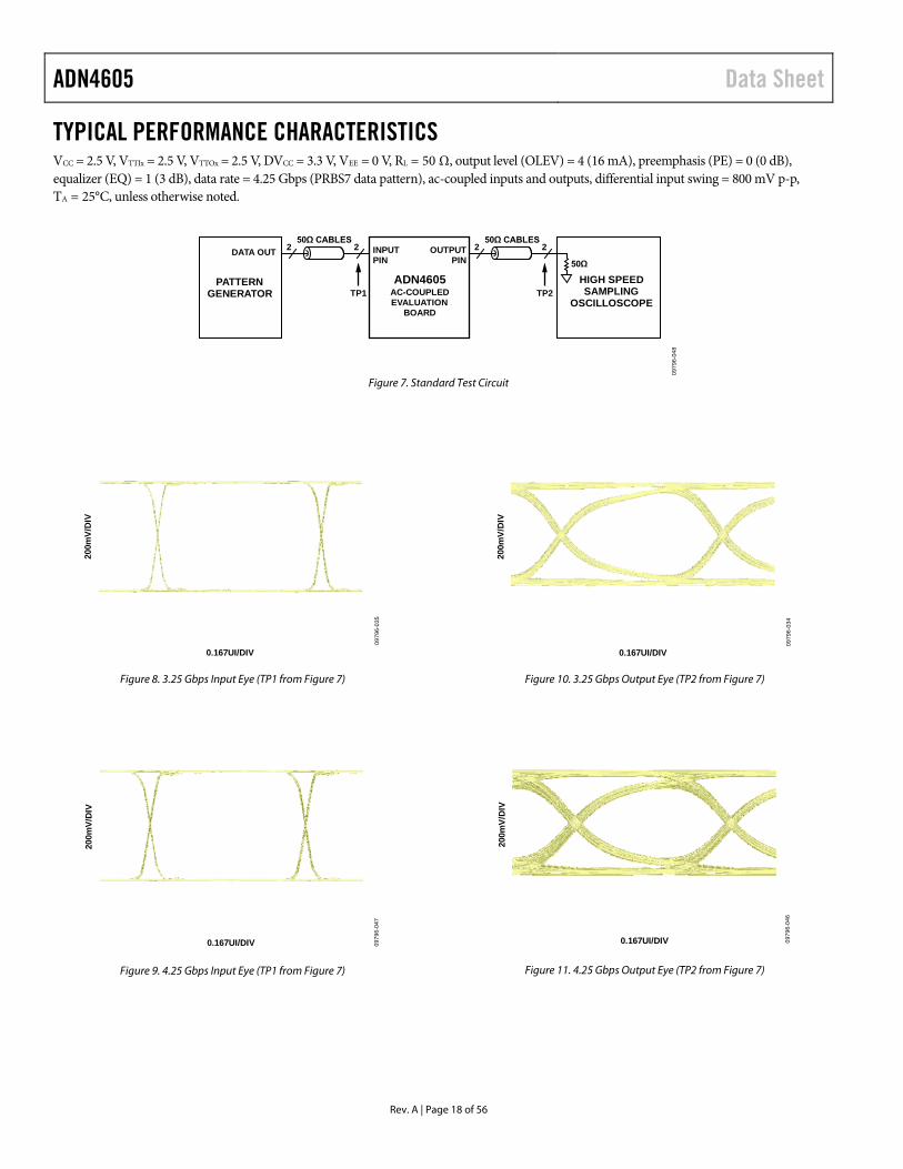
TYPICAL PERFORMANCE CHARACTERISTICS VCC = 2.5 V, VTTIx = 2.5 V, VTTOx = 2.5 V, DVCC = 3.3 V, VEE = 0 V, RL = 50 Ω, output level (OLEV) = 4 (16 mA), preemphasis (PE) = 0 (0 dB), equalizer (EQ) = 1 (3 dB), data rate = 4.25 Gbps (PRBS7 data pattern), ac-coupled inputs and outputs, differential input swing = 800 mV p-p, TA = 25°C, unless otherwise noted.
50Ω CABLES
2 2
HIGH SPEEDSAMPLING
OSCILLOSCOPE
50Ω CABLES2 2
50Ω
ADN4605AC-COUPLEDEVALUATION
BOARD
INPUTPIN
OUTPUTPIN
PATTERNGENERATOR
DATA OUT
TP2TP1
0979
6-04
8
Figure 7. Standard Test Circuit
0979
6-03
5
0.167UI/DIV
200m
V/D
IV
Figure 8. 3.25 Gbps Input Eye (TP1 from Figure 7)
0979
6-04
7
0.167UI/DIV
200m
V/D
IV
Figure 9. 4.25 Gbps Input Eye (TP1 from Figure 7)
0979
6-03
4
0.167UI/DIV
200m
V/D
IV
Figure 10. 3.25 Gbps Output Eye (TP2 from Figure 7)
0979
6-04
6
0.167UI/DIV
200m
V/D
IV
Figure 11. 4.25 Gbps Output Eye (TP2 from Figure 7)
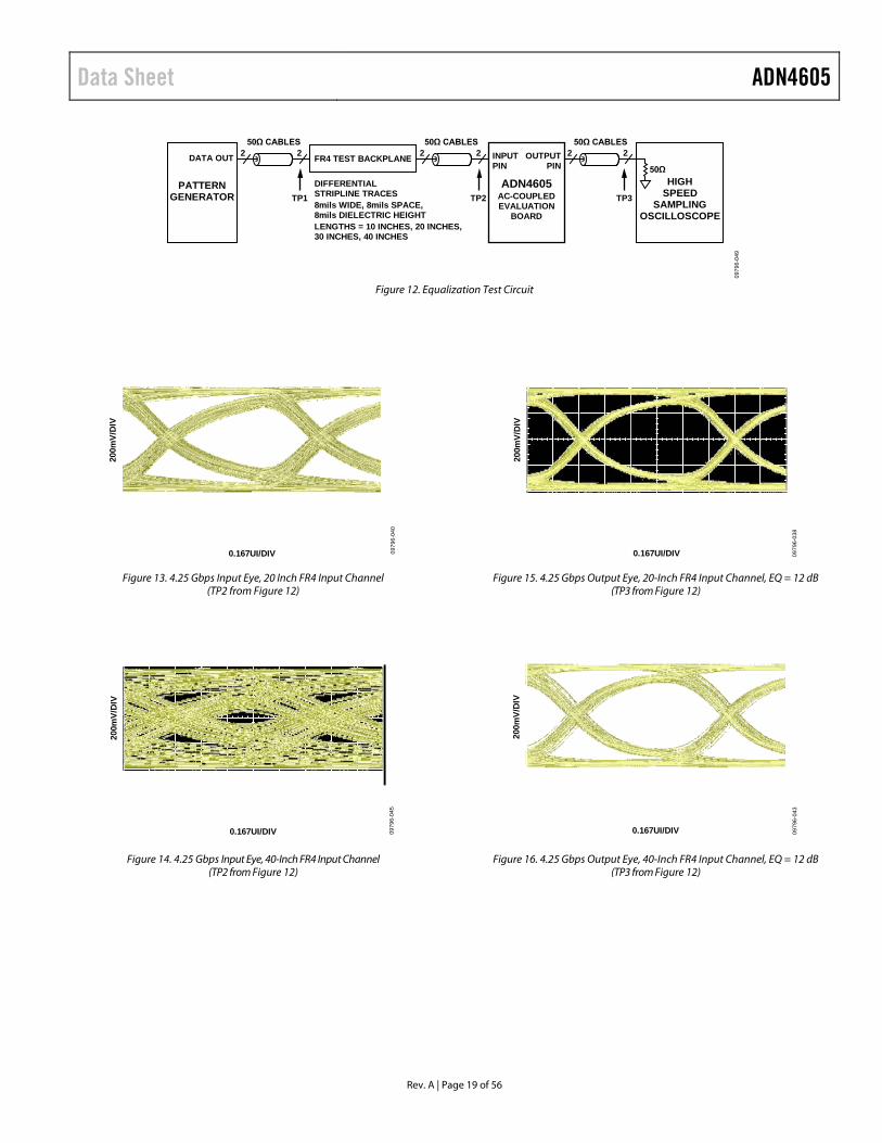
Data Sheet ADN4605
Rev. A | Page 19 of 56
50Ω CABLES
2 2
TP3
HIGHSPEED
SAMPLINGOSCILLOSCOPE
50Ω CABLES2 2
50Ω
ADN4605AC-COUPLEDEVALUATION
BOARD
INPUTPIN
OUTPUTPIN
PATTERNGENERATOR
DATA OUT
TP1
50Ω CABLES2 2
TP2
FR4 TEST BACKPLANE
DIFFERENTIALSTRIPLINE TRACES8mils WIDE, 8mils SPACE,8mils DIELECTRIC HEIGHTLENGTHS = 10 INCHES, 20 INCHES,30 INCHES, 40 INCHES
0979
6-04
9
Figure 12. Equalization Test Circuit
0979
6-04
0
0.167UI/DIV
200m
V/D
IV
Figure 13. 4.25 Gbps Input Eye, 20 Inch FR4 Input Channel (TP2 from Figure 12)
0979
6-04
5
0.167UI/DIV
200m
V/D
IV
Figure 14. 4.25 Gbps Input Eye, 40-Inch FR4 Input Channel (TP2 from Figure 12)
0979
6-03
8
0.167UI/DIV
200m
V/D
IV
Figure 15. 4.25 Gbps Output Eye, 20-Inch FR4 Input Channel, EQ = 12 dB (TP3 from Figure 12)
0979
6-04
3
0.167UI/DIV
200m
V/D
IV
Figure 16. 4.25 Gbps Output Eye, 40-Inch FR4 Input Channel, EQ = 12 dB (TP3 from Figure 12)
ADN4605 Data Sheet
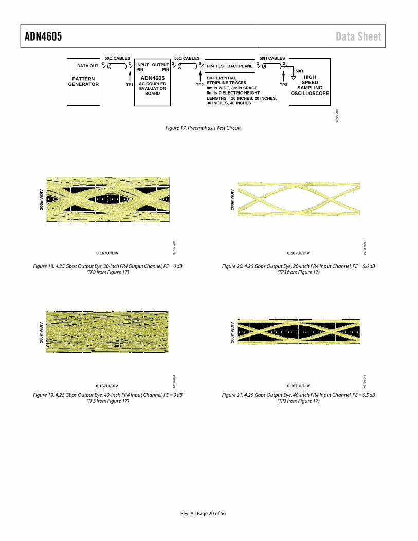
Rev. A | Page 20 of 56
50Ω CABLES2 2
TP3
HIGHSPEED
SAMPLINGOSCILLOSCOPE
50Ω CABLES2 2
50Ω
ADN4605AC-COUPLEDEVALUATION
BOARD
INPUTPIN
OUTPUTPIN
PATTERNGENERATOR
DATA OUT
TP1
50Ω CABLES2 2
TP2
FR4 TEST BACKPLANE
DIFFERENTIALSTRIPLINE TRACES8mils WIDE, 8mils SPACE,8mils DIELECTRIC HEIGHTLENGTHS = 10 INCHES, 20 INCHES,30 INCHES, 40 INCHES
0979
6-05
0
Figure 17. Preemphasis Test Circuit
0979
6-03
9
0.167UI/DIV
200m
V/D
IV
Figure 18. 4.25 Gbps Output Eye, 20-Inch FR4 Output Channel, PE = 0 dB (TP3 from Figure 17)
0979
6-04
4
0.167UI/DIV
200m
V/D
IV
Figure 19. 4.25 Gbps Output Eye, 40-Inch FR4 Input Channel, PE = 0 dB
(TP3 from Figure 17)
0979
6-03
6
0.167UI/DIV
200m
V/D
IV
Figure 20. 4.25 Gbps Output Eye, 20-Inch FR4 Input Channel, PE = 5.6 dB (TP3 from Figure 17)
0979
6-04
1
0.167UI/DIV
200m
V/D
IV
Figure 21. 4.25 Gbps Output Eye, 40-Inch FR4 Input Channel, PE = 9.5 dB
(TP3 from Figure 17)
Data Sheet ADN4605
Rev. A | Page 21 of 56
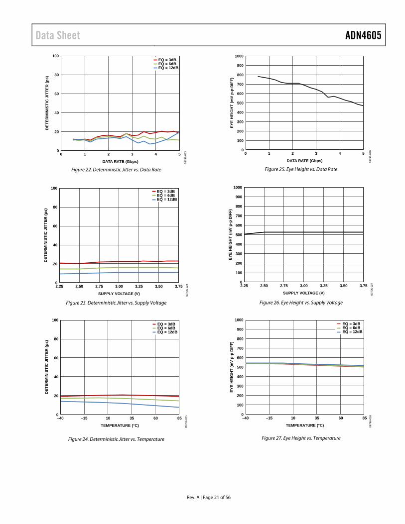
0
20
40
60
80
100
0 1 2 3 4 5
DET
ERM
INIS
TIC
JIT
TER
(ps)
DATA RATE (Gbps) 0979
6-03
3
EQ = 3dBEQ = 6dBEQ = 12dB
Figure 22. Deterministic Jitter vs. Data Rate
0
20
40
60
80
100
2.25 2.50 2.75 3.00 3.25 3.50 3.75
DET
ERM
INIS
TIC
JIT
TER
(ps)
SUPPLY VOLTAGE (V) 0979
6-02
4
EQ = 3dBEQ = 6dBEQ = 12dB
Figure 23. Deterministic Jitter vs. Supply Voltage
0
20
40
60
80
100
–40 –15 10 35 60 85
DET
ERM
INIS
TIC
JIT
TER
(ps)
TEMPERATURE (°C) 0979
6-02
5
EQ = 3dBEQ = 6dBEQ = 12dB
Figure 24. Deterministic Jitter vs. Temperature
0
100
200
300
400
500
600
700
800
900
1000
0 1 2 3 4 5
EYE
HEI
GH
T (m
V p-
p D
IFF)
DATA RATE (Gbps) 0979
6-03
0
Figure 25. Eye Height vs. Data Rate
0
100
200
300
400
500
600
700
800
900
1000
2.25 2.50 2.75 3.00 3.25 3.50 3.75
EYE
HEI
GH
T (m
V p-
p D
IFF)
SUPPLY VOLTAGE (V) 0979
6-02
7
Figure 26. Eye Height vs. Supply Voltage
0
100
200
300
400
500
600
700
800
900
1000
–40 –15 10 35 60 85
TEMPERATURE (°C)
EYE
HEI
GH
T(m
V p-
p D
IFF)
EQ = 3dBEQ = 6dBEQ = 12dB
0979
6-02
6
Figure 27. Eye Height vs. Temperature
ADN4605 Data Sheet
Rev. A | Page 22 of 56
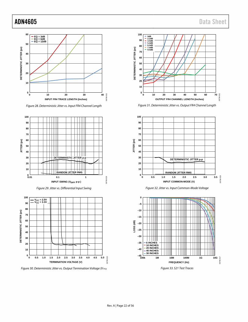
0
10
20
30
40
50
60
0 10 20 30 40
DET
ERM
INIS
TIC
JIT
TER
(ps)
INPUT FR4 TRACE LENGTH (Inches) 0979
6-03
2
EQ = 3dBEQ = 6dBEQ = 12dB
Figure 28. Deterministic Jitter vs. Input FR4 Channel Length
0
10
20
30
40
50
60
70
80
90
100
0.01 0.1 1
JITT
ER (p
s)
INPUT SWING (VDIFF p-p )
DETERMINISTIC JITTER p-p
RANDOM JITTER RMS
0979
6-02
9
Figure 29. Jitter vs. Differential Input Swing
0
10
20
30
40
50
60
70
80
90
100
0 0.5 1.0 1.5 2.0 2.5 3.0 3.5 4.0 4.5 5.0
DET
ERM
INIS
TIC
JIT
TER
(ps)
TERMINATION VOLTAGE (V)
VCC = 2.5VVCC = 3.3V
0979
6-02
2
Figure 30. Deterministic Jitter vs. Output Termination Voltage (VTTO)
0
10
20
30
40
50
60
70
80
90
100
0 10 20 30 40 50 60 70
DET
ERM
INIS
TIC
JIT
TER
(ps)
OUTPUT FR4 CHANNEL LENGTH (Inches) 0979
6-03
1
0dB2.2dB3.5dB5.4dB6.0dB7.4dB9.5dB
Figure 31. Deterministic Jitter vs. Output FR4 Channel Length
0
10
20
30
40
50
60
70
80
90
100
0 0.5 1.0 1.5 2.0 2.5 3.0 3.5
JITT
ER (p
s)
INPUT COMMON-MODE (V)
RANDOM JITTER RMS
DETERMINISTIC JITTER p-p
0979
6-02
8
Figure 32. Jitter vs. Input Common-Mode Voltage
–45
–40
–35
–30
–25
–20
–15
–10
–5
0
100k 1M 10M 100M 1G 10G
0979
6-01
7
LOSS
(dB
)
FREQUENCY (Hz)
6 INCHES10 INCHES20 INCHES40 INCHES30 INCHES
Figure 33. S21 Test Traces
Data Sheet ADN4605
Rev. A | Page 23 of 56
0
20
40
60
80
100
120
140
–40 –20 0 20 40 60 80 100
RIS
E/FA
LL T
IME
(ps)
TEMPERATURE (°C)
RISE TIMEFALL TIME
0979
6-01
8
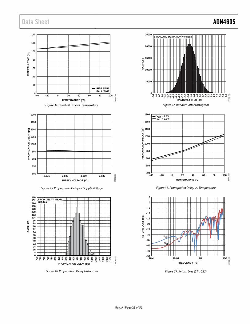
Figure 34. Rise/Fall Time vs. Temperature
800
850
900
950
1000
1050
1100
1150
1200
2.375 2.500 3.300 3.630
PRO
PAG
ATIO
N D
ELAY
(ps)
SUPPLY VOLTAGE (V) 0979
6-05
1
Figure 35. Propagation Delay vs. Supply Voltage
160152144136128120112104
9688807264564840322416
80
SAM
PLES
PROPAGATION DELAY (ps)
700
720
740
760
780
800
820
840
860
880
900
920
940
960
980
1000
1020
1040
1060
1080
1100
PROP DELAY MEAN922.4ps
0979
6-02
3
Figure 36. Propagation Delay Histogram
0979
6-02
10
5000
10000
15000
20000
25000
–4.0
–3.7
–3.4
–3.0
–2.7
–2.4
–2.1
–1.8
–1.4
–1.1
–0.8
–0.5
–0.2 0.2
0.5
0.8
1.1
1.4
1.8
2.1
2.4
2.7
3.0
3.4
3.7
4.0
SAM
PLES
RANDOM JITTER (ps)
STANDARD DEVIATION = 0.81ps
Figure 37. Random Jitter Histogram
800
850
900
950
1000
1050
1100
1150
1200
–40 –20 0 20 40 60 80 100
PRO
PAG
ATIO
N D
ELAY
(ps)
TEMPERATURE (°C)
VCC = 2.5VVCC = 3.3V
0979
6-02
0
Figure 38. Propagation Delay vs. Temperature
–50
–45
–40
–35
–30
–25
–20
–15
–10
–5
0
5
10M 100M 1G 10G
RET
UR
N L
OSS
(dB
)
FREQUENCY (Hz)
S22
S11
0979
6-01
9
Figure 39. Return Loss (S11, S22)
ADN4605 Data Sheet
Rev. A | Page 24 of 56
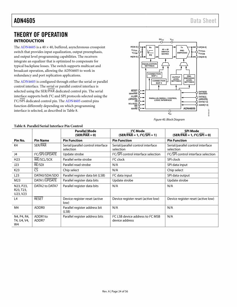
THEORY OF OPERATION INTRODUCTION The ADN4605 is a 40 × 40, buffered, asynchronous crosspoint switch that provides input equalization, output preemphasis, and output level programming capabilities. The receivers integrate an equalizer that is optimized to compensate for typical backplane losses. The switch supports multicast and broadcast operation, allowing the ADN4605 to work in redundancy and port replication applications.
The ADN4605 is configured through either the serial or parallel control interface. The serial or parallel control interface is selected using the SER/PAR dedicated control pin. The serial interface supports both I2C and SPI protocols selected using the I2C/ SPI dedicated control pin. The ADN4605 control pins function differently depending on which programming interface is selected, as described in Table 8.
EQ
Rx TxPRE-
EMPHASIS40 × 40
SWITCHMATRIX
CONNECTIONMAP 1
CONNECTIONMAP 0
PARALLEL/SERIAL CONTROLLOGIC INTERFACE
PRE-EMPHASIS
LEVELSETTINGS
OUTPUTLEVEL
SETTINGS
ADN4605
VCC
VEE
DVCC
OP[39:0]
VTTOA,VTTOBON[39:0]
IP[39:0]VTTIA,VTTIB
IN[39:0]
I2C/SPI(UPDATE)
SDI/RE
SCL/SCK/WE
RESETSER/PAR
CS
EQUALIZATIONSETTINGS
DATA[1](UPDATE)
DATA[0]/SDA/SDO
DATA[7:2]ADDR[7:0]
0979
6-00
7
Figure 40. Block Diagram
Table 8. Parallel/Serial Interface Pin Control
Pin No. Pin Name
Parallel Mode (SER/PAR = 0)
I2C Mode (SER/PAR = 1, I2C/ SPI = 1)
SPI Mode (SER/PAR = 1, I2C/ SPI = 0)
Pin Function Pin Function Pin Function K4 SER/PAR Serial/parallel control interface
selection Serial/parallel control interface selection
Serial/parallel control interface selection
J4 I2C/SPI/ UPDATE Update strobe I2C/SPI control interface selection I2C/SPI control interface selection
H23 WE/SCL/SCK Parallel write strobe I2C clock SPI clock
J23 RE/SDI Parallel read strobe N/A SPI data input
K23 CS Chip select N/A Chip select
L23 DATA0/SDA/SDO Parallel register data bit (LSB) I2C data input SPI data output M23 DATA1/UPDATE Parallel register data bits Update strobe Update strobe
N23, P23, R23, T23, U23, V23
DATA2 to DATA7 Parallel register data bits N/A N/A
L4 RESET Device register reset (active low)
Device register reset (active low) Device register reset (active low)
M4 ADDR0 Parallel register address bit (LSB)
N/A N/A
N4, P4, R4, T4, U4, V4, W4
ADDR1to ADDR7
Parallel register address bits I2C LSB device address to I2C MSB device address
N/A
Data Sheet ADN4605
Rev. A | Page 25 of 56
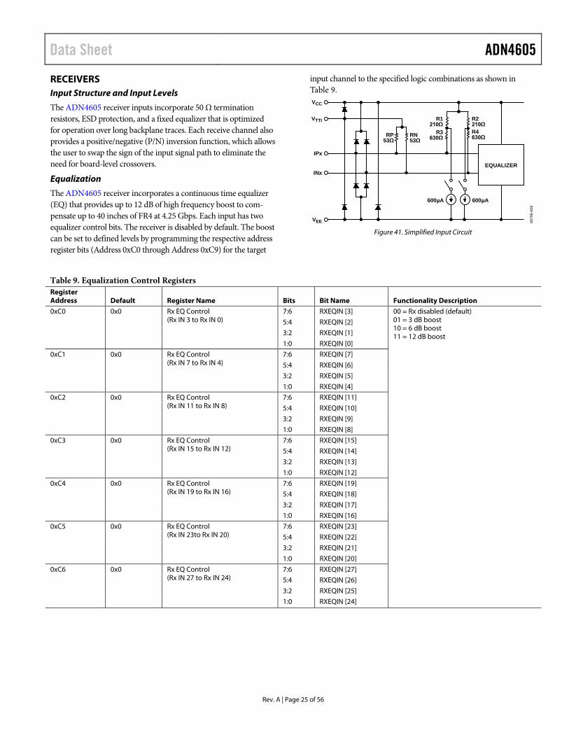
RECEIVERS Input Structure and Input Levels
The ADN4605 receiver inputs incorporate 50 Ω termination resistors, ESD protection, and a fixed equalizer that is optimized for operation over long backplane traces. Each receive channel also provides a positive/negative (P/N) inversion function, which allows the user to swap the sign of the input signal path to eliminate the need for board-level crossovers.
Equalization
The ADN4605 receiver incorporates a continuous time equalizer (EQ) that provides up to 12 dB of high frequency boost to com-pensate up to 40 inches of FR4 at 4.25 Gbps. Each input has two equalizer control bits. The receiver is disabled by default. The boost can be set to defined levels by programming the respective address register bits (Address 0xC0 through Address 0xC9) for the target
input channel to the specified logic combinations as shown in Table 9. VCC
VTTI
IPx
INx
VEE
R2210ΩR4630ΩRN
53ΩRP
53Ω
R1210Ω
R3630Ω
600µA 600µA
EQUALIZER
0979
6-00
8
Figure 41. Simplified Input Circuit
Table 9. Equalization Control Registers Register Address Default Register Name Bits Bit Name Functionality Description
0xC0 0x0 Rx EQ Control (Rx IN 3 to Rx IN 0)
7:6 RXEQIN [3] 00 = Rx disabled (default) 01 = 3 dB boost 10 = 6 dB boost 11 = 12 dB boost
5:4 RXEQIN [2]
3:2 RXEQIN [1]
1:0 RXEQIN [0]
0xC1 0x0 Rx EQ Control (Rx IN 7 to Rx IN 4)
7:6 RXEQIN [7]
5:4 RXEQIN [6]
3:2 RXEQIN [5]
1:0 RXEQIN [4]
0xC2 0x0 Rx EQ Control (Rx IN 11 to Rx IN 8)
7:6 RXEQIN [11]
5:4 RXEQIN [10]
3:2 RXEQIN [9]
1:0 RXEQIN [8]
0xC3 0x0 Rx EQ Control (Rx IN 15 to Rx IN 12)
7:6 RXEQIN [15]
5:4 RXEQIN [14]
3:2 RXEQIN [13]
1:0 RXEQIN [12]
0xC4 0x0 Rx EQ Control (Rx IN 19 to Rx IN 16)
7:6 RXEQIN [19]
5:4 RXEQIN [18]
3:2 RXEQIN [17]
1:0 RXEQIN [16]
0xC5 0x0 Rx EQ Control (Rx IN 23to Rx IN 20)
7:6 RXEQIN [23]
5:4 RXEQIN [22]
3:2 RXEQIN [21]
1:0 RXEQIN [20]
0xC6 0x0 Rx EQ Control (Rx IN 27 to Rx IN 24)
7:6 RXEQIN [27]
5:4 RXEQIN [26]
3:2 RXEQIN [25]
1:0 RXEQIN [24]
ADN4605 Data Sheet
Rev. A | Page 26 of 56
Register Address Default Register Name Bits Bit Name Functionality Description
0xC7 0x0 Rx EQ Control (Rx IN 31 to Rx IN 28)
7:6 RXEQIN [31] 00 = Rx disabled (default) 01 = 3 dB boost 10 = 6 dB boost 11 = 12 dB boost
5:4 RXEQIN [30]
3:2 RXEQIN [29]
1:0 RXEQIN [28]
0xC8 0x0 Rx EQ Control (Rx IN35 to Rx IN 32)
7:6 RXEQIN [35]
5:4 RXEQIN [34]
3:2 RXEQIN [33]
1:0 RXEQIN [32]
0xC9 0x0 Rx EQ Control (Rx IN 39 to Rx IN 36)
7:6 RXEQIN [39]
5:4 RXEQIN [38]
3:2 RXEQIN [37]
1:0 RXEQIN [36]
0xCA 0x0 (Write only)
Rx EQ Control (Rx IN Broadcast)
1:0 RXEQIN BC
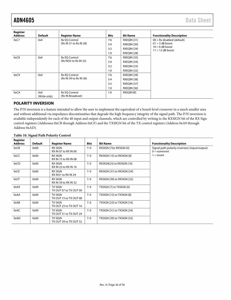
POLARITY INVERSION The P/N inversion is a feature intended to allow the user to implement the equivalent of a board-level crossover in a much smaller area and without additional via impedance discontinuities that degrade the high frequency integrity of the signal path. The P/N inversion is available independently for each of the 40 input and output channels, which are controlled by writing to the RXSIGN bit of the RX Sign control registers (Addresses 0xCB through Address 0xCF) and the TXSIGN bit of the TX control registers (Address 0xA9 through Address 0xAD).
Table 10. Signal Path Polarity Control Register Address Default Register Name Bits Bit Name Functionality Description
0xCB 0x00 RX SIGN RX IN 07 to RX IN 00
7: 0 RXSIGN [7]to RXSIGN [0] Signal path polarity inversion (input/output) 0 = noninvert 1 = invert
0xCC 0x00 RX SIGN RX IN 15 to RX IN 08
7: 0 RXSIGN [15] to RXSIGN [8]
0xCD 0x00 RX SIGN RX IN 23 to RX IN 16
7: 0 RXSIGN[23] to RXSIGN [16]
0xCE 0x00 RX SIGN RX IN31 to RX IN 24
7: 0 RXSIGN [31] to RXSIGN [24]
0xCF 0x00 RX SIGN RX IN 39 to RX IN 32
7: 0 RXSIGN [39] to RXSIGN [32]
0xA9 0x00 TX SIGN TX OUT 07 to TX OUT 00
7: 0 TXSIGN [7] to TXSIGN [0]
0xAA 0x00 TX SIGN TX OUT 15 to TX OUT 08
7: 0 TXSIGN [15] to TXSIGN [8]
0xAB 0x00 TX SIGN TX OUT 23 to TX OUT 16
7: 0 TXSIGN [23] to TXSIGN [16]
0xAC 0x00 TX SIGN TX OUT 31 to TX OUT 24
7: 0 TXSIGN [31] to TXSIGN [24]
0xAD 0x00 TX SIGN TX OUT 39 to TX OUT 32
7: 0 TXSIGN [39] to TXSIGN [32]
Data Sheet ADN4605
Rev. A | Page 27 of 56
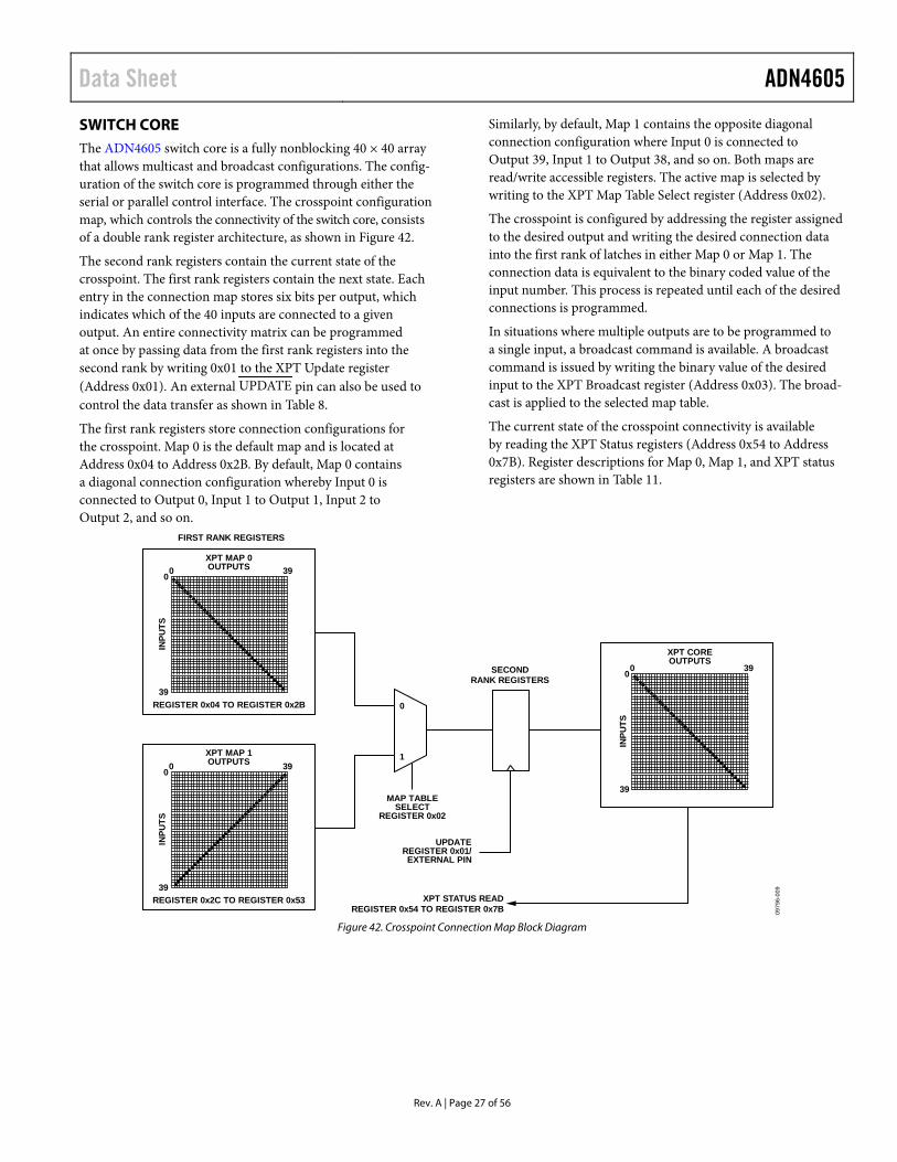
SWITCH CORE The ADN4605 switch core is a fully nonblocking 40 × 40 array that allows multicast and broadcast configurations. The config-uration of the switch core is programmed through either the serial or parallel control interface. The crosspoint configuration map, which controls the connectivity of the switch core, consists of a double rank register architecture, as shown in Figure 42.
The second rank registers contain the current state of the crosspoint. The first rank registers contain the next state. Each entry in the connection map stores six bits per output, which indicates which of the 40 inputs are connected to a given output. An entire connectivity matrix can be programmed at once by passing data from the first rank registers into the second rank by writing 0x01 to the XPT Update register (Address 0x01). An external UPDATE pin can also be used to control the data transfer as shown in Table 8.
The first rank registers store connection configurations for the crosspoint. Map 0 is the default map and is located at Address 0x04 to Address 0x2B. By default, Map 0 contains a diagonal connection configuration whereby Input 0 is connected to Output 0, Input 1 to Output 1, Input 2 to Output 2, and so on.
Similarly, by default, Map 1 contains the opposite diagonal connection configuration where Input 0 is connected to Output 39, Input 1 to Output 38, and so on. Both maps are read/write accessible registers. The active map is selected by writing to the XPT Map Table Select register (Address 0x02).
The crosspoint is configured by addressing the register assigned to the desired output and writing the desired connection data into the first rank of latches in either Map 0 or Map 1. The connection data is equivalent to the binary coded value of the input number. This process is repeated until each of the desired connections is programmed.
In situations where multiple outputs are to be programmed to a single input, a broadcast command is available. A broadcast command is issued by writing the binary value of the desired input to the XPT Broadcast register (Address 0x03). The broad-cast is applied to the selected map table.
The current state of the crosspoint connectivity is available by reading the XPT Status registers (Address 0x54 to Address 0x7B). Register descriptions for Map 0, Map 1, and XPT status registers are shown in Table 11.
0 390
39
INPU
TSIN
PUTS
REGISTER 0x04 TO REGISTER 0x2B
XPT MAP 0OUTPUTS
REGISTER 0x2C TO REGISTER 0x53
XPT MAP 1OUTPUTS
0
1
MAP TABLESELECT
REGISTER 0x02
XPT STATUS READREGISTER 0x54 TO REGISTER 0x7B
UPDATEREGISTER 0x01/
EXTERNAL PIN
FIRST RANK REGISTERS
SECONDRANK REGISTERS
0 390
39
XPT COREOUTPUTS
0979
6-00
9
0 390
39
INPU
TS
Figure 42. Crosspoint Connection Map Block Diagram
ADN4605 Data Sheet
Rev. A | Page 28 of 56
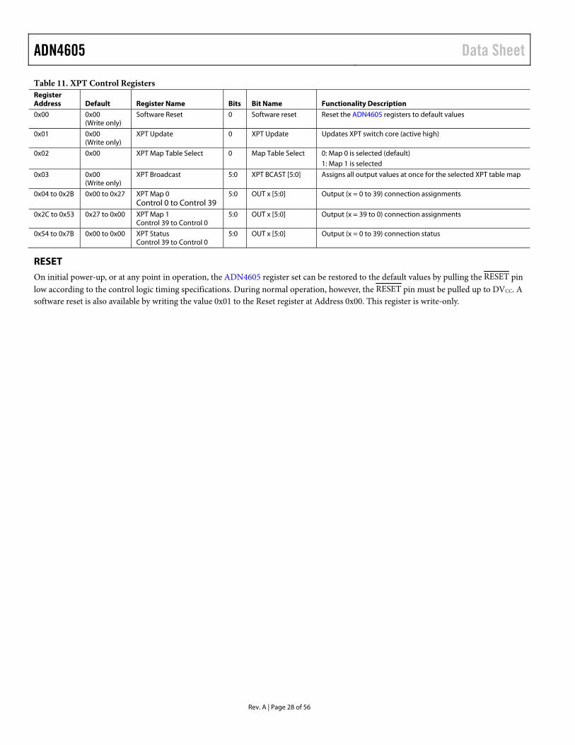
Table 11. XPT Control Registers Register Address Default Register Name Bits Bit Name Functionality Description
0x00 0x00 (Write only)
Software Reset 0 Software reset Reset the ADN4605 registers to default values
0x01 0x00 (Write only)
XPT Update 0 XPT Update Updates XPT switch core (active high)
0x02 0x00 XPT Map Table Select 0 Map Table Select 0: Map 0 is selected (default) 1: Map 1 is selected
0x03 0x00 (Write only)
XPT Broadcast 5:0 XPT BCAST [5:0] Assigns all output values at once for the selected XPT table map
0x04 to 0x2B 0x00 to 0x27 XPT Map 0 Control 0 to Control 39
5:0 OUT x [5:0] Output (x = 0 to 39) connection assignments
0x2C to 0x53 0x27 to 0x00 XPT Map 1 Control 39 to Control 0
5:0 OUT x [5:0] Output (x = 39 to 0) connection assignments
0x54 to 0x7B 0x00 to 0x00 XPT Status Control 39 to Control 0
5:0 OUT x [5:0] Output (x = 0 to 39) connection status
RESET
On initial power-up, or at any point in operation, the ADN4605 register set can be restored to the default values by pulling the RESET pin low according to the control logic timing specifications. During normal operation, however, the RESET pin must be pulled up to DVCC. A software reset is also available by writing the value 0x01 to the Reset register at Address 0x00. This register is write-only.
Data Sheet ADN4605
Rev. A | Page 29 of 56
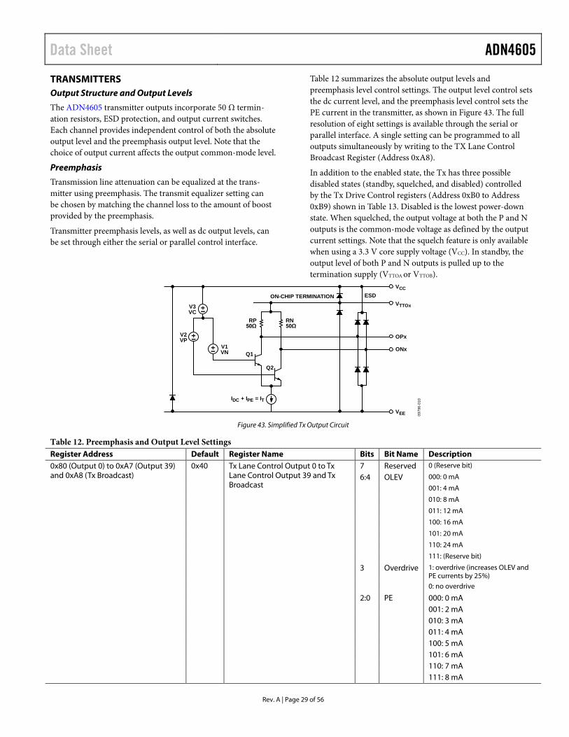
TRANSMITTERS Output Structure and Output Levels
The ADN4605 transmitter outputs incorporate 50 Ω termin-ation resistors, ESD protection, and output current switches. Each channel provides independent control of both the absolute output level and the preemphasis output level. Note that the choice of output current affects the output common-mode level.
Preemphasis
Transmission line attenuation can be equalized at the trans-mitter using preemphasis. The transmit equalizer setting can be chosen by matching the channel loss to the amount of boost provided by the preemphasis.
Transmitter preemphasis levels, as well as dc output levels, can be set through either the serial or parallel control interface.
Table 12 summarizes the absolute output levels and preemphasis level control settings. The output level control sets the dc current level, and the preemphasis level control sets the PE current in the transmitter, as shown in Figure 43. The full resolution of eight settings is available through the serial or parallel interface. A single setting can be programmed to all outputs simultaneously by writing to the TX Lane Control Broadcast Register (Address 0xA8).
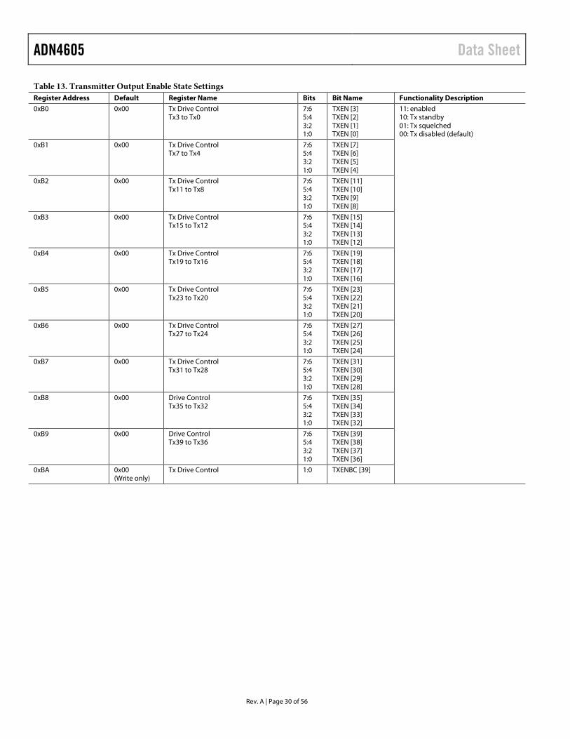
In addition to the enabled state, the Tx has three possible disabled states (standby, squelched, and disabled) controlled by the Tx Drive Control registers (Address 0xB0 to Address 0xB9) shown in Table 13. Disabled is the lowest power-down state. When squelched, the output voltage at both the P and N outputs is the common-mode voltage as defined by the output current settings. Note that the squelch feature is only available when using a 3.3 V core supply voltage (VCC). In standby, the output level of both P and N outputs is pulled up to the termination supply (VTTOA or VTTOB).
ON-CHIP TERMINATION ESDVCC
VTTOx
OPx
ONx
VEE
V3VC
V2VP
V1VN Q1
IDC + IPE = IT
Q2
RP50Ω
RN50Ω
0979
6-01
0
Figure 43. Simplified Tx Output Circuit
Table 12. Preemphasis and Output Level Settings Register Address Default Register Name Bits Bit Name Description 0x80 (Output 0) to 0xA7 (Output 39) and 0xA8 (Tx Broadcast)
0x40 Tx Lane Control Output 0 to Tx Lane Control Output 39 and Tx Broadcast
7 Reserved 0 (Reserve bit)
6:4 OLEV 000: 0 mA
001: 4 mA
010: 8 mA
011: 12 mA
100: 16 mA
101: 20 mA
110: 24 mA
111: (Reserve bit)
3 Overdrive 1: overdrive (increases OLEV and PE currents by 25%)
0: no overdrive
2:0 PE 000: 0 mA 001: 2 mA 010: 3 mA 011: 4 mA 100: 5 mA 101: 6 mA 110: 7 mA 111: 8 mA
ADN4605 Data Sheet
Rev. A | Page 30 of 56
Table 13. Transmitter Output Enable State Settings Register Address Default Register Name Bits Bit Name Functionality Description
0xB0 0x00 Tx Drive Control Tx3 to Tx0
7:6 5:4 3:2 1:0
TXEN [3] TXEN [2] TXEN [1] TXEN [0]
11: enabled 10: Tx standby 01: Tx squelched 00: Tx disabled (default) 0xB1 0x00 Tx Drive Control
Tx7 to Tx4 7:6 5:4 3:2 1:0
TXEN [7] TXEN [6] TXEN [5] TXEN [4]
0xB2 0x00 Tx Drive Control Tx11 to Tx8
7:6 5:4 3:2 1:0
TXEN [11] TXEN [10] TXEN [9] TXEN [8]
0xB3 0x00 Tx Drive Control Tx15 to Tx12
7:6 5:4 3:2 1:0
TXEN [15] TXEN [14] TXEN [13] TXEN [12]
0xB4 0x00 Tx Drive Control Tx19 to Tx16
7:6 5:4 3:2 1:0
TXEN [19] TXEN [18] TXEN [17] TXEN [16]
0xB5 0x00 Tx Drive Control Tx23 to Tx20
7:6 5:4 3:2 1:0
TXEN [23] TXEN [22] TXEN [21] TXEN [20]
0xB6 0x00 Tx Drive Control Tx27 to Tx24
7:6 5:4 3:2 1:0
TXEN [27] TXEN [26] TXEN [25] TXEN [24]
0xB7 0x00 Tx Drive Control Tx31 to Tx28
7:6 5:4 3:2 1:0
TXEN [31] TXEN [30] TXEN [29] TXEN [28]
0xB8 0x00 Drive Control Tx35 to Tx32
7:6 5:4 3:2 1:0
TXEN [35] TXEN [34] TXEN [33] TXEN [32]
0xB9 0x00 Drive Control Tx39 to Tx36
7:6 5:4 3:2 1:0
TXEN [39] TXEN [38] TXEN [37] TXEN [36]
0xBA 0x00 (Write only)
Tx Drive Control 1:0 TXENBC [39]
Data Sheet ADN4605
Rev. A | Page 31 of 56
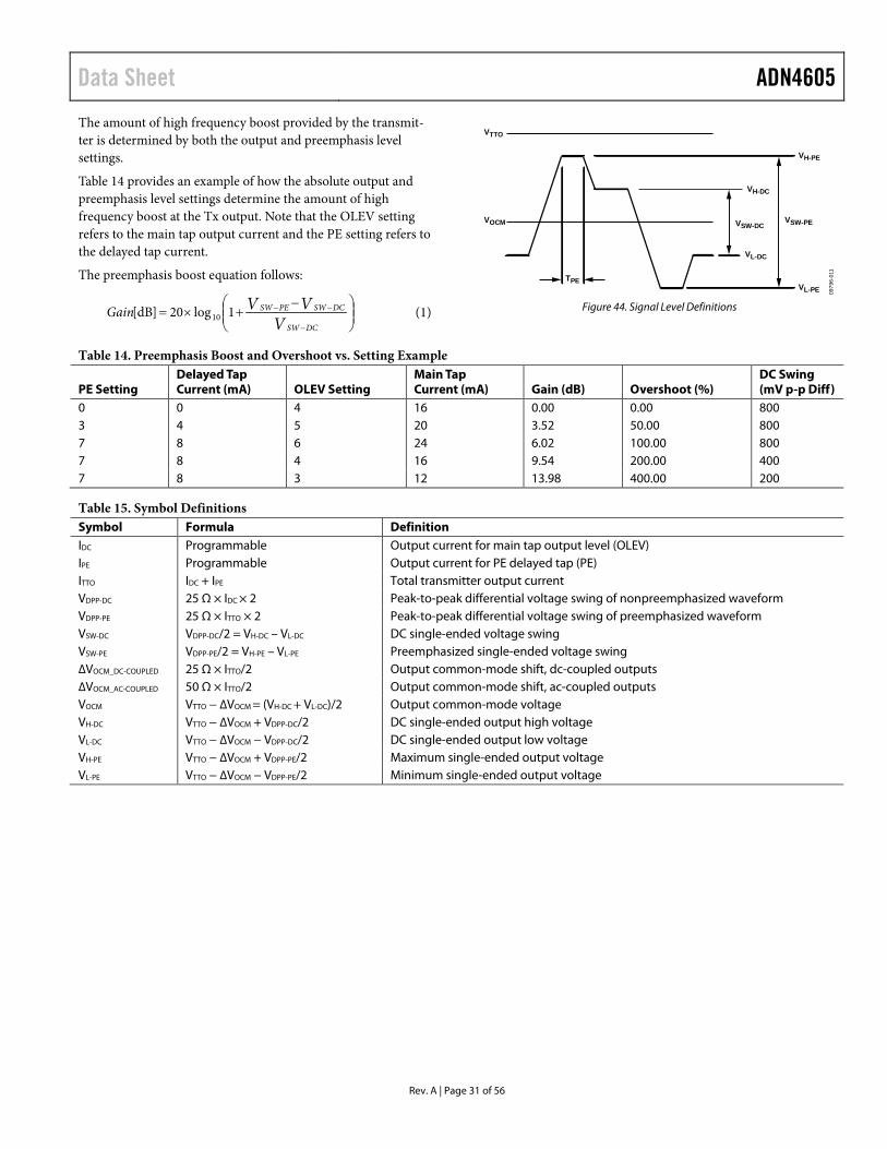
The amount of high frequency boost provided by the transmit-ter is determined by both the output and preemphasis level settings.
Table 14 provides an example of how the absolute output and preemphasis level settings determine the amount of high frequency boost at the Tx output. Note that the OLEV setting refers to the main tap output current and the PE setting refers to the delayed tap current.
The preemphasis boost equation follows:
−+×=
−
−−
VVV
DCSW
DCSWPESWGain 1log20]dB[ 10 (1)
VTTO
VH-PE
VSW-PE
VL-PE
VL-DC
VSW-DC
VH-DC
VOCM
TPE
0979
6-01
1
Figure 44. Signal Level Definitions
Table 14. Preemphasis Boost and Overshoot vs. Setting Example
PE Setting Delayed Tap Current (mA) OLEV Setting
Main Tap Current (mA) Gain (dB) Overshoot (%)
DC Swing (mV p-p Diff)
0 0 4 16 0.00 0.00 800 3 4 5 20 3.52 50.00 800 7 8 6 24 6.02 100.00 800 7 8 4 16 9.54 200.00 400 7 8 3 12 13.98 400.00 200
Table 15. Symbol Definitions Symbol Formula Definition IDC Programmable Output current for main tap output level (OLEV) IPE Programmable Output current for PE delayed tap (PE) ITTO IDC + IPE Total transmitter output current VDPP-DC 25 Ω × IDC × 2 Peak-to-peak differential voltage swing of nonpreemphasized waveform VDPP-PE 25 Ω × ITTO × 2 Peak-to-peak differential voltage swing of preemphasized waveform VSW-DC VDPP-DC/2 = VH-DC – VL-DC DC single-ended voltage swing VSW-PE VDPP-PE/2 = VH-PE – VL-PE Preemphasized single-ended voltage swing ∆VOCM_DC-COUPLED 25 Ω × ITTO/2 Output common-mode shift, dc-coupled outputs ∆VOCM_AC-COUPLED 50 Ω × ITTO/2 Output common-mode shift, ac-coupled outputs VOCM VTTO − ∆VOCM = (VH-DC + VL-DC)/2 Output common-mode voltage VH-DC VTTO − ∆VOCM + VDPP-DC/2 DC single-ended output high voltage VL-DC VTTO − ∆VOCM − VDPP-DC/2 DC single-ended output low voltage VH-PE VTTO − ∆VOCM + VDPP-PE/2 Maximum single-ended output voltage VL-PE VTTO − ∆VOCM − VDPP-PE/2 Minimum single-ended output voltage
ADN4605 Data Sheet
Rev. A | Page 32 of 56
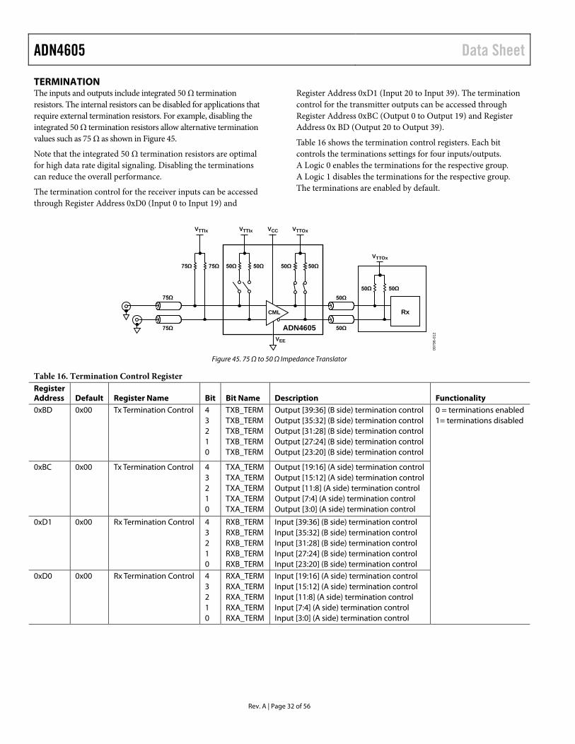
TERMINATION The inputs and outputs include integrated 50 Ω termination resistors. The internal resistors can be disabled for applications that require external termination resistors. For example, disabling the integrated 50 Ω termination resistors allow alternative termination values such as 75 Ω as shown in Figure 45.
Note that the integrated 50 Ω termination resistors are optimal for high data rate digital signaling. Disabling the terminations can reduce the overall performance.
The termination control for the receiver inputs can be accessed through Register Address 0xD0 (Input 0 to Input 19) and
Register Address 0xD1 (Input 20 to Input 39). The termination control for the transmitter outputs can be accessed through Register Address 0xBC (Output 0 to Output 19) and Register Address 0x BD (Output 20 to Output 39).
Table 16 shows the termination control registers. Each bit controls the terminations settings for four inputs/outputs. A Logic 0 enables the terminations for the respective group. A Logic 1 disables the terminations for the respective group. The terminations are enabled by default.
CML
VEE
VTTOx
VTTOx
VCCVTTIx
ADN4605
Rx
50Ω50Ω
50Ω50Ω50Ω
75Ω
75Ω
50Ω
VTTIx
75Ω75Ω
50Ω
50Ω
0979
6-01
2
Figure 45. 75 Ω to 50 Ω Impedance Translator
Table 16. Termination Control Register Register Address Default Register Name Bit Bit Name Description Functionality 0xBD 0x00 Tx Termination Control 4
3 2 1 0
TXB_TERM TXB_TERM TXB_TERM TXB_TERM TXB_TERM
Output [39:36] (B side) termination control Output [35:32] (B side) termination control Output [31:28] (B side) termination control Output [27:24] (B side) termination control Output [23:20] (B side) termination control
0 = terminations enabled 1= terminations disabled
0xBC 0x00 Tx Termination Control 4 3 2 1 0
TXA_TERM TXA_TERM TXA_TERM TXA_TERM TXA_TERM
Output [19:16] (A side) termination control Output [15:12] (A side) termination control Output [11:8] (A side) termination control Output [7:4] (A side) termination control Output [3:0] (A side) termination control
0xD1 0x00 Rx Termination Control 4 3 2 1 0
RXB_TERM RXB_TERM RXB_TERM RXB_TERM RXB_TERM
Input [39:36] (B side) termination control Input [35:32] (B side) termination control Input [31:28] (B side) termination control Input [27:24] (B side) termination control Input [23:20] (B side) termination control
0xD0 0x00 Rx Termination Control 4 3 2 1 0
RXA_TERM RXA_TERM RXA_TERM RXA_TERM RXA_TERM
Input [19:16] (A side) termination control Input [15:12] (A side) termination control Input [11:8] (A side) termination control Input [7:4] (A side) termination control Input [3:0] (A side) termination control
Data Sheet ADN4605
Rev. A | Page 33 of 56
I2C SERIAL CONTROL INTERFACE The ADN4605 register set is controlled through a 2-wire I2C interface. To access the I2C serial interface, both the SER/PAR line and I2C/ SPI lines must be held at logic high. The ADN4605 acts only as an I2C slave device. Therefore, the I2C bus in the system needs to include an I2C master to configure the ADN4605 and other I2C devices that may be on the bus.
The ADN4605 I2C interface can be run in the standard (100 kHz) and fast (400 kHz) modes. The SDA line only changes value when the SCL pin is low with two exceptions. To indicate the beginning or continuation of a transfer, the SDA pin is driven low while the SCL pin is high; to indicate the end of a transfer, the SDA line is driven high while the SCL line is high. Therefore, it is important to control the SCL clock to toggle only when the SDA line is stable unless indicating a start, repeated start, or stop condition. To establish I2C communication with the ADN4605, parallel address lines (ADDR[7:1]) need to be configured to the user-assigned I2C device address as shown in Table 17.
Table 17. Example of I2C Device Address Assignment A7 A6 A5 A4 A3 A2 A1 A0 I2C Device Address
1 0 0 1 0 0 0 X 0x90 1 0 0 1 0 0 1 X 0x92 1 0 0 1 0 1 0 X 0x94 1 0 0 1 0 1 1 X 0x96
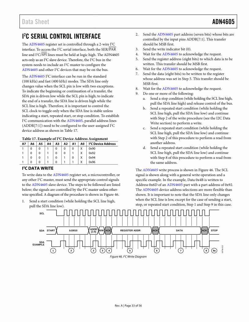
I2C DATA WRITE To write data to the ADN4605 register set, a microcontroller, or any other I2C master, must send the appropriate control signals to the ADN4605 slave device. The steps to be followed are listed below; the signals are controlled by the I2C master unless other-wise specified. A diagram of the procedure is shown in Figure 46.
1. Send a start condition (while holding the SCL line high, pull the SDA line low).
2. Send the ADN4605 part address (seven bits) whose bits are controlled by the input pins ADDR[7:1]. This transfer should be MSB first.
3. Send the write indicator bit (0). 4. Wait for the ADN4605 to acknowledge the request. 5. Send the register address (eight bits) to which data is to be
written. This transfer should be MSB first. 6. Wait for the ADN4605 to acknowledge the request. 7. Send the data (eight bits) to be written to the register
whose address was set in Step 5. This transfer should be MSB first.
8. Wait for the ADN4605 to acknowledge the request. 9. Do one or more of the following:
a. Send a stop condition (while holding the SCL line high, pull the SDA line high) and release control of the bus.
b. Send a repeated start condition (while holding the SCL line high, pull the SDA line low) and continue with Step 2 of the write procedure (see the I2C Data Write section) to perform a write.
c. Send a repeated start condition (while holding the SCL line high, pull the SDA line low) and continue with Step 2 of this procedure to perform a read from another address.
d. Send a repeated start condition (while holding the SCL line high, pull the SDA line low) and continue with Step 8 of this procedure to perform a read from the same address.
The ADN4605 write process is shown in Figure 46. The SCL signal is shown along with a general write operation and a specific example. In the example, Data 0x4B is written to Address 0x6D of an ADN4605 part with a part address of 0x92. The ADN4605 device address selections are more flexible than shown. It is important to note that the SDA line only changes when the SCL line is low, except for the case of sending a start, stop, or repeated start condition, Step 1 and Step 9 in this case.
START R/W ACK ACK ACK STOPDATAADDR[1:0]b10010 REGISTER ADDR
SCL
SDA
SDAEXAMPLE
1 2 2 3 4 5 6 7 8 9a
0979
6-01
3
Figure 46. I2C Write Diagram
ADN4605 Data Sheet
Rev. A | Page 34 of 56
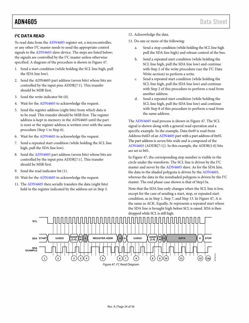
I2C DATA READ To read data from the ADN4605 register set, a microcontroller, or any other I2C master needs to send the appropriate control signals to the ADN4605 slave device. The steps are listed below; the signals are controlled by the I2C master unless otherwise specified. A diagram of the procedure is shown in Figure 47.
1. Send a start condition (while holding the SCL line high, pull the SDA line low).
2. Send the ADN4605 part address (seven bits) whose bits are controlled by the input pins ADDR[7:1]. This transfer should be MSB first.
3. Send the write indicator bit (0).
4. Wait for the ADN4605 to acknowledge the request.
5. Send the register address (eight bits) from which data is to be read. This transfer should be MSB first. The register address is kept in memory in the ADN4605 until the part is reset or the register address is written over with the same procedure (Step 1 to Step 6).
6. Wait for the ADN4605 to acknowledge the request.
7. Send a repeated start condition (while holding the SCL line high, pull the SDA line low).
8. Send the ADN4605 part address (seven bits) whose bits are controlled by the input pins ADDR[7:1]. This transfer should be MSB first.
9. Send the read indicator bit (1).
10. Wait for the ADN4605 to acknowledge the request.
11. The ADN4605 then serially transfers the data (eight bits) held in the register indicated by the address set in Step 5.
12. Acknowledge the data.
13. Do one or more of the following:
a. Send a stop condition (while holding the SCL line high pull the SDA line high) and release control of the bus.
b. Send a repeated start condition (while holding the SCL line high, pull the SDA line low) and continue with Step 2 of the write procedure (see the I2C Data Write section) to perform a write.
c. Send a repeated start condition (while holding the SCL line high, pull the SDA line low) and continue with Step 2 of this procedure to perform a read from another address.
d. Send a repeated start condition (while holding the SCL line high, pull the SDA line low) and continue with Step 8 of this procedure to perform a read from the same address.
The ADN4605 read process is shown in Figure 47. The SCL signal is shown along with a general read operation and a specific example. In the example, Data 0x49 is read from Address 0x6D of an ADN4605 part with a part address of 0x92. The part address is seven bits wide and is composed of the ADN4605 (ADDR[7:1]). In this example, the ADDR1:0] bits are set to b01.
In Figure 47, the corresponding step number is visible in the circle under the waveform. The SCL line is driven by the I2C master and never by the ADN4605 slave. As for the SDA line, the data in the shaded polygons is driven by the ADN4605, whereas the data in the nonshaded polygons is driven by the I2C master. The end phase case shown is that of Step13a.
Note that the SDA line only changes when the SCL line is low, except for the case of sending a start, stop, or repeated start condition, as in Step 1, Step 7, and Step 13. In Figure 47, A is the same as ACK. Equally, Sr represents a repeated start where the SDA line is brought high before SCL is raised. SDA is then dropped while SCL is still high.
SCL
SDA
SDAEXAMPLE
1 2 2 3 4 5 6 7 8 8 9 10 11 12 13a
b10010 A A Sr DATA A STOPREGISTER ADDRSTART ADDR[1:0]
ADDR[1:0]b10010R/
W AR/W
0979
6-01
4
Figure 47. I2C Read Diagram
Data Sheet ADN4605
Rev. A | Page 35 of 56
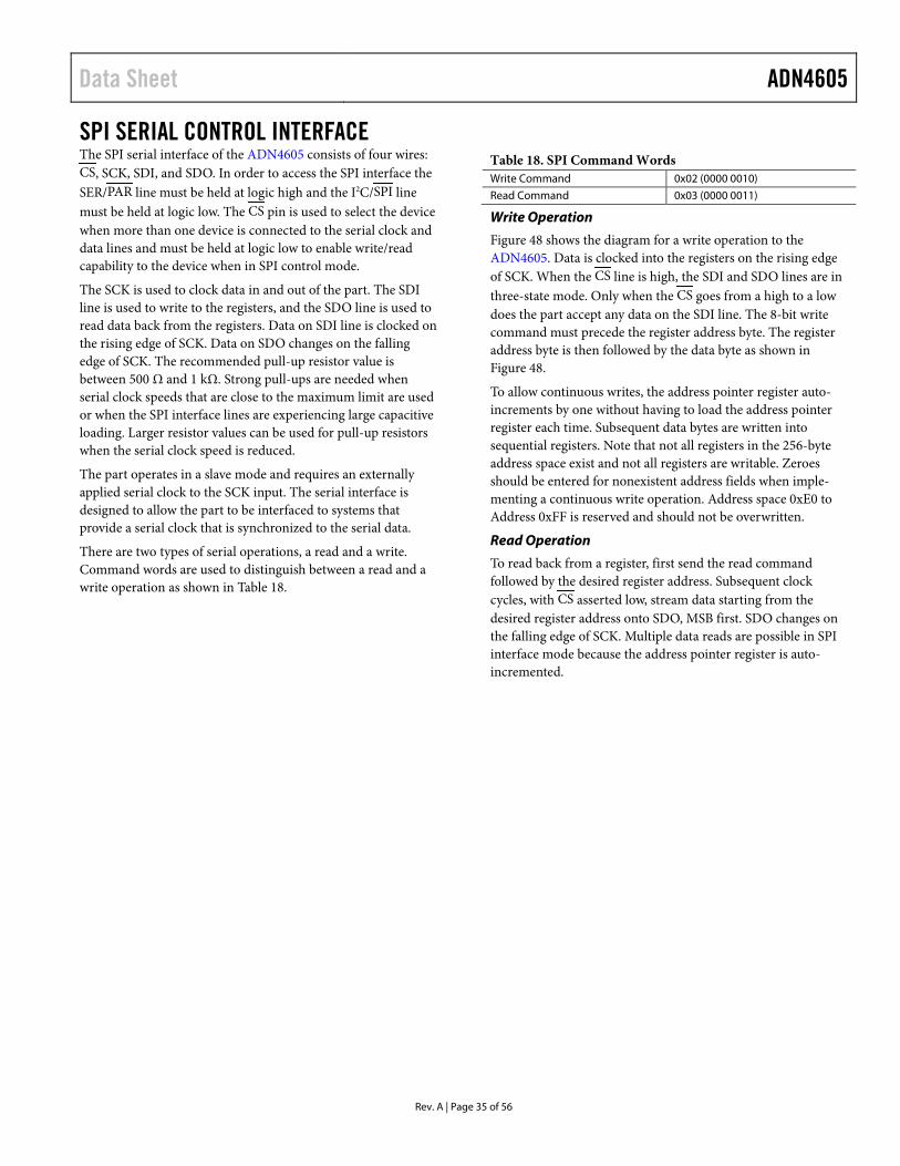
SPI SERIAL CONTROL INTERFACE The SPI serial interface of the ADN4605 consists of four wires: CS, SCK, SDI, and SDO. In order to access the SPI interface the SER/ PAR line must be held at logic high and the I2C/SPI line must be held at logic low. The CS pin is used to select the device when more than one device is connected to the serial clock and data lines and must be held at logic low to enable write/read capability to the device when in SPI control mode.
The SCK is used to clock data in and out of the part. The SDI line is used to write to the registers, and the SDO line is used to read data back from the registers. Data on SDI line is clocked on the rising edge of SCK. Data on SDO changes on the falling edge of SCK. The recommended pull-up resistor value is between 500 Ω and 1 kΩ. Strong pull-ups are needed when serial clock speeds that are close to the maximum limit are used or when the SPI interface lines are experiencing large capacitive loading. Larger resistor values can be used for pull-up resistors when the serial clock speed is reduced.
The part operates in a slave mode and requires an externally applied serial clock to the SCK input. The serial interface is designed to allow the part to be interfaced to systems that provide a serial clock that is synchronized to the serial data.
There are two types of serial operations, a read and a write. Command words are used to distinguish between a read and a write operation as shown in Table 18.
Table 18. SPI Command Words Write Command 0x02 (0000 0010)
Read Command 0x03 (0000 0011)
Write Operation
Figure 48 shows the diagram for a write operation to the ADN4605. Data is clocked into the registers on the rising edge of SCK. When the CS line is high, the SDI and SDO lines are in three-state mode. Only when the CS goes from a high to a low does the part accept any data on the SDI line. The 8-bit write command must precede the register address byte. The register address byte is then followed by the data byte as shown in Figure 48.
To allow continuous writes, the address pointer register auto-increments by one without having to load the address pointer register each time. Subsequent data bytes are written into sequential registers. Note that not all registers in the 256-byte address space exist and not all registers are writable. Zeroes should be entered for nonexistent address fields when imple-menting a continuous write operation. Address space 0xE0 to Address 0xFF is reserved and should not be overwritten.
Read Operation
To read back from a register, first send the read command followed by the desired register address. Subsequent clock cycles, with CS asserted low, stream data starting from the desired register address onto SDO, MSB first. SDO changes on the falling edge of SCK. Multiple data reads are possible in SPI interface mode because the address pointer register is auto-incremented.
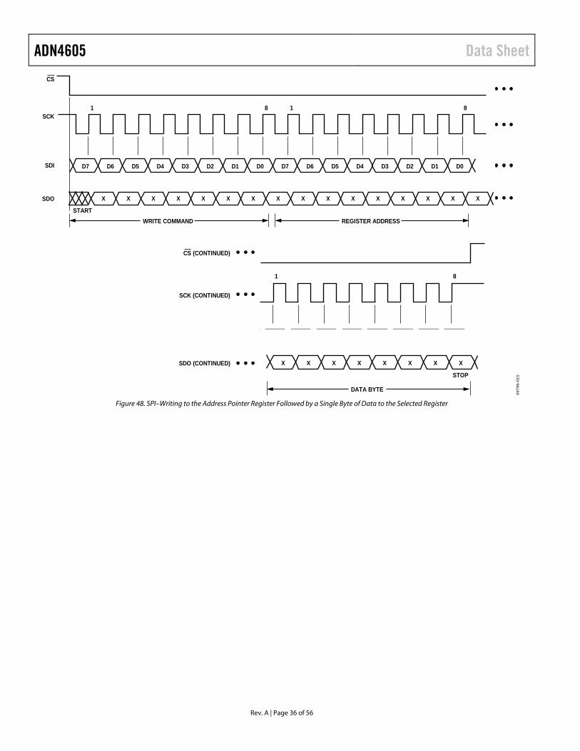
ADN4605 Data Sheet
Rev. A | Page 36 of 56
WRITE COMMANDSTART
STOP
REGISTER ADDRESS
D7 D6 D5 D4 D3 D2 D1 D0 D7 D6 D5 D4 D3 D2 D1 D0
X X X X X X X X X X X X X X X X
CS
SCK
SDI
SDO
DATA BYTE
X X X X X X X X
D7 D6 D5 D4 D3 D2 D1 D0
CS (CONTINUED)
SCK (CONTINUED)
SDI (CONTINUED)
SDO (CONTINUED)
1 8 1 8
1 8
0979
6-01
5
Figure 48. SPI–Writing to the Address Pointer Register Followed by a Single Byte of Data to the Selected Register
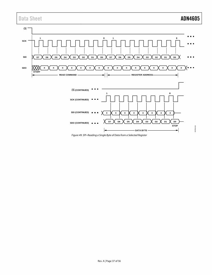
Data Sheet ADN4605
Rev. A | Page 37 of 56
READ COMMANDSTART
STOP
REGISTER ADDRESS
D7 D6 D5 D4 D3 D2 D1 D0 D7 D6 D5 D4 D3 D2 D1 D0
X X X X X X X X X X X X X X X X
CS
SCK
SDI
SDO
DATA BYTE
X X X X X X X X
D7 D6 D5 D4 D3 D2 D1 D0
CS (CONTINUED)
SCK (CONTINUED)
SDI (CONTINUED)
SDO (CONTINUED)
1 8 1 8
1 8
0979
6-01
6
Figure 49. SPI–Reading a Single Byte of Data from a Selected Register
ADN4605 Data Sheet
Rev. A | Page 38 of 56
PARALLEL CONTROL INTERFACE The parallel control interface of the ADN4605 consists of nineteen wires: ADDR[7:0], DATA[7:0], WE, RE, and CS. To access the parallel control interface, the SER/PAR line must be held at logic low. The CS line is used to select a device when one or more devices share the same address and data lines. The CS line must be held at logic low to enable write/read capability to the device when in parallel control mode.
ADDRESS INPUTS: ADDR[7:0] The binary coded address applied to the address lines determines which device registers are being programmed or read back.
DATA INPUTS/OUTPUTS: DATA[7:0] In write mode, the binary encoded data applied to the data lines (DATA[7:0]) determine the configuration setting of the register specified by the address lines (ADDR[7:0]).
In read mode, data lines (DATA[7:0]) are low impedance outputs indicating the data byte stored in the register specified by the address lines (ADDR[7:0]). Note that some registers are write only and may not be read from (see Table 19) The read-back drivers are designed to drive high impedances only (>1 kΩ).
WRITE OPERATION For first rank write enable, forcing this pin to logic low allows the data on the DATA[7:0] lines to be stored in the first rank latch for the register specified by the address lines (ADDR[7:0]). The data is latched during the high-to-low transition of the write enable pulse. The WE line must be returned to a logic high state after the write cycle to avoid overwriting the first rank data.
READ OPERATION For second rank read enable, forcing this line to a logic low state enables the output drivers on the bidirectional data lines (DATA[7:0]), placing the logic in readback mode of operation. The register selected to read from is determined by the binary encoded data configured on the address lines (ADDR[7:0]). When the read enable line is at a logic low, the data stored in the specified register will be latched onto the data lines (DATA[7:0]). The RE line is higher priority than the WE line; therefore, first rank programming is not possible while in readback mode. Note that some registers are defined as write only and are not accessible in readback mode (see Table 19).
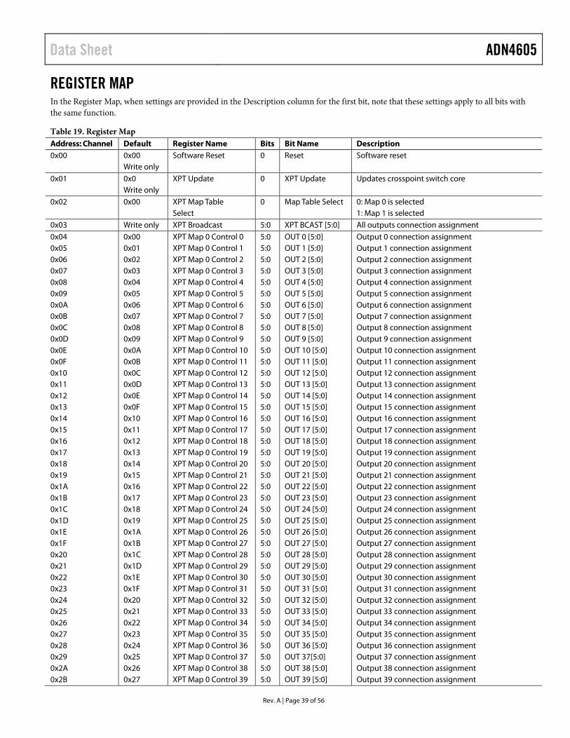
Data Sheet ADN4605
Rev. A | Page 39 of 56
REGISTER MAP
In the Register Map, when settings are provided in the Description column for the first bit, note that these settings apply to all bits with the same function.
Table 19. Register Map Address: Channel Default Register Name Bits Bit Name Description 0x00 0x00 Software Reset 0 Reset Software reset Write only 0x01 0x0 XPT Update 0 XPT Update Updates crosspoint switch core Write only 0x02 0x00 XPT Map Table 0 Map Table Select 0: Map 0 is selected Select 1: Map 1 is selected 0x03 Write only XPT Broadcast 5:0 XPT BCAST [5:0] All outputs connection assignment 0x04 0x00 XPT Map 0 Control 0 5:0 OUT 0 [5:0] Output 0 connection assignment 0x05 0x01 XPT Map 0 Control 1 5:0 OUT 1 [5:0] Output 1 connection assignment 0x06 0x02 XPT Map 0 Control 2 5:0 OUT 2 [5:0] Output 2 connection assignment 0x07 0x03 XPT Map 0 Control 3 5:0 OUT 3 [5:0] Output 3 connection assignment 0x08 0x04 XPT Map 0 Control 4 5:0 OUT 4 [5:0] Output 4 connection assignment 0x09 0x05 XPT Map 0 Control 5 5:0 OUT 5 [5:0] Output 5 connection assignment 0x0A 0x06 XPT Map 0 Control 6 5:0 OUT 6 [5:0] Output 6 connection assignment 0x0B 0x07 XPT Map 0 Control 7 5:0 OUT 7 [5:0] Output 7 connection assignment 0x0C 0x08 XPT Map 0 Control 8 5:0 OUT 8 [5:0] Output 8 connection assignment 0x0D 0x09 XPT Map 0 Control 9 5:0 OUT 9 [5:0] Output 9 connection assignment 0x0E 0x0A XPT Map 0 Control 10 5:0 OUT 10 [5:0] Output 10 connection assignment 0x0F 0x0B XPT Map 0 Control 11 5:0 OUT 11 [5:0] Output 11 connection assignment 0x10 0x0C XPT Map 0 Control 12 5:0 OUT 12 [5:0] Output 12 connection assignment 0x11 0x0D XPT Map 0 Control 13 5:0 OUT 13 [5:0] Output 13 connection assignment 0x12 0x0E XPT Map 0 Control 14 5:0 OUT 14 [5:0] Output 14 connection assignment 0x13 0x0F XPT Map 0 Control 15 5:0 OUT 15 [5:0] Output 15 connection assignment 0x14 0x10 XPT Map 0 Control 16 5:0 OUT 16 [5:0] Output 16 connection assignment 0x15 0x11 XPT Map 0 Control 17 5:0 OUT 17 [5:0] Output 17 connection assignment 0x16 0x12 XPT Map 0 Control 18 5:0 OUT 18 [5:0] Output 18 connection assignment 0x17 0x13 XPT Map 0 Control 19 5:0 OUT 19 [5:0] Output 19 connection assignment 0x18 0x14 XPT Map 0 Control 20 5:0 OUT 20 [5:0] Output 20 connection assignment 0x19 0x15 XPT Map 0 Control 21 5:0 OUT 21 [5:0] Output 21 connection assignment 0x1A 0x16 XPT Map 0 Control 22 5:0 OUT 22 [5:0] Output 22 connection assignment 0x1B 0x17 XPT Map 0 Control 23 5:0 OUT 23 [5:0] Output 23 connection assignment 0x1C 0x18 XPT Map 0 Control 24 5:0 OUT 24 [5:0] Output 24 connection assignment 0x1D 0x19 XPT Map 0 Control 25 5:0 OUT 25 [5:0] Output 25 connection assignment 0x1E 0x1A XPT Map 0 Control 26 5:0 OUT 26 [5:0] Output 26 connection assignment 0x1F 0x1B XPT Map 0 Control 27 5:0 OUT 27 [5:0] Output 27 connection assignment 0x20 0x1C XPT Map 0 Control 28 5:0 OUT 28 [5:0] Output 28 connection assignment 0x21 0x1D XPT Map 0 Control 29 5:0 OUT 29 [5:0] Output 29 connection assignment 0x22 0x1E XPT Map 0 Control 30 5:0 OUT 30 [5:0] Output 30 connection assignment 0x23 0x1F XPT Map 0 Control 31 5:0 OUT 31 [5:0] Output 31 connection assignment 0x24 0x20 XPT Map 0 Control 32 5:0 OUT 32 [5:0] Output 32 connection assignment 0x25 0x21 XPT Map 0 Control 33 5:0 OUT 33 [5:0] Output 33 connection assignment 0x26 0x22 XPT Map 0 Control 34 5:0 OUT 34 [5:0] Output 34 connection assignment 0x27 0x23 XPT Map 0 Control 35 5:0 OUT 35 [5:0] Output 35 connection assignment 0x28 0x24 XPT Map 0 Control 36 5:0 OUT 36 [5:0] Output 36 connection assignment 0x29 0x25 XPT Map 0 Control 37 5:0 OUT 37[5:0] Output 37 connection assignment 0x2A 0x26 XPT Map 0 Control 38 5:0 OUT 38 [5:0] Output 38 connection assignment 0x2B 0x27 XPT Map 0 Control 39 5:0 OUT 39 [5:0] Output 39 connection assignment
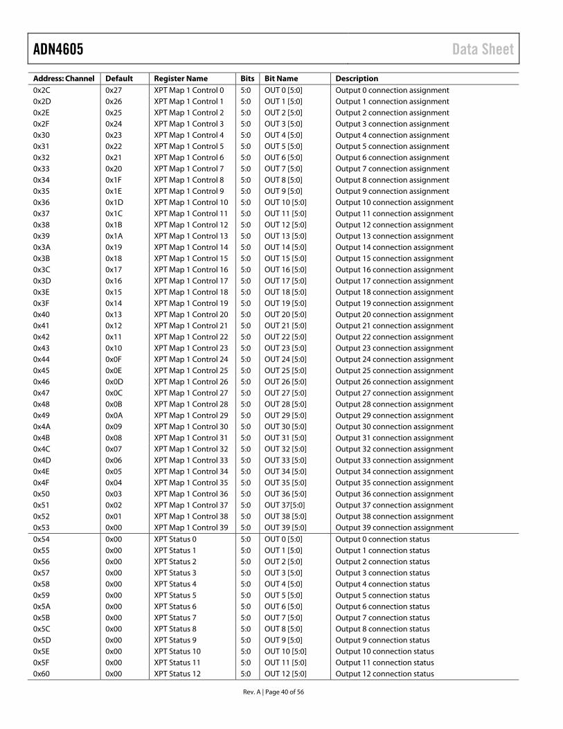
ADN4605 Data Sheet
Rev. A | Page 40 of 56
Address: Channel Default Register Name Bits Bit Name Description 0x2C 0x27 XPT Map 1 Control 0 5:0 OUT 0 [5:0] Output 0 connection assignment 0x2D 0x26 XPT Map 1 Control 1 5:0 OUT 1 [5:0] Output 1 connection assignment 0x2E 0x25 XPT Map 1 Control 2 5:0 OUT 2 [5:0] Output 2 connection assignment 0x2F 0x24 XPT Map 1 Control 3 5:0 OUT 3 [5:0] Output 3 connection assignment 0x30 0x23 XPT Map 1 Control 4 5:0 OUT 4 [5:0] Output 4 connection assignment 0x31 0x22 XPT Map 1 Control 5 5:0 OUT 5 [5:0] Output 5 connection assignment 0x32 0x21 XPT Map 1 Control 6 5:0 OUT 6 [5:0] Output 6 connection assignment 0x33 0x20 XPT Map 1 Control 7 5:0 OUT 7 [5:0] Output 7 connection assignment 0x34 0x1F XPT Map 1 Control 8 5:0 OUT 8 [5:0] Output 8 connection assignment 0x35 0x1E XPT Map 1 Control 9 5:0 OUT 9 [5:0] Output 9 connection assignment 0x36 0x1D XPT Map 1 Control 10 5:0 OUT 10 [5:0] Output 10 connection assignment 0x37 0x1C XPT Map 1 Control 11 5:0 OUT 11 [5:0] Output 11 connection assignment 0x38 0x1B XPT Map 1 Control 12 5:0 OUT 12 [5:0] Output 12 connection assignment 0x39 0x1A XPT Map 1 Control 13 5:0 OUT 13 [5:0] Output 13 connection assignment 0x3A 0x19 XPT Map 1 Control 14 5:0 OUT 14 [5:0] Output 14 connection assignment 0x3B 0x18 XPT Map 1 Control 15 5:0 OUT 15 [5:0] Output 15 connection assignment 0x3C 0x17 XPT Map 1 Control 16 5:0 OUT 16 [5:0] Output 16 connection assignment 0x3D 0x16 XPT Map 1 Control 17 5:0 OUT 17 [5:0] Output 17 connection assignment 0x3E 0x15 XPT Map 1 Control 18 5:0 OUT 18 [5:0] Output 18 connection assignment 0x3F 0x14 XPT Map 1 Control 19 5:0 OUT 19 [5:0] Output 19 connection assignment 0x40 0x13 XPT Map 1 Control 20 5:0 OUT 20 [5:0] Output 20 connection assignment 0x41 0x12 XPT Map 1 Control 21 5:0 OUT 21 [5:0] Output 21 connection assignment 0x42 0x11 XPT Map 1 Control 22 5:0 OUT 22 [5:0] Output 22 connection assignment 0x43 0x10 XPT Map 1 Control 23 5:0 OUT 23 [5:0] Output 23 connection assignment 0x44 0x0F XPT Map 1 Control 24 5:0 OUT 24 [5:0] Output 24 connection assignment 0x45 0x0E XPT Map 1 Control 25 5:0 OUT 25 [5:0] Output 25 connection assignment 0x46 0x0D XPT Map 1 Control 26 5:0 OUT 26 [5:0] Output 26 connection assignment 0x47 0x0C XPT Map 1 Control 27 5:0 OUT 27 [5:0] Output 27 connection assignment 0x48 0x0B XPT Map 1 Control 28 5:0 OUT 28 [5:0] Output 28 connection assignment 0x49 0x0A XPT Map 1 Control 29 5:0 OUT 29 [5:0] Output 29 connection assignment 0x4A 0x09 XPT Map 1 Control 30 5:0 OUT 30 [5:0] Output 30 connection assignment 0x4B 0x08 XPT Map 1 Control 31 5:0 OUT 31 [5:0] Output 31 connection assignment 0x4C 0x07 XPT Map 1 Control 32 5:0 OUT 32 [5:0] Output 32 connection assignment 0x4D 0x06 XPT Map 1 Control 33 5:0 OUT 33 [5:0] Output 33 connection assignment 0x4E 0x05 XPT Map 1 Control 34 5:0 OUT 34 [5:0] Output 34 connection assignment 0x4F 0x04 XPT Map 1 Control 35 5:0 OUT 35 [5:0] Output 35 connection assignment 0x50 0x03 XPT Map 1 Control 36 5:0 OUT 36 [5:0] Output 36 connection assignment 0x51 0x02 XPT Map 1 Control 37 5:0 OUT 37[5:0] Output 37 connection assignment 0x52 0x01 XPT Map 1 Control 38 5:0 OUT 38 [5:0] Output 38 connection assignment 0x53 0x00 XPT Map 1 Control 39 5:0 OUT 39 [5:0] Output 39 connection assignment 0x54 0x00 XPT Status 0 5:0 OUT 0 [5:0] Output 0 connection status 0x55 0x00 XPT Status 1 5:0 OUT 1 [5:0] Output 1 connection status 0x56 0x00 XPT Status 2 5:0 OUT 2 [5:0] Output 2 connection status 0x57 0x00 XPT Status 3 5:0 OUT 3 [5:0] Output 3 connection status 0x58 0x00 XPT Status 4 5:0 OUT 4 [5:0] Output 4 connection status 0x59 0x00 XPT Status 5 5:0 OUT 5 [5:0] Output 5 connection status 0x5A 0x00 XPT Status 6 5:0 OUT 6 [5:0] Output 6 connection status 0x5B 0x00 XPT Status 7 5:0 OUT 7 [5:0] Output 7 connection status 0x5C 0x00 XPT Status 8 5:0 OUT 8 [5:0] Output 8 connection status 0x5D 0x00 XPT Status 9 5:0 OUT 9 [5:0] Output 9 connection status 0x5E 0x00 XPT Status 10 5:0 OUT 10 [5:0] Output 10 connection status 0x5F 0x00 XPT Status 11 5:0 OUT 11 [5:0] Output 11 connection status 0x60 0x00 XPT Status 12 5:0 OUT 12 [5:0] Output 12 connection status
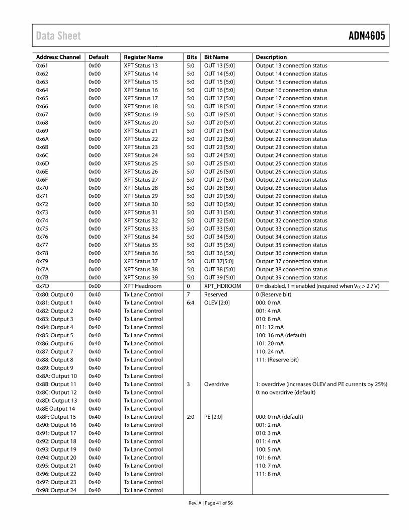
Data Sheet ADN4605
Rev. A | Page 41 of 56
Address: Channel Default Register Name Bits Bit Name Description 0x61 0x00 XPT Status 13 5:0 OUT 13 [5:0] Output 13 connection status 0x62 0x00 XPT Status 14 5:0 OUT 14 [5:0] Output 14 connection status 0x63 0x00 XPT Status 15 5:0 OUT 15 [5:0] Output 15 connection status 0x64 0x00 XPT Status 16 5:0 OUT 16 [5:0] Output 16 connection status 0x65 0x00 XPT Status 17 5:0 OUT 17 [5:0] Output 17 connection status 0x66 0x00 XPT Status 18 5:0 OUT 18 [5:0] Output 18 connection status 0x67 0x00 XPT Status 19 5:0 OUT 19 [5:0] Output 19 connection status 0x68 0x00 XPT Status 20 5:0 OUT 20 [5:0] Output 20 connection status 0x69 0x00 XPT Status 21 5:0 OUT 21 [5:0] Output 21 connection status 0x6A 0x00 XPT Status 22 5:0 OUT 22 [5:0] Output 22 connection status 0x6B 0x00 XPT Status 23 5:0 OUT 23 [5:0] Output 23 connection status 0x6C 0x00 XPT Status 24 5:0 OUT 24 [5:0] Output 24 connection status 0x6D 0x00 XPT Status 25 5:0 OUT 25 [5:0] Output 25 connection status 0x6E 0x00 XPT Status 26 5:0 OUT 26 [5:0] Output 26 connection status 0x6F 0x00 XPT Status 27 5:0 OUT 27 [5:0] Output 27 connection status 0x70 0x00 XPT Status 28 5:0 OUT 28 [5:0] Output 28 connection status 0x71 0x00 XPT Status 29 5:0 OUT 29 [5:0] Output 29 connection status 0x72 0x00 XPT Status 30 5:0 OUT 30 [5:0] Output 30 connection status 0x73 0x00 XPT Status 31 5:0 OUT 31 [5:0] Output 31 connection status 0x74 0x00 XPT Status 32 5:0 OUT 32 [5:0] Output 32 connection status 0x75 0x00 XPT Status 33 5:0 OUT 33 [5:0] Output 33 connection status 0x76 0x00 XPT Status 34 5:0 OUT 34 [5:0] Output 34 connection status 0x77 0x00 XPT Status 35 5:0 OUT 35 [5:0] Output 35 connection status 0x78 0x00 XPT Status 36 5:0 OUT 36 [5:0] Output 36 connection status 0x79 0x00 XPT Status 37 5:0 OUT 37[5:0] Output 37 connection status 0x7A 0x00 XPT Status 38 5:0 OUT 38 [5:0] Output 38 connection status 0x7B 0x00 XPT Status 39 5:0 OUT 39 [5:0] Output 39 connection status 0x7D 0x00 XPT Headroom 0 XPT_HDROOM 0 = disabled, 1 = enabled (required when VCC > 2.7 V) 0x80: Output 0 0x40 Tx Lane Control 7 Reserved 0 (Reserve bit) 0x81: Output 1 0x40 Tx Lane Control 6:4 OLEV [2:0] 000: 0 mA 0x82: Output 2 0x40 Tx Lane Control 001: 4 mA 0x83: Output 3 0x40 Tx Lane Control 010: 8 mA 0x84: Output 4 0x40 Tx Lane Control 011: 12 mA 0x85: Output 5 0x40 Tx Lane Control 100: 16 mA (default) 0x86: Output 6 0x40 Tx Lane Control 101: 20 mA 0x87: Output 7 0x40 Tx Lane Control 110: 24 mA 0x88: Output 8 0x40 Tx Lane Control 111: (Reserve bit) 0x89: Output 9 0x40 Tx Lane Control 0x8A: Output 10 0x40 Tx Lane Control 0x8B: Output 11 0x40 Tx Lane Control 3 Overdrive 1: overdrive (increases OLEV and PE currents by 25%) 0x8C: Output 12 0x40 Tx Lane Control 0: no overdrive (default) 0x8D: Output 13 0x40 Tx Lane Control 0x8E Output 14 0x40 Tx Lane Control 0x8F: Output 15 0x40 Tx Lane Control 2:0 PE [2:0] 000: 0 mA (default) 0x90: Output 16 0x40 Tx Lane Control 001: 2 mA 0x91: Output 17 0x40 Tx Lane Control 010: 3 mA 0x92: Output 18 0x40 Tx Lane Control 011: 4 mA 0x93: Output 19 0x40 Tx Lane Control 100: 5 mA 0x94: Output 20 0x40 Tx Lane Control 101: 6 mA 0x95: Output 21 0x40 Tx Lane Control 110: 7 mA 0x96: Output 22 0x40 Tx Lane Control 111: 8 mA 0x97: Output 23 0x40 Tx Lane Control 0x98: Output 24 0x40 Tx Lane Control
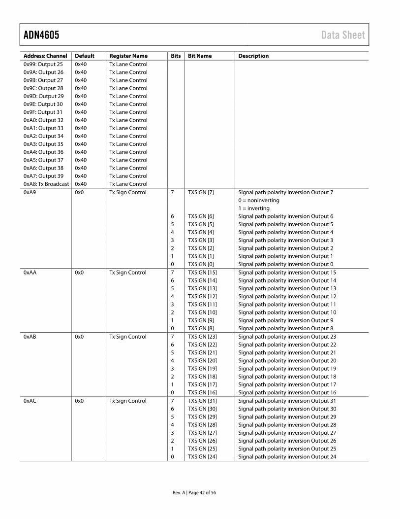
ADN4605 Data Sheet
Rev. A | Page 42 of 56
Address: Channel Default Register Name Bits Bit Name Description 0x99: Output 25 0x40 Tx Lane Control 0x9A: Output 26 0x40 Tx Lane Control 0x9B: Output 27 0x40 Tx Lane Control 0x9C: Output 28 0x40 Tx Lane Control 0x9D: Output 29 0x40 Tx Lane Control 0x9E: Output 30 0x40 Tx Lane Control 0x9F: Output 31 0x40 Tx Lane Control 0xA0: Output 32 0x40 Tx Lane Control 0xA1: Output 33 0x40 Tx Lane Control 0xA2: Output 34 0x40 Tx Lane Control 0xA3: Output 35 0x40 Tx Lane Control 0xA4: Output 36 0x40 Tx Lane Control 0xA5: Output 37 0x40 Tx Lane Control 0xA6: Output 38 0x40 Tx Lane Control 0xA7: Output 39 0x40 Tx Lane Control 0xA8: Tx Broadcast 0x40 Tx Lane Control 0xA9 0x0 Tx Sign Control 7 TXSIGN [7] Signal path polarity inversion Output 7 0 = noninverting 1 = inverting 6 TXSIGN [6] Signal path polarity inversion Output 6 5 TXSIGN [5] Signal path polarity inversion Output 5 4 TXSIGN [4] Signal path polarity inversion Output 4 3 TXSIGN [3] Signal path polarity inversion Output 3 2 TXSIGN [2] Signal path polarity inversion Output 2 1 TXSIGN [1] Signal path polarity inversion Output 1 0 TXSIGN [0] Signal path polarity inversion Output 0 0xAA 0x0 Tx Sign Control 7 TXSIGN [15] Signal path polarity inversion Output 15 6 TXSIGN [14] Signal path polarity inversion Output 14 5 TXSIGN [13] Signal path polarity inversion Output 13 4 TXSIGN [12] Signal path polarity inversion Output 12 3 TXSIGN [11] Signal path polarity inversion Output 11 2 TXSIGN [10] Signal path polarity inversion Output 10 1 TXSIGN [9] Signal path polarity inversion Output 9 0 TXSIGN [8] Signal path polarity inversion Output 8 0xAB 0x0 Tx Sign Control 7 TXSIGN [23] Signal path polarity inversion Output 23 6 TXSIGN [22] Signal path polarity inversion Output 22 5 TXSIGN [21] Signal path polarity inversion Output 21 4 TXSIGN [20] Signal path polarity inversion Output 20 3 TXSIGN [19] Signal path polarity inversion Output 19 2 TXSIGN [18] Signal path polarity inversion Output 18 1 TXSIGN [17] Signal path polarity inversion Output 17 0 TXSIGN [16] Signal path polarity inversion Output 16 0xAC 0x0 Tx Sign Control 7 TXSIGN [31] Signal path polarity inversion Output 31 6 TXSIGN [30] Signal path polarity inversion Output 30 5 TXSIGN [29] Signal path polarity inversion Output 29 4 TXSIGN [28] Signal path polarity inversion Output 28 3 TXSIGN [27] Signal path polarity inversion Output 27 2 TXSIGN [26] Signal path polarity inversion Output 26 1 TXSIGN [25] Signal path polarity inversion Output 25 0 TXSIGN [24] Signal path polarity inversion Output 24
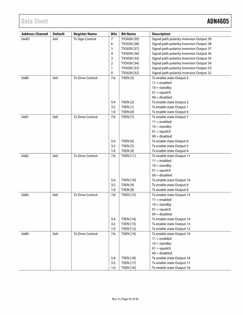
Data Sheet ADN4605
Rev. A | Page 43 of 56
Address: Channel Default Register Name Bits Bit Name Description 0xAD 0x0 Tx Sign Control 7 TXSIGN [39] Signal path polarity inversion Output 39 6 TXSIGN [38] Signal path polarity inversion Output 38 5 TXSIGN [37] Signal path polarity inversion Output 37 4 TXSIGN [36] Signal path polarity inversion Output 36 3 TXSIGN [35] Signal path polarity inversion Output 35 2 TXSIGN [34] Signal path polarity inversion Output 34 1 TXSIGN [33] Signal path polarity inversion Output 33 0 TXSIGN [32] Signal path polarity inversion Output 32 0xB0 0x0 Tx Drive Control 7:6 TXEN [3] Tx enable state Output 3 11 = enabled 10 = standby 01 = squelch 00 = disabled 5:4 TXEN [2] Tx enable state Output 2 3:2 TXEN [1] Tx enable state Output 1 1:0 TXEN [0] Tx enable state Output 0 0xB1 0x0 Tx Drive Control 7:6 TXEN [7] Tx enable state Output 7 11 = enabled 10 = standby 01 = squelch 00 = disabled 5:4 TXEN [6] Tx enable state Output 6 3:2 TXEN [5] Tx enable state Output 5 1:0 TXEN [4] Tx enable state Output 4 0xB2 0x0 Tx Drive Control 7:6 TXEN [11] Tx enable state Output 11 11 = enabled 10 = standby 01 = squelch 00 = disabled 5:4 TXEN [10] Tx enable state Output 10 3:2 TXEN [9] Tx enable state Output 9 1:0 TXEN [8] Tx enable state Output 8 0xB3 0x0 Tx Drive Control 7:6 TXEN [15] Tx enable state Output 15 11 = enabled 10 = standby 01 = squelch 00 = disabled 5:4 TXEN [14] Tx enable state Output 14 3:2 TXEN [13] Tx enable state Output 13 1:0 TXEN [12] Tx enable state Output 12 0xB4 0x0 Tx Drive Control 7:6 TXEN [19] Tx enable state Output 19 11 = enabled 10 = standby 01 = squelch 00 = disabled 5:4 TXEN [18] Tx enable state Output 18 3:2 TXEN [17] Tx enable state Output 17 1:0 TXEN [16] Tx enable state Output 16
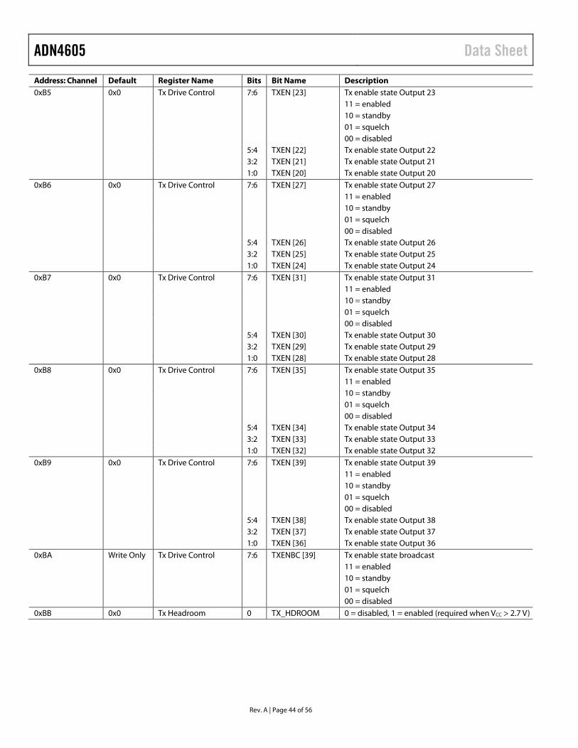
ADN4605 Data Sheet
Rev. A | Page 44 of 56
Address: Channel Default Register Name Bits Bit Name Description 0xB5 0x0 Tx Drive Control 7:6 TXEN [23] Tx enable state Output 23 11 = enabled 10 = standby 01 = squelch 00 = disabled 5:4 TXEN [22] Tx enable state Output 22 3:2 TXEN [21] Tx enable state Output 21 1:0 TXEN [20] Tx enable state Output 20 0xB6 0x0 Tx Drive Control 7:6 TXEN [27] Tx enable state Output 27 11 = enabled 10 = standby 01 = squelch 00 = disabled 5:4 TXEN [26] Tx enable state Output 26 3:2 TXEN [25] Tx enable state Output 25 1:0 TXEN [24] Tx enable state Output 24 0xB7 0x0 Tx Drive Control 7:6 TXEN [31] Tx enable state Output 31 11 = enabled 10 = standby 01 = squelch 00 = disabled 5:4 TXEN [30] Tx enable state Output 30 3:2 TXEN [29] Tx enable state Output 29 1:0 TXEN [28] Tx enable state Output 28 0xB8 0x0 Tx Drive Control 7:6 TXEN [35] Tx enable state Output 35 11 = enabled 10 = standby 01 = squelch 00 = disabled 5:4 TXEN [34] Tx enable state Output 34 3:2 TXEN [33] Tx enable state Output 33 1:0 TXEN [32] Tx enable state Output 32 0xB9 0x0 Tx Drive Control 7:6 TXEN [39] Tx enable state Output 39 11 = enabled 10 = standby 01 = squelch 00 = disabled 5:4 TXEN [38] Tx enable state Output 38 3:2 TXEN [37] Tx enable state Output 37 1:0 TXEN [36] Tx enable state Output 36 0xBA Write Only Tx Drive Control 7:6 TXENBC [39] Tx enable state broadcast 11 = enabled 10 = standby 01 = squelch 00 = disabled 0xBB 0x0 Tx Headroom 0 TX_HDROOM 0 = disabled, 1 = enabled (required when VCC > 2.7 V)
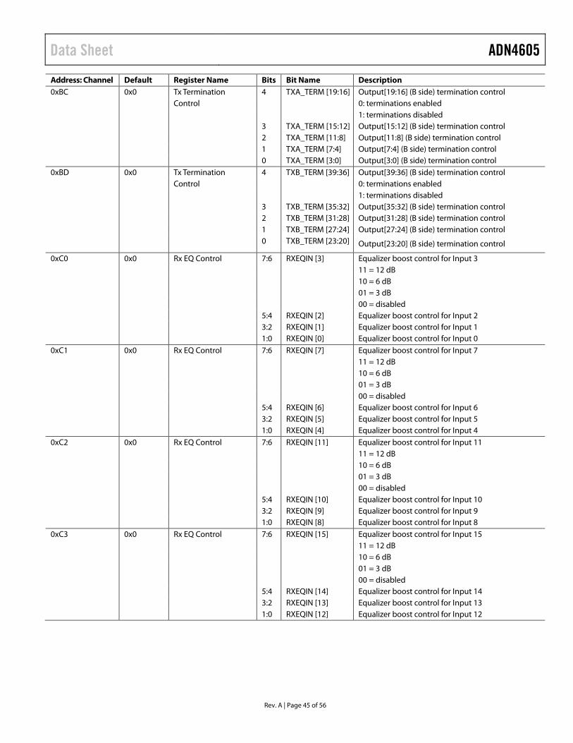
Data Sheet ADN4605
Rev. A | Page 45 of 56
Address: Channel Default Register Name Bits Bit Name Description 0xBC 0x0 Tx Termination 4 TXA_TERM [19:16] Output[19:16] (B side) termination control Control 0: terminations enabled 1: terminations disabled 3 TXA_TERM [15:12] Output[15:12] (B side) termination control 2 TXA_TERM [11:8] Output[11:8] (B side) termination control 1 TXA_TERM [7:4] Output[7:4] (B side) termination control 0 TXA_TERM [3:0] Output[3:0] (B side) termination control 0xBD 0x0 Tx Termination 4 TXB_TERM [39:36] Output[39:36] (B side) termination control Control 0: terminations enabled 1: terminations disabled 3 TXB_TERM [35:32] Output[35:32] (B side) termination control 2 TXB_TERM [31:28] Output[31:28] (B side) termination control 1 TXB_TERM [27:24] Output[27:24] (B side) termination control 0 TXB_TERM [23:20] Output[23:20] (B side) termination control
0xC0 0x0 Rx EQ Control 7:6 RXEQIN [3] Equalizer boost control for Input 3 11 = 12 dB 10 = 6 dB 01 = 3 dB 00 = disabled 5:4 RXEQIN [2] Equalizer boost control for Input 2 3:2 RXEQIN [1] Equalizer boost control for Input 1 1:0 RXEQIN [0] Equalizer boost control for Input 0 0xC1 0x0 Rx EQ Control 7:6 RXEQIN [7] Equalizer boost control for Input 7 11 = 12 dB 10 = 6 dB 01 = 3 dB 00 = disabled 5:4 RXEQIN [6] Equalizer boost control for Input 6 3:2 RXEQIN [5] Equalizer boost control for Input 5 1:0 RXEQIN [4] Equalizer boost control for Input 4 0xC2 0x0 Rx EQ Control 7:6 RXEQIN [11] Equalizer boost control for Input 11 11 = 12 dB 10 = 6 dB 01 = 3 dB 00 = disabled 5:4 RXEQIN [10] Equalizer boost control for Input 10 3:2 RXEQIN [9] Equalizer boost control for Input 9 1:0 RXEQIN [8] Equalizer boost control for Input 8 0xC3 0x0 Rx EQ Control 7:6 RXEQIN [15] Equalizer boost control for Input 15 11 = 12 dB 10 = 6 dB 01 = 3 dB 00 = disabled 5:4 RXEQIN [14] Equalizer boost control for Input 14 3:2 RXEQIN [13] Equalizer boost control for Input 13 1:0 RXEQIN [12] Equalizer boost control for Input 12
ADN4605 Data Sheet
Rev. A | Page 46 of 56
Address: Channel Default Register Name Bits Bit Name Description 0xC4 0x0 Rx EQ Control 7:6 RXEQIN [19] Equalizer boost control for Input 19 11 = 12 dB 10 = 6 dB 01 = 3 dB 00 = disabled 5:4 RXEQIN [18] Equalizer boost control for Input 18 3:2 RXEQIN [17] Equalizer boost control for Input 17 1:0 RXEQIN [16] Equalizer boost control for Input 16 0xC5 0x0 Rx EQ Control 7:6 RXEQIN [23] Equalizer boost control for Input 23 11 = 12 dB 10 = 6 dB 01 = 3 dB 00 = disabled 5:4 RXEQIN [22] Equalizer boost control for Input 22 3:2 RXEQIN [21] Equalizer boost control for Input 21 1:0 RXEQIN [20] Equalizer boost control for Input 20 0xC6 0x0 Rx EQ Control 7:6 RXEQIN [27] Equalizer boost control for Input 27 11 = 12 dB 10 = 6 dB 01 = 3 dB 00 = disabled 5:4 RXEQIN [26] Equalizer boost control for Input 26 3:2 RXEQIN [25] Equalizer boost control for Input 25 1:0 RXEQIN [24] Equalizer boost control for Input 24 0xC7 0x0 Rx EQ Control 7:6 RXEQIN [31] Equalizer boost control for Input 31 11 = 12 dB 10 = 6 dB 01 = 3 dB 00 = disabled 5:4 RXEQIN [30] Equalizer boost control for Input 30 3:2 RXEQIN [29] Equalizer boost control for Input 29 1:0 RXEQIN [28] Equalizer boost control for Input 28 0xC8 0x0 Rx EQ Control 7:6 RXEQIN [35] Equalizer boost control for Input 35 11 = 12 dB 10 = 6 dB 01 = 3 dB 00 = disabled 5:4 RXEQIN [34] Equalizer boost control for Input 34 3:2 RXEQIN [33] Equalizer boost control for Input 33 1:0 RXEQIN [32] Equalizer boost control for Input 32 0xC9 0x0 Rx EQ Control 7:6 RXEQIN [39] Equalizer boost control for Input 39 11 = 12 dB 10 = 6 dB 01 = 3 dB 00 = disabled 5:4 RXEQIN [38] Equalizer boost control for Input 38 3:2 RXEQIN [37] Equalizer boost control for Input 37 1:0 RXEQIN [36] Equalizer boost control for Input 36 0xCA 0x0 Rx EQ Control 1:0 RXEQIN BC Equalizer boost control for all inputs 11 = 12 dB 10 = 6 dB 01 = 3 dB 00 = disabled
Data Sheet ADN4605
Rev. A | Page 47 of 56
Address: Channel Default Register Name Bits Bit Name Description 0xCB 0x0 Rx Sign Control 7 RXSIGN [7] Signal path polarity inversion Input 7 6 RXSIGN [6] Signal path polarity inversion Input 6 5 RXSIGN [5] Signal path polarity inversion Input 5 4 RXSIGN [4] Signal path polarity inversion Input 4 3 RXSIGN [3] Signal path polarity inversion Input 3 2 RXSIGN [2] Signal path polarity inversion Input 2 1 RXSIGN [1] Signal path polarity inversion Input 1 0 RXSIGN [0] Signal path polarity inversion Input 0 0xCC 0x0 Rx Sign Control 7 RXSIGN [15] Signal path polarity inversion Input 15 6 RXSIGN [14] Signal path polarity inversion Input 14 5 RXSIGN [13] Signal path polarity inversion Input 13 4 RXSIGN [12] Signal path polarity inversion Input 12 3 RXSIGN [11] Signal path polarity inversion Input 11 2 RXSIGN [10] Signal path polarity inversion Input 10 1 RXSIGN [9] Signal path polarity inversion Input 9 0 RXSIGN [8] Signal path polarity inversion Input 8 0xCD 0x0 Rx Sign Control 7 RXSIGN [23] Signal path polarity inversion Input 23 6 RXSIGN [22] Signal path polarity inversion Input 22 5 RXSIGN [21] Signal path polarity inversion Input 21 4 RXSIGN [20] Signal path polarity inversion Input 20 3 RXSIGN [19] Signal path polarity inversion Input 19 2 RXSIGN [18] Signal path polarity inversion Input 18 1 RXSIGN [17] Signal path polarity inversion Input 17 0 RXSIGN [16] Signal path polarity inversion Input 16 0xCE 0x0 Rx Sign Control 7 RXSIGN [31] Signal path polarity inversion Input 31 6 RXSIGN [30] Signal path polarity inversion Input 30 5 RXSIGN [29] Signal path polarity inversion Input 29 4 RXSIGN [28] Signal path polarity inversion Input 28 3 RXSIGN [27] Signal path polarity inversion Input 27 2 RXSIGN [26] Signal path polarity inversion Input 26 1 RXSIGN [25] Signal path polarity inversion Input 25 0 RXSIGN [24] Signal path polarity inversion Input 24 0xCF 0x0 Rx Sign Control 7 RXSIGN [39] Signal path polarity inversion Input 39 6 RXSIGN [38] Signal path polarity inversion Input 38 5 RXSIGN [37] Signal path polarity inversion Input 37 4 RXSIGN [36] Signal path polarity inversion Input 36 3 RXSIGN [35] Signal path polarity inversion Input 35 2 RXSIGN [34] Signal path polarity inversion Input 34 1 RXSIGN [33] Signal path polarity inversion Input 33 0 RXSIGN [32] Signal path polarity inversion Input 32 0xD0 0x0 Rx Termination 4 RXA_TERM [19:16] Input[19:16] (A Side) termination control Control 0: termination control enabled 1: termination control disabled 3 RXA_TERM [15:12] Input [15:12] (A side) termination control 2 RXA_TERM [11:8] Input [11:8] (A side) termination control 1 RXA_TERM [7:4] Input [7:4] (A side) termination control 0 RXA_TERM [3:0] Input [3:0] (A side) termination control
ADN4605 Data Sheet
Rev. A | Page 48 of 56
Address: Channel Default Register Name Bits Bit Name Description 0xD1 0x0 Rx Termination 4 RXB_TERM [39:36] Input [39:36] (B Side) termination control Control 0: terminations enabled 1: terminations disabled 3 RXB_TERM [35:32] Input [35:32] (B Side) termination control 2 RXB_TERM [31:28] Input [31:28] (B Side) termination control 1 RXB_TERM [27:24] Input [27:24] (B Side) termination control 0 RXB_TERM [23:20] Input [23:20] (B Side) termination control
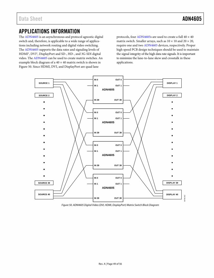
Data Sheet ADN4605
Rev. A | Page 49 of 56
APPLICATIONS INFORMATION The ADN4605 is an asynchronous and protocol agnostic digital switch and, therefore, is applicable to a wide range of applica-tions including network routing and digital video switching. The ADN4605 supports the data rates and signaling levels of HDMI®, DVI®, DisplayPort and SD-, HD-, and 3G-SDI digital video. The ADN4605 can be used to create matrix switches. An example block diagram of a 40 × 40 matrix switch is shown in Figure 50. Since HDMI, DVI, and DisplayPort are quad lane
protocols, four ADN4605s are used to create a full 40 × 40 matrix switch. Smaller arrays, such as 10 × 10 and 20 × 20, require one and two ADN4605 devices, respectively. Proper high speed PCB design techniques should be used to maintain the signal integrity of the high data rate signals. It is important to minimize the lane-to-lane skew and crosstalk in these applications.
ADN4605
IN 0
IN 1
IN 39
OUT 0
OUT 1
OUT 39
ADN4605
IN 0
IN 1
IN 39
OUT 0
OUT 1
OUT 39
ADN4605
IN 0
IN 1
IN 39
OUT 0
OUT 1
OUT 39
ADN4605
IN 0
IN 1
IN 39
OUT 0
OUT 1
OUT 39
SOURCE 1
SOURCE 2
SOURCE 40
SOURCE 39
DISPLAY 1
DISPLAY 2
DISPLAY 40
DISPLAY 3909
796-
052
Figure 50. ADN4605 Digital Video (DVI, HDMI, DisplayPort) Matrix Switch Block Diagram
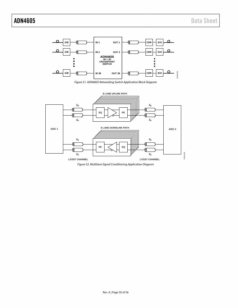
ADN4605 Data Sheet
Rev. A | Page 50 of 56
O/E
O/E
E/O
E/O
CDR
CDR
O/E E/OCDR
ADN460540 × 40
CROSSPOINTSWITCH
IN 1
IN 2
IN 39
OUT 1
OUT 2
OUT 39
0979
6-05
3
Figure 51. ADN4605 Networking Switch Application Block Diagram
PE EQ
LOSSY CHANNEL
8 LANE UPLINK PATH
8 LANE DOWNLINK PATH
LOSSY CHANNEL
ASIC 2
EQ PE
ASIC 1
Z0
Z0
Z0
Z0
Z0
Z0
Z0
Z0
0793
4-05
3
Figure 52. Multilane Signal Conditioning Application Diagram
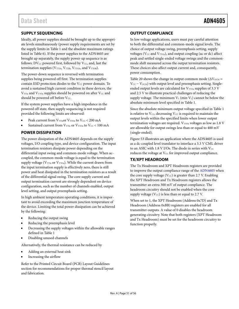
Data Sheet ADN4605
Rev. A | Page 51 of 56
SUPPLY SEQUENCING Ideally, all power supplies should be brought up to the appropri-ate levels simultaneously (power supply requirements are set by the supply limits in Table 1 and the absolute maximum ratings listed in Table 6). If the power supplies to the ADN4605 are brought up separately, the supply power-up sequence is as follows: DVCC powered first, followed by VCC, and, last the termination supplies (VTTIA, VTTIB, VTTOA, and VTTOB).
The power-down sequence is reversed with termination supplies being powered off first. The termination supplies contain ESD protection diodes to the VCC power domain. To avoid a sustained high current condition in these devices, the VTTIx and VTTOx supplies should be powered on after VCC and should be powered off before VCC.
If the system power supplies have a high impedance in the powered off state, then supply sequencing is not required provided the following limits are observed:
• Peak current from VTTIxor VTTOx to VCC < 200 mA • Sustained current from VTTIx or VTTOx to VCC < 100 mA
POWER DISSIPATION The power dissipation of the ADN4605 depends on the supply voltages, I/O coupling type, and device configuration. The input termination resistors dissipate power depending on the differential input swing and common-mode voltage. When ac-coupled, the common-mode voltage is equal to the termination supply voltage (VTTIx or VTTOx). While the current drawn from the input termination supply is effectively zero, there is still power and heat dissipated in the termination resistors as a result of the differential signal swing. The core supply current and output termination current are strongly dependent on device configuration, such as the number of channels enabled, output level setting, and output preemphasis setting.
In high ambient temperature operating conditions, it is impor-tant to avoid exceeding the maximum junction temperature of the device. Limiting the total power dissipation can be achieved by the following:
• Reducing the output swing • Reducing the preemphasis level • Decreasing the supply voltages within the allowable ranges
defined in Table 1 • Disabling unused channels
Alternatively, the thermal resistance can be reduced by
• Adding an external heat sink • Increasing the airflow
Refer to the Printed Circuit Board (PCB) Layout Guidelines section for recommendations for proper thermal stencil layout and fabrication.
OUTPUT COMPLIANCE In low voltage applications, users must pay careful attention to both the differential and common-mode signal levels. The choice of output voltage swing, preemphasis setting, supply voltages (VCC and VTTOx), and output coupling (ac or dc) affect peak and settled single-ended voltage swings and the common-mode shift measured across the output termination resistors. These choices also affect output current and, consequently, power consumption.
Table 20 shows the change in output common mode (ΔVOCM = VCC − VOCM) with output level and preemphasis setting. Single-ended output levels are calculated for VTTOx supplies of 3.3 V and 2.5 V to illustrate practical challenges of reducing the supply voltage. The minimum VL (min VL) cannot be below the absolute minimum level specified in Table 1.
Since the absolute minimum output voltage specified in Table 1 is relative to VCC, decreasing VCC is required to maintain the output levels within the specified limits when lower output termination voltages are required. VTTOx voltages as low as 1.8 V are allowable for output swings less than or equal to 400 mV (single-ended).
Figure 53 illustrates an application where the ADN4605 is used as a dc-coupled level translator to interface a 3.3 V CML driver to an ASIC with 1.8 V I/Os. The diode in series with VCC reduces the voltage at VCC for improved output compliance.
TX/XPT HEADROOM The Tx Headroom and XPT Headroom registers are provided to improve the output compliance range of the ADN4605 when the core supply voltage (VCC) is greater than 2.7 V. Enabling the XPT Headroom and Tx Headroom registers allows the transmitter an extra 300 mV of output compliance. The headroom circuitry should not be enabled when the core supply voltage (VCC) is less than or equal to 2.7 V.
When set to 1, the XPT Headroom (Address 0x7D) and Tx Headroom (Address 0xBB) registers are enabled for all transmitter outputs. A value of 0 disables the headroom generating circuitry. Note that both registers (XPT Headroom and Tx Headroom) must be set for the headroom circuitry to function properly.
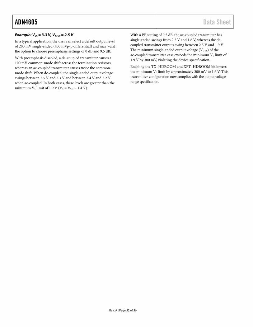
ADN4605 Data Sheet
Rev. A | Page 52 of 56
Example: VCC = 3.3 V, VTTOx = 2.5 V
In a typical application, the user can select a default output level of 200 mV single-ended (400 mVp-p differential) and may want the option to choose preemphasis settings of 0 dB and 9.5 dB.
With preemphasis disabled, a dc-coupled transmitter causes a 100 mV common-mode shift across the termination resistors, whereas an ac-coupled transmitter causes twice the common-mode shift. When dc-coupled, the single-ended output voltage swings between 2.5 V and 2.3 V and between 2.4 V and 2.2 V when ac-coupled. In both cases, these levels are greater than the minimum VL limit of 1.9 V (VL = VCC − 1.4 V).
With a PE setting of 9.5 dB, the ac-coupled transmitter has single-ended swings from 2.2 V and 1.6 V, whereas the dc-coupled transmitter outputs swing between 2.5 V and 1.9 V. The minimum single-ended output voltage (VL-PE) of the ac-coupled transmitter case exceeds the minimum VL limit of 1.9 V by 300 mV, violating the device specification.
Enabling the TX_HDROOM and XPT_HDROOM bit lowers the minimum VL limit by approximately 300 mV to 1.6 V. This transmitter configuration now complies with the output voltage range specification.
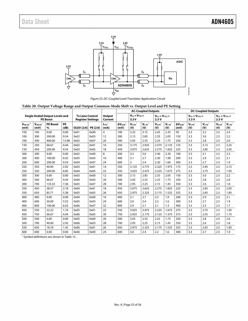
Data Sheet ADN4605
Rev. A | Page 53 of 56
CML
VEE
VTTOx
1.8V
1.8V3.3V
3.3V
VCCVTTIx
ADN4605
CML
3.3V
Z0
Z0
Z0
Z0
ASIC
Rx
0979
6-05
5
Figure 53. DC-Coupled Level Translator Application Circuit
Table 20. Output Voltage Range and Output Common-Mode Shift vs. Output Level and PE Setting
Single-Ended Output Levels and PE Boost
Tx Lane Control Register Settings
Output Current
AC-Coupled Outputs DC-Coupled Outputs
VCC = VTTO = 3.3 V
VCC = VTTO = 2.5 V
VCC = VTTO = 3.3 V
VCC = VTTO = 2.5 V
VSW-DC1
(mV) VSW-PE
1 (mV)
PE Boost %
PE (dB) OLEV [2:0] PE [2:0]
ITTO1
(mA) ∆VOCM
1 (mV)
VH-PE1
(V) VL-PE
1 (V)
VH-PE1
(V) VL-PE
1 (V)
∆VOCM1
(mV) VH-PE
1 (V)
VL-PE1
(V) VH-PE
1 (V)
VL-PE1
(V)
100 100 0.00 0.00 0x01 0x00 4 100 3.25 3.15 2.45 2.35 50 3.3 3.2 2.5 2.4 100 300 200.00 9.54 0x02 0x03 12 300 3.15 2.85 2.35 2.05 150 3.3 3.0 2.5 2.2 100 500 400.00 13.98 0x03 0x07 20 500 3.05 2.55 2.25 1.75 250 3.3 2.8 2.5 2.0
150 250 66.67 4.44 0x02 0x01 10 250 3.175 2.925 2.375 2.125 125 3.3 3.15 2.5 2.25 150 450 200.00 9.54 0x03 0x05 18 450 3.075 2.625 2.275 1.825 225 3.3 2.85 2.5 2.05
200 200 0.00 0.00 0x02 0x00 8 200 3.2 3.0 2.40 2.20 100 3.3 3.1 2.5 2.3 200 400 100.00 6.02 0x03 0x03 16 400 3.1 2.7 2.30 1.90 200 3.3 2.9 2.5 2.1 200 600 200.00 9.54 0x04 0x07 24 600 3 2.4 2.20 1.60 300 3.3 2.7 2.5 1.9
250 350 40.00 2.92 0x03 0x01 14 350 3.125 2.775 2.325 1.975 175 3.3 2.95 2.5 2.15 250 550 200.00 6.85 0x04 0x05 22 550 3.025 2.475 2.225 1.675 275 3.3 2.75 2.5 1.95
300 300 0.00 0.00 0x03 0x00 12 300 3.15 2.85 2.35 2.05 150 3.3 3.0 2.5 2.2 300 500 66.67 4.44 0x04 0x03 20 500 3.05 2.55 2.25 1.75 250 3.3 2.8 2.5 2.0 300 700 133.33 7.36 0x05 0x07 28 700 2.95 2.25 2.15 1.45 350 3.3 2.6 2.5 1.8
350 450 28.57 2.18 0x04 0x01 18 450 3.075 2.625 2.275 1.825 225 3.3 2.85 2.5 2.05 350 650 85.71 5.38 0x05 0x05 26 650 2.975 2.325 2.175 1.525 325 3.3 2.65 2.5 1.85
400 400 0.00 0.00 0x04 0x00 16 400 3.1 2.7 2.3 1.9 200 3.3 2.9 2.5 2.1 400 600 50.00 3.52 0x05 0x03 24 600 3.0 2.4 2.2 1.6 300 3.3 2.7 2.5 1.9 400 800 100.00 6.02 0x06 0x07 32 800 2.9 2.1 2.1 1.3 400 3.3 2.5 2.5 1.7
450 550 22.22 1.74 0x05 0x01 22 550 3.025 2.475 2.225 1.675 275 3.3 2.75 2.5 1.95 450 750 66.67 4.44 0x06 0x05 30 750 2.925 2.175 2.125 1.375 375 3.3 2.55 2.5 1.75
500 500 0.00 0.00 0x05 0x00 20 500 3.05 2.55 2.25 1.75 250 3.3 2.8 2.5 2.0 500 700 40.00 2.92 0x06 0x03 28 700 2.95 2.25 2.15 1.45 350 3.3 2.6 2.5 1.8
550 650 18.18 1.45 0x06 0x01 26 650 2.975 2.325 2.175 1.525 325 3.3 2.65 2.5 1.85
600 600 0.00 0.00 0x06 0x00 24 600 3.0 2.4 2.2 1.6 300 3.3 2.7 2.5 1.9 1 Symbol definitions are shown in Table 15.
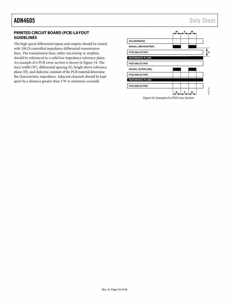
ADN4605 Data Sheet
Rev. A | Page 54 of 56
PRINTED CIRCUIT BOARD (PCB) LAYOUT GUIDELINES The high speed differential inputs and outputs should be routed with 100 Ω controlled impedance differential transmission lines. The transmission lines, either microstrip or stripline, should be referenced to a solid low impedance reference plane. An example of a PCB cross-section is shown in Figure 54. The trace width (W), differential spacing (S), height above reference plane (H), and dielectric constant of the PCB material determine the characteristic impedance. Adjacent channels should be kept apart by a distance greater than 3 W to minimize crosstalk.
PCB DIELECTRIC
SIGNAL (MICROSTRIP)
SOLDERMASK
PCB DIELECTRIC
PCB DIELECTRIC
PCB DIELECTRIC
REFERENCE PLANE
REFERENCE PLANE
SIGNAL (STRIPLINE)
WSW
H
WSW
0979
6-10
0
Figure 54. Example of a PCB Cross-Section
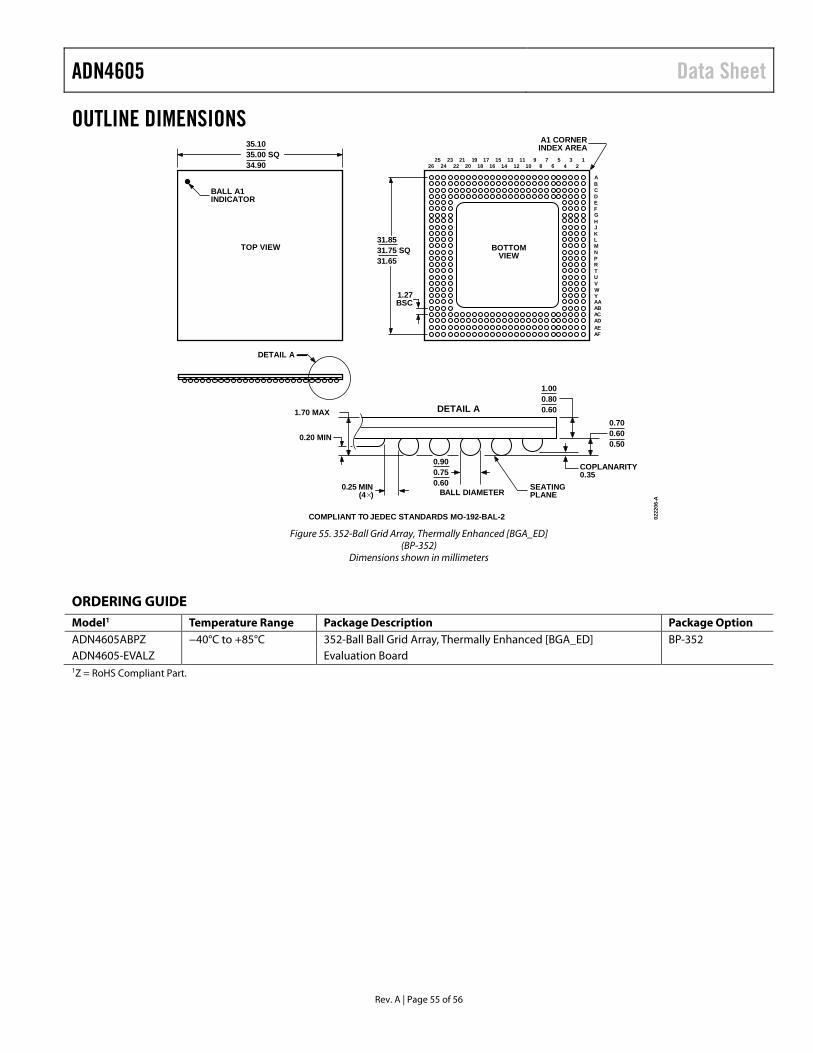
ADN4605 Data Sheet
Rev. A | Page 55 of 56
OUTLINE DIMENSIONS
DETAIL A
1.27BSC
ABCDEFGHJKLMNPRTUVWYAAABACADAEAF
14681012
357911216182022
151719212314
1324
2526
31.8531.75 SQ31.65
35.1035.00 SQ34.90
BALL A1INDICATOR
TOP VIEW BOTTOMVIEW
A1 CORNERINDEX AREA
0.20 MIN
0.700.600.50
1.000.800.60
COPLANARITY0.35
0.900.750.60 SEATING
PLANEBALL DIAMETER
DETAIL A1.70 MAX
COMPLIANT TO JEDEC STANDARDS MO-192-BAL-2 0222
06-A
0.25 MIN(4 )
Figure 55. 352-Ball Grid Array, Thermally Enhanced [BGA_ED]
(BP-352) Dimensions shown in millimeters
ORDERING GUIDE Model1 Temperature Range Package Description Package Option ADN4605ABPZ −40°C to +85°C 352-Ball Ball Grid Array, Thermally Enhanced [BGA_ED] BP-352 ADN4605-EVALZ Evaluation Board 1Z = RoHS Compliant Part.

ADN4605 Data Sheet
Rev. A | Page 56 of 56
NOTES
I2C refers to a communications protocol originally developed by Philips Semiconductors (now NXP Semiconductors). HDMI, the HDMI Logo, and High-Definition Multimedia Interface are trademarks or registered trademarks of HDMI Licensing LLC in the United States and other countries.
©2011 Analog Devices, Inc. All rights reserved. Trademarks and registered trademarks are the property of their respective owners. D09796-0-11/11(A)