Embed Size (px)
Citation preview
Power Integrations
5245 Hellyer Avenue, San Jose, CA 95138 USA. Tel: +1 408 414 9200 Fax: +1 408 414 9201
www.powerint.com
Title Engineering Prototype Report for RDK-91 –12 W Power Supply Using TinySwitch®-III (TNY278PN)
Specification 85-265 VAC Input, 12 V, 1 A Output
Application TinySwitch-III Reference Design (RDK-91)
Author Power Integrations Applications Department
Document Number RDR-91
Date 18-July-2007
Revision 1.2
Summary and Features
• EcoSmart® – Meets all existing and proposed harmonized energy efficiency standards including: CECP (China), CEC, EPA, AGO, European Commission • No-load consumption 140 mW at 265 VAC (no bias winding required) • > 75% active-mode efficiency (exceeds standards requirement of 71%)
• BP/M capacitor value selects MOSFET current limit for greater design flexibility • Output overvoltage protection (OVP) using primary bias winding sensed
shutdown feature • Tightly toleranced I2f parameter (–10%, +12%) reduces system cost:
• Increases MOSFET and magnetics power delivery • Reduces overload power, which lowers output diode and capacitor costs
• Integrated TinySwitch-III Safety/Reliability features: • Accurate (± 5%), auto-recovering, hysteretic thermal shutdown function
maintains safe PCB temperatures under all conditions • Auto-restart protects against output short circuit and open loop fault
conditions • > 3.2 mm creepage on package enables reliable operation in high humidity
and high pollution environments • Meets EN550022 and CISPR-22 Class B conducted EMI with >12 dBµV margin • Meets IEC61000-4-5 Class 3 AC line surge

RDR-91 12 V, 1 A, Universal Input Supply 18-July-2007
Page 2 of 37
Power Integrations Tel: +1 408 414 9200 Fax: +1 408 414 9201 www.powerint.com
The products and applications illustrated herein (including circuits external to the products and transformer construction) may be covered by one or more U.S. and foreign patents or potentially by pending U.S. and foreign patent applications assigned to Power Integrations. A complete list of Power Integrations’ patents may be found at www.powerint.com.
18-July-2007 RDR-91 12 V, 1 A, Universal Input Supply
Page 3 of 37
Power Integrations Tel: +1 408 414 9200 Fax: +1 408 414 9201
www.powerint.com
Table of Contents 1 Introduction .................................................................................................................5 2 Power Supply Specification ........................................................................................6 3 Circuit Diagram ...........................................................................................................7 4 Circuit Description.......................................................................................................8
4.1 Input Rectification and Filtering ...........................................................................8 4.2 TNY278PN Operation..........................................................................................8 4.3 Output Rectification and Filtering.........................................................................9 4.4 Feedback and Output Voltage Regulation ...........................................................9 4.5 Output Overvoltage Shutdown.............................................................................9 4.6 EMI Design Aspects ............................................................................................9 4.7 Peak Primary Current Limit Selection ................................................................10 4.8 UV Lockout ........................................................................................................10
5 PCB Layout...............................................................................................................11 6 Bill of Materials .........................................................................................................12 7 Transformer Specification .........................................................................................14
7.1 Electrical Diagram..............................................................................................14 7.2 Electrical Specifications .....................................................................................14 7.3 Materials ............................................................................................................15 7.4 Transformer Build Diagram................................................................................15 7.5 Transformer Construction ..................................................................................16
8 Transformer Spreadsheet .........................................................................................17 9 Performance Data.....................................................................................................19
9.1 Efficiency ...........................................................................................................19 9.2 Active Mode CEC Measurement Data ...............................................................20 9.3 No-load Input Power (R8 not installed: no bias winding supplementation) ........21 9.4 No-load Input Power (with R8 and bias winding supplementation)....................21 9.5 Available Standby Output Power .......................................................................22 9.6 Regulation .........................................................................................................23
9.6.1 Load and Line.............................................................................................23 10 Thermal Performance............................................................................................24 11 Waveforms ............................................................................................................25
11.1 Drain Voltage and Current, Normal Operation...................................................25 11.2 Output Voltage Start-Up Profile .........................................................................26 11.3 Drain Voltage and Current Start-Up Profile........................................................26 11.4 Load Transient Response (75% to 100% Load Step)........................................27 11.5 Output Ripple Measurements ............................................................................28
11.5.1 Ripple Measurement Technique.................................................................28 11.5.2 Measurement Results.................................................................................29
11.6 Overvoltage Shutdown ......................................................................................29 12 Line Surge.............................................................................................................30 13 Conducted EMI .....................................................................................................31
13.1 115 VAC, Full Load............................................................................................31 13.2 230 VAC, Full Load............................................................................................32
14 Audible Noise ........................................................................................................33

RDR-91 12 V, 1 A, Universal Input Supply 18-July-2007
Page 4 of 37
Power Integrations Tel: +1 408 414 9200 Fax: +1 408 414 9201 www.powerint.com
15 Extended and Reduced Current Limit (ILIMIT) Operation........................................34 16 TNY277PN and TNY279PN Operation in RD-91 ..................................................34 17 OVP Operation Verification...................................................................................35 18 Revision History ....................................................................................................36 Important Note: Although this board was designed to satisfy safety isolation requirements, it has not been agency approved. Therefore, all testing should be performed using an isolation transformer to provide the AC input to the power supply.
18-July-2007 RDR-91 12 V, 1 A, Universal Input Supply
Page 5 of 37
Power Integrations Tel: +1 408 414 9200 Fax: +1 408 414 9201
www.powerint.com
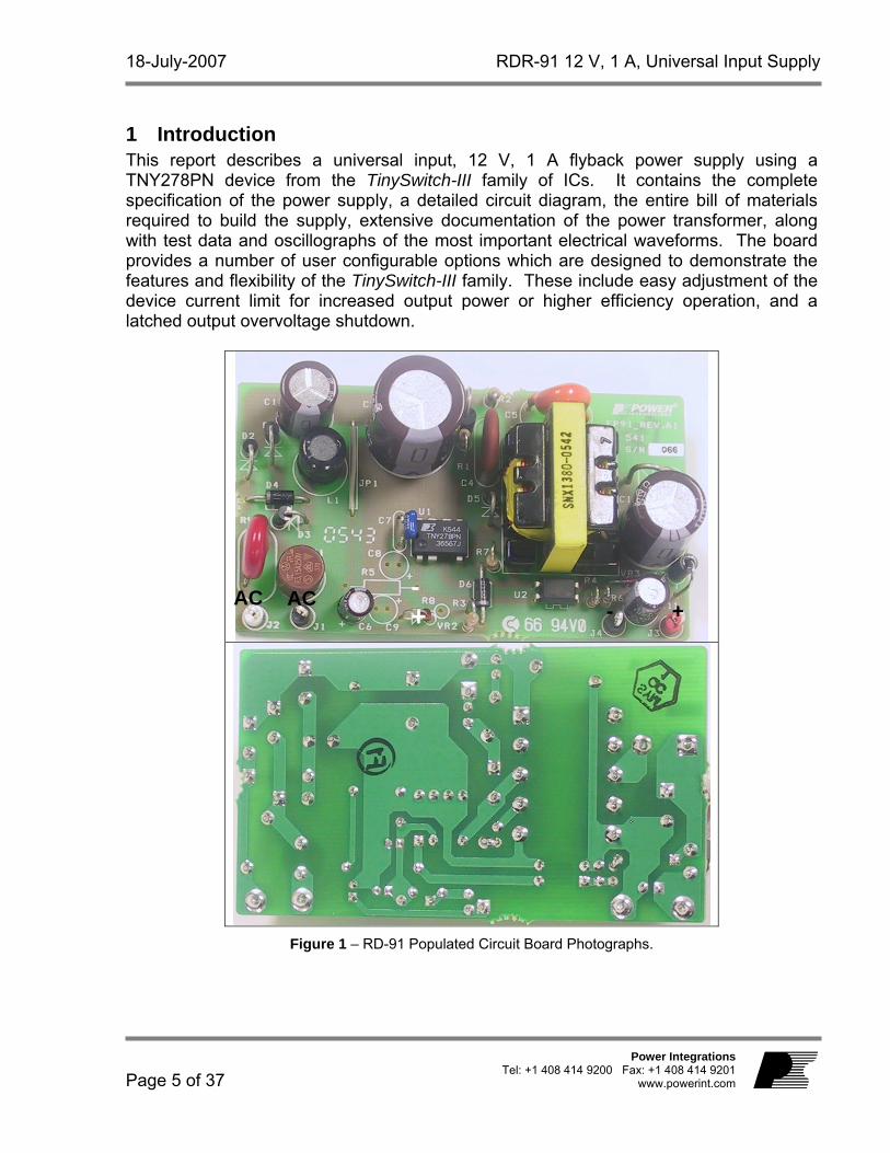
1 Introduction This report describes a universal input, 12 V, 1 A flyback power supply using a TNY278PN device from the TinySwitch-III family of ICs. It contains the complete specification of the power supply, a detailed circuit diagram, the entire bill of materials required to build the supply, extensive documentation of the power transformer, along with test data and oscillographs of the most important electrical waveforms. The board provides a number of user configurable options which are designed to demonstrate the features and flexibility of the TinySwitch-III family. These include easy adjustment of the device current limit for increased output power or higher efficiency operation, and a latched output overvoltage shutdown.
Figure 1 – RD-91 Populated Circuit Board Photographs.
- +
AC AC - +
RDR-91 12 V, 1 A, Universal Input Supply 18-July-2007
Page 6 of 37
Power Integrations Tel: +1 408 414 9200 Fax: +1 408 414 9201 www.powerint.com
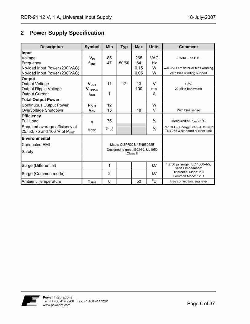
2 Power Supply Specification
Description Symbol Min Typ Max Units Comment Input Voltage VIN 85 265 VAC 2 Wire – no P.E. Frequency fLINE 47 50/60 64 Hz No-load Input Power (230 VAC) 0.15 W w/o UVLO resistor or bias windingNo-load Input Power (230 VAC) 0.05 W With bias winding support
Output Output Voltage VOUT 11 12 13 V ± 8% Output Ripple Voltage VRIPPLE 100 mV 20 MHz bandwidth Output Current IOUT 1 A
Total Output Power
Continuous Output Power POUT 12 W Overvoltage Shutdown VOV 15 18 V With bias sense
Efficiency Full Load η 75 % Measured at POUT 25 oC
Required average efficiency at 25, 50, 75 and 100 % of POUT ηCEC 71.3 % Per CEC / Energy Star STDs, with
TNY278 & standard current limit
Environmental
Conducted EMI Meets CISPR22B / EN55022B
Safety Designed to meet IEC950, UL1950 Class II
Surge (Differential) 1 kV
Surge (Common mode) 2 kV
1.2/50 µs surge, IEC 1000-4-5, Series Impedance:
Differential Mode: 2 Ω Common Mode: 12 Ω
Ambient Temperature TAMB 0 50 oC Free convection, sea level
18-July-2007 RDR-91 12 V, 1 A, Universal Input Supply
Page 7 of 37
Power Integrations Tel: +1 408 414 9200 Fax: +1 408 414 9201
www.powerint.com
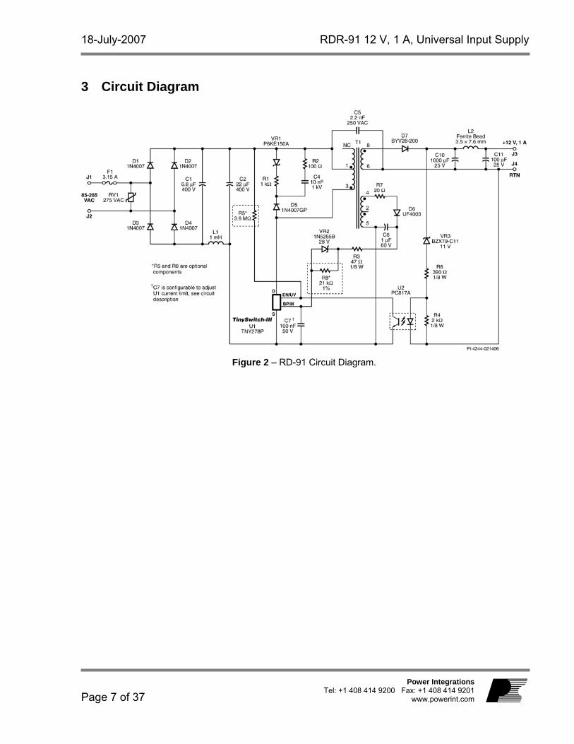
3 Circuit Diagram
Figure 2 – RD-91 Circuit Diagram.
RDR-91 12 V, 1 A, Universal Input Supply 18-July-2007
Page 8 of 37
Power Integrations Tel: +1 408 414 9200 Fax: +1 408 414 9201 www.powerint.com
4 Circuit Description This flyback power supply was designed around the TNY278PN (U1 in Figure 2). The output voltage is sensed and fed back to U1 through optocoupler U2. That feedback is used by U1 to maintain constant voltage (CV) regulation of the output.
4.1 Input Rectification and Filtering Diodes D1–D4 rectify the AC input. Capacitors C1 and C2 filter the rectified DC. Inductor L1, C1 and C2 form a pi filter that attenuates differential mode conducted EMI.
4.2 TNY278PN Operation The TNY278PN device (U1) integrates an oscillator, a switch controller, startup and protection circuitry, and a power MOSFET, all on one monolithic IC. One side of the power transformer (T1) primary winding is connected to the positive leg of C2, and the other side is connected to the DRAIN pin of U1. At the start of a switching cycle, the controller turns the MOSFET on, and current ramps up in the primary winding, which stores energy in the core of the transformer. When that current reaches the limit threshold, the controller turns the MOSFET off. Due to the phasing of the transformer windings and the orientation of the output diode, the stored energy then induces a voltage across the secondary winding, which forward biases the output diode, and the stored energy is delivered to the output capacitor. When the MOSFET turns off, the leakage inductance of the transformer induces a voltage spike on the drain node. The amplitude of that spike is limited by an RCD clamp network that consists of D5, C4 and R2. Resistor R1 and VR1 provide hard clamping of the drain voltage, only conducting during output overload. Resistor R2 also limits the reverse current that flows through D5 when the MOSFET turns on. This allows a slow, low-cost, glass passivated diode (with a recovery time of ≤2 µs.) to be used for D5, which improves conducted EMI and efficiency. Using ON/OFF control, U1 skips switching cycles to regulate the output voltage, based on feedback to its EN/UV pin. The EN/UV pin current is sampled, just prior to each switching cycle, to determine if that switching cycle should be enabled or disabled. If the EN/UV pin current is <115 µA, the next switching cycle begins, and is terminated when the current through the MOSFET reaches the internal current limit threshold. To evenly spread switching cycles, preventing group pulsing, the EN pin threshold current is modulated between 115 µA and 60 µA based on the state during the previous cycle. A state-machine within the controller adjusts the MOSFET current limit threshold to one of four levels, depending on the load being demanded from the supply. As the load on the supply drops, the current limit threshold is reduced. This ensures that the effective switching frequency stays above the audible range until the transformer flux density is low. When the standard production technique of dip varnishing is used for the transformer, audible noise is practically eliminated.
18-July-2007 RDR-91 12 V, 1 A, Universal Input Supply
Page 9 of 37
Power Integrations Tel: +1 408 414 9200 Fax: +1 408 414 9201
www.powerint.com
4.3 Output Rectification and Filtering Diode D7 rectifies the output of T1. Output voltage ripple was minimized by using a low ESR capacitor for C10 (see Section 6 for component part numbers and values). A post filter (ferrite bead L2 and C11) attenuates the high frequency switching noise.
4.4 Feedback and Output Voltage Regulation The supply’s output voltage regulation set point is set by the voltage that develops across Zener diode VR3, R6 and the LED in opto-coupler U2. The value of R4 was calculated to bias VR3 to about 0.5 mA when it goes into reverse avalanche conduction. This ensures that it is operating close to its rated knee current. Resistor R6 limits the maximum current during load transients. The values of R4 and R6 can both be varied slightly to fine-tune the output regulation set point. When the output voltage rises above the set point, the LED in U2 becomes forward biased. On the primary side, the photo-transistor of U2 turns on and draws current out of the EN/UV pin of U1. Just before the start of each switching cycle, the controller checks the EN/UV pin current. If the current flowing out of the EN/UV pin is greater than 115 µA, that switching cycle will be disabled. As switching cycles are enabled and disabled, the output voltage is kept very close to the regulation set point. For greater output voltage regulation accuracy, a reference IC such as a TL431 can be used in place of VR3.
4.5 Output Overvoltage Shutdown The TinySwitch-III family of ICs can detect overvoltage on the output of the supply and latch off. This protects the load in an open feedback loop fault condition, such as the failure of the optocoupler. Overvoltage on the output is detected through the BP/M pin and the bias winding on the transformer. The bias winding voltage is determined by the reflection of the output voltage through the turns ratio of the transformer. Therefore, an overvoltage on the output will be reflected onto the bias winding. The overvoltage threshold is the sum of the breakdown voltage of Zener diode VR2 and the BP/M pin voltage (28 V + 5.8 V). If the output voltage becomes abnormally high, the voltage on the bias winding will exceed the threshold voltage and excess current will flow into the BP/M pin. The latching shutdown circuit is activated when current into the BP/M pin exceeds 5 mA. Resetting a latched shutdown requires removing the AC input from the supply long enough to allow the input capacitors (C1 and C2) to discharge, and the BP/M pin voltage to drop below 2 V. Resistors R7 and R3 provide additional filtering of the bias voltage, with R3 also limiting the maximum current into the BYPASS pin in an OV condition
4.6 EMI Design Aspects An input pi filter (C1, L1 and C2) attenuates conducted, differential mode EMI noise. Shielding techniques (E-Shield™) were used in the construction of T1 to reduce common mode EMI displacement currents. Resistor R2 and capacitor C4 dampen out some of the high frequency ringing that occurs when the MOSFET turns off. When combined with the IC’s frequency jitter function, these techniques produce excellent conducted and radiated EMI performance (see Section 12 of this report).
RDR-91 12 V, 1 A, Universal Input Supply 18-July-2007
Page 10 of 37
Power Integrations Tel: +1 408 414 9200 Fax: +1 408 414 9201 www.powerint.com
4.7 Peak Primary Current Limit Selection The value of the capacitor installed on the BP/M pin allows the current limit of U1 to be selected. The power supply designer can change the current limit of the MOSFET by simply changing the capacitance value connected to the BP/M pin (see the TinySwitch-III data sheet for more details).
Installing a 0.1 µF capacitor on the BP/M pin selects the standard current limit of the IC, and is the normal choice for enclosed adapter applications.
Installing a 1 µF capacitor on the BP/M pin reduces the MOSFET current
limit, which lowers conduction losses and improves efficiency (at the expense of reducing the maximum power capability of the IC).
A 10 µF capacitor on the BP/M pin will raise the MOSFET current limit and
extend the power capability of the IC (for higher power applications that do not have the thermal constraints of an enclosed adapter, or to supply short-duration, peak load demands).
The EP91 demonstration board comes with a 0.1 µF capacitor installed as C7, which causes U1 to select the standard current limit specified in the TinySwitch-III data sheet. If C7 were replaced by a 1 µF capacitor (C8 in the BOM, section 6), the current limit of U1 will be the same as the standard current limit for a TNY277 device. If a 10 µF capacitor is installed, the current limit of U1 will be the same as the standard current limit for a TNY279 device. The flexibility of this option enables the designer to do three things. First, it allows the designer to measure the effect of switching to an adjacent device without actually removing and replacing the IC. Second, it allows a larger device to be used with a lower current limit, for higher efficiency. Third, it allows a smaller device to be used with a higher current limit in a design when higher power is not required on a continual basis, which effectively lowers the cost of the supply.
4.8 UV Lockout The EP91 circuit board has a location where an optional under-voltage (UV) lockout detection resistor (R5) can be installed. When installed, MOSFET switching is disabled at startup until current into the EN/UV pin exceeds 25 µA. This allows the designer to set the input voltage at which MOSFET switching will be enabled by choosing the value of R5. For example, a value of 3.6 MΩ requires an input voltage of 65 VAC (92 VDC across C2) before the current into the EN/UV pin exceeds 25 µA. The UV detect function also prevents the output of the power supply from glitching (trying to restart) after output regulation is lost (during shutdown), by disabling MOSFET switching until the input voltage rises above the under-voltage lockout threshold.

18-July-2007 RDR-91 12 V, 1 A, Universal Input Supply
Page 11 of 37
Power Integrations Tel: +1 408 414 9200 Fax: +1 408 414 9201
www.powerint.com
5 PCB Layout
Figure 3 – Printed Circuit Board Layout (3.2 × 1.8 inches).
RDR-91 12 V, 1 A, Universal Input Supply 18-July-2007
Page 12 of 37
Power Integrations Tel: +1 408 414 9200 Fax: +1 408 414 9201 www.powerint.com
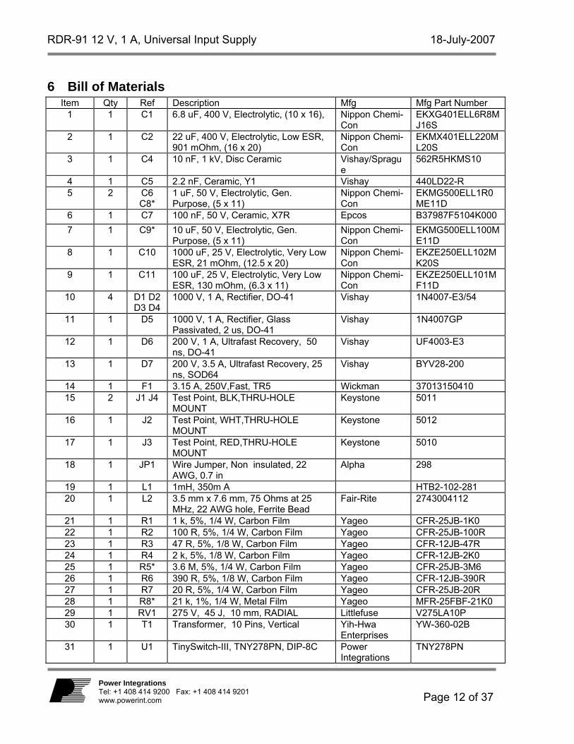
6 Bill of Materials Item Qty Ref Description Mfg Mfg Part Number
1 1 C1 6.8 uF, 400 V, Electrolytic, (10 x 16), Nippon Chemi-Con
EKXG401ELL6R8MJ16S
2 1 C2 22 uF, 400 V, Electrolytic, Low ESR, 901 mOhm, (16 x 20)
Nippon Chemi-Con
EKMX401ELL220ML20S
3 1 C4 10 nF, 1 kV, Disc Ceramic Vishay/Sprague
562R5HKMS10
4 1 C5 2.2 nF, Ceramic, Y1 Vishay 440LD22-R 5 2 C6
C8* 1 uF, 50 V, Electrolytic, Gen. Purpose, (5 x 11)
Nippon Chemi-Con
EKMG500ELL1R0ME11D
6 1 C7 100 nF, 50 V, Ceramic, X7R Epcos B37987F5104K000 7 1 C9* 10 uF, 50 V, Electrolytic, Gen.
Purpose, (5 x 11) Nippon Chemi-Con
EKMG500ELL100ME11D
8 1 C10 1000 uF, 25 V, Electrolytic, Very Low ESR, 21 mOhm, (12.5 x 20)
Nippon Chemi-Con
EKZE250ELL102MK20S
9 1 C11 100 uF, 25 V, Electrolytic, Very Low ESR, 130 mOhm, (6.3 x 11)
Nippon Chemi-Con
EKZE250ELL101MF11D
10 4 D1 D2 D3 D4
1000 V, 1 A, Rectifier, DO-41 Vishay 1N4007-E3/54
11 1 D5 1000 V, 1 A, Rectifier, Glass Passivated, 2 us, DO-41
Vishay 1N4007GP
12 1 D6 200 V, 1 A, Ultrafast Recovery, 50 ns, DO-41
Vishay UF4003-E3
13 1 D7 200 V, 3.5 A, Ultrafast Recovery, 25 ns, SOD64
Vishay BYV28-200
14 1 F1 3.15 A, 250V,Fast, TR5 Wickman 37013150410 15 2 J1 J4 Test Point, BLK,THRU-HOLE
MOUNT Keystone 5011
16 1 J2 Test Point, WHT,THRU-HOLE MOUNT
Keystone 5012
17 1 J3 Test Point, RED,THRU-HOLE MOUNT
Keystone 5010
18 1 JP1 Wire Jumper, Non insulated, 22 AWG, 0.7 in
Alpha 298
19 1 L1 1mH, 350m A HTB2-102-281 20 1 L2 3.5 mm x 7.6 mm, 75 Ohms at 25
MHz, 22 AWG hole, Ferrite Bead Fair-Rite 2743004112
21 1 R1 1 k, 5%, 1/4 W, Carbon Film Yageo CFR-25JB-1K0 22 1 R2 100 R, 5%, 1/4 W, Carbon Film Yageo CFR-25JB-100R 23 1 R3 47 R, 5%, 1/8 W, Carbon Film Yageo CFR-12JB-47R 24 1 R4 2 k, 5%, 1/8 W, Carbon Film Yageo CFR-12JB-2K0 25 1 R5* 3.6 M, 5%, 1/4 W, Carbon Film Yageo CFR-25JB-3M6 26 1 R6 390 R, 5%, 1/8 W, Carbon Film Yageo CFR-12JB-390R 27 1 R7 20 R, 5%, 1/4 W, Carbon Film Yageo CFR-25JB-20R 28 1 R8* 21 k, 1%, 1/4 W, Metal Film Yageo MFR-25FBF-21K0 29 1 RV1 275 V, 45 J, 10 mm, RADIAL Littlefuse V275LA10P 30 1 T1 Transformer, 10 Pins, Vertical Yih-Hwa
Enterprises YW-360-02B
31 1 U1 TinySwitch-III, TNY278PN, DIP-8C Power Integrations
TNY278PN
18-July-2007 RDR-91 12 V, 1 A, Universal Input Supply
Page 13 of 37
Power Integrations Tel: +1 408 414 9200 Fax: +1 408 414 9201
www.powerint.com
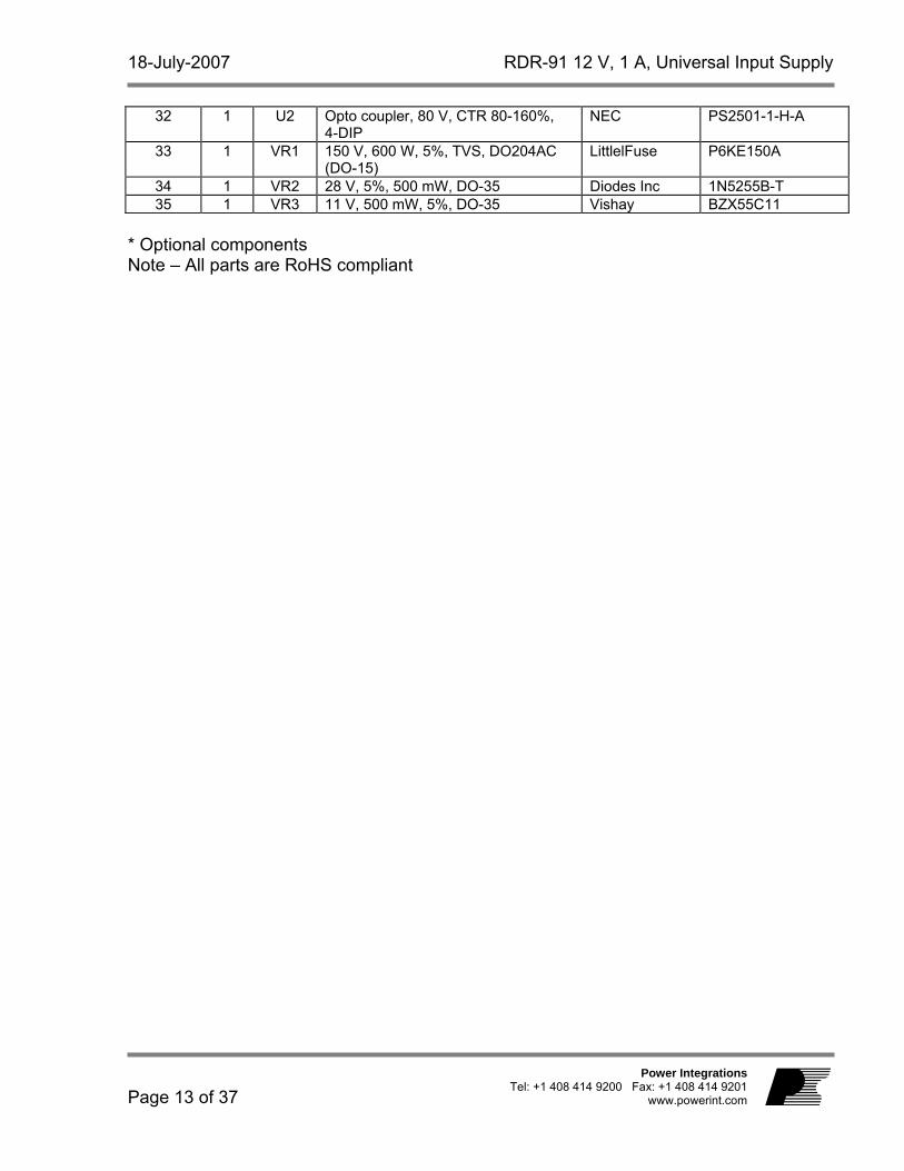
32 1 U2 Opto coupler, 80 V, CTR 80-160%, 4-DIP
NEC PS2501-1-H-A
33 1 VR1 150 V, 600 W, 5%, TVS, DO204AC (DO-15)
LittlelFuse P6KE150A
34 1 VR2 28 V, 5%, 500 mW, DO-35 Diodes Inc 1N5255B-T 35 1 VR3 11 V, 500 mW, 5%, DO-35 Vishay BZX55C11
* Optional components Note – All parts are RoHS compliant
RDR-91 12 V, 1 A, Universal Input Supply 18-July-2007
Page 14 of 37
Power Integrations Tel: +1 408 414 9200 Fax: +1 408 414 9201 www.powerint.com
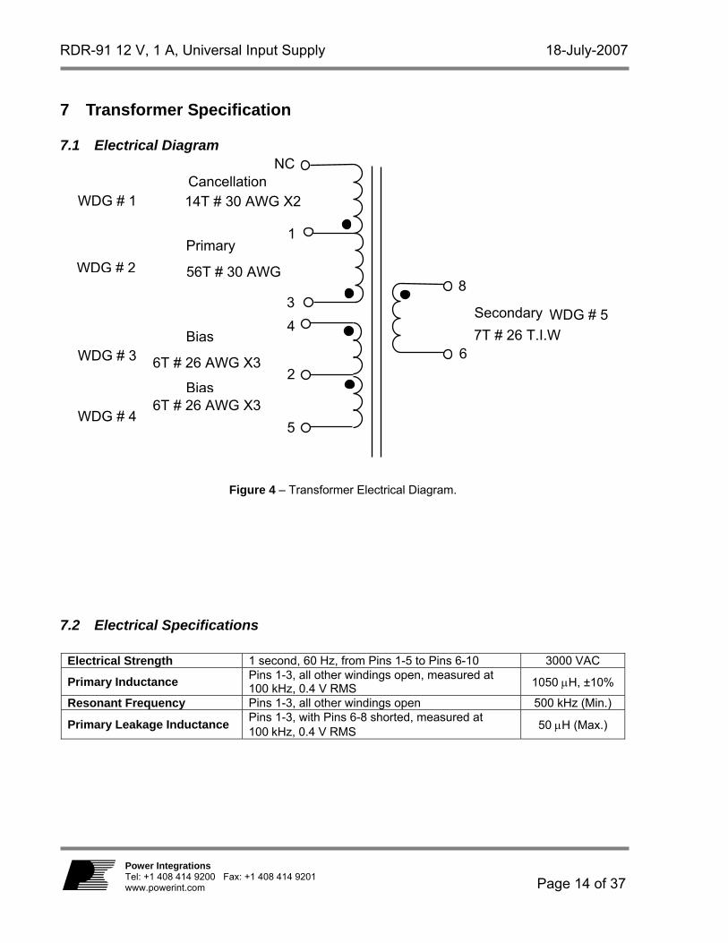
7 Transformer Specification
7.1 Electrical Diagram
Figure 4 – Transformer Electrical Diagram.
7.2 Electrical Specifications
Electrical Strength 1 second, 60 Hz, from Pins 1-5 to Pins 6-10 3000 VAC
Primary Inductance Pins 1-3, all other windings open, measured at 100 kHz, 0.4 V RMS 1050 µH, ±10%
Resonant Frequency Pins 1-3, all other windings open 500 kHz (Min.)
Primary Leakage Inductance Pins 1-3, with Pins 6-8 shorted, measured at 100 kHz, 0.4 V RMS 50 µH (Max.)
NC
3 4
Cancellation
Bias
Primary
56T # 30 AWG
WDG # 3
WDG # 1
6T # 26 AWG X3
WDG # 2
14T # 30 AWG X2
2
1
Bias6T # 26 AWG X3
5
8
6
Secondary 7T # 26 T.I.W
WDG # 5
WDG # 4
18-July-2007 RDR-91 12 V, 1 A, Universal Input Supply
Page 15 of 37
Power Integrations Tel: +1 408 414 9200 Fax: +1 408 414 9201
www.powerint.com
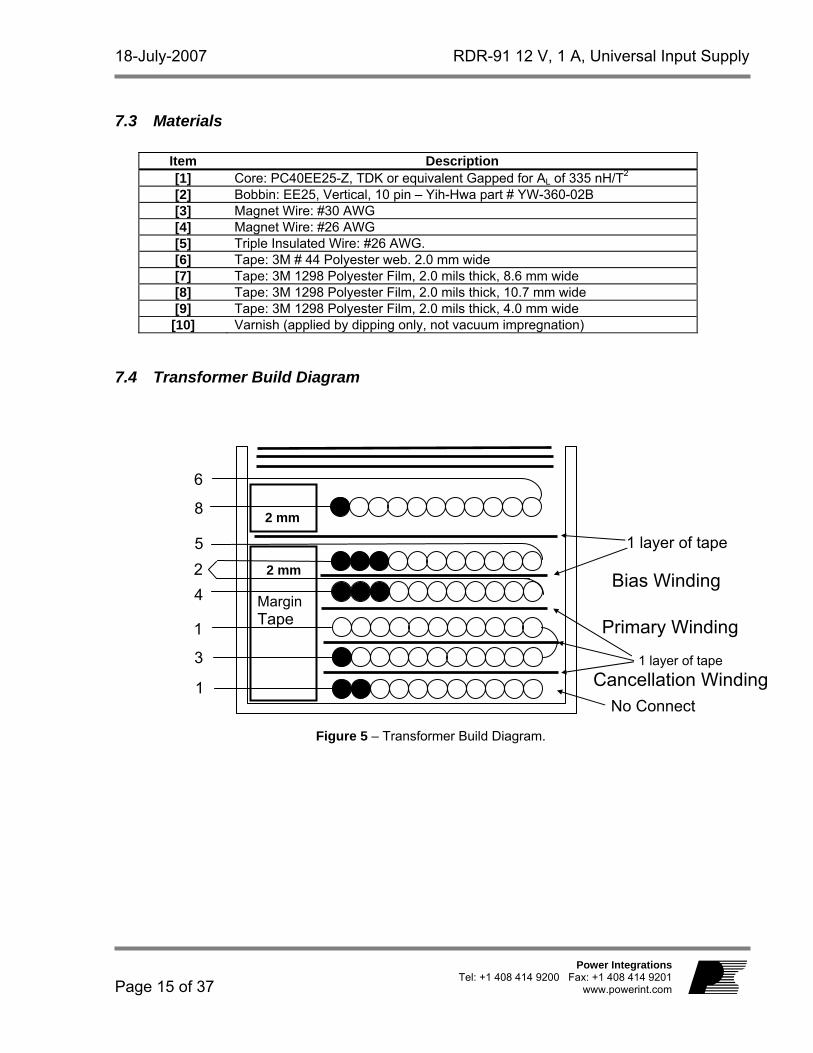
7.3 Materials
Item Description [1] Core: PC40EE25-Z, TDK or equivalent Gapped for AL of 335 nH/T2 [2] Bobbin: EE25, Vertical, 10 pin – Yih-Hwa part # YW-360-02B [3] Magnet Wire: #30 AWG [4] Magnet Wire: #26 AWG [5] Triple Insulated Wire: #26 AWG. [6] Tape: 3M # 44 Polyester web. 2.0 mm wide [7] Tape: 3M 1298 Polyester Film, 2.0 mils thick, 8.6 mm wide [8] Tape: 3M 1298 Polyester Film, 2.0 mils thick, 10.7 mm wide [9] Tape: 3M 1298 Polyester Film, 2.0 mils thick, 4.0 mm wide [10] Varnish (applied by dipping only, not vacuum impregnation)
7.4 Transformer Build Diagram
Figure 5 – Transformer Build Diagram.
1No Connect
Primary Winding
Bias Winding
Cancellation Winding 3
4
6
8
2 mm
Margin Tape
5
1
2 mm
1 layer of tape
1 layer of tape
2
RDR-91 12 V, 1 A, Universal Input Supply 18-July-2007
Page 16 of 37
Power Integrations Tel: +1 408 414 9200 Fax: +1 408 414 9201 www.powerint.com
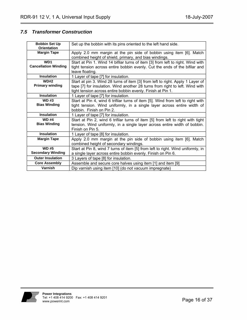
7.5 Transformer Construction
Bobbin Set Up Orientation
Set up the bobbin with its pins oriented to the left hand side.
Margin Tape Apply 2.0 mm margin at the pin side of bobbin using item [6]. Match combined height of shield, primary, and bias windings.
WD1 Cancellation Winding
Start at Pin 1. Wind 14 bifilar turns of item [3] from left to right. Wind with tight tension across entire bobbin evenly. Cut the ends of the bifilar and leave floating.
Insulation 1 Layer of tape [7] for insulation. WD#2
Primary winding Start at pin 3. Wind 28 turns of item [3] from left to right. Apply 1 Layer of tape [7] for insulation. Wind another 28 turns from right to left. Wind with tight tension across entire bobbin evenly. Finish at Pin 1.
Insulation 1 Layer of tape [7] for insulation. WD #3
Bias Winding Start at Pin 4, wind 6 trifilar turns of item [5]. Wind from left to right with tight tension. Wind uniformly, in a single layer across entire width of bobbin. Finish on Pin 2.
Insulation 1 Layer of tape [7] for insulation. WD #4
Bias Winding Start at Pin 2, wind 6 trifilar turns of item [5] from left to right with tight tension. Wind uniformly, in a single layer across entire width of bobbin. Finish on Pin 5.
Insulation 1 Layer of tape [8] for insulation. Margin Tape Apply 2.0 mm margin at the pin side of bobbin using item [6]. Match
combined height of secondary windings. WD #5
Secondary Winding Start at Pin 8, wind 7 turns of item [5] from left to right. Wind uniformly, in a single layer across entire bobbin evenly. Finish on Pin 6.
Outer Insulation 3 Layers of tape [8] for insulation. Core Assembly Assemble and secure core halves using item [1] and item [9]
Varnish Dip varnish using item [10] (do not vacuum impregnate)
18-July-2007 RDR-91 12 V, 1 A, Universal Input Supply
Page 17 of 37
Power Integrations Tel: +1 408 414 9200 Fax: +1 408 414 9201
www.powerint.com
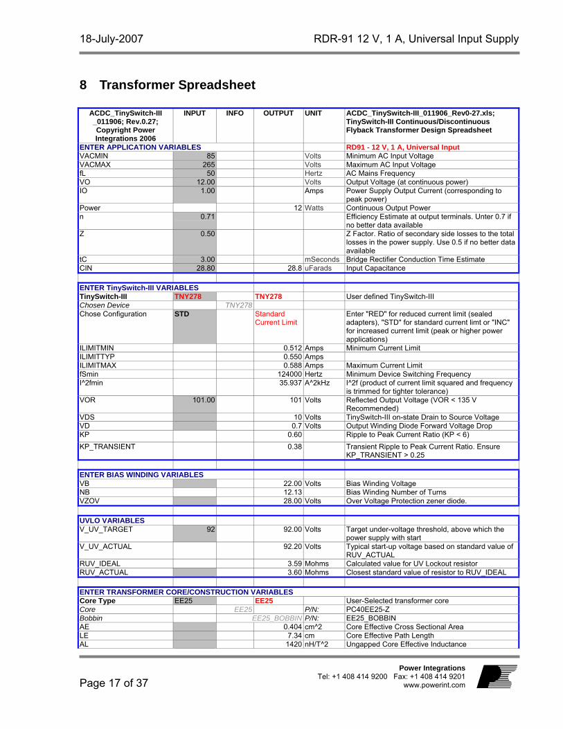
8 Transformer Spreadsheet
ACDC_TinySwitch-III _011906; Rev.0.27; Copyright Power Integrations 2006
INPUT INFO OUTPUT UNIT ACDC_TinySwitch-III_011906_Rev0-27.xls; TinySwitch-III Continuous/Discontinuous Flyback Transformer Design Spreadsheet
ENTER APPLICATION VARIABLES RD91 - 12 V, 1 A, Universal Input VACMIN 85 Volts Minimum AC Input Voltage VACMAX 265 Volts Maximum AC Input Voltage fL 50 Hertz AC Mains Frequency VO 12.00 Volts Output Voltage (at continuous power) IO 1.00 Amps Power Supply Output Current (corresponding to
peak power) Power 12 Watts Continuous Output Power n 0.71 Efficiency Estimate at output terminals. Unter 0.7 if
no better data available Z 0.50 Z Factor. Ratio of secondary side losses to the total
losses in the power supply. Use 0.5 if no better data available
tC 3.00 mSeconds Bridge Rectifier Conduction Time Estimate CIN 28.80 28.8 uFarads Input Capacitance
ENTER TinySwitch-III VARIABLES TinySwitch-III TNY278 TNY278 User defined TinySwitch-III Chosen Device TNY278 Chose Configuration STD Standard
Current Limit Enter "RED" for reduced current limit (sealed adapters), "STD" for standard current limt or "INC" for increased current limit (peak or higher power applications)
ILIMITMIN 0.512 Amps Minimum Current Limit ILIMITTYP 0.550 Amps ILIMITMAX 0.588 Amps Maximum Current Limit fSmin 124000 Hertz Minimum Device Switching Frequency I^2fmin 35.937 A^2kHz I^2f (product of current limit squared and frequency
is trimmed for tighter tolerance) VOR 101.00 101 Volts Reflected Output Voltage (VOR < 135 V
Recommended) VDS 10 Volts TinySwitch-III on-state Drain to Source Voltage VD 0.7 Volts Output Winding Diode Forward Voltage Drop KP 0.60 Ripple to Peak Current Ratio (KP < 6) KP_TRANSIENT 0.38 Transient Ripple to Peak Current Ratio. Ensure
KP_TRANSIENT > 0.25
ENTER BIAS WINDING VARIABLES VB 22.00 Volts Bias Winding Voltage NB 12.13 Bias Winding Number of Turns VZOV 28.00 Volts Over Voltage Protection zener diode.
UVLO VARIABLES V_UV_TARGET 92 92.00 Volts Target under-voltage threshold, above which the
power supply with start V_UV_ACTUAL 92.20 Volts Typical start-up voltage based on standard value of
RUV_ACTUAL RUV_IDEAL 3.59 Mohms Calculated value for UV Lockout resistor RUV_ACTUAL 3.60 Mohms Closest standard value of resistor to RUV_IDEAL
ENTER TRANSFORMER CORE/CONSTRUCTION VARIABLES Core Type EE25 EE25 User-Selected transformer core Core EE25 P/N: PC40EE25-Z Bobbin EE25_BOBBIN P/N: EE25_BOBBIN AE 0.404 cm^2 Core Effective Cross Sectional Area LE 7.34 cm Core Effective Path Length AL 1420 nH/T^2 Ungapped Core Effective Inductance
RDR-91 12 V, 1 A, Universal Input Supply 18-July-2007
Page 18 of 37
Power Integrations Tel: +1 408 414 9200 Fax: +1 408 414 9201 www.powerint.com
BW 10.2 mm Bobbin Physical Winding Width M 1.00 1 mm Safety Margin Width (Half the Primary to Secondary
Creepage Distance) L 2.00 2 Number of Primary Layers NS 7 7 Number of Secondary Turns
DC INPUT VOLTAGE PARAMETERS
VMIN 79 Volts Minimum DC Input Voltage VMAX 375 Volts Maximum DC Input Voltage
CURRENT WAVEFORM SHAPE PARAMETERS DMAX 0.59 Duty Ratio at full load, minimum primary inductance
and minimum input voltage IAVG 0.24 Amps Average Primary Current IP 0.5120 Amps Minimum Peak Primary Current IR 0.3075 Amps Primary Ripple Current IRMS 0.33 Amps Primary RMS Current
TRANSFORMER PRIMARY DESIGN PARAMETERS LP 1050 uHenries Typical Primary Inductance. +/- 10% to ensure a
minimum primary inductance of 954 uH LP_TOLERANCE 10.00 10 % Primary inductance tolerance NP 56 Primary Winding Number of Turns ALG 339 nH/T^2 Gapped Core Effective Inductance BM 2745 Gauss Maximum Operating Flux Density, BM<3000 is
recommended BAC 824 Gauss AC Flux Density for Core Loss Curves (0.5 X Peak
to Peak) ur 2053 Relative Permeability of Ungapped Core LG 0.11 mm Gap Length (Lg > 0.1 mm) BWE 16.4 mm Effective Bobbin Width OD 0.295 mm Maximum Primary Wire Diameter including
insulation INS 0.05 mm Estimated Total Insulation Thickness (= 2 * film
thickness) DIA 0.243 mm Bare conductor diameter AWG 31 AWG Primary Wire Gauge (Rounded to next smaller
standard AWG value) CM 81 Cmils Bare conductor effective area in circular mils CMA 247 Cmils/Amp Primary Winding Current Capacity (200 < CMA <
500)
TRANSFORMER SECONDARY DESIGN PARAMETERS Lumped parameters ISP 4.07 Amps Peak Secondary Current ISRMS 2.15 Amps Secondary RMS Current IRIPPLE 1.90 Amps Output Capacitor RMS Ripple Current CMS 430 Cmils Secondary Bare Conductor minimum circular mils AWGS 23 AWG Secondary Wire Gauge (Rounded up to next larger
standard AWG value)
VOLTAGE STRESS PARAMETERS VDRAIN 607 Volts Maximum Drain Voltage Estimate (Assumes 20%
zener clamp tolerance and an additional 10% temperature tolerance)
PIVS 59 Volts Output Rectifier Maximum Peak Inverse Voltage
18-July-2007 RDR-91 12 V, 1 A, Universal Input Supply
Page 19 of 37
Power Integrations Tel: +1 408 414 9200 Fax: +1 408 414 9201
www.powerint.com
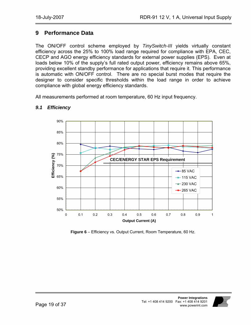
9 Performance Data The ON/OFF control scheme employed by TinySwitch-III yields virtually constant efficiency across the 25% to 100% load range required for compliance with EPA, CEC, CECP and AGO energy efficiency standards for external power supplies (EPS). Even at loads below 10% of the supply’s full rated output power, efficiency remains above 65%, providing excellent standby performance for applications that require it. This performance is automatic with ON/OFF control. There are no special burst modes that require the designer to consider specific thresholds within the load range in order to achieve compliance with global energy efficiency standards. All measurements performed at room temperature, 60 Hz input frequency.
9.1 Efficiency
Figure 6 – Efficiency vs. Output Current, Room Temperature, 60 Hz.
50%
55%
60%
65%
70%
75%
80%
85%
90%
0 0.1 0.2 0.3 0.4 0.5 0.6 0.7 0.8 0.9 1
Output Current (A)
Effic
ienc
y (%
)
85 VAC
115 VAC
230 VAC
265 VAC
CEC/ENERGY STAR EPS Requirement

RDR-91 12 V, 1 A, Universal Input Supply 18-July-2007
Page 20 of 37
Power Integrations Tel: +1 408 414 9200 Fax: +1 408 414 9201 www.powerint.com
9.2 Active Mode CEC Measurement Data In the state of California, after July 1, 2006, all single-output EPS adapters – including those sold with the products they power – must meet the California Energy Commission (CEC) requirement for minimum active-mode efficiency and no-load input power consumption. Minimum active-mode efficiency is defined as the average efficiency at 25, 50, 75 and 100% of rated output power printed on the nameplate of the supply:
Nameplate Output (PO) Minimum Efficiency in Active Mode of Operation
< 1 W 0.49 × PO ≥ 1 W to ≤ 49 W 0.09 × ln (PO) + 0.49 [ln = natural log]
> 49 W 0.84 W For adapters that are single input voltage only, the measurements are to be made at the nominal rated input voltage (115 VAC or 230 VAC). For universal input adapters, the measurements are to be made at both nominal input voltages (115 VAC and 230 VAC). To comply with the standard, the average of the four efficiency measurements must be greater than or equal to the efficiency specified by the standard.
Percent of Full Load Efficiency (%)
115 VAC 230 VAC 25 75 74.5 50 78.5 78.8 75 78.8 78.5 100 78 79.1
Average 77.6 77.7 Required CEC
minimum average efficiency (%)
71.3
From these results it is apparent that the efficiency of this design easily exceeds the required 71.3 %. More states within the USA, and many other countries around the world are adopting similar energy efficiency standards (based on the original Energy Star standard). For the latest, up-to-date information on energy efficiency regulations, please visit the PI Green Room, at:
http://www.powerint.com/greenroom/regulations.htm
18-July-2007 RDR-91 12 V, 1 A, Universal Input Supply
Page 21 of 37
Power Integrations Tel: +1 408 414 9200 Fax: +1 408 414 9201
www.powerint.com
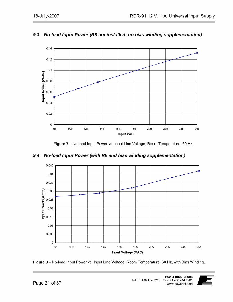
9.3 No-load Input Power (R8 not installed: no bias winding supplementation)
Figure 7 – No-load Input Power vs. Input Line Voltage, Room Temperature, 60 Hz.
9.4 No-load Input Power (with R8 and bias winding supplementation)
Figure 8 – No-load Input Power vs. Input Line Voltage, Room Temperature, 60 Hz, with Bias Winding.
0
0.005
0.01
0.015
0.02
0.025
0.03
0.035
0.04
0.045
85 105 125 145 165 185 205 225 245 265
Input Voltage (VAC)
Inpu
t Pow
er (W
atts
)
0
0.02
0.04
0.06
0.08
0.1
0.12
0.14
85 105 125 145 165 185 205 225 245 265
Input VAC
Inpu
t Pow
er (W
atts
)
RDR-91 12 V, 1 A, Universal Input Supply 18-July-2007
Page 22 of 37
Power Integrations Tel: +1 408 414 9200 Fax: +1 408 414 9201 www.powerint.com
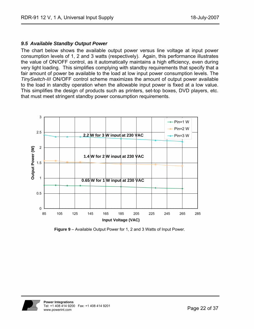
9.5 Available Standby Output Power The chart below shows the available output power versus line voltage at input power consumption levels of 1, 2 and 3 watts (respectively). Again, this performance illustrates the value of ON/OFF control, as it automatically maintains a high efficiency, even during very light loading. This simplifies complying with standby requirements that specify that a fair amount of power be available to the load at low input power consumption levels. The TinySwitch-III ON/OFF control scheme maximizes the amount of output power available to the load in standby operation when the allowable input power is fixed at a low value. This simplifies the design of products such as printers, set-top boxes, DVD players, etc. that must meet stringent standby power consumption requirements.
Figure 9 – Available Output Power for 1, 2 and 3 Watts of Input Power.
0
0.5
1
1.5
2
2.5
3
85 105 125 145 165 185 205 225 245 265 285
Input Voltage (VAC)
Out
put P
ower
(W)
Pin=1 W
Pin=2 W
Pin=3 W2.2 W for 3 W input at 230 VAC
1.4 W for 2 W input at 230 VAC
0.65 W for 1 W input at 230 VAC
18-July-2007 RDR-91 12 V, 1 A, Universal Input Supply
Page 23 of 37
Power Integrations Tel: +1 408 414 9200 Fax: +1 408 414 9201
www.powerint.com
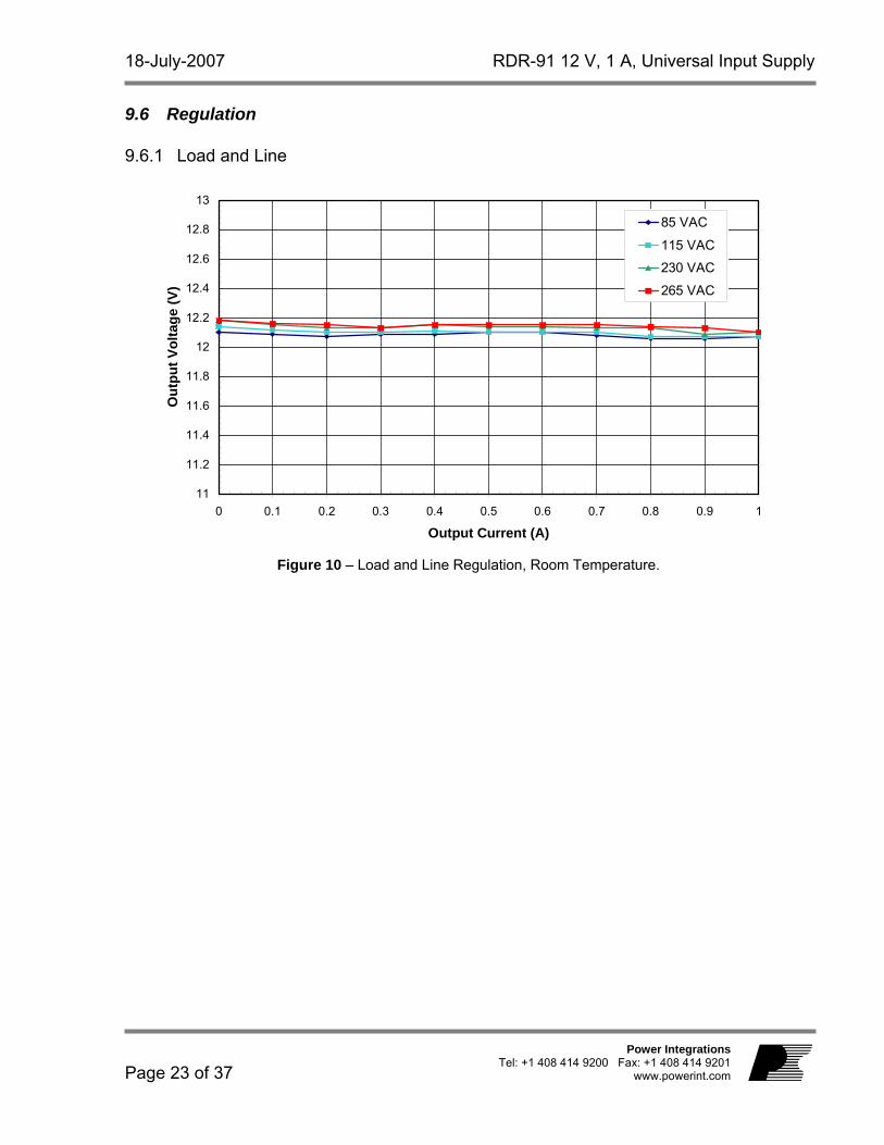
9.6 Regulation
9.6.1 Load and Line
Figure 10 – Load and Line Regulation, Room Temperature.
11
11.2
11.4
11.6
11.8
12
12.2
12.4
12.6
12.8
13
0 0.1 0.2 0.3 0.4 0.5 0.6 0.7 0.8 0.9 1
Output Current (A)
Out
put V
olta
ge (V
)
85 VAC
115 VAC
230 VAC
265 VAC

RDR-91 12 V, 1 A, Universal Input Supply 18-July-2007
Page 24 of 37
Power Integrations Tel: +1 408 414 9200 Fax: +1 408 414 9201 www.powerint.com
10 Thermal Performance Temperature measurements of key components were taken using T-type thermocouples. The thermocouples were soldered directly to a SOURCE pin of the TNY278PN device and to the cathode of the output rectifier. The thermocouples were glued to the output capacitor and to the external core and winding surfaces of transformer T1. The unit was sealed inside a large box to eliminate any air currents. The box was placed inside a thermal chamber. The ambient temperature within the large box was raised to 50 °C. The unit was then operated at full load and the temperature measurements were taken after they stabilized for 1 hour at 50 °C.
Temperature (°C)
Item 85 VAC 265 VAC
Ambient 50* 50*
TNY278PNP (U1) 96.1 92.8
Transformer (T1) 77.8 80
Output Rectifier (D7) 101 100
Output Capacitor (C10) 68.2 66.8
*To simulate operation inside sealed enclosure at 40 °C external ambient. These results show that all key components have an acceptable rise in temperature.
85 VAC, 12 W Load, 22 °C Ambient
Figure 11 – Infrared Thermograph of Open Frame Operation, at Room Temperature.
18-July-2007 RDR-91 12 V, 1 A, Universal Input Supply
Page 25 of 37
Power Integrations Tel: +1 408 414 9200 Fax: +1 408 414 9201
www.powerint.com
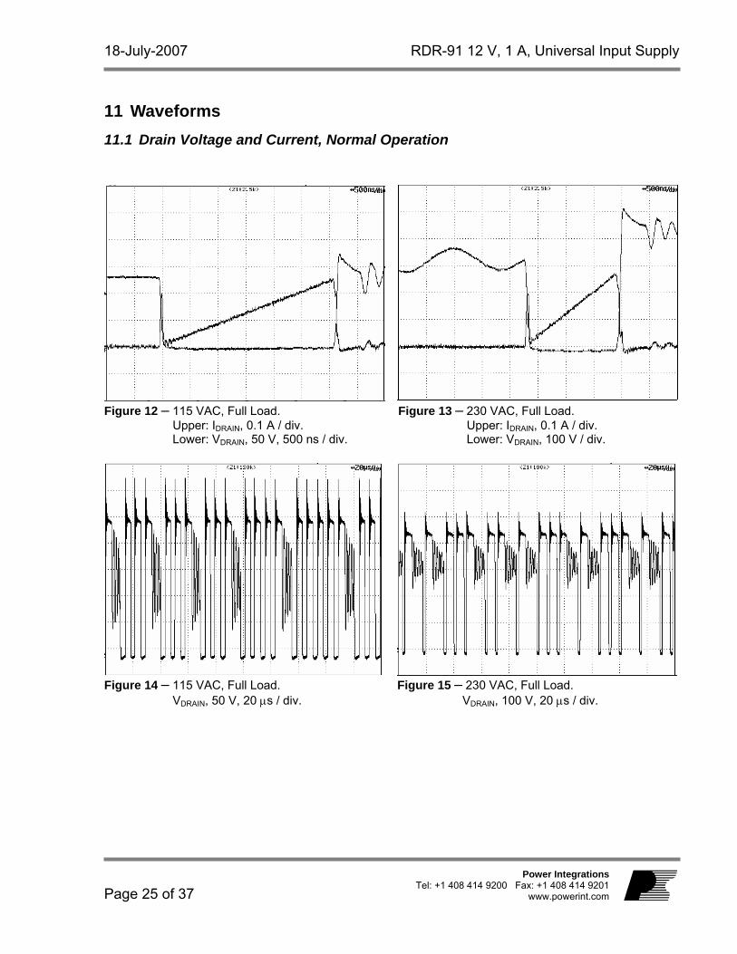
11 Waveforms 11.1 Drain Voltage and Current, Normal Operation
Figure 12 – 115 VAC, Full Load. Upper: IDRAIN, 0.1 A / div. Lower: VDRAIN, 50 V, 500 ns / div.
Figure 13 – 230 VAC, Full Load. Upper: IDRAIN, 0.1 A / div. Lower: VDRAIN, 100 V / div.
Figure 14 – 115 VAC, Full Load.
VDRAIN, 50 V, 20 µs / div. Figure 15 – 230 VAC, Full Load.
VDRAIN, 100 V, 20 µs / div.
RDR-91 12 V, 1 A, Universal Input Supply 18-July-2007
Page 26 of 37
Power Integrations Tel: +1 408 414 9200 Fax: +1 408 414 9201 www.powerint.com
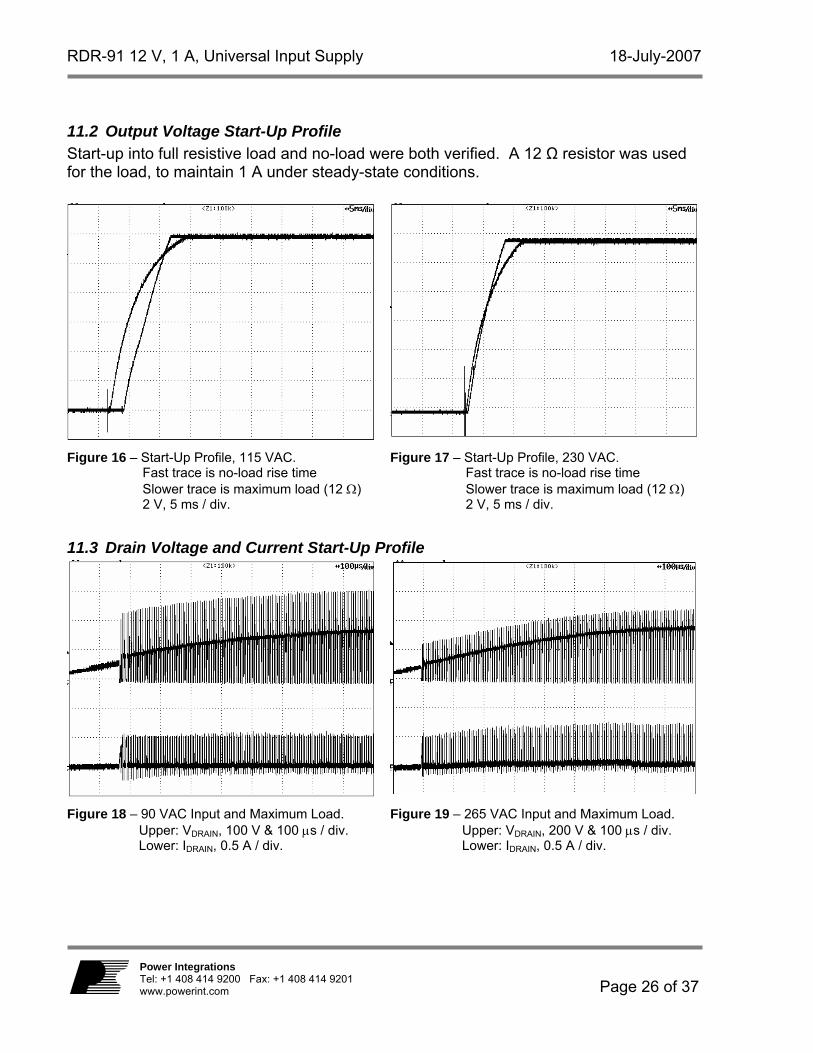
11.2 Output Voltage Start-Up Profile Start-up into full resistive load and no-load were both verified. A 12 Ω resistor was used for the load, to maintain 1 A under steady-state conditions.
Figure 16 – Start-Up Profile, 115 VAC. Fast trace is no-load rise time Slower trace is maximum load (12 Ω) 2 V, 5 ms / div.
Figure 17 – Start-Up Profile, 230 VAC. Fast trace is no-load rise time Slower trace is maximum load (12 Ω) 2 V, 5 ms / div.
11.3 Drain Voltage and Current Start-Up Profile
Figure 18 – 90 VAC Input and Maximum Load. Upper: VDRAIN, 100 V & 100 µs / div. Lower: IDRAIN, 0.5 A / div.
Figure 19 – 265 VAC Input and Maximum Load. Upper: VDRAIN, 200 V & 100 µs / div. Lower: IDRAIN, 0.5 A / div.
18-July-2007 RDR-91 12 V, 1 A, Universal Input Supply
Page 27 of 37
Power Integrations Tel: +1 408 414 9200 Fax: +1 408 414 9201
www.powerint.com
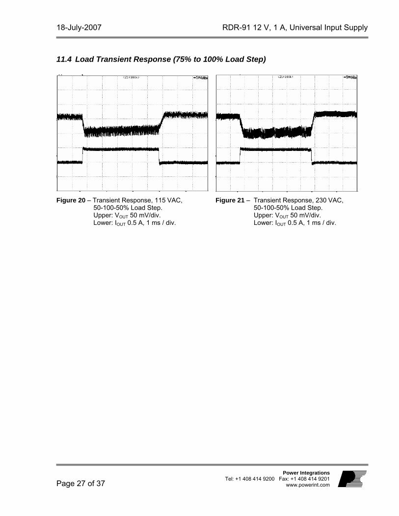
11.4 Load Transient Response (75% to 100% Load Step)
Figure 20 – Transient Response, 115 VAC,
50-100-50% Load Step. Upper: VOUT 50 mV/div. Lower: IOUT 0.5 A, 1 ms / div.
Figure 21 – Transient Response, 230 VAC, 50-100-50% Load Step. Upper: VOUT 50 mV/div. Lower: IOUT 0.5 A, 1 ms / div.

RDR-91 12 V, 1 A, Universal Input Supply 18-July-2007
Page 28 of 37
Power Integrations Tel: +1 408 414 9200 Fax: +1 408 414 9201 www.powerint.com
11.5 Output Ripple Measurements
11.5.1 Ripple Measurement Technique A modified oscilloscope test probe was used to take output ripple measurements, in order to reduce the pickup of spurious signals. Using the probe adapter pictured in Figure 22, the output ripple was measured with a 1 µF electrolytic, and a 0.1 µF ceramic capacitor connected as shown.
Figure 22 – Oscilloscope Probe Prepared for Ripple Measurement (End Cap and Ground Lead Removed).
Probe Ground
Probe Tip
18-July-2007 RDR-91 12 V, 1 A, Universal Input Supply
Page 29 of 37
Power Integrations Tel: +1 408 414 9200 Fax: +1 408 414 9201
www.powerint.com
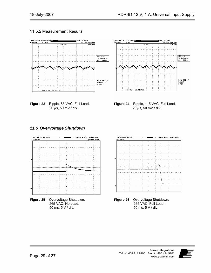
11.5.2 Measurement Results
Figure 23 – Ripple, 85 VAC, Full Load.
20 µs, 50 mV / div. Figure 24 – Ripple, 115 VAC, Full Load.
20 µs, 50 mV / div.
11.6 Overvoltage Shutdown
Figure 25 – Overvoltage Shutdown. 265 VAC, No Load. 50 ms, 5 V / div.
Figure 26 – Overvoltage Shutdown. 265 VAC, Full Load. 50 ms, 5 V / div.
RDR-91 12 V, 1 A, Universal Input Supply 18-July-2007
Page 30 of 37
Power Integrations Tel: +1 408 414 9200 Fax: +1 408 414 9201 www.powerint.com
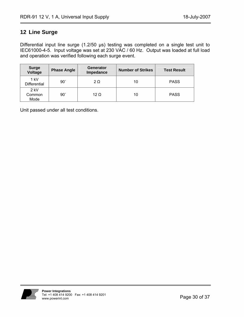
12 Line Surge Differential input line surge (1.2/50 µs) testing was completed on a single test unit to IEC61000-4-5. Input voltage was set at 230 VAC / 60 Hz. Output was loaded at full load and operation was verified following each surge event.
Surge Voltage Phase Angle Generator
Impedance Number of Strikes Test Result
1 kV Differential 90˚ 2 Ω 10 PASS
2 kV Common
Mode 90˚ 12 Ω 10 PASS
Unit passed under all test conditions.
18-July-2007 RDR-91 12 V, 1 A, Universal Input Supply
Page 31 of 37
Power Integrations Tel: +1 408 414 9200 Fax: +1 408 414 9201
www.powerint.com
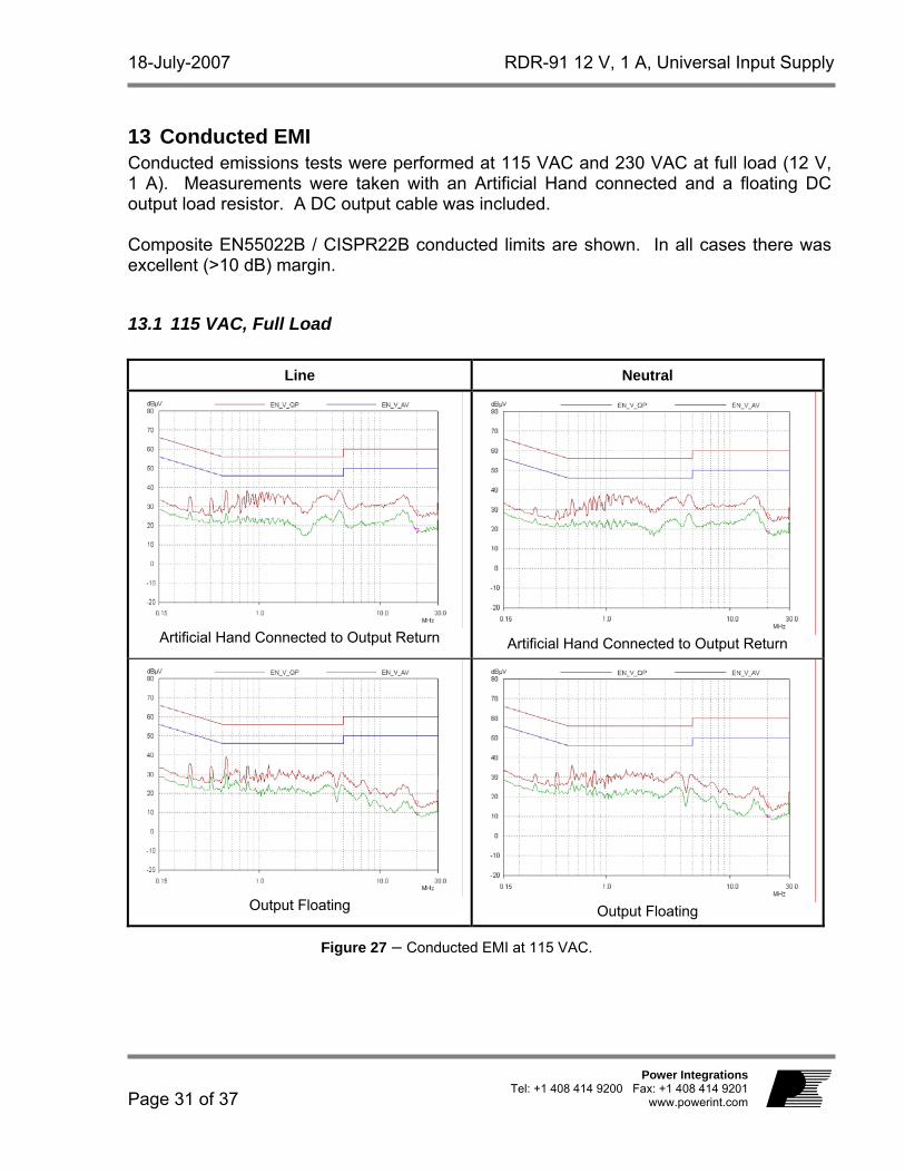
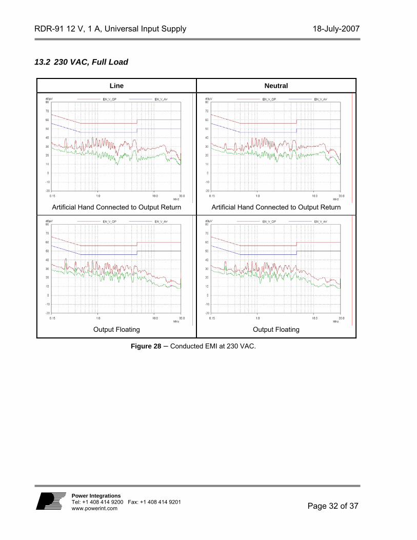
13 Conducted EMI Conducted emissions tests were performed at 115 VAC and 230 VAC at full load (12 V, 1 A). Measurements were taken with an Artificial Hand connected and a floating DC output load resistor. A DC output cable was included. Composite EN55022B / CISPR22B conducted limits are shown. In all cases there was excellent (>10 dB) margin.
13.1 115 VAC, Full Load
Line Neutral
Artificial Hand Connected to Output Return Artificial Hand Connected to Output Return
Output Floating Output Floating Figure 27 – Conducted EMI at 115 VAC.
RDR-91 12 V, 1 A, Universal Input Supply 18-July-2007
Page 32 of 37
Power Integrations Tel: +1 408 414 9200 Fax: +1 408 414 9201 www.powerint.com
13.2 230 VAC, Full Load
Line Neutral
Artificial Hand Connected to Output Return Artificial Hand Connected to Output Return
Output Floating Output Floating
Figure 28 – Conducted EMI at 230 VAC.
18-July-2007 RDR-91 12 V, 1 A, Universal Input Supply
Page 33 of 37
Power Integrations Tel: +1 408 414 9200 Fax: +1 408 414 9201
www.powerint.com
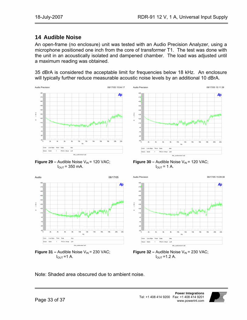
14 Audible Noise An open-frame (no enclosure) unit was tested with an Audio Precision Analyzer, using a microphone positioned one inch from the core of transformer T1. The test was done with the unit in an acoustically isolated and dampened chamber. The load was adjusted until a maximum reading was obtained. 35 dBrA is considered the acceptable limit for frequencies below 18 kHz. An enclosure will typically further reduce measurable acoustic noise levels by an additional 10 dBrA. Audio Precision 08/17/05 15:04:17
Arts_audionoise1.at2
Color Line Style Thick Data Axis
Green Solid 1 Fft.Ch.1 Ampl Left
-30
+80
-20
-10
+0
+10
+20
+30
+40
+50
+60
+70
dBr A
0 22k2k 4k 6k 8k 10k 12k 14k 16k 18k 20kHz
Audio Precision 08/17/05 15:11:39
Arts_audionoise1.at2
Color Line Style Thick Data Axis
Green Solid 1 Fft.Ch.1 Ampl Left
-30
+80
-20
-10
+0
+10
+20
+30
+40
+50
+60
+70
dBr A
0 22k2k 4k 6k 8k 10k 12k 14k 16k 18k 20kHz
Figure 29 – Audible Noise VIN = 120 VAC; IOUT = 350 mA.
Figure 30 – Audible Noise VIN = 120 VAC; IOUT = 1 A.
Audio 08/17/05
Arts_audionoise1.at2
Color Line Style Thick Data Axis Green Solid 1 Fft.Ch.1 Ampl Left
-30
+80
-20
-10
+0
+10
+20
+30
+40
+50
+60
+70
d B r A
0 22k2k 4k 6k 8k 10k 12k 14k 16k 18k 20kHz
Audio Precision 08/17/05 15:09:38
Arts_audionoise1.at2
Color Line Style Thick Data Axis
Green Solid 1 Fft.Ch.1 Ampl Left
-30
+80
-20
-10
+0
+10
+20
+30
+40
+50
+60
+70
dBr A
0 22k2k 4k 6k 8k 10k 12k 14k 16k 18k 20kHz
Figure 31 – Audible Noise VIN = 230 VAC; IOUT =1 A.
Figure 32 – Audible Noise VIN = 230 VAC; IOUT =1.2 A.
Note: Shaded area obscured due to ambient noise.
RDR-91 12 V, 1 A, Universal Input Supply 18-July-2007
Page 34 of 37
Power Integrations Tel: +1 408 414 9200 Fax: +1 408 414 9201 www.powerint.com
15 Extended and Reduced Current Limit (ILIMIT) Operation Additional capacitors (C8 and C9 on the BOM in Section 6) have been included in the DAK-91 kit for the convenience of trying out the ILIMIT+1 and ILIMIT–1 operation of TNY278PN in the RD-91 reference board. When C7 (0.1 µF) is replaced with a 10 µF capacitor (C9), the TNY278PN will operate in the ILIMIT+1 mode, which increases the maximum primary current limit from the standard maximum limit of 0.55 A to 0.65 A (equal to that of a TNY279PN). This allows a TNY278PN to deliver from 15% to 25% more output power (depending on the output voltage and current). CAUTION: Because RD-91 was designed for standard ILIMIT operation, It should not be loaded with more than 1.25 A at an elevated temperature for very long (a few minutes) when verifying the performance of TNY278PN in the ILIMIT+1 mode, since the other power components (transformer, input bulk capacitors, output diode, output capacitors and primary clamp network) are not sized for sustained operation at more than 12 W. When C7 is replaced with a 1 µF capacitor (C8), the TNY278PN will operate in the ILIMIT–1 mode, which reduces the maximum current limit from the standard maximum limit of 0.55 A to 0.45 A (equal to that of a TNY277PN). Although this reduces the maximum output power that the supply can deliver, it typically will increase the efficiency, especially at lower output power levels. To take the fullest advantage of the increase in efficiency that can be obtained from ILIMIT–1 operation, the power transformer would need to be redesigned slightly.
16 TNY277PN and TNY279PN Operation in RD-91 A TNY277PN device used in the ILIMIT+1 mode (a 10 µF installed in place of C7) will work in the RD-91 reference board, and deliver output power equal to that of a TNY278PN device. This flexibility allows a design engineer the option of using a lower cost part in applications with less demanding thermal requirements. A TNY279PN device used in the ILIMIT–1 mode (a 1 µF installed in place of C7) will deliver the same output power as a TNY278PN in the standard ILIMIT configuration. This can improve efficiency and lower the temperature rise of the device, which can give greater thermal margin to a design that must operate in high ambient temperature environments.
18-July-2007 RDR-91 12 V, 1 A, Universal Input Supply
Page 35 of 37
Power Integrations Tel: +1 408 414 9200 Fax: +1 408 414 9201
www.powerint.com
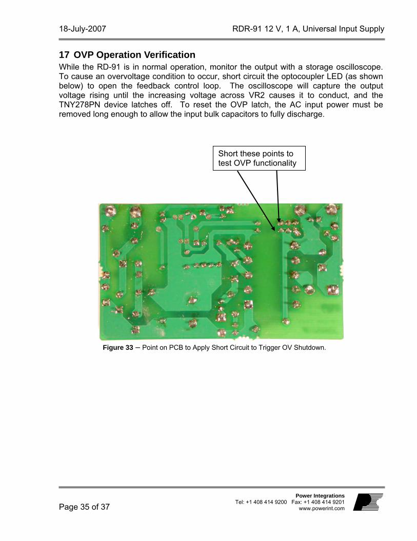
17 OVP Operation Verification While the RD-91 is in normal operation, monitor the output with a storage oscilloscope. To cause an overvoltage condition to occur, short circuit the optocoupler LED (as shown below) to open the feedback control loop. The oscilloscope will capture the output voltage rising until the increasing voltage across VR2 causes it to conduct, and the TNY278PN device latches off. To reset the OVP latch, the AC input power must be removed long enough to allow the input bulk capacitors to fully discharge.
Short these points to test OVP functionality
Figure 33 – Point on PCB to Apply Short Circuit to Trigger OV Shutdown.
RDR-91 12 V, 1 A, Universal Input Supply 18-July-2007
Page 36 of 37
Power Integrations Tel: +1 408 414 9200 Fax: +1 408 414 9201 www.powerint.com
18 Revision History
Date Author Revision Description & changes 25-Jan-06 JAJ 1.0 Formatted for Final Release 07-Feb-06 JAJ 1.1 Formatted and corrected measurement
scales / div. 18-July-2007 SGK 1.2 Updated for RoHS compliance, changed
to RD-91.
18-July-2007 RDR-91 12 V, 1 A, Universal Input Supply
Page 37 of 37
Power Integrations Tel: +1 408 414 9200 Fax: +1 408 414 9201
www.powerint.com
For the latest updates, visit our website: www.powerint.com Power Integrations reserves the right to make changes to its products at any time to improve reliability or manufacturability. Power Integrations does not assume any liability arising from the use of any device or circuit described herein. POWER INTEGRATIONS MAKES NO WARRANTY HEREIN AND SPECIFICALLY DISCLAIMS ALL WARRANTIES INCLUDING, WITHOUT LIMITATION, THE IMPLIED WARRANTIES OF MERCHANTABILITY, FITNESS FOR A PARTICULAR PURPOSE, AND NON-INFRINGEMENT OF THIRD PARTY RIGHTS.
PATENT INFORMATION The products and applications illustrated herein (including transformer construction and circuits external to the products) may be covered by one or more U.S. and foreign patents, or potentially by pending U.S. and foreign patent applications assigned to Power Integrations. A complete list of Power Integrations’ patents may be found at www.powerint.com. Power Integrations grants its customers a license under certain patent rights as set forth at http://www.powerint.com/ip.htm. The PI Logo, TOPSwitch, TinySwitch, LinkSwitch, DPA-Switch, EcoSmart, Clampless, E-Shield, Filterfuse, PI Expert and PI FACTS are trademarks of Power Integrations, Inc. Other trademarks are property of their respective companies. ©Copyright 2006 Power Integrations, Inc.
Power Integrations Worldwide Sales Support Locations
WORLD HEADQUARTERS 5245 Hellyer Avenue San Jose, CA 95138, USA. Main: +1-408-414-9200 Customer Service: Phone: +1-408-414-9665 Fax: +1-408-414-9765 e-mail: [email protected]
GERMANY Rueckertstrasse 3 D-80336, Munich Germany Phone: +49-89-5527-3910 Fax: +49-89-5527-3920 e-mail: [email protected]
JAPAN Keihin Tatemono 1st Bldg 2-12-20 Shin-Yokohama, Kohoku-ku, Yokohama-shi, Kanagawa ken, Japan 222-0033 Phone: +81-45-471-1021 Fax: +81-45-471-3717 e-mail: [email protected]
TAIWAN 5F, No. 318, Nei Hu Rd., Sec. 1 Nei Hu Dist. Taipei, Taiwan 114, R.O.C. Phone: +886-2-2659-4570 Fax: +886-2-2659-4550 e-mail: [email protected]
CHINA (SHANGHAI) Rm 807-808A, Pacheer Commercial Centre, 555 Nanjing Rd. West Shanghai, P.R.C. 200041 Phone: +86-21-6215-5548 Fax: +86-21-6215-2468 e-mail: [email protected]
INDIA 261/A, Ground Floor 7th Main, 17th Cross, Sadashivanagar Bangalore, India 560080 Phone: +91-80-5113-8020 Fax: +91-80-5113-8023 e-mail: [email protected]
KOREA RM 602, 6FL Korea City Air Terminal B/D, 159-6 Samsung-Dong, Kangnam-Gu, Seoul, 135-728, Korea Phone: +82-2-2016-6610 Fax: +82-2-2016-6630 e-mail: [email protected]
EUROPE HQ 1st Floor, St. James’s House East Street, Farnham Surrey, GU9 7TJ United Kingdom Phone: +44 (0) 1252-730-140 Fax: +44 (0) 1252-727-689 e-mail: [email protected]
CHINA (SHENZHEN) Room 2206-2207, Block A, Elec. Sci. Tech. Bldg. 2070 Shennan Zhong Rd. Shenzhen, Guangdong, China, 518031 Phone: +86-755-8379-3243 Fax: +86-755-8379-5828 e-mail: [email protected]
ITALY Via Vittorio Veneto 12 20091 Bresso MI Italy Phone: +39-028-928-6000 Fax: +39-028-928-6009 e-mail: [email protected]
SINGAPORE 51 Newton Road, #15-08/10 Goldhill Plaza, Singapore, 308900 Phone: +65-6358-2160 Fax: +65-6358-2015 e-mail: [email protected]
APPLICATIONS HOTLINE World Wide +1-408-414-9660 APPLICATIONS FAX World Wide +1-408-414-9760


![2960SCG[1] Swicht Manual de Configuracion](https://img.pdfslide.net/doc/110x75/577cbd111a28aba7118de396/2960scg1-swicht-manual-de-configuracion.jpg)