Embed Size (px)
Citation preview
This is information on a product in full production.
September 2013 DocID9035 Rev 10 1/16
16
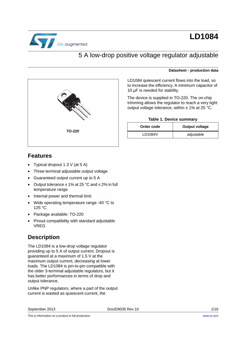
LD1084
5 A low-drop positive voltage regulator adjustable
Datasheet - production data
Features• Typical dropout 1.3 V (at 5 A)
• Three-terminal adjustable output voltage
• Guaranteed output current up to 5 A
• Output tolerance ± 1% at 25 °C and ± 2% in full temperature range
• Internal power and thermal limit
• Wide operating temperature range -40 °C to 125 °C
• Package available: TO-220
• Pinout compatibility with standard adjustable VREG
DescriptionThe LD1084 is a low-drop voltage regulator providing up to 5 A of output current. Dropout is guaranteed at a maximum of 1.5 V at the maximum output current, decreasing at lower loads. The LD1084 is pin-to-pin compatible with the older 3-terminal adjustable regulators, but it has better performances in terms of drop and output tolerance.
Unlike PNP regulators, where a part of the output current is wasted as quiescent current, the
LD1084 quiescent current flows into the load, so to increase the efficiency. A minimum capacitor of 10 µF is needed for stability.
The device is supplied in TO-220. The on-chip trimming allows the regulator to reach a very tight output voltage tolerance, within ± 1% at 25 °C.
TO-220
Table 1. Device summary
Order code Output voltage
LD1084V adjustable
www.st.com
Contents LD1084
2/16 DocID9035 Rev 10
Contents
1 Diagram . . . . . . . . . . . . . . . . . . . . . . . . . . . . . . . . . . . . . . . . . . . . . . . . . . . 3
2 Pin configuration . . . . . . . . . . . . . . . . . . . . . . . . . . . . . . . . . . . . . . . . . . . 4
3 Maximum ratings . . . . . . . . . . . . . . . . . . . . . . . . . . . . . . . . . . . . . . . . . . . . 5
4 Schematic application . . . . . . . . . . . . . . . . . . . . . . . . . . . . . . . . . . . . . . . 6
5 Electrical characteristics . . . . . . . . . . . . . . . . . . . . . . . . . . . . . . . . . . . . . 7
6 Typical performance characteristics . . . . . . . . . . . . . . . . . . . . . . . . . . . . 8
7 Package mechanical data . . . . . . . . . . . . . . . . . . . . . . . . . . . . . . . . . . . . 13
8 Revision history . . . . . . . . . . . . . . . . . . . . . . . . . . . . . . . . . . . . . . . . . . . 15
DocID9035 Rev 10 3/16
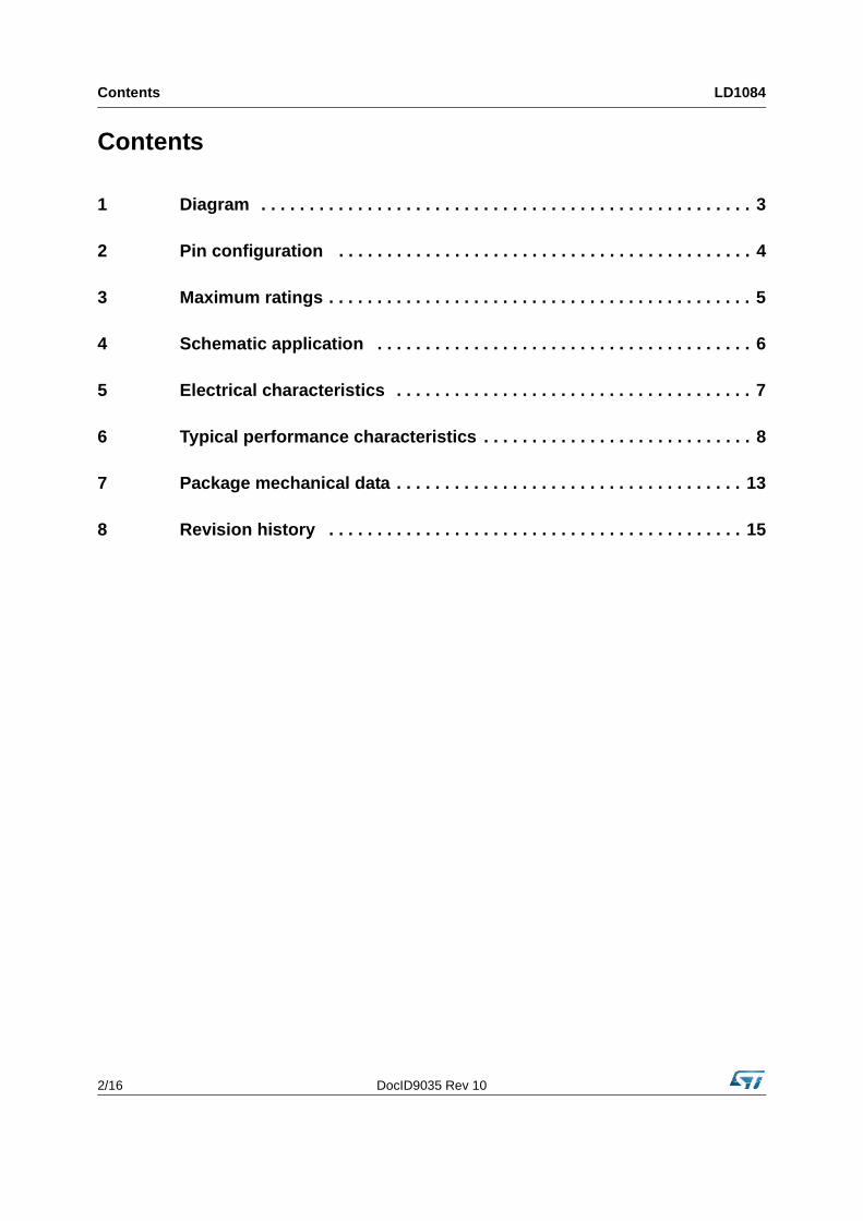
LD1084 Diagram
1 Diagram
Figure 1. Schematic diagram
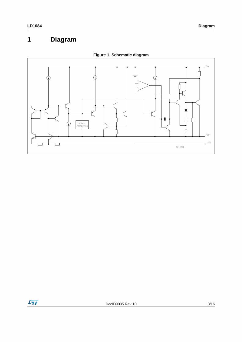
Pin configuration LD1084
4/16 DocID9035 Rev 10
2 Pin configuration
Figure 2. Pin connections (top view)
DocID9035 Rev 10 5/16
LD1084 Maximum ratings
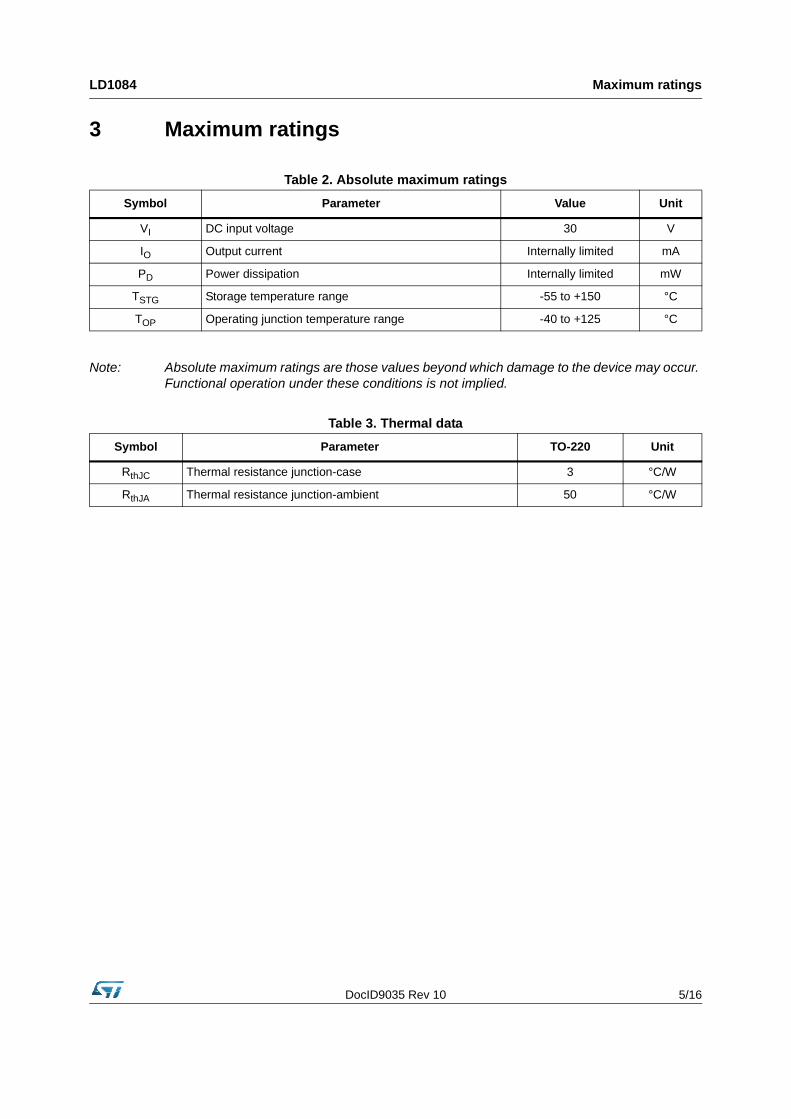
3 Maximum ratings
Note: Absolute maximum ratings are those values beyond which damage to the device may occur. Functional operation under these conditions is not implied.
Table 2. Absolute maximum ratings
Symbol Parameter Value Unit
VI DC input voltage 30 V
IO Output current Internally limited mA
PD Power dissipation Internally limited mW
TSTG Storage temperature range -55 to +150 °C
TOP Operating junction temperature range -40 to +125 °C
Table 3. Thermal data
Symbol Parameter TO-220 Unit
RthJC Thermal resistance junction-case 3 °C/W
RthJA Thermal resistance junction-ambient 50 °C/W
Schematic application LD1084
6/16 DocID9035 Rev 10
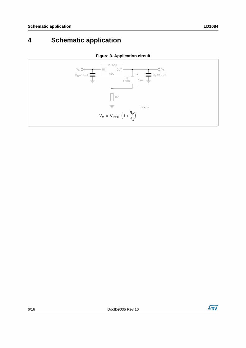
4 Schematic application
Figure 3. Application circuit
VO VREF 1R2
R1-------+
⋅=
DocID9035 Rev 10 7/16
LD1084 Electrical characteristics
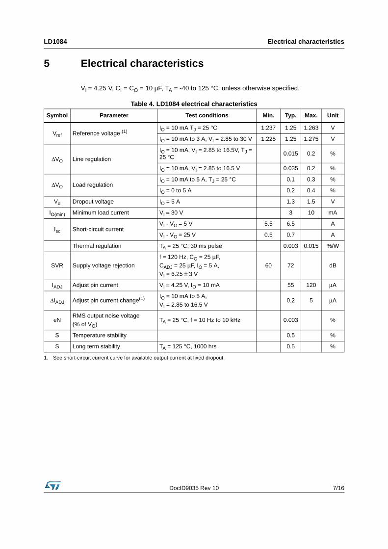
5 Electrical characteristics
VI = 4.25 V, CI = CO = 10 µF, TA = -40 to 125 °C, unless otherwise specified.
Table 4. LD1084 electrical characteristics
Symbol Parameter Test conditions Min. Typ. Max. Unit
Vref Reference voltage (1)IO = 10 mA TJ = 25 °C 1.237 1.25 1.263 V
IO = 10 mA to 3 A, VI = 2.85 to 30 V 1.225 1.25 1.275 V
ΔVO Line regulation
IO = 10 mA, VI = 2.85 to 16.5V, TJ = 25 °C
0.015 0.2 %
IO = 10 mA, VI = 2.85 to 16.5 V 0.035 0.2 %
ΔVO Load regulationIO = 10 mA to 5 A, TJ = 25 °C 0.1 0.3 %
IO = 0 to 5 A 0.2 0.4 %
Vd Dropout voltage IO = 5 A 1.3 1.5 V
IO(min) Minimum load current VI = 30 V 3 10 mA
Isc Short-circuit currentVI - VO = 5 V 5.5 6.5 A
VI - VO = 25 V 0.5 0.7 A
Thermal regulation TA = 25 °C, 30 ms pulse 0.003 0.015 %/W
SVR Supply voltage rejection
f = 120 Hz, CO = 25 µF,
CADJ = 25 µF, IO = 5 A, VI = 6.25 ± 3 V
60 72 dB
IADJ Adjust pin current VI = 4.25 V, IO = 10 mA 55 120 μA
ΔIADJ Adjust pin current change(1) IO = 10 mA to 5 A,
VI = 2.85 to 16.5 V0.2 5 μA
eNRMS output noise voltage
(% of VO)TA = 25 °C, f = 10 Hz to 10 kHz 0.003 %
S Temperature stability 0.5 %
S Long term stability TA = 125 °C, 1000 hrs 0.5 %
1. See short-circuit current curve for available output current at fixed dropout.
Typical performance characteristics LD1084
8/16 DocID9035 Rev 10
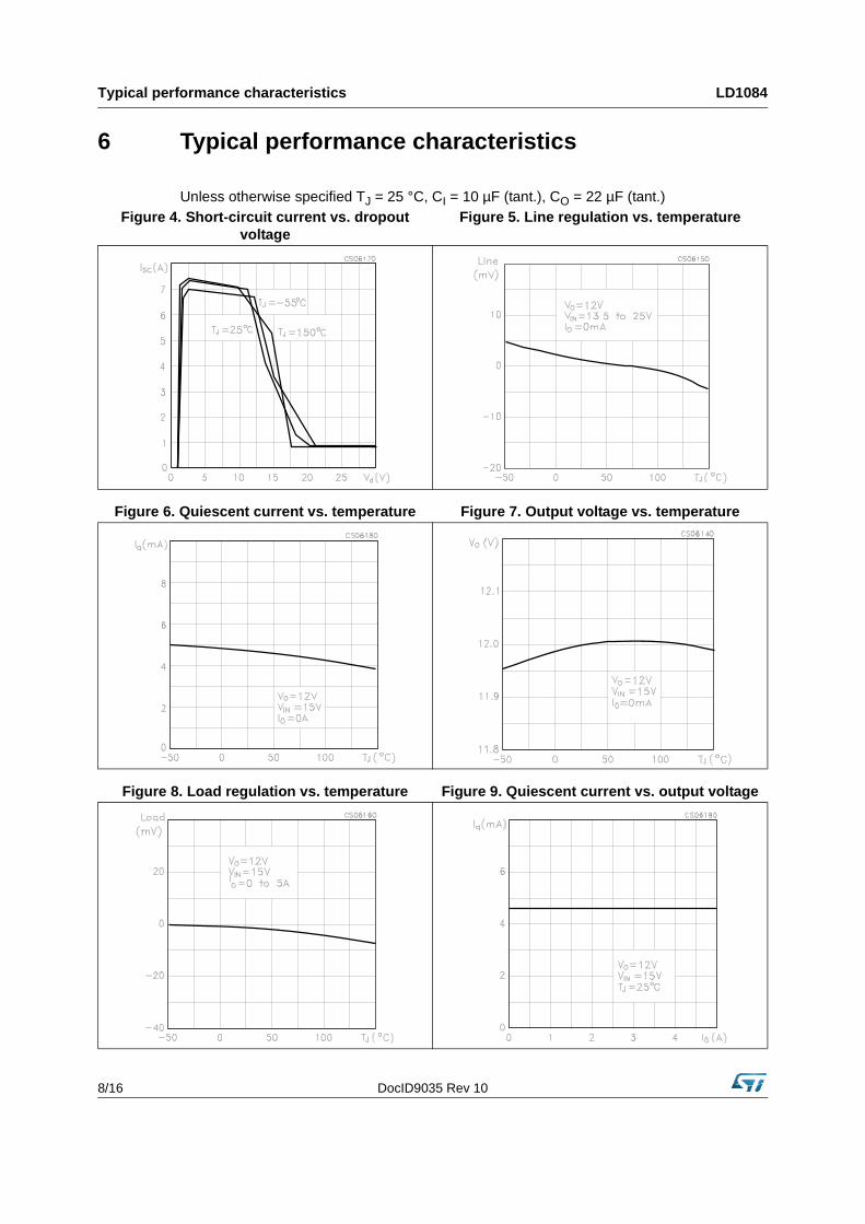
6 Typical performance characteristics
Unless otherwise specified TJ = 25 °C, CI = 10 µF (tant.), CO = 22 µF (tant.)Figure 4. Short-circuit current vs. dropout
voltageFigure 5. Line regulation vs. temperature
Figure 6. Quiescent current vs. temperature Figure 7. Output voltage vs. temperature
Figure 8. Load regulation vs. temperature Figure 9. Quiescent current vs. output voltage
DocID9035 Rev 10 9/16
LD1084 Typical performance characteristics
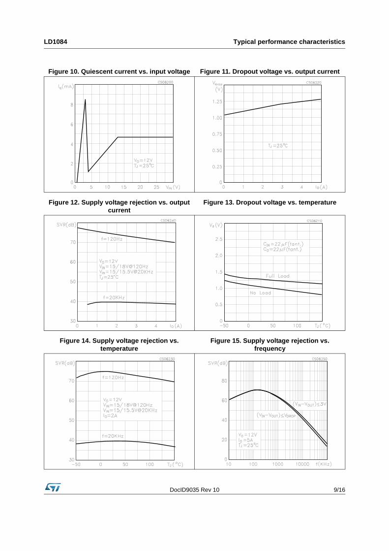
Figure 10. Quiescent current vs. input voltage Figure 11. Dropout voltage vs. output current
Figure 12. Supply voltage rejection vs. output current
Figure 13. Dropout voltage vs. temperature
Figure 14. Supply voltage rejection vs. temperature
Figure 15. Supply voltage rejection vs. frequency
Typical performance characteristics LD1084
10/16 DocID9035 Rev 10
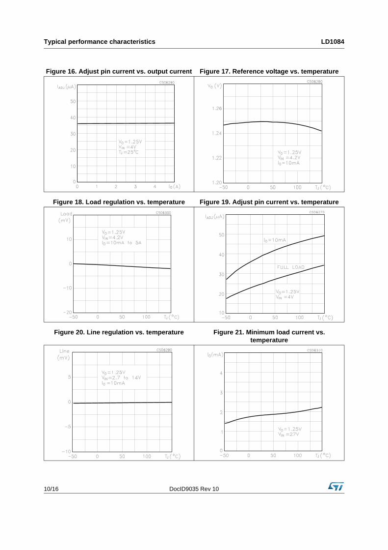
Figure 16. Adjust pin current vs. output current Figure 17. Reference voltage vs. temperature
Figure 18. Load regulation vs. temperature Figure 19. Adjust pin current vs. temperature
Figure 20. Line regulation vs. temperature Figure 21. Minimum load current vs. temperature
DocID9035 Rev 10 11/16
LD1084 Typical performance characteristics
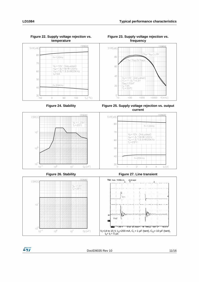
Figure 22. Supply voltage rejection vs. temperature
Figure 23. Supply voltage rejection vs. frequency
Figure 24. Stability Figure 25. Supply voltage rejection vs. output current
Figure 26. Stability Figure 27. Line transient
VI=14 to 15 V, IO=200 mA, CI = 1 µF (tant), CO= 10 µF (tant), ts= tf = 5 µs
Typical performance characteristics LD1084
12/16 DocID9035 Rev 10
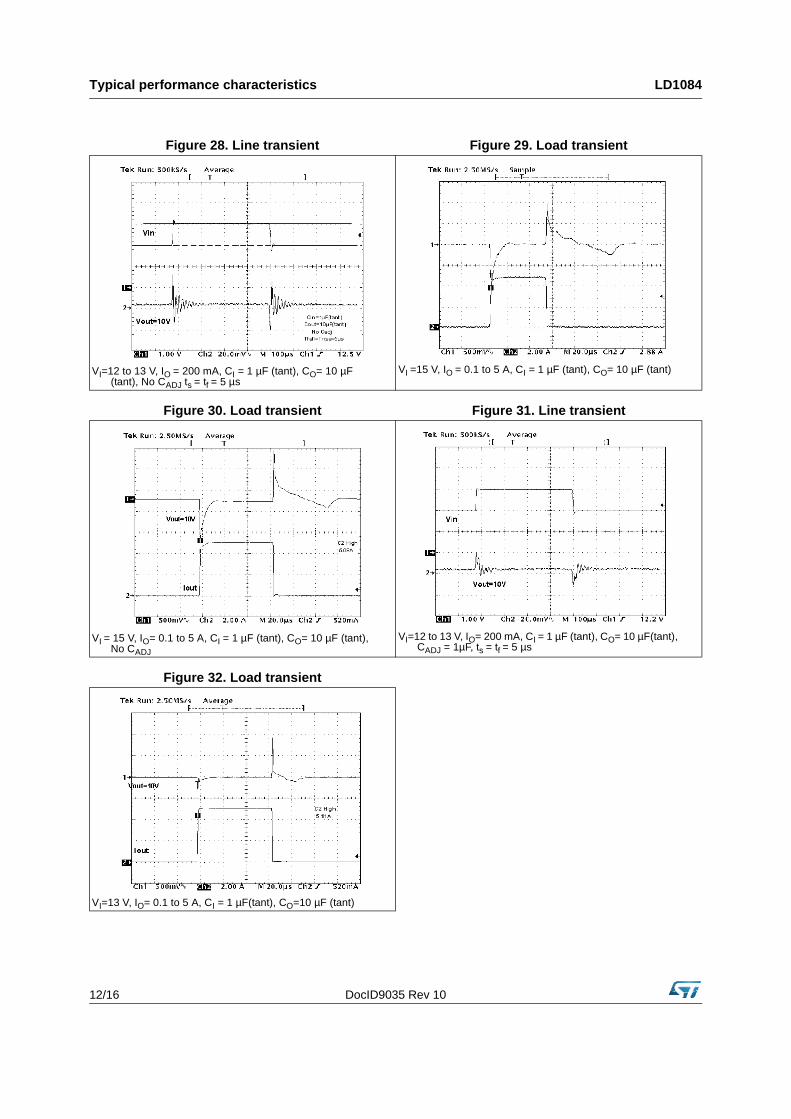
Figure 28. Line transient Figure 29. Load transient
VI=12 to 13 V, IO = 200 mA, CI = 1 µF (tant), CO= 10 µF (tant), No CADJ ts = tf = 5 µs
VI =15 V, IO = 0.1 to 5 A, CI = 1 µF (tant), CO= 10 µF (tant)
Figure 30. Load transient Figure 31. Line transient
VI = 15 V, IO= 0.1 to 5 A, CI = 1 µF (tant), CO= 10 µF (tant), No CADJ
VI=12 to 13 V, IO= 200 mA, CI = 1 µF (tant), CO= 10 µF(tant), CADJ = 1µF, ts = tf = 5 µs
Figure 32. Load transient
VI=13 V, IO= 0.1 to 5 A, CI = 1 µF(tant), CO=10 µF (tant)
DocID9035 Rev 10 13/16
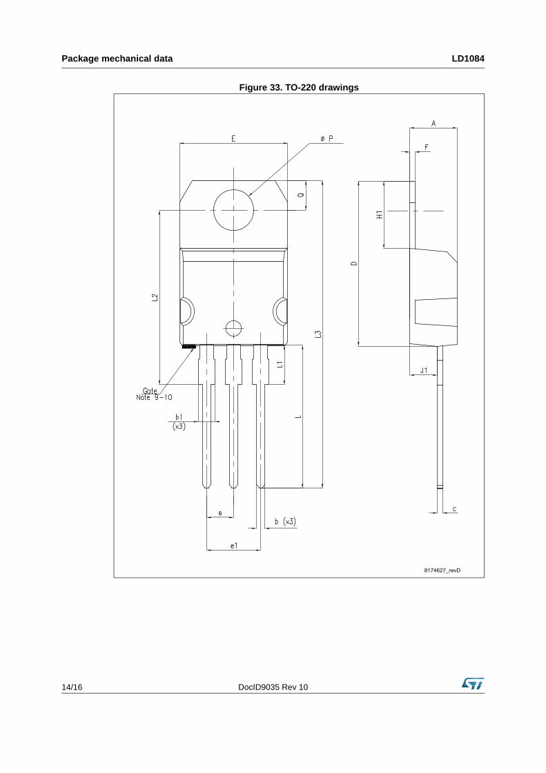
LD1084 Package mechanical data
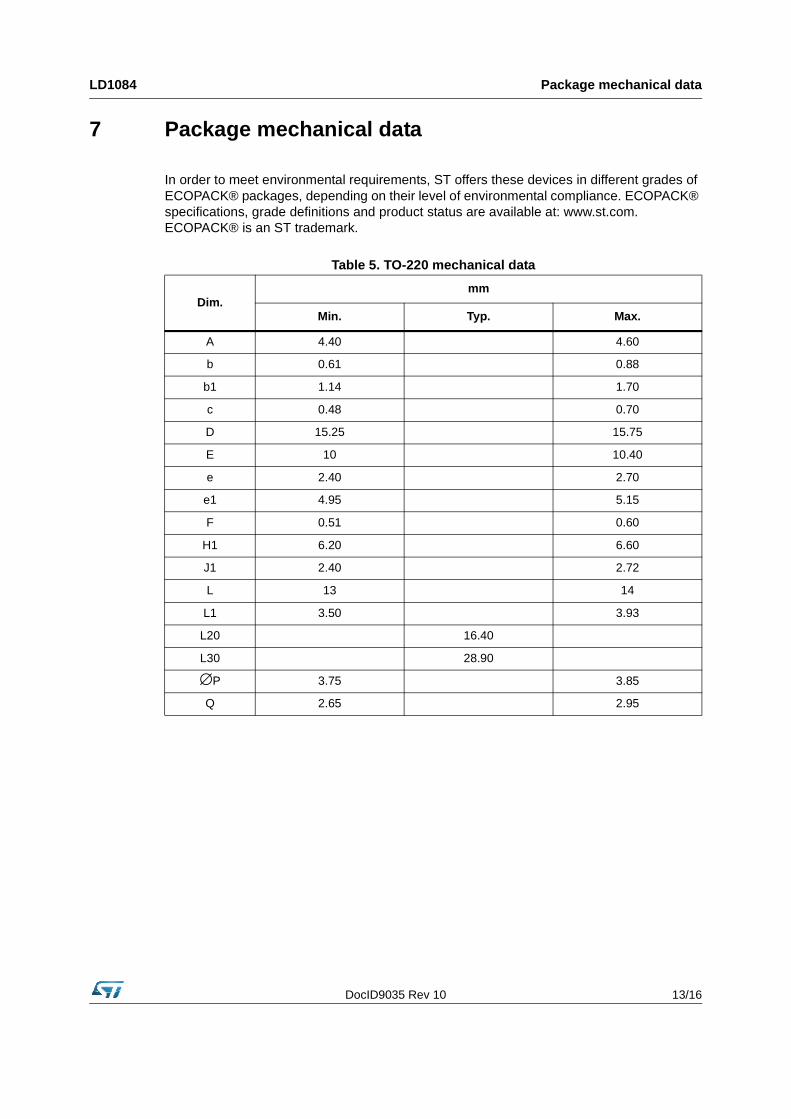
7 Package mechanical data
In order to meet environmental requirements, ST offers these devices in different grades of ECOPACK® packages, depending on their level of environmental compliance. ECOPACK® specifications, grade definitions and product status are available at: www.st.com. ECOPACK® is an ST trademark.
Table 5. TO-220 mechanical data
Dim.mm
Min. Typ. Max.
A 4.40 4.60
b 0.61 0.88
b1 1.14 1.70
c 0.48 0.70
D 15.25 15.75
E 10 10.40
e 2.40 2.70
e1 4.95 5.15
F 0.51 0.60
H1 6.20 6.60
J1 2.40 2.72
L 13 14
L1 3.50 3.93
L20 16.40
L30 28.90
∅P 3.75 3.85
Q 2.65 2.95
Package mechanical data LD1084
14/16 DocID9035 Rev 10
Figure 33. TO-220 drawings
DocID9035 Rev 10 15/16
LD1084 Revision history
8 Revision history
Table 6. Document revision history
Date Revision Changes
07-Oct-2004 3 Mistake order codes - Table 1.
08-Feb-2005 4 Mistake U.M. Load Regulation - V ==> mV.
16-Jun-2005 5 Order codes updated.
04-Apr-2007 6 Order code updated.
07-Jun-2007 7 Order codes updated.
08-Apr-2008 8Modified: Table 1 on page 1. Removed: packages D²PAK, D²PAK/A and mechanical data.
29-Jul-2009 9 Modified: Table 1 on page 1.
04-Sep-2013 10
RPN LD1084XX changed to LD1084.Updated the Description in cover page, Section 7: Package mechanical data, Figure 2: Pin connections (top view) and Figure 3: Application circuit.Minor text changes.
LD1084
16/16 DocID9035 Rev 10
Please Read Carefully:
Information in this document is provided solely in connection with ST products. STMicroelectronics NV and its subsidiaries (“ST”) reserve theright to make changes, corrections, modifications or improvements, to this document, and the products and services described herein at anytime, without notice.
All ST products are sold pursuant to ST’s terms and conditions of sale.
Purchasers are solely responsible for the choice, selection and use of the ST products and services described herein, and ST assumes noliability whatsoever relating to the choice, selection or use of the ST products and services described herein.
No license, express or implied, by estoppel or otherwise, to any intellectual property rights is granted under this document. If any part of thisdocument refers to any third party products or services it shall not be deemed a license grant by ST for the use of such third party productsor services, or any intellectual property contained therein or considered as a warranty covering the use in any manner whatsoever of suchthird party products or services or any intellectual property contained therein.
UNLESS OTHERWISE SET FORTH IN ST’S TERMS AND CONDITIONS OF SALE ST DISCLAIMS ANY EXPRESS OR IMPLIEDWARRANTY WITH RESPECT TO THE USE AND/OR SALE OF ST PRODUCTS INCLUDING WITHOUT LIMITATION IMPLIEDWARRANTIES OF MERCHANTABILITY, FITNESS FOR A PARTICULAR PURPOSE (AND THEIR EQUIVALENTS UNDER THE LAWSOF ANY JURISDICTION), OR INFRINGEMENT OF ANY PATENT, COPYRIGHT OR OTHER INTELLECTUAL PROPERTY RIGHT.
ST PRODUCTS ARE NOT AUTHORIZED FOR USE IN WEAPONS. NOR ARE ST PRODUCTS DESIGNED OR AUTHORIZED FOR USEIN: (A) SAFETY CRITICAL APPLICATIONS SUCH AS LIFE SUPPORTING, ACTIVE IMPLANTED DEVICES OR SYSTEMS WITHPRODUCT FUNCTIONAL SAFETY REQUIREMENTS; (B) AERONAUTIC APPLICATIONS; (C) AUTOMOTIVE APPLICATIONS ORENVIRONMENTS, AND/OR (D) AEROSPACE APPLICATIONS OR ENVIRONMENTS. WHERE ST PRODUCTS ARE NOT DESIGNEDFOR SUCH USE, THE PURCHASER SHALL USE PRODUCTS AT PURCHASER’S SOLE RISK, EVEN IF ST HAS BEEN INFORMED INWRITING OF SUCH USAGE, UNLESS A PRODUCT IS EXPRESSLY DESIGNATED BY ST AS BEING INTENDED FOR “AUTOMOTIVE,AUTOMOTIVE SAFETY OR MEDICAL” INDUSTRY DOMAINS ACCORDING TO ST PRODUCT DESIGN SPECIFICATIONS.PRODUCTS FORMALLY ESCC, QML OR JAN QUALIFIED ARE DEEMED SUITABLE FOR USE IN AEROSPACE BY THECORRESPONDING GOVERNMENTAL AGENCY.
Resale of ST products with provisions different from the statements and/or technical features set forth in this document shall immediately voidany warranty granted by ST for the ST product or service described herein and shall not create or extend in any manner whatsoever, anyliability of ST.
ST and the ST logo are trademarks or registered trademarks of ST in various countries.Information in this document supersedes and replaces all information previously supplied.
The ST logo is a registered trademark of STMicroelectronics. All other names are the property of their respective owners.
© 2013 STMicroelectronics - All rights reserved
STMicroelectronics group of companies
Australia - Belgium - Brazil - Canada - China - Czech Republic - Finland - France - Germany - Hong Kong - India - Israel - Italy - Japan - Malaysia - Malta - Morocco - Philippines - Singapore - Spain - Sweden - Switzerland - United Kingdom - United States of America
www.st.com

Mouser Electronics
Authorized Distributor
Click to View Pricing, Inventory, Delivery & Lifecycle Information: STMicroelectronics:
LD1084V