Embed Size (px)
Citation preview
© March 2009 Altera Corporation Quartus II Handbook Version 9.0 Volume 5: Embedded Peripherals
5. JTAG UART Core
Core OverviewThe JTAG UART core with Avalon® interface implements a method to communicate serial character streams between a host PC and an SOPC Builder system on an Altera® FPGA. In many designs, the JTAG UART core eliminates the need for a separate RS-232 serial connection to a host PC for character I/O. The core provides an Avalon interface that hides the complexities of the JTAG interface from embedded software programmers. Master peripherals (such as a Nios® II processor) communicate with the core by reading and writing control and data registers.
The JTAG UART core uses the JTAG circuitry built in to Altera FPGAs, and provides host access via the JTAG pins on the FPGA. The host PC can connect to the FPGA via any Altera JTAG download cable, such as the USB-Blaster™ cable. Software support for the JTAG UART core is provided by Altera. For the Nios II processor, device drivers are provided in the HAL system library, allowing software to access the core using the ANSI C Standard Library stdio.h routines. For the host PC, Altera provides JTAG terminal software that manages the connection to the target, decodes the JTAG data stream, and displays characters on screen.
The JTAG UART core is SOPC Builder-ready and integrates easily into any SOPC Builder-generated system. This chapter contains the following sections:
■ “Functional Description” on page 5–2
■ “Device and Tools Support” on page 5–4
■ “Instantiating the Core in SOPC Builder” on page 5–4
■ “Hardware Simulation Considerations” on page 5–6
■ “Software Programming Model” on page 5–6
NII51009-9.0.0
5–2 Chapter 5: JTAG UART CoreFunctional Description
Quartus II Handbook Version 9.0 Volume 5: Embedded Peripherals © March 2009 Altera Corporation
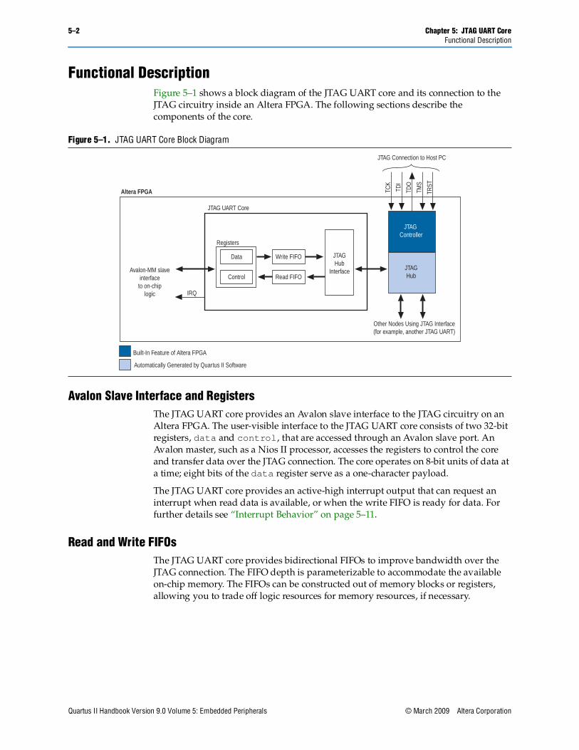
Functional DescriptionFigure 5–1 shows a block diagram of the JTAG UART core and its connection to the JTAG circuitry inside an Altera FPGA. The following sections describe the components of the core.
Avalon Slave Interface and RegistersThe JTAG UART core provides an Avalon slave interface to the JTAG circuitry on an Altera FPGA. The user-visible interface to the JTAG UART core consists of two 32-bit registers, data and control, that are accessed through an Avalon slave port. An Avalon master, such as a Nios II processor, accesses the registers to control the core and transfer data over the JTAG connection. The core operates on 8-bit units of data at a time; eight bits of the data register serve as a one-character payload.
The JTAG UART core provides an active-high interrupt output that can request an interrupt when read data is available, or when the write FIFO is ready for data. For further details see “Interrupt Behavior” on page 5–11.
Read and Write FIFOsThe JTAG UART core provides bidirectional FIFOs to improve bandwidth over the JTAG connection. The FIFO depth is parameterizable to accommodate the available on-chip memory. The FIFOs can be constructed out of memory blocks or registers, allowing you to trade off logic resources for memory resources, if necessary.
Figure 5–1. JTAG UART Core Block Diagram
Avalon-MM slaveinterface
to on-chiplogic
JTAG UART Core
Registers
JTAGHub
Interface
IRQ
Built-In Feature of Altera FPGA
Write FIFO
Read FIFO
Data
ControlJTAGHub
JTAG Connection to Host PC
Altera FPGA
Other Nodes Using JTAG Interface(for example, another JTAG UART)
TCK
TDI
TDO
TMS
TRST
JTAG Controller
Automatically Generated by Quartus II Software

Chapter 5: JTAG UART Core 5–3Functional Description
© March 2009 Altera Corporation Quartus II Handbook Version 9.0 Volume 5: Embedded Peripherals
JTAG InterfaceAltera FPGAs contain built-in JTAG control circuitry between the device’s JTAG pins and the logic inside the device. The JTAG controller can connect to user-defined circuits called nodes implemented in the FPGA. Because several nodes may need to communicate via the JTAG interface, a JTAG hub, which is a multiplexer, is necessary. During logic synthesis and fitting, the Quartus® II software automatically generates the JTAG hub logic. No manual design effort is required to connect the JTAG circuitry inside the device; the process is presented here only for clarity.
Host-Target ConnectionFigure 5–2 shows the connection between a host PC and an SOPC Builder-generated system containing a JTAG UART core.
The JTAG controller on the FPGA and the download cable driver on the host PC implement a simple data-link layer between host and target. All JTAG nodes inside the FPGA are multiplexed through the single JTAG connection. JTAG server software on the host PC controls and decodes the JTAG data stream, and maintains distinct connections with nodes inside the FPGA.
The example system in Figure 5–2 contains one JTAG UART core and a Nios II processor. Both agents communicate with the host PC over a single Altera download cable. Thanks to the JTAG server software, each host application has an independent connection to the target. Altera provides the JTAG server drivers and host software required to communicate with the JTAG UART core.
1 Systems with multiple JTAG UART cores are possible, and all cores communicate via the same JTAG interface. To maintain coherent data streams, only one processor should communicate with each JTAG UART core.
Figure 5–2. Example System Using the JTAG UART Core
PC Interface
Host PC
JTAGServer
DownloadCable
AlteraDownlo
C
DebuggerDebugger
CDebug Data
PC Interface JTAG
Host PC
Altera FPGA
JTA
G C
ontro
ller
JTAG
Hub
JTAGServer
DownloadCableDriver
AlteraDownload
Cable
JTAGDebugModule
JTAGUART
System Interconnect Fabric
Character Stream
DebuggerDebugger
C
JTAG TerminalJTAG Terminal
Nios IIProcessor
On-ChipMemory
M
S S
M
S
Avalon-MM master port
Avalon-MM slave port
5–4 Chapter 5: JTAG UART CoreDevice and Tools Support
Quartus II Handbook Version 9.0 Volume 5: Embedded Peripherals © March 2009 Altera Corporation
Device and Tools SupportThe JTAG UART core supports all Altera® device families. The JTAG UART core is supported by the Nios II hardware abstraction layer (HAL) system library.
To view the character stream on the host PC, the JTAG UART core must be used in conjunction with the JTAG terminal software provided by Altera. Nios II processor users access the JTAG UART via the Nios II IDE or the nios2-terminal command-line utility.
f For further details, refer to the Nios II Software Developer's Handbook or the Nios II IDE online help.
Instantiating the Core in SOPC BuilderUse the MegaWizard™ interface for the JTAG UART core in SOPC Builder to specify the core features. The following sections describe the available options.
Configuration PageThe options on this page control the hardware configuration of the JTAG UART core. The default settings are pre-configured to behave optimally with the Altera-provided device drivers and JTAG terminal software. Most designers should not change the default values, except for the Construct using registers instead of memory blocks option.
Write FIFO SettingsThe write FIFO buffers data flowing from the Avalon interface to the host. The following settings are available:
■ Depth—The write FIFO depth can be set from 8 to 32,768 bytes. Only powers of two are allowed. Larger values consume more on-chip memory resources. A depth of 64 is generally optimal for performance, and larger values are rarely necessary.
■ IRQ Threshold—The write IRQ threshold governs how the core asserts its IRQ in response to the FIFO emptying. As the JTAG circuitry empties data from the write FIFO, the core asserts its IRQ when the number of characters remaining in the FIFO reaches this threshold value. For maximum bandwidth, a processor should service the interrupt by writing more data and preventing the write FIFO from emptying completely. A value of 8 is typically optimal. See “Interrupt Behavior” on page 5–11 for further details.
■ Construct using registers instead of memory blocks—Turning on this option causes the FIFO to be constructed out of on-chip logic resources. This option is useful when memory resources are limited. Each byte consumes roughly 11 logic elements (LEs), so a FIFO depth of 8 (bytes) consumes roughly 88 LEs.
Chapter 5: JTAG UART Core 5–5Instantiating the Core in SOPC Builder
© March 2009 Altera Corporation Quartus II Handbook Version 9.0 Volume 5: Embedded Peripherals
Read FIFO SettingsThe read FIFO buffers data flowing from the host to the Avalon interface. Settings are available to control the depth of the FIFO and the generation of interrupts.
■ Depth—The read FIFO depth can be set from 8 to 32,768 bytes. Only powers of two are allowed. Larger values consume more on-chip memory resources. A depth of 64 is generally optimal for performance, and larger values are rarely necessary.
■ IRQ Threshold—The IRQ threshold governs how the core asserts its IRQ in response to the FIFO filling up. As the JTAG circuitry fills up the read FIFO, the core asserts its IRQ when the amount of space remaining in the FIFO reaches this threshold value. For maximum bandwidth, a processor should service the interrupt by reading data and preventing the read FIFO from filling up completely. A value of 8 is typically optimal. See “Interrupt Behavior” on page 5–11 for further details.
■ Construct using registers instead of memory blocks—Turning on this option causes the FIFO to be constructed out of logic resources. This option is useful when memory resources are limited. Each byte consumes roughly 11 LEs, so a FIFO depth of 8 (bytes) consumes roughly 88 LEs.
Simulation SettingsAt system generation time, when SOPC Builder generates the logic for the JTAG UART core, a simulation model is also constructed. The simulation model offers features to simplify simulation of systems using the JTAG UART core. Changes to the simulation settings do not affect the behavior of the core in hardware; the settings affect only functional simulation.
Simulated Input Character StreamYou can enter a character stream that will be simulated entering the read FIFO upon simulated system reset. The MegaWizard Interface accepts an arbitrary character string, which is later incorporated into the test bench. After reset, this character string is pre-initialized in the read FIFO, giving the appearance that an external JTAG terminal program is sending a character stream to the JTAG UART core.
Prepare Interactive WindowsAt system generation time, the JTAG UART core generator can create ModelSim® macros to open interactive windows during simulation. These windows allow the user to send and receive ASCII characters via a console, giving the appearance of a terminal session with the system executing in hardware. The following options are available:
■ Do not generate ModelSim aliases for interactive windows—This option does not create any ModelSim macros for character I/O.
■ Create ModelSim alias to open a window showing output as ASCII text—This option creates a ModelSim macro to open a console window that displays output from the write FIFO. Values written to the write FIFO via the Avalon interface are displayed in the console as ASCII characters.
5–6 Chapter 5: JTAG UART CoreHardware Simulation Considerations
Quartus II Handbook Version 9.0 Volume 5: Embedded Peripherals © March 2009 Altera Corporation
■ Create ModelSim alias to open an interactive stimulus/response window—This option creates a ModelSim macro to open a console window that allows input and output interaction with the core. Values written to the write FIFO via the Avalon interface are displayed in the console as ASCII characters. Characters typed into the console are fed into the read FIFO, and can be read via the Avalon interface. When this option is enabled, the simulated character input stream option is ignored.
Hardware Simulation ConsiderationsThe simulation features were created for easy simulation of Nios II processor systems when using the ModelSim simulator. The simulation model is implemented in the JTAG UART core’s top-level HDL file. The synthesizable HDL and the simulation HDL are implemented in the same file. Some simulation features are implemented using translate on/off synthesis directives that make certain sections of HDL code visible only to the synthesis tool.
1 For complete details about simulating the JTAG UART core in Nios II systems, refer to AN 351: Simulating Nios II Processor Designs.
Other simulators can be used, but require user effort to create a custom simulation process. You can use the auto-generated ModelSim scripts as references to create similar functionality for other simulators.
c Do not edit the simulation directives if you are using Altera’s recommended simulation procedures. If you change the simulation directives to create a custom simulation flow, be aware that SOPC Builder overwrites existing files during system generation. Take precautions to ensure your changes are not overwritten.
Software Programming ModelThe following sections describe the software programming model for the JTAG UART core, including the register map and software declarations to access the hardware. For Nios II processor users, Altera provides HAL system library drivers that enable you to access the JTAG UART using the ANSI C standard library functions, such as printf() and getchar().
HAL System Library SupportThe Altera-provided driver implements a HAL character-mode device driver that integrates into the HAL system library for Nios II systems. HAL users should access the JTAG UART via the familiar HAL API and the ANSI C standard library, rather than accessing the JTAG UART registers. ioctl() requests are defined that allow HAL users to control the hardware-dependent aspects of the JTAG UART.
c If your program uses the Altera-provided HAL device driver to access the JTAG UART hardware, accessing the device registers directly will interfere with the correct behavior of the driver.
Chapter 5: JTAG UART Core 5–7Software Programming Model
© March 2009 Altera Corporation Quartus II Handbook Version 9.0 Volume 5: Embedded Peripherals
For Nios II processor users, the HAL system library API provides complete access to the JTAG UART core's features. Nios II programs treat the JTAG UART core as a character mode device, and send and receive data using the ANSI C standard library functions, such as getchar() and printf().
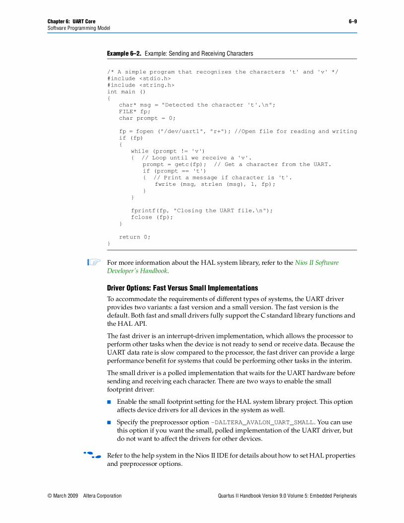
Example 5–1 demonstrates the simplest possible usage, printing a message to stdout using printf(). In this example, the SOPC Builder system contains a JTAG UART core, and the HAL system library is configured to use this JTAG UART device for stdout.
Example 5–2 demonstrates reading characters from and sending messages to a JTAG UART core using the C standard library. In this example, the SOPC Builder system contains a JTAG UART core named jtag_uart that is not necessarily configured as the stdout device. In this case, the program treats the device like any other node in the HAL file system.
Example 5–1. Printing Characters to a JTAG UART Core as stdout
#include <stdio.h>int main (){
printf("Hello world.\n");return 0;
}
Example 5–2. Transmitting Characters to a JTAG UART Core
/* A simple program that recognizes the characters 't' and 'v' */#include <stdio.h>#include <string.h>int main (){
char* msg = "Detected the character 't'.\n";FILE* fp;char prompt = 0;
fp = fopen ("/dev/jtag_uart", "r+"); //Open file for reading and writingif (fp){
while (prompt != 'v') { // Loop until we receive a 'v'.
prompt = getc(fp); // Get a character from the JTAG UART.if (prompt == 't'){ // Print a message if character is 't'.
fwrite (msg, strlen (msg), 1, fp);}
if (ferror(fp))// Check if an error occurred with the filepointer clearerr(fp);// If so, clear it.
}
fprintf(fp, "Closing the JTAG UART file handle.\n");fclose (fp);}
return 0;}
5–8 Chapter 5: JTAG UART CoreSoftware Programming Model
Quartus II Handbook Version 9.0 Volume 5: Embedded Peripherals © March 2009 Altera Corporation
In this example, the ferror(fp) is used to check if an error occurred on the JTAG UART connection, such as a disconnected JTAG connection. In this case, the driver detects that the JTAG connection is disconnected, reports an error (EIO), and discards data for subsequent transactions. If this error ever occurs, the C library latches the value until you explicitly clear it with the clearerr() function.
f For complete details of the HAL system library, refer to the Nios II Software Developer's Handbook.
The Nios II Embedded Design Suite (EDS) provides a number of software example designs that use the JTAG UART core.
Driver Options: Fast vs. Small ImplementationsTo accommodate the requirements of different types of systems, the JTAG UART driver has two variants, a fast version and a small version. The fast behavior is used by default. Both the fast and small drivers fully support the C standard library functions and the HAL API.
The fast driver is an interrupt-driven implementation, which allows the processor to perform other tasks when the device is not ready to send or receive data. Because the JTAG UART data rate is slow compared to the processor, the fast driver can provide a large performance benefit for systems that could be performing other tasks in the interim. In addition, the fast version of the Altera Avalon JTAG UART monitors the connection to the host. The driver discards characters if no host is connected, or if the host is not running an application that handles the I/O stream.
The small driver is a polled implementation that waits for the JTAG UART hardware before sending and receiving each character. The performance of the small driver is poor if you are sending large amounts of data. The small version assumes that the host is always connected, and will never discard characters. Therefore, the small driver will hang the system if the JTAG UART hardware is ever disconnected from the host while the program is sending or receiving data. There are two ways to enable the small footprint driver:
■ Enable the small footprint setting for the HAL system library project. This option affects device drivers for all devices in the system.
■ Specify the preprocessor option -DALTERA_AVALON_JTAG_UART_SMALL. Use this option if you want the small, polled implementation of the JTAG UART driver, but you do not want to affect the drivers for other devices.
ioctl() OperationsThe fast version of the JTAG UART driver supports the ioctl() function to allow HAL-based programs to request device-specific operations. Specifically, you can use the ioctl() operations to control the timeout period, and to detect whether or not a host is connected. The fast driver defines the ioctl() operations shown in Table 5–1.
Chapter 5: JTAG UART Core 5–9Software Programming Model
© March 2009 Altera Corporation Quartus II Handbook Version 9.0 Volume 5: Embedded Peripherals
f For details about the ioctl() function, refer to the Nios II Software Developer's Handbook.
Software FilesThe JTAG UART core is accompanied by the following software files. These files define the low-level interface to the hardware, and provide the HAL drivers. Application developers should not modify these files.
■ altera_avalon_jtag_uart_regs.h—This file defines the core's register map, providing symbolic constants to access the low-level hardware. The symbols in this file are used only by device driver functions.
■ altera_avalon_jtag_uart.h, altera_avalon_jtag_uart.c—These files implement the HAL system library device driver.
Accessing the JTAG UART Core via a Host PCHost software is necessary for a PC to access the JTAG UART core. The Nios II IDE supports the JTAG UART core, and displays character I/O in a console window. Altera also provides a command-line utility called nios2-terminal that opens a terminal session with the JTAG UART core.
f For further details, refer to the Nios II Software Developer's Handbook and Nios II IDE online help.
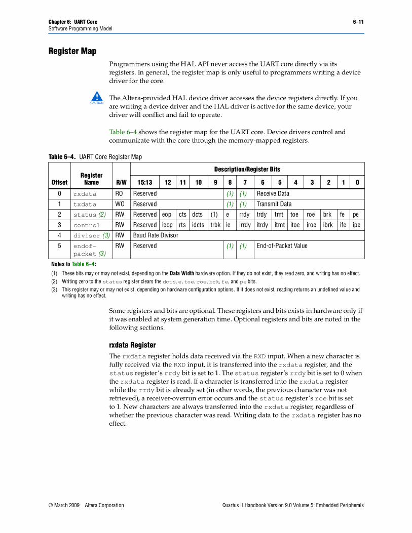
Register MapProgrammers using the HAL API never access the JTAG UART core directly via its registers. In general, the register map is only useful to programmers writing a device driver for the core.
c The Altera-provided HAL device driver accesses the device registers directly. If you are writing a device driver, and the HAL driver is active for the same device, your driver will conflict and fail to operate.
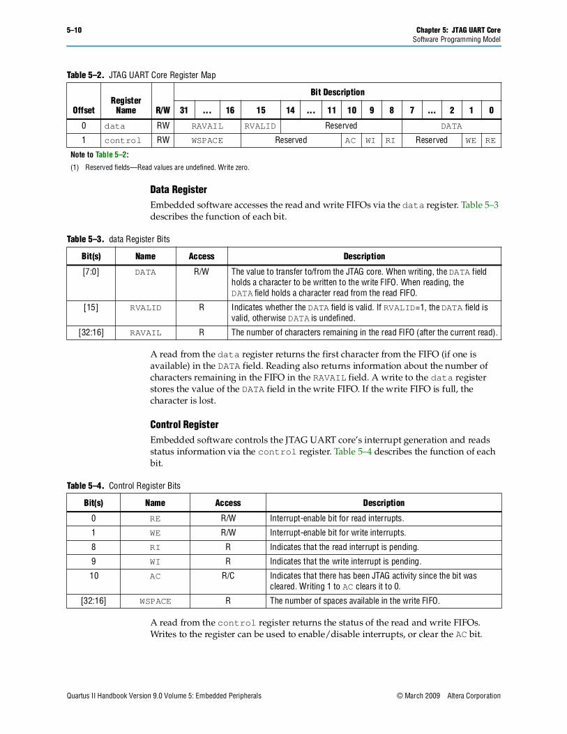
Table 5–2 shows the register map for the JTAG UART core. Device drivers control and communicate with the core through the two, 32-bit memory-mapped registers.
Table 5–1. JTAG UART ioctl() Operations for the Fast Driver Only
Request Meaning
TIOCSTIMEOUT Set the timeout (in seconds) after which the driver will decide that the host is not connected. A timeout of 0 makes the target assume that the host is always connected. The ioctl arg parameter passed in must be a pointer to an integer.
TIOCGCONNECTED Sets the integer arg parameter to a value that indicates whether the host is connected and acting as a terminal (1), or not connected (0). The ioctl arg parameter passed in must be a pointer to an integer.
5–10 Chapter 5: JTAG UART CoreSoftware Programming Model
Quartus II Handbook Version 9.0 Volume 5: Embedded Peripherals © March 2009 Altera Corporation
Data RegisterEmbedded software accesses the read and write FIFOs via the data register. Table 5–3 describes the function of each bit.
A read from the data register returns the first character from the FIFO (if one is available) in the DATA field. Reading also returns information about the number of characters remaining in the FIFO in the RAVAIL field. A write to the data register stores the value of the DATA field in the write FIFO. If the write FIFO is full, the character is lost.
Control RegisterEmbedded software controls the JTAG UART core’s interrupt generation and reads status information via the control register. Table 5–4 describes the function of each bit.
A read from the control register returns the status of the read and write FIFOs. Writes to the register can be used to enable/disable interrupts, or clear the AC bit.
Table 5–2. JTAG UART Core Register Map
OffsetRegister
Name R/W
Bit Description
31 ... 16 15 14 ... 11 10 9 8 7 ... 2 1 0
0 data RW RAVAIL RVALID Reserved DATA
1 control RW WSPACE Reserved AC WI RI Reserved WE RE
Note to Table 5–2:
(1) Reserved fields—Read values are undefined. Write zero.
Table 5–3. data Register Bits
Bit(s) Name Access Description
[7:0] DATA R/W The value to transfer to/from the JTAG core. When writing, the DATA field holds a character to be written to the write FIFO. When reading, the DATA field holds a character read from the read FIFO.
[15] RVALID R Indicates whether the DATA field is valid. If RVALID=1, the DATA field is valid, otherwise DATA is undefined.
[32:16] RAVAIL R The number of characters remaining in the read FIFO (after the current read).
Table 5–4. Control Register Bits
Bit(s) Name Access Description
0 RE R/W Interrupt-enable bit for read interrupts.
1 WE R/W Interrupt-enable bit for write interrupts.
8 RI R Indicates that the read interrupt is pending.
9 WI R Indicates that the write interrupt is pending.
10 AC R/C Indicates that there has been JTAG activity since the bit was cleared. Writing 1 to AC clears it to 0.
[32:16] WSPACE R The number of spaces available in the write FIFO.
Chapter 5: JTAG UART Core 5–11Software Programming Model
© March 2009 Altera Corporation Quartus II Handbook Version 9.0 Volume 5: Embedded Peripherals
The RE and WE bits enable interrupts for the read and write FIFOs, respectively. The WI and RI bits indicate the status of the interrupt sources, qualified by the values of the interrupt enable bits (WE and RE). Embedded software can examine RI and WI to determine the condition that generated the IRQ. See “Interrupt Behavior” on page 5–11 for further details.
The AC bit indicates that an application on the host PC has polled the JTAG UART core via the JTAG interface. Once set, the AC bit remains set until it is explicitly cleared via the Avalon interface. Writing 1 to AC clears it. Embedded software can examine the AC bit to determine if a connection exists to a host PC. If no connection exists, the software may choose to ignore the JTAG data stream. When the host PC has no data to transfer, it can choose to poll the JTAG UART core as infrequently as once per second. Delays caused by other host software using the JTAG download cable could cause delays of up to 10 seconds between polls.
Interrupt BehaviorThe JTAG UART core generates an interrupt when either of the individual interrupt conditions is pending and enabled.
1 Interrupt behavior is of interest to device driver programmers concerned with the bandwidth performance to the host PC. Example designs and the JTAG terminal program provided with Nios II Embedded Design Suite (EDS) are pre-configured with optimal interrupt behavior.
The JTAG UART core has two kinds of interrupts: write interrupts and read interrupts. The WE and RE bits in the control register enable/disable the interrupts.
The core can assert a write interrupt whenever the write FIFO is nearly empty. The nearly empty threshold, write_threshold, is specified at system generation time and cannot be changed by embedded software. The write interrupt condition is set whenever there are write_threshold or fewer characters in the write FIFO. It is cleared by writing characters to fill the write FIFO beyond the write_threshold. Embedded software should only enable write interrupts after filling the write FIFO. If it has no characters remaining to send, embedded software should disable the write interrupt.
The core can assert a read interrupt whenever the read FIFO is nearly full. The nearly full threshold value, read_threshold, is specified at system generation time and cannot be changed by embedded software. The read interrupt condition is set whenever the read FIFO has read_threshold or fewer spaces remaining. The read interrupt condition is also set if there is at least one character in the read FIFO and no more characters are expected. The read interrupt is cleared by reading characters from the read FIFO.
For optimum performance, the interrupt thresholds should match the interrupt response time of the embedded software. For example, with a 10-MHz JTAG clock, a new character is provided (or consumed) by the host PC every 1 µs. With a threshold of 8, the interrupt response time must be less than 8 µs. If the interrupt response time is too long, performance suffers. If it is too short, interrupts occurs too often.
1 For Nios II processor systems, read and write thresholds of 8 are an appropriate default.

5–12 Chapter 5: JTAG UART CoreReferenced Documents
Quartus II Handbook Version 9.0 Volume 5: Embedded Peripherals © March 2009 Altera Corporation
Referenced DocumentsThis chapter references the Nios II Software Developer’s Handbook.
Document Revision HistoryTable 5–5 shows the revision history for this chapter.
f For previous versions of the Quartus II Handbook, refer to the Quartus II Handbook Archive.
Table 5–5. Document Revision History
Date and Document Version Changes Made Summary of Changes
March 2009
v9.0.0
No change from previous release. —
November 2008
v8.1.0
Changed to 8-1/2 x 11 page size. No change to content. —
May 2008
v8.0.0
No change from previous release. —
© March 2009 Altera Corporation Quartus II Handbook Version 9.0 Volume 5: Embedded Peripherals
6. UART Core
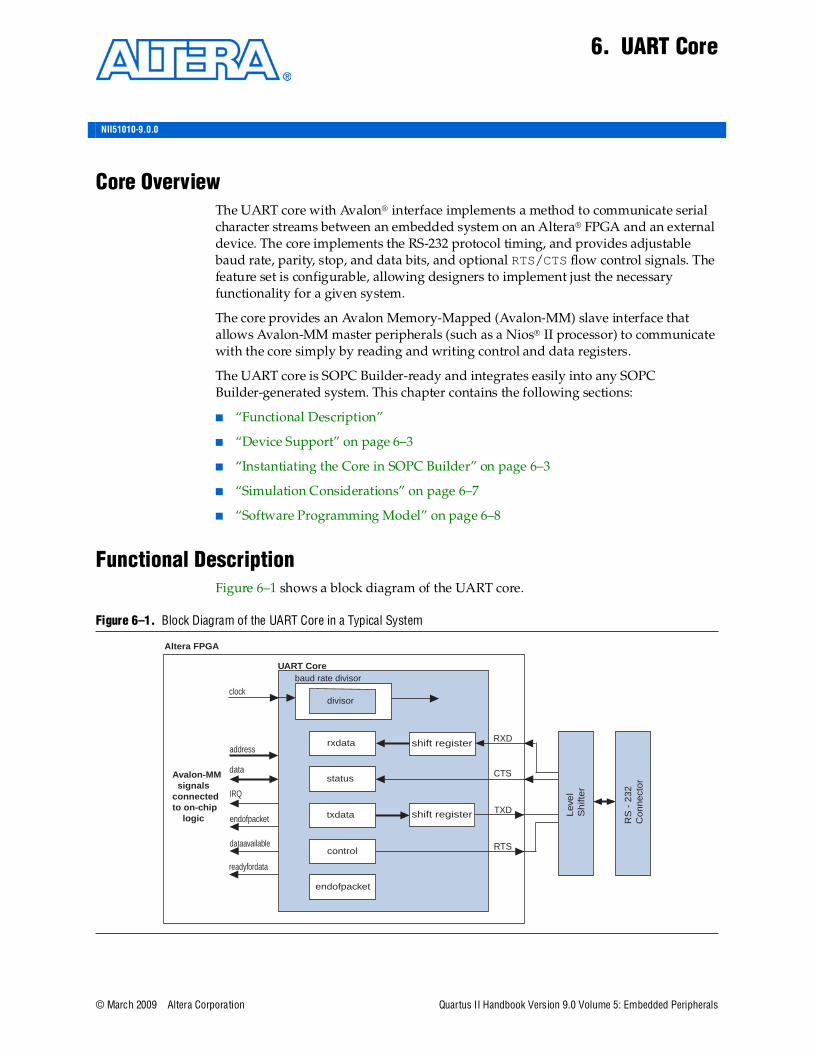
Core OverviewThe UART core with Avalon® interface implements a method to communicate serial character streams between an embedded system on an Altera® FPGA and an external device. The core implements the RS-232 protocol timing, and provides adjustable baud rate, parity, stop, and data bits, and optional RTS/CTS flow control signals. The feature set is configurable, allowing designers to implement just the necessary functionality for a given system.
The core provides an Avalon Memory-Mapped (Avalon-MM) slave interface that allows Avalon-MM master peripherals (such as a Nios® II processor) to communicate with the core simply by reading and writing control and data registers.
The UART core is SOPC Builder-ready and integrates easily into any SOPC Builder-generated system. This chapter contains the following sections:
■ “Functional Description”
■ “Device Support” on page 6–3
■ “Instantiating the Core in SOPC Builder” on page 6–3
■ “Simulation Considerations” on page 6–7
■ “Software Programming Model” on page 6–8
Functional DescriptionFigure 6–1 shows a block diagram of the UART core.
Figure 6–1. Block Diagram of the UART Core in a Typical System
Altera FPGA
UART Corebaud rate divisor
shift register RXD
RTS
CTS
TXD Lev
el
Sh
ifte
r
RS
- 2
32C
onne
ctor
Avalon-MM signalsconnectedto on-chip logic
data
IRQ
dataavailable
readyfordata
endofpacket
address
clock
rxdata
status
control
txdata
endofpacket
shift register
divisor
NII51010-9.0.0
6–2 Chapter 6: UART CoreFunctional Description
Quartus II Handbook Version 9.0 Volume 5: Embedded Peripherals © March 2009 Altera Corporation
The core has two user-visible parts:
■ The register file, which is accessed via the Avalon-MM slave port
■ The RS-232 signals, RXD, TXD, CTS, and RTS
Avalon-MM Slave Interface and RegistersThe UART core provides an Avalon-MM slave interface to the internal register file. The user interface to the UART core consists of six, 16-bit registers: control, status, rxdata, txdata, divisor, and endofpacket. A master peripheral, such as a Nios II processor, accesses the registers to control the core and transfer data over the serial connection.
The UART core provides an active-high interrupt request (IRQ) output that can request an interrupt when new data has been received, or when the core is ready to transmit another character. For further details, refer “Interrupt Behavior” on page 6–15.
The Avalon-MM slave port is capable of transfers with flow control. The UART core can be used in conjunction with a direct memory access (DMA) peripheral with Avalon-MM flow control to automate continuous data transfers between, for example, the UART core and memory.
f For more information, refer to the Timer Core chapter in volume 5 of the Quartus II Handbook. For details about the Avalon-MM interface, refer to the Avalon Interface Specifications.
RS-232 InterfaceThe UART core implements RS-232 asynchronous transmit and receive logic. The UART core sends and receives serial data via the TXD and RXD ports. The I/O buffers on most Altera FPGA families do not comply with RS-232 voltage levels, and may be damaged if driven directly by signals from an RS-232 connector. To comply with RS-232 voltage signaling specifications, an external level-shifting buffer is required (for example, Maxim MAX3237) between the FPGA I/O pins and the external RS-232 connector.
The UART core uses a logic 0 for mark, and a logic 1 for space. An inverter inside the FPGA can be used to reverse the polarity of any of the RS-232 signals, if necessary.
Transmitter LogicThe UART transmitter consists of a 7-, 8-, or 9-bit txdata holding register and a corresponding 7-, 8-, or 9-bit transmit shift register. Avalon-MM master peripherals write the txdata holding register via the Avalon-MM slave port. The transmit shift register is loaded from the txdata register automatically when a serial transmit shift operation is not currently in progress. The transmit shift register directly feeds the TXD output. Data is shifted out to TXD LSB first.
These two registers provide double buffering. A master peripheral can write a new value into the txdata register while the previously written character is being shifted out. The master peripheral can monitor the transmitter ’s status by reading the status register ’s transmitter ready (TRDY), transmitter shift register empty (tmt), and transmitter overrun error (TOE) bits.
Chapter 6: UART Core 6–3Device Support
© March 2009 Altera Corporation Quartus II Handbook Version 9.0 Volume 5: Embedded Peripherals
The transmitter logic automatically inserts the correct number of start, stop, and parity bits in the serial TXD data stream as required by the RS-232 specification.
Receiver LogicThe UART receiver consists of a 7-, 8-, or 9-bit receiver-shift register and a corresponding 7-, 8-, or 9-bit rxdata holding register. Avalon-MM master peripherals read the rxdata holding register via the Avalon-MM slave port. The rxdata holding register is loaded from the receiver shift register automatically every time a new character is fully received.
These two registers provide double buffering. The rxdata register can hold a previously received character while the subsequent character is being shifted into the receiver shift register.
A master peripheral can monitor the receiver’s status by reading the status register ’s read-ready (RRDY), receiver-overrun error (ROE), break detect (BRK), parity error (PE), and framing error (FE) bits. The receiver logic automatically detects the correct number of start, stop, and parity bits in the serial RXD stream as required by the RS-232 specification. The receiver logic checks for four exceptional conditions, frame error, parity error, receive overrun error, and break, in the received data and sets corresponding status register bits.
Baud Rate GenerationThe UART core’s internal baud clock is derived from the Avalon-MM clock input. The internal baud clock is generated by a clock divider. The divisor value can come from one of the following sources:
■ A constant value specified at system generation time
■ The 16-bit value stored in the divisor register
The divisor register is an optional hardware feature. If it is disabled at system generation time, the divisor value is fixed and the baud rate cannot be altered.
Device SupportThe UART core supports all Altera® device families.
Instantiating the Core in SOPC BuilderInstantiating the UART in hardware creates at least two I/O ports for each UART core: An RXD input, and a TXD output. Optionally, the hardware may include flow control signals, the CTS input and RTS output.
Use the MegaWizard™ interface for the UART core in SOPC Builder to configure the hardware feature set. The following sections describe the available options.
6–4 Chapter 6: UART CoreInstantiating the Core in SOPC Builder
Quartus II Handbook Version 9.0 Volume 5: Embedded Peripherals © March 2009 Altera Corporation
Configuration SettingsThis section describes the configuration settings.
Baud Rate OptionsThe UART core can implement any of the standard baud rates for RS-232 connections. The baud rate can be configured in one of two ways:
■ Fixed rate—The baud rate is fixed at system generation time and cannot be changed via the Avalon-MM slave port.
■ Variable rate—The baud rate can vary, based on a clock divisor value held in the divisor register. A master peripheral changes the baud rate by writing new values to the divisor register.
1 The baud rate is calculated based on the clock frequency provided by the Avalon-MM interface. Changing the system clock frequency in hardware without regenerating the UART core hardware results in incorrect signaling.
Baud Rate (bps) Setting
The Baud Rate setting determines the default baud rate after reset. The Baud Rate option offers standard preset values.
The baud rate value is used to calculate an appropriate clock divisor value to implement the desired baud rate. Baud rate and divisor values are related as shown in Equation 6–1 and Equation 6–2:
Baud Rate Can Be Changed By Software Setting
When this setting is on, the hardware includes a 16-bit divisor register at address offset 4. The divisor register is writable, so the baud rate can be changed by writing a new value to this register.
When this setting is off, the UART hardware does not include a divisor register. The UART hardware implements a constant baud divisor, and the value cannot be changed after system generation. In this case, writing to address offset 4 has no effect, and reading from address offset 4 produces an undefined result.
Equation 6–1.
Equation 6–2.
divisor int clock frequencybaud rate
------------------------------------- 0.5+⎝ ⎠⎛ ⎞=
baud rate clock frequencydivisor 1+
-------------------------------------=
Chapter 6: UART Core 6–5Instantiating the Core in SOPC Builder
© March 2009 Altera Corporation Quartus II Handbook Version 9.0 Volume 5: Embedded Peripherals
Data Bits, Stop Bits, ParityThe UART core’s parity, data bits and stop bits are configurable. These settings are fixed at system generation time; they cannot be altered via the register file. Table 6–1 explains the settings.
Synchronizer StagesThe option Synchronizer Stages allows you to specify the length of synchronization register chains. These register chains are used when a metastable event is likely to occur and the length specified determines the meantime before failure. The register chain length, however, affects the latency of the core.
f For more information on metastability in Altera devices, refer to AN 42: Metastability in Altera Devices. For more information on metastability analysis and synchronization register chains, refer to the Area and Timing Optimization chapter in volume 2 of the Quartus II Handbook.
Flow ControlWhen the option Include CTS/RTS pins and control register bits is turned on, the UART core includes the following features:
■ cts_n (logic negative CTS) input port
■ rts_n (logic negative RTS) output port
■ CTS bit in the status register
■ DCTS bit in the status register
■ RTS bit in the control register
■ IDCTS bit in the control register
Table 6–1. Data Bits Settings
Setting Legal Values Description
Data Bits 7, 8, 9 This setting determines the widths of the txdata, rxdata, and endofpacket registers.
Stop Bits 1, 2 This setting determines whether the core transmits 1 or 2 stop bits with every character. The core always terminates a receive transaction at the first stop bit, and ignores all subsequent stop bits, regardless of this setting.
Parity None, Even, Odd This setting determines whether the UART core transmits characters with parity checking, and whether it expects received characters to have parity checking.
When Parity is set to None, the transmit logic sends data without including a parity bit, and the receive logic presumes the incoming data does not include a parity bit. The PE bit in the status register is not implemented; it always reads 0.
When Parity is set to Odd or Even, the transmit logic computes and inserts the required parity bit into the outgoing TXD bitstream, and the receive logic checks the parity bit in the incoming RXD bitstream. If the receiver finds data with incorrect parity, the PE bit in the status register is set to 1. When Parity is Even, the parity bit is 0 if the character has an even number of 1 bits; otherwise the parity bit is 1. Similarly, when parity is Odd, the parity bit is 0 if the character has an odd number of 1 bits.
6–6 Chapter 6: UART CoreInstantiating the Core in SOPC Builder
Quartus II Handbook Version 9.0 Volume 5: Embedded Peripherals © March 2009 Altera Corporation
Based on these hardware facilities, an Avalon-MM master peripheral can detect CTS and transmit RTS flow control signals. The CTS input and RTS output ports are tied directly to bits in the status and control registers, and have no direct effect on any other part of the core. When using flow control, be sure the terminal program on the host side is also configured for flow control.
When the Include CTS/RTS pins and control register bits setting is off, the core does not include the aforementioned hardware and continuous writes to the UART may loose data. The control/status bits CTS, DCTS, IDCTS, and RTS are not implemented; they always read as 0.
Streaming Data (DMA) ControlThe UART core’s Avalon-MM interface optionally implements Avalon-MM transfers with flow control. Flow control allows an Avalon-MM master peripheral to write data only when the UART core is ready to accept another character, and to read data only when the core has data available. The UART core can also optionally include the end-of-packet register.
Include End-of-Packet Register
When this setting is on, the UART core includes:
■ A 7-, 8-, or 9-bit endofpacket register at address-offset 5. The data width is determined by the Data Bits setting.
■ EOP bit in the status register.
■ IEOP bit in the control register.
■ endofpacket signal in the Avalon-MM interface to support data transfers with flow control to and from other master peripherals in the system.
End-of-packet (EOP) detection allows the UART core to terminate a data transaction with an Avalon-MM master with flow control. EOP detection can be used with a DMA controller, for example, to implement a UART that automatically writes received characters to memory until a specified character is encountered in the incoming RXD stream. The terminating (EOP) character ’s value is determined by the endofpacket register.
When the EOP register is disabled, the UART core does not include the EOP resources. Writing to the endofpacket register has no effect, and reading produces an undefined value.
Simulation SettingsWhen the UART core’s logic is generated, a simulation model is also created. The simulation model offers features to simplify and accelerate simulation of systems that use the UART core. Changes to the simulation settings do not affect the behavior of the UART core in hardware; the settings affect only functional simulation.
f For examples of how to use the following settings to simulate Nios II systems, refer to AN 351: Simulating Nios II Embedded Processor Designs.
Chapter 6: UART Core 6–7Simulation Considerations
© March 2009 Altera Corporation Quartus II Handbook Version 9.0 Volume 5: Embedded Peripherals
Simulated RXD-Input Character StreamYou can enter a character stream that is simulated entering the RXD port upon simulated system reset. The UART core’s MegaWizard™ interface accepts an arbitrary character string, which is later incorporated into the UART simulation model. After reset in reset, the string is input into the RXD port character-by-character as the core is able to accept new data.
Prepare Interactive WindowsAt system generation time, the UART core generator can create ModelSim macros that facilitate interaction with the UART model during simulation. You can turn on the following options:
■ Create ModelSim alias to open streaming output window to create a ModelSim macro that opens a window to display all output from the TXD port.
■ Create ModelSim alias to open interactive stimulus window to create a ModelSim macro that opens a window to accept stimulus for the RXD port. The window sends any characters typed in the window to the RXD port.
Simulated Transmitter Baud RateRS-232 transmission rates are often slower than any other process in the system, and it is seldom useful to simulate the functional model at the true baud rate. For example, at 115,200 bps, it typically takes thousands of clock cycles to transfer a single character. The UART simulation model has the ability to run with a constant clock divisor of 2, allowing the simulated UART to transfer bits at half the system clock speed, or roughly one character per 20 clock cycles. You can choose one of the following options for the simulated transmitter baud rate:
■ Accelerated (use divisor = 2)—TXD emits one bit per 2 clock cycles in simulation.
■ Actual (use true baud divisor)—TXD transmits at the actual baud rate, as determined by the divisor register.
Simulation ConsiderationsThe simulation features were created for easy simulation of Nios II processor systems when using the ModelSim simulator. The documentation for the processor documents the suggested usage of these features. Other usages may be possible, but will require additional user effort to create a custom simulation process.
The simulation model is implemented in the UART core’s top-level HDL file; the synthesizable HDL and the simulation HDL are implemented in the same file. The simulation features are implemented using translate on and translate off synthesis directives that make certain sections of HDL code visible only to the synthesis tool.
Do not edit the simulation directives if you are using Altera’s recommended simulation procedures. If you do change the simulation directives for your custom simulation flow, be aware that SOPC Builder overwrites existing files during system generation. Take precaution so that your changes are not overwritten.
f For details about simulating the UART core in Nios II processor systems, refer to AN 351: Simulating Nios II Processor Designs.
6–8 Chapter 6: UART CoreSoftware Programming Model
Quartus II Handbook Version 9.0 Volume 5: Embedded Peripherals © March 2009 Altera Corporation
Software Programming ModelThe following sections describe the software programming model for the UART core, including the register map and software declarations to access the hardware. For Nios II processor users, Altera provides hardware abstraction layer (HAL) system library drivers that enable you to access the UART core using the ANSI C standard library functions, such as printf() and getchar().
HAL System Library SupportThe Altera-provided driver implements a HAL character-mode device driver that integrates into the HAL system library for Nios II systems. HAL users should access the UART via the familiar HAL API and the ANSI C standard library, rather than accessing the UART registers. ioctl() requests are defined that allow HAL users to control the hardware-dependent aspects of the UART.
c If your program uses the HAL device driver to access the UART hardware, accessing the device registers directly interferes with the correct behavior of the driver.
For Nios II processor users, the HAL system library API provides complete access to the UART core's features. Nios II programs treat the UART core as a character mode device, and send and receive data using the ANSI C standard library functions.
The driver supports the CTS/RTS control signals when they are enabled in SOPC Builder. Refer to “Driver Options: Fast Versus Small Implementations” on page 6–9.
The following code demonstrates the simplest possible usage, printing a message to stdout using printf(). In this example, the SOPC Builder system contains a UART core, and the HAL system library has been configured to use this device for stdout.
The following code demonstrates reading characters from and sending messages to a UART device using the C standard library. In this example, the SOPC Builder system contains a UART core named uart1 that is not necessarily configured as the stdout device. In this case, the program treats the device like any other node in the HAL file system.
Example 6–1. Example: Printing Characters to a UART Core as stdout
#include <stdio.h>int main (){
printf("Hello world.\n");return 0;
}
Chapter 6: UART Core 6–9Software Programming Model
© March 2009 Altera Corporation Quartus II Handbook Version 9.0 Volume 5: Embedded Peripherals
1 For more information about the HAL system library, refer to the Nios II Software Developer's Handbook.
Driver Options: Fast Versus Small ImplementationsTo accommodate the requirements of different types of systems, the UART driver provides two variants: a fast version and a small version. The fast version is the default. Both fast and small drivers fully support the C standard library functions and the HAL API.
The fast driver is an interrupt-driven implementation, which allows the processor to perform other tasks when the device is not ready to send or receive data. Because the UART data rate is slow compared to the processor, the fast driver can provide a large performance benefit for systems that could be performing other tasks in the interim.
The small driver is a polled implementation that waits for the UART hardware before sending and receiving each character. There are two ways to enable the small footprint driver:
■ Enable the small footprint setting for the HAL system library project. This option affects device drivers for all devices in the system as well.
■ Specify the preprocessor option -DALTERA_AVALON_UART_SMALL. You can use this option if you want the small, polled implementation of the UART driver, but do not want to affect the drivers for other devices.
f Refer to the help system in the Nios II IDE for details about how to set HAL properties and preprocessor options.
Example 6–2. Example: Sending and Receiving Characters
/* A simple program that recognizes the characters 't' and 'v' */#include <stdio.h>#include <string.h>int main (){
char* msg = "Detected the character 't'.\n";FILE* fp;char prompt = 0;
fp = fopen ("/dev/uart1", "r+"); //Open file for reading and writingif (fp){
while (prompt != 'v') { // Loop until we receive a 'v'.
prompt = getc(fp); // Get a character from the UART.if (prompt == 't'){ // Print a message if character is 't'.
fwrite (msg, strlen (msg), 1, fp);}
}
fprintf(fp, "Closing the UART file.\n");fclose (fp);
}
return 0;}

6–10 Chapter 6: UART CoreSoftware Programming Model
Quartus II Handbook Version 9.0 Volume 5: Embedded Peripherals © March 2009 Altera Corporation
If the CTS/RTS flow control signals are enabled in hardware, the fast driver automatically uses them. The small driver always ignores them.
ioctl() OperationsThe UART driver supports the ioctl() function to allow HAL-based programs to request device-specific operations. Table 6–2 defines operation requests that the UART driver supports.
Additional operation requests are also optionally available for the fast driver only, as shown in Table 6–3. To enable these operations in your program, you must set the preprocessor option -DALTERA_AVALON_UART_USE_IOCTL.
f For details about the ioctl() function, refer to the Nios II Software Developer's Handbook.
LimitationsThe HAL driver for the UART core does not support the endofpacket register. Refer to “Register Map” for details.
Software FilesThe UART core is accompanied by the following software files. These files define the low-level interface to the hardware, and provide the HAL drivers. Application developers should not modify these files.
■ altera_avalon_uart_regs.h—This file defines the core’s register map, providing symbolic constants to access the low-level hardware. The symbols in this file are used only by device driver functions.
■ altera_avalon_uart.h, altera_avalon_uart.c—These files implement the UART core device driver for the HAL system library.
Table 6–2. UART ioctl() Operations
Request Description
TIOCEXCL Locks the device for exclusive access. Further calls to open() for this device will fail until either this file descriptor is closed, or the lock is released using the TIOCNXCL ioctl request. For this request to succeed there can be no other existing file descriptors for this device. The parameter arg is ignored.
TIOCNXCL Releases a previous exclusive access lock. The parameter arg is ignored.
Table 6–3. Optional UART ioctl() Operations for the Fast Driver Only
Request Description
TIOCMGET Returns the current configuration of the device by filling in the contents of the input termios structure. (1) A pointer to this structure is supplied as the value of the parameter opt.
TIOCMSET Sets the configuration of the device according to the values contained in the input termios structure. (1) A pointer to this structure is supplied as the value of the parameter arg.
Note to Table 8–3:
(1) The termios structure is defined by the Newlib C standard library. You can find the definition in the file <Nios II EDS install path>/components/altera_hal/HAL/inc/sys/termios.h.
Chapter 6: UART Core 6–11Software Programming Model
© March 2009 Altera Corporation Quartus II Handbook Version 9.0 Volume 5: Embedded Peripherals
Register MapProgrammers using the HAL API never access the UART core directly via its registers. In general, the register map is only useful to programmers writing a device driver for the core.
c The Altera-provided HAL device driver accesses the device registers directly. If you are writing a device driver and the HAL driver is active for the same device, your driver will conflict and fail to operate.
Table 6–4 shows the register map for the UART core. Device drivers control and communicate with the core through the memory-mapped registers.
Some registers and bits are optional. These registers and bits exists in hardware only if it was enabled at system generation time. Optional registers and bits are noted in the following sections.
rxdata RegisterThe rxdata register holds data received via the RXD input. When a new character is fully received via the RXD input, it is transferred into the rxdata register, and the status register’s rrdy bit is set to 1. The status register’s rrdy bit is set to 0 when the rxdata register is read. If a character is transferred into the rxdata register while the rrdy bit is already set (in other words, the previous character was not retrieved), a receiver-overrun error occurs and the status register’s roe bit is set to 1. New characters are always transferred into the rxdata register, regardless of whether the previous character was read. Writing data to the rxdata register has no effect.
Table 6–4. UART Core Register Map
OffsetRegister
Name R/W
Description/Register Bits
15:13 12 11 10 9 8 7 6 5 4 3 2 1 0
0 rxdata RO Reserved (1) (1) Receive Data
1 txdata WO Reserved (1) (1) Transmit Data
2 status (2) RW Reserved eop cts dcts (1) e rrdy trdy tmt toe roe brk fe pe
3 control RW Reserved ieop rts idcts trbk ie irrdy itrdy itmt itoe iroe ibrk ife ipe
4 divisor (3) RW Baud Rate Divisor
5 endof-packet (3)
RW Reserved (1) (1) End-of-Packet Value
Notes to Table 6–4:
(1) These bits may or may not exist, depending on the Data Width hardware option. If they do not exist, they read zero, and writing has no effect. (2) Writing zero to the status register clears the dcts, e, toe, roe, brk, fe, and pe bits. (3) This register may or may not exist, depending on hardware configuration options. If it does not exist, reading returns an undefined value and
writing has no effect.
6–12 Chapter 6: UART CoreSoftware Programming Model
Quartus II Handbook Version 9.0 Volume 5: Embedded Peripherals © March 2009 Altera Corporation
txdata RegisterAvalon-MM master peripherals write characters to be transmitted into the txdata register. Characters should not be written to txdata until the transmitter is ready for a new character, as indicated by the TRDY bit in the status register. The TRDY bit is set to 0 when a character is written into the txdata register. The TRDY bit is set to 1 when the character is transferred from the txdata register into the transmitter shift register. If a character is written to the txdata register when TRDY is 0, the result is undefined. Reading the txdata register returns an undefined value.
For example, assume the transmitter logic is idle and an Avalon-MM master peripheral writes a first character into the txdata register. The TRDY bit is set to 0, then set to 1 when the character is transferred into the transmitter shift register. The master can then write a second character into the txdata register, and the TRDY bit is set to 0 again. However, this time the shift register is still busy shifting out the first character to the TXD output. The TRDY bit is not set to 1 until the first character is fully shifted out and the second character is automatically transferred into the transmitter shift register.
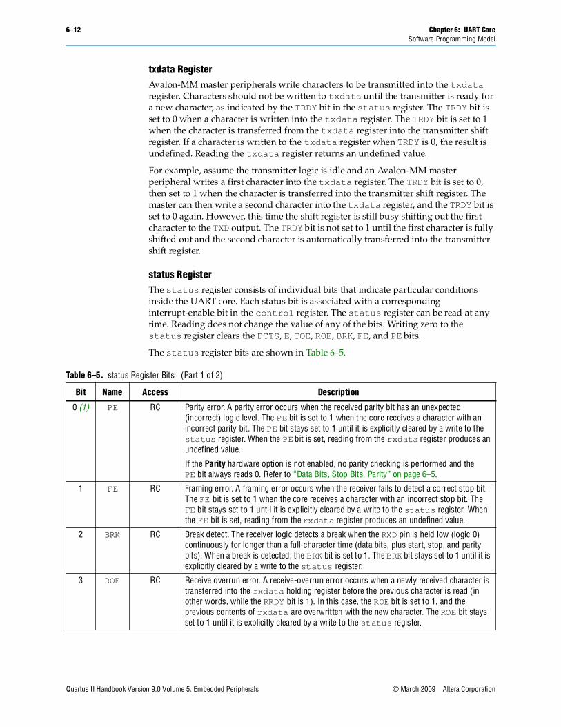
status RegisterThe status register consists of individual bits that indicate particular conditions inside the UART core. Each status bit is associated with a corresponding interrupt-enable bit in the control register. The status register can be read at any time. Reading does not change the value of any of the bits. Writing zero to the status register clears the DCTS, E, TOE, ROE, BRK, FE, and PE bits.
The status register bits are shown in Table 6–5.
Table 6–5. status Register Bits (Part 1 of 2)
Bit Name Access Description
0 (1) PE RC Parity error. A parity error occurs when the received parity bit has an unexpected (incorrect) logic level. The PE bit is set to 1 when the core receives a character with an incorrect parity bit. The PE bit stays set to 1 until it is explicitly cleared by a write to the status register. When the PE bit is set, reading from the rxdata register produces an undefined value.
If the Parity hardware option is not enabled, no parity checking is performed and the PE bit always reads 0. Refer to “Data Bits, Stop Bits, Parity” on page 6–5.
1 FE RC Framing error. A framing error occurs when the receiver fails to detect a correct stop bit. The FE bit is set to 1 when the core receives a character with an incorrect stop bit. The FE bit stays set to 1 until it is explicitly cleared by a write to the status register. When the FE bit is set, reading from the rxdata register produces an undefined value.
2 BRK RC Break detect. The receiver logic detects a break when the RXD pin is held low (logic 0) continuously for longer than a full-character time (data bits, plus start, stop, and parity bits). When a break is detected, the BRK bit is set to 1. The BRK bit stays set to 1 until it is explicitly cleared by a write to the status register.
3 ROE RC Receive overrun error. A receive-overrun error occurs when a newly received character is transferred into the rxdata holding register before the previous character is read (in other words, while the RRDY bit is 1). In this case, the ROE bit is set to 1, and the previous contents of rxdata are overwritten with the new character. The ROE bit stays set to 1 until it is explicitly cleared by a write to the status register.
Chapter 6: UART Core 6–13Software Programming Model
© March 2009 Altera Corporation Quartus II Handbook Version 9.0 Volume 5: Embedded Peripherals
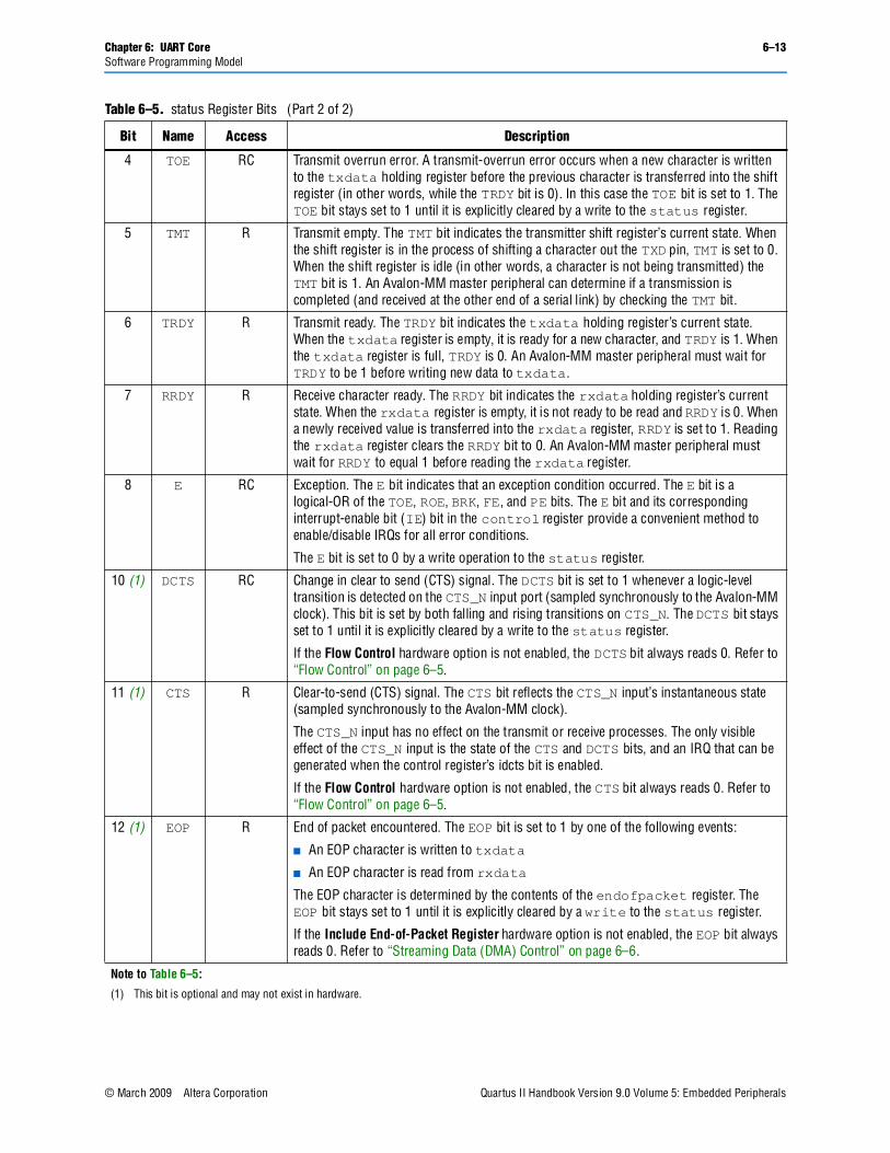
4 TOE RC Transmit overrun error. A transmit-overrun error occurs when a new character is written to the txdata holding register before the previous character is transferred into the shift register (in other words, while the TRDY bit is 0). In this case the TOE bit is set to 1. The TOE bit stays set to 1 until it is explicitly cleared by a write to the status register.
5 TMT R Transmit empty. The TMT bit indicates the transmitter shift register’s current state. When the shift register is in the process of shifting a character out the TXD pin, TMT is set to 0. When the shift register is idle (in other words, a character is not being transmitted) the TMT bit is 1. An Avalon-MM master peripheral can determine if a transmission is completed (and received at the other end of a serial link) by checking the TMT bit.
6 TRDY R Transmit ready. The TRDY bit indicates the txdata holding register’s current state. When the txdata register is empty, it is ready for a new character, and TRDY is 1. When the txdata register is full, TRDY is 0. An Avalon-MM master peripheral must wait for TRDY to be 1 before writing new data to txdata.
7 RRDY R Receive character ready. The RRDY bit indicates the rxdata holding register’s current state. When the rxdata register is empty, it is not ready to be read and RRDY is 0. When a newly received value is transferred into the rxdata register, RRDY is set to 1. Reading the rxdata register clears the RRDY bit to 0. An Avalon-MM master peripheral must wait for RRDY to equal 1 before reading the rxdata register.
8 E RC Exception. The E bit indicates that an exception condition occurred. The E bit is a logical-OR of the TOE, ROE, BRK, FE, and PE bits. The E bit and its corresponding interrupt-enable bit (IE) bit in the control register provide a convenient method to enable/disable IRQs for all error conditions.
The E bit is set to 0 by a write operation to the status register.
10 (1) DCTS RC Change in clear to send (CTS) signal. The DCTS bit is set to 1 whenever a logic-level transition is detected on the CTS_N input port (sampled synchronously to the Avalon-MM clock). This bit is set by both falling and rising transitions on CTS_N. The DCTS bit stays set to 1 until it is explicitly cleared by a write to the status register.
If the Flow Control hardware option is not enabled, the DCTS bit always reads 0. Refer to “Flow Control” on page 6–5.
11 (1) CTS R Clear-to-send (CTS) signal. The CTS bit reflects the CTS_N input’s instantaneous state (sampled synchronously to the Avalon-MM clock).
The CTS_N input has no effect on the transmit or receive processes. The only visible effect of the CTS_N input is the state of the CTS and DCTS bits, and an IRQ that can be generated when the control register’s idcts bit is enabled.
If the Flow Control hardware option is not enabled, the CTS bit always reads 0. Refer to “Flow Control” on page 6–5.
12 (1) EOP R End of packet encountered. The EOP bit is set to 1 by one of the following events:
■ An EOP character is written to txdata
■ An EOP character is read from rxdata
The EOP character is determined by the contents of the endofpacket register. The EOP bit stays set to 1 until it is explicitly cleared by a write to the status register.
If the Include End-of-Packet Register hardware option is not enabled, the EOP bit always reads 0. Refer to “Streaming Data (DMA) Control” on page 6–6.
Note to Table 6–5:
(1) This bit is optional and may not exist in hardware.
Table 6–5. status Register Bits (Part 2 of 2)
Bit Name Access Description
6–14 Chapter 6: UART CoreSoftware Programming Model
Quartus II Handbook Version 9.0 Volume 5: Embedded Peripherals © March 2009 Altera Corporation
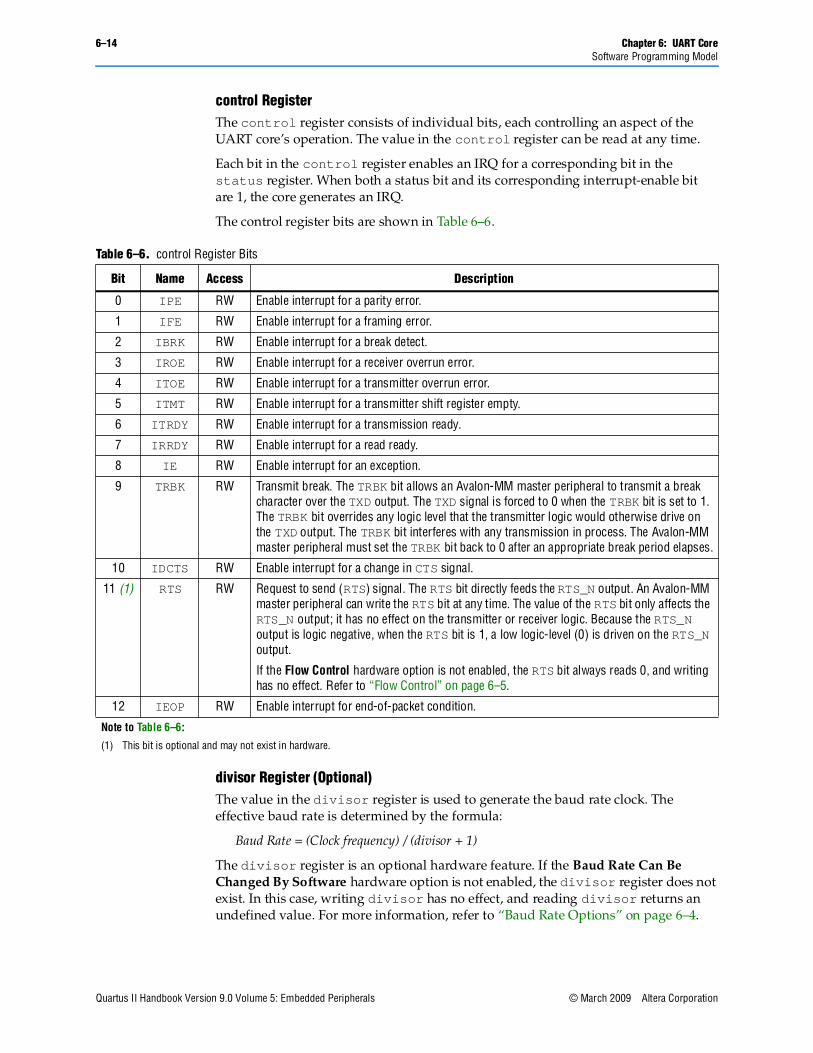
control RegisterThe control register consists of individual bits, each controlling an aspect of the UART core’s operation. The value in the control register can be read at any time.
Each bit in the control register enables an IRQ for a corresponding bit in the status register. When both a status bit and its corresponding interrupt-enable bit are 1, the core generates an IRQ.
The control register bits are shown in Table 6–6.
divisor Register (Optional)The value in the divisor register is used to generate the baud rate clock. The effective baud rate is determined by the formula:
Baud Rate = (Clock frequency) / (divisor + 1)
The divisor register is an optional hardware feature. If the Baud Rate Can Be Changed By Software hardware option is not enabled, the divisor register does not exist. In this case, writing divisor has no effect, and reading divisor returns an undefined value. For more information, refer to “Baud Rate Options” on page 6–4.
Table 6–6. control Register Bits
Bit Name Access Description
0 IPE RW Enable interrupt for a parity error.
1 IFE RW Enable interrupt for a framing error.
2 IBRK RW Enable interrupt for a break detect.
3 IROE RW Enable interrupt for a receiver overrun error.
4 ITOE RW Enable interrupt for a transmitter overrun error.
5 ITMT RW Enable interrupt for a transmitter shift register empty.
6 ITRDY RW Enable interrupt for a transmission ready.
7 IRRDY RW Enable interrupt for a read ready.
8 IE RW Enable interrupt for an exception.
9 TRBK RW Transmit break. The TRBK bit allows an Avalon-MM master peripheral to transmit a break character over the TXD output. The TXD signal is forced to 0 when the TRBK bit is set to 1. The TRBK bit overrides any logic level that the transmitter logic would otherwise drive on the TXD output. The TRBK bit interferes with any transmission in process. The Avalon-MM master peripheral must set the TRBK bit back to 0 after an appropriate break period elapses.
10 IDCTS RW Enable interrupt for a change in CTS signal.
11 (1) RTS RW Request to send (RTS) signal. The RTS bit directly feeds the RTS_N output. An Avalon-MM master peripheral can write the RTS bit at any time. The value of the RTS bit only affects the RTS_N output; it has no effect on the transmitter or receiver logic. Because the RTS_N output is logic negative, when the RTS bit is 1, a low logic-level (0) is driven on the RTS_N output.
If the Flow Control hardware option is not enabled, the RTS bit always reads 0, and writing has no effect. Refer to “Flow Control” on page 6–5.
12 IEOP RW Enable interrupt for end-of-packet condition.
Note to Table 6–6:
(1) This bit is optional and may not exist in hardware.

Chapter 6: UART Core 6–15Referenced Documents
© March 2009 Altera Corporation Quartus II Handbook Version 9.0 Volume 5: Embedded Peripherals
endofpacket Register (Optional)The value in the endofpacket register determines the end-of-packet character for variable-length DMA transactions. After reset, the default value is zero, which is the ASCII null character (\0). For more information, refer to Table 6–5 on page 6–12 for the description for the EOP bit.
The endofpacket register is an optional hardware feature. If the Include end-of-packet register hardware option is not enabled, the endofpacket register does not exist. In this case, writing endofpacket has no effect, and reading returns an undefined value.
Interrupt BehaviorThe UART core outputs a single IRQ signal to the Avalon-MM interface, which can connect to any master peripheral in the system, such as a Nios II processor. The master peripheral must read the status register to determine the cause of the interrupt.
Every interrupt condition has an associated bit in the status register and an interrupt-enable bit in the control register. When any of the interrupt conditions occur, the associated status bit is set to 1 and remains set until it is explicitly acknowledged. The IRQ output is asserted when any of the status bits are set while the corresponding interrupt-enable bit is 1. A master peripheral can acknowledge the IRQ by clearing the status register.
At reset, all interrupt-enable bits are set to 0; therefore, the core cannot assert an IRQ until a master peripheral sets one or more of the interrupt-enable bits to 1.
All possible interrupt conditions are listed with their associated status and control (interrupt-enable) bits in Table 6–5 on page 6–16 and Table 6–6 on page 6–18. Details of each interrupt condition are provided in the status bit descriptions.
Referenced DocumentsThis chapter references the following documents:
■ AN 350: Upgrading Nios Processor Systems to the Nios II Processor
■ AN 351: Simulating Nios II Embedded Processor Designs
■ Avalon Interface Specifications
■ Nios II Software Developer's Handbook
■ Timer Core chapter in volume 5 of the Quartus II Handbook
■ AN 42: Metastability in Altera Devices
■ Area and Timing Optimization chapter in volume 2 of the Quartus II Handbook
6–16 Chapter 6: UART CoreDocument Revision History
Quartus II Handbook Version 9.0 Volume 5: Embedded Peripherals © March 2009 Altera Corporation
Document Revision HistoryTable 6–7 shows the revision history for this chapter.
f For previous versions of the Quartus II Handbook, refer to the Quartus II Handbook Archive.
Table 6–7. Document Revision History
Date and Document Version Changes Made Summary of Changes
March 2009
v9.0.0
Added description of a new parameter, Synchronizer stages. —
November 2008
v8.1.0
Changed to 8-1/2 x 11 page size. No change to content. —
May 2008
v8.0.0
No change from previous release. —

© March 2009 Altera Corporation Quartus II Handbook Version 9.0 Volume 5: Embedded Peripherals
7. SPI Core
Core OverviewSPI is an industry-standard serial protocol commonly used in embedded systems to connect microprocessors to a variety of off-chip sensor, conversion, memory, and control devices. The SPI core with Avalon® interface implements the SPI protocol and provides an Avalon Memory-Mapped (Avalon-MM) interface on the back end.
The SPI core can implement either the master or slave protocol. When configured as a master, the SPI core can control up to 32 independent SPI slaves. The width of the receive and transmit registers are configurable between 1 and 32 bits. Longer transfer lengths can be supported with software routines. The SPI core provides an interrupt output that can flag an interrupt whenever a transfer completes.
The SPI core is SOPC Builder ready and integrates easily into any SOPC Builder-generated system. This chapter contains the following sections:
■ “Functional Description”
■ “Instantiating the SPI Core in SOPC Builder” on page 7–5
■ “Device Support” on page 7–8
■ “Software Programming Model” on page 7–8
Functional DescriptionThe SPI core communicates using two data lines, a control line, and a synchronization clock:
■ Master Out Slave In (mosi)—Output data from the master to the inputs of the slaves
■ Master In Slave Out (miso)—Output data from a slave to the input of the master
■ Serial Clock (sclk)—Clock driven by the master to slaves, used to synchronize the data bits
■ Slave Select (ss_n)— Select signal (active low) driven by the master to individual slaves, used to select the target slave
The SPI core has the following user-visible features:
■ A memory-mapped register space comprised of five registers: rxdata, txdata, status, control, and slaveselect
■ Four SPI interface ports: sclk, ss_n, mosi, and miso
The registers provide an interface to the SPI core and are visible via the Avalon-MM slave port. The sclk, ss_n, mosi, and miso ports provide the hardware interface to other SPI devices. The behavior of sclk, ss_n, mosi, and miso depends on whether the SPI core is configured as a master or slave.
NII51011-9.0.0
7–2 Chapter 7: SPI CoreFunctional Description
Quartus II Handbook Version 9.0 Volume 5: Embedded Peripherals © March 2009 Altera Corporation
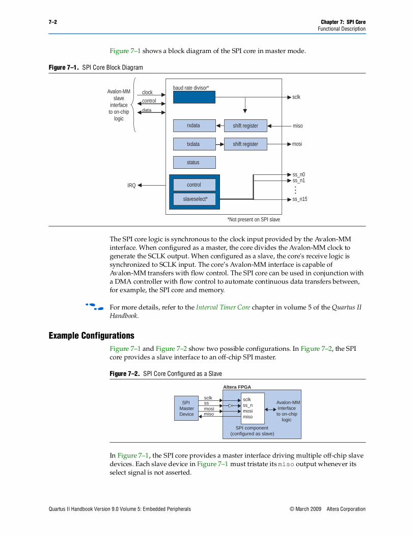
Figure 7–1 shows a block diagram of the SPI core in master mode.
The SPI core logic is synchronous to the clock input provided by the Avalon-MM interface. When configured as a master, the core divides the Avalon-MM clock to generate the SCLK output. When configured as a slave, the core's receive logic is synchronized to SCLK input. The core’s Avalon-MM interface is capable of Avalon-MM transfers with flow control. The SPI core can be used in conjunction with a DMA controller with flow control to automate continuous data transfers between, for example, the SPI core and memory.
f For more details, refer to the Interval Timer Core chapter in volume 5 of the Quartus II Handbook.
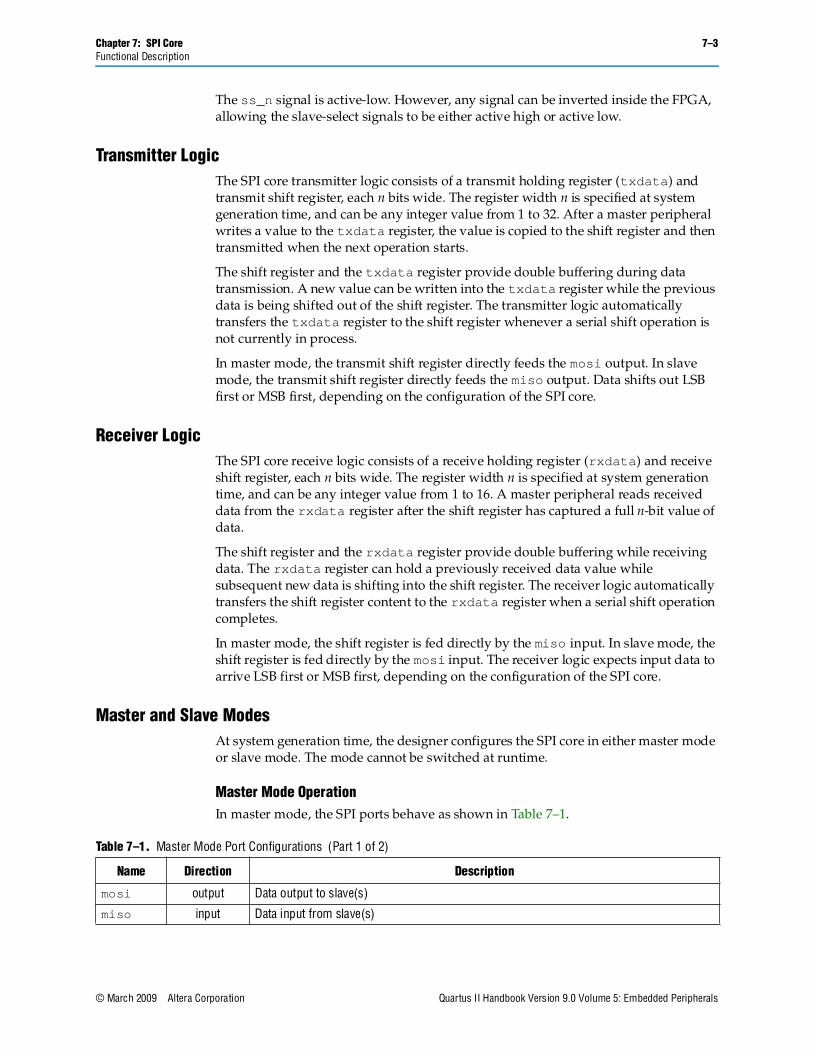
Example ConfigurationsFigure 7–1 and Figure 7–2 show two possible configurations. In Figure 7–2, the SPI core provides a slave interface to an off-chip SPI master.
In Figure 7–1, the SPI core provides a master interface driving multiple off-chip slave devices. Each slave device in Figure 7–1 must tristate its miso output whenever its select signal is not asserted.
Figure 7–1. SPI Core Block Diagram
clock
control
control
baud rate divisor*
IRQ
sclk
mosi
miso
ss_n0ss_n1
ss_n15
*Not present on SPI slave
slaveselect*
Avalon-MMslave
interfaceto on-chip
logic
txdata shift register
status
rxdata shift register
data
Figure 7–2. SPI Core Configured as a Slave
Altera FPGA
Avalon-MM interfaceto on-chip logic
sclkss_nmosimiso
SPI component(configured as slave)
misomosisssclk
SPIMasterDevice
Chapter 7: SPI Core 7–3Functional Description
© March 2009 Altera Corporation Quartus II Handbook Version 9.0 Volume 5: Embedded Peripherals
The ss_n signal is active-low. However, any signal can be inverted inside the FPGA, allowing the slave-select signals to be either active high or active low.
Transmitter LogicThe SPI core transmitter logic consists of a transmit holding register (txdata) and transmit shift register, each n bits wide. The register width n is specified at system generation time, and can be any integer value from 1 to 32. After a master peripheral writes a value to the txdata register, the value is copied to the shift register and then transmitted when the next operation starts.
The shift register and the txdata register provide double buffering during data transmission. A new value can be written into the txdata register while the previous data is being shifted out of the shift register. The transmitter logic automatically transfers the txdata register to the shift register whenever a serial shift operation is not currently in process.
In master mode, the transmit shift register directly feeds the mosi output. In slave mode, the transmit shift register directly feeds the miso output. Data shifts out LSB first or MSB first, depending on the configuration of the SPI core.
Receiver LogicThe SPI core receive logic consists of a receive holding register (rxdata) and receive shift register, each n bits wide. The register width n is specified at system generation time, and can be any integer value from 1 to 16. A master peripheral reads received data from the rxdata register after the shift register has captured a full n-bit value of data.
The shift register and the rxdata register provide double buffering while receiving data. The rxdata register can hold a previously received data value while subsequent new data is shifting into the shift register. The receiver logic automatically transfers the shift register content to the rxdata register when a serial shift operation completes.
In master mode, the shift register is fed directly by the miso input. In slave mode, the shift register is fed directly by the mosi input. The receiver logic expects input data to arrive LSB first or MSB first, depending on the configuration of the SPI core.
Master and Slave ModesAt system generation time, the designer configures the SPI core in either master mode or slave mode. The mode cannot be switched at runtime.
Master Mode OperationIn master mode, the SPI ports behave as shown in Table 7–1.
Table 7–1. Master Mode Port Configurations (Part 1 of 2)
Name Direction Description
mosi output Data output to slave(s)
miso input Data input from slave(s)
7–4 Chapter 7: SPI CoreFunctional Description
Quartus II Handbook Version 9.0 Volume 5: Embedded Peripherals © March 2009 Altera Corporation
In master mode, an intelligent host (for example, a microprocessor) configures the SPI core using the control and slaveselect registers, and then writes data to the txdata buffer to initiate a transaction. A master peripheral can monitor the status of the transaction by reading the status register. A master peripheral can enable interrupts to notify the host whenever new data is received (for example, a transfer has completed), or whenever the transmit buffer is ready for new data.
The SPI protocol is full duplex, so every transaction both sends and receives data at the same time. The master transmits a new data bit on the mosi output and the slave drives a new data bit on the miso input for each active edge of sclk. The SPI core divides the Avalon-MM system clock using a clock divider to generate the sclk signal.
When the SPI core is configured to interface with multiple slaves, the core has one ss_n signal for each slave, up to a maximum of sixteen slaves. During a transfer, the master asserts ss_n to each slave specified in the slaveselect register. Note that there can be no more than one slave transmitting data during any particular transfer, or else there will be a contention on the miso input. The number of slave devices is specified at system generation time.
Slave Mode OperationIn slave mode, the SPI ports behave as shown in Table 7–2.
In slave mode, the SPI core simply waits for the master to initiate transactions. Before a transaction begins, the slave logic continuously polls the ss_n input. When the master asserts ss_n, the slave logic immediately begins sending the transmit shift register contents to the miso output. The slave logic also captures data on the mosi input, and fills the receive shift register simultaneously.
An intelligent host such as a microprocessor writes data to the txdata registers, so that it is transmitted the next time the master initiates an operation. A master peripheral reads received data from the rxdata register. A master peripheral can enable interrupts to notify the host whenever new data is received, or whenever the transmit buffer is ready for new data.
sclk output Synchronization clock to all slaves
ss_nM output Slave select signal to slave M, where M is a number between 0 and 15.
Table 7–1. Master Mode Port Configurations (Part 2 of 2)
Name Direction Description
Table 7–2. Slave Mode Port Configurations
Name Direction Description
mosi input Data input from the master
miso output Data output to the master
sclk input Synchronization clock
ss_n input Select signal
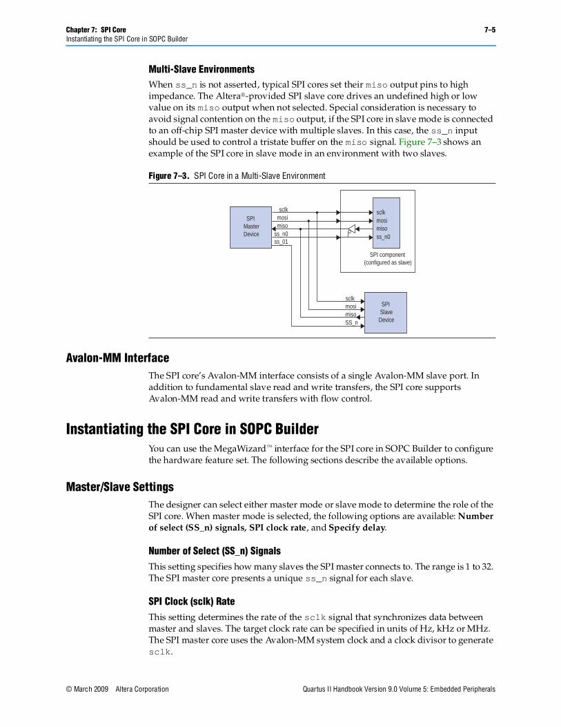
Chapter 7: SPI Core 7–5Instantiating the SPI Core in SOPC Builder
© March 2009 Altera Corporation Quartus II Handbook Version 9.0 Volume 5: Embedded Peripherals
Multi-Slave EnvironmentsWhen ss_n is not asserted, typical SPI cores set their miso output pins to high impedance. The Altera®-provided SPI slave core drives an undefined high or low value on its miso output when not selected. Special consideration is necessary to avoid signal contention on the miso output, if the SPI core in slave mode is connected to an off-chip SPI master device with multiple slaves. In this case, the ss_n input should be used to control a tristate buffer on the miso signal. Figure 7–3 shows an example of the SPI core in slave mode in an environment with two slaves.
Avalon-MM InterfaceThe SPI core’s Avalon-MM interface consists of a single Avalon-MM slave port. In addition to fundamental slave read and write transfers, the SPI core supports Avalon-MM read and write transfers with flow control.
Instantiating the SPI Core in SOPC BuilderYou can use the MegaWizard™ interface for the SPI core in SOPC Builder to configure the hardware feature set. The following sections describe the available options.
Master/Slave SettingsThe designer can select either master mode or slave mode to determine the role of the SPI core. When master mode is selected, the following options are available: Number of select (SS_n) signals, SPI clock rate, and Specify delay.
Number of Select (SS_n) SignalsThis setting specifies how many slaves the SPI master connects to. The range is 1 to 32. The SPI master core presents a unique ss_n signal for each slave.
SPI Clock (sclk) RateThis setting determines the rate of the sclk signal that synchronizes data between master and slaves. The target clock rate can be specified in units of Hz, kHz or MHz. The SPI master core uses the Avalon-MM system clock and a clock divisor to generate sclk.
Figure 7–3. SPI Core in a Multi-Slave Environment
SPIMasterDevice
sclk mosi misoss_n0ss_01
sclk mosi miso ss_n0
SPI component(configured as slave)
SPI SlaveDeviceSS_n
misomosisclk
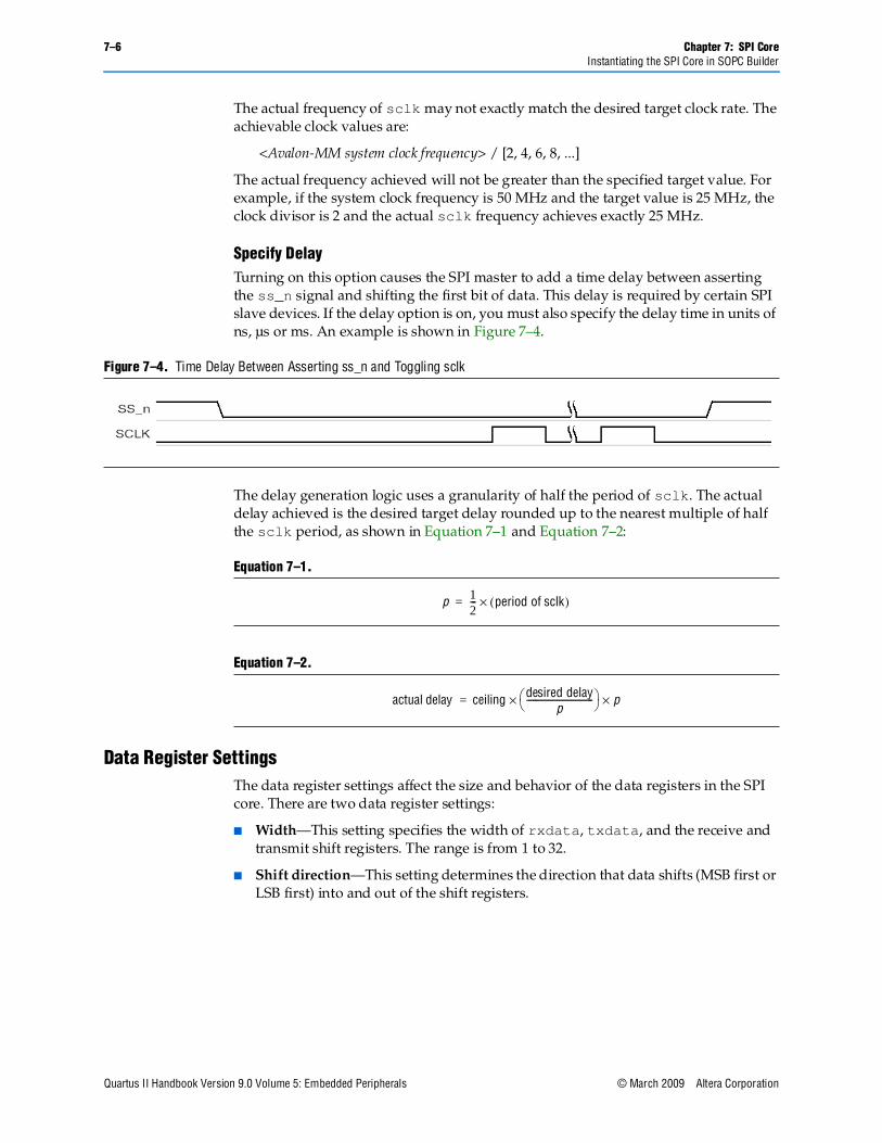
7–6 Chapter 7: SPI CoreInstantiating the SPI Core in SOPC Builder
Quartus II Handbook Version 9.0 Volume 5: Embedded Peripherals © March 2009 Altera Corporation
The actual frequency of sclk may not exactly match the desired target clock rate. The achievable clock values are:
<Avalon-MM system clock frequency> / [2, 4, 6, 8, ...]
The actual frequency achieved will not be greater than the specified target value. For example, if the system clock frequency is 50 MHz and the target value is 25 MHz, the clock divisor is 2 and the actual sclk frequency achieves exactly 25 MHz.
Specify DelayTurning on this option causes the SPI master to add a time delay between asserting the ss_n signal and shifting the first bit of data. This delay is required by certain SPI slave devices. If the delay option is on, you must also specify the delay time in units of ns, µs or ms. An example is shown in Figure 7–4.
The delay generation logic uses a granularity of half the period of sclk. The actual delay achieved is the desired target delay rounded up to the nearest multiple of half the sclk period, as shown in Equation 7–1 and Equation 7–2:
Data Register SettingsThe data register settings affect the size and behavior of the data registers in the SPI core. There are two data register settings:
■ Width—This setting specifies the width of rxdata, txdata, and the receive and transmit shift registers. The range is from 1 to 32.
■ Shift direction—This setting determines the direction that data shifts (MSB first or LSB first) into and out of the shift registers.
Figure 7–4. Time Delay Between Asserting ss_n and Toggling sclk
Equation 7–1.
Equation 7–2.
p 12--- period of sclk( )×=
actual delay ceiling desired delayp
-------------------------------⎝ ⎠⎛ ⎞ p××=
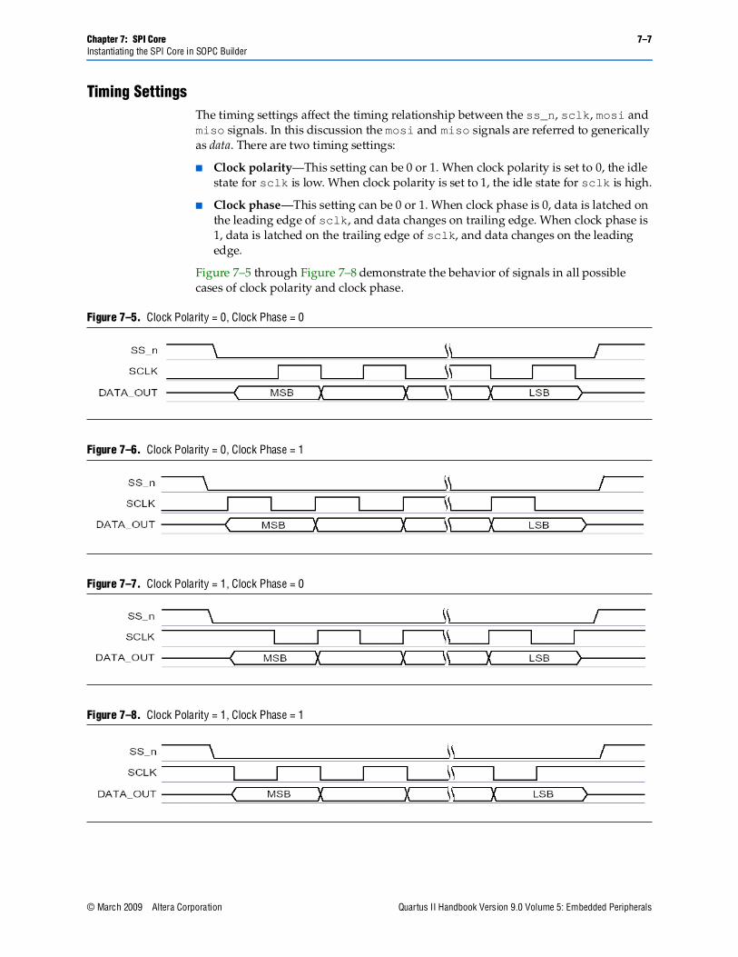
Chapter 7: SPI Core 7–7Instantiating the SPI Core in SOPC Builder
© March 2009 Altera Corporation Quartus II Handbook Version 9.0 Volume 5: Embedded Peripherals
Timing SettingsThe timing settings affect the timing relationship between the ss_n, sclk, mosi and miso signals. In this discussion the mosi and miso signals are referred to generically as data. There are two timing settings:
■ Clock polarity—This setting can be 0 or 1. When clock polarity is set to 0, the idle state for sclk is low. When clock polarity is set to 1, the idle state for sclk is high.
■ Clock phase—This setting can be 0 or 1. When clock phase is 0, data is latched on the leading edge of sclk, and data changes on trailing edge. When clock phase is 1, data is latched on the trailing edge of sclk, and data changes on the leading edge.
Figure 7–5 through Figure 7–8 demonstrate the behavior of signals in all possible cases of clock polarity and clock phase.
Figure 7–5. Clock Polarity = 0, Clock Phase = 0
Figure 7–6. Clock Polarity = 0, Clock Phase = 1
Figure 7–7. Clock Polarity = 1, Clock Phase = 0
Figure 7–8. Clock Polarity = 1, Clock Phase = 1
7–8 Chapter 7: SPI CoreDevice Support
Quartus II Handbook Version 9.0 Volume 5: Embedded Peripherals © March 2009 Altera Corporation
Device SupportThe SPI core supports all Altera® device families.
Software Programming ModelThe following sections describe the software programming model for the SPI core, including the register map and software constructs used to access the hardware. For Nios® II processor users, Altera provides the HAL system library header file that defines the SPI core registers. The SPI core does not match the generic device model categories supported by the HAL, so it cannot be accessed via the HAL API or the ANSI C standard library. Altera provides a routine to access the SPI hardware that is specific to the SPI core.
Hardware Access RoutinesAltera provides one access routine, alt_avalon_spi_command(), that provides general-purpose access to an SPI core configured as a master.
Chapter 7: SPI Core 7–9Software Programming Model
© March 2009 Altera Corporation Quartus II Handbook Version 9.0 Volume 5: Embedded Peripherals
alt_avalon_spi_command()
Software FilesThe SPI core is accompanied by the following software files. These files provide a low-level interface to the hardware.
■ altera_avalon_spi.h—This file defines the core's register map, providing symbolic constants to access the low-level hardware.
■ altera_avalon_spi.c—This file implements low-level routines to access the hardware.
Register MapAn Avalon-MM master peripheral controls and communicates with the SPI core via the six 32-bit registers, shown in Table 7–3. The table assumes an n-bit data width for rxdata and txdata.
Prototype: int alt_avalon_spi_command(alt_u32 base, alt_u32 slave,
alt_u32 write_length, const alt_u8* wdata,
alt_u32 read_length,
alt_u8* read_data,
alt_u32 flags)
Thread-safe: No.
Available from ISR: No.
Include: <altera_avalon_spi.h>
Description: alt_avalon_spi_command() is used to perform a control sequence on the SPI bus. This routine is designed for SPI masters of 8-bit data width or less. Currently, it does not support SPI hardware with data-width greater than 8 bits. A single call to this function writes a data buffer of arbitrary length out the MOSI port, and then reads back an arbitrary amount of data from the MISO port. The function performs the following actions:
(1) Asserts the slave select output for the specified slave. The first slave select output is numbered 0, the next is 1, etc.
(2) Transmits write_length bytes of data from wdata through the SPI interface, discarding the incoming data on MISO.
(3) Reads read_length bytes of data, storing the data into the buffer pointed to by read_data. MOSI is set to zero during the read transaction.
(4) De-asserts the slave select output, unless the flags field contains the value ALT_AVALON_SPI_COMMAND_MERGE. If you want to transmit from scattered buffers then you can call the function multiple times, specifying the merge flag on all the accesses except the last.
This function is not thread safe. If you want to access the SPI bus from more than one thread, you should use a semaphore or mutex to ensure that only one thread is executing within this function at any time.
Returns: The number of bytes stored in the read_data buffer.
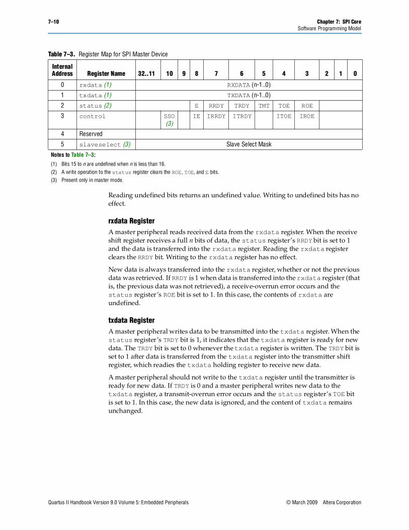
7–10 Chapter 7: SPI CoreSoftware Programming Model
Quartus II Handbook Version 9.0 Volume 5: Embedded Peripherals © March 2009 Altera Corporation
Reading undefined bits returns an undefined value. Writing to undefined bits has no effect.
rxdata RegisterA master peripheral reads received data from the rxdata register. When the receive shift register receives a full n bits of data, the status register’s RRDY bit is set to 1 and the data is transferred into the rxdata register. Reading the rxdata register clears the RRDY bit. Writing to the rxdata register has no effect.
New data is always transferred into the rxdata register, whether or not the previous data was retrieved. If RRDY is 1 when data is transferred into the rxdata register (that is, the previous data was not retrieved), a receive-overrun error occurs and the status register ’s ROE bit is set to 1. In this case, the contents of rxdata are undefined.
txdata RegisterA master peripheral writes data to be transmitted into the txdata register. When the status register ’s TRDY bit is 1, it indicates that the txdata register is ready for new data. The TRDY bit is set to 0 whenever the txdata register is written. The TRDY bit is set to 1 after data is transferred from the txdata register into the transmitter shift register, which readies the txdata holding register to receive new data.
A master peripheral should not write to the txdata register until the transmitter is ready for new data. If TRDY is 0 and a master peripheral writes new data to the txdata register, a transmit-overrun error occurs and the status register’s TOE bit is set to 1. In this case, the new data is ignored, and the content of txdata remains unchanged.
Table 7–3. Register Map for SPI Master Device
Internal Address Register Name 32..11 10 9 8 7 6 5 4 3 2 1 0
0 rxdata (1) RXDATA (n-1..0)
1 txdata (1) TXDATA (n-1..0)
2 status (2) E RRDY TRDY TMT TOE ROE
3 control SSO (3)
IE IRRDY ITRDY ITOE IROE
4 Reserved
5 slaveselect (3) Slave Select Mask
Notes to Table 7–3:
(1) Bits 15 to n are undefined when n is less than 16.(2) A write operation to the status register clears the ROE, TOE, and E bits.(3) Present only in master mode.
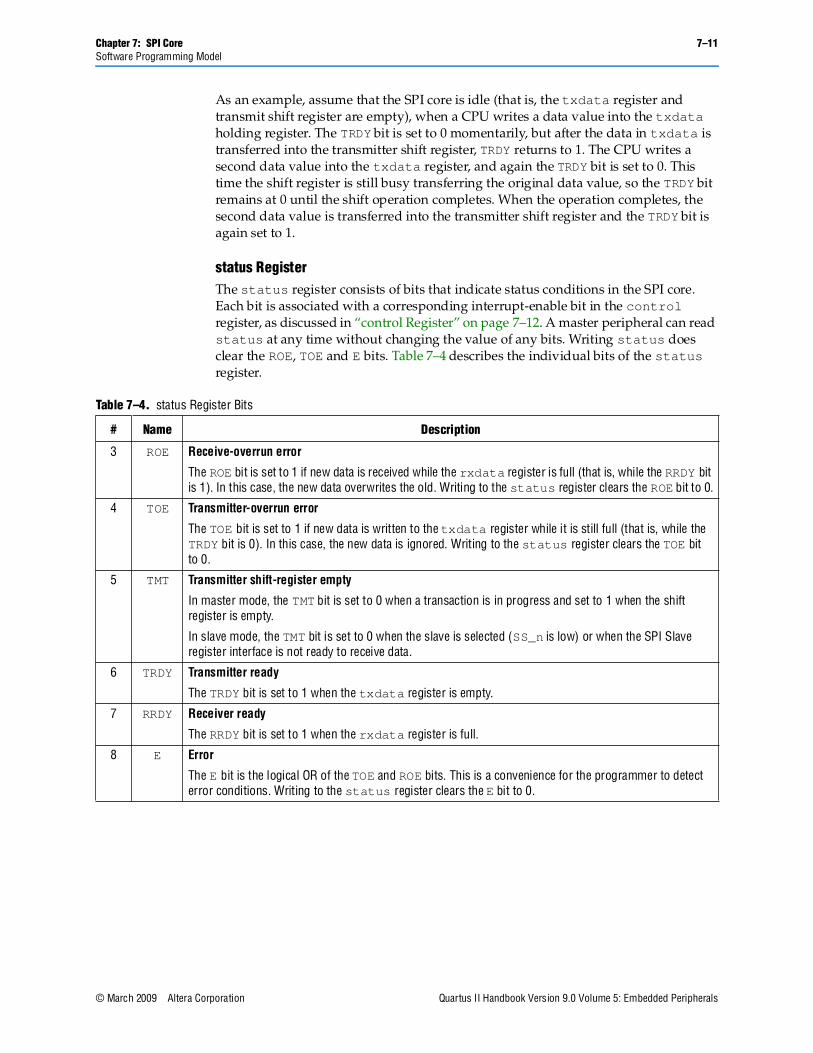
Chapter 7: SPI Core 7–11Software Programming Model
© March 2009 Altera Corporation Quartus II Handbook Version 9.0 Volume 5: Embedded Peripherals
As an example, assume that the SPI core is idle (that is, the txdata register and transmit shift register are empty), when a CPU writes a data value into the txdata holding register. The TRDY bit is set to 0 momentarily, but after the data in txdata is transferred into the transmitter shift register, TRDY returns to 1. The CPU writes a second data value into the txdata register, and again the TRDY bit is set to 0. This time the shift register is still busy transferring the original data value, so the TRDY bit remains at 0 until the shift operation completes. When the operation completes, the second data value is transferred into the transmitter shift register and the TRDY bit is again set to 1.
status RegisterThe status register consists of bits that indicate status conditions in the SPI core. Each bit is associated with a corresponding interrupt-enable bit in the control register, as discussed in “control Register” on page 7–12. A master peripheral can read status at any time without changing the value of any bits. Writing status does clear the ROE, TOE and E bits. Table 7–4 describes the individual bits of the status register.
Table 7–4. status Register Bits
# Name Description
3 ROE Receive-overrun error
The ROE bit is set to 1 if new data is received while the rxdata register is full (that is, while the RRDY bit is 1). In this case, the new data overwrites the old. Writing to the status register clears the ROE bit to 0.
4 TOE Transmitter-overrun error
The TOE bit is set to 1 if new data is written to the txdata register while it is still full (that is, while the TRDY bit is 0). In this case, the new data is ignored. Writing to the status register clears the TOE bit to 0.
5 TMT Transmitter shift-register empty
In master mode, the TMT bit is set to 0 when a transaction is in progress and set to 1 when the shift register is empty.
In slave mode, the TMT bit is set to 0 when the slave is selected (SS_n is low) or when the SPI Slave register interface is not ready to receive data.
6 TRDY Transmitter ready
The TRDY bit is set to 1 when the txdata register is empty.
7 RRDY Receiver ready
The RRDY bit is set to 1 when the rxdata register is full.
8 E Error
The E bit is the logical OR of the TOE and ROE bits. This is a convenience for the programmer to detect error conditions. Writing to the status register clears the E bit to 0.
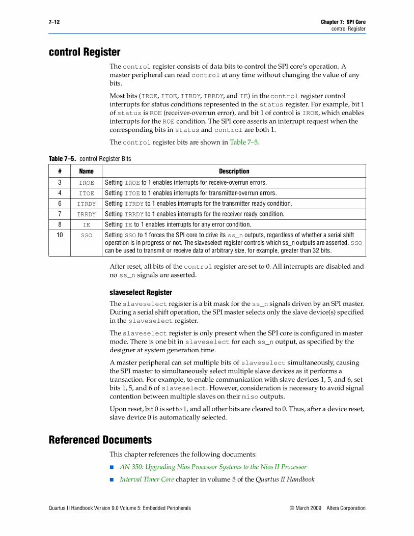
7–12 Chapter 7: SPI Corecontrol Register
Quartus II Handbook Version 9.0 Volume 5: Embedded Peripherals © March 2009 Altera Corporation
control RegisterThe control register consists of data bits to control the SPI core’s operation. A master peripheral can read control at any time without changing the value of any bits.
Most bits (IROE, ITOE, ITRDY, IRRDY, and IE) in the control register control interrupts for status conditions represented in the status register. For example, bit 1 of status is ROE (receiver-overrun error), and bit 1 of control is IROE, which enables interrupts for the ROE condition. The SPI core asserts an interrupt request when the corresponding bits in status and control are both 1.
The control register bits are shown in Table 7–5.
After reset, all bits of the control register are set to 0. All interrupts are disabled and no ss_n signals are asserted.
slaveselect RegisterThe slaveselect register is a bit mask for the ss_n signals driven by an SPI master. During a serial shift operation, the SPI master selects only the slave device(s) specified in the slaveselect register.
The slaveselect register is only present when the SPI core is configured in master mode. There is one bit in slaveselect for each ss_n output, as specified by the designer at system generation time.
A master peripheral can set multiple bits of slaveselect simultaneously, causing the SPI master to simultaneously select multiple slave devices as it performs a transaction. For example, to enable communication with slave devices 1, 5, and 6, set bits 1, 5, and 6 of slaveselect. However, consideration is necessary to avoid signal contention between multiple slaves on their miso outputs.
Upon reset, bit 0 is set to 1, and all other bits are cleared to 0. Thus, after a device reset, slave device 0 is automatically selected.
Referenced DocumentsThis chapter references the following documents:
■ AN 350: Upgrading Nios Processor Systems to the Nios II Processor
■ Interval Timer Core chapter in volume 5 of the Quartus II Handbook
Table 7–5. control Register Bits
# Name Description
3 IROE Setting IROE to 1 enables interrupts for receive-overrun errors.
4 ITOE Setting ITOE to 1 enables interrupts for transmitter-overrun errors.
6 ITRDY Setting ITRDY to 1 enables interrupts for the transmitter ready condition.
7 IRRDY Setting IRRDY to 1 enables interrupts for the receiver ready condition.
8 IE Setting IE to 1 enables interrupts for any error condition.
10 SSO Setting SSO to 1 forces the SPI core to drive its ss_n outputs, regardless of whether a serial shift operation is in progress or not. The slaveselect register controls which ss_n outputs are asserted. SSO can be used to transmit or receive data of arbitrary size, for example, greater than 32 bits.
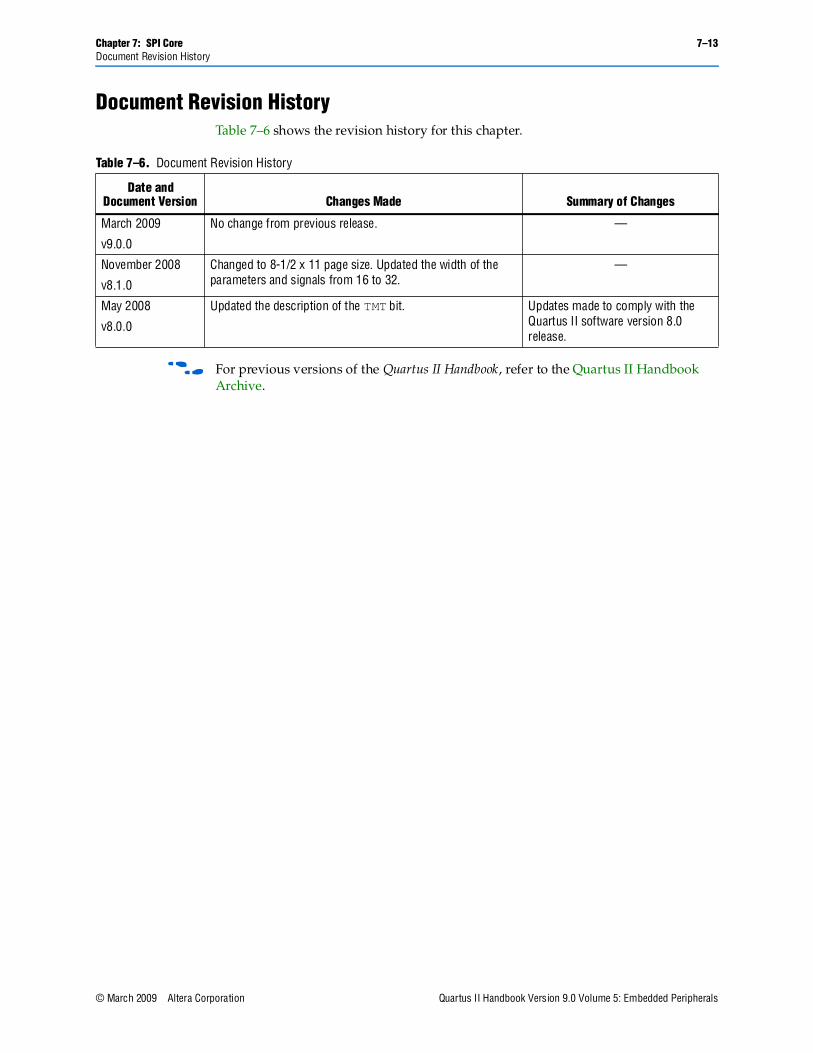
Chapter 7: SPI Core 7–13Document Revision History
© March 2009 Altera Corporation Quartus II Handbook Version 9.0 Volume 5: Embedded Peripherals
Document Revision HistoryTable 7–6 shows the revision history for this chapter.
f For previous versions of the Quartus II Handbook, refer to the Quartus II Handbook Archive.
Table 7–6. Document Revision History
Date and Document Version Changes Made Summary of Changes
March 2009
v9.0.0
No change from previous release. —
November 2008
v8.1.0
Changed to 8-1/2 x 11 page size. Updated the width of the parameters and signals from 16 to 32.
—
May 2008
v8.0.0
Updated the description of the TMT bit. Updates made to comply with the Quartus II software version 8.0 release.

7–14 Chapter 7: SPI CoreDocument Revision History
Quartus II Handbook Version 9.0 Volume 5: Embedded Peripherals © March 2009 Altera Corporation
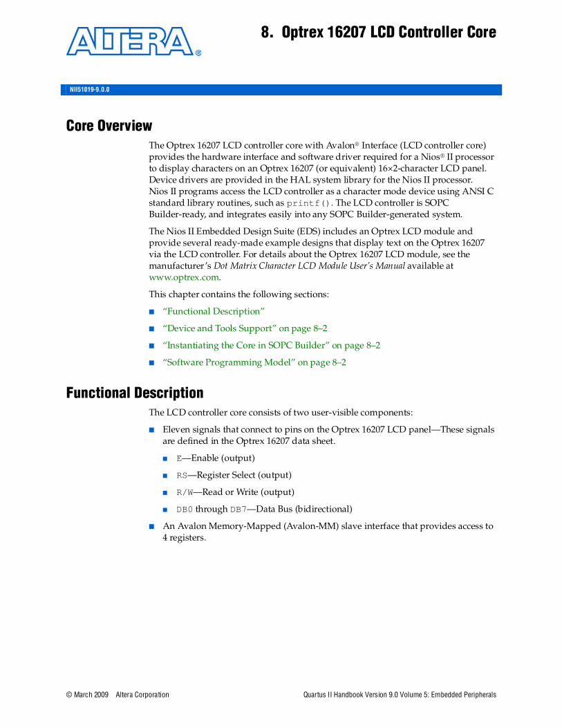
© March 2009 Altera Corporation Quartus II Handbook Version 9.0 Volume 5: Embedded Peripherals
8. Optrex 16207 LCD Controller Core
Core OverviewThe Optrex 16207 LCD controller core with Avalon® Interface (LCD controller core) provides the hardware interface and software driver required for a Nios® II processor to display characters on an Optrex 16207 (or equivalent) 16×2-character LCD panel. Device drivers are provided in the HAL system library for the Nios II processor. Nios II programs access the LCD controller as a character mode device using ANSI C standard library routines, such as printf(). The LCD controller is SOPC Builder-ready, and integrates easily into any SOPC Builder-generated system.
The Nios II Embedded Design Suite (EDS) includes an Optrex LCD module and provide several ready-made example designs that display text on the Optrex 16207 via the LCD controller. For details about the Optrex 16207 LCD module, see the manufacturer’s Dot Matrix Character LCD Module User’s Manual available at www.optrex.com.
This chapter contains the following sections:
■ “Functional Description”
■ “Device and Tools Support” on page 8–2
■ “Instantiating the Core in SOPC Builder” on page 8–2
■ “Software Programming Model” on page 8–2
Functional DescriptionThe LCD controller core consists of two user-visible components:
■ Eleven signals that connect to pins on the Optrex 16207 LCD panel—These signals are defined in the Optrex 16207 data sheet.
■ E—Enable (output)
■ RS—Register Select (output)
■ R/W—Read or Write (output)
■ DB0 through DB7—Data Bus (bidirectional)
■ An Avalon Memory-Mapped (Avalon-MM) slave interface that provides access to 4 registers.
NII51019-9.0.0
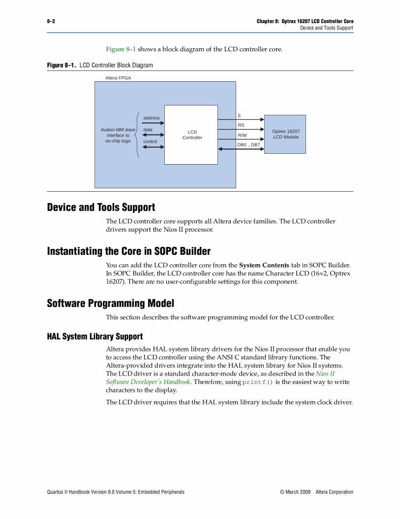
8–2 Chapter 8: Optrex 16207 LCD Controller CoreDevice and Tools Support
Quartus II Handbook Version 9.0 Volume 5: Embedded Peripherals © March 2009 Altera Corporation
Figure 8–1 shows a block diagram of the LCD controller core.
Device and Tools SupportThe LCD controller core supports all Altera device families. The LCD controller drivers support the Nios II processor.
Instantiating the Core in SOPC BuilderYou can add the LCD controller core from the System Contents tab in SOPC Builder. In SOPC Builder, the LCD controller core has the name Character LCD (16×2, Optrex 16207). There are no user-configurable settings for this component.
Software Programming ModelThis section describes the software programming model for the LCD controller.
HAL System Library SupportAltera provides HAL system library drivers for the Nios II processor that enable you to access the LCD controller using the ANSI C standard library functions. The Altera-provided drivers integrate into the HAL system library for Nios II systems. The LCD driver is a standard character-mode device, as described in the Nios II Software Developer's Handbook. Therefore, using printf() is the easiest way to write characters to the display.
The LCD driver requires that the HAL system library include the system clock driver.
Figure 8–1. LCD Controller Block Diagram
address
data
controlDB0 .. DB7
R/W
RS
E
Optrex 16207LCD Module
LCDController
Avalon-MM slaveinterface to
on-chip logic
Altera FPGA
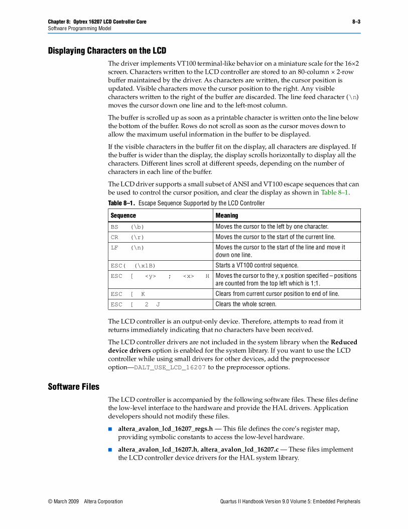
Chapter 8: Optrex 16207 LCD Controller Core 8–3Software Programming Model
© March 2009 Altera Corporation Quartus II Handbook Version 9.0 Volume 5: Embedded Peripherals
Displaying Characters on the LCDThe driver implements VT100 terminal-like behavior on a miniature scale for the 16×2 screen. Characters written to the LCD controller are stored to an 80-column × 2-row buffer maintained by the driver. As characters are written, the cursor position is updated. Visible characters move the cursor position to the right. Any visible characters written to the right of the buffer are discarded. The line feed character (\n) moves the cursor down one line and to the left-most column.
The buffer is scrolled up as soon as a printable character is written onto the line below the bottom of the buffer. Rows do not scroll as soon as the cursor moves down to allow the maximum useful information in the buffer to be displayed.
If the visible characters in the buffer fit on the display, all characters are displayed. If the buffer is wider than the display, the display scrolls horizontally to display all the characters. Different lines scroll at different speeds, depending on the number of characters in each line of the buffer.
The LCD driver supports a small subset of ANSI and VT100 escape sequences that can be used to control the cursor position, and clear the display as shown in Table 8–1.
The LCD controller is an output-only device. Therefore, attempts to read from it returns immediately indicating that no characters have been received.
The LCD controller drivers are not included in the system library when the Reduced device drivers option is enabled for the system library. If you want to use the LCD controller while using small drivers for other devices, add the preprocessor option—DALT_USE_LCD_16207 to the preprocessor options.
Software FilesThe LCD controller is accompanied by the following software files. These files define the low-level interface to the hardware and provide the HAL drivers. Application developers should not modify these files.
■ altera_avalon_lcd_16207_regs.h — This file defines the core’s register map, providing symbolic constants to access the low-level hardware.
■ altera_avalon_lcd_16207.h, altera_avalon_lcd_16207.c — These files implement the LCD controller device drivers for the HAL system library.
Table 8–1. Escape Sequence Supported by the LCD Controller
Sequence Meaning
BS (\b) Moves the cursor to the left by one character.
CR (\r) Moves the cursor to the start of the current line.
LF (\n) Moves the cursor to the start of the line and move it down one line.
ESC( (\x1B) Starts a VT100 control sequence.
ESC [ <y> ; <x> H Moves the cursor to the y, x position specified – positions are counted from the top left which is 1;1.
ESC [ K Clears from current cursor position to end of line.
ESC [ 2 J Clears the whole screen.
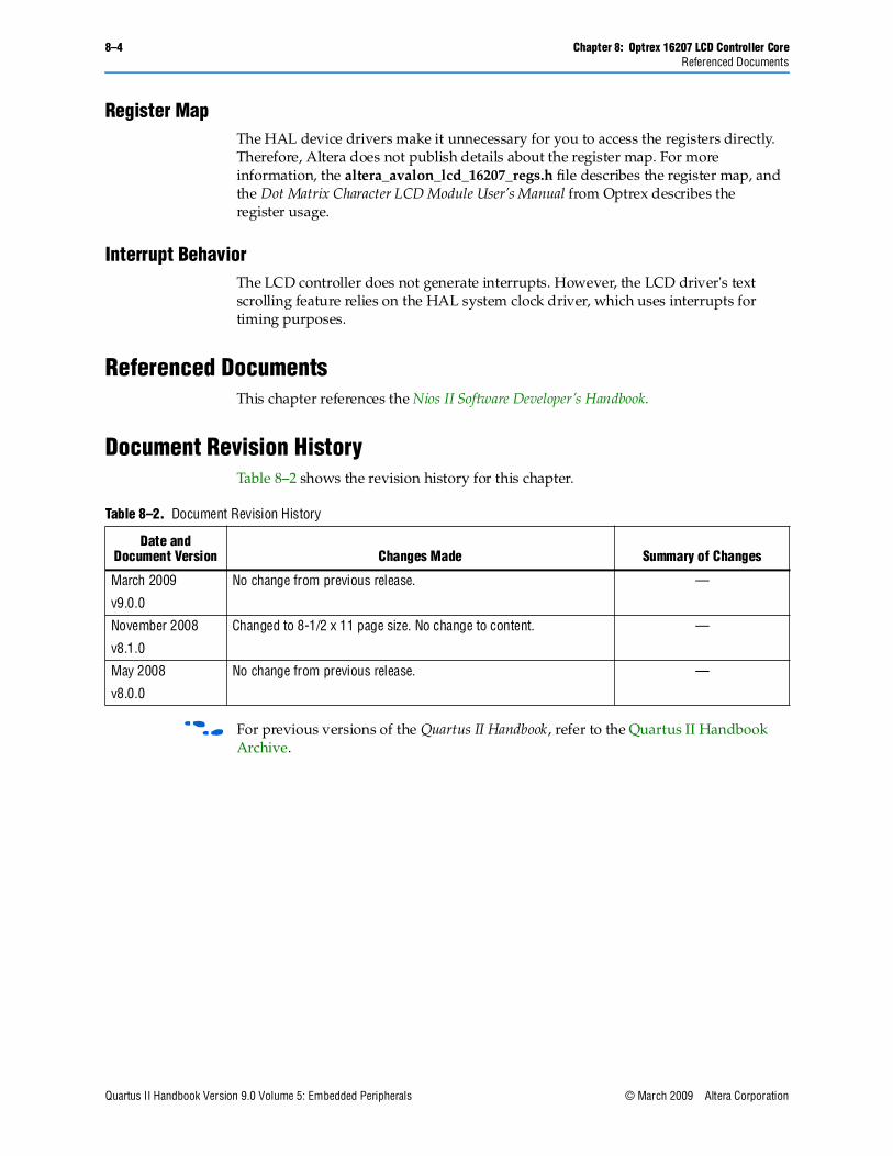
8–4 Chapter 8: Optrex 16207 LCD Controller CoreReferenced Documents
Quartus II Handbook Version 9.0 Volume 5: Embedded Peripherals © March 2009 Altera Corporation
Register MapThe HAL device drivers make it unnecessary for you to access the registers directly. Therefore, Altera does not publish details about the register map. For more information, the altera_avalon_lcd_16207_regs.h file describes the register map, and the Dot Matrix Character LCD Module User’s Manual from Optrex describes the register usage.
Interrupt BehaviorThe LCD controller does not generate interrupts. However, the LCD driver's text scrolling feature relies on the HAL system clock driver, which uses interrupts for timing purposes.
Referenced Documents This chapter references the Nios II Software Developer’s Handbook.
Document Revision HistoryTable 8–2 shows the revision history for this chapter.
f For previous versions of the Quartus II Handbook, refer to the Quartus II Handbook Archive.
Table 8–2. Document Revision History
Date and Document Version Changes Made Summary of Changes
March 2009
v9.0.0
No change from previous release. —
November 2008
v8.1.0
Changed to 8-1/2 x 11 page size. No change to content. —
May 2008
v8.0.0
No change from previous release. —
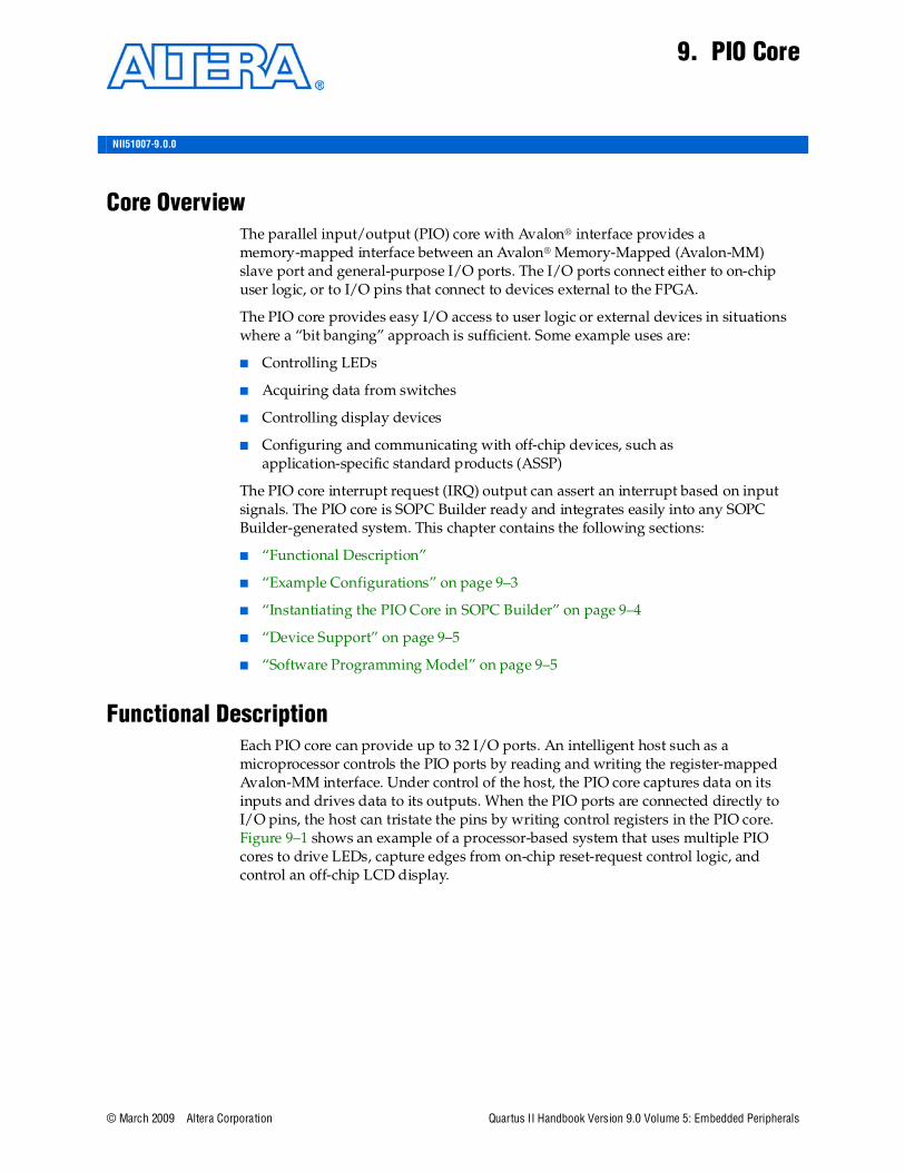
© March 2009 Altera Corporation Quartus II Handbook Version 9.0 Volume 5: Embedded Peripherals
9. PIO Core
Core OverviewThe parallel input/output (PIO) core with Avalon® interface provides a memory-mapped interface between an Avalon® Memory-Mapped (Avalon-MM) slave port and general-purpose I/O ports. The I/O ports connect either to on-chip user logic, or to I/O pins that connect to devices external to the FPGA.
The PIO core provides easy I/O access to user logic or external devices in situations where a “bit banging” approach is sufficient. Some example uses are:
■ Controlling LEDs
■ Acquiring data from switches
■ Controlling display devices
■ Configuring and communicating with off-chip devices, such as application-specific standard products (ASSP)
The PIO core interrupt request (IRQ) output can assert an interrupt based on input signals. The PIO core is SOPC Builder ready and integrates easily into any SOPC Builder-generated system. This chapter contains the following sections:
■ “Functional Description”
■ “Example Configurations” on page 9–3
■ “Instantiating the PIO Core in SOPC Builder” on page 9–4
■ “Device Support” on page 9–5
■ “Software Programming Model” on page 9–5
Functional DescriptionEach PIO core can provide up to 32 I/O ports. An intelligent host such as a microprocessor controls the PIO ports by reading and writing the register-mapped Avalon-MM interface. Under control of the host, the PIO core captures data on its inputs and drives data to its outputs. When the PIO ports are connected directly to I/O pins, the host can tristate the pins by writing control registers in the PIO core. Figure 9–1 shows an example of a processor-based system that uses multiple PIO cores to drive LEDs, capture edges from on-chip reset-request control logic, and control an off-chip LCD display.
NII51007-9.0.0
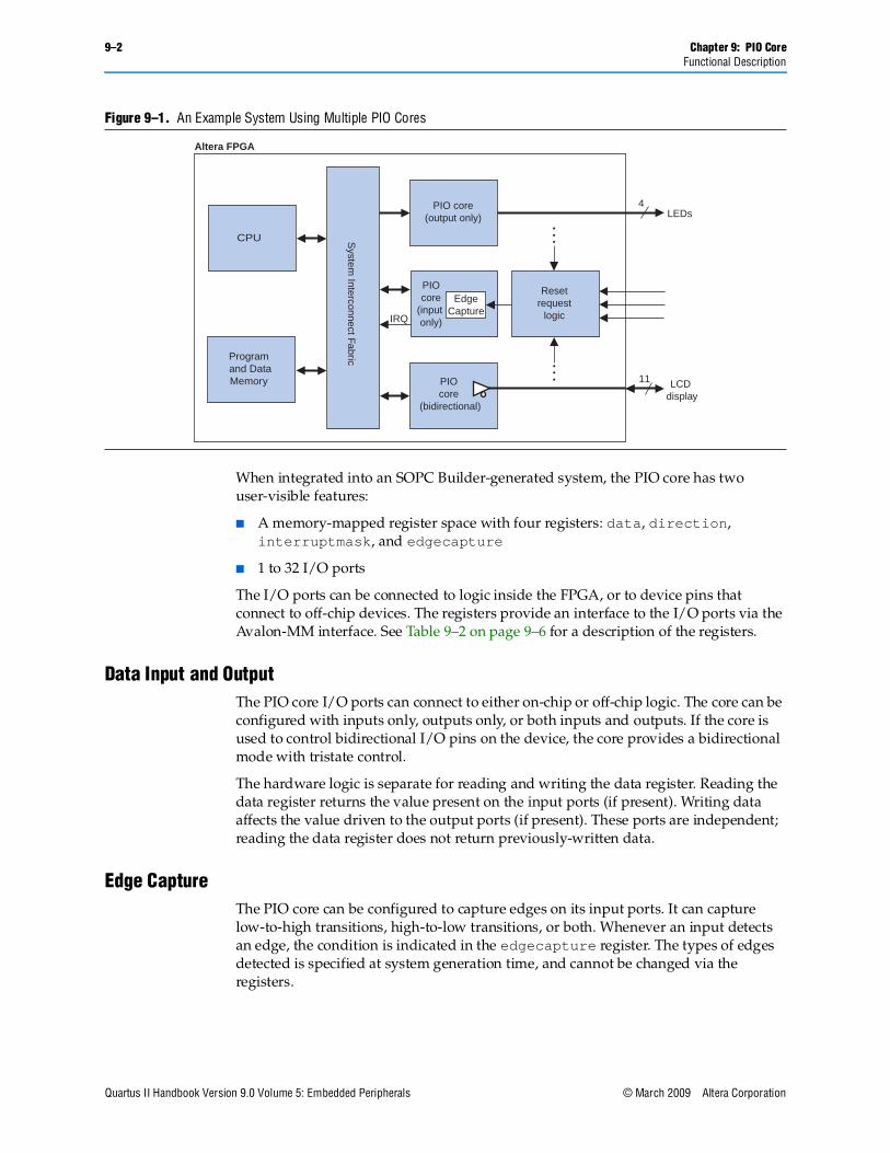
9–2 Chapter 9: PIO CoreFunctional Description
Quartus II Handbook Version 9.0 Volume 5: Embedded Peripherals © March 2009 Altera Corporation
When integrated into an SOPC Builder-generated system, the PIO core has two user-visible features:
■ A memory-mapped register space with four registers: data, direction, interruptmask, and edgecapture
■ 1 to 32 I/O ports
The I/O ports can be connected to logic inside the FPGA, or to device pins that connect to off-chip devices. The registers provide an interface to the I/O ports via the Avalon-MM interface. See Table 9–2 on page 9–6 for a description of the registers.
Data Input and OutputThe PIO core I/O ports can connect to either on-chip or off-chip logic. The core can be configured with inputs only, outputs only, or both inputs and outputs. If the core is used to control bidirectional I/O pins on the device, the core provides a bidirectional mode with tristate control.
The hardware logic is separate for reading and writing the data register. Reading the data register returns the value present on the input ports (if present). Writing data affects the value driven to the output ports (if present). These ports are independent; reading the data register does not return previously-written data.
Edge CaptureThe PIO core can be configured to capture edges on its input ports. It can capture low-to-high transitions, high-to-low transitions, or both. Whenever an input detects an edge, the condition is indicated in the edgecapture register. The types of edges detected is specified at system generation time, and cannot be changed via the registers.
Figure 9–1. An Example System Using Multiple PIO Cores
System
Interconnect Fabric
CPU
PIO core(output only)
Program and DataMemory PIO
core (bidirectional)
IRQ
LEDs
EdgeCapture
PIOcore
(input only)
Resetrequest
logic
Altera FPGA
4
11 LCD display
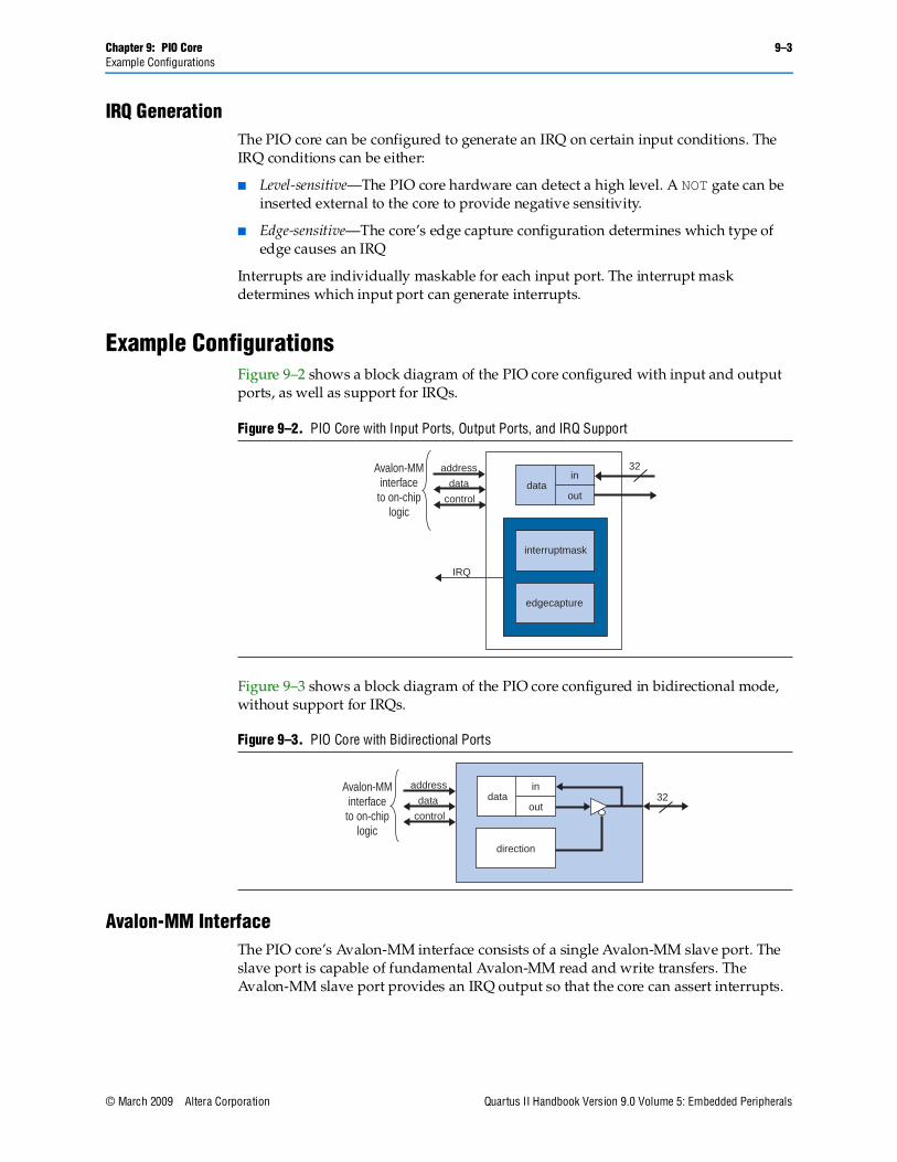
Chapter 9: PIO Core 9–3Example Configurations
© March 2009 Altera Corporation Quartus II Handbook Version 9.0 Volume 5: Embedded Peripherals
IRQ GenerationThe PIO core can be configured to generate an IRQ on certain input conditions. The IRQ conditions can be either:
■ Level-sensitive—The PIO core hardware can detect a high level. A NOT gate can be inserted external to the core to provide negative sensitivity.
■ Edge-sensitive—The core’s edge capture configuration determines which type of edge causes an IRQ
Interrupts are individually maskable for each input port. The interrupt mask determines which input port can generate interrupts.
Example ConfigurationsFigure 9–2 shows a block diagram of the PIO core configured with input and output ports, as well as support for IRQs.
Figure 9–3 shows a block diagram of the PIO core configured in bidirectional mode, without support for IRQs.
Avalon-MM InterfaceThe PIO core’s Avalon-MM interface consists of a single Avalon-MM slave port. The slave port is capable of fundamental Avalon-MM read and write transfers. The Avalon-MM slave port provides an IRQ output so that the core can assert interrupts.
Figure 9–2. PIO Core with Input Ports, Output Ports, and IRQ Support
Figure 9–3. PIO Core with Bidirectional Ports
datain
out
address
data
control
IRQ
32
interruptmask
edgecapture
Avalon-MMinterface
to on-chiplogic
direction
datain
out
address
data
control
32Avalon-MM
interfaceto on-chip
logic
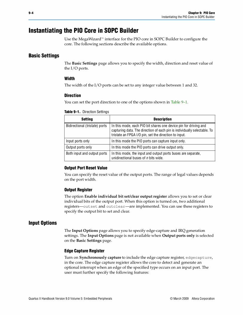
9–4 Chapter 9: PIO CoreInstantiating the PIO Core in SOPC Builder
Quartus II Handbook Version 9.0 Volume 5: Embedded Peripherals © March 2009 Altera Corporation
Instantiating the PIO Core in SOPC BuilderUse the MegaWizard™ interface for the PIO core in SOPC Builder to configure the core. The following sections describe the available options.
Basic SettingsThe Basic Settings page allows you to specify the width, direction and reset value of the I/O ports.
WidthThe width of the I/O ports can be set to any integer value between 1 and 32.
DirectionYou can set the port direction to one of the options shown in Table 9–1.
Output Port Reset ValueYou can specify the reset value of the output ports. The range of legal values depends on the port width.
Output RegisterThe option Enable individual bit set/clear output register allows you to set or clear individual bits of the output port. When this option is turned on, two additional registers—outset and outclear—are implemented. You can use these registers to specify the output bit to set and clear.
Input OptionsThe Input Options page allows you to specify edge-capture and IRQ generation settings. The Input Options page is not available when Output ports only is selected on the Basic Settings page.
Edge Capture RegisterTurn on Synchronously capture to include the edge capture register, edgecapture, in the core. The edge capture register allows the core to detect and generate an optional interrupt when an edge of the specified type occurs on an input port. The user must further specify the following features:
Table 9–1. Direction Settings
Setting Description
Bidirectional (tristate) ports In this mode, each PIO bit shares one device pin for driving and capturing data. The direction of each pin is individually selectable. To tristate an FPGA I/O pin, set the direction to input.
Input ports only In this mode the PIO ports can capture input only.
Output ports only In this mode the PIO ports can drive output only.
Both input and output ports In this mode, the input and output ports buses are separate, unidirectional buses of n bits wide.
Chapter 9: PIO Core 9–5Device Support
© March 2009 Altera Corporation Quartus II Handbook Version 9.0 Volume 5: Embedded Peripherals
■ Select the type of edge to detect:
■ Rising Edge
■ Falling Edge
■ Either Edge
■ Turn on Enable bit-clearing for edge capture register to clear individual bit in the edge capture register. To clear a given bit, write 1 to the bit in the edge capture register.
InterruptTurn on Generate IRQ to assert an IRQ output when a specified event occurs on input ports. The user must further specify the cause of an IRQ event:
■ Level—The core generates an IRQ whenever a specific input is high and interrupts are enabled for that input in the interruptmask register.
■ Edge—The core generates an IRQ whenever a specific bit in the edge capture register is high and interrupts are enabled for that bit in the interruptmask register.
When Generate IRQ is off, the interruptmask register does not exist.
SimulationThe Simulation page allows you to specify the value of the input ports during simulation. Turn on Hardwire PIO inputs in test bench to set the PIO input ports to a certain value in the testbench, and specify the value in Drive inputs to field.
Device SupportThe PIO core supports all Altera® device families.
Software Programming ModelThis section describes the software programming model for the PIO core, including the register map and software constructs used to access the hardware. For Nios® II processor users, Altera provides the HAL system library header file that defines the PIO core registers. The PIO core does not match the generic device model categories supported by the HAL, so it cannot be accessed via the HAL API or the ANSI C standard library.
The Nios II Embedded Design Suite (EDS) provides several example designs that demonstrate usage of the PIO core. In particular, the count_binary.c example uses the PIO core to drive LEDs, and detect button presses using PIO edge-detect interrupts.
Software FilesThe PIO core is accompanied by one software file, altera_avalon_pio_regs.h. This file defines the core’s register map, providing symbolic constants to access the low-level hardware.
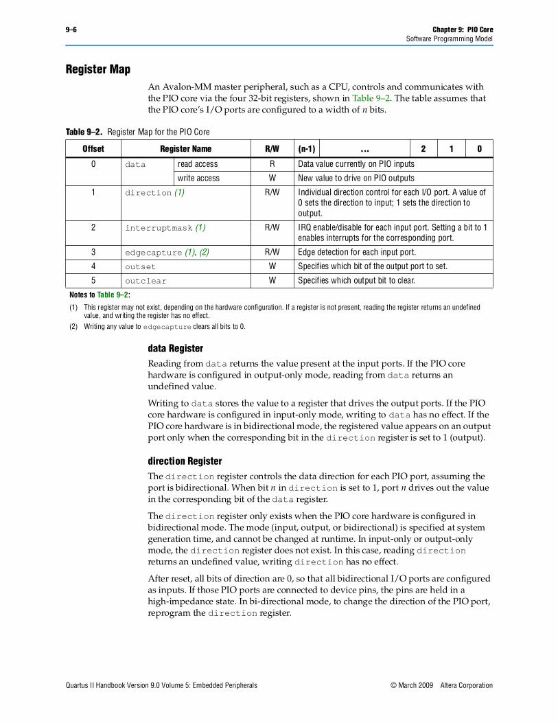
9–6 Chapter 9: PIO CoreSoftware Programming Model
Quartus II Handbook Version 9.0 Volume 5: Embedded Peripherals © March 2009 Altera Corporation
Register MapAn Avalon-MM master peripheral, such as a CPU, controls and communicates with the PIO core via the four 32-bit registers, shown in Table 9–2. The table assumes that the PIO core’s I/O ports are configured to a width of n bits.
data RegisterReading from data returns the value present at the input ports. If the PIO core hardware is configured in output-only mode, reading from data returns an undefined value.
Writing to data stores the value to a register that drives the output ports. If the PIO core hardware is configured in input-only mode, writing to data has no effect. If the PIO core hardware is in bidirectional mode, the registered value appears on an output port only when the corresponding bit in the direction register is set to 1 (output).
direction RegisterThe direction register controls the data direction for each PIO port, assuming the port is bidirectional. When bit n in direction is set to 1, port n drives out the value in the corresponding bit of the data register.
The direction register only exists when the PIO core hardware is configured in bidirectional mode. The mode (input, output, or bidirectional) is specified at system generation time, and cannot be changed at runtime. In input-only or output-only mode, the direction register does not exist. In this case, reading direction returns an undefined value, writing direction has no effect.
After reset, all bits of direction are 0, so that all bidirectional I/O ports are configured as inputs. If those PIO ports are connected to device pins, the pins are held in a high-impedance state. In bi-directional mode, to change the direction of the PIO port, reprogram the direction register.
Table 9–2. Register Map for the PIO Core
Offset Register Name R/W (n-1) ... 2 1 0
0 data read access R Data value currently on PIO inputs
write access W New value to drive on PIO outputs
1 direction (1) R/W Individual direction control for each I/O port. A value of 0 sets the direction to input; 1 sets the direction to output.
2 interruptmask (1) R/W IRQ enable/disable for each input port. Setting a bit to 1 enables interrupts for the corresponding port.
3 edgecapture (1), (2) R/W Edge detection for each input port.
4 outset W Specifies which bit of the output port to set.
5 outclear W Specifies which output bit to clear.
Notes to Table 9–2:
(1) This register may not exist, depending on the hardware configuration. If a register is not present, reading the register returns an undefined value, and writing the register has no effect.
(2) Writing any value to edgecapture clears all bits to 0.
Chapter 9: PIO Core 9–7Software Programming Model
© March 2009 Altera Corporation Quartus II Handbook Version 9.0 Volume 5: Embedded Peripherals
interruptmask RegisterSetting a bit in the interruptmask register to 1 enables interrupts for the corresponding PIO input port. Interrupt behavior depends on the hardware configuration of the PIO core. See “Interrupt Behavior” on page 9–7.
The interruptmask register only exists when the hardware is configured to generate IRQs. If the core cannot generate IRQs, reading interruptmask returns an undefined value, and writing to interruptmask has no effect.
After reset, all bits of interruptmask are zero, so that interrupts are disabled for all PIO ports.
edgecapture RegisterBit n in the edgecapture register is set to 1 whenever an edge is detected on input port n. An Avalon-MM master peripheral can read the edgecapture register to determine if an edge has occurred on any of the PIO input ports. If the option Enable bit-clearing for edge capture register is turned off, writing any value to the edgecapture register clears all bits in the register. Otherwise, writing a 1 to a particular bit in the register clears only that bit.
The type of edge(s) to detect is fixed in hardware at system generation time. The edgecapture register only exists when the hardware is configured to capture edges. If the core is not configured to capture edges, reading from edgecapture returns an undefined value, and writing to edgecapture has no effect.
outset and outclear RegistersYou can use the outset and outclear registers to set and clear individual bits of the output port. For example, to set bit 6 of the output port, write 0x40 to the outset register. Writing 0x08 to the outclear register clears bit 3 of the output port.
These registers are only present when the option Enable individual bit set/clear output register is turned on.
Interrupt BehaviorThe PIO core outputs a single IRQ signal that can connect to any master peripheral in the system. The master can read either the data register or the edgecapture register to determine which input port caused the interrupt.
When the hardware is configured for level-sensitive interrupts, the IRQ is asserted whenever corresponding bits in the data and interruptmask registers are 1. When the hardware is configured for edge-sensitive interrupts, the IRQ is asserted whenever corresponding bits in the edgecapture and interruptmask registers are 1. The IRQ remains asserted until explicitly acknowledged by disabling the appropriate bit(s) in interruptmask, or by writing to edgecapture.
Software FilesThe PIO core is accompanied by the following software file. This file provide low-level access to the hardware. Application developers should not modify the file.
■ altera_avalon_pio_regs.h—This file defines the core’s register map, providing symbolic constants to access the low-level hardware. The symbols in this file are used by device driver functions.
9–8 Chapter 9: PIO CoreDocument Revision History
Quartus II Handbook Version 9.0 Volume 5: Embedded Peripherals © March 2009 Altera Corporation
Document Revision HistoryTable 9–3 shows the revision history for this chapter.
f For previous versions of the Quartus II Handbook, refer to the Quartus II Handbook Archive.
Table 9–3. Document Revision History
Date and Document Version Changes Made Summary of Changes
March 2009
v9.0.0
Added a section on new registers, outset and outclear. —
November 2008
v8.1.0
Changed to 8-1/2 x 11 page size. Added the description for Output Port Reset Value and Simulation parameters.
—
May 2008
v8.0.0
No change from previous release. —


![Designing with 88MW320-88MW322Majority of QSPI devices operate in 1.8V or 3.0/3.3V range • JTAG and UART[0] signals useful for development, programming, monitoring, and provisioning](https://img.pdfslide.net/doc/110x75/5f9f43aa36e55c6c70790505/designing-with-88mw320-88mw322-majority-of-qspi-devices-operate-in-18v-or-3033v.jpg)