Embed Size (px)
Citation preview
DS-7000, Rev 1.2, 1/28/99 © Quantum Effect Design, Inc. Page 1 of 27
QED RISCMark™ RM7000™64-Bit Superscalar MicroprocessorAdvanced Information
FEATURES:
• RM5270 and RM5271 pin compatible
• Dual Issue symmetric superscalar microprocessor with instruc-tion prefetch optimized for system level price/performance— 200, 225, 250, 263 MHz operating frequency— >450 Dhrystone 2.1 MIPS @263 MHz— 11-13 SPECint95, 13-15 SPECfp95 @ 263 MHz— MIPS IV Superset Instruction Set Architecture
• High-performance interface (RM52xx compatible)— 1000 MB per second peak throughput— 125 MHz max. freq., multiplexed address/data— Supports two outstanding reads with out-of-order return
— Supports ½ clock divisors (2, 2.5, 3, 3.5, 4, 4.5, 5, 6, 7, 8, 9)— IEEE 1149.1 JTAG (TAP) boundary scan
• Integrated primary and secondary caches - all are 4-way set associative with 32 byte line size— 16KB instruction — 16KB data: non-blocking and write-back or write-through— 256KB on-chip secondary: unified, non-blocking, block write-
back— Per line cache locking in primaries and secondary
• Integrated tertiary cache controller (RM527x compatible)— Supports 512K, 1M, 2M, 4M, or 8 MByte block write-through
• MIPS IV instruction set— Data PREFETCH instruction allows the processor to overlap
cache miss latency and instruction execution— Floating point combined multiply-add instruction increases
performance in signal processing and graphics applications— Conditional moves reduce branch frequency— Index address modes (register + register)
• Integrated memory management unit (RM52xx compatible)— Fully associative joint TLB (shared by I and D translations)— 48 dual entries map 96 pages— 4 entry DTLB and 4 entry ITLB— Variable page size (4KB to 16MB in 4x increments)
• Embedded application enhancements— Specialized DSP integer Multiply-Accumulate instruction,
(MAD/MADU) and three-operand multiply instruction (MUL/MULU)
— I&D Test/Break-point (Watch) registers for emulation & debug
— Performance counter for system and software tuning & debug
— Fourteen fully prioritized vectored interrupts - 10 external, 2 internal, 2 software
— Bypass secondary/tertiary cache option— Fast Hit-Writeback-Invalidate and Hit-Invalidate cache oper-
ations for efficient cache management
• High-performance floating-point unit - 600 M FLOPS maximum— Single cycle repeat rate for common single-precision opera-
tions and some double-precision operations— Single cycle repeat rate for single-precision combined multi-
ply-add operations— Two cycle repeat rate for double-precision multiply and dou-
ble-precision combined multiply-add operations
• Fully static CMOS design with dynamic power down logic— Standby reduced power mode with WAIT instruction— 3.3 watts typical @ 2.5V Int., 3.3V I/O, 200MHz
• 304 pin SBGA package, 31x31mm
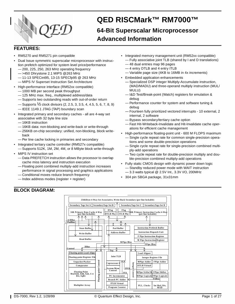
BLOCK DIAGRAM:
Read B uffer
In teger Reg ister F ile
M Pipe Adder
DTL B Virtual
M Pipe StA ln/Sh
M Pipe Log icals
Program Counter
PC Increm enter
Branch PC Adder
L oad A ligner
Floa ting-point Reg ister File
Unpacker/Packer
PLL , C locksIT LB Virtual
Join t T LB
16K Prim ary Data Cache 4-Way
256KB yte 4-Way Set Associative, W rite-Back Secondary (per line lockable)
DTag
DT LB Phy
Address B uffer
Pad Buffer
ITag
ITL B Phy
Store Buffer
W rite B uffer
DVA
IVA
Secondary Tags Set A
Flo
atin
g-p
oin
t Con
trol In
teger C
ontro
l
DBus
Coprocessor 0
System /M emControl
Tag
Instruct ion D ispatch Unit
Contro l
M Pipe Instruction Register
F Pipe Instruction Register
FPipe IB usM Pipe IB us
Int M ul, D iv,
Floating P ointM ulAdd, Add, Sub, Cvt
D iv, SqRtFAB us
Instruction Prefetch B uffer
PadBusA /DBus
F Pipe Adder
FPipe Shifter
FPipe L ogica ls
SecondaryTags Set B SecondaryTags Set C SecondaryTags Set D
M ultip lier A rray
Float ing-point Load A lign
M AD
Com parator
16K P rim ary Instruction Cache 4-Way(per line lockable)(per line lockable)
QED RISCMark™ RM7000™ Advanced Information 64-Bit Superscalar Microprocessor
Page 2 of 27 © Quantum Effect Design, Inc. DS-7000, Rev 1.2, 1/28/99
DESCRIPTION:
The QED RM7000 is a highly integrated symmetric super-scalar microprocessor capable of issuing two instructions each processor cycle. It has two high-performance 64-bit integer units as well as a high-throughput, fully pipelined 64-bit floating point unit. To keep its multiple execution units running efficiently, the RM7000 integrates not only 16KB 4-way set associative instruction and data caches but backs them up with an integrated 256KB 4-way set associative secondary as well. For maximum efficiency, the data and secondary caches are write-back and non-blocking. An optional external tertiary cache provides high-performance capability even in applications having very large data sets. A RM52xx family compatible, operating system friendly
memory management unit with a 48-entry fully associative TLB and a high-performance 64-bit system interface sup-porting multiple outstanding reads with out-of-order return and hardware prioritized and vectored interrupts round out the main features of the processor.
The RM7000 is ideally suited for high-end embedded con-trol applications such as internetworking, high-performance image manipulation, high-speed printing, and 3-D visual-ization. The RM7000 is also applicable to the low end work-station market where its balanced integer and floating-point performance and direct support for a large tertiary cache (up to 8MB) provide outstanding price/performance.
HARDWARE OVERVIEW
The RM7000 offers a high-level of integration targeted at high-performance embedded applications. The key ele-ments of the RM7000 are briefly described below.
CPU Registers
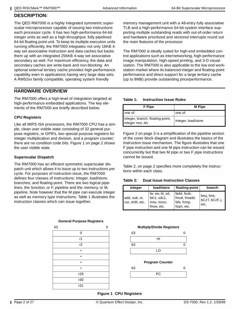
Like all MIPS ISA processors, the RM7000 CPU has a sim-ple, clean user visible state consisting of 32 general pur-pose registers, or GPR’s, two special purpose registers for integer multiplication and division, and a program counter; there are no condition code bits. Figure 1 on page 2 shows the user visible state.
Superscalar Dispatch
The RM7000 has an efficient symmetric superscalar dis-patch unit which allows it to issue up to two instructions per cycle. For purposes of instruction issue, the RM7000 defines four classes of instructions: integer, load/store, branches, and floating-point. There are two logical pipe-lines, the function, or F, pipeline and the memory, or M, pipeline. Note however that the M pipe can execute integer as well as memory type instructions. Table 1 illustrates the instruction classes which can issue together.
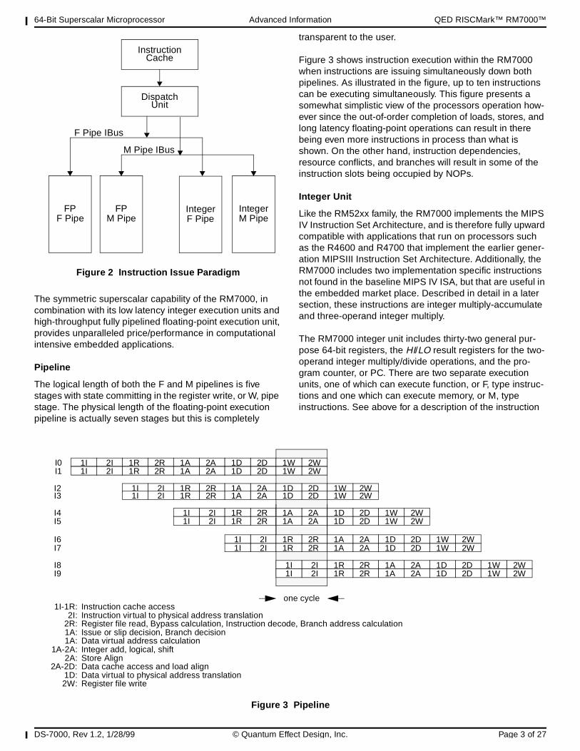
Figure 2 on page 3 is a simplification of the pipeline section of the cover block diagram and illustrates the basics of the instruction issue mechanism. The figure illustrates that one F pipe instruction and one M pipe instruction can be issued concurrently but that two M pipe or two F pipe instructions cannot be issued.
Table 2, on page 2 specifies more completely the instruc-tions within each class.
Figure 1 CPU Registers
General Purpose Registers
63 0 Multiply/Divide Registers
0 63 0
r1 HI
r2 63 0
• LO
•
• Program Counter
• 63 0
r29 PC
r30
r31
Table 1: Instruction Issue Rules
F Pipe M Pipe
one of: one of:
integer, branch, floating-point, integer mul, div
integer, load/store
Table 2: Dual Issue Instruction Classes
integer load/store floating-point branch
add, sub, or, xor, shift, etc.
lw, sw, ld, sd, ldc1, sdc1, mov, movc, fmov, etc.
fadd, fsub, fmult, fmadd, fdiv, fcmp, fsqrt, etc.
beq, bne, bCzT, bCzF, j, etc.
64-Bit Superscalar Microprocessor Advanced Information QED RISCMark™ RM7000™
DS-7000, Rev 1.2, 1/28/99 © Quantum Effect Design, Inc. Page 3 of 27
The symmetric superscalar capability of the RM7000, in combination with its low latency integer execution units and high-throughput fully pipelined floating-point execution unit, provides unparalleled price/performance in computational intensive embedded applications.
Pipeline
The logical length of both the F and M pipelines is five stages with state committing in the register write, or W, pipe stage. The physical length of the floating-point execution pipeline is actually seven stages but this is completely
transparent to the user.
Figure 3 shows instruction execution within the RM7000 when instructions are issuing simultaneously down both pipelines. As illustrated in the figure, up to ten instructions can be executing simultaneously. This figure presents a somewhat simplistic view of the processors operation how-ever since the out-of-order completion of loads, stores, and long latency floating-point operations can result in there being even more instructions in process than what is shown. On the other hand, instruction dependencies, resource conflicts, and branches will result in some of the instruction slots being occupied by NOPs.
Integer Unit
Like the RM52xx family, the RM7000 implements the MIPS IV Instruction Set Architecture, and is therefore fully upward compatible with applications that run on processors such as the R4600 and R4700 that implement the earlier gener-ation MIPSIII Instruction Set Architecture. Additionally, the RM7000 includes two implementation specific instructions not found in the baseline MIPS IV ISA, but that are useful in the embedded market place. Described in detail in a later section, these instructions are integer multiply-accumulate and three-operand integer multiply.
The RM7000 integer unit includes thirty-two general pur-pose 64-bit registers, the HI/LO result registers for the two-operand integer multiply/divide operations, and the pro-gram counter, or PC. There are two separate execution units, one of which can execute function, or F, type instruc-tions and one which can execute memory, or M, type instructions. See above for a description of the instruction
Figure 2 Instruction Issue Paradigm
F PipeInteger
M PipeInteger
F PipeFP
M PipeFP
CacheInstruction
UnitDispatch
F Pipe IBus
M Pipe IBus
Figure 3 Pipeline
I0
I2
I4
I6
I8
2I1I 1R 2R 1A 2A 1D 2D 1W 2W
2I1I 1R 2R 1A 2A 1D 2D 1W 2W
2I1I 1R 2R 1A 2A 1D 2D 1W 2W
2I1I 1R 2R 1A 2A 1D 2D 1W 2W
2I1I 1R 2R 1A 2A 1D 2D 1W 2W
one cycle1I-1R:
2I:
2A-2D:
2R:
1A-2A:
1A:1A:
1D:
2A:
2W:
Instruction cache accessInstruction virtual to physical address translation Register file read, Bypass calculation, Instruction decode, Branch address calculationIssue or slip decision, Branch decision
Integer add, logical, shiftData virtual address calculation
Data virtual to physical address translation
Store Align
Register file write
Data cache access and load align
I1 2I1I 1R 2R 1A 2A 1D 2D 1W 2W
I3 2I1I 1R 2R 1A 2A 1D 2D 1W 2W
I5 2I1I 1R 2R 1A 2A 1D 2D 1W 2W
I7 2I1I 1R 2R 1A 2A 1D 2D 1W 2W
I9 2I1I 1R 2R 1A 2A 1D 2D 1W 2W
QED RISCMark™ RM7000™ Advanced Information 64-Bit Superscalar Microprocessor
Page 4 of 27 © Quantum Effect Design, Inc. DS-7000, Rev 1.2, 1/28/99
types and the issue rules. As a special case, integer multi-ply/divide instructions as well as their corresponding MFHI and MFLO instructions can only be executed in the F type execution unit. Within each execution unit the operational characteristics are the same as on previous QED designs with single cycle ALU operations (add, sub, logical, shift), one cycle load delay, and an autonomous multiply/divide unit.
Register FileThe RM7000 has thirty-two general purpose registers with register location 0 (r0) hard wired to a zero value. These registers are used for scalar integer operations and address calculation. In order to service the two integer exe-cution units, the register file has four read ports and two write ports and is fully bypassed both within and between the two execution units to minimize operation latency in the pipeline.
ALU
The RM7000 has two complete integer ALU’s each consist-ing of an integer adder/subtractor, a logic unit, and a shifter. Table 3 below shows the functions performed by the ALU’s for each execution unit. Each of these units is optimized to perform all operations in a single processor cycle.
Integer Multiply/Divide
The RM7000 has a single dedicated integer multiply/divide unit optimized for high-speed multiply and multiply-accumu-late operations. The multiply/divide unit resides in the F type execution unit. Table 4 shows the performance of the multiply/divide unit on each operation.
The baseline MIPS IV ISA specifies that the results of a multiply or divide operation be placed in the Hi and Lo reg-isters. These values can then be transferred to the general purpose register file using the Move-from-Hi and Move-from-Lo (MFHI/MFLO ) instructions.
In addition to the baseline MIPS IV integer multiply instruc-tions, the RM7000 also implements the multiply instruction, MUL . This instruction specifies that the multiply result go directly to the integer register file rather than the Lo regis-ter. The portion of the multiply that would have normally gone into the Hi register is discarded. For applications where it is known that the upper half of the multiply result is not required, using the MUL instruction eliminates the necessity of executing an explicit MFLO instruction.
Also included in the RM7000 is the multiply-add instruction, MAD. This instruction multiplies two operands and adds the resulting product to the current contents of the Hi and Lo registers. The multiply-accumulate operation is the core primitive of almost all signal processing algorithms allowing the RM7000 to eliminate the need for a separate DSP engine in many embedded applications.
By pipelining the multiply-accumulate function and dynami-cally determining the size of the input operands, the RM7000 is able to maximize throughput while still using an area efficient implementation.
Floating-Point Coprocessor
The RM7000 incorporates a high-performance fully pipe-lined floating-point coprocessor which includes a floating-point register file and autonomous execution units for multi-ply/add/convert and divide/square root. The floating-point coprocessor is a tightly coupled co-execution unit, decod-ing and executing instructions in parallel with, and in the case of floating-point loads and stores, in cooperation with the M pipe of the integer unit. As described earlier, the superscalar capabilities of the RM7000 allow floating-point computation instructions to issue concurrently with integer instructions.
Floating-Point Unit
The RM7000 floating-point execution unit supports single and double precision arithmetic, as specified in the IEEE Standard 754. The execution unit is broken into a separate divide/square root unit and a pipelined multiply/add unit. Overlap of divide/square root and multiply/add is sup-ported.
The RM7000 maintains fully precise floating-point excep-tions while allowing both overlapped and pipelined opera-tions. Precise exceptions are extremely important in object-oriented programming environments and highly desirable for debugging in any environment.
The floating-point unit’s operation set includes floating-point add, subtract, multiply, multiply-add, divide, square root, reciprocal, reciprocal square root, conditional moves, con-
Table 3: ALU Functions
Unit F Pipe M Pipe
Adder add, subadd, sub, data address add
Logiclogic, moves, zero shifts (nop)
logic, moves, zero shifts (nop)
Shifter non zero shift non zero shift, store align
Table 4: Inte ger Multi ply/Divide O perations
OpcodeOperand
SizeLatency
Repeat Rate
Stall Cycles
MULT/U, MAD/U
16 bit 4 3 0
32 bit 5 4 0
MUL16 bit 4 3 2
32 bit 5 4 3
DMULT, DMULTU
any 9 8 0
DIV, DIVD any 36 36 0
DDIV, DDIVU
any 68 68 0
64-Bit Superscalar Microprocessor Advanced Information QED RISCMark™ RM7000™
DS-7000, Rev 1.2, 1/28/99 © Quantum Effect Design, Inc. Page 5 of 27
version between fixed-point and floating-point format, con-version between floating-point formats, and floating-point compare.
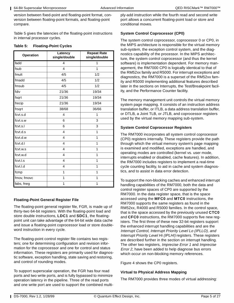
Table 5 gives the latencies of the floating-point instructions in internal processor cycles.
Floating-Point General Register File
The floating-point general register file, FGR, is made up of thirty-two 64-bit registers. With the floating-point load and store double instructions, LDC1 and SDC1, the floating-point unit can take advantage of the 64-bit wide data cache and issue a floating-point coprocessor load or store double-word instruction in every cycle.
The floating-point control register file contains two regis-ters; one for determining configuration and revision infor-mation for the coprocessor and one for control and status information. These registers are primarily used for diagnos-tic software, exception handling, state saving and restoring, and control of rounding modes.
To support superscalar operation, the FGR has four read ports and two write ports, and is fully bypassed to minimize operation latency in the pipeline. Three of the read ports and one write port are used to support the combined multi-
ply-add instruction while the fourth read and second write port allows a concurrent floating-point load or store and conditional moves.
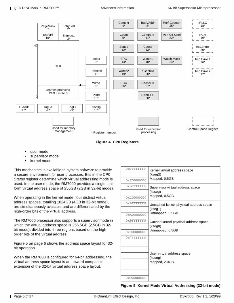
System Control Coprocessor (CP0)
The system control coprocessor, coprocessor 0 or CP0, in the MIPS architecture is responsible for the virtual memory sub-system, the exception control system, and the diag-nostics capability of the processor. In the MIPS architec-ture, the system control coprocessor (and thus the kernel software) is implementation dependent. For memory man-agement, the RM7000 CP0 is logically identical to that of the RM52xx family and R5000. For interrupt exceptions and diagnostics, the RM7000 is a superset of the RM52xx fam-ily and R5000 implementing additional features described later in the sections on Interrupts, the Test/Breakpoint facil-ity, and the Performance Counter facility.
The memory management unit controls the virtual memory system page mapping. It consists of an instruction address translation buffer, or ITLB, a data address translation buffer, or DTLB, a Joint TLB, or JTLB, and coprocessor registers used by the virtual memory mapping sub-system.
System Control Coprocessor Registers
The RM7000 incorporates all system control coprocessor (CP0) registers internally. These registers provide the path through which the virtual memory system’s page mapping is examined and modified, exceptions are handled, and operating modes are controlled (kernel vs. user mode, interrupts enabled or disabled, cache features). In addition, the RM7000 includes registers to implement a real-time cycle counting facility, to aid in cache and system diagnos-tics, and to assist in data error detection.
To support the non-blocking caches and enhanced interrupt handling capabilities of the RM7000, both the data and control register spaces of CP0 are supported by the RM7000. In the data register space, that is the space accessed using the MFC0 and MTC0 instructions, the RM7000 supports the same registers as found in the RM52xx, R4000 and R5000 families. In the control space, that is the space accessed by the previously unused CTC0 and CFC0 instructions, the RM7000 supports five new reg-isters. The first three of these new 32-bit registers support the enhanced interrupt handling capabilities and are the Interrupt Control, Interrupt Priority Level Lo (IPLLO), and Interrupt Priority Level Hi (IPLHI) registers. These registers are described further in the section on interrupt handling. The other two registers, Imprecise Error 1 and Imprecise Error 2, have been added to help diagnose bus errors which occur on non-blocking memory references.
Figure 4 shows the CP0 registers.
Virtual to Physical Address Mapping
The RM7000 provides three modes of virtual addressing:
Table 5: Floating-Point Cycles
OperationLatency
single/doubleRepeat Rate
single/double
fadd 4 1
fsub 4 1
fmult 4/5 1/2
fmadd 4/5 1/2
fmsub 4/5 1/2
fdiv 21/36 19/34
fsqrt 21/36 19/34
frecip 21/36 19/34
frsqrt 38/68 36/66
fcvt.s.d 4 1
fcvt.s.w 6 3
fcvt.s.l 6 3
fcvt.d.s 4 1
fcvt.d.w 4 1
fcvt.d.l 4 1
fcvt.w.s 4 1
fcvt.w.d 4 1
fcvt.l.s 4 1
fcvt.l.d 4 1
fcmp 1 1
fmov, fmovc 1 1
fabs, fneg 1 1
QED RISCMark™ RM7000™ Advanced Information 64-Bit Superscalar Microprocessor
Page 6 of 27 © Quantum Effect Design, Inc. DS-7000, Rev 1.2, 1/28/99
• user mode• supervisor mode• kernel mode
This mechanism is available to system software to provide a secure environment for user processes. Bits in the CP0 Status register determine which virtual addressing mode is used. In the user mode, the RM7000 provides a single, uni-form virtual address space of 256GB (2GB in 32-bit mode).
When operating in the kernel mode, four distinct virtual address spaces, totalling 1024GB (4GB in 32-bit mode), are simultaneously available and are differentiated by the high-order bits of the virtual address.
The RM7000 processor also supports a supervisor mode in which the virtual address space is 256.5GB (2.5GB in 32-bit mode), divided into three regions based on the high-order bits of the virtual address.
Figure 5 on page 6 shows the address space layout for 32-bit operation.
When the RM7000 is configured for 64-bit addressing, the virtual address space layout is an upward compatible extension of the 32-bit virtual address space layout.
Figure 4 CP0 Registers
0
47
TLB
(entries protectedfrom TLBWR)
EntryHi10*
EntryLo02*
EntryLo13*
PageMask5*
Wired6*
Random1*
Index0*
Status12*
Cause13*
EPC14*
ErrorEPC30*
Count9*
Compare11*
Context4*
Watch118*
PRId15*
Config16*
TagHi29*
TagLo28*
ECC26*
CacheErr27*
BadVAddr8*
LLAddr17*
Watch219*
XContext20*
Used for memorymanagement
Used for exceptionprocessing
Perf Ctr Cntrl22*
Perf Counter25*
Watch Mask24*
* Register number
IntControl20*
IPLHI19*
IPLLO18*
Control Space Registe
Imp Error 227*
Imp Error 126*
Figure 5 Kernel Mode Virtual Addressing (32-bit mode)
0xFFFFFFFF Kernel virtual address space(kseg3)Mapped, 0.5GB0xE0000000
0xDFFFFFFF Supervisor virtual address space(ksseg)Mapped, 0.5GB0xC0000000
0xBFFFFFFF Uncached kernel physical address space(kseg1)Unmapped, 0.5GB0xA0000000
0x9FFFFFFF Cached kernel physical address space(kseg0)Unmapped, 0.5GB0x80000000
0x7FFFFFFF
User virtual address space(kuseg)Mapped, 2.0GB
0x00000000
64-Bit Superscalar Microprocessor Advanced Information QED RISCMark™ RM7000™
DS-7000, Rev 1.2, 1/28/99 © Quantum Effect Design, Inc. Page 7 of 27
Joint TLB
For fast virtual-to-physical address translation, the RM7000 uses a large, fully associative TLB that maps 128 virtual pages to their corresponding physical addresses. As indi-cated by its name, the joint TLB (JTLB) is used for both instruction and data translations. The JTLB is organized as 48 pairs of even-odd entries, and maps a virtual address and address space identifier into the large, 64GB physical address space.
Two mechanisms are provided to assist in controlling the amount of mapped space, and the replacement character-istics of various memory regions. First, the page size can be configured, on a per-entry basis, to use page sizes in the range of 4KB to 16MB (in 4X multiples). A CP0 register, PageMask, is loaded with the desired page size of a map-ping, and that size is stored into the TLB along with the vir-tual address when a new entry is written. Thus, operating systems can create special purpose maps; for example, a typical frame buffer can be memory mapped using only one TLB entry.
The second mechanism controls the replacement algorithm when a TLB miss occurs. The RM7000 provides a random replacement algorithm to select a TLB entry to be written with a new mapping; however, the processor also provides a mechanism whereby a system specific number of map-pings can be locked into the TLB, thereby avoiding random replacement. This mechanism allows the operating system to guarantee that certain pages are always mapped for per-formance reasons and for deadlock avoidance. This mech-anism also facilitates the design of real-time systems by allowing deterministic access to critical software.
The JTLB also contains information that controls the cache coherency protocol for each page. Specifically, each page has attribute bits to determine whether the coherency algo-rithm is: uncached, write-back, write-through with write-allocate, write-through without write-allocate, write-back with secondary and tertiary bypass. Note that both of the write-through protocols bypass both the secondary and the tertiary caches since neither of these caches support writes of less than a complete cache line.
These protocols are used for both code and data on the RM7000 with data using write-back or write-through depending on the application. The write-through modes support the same efficient frame buffer handling as the RM52xx family, R4700 and R5000.
Instruction TLB
The RM7000 uses a 4-entry instruction TLB (ITLB) to mini-mize contention for the JTLB, to eliminate the critical path of translating through a large associative array, and to save power. Each ITLB entry maps a 4KB page. The ITLB improves performance by allowing instruction address translation to occur in parallel with data address translation. When a miss occurs on an instruction address translation by the ITLB, the least-recently used ITLB entry is filled from
the JTLB. The operation of the ITLB is completely transpar-ent to the user.
Data TLB
The RM7000 uses a 4-entry data TLB (DTLB) for the same reasons cited above for the ITLB. Each DTLB entry maps a 4KB page. The DTLB improves performance by allowing data address translation to occur in parallel with instruction address translation. When a miss occurs on a data address translation by the DTLB, the DTLB is filled from the JTLB. The DTLB refill is pseudo-LRU: the least recently used entry of the least recently used pair of entries is filled. The operation of the DTLB is completely transparent to the user.
Cache Memory
In order to keep the RM7000’s superscalar pipeline full and operating efficiently, the RM7000 has integrated primary instruction and data caches with single cycle access as well as a large unified secondary cache with a three cycle miss penalty from the primaries. Each primary cache has a 64-bit read path, a 128-bit write path, and both caches can be accessed simultaneously. The primary caches provide the integer and floating-point units with an aggregate band-width of 4.256 GB per second at an internal clock fre-quency of 263 MHz. During an instruction or data primary cache refill, the secondary cache can provide a 64-bit datum every cycle following the initial three cycle latency for a peak bandwidth of 2.4 GB per second. For applications requiring even higher performance, the RM7000 also has a direct interface to a large external tertiary cache.
Instruction Cache
The RM7000 has an integrated 16KB, four-way set asso-ciative instruction cache and, even though instruction address translation is done in parallel with the cache access, the combination of 4-way set associativity and 16KB size results in a cache which is physically indexed and physically tagged. Since the effective physical index eliminates the potential for virtual aliases in the cache, it is possible that some operating system code can be simpli-fied vis-a-vis the RM52xx family, R5000 and R4000 class processors.
The data array portion of the instruction cache is 64 bits wide and protected by word parity while the tag array holds a 24-bit physical address, 14 housekeeping bits, a valid bit, and a single bit of parity protection.
By accessing 64 bits per cycle, the instruction cache is able to supply two instructions per cycle to the superscalar dis-patch unit. For signal processing, graphics, and other numerical code sequences where a floating-point load or store and a floating-point computation instruction are being issued together in a loop, the entire bandwidth available from the instruction cache will be consumed by instruction issue. For typical integer code mixes, where instruction dependencies and other resource constraints restrict the
QED RISCMark™ RM7000™ Advanced Information 64-Bit Superscalar Microprocessor
Page 8 of 27 © Quantum Effect Design, Inc. DS-7000, Rev 1.2, 1/28/99
achievable parallelism, the extra instruction cache band-width is used to fetch both the taken and non-taken branch paths to minimize the overall penalty for branches.
A 32-byte, eight instruction, line size is used to maximize the communication efficiency between the instruction cache and the secondary cache, tertiary cache, or memory system.
The RM7000 is the first MIPS RISC microprocessor to sup-port cache locking on a per line basis. The contents of each line of the cache can be locked by setting a bit in the Tag. Locking the line prevents its contents from being overwrit-ten by a subsequent cache miss. Refill will occur only into unlocked cache lines. This mechanism allows the program-mer to lock critical code into the cache thereby guarantee-ing deterministic behavior for the locked code sequence.
Data Cache
The RM7000 has an integrated 16KB, four-way set asso-ciative data cache, and even though data address transla-tion is done in parallel with the cache access, the combination of 4-way set associativity and 16KB size results in a cache which is physically indexed and physi-cally tagged. Since the effective physical index eliminates the potential for virtual aliases in the cache, it is possible that some operating system code can be simplified vis-a-vis the RM52xx family, R5000 and R4000 class processors.
The data cache is non-blocking; that is, a miss in the data cache will not necessarily stall the processor pipeline. As long as no instruction is encountered which is dependent on the data reference which caused the miss, the pipeline will continue to advance. Once there are two cache misses outstanding, the processor will stall if it encounters another load or store instruction.
A 32-byte, eight instruction, line size is used to maximize the communication efficiency between the data cache and the secondary cache, tertiary cache, or memory system.
The data array portion of the data cache is 64 bits wide and protected by byte parity while the tag array holds a 24-bit physical address, 3 housekeeping bits, a two bit cache state field, and has two bits of parity protection.
The normal write policy is write-back, which means that a store to a cache line does not immediately cause memory to be updated. This increases system performance by reducing bus traffic and eliminating the bottleneck of wait-ing for each store operation to finish before issuing a sub-sequent memory operation. Software can, however, select write-through on a per-page basis when appropriate, such as for frame buffers. Cache protocols supported for the data cache are:
1. Uncached. Reads to addresses in a memory area iden-tified as uncached will not access the cache. Writes to
such addresses will be written directly to main memory without updating the cache.
2. Write-back. Loads and instruction fetches will first search the cache, reading the next memory hierarchy level only if the desired data is not cache resident. On data store operations, the cache is first searched to determine if the target address is cache resident. If it is resident, the cache contents will be updated, and the cache line marked for later write-back. If the cache lookup misses, the target line is first brought into the cache and then the write is performed as above.
3. Write-through with write allocate. Loads and instruc-tion fetches will first search the cache, reading from memory only if the desired data is not cache resident; write-through data is never cached in the secondary or tertiary caches. On data store operations, the cache is first searched to determine if the target address is cache resident. If it is resident, the primary cache con-tents will be updated and main memory will also be writ-ten leaving the write-back bit of the cache line unchanged; no writes will occur into the secondary or tertiary. If the cache lookup misses, the target line is first brought into the cache and then the write is performed as above.
4. Write-through without write allocate. Loads and instruction fetches will first search the cache, reading from memory only if the desired data is not cache resi-dent; write-through data is never cached in the second-ary or tertiary caches. On data store operations, the cache is first searched to determine if the target address is cache resident. If it is resident, the cache contents will be updated and main memory will also be written leaving the write-back bit of the cache line unchanged; no writes will occur into the secondary or tertiary. If the cache lookup misses, then only main memory is written.
Write-back with secondary and tertiary bypass. Loads and instruction fetches will first search the cache, reading from memory only if the desired data is not cache resident; the secondary and tertiary will not be searched. On data store operations, the cache is first searched to determine if the target address is cache resident. If it is resident, the cache contents will be updated, and the cache line marked for later write-back. If the cache lookup misses, the target line is first brought into the cache and then the write is per-formed as above.
Associated with the Data Cache is the store buffer. When the RM7000 executes a STORE instruction, this single-entry buffer gets written with the store data while the tag comparison is performed. If the tag matches, then the data is written into the Data Cache in the next cycle that the Data Cache is not accessed (the next non-load cycle). The store buffer allows the RM7000 to execute a store every processor cycle and to perform back-to-back stores without penalty. In the event of a store immediately followed by a load to the same address, a combined merge and cache write will occur such that no penalty is incurred.
64-Bit Superscalar Microprocessor Advanced Information QED RISCMark™ RM7000™
DS-7000, Rev 1.2, 1/28/99 © Quantum Effect Design, Inc. Page 9 of 27
Secondary Cache
The RM7000 has an integrated 256KB, four-way set asso-ciative, block write-back secondary cache. The secondary has the same line size as the primaries, 32 bytes, is logi-cally 64-bits wide matching the system interface and pri-mary widths, and is protected with doubleword parity. The secondary tag array holds a 20-bit physical address, 2 housekeeping bits, a three bit cache state field, and two parity bits.
By integrating a secondary cache, the RM7000 is able to dramatically decrease the latency of a primary cache miss without dramatically increasing the number of pins and the amount of power required by the processor. From a technology point of view, integrating a secondary cache maximally leverages CMOS semiconductor technology by using silicon to build the structures that are most amenable to silicon technology; silicon is being used to build very dense, low power memory arrays rather than large power hungry I/O buffers.
Further benefits of an integrated secondary are flexibility in the cache organization and management policies that are not practical with an external cache. Two previously men-tioned examples are the 4-way associativity and write-back cache protocol.
A third management policy for which integration affords flexibility is cache hierarchy management. With multiple lev-els of cache, it is necessary to specify a policy for dealing with cases where two cache lines at level n of the hierarchy would, if possible, be sharing an entry in level n+1 of the hierarchy. The policy followed by the RM7000 is motivated by the desire to get maximum cache utility and results in the RM7000 allowing entries in the primaries which do not necessarily have a corresponding entry in the secondary; the RM7000 does not force the primaries to be a subset of the secondary. For example, if primary cache line A is being filled and a cache line already exists in the secondary for primary cache line B at the location where primary A’s line would reside then that secondary entry will be replaced by an entry corresponding to primary cache line A and no action will occur in the primary for cache line B. This opera-tion will create the aforementioned scenario where the pri-mary cache line which initially had a corresponding secondary entry will no longer have such an entry. Such a primary line is called an orphan. In general, cache lines at level n+1 of the hierarchy are called parents of level n’s chil-dren.
Another RM7000 cache management optimization occurs for the case of a secondary cache line replacement where the secondary line is dirty and has a corresponding dirty line in the primary. In this case, since it is permissible to leave the dirty line in the primary, it is not necessary to write the secondary line back to main memory. Taking this sce-nario one step further, a final optimization occurs when the aforementioned dirty primary line is replaced by another
line and must be written back, in this case, it will be written directly to memory bypassing the secondary cache.
Secondary Caching Protocols
Unlike the primary data cache, the secondary cache sup-ports only uncached and block write-back. As noted earlier, cache lines managed with either of the write-through proto-cols will not be placed in the secondary cache. A new cach-ing attribute, write-back with secondary and tertiary bypass, allows the secondary, and the tertiary if present, to be bypassed entirely. When this attribute is selected, the secondary and tertiary will not be filled on load misses and will not be written on dirty write-backs from the primary.
Tertiary Cache
Like the RM5270, RM5271 and R5000, the RM7000 has direct support for an external cache. In the case of the RM527x chips this is a secondary cache whereas for the RM7000 this cache becomes a level-3, or tertiary cache. The tertiary cache is direct mapped and block write-through with byte parity protection for data. The RM7000 tertiary operates identical to the secondary of the RM527x and R5000 while supporting additional size increments to 4M and 8M byte caches.
The tertiary interface uses the SysAD bus for data and tags while providing a separate bus, TcLine , for addresses, and a handful of tertiary specific control signals (for the com-plete set, see Pin Listing).
A tertiary read looks nearly identical to a standard proces-sor read except that the tag chip enable signal, TcTCE*, is asserted concurrently with ValidOut* and Release* , initiat-ing a tag probe and indicating to the external controller that a tertiary cache access is being performed. As a result, the external controller monitors the tertiary hit signal, TcMatch , and if a hit is indicated the controller will abort the memory read and will refrain from acquiring control of the system interface. Along with TcTCE*, the processor also asserts the tag data enable signal, TcTDE*, which causes the tag RAM’s to latch the SysAD address internally for use as the replacement tag if a cache miss occurs.
On a tertiary miss, a refill is accomplished with a two signal handshake between the data output enable signal, TcDOE*, which is deasserted by the controller and the tag and data write enable signal, TcCWE*, which is asserted by the processor. Figure 6 on page 10 illustrates a hit fol-lowed by a miss in the tertiary cache.
Other capabilities of the tertiary interface include block write, tag invalidate, and tag probe. For details of these transactions as well as detailed timing waveforms for all the tertiary transactions, see the R5000 or RM7000 Bus Inter-face Specifications. The tertiary cache can easily be imple-mented with standard components such as the Motorola MCM69T618.
QED RISCMark™ RM7000™ Advanced Information 64-Bit Superscalar Microprocessor
Page 10 of 27 © Quantum Effect Design, Inc. DS-7000, Rev 1.2, 1/28/99
The RM7000 cache attributes for the instruction, data, internal secondary, and optional external tertiary caches are summarized in Table 6.
Cache Locking
The RM7000 allows critical code or data fragments to be locked into the primary and secondary caches. The user has complete control over what locking is performed with cache line granularity. For instruction and data fragments in the primaries, locking is accomplished by setting either or both of the cache lock enable bits in the CP0 ECC register, specifying the set via a field in the CP0 ECC register, and
then executing either a load instruction or a Fill_I cache operation for data or instructions respectively. Only two sets are lockable within each cache: set A and set B. Locking within the secondary works identically to the primaries using a separate secondary lock enable bit and the same set selection field. As with the primaries, only two sets are lockable: sets A and B. Table 7 summarizes the cache lock-ing capabilities.
Cache Management
To improve the performance of critical data movement operations in the embedded environment, the RM7000 sig-
Figure 6 Tertiary Cache Hit and Miss
TcDCE*
TcCWE*
TcMatch
SysClock
SysAD
TcLine[19:2]
TcTCE*
Addr Data1 Data2
Index
Data0 Addr Data0Data3 Data1Data0 Data1
TcDOE*
Index
TcWord[1:0] I0 I1 I2 I0I3 I0 I1 I2 I3 I1
Master Processor Tertiar y(Hit) Tertiar y(Miss) SystemProcessor
Table 6: Cache Attributes
Attribute Instruction Data Secondary Tertiary
Size 16KB 16KB 256KB 512K, 2M, or 8M
Associativity 4-way 4-way 4-way direct mapped
Replacement Algorithm. cyclic cyclic cyclic direct replacement
Line size 32 byte 32 byte 32 byte 32 byte
Index vAddr11..0 vAddr11..0 pAddr15..0 pAddr22..0
Tag pAddr35..12 pAddr35..12 pAddr35..16 pAddr35..19
Write policy n.a. write-back, write-through block write-back, bypassblock write-through, bypass
read policy n.a.non-blocking (2 outstand-ing)
non-blocking (data only, 2 outstanding)
non-blocking (data only, 2 outstanding)
read order critical word first critical word first critical word first critical word first
write order sequential sequential sequential sequential
miss restart following: complete linefirst double (if waiting for data)
n.a. n.a.
Parity per word per byte per doubleword per byte
64-Bit Superscalar Microprocessor Advanced Information QED RISCMark™ RM7000™
DS-7000, Rev 1.2, 1/28/99 © Quantum Effect Design, Inc. Page 11 of 27
nificantly improves the speed of operation of certain critical cache management operations vis-a-vis the R5000 and R4000 families. In particular, the speed of the Hit-Write-back-Invalidate and Hit-Invalidate cache operations has been improved in some cases by an order of magnitude over that of the earlier families. Table 8 compares the RM7000 with the R4000 and R5000 processors.
For the Hit-Dirty case of Hit-Writeback-Invalidate, if the writeback buffer is full from some previous cache eviction then n is the number of cycles required to empty the write-back buffer. If the buffer is empty then n is zero.
The penalty value is the number of processor cycles beyond the one cycle required to issue the instruction that is required to implement the operation.
Primary Write buffer
Writes to secondary cache or external memory, whether cache miss write-backs or stores to uncached or write-through addresses, use the integrated primary write buffer. The write buffer holds up to four 64-bit address and data pairs. The entire buffer is used for a data cache write-back and allows the processor to proceed in parallel with mem-ory update. For uncached and write-through stores, the write buffer significantly increases performance by decou-pling the SysAD bus transfers from the instruction execu-tion stream.
System Interface
The RM7000 provides a high-performance 64-bit system interface which is compatible with the RM52xx family and R5000. Unlike the R4000 and R5000 family processors which provide only an integral multiplication factor between
SysClock and the pipeline clock, the RM7000 also allows half-integral multipliers, thereby providing greater granular-ity in the designers choice of pipeline and system interface frequencies.
The interface consists of a 64-bit Address/Data bus with 8 check bits and a 9-bit command bus. In addition, there are ten handshake signals and ten interrupt inputs. The inter-face has a simple timing specification and is capable of transferring data between the processor and memory at a peak rate of 1000MB/sec with a 125MHz SysClock.
Figure 7 on page 12 shows a typical embedded system using the RM7000. This example shows a system with a bank of DRAMs, an optional tertiary cache, and an inter-face ASIC which provides DRAM control as well as an I/O port.
System Address/Data Bus
The 64-bit System Address Data (SysAD) bus is used to transfer addresses and data between the RM7000 and the rest of the system. It is protected with an 8-bit parity check bus, SysADC.
The system interface is configurable to allow easy interfac-ing to memory and I/O systems of varying frequencies. The data rate and the bus frequency at which the RM7000 transmits data to the system interface are programmable via boot time mode control bits. Also, the rate at which the processor receives data is fully controlled by the external device. Therefore, either a low cost interface requiring no read or write buffering or a faster, high-performance inter-face can be designed to communicate with the RM7000. Again, the system designer has the flexibility to make these price/performance trade-offs.
System Command Bus
The RM7000 interface has a 9-bit System Command (SysCmd) bus. The command bus indicates whether the SysAD bus carries an address or data. If the SysAD bus carries an address, then the SysCmd bus also indicates what type of transaction is to take place (for example, a read or write). If the SysAD bus carries data, then the SysCmd bus also gives information about the data (for example, this is the last data word transmitted, or the data contains an error). The SysCmd bus is bidirectional to sup-port both processor requests and external requests to the RM7000. Processor requests are initiated by the RM7000 and responded to by an external device. External requests are issued by an external device and require the RM7000 to respond.
The RM7000 supports one to eight byte and 32-byte block transfers on the SysAD bus. In the case of a sub-double-word transfer, the 3 low-order address bits give the byte address of the transfer, and the SysCmd bus indicates the number of bytes being transferred.
Table 7: Cache Locking Control
CacheLock
EnableSet
SelectActivate
Primary I ECC[27]ECC[28]=0→AECC[28]=1→B
Fill_I
Primary D ECC[26]ECC[28]=0→AECC[28]=1→B
Load/Store
Secondary ECC[25]ECC[28]=0→AECC[28]=1→B
Fill_I orLoad/Store
Table 8: Penalty Cycles
Operation ConditionPenalty
RM7000 R4000/R5000
Hit-Writeback-Invalidate
Miss 0 7
Hit-Clean 3 12
Hit-Dirty 3+n 14+n
Hit-InvalidateMiss 0 7
Hit 2 9
QED RISCMark™ RM7000™ Advanced Information 64-Bit Superscalar Microprocessor
Page 12 of 27 © Quantum Effect Design, Inc. DS-7000, Rev 1.2, 1/28/99
Handshake Signals
There are ten handshake signals on the system interface. Two of these, RdRdy* and WrRdy* , are used by an exter-nal device to indicate to the RM7000 whether it can accept a new read or write transaction. The RM7000 samples these signals before deasserting the address on read and write requests.
ExtRqst* and Release* are used to transfer control of the SysAD and SysCmd buses from the processor to an exter-nal device. When an external device needs to control the interface, it asserts ExtRqst* . The RM7000 responds by asserting Release* to release the system interface to slave state.
PRqst* and PAck* are used to transfer control of the SysAD and SysCmd buses from the external agent to the processor. These two pins are new to the interface relative to the RM52x, R4000 and R5000 families and have been added to support multiple outstanding reads and ultimately the non-blocking caches. When the processor needs to reacquire control of the interface, it asserts PRqst* . The external device responds by asserting PAck* to return con-trol of the interface to the processor.
RspSwap* is also a new pin and is used by the external agent to tell the processor when it is returning data out of order; i.e., when there are two outstanding reads, the exter-nal agent asserts RspSwap* when it is going to return the data for the second read before it returns the data for the first read. RspSwap* must be asserted by the external agent two cycles ahead of when it presents data so that the processor has time to switch to the correct address for writes into the tertiary cache.
RdType is the last new pin on the interface. RdType indi-cates whether a read is an instruction read or a data read.
When asserted the reference is an instruction read, when deasserted it is a data read. RdType is only valid during valid address cycles.
ValidOut* and ValidIn* are used by the RM7000 and the external device respectively to indicate that there is a valid command or data on the SysAD and SysCmd buses. The RM7000 asserts ValidOut* when it is driving these buses with a valid command or data, and the external device drives ValidIn* when it has control of the buses and is driv-ing a valid command or data.
System Interface Operation
Unlike the R4000 and R5000 processor families, to support the non-blocking caches and data Prefetch instructions, the RM7000 allows two outstanding reads. An external device may respond to read requests in whatever order it chooses by using the response order indicator pin RspSwap* . No more than two read requests will be submitted to the exter-nal device. Other than support for two outstanding reads, operation of the system interface is identical to that of the RM5270, RM5271 and R5000. Support for multiple out-standing reads can be enabled or disabled via a boot-time mode bit.
The RM7000 can issue read and write requests to an exter-nal device, while an external device can issue null and write requests to the RM7000.
For processor reads, the RM7000 asserts ValidOut* and simultaneously drives the address and read command on the SysAD and SysCmd buses. If the system interface has RdRdy* asserted, then the processor tristates its drivers and releases the system interface to slave state by assert-ing Release*. The external device can then begin sending data to the RM7000.
Figure 7 Typical Embedded System Block Diagram
RM7000Memory I/OController
DRAMFlash/
Control
Address
x x
72
Boot
PCI Bus
ROM
72
(E.G. Galileo GT64120)25
Latch
72
8
Tertiary Cache
72
(optional)(MCM69T618)
SysAD Bus
TcLine, etc.
SysCmd
64-Bit Superscalar Microprocessor Advanced Information QED RISCMark™ RM7000™
DS-7000, Rev 1.2, 1/28/99 © Quantum Effect Design, Inc. Page 13 of 27
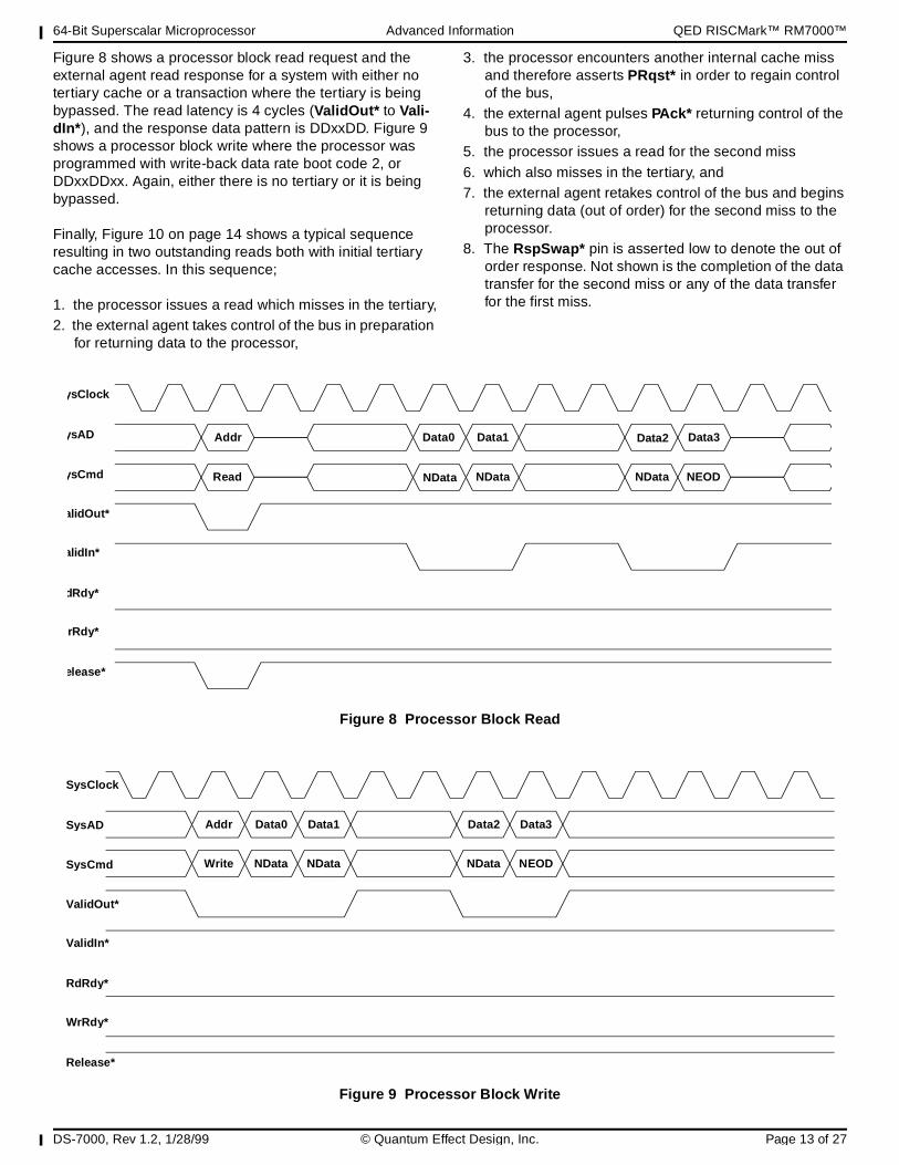
Figure 8 shows a processor block read request and the external agent read response for a system with either no tertiary cache or a transaction where the tertiary is being bypassed. The read latency is 4 cycles (ValidOut* to Vali-dIn* ), and the response data pattern is DDxxDD. Figure 9 shows a processor block write where the processor was programmed with write-back data rate boot code 2, or DDxxDDxx. Again, either there is no tertiary or it is being bypassed.
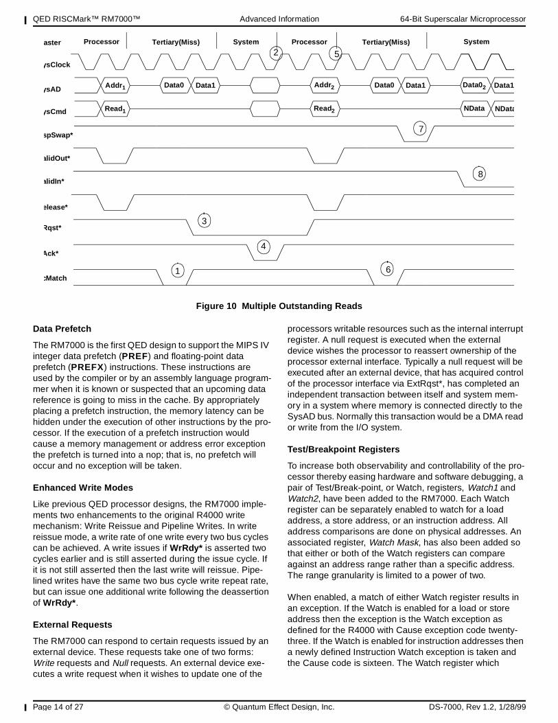
Finally, Figure 10 on page 14 shows a typical sequence resulting in two outstanding reads both with initial tertiary cache accesses. In this sequence;
1. the processor issues a read which misses in the tertiary,2. the external agent takes control of the bus in preparation
for returning data to the processor,
3. the processor encounters another internal cache miss and therefore asserts PRqst* in order to regain control of the bus,
4. the external agent pulses PAck* returning control of the bus to the processor,
5. the processor issues a read for the second miss6. which also misses in the tertiary, and7. the external agent retakes control of the bus and begins
returning data (out of order) for the second miss to the processor.
8. The RspSwap* pin is asserted low to denote the out of order response. Not shown is the completion of the data transfer for the second miss or any of the data transfer for the first miss.
Figure 8 Processor Block Read
Figure 9 Processor Block Write
ysClock
ysAD Addr Data0 Data1 Data2 Data3
ysCmd Read NData NData NData NEOD
alidOut*
alidIn*
dRdy*
rRdy*
elease*
SysClock
SysAD Addr Data0 Data1 Data2 Data3
SysCmd
ValidOut*
ValidIn*
RdRdy*
WrRdy*
Release*
Write NData NData NData NEOD
QED RISCMark™ RM7000™ Advanced Information 64-Bit Superscalar Microprocessor
Page 14 of 27 © Quantum Effect Design, Inc. DS-7000, Rev 1.2, 1/28/99
Data Prefetch
The RM7000 is the first QED design to support the MIPS IV integer data prefetch (PREF) and floating-point data prefetch (PREFX) instructions. These instructions are used by the compiler or by an assembly language program-mer when it is known or suspected that an upcoming data reference is going to miss in the cache. By appropriately placing a prefetch instruction, the memory latency can be hidden under the execution of other instructions by the pro-cessor. If the execution of a prefetch instruction would cause a memory management or address error exception the prefetch is turned into a nop; that is, no prefetch will occur and no exception will be taken.
Enhanced Write Modes
Like previous QED processor designs, the RM7000 imple-ments two enhancements to the original R4000 write mechanism: Write Reissue and Pipeline Writes. In write reissue mode, a write rate of one write every two bus cycles can be achieved. A write issues if WrRdy* is asserted two cycles earlier and is still asserted during the issue cycle. If it is not still asserted then the last write will reissue. Pipe-lined writes have the same two bus cycle write repeat rate, but can issue one additional write following the deassertion of WrRdy* .
External Requests
The RM7000 can respond to certain requests issued by an external device. These requests take one of two forms: Write requests and Null requests. An external device exe-cutes a write request when it wishes to update one of the
processors writable resources such as the internal interrupt register. A null request is executed when the external device wishes the processor to reassert ownership of the processor external interface. Typically a null request will be executed after an external device, that has acquired control of the processor interface via ExtRqst*, has completed an independent transaction between itself and system mem-ory in a system where memory is connected directly to the SysAD bus. Normally this transaction would be a DMA read or write from the I/O system.
Test/Breakpoint Registers
To increase both observability and controllability of the pro-cessor thereby easing hardware and software debugging, a pair of Test/Break-point, or Watch, registers, Watch1 and Watch2, have been added to the RM7000. Each Watch register can be separately enabled to watch for a load address, a store address, or an instruction address. All address comparisons are done on physical addresses. An associated register, Watch Mask, has also been added so that either or both of the Watch registers can compare against an address range rather than a specific address. The range granularity is limited to a power of two.
When enabled, a match of either Watch register results in an exception. If the Watch is enabled for a load or store address then the exception is the Watch exception as defined for the R4000 with Cause exception code twenty-three. If the Watch is enabled for instruction addresses then a newly defined Instruction Watch exception is taken and the Cause code is sixteen. The Watch register which
Figure 10 Multiple Outstanding Reads
Rqst*
Ack*
elease*
cMatch
ysClock
ysAD
ysCmd
alidOut*
alidIn*
Addr 1 Data1 Data1
Read1
Data0 Addr 2 Data0 Data02
Read2 NData
aster Processor Tertiar y(Miss) Tertiar y(Miss)Processor
Data12
NData
System System
spSwap*
1
2
3
4
5
6
7
8
64-Bit Superscalar Microprocessor Advanced Information QED RISCMark™ RM7000™
DS-7000, Rev 1.2, 1/28/99 © Quantum Effect Design, Inc. Page 15 of 27
caused the exception is indicated by Cause bits 25..24. Table 9 summarizes Watch operation.
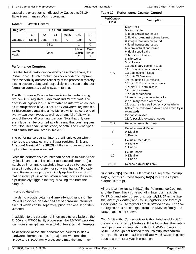
Performance Counters
Like the Test/Break-point capability described above, the Performance Counter feature has been added to improve the observability and controllability of the processor thereby easing system debug and, especially in the case of the per-formance counters, easing system tuning.
The Performance Counter feature is implemented using two new CP0 registers, PerfCount and PerfControl. The PerfCount register is a 32-bit writable counter which causes an interrupt when bit 31 is set. The PerfControl register is a 32-bit register containing a five bit field which selects one of twenty-two event types as well as a handful of bits which control the overall counting function. Note that only one event type can be counted at a time and that counting can occur for user code, kernel code, or both. The event types and control bits are listed in Table 10.
The performance counter interrupt will only occur when interrupts are enabled in the Status register, IE=1, and Interrupt Mask bit 13 (IM[13] ) of the coprocessor 0 inter-rupt control register is not set
Since the performance counter can be set up to count clock cycles, it can be used as either a) a second timer or b) a watchdog interrupt. A watchdog interrupt can be used as an aid in debugging system or software “hangs.” Typically the software is setup to periodically update the count so that no interrupt will occur. When a hang occurs the inter-rupt ultimately triggers thereby breaking free from the hang-up.
Interrupt Handling
In order to provide better real time interrupt handling, the RM7000 provides an extended set of hardware interrupts each of which can be separately prioritized and separately vectored.
In addition to the six external interrupt pins available on the R4000 and R5000 family processors, the RM7000 provides four more interrupt pins for a total of ten external interrupts.
As described above, the performance counter is also a hardware interrupt source, Int[13]. Also, whereas the R4000 and R5000 family processors map the timer inter-
rupt onto Int[5], the RM7000 provides a separate interrupt, Int[12] , for this purpose freeing Int[5] for use as a pure external interrupt.
All of these interrupts, Int[9..0], the Performance Counter, and the Timer, have corresponding interrupt mask bits, IM[13..0], and interrupt pending bits, IP[13..0] , in the Sta-tus, Interrupt Control, and Cause registers. The Interrupt Control and Cause registers are illustrated below. The Sta-tus register has not changed from the RM52xx family and R5000, and is not shown.
The IV bit in the Cause register is the global enable bit for the enhanced interrupt features. If this bit is clear then inter-rupt operation is compatible with the RM52xx family and R5000. Although not related to the interrupt mechanism, note that the W1 and W2 bits indicate which Watch register caused a particular Watch exception.
Table 9: Watch Control
Register Bit Field/Function
63 62 61 60:36 35:2 1:0
Watch1, 2 Store Load Instr 0 Addr 0
31:2 1 0
Watch Mask
MaskMask Watch
2
Mask Watch
1
Table 10: Performance Counter Control
PerfControlField
Description
4..0
Event Type0: clock cycles1: total instructions issued2: floating point instructions issued3: integer instructions issued4: load instructions issued5: store instructions issued6: dual issued pairs7: branch prefetches8: slip cycles9: stall cycles10: secondary cache misses11: instruction cache misses12: data cache misses13: data TLB misses14: instruction TLB misses15: joint TLB instruction misses16: joint TLB data misses17: branches taken18: branches issued19: secondary cache writebacks20: primary cache writebacks21: dcache miss stall cycles (cycles where both cache miss tokens taken and a third try is requested)22: cache misses23: fp possible exception cycles
7..5 Reserved (must be zero)
8Count in Kernel Mode0: Disable1: Enable
9Count in User Mode0: Disable1: Enable
10Count Enable0: Disable1: Enable
31..11 Reserved (must be zero)
QED RISCMark™ RM7000™ Advanced Information 64-Bit Superscalar Microprocessor
Page 16 of 27 © Quantum Effect Design, Inc. DS-7000, Rev 1.2, 1/28/99
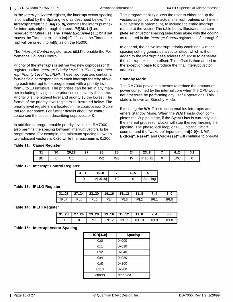
In the Interrupt Control register, the interrupt vector spacing is controlled by the Spacing field as described below. The Interrupt Mask field (IM[15..8]) contains the interrupt mask for interrupts eight through thirteen. IM[15..14] are reserved for future use. The Timer Exclusive (TE) bit if set moves the Timer interrupt to Int[12]. If clear, the Timer inter-rupt will be or’ed into Int[5] as on the R5000.
The Interrupt Control register uses IM13 to enable the Per-formance Counter Control.
Priority of the interrupts is set via two new coprocessor 0 registers called Interrupt Priority Level Lo, IPLLO, and Inter-rupt Priority Level Hi, IPLHI. These two registers contain a four-bit field corresponding to each interrupt thereby allow-ing each interrupt to be programmed with a priority level from 0 to 13 inclusive. The priorities can be set in any man-ner including having all the priorities set exactly the same. Priority 0 is the highest level and priority 15 the lowest. The format of the priority level registers is illustrated below. The priority level registers are located in the coprocessor 0 con-trol register space. For further details about the control space see the section describing coprocessor 0.
In addition to programmable priority levels, the RM7000 also permits the spacing between interrupt vectors to be programmed. For example, the minimum spacing between two adjacent vectors is 0x20 while the maximum is 0x200.
This programmability allows the user to either set up the vectors as jumps to the actual interrupt routines or, if inter-rupt latency is paramount, to include the entire interrupt routine at the vector. The table below illustrates the com-plete set of vector spacing selections along with the coding as required in the Interrupt Control register bits 3 through 0.
In general, the active interrupt priority combined with the spacing setting generates a vector offset which is then added to the interrupt base address of 0x200 to generate the interrupt exception offset. This offset is then added to the exception base to produce the final interrupt vector address.
Standby Mode
The RM7000 provides a means to reduce the amount of power consumed by the internal core when the CPU would not otherwise be performing any useful operations. This state is known as Standby Mode.
Executing the WAIT instruction enables interrupts and enters Standby Mode. When the WAIT instruction com-pletes the W pipe stage, if the SysAD bus is currently idle, the internal processor clocks will stop thereby freezing the pipeline. The phase lock loop, or PLL, internal timer/counter, and the “wake up” input pins: Int[9:0]* , NMI*, ExtReq* , Reset* , and ColdReset* will continue to operate
Table 11: Cause Register
Table 12: Interrupt Control Register
Table 13: IPLLO Register
Table 14: IPLHI Register
Table 15: Interrupt Vector Spacing
31 30 29,28 27 26 25 24 23..8 7 6..2 0,1
BD 0 CE 0 W2 W1 IV IP[15..0] 0 EXC 0
31..16 15..8 7 6..5 4..0
0 IM[15..8] TE 0 Spacing
31..28 27..24 23..20 19..16 15..12 11..8 7..4 3..0
IPL7 IPL6 IPL5 IPL4 IPL3 IPL2 IPL1 IPL0
31..28 27..24 23..20 19..16 15..12 11..8 7..4 3..0
0 0 IPL13 IPL12 IPL11 IPL10 IPL9 IPL8
ICR[4..0] Spacing
0x0 0x000
0x1 0x020
0x2 0x040
0x4 0x080
0x8 0x100
0x10 0x200
others reserved
64-Bit Superscalar Microprocessor Advanced Information QED RISCMark™ RM7000™
DS-7000, Rev 1.2, 1/28/99 © Quantum Effect Design, Inc. Page 17 of 27
in their normal fashion. If the SysAD bus is not idle when the WAIT instruction completes the W pipe stage, then the WAIT is treated as a NOP. Once the processor is in Standby, any interrupt, including the internally generated timer interrupt, will cause the processor to exit Standby and resume operation where it left off. The WAIT instruction is typically inserted in the idle loop of the operating system or real time executive.
JTAG Interface
The RM7000 interface supports JTAG boundary scan in conformance with IEEE 1149.1. The JTAG interface is especially helpful for checking the integrity of the proces-sor’s pin connections.
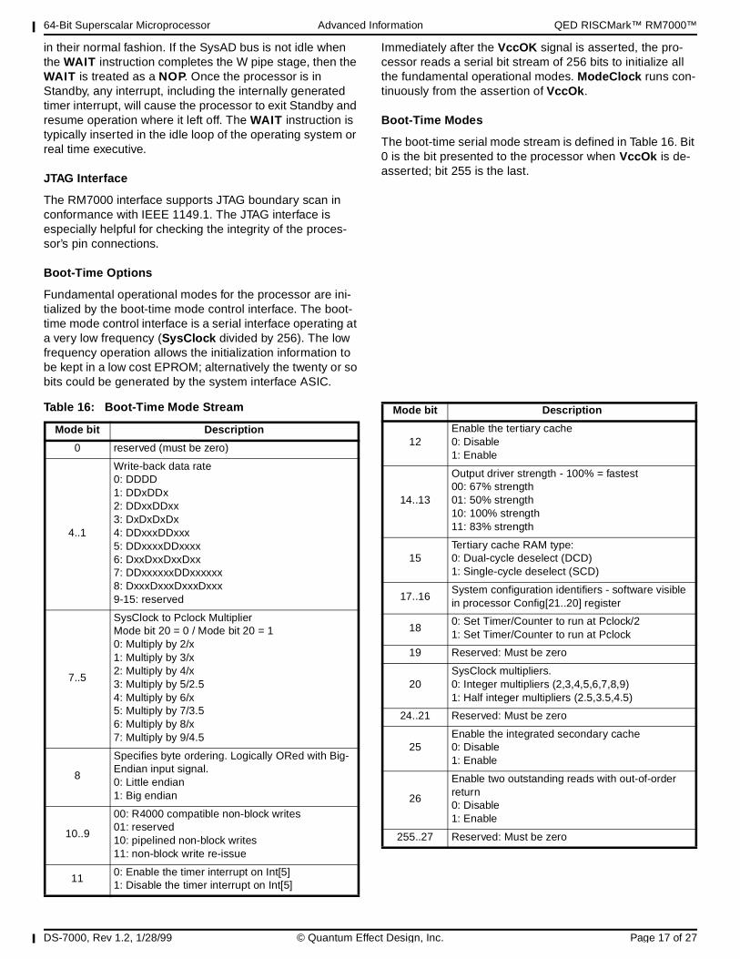
Boot-Time Options
Fundamental operational modes for the processor are ini-tialized by the boot-time mode control interface. The boot-time mode control interface is a serial interface operating at a very low frequency (SysClock divided by 256). The low frequency operation allows the initialization information to be kept in a low cost EPROM; alternatively the twenty or so bits could be generated by the system interface ASIC.
Immediately after the VccOK signal is asserted, the pro-cessor reads a serial bit stream of 256 bits to initialize all the fundamental operational modes. ModeClock runs con-tinuously from the assertion of VccOk .
Boot-Time Modes
The boot-time serial mode stream is defined in Table 16. Bit 0 is the bit presented to the processor when VccOk is de-asserted; bit 255 is the last.
Table 16: Boot-Time Mode Stream
Mode bit Description
0 reserved (must be zero)
4..1
Write-back data rate0: DDDD1: DDxDDx2: DDxxDDxx3: DxDxDxDx4: DDxxxDDxxx5: DDxxxxDDxxxx6: DxxDxxDxxDxx7: DDxxxxxxDDxxxxxx8: DxxxDxxxDxxxDxxx9-15: reserved
7..5
SysClock to Pclock MultiplierMode bit 20 = 0 / Mode bit 20 = 10: Multiply by 2/x1: Multiply by 3/x2: Multiply by 4/x3: Multiply by 5/2.54: Multiply by 6/x5: Multiply by 7/3.56: Multiply by 8/x7: Multiply by 9/4.5
8
Specifies byte ordering. Logically ORed with Big-Endian input signal.0: Little endian1: Big endian
10..9
00: R4000 compatible non-block writes01: reserved10: pipelined non-block writes11: non-block write re-issue
110: Enable the timer interrupt on Int[5]1: Disable the timer interrupt on Int[5]
12Enable the tertiary cache0: Disable1: Enable
14..13
Output driver strength - 100% = fastest00: 67% strength01: 50% strength10: 100% strength11: 83% strength
15Tertiary cache RAM type:0: Dual-cycle deselect (DCD)1: Single-cycle deselect (SCD)
17..16System configuration identifiers - software visible in processor Config[21..20] register
180: Set Timer/Counter to run at Pclock/21: Set Timer/Counter to run at Pclock
19 Reserved: Must be zero
20SysClock multipliers.0: Integer multipliers (2,3,4,5,6,7,8,9)1: Half integer multipliers (2.5,3.5,4.5)
24..21 Reserved: Must be zero
25Enable the integrated secondary cache0: Disable1: Enable
26
Enable two outstanding reads with out-of-order return0: Disable1: Enable
255..27 Reserved: Must be zero
Mode bit Description
64-Bit Superscalar Microprocessor Advanced Information QED RISCMark™ RM7000™
DS-7000, Rev 1.2, 1/28/99 © Quantum Effect Design, Inc. Page 18 of 27
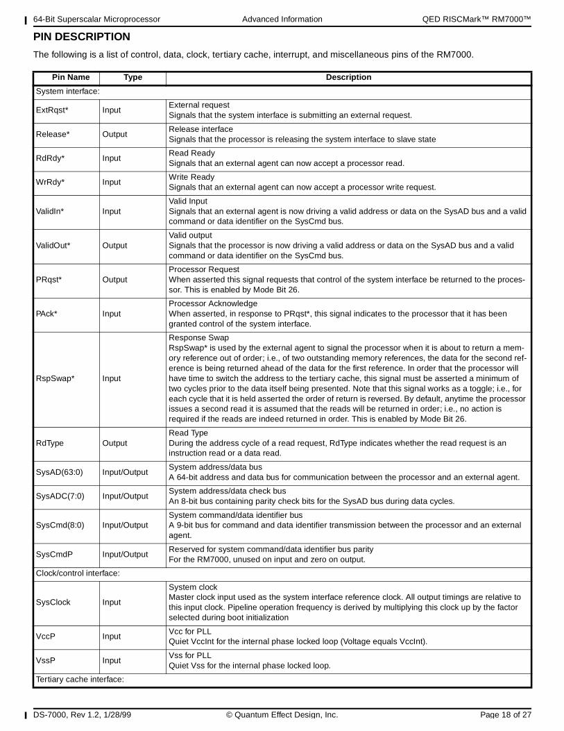
PIN DESCRIPTION
The following is a list of control, data, clock, tertiary cache, interrupt, and miscellaneous pins of the RM7000.
Pin Name Type Description
System interface:
ExtRqst* InputExternal requestSignals that the system interface is submitting an external request.
Release* OutputRelease interfaceSignals that the processor is releasing the system interface to slave state
RdRdy* InputRead ReadySignals that an external agent can now accept a processor read.
WrRdy* InputWrite ReadySignals that an external agent can now accept a processor write request.
ValidIn* InputValid InputSignals that an external agent is now driving a valid address or data on the SysAD bus and a valid command or data identifier on the SysCmd bus.
ValidOut* OutputValid outputSignals that the processor is now driving a valid address or data on the SysAD bus and a valid command or data identifier on the SysCmd bus.
PRqst* OutputProcessor RequestWhen asserted this signal requests that control of the system interface be returned to the proces-sor. This is enabled by Mode Bit 26.
PAck* InputProcessor AcknowledgeWhen asserted, in response to PRqst*, this signal indicates to the processor that it has been granted control of the system interface.
RspSwap* Input
Response SwapRspSwap* is used by the external agent to signal the processor when it is about to return a mem-ory reference out of order; i.e., of two outstanding memory references, the data for the second ref-erence is being returned ahead of the data for the first reference. In order that the processor will have time to switch the address to the tertiary cache, this signal must be asserted a minimum of two cycles prior to the data itself being presented. Note that this signal works as a toggle; i.e., for each cycle that it is held asserted the order of return is reversed. By default, anytime the processor issues a second read it is assumed that the reads will be returned in order; i.e., no action is required if the reads are indeed returned in order. This is enabled by Mode Bit 26.
RdType OutputRead TypeDuring the address cycle of a read request, RdType indicates whether the read request is an instruction read or a data read.
SysAD(63:0) Input/OutputSystem address/data busA 64-bit address and data bus for communication between the processor and an external agent.
SysADC(7:0) Input/OutputSystem address/data check busAn 8-bit bus containing parity check bits for the SysAD bus during data cycles.
SysCmd(8:0) Input/OutputSystem command/data identifier busA 9-bit bus for command and data identifier transmission between the processor and an external agent.
SysCmdP Input/OutputReserved for system command/data identifier bus parityFor the RM7000, unused on input and zero on output.
Clock/control interface:
SysClock Input
System clockMaster clock input used as the system interface reference clock. All output timings are relative to this input clock. Pipeline operation frequency is derived by multiplying this clock up by the factor selected during boot initialization
VccP InputVcc for PLLQuiet VccInt for the internal phase locked loop (Voltage equals VccInt).
VssP InputVss for PLLQuiet Vss for the internal phase locked loop.
Tertiary cache interface:
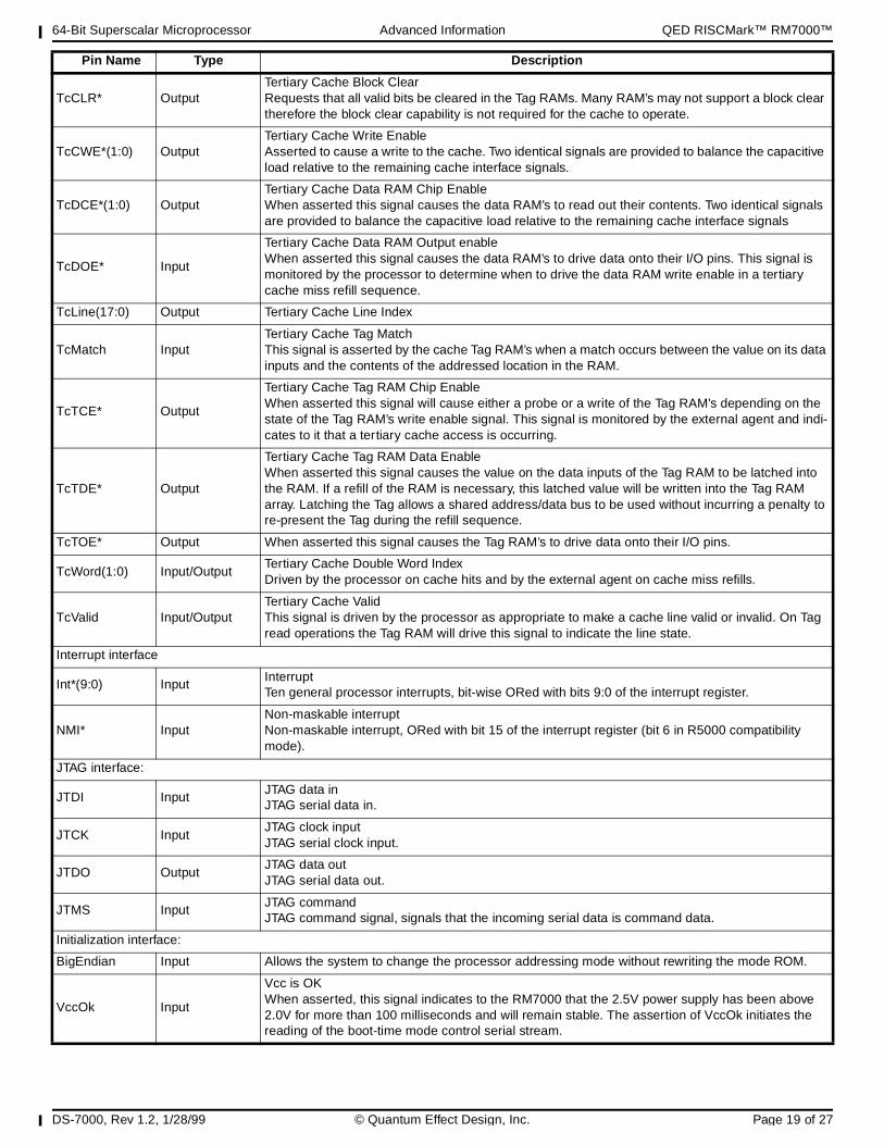
64-Bit Superscalar Microprocessor Advanced Information QED RISCMark™ RM7000™
DS-7000, Rev 1.2, 1/28/99 © Quantum Effect Design, Inc. Page 19 of 27
TcCLR* OutputTertiary Cache Block ClearRequests that all valid bits be cleared in the Tag RAMs. Many RAM’s may not support a block clear therefore the block clear capability is not required for the cache to operate.
TcCWE*(1:0) OutputTertiary Cache Write EnableAsserted to cause a write to the cache. Two identical signals are provided to balance the capacitive load relative to the remaining cache interface signals.
TcDCE*(1:0) OutputTertiary Cache Data RAM Chip EnableWhen asserted this signal causes the data RAM’s to read out their contents. Two identical signals are provided to balance the capacitive load relative to the remaining cache interface signals
TcDOE* Input
Tertiary Cache Data RAM Output enableWhen asserted this signal causes the data RAM’s to drive data onto their I/O pins. This signal is monitored by the processor to determine when to drive the data RAM write enable in a tertiary cache miss refill sequence.
TcLine(17:0) Output Tertiary Cache Line Index
TcMatch InputTertiary Cache Tag MatchThis signal is asserted by the cache Tag RAM’s when a match occurs between the value on its data inputs and the contents of the addressed location in the RAM.
TcTCE* Output
Tertiary Cache Tag RAM Chip EnableWhen asserted this signal will cause either a probe or a write of the Tag RAM’s depending on the state of the Tag RAM’s write enable signal. This signal is monitored by the external agent and indi-cates to it that a tertiary cache access is occurring.
TcTDE* Output
Tertiary Cache Tag RAM Data EnableWhen asserted this signal causes the value on the data inputs of the Tag RAM to be latched into the RAM. If a refill of the RAM is necessary, this latched value will be written into the Tag RAM array. Latching the Tag allows a shared address/data bus to be used without incurring a penalty to re-present the Tag during the refill sequence.
TcTOE* Output When asserted this signal causes the Tag RAM’s to drive data onto their I/O pins.
TcWord(1:0) Input/OutputTertiary Cache Double Word IndexDriven by the processor on cache hits and by the external agent on cache miss refills.
TcValid Input/OutputTertiary Cache ValidThis signal is driven by the processor as appropriate to make a cache line valid or invalid. On Tag read operations the Tag RAM will drive this signal to indicate the line state.
Interrupt interface
Int*(9:0) InputInterruptTen general processor interrupts, bit-wise ORed with bits 9:0 of the interrupt register.
NMI* InputNon-maskable interruptNon-maskable interrupt, ORed with bit 15 of the interrupt register (bit 6 in R5000 compatibility mode).
JTAG interface:
JTDI InputJTAG data inJTAG serial data in.
JTCK InputJTAG clock inputJTAG serial clock input.
JTDO OutputJTAG data outJTAG serial data out.
JTMS InputJTAG commandJTAG command signal, signals that the incoming serial data is command data.
Initialization interface:
BigEndian Input Allows the system to change the processor addressing mode without rewriting the mode ROM.
VccOk Input
Vcc is OKWhen asserted, this signal indicates to the RM7000 that the 2.5V power supply has been above 2.0V for more than 100 milliseconds and will remain stable. The assertion of VccOk initiates the reading of the boot-time mode control serial stream.
Pin Name Type Description
64-Bit Superscalar Microprocessor Advanced Information QED RISCMark™ RM7000™
DS-7000, Rev 1.2, 1/28/99 © Quantum Effect Design, Inc. Page 20 of 27
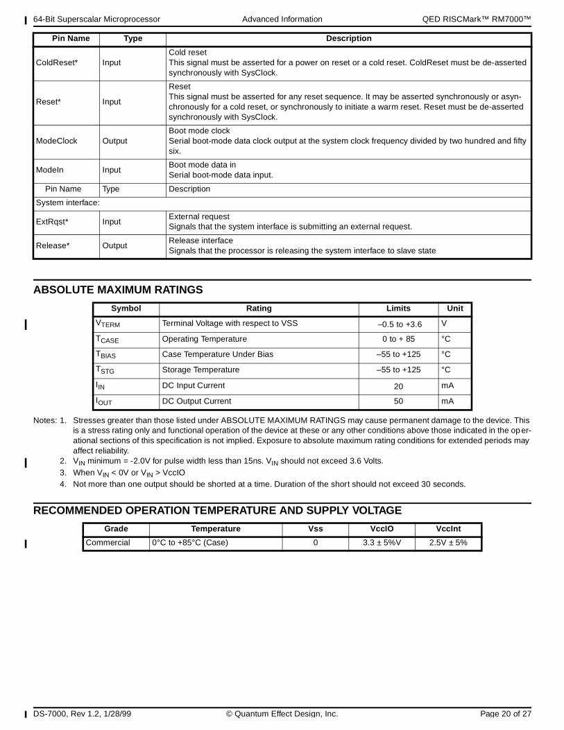
ABSOLUTE MAXIMUM RATINGS
Notes: 1. Stresses greater than those listed under ABSOLUTE MAXIMUM RATINGS may cause permanent damage to the device. This is a stress rating only and functional operation of the device at these or any other conditions above those indicated in the oper-ational sections of this specification is not implied. Exposure to absolute maximum rating conditions for extended periods may affect reliability.
2. VIN minimum = -2.0V for pulse width less than 15ns. VIN should not exceed 3.6 Volts.3. When VIN < 0V or VIN > VccIO4. Not more than one output should be shorted at a time. Duration of the short should not exceed 30 seconds.
RECOMMENDED OPERATION TEMPERATURE AND SUPPLY VOLTAGE
ColdReset* InputCold resetThis signal must be asserted for a power on reset or a cold reset. ColdReset must be de-asserted synchronously with SysClock.
Reset* Input
ResetThis signal must be asserted for any reset sequence. It may be asserted synchronously or asyn-chronously for a cold reset, or synchronously to initiate a warm reset. Reset must be de-asserted synchronously with SysClock.
ModeClock OutputBoot mode clockSerial boot-mode data clock output at the system clock frequency divided by two hundred and fifty six.
ModeIn InputBoot mode data inSerial boot-mode data input.
Pin Name Type Description
System interface:
ExtRqst* InputExternal requestSignals that the system interface is submitting an external request.
Release* OutputRelease interfaceSignals that the processor is releasing the system interface to slave state
Symbol Rating Limits Unit
VTERM Terminal Voltage with respect to VSS –0.5 to +3.6 V
TCASE Operating Temperature 0 to + 85 °C
TBIAS Case Temperature Under Bias –55 to +125 °C
TSTG Storage Temperature –55 to +125 °C
IIN DC Input Current 20 mA
IOUT DC Output Current 50 mA
Grade Temperature Vss VccIO VccInt
Commercial 0°C to +85°C (Case) 0 3.3 ± 5%V 2.5V ± 5%
Pin Name Type Description
64-Bit Superscalar Microprocessor Advanced Information QED RISCMark™ RM7000™
DS-7000, Rev 1.2, 1/28/99 © Quantum Effect Design, Inc. Page 21 of 27
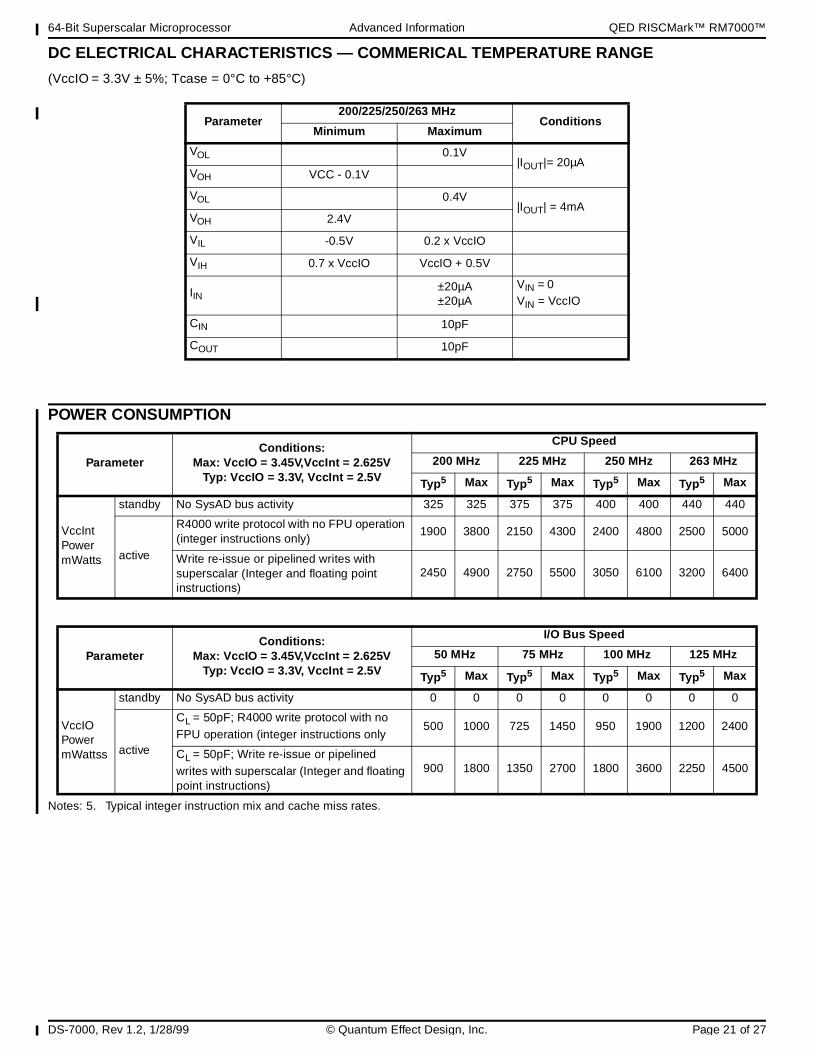
DC ELECTRICAL CHARACTERISTICS — COMMERICAL TEMPERATURE RANGE
(VccIO = 3.3V ± 5%; Tcase = 0°C to +85°C)
POWER CONSUMPTION
Notes: 5. Typical integer instruction mix and cache miss rates.
Parameter200/225/250/263 MHz
ConditionsMinimum Maximum
VOL 0.1V|IOUT|= 20µA
VOH VCC - 0.1V
VOL 0.4V|IOUT| = 4mA
VOH 2.4V
VIL -0.5V 0.2 x VccIO
VIH 0.7 x VccIO VccIO + 0.5V
IIN±20µA±20µA
VIN = 0VIN = VccIO
CIN 10pF
COUT 10pF
ParameterConditions:
Max: VccIO = 3.45V,VccInt = 2.625VTyp: VccIO = 3.3V, VccInt = 2.5V
CPU Speed
200 MHz 225 MHz 250 MHz 263 MHz
Typ5 Max Typ5 Max Typ5 Max Typ5 Max
VccInt Power mWatts
standby No SysAD bus activity 325 325 375 375 400 400 440 440
active
R4000 write protocol with no FPU operation (integer instructions only)
1900 3800 2150 4300 2400 4800 2500 5000
Write re-issue or pipelined writes with superscalar (Integer and floating point instructions)
2450 4900 2750 5500 3050 6100 3200 6400
ParameterConditions:
Max: VccIO = 3.45V,VccInt = 2.625VTyp: VccIO = 3.3V, VccInt = 2.5V
I/O Bus Speed
50 MHz 75 MHz 100 MHz 125 MHz
Typ5 Max Typ5 Max Typ5 Max Typ5 Max
VccIO Power mWattss
standby No SysAD bus activity 0 0 0 0 0 0 0 0
active
CL = 50pF; R4000 write protocol with no FPU operation (integer instructions only
500 1000 725 1450 950 1900 1200 2400
CL = 50pF; Write re-issue or pipelined writes with superscalar (Integer and floating point instructions)
900 1800 1350 2700 1800 3600 2250 4500
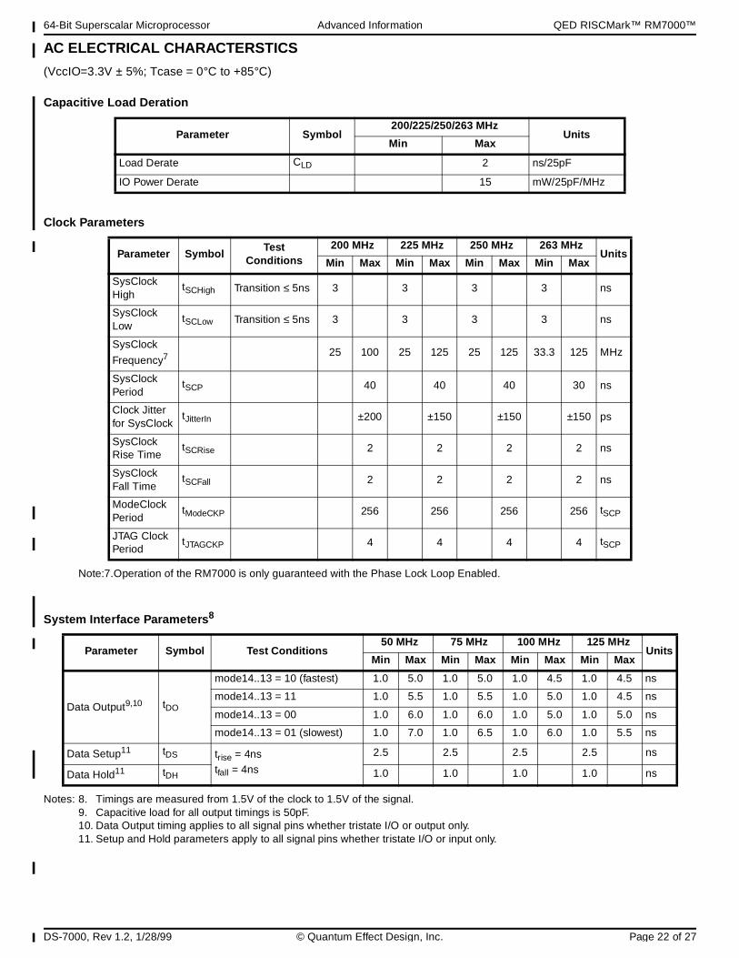
64-Bit Superscalar Microprocessor Advanced Information QED RISCMark™ RM7000™
DS-7000, Rev 1.2, 1/28/99 © Quantum Effect Design, Inc. Page 22 of 27
AC ELECTRICAL CHARACTERSTICS
(VccIO=3.3V ± 5%; Tcase = 0°C to +85°C)
Capacitive Load Deration
Clock Parameters
Note:7.Operation of the RM7000 is only guaranteed with the Phase Lock Loop Enabled.
System Interface Parameters 8
Notes: 8. Timings are measured from 1.5V of the clock to 1.5V of the signal.9. Capacitive load for all output timings is 50pF.10. Data Output timing applies to all signal pins whether tristate I/O or output only.11. Setup and Hold parameters apply to all signal pins whether tristate I/O or input only.
Parameter Symbol 200/225/250/263 MHz
UnitsMin Max
Load Derate CLD 2 ns/25pF
IO Power Derate 15 mW/25pF/MHz
Parameter SymbolTest
Conditions200 MHz 225 MHz 250 MHz 263 MHz
UnitsMin Max Min Max Min Max Min Max
SysClock High
tSCHigh Transition ≤ 5ns 3 3 3 3 ns
SysClock Low
tSCLow Transition ≤ 5ns 3 3 3 3 ns
SysClock
Frequency7 25 100 25 125 25 125 33.3 125 MHz
SysClock Period
tSCP 40 40 40 30 ns
Clock Jitter for SysClock
tJitterIn ±200 ±150 ±150 ±150 ps
SysClock Rise Time
tSCRise 2 2 2 2 ns
SysClock Fall Time
tSCFall 2 2 2 2 ns
ModeClock Period
tModeCKP 256 256 256 256 tSCP
JTAG Clock Period
tJTAGCKP 4 4 4 4 tSCP
Parameter Symbol Test Conditions 50 MHz 75 MHz 100 MHz 125 MHz
UnitsMin Max Min Max Min Max Min Max
Data Output9,10 tDO
mode14..13 = 10 (fastest) 1.0 5.0 1.0 5.0 1.0 4.5 1.0 4.5 ns
mode14..13 = 11 1.0 5.5 1.0 5.5 1.0 5.0 1.0 4.5 ns
mode14..13 = 00 1.0 6.0 1.0 6.0 1.0 5.0 1.0 5.0 ns
mode14..13 = 01 (slowest) 1.0 7.0 1.0 6.5 1.0 6.0 1.0 5.5 ns
Data Setup11 tDS trise = 4nstfall = 4ns
2.5 2.5 2.5 2.5 ns
Data Hold11 tDH 1.0 1.0 1.0 1.0 ns
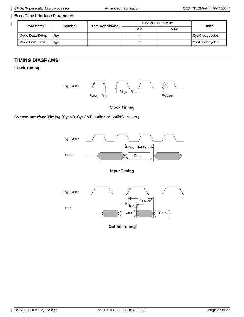
64-Bit Superscalar Microprocessor Advanced Information QED RISCMark™ RM7000™
DS-7000, Rev 1.2, 1/28/99 © Quantum Effect Design, Inc. Page 23 of 27
Boot-Time Interface Parameters
TIMING DIAGRAMS
Clock Timing
Clock Timing
System Interface Timing (SysAD, SysCMD, ValindIn*, ValidOut*, etc.)
Input Timing
Output Timing
Parameter Symbol Test Conditions 50/75/100/125 MHz
UnitsMin Max
Mode Data Setup tDS 4 SysClock cycles
Mode Data Hold tDH 0 SysClock cycles
SysClock
tRise tFall
tHigh tLow±tJitterIn
tDS tDH
Data
SysClock
Data
tDOmin
tDOmax
SysClock
DataDataData
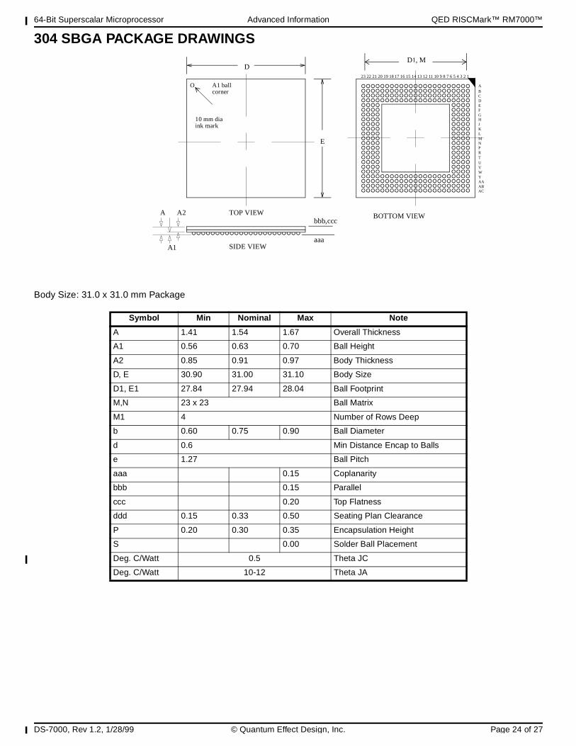
64-Bit Superscalar Microprocessor Advanced Information QED RISCMark™ RM7000™
DS-7000, Rev 1.2, 1/28/99 © Quantum Effect Design, Inc. Page 24 of 27
304 SBGA PACKAGE DRAWINGS
Body Size: 31.0 x 31.0 mm Package
Symbol Min Nominal Max Note
A 1.41 1.54 1.67 Overall Thickness
A1 0.56 0.63 0.70 Ball Height
A2 0.85 0.91 0.97 Body Thickness
D, E 30.90 31.00 31.10 Body Size
D1, E1 27.84 27.94 28.04 Ball Footprint
M,N 23 x 23 Ball Matrix
M1 4 Number of Rows Deep
b 0.60 0.75 0.90 Ball Diameter
d 0.6 Min Distance Encap to Balls
e 1.27 Ball Pitch
aaa 0.15 Coplanarity
bbb 0.15 Parallel
ccc 0.20 Top Flatness
ddd 0.15 0.33 0.50 Seating Plan Clearance
P 0.20 0.30 0.35 Encapsulation Height
S 0.00 Solder Ball Placement
Deg. C/Watt 0.5 Theta JC
Deg. C/Watt 10-12 Theta JA
O
23 22 21 20 19 18 17 16 15 14 13 12 11 10 9 8 7 6 5 4 3 2 1
ABCDEFGHJKLMNPRTUVWYAAABAC
D1, MD
E
TOP VIEW BOTTOM VIEW
SIDE VIEW
O
10 mm diaink mark
A1 ballcorner
A
A1
A2bbb,ccc
aaa
64-Bit Superscalar Microprocessor Advanced Information QED RISCMark™ RM7000™
DS-7000, Rev 1.2, 1/28/99 © Quantum Effect Design, Inc. Page 25 of 27
RM7000 304 SBGA PACKAGE PINOUT:
Pin Function Pin Function Pin Function Pin Function
A1 VccIO A2 VssIO A3 VssIO A4 TcLine11
A5 Do Not Connect A6 VssIO A7 Do Not Connect A8 VssIO
A9 SysAD32 A10 SysADC1 A11 Do Not Connect A12 VssIO
A13 VccInt A14 VccInt A15 SysAD63 A16 VssIO
A17 SysAD61 A18 VssIO A19 Do Not Connect A20 TcLine4
A21 VssIO A22 VssIO A23 VccIO B1 VssInt
B2 VccIO B3 VssInt B4 VssIO B5 TcLine10
B6 SysAD35 B7 SysAD34 B8 VccInt B9 SysAD33
B10 SysADC5 B11 SysADC0 B12 Do Not Connect B13 SysADC7
B14 SysADC6 B15 Do Not Connect B16 SysAD30 B17 SysAD29
B18 SysAD28 B19 TcLine5 B20 VssIO B21 VssInt
B22 VccIO B23 VssIO C1 VssIO C2 VssInt
C3 VccIO C4 VccIO C5 Do Not Connect C6 TcLine9
C7 SysAD3 C8 SysAD2 C9 VccInt C10 SysAD0
C11 SysADC4 C12 VccInt C13 SysADC3 C14 SysADC2
C15 SysAD62 C16 VccInt C17 SysAD60 C18 TcLine6
C19 Do Not Connect C20 VccIO C21 VccIO C22 VssInt
C23 VssIO D1 TcLine13 D2 VssIO D3 VccIO
D4 VccIO D5 VccIO D6 VccIO D7 TcLine8
D8 VccInt D9 VccIO D10 SysAD1 D11 VccInt
D12 VccIO D13 VccInt D14 SysAD31 D15 VccIO
D16 VccInt D17 TcLine7 D18 VccIO D19 VccIO
D20 VccIO D21 VccIO D22 VssIO D23 Do Not Connect
E1 VccInt E2 TcLine14 E3 TcLine12 E4 VccIO
E20 VccIO E21 Do Not Connect E22 Do Not Connect E23 TcLine1
F1 VssIO F2 TcLine16 F3 TcLine15 F4 VccIO
F20 VccIO F21 TcLine3 F22 TcLine0 F23 VssIO
G1 SysAD36 G2 SysAD4 G3 TcLine17 G4 VccInt
G20 TcLine2 G21 VccInt G22 SysAD59 G23 SysAD58
H1 VssIO H2 SysAD37 H3 SysAD5 H4 Do Not Connect
H20 VccInt H21 SysAD27 H22 SysAD26 H23 VssIO
J1 SysAD7 J2 SysAD6 J3 VccInt J4 VccIO
J20 VccIO J21 VccInt J22 SysAD57 J23 SysAD56
K1 SysAD40 K2 SysAD8 K3 SysAD39 K4 SysAD38
K20 SysAD25 K21 SysAD24 K22 SysAD55 K23 SysAD23
L1 SysAD10 L2 SysAD41 L3 SysAD9 L4 VccInt
L20 VccInt L21 SysAD54 L22 SysAD22 L23 SysAD53
M1 VssIO M2 SysAD11 M3 SysAD42 M4 VccIO
M20 VccIO M21 SysAD52 M22 SysAD21 M23 VssIO
N1 SysAD43 N2 VccInt N3 SysAD12 N4 SysAD44
N20 SysAD19 N21 SysAD51 N22 VccInt N23 SysAD20
P1 SysAD13 P2 SysAD45 P3 SysAD14 P4 VccInt
P20 VccInt P21 SysAD49 P22 SysAD18 P23 SysAD50
R1 SysAD46 R2 SysAD15 R3 SysAD47 R4 VccIO
R20 VccIO R21 SysAD16 R22 SysAD48 R23 SysAD17
64-Bit Superscalar Microprocessor Advanced Information QED RISCMark™ RM7000™
DS-7000, Rev 1.2, 1/28/99 © Quantum Effect Design, Inc. Page 26 of 27
Note: The pins marked Do Not Connect are reserved for future use. Do not connect these pins to any singal or power planes.
T1 VssIO T2 RspSwap* T3 PRqst* T4 VccInt
T20 ExtRqst* T21 VccOK T22 BigEndian T23 VssIO
U1 PAck* U2 VccInt U3 ModeClock U4 JTCK
U20 VccInt U21 NMI* U22 Reset* U23 ColdReset*
V1 VssIO V2 JTDO V3 JTMS V4 VccIO
V20 VccIO V21 Int9* V22 VccInt V23 VssIO
W1 JTDI W2 VccIO W3 Do Not Connect W4 VccIO
W20 VccIO W21 Int6* W22 Int8* W23 VccInt
Y1 Do Not Connect Y2 VssIO Y3 VccIO Y4 VccIO
Y5 VccIO Y6 VccIO Y7 RdRdy* Y8 Release*
Y9 VccIO Y10 TcWord0 Y11 VccInt Y12 VccIO
Y13 SysCmd5 Y14 VccInt Y15 VccIO Y16 VccInt
Y17 Int2* Y18 VccIO Y19 VccIO Y20 VccIO
Y21 VccIO Y22 VssIO Y23 Int7* AA1 VssIO
AA2 VssInt AA3 VccIO AA4 VccIO AA5 Do Not Connect
AA6 TcMatch AA7 ValidOut* AA8 SysClock AA9 VccInt
AA10 Do Not Connect AA11 Do Not Connect AA12 SysCmd0 AA13 SysCmd4
AA14 SysCmd8 AA15 TcTCE* AA16 TcValid AA17 VccInt
AA18 Int3* AA19 Do Not Connect AA20 VccIO AA21 VccIO
AA22 VssInt AA23 VssIO AB1 VssIO AB2 VccIO
AB3 VssInt AB4 VssIO AB5 ModeIn AB6 ValidIn*
AB7 VccP AB8 VccInt AB9 VccInt AB10 TcCWE0*
AB11 TcDCE0* AB12 SysCmd1 AB13 SysCmd3 AB14 SysCmd7
AB15 TcClr* AB16 TcTDE* AB17 TcDOE* AB18 Int0*
AB19 Int4* AB20 VssIO AB21 VssInt AB22 VccIO
AB23 VssInt AC1 VccIO AC2 VssInt AC3 VssIO
AC4 RdType AC5 WrRdy* AC6 VssIO AC7 VssP
AC8 VssIO AC9 TcWord1 AC10 TcCWE1* AC11 TcDCE1*
AC12 VssIO AC13 SysCmd2 AC14 SysCmd6 AC15 SysCmdP
AC16 VssIO AC17 TcTOE* AC18 VssIO AC19 Int1*
AC20 Int5* AC21 VssIO AC22 VssIO AC23 VccIO
Pin Function Pin Function Pin Function Pin Function
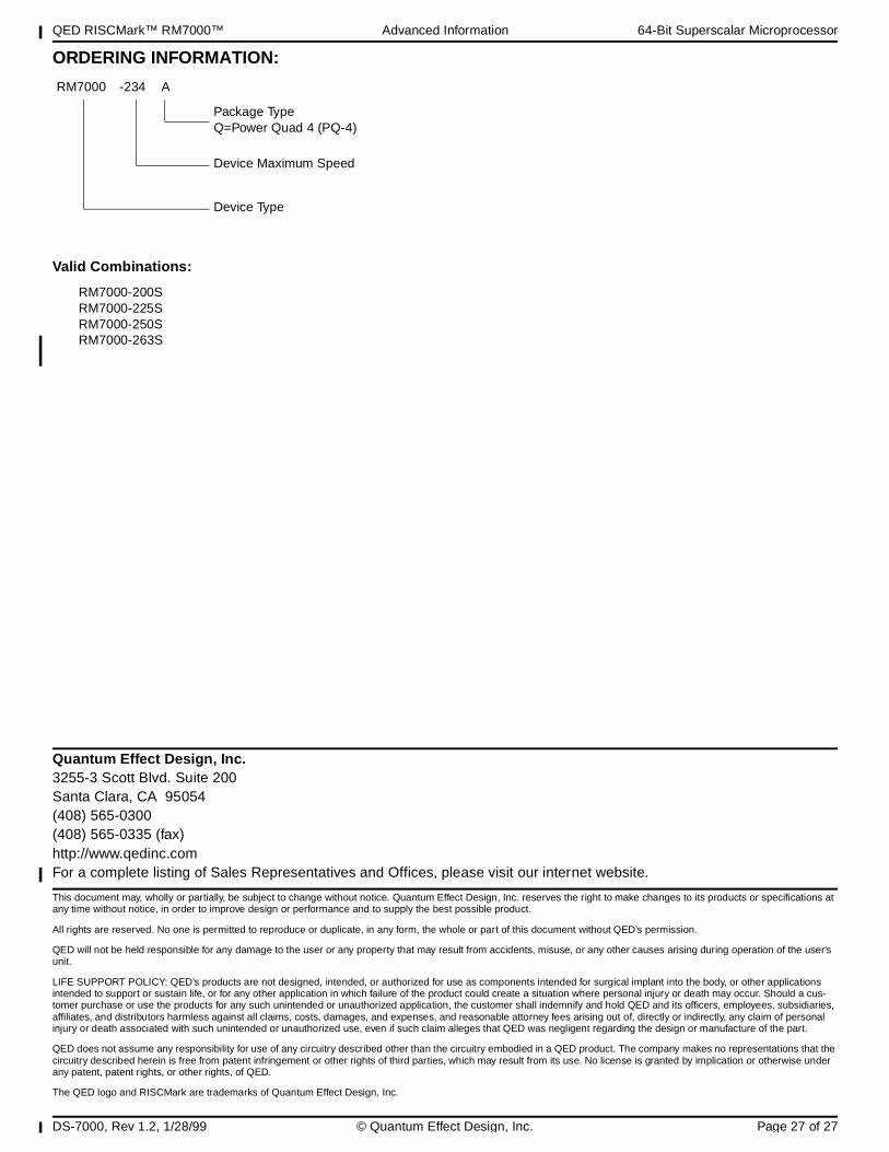
QED RISCMark™ RM7000™ Advanced Information 64-Bit Superscalar Microprocessor
DS-7000, Rev 1.2, 1/28/99 © Quantum Effect Design, Inc. Page 27 of 27
Quantum Effect Design, Inc.3255-3 Scott Blvd. Suite 200Santa Clara, CA 95054(408) 565-0300(408) 565-0335 (fax)http://www.qedinc.comFor a complete listing of Sales Representatives and Offices, please visit our internet website.
This document may, wholly or partially, be subject to change without notice. Quantum Effect Design, Inc. reserves the right to make changes to its products or specifications at any time without notice, in order to improve design or performance and to supply the best possible product.
All rights are reserved. No one is permitted to reproduce or duplicate, in any form, the whole or part of this document without QED’s permission.
QED will not be held responsible for any damage to the user or any property that may result from accidents, misuse, or any other causes arising during operation of the user’s unit.
LIFE SUPPORT POLICY: QED’s products are not designed, intended, or authorized for use as components intended for surgical implant into the body, or other applications intended to support or sustain life, or for any other application in which failure of the product could create a situation where personal injury or death may occur. Should a cus-tomer purchase or use the products for any such unintended or unauthorized application, the customer shall indemnify and hold QED and its officers, employees, subsidiaries, affiliates, and distributors harmless against all claims, costs, damages, and expenses, and reasonable attorney fees arising out of, directly or indirectly, any claim of personal injury or death associated with such unintended or unauthorized use, even if such claim alleges that QED was negligent regarding the design or manufacture of the part.
QED does not assume any responsibility for use of any circuitry described other than the circuitry embodied in a QED product. The company makes no representations that the circuitry described herein is free from patent infringement or other rights of third parties, which may result from its use. No license is granted by implication or otherwise under any patent, patent rights, or other rights, of QED.
The QED logo and RISCMark are trademarks of Quantum Effect Design, Inc.
ORDERING INFORMATION:
Valid Combinations:
RM7000-200SRM7000-225SRM7000-250SRM7000-263S
RM7000 -234 A
Package TypeQ=Power Quad 4 (PQ-4)
Device Maximum Speed
Device Type