Embed Size (px)
Citation preview
GDDR5X SGRAMMT58K256M321JA-100/-110/-120:A16 Meg x 32 I/O x 16 banks, 32 Meg x 16 I/O x 16 banks
Features• VDD = VDDQ = 1.35V ±3%• VPP = 1.8V -3%/+6%• Data rate: 12.0 Gb/s, 11.0 Gb/s, 10.0 Gb/s• Single ended interface for command, address and
data• Differential clock input CK_t/CK_c for ADD/CMD• Two differential clock inputs WCK_t/WCK_c, each
associated with two data bytes (DQ, DBI_n, EDC)• Single data rate (SDR) commands (CK)• Double data rate (DDR) addresses (CK)• QDR and DDR operating modes:
– QDR mode: Quad data rate (QDR) data (WCK);16n prefetch architecture with 512bit per arrayread or write access; burst length 16
– DDR mode: Double data rate (DDR) data (WCK);8n prefetch architecture with 256bit per arrayread or write access; burst length 8
• 16 internal banks• 4 bank groups for tCCDL = 3 tCK and 4 tCK• Programmable READ latency: 9 to 20• Programmable WRITE latency: 5 to 7• Write data mask function via address bus (single/
double/quad byte mask)• Data bus inversion (DBI) and address bus inversion
(ABI)• Input/output PLL• Address training: Address input monitoring via DQ/
DBI_n/EDC pins• WCK2CK clock training with phase information via
EDC pins• Data read and write training via read FIFO (depth =
6)• Read FIFO pattern preload by LDFF command• Write data load to read FIFO via WRTR command• Consecutive read of read FIFO via RDTR command• Read/write EDC on/off mode• Programmable EDC hold pattern for CDR• Read/write data transmission integrity secured by
cyclic redundancy check (CRC‐8)• Programmable CRC READ latency = 2 to 3• Programmable CRC WRITE latency = 9 to 14
• Low power modes• RDQS mode on EDC pins• On‐chip temperature sensor with read‐out• Auto precharge option for each burst access• Auto refresh mode with per-bank refresh option• Temperature sensor controlled self refresh rate• Digital tRAS lockout• On‐die termination (ODT) for all high‐speed inputs• Pseudo open drain (POD‐135) compatible outputs• ODT and output driver strength auto‐calibration
with external resistor ZQ pin (120 Ω)• Programmable termination and driver strength off-
sets• Internal VREF for data inputs• Selectable external or internal VREF for ADD/CMD
inputs• Data input receiver characteristics programmable
per byte• Vendor ID for device identification• Mirror function with MF pin• IEEE 1149.1 compliant boundary scan• 190 ball BGA package• Lead-free (RoHS-compliant) and halogen-free
packaging• TC = 0°C to +95°C
Options1 Marking• Organization
– 256 Meg x 32 (words x bits) 256M321• FBGA package
– 190-ball (10mm x 14mm) JA• Timing – maximum data rate
– 12.0 Gb/s -120– 11.0 Gb/s -110– 10.0 Gb/s -100
• Operating temperature – Commercial (0°C ≤ TC ≤ +95°C) None
• Revision A
Note: 1. Not all options listed can be combined todefine an offered product. Use the partcatalog search on http://www.micron.comfor available offerings.
8Gb: x16, x32 GDDR5X SGRAMFeatures
CMTD-1412786195-10190gddr5x_sgram_8gb_mt58k256m321.pdf - Rev. C 2/17 EN 1 Micron Technology, Inc. reserves the right to change products or specifications without notice.
© 2016 Micron Technology, Inc. All rights reserved.
Products and specifications discussed herein are subject to change by Micron without notice.
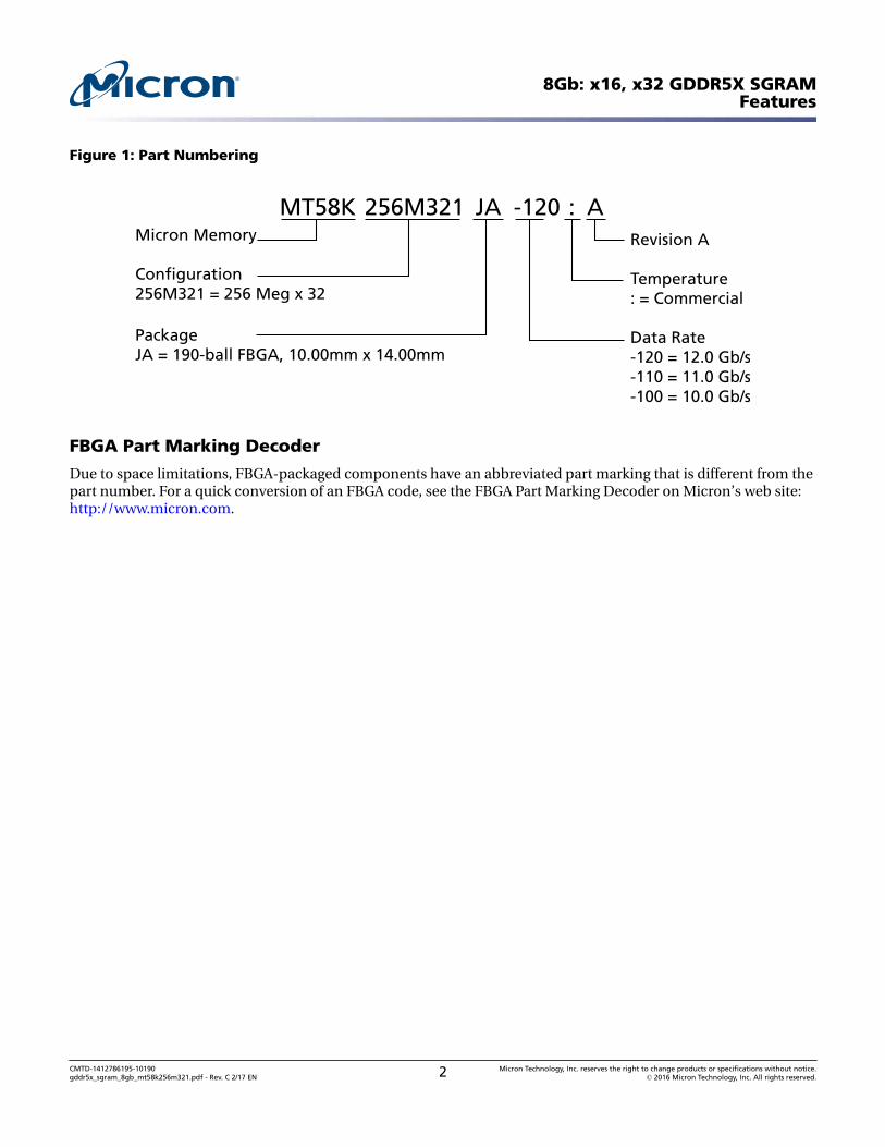
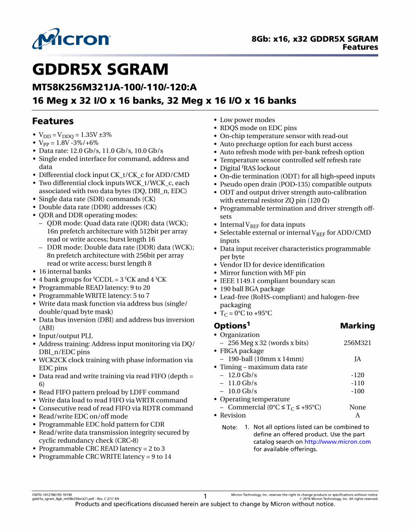
Figure 1: Part Numbering
Micron Memory
Configuration256M321 = 256 Meg x 32
PackageJA = 190-ball FBGA, 10.00mm x 14.00mm
MT58K 256M321 JA -120 : ARevision A
Temperature: = Commercial
Data Rate-120 = 12.0 Gb/s-110 = 11.0 Gb/s-100 = 10.0 Gb/s
FBGA Part Marking Decoder
Due to space limitations, FBGA-packaged components have an abbreviated part marking that is different from thepart number. For a quick conversion of an FBGA code, see the FBGA Part Marking Decoder on Micron’s web site:http://www.micron.com.
8Gb: x16, x32 GDDR5X SGRAMFeatures
CMTD-1412786195-10190gddr5x_sgram_8gb_mt58k256m321.pdf - Rev. C 2/17 EN 2 Micron Technology, Inc. reserves the right to change products or specifications without notice.
© 2016 Micron Technology, Inc. All rights reserved.
Operating Frequency Ranges
Figure 2: Data Rates in QDR, DDR, and RDQS Modes
MT58K256M321JA-110:A
QDR Mode
RDQS Mode
[Gbps/pin]0.2 2.0 4.0 6.0 8.0 10.0
DDR Mode
MT58K256M321JA-120:A
QDR Mode
RDQS Mode
[Gbps/pin]0.2 2.0 4.0 6.0 8.0 10.0 12.0
DDR Mode
MT58K256M321JA-100:A
QDR Mode
RDQS Mode
[Gbps/pin]0.2 2.0 4.0 6.05.5
5.5
8.0 10.0
DDR Mode
11.0
Table 1: Operating Frequency Ranges
Operating Mode Symbol
-100 -110 -120
UnitMin Max Min Max Min Max
QDR mode fCK 687 1250 687 1375 750 1500 MHz
DDR mode 50 1375 50 1375 50 1500
RDQS mode 50 500 50 500 50 500
Note: The operating range and AC timings of a faster speed bin are a superset of allslower speed bins. Therefore it is safe to use a faster bin device as a drop-in replacementof a slower bin device when operated within the frequency range of the slower bin de-vice.
8Gb: x16, x32 GDDR5X SGRAMOperating Frequency Ranges
CMTD-1412786195-10190gddr5x_sgram_8gb_mt58k256m321.pdf - Rev. C 2/17 EN 3 Micron Technology, Inc. reserves the right to change products or specifications without notice.
© 2016 Micron Technology, Inc. All rights reserved.
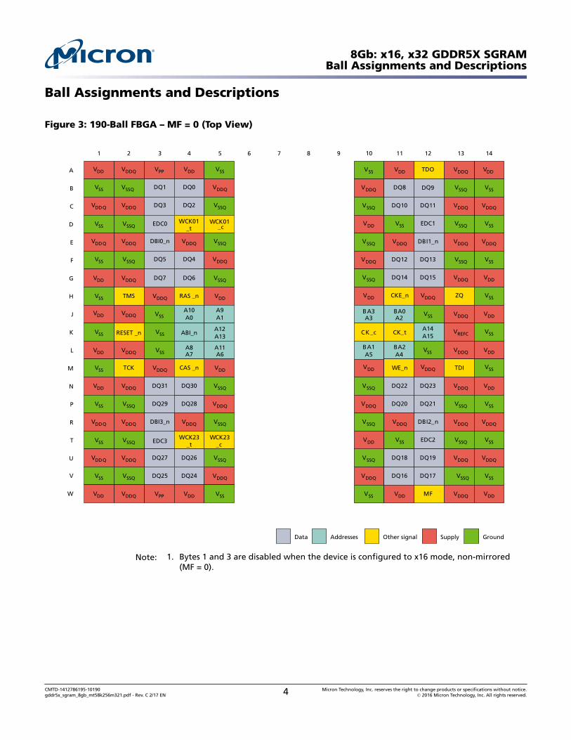
Ball Assignments and Descriptions
Figure 3: 190-Ball FBGA – MF = 0 (Top View)
A
B
C
D
E
F
G
H
J
K
L
M
N
P
R
T
V
W
U
GroundSupplyOther signalAddressesData
6 7 8 9 14
V DD
VSS
VDDQ
VSS
VDDQ
VSS
VDD
VSS
VDD
VSS
VDD
VSS
VDD
VSS
VDDQ
VSS
VDDQ
VSS
VDD
13
VDDQ
VSSQ
VDDQ
VSSQ
VDDQ
VSSQ
VDDQ
ZQ
VDDQ
VREFC
VDDQ
TDI
VDDQ
VSSQ
VDDQ
VSSQ
VDDQ
VSSQ
VDDQ
12
TDO
DQ9
DQ11
EDC1
DBI1_n
DQ13
DQ15
VDDQ
VSS
A14A15
VSS
VDDQ
DQ23
DQ21
DBI2_n
EDC2
DQ19
DQ17
MF
11
VDD
DQ8
DQ10
VSS
VDDQ
DQ12
DQ14
CKE_n
BA0A2
CK_t
BA2A4
WE_n
DQ22
DQ20
VDDQ
VSS
DQ18
DQ16
VDD
10
VSS
VDDQ
VSSQ
VDD
VSSQ
VDDQ
VSSQ
VDD
BA3A3
CK_c
BA1A5
VDD
VSSQ
VDDQ
VSSQ
VDD
VSSQ
VDDQ
VSS
5
VSS
VDDQ
VSSQ
WCK01_c
VSSQ
VDDQ
VSSQ
VDD
A9A1
A12A13
A11A6
VDD
VSSQ
VDDQ
VSSQ
WCK23_c
VSSQ
VDDQ
VSS
4
VDD
DQ0
DQ2
WCK01_t
VDDQ
DQ4
DQ6
RAS _n
A10A0
ABI_n
A8A7
CAS _n
DQ30
DQ28
VDDQ
WCK23_t
DQ26
DQ24
VDD
3
VPP
DQ1
DQ3
EDC0
DBI0_n
DQ5
DQ7
VDDQ
VSS
VSS
VSS
VDDQ
DQ31
DQ29
DBI3_n
EDC3
DQ27
DQ25
VPP
2
VDDQ
VSSQ
VDDQ
VSSQ
VDDQ
VSSQ
VDDQ
TMS
VDDQ
RESET _n
VDDQ
TCK
VDDQ
VSSQ
VDDQ
VSSQ
VDDQ
VSSQ
VDDQ
1
VDD
VSS
VDDQ
VSS
VDDQ
VSS
VDD
VSS
VDD
VSS
VDD
VSS
VDD
VSS
VDDQ
VSS
VDDQ
VSS
VDD
Note: 1. Bytes 1 and 3 are disabled when the device is configured to x16 mode, non‐mirrored(MF = 0).
8Gb: x16, x32 GDDR5X SGRAMBall Assignments and Descriptions
CMTD-1412786195-10190gddr5x_sgram_8gb_mt58k256m321.pdf - Rev. C 2/17 EN 4 Micron Technology, Inc. reserves the right to change products or specifications without notice.
© 2016 Micron Technology, Inc. All rights reserved.
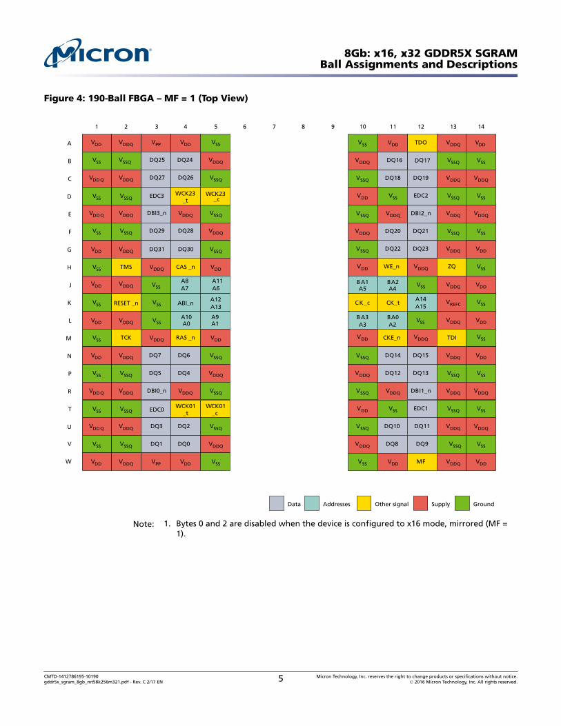
Figure 4: 190-Ball FBGA – MF = 1 (Top View)
A
B
C
D
E
F
G
H
J
K
L
M
N
P
R
T
V
W
U
6 7 8 9 14
V DD
VSS
VDDQ
VSS
VDDQ
VSS
VDD
VSS
VDD
VSS
VDD
VSS
VDD
VSS
VDDQ
VSS
VDDQ
VSS
VDD
13
VDDQ
VSSQ
VDDQ
VSSQ
VDDQ
VSSQ
VDDQ
ZQ
VDDQ
VREFC
VDDQ
TDI
VDDQ
VSSQ
VDDQ
VSSQ
VDDQ
VSSQ
VDDQ
12
TDO
DQ17
DQ19
EDC2
DBI2_n
DQ21
DQ23
VDDQ
VSS
A14A15
VSS
VDDQ
DQ15
DQ13
DBI1_n
EDC1
DQ11
DQ9
MF
11
VDD
DQ16
DQ18
VSS
VDDQ
DQ20
DQ22
WE_n
BA2A4
CK_t
BA0A2
CKE_n
DQ14
DQ12
VDDQ
VSS
DQ10
DQ8
VDD
10
VSS
VDDQ
VSSQ
VDD
VSSQ
VDDQ
VSSQ
VDD
BA1A5
CK_c
BA3A3
VDD
VSSQ
VDDQ
VSSQ
VDD
VSSQ
VDDQ
VSS
5
VSS
VDDQ
VSSQ
WCK23_c
VSSQ
VDDQ
VSSQ
VDD
A11A6
A12A13
A9A1
VDD
VSSQ
VDDQ
VSSQ
WCK01_c
VSSQ
VDDQ
VSS
4
VDD
DQ24
DQ26
WCK23_t
VDDQ
DQ28
DQ30
CAS _n
A8A7
ABI_n
A10A0
RAS _n
DQ6
DQ4
VDDQ
WCK01_t
DQ2
DQ0
VDD
3
VPP
DQ25
DQ27
EDC3
DBI3_n
DQ29
DQ31
VDDQ
VSS
VSS
VSS
VDDQ
DQ7
DQ5
DBI0_n
EDC0
DQ3
DQ1
VPP
2
VDDQ
VSSQ
VDDQ
VSSQ
VDDQ
VSSQ
VDDQ
TMS
VDDQ
RESET _n
VDDQ
TCK
VDDQ
VSSQ
VDDQ
VSSQ
VDDQ
VSSQ
VDDQ
1
VDD
VSS
VDDQ
VSS
VDDQ
VSS
VDD
VSS
VDD
VSS
VDD
VSS
VDD
VSS
VDDQ
VSS
VDDQ
VSS
VDD
GroundSupplyOther signalAddressesData
Note: 1. Bytes 0 and 2 are disabled when the device is configured to x16 mode, mirrored (MF =1).
8Gb: x16, x32 GDDR5X SGRAMBall Assignments and Descriptions
CMTD-1412786195-10190gddr5x_sgram_8gb_mt58k256m321.pdf - Rev. C 2/17 EN 5 Micron Technology, Inc. reserves the right to change products or specifications without notice.
© 2016 Micron Technology, Inc. All rights reserved.
Table 2: 190-Ball FBGA Ball Descriptions
Symbol Type Description
A[15:0] Input Address inputs: A[13:0] (A14) provide the row address for ACTIVATE commands.A[5:0] provide the lower column address (CAL), and A7, A9, and A[15:12] the uppercolumn address (CAU) in QDR operating mode; A[6:0] provide the lower column ad-dress (CAL), and A[7:6], A9, and A[15:12] the upper column address (CAU) in DDR op-erating mode. A8 defines the AUTO PRECHARGE function for READ/WRITE com-mands, to select one location out of the memory array in the respective bank. A8sampled during a PRECHARGE command determines whether the precharge appliesto one bank (A8 LOW, bank selected by BA[3:0]) or all banks (A8 HIGH). The addressinputs also provide the op‐code during a MODE REGISTER SET command and the da-ta bits during a LDFF command. A[12:8] and A14 are sampled with the rising edge ofCK_t and A[7:0], A13, and A15 are sampled with the rising edge of CK_c. CAL is asso-ciated with DQ[15:0] and CAU is associated with DQ[31:16].
ABI_n Input Address bus inversion
BA[3:0] Input Bank address inputs: BA[3:0] define to which bank an ACTIVATE, READ, WRITE,PRECHARGE, or PER-BANK REFRESH command is being applied. BA[3:0] also deter-mine which mode register is accessed with an MODE REGISTER SET command.BA[3:0] are sampled with the rising edge of CK_t.
CK_t, CK_c Input Clock: CK_t and CK_c are differential clock inputs. Command inputs are latched onthe rising edge of CK_t. Address inputs are latched on the rising edge of CK_t andthe rising edge of CK_c. All latencies are referenced to CK_t.
WCK01_t, WCK01_c/WCK23_t, WCK23_c
Input Write Clocks: WCK_t and WCK_c are differential clocks used for write data captureand read data output. WCK01_t/WCK01_c is associated with DQ[15:0], DBI0_n,DBI1_n, EDC0, and EDC1. WCK23_t/WCK23_c is associated with DQ[31:16], DBI2_n,DBI3_n, EDC2, and EDC3.
CKE_n Input Clock enable: CKE_n LOW activates and CKE_n HIGH deactivates the internal clock,device input buffers, and output drivers. Taking CKE_n HIGH provides PRECHARGEPOWER‐DOWN and SELF REFRESH operations (all banks idle), or ACTIVE POWER‐DOWN (LOW ACTIVE in any bank). CKE_n must be maintained LOW throughout readand write accesses.
MF Input Mirror function: Must be tied to power or ground.
RAS_n, CAS_n, WE_n Input Command inputs: RAS_n, CAS_n, and WE_n define the command being entered.
RESET_n Input Reset: RESET_n LOW asynchronously initiates a full chip reset. With RESET_n LOWall ODTs are disabled. A full chip reset may be performed at any time by pulling RE-SET_n LOW.
DQ[31:0] I/O Data input/output: Bidirectional 32-bit data bus.
DBI[3:0]_n I/O Data bus inversion: DBI0_n is associated with DQ[7:0], DBI1_n is associated withDQ[15:8], DBI2_n is associated with DQ[23:16], DBI3_n is associated with DQ[31:24].
EDC[3:0] Output Error detection code: The calculated CRC data is transmitted on these pins. In ad-dition these pins drive a hold pattern when idle and can be used as an RDQS func-tion. EDC0 is associated with DQ[7:0], EDC1 is associated with DQ[15:8], EDC2 is asso-ciated with DQ[23:16], EDC3 is associated with DQ[31:24].
VDD Supply Power supply
VDDQ Supply DQ power supply: I/O power supply
VREFC Supply Reference voltage for address and command pins
8Gb: x16, x32 GDDR5X SGRAMBall Assignments and Descriptions
CMTD-1412786195-10190gddr5x_sgram_8gb_mt58k256m321.pdf - Rev. C 2/17 EN 6 Micron Technology, Inc. reserves the right to change products or specifications without notice.
© 2016 Micron Technology, Inc. All rights reserved.
Table 2: 190-Ball FBGA Ball Descriptions (Continued)
Symbol Type Description
VPP Supply Pump Voltage
VSS Supply Ground
VSSQ Supply DQ ground: Isolated on the device for improved noise immunity.
ZQ Supply External reference ball for impedance calibration
TDI Input JTAG test data input
TDO Output JTAG test data output
TMS Input JTAG test mode select
TCK Input JTAG test clock
8Gb: x16, x32 GDDR5X SGRAMBall Assignments and Descriptions
CMTD-1412786195-10190gddr5x_sgram_8gb_mt58k256m321.pdf - Rev. C 2/17 EN 7 Micron Technology, Inc. reserves the right to change products or specifications without notice.
© 2016 Micron Technology, Inc. All rights reserved.
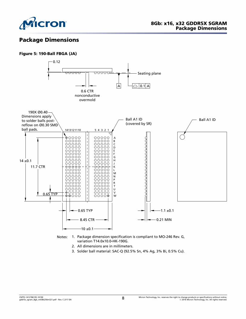
Package Dimensions
Figure 5: 190-Ball FBGA (JA)
0.6 CTRnonconductive
overmold
0.12
Seating plane
0.1 A
Ball A1 ID(covered by SR)
Ball A1 ID
A
0.21 MIN
1.1 ±0.1
8.45 CTR
10 ±0.1
0.65 TYP
11.7 CTR
14 ±0.1
190X Ø0.40Dimensions applyto solder balls post-reflow on Ø0.30 SMDball pads.
0.65 TYP
123101112
ABCDEFGHJKLMNPRTUVW
451314
Notes: 1. Package dimension specification is compliant to MO‐246 Rev. G,variation T14.0x10.0‐HK‐190G.
2. All dimensions are in millimeters.3. Solder ball material: SAC-Q (92.5% Sn, 4% Ag, 3% Bi, 0.5% Cu).
8Gb: x16, x32 GDDR5X SGRAMPackage Dimensions
CMTD-1412786195-10190gddr5x_sgram_8gb_mt58k256m321.pdf - Rev. C 2/17 EN 8 Micron Technology, Inc. reserves the right to change products or specifications without notice.
© 2016 Micron Technology, Inc. All rights reserved.
Functional Description
Functional Overview
The GDDR5X SGRAM is a high speed dynamic random‐access memory designed for ap-plications requiring high bandwidth. It is internally configured as 16‐bank memory andcontains 8,589,934,592 bits.
The device’s high‐speed interface is optimized for point‐to‐point connections to a hostcontroller. On‐die termination (ODT) is provided for all high‐speed interface signals toeliminate the need for termination resistors in the system.
Two operating modes are supported which mainly differ in the internal prefetch andDQ/DBI_n pin to WCK clock frequency ratio. The operating mode is set by a mode reg-ister bit:
• In quad data rate (QDR) mode the interface transfers four 32‐bit wide data words perWCK clock cycle to/from the I/O pins. Corresponding to the 16n-prefetch a singlewrite or read access consists of a 512-bit wide, two CK clock cycle data transfer at theinternal memory core and sixteen corresponding 32-bit wide one‐quarter WCK clockcycle data transfers to the I/O pins.
• In double data rate (DDR) mode the interface transfers two 32‐bit wide data wordsper WCK clock cycle to/from the I/O pins. Corresponding to the 8n-prefetch a singlewrite or read access consists of a 256-bit wide, two CK clock cycle data transfer at theinternal memory core and eight corresponding 32-bit wide one‐half WCK clock cycledata transfers to the I/O pins.
Read and write accesses are burst oriented; an access starts at a selected location andconsists of a total of sixteen data words in QDR mode and eight data words in DDRmode. Accesses begin with the registration of an ACTIVATE command, which is thenfollowed by a READ or WRITE command. The address bits registered coincident withthe ACTIVATE command and the next rising CK_c edge are used to select the bank andthe row to be accessed. The address bits registered coincident with the READ or WRITEcommand and the next rising CK_c edge are used to select the bank and the columnlocation for the burst access.
Mirror Function Enable
A mirror function (MF) mode is provided to change the physical location of the data,command and address pins assisting in PCB signal routing. The MF pin should be tieddirectly to VSSQ or VDDQ depending on the desired ballout.
It is pointed out that this mirror function mode swaps the location of the data bytes(Byte 0 .. Byte 3). The controller must strictly adhere to this data byte order because thisbyte order is assumed in the internal assignment of the write data mask received withWDM and WSM commands.
8Gb: x16, x32 GDDR5X SGRAMFunctional Description
CMTD-1412786195-10190gddr5x_sgram_8gb_mt58k256m321.pdf - Rev. C 2/17 EN 9 Micron Technology, Inc. reserves the right to change products or specifications without notice.
© 2016 Micron Technology, Inc. All rights reserved.
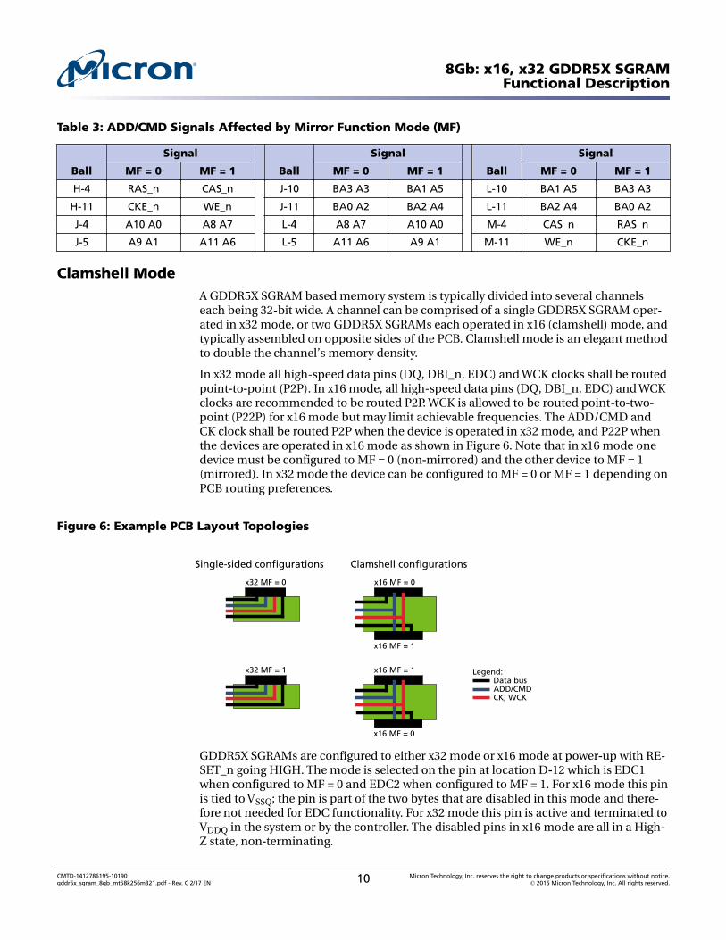
Table 3: ADD/CMD Signals Affected by Mirror Function Mode (MF)
Ball
Signal
Ball
Signal
Ball
Signal
MF = 0 MF = 1 MF = 0 MF = 1 MF = 0 MF = 1
H‐4 RAS_n CAS_n J‐10 BA3 A3 BA1 A5 L‐10 BA1 A5 BA3 A3
H‐11 CKE_n WE_n J‐11 BA0 A2 BA2 A4 L‐11 BA2 A4 BA0 A2
J‐4 A10 A0 A8 A7 L‐4 A8 A7 A10 A0 M‐4 CAS_n RAS_n
J‐5 A9 A1 A11 A6 L‐5 A11 A6 A9 A1 M‐11 WE_n CKE_n
Clamshell Mode
A GDDR5X SGRAM based memory system is typically divided into several channelseach being 32-bit wide. A channel can be comprised of a single GDDR5X SGRAM oper-ated in x32 mode, or two GDDR5X SGRAMs each operated in x16 (clamshell) mode, andtypically assembled on opposite sides of the PCB. Clamshell mode is an elegant methodto double the channel’s memory density.
In x32 mode all high-speed data pins (DQ, DBI_n, EDC) and WCK clocks shall be routedpoint‐to‐point (P2P). In x16 mode, all high-speed data pins (DQ, DBI_n, EDC) and WCKclocks are recommended to be routed P2P. WCK is allowed to be routed point‐to‐two‐point (P22P) for x16 mode but may limit achievable frequencies. The ADD/CMD andCK clock shall be routed P2P when the device is operated in x32 mode, and P22P whenthe devices are operated in x16 mode as shown in Figure 6. Note that in x16 mode onedevice must be configured to MF = 0 (non‐mirrored) and the other device to MF = 1(mirrored). In x32 mode the device can be configured to MF = 0 or MF = 1 depending onPCB routing preferences.
Figure 6: Example PCB Layout Topologies
Single-sided configurations
x32 MF = 0
Clamshell configurations
Legend:Data busADD/CMDCK, WCK
x16 MF = 1
x16 MF = 0
x32 MF = 1
x16 MF = 0
x16 MF = 1
GDDR5X SGRAMs are configured to either x32 mode or x16 mode at power‐up with RE-SET_n going HIGH. The mode is selected on the pin at location D‐12 which is EDC1when configured to MF = 0 and EDC2 when configured to MF = 1. For x16 mode this pinis tied to VSSQ; the pin is part of the two bytes that are disabled in this mode and there-fore not needed for EDC functionality. For x32 mode this pin is active and terminated toVDDQ in the system or by the controller. The disabled pins in x16 mode are all in a High‐Z state, non‐terminating.
8Gb: x16, x32 GDDR5X SGRAMFunctional Description
CMTD-1412786195-10190gddr5x_sgram_8gb_mt58k256m321.pdf - Rev. C 2/17 EN 10 Micron Technology, Inc. reserves the right to change products or specifications without notice.
© 2016 Micron Technology, Inc. All rights reserved.
The ADD/CMD and CK pin ODT are enabled with a value as determined by the level ofthe CKE_n pin at RESET_n going HIGH.
Table 4: MF, x32/x16 Mode and Default ADD/CMD/CK ODT
Mode MF EDC1 (MF = 0) or EDC2 (MF = 1) Default ADD/CMD/CK ODT
x16 non-mirrored VSSQ VSSQ ZQ = 120Ωx32 non-mirrored VSSQ VDDQ (terminated by the system or controller) ZQ/2 = 60Ωx16 mirrored VDDQ VSSQ ZQ = 120Ωx32 mirrored VDDQ VDDQ (terminated by the system or controller) ZQ/2 = 60Ω
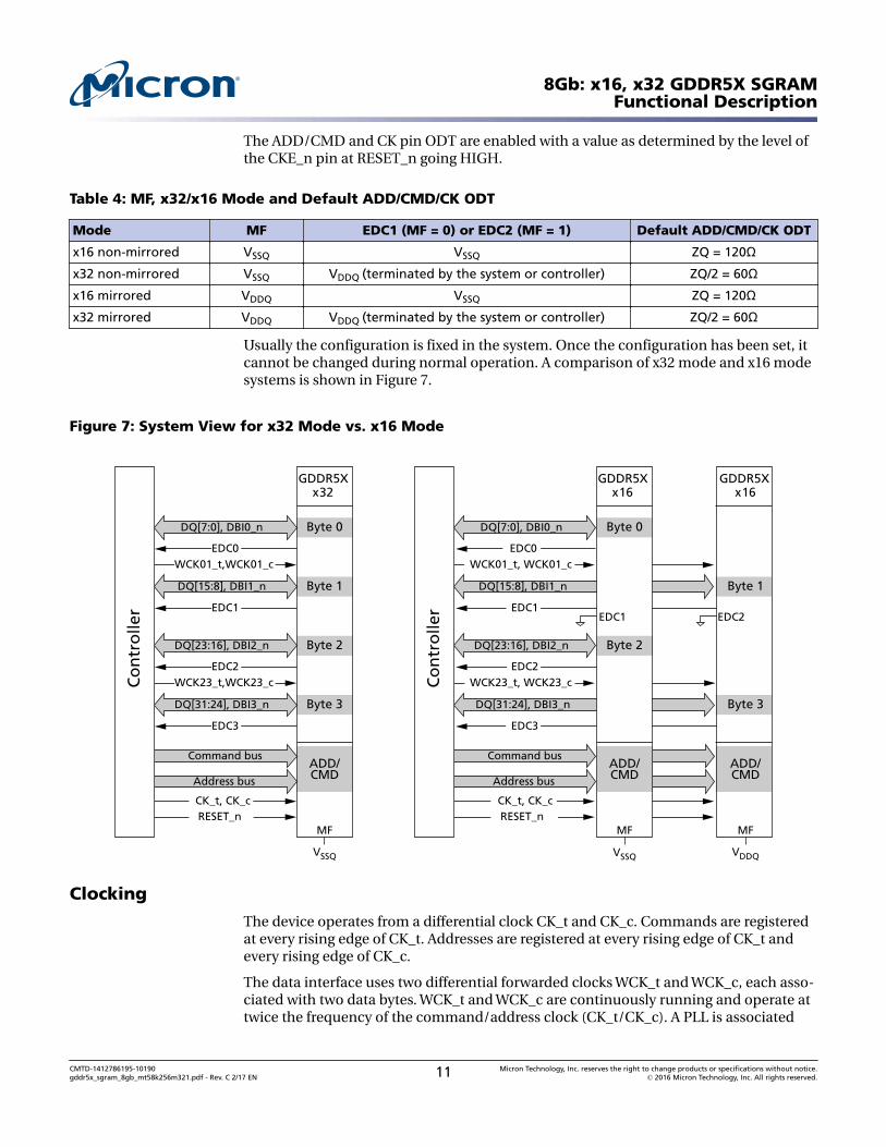
Usually the configuration is fixed in the system. Once the configuration has been set, itcannot be changed during normal operation. A comparison of x32 mode and x16 modesystems is shown in Figure 7.
Figure 7: System View for x32 Mode vs. x16 Mode
VSSQ
GDDR5Xx16
MF
GDDR5Xx16
MF
VDDQ
Co
ntr
olle
r
Address bus
CK_t, CK_cRESET_n
ADD/CMD
Command busADD/CMD
EDC1 EDC2
Byte 1
Byte 0
EDC0WCK01_t, WCK01_c
DQ[7:0], DBI0_n
EDC1
Byte 3
Byte 2
EDC2WCK23_t, WCK23_c
DQ[23:16], DBI2_n
EDC3
DQ[31:24], DBI3_n
DQ[15:8], DBI1_n
GDDR5Xx32
MF
VSSQ
Co
ntr
olle
r
Byte 3
Byte 2
EDC2
EDC3
WCK23_t,WCK23_c
DQ[23:16], DBI2_n
DQ[31:24], DBI3_n
Byte 1
Byte 0
EDC0
EDC1
WCK01_t,WCK01_c
DQ[7:0], DBI0_n
DQ[15:8], DBI1_n
Address bus
CK_t, CK_cRESET_n
ADD/CMD
Command bus
Clocking
The device operates from a differential clock CK_t and CK_c. Commands are registeredat every rising edge of CK_t. Addresses are registered at every rising edge of CK_t andevery rising edge of CK_c.
The data interface uses two differential forwarded clocks WCK_t and WCK_c, each asso-ciated with two data bytes. WCK_t and WCK_c are continuously running and operate attwice the frequency of the command/address clock (CK_t/CK_c). A PLL is associated
8Gb: x16, x32 GDDR5X SGRAMFunctional Description
CMTD-1412786195-10190gddr5x_sgram_8gb_mt58k256m321.pdf - Rev. C 2/17 EN 11 Micron Technology, Inc. reserves the right to change products or specifications without notice.
© 2016 Micron Technology, Inc. All rights reserved.
with each WCK pair. The use of the PLL is mandatory in QDR mode and not supportedin DDR mode.
• QDR mode uses a quad data rate data interface and a 16n‐prefetch architecture forDQ/DBI_n, and a double data rate data interface and 8n‐prefetch architecture forEDC. The PLL generates four equally spaced clock edges per WCK clock cycle. QDRmeans that four DQ/DBI_n data words per WCK cycle are registered at these internal-ly generated clock edges. DDR means that two EDC data words per WCK cycle are reg-istered at every second of these internally generated clock edges.
• DDR mode uses a double data rate data interface and an 8n‐prefetch architecture forDQ/DBI_n/EDC. DDR means that the data is registered at every rising edge of WCK_tand rising edge of WCK_c.
The table below and Figure 8 illustrate the clock and interface signal relationship forboth QDR and DDR operating modes.
Table 5: Example Clock and Interface Signal Frequency Relationship
Pin QDR Mode DDR Mode Unit
CK_t, CK_c 1.5 1.5 GHz
Command 1.5 1.5 Gbps/pin
Address 3 3 Gbps/pin
WCK_t, WCK_c 3 3 GHz
DQ, DBI_n 12 6 Gbps/pin
EDC 6 6 Gbps/pin
Figure 8: Clocking and Interface Relationship
CK_c
CK_t
Command
WCK_t
WCK_c
DQ, DBI_n(QDR mode)
DQ, DBI_n(DDR mode)
EDC(QDR + DDR modes)
Address
Note: 1. Above shows the relationship between the data rate of the buses and the clocks, and isnot a timing diagram.
8Gb: x16, x32 GDDR5X SGRAMFunctional Description
CMTD-1412786195-10190gddr5x_sgram_8gb_mt58k256m321.pdf - Rev. C 2/17 EN 12 Micron Technology, Inc. reserves the right to change products or specifications without notice.
© 2016 Micron Technology, Inc. All rights reserved.
Figure 9: Block Diagram of an Example Clock System
GDDR5X SGRAM
ADD/CMD
to internal state machineADD/CMD
CMD sampled by CK_t/CK_c as SDRADD sampled by CK_t/CK_c as DDR
CK_t, CK_c(1.5 GHz)
D Q
WCK_t, WCK_c(3 GHz)
to EDC pin
WCK2CK Alignment
(DDR mode only)
/2 PLL Internal WCK(4 phases)QDR mode: 3.0 GHzDDR mode: 1.5 GHz
PLLData Tx/Rx
DRAM Core
Controller
DQ
D Q
clock phase ctrl
WRITEdata
clock phase ctrl
READdata
DATA(QDR mode:
12 Gb/sDDR mode:
6 Gb/s)
ADD/CMD centered with CK_t/CK_c
D Q
D Q
Osc.
DQ
early/ late
D Q
Addressing
GDDR5X SGRAMs use a double data rate address scheme to reduce pins required onthe device as shown in Table 6. The addresses should be provided in two parts; the firsthalf is latched on the rising edge of CK_t along with the command pins such as RAS_n,CAS_n, and WE_n; the second half is latched on the next rising edge of CK_c.
The use of DDR addressing allows all address values to be latched in at the same rate asthe SDR commands. All addresses related to command access have been positioned forlatching on the initial rising edge for faster decoding.
Table 6: Address Pairs
Clock Edge Address Inputs
Rising CK_t BA3 BA2 BA1 BA0 A14 A12 A11 A10 A9 A8
Rising CK_c A3 A4 A5 A2 A15 A13 A6 A0 A1 A7
8Gb: x16, x32 GDDR5X SGRAMFunctional Description
CMTD-1412786195-10190gddr5x_sgram_8gb_mt58k256m321.pdf - Rev. C 2/17 EN 13 Micron Technology, Inc. reserves the right to change products or specifications without notice.
© 2016 Micron Technology, Inc. All rights reserved.
Table 7: Addressing
Parameter 256 Meg x 32 512 Meg x 16
Row address A0 to A13 A0 to A14
Column address DQ[15:0] QDR mode A0 to A5
DDR mode A0 to A6
Column addressDQ[31:16]
QDR mode A7, A9, A12 to A15
DDR mode A7, A9, A12 to A15, A6
Bank address BA0 to BA3
Auto precharge A8
Page size 4K 2K
Refresh 16K/32ms
Refresh period 1.9µs
Note: 1. The burst order is fixed for reads and writes, and no column address bits are assigned todistinguish between the UIs of a burst. A memory controller may internally assign suchcolumn address bits, but these column address bits are not transmitted on the columnaddress bus.
Two column addresses with a common bank address are provided with each READ andWRITE command, allowing two pseudo‐independent memory accesses with 32 bytesaccess granularity in QDR operating mode and 16 bytes access granularity in DDR oper-ating mode:
• The lower column address (CAL) is associated with DQ[15:0] and received on address-es A[5:0].
• The upper column address (CAU) is associated with DQ[31:16] and received on ad-dresses A[15:12, 9, 7].
The addressing is transparent between QDR and DDR operating modes: data can bewritten in QDR operating mode with a single BL = 16 WRITE burst, and read in DDRoperating mode with two BL = 8 READ bursts, and vice versa. Column address A6 isevaluated in DDR operating mode only; it can be considered the LSB and selects be-tween the data corresponding to the first half of a BL = 16 burst (UI 0..7) with A6 beingset LOW, and the data corresponding to the second half of a BL = 16 burst (UI 8..15) withA6 being set HIGH.
Figure below illustrates the addressing in QDR and DDR operating modes assuming thesame column addresses CAL and CAU for lower and upper data bytes. This is equivalentto accesses using a single column address, however, it is required to provide both CALand CAU along with the READ or WRITE command.
8Gb: x16, x32 GDDR5X SGRAMFunctional Description
CMTD-1412786195-10190gddr5x_sgram_8gb_mt58k256m321.pdf - Rev. C 2/17 EN 14 Micron Technology, Inc. reserves the right to change products or specifications without notice.
© 2016 Micron Technology, Inc. All rights reserved.
Figure 10: Column Accesses with Identical Lower and Upper Column Addresses
Case 1: Single READ/WRITE burst in QDR mode (BL16) with CAL = CAU
DQ[31:16] DQ[15:0]
BL16 BL16CAL
CA6 = XCAU
CA6=X
Case 2: Two READ/WRITE bursts in DDR mode (BL8) with CAL = CAU
CAUCA6=0
CALCA6 = 0BL8 BL8
DQ[31:16] DQ[15:0]
CAUCA6=1
CALCA6 = 1
BL8 BL8
Figure below illustrates the addressing in QDR and DDR operating modes assuming dif-ferent column address for lower and upper bytes. This corresponds to two pseudo‐inde-pendent memory accesses with 32 bytes access granularity in QDR operating mode and16 bytes in DDR operating mode. It is pointed out that both accesses share the bank ad-dress, and therefore access the same open row in that bank.
8Gb: x16, x32 GDDR5X SGRAMFunctional Description
CMTD-1412786195-10190gddr5x_sgram_8gb_mt58k256m321.pdf - Rev. C 2/17 EN 15 Micron Technology, Inc. reserves the right to change products or specifications without notice.
© 2016 Micron Technology, Inc. All rights reserved.
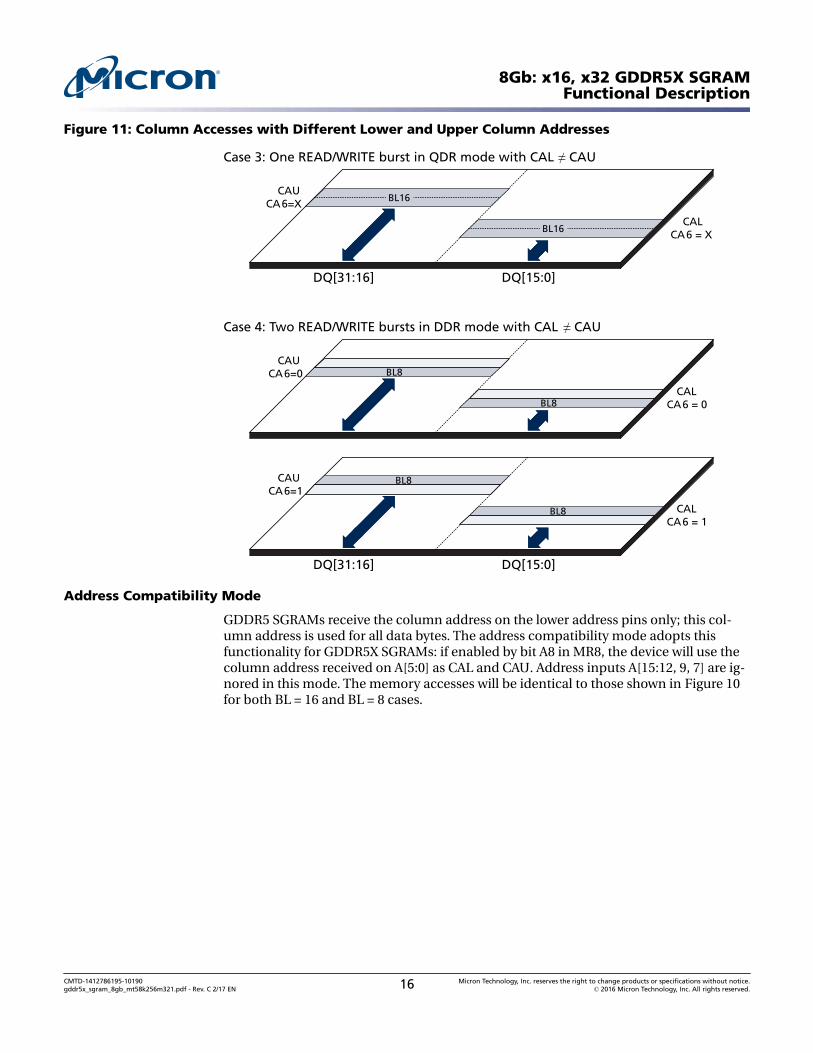
Figure 11: Column Accesses with Different Lower and Upper Column Addresses
Case 3: One READ/WRITE burst in QDR mode with CAL ≠ CAU
DQ[31:16] DQ[15:0]
BL16
BL16CAL
CA6 = X
CAUCA6=X
Case 4: Two READ/WRITE bursts in DDR mode with CAL ≠ CAU
CAUCA6=0
CALCA6 = 0
BL8
BL8
DQ[31:16] DQ[15:0]
CAUCA6=1
CALCA6 = 1
BL8
BL8
Address Compatibility Mode
GDDR5 SGRAMs receive the column address on the lower address pins only; this col-umn address is used for all data bytes. The address compatibility mode adopts thisfunctionality for GDDR5X SGRAMs: if enabled by bit A8 in MR8, the device will use thecolumn address received on A[5:0] as CAL and CAU. Address inputs A[15:12, 9, 7] are ig-nored in this mode. The memory accesses will be identical to those shown in Figure 10for both BL = 16 and BL = 8 cases.
8Gb: x16, x32 GDDR5X SGRAMFunctional Description
CMTD-1412786195-10190gddr5x_sgram_8gb_mt58k256m321.pdf - Rev. C 2/17 EN 16 Micron Technology, Inc. reserves the right to change products or specifications without notice.
© 2016 Micron Technology, Inc. All rights reserved.
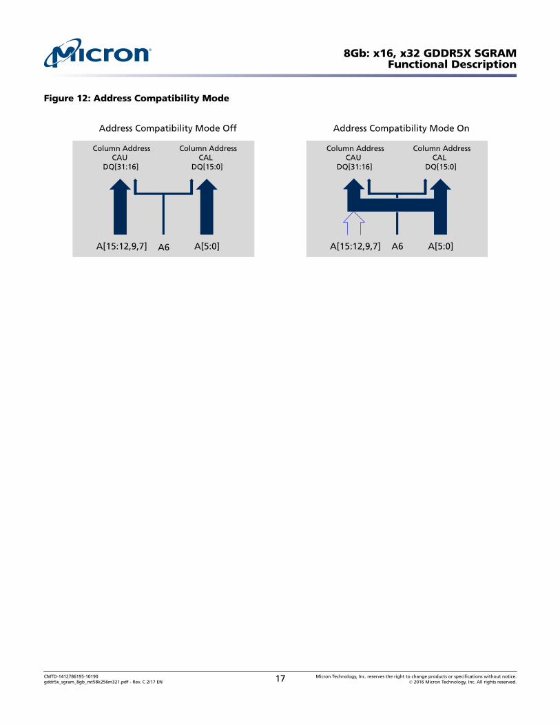
Figure 12: Address Compatibility Mode
A[15:12,9,7] A[5:0]
Column AddressCAL
DQ[15:0]
Column AddressCAU
DQ[31:16]
Address Compatibility Mode On
A[15:12,9,7] A[5:0]
Column AddressCAL
DQ[15:0]
Column AddressCAU
DQ[31:16]
Address Compatibility Mode Off
A6 A6
8Gb: x16, x32 GDDR5X SGRAMFunctional Description
CMTD-1412786195-10190gddr5x_sgram_8gb_mt58k256m321.pdf - Rev. C 2/17 EN 17 Micron Technology, Inc. reserves the right to change products or specifications without notice.
© 2016 Micron Technology, Inc. All rights reserved.
Operating Conditions
Absolute Maximum Ratings
Stresses greater than those listed may cause permanent damage to the device. This is astress rating only, and functional operation of the device at these or any other condi-tions above those indicated in the operational sections of this specification is not im-plied. Exposure to absolute maximum rating conditions for extended periods may ad-versely affect reliability.
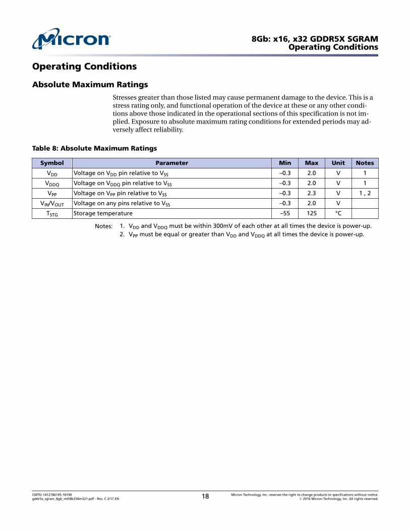
Table 8: Absolute Maximum Ratings
Symbol Parameter Min Max Unit Notes
VDD Voltage on VDD pin relative to VSS –0.3 2.0 V 1
VDDQ Voltage on VDDQ pin relative to VSS –0.3 2.0 V 1
VPP Voltage on VPP pin relative to VSS –0.3 2.3 V 1 , 2
VIN/VOUT Voltage on any pins relative to VSS –0.3 2.0 V
TSTG Storage temperature –55 125 °C
Notes: 1. VDD and VDDQ must be within 300mV of each other at all times the device is power‐up.2. VPP must be equal or greater than VDD and VDDQ at all times the device is power‐up.
8Gb: x16, x32 GDDR5X SGRAMOperating Conditions
CMTD-1412786195-10190gddr5x_sgram_8gb_mt58k256m321.pdf - Rev. C 2/17 EN 18 Micron Technology, Inc. reserves the right to change products or specifications without notice.
© 2016 Micron Technology, Inc. All rights reserved.
DC and AC Operating Conditions
GDDR5X SGRAMs are designed for 1.35V typical operating voltages. The interface fol-lows the POD135 standard (JESD8‐21A). All AC and DC values are measured at the ball.
Table 9: DC Operating Conditions
Symbol Parameter Min Typ Max Unit Notes
VDD Device supply voltage 1.3095 1.35 1.3905 V 1
VDDQ Output supply voltage 1.3095 1.35 1.3905 V 1
VPP Pump voltage 1.746 1.8 1.908 V 2
VREFD Reference voltage: DQ and DBI_n pins 0.69 × VDDQ – 0.71 × VDDQ V 3, 4
VREFD2 0.49 × VDDQ – 0.51 × VDDQ V 3, 4, 5
VREFC Reference voltage: ADD/CMD pins 0.69 × VDDQ – 0.71 × VDDQ V 6
VREFC2 0.49 × VDDQ – 0.51 × VDDQ V 6
VIHA(DC) DC input logic HIGH voltage with VREFC: ADD/CMDpins
VREFC + 0.135 – – V 7, 9
VILA(DC) DC input logic LOW voltage with VREFC: ADD/CMDpins
– – VREFC ‐ 0.135 V 7, 9
VIHA2(DC) DC input logic HIGH voltage with VREFC2: ADD/CMDpins
VREFC2 + 0.27 – – V 9
VILA2(DC) DC input logic LOW voltage with VREFC2: ADD/CMDpins
– – VREFC2 ‐ 0.27 V 9
VIHD(DC) DC input logic HIGH voltage with VREFD: DQ andDBI_n pins
VREFD + 0.09 – – V 8, 9
VILD(DC) DC input logic LOW voltage with VREFD: DQ andDBI_n pins
– – VREFD ‐ 0.09 V 8, 9
VIHD2(DC) DC input logic HIGH voltage with VREFD2: DQ andDBI_n pins
VREFD2 + 0.27 – – V 9
VILD2(DC) DC input logic LOW voltage with VREFD2: DQ andDBI_n pins
– – VREFD2 ‐ 0.27 V 9
VIHR RESET_n, MF and boundary scan input logic HIGHvoltage; EDC1/2 input logic HIGH voltage for×32/×16 mode select
0.8 × VDDQ – – V 9
VILR RESET_n, MF and boundary scan input logic LOWvoltage; EDC1/2 input logic LOW voltage for ×32/×16mode select
– – 0.2 × VDDQ V 9
IL Input leakage current (any input 0V ≤ VIN ≤ VDDQ; allother pins not under test = 0V)
–5 – 5 μA 10
IOZ Output leakage current (outputs are disabled; 0V ≤VOUT ≤ VDDQ)
–5 – 5 μA 11
VOL(DC) Output logic LOW voltage – – 0.56 V
Notes: 1. GDDR5X SGRAM devices are designed to tolerate PCB designs with separate VDDQ andVDD power regulators.
2. DC bandwidth is limited to 20 MHz.
8Gb: x16, x32 GDDR5X SGRAMOperating Conditions
CMTD-1412786195-10190gddr5x_sgram_8gb_mt58k256m321.pdf - Rev. C 2/17 EN 19 Micron Technology, Inc. reserves the right to change products or specifications without notice.
© 2016 Micron Technology, Inc. All rights reserved.
3. AC noise in the system is estimated at 50mV peak-to-peak for the purpose of DRAM de-sign.
4. The reference voltage source and control for DQ and DBI_n pins are determined by halfVREFD, VREF C2D and VREFD level mode register bits.
5. Programmable VREFD levels are not supported with VREFD2.6. The reference voltage source (external or internal) is determined at power‐up; the refer-
ence voltage level is determined by half VREFC mode register bit.7. ADD/CMD input slew rate must be greater than or equal to 2.7 V/ns. The slew rate is
measured between VREFC crossing and VIHA(AC) or VILA(AC), or between VREFC2 crossingand VIHA2(AC) or VILA2(AC).
8. DQ/DBI_n input slew rate must be greater than or equal to 2.7 V/ns. The slew rate ismeasured between VREFD crossing and VIHD(AC) or VILD(AC), or between VREFD2 crossingand VIHD2(AC) or VILD2(AC).
9. VIHR and VILR apply to boundary scan input pins TDI, TMS, and TCK. VIHR and VILR alsoapply to ADD/CMD, CK_t/CK_c, DQ, DBI_n, and WCK_t/WCK_c input pins when boundaryscan mode is active and input data are latched in the capture‐DR TAP controller state.
10. IL is measured with ODT off. Any input 0V ≤ VIN ≤ VDDQ; all other pins not under testexcluding TDI, TMS, and TCK = 0V.
11. IOZ is measured with DQ disabled; 0V ≤ VOUT ≤ VDDQ.
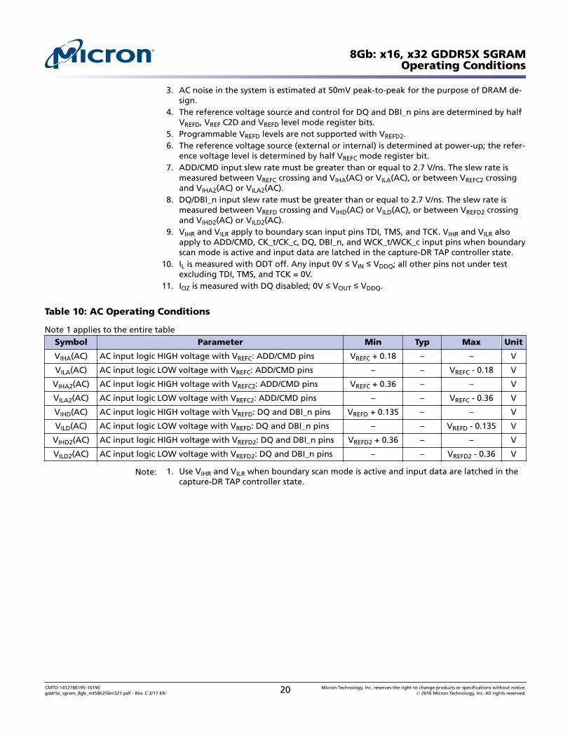
Table 10: AC Operating Conditions
Note 1 applies to the entire tableSymbol Parameter Min Typ Max Unit
VIHA(AC) AC input logic HIGH voltage with VREFC: ADD/CMD pins VREFC + 0.18 – – V
VILA(AC) AC input logic LOW voltage with VREFC: ADD/CMD pins – – VREFC ‐ 0.18 V
VIHA2(AC) AC input logic HIGH voltage with VREFC2: ADD/CMD pins VREFC + 0.36 – – V
VILA2(AC) AC input logic LOW voltage with VREFC2: ADD/CMD pins – – VREFC ‐ 0.36 V
VIHD(AC) AC input logic HIGH voltage with VREFD: DQ and DBI_n pins VREFD + 0.135 – – V
VILD(AC) AC input logic LOW voltage with VREFD: DQ and DBI_n pins – – VREFD ‐ 0.135 V
VIHD2(AC) AC input logic HIGH voltage with VREFD2: DQ and DBI_n pins VREFD2 + 0.36 – – V
VILD2(AC) AC input logic LOW voltage with VREFD2: DQ and DBI_n pins – – VREFD2 ‐ 0.36 V
Note: 1. Use VIHR and VILR when boundary scan mode is active and input data are latched in thecapture‐DR TAP controller state.
8Gb: x16, x32 GDDR5X SGRAMOperating Conditions
CMTD-1412786195-10190gddr5x_sgram_8gb_mt58k256m321.pdf - Rev. C 2/17 EN 20 Micron Technology, Inc. reserves the right to change products or specifications without notice.
© 2016 Micron Technology, Inc. All rights reserved.
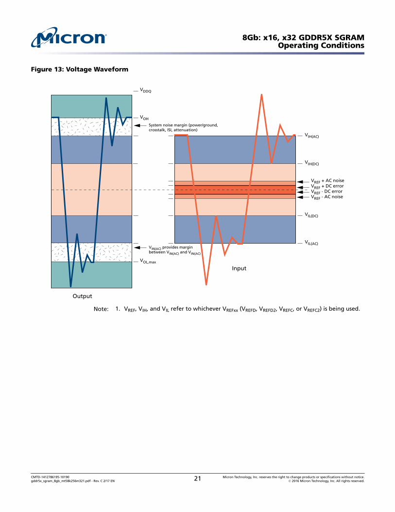
Figure 13: Voltage Waveform
VDDQ
VOH
System noise margin (power/ground,crosstalk, ISI, attenuation)
VIH(AC)
VIL(AC)
VIH(DC)
VREF + AC noiseVREF + DC errorVREF - DC errorVREF - AC noise
VIL(DC)
VIN(AC) provides marginbetween VIN(AC) and VIN(AC)
VOL,max
Output
Input
Note: 1. VREF, VIH, and VIL refer to whichever VREFxx (VREFD, VREFD2, VREFC, or VREFC2) is being used.
8Gb: x16, x32 GDDR5X SGRAMOperating Conditions
CMTD-1412786195-10190gddr5x_sgram_8gb_mt58k256m321.pdf - Rev. C 2/17 EN 21 Micron Technology, Inc. reserves the right to change products or specifications without notice.
© 2016 Micron Technology, Inc. All rights reserved.
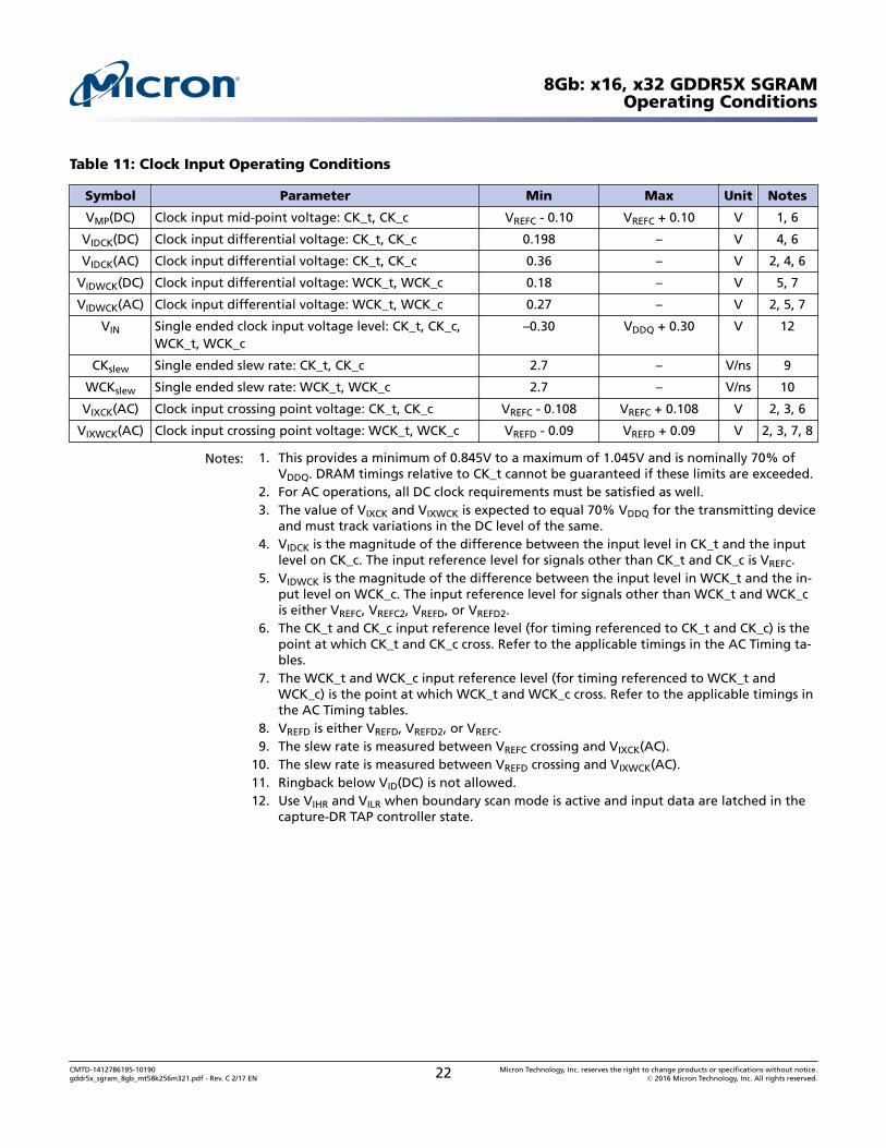
Table 11: Clock Input Operating Conditions
Symbol Parameter Min Max Unit Notes
VMP(DC) Clock input mid-point voltage: CK_t, CK_c VREFC ‐ 0.10 VREFC + 0.10 V 1, 6
VIDCK(DC) Clock input differential voltage: CK_t, CK_c 0.198 – V 4, 6
VIDCK(AC) Clock input differential voltage: CK_t, CK_c 0.36 – V 2, 4, 6
VIDWCK(DC) Clock input differential voltage: WCK_t, WCK_c 0.18 – V 5, 7
VIDWCK(AC) Clock input differential voltage: WCK_t, WCK_c 0.27 – V 2, 5, 7
VIN Single ended clock input voltage level: CK_t, CK_c,WCK_t, WCK_c
–0.30 VDDQ + 0.30 V 12
CKslew Single ended slew rate: CK_t, CK_c 2.7 – V/ns 9
WCKslew Single ended slew rate: WCK_t, WCK_c 2.7 – V/ns 10
VIXCK(AC) Clock input crossing point voltage: CK_t, CK_c VREFC ‐ 0.108 VREFC + 0.108 V 2, 3, 6
VIXWCK(AC) Clock input crossing point voltage: WCK_t, WCK_c VREFD ‐ 0.09 VREFD + 0.09 V 2, 3, 7, 8
Notes: 1. This provides a minimum of 0.845V to a maximum of 1.045V and is nominally 70% ofVDDQ. DRAM timings relative to CK_t cannot be guaranteed if these limits are exceeded.
2. For AC operations, all DC clock requirements must be satisfied as well.3. The value of VIXCK and VIXWCK is expected to equal 70% VDDQ for the transmitting device
and must track variations in the DC level of the same.4. VIDCK is the magnitude of the difference between the input level in CK_t and the input
level on CK_c. The input reference level for signals other than CK_t and CK_c is VREFC.5. VIDWCK is the magnitude of the difference between the input level in WCK_t and the in-
put level on WCK_c. The input reference level for signals other than WCK_t and WCK_cis either VREFC, VREFC2, VREFD, or VREFD2.
6. The CK_t and CK_c input reference level (for timing referenced to CK_t and CK_c) is thepoint at which CK_t and CK_c cross. Refer to the applicable timings in the AC Timing ta-bles.
7. The WCK_t and WCK_c input reference level (for timing referenced to WCK_t andWCK_c) is the point at which WCK_t and WCK_c cross. Refer to the applicable timings inthe AC Timing tables.
8. VREFD is either VREFD, VREFD2, or VREFC.9. The slew rate is measured between VREFC crossing and VIXCK(AC).
10. The slew rate is measured between VREFD crossing and VIXWCK(AC).11. Ringback below VID(DC) is not allowed.12. Use VIHR and VILR when boundary scan mode is active and input data are latched in the
capture‐DR TAP controller state.
8Gb: x16, x32 GDDR5X SGRAMOperating Conditions
CMTD-1412786195-10190gddr5x_sgram_8gb_mt58k256m321.pdf - Rev. C 2/17 EN 22 Micron Technology, Inc. reserves the right to change products or specifications without notice.
© 2016 Micron Technology, Inc. All rights reserved.
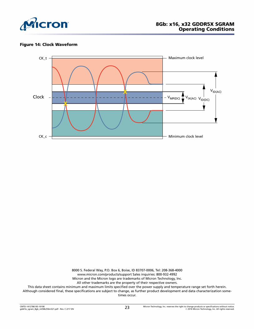
Figure 14: Clock Waveform
Maximum clock level
Minimum clock level
VID(AC)
VID(DC)VIX(AC)VMP(DC)
CK_t
CK_c
Clock
8000 S. Federal Way, P.O. Box 6, Boise, ID 83707-0006, Tel: 208-368-4000www.micron.com/products/support Sales inquiries: 800-932-4992
Micron and the Micron logo are trademarks of Micron Technology, Inc.All other trademarks are the property of their respective owners.
This data sheet contains minimum and maximum limits specified over the power supply and temperature range set forth herein.Although considered final, these specifications are subject to change, as further product development and data characterization some-
times occur.
8Gb: x16, x32 GDDR5X SGRAMOperating Conditions
CMTD-1412786195-10190gddr5x_sgram_8gb_mt58k256m321.pdf - Rev. C 2/17 EN 23 Micron Technology, Inc. reserves the right to change products or specifications without notice.
© 2016 Micron Technology, Inc. All rights reserved.