Embed Size (px)
Citation preview
A Top Down Design Methodology for Mixed-Signal Integrated Circuits using the VppSim Simulator
CDNLive! 2006Session Track: Custom IC Design
Session Number: 3.4
Michael PerrottMassachusetts Institute of Technology
September 2006
Copyright © 2006 by Michael H. PerrottAll rights reserved.
2
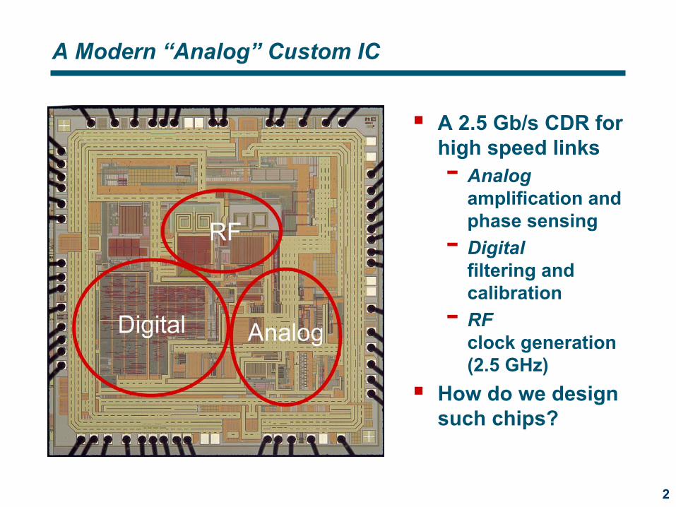
A Modern “Analog” Custom IC
A 2.5 Gb/s CDR for high speed links- Analog
amplification and phase sensing
- Digitalfiltering and calibration
- RFclock generation (2.5 GHz)
How do we design such chips?
3
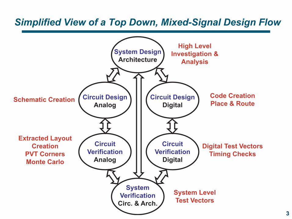
Simplified View of a Top Down, Mixed-Signal Design Flow
System Design
Architecture
Circuit
Verification
Digital
Circuit Design
Analog
Circuit Design
Digital
Circuit
Verification
Analog
System
Verification
Circ. & Arch.
High Level
Investigation &
Analysis
System Level
Test Vectors
Schematic Creation Code Creation
Place & Route
Extracted Layout
Creation
PVT Corners
Monte Carlo
Digital Test Vectors
Timing Checks
4
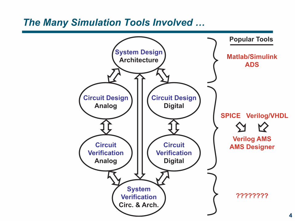
The Many Simulation Tools Involved …
System Design
Architecture
Circuit
Verification
Digital
Circuit Design
Analog
Circuit Design
Digital
Circuit
Verification
Analog
System
Verification
Circ. & Arch.
Matlab/Simulink
ADS
SPICE Verilog/VHDL
Verilog AMS
AMS Designer
????????
Popular Tools

5
Goal: Create a Universal Simulator
The challenges of developing the Managing Kernel- Difficult to match up simulator signals at their boundaries
without overly complicating the life of the user- Difficult to maintain fast simulation speed- Difficult to retrain designers on a new tool with a new flow
Managing
Kernel
SPICE
Matlab
Verilog
VHDL
System Designer
Analog Designer
Digital Designer

6
A Different Approach
Look for commonality among simulators to allow “universal” simulation models to be used- C++ provides one such hook
Allow designers to use their tool of choice while sharing “universal” simulation models
SPICE
Matlab
Verilog
VHDL
C/C++
Mex functions
C/C++
PLI Calls
C/C++
PLI Calls
(Verilog AMS
& AMS Designer)
Key idea: bootstrap into existing simulators
7
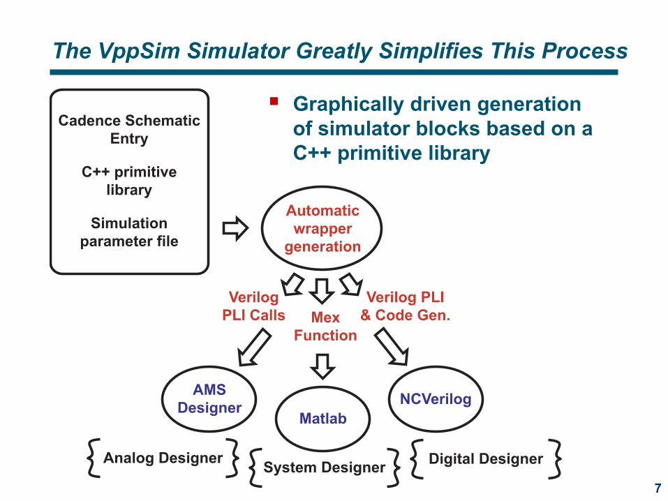
The VppSim Simulator Greatly Simplifies This Process
Graphically driven generation of simulator blocks based on a C++ primitive library
Automatic
wrapper
generation
AMS
DesignerMatlab
NCVerilog
Analog DesignerSystem Designer
Digital Designer
Mex
Function
Verilog PLI
& Code Gen.
Verilog
PLI Calls
Cadence Schematic
Entry
C++ primitive
library
Simulation
parameter file
8
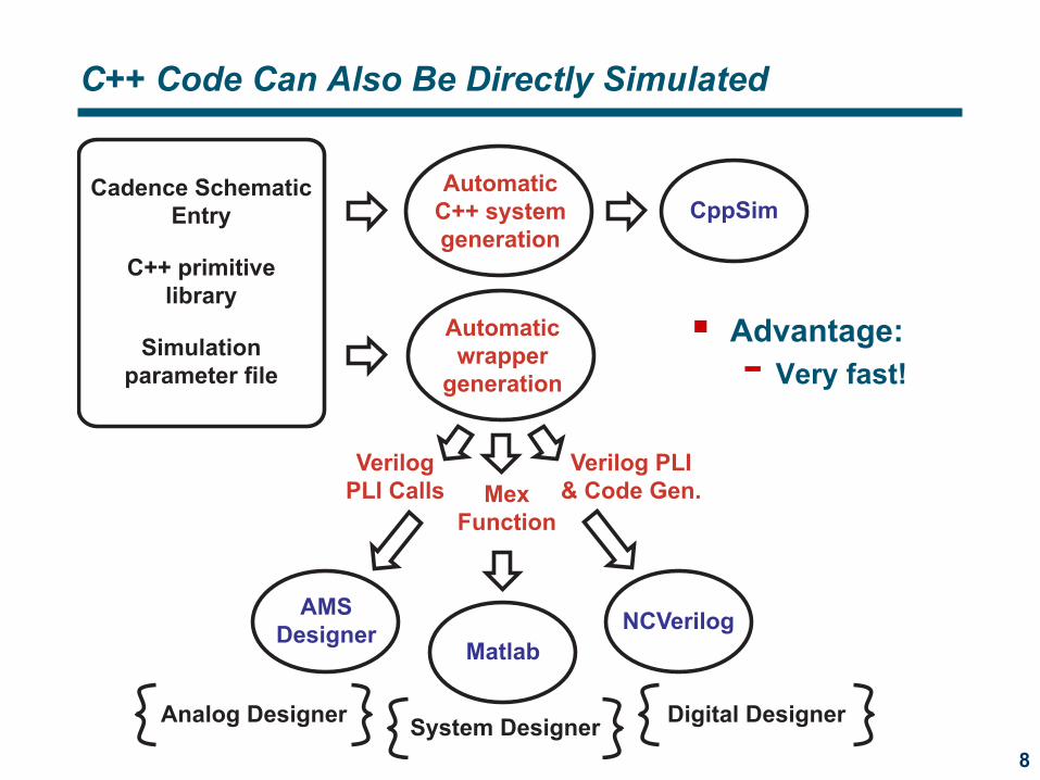
C++ Code Can Also Be Directly Simulated
Advantage:- Very fast!
Automatic
wrapper
generation
AMS
DesignerMatlab
NCVerilog
Analog DesignerSystem Designer
Digital Designer
Mex
Function
Verilog PLI
& Code Gen.
Verilog
PLI Calls
Automatic
C++ system
generation
Cadence Schematic
Entry
C++ primitive
library
CppSim
Simulation
parameter file
9
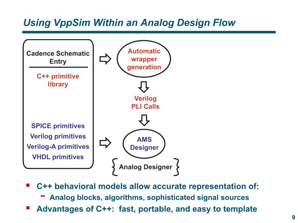
Using VppSim Within an Analog Design Flow
Automatic
wrapper
generation
AMS
Designer
Analog Designer
Verilog
PLI Calls
Cadence Schematic
Entry
C++ primitive
library
SPICE primitives
Verilog-A primitives
Verilog primitives
VHDL primitives
C++ behavioral models allow accurate representation of:- Analog blocks, algorithms, sophisticated signal sources
Advantages of C++: fast, portable, and easy to template
10
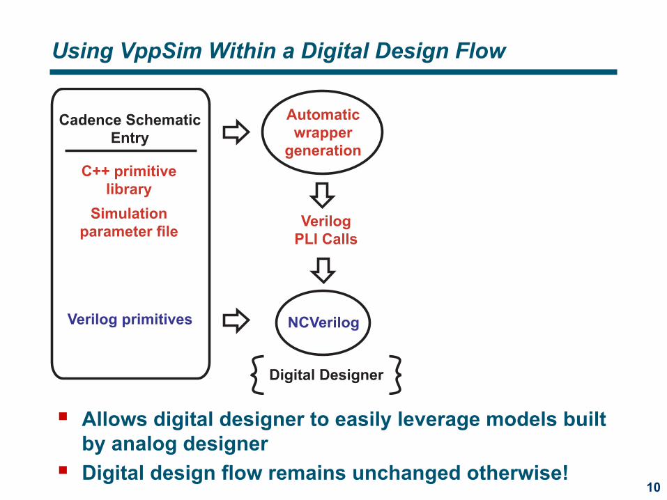
Using VppSim Within a Digital Design Flow
Allows digital designer to easily leverage models built by analog designerDigital design flow remains unchanged otherwise!
Automatic
wrapper
generation
NCVerilog
Digital Designer
Verilog
PLI Calls
Cadence Schematic
Entry
C++ primitive
library
Verilog primitives
Simulation
parameter file
11
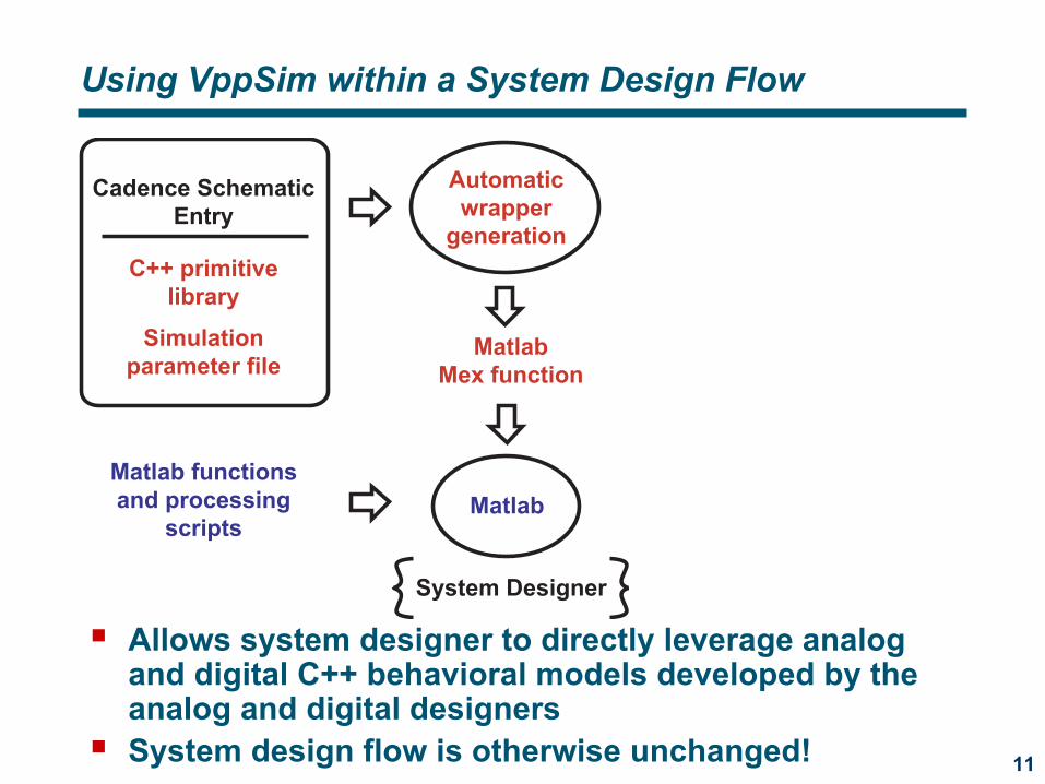
Using VppSim within a System Design Flow
Allows system designer to directly leverage analog and digital C++ behavioral models developed by the analog and digital designersSystem design flow is otherwise unchanged!
Automatic
wrapper
generation
Matlab
System Designer
Matlab
Mex function
Cadence Schematic
Entry
C++ primitive
library
Matlab functions
and processing
scripts
Simulation
parameter file
12
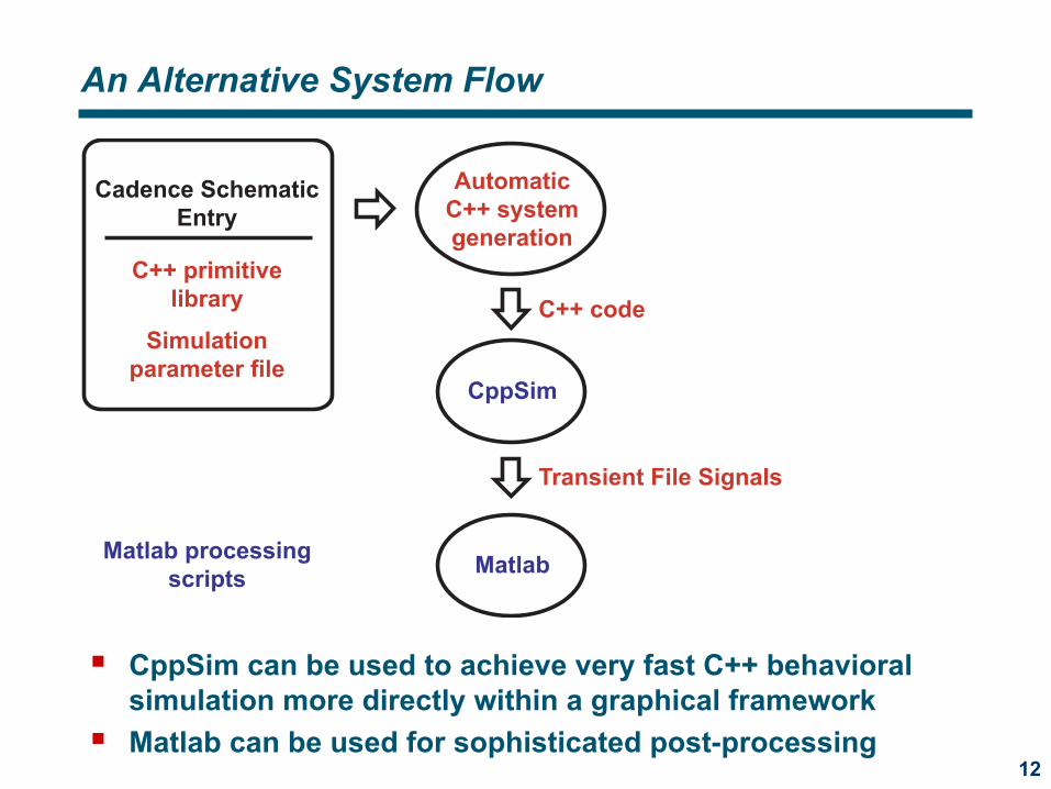
An Alternative System Flow
CppSim can be used to achieve very fast C++ behavioral simulation more directly within a graphical frameworkMatlab can be used for sophisticated post-processing
Automatic
C++ system
generation
CppSim
C++ code
Cadence Schematic
Entry
C++ primitive
library
Matlab processing
scripts
Simulation
parameter file
Matlab
Transient File Signals
13
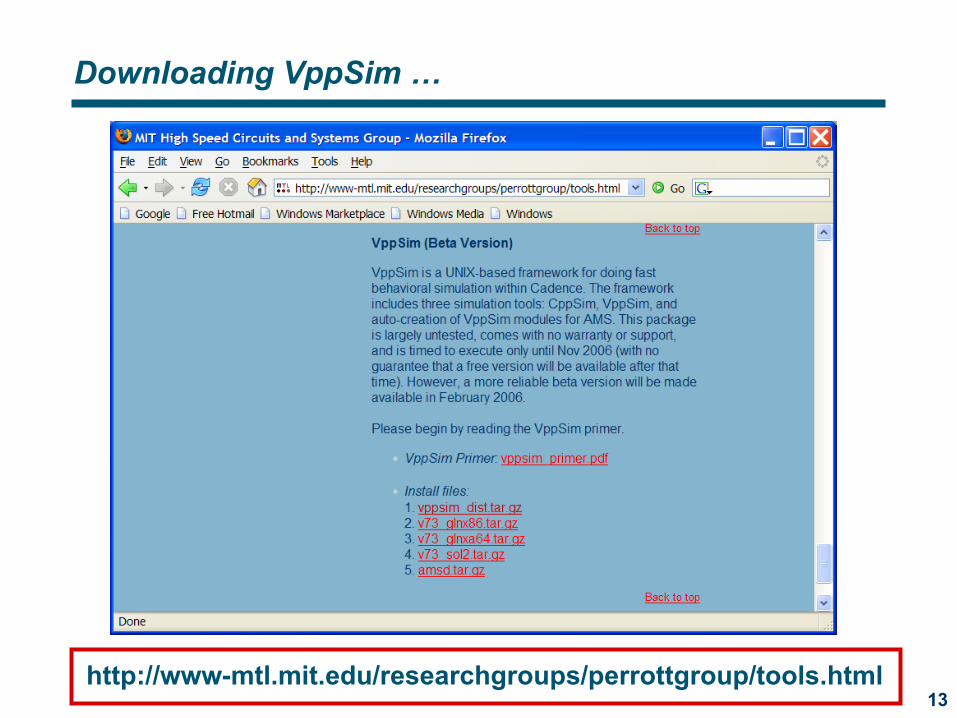
Downloading VppSim …
http://www-mtl.mit.edu/researchgroups/perrottgroup/tools.html

Can You Accurately Model Complicated Mixed-Signal Circuits using C++ Behavioral Models?
15
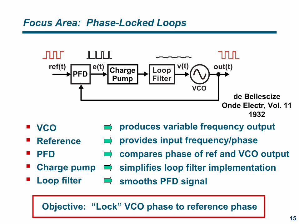
Focus Area: Phase-Locked Loops
PFDChargePump
out(t)e(t) v(t)LoopFilter
VCO
ref(t)
VCOReference PFD Charge pumpLoop filter
produces variable frequency outputprovides input frequency/phasecompares phase of ref and VCO outputsimplifies loop filter implementationsmooths PFD signal
Objective: “Lock” VCO phase to reference phase
de BellescizeOnde Electr, Vol. 11
1932

16
Integer-N Frequency Synthesizer
Leverages frequency divider to create “indirect” frequency multiplication- Allows digital adjustment of output frequency in
increments of the reference frequency
PFD ChargePump
out(t)e(t) v(t)
N
LoopFilter
DividerVCO
ref(t)
div(t)
Fout = N FrefFref
Sepe and JohnstonUS Patent 3,551,826
1968 (filing date)
17
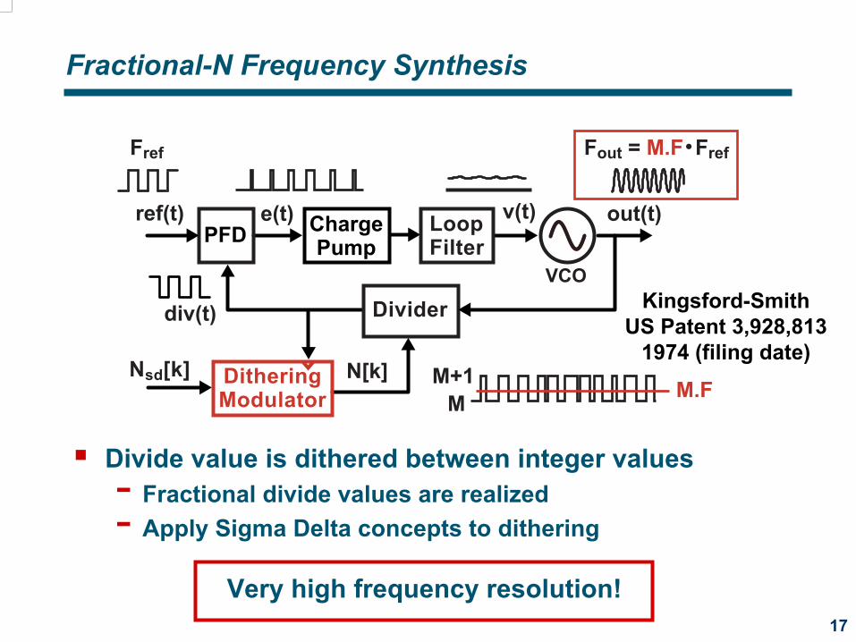
Fractional-N Frequency Synthesis
Divide value is dithered between integer values- Fractional divide values are realized- Apply Sigma Delta concepts to dithering
Very high frequency resolution!
PFDChargePump
Nsd[k]
out(t)e(t)
DitheringModulator
v(t)
N[k]
LoopFilter
Divider
VCO
ref(t)
div(t)
M
M+1
Fout = M.F Fref
M.F
Fref
Kingsford-SmithUS Patent 3,928,813
1974 (filing date)
18
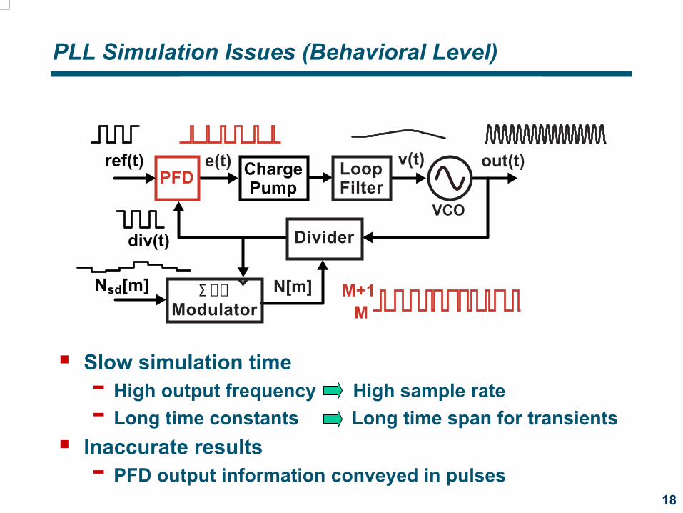
PLL Simulation Issues (Behavioral Level)
Slow simulation time- High output frequency High sample rate - Long time constants Long time span for transients
Inaccurate results- PFD output information conveyed in pulses
PFD ChargePump
Nsd[m]
out(t)e(t)
Σ−∆Modulator
v(t)
N[m]
LoopFilter
DividerVCO
ref(t)
div(t)
MM+1
19
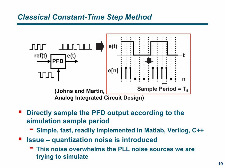
Classical Constant-Time Step Method
Directly sample the PFD output according to the simulation sample period- Simple, fast, readily implemented in Matlab, Verilog, C++
Issue – quantization noise is introduced- This noise overwhelms the PLL noise sources we are
trying to simulate
PFDe(t)ref(t)
e(t)t
e[n]n
Sample Period = Ts(Johns and Martin,Analog Integrated Circuit Design)
20
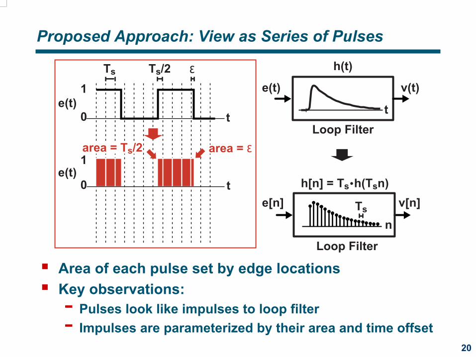
Proposed Approach: View as Series of Pulses
Area of each pulse set by edge locationsKey observations:- Pulses look like impulses to loop filter- Impulses are parameterized by their area and time offset
e(t)
tLoop Filter
h(t)
v(t)
e(t)
e(t)t
t
1
0
1
0
εTs Ts/2
area = εarea = Ts/2
e[n]
n
Loop Filter
Ts v[n]h[n] = Ts h(Tsn)
21
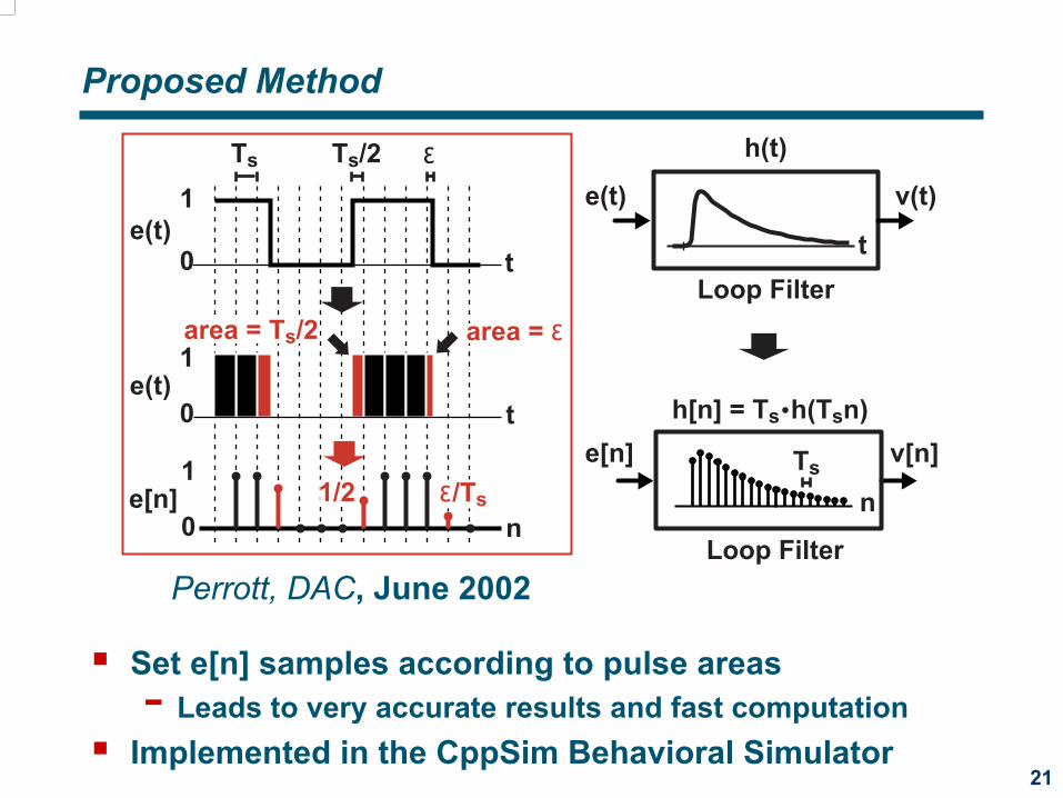
Proposed Method
Set e[n] samples according to pulse areas- Leads to very accurate results and fast computation
Implemented in the CppSim Behavioral Simulator
e(t)
tLoop Filter
h(t)
v(t)
e(t)
e(t)t
t
e[n]n
1
0
1
0
1
0
εTs Ts/2
area = εarea = Ts/2
ε/Ts1/2e[n]
n
Loop Filter
Ts v[n]h[n] = Ts h(Tsn)
Perrott, DAC, June 2002
Some Fabricated Examples to Consider:
1) A 3.6 GHz, Low Noise, Wideband Fractional-N Synthesizer
2) A 2.5 Gb/s, Low Jitter, Clock and Data Recovery Circuit
3) A 3.1 GHz Limit Amplifier with Fast Offset Correction
4) A 2 GHz VCO-based A/D Converter
Does C++ behavioral simulation really help?
23
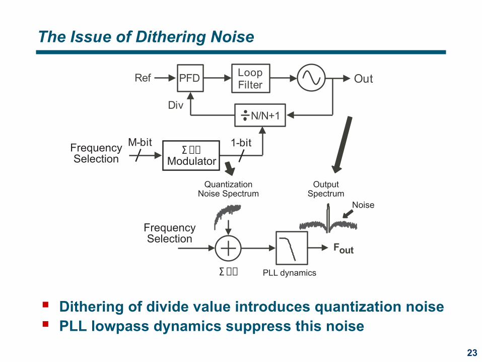
The Issue of Dithering Noise
PFD LoopFilter
N/N+1
Ref Out
M-bit 1-bit
Div
Σ−∆Modulator
Fout
Noise
FrequencySelection
FrequencySelection
OutputSpectrum
QuantizationNoise Spectrum
PLL dynamicsΣ−∆
Dithering of divide value introduces quantization noisePLL lowpass dynamics suppress this noise
24
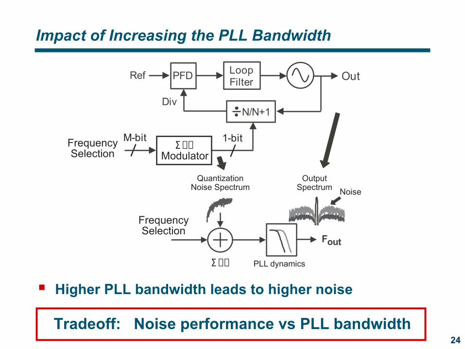
Impact of Increasing the PLL Bandwidth
Higher PLL bandwidth leads to higher noise
PFD LoopFilter
N/N+1
Ref Out
M-bit 1-bit
Div
Σ−∆Modulator
Fout
Noise
FrequencySelection
FrequencySelection
OutputSpectrum
QuantizationNoise Spectrum
PLL dynamicsΣ−∆
Tradeoff: Noise performance vs PLL bandwidth
25
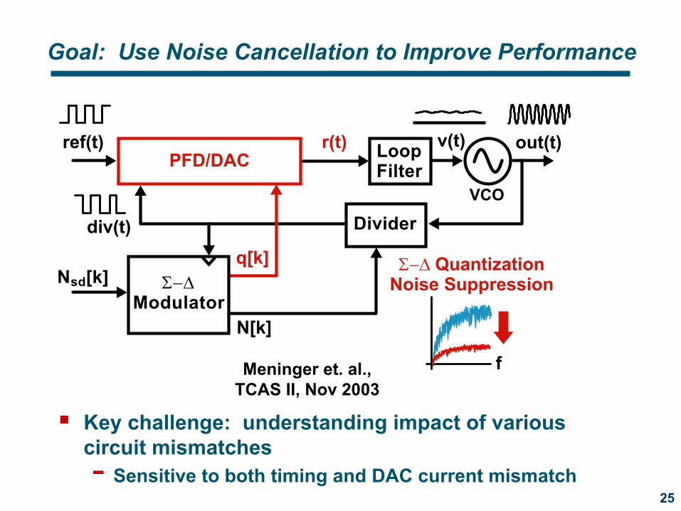
Goal: Use Noise Cancellation to Improve Performance
Key challenge: understanding impact of various circuit mismatches- Sensitive to both timing and DAC current mismatch
PFD/DAC
Nsd[k]
out(t)r(t)
Σ−∆Modulator
v(t)
N[k]
LoopFilter
DividerVCO
ref(t)
div(t)
f
Σ−∆ QuantizationNoise Suppression
q[k]
Meninger et. al.,TCAS II, Nov 2003
26
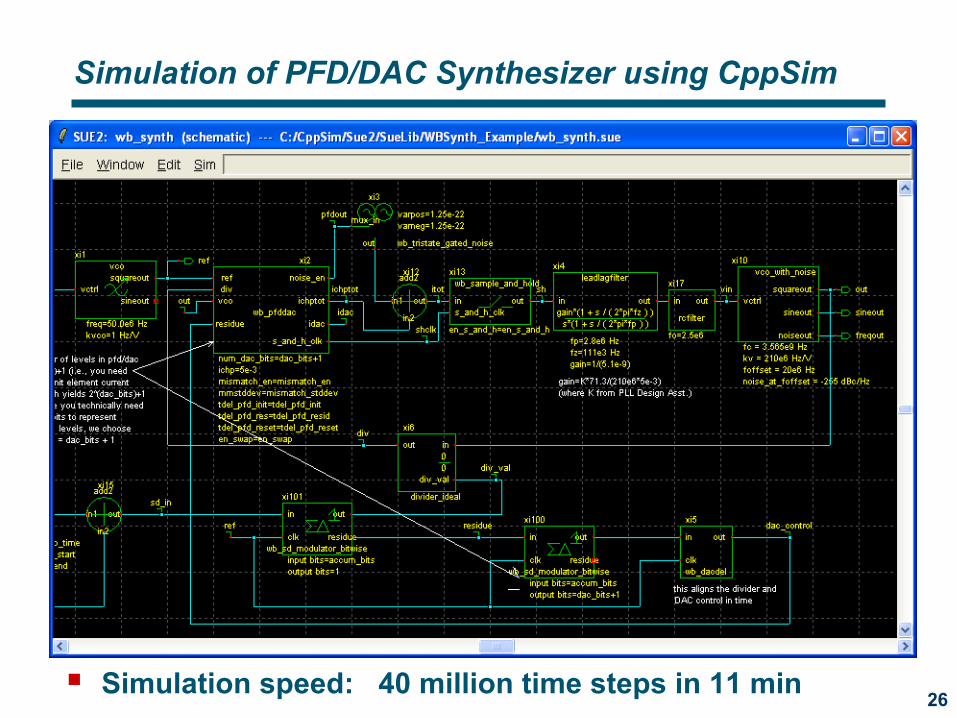
Simulation of PFD/DAC Synthesizer using CppSim
Simulation speed: 40 million time steps in 11 min
27
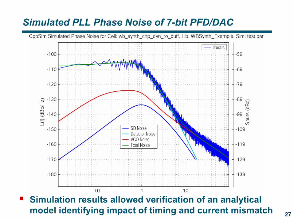
Simulated PLL Phase Noise of 7-bit PFD/DAC
Simulation results allowed verification of an analytical model identifying impact of timing and current mismatch
28
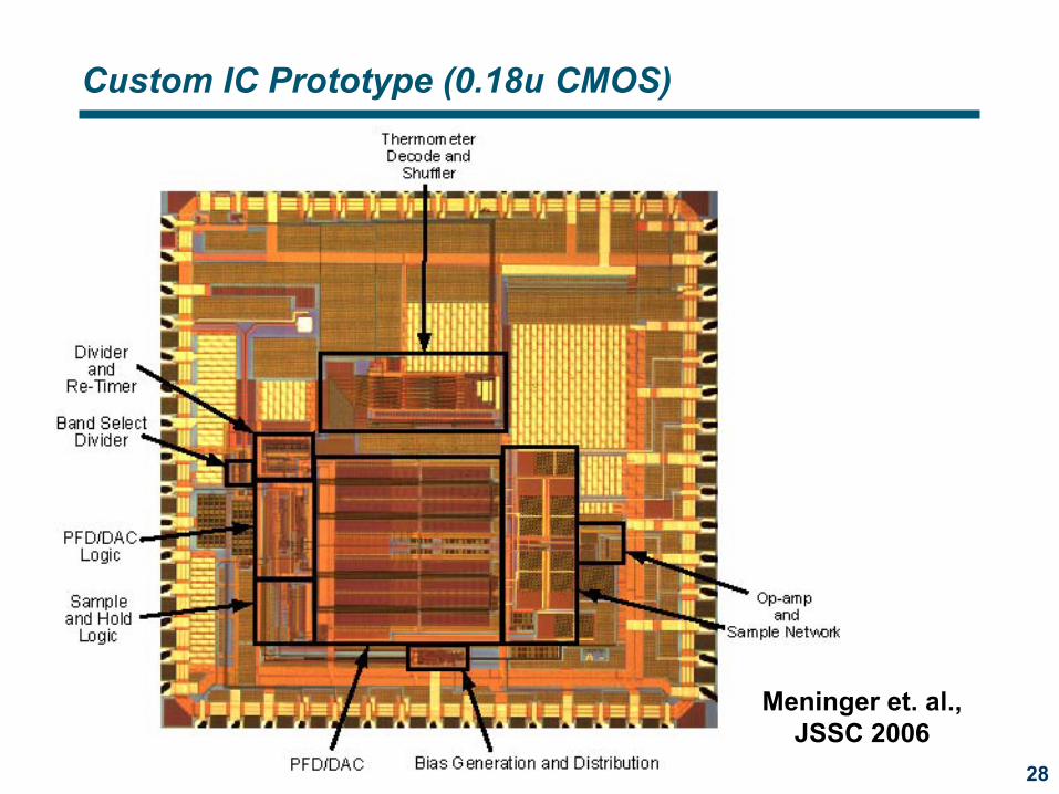
Custom IC Prototype (0.18u CMOS)
Meninger et. al.,JSSC 2006
29
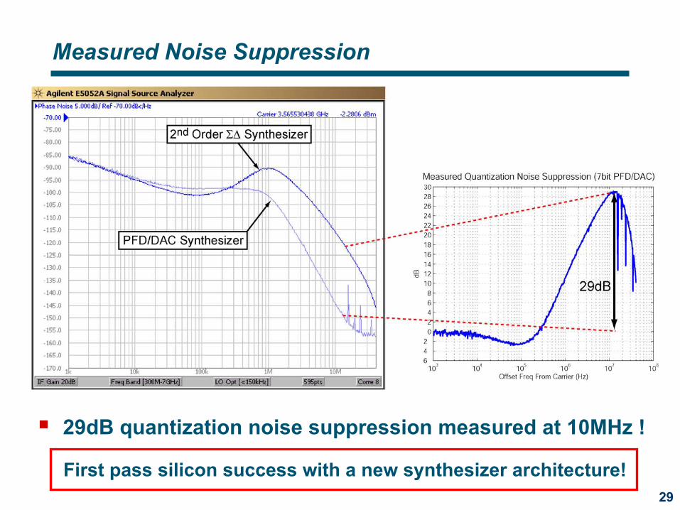
Measured Noise Suppression
29dB quantization noise suppression measured at 10MHz !
First pass silicon success with a new synthesizer architecture!
30
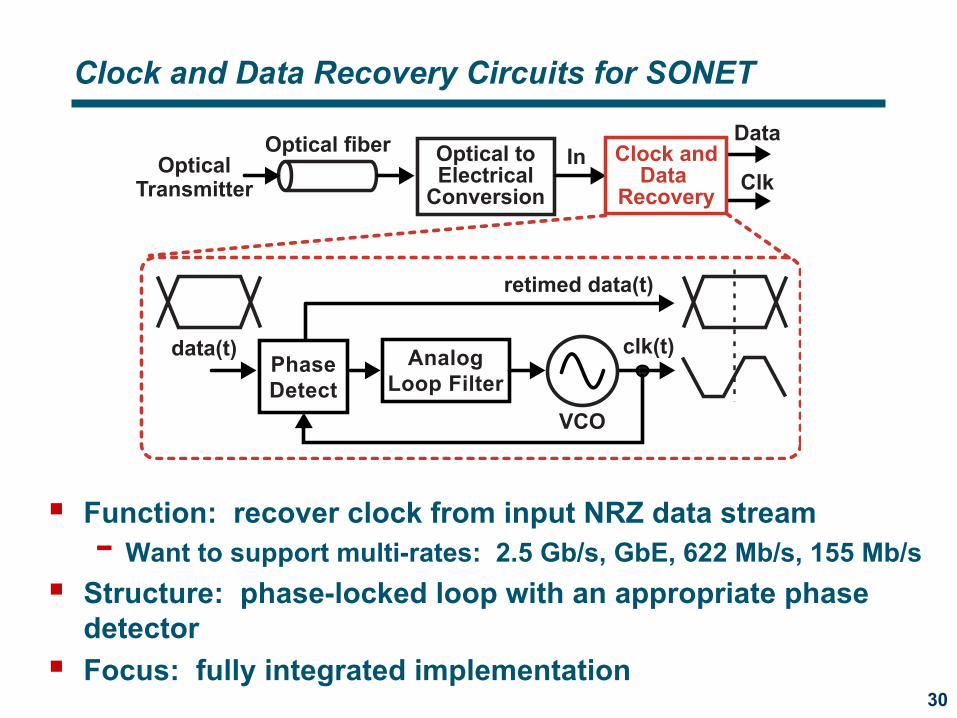
Clock and Data Recovery Circuits for SONET
Function: recover clock from input NRZ data stream- Want to support multi-rates: 2.5 Gb/s, GbE, 622 Mb/s, 155 Mb/s
Structure: phase-locked loop with an appropriate phase detectorFocus: fully integrated implementation
OpticalTransmitter
Optical fiber Optical toElectrical
Conversion
InData
Clk
Clock andData
Recovery
clk(t)
retimed data(t)
data(t) Analog
Loop FilterPhase
Detect
VCO
31
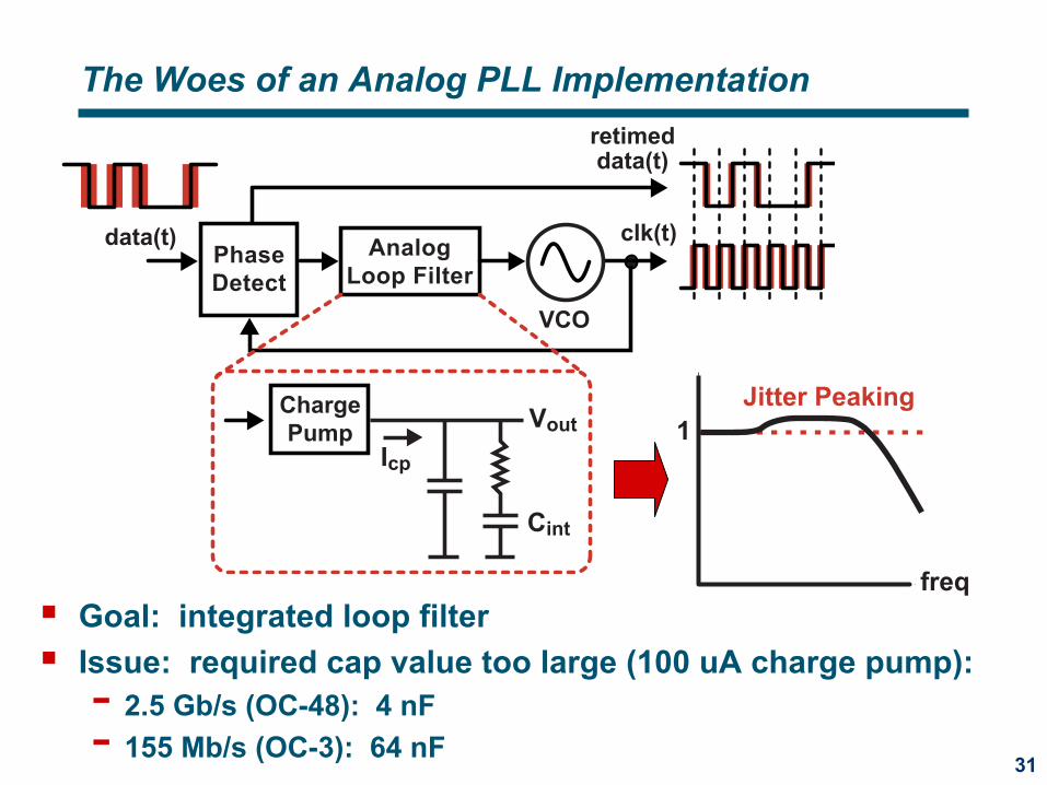
The Woes of an Analog PLL Implementation
Goal: integrated loop filterIssue: required cap value too large (100 uA charge pump):- 2.5 Gb/s (OC-48): 4 nF- 155 Mb/s (OC-3): 64 nF
clk(t)
retimeddata(t)
data(t) Analog
Loop FilterPhase
Detect
VCO
Icp
VoutCharge
Pump
Cint
freq
Jitter Peaking
1
32
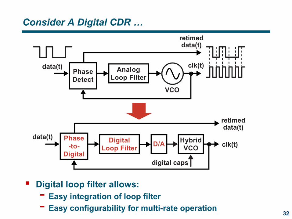
Consider A Digital CDR …
Digital loop filter allows:- Easy integration of loop filter- Easy configurability for multi-rate operation
clk(t)
retimeddata(t)
data(t) Analog
Loop FilterPhase
Detect
VCO
clk(t)data(t)
Hybrid
VCO
Digital
Loop Filter
Phase
-to-
Digital
retimeddata(t)
digital caps
D/A
33
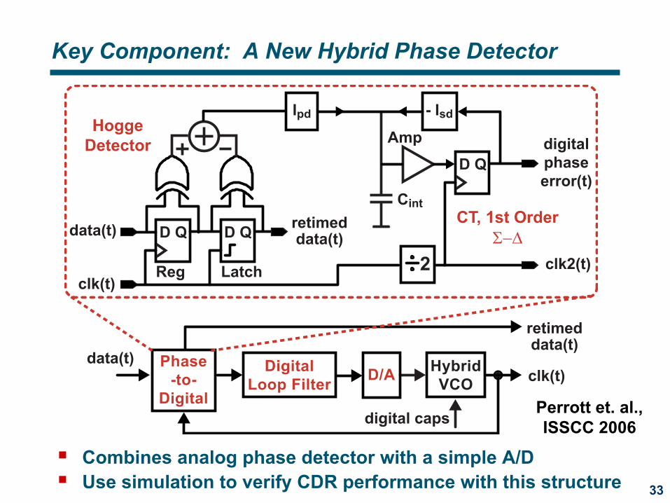
Key Component: A New Hybrid Phase Detector
Combines analog phase detector with a simple A/DUse simulation to verify CDR performance with this structure
retimeddata(t)D QD Q
clk(t)
data(t)
LatchReg
D Q
Amp
- Isd
Cint
2
Ipd
digital
phase
error(t)
clk2(t)
CT, 1st Order
Σ−∆
Hogge
Detector
clk(t)data(t)
Hybrid
VCO
Digital
Loop Filter
Phase
-to-
Digital
retimeddata(t)
digital caps
D/A
Perrott et. al.,ISSCC 2006
34
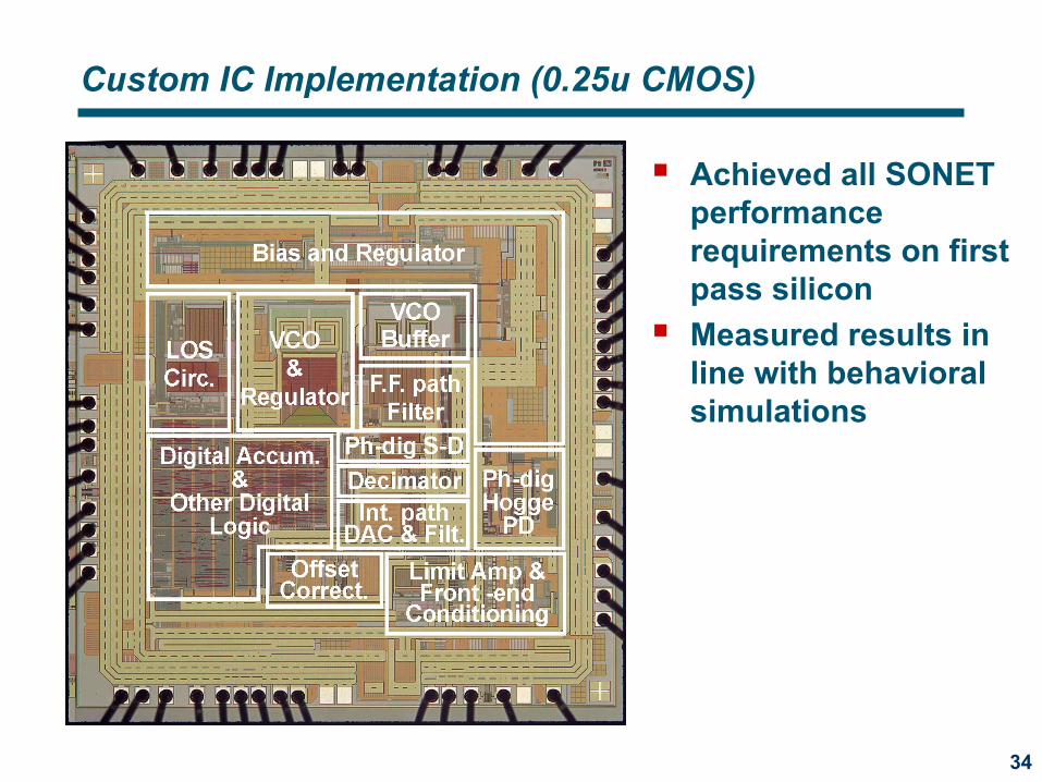
Custom IC Implementation (0.25u CMOS)
Achieved all SONET performance requirements on first pass siliconMeasured results in line with behavioral simulations
35
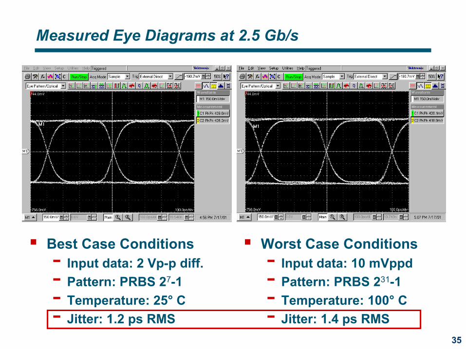
Measured Eye Diagrams at 2.5 Gb/s
Best Case Conditions- Input data: 2 Vp-p diff.- Pattern: PRBS 27-1- Temperature: 25° C- Jitter: 1.2 ps RMS
Worst Case Conditions- Input data: 10 mVppd- Pattern: PRBS 231-1- Temperature: 100° C- Jitter: 1.4 ps RMS

36
A Fast Acquisition Limit Amp
Acquisition time of CDR is limited by slow response of limit amp offset correction loop (typically milliseconds)Research focus: improve speed of offset correction
Trans-ImpedanceAmp
LimitAmp
Clock andData
Recovery
Data
ClkDigital
ProcessorIn
Optic Fiber
Interface Circuit CMOS ASIC
LoopFilter
PhaseDetector
Data Out
Data In Clk Out
VCO
Analog Digital
37
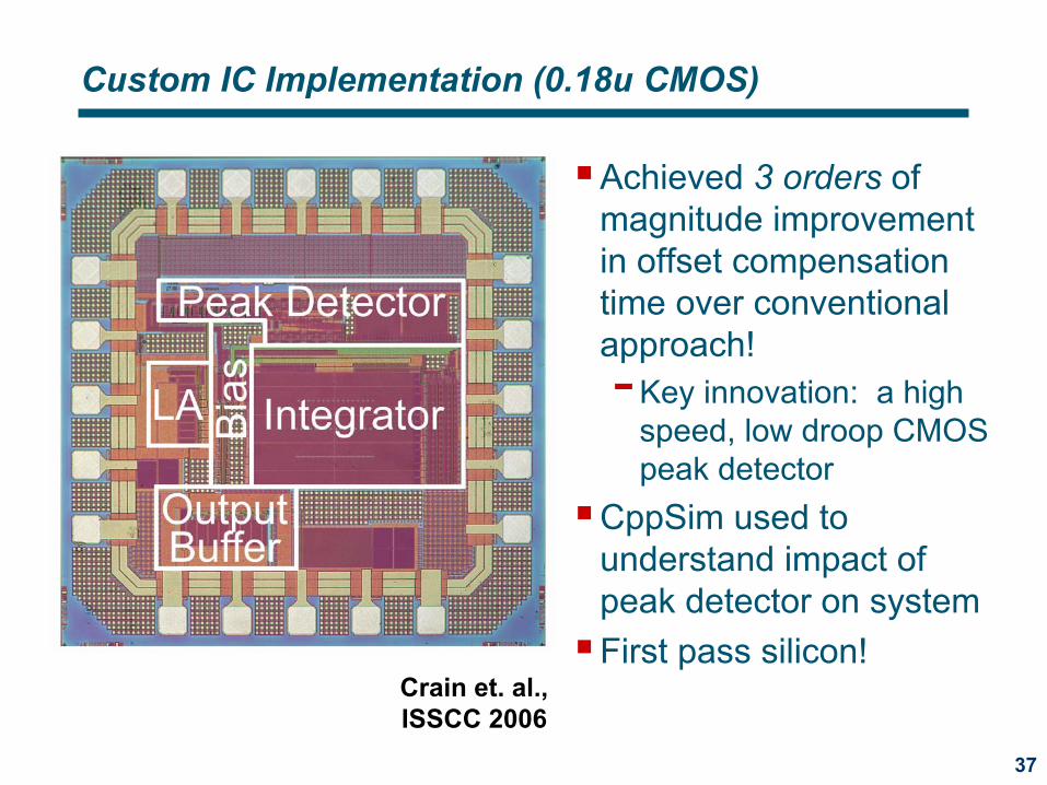
Custom IC Implementation (0.18u CMOS)
Achieved 3 orders of magnitude improvement in offset compensation time over conventional approach!-Key innovation: a high
speed, low droop CMOS peak detector
CppSim used to understand impact of peak detector on systemFirst pass silicon!
Crain et. al.,ISSCC 2006
38
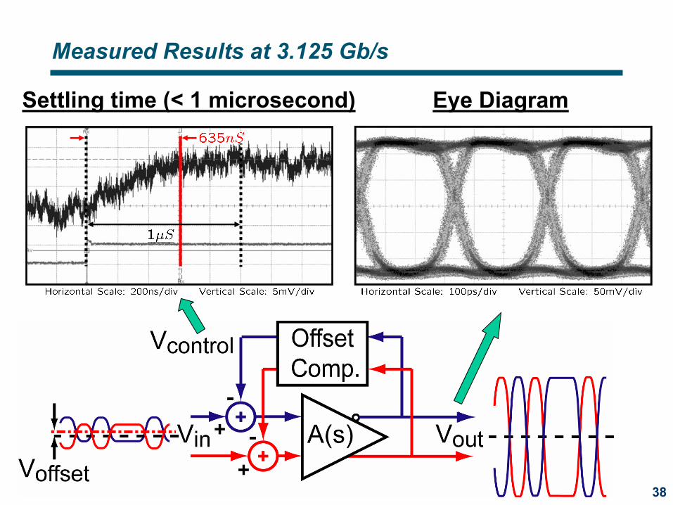
Measured Results at 3.125 Gb/s
Settling time (< 1 microsecond) Eye Diagram
39
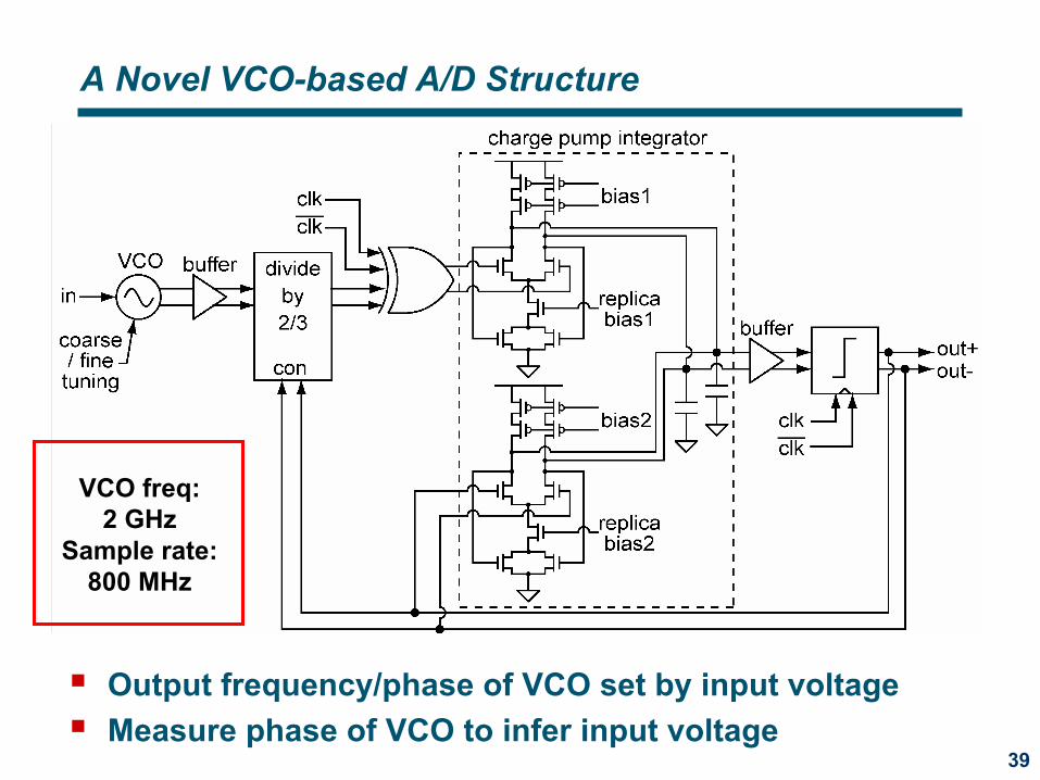
A Novel VCO-based A/D Structure
Output frequency/phase of VCO set by input voltageMeasure phase of VCO to infer input voltage
VCO freq:2 GHz
Sample rate:800 MHz
40
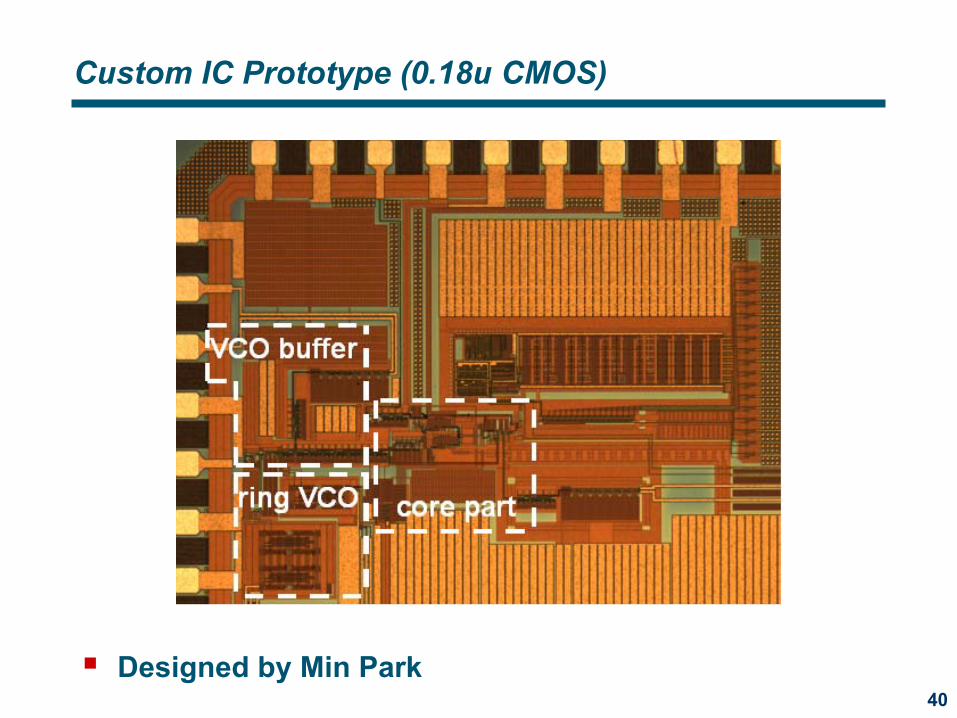
Custom IC Prototype (0.18u CMOS)
Designed by Min Park

41
Measured output spectrum (Hann Window)
22 dBInputSignal
42
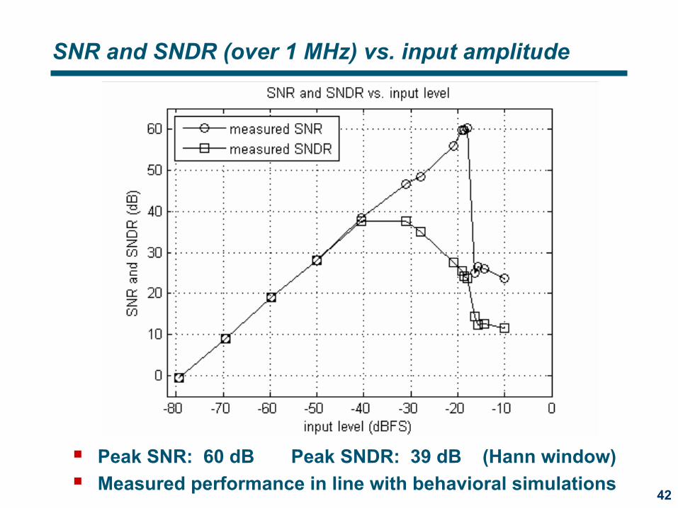
SNR and SNDR (over 1 MHz) vs. input amplitude
Peak SNR: 60 dB Peak SNDR: 39 dB (Hann window)Measured performance in line with behavioral simulations
43
Conclusion
C++ behavioral models allow fast and accurate simulation of novel mixed-signal circuits- Allows the designer to understand key issues before
spending time on transistor level circuitsC++ models allow seamless bootstrapping into a variety of simulators- AMS Designer- NCVerilog- Matlab- CppSim
VppSim dramatically simplifies the integration of these models in each of the above simulators