Embed Size (px)
Citation preview
IEEE TRANSACTIONS ON POWER ELECTRONICS, VOL. 27, NO. 8, AUGUST 2012 3513
A ZVS Interleaved Boost AC/DC Converter Usedin Plug-in Electric Vehicles
Majid Pahlevaninezhad, Member, IEEE, Pritam Das, Member, IEEE, Josef Drobnik, Senior Member, IEEE,Praveen K. Jain, Fellow, IEEE, and Alireza Bakhshai, Senior Member, IEEE
Abstract—This paper presents a novel, yet simple zero-voltageswitching (ZVS) interleaved boost power factor correction (PFC)ac/dc converter used to charge the traction battery of an electricvehicle from the utility mains. The proposed opology consists ofa passive auxiliary circuit, placed between two phases of the in-terleaved front-end boost PFC converter, which provides enoughcurrent to charge and discharge the MOSFETs’ output capacitorsduring turn-ON times. Therefore, the MOSFETs are turned ONat zero voltage. The proposed converter maintains ZVS for theuniversal input voltage (85 to 265 Vrm s ), which includes a verywide range of duty ratios (0.07–1). In addition, the control systemoptimizes the amount of reactive current required to guaranteeZVS during the line cycle for different load conditions. This opti-mization is crucial in this application since the converter may workat very light loads for a long period of time. Experimental resultsfrom a 3 kW ac/dc converter are presented in the paper to evalu-ate the performance of the proposed converter. The results show aconsiderable increase in efficiency and superior performance of theproposed converter compared to the conventional hard-switchedinterleaved boost PFC converter.
Index Terms—AC/DC converter, continuous current mode(CCM), dc/dc converter, interleaved boost converter, power fac-tor correction (PFC), zero-current switching (ZCS), zero-voltageswitching (ZVS).
NOMENCLATURE
ΔiLA Inductor current ripple of boost A (A).ωl Line frequency (rad/s).ψ Phase-shift between leading leg and lagging leg
pulses.CSo Output capacitance of the boost MOSFET (F).D PFC duty ratio.fs Switching frequency (Hz).iAux,p Peak value of the auxiliary circuit current (A).
Manuscript received September 27, 2011; revised December 20, 2011;accepted January 20, 2012. Date of current version April 20, 2012. This workwas supported by Freescale Semiconductor, Inc., Tempe, Arizona. Recom-mended for publication by Associate Editor A. Emadi.
M. Pahlevaninezhad, P. K. Jain, and A. Bakhshai are with the Queen’sCentre for Energy and Power Electronics Research (ePOWER), Queen’sUniversity, Kingston, ON K7L3N6, Canada (e-mail: [email protected];[email protected]; [email protected]).
P. Das was with the Queen’s Centre for Energy and Power ElectronicsResearch (ePOWER), Queen’s University, Kingston, ON K7L3N6, Canada.He is now with Murata Power Solutions, Markham, ON L3S0J3, Canada(e-mail: [email protected]).
J. Drobnik is with Freescale Semiconductor, Inc., Tempe, AZ 85284 USA(e-mail: [email protected]).
Color versions of one or more of the figures in this paper are available onlineat http://ieeexplore.ieee.org.
Digital Object Identifier 10.1109/TPEL.2012.2186320
iin Input current of power factor correction (PFC) (A).iLA Inductor current of boost A (A).iLB Inductor current of boost B (A).iSA 1 Switch SA 1 current (A).IBAT Battery current (A).Io DC output current (A).IP Peak current of the boost inductor (A).Iref Peak value of the auxiliary circuit reference current
(A).IV Valley current of the boost inductor (A).k1 Controller coefficient.pin Instantaneous input power (W).pref Instantaneous input power reference value (W).Pin,pk Peak input power (W).Pref Power reference value (W).ro Load incremental resistance (Ω).Psw Switching losses (W).Re Converter effective load resistance (Ω).RL PFC inductor series resistance (Ω).t Time (s).td Dead time (s).u Control input.vAUX Voltage across auxiliary circuit (V).vin Instantaneous input voltage of PFC (V).VBAT Battery voltage (V).Vd Output diode forward voltage drop (V).Vo DC output voltage (V).x State variables.ESR Equivalent series resistance (Ω).SiC Silicon carbide.Si Silicon.
I. INTRODUCTION
E LECTRIC vehicle (EV) power conditioning systems usu-ally utilize a high-energy battery pack to store energy for
the electric traction system [1]. A typical block diagram of thepower conditioning system in an EV is shown in Fig. 1. Thehigh-energy battery pack is typically charged from a utility acoutlet [2]. This energy conversion during the battery charging isperformed by an ac/dc converter. Such ac/dc converters, whichare used to charge the high-energy battery, usually consist oftwo stages: front-end boost converter, which performs inputPFC and ac/dc conversion, and full-bridge dc/dc converter forbattery charging and galvanic isolation [3]. PFC is essential toimprove the quality of the input current, which is drawn fromthe utility so as to comply with the regulatory standards like IEC61000-3-2.
0885-8993/$31.00 © 2012 IEEE
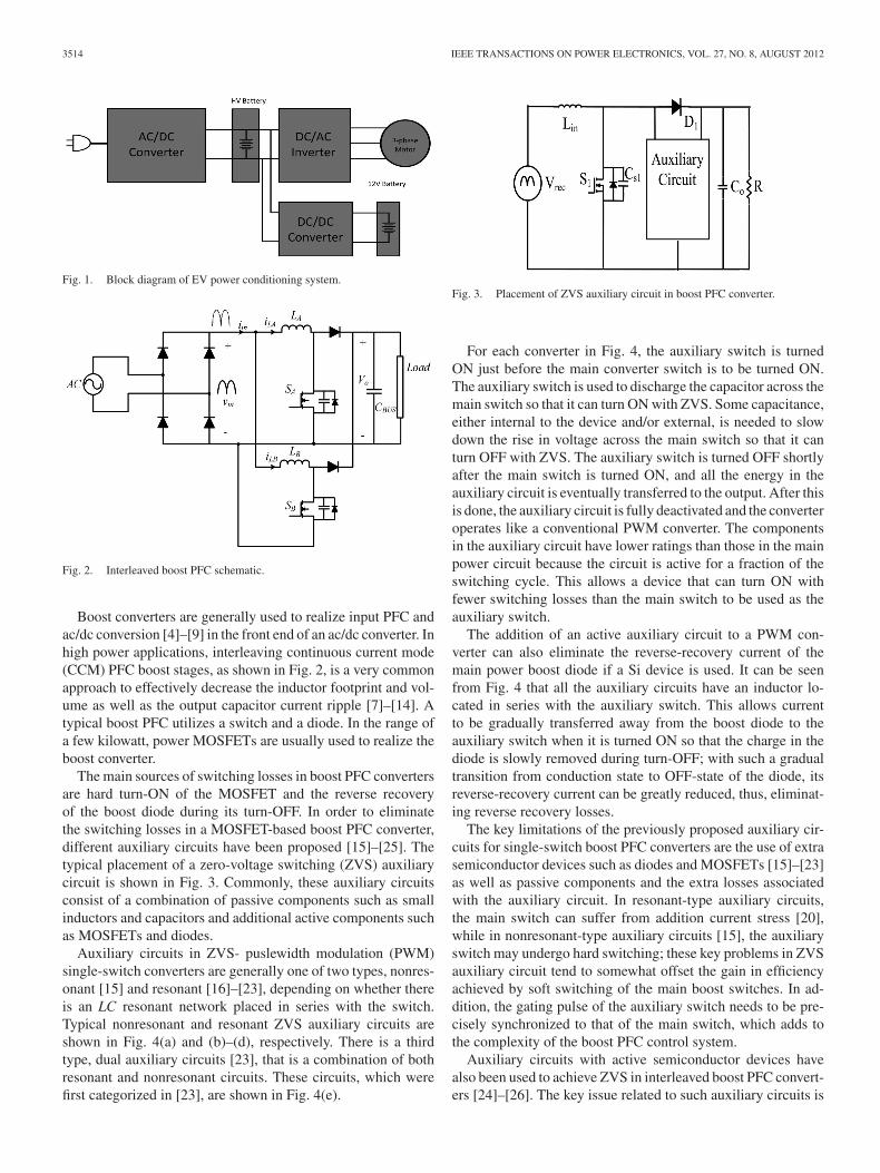
3514 IEEE TRANSACTIONS ON POWER ELECTRONICS, VOL. 27, NO. 8, AUGUST 2012
Fig. 1. Block diagram of EV power conditioning system.
Fig. 2. Interleaved boost PFC schematic.
Boost converters are generally used to realize input PFC andac/dc conversion [4]–[9] in the front end of an ac/dc converter. Inhigh power applications, interleaving continuous current mode(CCM) PFC boost stages, as shown in Fig. 2, is a very commonapproach to effectively decrease the inductor footprint and vol-ume as well as the output capacitor current ripple [7]–[14]. Atypical boost PFC utilizes a switch and a diode. In the range ofa few kilowatt, power MOSFETs are usually used to realize theboost converter.
The main sources of switching losses in boost PFC convertersare hard turn-ON of the MOSFET and the reverse recoveryof the boost diode during its turn-OFF. In order to eliminatethe switching losses in a MOSFET-based boost PFC converter,different auxiliary circuits have been proposed [15]–[25]. Thetypical placement of a zero-voltage switching (ZVS) auxiliarycircuit is shown in Fig. 3. Commonly, these auxiliary circuitsconsist of a combination of passive components such as smallinductors and capacitors and additional active components suchas MOSFETs and diodes.
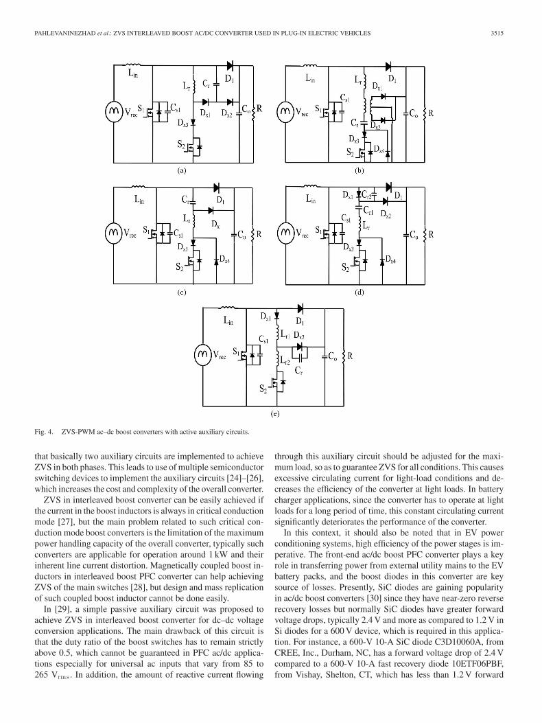
Auxiliary circuits in ZVS- puslewidth modulation (PWM)single-switch converters are generally one of two types, nonres-onant [15] and resonant [16]–[23], depending on whether thereis an LC resonant network placed in series with the switch.Typical nonresonant and resonant ZVS auxiliary circuits areshown in Fig. 4(a) and (b)–(d), respectively. There is a thirdtype, dual auxiliary circuits [23], that is a combination of bothresonant and nonresonant circuits. These circuits, which werefirst categorized in [23], are shown in Fig. 4(e).
Fig. 3. Placement of ZVS auxiliary circuit in boost PFC converter.
For each converter in Fig. 4, the auxiliary switch is turnedON just before the main converter switch is to be turned ON.The auxiliary switch is used to discharge the capacitor across themain switch so that it can turn ON with ZVS. Some capacitance,either internal to the device and/or external, is needed to slowdown the rise in voltage across the main switch so that it canturn OFF with ZVS. The auxiliary switch is turned OFF shortlyafter the main switch is turned ON, and all the energy in theauxiliary circuit is eventually transferred to the output. After thisis done, the auxiliary circuit is fully deactivated and the converteroperates like a conventional PWM converter. The componentsin the auxiliary circuit have lower ratings than those in the mainpower circuit because the circuit is active for a fraction of theswitching cycle. This allows a device that can turn ON withfewer switching losses than the main switch to be used as theauxiliary switch.
The addition of an active auxiliary circuit to a PWM con-verter can also eliminate the reverse-recovery current of themain power boost diode if a Si device is used. It can be seenfrom Fig. 4 that all the auxiliary circuits have an inductor lo-cated in series with the auxiliary switch. This allows currentto be gradually transferred away from the boost diode to theauxiliary switch when it is turned ON so that the charge in thediode is slowly removed during turn-OFF; with such a gradualtransition from conduction state to OFF-state of the diode, itsreverse-recovery current can be greatly reduced, thus, eliminat-ing reverse recovery losses.
The key limitations of the previously proposed auxiliary cir-cuits for single-switch boost PFC converters are the use of extrasemiconductor devices such as diodes and MOSFETs [15]–[23]as well as passive components and the extra losses associatedwith the auxiliary circuit. In resonant-type auxiliary circuits,the main switch can suffer from addition current stress [20],while in nonresonant-type auxiliary circuits [15], the auxiliaryswitch may undergo hard switching; these key problems in ZVSauxiliary circuit tend to somewhat offset the gain in efficiencyachieved by soft switching of the main boost switches. In ad-dition, the gating pulse of the auxiliary switch needs to be pre-cisely synchronized to that of the main switch, which adds tothe complexity of the boost PFC control system.
Auxiliary circuits with active semiconductor devices havealso been used to achieve ZVS in interleaved boost PFC convert-ers [24]–[26]. The key issue related to such auxiliary circuits is
PAHLEVANINEZHAD et al.: ZVS INTERLEAVED BOOST AC/DC CONVERTER USED IN PLUG-IN ELECTRIC VEHICLES 3515
Fig. 4. ZVS-PWM ac–dc boost converters with active auxiliary circuits.
that basically two auxiliary circuits are implemented to achieveZVS in both phases. This leads to use of multiple semiconductorswitching devices to implement the auxiliary circuits [24]–[26],which increases the cost and complexity of the overall converter.
ZVS in interleaved boost converter can be easily achieved ifthe current in the boost inductors is always in critical conductionmode [27], but the main problem related to such critical con-duction mode boost converters is the limitation of the maximumpower handling capacity of the overall converter, typically suchconverters are applicable for operation around 1 kW and theirinherent line current distortion. Magnetically coupled boost in-ductors in interleaved boost PFC converter can help achievingZVS of the main switches [28], but design and mass replicationof such coupled boost inductor cannot be done easily.
In [29], a simple passive auxiliary circuit was proposed toachieve ZVS in interleaved boost converter for dc–dc voltageconversion applications. The main drawback of this circuit isthat the duty ratio of the boost switches has to remain strictlyabove 0.5, which cannot be guaranteed in PFC ac/dc applica-tions especially for universal ac inputs that vary from 85 to265 Vrms . In addition, the amount of reactive current flowing
through this auxiliary circuit should be adjusted for the maxi-mum load, so as to guarantee ZVS for all conditions. This causesexcessive circulating current for light-load conditions and de-creases the efficiency of the converter at light loads. In batterycharger applications, since the converter has to operate at lightloads for a long period of time, this constant circulating currentsignificantly deteriorates the performance of the converter.
In this context, it should also be noted that in EV powerconditioning systems, high efficiency of the power stages is im-perative. The front-end ac/dc boost PFC converter plays a keyrole in transferring power from external utility mains to the EVbattery packs, and the boost diodes in this converter are keysource of losses. Presently, SiC diodes are gaining popularityin ac/dc boost converters [30] since they have near-zero reverserecovery losses but normally SiC diodes have greater forwardvoltage drops, typically 2.4 V and more as compared to 1.2 V inSi diodes for a 600 V device, which is required in this applica-tion. For instance, a 600-V 10-A SiC diode C3D10060A, fromCREE, Inc., Durham, NC, has a forward voltage drop of 2.4 Vcompared to a 600-V 10-A fast recovery diode 10ETF06PBF,from Vishay, Shelton, CT, which has less than 1.2 V forward
3516 IEEE TRANSACTIONS ON POWER ELECTRONICS, VOL. 27, NO. 8, AUGUST 2012
voltage drop. In addition, the thermal coefficient of SiC diodeson the forward voltage drop is positive, implying that the voltagedrop increases with temperature, while the one for Si diode isnegative. Thus, the use of Si diodes in very high power (3 kWor more) ac/dc boost PFC converter contributes to high reverse-recovery losses, while the use of SiC diodes contributes to veryhigh conduction losses in such converters.
In this paper, a novel interleaved boost PFC converter is pro-posed to achieve soft switching in the main switches of theconverter. The proposed converter implements soft switchingthrough a simple passive auxiliary circuit placed in between thetwo phases of the interleaved boost converter. This auxiliary cir-cuit is able to provide reactive current to charge and discharge theoutput capacitors of the boost MOSFETs and guarantee ZVS.Since there are no extra semiconductors used in the auxiliarycircuit, high efficiency and reliability are the main advantages ofthe proposed system. In addition, the proposed converter is ableto optimize the amount of reactive current required to implementsoft switching based on the load condition and the input voltage.Thus, the conduction losses caused by the auxiliary circuit areminimized based on the operating condition.
This paper is organized as follows. In Section II, the steady-state analysis of the proposed interleaved boost PFC converter isexplained. A qualitative study of the proposed converter is givenin Section III. Section IV presents the proposed control systemfor the interleaved boost converter. A summary of the designprocedure for the auxiliary circuit inductor is provided in SectionV. Experimental results obtained from a 3 kW prototype arepresented in Section VI and finally Section VII is the conclusion.
II. STEADY-STATE ANALYSIS OF THE ZVS INTERLEAVED
BOOST PFC CONVERTER
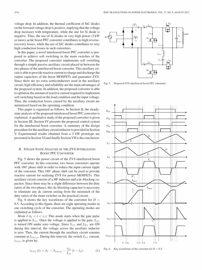
Fig. 5 shows the power circuit of the ZVS interleaved boostPFC converter. In this converter, two boost converters operatewith 180◦ phase shift in order to reduce the input current rippleof the converter. This 180◦ phase shift can be used to providereactive current for realizing ZVS for power MOSFETs. Thisauxiliary circuit consists of a HF inductor and a dc-blocking ca-pacitor. Since there may be a slight difference between the dutyratios of the two phases, this dc-blocking capacitor is necessaryto eliminate any dc current arising from the mismatch of theduty ratios of the main switches in the practical circuit.
Fig. 6 shows the key waveforms of the converter for D >0.5. According to this figure, there are eight operating modes inone switching cycle of the converter. The operating modes areexplained as follows.
Mode I (t0 < t < t1): This mode starts when the gate pulseis applied to SA 1 . Once the voltage is applied to the gate, SA 1is turned ON under zero voltage. Since SA 1 and SB 1 are ONduring this interval, the voltage across the auxiliary inductoris zero. Thus, the current through the auxiliary circuit remainsconstant at IAux,p . During this interval, the switch SA 1 current,iSA 1 , is given by:
iSA1 (t) = IV − IAux,p − vin
LA(t − t0) . (1)
Fig. 5. Proposed ZVS interleaved boost PFC schematic.
Fig. 6. Key waveforms of the converter for D > 0.5.

PAHLEVANINEZHAD et al.: ZVS INTERLEAVED BOOST AC/DC CONVERTER USED IN PLUG-IN ELECTRIC VEHICLES 3517
Since the two phases have 180◦ phase shift, the value of t1 isgiven by:
t1 − t0 = (D − 0.5) Ts. (2)
Therefore, the duty ratio is given by
D = (t1 − t0) fs +12. (3)
Inserting (2) into (1), the value of the switch current is calcu-lated at t1
I1 = IV − IAux,p(t) −vin
2LAfs− v2
in
LAfsVo. (4)
This mode ends once the gate voltage has been removed fromSB 1 .
Mode II (t1 < t < t2): This mode is the dead time between thephase B MOSFETs. During this interval, the auxiliary circuitcurrent charges the output capacitance of SB 1 and dischargesthe output capacitance of SB 2 . In this mode, the average voltageacross the boost inductance LB is zero. Therefore, the currentthrough LB remains constant at its peak value. The voltageacross the auxiliary inductor is given by:
vAUX(t) = − Vo
(t2 − t1)(t − t1). (5)
Thus, the current through auxiliary circuit is given by:
iAUX (t) = IAux,p − Vo
2 (t2 − t1) LAUX(t − t1)
2 (6)
t2 − t1 = td is the dead time between SB 1 and SB 2 . Duringthis period, the output capacitors of the MOSFETs should fullycharge and discharge in order to guarantee ZVS for SB 1 andSB 2 . Thus, the dead time is calculated as follows:
IP + IAux,p − Vo
2LAUXtd = 2CSo
Vo
td(7)
td =(IP + IAux,p)LAUX
Vo
+
√(IP + IAux,p)2L2
AUX
V 2o
− 4CSoLAUX (8)
the current through switch SA 1 is calculated as follows:
iSA1 (t) = IV − IAux,p − vin
LA(t − t0) +
Vo
2tdLAUX(t − t1)
2 .
(9)This mode ends when the output capacitors completely
charged and discharged. The switch current iSA 1 at this point isgiven by:
I2 = IV − IAux,p − vin
LA(td + t1 − t0) +
Vo
2LAUXtd . (10)
Mode III (t2 < t < t3): Once the output capacitors of SB 1and SB 2 have been charged and discharged completely, the gatesignal of SB 2 is applied and SB 2 is turned ON under ZVS.During this interval, the voltage across the auxiliary circuit is−Vo . The current through the auxiliary inductor, inductor LA
and switch SA 1 , is given by:
iAUX = IAux,p − Vo
2LAUXtd − Vo
LAUX(t − t2) (11)
iLA (t) = IV +vin
LA(t − t0) . (12)
iSA1 (t) = IV − IAux,p − vin
LA(t − t0)
+Vo
2LAUXtd +
Vo
LAUX(t − t2) . (13)
This mode ends once the gate signal of SB 2 has become zero(t3 = t0 + 0.5 Ts − td ). The value of iSA 1 at this point is givenby:
I3 (t) = IV − IAux,p +vin
2fsLA− vintd
LA
+Vo
2LAUXtd +
Vo
fsLAUX(1 − D) − 2Vo
LAUXtd . (14)
Mode IV (t3 < t < t4): During this mode, the output capacitorof SB 2 is charging from zero to Vo and the output capacitorof SB 1 is discharging from Vo to zero. This period is actuallythe dead time between SB 2 and SB 1 (t4 − t3 = td ). The auxil-iary inductor current, the boost inductor current, and the switchcurrent, during this mode, is given by:
iAUX (t) = IAux,p +3Vo
2LAUXtd
− Vo
fsLAUX(1 − D) − Vo
2tdLAUX(t − t3)
2 (15)
iLA (t) = IV +vin
LA(t − t0) (16)
iSA1 (t) = IV − IAux,p − vin
LA(t − t0)
+Vo
2LAUXtd +
Vo
LAUX(t − t2) . (17)
This mode ends once the gate signal is applied to SB 1 . Thevalue of iSA 1 at this instant is given by:
I4 (t)=IV −IAux,p +vin
2fsLA+
Vo
LAUXtd +
Vo
fsLAUX(1 − D).
(18)Mode V (t4 < t < t5): This mode starts when the gate signal is
applied to SB 1 . Once the gate has been applied, SB 1 is turned ONunder ZVS. Since SA 1 and SB 1 are ON during this period, thevoltage across the auxiliary inductor is zero; hence, the auxiliaryinductor current remains constant at its peak value, IAux,p . Theboost inductor current and the switch current, during this mode,are given by:
iLA (t) = IV +vin
LA(t − t0) (19)
iSA1 (t) = IV + IAux,p − vin
LA(t − t0) . (20)

3518 IEEE TRANSACTIONS ON POWER ELECTRONICS, VOL. 27, NO. 8, AUGUST 2012
This mode ends once the gate signal is removed from SA 1 .The value of iSA 1 at this time is given by:
iSA1 (t) = IV + IAux,p − vin
fsLAD. (21)
Mode VI (t5 < t < t6): During this mode, the output capacitorof SA 1 is charging from zero to Vo and the output capacitor ofSA 2 is discharging from Vo to zero. This period is actually thedead time between SA 1 and SA 2 (t6 − t5 = td ). In this period,the current through the boost inductor LA remains constant atits peak value. The auxiliary inductor current iAUX is given by:
iAUX (t) = −IAux,p +Vo
2tdLAUX(t − t5)
2 . (22)
This mode ends once the output capacitors have completelybeen charged and discharged.
Mode VII (t6 < t < t7): During this mode, the voltage acrossthe auxiliary circuit is Vo ; hence, the current through the auxil-iary circuit is given by:
iAUX (t) = −IAux,p +Vo
2LAUXtd +
Vo
LAUX(t − t6) . (23)
During this mode, the MOSFET channel SA 2 is conductingthe current to the output. The current through this switch is givenby:
iSA2 (t) = IAux,p − Vo
2LAUXtd +
Vo
LAUX(t − t6)
+ IP − vin − Vo
LA(t − t6) . (24)
The peak value of this current is given by:
I5 (t) = −IAux,p +Vo
2LAUXtd + IP . (25)
This mode ends when iSA 2 reaches zero. Thus t7 is given by:
t7 = t6 +IAux,p − (Vo/2LAUX)td
(Vo/LAUX) + (vin− Vo/LA ). (26)
Mode VIII (t7 < t < t8): During this mode, the output capacitorof SA 1 is discharging from Vo to zero and the output capacitorof SA 2 is charging from zero to Vo . In this mode, the currentthrough LA is at its minimum value IV and the excess currentfrom the auxiliary circuit charges and discharges the outputcapacitors. The auxiliary inductor current is given by:
iAUX(t) = −IAux,p +Vo
2LAUXtd
+Vo
LAUX
IAux,p−(Vo/2LAUX)td(Vo/LAUX)+((vin − Vo)/LA )
+Vo
2LAUX(t − t7)
2 .
(27)
Since this mode is the dead time between SA 1 and SA 2 , t8 = t7 +td . This mode ends once the output capacitors have been charged
Fig. 7. Key waveforms of the converter for D < 0.5.
and discharged completely. Fig. 7 shows the key waveforms ofthe circuit for D < 0.5. According to this figure, the modes ofoperation are the same for the proposed circuit.
PAHLEVANINEZHAD et al.: ZVS INTERLEAVED BOOST AC/DC CONVERTER USED IN PLUG-IN ELECTRIC VEHICLES 3519
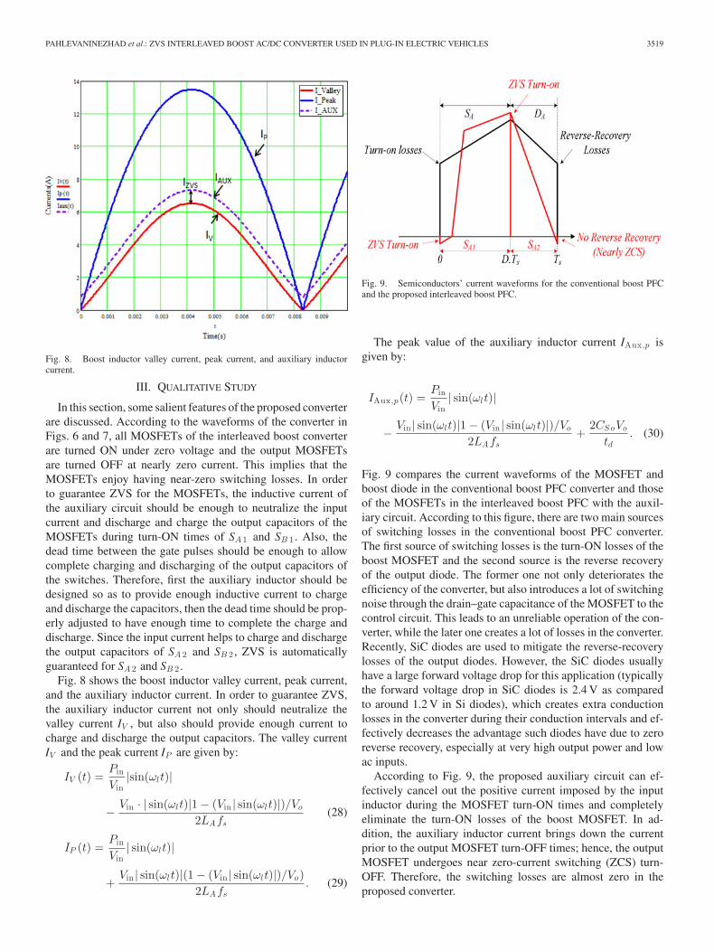
Fig. 8. Boost inductor valley current, peak current, and auxiliary inductorcurrent.
III. QUALITATIVE STUDY
In this section, some salient features of the proposed converterare discussed. According to the waveforms of the converter inFigs. 6 and 7, all MOSFETs of the interleaved boost converterare turned ON under zero voltage and the output MOSFETsare turned OFF at nearly zero current. This implies that theMOSFETs enjoy having near-zero switching losses. In orderto guarantee ZVS for the MOSFETs, the inductive current ofthe auxiliary circuit should be enough to neutralize the inputcurrent and discharge and charge the output capacitors of theMOSFETs during turn-ON times of SA 1 and SB 1 . Also, thedead time between the gate pulses should be enough to allowcomplete charging and discharging of the output capacitors ofthe switches. Therefore, first the auxiliary inductor should bedesigned so as to provide enough inductive current to chargeand discharge the capacitors, then the dead time should be prop-erly adjusted to have enough time to complete the charge anddischarge. Since the input current helps to charge and dischargethe output capacitors of SA 2 and SB 2 , ZVS is automaticallyguaranteed for SA 2 and SB 2 .
Fig. 8 shows the boost inductor valley current, peak current,and the auxiliary inductor current. In order to guarantee ZVS,the auxiliary inductor current not only should neutralize thevalley current IV , but also should provide enough current tocharge and discharge the output capacitors. The valley currentIV and the peak current IP are given by:
IV (t) =Pin
Vin|sin(ωlt)|
− Vin · | sin(ωlt)|1 − (Vin | sin(ωlt)|)/Vo
2LAfs(28)
IP (t) =Pin
Vin| sin(ωlt)|
+Vin | sin(ωlt)|(1 − (Vin | sin(ωlt)|)/Vo)
2LAfs. (29)
Fig. 9. Semiconductors’ current waveforms for the conventional boost PFCand the proposed interleaved boost PFC.
The peak value of the auxiliary inductor current IAux,p isgiven by:
IAux,p(t) =Pin
Vin| sin(ωlt)|
− Vin | sin(ωlt)|1 − (Vin | sin(ωlt)|)/Vo
2LAfs+
2CSoVo
td. (30)
Fig. 9 compares the current waveforms of the MOSFET andboost diode in the conventional boost PFC converter and thoseof the MOSFETs in the interleaved boost PFC with the auxil-iary circuit. According to this figure, there are two main sourcesof switching losses in the conventional boost PFC converter.The first source of switching losses is the turn-ON losses of theboost MOSFET and the second source is the reverse recoveryof the output diode. The former one not only deteriorates theefficiency of the converter, but also introduces a lot of switchingnoise through the drain–gate capacitance of the MOSFET to thecontrol circuit. This leads to an unreliable operation of the con-verter, while the later one creates a lot of losses in the converter.Recently, SiC diodes are used to mitigate the reverse-recoverylosses of the output diodes. However, the SiC diodes usuallyhave a large forward voltage drop for this application (typicallythe forward voltage drop in SiC diodes is 2.4 V as comparedto around 1.2 V in Si diodes), which creates extra conductionlosses in the converter during their conduction intervals and ef-fectively decreases the advantage such diodes have due to zeroreverse recovery, especially at very high output power and lowac inputs.
According to Fig. 9, the proposed auxiliary circuit can ef-fectively cancel out the positive current imposed by the inputinductor during the MOSFET turn-ON times and completelyeliminate the turn-ON losses of the boost MOSFET. In ad-dition, the auxiliary inductor current brings down the currentprior to the output MOSFET turn-OFF times; hence, the outputMOSFET undergoes near zero-current switching (ZCS) turn-OFF. Therefore, the switching losses are almost zero in theproposed converter.
3520 IEEE TRANSACTIONS ON POWER ELECTRONICS, VOL. 27, NO. 8, AUGUST 2012
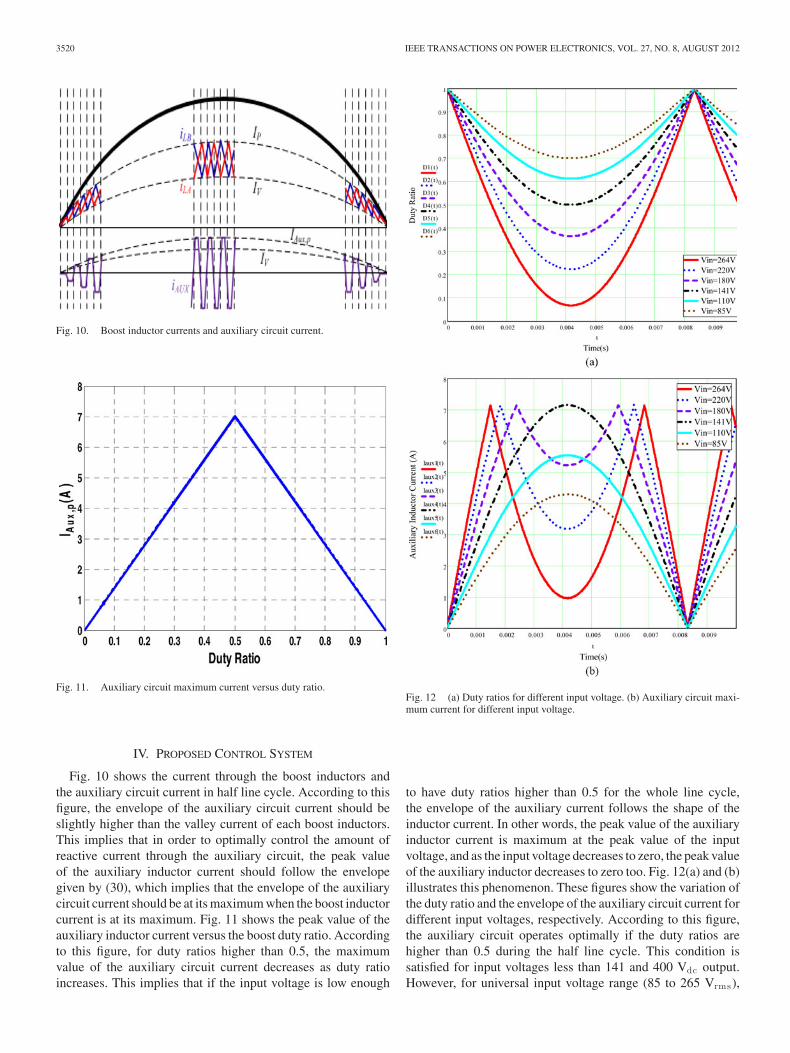
Fig. 10. Boost inductor currents and auxiliary circuit current.
Fig. 11. Auxiliary circuit maximum current versus duty ratio.
IV. PROPOSED CONTROL SYSTEM
Fig. 10 shows the current through the boost inductors andthe auxiliary circuit current in half line cycle. According to thisfigure, the envelope of the auxiliary circuit current should beslightly higher than the valley current of each boost inductors.This implies that in order to optimally control the amount ofreactive current through the auxiliary circuit, the peak valueof the auxiliary inductor current should follow the envelopegiven by (30), which implies that the envelope of the auxiliarycircuit current should be at its maximum when the boost inductorcurrent is at its maximum. Fig. 11 shows the peak value of theauxiliary inductor current versus the boost duty ratio. Accordingto this figure, for duty ratios higher than 0.5, the maximumvalue of the auxiliary circuit current decreases as duty ratioincreases. This implies that if the input voltage is low enough
Fig. 12 (a) Duty ratios for different input voltage. (b) Auxiliary circuit maxi-mum current for different input voltage.
to have duty ratios higher than 0.5 for the whole line cycle,the envelope of the auxiliary current follows the shape of theinductor current. In other words, the peak value of the auxiliaryinductor current is maximum at the peak value of the inputvoltage, and as the input voltage decreases to zero, the peak valueof the auxiliary inductor decreases to zero too. Fig. 12(a) and (b)illustrates this phenomenon. These figures show the variation ofthe duty ratio and the envelope of the auxiliary circuit current fordifferent input voltages, respectively. According to this figure,the auxiliary circuit operates optimally if the duty ratios arehigher than 0.5 during the half line cycle. This condition issatisfied for input voltages less than 141 and 400 Vdc output.However, for universal input voltage range (85 to 265 Vrms),
PAHLEVANINEZHAD et al.: ZVS INTERLEAVED BOOST AC/DC CONVERTER USED IN PLUG-IN ELECTRIC VEHICLES 3521
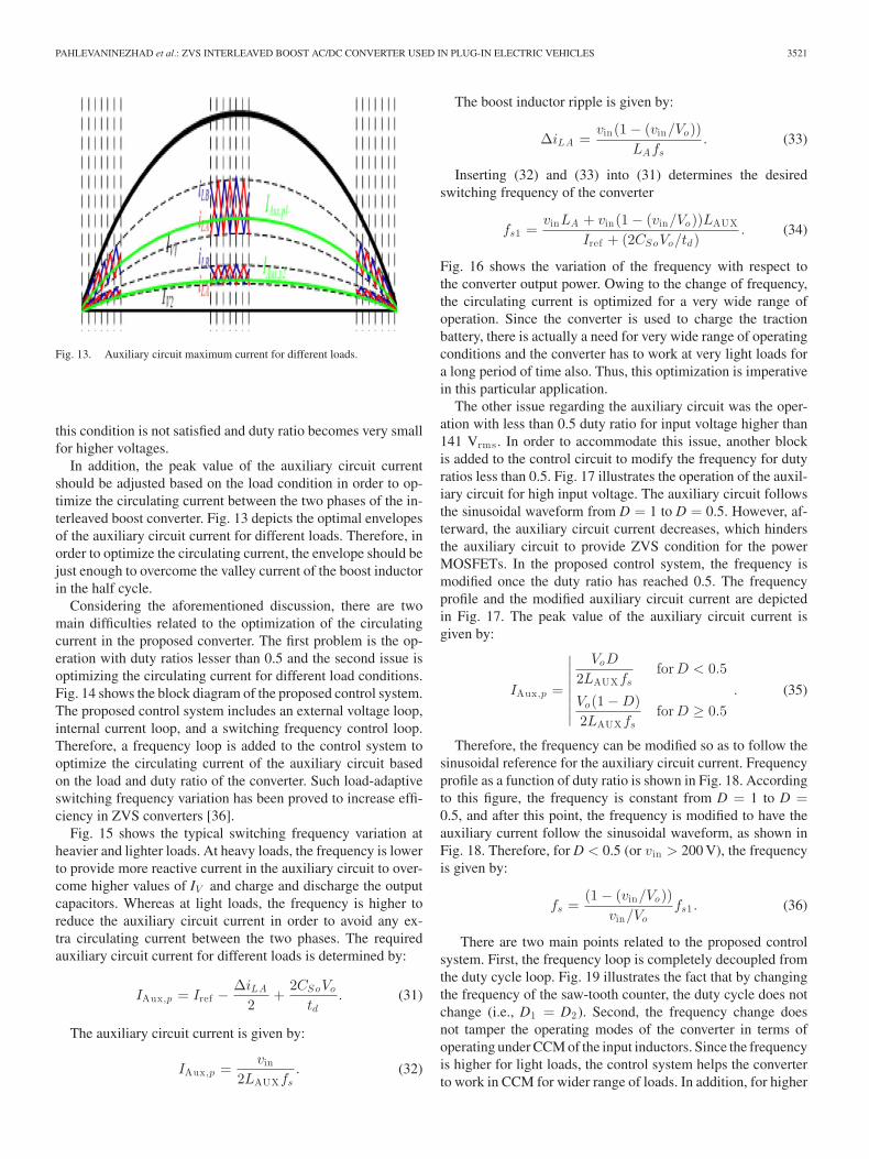
Fig. 13. Auxiliary circuit maximum current for different loads.
this condition is not satisfied and duty ratio becomes very smallfor higher voltages.
In addition, the peak value of the auxiliary circuit currentshould be adjusted based on the load condition in order to op-timize the circulating current between the two phases of the in-terleaved boost converter. Fig. 13 depicts the optimal envelopesof the auxiliary circuit current for different loads. Therefore, inorder to optimize the circulating current, the envelope should bejust enough to overcome the valley current of the boost inductorin the half cycle.
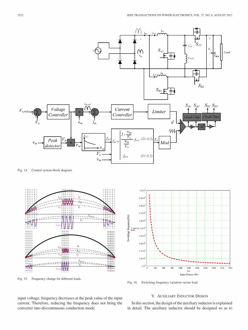
Considering the aforementioned discussion, there are twomain difficulties related to the optimization of the circulatingcurrent in the proposed converter. The first problem is the op-eration with duty ratios lesser than 0.5 and the second issue isoptimizing the circulating current for different load conditions.Fig. 14 shows the block diagram of the proposed control system.The proposed control system includes an external voltage loop,internal current loop, and a switching frequency control loop.Therefore, a frequency loop is added to the control system tooptimize the circulating current of the auxiliary circuit basedon the load and duty ratio of the converter. Such load-adaptiveswitching frequency variation has been proved to increase effi-ciency in ZVS converters [36].
Fig. 15 shows the typical switching frequency variation atheavier and lighter loads. At heavy loads, the frequency is lowerto provide more reactive current in the auxiliary circuit to over-come higher values of IV and charge and discharge the outputcapacitors. Whereas at light loads, the frequency is higher toreduce the auxiliary circuit current in order to avoid any ex-tra circulating current between the two phases. The requiredauxiliary circuit current for different loads is determined by:
IAux,p = Iref −ΔiLA
2+
2CSoVo
td. (31)
The auxiliary circuit current is given by:
IAux,p =vin
2LAUXfs. (32)
The boost inductor ripple is given by:
ΔiLA =vin(1 − (vin/Vo))
LAfs. (33)
Inserting (32) and (33) into (31) determines the desiredswitching frequency of the converter
fs1 =vinLA + vin(1 − (vin/Vo))LAUX
Iref + (2CSoVo/td). (34)
Fig. 16 shows the variation of the frequency with respect tothe converter output power. Owing to the change of frequency,the circulating current is optimized for a very wide range ofoperation. Since the converter is used to charge the tractionbattery, there is actually a need for very wide range of operatingconditions and the converter has to work at very light loads fora long period of time also. Thus, this optimization is imperativein this particular application.
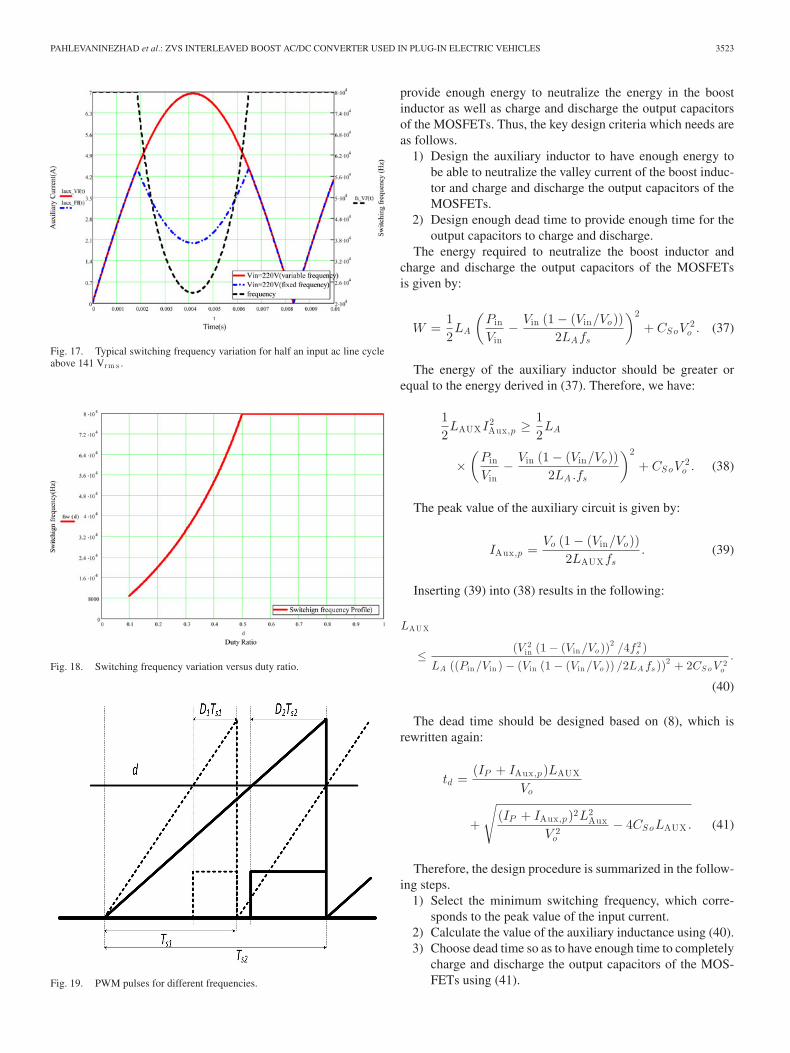
The other issue regarding the auxiliary circuit was the oper-ation with less than 0.5 duty ratio for input voltage higher than141 Vrms . In order to accommodate this issue, another blockis added to the control circuit to modify the frequency for dutyratios less than 0.5. Fig. 17 illustrates the operation of the auxil-iary circuit for high input voltage. The auxiliary circuit followsthe sinusoidal waveform from D = 1 to D = 0.5. However, af-terward, the auxiliary circuit current decreases, which hindersthe auxiliary circuit to provide ZVS condition for the powerMOSFETs. In the proposed control system, the frequency ismodified once the duty ratio has reached 0.5. The frequencyprofile and the modified auxiliary circuit current are depictedin Fig. 17. The peak value of the auxiliary circuit current isgiven by:
IAux,p =
∣∣∣∣∣∣∣∣VoD
2LAUXfsforD < 0.5
Vo(1 − D)2LAUXfs
forD ≥ 0.5. (35)
Therefore, the frequency can be modified so as to follow thesinusoidal reference for the auxiliary circuit current. Frequencyprofile as a function of duty ratio is shown in Fig. 18. Accordingto this figure, the frequency is constant from D = 1 to D =0.5, and after this point, the frequency is modified to have theauxiliary current follow the sinusoidal waveform, as shown inFig. 18. Therefore, for D < 0.5 (or vin > 200 V), the frequencyis given by:
fs =(1 − (vin/Vo))
vin/Vofs1 . (36)
There are two main points related to the proposed controlsystem. First, the frequency loop is completely decoupled fromthe duty cycle loop. Fig. 19 illustrates the fact that by changingthe frequency of the saw-tooth counter, the duty cycle does notchange (i.e., D1 = D2). Second, the frequency change doesnot tamper the operating modes of the converter in terms ofoperating under CCM of the input inductors. Since the frequencyis higher for light loads, the control system helps the converterto work in CCM for wider range of loads. In addition, for higher
3522 IEEE TRANSACTIONS ON POWER ELECTRONICS, VOL. 27, NO. 8, AUGUST 2012
Fig. 14. Control system block diagram.
Fig. 15. Frequency change for different loads.
input voltage, frequency decreases at the peak value of the inputcurrent. Therefore, reducing the frequency does not bring theconverter into discontinuous conduction mode.
Fig. 16. Switching frequency variation versus load.
V. AUXILIARY INDUCTOR DESIGN
In this section, the design of the auxiliary inductor is explainedin detail. The auxiliary inductor should be designed so as to
PAHLEVANINEZHAD et al.: ZVS INTERLEAVED BOOST AC/DC CONVERTER USED IN PLUG-IN ELECTRIC VEHICLES 3523
Fig. 17. Typical switching frequency variation for half an input ac line cycleabove 141 Vrm s .
Fig. 18. Switching frequency variation versus duty ratio.
Fig. 19. PWM pulses for different frequencies.
provide enough energy to neutralize the energy in the boostinductor as well as charge and discharge the output capacitorsof the MOSFETs. Thus, the key design criteria which needs areas follows.
1) Design the auxiliary inductor to have enough energy tobe able to neutralize the valley current of the boost induc-tor and charge and discharge the output capacitors of theMOSFETs.
2) Design enough dead time to provide enough time for theoutput capacitors to charge and discharge.
The energy required to neutralize the boost inductor andcharge and discharge the output capacitors of the MOSFETsis given by:
W =12LA
(Pin
Vin− Vin (1 − (Vin/Vo))
2LAfs
)2
+ CSoV2o . (37)
The energy of the auxiliary inductor should be greater orequal to the energy derived in (37). Therefore, we have:
12LAUXI2
Aux,p ≥ 12LA
×(
Pin
Vin− Vin (1 − (Vin/Vo))
2LA.fs
)2
+ CSoV2o . (38)
The peak value of the auxiliary circuit is given by:
IAux,p =Vo (1 − (Vin/Vo))
2LAUXfs. (39)
Inserting (39) into (38) results in the following:
LAUX
≤ (V 2in (1 − (Vin/Vo ))
2 /4f 2s )
LA ((Pin/Vin ) − (Vin (1 − (Vin/Vo )) /2LA fs ))2 + 2CS o V 2
o
.
(40)
The dead time should be designed based on (8), which isrewritten again:
td =(IP + IAux,p)LAUX
Vo
+
√(IP + IAux,p)2L2
Aux
V 2o
− 4CSoLAUX . (41)
Therefore, the design procedure is summarized in the follow-ing steps.
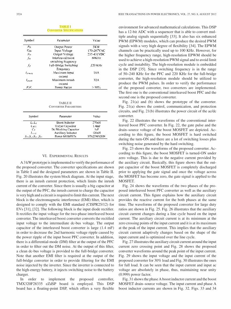
1) Select the minimum switching frequency, which corre-sponds to the peak value of the input current.
2) Calculate the value of the auxiliary inductance using (40).3) Choose dead time so as to have enough time to completely
charge and discharge the output capacitors of the MOS-FETs using (41).
3524 IEEE TRANSACTIONS ON POWER ELECTRONICS, VOL. 27, NO. 8, AUGUST 2012
TABLE ICONVERTER SPECIFICATIONS
TABLE IICONVERTER PARAMETERS
VI. EXPERIMENTAL RESULTS
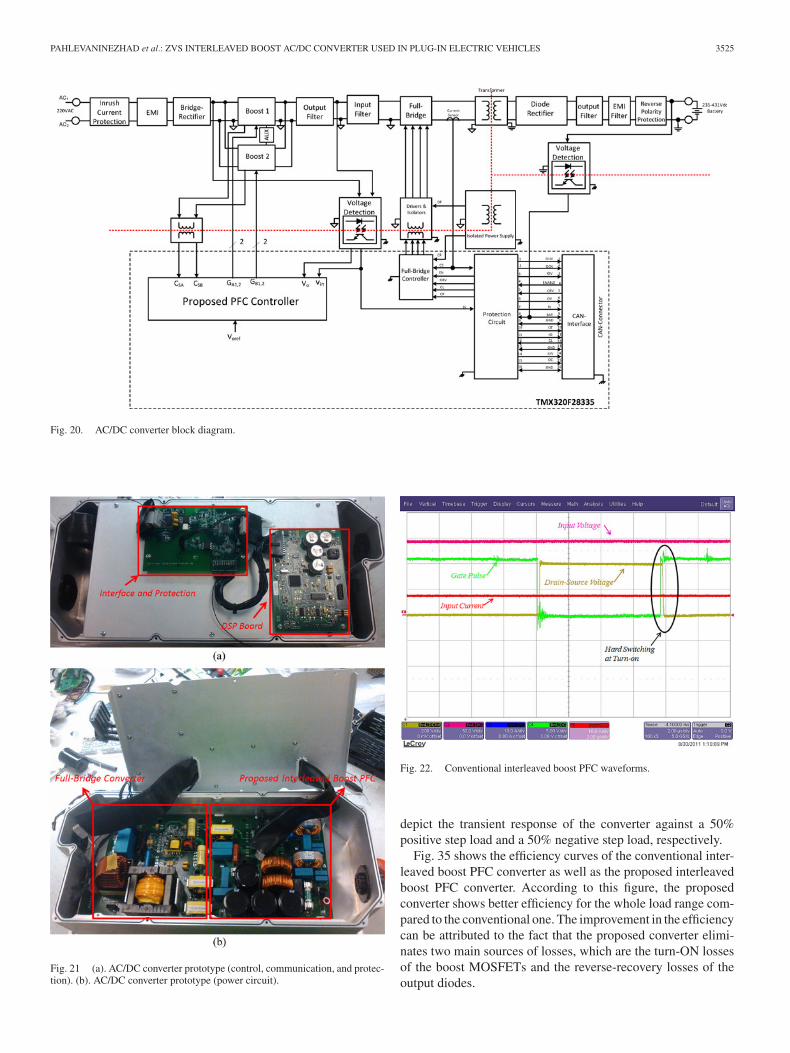
A 3 kW prototype is implemented to verify the performance ofthe proposed converter. The converter specifications are shownin Table I and the designed parameters are shown in Table II.Fig. 20 illustrates the system block diagram. At the input stage,there is an inrush current protection, which limits the inrushcurrent of the converter. Since there is usually a big capacitor atthe output of the PFC, the inrush current to charge the capacitoris very high and a circuit is required to limit this current. The nextblock is the electromagnetic interference (EMI) filter, which isdesigned to comply with the EMI standard (CISPR25/12) forEVs [31], [32]. The following block is the input diode rectifier.It rectifies the input voltage for the two-phase interleaved boostconverter. The interleaved boost converter converts the rectifiedinput voltage to the intermediate dc-bus voltage. The outputcapacitor of the interleaved boost converter is large (1.4 mF)in order to decrease the 2nd harmonic voltage ripple caused bythe power ripple of the input boost PFC converter. In addition,there is a differential-mode (DM) filter at the output of the PFCin order to filter out the DM noise. At the output of this filter,a clean dc-bus voltage is provided to the full-bridge converter.Note that another EMI filter is required at the output of thefull-bridge converter in order to provide filtering for the EMInoise injected by the inverter. Since the inverter is connected tothe high-energy battery, it injects switching noise to the batterycharger.
In order to implement the proposed controller,TMX320F28335 eZdSP board is employed. This DSPboard has a floating-point DSP, which offers a very flexible
environment for advanced mathematical calculations. This DSPhas a 12-bit ADC with a sequencer that is able to convert mul-tiple analog signals sequentially [33]. It also has six enhancedPWM (EPWM) modules, which can produce the desired PWMsignals with a very high degree of flexibility [34]. The EPWMchannels can be practically used up to 100 KHz. However, forthe higher frequency range, high-resolution EPWM should beused to achieve a high-resolution PWM signal and to avoid limitcycle and instability. The high-resolution module is embeddedin the DSP [35]. Since switching frequency is in the rangeof 50–240 KHz for the PFC and 220 KHz for the full-bridgeconverter, the high-resolution module should be utilized toproduce the PWM pulses. In order to verify the performanceof the proposed converter, two converters are implemented.The first one is the conventional interleaved boost PFC and thesecond one is the proposed converter.
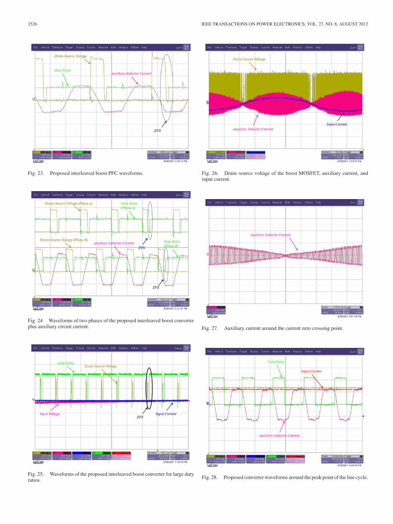
Fig. 21(a) and (b) shows the prototype of the converter.Fig. 21(a) shows the control, communication, and protectioncircuits, and Fig. 21(b) illustrates the power circuit of the ac/dcconverter.
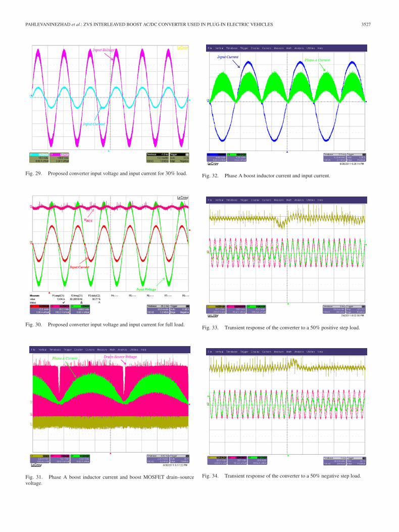
Fig. 22 illustrates the waveforms of the conventional inter-leaved boost PFC converter. In Fig. 22, the gate pulse and thedrain–source voltage of the boost MOSFET are depicted. Ac-cording to this figure, the boost MOSFET is hard switchedduring the turn-ON and there are a lot of switching losses plusswitching noise generated by the hard switching.
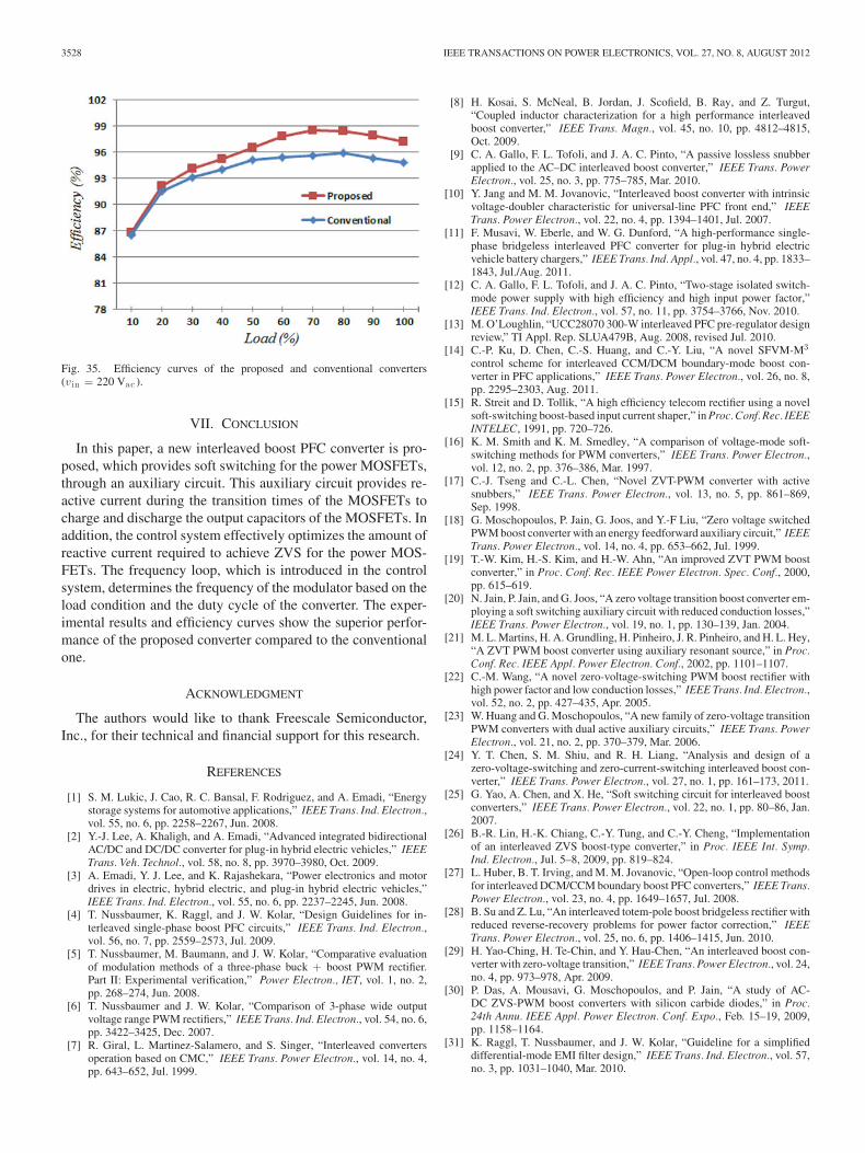
Fig. 23 shows the waveforms of the proposed converter. Ac-cording to this figure, the boost MOSFET is turned-ON underzero voltage. This is due to the negative current provided bythe auxiliary circuit. Basically, this figure shows that the out-put capacitor of the boost MOSFET is completely dischargedprior to applying the gate signal and once the voltage acrossthe MOSFET has become zero, the gate signal is applied to theMOSFET.
Fig. 24 shows the waveforms of the two phases of the pro-posed interleaved boost PFC converter as well as the auxiliarycircuit current. This figure explains how the auxiliary circuitprovides the reactive current for the both phases at the sametime. The waveforms of the proposed converter for large dutyratios are shown in Fig. 25. Fig. 26 illustrates that the auxiliarycircuit current changes during a line cycle based on the inputcurrent. The auxiliary circuit current is at its minimum at thezero crossing points of the input current and it is at its maximumat the peak of the input current. This implies that the auxiliarycircuit current adaptively changes based on the shape of theinput current and is optimized over the line cycle.
Fig. 27 illustrates the auxiliary circuit current around the inputcurrent zero crossing point and Fig. 28 shows the proposedconverter waveforms around the peak point of the input current.Fig. 29 shows the input voltage and the input current of theproposed converter for 30% load and Fig. 30 illustrates the onesfor full load. It can be seen that the input current and input acvoltage are absolutely in phase, thus, maintaining near unity(0.999) power factor.
Fig. 31 shows the phase A boost inductor current and the boostMOSFET drain–source voltage. The input current and phase Aboost inductor currents are shown in Fig. 32. Figs. 33 and 34
PAHLEVANINEZHAD et al.: ZVS INTERLEAVED BOOST AC/DC CONVERTER USED IN PLUG-IN ELECTRIC VEHICLES 3525
Fig. 20. AC/DC converter block diagram.
Fig. 21 (a). AC/DC converter prototype (control, communication, and protec-tion). (b). AC/DC converter prototype (power circuit).
Fig. 22. Conventional interleaved boost PFC waveforms.
depict the transient response of the converter against a 50%positive step load and a 50% negative step load, respectively.
Fig. 35 shows the efficiency curves of the conventional inter-leaved boost PFC converter as well as the proposed interleavedboost PFC converter. According to this figure, the proposedconverter shows better efficiency for the whole load range com-pared to the conventional one. The improvement in the efficiencycan be attributed to the fact that the proposed converter elimi-nates two main sources of losses, which are the turn-ON lossesof the boost MOSFETs and the reverse-recovery losses of theoutput diodes.
3526 IEEE TRANSACTIONS ON POWER ELECTRONICS, VOL. 27, NO. 8, AUGUST 2012
Fig. 23. Proposed interleaved boost PFC waveforms.
Fig. 24 Waveforms of two phases of the proposed interleaved boost converterplus auxiliary circuit current.
Fig. 25. Waveforms of the proposed interleaved boost converter for large dutyratios.
Fig. 26. Drain–source voltage of the boost MOSFET, auxiliary current, andinput current.
Fig. 27. Auxiliary current around the current zero crossing point.
Fig. 28. Proposed converter waveforms around the peak point of the line cycle.
PAHLEVANINEZHAD et al.: ZVS INTERLEAVED BOOST AC/DC CONVERTER USED IN PLUG-IN ELECTRIC VEHICLES 3527
Fig. 29. Proposed converter input voltage and input current for 30% load.
Fig. 30. Proposed converter input voltage and input current for full load.
Fig. 31. Phase A boost inductor current and boost MOSFET drain–sourcevoltage.
Fig. 32. Phase A boost inductor current and input current.
Fig. 33. Transient response of the converter to a 50% positive step load.
Fig. 34. Transient response of the converter to a 50% negative step load.
3528 IEEE TRANSACTIONS ON POWER ELECTRONICS, VOL. 27, NO. 8, AUGUST 2012
Fig. 35. Efficiency curves of the proposed and conventional converters(v in = 220 Vac ).
VII. CONCLUSION
In this paper, a new interleaved boost PFC converter is pro-posed, which provides soft switching for the power MOSFETs,through an auxiliary circuit. This auxiliary circuit provides re-active current during the transition times of the MOSFETs tocharge and discharge the output capacitors of the MOSFETs. Inaddition, the control system effectively optimizes the amount ofreactive current required to achieve ZVS for the power MOS-FETs. The frequency loop, which is introduced in the controlsystem, determines the frequency of the modulator based on theload condition and the duty cycle of the converter. The exper-imental results and efficiency curves show the superior perfor-mance of the proposed converter compared to the conventionalone.
ACKNOWLEDGMENT
The authors would like to thank Freescale Semiconductor,Inc., for their technical and financial support for this research.
REFERENCES
[1] S. M. Lukic, J. Cao, R. C. Bansal, F. Rodriguez, and A. Emadi, “Energystorage systems for automotive applications,” IEEE Trans. Ind. Electron.,vol. 55, no. 6, pp. 2258–2267, Jun. 2008.
[2] Y.-J. Lee, A. Khaligh, and A. Emadi, “Advanced integrated bidirectionalAC/DC and DC/DC converter for plug-in hybrid electric vehicles,” IEEETrans. Veh. Technol., vol. 58, no. 8, pp. 3970–3980, Oct. 2009.
[3] A. Emadi, Y. J. Lee, and K. Rajashekara, “Power electronics and motordrives in electric, hybrid electric, and plug-in hybrid electric vehicles,”IEEE Trans. Ind. Electron., vol. 55, no. 6, pp. 2237–2245, Jun. 2008.
[4] T. Nussbaumer, K. Raggl, and J. W. Kolar, “Design Guidelines for in-terleaved single-phase boost PFC circuits,” IEEE Trans. Ind. Electron.,vol. 56, no. 7, pp. 2559–2573, Jul. 2009.
[5] T. Nussbaumer, M. Baumann, and J. W. Kolar, “Comparative evaluationof modulation methods of a three-phase buck + boost PWM rectifier.Part II: Experimental verification,” Power Electron., IET, vol. 1, no. 2,pp. 268–274, Jun. 2008.
[6] T. Nussbaumer and J. W. Kolar, “Comparison of 3-phase wide outputvoltage range PWM rectifiers,” IEEE Trans. Ind. Electron., vol. 54, no. 6,pp. 3422–3425, Dec. 2007.
[7] R. Giral, L. Martinez-Salamero, and S. Singer, “Interleaved convertersoperation based on CMC,” IEEE Trans. Power Electron., vol. 14, no. 4,pp. 643–652, Jul. 1999.
[8] H. Kosai, S. McNeal, B. Jordan, J. Scofield, B. Ray, and Z. Turgut,“Coupled inductor characterization for a high performance interleavedboost converter,” IEEE Trans. Magn., vol. 45, no. 10, pp. 4812–4815,Oct. 2009.
[9] C. A. Gallo, F. L. Tofoli, and J. A. C. Pinto, “A passive lossless snubberapplied to the AC–DC interleaved boost converter,” IEEE Trans. PowerElectron., vol. 25, no. 3, pp. 775–785, Mar. 2010.
[10] Y. Jang and M. M. Jovanovic, “Interleaved boost converter with intrinsicvoltage-doubler characteristic for universal-line PFC front end,” IEEETrans. Power Electron., vol. 22, no. 4, pp. 1394–1401, Jul. 2007.
[11] F. Musavi, W. Eberle, and W. G. Dunford, “A high-performance single-phase bridgeless interleaved PFC converter for plug-in hybrid electricvehicle battery chargers,” IEEE Trans. Ind. Appl., vol. 47, no. 4, pp. 1833–1843, Jul./Aug. 2011.
[12] C. A. Gallo, F. L. Tofoli, and J. A. C. Pinto, “Two-stage isolated switch-mode power supply with high efficiency and high input power factor,”IEEE Trans. Ind. Electron., vol. 57, no. 11, pp. 3754–3766, Nov. 2010.
[13] M. O’Loughlin, “UCC28070 300-W interleaved PFC pre-regulator designreview,” TI Appl. Rep. SLUA479B, Aug. 2008, revised Jul. 2010.
[14] C.-P. Ku, D. Chen, C.-S. Huang, and C.-Y. Liu, “A novel SFVM-M3
control scheme for interleaved CCM/DCM boundary-mode boost con-verter in PFC applications,” IEEE Trans. Power Electron., vol. 26, no. 8,pp. 2295–2303, Aug. 2011.
[15] R. Streit and D. Tollik, “A high efficiency telecom rectifier using a novelsoft-switching boost-based input current shaper,” in Proc. Conf. Rec. IEEEINTELEC, 1991, pp. 720–726.
[16] K. M. Smith and K. M. Smedley, “A comparison of voltage-mode soft-switching methods for PWM converters,” IEEE Trans. Power Electron.,vol. 12, no. 2, pp. 376–386, Mar. 1997.
[17] C.-J. Tseng and C.-L. Chen, “Novel ZVT-PWM converter with activesnubbers,” IEEE Trans. Power Electron., vol. 13, no. 5, pp. 861–869,Sep. 1998.
[18] G. Moschopoulos, P. Jain, G. Joos, and Y.-F Liu, “Zero voltage switchedPWM boost converter with an energy feedforward auxiliary circuit,” IEEETrans. Power Electron., vol. 14, no. 4, pp. 653–662, Jul. 1999.
[19] T.-W. Kim, H.-S. Kim, and H.-W. Ahn, “An improved ZVT PWM boostconverter,” in Proc. Conf. Rec. IEEE Power Electron. Spec. Conf., 2000,pp. 615–619.
[20] N. Jain, P. Jain, and G. Joos, “A zero voltage transition boost converter em-ploying a soft switching auxiliary circuit with reduced conduction losses,”IEEE Trans. Power Electron., vol. 19, no. 1, pp. 130–139, Jan. 2004.
[21] M. L. Martins, H. A. Grundling, H. Pinheiro, J. R. Pinheiro, and H. L. Hey,“A ZVT PWM boost converter using auxiliary resonant source,” in Proc.Conf. Rec. IEEE Appl. Power Electron. Conf., 2002, pp. 1101–1107.
[22] C.-M. Wang, “A novel zero-voltage-switching PWM boost rectifier withhigh power factor and low conduction losses,” IEEE Trans. Ind. Electron.,vol. 52, no. 2, pp. 427–435, Apr. 2005.
[23] W. Huang and G. Moschopoulos, “A new family of zero-voltage transitionPWM converters with dual active auxiliary circuits,” IEEE Trans. PowerElectron., vol. 21, no. 2, pp. 370–379, Mar. 2006.
[24] Y. T. Chen, S. M. Shiu, and R. H. Liang, “Analysis and design of azero-voltage-switching and zero-current-switching interleaved boost con-verter,” IEEE Trans. Power Electron., vol. 27, no. 1, pp. 161–173, 2011.
[25] G. Yao, A. Chen, and X. He, “Soft switching circuit for interleaved boostconverters,” IEEE Trans. Power Electron., vol. 22, no. 1, pp. 80–86, Jan.2007.
[26] B.-R. Lin, H.-K. Chiang, C.-Y. Tung, and C.-Y. Cheng, “Implementationof an interleaved ZVS boost-type converter,” in Proc. IEEE Int. Symp.Ind. Electron., Jul. 5–8, 2009, pp. 819–824.
[27] L. Huber, B. T. Irving, and M. M. Jovanovic, “Open-loop control methodsfor interleaved DCM/CCM boundary boost PFC converters,” IEEE Trans.Power Electron., vol. 23, no. 4, pp. 1649–1657, Jul. 2008.
[28] B. Su and Z. Lu, “An interleaved totem-pole boost bridgeless rectifier withreduced reverse-recovery problems for power factor correction,” IEEETrans. Power Electron., vol. 25, no. 6, pp. 1406–1415, Jun. 2010.
[29] H. Yao-Ching, H. Te-Chin, and Y. Hau-Chen, “An interleaved boost con-verter with zero-voltage transition,” IEEE Trans. Power Electron., vol. 24,no. 4, pp. 973–978, Apr. 2009.
[30] P. Das, A. Mousavi, G. Moschopoulos, and P. Jain, “A study of AC-DC ZVS-PWM boost converters with silicon carbide diodes,” in Proc.24th Annu. IEEE Appl. Power Electron. Conf. Expo., Feb. 15–19, 2009,pp. 1158–1164.
[31] K. Raggl, T. Nussbaumer, and J. W. Kolar, “Guideline for a simplifieddifferential-mode EMI filter design,” IEEE Trans. Ind. Electron., vol. 57,no. 3, pp. 1031–1040, Mar. 2010.
PAHLEVANINEZHAD et al.: ZVS INTERLEAVED BOOST AC/DC CONVERTER USED IN PLUG-IN ELECTRIC VEHICLES 3529
[32] J. Biela, A. Wirthmueller, R. Waespe, M. L. Heldwein, K. Raggl, andJ. W. Kolar, “Passive and active hybrid integrated EMI filters,” IEEETrans. Power Electron., vol. 24, no. 5, pp. 1340–1349, May 2009.
[33] Texas Instrument, “TMS320×2833 analog-to-digital converter (ADC)module,” Rep. no. SPRU812A, Sep. 2007, 2012.
[34] Texas Instrument, “TMS320×2833, 2823× enhanced pulse width mod-ulator (ePWM) module,” Rep. no. SPRUG04A, Oct. 2008, Revised Jul.2009.
[35] Texas Instrument, “TMS320×2833, 2823× high resolution pulse widthmodulator,” Rep. no. SPRUG02, Feb. 2009.
[36] M. Pahlevaninezhad, J. Drobnik, P. Jain, and A. Bakhshai, “A load adaptivecontrol approach for a zero voltage switching DC/DC converter used forelectric vehicles,” IEEE Trans. Ind. Electron., vol. 59, no. 2, pp. 920–933,2011.
Majid Pahlevaninezhad (S’07–M’12) received theB.S and M.S degrees in electrical engineering fromIsfahan University of Technology, Isfahan, Iran, andthe Ph.D. degree from Queens University, Kingston,ON, Canada.
He is currently a Postdoctoral Research Associatein the Department of Electrical and Computer Engi-neering, Queen’s University. From 2003 to 2007, hewas a Technical Designer with the Information andCommunication Technology Institute, Isfahan Uni-versity of Technology, where he was involved in the
design and implementation of high-quality resonant converters. He also collab-orated with Freescale Semiconductor, Inc., where he was the leader of a researchteam working on the design and implementation of the power converters for apure electric vehicle from 2008 to 2012. He is the author of more than 32 journaland conference proceeding papers and the holder of 4 US patents. His currentresearch interests include robust and nonlinear control in power electronics,advanced soft-switching methods in power converters, plug-in pure electric ve-hicles, and photovoltaic microinverters.
Dr. Pahlevaninezhad is a member of the IEEE Power Electronics Society andIndustrial Electronics Society. He was a recipient of the distinguished graduatestudent award from Isfahan University of Technology.
Pritam Das (S’09–M’12) was born in Calcutta, Indiain 1978. He received the B.Eng. degree in electronicsand communication engineering from the Universityof Burdwan, India. He also received the Master’s ofApplied Science degree and the Ph.D. degree, both inelectrical engineering from the University of West-ern Ontario, London, ON, Canada in 2005 and 2010respectively.
From 2010 to 2011, he was a Postdoctoral Fel-low at the Queen’s Centre for Energy and PowerElectronics Research (ePOWER), Queen’s Univer-
sity Kingston, Ontario, Canada. Presently, he is with Murata Power Solutions,Markham, Ontario, where is involved in research and development of front-endAC-DC converters conforming to 80 Plus Platinum efficiency standards. Hisresearch interests include high frequency and high efficiency ac-dc and dc-dcpower converters, power factor correction, soft switching techniques, design ofhigh frequency magnetic components for power converter and modeling anddesign of non-linear controllers for ac-dc and dc-dc converters. He is involvedin research on modeling and control of high frequency and high efficiency res-onant and PWM converters for various applications including electric vehicles,photo-voltaic micro-inverters, data centers, etc. He has published over 33 tech-nical papers in referred journals and conferences.
Dr. Das is also a reviewer of IEEE TRANSACTIONS ON POWER ELECTRONICS,IEEE TRANSACTIONS ON INDUSTRIAL ELECTRONICS, and IEEE TRANSACTIONS
ON INDUSTRIAL INFORMATICS.
Josef Drobnik (SM’93) received his B.Sc., M.Sc.,and Ph.D. degrees all in electrical engineering fromthe Czech Technical University in Prague in 1975,1977, and 1981, respectively.
He left Czechoslovakia in 1982 for political rea-sons; since then, he has been working in the field ofpower electronics with steadily increasing responsi-bilities. From 1982 to 1995, he was in Canada withCanadian Voice Data Switching, Bell-Northern Re-search, and Nortel. In 1995, he relocated to the U.S.to work for GE Corporate R&D, then Intel, and L3
Communications. He is currently with Freescale Semiconductors, Inc., Tempe,AZ. His positions include Chief Engineer, Technical Advisor, and Director. Hepublished 46 technical papers and is responsible for 33 U.S. and internationalpatents. His professional interest includes new power conversion topologies andintegrated magnetic and “after silicon” semiconductors
Praveen K. Jain (S’86–M’88–SM’91–F’02) re-ceived the B.E. degree (Hons.) from the Universityof Allahabad, Allahabad, India, in 1980, and theM.A.Sc. and Ph.D. degrees from the University ofToronto, Toronto, ON, Canada, in 1984 and 1987,respectively, all in electrical engineering.
He is currently a Professor and Canada ResearchChair at the Department of Electrical and Com-puter Engineering, Queen’s University, Kingston,ON, Canada, where he is also the Director of theQueen’s Centre for Energy and Power Electronics
Research (ePOWER). Prior to joining Queen’s University, he was a Professor atConcordia University (1994–2000), Technical Advisor at Nortel (1990–1994),Senior Space Power Electronics Engineer at Canadian Astronautics Ltd. (1987–1990), Design Engineer at ABB (1981), and Production Engineer at CromptonGreaves (1980). In addition, he has been a Consultant with Astec, Ballard Power,Freescale Semiconductor, Inc., General Electric, Intel, and Nortel. He is alsoa Founder of CHiL Semiconductor in Tewksbury, MA, and SPARQ System,Kingston. He has secured over $20M cash and $20M in-kind in external re-search funding to conduct research in the field of power electronics. He hassupervised more than 75 graduate students, postdoctoral fellows, and researchengineers. He is the author or coauthor of more than 350 technical papers (in-cluding more than 90 IEEE Transactions papers) and holds more than 50 patents(granted and pending).
Dr. Jain is an Associate Editor of the IEEE TRANSACTIONS ON POWER ELEC-TRONICS and an Editor of the International Journal of Power Electronics. Heis also a Distinguished Lecturer of IEEE Industry Applications Society. He isa Fellow of the Engineering Institute of Canada and the Canadian Academyof Engineering. He received of the 2004 Engineering Medal (R&D) from theProfessional Engineers of Ontario. He also received the 2011 IEEE WilliamNewell Power Electronics Field Award.
Alireza Bakhshai (M’04–SM’99) received the B.Sc.and M.Sc. degrees from the Isfahan University ofTechnology, Isfahann, Iran, in 1984 and 1986, respec-tively, and the Ph.D. degree from Concordiia Univer-sity, Montreal, QC, Canada, in 1977.
From 1986 to 1993 and from 1998 to 2004, hewas with the faculty of the Department of Electri-cal and Computer Engineering, Isfahan University ofTechnology. From 1997 to 1998, he was a Postdoc-toral Fellow at Concordia University. He is currentlywith the Department of Electrical and Computer En-
gineering, Queen’s University, Kingston, ON, Canada. His research interestsinclude high-power electronics and applications in distributed generation andwind energy, control systems, and flexible ac transmission services.