Embed Size (px)
Citation preview
ESD-TR-91-090 /)
AD-A244 636!ll$ l1 Tchn~9ical Report23
An Experimental Spatial Acquisitionand Tracking System for
Optical Intersatellite Crosslinks
D.J. Bernays
E.P. Colagiuri-Cafarelli
3 December 1991
Lincoln LaboratoryMA\SSAC1USETTS INSTITUTE OF TECHNOLOGY
CD EXIN(;TON.VlCSSAC5t( SE %TTS
0 Prepared for the Department of the Air Forceunder Contract F!9628-90-C-0002.
_____ .r r- p
*~pp ,e.I orptldc elae:lit ih tio i uliitd
This report is based on studies performed at Lincoln Laboratory, a center forresearch operated by Massachusetts Institute of Technology. The work was sponsoredby the Department of the Air Force under Contract F19628-90-C-0002.
This report may be reproduced to satisfy needs of U.S. Government agencies.
The ESD Public Affairs Office has reviewed this report, andit is releasable to the National fechnical InformationService, where it will be available to the general public,including foreign nationals.
This technical report has been reviewed and is approved for publication.
FOR THE COMMANDER
Hugh L. Southall, Lt. Col., USAFChief, ESD Lincoln Laboratory Project Office
Non-Lincoln Recipients
PLEASE DO NOT RETURN
Permission is given to destroy this documentwhen it is no longer needed.
MASSACHUSETT'S INSTITUTE OF TECHNOLOGYLINCOLN LABORATORY
AN EXPERIMENTAL SPATIAL ACQUISITIONAND TRACKING SYSTEM FOR
OPTICAL INTERSATELLITE CROSSLINKS
D.J. BERNAYS
Group 42
E. P. COLAGIURI-CAFARELLIGroup 67
TECHNICAL REPORT 923
3 DECEMBER 1991
Approved for public release; distribution is unlimited.
LEXINGTON MASSACHUSETT~S
ABSTRACT
Optical intersatellite communications crosslinks will operate with much higher antenna gains andhence more stringent pointing and tracking requirements than do present RF and microwave-based sys-tems. The design and experimental demonstration of an optical heterodtyne communications receiver thatincludes an integrated 2-axis spatial acquisition subsystem and heterodyne tracker are presented. Require-ments for the acquisition and tracking system are derived from the Laser Intersatellite TransmissionExperiment (LITE). The acquisition subsystem employs a parallel search algorithm using a direct detec-tion, charge-coupled device (CCD) array. The heterodyne spatial tracker is based upon angle detectionin the pupil plane. It uses a commutating, correlation demodulation scheme to reduce front-end-noise-induced biases relative to those from square law detection in the track channel alone. A robust handoffalgorithm is presented for the transition between CCD-based acquisition and heterodyne spatial tracking.Results from a laboratory demonstration system are presented.
SNT'
iii
ACKNOWLEDGMENTS
This project was the culmination of several years of work. We are happy to thank Kim Winick,Gary Carter, and Dave McDonough for the initial studies, theoretical and experimental, which were theunderpinnings for this project. Bob Taylor was responsible for building much of the low frequencyelectronics, while Dave Hodsdon, Doug White, Bob Parr, and Dave Materna from Group 63 designed,built, and tested the spatial tracking demodulator. In addition, thanks are due to Doug Marquis for helpwith the software, and John Kaufmann for considerable help on the system analysis. Finally, we thankDon Boroson, Eric Swanson, Roy Bondurant, Lori Jeromin, Steve Alexander, Fred Walther, EmilyKintzer, Sergio Cafarelli, and Vincent Chan for many encouraging and insightful discussions throughoutthis work.
V
TABLE OF CONTENTS
Abstract i
Acknowledgments vList of Illustrations ixList if Tables xi
1. INTRODUCTION 1
2. OVERVIEW OF LITE 32.1 LITE Acquisition Sequence Definition 32.2 LITE Link Budgets for GEO to LEO Acquisition, Spatial Tracking,
and Communications 42.3 Microjitter Angular Disturbance Spectra 6
3. SPATIAL ACQUISITION AND TRACKING SYSTEM REQUIREMENTS 9
3.1 Acquisition System Requirements 93.2 Spatial Tracking System Requirements 9
4. SYSTEM OVERVIEW 11
5. OPTICAL LAYOUT COMMON TO BOTH ACQUISTION AND
TRACKING SUBSYSTEMS 13
5.1 Signal Simulation 13
5.2 Jitter Simulation and Tracking Mirrors 13
5.3 Acquisition/Tracking Beam Switch 15
6. SPATIAL ACQUISITION SYSTEM IMPLEMENTATION 17
6.1 Acquisition System Overview 17
6.2 Spatial Acquisition System Laboratory Optical Layout 18
6.3 Acquisition Algorithm 18
6.4 Electronics 21
7. SPATIAL ACQuJISITION SYSTEM THEORY OF OPERATION 29
7.1 Algorithm to Obtain Subpixel Resolution 29
7.2 Probability of Error in Acquisition 32
7.3 Effects of Jitter
8. SPATIAL ACQUISITION SYSTEM RESULTS 41
8.1 Signal Angle of Arrival vs Detected CCD Position 41
8.2 System Gain 41
8.3 Centroid Algorithm Gain Determination 41
vii

8.4 Acquisition Sensor Noise Sources 458.5 Acquisition Range 488.6 Probability of Acquisition 488.7 Jitter 49
9. HETERODYNE SPATIAL TRACKING SYSTEM 51
9.1 Heterodyne Receiver and Spatial Tracking Optical Elements 519.2 Detector/Preamps 519.3 Spatial Tracking Demodulator 529.4 Baseband Servo Electronics 549.5 Handoff Circuitry 549.6 Communications Link 57
10. THEORY OF OPERATION FOR THE HETERODYNE SPATIAL TRACKER 59
10.1 Definition of Geometry 5910.2 Derivation of IF Heterodyne Currents 5910.3 Correlation-Based Tracking Discriminant Near Boresight 6210.4 Noise Equivalent Angle for Commutated, Correlated Processor 6510.5 Effects of LO Angular Disturbances 65
11. SPATIAL TRACKER AND HANDOFF RESULTS 69
11.1 Beam Characterization 6911.2 CNR vs Signal Optical Power 6911.3 Near Boresight Discriminant Gain and Bias 7311.4 Off Axis Discriminant Shape 7611.5 Measured NEA in the Commutation Correlation Processor 7611.6 Comparison of NEAs Achievable with Other Processing Architectures 8111.7 Closed Loop Tracking and Disturbance Rejection 8311.8 BER vs Optical Power, Jitter 8711.9 Handoff Characterization 88
12. CONCLUSIONS 99
APPENDIX A. TORQUE MOTOR BEAM STEERER CONTROL 101
APPENDIX B. CCD PRIMER 107
APPENDIX C. DERIVATION OF NEA FOR COMMUTATING, CORRELATION TRACKER 113
APPENDIX D. LIST OF ACRONYMS AND SYMBOLS 119
REFERENCES 123
viii
LIST OF ILLUSTRATIONS
Figure PageNo.
I GEO-LEO link acquisition sequence. 4
2 (a) PSD of jitter spectrum. (b) PSD of ACTS jitter spectral components. 7
3 Coherent receiver with integrated acquisition and tracking subsystems. 13
4 Optical layout for demonstration system. 14
5 Spatial acquisition using focal plane array. 17
6 CCD modes of operation. 19
7 Acquisition sequence. 20
8 Spatial acquisition subsystem block diagram. 21
9 CCD fixture.
10 CCD FET output. 25
11 Digital processing unit block diagram. 26
12 Maxblock geometry. 30
13 Calculated CCD sensor output vs focal plane translation, for a variety of gainsand for several spot sizes. 31
14 Calculated CCD sensor output vs focal plane translation, for several airydistributions, and several gains. 33
15 (a) Calculated mean square error vs gain (K). (b) Calculated peak errorvs gain (K). 34
16 Maxblock sum vs jitter amplitude. 39
17 Measured CCD-sensed-position vs disturbance mirror angle. 42
18 Measured maxblock sum vs signal arrival rate. 43
19 Measured CCD linearity for small (<2 bw) angular motions. 44
20 Measured noise floor without pixel masking. 46
21 Measured probability of acquisition error, masked and unmasked. 47
22 Theoretical vs measured probability of acquisition error. 48
23 Effect of jitter on measured signal power. 50
24 Commutated correlation demodulator architecture. 53
25 Spatial tracking compensator block diagram. 55
26 Handoff spiral scan. 57
ix
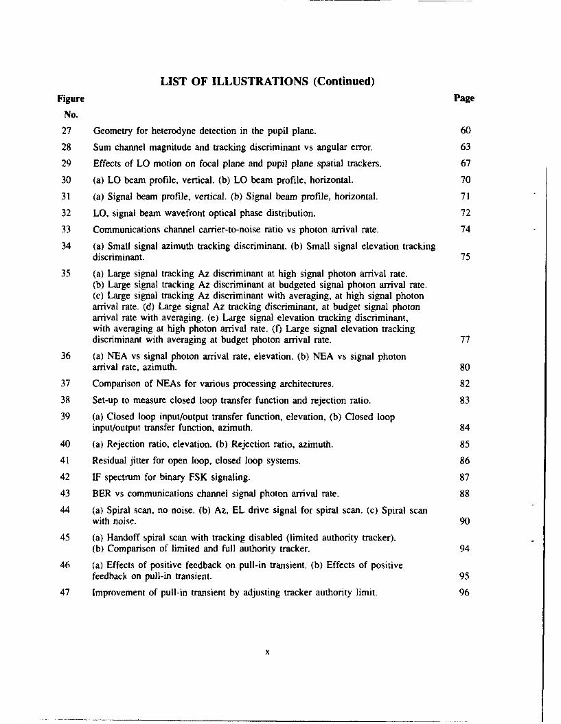
LIST OF ILLUSTRATIONS (Continued)Figure Page
No.
27 Geometry for heterodyne detection in the pupil plane. 60
28 Sum channel magnitude and tracking discriminant vs angular error. 63
29 Effects of LO motion on focal plane and pupil plane spatial trackers. 67
30 (a) LO beam profile, vertical. (b) LO beam profile, horizontal. 70
31 (a) Signal beam profile, vertical. (b) Signal beam profile, horizontal. 71
32 LO, signal beam wavefront optical phase distribution. 72
33 Communications channel carrier-to-noise ratio vs photon arrival rate. 74
34 (a) Small signal azimuth tracking discriminant. (b) Small signal elevation trackingdiscriminant. 75
35 (a) Large signal tracking Az discriminant at high signal photon arrival rate.(b) Large signal tracking Az discriminant at budgeted signal photon arrival rate.(c) Large signal tracking Az discriminant with averaging, at high signal photonarrival rate. (d) Large signal Az tracking discriminant, at budget signal photonarrival rate with averaging. (e) Large signal elevation tracking discriminant,with averaging at high photon arrival rate. (f) Large signal elevation trackingdiscriminant with averaging at budget photon arrival rate. 77
36 (a) NEA vs signal photon arrival rate, elevation. (b) NEA vs signal photonarrival rate, azimuth. 80
37 Comparison of NEAs for various processing architectures. 82
38 Set-up to measure closed loop transfer function and rejection ratio. 83
39 (a) Closed loop input/output transfer function, elevation, (b) Closed loopinput/output transfer function, azimuth. 84
40 (a) Rejection ratio, elevation. (b) Rejection ratio, azimuth. 85
41 Residual jitter for open loop, closed loop systems. 86
42 IF spectrum for binary FSK signaling. 87
43 BER vs communications channel signal photon arrival rate. 88
44 (a) Spiral scan, no noise. (b) Az, EL drive signal for spiral scan. (c) Spiral scanwith noise. 90
45 (a) Handoff spiral scan with tracking disabled (limited authority tracker).(b) Comparison of limited and full authority tracker. 94
46 (a) Effects of positive feedback on pull-in transient. (b) Effects of positivefeedback on pull-in transient. 95
47 Improvement of pull-in transient by adjusting tracker authority limit. 96
'C
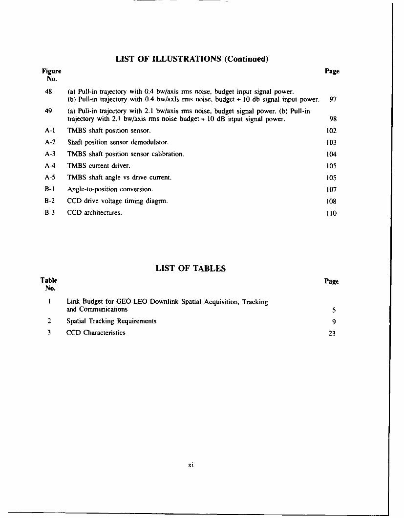
LIST OF ILLUSTRATIONS (Continued)
Figure PageNo.
48 (a) Pull-in trajectory with 0.4 bw/axis rms noise, budget input signal power.(b) Pull-in trajectory with 0.4 bw/axls rms noise, budget + 10 db signal input power. 97
49 (a) Pull-in trajectory with 2.1 bw/axis rms noise, budget signal power. (b) Pull-intrajectory with 2.1 bw/axis rms noise budget + 10 dB input signal power. 98
A-I TMBS shaft position sensor. 102
A-2 Shaft position sensor demodulator. 103
A-3 TMBS shaft position sensor calibration. 104
A-4 TMBS current driver. 105
A-5 TMBS shaft angle vs drive current. 105
B-I Angle-to-position conversion. 107
B-2 CCD drive voltage timing diagrm. 108
B-3 CCD architectures. 110
LIST OF TABLESTable Pagc
No.I Link Budget for GEO-LEO Downlink Spatial Acquisition, Tracking
and Communications 5
2 Spatial Tracking Requirements 9
3 CCD Characteristics 23
xi
1. INTRODUCTION
Optical crosslinks between spaceborne platforms are attra&tive because they offer the potential ofsupporting high-data-rate communications (greater than I Gb/s) using small-aperture telescopes and withless weight and power than microwave-based links. However, the narrow beamwidth achievable at opticalwavelengths (-1 pm) compared to microwave wavelengths (-1 cm) demands highly accurate spatialacquisition and tracking to obtain good communication performance.
During acquisition a communication satellite may have attitude angular uncertainties of the orderof 1 mrad, yet the full-width half-maximum field of view (FOV) of a diffraction-limited receiver is only4.4 Wad when using a 20-cm aperture at diode-laser wavelengths (-0.86 pm). Broadening the transmittedbeam increases the probability of illuminating the receiver for acquisition, despite initial transmitterpointing errors, but reduces signal power at the receiver. As we will show, acquisition for a realisticoptical link may entail searching more than 104 locations in less than a minute for a signal that has aphoton arrival rate on the order of only 105 photons/s.
In addition to acquisition, angle tracking of a received signal is important to space-based lasercommunications systems. Typically, the input signal , -tical power required to maintain constant bit errorrate (BER) in a heterodyne optical communications link increases drastically as the single axis tracking(tilt) errors exceed 0.3 to 0.5 beamwidth (bw). Because transient spatial tracking errors last for manysymbol times in a high-speed communications system, relatively infrequent errors of this magnitude cansignificantly degrade the link BER. Studies have shown that the probability of burst errors must bereduced to a level similar to the desired probability of bit error in order to realize the desired BER in thepresence of statistical tracking errors [1,2,3]. This may be achieved by reducing the sum of trackingbiases and the rms level of tracking jitter to approximately 0.05 to 0.1 bw.
This report describes a design for an integrated acquisition and spatial tracking system that formspart of a high-speed optical heterodyne communications receiver. The baseline design is a receiver thatcould realistically serve as the low-earth-orbit (LEO) end of a geosynchronous orbit (GEO) to LEOcommunications link. The design was originally intended to be the ground receiver for Phase I, GEO toground, of the Laser Intersatellite Transmission Experiment (LITE). First this report presents an overviewof LITE and the requirements that the LEO receiver acquisition and tracking system mist satisfy tosupport the communications link of which it is a part. Next, the acquisition and tracking portions of thesystem implementation are described in detail. Within each discussion data are presented to verify theperformance of the acquisition and tracking subsystems in a laboratory breadboard of the receiver. A listof acronyms and symbols is included as Appendix D.
2. OVERVIEW OF LITE
The potential advantages of an optical intersatellite crosslink over microwave-based systems havebeen the subject of considerable research for several years at MIT Lincoln Laboratory and elsewhere. In
1985 MIT Lincoln Laboratory began the design for LITE [4]. The initial phase of this experiment wasto demonstrate optical communications between a spacebome package on the NASA Advanced Com-munications Technology Satellite (ACTS) and a ground-based heterodyne detection receiver at an as-tronomical site in the United States (probably Mt. Wilson). Subsequent phases would have demonstratedGEO-LEO and GEO-GEO communications links. Although the flight portion of LITE was cancelled dueto funding constraints, an engineering model of the spaceborne platform is under development, and alaboratory demonstration of the heterodyne receiver intended for either ground or LEO has been com-pleted. This report details the spatial acquisition and tracking portion of the LEO receiver. It includes asummary of the important GEO platform design features to help put the LEO receiver design in context.A more complete description of the GEO spatial acquisition, tracking, and pointing system may be foundin Bondurant et al., and Kaufman and Swanson [5,61.
LITE included an intensity modulated (54 kI-lz, 50 percent duty cycle square wave) uplink beaconfrom the LEO platform to the direct detection ACTS receiver located in GEO. This beacon provided atracking reference for the ACTS-based platform, which returned a constant amplitude, 2- or 4-ary,frequency shift keyed (FSK) modulated downlink to the heterodyne detection LEO receiver. The data rateon the downlink could be set to 27.5, 55, 110, or 220 Mb/s. Both ends of the communications linkemployed 30-mW semiconductor lasers operating at nominal wavelengths of 0.86 ym. LITE included ademonstration of direct detection acquisition and spatial tracking of the uplink beacon by the GEOplatform and a simultaneous demonstration of acquisition, spatial tracking, and data demodulation of thedownlink by the LEO receiver.
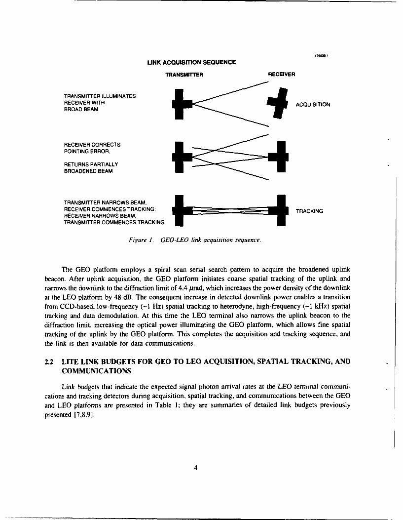
2.1 LITE ACQUISITION SEQI EN-CE DEFINITION
The following acquisition sequenc,, illustrated in Figure 1, was developed to establish a commu-nications link between the LEO and GEO terminals. First, the GEO transmitter illuminates the LEOreceiver witli a downlink beam 'r dened to 1 mrad from the 4.4-grad full-width half-maximum (FWHM)diffraction limit. T: beam is broadened to guarantee illumination of the LEO platform despite the initialGEO platform pointing errors. The broadened beam illuminates the LEO platform with 48 dB less powerdensity than the perfectly pointed, diffraction-limited communications beam.
Next, the LEO platform initiates a parallel search using a charged-coupled device (CCD) to acquirethe broadened downlink within the LEO pointing uncertainty region, which is also 1 rad. The LEO platformthen tracks the downlink with repeated CCD acquisitions well enough to maintain the downlink withinI to 2 bw J-f the communications receiver field of view (FOV), and simultaneously corrects much of theinitial pointing error in the uplink beacon. This coarse tracking loop is limited in bandwidth to less thanI Hz because of the I-s integration time of the acquisition sensor. During coarse tracking the uplinkbeacon (b-oadened to 18 grad from its diffraction limit of -t.4 grad) illuminates the GEO platform.
3
176039-1
LINK ACQUISITION SEQUENCE
TRANSMITTER RECEIVER
TRANSMITTER ILLUMINATESRECEIVER WITH ACQUISITIONBROAD BEAM
RECEIVER CORRECTSPOINTING ERROR,
RETURNS PARTIALLYBROADENED BEAM
TRANSMITTER NARROWS BEAM,RECEIVER COMMENCES TRACKING; TRACKINGRECEIVER NARROWS BEAM, TAI
TRANSMITTER COMMENCES TRACKING
Figure 1. GEO-LEO link acquisition sequence.
The GEO platform employs a spiral scan serial search pattern to acquire the broadened uplinkbeacon. After uplink acquisition, the GEO platform initiates coarse spatial tracking of the uplink andnarrows the downlink to the diffraction limit of 4.4 prad, which increases the power density of the downlinkat the LEO platform by 48 dB. The consequent increase in detected downlink power enables a transitionfrom CCD-based, low-frequency (-1 Hz) spatial tracking to heterodyne, high-frequency (-1 kHz) spatialtracking and data demodulation. At this time :he LEO terminal also narrows the uplink beacon to thediffraction limit, increasing the optical power illuminating the GEO platform, which allows fine spatialtracking of the uplink by the GEO platform. This completes the acquisition and tracking sequence, andthe link is then available for data communications.
2.2 LITE LINK BUDGETS FOR GEO TO LEO ACQUISITION, SPATIAL TRACKING, ANDCOMMUNICATIONS
Link budgets that indicate the expected signal photon arrival rates at the LEO terminal communi-cations and tracking detectors during acquisition, spatial tracking, and communications between the GEOand LEO platforms are presented in Table 1; they are summaries of detailed link budgets previouslypresented [7,8,91.
4
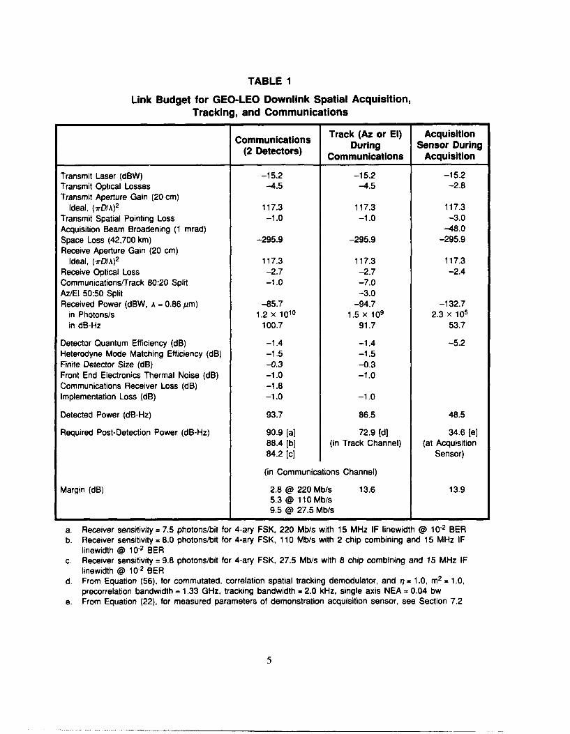
TABLE 1
Link Budget for GEO-LEO Downllnk Spatial Acquisition,Tracking, and Communications
Track (Az or El) Acquisition(2 Detectors) During Sensor During
Communications Acquisition
Transmit Laser (dBW) -15.2 -15.2 -15.2Transmit Optical Losses -4.5 -4.5 -2.8Transmit Aperture Gain (20 cm)
Ideal, (7-D/A) 2 117.3 117.3 117.3Transmit Spatial Pointing Loss -1.0 -1.0 -3.0Acquisition Beam Broadening (1 mrad) -48.0Space Loss (42,700 km) -295.9 -295.9 -295.9Receive Aperture Gain (20 cm)
Ideal, (l-D/A)2 117.3 117.3 117.3Receive Optical Loss -2.7 -2.7 -2.4Communications/Track 80:20 Split -1.0 -7.0AzIEI 50:50 Split -3.0Received Power (dBW, A = 0.86 pm) -85.7 -94.7 -132.7
in Photons/s 1.2 x 10¹⁰ 1.5 x 10⁹ 2.3 x 10⁵in dB-Hz 100.7 91.7 53.7
Detector Quantum Efficiency (dB) -1.4 -1.4 -5.2Heterodyne Mode Matching Efficiency (dB) -1.5 -1.5Finite Detector Size (dB) -0.3 -0.3Front End Electronics Thermal Noise (dB) -1.0 -1.0Communications Receiver Loss (dB) -1.8Implementation Loss (dB) -1.0 -1.0
Detected Power (dB-Hz) 93.7 86.5 48.5
Required Post-Detection Power (dB-Hz) 90.9 [a] 72.9 [d] 34.6 [e]88.4 [b] (in Track Channel) (at Acquisition84.2 [c] Sensor)
(in Communications Channel)
Margin (dB) 2.8 @ 220 Mb/s 13.6 13.95.3 @ 110 Mb/s9.5 @ 27.5 Mb/s
a. Receiver sensitivity = 7.5 photons/bit for 4-ary FSK, 220 Mb/s with 15 MHz IF linewidth @ 10-2 BERb. Receiver sensitivity = 8.0 photons/bit for 4-ary FSK, 110 Mb/s with 2 chip combining and 15 MHz IF
linewidth @ 10-2 BERc. Receiver sensitivity = 9.8 photons/bit for 4-ary FSK, 27.5 Mb/s with 8 chip combining and 15 MHz IF
linewidth @ 10-2 BERd. From Equation (56), for commutated, correlation spatial tracking demodulator, and q = 1.0, m2 = 1.0,
precorrelation bandwidth = 1.33 GHz, tracking bandwidth = 2.0 kHz, single axis NEA = 0.04 bwe. From Equation (22), for measured parameters of demonstration acquisition sensor, see Section 7.2
5
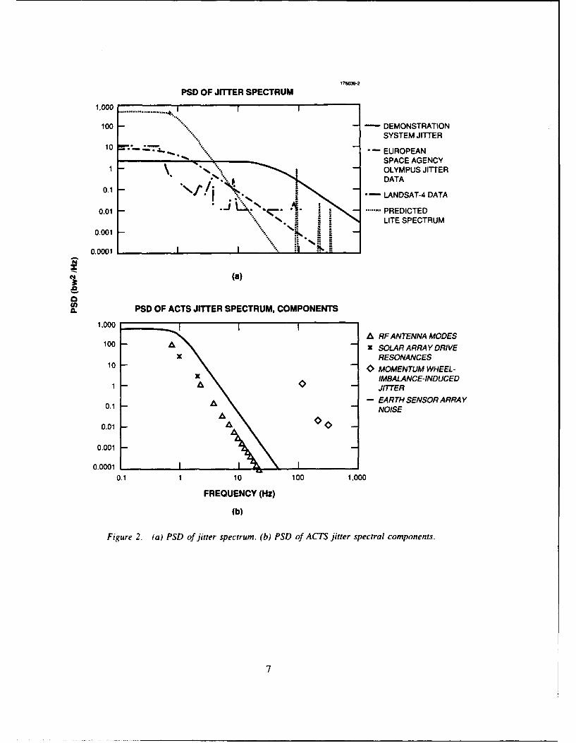
2.3 MICROJITTER ANGULAR DISTURBANCE SPECTRA
Angular motions of the host platform result in disturbances in both the optical receiver and transmitter
lines of sight (LOS); the spectral distribution of these disturbances detennines the rejection that the spatial
tracking system must provide. Little data are available that characterize such disturbances on actual hostsatellites. Two notable examples of measured spacecraft microjitter spectra are data taken on the Landsat-4
spacecraft [10] and on European Space Agency's (ESA) communication satellite OLYMPUS [I11.
2.3.1 Microjitter During Spatial Tracking for LITE
For LITE, considerable study was undertaken to estimate the on-orbit microjitter spectrum of theNASA ACTS satellite (see Reference 6 for a detailed description and additional references). The LEOplatform dynamics were assumed to be similar to those on ACTS. A combination of measurements ona mock-up of a satellite similar to ACTS and NASTRAN modeling of the optical platform was used topredict the effects of various noise components on the receiver LOS. The major contributors to microjitterwere noise in the earth sensor array used for spacecraft attitude control, mechanical vibration due tomotion of the solar array drive, mechanical resonances in the RF antennas, and relatively high frequencyjitter due to mass imbalances in the momentum wheels used for attitude stabilization. A comparison ofthe measured spectra for Landsat-4 and OLYMPUS and the predicted jitter spectra for ACTS are shownin Figure 2(a). In this figure the Landsat-4 and OLYMPUS curves are best fits to measurements ofmicrojitter on those platforms. The power spectral density of the various expected jitter components onACTS are plotted separately in Figure 2(b).
In the demonstration system the expected jitter environment on ACTS is simulated by driving eachaxis of the disturbance mirror pair with independent, Gaussian, white noise sources filtered with a singlepole filter (at 35 Hz) in each axis. The spectrum of the filtered noise source in the demonstration system
(rms jitter amplitude set to 2.1 bw) is shown in Figure 2(a).
2.3.2 Microjitter During Spatial Acquisition for LITE
During acquisition the ACTS attitude control system was to be switched from the earth sensor arrayto gyro control. The resultant microjitter spectrum was identical in shape to the earth sensor array jitterspectrum, but reduced in amplitude from 100- to 2-grad rms. In addition, the solar array drive was to beturned off, which also removed the excitation of the RF antenna resonances. The microjitter duringacquisition therefore was approximated as 1/50 of the earth sensor array noise plus the momentum wheeljitter.
6
176=392
PSD OF J17TER SPECTRUM
100 DEMONSTRATIONSYSTEM JITTER
10- EUROPEANSPACE AGENCYOLYMPUS JITTERDATA
0.1 LANDSAT-4 DATA
0.01 .. PREDICTED- - LITE SPECTRUM
0.001
0.00
CL PSD OF ACTS JITTER SPECTRUM, COMPONENTS1,000 I
A RFANTENNA MODES100- AX SOLAR ARRAY DRIVEx RESONANCES
10 0 MOMENTUM WHEEL -z IMBALANCE-INDUCED
1 AJITTER
0.1 A -EARTH SENSOR ARRAY
0.01 ANOS
0.001
0.00010.1 1 10 100 1,000
FREQUENCY (Hz)
(b)
Figure 2. (a) PSD of jitter spectrum. (b) PS0 of ACTS jitter spectral components.
7
3. SPATIAL ACQUISITION AND TRACKING SYSTEM REQUIREMENTS
3.1 ACQUISITION SYSTEM REQUIREMENTS
The acquisition system on the LEO terminal must locate the broadened downlink with a highprobability of success (> 0.99) and a low false alarm rate (< 0.01) for a budgeted signal photon arrivalrate of 2.3 X 10⁵ photons/s. The initial 1 mrad or -230 bw angular uncertainty in locating the downlinkmust be reduced to less than 2 diffraction-limited bw. Acquisition must be performed in a time that issubstantially less than -1 min. Finally, the acquisition system must sense the power surge that occurswhen the downlink is narrowed, and it must initiate handoff to the spatial tracking system.
3.2 SPATIAL TRACKING SYSTEM REQUIREMENTS
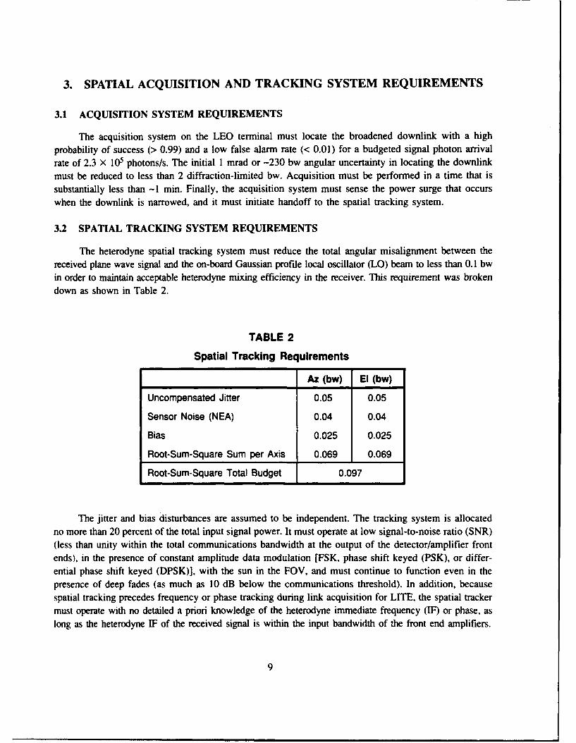
The heterodyne spatial tracking system must reduce the total angular misalignment between thereceived plane wave signal and the on-board Gaussian profile local oscillator (LO) beam to less than 0.1 bwin order to maintain acceptable heterodyne mixing efficiency in the receiver. This requirement was brokendown as shown in Table 2.
TABLE 2
Spatial Tracking Requirements
Az (bw) El (bw)
Uncompensated Jitter 0.05 0.05
Sensor Noise (NEA) 0.04 0.04
Bias 0.025 0.025
Root-Sum-Square Sum per Axis 0.069 0.069
Root-Sum-Square Total Budget 0.097
The jitter and bias disturbances are assumed to be independent. The tracking system is allocatedno more than 20 percent of the total input signal power. It must operate at low signal-to-noise ratio (SNR)(less than unity within the total communications bandwidth at the output of the detector/amplifier frontends), in the presence of constant amplitude data modulation [FSK, phase shift keyed (PSK), or differ-ential phase shift keyed (DPSK)], with the sun in the FOV, and must continue to function even in thepresence of deep fades (as much as 10 dB below the communications threshold). In addition, becausespatial tracking precedes frequency or phase tracking during link acquisition for LITE, the spatial trackermust operate with no detailed a priori knowledge of the heterodyne immediate frequency (IF) or phase, aslong as the heterodyne IF of the received signal is within the input bandwidth of the front end amplifiers.
9
4. SYSTEM OVERVIEW
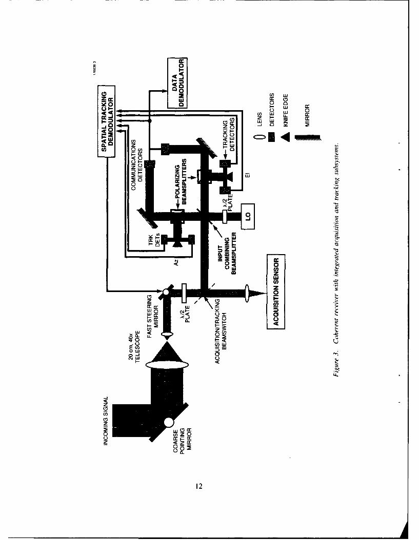
The major system components are illustrated in Figure 3. The incoming optical signal is incidentupon a large gimballed flat, referred to as the coarse pointing mirror (CPM), which can sweep the receiverFOV across a wide range of crosslink locations. The light is collected in a 20 cm, 40x telescope, relayedto a 2-axis fast steering mirror (FSM) for high-frequency, small-angle corrections, and relayed to eitherthe acquisition sensor or the communications receiver as a function of the beamswitch position. Thecommunications receiver is arranged as a balanced detector [ 12,13], with separate optical pickoffs for theazimuth and elevation track paths. The communications signal serves as a phase-coherent reference to thetrack channel outputs, from which an azimuth (elevation) tracking demodulator [14] is formed based uponthe phase difference between each half of the azimuth (elevation) track channel. It can be shown that theangular misalignments in each axis between the LO and signal beam are proportional to these phasedifferences. The baseband error signal is processed appropriately and applied to the FSM to provideclosed loop tracking of the angular error.
11
0
Z=Ll a:
o 0
J~ ~ ~ z --
z 00 Te
2 OL.
<0
00I
12
5. OPTICAL LAYOUT COMMON TO BOTHACQUISITION AND TRACKING SUBSYSTEMS
The optical layout used in the demonstration system was similar to that described previously
14,15]. Only that portion of the system beyond the 20-cm telescope was demonstrated, which meant thatall of the optical processing was performed with 5-mm diameter beams, instead of 20-cm beams. Adetailed optical layout is shown in Figure 4. This section describes that portion of the optical layoutcommon to both the acquisition and tracking systems, i.e., from the signal laser to the acquisition/trackingbeamswitch. The portions of the optical layout unique to acquisition and tracking are described inSections 6.2 and 9.1, respectively.
5.1 SIGNAL SIMULATION
The received signal was simulated using a Hitachi HLP-8314 laser diode, operating in a singlelongitudinal mode at a nominal wavelength of 0.86 pn. A Fujinon f/1.1, 7.7-mm focal length lens anda Special Optics anamorphic prism pair served to form the output of the laser into a circular Gaussianbeam with a lie (E field) radius of 2.5 mm. A pair of Optics For Research Faraday isolators, each witha clear aperture of 5 um, was used to reduce feedback to the signal laser. A neutral density filter wasplaced in front of the first isolator to further attenuate backscattering from the isolator crystal into thelaser. A small percentage of the signal was picked off, using the inherent imperfection of the high-reflectance coating on the first fold mirror, and sent to a 300-MHz free spectral range Fabry-Perotinterferometer (Coherent model 216) for monitoring purposes.
Approximately 4 mW of the 30-mW output of the signal laser were available beyond the neutraldensity filter and the Faraday isolators. This output was coupled into a short (=3 m) length of polariza-tion-preserving, single-mode fiber. The use of the fiber made it possible to locate the signal laser on aseparate table without affecting the alignment of the system. The output of the fiber was collimated usinganother Fujinon lens; it then passed through an Isomet acousto-optic modulator, which served as a high-speed intensity modulator, with more than 50 dB of dynamic range. The acousto-optic modulator wasdriven with up to 1 W of RF power at 82 MHz. At this drive power 67 percent of the input optical powerwas diffracted into the first order output beam. The zero order beam was blocked, and the first orderdiffracted beam was passed through a Special Optics 20x beam expander. A 5-mm iris at the output ofthe beam expander was used to block all but the center of the expanded beam, forming a reasonableapproximation to the 5-mm diameter plane wave that would be present at the output of the 40x, 20-cmtelescope in the actual receiver. Finally, a Karl Lambrecht Corporation half-wave plate was placedbeyond the 5-mm iris to control the orientation of the signal polarization.
5.2 JITTER SIMULATION AND TRACKING MIRRORS
Two pairs of single-axis, flexure-mounted, General Scanning Z2046 torque motor beam steerers(TMBSs) with 1-cm square mirrors were used to form the 2-axis angular jitter source and the 2-axis FSMfor closed-loop spatial tracking. Each TMBS was configured with a position sensor (Appendix A) and
13
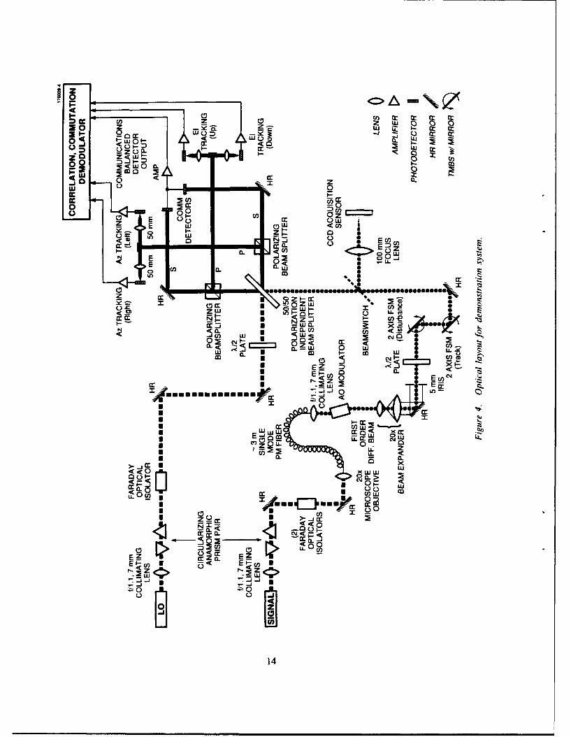
zA-20l <>A I
0 0
z 0so z 2-2 1-- : q ): m -) -
0-1 < MO0
w 0 (00 2 C0
0 0 5
z aU U
,a : Ci)E D
Ew 02
E -C L
0- I.a
I
m mVcc Lie Z)ZLu4
)-m j Z wUUL
LL UiLI
*U CD 0 W
40i 0.0..f0 z' 0EZ -
UC U-i-I UU -- W-oC xC1 Jw0L
140 L C YL
velocity feedback to provide sufficient active damping to reduce the Q of the first resonance (109 Hz)to that of a critically damped, second-order system. Details of the drive circuitry are given in AppendixA. The response of each position sensor was flat to beyond 1.1 kHz, and measurements of shaft positionusing both the shaft-position sensors and an external optical monitor agreed to within 1 percent atfrequencies less than 1 kHz. The measured linearity between TMBS current and angular position wasbetter than 1 percent. The TMBSs were configured to have excellent linearity and critical damping inorder that an undistorted spiral scan could be generated during handoff (see Sections 9.5 and 11.9.2)without requiring any optical feedback.
To minimize beam walk, a pair of 75-mm focal length lenses was used to relay an image planelocated halfway between the jitter TMBS pair to an image plane located halfway between the trackingTMBS pair.
5.3 ACQUISITION/TRACKING BEAM SWITCH
A pair of 300-mm lenses was used to relay the image plane at the tracking mirrors through abeamswitch to either the input of the CCD acquisition sensor or the input combining beamsplitter of thecommunications receiver, depending on the beamswitch position. Just ahead of the beamswitch was apolarizing beamsplitter, used to direct a small percentage of the incoming signal power into a monitorport for independent observation of signal power or signal angle variations.
The beamswitch, formed from an aluminum wheel, rotated a 1-inch circular mirror in or out of thebeam path. When the mirror was not in the path all of the signal was incident on the CCD acquisitionsensor. When the mirror was in the path most of the signal was sent to the heterodyne tracker, while asmall fraction (-48 dB) was incident on the acquisition sensor because the mirror was coated to provide48-dB attenuation in transmission. The effect of the narrowing of the signal beam (during the transitionbetween acquisition and tracking) was modeled as a 48 dB increase in received signal optical power. Thenet result was that a constant signal power level was incident upon the CCD sensor during both acqui-sition and subsequent tracking. Purely for experimental convenience, this allowed the CCD to continueto monitor the signal beam position while the heterodyne tracker was operating. The mirror was undercomputer control and could be moved in or out of the beam path in about 200 ms. The angular repeatabilityof the beam position following several beamswitch cycles was measured to be better than 0.1 bw.
15
6. SPATIAL ACQUISITION SYSTEM IMPLEMENTATION
6.1 ACQUISITION SYSTEM OVERVIEW
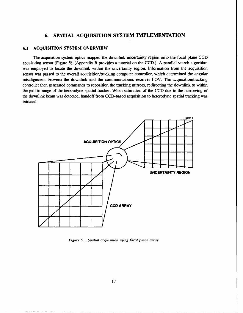
The acquisition system optics mapped the downlink uncertainty region onto the focal plane CCDacquisition sensor (Figure 5). (Appendix B provides a tutorial on the CCD.) A parallel search algorithmwas employed to locate the downlink within the uncertainty region. Information from the acquisitionsensor was passed to the overall acquisition/tracking computer controller, which determined the angularmisalignment between the downlink and the communications receiver FOV. The acquisition/trackingcontroller then generated commands to reposition the tracking mirrors, redirecting the downlink to withinthe pull-in range of the heterodyne spatial tracker. When saturation of the CCD due to the narrowing ofthe downlink beam was detected, handoff from CCD-based acquisition to heterodyne spatial tracking wasinitiated.
CCD ARRAY
Figure S. Spatial acquisition using focal plane array.
17
The frame integration period was chosen to be I s. This yielded a sufficiently high SNR that therequired signal detection probability could be obtained at room temperature while maintaining sufficientdynamic range, within a reasonably prompt acquisition time. A shorter integration time would result ina smaller SNR, thereby increasing the signal power required to maintain the same probability of success-ful acquisition. For example, a factor of 2 reduction in integration time in the system would theoreticallyrequire a 2.45-dB increase in signal power to maintain a probability of success of 0.99 [Equation (22)].A longer integration time would improve the SNR at the cost of increased acquisition time anI thepossibility of saturating the CCD with either accumulated dark current or signal. An electronic shutterwith on/off times of approximately 5 ms was placed in front of the CCD to control the illumination ofthe CCD during acquisition.
Note that alternatives to the parallel search algorithm exist, such as the serial scan used in the LITEuplink acquisition system [5,6]. However, at a photon arrival rate low enough to require an integrationtime on the order of 1 s for acceptable probability of acquisition, a serial search of 40,000 possiblelocations was deemed impractical.
6.2 SPATIAL ACQUISITION SYSTEM LABORATORY OPTICAL LAYOUT
The CCD acquisition sensor was located in the back focal plane of a 100-mm lens. The input tothe spatial acquisition system (simulating the output of the 20-cm, 40x telescope) was a collimated beam5 mm in diameter. The calculated diffraction-limited FWHM spot size at the CCD was 17.7 pm, or two-thirds the width of a single pixel. The uncertainty region of -230 X 230 diffraction-limited beamwidthstherefore corresponded to an array of approximately 153 X 153 pixels. In order to reduce processing timeit wa, onvenient to use a 200 x 200 pixel subarray of the 512 X 512 pixel CCD, which more thanadequately covered the uncertainty region.
The focused spot size at the CCD was selected to provide sufficient resolution while maintainingadequate SNR in the pixels that contained the focused spot [16]. A spot size approximately equal to Ipixel makes efficient use of the signal. For a spot much smaller than 1 pixel, the CCD cannot resolvebeam motions within a pixel. When the spot is spread over several pixels, the presence of backgroundand readout noise causes the SNR to drop with no attendant gain in resolution. The estimated effectivespot size in the laboratory implementation, after accounting for acoustic and mechanical disturbances andimperfections of the lens, was between 0.85 and 0.9 pixel.
6.3 ACQUISITION ALGORITHM
During spatial acquisition the CCD sensor operated in either frame integration mode or readoutmode (Figure 6). During frame integration the clocks weie disabled, which allowed charge, due both todark current and any incident photons, to accumulate in the CCD. During readout the shutter was closedand the clocks were enabled to serially transfer the accumulated charge from the array to the outputamplifier. The output amplifier developed a voltage proportional to the charge in each pixel, and a digitalrepresentation of this voltage was stored on a digital processing board in one of three memory maps ofthe CCD. The three memory maps included a signal frame, a background frame, and a difference frame.
18
The acquisition process required integrating both a background and a signal frame. The backgroundframe was taken with the shutter closed during integration to characterize the dark noise in the array. Thesignal frame was taken with the shutter open during integration to gather charge from both dark currentand signal photons. Using digital hardwar- the background frame was subtracted from the signal frame,forming a difference frame, to reduce the effects of pixel-to-pixel variations across the array in averagedark current. The CCD was continuously read out between frame integratiL , to clear the array ofaccumulated dark current prior to the next frame integration.
176039-5
MODE INTEGRATION READOUT(Accumulate Charge) (Transfer Charge)
CLOCKS DISABLED ENABLED
BACKGROUND SIGNALFRAME FRAME
SHUTTER CLOSED OPEN CLOSED
Figure 6. CCD modes of operation.
Gain calibration of the CCD was not implemented in the system. Although pixels with particularlyhigh or low gain could affect the accuracy of the acquisition system estimate of signal position, the responseof only a few pixels (less than 0.1 percent) was significantly different from average (see Section 8.4.2), andthe performance of the acquisition system was not limited by gain nonuniformity in the acquisitionsensor. It is noted that it is theoretically possible to calibrate gain using a uniform illumination of theCCD.
The detailed acquisition sequence follows (Figure'7). Prior to the acquisition session a backgroundframe was integrated, read out, and stored in memory . The session began with the integration of a signalframe. Next, as the signal frame was read out from the CCD, the background frame data was subtractedfrom the signal frame data, and the resultant difference frame was stored in memory. Using hardwareprocessing, the 200 X 200 pixel difference frame was scanned within 32 ms to identify the address ofthe 2 X 2 pixel block with the largest total signal, referred to as the MAXBLOCK. Given that the focusedspot size (FWHM) on the array was approximately 0.9 pixel, an estimated 75 to 82 pcrcent of the signalenergy would have been contained within the MAXBLOCK group. The MAXBLOCK address and thesignal level of each pixel within the MAXBLOCK group was then sent to the acquisition/trackingcontroller. By using a simple first order algorithm (difference/sum) similar to that used for a quadrantdetector, the acquisition/tracking controller obtained with subpixel resolution an estimate of the signal
19
location within the MAXBLOCK. Commands were then generated to position the track mirrors so thatthe signal was centered within the heterodyne receiver FOV. The location of the heterodyne receiver FOVrelative to the acquisition sensor coordinates was determined by the acquisition/tracking system througha boresight procedure prior to the start of the acquisition sequence.
176039-6
PROCESS
1. INTEGRATE BACKGROUND FRAME SHUTTER: CLOSEDCLOCKS: DISABLED
2. READOUT AND STORE BACKGROUND SHUTTER: CLOSEDFRAME CLOCKS: ENABLED
3. INTEGRATE SIGNAL. FRAME SHUTTER: OPENCLOCKS: DISABLED
4. READOUT SIGNAL FRAME, SUBTRACT SHUTTER: CLOSEDBACKGROUND FRAME, AND STORE CLOCKS: ENABLEDDIFFERENCE FRAME
5. LOCATE MAXBLOCK
6. TRANSFER MAXBLOCK DATA TO CONTROLLERFOR SUB-PIXEL LOCATION ESTIMATION
7. REPEAT (3) THROUGH (6) UNTIL POWERSURGE DETECTION
Figure 7. Acquisition sequence.
A loop referred to as "coarse tracking" continued to update the CCD estimate of the location ofthe signal and adjust the tracking mirrors until a power surge was detected. This surge, the consequenceof downlink beam narrowing, resulted in the saturation of the MAXBLOCK pixels and was detected bytesting for the full-scale reading of the value of the MAXBLOCK sum. Upon surge deteL.ion the beamswitchredirected the signal to the heterodyne spatial tracker and the handoff procedure was initiated.
The minimum total acquisition time was the sum of the integration interval, the readout time, andthe processing time. The integration interval was 1 s. With a frame readout rate of 1 MHz the readoutof the 200 X 200 subarray required 113 ms. In order to clear the CCD, however, the entire array was read,requiring 28, ms. The processing time to identify the MAXBLOCK location was 32 ms. The totalacquisition time therefore was 1.32 s. This total increased to 2.6 s if a dark frame was taken prior to everysignal acquisition instead of just at the beginning of the session. It was convenient (and within budgeted
20
time constraints) to integrate a new dark frame prior to every signal acquisition, thereby assuring that
the dark frame stored in memory more accurately represented dark current levels at the time of acqui-
sition.
This algorithm does not define a protocol for acquisition when the initial uncertainty is greater than
the CCD FOV. If the signal were outside the CCD FOV, consecutive positional estimates in the coarse
tracking loop would vary by more than a few pixels. One approach could be to program the acquisition/
tracking controller to look for this condition and react to it by repositioning the CCD FOV and restarting
the acquisition session.
6.4 ELECTRONICS
The system electronics consisted of five units: the CCD imager, a multiphase clock generator and voltage
generator, an analog signal conditioner, a digital memory and processing unit, and a microprocessor-based
control board. The acquisition subsystem was under the control of the HP 9000/320-based acquisition/
tracking computer contoller, as shown in Figure 8.
176039-7
ANALOG SIGNAL CONDITIONER
CCD LEVEL SHIFTER m CORRELATED m POSTAMPLIFIER
EPREAMPLIFIER H DOUBLE-SAMPLER H LEVEL SHIFTER
MULTIPHASE DIGITALCLOCK -PROCESSING UNITGENERATOR 1 ADC
MICROPROCESSOR FRAME STORAGECONTROL UNIT FRAME SUBTRACTIONCOMPUTER INTERFACE COARSE ACQUISITIONACQUISITION SYSTEM INTERNAL COMMANDS DATA TRANSFERPIXEL MASK TRANSFERNARROWED BEAM DETECTIONDATA TRANSFER
HETERODYNESPATIALTRACKING ACQUISITION/TRACKING
SYSTEMCOMPUTER CONTROLLER
Figure 8. Spatial acquisition subsystem block diagram.
21
6.4.1 CCD
Characterization. Our acquisition sensor was required to be large enough to cover the 1-mrad
uncertainty region with a resolution of better than 2 bw. A 200 X 200 pixel subarray of the 512 X 512pixel TK512M used in conjunction with a 100-mm lens covered approximately 1.3 mrad in object space,or 295 beamwidths. Each pixel was square with 27 pm on a side and had a FOV equal to 1.5 diffraction-limited beamwidths.
The TK512M is specified to have dark current less than 10 nA/cm2 at 20'C, or 4.37 X 10 e-/s/pixel.Our particular sensor was measured to have an unusually low dark current density of 130 pA/cm 2 or5.7 X 103 e-/s/pixel at room temperature [17]. (By thermoelectric cooling to -60'C, dark current couldlikely have been reduced to close to 1 e-/s/pixel.)
The accumulated charge due to dark current may be represented as a bias plus shot noise. In aperfect CCD the dark current, and hence the bias, would be the same across the entire array. Unfortu-nately, due to substrate inhomogeneities there is a certain amount of pixel-to-pixel nonuniformity. Theseinhomogeneities result in highly repeatable pixel-to-pixel variations in dark current, which cause bothvariations in pixel bias and shot noise. Variations in pixel bias or average accumulated dark current maybe removed by recording an unilluminated frame from the CCD and subtracting it from any subsequentframe. The limitations introduced due to increased dark-current-induced shot noise in pixels with unusu-ally large dark current "blemishes" may be removed by pixel masking.
Read noise is generally a function of readout rate and device temperature. Most specifications aregiven for rates much slower than the 1 MHz readout rate of our system. The specification for the TK512Mis 10 e- at a 200 kHz readout rate and -90'C. Our sensor readout noise was measured to be 78 rms e-/pixelat a 1 MHz readout rate and room temperature [18].
Crosstalk, the lateral diffusion of electrons generated below the depletion region of the CCD, is onlysignificant at wavelengths longer than 0.75 pm. For our purposes, the crosstalk had to be low enough thatthe estimate of signal location was not noticeably affected. Measured values for our acquisition sensorwere 8 percent between rows and 9 percent between columns [18]. These numbers represent the relativevalue of one pixel adjacent to a second pixel in which a signal (much smaller than a pixel) is centered.Optical imperfections, charge transfer inefficiency, and insufficient video bandwidth may have contrib-uted to the measured values. It was determined that this level of crosstalk had a negligible effect on boththe probability of acquisition and the accuracy of the estimate of signal location [18].
Table 3 summarizes the characteristics of the acquisition sensor necessary to meet system require-ments [19] and the actual performance of the TK5I2M [17].
22
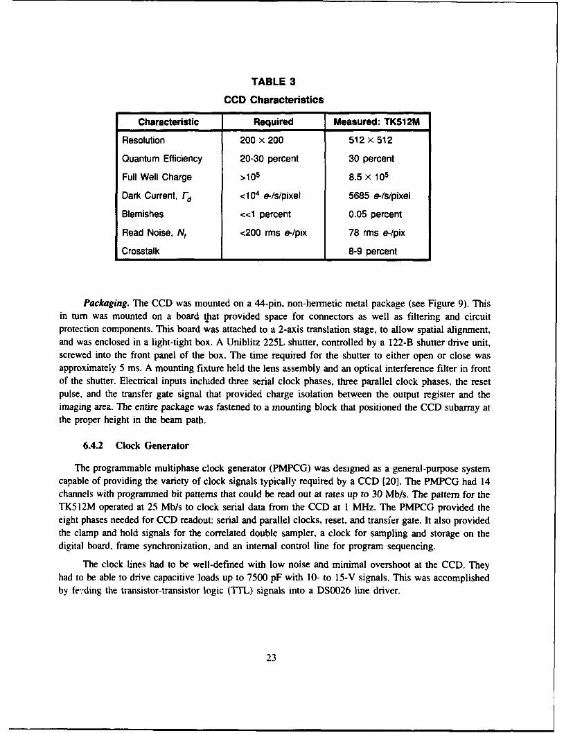
TABLE 3
CCD Characteristics
Characteristic Required Measured: TK512M
Resolution 200 x 200 512 x 512
Quantum Efficiency 20-30 percent 30 percent
Full Well Charge >10S 8.5 x 10⁵
Dark Current, Fd <104 e-/s/pixel 5685 e-/s/pixel
Blemishes <<1 percent 0.05 percent
Read Noise, N, <200 rms e-/pix 78 rms e-/pix
Crosstalk 8-9 percent
Packaging. The CCD was mounted on a 44-pin, non-hermetic metal package (see Figure 9). Thisin turn was mounted on a board that provided space for connectors as well as filtering and circuitprotection components. This board was attached to a 2-axis translation stage, to allow spatial alignment,and was enclosed in a light-tight box. A Uniblitz 225L shutter, controlled by a 122-B shutter drive unit,screwed into the front panel of the box. The time required for the shutter to either open or close wasapproximately 5 ins. A mounting fixture held the lens assembly and an optical interference filter in frontof the shutter. Electrical inputs included three serial clock phases, three parallel clock phases, the resetpulse, and the transfer gate signal that provided charge isolation between the output register and theimaging area. The entire package was fastened to a mounting block that positioned the CCD subarray atthe proper height in the beam path.
6.4.2 Clock Generator
The programmable multiphase clock generator (PMPCG) was designed as a general-purpose systemcapable of providing the variety of clock signals typically required by a CCD [20]. The PMPCG had 14channels with programmed bit patterns that could be read out at rates up to 30 Mb/s. The pattern for theTK512M operated at 25 Mb/s to clock serial data from the CCD at 1 MHz. The PMPCG provided theeight phases needed for CCD readout: serial and parallel clocks, reset, and transfer gate. It also providedthe clamp and hold signals for the correlated double sampler, a clock for sampling and storage on thedigital board, frame synchronization, and an internal control line for program sequencing.
The clock lines had to be well-defined with low noise and minimal overshoot at the CCD. Theyhad to be able to drive capacitive loads up to 7500 pF with 10- to 15-V signals. This was accomplishedby fe,.,ding the transistor-transistor logic (TTL) signals into a DS0026 line driver.
23
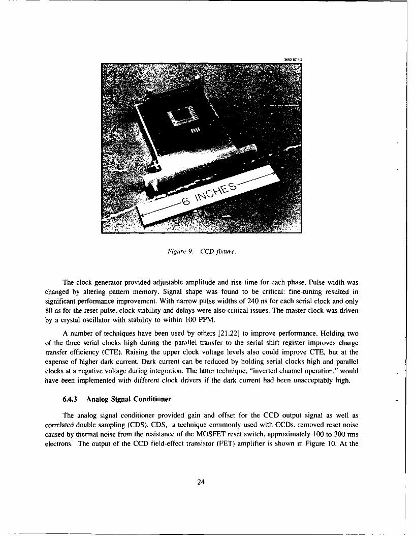
3692-87-1C
Figure 9. CCD fiture.
The clock generator provided adjustable amplitude and rise time for each phase. Pulse width waschanged by altering pattern memory. Signal shape was found to be critical: fine-tuning resulted insignificant performance improvement. With narrow pulse widths of 240 ns for each serial clock and only80 ns for the reset pulse, clock stability and delays were also critical issues. The master clock was drivenby a crystal oscillator with stability to within 100 PPM.
A number of techniques have been used by others [21,22] to improve performance. Holding twoof the three serial clocks high during the parallel transfer to the serial shift register improves chargetransfer efficiency (CTE). Raising the upper clock voltage levels also could improve CTE, but at theexpense of higher dark current. Dark current can be reduced by holding serial clocks high and parallelclocks at a negative voltage during integration. The latter technique, "inverted channel operation," wouldhave been implemented with different clock drivers if the dark current had been unacceptably high.
6.4.3 Analog Signal Conditioner
The analog signal conditioner provided gain and offset for the CCD output signal as well ascorrelated double sampling (CDS). CDS, a technique commonly used with CCDs, removed reset noisecaused by thermal noise from the resistance of the MOSFET reset switch, approximately 100 to 300 rmselectrons. The output of the CCD field-effect transistor (FET) amplifier is shown in Figure 10. At the
24
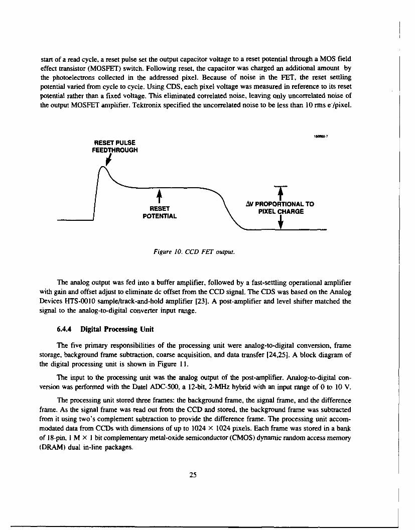
start of a read cycle, a reset pulse set the output capacitor voltage to a reset potential through a MOS fieldeffect transistor (MOSFET) switch. Following reset, the capacitor was charged an additional amount bythe photoelectrons collected in the addressed pixel. Because of noise in the FET, the reset settlingpotential varied from cycle to cycle. Using CDS, each pixel voltage was measured in reference to its resetpotential rather than a fixed voltage. This eliminated correlated noise, leaving only uncorrelated noise ofthe output MOSFET amplifier. Tektronix specified the uncorrelated noise to be less than 10 rms e/pixel.
168888-7
RESET PULSEFEEDTHROUGH
RESETAV PROPORTIONAL TOPIXEL CHARGE
Figure 10. CCD FET output.
The analog output was fed into a buffer amplifier, followed by a fast-settling operational amplifierwith gain and offset adjust to eliminate dc offset from the CCD signal. The CDS was based on the AnalogDevices HTS-0010 sample/track-and-hold amplifier [23]. A post-amplifier and level shifter matched thesignal to the analog-to-digital converter input range.
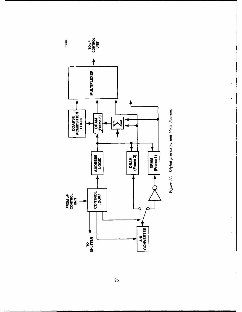
6.4.4 Digital Processing Unit
The five primary responsibilities of the processing unit were analog-to-digital conversion, framestorage, background frame subtraction, coarse acquisition, and data transfer [24,25]. A block diagram ofthe digital processing unit is shown in Figure 11.
The input to the processing unit was the analog output of the post-amplifier. Analog-to-digital con-version was performed with the Datel ADC-500, a 12-bit, 2-MHz hybrid with an input range of 0 to 10 V.
The processing unit stored three frames: the background frame, the signal frame, and the differenceframe. As the signal frame was read out from the CCD and stored, the background frame was subtractedfrom it using two's complement subtraction to provide the difference frame. The processing unit accom-modated data from CCDs with dimensions of up to 1024 X 1024 pixels. Each frame was stored in a bankof 18-pin, I M X 1 bit complementary metal-oxide semiconductor (CMOS) dynamic random access memory(DRAM) dual in-line packages.
25
.1
'0
cc
I
zzUJ 0
126
Coarse acquisition was the process of finding the MAXBLOCK address. This was performed inhardware while the fine centroiding with subpixel accuracywas performed in software. These choicesminimized the combination of processing time and hardware. Processing time to find the MAXBLOCKaddress within the 200 X 200 pixel processing region was 32 ms. The most significant time constraintin processing was due to the access time of the DRAM used for data storage.
Frame data and the address of MAXBLOCK were transferred via an IEEE-488 bus through themicroprocessor control board to the acquisition/tracking controller, which performed fine centroidingusing a first-order algorithm.
6.4.5 Microprocessor Control Board
The microprocessor control board (see Figure 8) was responsible for interfacing with the acquisi-tion/tracking controller and commanding the internal operations of the acquisition system. The unit wasdesigned around a Motorola 68000 microprocessor receiving commands over an IEEE-488 bus. Thecontrol unit was also responsible for pixel mask transfer to the processing unit (see Section 8.4.2), beamnarrowing detection (see Section 6.3), and data transfer from the processing unit to the acquisition/
tracking controller.
27
7. SPATIAL ACQUISITION SYSTEM THEORY OF OPERATION
7.1 ALGORITHM TO OBTAIN SUBPIXEL RESOLUTION
The hardware processing of the CCD difference frame had as its output the MAXBLOCK addressand the values of the each pixel of the 2 X 2 pixel block which made up the MAXBLOCK group (Sec-tion 6.2). A simple first order algorithm was used to calculate a subpixel offset within the MAXBLOCKgroup, based on the value of each of the four MAXBLOCK pixels. This process, referred to as finecentroiding, improved the accuracy of the estimate of the signal position.
The MAXBLOCK location returned by the processing unit was the address, P1, of the lower lefthand pixel of the MAXBLOCK group as shown in Figure 12(a). The complete estimate of the beamposition was expressed as P1 + A(Az,EI), where A(Az,EI) represented the subpixel offset of the beamlocation within the MAXBLOCK group. A(Az,EI) was defined with respect to a coordinate system inwhich the center of pixel P1 was the origin. The following equations were used to calculate A(Az,EI) withVi representing the value of pixel Pi:
AAz = 0.5 + K1 [(V4 + V3)- (VI + V2)] / (Vl + V2 + V3 + V4) (1)
and
AEl = 0.5 + K2 [(V2 + V3)- (VI + V4)]/(VI + V2 + V3+ V4) (2)
This algorithm normalized the signal to make the calculated offsets independent of received totalsignal power. The additive constant 0.5 resulted from defining the origin at the center of P1. Considera spot evenly centered within P1, P2, P3, and P4 such that the numerator equals zero in Equations (1)and (2). The offset along either axis from (0,0), the center of P1, should be 0.5, or half a pixel from thecenter of P1.
The gain factors K1 and K2 are dependent upon the size and shape of the focused signal beamrelative to the size and shape of a CCD pixel. A poor selection of K yields discontinuities in the singleaxis transfer function between actual estimated beam position: low gain produces a staircase shape, highgain rrsults in "hop-back." These discontinuities occur as the beam location is translated through thepoint at which the MAXBLOCK address changes, e.g., from P1 to P1' in Figure 12(b). The discontinuitymay be expressed analytically as the difference between (PI+A) and (Pl'+A').
To examine the effects of the gain factor K on the calculated offset, consider the simple case ofthe translation along one axis of a uniformly illuminated square spot in the focal plane, where the spotis the same size as 1 pixel. Such a beam shape is impractical, but it will serve to clearly illustrate theoffset variation as K changes. For this ideal case and when K = 0.5, the first order difference/sum algo-rithm yields a linear transfer function with unity gain between actual and estimated beam position. Theeffects of suboptimum K values have been calculated and are summarized in Figure 13. K = 0.5 is correctonly for a spot size equal to 1 pixel; the ideal gain must be increased for a larger spot and decreased fora smaller spot.
29
176039-9
ELEVATIONOFFSET
1P2 P3MAXBLOCKGROUP
(a)
0 Pi P4
0 AZIMUTHOFFSET
P2P3T MAXBLOCK A = P1, P2, P3, P4MAXBLOCK B = P1', P2', P3T, P4',BEAM CENTER =X
(b) ......
ESTIMATED BEAM POSITION =P1 + AOR i
i P4' WHEN X IS AT BOUNDARY OFOWN MAXBLOCK A AND MAXBLOCK B.
A=P1 -X
Figure 12. Maxblock geometry.
30
176MI-O
SPOT =1 SQUARE PIXEL4
K.23
K Ks.5
-t-
-2
F
SPOT =0.25 SQUARE PIXELS4
F K=21
01
c c - 1 ..
-2 [
SPOT =4 SQUARE PIXELS
3K-2
2 K- K.
-1-.
-2
0 12
TRANSLATION (Pixels)
Figure 13. Calculated CCD sensor output vs focal plane translation, for a v'ariety of gainsand for several spot sizes.
31
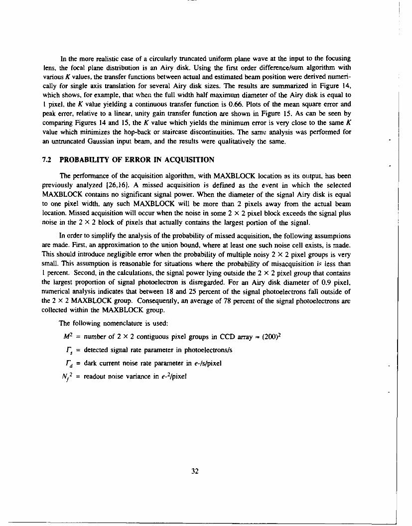
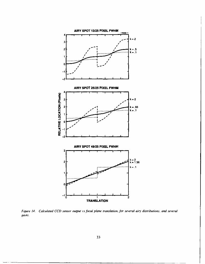
In the more realistic case of a circularly truncated uniform plane wave at the input to the focusinglens, the focal plane distribution is an Airy disk. Using the first order difference/sum algorithm withvarious K values, the transfer functions between actual and estimated beam position were derived numeri-cally for single axis translation for several Airy disk sizes. The results are summarized in Figure 14,which shows, for example, that when the full width half maximum diameter of the Airy disk is equal toI pixel, the K value yielding a continuous transfer function is 0.66. Plots of the mean square error andpeak error, relative to a linear, unity gain transfer function are shown in Figure 15. As can be seen bycomparing Figures 14 and 15, the K value which yields the minimum error is very close to the same Kvalue which minimizes the hop-back or staircase discontinuities. The same analysis was performed foran untruncated Gaussian input beam, and the results were qualitatively the same.
7.2 PROBABILITY OF ERROR IN ACQUISITION
The performance of the acquisition algorithm, with MAXBLOCK location as its output, has beenpreviously analyzed [26,161. A missed acquisition is defined as the event in which the selectedMAXBLOCK contains no significant signal power. When the diameter of the signal Airy disk is equalto one pixel width, any such MAXBLOCK will be more than 2 pixels away from the actual beamlocation. Missed acquisition will occur when the noise in some 2 X 2 pixel block exceeds the signal plusnoise in the 2 X 2 block of pixels that actually contains the largest portion of the signal.
In order to simplify the analysis of the probability of missed acquisition, the following assumptionsare made. First, an approximation to the union bound, where at least one such noise cell exists, is made.This should introduce negligible error when the probability of multiple noisy 2 X 2 pixel groups is verysmall. This assumption is reasonable for situations where the probability of misacquisition is less than1 percent. Second, in the calculations, the signal power lying outside the 2 X 2 pixel group that containsthe largest proportion of signal photoelectron is disregarded. For an Airy disk diameter of 0.9 pixel,numerical analysis indicates that between 18 and 25 percent of the signal photoelectrons fall outside ofthe 2 x 2 MAXBLOCK group. Consequently, an average of 78 percent of the signal photoelectrons arecollected within the MAXBLOCK group.
The following nomenclature is used:
M 2 = number of 2 X 2 contiguous pixel groups in CCD array = (200)2
F = detected signal rate parameter in photoelectrons/s
Fd = dark current noise rate parameter in e-/s/pixel
Nf2 = readout noise variance in e- 2/pixel
32
AIRY SPOT 13/25 PIXEL FWHMk tO - 2
3-
- =.5J* r ....... ...... k 1'... ......
... ... .. ...... ..0
-21
F
AIRY SPOT 25/25 PIXEL FWHM
2
x 3 -s k 2
1
0) 2 -, k = .66P - - k =.1
-2I I I I I
AIRY SPOT 49/25 PIXEL FWHM
k= 1.56
........ .. = .. .. 1. .
-1
0 12
TRANSLATION
Figure 14. Calculated CCD sensor output vs focal plane translation, for several airy distributions, and severalgains.
33
176039-12
0.05
2 0.045 - SPOT SIZE - 13/25 PIXEL* 0 SPOT SIZE . 2525 PIXELS0.04 * SPOT SIZE - 49/25 PIXEL
I- 0.035 AIRY DISK FWHM0CC 0.03'U,, 0.0254 0.02 hO 0.015
:k001
0.005
0(a)
I I I I I I I I II -'
0.
0.45-U SPOT SIZE = 13/25 PIXEL0 SPOT SIZE = 2525 PIXEL
0.34 SPOT SIZE = 49125 PIXELAIRY DISK FWHM
o 0.3
m 0.25
U 0.2
S0.15
2 0.1 -
0.05 -
0 0.2 0.4 0.6 0.8 1 1.2 1.4 1.6 1.8 2
K VALUE
(b)
Figure 15. (a) Calculated mean square error vs gain (K). (b) Calculated peak error vs gain (Kw
34
Nq2 = ADC quantization noise variance in e-2/pixel (nominally 261)
T = CCD integration time in seconds (nominally 1)
With dark current and readout noise a pixel with no signal will have
variance =rT+N 2 (3)
With some part of the spot illuminating a pixel, there is a Poisson-distributed contribution from the signalwith mean equal to variance such that
nacans = variance = Cr T (4)
where C is the fraction of the spot within the pixel (0 5 C _< 1). The resulting variance ot signal plusnoise is therefore
va-ce = CI-sT+ dT+N f2 (5)
The signal is quantified with a uniform analog-to-digital converter. The resulting quantization errorhas zero mean and a variance of 261 e- 2/pixel. Following analog-to-digital conversion and backgroundsubtraction of an independent frame, a pixel without signal has
mean = 0 (6)
=2r dT+2Nf 2 +2N 2 (7)
while the pixel with signal has
means+ n = Cf-sT (8)
variances = CrT+2rd T+2N f2 +2N 2 (9)
Summing over a group of 2 X 2 contiguous pixels that contains no signal,
mean 4n = 0 (10)
variance 4n =8r dT+8Nf2 +8N q2 (11)
while a group containing some signal would have a sum of
mean 4( r3T (12)
35
var4 (s+n) Y IST+8dT+8Nf +8Nq2 (13)
For this system, with a spot size of approximately 0.9 pixel, I4 ci 0.78.
The value of the sum of the group of four pixels containing the signal is denoted SIG4 wheremean = mean4(s + n) ,nd variance = var4(s + n), and the value of any other group of four pixels, notcontaining the signal, is denoted as NOISE 4 where mean = mean 4n and variance = variance 4n. The totalnumber of groups of 2 X 2 contiguous pixels is (M - 1)2, or approximately M 2 for M>> 1. A miss occurswhen one or more of the M2 groups of four pixels exceeds the value of SIG4 and is therefore chosenduring acquisition. Using the union bound PUB to express the probability of this event, P, we have
P5 <PUB = M 2 . prob[SIG 4 - NOISE 4 <0] (14)
Using central limit theorem arguments the statistics are approximated as Gaussian. PUB therefore can bewritten as
(x-0781T)2]
PUB --"M 2 1 1dX (15)
with 2 = var4 ()+ var4
=O, 78FST+l6FdT+16(Nf2 +Nq2) (16)
which is equivalent to
P BM 2 W e 4 L (17)
0. 78F Twith w- 5 (18)
For w > 2, the error function,
_[]2erf (w)2- e dx (19)
can be approximated by [271
36
_w2
erf (W)--i e 2 (20)
Therefore the expression for P can be similarly bounded as
-W2
p:5 M 2 e 2 (21)
0.78r Twith W = s (22)
j[0.781ST + l6 rdT + 16(Nf2 + Nq2)]
provided w > 2.
(Equality with the bound would assume complete independence of each trial, defined as eachcontiguous 2 X 2 pixel block within the array. There is, however, some correlation due to the fact thateach pixel is included in four separate trials.)
7.3 EFFECTS OF JITTER
Jitter on the signal received at the CCD will result in spreading of the beam over the array witha commensurate power reduction in the 2 X 2 pixel block containing the largest proportion of the signal.
An analysis was done [281 to predict the effect of sinusoidal jitter on the MAXBLOCK sum. Thesignal is modeled as a Gaussian intensity distribution with an e1 width of a beamwidths in each axis.The FWHM beamwidth of the unjittered beam is 0.9 pixel. The period of the jitter is assumed to be muchshorter than the integration time. The x and y axis jitters have equal amplitudes and frequencies of (o,and o2 rad/s, respectively. Any phase difference is unimportant over a long integration time, so forsimplicity a zero phase offset is assumed. With the beam centered within a pixel, the beam has anormalized intensity distribution given by
-[xACos 1 )2 +(y-A Cos 02 )2]
i(0,, 02 ,x, y) = e 2a2 (23)
where 81 = 0),t and 02 = oat. Over a long integration time this can be treated as a time average of theintensity:
I(x, y) =< 1( 01 ,02 ,x, y)> (24)
J2RJ2)t1(01 , 02 .xV) d 1 32 (25)
37
Using the Fourier representation of l(O1,,02,x,y) Equation (23) can be written as
'jr 0 0 -jaos 1 O -z 2 a-2--(ex~y=2Yra - 2 e J:IX -1' 21r2
f?** e- A cos029 -,22 dz 2e--2'22 e- j z2x 2 (26)22r
where zI and z2 are the Fourier variables. The time average Equation (25) then becomes
[2yr [2x 2j'" .?* -Zl A coOO-Z 2 0. 2 jj
e2j2 O 222 ejZy 212 (27)27r 2y 21r
Using the identity
r )FJAz cos6 dOJ -(-Az) e (28)0 o 2 Y
where Jo(q) is the zero order Bessel function of the first kind, then Equation (27) becomes
2 2 . -
i(xy)=2 Yrc2f jo(-Azl)e 2 eJ lXlx2r
2 dzJ Jo(-Az2 )e 2 2 e j 2y d 2 (29)2Kr
containing Fourier integrals, 1 '(x) and I'(y), defined as follows
-z 12- J-Zx2 d
I'(x)= E J0 (-AzlIe 2 e __ d1(
2 d2
l(y) = T._, Jo(-Az 2 e '- 2 2 eJz2 y d._.2 (31)
2Kr
which can be evaluated using fast Fourier transform (FFT) techniques.
38
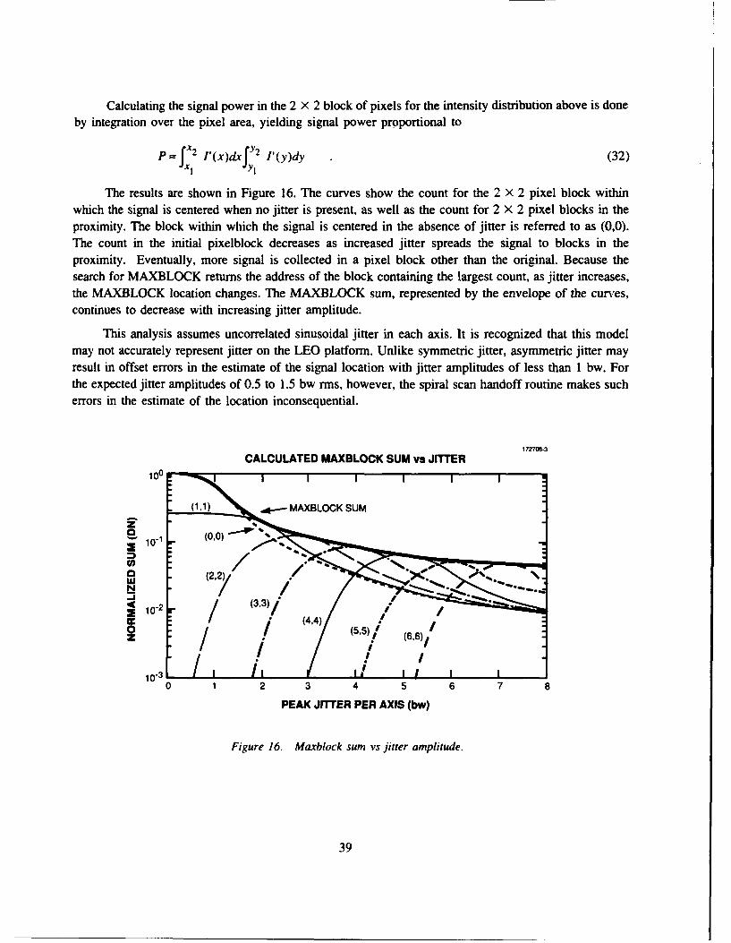
Calculating the signal power in the 2 X 2 block of pixels for the intensity distribution above is doneby integration over the pixel area, yielding signal power proportional to
p=.x2 1(x)dxfy2 l'(y)dy (32).l I Y l
The results are shown in Figure 16. The curves show the count for the 2 X 2 pixel block withinwhich the signal is centered when no jitter is present, as well as the count for 2 X 2 pixel blocks in theproximity. The block within which the signal is centered in the absence of jitter is referred to as (0,0).The count in the initial pixelblock decreases as increased jitter spreads the signal to blocks in theproximity. Eventually, more signal is collected in a pixel block other than the original. Because thesearch for MAXBLOCK returns the address of the block containing the largest count, as jitter increases,the MAXBLOCK location changes. The MAXBLOCK sum, represented by the envelope of the curves,continues to decrease with increasing jitter amplitude.
This analysis assumes uncorrelated sinusoidal jitter in each axis. It is recognized that this modelmay not accurately represent jitter on the LEO platform. Unlike symmetric jitter, asymmetric jitter mayresult in offset errors in the estimate of the signal location with jitter amplitudes of less than 1 bw. Forthe expected jitter amplitudes of 0.5 to 1.5 bw rms, however, the spiral scan handoff routine makes sucherrors in the estimate of the location inconsequential.
1727W8-3
CALCULATED MAXBLOCK SUM vs JITTER100
(1,1) 4-- MAXBLOCK SUM
10-1 (0,)
000
LU (2,2)/
10/ (3,3)1cc(4,4)/
Z 55 (6,6)1
10-30 1 2 3 4 5 6 7 8
PEAK JITTER PER AXIS (bw)
Figure 16. Maxblock sum vs jitter amplitude.
39
8. SPATIAL ACQUISITION SYSTEM RESULTS
8.1 SIGNAL ANGLE OF ARRIVAL vs DETECTED CCD POSITION
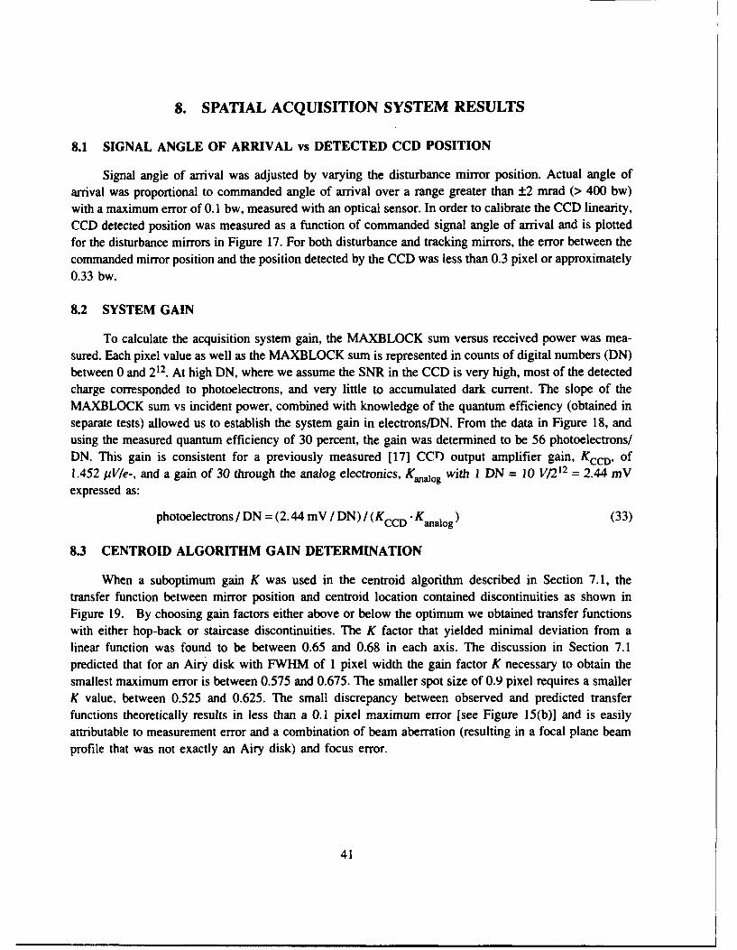
Signal angle of arrival was adjusted by varying the disturbance mirror position. Actual angle ofarrival was proportional to commanded angle of arrival over a range greater than ±2 mrad (> 400 bw)with a maximum error of 0.1 bw, measured with an optical sensor. In order to calibrate the CCD linearity,CCD detected position was measured as a function of commanded signal angle of arrival and is plottedfor the disturbance mirrors in Figure 17. For both disturbance and tracking mirrors, the error between thecommanded mirror position and the position detected by the CCD was less than 0.3 pixel or approximately0.33 bw.
8.2 SYSTEM GAIN
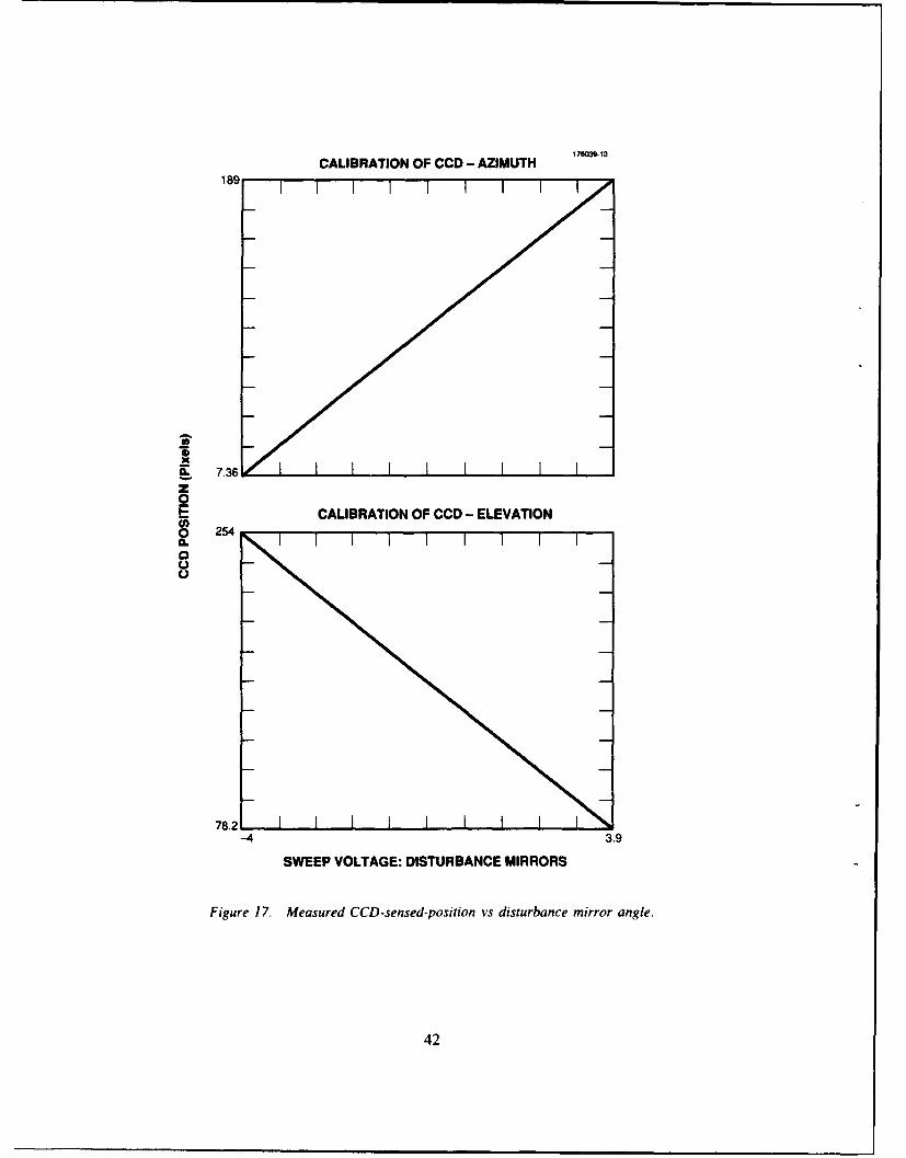
To calculate the acquisition system gain, the MAXBLOCK sum versus received power was mea-sured. Each pixel value as well as the MAXBLOCK sum is represented in counts of digital numbers (DN)between 0 and 212. At high DN, where we assume the SNR in the CCD is very high, most of the detectedcharge corresponded to photoelectrons, and very little to accumulated dark current. The slope of theMAXBLOCK sum vs incident power, combined with knowledge of the quantum efficiency (obtained inseparate tests) allowed us to establish the system gain in electrons/DN. From the data in Figure 18, andusing the measured quantum efficiency of 30 percent, the gain was determined to be 56 photoelectrons/DN. This gain is consistent for a previously measured [17] CC') output amplifier gain, KCCD, of1.452 yV/e-, and a gain of 30 through the analog electronics, KanWdg with 1 DN = 10 V/2 12 = 2.44 mVexpressed as:
photoelectrons / DN = (2.44 mV / DN) / (KCCD K )analog (33)
8.3 CENTROID ALGORITHM GAIN DETERMINATION
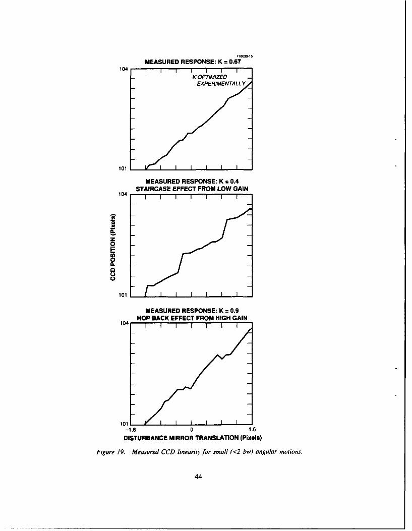
When a suboptimum gain K was used in the centroid algorithm described in Section 7.1, thetransfer function between mirror position and centroid location contained discontinuities as shown inFigure 19. By choosing gain factors either above or below the optimum we obtained transfer functionswith either hop-back or staircase discontinuities. The K factor that yielded minimal deviation from alinear function was found to be between 0.65 and 0.68 in each axis. The discussion in Section 7.1predicted that for an Airy disk with FWHM of 1 pixel width the gain factor K necessary to obtain thesmallest maximum error is between 0.575 and 0.675. The smaller spot size of 0.9 pixel requires a smallerK value, between 0.525 and 0.625. The small discrepancy between observed and predicted transferfunctions theoretically results in less than a 0.1 pixel maximum error [see Figure 15(b)] and is easilyattributable to measurement error and a combination of beam aberration (resulting in a focal plane beamprofile that was not exactly an Airy disk) and focus error.
41
CALIBRATION OF CCD - AZIMUTH 170-3
189
a. 7.36z0
E CALIBRATION OF CCD - ELEVATIONU)O 254
-4 3.9
SWEEP VOLTAGE: DISTURBANCE MIRRORS
Figure 17. Measured CCD-sensed-position vs disturbance mirror angle.
42
17603-3-144 1
MAXBLOCK SUMPROPORTIONAL TOSIGNAL ARRIVAL RATE
(I)S3
0~.j
0
2
FLOOR ----
6.6X10 3 104 105 6.6XI0 4
SIGNAL ARRIVAL RATE (Photons/a)
Figure 18. Measured maxblock sum vs signal arrival rate.
43
176039-15
MEASURED RESPONSE: K = 0.67104 I I I I
K OPTIMIZEDEXPERIMENTALLY
101 1 1 I I I I
MEASURED RESPONSE: K = 0.4STAIRCASE EFFECT FROM LOW GAIN
104
_1
S
z0P
0
101 1
MEASURED RESPONSE: K = 0.9HOP BACK EFFECT FROM HIGH GAIN
104 1I I I I
101-1.6 0 1.6DISTURBANCE MIRROR TRANSLATION (Pixels)
Figure 19. Measured CCD linearity for small (<2 bw) angular motions.
44
8.4 ACQUISITION SENSOR NOISE SOURCES
The extremely low signal level of the incoming beam forced tight constraints on noise levels of thereadout and processing electronics in order to reliably find the correct MAXBLOCK location. Noisemanifested itself in frame-to-frame variations of the detected charge per pixel when no signal was present.Looking at the variation in the output of single pixels for repeated background frames, it was noted thatthe CCD output could be corrupted by factors such as temperature variations (that affected the accumulateddark current), clock interference, and noisy power supply lines. In addition, certain "problem pixels" wereidentified that had particularly high noise levels. The next two sections discuss these factors.
8.4.1 Temperature
During overnight runs, bimodal distributions of pixel values were obtained that correlated well withmodels of distributions as a function of temperature change. The average value of a single pixel variedby more than 100 digital numbers or 5600 electrons. This was attributed to temperature-induced variationsin the average dark current: a CCD's dark current level doubles for every 7°C. These data indicate thatwhen utilizing frame subtraction it is necessary either to closely control the temperature of the CCD orto regularly update the background frame so that frame subtraction can effectively track changes inaccumulated dark current due to gradual temperature changes. For this spatial acquisition system, updat-ing the background frame as part of the acquisition algorithm added less than 2 s to the overall processand was preferable to temperature control.
8.4.2 Problem Pixels
A series of signal acquisitions was performed with the signal laser blocked. This showed thatcertain pixels within the 200 X 200 subarray of the TK512M CCD were regularly selected as theMAXBLOCK location, despite frame subtraction. By taking many unilluminated frames and listing theMAXBLOCK locations that appeared most frequently, 11 chronic problem pixels, and an additional 15troublesome pixels out of the total field of 40,000 pixels were identified.
The 26 problem pixels were located in 18 distinct regions within the 200 X 200 pixel subarray.There were seven pixel pairs with the same row address and adjacent column address, and one pixel pairwith the same column address and adjacent row address. Two of the eight pairs described contained apixel with particularly high dark current. Of the 10 remaining problem spots, two were adjacent toindividual pixels with high dark current in the same row, one was adjacent to a pixel with saturating darkcurrent in the same column. The manufacturer determined that there were 15 "hot" pixels defects in theentire array with dark current 10 times the specification. Poor charge transfer efficiency between the lastelement in the serial register and the summing well of the output amplifier in the TK512M, previouslyreported [29], would explain noisy pixels resulting from the smearing of charge from the "hot" pixels toadjacent pixels during readout. Suboptimal clocking waveforms due to noise, pulse shape, or pulse
45
amplitude would also contribute to reduced charge transfer efficiency and increase smearing in both serialand parallel transfers. Further investigation could more accurately determine the noise source in theseproblem pixels.
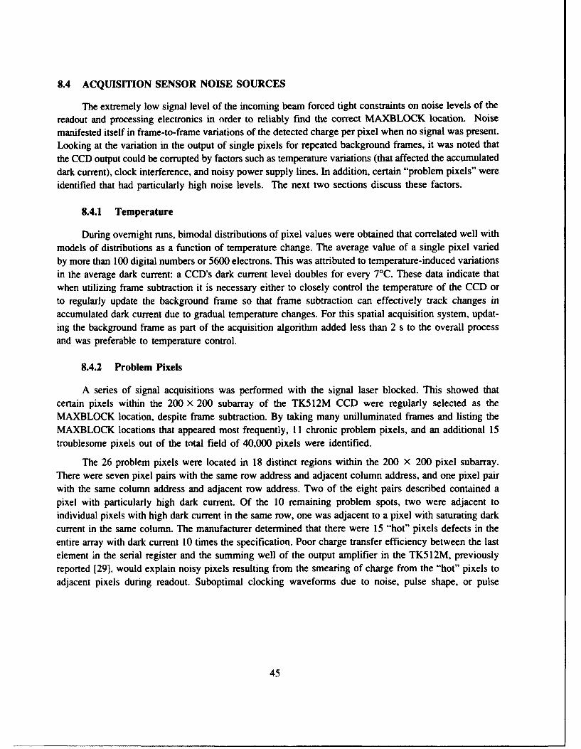
Because of their high noise level these problem pixels caused frequent false acquisitions whenacquiring at low light levels. This resulted in a minimum probability of error well above that which ispredicted simply from the quantum shot noise of the dark current in a uniform array. The problem canbe seen in the measured MAXBLOCK sum vs input photon arrival rate shown in Figure 20. The noisefloor, below which the measured MAXBLOCK sum does not fall, is considerably above the predictedvalue for a uniform, dark-current-shot-noise-limited array. One technique was tested, then a secondtechnique was implemented to reduce the effects of problem pixels.
MAXBLOCK SUM vs POWER 176039-16
1.5
10 4 I105
SIGNAL ARRIVAL RATE (Photons/s)
Figure 20. Measured noise floor without pixel masking.
First, as a test, the search region was limited to a small area free from problem pixels. With thistechnique a significant reduction in the noise floor was obtained. Using a 10 X 10 pixel processing zonewithin which the signal was positioned, the correct location was selected for signal photon arrival ratesas low as 104 photons/s. This indicated that the performance could be improved if all the pixels withinthe search area had a uniform response.
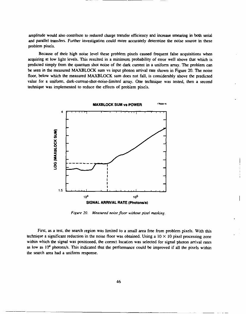
46
In order to eliminate problem pixels while maintaining the required 200 X 200 pixel processingregion, a "pixel masking" routine was developed. Masking forced the difference frame to zero at eachproblem pixel during the hardware subtraction routine. In this way the identified problem pixels no longeraffected the selection of the MAXBLOCK location. This procedure was implemented in such a way thatprocessing time was unaffected. The increase in probability of error can be bounded in the following way.The number of MAXBLOCK groups that may include at least one masked pixel is equal to four timesthe number of masked single pixels (10) and six times the number of masked paired pixels (8) for a totalof 88. Assume, as an upper bound, the signal is not detected when it falls within a MAXBLOCK groupthat contains a masked pixel; the resultant increase in error rate is the ratio of affected MAXBLOCKgroups to the total number of MAXBLOCK groups or 2 X 10⁻³.This is an upper bound because in theworst case, when the signal is centered upon the single masked pixel, approximately 12 percent of thesignal is still incident upon the surrounding pixels within the MAXBLOCK group. With the signalcentered within the MAXBLOCK group 60 percent of the signal illuminates active pixels in theMAXBLOCK group despite a single masked pixel, and at least 40 percent of the signal is detected despitea masked pixel pair.
An estimate of the probability of successful acquisition was obtained by counting the number ofmissed acquisitions over many trials, while the signal was held fixed at a single location in the CCD.Trials were performed both with and without the pixel masking routine over a range of input photonarrival rates. The results are plotted in Figure 21. Pixel masking yielded as much as a 10 dB improvementat 4 x l04 photons/s. Successful acquisition was obtained with a probability of 0.999 with as few as3 X l04 photons/s compared to approximately l0W photons/s without masking and with a probability of0.99 with as few as 1.3 X 10⁴ photons/s rather than 3.3 X 10⁴ without masking.
100 1 1 7631 1
)b MASK OFF
c MASK ON010I
E
IL
0 -210
o 10",
10 - 4
1. a i I I all[1
103 104 105 106
SIGNAL ARRIVAL RATE (Photons/s)
Figure 21. Measured probability of acquisition error, masked and unmasked.
47
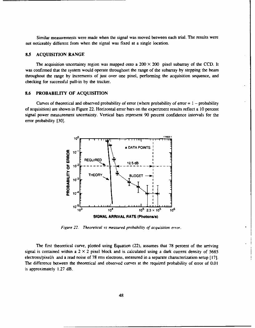
Similar measurements were made when the signal was moved between each trial. The results werenot noticeably different from when the signal was fixed at a single location.
8.5 ACQUISITION RANGE
The acquisition uncertainty region was mapped onto a 200 X 200 pixel subarray of the CCD. Itwas confirmed that the system would operate throughout the range of the subarray by stepping the beam
throughout the range by increments of just over one pixel, performing the acquisition sequence, andchecking for successful pull-in by the tracker.
8.6 PROBABILITY OF ACQUISITION
Curves of theoretical and observed probability of error (where probability of error = 1 - probabilityof acquisition) are shown in Figure 22. Horizontal error bars on the experiment results reflect a 10 percentsignal power measurement uncertainty. Vertical bars represent 90 percent confidence intervals for the
error probability [30].
100 .174503-1
ADATA POINTSIt 10-1
REQUIRED
L. 10.2 -------------- - --- -0
-- 0-3 THEORY ..THERY '~.. BUDGET -- vi1+ ito
10- I .3 i l
M 4
103 104 105 2.3 x 10⁵ 106
SIGNAL ARRIVAL RATE (Photonsis)
Figure 22, Theoretical vs measured probability of acquisition error.
The first theoretical curve, plotted using Equation (22), assumes that 78 percent of the arriving
signal is contained within a 2 X 2 pixel block and is calculated using a dark current density of 5685electrons/pixel/s and a read noise of 78 rms electrons, measured in a separate characterization setup [ 17].The difference between the theoretical and observed curves at the required probability of error of 0.01is approximately 1.27 dB.
48
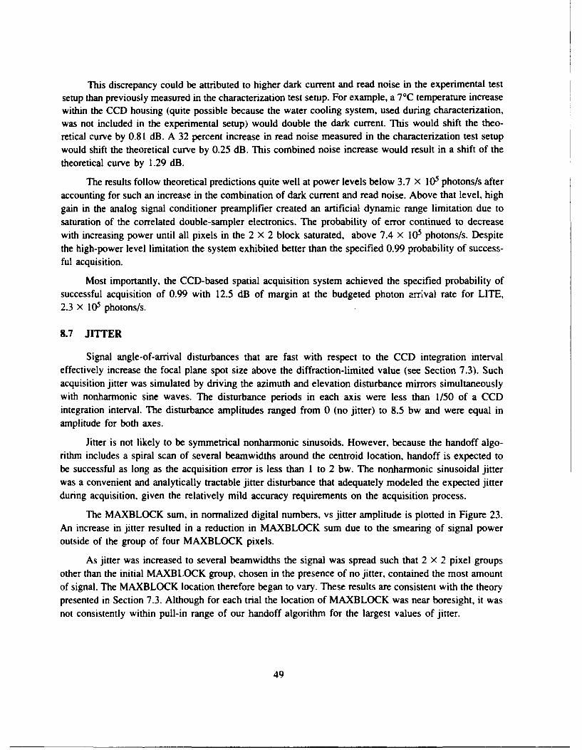
This discrepancy could be attributed to higher dark current and read noise in the experimental testsetup than previously measured in the characterization test setup. For example, a 7°C temperature increasewithin the CCD housing (quite possible because the water cooling system, used during characterization,was not included in the experimental setup) would double the dark current. This would shift the theo-
retical curve by 0.81 dB. A 32 percent increase in read noise measured in the characterization test setupwould shift the theoretical curve by 0.25 dB. This combined noise increase would result in a shift of thetheoretical curve by 1.29 dB.
The results follow theoretical predictions quite well at power levels below 3.7 X 10⁵ photons/s afteraccounting for such an increase in the combination of dark current and read noise. Above that level, highgain in the analog signal conditioner preamplifier created an artificial dynamic range limitation due tosaturation of the correlated double-sampler electronics. The probability of error continued to decreasewith increasing power until all pixels in the 2 X 2 block saturated, above 7.4 X 10⁵ photons/s. Despitethe high-power level limitation the system exhibited better than the specified 0.99 probability of success-ful acquisition.
Most importantly, the CCD-based spatial acquisition system achieved the specified probability ofsuccessful acquisition of 0.99 with 12.5 dB of margin at the budgeted photon arrival rate for LITE,2.3 X 10 photons/s.
8.7 JITTER
Signal angle-of-arrival disturbances that are fast with respect to the CCD integration intervaleffectively increase the focal plane spot size above the diffraction-limited value (see Section 7.3). Such
acquisition jitter was simulated by driving the azimuth and elevation disturbance mirrors simultaneouslywith nonharmonic sine waves. The disturbance periods in each axis were less than 1/50 of a CCDintegration interval. The disturbance amplitudes ranged from 0 (no jitter) to 8.5 bw and were equal in
amplitude for both axes.
Jitter is not likely to be symmetrical nonharmonic sinusoids. However, because the handoff algo-rithm includes a spiral scan of several beamwidths around the centroid location, handoff is expected tobe successful as long as the acquisition error is less than I to 2 bw. The nonharmonic sinusoidal jitterwas a convenient and analytically tractable jitter disturbance that adequately modeled the expected jitter
during acquisition, given the relatively mild accuracy requirements on the acquisition process.
The MAXBLOCK sum, in normalized digital numbers, vs jitter amplitude is plotted in Figure 23.An increase in jitter resulted in a reduction in MAXBLOCK sum due to the smearing of signal poweroutside of the group of four MAXBLOCK pixels.
As jitter was increased to several beamwidths the signal was spread such that 2 x 2 pixel groupsother than the initial MAXBLOCK group, chosen in the presence of no jitter, contained the most amountof signal. The MAXBLOCK location therefore began to vary. These results are consistent with the theorypresented in Section 7.3. Although for each trial the location of MAXBLOCK was near boresight, it wasnot consistently within pull-in range of our handoff algorithm for the largest values of jitter.
49
176039-8
100 O
a0(n
8 10.1
9m CALCULATED RESPONSE
Xx
wi 10-2
Nj MEASURED RESPONSE
0z o_ I I I I I I
0 1 2 3 4 5 6 7 8
PEAK JITTER PER AXIS (bw)
Figure 23. Effect of jitter on measured signal power.
The expected jitter levels during acquisition were described in Section 2.3.2. The high frequencyportion of this spectrum (above 1 Hz) has an rms value of approximately 1 bw, which is well below themeasured level of jitter in the demonstration system that caused erratic acquisition.
The low frequency jitter (below I Hz) on the ACTS satellite is expected to be less than 0.5 rms bw.Jitter on the LEO platform is assumed to be similar. The expected acquisition error due to these disturbancesmay be bounded by modeling all of the rms low frequency jitter as a single frequency term with anamplitude of 0.71 bw. The maximum error is then equal to the peak amplitude of this disturbance, whichis still less than I bw. Therefore with confidence, the effects of the expected jitter (on the order of 1 bw)are modeled as a simple reduction in received power at the acquisition sensor, which should not degradeeither the accuracy of the position estimate or the probability of successful acquisition by an unacceptableamount.
50
9. HETERODYNE SPATIAL TRACKING SYSTEM
This section describes the specific oldcal >yout b- .A .3ntrol electronics that are used to implement
the spatial tracking system. The demonstration system was built largely with off-the-shelf components,
both optiral and electronic, and was designe:d to illustrate the functionality of this system without considering
packaging issues.
9.1 HETERODYNE RECEIVER AND SPATIAL TRACKING OPTICAL ELEMENTS
When the acquisition/tracking beamswitch (shown in Figure 3) was set to the spatial tracking
position, the LO and signal beams were combined at the input to the communications receiver on a 50:50,
polarization-independent beamsplitter, and equal length paths were provided to each of the p-type intrinsic-n-type (PIN) photodiodes that formed the balanced detector for the communications channel. The input
combining beam splitter was specified to be as close to 50:50 as possible in order to equalize the LOpower delivered to each half of the balanced communications receiver. The residual LO mismatch was
corrected using a variable attenuator, formed from a quarter wave plate and polarizer in the appropriate
arm of the balanced receiver. This was necessary to achieve adequate LO intensity noise cancellation[1-"J. If the beamsplitter mismatch is characterized by the ratio 8 of the reflection to transmission (or
transmission to reflection) coefficients, defined so that g5 < 1, then the signal in one arm of the balancedreceiver is attenuated by 82, which is another reason to specify the beamsplitter to be as symmetric aspossible. Note that beamsplitters are available that are sufficiently symmetric to reduce the loss of signal
due to intensity matching to less than 0.3 dB, while the use of the balanced receiver may provide as much
as 3 to 4 dB of improvement over an unbalanced receiver.
Separate and symmetric pickoffs were provided via polarizing beamsplitters for each (azimuth andelevation) track path. This configuration meant that in order to supply equal LO power to each track
channel the input combining 50:50 beamsplitter had to be polarization independent. Half wave plates inthe LO and signal paths, ahead of the combining beamsplitter, allowed individual control of the LO and
signal polarization, and hence separate control of the LO and signal power split between the communi-
cations and track paths. These were adjusted so that nominally equal LO power was sent to each pho-todetector, -2 mW, while the signal power was split approximately 80:10:10 between the communication,
azimuth, and elevation paths, respectively.
Split detectors were formed in each track channel (Az,EI) using a gold-coated knife edge (imple-
mented with one edge of a pyramid splitter) and discrete PIN photodiodes because wideband (-1 GHz)segiaented detectors with sufficiently small dead zones were not available.
The LO laser was identical to that used for the signal and was similarly collimated and circularized
as described in Section 5.1.
9.2 DETECTOR/PREAMPS
Commercially available RCA CA-30917E wideband PIN detectors were used in both the commu-nications and track channels. The outputs of the matched communications detectors and each track
51
photodetector were terminated with 50 Q resistors. This increased the thermal noise too much to allowoperation near the quantum shot noise limit but improved the flatness of the frequency response in eachchannel. These electrical signals were then amplified using discrete amplifier modules. Each module wasformed from a pair of Watkins-Johnson RA-26 amplifiers and padded with wideband attenuators to yielda module gain of 42 ±0.5 dB from 50 to 1100 MHz. The noise figure of the front end detector/amplifiercombinations could be improved to allow operation within 0.5 to 1 dB of the quantum shot noise limitby using hybrid detector/amplifier modules such as those described by Alexander [12]. Such amplifierswere not available to us at the time this experiment was performed.
9.3 SPATIAL TRACKING DEMODULATOR
The spatial tracking demodulator for the azimuth (elevation) channel was implemented as a highprecision phase detector, designed to develop a baseband voltage proportional to the electrical phasedifference between the two halves of the azimuth (elevation) track channel. In order to minimize thephase matching requirements within the tracking demodulator, a commutating architecture was chosen asillustrated in Figure 24. Details of the spatial tracking demodulator have been described elsewhere[31,32]; an overview will be given here, and a more complete analysis of the demodulator performanceis given in Section 10.
For simplicity the following description will refer to the azimuth channel; the elevation channel isexactly analogous. The azimuth track channel outputs were alternately selected via a single-pole double-throw high speed RF switch, forming the commutated track signal. Both the commutated track signal andthe communications signal (output of the balanced communications detector/amplifier front end) werethen passed through input amplifiers that included automatic gain control (AGC). The front end AGCsignal for all three amplifiers (communications, azimuth, elevation) was derived from envelope detectionof the communications channel. The commutated azimuth signal was correlated with the communicationssignal in a wideband RF multiplier, which yielded an ac tracking error signal at the commutation fre-quency with an amplitude that was proportional to the phase difference between the two halves of theazimuth channel. The error signal was then bandpass filtered and synchronously demodulated to obtaina baseband tracking error signal.
As long as the communications channel SNR within the precorrelation noise bandwidth (-1 GHz)was greater than unity, the AGC in the input amplifiers was derived from the heterodyne IF signal, andthe amplifier outputs were held constant despite any input signal optical power fluctuations. However,when the precorrelation communications channel SNR dropped below unity, the front end AGC level wasbased upon the input noise power, which is mostly LO shot noise in a well designed system (note thatin the demonstration system the input noise was a combination of thermal and LO shot noise). When thefront end AGC gain was fixed, the gain of the demodulator transfer function (volts/phase shift) was thenlinearly dependent on the input signal optical power.
In order to extend the effective AGC dynamic range to include operation when the input signaloptical power dropped below the level where the precorrelation SNR was less than unity, additionalnormalization was implemented. This estimate of the signal power was developed at baseband using an
52
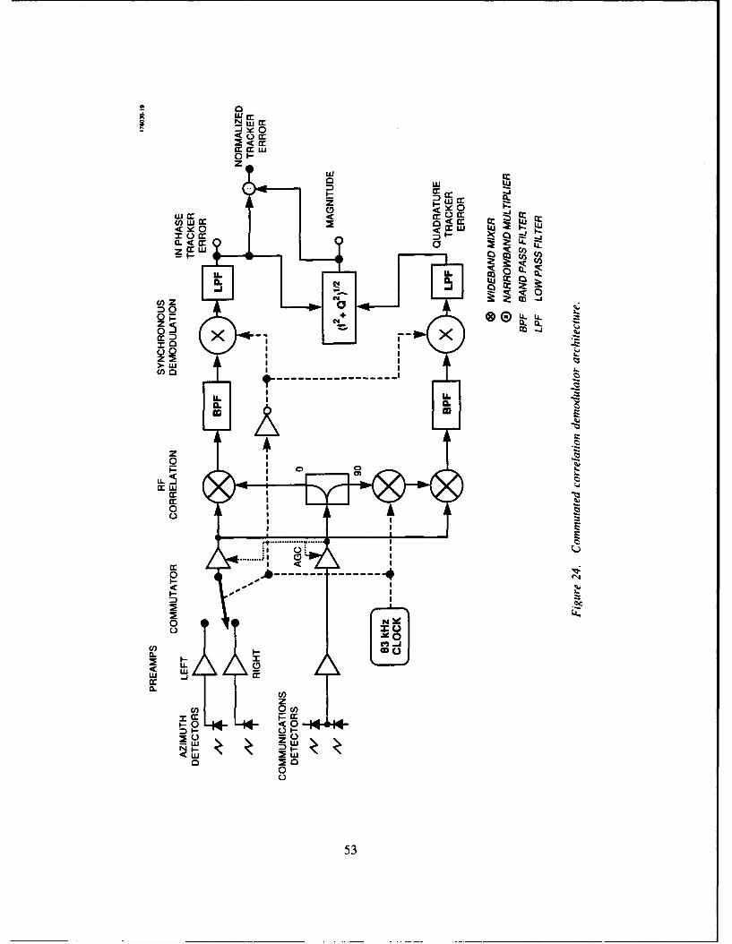
w cc
x ~0cc
of-zw c
w I
< 0C U) j P.L0. .
_L LL ,.
IL V -iCR
00+ I.
z 2~
W a
-------------
0 L Iz L
00
0
00
53Z
I and Q receiver. The portion of the receiver described in the previous paragraph developed the I signal.The Q signal was formed by multiplying the commutated azimuth signal by a 90*-shifted version of thecommunications signal. Note that the development of the wideband quadrature hybrid that provided thequadrature communication signal over a frequency band of 70 to 1170 MHz was one of the critical piecesof technology development necessary for the success of this processing scheme. The phase-shifted com-munication signal was also biphase modulated at the commutation frequency in order to produce a post-correlation signal at the commutation frequency, and not at dc. The subsequent bandpass filter andsynchronous demodulation were identical to the I channel. The baseband normalization signal was thenformed by using a commercially available analog function block to obtain (12 + Q2)2. The resultant twostage AGC normalization yielded a net transfer function of the spatial tracking demodulator electronicsthat was measured to have a mean gain of 1.38 V/radian. The transfer function gain varied by less than± 5 percent over a 30-dB range of input optical power variation.
9.4 BASEBAND SERVO ELECTRONICS
A block diagram of the baseband servo electronics, including the coarse track loop (acquisition,CCD-based), the heterodyne tracking loop, and the handoff circuitry used to transition between coarseand fine tracking, is shown in Figure 25. The coarse tracking function was a simple digital loop that usedsuccessive estimates from the CCD acquisition system to maintain the received signal at a position onthe CCD that corresponded to the center of the receiver FOV. Positional updates were generated every1.3 s. The digital filter used for the compensation element in the loop consisted of a single integrator(accumulator). The output of the accumulator was converted to an analog signal in a 12-bit digital-to-analog converter (DAC). The equivalent resolution of the DAC was 0.2 bw least significant bit.
Closed loop correction of angular misalignment (fine tracking) was performed by filtering thenormalized angle error signal, developed at the output of the spatial tracking demodulator, and using theresultant signal to drive the TMBSs. The compensator filter in each track channel included two integratorsfor sufficient low-frequency rejection, a lead-lag network for good phase margin at loop crossover, anda fourth order notch filter at 11.4 kHz to keep from exciting the second resonance of the TMBSs.
9.5 HANDOFF CIRCUITRY
The transition from coarse tracking, performed at a sub-Hertz update rate with tracking informationderived from the CCD acquisition sensor, to fine tracking using the heterodyne tracking system is denotedas handoff. As discussed in Sections 2.3.2 and 7.3, the expected rms jitter during coarse acquisition andhandoff is approximately I to 2 bw (-0.5 bw rms due to noise in the gyros used for short-term attitudestabilization, and -1 bw rms due to momentum wheel jitter). Because the coarse acquisition loop (de-scribed in Section 2. 1 ) is limited in bandwidth by the 1 s integration time, little or none of the jitter above0.5 to 1 Hz is rejected. Thus peak angular errors of at least 1 bw are likely to be present during thehandoff process for times on the order of 1 to 10 ms. Because the heterodyne tracker will not reliablypull in a signal that is outside the receiver FOV, and because the tracker response time is on the order
54
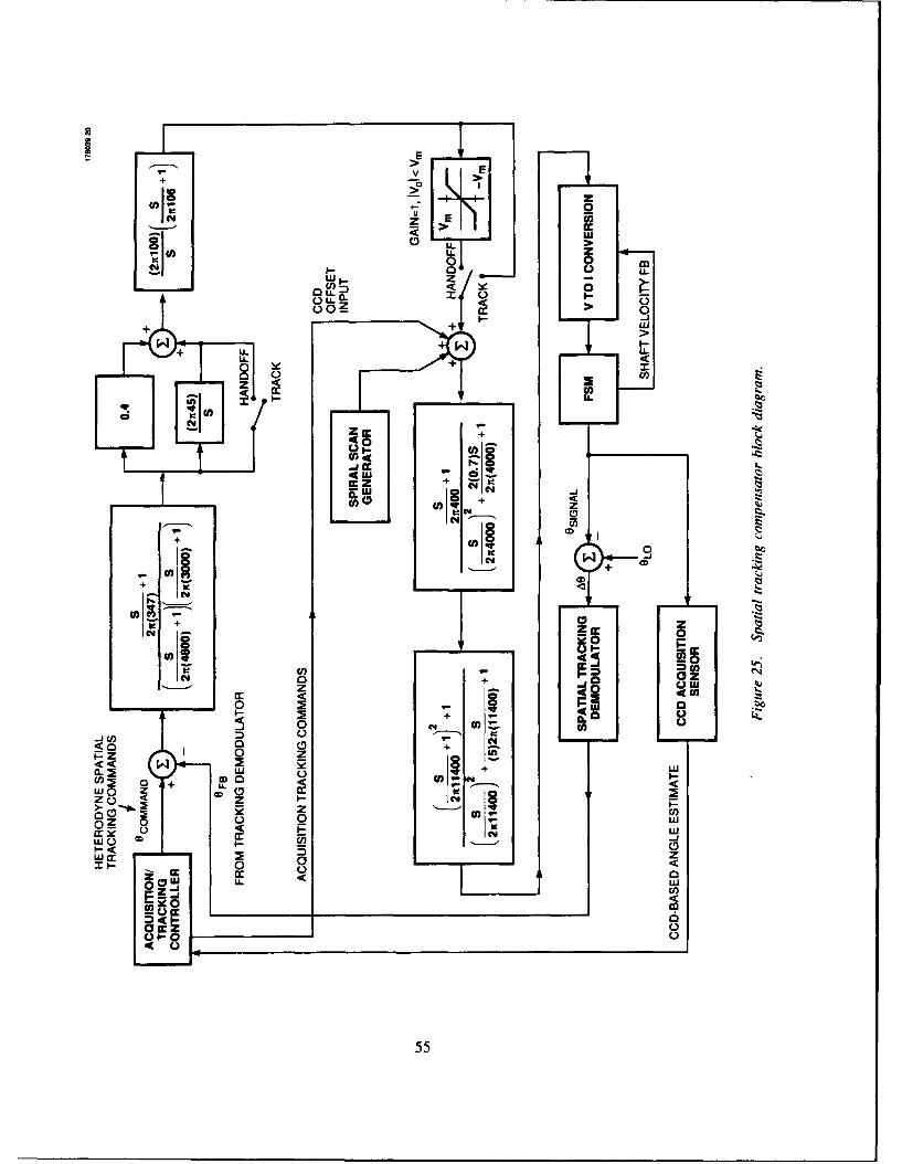
_ zU) 0
z E FzLAS L
U-0-
1---J
LLL
+ + L
+ U.p- 00
+ LLU)
0 +
U)'
!Ez
0 ) 0 0KJa C4)
MiM0 +
o 0001 3z
U))
U))+ U.
N m55
of a few milliseconds, such errors during handoff could cause large and potentially unrecoverable tran-sients. Any bias errors in the acquisition process would tend to worsen this situation. Therefore, a
technique for handoff was devised that would allow reliable handoff even when the signal did not initiallyilluminate the receiver FOV.
When the signal was outside the receiver FOV, an open loop spiral search centered on the acqui-sition location was initiated. As soon as the signal was directed to within the receiver FOV, control was
transferred to the heterodyne tracker. Thus, for successful handoff it was necessary to first determinewhether the signal was actually within the receiver FOV prior to transferring full control of the TMBSs
to the heterodyne tracker.
The traditional implementation for such a handoff (e.g., the LITE opto-mechanical system (OMS)acquisition and tracking system, [6]) is to develop an estimate of the received signal power and to transfercontrol of the tracking mirrors when the received signal power exceeds a predetermined level. The key
to the success of this method is in picking the threshold level. Unfortunately, any thresholding schemeis subject to the problems associated with a simple threshold that cannot distinguish between a strong
signal off boresight and a weak signal near boresight. In the static case this is not important, but forhandoff of a moving signal (e.g., with a spiral scan or in the presence of jitter) it may be possible to pullin a weak signal near boresight, while a strong signal at the edge of the receiver FOV may move out ofthe FOV before the tracking loop can capture it [33].
The handoff method implemented for the two-axis tracker described here, first proposed by Kaufmann[34], modified the usual thresholding scheme to increase robustness. Instead of completely disabling the
tracking loop during the open loop scan at the beginning of the handoff transition, the tracking loopoutput was limited to a voltage equivalent to an angular excursion of ±1 to 2 beamwidths, which was
called the authority limit. This limited output was added to the open loop scan. An ideal noiseless spiralscan is illustrated in Figure 26(a). As the signal was scanned the tracking loop was driven by noise aslong as the signal was outside the receiver FOV, which led to modifiea spiral scan shown in Figure 26(b).When the signal was scanned to within the authority limit of the tracking loop, the loop acted to centerthe signal, in effect counteracting the spiral scan. When the signal was centered the authority limits wereopened to allow the loop full authority and fine tracking commenced. The performance of this techniqueis presented in Section 11.9.
There are two advantages to this method relative to the traditional approach. First, the thresholdproblem is greatly simplified to merely detecting the minimum signal power that corresponds to thelowest received optical power at which tracking can take place, when the signal is centered on boresight.The question of which conditions will potentially lead to a large enough detected signal to trigger athreshold, but will not lead to a successful pull-in, need not be determined exhaustively a priori, sincethe system will automatically fail gracefully in those cases (i.e., the spiral scan will continue withoutinterruption until the signal sweeps close enough to boresight to pull in). Second, this method guaranteesthat the compensator integrators are automatically set to the correct voltage to minimize any transientwhen control is passed to the tracking loop.
56
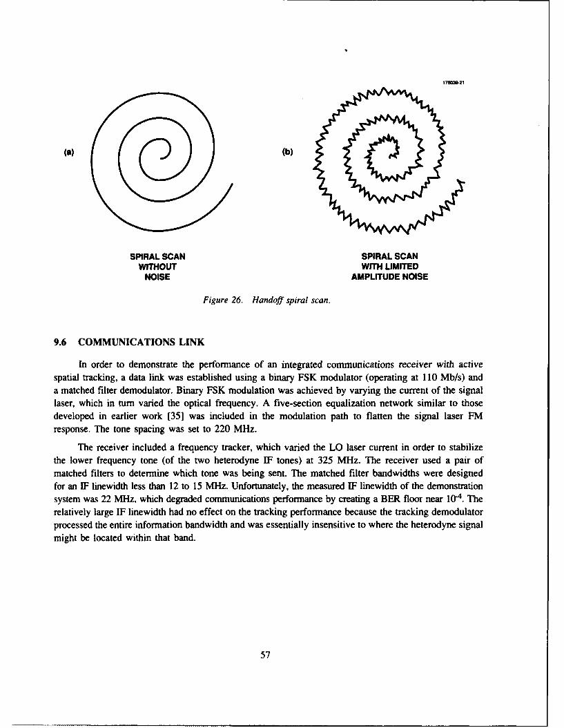
176039,21
(a) (b)
SPIRAL SCAN SPIRAL SCANWITHOUT WITH LIMITED
NOISE AMPLITUDE NOISE
Figure 26. Handoff spiral scan.
9.6 COMMUNICATIONS LINK
In order to demonstrate the performance of an integrated communications receiver with activespatial tracking, a data link was established using a binary FSK modulator (operating at 110 Mb/s) anda matched filter demodulator. Binary FSK modulation was achieved by varying the current of the signallaser, which in turn varied the optical frequency. A five-section equalization network similar to thosedeveloped in earlier work [35] was included in the modulation path to flatten the signal laser FMresponse. The tone spacing was set to 220 MHz.
The receiver included a frequency tracker, which varied the LO laser current in order to stabilizethe lower frequency tone (of the two heterodyne IF tones) at 325 MHz. The receiver used a pair ofmatched filters to determine which tone was being sent. The matched filter bandwidths were designedfor an IF linewidth less than 12 to 15 MHz. Unfortunately, the measured IF linewidth of the demonstrationsystem was 22 MHz, which degraded communications performance by creating a BER floor near 10 -4. Therelatively large IF linewidth had no effect on the tracking performance because the tracking demodulatorprocessed the entire information bandwidth and was essentially insensitive to where the heterodyne signalmight be located within that band.
57
10. THEORY OF OPERATION FOR THEHETERODYNE SPATIAL TRACKER
In this section the expressions for the photocurrents both in the azimuth segmented detectors andat the output of the balanced communications detectors are derived. The transfer function between opticalangle error (between the LO and signal optical beams) and the normalized output voltage of the trackingdemodulator is developed. This quantity is commonly referred to as the tracking discriminant. Finally,an analysis of the noise performance of the track channels, including the effects of the commutating,correlation processing is presented.
Throughout this section the performance of the azimuth track channel only is derived. The elevationchannel is exactly analogous. Also, the azimuth track channel power is defined as the total LO or signalpower at the azimuth beamsplitter. Similarly, the communications channel power will refer to the LO orsignal optical power arriving at both communications detectors. Finally, a beamwidth is defined as thefull angular width between the half maximum points of the far field intensity pattern of the signal beamand is equal I.o 3.24/ka (radians) for a uniform circular beam of radius a, where k is 21r/A.
10.1 DEFINITION OF GEOMETRY
The geometry for the track channels is shown in Figure 27(a), where a Gaussian LO is normallyincident upon a split detector, and a truncated plane wave signal beam overlaps the LO but is angularlymisaligned from the LO by an angle AO. This same geometry applies to the communication channel,except that the detectors are not segmented. The coordinate system is illustrated in Figure 27(b), wherethe k vector, k S, is projected into the plane of the detector. For a nonzero angular misalignment 0 therewill be nonzero components of the signal k vector in the plane of the detector. This projection of I iss
written in polar coordinates, kr, 0 , in order to exploit the circular symmetry of the beams, where T is theposition vector within the detector plane. 0 = 0 corresponds to a beam angular deviation only in the xdirection while 00 = ir/2 corresponds to a beam angular deviation only in the y direction. For small angularmisalignments the azimuth and elevation disturbances may be considered orthogonal (i.e., 02 Ox2 + 0y2 ).
10.2 DERIVATION OF IF HETERODYNE CURRENTS
By looking at the integral of the Poynting vector of the combined LO and signal beams normal tothe plane of each detector, an expression can be derived for the electrical IF signal at the detector outputs.For any position F in the detector plane, let the " fields of the LO and signal beams be characterized asfollows:
the signal beam at the split detector (Az or El),
Es.track = V'2Wc:oAs(xy) e-J((0St-k-7) (34)
59
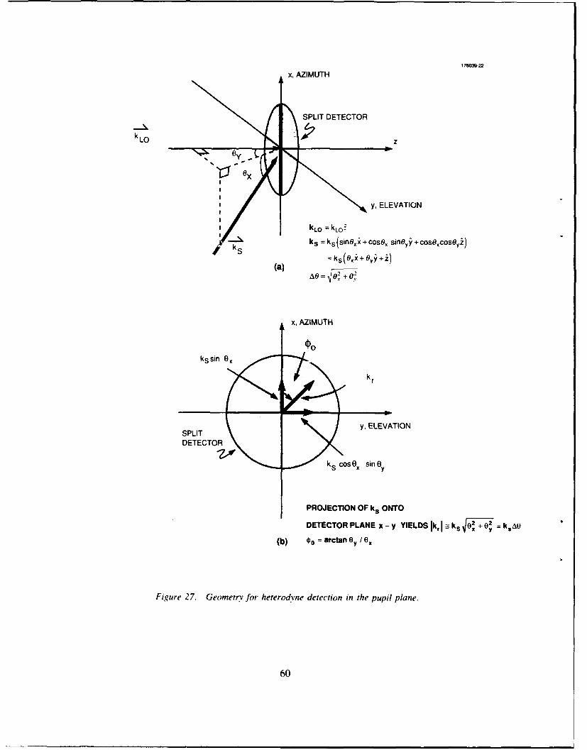
176039-22
x, AZIMUTH
SPLIT DETECTOR
LO oy------O-z
y, ELEVATION
kL0 =kLO'
kS = ks(sinei + cose,, siiy osxoe
S (a) -k(0i+ej+iA 0= NF2 +62-
x, AZIMUTH
k r
y, ELEVATION
PROJECTION OF k9 ONTO
DETECTOR PLANE x - y YIELDS Ikr I ks 6 y+O kstW
(b) 00 arctan6 0.e/0
Figure 27. Geometryv for heterodvne detection in the pupil plane.
60
the LO beam at the split detector (Az or El),
ELOtrack - /2 LO z ALO(xy) e-JWLt (35)
the signal beam at each communication detector,
E!Scomm = Zo As(xy) e-J(Ost-iF) (36)
and the LO beam at each communication detector,
ELO,comm = LO o ALO (x,y) e - j ((OLt +Y12 ) (37)
where y is the ratio of track signal optical power to communications signal optical power, and ALo(x,y)and As(x,y) are the field amplitudes of the LO and signal beams, respectively, normalized such that
J*dx j dylALO(X,y) 2 = J xf dY As(x,Y)j =1 (38)
The 90' phase shift between the LO field in the communications channel and the LO field in the trackchannel is introduced optically, via a quarter wave plate ahead of the combining beamsplitter. The neteffect is to make the communications and sum track channel IF photocurrents differ in phase by 900. Thephase shift is introduced optically (prior to photodetection) in order to make the slope of the trackingdiscriminant independent of the sign of oLO - s .
In general, the IF heterodyne current may be written as
iHET (t) = en Ref ES (F) ELO (F) ei(Ac-kF)dA} (39)
For the specific case where the signal is a circularly truncated plane wave, As(r,4) = (1/ al-)circ(r/a),and the LO is Gaussian, ALO(r,O) = 2 / w2 exp-(r 2/w2), and the beams are matched such that a = w,then the heterodyne IF current over one azimuth detector segment may be written as
ir~) =2 /2ei7 COS -tP= f Ir/22____ -r -j3240r o O(0 "--= P P c LO co dr=_jr/2 r er 2 e (40)
where the angular mismatch 0 is in units of angular beamwidths. The current in the left azimuth detector,ift, may be obtained by changing the limits on 0 in Equation (40) to ,r/2 < 0 < 3r/2, and when the LO andsignal beams overlap perfectly, ift is the complex conjugate of in. It is convenient to write Equation (40)as
i rt (t) = I[m(O) cos Aot + q(O) sin Awo] (41)
yP Pf (42)hv y PC PLO
61
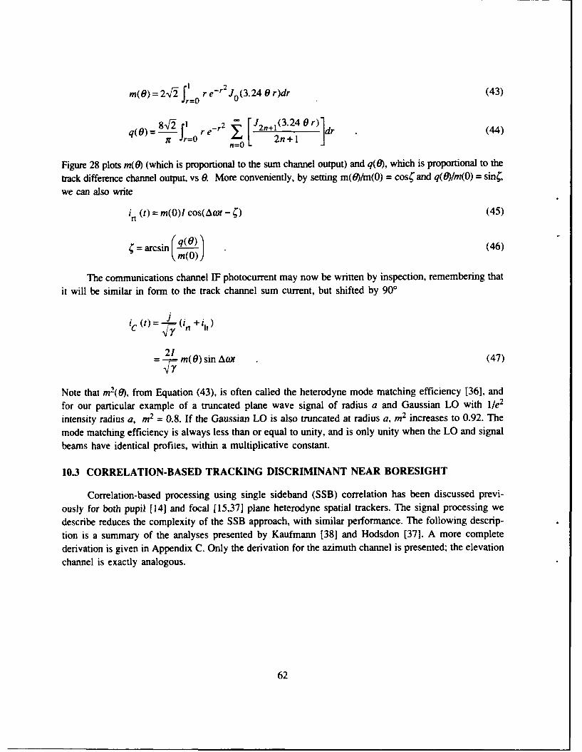
m(6) = 2V2 re - r2 j (3.24 0 r)dr (43)
reLr2 ~ [J 2n+l(3.24Or) Idr (44)q(0)= ir fr=0 r e - r drO 2n4)
Figure 28 plots m(6) (which is proportional to the sum channel output) and q(6), which is proportional to the
track difference channel output, vs 0. More conveniently, by setting m(6)/m(0) = cos and q(O)/m(0) = sin,
we can also write
in () = m(0)I cos(Aot - 5) (45)
( q(O) ) (46)
The communications channel IF photocurrent may now be written by inspection, remembering that
it will be similar in form to the track channel sum current, but shifted by 900
i, (t) = (irn + iit
21 (71 -=m(O) sin AoX (47)
Note that m2(0), from Equation (43), is often called the heterodyne mode matching efficiency [36], and
for our particular example of a truncated plane wave signal of radius a and Gaussian LO with l1e 2
intensity radius a, m2 = 0.8. If the Gaussian LO is also truncated at radius a, m2 increases to 0.92. Themode matching efficiency is always less than or equal to unity, and is only unity when the LO and signal
beams have identical profiles, within a multiplicative constant.
10.3 CORRELATION-BASED TRACKING DISCRIMINANT NEAR BORESIGHT
Correlation-based processing using single sideband (SSB) correlation has been discussed previ-
ously for both pupil [14] and focal [15,37] plane heterodyne spatial trackers. The signal processing we
describe reduces the complexity of the SSB approach, with similar performance. The following descrip-
tion is a summary of the analyses presented by Kaufmann [38] and Hodsdon [371. A more completederivation is given in Appendix C. Only the derivation for the azimuth channel is presented; the elevationchannel is exactly analogous.
62
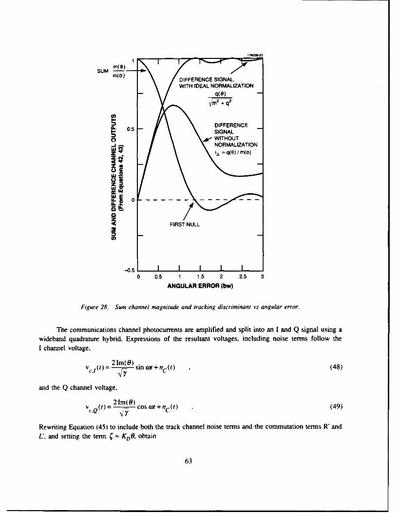
SUM (o) DIFFERENCE SIGNAL,
WITH IDEAL NORMALIZATIONq(9)
05DIFFERENCE
a.5
SIGNAL0 WITHOUT
-A - NORMAL17-ATION
WEo
L !Z 4IL a.
Cz
=U~FIRST NULL
-0.50 0.5 1 1.5 2 2.5 3
ANGULAR ERROR (bw)
Figure 28. Sum channel magnitude and tracking discriminant vs angular error.
The communications channel photocurrents are amplified and split into an I and Q signal using awideband quadrature hybrid. Expressions of the resultant voltages, including noise terms follow the
I channel voltage,
21m(0) sin M+fnC Q) (48)
and the Q channel voltage,
2 lm(O)Vc'Q(t)= l cos tO + nC(t) (49)
Rewriting Equation (45) to include both the track channel noise terms and the commutation terms R' andL', and setting the term KDO. obtain
63
the voltage in the left azimuth che ,tel,
V lef(t) = L'[m(O) cos(a + K D Obw)+ nL (t)] (50)
and the voltage in the right azimuth channel,
vright (t)= R' [m(O)I cos(oxt-KDObw)+nR (t)] (51)
The gain KD = 1.24 radians/bw may be obtained by linearizing q(O)/m(O), Equation (46), for small 0. Notethat n(t), nL(t), and nR(t) are all uncorrelated, additive, white, Gaussian noise terms with two-sidedspectral densities NJ2, NJ4, and NJ4, respectively. In a system dominated by the LO quantum shot noiseN, = 2eidc = 2e2 rPLo/hv. The commutation in the track channel is modeled as a multiplication of theazimuth signals by an offset square wave, so that R', L' are written as
the right track commutation function,
R' :B k Cos (k co)J , (52)
and the left track commutation function,
Bk= Cos kowr)) (53)
for
kirsin -
B- 2 (54)Bk kir
2
Following the commutated correlation processing illustrated in Figure 24, it can be shown (Appen-dix C) that the normalized output of the I channel is given by
V (9) =K 08+ 4m2 r ) sn (t) +n (01 (55)0 D m2(0) / 2
where I was defined in Equation (42), m(6) was defined in Equation (43), and KDO" 1. The noise terms,nsxn(t) and nnxn(t), are discussed in Section 10.4. The normalization is implemented by dividing theI channel output by the square root of the sum of the squares of the I and Q outputs.
64
10.4 NOISE EQUIVALENT ANGLE FOR COMMUTATED, CORRELATED PROCESSOR
The noise analysis for both pupil and focal plane heterodyne spatial trackers with correlationprocessing has been previously presented [14,15]. The noise equivalent angle is th, offset angle ONEA,which in a noise-free system would yield the same output as the rms noise voltage in the real system.From Equation (55) and following some manipulation (see Appendix C), ONE may be written as
6NEA =~aiKD ~ I /= r( F ]121 12(62 KD CNDR ack CNDRJ(6
where F is the single-sided noise equivalent bandwidth of the closed loop tracking servo, W is the single-sided noise equivalent bandwidth of the input electronics before correlation, and CNDRcomun and CNDRtrackare the carrier-to noise density ratios in the communications and track (sum) channels, respectively. Ina shot-noise-limited system, CNDRX is simply 1lm 2p,//v, where 77 is the quantum efficiency of the pho-todetector, h is Planck's constant, v is the optical frequency, m2 is the spatial mode matching parameter,and Px is the optical power incident onto the photodetectors in channel x. The noise equivalent angle(NEA) in Equation (56) is N2 greater than in a simple correlation processor. Note that as discussed inSection 11.6, by building a second identical correlation channel in which the commutation signals areinverted with respect to the first, and subtracting the outputs, the 7r/2 factor in Equation (55) could bereduced to i((2v7 ) = 1.11. For comparison, the expression for the NEA of a system in which thefrequency of the received tone is known exactly, i.e., the RF demodulation is done coherently, [141 isgiven by
/ 1/2 (76NEA =KD CNDRt(57)
10.5 EFFECTS OF LO ANGULAR DISTURBANCES
An important difference between detection in the pupil plane and in the focal plane which has notpreviously been noted is the sensitivity of the two methods to angular movement of the LO beam. In atypical closed loop tracking system the signal beam angle of arrival is adjusted to maintain zero errorsignal at the output of a segmented detector in the track channel. Proper choice of an error signal ensuresthat when the error is driven to zero the angular misalignment between the LO and signal beam is alsominimized. For focal plane detection, the usual error signal is based upon the amplitude differencebetween the heterodyne current in each half ofa segmented detector. Unfortunately in such a system zeroerror signal only corresponds to perfect signal-LO beam angular alignment when the LO is centered.
65
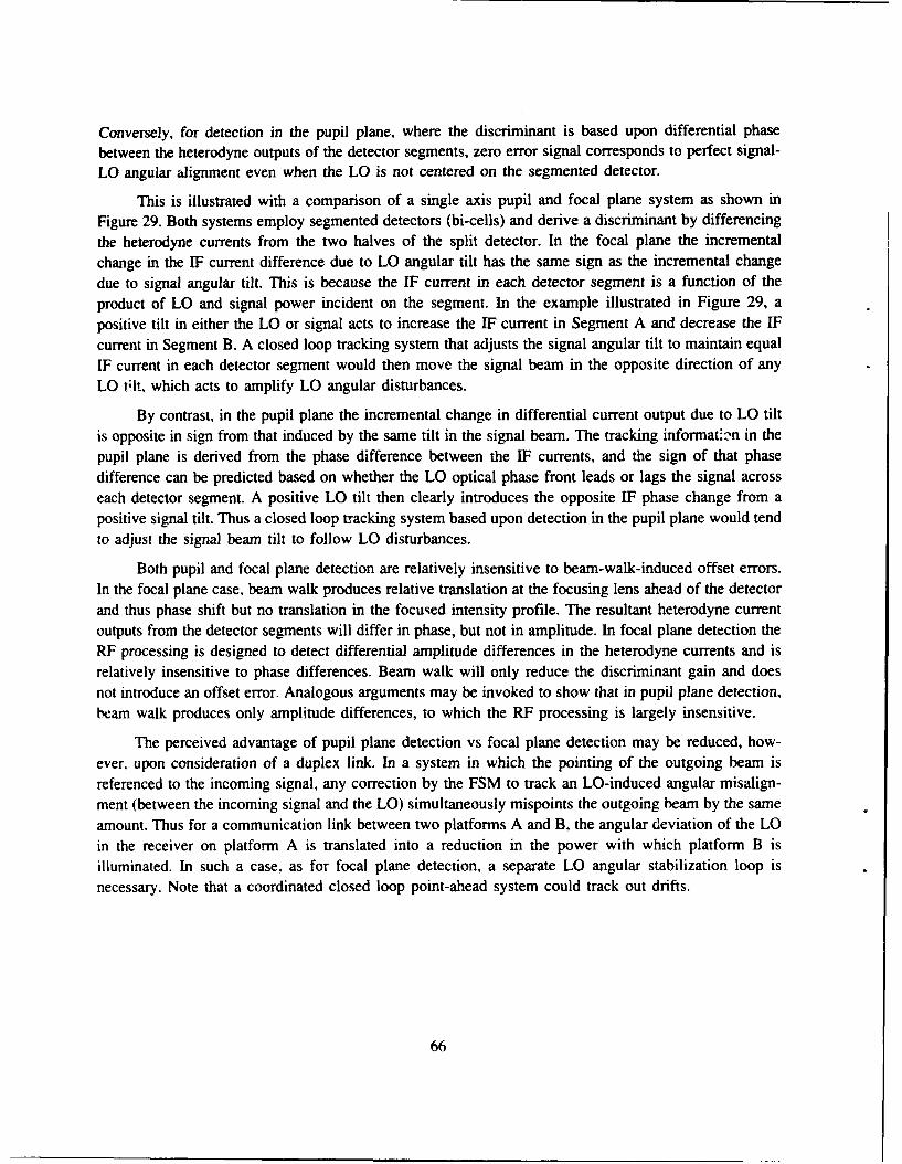
Conversely, for detection in the pupil plane, where the discriminant is based upon differential phase
between the heterodyne outputs of the detector segments, zero error signal corresponds to perfect signal-
LO angular alignment even when the LO is not centered on the segmented detector.
This is illustrated with a comparison of a single axis pupil and focal plane system as shown in
Figure 29. Both systems employ segmented detectors (bi-cells) and derive a discriminant by differencing
the heterodyne currents from the two halves of the split detector. In the focal plane the incremental
change in the IF current difference due to LO angular tilt has the same sign as the incremental change
due to signal angular tilt. This is because the IF current in each detector segment is a function of the
product of LO and signal power incident on the segment. In the example illustrated in Figure 29, a
positive tilt in either the LO or signal acts to increase the IF current in Segment A and decrease the IF
current in Segment B. A closed loop tracking system that adjusts the signal angular tilt to maintain equal
IF current in each detector segment would then move the signal beam in the opposite direction of any
LO tOt, which acts to amplify LO angular disturbances.
By contrast, in the pupil plane the incremental change in differential current output due to LO tilt
is opposite in sign from that induced by the same tilt in the signal beam. The tracking informati-n in the
pupil plane is derived from the phase difference between the IF currents, and the sign of that phase
difference can be predicted based on whether the LO optical phase front leads or lags the signal across
each detector segment. A positive LO tilt then clearly introduces the opposite IF phase change from a
positive signal tilt. Thus a closed loop tracking system based upon detection in the pupil plane would tend
to adjust the signal beam tilt to follow LO disturbances.
Both pupil and focal plane detection are relatively insensitive to beam-walk-induced offset errors.
In the focal plane case, beam walk produces relative translation at the focusing lens ahead of the detector
and thus phase shift but no translation in the focused intensity profile. The resultant heterodyne current
outputs from the detector segments will differ in phase, but not in amplitude. In focal plane detection the
RF processing is designed to detect differential amplitude differences in the heterodyne currents and is
relatively insensitive to phase differences. Beam walk will only reduce the discriminant gain and does
not introduce an offset error. Analogous arguments may be invoked to show that in pupil plane detection,
beam walk produces only amplitude differences, to which the RF processing is largely insensitive.
The perceived advantage of pupil plane detection vs focal plane detection may be reduced, how-
ever, upon consideration of a duplex link. In a system in which the pointing of the outgoing beam is
referenced to the incoming signal, any correction by the FSM to track an LO-induced angular misalign-
ment (between the incoming signal and the LO) simultaneously mispoints the outgoing beam by the same
amount. Thus for a communication link between two platforms A and B, the angular deviation of the LO
in the receiver on platform A is translated into a reduction in the power with which platform B is
illuminated. In such a case, as for focal plane detection, a separate LO angular stabilization loop is
necessary. Note that a coordinated closed loop point-ahead system could track out drifts.
66
>10_j0
z
z 1
IDY .0
0w
0 49 0 IL
z0
w Z(13 0
m LL
0c 0. (1A U30n NFn -c
0UILL -I
W. Z 0
w C
C)z zn0
w0 I Co
w C) L.
w c 0 w1 us w a:
49 z iz CC-L
0 -1 w
67
11. SPATIAL TRACKER AND HANDOFF RESULTS
This section summarizes the results of the various characterization tests of the heterodyne tracker
and acquisition/tracking handoff procedure. For each test the method is described, then the measured data
are presented.
11.1 BEAM CHARACTERIZATION
Hitachi HLP-8314E lasers operating at a nominal wavelength of 0.86 um and in a single longi-
tudinal mode served as the signal and LO sources. The laser outputs were collimated and circularized
using a Fujinon 7-mm fil. 1 lens and an anamorphic prism pair. After collimation the beam profiles werewell approximated by circular Gaussians with lie (E field amplitude) radii of 2.65 pm. The LO profilewas measured with a Beamscan scanning slit profilometer inserted in the beam path just after the input
50:50 combining beamsplitter, and the vertical and horizontal profiles are shown in Figure 30.
The signal beam was further conditioned, in order to approximate a plane wave, by expanding theoutput from the single mode waveguide through a 20x telescope and blocking all but the center of the
beam with an iris, the nominal diameter of which was 5.3 pm. The horizontal and vertical intensity profileswere measured as described above and are shown in Figure 31. Note that the constant amplitude curves
one might expect in Figure 31 are not obtained because the beam profile is measured using a scanning
slit, which actually integrates the beam along the direction perpendicular to the scan direction. For a
constant amplitude, circularly truncated beam, the resultant output of the profilometer is proportional to( -x 2)1/ 2 when scanning in the x direction. In comparison, for a circular Gaussian beam the output of
the profilometer is still a Gaussian profile.
The signal and LO wave fronts were also characterized using a LADITE wave front measuring
instrument. Plots of the optical path differences (OPD) across each wave front are shown in Figure 32.
The measured Strehl ratios were 0.90 and 0.84 for the LO and signal, respectively.
Using the method first described in [39] and later in [36] the spatial mode matching was measuredto be 0.66. The theoretical spatial mode matching for a matched Gaussian (E field Ile radius w, and truncated
at radius w) and plane wave (radius a) is 0.93, for a = w. Based on the analysis in [39,36], the modematching for beams with small, uncorrelated aberrations may be approximated by the product of the ideal
mode matching and the Strehl ratios of the signal and LO beams. Good agreement was obtained between themeasured mode matching, 0.66, and the expected value based on the Strehl ratios, 0.93*0.84*0.90 = 0.70.
11.2 CNR vs SIGNAL OPTICAL POWER
The thermal to LO shot noise ratio in the communications channel was characterized by measuringthe ratio between the outputs of the communications channel photodetector/preamplifier front end with
the signal beam blocked, and the LO alternately blocked and unblocked. Eac!; communication photode-tector received approximately 1.8 mW of LO power, which produced 0.9 mA of dc photocurrent. The
sum of the shot noise plus thermal noise was 4.3 dB above the LO shot noise alone, within a 1 GHz noise
bandwidth. Both the shot noise and total noise spectra were flat to within 0.5 dB over a 70 to 1300 MHzbandwidth.
69
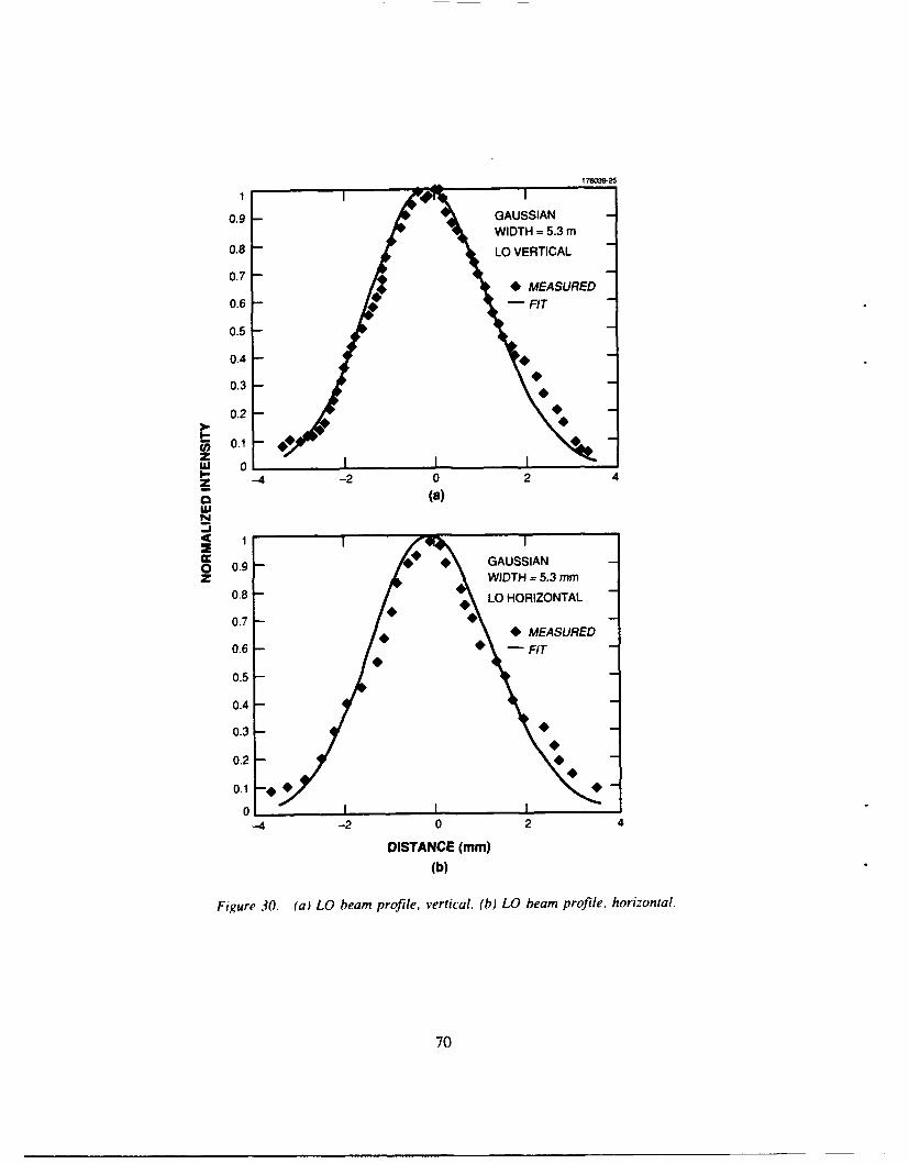
176039-25
1T
0.9 -GAUSSIANWIDTH = 5.3 m
0.6 LO VERTICAL
0.7*MEASURED
0.6 ' -FIT
0.5
0.4
0.3
0.2
0.1 *
z -4 -2 0 2 4
o (a)
o 0.9 4' 4 GAUSSIANZ WIDTH = 5.3mmn
0.7 LO HORIZONTAL
*MEASURED
0.6 4' FIT
0.5
0.4
0.3 4'
0.2
0.1 *'4
0 I
-4 -2 0 2 4
DISTANCE (mm)(b)
Figure 30. (a) LO beam profile, vertical. (b) LO beam profile, horizontal.
70
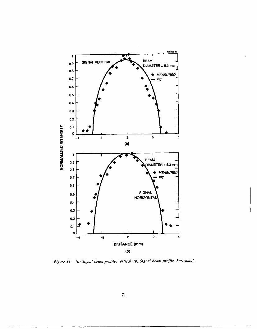
176039-26
0.9 -SIGNAL VERTICAL BEAMETR=53m
0.8 -DAEE . i
*MEASURED0.7-FI
0.6
0.5
0.4
0.3
0.2
S 0.1
z 0WU -1 1 3 5 7
(a)'U
~ 0. * * BEAM0 DIAMETER =5.3 mmZ 0.8
*MEASURED
0.7 -FIT
0.6
0.5 - SIGNAL* HORIZONTAL
0.4
0.3
0.2
0.1*
0
-4 -2 0 2 4
DISTANCE (mm)
(b)
Figure 3J. (a) Signal beam profile, vertical, (b) Signal beam profile, horizontal.
71
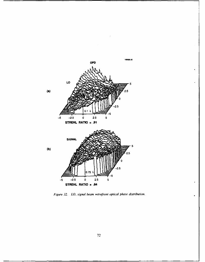
OPO
LO 5
(a)5
-5 -2.5 0 2.55
STREHL 0. RAIx 9
-55-5 -. 5 0 2.)
STREHL RATIO =.91
72.
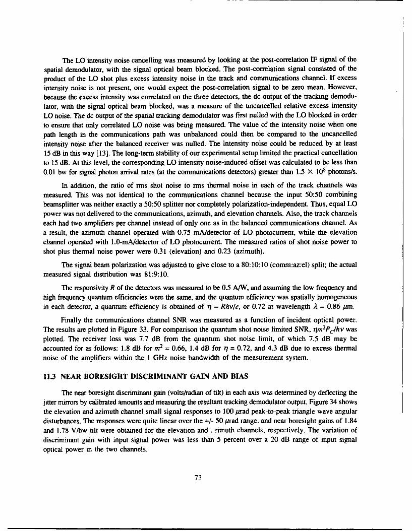
The LO intensity noise cancelling was measured by looking at the post-correlation IF signal of the
spatial demodulator, with the signal optical beam blocked. The post-correlation signal consisted of theproduct of the LO shot plus excess intensity noise in the track and communications channel. If excessintensity noise is not present, one would expect the post-correlation signal to be zero mean. However,because the excess intensity was correlated on the three detectors, the dc output of the tracking demodu-
lator, with the signal optical beam blocked, was a measure of the uncancelled relative excess intensityLO noise. The dc output of the spatial tracking demodulator was first nulled with the LO blocked in orderto ensure that only correlated LO noise was being measured. The value of the intensity noise when onepath length in the communications path was unbalanced could then be compared to the uncancelledintensity noise after the balanced receiver was nulled. The intensity noise could be reduced by at least15 dB in this way [13]. The long-term stability of our experimental setup limited the practical cancellationto 15 dB. At this level, the corresponding LO intensity noise-induced offset was calculated to be less than0.01 bw for signal photon arrival rates (at the communications detectors) greater than 1.5 X 10⁸ photons/s.
In addition, the ratio of rms shot noise to rms thermal noise in each of the track channels wasmeasured. This was not identical to the communications channel because the input 50:50 combiningbeamsplitter was neither exactly a 50:50 splitter nor completely polarization-independent. Thus, equal LOpower was not delivered to the communications, azimuth, and elevation channels. Also, the track channels
each had two amplifiers per channel instead of only one as in the balanced communications channel. Asa result, the azimuth channel operated with 0.75 mA/detector of LO photocurrent, while the elevationchannel operated with 1.0-mA/detector of LO photocurrent. The measured ratios of shot noise power toshot plus thermal noise power were 0.31 (elevation) and 0.23 (azimuth).
The signal beam polarization was adjusted to give close to a 80:10:10 (comm:az:el) split; the actualmeasured signal distribution was 81:9:10.
The responsivity R of the detectors was measured to be 0.5 A/W, and assuming the low frequency andhigh frequency quantum efficiencies were the same, and the quantum efficiency was spatially homogeneousin each detector, a quantum efficiency is obtained of ?I = Rhv/e, or 0.72 at wavelength A = 0.86 pm.
Finally the communications channel SNR was measured as a function of incident optical power.The results are plotted in Figure 33. For comparison the quantum shot noise limited SNR, q7m 2Pc/hV wasplotted. The receiver loss was 7.7 dB from the quantum shot noise limit, of which 7.5 dB may beaccounted for as follows: 1.8 dB for m2 = 0.66, 1.4 dB for 17 = 0.72, and 4.3 dB due to excess thermalnoise of the amplifiers within the 1 GHz noise bandwidth of the measurement system.
11.3 NEAR BORESIGHT DISCRIMINANT GAIN AND BIAS
The near boresight discriminant gain (volts/radian of tilt) in each axis was determined by deflecting thejitter mirrors by calibrated amounts and measuring the resultant tracking demodulator output. Figure 34 showsthe elevation and azimuth channel small signal responses to 100 prad peak-to-peak triangle wave angulardisturbances. The responses were quite linear over the +/- 50 prad range, and near boresight gains of 1.84and 1.78 V/bw tilt were obtained for the elevation and . -!imuth channels, respectively. The variation ofdiscriminant gain with input signal power was less than 5 percent over a 20 dB range of input signaloptical power in the two channels.
73
1 76039-27
20 mmeFOR MATCHED TRUNCATED GAUSSIAN, PLANE = .93.-- IDEAL (mme = 0.93, qe = 1)
15 mme -. 66, qe =. 7215 MEASURED CARRIER/SHOTNOISEA MEASURED CARRIER/
TOTAL NOISE
10
A
0 FRONT END NOISE - 4.3 dB
qe = .72 - 1.4 dBmme= .66 - 1.8 dB
A ADDITIONAL LOSS - 0.2 dB-5
TOTAL RECEIVER LOSS 7.7 db
-10 ____________________________
109 1010 10"l
PHOTON ARRIVAL RATE (Photons/s)
Figure 33. Communications channel carrier-to-noise ratio vs photon arrival rate.
In order to compare these results with theory, the gain, Kp = 1.38 V/radian, of the tracking de-modulator electronics was separately measured. Combining the measured transfer function of the trackingdemodulator with KD, the calculated electrical phase shift per beamwidth of optical tilt which was ob-tained via numerical integration of Equation (46), the predicted discriminant gain was KpKD = 1.71 V/bw of tilt. The discrepancy between predicted and measured gains (1.84,1.78 vs 1.71) is not due solelyto beam diameter mismatch because the discriminant gain KD is not particularly sensitive to such a mis-match. Calculations indicate that varying the ratio of beam diameters from 0.9 to 1.1 should produce lessthan ±3 percent change from the gain for matched beam diameters. Also, the translational mismatchbetween the LO and signal beams was less than 300 pm, which would not account for all of the observedgain difference. The discrepancy is attributed to inaccuracies in the calibration of the test aid used to findthe gain of the demodulator electronics.
The tracking bias was measured by dithering the disturbance mirror at a frequency above the rangein which the tracking loop had significant rejection (above 1 kHz). The resultant envelope modulationof the communication channel signal was then synchronously detected to determine the tracking biasoffset. Over a -10 dB to +20 dB range of input optical signal power (relative to the budgeted level, seeTable 1), and for IF heterodyne frequencies between 100 MHz and I GHz, the measured tracking biaswas less than 0.015 bw.
74
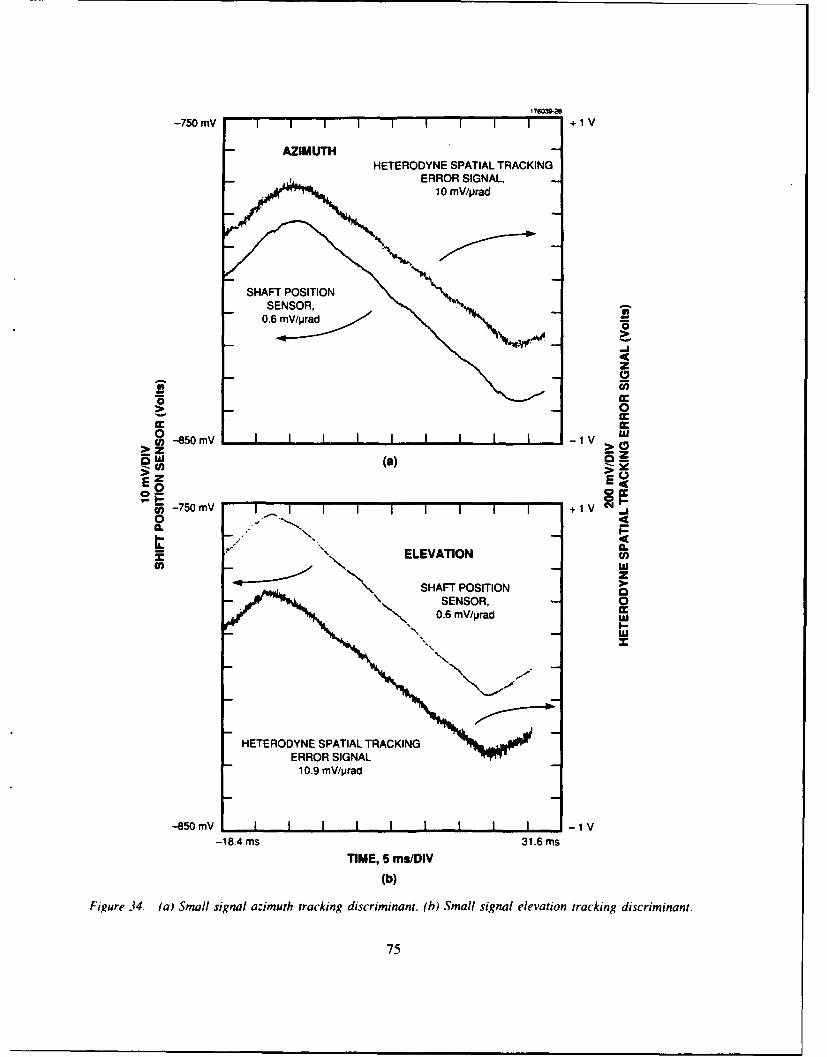
176039-28
-750 mV +-1 V
AZIMUTHHETERODYNE SPATIAL TRACKING
ERROR SIGNAL,10 mV/prad
z
00>. 0
U) (a) b
ro -750 mV + 1V C4-o0
z ELEVATION
- zNN. SHAFT POSITION
SENSOR, 00.6 mV/Ijrad SLU
ERROR SIGNAL10.9 mV/prad
-18.4 ms 31.6 msTIME, 5 ms/DIV
(b)
Figure 34. (a) Small signal azimuth tracking discriminant. (b) Small signal elevation tracking discriminant.
75
11.4 OFF AXIS DISCRIMINANT SHAPE
The complete discriminants, at high and low SNR, are shown in Figure 35 for each track channel. Themajor features of the discriminant which can be compared with theory are the initial slope (Section 10.3), thefirst zero crossing, and the off-axis sign reversal for high SNR. Ideally, in a system with infinite AGCgain the off-axis shape of the discriminant normalized by the norm of Equation (9) would be given bycurve c in Figure 28. Unfortunately, the AGC gain in any real system is finite, and hence the post-correlation signal has corresponding nulls and sign reversals with the communications (sum) channel.From Figure 28, in a system with matched Gaussian and plane wave optical beams the communicationsor sum channel magnitude, and hence the post-correlation discriminant, is expected to have a null at1.2 bw. At high SNR, and for angular errors greater than 1.2 bw, the normalized discriminant actuallyreverses in sign, which can lead to positive feedback during closed loop operation (e.g., during acqui-sition). As discussed in Section 11.9.4, this affected the pull-in transients but did not otherwise affectnormal operation of the tracking system. At low SNR the tails of the discriminant are dominated by thenoise of the system.
11.5 MEASURED NEA IN THE COMMUTATION CORRELATION PROCESSOR
The NEA of the spatial tracker may be obtained by measuring the rms noise equivalent voltage(NEV) at the output of the tracking demodulator within a 2-kHz noise bandwidth and then normalizingby the square root of the measured discriminant gain. These measurements were made with a frequencytracking loop enabled that controlled the LO laser current to maintain a constant IF tone at 325 MHz. Thesignal laser current was not modulated, i.e., no data were transmitted, during these measurements. Inorder to characterize the open loop angle sensor, the NEV measurements were made with the spatialtracking loop disabled. Because the relatively large low frequency disturbances in the open loop system,due to acoustic and mechanical noise on the optical table, would otherwise have dominated the measure-ments, the NEV was measured in a 2-kHz bandwidth from 1 to 3 kHz. The spectral density of the noiseat the output of the tracking demodulator due to shot noise and amplifier thermal noise was flat to beyond5 kHz, and above I kHz there were negligible mechanical and acoustic disturbances. The resultant NEAsare plotted in Figure 36. Error bars indicate the repeatability of the measurements. The major factors thataccounted for the measured NEA variations at constant nominal input power were fluctuations in thesignal optical power during the measurement interval (I s) and inaccuracy in optical power measurementsat received power levels of less than 50 nW.
For comparison Figure 36 plots the theoretical shot-noise-limited NEA for a commutated correla-tion processor (curve a), as well as the predicted NEAs for the laboratory system (curve b), which arebased upon the measured, non-shot-noise-limited CNDRs in the track and communication channels (Sec-tion 11.2) and the measured gain near boresight (Section 11.3). Within experimental repeatability themeasured NEAs in Figure 36 agree with calculated values in curve c for our non-shot-noise-limitedimplementation.
76
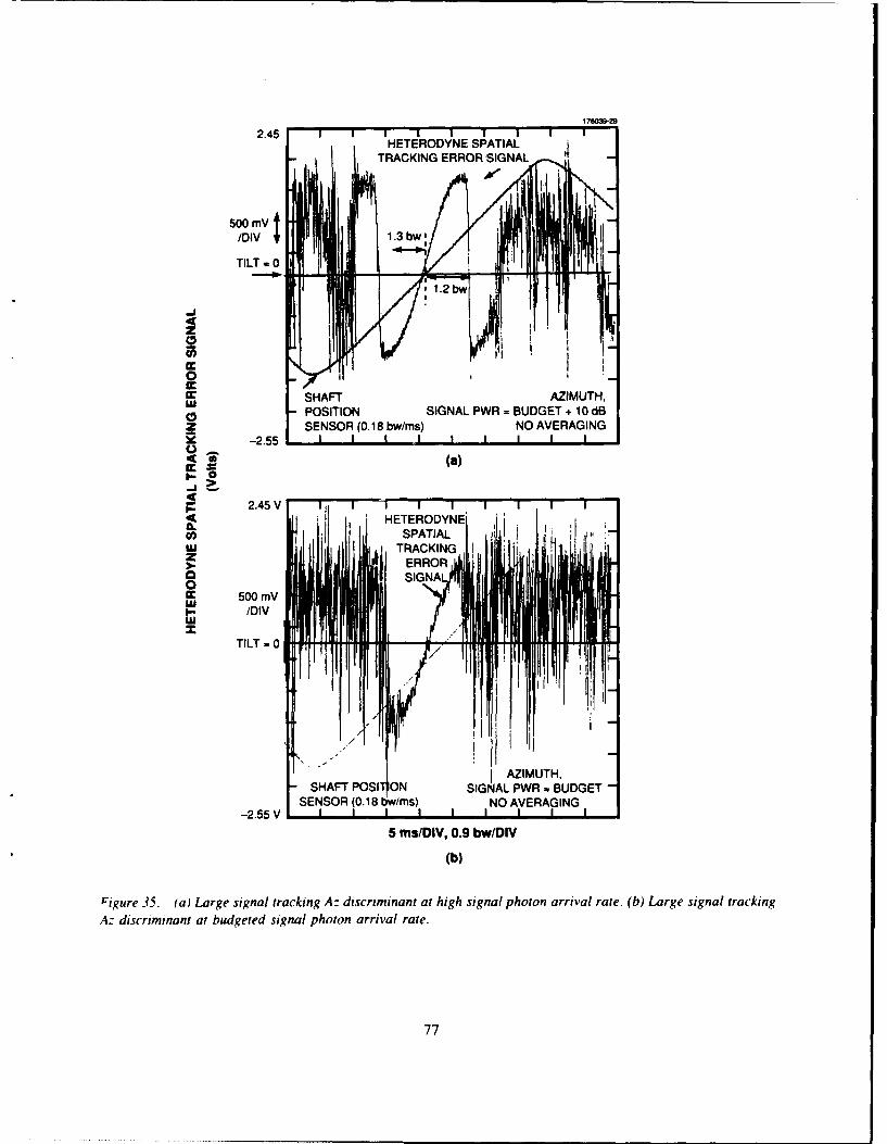
176039-29
2.45 1HETERODYNE SPATIAL
TRACKING ERROR-SIGNAL
500 mV/DIV 1.*b
z
0
0z SENSOR (0. 18 bw/ms) NO AVERAGING
-2.55
(a)
P 2.45 V I I I4 HETERODYNE
SPATIALU. TACINz
m 500 mVTAI- /DIVw
SHAFT POSIT ION SIGNAL PWR -BUDGETSENSOR (0.18 bw/ms) NO AVERAGING
-2.55 V I I I 1 1 -1 1 1 1
5 mslDly, 0.9 bwlDIV
(b)
Figure 35. (a) Large signal tracking A: discriminant at high signal photon arrival rate. (b) Large signal trackingA: discriminant at budgeted signal photon arrival rate.
77
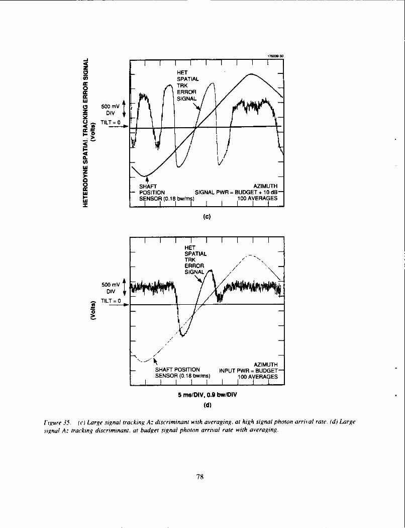
17603-30
z
0
DI-
0>
wU POSITION SIGNAL PWR =BUDGET + 10 dBSISENSOR (0.18 bw/ms) 100 AVERAGES
x
(C)
HETSPATIALTRK/
500 mV SGA
DIV
SHAFT POSITION INPUT PWR =BUDGET-
SENSOR (0.18 bw/ms) 100 AVERAGESF I I I I I I I 1 1
5 ms/DIV, 0.9 bwlDIV(d)
Figure 35. (c) Large signal tracking A: discriminant with averaging. at high signal photon arrival rate. (d) Large
signal A: tracking discriminant, at budget signal photon arrival rate with averaging.
78
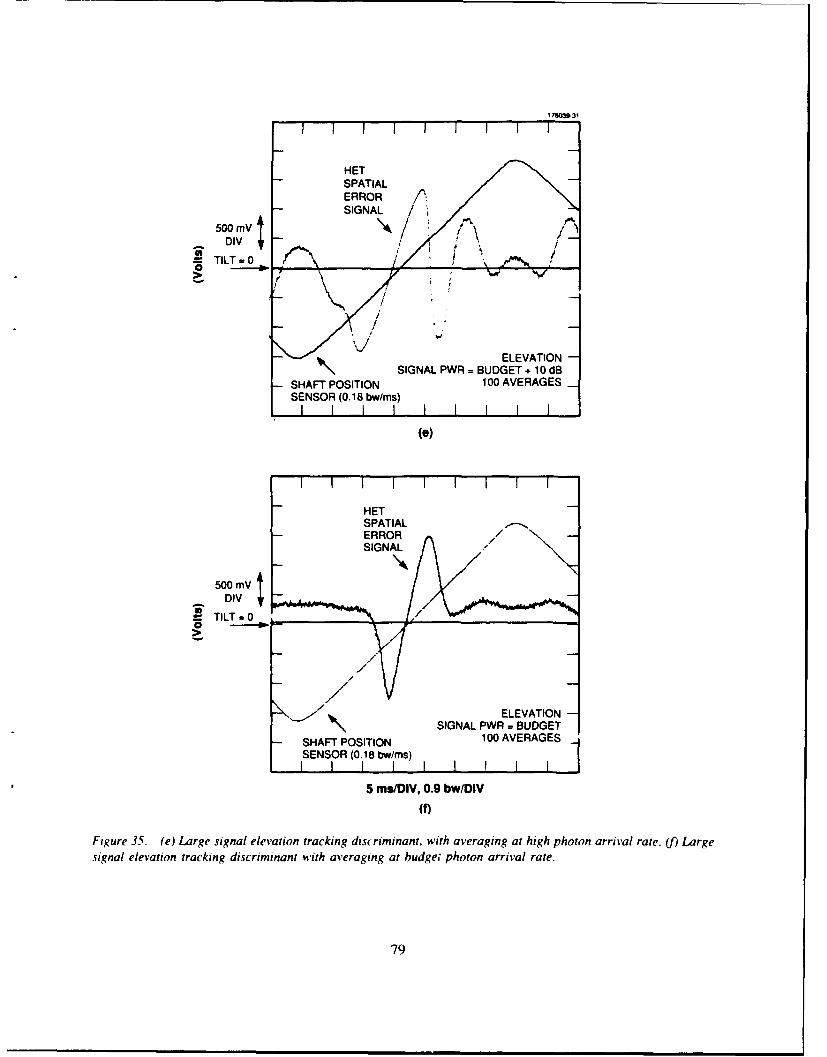
170039-31
HETSPATIALERROR /*SIGNAL /
500 mV
ELEVATIONSIGNAL PWF4 BUDGET + 10 dB
SHAFT POSITION 100 AVERAGESSENSOR (0. 18 bw/ms)
(e)
HETSPATIALERROR / 'SIGNAL
500 mVDIV
=TILT 0/
ELEVATIONSIGNAL PWR = BUDGET
SHAFT POSITION 100 AVERAGESSENSOR (0. 18 bw/m)1
5 msDIV, 0.9 bwlDIV(f)
Figure 35. (e) Large signal elevation tracking disriminant. with averaging at high photon arrival rate. (jf) Largesignal elevation tracking discriminant with averaging at budge,' photon arrival rate.
79
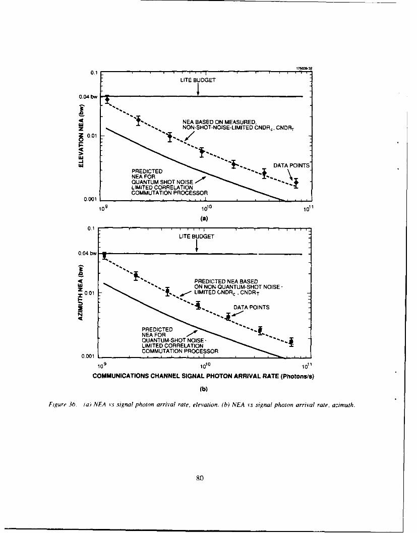
176003-32
0.1 I
LITE BUDGET
0.04 bw
NEA BASED ON MEASURED,Z , NON-SHOT-NOISE-LIMITED CNDRc, CNDRT2 0.010*
w PEIT DATA POINTS
NEA FOR I 1..,. 1
QUANTUM SHOT NOISE - *LIMITED CORRELATIONCOMMUTATION PROCESSOR
0.001
109 1010 101
(a)0.1 1 I I ' '
LITE BUDGET
0.04 bw
cc PREDICTED NEA BASED00 ON NON QUANTUM-SHOT NOISE-0.01 LIMITED GNDRc, CNDRT
S, DATA POINTS
PREDICTED~~~NEA FOR " '* -,
QUANTUM-SHOT NOISE-LIMITED CORRELATIONCOMMUTATION PROCESSOR
0.001
109 1010 1011
COMMUNICATIONS CHANNEL SIGNAL PHOTON ARRIVAL RATE (Photons/s)
(b)
Figure 36. (a) NEA vs signal photon arrival rate, elevation. (b) NEA vs signal photon arrival rate, azimuth.
80
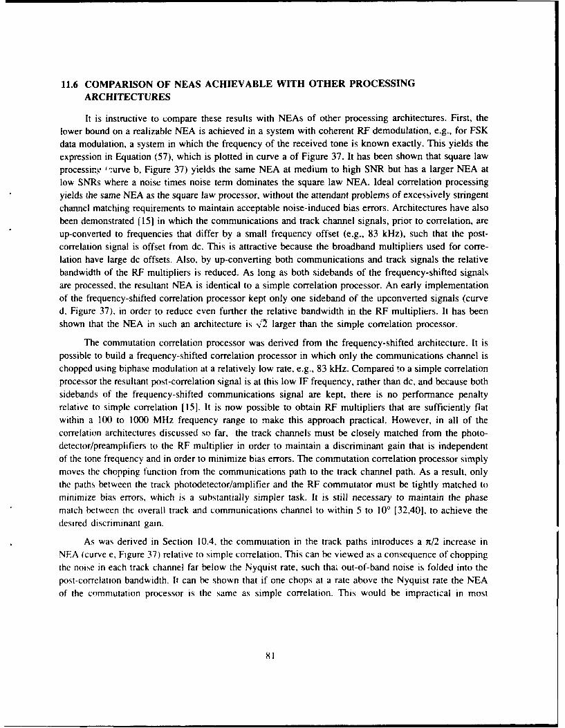
11.6 COMPARISON OF NEAS ACHIEVABLE WITH OTHER PROCESSINGARCHITECTURES
It is instructive to compare these results with NEAs of other processing architectures. First, thelower bound on a realizable NEA is achieved in a system with coherent RF demodulation, e.g., for FSKdata modulation, a system in which the frequency of the received tone is known exactly. This yields theexpression in Equation (57), which is plotted in curve a of Figure 37. It has been shown that square lawprocessinw ":urve b, Figure 37) yields the same NEA at medium to high SNR but has a larger NEA atlow SNRs where a noise times noise term dominates the square law NEA. Ideal correlation processingyields the same NEA as the square law processor, without the attendant problems of excessively stringentchannel matching requirements to maintain acceptable noise-induced bias errors. Architectures have alsobeen demonstrated (15] in which the communications and track channel signals, prior to correlation, areup-converted to frequencies that differ by a small frequency offset (e.g., 83 kHz), such that the post-correlation signal is offset from dc. This is attractive because the broadband multipliers used for corre-lation have large dc offsets. Also, by up-converting both communications and track signals the relativebandwidth of the RF multipliers is reduced. As long as both sidebands of the frequency-shifted signalsare processed, the resultant NEA is identical to a simple correlation processor. An early implementationof the frequency-shifted correlation processor kept only one sideband of the upconverted signals (curved, Figure 37), in order to reduce even further the relative bandwidth in the RF multipliers. It has beenshown that the NEA in such an architecture is -'2 larger than the simple correlation processor.
The commutation correlation processor was derived from the frequency-shifted architecture. It ispossible to build a frequency-shifted correlation processor in which only the communications channel ischopped using biphase modulation at a relatively low rate, e.g., 83 kHz. Compared !o a simple correlationprocessor the resultant post-correlation signal is at this low IF frequency, rather than dc, and because bothsidebands of the frequency-shifted communications signal are kept, there is no performance penaltyrelative to simple correlation [15]. It is now possible to obtain RF multipliers that are sufficiently flatwithin a 100 to 1000 MHz frequency range to make this approach practical. However, in all of thecorrelation architectures discussed so far, the track channels must be closely matched from the photo-detector/preamplifiers to the RF multiplier in order to maintain a discriminant gain that is independentof the tone frequency and in order to minimize bias errors. The commutation correlation processor simplymoves the chopping function from the communications path to the track channel path. As a result, onlythe paths between the track photodetector/amplifier and the RF commutator must be tightly matched tominimize bias errors, which is a substantially simpler task. It is still necessary to maintain the phasematch between the overall track and communications channel to within 5 to 100 [32,40], to achieve thedesired discriminant gain.
As was derived in Section 10.4, the commutation in the track paths introduces a n/2 increase inNEA (curve e. Figure 37) relative to simple correlation. This can be viewed as a consequence of choppingthe noise in each track channel far below the Nyquist rate, such thai out-of-band noise is folded into thepost-correlation bandwidth. It can be shown that if one chops at a rate above the Nyquist rate the NEAof the commutation processor is the same as simple correlation. This would be impractical in most
81
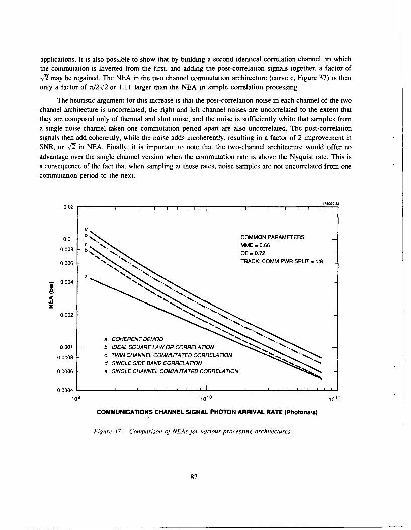
applications. It is also possible to show that by building a second identical correlation channel, in whichthe commutation is inverted from the first, and adding the post-correlation signals together, a factor of-v'7 may be regained. The NEA in the two channel commutation architecture (curve c, Figure 37) is thenonly a factor of t/2 2 or 1.11 larger than the NEA in simple correlation processing
The heuristic argument for this increase is that the post-correlation noise in each channel of the twochannel architecture is uncorrelated; the right and left channel noises are uncorrelated to the extent thatthey are composed only of thermal and shot noise, and the noise is sufficiently white that samples froma single noise channel taken one commutation period apart are also uncorrelated. The post-correlationsignals then add coherently, while the noise adds incoherently, resulting in a factor of 2 improvement inSNR, or V2 in NEA. Finally, it is important to note that the two-channel architecture would offer noadvantage over the single channel version when the commutation rate is above the Nyquist rate. This isa consequence of the fact that when sampling at these rates, noise samples are not uncorrelated from onecommutation period to the next.
176039330 .02 1 1 1 1 1 1 1 1 1 1 1 1 1 1 1 1
e0.01 d COMMON PARAMETERS
c"' MME = 0.660.008 b OE = 0.72
0,006 TRACK: COMM PWR SPLIT = 1:8
0.004
z0.002
a. COHERENT DEMOD
0.0008 c. TWIN CHANNEL COMMUTATED CORRELATION Jd. SIGESD ADCORRELATION
0.0006 e. SINGLE CHANNEL COMMUTA TED CORRELATION
0.0004 ,
109 1010 1011
COMMUNICATIONS CHANNEL SIGNAL PHOTON ARRIVAL RATE (Photons/s)
Figure 37. Comparison of NEAs for various processing architectures.
82
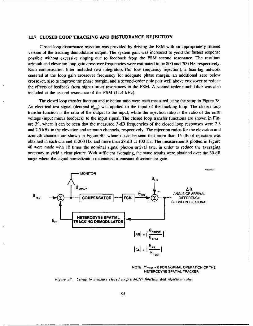
11.7 CLOSED LOOP TRACKING AND DISTURBANCE REJECTION
Closed loop disturbance rejection was provided by driving the FSM with an appropriately filteredversion of the tracking demodulator output. The system gain was increased to yield the fastest responsepossible without excessive ringing due to feedback from the FSM second resonance. The resultantazimuth and elevation loop gain crossover frequencies were estimated to be 800 and 700 Hz, respectively.Each compensation filter included two integrators (for low frequency rejection), a lead-lag networkcentered at the loop gain crossover frequency for adequate phase margin, an additional zero belowcrossover, also to improve the phase margin, and a second-order pole pair well above crossover to reducethe effects of feedback from higher-order resonances in the FSM. A second-order notch filter was alsoincluded at the second resonance of the FSM (11.4 kHz).
The closed loop transfer function and rejection ratio were each measured using the setup in Figure 38.An electrical test signal (denoted 0test) was applied to the input of the tracking loop. The closed looptransfer function is the ratio of the output to the input, while the rejection ratio is the ratio of the errorvoltage (input minus feedback) to the input signal. The closed loop transfer functions are shown in Fig-ure 39, where it can be seen that the measured 3-dB frequencies of the closed loop responses were 2.3and 2.5 kHz in the elevation and azimuth channels, respectively. The rejection ratios for the elevation andazimuth channels are shown in Figure 40, where it can be seen that more than 15 dB of rejection wasobtained in each channel at 200 Hz, and more than 28 dB at 100 Hz. The measurements plotted in Figure40 were made with 10 times the nominal signal photon arrival rate, in order to reduce the averagingnecessary to yield a clear picture. With sufficient averaging, the same results were obtained over the 30-dBrange where the signal normalization maintained a constant discriminant gain.
176039-34SMONITOR
L
OLOI
O R R O R Ar " 0,
RSIG ANGLE OF ARRIVAL
0 RRES---1 F-SMI
0 TESSCOMPENSATOR DIFFERENCE
0 EETWEEN
LO, SIGNAL
HETERODYNE SPATIALOFS TRACKING DEMODULATOR
IRRI = 1i RO
I OLI =I F IUTEST
NOTE: OTEST = 0 FOR NORMAL OPERATION OF THEHETERODYNE SPATIAL TRACKER
Figure 38. Set-up to measure closed loop transfer function and rejection ratio.
83
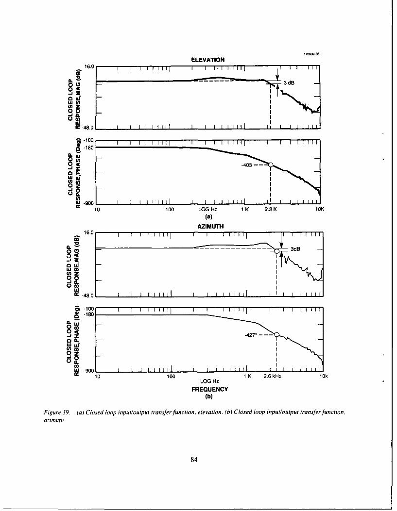
17603-35
ELEVATION16.0 Ii ' ' " , 1 Jilln n
T B
wff
E€-48.0 I I ] I IIIII I I i Iii l Ij I 1 1I Il
- 180
o -0 . I
00
0U)
E 10 100 LOG Hz 1 K ..3 K 10K(a)
AZIMUTH16.0 I I I I' 1 I , II , u
Ix -48.
W
- -
Il" 4 oI I i I lll I II Ii!i I w ill
180
L LU084( -403-
10 100 1K 2.6kHz 10kLOG Hz
FREQUENCY(b)
Figure 39. (a) Closed ioop inputloutput transfer function, elevation. (b) Closed loop input/output transfer function.
azimuth.
84
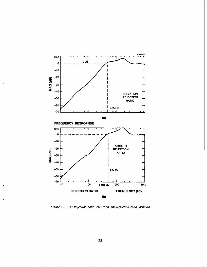
0 d
-10
-- 20
03-4
IELEVATION-50 REJECTION
-60 RATIO
-60 435 Hz
(a)FREQUENCY RESPOPNSE
10.0 1 1 1 11 1 1 1 1
-10 IAZIMUTH
-20I REJECTIONV 3 RATIO
-50 - 530 Hz
-60
-7 1 11 llII I I.. m lI10 100 LOG HZ 1000 10k
REJECTION RATIO FREQUENCY (Hz)
(b)
Figure 40. (a) Rejection ratio, elevation. (b) Rejection ratio, azimuth.
85
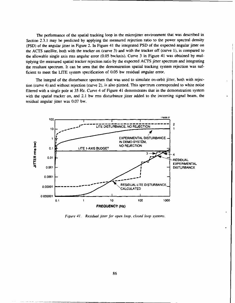
The performance of the spatial tracking loop in the microjitter environment that was described in
Section 2.3.1 may be predicted by applying the measured rejection ratio to the power spectral density
(PSD) of the angular jitter in Figure 2. In Figure 41 the integrated PSD of the expected angular jitter on
the ACTS satellite, both with the tracker on (curve 3) and with the tracker off (curve 1), is compared to
the allowable single axis rms angular error (0.05 bw/axis). Curve 3 in Figure 41 was obtained by mul-
tiplying the measured spatial tracker rejection ratio by the expected ACTS jitter spectrum and integrating
the resultant spectrum. It can be seen that the demonstration spatial tracking system rejection was suf-
ficient to meet the LITE system specification of 0.05 bw residual angular error.
The integral of the disturbance spectrum that was used to simulate on-orbit jitter, both with rejec-
tion (curve 4) and without rejection (curve 2), is also plotted. This spectrum corresponded to white noise
filtered with a single pole at 35 Hz. Curve 4 of Figure 41 demonstrates that in the demonstration system
with the spatial tracker on, and 2.1 bw rms disturbance jitter added to the incoming signal beam, the
residual angular jitter was 0.07 bw.
100 17639"37
10 - 1..
1 EXPERIMENTAL DISTURBANCE -,-, IN DEMO SYSTEM,
LTDU NO REJECTION
M 0.1 LITE 1-AXIS BUDGET
0.0 1- RESIDUAL
EXPERIMENTAL" 0.001 - DISTURBANCE
0.0001 -
0.00001-------- - - - - - \RESIDUAL LITE DISTURBANCE,_CALCULATED
0.000001 1
0.1 1 10 100 1000
FREQUENCY (Hz)
Figure 41. Residual jitter for open loop, closed loop systems.
86
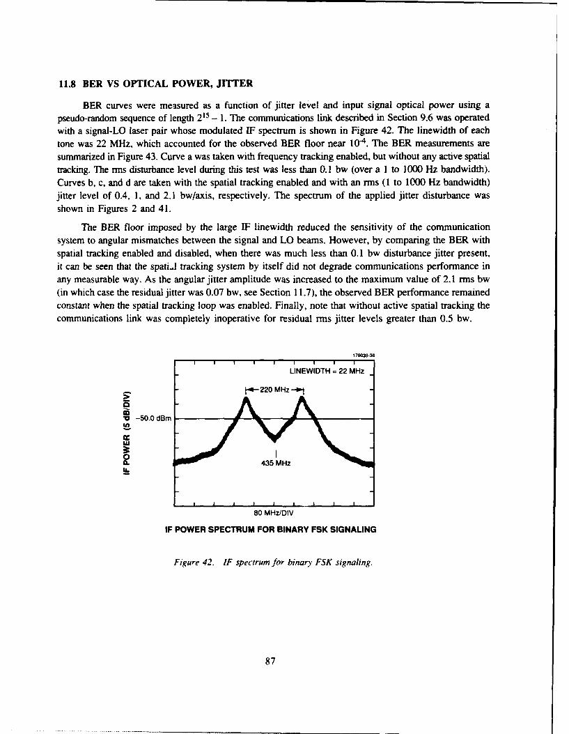
11.8 BER VS OPTICAL POWER, JITTER
BER curves were measured as a function of jitter level and input signal optical power using apseudo-random sequence of length 215 - 1. The communications link described in Section 9.6 was operatedwith a signal-LO laser pair whose modulated IF spectrum is shown in Figure 42. The linewidth of eachtone was 22 MHz, which accounted for the observed BER floor near 10 -4. The BER measurements aresummarized in Figure 43. Curve a was taken with frequency tracking enabled, but without any active spatialtracking. The rms disturbance level during this test was less than 0.1 bw (over a I to 1000 Hz bandwidth).Curves b, c, and d are taken with the spatial tracking enabled and with an rms (1 to 1000 Hz bandwidth)jitter level of 0.4, 1, and 2.1 bw/axis, respectively. The spectrum of the applied jitter disturbance wasshown in Figures 2 and 41.
The BER floor imposed by the large IF linewidth reduced the sensitivity of the communicationsystem to angular mismatches between the signal and LO beams. However, by comparing the BER withspatial tracking enabled and disabled, when there was much less than 0.1 bw disturbance jitter present,it can be seen that the spati-J tracking system by itself did not degrade communications performance inany measurable way. As the angular jitter amplitude was increased to the maximum value of 2.1 rms bw(in which case the residual jitter was 0.07 bw, see Section 11.7), the observed BER performance remainedconstant when the spatial tracking loop was enabled. Finally, note that without active spatial tracking thecommunications link was completely inoperative for residual rms jitter levels greater than 0.5 bw.
176039-3a
LINEWIDTH =22 MHz .
" I--220 MHz
-50.0 dBm -.
435 MHz
80 MHz/DIV
IF POWER SPECTRUM FOR BINARY FSK SIGNALING
Figure 42. IF spectrum for binary FSK signaling.
87
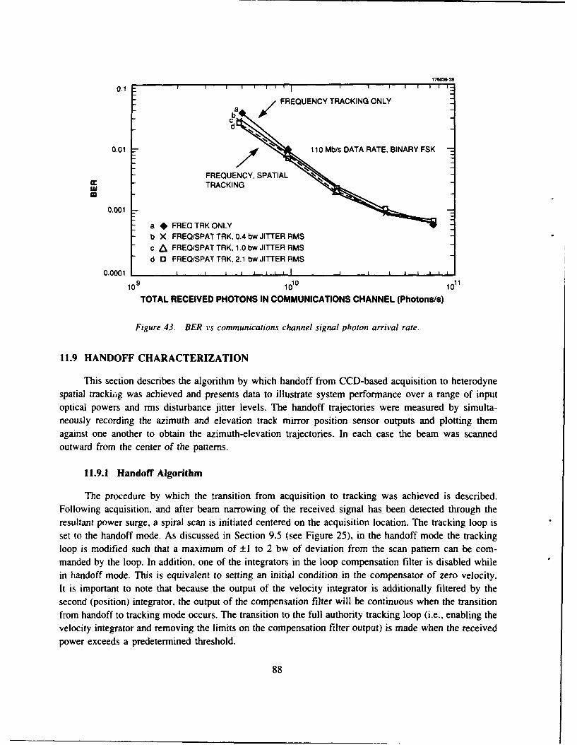
1760 -390.1 I I I I I I I I i I I I IIt
a FREQUENCY TRACKING ONLY
d ,
0.01 110 Mb/s DATA RATE, BINARY FSK
FREQUENCY, SPATIAL 'S
TRACKING 'S
0.001
a * FREO TRK ONLYb X FREQ/SPAT TRK, 0.4 bw JITTER RMSc & FREQ/SPAT TRK, 1.0 bw JITTER RMSd 13 FREQ/SPAT TRK, 2.1 bw JITTER RMS
0.0001 1 1 1 1 1 1 1 1 1 1
109 1010 1011
TOTAL RECEIVED PHOTONS IN COMMUNICATIONS CHANNEL (Photons/s)
Figure 43. BER vs communications channel signal photon arrival rate.
11.9 HANDOFF CHARACTERIZATION
This section describes the algorithm by which handoff from CCD-based acquisition to heterodynespatial trackitig was achieved and presents data to illustrate system performance over a range of inputoptical powers and rms disturbance jitter levels. The handoff trajectories were measured by simulta-neously recording the azimuth and elevation track mirror position sensor outputs and plotting themagainst one another to obtain the azimuth-elevation trajectories. In each case the beam was scannedoutward from the center of the patterns.
11.9.1 Handoff Algorithm
The procedure by which the transition from acquisition to tracking was achieved is described.Following acquisition, and after beam narrowing of the received signal has been detected through theresultant power surge, a spiral scan is initiated centered on the acquisition location. The tracking loop isset to the handoff mode. As discussed in Section 9.5 (see Figure 25), in the handoff mode the trackingloop is modified such that a maximum of ±1 to 2 bw of deviation from the scan pattern can be com-manded by the loop. In addition, one of the integrators in the loop compensation filter is disabled whilein handoff mode. This is equivalent to setting an initial condition in the compensator of zero velocity.It is important to note that because the output of the velocity integrator is additionally filtered by thesecond (position) integrator, the output of the compensation filter will be continuous when the transitionfrom handoff to tracking mode occurs. The transition to the full authority tracking loop (i.e., enabling thevelocity integrator and removing the limits on the compensation filter output) is made when the receivedpower exceeds a predetermined threshold.
88
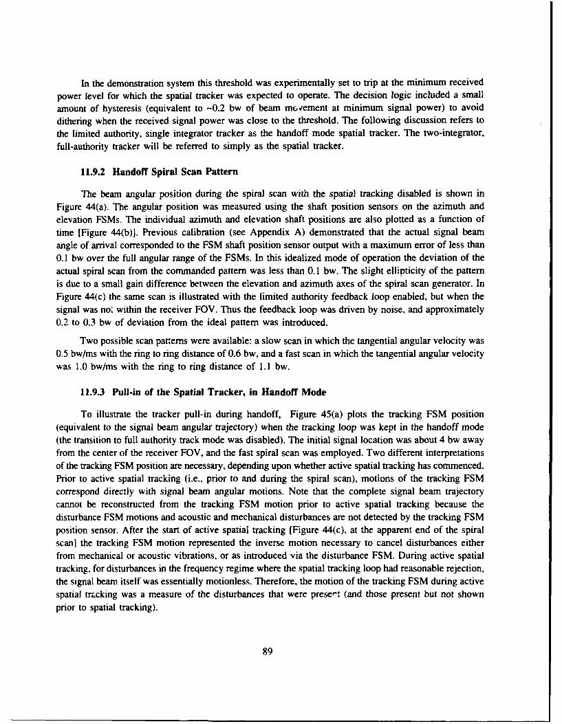
In the demonstration system this threshold was experimentally set to trip at the minimum receivedpower level for which the spatial tracker was expected to operate. The decision logic included a small
amount of hysteresis (equivalent to -0.2 bw of beam mra cement at minimum signal power) to avoid
dithering when the received signal power was close to the threshold. The following discussion refers to
the limited authority, single integrator tracker as the handoff mode spatial tracker. The two-integrator,
full-authority tracker will be referred to simply as the spatial tracker.
11.9.2 Handoff Spiral Scan Pattern
The beam angular position during the spiral scan with the spatial tracking disabled is shown inFigure 44(a). The angular position was measured using the shaft position sensors on the azimuth andelevation FSMs. The individual azimuth and elevation shaft positions are also plotted as a function oftime [Figure 44(b)]. Previous calibration (see Appendix A) demonstrated that the actual signal beamangle of arrival corresponded to the FSM shaft position sensor output with a maximum error of less than0.1 bw over the full angular range of the FSMs. In this idealized mode of operation the deviation of theactual spiral scan from the commanded pattern was less than 0.1 bw. The slight ellipticity of the patternis due to a small gain difference between the elevation and azimuth axes of the spiral scan generator. InFigure 44(c) the same scan is illustrated with the limited authority feedback loop enabled, but when thesignal was no: within the receiver FOV. Thus the feedback loop was driven by noise, and approximately0.2 to 0.3 bw of deviation from the ideal pattern was introduced.
Two possible scan panerns were available: a slow scan in which the tangential angular velocity was0.5 bw/ms with the ring to ring distance of 0.6 bw, and a fast scan in which the tangential angular velocitywas 1.0 bw/ms with the ring to ring distance of 1.1 bw.
11.9.3 Pull-in of the Spatial Tracker, in Handoff Mode
To illustrate the tracker pull-in during handoff, Figure 45(a) plots the tracking FSM position(equivalent to the signal beam angular trajectory) when the tracking loop was kept in the handoff mode(the transition to full authority track mode was disabled). The initial signal location was about 4 bw awayfrom the center of the receiver FOV, and the fast spiral scan was employed. Two different interpretationsof the tracking FSM position are necessary, depending upon whether active spatial tracking has commenced.Prior to active spatial tracking (i.e., prior to and during the spiral scan), motions of the tracking FSMcorrespond directly with signal beam angular motions. Note that the complete signal beam trajectorycannot be reconstructed from the tracking FSM motion prior to active spatial tracking because thedisturbance FSM motions and acoustic and mechanical disturbances are not detected by the tracking FSMposition sensor. After the start of active spatial tracking [Figure 44(c), at the apparent end of the spiralscan] the tracking FSM motion represented the inverse motion necessary to cancel disturbances eitherfrom mechanical or acoustic vibrations, or as introduced via the disturbance FSM. During active spatial
tracking, for disturbances in the frequency regime where the spatial tracking loop had reasonable rejection,the signal beam itself was essentially motionless. Therefore, the motion of the tracking FSM during activespatial trzcking was a measure of the disturbances that were preset (and those present but not shownprior to spatial tracking).
89
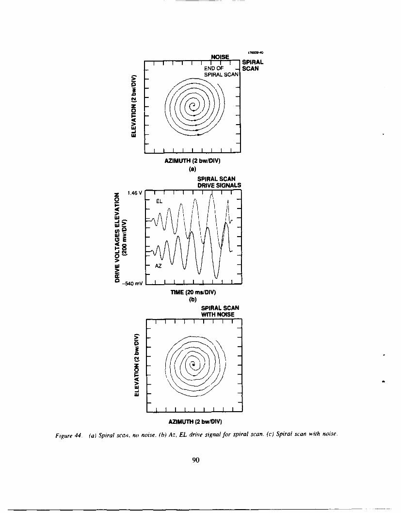
NOISEIISPIRAL
END OF -SCANSPIRAL SCAN
0>'UI.j
IU ------- I I
AZIMUTH (2 bwlDIV)
(a)SPIRAL SCANDRIVE SIGNALS
S1.46 V -
0 EL
'UL\U
cm~
0-
'U AZ
a -540mV II I
TIME (20 mnsDIV)(b)
SPIRAL SCANWITH NOISE
.0
09
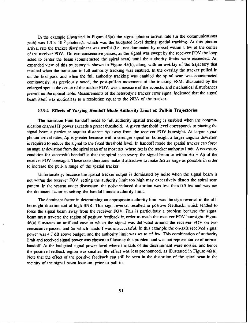
In the example illustrated in Figure 45(a) the signal photon arrival rate (in the communications
path) was 1.3 x 10¹⁰ photons/s, which was the budgeted level during spatial tracking. At this photon
arrival rate the tracker discriminant was useful (i.e., not dominated by noise) within 1 bw of the center
of the receiver FOV. On two consecutive passes, as the signal was swept by the receiver FOV the loop
acted to center the beam (counteracted the spiral scan) until the authority limits were exceeded. An
expanded view of this trajectory is shown in Figure 45(b), along with an overlay of the trajectory that
resulted when the transition to full authority tracking was enabled. In the overlay the tracker pulled in
on the first pass, and when the full authority tracking was enabled the spiral scan was counteracted
continuously. As previously noted, the post-pull-in movement of the tracking FSM, illustrated by the
enlarged spot at the center of the tracker FOV, was a measure of the acoustic and mechanical disturbancespresent on the optical table. Measurements of the heterodyne tracker error signal indicated that the signalbeam itself was motionless to a resolution equal to the NEA of the tracker.
11.9.4 Effects of Varying Handoff Mode Authority Limit on Pull-in Trajectories
The transition from handoff mode to full authority spatial tracking is enabled when the commu-nication channel IF power exceeds a preset threshold. A given threshold level corresponds to placing thesignal beam a particular angular distance Ap away from the receiver FOV boresight. At larger signalphoton arrival rates, Ap is greater because with a stronger signal on boresight a larger angular deviationis required to reduce the signal to the fixed threshold level. In handoff mode the spatial tracker can forcean angular deviation from the spiral scan of at most Act, where Ac is the tracker authority limit. A necessarycondition for successful handoff is that the spiral scan swr.'p the signal beam to within Act + Ap of thereceiver FOV boresight. These considerations make it attractive to make Aca as large as possible in orderto increase the pull-in range of the spatial tracker.
Unfortunately, because the spatial tracker output is dominated by noise when the signal beam isnot within the receiver FOV, setting the authority limit too high may excessively distort the spiral scanpattern. In the system under discussion, the noise-induced distortion was less than 0.5 bw and was not
the dominant factor in setting the handoff mode authority limit.
The dominant factor in determining an appropriate authority limit was the sign reversal in the off-boresight discriminant at high SNR. This sign reversal resulted in positive feedback, which tended to
force the signal beam away from the receiver FOV. This is particularly a problem because the signalbeam must traverse the region of positive feedback in order to reach the receiver FOV boresight. Figure46(a) illustrates an artificial case in which the signal was deflected around the receiver FOV on twoconsecutive passes, and for which handoff was unsuccessful. In this example the on-axis received signalpower was 4.7 dB above budget, and the authority limit was set to ±5 bw. This combination of authority
limit and received signal power was chosen to illustrate this problem and was not representative of normalhandoff. At the budgeted signal power level where the tails of the discriminant were noisier, and hencethe positive feedback region was smaller, the effect was less pronounced, as illustrated in Figure 46(b).Note that the effect of the positive feedback can still be seen in the distortion of the spiral scan in thevicinity of the signal beam location, prior to pull-in.
91
It was possible to improve the pull-in performance by reducing the authority limit. Since the
discriminant is of little use when it either changes sign or is dominated by noise, the pull-in range for
a correlation-based tracker cannot be greater than about 1.2 bw (the point at which the communications
channel magnitude has its first null). When the authority limit was set to a maximum excursion of 1.5 bw
(± 0.75 bw) and the signal photon arrival rate was much higher than nominal, the trajectory in Figure 47(a)
was obtained. Reduction of the authority limit to ±0.5 bw, shown in Figure 47(b), resulted in somewhat less
distortion of the scan pattern outside the pull-in range, but no real change in the actual pull-in transient.
In each case the spatial tracker pulled in on the seventh cycle of the spiral scan. These examples
demonstrate that the problem illustrated in Figure 48(a) can be reliably eliminated, even when the
discriminant has regions of positive feedback, by selecting an adequately small authority limit during
handoff. Furthermore, an adequately small authority limit does not reduce the pull-in range below that
defined by the angular misalignment at which the discriminant is dominated by noise.
11.9.5 Effects of Angular Jitter on Pull-in Trajectories
Using the slow spiral scan described in Section 11.9.2 with the authority limits on the handoff
mode set to ±0.75 bw, pull-in trajectories were recorded for signal photon arrival rates of 1.3 X 10¹⁰ and
13 X 1010 photons/s (budget and 10 dB above budget), and for rms angular jitter levels of 0.4 and
2.1 bw/axis. The disturbance FSM (see Figure 4) in each channel was driven with independent Gaussian
noise power spectral density flat to 35 Hz and then rolled off in single-pole fashion. Sample trajectories
are shown in Figures 48 and 49.
The rms jitter amplitude did not noticeably affect the spiral scan trajectories, even when the peakjitter excursions were several beamwidths in extent. The jitter had no observable effect on the trajectory
during the actual handoff from spiral scan to active spatial tracking, i.e., the transition during which the
signal moved from the edge to the center of the receiver FOV. The transition was always observed to
be direct and free of significant overshoot or ringing. This was confirmed by looking at the heterodyne
spatial tracking error signal during the transition.
The jitter did affect exactly when pull-in occurred. Over several repetitions in which the signal had
the same initial angular offset from the receiver FOV, the actual point along the spiral scan when the
signal came within the receiver FOV was observed to vary by approximately the rms amplitude of thejitter. In our demonstration system this meant that the actual pull-in would occur with a variation of ± I cycle
of the spiral scan, for ms jitter less than or equal to 2.1 bw.
11.9.6 Probability of Pull-in
The probability of pull-in is affected by the spiral scan parameters (ring to ring spacing and
tangential velocity), the rms jitter amplitude of the signal during handoff, the authority limit of the spatial
tracker in handoff mode, and the signal photon arrival rate. In order to characterize the pull-in probability,
a series of trials were performed in which the signal was located 3 to 5 bw outside of the receiver FOV,
and pull-in was initiated with various initial conditions. In these trials one of two spiral scans was used:
a fast scan with I bw/ms tangential velocity and 1.1 bw spacing between rings, or a slow scan with
92
0.5 bw/ms tangential velocity and 0.55 bw spacing between rings. Gaussian noise as described in Sec-
tion 11.9.5 was introduced at rms levels of 0.4 or 2.1 bw/axis. The signal photon arrival rate was varied
from -6 dB to +10 dB relative to the budgeted level of 1.3 X 10¹⁰ photons/s.
Effects of Tracker Authority Limits on Probability of Pull-in. As described in Section 11.9.4,
when the handoff mode tracker authority limit was much larger than ±1 beamwidth, the pull-in process
could fail because the discriminant changed sign at large angular disturbances and at high signal photon
arrival rates. However, when the tracker authority limit was reduced to less than ±0.75 bw, no missed
pull-ins were observed in 2000 trials for the fast spiral scan in the absence of angular disturbances and
at a photon arrival rate 10 dB above budget, which represented a worst case scenario. The pull-in
performance was not measurably different at high photon arrival rates when the authority limits were set
to either ±0.75 or ±0.5 bw.
Effects of RMS Jitter and Photon Arrival Rate on Probability of Pull-in. The transition between
handoff mode and spatial tracking was enabled by comparing the output of an envelope detector in the
communications channel to a preset threshold voltage. At lower input photon arrival rates a relatively
smaller angular disturbance would reduce the communications channel envelope detector below the
transition threshold, which would cause the spatial tracker to revert to the handoff mode. However, as
long as the residual jitter was less than 0.2 to 0.3 rms bw, no pull-in failures were recorded in 2000 trials
for input photon arrival rates 6 dB below the nominal photon arrival rate of 1.7 X 10¹⁰ photons/s. When
the residual jitter approached 0.5 rms bw the tracker was in a nearly continuous transition between
handoff and spatial tracking. Note that these levels of residual jitter were more than five times the
expected levels for LITE. In summary, the pull-in process was more robust than the spatial tracker.
93
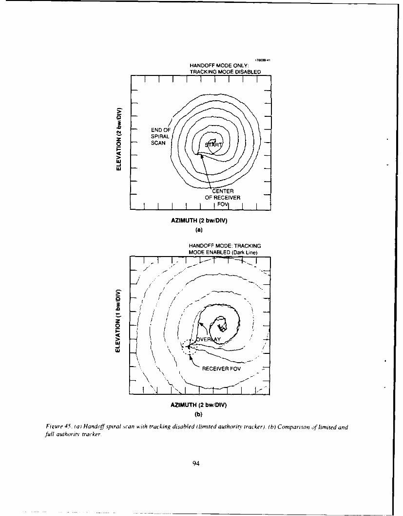
176039-41
HANDOFF MODE ONLY:TRACKING MODE DISABLED
0 SCANR
-I
OF RECEIVER
I I I I FOVI
AZIMUTH (2 bwlDIV)
(a)
HANDOFF MODE: TRACKINGMODE ENABLED (Dark Line)
z--
0
.j
REEVER FOV
AZIMUTH (2 bwlDIV)(b)
Figure 45. ao) Handoff spiral .wan with tracking disabled (limited authority tracker). (b) Comparison of limited andfull authority tracker.
94
176039-42
SCAN RATE: 1 bwlmsLIMIT: ±5 bwPOWER: BUDGET+1O0 dB
ECIV
0 (a)> SCAN RATE:l1bw/ms
LU LIMIT: ±5 bwPOWER: BUDGET
AZIMUTH (2 bw/DIV)(b)
Figure 46. (a) Effects of positive feedback on pull-in transient. (b) Effects of positive feedback on pull- in transient.
95
176093-43
SCAN RATE: 0.5 bw/sLIMIT: ±0.75 bwPOWER: BUDGET +10 dB
zi
oc - _
I I I I I I I I I
(U)Z I I I I I I I I I SCAN RATE: 0.5 bw/s
I- LIMIT: ±0.5 bw
> -POWER: BUDGET +10 dBi.-_J'LI
i- I
I I I I I I I J I
AZIMUTH (2 bw/DIV)
(b)
Figure 47. Improvement of pull-in transient by adjusting tracker authority limit.
96
176039-44S I I I I I I I I
SCAN RATE: 0.5 bw/sLIMIT: ±0.75 bwPOWER: BUDGET
0.4 bw/AXISrms .
JITTER .\
--
v (a)
0i- SCAN RATE: 0.5 bw/s
> LIMIT: ±0.75 bw• "J POWER: BUDGET + 10 dBIul
0.4 bw/AXISrms.-. ..
JITTER
I I I I I I I I
AZIMUTH (2 bw/DIV)
(b)
Figure 48. (a) Pull-in trajectory with 0.4 bw/axis rms noise, budget input signal power. (b) Pull-in trajectory with
0 4 bw/axis rms noise, budget + 10 db signal input power.
97
176039-45
I I I I I I I ISCAN RATE: 0.5 bw/sLIMIT: ±0.75 bwPOWER: BUDGET
2.1 bw/AXISrrns
JITTER
(a)20 _ _ _ _ _ _ _ _ _ _ _ _ _ _ _ _ _ _
PSCAN RATE: 0.5 bw/s
I~l LIMIT: ±0.75 bwPOWER: BUDGET ±10 dB
2.1 bw/AXIS
AZIMUTH (2bw/DIV)(b)
Figure 49. (a) Pull-in trajectory with 2.1 bw/axis rms noise, budget signal power. (b) Pull-in trajectory with 2.1bwiaxis rms noise budget + 10 dB input signal power.
98
12. CONCLUSIONS
A 110 Mb/s, binary FSK laboratory demonstration receiver has been developed and demonstrated,which included spatial acquisition and tracking subsystems, that is suitable for use in a communicationslink such as that proposed for the LITE. A description of the microjitter environment was developed
based upon LITE, and the resultant disturbance spectrum is conservative when compared with on-orbitmeasured data from the Landsat-4 and Olympus satellites. Requirements for the spatial acquisition and
tracking system were presented, based in part on the expected microjitter environment in LITE.
The spatial acquisition system was based upon a commercially available CCD array that was usedto perform d parallel search to initially locate the incoming signal beam during acquisition. The expectedaccuracy, both with and without jitter, and the probability of successful acquisition were derived andcompared with measured data from the laboratory demonstration system. The effects of CCD imperfectionsand variations in signal photon arrival rate and signal angle of arrival were described and documented.A pixel masking routine was developed to reduce the acquisition noise floor that resulted when a fewexcessively noisy pixels dominated acquisition performance at low photon arrival rates. The demonstratedspatial acquisition system met the LITE system requirements with 12.5 dB of margin.
The spatial tracker was based on measurement in the pupil plane of the angle of arrival differencebetween the LO and the signal beam. A commutating, correlation demodulator was developed to providea high precision, bias-free error signal for use in the closed loop spatial tracker. Because of the commu-tation the spatial tracking demodulator was predicted to have an NEA which was a factor of 1.6 greaterthan that of a simple correlation processor (the inherent loss could be reduced from 1.6 to 1.1 throughthe use of a second correlation channel in which the commutation sequence was reversed with respectto the first channel). The discriminant gain in each axis of the spatial tracker was within 8 percent and4 percent of the predicted values, in the elevation and azimuth axes, respectively. The spatial tracker didnot operate at the quantum shot noise limit due to imperfect front end amplifier/detector combinations,but did operate with NEAs in each axis which were within 5 percent of the expected values after excessfront end noise and the effects of demodulator commutation were taken into account. BER curves weremeasured both with the spatial tracker on and off and in the presence of high frequency angular distur-bances similar to those expected on LITE. The BER of the receiver was essentially unaffected by theseangular disturbances, which were far in excess of the level necessary to shut down the link without activespatial tracking.
A robust handoff algorithm was developed, for which no failures were observed in approximately2000 trials, and which reduced the accuracy requirements on the spatial acquisition system to easilyrealizable levels. The handoff algorithm employed a constant tangential velocity, outward spiral searchinitiated at the incoming signal beam location as determined by the spatial acquisition system. The spatialtracker was partially enabled during this search, such that if the signal were swept across the commu-nications receiver FOV then the partially enabled spatial tracker would center the signal within thereceiver FOV. When the signal was approximately centered within the receiver FOV, and if the detectedsignal photon arrival rate exceeded a preset threshold, the spatial tracker was fully enabled and spatial
99
tracking proceeded normally. The handoff algorithm was found to be sensitive to sign reversals in thespatial tracker discriminant off boresight at high signal photon arrival rates. The algorithm could be maderobust when facing these reversals by limiting the range of the partially enabled spatial tracker to lessthan ±0.75 bw. Data from the demonstration system confirmed that successful handoffs were possiblegiven any combination of signal photon arrival rate and angular disturbance level that would subsequentlyallow the spatial tracker to meet system requirements.
In summary, a laboratory breadboard of a spatial acquisition and tracking system suitable forintersatellite optical communications links has been described, analyzed, and demonstrated. Robust per-formance has been demonstrated that is well-predicted by theoretical models of the system.
100
APPENDIX ATORQUE MOTOR BEAM STEERER CONTROL
This appendix details the design of the control circuitry for the torque motor beam steerers (TMBS)used as fast steering mirrors in the demonstration system. The position sensor that is part of each TMBSis first discussed, and then the current source, which is used as a driver for each TMBS, is presented.
A.1 TMBS SHAFT POSITION SENSOR
TMBSs from General Scanning, Model Z2046 were used; they have a capacitive shaft positionsensof built into each unit. The basic sensor is shown in Figure A-1. The capacitors Cl and C2 varydifferentially as the shaft is turned. At the null position the capacitors are each approximately 11 pF.
In order to use the sensor to detect shaft position the diode bridge is driven with a capacitively-coupled common mode signal. During the positive half of the common mode drive signal a positivecharge, Cl Av and C2 Av, is transferred onto CI and C2, respectively, through diodes DI and D4. Theaverage current I1+ (averaged over one cycle of the drive voltage) is CI Av/AT, while 12+ is similarlyC2 Av/AT. During the negative half cycle of the drive voltage CI discharges through D2, and C1discharges through D3, which yields average currents I1- = -C2 Av/AT and 12- = -CI Av/AT. The averagedc current I1 may then be obtained by adding I1+ + I1- = (CI - C2) Av/AT. 12 is obtained similarly as(C2 - C I) Av/AT. The resultant dc currents I1 and 12 are then detected with current to voltage converters.It is important that the current to voltage converters have low input impedance at frequencies below afew kilohertz (so as to accurately detect the expected shaft motion), and also have a high input impedanceat the drive frequency (2 MHz), in order to block out the drive signal.
A commercially available oscillator board is used, Model OD-401, supplied by General Scanning.The board includes a blocking oscillator designed to supply approximately 200 V p-p at 2 MHz to theTMBS sensor, a half-wave rectified output that is used to sense the amplitude of the drive voltage, anamplitude control input, and the coupled inductor shown in Figure A-i that is used as a common modehigh frequency filter at the inputs to the current to voltage converters.
The circuit shown in Figure A-2 included the additional circuitry necessary to implement an AGCloop for the oscillator and to provide the current to voltage conversion. The offset adjust resistor R 1I wasselected to match the offset voltage of the particular TMBS with which the demodulator circuit was used.
Results from a prototype demodulator circuit are shown in Figure A-3. The only difference betweenthe prototype and the demodulators used in the demonstration system is that the prototype had a factorof 8.4 more gain in the output stage U4. The measured rms deviations from linearity are less than 2 percentand are within the resolution within which the shaft angle for this test could be determined.
101
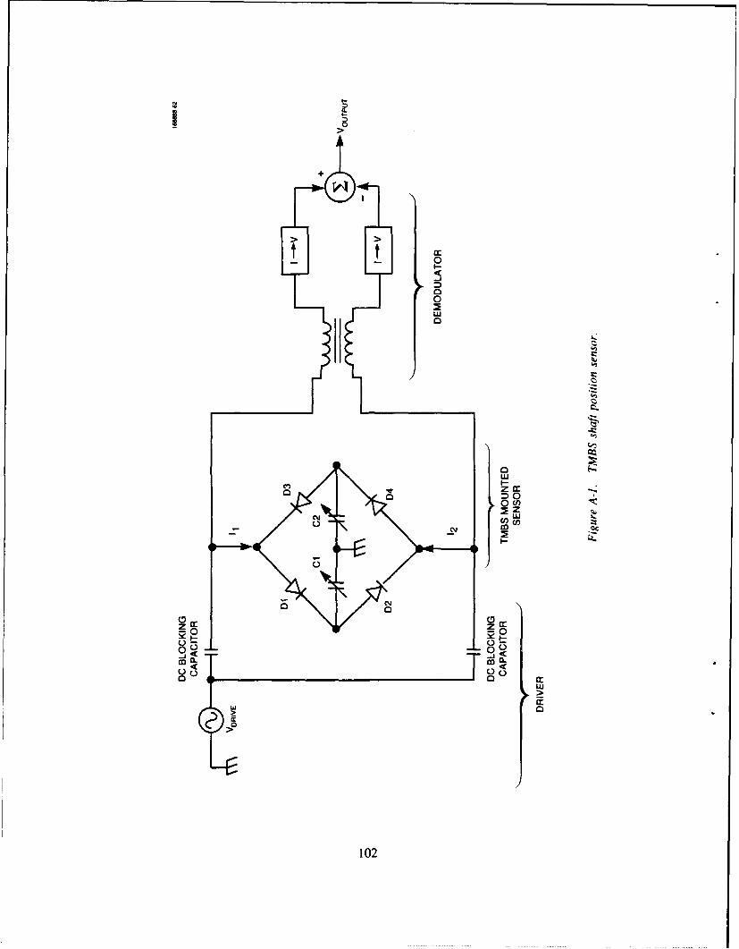
I-
0
00
00
LLI-
-
u,
0o cow
wV 0
10
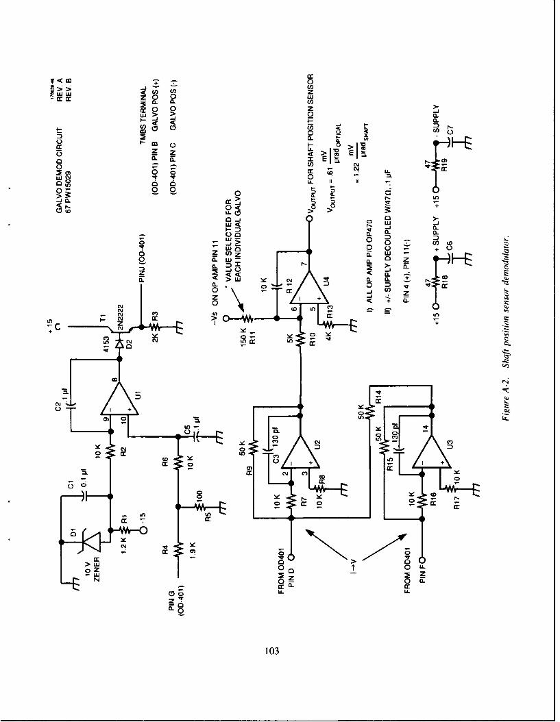
a:- 0
cc c zO0 0 wt .CL W
cc 0 0 z -wLJ> > 0 CL
< CL .01 L9 Cl)
oc a: LiD0 Q
L 0.
0 CY0 cy -L Cc
00 0.W 0
-,-
.L8 L
oi o+ U)~ +
z CL)
0 cc
0 0 +
cliIL (D Ln)l0YMU - := -
U +012-
oGo:L
0 +
a ? aN- a:
0x
103-
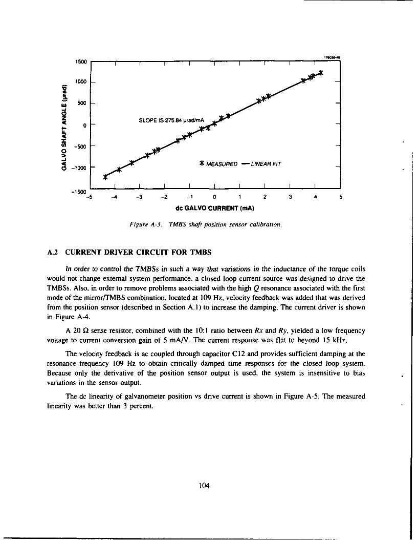
1500 I I I I I I
1000
W 500o--
-500
-5 -4 -3 -2 -1 0 1 2 3 4 5
dc GALVO CURRENT (mA)
Figure A-3. TMBS shaft position sensor calibration.
A.2 CURRENT DRIVER CIRCUIT FOR TMBS
In order to control the TMBSs in such a way that variations in the inductance of the torque coilswould not change external system performance, a closed loop current source was designed to drive theTMBSs. Also, in order to remove problems associated with the high Q resonance associated with the firstmode of the mirror/TMBS combination, located at 109 Hz, velocity feedback was added that was derivedfrom the position sensor (described in Section A. 1) to increase the damping. The current driver is shownin Figure A-4.
A 20 Q sense resistor, combined with the 10: 1 ratio between Rx and Ry, yielded a low frequencyvoltage to current conversion gain of 5 mA/V. The current response was Mlt to beyond 15 kHz.
The velocity feedback is ac coupled through capacitor C12 and provides sufficient damping at theresonance frequency 109 Hz to obtain critically damped time responses for the closed loop system.Because only the derivative of the position sensor output is used, the system is insensitive to biasvariations in the sensor output.
The dc linearity of galvanometer position vs drive current is shown in Figure A-5. Tie measuredlinearity was better than 3 percent.
104
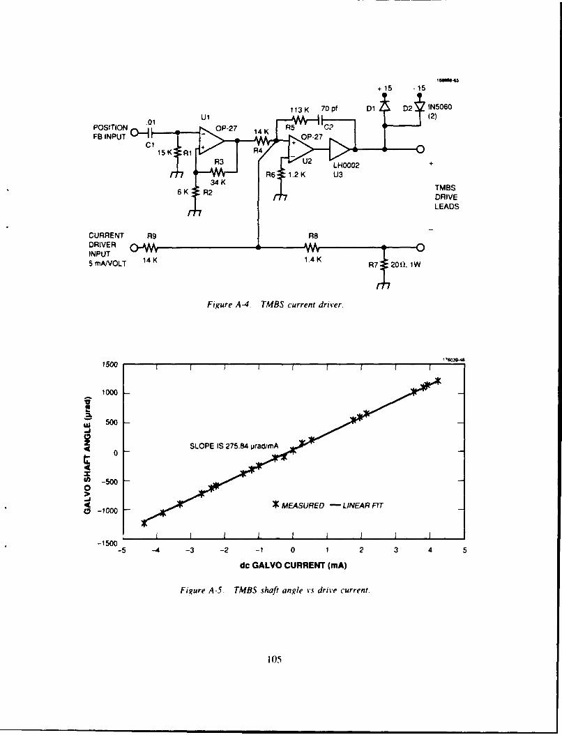
113 K 70 pt DI D2 IN5060
POSITION .1U P2 5 C 2
FB INPUT (0-I- _4K P2C1 jR + RP2 4K 5 C
34 K TMBS6 R2 DRIVE
LEADS
CURRENT R9 R8
5INUT 14 K 1.4 K R7,j20n,. 1W
Figure A-4. TMBS current driver.
1500 1634
1000
LU 500
z SLOPE IS 275.84 prad/mA
0
(7-1000
-1500-5 -4 -3 -2 -1 0 1 2 3 4 5
dc GALVO CURRENT (mA)
Figure A-S. TMBS shaft angle vs drive current.
105
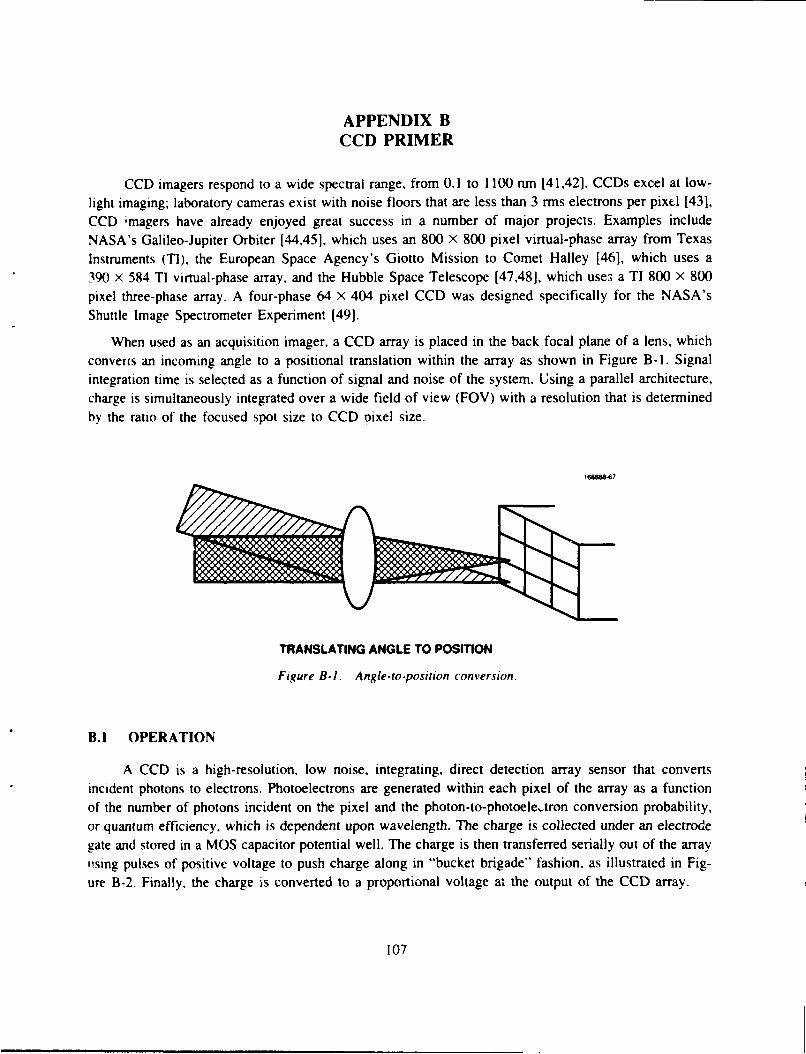
APPENDIX BCCD PRIMER
CCD imagers respond to a wide spectral range, from 0.1 to 1100 nm [41,42]. CCDs excel at low-light imaging, laboratory cameras exist with noise floors that are less than 3 rms electrons per pixel [43],CCD ;magers have already enjoyed great success in a number of major projects. Examples includeNASA's Galileo-Jupiter Orbiter [44,45], which uses an 800 x 800 pixel virtual-phase array from TexasInstruments (TI), the European Space Agency's Giotto Mission to Comet Halley [46], which uses a390 x 584 TI virtual-phase array, and the Hubble Space Telescope [47,48], which uses a TI 800 X 800pixel three-phase array. A four-phase 64 X 404 pixel CCD was designed specifically for the NASA'sShuttle Image Spectrometer Experiment [491.
When used as an acquisition imager, a CCD array is placed in the back focal plane of a lens, whichconverts an incoming angle to a positional translation within the array as shown in Figure B-1. Signalintegration time is selected as a function of signal and noise of the system. Using a parallel architecture,charge is simultaneously integrated over a wide field of view (FOV) with a resolution that is determinedby the ratio of the focused spot size to CCD oixel size.
16888-67
TRANSLATING ANGLE TO POSITION
Figure B-i. Angle-to-position conversion.
B.1 OPERATION
A CCD is a high-resolution. low noise, integrating, direct detection array sensor that converts
incident photons to electrons. Photoelectrons are generated within each pixel of the array as a function
of the number of photons incident on the pixel and the photon-to-photoele,tron conversion probability,or quantum efficiency. which is dependent upon wavelength. The charge is collected under an electrodegate and stored in a MOS capacitor potential well. The charge is then transferred serially out of the array11sing pulses of positive voltage to push charge along in "bucket brigade" fashion, as illustrated in Fig-ure B-2. Finally, the charge is converted to a proportional voltage at the output of the CCD array.
107
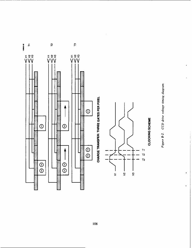
NC.() - CJc C )
LL.
-I
Luj
Ix C
zU.0U)0z -
- - - -T2
0 T30 0
108
B.2 ARCHITECTURES
Three types of CCD array architectures are commonly used for electronic imaging: interline trans-fer, frame transfer, and full frame imaging (see Figure B-3). Each array collects photons on the imagingarea during the integration time. The charge collected in the pixels of the imaging area may first betransferred to a storage area or may be directly shifted to a parallel-to-serial readout register.
B.2.1 Interline Transfer CCD Array
An interline transfer CCD has a storage array intermeshed with the imaging array. The chargecollected on each line of imaging area during integration time is transferred under the adjacent interlinemask. Each mask is then read out serially through a parallel-to-serial shift register. Since transfer fromthe imaging zone to the mask is so quick, the integration duty cycle is essentially 100 percent. Becausethe interline mask blocks incoming photons, during readout there is no need for a shutter and there is noimage smearing. However, each strip covered by the interline mask is a dead zone not sensitive toincoming photons.
B.2.2 Frame Transfer CCD Array
A frame transfer array provides the high frame rate needed for conventional television broadcast.It is composed of two arrays in tandem: one performs the imaging operation and the other, covered byan opaque mask, serves as temporary storage area for image data. Charge is quickly shifted line-by-linefrom the imaging section to the storage section, typically in about 1 ms. In most applications this is fastenough to keep image blur to an acceptable level without using a shutter. Following transfer, the imagingsection can integrate another image while the stored data are read out through a parallel-to-serial register.This architecture is commonly operated continuously at television frame rates. Without the opaque maskthe array can operate as a full frame imager.
B.2.3 Full Frame CCD Array
A full frame array collects photons on the imaging area during the integration time, then transfersthe charge collected in every pixel, row by row, directly to a parallel-to-serial shift register for serialreadout. During data transfer a shutter typically blocks the imaging area so that the image is unalteredby photons arriving during the readout process.
A full frame CCD array was chosen for our receiver acquisition system in order to eliminate deadzones within the active area of the sensor and because high frame rates were not necessary. The TektronixTK512M, a full frame array of 512 X 512 pixels, was selected because it had specifications that metsystem noise and sensitivity requirements and was commercially available from an American manufacturer.
Other manufacturers of commercially available CCDs include Texas Instruments, Kodak, Thomp-son-CSF, and Photometrics.
109
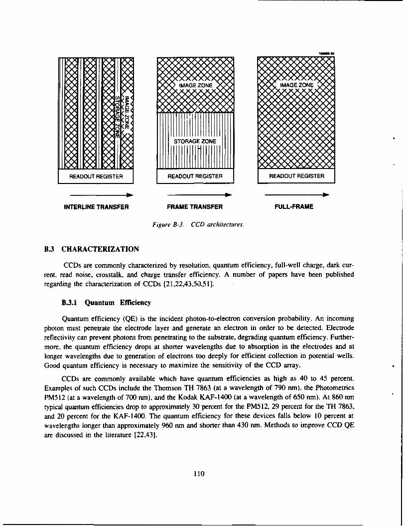
VA CHARACT ZIMAGEZONE
CCDs are commonly characterized by resolution, quantum efficiency, full-well charge, dark cur-rent, read noise, crosstalk, and charge transfer efficiency. A number of papers have been publishedregarding the characterization of CCDs [21,22,43,50,51].
B.3.1 Quantum Efficiency
Quantum efficiency (QE) is the incident photon-to-electron conversion probability. An incomingphoton must penetrate the electrode layer and generate an electron in order to be detected. Electrodereflectivity can prevent photons from penetrating to the substrate, degrading quantum efficiency. Further-more, the quantum efficiency drops at shorter wavelengths due to absorption in the electrodes and atlonger wavelengths due to generation of electrons too deeply for efficient collection in potential wells.Good quantum efficiency is necessary to maximize the sensitivity of the CCD array.
CCDs are commonly available which have quantum efficiencies as high as 40 to 45 percent.Examples of such CCDs include the Thomson TH 7863 (at a wavelength of 790 nm), the PhotometricsPM5 12 (at a wavelength of 700 nmi), and the Kodak KAF-1400 (at a wavelength of 650 ni). At 860 rntypical quantum efficiencies drop to approximately 30 percent for the PM5S12, 29 percent for the Th 7863,and 20 percent for the KAF-1400. The quantum efficiency for these devices falls below 10 percent atwavelengths longer than approximately 960 nm and shorter than 430 nm. Methods to improve CCD QE
are discussed in the literature [22,431.
110
B.3.2 Full-Well Capacity
Full-well capacity defines the saturation limit, in electrons, for each pixel. Typically this numberis above I05 electrons. The difference between the full-well capacity and the minimum noise per pixelin rms electrons, divided by the quantum efficiency of the device, determines the dynamic range of thesensor.
B.3.3 Dark Current
Dark current is the rate of thermally-generated charge accumulation within the CCD imagingregion. Dark current, as the name implies, is independent of photon arrival rate but doubles for every 7'Ctemperature increase near room temperature. An average dark current is commonly measured for theentire CCD array. By thermoelectric cooling to -100'C, dark current has been reduced to less thanI e-/s/pixel [431. For extremely long exposures the CCD can be cooled to -120'C with liquid nitrogen.CCDs are not commonly operated at temperatures below -120'C because the charge transfer efficiencydegrades significantly.
B.3.4 Read Noise
Read noise is generated by sources intrinsic to the CCD during the transfer of charge from the CCDto the outside circuitry. Examples include reset noise and amplifier noise [43]. Generally read noise isa function of readout rate and device temperature.
Reset noise results from variations in the reset voltage of the output node prior to a charge dumpof a pixel during readout. This noise may be expressed [43], in rms electrons, as: Nr(e-)= (kTC) /2/qwhere k = Boltzmann's constant, T = temperature in Kelvin, C = output capacitance, q = the electroniccharge.
Correlated double sampling is often used to greatly reduce reset noise. Correlated double samplingrefers to the practice of sampling the CCD output immediately after the reset pulse and then again afterthe charge dump. The difference between the two samples represents the signal charge, free from anyadded charge associated with the reset procedure. Without correlated double sampling the read noise flooris typically above 200 e-/pixel.rms (see Section 7.3.4).
The on-chip amplifier is the main source of read noise. Voltages driving this amplifier, the resettransistor drain voltage, reset transistor gate clock, and source-follower drain voltage, most criticallyaffect performance [51 ]. The reset drain, for example, provides the critical reference level following thereset pulse prior to the charge dump during readout.
B.3.5 Charge Transfer Efficiency
Charge transfer efficiency (CTE) measures the percentage of collected charge that is transferredfrom one gate to the next. CTE decreases with increased clock frequency or gate length and will dimin-ish at low temperatures. CTEs of 0.999995 can be obtained with today's fabrication technology. A
111
CTE > 0.99995 is routine today; scientific grade is 0.99997. The TK512M is specified to have a CTEof 0.99999. This parameter is critical: for the 200 X 200 three-phase subarray selected, the 0.00004difference between specification (0.99999) and a CTE of 0.99995 results in retaining 99 percent ratherthan 93 percent of the original signal in the last pixel, following transfer to the output. With a larger array,say a 2048 X 2048 pixel array, the last value will represent only 54 percent of the original signal at aCTE of 0.99995, but 88.4 percent at 0.99999. Work done by Janesick et al. indicates that at low signallevels, below 1000 detected electrons, CTE is often worse than specification [43].
112
APPENDIX CDERIVATION OF NEA FOR COMMUTATING, CORRELATION TRACKER
In this appendix the noise equivalent angle (NEA) for a commutating, correlation tracker is derivedin more detail. The analysis will be based upon the processing illustrated in Figure 17. The analysis isperformed for the azimuth track channel only; the elevation channel is exactly analogous. For conve-nience the appropriate equations from Section 10 are repeated;
vc. 2ni() sin ot+nc(t) I channel (C-i)
21mr(O)Vc,Q(t)= 2 cos ot+nc(t) Q channel (C-2)
Vleft (t) =L'[m(O)I cos (t + ) + nL (t)] Az, left (C -3)
v rght (t)=R'[m(O)l cos(cot - )+nR (t)] Az, right (C-4)
R'= + os(kwst) right track commutation (C - 5)k=1
L'= Bk Cos kw t) left track commutation (C-6)
2 k=1sin -
2k k2 (C-7)
2
elo C-8)
where o is the heterodyne IF frequency, between 0.1 and 1 GHz in our system, o KoO for small e, and
0 is the angular misalignment between the signal and LO beams in units of angular beamwidths corre-sponding to the full width, half maximum of the far field intensity profile of the signal beam. The commutatedtrack signal is obtained by substituting Equations (C-5) to (C-7) into Equations (C-3) and (C-4) and then takingthe sum of vleft(t) and vnght(t). Following correlation with the I channel communications signal, bandpassfiltering, and synchronous detection, the baseband output may be written in the following form
V, (t) = V' s(t)+ nsxn (t)+ nn(t) (C-9)
Each of the three terms will be discussed separately.
113
C.1 SIGNAL x SIGNALThe signal portion of the vwck(t) = Vief(t) + Vnght(t) is given by
V M (O) {cos(ox + ;)+ cos (Wt-)} +V2
m(O)I {cos (ot- )-cos(o+ )} Bkco Iktk=l
=m(O)l cos (ot + 2m(O)l sin ; sin ot Bk cos kosamplet (C - 10)
k=l
where it is helpful to recall the definition in Equation (46) that cos;= m(O)/m(O) and sin;= q(O)/m(O).
Keeping only the terms at the sample frequency wsample, the post-correlation signal may be written as
Vtrack (t) = 412 m(O)m(O)sin cos wsamplet post - correlation. (C - 11)
Following the bandpass filter centered at tosample' and subsequent multiplication by 2 cos rsamplet forsynchronous demodulation, the in-phase baseband output is
V1 4 12 m(O)VI s Mt = 4 _ i2 m(sin (I channel, after synch demod). (C - 12)
The quadrature correlation output is used for normalization. The quadrature communications chan-
nel is biphase modulated at the chopping frequency osample' because otherwise the product of the Q channeland the commutated track channel has negligibly small components at osample for small e. The biphasemodulated Q channel communications signal (keeping only the term at (Osample) Is
Vc Q (t) = 8 c m(O) Cos tO cos t)samplet (C - 13)
Correlation of the chopped Q channel communications signal with the commutated track signalVtrack(t), and again keeping only the terms at the sample frequency oosample, yields
vQ 412 m2 ( 0)sxs~t = 7f ososamplet(-14
Bandpass filtering to isolate the (osample term and subsequent synchronous demodulation (multipli-
cation by 2 coswaplet ) yields the following baseband term
114
VQs(t) = 412 m2(e) (C -15)
The normalization is performed by taking the square root of the sum of the squares of the I and Q channeloutputs. If the small angle approximation KoO = sin(KDO) is not made in the expression for the basebandI channel output, then the normalization voltage may be written as
Vormalization () = (VQ ()) + (Vlx () )2 =
412 m(O)m(O) m() 2 16)
Recall from Equation 46 that m(6)/m(O) = cos4, which makes it apparent that the square root term on theright side of Equation (C- 16) is unity. Thus
Vno~~Ion M 4J 2 m(O)m(6) (C-17)normalization()= lf C-17
and Equation (56) is obtained
V (0)= Ko0+- {sx(t+ n (t)} (C -18)0 D 4 m2 (0) 12 x nn
where the approximations m(0) = m(O) and sin =KDO have been made for small .
C.2 SIGNAL X NOISE
The dominant signal x noise term, nsx(t), is formed by the product of the communication signal.V,,(t), and the commutated track noise, and may be written as
2 1 i(O) +
nsxn (')= sin am [(n left (t) + n right (,))- 2
( t(t)-n l (0): Bk Coskwsaplej (C-19)
It will be convenient to derive the power spectral density, N,,n(), of nsxn(t) and then find the varianceby integrating Nsxn(t). First it will be necessary to model the effects of the commutation on the tracknoise.
115
The noise in each track channel is white with power spectral density N.14. Recall that the com-munications channel noise nc(t) or fi(t) is also white, with spectral density N(J2. The commutationprocess alternately connects first one track channel noise, and then the other, to the output of the com-mutation switch. If the two track channel noises are uncorrelated and white, alternating between themshould yield the same spectral density, and hence the same variance as either channel alone. This isderived more rigorously as follows.
Note that multiplying wideband white noise (spectral density N., bandwidth W) by a sinusoid A sinoa,where o < W, produces noise with a low frequency spectral distribution that is still white, and a spectraldensity that is NoA2/2. Next, note that the spectral density of either the sum or difference of nleft(t) andnright(t) is N.12. Recognizing that
B2= 2 forkodd (C-20)
and
- =- for k odd (C -21)
the spectral density of nsxn(t) may be written as
N (f) =Im+-(IB)sxn y 2 + 2 4 2 2= k
412m2 (e) I_[1 , (C 22)y, 2 4(
which is the same as multiplying Vc(t) by the noise in either track channel alone, as expected. Note thatthis approximation for Nsxn) is only valid for f, Osample<W.
Subsequent narrowband bandpass filtering at )sample with single sided bandwidth F producesnarrowband white noise, which may be approximated as n(t) = n,(t) cos 0sampl et + nQ(t) sin O)samplet, wheren,(t) and nQ(t) each have spectral density equal to twice that of the unfiltered noise. Synchronous de-modulation and lowpass filtering (bandwidth F) yields a baseband distribution that is white, bandlimitedto bandwidth F, and has spectral density of
N12M2(0) N (C- 23)sxf 0,
The variance of nsxn(t) within a single-sided bandwidth of F is then
var [n (t)]-j 2 =O N 0 (C -24)7 0
116
C.3 NOISE X NOISE TERM
The variance of the noise X noise term may be derived by first finding the spectral density of thecommutated track noise term, convolving this with the spectral density of the noise in the communica-tions channel, and then evaluating the integral of the post-bandpass noise to obtain the variance.
Recalling that the commutated track noise density is white with spectral density N.14, and bandlimitedwith bandwidth W, the convolution of the communication and commutated track noises yields a triangulardistribution with spectral density at dc of N2W/4. For frequencies much less than W, this distribution isapproximated as rectangular with spectral density N2W/4.
As before, the bandpass filtered noise is written as narrowband white bandpass noise n(t) = nl(t)Cos 0)samplet + nQ(t) sin o)saplet. The spectral density of both nl(t) and nQ(t) is 2N2W/4. Synchronousdemodulation corresponds to multiplication by 2 cos O0sample t , and the spectral distribution of the post-demodulation noise X noise term is rectangular with spectral density N2W/2 for frequencies much lessthan W, which allows us to write the low frequency spectral density Nnxn(O)
N2WN (f)= o . f <<W (C - 25)2
The variance of nnxn(t) within the single-sided bandwidth F may now be expressed as
var [n ()] = FN2W (C-26)
C.4 NEA FOR COMMUTATED CORRELATION PROCESSING
The NEA of the commutated correlation processor may be written as
{var rn(0)]+ var[n@)(11- (C-27)
(QI
where Q 412KDm 2 (0) /7j. Substituting Equations (C-24) and (C-26) into (C-27) yields
-r~ FN 2 FNol2m2 20NEA - FN2W O (C - 28)
117
For a quantum-shot-noise-limited system in which the LO optical power is much larger than the signal
optical power, No = 2eidc = 2e2"rlPLoJhv. Substituting into Equation (C-28) for I [Equation (C-8)] and No
obtains
( F 1/ 1 1/26NEA = 2 __m c _m2p (C -29)
NA 2KD hv hvc
from which Equation (56) may be written.
118
APPENDIX DLIST OF ACRONYMS AND SYMBOLS
a radius for a truncated plane wave
Aj(xy) normalized E field distribution for LO (j = LO) or signal beam (j = s)
acq acquisition
ACTS Advanced Communications Technology Satellite
ADC analog-to-digital converter
AGC automatic gain control
Bk kth Fourier coefficient for Fourier expansion of commutation signal
BER bit error rate
bw angular beamwidth, usually full width half maximum of the far field intensity profile
CCD charge-coupled device
CDS correlated double sampling
CNDR carrier-to-noise density ratio
CNR carrier-to-noise ratio
comm communication
CMOS complementary metal-oxide semiconductor
CPM course pointing mirror
CTE charge transfer efficiency
DAC digital-to-analog converter
DPSK differential phase shift keying
DN digital number
DRAM dynamic random access memory
e electronic charge
e- electron
E,(x.v) electric field distribution for LO (j = LO) or signal beam (j = s)
ESA European Space Agency
F single-sided noise bandwidth of heterodyne spatial tracker
FET field effect transistor
FFT fast Fourier transform
119
FOV field of view
FSK frequency shift keying
FSM fast steering mirror
FWHM full-width half-maximum
Gb/s gigabit per second
GEO geostationary earth orbit
GHz gigahertz
Y ratio of Az or El track signal power to communication signal power
Fd dark current (e-/s/pixel)
F, detected signal in photoelectrons/s
T1 detector quantum efficiency
h Planck's constant
IF intermediate frequency
in Bessel function of order n
L' commutation signal, left channel
LEO low earth orbit
LITE Laser Intersatellite Transmission Experiment
LO local oscillator
LOS line of sight
LSB least significant bit
m2(6) heterodyne mode matching efficiency
MAXBLOCK location of 2 X 2 pixel group within CCD with largest detected signal
Mb/s megabits per second
ms millisecond
Nf read noise (e-/pixel rms)
N, ADC quantization noise (e-/pixel rms)
nnxn(t) noise term due to comm noise times track noise
nllxn(t) noise term due to comm IF signal times track noise
Nnxn(f spectral density of nnxn(t)
Nsxn(f) spectral density of nsxn(t)
120
v optical frequency
NEA noise equivalent angle
NEV noise equivalent voltage or rms voltage
ns nanosecond
OMS opto-mechanical subsystem
OPD optical path difference
PX optical power in channe! j for j = comm, track; optical power in LO or signal beamfor j = LO,s
PMPCG programmable multiphase clock generator
PPM parts per million
PSD power spectral density
PSK phase shift keyed
q(O) heterodyne discriminant function
0 angular misalignment between LO and signal beam
ONEA noise equivalent angle
R' commutation signal, right channel
rad radian
recvr receiver
rms root-mean-square
rss root-sum-squa -
s second
SNR signal-to-noise ratio
SSB single side band
T CCD integration time
TMBS torque motor beam steerer, also called a galvonometer
"T'L Transistor-Transistor Logic
VO 6) normalized output of commutated, correlation processor
W single-sided noise bandwidth of front end amplifiers in the heterodyne spatial tracker
w radius for a Gaussian distribution
0) heterodyne IF frequency
toample commutation or sampling frequency
121
LIST OF REFERENCES
1. J.D. Barry, and G.S. Mecherle, "Communication channel burst errors induced by Gaussian distrib-uted mispointing," SPIE Proceedings, Vol. 616, (1986), pp. 137-140.
2. G.A. Koepf et al., "Analysis of burst error occurrence on optical intersatellite link (ISL) design,"SPIE Proceedings, Vol. 616, (1986), pp. 129-136.
3. A.F. Popescu et al., "Experimental investigation of the influence of tracking errors on the perfor-mance of free-space laser links," SPIE Proceedings, Vol. 885, (1988), pp. 93-99.
4. V.W.S. Chan, private communication.
5. R.S. Bondurant et al., "An Opto-Mechanical Subsystem for Space-based Coherent Optical Commu-nications," SPIE Proceedings, Vol. 995, (1989), pp. 92-100.
6. J.E. Kaufmann and E.A. Swanson, private communication.
7. J.E. Kaufmann (memo, 1989).
8. E.A. Bucher (memo, 1987).
9. L. Jeromin (memo, 1987).
10. J. Sudey and J.R. Sculman, "In orbit measurements of Landsat-4," 35th Congress of InternationalAstronomical Federation, Lausanne, Switzerland, (1984).
It. M. Wittig et al., "in orbit measurements of microaccelerations of ESA's communications satelliteOLYMPUS," SPIE Proceedings, Vol. 1218, (1990), pp. 205-214.
12. S. B. Alexander, "Design of wide-band optical heterodyne balanced mixer receivers," J. LightwaveTech., Vol. LT-5, No. 4, 523-537 (1987).
13. G.L. Abbas et al., "A dual-detector optical heterodyne receiver for local oscillator noise suppres-sion," J. Lightwave Tech., Vol. LT-3, No. 5, 1110-1122 (1985).
14. E.A. Swanson et al., "Optical spatial tracking using coherent detection in the pupil plane," AppliedOptics, Vol. 28, No. 18, 3918-3928, (1989).
15. D.J. Bemays et al., "Wideband heterodyne spatial tracking for optical space communications," MITLincoln Laboratory, Lexington, Mass. Technical Report TR-910, (8 February 1991).
16. K.A. Winick, "Cramer-Rao lower bounds on the performance of CCD optical position estimators,"Optical Society of America A3, 1809-1815, (1986).
17. D.F. McDonough (memo 1986).
18. D.F. McDonough (memo, 1988).
19. K.A. Winick (memo, 1986).
123
20. E.P. Colagiuri (memo, 1987).
21. M.M. Blouke et al., "Large format, high resolution image sensors," Opt. Eng. 26(9), 837-843 (1987).
22. R.W. Leach, "Optimizing charge-coupled-device detector operation for optical astronomy," Opt. Eng.
26(10), 1061-1066 (1987).
23. W.H. McGonagle, private conversation.
24. E.P. Colagiuri (memo, 1986).
25. E.P. Colagiuri (memo, 1986).
26. K.A. Winick (memo, 1985).
27. J.M. Wozencraft and I.M. Jacobs, Principles of Engineering, New York: Wiley (1965) p. 83.
28. J.E. Kaufmann, private communication.
29. P.M. Epperson et al., "Electro-optical characterization of the Tektronix TK512M-01 1 charge-coupled
device," Opt. Eng. 26(8), 715-723 (1987).
30. J.L. Massey, "The statistical significance of error probability as determined from decoding simu-lations for long codes," in Proc. Modelling and Simulation, Vol. 7, eds. W.G. Vogt, and M.H.Mickle, University of Pittsburgh, ISA (1976).
31. R.J. Parr (memo, 1989).
32. D.M. Hodson (memo, 1988).
33. J.E. Kaufmann (memo, 1989).
34. J.E. Kaufmann (memo, 1989).
35 S.B. Alexander and D. Welford, "Equalization of semiconductor diode laser frequency modulationwith a passive network," Elect. Lett., Vol. 21, No. 9, 361-362 (1985).
36. K.A. Winick and P. Kumar, "Spatial mode matching efficiencies for heterodyned GaAlAs semicon-ductor lasers," Lightwave Tech., Vol. 6, No. 4, 513-520 (1988).
37. D.M. Hodsdon (memo, 1988).
38. J.E. Kaufmann (memo, 1989).
39. G.M. Carter (memo, 1980).
40. D.J. Bemays and G.M. Carter (memo, 1988).
41. J.R. Janesick et al., "Potential of CCDs for UV and x-ray plasma diagnostics," Rev. Sci. Instrum.56, 796 (1985).
42. M.C. Peckerar, D.H. McCann, and L. Yu, "X-ray imaging with a charge-coupled device fabricatedon a high resistivity silicon substrate," Appl. Phys. Lett. 39, 1 (1981).
124
43. J.R. Janesick et al., "Scientific charge-coupled devices," Opt. Eng. 26(8), 692-714 (1987).
44. K.P. Klaasen, M.C. Clary, and J. R. Janesick,"Charge-c'.-upled device television camera for NASA'sGalileo mission to Jupiter," Opt. Eng. 23(3), 334-342 (1984).
45. J.R. Janesick, J. Hynecek, and M.M. Blouke, "Virtual phase imager for Galileo," in Solid StateImagers for Astronomy, J.C. Geary and D.W. Latham, eds., Proc. SPIE 290, pp. 165-173 (1981).
46. H.U. Keller et al.,"Giotto multicolour camera," European Space Agency SP-1077, 149 (1986).
47. M.M. Blouke, J.R. Janesick, J.E. Hall, J.W. Cowens, and P.J. May, "800 X 800 charge-coupled deviceimager sensor," Opt. Eng. 22(5), 607-614 (1983).
48. J. Kristian and M. Blouke, "Microelectronics in astronomy," SciAm. 247(4), 48 (1982).
49. W.L. Wang, L.R. Hudson, and H.F. Tseng, "High performance visible and near-infrared charge-coupled-device array for spectroscopy applications," Opt. Eng. 26(9), 884-851 (1987).
50. P.M. Epperson et al., "Electro-optical characterization of the Tektronix TK512M-01 1 charge-coupleddevice," Opt. Eng. 26(8), 715-723 (1987).
51. J.R. Janesick, K.P. Klaasen, and T. Elliott, "Charge-coupled-device charge-collection efficiencyand the photon-transfer technique," Opt. Eng. 26(10), 972-980 (1987).
125

Form AA~~odREPORT DOCUMENTATION PAGE I O No. 00ov1
PuWk @MOn bumfm t , d Wften is mtKto @wrap I hoaw pw r es om, VxWv ft Wm for rwAw waftcW4.e Nowtd" em dt cm. 90wd ig &W ffvW1wV to dam nmeW.sWd - p I - h AQ~cd No tf t veftu. BM g -mwew Oft h I wn m or " ow OMMd of MW lso of L "W. - - - ajpet fo to Wago
B SOM OMM MA W te t"a O:Psama O WN a 1215 ,UW~' 0.~ 1 $ . &A.m 1204. Mkql.n. VA UMA. .d 1. 1. OM 0 M.. d & .=10."-o ). WO 0. OC 20W3.
1. AGENCY USE ONLY (Leave blank) 2. REPORT DATE 3. REPORT TYPE AND DATES COVERED3 December 1991 Technical Repor
4. TITLE AND SUBTITLE 5. FUNDING NUMBERS
An Experimental Spatial Acquiition and Tracking
System for Optical Intersatellite CrosslinksC - F19628-90-C-0002
6. AUTHOR(S) PE - 63789F,33110F
PR - 270
D.J. Bernays and E.P. Colagiuri-Cafarelli
7. PERFORMING ORGANIZATION NAME(S) AND ADDRESS(ES) 8. PERFORMING ORGANIZATIONREPORT NUMBER
Lincoln Laboratory, MITP.O. Box 73 TR-923Lexington, MA 02173-9108
9. SPONSORING/MONITORING AGENCY NAME(S) AND ADDRESS(ES) 10. SPONSORING/MONITORINGAGENCY REPORT NUMBER
PLISWCKirtland AFB, New Mexico ESD-TR-91-090
11. SUPPLEMENTARY NOTES
None
12a. DISTRIBUTION/AVAILABILITY STATEMENT 12b. DISTRIBUTION CODE
Approved for public release; distribution is unlimited
13. ABSTRACT (Maximum 200 words)
Optical intersatellite communications crosslinks will operate with much higher antenna gains and hence morestringent pointing and tracking requirements than do present RF and microwave-based systems. The design andexperimental demonstration of an optical heterodyne communications receiver that includes an integrated 2-axisspatial acquisition subsystem and heterodyne tracker are presented. Requirements for the acquisition and trackingsystem are derived from the Laser Intersatellite Transmission Experiment (LITE). The acquisition subsystememploys a parallel search algorithm using a direct detection, charge-coupled device (CCD) array. The heterodyne
spatial tracker is based upon angle detection in the pupil plane. It uses a commutating, correlation demodulationscheme to reduce front-end-noise-induced biases relative to those from square law detection in the track channelalone. A robust handoff algorithm is presented for the transition between CCD-based acquisition and heterodynespatial tracking. Results from a laboratory demonstration system are presented.
14. SUBJECT TERMS 15. NUMBER OF PAGESheterodyne tracker optical communications 140acquisition and tracking spatial acquisitionpupil plane satellite communications 16. PRICE CODECCD
17. SECURITY CLASSIFICATION 18. SECURITY CLASSIFICATION 19. SECURITY CLASSIFICATION 20. LIMITATION OFOF REPORT OF THIS PAGE OF ABSTRACT ABSTRACT
Unclassified Unclassified Unclassified SAR
NSN 7540-01-280-5500 Standard Fom 296 (Rev. 2-9)Prescrbed by AMSI Std. 239-18298-102