Embed Size (px)
Citation preview
Input Frequency (GHz)
Nor
mal
ized
Gai
n R
espo
nse
(dB
)
0 2 4 6 8 10 12-15
-12
-9
-6
-3
0
3
D_BW
Single Channel ModeDual Channel Mode
Product
Folder
Order
Now
Technical
Documents
Tools &
Software
Support &Community
An IMPORTANT NOTICE at the end of this data sheet addresses availability, warranty, changes, use in safety-critical applications,intellectual property matters and other important disclaimers. PRODUCTION DATA.
ADC08DJ3200SLVSDR1 –FEBRUARY 2018
ADC08DJ3200 6.4-GSPS Single-Channel or 3.2-GSPS Dual-Channel,8-Bit, RF-Sampling Analog-to-Digital Converter (ADC)
1
1 Features1• ADC Core:
– 8-Bit Resolution– Up to 6.4 GSPS in Single-Channel Mode– Up to 3.2 GSPS in Dual-Channel Mode
• Performance Specifications (fIN = 997 MHz):– ENOB: 7.8 Bits– SFDR:
– Dual-Channel Mode: 67 dBFS– Single-Channel Mode: 62 dBFS
• Buffered Analog Inputs With VCMI of 0 V:– Analog Input Bandwidth (–3 dB): 8.0 GHz– Usable Input Frequency Range: >10 GHz– Full-Scale Input Voltage (VFS, Default): 0.8 VPP
– Analog Input Common-Mode (VICM): 0 V• Noiseless Aperture Delay (TAD) Adjustment:
– Precise Sampling Control: 19-fs Step– Simplifies Synchronization and Interleaving– Temperature and Voltage Invariant Delays
• Easy-to-Use Synchronization Features:– Automatic SYSREF Timing Calibration– Timestamp for Sample Marking
• JESD204B Serial Data Interface:– Supports Subclass 0 and 1– Maximum Lane Rate: 12.8 Gbps– Up to 16 Lanes Allows Reduced Lane Rate
• Power Consumption: 2.8 W• Power Supplies: 1.1 V, 1.9 V
ADC08DJ3200 Measured Input Bandwidth
2 Applications• Satellite Communications (SATCOM)• Synthetic Aperture Radar (SAR)• Time-of-Flight and LIDAR Distance Measurement• Oscilloscopes and Wideband Digitizers• Microwave Backhaul• RF Sampling Software-Defined Radio (SDR)• Spectrometry
3 DescriptionThe ADC08DJ3200 device is an RF-sampling, giga-sample, analog-to-digital converter (ADC) that candirectly sample input frequencies from DC to above10 GHz. In dual-channel mode, the ADC08DJ3200can sample up to 3200 MSPS and up to 6400 MSPSin single-channel mode. Programmable tradeoffs inchannel count (dual-channel mode) and Nyquistbandwidth (single-channel mode) allow developmentof flexible hardware that meets the needs of both highchannel count or wide instantaneous signalbandwidth applications. Full-power input bandwidth(–3 dB) of 8.0 GHz, with usable frequenciesexceeding the –3-dB point in both dual- and single-channel modes, allows direct RF sampling of L-band,S-band, C-band, and X-band for frequency agilesystems.
The ADC08DJ3200 uses a high-speed JESD204Boutput interface with up to 16 serialized lanes andsubclass-1 compliance for deterministic latency andmulti-device synchronization. The serial output lanessupport up to 12.8 Gbps and can be configured totrade-off bit rate and number of lanes. At 5 GSPS,only four total lanes are required running at 12.5Gbps or 16 lanes can be used to reduce the lane rateto 3.125 Gbps. Innovative synchronization features,including noiseless aperture delay (TAD) adjustmentand SYSREF windowing, simplify system design forphased array radar and MIMO communications.
Device Information(1)
PART NUMBER PACKAGE BODY SIZE (NOM)ADC08DJ3200 FCBGA (144) 10.00 mm × 10.00 mm
(1) For all available packages, see the orderable addendum atthe end of the data sheet.
2
ADC08DJ3200SLVSDR1 –FEBRUARY 2018 www.ti.com
Product Folder Links: ADC08DJ3200
Submit Documentation Feedback Copyright © 2018, Texas Instruments Incorporated
Table of Contents1 Features .................................................................. 12 Applications ........................................................... 13 Description ............................................................. 14 Revision History..................................................... 25 Pin Configuration and Functions ......................... 36 Specifications....................................................... 10
6.1 Absolute Maximum Ratings .................................... 106.2 ESD Ratings............................................................ 106.3 Recommended Operating Conditions..................... 116.4 Thermal Information ................................................ 116.5 Electrical Characteristics: DC Specifications .......... 126.6 Electrical Characteristics: Power Consumption ...... 146.7 Electrical Characteristics: AC Specifications (Dual-
Channel Mode) ........................................................ 156.8 Electrical Characteristics: AC Specifications (Single-
Channel Mode) ........................................................ 186.9 Timing Requirements .............................................. 216.10 Switching Characteristics ...................................... 226.11 Typical Characteristics .......................................... 25
7 Detailed Description ............................................ 357.1 Overview ................................................................. 357.2 Functional Block Diagram ....................................... 367.3 Feature Description................................................. 36
7.4 Device Functional Modes........................................ 497.5 Programming........................................................... 617.6 Register Maps ......................................................... 62
8 Application and Implementation ...................... 1068.1 Application Information.......................................... 1068.2 Typical Applications ............................................. 1068.3 Initialization Set Up .............................................. 112
9 Power Supply Recommendations .................... 1129.1 Power Sequencing ................................................ 114
10 Layout................................................................. 11410.1 Layout Guidelines ............................................... 11410.2 Layout Example .................................................. 115
11 Device and Documentation Support ............... 11811.1 Device Support .................................................. 11811.2 Documentation Support ...................................... 11811.3 Receiving Notification of Documentation
Updates.................................................................. 11811.4 Community Resources........................................ 11911.5 Trademarks ......................................................... 11911.6 Electrostatic Discharge Caution.......................... 11911.7 Glossary .............................................................. 119
12 Mechanical, Packaging, and OrderableInformation ......................................................... 119
4 Revision HistoryNOTE: Page numbers for previous revisions may differ from page numbers in the current version.
DATE REVISION NOTESFebruary 2018 * Initial release.
1 2 3 4 5 6 7 8 9 10 11 12
A
B
C
D
E
F
G
H
J
K
L
M
Not to scale
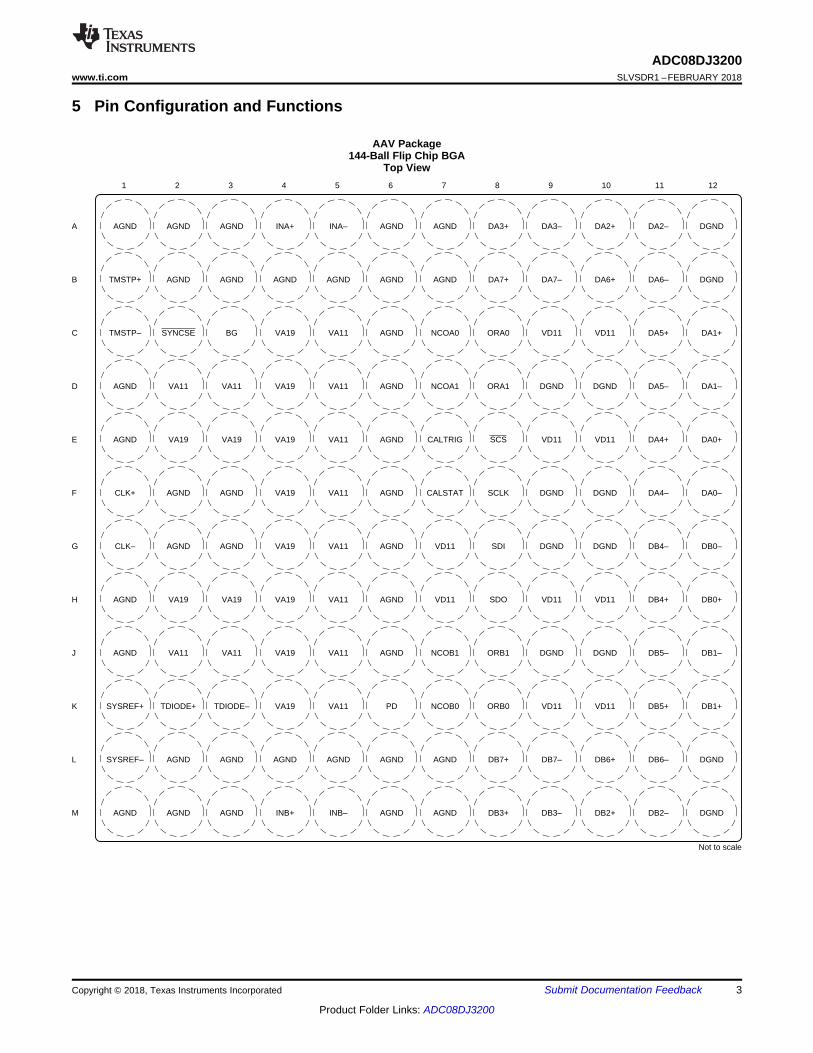
AGND AGND AGND INA+ INA± AGND AGND DA3+ DA3± DA2+ DA2± DGND
TMSTP+ AGND AGND AGND AGND AGND AGND DA7+ DA7± DA6+ DA6± DGND
TMSTP± SYNCSE BG VA19 VA11 AGND NCOA0 ORA0 VD11 VD11 DA5+ DA1+
AGND VA11 VA11 VA19 VA11 AGND NCOA1 ORA1 DGND DGND DA5± DA1±
AGND VA19 VA19 VA19 VA11 AGND CALTRIG SCS VD11 VD11 DA4+ DA0+
CLK+ AGND AGND VA19 VA11 AGND CALSTAT SCLK DGND DGND DA4± DA0±
CLK± AGND AGND VA19 VA11 AGND VD11 SDI DGND DGND DB4± DB0±
AGND VA19 VA19 VA19 VA11 AGND VD11 SDO VD11 VD11 DB4+ DB0+
AGND VA11 VA11 VA19 VA11 AGND NCOB1 ORB1 DGND DGND DB5± DB1±
SYSREF+ TDIODE+ TDIODE± VA19 VA11 PD NCOB0 ORB0 VD11 VD11 DB5+ DB1+
SYSREF± AGND AGND AGND AGND AGND AGND DB7+ DB7± DB6+ DB6± DGND
AGND AGND AGND INB+ INB± AGND AGND DB3+ DB3± DB2+ DB2± DGND
3
ADC08DJ3200www.ti.com SLVSDR1 –FEBRUARY 2018
Product Folder Links: ADC08DJ3200
Submit Documentation FeedbackCopyright © 2018, Texas Instruments Incorporated
5 Pin Configuration and Functions
AAV Package144-Ball Flip Chip BGA
Top View
4
ADC08DJ3200SLVSDR1 –FEBRUARY 2018 www.ti.com
Product Folder Links: ADC08DJ3200
Submit Documentation Feedback Copyright © 2018, Texas Instruments Incorporated
(1) Powering down the high-speed data outputs (DA0± ... DA7±, DB0± ... DB7±) for extended times may reduce performance of the outputserializers, especially at high data rates. Powering down the serializers occurs when the PD pin is held high, the MODE register isprogrammed to a value other than 0x00 or 0x01, the PD_ACH or PD_BCH registers settings are programmed to 1, or when the JMODEregister setting is programmed to a mode that uses less than the 16 total lanes that the device allows. For instance, JMODE 0 useseight total lanes and therefore the four highest-indexed lanes for each JESD204B link (DA4± ... DA7±, DB4± ... DB7±) are powereddown in this mode. When the PD pin is held high or the MODE register is programmed to a value other than 0x00 or 0x01, all outputserializers are powered down. When the PD_ACH or PD_BCH register settings are programmed to 1, the associated ADC channel andlanes are powered down. To prevent unreliable operation, the PD pin and MODE register must only be used for brief periods of time tomeasure temperature diode offsets and not used for long-term power savings. Furthermore, using a JMODE that uses fewer than 16lanes results in unreliable operation of the unused lanes. If the system will never use the unused lanes during the lifetime of the device,then the unused lanes do not cause issues and can be powered down. If the system may make use of the unused lanes at a later time,the reliable operation of the serializer outputs can be maintained by enabling JEXTRA_A and JEXTRA_B, which results in the VD11power consumption to increase and the output serializers to toggle.
Pin FunctionsPIN
I/O DESCRIPTIONNO. NAME
A1, A2, A3 AGND — Analog supply ground. Tie AGND and DGND to a common ground plane (GND) on the circuitboard.
A4 INA+ I
Channel A analog input positive connection. The differential full-scale input voltage is determinedby the FS_RANGE_A register (see the Full-Scale Voltage (VFS) Adjustment section). This inputis terminated to ground through a 50-Ω termination resistor. The input common-mode voltage istypically be set to 0 V (GND) and must follow the recommendations in the RecommendedOperating Conditions table. This pin can be left disconnected if not used. Using INA± isrecommended in single-channel mode for optimized performance.
A5 INA– IChannel A analog input negative connection. See INA+ (pin A4) for detailed description. Thisinput is terminated to ground through a 50-Ω termination resistor. This pin can be leftdisconnected if not used.
A6, A7 AGND — Analog supply ground. Tie AGND and DGND to a common ground plane (GND) on the circuitboard.
A8 DA3+ O
High-speed serialized-data output for channel A, lane 3, positive connection. This differentialoutput must be AC-coupled and must always be terminated with a 100-Ω differential terminationat the receiver. This pin can be left disconnected if not used. For information regarding reliableserializer operation, see footnote (1) in the Pin Functions table.
A9 DA3– OHigh-speed serialized-data output for channel A, lane 3, negative connection. This pin can be leftdisconnected if not used. For information regarding reliable serializer operation, see footnote (1) inthe Pin Functions table.
A10 DA2+ O
High-speed serialized-data output for channel A, lane 2, positive connection. This differentialoutput must be AC-coupled and must always be terminated with a 100-Ω differential terminationat the receiver. This pin can be left disconnected if not used. For information regarding reliableserializer operation, see footnote (1) in the Pin Functions table.
A11 DA2– OHigh-speed serialized-data output for channel A, lane 2, negative connection. This pin can be leftdisconnected if not used. For information regarding reliable serializer operation, see footnote (1) inthe Pin Functions table.
A12 DGND — Digital supply ground. Tie AGND and DGND to a common ground plane (GND) on the circuitboard.
B1 TMSTP+ I
Timestamp input positive connection or differential JESD204B SYNC positive connection. Thisinput is a timestamp input, used to mark a specific sample, when TIMESTAMP_EN is set to 1.This differential input is used as the JESD204B SYNC signal input when SYNC_SEL is set 1.This input can be used as both a timestamp and differential SYNC input at the same time,allowing feedback of the SYNC signal using the timestamp mechanism. TMSTP± uses active lowsignaling when used as a JESD204B SYNC. For additional usage information, see theTimestamp section.TMSTP_RECV_EN must be set to 1 to use this input. This differential input (TMSTP+ toTMSTP–) has an internal untrimmed 100-Ω differential termination and can be AC-coupled whenTMSTP_LVPECL_EN is set to 0. The termination changes to 50 Ω to ground on each input pin(TMSTP+ and TMSTP–) and can be DC coupled when TMSTP_LVPECL_EN is set to 1. This pinis not self-biased and therefore must be externally biased for both AC- and DC-coupledconfigurations. The common-mode voltage must be within the range provided in theRecommended Operating Conditions table when both AC and DC coupled. This pin can be leftdisconnected and disabled (TMSTP_RECV_EN = 0) if SYNCSE is used for JESD204B SYNCand timestamp is not required.
B2, B3, B4,B5, B6, B7 AGND — Analog supply ground. Tie AGND and DGND to a common ground plane (GND) on the circuit
board.
5
ADC08DJ3200www.ti.com SLVSDR1 –FEBRUARY 2018
Product Folder Links: ADC08DJ3200
Submit Documentation FeedbackCopyright © 2018, Texas Instruments Incorporated
Pin Functions (continued)PIN
I/O DESCRIPTIONNO. NAME
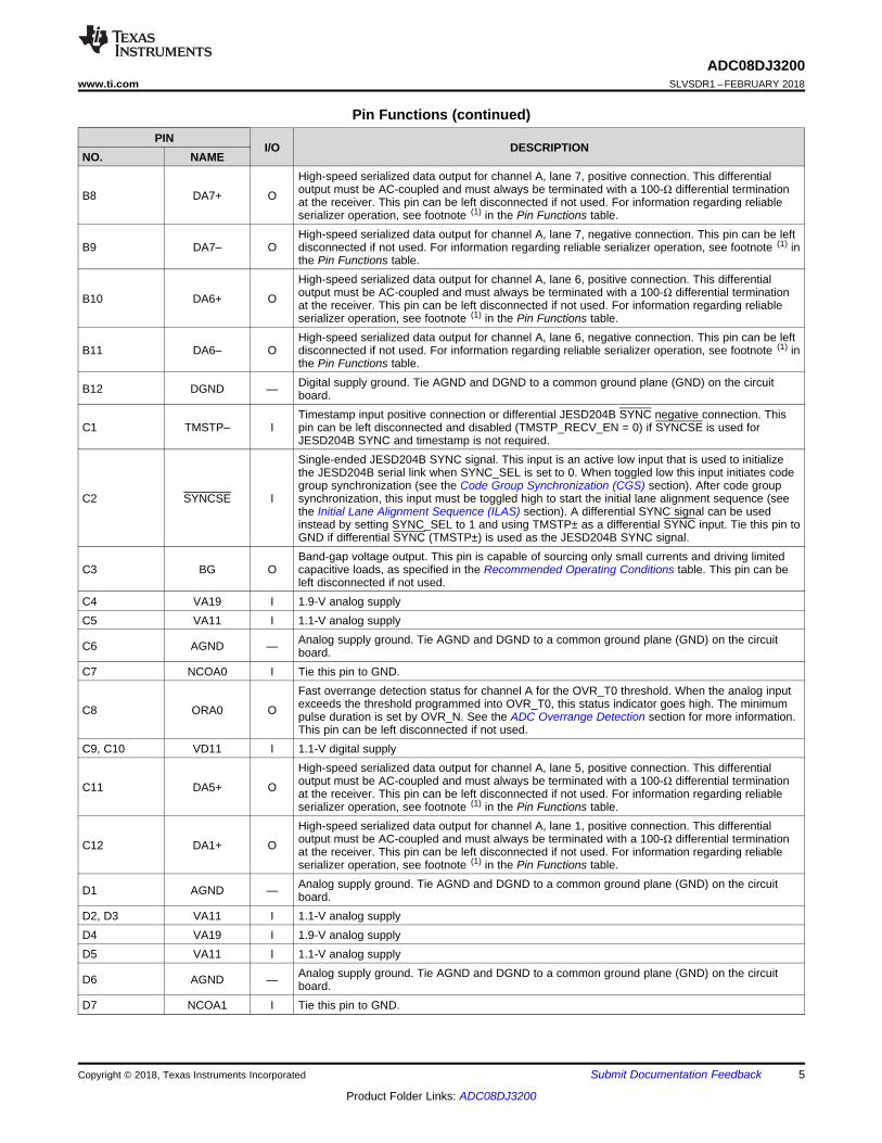
B8 DA7+ O
High-speed serialized data output for channel A, lane 7, positive connection. This differentialoutput must be AC-coupled and must always be terminated with a 100-Ω differential terminationat the receiver. This pin can be left disconnected if not used. For information regarding reliableserializer operation, see footnote (1) in the Pin Functions table.
B9 DA7– OHigh-speed serialized data output for channel A, lane 7, negative connection. This pin can be leftdisconnected if not used. For information regarding reliable serializer operation, see footnote (1) inthe Pin Functions table.
B10 DA6+ O
High-speed serialized data output for channel A, lane 6, positive connection. This differentialoutput must be AC-coupled and must always be terminated with a 100-Ω differential terminationat the receiver. This pin can be left disconnected if not used. For information regarding reliableserializer operation, see footnote (1) in the Pin Functions table.
B11 DA6– OHigh-speed serialized data output for channel A, lane 6, negative connection. This pin can be leftdisconnected if not used. For information regarding reliable serializer operation, see footnote (1) inthe Pin Functions table.
B12 DGND — Digital supply ground. Tie AGND and DGND to a common ground plane (GND) on the circuitboard.
C1 TMSTP– ITimestamp input positive connection or differential JESD204B SYNC negative connection. Thispin can be left disconnected and disabled (TMSTP_RECV_EN = 0) if SYNCSE is used forJESD204B SYNC and timestamp is not required.
C2 SYNCSE I
Single-ended JESD204B SYNC signal. This input is an active low input that is used to initializethe JESD204B serial link when SYNC_SEL is set to 0. When toggled low this input initiates codegroup synchronization (see the Code Group Synchronization (CGS) section). After code groupsynchronization, this input must be toggled high to start the initial lane alignment sequence (seethe Initial Lane Alignment Sequence (ILAS) section). A differential SYNC signal can be usedinstead by setting SYNC_SEL to 1 and using TMSTP± as a differential SYNC input. Tie this pin toGND if differential SYNC (TMSTP±) is used as the JESD204B SYNC signal.
C3 BG OBand-gap voltage output. This pin is capable of sourcing only small currents and driving limitedcapacitive loads, as specified in the Recommended Operating Conditions table. This pin can beleft disconnected if not used.
C4 VA19 I 1.9-V analog supplyC5 VA11 I 1.1-V analog supply
C6 AGND — Analog supply ground. Tie AGND and DGND to a common ground plane (GND) on the circuitboard.
C7 NCOA0 I Tie this pin to GND.
C8 ORA0 O
Fast overrange detection status for channel A for the OVR_T0 threshold. When the analog inputexceeds the threshold programmed into OVR_T0, this status indicator goes high. The minimumpulse duration is set by OVR_N. See the ADC Overrange Detection section for more information.This pin can be left disconnected if not used.
C9, C10 VD11 I 1.1-V digital supply
C11 DA5+ O
High-speed serialized data output for channel A, lane 5, positive connection. This differentialoutput must be AC-coupled and must always be terminated with a 100-Ω differential terminationat the receiver. This pin can be left disconnected if not used. For information regarding reliableserializer operation, see footnote (1) in the Pin Functions table.
C12 DA1+ O
High-speed serialized data output for channel A, lane 1, positive connection. This differentialoutput must be AC-coupled and must always be terminated with a 100-Ω differential terminationat the receiver. This pin can be left disconnected if not used. For information regarding reliableserializer operation, see footnote (1) in the Pin Functions table.
D1 AGND — Analog supply ground. Tie AGND and DGND to a common ground plane (GND) on the circuitboard.
D2, D3 VA11 I 1.1-V analog supplyD4 VA19 I 1.9-V analog supplyD5 VA11 I 1.1-V analog supply
D6 AGND — Analog supply ground. Tie AGND and DGND to a common ground plane (GND) on the circuitboard.
D7 NCOA1 I Tie this pin to GND.
6
ADC08DJ3200SLVSDR1 –FEBRUARY 2018 www.ti.com
Product Folder Links: ADC08DJ3200
Submit Documentation Feedback Copyright © 2018, Texas Instruments Incorporated
Pin Functions (continued)PIN
I/O DESCRIPTIONNO. NAME
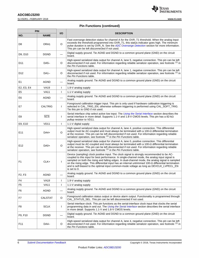
D8 ORA1 O
Fast overrange detection status for channel A for the OVR_T1 threshold. When the analog inputexceeds the threshold programmed into OVR_T1, this status indicator goes high. The minimumpulse duration is set by OVR_N. See the ADC Overrange Detection section for more information.This pin can be left disconnected if not used.
D9, D10 DGND — Digital supply ground. Tie AGND and DGND to a common ground plane (GND) on the circuitboard.
D11 DA5– OHigh-speed serialized data output for channel A, lane 5, negative connection. This pin can be leftdisconnected if not used. For information regarding reliable serializer operation, see footnote (1) inthe Pin Functions table.
D12 DA1– OHigh-speed serialized data output for channel A, lane 1, negative connection. This pin can be leftdisconnected if not used. For information regarding reliable serializer operation, see footnote (1) inthe Pin Functions table.
E1 AGND — Analog supply ground. Tie AGND and DGND to a common ground plane (GND) on the circuitboard.
E2, E3, E4 VA19 I 1.9-V analog supplyE5 VA11 I 1.1-V analog supply
E6 AGND — Analog supply ground. Tie AGND and DGND to a common ground plane (GND) on the circuitboard.
E7 CALTRIG IForeground calibration trigger input. This pin is only used if hardware calibration triggering isselected in CAL_TRIG_EN, otherwise software triggering is performed using CAL_SOFT_TRIG.Tie this pin to GND if not used.
E8 SCS ISerial interface chip select active low input. The Using the Serial Interface section describes theserial interface in more detail. Supports 1.1-V and 1.8-V CMOS levels. This pin has a 82-kΩpullup resistor to VD11.
E9, E10 VD11 I 1.1-V digital supply
E11 DA4+ O
High-speed serialized data output for channel A, lane 4, positive connection. This differentialoutput must be AC-coupled and must always be terminated with a 100-Ω differential terminationat the receiver. This pin can be left disconnected if not used. For information regarding reliableserializer operation, see footnote (1) in the Pin Functions table.
E12 DA0+ O
High-speed serialized data output for channel A, lane 0, positive connection. This differentialoutput must be AC-coupled and must always be terminated with a 100-Ω differential terminationat the receiver. This pin can be left disconnected if not used. For information regarding reliableserializer operation, see footnote (1) in the Pin Functions table.
F1 CLK+ I
Device (sampling) clock positive input. The clock signal is strongly recommended to be AC-coupled to this input for best performance. In single-channel mode, the analog input signal issampled on both the rising and falling edges. In dual-channel mode, the analog signal is sampledon the rising edge. This differential input has an internal untrimmed 100-Ω differential terminationand is self-biased to the optimal input common-mode voltage as long as DEVCLK_LVPECL_ENis set to 0.
F2, F3 AGND — Analog supply ground. Tie AGND and DGND to a common ground plane (GND) on the circuitboard.
F4 VA19 I 1.9-V analog supplyF5 VA11 I 1.1-V analog supply
F6 AGND — Analog supply ground. Tie AGND and DGND to a common ground plane (GND) on the circuitboard.
F7 CALSTAT O Foreground calibration status output or device alarm output. Functionality is programmed throughCAL_STATUS_SEL. This pin can be left disconnected if not used.
F8 SCLK ISerial interface clock. This pin functions as the serial-interface clock input that clocks the serialprogramming data in and out. The Using the Serial Interface section describes the serial interfacein more detail. Supports 1.1-V and 1.8-V CMOS levels.
F9, F10 DGND — Digital supply ground. Tie AGND and DGND to a common ground plane (GND) on the circuitboard.
F11 DA4– OHigh-speed serialized data output for channel A, lane 4, negative connection. This pin can be leftdisconnected if not used. For information regarding reliable serializer operation, see footnote (1) inthe Pin Functions table.
7
ADC08DJ3200www.ti.com SLVSDR1 –FEBRUARY 2018
Product Folder Links: ADC08DJ3200
Submit Documentation FeedbackCopyright © 2018, Texas Instruments Incorporated
Pin Functions (continued)PIN
I/O DESCRIPTIONNO. NAME
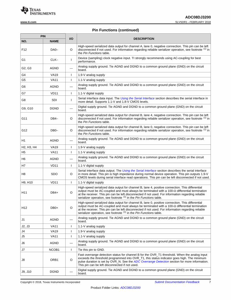
F12 DA0– OHigh-speed serialized data output for channel A, lane 0, negative connection. This pin can be leftdisconnected if not used. For information regarding reliable serializer operation, see footnote (1) inthe Pin Functions table.
G1 CLK– I Device (sampling) clock negative input. TI strongly recommends using AC-coupling for bestperformance.
G2, G3 AGND — Analog supply ground. Tie AGND and DGND to a common ground plane (GND) on the circuitboard.
G4 VA19 I 1.9-V analog supplyG5 VA11 I 1.1-V analog supply
G6 AGND — Analog supply ground. Tie AGND and DGND to a common ground plane (GND) on the circuitboard.
G7 VD11 I 1.1-V digital supply
G8 SDI I Serial interface data input. The Using the Serial Interface section describes the serial interface inmore detail. Supports 1.1-V and 1.8-V CMOS levels.
G9, G10 DGND — Digital supply ground. Tie AGND and DGND to a common ground plane (GND) on the circuitboard.
G11 DB4– OHigh-speed serialized data output for channel B, lane 4, negative connection. This pin can be leftdisconnected if not used. For information regarding reliable serializer operation, see footnote (1) inthe Pin Functions table.
G12 DB0– OHigh-speed serialized data output for channel B, lane 0, negative connection. This pin can be leftdisconnected if not used. For information regarding reliable serializer operation, see footnote (1) inthe Pin Functions table.
H1 AGND — Analog supply ground. Tie AGND and DGND to a common ground plane (GND) on the circuitboard.
H2, H3, H4 VA19 I 1.9-V analog supplyH5 VA11 I 1.1-V analog supply
H6 AGND — Analog supply ground. Tie AGND and DGND to a common ground plane (GND) on the circuitboard.
H7 VD11 I 1.1-V digital supply
H8 SDO OSerial interface data output. The Using the Serial Interface section describes the serial interfacein more detail. This pin is high impedance during normal device operation. This pin outputs 1.9-VCMOS levels during serial interface read operations. This pin can be left disconnected if not used.
H9, H10 VD11 I 1.1-V digital supply
H11 DB4+ O
High-speed serialized data output for channel B, lane 4, positive connection. This differentialoutput must be AC-coupled and must always be terminated with a 100-Ω differential terminationat the receiver. This pin can be left disconnected if not used. For information regarding reliableserializer operation, see footnote (1) in the Pin Functions table.
H12 DB0+ O
High-speed serialized data output for channel B, lane 0, positive connection. This differentialoutput must be AC-coupled and must always be terminated with a 100-Ω differential terminationat the receiver. This pin can be left disconnected if not used. For information regarding reliableserializer operation, see footnote (1) in the Pin Functions table.
J1 AGND — Analog supply ground. Tie AGND and DGND to a common ground plane (GND) on the circuitboard.
J2, J3 VA11 I 1.1-V analog supplyJ4 VA19 I 1.9-V analog supplyJ5 VA11 I 1.1-V analog supply
J6 AGND — Analog supply ground. Tie AGND and DGND to a common ground plane (GND) on the circuitboard.
J7 NCOB1 I Tie this pin to GND.
J8 ORB1 O
Fast overrange detection status for channel B for the OVR_T1 threshold. When the analog inputexceeds the threshold programmed into OVR_T1, this status indicator goes high. The minimumpulse duration is set by OVR_N. See the ADC Overrange Detection section for more information.This pin can be left disconnected if not used.
J9, J10 DGND — Digital supply ground. Tie AGND and DGND to a common ground plane (GND) on the circuitboard.
8
ADC08DJ3200SLVSDR1 –FEBRUARY 2018 www.ti.com
Product Folder Links: ADC08DJ3200
Submit Documentation Feedback Copyright © 2018, Texas Instruments Incorporated
Pin Functions (continued)PIN
I/O DESCRIPTIONNO. NAME
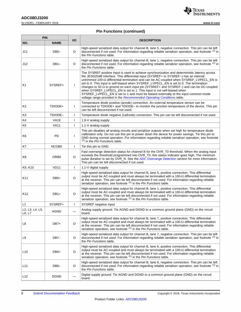
J11 DB5– OHigh-speed serialized data output for channel B, lane 5, negative connection. This pin can be leftdisconnected if not used. For information regarding reliable serializer operation, see footnote (1) inthe Pin Functions table.
J12 DB1– OHigh-speed serialized data output for channel B, lane 1, negative connection. This pin can be leftdisconnected if not used. For information regarding reliable serializer operation, see footnote (1) inthe Pin Functions table.
K1 SYSREF+ I
The SYSREF positive input is used to achieve synchronization and deterministic latency acrossthe JESD204B interface. This differential input (SYSREF+ to SYSREF–) has an internaluntrimmed 100-Ω differential termination and can be AC-coupled when SYSREF_LVPECL_EN isset to 0. This input is self-biased when SYSREF_LVPECL_EN is set to 0. The terminationchanges to 50 Ω to ground on each input pin (SYSREF+ and SYSREF–) and can be DC-coupledwhen SYSREF_LVPECL_EN is set to 1. This input is not self-biased whenSYSREF_LVPECL_EN is set to 1 and must be biased externally to the input common-modevoltage range provided in the Recommended Operating Conditions table.
K2 TDIODE+ ITemperature diode positive (anode) connection. An external temperature sensor can beconnected to TDIODE+ and TDIODE– to monitor the junction temperature of the device. This pincan be left disconnected if not used.
K3 TDIODE– I Temperature diode negative (cathode) connection. This pin can be left disconnected if not used.K4 VA19 I 1.9-V analog supplyK5 VA11 I 1.1-V analog supply
K6 PD I
This pin disables all analog circuits and serializer outputs when set high for temperature diodecalibration only. Do not use this pin to power down the device for power savings. Tie this pin toGND during normal operation. For information regarding reliable serializer operation, see footnote(1) in the Pin Functions table.
K7 NCOB0 I Tie this pin to GND.
K8 ORB0 O
Fast overrange detection status for channel B for the OVR_T0 threshold. When the analog inputexceeds the threshold programmed into OVR_T0, this status indicator goes high. The minimumpulse duration is set by OVR_N. See the ADC Overrange Detection section for more information.This pin can be left disconnected if not used.
K9, K10 VD11 I 1.1-V digital supply
K11 DB5+ O
High-speed serialized data output for channel B, lane 5, positive connection. This differentialoutput must be AC-coupled and must always be terminated with a 100-Ω differential terminationat the receiver. This pin can be left disconnected if not used. For information regarding reliableserializer operation, see footnote (1) in the Pin Functions table.
K12 DB1+ O
High-speed serialized data output for channel B, lane 1, positive connection. This differentialoutput must be AC-coupled and must always be terminated with a 100-Ω differential terminationat the receiver. This pin can be left disconnected if not used. For information regarding reliableserializer operation, see footnote (1) in the Pin Functions table.
L1 SYSREF– I SYSREF negative inputL2, L3, L4, L5,L6, L7 AGND — Analog supply ground. Tie AGND and DGND to a common ground plane (GND) on the circuit
board.
L8 DB7+ O
High-speed serialized data output for channel B, lane 7, positive connection. This differentialoutput must be AC-coupled and must always be terminated with a 100-Ω differential terminationat the receiver. This pin can be left disconnected if not used. For information regarding reliableserializer operation, see footnote (1) in the Pin Functions table.
L9 DB7– OHigh-speed serialized data output for channel B, lane 7, negative connection. This pin can be leftdisconnected if not used. For information regarding reliable serializer operation, see footnote (1) inthe Pin Functions table.
L10 DB6+ O
High-speed serialized data output for channel B, lane 6, positive connection. This differentialoutput must be AC-coupled and must always be terminated with a 100-Ω differential terminationat the receiver. This pin can be left disconnected if not used. For information regarding reliableserializer operation, see footnote (1) in the Pin Functions table.
L11 DB6– OHigh-speed serialized data output for channel B, lane 6, negative connection. This pin can be leftdisconnected if not used. For information regarding reliable serializer operation, see footnote (1) inthe Pin Functions table.
L12 DGND — Digital supply ground. Tie AGND and DGND to a common ground plane (GND) on the circuitboard.
9
ADC08DJ3200www.ti.com SLVSDR1 –FEBRUARY 2018
Product Folder Links: ADC08DJ3200
Submit Documentation FeedbackCopyright © 2018, Texas Instruments Incorporated
Pin Functions (continued)PIN
I/O DESCRIPTIONNO. NAME
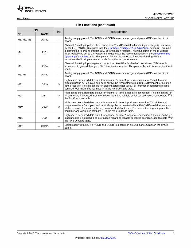
M1, M2, M3 AGND — Analog supply ground. Tie AGND and DGND to a common ground plane (GND) on the circuitboard.
M4 INB+ I
Channel B analog input positive connection. The differential full-scale input voltage is determinedby the FS_RANGE_B register (see the Full-Scale Voltage (VFS) Adjustment section). This inputis terminated to ground through a 50-Ω termination resistor. The input common-mode voltagemust typically be set to 0 V (GND) and must follow the recommendations in the RecommendedOperating Conditions table. This pin can be left disconnected if not used. Using INA± isrecommended in single-channel mode for optimized performance.
M5 INB– IChannel B analog input negative connection. See INB+ for detailed description. This input isterminated to ground through a 50-Ω termination resistor. This pin can be left disconnected if notused.
M6, M7 AGND — Analog supply ground. Tie AGND and DGND to a common ground plane (GND) on the circuitboard.
M8 DB3+ O
High-speed serialized data output for channel B, lane 3, positive connection. This differentialoutput must be AC-coupled and must always be terminated with a 100-Ω differential terminationat the receiver. This pin can be left disconnected if not used. For information regarding reliableserializer operation, see footnote (1) in the Pin Functions table.
M9 DB3– OHigh-speed serialized data output for channel B, lane 3, negative connection. This pin can be leftdisconnected if not used. For information regarding reliable serializer operation, see footnote (1) inthe Pin Functions table.
M10 DB2+ O
High-speed serialized data output for channel B, lane 2, positive connection. This differentialoutput must be AC-coupled and must always be terminated with a 100-Ω differential terminationat the receiver. This pin can be left disconnected if not used. For information regarding reliableserializer operation, see footnote (1) in the Pin Functions table.
M11 DB2– OHigh-speed serialized data output for channel B, lane 2, negative connection. This pin can be leftdisconnected if not used. For information regarding reliable serializer operation, see footnote (1) inthe Pin Functions table.
M12 DGND — Digital supply ground. Tie AGND and DGND to a common ground plane (GND) on the circuitboard.
10
ADC08DJ3200SLVSDR1 –FEBRUARY 2018 www.ti.com
Product Folder Links: ADC08DJ3200
Submit Documentation Feedback Copyright © 2018, Texas Instruments Incorporated
(1) Stresses beyond those listed under Absolute Maximum Ratings may cause permanent damage to the device. These are stress ratingsonly, which do not imply functional operation of the device at these or any other conditions beyond those indicated under RecommendedOperating Conditions. Exposure to absolute-maximum-rated conditions for extended periods may affect device reliability.
(2) Measured to AGND.(3) Measured to DGND.
6 Specifications
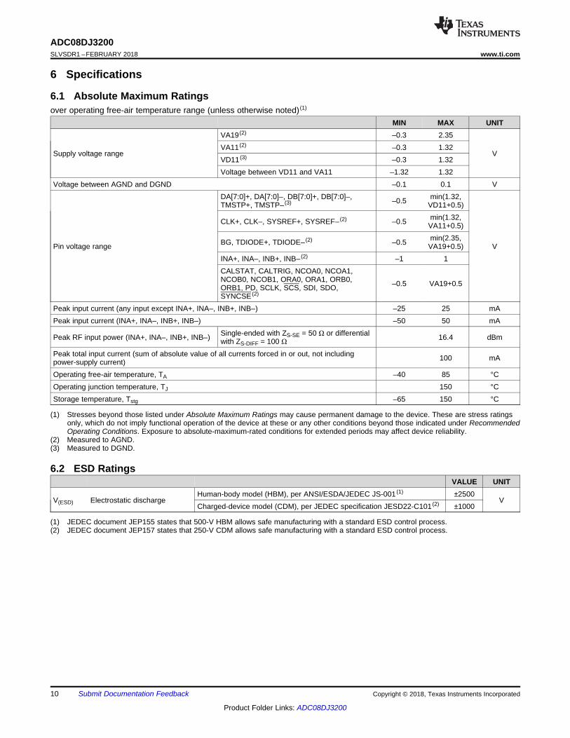
6.1 Absolute Maximum Ratingsover operating free-air temperature range (unless otherwise noted) (1)
MIN MAX UNIT
Supply voltage range
VA19 (2) –0.3 2.35
VVA11 (2) –0.3 1.32VD11 (3) –0.3 1.32Voltage between VD11 and VA11 –1.32 1.32
Voltage between AGND and DGND –0.1 0.1 V
Pin voltage range
DA[7:0]+, DA[7:0]–, DB[7:0]+, DB[7:0]–,TMSTP+, TMSTP– (3) –0.5 min(1.32,
VD11+0.5)
V
CLK+, CLK–, SYSREF+, SYSREF– (2) –0.5 min(1.32,VA11+0.5)
BG, TDIODE+, TDIODE– (2) –0.5 min(2.35,VA19+0.5)
INA+, INA–, INB+, INB– (2) –1 1CALSTAT, CALTRIG, NCOA0, NCOA1,NCOB0, NCOB1, ORA0, ORA1, ORB0,ORB1, PD, SCLK, SCS, SDI, SDO,SYNCSE (2)
–0.5 VA19+0.5
Peak input current (any input except INA+, INA–, INB+, INB–) –25 25 mAPeak input current (INA+, INA–, INB+, INB–) –50 50 mA
Peak RF input power (INA+, INA–, INB+, INB–) Single-ended with ZS-SE = 50 Ω or differentialwith ZS-DIFF = 100 Ω 16.4 dBm
Peak total input current (sum of absolute value of all currents forced in or out, not includingpower-supply current) 100 mA
Operating free-air temperature, TA –40 85 °COperating junction temperature, TJ 150 °CStorage temperature, Tstg –65 150 °C
(1) JEDEC document JEP155 states that 500-V HBM allows safe manufacturing with a standard ESD control process.(2) JEDEC document JEP157 states that 250-V CDM allows safe manufacturing with a standard ESD control process.
6.2 ESD RatingsVALUE UNIT
V(ESD) Electrostatic dischargeHuman-body model (HBM), per ANSI/ESDA/JEDEC JS-001 (1) ±2500
VCharged-device model (CDM), per JEDEC specification JESD22-C101 (2) ±1000
11
ADC08DJ3200www.ti.com SLVSDR1 –FEBRUARY 2018
Product Folder Links: ADC08DJ3200
Submit Documentation FeedbackCopyright © 2018, Texas Instruments Incorporated
(1) Measured to AGND.(2) Measured to DGND.(3) TI strongly recommends that CLK± be AC-coupled with DEVCLK_LVPECL_EN set to 0 to allow CLK± to self-bias to the optimal input
common-mode voltage for best performance. TI recommends AC-coupling for SYSREF± unless DC-coupling is required, in which casethe LVPECL input mode must be used (SYSREF_LVPECL_EN = 1).
(4) TMSTP± does not have internal biasing that requires TMSTP± to be biased externally whether AC-coupled with TMSTP_LVPECL_EN =0 or DC-coupled with TMSTP_LVPECL_EN = 1.
(5) The ADC output code saturates when VID for INA± or INB± exceeds the programmed full-scale voltage (VFS) set by FS_RANGE_A forINA± or FS_RANGE_B for INB±.
(6) Prolonged use above this junction temperature may increase the device failure-in-time (FIT) rate.(7) Tested up to 1000 hours continuous operation at TJ = 125°C. See the Absolute Maximum Ratings table for the absolute maximum
operational temperature.
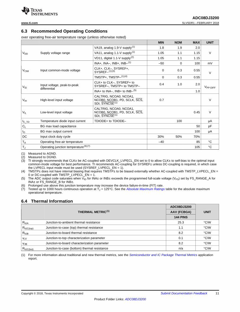
6.3 Recommended Operating Conditionsover operating free-air temperature range (unless otherwise noted)
MIN NOM MAX UNIT
VDD Supply voltage rangeVA19, analog 1.9-V supply (1) 1.8 1.9 2.0
VVA11, analog 1.1-V supply (1) 1.05 1.1 1.15VD11, digital 1.1-V supply (2) 1.05 1.1 1.15
VCMI Input common-mode voltage
INA+, INA–, INB+, INB– (1) –50 0 100 mVCLK+, CLK–, SYSREF+,SYSREF– (1) (3) 0 0.3 0.55
VTMSTP+, TMSTP– (1) (4) 0 0.3 0.55
VIDInput voltage, peak-to-peakdifferential
CLK+ to CLK–, SYSREF+ toSYSREF–, TMSTP+ to TMSTP– 0.4 1.0 2.0
VPP-DIFFINA+ to INA–, INB+ to INB– (5) 1.0
VIH High-level input voltageCALTRIG, NCOA0, NCOA1,NCOB0, NCOB1, PD, SCLK, SCS,SDI, SYNCSE (1)
0.7 V
VIL Low-level input voltageCALTRIG, NCOA0, NCOA1,NCOB0, NCOB1, PD, SCLK, SCS,SDI, SYNCSE (1)
0.45 V
IC_TD Temperature diode input current TDIODE+ to TDIODE– 100 µACL BG max load capacitance 50 pFIO BG max output current 100 µADC Input clock duty cycle 30% 50% 70%TA Operating free-air temperature –40 85 °CTJ Operating junction temperature (6) (7) 105 °C
(1) For more information about traditional and new thermal metrics, see the Semiconductor and IC Package Thermal Metrics applicationreport.
6.4 Thermal Information
THERMAL METRIC (1)ADC08DJ3200
UNITAAV (FCBGA)144 PINS
RθJA Junction-to-ambient thermal resistance 25.3 °C/WRθJC(top) Junction-to-case (top) thermal resistance 1.1 °C/WRθJB Junction-to-board thermal resistance 8.2 °C/WψJT Junction-to-top characterization parameter 0.1 °C/WψJB Junction-to-board characterization parameter 8.2 °C/WRθJC(bot) Junction-to-case (bottom) thermal resistance n/a °C/W
12
ADC08DJ3200SLVSDR1 –FEBRUARY 2018 www.ti.com
Product Folder Links: ADC08DJ3200
Submit Documentation Feedback Copyright © 2018, Texas Instruments Incorporated
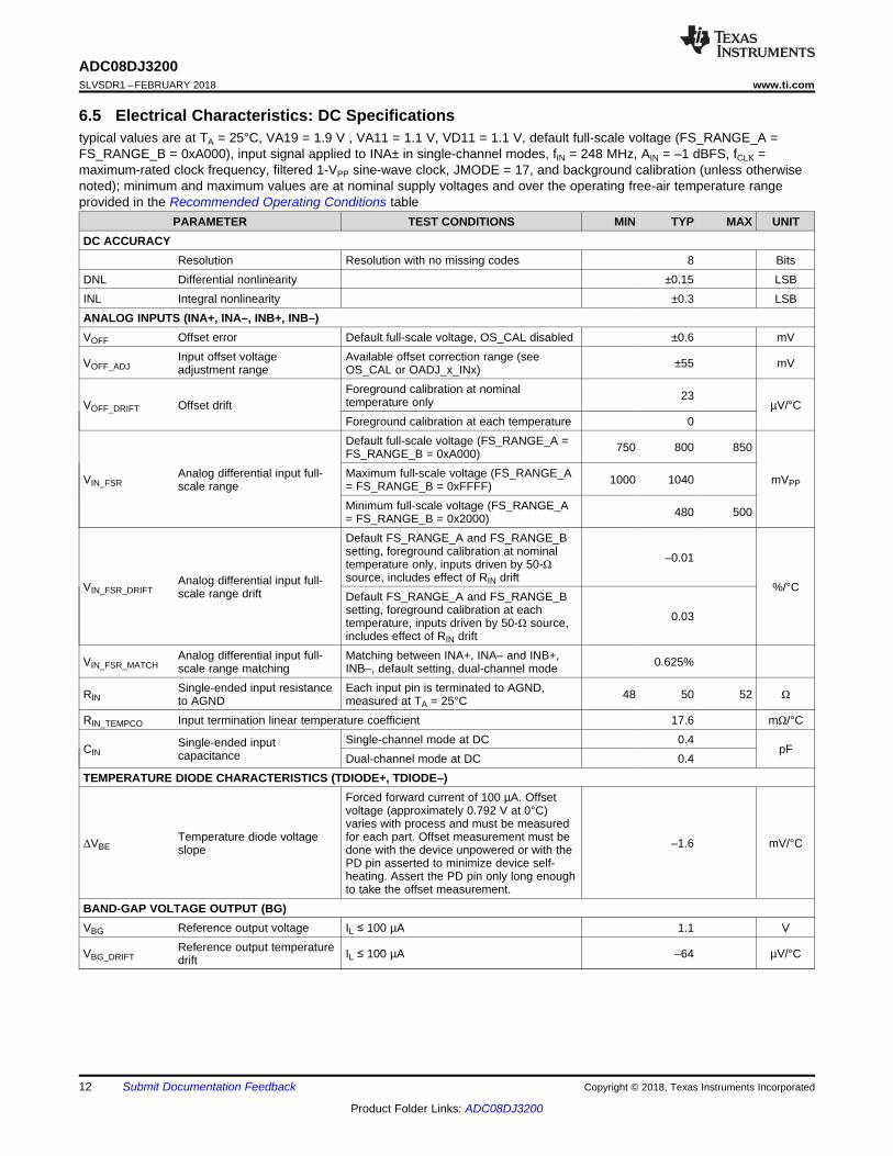
6.5 Electrical Characteristics: DC Specificationstypical values are at TA = 25°C, VA19 = 1.9 V , VA11 = 1.1 V, VD11 = 1.1 V, default full-scale voltage (FS_RANGE_A =FS_RANGE_B = 0xA000), input signal applied to INA± in single-channel modes, fIN = 248 MHz, AIN = –1 dBFS, fCLK =maximum-rated clock frequency, filtered 1-VPP sine-wave clock, JMODE = 17, and background calibration (unless otherwisenoted); minimum and maximum values are at nominal supply voltages and over the operating free-air temperature rangeprovided in the Recommended Operating Conditions table
PARAMETER TEST CONDITIONS MIN TYP MAX UNITDC ACCURACY
Resolution Resolution with no missing codes 8 BitsDNL Differential nonlinearity ±0.15 LSBINL Integral nonlinearity ±0.3 LSBANALOG INPUTS (INA+, INA–, INB+, INB–)VOFF Offset error Default full-scale voltage, OS_CAL disabled ±0.6 mV
VOFF_ADJInput offset voltageadjustment range
Available offset correction range (seeOS_CAL or OADJ_x_INx) ±55 mV
VOFF_DRIFT Offset driftForeground calibration at nominaltemperature only 23
µV/°CForeground calibration at each temperature 0
VIN_FSRAnalog differential input full-scale range
Default full-scale voltage (FS_RANGE_A =FS_RANGE_B = 0xA000) 750 800 850
mVPPMaximum full-scale voltage (FS_RANGE_A= FS_RANGE_B = 0xFFFF) 1000 1040
Minimum full-scale voltage (FS_RANGE_A= FS_RANGE_B = 0x2000) 480 500
VIN_FSR_DRIFTAnalog differential input full-scale range drift
Default FS_RANGE_A and FS_RANGE_Bsetting, foreground calibration at nominaltemperature only, inputs driven by 50-Ωsource, includes effect of RIN drift
–0.01
%/°CDefault FS_RANGE_A and FS_RANGE_Bsetting, foreground calibration at eachtemperature, inputs driven by 50-Ω source,includes effect of RIN drift
0.03
VIN_FSR_MATCHAnalog differential input full-scale range matching
Matching between INA+, INA– and INB+,INB–, default setting, dual-channel mode 0.625%
RINSingle-ended input resistanceto AGND
Each input pin is terminated to AGND,measured at TA = 25°C 48 50 52 Ω
RIN_TEMPCO Input termination linear temperature coefficient 17.6 mΩ/°C
CINSingle-ended inputcapacitance
Single-channel mode at DC 0.4pF
Dual-channel mode at DC 0.4TEMPERATURE DIODE CHARACTERISTICS (TDIODE+, TDIODE–)
ΔVBETemperature diode voltageslope
Forced forward current of 100 µA. Offsetvoltage (approximately 0.792 V at 0°C)varies with process and must be measuredfor each part. Offset measurement must bedone with the device unpowered or with thePD pin asserted to minimize device self-heating. Assert the PD pin only long enoughto take the offset measurement.
–1.6 mV/°C
BAND-GAP VOLTAGE OUTPUT (BG)VBG Reference output voltage IL ≤ 100 µA 1.1 V
VBG_DRIFTReference output temperaturedrift IL ≤ 100 µA –64 µV/°C
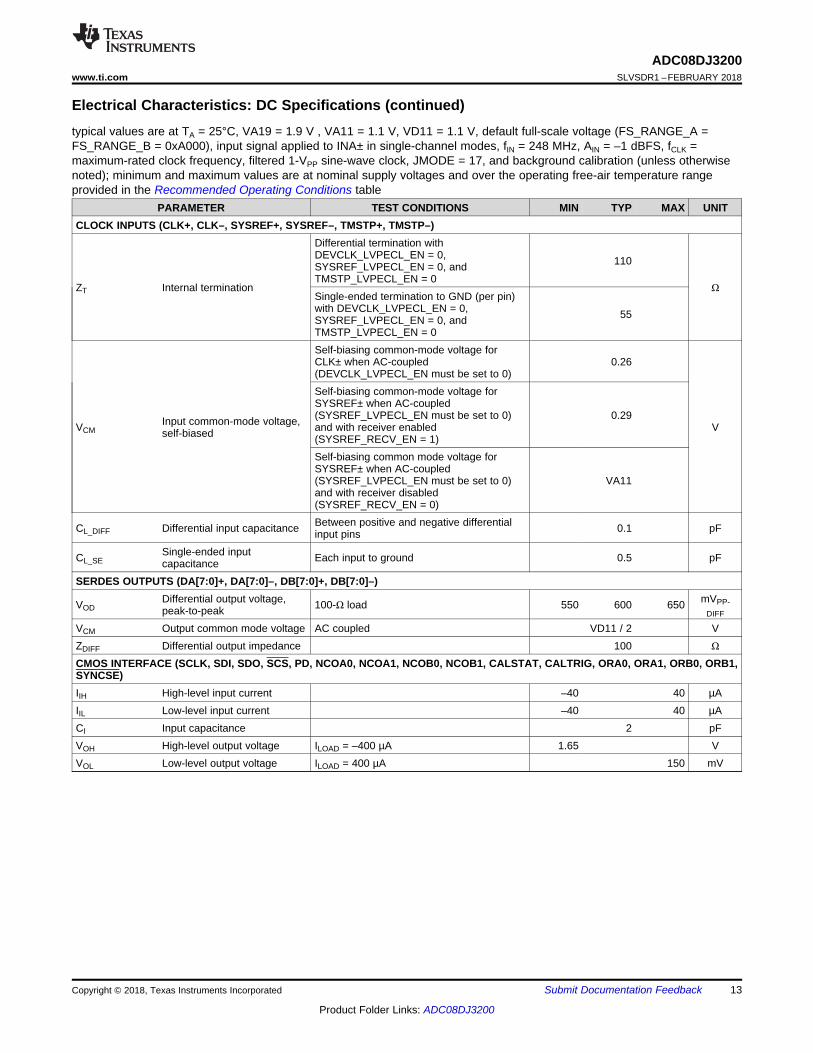
13
ADC08DJ3200www.ti.com SLVSDR1 –FEBRUARY 2018
Product Folder Links: ADC08DJ3200
Submit Documentation FeedbackCopyright © 2018, Texas Instruments Incorporated
Electrical Characteristics: DC Specifications (continued)typical values are at TA = 25°C, VA19 = 1.9 V , VA11 = 1.1 V, VD11 = 1.1 V, default full-scale voltage (FS_RANGE_A =FS_RANGE_B = 0xA000), input signal applied to INA± in single-channel modes, fIN = 248 MHz, AIN = –1 dBFS, fCLK =maximum-rated clock frequency, filtered 1-VPP sine-wave clock, JMODE = 17, and background calibration (unless otherwisenoted); minimum and maximum values are at nominal supply voltages and over the operating free-air temperature rangeprovided in the Recommended Operating Conditions table
PARAMETER TEST CONDITIONS MIN TYP MAX UNITCLOCK INPUTS (CLK+, CLK–, SYSREF+, SYSREF–, TMSTP+, TMSTP–)
ZT Internal termination
Differential termination withDEVCLK_LVPECL_EN = 0,SYSREF_LVPECL_EN = 0, andTMSTP_LVPECL_EN = 0
110
ΩSingle-ended termination to GND (per pin)with DEVCLK_LVPECL_EN = 0,SYSREF_LVPECL_EN = 0, andTMSTP_LVPECL_EN = 0
55
VCMInput common-mode voltage,self-biased
Self-biasing common-mode voltage forCLK± when AC-coupled(DEVCLK_LVPECL_EN must be set to 0)
0.26
V
Self-biasing common-mode voltage forSYSREF± when AC-coupled(SYSREF_LVPECL_EN must be set to 0)and with receiver enabled(SYSREF_RECV_EN = 1)
0.29
Self-biasing common mode voltage forSYSREF± when AC-coupled(SYSREF_LVPECL_EN must be set to 0)and with receiver disabled(SYSREF_RECV_EN = 0)
VA11
CL_DIFF Differential input capacitance Between positive and negative differentialinput pins 0.1 pF
CL_SESingle-ended inputcapacitance Each input to ground 0.5 pF
SERDES OUTPUTS (DA[7:0]+, DA[7:0]–, DB[7:0]+, DB[7:0]–)
VODDifferential output voltage,peak-to-peak 100-Ω load 550 600 650 mVPP-
DIFF
VCM Output common mode voltage AC coupled VD11 / 2 VZDIFF Differential output impedance 100 Ω
CMOS INTERFACE (SCLK, SDI, SDO, SCS, PD, NCOA0, NCOA1, NCOB0, NCOB1, CALSTAT, CALTRIG, ORA0, ORA1, ORB0, ORB1,SYNCSE)IIH High-level input current –40 40 µAIIL Low-level input current –40 40 µACI Input capacitance 2 pFVOH High-level output voltage ILOAD = –400 µA 1.65 VVOL Low-level output voltage ILOAD = 400 µA 150 mV
14
ADC08DJ3200SLVSDR1 –FEBRUARY 2018 www.ti.com
Product Folder Links: ADC08DJ3200
Submit Documentation Feedback Copyright © 2018, Texas Instruments Incorporated
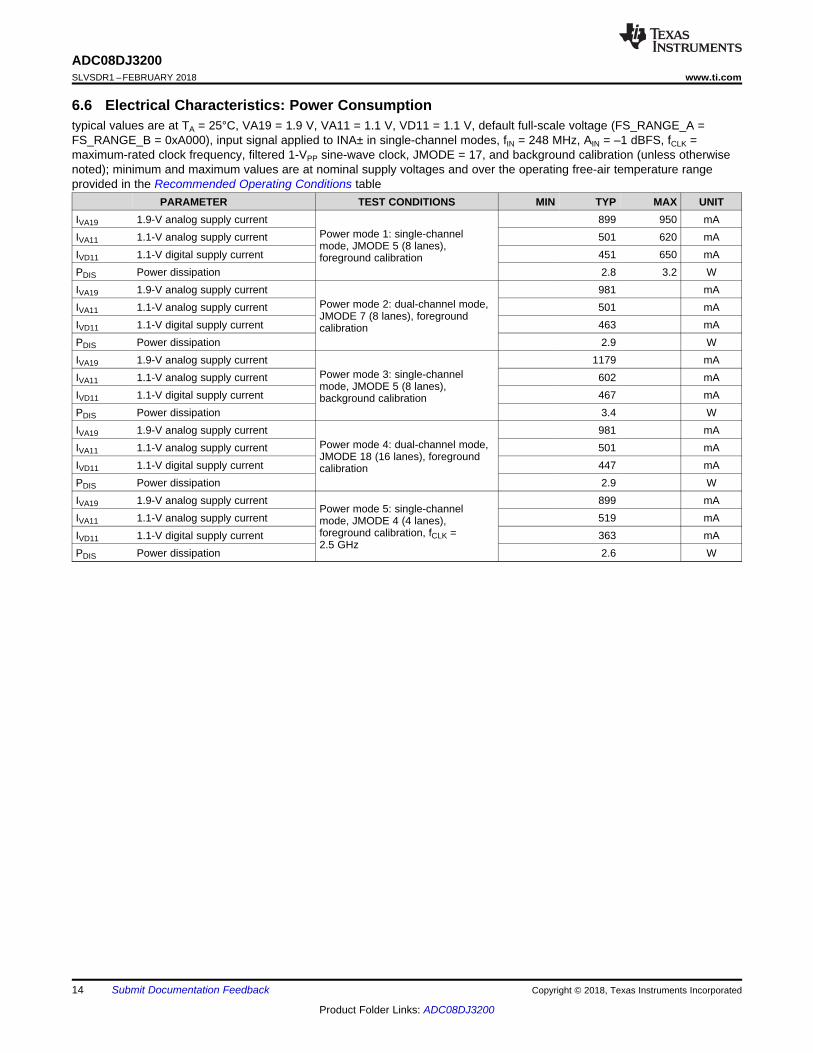
6.6 Electrical Characteristics: Power Consumptiontypical values are at TA = 25°C, VA19 = 1.9 V, VA11 = 1.1 V, VD11 = 1.1 V, default full-scale voltage (FS_RANGE_A =FS_RANGE_B = 0xA000), input signal applied to INA± in single-channel modes, fIN = 248 MHz, AIN = –1 dBFS, fCLK =maximum-rated clock frequency, filtered 1-VPP sine-wave clock, JMODE = 17, and background calibration (unless otherwisenoted); minimum and maximum values are at nominal supply voltages and over the operating free-air temperature rangeprovided in the Recommended Operating Conditions table
PARAMETER TEST CONDITIONS MIN TYP MAX UNITIVA19 1.9-V analog supply current
Power mode 1: single-channelmode, JMODE 5 (8 lanes),foreground calibration
899 950 mAIVA11 1.1-V analog supply current 501 620 mAIVD11 1.1-V digital supply current 451 650 mAPDIS Power dissipation 2.8 3.2 WIVA19 1.9-V analog supply current
Power mode 2: dual-channel mode,JMODE 7 (8 lanes), foregroundcalibration
981 mAIVA11 1.1-V analog supply current 501 mAIVD11 1.1-V digital supply current 463 mAPDIS Power dissipation 2.9 WIVA19 1.9-V analog supply current
Power mode 3: single-channelmode, JMODE 5 (8 lanes),background calibration
1179 mAIVA11 1.1-V analog supply current 602 mAIVD11 1.1-V digital supply current 467 mAPDIS Power dissipation 3.4 WIVA19 1.9-V analog supply current
Power mode 4: dual-channel mode,JMODE 18 (16 lanes), foregroundcalibration
981 mAIVA11 1.1-V analog supply current 501 mAIVD11 1.1-V digital supply current 447 mAPDIS Power dissipation 2.9 WIVA19 1.9-V analog supply current
Power mode 5: single-channelmode, JMODE 4 (4 lanes),foreground calibration, fCLK =2.5 GHz
899 mAIVA11 1.1-V analog supply current 519 mAIVD11 1.1-V digital supply current 363 mAPDIS Power dissipation 2.6 W
15
ADC08DJ3200www.ti.com SLVSDR1 –FEBRUARY 2018
Product Folder Links: ADC08DJ3200
Submit Documentation FeedbackCopyright © 2018, Texas Instruments Incorporated
(1) Full-power input bandwidth (FPBW) is defined as the input frequency where the reconstructed output of the ADC drops 3 dB below thepower of a full-scale input signal at a low input frequency. Useable bandwidth may exceed the –3-dB full-power input bandwidth.
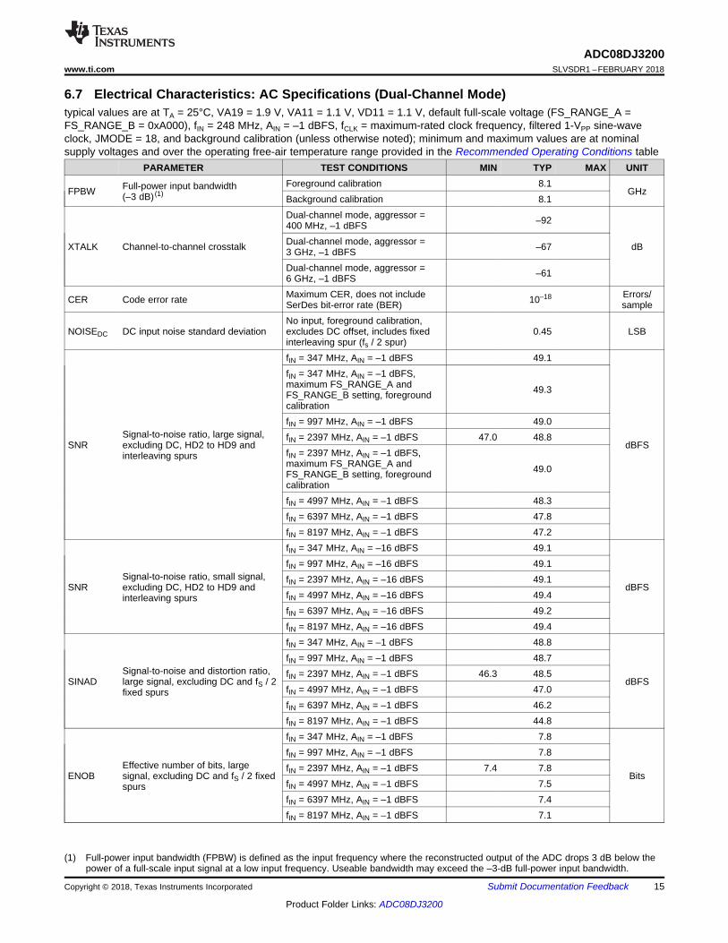
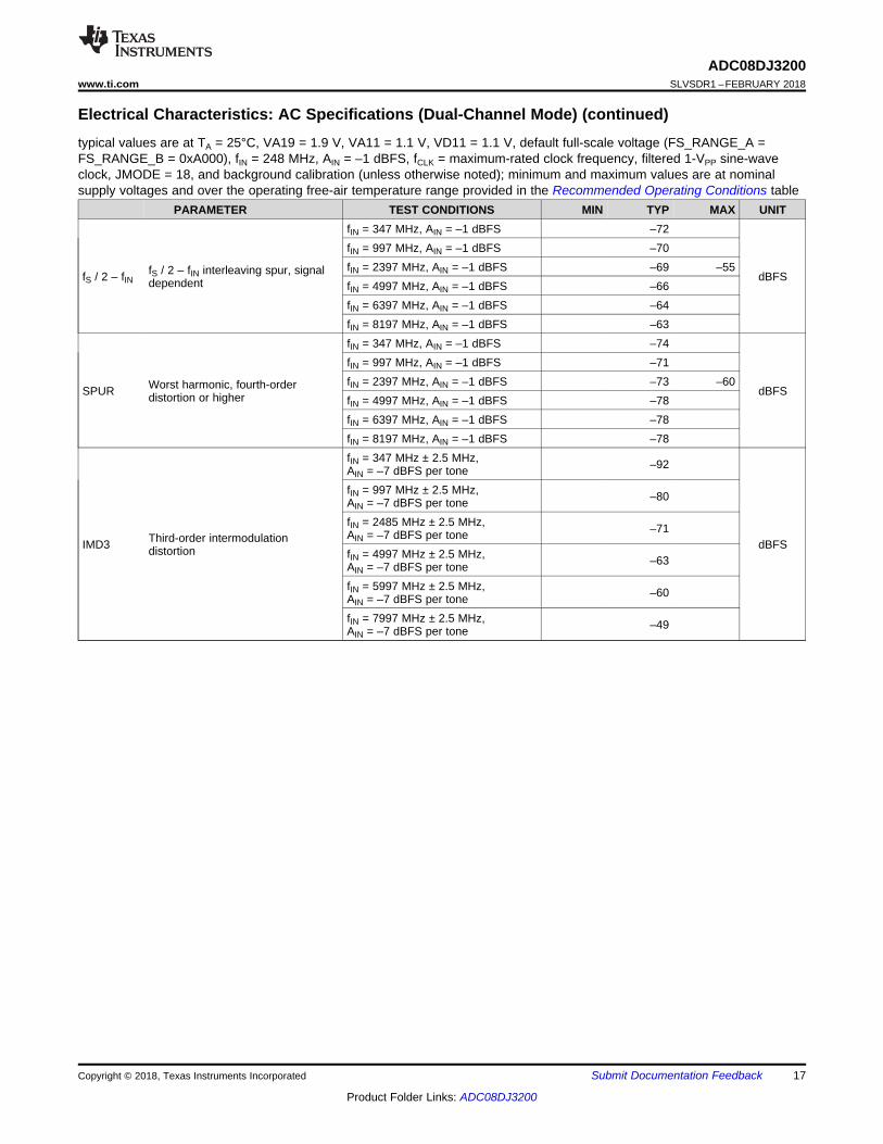
6.7 Electrical Characteristics: AC Specifications (Dual-Channel Mode)typical values are at TA = 25°C, VA19 = 1.9 V, VA11 = 1.1 V, VD11 = 1.1 V, default full-scale voltage (FS_RANGE_A =FS_RANGE_B = 0xA000), fIN = 248 MHz, AIN = –1 dBFS, fCLK = maximum-rated clock frequency, filtered 1-VPP sine-waveclock, JMODE = 18, and background calibration (unless otherwise noted); minimum and maximum values are at nominalsupply voltages and over the operating free-air temperature range provided in the Recommended Operating Conditions table
PARAMETER TEST CONDITIONS MIN TYP MAX UNIT
FPBW Full-power input bandwidth(–3 dB) (1)
Foreground calibration 8.1GHz
Background calibration 8.1
XTALK Channel-to-channel crosstalk
Dual-channel mode, aggressor =400 MHz, –1 dBFS –92
dBDual-channel mode, aggressor =3 GHz, –1 dBFS –67
Dual-channel mode, aggressor =6 GHz, –1 dBFS –61
CER Code error rate Maximum CER, does not includeSerDes bit-error rate (BER) 10–18 Errors/
sample
NOISEDC DC input noise standard deviationNo input, foreground calibration,excludes DC offset, includes fixedinterleaving spur (fs / 2 spur)
0.45 LSB
SNRSignal-to-noise ratio, large signal,excluding DC, HD2 to HD9 andinterleaving spurs
fIN = 347 MHz, AIN = –1 dBFS 49.1
dBFS
fIN = 347 MHz, AIN = –1 dBFS,maximum FS_RANGE_A andFS_RANGE_B setting, foregroundcalibration
49.3
fIN = 997 MHz, AIN = –1 dBFS 49.0fIN = 2397 MHz, AIN = –1 dBFS 47.0 48.8fIN = 2397 MHz, AIN = –1 dBFS,maximum FS_RANGE_A andFS_RANGE_B setting, foregroundcalibration
49.0
fIN = 4997 MHz, AIN = –1 dBFS 48.3fIN = 6397 MHz, AIN = –1 dBFS 47.8fIN = 8197 MHz, AIN = –1 dBFS 47.2
SNRSignal-to-noise ratio, small signal,excluding DC, HD2 to HD9 andinterleaving spurs
fIN = 347 MHz, AIN = –16 dBFS 49.1
dBFS
fIN = 997 MHz, AIN = –16 dBFS 49.1fIN = 2397 MHz, AIN = –16 dBFS 49.1fIN = 4997 MHz, AIN = –16 dBFS 49.4fIN = 6397 MHz, AIN = –16 dBFS 49.2fIN = 8197 MHz, AIN = –16 dBFS 49.4
SINADSignal-to-noise and distortion ratio,large signal, excluding DC and fS / 2fixed spurs
fIN = 347 MHz, AIN = –1 dBFS 48.8
dBFS
fIN = 997 MHz, AIN = –1 dBFS 48.7fIN = 2397 MHz, AIN = –1 dBFS 46.3 48.5fIN = 4997 MHz, AIN = –1 dBFS 47.0fIN = 6397 MHz, AIN = –1 dBFS 46.2fIN = 8197 MHz, AIN = –1 dBFS 44.8
ENOBEffective number of bits, largesignal, excluding DC and fS / 2 fixedspurs
fIN = 347 MHz, AIN = –1 dBFS 7.8
Bits
fIN = 997 MHz, AIN = –1 dBFS 7.8fIN = 2397 MHz, AIN = –1 dBFS 7.4 7.8fIN = 4997 MHz, AIN = –1 dBFS 7.5fIN = 6397 MHz, AIN = –1 dBFS 7.4fIN = 8197 MHz, AIN = –1 dBFS 7.1
16
ADC08DJ3200SLVSDR1 –FEBRUARY 2018 www.ti.com
Product Folder Links: ADC08DJ3200
Submit Documentation Feedback Copyright © 2018, Texas Instruments Incorporated
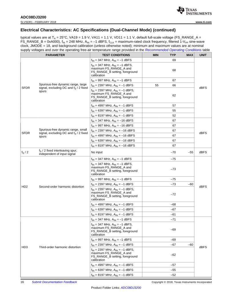
Electrical Characteristics: AC Specifications (Dual-Channel Mode) (continued)typical values are at TA = 25°C, VA19 = 1.9 V, VA11 = 1.1 V, VD11 = 1.1 V, default full-scale voltage (FS_RANGE_A =FS_RANGE_B = 0xA000), fIN = 248 MHz, AIN = –1 dBFS, fCLK = maximum-rated clock frequency, filtered 1-VPP sine-waveclock, JMODE = 18, and background calibration (unless otherwise noted); minimum and maximum values are at nominalsupply voltages and over the operating free-air temperature range provided in the Recommended Operating Conditions table
PARAMETER TEST CONDITIONS MIN TYP MAX UNIT
SFDRSpurious-free dynamic range, largesignal, excluding DC and fS / 2 fixedspurs
fIN = 347 MHz, AIN = –1 dBFS 69
dBFS
fIN = 347 MHz, AIN = –1 dBFS,maximum FS_RANGE_A andFS_RANGE_B setting, foregroundcalibration
68
fIN = 997 MHz, AIN = –1 dBFS 67fIN = 2397 MHz, AIN = –1 dBFS 55 66fIN = 2397 MHz, AIN = –1 dBFS,maximum FS_RANGE_A andFS_RANGE_B setting, foregroundcalibration
62
fIN = 4997 MHz, AIN = –1 dBFS 57fIN = 6397 MHz, AIN = –1 dBFS 55fIN = 8197 MHz, AIN = –1 dBFS 52
SFDRSpurious-free dynamic range, smallsignal, excluding DC and fS / 2 fixedspurs
fIN = 347 MHz, AIN = –16 dBFS 67
dBFS
fIN = 997 MHz, AIN = –16 dBFS 67fIN = 2397 MHz, AIN = –16 dBFS 67fIN = 4997 MHz, AIN = –16 dBFS 67fIN = 6397 MHz, AIN = –16 dBFS 67fIN = 8197 MHz, AIN = –16 dBFS 67
fS / 2 fS / 2 fixed interleaving spur,independent of input signal No input –70 –55 dBFS
HD2 Second-order harmonic distortion
fIN = 347 MHz, AIN = –1 dBFS –75
dBFS
fIN = 347 MHz, AIN = –1 dBFS,maximum FS_RANGE_A andFS_RANGE_B setting, foregroundcalibration
–73
fIN = 997 MHz, AIN = –1 dBFS –75fIN = 2397 MHz, AIN = –1 dBFS –73 –60fIN = 2397 MHz, AIN = –1 dBFS,maximum FS_RANGE_A andFS_RANGE_B setting, foregroundcalibration
–72
fIN = 4997 MHz, AIN = –1 dBFS –68fIN = 6397 MHz, AIN = –1 dBFS –67fIN = 8197 MHz, AIN = –1 dBFS –61
HD3 Third-order harmonic distortion
fIN = 347 MHz, AIN = –1 dBFS –71
dBFS
fIN = 347 MHz, AIN = –1 dBFS,maximum FS_RANGE_A andFS_RANGE_B setting, foregroundcalibration
–69
fIN = 997 MHz, AIN = –1 dBFS –69fIN = 2397 MHz, AIN = –1 dBFS –67 –60fIN = 2397 MHz, AIN = –1 dBFS,maximum FS_RANGE_A andFS_RANGE_B setting, foregroundcalibration
–62
fIN = 4997 MHz, AIN = –1 dBFS –57fIN = 6397 MHz, AIN = –1 dBFS –55fIN = 8197 MHz, AIN = –1 dBFS –52
17
ADC08DJ3200www.ti.com SLVSDR1 –FEBRUARY 2018
Product Folder Links: ADC08DJ3200
Submit Documentation FeedbackCopyright © 2018, Texas Instruments Incorporated
Electrical Characteristics: AC Specifications (Dual-Channel Mode) (continued)typical values are at TA = 25°C, VA19 = 1.9 V, VA11 = 1.1 V, VD11 = 1.1 V, default full-scale voltage (FS_RANGE_A =FS_RANGE_B = 0xA000), fIN = 248 MHz, AIN = –1 dBFS, fCLK = maximum-rated clock frequency, filtered 1-VPP sine-waveclock, JMODE = 18, and background calibration (unless otherwise noted); minimum and maximum values are at nominalsupply voltages and over the operating free-air temperature range provided in the Recommended Operating Conditions table
PARAMETER TEST CONDITIONS MIN TYP MAX UNIT
fS / 2 – fINfS / 2 – fIN interleaving spur, signaldependent
fIN = 347 MHz, AIN = –1 dBFS –72
dBFS
fIN = 997 MHz, AIN = –1 dBFS –70fIN = 2397 MHz, AIN = –1 dBFS –69 –55fIN = 4997 MHz, AIN = –1 dBFS –66fIN = 6397 MHz, AIN = –1 dBFS –64fIN = 8197 MHz, AIN = –1 dBFS –63
SPUR Worst harmonic, fourth-orderdistortion or higher
fIN = 347 MHz, AIN = –1 dBFS –74
dBFS
fIN = 997 MHz, AIN = –1 dBFS –71fIN = 2397 MHz, AIN = –1 dBFS –73 –60fIN = 4997 MHz, AIN = –1 dBFS –78fIN = 6397 MHz, AIN = –1 dBFS –78fIN = 8197 MHz, AIN = –1 dBFS –78
IMD3 Third-order intermodulationdistortion
fIN = 347 MHz ± 2.5 MHz,AIN = –7 dBFS per tone –92
dBFS
fIN = 997 MHz ± 2.5 MHz,AIN = –7 dBFS per tone –80
fIN = 2485 MHz ± 2.5 MHz,AIN = –7 dBFS per tone –71
fIN = 4997 MHz ± 2.5 MHz,AIN = –7 dBFS per tone –63
fIN = 5997 MHz ± 2.5 MHz,AIN = –7 dBFS per tone –60
fIN = 7997 MHz ± 2.5 MHz,AIN = –7 dBFS per tone –49
18
ADC08DJ3200SLVSDR1 –FEBRUARY 2018 www.ti.com
Product Folder Links: ADC08DJ3200
Submit Documentation Feedback Copyright © 2018, Texas Instruments Incorporated
(1) Full-power input bandwidth (FPBW) is defined as the input frequency where the reconstructed output of the ADC drops 3 dB below thepower of a full-scale input signal at a low input frequency. Useable bandwidth may exceed the –3-dB full-power input bandwidth.
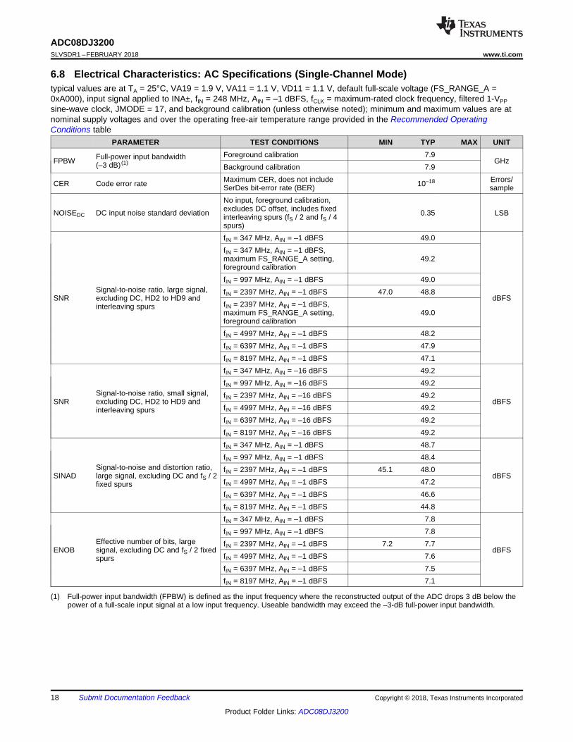
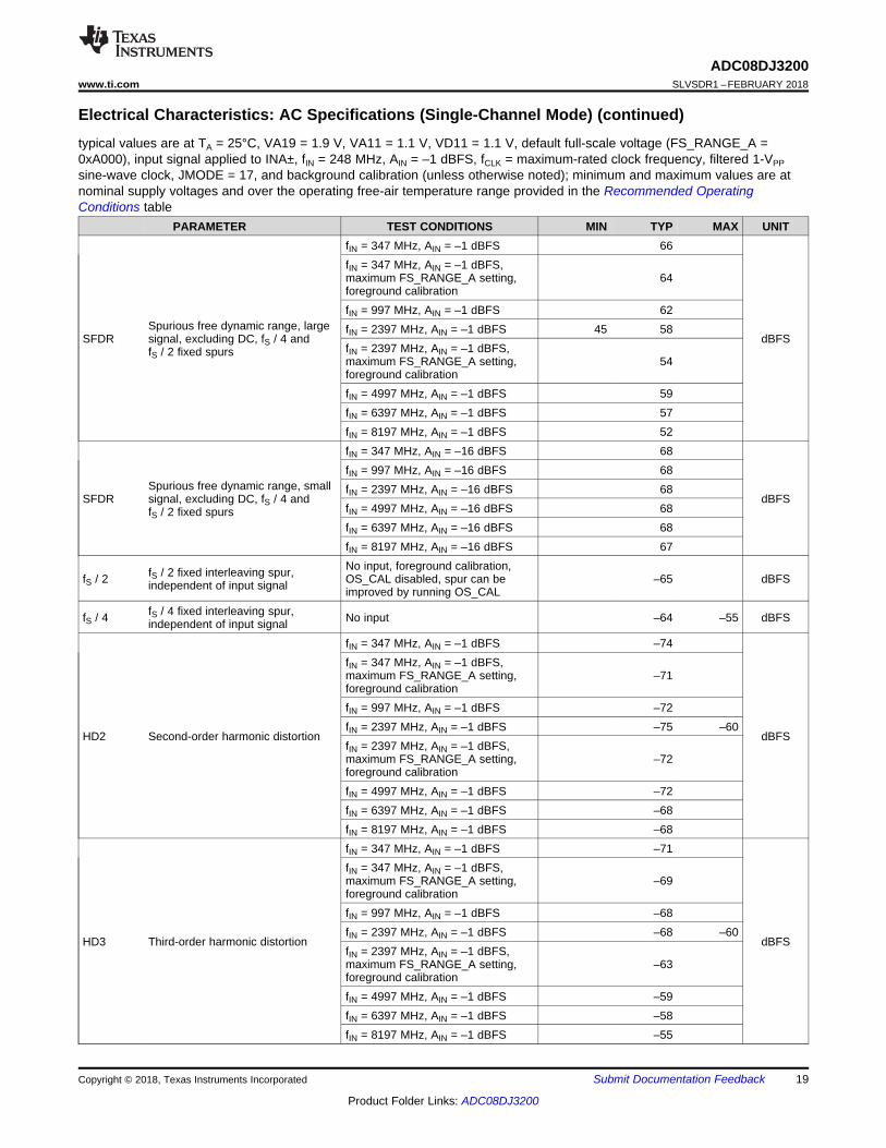
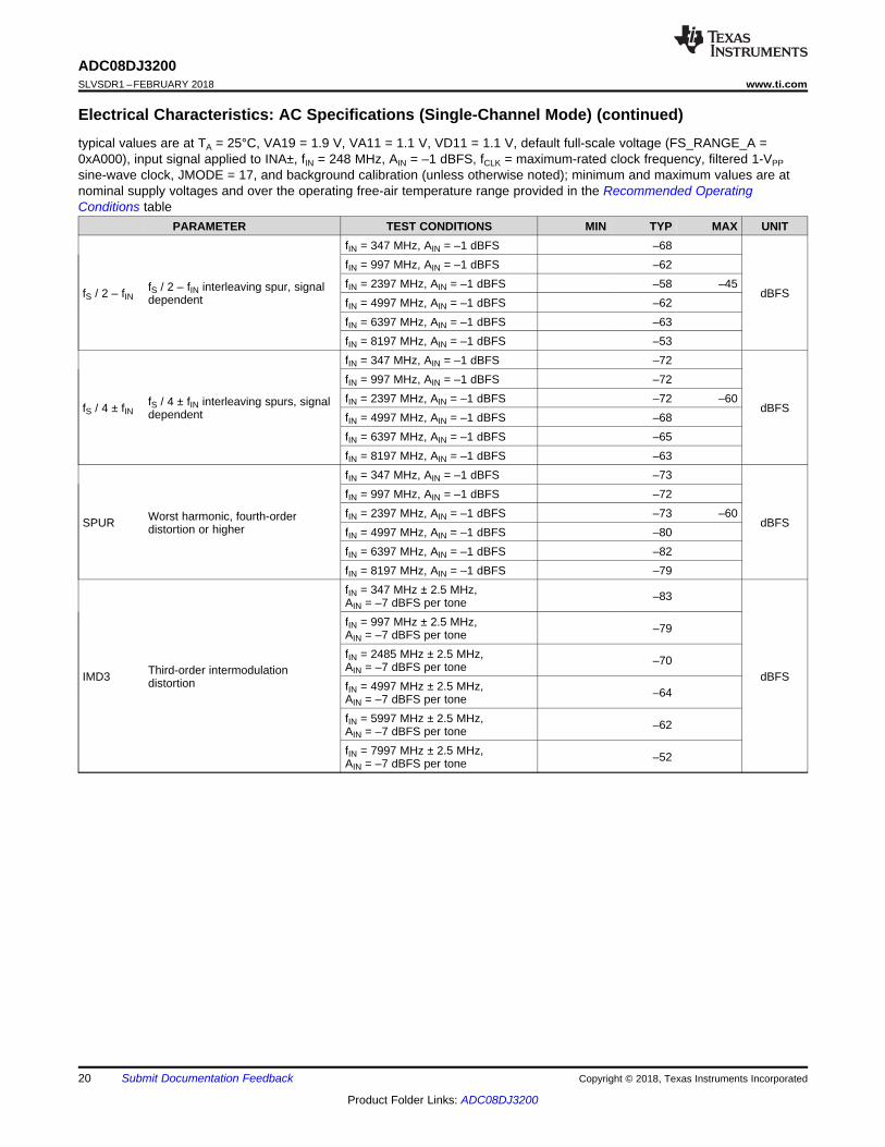
6.8 Electrical Characteristics: AC Specifications (Single-Channel Mode)typical values are at TA = 25°C, VA19 = 1.9 V, VA11 = 1.1 V, VD11 = 1.1 V, default full-scale voltage (FS_RANGE_A =0xA000), input signal applied to INA±, fIN = 248 MHz, AIN = –1 dBFS, fCLK = maximum-rated clock frequency, filtered 1-VPPsine-wave clock, JMODE = 17, and background calibration (unless otherwise noted); minimum and maximum values are atnominal supply voltages and over the operating free-air temperature range provided in the Recommended OperatingConditions table
PARAMETER TEST CONDITIONS MIN TYP MAX UNIT
FPBW Full-power input bandwidth(–3 dB) (1)
Foreground calibration 7.9GHz
Background calibration 7.9
CER Code error rate Maximum CER, does not includeSerDes bit-error rate (BER) 10–18 Errors/
sample
NOISEDC DC input noise standard deviation
No input, foreground calibration,excludes DC offset, includes fixedinterleaving spurs (fS / 2 and fS / 4spurs)
0.35 LSB
SNRSignal-to-noise ratio, large signal,excluding DC, HD2 to HD9 andinterleaving spurs
fIN = 347 MHz, AIN = –1 dBFS 49.0
dBFS
fIN = 347 MHz, AIN = –1 dBFS,maximum FS_RANGE_A setting,foreground calibration
49.2
fIN = 997 MHz, AIN = –1 dBFS 49.0fIN = 2397 MHz, AIN = –1 dBFS 47.0 48.8fIN = 2397 MHz, AIN = –1 dBFS,maximum FS_RANGE_A setting,foreground calibration
49.0
fIN = 4997 MHz, AIN = –1 dBFS 48.2fIN = 6397 MHz, AIN = –1 dBFS 47.9fIN = 8197 MHz, AIN = –1 dBFS 47.1
SNRSignal-to-noise ratio, small signal,excluding DC, HD2 to HD9 andinterleaving spurs
fIN = 347 MHz, AIN = –16 dBFS 49.2
dBFS
fIN = 997 MHz, AIN = –16 dBFS 49.2fIN = 2397 MHz, AIN = –16 dBFS 49.2fIN = 4997 MHz, AIN = –16 dBFS 49.2fIN = 6397 MHz, AIN = –16 dBFS 49.2fIN = 8197 MHz, AIN = –16 dBFS 49.2
SINADSignal-to-noise and distortion ratio,large signal, excluding DC and fS / 2fixed spurs
fIN = 347 MHz, AIN = –1 dBFS 48.7
dBFS
fIN = 997 MHz, AIN = –1 dBFS 48.4fIN = 2397 MHz, AIN = –1 dBFS 45.1 48.0fIN = 4997 MHz, AIN = –1 dBFS 47.2fIN = 6397 MHz, AIN = –1 dBFS 46.6fIN = 8197 MHz, AIN = –1 dBFS 44.8
ENOBEffective number of bits, largesignal, excluding DC and fS / 2 fixedspurs
fIN = 347 MHz, AIN = –1 dBFS 7.8
dBFS
fIN = 997 MHz, AIN = –1 dBFS 7.8fIN = 2397 MHz, AIN = –1 dBFS 7.2 7.7fIN = 4997 MHz, AIN = –1 dBFS 7.6fIN = 6397 MHz, AIN = –1 dBFS 7.5fIN = 8197 MHz, AIN = –1 dBFS 7.1
19
ADC08DJ3200www.ti.com SLVSDR1 –FEBRUARY 2018
Product Folder Links: ADC08DJ3200
Submit Documentation FeedbackCopyright © 2018, Texas Instruments Incorporated
Electrical Characteristics: AC Specifications (Single-Channel Mode) (continued)typical values are at TA = 25°C, VA19 = 1.9 V, VA11 = 1.1 V, VD11 = 1.1 V, default full-scale voltage (FS_RANGE_A =0xA000), input signal applied to INA±, fIN = 248 MHz, AIN = –1 dBFS, fCLK = maximum-rated clock frequency, filtered 1-VPPsine-wave clock, JMODE = 17, and background calibration (unless otherwise noted); minimum and maximum values are atnominal supply voltages and over the operating free-air temperature range provided in the Recommended OperatingConditions table
PARAMETER TEST CONDITIONS MIN TYP MAX UNIT
SFDRSpurious free dynamic range, largesignal, excluding DC, fS / 4 andfS / 2 fixed spurs
fIN = 347 MHz, AIN = –1 dBFS 66
dBFS
fIN = 347 MHz, AIN = –1 dBFS,maximum FS_RANGE_A setting,foreground calibration
64
fIN = 997 MHz, AIN = –1 dBFS 62fIN = 2397 MHz, AIN = –1 dBFS 45 58fIN = 2397 MHz, AIN = –1 dBFS,maximum FS_RANGE_A setting,foreground calibration
54
fIN = 4997 MHz, AIN = –1 dBFS 59fIN = 6397 MHz, AIN = –1 dBFS 57fIN = 8197 MHz, AIN = –1 dBFS 52
SFDRSpurious free dynamic range, smallsignal, excluding DC, fS / 4 andfS / 2 fixed spurs
fIN = 347 MHz, AIN = –16 dBFS 68
dBFS
fIN = 997 MHz, AIN = –16 dBFS 68fIN = 2397 MHz, AIN = –16 dBFS 68fIN = 4997 MHz, AIN = –16 dBFS 68fIN = 6397 MHz, AIN = –16 dBFS 68fIN = 8197 MHz, AIN = –16 dBFS 67
fS / 2 fS / 2 fixed interleaving spur,independent of input signal
No input, foreground calibration,OS_CAL disabled, spur can beimproved by running OS_CAL
–65 dBFS
fS / 4 fS / 4 fixed interleaving spur,independent of input signal No input –64 –55 dBFS
HD2 Second-order harmonic distortion
fIN = 347 MHz, AIN = –1 dBFS –74
dBFS
fIN = 347 MHz, AIN = –1 dBFS,maximum FS_RANGE_A setting,foreground calibration
–71
fIN = 997 MHz, AIN = –1 dBFS –72fIN = 2397 MHz, AIN = –1 dBFS –75 –60fIN = 2397 MHz, AIN = –1 dBFS,maximum FS_RANGE_A setting,foreground calibration
–72
fIN = 4997 MHz, AIN = –1 dBFS –72fIN = 6397 MHz, AIN = –1 dBFS –68fIN = 8197 MHz, AIN = –1 dBFS –68
HD3 Third-order harmonic distortion
fIN = 347 MHz, AIN = –1 dBFS –71
dBFS
fIN = 347 MHz, AIN = –1 dBFS,maximum FS_RANGE_A setting,foreground calibration
–69
fIN = 997 MHz, AIN = –1 dBFS –68fIN = 2397 MHz, AIN = –1 dBFS –68 –60fIN = 2397 MHz, AIN = –1 dBFS,maximum FS_RANGE_A setting,foreground calibration
–63
fIN = 4997 MHz, AIN = –1 dBFS –59fIN = 6397 MHz, AIN = –1 dBFS –58fIN = 8197 MHz, AIN = –1 dBFS –55
20
ADC08DJ3200SLVSDR1 –FEBRUARY 2018 www.ti.com
Product Folder Links: ADC08DJ3200
Submit Documentation Feedback Copyright © 2018, Texas Instruments Incorporated
Electrical Characteristics: AC Specifications (Single-Channel Mode) (continued)typical values are at TA = 25°C, VA19 = 1.9 V, VA11 = 1.1 V, VD11 = 1.1 V, default full-scale voltage (FS_RANGE_A =0xA000), input signal applied to INA±, fIN = 248 MHz, AIN = –1 dBFS, fCLK = maximum-rated clock frequency, filtered 1-VPPsine-wave clock, JMODE = 17, and background calibration (unless otherwise noted); minimum and maximum values are atnominal supply voltages and over the operating free-air temperature range provided in the Recommended OperatingConditions table
PARAMETER TEST CONDITIONS MIN TYP MAX UNIT
fS / 2 – fINfS / 2 – fIN interleaving spur, signaldependent
fIN = 347 MHz, AIN = –1 dBFS –68
dBFS
fIN = 997 MHz, AIN = –1 dBFS –62fIN = 2397 MHz, AIN = –1 dBFS –58 –45fIN = 4997 MHz, AIN = –1 dBFS –62fIN = 6397 MHz, AIN = –1 dBFS –63fIN = 8197 MHz, AIN = –1 dBFS –53
fS / 4 ± fINfS / 4 ± fIN interleaving spurs, signaldependent
fIN = 347 MHz, AIN = –1 dBFS –72
dBFS
fIN = 997 MHz, AIN = –1 dBFS –72fIN = 2397 MHz, AIN = –1 dBFS –72 –60fIN = 4997 MHz, AIN = –1 dBFS –68fIN = 6397 MHz, AIN = –1 dBFS –65fIN = 8197 MHz, AIN = –1 dBFS –63
SPUR Worst harmonic, fourth-orderdistortion or higher
fIN = 347 MHz, AIN = –1 dBFS –73
dBFS
fIN = 997 MHz, AIN = –1 dBFS –72fIN = 2397 MHz, AIN = –1 dBFS –73 –60fIN = 4997 MHz, AIN = –1 dBFS –80fIN = 6397 MHz, AIN = –1 dBFS –82fIN = 8197 MHz, AIN = –1 dBFS –79
IMD3 Third-order intermodulationdistortion
fIN = 347 MHz ± 2.5 MHz,AIN = –7 dBFS per tone –83
dBFS
fIN = 997 MHz ± 2.5 MHz,AIN = –7 dBFS per tone –79
fIN = 2485 MHz ± 2.5 MHz,AIN = –7 dBFS per tone –70
fIN = 4997 MHz ± 2.5 MHz,AIN = –7 dBFS per tone –64
fIN = 5997 MHz ± 2.5 MHz,AIN = –7 dBFS per tone –62
fIN = 7997 MHz ± 2.5 MHz,AIN = –7 dBFS per tone –52
21
ADC08DJ3200www.ti.com SLVSDR1 –FEBRUARY 2018
Product Folder Links: ADC08DJ3200
Submit Documentation FeedbackCopyright © 2018, Texas Instruments Incorporated
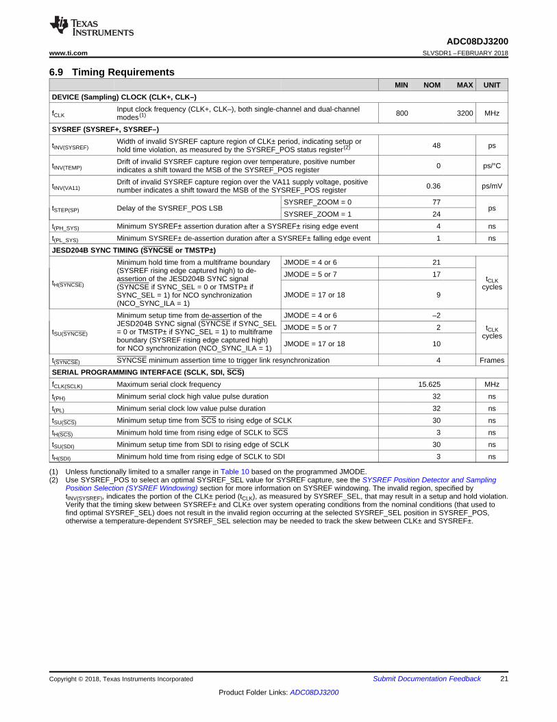
(1) Unless functionally limited to a smaller range in Table 10 based on the programmed JMODE.(2) Use SYSREF_POS to select an optimal SYSREF_SEL value for SYSREF capture, see the SYSREF Position Detector and Sampling
Position Selection (SYSREF Windowing) section for more information on SYSREF windowing. The invalid region, specified bytINV(SYSREF), indicates the portion of the CLK± period (tCLK), as measured by SYSREF_SEL, that may result in a setup and hold violation.Verify that the timing skew between SYSREF± and CLK± over system operating conditions from the nominal conditions (that used tofind optimal SYSREF_SEL) does not result in the invalid region occurring at the selected SYSREF_SEL position in SYSREF_POS,otherwise a temperature-dependent SYSREF_SEL selection may be needed to track the skew between CLK± and SYSREF±.
6.9 Timing RequirementsMIN NOM MAX UNIT
DEVICE (Sampling) CLOCK (CLK+, CLK–)
fCLKInput clock frequency (CLK+, CLK–), both single-channel and dual-channelmodes (1) 800 3200 MHz
SYSREF (SYSREF+, SYSREF–)
tINV(SYSREF)Width of invalid SYSREF capture region of CLK± period, indicating setup orhold time violation, as measured by the SYSREF_POS status register (2) 48 ps
tINV(TEMP)Drift of invalid SYSREF capture region over temperature, positive numberindicates a shift toward the MSB of the SYSREF_POS register 0 ps/°C
tINV(VA11)Drift of invalid SYSREF capture region over the VA11 supply voltage, positivenumber indicates a shift toward the MSB of the SYSREF_POS register 0.36 ps/mV
tSTEP(SP) Delay of the SYSREF_POS LSBSYSREF_ZOOM = 0 77
psSYSREF_ZOOM = 1 24
t(PH_SYS) Minimum SYSREF± assertion duration after a SYSREF± rising edge event 4 nst(PL_SYS) Minimum SYSREF± de-assertion duration after a SYSREF± falling edge event 1 nsJESD204B SYNC TIMING (SYNCSE or TMSTP±)
tH(SYNCSE)
Minimum hold time from a multiframe boundary(SYSREF rising edge captured high) to de-assertion of the JESD204B SYNC signal(SYNCSE if SYNC_SEL = 0 or TMSTP± ifSYNC_SEL = 1) for NCO synchronization(NCO_SYNC_ILA = 1)
JMODE = 4 or 6 21
tCLKcycles
JMODE = 5 or 7 17
JMODE = 17 or 18 9
tSU(SYNCSE)
Minimum setup time from de-assertion of theJESD204B SYNC signal (SYNCSE if SYNC_SEL= 0 or TMSTP± if SYNC_SEL = 1) to multiframeboundary (SYSREF rising edge captured high)for NCO synchronization (NCO_SYNC_ILA = 1)
JMODE = 4 or 6 –2
tCLKcycles
JMODE = 5 or 7 2
JMODE = 17 or 18 10
t(SYNCSE) SYNCSE minimum assertion time to trigger link resynchronization 4 FramesSERIAL PROGRAMMING INTERFACE (SCLK, SDI, SCS)fCLK(SCLK) Maximum serial clock frequency 15.625 MHzt(PH) Minimum serial clock high value pulse duration 32 nst(PL) Minimum serial clock low value pulse duration 32 nstSU(SCS) Minimum setup time from SCS to rising edge of SCLK 30 nstH(SCS) Minimum hold time from rising edge of SCLK to SCS 3 nstSU(SDI) Minimum setup time from SDI to rising edge of SCLK 30 nstH(SDI) Minimum hold time from rising edge of SCLK to SDI 3 ns
22
ADC08DJ3200SLVSDR1 –FEBRUARY 2018 www.ti.com
Product Folder Links: ADC08DJ3200
Submit Documentation Feedback Copyright © 2018, Texas Instruments Incorporated
(1) tAJ increases because of additional attenuation on the internal clock path.
6.10 Switching Characteristicstypical values are at TA = 25°C, VA19 = 1.9 V, VA11 = 1.1 V, VD11 = 1.1 V, default full-scale voltage (FS_RANGE_A =FS_RANGE_B = 0xA000), input signal applied to INA± in single-channel modes, fIN = 248 MHz, AIN = –1 dBFS, fCLK =maximum-rated clock frequency, filtered 1-VPP sine-wave clock, JMODE = 17, and background calibration (unless otherwisenoted); minimum and maximum values are at nominal supply voltages and over the operating free-air temperature rangeprovided in the Recommended Operating Conditions table
PARAMETER TEST CONDITIONS MIN TYP MAX UNITDEVICE (Sampling) CLOCK (CLK+, CLK–)
tAD
Sampling (aperture) delay fromCLK± rising edge (dual-channelmode) or rising and falling edge(single-channel mode) to samplinginstant
TAD_COARSE = 0x00, TAD_FINE =0x00, and TAD_INV = 0 360 ps
tTAD(MAX)
Maximum tAD adjust programmabledelay, not including clock inversion(TAD_INV = 0)
Coarse adjustment (TAD_COARSE= 0xFF) 289
psFine adjustment (TAD_FINE = 0xFF) 4.9
tTAD(STEP)tAD adjust programmable delay stepsize
Coarse adjustment (TAD_COARSE) 1.13 psFine adjustment (TAD_FINE) 19 fs
tAJ Aperture jitter, rms
Minimum tAD adjust coarse setting(TAD_COARSE = 0x00, TAD_INV =0)
50
fsMaximum tAD adjust coarse setting(TAD_COARSE = 0xFF) excludingTAD_INV (TAD_INV = 0)
70 (1)
SERIAL DATA OUTPUTS (DA[7:0]+, DA[7:0]–, DB[7:0]+, DB[7:0]–)fSERDES Serialized output bit rate 1 12.8 GbpsUI Serialized output unit interval 78.125 1000 ps
tTLHLow-to-high transition time(differential)
20% to 80%, PRBS-7 test pattern,12.8 Gbps, SER_PE = 0x04 37 ps
tTHLHigh-to-low transition time(differential)
20% to 80%, PRBS-7 test pattern,12.8 Gbps, SER_PE = 0x04 37 ps
DDJ Data dependent jitter, peak-to-peak PRBS-7 test pattern, 12.8 Gbps,SER_PE = 0x04, JMODE = 2 7.8 ps
RJ Random jitter, RMS PRBS-7 test pattern, 12.8 Gbps,SER_PE = 0x04, JMODE = 2 1.1 ps
TJTotal jitter, peak-to-peak, withGaussian portion defined withrespect to a BER = 1e-15 (Q = 7.94)
PRBS-7 test pattern, 8 Gbps,SER_PE = 0x04, JMODE = 4, 5, 6,7
28 ps
23
ADC08DJ3200www.ti.com SLVSDR1 –FEBRUARY 2018
Product Folder Links: ADC08DJ3200
Submit Documentation FeedbackCopyright © 2018, Texas Instruments Incorporated
Switching Characteristics (continued)typical values are at TA = 25°C, VA19 = 1.9 V, VA11 = 1.1 V, VD11 = 1.1 V, default full-scale voltage (FS_RANGE_A =FS_RANGE_B = 0xA000), input signal applied to INA± in single-channel modes, fIN = 248 MHz, AIN = –1 dBFS, fCLK =maximum-rated clock frequency, filtered 1-VPP sine-wave clock, JMODE = 17, and background calibration (unless otherwisenoted); minimum and maximum values are at nominal supply voltages and over the operating free-air temperature rangeprovided in the Recommended Operating Conditions table
PARAMETER TEST CONDITIONS MIN TYP MAX UNIT
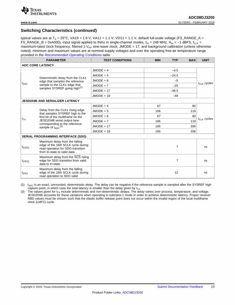
(2) tADC is an exact, unrounded, deterministic delay. The delay can be negative if the reference sample is sampled after the SYSREF highcapture point, in which case the total latency is smaller than the delay given by tTX.
(3) The values given for tTX include deterministic and non-deterministic delays. The delay varies over process, temperature, and voltage.JESD204B accounts for these variations when operating in subclass-1 mode in order to achieve deterministic latency. Proper receiverRBD values must be chosen such that the elastic buffer release point does not occur within the invalid region of the local multiframeclock (LMFC) cycle.
ADC CORE LATENCY
tADC
Deterministic delay from the CLK±edge that samples the referencesample to the CLK± edge thatsamples SYSREF going high (2)
JMODE = 4 –4.5
tCLK cycles
JMODE = 5 –24.5JMODE = 6 –5JMODE = 7 –25JMODE = 17 –48.5JMODE = 18 –49
JESD204B AND SERIALIZER LATENCY
tTX
Delay from the CLK± rising edgethat samples SYSREF high to thefirst bit of the multiframe on theJESD204B serial output lanecorresponding to the referencesample of tADC
(3)
JMODE = 4 67 80
tCLK cycles
JMODE = 5 106 119JMODE = 6 67 80JMODE = 7 106 119JMODE = 17 195 208JMODE = 18 195 208
SERIAL PROGRAMMING INTERFACE (SDO)
t(OZD)
Maximum delay from the fallingedge of the 16th SCLK cycle duringread operation for SDO transitionfrom tri-state to valid data
7 ns
t(ODZ)
Maximum delay from the SCS risingedge for SDO transition from validdata to tri-state
7 ns
t(OD)
Maximum delay from the fallingedge of the 16th SCLK cycle duringread operation to SDO valid
12 ns
tH(SCS)
1st clock
SCLK
16th clock 24th clock
SCS
tSU(SCS)
t(ODZ)
SDI
t(OZD)
D7 D0D1
COMMAND FIELDt(OD)
D7 D0D1SDO
Write Command
Read Command
tSU(SDI) tH(SDI)
t(PH) t(PL)
t(PH) + t(PL) = t(P) = 1 / ¦CLK(SCLK)
Hi-Z Hi-Z
tH(SCS) tSU(SCS)
tSU(SDI) tH(SDI)
CLK+
CLK±
DA0+/±(2)
SYSREF+
SYSREF±
/R
SYNCSE(SYNC_SEL = 0)
tH(SYNCSE) tSU(SYNCSE)
tTXStart of ILAS
LMFC(1)
(Internal)
One multi-frame One multi-frame
TMSTP+/±(SYNC_SEL = 1)
CLK+
CLK±
DA0+/±(1)
tAD tADC
SYSREF+
SYSREF±
tSU(SYSREF)
tTX
S0
S1S2
tCLK
S0 S1 S2
tH(SYSREF)
Start of Multi-Frame
24
ADC08DJ3200SLVSDR1 –FEBRUARY 2018 www.ti.com
Product Folder Links: ADC08DJ3200
Submit Documentation Feedback Copyright © 2018, Texas Instruments Incorporated
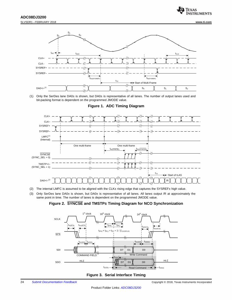
(1) Only the SerDes lane DA0± is shown, but DA0± is representative of all lanes. The number of output lanes used andbit-packing format is dependent on the programmed JMODE value.
Figure 1. ADC Timing Diagram
(2) The internal LMFC is assumed to be aligned with the CLK± rising edge that captures the SYSREF± high value.(3) Only SerDes lane DA0± is shown, but DA0± is representative of all lanes. All lanes output /R at approximately the
same point in time. The number of lanes is dependent on the programmed JMODE value.
Figure 2. SYNCSE and TMSTP± Timing Diagram for NCO Synchronization
Figure 3. Serial Interface Timing
fIN (MHz)
Mag
nitu
de (
dBF
S)
0 2000 4000 6000 8000 10000-90
-85
-80
-75
-70
-65
-60
-55
-50
-45
D130
HD2HD3THD
fIN (MHz)
Mag
nitu
de (
dBF
S)
0 2000 4000 6000 8000 10000-85
-80
-75
-70
-65
-60
-55
-50
-45
D132
HD2HD3THD
fIN (MHz)
Mag
nitu
de (
dBF
S)
0 2000 4000 6000 8000 1000040
45
50
55
60
65
70
75
D131
SNRSINADSFDR
fIN (MHz)
Mag
nitu
de (
dBF
S)
0 2000 4000 6000 8000 1000040
45
50
55
60
65
70
75
D129
SNRSINADSFDR
fIN (MHz)
Effe
ctiv
e N
umbe
r of
Bits
(B
its)
0 2000 4000 6000 8000 100006.5
7
7.5
8
D010
BG CalibrationFG Calibration
fIN (MHz)
Effe
ctiv
e N
umbe
r of
Bits
(B
its)
0 2000 4000 6000 8000 100006.5
7
7.5
8
D002
BG CalibrationFG Calibration
25
ADC08DJ3200www.ti.com SLVSDR1 –FEBRUARY 2018
Product Folder Links: ADC08DJ3200
Submit Documentation FeedbackCopyright © 2018, Texas Instruments Incorporated
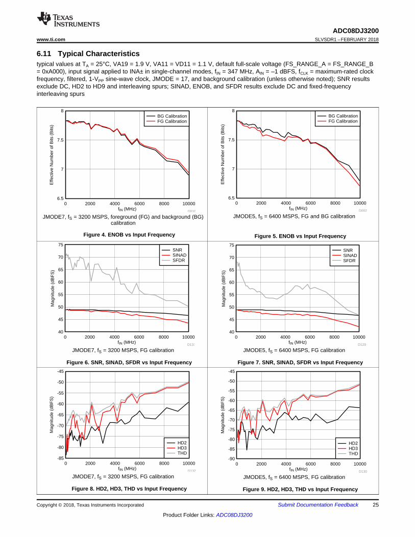
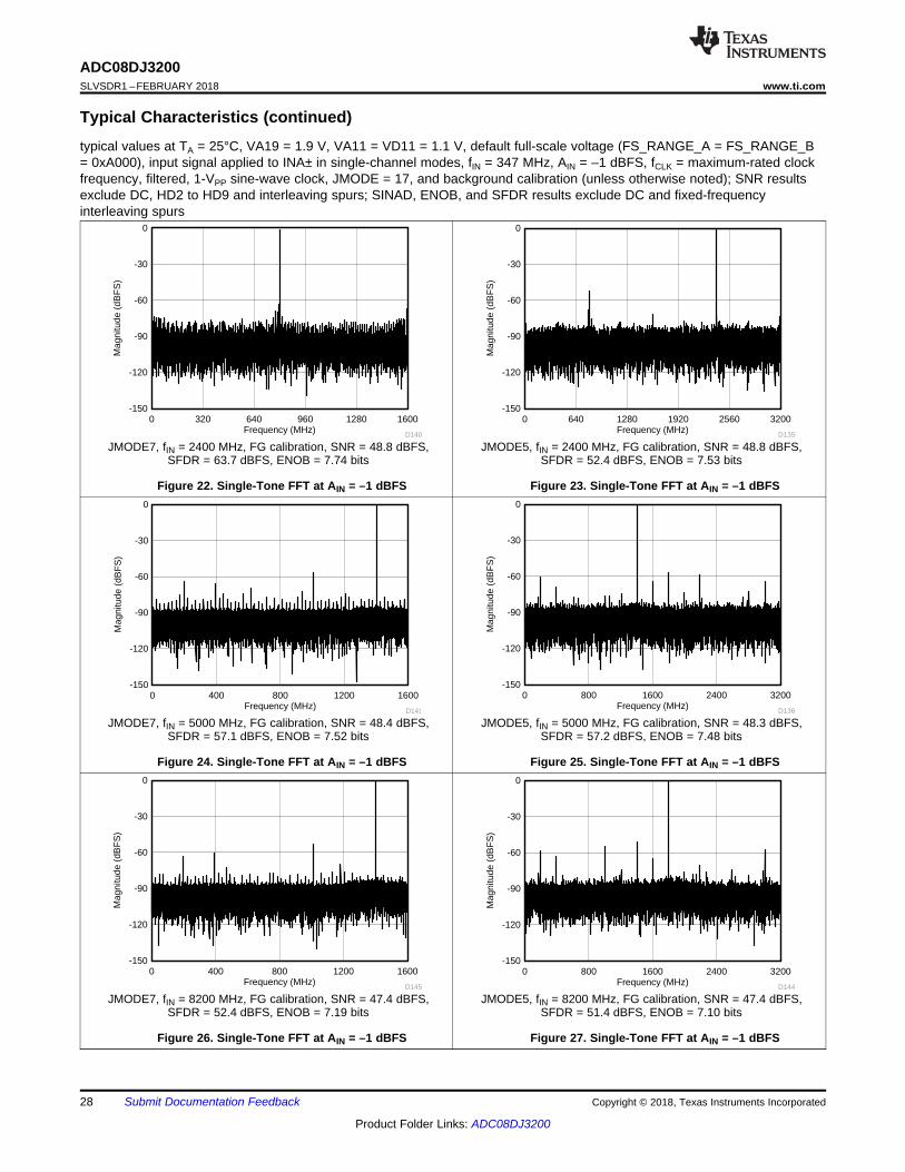
6.11 Typical Characteristicstypical values at TA = 25°C, VA19 = 1.9 V, VA11 = VD11 = 1.1 V, default full-scale voltage (FS_RANGE_A = FS_RANGE_B= 0xA000), input signal applied to INA± in single-channel modes, fIN = 347 MHz, AIN = –1 dBFS, fCLK = maximum-rated clockfrequency, filtered, 1-VPP sine-wave clock, JMODE = 17, and background calibration (unless otherwise noted); SNR resultsexclude DC, HD2 to HD9 and interleaving spurs; SINAD, ENOB, and SFDR results exclude DC and fixed-frequencyinterleaving spurs
JMODE7, fS = 3200 MSPS, foreground (FG) and background (BG)calibration
Figure 4. ENOB vs Input Frequency
JMODE5, fS = 6400 MSPS, FG and BG calibration
Figure 5. ENOB vs Input Frequency
JMODE7, fS = 3200 MSPS, FG calibration
Figure 6. SNR, SINAD, SFDR vs Input Frequency
JMODE5, fS = 6400 MSPS, FG calibration
Figure 7. SNR, SINAD, SFDR vs Input Frequency
JMODE7, fS = 3200 MSPS, FG calibration
Figure 8. HD2, HD3, THD vs Input Frequency
JMODE5, fS = 6400 MSPS, FG calibration
Figure 9. HD2, HD3, THD vs Input Frequency
fS (MSPS)
Effe
ctiv
e N
umbe
r of
Bits
(B
its)
800 1200 1600 2000 2400 2800 32007.25
7.5
7.75
8
8.25
D013fS (MSPS)
Effe
ctiv
e N
umbe
r of
Bits
(B
its)
1600 2400 3200 4000 4800 5600 64007.25
7.5
7.75
8
8.25
D005
fIN (MHz)
Mag
nitu
de (
dBF
S)
0 2000 4000 6000 8000 10000-80
-75
-70
-65
-60
-55
-50
-45
D003
HD2HD3THD
fIN (MHz)
Mag
nitu
de (
dBF
S)
0 2000 4000 6000 8000 10000-80
-75
-70
-65
-60
-55
-50
-45
D011
HD2HD3THD
fIN (MHz)
Mag
nitu
de (
dBF
S)
0 2000 4000 6000 8000 1000040
45
50
55
60
65
70
75
D009
SNRSINADSFDR
fIN (MHz)
Mag
nitu
de (
dBF
S)
0 2000 4000 6000 8000 1000040
45
50
55
60
65
70
75
D001
SNRSINADSFDR
26
ADC08DJ3200SLVSDR1 –FEBRUARY 2018 www.ti.com
Product Folder Links: ADC08DJ3200
Submit Documentation Feedback Copyright © 2018, Texas Instruments Incorporated
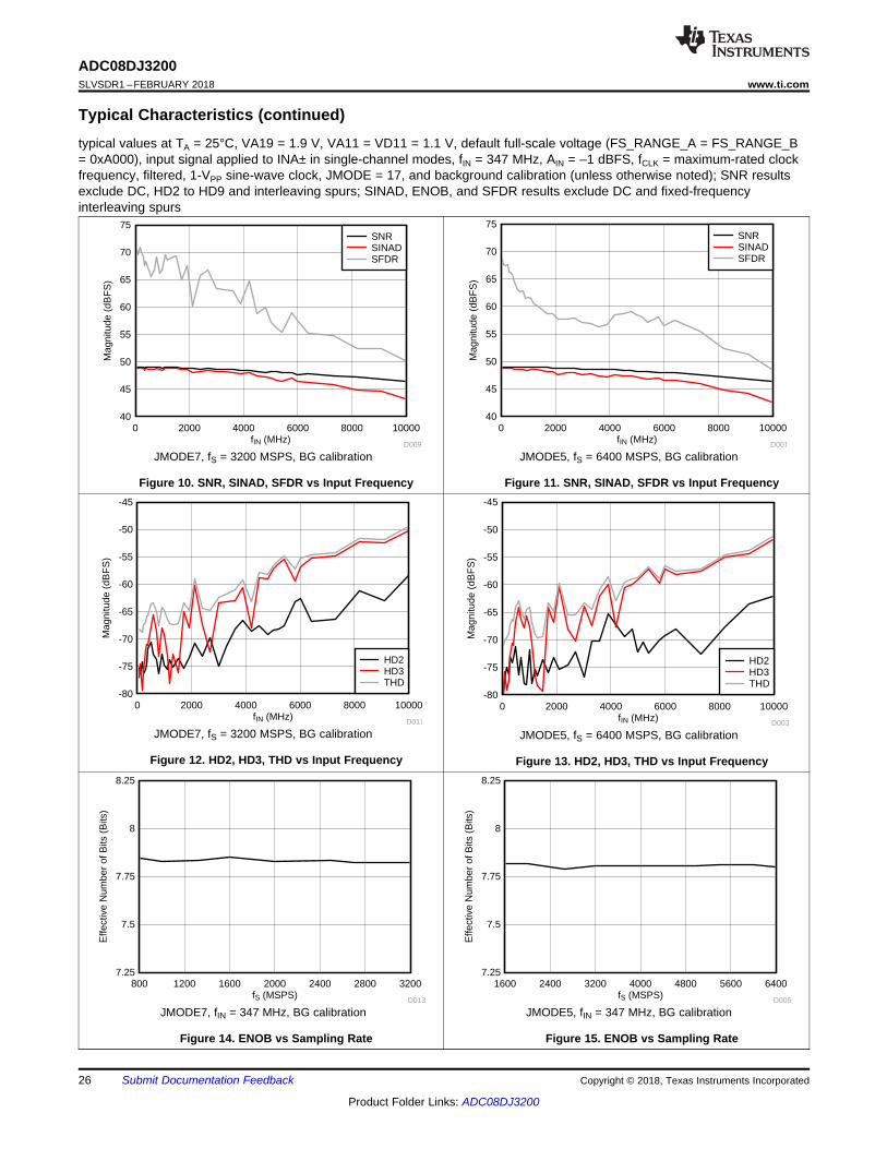
Typical Characteristics (continued)typical values at TA = 25°C, VA19 = 1.9 V, VA11 = VD11 = 1.1 V, default full-scale voltage (FS_RANGE_A = FS_RANGE_B= 0xA000), input signal applied to INA± in single-channel modes, fIN = 347 MHz, AIN = –1 dBFS, fCLK = maximum-rated clockfrequency, filtered, 1-VPP sine-wave clock, JMODE = 17, and background calibration (unless otherwise noted); SNR resultsexclude DC, HD2 to HD9 and interleaving spurs; SINAD, ENOB, and SFDR results exclude DC and fixed-frequencyinterleaving spurs
JMODE7, fS = 3200 MSPS, BG calibration
Figure 10. SNR, SINAD, SFDR vs Input Frequency
JMODE5, fS = 6400 MSPS, BG calibration
Figure 11. SNR, SINAD, SFDR vs Input Frequency
JMODE7, fS = 3200 MSPS, BG calibration
Figure 12. HD2, HD3, THD vs Input Frequency
JMODE5, fS = 6400 MSPS, BG calibration
Figure 13. HD2, HD3, THD vs Input Frequency
JMODE7, fIN = 347 MHz, BG calibration
Figure 14. ENOB vs Sampling Rate
JMODE5, fIN = 347 MHz, BG calibration
Figure 15. ENOB vs Sampling Rate
Frequency (MHz)
Mag
nitu
de (
dBF
S)
0 400 800 1200 1600-150
-120
-90
-60
-30
0
D139Frequency (MHz)
Mag
nitu
de (
dBF
S)
0 800 1600 2400 3200-150
-120
-90
-60
-30
0
D134
fS (MSPS)
Mag
nitu
de (
dBF
S)
800 1200 1600 2000 2400 2800 3200-90
-85
-80
-75
-70
-65
-60
-55
D014D014
HD2HD3THD
fS (MSPS)
Mag
nitu
de (
dBF
S)
1600 2400 3200 4000 4800 5600 6400-90
-85
-80
-75
-70
-65
-60
-55
D006
HD2HD3THD
fS (MSPS)
Mag
nitu
de (
dBF
S)
1600 2400 3200 4000 4800 5600 640035
40
45
50
55
60
65
70
75
D004
SNRSINADSFDR
fS (MSPS)
Mag
nitu
de (
dBF
S)
800 1200 1600 2000 2400 2800 320035
40
45
50
55
60
65
70
75
D012
SNRSINADSFDR
27
ADC08DJ3200www.ti.com SLVSDR1 –FEBRUARY 2018
Product Folder Links: ADC08DJ3200
Submit Documentation FeedbackCopyright © 2018, Texas Instruments Incorporated
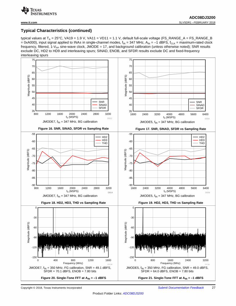
Typical Characteristics (continued)typical values at TA = 25°C, VA19 = 1.9 V, VA11 = VD11 = 1.1 V, default full-scale voltage (FS_RANGE_A = FS_RANGE_B= 0xA000), input signal applied to INA± in single-channel modes, fIN = 347 MHz, AIN = –1 dBFS, fCLK = maximum-rated clockfrequency, filtered, 1-VPP sine-wave clock, JMODE = 17, and background calibration (unless otherwise noted); SNR resultsexclude DC, HD2 to HD9 and interleaving spurs; SINAD, ENOB, and SFDR results exclude DC and fixed-frequencyinterleaving spurs
JMODE7, fIN = 347 MHz, BG calibration
Figure 16. SNR, SINAD, SFDR vs Sampling Rate
JMODE5, fIN = 347 MHz, BG calibration
Figure 17. SNR, SINAD, SFDR vs Sampling Rate
JMODE7, fIN = 347 MHz, BG calibration
Figure 18. HD2, HD3, THD vs Sampling Rate
JMODE5, fIN = 347 MHz, BG calibration
Figure 19. HD2, HD3, THD vs Sampling Rate
JMODE7, fIN = 350 MHz, FG calibration, SNR = 49.1 dBFS,SFDR = 70.1 dBFS, ENOB = 7.80 bits
Figure 20. Single-Tone FFT at AIN = –1 dBFS
JMODE5, fIN = 350 MHz, FG calibration, SNR = 49.0 dBFS,SFDR = 64.0 dBFS, ENOB = 7.80 bits
Figure 21. Single-Tone FFT at AIN = –1 dBFS
Frequency (MHz)
Mag
nitu
de (
dBF
S)
0 400 800 1200 1600-150
-120
-90
-60
-30
0
D145 Frequency (MHz)
Mag
nitu
de (
dBF
S)
0 800 1600 2400 3200-150
-120
-90
-60
-30
0
D144
Frequency (MHz)
Mag
nitu
de (
dBF
S)
0 400 800 1200 1600-150
-120
-90
-60
-30
0
D141Frequency (MHz)
Mag
nitu
de (
dBF
S)
0 800 1600 2400 3200-150
-120
-90
-60
-30
0
D136
Frequency (MHz)
Mag
nitu
de (
dBF
S)
0 320 640 960 1280 1600-150
-120
-90
-60
-30
0
D140Frequency (MHz)
Mag
nitu
de (
dBF
S)
0 640 1280 1920 2560 3200-150
-120
-90
-60
-30
0
D135
28
ADC08DJ3200SLVSDR1 –FEBRUARY 2018 www.ti.com
Product Folder Links: ADC08DJ3200
Submit Documentation Feedback Copyright © 2018, Texas Instruments Incorporated
Typical Characteristics (continued)typical values at TA = 25°C, VA19 = 1.9 V, VA11 = VD11 = 1.1 V, default full-scale voltage (FS_RANGE_A = FS_RANGE_B= 0xA000), input signal applied to INA± in single-channel modes, fIN = 347 MHz, AIN = –1 dBFS, fCLK = maximum-rated clockfrequency, filtered, 1-VPP sine-wave clock, JMODE = 17, and background calibration (unless otherwise noted); SNR resultsexclude DC, HD2 to HD9 and interleaving spurs; SINAD, ENOB, and SFDR results exclude DC and fixed-frequencyinterleaving spurs
JMODE7, fIN = 2400 MHz, FG calibration, SNR = 48.8 dBFS,SFDR = 63.7 dBFS, ENOB = 7.74 bits
Figure 22. Single-Tone FFT at AIN = –1 dBFS
JMODE5, fIN = 2400 MHz, FG calibration, SNR = 48.8 dBFS,SFDR = 52.4 dBFS, ENOB = 7.53 bits
Figure 23. Single-Tone FFT at AIN = –1 dBFS
JMODE7, fIN = 5000 MHz, FG calibration, SNR = 48.4 dBFS,SFDR = 57.1 dBFS, ENOB = 7.52 bits
Figure 24. Single-Tone FFT at AIN = –1 dBFS
JMODE5, fIN = 5000 MHz, FG calibration, SNR = 48.3 dBFS,SFDR = 57.2 dBFS, ENOB = 7.48 bits
Figure 25. Single-Tone FFT at AIN = –1 dBFS
JMODE7, fIN = 8200 MHz, FG calibration, SNR = 47.4 dBFS,SFDR = 52.4 dBFS, ENOB = 7.19 bits
Figure 26. Single-Tone FFT at AIN = –1 dBFS
JMODE5, fIN = 8200 MHz, FG calibration, SNR = 47.4 dBFS,SFDR = 51.4 dBFS, ENOB = 7.10 bits
Figure 27. Single-Tone FFT at AIN = –1 dBFS
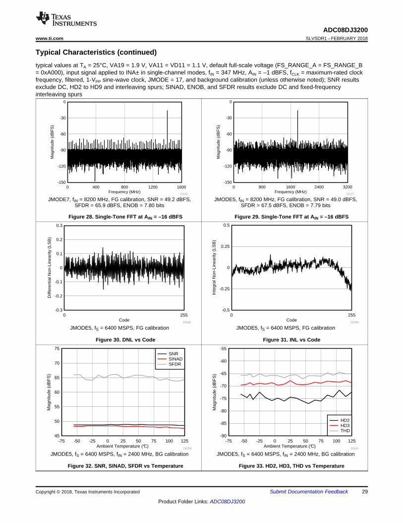
Ambient Temperature (°C)
Mag
nitu
de (
dBF
S)
-75 -50 -25 0 25 50 75 100 12545
50
55
60
65
70
75
D039
SNRSINADSFDR
Ambient Temperature (°C)
Mag
nitu
de (
dBF
S)
-75 -50 -25 0 25 50 75 100 125-90
-85
-80
-75
-70
-65
-60
-55
D041
HD2HD3THD
Code
Diff
eren
tial N
on-L
inea
rity
(LS
B)
0 255-0.3
-0.2
-0.1
0
0.1
0.2
0.3
D048Code
Inte
gral
Non
-Lin
earit
y (L
SB
)
0 255-0.5
-0.25
0
0.25
0.5
D049
Frequency (MHz)
Mag
nitu
de (
dBF
S)
0 400 800 1200 1600-150
-120
-90
-60
-30
0
D142Frequency (MHz)
Mag
nitu
de (
dBF
S)
0 800 1600 2400 3200-150
-120
-90
-60
-30
0
D137
29
ADC08DJ3200www.ti.com SLVSDR1 –FEBRUARY 2018
Product Folder Links: ADC08DJ3200
Submit Documentation FeedbackCopyright © 2018, Texas Instruments Incorporated
Typical Characteristics (continued)typical values at TA = 25°C, VA19 = 1.9 V, VA11 = VD11 = 1.1 V, default full-scale voltage (FS_RANGE_A = FS_RANGE_B= 0xA000), input signal applied to INA± in single-channel modes, fIN = 347 MHz, AIN = –1 dBFS, fCLK = maximum-rated clockfrequency, filtered, 1-VPP sine-wave clock, JMODE = 17, and background calibration (unless otherwise noted); SNR resultsexclude DC, HD2 to HD9 and interleaving spurs; SINAD, ENOB, and SFDR results exclude DC and fixed-frequencyinterleaving spurs
JMODE7, fIN = 8200 MHz, FG calibration, SNR = 49.2 dBFS,SFDR = 65.9 dBFS, ENOB = 7.80 bits
Figure 28. Single-Tone FFT at AIN = –16 dBFS
JMODE5, fIN = 8200 MHz, FG calibration, SNR = 49.0 dBFS,SFDR = 67.5 dBFS, ENOB = 7.79 bits
Figure 29. Single-Tone FFT at AIN = –16 dBFS
JMODE5, fS = 6400 MSPS, FG calibration
Figure 30. DNL vs Code
JMODE5, fS = 6400 MSPS, FG calibration
Figure 31. INL vs Code
JMODE5, fS = 6400 MSPS, fIN = 2400 MHz, BG calibration
Figure 32. SNR, SINAD, SFDR vs Temperature
JMODE5, fS = 6400 MSPS, fIN = 2400 MHz, BG calibration
Figure 33. HD2, HD3, THD vs Temperature
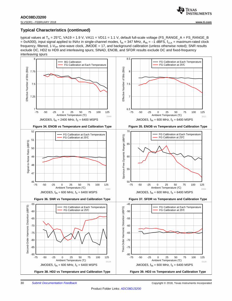
Ambient Temperature (°C)
Sec
ond-
Ord
er H
arm
onic
Dis
tort
ion
(dB
FS
)
-75 -50 -25 0 25 50 75 100 125-90
-85
-80
-75
-70
-65
-60
-55
D119
FG Calibration at Each TemperatureFG Calibration at 25°C
Ambient Temperature (°C)
Thi
rd-O
rder
Har
mon
ic D
isto
rtio
n (d
BF
S)
-75 -50 -25 0 25 50 75 100 125-80
-75
-70
-65
-60
-55
-50
-45
D120
FG Calibration at Each TemperatureFG Calibration at 25°C
Ambient Temperature (°C)
Sig
nal-t
o-N
oise
Rat
io (
dBF
S)
-75 -50 -25 0 25 50 75 100 12546
47
48
49
50
51
52
D063
FG Calibration at Each TemperatureFG Calibration at 25°C
Ambient Temperature (°C)
Spu
rious
-Fre
e D
ynam
ic R
ange
(dB
FS
)
-75 -50 -25 0 25 50 75 100 12550
55
60
65
70
D064
FG Calibration at Each TemperatureFG Calibration at 25°C
Ambient Temperature (°C)
Effe
ctiv
e N
umbe
r of
Bits
(B
its)
-75 -50 -25 0 25 50 75 100 1257
7.25
7.5
7.75
8
D040
BG CalibrationFG Calibration at Each Temperature
Ambient Temperature (°C)
Effe
ctiv
e N
umbe
r of
Bits
(B
its)
-75 -50 -25 0 25 50 75 100 1256.5
7
7.5
8
8.5
D121
FG Calibration at Each TemperatureFG Calibration at 25°C
30
ADC08DJ3200SLVSDR1 –FEBRUARY 2018 www.ti.com
Product Folder Links: ADC08DJ3200
Submit Documentation Feedback Copyright © 2018, Texas Instruments Incorporated
Typical Characteristics (continued)typical values at TA = 25°C, VA19 = 1.9 V, VA11 = VD11 = 1.1 V, default full-scale voltage (FS_RANGE_A = FS_RANGE_B= 0xA000), input signal applied to INA± in single-channel modes, fIN = 347 MHz, AIN = –1 dBFS, fCLK = maximum-rated clockfrequency, filtered, 1-VPP sine-wave clock, JMODE = 17, and background calibration (unless otherwise noted); SNR resultsexclude DC, HD2 to HD9 and interleaving spurs; SINAD, ENOB, and SFDR results exclude DC and fixed-frequencyinterleaving spurs
JMODE5, fIN = 2400 MHz, fS = 6400 MSPS
Figure 34. ENOB vs Temperature and Calibration Type
JMODE5, fIN = 600 MHz, fS = 6400 MSPS
Figure 35. ENOB vs Temperature and Calibration Type
JMODE5, fIN = 600 MHz, fS = 6400 MSPS
Figure 36. SNR vs Temperature and Calibration Type
JMODE5, fIN = 600 MHz, fS = 6400 MSPS
Figure 37. SFDR vs Temperature and Calibration Type
JMODE5, fIN = 600 MHz, fS = 6400 MSPS
Figure 38. HD2 vs Temperature and Calibration Type
JMODE5, fIN = 600 MHz, fS = 6400 MSPS
Figure 39. HD3 vs Temperature and Calibration Type
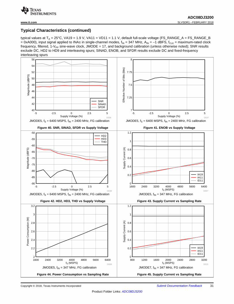
fS (MSPS)
Pow
er C
onsu
mpt
ion
(W)
1600 2400 3200 4000 4800 5600 64002
2.2
2.4
2.6
2.8
3
3.2
D008fS (MSPS)
Sup
ply
Cur
rent
(A
)
800 1200 1600 2000 2400 2800 32000
0.2
0.4
0.6
0.8
1
1.2
D015
IA19IA11ID11
Supply Voltage (%)
Mag
nitu
de (
dBF
S)
-5 -2.5 0 2.5 5-90
-85
-80
-75
-70
-65
-60
-55
-50
D038
HD2HD3THD
fS (MSPS)
Sup
ply
Cur
rent
(A
)
1600 2400 3200 4000 4800 5600 64000
0.2
0.4
0.6
0.8
1
1.2
D007
IA19IA11ID11
Supply Voltage (%)
Mag
nitu
de (
dBF
S)
-5 -2.5 0 2.5 540
42
44
46
48
50
52
54
56
D036
SNRSINADSFDR
Supply Voltage (%)
Effe
ctiv
e N
umbe
r of
Bits
(B
its)
-5 -2.5 0 2.5 57
7.25
7.5
7.75
8
D037
31
ADC08DJ3200www.ti.com SLVSDR1 –FEBRUARY 2018
Product Folder Links: ADC08DJ3200
Submit Documentation FeedbackCopyright © 2018, Texas Instruments Incorporated
Typical Characteristics (continued)typical values at TA = 25°C, VA19 = 1.9 V, VA11 = VD11 = 1.1 V, default full-scale voltage (FS_RANGE_A = FS_RANGE_B= 0xA000), input signal applied to INA± in single-channel modes, fIN = 347 MHz, AIN = –1 dBFS, fCLK = maximum-rated clockfrequency, filtered, 1-VPP sine-wave clock, JMODE = 17, and background calibration (unless otherwise noted); SNR resultsexclude DC, HD2 to HD9 and interleaving spurs; SINAD, ENOB, and SFDR results exclude DC and fixed-frequencyinterleaving spurs
JMODE5, fS = 6400 MSPS, fIN = 2400 MHz, FG calibration
Figure 40. SNR, SINAD, SFDR vs Supply Voltage
JMODE5, fS = 6400 MSPS, fIN = 2400 MHz, FG calibration
Figure 41. ENOB vs Supply Voltage
JMODE5, fS = 6400 MSPS, fIN = 2400 MHz, FG calibration
Figure 42. HD2, HD3, THD vs Supply Voltage
JMODE5, fIN = 347 MHz, FG calibration
Figure 43. Supply Current vs Sampling Rate
JMODE5, fIN = 347 MHz, FG calibration
Figure 44. Power Consumption vs Sampling Rate
JMODE7, fIN = 347 MHz, FG calibration
Figure 45. Supply Current vs Sampling Rate
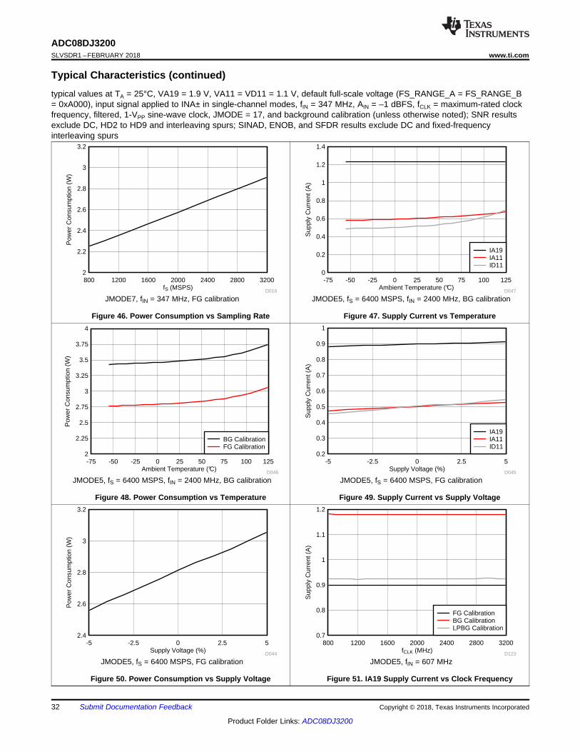
Supply Voltage (%)
Pow
er C
onsu
mpt
ion
(W)
-5 -2.5 0 2.5 52.4
2.6
2.8
3
3.2
D044fCLK (MHz)
Sup
ply
Cur
rent
(A
)
800 1200 1600 2000 2400 2800 32000.7
0.8
0.9
1
1.1
1.2
D123
FG CalibrationBG CalibrationLPBG Calibration
Ambient Temperature (°C)
Pow
er C
onsu
mpt
ion
(W)
-75 -50 -25 0 25 50 75 100 1252
2.25
2.5
2.75
3
3.25
3.5
3.75
4
D046
BG CalibrationFG Calibration
Supply Voltage (%)
Sup
ply
Cur
rent
(A
)
-5 -2.5 0 2.5 50.2
0.3
0.4
0.5
0.6
0.7
0.8
0.9
1
D045
IA19IA11ID11
fS (MSPS)
Pow
er C
onsu
mpt
ion
(W)
800 1200 1600 2000 2400 2800 32002
2.2
2.4
2.6
2.8
3
3.2
D016Ambient Temperature (°C)
Sup
ply
Cur
rent
(A
)
-75 -50 -25 0 25 50 75 100 1250
0.2
0.4
0.6
0.8
1
1.2
1.4
D047
IA19IA11ID11
32
ADC08DJ3200SLVSDR1 –FEBRUARY 2018 www.ti.com
Product Folder Links: ADC08DJ3200
Submit Documentation Feedback Copyright © 2018, Texas Instruments Incorporated
Typical Characteristics (continued)typical values at TA = 25°C, VA19 = 1.9 V, VA11 = VD11 = 1.1 V, default full-scale voltage (FS_RANGE_A = FS_RANGE_B= 0xA000), input signal applied to INA± in single-channel modes, fIN = 347 MHz, AIN = –1 dBFS, fCLK = maximum-rated clockfrequency, filtered, 1-VPP sine-wave clock, JMODE = 17, and background calibration (unless otherwise noted); SNR resultsexclude DC, HD2 to HD9 and interleaving spurs; SINAD, ENOB, and SFDR results exclude DC and fixed-frequencyinterleaving spurs
JMODE7, fIN = 347 MHz, FG calibration
Figure 46. Power Consumption vs Sampling Rate
JMODE5, fS = 6400 MSPS, fIN = 2400 MHz, BG calibration
Figure 47. Supply Current vs Temperature
JMODE5, fS = 6400 MSPS, fIN = 2400 MHz, BG calibration
Figure 48. Power Consumption vs Temperature
JMODE5, fS = 6400 MSPS, FG calibration
Figure 49. Supply Current vs Supply Voltage
JMODE5, fS = 6400 MSPS, FG calibration
Figure 50. Power Consumption vs Supply Voltage
JMODE5, fIN = 607 MHz
Figure 51. IA19 Supply Current vs Clock Frequency
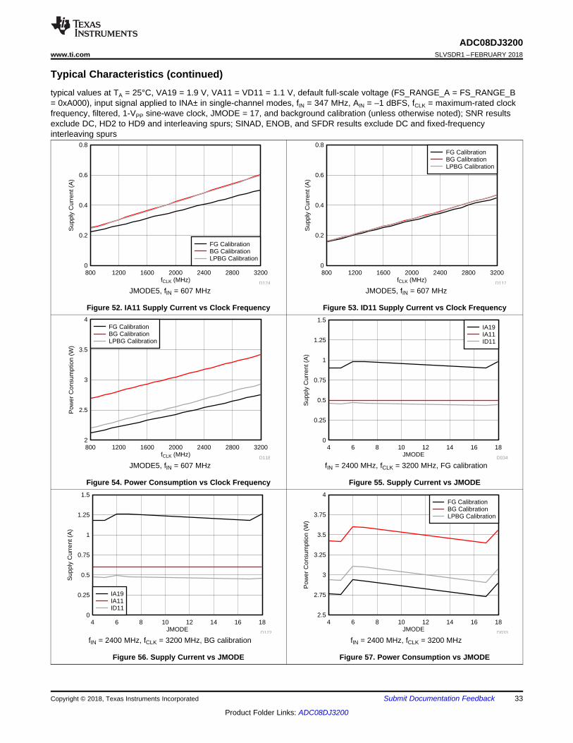
JMODE
Sup
ply
Cur
rent
(A
)
4 6 8 10 12 14 16 180
0.25
0.5
0.75
1
1.25
1.5
D122
IA19IA11ID11
JMODE
Pow
er C
onsu
mpt
ion
(W)
4 6 8 10 12 14 16 182.5
2.75
3
3.25
3.5
3.75
4
D033
FG CalibrationBG CalibrationLPBG Calibration
fCLK (MHz)
Pow
er C
onsu
mpt
ion
(W)
800 1200 1600 2000 2400 2800 32002
2.5
3
3.5
4
D118
FG CalibrationBG CalibrationLPBG Calibration
JMODE
Sup
ply
Cur
rent
(A
)
4 6 8 10 12 14 16 180
0.25
0.5
0.75
1
1.25
1.5
D034
IA19IA11ID11
fCLK (MHz)
Sup
ply
Cur
rent
(A
)
800 1200 1600 2000 2400 2800 32000
0.2
0.4
0.6
0.8
D124
FG CalibrationBG CalibrationLPBG Calibration
fCLK (MHz)
Sup
ply
Cur
rent
(A
)
800 1200 1600 2000 2400 2800 32000
0.2
0.4
0.6
0.8
D117
FG CalibrationBG CalibrationLPBG Calibration
33
ADC08DJ3200www.ti.com SLVSDR1 –FEBRUARY 2018
Product Folder Links: ADC08DJ3200
Submit Documentation FeedbackCopyright © 2018, Texas Instruments Incorporated
Typical Characteristics (continued)typical values at TA = 25°C, VA19 = 1.9 V, VA11 = VD11 = 1.1 V, default full-scale voltage (FS_RANGE_A = FS_RANGE_B= 0xA000), input signal applied to INA± in single-channel modes, fIN = 347 MHz, AIN = –1 dBFS, fCLK = maximum-rated clockfrequency, filtered, 1-VPP sine-wave clock, JMODE = 17, and background calibration (unless otherwise noted); SNR resultsexclude DC, HD2 to HD9 and interleaving spurs; SINAD, ENOB, and SFDR results exclude DC and fixed-frequencyinterleaving spurs
JMODE5, fIN = 607 MHz
Figure 52. IA11 Supply Current vs Clock Frequency
JMODE5, fIN = 607 MHz
Figure 53. ID11 Supply Current vs Clock Frequency
JMODE5, fIN = 607 MHz
Figure 54. Power Consumption vs Clock Frequency
fIN = 2400 MHz, fCLK = 3200 MHz, FG calibration
Figure 55. Supply Current vs JMODE
fIN = 2400 MHz, fCLK = 3200 MHz, BG calibration
Figure 56. Supply Current vs JMODE
fIN = 2400 MHz, fCLK = 3200 MHz
Figure 57. Power Consumption vs JMODE
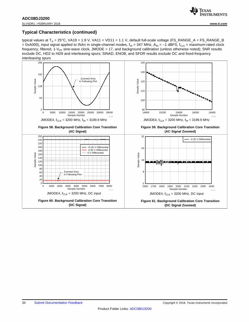
Sample Number
Sam
ple
Val
ue
1600 1700 1800 1900 2000 2100 2200 2300 24000
8
16
24
32
D128
-0.35 V Differential
Sample Number
Sam
ple
Val
ue
0 1000 2000 3000 4000 5000 6000 7000 80000
20
40
60
80
100
120
140
160
180
200
220
240
260
Zoomed Areain Following Plot
D127
+0.35 V Differential-0.35 V Differential0 V Differential
Sample Number
Sam
ple
Val
ue
0 5000 10000 15000 20000 25000 30000 350000
64
128
192
256
Zoomed Areain Following Plot
D125Sample Number
Sam
ple
Val
ue
14800 15200 15600 16000 1640090
100
110
120
130
140
D126
34
ADC08DJ3200SLVSDR1 –FEBRUARY 2018 www.ti.com
Product Folder Links: ADC08DJ3200
Submit Documentation Feedback Copyright © 2018, Texas Instruments Incorporated
Typical Characteristics (continued)typical values at TA = 25°C, VA19 = 1.9 V, VA11 = VD11 = 1.1 V, default full-scale voltage (FS_RANGE_A = FS_RANGE_B= 0xA000), input signal applied to INA± in single-channel modes, fIN = 347 MHz, AIN = –1 dBFS, fCLK = maximum-rated clockfrequency, filtered, 1-VPP sine-wave clock, JMODE = 17, and background calibration (unless otherwise noted); SNR resultsexclude DC, HD2 to HD9 and interleaving spurs; SINAD, ENOB, and SFDR results exclude DC and fixed-frequencyinterleaving spurs
JMODE4, fCLK = 3200 MHz, fIN = 3199.9 MHz
Figure 58. Background Calibration Core Transition(AC Signal)
JMODE4, fCLK = 3200 MHz, fIN = 3199.9 MHz
Figure 59. Background Calibration Core Transition(AC Signal Zoomed)
JMODE4, fCLK = 3200 MHz, DC input
Figure 60. Background Calibration Core Transition(DC Signal)
JMODE4, fCLK = 3200 MHz, DC input
Figure 61. Background Calibration Core Transition(DC Signal Zoomed)
35
ADC08DJ3200www.ti.com SLVSDR1 –FEBRUARY 2018
Product Folder Links: ADC08DJ3200
Submit Documentation FeedbackCopyright © 2018, Texas Instruments Incorporated
7 Detailed Description
7.1 OverviewThe ADC08DJ3200 is an RF-sampling, giga-sample analog-to-digital converter (ADC) that can directly sampleinput frequencies from DC to above 10 GHz. In dual-channel mode, the ADC08DJ3200 can sample up to3200 MSPS and up to 6400 MSPS in single-channel mode. Programmable tradeoffs in channel count (dual-channel mode) and Nyquist bandwidth (single-channel mode) allow development of flexible hardware that meetsthe needs of both high channel count or wide instantaneous signal bandwidth applications. Full-power inputbandwidth (–3 dB) of 8.0 GHz, with usable frequencies exceeding the –3-dB point in both dual- and single-channel modes, allows direct RF sampling of L-band, S-band, C-band, and X-band for frequency agile systems.
Time interleaving is achieved internally through four active cores. In dual-channel mode, two cores areinterleaved per channel to increase the sample rate to twice the core sample rate. In single-channel mode, allfour cores are time interleaved to increase the sample rate to 4x the core sample rate. Either input can be usedin single-channel mode, however performance is optimized for INA±. The user provides a clock at twice the ADCcore sample rate and clock generation for the interleaved cores is done internally for both single-channel modeand dual-channel mode. The ADC08DJ3200 also provides foreground and background calibration options tomatch the gain and offset between cores to minimize spurious artifacts from interleaving.
The ADC08DJ3200 uses a high-speed JESD204B output interface with up to 16 serialized lanes and subclass-1compliance for deterministic latency and multi-device synchronization. The serial output lanes support up to12.8 Gbps and can be configured to trade-off bit rate and number of lanes. At 5 Gsps, only four total lanes arerequired running at 12.5 Gbps or 16 lanes can be used to reduce the lane rate to 3.125 Gbps. Innovativesynchronization features, including noiseless aperture delay (tAD) adjustment and SYSREF windowing, simplifysystem design for phased array radar and multiple-input-multiple-output (MIMO) communications.
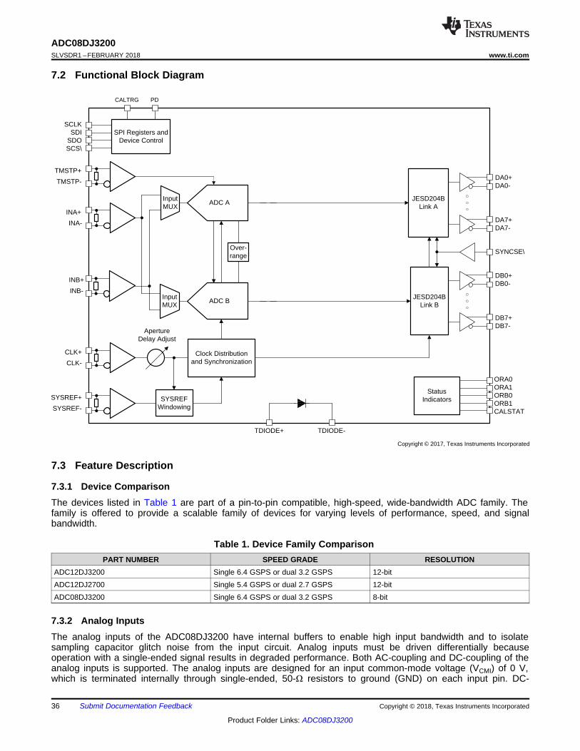
SCLKSDI
SDOSCS\
ADC AJESD204B
Link A
JESD204BLink B
Aperture Delay Adjust
Clock Distribution and Synchronization
CLK+
CLK-
SYSREF+
SYSREF-
SYNCSE\Over-range
DA0+DA0-
DA7+DA7-
DB0+DB0-
DB7+DB7-
Status Indicators
ORA0ORA1ORB0ORB1CALSTAT
ADC B
TDIODE+ TDIODE-
CALTRG PD
SPI Registers and Device Control
INA+
INA-
INB+
INB-
TMSTP+
TMSTP-
Input MUX
Input MUX
SYSREF Windowing
Copyright © 2017, Texas Instruments Incorporated
36
ADC08DJ3200SLVSDR1 –FEBRUARY 2018 www.ti.com
Product Folder Links: ADC08DJ3200
Submit Documentation Feedback Copyright © 2018, Texas Instruments Incorporated
7.2 Functional Block Diagram
7.3 Feature Description
7.3.1 Device ComparisonThe devices listed in Table 1 are part of a pin-to-pin compatible, high-speed, wide-bandwidth ADC family. Thefamily is offered to provide a scalable family of devices for varying levels of performance, speed, and signalbandwidth.
Table 1. Device Family ComparisonPART NUMBER SPEED GRADE RESOLUTION
ADC12DJ3200 Single 6.4 GSPS or dual 3.2 GSPS 12-bitADC12DJ2700 Single 5.4 GSPS or dual 2.7 GSPS 12-bitADC08DJ3200 Single 6.4 GSPS or dual 3.2 GSPS 8-bit
7.3.2 Analog InputsThe analog inputs of the ADC08DJ3200 have internal buffers to enable high input bandwidth and to isolatesampling capacitor glitch noise from the input circuit. Analog inputs must be driven differentially becauseoperation with a single-ended signal results in degraded performance. Both AC-coupling and DC-coupling of theanalog inputs is supported. The analog inputs are designed for an input common-mode voltage (VCMI) of 0 V,which is terminated internally through single-ended, 50-Ω resistors to ground (GND) on each input pin. DC-
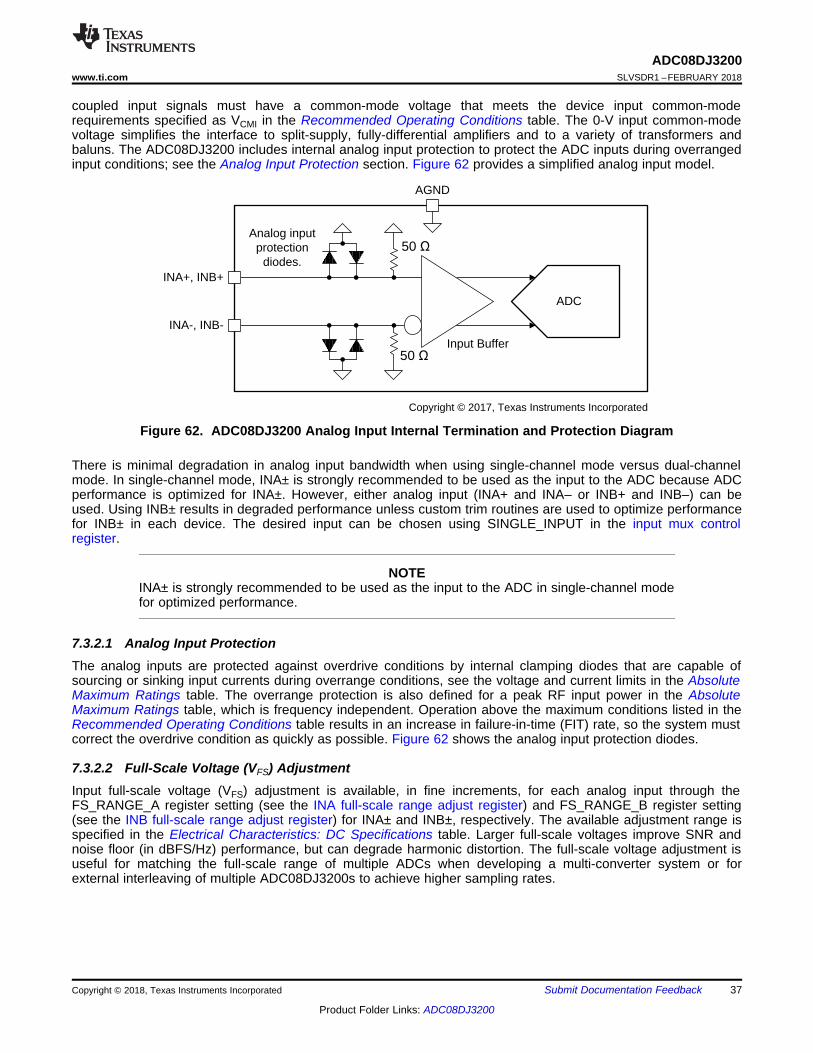
ADC
50
50
INA+, INB+
INA-, INB-
AGND
Analog input protection
diodes.
Input Buffer
Copyright © 2017, Texas Instruments Incorporated
37
ADC08DJ3200www.ti.com SLVSDR1 –FEBRUARY 2018
Product Folder Links: ADC08DJ3200
Submit Documentation FeedbackCopyright © 2018, Texas Instruments Incorporated
coupled input signals must have a common-mode voltage that meets the device input common-moderequirements specified as VCMI in the Recommended Operating Conditions table. The 0-V input common-modevoltage simplifies the interface to split-supply, fully-differential amplifiers and to a variety of transformers andbaluns. The ADC08DJ3200 includes internal analog input protection to protect the ADC inputs during overrangedinput conditions; see the Analog Input Protection section. Figure 62 provides a simplified analog input model.
Figure 62. ADC08DJ3200 Analog Input Internal Termination and Protection Diagram
There is minimal degradation in analog input bandwidth when using single-channel mode versus dual-channelmode. In single-channel mode, INA± is strongly recommended to be used as the input to the ADC because ADCperformance is optimized for INA±. However, either analog input (INA+ and INA– or INB+ and INB–) can beused. Using INB± results in degraded performance unless custom trim routines are used to optimize performancefor INB± in each device. The desired input can be chosen using SINGLE_INPUT in the input mux controlregister.
NOTEINA± is strongly recommended to be used as the input to the ADC in single-channel modefor optimized performance.
7.3.2.1 Analog Input ProtectionThe analog inputs are protected against overdrive conditions by internal clamping diodes that are capable ofsourcing or sinking input currents during overrange conditions, see the voltage and current limits in the AbsoluteMaximum Ratings table. The overrange protection is also defined for a peak RF input power in the AbsoluteMaximum Ratings table, which is frequency independent. Operation above the maximum conditions listed in theRecommended Operating Conditions table results in an increase in failure-in-time (FIT) rate, so the system mustcorrect the overdrive condition as quickly as possible. Figure 62 shows the analog input protection diodes.
7.3.2.2 Full-Scale Voltage (VFS) AdjustmentInput full-scale voltage (VFS) adjustment is available, in fine increments, for each analog input through theFS_RANGE_A register setting (see the INA full-scale range adjust register) and FS_RANGE_B register setting(see the INB full-scale range adjust register) for INA± and INB±, respectively. The available adjustment range isspecified in the Electrical Characteristics: DC Specifications table. Larger full-scale voltages improve SNR andnoise floor (in dBFS/Hz) performance, but can degrade harmonic distortion. The full-scale voltage adjustment isuseful for matching the full-scale range of multiple ADCs when developing a multi-converter system or forexternal interleaving of multiple ADC08DJ3200s to achieve higher sampling rates.
IN FSN
CodeV V
2
38
ADC08DJ3200SLVSDR1 –FEBRUARY 2018 www.ti.com
Product Folder Links: ADC08DJ3200
Submit Documentation Feedback Copyright © 2018, Texas Instruments Incorporated
7.3.2.3 Analog Input Offset AdjustThe input offset voltage for each input can be adjusted through the OADJ_x_INy registers (registers 0x08A and0x095), where x represents the ADC core (A, B, or C) and y represents the analog input (INA± or INB±). Theadjustment range is approximately 28 mV to –28 mV differential. See the Calibration Modes and Trimmingsection for more information.
7.3.3 ADC CoreThe ADC08DJ3200 consists of a total of six ADC cores. The cores are interleaved for higher sampling rates andswapped on-the-fly for calibration as required by the operating mode. This section highlights the theory and keyfeatures of the ADC cores.
7.3.3.1 ADC Theory of OperationThe differential voltages at the analog inputs are captured by the rising edge of CLK± in dual-channel mode or bythe rising and falling edges of CLK± in single-channel mode. After capturing the input signal, the ADC convertsthe analog voltage to a digital value by comparing the voltage to the internal reference voltage. If the voltage onINA– or INB– is higher than the voltage on INA+ or INB+, respectively, then the digital output is a negative 2'scomplement value. If the voltage on INA+ or INB+ is higher than the voltage on INA– or INB–, respectively, thenthe digital output is a positive 2's complement value. Equation 1 can calculate the differential voltage at the inputpins from the digital output.
where• Code is the signed decimation output code (for example, –2048 to +2047)• N is the ADC resolution• and VFS is the full-scale input voltage of the ADC as specified in the Recommended Operating Conditions
table, including any adjustment performed by programming FS_RANGE_A or FS_RANGE_B (1)
7.3.3.2 ADC Core CalibrationADC core calibration is required to optimize the analog performance of the ADC cores. Calibration must berepeated when operating conditions change significantly, namely temperature, in order to maintain optimalperformance. The ADC08DJ3200 has a built-in calibration routine that can be run as a foreground operation or abackground operation. Foreground operation requires ADC downtime, where the ADC is no longer sampling theinput signal, to complete the process. Background calibration can be used to overcome this limitation and allowconstant operation of the ADC. See the Calibration Modes and Trimming section for detailed information on eachmode.
7.3.3.3 ADC Overrange DetectionTo ensure that system gain management has the quickest possible response time, a low-latency configurableoverrange function is included. The overrange function works by monitoring the converted 8-bit samples at theADC to quickly detect if the ADC is near saturation or already in an overrange condition. The absolute value ofthe 8 bits of the ADC data are checked against two programmable thresholds, OVR_T0 and OVR_T1. Thesethresholds apply to both channel A and channel B in dual-channel mode. Table 2 lists how an ADC sample isconverted to an absolute value for a comparison of the thresholds.
Table 2. Conversion of ADC Sample for Overrange ComparisonADC SAMPLE(Offset Binary)
ADC SAMPLE(2's Complement) ABSOLUTE VALUE 8 BITS USED FOR COMPARISON
1111 1111 (255) 0111 1111 (+127) 111 1111 (127) 1111 1111 (255)1000 0000 (128) 0000 0000 (0) 000 0000 (0) 0000 0000 (0)0000 0001 (1) 1000 0001 (–127) 111 1111 (127) 1111 1110 (254)0000 0000 (0) 1000 0000 (–128) 111 1111 (127) 1111 1111 (255)
39
ADC08DJ3200www.ti.com SLVSDR1 –FEBRUARY 2018
Product Folder Links: ADC08DJ3200
Submit Documentation FeedbackCopyright © 2018, Texas Instruments Incorporated
If the 8 bits of the absolute value equal or exceed the OVR_T0 or OVR_T1 thresholds during the monitoringperiod, then the overrange bit associated with the threshold is set to 1, otherwise the overrange bit is 0. In dual-channel mode, the overrange status can be monitored on the ORA0 and ORA1 pins for channel A and the ORB0and ORB1 pins for channel B, where ORx0 corresponds to the OVR_T0 threshold and ORx1 corresponds to theOVR_T1 threshold. In single-channel mode, the overrange status for the OVR_T0 threshold is determined bymonitoring both the ORA0 and ORB0 outputs and the OVR_T1 threshold is determined by monitoring both ORA1and ORB1 outputs. In single-channel mode, the two outputs for each threshold must be OR'd together todetermine whether an overrange condition occurred. OVR_N can be used to set the output pulse duration fromthe last overrange event. Table 3 lists the overrange pulse lengths for the various OVR_N settings (see theoverrange configuration register).
Table 3. Overrange Monitoring Period for the ORA0, ORA1, ORB0, and ORB1 Outputs
OVR_N OVERRANGE PULSE LENGTH SINCE LAST OVERRANGEEVENT (DEVCLK Cycles)
0 81 162 323 644 1285 2566 5127 1024
Typically, the OVR_T0 threshold can be set near the full-scale value (228 for example). When the threshold istriggered, a typical system can turn down the system gain to avoid clipping. The OVR_T1 threshold can be setmuch lower. For example, the OVR_T1 threshold can be set to 64 (peak input voltage of −12 dBFS). If the inputsignal is strong, the OVR_T1 threshold is tripped occasionally. If the input is quite weak, the threshold is nevertripped. The downstream logic device monitors the OVR_T1 bit. If OVR_T1 stays low for an extended period oftime, then the system gain can be increased until the threshold is occasionally tripped (meaning the peak level ofthe signal is above −12 dBFS).
7.3.3.4 Code Error Rate (CER)ADC cores can generate bit errors within a sample, often called code errors (CER) or referred to as sparklecodes, resulting from metastability caused by non-ideal comparator limitations. The ADC08DJ3200 uses aunique ADC architecture that inherently allows significant code error rate improvements from traditional pipelinedflash or successive approximation register (SAR) ADCs. The code error rate of the ADC08DJ3200 is multipleorders of magnitude better than what can be achieved in alternative architectures at equivalent sampling ratesproviding significant signal reliability improvements.
7.3.4 TimestampThe TMSTP+ and TMSTP– differential input can be used as a time-stamp input to mark a specific sample basedon the timing of an external trigger event relative to the sampled signal. TIMESTAMP_EN (see the LSB controlbit output register) must be set in order to use the timestamp feature and output the timestamp data. Whenenabled, the LSB of the 8-bit ADC digital output reports the status of the TMSTP± input. In effect, the 8-bit outputsample consists of the upper 7-bits of the 8-bit converter and the LSB of the 8-bit output sample is the output of aparallel 1-bit converter (TMSTP±) with the same latency as the ADC core. The trigger must be applied to thedifferential TMSTP+ and TMSTP– inputs. The trigger can be asynchronous to the ADC sampling clock and issampled at approximately the same time as the analog input. Timestamp cannot be used when a JMODE withdecimation is selected and instead SYSREF must be used to achieve synchronization through the JESD204Bsubclass-1 method for achieving deterministic latency.
7.3.5 ClockingThe clocking subsystem of the ADC08DJ3200 has two input signals, device clock (CLK+, CLK–) and SYSREF(SYSREF+, SYSREF–). Within the clocking subsystem there is a noiseless aperture delay adjustment (tADadjust), a clock duty cycle corrector, and a SYSREF capture block. Figure 63 describes the clocking subsystem.
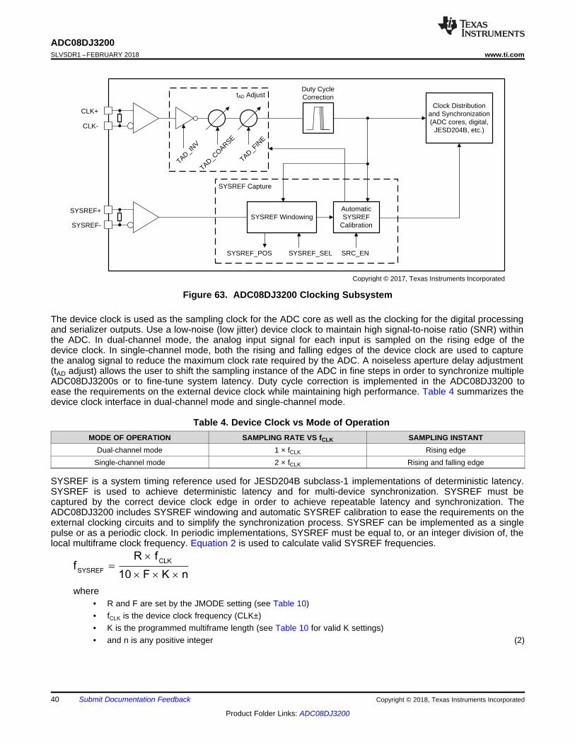
CLK
SYSREF
R ff
10 F K n
u
u u u
SYSREF Capture
tAD Adjust
Clock Distribution and Synchronization(ADC cores, digital,
JESD204B, etc.)
CLK+
CLK-
SYSREF+
SYSREF-SYSREF Windowing
Automatic SYSREF
Calibration
SYSREF_POS SYSREF_SEL
TAD_INV
TAD_COARSE
TAD_FIN
E
SRC_EN
Duty Cycle Correction
Copyright © 2017, Texas Instruments Incorporated
40
ADC08DJ3200SLVSDR1 –FEBRUARY 2018 www.ti.com
Product Folder Links: ADC08DJ3200
Submit Documentation Feedback Copyright © 2018, Texas Instruments Incorporated
Figure 63. ADC08DJ3200 Clocking Subsystem
The device clock is used as the sampling clock for the ADC core as well as the clocking for the digital processingand serializer outputs. Use a low-noise (low jitter) device clock to maintain high signal-to-noise ratio (SNR) withinthe ADC. In dual-channel mode, the analog input signal for each input is sampled on the rising edge of thedevice clock. In single-channel mode, both the rising and falling edges of the device clock are used to capturethe analog signal to reduce the maximum clock rate required by the ADC. A noiseless aperture delay adjustment(tAD adjust) allows the user to shift the sampling instance of the ADC in fine steps in order to synchronize multipleADC08DJ3200s or to fine-tune system latency. Duty cycle correction is implemented in the ADC08DJ3200 toease the requirements on the external device clock while maintaining high performance. Table 4 summarizes thedevice clock interface in dual-channel mode and single-channel mode.
Table 4. Device Clock vs Mode of OperationMODE OF OPERATION SAMPLING RATE VS fCLK SAMPLING INSTANT
Dual-channel mode 1 × fCLK Rising edgeSingle-channel mode 2 × fCLK Rising and falling edge
SYSREF is a system timing reference used for JESD204B subclass-1 implementations of deterministic latency.SYSREF is used to achieve deterministic latency and for multi-device synchronization. SYSREF must becaptured by the correct device clock edge in order to achieve repeatable latency and synchronization. TheADC08DJ3200 includes SYSREF windowing and automatic SYSREF calibration to ease the requirements on theexternal clocking circuits and to simplify the synchronization process. SYSREF can be implemented as a singlepulse or as a periodic clock. In periodic implementations, SYSREF must be equal to, or an integer division of, thelocal multiframe clock frequency. Equation 2 is used to calculate valid SYSREF frequencies.
where• R and F are set by the JMODE setting (see Table 10)• fCLK is the device clock frequency (CLK±)• K is the programmed multiframe length (see Table 10 for valid K settings)• and n is any positive integer (2)
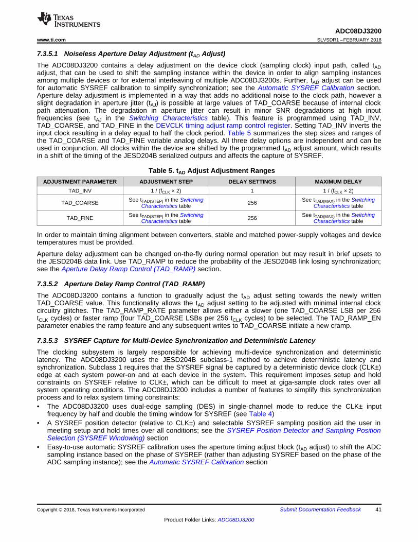
41
ADC08DJ3200www.ti.com SLVSDR1 –FEBRUARY 2018
Product Folder Links: ADC08DJ3200
Submit Documentation FeedbackCopyright © 2018, Texas Instruments Incorporated
7.3.5.1 Noiseless Aperture Delay Adjustment (tAD Adjust)The ADC08DJ3200 contains a delay adjustment on the device clock (sampling clock) input path, called tADadjust, that can be used to shift the sampling instance within the device in order to align sampling instancesamong multiple devices or for external interleaving of multiple ADC08DJ3200s. Further, tAD adjust can be usedfor automatic SYSREF calibration to simplify synchronization; see the Automatic SYSREF Calibration section.Aperture delay adjustment is implemented in a way that adds no additional noise to the clock path, however aslight degradation in aperture jitter (tAJ) is possible at large values of TAD_COARSE because of internal clockpath attenuation. The degradation in aperture jitter can result in minor SNR degradations at high inputfrequencies (see tAJ in the Switching Characteristics table). This feature is programmed using TAD_INV,TAD_COARSE, and TAD_FINE in the DEVCLK timing adjust ramp control register. Setting TAD_INV inverts theinput clock resulting in a delay equal to half the clock period. Table 5 summarizes the step sizes and ranges ofthe TAD_COARSE and TAD_FINE variable analog delays. All three delay options are independent and can beused in conjunction. All clocks within the device are shifted by the programmed tAD adjust amount, which resultsin a shift of the timing of the JESD204B serialized outputs and affects the capture of SYSREF.
Table 5. tAD Adjust Adjustment RangesADJUSTMENT PARAMETER ADJUSTMENT STEP DELAY SETTINGS MAXIMUM DELAY
TAD_INV 1 / (fCLK × 2) 1 1 / (fCLK × 2)
TAD_COARSE See tTAD(STEP) in the SwitchingCharacteristics table 256 See tTAD(MAX) in the Switching
Characteristics table
TAD_FINE See tTAD(STEP) in the SwitchingCharacteristics table 256 See tTAD(MAX) in the Switching
Characteristics table
In order to maintain timing alignment between converters, stable and matched power-supply voltages and devicetemperatures must be provided.
Aperture delay adjustment can be changed on-the-fly during normal operation but may result in brief upsets tothe JESD204B data link. Use TAD_RAMP to reduce the probability of the JESD204B link losing synchronization;see the Aperture Delay Ramp Control (TAD_RAMP) section.
7.3.5.2 Aperture Delay Ramp Control (TAD_RAMP)The ADC08DJ3200 contains a function to gradually adjust the tAD adjust setting towards the newly writtenTAD_COARSE value. This functionality allows the tAD adjust setting to be adjusted with minimal internal clockcircuitry glitches. The TAD_RAMP_RATE parameter allows either a slower (one TAD_COARSE LSB per 256tCLK cycles) or faster ramp (four TAD_COARSE LSBs per 256 tCLK cycles) to be selected. The TAD_RAMP_ENparameter enables the ramp feature and any subsequent writes to TAD_COARSE initiate a new cramp.
7.3.5.3 SYSREF Capture for Multi-Device Synchronization and Deterministic LatencyThe clocking subsystem is largely responsible for achieving multi-device synchronization and deterministiclatency. The ADC08DJ3200 uses the JESD204B subclass-1 method to achieve deterministic latency andsynchronization. Subclass 1 requires that the SYSREF signal be captured by a deterministic device clock (CLK±)edge at each system power-on and at each device in the system. This requirement imposes setup and holdconstraints on SYSREF relative to CLK±, which can be difficult to meet at giga-sample clock rates over allsystem operating conditions. The ADC08DJ3200 includes a number of features to simplify this synchronizationprocess and to relax system timing constraints:• The ADC08DJ3200 uses dual-edge sampling (DES) in single-channel mode to reduce the CLK± input
frequency by half and double the timing window for SYSREF (see Table 4)• A SYSREF position detector (relative to CLK±) and selectable SYSREF sampling position aid the user in
meeting setup and hold times over all conditions; see the SYSREF Position Detector and Sampling PositionSelection (SYSREF Windowing) section
• Easy-to-use automatic SYSREF calibration uses the aperture timing adjust block (tAD adjust) to shift the ADCsampling instance based on the phase of SYSREF (rather than adjusting SYSREF based on the phase of theADC sampling instance); see the Automatic SYSREF Calibration section
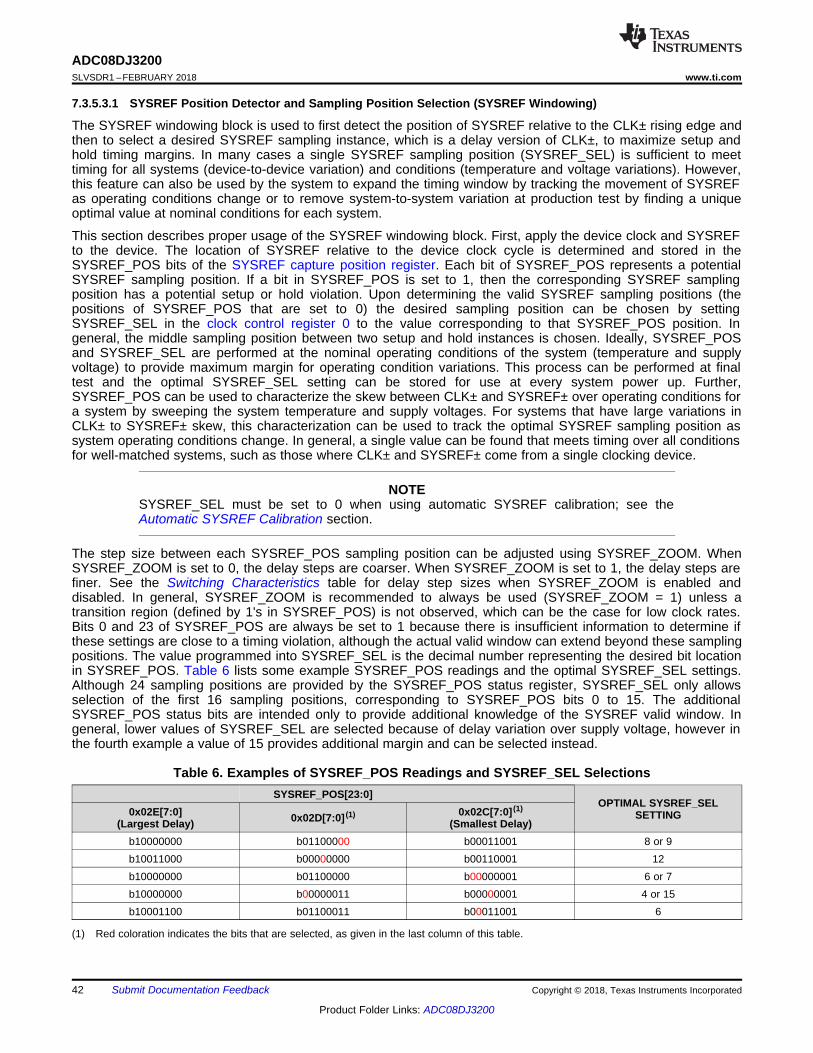
42
ADC08DJ3200SLVSDR1 –FEBRUARY 2018 www.ti.com
Product Folder Links: ADC08DJ3200
Submit Documentation Feedback Copyright © 2018, Texas Instruments Incorporated
(1) Red coloration indicates the bits that are selected, as given in the last column of this table.
7.3.5.3.1 SYSREF Position Detector and Sampling Position Selection (SYSREF Windowing)
The SYSREF windowing block is used to first detect the position of SYSREF relative to the CLK± rising edge andthen to select a desired SYSREF sampling instance, which is a delay version of CLK±, to maximize setup andhold timing margins. In many cases a single SYSREF sampling position (SYSREF_SEL) is sufficient to meettiming for all systems (device-to-device variation) and conditions (temperature and voltage variations). However,this feature can also be used by the system to expand the timing window by tracking the movement of SYSREFas operating conditions change or to remove system-to-system variation at production test by finding a uniqueoptimal value at nominal conditions for each system.
This section describes proper usage of the SYSREF windowing block. First, apply the device clock and SYSREFto the device. The location of SYSREF relative to the device clock cycle is determined and stored in theSYSREF_POS bits of the SYSREF capture position register. Each bit of SYSREF_POS represents a potentialSYSREF sampling position. If a bit in SYSREF_POS is set to 1, then the corresponding SYSREF samplingposition has a potential setup or hold violation. Upon determining the valid SYSREF sampling positions (thepositions of SYSREF_POS that are set to 0) the desired sampling position can be chosen by settingSYSREF_SEL in the clock control register 0 to the value corresponding to that SYSREF_POS position. Ingeneral, the middle sampling position between two setup and hold instances is chosen. Ideally, SYSREF_POSand SYSREF_SEL are performed at the nominal operating conditions of the system (temperature and supplyvoltage) to provide maximum margin for operating condition variations. This process can be performed at finaltest and the optimal SYSREF_SEL setting can be stored for use at every system power up. Further,SYSREF_POS can be used to characterize the skew between CLK± and SYSREF± over operating conditions fora system by sweeping the system temperature and supply voltages. For systems that have large variations inCLK± to SYSREF± skew, this characterization can be used to track the optimal SYSREF sampling position assystem operating conditions change. In general, a single value can be found that meets timing over all conditionsfor well-matched systems, such as those where CLK± and SYSREF± come from a single clocking device.
NOTESYSREF_SEL must be set to 0 when using automatic SYSREF calibration; see theAutomatic SYSREF Calibration section.
The step size between each SYSREF_POS sampling position can be adjusted using SYSREF_ZOOM. WhenSYSREF_ZOOM is set to 0, the delay steps are coarser. When SYSREF_ZOOM is set to 1, the delay steps arefiner. See the Switching Characteristics table for delay step sizes when SYSREF_ZOOM is enabled anddisabled. In general, SYSREF_ZOOM is recommended to always be used (SYSREF_ZOOM = 1) unless atransition region (defined by 1's in SYSREF_POS) is not observed, which can be the case for low clock rates.Bits 0 and 23 of SYSREF_POS are always be set to 1 because there is insufficient information to determine ifthese settings are close to a timing violation, although the actual valid window can extend beyond these samplingpositions. The value programmed into SYSREF_SEL is the decimal number representing the desired bit locationin SYSREF_POS. Table 6 lists some example SYSREF_POS readings and the optimal SYSREF_SEL settings.Although 24 sampling positions are provided by the SYSREF_POS status register, SYSREF_SEL only allowsselection of the first 16 sampling positions, corresponding to SYSREF_POS bits 0 to 15. The additionalSYSREF_POS status bits are intended only to provide additional knowledge of the SYSREF valid window. Ingeneral, lower values of SYSREF_SEL are selected because of delay variation over supply voltage, however inthe fourth example a value of 15 provides additional margin and can be selected instead.
Table 6. Examples of SYSREF_POS Readings and SYSREF_SEL SelectionsSYSREF_POS[23:0]
OPTIMAL SYSREF_SELSETTING0x02E[7:0]
(Largest Delay) 0x02D[7:0] (1) 0x02C[7:0] (1)
(Smallest Delay)b10000000 b01100000 b00011001 8 or 9b10011000 b00000000 b00110001 12b10000000 b01100000 b00000001 6 or 7b10000000 b00000011 b00000001 4 or 15b10001100 b01100011 b00011001 6
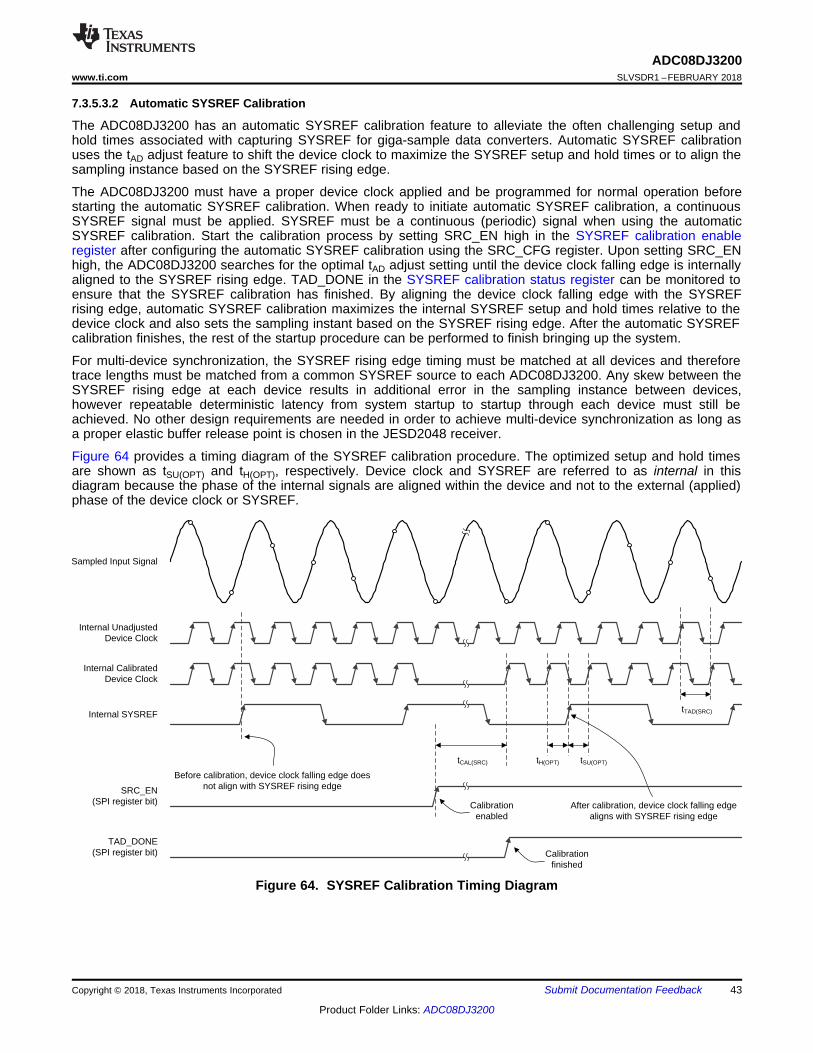
Sampled Input Signal
Internal UnadjustedDevice Clock
Internal SYSREF
SRC_EN(SPI register bit)
tH(OPT) tSU(OPT)
Internal Calibrated Device Clock
Before calibration, device clock falling edge does not align with SYSREF rising edge
tTAD(SRC)
Calibration enabled
After calibration, device clock falling edge aligns with SYSREF rising edge
tCAL(SRC)
TAD_DONE(SPI register bit) Calibration
finished
43
ADC08DJ3200www.ti.com SLVSDR1 –FEBRUARY 2018
Product Folder Links: ADC08DJ3200
Submit Documentation FeedbackCopyright © 2018, Texas Instruments Incorporated
7.3.5.3.2 Automatic SYSREF Calibration
The ADC08DJ3200 has an automatic SYSREF calibration feature to alleviate the often challenging setup andhold times associated with capturing SYSREF for giga-sample data converters. Automatic SYSREF calibrationuses the tAD adjust feature to shift the device clock to maximize the SYSREF setup and hold times or to align thesampling instance based on the SYSREF rising edge.
The ADC08DJ3200 must have a proper device clock applied and be programmed for normal operation beforestarting the automatic SYSREF calibration. When ready to initiate automatic SYSREF calibration, a continuousSYSREF signal must be applied. SYSREF must be a continuous (periodic) signal when using the automaticSYSREF calibration. Start the calibration process by setting SRC_EN high in the SYSREF calibration enableregister after configuring the automatic SYSREF calibration using the SRC_CFG register. Upon setting SRC_ENhigh, the ADC08DJ3200 searches for the optimal tAD adjust setting until the device clock falling edge is internallyaligned to the SYSREF rising edge. TAD_DONE in the SYSREF calibration status register can be monitored toensure that the SYSREF calibration has finished. By aligning the device clock falling edge with the SYSREFrising edge, automatic SYSREF calibration maximizes the internal SYSREF setup and hold times relative to thedevice clock and also sets the sampling instant based on the SYSREF rising edge. After the automatic SYSREFcalibration finishes, the rest of the startup procedure can be performed to finish bringing up the system.
For multi-device synchronization, the SYSREF rising edge timing must be matched at all devices and thereforetrace lengths must be matched from a common SYSREF source to each ADC08DJ3200. Any skew between theSYSREF rising edge at each device results in additional error in the sampling instance between devices,however repeatable deterministic latency from system startup to startup through each device must still beachieved. No other design requirements are needed in order to achieve multi-device synchronization as long asa proper elastic buffer release point is chosen in the JESD2048 receiver.
Figure 64 provides a timing diagram of the SYSREF calibration procedure. The optimized setup and hold timesare shown as tSU(OPT) and tH(OPT), respectively. Device clock and SYSREF are referred to as internal in thisdiagram because the phase of the internal signals are aligned within the device and not to the external (applied)phase of the device clock or SYSREF.
Figure 64. SYSREF Calibration Timing Diagram
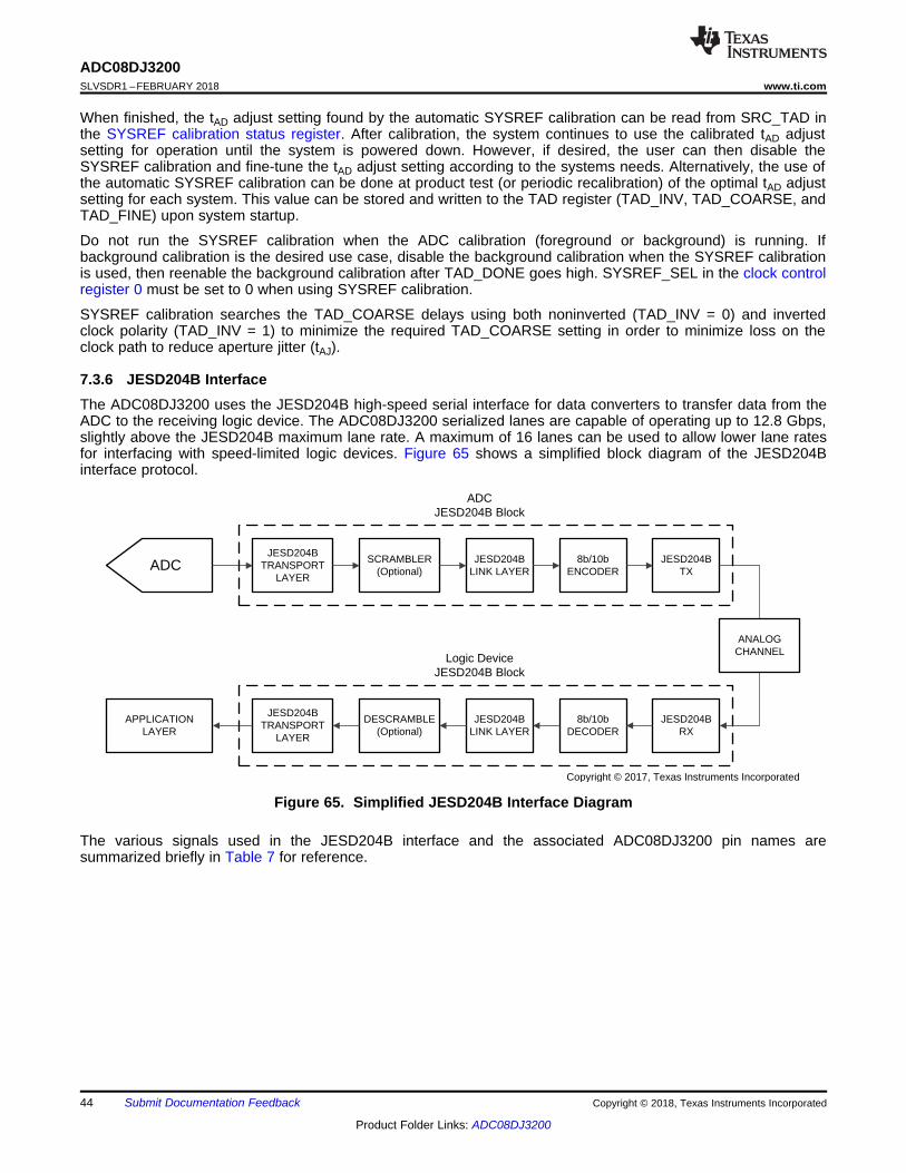
ADCJESD204B
TRANSPORT LAYER
SCRAMBLER(Optional)
JESD204BLINK LAYER
JESD204BTX
8b/10bENCODER
APPLICATION LAYER
JESD204BTRANSPORT
LAYER
DESCRAMBLE(Optional)
JESD204BLINK LAYER
JESD204BRX
8b/10bDECODER
ADCJESD204B Block
Logic Device JESD204B Block
ANALOGCHANNEL
Copyright © 2017, Texas Instruments Incorporated
44
ADC08DJ3200SLVSDR1 –FEBRUARY 2018 www.ti.com
Product Folder Links: ADC08DJ3200
Submit Documentation Feedback Copyright © 2018, Texas Instruments Incorporated
When finished, the tAD adjust setting found by the automatic SYSREF calibration can be read from SRC_TAD inthe SYSREF calibration status register. After calibration, the system continues to use the calibrated tAD adjustsetting for operation until the system is powered down. However, if desired, the user can then disable theSYSREF calibration and fine-tune the tAD adjust setting according to the systems needs. Alternatively, the use ofthe automatic SYSREF calibration can be done at product test (or periodic recalibration) of the optimal tAD adjustsetting for each system. This value can be stored and written to the TAD register (TAD_INV, TAD_COARSE, andTAD_FINE) upon system startup.
Do not run the SYSREF calibration when the ADC calibration (foreground or background) is running. Ifbackground calibration is the desired use case, disable the background calibration when the SYSREF calibrationis used, then reenable the background calibration after TAD_DONE goes high. SYSREF_SEL in the clock controlregister 0 must be set to 0 when using SYSREF calibration.
SYSREF calibration searches the TAD_COARSE delays using both noninverted (TAD_INV = 0) and invertedclock polarity (TAD_INV = 1) to minimize the required TAD_COARSE setting in order to minimize loss on theclock path to reduce aperture jitter (tAJ).
7.3.6 JESD204B InterfaceThe ADC08DJ3200 uses the JESD204B high-speed serial interface for data converters to transfer data from theADC to the receiving logic device. The ADC08DJ3200 serialized lanes are capable of operating up to 12.8 Gbps,slightly above the JESD204B maximum lane rate. A maximum of 16 lanes can be used to allow lower lane ratesfor interfacing with speed-limited logic devices. Figure 65 shows a simplified block diagram of the JESD204Binterface protocol.
Figure 65. Simplified JESD204B Interface Diagram
The various signals used in the JESD204B interface and the associated ADC08DJ3200 pin names aresummarized briefly in Table 7 for reference.
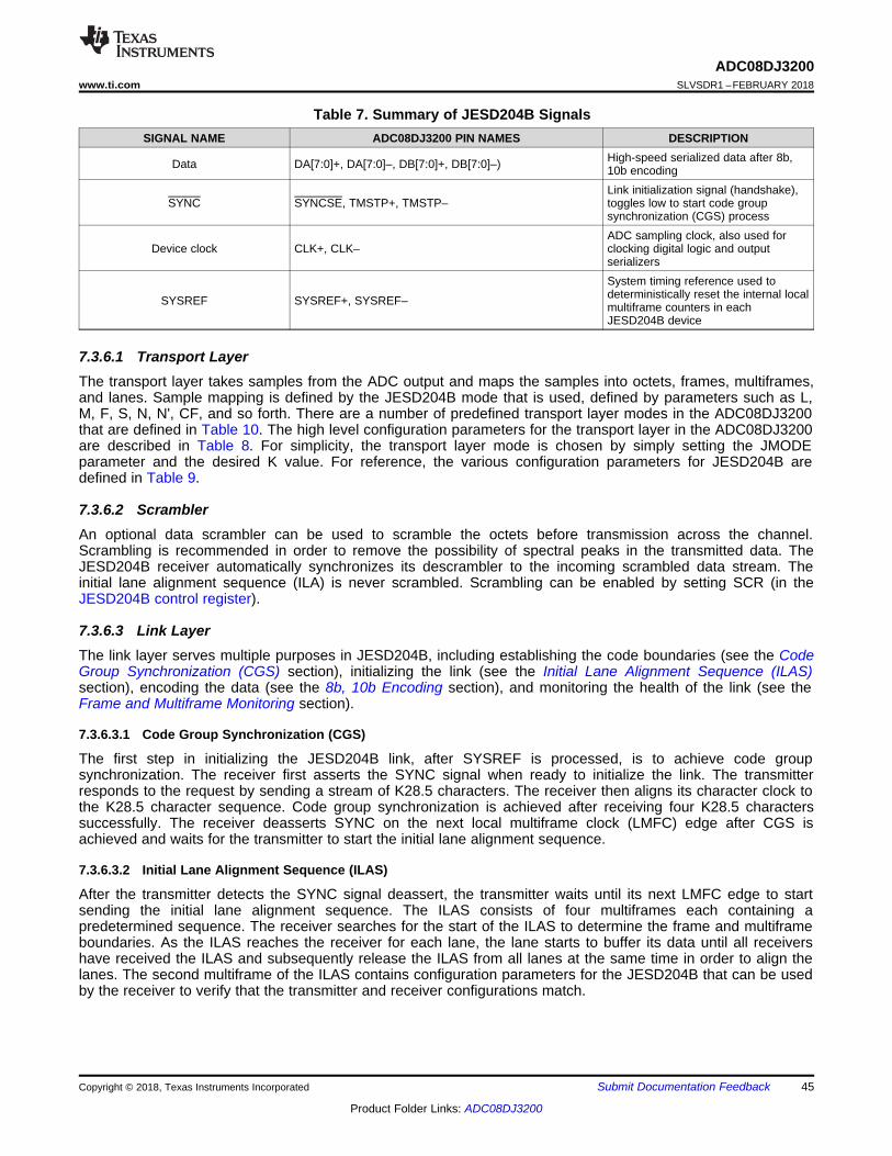
45
ADC08DJ3200www.ti.com SLVSDR1 –FEBRUARY 2018
Product Folder Links: ADC08DJ3200
Submit Documentation FeedbackCopyright © 2018, Texas Instruments Incorporated
Table 7. Summary of JESD204B SignalsSIGNAL NAME ADC08DJ3200 PIN NAMES DESCRIPTION
Data DA[7:0]+, DA[7:0]–, DB[7:0]+, DB[7:0]–) High-speed serialized data after 8b,10b encoding
SYNC SYNCSE, TMSTP+, TMSTP–Link initialization signal (handshake),toggles low to start code groupsynchronization (CGS) process
Device clock CLK+, CLK–ADC sampling clock, also used forclocking digital logic and outputserializers
SYSREF SYSREF+, SYSREF–
System timing reference used todeterministically reset the internal localmultiframe counters in eachJESD204B device
7.3.6.1 Transport LayerThe transport layer takes samples from the ADC output and maps the samples into octets, frames, multiframes,and lanes. Sample mapping is defined by the JESD204B mode that is used, defined by parameters such as L,M, F, S, N, N', CF, and so forth. There are a number of predefined transport layer modes in the ADC08DJ3200that are defined in Table 10. The high level configuration parameters for the transport layer in the ADC08DJ3200are described in Table 8. For simplicity, the transport layer mode is chosen by simply setting the JMODEparameter and the desired K value. For reference, the various configuration parameters for JESD204B aredefined in Table 9.
7.3.6.2 ScramblerAn optional data scrambler can be used to scramble the octets before transmission across the channel.Scrambling is recommended in order to remove the possibility of spectral peaks in the transmitted data. TheJESD204B receiver automatically synchronizes its descrambler to the incoming scrambled data stream. Theinitial lane alignment sequence (ILA) is never scrambled. Scrambling can be enabled by setting SCR (in theJESD204B control register).
7.3.6.3 Link LayerThe link layer serves multiple purposes in JESD204B, including establishing the code boundaries (see the CodeGroup Synchronization (CGS) section), initializing the link (see the Initial Lane Alignment Sequence (ILAS)section), encoding the data (see the 8b, 10b Encoding section), and monitoring the health of the link (see theFrame and Multiframe Monitoring section).
7.3.6.3.1 Code Group Synchronization (CGS)
The first step in initializing the JESD204B link, after SYSREF is processed, is to achieve code groupsynchronization. The receiver first asserts the SYNC signal when ready to initialize the link. The transmitterresponds to the request by sending a stream of K28.5 characters. The receiver then aligns its character clock tothe K28.5 character sequence. Code group synchronization is achieved after receiving four K28.5 characterssuccessfully. The receiver deasserts SYNC on the next local multiframe clock (LMFC) edge after CGS isachieved and waits for the transmitter to start the initial lane alignment sequence.
7.3.6.3.2 Initial Lane Alignment Sequence (ILAS)
After the transmitter detects the SYNC signal deassert, the transmitter waits until its next LMFC edge to startsending the initial lane alignment sequence. The ILAS consists of four multiframes each containing apredetermined sequence. The receiver searches for the start of the ILAS to determine the frame and multiframeboundaries. As the ILAS reaches the receiver for each lane, the lane starts to buffer its data until all receivershave received the ILAS and subsequently release the ILAS from all lanes at the same time in order to align thelanes. The second multiframe of the ILAS contains configuration parameters for the JESD204B that can be usedby the receiver to verify that the transmitter and receiver configurations match.
46
ADC08DJ3200SLVSDR1 –FEBRUARY 2018 www.ti.com
Product Folder Links: ADC08DJ3200
Submit Documentation Feedback Copyright © 2018, Texas Instruments Incorporated
7.3.6.3.3 8b, 10b Encoding
The data link layer converts the 8-bit octets from the transport layer into 10-bit characters for transmission acrossthe link using 8b, 10b encoding. 8b, 10b encoding provides DC balance for AC-coupling of the SerDes links anda sufficient number of edge transitions for the receiver to reliably recover the data clock. 8b, 10b also providessome amount of error detection where a single bit error in a character likely results in either not being able to findthe 10-bit character in the 8b, 10b decoder lookup table or incorrect character disparity.
7.3.6.3.4 Frame and Multiframe Monitoring
The ADC08DJ3200 supports frame and multiframe monitoring for verifying the health of the JESD204B link. Ifthe last octet of a frame matches the last octet of the previous frame, then the last octet in the second frame isreplaced with an /F/ (/K28.7/) character. If the second frame is the last frame of a multiframe, then an /A/(/K28.3/) character is used instead. When scrambling is enabled, if the last octet of a frame is 0xFC then thetransmitter replaces the octet with an /F/ (/K28.7/) character. With scrambling, if the last octet of a multiframe is0x7C then the transmitter replaces the octet with an /A/ (/K28.3/) character. When the receiver detects an /F/ or/A/ character, the receiver checks if the character occurs at the end of a frame or multiframe, and replaces thatoctet with the appropriate data character. The receiver can report an error if the alignment characters occur inthe incorrect place and trigger a link realignment.
7.3.6.4 Physical LayerThe JESD204B physical layer consists of a current mode logic (CML) output driver and receiver. The receiverconsists of a clock detection and recovery (CDR) unit to extract the data clock from the serialized data streamand can contain an equalizer to correct for the low-pass response of the physical transmission channel. Likewise,the transmitter can contain pre-equalization to account for frequency dependent losses across the channel. Thetotal reach of the SerDes links depends on the data rate, board material, connectors, equalization, noise andjitter, and required bit-error performance. The SerDes lanes do not have to be matched in length because thereceiver aligns the lanes during the initial lane alignment sequence.
7.3.6.4.1 SerDes Pre-Emphasis
The ADC08DJ3200 high-speed output drivers can pre-equalize the transmitted data stream by using pre-emphasis in order to compensate for the low-pass response of the transmission channel. Configurable pre-emphasis settings allow the output drive waveform to be optimized for different PCB materials and signaltransmission distances. The pre-emphasis setting is adjusted through the serializer pre-emphasis settingSER_PE (in the serializer pre-emphasis control register). Higher values increase the pre-emphasis tocompensate for more lossy PCB materials. This adjustment is best used in conjunction with an eye-diagramanalysis capability in the receiver. Adjust the pre-emphasis setting to optimize the eye-opening for the specifichardware configuration and line rates needed.
7.3.6.5 JESD204B EnableThe JESD204B interface must be disabled through JESD_EN (in the JESD204B enable register) while any of theother JESD204B parameters are being changed. When JESD_EN is set to 0 the block is held in reset and theserializers are powered down. The clocks for this section are also gated off to further save power. When theparameters are set as desired, the JESD204B block can be enabled (JESD_EN is set to 1).
7.3.6.6 Multi-Device Synchronization and Deterministic LatencyJESD204B subclass 1 outlines a method to achieve deterministic latency across the serial link. If two devicesachieve the same deterministic latency then they can be considered synchronized. This latency must beachieved from system startup to startup to be deterministic. There are two key requirements to achievedeterministic latency. The first is proper capture of SYSREF for which the ADC08DJ3200 provides a number offeatures to simplify this requirement at giga-sample clock rates (see the SYSREF Capture for Multi-DeviceSynchronization and Deterministic Latency section for more information).
The second requirement is to choose a proper elastic buffer release point in the receiver. Because theADC08DJ3200 is an ADC, the ADC08DJ3200 is the transmitter (TX) in the JESD204B link and the logic deviceis the receiver (RX). The elastic buffer is the key block for achieving deterministic latency, and does so byabsorbing variations in the propagation delays of the serialized data as the data travels from the transmitter tothe receiver. A proper release point is one that provides sufficient margin against delay variations. An incorrect
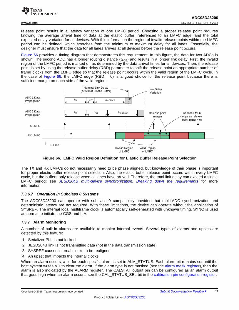
TX LMFC
RX LMFC
ADC 1 Data Propagation tTX tPCB tRX-DESER
Time
ADC 2 Data Propagation
tTX tPCB
Invalid Region of LMFC
Valid Region of LMFC
Nominal Link Delay(Arrival at Elastic Buffer)
Link Delay Variation
Choose LMFC edge as release point (RBD = 0)
Release point margin
tRX-DESER
47
ADC08DJ3200www.ti.com SLVSDR1 –FEBRUARY 2018
Product Folder Links: ADC08DJ3200
Submit Documentation FeedbackCopyright © 2018, Texas Instruments Incorporated
release point results in a latency variation of one LMFC period. Choosing a proper release point requiresknowing the average arrival time of data at the elastic buffer, referenced to an LMFC edge, and the totalexpected delay variation for all devices. With this information the region of invalid release points within the LMFCperiod can be defined, which stretches from the minimum to maximum delay for all lanes. Essentially, thedesigner must ensure that the data for all lanes arrives at all devices before the release point occurs.
Figure 66 provides a timing diagram that demonstrates this requirement. In this figure, the data for two ADCs isshown. The second ADC has a longer routing distance (tPCB) and results in a longer link delay. First, the invalidregion of the LMFC period is marked off as determined by the data arrival times for all devices. Then, the releasepoint is set by using the release buffer delay (RBD) parameter to shift the release point an appropriate number offrame clocks from the LMFC edge so that the release point occurs within the valid region of the LMFC cycle. Inthe case of Figure 66, the LMFC edge (RBD = 0) is a good choice for the release point because there issufficient margin on each side of the valid region.
Figure 66. LMFC Valid Region Definition for Elastic Buffer Release Point Selection
The TX and RX LMFCs do not necessarily need to be phase aligned, but knowledge of their phase is importantfor proper elastic buffer release point selection. Also, the elastic buffer release point occurs within every LMFCcycle, but the buffers only release when all lanes have arrived. Therefore, the total link delay can exceed a singleLMFC period; see JESD204B multi-device synchronization: Breaking down the requirements for moreinformation.
7.3.6.7 Operation in Subclass 0 SystemsThe ADC08DJ3200 can operate with subclass 0 compatibility provided that multi-ADC synchronization anddeterministic latency are not required. With these limitations, the device can operate without the application ofSYSREF. The internal local multiframe clock is automatically self-generated with unknown timing. SYNC is usedas normal to initiate the CGS and ILA.
7.3.7 Alarm MonitoringA number of built-in alarms are available to monitor internal events. Several types of alarms and upsets aredetected by this feature:
1. Serializer PLL is not locked2. JESD204B link is not transmitting data (not in the data transmission state)3. SYSREF causes internal clocks to be realigned4. An upset that impacts the internal clocks
When an alarm occurs, a bit for each specific alarm is set in ALM_STATUS. Each alarm bit remains set until thehost system writes a 1 to clear the alarm. If the alarm type is not masked (see the alarm mask register), then thealarm is also indicated by the ALARM register. The CALSTAT output pin can be configured as an alarm outputthat goes high when an alarm occurs; see the CAL_STATUS_SEL bit in the calibration pin configuration register.
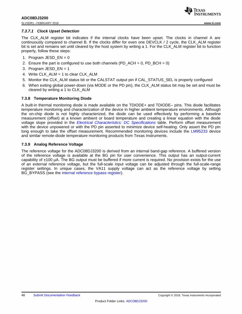
48
ADC08DJ3200SLVSDR1 –FEBRUARY 2018 www.ti.com
Product Folder Links: ADC08DJ3200
Submit Documentation Feedback Copyright © 2018, Texas Instruments Incorporated
7.3.7.1 Clock Upset DetectionThe CLK_ALM register bit indicates if the internal clocks have been upset. The clocks in channel A arecontinuously compared to channel B. If the clocks differ for even one DEVCLK / 2 cycle, the CLK_ALM registerbit is set and remains set until cleared by the host system by writing a 1. For the CLK_ALM register bit to functionproperly, follow these steps:
1. Program JESD_EN = 02. Ensure the part is configured to use both channels (PD_ACH = 0, PD_BCH = 0)3. Program JESD_EN = 14. Write CLK_ALM = 1 to clear CLK_ALM5. Monitor the CLK_ALM status bit or the CALSTAT output pin if CAL_STATUS_SEL is properly configured6. When exiting global power-down (via MODE or the PD pin), the CLK_ALM status bit may be set and must be
cleared by writing a 1 to CLK_ALM
7.3.8 Temperature Monitoring DiodeA built-in thermal monitoring diode is made available on the TDIODE+ and TDIODE– pins. This diode facilitatestemperature monitoring and characterization of the device in higher ambient temperature environments. Althoughthe on-chip diode is not highly characterized, the diode can be used effectively by performing a baselinemeasurement (offset) at a known ambient or board temperature and creating a linear equation with the diodevoltage slope provided in the Electrical Characteristics: DC Specifications table. Perform offset measurementwith the device unpowered or with the PD pin asserted to minimize device self-heating. Only assert the PD pinlong enough to take the offset measurement. Recommended monitoring devices include the LM95233 deviceand similar remote-diode temperature monitoring products from Texas Instruments.
7.3.9 Analog Reference VoltageThe reference voltage for the ADC08DJ3200 is derived from an internal band-gap reference. A buffered versionof the reference voltage is available at the BG pin for user convenience. This output has an output-currentcapability of ±100 µA. The BG output must be buffered if more current is required. No provision exists for the useof an external reference voltage, but the full-scale input voltage can be adjusted through the full-scale-rangeregister settings. In unique cases, the VA11 supply voltage can act as the reference voltage by settingBG_BYPASS (see the internal reference bypass register).
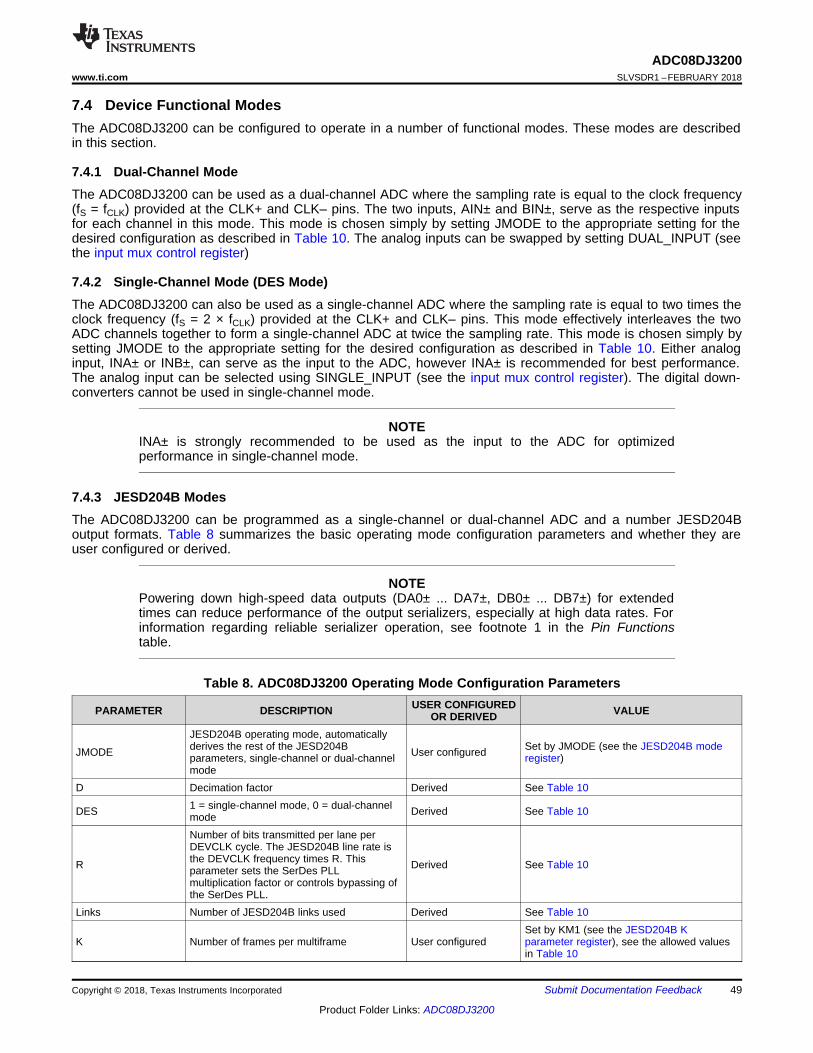
49
ADC08DJ3200www.ti.com SLVSDR1 –FEBRUARY 2018
Product Folder Links: ADC08DJ3200
Submit Documentation FeedbackCopyright © 2018, Texas Instruments Incorporated
7.4 Device Functional ModesThe ADC08DJ3200 can be configured to operate in a number of functional modes. These modes are describedin this section.
7.4.1 Dual-Channel ModeThe ADC08DJ3200 can be used as a dual-channel ADC where the sampling rate is equal to the clock frequency(fS = fCLK) provided at the CLK+ and CLK– pins. The two inputs, AIN± and BIN±, serve as the respective inputsfor each channel in this mode. This mode is chosen simply by setting JMODE to the appropriate setting for thedesired configuration as described in Table 10. The analog inputs can be swapped by setting DUAL_INPUT (seethe input mux control register)
7.4.2 Single-Channel Mode (DES Mode)The ADC08DJ3200 can also be used as a single-channel ADC where the sampling rate is equal to two times theclock frequency (fS = 2 × fCLK) provided at the CLK+ and CLK– pins. This mode effectively interleaves the twoADC channels together to form a single-channel ADC at twice the sampling rate. This mode is chosen simply bysetting JMODE to the appropriate setting for the desired configuration as described in Table 10. Either analoginput, INA± or INB±, can serve as the input to the ADC, however INA± is recommended for best performance.The analog input can be selected using SINGLE_INPUT (see the input mux control register). The digital down-converters cannot be used in single-channel mode.
NOTEINA± is strongly recommended to be used as the input to the ADC for optimizedperformance in single-channel mode.
7.4.3 JESD204B ModesThe ADC08DJ3200 can be programmed as a single-channel or dual-channel ADC and a number JESD204Boutput formats. Table 8 summarizes the basic operating mode configuration parameters and whether they areuser configured or derived.
NOTEPowering down high-speed data outputs (DA0± ... DA7±, DB0± ... DB7±) for extendedtimes can reduce performance of the output serializers, especially at high data rates. Forinformation regarding reliable serializer operation, see footnote 1 in the Pin Functionstable.
Table 8. ADC08DJ3200 Operating Mode Configuration Parameters
PARAMETER DESCRIPTION USER CONFIGUREDOR DERIVED VALUE
JMODE
JESD204B operating mode, automaticallyderives the rest of the JESD204Bparameters, single-channel or dual-channelmode
User configured Set by JMODE (see the JESD204B moderegister)
D Decimation factor Derived See Table 10
DES 1 = single-channel mode, 0 = dual-channelmode Derived See Table 10
R
Number of bits transmitted per lane perDEVCLK cycle. The JESD204B line rate isthe DEVCLK frequency times R. Thisparameter sets the SerDes PLLmultiplication factor or controls bypassing ofthe SerDes PLL.
Derived See Table 10
Links Number of JESD204B links used Derived See Table 10
K Number of frames per multiframe User configuredSet by KM1 (see the JESD204B Kparameter register), see the allowed valuesin Table 10
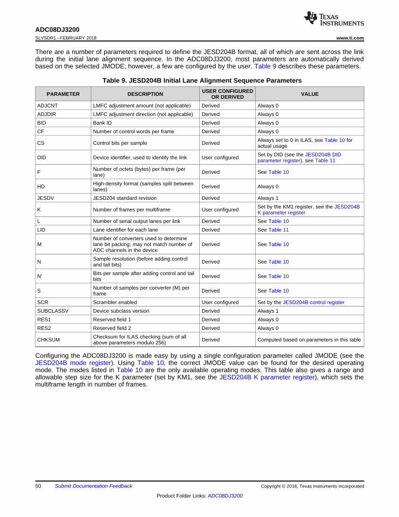
50
ADC08DJ3200SLVSDR1 –FEBRUARY 2018 www.ti.com
Product Folder Links: ADC08DJ3200
Submit Documentation Feedback Copyright © 2018, Texas Instruments Incorporated
There are a number of parameters required to define the JESD204B format, all of which are sent across the linkduring the initial lane alignment sequence. In the ADC08DJ3200, most parameters are automatically derivedbased on the selected JMODE; however, a few are configured by the user. Table 9 describes these parameters.
Table 9. JESD204B Initial Lane Alignment Sequence Parameters
PARAMETER DESCRIPTION USER CONFIGUREDOR DERIVED VALUE
ADJCNT LMFC adjustment amount (not applicable) Derived Always 0ADJDIR LMFC adjustment direction (not applicable) Derived Always 0BID Bank ID Derived Always 0CF Number of control words per frame Derived Always 0
CS Control bits per sample Derived Always set to 0 in ILAS, see Table 10 foractual usage
DID Device identifier, used to identify the link User configured Set by DID (see the JESD204B DIDparameter register), see Table 11
F Number of octets (bytes) per frame (perlane) Derived See Table 10
HD High-density format (samples split betweenlanes) Derived Always 0
JESDV JESD204 standard revision Derived Always 1
K Number of frames per multiframe User configured Set by the KM1 register, see the JESD204BK parameter register
L Number of serial output lanes per link Derived See Table 10LID Lane identifier for each lane Derived See Table 11
MNumber of converters used to determinelane bit packing; may not match number ofADC channels in the device
Derived See Table 10
N Sample resolution (before adding controland tail bits) Derived See Table 10
N' Bits per sample after adding control and tailbits Derived See Table 10
S Number of samples per converter (M) perframe Derived See Table 10
SCR Scrambler enabled User configured Set by the JESD204B control registerSUBCLASSV Device subclass version Derived Always 1RES1 Reserved field 1 Derived Always 0RES2 Reserved field 2 Derived Always 0
CHKSUM Checksum for ILAS checking (sum of allabove parameters modulo 256) Derived Computed based on parameters in this table
Configuring the ADC08DJ3200 is made easy by using a single configuration parameter called JMODE (see theJESD204B mode register). Using Table 10, the correct JMODE value can be found for the desired operatingmode. The modes listed in Table 10 are the only available operating modes. This table also gives a range andallowable step size for the K parameter (set by KM1, see the JESD204B K parameter register), which sets themultiframe length in number of frames.
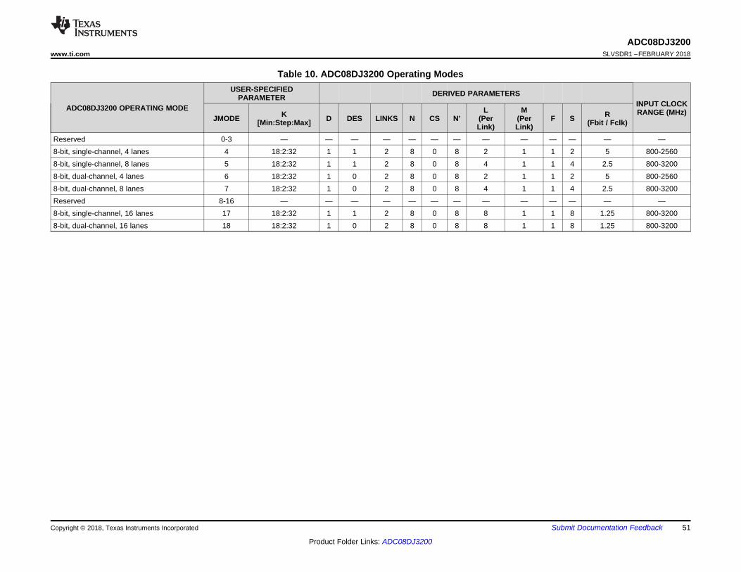
ADC08DJ3200www.ti.com SLVSDR1 –FEBRUARY 2018
51
Product Folder Links: ADC08DJ3200
Submit Documentation FeedbackCopyright © 2018, Texas Instruments Incorporated
Table 10. ADC08DJ3200 Operating Modes
ADC08DJ3200 OPERATING MODE
USER-SPECIFIEDPARAMETER DERIVED PARAMETERS
INPUT CLOCKRANGE (MHz)
JMODE K[Min:Step:Max] D DES LINKS N CS N’
L(PerLink)
M(PerLink)
F S R(Fbit / Fclk)
Reserved 0-3 — — — — — — — — — — — — —8-bit, single-channel, 4 lanes 4 18:2:32 1 1 2 8 0 8 2 1 1 2 5 800-25608-bit, single-channel, 8 lanes 5 18:2:32 1 1 2 8 0 8 4 1 1 4 2.5 800-32008-bit, dual-channel, 4 lanes 6 18:2:32 1 0 2 8 0 8 2 1 1 2 5 800-25608-bit, dual-channel, 8 lanes 7 18:2:32 1 0 2 8 0 8 4 1 1 4 2.5 800-3200Reserved 8-16 — — — — — — — — — — — — —8-bit, single-channel, 16 lanes 17 18:2:32 1 1 2 8 0 8 8 1 1 8 1.25 800-32008-bit, dual-channel, 16 lanes 18 18:2:32 1 0 2 8 0 8 8 1 1 8 1.25 800-3200
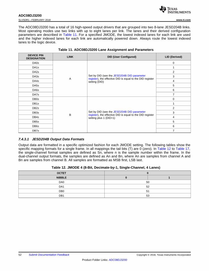
52
ADC08DJ3200SLVSDR1 –FEBRUARY 2018 www.ti.com
Product Folder Links: ADC08DJ3200
Submit Documentation Feedback Copyright © 2018, Texas Instruments Incorporated
The ADC08DJ3200 has a total of 16 high-speed output drivers that are grouped into two 8-lane JESD204B links.Most operating modes use two links with up to eight lanes per link. The lanes and their derived configurationparameters are described in Table 11. For a specified JMODE, the lowest indexed lanes for each link are usedand the higher indexed lanes for each link are automatically powered down. Always route the lowest indexedlanes to the logic device.
Table 11. ADC08DJ3200 Lane Assignment and ParametersDEVICE PIN
DESIGNATION LINK DID (User Configured) LID (Derived)
DA0±
ASet by DID (see the JESD204B DID parameterregister), the effective DID is equal to the DID registersetting (DID)
0DA1± 1DA2± 2DA3± 3DA4± 4DA5± 5DA6± 6DA7± 7DB0±
BSet by DID (see the JESD204B DID parameterregister), the effective DID is equal to the DID registersetting plus 1 (DID+1)
0DB1± 1DB2± 2DB3± 3DB4± 4DB5± 5DB6± 6DB7± 7
7.4.3.1 JESD204B Output Data FormatsOutput data are formatted in a specific optimized fashion for each JMODE setting. The following tables show thespecific mapping formats for a single frame. In all mappings the tail bits (T) are 0 (zero). In Table 12 to Table 17,the single-channel format samples are defined as Sn, where n is the sample number within the frame. In thedual-channel output formats, the samples are defined as An and Bn, where An are samples from channel A andBn are samples from channel B. All samples are formatted as MSB first, LSB last.
Table 12. JMODE 4 (8-Bit, Decimate-by-1, Single-Channel, 4 Lanes)OCTET 0NIBBLE 0 1
DA0 S0DA1 S2DB0 S1DB1 S3
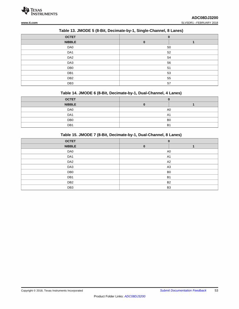
53
ADC08DJ3200www.ti.com SLVSDR1 –FEBRUARY 2018
Product Folder Links: ADC08DJ3200
Submit Documentation FeedbackCopyright © 2018, Texas Instruments Incorporated
Table 13. JMODE 5 (8-Bit, Decimate-by-1, Single-Channel, 8 Lanes)OCTET 0NIBBLE 0 1
DA0 S0DA1 S2DA2 S4DA3 S6DB0 S1DB1 S3DB2 S5DB3 S7
Table 14. JMODE 6 (8-Bit, Decimate-by-1, Dual-Channel, 4 Lanes)OCTET 0NIBBLE 0 1
DA0 A0DA1 A1DB0 B0DB1 B1
Table 15. JMODE 7 (8-Bit, Decimate-by-1, Dual-Channel, 8 Lanes)OCTET 0NIBBLE 0 1
DA0 A0DA1 A1DA2 A2DA3 A3DB0 B0DB1 B1DB2 B2DB3 B3
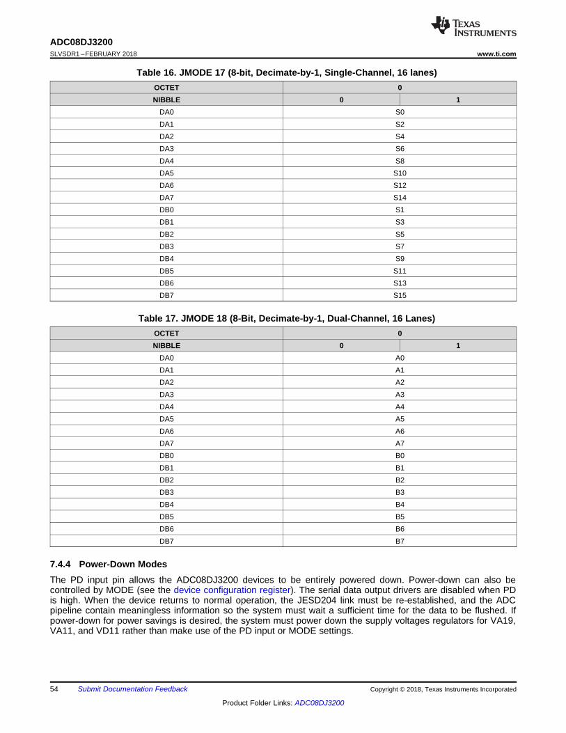
54
ADC08DJ3200SLVSDR1 –FEBRUARY 2018 www.ti.com
Product Folder Links: ADC08DJ3200
Submit Documentation Feedback Copyright © 2018, Texas Instruments Incorporated
Table 16. JMODE 17 (8-bit, Decimate-by-1, Single-Channel, 16 lanes)OCTET 0NIBBLE 0 1
DA0 S0DA1 S2DA2 S4DA3 S6DA4 S8DA5 S10DA6 S12DA7 S14DB0 S1DB1 S3DB2 S5DB3 S7DB4 S9DB5 S11DB6 S13DB7 S15
Table 17. JMODE 18 (8-Bit, Decimate-by-1, Dual-Channel, 16 Lanes)OCTET 0NIBBLE 0 1
DA0 A0DA1 A1DA2 A2DA3 A3DA4 A4DA5 A5DA6 A6DA7 A7DB0 B0DB1 B1DB2 B2DB3 B3DB4 B4DB5 B5DB6 B6DB7 B7
7.4.4 Power-Down ModesThe PD input pin allows the ADC08DJ3200 devices to be entirely powered down. Power-down can also becontrolled by MODE (see the device configuration register). The serial data output drivers are disabled when PDis high. When the device returns to normal operation, the JESD204 link must be re-established, and the ADCpipeline contain meaningless information so the system must wait a sufficient time for the data to be flushed. Ifpower-down for power savings is desired, the system must power down the supply voltages regulators for VA19,VA11, and VD11 rather than make use of the PD input or MODE settings.
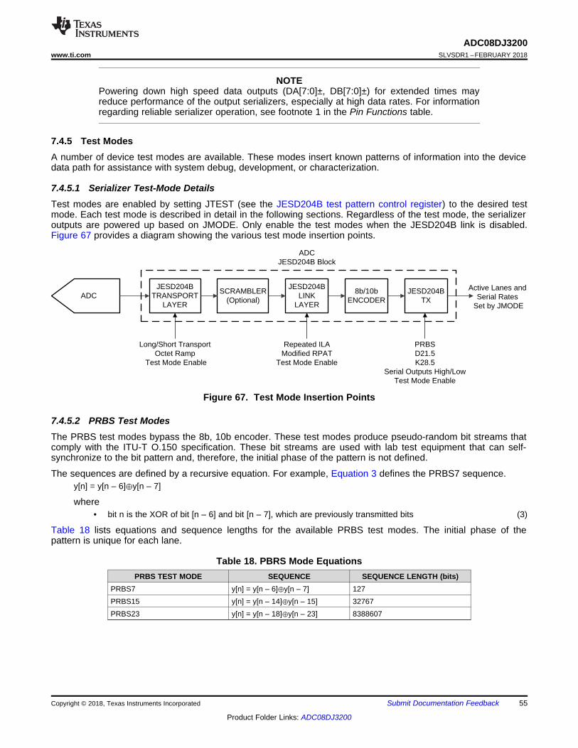
ADCJESD204B
TRANSPORT LAYER
SCRAMBLER(Optional)
JESD204BLINK
LAYER
JESD204BTX
8b/10bENCODER
ADCJESD204B Block
Long/Short TransportOctet Ramp
Test Mode Enable
Repeated ILAModified RPAT
Test Mode Enable
PRBSD21.5K28.5
Serial Outputs High/LowTest Mode Enable
Active Lanes andSerial Rates
Set by JMODE
55
ADC08DJ3200www.ti.com SLVSDR1 –FEBRUARY 2018
Product Folder Links: ADC08DJ3200
Submit Documentation FeedbackCopyright © 2018, Texas Instruments Incorporated
NOTEPowering down high speed data outputs (DA[7:0]±, DB[7:0]±) for extended times mayreduce performance of the output serializers, especially at high data rates. For informationregarding reliable serializer operation, see footnote 1 in the Pin Functions table.
7.4.5 Test ModesA number of device test modes are available. These modes insert known patterns of information into the devicedata path for assistance with system debug, development, or characterization.
7.4.5.1 Serializer Test-Mode DetailsTest modes are enabled by setting JTEST (see the JESD204B test pattern control register) to the desired testmode. Each test mode is described in detail in the following sections. Regardless of the test mode, the serializeroutputs are powered up based on JMODE. Only enable the test modes when the JESD204B link is disabled.Figure 67 provides a diagram showing the various test mode insertion points.
Figure 67. Test Mode Insertion Points
7.4.5.2 PRBS Test ModesThe PRBS test modes bypass the 8b, 10b encoder. These test modes produce pseudo-random bit streams thatcomply with the ITU-T O.150 specification. These bit streams are used with lab test equipment that can self-synchronize to the bit pattern and, therefore, the initial phase of the pattern is not defined.
The sequences are defined by a recursive equation. For example, Equation 3 defines the PRBS7 sequence.y[n] = y[n – 6]⊕y[n – 7]
where• bit n is the XOR of bit [n – 6] and bit [n – 7], which are previously transmitted bits (3)
Table 18 lists equations and sequence lengths for the available PRBS test modes. The initial phase of thepattern is unique for each lane.
Table 18. PBRS Mode EquationsPRBS TEST MODE SEQUENCE SEQUENCE LENGTH (bits)
PRBS7 y[n] = y[n – 6]⊕y[n – 7] 127PRBS15 y[n] = y[n – 14]⊕y[n – 15] 32767PRBS23 y[n] = y[n – 18]⊕y[n – 23] 8388607
56
ADC08DJ3200SLVSDR1 –FEBRUARY 2018 www.ti.com
Product Folder Links: ADC08DJ3200
Submit Documentation Feedback Copyright © 2018, Texas Instruments Incorporated
7.4.5.3 Ramp Test ModeIn the ramp test mode, the JESD204B link layer operates normally, but the transport layer is disabled and theinput from the formatter is ignored. After the ILA sequence, each lane transmits an identical octet stream thatincrements from 0x00 to 0xFF and repeats.
7.4.5.4 Short and Long Transport Test ModeJESD204B defines both short and long transport test modes to verify that the transport layers in the transmitterand receiver are operating correctly. The ADC08DJ3200 only supports the short transport test pattern.
7.4.5.4.1 Short Transport Test Pattern
Short transport test patterns send a predefined octet format that repeats every frame. In the ADC08DJ3200, allJMODE configurations that have an N' value of 8 use the short transport test pattern. Table 19 define the shorttransport test patterns for N' values of 8. All applicable lanes are shown, however only the enabled lanes (lowestindexed) for the configured JMODE are used.
Table 19. Short Transport Test Pattern for N' = 8 Modes (Length = 2 Frames)FRAME 0 1
DA0 0x00 0xFFDA1 0x01 0xFEDA2 0x02 0xFDDA3 0x03 0xFCDB0 0x00 0xFFDB1 0x01 0xFEDB2 0x02 0xFDDB3 0x03 0xFC
7.4.5.5 D21.5 Test ModeIn this test mode, the controller transmits a continuous stream of D21.5 characters (alternating 0s and 1s).
7.4.5.6 K28.5 Test ModeIn this test mode, the controller transmits a continuous stream of K28.5 characters.
7.4.5.7 Repeated ILA Test ModeIn this test mode, the JESD204B link layer operates normally, except that the ILA sequence (ILAS) repeatsindefinitely instead of starting the data phase. Whenever the receiver issues a synchronization request, thetransmitter initiates code group synchronization. Upon completion of code group synchronization, the transmitterrepeatedly transmits the ILA sequence.
7.4.5.8 Modified RPAT Test ModeA 12-octet repeating pattern is defined in INCITS TR-35-2004. The purpose of this pattern is to generate whitespectral content for JESD204B compliance and jitter testing. Table 20 lists the pattern before and after 8b, 10bencoding.
57
ADC08DJ3200www.ti.com SLVSDR1 –FEBRUARY 2018
Product Folder Links: ADC08DJ3200
Submit Documentation FeedbackCopyright © 2018, Texas Instruments Incorporated
Table 20. Modified RPAT Pattern Values
OCTET NUMBER Dx.y NOTATION 8-BIT INPUT TO 8b, 10b ENCODER 20b OUTPUT OF 8b, 10b ENCODER(Two Characters)
0 D30.5 0xBE0x86BA6
1 D23.6 0xD7
2 D3.1 0x230xC6475
3 D7.2 0x47
4 D11.3 0x6B0xD0E8D
5 D15.4 0x8F
6 D19.5 0xB30xCA8B4
7 D20.0 0x14
8 D30.2 0x5E0x7949E
9 D27.7 0xFB
10 D21.1 0x350xAA665
11 D25.2 0x59
7.4.6 Calibration Modes and TrimmingThe ADC08DJ3200 has two calibration modes available: foreground calibration and background calibration.When foreground calibration is initiated the ADCs are automatically taken offline and the output data becomesmid-code (0x000 in 2's complement) while a calibration is occurring. Background calibration allows the ADC tocontinue normal operation while the ADC cores are calibrated in the background by swapping in a different ADCcore to take its place. Additional offset calibration features are available in both foreground and backgroundcalibration modes. Further, a number of ADC parameters can be trimmed to optimize performance in a usersystem.
The ADC08DJ3200 consists of a total of six sub-ADCs, each referred to as a bank, with two banks forming anADC core. The banks sample out-of-phase so that each ADC core is two-way interleaved. The six banks formthree ADC cores, referred to as ADC A, ADC B, and ADC C. In foreground calibration mode, ADC A samplesINA± and ADC B samples INB± in dual-channel mode and both ADC A and ADC B sample INA± (or INB±) insingle-channel mode. In the background calibration modes, the third ADC core, ADC C, is swapped inperiodically for ADC A and ADC B so that they can be calibrated without disrupting operation. Figure 68 providesa diagram of the calibration system including labeling of the banks that make up each ADC core. Whencalibration is performed the linearity, gain, and offset voltage for each bank are calibrated to an internallygenerated calibration signal. The analog inputs can be driven during calibration, both foreground andbackground, except that when offset calibration (OS_CAL or BGOS_CAL) is used there must be no signals (oraliased signals) near DC for proper estimation of the offset (see the Offset Calibration section).
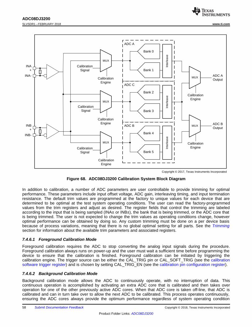
ADC A
INA+
INA-
INB+
INB-
Calibration Signal
Calibration Signal
Calibration Signal
Bank 1
Bank 0
ADC C
Bank 3
Bank 2
ADC B
Bank 5
Bank 4
Calibration Engine
MUX
MUX
MUX
MUX
MUX
ADC A Output
ADC B Output
Calibration Engine
Calibration Engine
Calibration Engine
Calibration Engine
Inte
rleav
eIn
terle
ave
Inte
rleav
e
Copyright © 2017, Texas Instruments Incorporated
58
ADC08DJ3200SLVSDR1 –FEBRUARY 2018 www.ti.com
Product Folder Links: ADC08DJ3200
Submit Documentation Feedback Copyright © 2018, Texas Instruments Incorporated
Figure 68. ADC08DJ3200 Calibration System Block Diagram
In addition to calibration, a number of ADC parameters are user controllable to provide trimming for optimalperformance. These parameters include input offset voltage, ADC gain, interleaving timing, and input terminationresistance. The default trim values are programmed at the factory to unique values for each device that aredetermined to be optimal at the test system operating conditions. The user can read the factory-programmedvalues from the trim registers and adjust as desired. The register fields that control the trimming are labeledaccording to the input that is being sampled (INA± or INB±), the bank that is being trimmed, or the ADC core thatis being trimmed. The user is not expected to change the trim values as operating conditions change, howeveroptimal performance can be obtained by doing so. Any custom trimming must be done on a per device basisbecause of process variations, meaning that there is no global optimal setting for all parts. See the Trimmingsection for information about the available trim parameters and associated registers.
7.4.6.1 Foreground Calibration ModeForeground calibration requires the ADC to stop converting the analog input signals during the procedure.Foreground calibration always runs on power-up and the user must wait a sufficient time before programming thedevice to ensure that the calibration is finished. Foreground calibration can be initiated by triggering thecalibration engine. The trigger source can be either the CAL_TRIG pin or CAL_SOFT_TRIG (see the calibrationsoftware trigger register) and is chosen by setting CAL_TRIG_EN (see the calibration pin configuration register).
7.4.6.2 Background Calibration ModeBackground calibration mode allows the ADC to continuously operate, with no interruption of data. Thiscontinuous operation is accomplished by activating an extra ADC core that is calibrated and then takes overoperation for one of the other previously active ADC cores. When that ADC core is taken off-line, that ADC iscalibrated and can in turn take over to allow the next ADC to be calibrated. This process operates continuously,ensuring the ADC cores always provide the optimum performance regardless of system operating condition
59
ADC08DJ3200www.ti.com SLVSDR1 –FEBRUARY 2018
Product Folder Links: ADC08DJ3200
Submit Documentation FeedbackCopyright © 2018, Texas Instruments Incorporated
changes. Because of the additional active ADC core, background calibration mode has increased powerconsumption in comparison to foreground calibration mode. The low-power background calibration (LPBG) modediscussed in the Low-Power Background Calibration (LPBG) Mode section provides reduced average powerconsumption in comparison with the standard background calibration mode. Background calibration can beenabled by setting CAL_BG (see the calibration configuration 0 register). CAL_TRIG_EN must be set to 0 andCAL_SOFT_TRIG must be set to 1.
Great care has been taken to minimize effects on converted data as the core switching process occurs, however,small brief glitches may still occur on the converter data as the cores are swapped. See the TypicalCharacteristics section for examples of possible glitches in sine-wave and DC signals.
7.4.6.3 Low-Power Background Calibration (LPBG) ModeLow-power background calibration (LPBG) mode reduces the power-overhead of enabling additional ADC cores.Off-line cores are powered down until ready to be calibrated and put on-line. Set LP_EN = 1 to enable the low-power background calibration feature. LP_SLEEP_DLY is used to adjust the amount of time an ADC sleepsbefore waking up for calibration (if LP_EN = 1 and LP_TRIG = 0). LP_WAKE_DLY sets how long the core isallowed to stabilize before calibration and being put on-line. LP_TRIG is used to select between an automaticswitching process or one that is controlled by the user via CAL_SOFT_TRIG or CAL_TRIG. In this mode there isan increase in power consumption during the ADC core calibration. The power consumption roughly alternatesbetween the power consumption in foreground calibration when the spare ADC core is sleeping to the powerconsumption in background calibration when the spare ADC is being calibrated. Design the power-supplynetwork to handle the transient power requirements for this mode.
7.4.7 Offset CalibrationForeground calibration and background calibration modes inherently calibrate the offsets of the ADC cores;however, the input buffers sit outside of the calibration loop and therefore their offsets are not calibrated by thestandard calibration process. In both dual-channel mode and single-channel mode, uncalibrated input bufferoffsets result in a shift in the mid-code output (DC offset) with no input. Further, in single-channel modeuncalibrated input buffer offsets can result in a fixed spur at fS / 2. A separate calibration is provided to correctthe input buffer offsets.
There must be no signals at or near DC or aliased signals that fall at or near DC in order to properly calibrationthe offsets, requiring the system to ensure this condition during normal operation or have the ability to mute theinput signal during calibration. Foreground offset calibration is enabled via CAL_OS and only performs thecalibration one time as part of the foreground calibration procedure. Background offset calibration is enabled viaCAL_BGOS and continues to correct the offset as part of the background calibration routine to account foroperating condition changes. When CAL_BGOS is set, the system must ensure that there are no DC or near DCsignals or aliased signals that fall at or near DC during normal operation. Offset calibration can be performed asa foreground operation when using background calibration by setting CAL_OS to 1 before setting CAL_EN, butdoes not correct for variations as operating conditions change.
The offset calibration correction uses the input offset voltage trim registers (see Table 21) to correct the offsetand therefore must not be written by the user when offset calibration is used. The user can read the calibratedvalues by reading the OADJ_x_VINy registers, where x is the ADC core and y is the input (INA± or INB±), aftercalibration is completed. Only read the values when FG_DONE is read as 1 when using foreground offsetcalibration (CAL_OS = 1) and do not read the values when using background offset calibration (CAL_BGOS = 1).
60
ADC08DJ3200SLVSDR1 –FEBRUARY 2018 www.ti.com
Product Folder Links: ADC08DJ3200
Submit Documentation Feedback Copyright © 2018, Texas Instruments Incorporated
7.4.8 TrimmingTable 21 lists the parameters that can be trimmed and the associated registers.
Table 21. Trim Register DescriptionsTRIM PARAMETER TRIM REGISTER NOTES
Band-gap reference BG_TRIM Measurement on BG output pin.
Input termination resistance RTRIM_x,where x = A for INA± or B for INB±)
The device must be powered on with a clockapplied.
Input offset voltageOADJ_x_VINy,
where x = ADC core (A, B or C)and y = A for INA± or B for INB±)
A different trim value is allowed for eachADC core (A, B, or C) to allow moreconsistent offset performance in backgroundcalibration mode.
INA± and INB± gain GAIN_TRIM_x,where x = A for INA± or B for INB±)
Set FS_RANGE_A and FS_RANGE_B todefault values before trimming the input. UseFS_RANGE_A and FS_RANGE_B to adjustthe full-scale input voltage.
INA± and INB± full-scale input voltage FS_RANGE_x,where x = A for INA± or B for INB±)
Full-scale input voltage adjustment for eachinput. The default value is effected byGAIN_TRIM_x (x = A or B). TrimGAIN_TRIM_x with FS_RANGE_x set to thedefault value. FS_RANGE_x can then beused to trim the full-scale input voltage.
Intra-ADC core timing (bank timing)Bx_TIME_y,
where x = bank number (0–5)and y = 0° or –90° clock phase
Trims the timing between the two banks ofan ADC core (ADC A, B, or C) for two clockphases, either 0° or –90°. The –90° clockphase is used in single-channel mode only.
Inter-ADC core timing (dual-channel mode) TADJ_A, TADJ_B, TADJ_CA, TADJ_CB
The suffix letter (A, B, CA, or CB) indicatesthe ADC core that is being trimmed. CAindicates the timing trim in backgroundcalibration mode for ADC C when standing infor ADC A, whereas CB is the timing trim forADC C when standing in for ADC B.
Inter-ADC core timing (single-channel mode)TADJ_A_FG90, TADJ_B_FG0,TADJ_A_BG90, TADJ_C_BG0,TADJ_C_BG90, TADJ_B_BG0
The middle letter (A, B, or C) indicates theADC core that is being trimmed. FG indicatesa trim for foreground calibration while BGindicates background calibration. The suffixof 0 or 90 indicates the clock phase appliedto the ADC core. 0 indicates a 0° clock and issampling in-phase with the clock input. 90indicates a 90° clock and therefore issampling out-of-phase with the clock input.These timings must be trimmed for optimalperformance if the user prefers to use INB±in single-channel mode. These timings aretrimmed for INA± at the factory.
7.4.9 Offset FilteringThe ADC08DJ3200 has an additional feature that can be enabled to reduce offset-related interleaving spurs at fS/ 2 and fS / 4 (single input mode only). Offset filtering is enabled via CAL_OSFILT. The OSFILT_BW andOSFILT_SOAK parameters can be adjusted to tradeoff offset spur reduction with potential impact on informationin the mission mode signal being processed. Set these two parameters to the same value under most situations.The DC_RESTORE setting is used to either retain or filter out all DC-related content in the signal.
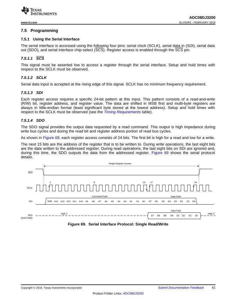
SCLK
1 24
Single Register Access
SCS
SDI
Command Field Data Field
SDO (read mode)
Data FieldHigh Z High Z
17168
A14 A13 A12 A11 A10 A9 A8 A7 A6 A5 A4 A3 A2 A1 A0 D7 D6 D5 D4 D3 D2 D1 D0
D7 D6 D5 D4 D3 D2 D1 D0
R/W
61
ADC08DJ3200www.ti.com SLVSDR1 –FEBRUARY 2018
Product Folder Links: ADC08DJ3200
Submit Documentation FeedbackCopyright © 2018, Texas Instruments Incorporated
7.5 Programming
7.5.1 Using the Serial InterfaceThe serial interface is accessed using the following four pins: serial clock (SCLK), serial data in (SDI), serial dataout (SDO), and serial interface chip-select (SCS). Register access is enabled through the SCS pin.
7.5.1.1 SCSThis signal must be asserted low to access a register through the serial interface. Setup and hold times withrespect to the SCLK must be observed.
7.5.1.2 SCLKSerial data input is accepted at the rising edge of this signal. SCLK has no minimum frequency requirement.
7.5.1.3 SDIEach register access requires a specific 24-bit pattern at this input. This pattern consists of a read-and-write(R/W) bit, register address, and register value. The data are shifted in MSB first and multi-byte registers arealways in little-endian format (least significant byte stored at the lowest address). Setup and hold times withrespect to the SCLK must be observed (see the Timing Requirements table).
7.5.1.4 SDOThe SDO signal provides the output data requested by a read command. This output is high impedance duringwrite bus cycles and during the read bit and register address portion of read bus cycles.
As shown in Figure 69, each register access consists of 24 bits. The first bit is high for a read and low for a write.
The next 15 bits are the address of the register that is to be written to. During write operations, the last eight bitsare the data written to the addressed register. During read operations, the last eight bits on SDI are ignored and,during this time, the SDO outputs the data from the addressed register. Figure 69 shows the serial protocoldetails.
Figure 69. Serial Interface Protocol: Single Read/Write
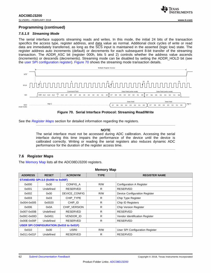
SCLK
1 24
Multiple Register Access
SCS
SDI
Command Field Data Field (write mode)
SDO (read mode)
Data FieldHigh Z
17168 32
Data FieldHigh Z
25
Data Field (write mode)
A14 A13 A12A11
A10 A9 A8 A7 A6 A5 A4 A3 A2 A1 A0 D7 D6 D5 D4 D3 D2 D1 D0 D7 D6 D5 D4 D3 D2 D1 D0R/W
D7 D6 D5 D4 D3 D2 D1 D0 D7 D6 D5 D4 D3 D2 D1 D0
62
ADC08DJ3200SLVSDR1 –FEBRUARY 2018 www.ti.com
Product Folder Links: ADC08DJ3200
Submit Documentation Feedback Copyright © 2018, Texas Instruments Incorporated
Programming (continued)7.5.1.5 Streaming ModeThe serial interface supports streaming reads and writes. In this mode, the initial 24 bits of the transactionspecifics the access type, register address, and data value as normal. Additional clock cycles of write or readdata are immediately transferred, as long as the SCS input is maintained in the asserted (logic low) state. Theregister address auto increments (default) or decrements for each subsequent 8-bit transfer of the streamingtransaction. The ADDR_ASC bit (register 000h, bits 5 and 2) controls whether the address value ascends(increments) or descends (decrements). Streaming mode can be disabled by setting the ADDR_HOLD bit (seethe user SPI configuration register). Figure 70 shows the streaming mode transaction details.
Figure 70. Serial Interface Protocol: Streaming Read/Write
See the Register Maps section for detailed information regarding the registers.
NOTEThe serial interface must not be accessed during ADC calibration. Accessing the serialinterface during this time impairs the performance of the device until the device iscalibrated correctly. Writing or reading the serial registers also reduces dynamic ADCperformance for the duration of the register access time.
7.6 Register MapsThe Memory Map lists all the ADC08DJ3200 registers.
Memory MapADDRESS RESET ACRONYM TYPE REGISTER NAME
STANDARD SPI-3.0 (0x000 to 0x00F)0x000 0x30 CONFIG_A R/W Configuration A Register0x001 Undefined RESERVED R RESERVED0x002 0x00 DEVICE_CONFIG R/W Device Configuration Register0x003 0x03 CHIP_TYPE R Chip Type Register
0x004-0x005 0x0020 CHIP_ID R Chip ID Registers0x006 0x0A CHIP_VERSION R Chip Version Register
0x007-0x00B Undefined RESERVED R RESERVED0x00C-0x00D 0x0451 VENDOR_ID R Vendor Identification Register0x00E-0x00F Undefined RESERVED R RESERVEDUSER SPI CONFIGURATION (0x010 to 0x01F)
0x010 0x00 USR0 R/W User SPI Configuration Register0x011-0x01F Undefined RESERVED R RESERVED
63
ADC08DJ3200www.ti.com SLVSDR1 –FEBRUARY 2018
Product Folder Links: ADC08DJ3200
Submit Documentation FeedbackCopyright © 2018, Texas Instruments Incorporated
Register Maps (continued)Memory Map (continued)
ADDRESS RESET ACRONYM TYPE REGISTER NAMEMISCELLANEOUS ANALOG REGISTERS (0x020 to 0x047)0x020-0x028 Undefined RESERVED R RESERVED
0x029 0x00 CLK_CTRL0 R/W Clock Control Register 00x02A 0x20 CLK_CTRL1 R/W Clock Control Register 10x02B Undefined RESERVED R RESERVED
0x02C-0x02E Undefined SYSREF_POS R SYSREF Capture Position Register0x02F Undefined RESERVED R RESERVED
0x030-0x031 0xA000 FS_RANGE_A R/W INA Full-Scale Range Adjust Register0x032-0x033 0xA000 FS_RANGE_B R/W INB Full-Scale Range Adjust Register0x034-0x037 Undefined RESERVED R RESERVED
0x038 0x00 BG_BYPASS R/W Internal Reference Bypass Register0x039-0x03A Undefined RESERVED R RESERVED
0x03B 0x00 TMSTP_CTRL R/W TMSTP± Control Register0x03C-0x047 Undefined RESERVED R RESERVEDSERIALIZER REGISTERS (0x048 to 0x05F)
0x048 0x00 SER_PE R/W Serializer Pre-Emphasis Control Register0x049-0x05F Undefined RESERVED R RESERVEDCALIBRATION REGISTERS (0x060 to 0x0FF)
0x060 0x01 INPUT_MUX R/W Input Mux Control Register0x061 0x01 CAL_EN R/W Calibration Enable Register0x062 0x01 CAL_CFG0 R/W Calibration Configuration 0 Register
0x063-0x069 Undefined RESERVED R RESERVED0x06A Undefined CAL_STATUS R Calibration Status Register0x06B 0x00 CAL_PIN_CFG R/W Calibration Pin Configuration Register0x06C 0x01 CAL_SOFT_TRIG R/W Calibration Software Trigger Register0x06D Undefined RESERVED R RESERVED0x06E 0x88 CAL_LP R/W Low-Power Background Calibration Register0x06F Undefined RESERVED R RESERVED0x070 0x00 CAL_DATA_EN R/W Calibration Data Enable Register0x071 Undefined CAL_DATA R/W Calibration Data Register
0x072-0x079 Undefined RESERVED R RESERVED0x07A Undefined GAIN_TRIM_A R/W Channel A Gain Trim Register0x07B Undefined GAIN_TRIM_B R/W Channel B Gain Trim Register0x07C Undefined BG_TRIM R/W Band-Gap Reference Trim Register0x07D Undefined RESERVED R RESERVED0x07E Undefined RTRIM_A R/W VINA Input Resistor Trim Register0x07F Undefined RTRIM_B R/W VINB Input Resistor Trim Register
0x080 Undefined TADJ_A_FG90 R/W Timing Adjustment for A-ADC, Single-Channel Mode,Foreground Calibration Register
0x081 Undefined TADJ_B_FG0 R/W Timing Adjustment for B-ADC, Single-Channel Mode,Foreground Calibration Register
0x082 Undefined TADJ_A_BG90 R/W Timing Adjustment for A-ADC, Single-Channel Mode,Background Calibration Register
0x083 Undefined TADJ_C_BG0 R/W Timing Adjustment for C-ADC, Single-Channel Mode,Background Calibration Register
0x084 Undefined TADJ_C_BG90 R/W Timing Adjustment for C-ADC, Single-Channel Mode,Background Calibration Register
64
ADC08DJ3200SLVSDR1 –FEBRUARY 2018 www.ti.com
Product Folder Links: ADC08DJ3200
Submit Documentation Feedback Copyright © 2018, Texas Instruments Incorporated
Register Maps (continued)Memory Map (continued)
ADDRESS RESET ACRONYM TYPE REGISTER NAME
0x085 Undefined TADJ_B_BG0 R/W Timing Adjustment for B-ADC, Single-Channel Mode,Background Calibration Register
0x086 Undefined TADJ_A R/W Timing Adjustment for A-ADC, Dual-Channel Mode Register
0x087 Undefined TADJ_CA R/W Timing Adjustment for C-ADC Acting for A-ADC, Dual-Channel Mode Register
0x088 Undefined TADJ_CB R/W Timing Adjustment for C-ADC Acting for B-ADC, Dual-Channel Mode Register
0x089 Undefined TADJ_B R/W Timing Adjustment for B-ADC, Dual-Channel Mode Register0x08A-0x08B Undefined OADJ_A_INA R/W Offset Adjustment for A-ADC and INA Register0x08C-0x08D Undefined OADJ_A_INB R/W Offset Adjustment for A-ADC and INB Register0x08E-0x08F Undefined OADJ_C_INA R/W Offset Adjustment for C-ADC and INA Register0x090-0x091 Undefined OADJ_C_INB R/W Offset Adjustment for C-ADC and INB Register0x092-0x093 Undefined OADJ_B_INA R/W Offset Adjustment for B-ADC and INA Register0x094-0x095 Undefined OADJ_B_INB R/W Offset Adjustment for B-ADC and INB Register
0x096 Undefined RESERVED R RESERVED0x097 0x00 OSFILT0 R/W Offset Filtering Control 00x098 0x33 OSFILT1 R/W Offset Filtering Control 1
0x099-0x0FF Undefined RESERVED R RESERVEDADC BANK REGISTERS (0x100 to 0x15F)0x100-0x101 Undefined RESERVED R RESERVED
0x102 Undefined B0_TIME_0 R/W Timing Adjustment for Bank 0 (0° Clock) Register0x103 Undefined B0_TIME_90 R/W Timing Adjustment for Bank 0 (–90° Clock) Register
0x104-0x111 Undefined RESERVED R RESERVED0x112 Undefined B1_TIME_0 R/W Timing Adjustment for Bank 1 (0° Clock) Register0x113 Undefined B1_TIME_90 R/W Timing Adjustment for Bank 1 (–90° Clock) Register
0x114-0x121 Undefined RESERVED R RESERVED0x122 Undefined B2_TIME_0 R/W Timing Adjustment for Bank 2 (0° Clock) Register0x123 Undefined B2_TIME_90 R/W Timing Adjustment for Bank 2 (–90° Clock) Register
0x124-0x131 Undefined RESERVED R RESERVED0x132 Undefined B3_TIME_0 R/W Timing Adjustment for Bank 3 (0° Clock) Register0x133 Undefined B3_TIME_90 R/W Timing Adjustment for Bank 3 (–90° Clock) Register
0x134-0x141 Undefined RESERVED R RESERVED0x142 Undefined B4_TIME_0 R/W Timing Adjustment for Bank 4 (0° Clock) Register0x143 Undefined B4_TIME_90 R/W Timing Adjustment for Bank 4 (–90° Clock) Register
0x144-0x151 Undefined RESERVED R RESERVED0x152 Undefined B5_TIME_0 R/W Timing Adjustment for Bank 5 (0° Clock) Register0x153 Undefined B5_TIME_90 R/W Timing Adjustment for Bank 5 (–90° Clock) Register
0x154-0x15F Undefined RESERVED R RESERVEDLSB CONTROL REGISTERS (0x160 to 0x1FF)
0x160 0x00 ENC_LSB R/W LSB Control Bit Output Register0x161-0x1FF Undefined RESERVED R RESERVEDJESD204B REGISTERS (0x200 to 0x20F)
0x200 0x01 JESD_EN R/W JESD204B Enable Register0x201 0x02 JMODE R/W JESD204B Mode (JMODE) Register0x202 0x1F KM1 R/W JESD204B K Parameter Register0x203 0x01 JSYNC_N R/W JESD204B Manual SYNC Request Register0x204 0x02 JCTRL R/W JESD204B Control Register
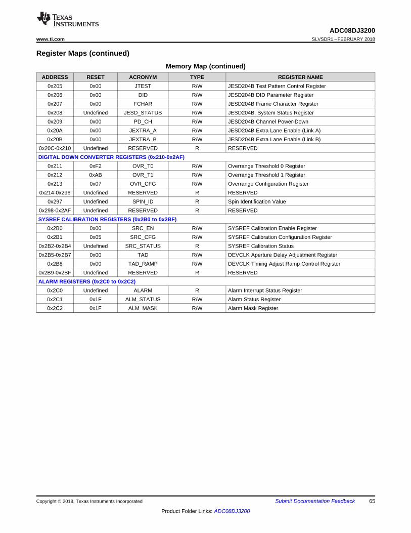
65
ADC08DJ3200www.ti.com SLVSDR1 –FEBRUARY 2018
Product Folder Links: ADC08DJ3200
Submit Documentation FeedbackCopyright © 2018, Texas Instruments Incorporated
Register Maps (continued)Memory Map (continued)
ADDRESS RESET ACRONYM TYPE REGISTER NAME0x205 0x00 JTEST R/W JESD204B Test Pattern Control Register0x206 0x00 DID R/W JESD204B DID Parameter Register0x207 0x00 FCHAR R/W JESD204B Frame Character Register0x208 Undefined JESD_STATUS R/W JESD204B, System Status Register0x209 0x00 PD_CH R/W JESD204B Channel Power-Down0x20A 0x00 JEXTRA_A R/W JESD204B Extra Lane Enable (Link A)0x20B 0x00 JEXTRA_B R/W JESD204B Extra Lane Enable (Link B)
0x20C-0x210 Undefined RESERVED R RESERVEDDIGITAL DOWN CONVERTER REGISTERS (0x210-0x2AF)
0x211 0xF2 OVR_T0 R/W Overrange Threshold 0 Register0x212 0xAB OVR_T1 R/W Overrange Threshold 1 Register0x213 0x07 OVR_CFG R/W Overrange Configuration Register
0x214-0x296 Undefined RESERVED R RESERVED0x297 Undefined SPIN_ID R Spin Identification Value
0x298-0x2AF Undefined RESERVED R RESERVEDSYSREF CALIBRATION REGISTERS (0x2B0 to 0x2BF)
0x2B0 0x00 SRC_EN R/W SYSREF Calibration Enable Register0x2B1 0x05 SRC_CFG R/W SYSREF Calibration Configuration Register
0x2B2-0x2B4 Undefined SRC_STATUS R SYSREF Calibration Status0x2B5-0x2B7 0x00 TAD R/W DEVCLK Aperture Delay Adjustment Register
0x2B8 0x00 TAD_RAMP R/W DEVCLK Timing Adjust Ramp Control Register0x2B9-0x2BF Undefined RESERVED R RESERVEDALARM REGISTERS (0x2C0 to 0x2C2)
0x2C0 Undefined ALARM R Alarm Interrupt Status Register0x2C1 0x1F ALM_STATUS R/W Alarm Status Register0x2C2 0x1F ALM_MASK R/W Alarm Mask Register
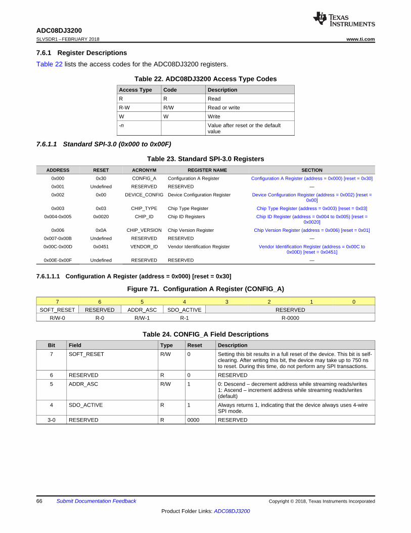
66
ADC08DJ3200SLVSDR1 –FEBRUARY 2018 www.ti.com
Product Folder Links: ADC08DJ3200
Submit Documentation Feedback Copyright © 2018, Texas Instruments Incorporated
7.6.1 Register DescriptionsTable 22 lists the access codes for the ADC08DJ3200 registers.
Table 22. ADC08DJ3200 Access Type CodesAccess Type Code DescriptionR R ReadR-W R/W Read or writeW W Write-n Value after reset or the default
value
7.6.1.1 Standard SPI-3.0 (0x000 to 0x00F)
Table 23. Standard SPI-3.0 RegistersADDRESS RESET ACRONYM REGISTER NAME SECTION
0x000 0x30 CONFIG_A Configuration A Register Configuration A Register (address = 0x000) [reset = 0x30]
0x001 Undefined RESERVED RESERVED —
0x002 0x00 DEVICE_CONFIG Device Configuration Register Device Configuration Register (address = 0x002) [reset =0x00]
0x003 0x03 CHIP_TYPE Chip Type Register Chip Type Register (address = 0x003) [reset = 0x03]
0x004-0x005 0x0020 CHIP_ID Chip ID Registers Chip ID Register (address = 0x004 to 0x005) [reset =0x0020]
0x006 0x0A CHIP_VERSION Chip Version Register Chip Version Register (address = 0x006) [reset = 0x01]
0x007-0x00B Undefined RESERVED RESERVED —
0x00C-0x00D 0x0451 VENDOR_ID Vendor Identification Register Vendor Identification Register (address = 0x00C to0x00D) [reset = 0x0451]
0x00E-0x00F Undefined RESERVED RESERVED —
7.6.1.1.1 Configuration A Register (address = 0x000) [reset = 0x30]
Figure 71. Configuration A Register (CONFIG_A)
7 6 5 4 3 2 1 0SOFT_RESET RESERVED ADDR_ASC SDO_ACTIVE RESERVED
R/W-0 R-0 R/W-1 R-1 R-0000
Table 24. CONFIG_A Field DescriptionsBit Field Type Reset Description7 SOFT_RESET R/W 0 Setting this bit results in a full reset of the device. This bit is self-
clearing. After writing this bit, the device may take up to 750 nsto reset. During this time, do not perform any SPI transactions.
6 RESERVED R 0 RESERVED5 ADDR_ASC R/W 1 0: Descend – decrement address while streaming reads/writes
1: Ascend – increment address while streaming reads/writes(default)
4 SDO_ACTIVE R 1 Always returns 1, indicating that the device always uses 4-wireSPI mode.
3-0 RESERVED R 0000 RESERVED
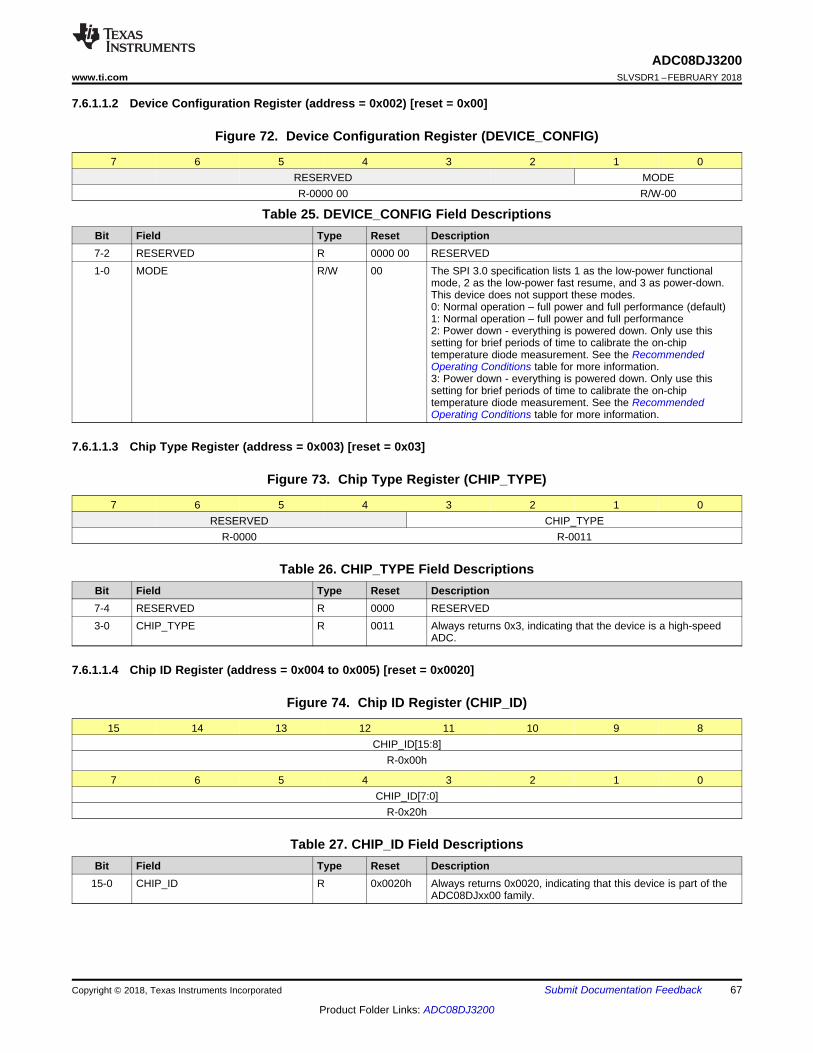
67
ADC08DJ3200www.ti.com SLVSDR1 –FEBRUARY 2018
Product Folder Links: ADC08DJ3200
Submit Documentation FeedbackCopyright © 2018, Texas Instruments Incorporated
7.6.1.1.2 Device Configuration Register (address = 0x002) [reset = 0x00]
Figure 72. Device Configuration Register (DEVICE_CONFIG)
7 6 5 4 3 2 1 0RESERVED MODER-0000 00 R/W-00
Table 25. DEVICE_CONFIG Field DescriptionsBit Field Type Reset Description7-2 RESERVED R 0000 00 RESERVED1-0 MODE R/W 00 The SPI 3.0 specification lists 1 as the low-power functional
mode, 2 as the low-power fast resume, and 3 as power-down.This device does not support these modes.0: Normal operation – full power and full performance (default)1: Normal operation – full power and full performance2: Power down - everything is powered down. Only use thissetting for brief periods of time to calibrate the on-chiptemperature diode measurement. See the RecommendedOperating Conditions table for more information.3: Power down - everything is powered down. Only use thissetting for brief periods of time to calibrate the on-chiptemperature diode measurement. See the RecommendedOperating Conditions table for more information.
7.6.1.1.3 Chip Type Register (address = 0x003) [reset = 0x03]
Figure 73. Chip Type Register (CHIP_TYPE)
7 6 5 4 3 2 1 0RESERVED CHIP_TYPE
R-0000 R-0011
Table 26. CHIP_TYPE Field DescriptionsBit Field Type Reset Description7-4 RESERVED R 0000 RESERVED3-0 CHIP_TYPE R 0011 Always returns 0x3, indicating that the device is a high-speed
ADC.
7.6.1.1.4 Chip ID Register (address = 0x004 to 0x005) [reset = 0x0020]
Figure 74. Chip ID Register (CHIP_ID)
15 14 13 12 11 10 9 8CHIP_ID[15:8]
R-0x00h
7 6 5 4 3 2 1 0CHIP_ID[7:0]
R-0x20h
Table 27. CHIP_ID Field DescriptionsBit Field Type Reset Description
15-0 CHIP_ID R 0x0020h Always returns 0x0020, indicating that this device is part of theADC08DJxx00 family.
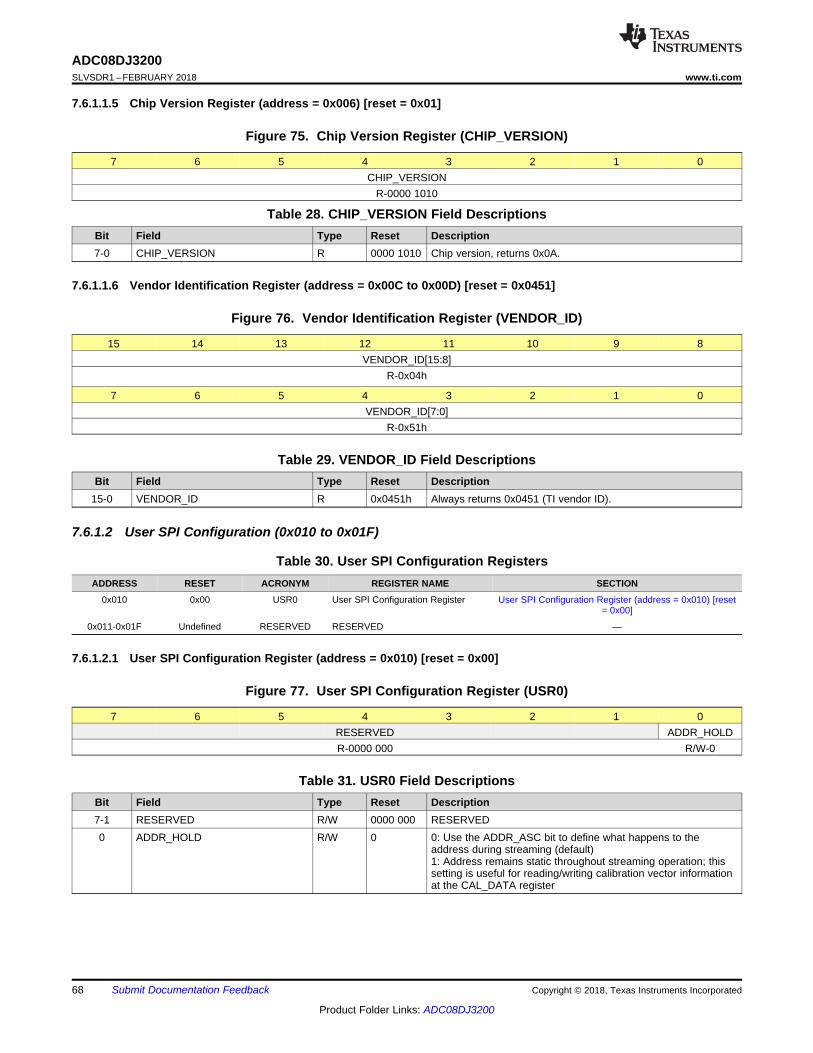
68
ADC08DJ3200SLVSDR1 –FEBRUARY 2018 www.ti.com
Product Folder Links: ADC08DJ3200
Submit Documentation Feedback Copyright © 2018, Texas Instruments Incorporated
7.6.1.1.5 Chip Version Register (address = 0x006) [reset = 0x01]
Figure 75. Chip Version Register (CHIP_VERSION)
7 6 5 4 3 2 1 0CHIP_VERSION
R-0000 1010
Table 28. CHIP_VERSION Field DescriptionsBit Field Type Reset Description7-0 CHIP_VERSION R 0000 1010 Chip version, returns 0x0A.
7.6.1.1.6 Vendor Identification Register (address = 0x00C to 0x00D) [reset = 0x0451]
Figure 76. Vendor Identification Register (VENDOR_ID)
15 14 13 12 11 10 9 8VENDOR_ID[15:8]
R-0x04h
7 6 5 4 3 2 1 0VENDOR_ID[7:0]
R-0x51h
Table 29. VENDOR_ID Field DescriptionsBit Field Type Reset Description
15-0 VENDOR_ID R 0x0451h Always returns 0x0451 (TI vendor ID).
7.6.1.2 User SPI Configuration (0x010 to 0x01F)
Table 30. User SPI Configuration RegistersADDRESS RESET ACRONYM REGISTER NAME SECTION
0x010 0x00 USR0 User SPI Configuration Register User SPI Configuration Register (address = 0x010) [reset= 0x00]
0x011-0x01F Undefined RESERVED RESERVED —
7.6.1.2.1 User SPI Configuration Register (address = 0x010) [reset = 0x00]
Figure 77. User SPI Configuration Register (USR0)
7 6 5 4 3 2 1 0RESERVED ADDR_HOLDR-0000 000 R/W-0
Table 31. USR0 Field DescriptionsBit Field Type Reset Description7-1 RESERVED R/W 0000 000 RESERVED0 ADDR_HOLD R/W 0 0: Use the ADDR_ASC bit to define what happens to the
address during streaming (default)1: Address remains static throughout streaming operation; thissetting is useful for reading/writing calibration vector informationat the CAL_DATA register
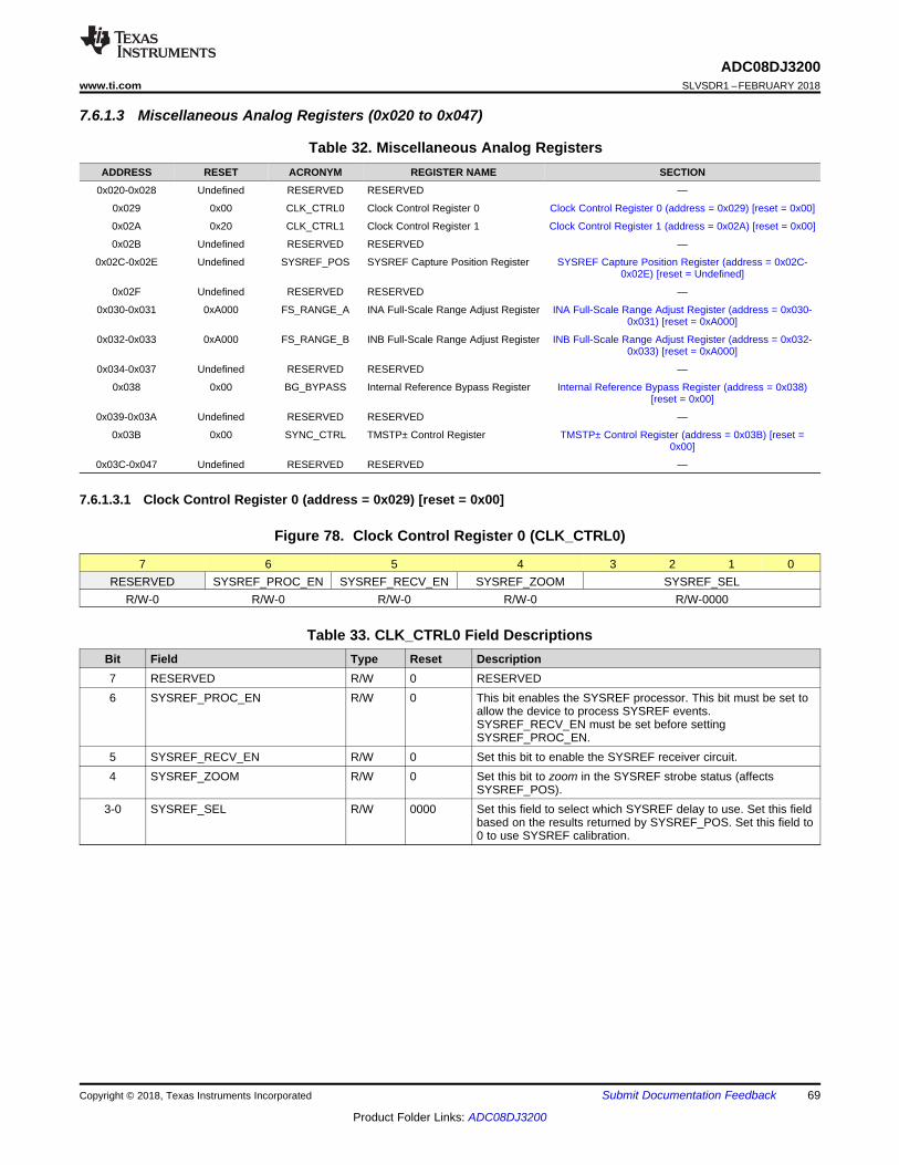
69
ADC08DJ3200www.ti.com SLVSDR1 –FEBRUARY 2018
Product Folder Links: ADC08DJ3200
Submit Documentation FeedbackCopyright © 2018, Texas Instruments Incorporated
7.6.1.3 Miscellaneous Analog Registers (0x020 to 0x047)
Table 32. Miscellaneous Analog RegistersADDRESS RESET ACRONYM REGISTER NAME SECTION
0x020-0x028 Undefined RESERVED RESERVED —
0x029 0x00 CLK_CTRL0 Clock Control Register 0 Clock Control Register 0 (address = 0x029) [reset = 0x00]
0x02A 0x20 CLK_CTRL1 Clock Control Register 1 Clock Control Register 1 (address = 0x02A) [reset = 0x00]
0x02B Undefined RESERVED RESERVED —
0x02C-0x02E Undefined SYSREF_POS SYSREF Capture Position Register SYSREF Capture Position Register (address = 0x02C-0x02E) [reset = Undefined]
0x02F Undefined RESERVED RESERVED —
0x030-0x031 0xA000 FS_RANGE_A INA Full-Scale Range Adjust Register INA Full-Scale Range Adjust Register (address = 0x030-0x031) [reset = 0xA000]
0x032-0x033 0xA000 FS_RANGE_B INB Full-Scale Range Adjust Register INB Full-Scale Range Adjust Register (address = 0x032-0x033) [reset = 0xA000]
0x034-0x037 Undefined RESERVED RESERVED —
0x038 0x00 BG_BYPASS Internal Reference Bypass Register Internal Reference Bypass Register (address = 0x038)[reset = 0x00]
0x039-0x03A Undefined RESERVED RESERVED —
0x03B 0x00 SYNC_CTRL TMSTP± Control Register TMSTP± Control Register (address = 0x03B) [reset =0x00]
0x03C-0x047 Undefined RESERVED RESERVED —
7.6.1.3.1 Clock Control Register 0 (address = 0x029) [reset = 0x00]
Figure 78. Clock Control Register 0 (CLK_CTRL0)
7 6 5 4 3 2 1 0RESERVED SYSREF_PROC_EN SYSREF_RECV_EN SYSREF_ZOOM SYSREF_SEL
R/W-0 R/W-0 R/W-0 R/W-0 R/W-0000
Table 33. CLK_CTRL0 Field DescriptionsBit Field Type Reset Description7 RESERVED R/W 0 RESERVED6 SYSREF_PROC_EN R/W 0 This bit enables the SYSREF processor. This bit must be set to
allow the device to process SYSREF events.SYSREF_RECV_EN must be set before settingSYSREF_PROC_EN.
5 SYSREF_RECV_EN R/W 0 Set this bit to enable the SYSREF receiver circuit.4 SYSREF_ZOOM R/W 0 Set this bit to zoom in the SYSREF strobe status (affects
SYSREF_POS).3-0 SYSREF_SEL R/W 0000 Set this field to select which SYSREF delay to use. Set this field
based on the results returned by SYSREF_POS. Set this field to0 to use SYSREF calibration.
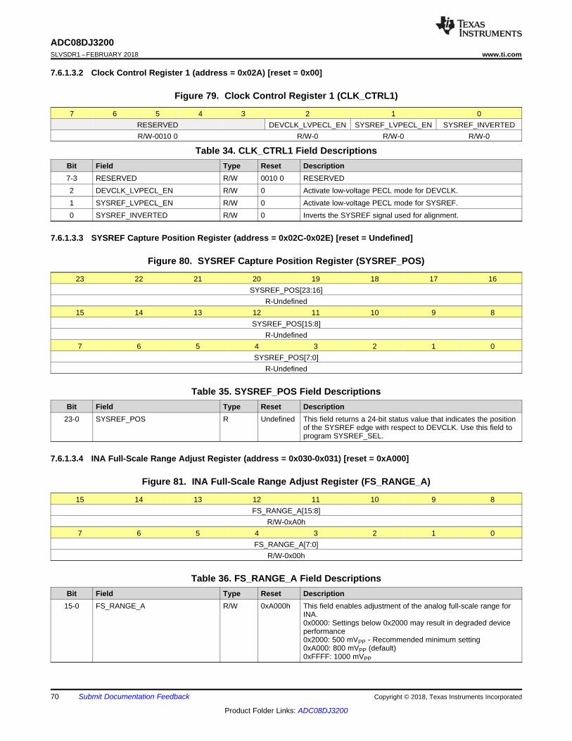
70
ADC08DJ3200SLVSDR1 –FEBRUARY 2018 www.ti.com
Product Folder Links: ADC08DJ3200
Submit Documentation Feedback Copyright © 2018, Texas Instruments Incorporated
7.6.1.3.2 Clock Control Register 1 (address = 0x02A) [reset = 0x00]
Figure 79. Clock Control Register 1 (CLK_CTRL1)
7 6 5 4 3 2 1 0RESERVED DEVCLK_LVPECL_EN SYSREF_LVPECL_EN SYSREF_INVERTEDR/W-0010 0 R/W-0 R/W-0 R/W-0
Table 34. CLK_CTRL1 Field DescriptionsBit Field Type Reset Description7-3 RESERVED R/W 0010 0 RESERVED2 DEVCLK_LVPECL_EN R/W 0 Activate low-voltage PECL mode for DEVCLK.1 SYSREF_LVPECL_EN R/W 0 Activate low-voltage PECL mode for SYSREF.0 SYSREF_INVERTED R/W 0 Inverts the SYSREF signal used for alignment.
7.6.1.3.3 SYSREF Capture Position Register (address = 0x02C-0x02E) [reset = Undefined]
Figure 80. SYSREF Capture Position Register (SYSREF_POS)
23 22 21 20 19 18 17 16SYSREF_POS[23:16]
R-Undefined15 14 13 12 11 10 9 8
SYSREF_POS[15:8]R-Undefined
7 6 5 4 3 2 1 0SYSREF_POS[7:0]
R-Undefined
Table 35. SYSREF_POS Field DescriptionsBit Field Type Reset Description
23-0 SYSREF_POS R Undefined This field returns a 24-bit status value that indicates the positionof the SYSREF edge with respect to DEVCLK. Use this field toprogram SYSREF_SEL.
7.6.1.3.4 INA Full-Scale Range Adjust Register (address = 0x030-0x031) [reset = 0xA000]
Figure 81. INA Full-Scale Range Adjust Register (FS_RANGE_A)
15 14 13 12 11 10 9 8FS_RANGE_A[15:8]
R/W-0xA0h7 6 5 4 3 2 1 0
FS_RANGE_A[7:0]R/W-0x00h
Table 36. FS_RANGE_A Field DescriptionsBit Field Type Reset Description
15-0 FS_RANGE_A R/W 0xA000h This field enables adjustment of the analog full-scale range forINA.0x0000: Settings below 0x2000 may result in degraded deviceperformance0x2000: 500 mVPP - Recommended minimum setting0xA000: 800 mVPP (default)0xFFFF: 1000 mVPP
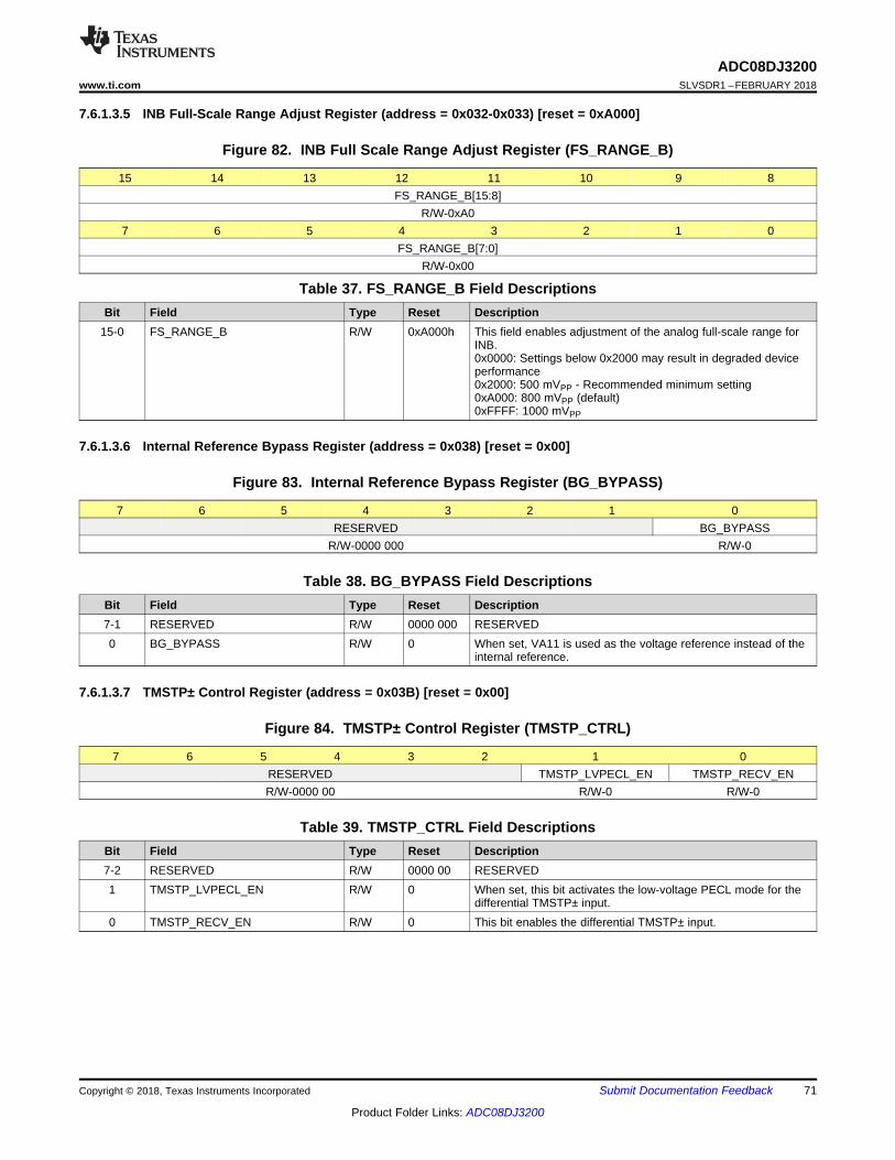
71
ADC08DJ3200www.ti.com SLVSDR1 –FEBRUARY 2018
Product Folder Links: ADC08DJ3200
Submit Documentation FeedbackCopyright © 2018, Texas Instruments Incorporated
7.6.1.3.5 INB Full-Scale Range Adjust Register (address = 0x032-0x033) [reset = 0xA000]
Figure 82. INB Full Scale Range Adjust Register (FS_RANGE_B)
15 14 13 12 11 10 9 8FS_RANGE_B[15:8]
R/W-0xA07 6 5 4 3 2 1 0
FS_RANGE_B[7:0]R/W-0x00
Table 37. FS_RANGE_B Field DescriptionsBit Field Type Reset Description
15-0 FS_RANGE_B R/W 0xA000h This field enables adjustment of the analog full-scale range forINB.0x0000: Settings below 0x2000 may result in degraded deviceperformance0x2000: 500 mVPP - Recommended minimum setting0xA000: 800 mVPP (default)0xFFFF: 1000 mVPP
7.6.1.3.6 Internal Reference Bypass Register (address = 0x038) [reset = 0x00]
Figure 83. Internal Reference Bypass Register (BG_BYPASS)
7 6 5 4 3 2 1 0RESERVED BG_BYPASS
R/W-0000 000 R/W-0
Table 38. BG_BYPASS Field DescriptionsBit Field Type Reset Description7-1 RESERVED R/W 0000 000 RESERVED0 BG_BYPASS R/W 0 When set, VA11 is used as the voltage reference instead of the
internal reference.
7.6.1.3.7 TMSTP± Control Register (address = 0x03B) [reset = 0x00]
Figure 84. TMSTP± Control Register (TMSTP_CTRL)
7 6 5 4 3 2 1 0RESERVED TMSTP_LVPECL_EN TMSTP_RECV_ENR/W-0000 00 R/W-0 R/W-0
Table 39. TMSTP_CTRL Field DescriptionsBit Field Type Reset Description7-2 RESERVED R/W 0000 00 RESERVED1 TMSTP_LVPECL_EN R/W 0 When set, this bit activates the low-voltage PECL mode for the
differential TMSTP± input.0 TMSTP_RECV_EN R/W 0 This bit enables the differential TMSTP± input.
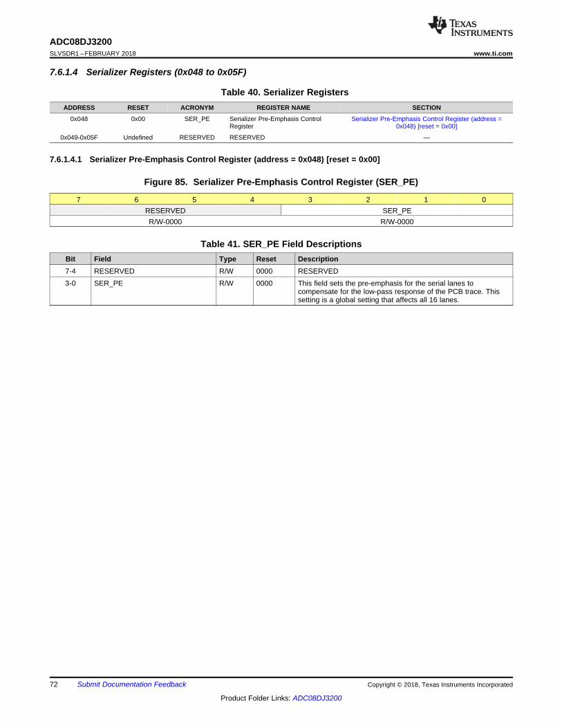
72
ADC08DJ3200SLVSDR1 –FEBRUARY 2018 www.ti.com
Product Folder Links: ADC08DJ3200
Submit Documentation Feedback Copyright © 2018, Texas Instruments Incorporated
7.6.1.4 Serializer Registers (0x048 to 0x05F)
Table 40. Serializer RegistersADDRESS RESET ACRONYM REGISTER NAME SECTION
0x048 0x00 SER_PE Serializer Pre-Emphasis ControlRegister
Serializer Pre-Emphasis Control Register (address =0x048) [reset = 0x00]
0x049-0x05F Undefined RESERVED RESERVED —
7.6.1.4.1 Serializer Pre-Emphasis Control Register (address = 0x048) [reset = 0x00]
Figure 85. Serializer Pre-Emphasis Control Register (SER_PE)
7 6 5 4 3 2 1 0RESERVED SER_PER/W-0000 R/W-0000
Table 41. SER_PE Field DescriptionsBit Field Type Reset Description7-4 RESERVED R/W 0000 RESERVED3-0 SER_PE R/W 0000 This field sets the pre-emphasis for the serial lanes to
compensate for the low-pass response of the PCB trace. Thissetting is a global setting that affects all 16 lanes.
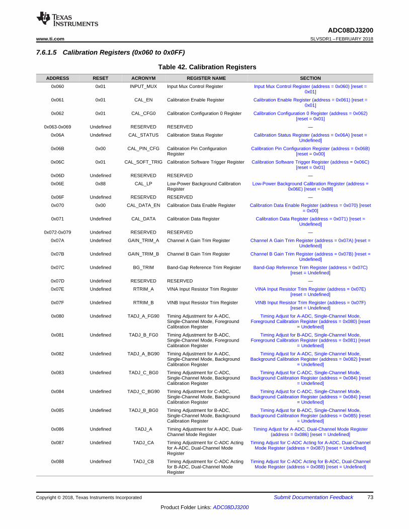
73
ADC08DJ3200www.ti.com SLVSDR1 –FEBRUARY 2018
Product Folder Links: ADC08DJ3200
Submit Documentation FeedbackCopyright © 2018, Texas Instruments Incorporated
7.6.1.5 Calibration Registers (0x060 to 0x0FF)
Table 42. Calibration RegistersADDRESS RESET ACRONYM REGISTER NAME SECTION
0x060 0x01 INPUT_MUX Input Mux Control Register Input Mux Control Register (address = 0x060) [reset =0x01]
0x061 0x01 CAL_EN Calibration Enable Register Calibration Enable Register (address = 0x061) [reset =0x01]
0x062 0x01 CAL_CFG0 Calibration Configuration 0 Register Calibration Configuration 0 Register (address = 0x062)[reset = 0x01]
0x063-0x069 Undefined RESERVED RESERVED —
0x06A Undefined CAL_STATUS Calibration Status Register Calibration Status Register (address = 0x06A) [reset =Undefined]
0x06B 0x00 CAL_PIN_CFG Calibration Pin ConfigurationRegister
Calibration Pin Configuration Register (address = 0x06B)[reset = 0x00]
0x06C 0x01 CAL_SOFT_TRIG Calibration Software Trigger Register Calibration Software Trigger Register (address = 0x06C)[reset = 0x01]
0x06D Undefined RESERVED RESERVED —
0x06E 0x88 CAL_LP Low-Power Background CalibrationRegister
Low-Power Background Calibration Register (address =0x06E) [reset = 0x88]
0x06F Undefined RESERVED RESERVED —
0x070 0x00 CAL_DATA_EN Calibration Data Enable Register Calibration Data Enable Register (address = 0x070) [reset= 0x00]
0x071 Undefined CAL_DATA Calibration Data Register Calibration Data Register (address = 0x071) [reset =Undefined]
0x072-0x079 Undefined RESERVED RESERVED —
0x07A Undefined GAIN_TRIM_A Channel A Gain Trim Register Channel A Gain Trim Register (address = 0x07A) [reset =Undefined]
0x07B Undefined GAIN_TRIM_B Channel B Gain Trim Register Channel B Gain Trim Register (address = 0x07B) [reset =Undefined]
0x07C Undefined BG_TRIM Band-Gap Reference Trim Register Band-Gap Reference Trim Register (address = 0x07C)[reset = Undefined]
0x07D Undefined RESERVED RESERVED —
0x07E Undefined RTRIM_A VINA Input Resistor Trim Register VINA Input Resistor Trim Register (address = 0x07E)[reset = Undefined]
0x07F Undefined RTRIM_B VINB Input Resistor Trim Register VINB Input Resistor Trim Register (address = 0x07F)[reset = Undefined]
0x080 Undefined TADJ_A_FG90 Timing Adjustment for A-ADC,Single-Channel Mode, ForegroundCalibration Register
Timing Adjust for A-ADC, Single-Channel Mode,Foreground Calibration Register (address = 0x080) [reset
= Undefined]
0x081 Undefined TADJ_B_FG0 Timing Adjustment for B-ADC,Single-Channel Mode, ForegroundCalibration Register
Timing Adjust for B-ADC, Single-Channel Mode,Foreground Calibration Register (address = 0x081) [reset
= Undefined]
0x082 Undefined TADJ_A_BG90 Timing Adjustment for A-ADC,Single-Channel Mode, BackgroundCalibration Register
Timing Adjust for A-ADC, Single-Channel Mode,Background Calibration Register (address = 0x082) [reset
= Undefined]
0x083 Undefined TADJ_C_BG0 Timing Adjustment for C-ADC,Single-Channel Mode, BackgroundCalibration Register
Timing Adjust for C-ADC, Single-Channel Mode,Background Calibration Register (address = 0x084) [reset
= Undefined]
0x084 Undefined TADJ_C_BG90 Timing Adjustment for C-ADC,Single-Channel Mode, BackgroundCalibration Register
Timing Adjust for C-ADC, Single-Channel Mode,Background Calibration Register (address = 0x084) [reset
= Undefined]
0x085 Undefined TADJ_B_BG0 Timing Adjustment for B-ADC,Single-Channel Mode, BackgroundCalibration Register
Timing Adjust for B-ADC, Single-Channel Mode,Background Calibration Register (address = 0x085) [reset
= Undefined]
0x086 Undefined TADJ_A Timing Adjustment for A-ADC, Dual-Channel Mode Register
Timing Adjust for A-ADC, Dual-Channel Mode Register(address = 0x086) [reset = Undefined]
0x087 Undefined TADJ_CA Timing Adjustment for C-ADC Actingfor A-ADC, Dual-Channel ModeRegister
Timing Adjust for C-ADC Acting for A-ADC, Dual-ChannelMode Register (address = 0x087) [reset = Undefined]
0x088 Undefined TADJ_CB Timing Adjustment for C-ADC Actingfor B-ADC, Dual-Channel ModeRegister
Timing Adjust for C-ADC Acting for B-ADC, Dual-ChannelMode Register (address = 0x088) [reset = Undefined]
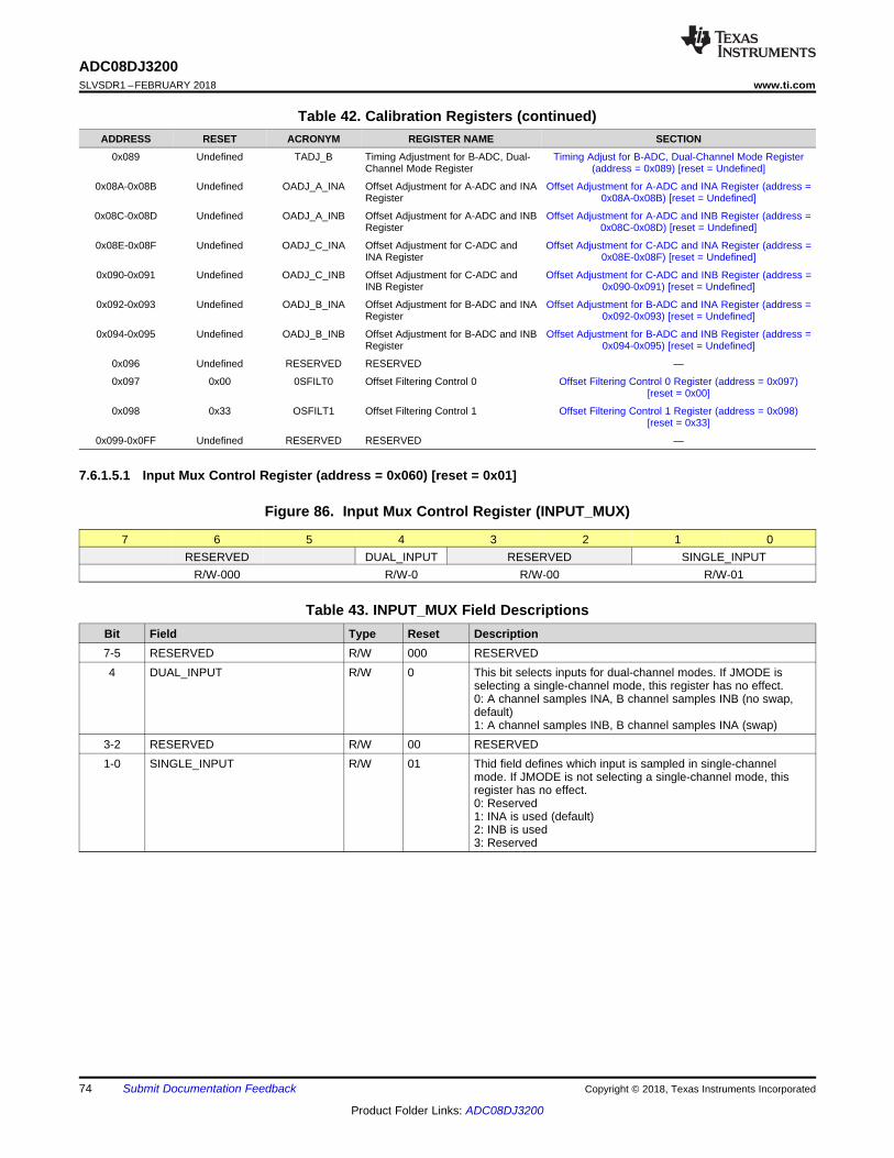
74
ADC08DJ3200SLVSDR1 –FEBRUARY 2018 www.ti.com
Product Folder Links: ADC08DJ3200
Submit Documentation Feedback Copyright © 2018, Texas Instruments Incorporated
Table 42. Calibration Registers (continued)ADDRESS RESET ACRONYM REGISTER NAME SECTION
0x089 Undefined TADJ_B Timing Adjustment for B-ADC, Dual-Channel Mode Register
Timing Adjust for B-ADC, Dual-Channel Mode Register(address = 0x089) [reset = Undefined]
0x08A-0x08B Undefined OADJ_A_INA Offset Adjustment for A-ADC and INARegister
Offset Adjustment for A-ADC and INA Register (address =0x08A-0x08B) [reset = Undefined]
0x08C-0x08D Undefined OADJ_A_INB Offset Adjustment for A-ADC and INBRegister
Offset Adjustment for A-ADC and INB Register (address =0x08C-0x08D) [reset = Undefined]
0x08E-0x08F Undefined OADJ_C_INA Offset Adjustment for C-ADC andINA Register
Offset Adjustment for C-ADC and INA Register (address =0x08E-0x08F) [reset = Undefined]
0x090-0x091 Undefined OADJ_C_INB Offset Adjustment for C-ADC andINB Register
Offset Adjustment for C-ADC and INB Register (address =0x090-0x091) [reset = Undefined]
0x092-0x093 Undefined OADJ_B_INA Offset Adjustment for B-ADC and INARegister
Offset Adjustment for B-ADC and INA Register (address =0x092-0x093) [reset = Undefined]
0x094-0x095 Undefined OADJ_B_INB Offset Adjustment for B-ADC and INBRegister
Offset Adjustment for B-ADC and INB Register (address =0x094-0x095) [reset = Undefined]
0x096 Undefined RESERVED RESERVED —
0x097 0x00 0SFILT0 Offset Filtering Control 0 Offset Filtering Control 0 Register (address = 0x097)[reset = 0x00]
0x098 0x33 OSFILT1 Offset Filtering Control 1 Offset Filtering Control 1 Register (address = 0x098)[reset = 0x33]
0x099-0x0FF Undefined RESERVED RESERVED —
7.6.1.5.1 Input Mux Control Register (address = 0x060) [reset = 0x01]
Figure 86. Input Mux Control Register (INPUT_MUX)
7 6 5 4 3 2 1 0RESERVED DUAL_INPUT RESERVED SINGLE_INPUT
R/W-000 R/W-0 R/W-00 R/W-01
Table 43. INPUT_MUX Field DescriptionsBit Field Type Reset Description7-5 RESERVED R/W 000 RESERVED4 DUAL_INPUT R/W 0 This bit selects inputs for dual-channel modes. If JMODE is
selecting a single-channel mode, this register has no effect.0: A channel samples INA, B channel samples INB (no swap,default)1: A channel samples INB, B channel samples INA (swap)
3-2 RESERVED R/W 00 RESERVED1-0 SINGLE_INPUT R/W 01 Thid field defines which input is sampled in single-channel
mode. If JMODE is not selecting a single-channel mode, thisregister has no effect.0: Reserved1: INA is used (default)2: INB is used3: Reserved
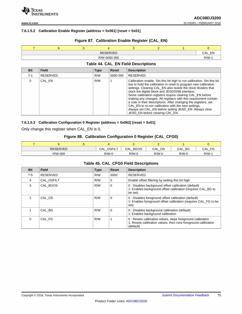
75
ADC08DJ3200www.ti.com SLVSDR1 –FEBRUARY 2018
Product Folder Links: ADC08DJ3200
Submit Documentation FeedbackCopyright © 2018, Texas Instruments Incorporated
7.6.1.5.2 Calibration Enable Register (address = 0x061) [reset = 0x01]
Figure 87. Calibration Enable Register (CAL_EN)
7 6 5 4 3 2 1 0RESERVED CAL_EN
R/W-0000 000 R/W-1
Table 44. CAL_EN Field DescriptionsBit Field Type Reset Description7-1 RESERVED R/W 0000 000 RESERVED0 CAL_EN R/W 1 Calibration enable. Set this bit high to run calibration. Set this bit
low to hold the calibration in reset to program new calibrationsettings. Clearing CAL_EN also resets the clock dividers thatclock the digital block and JESD204B interface.Some calibration registers require clearing CAL_EN beforemaking any changes. All registers with this requirement containa note in their descriptions. After changing the registers, setCAL_EN to re-run calibration with the new settings.Always set CAL_EN before setting JESD_EN. Always clearJESD_EN before clearing CAL_EN.
7.6.1.5.3 Calibration Configuration 0 Register (address = 0x062) [reset = 0x01]
Only change this register when CAL_EN is 0.
Figure 88. Calibration Configuration 0 Register (CAL_CFG0)
7 6 5 4 3 2 1 0RESERVED CAL_OSFILT CAL_BGOS CAL_OS CAL_BG CAL_FG
R/W-000 R/W-0 R/W-0 R/W-0 R/W-0 R/W-1
Table 45. CAL_CFG0 Field DescriptionsBit Field Type Reset Description7-5 RESERVED R/W 0000 RESERVED4 CAL_OSFILT R/W 0 Enable offset filtering by setting this bit high.3 CAL_BGOS R/W 0 0 : Disables background offset calibration (default)
1: Enables background offset calibration (requires CAL_BG tobe set).
2 CAL_OS R/W 0 0 : Disables foreground offset calibration (default)1: Enables foreground offset calibration (requires CAL_FG to beset)
1 CAL_BG R/W 0 0 : Disables background calibration (default)1: Enables background calibration
0 CAL_FG R/W 1 0 : Resets calibration values, skips foreground calibration1: Resets calibration values, then runs foreground calibration(default)
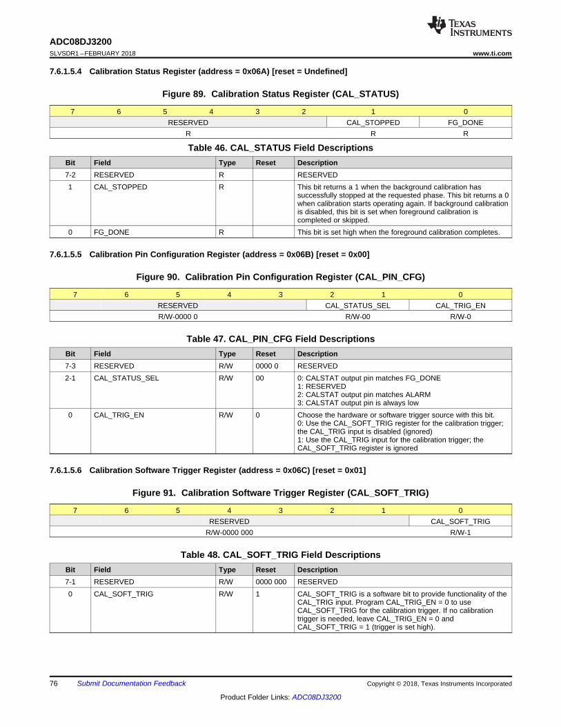
76
ADC08DJ3200SLVSDR1 –FEBRUARY 2018 www.ti.com
Product Folder Links: ADC08DJ3200
Submit Documentation Feedback Copyright © 2018, Texas Instruments Incorporated
7.6.1.5.4 Calibration Status Register (address = 0x06A) [reset = Undefined]
Figure 89. Calibration Status Register (CAL_STATUS)
7 6 5 4 3 2 1 0RESERVED CAL_STOPPED FG_DONE
R R R
Table 46. CAL_STATUS Field DescriptionsBit Field Type Reset Description7-2 RESERVED R RESERVED1 CAL_STOPPED R This bit returns a 1 when the background calibration has
successfully stopped at the requested phase. This bit returns a 0when calibration starts operating again. If background calibrationis disabled, this bit is set when foreground calibration iscompleted or skipped.
0 FG_DONE R This bit is set high when the foreground calibration completes.
7.6.1.5.5 Calibration Pin Configuration Register (address = 0x06B) [reset = 0x00]
Figure 90. Calibration Pin Configuration Register (CAL_PIN_CFG)
7 6 5 4 3 2 1 0RESERVED CAL_STATUS_SEL CAL_TRIG_ENR/W-0000 0 R/W-00 R/W-0
Table 47. CAL_PIN_CFG Field DescriptionsBit Field Type Reset Description7-3 RESERVED R/W 0000 0 RESERVED2-1 CAL_STATUS_SEL R/W 00 0: CALSTAT output pin matches FG_DONE
1: RESERVED2: CALSTAT output pin matches ALARM3: CALSTAT output pin is always low
0 CAL_TRIG_EN R/W 0 Choose the hardware or software trigger source with this bit.0: Use the CAL_SOFT_TRIG register for the calibration trigger;the CAL_TRIG input is disabled (ignored)1: Use the CAL_TRIG input for the calibration trigger; theCAL_SOFT_TRIG register is ignored
7.6.1.5.6 Calibration Software Trigger Register (address = 0x06C) [reset = 0x01]
Figure 91. Calibration Software Trigger Register (CAL_SOFT_TRIG)
7 6 5 4 3 2 1 0RESERVED CAL_SOFT_TRIG
R/W-0000 000 R/W-1
Table 48. CAL_SOFT_TRIG Field DescriptionsBit Field Type Reset Description7-1 RESERVED R/W 0000 000 RESERVED0 CAL_SOFT_TRIG R/W 1 CAL_SOFT_TRIG is a software bit to provide functionality of the
CAL_TRIG input. Program CAL_TRIG_EN = 0 to useCAL_SOFT_TRIG for the calibration trigger. If no calibrationtrigger is needed, leave CAL_TRIG_EN = 0 andCAL_SOFT_TRIG = 1 (trigger is set high).
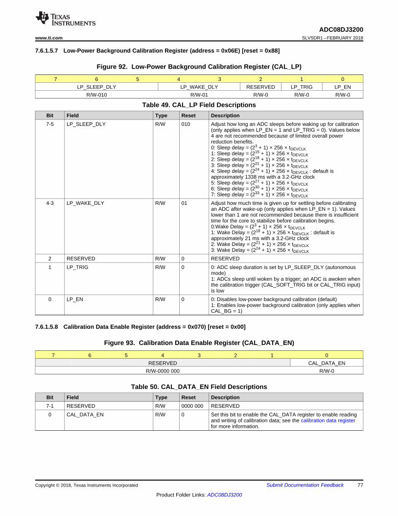
77
ADC08DJ3200www.ti.com SLVSDR1 –FEBRUARY 2018
Product Folder Links: ADC08DJ3200
Submit Documentation FeedbackCopyright © 2018, Texas Instruments Incorporated
7.6.1.5.7 Low-Power Background Calibration Register (address = 0x06E) [reset = 0x88]
Figure 92. Low-Power Background Calibration Register (CAL_LP)
7 6 5 4 3 2 1 0LP_SLEEP_DLY LP_WAKE_DLY RESERVED LP_TRIG LP_EN
R/W-010 R/W-01 R/W-0 R/W-0 R/W-0
Table 49. CAL_LP Field DescriptionsBit Field Type Reset Description7-5 LP_SLEEP_DLY R/W 010 Adjust how long an ADC sleeps before waking up for calibration
(only applies when LP_EN = 1 and LP_TRIG = 0). Values below4 are not recommended because of limited overall powerreduction benefits.0: Sleep delay = (23 + 1) × 256 × tDEVCLK1: Sleep delay = (215 + 1) × 256 × tDEVCLK2: Sleep delay = (218 + 1) × 256 × tDEVCLK3: Sleep delay = (221 + 1) × 256 × tDEVCLK4: Sleep delay = (224 + 1) × 256 × tDEVCLK : default isapproximately 1338 ms with a 3.2-GHz clock5: Sleep delay = (227 + 1) × 256 × tDEVCLK6: Sleep delay = (230 + 1) × 256 × tDEVCLK7: Sleep delay = (233 + 1) × 256 × tDEVCLK
4-3 LP_WAKE_DLY R/W 01 Adjust how much time is given up for settling before calibratingan ADC after wake-up (only applies when LP_EN = 1). Valueslower than 1 are not recommended because there is insufficienttime for the core to stabilize before calibration begins.0:Wake Delay = (23 + 1) × 256 × tDEVCLK1: Wake Delay = (218 + 1) × 256 × tDEVCLK : default isapproximately 21 ms with a 3.2-GHz clock2: Wake Delay = (221 + 1) × 256 × tDEVCLK3: Wake Delay = (224 + 1) × 256 × tDEVCLK
2 RESERVED R/W 0 RESERVED1 LP_TRIG R/W 0 0: ADC sleep duration is set by LP_SLEEP_DLY (autonomous
mode)1: ADCs sleep until woken by a trigger; an ADC is awoken whenthe calibration trigger (CAL_SOFT_TRIG bit or CAL_TRIG input)is low
0 LP_EN R/W 0 0: Disables low-power background calibration (default)1: Enables low-power background calibration (only applies whenCAL_BG = 1)
7.6.1.5.8 Calibration Data Enable Register (address = 0x070) [reset = 0x00]
Figure 93. Calibration Data Enable Register (CAL_DATA_EN)
7 6 5 4 3 2 1 0RESERVED CAL_DATA_EN
R/W-0000 000 R/W-0
Table 50. CAL_DATA_EN Field DescriptionsBit Field Type Reset Description7-1 RESERVED R/W 0000 000 RESERVED0 CAL_DATA_EN R/W 0 Set this bit to enable the CAL_DATA register to enable reading
and writing of calibration data; see the calibration data registerfor more information.
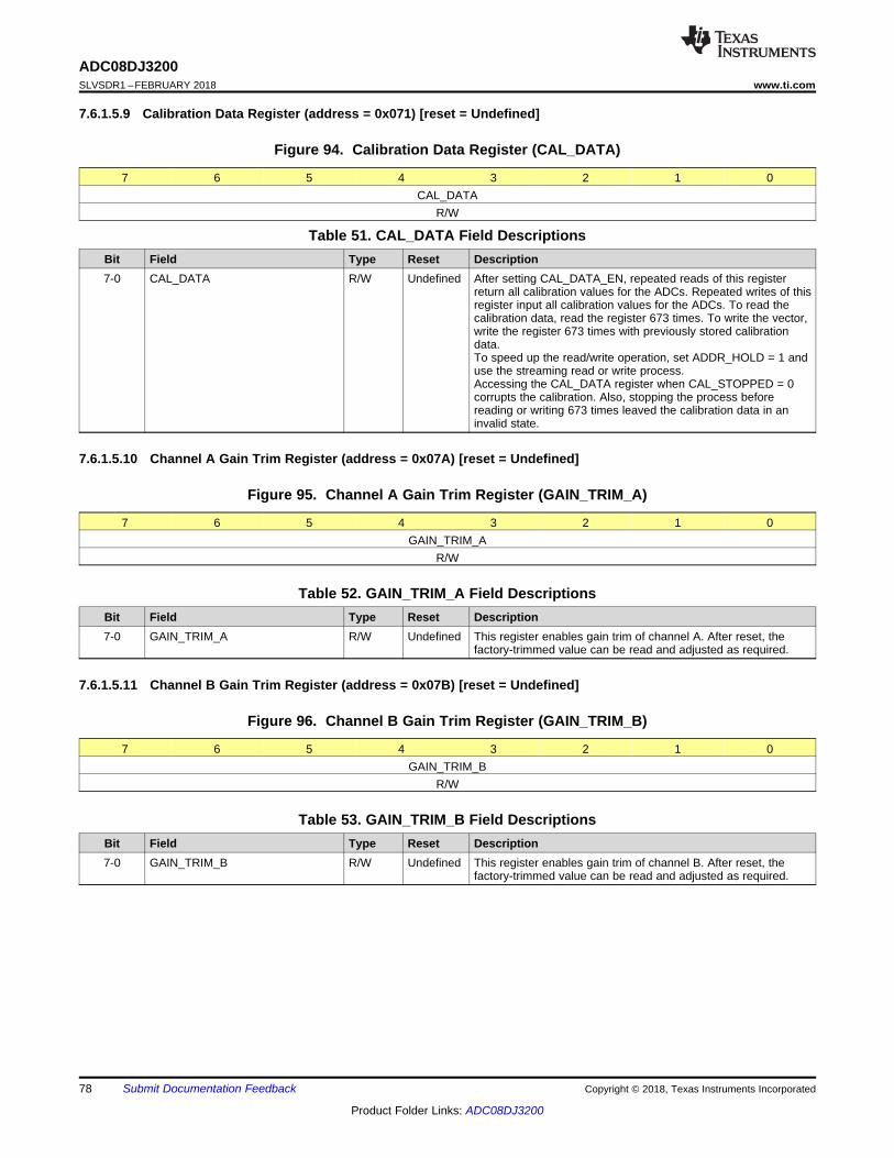
78
ADC08DJ3200SLVSDR1 –FEBRUARY 2018 www.ti.com
Product Folder Links: ADC08DJ3200
Submit Documentation Feedback Copyright © 2018, Texas Instruments Incorporated
7.6.1.5.9 Calibration Data Register (address = 0x071) [reset = Undefined]
Figure 94. Calibration Data Register (CAL_DATA)
7 6 5 4 3 2 1 0CAL_DATA
R/W
Table 51. CAL_DATA Field DescriptionsBit Field Type Reset Description7-0 CAL_DATA R/W Undefined After setting CAL_DATA_EN, repeated reads of this register
return all calibration values for the ADCs. Repeated writes of thisregister input all calibration values for the ADCs. To read thecalibration data, read the register 673 times. To write the vector,write the register 673 times with previously stored calibrationdata.To speed up the read/write operation, set ADDR_HOLD = 1 anduse the streaming read or write process.Accessing the CAL_DATA register when CAL_STOPPED = 0corrupts the calibration. Also, stopping the process beforereading or writing 673 times leaved the calibration data in aninvalid state.
7.6.1.5.10 Channel A Gain Trim Register (address = 0x07A) [reset = Undefined]
Figure 95. Channel A Gain Trim Register (GAIN_TRIM_A)
7 6 5 4 3 2 1 0GAIN_TRIM_A
R/W
Table 52. GAIN_TRIM_A Field DescriptionsBit Field Type Reset Description7-0 GAIN_TRIM_A R/W Undefined This register enables gain trim of channel A. After reset, the
factory-trimmed value can be read and adjusted as required.
7.6.1.5.11 Channel B Gain Trim Register (address = 0x07B) [reset = Undefined]
Figure 96. Channel B Gain Trim Register (GAIN_TRIM_B)
7 6 5 4 3 2 1 0GAIN_TRIM_B
R/W
Table 53. GAIN_TRIM_B Field DescriptionsBit Field Type Reset Description7-0 GAIN_TRIM_B R/W Undefined This register enables gain trim of channel B. After reset, the
factory-trimmed value can be read and adjusted as required.
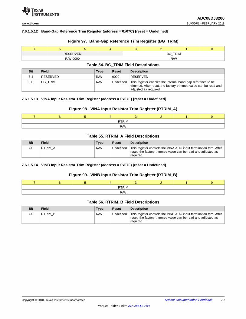
79
ADC08DJ3200www.ti.com SLVSDR1 –FEBRUARY 2018
Product Folder Links: ADC08DJ3200
Submit Documentation FeedbackCopyright © 2018, Texas Instruments Incorporated
7.6.1.5.12 Band-Gap Reference Trim Register (address = 0x07C) [reset = Undefined]
Figure 97. Band-Gap Reference Trim Register (BG_TRIM)
7 6 5 4 3 2 1 0RESERVED BG_TRIMR/W-0000 R/W
Table 54. BG_TRIM Field DescriptionsBit Field Type Reset Description7-4 RESERVED R/W 0000 RESERVED3-0 BG_TRIM R/W Undefined This register enables the internal band-gap reference to be
trimmed. After reset, the factory-trimmed value can be read andadjusted as required.
7.6.1.5.13 VINA Input Resistor Trim Register (address = 0x07E) [reset = Undefined]
Figure 98. VINA Input Resistor Trim Register (RTRIM_A)
7 6 5 4 3 2 1 0RTRIM
R/W
Table 55. RTRIM_A Field DescriptionsBit Field Type Reset Description7-0 RTRIM_A R/W Undefined This register controls the VINA ADC input termination trim. After
reset, the factory-trimmed value can be read and adjusted asrequired.
7.6.1.5.14 VINB Input Resistor Trim Register (address = 0x07F) [reset = Undefined]
Figure 99. VINB Input Resistor Trim Register (RTRIM_B)
7 6 5 4 3 2 1 0RTRIM
R/W
Table 56. RTRIM_B Field DescriptionsBit Field Type Reset Description7-0 RTRIM_B R/W Undefined This register controls the VINB ADC input termination trim. After
reset, the factory-trimmed value can be read and adjusted asrequired.
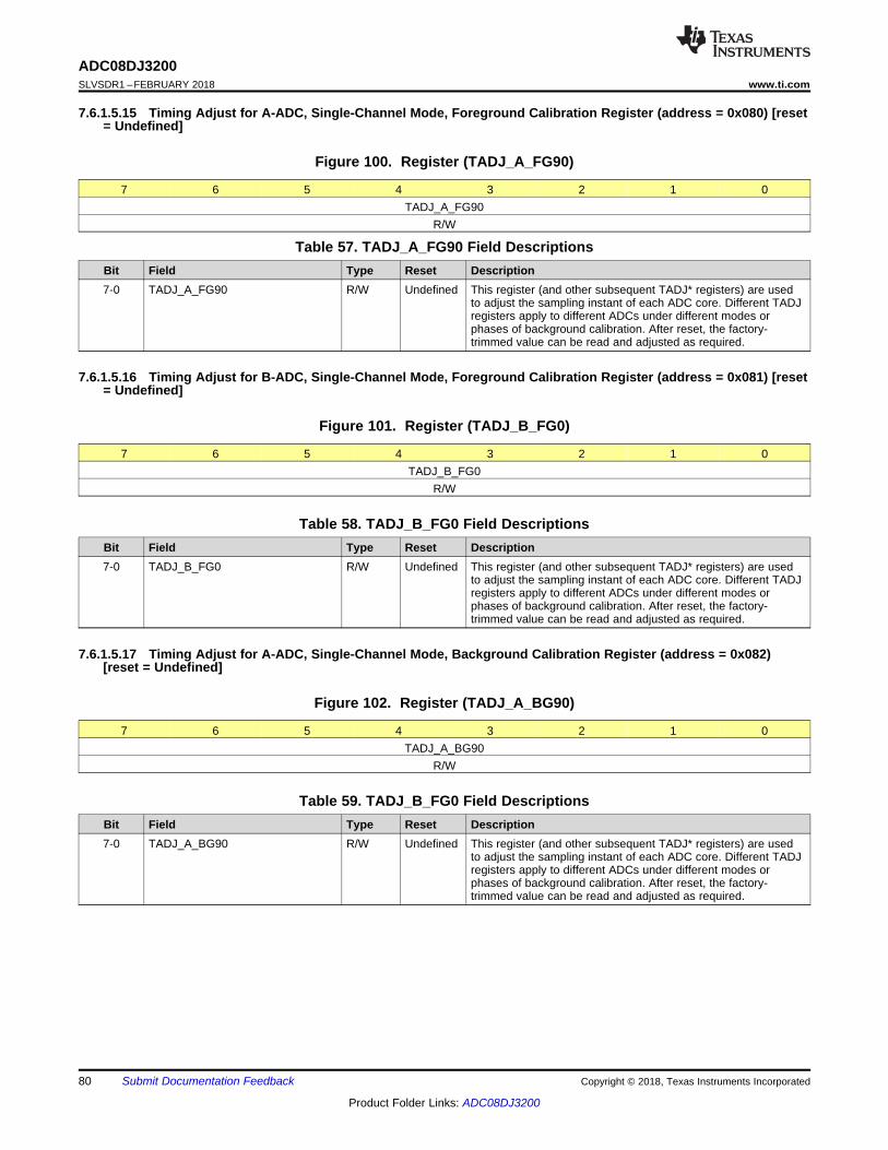
80
ADC08DJ3200SLVSDR1 –FEBRUARY 2018 www.ti.com
Product Folder Links: ADC08DJ3200
Submit Documentation Feedback Copyright © 2018, Texas Instruments Incorporated
7.6.1.5.15 Timing Adjust for A-ADC, Single-Channel Mode, Foreground Calibration Register (address = 0x080) [reset= Undefined]
Figure 100. Register (TADJ_A_FG90)
7 6 5 4 3 2 1 0TADJ_A_FG90
R/W
Table 57. TADJ_A_FG90 Field DescriptionsBit Field Type Reset Description7-0 TADJ_A_FG90 R/W Undefined This register (and other subsequent TADJ* registers) are used
to adjust the sampling instant of each ADC core. Different TADJregisters apply to different ADCs under different modes orphases of background calibration. After reset, the factory-trimmed value can be read and adjusted as required.
7.6.1.5.16 Timing Adjust for B-ADC, Single-Channel Mode, Foreground Calibration Register (address = 0x081) [reset= Undefined]
Figure 101. Register (TADJ_B_FG0)
7 6 5 4 3 2 1 0TADJ_B_FG0
R/W
Table 58. TADJ_B_FG0 Field DescriptionsBit Field Type Reset Description7-0 TADJ_B_FG0 R/W Undefined This register (and other subsequent TADJ* registers) are used
to adjust the sampling instant of each ADC core. Different TADJregisters apply to different ADCs under different modes orphases of background calibration. After reset, the factory-trimmed value can be read and adjusted as required.
7.6.1.5.17 Timing Adjust for A-ADC, Single-Channel Mode, Background Calibration Register (address = 0x082)[reset = Undefined]
Figure 102. Register (TADJ_A_BG90)
7 6 5 4 3 2 1 0TADJ_A_BG90
R/W
Table 59. TADJ_B_FG0 Field DescriptionsBit Field Type Reset Description7-0 TADJ_A_BG90 R/W Undefined This register (and other subsequent TADJ* registers) are used
to adjust the sampling instant of each ADC core. Different TADJregisters apply to different ADCs under different modes orphases of background calibration. After reset, the factory-trimmed value can be read and adjusted as required.
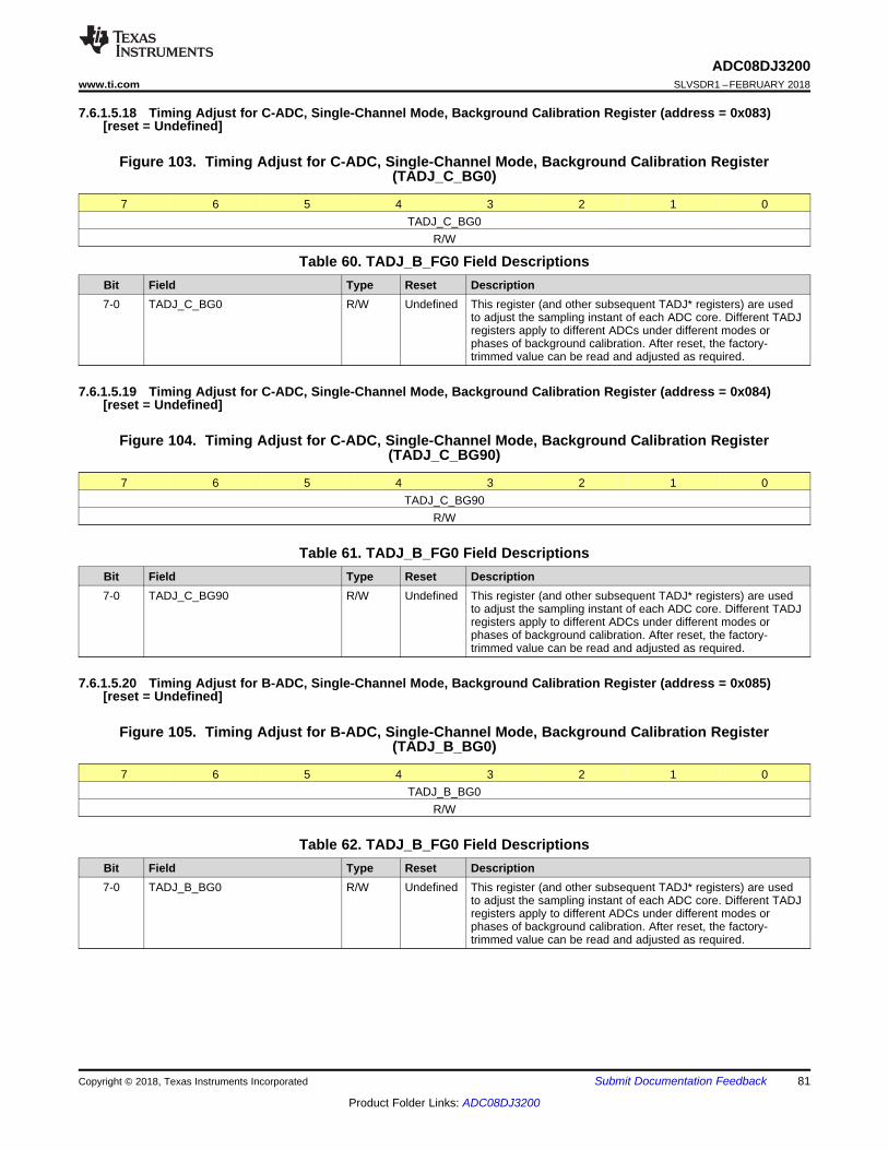
81
ADC08DJ3200www.ti.com SLVSDR1 –FEBRUARY 2018
Product Folder Links: ADC08DJ3200
Submit Documentation FeedbackCopyright © 2018, Texas Instruments Incorporated
7.6.1.5.18 Timing Adjust for C-ADC, Single-Channel Mode, Background Calibration Register (address = 0x083)[reset = Undefined]
Figure 103. Timing Adjust for C-ADC, Single-Channel Mode, Background Calibration Register(TADJ_C_BG0)
7 6 5 4 3 2 1 0TADJ_C_BG0
R/W
Table 60. TADJ_B_FG0 Field DescriptionsBit Field Type Reset Description7-0 TADJ_C_BG0 R/W Undefined This register (and other subsequent TADJ* registers) are used
to adjust the sampling instant of each ADC core. Different TADJregisters apply to different ADCs under different modes orphases of background calibration. After reset, the factory-trimmed value can be read and adjusted as required.
7.6.1.5.19 Timing Adjust for C-ADC, Single-Channel Mode, Background Calibration Register (address = 0x084)[reset = Undefined]
Figure 104. Timing Adjust for C-ADC, Single-Channel Mode, Background Calibration Register(TADJ_C_BG90)
7 6 5 4 3 2 1 0TADJ_C_BG90
R/W
Table 61. TADJ_B_FG0 Field DescriptionsBit Field Type Reset Description7-0 TADJ_C_BG90 R/W Undefined This register (and other subsequent TADJ* registers) are used
to adjust the sampling instant of each ADC core. Different TADJregisters apply to different ADCs under different modes orphases of background calibration. After reset, the factory-trimmed value can be read and adjusted as required.
7.6.1.5.20 Timing Adjust for B-ADC, Single-Channel Mode, Background Calibration Register (address = 0x085)[reset = Undefined]
Figure 105. Timing Adjust for B-ADC, Single-Channel Mode, Background Calibration Register(TADJ_B_BG0)
7 6 5 4 3 2 1 0TADJ_B_BG0
R/W
Table 62. TADJ_B_FG0 Field DescriptionsBit Field Type Reset Description7-0 TADJ_B_BG0 R/W Undefined This register (and other subsequent TADJ* registers) are used
to adjust the sampling instant of each ADC core. Different TADJregisters apply to different ADCs under different modes orphases of background calibration. After reset, the factory-trimmed value can be read and adjusted as required.
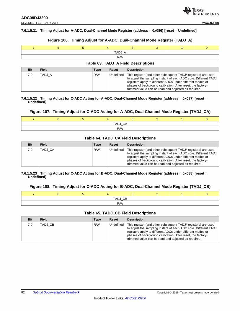
82
ADC08DJ3200SLVSDR1 –FEBRUARY 2018 www.ti.com
Product Folder Links: ADC08DJ3200
Submit Documentation Feedback Copyright © 2018, Texas Instruments Incorporated
7.6.1.5.21 Timing Adjust for A-ADC, Dual-Channel Mode Register (address = 0x086) [reset = Undefined]
Figure 106. Timing Adjust for A-ADC, Dual-Channel Mode Register (TADJ_A)
7 6 5 4 3 2 1 0TADJ_A
R/W
Table 63. TADJ_A Field DescriptionsBit Field Type Reset Description7-0 TADJ_A R/W Undefined This register (and other subsequent TADJ* registers) are used
to adjust the sampling instant of each ADC core. Different TADJregisters apply to different ADCs under different modes orphases of background calibration. After reset, the factory-trimmed value can be read and adjusted as required.
7.6.1.5.22 Timing Adjust for C-ADC Acting for A-ADC, Dual-Channel Mode Register (address = 0x087) [reset =Undefined]
Figure 107. Timing Adjust for C-ADC Acting for A-ADC, Dual-Channel Mode Register (TADJ_CA)
7 6 5 4 3 2 1 0TADJ_CA
R/W
Table 64. TADJ_CA Field DescriptionsBit Field Type Reset Description7-0 TADJ_CA R/W Undefined This register (and other subsequent TADJ* registers) are used
to adjust the sampling instant of each ADC core. Different TADJregisters apply to different ADCs under different modes orphases of background calibration. After reset, the factory-trimmed value can be read and adjusted as required.
7.6.1.5.23 Timing Adjust for C-ADC Acting for B-ADC, Dual-Channel Mode Register (address = 0x088) [reset =Undefined]
Figure 108. Timing Adjust for C-ADC Acting for B-ADC, Dual-Channel Mode Register (TADJ_CB)
7 6 5 4 3 2 1 0TADJ_CB
R/W
Table 65. TADJ_CB Field DescriptionsBit Field Type Reset Description7-0 TADJ_CB R/W Undefined This register (and other subsequent TADJ* registers) are used
to adjust the sampling instant of each ADC core. Different TADJregisters apply to different ADCs under different modes orphases of background calibration. After reset, the factory-trimmed value can be read and adjusted as required.
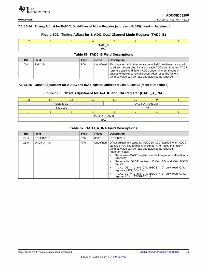
83
ADC08DJ3200www.ti.com SLVSDR1 –FEBRUARY 2018
Product Folder Links: ADC08DJ3200
Submit Documentation FeedbackCopyright © 2018, Texas Instruments Incorporated
7.6.1.5.24 Timing Adjust for B-ADC, Dual-Channel Mode Register (address = 0x089) [reset = Undefined]
Figure 109. Timing Adjust for B-ADC, Dual-Channel Mode Register (TADJ_B)
7 6 5 4 3 2 1 0TADJ_B
R/W
Table 66. TADJ_B Field DescriptionsBit Field Type Reset Description7-0 TADJ_B R/W Undefined This register (and other subsequent TADJ* registers) are used
to adjust the sampling instant of each ADC core. Different TADJregisters apply to different ADCs under different modes orphases of background calibration. After reset, the factory-trimmed value can be read and adjusted as required.
7.6.1.5.25 Offset Adjustment for A-ADC and INA Register (address = 0x08A-0x08B) [reset = Undefined]
Figure 110. Offset Adjustment for A-ADC and INA Register (OADJ_A_INA)
15 14 13 12 11 10 9 8RESERVED OADJ_A_INA[11:8]R/W-0000 R/W
7 6 5 4 3 2 1 0OADJ_A_INA[7:0]
R/W
Table 67. OADJ_A_INA Field DescriptionsBit Field Type Reset Description
15-12 RESERVED R/W 0000 RESERVED11-0 OADJ_A_INA R/W Undefined Offset adjustment value for ADC0 (A-ADC) applied when ADC0
samples INA. The format is unsigned. After reset, the factory-trimmed value can be read and adjusted as required.Important notes:• Never write OADJ* registers while foreground calibration is
underway• Never write OADJ* registers if CAL_BG and CAL_BGOS
are set• If CAL_OS = 1 and CAL_BGOS = 0, only read OADJ*
registers if FG_DONE = 1• If CAL_BG = 1 and CAL_BGOS = 1, only read OADJ*
register if CAL_STOPPED = 1
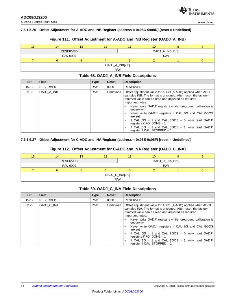
84
ADC08DJ3200SLVSDR1 –FEBRUARY 2018 www.ti.com
Product Folder Links: ADC08DJ3200
Submit Documentation Feedback Copyright © 2018, Texas Instruments Incorporated
7.6.1.5.26 Offset Adjustment for A-ADC and INB Register (address = 0x08C-0x08D) [reset = Undefined]
Figure 111. Offset Adjustment for A-ADC and INB Register (OADJ_A_INB)
15 14 13 12 11 10 9 8RESERVED OADJ_A_INB[11:8]R/W-0000 R/W
7 6 5 4 3 2 1 0OADJ_A_INB[7:0]
R/W
Table 68. OADJ_A_INB Field DescriptionsBit Field Type Reset Description
15-12 RESERVED R/W 0000 RESERVED11-0 OADJ_A_INB R/W Undefined Offset adjustment value for ADC0 (A-ADC) applied when ADC0
samples INB. The format is unsigned. After reset, the factory-trimmed value can be read and adjusted as required.Important notes:• Never write OADJ* registers while foreground calibration is
underway• Never write OADJ* registers if CAL_BG and CAL_BGOS
are set• If CAL_OS = 1 and CAL_BGOS = 0, only read OADJ*
registers if FG_DONE = 1• If CAL_BG = 1 and CAL_BGOS = 1, only read OADJ*
register if CAL_STOPPED = 1
7.6.1.5.27 Offset Adjustment for C-ADC and INA Register (address = 0x08E-0x08F) [reset = Undefined]
Figure 112. Offset Adjustment for C-ADC and INA Register (OADJ_C_INA)
15 14 13 12 11 10 9 8RESERVED OADJ_C_INA[11:8]R/W-0000 R/W
7 6 5 4 3 2 1 0OADJ_C_INA[7:0]
R/W
Table 69. OADJ_C_INA Field DescriptionsBit Field Type Reset Description
15-12 RESERVED R/W 0000 RESERVED11-0 OADJ_C_INA R/W Undefined Offset adjustment value for ADC1 (A-ADC) applied when ADC1
samples INA. The format is unsigned. After reset, the factory-trimmed value can be read and adjusted as required.Important notes:• Never write OADJ* registers while foreground calibration is
underway• Never write OADJ* registers if CAL_BG and CAL_BGOS
are set• If CAL_OS = 1 and CAL_BGOS = 0, only read OADJ*
registers if FG_DONE = 1• If CAL_BG = 1 and CAL_BGOS = 1, only read OADJ*
register if CAL_STOPPED = 1
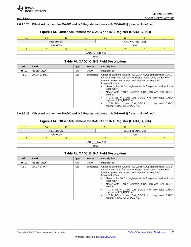
85
ADC08DJ3200www.ti.com SLVSDR1 –FEBRUARY 2018
Product Folder Links: ADC08DJ3200
Submit Documentation FeedbackCopyright © 2018, Texas Instruments Incorporated
7.6.1.5.28 Offset Adjustment for C-ADC and INB Register (address = 0x090-0x091) [reset = Undefined]
Figure 113. Offset Adjustment for C-ADC and INB Register (OADJ_C_INB)
15 14 13 12 11 10 9 8RESERVED OADJ_C_INB[11:8]R/W-0000 R/W
7 6 5 4 3 2 1 0OADJ_C_INB[7:0]
R/W
Table 70. OADJ_C_INB Field DescriptionsBit Field Type Reset Description
15-12 RESERVED R/W 0000 RESERVED11-0 OADJ_C_INB R/W Undefined Offset adjustment value for ADC1 (A-ADC) applied when ADC1
samples INB. The format is unsigned. After reset, the factory-trimmed value can be read and adjusted as required.Important notes:• Never write OADJ* registers while foreground calibration is
underway• Never write OADJ* registers if CAL_BG and CAL_BGOS
are set• If CAL_OS = 1 and CAL_BGOS = 0, only read OADJ*
registers if FG_DONE = 1• If CAL_BG = 1 and CAL_BGOS = 1, only read OADJ*
register if CAL_STOPPED = 1
7.6.1.5.29 Offset Adjustment for B-ADC and INA Register (address = 0x092-0x093) [reset = Undefined]
Figure 114. Offset Adjustment for B-ADC and INA Register (OADJ_B_INA)
15 14 13 12 11 10 9 8RESERVED OADJ_B_INA[11:8]R/W-0000 R/W
7 6 5 4 3 2 1 0OADJ_B_INA[7:0]
R/W
Table 71. OADJ_B_INA Field DescriptionsBit Field Type Reset Description
15-12 RESERVED R/W 0000 RESERVED11-0 OADJ_B_INA R/W Undefined Offset adjustment value for ADC2 (B-ADC) applied when ADC2
samples INA. The format is unsigned. After reset, the factory-trimmed value can be read and adjusted as required.Important notes:• Never write OADJ* registers while foreground calibration is
underway• Never write OADJ* registers if CAL_BG and CAL_BGOS
are set• If CAL_OS = 1 and CAL_BGOS = 0, only read OADJ*
registers if FG_DONE = 1• If CAL_BG = 1 and CAL_BGOS = 1, only read OADJ*
register if CAL_STOPPED = 1
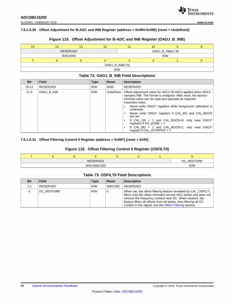
86
ADC08DJ3200SLVSDR1 –FEBRUARY 2018 www.ti.com
Product Folder Links: ADC08DJ3200
Submit Documentation Feedback Copyright © 2018, Texas Instruments Incorporated
7.6.1.5.30 Offset Adjustment for B-ADC and INB Register (address = 0x094-0x095) [reset = Undefined]
Figure 115. Offset Adjustment for B-ADC and INB Register (OADJ_B_INB)
15 14 13 12 11 10 9 8RESERVED OADJ_B_INB[11:8]R/W-0000 R/W
7 6 5 4 3 2 1 0OADJ_B_INB[7:0]
R/W
Table 72. OADJ_B_INB Field DescriptionsBit Field Type Reset Description
15-12 RESERVED R/W 0000 RESERVED11-0 OADJ_B_INB R/W Undefined Offset adjustment value for ADC2 (B-ADC) applied when ADC2
samples INB. The format is unsigned. After reset, the factory-trimmed value can be read and adjusted as required.Important notes:• Never write OADJ* registers while foreground calibration is
underway• Never write OADJ* registers if CAL_BG and CAL_BGOS
are set• If CAL_OS = 1 and CAL_BGOS=0, only read OADJ*
registers if FG_DONE = 1• If CAL_BG = 1 and CAL_BGOS=1, only read OADJ*
register if CAL_STOPPED = 1
7.6.1.5.31 Offset Filtering Control 0 Register (address = 0x097) [reset = 0x00]
Figure 116. Offset Filtering Control 0 Register (OSFILT0)
7 6 5 4 3 2 1 0RESERVED DC_RESTORE
R/W-0000 000 R/W
Table 73. OSFILT0 Field DescriptionsBit Field Type Reset Description7-1 RESERVED R/W 0000 000 RESERVED0 DC_RESTORE R/W 0 When set, the offset filtering feature (enabled by CAL_OSFILT)
filters only the offset mismatch across ADC banks and does notremove the frequency content near DC. When cleared, thefeature filters all offsets from all banks, thus filtering all DCcontent in the signal; see the Offset Filtering section.
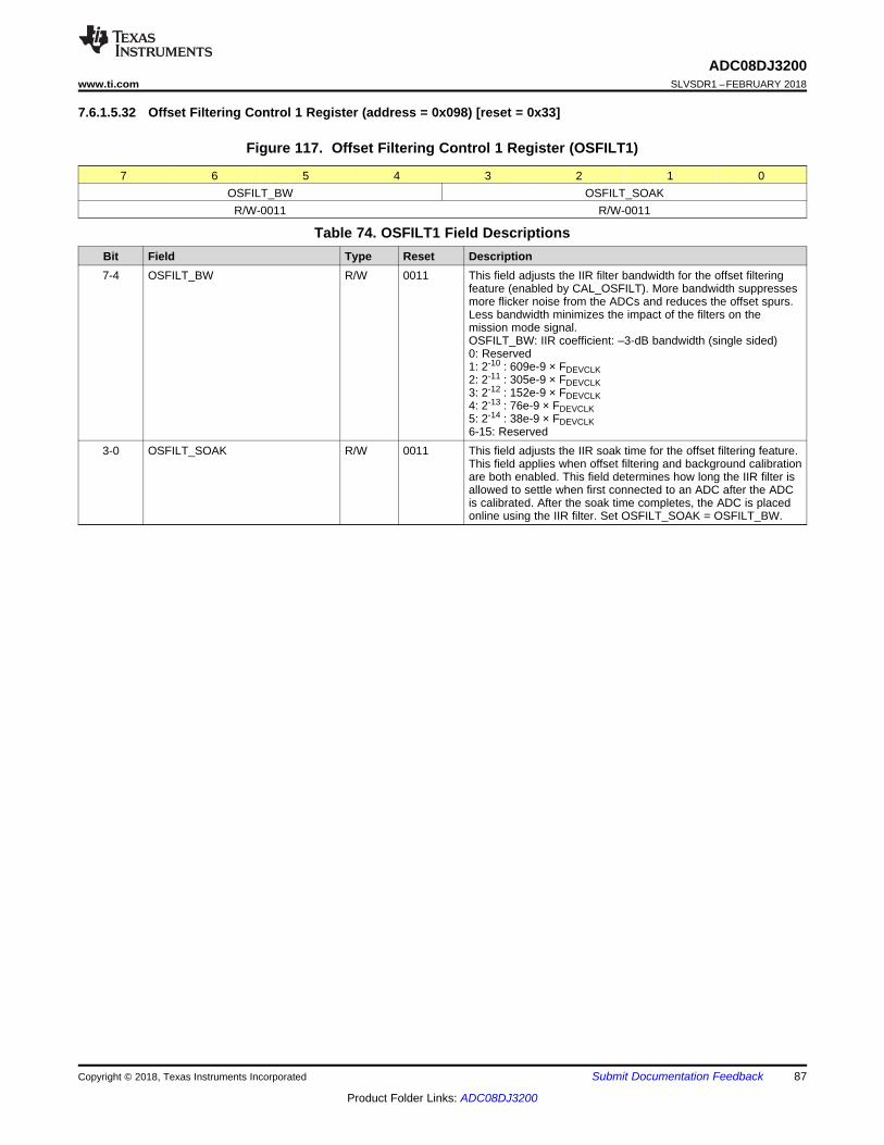
87
ADC08DJ3200www.ti.com SLVSDR1 –FEBRUARY 2018
Product Folder Links: ADC08DJ3200
Submit Documentation FeedbackCopyright © 2018, Texas Instruments Incorporated
7.6.1.5.32 Offset Filtering Control 1 Register (address = 0x098) [reset = 0x33]
Figure 117. Offset Filtering Control 1 Register (OSFILT1)
7 6 5 4 3 2 1 0OSFILT_BW OSFILT_SOAK
R/W-0011 R/W-0011
Table 74. OSFILT1 Field DescriptionsBit Field Type Reset Description7-4 OSFILT_BW R/W 0011 This field adjusts the IIR filter bandwidth for the offset filtering
feature (enabled by CAL_OSFILT). More bandwidth suppressesmore flicker noise from the ADCs and reduces the offset spurs.Less bandwidth minimizes the impact of the filters on themission mode signal.OSFILT_BW: IIR coefficient: –3-dB bandwidth (single sided)0: Reserved1: 2-10 : 609e-9 × FDEVCLK2: 2-11 : 305e-9 × FDEVCLK3: 2-12 : 152e-9 × FDEVCLK4: 2-13 : 76e-9 × FDEVCLK5: 2-14 : 38e-9 × FDEVCLK6-15: Reserved
3-0 OSFILT_SOAK R/W 0011 This field adjusts the IIR soak time for the offset filtering feature.This field applies when offset filtering and background calibrationare both enabled. This field determines how long the IIR filter isallowed to settle when first connected to an ADC after the ADCis calibrated. After the soak time completes, the ADC is placedonline using the IIR filter. Set OSFILT_SOAK = OSFILT_BW.
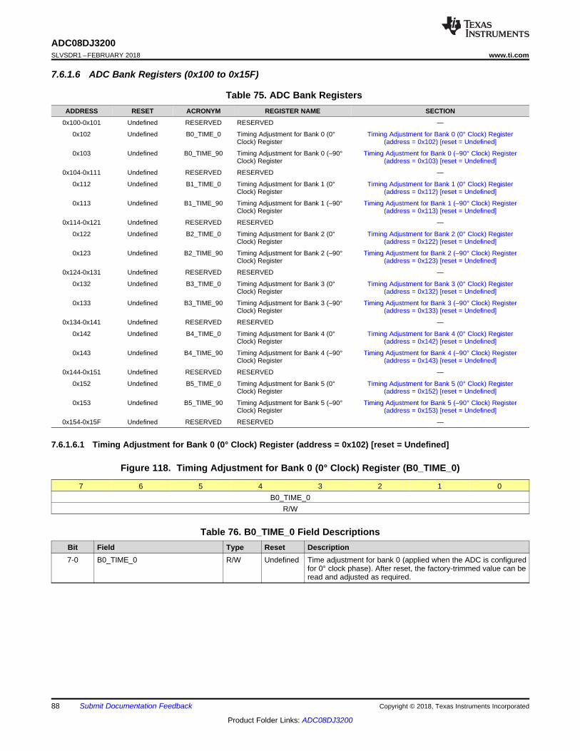
88
ADC08DJ3200SLVSDR1 –FEBRUARY 2018 www.ti.com
Product Folder Links: ADC08DJ3200
Submit Documentation Feedback Copyright © 2018, Texas Instruments Incorporated
7.6.1.6 ADC Bank Registers (0x100 to 0x15F)
Table 75. ADC Bank RegistersADDRESS RESET ACRONYM REGISTER NAME SECTION
0x100-0x101 Undefined RESERVED RESERVED —
0x102 Undefined B0_TIME_0 Timing Adjustment for Bank 0 (0°Clock) Register
Timing Adjustment for Bank 0 (0° Clock) Register(address = 0x102) [reset = Undefined]
0x103 Undefined B0_TIME_90 Timing Adjustment for Bank 0 (–90°Clock) Register
Timing Adjustment for Bank 0 (–90° Clock) Register(address = 0x103) [reset = Undefined]
0x104-0x111 Undefined RESERVED RESERVED —
0x112 Undefined B1_TIME_0 Timing Adjustment for Bank 1 (0°Clock) Register
Timing Adjustment for Bank 1 (0° Clock) Register(address = 0x112) [reset = Undefined]
0x113 Undefined B1_TIME_90 Timing Adjustment for Bank 1 (–90°Clock) Register
Timing Adjustment for Bank 1 (–90° Clock) Register(address = 0x113) [reset = Undefined]
0x114-0x121 Undefined RESERVED RESERVED —
0x122 Undefined B2_TIME_0 Timing Adjustment for Bank 2 (0°Clock) Register
Timing Adjustment for Bank 2 (0° Clock) Register(address = 0x122) [reset = Undefined]
0x123 Undefined B2_TIME_90 Timing Adjustment for Bank 2 (–90°Clock) Register
Timing Adjustment for Bank 2 (–90° Clock) Register(address = 0x123) [reset = Undefined]
0x124-0x131 Undefined RESERVED RESERVED —
0x132 Undefined B3_TIME_0 Timing Adjustment for Bank 3 (0°Clock) Register
Timing Adjustment for Bank 3 (0° Clock) Register(address = 0x132) [reset = Undefined]
0x133 Undefined B3_TIME_90 Timing Adjustment for Bank 3 (–90°Clock) Register
Timing Adjustment for Bank 3 (–90° Clock) Register(address = 0x133) [reset = Undefined]
0x134-0x141 Undefined RESERVED RESERVED —
0x142 Undefined B4_TIME_0 Timing Adjustment for Bank 4 (0°Clock) Register
Timing Adjustment for Bank 4 (0° Clock) Register(address = 0x142) [reset = Undefined]
0x143 Undefined B4_TIME_90 Timing Adjustment for Bank 4 (–90°Clock) Register
Timing Adjustment for Bank 4 (–90° Clock) Register(address = 0x143) [reset = Undefined]
0x144-0x151 Undefined RESERVED RESERVED —
0x152 Undefined B5_TIME_0 Timing Adjustment for Bank 5 (0°Clock) Register
Timing Adjustment for Bank 5 (0° Clock) Register(address = 0x152) [reset = Undefined]
0x153 Undefined B5_TIME_90 Timing Adjustment for Bank 5 (–90°Clock) Register
Timing Adjustment for Bank 5 (–90° Clock) Register(address = 0x153) [reset = Undefined]
0x154-0x15F Undefined RESERVED RESERVED —
7.6.1.6.1 Timing Adjustment for Bank 0 (0° Clock) Register (address = 0x102) [reset = Undefined]
Figure 118. Timing Adjustment for Bank 0 (0° Clock) Register (B0_TIME_0)
7 6 5 4 3 2 1 0B0_TIME_0
R/W
Table 76. B0_TIME_0 Field DescriptionsBit Field Type Reset Description7-0 B0_TIME_0 R/W Undefined Time adjustment for bank 0 (applied when the ADC is configured
for 0° clock phase). After reset, the factory-trimmed value can beread and adjusted as required.
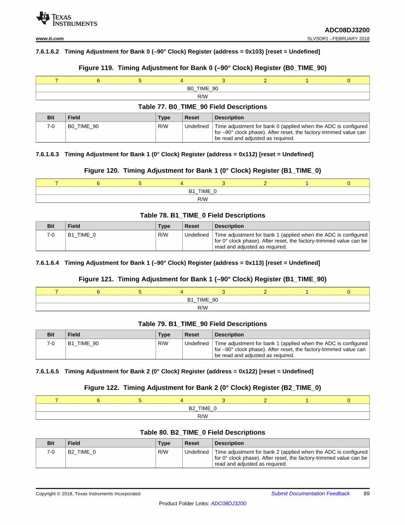
89
ADC08DJ3200www.ti.com SLVSDR1 –FEBRUARY 2018
Product Folder Links: ADC08DJ3200
Submit Documentation FeedbackCopyright © 2018, Texas Instruments Incorporated
7.6.1.6.2 Timing Adjustment for Bank 0 (–90° Clock) Register (address = 0x103) [reset = Undefined]
Figure 119. Timing Adjustment for Bank 0 (–90° Clock) Register (B0_TIME_90)
7 6 5 4 3 2 1 0B0_TIME_90
R/W
Table 77. B0_TIME_90 Field DescriptionsBit Field Type Reset Description7-0 B0_TIME_90 R/W Undefined Time adjustment for bank 0 (applied when the ADC is configured
for –90° clock phase). After reset, the factory-trimmed value canbe read and adjusted as required.
7.6.1.6.3 Timing Adjustment for Bank 1 (0° Clock) Register (address = 0x112) [reset = Undefined]
Figure 120. Timing Adjustment for Bank 1 (0° Clock) Register (B1_TIME_0)
7 6 5 4 3 2 1 0B1_TIME_0
R/W
Table 78. B1_TIME_0 Field DescriptionsBit Field Type Reset Description7-0 B1_TIME_0 R/W Undefined Time adjustment for bank 1 (applied when the ADC is configured
for 0° clock phase). After reset, the factory-trimmed value can beread and adjusted as required.
7.6.1.6.4 Timing Adjustment for Bank 1 (–90° Clock) Register (address = 0x113) [reset = Undefined]
Figure 121. Timing Adjustment for Bank 1 (–90° Clock) Register (B1_TIME_90)
7 6 5 4 3 2 1 0B1_TIME_90
R/W
Table 79. B1_TIME_90 Field DescriptionsBit Field Type Reset Description7-0 B1_TIME_90 R/W Undefined Time adjustment for bank 1 (applied when the ADC is configured
for –90° clock phase). After reset, the factory-trimmed value canbe read and adjusted as required.
7.6.1.6.5 Timing Adjustment for Bank 2 (0° Clock) Register (address = 0x122) [reset = Undefined]
Figure 122. Timing Adjustment for Bank 2 (0° Clock) Register (B2_TIME_0)
7 6 5 4 3 2 1 0B2_TIME_0
R/W
Table 80. B2_TIME_0 Field DescriptionsBit Field Type Reset Description7-0 B2_TIME_0 R/W Undefined Time adjustment for bank 2 (applied when the ADC is configured
for 0° clock phase). After reset, the factory-trimmed value can beread and adjusted as required.
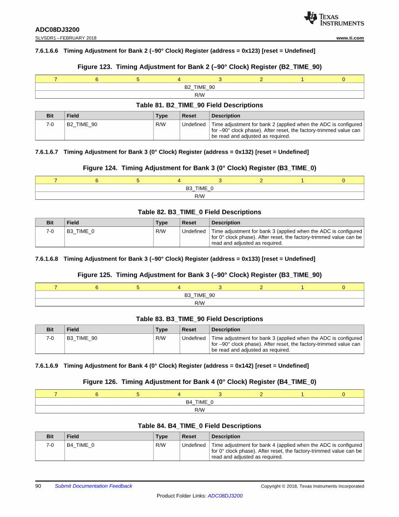
90
ADC08DJ3200SLVSDR1 –FEBRUARY 2018 www.ti.com
Product Folder Links: ADC08DJ3200
Submit Documentation Feedback Copyright © 2018, Texas Instruments Incorporated
7.6.1.6.6 Timing Adjustment for Bank 2 (–90° Clock) Register (address = 0x123) [reset = Undefined]
Figure 123. Timing Adjustment for Bank 2 (–90° Clock) Register (B2_TIME_90)
7 6 5 4 3 2 1 0B2_TIME_90
R/W
Table 81. B2_TIME_90 Field DescriptionsBit Field Type Reset Description7-0 B2_TIME_90 R/W Undefined Time adjustment for bank 2 (applied when the ADC is configured
for –90° clock phase). After reset, the factory-trimmed value canbe read and adjusted as required.
7.6.1.6.7 Timing Adjustment for Bank 3 (0° Clock) Register (address = 0x132) [reset = Undefined]
Figure 124. Timing Adjustment for Bank 3 (0° Clock) Register (B3_TIME_0)
7 6 5 4 3 2 1 0B3_TIME_0
R/W
Table 82. B3_TIME_0 Field DescriptionsBit Field Type Reset Description7-0 B3_TIME_0 R/W Undefined Time adjustment for bank 3 (applied when the ADC is configured
for 0° clock phase). After reset, the factory-trimmed value can beread and adjusted as required.
7.6.1.6.8 Timing Adjustment for Bank 3 (–90° Clock) Register (address = 0x133) [reset = Undefined]
Figure 125. Timing Adjustment for Bank 3 (–90° Clock) Register (B3_TIME_90)
7 6 5 4 3 2 1 0B3_TIME_90
R/W
Table 83. B3_TIME_90 Field DescriptionsBit Field Type Reset Description7-0 B3_TIME_90 R/W Undefined Time adjustment for bank 3 (applied when the ADC is configured
for –90° clock phase). After reset, the factory-trimmed value canbe read and adjusted as required.
7.6.1.6.9 Timing Adjustment for Bank 4 (0° Clock) Register (address = 0x142) [reset = Undefined]
Figure 126. Timing Adjustment for Bank 4 (0° Clock) Register (B4_TIME_0)
7 6 5 4 3 2 1 0B4_TIME_0
R/W
Table 84. B4_TIME_0 Field DescriptionsBit Field Type Reset Description7-0 B4_TIME_0 R/W Undefined Time adjustment for bank 4 (applied when the ADC is configured
for 0° clock phase). After reset, the factory-trimmed value can beread and adjusted as required.
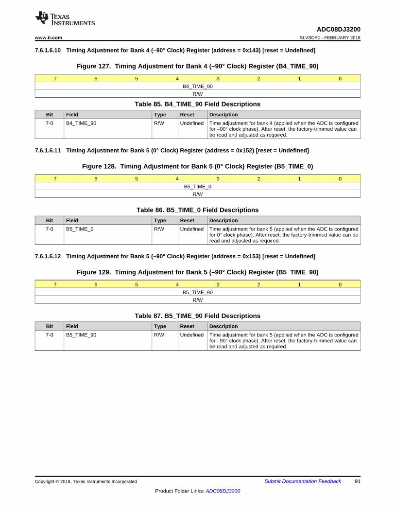
91
ADC08DJ3200www.ti.com SLVSDR1 –FEBRUARY 2018
Product Folder Links: ADC08DJ3200
Submit Documentation FeedbackCopyright © 2018, Texas Instruments Incorporated
7.6.1.6.10 Timing Adjustment for Bank 4 (–90° Clock) Register (address = 0x143) [reset = Undefined]
Figure 127. Timing Adjustment for Bank 4 (–90° Clock) Register (B4_TIME_90)
7 6 5 4 3 2 1 0B4_TIME_90
R/W
Table 85. B4_TIME_90 Field DescriptionsBit Field Type Reset Description7-0 B4_TIME_90 R/W Undefined Time adjustment for bank 4 (applied when the ADC is configured
for –90° clock phase). After reset, the factory-trimmed value canbe read and adjusted as required.
7.6.1.6.11 Timing Adjustment for Bank 5 (0° Clock) Register (address = 0x152) [reset = Undefined]
Figure 128. Timing Adjustment for Bank 5 (0° Clock) Register (B5_TIME_0)
7 6 5 4 3 2 1 0B5_TIME_0
R/W
Table 86. B5_TIME_0 Field DescriptionsBit Field Type Reset Description7-0 B5_TIME_0 R/W Undefined Time adjustment for bank 5 (applied when the ADC is configured
for 0° clock phase). After reset, the factory-trimmed value can beread and adjusted as required.
7.6.1.6.12 Timing Adjustment for Bank 5 (–90° Clock) Register (address = 0x153) [reset = Undefined]
Figure 129. Timing Adjustment for Bank 5 (–90° Clock) Register (B5_TIME_90)
7 6 5 4 3 2 1 0B5_TIME_90
R/W
Table 87. B5_TIME_90 Field DescriptionsBit Field Type Reset Description7-0 B5_TIME_90 R/W Undefined Time adjustment for bank 5 (applied when the ADC is configured
for –90° clock phase). After reset, the factory-trimmed value canbe read and adjusted as required.
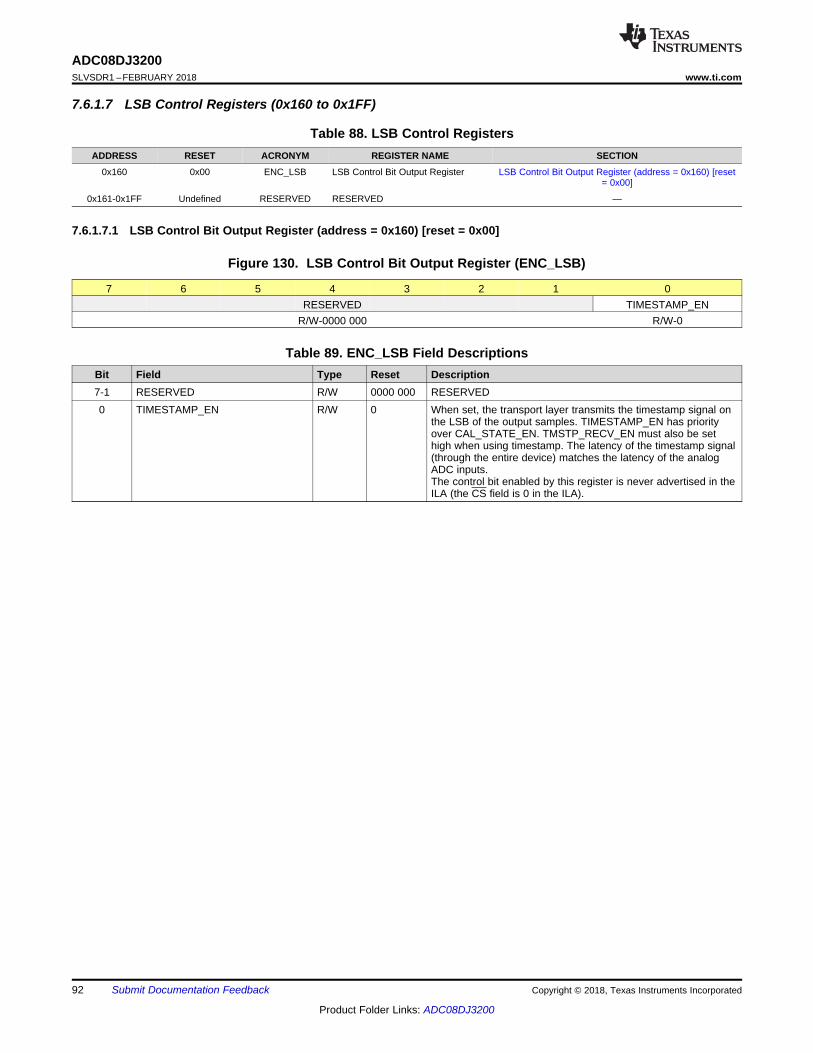
92
ADC08DJ3200SLVSDR1 –FEBRUARY 2018 www.ti.com
Product Folder Links: ADC08DJ3200
Submit Documentation Feedback Copyright © 2018, Texas Instruments Incorporated
7.6.1.7 LSB Control Registers (0x160 to 0x1FF)
Table 88. LSB Control RegistersADDRESS RESET ACRONYM REGISTER NAME SECTION
0x160 0x00 ENC_LSB LSB Control Bit Output Register LSB Control Bit Output Register (address = 0x160) [reset= 0x00]
0x161-0x1FF Undefined RESERVED RESERVED —
7.6.1.7.1 LSB Control Bit Output Register (address = 0x160) [reset = 0x00]
Figure 130. LSB Control Bit Output Register (ENC_LSB)
7 6 5 4 3 2 1 0RESERVED TIMESTAMP_EN
R/W-0000 000 R/W-0
Table 89. ENC_LSB Field DescriptionsBit Field Type Reset Description7-1 RESERVED R/W 0000 000 RESERVED0 TIMESTAMP_EN R/W 0 When set, the transport layer transmits the timestamp signal on
the LSB of the output samples. TIMESTAMP_EN has priorityover CAL_STATE_EN. TMSTP_RECV_EN must also be sethigh when using timestamp. The latency of the timestamp signal(through the entire device) matches the latency of the analogADC inputs.The control bit enabled by this register is never advertised in theILA (the CS field is 0 in the ILA).
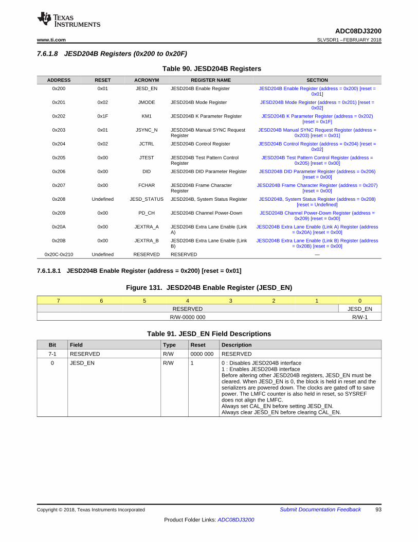
93
ADC08DJ3200www.ti.com SLVSDR1 –FEBRUARY 2018
Product Folder Links: ADC08DJ3200
Submit Documentation FeedbackCopyright © 2018, Texas Instruments Incorporated
7.6.1.8 JESD204B Registers (0x200 to 0x20F)
Table 90. JESD204B RegistersADDRESS RESET ACRONYM REGISTER NAME SECTION
0x200 0x01 JESD_EN JESD204B Enable Register JESD204B Enable Register (address = 0x200) [reset =0x01]
0x201 0x02 JMODE JESD204B Mode Register JESD204B Mode Register (address = 0x201) [reset =0x02]
0x202 0x1F KM1 JESD204B K Parameter Register JESD204B K Parameter Register (address = 0x202)[reset = 0x1F]
0x203 0x01 JSYNC_N JESD204B Manual SYNC RequestRegister
JESD204B Manual SYNC Request Register (address =0x203) [reset = 0x01]
0x204 0x02 JCTRL JESD204B Control Register JESD204B Control Register (address = 0x204) [reset =0x02]
0x205 0x00 JTEST JESD204B Test Pattern ControlRegister
JESD204B Test Pattern Control Register (address =0x205) [reset = 0x00]
0x206 0x00 DID JESD204B DID Parameter Register JESD204B DID Parameter Register (address = 0x206)[reset = 0x00]
0x207 0x00 FCHAR JESD204B Frame CharacterRegister
JESD204B Frame Character Register (address = 0x207)[reset = 0x00]
0x208 Undefined JESD_STATUS JESD204B, System Status Register JESD204B, System Status Register (address = 0x208)[reset = Undefined]
0x209 0x00 PD_CH JESD204B Channel Power-Down JESD204B Channel Power-Down Register (address =0x209) [reset = 0x00]
0x20A 0x00 JEXTRA_A JESD204B Extra Lane Enable (LinkA)
JESD204B Extra Lane Enable (Link A) Register (address= 0x20A) [reset = 0x00]
0x20B 0x00 JEXTRA_B JESD204B Extra Lane Enable (LinkB)
JESD204B Extra Lane Enable (Link B) Register (address= 0x20B) [reset = 0x00]
0x20C-0x210 Undefined RESERVED RESERVED —
7.6.1.8.1 JESD204B Enable Register (address = 0x200) [reset = 0x01]
Figure 131. JESD204B Enable Register (JESD_EN)
7 6 5 4 3 2 1 0RESERVED JESD_EN
R/W-0000 000 R/W-1
Table 91. JESD_EN Field DescriptionsBit Field Type Reset Description7-1 RESERVED R/W 0000 000 RESERVED0 JESD_EN R/W 1 0 : Disables JESD204B interface
1 : Enables JESD204B interfaceBefore altering other JESD204B registers, JESD_EN must becleared. When JESD_EN is 0, the block is held in reset and theserializers are powered down. The clocks are gated off to savepower. The LMFC counter is also held in reset, so SYSREFdoes not align the LMFC.Always set CAL_EN before setting JESD_EN.Always clear JESD_EN before clearing CAL_EN.
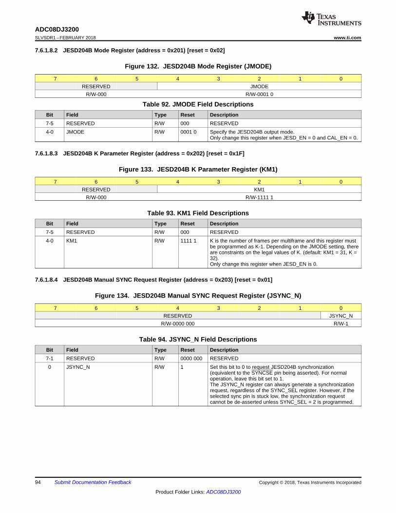
94
ADC08DJ3200SLVSDR1 –FEBRUARY 2018 www.ti.com
Product Folder Links: ADC08DJ3200
Submit Documentation Feedback Copyright © 2018, Texas Instruments Incorporated
7.6.1.8.2 JESD204B Mode Register (address = 0x201) [reset = 0x02]
Figure 132. JESD204B Mode Register (JMODE)
7 6 5 4 3 2 1 0RESERVED JMODE
R/W-000 R/W-0001 0
Table 92. JMODE Field DescriptionsBit Field Type Reset Description7-5 RESERVED R/W 000 RESERVED4-0 JMODE R/W 0001 0 Specify the JESD204B output mode.
Only change this register when JESD_EN = 0 and CAL_EN = 0.
7.6.1.8.3 JESD204B K Parameter Register (address = 0x202) [reset = 0x1F]
Figure 133. JESD204B K Parameter Register (KM1)
7 6 5 4 3 2 1 0RESERVED KM1
R/W-000 R/W-1111 1
Table 93. KM1 Field DescriptionsBit Field Type Reset Description7-5 RESERVED R/W 000 RESERVED4-0 KM1 R/W 1111 1 K is the number of frames per multiframe and this register must
be programmed as K-1. Depending on the JMODE setting, thereare constraints on the legal values of K. (default: KM1 = 31, K =32).Only change this register when JESD_EN is 0.
7.6.1.8.4 JESD204B Manual SYNC Request Register (address = 0x203) [reset = 0x01]
Figure 134. JESD204B Manual SYNC Request Register (JSYNC_N)
7 6 5 4 3 2 1 0RESERVED JSYNC_N
R/W-0000 000 R/W-1
Table 94. JSYNC_N Field DescriptionsBit Field Type Reset Description7-1 RESERVED R/W 0000 000 RESERVED0 JSYNC_N R/W 1 Set this bit to 0 to request JESD204B synchronization
(equivalent to the SYNCSE pin being asserted). For normaloperation, leave this bit set to 1.The JSYNC_N register can always generate a synchronizationrequest, regardless of the SYNC_SEL register. However, if theselected sync pin is stuck low, the synchronization requestcannot be de-asserted unless SYNC_SEL = 2 is programmed.
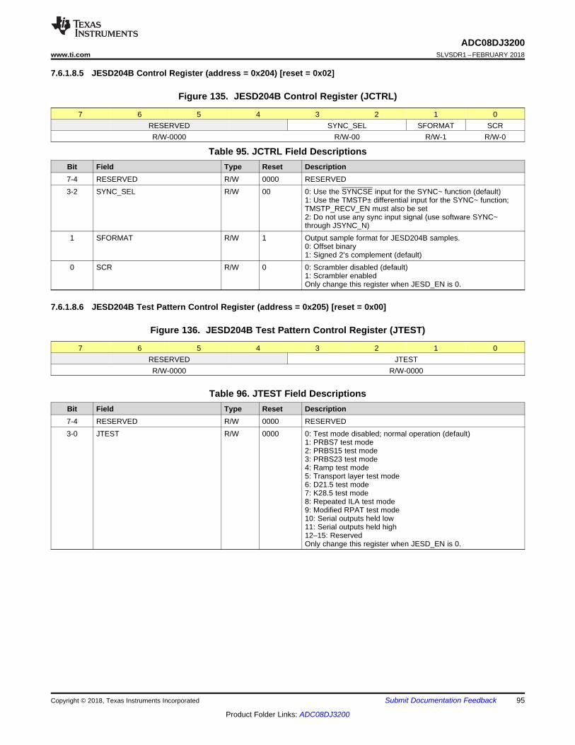
95
ADC08DJ3200www.ti.com SLVSDR1 –FEBRUARY 2018
Product Folder Links: ADC08DJ3200
Submit Documentation FeedbackCopyright © 2018, Texas Instruments Incorporated
7.6.1.8.5 JESD204B Control Register (address = 0x204) [reset = 0x02]
Figure 135. JESD204B Control Register (JCTRL)
7 6 5 4 3 2 1 0RESERVED SYNC_SEL SFORMAT SCRR/W-0000 R/W-00 R/W-1 R/W-0
Table 95. JCTRL Field DescriptionsBit Field Type Reset Description7-4 RESERVED R/W 0000 RESERVED3-2 SYNC_SEL R/W 00 0: Use the SYNCSE input for the SYNC~ function (default)
1: Use the TMSTP± differential input for the SYNC~ function;TMSTP_RECV_EN must also be set2: Do not use any sync input signal (use software SYNC~through JSYNC_N)
1 SFORMAT R/W 1 Output sample format for JESD204B samples.0: Offset binary1: Signed 2’s complement (default)
0 SCR R/W 0 0: Scrambler disabled (default)1: Scrambler enabledOnly change this register when JESD_EN is 0.
7.6.1.8.6 JESD204B Test Pattern Control Register (address = 0x205) [reset = 0x00]
Figure 136. JESD204B Test Pattern Control Register (JTEST)
7 6 5 4 3 2 1 0RESERVED JTESTR/W-0000 R/W-0000
Table 96. JTEST Field DescriptionsBit Field Type Reset Description7-4 RESERVED R/W 0000 RESERVED3-0 JTEST R/W 0000 0: Test mode disabled; normal operation (default)
1: PRBS7 test mode2: PRBS15 test mode3: PRBS23 test mode4: Ramp test mode5: Transport layer test mode6: D21.5 test mode7: K28.5 test mode8: Repeated ILA test mode9: Modified RPAT test mode10: Serial outputs held low11: Serial outputs held high12–15: ReservedOnly change this register when JESD_EN is 0.
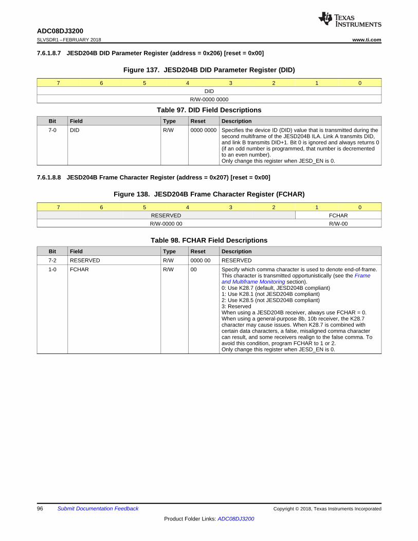
96
ADC08DJ3200SLVSDR1 –FEBRUARY 2018 www.ti.com
Product Folder Links: ADC08DJ3200
Submit Documentation Feedback Copyright © 2018, Texas Instruments Incorporated
7.6.1.8.7 JESD204B DID Parameter Register (address = 0x206) [reset = 0x00]
Figure 137. JESD204B DID Parameter Register (DID)
7 6 5 4 3 2 1 0DID
R/W-0000 0000
Table 97. DID Field DescriptionsBit Field Type Reset Description7-0 DID R/W 0000 0000 Specifies the device ID (DID) value that is transmitted during the
second multiframe of the JESD204B ILA. Link A transmits DID,and link B transmits DID+1. Bit 0 is ignored and always returns 0(if an odd number is programmed, that number is decrementedto an even number).Only change this register when JESD_EN is 0.
7.6.1.8.8 JESD204B Frame Character Register (address = 0x207) [reset = 0x00]
Figure 138. JESD204B Frame Character Register (FCHAR)
7 6 5 4 3 2 1 0RESERVED FCHARR/W-0000 00 R/W-00
Table 98. FCHAR Field DescriptionsBit Field Type Reset Description7-2 RESERVED R/W 0000 00 RESERVED1-0 FCHAR R/W 00 Specify which comma character is used to denote end-of-frame.
This character is transmitted opportunistically (see the Frameand Multiframe Monitoring section).0: Use K28.7 (default, JESD204B compliant)1: Use K28.1 (not JESD204B compliant)2: Use K28.5 (not JESD204B compliant)3: ReservedWhen using a JESD204B receiver, always use FCHAR = 0.When using a general-purpose 8b, 10b receiver, the K28.7character may cause issues. When K28.7 is combined withcertain data characters, a false, misaligned comma charactercan result, and some receivers realign to the false comma. Toavoid this condition, program FCHAR to 1 or 2.Only change this register when JESD_EN is 0.
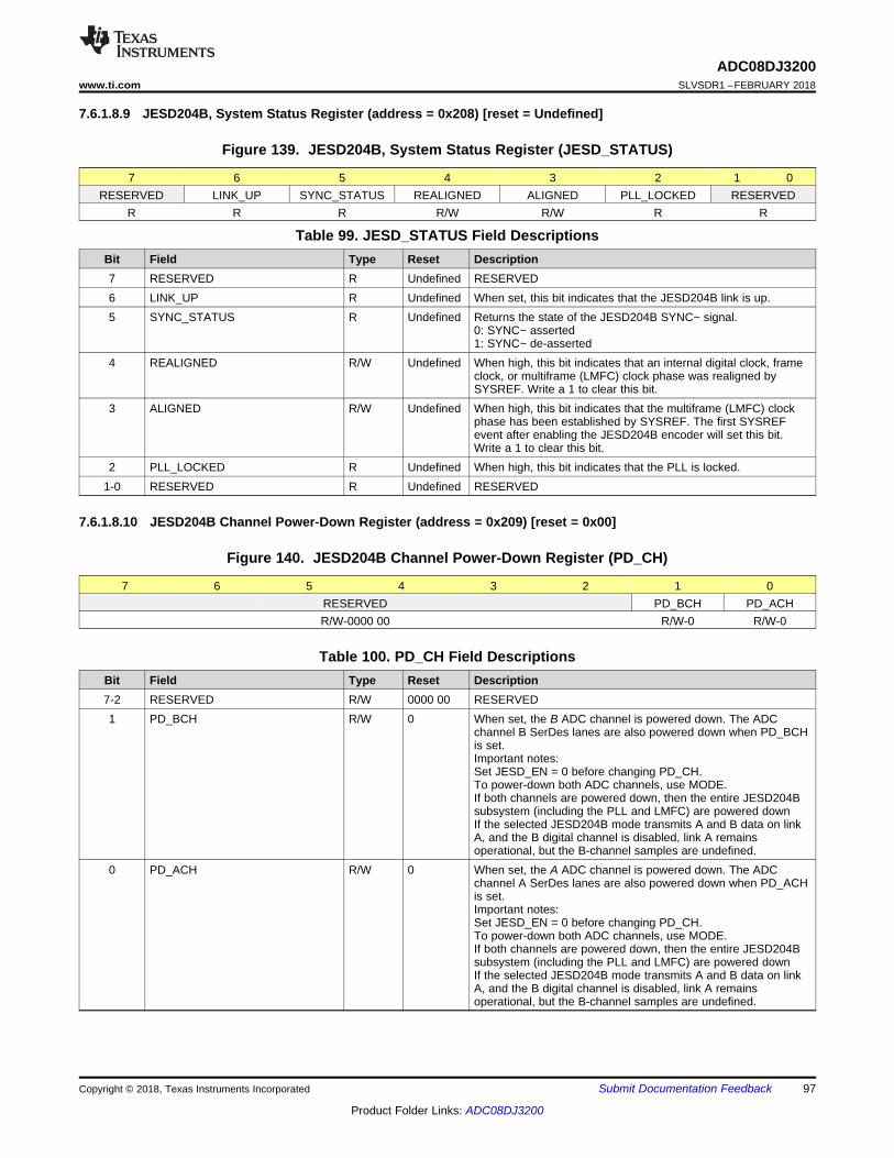
97
ADC08DJ3200www.ti.com SLVSDR1 –FEBRUARY 2018
Product Folder Links: ADC08DJ3200
Submit Documentation FeedbackCopyright © 2018, Texas Instruments Incorporated
7.6.1.8.9 JESD204B, System Status Register (address = 0x208) [reset = Undefined]
Figure 139. JESD204B, System Status Register (JESD_STATUS)
7 6 5 4 3 2 1 0RESERVED LINK_UP SYNC_STATUS REALIGNED ALIGNED PLL_LOCKED RESERVED
R R R R/W R/W R R
Table 99. JESD_STATUS Field DescriptionsBit Field Type Reset Description7 RESERVED R Undefined RESERVED6 LINK_UP R Undefined When set, this bit indicates that the JESD204B link is up.5 SYNC_STATUS R Undefined Returns the state of the JESD204B SYNC~ signal.
0: SYNC~ asserted1: SYNC~ de-asserted
4 REALIGNED R/W Undefined When high, this bit indicates that an internal digital clock, frameclock, or multiframe (LMFC) clock phase was realigned bySYSREF. Write a 1 to clear this bit.
3 ALIGNED R/W Undefined When high, this bit indicates that the multiframe (LMFC) clockphase has been established by SYSREF. The first SYSREFevent after enabling the JESD204B encoder will set this bit.Write a 1 to clear this bit.
2 PLL_LOCKED R Undefined When high, this bit indicates that the PLL is locked.1-0 RESERVED R Undefined RESERVED
7.6.1.8.10 JESD204B Channel Power-Down Register (address = 0x209) [reset = 0x00]
Figure 140. JESD204B Channel Power-Down Register (PD_CH)
7 6 5 4 3 2 1 0RESERVED PD_BCH PD_ACHR/W-0000 00 R/W-0 R/W-0
Table 100. PD_CH Field DescriptionsBit Field Type Reset Description7-2 RESERVED R/W 0000 00 RESERVED1 PD_BCH R/W 0 When set, the B ADC channel is powered down. The ADC
channel B SerDes lanes are also powered down when PD_BCHis set.Important notes:Set JESD_EN = 0 before changing PD_CH.To power-down both ADC channels, use MODE.If both channels are powered down, then the entire JESD204Bsubsystem (including the PLL and LMFC) are powered downIf the selected JESD204B mode transmits A and B data on linkA, and the B digital channel is disabled, link A remainsoperational, but the B-channel samples are undefined.
0 PD_ACH R/W 0 When set, the A ADC channel is powered down. The ADCchannel A SerDes lanes are also powered down when PD_ACHis set.Important notes:Set JESD_EN = 0 before changing PD_CH.To power-down both ADC channels, use MODE.If both channels are powered down, then the entire JESD204Bsubsystem (including the PLL and LMFC) are powered downIf the selected JESD204B mode transmits A and B data on linkA, and the B digital channel is disabled, link A remainsoperational, but the B-channel samples are undefined.
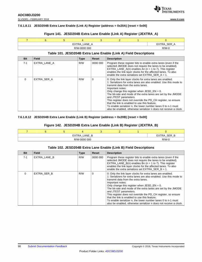
98
ADC08DJ3200SLVSDR1 –FEBRUARY 2018 www.ti.com
Product Folder Links: ADC08DJ3200
Submit Documentation Feedback Copyright © 2018, Texas Instruments Incorporated
7.6.1.8.11 JESD204B Extra Lane Enable (Link A) Register (address = 0x20A) [reset = 0x00]
Figure 141. JESD204B Extra Lane Enable (Link A) Register (JEXTRA_A)
7 6 5 4 3 2 1 0EXTRA_LANE_A EXTRA_SER_A
R/W-0000 000 R/W-0
Table 101. JESD204B Extra Lane Enable (Link A) Field DescriptionsBit Field Type Reset Description7-1 EXTRA_LANE_A R/W 0000 000 Program these register bits to enable extra lanes (even if the
selected JMODE does not require the lanes to be enabled).EXTRA_LANE_A(n) enables An (n = 1 to 7). This registerenables the link layer clocks for the affected lanes. To alsoenable the extra serializes set EXTRA_SER_A = 1.
0 EXTRA_SER_A R/W 0 0: Only the link layer clocks for extra lanes are enabled.1: Serializers for extra lanes are also enabled. Use this mode totransmit data from the extra lanes.Important notes:Only change this register when JESD_EN = 0.The bit-rate and mode of the extra lanes are set by the JMODEand JTEST parameters.This register does not override the PD_CH register, so ensurethat the link is enabled to use this feature.To enable serializer n, the lower number lanes 0 to n-1 mustalso be enabled, otherwise serializer n does not receive a clock.
7.6.1.8.12 JESD204B Extra Lane Enable (Link B) Register (address = 0x20B) [reset = 0x00]
Figure 142. JESD204B Extra Lane Enable (Link B) Register (JEXTRA_B)
7 6 5 4 3 2 1 0EXTRA_LANE_B EXTRA_SER_B
R/W-0000 000 R/W-0
Table 102. JESD204B Extra Lane Enable (Link B) Field DescriptionsBit Field Type Reset Description7-1 EXTRA_LANE_B R/W 0000 000 Program these register bits to enable extra lanes (even if the
selected JMODE does not require the lanes to be enabled).EXTRA_LANE_B(n) enables Bn (n = 1 to 7). This registerenables the link layer clocks for the affected lanes. To alsoenable the extra serializes set EXTRA_SER_B = 1.
0 EXTRA_SER_B R/W 0 0: Only the link layer clocks for extra lanes are enabled.1: Serializers for extra lanes are also enabled. Use this mode totransmit data from the extra lanes.Important notes:Only change this register when JESD_EN = 0.The bit-rate and mode of the extra lanes are set by the JMODEand JTEST parameters.This register does not override the PD_CH register, so ensurethat the link is enabled to use this feature.To enable serializer n, the lower number lanes 0 to n-1 mustalso be enabled, otherwise serializer n does not receive a clock.
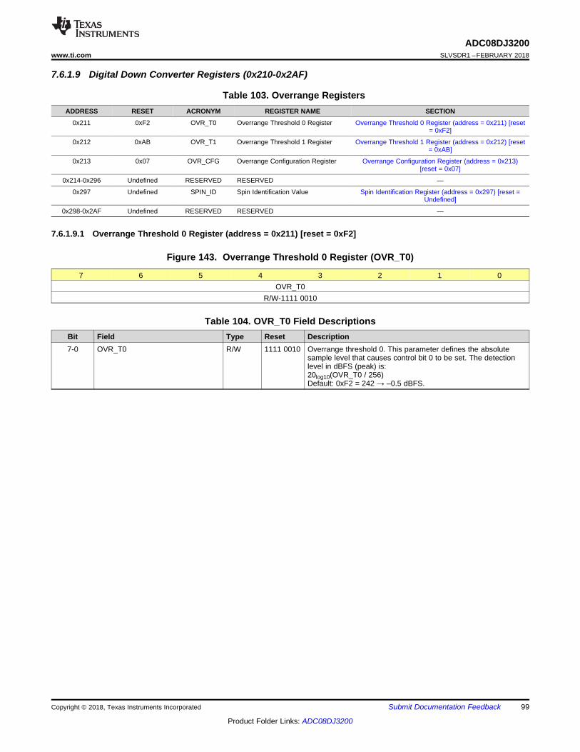
99
ADC08DJ3200www.ti.com SLVSDR1 –FEBRUARY 2018
Product Folder Links: ADC08DJ3200
Submit Documentation FeedbackCopyright © 2018, Texas Instruments Incorporated
7.6.1.9 Digital Down Converter Registers (0x210-0x2AF)
Table 103. Overrange RegistersADDRESS RESET ACRONYM REGISTER NAME SECTION
0x211 0xF2 OVR_T0 Overrange Threshold 0 Register Overrange Threshold 0 Register (address = 0x211) [reset= 0xF2]
0x212 0xAB OVR_T1 Overrange Threshold 1 Register Overrange Threshold 1 Register (address = 0x212) [reset= 0xAB]
0x213 0x07 OVR_CFG Overrange Configuration Register Overrange Configuration Register (address = 0x213)[reset = 0x07]
0x214-0x296 Undefined RESERVED RESERVED —
0x297 Undefined SPIN_ID Spin Identification Value Spin Identification Register (address = 0x297) [reset =Undefined]
0x298-0x2AF Undefined RESERVED RESERVED —
7.6.1.9.1 Overrange Threshold 0 Register (address = 0x211) [reset = 0xF2]
Figure 143. Overrange Threshold 0 Register (OVR_T0)
7 6 5 4 3 2 1 0OVR_T0
R/W-1111 0010
Table 104. OVR_T0 Field DescriptionsBit Field Type Reset Description7-0 OVR_T0 R/W 1111 0010 Overrange threshold 0. This parameter defines the absolute
sample level that causes control bit 0 to be set. The detectionlevel in dBFS (peak) is:20log10(OVR_T0 / 256)Default: 0xF2 = 242 → –0.5 dBFS.
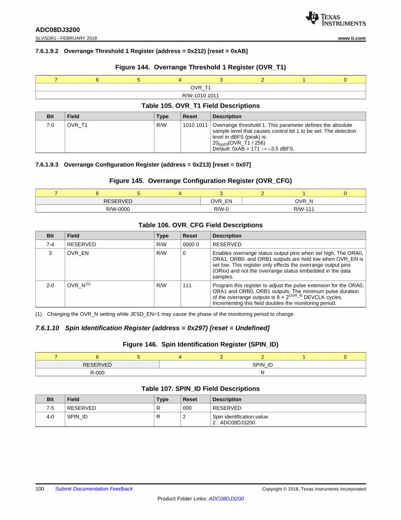
100
ADC08DJ3200SLVSDR1 –FEBRUARY 2018 www.ti.com
Product Folder Links: ADC08DJ3200
Submit Documentation Feedback Copyright © 2018, Texas Instruments Incorporated
7.6.1.9.2 Overrange Threshold 1 Register (address = 0x212) [reset = 0xAB]
Figure 144. Overrange Threshold 1 Register (OVR_T1)
7 6 5 4 3 2 1 0OVR_T1
R/W-1010 1011
Table 105. OVR_T1 Field DescriptionsBit Field Type Reset Description7-0 OVR_T1 R/W 1010 1011 Overrange threshold 1. This parameter defines the absolute
sample level that causes control bit 1 to be set. The detectionlevel in dBFS (peak) is:20log10(OVR_T1 / 256)Default: 0xAB = 171 → –3.5 dBFS.
7.6.1.9.3 Overrange Configuration Register (address = 0x213) [reset = 0x07]
Figure 145. Overrange Configuration Register (OVR_CFG)
7 6 5 4 3 2 1 0RESERVED OVR_EN OVR_NR/W-0000 R/W-0 R/W-111
(1) Changing the OVR_N setting while JESD_EN=1 may cause the phase of the monitoring period to change.
Table 106. OVR_CFG Field DescriptionsBit Field Type Reset Description7-4 RESERVED R/W 0000 0 RESERVED3 OVR_EN R/W 0 Enables overrange status output pins when set high. The ORA0,
ORA1, ORB0, and ORB1 outputs are held low when OVR_EN isset low. This register only effects the overrange output pins(ORxx) and not the overrange status embedded in the datasamples.
2-0 OVR_N (1) R/W 111 Program this register to adjust the pulse extension for the ORA0,ORA1 and ORB0, ORB1 outputs. The minimum pulse durationof the overrange outputs is 8 × 2OVR_N DEVCLK cycles.Incrementing this field doubles the monitoring period.
7.6.1.10 Spin Identification Register (address = 0x297) [reset = Undefined]
Figure 146. Spin Identification Register (SPIN_ID)
7 6 5 4 3 2 1 0RESERVED SPIN_ID
R-000 R
Table 107. SPIN_ID Field DescriptionsBit Field Type Reset Description7-5 RESERVED R 000 RESERVED4-0 SPIN_ID R 2 Spin identification value.
2 : ADC08DJ3200
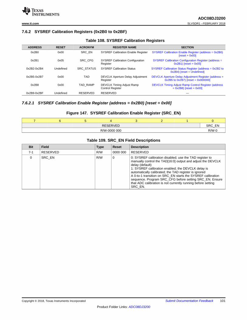
101
ADC08DJ3200www.ti.com SLVSDR1 –FEBRUARY 2018
Product Folder Links: ADC08DJ3200
Submit Documentation FeedbackCopyright © 2018, Texas Instruments Incorporated
7.6.2 SYSREF Calibration Registers (0x2B0 to 0x2BF)
Table 108. SYSREF Calibration RegistersADDRESS RESET ACRONYM REGISTER NAME SECTION
0x2B0 0x00 SRC_EN SYSREF Calibration Enable Register SYSREF Calibration Enable Register (address = 0x2B0)[reset = 0x00]
0x2B1 0x05 SRC_CFG SYSREF Calibration ConfigurationRegister
SYSREF Calibration Configuration Register (address =0x2B1) [reset = 0x05]
0x2B2-0x2B4 Undefined SRC_STATUS SYSREF Calibration Status SYSREF Calibration Status Register (address = 0x2B2 to0x2B4) [reset = Undefined]
0x2B5-0x2B7 0x00 TAD DEVCLK Aperture Delay AdjustmentRegister
DEVCLK Aperture Delay Adjustment Register (address =0x2B5 to 0x2B7) [reset = 0x000000]
0x2B8 0x00 TAD_RAMP DEVCLK Timing Adjust RampControl Register
DEVCLK Timing Adjust Ramp Control Register (address= 0x2B8) [reset = 0x00]
0x2B9-0x2BF Undefined RESERVED RESERVED —
7.6.2.1 SYSREF Calibration Enable Register (address = 0x2B0) [reset = 0x00]
Figure 147. SYSREF Calibration Enable Register (SRC_EN)
7 6 5 4 3 2 1 0RESERVED SRC_EN
R/W-0000 000 R/W-0
Table 109. SRC_EN Field DescriptionsBit Field Type Reset Description7-1 RESERVED R/W 0000 000 RESERVED0 SRC_EN R/W 0 0: SYSREF calibration disabled; use the TAD register to
manually control the TAD[16:0] output and adjust the DEVCLKdelay (default)1: SYSREF calibration enabled; the DEVCLK delay isautomatically calibrated; the TAD register is ignoredA 0-to-1 transition on SRC_EN starts the SYSREF calibrationsequence. Program SRC_CFG before setting SRC_EN. Ensurethat ADC calibration is not currently running before settingSRC_EN.
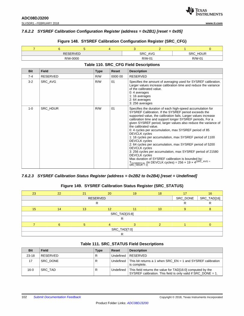
102
ADC08DJ3200SLVSDR1 –FEBRUARY 2018 www.ti.com
Product Folder Links: ADC08DJ3200
Submit Documentation Feedback Copyright © 2018, Texas Instruments Incorporated
7.6.2.2 SYSREF Calibration Configuration Register (address = 0x2B1) [reset = 0x05]
Figure 148. SYSREF Calibration Configuration Register (SRC_CFG)
7 6 5 4 3 2 1 0RESERVED SRC_AVG SRC_HDURR/W-0000 R/W-01 R/W-01
Table 110. SRC_CFG Field DescriptionsBit Field Type Reset Description7-4 RESERVED R/W 0000 00 RESERVED3-2 SRC_AVG R/W 01 Specifies the amount of averaging used for SYSREF calibration.
Larger values increase calibration time and reduce the varianceof the calibrated value.0: 4 averages1: 16 averages2: 64 averages3: 256 averages
1-0 SRC_HDUR R/W 01 Specifies the duration of each high-speed accumulation forSYSREF Calibration. If the SYSREF period exceeds thesupported value, the calibration fails. Larger values increasecalibration time and support longer SYSREF periods. For agiven SYSREF period, larger values also reduce the variance ofthe calibrated value.0: 4 cycles per accumulation, max SYSREF period of 85DEVCLK cycles1: 16 cycles per accumulation, max SYSREF period of 1100DEVCLK cycles2: 64 cycles per accumulation, max SYSREF period of 5200DEVCLK cycles3: 256 cycles per accumulation, max SYSREF period of 21580DEVCLK cyclesMax duration of SYSREF calibration is bounded by:TSYSREFCAL (in DEVCLK cycles) = 256 × 19 × 4(SRC_AVG +SRC_HDUR + 2)
7.6.2.3 SYSREF Calibration Status Register (address = 0x2B2 to 0x2B4) [reset = Undefined]
Figure 149. SYSREF Calibration Status Register (SRC_STATUS)
23 22 21 20 19 18 17 16RESERVED SRC_DONE SRC_TAD[16]
R R R
15 14 13 12 11 10 9 8SRC_TAD[15:8]
R
7 6 5 4 3 2 1 0SRC_TAD[7:0]
R
Table 111. SRC_STATUS Field DescriptionsBit Field Type Reset Description
23-18 RESERVED R Undefined RESERVED17 SRC_DONE R Undefined This bit returns a 1 when SRC_EN = 1 and SYSREF calibration
is complete.16-0 SRC_TAD R Undefined This field returns the value for TAD[16:0] computed by the
SYSREF calibration. This field is only valid if SRC_DONE = 1.
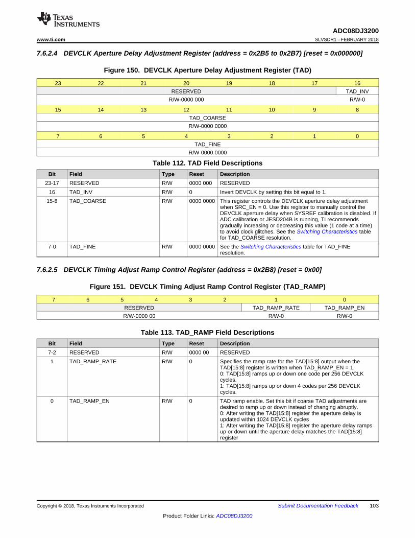
103
ADC08DJ3200www.ti.com SLVSDR1 –FEBRUARY 2018
Product Folder Links: ADC08DJ3200
Submit Documentation FeedbackCopyright © 2018, Texas Instruments Incorporated
7.6.2.4 DEVCLK Aperture Delay Adjustment Register (address = 0x2B5 to 0x2B7) [reset = 0x000000]
Figure 150. DEVCLK Aperture Delay Adjustment Register (TAD)
23 22 21 20 19 18 17 16RESERVED TAD_INV
R/W-0000 000 R/W-0
15 14 13 12 11 10 9 8TAD_COARSER/W-0000 0000
7 6 5 4 3 2 1 0TAD_FINE
R/W-0000 0000
Table 112. TAD Field DescriptionsBit Field Type Reset Description
23-17 RESERVED R/W 0000 000 RESERVED16 TAD_INV R/W 0 Invert DEVCLK by setting this bit equal to 1.
15-8 TAD_COARSE R/W 0000 0000 This register controls the DEVCLK aperture delay adjustmentwhen SRC_EN = 0. Use this register to manually control theDEVCLK aperture delay when SYSREF calibration is disabled. IfADC calibration or JESD204B is running, TI recommendsgradually increasing or decreasing this value (1 code at a time)to avoid clock glitches. See the Switching Characteristics tablefor TAD_COARSE resolution.
7-0 TAD_FINE R/W 0000 0000 See the Switching Characteristics table for TAD_FINEresolution.
7.6.2.5 DEVCLK Timing Adjust Ramp Control Register (address = 0x2B8) [reset = 0x00]
Figure 151. DEVCLK Timing Adjust Ramp Control Register (TAD_RAMP)
7 6 5 4 3 2 1 0RESERVED TAD_RAMP_RATE TAD_RAMP_ENR/W-0000 00 R/W-0 R/W-0
Table 113. TAD_RAMP Field DescriptionsBit Field Type Reset Description7-2 RESERVED R/W 0000 00 RESERVED1 TAD_RAMP_RATE R/W 0 Specifies the ramp rate for the TAD[15:8] output when the
TAD[15:8] register is written when TAD_RAMP_EN = 1.0: TAD[15:8] ramps up or down one code per 256 DEVCLKcycles.1: TAD[15:8] ramps up or down 4 codes per 256 DEVCLKcycles.
0 TAD_RAMP_EN R/W 0 TAD ramp enable. Set this bit if coarse TAD adjustments aredesired to ramp up or down instead of changing abruptly.0: After writing the TAD[15:8] register the aperture delay isupdated within 1024 DEVCLK cycles1: After writing the TAD[15:8] register the aperture delay rampsup or down until the aperture delay matches the TAD[15:8]register
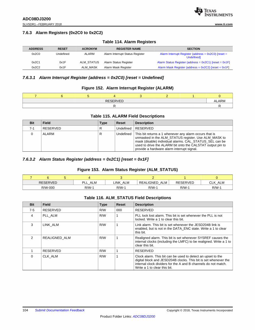
104
ADC08DJ3200SLVSDR1 –FEBRUARY 2018 www.ti.com
Product Folder Links: ADC08DJ3200
Submit Documentation Feedback Copyright © 2018, Texas Instruments Incorporated
7.6.3 Alarm Registers (0x2C0 to 0x2C2)
Table 114. Alarm RegistersADDRESS RESET ACRONYM REGISTER NAME SECTION
0x2C0 Undefined ALARM Alarm Interrupt Status Register Alarm Interrupt Register (address = 0x2C0) [reset =Undefined]
0x2C1 0x1F ALM_STATUS Alarm Status Register Alarm Status Register (address = 0x2C1) [reset = 0x1F]
0x2C2 0x1F ALM_MASK Alarm Mask Register Alarm Mask Register (address = 0x2C2) [reset = 0x1F]
7.6.3.1 Alarm Interrupt Register (address = 0x2C0) [reset = Undefined]
Figure 152. Alarm Interrupt Register (ALARM)
7 6 5 4 3 2 1 0RESERVED ALARM
R R
Table 115. ALARM Field DescriptionsBit Field Type Reset Description7-1 RESERVED R Undefined RESERVED0 ALARM R Undefined This bit returns a 1 whenever any alarm occurs that is
unmasked in the ALM_STATUS register. Use ALM_MASK tomask (disable) individual alarms. CAL_STATUS_SEL can beused to drive the ALARM bit onto the CALSTAT output pin toprovide a hardware alarm interrupt signal.
7.6.3.2 Alarm Status Register (address = 0x2C1) [reset = 0x1F]
Figure 153. Alarm Status Register (ALM_STATUS)
7 6 5 4 3 2 1 0RESERVED PLL_ALM LINK_ALM REALIGNED_ALM RESERVED CLK_ALM
R/W-000 R/W-1 R/W-1 R/W-1 R/W-1 R/W-1
Table 116. ALM_STATUS Field DescriptionsBit Field Type Reset Description7-5 RESERVED R/W 000 RESERVED4 PLL_ALM R/W 1 PLL lock lost alarm. This bit is set whenever the PLL is not
locked. Write a 1 to clear this bit.3 LINK_ALM R/W 1 Link alarm. This bit is set whenever the JESD204B link is
enabled, but is not in the DATA_ENC state. Write a 1 to clearthis bit.
2 REALIGNED_ALM R/W 1 Realigned alarm. This bit is set whenever SYSREF causes theinternal clocks (including the LMFC) to be realigned. Write a 1 toclear this bit.
1 RESERVED R/W 1 RESERVED0 CLK_ALM R/W 1 Clock alarm. This bit can be used to detect an upset to the
digital block and JESD204B clocks. This bit is set whenever theinternal clock dividers for the A and B channels do not match.Write a 1 to clear this bit.
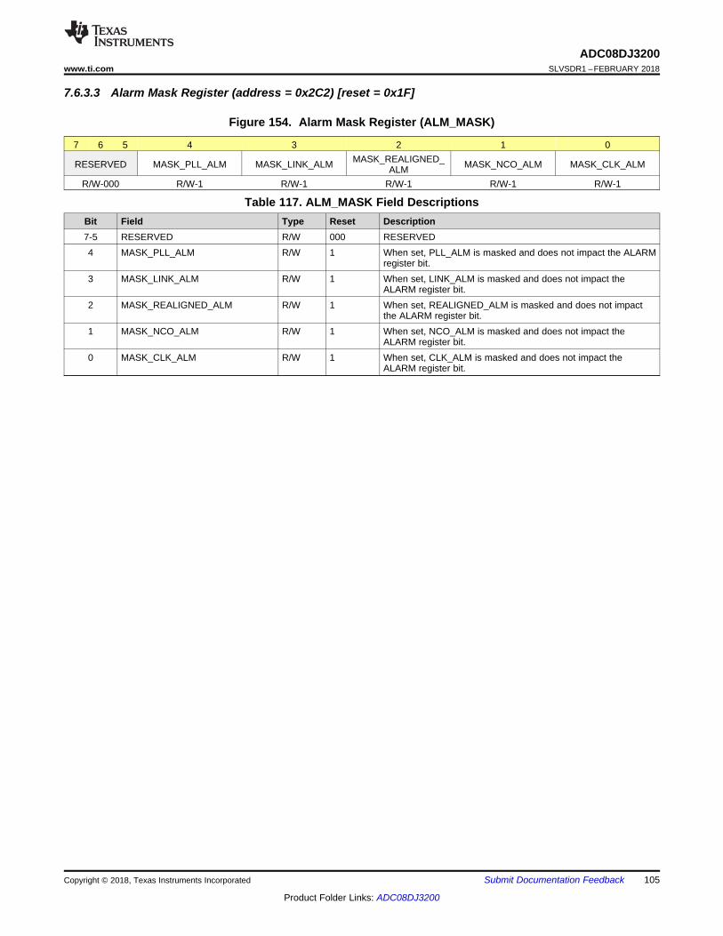
105
ADC08DJ3200www.ti.com SLVSDR1 –FEBRUARY 2018
Product Folder Links: ADC08DJ3200
Submit Documentation FeedbackCopyright © 2018, Texas Instruments Incorporated
7.6.3.3 Alarm Mask Register (address = 0x2C2) [reset = 0x1F]
Figure 154. Alarm Mask Register (ALM_MASK)
7 6 5 4 3 2 1 0
RESERVED MASK_PLL_ALM MASK_LINK_ALM MASK_REALIGNED_ALM MASK_NCO_ALM MASK_CLK_ALM
R/W-000 R/W-1 R/W-1 R/W-1 R/W-1 R/W-1
Table 117. ALM_MASK Field DescriptionsBit Field Type Reset Description7-5 RESERVED R/W 000 RESERVED4 MASK_PLL_ALM R/W 1 When set, PLL_ALM is masked and does not impact the ALARM
register bit.3 MASK_LINK_ALM R/W 1 When set, LINK_ALM is masked and does not impact the
ALARM register bit.2 MASK_REALIGNED_ALM R/W 1 When set, REALIGNED_ALM is masked and does not impact
the ALARM register bit.1 MASK_NCO_ALM R/W 1 When set, NCO_ALM is masked and does not impact the
ALARM register bit.0 MASK_CLK_ALM R/W 1 When set, CLK_ALM is masked and does not impact the
ALARM register bit.
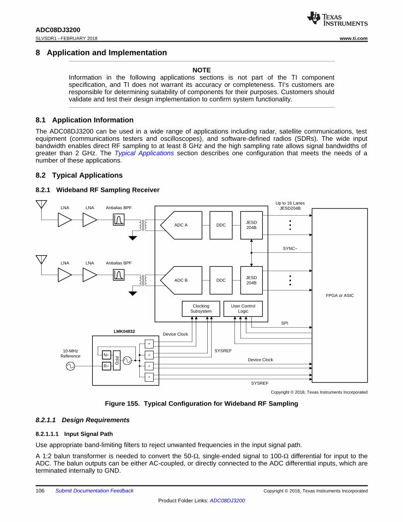
Clocking Subsystem
User Control Logic
FPGA or ASIC
Up to 16 Lanes JESD204B
SYNC~
÷
Device Clock
SYSREF
Device Clock
SYSREF
SPI
R÷
N÷ PF
D
÷
÷
10-MHz Reference
LMK04832
Antialias BPF
÷
Copyright © 2018, Texas Instruments Incorporated
LNA LNA
Antialias BPF
LNA LNA
DDCADC A
ADC B
JESD204B
JESD204B
DDC
106
ADC08DJ3200SLVSDR1 –FEBRUARY 2018 www.ti.com
Product Folder Links: ADC08DJ3200
Submit Documentation Feedback Copyright © 2018, Texas Instruments Incorporated
8 Application and Implementation
NOTEInformation in the following applications sections is not part of the TI componentspecification, and TI does not warrant its accuracy or completeness. TI’s customers areresponsible for determining suitability of components for their purposes. Customers shouldvalidate and test their design implementation to confirm system functionality.
8.1 Application InformationThe ADC08DJ3200 can be used in a wide range of applications including radar, satellite communications, testequipment (communications testers and oscilloscopes), and software-defined radios (SDRs). The wide inputbandwidth enables direct RF sampling to at least 8 GHz and the high sampling rate allows signal bandwidths ofgreater than 2 GHz. The Typical Applications section describes one configuration that meets the needs of anumber of these applications.
8.2 Typical Applications
8.2.1 Wideband RF Sampling Receiver
Figure 155. Typical Configuration for Wideband RF Sampling
8.2.1.1 Design Requirements
8.2.1.1.1 Input Signal Path
Use appropriate band-limiting filters to reject unwanted frequencies in the input signal path.
A 1:2 balun transformer is needed to convert the 50-Ω, single-ended signal to 100-Ω differential for input to theADC. The balun outputs can be either AC-coupled, or directly connected to the ADC differential inputs, which areterminated internally to GND.
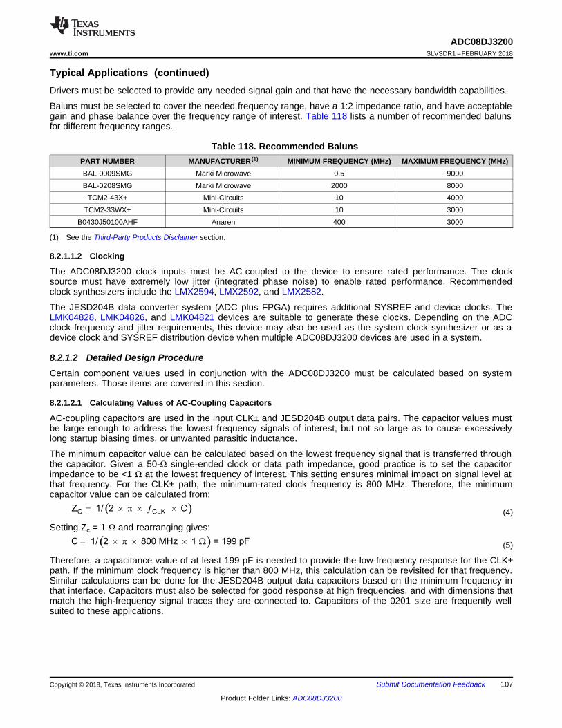
( )C 1/ 2 800 MHz 1 = 1 pF99´= ´ p ´ W
( )LC C KZ 1/ 2 C= ´ ´ ´p ¦
107
ADC08DJ3200www.ti.com SLVSDR1 –FEBRUARY 2018
Product Folder Links: ADC08DJ3200
Submit Documentation FeedbackCopyright © 2018, Texas Instruments Incorporated
Typical Applications (continued)
(1) See the Third-Party Products Disclaimer section.
Drivers must be selected to provide any needed signal gain and that have the necessary bandwidth capabilities.
Baluns must be selected to cover the needed frequency range, have a 1:2 impedance ratio, and have acceptablegain and phase balance over the frequency range of interest. Table 118 lists a number of recommended balunsfor different frequency ranges.
Table 118. Recommended BalunsPART NUMBER MANUFACTURER (1) MINIMUM FREQUENCY (MHz) MAXIMUM FREQUENCY (MHz)BAL-0009SMG Marki Microwave 0.5 9000BAL-0208SMG Marki Microwave 2000 8000
TCM2-43X+ Mini-Circuits 10 4000TCM2-33WX+ Mini-Circuits 10 3000
B0430J50100AHF Anaren 400 3000
8.2.1.1.2 Clocking
The ADC08DJ3200 clock inputs must be AC-coupled to the device to ensure rated performance. The clocksource must have extremely low jitter (integrated phase noise) to enable rated performance. Recommendedclock synthesizers include the LMX2594, LMX2592, and LMX2582.
The JESD204B data converter system (ADC plus FPGA) requires additional SYSREF and device clocks. TheLMK04828, LMK04826, and LMK04821 devices are suitable to generate these clocks. Depending on the ADCclock frequency and jitter requirements, this device may also be used as the system clock synthesizer or as adevice clock and SYSREF distribution device when multiple ADC08DJ3200 devices are used in a system.
8.2.1.2 Detailed Design ProcedureCertain component values used in conjunction with the ADC08DJ3200 must be calculated based on systemparameters. Those items are covered in this section.
8.2.1.2.1 Calculating Values of AC-Coupling Capacitors
AC-coupling capacitors are used in the input CLK± and JESD204B output data pairs. The capacitor values mustbe large enough to address the lowest frequency signals of interest, but not so large as to cause excessivelylong startup biasing times, or unwanted parasitic inductance.
The minimum capacitor value can be calculated based on the lowest frequency signal that is transferred throughthe capacitor. Given a 50-Ω single-ended clock or data path impedance, good practice is to set the capacitorimpedance to be <1 Ω at the lowest frequency of interest. This setting ensures minimal impact on signal level atthat frequency. For the CLK± path, the minimum-rated clock frequency is 800 MHz. Therefore, the minimumcapacitor value can be calculated from:
(4)
Setting Zc = 1 Ω and rearranging gives:
(5)
Therefore, a capacitance value of at least 199 pF is needed to provide the low-frequency response for the CLK±path. If the minimum clock frequency is higher than 800 MHz, this calculation can be revisited for that frequency.Similar calculations can be done for the JESD204B output data capacitors based on the minimum frequency inthat interface. Capacitors must also be selected for good response at high frequencies, and with dimensions thatmatch the high-frequency signal traces they are connected to. Capacitors of the 0201 size are frequently wellsuited to these applications.
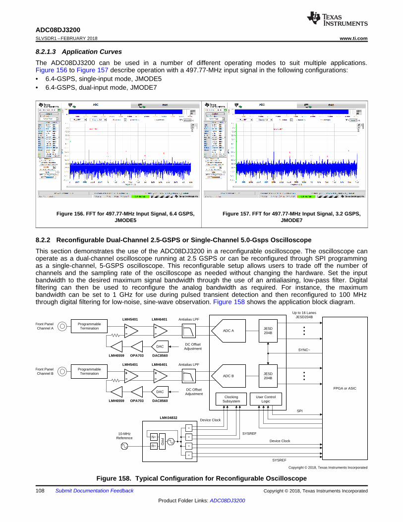
ADC A
ADC B
Clocking Subsystem
User Control Logic
JESD204B
JESD204B
FPGA or ASIC
Up to 16 Lanes JESD204B
SYNC~
÷
Device Clock
SYSREF
Device Clock
SYSREF
SPI
R÷
N÷ PF
D
÷
÷
10-MHz Reference
LMH6401LMH5401
LMK04832
DAC8560
DAC
OPA703LMH6559
Antialias LPFLMH6401LMH5401
DAC8560
DAC
OPA703LMH6559
DC Offset Adjustment
DC Offset Adjustment
Antialias LPFFront Panel Channel A
Programmable Termination
÷
Front Panel Channel B
Programmable Termination
Copyright © 2018, Texas Instruments Incorporated
108
ADC08DJ3200SLVSDR1 –FEBRUARY 2018 www.ti.com
Product Folder Links: ADC08DJ3200
Submit Documentation Feedback Copyright © 2018, Texas Instruments Incorporated
8.2.1.3 Application CurvesThe ADC08DJ3200 can be used in a number of different operating modes to suit multiple applications.Figure 156 to Figure 157 describe operation with a 497.77-MHz input signal in the following configurations:• 6.4-GSPS, single-input mode, JMODE5• 6.4-GSPS, dual-input mode, JMODE7
Figure 156. FFT for 497.77-MHz Input Signal, 6.4 GSPS,JMODE5
Figure 157. FFT for 497.77-MHz Input Signal, 3.2 GSPS,JMODE7
8.2.2 Reconfigurable Dual-Channel 2.5-GSPS or Single-Channel 5.0-Gsps OscilloscopeThis section demonstrates the use of the ADC08DJ3200 in a reconfigurable oscilloscope. The oscilloscope canoperate as a dual-channel oscilloscope running at 2.5 GSPS or can be reconfigured through SPI programmingas a single-channel, 5-GSPS oscilloscope. This reconfigurable setup allows users to trade off the number ofchannels and the sampling rate of the oscilloscope as needed without changing the hardware. Set the inputbandwidth to the desired maximum signal bandwidth through the use of an antialiasing, low-pass filter. Digitalfiltering can then be used to reconfigure the analog bandwidth as required. For instance, the maximumbandwidth can be set to 1 GHz for use during pulsed transient detection and then reconfigured to 100 MHzthrough digital filtering for low-noise, sine-wave observation. Figure 158 shows the application block diagram.
Figure 158. Typical Configuration for Reconfigurable Oscilloscope
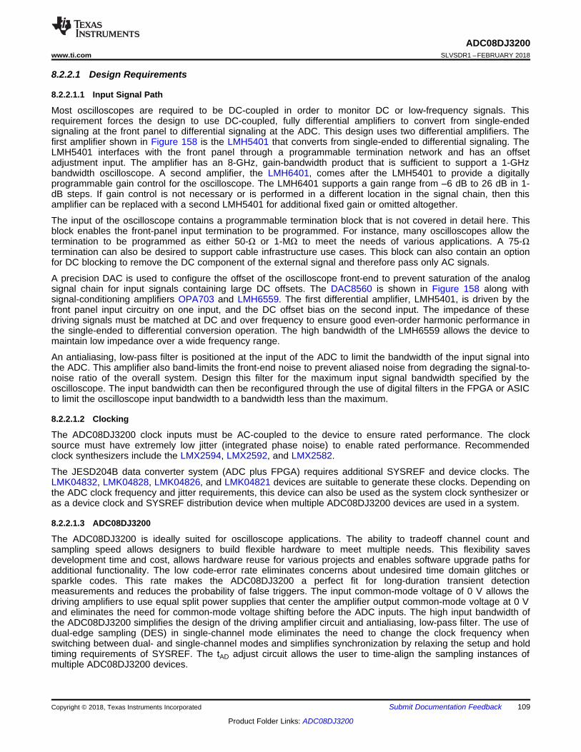
109
ADC08DJ3200www.ti.com SLVSDR1 –FEBRUARY 2018
Product Folder Links: ADC08DJ3200
Submit Documentation FeedbackCopyright © 2018, Texas Instruments Incorporated
8.2.2.1 Design Requirements
8.2.2.1.1 Input Signal Path
Most oscilloscopes are required to be DC-coupled in order to monitor DC or low-frequency signals. Thisrequirement forces the design to use DC-coupled, fully differential amplifiers to convert from single-endedsignaling at the front panel to differential signaling at the ADC. This design uses two differential amplifiers. Thefirst amplifier shown in Figure 158 is the LMH5401 that converts from single-ended to differential signaling. TheLMH5401 interfaces with the front panel through a programmable termination network and has an offsetadjustment input. The amplifier has an 8-GHz, gain-bandwidth product that is sufficient to support a 1-GHzbandwidth oscilloscope. A second amplifier, the LMH6401, comes after the LMH5401 to provide a digitallyprogrammable gain control for the oscilloscope. The LMH6401 supports a gain range from –6 dB to 26 dB in 1-dB steps. If gain control is not necessary or is performed in a different location in the signal chain, then thisamplifier can be replaced with a second LMH5401 for additional fixed gain or omitted altogether.
The input of the oscilloscope contains a programmable termination block that is not covered in detail here. Thisblock enables the front-panel input termination to be programmed. For instance, many oscilloscopes allow thetermination to be programmed as either 50-Ω or 1-MΩ to meet the needs of various applications. A 75-Ωtermination can also be desired to support cable infrastructure use cases. This block can also contain an optionfor DC blocking to remove the DC component of the external signal and therefore pass only AC signals.
A precision DAC is used to configure the offset of the oscilloscope front-end to prevent saturation of the analogsignal chain for input signals containing large DC offsets. The DAC8560 is shown in Figure 158 along withsignal-conditioning amplifiers OPA703 and LMH6559. The first differential amplifier, LMH5401, is driven by thefront panel input circuitry on one input, and the DC offset bias on the second input. The impedance of thesedriving signals must be matched at DC and over frequency to ensure good even-order harmonic performance inthe single-ended to differential conversion operation. The high bandwidth of the LMH6559 allows the device tomaintain low impedance over a wide frequency range.
An antialiasing, low-pass filter is positioned at the input of the ADC to limit the bandwidth of the input signal intothe ADC. This amplifier also band-limits the front-end noise to prevent aliased noise from degrading the signal-to-noise ratio of the overall system. Design this filter for the maximum input signal bandwidth specified by theoscilloscope. The input bandwidth can then be reconfigured through the use of digital filters in the FPGA or ASICto limit the oscilloscope input bandwidth to a bandwidth less than the maximum.
8.2.2.1.2 Clocking
The ADC08DJ3200 clock inputs must be AC-coupled to the device to ensure rated performance. The clocksource must have extremely low jitter (integrated phase noise) to enable rated performance. Recommendedclock synthesizers include the LMX2594, LMX2592, and LMX2582.
The JESD204B data converter system (ADC plus FPGA) requires additional SYSREF and device clocks. TheLMK04832, LMK04828, LMK04826, and LMK04821 devices are suitable to generate these clocks. Depending onthe ADC clock frequency and jitter requirements, this device can also be used as the system clock synthesizer oras a device clock and SYSREF distribution device when multiple ADC08DJ3200 devices are used in a system.
8.2.2.1.3 ADC08DJ3200
The ADC08DJ3200 is ideally suited for oscilloscope applications. The ability to tradeoff channel count andsampling speed allows designers to build flexible hardware to meet multiple needs. This flexibility savesdevelopment time and cost, allows hardware reuse for various projects and enables software upgrade paths foradditional functionality. The low code-error rate eliminates concerns about undesired time domain glitches orsparkle codes. This rate makes the ADC08DJ3200 a perfect fit for long-duration transient detectionmeasurements and reduces the probability of false triggers. The input common-mode voltage of 0 V allows thedriving amplifiers to use equal split power supplies that center the amplifier output common-mode voltage at 0 Vand eliminates the need for common-mode voltage shifting before the ADC inputs. The high input bandwidth ofthe ADC08DJ3200 simplifies the design of the driving amplifier circuit and antialiasing, low-pass filter. The use ofdual-edge sampling (DES) in single-channel mode eliminates the need to change the clock frequency whenswitching between dual- and single-channel modes and simplifies synchronization by relaxing the setup and holdtiming requirements of SYSREF. The tAD adjust circuit allows the user to time-align the sampling instances ofmultiple ADC08DJ3200 devices.
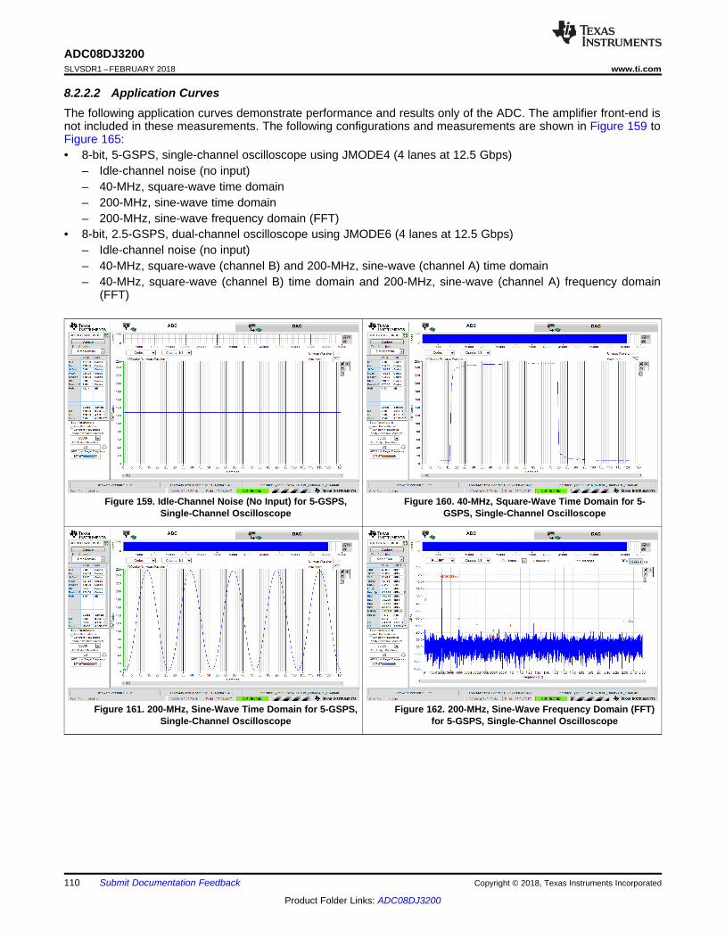
110
ADC08DJ3200SLVSDR1 –FEBRUARY 2018 www.ti.com
Product Folder Links: ADC08DJ3200
Submit Documentation Feedback Copyright © 2018, Texas Instruments Incorporated
8.2.2.2 Application CurvesThe following application curves demonstrate performance and results only of the ADC. The amplifier front-end isnot included in these measurements. The following configurations and measurements are shown in Figure 159 toFigure 165:• 8-bit, 5-GSPS, single-channel oscilloscope using JMODE4 (4 lanes at 12.5 Gbps)
– Idle-channel noise (no input)– 40-MHz, square-wave time domain– 200-MHz, sine-wave time domain– 200-MHz, sine-wave frequency domain (FFT)
• 8-bit, 2.5-GSPS, dual-channel oscilloscope using JMODE6 (4 lanes at 12.5 Gbps)– Idle-channel noise (no input)– 40-MHz, square-wave (channel B) and 200-MHz, sine-wave (channel A) time domain– 40-MHz, square-wave (channel B) time domain and 200-MHz, sine-wave (channel A) frequency domain
(FFT)
Figure 159. Idle-Channel Noise (No Input) for 5-GSPS,Single-Channel Oscilloscope
Figure 160. 40-MHz, Square-Wave Time Domain for 5-GSPS, Single-Channel Oscilloscope
Figure 161. 200-MHz, Sine-Wave Time Domain for 5-GSPS,Single-Channel Oscilloscope
Figure 162. 200-MHz, Sine-Wave Frequency Domain (FFT)for 5-GSPS, Single-Channel Oscilloscope
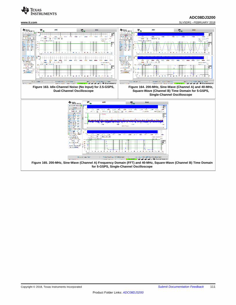
111
ADC08DJ3200www.ti.com SLVSDR1 –FEBRUARY 2018
Product Folder Links: ADC08DJ3200
Submit Documentation FeedbackCopyright © 2018, Texas Instruments Incorporated
Figure 163. Idle-Channel Noise (No Input) for 2.5-GSPS,Dual-Channel Oscilloscope
Figure 164. 200-MHz, Sine-Wave (Channel A) and 40-MHz,Square-Wave (Channel B) Time Domain for 5-GSPS,
Single-Channel Oscilloscope
Figure 165. 200-MHz, Sine-Wave (Channel A) Frequency Domain (FFT) and 40-MHz, Square-Wave (Channel B) Time Domainfor 5-GSPS, Single-Channel Oscilloscope
112
ADC08DJ3200SLVSDR1 –FEBRUARY 2018 www.ti.com
Product Folder Links: ADC08DJ3200
Submit Documentation Feedback Copyright © 2018, Texas Instruments Incorporated
8.3 Initialization Set UpThe device and JESD204 interface require a specific startup and alignment sequence. The general order of thatsequence is listed in the following steps.1. Power-up or reset the device.2. Apply a stable device CLK signal at the desired frequency.3. Program JESD_EN = 0 to stop the JESD204B state machine and allow setting changes.4. Program CAL_EN = 0 to stop the calibration state machine and allow setting changes.5. Program the desired JMODE.6. Program the desired KM1 value. KM1 = K–1.7. Program SYNC_SEL as needed. Choose SYNCSE or timestamp differential inputs.8. Configure device calibration settings as desired. Select foreground or background calibration modes and
offset calibration as needed.9. Program CAL_EN = 1 to enable the calibration state machine.10. Enable overrange via OVR_EN and adjust settings if desired.11. Program JESD_EN = 1 to re-start the JESD204B state machine and allow the link to restart.12. The JESD204B interface operates in response to the applied SYNC signal from the receiver.13. Program CAL_SOFT_TRIG = 0.14. Program CAL_SOFT_TRIG = 1 to initiate a calibration.
9 Power Supply RecommendationsThe device requires two different power-supply voltages. 1.9 V DC is required for the VA19 power bus and 1.1 VDC is required for the VA11 and VD11 power buses.
The power-supply voltages must be low noise and provide the needed current to achieve rated deviceperformance.
There are two recommended power supply architectures:1. Step down using high-efficiency switching converters, followed by a second stage of regulation to provide
switching noise reduction and improved voltage accuracy.2. Directly step down the final ADC supply voltage using high-efficiency switching converters. This approach
provides the best efficiency, but care must be taken to ensure switching noise is minimized to preventdegraded ADC performance.
TI WEBENCH® Power Designer can be used to select and design the individual power supply elements needed:see the WEBENCH® Power Designer
Recommended switching regulators for the first stage include the TPS62085, TPS82130, TPS62130A, andsimilar devices.
Recommended Low Drop-Out (LDO) linear regulators include the TPS7A7200, TPS74401, and similar devices.
For the switcher only approach, the ripple filter must be designed with a notch frequency that aligns with theswitching ripple frequency of the DC-DC converter. Make a note of the switching frequency reported fromWEBENCH® and design the EMI filter and capacitor combination to have the notch frequency centered asneeded. Figure 166 and Figure 167 illustrate the two approaches.
Ripple Filter
Ripple Filter
Buck10 �F 0.1 �F 0.1 �F
GND
+±
GND
5 V - 12 VVA19
Buck10 �F 0.1 �F 0.1 �F
GND
VA11
10 �F 0.1 �F 0.1 �F
GND
VD11
FB
FB
FB
Copyright © 2018, Texas Instruments Incorporated
10 �F 10 �F 10 �F
GND
FB
10 �F 10 �F 10 �F
GND
FB
PowerGood
1.9 V
1.1 V
Buck LDO47 �F 47 �F 10 �F 0.1 �F 0.1 �F
GND GND GND
+±
GND
5 V - 12 V2.2 V VA19
Buck LDO47 �F 47 �F 10 �F 0.1 �F 0.1 �F
GND GND GND
1.4 V VA11
10 �F 0.1 �F 0.1 �F
GND
VD11
1.9 V
1.1 V
FB
FB FB
FB
FB
Power Good
Copyright © 2018, Texas Instruments Incorporated
113
ADC08DJ3200www.ti.com SLVSDR1 –FEBRUARY 2018
Product Folder Links: ADC08DJ3200
Submit Documentation FeedbackCopyright © 2018, Texas Instruments Incorporated
NOTE: FB = ferrite bead filter.
Figure 166. LDO Linear Regulator Approach Example
NOTE: Ripple filter notch frequency to match the fs of the buck converter.NOTE: FB = ferrite bead filter.
Figure 167. Switcher-Only Approach Example
114
ADC08DJ3200SLVSDR1 –FEBRUARY 2018 www.ti.com
Product Folder Links: ADC08DJ3200
Submit Documentation Feedback Copyright © 2018, Texas Instruments Incorporated
9.1 Power SequencingThe voltage regulators must be sequenced using the power-good outputs and enable inputs to ensure that theVx11 regulator is enabled after the VA19 supply is good. Similarly, as soon as the VA19 supply drops out ofregulation on power-down, the Vx11 regulator is disabled.
The general requirement for the ADC is that VA19 ≥ Vx11 during power-up, operation, and power-down.
TI also recommends that VA11 and VD11 are derived from a common 1.1-V regulator. This recommendationensures that all 1.1-V blocks are at the same voltage, and no sequencing problems exist between these supplies.Also use ferrite bead filters to isolate any noise on the VA11 and VD11 buses from affecting each other.
10 Layout
10.1 Layout GuidelinesThere are many critical signals that require specific care during board design:1. Analog input signals2. CLK and SYSREF3. JESD204B data outputs:
1. Lower eight pairs operating at up to 12.8 Gbit per second2. Upper eight pairs operating at up to 6.4 Gbit per second
4. Power connections5. Ground connections
Items 1, 2, and 3 must be routed for excellent signal quality at high frequencies. Use the following generalpractices:1. Route using loosely coupled 100-Ω differential traces. This routing minimizes impact of corners and length-
matching serpentines on pair impedance.2. Provide adequate pair-to-pair spacing to minimize crosstalk.3. Provide adequate ground plane pour spacing to minimize coupling with the high-speed traces.4. Use smoothly radiused corners. Avoid 45- or 90-degree bends.5. Incorporate ground plane cutouts at component landing pads to avoid impedance discontinuities at these
locations. Cut-out below the landing pads on one or multiple ground planes to achieve a pad size or stackupheight that achieves the needed 50-Ω, single-ended impedance.
6. Avoid routing traces near irregularities in the reference ground planes. Irregularities include ground planeclearances associated with power and signal vias and through-hole component leads.
7. Provide symmetrically located ground tie vias adjacent to any high-speed signal vias.8. When high-speed signals must transition to another layer using vias, transition as far through the board as
possible (top to bottom is best case) to minimize via stubs on top or bottom of the vias. If layer selection isnot flexible, use back-drilled or buried, blind vias to eliminate stubs.
In addition, TI recommends performing signal quality simulations of the critical signal traces before committing tofabrication. Insertion loss, return loss, and time domain reflectometry (TDR) evaluations should be done.
The power and ground connections for the device are also very important. These rules must be followed:1. Provide low-resistance connection paths to all power and ground pins.2. Use multiple power layers if necessary to access all pins.3. Avoid narrow isolated paths that increase connection resistance.4. Use a signal, ground, or power circuit board stackup to maximum coupling between the ground and power
planes.
115
ADC08DJ3200www.ti.com SLVSDR1 –FEBRUARY 2018
Product Folder Links: ADC08DJ3200
Submit Documentation FeedbackCopyright © 2018, Texas Instruments Incorporated
10.2 Layout ExampleFigure 168 to Figure 170 provide examples of the critical traces routed on the device evaluation module (EVM).
Figure 168. Top Layer Routing: Analog Inputs, CLK and SYSREF, DA0-3, DB0-3
116
ADC08DJ3200SLVSDR1 –FEBRUARY 2018 www.ti.com
Product Folder Links: ADC08DJ3200
Submit Documentation Feedback Copyright © 2018, Texas Instruments Incorporated
Layout Example (continued)
Figure 169. GND1 Cutouts to Optimize Impedance of Component Pads
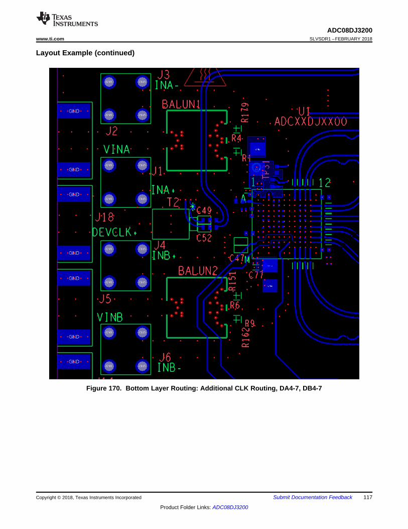
117
ADC08DJ3200www.ti.com SLVSDR1 –FEBRUARY 2018
Product Folder Links: ADC08DJ3200
Submit Documentation FeedbackCopyright © 2018, Texas Instruments Incorporated
Layout Example (continued)
Figure 170. Bottom Layer Routing: Additional CLK Routing, DA4-7, DB4-7
118
ADC08DJ3200SLVSDR1 –FEBRUARY 2018 www.ti.com
Product Folder Links: ADC08DJ3200
Submit Documentation Feedback Copyright © 2018, Texas Instruments Incorporated
11 Device and Documentation Support
11.1 Device Support
11.1.1 Third-Party Products DisclaimerTI'S PUBLICATION OF INFORMATION REGARDING THIRD-PARTY PRODUCTS OR SERVICES DOES NOTCONSTITUTE AN ENDORSEMENT REGARDING THE SUITABILITY OF SUCH PRODUCTS OR SERVICESOR A WARRANTY, REPRESENTATION OR ENDORSEMENT OF SUCH PRODUCTS OR SERVICES, EITHERALONE OR IN COMBINATION WITH ANY TI PRODUCT OR SERVICE.
11.1.2 Development SupportWEBENCH® Power Designer
11.2 Documentation Support
11.2.1 Related DocumentationFor related documentation see the following:• JESD204B multi-device synchronization: Breaking down the requirements• LM95233 Dual Remote Diode and Local Temperature Sensor with SMBus Interface and TruTherm™
Technology• LMX2594 15-GHz Wideband PLLatinum™ RF Synthesizer With Phase Synchronization and JESD204B
Support• LMX2592 High Performance, Wideband PLLatinum™ RF Synthesizer With Integrated VCO• LMX2582 High Performance, Wideband PLLatinum™ RF Synthesizer With Integrated VCO• LMK0482x Ultra Low-Noise JESD204B Compliant Clock Jitter Cleaner with Dual Loop PLLs• TPS6208x 3-A Step-Down Converter With Hiccup Short-Circuit Protection In 2 × 2 QFN Package• TPS82130 17-V Input 3-A Step-Down Converter MicroSiP™ Module with Integrated Inductor• TPS6213x 3-V to17-V, 3-A Step-Down Converter In 3x3 QFN Package• TPS7A7200 2-A, Fast-Transient, Low-Dropout Voltage Regulator• TPS74401 3.0-A, Ultra-LDO with Programmable Soft-Start• Direct RF-Sampling Radar Receiver for L-, S-, C-, and X-Band Using ADC12DJ3200 Reference Design• ADC12DJ2700 Evaluation Module User's Guide• Multi-Channel JESD204B 15 GHz Clocking Reference Design for DSO, Radar and 5G Wireless Testers• LMH5401 8-GHz, Low-Noise, Low-Power, Fully-Differential Amplifier• LMH6401 DC to 4.5 GHz, Fully-Differential, Digital Variable-Gain Amplifier• DAC8560 16-Bit, Ultra-Low Glitch, Voltage Output Digital-to-Analog Converter With 2.5-V, 2-ppm/°C Internal
Reference• OPA70x CMOS, Rail-to-Rail, I/O Operational Amplifiers• LMH6559 High-Speed, Closed-Loop Buffer• LMK04832 Ultra Low-Noise JESD204B Compliant Clock Jitter Cleaner With Dual Loop PLLs
11.3 Receiving Notification of Documentation UpdatesTo receive notification of documentation updates, navigate to the device product folder on ti.com. In the upperright corner, click on Alert me to register and receive a weekly digest of any product information that haschanged. For change details, review the revision history included in any revised document.
119
ADC08DJ3200www.ti.com SLVSDR1 –FEBRUARY 2018
Product Folder Links: ADC08DJ3200
Submit Documentation FeedbackCopyright © 2018, Texas Instruments Incorporated
11.4 Community ResourcesThe following links connect to TI community resources. Linked contents are provided "AS IS" by the respectivecontributors. They do not constitute TI specifications and do not necessarily reflect TI's views; see TI's Terms ofUse.
TI E2E™ Online Community TI's Engineer-to-Engineer (E2E) Community. Created to foster collaborationamong engineers. At e2e.ti.com, you can ask questions, share knowledge, explore ideas and helpsolve problems with fellow engineers.
Design Support TI's Design Support Quickly find helpful E2E forums along with design support tools andcontact information for technical support.
11.5 TrademarksE2E is a trademark of Texas Instruments.WEBENCH is a registered trademark of Texas Instruments.All other trademarks are the property of their respective owners.
11.6 Electrostatic Discharge CautionThese devices have limited built-in ESD protection. The leads should be shorted together or the device placed in conductive foamduring storage or handling to prevent electrostatic damage to the MOS gates.
11.7 GlossarySLYZ022 — TI Glossary.
This glossary lists and explains terms, acronyms, and definitions.
12 Mechanical, Packaging, and Orderable InformationThe following pages include mechanical, packaging, and orderable information. This information is the mostcurrent data available for the designated devices. This data is subject to change without notice and revision ofthis document. For browser-based versions of this data sheet, refer to the left-hand navigation.
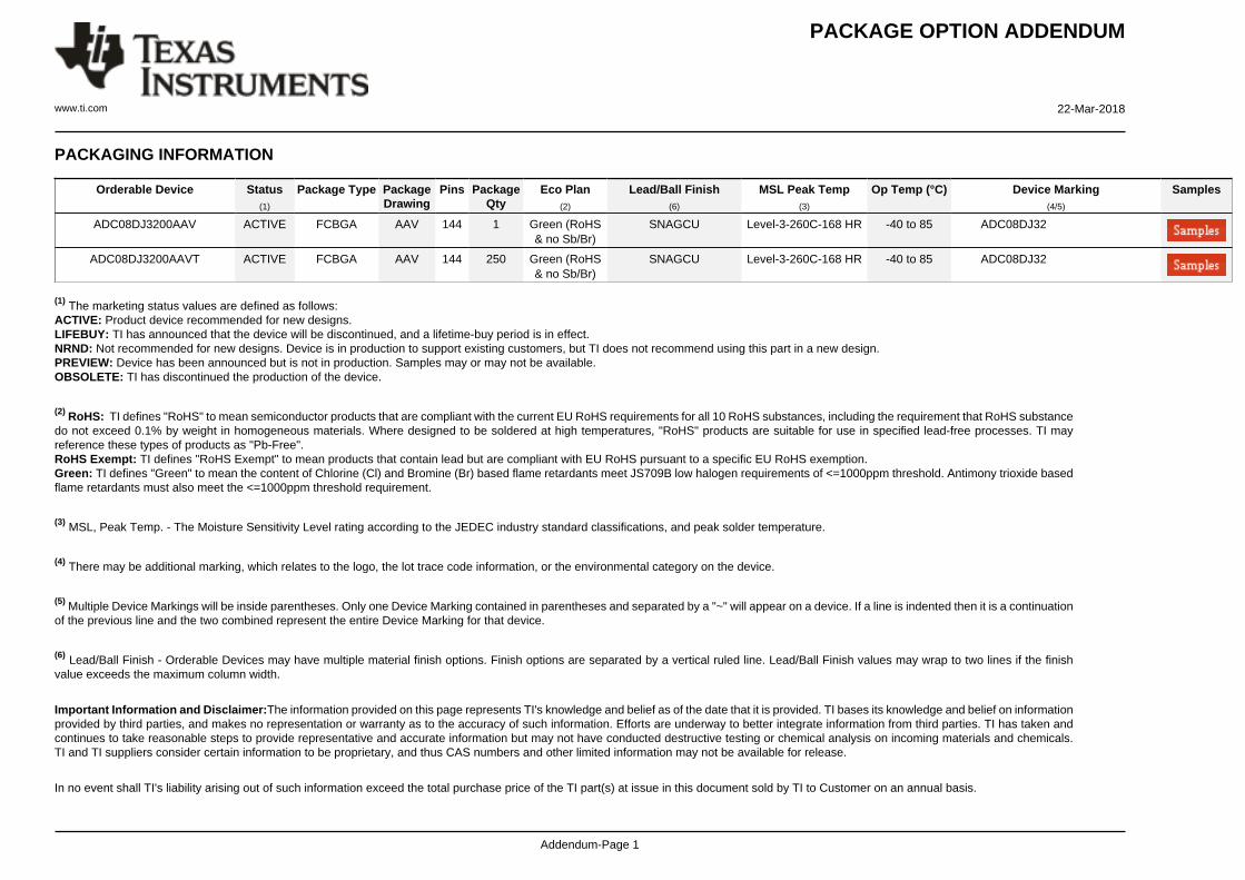
PACKAGE OPTION ADDENDUM
www.ti.com 22-Mar-2018
Addendum-Page 1
PACKAGING INFORMATION
Orderable Device Status(1)
Package Type PackageDrawing
Pins PackageQty
Eco Plan(2)
Lead/Ball Finish(6)
MSL Peak Temp(3)
Op Temp (°C) Device Marking(4/5)
Samples
ADC08DJ3200AAV ACTIVE FCBGA AAV 144 1 Green (RoHS& no Sb/Br)
SNAGCU Level-3-260C-168 HR -40 to 85 ADC08DJ32
ADC08DJ3200AAVT ACTIVE FCBGA AAV 144 250 Green (RoHS& no Sb/Br)
SNAGCU Level-3-260C-168 HR -40 to 85 ADC08DJ32
(1) The marketing status values are defined as follows:ACTIVE: Product device recommended for new designs.LIFEBUY: TI has announced that the device will be discontinued, and a lifetime-buy period is in effect.NRND: Not recommended for new designs. Device is in production to support existing customers, but TI does not recommend using this part in a new design.PREVIEW: Device has been announced but is not in production. Samples may or may not be available.OBSOLETE: TI has discontinued the production of the device.
(2) RoHS: TI defines "RoHS" to mean semiconductor products that are compliant with the current EU RoHS requirements for all 10 RoHS substances, including the requirement that RoHS substancedo not exceed 0.1% by weight in homogeneous materials. Where designed to be soldered at high temperatures, "RoHS" products are suitable for use in specified lead-free processes. TI mayreference these types of products as "Pb-Free".RoHS Exempt: TI defines "RoHS Exempt" to mean products that contain lead but are compliant with EU RoHS pursuant to a specific EU RoHS exemption.Green: TI defines "Green" to mean the content of Chlorine (Cl) and Bromine (Br) based flame retardants meet JS709B low halogen requirements of <=1000ppm threshold. Antimony trioxide basedflame retardants must also meet the <=1000ppm threshold requirement.
(3) MSL, Peak Temp. - The Moisture Sensitivity Level rating according to the JEDEC industry standard classifications, and peak solder temperature.
(4) There may be additional marking, which relates to the logo, the lot trace code information, or the environmental category on the device.
(5) Multiple Device Markings will be inside parentheses. Only one Device Marking contained in parentheses and separated by a "~" will appear on a device. If a line is indented then it is a continuationof the previous line and the two combined represent the entire Device Marking for that device.
(6) Lead/Ball Finish - Orderable Devices may have multiple material finish options. Finish options are separated by a vertical ruled line. Lead/Ball Finish values may wrap to two lines if the finishvalue exceeds the maximum column width.
Important Information and Disclaimer:The information provided on this page represents TI's knowledge and belief as of the date that it is provided. TI bases its knowledge and belief on informationprovided by third parties, and makes no representation or warranty as to the accuracy of such information. Efforts are underway to better integrate information from third parties. TI has taken andcontinues to take reasonable steps to provide representative and accurate information but may not have conducted destructive testing or chemical analysis on incoming materials and chemicals.TI and TI suppliers consider certain information to be proprietary, and thus CAS numbers and other limited information may not be available for release.
In no event shall TI's liability arising out of such information exceed the total purchase price of the TI part(s) at issue in this document sold by TI to Customer on an annual basis.

PACKAGE OPTION ADDENDUM
www.ti.com 22-Mar-2018
Addendum-Page 2
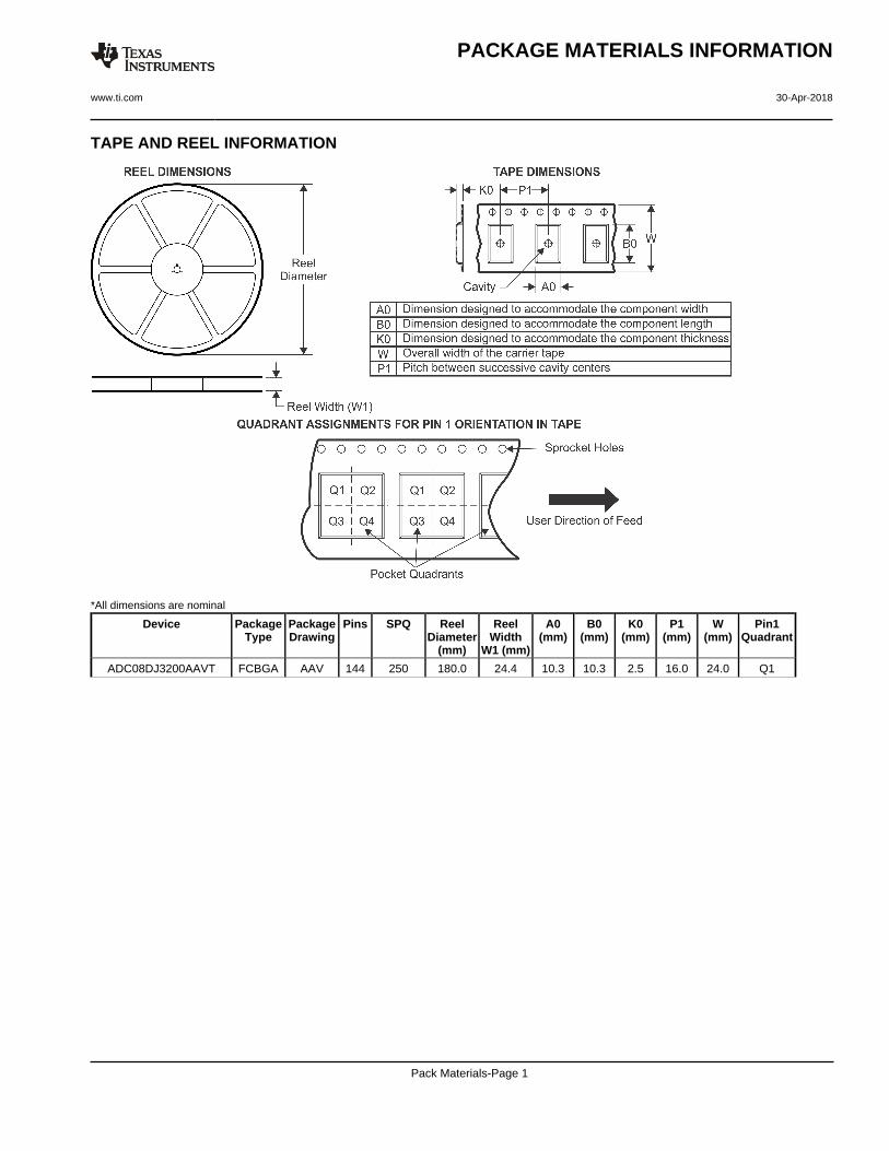
TAPE AND REEL INFORMATION
*All dimensions are nominal
Device PackageType
PackageDrawing
Pins SPQ ReelDiameter
(mm)
ReelWidth
W1 (mm)
A0(mm)
B0(mm)
K0(mm)
P1(mm)
W(mm)
Pin1Quadrant
ADC08DJ3200AAVT FCBGA AAV 144 250 180.0 24.4 10.3 10.3 2.5 16.0 24.0 Q1
PACKAGE MATERIALS INFORMATION
www.ti.com 30-Apr-2018
Pack Materials-Page 1

*All dimensions are nominal
Device Package Type Package Drawing Pins SPQ Length (mm) Width (mm) Height (mm)
ADC08DJ3200AAVT FCBGA AAV 144 250 213.0 191.0 55.0
PACKAGE MATERIALS INFORMATION
www.ti.com 30-Apr-2018
Pack Materials-Page 2
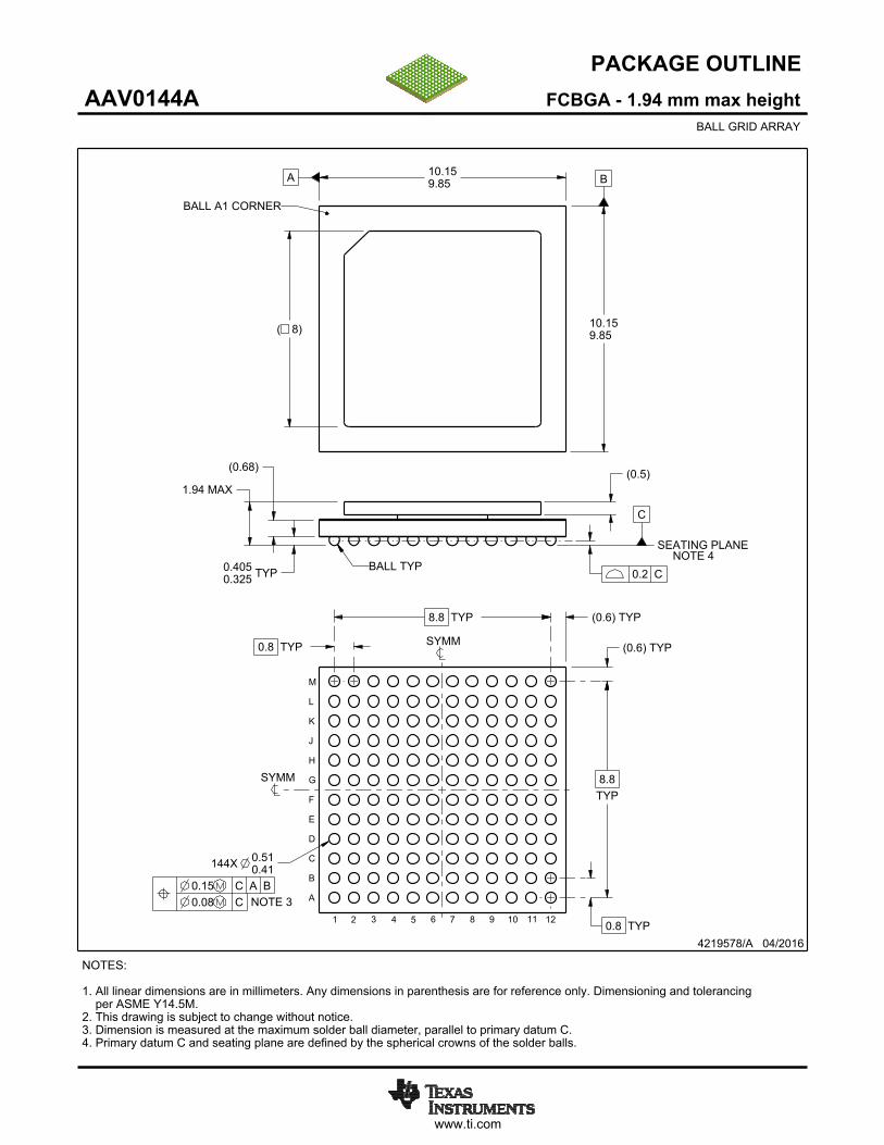
www.ti.com
PACKAGE OUTLINE
C
1.94 MAX
TYP0.4050.325
8.8TYP
8.8 TYP
0.8 TYP
0.8 TYP
144X 0.510.41
(0.68)
A 10.159.85 B
10.159.85
(0.6) TYP
( 8)
(0.5)
(0.6) TYP
FCBGA - 1.94 mm max heightAAV0144ABALL GRID ARRAY
4219578/A 04/2016
NOTES: 1. All linear dimensions are in millimeters. Any dimensions in parenthesis are for reference only. Dimensioning and tolerancing per ASME Y14.5M. 2. This drawing is subject to change without notice.3. Dimension is measured at the maximum solder ball diameter, parallel to primary datum C.4. Primary datum C and seating plane are defined by the spherical crowns of the solder balls.
BALL A1 CORNER
SEATING PLANE
BALL TYP0.2 C
NOTE 4
M
L
K
J
H
G
F
E
D
C
B
A
1 2 3
0.15 C A B0.08 C
SYMM
SYMM
4
NOTE 35 6 7 8 9 10 11 12
SCALE 1.400
www.ti.com
EXAMPLE BOARD LAYOUT
144X ( )0.4
(0.8) TYP
(0.8) TYP
( )METAL
0.4 0.05 MAX
SOLDER MASKOPENING
METAL UNDERSOLDER MASK
( )SOLDER MASKOPENING
0.4
0.05 MIN
FCBGA - 1.94 mm max heightAAV0144ABALL GRID ARRAY
4219578/A 04/2016
NOTES: (continued) 5. Final dimensions may vary due to manufacturing tolerance considerations and also routing constraints. For more information, see Texas Instruments literature number SPRU811 (www.ti.com/lit/spru811).
SYMM
SYMM
LAND PATTERN EXAMPLESCALE:8X
1A
B
C
D
E
F
G
H
J
K
L
M
2 3 4 5 6 7 8 9 10 11 12
NON-SOLDER MASKDEFINED
(PREFERRED)
SOLDER MASK DETAILSNOT TO SCALE
SOLDER MASKDEFINED
www.ti.com
EXAMPLE STENCIL DESIGN
(0.8)TYP
(0.8) TYP 144X ( )0.4
FCBGA - 1.94 mm max heightAAV0144ABALL GRID ARRAY
4219578/A 04/2016
NOTES: (continued) 6. Laser cutting apertures with trapezoidal walls and rounded corners may offer better paste release.
SOLDER PASTE EXAMPLEBASED ON 0.15 mm THICK STENCIL
SCALE:8X
SYMM
SYMM
1A
B
C
D
E
F
G
H
J
K
L
M
2 3 4 5 6 7 8 9 10 11 12

IMPORTANT NOTICE
Texas Instruments Incorporated (TI) reserves the right to make corrections, enhancements, improvements and other changes to itssemiconductor products and services per JESD46, latest issue, and to discontinue any product or service per JESD48, latest issue. Buyersshould obtain the latest relevant information before placing orders and should verify that such information is current and complete.TI’s published terms of sale for semiconductor products (http://www.ti.com/sc/docs/stdterms.htm) apply to the sale of packaged integratedcircuit products that TI has qualified and released to market. Additional terms may apply to the use or sale of other types of TI products andservices.Reproduction of significant portions of TI information in TI data sheets is permissible only if reproduction is without alteration and isaccompanied by all associated warranties, conditions, limitations, and notices. TI is not responsible or liable for such reproduceddocumentation. Information of third parties may be subject to additional restrictions. Resale of TI products or services with statementsdifferent from or beyond the parameters stated by TI for that product or service voids all express and any implied warranties for theassociated TI product or service and is an unfair and deceptive business practice. TI is not responsible or liable for any such statements.Buyers and others who are developing systems that incorporate TI products (collectively, “Designers”) understand and agree that Designersremain responsible for using their independent analysis, evaluation and judgment in designing their applications and that Designers havefull and exclusive responsibility to assure the safety of Designers' applications and compliance of their applications (and of all TI productsused in or for Designers’ applications) with all applicable regulations, laws and other applicable requirements. Designer represents that, withrespect to their applications, Designer has all the necessary expertise to create and implement safeguards that (1) anticipate dangerousconsequences of failures, (2) monitor failures and their consequences, and (3) lessen the likelihood of failures that might cause harm andtake appropriate actions. Designer agrees that prior to using or distributing any applications that include TI products, Designer willthoroughly test such applications and the functionality of such TI products as used in such applications.TI’s provision of technical, application or other design advice, quality characterization, reliability data or other services or information,including, but not limited to, reference designs and materials relating to evaluation modules, (collectively, “TI Resources”) are intended toassist designers who are developing applications that incorporate TI products; by downloading, accessing or using TI Resources in anyway, Designer (individually or, if Designer is acting on behalf of a company, Designer’s company) agrees to use any particular TI Resourcesolely for this purpose and subject to the terms of this Notice.TI’s provision of TI Resources does not expand or otherwise alter TI’s applicable published warranties or warranty disclaimers for TIproducts, and no additional obligations or liabilities arise from TI providing such TI Resources. TI reserves the right to make corrections,enhancements, improvements and other changes to its TI Resources. TI has not conducted any testing other than that specificallydescribed in the published documentation for a particular TI Resource.Designer is authorized to use, copy and modify any individual TI Resource only in connection with the development of applications thatinclude the TI product(s) identified in such TI Resource. NO OTHER LICENSE, EXPRESS OR IMPLIED, BY ESTOPPEL OR OTHERWISETO ANY OTHER TI INTELLECTUAL PROPERTY RIGHT, AND NO LICENSE TO ANY TECHNOLOGY OR INTELLECTUAL PROPERTYRIGHT OF TI OR ANY THIRD PARTY IS GRANTED HEREIN, including but not limited to any patent right, copyright, mask work right, orother intellectual property right relating to any combination, machine, or process in which TI products or services are used. Informationregarding or referencing third-party products or services does not constitute a license to use such products or services, or a warranty orendorsement thereof. Use of TI Resources may require a license from a third party under the patents or other intellectual property of thethird party, or a license from TI under the patents or other intellectual property of TI.TI RESOURCES ARE PROVIDED “AS IS” AND WITH ALL FAULTS. TI DISCLAIMS ALL OTHER WARRANTIES ORREPRESENTATIONS, EXPRESS OR IMPLIED, REGARDING RESOURCES OR USE THEREOF, INCLUDING BUT NOT LIMITED TOACCURACY OR COMPLETENESS, TITLE, ANY EPIDEMIC FAILURE WARRANTY AND ANY IMPLIED WARRANTIES OFMERCHANTABILITY, FITNESS FOR A PARTICULAR PURPOSE, AND NON-INFRINGEMENT OF ANY THIRD PARTY INTELLECTUALPROPERTY RIGHTS. TI SHALL NOT BE LIABLE FOR AND SHALL NOT DEFEND OR INDEMNIFY DESIGNER AGAINST ANY CLAIM,INCLUDING BUT NOT LIMITED TO ANY INFRINGEMENT CLAIM THAT RELATES TO OR IS BASED ON ANY COMBINATION OFPRODUCTS EVEN IF DESCRIBED IN TI RESOURCES OR OTHERWISE. IN NO EVENT SHALL TI BE LIABLE FOR ANY ACTUAL,DIRECT, SPECIAL, COLLATERAL, INDIRECT, PUNITIVE, INCIDENTAL, CONSEQUENTIAL OR EXEMPLARY DAMAGES INCONNECTION WITH OR ARISING OUT OF TI RESOURCES OR USE THEREOF, AND REGARDLESS OF WHETHER TI HAS BEENADVISED OF THE POSSIBILITY OF SUCH DAMAGES.Unless TI has explicitly designated an individual product as meeting the requirements of a particular industry standard (e.g., ISO/TS 16949and ISO 26262), TI is not responsible for any failure to meet such industry standard requirements.Where TI specifically promotes products as facilitating functional safety or as compliant with industry functional safety standards, suchproducts are intended to help enable customers to design and create their own applications that meet applicable functional safety standardsand requirements. Using products in an application does not by itself establish any safety features in the application. Designers mustensure compliance with safety-related requirements and standards applicable to their applications. Designer may not use any TI products inlife-critical medical equipment unless authorized officers of the parties have executed a special contract specifically governing such use.Life-critical medical equipment is medical equipment where failure of such equipment would cause serious bodily injury or death (e.g., lifesupport, pacemakers, defibrillators, heart pumps, neurostimulators, and implantables). Such equipment includes, without limitation, allmedical devices identified by the U.S. Food and Drug Administration as Class III devices and equivalent classifications outside the U.S.TI may expressly designate certain products as completing a particular qualification (e.g., Q100, Military Grade, or Enhanced Product).Designers agree that it has the necessary expertise to select the product with the appropriate qualification designation for their applicationsand that proper product selection is at Designers’ own risk. Designers are solely responsible for compliance with all legal and regulatoryrequirements in connection with such selection.Designer will fully indemnify TI and its representatives against any damages, costs, losses, and/or liabilities arising out of Designer’s non-compliance with the terms and provisions of this Notice.
Mailing Address: Texas Instruments, Post Office Box 655303, Dallas, Texas 75265Copyright © 2018, Texas Instruments Incorporated


![Channel Structure and Function [Compatibility Mode]](https://img.pdfslide.net/doc/110x75/577cc0f01a28aba71191a8b0/channel-structure-and-function-compatibility-mode.jpg)

![Flow in open channel i sem_13_14 [compatibility mode]](https://img.pdfslide.net/doc/110x75/557e6fa9d8b42a03668b480e/flow-in-open-channel-i-sem1314-compatibility-mode.jpg)
