Embed Size (px)
Citation preview
April 2013 Altera Corporation
AN-677
© 2013 Altera Corporation. AlQUARTUS and STRATIX worOffice and in other countries. respective holders as describedproducts to current specificatioproducts and services at any tiof any information, product, oadvised to obtain the latest verfor products or services.
101 Innovation DriveSan Jose, CA 95134www.altera.com
Adding New Design Components to thePROFINET IP
Application Note
This application note shows how you can change the out-of-the-box PROFINET IP design so that it incorporates a UART interface that is implemented through the RS-232 port on the DE2-115 board from Terasic. The DE2-115 board is the main board used in the Industrial Networking Development Kit (INK) also from Terasic. The addition of the UART interface is not particularly complex, but it touches all major portions of the design, including Qsys, Synthesis and FW, and provides a good example of how to modify the delivered IP and add custom logic.
f You can download the related Softing IP from the Altera® Industrial Ethernet page. Ensure that there are no spaces in path name of the install directory you choose.
f For more information on the The DE2-115 board, refer to the Altera DE2-115 Development and Education Board page.
f For more information on the INK board specifications and ordering, refer to the Industrial Networking Kit (INK) page.
This application note assumes that you are familiar with the Quartus II software tool set including Qsys. If not, there are several tutorials on the subject available on the Altera website. You should have some basic HDL coding understanding or at least a general familiarity with an HDL.
This document is organized to describe the steps on how to build the FPGA/FW images for both the unmodified design (without the UART) and for the modified design (adding the UART). The build process for both is nearly identical, but Altera strongly recommends that you run the unmodified design through the flow before making modifications to the design. Because the build steps are so similar, the process is only documented once, but with additional steps added for the modified design. Those steps and paragraphs are marked by the MODIFIED DESIGN: preface, which are bold, red, and double-underlined.
1 Important: The steps for the MODIFIED DESIGN should be skipped on the first, unmodified run.
Useful TipsThis section is describes the minimum required information for those not reading the entire application note.
■ Read the included documents provided with the Softing IP. They contain valuable information not covered by this application note.
l rights reserved. ALTERA, ARRIA, CYCLONE, HARDCOPY, MAX, MEGACORE, NIOS, ds and logos are trademarks of Altera Corporation and registered in the U.S. Patent and Trademark All other words and logos identified as trademarks or service marks are the property of their
at www.altera.com/common/legal.html. Altera warrants performance of its semiconductor ns in accordance with Altera's standard warranty, but reserves the right to make changes to any
me without notice. Altera assumes no responsibility or liability arising out of the application or use r service described herein except as expressly agreed to in writing by Altera. Altera customers are sion of device specifications before relying on any published information and before placing orders
Feedback Subscribe
ISO 9001:2008 Registered
Page 2 Important Terms
■ Be sure that you set the Qsys search path correctly or you will have stale or missing components. This is discussed in the “Generate Qsys Subsystem” section that follows.
■ Pay attention to timing. A design that does not meet timing can have unexpected behaviors. This is discussed in the following “Design Preparation” and “Timing Constraints” sections.
■ It is advisable to keep a clean copy of the design before making modifications. This will ensure that any experiments you perform on the design can be undone once the experiment is through.
■ The Softing IP download makefile uses three key files to build the FW and program the flash on the board. These three files are part of the delivered IP, and the makefile will pull them from the following directory:
C:\<PathToIPDrop>\altera_ink_switch\software\fpga\profinet-irt
When regenerating the IP or creating modifications, you must manually copy the key files from where they are generated to the above software path. The three key files are the following:
■ altera_ink_switch.sof
■ altera_ink_switch.jdi
■ qsys_system.sopcinfo
This is discussed in “Design Preparation and FPGA Synthesis” section.
■ For validation purposes, this application note assumes that you have a working system that includes the INK and a connected device such as a PLC prior to regenerating or modifying the out-of-box Softing system. Some configuration is required, for example, MAC address configuration, which is outside the scope of this application note.
Important TermsThis document uses the terms black, gray, and white boxes. They are defined as follows:
Black box—Root modules of the Softing IP. These modules are encrypted and are not visible to the end user.
Gray box—Components that are visible to the user, but should not be changed from the delivered design. Changing these components results in unpredictable behavior that is not supported.
White box—Components that are visible to the user and can be changed.
Build StepsThe following list shows the high-level steps to build the design:
1. License file setup.
2. Build and generate Qsys subsystems.
3. Design preparation and FPGA synthesis.
Adding New Design Components to the PROFINET IP April 2013 Altera Corporation

Build Steps Page 3
4. Build FW and download to the device.
License File SetupTo compile the Softing IP, you must first setup the license file. A license file is required for the Softing IP and is provided with the delivered IP.
1. On the Tools menu of the Quartus II software, click License Setup. The Options dialog box appears.
2. In the License Setup page:
a. Type a semicolon after any existing license file in the License File box.
b. Browse and add the license file from the following path to the end of the list:
C:\<PathToIPDrop>\altera_ink_switch\hardware\ip_core\licence.dat
3. When the license file has been added, click OK to close the dialog.
4. To confirm that the Softing IP has been successfully licensed, re-open the License Setup page. Softing should appear in the Vendor column (licensed product list) with the product shown as the number 0047 in the Product column.
The available license features will be displayed in the same order as they are read in. If the Softing license.dat file was added at the end of the License file box (after a semicolon), then the Softing license should be the last license on the list.
If the license feature is not seen, double check the spelling on the path name, or check that the license has not expired by opening the license file and checking the expiration date on the first line.
5. Ensure that you have a NIOS II license from Altera so you can build the design.
You can use the NIOS II IP core in a limited, unlicensed mode using Altera's OpenCore Plus (OCP) functionality. OCP allows for unlimited usage as long as the device is connected to a licensed Quartus tool (tethered to a computer via a USB/JTAG cable) or in a time-limited capability if untethered.
Adding New Design Components to the PROFINET IPApril 2013 Altera Corporation
Page 4 Build Steps
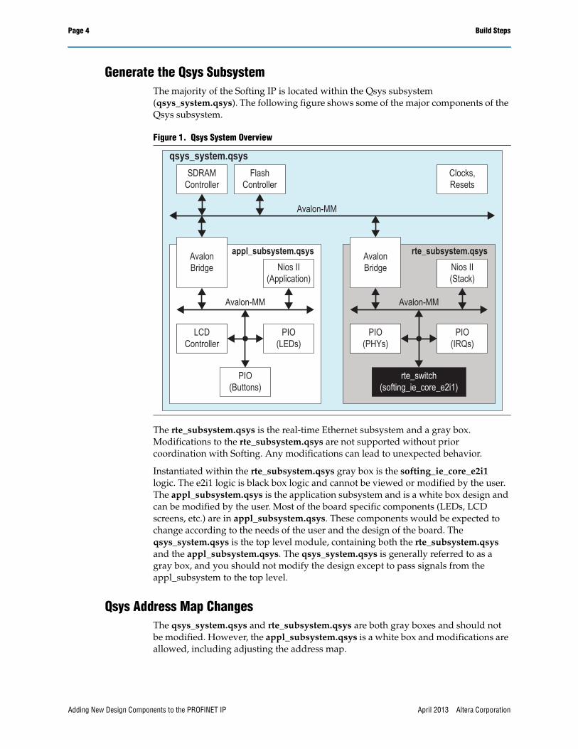
Generate the Qsys SubsystemThe majority of the Softing IP is located within the Qsys subsystem (qsys_system.qsys). The following figure shows some of the major components of the Qsys subsystem.
The rte_subsystem.qsys is the real-time Ethernet subsystem and a gray box. Modifications to the rte_subsystem.qsys are not supported without prior coordination with Softing. Any modifications can lead to unexpected behavior.
Instantiated within the rte_subsystem.qsys gray box is the softing_ie_core_e2i1 logic. The e2i1 logic is black box logic and cannot be viewed or modified by the user. The appl_subsystem.qsys is the application subsystem and is a white box design and can be modified by the user. Most of the board specific components (LEDs, LCD screens, etc.) are in appl_subsystem.qsys. These components would be expected to change according to the needs of the user and the design of the board. The qsys_system.qsys is the top level module, containing both the rte_subsystem.qsys and the appl_subsystem.qsys. The qsys_system.qsys is generally referred to as a gray box, and you should not modify the design except to pass signals from the appl_subsystem to the top level.
Qsys Address Map ChangesThe qsys_system.qsys and rte_subsystem.qsys are both gray boxes and should not be modified. However, the appl_subsystem.qsys is a white box and modifications are allowed, including adjusting the address map.
Figure 1. Qsys System Overview
SDRAM
Controller
Flash
Controller
Avalon
Bridge
PIO
(LEDs)
PIO
(Buttons)
Nios II
(Application)
Nios II
(Application)
LCD
Controller
appl_subsystem.qsysAvalon
Bridge
PIO
(IRQs)
rte_switch
(softing_ie_core_e2i1)
Nios II
(Stack)
Nios II
(Application)
PIO
(PHYs)
rte_subsystem.qsys
Avalon-MM Avalon-MM
Clocks,
Resets
qsys_system.qsys
Avalon-MM
Adding New Design Components to the PROFINET IP April 2013 Altera Corporation
Build Steps Page 5
Generally, it is wise to leave the existing addresses alone and only add new components to the end of the existing address map. This is because there is no significant advantage to rearranging the address map, which can break some components. For example, the NIOS II in the appl_subsystem.qsys has both a reset vector address and an exception vector address as part of its configuration. These addresses point to the mm_bridge_to_system of the appl_subsystem.qsys, which in turn points to a location in the SDRAM where the correct vector software is loaded. If you move the location of the mm_bridge_to_system component to a new address, you would have to change the NIOS II parameters to have a new reset/exception vector address, and you would possibly have to change the vector FW in the SDRAM. So, it is best to not rearrange the address locations of components.
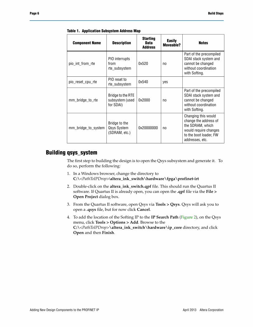
However, if the modifications to the design do require rearranging the existing address map (for example, to reduce the overall address footprint), then most of the components are referenced using the Qsys/HAL system defines and have no other dependencies and can be moved easily. Table 1 shows the address map of the appl_subsystem.qsys and indicates which components can be moved easily and do not require additional configuration for the system to behave correctly. Components that are not easily moved can still be rearranged, but that requires at least one additional component change or modification to the demo FW.
Table 1. Application Subsystem Address Map
Component Name DescriptionStarting
Data Address
Easily Moveable? Notes
pio_led_green PIOs controlling green LEDs 0x400 yes
pio_led_red PIOs controlling red LEDs 0x420 yes
pio_buttonPIOs reading the 18 black switches
0x440 yes
pio_keyPIOs reading the 4 blue (or black) push buttons
0x460 yes
seven_segmentPIOs controlling the seven segment LEDs
0x480 yes
lcd Interface for LCD screen 0x4a0 yes
cpu_appl jtag_debug Processor JTAG interface 0x800 yes
timer_appl Timers 0x100 yes
jtag_uart_appl Character I/O to host PC 0x200 yes
pio_int_to_rte PIO interrupts to rte_subsystem 0x500 no
Part of the precompiled SDAI stack system and cannot be changed without coordination with Softing.
Adding New Design Components to the PROFINET IPApril 2013 Altera Corporation
Page 6 Build Steps
Building qsys_systemThe first step to building the design is to open the Qsys subsystem and generate it. To do so, perform the following:
1. In a Windows browser, change the directory to C:\<PathToIPDrop>\altera_ink_switch\hardware\fpga\profinet-irt
2. Double-click on the altera_ink_switch.qpf file. This should run the Quartus II software. If Quartus II is already open, you can open the .qpf file via the File > Open Project dialog box.
3. From the Quartus II software, open Qsys via Tools > Qsys. Qsys will ask you to open a .qsys file, but for now click Cancel.
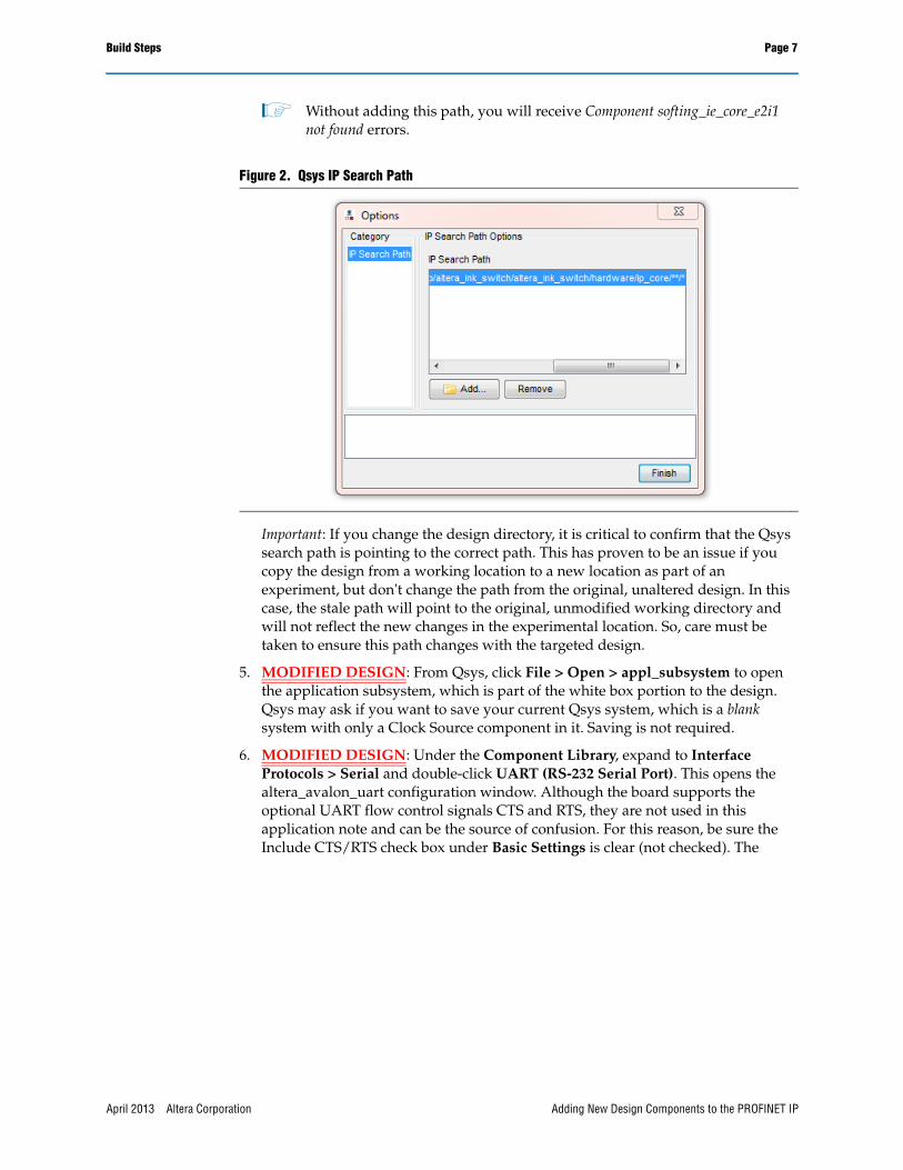
4. To add the location of the Softing IP to the IP Search Path (Figure 2), on the Qsys menu, click Tools > Options > Add. Browse to the C:\<PathToIPDrop>\altera_ink_switch\hardware\ip_core directory, and click Open and then Finish.
pio_int_from_rtePIO interrupts from rte_subsystem
0x520 no
Part of the precompiled SDAI stack system and cannot be changed without coordination with Softing.
pio_reset_cpu_rte PIO reset to rte_subsystem 0x540 yes
mm_bridge_to_rteBridge to the RTE subsystem (used for SDAI)
0x2000 no
Part of the precompiled SDAI stack system and cannot be changed without coordination with Softing.
mm_bridge_to_systemBridge to the Qsys System (SDRAM, etc.)
0x20000000 no
Changing this would change the address of the SDRAM, which would require changes to the boot loader, FW addresses, etc.
Table 1. Application Subsystem Address Map
Component Name DescriptionStarting
Data Address
Easily Moveable? Notes
Adding New Design Components to the PROFINET IP April 2013 Altera Corporation
Build Steps Page 7
1 Without adding this path, you will receive Component softing_ie_core_e2i1 not found errors.
Important: If you change the design directory, it is critical to confirm that the Qsys search path is pointing to the correct path. This has proven to be an issue if you copy the design from a working location to a new location as part of an experiment, but don't change the path from the original, unaltered design. In this case, the stale path will point to the original, unmodified working directory and will not reflect the new changes in the experimental location. So, care must be taken to ensure this path changes with the targeted design.
5. MODIFIED DESIGN: From Qsys, click File > Open > appl_subsystem to open the application subsystem, which is part of the white box portion to the design. Qsys may ask if you want to save your current Qsys system, which is a blank system with only a Clock Source component in it. Saving is not required.
6. MODIFIED DESIGN: Under the Component Library, expand to Interface Protocols > Serial and double-click UART (RS-232 Serial Port). This opens the altera_avalon_uart configuration window. Although the board supports the optional UART flow control signals CTS and RTS, they are not used in this application note and can be the source of confusion. For this reason, be sure the Include CTS/RTS check box under Basic Settings is clear (not checked). The
Figure 2. Qsys IP Search Path
Adding New Design Components to the PROFINET IPApril 2013 Altera Corporation
Page 8 Build Steps
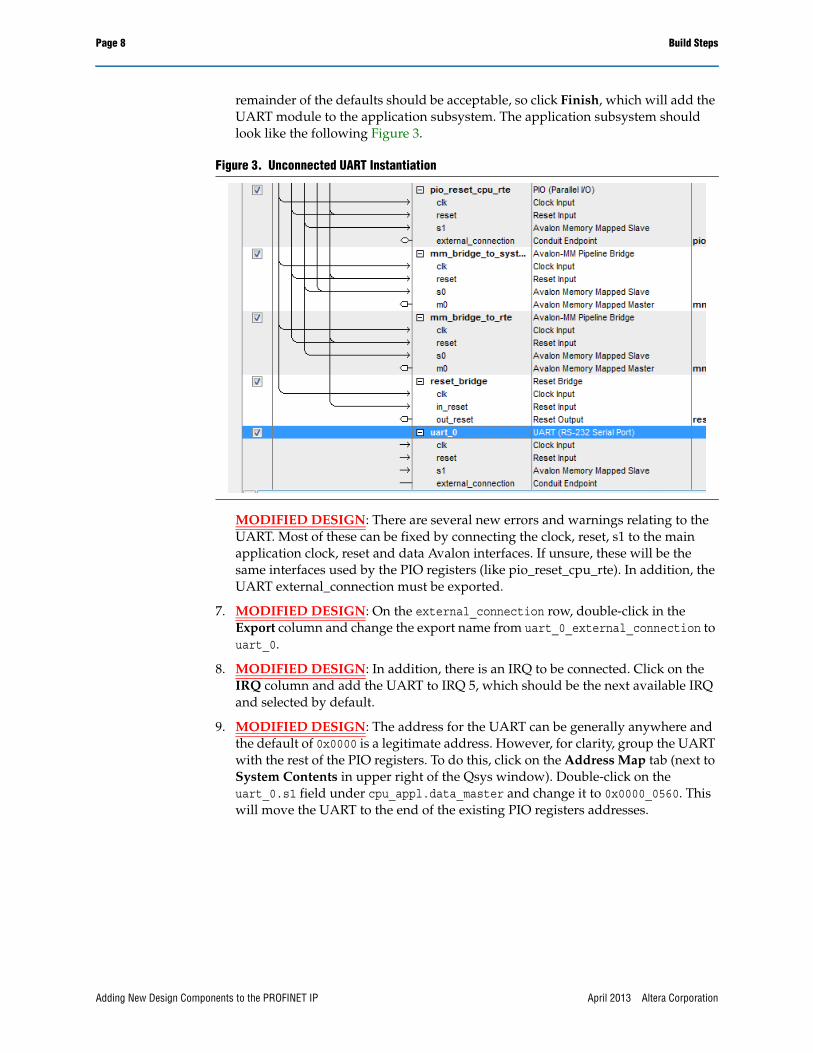
remainder of the defaults should be acceptable, so click Finish, which will add the UART module to the application subsystem. The application subsystem should look like the following Figure 3.
MODIFIED DESIGN: There are several new errors and warnings relating to the UART. Most of these can be fixed by connecting the clock, reset, s1 to the main application clock, reset and data Avalon interfaces. If unsure, these will be the same interfaces used by the PIO registers (like pio_reset_cpu_rte). In addition, the UART external_connection must be exported.
7. MODIFIED DESIGN: On the external_connection row, double-click in the Export column and change the export name from uart_0_external_connection to uart_0.
8. MODIFIED DESIGN: In addition, there is an IRQ to be connected. Click on the IRQ column and add the UART to IRQ 5, which should be the next available IRQ and selected by default.
9. MODIFIED DESIGN: The address for the UART can be generally anywhere and the default of 0x0000 is a legitimate address. However, for clarity, group the UART with the rest of the PIO registers. To do this, click on the Address Map tab (next to System Contents in upper right of the Qsys window). Double-click on the uart_0.s1 field under cpu_appl.data_master and change it to 0x0000_0560. This will move the UART to the end of the existing PIO registers addresses.
Figure 3. Unconnected UART Instantiation
Adding New Design Components to the PROFINET IP April 2013 Altera Corporation
Build Steps Page 9
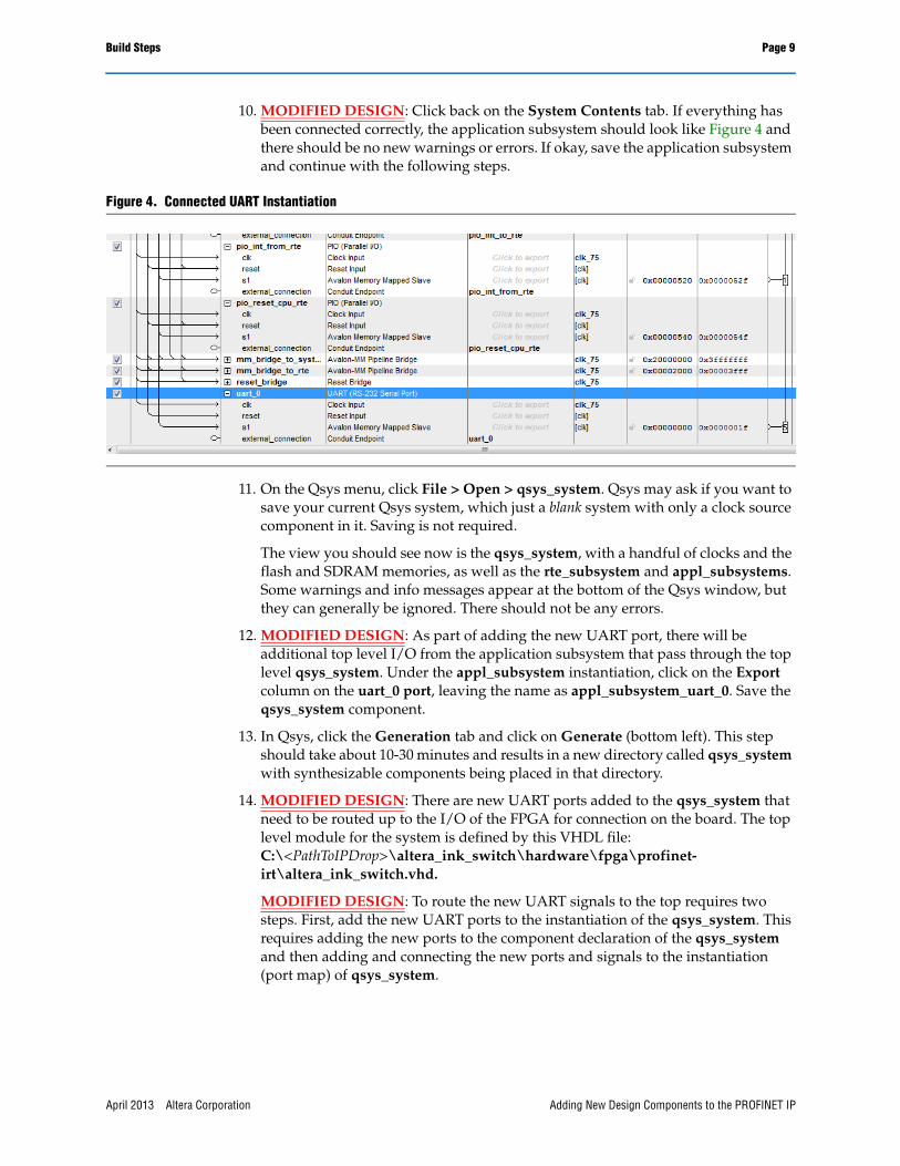
10. MODIFIED DESIGN: Click back on the System Contents tab. If everything has been connected correctly, the application subsystem should look like Figure 4 and there should be no new warnings or errors. If okay, save the application subsystem and continue with the following steps.
11. On the Qsys menu, click File > Open > qsys_system. Qsys may ask if you want to save your current Qsys system, which just a blank system with only a clock source component in it. Saving is not required.
The view you should see now is the qsys_system, with a handful of clocks and the flash and SDRAM memories, as well as the rte_subsystem and appl_subsystems. Some warnings and info messages appear at the bottom of the Qsys window, but they can generally be ignored. There should not be any errors.
12. MODIFIED DESIGN: As part of adding the new UART port, there will be additional top level I/O from the application subsystem that pass through the top level qsys_system. Under the appl_subsystem instantiation, click on the Export column on the uart_0 port, leaving the name as appl_subsystem_uart_0. Save the qsys_system component.
13. In Qsys, click the Generation tab and click on Generate (bottom left). This step should take about 10-30 minutes and results in a new directory called qsys_system with synthesizable components being placed in that directory.
14. MODIFIED DESIGN: There are new UART ports added to the qsys_system that need to be routed up to the I/O of the FPGA for connection on the board. The top level module for the system is defined by this VHDL file: C:\<PathToIPDrop>\altera_ink_switch\hardware\fpga\profinet-irt\altera_ink_switch.vhd.
MODIFIED DESIGN: To route the new UART signals to the top requires two steps. First, add the new UART ports to the instantiation of the qsys_system. This requires adding the new ports to the component declaration of the qsys_system and then adding and connecting the new ports and signals to the instantiation (port map) of qsys_system.
Figure 4. Connected UART Instantiation
Adding New Design Components to the PROFINET IPApril 2013 Altera Corporation
Page 10 Build Steps
MODIFIED DESIGN: The next step is to route those newly added signal from the qsys_system instance and add them as new ports to the top level entity. For simplicity, the signal names of the top level are kept the same as the port names on the qsys_system.
MODIFIED DESIGN: The names of the new ports can be found either in the Qsys HDL Example tab, which shows the instance of qsys_system, or by looking at the generated HDL in C:\<PathToIPDrop>\altera_ink_switch\hardware\fpga\profinet-irt\qsys_system\synthesis\qsys_system.v.
From these sources, you can see the names and directions of the new ports. They are listed in the following table.
MODIFIED DESIGN: If added correctly, there should be modifications to altera_ink_switch.vhd in three locations, and the top level entity should have appl_subsystem_uart_0_rxd as an input and appl_subsystem_uart_0_txd as an output. Examples of the changes can be found in the “VHDL Modification Examples” section that follows and may help those unfamiliar with VHDL.
1 Once the generation is complete, you can close Qsys. It will not be needed by the procedure in this applications note.
Design Preparation and FPGA SynthesisThis section is written as a set of general rules and concepts rather than a step-by-step instruction, the purpose being to ensure the user is familiar with certain FPGA concepts when building the design.
1 There is a final step-by-step task list at the end of this section meant to be used as a checklist.
Some of the preparatory steps included in this design are more applicable to the modified design rather than the out-of-box design flow. However, it is worthwhile to review these steps, even the out-of-box design flow, to help avoid unexpected changes outside the scope of the delivered IP or this application note. For example, it is possible that the Terasic INK development board may undergo a design revision or that an FPGA with a different speed grade is on the board. By following these steps, such unforeseen changes can be observed and detected.
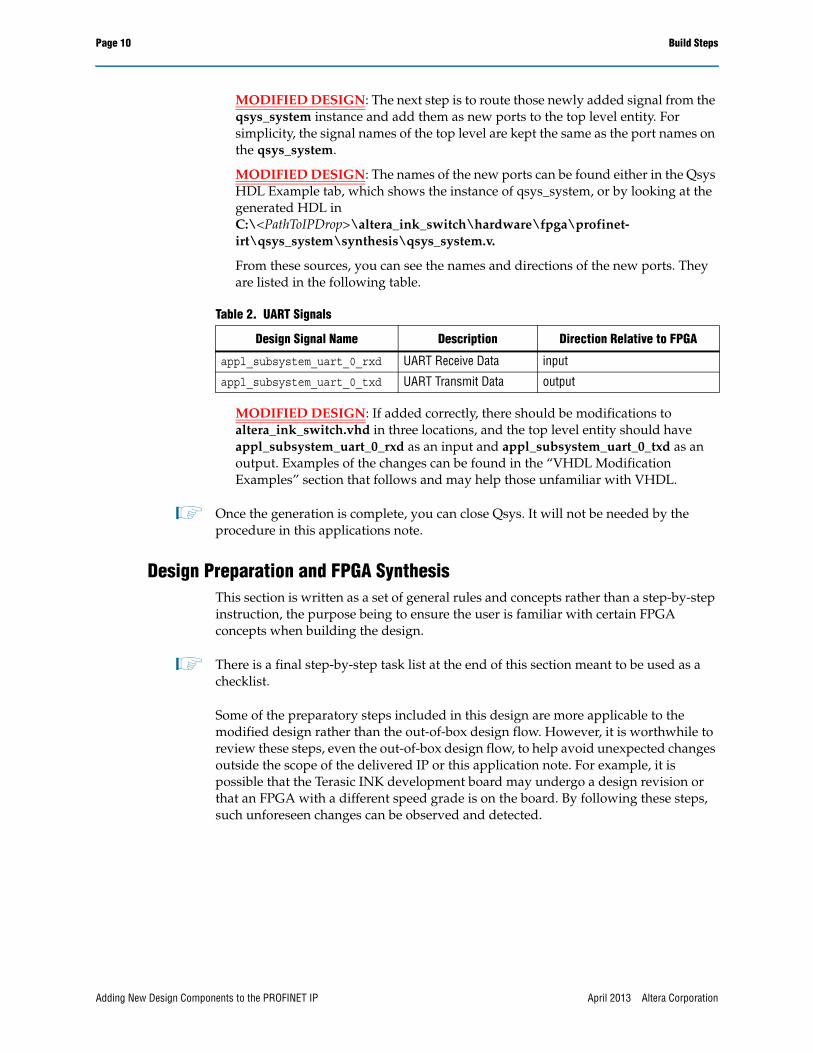
Table 2. UART Signals
Design Signal Name Description Direction Relative to FPGA
appl_subsystem_uart_0_rxd UART Receive Data input
appl_subsystem_uart_0_txd UART Transmit Data output
Adding New Design Components to the PROFINET IP April 2013 Altera Corporation
Build Steps Page 11
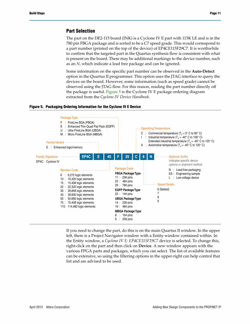
Part SelectionThe part on the DE2-115 board (INK) is a Cyclone IV E part with 115K LE and is in the 780 pin FBGA package and is sorted to be a C7 speed grade. This would correspond to a part number (printed on the top of the device) of EP4CE115F29C7. It is worthwhile to confirm that the targeted part in the Quartus synthesis flow is consistent with what is present on the board. There may be additional markings to the device number, such as an N, which indicate a lead free package and can be ignored.
Some information on the specific part number can be observed in the Auto-Detect option in the Quartus II programmer. This option uses the JTAG interface to query the devices on the board. However, some information (such as speed grade) cannot be observed using the JTAG flow. For this reason, reading the part number directly off the package is useful. Figure 5 is the Cyclone IV E package ordering diagram extracted from the Cyclone IV Device Handbook.
If you need to change the part, do this is on the main Quartus II window. In the upper left, there is a Project Navigator window with a Entity window contained within. In the Entity window, a Cyclone IV E: EP4CE115F29C7 device is selected. To change this, right-click on the part and then click on Device. A new window appears with the various FPGA parts and packages, which you can select. The list of available features can be extensive, so using the filtering options in the upper-right can help control that list and are advised to be used.
Figure 5. Packaging Ordering Information for the Cyclone IV E Device
Family Signature
Package Type
Package Code
Operating Temperature
Speed Grade
Optional SuffixIndicates specific device options or shipment method
E : Enhanced logic/memory
EP4C : Cyclone IV
6 : 6,272 logic elements10 : 10,320 logic elements15 : 15,408 logic elements22 : 22,320 logic elements30 : 28,848 logic elements40 : 39,600 logic elements55 : 55,856 logic elements75 : 75,408 logic elements115 : 114,480 logic elements
F : FineLine BGA (FBGA)E : Enhanced Thin Quad Flat Pack (EQFP)U : Ultra FineLine BGA (UBGA)M : Micro FineLine BGA (MBGA)
FBGA Package Type17 : 256 pins23 : 484 pins29 : 780 pins
EQFP Package Type22 : 144 pins
UBGA Package Type14 : 256 pins19 : 484 pins
MBGA Package Type8 : 164 pins9 : 256 pins
C : Commercial temperature (TJ = 0° C to 85° C)I : Industrial temperature (TJ = -40° C to 100° C) Extended industrial temperature (TJ = -40° C to 125° C)A : Automotive temperature (TJ = -40° C to 125° C)
6 (fastest)789
N : Lead-free packagingES : Engineering sampleL : Low-voltage device
EP4C E 40 F 29 C 8 N
Member Code
Family Variant
Adding New Design Components to the PROFINET IPApril 2013 Altera Corporation
Page 12 Build Steps
When selecting a new device, the pinout location information will be lost. If the design is synthesized, Quartus II will use a generic I/O timing model instead of the more pin-specific timing mode. However, the generic model is likely good enough to identify if a specified part and speed grade will contain the system. Using this method, you can dial in an appropriate FPGA candidate to use for your specific board and design, including various package selections, temperature ranges, and speed grades. If the design makes its way through the compile of the FPGA and meets timing, and it does not use more resources than supported by the targeted FPGA, then the user can be reasonably confident the design can be ported to the targeted FPGA.
Pinout DefinitionTop level signals need to be connected to specified pins on the FPGA package for routing to the board itself. The location and configuration of these pins are contained in the .qsf file delivered with the design. However, this file should not be edited directly. Rather, to view the pin out configuration, open the Quartus II software and click on Assignments > Pin Planner, and make any needed edits from that window.
MODIFIED DESIGN: The new UART ports must be connected to the external level-shifter for routing to the RS232 port. The details of this are specified by the board layout. For the DE2-115 board, the details for the RS-232 can be found on the user manual for the board. The details are shown in Table 3, but it may be worthwhile to double-check these settings.
MODIFIED DESIGN: Generally, it is much easier to modify the pin-out once Quartus II software has passed the Analysis and Synthesis step. Doing this step eliminates the errors associated with manual input of the signal names.
MODIFIED DESIGN: From Quartus II, under the Tasks window, right-click on Analysis and Synthesis and click Start (or Start Again). Once the initial synthesis is done, on the main Quartus II window, click Assignments > Pin Planner to get the pin placement window. To quickly locate the unassigned pins, click on the Location tab, which sorts the signals according to the pin placement. For each of the UART signals, specify the FPGA pin as shown in the Table 3. Be sure to configure the correct I/O standard as well. When this is done, you can close the Pin Planner window. There is no need to manually save the pin out changes, it is done automatically within Quartus II.
Timing ConstraintsMost of the external timing constraints associated with the design are specified in the Timing_Constraints.sdc file in the C:\<PathToIPDrop>\altera_ink_switch\hardware\fpga\profinet-irt directory. This file defines the clocks and the specific the timing constraints required by the design. Some of the timing constraints are derived from the specific board layout and others are affected by specific protocol specifications (for example, MII).
Table 3. MODIFIED DESIGN: DE2-115 UART Pinout
Design Signal Name FPGA Pin DescriptionDirection
Relative to FPGA
Board Signal Name Voltage
appl_subsystem_uart_0_rxd G12 UART Receive Data input UART_RXD 3.3V LVTTL
appl_subsystem_uart_0_txd G9 UART Transmit Data output UART_TXD 3.3V LVTTL
Adding New Design Components to the PROFINET IP April 2013 Altera Corporation
Build Steps Page 13
There are also other SDC files that are generated as part of the Qsys system builder. For example, the design contains two NIOS processors, each of which has a set of false paths between some internal debug logic and the JTAG chain. These SDC files are part of the Qsys design and can be generally ignored by the user.
It is very important to ensure that all I/O are constrained, even if the timing requirements are modest. If there are timing paths that have very modest timing requirements, it is still important to constrain them. Otherwise, it will be difficult to separate the timing constraints that were purposely left out from the ones with syntax errors or other forms of ignored constraints. Details on how to check for unconstrained paths are in the “Unconstrained Paths” section below.
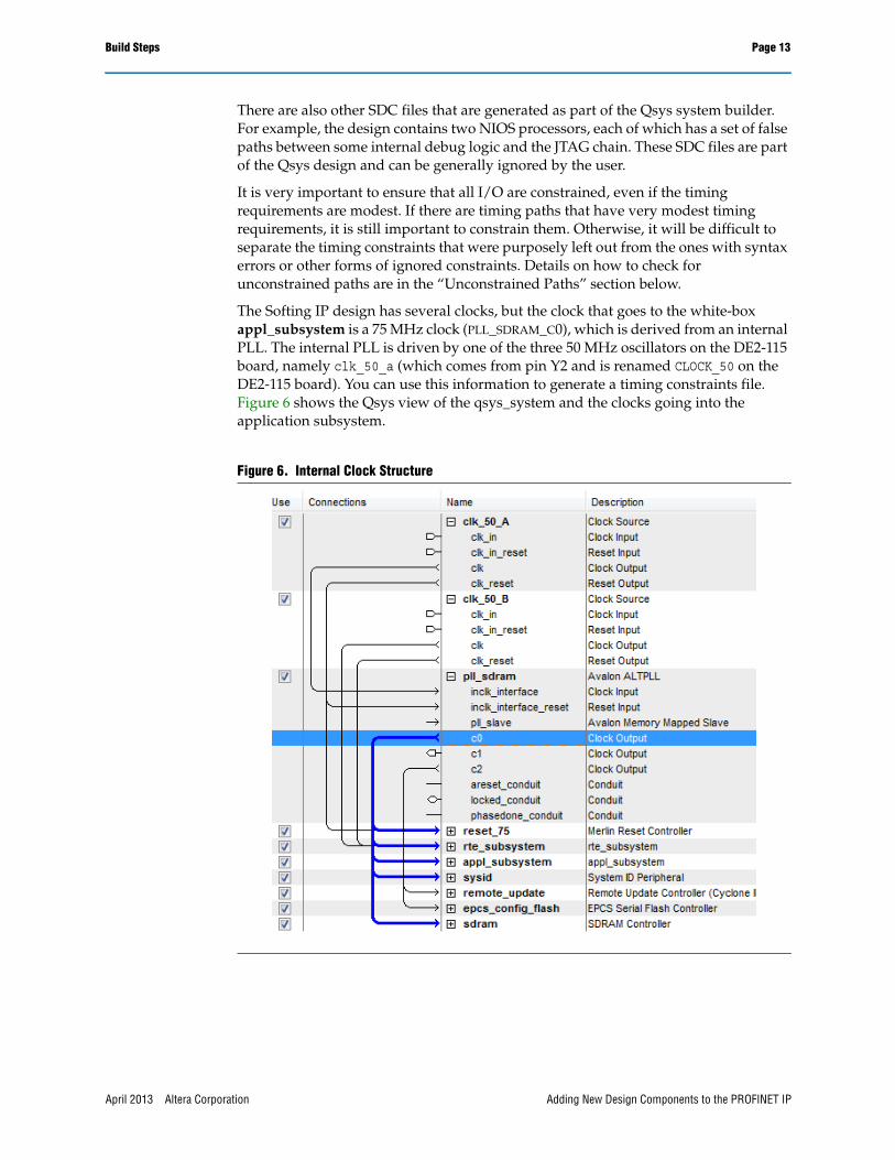
The Softing IP design has several clocks, but the clock that goes to the white-box appl_subsystem is a 75 MHz clock (PLL_SDRAM_C0), which is derived from an internal PLL. The internal PLL is driven by one of the three 50 MHz oscillators on the DE2-115 board, namely clk_50_a (which comes from pin Y2 and is renamed CLOCK_50 on the DE2-115 board). You can use this information to generate a timing constraints file. Figure 6 shows the Qsys view of the qsys_system and the clocks going into the application subsystem.
Figure 6. Internal Clock Structure
Adding New Design Components to the PROFINET IPApril 2013 Altera Corporation
Page 14 Build Steps
MODIFIED DESIGN: As part of adding the new UART port, there will be new top level ports to the Qsys design that require additional timing. Fortunately, the UART port timings are very modest, but it is still worthwhile to constrain all paths on the design. Part of the beauty in the design of a UART is that there is no clock signal. Rather, it is assumed that the transmitter clock/frequency are reasonably close to the receiver clock/frequency, at least over short bursts of data. So, as long as the absolute frequency on the PC (including jitter, XTAL variations, etc.) is within a small tolerance (~3%) of the INK board (including jitter, XTAL variations, etc.) then the system will operate correctly. But, this means that the constraints for the UART are extremely simple, and much of the more complex timing constraints are not needed, which makes the UART a poor test case for timing constraints.
f There are detailed Altera timing guides that can guide you through more interesting timing constraints such as the TimeQuest User Guide as well as more formalized training and instructor led training courses.
MODIFIED DESIGN: For now, open the Timing_Constraints.sdc file in an editor and add the following constraints:
#####################################################################
# UART Ports
#####################################################################
# Design for 115200 baud clock (period = 8680 ns).
create_clock -name {virt_clk_uart} -period 8680 -waveform {0 4340}
# Add conservative SWAG at external constraints
set_output_delay -clock virt_clk_uart -min 10 appl_subsystem_uart_0_txd
set_output_delay -clock virt_clk_uart -max 50 appl_subsystem_uart_0_txd
set_input_delay -clock virt_clk_uart -min 10 appl_subsystem_uart_0_rxd
set_input_delay -clock virt_clk_uart -max 50 appl_subsystem_uart_0_rxd
# Internal clock runs at 75MHz. Allow 10 of those 75MHz clocks
# to account for transfer of the data out of the FPGA.
set_multicycle_path -setup -start -to appl_subsystem_uart_0_txd 10
set_multicycle_path -hold -start -to appl_subsystem_uart_0_txd 9
TimeQuest ResultsIt is important to verify that the timing results are good. A quick pass/fail metric is to look at the TimeQuest Timing Analysis report under the Multicorner Timing Analysis Summary report. This can be accessed from the Task > Compile Design > TimeQuest Timing Analysis > View Report window, or from the Compilation Report window. If there are any negative slack paths (usually outlined in red), then timing has not been met. Not passing timing will usually be reported as critical warnings in the synthesis flow.
Adding New Design Components to the PROFINET IP April 2013 Altera Corporation
Build Steps Page 15
If timing was not met with the out-of-the-box settings, then use the Tools > Advisors > Timing Optimization Advisor command from Quartus II. Most timing paths can be fixed by telling the tool to work a little harder. You can do this by enabling the options under Maximum Frequency (fmax) > Use High-Effort fmax Optimization Settings > Correct All Settings. This typically requires least amount of effort to achieve the best results. However, the Timing Optimization Advisor and Quartus II settings have additional options that may be required to squeeze the most out of the FPGA cycles.
1 For more details on timing closures methods, consider a variety of timing courses at Altera Training. Some are free or instructor led. Type in timing closure in the Search Courses box.
Unconstrained PathsIn addition to the multicorner timing summary, it would be wise to verify that there are no unconstrained paths in the designs. Unconstrained paths are timing paths that have no explicit timing associated with them, and as such cannot be optimized to meet timing. These paths are typically optimized for area, which may result in a reasonable timing, but with some ambiguity due to the lack of timing constraint.
To check if there are unconstrained paths, look at the Unconstrained Paths report under the TimeQuest Timing Analyzer window using the same paths as above.
To identify which I/O do not have timing paths, open the Tools > TimeQuest Timing Analyzer from Quartus II. In the newly opened TimeQuest window, under the Tasks pane on the left, scroll down to the Diagnostic section and double-click Report Unconstrained Paths. In the Report window (top left), there will be a summary that should echo what Quartus displayed. The details for each of these paths are under Setup and Hold Analysis windows.
Background on Timing CornersThose already familiar ASIC and FPGA timing flows (or those simply uninterested) can skip this section. It is meant to provide brief overview of a timing corner and the analysis performed by the TimeQuest Analyzer.
Adding New Design Components to the PROFINET IPApril 2013 Altera Corporation
Page 16 Build Steps
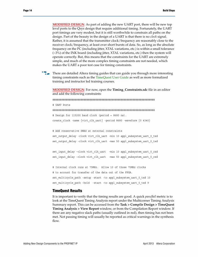
In an FPGA or ASIC design flow, the design must be adjusted to fit specific timing criteria, such as a specific clock period. For example, if the clock is set to 1 MHz, then a specific timing path would have exactly 1 s to propagate from one flip flop, through a section of logic and on to the destination flip flop. Figure 7 shows this example and a quick calculation of the slack in the path.
At first glance, this problem seems simple enough: simply add up the delays of the elements between each flop and compare against the minimum time required. If the timing path has a positive slack, then this means it has enough time to propagate through the logic with the positive value that indicates how much additional time is available in the timing path. If the timing path has a negative slack, it does not have enough time to propagate through the logic to the second flop.
This would be the simple solution if silicon's semi-conductor properties were consistent across temperature and voltage, however they are not. Generally, as silicon gets hotter it conducts electricity less efficiently (slower) than it does when it is cold1. Similarly, with a slightly lower voltage (say 1.79 volts instead of 1.80 volts), silicon will run slower. Additionally, microscopic defects (on the order of a handful of atoms) cause slight variations in the silicon which causes additional uncertainty.
Figure 7. Example Timing Path
1In smaller geometries (around 90nm), a phenomenon known as Temperature Inversion is observed where in some situations as the temperature rises, the cell delays shrink, especially at lower voltages.
1 Clock Period = 1 µs
(1 MHz Clock)
Delay through INV
Clock Clock
Slack = Period - Logic Delay
Slack = 1 µs - Delay through INV
Adding New Design Components to the PROFINET IP April 2013 Altera Corporation
Build Steps Page 17
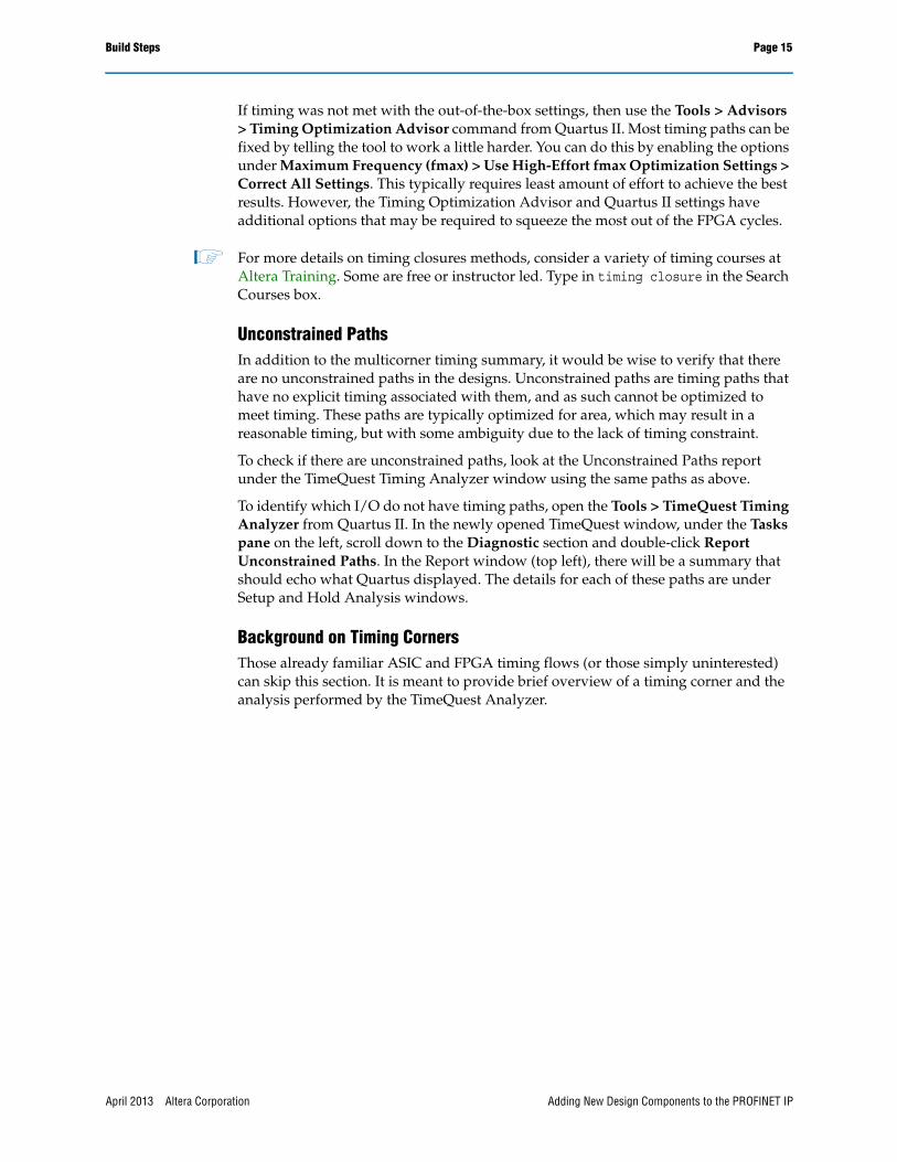
So, to ensure that a piece of silicon like an FPGA meets timing, its paths must be checked against a range of different criteria. We tend to only care about the worst case corners (as shown in Figure 8), with the idea that if timing is met at the worst case corners, then it should be fine at the other corners.
This is why timing analysis is done at multiple corners, varying the timing checks across temperature, manufacture variations, and voltage. Fortunately, the actual calculations and timing information is programmed into Quartus II, so you need not be aware of the complexities under the hood. As long as the external IO and clock specifications are valid, then Quartus II generally does the rest and confirms the timing.
1 It is important when synthesis is done, to confirm that timing was met across all corners. For best results, all timing paths should be met to ensure proper behavior.
Figure 8. Example Timing Corner
VMIN
VMAX
Faster Slower
Minimum
Temperature
Maximum
Temperature
Worst Case Corners
Less Interesting Corners
Faster
Slower
Adding New Design Components to the PROFINET IPApril 2013 Altera Corporation
Page 18 Build FW and Download to the Device
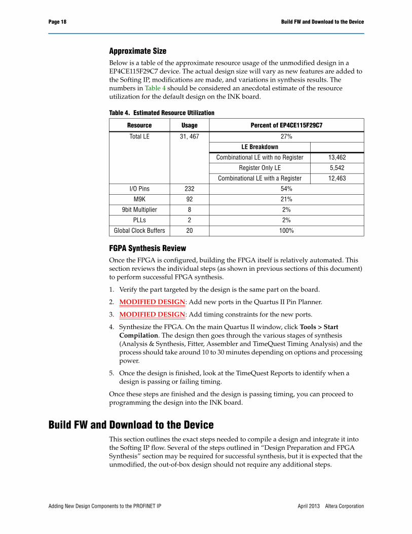
Approximate SizeBelow is a table of the approximate resource usage of the unmodified design in a EP4CE115F29C7 device. The actual design size will vary as new features are added to the Softing IP, modifications are made, and variations in synthesis results. The numbers in Table 4 should be considered an anecdotal estimate of the resource utilization for the default design on the INK board.
FGPA Synthesis ReviewOnce the FPGA is configured, building the FPGA itself is relatively automated. This section reviews the individual steps (as shown in previous sections of this document) to perform successful FPGA synthesis.
1. Verify the part targeted by the design is the same part on the board.
2. MODIFIED DESIGN: Add new ports in the Quartus II Pin Planner.
3. MODIFIED DESIGN: Add timing constraints for the new ports.
4. Synthesize the FPGA. On the main Quartus II window, click Tools > Start Compilation. The design then goes through the various stages of synthesis (Analysis & Synthesis, Fitter, Assembler and TimeQuest Timing Analysis) and the process should take around 10 to 30 minutes depending on options and processing power.
5. Once the design is finished, look at the TimeQuest Reports to identify when a design is passing or failing timing.
Once these steps are finished and the design is passing timing, you can proceed to programming the design into the INK board.
Build FW and Download to the DeviceThis section outlines the exact steps needed to compile a design and integrate it into the Softing IP flow. Several of the steps outlined in “Design Preparation and FPGA Synthesis” section may be required for successful synthesis, but it is expected that the unmodified, the out-of-box design should not require any additional steps.
Table 4. Estimated Resource Utilization
Resource Usage Percent of EP4CE115F29C7
Total LE 31, 467 27%
LE Breakdown
Combinational LE with no Register 13,462
Register Only LE 5,542
Combinational LE with a Register 12,463
I/O Pins 232 54%
M9K 92 21%
9bit Multiplier 8 2%
PLLs 2 2%
Global Clock Buffers 20 100%
Adding New Design Components to the PROFINET IP April 2013 Altera Corporation
Build FW and Download to the Device Page 19
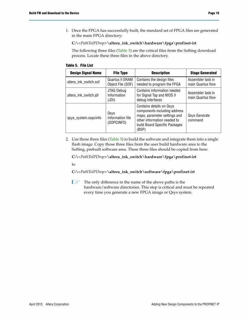
1. Once the FPGA has successfully built, the standard set of FPGA files are generated in the main FPGA directory:
C:\<PathToIPDrop>\altera_ink_switch\hardware\fpga\profinet-irt
The following three files (Table 5) are the critical files from the Softing download process. Locate these three files in the above directory.
2. Use those three files (Table 5) to build the software and integrate them into a single flash image. Copy those three files from the user build hardware area to the Softing, prebuilt software area. These three files should be copied from here:
C:\<PathToIPDrop>\altera_ink_switch\hardware\fpga\profinet-irt
to
C:\<PathToIPDrop>\altera_ink_switch\software\fpga\profinet-irt
1 The only difference in the name of the above paths is the hardware/software directories. This step is critical and must be repeated every time you generate a new FPGA image or Qsys system.
Table 5. File List
Design Signal Name File Type Description Stage Generated
altera_ink_switch.sof Quartus II SRAM Object File (SOF)
Contains the design files needed to program the FPGA
Assembler task in main Quartus flow
altera_ink_switch.jdiJTAG Debug Information (JDI)
Contains information needed for Signal Tap and NIOS II debug interfaces
Assembler task in main Quartus flow
qsys_system.sopcinfoQsys Information file (SOPCINFO)
Contains details on Qsys components including address maps, parameter settings and other information needed to build Board Specific Packages (BSP)
Qsys Generate command
Adding New Design Components to the PROFINET IPApril 2013 Altera Corporation
Page 20 Build FW and Download to the Device
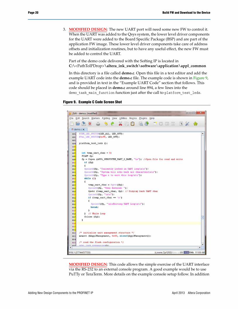
3. MODIFIED DESIGN: The new UART port will need some new FW to control it. When the UART was added to the Qsys system, the lower level driver components for the UART were added to the Board Specific Package (BSP) and are part of the application FW image. These lower level driver components take care of address offsets and initialization routines, but to have any useful effect, the new FW must be added to control the UART.
Part of the demo code delivered with the Softing IP is located in C:\<PathToIPDrop>\altera_ink_switch\software\application\appl_common
In this directory is a file called demo.c. Open this file in a text editor and add the example UART code into the demo.c file. The example code is shown in Figure 9, and is provided in text in the “Example UART Code” section that follows. This code should be placed in demo.c around line 894, a few lines into the demo_task_main_function function just after the call to platform_test_leds.
MODIFIED DESIGN: This code allows the simple exercise of the UART interface via the RS-232 to an external console program. A good example would be to use PuTTy or TeraTerm. More details on the example console setup follow. In addition
Figure 9. Example C Code Screen Shot
Adding New Design Components to the PROFINET IP April 2013 Altera Corporation
Wrap Up Page 21
to several print messages, the console waits for an x to be entered onto the screen before allowing the code to proceed. The following example code stalls the application FW until it receives an input from the RS232. It is important to be aware of this, since without a UART interface, the INK would appear to just hang for no apparent reason.
4. The rest of the system is built as part of a makefile. To run the makefile from your windows machine, click START-> ALL PROGRAMS ->ALTERA -> NIOS II EDS -> NIOS II COMMAND SHELL.
5. Change directory, cd, to the software/applications directory, as shown:
cd C:/<PathToIPDrop>/altera_ink_switch/software/application
6. For the flash loading to work, the FPGA must first be configured with a valid design. It is possible that previously flashed images may have already loaded the FPGA, but it cannot hurt to reload the configuration to eliminate possible issues. Load the FPGA configuration with the following command that is run from the altera_ink_switch/software/application directory.
nios2-configure-sof ../fpga/profinet-irt/altera_ink_switch.sof
7. The makefile supports these commands:
clean - cleans the local area of prebuilt files
build - builds the application software
download - downloads the flash file, including the FPGA image and SW code, into the flash device
These commands can be run individually or all at once, but generally it is safe to run make clean build download as the tool will stop on the first error.
run: make clean build download
8. The download step will load the FPGA image and the supporting FW into the INK. However, a power cycle is required to start the newly downloaded image and FW. Do this by pressing the red power button on the INK once to turn off the power and again to turn it back on.
9. MODIFIED DESIGN: Once the new FW is loaded into the system, the UART will attempt to connect with a terminal. Example terminal setups and expected results are discussed the section titled “Example Console Setup and Expected Results” that follows. The new FW requires character input from the UART terminal for the system to progress.
Wrap UpThe previous steps build the Softing IP design. If this is the first run through, try rerunning with the MODIFIED DESIGN options. If this is the MODIFIED DESIGN run, then the system should now have an additional RS232 UART port and some simple firmware to interact with the UART. The newly added HW and FW are not particularly useful, but they are a first step to adding new logic/FW to the system, By following the same steps, additional logic and features can be added to the delivered design.
Adding New Design Components to the PROFINET IPApril 2013 Altera Corporation
Page 22 Appendix
Appendix
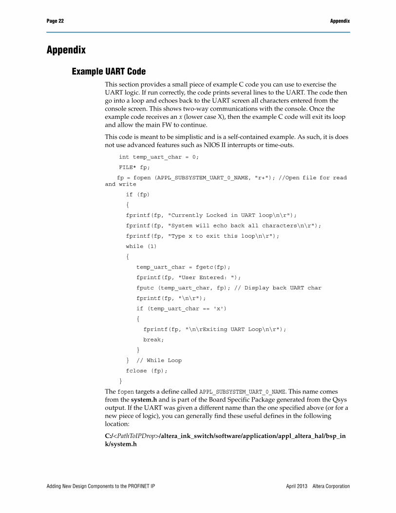
Example UART CodeThis section provides a small piece of example C code you can use to exercise the UART logic. If run correctly, the code prints several lines to the UART. The code then go into a loop and echoes back to the UART screen all characters entered from the console screen. This shows two-way communications with the console. Once the example code receives an x (lower case X), then the example C code will exit its loop and allow the main FW to continue.
This code is meant to be simplistic and is a self-contained example. As such, it is does not use advanced features such as NIOS II interrupts or time-outs.
int temp_uart_char = 0;
FILE* fp;
fp = fopen (APPL_SUBSYSTEM_UART_0_NAME, "r+"); //Open file for read and write
if (fp)
{
fprintf(fp, "Currently Locked in UART loop\n\r");
fprintf(fp, "System will echo back all characters\n\r");
fprintf(fp, "Type x to exit this loop\n\r");
while (1)
{
temp_uart_char = fgetc(fp);
fprintf(fp, "User Entered: ");
fputc (temp_uart_char, fp); // Display back UART char
fprintf(fp, "\n\r");
if (temp_uart_char == 'x')
{
fprintf(fp, "\n\rExiting UART Loop\n\r");
break;
}
} // While Loop
fclose (fp);
}
The fopen targets a define called APPL_SUBSYSTEM_UART_0_NAME. This name comes from the system.h and is part of the Board Specific Package generated from the Qsys output. If the UART was given a different name than the one specified above (or for a new piece of logic), you can generally find these useful defines in the following location:
C:/<PathToIPDrop>/altera_ink_switch/software/application/appl_altera_hal/bsp_ink/system.h
Adding New Design Components to the PROFINET IP April 2013 Altera Corporation
Appendix Page 23
1 It is worth noting that the UART added in this application note is an Avalon UART, which uses a set of Avalon-MM accessible registers and NIOS II code to run the UART. This is different from the jtag_uart often embedded in Altera designs as part of the STDOUT/STDERR interface. Although both are considered UARTs, only the Avalon UART makes use of the RS232 interface.
Example Console Setup and Expected ResultsThere are several terminal programs available. One of the more common is PuTTy, and it can be used as a UART console. The following section will explain how to setup the PuTTy to communicate with the DE2-115 board RS-232 port. This step is not strictly required, and the above design may be more useful just as an example on how to make the changes.
f PuTTy can be downloaded from http://www.putty.org.
PCs without RS232 ConnectorsRS232 DB9 connectors are becoming less common in modern PCs. However, there are several USB to Serial DB9 connectors that can be found in electronics stores.
f You can find the Rhino USB to DB9 Serial (Model: CBU-DB9) from Fry's Electronics.
Several of these devices have some level of support for PC to PC connections. Those programs are above and beyond the base USB to RS232 connection and are not required or suggested for this application note. Generally the autoinstall driver for these devices is sufficient.
Opening a SessionOnce you have the RS232 connector ready, it is important to find which COM port the device has connected to. It is often connected to COM1, but it can be random so it is worth confirming. In Windows 7, use the Device Manager: click Start > Control Panel > System > Device Manager (upper left of System window).
From this window you should see a Ports (COM and LPT) arrow which you can expand. From there you can see the COM chosen by the device. In Figure 10 on page 24, COM3 is selected.
Adding New Design Components to the PROFINET IPApril 2013 Altera Corporation
Page 24 Appendix
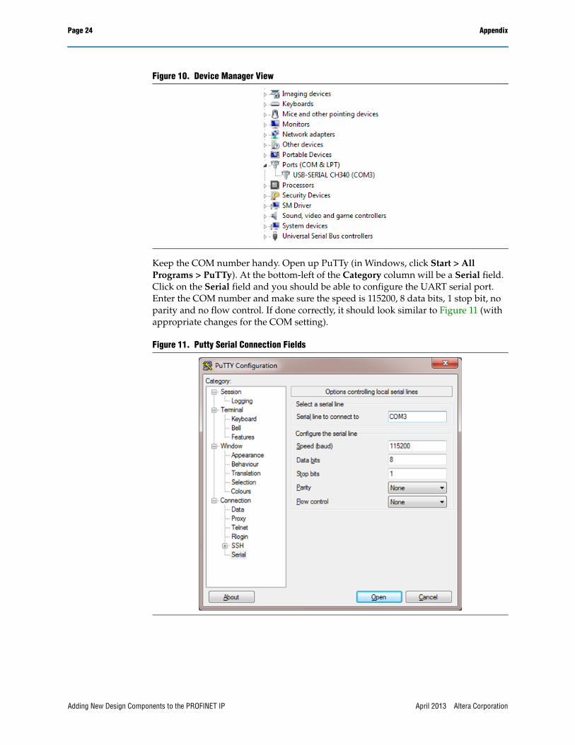
Keep the COM number handy. Open up PuTTy (in Windows, click Start > All Programs > PuTTy). At the bottom-left of the Category column will be a Serial field. Click on the Serial field and you should be able to configure the UART serial port. Enter the COM number and make sure the speed is 115200, 8 data bits, 1 stop bit, no parity and no flow control. If done correctly, it should look similar to Figure 11 (with appropriate changes for the COM setting).
Figure 10. Device Manager View
Figure 11. Putty Serial Connection Fields
Adding New Design Components to the PROFINET IP April 2013 Altera Corporation
VHDL Modification Examples Page 25
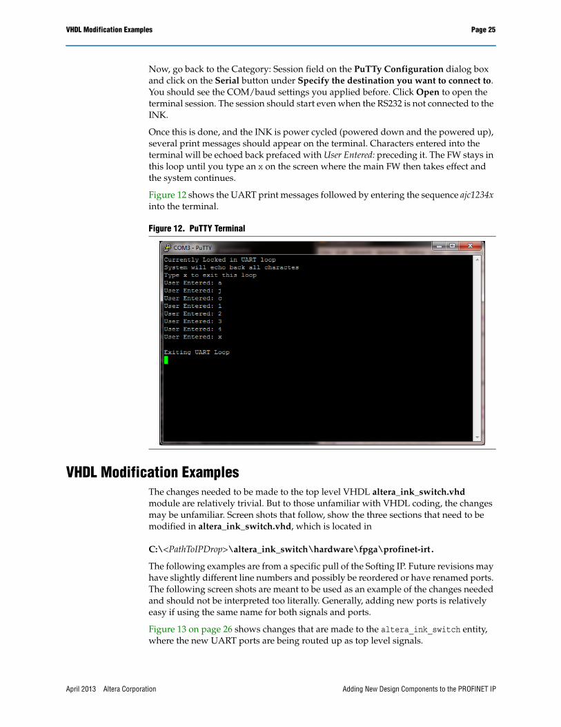
Now, go back to the Category: Session field on the PuTTy Configuration dialog box and click on the Serial button under Specify the destination you want to connect to. You should see the COM/baud settings you applied before. Click Open to open the terminal session. The session should start even when the RS232 is not connected to the INK.
Once this is done, and the INK is power cycled (powered down and the powered up), several print messages should appear on the terminal. Characters entered into the terminal will be echoed back prefaced with User Entered: preceding it. The FW stays in this loop until you type an x on the screen where the main FW then takes effect and the system continues.
Figure 12 shows the UART print messages followed by entering the sequence ajc1234x into the terminal.
VHDL Modification ExamplesThe changes needed to be made to the top level VHDL altera_ink_switch.vhd module are relatively trivial. But to those unfamiliar with VHDL coding, the changes may be unfamiliar. Screen shots that follow, show the three sections that need to be modified in altera_ink_switch.vhd, which is located in
C:\<PathToIPDrop>\altera_ink_switch\hardware\fpga\profinet-irt.
The following examples are from a specific pull of the Softing IP. Future revisions may have slightly different line numbers and possibly be reordered or have renamed ports. The following screen shots are meant to be used as an example of the changes needed and should not be interpreted too literally. Generally, adding new ports is relatively easy if using the same name for both signals and ports.
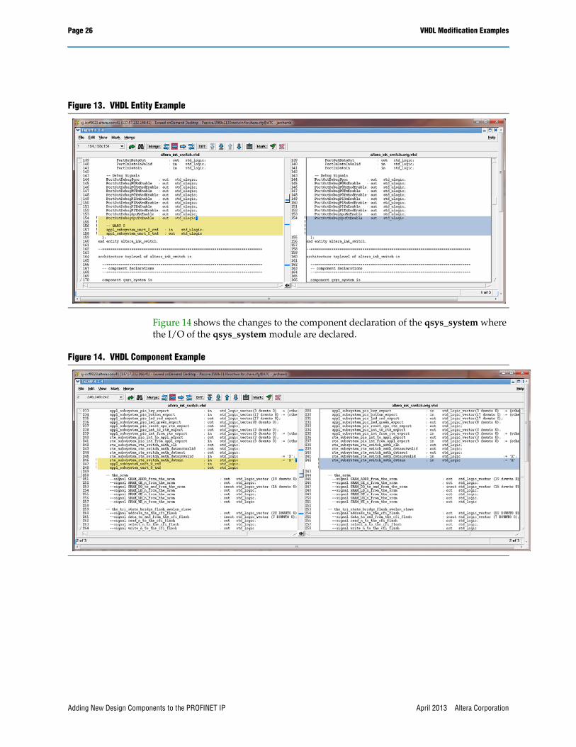
Figure 13 on page 26 shows changes that are made to the altera_ink_switch entity, where the new UART ports are being routed up as top level signals.
Figure 12. PuTTY Terminal
Adding New Design Components to the PROFINET IPApril 2013 Altera Corporation
Page 26 VHDL Modification Examples
Figure 14 shows the changes to the component declaration of the qsys_system where the I/O of the qsys_system module are declared.
Figure 13. VHDL Entity Example
Figure 14. VHDL Component Example
Adding New Design Components to the PROFINET IP April 2013 Altera Corporation
Document Revision History Page 27
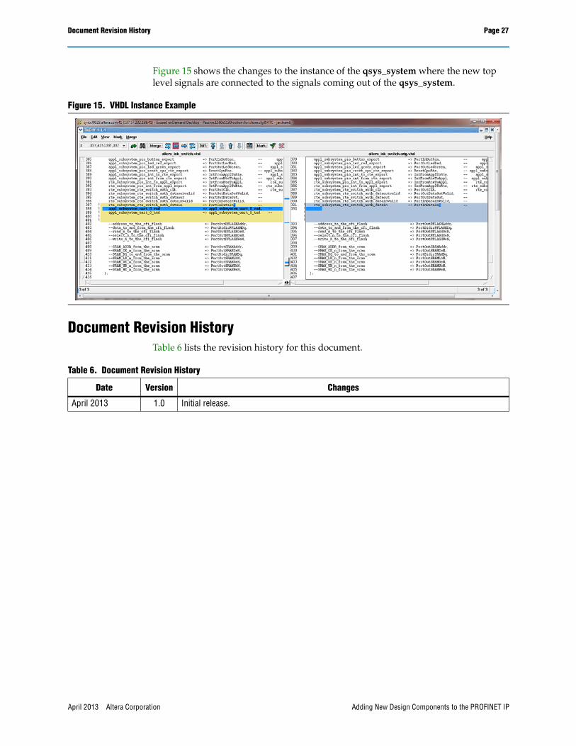
Figure 15 shows the changes to the instance of the qsys_system where the new top level signals are connected to the signals coming out of the qsys_system..
Document Revision HistoryTable 6 lists the revision history for this document.
Figure 15. VHDL Instance Example
Table 6. Document Revision History
Date Version Changes
April 2013 1.0 Initial release.
Adding New Design Components to the PROFINET IPApril 2013 Altera Corporation

Page 28 Document Revision History
Adding New Design Components to the PROFINET IP April 2013 Altera Corporation