Embed Size (px)
Citation preview
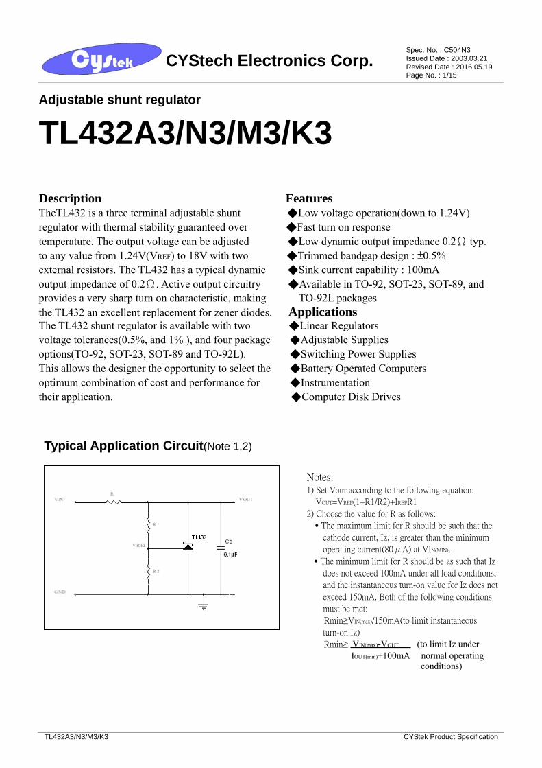
CYStech Electronics Corp. Spec. No. : C504N3 Issued Date : 2003.03.21 Revised Date : 2016.05.19 Page No. : 1/15
TL432A3/N3/M3/K3 CYStek Product Specification
Adjustable shunt regulator
TL432A3/N3/M3/K3
Description Features TheTL432 is a three terminal adjustable shunt ◆Low voltage operation(down to 1.24V) regulator with thermal stability guaranteed over ◆Fast turn on response temperature. The output voltage can be adjusted ◆Low dynamic output impedance 0.2Ω typ. to any value from 1.24V(VREF) to 18V with two ◆Trimmed bandgap design : ±0.5% external resistors. The TL432 has a typical dynamic ◆Sink current capability : 100mA output impedance of 0.2Ω. Active output circuitry ◆Available in TO-92, SOT-23, SOT-89, and provides a very sharp turn on characteristic, making TO-92L packages the TL432 an excellent replacement for zener diodes. Applications The TL432 shunt regulator is available with two ◆Linear Regulators voltage tolerances(0.5%, and 1% ), and four package ◆Adjustable Supplies options(TO-92, SOT-23, SOT-89 and TO-92L). ◆Switching Power Supplies This allows the designer the opportunity to select the ◆Battery Operated Computers optimum combination of cost and performance for ◆Instrumentation their application. ◆Computer Disk Drives
Typical Application Circuit(Note 1,2)
TL432
Notes: 1) Set VOUT according to the following equation:
VOUT=VREF(1+R1/R2)+IREFR1
2) Choose the value for R as follows:
˙The maximum limit for R should be such that the
cathode current, Iz, is greater than the minimum
operating current(80μA) at VIN(MIN).
˙The minimum limit for R should be as such that Iz
does not exceed 100mA under all load conditions,
and the instantaneous turn-on value for Iz does not
exceed 150mA. Both of the following conditions
must be met:
Rmin≥VIN(max)/150mA(to limit instantaneous
turn-on Iz)
Rmin≥ VIN(max)-VOUT (to limit Iz under IOUT(min)+100mA normal operating
conditions)
CYStech Electronics Corp. Spec. No. : C504N3 Issued Date : 2003.03.21 Revised Date : 2016.05.19 Page No. : 2/15
TL432A3/N3/M3/K3 CYStek Product Specification
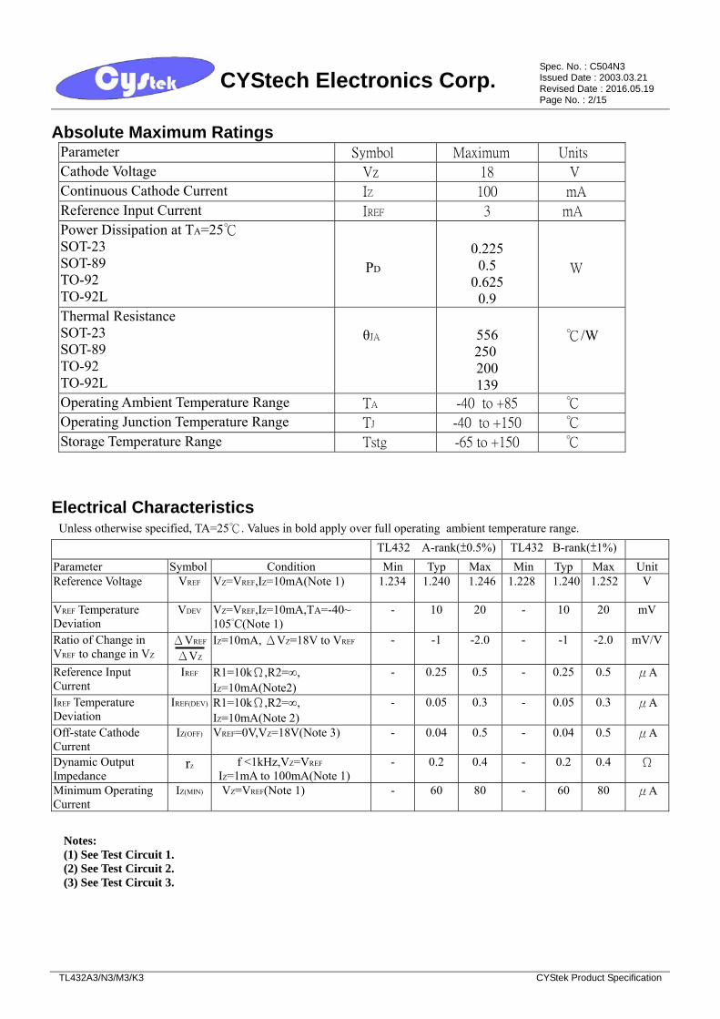
Absolute Maximum Ratings Parameter Symbol Maximum Units
Cathode Voltage Vz 18 V
Continuous Cathode Current IZ 100 mA
Reference Input Current IREF 3 mA
Power Dissipation at TA=25℃ SOT-23 SOT-89 TO-92 TO-92L
PD
0.225 0.5
0.625 0.9
W
Thermal Resistance SOT-23 SOT-89 TO-92 TO-92L
θJA
556 250
200 139
℃/W
Operating Ambient Temperature Range TA -40 to +85 ℃ Operating Junction Temperature Range TJ -40 to +150 ℃ Storage Temperature Range Tstg -65 to +150 ℃
Electrical Characteristics Unless otherwise specified, TA=25℃. Values in bold apply over full operating ambient temperature range.
TL432 A-rank(±0.5%) TL432 B-rank(±1%) Parameter Symbol Condition Min Typ Max Min Typ Max UnitReference Voltage VREF VZ=VREF,IZ=10mA(Note 1) 1.234
1.240 1.246 1.228 1.240 1.252 V
VREF Temperature Deviation
VDEV VZ=VREF,IZ=10mA,TA=-40~ 105°C(Note 1)
- 10 20 - 10 20 mV
Ratio of Change in VREF to change in VZ
ΔVREF ΔVZ
IZ=10mA, ΔVZ=18V to VREF - -1 -2.0 - -1 -2.0 mV/V
Reference Input Current
IREF R1=10kΩ,R2=∞, IZ=10mA(Note2)
- 0.25 0.5 - 0.25 0.5 μA
IREF Temperature Deviation
IREF(DEV) R1=10kΩ,R2=∞, IZ=10mA(Note 2)
- 0.05 0.3 - 0.05 0.3 μA
Off-state Cathode Current
IZ(OFF) VREF=0V,VZ=18V(Note 3) - 0.04 0.5 - 0.04 0.5 μA
Dynamic Output Impedance
rz f <1kHz,VZ=VREF
IZ=1mA to 100mA(Note 1) - 0.2 0.4 - 0.2 0.4 Ω
Minimum Operating Current
IZ(MIN) VZ=VREF(Note 1) - 60 80 - 60 80 μA
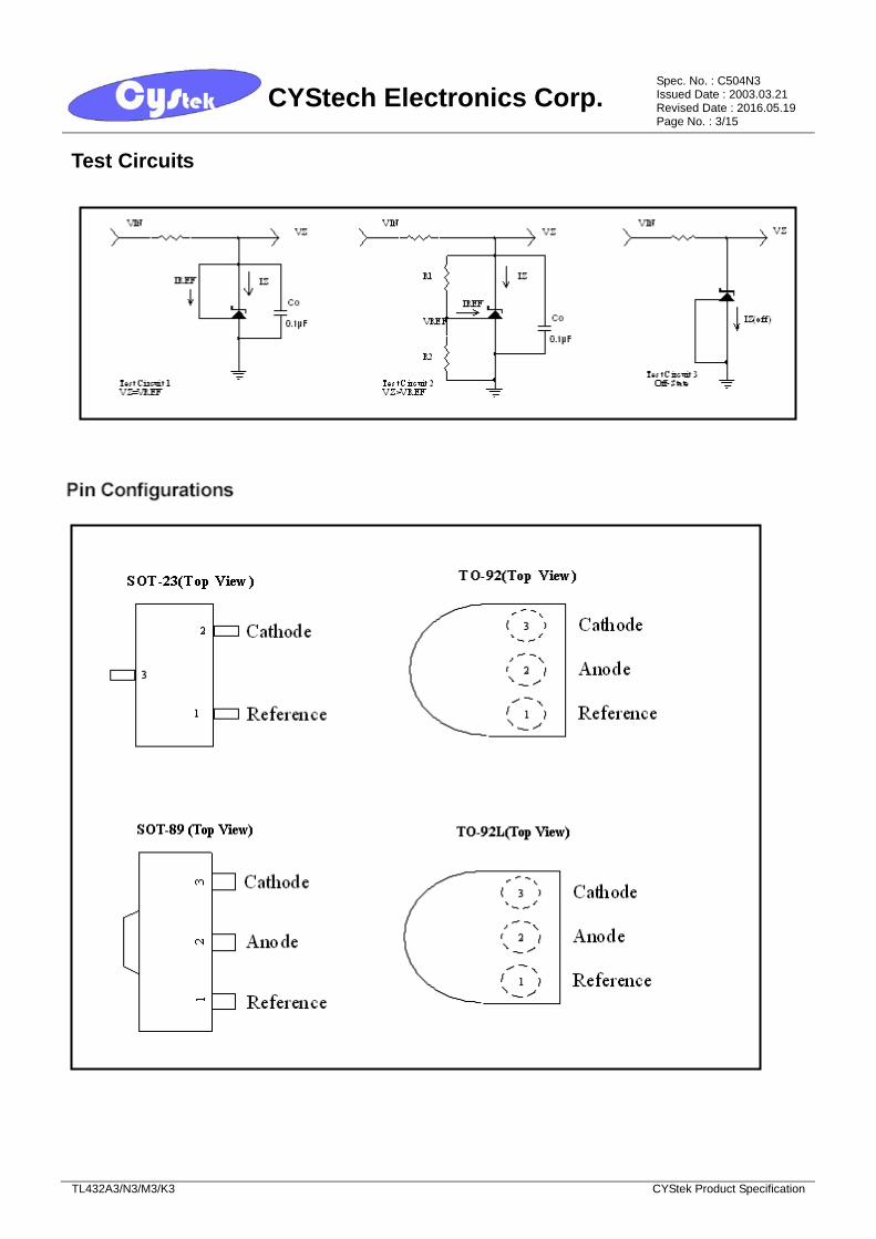
Notes: (1) See Test Circuit 1. (2) See Test Circuit 2. (3) See Test Circuit 3.
CYStech Electronics Corp. Spec. No. : C504N3 Issued Date : 2003.03.21 Revised Date : 2016.05.19 Page No. : 3/15
TL432A3/N3/M3/K3 CYStek Product Specification
Test Circuits
CYStech Electronics Corp. Spec. No. : C504N3 Issued Date : 2003.03.21 Revised Date : 2016.05.19 Page No. : 4/15
TL432A3/N3/M3/K3 CYStek Product Specification
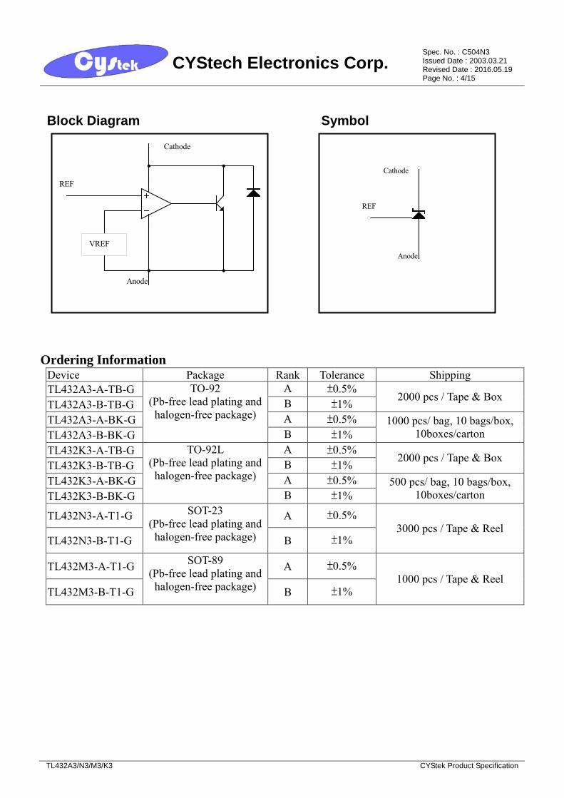
Block Diagram Symbol
REF
Anode
Cathode
VREF
Anode
REF
Cathode
Ordering Information
Device Package Rank Tolerance Shipping TL432A3-A-TB-G A ±0.5% TL432A3-B-TB-G B ±1% 2000 pcs / Tape & Box
TL432A3-A-BK-G A ±0.5% TL432A3-B-BK-G
TO-92 (Pb-free lead plating and
halogen-free package)
B ±1% 1000 pcs/ bag, 10 bags/box,
10boxes/carton TL432K3-A-TB-G A ±0.5% TL432K3-B-TB-G B ±1% 2000 pcs / Tape & Box
TL432K3-A-BK-G A ±0.5% TL432K3-B-BK-G
TO-92L (Pb-free lead plating and
halogen-free package)
B ±1% 500 pcs/ bag, 10 bags/box,
10boxes/carton
TL432N3-A-T1-G A ±0.5%
TL432N3-B-T1-G
SOT-23 (Pb-free lead plating and
halogen-free package) B ±1% 3000 pcs / Tape & Reel
TL432M3-A-T1-G A ±0.5%
TL432M3-B-T1-G
SOT-89 (Pb-free lead plating and
halogen-free package) B ±1% 1000 pcs / Tape & Reel
CYStech Electronics Corp. Spec. No. : C504N3 Issued Date : 2003.03.21 Revised Date : 2016.05.19 Page No. : 5/15
TL432A3/N3/M3/K3 CYStek Product Specification
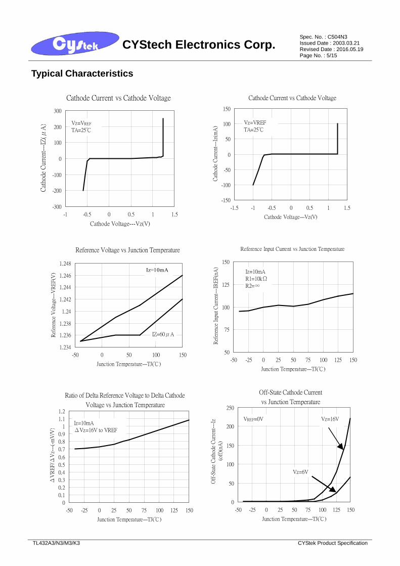
Typical Characteristics
Cathode Current vs Cathode Voltage
-300
-200
-100
0
100
200
300
-1 -0.5 0 0.5 1 1.5
Cathode Voltage---Vz(V)
Cat
hode
Cur
rent
---I
Z(μ
A) Vz=VREF
TA=25℃
Cathode Current vs Cathode Voltage
-150
-100
-50
0
50
100
150
-1.5 -1 -0.5 0 0.5 1 1.5
Cathode Voltage---Vz(V)C
atho
de C
urre
nt--
-Iz(
mA
)
Vz=VREF
TA=25℃
Reference Voltage vs Junction Temperature
1.234
1.236
1.238
1.24
1.242
1.244
1.246
1.248
-50 0 50 100 150
Junction Temperature---TJ(℃)
Ref
eren
ce V
olta
ge--
-VR
EF
(V)
IZ=60μA
Iz=10mA
Reference Input Current vs Junction Temperature
50
75
100
125
150
-50 -25 0 25 50 75 100 125 150
Junction Temperature---TJ(℃)
Ref
eren
ce I
nput
Cur
rent
---I
RE
F(n
A)
Iz=10mA
R1=10kΩ
R2=∞
Ratio of Delta Reference Voltage to Delta Cathode
Voltage vs Junction Temperature
0
0.1
0.2
0.3
0.4
0.5
0.6
0.7
0.8
0.9
1
1.1
1.2
-50 -25 0 25 50 75 100 125 150
Junction Temperature---TJ(℃)
ΔV
RE
F/Δ
Vz-
--(-
mV
/V)
Iz=10mA
ΔVz=16V to VREF
Off-State Cathode Current
vs Junction Temperature
0
50
100
150
200
250
-50 -25 0 25 50 75 100 125 150
Junction Temperature---TJ(℃)
Off
-Sta
te C
atho
de C
urre
nt--
-Iz
(off
)(nA
)
VREF=0V Vz=16V
Vz=6V
CYStech Electronics Corp. Spec. No. : C504N3 Issued Date : 2003.03.21 Revised Date : 2016.05.19 Page No. : 6/15
TL432A3/N3/M3/K3 CYStek Product Specification
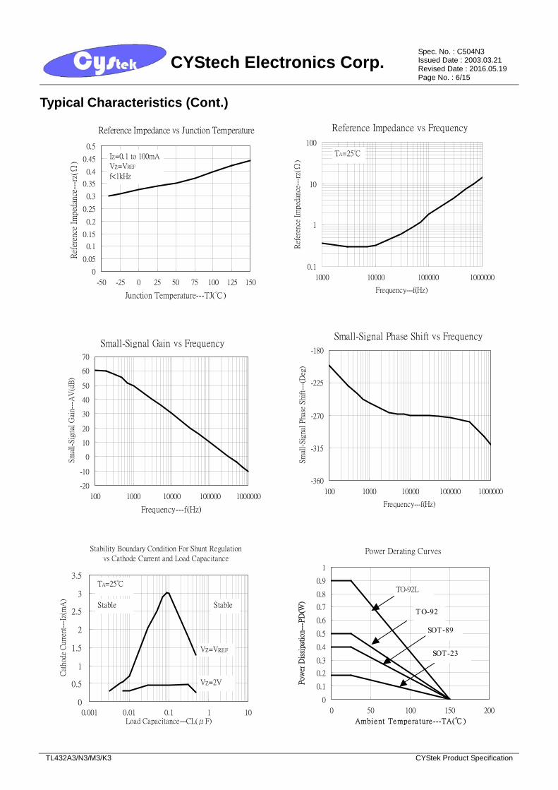
Typical Characteristics (Cont.)
Reference Impedance vs Junction Temperature
0
0.05
0.1
0.15
0.2
0.25
0.3
0.35
0.4
0.45
0.5
-50 -25 0 25 50 75 100 125 150
Junction Temperature---TJ(℃)
Ref
eren
ce I
mpe
danc
e---
rz(Ω
)
Iz=0.1 to 100mA
Vz=VREF
f<1kHz
Reference Impedance vs Frequency
0.1
1
10
100
1000 10000 100000 1000000
Frequency---f(Hz)R
efer
ence
Im
peda
nce-
--rz
(Ω)
TA=25℃
Small-Signal Gain vs Frequency
-20
-10
0
10
20
30
40
50
60
70
100 1000 10000 100000 1000000
Frequency---f(Hz)
Sm
all-
Sig
nal
Gai
n---
AV
(dB
)
Small-Signal Phase Shift vs Frequency
-360
-315
-270
-225
-180
100 1000 10000 100000 1000000
Frequency---f(Hz)
Sm
all-
Sig
nal
Pha
se S
hift
---(
Deg
)
Stability Boundary Condition For Shunt Regulation
vs Cathode Current and Load Capacitance
0
0.5
1
1.5
2
2.5
3
3.5
0.001 0.01 0.1 1 10Load Capacitance---CL(μF)
Cat
hode
Cur
rent
---I
z(m
A)
TA=25℃
Stable Stable
Vz=VREF
Vz=2V
Power Derating Curves
0
0.1
0.2
0.3
0.4
0.5
0.6
0.7
0.8
0.9
1
0 50 100 150 200
Ambient Tempe ra ture ---TA(℃)
Pow
er D
issi
pati
on--
-PD
(W)
TO-92
SOT-89
SOT-23
TO-92L
CYStech Electronics Corp. Spec. No. : C504N3 Issued Date : 2003.03.21 Revised Date : 2016.05.19 Page No. : 7/15
TL432A3/N3/M3/K3 CYStek Product Specification
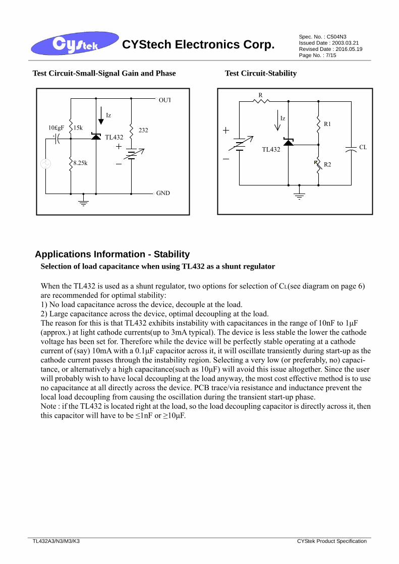
Test Circuit-Small-Signal Gain and Phase Test Circuit-Stability
+
15k
8.25k
PL432232
Iz
OUT
GND
10£gF
IzR1
R2
PL432
R
CL
TL432
TL432
Applications Information - Stability
Selection of load capacitance when using TL432 as a shunt regulator When the TL432 is used as a shunt regulator, two options for selection of CL(see diagram on page 6) are recommended for optimal stability: 1) No load capacitance across the device, decouple at the load. 2) Large capacitance across the device, optimal decoupling at the load. The reason for this is that TL432 exhibits instability with capacitances in the range of 10nF to 1μF (approx.) at light cathode currents(up to 3mA typical). The device is less stable the lower the cathode voltage has been set for. Therefore while the device will be perfectly stable operating at a cathode current of (say) 10mA with a 0.1μF capacitor across it, it will oscillate transiently during start-up as the cathode current passes through the instability region. Selecting a very low (or preferably, no) capaci- tance, or alternatively a high capacitance(such as 10μF) will avoid this issue altogether. Since the user will probably wish to have local decoupling at the load anyway, the most cost effective method is to use no capacitance at all directly across the device. PCB trace/via resistance and inductance prevent the local load decoupling from causing the oscillation during the transient start-up phase. Note : if the TL432 is located right at the load, so the load decoupling capacitor is directly across it, then this capacitor will have to be ≤1nF or ≥10μF.
CYStech Electronics Corp. Spec. No. : C504N3 Issued Date : 2003.03.21 Revised Date : 2016.05.19 Page No. : 8/15
TL432A3/N3/M3/K3 CYStek Product Specification
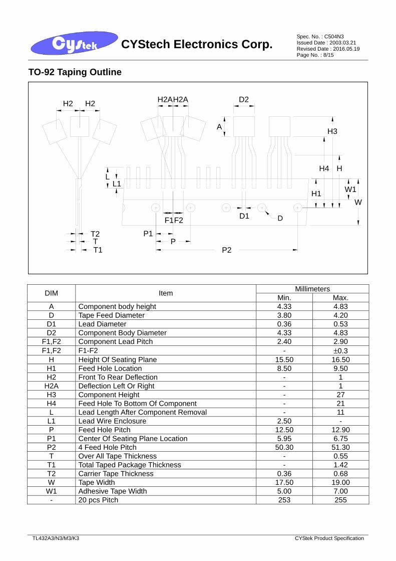
TO-92 Taping Outline
Millimeters DIM Item Min. Max.
A Component body height 4.33 4.83 D Tape Feed Diameter 3.80 4.20
D1 Lead Diameter 0.36 0.53 D2 Component Body Diameter 4.33 4.83
F1,F2 Component Lead Pitch 2.40 2.90 F1,F2 F1-F2 - ±0.3
H Height Of Seating Plane 15.50 16.50 H1 Feed Hole Location 8.50 9.50 H2 Front To Rear Deflection - 1
H2A Deflection Left Or Right - 1 H3 Component Height - 27 H4 Feed Hole To Bottom Of Component - 21 L Lead Length After Component Removal - 11
L1 Lead Wire Enclosure 2.50 - P Feed Hole Pitch 12.50 12.90
P1 Center Of Seating Plane Location 5.95 6.75 P2 4 Feed Hole Pitch 50.30 51.30 T Over All Tape Thickness - 0.55
T1 Total Taped Package Thickness - 1.42 T2 Carrier Tape Thickness 0.36 0.68 W Tape Width 17.50 19.00
W1 Adhesive Tape Width 5.00 7.00 - 20 pcs Pitch 253 255
H2AH2AH2H2 D2
A
H
WW1
H3
H4
H1L1
L
P2P
P1
F1F2 D1 D
T2TT1
CYStech Electronics Corp. Spec. No. : C504N3 Issued Date : 2003.03.21 Revised Date : 2016.05.19 Page No. : 9/15
TL432A3/N3/M3/K3 CYStek Product Specification
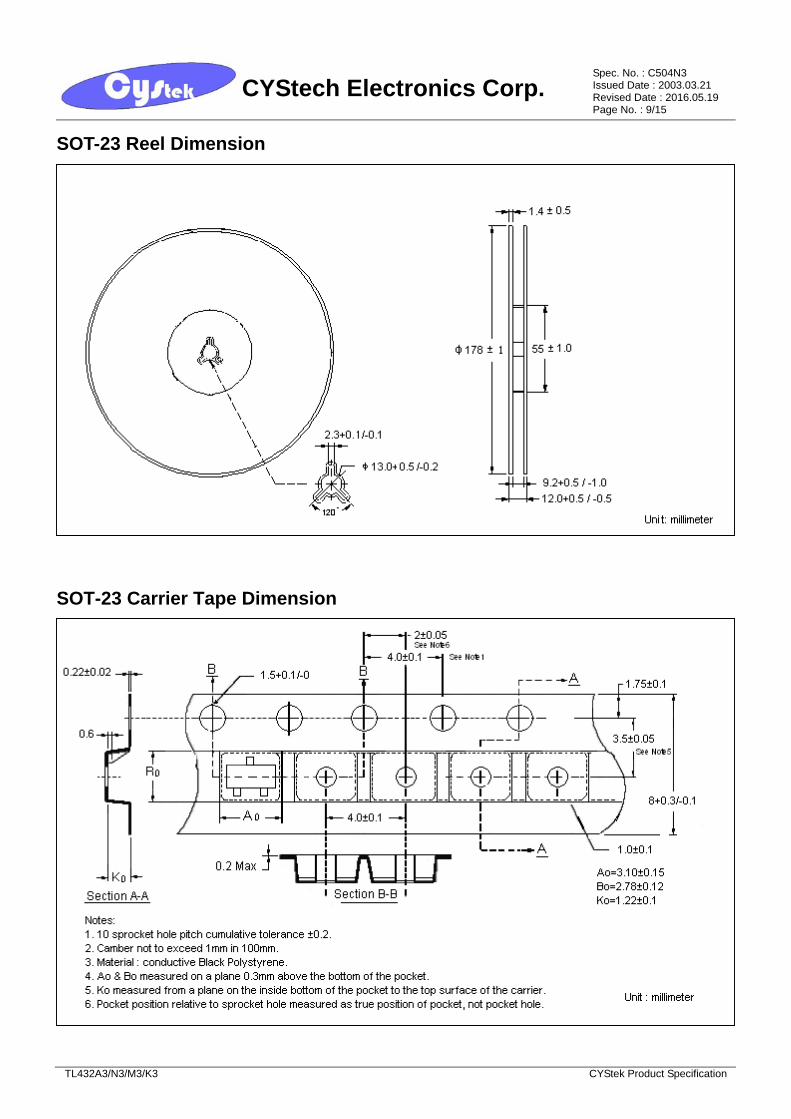
SOT-23 Reel Dimension
SOT-23 Carrier Tape Dimension
CYStech Electronics Corp. Spec. No. : C504N3 Issued Date : 2003.03.21 Revised Date : 2016.05.19 Page No. : 10/15
TL432A3/N3/M3/K3 CYStek Product Specification
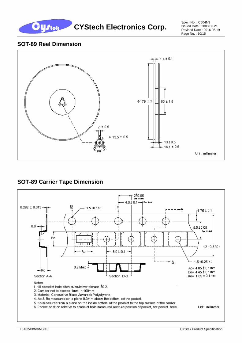
SOT-89 Reel Dimension
SOT-89 Carrier Tape Dimension
CYStech Electronics Corp. Spec. No. : C504N3 Issued Date : 2003.03.21 Revised Date : 2016.05.19 Page No. : 11/15
TL432A3/N3/M3/K3 CYStek Product Specification
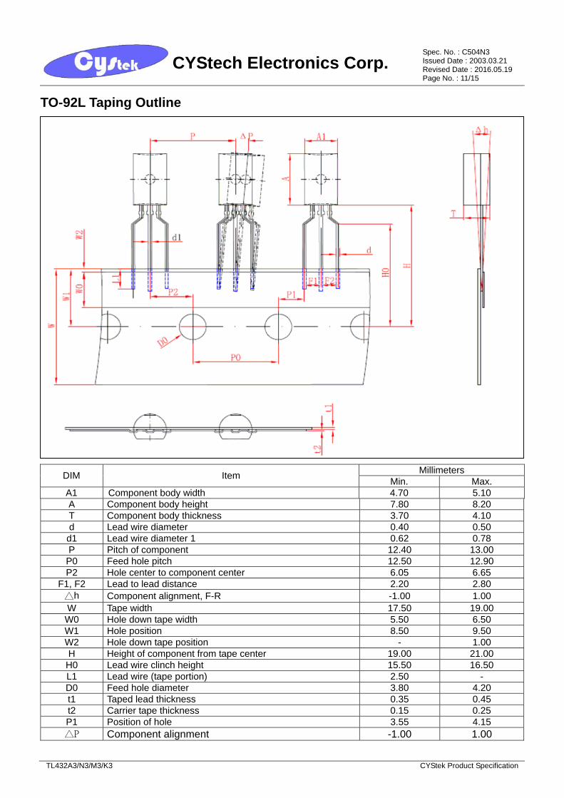
TO-92L Taping Outline
Millimeters DIM Item Min. Max. A1 Component body width 4.70 5.10 A Component body height 7.80 8.20 T Component body thickness 3.70 4.10 d Lead wire diameter 0.40 0.50
d1 Lead wire diameter 1 0.62 0.78 P Pitch of component 12.40 13.00
P0 Feed hole pitch 12.50 12.90 P2 Hole center to component center 6.05 6.65
F1, F2 Lead to lead distance 2.20 2.80 △h Component alignment, F-R -1.00 1.00 W Tape width 17.50 19.00 W0 Hole down tape width 5.50 6.50 W1 Hole position 8.50 9.50 W2 Hole down tape position - 1.00 H Height of component from tape center 19.00 21.00
H0 Lead wire clinch height 15.50 16.50 L1 Lead wire (tape portion) 2.50 - D0 Feed hole diameter 3.80 4.20 t1 Taped lead thickness 0.35 0.45 t2 Carrier tape thickness 0.15 0.25 P1 Position of hole 3.55 4.15 △P Component alignment -1.00 1.00
CYStech Electronics Corp. Spec. No. : C504N3 Issued Date : 2003.03.21 Revised Date : 2016.05.19 Page No. : 12/15
TL432A3/N3/M3/K3 CYStek Product Specification
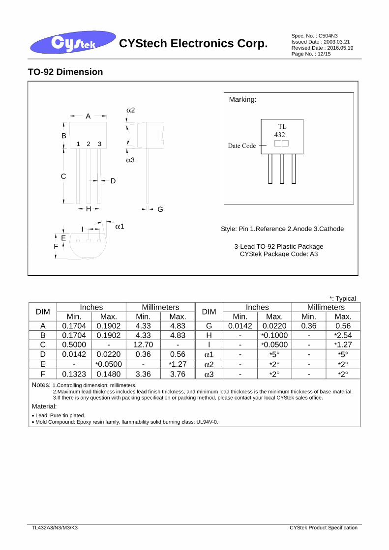
TO-92 Dimension
31
A
D
B
C
I α1E
F
α2
α3
GH
2
Marking:
TL 432 □□ Date Code
3-Lead TO-92 Plastic PackageCYStek Package Code: A3
Style: Pin 1.Reference 2.Anode 3.Cathode
*: Typical Inches Millimeters Inches Millimeters DIM Min. Max. Min. Max. DIM Min. Max. Min. Max.
A 0.1704 0.1902 4.33 4.83 G 0.0142 0.0220 0.36 0.56 B 0.1704 0.1902 4.33 4.83 H - *0.1000 - *2.54 C 0.5000 - 12.70 - I - *0.0500 - *1.27 D 0.0142 0.0220 0.36 0.56 α1 - *5° - *5°
- *0.0500 - *1.27 α2 - *2° - *2° E F 0.1323 0.1480 3.36 3.76 α3 - *2° - *2°
Notes: 1.Controlling dimension: millimeters. 2.Maximum lead thickness includes lead finish thickness, and minimum lead thickness is the minimum thickness of base material. 3.If there is any question with packing specification or packing method, please contact your local CYStek sales office.
Material: • Lead: Pure tin plated. • Mold Compound: Epoxy resin family, flammability solid burning class: UL94V-0.
CYStech Electronics Corp. Spec. No. : C504N3 Issued Date : 2003.03.21 Revised Date : 2016.05.19 Page No. : 13/15
TL432A3/N3/M3/K3 CYStek Product Specification
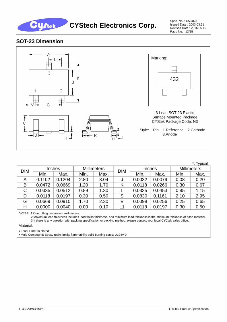
SOT-23 Dimension
*: Typical Inches Millimeters Inches Millimeters DIM Min. Max. Min. Max. DIM Min. Max. Min. Max.
Marking:
432
Style: Pin 1.Reference 2.Cathode3.Anode
3-Lead SOT-23 Plastic Surface Mounted PackageCYStek Package Code: N3
A 0.1102 0.1204 2.80 3.04 J 0.0032 0.0079 0.08 0.20 B 0.0472 0.0669 1.20 1.70 K 0.0118 0.0266 0.30 0.67 C 0.0335 0.0512 0.89 1.30 L 0.0335 0.0453 0.85 1.15 D 0.0118 0.0197 0.30 0.50 S 0.0830 0.1161 2.10 2.95 G 0.0669 0.0910 1.70 2.30 V 0.0098 0.0256 0.25 0.65 H 0.0000 0.0040 0.00 0.10 L1 0.0118 0.0197 0.30 0.50
Notes: 1.Controlling dimension: millimeters. 2.Maximum lead thickness includes lead finish thickness, and minimum lead thickness is the minimum thickness of base material. 3.If there is any question with packing specification or packing method, please contact your local CYCtek sales office.
Material: • Lead: Pure tin plated. • Mold Compound: Epoxy resin family, flammability solid burning class: UL94V-0.
CYStech Electronics Corp. Spec. No. : C504N3 Issued Date : 2003.03.21 Revised Date : 2016.05.19 Page No. : 14/15
TL432A3/N3/M3/K3 CYStek Product Specification
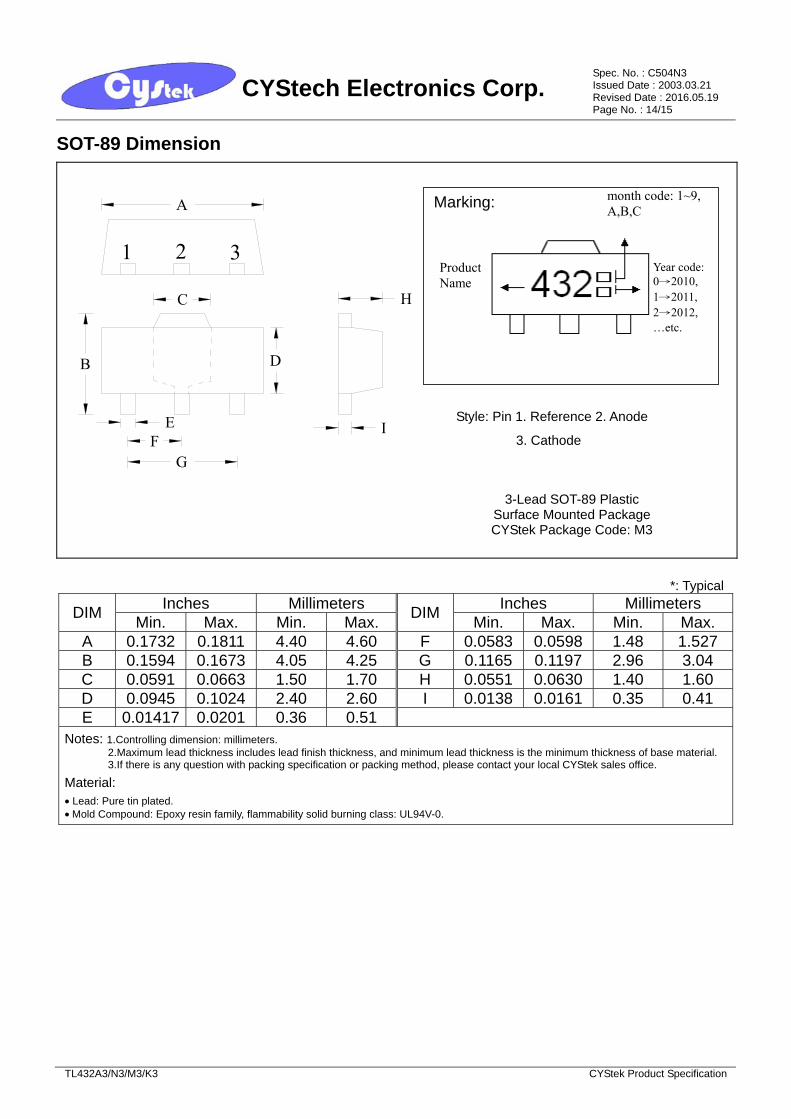
SOT-89 Dimension
*: Typical
Inches Millimeters
Inches Millimeters DIM Min. Max. Min. Max. DIM Min. Max. Min. Max. A 0.1732 0.1811 4.40 4.60 F 0.0583 0.0598 1.48 1.527 B 0.1594 0.1673 4.05 4.25 G 0.1165 0.1197 2.96 3.04 C 0.0591 0.0663 1.50 1.70 H 0.0551 0.0630 1.40 1.60 D 0.0945 0.1024 2.40 2.60 I 0.0138 0.0161 0.35 0.41 E 0.01417 0.0201 0.36 0.51
Notes: 1.Controlling dimension: millimeters. 2.Maximum lead thickness includes lead finish thickness, and minimum lead thickness is the minimum thickness of base material. 3.If there is any question with packing specification or packing method, please contact your local CYStek sales office.
Material: • Lead: Pure tin plated. • Mold Compound: Epoxy resin family, flammability solid burning class: UL94V-0.
Marking:
month code: 1~9,A,B,C
EF
G
C
B
A
321
Style: Pin 1. Reference 2. Anode
3. Cathode
Product Name
Year code:0→2010, 1→2011, 2→2012, …etc.
H
I
D
3-Lead SOT-89 Plastic Surface Mounted Package CYStek Package Code: M3
CYStech Electronics Corp. Spec. No. : C504N3 Issued Date : 2003.03.21 Revised Date : 2016.05.19 Page No. : 15/15
TL432A3/N3/M3/K3 CYStek Product Specification
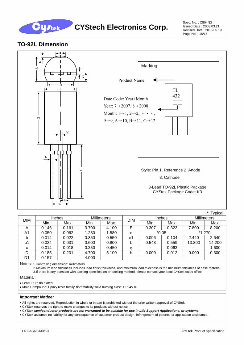
TO-92L Dimension
Style: Pin 1. Reference 2. Anode
3. Cathode
3-Lead TO-92L Plastic PackageCYStek Package Code: K3
Product Name
TL 432 □□
Year: 7→2007, 8→2008 Month: 1→1, 2→2, ‧‧‧, 9→9, A→10, B→11, C→12
Date Code: Year+Month
Marking:
*: Typical Inches Millimeters Inches Millimeters DIM Min. Max. Min. Max. DIM Min. Max. Min. Max.
A 0.146 0.161 3.700 4.100 E 0.307 0.323 7.800 8.200 A1 0.050 0.062 1.280 1.580 e *0.05 *1.270 b 0.014 0.022 0.350 0.550 e1 0.096 0.104 2.440 2.640
b1 0.024 0.031 0.600 0.800 L 0.543 0.559 13.800 14.200 c 0.014 0.018 0.350 0.450 ϕ - 0.063 - 1.600 D 0.185 0.201 4.700 5.100 h 0.000 0.012 0.000 0.300
D1 0.157 - 4.000 - Notes: 1.Controlling dimension: millimeters.
2.Maximum lead thickness includes lead finish thickness, and minimum lead thickness is the minimum thickness of base material. 3.If there is any question with packing specification or packing method, please contact your local CYStek sales office.
Material: • Lead: Pure tin plated. • Mold Compound: Epoxy resin family, flammability solid burning class: UL94V-0.
Important Notice: • All rights are reserved. Reproduction in whole or in part is prohibited without the prior written approval of CYStek. • CYStek reserves the right to make changes to its products without notice. • CYStek semiconductor products are not warranted to be suitable for use in Life-Support Applications, or systems. • CYStek assumes no liability for any consequence of customer product design, infringement of patents, or application assistance.