Embed Size (px)
Citation preview
[AK5572]
015016766-E-00 2015/12 - 1 -
1. General Description
The AK557x series is a 32-bit, 768 kHz sampling, differential input A/D converter for digital audio systems. It achieves 121 dB dynamic range and 112 dB S/(N+D) while maintaining low power consumption performance. The AK5572 integrates a 2-channel A/D converter, suitable for mixers and multi-channel recorders. Four types of digital filters are integrated and selectable according to the sound quality preference. The AK5572 can be easily connected to a DSP by supporting TDM audio formats. Additionally, it supports DSD output up to 11.2MHz.The channel summation mode improves the dynamic range performance by summing-up multiple channel A/D data and averaging. The dynamic range is improved to 124 dB in 2-to-1 mode.
2. Features
Sampling Rate: 8 kHz - 768 kHz
Input: Full Differential Inputs
S/(N+D): 112 dB
DR: 121 dB (2-to-1 mode: 124 dB)
S/N: 121 dB (2-to-1 mode: 124 dB)
Internal Filter: Four types of LPF, Digital HPF
Power Supply: 4.75-5.25 V (Analog), 1.7-1.98 V or 3.0-3.6 V (Digital)
Output Format
PCM mode: 24/32-bit MSB justified, I2S or TDM
DSD mode: DSD Native 64, 128, 256
Maximized Slot Efficiency in TDM Mode by Optimal Data Placed Mode
Cascade TDM I/F:
TDM512: fs= 48 kHz
TDM256: fs= 96 kHz or 48 kHz
TDM126: fs= 192 kHz, 96 kHz or 48 kHz
Operation Mode: Master Mode & Slave Mode
Detection Function: Input Overflow Flag
Serial Interface: 3-wire Serial and I2C μP I/F (Pin setting is also available)
Power Consumption: 148 mW (@AVDD= 5.0 V, TVDD= 3.3 V, fs= 48 kHz)
Package: 48-pin QFN
2-Channel Differential 32-bit ADC
AK5572
[AK5572]
015016766-E-00 2015/12 - 2 -
3. Table of Contents
1. General Description ............................................................................................................................ 1 2. Features .............................................................................................................................................. 1 3. Table of Contents ................................................................................................................................ 2 4. Block Diagram ..................................................................................................................................... 3
Block Diagram.................................................................................................................................... 3
5. Pin Configurations and Functions ...................................................................................................... 4
Pin Configurations ............................................................................................................................. 4
Pin Functions ..................................................................................................................................... 5
Handling of Unused Pin ..................................................................................................................... 7
6. Absolute Maximum Ratings ................................................................................................................ 8 7. Recommended Operation Conditions ................................................................................................ 8 8. Analog Characteristics ........................................................................................................................ 9 9. Filter Characteristics ......................................................................................................................... 10
ADC Filter Characteristics (fs= 48 kHz) .......................................................................................... 10
ADC Filter Characteristics (fs= 96 kHz) .......................................................................................... 12
ADC Filter Characteristics (fs= 192 kHz) ........................................................................................ 14
ADC Filter Characteristics (fs= 384 kHz) ........................................................................................ 16
ADC Filter Characteristics (fs= 768 kHz) ........................................................................................ 17
10. DC Characteristics ........................................................................................................................ 18 11. Switching Characteristics .............................................................................................................. 19
Timing Diagram ............................................................................................................................... 26
12. Functional Descriptions ................................................................................................................. 31
Digital Core Power Supply ............................................................................................................... 31
Output Mode .................................................................................................................................... 31
Master Mode and Slave Mode ......................................................................................................... 31
System Clock ................................................................................................................................... 31
Audio Interface Format .................................................................................................................... 34
Channel Summation (PCM mode, DSD mode) .............................................................................. 46
Optimal Data Placement Mode (PCM Mode, DSD Mode) .............................................................. 46
CH Power Down & Channel Summation (PCM mode, DSD mode) ............................................... 46
Data Slot Configuration.................................................................................................................... 50
Digital HPF (PCM mode) ................................................................................................................. 51
Overflow Detection (PCM mode, DSD mode) ................................................................................. 51
LDO .................................................................................................................................................. 52
Reset ................................................................................................................................................ 52
Power Down Function/ Sequence ................................................................................................... 53
Operation Mode Control .................................................................................................................. 56
Register Control Interface ................................................................................................................ 56
Register Map .................................................................................................................................... 60
Register Definitions .......................................................................................................................... 60
13. Recommended External Circuits .................................................................................................. 63 14. Package......................................................................................................................................... 66
Outline Dimensions .......................................................................................................................... 66
Material & Lead Finish ..................................................................................................................... 66
Marking ............................................................................................................................................ 66
15. Ordering Guide .............................................................................................................................. 67 16. Revision History ............................................................................................................................ 67 IMPORTANT NOTICE ........................................................................................................................... 68
[AK5572]
015016766-E-00 2015/12 - 3 -
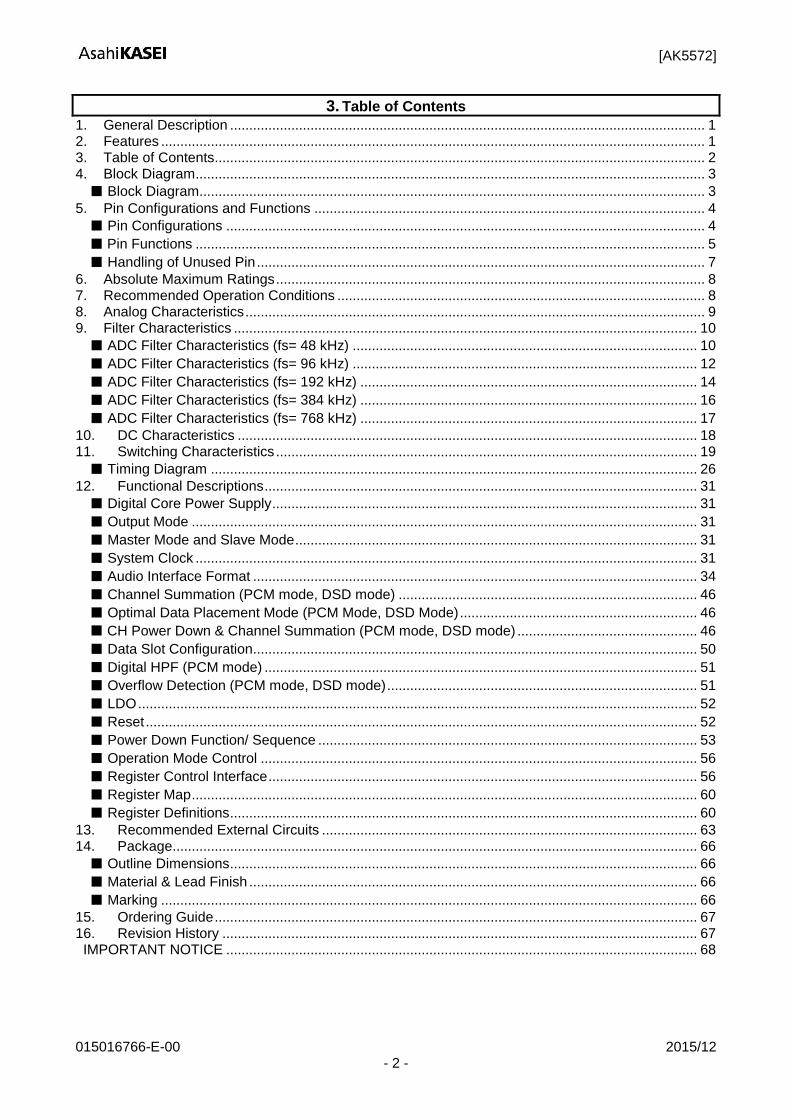
4. Block Diagram
Block Diagram
Figure 1. Block Diagram
Voltage Reference
Serial Output Interface
Delta-Sigma Modulator
Controller
LDO
Decimation Filter
HPF AIN1P
AIN1N DIF0/DSDSEL0
DIF1/DSDSEL1
BICK/DCLK
LRCK/DSDOL1
PSN/CAD0_SPI CKS0/SDA/CDTI CKS1/CAD0_I2C/CSN CKS2/SCL/CCLK CKS3/CAD1
VDD18 VR
EF
H1
VR
EF
L1
LDOE TVDD
AVDD
AVSS
DVSS
PD
N
Delta-Sigma Modulator
Decimation Filter
HPF AIN2P
AIN2N
TDMIN/DSDOR1
SDTO1
DP
TDM0
TDM1
ODP
MC
LK
TE
ST
SL
OW
/DC
KB
SD
/PM
OD
PW
2
PW
1
PW
0
MS
N
OV
F
DC
KS
/HP
FE
I2C
[AK5572]
015016766-E-00 2015/12 - 4 -
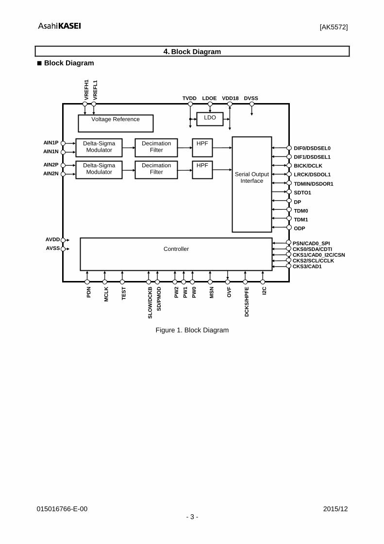
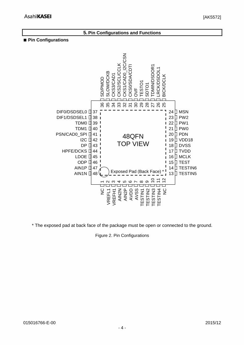
5. Pin Configurations and Functions
Pin Configurations
* The exposed pad at back face of the package must be open or connected to the ground.
Figure 2. Pin Configurations
DIF0/DSDSEL0
DIF1/DSDSEL1
TDM0
TDM1
PSN/CAD0_SPI
I2C
DP
HPFE/DCKS
LDOE
ODP
AIN1P
AIN1N
48QFN TOP VIEW
1
2
3
4
5
6
7
8
9
10
11
12
24
23
22
21
20
19
18
17
16
15
14
13
36
35
34
33
32
31
30
29
28
27
26
25
37
38
39
40
41
42
43
44
45
46
47
48 Exposed Pad (Back Face) *
SD
/PM
OD
SL
OW
/DC
KB
CK
S3
/CA
D1
CK
S2
/SC
L/C
CL
K
CK
S1
/CA
D0
_I2
C/C
SN
CK
S0
/SD
A/C
DT
I
OV
F
TE
ST
O1
SD
TO
1
TD
MIN
/DS
DO
R1
LR
CK
/DS
DO
L1
BIC
K/D
CL
K
NC
VR
EF
L1
VR
EF
H1
AIN
2N
AIN
2P
AV
DD
AV
SS
TE
ST
IN1
TE
ST
IN2
TE
ST
IN3
TE
ST
IN4
NC
MSN
PW2
PW1
PW0
PDN
VDD18
DVSS
TVDD
MCLK
TEST
TESTIN6
TESTIN5
[AK5572]
015016766-E-00 2015/12 - 5 -
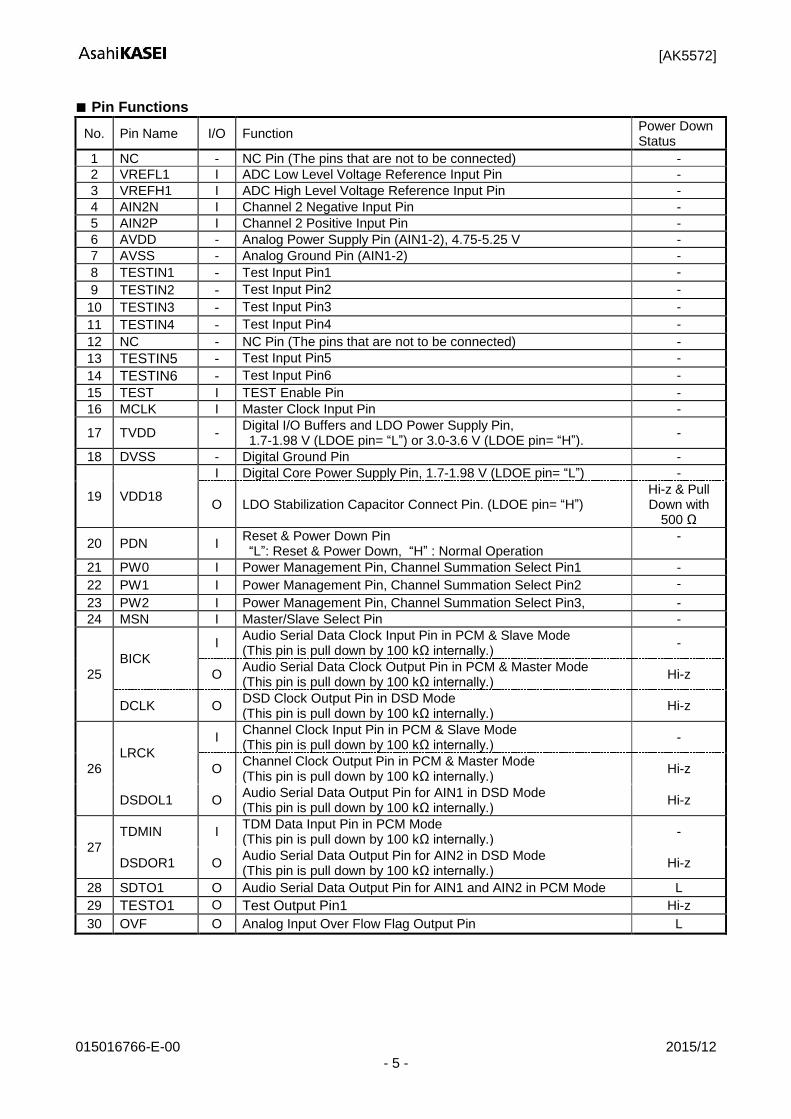
Pin Functions
No. Pin Name I/O Function Power Down Status
1 NC - NC Pin (The pins that are not to be connected) -
2 VREFL1 I ADC Low Level Voltage Reference Input Pin - 3 VREFH1 I ADC High Level Voltage Reference Input Pin - 4 AIN2N I Channel 2 Negative Input Pin - 5 AIN2P I Channel 2 Positive Input Pin - 6 AVDD - Analog Power Supply Pin (AIN1-2), 4.75-5.25 V -
7 AVSS - Analog Ground Pin (AIN1-2) -
8 TESTIN1 - Test Input Pin1 -
9 TESTIN2 - Test Input Pin2 -
10 TESTIN3 - Test Input Pin3 -
11 TESTIN4 - Test Input Pin4 -
12 NC - NC Pin (The pins that are not to be connected) -
13 TESTIN5 - Test Input Pin5 -
14 TESTIN6 - Test Input Pin6 -
15 TEST I TEST Enable Pin - 16 MCLK I Master Clock Input Pin -
17 TVDD - Digital I/O Buffers and LDO Power Supply Pin, 1.7-1.98 V (LDOE pin= “L”) or 3.0-3.6 V (LDOE pin= “H”).
-
18 DVSS - Digital Ground Pin -
19 VDD18
I Digital Core Power Supply Pin, 1.7-1.98 V (LDOE pin= “L”) -
O LDO Stabilization Capacitor Connect Pin. (LDOE pin= “H”) Hi-z & Pull Down with
500 Ω
20 PDN I Reset & Power Down Pin “L”: Reset & Power Down, “H” : Normal Operation
-
21 PW0 I Power Management Pin, Channel Summation Select Pin1 -
22 PW1 I Power Management Pin, Channel Summation Select Pin2 -
23 PW2 I Power Management Pin, Channel Summation Select Pin3, - 24 MSN I Master/Slave Select Pin -
25
BICK
I Audio Serial Data Clock Input Pin in PCM & Slave Mode (This pin is pull down by 100 kΩ internally.)
-
O Audio Serial Data Clock Output Pin in PCM & Master Mode (This pin is pull down by 100 kΩ internally.)
Hi-z
DCLK O DSD Clock Output Pin in DSD Mode (This pin is pull down by 100 kΩ internally.)
Hi-z
26
LRCK
I Channel Clock Input Pin in PCM & Slave Mode (This pin is pull down by 100 kΩ internally.)
-
O Channel Clock Output Pin in PCM & Master Mode (This pin is pull down by 100 kΩ internally.)
Hi-z
DSDOL1 O Audio Serial Data Output Pin for AIN1 in DSD Mode (This pin is pull down by 100 kΩ internally.)
Hi-z
27
TDMIN I TDM Data Input Pin in PCM Mode (This pin is pull down by 100 kΩ internally.)
-
DSDOR1 O Audio Serial Data Output Pin for AIN2 in DSD Mode (This pin is pull down by 100 kΩ internally.)
Hi-z
28 SDTO1 O Audio Serial Data Output Pin for AIN1 and AIN2 in PCM Mode L
29 TESTO1 O Test Output Pin1 Hi-z
30 OVF O Analog Input Over Flow Flag Output Pin L
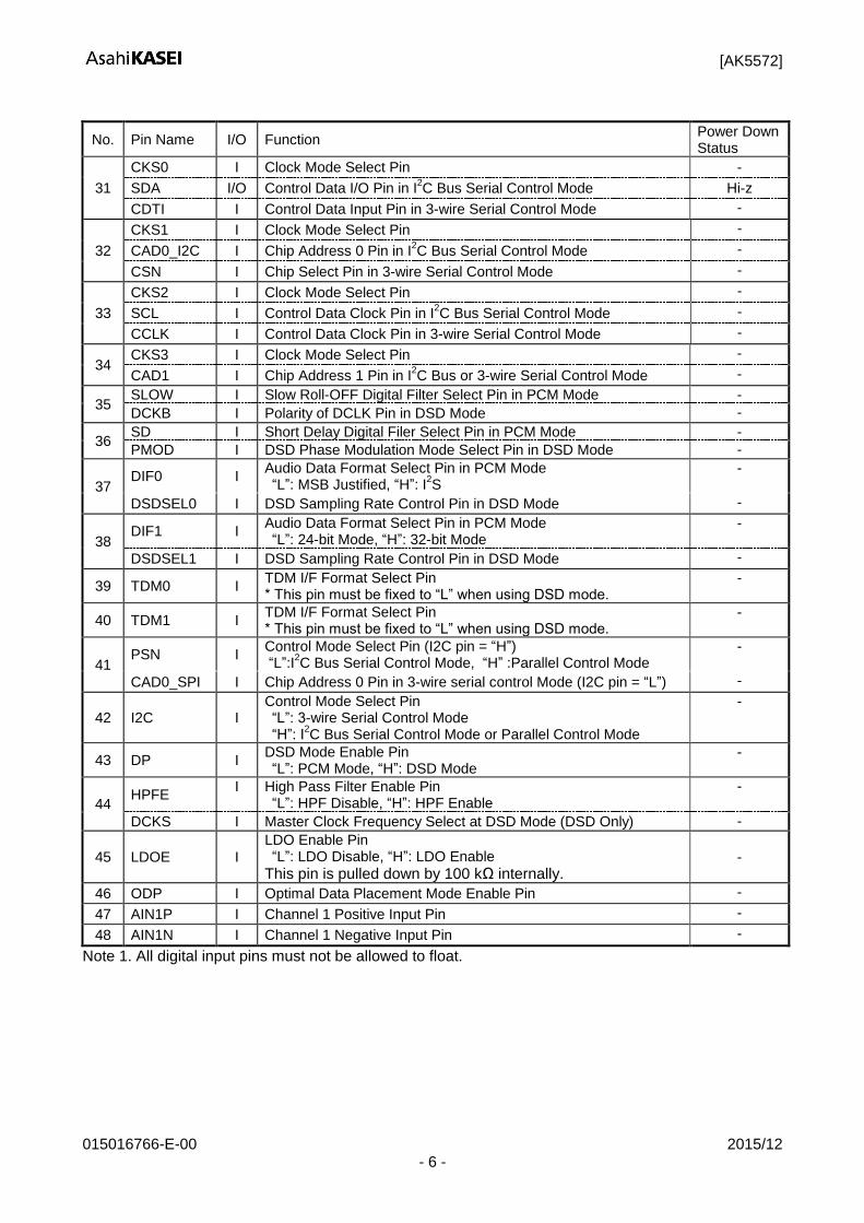
[AK5572]
015016766-E-00 2015/12 - 6 -
No. Pin Name I/O Function Power Down Status
31
CKS0 I Clock Mode Select Pin -
SDA I/O Control Data I/O Pin in I2C Bus Serial Control Mode Hi-z
CDTI I Control Data Input Pin in 3-wire Serial Control Mode -
32
CKS1 I Clock Mode Select Pin -
CAD0_I2C I Chip Address 0 Pin in I2C Bus Serial Control Mode -
CSN I Chip Select Pin in 3-wire Serial Control Mode -
33
CKS2 I Clock Mode Select Pin -
SCL I Control Data Clock Pin in I2C Bus Serial Control Mode -
CCLK I Control Data Clock Pin in 3-wire Serial Control Mode -
34 CKS3 I Clock Mode Select Pin -
CAD1 I Chip Address 1 Pin in I2C Bus or 3-wire Serial Control Mode -
35 SLOW I Slow Roll-OFF Digital Filter Select Pin in PCM Mode -
DCKB I Polarity of DCLK Pin in DSD Mode -
36 SD I Short Delay Digital Filer Select Pin in PCM Mode - PMOD I DSD Phase Modulation Mode Select Pin in DSD Mode -
37 DIF0 I
Audio Data Format Select Pin in PCM Mode “L”: MSB Justified, “H”: I
2S
-
DSDSEL0 I DSD Sampling Rate Control Pin in DSD Mode -
38 DIF1 I
Audio Data Format Select Pin in PCM Mode “L”: 24-bit Mode, “H”: 32-bit Mode
-
DSDSEL1 I DSD Sampling Rate Control Pin in DSD Mode -
39 TDM0 I TDM I/F Format Select Pin * This pin must be fixed to “L” when using DSD mode.
-
40 TDM1 I TDM I/F Format Select Pin * This pin must be fixed to “L” when using DSD mode.
-
41 PSN I
Control Mode Select Pin (I2C pin = “H”) “L”:I
2C Bus Serial Control Mode, “H” :Parallel Control Mode
-
CAD0_SPI I Chip Address 0 Pin in 3-wire serial control Mode (I2C pin = “L”) -
42 I2C I Control Mode Select Pin “L”: 3-wire Serial Control Mode “H”: I
2C Bus Serial Control Mode or Parallel Control Mode
-
43 DP I DSD Mode Enable Pin “L”: PCM Mode, “H”: DSD Mode
-
44 HPFE
I
High Pass Filter Enable Pin “L”: HPF Disable, “H”: HPF Enable
-
DCKS I Master Clock Frequency Select at DSD Mode (DSD Only) -
45 LDOE I
LDO Enable Pin “L”: LDO Disable, “H”: LDO Enable
This pin is pulled down by 100 kΩ internally. -
46 ODP I Optimal Data Placement Mode Enable Pin -
47 AIN1P I Channel 1 Positive Input Pin -
48 AIN1N I Channel 1 Negative Input Pin -
Note 1. All digital input pins must not be allowed to float.
[AK5572]
015016766-E-00 2015/12 - 7 -
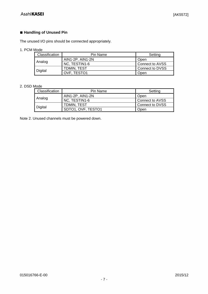
Handling of Unused Pin
The unused I/O pins should be connected appropriately. 1. PCM Mode
Classification Pin Name Setting
Analog AIN1-2P, AIN1-2N Open
NC, TESTIN1-6 Connect to AVSS
Digital TDMIN, TEST Connect to DVSS
OVF, TESTO1 Open
2. DSD Mode
Classification Pin Name Setting
Analog AIN1-2P, AIN1-2N Open
NC, TESTIN1-6 Connect to AVSS
Digital TDMIN, TEST Connect to DVSS
SDTO1, OVF, TESTO1 Open
Note 2. Unused channels must be powered down.
[AK5572]
015016766-E-00 2015/12 - 8 -
6. Absolute Maximum Ratings
(VSS= 0 V; Note 3)
Parameter Symbol Min. Max. Unit
Power Supplies:
Analog (AVDD pin) Digital Interface (TVDD pin) Digital Core (VDD18 pin)(Note 4)
AVDDam TVDDam VDD18am
−0.3 −0.3 −0.3
6.0 4.0 2.5
V V V
Input Current (Any Pin Except Supplies) IIN - 10 mA
Analog Input Voltage (AIN1-4P, AIN1-4N pins) VINA −0.3 AVDD+0.3 V
Digital Input Voltage VIND −0.3 TVDD+0.3 V
Ambient Temperature (Power applied) When the back tab is connected to VSS When the back tab is open
Ta Ta
−40 −40
105 70
C
C
Storage Temperature Tstg −65 150 C
Note 3. All voltages with respect to ground. Note 4. The 1.8 V LDO is off (LDOE pin = “L”) and an external power is supplied to the VDD18 pin. WARNING: Operation at or beyond these limits may result in permanent damage to the device.
Normal operation is not guaranteed at these extremes.
7. Recommended Operation Conditions
(VSS= 0 V; Note 3)
Parameter Symbol Min. Typ. Max. Unit
Power Supplies
Analog (AVDD pin) AVDD 4.75 5.0 5.25 V
(LDOE pin= “L”) (Note 5) Digital Interface (TVDD pin) (Note 6) Digital Core (VDD18 pin)
TVDD VDD18
1.7 1.7
1.8 1.8
1.98 1.98
V V
(LDOE pin= “H”) (Note 7) Digital Interface (TVDD pin)
TVDD
3.0
3.3
3.6
V
Voltage Reference (Note 11)
“H” voltage Reference (Note 8) VREFH1 4.75 5.0 5.25 V
“L” voltage reference VREFL1 - AVSS - V
Note 3. All voltages with respect to ground. Note 5. TVDD pin must be powered up before VDD18 pin when the LDOE pin = “L”. The power up
sequence between AVDD pin and TVDD pin or between AVDD pin and VDD18 pin is not critical. Note 6. TVDD must not exceed VDD18±0.1 V when LDOE pin= “L”. Note 7. When LDOE pin = “H”, the internal LDO supplies 1.8 V (typ). The power up sequences between
AVDD pin and TVDD pin is not critical. Note 8. VREFH1 must not exceed AVDD+0.1 V. Note 9. VREFL1 must be connected to AVSS. Analog Input Voltage is proportional to (VREFH) – (VREFL).
Vin (typ, @ 0dB) = 2.8 (VREFH) – (VREFL) / 5 [V]. * AKM assumes no responsibility for the usage beyond the conditions in this data sheet.
[AK5572]
015016766-E-00 2015/12 - 9 -
8. Analog Characteristics
(Ta= 25 C; AVDD= 5.0 V; TVDD= 3.3 V, fs= 48 kHz, BICK= 64fs; Signal Frequency= 1 kHz; 24-bit Data; Measurement frequency= 20 Hz-20 kHz at fs= 48 kHz, 40 Hz-40 kHz at fs= 96 kHz, 40 Hz-40 kHz at fs= 192 kHz, unless otherwise specified.)
Parameter Min. Typ. Max. Unit
Analog Input Characteristics:
Resolution - - 32 Bit
Input Voltage (Note 10) 2.7 2.8 2.9 Vpp
S/(N+D)
fs=48kHz BW=20kHz
1dBFS 20dBFS 60dBFS
100 - -
112 97 57
- - -
dB dB dB
fs=96kHz BW=40kHz
1dBFS 20dBFS 60dBFS
- - -
110 90 50
- - -
dB dB dB
fs=192kHz BW=40kHz
1dBFS 20dBFS 60dBFS
- - -
110 90 50
- - -
dB dB dB
Dynamic Range (60dBFS with A-weighted)
Not Sum. mode 2-to-1 mode
117 -
121 124
- -
dB dB
S/N (A-weighted)
Not Sum. mode 2-to-1 mode
117 -
121 124
- -
dB dB
Input Resistance These values will be doubled in DSD 64fs mode. (Values in DSD128 or DSD256 modes are as shown here)
3.0 3.6 4.2 k
Interchannel Isolation (AIN1AIN2)
110 120 - dB
Interchannel Gain Mismatch - 0 0.5 dB
Power Supply Rejection (Note 11) - 60 - dB
Power Supplies
Power Supply Current
Normal Operation (PDN pin = “H”, LDOE pin = “H”)
AVDD+VREFH1
TVDD (fs= 48 kHz)
TVDD (fs= 96 kHz)
TVDD (fs= 192 kHz)
Power down mode (PDN pin = “L”) (Note 12)
AVDD+TVDD
-
-
-
-
-
25
7
11
11
10
33
10
14
14
100
mA
mA
mA
mA
A
Note 10. This value is (AINnP)(AINnN) that the ADC output becomes full-scale (n=1-2).
Vin = 0.56 (VREFHmVREFLm) [Vpp]. (m=1) Note 11. PSRR is applied to AVDD, TVDD with 1kHz, 20mVpp sine wave. The VREFH1 is held to the
fixed voltage. Note 12. All digital inputs are fixed to TVDD or TVSS.
[AK5572]
015016766-E-00 2015/12 - 10 -
9. Filter Characteristics
ADC Filter Characteristics (fs= 48 kHz)
(Ta= 40 - +105 C; AVDD= 4.75-5.25 V, TVDD=1.7-1.98 V (LDOE pin=“L”) or 3.0-3.6 V (LDOE pin=“H”), VDD18= 1.7-1.98 V (LDOE pin= “L”))
Parameter Symbol Min. Typ. Max. Unit
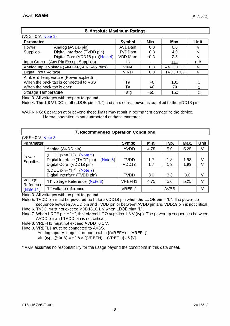
Digital Filter (Decimation LPF): SHARP ROLL-OFF (Figure 3) (SD pin=“L”, SLOW pin=“L”)
Passband (Note 13) +0.001/0.06 dB PB 0 - 22.0 kHz
6.0 dB - 24.4 - kHz
Stopband (Note 13) SB 27.9 - - kHz
Stopband Attenuation SA 85 - - dB
Group Delay Distortion 0 - 20.0 kHz GD - 0 - 1/fs
Group Delay (Note 14) GD - 19 - 1/fs
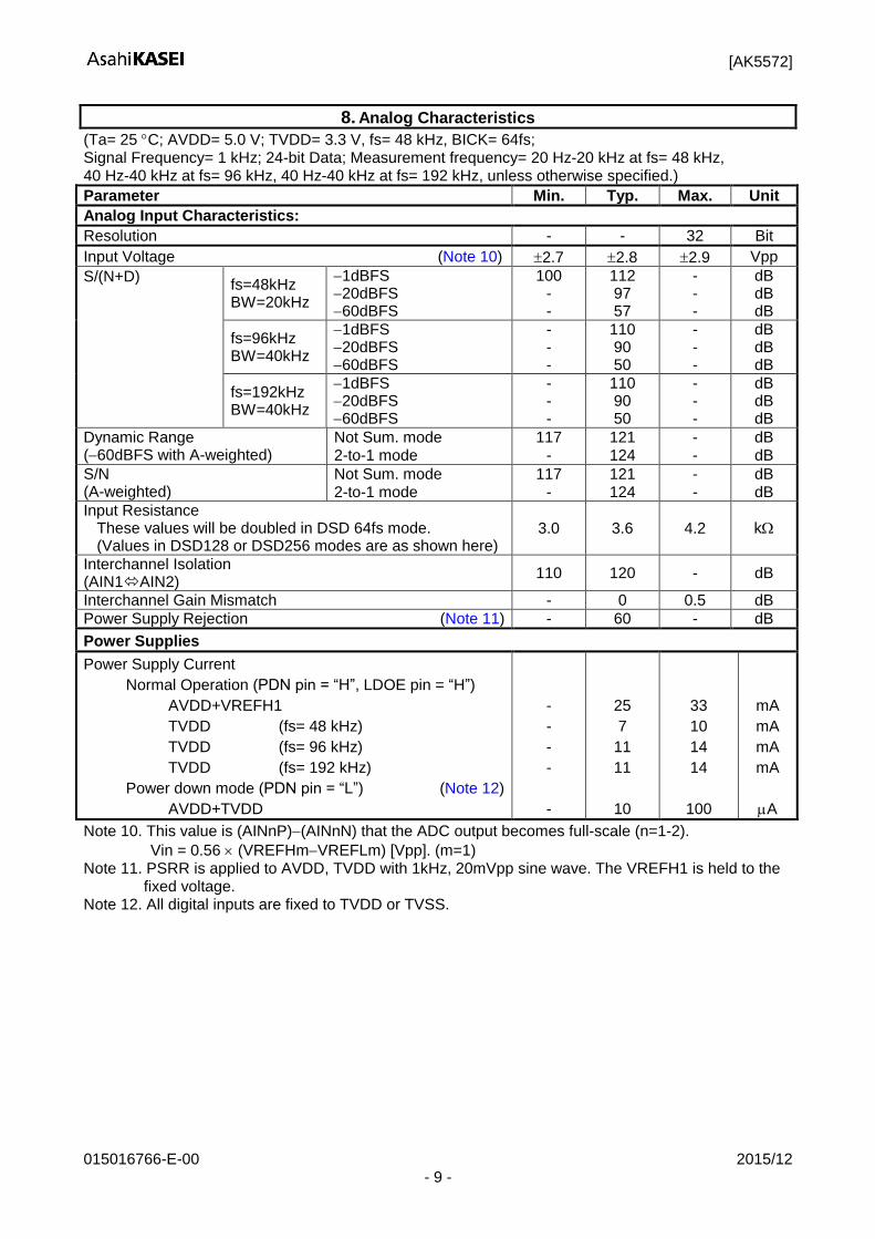
Digital Filter (Decimation LPF): SLOW ROLL-OFF (Figure 4) (SD pin=“L”, SLOW pin=“H”)
Passband (Note 13)
+0.001/0.076 dB
6.0 dB
PB
0 -
- 21.9
12.5 -
kHz kHz
Stopband (Note 13) SB 36.5 - - kHz
Stopband Attenuation SA 85 - - dB
Group Delay Distortion 0 - 20.0 kHz GD - 0 - 1/fs
Group Delay (Note 14) GD - 7 - 1/fs
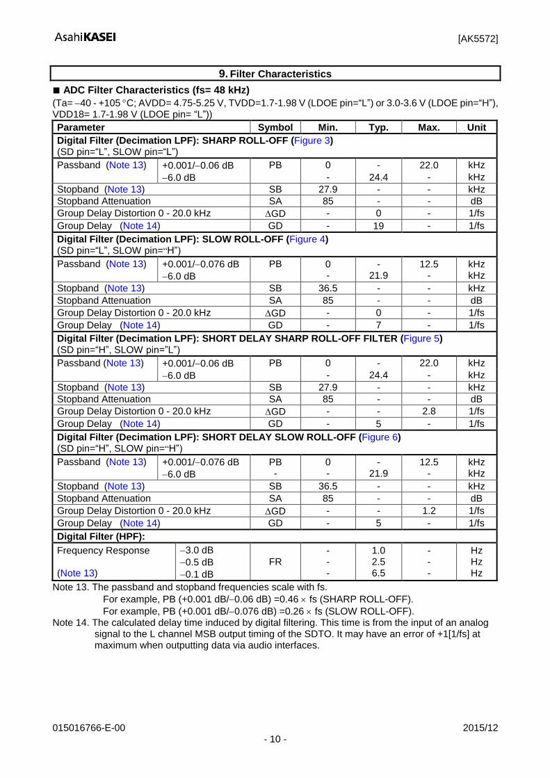
Digital Filter (Decimation LPF): SHORT DELAY SHARP ROLL-OFF FILTER (Figure 5) (SD pin=“H”, SLOW pin=”L”)
Passband (Note 13) +0.001/0.06 dB PB 0 - 22.0 kHz
6.0 dB - 24.4 - kHz
Stopband (Note 13) SB 27.9 - - kHz
Stopband Attenuation SA 85 - - dB
Group Delay Distortion 0 - 20.0 kHz GD - - 2.8 1/fs
Group Delay (Note 14) GD - 5 - 1/fs
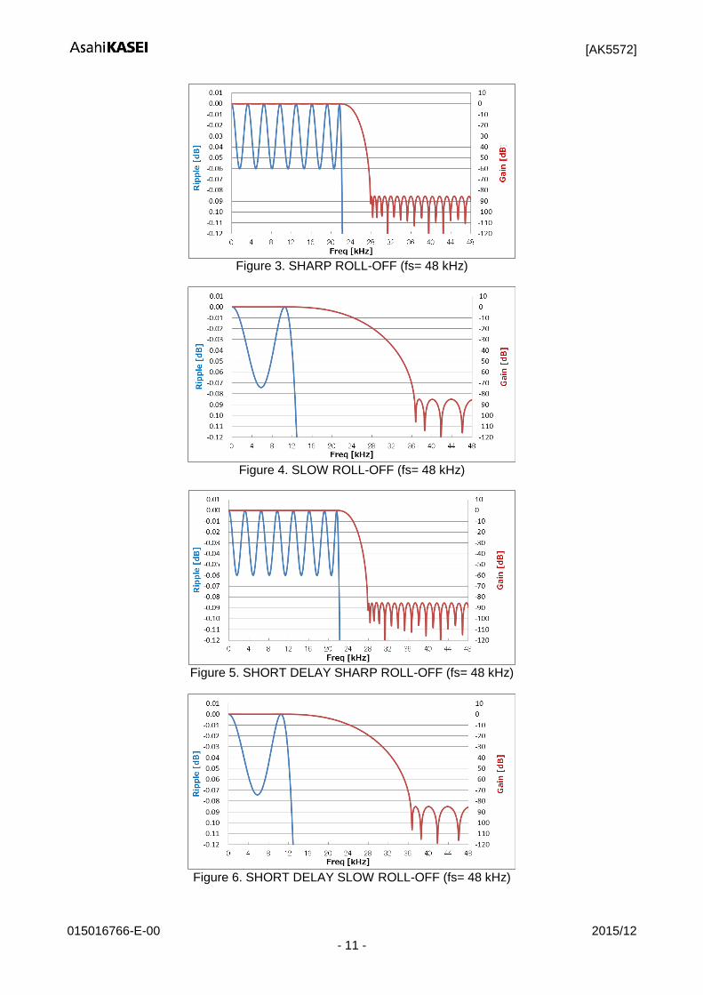
Digital Filter (Decimation LPF): SHORT DELAY SLOW ROLL-OFF (Figure 6) (SD pin=“H”, SLOW pin=“H”)
Passband (Note 13)
+0.001/0.076 dB
6.0 dB
PB -
0 -
- 21.9
12.5 -
kHz kHz
Stopband (Note 13) SB 36.5 - - kHz
Stopband Attenuation SA 85 - - dB
Group Delay Distortion 0 - 20.0 kHz GD - - 1.2 1/fs
Group Delay (Note 14) GD - 5 - 1/fs
Digital Filter (HPF):
Frequency Response (Note 13)
3.0 dB
0.5 dB
0.1 dB
FR - - -
1.0 2.5 6.5
- - -
Hz Hz Hz
Note 13. The passband and stopband frequencies scale with fs.
For example, PB (+0.001 dB/0.06 dB) =0.46 fs (SHARP ROLL-OFF).
For example, PB (+0.001 dB/0.076 dB) =0.26 fs (SLOW ROLL-OFF). Note 14. The calculated delay time induced by digital filtering. This time is from the input of an analog
signal to the L channel MSB output timing of the SDTO. It may have an error of +1[1/fs] at maximum when outputting data via audio interfaces.
[AK5572]
015016766-E-00 2015/12 - 11 -
Figure 3. SHARP ROLL-OFF (fs= 48 kHz)
Figure 4. SLOW ROLL-OFF (fs= 48 kHz)
Figure 5. SHORT DELAY SHARP ROLL-OFF (fs= 48 kHz)
Figure 6. SHORT DELAY SLOW ROLL-OFF (fs= 48 kHz)
[AK5572]
015016766-E-00 2015/12 - 12 -
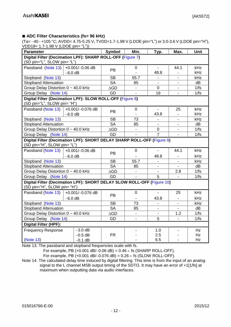
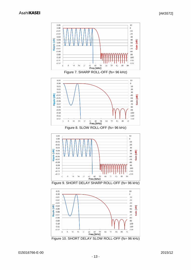
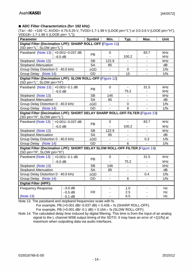
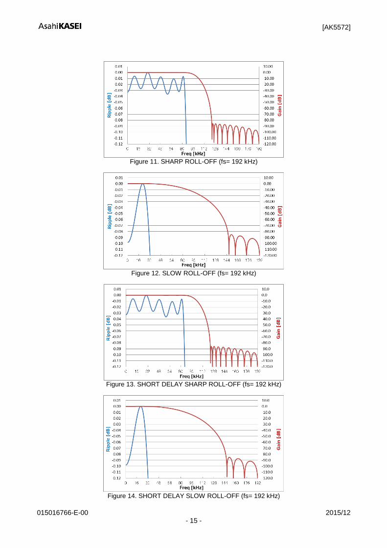
ADC Filter Characteristics (fs= 96 kHz)
(Ta= 40 - +105 C; AVDD= 4.75-5.25 V, TVDD=1.7-1.98 V (LDOE pin=“L”) or 3.0-3.6 V (LDOE pin=“H”), VDD18= 1.7-1.98 V (LDOE pin= “L”))
Parameter Symbol Min. Typ. Max. Unit
Digital Filter (Decimation LPF): SHARP ROLL-OFF (Figure 7) (SD pin=“L”, SLOW pin= “L”)
Passband (Note 13)
+0.001/0.06 dB
6.0 dB PB
0 -
- 48.8
44.1
-
kHz kHz
Stopband (Note 13) SB 55.7 - - kHz
Stopband Attenuation SA 85 - - dB
Group Delay Distortion 0 ~ 40.0 kHz GD - 0 - 1/fs
Group Delay (Note 14) GD - 19 - 1/fs
Digital Filter (Decimation LPF): SLOW ROLL-OFF (Figure 8) (SD pin=“L”, SLOW pin= “H”)
Passband (Note 13)
+0.001/0.076 dB
6.0 dB PB
0 -
- 43.8
25
-
kHz kHz
Stopband (Note 13) SB 73 - - kHz
Stopband Attenuation SA 85 - - dB
Group Delay Distortion 0 ~ 40.0 kHz GD - 0 - 1/fs
Group Delay (Note 14) GD - 7 - 1/fs
Digital Filter (Decimation LPF): SHORT DELAY SHARP ROLL-OFF (Figure 9) (SD pin=“H”, SLOW pin= “L”)
Passband (Note 13) +0.001/0.06 dB PB
0 - 44.1 kHz
6.0 dB - 48.8 - kHz
Stopband (Note 13) SB 55.7 - - kHz
Stopband Attenuation SA 85 - - dB
Group Delay Distortion 0 ~ 40.0 kHz GD - - 2.8 1/fs
Group Delay (Note 14) GD - 5 - 1/fs
Digital Filter (Decimation LPF): SHORT DELAY SLOW ROLL-OFF (Figure 10) (SD pin=“H”, SLOW pin= “H”)
Passband (Note 13) +0.001/0.076 dB PB
0 - 25 kHz
6.0 dB - 43.8 - kHz
Stopband (Note 13) SB 73 - - kHz
Stopband Attenuation SA 85 - - dB
Group Delay Distortion 0 ~ 40.0 kHz GD - - 1.2 1/fs
Group Delay (Note 14) GD - 5 - 1/fs
Digital Filter (HPF):
Frequency Response (Note 13)
3.0 dB
0.5 dB
0.1 dB
FR - - -
1.0 2.5 6.5
- - -
Hz Hz Hz
Note 13. The passband and stopband frequencies scale with fs.
For example, PB (+0.001 dB/0.06 dB) = 0.46 fs (SHARP ROLL-OFF).
For example, PB (+0.001 dB/0.076 dB) = 0.26 fs (SLOW ROLL-OFF). Note 14. The calculated delay time induced by digital filtering. This time is from the input of an analog
signal to the L channel MSB output timing of the SDTO. It may have an error of +1[1/fs] at maximum when outputting data via audio interfaces.
[AK5572]
015016766-E-00 2015/12 - 13 -
Figure 7. SHARP ROLL-OFF (fs= 96 kHz)
Figure 8. SLOW ROLL-OFF (fs= 96 kHz)
Figure 9. SHORT DELAY SHARP ROLL-OFF (fs= 96 kHz)
Figure 10. SHORT DELAY SLOW ROLL-OFF (fs= 96 kHz)
[AK5572]
015016766-E-00 2015/12 - 14 -
ADC Filter Characteristics (fs= 192 kHz)
(Ta= 40 - +105 C; AVDD= 4.75-5.25 V, TVDD=1.7-1.98 V (LDOE pin=“L”) or 3.0-3.6 V (LDOE pin=“H”), VDD18= 1.7-1.98 V (LDOE pin= “L”))
Parameter Symbol Min. Typ. Max. Unit
Digital Filter (Decimation LPF): SHARP ROLL-OFF (Figure 11) (SD pin=“L”, SLOW pin=“L”)
Passband (Note 13)
+0.001/0.037 dB
6.0 dB PB
0 -
- 100.2
83.7
-
kHz kHz
Stopband (Note 13) SB 122.9 - - kHz
Stopband Attenuation SA 85 - - dB
Group Delay Distortion 0 - 40.0 kHz GD - 0 - 1/fs
Group Delay (Note 14) GD - 15 - 1/fs
Digital Filter (Decimation LPF): SLOW ROLL-OFF (Figure 12) (SD pin=“L”, SLOW pin=“H”)
Passband (Note 13)
+0.001/0.1 dB
6.0 dB PB
0 -
- 75.2
31.5 -
kHz kHz
Stopband (Note 13) SB 146 - - kHz
Stopband Attenuation SA 85 - - dB
Group Delay Distortion 0 - 40.0 kHz GD - 0 - 1/fs
Group Delay (Note 14) GD - 8 - 1/fs
Digital Filter (Decimation LPF): SHORT DELAY SHARP ROLL-OFF FILTER (Figure 13) (SD pin=“H”, SLOW pin=“L”)
Passband (Note 13) +0.001/0.037 dB PB
0 - 83.7 kHz
6.0 dB - 100.2 - kHz
Stopband (Note 13) SB 122.9 - - kHz
Stopband Attenuation SA 85 - - dB
Group Delay Distortion 0 - 40.0 kHz GD - - 0.3 1/fs
Group Delay (Note 14) GD - 6 - 1/fs
Digital Filter (Decimation LPF): SHORT DELAY SLOW ROLL-OFF FILTER (Figure 14) (SD pin=“H”, SLOW pin=“H”)
Passband (Note 13) +0.001/0.1 dB PB
0 - 31.5 kHz
6.0 dB - 75.2 - kHz
Stopband (Note 13) SB 146 - - kHz
Stopband Attenuation SA 85 - - dB
Group Delay Distortion 0 - 40.0 kHz GD - - 0.4 1/fs
Group Delay (Note 14) GD - 6 - 1/fs
Digital Filter (HPF):
Frequency Response (Note 13)
3.0 dB
0.5 dB
0.1 dB
FR - - -
1.0 2.5 6.5
- - -
Hz Hz Hz
Note 13. The passband and stopband frequencies scale with fs.
For example, PB (+0.001 dB/0.037 dB) = 0.436 fs (SHARP ROLL-OFF).
For example, PB (+0.001 dB/0.1 dB) = 0.164 fs (SLOW ROLL-OFF). Note 14. The calculated delay time induced by digital filtering. This time is from the input of an analog
signal to the L channel MSB output timing of the SDTO. It may have an error of +1[1/fs] at maximum when outputting data via audio interfaces.
[AK5572]
015016766-E-00 2015/12 - 15 -
Figure 11. SHARP ROLL-OFF (fs= 192 kHz)
Figure 12. SLOW ROLL-OFF (fs= 192 kHz)
Figure 13. SHORT DELAY SHARP ROLL-OFF (fs= 192 kHz)
Figure 14. SHORT DELAY SLOW ROLL-OFF (fs= 192 kHz)
[AK5572]
015016766-E-00 2015/12 - 16 -
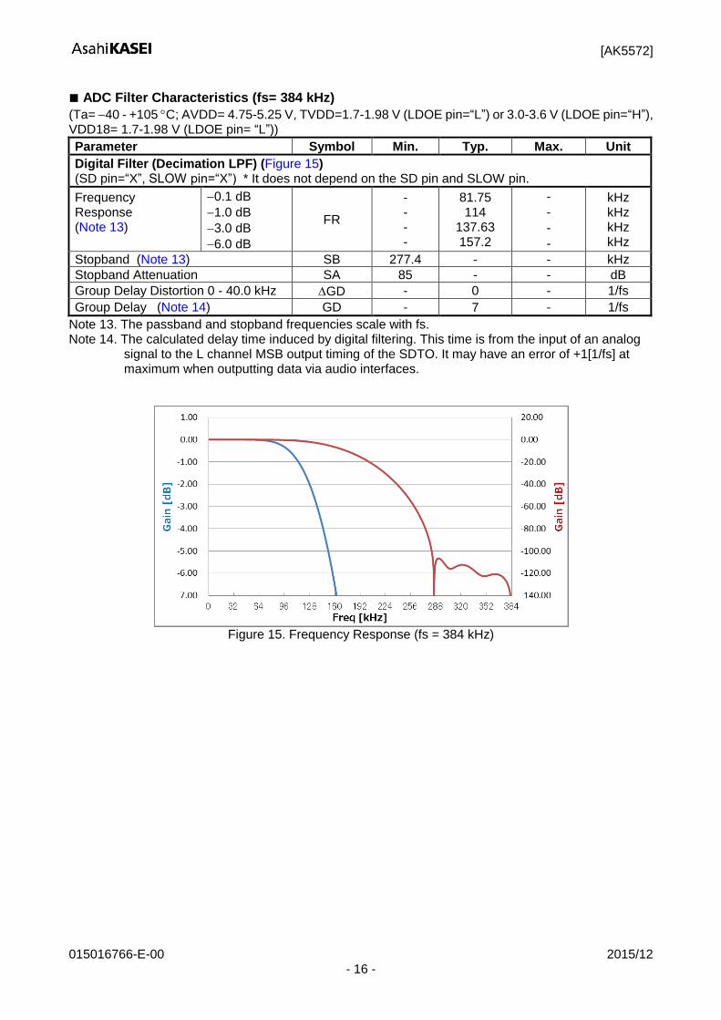
ADC Filter Characteristics (fs= 384 kHz)
(Ta= 40 - +105 C; AVDD= 4.75-5.25 V, TVDD=1.7-1.98 V (LDOE pin=“L”) or 3.0-3.6 V (LDOE pin=“H”), VDD18= 1.7-1.98 V (LDOE pin= “L”))
Parameter Symbol Min. Typ. Max. Unit
Digital Filter (Decimation LPF) (Figure 15) (SD pin=“X”, SLOW pin=“X”) * It does not depend on the SD pin and SLOW pin.
Frequency Response (Note 13)
0.1 dB
1.0 dB
3.0 dB
6.0 dB
FR
- - - -
81.75 114
137.63 157.2
-
-
-
-
kHz kHz kHz kHz
Stopband (Note 13) SB 277.4 - - kHz
Stopband Attenuation SA 85 - - dB
Group Delay Distortion 0 - 40.0 kHz GD - 0 - 1/fs
Group Delay (Note 14) GD - 7 - 1/fs
Note 13. The passband and stopband frequencies scale with fs. Note 14. The calculated delay time induced by digital filtering. This time is from the input of an analog
signal to the L channel MSB output timing of the SDTO. It may have an error of +1[1/fs] at maximum when outputting data via audio interfaces.
Figure 15. Frequency Response (fs = 384 kHz)
[AK5572]
015016766-E-00 2015/12 - 17 -
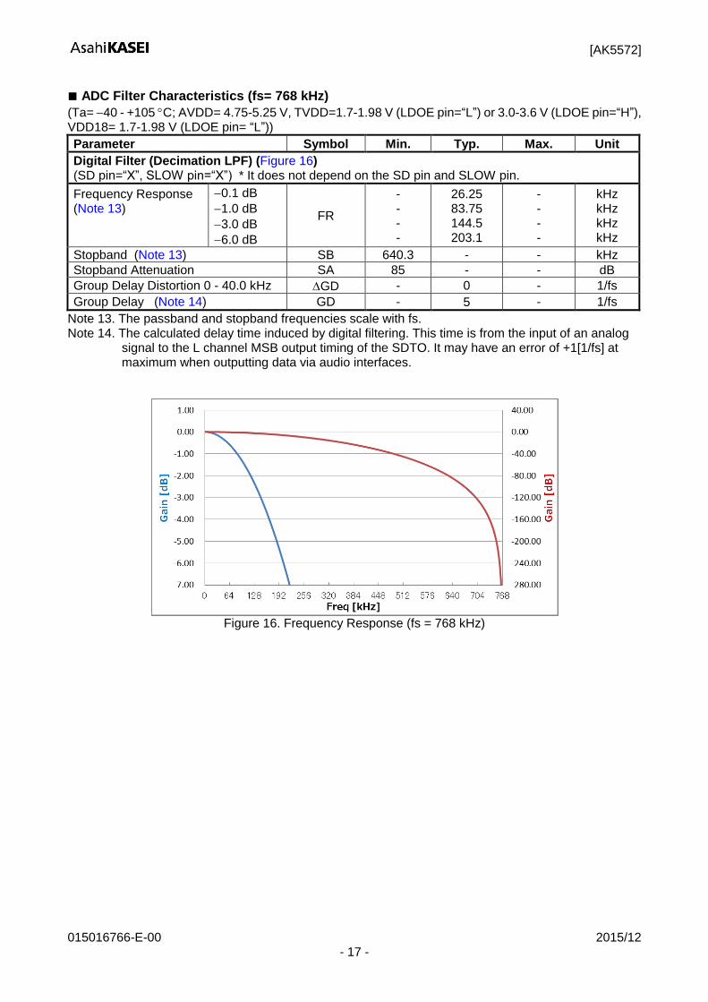
ADC Filter Characteristics (fs= 768 kHz)
(Ta= 40 - +105 C; AVDD= 4.75-5.25 V, TVDD=1.7-1.98 V (LDOE pin=“L”) or 3.0-3.6 V (LDOE pin=“H”), VDD18= 1.7-1.98 V (LDOE pin= “L”))
Parameter Symbol Min. Typ. Max. Unit
Digital Filter (Decimation LPF) (Figure 16) (SD pin=“X”, SLOW pin=“X”) * It does not depend on the SD pin and SLOW pin.
Frequency Response (Note 13)
0.1 dB
1.0 dB
3.0 dB
6.0 dB
FR
- - - -
26.25 83.75 144.5 203.1
- - - -
kHz kHz kHz kHz
Stopband (Note 13) SB 640.3 - - kHz
Stopband Attenuation SA 85 - - dB
Group Delay Distortion 0 - 40.0 kHz GD - 0 - 1/fs
Group Delay (Note 14) GD - 5 - 1/fs
Note 13. The passband and stopband frequencies scale with fs. Note 14. The calculated delay time induced by digital filtering. This time is from the input of an analog
signal to the L channel MSB output timing of the SDTO. It may have an error of +1[1/fs] at maximum when outputting data via audio interfaces.
Figure 16. Frequency Response (fs = 768 kHz)
[AK5572]
015016766-E-00 2015/12 - 18 -
10. DC Characteristics
(Ta= 40-105 C; AVDD= 4.75-5.25 V, VDD18= 1.7-1.98 V (LDOE pin=“L”))
Parameter Symbol Min. Typ. Max. Unit
TVDD= 3.0-3.6 V (LDOE pin=”H”)
High-Level Input Voltage (Note 15) Low-Level Input Voltage (Note 15)
VIH
VIL
70%TVDD
-
-
-
-
30%TVDD
V
V
High-Level Output Voltage (Note 16)
(Iout= 100 µA) Low-Level Output Voltage (Note 17) (except SDA pin: Iout= 100 µA) (SDA pin: Iout= 3 mA)
VOH
VOL
VOL
TVDD0.5
-
-
-
-
-
-
0.5
0.4
V
V
V
TVDD=1.7-1.98 V (LDOE pin=”L”)
High-Level Input Voltage (Note 15) Low-Level Input Voltage (Note 15)
VIH VIL
80%TVDD -
- -
- 20%TVDD
V V
High-Level Output Voltage (Note 16)
(Iout= 100 µA) Low-Level Output Voltage (Note 17) (except SDA pin: Iout= 100 µA) (SDA pin: Iout= 3 mA)
VOH
VOL
VOL
TVDD0.3
-
-
-
-
-
-
0.3
20%TVDD
V
V
V
Input Leakage Current Iin - - 10 A
Note 15. MCLK, PDN, PW0-2, MSN, BICK (Slave Mode), LRCK (Slave Mode), TDMIN, SLOW/DCKB, SD/PMOD, CKS0/SDA (Write)/CDTI, CKS1/CAD0_I2C/CSN, CKS2/SCL/CCLK, CKS3/CAD1, DIF0/DSDSEL0, DIF1/DSDSEL1, TDM0, TDM1, PSN/CAD0_SPI, I2C, DP, HPFE/DCKS, LDOE, ODP, TEST
Note 16. BICK (Master Mode)/DCLK, LRCK (Master Mode)/DSDOL1, DSDOR1, SDTO1, OVF Note 17. Note.16 and SDA (Read)
The external pull-up resistors should be connected to TVDD+0.3 V or less.
[AK5572]
015016766-E-00 2015/12 - 19 -
11. Switching Characteristics
(Ta= 40 - +105 C; AVDD= 4.75-5.25 V, TVDD= 1.7-1.98 V (LDOE pin=“L”) or 3.0-3.6 V (LDOE pin=“H”), VDD18= 1.7-1.98 V (LDOE pin=“L”), CL= 10 pF)
Parameter Symbol Min. Typ. Max. Unit
Master Clock Timing (Figure 18) fCLK dCLK
2.048
45
- -
49.152
55
MHz
% Frequency Duty Cycle
LRCK Frequency (Slave mode) (Figure 17)
Normal mode (TDM1-0 bits = “00”) Normal Speed mode Double Speed mode Quad Speed mode Oct Speed mode Hex Speed mode Duty Cycle
fsn fsd fsq fso fsh
Duty
8
54 108
- -
45
- - -
384 768
-
54
108 216
- -
55
kHz kHz kHz kHz kHz %
TDM128 mode (TDM1-0 bits = “01”) Normal Speed mode Double Speed mode Quad Speed mode High Time Low Time
fsn fsd fsq
tLRH tLRL
8
54 108
1/128fs 1/128fs
- - - - -
54
108 216
- -
kHz kHz kHz ns ns
TDM256 mode (TDM1-0 bits = “10”) Normal Speed mode Double Speed mode High time Low time
fsn fsd
tLRH tLRL
8
54 1/256fs 1/256fs
- - - -
54
108 - -
kHz kHz ns ns
TDM512 mode (TDM1-0 bits = “11”) Normal Speed mode High Time Low Time
fsn
tLRH tLRL
8
1/512fs 1/512fs
- - -
54 - -
kHz ns ns
LRCK Frequency (Master mode) (Figure 18)
Normal mode (TDM1-0 bits = “00”) Normal Speed mode Double Speed mode Quad Speed mode Oct Speed mode Hex Speed mode Duty Cycle
fsn fsd fsq fso fsh
Duty
8
54 108
- - -
- - -
384 768 50
54
108 216
- - -
kHz kHz kHz kHz kHz %
TDM128 mode (TDM1-0 bits = “01”) Normal Speed mode Double Speed mode Quad Speed mode High Time
fsn fsd fsq
tLRH
8
54 108
-
- - -
1/4fs
54
108 216
-
kHz kHz kHz ns
TDM256 mode (TDM1-0 bits = “10”) Normal Speed mode Double Speed mode High Time
fsn fsd
tLRH
8
54 -
- -
1/8fs
54
108 -
kHz kHz ns
TDM512 mode (TDM1-0 bits = “11”) Normal Speed mode High Time
fsn
tLRH
8 -
-
1/16fs
54 -
kHz ns
Note 18. When the 1024fs, 512fs or 768fs /256fs or 384fs /128fs or 192fs are switched, the AK5572 should be reset by the PDN pin or RSTN bit.
[AK5572]
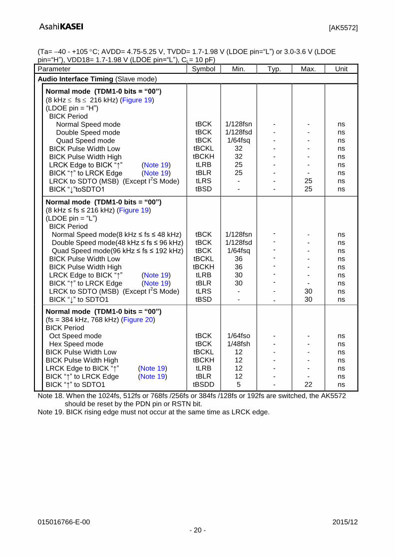
015016766-E-00 2015/12 - 20 -
(Ta= 40 - +105 C; AVDD= 4.75-5.25 V, TVDD= 1.7-1.98 V (LDOE pin=“L”) or 3.0-3.6 V (LDOE pin=“H”), VDD18= 1.7-1.98 V (LDOE pin=“L”), CL= 10 pF)
Parameter Symbol Min. Typ. Max. Unit
Audio Interface Timing (Slave mode)
Normal mode (TDM1-0 bits = “00”)
(8 kHz fs 216 kHz) (Figure 19) (LDOE pin = “H”) BICK Period
Normal Speed mode Double Speed mode Quad Speed mode
BICK Pulse Width Low BICK Pulse Width High LRCK Edge to BICK “↑” (Note 19) BICK “↑” to LRCK Edge (Note 19) LRCK to SDTO (MSB) (Except I
2S Mode)
BICK “↓”toSDTO1
tBCK tBCK tBCK tBCKL tBCKH tLRB tBLR tLRS tBSD
1/128fsn 1/128fsd 1/64fsq
32 32 25 25 - -
- - - - - - - - -
- - - - - - -
25 25
ns ns ns ns ns ns ns ns ns
Normal mode (TDM1-0 bits = “00”) (8 kHz ≤ fs ≤ 216 kHz) (Figure 19) (LDOE pin = “L”) BICK Period Normal Speed mode(8 kHz ≤ fs ≤ 48 kHz) Double Speed mode(48 kHz ≤ fs ≤ 96 kHz) Quad Speed mode(96 kHz ≤ fs ≤ 192 kHz)
BICK Pulse Width Low BICK Pulse Width High LRCK Edge to BICK “↑” (Note 19) BICK “↑” to LRCK Edge (Note 19) LRCK to SDTO (MSB) (Except I
2S Mode)
BICK “↓” to SDTO1
tBCK tBCK tBCK tBCKL tBCKH tLRB tBLR tLRS tBSD
1/128fsn 1/128fsd 1/64fsq
36 36 30 30 - -
- - - - - - -
-
-
- - - - - - -
30 30
ns ns ns ns ns ns ns ns ns
Normal mode (TDM1-0 bits = “00”) (fs = 384 kHz, 768 kHz) (Figure 20) BICK Period Oct Speed mode Hex Speed mode
BICK Pulse Width Low BICK Pulse Width High LRCK Edge to BICK “↑” (Note 19) BICK “↑” to LRCK Edge (Note 19) BICK “↑” to SDTO1
tBCK tBCK tBCKL tBCKH tLRB tBLR
tBSDD
1/64fso 1/48fsh
12 12 12 12 5
- - - - - - -
- - - - - -
22
ns ns ns ns ns ns ns
Note 18. When the 1024fs, 512fs or 768fs /256fs or 384fs /128fs or 192fs are switched, the AK5572 should be reset by the PDN pin or RSTN bit.
Note 19. BICK rising edge must not occur at the same time as LRCK edge.
[AK5572]
015016766-E-00 2015/12 - 21 -
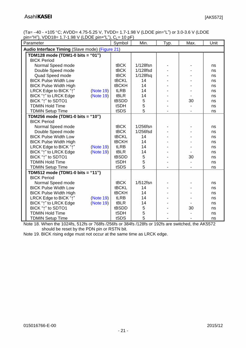
(Ta= 40 - +105 C; AVDD= 4.75-5.25 V, TVDD= 1.7-1.98 V (LDOE pin=“L”) or 3.0-3.6 V (LDOE pin=“H”), VDD18= 1.7-1.98 V (LDOE pin=“L”), CL= 10 pF)
Parameter Symbol Min. Typ. Max. Unit
Audio Interface Timing (Slave mode) (Figure 21)
TDM128 mode (TDM1-0 bits = “01”) BICK Period
Normal Speed mode Double Speed mode Quad Speed mode
BICK Pulse Width Low BICK Pulse Width High LRCK Edge to BICK “↑” (Note 19) BICK “↑” to LRCK Edge (Note 19) BICK “↑” to SDTO1 TDMIN Hold Time TDMIN Setup Time
tBCK tBCK tBCK
tBCKL tBCKH tLRB tBLR
tBSDD tSDH tSDS
1/128fsn 1/128fsd 1/128fsq
14 14 14 14 5 5 5
- - - - - - - - - -
- - - - - - -
30 - -
ns ns ns ns ns ns ns ns ns ns
TDM256 mode (TDM1-0 bits = “10”) BICK Period
Normal Speed mode Double Speed mode
BICK Pulse Width Low BICK Pulse Width High LRCK Edge to BICK “↑” (Note 19) BICK “↑” to LRCK Edge (Note 19) BICK “↑” to SDTO1 TDMIN Hold Time TDMIN Setup Time
tBCK tBCK
tBCKL tBCKH tLRB tBLR
tBSDD tSDH tSDS
1/256fsn 1/256fsd
14 14 14 14 5 5 5
- - - - - - - - -
- - - - - -
30 - -
ns ns ns ns ns ns ns ns ns
TDM512 mode (TDM1-0 bits = “11”) BICK Period
Normal Speed mode BICK Pulse Width Low BICK Pulse Width High LRCK Edge to BICK “↑” (Note 19) BICK “↑” to LRCK Edge (Note 19) BICK “↑” to SDTO1 TDMIN Hold Time TDMIN Setup Time
tBCK tBCKL tBCKH tLRB tBLR
tBSDD tSDH tSDS
1/512fsn 14 14 14 14 5 5 5
- - - - - - - -
- - - - -
30 - -
ns ns ns ns ns ns ns ns
Note 18. When the 1024fs, 512fs or 768fs /256fs or 384fs /128fs or 192fs are switched, the AK5572 should be reset by the PDN pin or RSTN bit.
Note 19. BICK rising edge must not occur at the same time as LRCK edge.
[AK5572]
015016766-E-00 2015/12 - 22 -
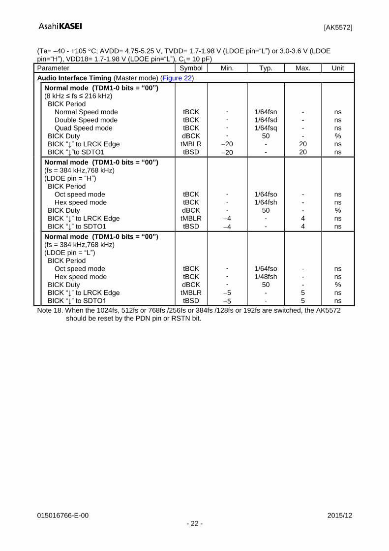
(Ta= 40 - +105 C; AVDD= 4.75-5.25 V, TVDD= 1.7-1.98 V (LDOE pin=“L”) or 3.0-3.6 V (LDOE pin=“H”), VDD18= 1.7-1.98 V (LDOE pin=“L”), CL= 10 pF)
Parameter Symbol Min. Typ. Max. Unit
Audio Interface Timing (Master mode) (Figure 22)
Normal mode (TDM1-0 bits = “00”) (8 kHz ≤ fs ≤ 216 kHz) BICK Period
Normal Speed mode Double Speed mode Quad Speed mode
BICK Duty BICK “↓” to LRCK Edge BICK “↓”to SDTO1
tBCK tBCK tBCK dBCK tMBLR tBSD
- - - -
20
20
1/64fsn 1/64fsd 1/64fsq
50 - -
- - - -
20 20
ns ns ns % ns ns
Normal mode (TDM1-0 bits = “00”) (fs = 384 kHz,768 kHz) (LDOE pin = “H”) BICK Period
Oct speed mode Hex speed mode
BICK Duty BICK “↓” to LRCK Edge BICK “↓” to SDTO1
tBCK tBCK dBCK tMBLR tBSD
- - -
4
4
1/64fso 1/64fsh
50 - -
- - - 4 4
ns ns % ns ns
Normal mode (TDM1-0 bits = “00”) (fs = 384 kHz,768 kHz) (LDOE pin = “L”) BICK Period
Oct speed mode Hex speed mode
BICK Duty BICK “↓” to LRCK Edge BICK “↓” to SDTO1
tBCK tBCK dBCK tMBLR tBSD
- - -
5
5
1/64fso 1/48fsh
50 - -
- - - 5 5
ns ns % ns ns
Note 18. When the 1024fs, 512fs or 768fs /256fs or 384fs /128fs or 192fs are switched, the AK5572 should be reset by the PDN pin or RSTN bit.
[AK5572]
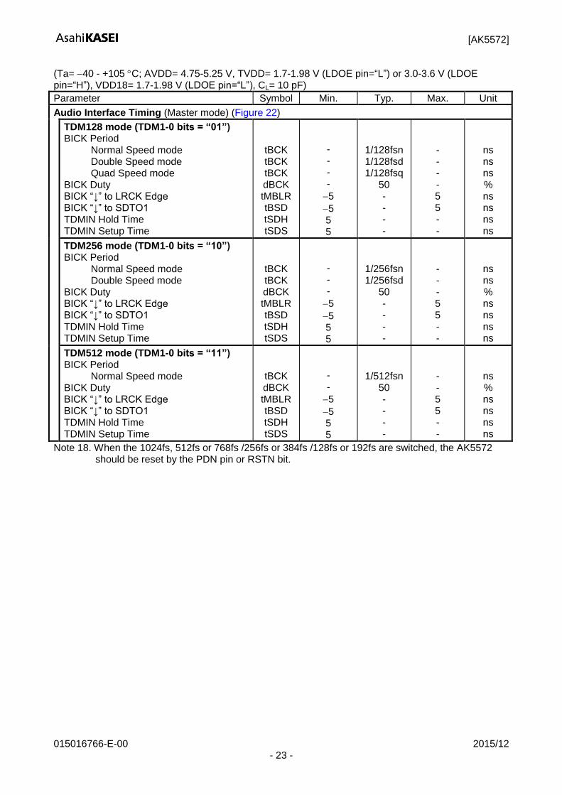
015016766-E-00 2015/12 - 23 -
(Ta= 40 - +105 C; AVDD= 4.75-5.25 V, TVDD= 1.7-1.98 V (LDOE pin=“L”) or 3.0-3.6 V (LDOE pin=“H”), VDD18= 1.7-1.98 V (LDOE pin=“L”), CL= 10 pF)
Parameter Symbol Min. Typ. Max. Unit
Audio Interface Timing (Master mode) (Figure 22)
TDM128 mode (TDM1-0 bits = “01”) BICK Period
Normal Speed mode Double Speed mode Quad Speed mode
BICK Duty BICK “↓” to LRCK Edge BICK “↓” to SDTO1 TDMIN Hold Time TDMIN Setup Time
tBCK tBCK tBCK dBCK tMBLR tBSD tSDH tSDS
- - - -
5
5 5 5
1/128fsn 1/128fsd 1/128fsq
50 - - - -
- - - - 5 5 - -
ns ns ns % ns ns ns ns
TDM256 mode (TDM1-0 bits = “10”) BICK Period
Normal Speed mode Double Speed mode
BICK Duty BICK “↓” to LRCK Edge BICK “↓” to SDTO1 TDMIN Hold Time TDMIN Setup Time
tBCK tBCK dBCK tMBLR tBSD tSDH tSDS
- - -
5
5 5 5
1/256fsn 1/256fsd
50 - - - -
- - - 5 5 - -
ns ns % ns ns ns ns
TDM512 mode (TDM1-0 bits = “11”) BICK Period
Normal Speed mode BICK Duty BICK “↓” to LRCK Edge BICK “↓” to SDTO1 TDMIN Hold Time TDMIN Setup Time
tBCK dBCK tMBLR tBSD tSDH tSDS
- -
5
5 5 5
1/512fsn 50 - - - -
- - 5 5 - -
ns % ns ns ns ns
Note 18. When the 1024fs, 512fs or 768fs /256fs or 384fs /128fs or 192fs are switched, the AK5572 should be reset by the PDN pin or RSTN bit.
[AK5572]
015016766-E-00 2015/12 - 24 -
(Ta= 40 - +105 C; AVDD= 4.75-5.25 V, TVDD= 1.7-1.98 V (LDOE pin=“L”) or 3.0-3.6 V (LDOE pin=“H”), VDD18= 1.7-1.98 V (LDOE pin=“L”), CL= 10 pF)
Parameter Symbol Min. Typ. Max. Unit
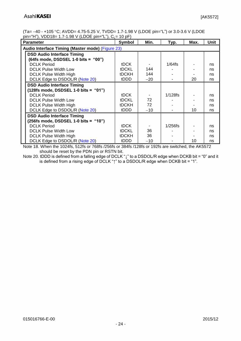
Audio Interface Timing (Master mode) (Figure 23)
DSD Audio Interface Timing
(64fs mode, DSDSEL 1-0 bits = “00”) DCLK Period DCLK Pulse Width Low DCLK Pulse Width High DCLK Edge to DSDOL/R (Note 20)
tDCK tDCKL tDCKH tDDD
-
144 144
20
1/64fs - - -
- - -
20
ns ns ns ns
DSD Audio Interface Timing
(128fs mode, DSDSEL 1-0 bits = “01”) DCLK Period DCLK Pulse Width Low DCLK Pulse Width High DCLK Edge to DSDOL/R (Note 20)
tDCK tDCKL tDCKH tDDD
-
72 72
10
1/128fs - - -
- - -
10
ns ns ns ns
DSD Audio Interface Timing
(256fs mode, DSDSEL 1-0 bits = “10”) DCLK Period DCLK Pulse Width Low DCLK Pulse Width High DCLK Edge to DSDOL/R (Note 20)
tDCK tDCKL tDCKH tDDD
-
36 36
10
1/256fs - - -
- - -
10
ns ns ns ns
Note 18. When the 1024fs, 512fs or 768fs /256fs or 384fs /128fs or 192fs are switched, the AK5572 should be reset by the PDN pin or RSTN bit.
Note 20. tDDD is defined from a falling edge of DCLK “↓” to a DSDOL/R edge when DCKB bit = “0” and it is defined from a rising edge of DCLK “↑” to a DSDOL/R edge when DCKB bit = “1”.
[AK5572]
015016766-E-00 2015/12 - 25 -
(Ta= 40 - +105 C; AVDD= 4.75-5.25 V, TVDD= 1.7-1.98 V (LDOE pin=“L”) or 3.0-3.6 V (LDOE pin=“H”), VDD18= 1.7-1.98 V (LDOE pin=“L”), CL= 10 pF)
Parameter Symbol Min. Typ. Max. Unit
Control Interface Timing (3-Wire Serial mode): (Figure 25) (Figure 26) CCLK Period CCLK Pulse Width Low Pulse Width High CDTI Setup Timing CDTI Hold Timing CSN “H” Time CSN “↓” to CCLK “↑” CCLK “↑” to CSN “↑”
tCCK tCCKL tCCKH tCDS tCDH tCSW tCSS tCSH
200 80 80 40 40 150 50 50
- - - - - - - -
- - - - - - - -
ns ns ns ns ns ns ns ns
Control Interface Timing (I2C Bus mode): (Figure 27)
SCL CLOCK Frequency Bus Free Time Between Transmissions Start Condition Hold Tune (Prior to First Clock Pulse) Clock Low Time Clock High Time Setup Time for Repeated Start Condition SDA Hold Time from SCL Falling (Note 21) SDA Setup Time from SCL Rising Rise Time of Both SDA and SCL Lines Fall Time of Both SDA and SCL Lines Setup Time for Stop Condition Pulse Width of Spike Noise Suppressed by Input Filter Capacitive Load on Bus
fSCL tBUF
tHD STA tLow
tHIGH tSU STA tHD DAT tSU DAT
tR tF
tSU STO tSP Cb
-
1.3 0.6 1.3 0.6 0.6 0
0.1 - -
0.6 0 -
- - - - - - - - - - - - -
400
- - - - - - -
1.0 0.3 -
50 400
kHz µs µs µs µs µs µs µs µs µs µs ns pF
Power Down & Reset Timing (Figure 28) PDN Pulse Width (Note 22) PDN Reject Pulse Width (Note 22) PDN “↑” to SDTO1 valid (Note 23)
tPD
tRPD tPDV
150
- -
- -
583
-
30 -
ns ns
1/fs
Note 21. Data must be held for sufficient time to bridge the 300 ns transition time of SCL. Note 22. The AK5572 can be reset by setting the PDN pin to “L” upon power-up. The PDN pin must held
“L” for more than 150 ns for a certain reset. The AK5572 is not reset by the “L” pulse less than 30 ns.
Note 23. This cycle is the number of LRCK rising edges from the PDN pin = “H”.
[AK5572]
015016766-E-00 2015/12 - 26 -
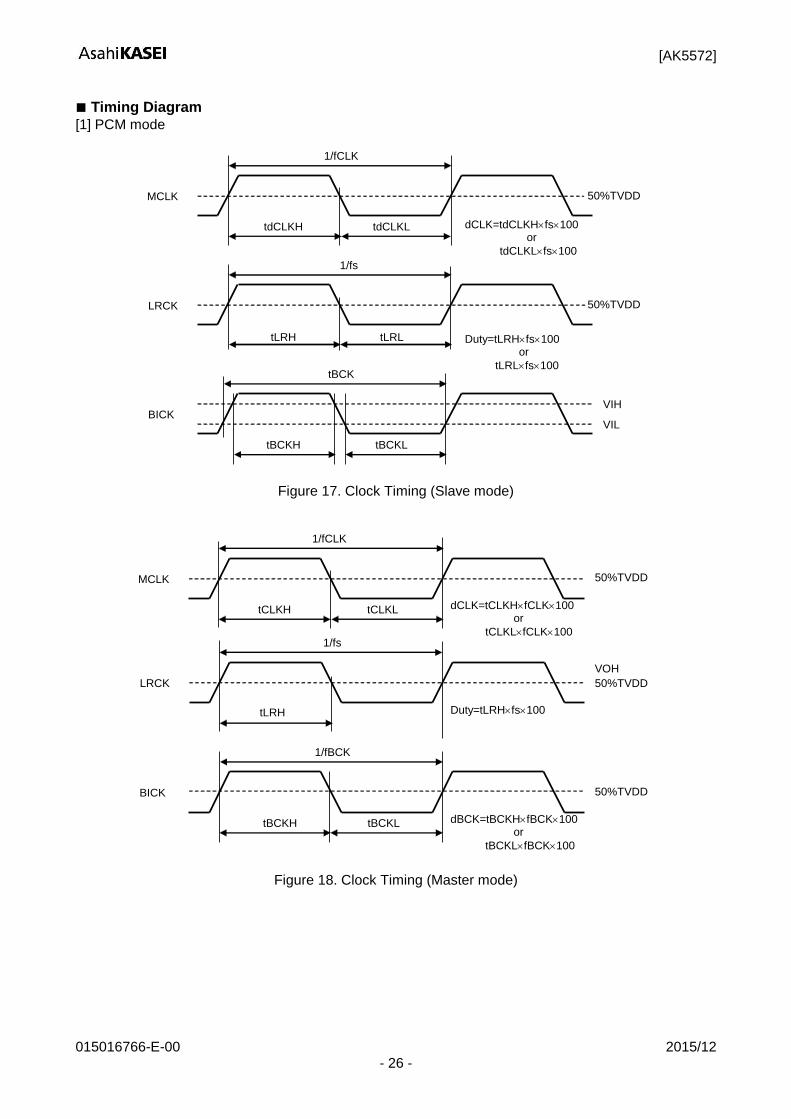
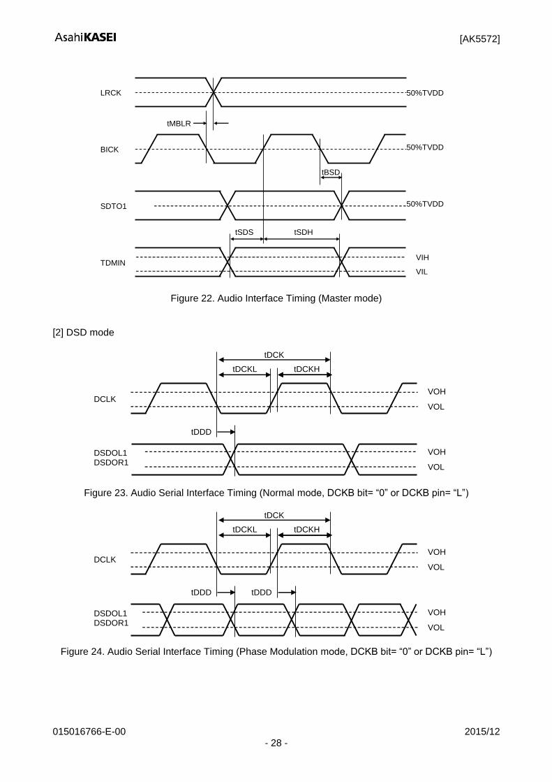
Timing Diagram
[1] PCM mode
1/fCLK
tdCLKL tdCLKH
MCLK
tBCK
tBCKL
VIH
tBCKH
BICK VIL
1/fs
LRCK 50%TVDD
tLRH tLRL Duty=tLRHfs100 or
tLRLfs100
50%TVDD
dCLK=tdCLKHfs100 or
tdCLKLfs100
Figure 17. Clock Timing (Slave mode)
1/fCLK
tCLKL tCLKH
MCLK
1/fBCK
tBCKL tBCKH
BICK 50%TVDD
1/fs
LRCK 50%TVDD
tLRH
VOH
Duty=tLRHfs100
dBCK=tBCKHfBCK100 or
tBCKLfBCK100
50%TVDD
dCLK=tCLKHfCLK100 or
tCLKLfCLK100
Figure 18. Clock Timing (Master mode)
[AK5572]
015016766-E-00 2015/12 - 27 -
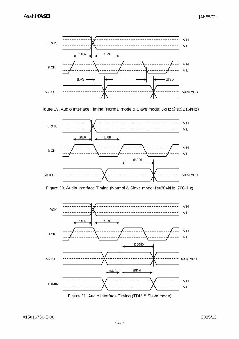
tLRB
LRCK
VIH BICK
VIL
tLRS
SDTO1 50%TVDD
tBSD
VIH
VIL
tBLR
Figure 19. Audio Interface Timing (Normal mode & Slave mode: 8kHz≦fs≦216kHz)
tLRB
LRCK
VIH BICK
VIL
SDTO1 50%TVDD
VIH
VIL
tBLR
tBSDD
Figure 20. Audio Interface Timing (Normal & Slave mode: fs=384kHz, 768kHz)
tLRB
LRCK
VIH BICK
VIL
SDTO1 50%TVDD
tBSDD
VIH
VIL
tBLR
tSDS
TDMIN VIH
VIL
tSDH
Figure 21. Audio Interface Timing (TDM & Slave mode)
[AK5572]
015016766-E-00 2015/12 - 28 -
LRCK
BICK
SDTO1
tBSD
tMBLR
50%TVDD
50%TVDD
50%TVDD
TDMIN
tSDH tSDS
VIH
VIL
Figure 22. Audio Interface Timing (Master mode)
[2] DSD mode
VOH DCLK
VOL
tDDD
VOH DSDOL1 DSDOR1
VOL
tDCKH tDCKL
tDCK
Figure 23. Audio Serial Interface Timing (Normal mode, DCKB bit= “0” or DCKB pin= “L”)
VOH DCLK
VOL
tDDD
VOH DSDOL1 DSDOR1
VOL
tDCKH tDCKL
tDCK
tDDD
Figure 24. Audio Serial Interface Timing (Phase Modulation mode, DCKB bit= “0” or DCKB pin= “L”)
[AK5572]
015016766-E-00 2015/12 - 29 -
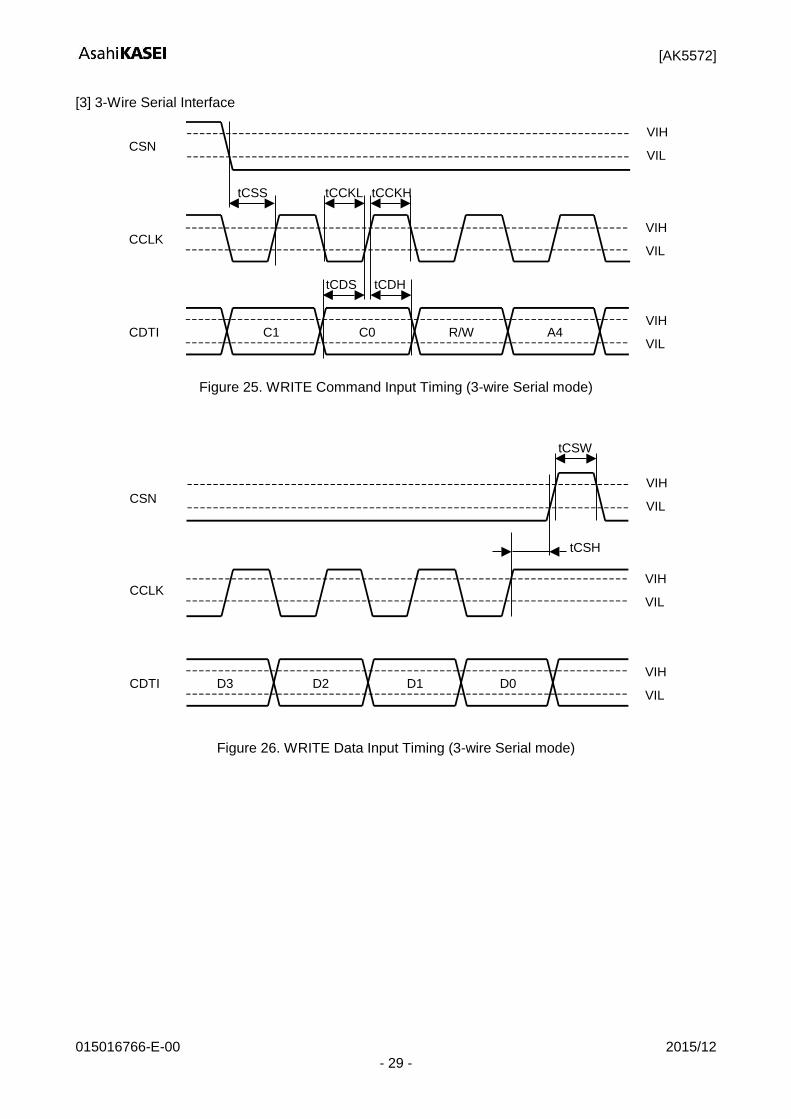
[3] 3-Wire Serial Interface
tCSS
CSN
VIHCCLK
VIL
VIHCDTI
VIL
VIH
VIL
C1 C0 R/W A4
tCCKL tCCKH
tCDS tCDH
Figure 25. WRITE Command Input Timing (3-wire Serial mode)
CSN
VIHCCLK
VIL
VIHCDTI
VIL
VIH
VIL
D3 D2 D1 D0
tCSW
tCSH
Figure 26. WRITE Data Input Timing (3-wire Serial mode)
[AK5572]
015016766-E-00 2015/12 - 30 -
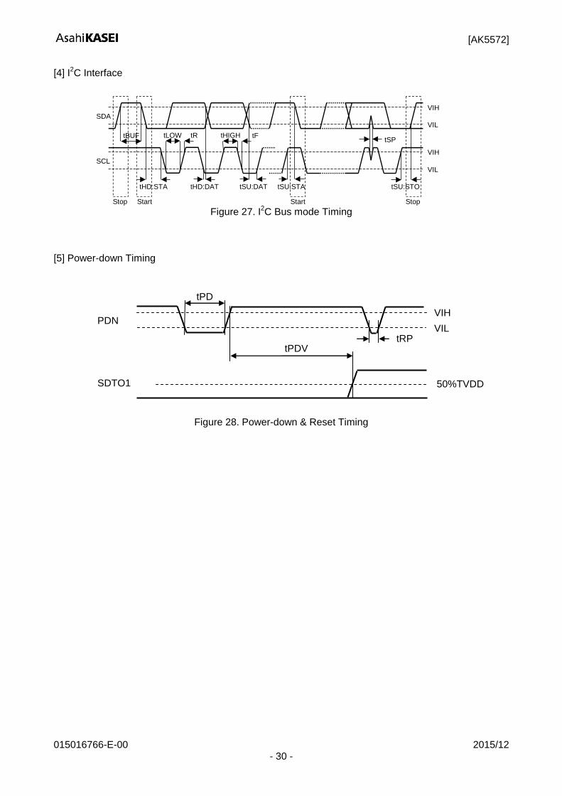
[4] I2C Interface
tHIGH
SCL
SDA
VIH
tLOWtBUF
tHD:STA
tR tF
tHD:DAT tSU:DAT tSU:STA
Stop Start Start Stop
tSU:STO
VIL
VIH
VIL
tSP
Figure 27. I
2C Bus mode Timing
[5] Power-down Timing
Figure 28. Power-down & Reset Timing
VIH
VIL
50%TVDD
tPD
SDTO1
PDN
tPDV tRPD
[AK5572]
015016766-E-00 2015/12 - 31 -
12. Functional Descriptions
Digital Core Power Supply
The digital core of the AK5572 is operates off of a 1.8 V power supply. Normally, this voltage is generated by the internal LDO from TVDD (3.3 V) for digital interface. The internal LDO will be powered up by setting the LDOE pin = “H”. Set the LDOE pin to “L” and supply a 1.8 V power to the VDD18 pin externally when a 1.8 V is used as TVDD.
Output Mode
The AK5572 is able to output either PCM or DSD data. The DP pin or DP bit select the output mode. Set the PW2 pin = PW1 pin = PW0 pin = “L” or RSTN bit = “0” or PW2-1 bits = “00” to reset all channels when changing the PCM/DSD mode. The AK5572 outputs data from the SDTO1 pin by BICK and LRCK in PCM mode. DSD data are output from the DSDOL1 and DSDOR1 pin by DCLK in DSD mode.
DP pin DP bit Interface
L 0 PCM
H 1 DSD
Table 1. PCM/DSD Mode Control
Master Mode and Slave Mode
The AK5572 requires a master clock (MCLK), an audio serial data clock (BICK) and an output channel clock (LRCK) in PCM mode. In this case, the LRCK frequency will be the sampling frequency. Both master and slave modes are available in PCM mode. In master mode, the AK5572 internally generates BICK and LRCK clocks from MCLK inputs and outputs them from the BICK pin and the LRCK pin. MCLK must be synchronized with BICK and LRCK but the phase is not important. The MSN pin controls master/slave mode. The AK5572 is in master mode when the MSN pin = “H” and in slave mode when the MSN pin = “L”. The AK5572 requires a master clock (MCLK) in DSD mode. Slave mode is not available in DSD mode, only master mode is supported.
System Clock
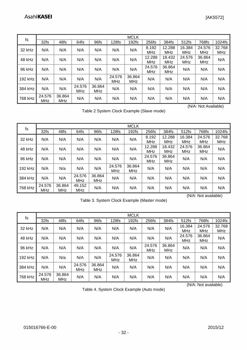
[1] PCM Mode The external system clocks, which are required to operate the AK5572, are MCLK, BICK and LRCK in PCM mode. MCLK frequency is determined based on LRCK frequency, according to the operation mode. Table 2, Table 3 and Table 4 show MCLK frequencies correspond to the normal audio rate. Set the frequency ratio between Sampling frequency and MCLK by the CKS3-0 pins (Table 5). All channels must be reset when changing the clock mode or audio interface format by the CKS2-0 pins (bits), TDM1-0 pins (bits), DIF1-0 pins (bits) and the MSN pin. In parallel control mode, all channels will be reset by the PDN pin = “L” or PW2-0 pins = “LLL”. In serial control mode, all channels will be reset by RSTN bit = “0” or PW4-1 bits = “0H”. A stable clock must be supplied after releasing the reset. The AK5572 integrates a phase detection circuit for LRCK. If the internal timing becomes out of synchronization in slave mode, the AK5572 is reset automatically and the phase is resynchronized. The following sequence must be executed when synchronizing multiple AK5572’s. Stop all AK5572’s in reset status by setting the PDN pin = “L” → “H” after stopping the system clock. Make pin or register settings while all channels are in reset status. After that, input the same system clock to all AK5572’s.
[AK5572]
015016766-E-00 2015/12 - 32 -
fs MCLK
32fs 48fs 64fs 96fs 128fs 192fs 256fs 384fs 512fs 768fs 1024fs
32 kHz N/A N/A N/A N/A N/A N/A 8.192 MHz
12.288 MHz
16.384 MHz
24.576 MHz
32.768 MHz
48 kHz N/A N/A N/A N/A N/A N/A 12.288 MHz
18.432 MHz
24.576 MHz
36.864 MHz
N/A
96 kHz N/A N/A N/A N/A N/A N/A 24.576 MHz
36.864 MHz
N/A N/A N/A
192 kHz N/A N/A N/A N/A 24.576 MHz
36.864 MHz
N/A N/A N/A N/A N/A
384 kHz N/A N/A 24.576 MHz
36.864 MHz
N/A N/A N/A N/A N/A N/A N/A
768 kHz 24.576 MHz
36.864 MHz
N/A N/A N/A N/A N/A N/A N/A N/A N/A
(N/A: Not Available) Table 2 System Clock Example (Slave mode)
fs MCLK
32fs 48fs 64fs 96fs 128fs 192fs 256fs 384fs 512fs 768fs 1024fs
32 kHz N/A N/A N/A N/A N/A N/A 8.192 MHz
12.288 MHz
16.384 MHz
24.576 MHz
32.768 MHz
48 kHz N/A N/A N/A N/A N/A N/A 12.288 MHz
18.432 MHz
24.576 MHz
36.864 MHz
N/A
96 kHz N/A N/A N/A N/A N/A N/A 24.576 MHz
36.864 MHz
N/A N/A N/A
192 kHz N/A N/a N/A N/A 24.576 MHz
36.864 MHz
N/A N/A N/A N/A N/A
384 kHz N/A N/A 24.576 MHz
36.864 MHz
N/A N/A N/A N/A N/A N/A N/A
768 kHz 24.576 MHz
36.864 MHz
49.152 MHz
N/A N/A N/A N/A N/A N/A N/A N/A
(N/A: Not available) Table 3. System Clock Example (Master mode)
fs MCLK
32fs 48fs 64fs 96fs 128fs 192fs 256fs 384fs 512fs 768fs 1024fs
32 kHz N/A N/A N/A N/A N/A N/A N/A N/A 16.384 MHz
24.576 MHz
32.768 MHz
48 kHz N/A N/A N/A N/A N/A N/A N/A N/A 24.576 MHz
36.864 MHz
N/A
96 kHz N/A N/A N/A N/A N/A N/A 24.576 MHz
36.864 MHz
N/A N/A N/A
192 kHz N/A N/a N/A N/A 24.576 MHz
36.864 MHz
N/A N/A N/A N/A N/A
384 kHz N/A N/A 24.576 MHz
36.864 MHz
N/A N/A N/A N/A N/A N/A N/A
768 kHz 24.576 MHz
36.864 MHz
N/A N/A N/A N/A N/A N/A N/A N/A N/A
(N/A: Not available) Table 4. System Clock Example (Auto mode)
[AK5572]
015016766-E-00 2015/12 - 33 -
CKS3 pin(bit)
CKS2 pin(bit)
CKS1 pin(bit)
CKS0 pin(bit)
MSN pin MCLK
Frequency Speed Mode
fs Range
L(0) L(0) L(0) L(0) L 128fs
24M Quad Speed
108 kHz fs 216 kHz H
L(0) L(0) L(0) H(1) L 192fs
36M Quad Speed
108 kHz fs 216 kHz H
L(0) L(0) H(1) L(0) L 256fs
12M Normal Speed
8 kHz fs 54 kHz H
L(0) L(0) H(1) H(1) L 256fs
24M Double Speed
54 kHz fs 108 kHz H
L(0) H(1) L(0) L(0) L 384fs
36M Double Speed
54 kHz fs 108 kHz H
L(0) H(1) L(0) H(1) L 384fs
18M Normal Speed
8 kHz fs 54 kHz H
L(0) H(1) H(1) L(0) L 512fs
24M Normal Speed
8 kHz fs 54 kHz H
L(0) H(1) H(1) H(1) L 768fs
36M Normal Speed
8 kHz fs 54 kHz H
H(1) L(0) L(0) L(0) L 64fs
24M Oct Speed
fs = 384 kHz H
H(1) L(0) L(0) H(1) L 32fs
24M Hex Speed
fs = 768 kHz H
H(1) L(0) H(1) L(0) L 96fs
36M Oct Speed
fs = 384 kHz H
H(1) L(0) H(1) H(1) L 48fs
36M Hex Speed
fs = 768 kHz H
H(1) H(1) L(0) L(0)
L NA NA
H 64fs
49.1M Hex Speed
fs = 768 kHz
H(1) H(1) L(0) H(1) L 1024fs
32M Normal Speed
8 kHz ≤ fs ≤ 32 kHz H
H(1) H(1) H(1) L(0) L
NA NA H
H(1) H(1) H(1) H(1) L Auto 8 kHz fs 768 kHz
H NA NA
Table 5. Clock Mode (fs & MCLK Frequency)
[AK5572]
015016766-E-00 2015/12 - 34 -
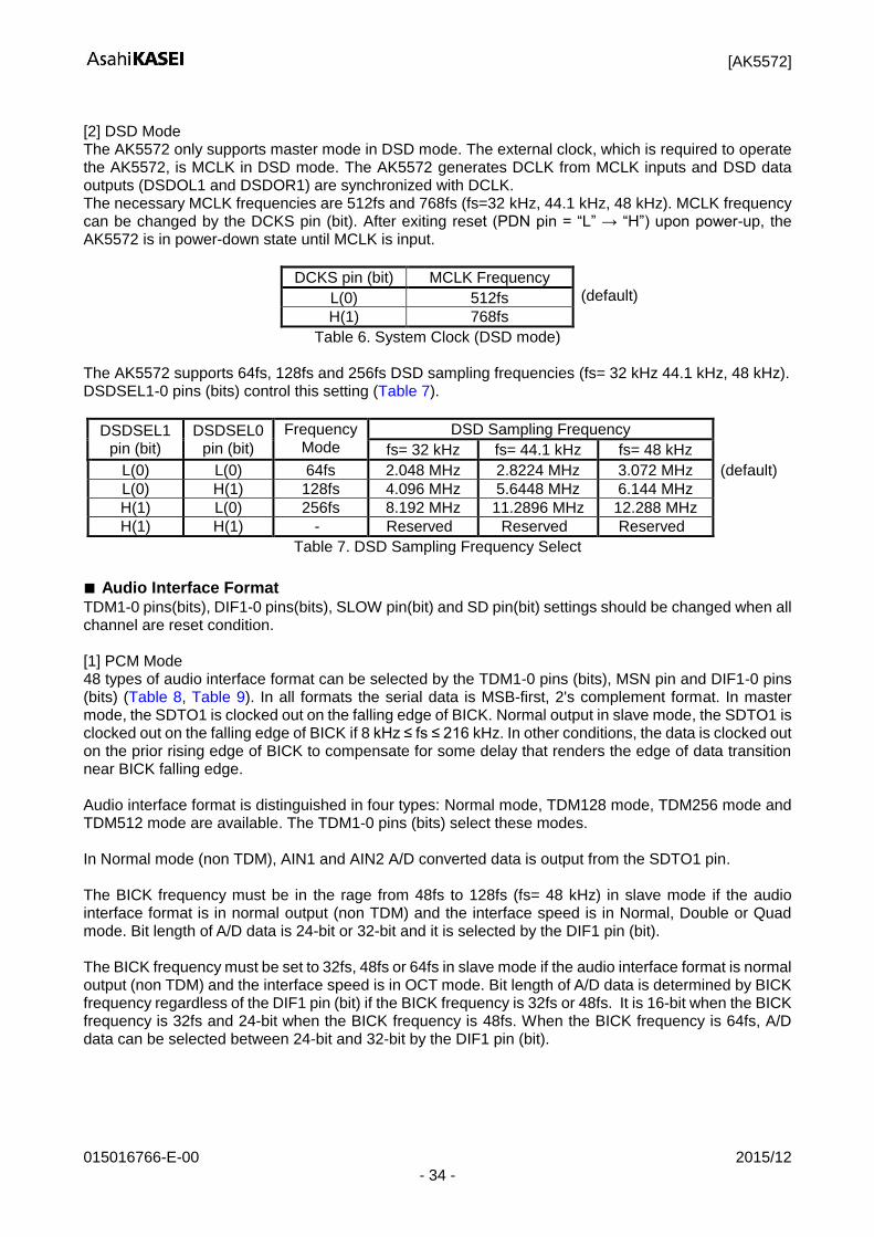
[2] DSD Mode The AK5572 only supports master mode in DSD mode. The external clock, which is required to operate the AK5572, is MCLK in DSD mode. The AK5572 generates DCLK from MCLK inputs and DSD data outputs (DSDOL1 and DSDOR1) are synchronized with DCLK. The necessary MCLK frequencies are 512fs and 768fs (fs=32 kHz, 44.1 kHz, 48 kHz). MCLK frequency can be changed by the DCKS pin (bit). After exiting reset (PDN pin = “L” → “H”) upon power-up, the AK5572 is in power-down state until MCLK is input.
DCKS pin (bit) MCLK Frequency (default)
L(0) 512fs
H(1) 768fs
Table 6. System Clock (DSD mode) The AK5572 supports 64fs, 128fs and 256fs DSD sampling frequencies (fs= 32 kHz 44.1 kHz, 48 kHz). DSDSEL1-0 pins (bits) control this setting (Table 7).
DSDSEL1 pin (bit)
DSDSEL0 pin (bit)
Frequency Mode
DSD Sampling Frequency
fs= 32 kHz fs= 44.1 kHz fs= 48 kHz
L(0) L(0) 64fs 2.048 MHz 2.8224 MHz 3.072 MHz (default)
L(0) H(1) 128fs 4.096 MHz 5.6448 MHz 6.144 MHz
H(1) L(0) 256fs 8.192 MHz 11.2896 MHz 12.288 MHz
H(1) H(1) - Reserved Reserved Reserved
Table 7. DSD Sampling Frequency Select
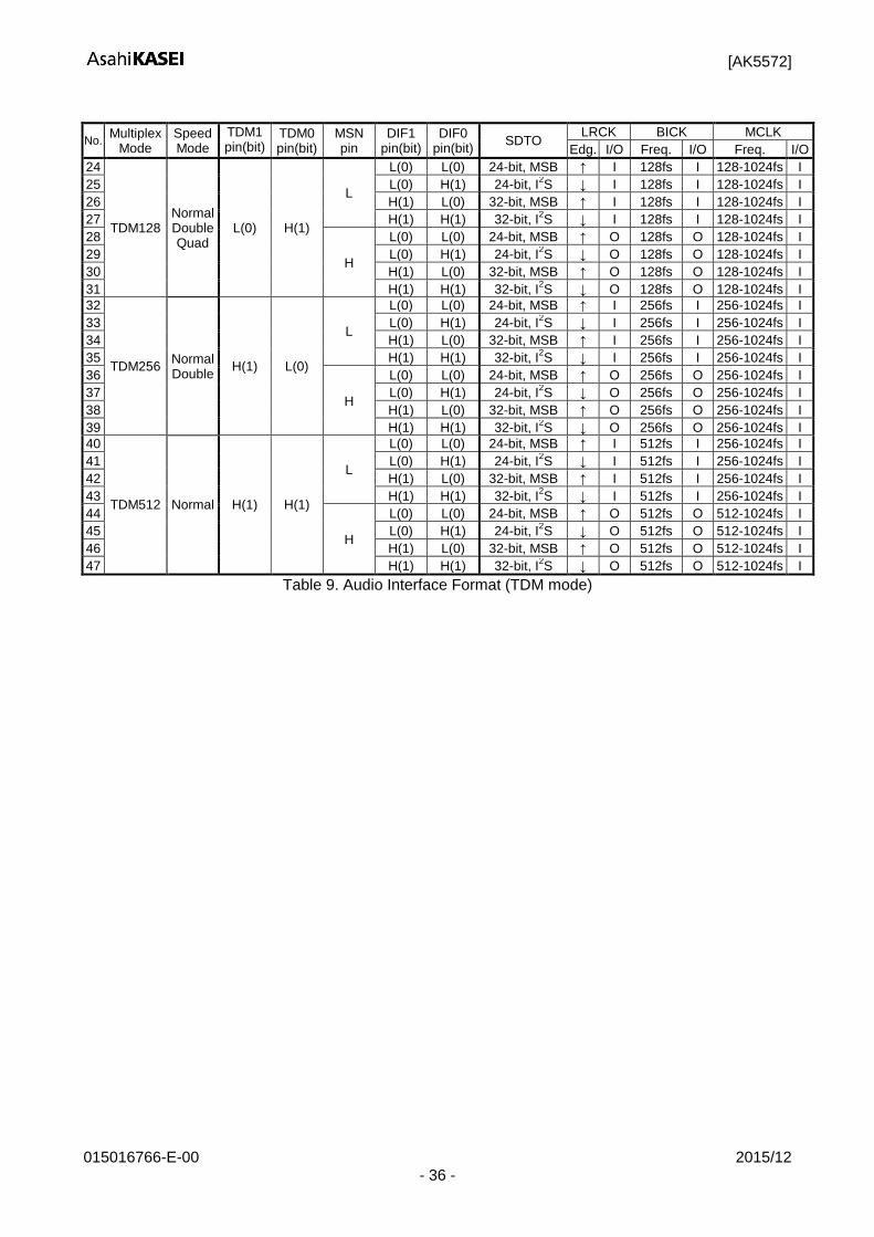
Audio Interface Format
TDM1-0 pins(bits), DIF1-0 pins(bits), SLOW pin(bit) and SD pin(bit) settings should be changed when all channel are reset condition. [1] PCM Mode 48 types of audio interface format can be selected by the TDM1-0 pins (bits), MSN pin and DIF1-0 pins (bits) (Table 8, Table 9). In all formats the serial data is MSBfirst, 2's complement format. In master mode, the SDTO1 is clocked out on the falling edge of BICK. Normal output in slave mode, the SDTO1 is clocked out on the falling edge of BICK if 8 kHz ≤ fs ≤ 216 kHz. In other conditions, the data is clocked out on the prior rising edge of BICK to compensate for some delay that renders the edge of data transition near BICK falling edge. Audio interface format is distinguished in four types: Normal mode, TDM128 mode, TDM256 mode and TDM512 mode are available. The TDM1-0 pins (bits) select these modes. In Normal mode (non TDM), AIN1 and AIN2 A/D converted data is output from the SDTO1 pin. The BICK frequency must be in the rage from 48fs to 128fs (fs= 48 kHz) in slave mode if the audio interface format is in normal output (non TDM) and the interface speed is in Normal, Double or Quad mode. Bit length of A/D data is 24-bit or 32-bit and it is selected by the DIF1 pin (bit). The BICK frequency must be set to 32fs, 48fs or 64fs in slave mode if the audio interface format is normal output (non TDM) and the interface speed is in OCT mode. Bit length of A/D data is determined by BICK frequency regardless of the DIF1 pin (bit) if the BICK frequency is 32fs or 48fs. It is 16-bit when the BICK frequency is 32fs and 24-bit when the BICK frequency is 48fs. When the BICK frequency is 64fs, A/D data can be selected between 24-bit and 32-bit by the DIF1 pin (bit).
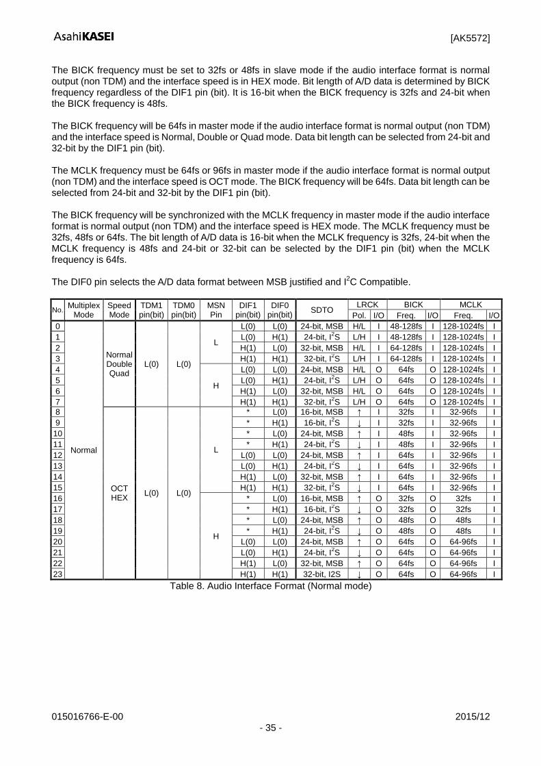
[AK5572]
015016766-E-00 2015/12 - 35 -
The BICK frequency must be set to 32fs or 48fs in slave mode if the audio interface format is normal output (non TDM) and the interface speed is in HEX mode. Bit length of A/D data is determined by BICK frequency regardless of the DIF1 pin (bit). It is 16-bit when the BICK frequency is 32fs and 24-bit when the BICK frequency is 48fs. The BICK frequency will be 64fs in master mode if the audio interface format is normal output (non TDM) and the interface speed is Normal, Double or Quad mode. Data bit length can be selected from 24-bit and 32-bit by the DIF1 pin (bit). The MCLK frequency must be 64fs or 96fs in master mode if the audio interface format is normal output (non TDM) and the interface speed is OCT mode. The BICK frequency will be 64fs. Data bit length can be selected from 24-bit and 32-bit by the DIF1 pin (bit). The BICK frequency will be synchronized with the MCLK frequency in master mode if the audio interface format is normal output (non TDM) and the interface speed is HEX mode. The MCLK frequency must be 32fs, 48fs or 64fs. The bit length of A/D data is 16-bit when the MCLK frequency is 32fs, 24-bit when the MCLK frequency is 48fs and 24-bit or 32-bit can be selected by the DIF1 pin (bit) when the MCLK frequency is 64fs. The DIF0 pin selects the A/D data format between MSB justified and I
2C Compatible.
No. Multiplex
Mode Speed Mode
TDM1 pin(bit)
TDM0 pin(bit)
MSN Pin
DIF1 pin(bit)
DIF0 pin(bit)
SDTO LRCK BICK MCLK
Pol. I/O Freq. I/O Freq. I/O
0
Normal
Normal Double Quad
L(0) L(0)
L
L(0) L(0) 24-bit, MSB H/L I 48-128fs I 128-1024fs I
1 L(0) H(1) 24-bit, I2S L/H I 48-128fs I 128-1024fs I
2 H(1) L(0) 32-bit, MSB H/L I 64-128fs I 128-1024fs I
3 H(1) H(1) 32-bit, I2S L/H I 64-128fs I 128-1024fs I
4
H
L(0) L(0) 24-bit, MSB H/L O 64fs O 128-1024fs I
5 L(0) H(1) 24-bit, I2S L/H O 64fs O 128-1024fs I
6 H(1) L(0) 32-bit, MSB H/L O 64fs O 128-1024fs I
7 H(1) H(1) 32-bit, I2S L/H O 64fs O 128-1024fs I
8
OCT HEX
L(0) L(0)
L
* L(0) 16-bit, MSB ↑ I 32fs I 32-96fs I
9 * H(1) 16-bit, I2S ↓ I 32fs I 32-96fs I
10 * L(0) 24-bit, MSB ↑ I 48fs I 32-96fs I
11 * H(1) 24-bit, I2S ↓ I 48fs I 32-96fs I
12 L(0) L(0) 24-bit, MSB ↑ I 64fs I 32-96fs I
13 L(0) H(1) 24-bit, I2S ↓ I 64fs I 32-96fs I
14 H(1) L(0) 32-bit, MSB ↑ I 64fs I 32-96fs I
15 H(1) H(1) 32-bit, I2S ↓ I 64fs I 32-96fs I
16
H
* L(0) 16-bit, MSB ↑ O 32fs O 32fs I
17 * H(1) 16-bit, I2S ↓ O 32fs O 32fs I
18 * L(0) 24-bit, MSB ↑ O 48fs O 48fs I
19 * H(1) 24-bit, I2S ↓ O 48fs O 48fs I
20 L(0) L(0) 24-bit, MSB ↑ O 64fs O 64-96fs I
21 L(0) H(1) 24-bit, I2S ↓ O 64fs O 64-96fs I
22 H(1) L(0) 32-bit, MSB ↑ O 64fs O 64-96fs I
23 H(1) H(1) 32-bit, I2S ↓ O 64fs O 64-96fs I
Table 8. Audio Interface Format (Normal mode)
[AK5572]
015016766-E-00 2015/12 - 36 -
No. Multiplex
Mode Speed Mode
TDM1 pin(bit)
TDM0 pin(bit)
MSN pin
DIF1 pin(bit)
DIF0 pin(bit)
SDTO LRCK BICK MCLK
Edg. I/O Freq. I/O Freq. I/O
24
TDM128 Normal Double Quad
L(0) H(1)
L
L(0) L(0) 24-bit, MSB ↑ I 128fs I 128-1024fs I
25 L(0) H(1) 24-bit, I2S ↓ I 128fs I 128-1024fs I
26 H(1) L(0) 32-bit, MSB ↑ I 128fs I 128-1024fs I
27 H(1) H(1) 32-bit, I2S ↓ I 128fs I 128-1024fs I
28
H
L(0) L(0) 24-bit, MSB ↑ O 128fs O 128-1024fs I
29 L(0) H(1) 24-bit, I2S ↓ O 128fs O 128-1024fs I
30 H(1) L(0) 32-bit, MSB ↑ O 128fs O 128-1024fs I
31 H(1) H(1) 32-bit, I2S ↓ O 128fs O 128-1024fs I
32
TDM256 Normal Double
H(1) L(0)
L
L(0) L(0) 24-bit, MSB ↑ I 256fs I 256-1024fs I
33 L(0) H(1) 24-bit, I2S ↓ I 256fs I 256-1024fs I
34 H(1) L(0) 32-bit, MSB ↑ I 256fs I 256-1024fs I
35 H(1) H(1) 32-bit, I2S ↓ I 256fs I 256-1024fs I
36
H
L(0) L(0) 24-bit, MSB ↑ O 256fs O 256-1024fs I
37 L(0) H(1) 24-bit, I2S ↓ O 256fs O 256-1024fs I
38 H(1) L(0) 32-bit, MSB ↑ O 256fs O 256-1024fs I
39 H(1) H(1) 32-bit, I2S ↓ O 256fs O 256-1024fs I
40
TDM512 Normal H(1) H(1)
L
L(0) L(0) 24-bit, MSB ↑ I 512fs I 256-1024fs I
41 L(0) H(1) 24-bit, I2S ↓ I 512fs I 256-1024fs I
42 H(1) L(0) 32-bit, MSB ↑ I 512fs I 256-1024fs I
43 H(1) H(1) 32-bit, I2S ↓ I 512fs I 256-1024fs I
44
H
L(0) L(0) 24-bit, MSB ↑ O 512fs O 512-1024fs I
45 L(0) H(1) 24-bit, I2S ↓ O 512fs O 512-1024fs I
46 H(1) L(0) 32-bit, MSB ↑ O 512fs O 512-1024fs I
47 H(1) H(1) 32-bit, I2S ↓ O 512fs O 512-1024fs I
Table 9. Audio Interface Format (TDM mode)
[AK5572]
015016766-E-00 2015/12 - 37 -
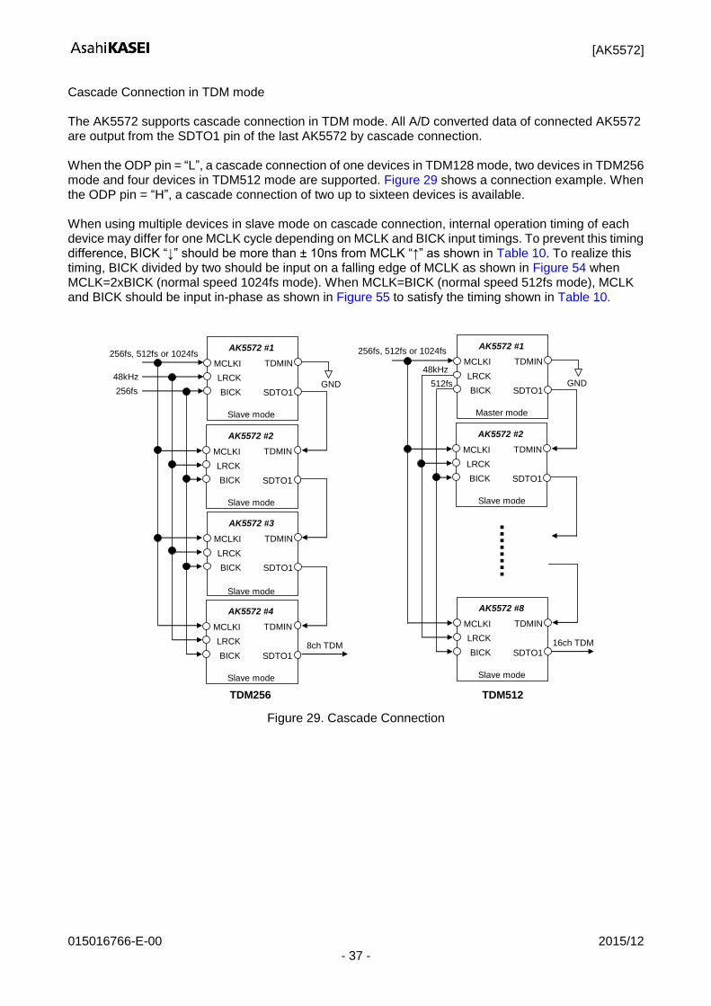
Cascade Connection in TDM mode The AK5572 supports cascade connection in TDM mode. All A/D converted data of connected AK5572 are output from the SDTO1 pin of the last AK5572 by cascade connection. When the ODP pin = “L”, a cascade connection of one devices in TDM128 mode, two devices in TDM256 mode and four devices in TDM512 mode are supported. Figure 29 shows a connection example. When the ODP pin = “H”, a cascade connection of two up to sixteen devices is available. When using multiple devices in slave mode on cascade connection, internal operation timing of each device may differ for one MCLK cycle depending on MCLK and BICK input timings. To prevent this timing difference, BICK “↓” should be more than ± 10ns from MCLK “↑” as shown in Table 10. To realize this timing, BICK divided by two should be input on a falling edge of MCLK as shown in Figure 54 when MCLK=2xBICK (normal speed 1024fs mode). When MCLK=BICK (normal speed 512fs mode), MCLK and BICK should be input in-phase as shown in Figure 55 to satisfy the timing shown in Table 10.
48kHz
256fs
256fs, 512fs or 1024fs
GND LRCK
AK5572 #1
BICK
TDMIN
SDTO1
MCLKI
LRCK
AK5572 #2
BICK
TDMIN
SDTO1
MCLKI
16ch TDM
GND LRCK
AK5572 #1
BICK
TDMIN
SDTO1
MCLKI
LRCK
AK5572 #2
BICK
TDMIN
SDTO1
MCLKI
LRCK
AK5572 #8
BICK
TDMIN
SDTO1
MCLKI
TDM256 TDM512
8ch TDM
LRCK
AK5572 #3
BICK
TDMIN
SDTO1
MCLKI
LRCK
AK5572 #4
BICK
TDMIN
SDTO1
MCLKI
256fs, 512fs or 1024fs
Slave mode
Slave mode
Slave mode
Slave mode
Master mode
Slave mode
Slave mode
48kHz
512fs
Figure 29. Cascade Connection
[AK5572]
015016766-E-00 2015/12 - 38 -
LRCK
BICK(64fs)
SDTO1
0 1 2 11 12 13 23 24 31 0 1 2 11 12 13 23 24 31 0
23
1
22 23 22 13 12 11 31
AIN1 Data
13 12 0
23: MSB, 0: LSB
11 1 1 0
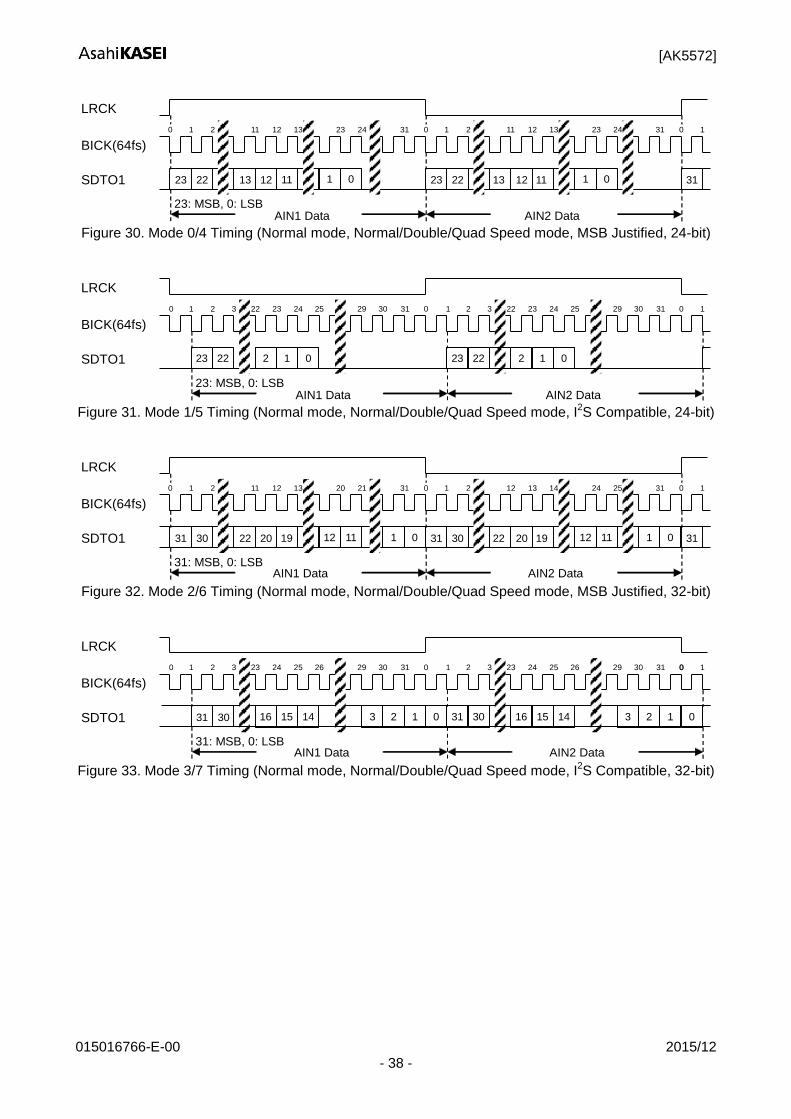
AIN2 Data Figure 30. Mode 0/4 Timing (Normal mode, Normal/Double/Quad Speed mode, MSB Justified, 24-bit)
LRCK
BICK(64fs)
SDTO1
0 1 2 3 22 23 24 25 0 0 1 31 29 30
23: MSB, 0: LSB AIN1 Data
0
2 3 22 23 24 25 31 29 30 1
1 23 23 22 2 1 0
AIN2 Data
22 2
Figure 31. Mode 1/5 Timing (Normal mode, Normal/Double/Quad Speed mode, I
2S Compatible, 24-bit)
LRCK
BICK(64fs)
SDTO1
0 1 2 11 12 13 20 21 31 0 1 2 12 13 14 24 25 31 0
31
1
30 31 30 22 20 19 31
AIN1 Data AIN2 Data
22 20 11
31: MSB, 0: LSB
1 0 19 12 0 12 11 1
Figure 32. Mode 2/6 Timing (Normal mode, Normal/Double/Quad Speed mode, MSB Justified, 32-bit)
LRCK
BICK(64fs)
SDTO1
0 1 2 3 23 24 25 26 0 0 1 31 29 30
31 30
31: MSB, 0: LSB AIN1 Data AIN2 Data
14
2 3 23 24 25 26 0 31 29 30 1
0 1 2 3 15 16 31 30 16 15 14 3 1 2 0
Figure 33. Mode 3/7 Timing (Normal mode, Normal/Double/Quad Speed mode, I
2S Compatible, 32-bit)
[AK5572]
015016766-E-00 2015/12 - 39 -
LRCK (Slave)
BICK (32fs)
SDTO1 (O) 14 9
AIN1 Data
16 BICK
32 BICK
6 1 0 14 9
AIN2 Data
16 BICK
6 1
LRCK (Master)
14 15 8 7 0 15 8 7 0 15
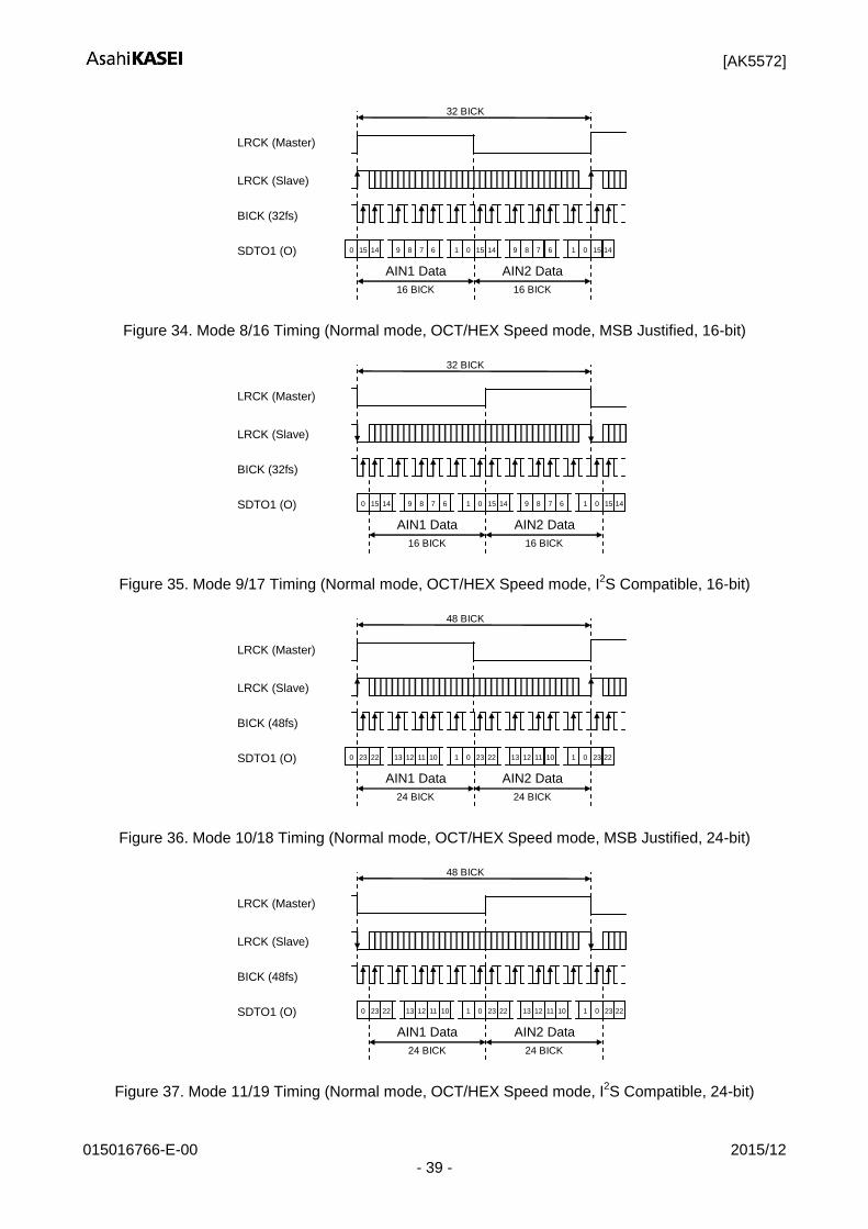
Figure 34. Mode 8/16 Timing (Normal mode, OCT/HEX Speed mode, MSB Justified, 16-bit)
LRCK (Slave)
BICK (32fs)
SDTO1 (O) 14 9
AIN1 Data
16 BICK
32 BICK
6 1 0 14 9
AIN2 Data
16 BICK
6 1
LRCK (Master)
14 15 8 7 0 15 8 7 0 15
Figure 35. Mode 9/17 Timing (Normal mode, OCT/HEX Speed mode, I
2S Compatible, 16-bit)
LRCK (Slave)
BICK (48fs)
SDTO1 (O) 22 13
AIN1 Data
24 BICK
48 BICK
10 1 0 22 13
AIN2 Data
24 BICK
10 1
LRCK (Master)
22 23 12 11 0 23 12 11 0 23
Figure 36. Mode 10/18 Timing (Normal mode, OCT/HEX Speed mode, MSB Justified, 24-bit)
LRCK (Slave)
BICK (48fs)
SDTO1 (O) 22 13
AIN1 Data
24 BICK
48 BICK
10 1 0 22 13
AIN2 Data
24 BICK
10 1
LRCK (Master)
22 23 12 11 0 23 12 11 0 23
Figure 37. Mode 11/19 Timing (Normal mode, OCT/HEX Speed mode, I
2S Compatible, 24-bit)
[AK5572]
015016766-E-00 2015/12 - 40 -
LRCK (Slave)
BICK (64fs)
SDTO1 (O) 22
AIN1 Data
32 BICK
64 BICK
7 0 22 15
AIN2 Data
32 BICK
7 0
LRCK (Master)
22 23 8 23 8 23 15
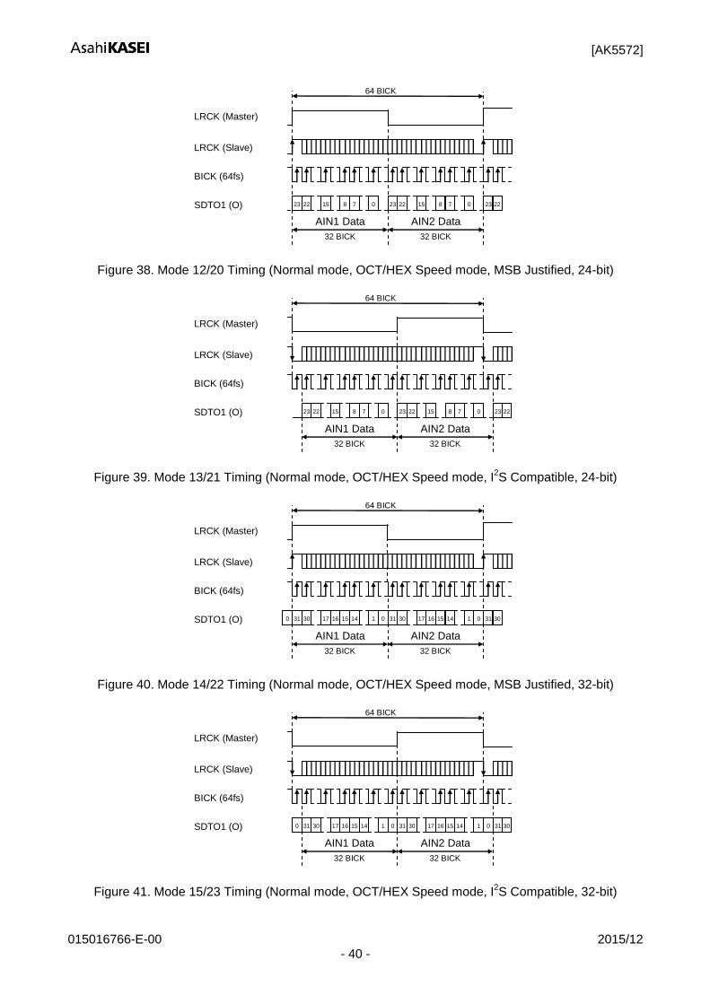
Figure 38. Mode 12/20 Timing (Normal mode, OCT/HEX Speed mode, MSB Justified, 24-bit)
LRCK (Slave)
BICK (64fs)
SDTO1 (O) 22 15
AIN1 Data
32 BICK
64 BICK
7 0 22 15
AIN2 Data
32 BICK
7 0
LRCK (Master)
22 23 8 23 8 23
Figure 39. Mode 13/21 Timing (Normal mode, OCT/HEX Speed mode, I
2S Compatible, 24-bit)
LRCK (Slave)
BICK (64fs)
SDTO1 (O) 30 17
AIN1 Data
32 BICK
64 BICK
14 1 0 30 17
AIN2 Data
32 BICK
14 1
LRCK (Master)
30 31 16 15 0 31 16 15 0 31
Figure 40. Mode 14/22 Timing (Normal mode, OCT/HEX Speed mode, MSB Justified, 32-bit)
LRCK (Slave)
BICK (64fs)
SDTO1 (O) 30 17
AIN1 Data
32 BICK
64 BICK
14 1 0 30 17
AIN2 Data
32 BICK
14 1
LRCK (Master)
30 31 16 15 0 31 16 15 0 31
Figure 41. Mode 15/23 Timing (Normal mode, OCT/HEX Speed mode, I
2S Compatible, 32-bit)
[AK5572]
015016766-E-00 2015/12 - 41 -
LRCK (Slave)
BICK (256fs)
SDTO1 (O) 22 0
Data 1
32 BICK
128 BICK
22 0
Data 2
32 BICK
LRCK (Master)
22 23 23 23
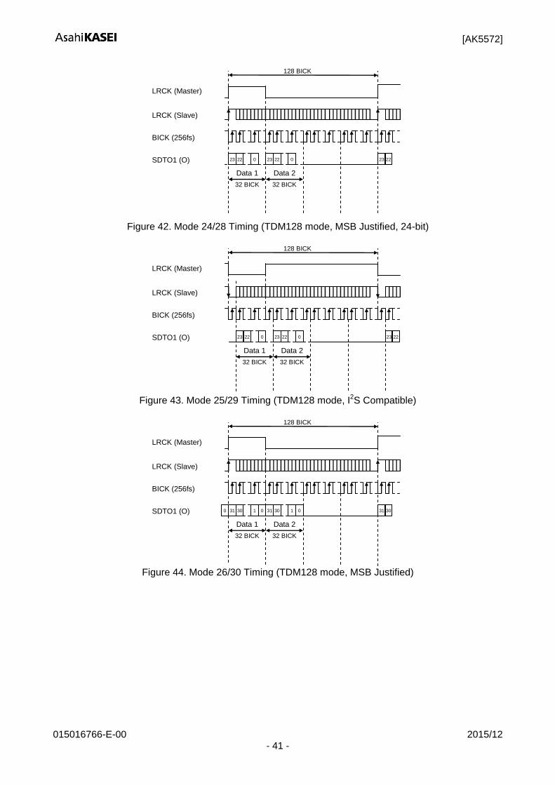
Figure 42. Mode 24/28 Timing (TDM128 mode, MSB Justified, 24-bit)
LRCK (Slave)
BICK (256fs)
SDTO1 (O) 22 0
Data 1
32 BICK
128 BICK
22 0
Data 2
32 BICK
LRCK (Master)
22 23 23 23
Figure 43. Mode 25/29 Timing (TDM128 mode, I
2S Compatible)
LRCK (Slave)
BICK (256fs)
SDTO1 (O) 30 1
Data 1
32 BICK
128 BICK
30 1
Data 2
32 BICK
0
LRCK (Master)
30 31 0 31 0 31
Figure 44. Mode 26/30 Timing (TDM128 mode, MSB Justified)
[AK5572]
015016766-E-00 2015/12 - 42 -
LRCK (Slave)
BICK (256fs)
SDTO1 (O) 30 1
Data 1
32 BICK
128 BICK
30 1
Data 2
32 BICK
0
LRCK (Master)
30 31 0 31 0 31
Figure 45. Mode 27/31 Timing (TDM128 mode, I
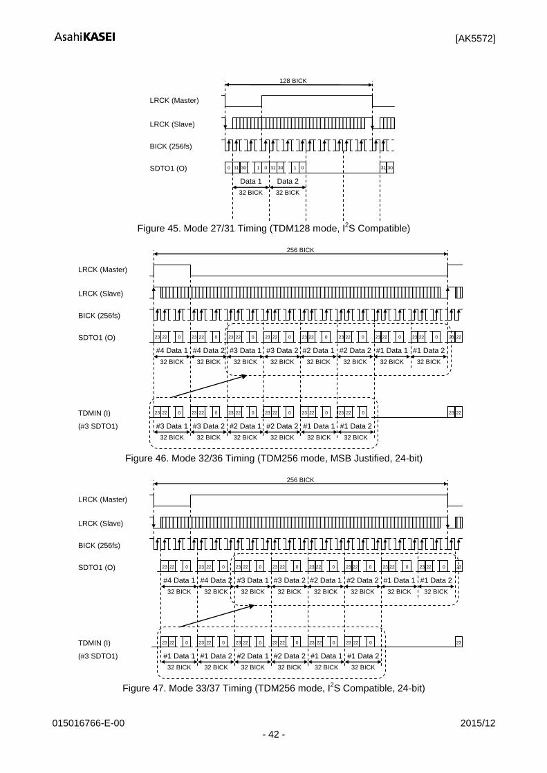
2S Compatible)
LRCK (Slave)
BICK (256fs)
SDTO1 (O) 22 0
#4 Data 1
32 BICK
256 BICK
22 0
#4 Data 2
32 BICK
22 22 0
#3 Data 1
32 BICK
22 0
#3 Data 2
32 BICK
LRCK (Master)
TDMIN (I)
(#3 SDTO1)
22 0
#3 Data 1
32 BICK
22 0
#3 Data 2
32 BICK
22 22 0
#2 Data 1
32 BICK
22 0
#2 Data 2
32 BICK
22 0
#2 Data 1
32 BICK
22 0
#2 Data 2
32 BICK
22 0
#1 Data 1
32 BICK
22 0
#1 Data 2
32 BICK
23 23 23 23 23 23 23 23 23
23 23 23 23 23 22 0
#1 Data 1
32 BICK
22 0
#1 Data 2
32 BICK
23 23
Figure 46. Mode 32/36 Timing (TDM256 mode, MSB Justified, 24-bit)
LRCK (Slave)
BICK (256fs)
SDTO1 (O) 22 0
#4 Data 1
32 BICK
256 BICK
22 0
#4 Data 2
32 BICK
22 0
#3 Data 1
32 BICK
22 0
#3 Data 2
32 BICK
LRCK (Master)
TDMIN (I)
(#3 SDTO1)
22 0
#1 Data 1
32 BICK
22 0
#1 Data 2
32 BICK
22 0
#2 Data 1
32 BICK
22 0
#2 Data 2
32 BICK
22 0
#2 Data 1
32 BICK
22 0
#2 Data 2
32 BICK
22 0
#1 Data 1
32 BICK
22 0
#1 Data 2
32 BICK
23 23 23 23 23 23 23 23 23
23 23 23 23 23 22 0
#1 Data 1
32 BICK
22 0
#1 Data 2
32 BICK
23 23
Figure 47. Mode 33/37 Timing (TDM256 mode, I
2S Compatible, 24-bit)
[AK5572]
015016766-E-00 2015/12 - 43 -
LRCK (Slave)
BICK (256fs)
SDTO1 (O) 30 1
#4 Data 1
32 BICK
256 BICK
30 1
#4 Data 2
32 BICK
30 30 1
#3 Data 1
32 BICK
30 1
#3 Data 2
32 BICK
LRCK (Master)
TDMIN (I)
(#3 SDTO1)
30 1
#3 Data 1
32 BICK
30 1
#3 Data 2
32 BICK
30 30 1
#2 Data 1
32 BICK
30 1
#2 Data 2
32 BICK
30 1
#2 Data 1
32 BICK
30 1
#2 Data 2
32 BICK
30 1
#1 Data 1
32 BICK
30 1
#1 Data 2
32 BICK
31 0 31 0 31 0 31 0 31 0 31 0 31 0 31 0 31
31 0 31 0 31 0 31 0 31 30 1
#1 Data 1
32 BICK
30 1
#1 Data 2
32 BICK
31 0 31 0
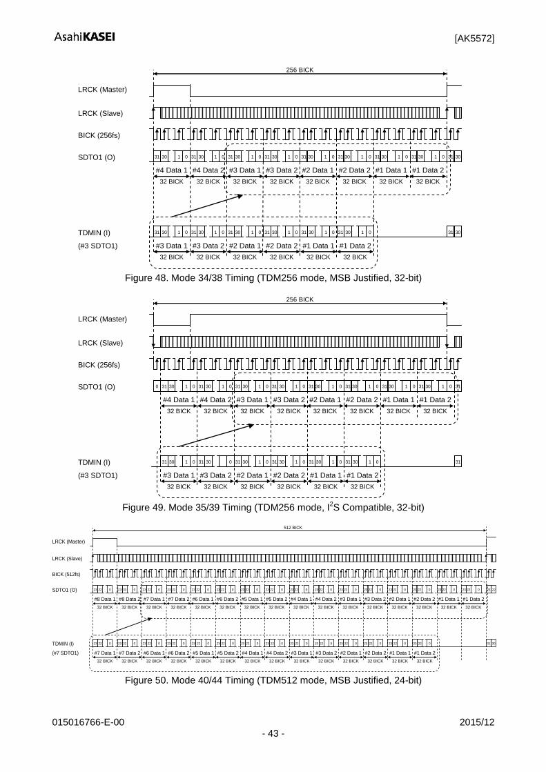
Figure 48. Mode 34/38 Timing (TDM256 mode, MSB Justified, 32-bit)
LRCK (Slave)
BICK (256fs)
SDTO1 (O) 30 1
#4 Data 1
32 BICK
256 BICK
30 1
#4 Data 2
32 BICK
0 30 1
#3 Data 1
32 BICK
30 1
#3 Data 2
32 BICK
LRCK (Master)
TDMIN (I)
(#3 SDTO1)
30 1
#3 Data 1
32 BICK
30
#3 Data 2
32 BICK
30 1
#2 Data 1
32 BICK
30 1
#2 Data 2
32 BICK
30 1
#2 Data 1
32 BICK
30 1
#2 Data 2
32 BICK
30 1
#1 Data 1
32 BICK
30 1
#1 Data 2
32 BICK
31 0 31 0 31 0 31 0 31 0 31 0 31 0 31 0 31
31 0 31 0 31 0 31 0 31 30 1
#1 Data 1
32 BICK
30 1
#1 Data 2
32 BICK
31 0 31 0
Figure 49. Mode 35/39 Timing (TDM256 mode, I
2S Compatible, 32-bit)
LRCK (Slave)
BICK (512fs)
SDTO1 (O) 22 0
#8 Data 1
32 BICK
512 BICK
33 0
#8 Data 2
32 BICK
22 0
#7 Data 1
32 BICK
22 0
#7 Data 2
32 BICK
LRCK (Master)
TDMIN (I)
(#7 SDTO1)
22 0
#7 Data 1
32 BICK
22 0
#7 Data 2
32 BICK
30 22 0
#6 Data 1
32 BICK
22 0
#6 Data 2
32 BICK
22 0
#6 Data 1
32 BICK
22 0
#6 Data 2
32 BICK
22 0
#5 Data 1
32 BICK
22 0
#5 Data 2
32 BICK
22 0
#4 Data 1
32 BICK
22 0
#4 Data 2
32 BICK
22 0
#3 Data 1
32 BICK
22 0
#3 Data 2
32 BICK
22 0
#2 Data 1
32 BICK
22 0
#2 Data 2
32 BICK
22 0
#1 Data 1
32 BICK
22 0
#1 Data 2
32 BICK
22 0
#5 Data 1
32 BICK
22 0
#5 Data 2
32 BICK
22 0
#4 Data 1
32 BICK
22 0
#4 Data 2
32 BICK
23 23 23 23 23 23 23 23 23 23 23 23 23 23 23 23
31
22 23
23 23 23 23 23 23 23 23 22 0
#3 Data 1
32 BICK
22 0
#3 Data 2
32 BICK
22 0
#2 Data 1
32 BICK
22 0
#2 Data 2
32 BICK
23 23 23 23 22 0
#1 Data 1
32 BICK
22 0
#1 Data 2
32 BICK
23 23
Figure 50. Mode 40/44 Timing (TDM512 mode, MSB Justified, 24-bit)
[AK5572]
015016766-E-00 2015/12 - 44 -
LRCK (Slave)
BICK (512fs)
SDTO1 (O) 22 0
#8 Data 1
32 BICK
512 BICK
22 0
#8 Data 2
32 BICK
22 0
#7 Data 1
32 BICK
22 0
#7 Data 2
32 BICK
LRCK (Master)
TDMIN (I)
(#7 SDTO1)
22 0
#7 Data 1
32 BICK
22 0
#7 Data 2
32 BICK
22 0
#6 Data 1
32 BICK
22 0
#6 Data 2
32 BICK
22 0
#6 Data 1
32 BICK
22 0
#6 Data 2
32 BICK
22 0
#5 Data 1
32 BICK
22 0
#5 Data 2
32 BICK
22 0
#4 Data 1
32 BICK
22 0
#4 Data 2
32 BICK
22 0
#3 Data 1
32 BICK
22 0
#3 Data2
32 BICK
22 0
#2 Data 1
32 BICK
22 0
#2 Data 2
32 BICK
22 0
#1 Data 1
32 BICK
22 0
#1 Data2
32 BICK
22 0
#5 Data 1
32 BICK
22 0
#5 Data 2
32 BICK
22 0
#4 Data 1
32 BICK
22 0
#4 Data 2
32 BICK
23 23 23 23 23 23 23 23 23 23 23 23 23 23 23 23
23
23
23 23 23 23 23 23 23 23 22 0
#3 Data 1
32 BICK
22 0
#3 Data 2
32 BICK
22 0
#2 Data 1
32 BICK
22 0
#2 Data 2
32 BICK
23 23 23 23 22 0
#1 Data 1
32 BICK
22 0
#1 Data 2
32 BICK
23 23
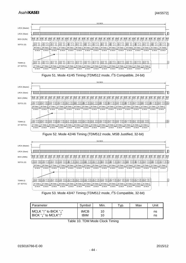
Figure 51. Mode 41/45 Timing (TDM512 mode, I2S Compatible, 24-bit)
LRCK (Slave)
BICK (256fs)
SDTO1 (O) 30 1
#8 Data 1
32 BICK
512 BICK
30 1
#8 Data 2
32 BICK
30 1
#7 Data 1
32 BICK
30 1
#7 Data 2
32 BICK
LRCK (Master)
TDMIN (I)
(#7 SDTO1)
30 1
#7 Data 1
32 BICK
30 1
#7 Data 2
32 BICK
30 30 1
#6 Data 1
32 BICK
30 1
#6 Data 2
32 BICK
30 1
#6 Data 1
32 BICK
30 1
#6 Data 2
32 BICK
30 1
#5 Data 1
32 BICK
30 1
#5 Data 2
32 BICK
30 1
#4 Data 1
32 BICK
30 1
#4 Data 2
32 BICK
30 1
#3 Data 1
32 BICK
30 1
#3 Data 2
32 BICK
30 1
#2 Data 1
32 BICK
30 1
#2 Data 2
32 BICK
30 1
#1 Data 1
32 BICK
30 1
#1 Data 2
32 BICK
30 1
#5 Data 1
32 BICK
30 1
#5 Data 2
32 BICK
30 1
#4 Data 1
32 BICK
30 1
#4 Data 2
32 BICK
30 1
#3 Data 1
32 BICK
30 1
#3 Data 2
32 BICK
30 0
#2 Data 1
32 BICK
30 1
#2 Data 2
32 BICK
31 0 31 0 31 0 31 0 31 0 31 0 31 0 31 0 31 0 31 0 31 0 31 0 31 0 31 0 31 0 31 0
31
30 31
31 0 31 0 31 0 31 0 31 0 31 0 31 0 31 0 31 0 31 0 31 1 31 0 30 0
#1 Data 1
32 BICK
30 1
#1 Data 2
32 BICK
31 1 31 0
Figure 52. Mode 42/46 Timing (TDM512 mode, MSB Justified, 32-bit)
LRCK (Slave)
BICK (256fs)
SDTO1 (O) 30 1
#8 Data 1
32 BICK
512 BICK
30 1
#8 Data 2
32 BICK
30 1
#7 Data 1
32 BICK
30 1
#7 Data 2
32 BICK
LRCK (Master)
TDMIN (I)
(#7 SDTO1)
30 1
#7 Data 1
32 BICK
30 1
#7 Data 2
32 BICK
30 1
#6 Data 1
32 BICK
30 1
#6 Data 2
32 BICK
30 1
#6 Data 1
32 BICK
30 1
#6 Data 2
32 BICK
30 1
#5 Data 1
32 BICK
30 1
#5 Data 2
32 BICK
30 1
#4 Data 1
32 BICK
30 1
#4 Data 2
32 BICK
30 1
#3 Data 1
32 BICK
30 1
#3 Data2
32 BICK
30 1
#2 Data 1
32 BICK
30 1
#2 Data 2
32 BICK
30 1
#1 Data 1
32 BICK
30 1
#1 Data 2
32 BICK
30 1
#5 Data 1
32 BICK
30 1
#5 Data 2
32 BICK
30 1
#4 Data 1
32 BICK
30 1
#4 Data 2
32 BICK
30 1
#3 Data 1
32 BICK
30 1
#3 Data 2
32 BICK
30 0
#2 Data 1
32 BICK
30 1
#2 Data 2
32 BICK
31 0 31 0 31 0 31 0 31 0 31 0 31 0 31 0 31 0 31 0 31 0 31 0 31 0 31 0 31 0 31 0
31
31
31 0 31 0 31 0 31 0 31 0 31 0 31 0 31 0 31 0 31 0 31 1 31 0
0
30 0
#1 Data 1
32 BICK
30 1
#1 Data 2
32 BICK
31 1 31 0
Figure 53. Mode 43/47 Timing (TDM512 mode, I2S Compatible, 32-bit)
Parameter Symbol Min. Typ. Max Unit
MCLK “↑” to BICK “↓” BICK “↓” to MCLK“↑”
tMCB tBIM
10 10
ns ns
Table 10. TDM Mode Clock Timing
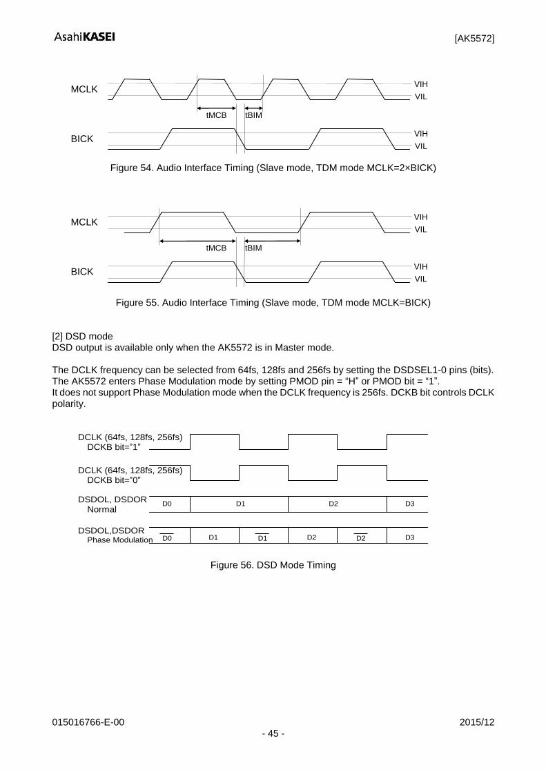
[AK5572]
015016766-E-00 2015/12 - 45 -
Figure 54. Audio Interface Timing (Slave mode, TDM mode MCLK=2×BICK)
Figure 55. Audio Interface Timing (Slave mode, TDM mode MCLK=BICK)
[2] DSD mode DSD output is available only when the AK5572 is in Master mode. The DCLK frequency can be selected from 64fs, 128fs and 256fs by setting the DSDSEL1-0 pins (bits). The AK5572 enters Phase Modulation mode by setting PMOD pin = “H” or PMOD bit = “1”. It does not support Phase Modulation mode when the DCLK frequency is 256fs. DCKB bit controls DCLK polarity.
DCLK (64fs, 128fs, 256fs) DCKB bit=”1”
DCLK (64fs, 128fs, 256fs) DCKB bit=”0”
DSDOL, DSDOR Normal
DSDOL,DSDOR Phase Modulation
D1
D0 D1 D2
D0 D2 D3
D1 D2 D3
Figure 56. DSD Mode Timing
MCLK
BICK
tMCB tBIM
VIH
VIL
VIH
VIL
MCLK
BICK
tMCB tBIM
VIH
VIL
VIH
VIL
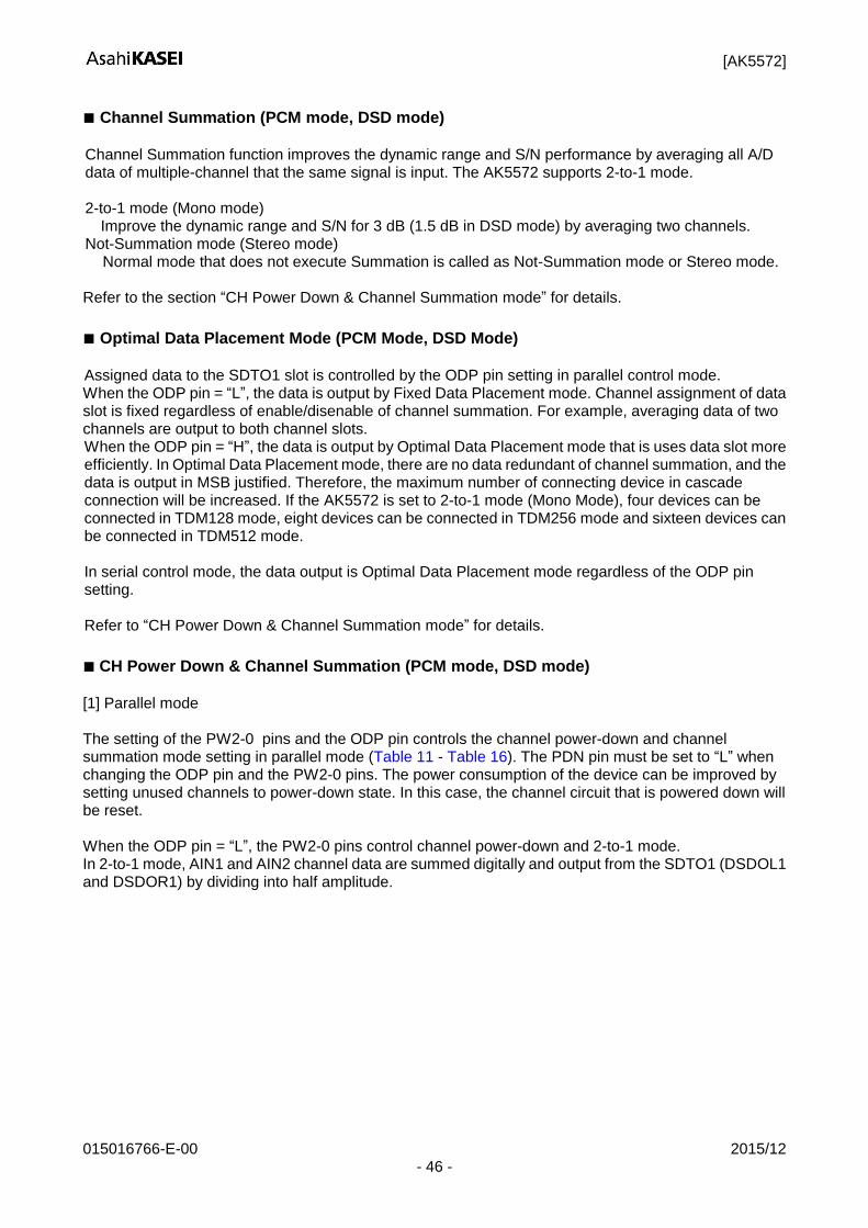
[AK5572]
015016766-E-00 2015/12 - 46 -
Channel Summation (PCM mode, DSD mode)
Channel Summation function improves the dynamic range and S/N performance by averaging all A/D data of multiple-channel that the same signal is input. The AK5572 supports 2-to-1 mode. 2-to-1 mode (Mono mode)
Improve the dynamic range and S/N for 3 dB (1.5 dB in DSD mode) by averaging two channels. Not-Summation mode (Stereo mode)
Normal mode that does not execute Summation is called as Not-Summation mode or Stereo mode. Refer to the section “CH Power Down & Channel Summation mode” for details.
Optimal Data Placement Mode (PCM Mode, DSD Mode)
Assigned data to the SDTO1 slot is controlled by the ODP pin setting in parallel control mode. When the ODP pin = “L”, the data is output by Fixed Data Placement mode. Channel assignment of data slot is fixed regardless of enable/disenable of channel summation. For example, averaging data of two channels are output to both channel slots. When the ODP pin = “H”, the data is output by Optimal Data Placement mode that is uses data slot more efficiently. In Optimal Data Placement mode, there are no data redundant of channel summation, and the data is output in MSB justified. Therefore, the maximum number of connecting device in cascade connection will be increased. If the AK5572 is set to 2-to-1 mode (Mono Mode), four devices can be connected in TDM128 mode, eight devices can be connected in TDM256 mode and sixteen devices can be connected in TDM512 mode. In serial control mode, the data output is Optimal Data Placement mode regardless of the ODP pin setting. Refer to “CH Power Down & Channel Summation mode” for details.
CH Power Down & Channel Summation (PCM mode, DSD mode)
[1] Parallel mode The setting of the PW2-0 pins and the ODP pin controls the channel power-down and channel summation mode setting in parallel mode (Table 11 - Table 16). The PDN pin must be set to “L” when changing the ODP pin and the PW2-0 pins. The power consumption of the device can be improved by setting unused channels to power-down state. In this case, the channel circuit that is powered down will be reset. When the ODP pin = “L”, the PW2-0 pins control channel power-down and 2-to-1 mode. In 2-to-1 mode, AIN1 and AIN2 channel data are summed digitally and output from the SDTO1 (DSDOL1 and DSDOR1) by dividing into half amplitude.
[AK5572]
015016766-E-00 2015/12 - 47 -
PW2 pin
PW1 pin
PW0 pin
Power ON/OFF
Ch2 Ch1
L L L OFF OFF
L L H ON OFF
L H L OFF ON
L H H ON ON
H L L OFF OFF
H L H ON OFF
H H L OFF ON
H H H ON ON
Table 11. Channel Power ON/OFF (Parallel Control Mode, ODP pin= ”L”)
PW2 pin
PW1 pin
PW0 pin
Data on Slot
Slot 2 Slot 1
L L L All “0” All “0”
L L H CH2 All “0”
L H L All “0” CH1
L H H (CH1+2)/2 (CH1+2)/2
H L L All “0” All “0”
H L H CH2 All “0”
H H L All “0” CH1
H H H CH2 CH1
Table 12. Slot Data Assign (Parallel Control Mode, ODP pin= “L”) When the ODP pin = “H”, the AK5572 becomes optimal data placement mode and data slots can be used efficiently. The PW2-0 pins control power down, 2-to-1 mode. In 2-to-1 mode, AIN1 and AIN2 channel data are summed digitally and output from the SDTO1 (DSDOL1) by dividing into half amplitude.
PW2 pin
PW1 pin
PW0 pin
Power ON/OFF
Ch2 Ch1
L L L OFF OFF
L L H ON ON
L H L ON ON
L H H ON ON
H L L ON ON
H L H ON ON
H H L ON ON
H H H ON ON
Table 13. Channel Power ON/OFF (Parallel Control mode, ODP pin= ”H”)
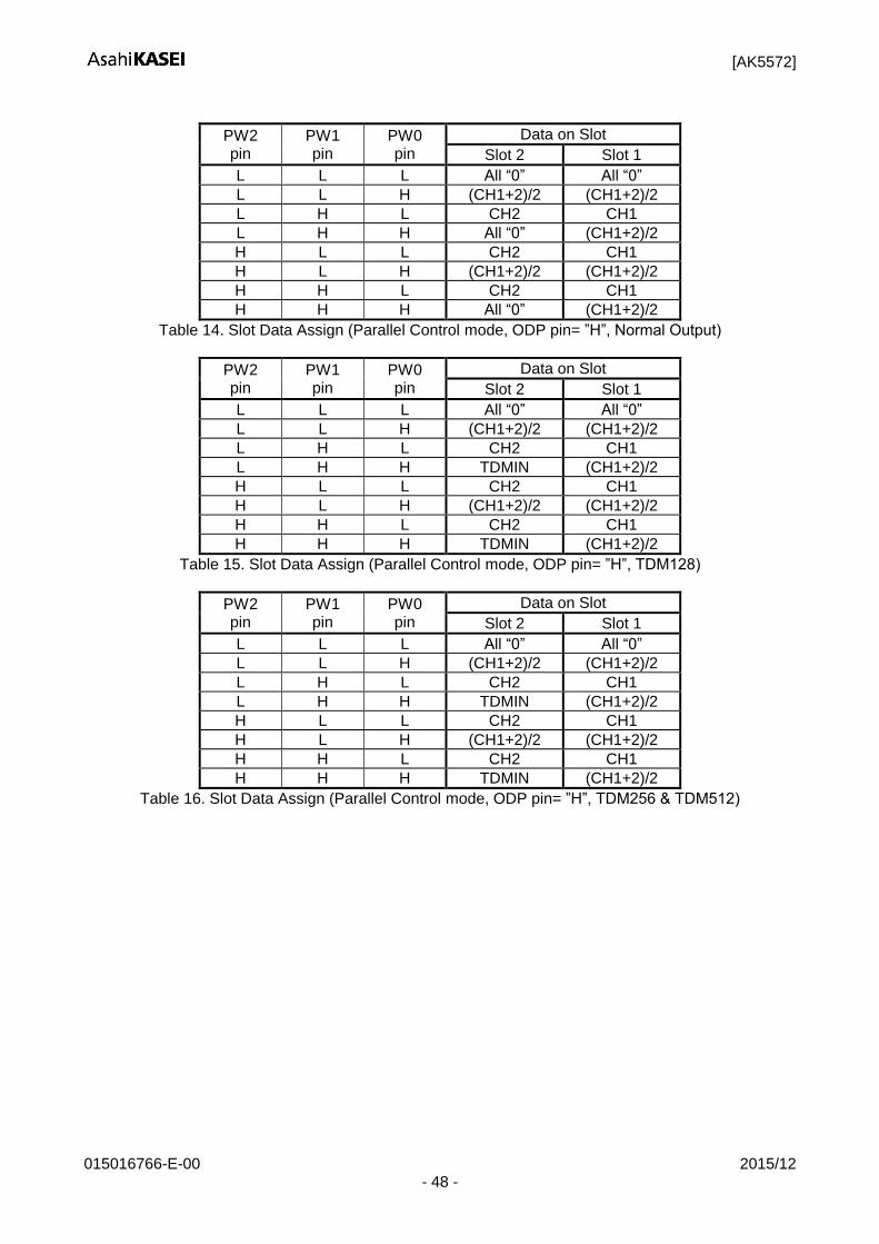
[AK5572]
015016766-E-00 2015/12 - 48 -
PW2 pin
PW1 pin
PW0 pin
Data on Slot
Slot 2 Slot 1
L L L All “0” All “0”
L L H (CH1+2)/2 (CH1+2)/2
L H L CH2 CH1
L H H All “0” (CH1+2)/2
H L L CH2 CH1
H L H (CH1+2)/2 (CH1+2)/2
H H L CH2 CH1
H H H All “0” (CH1+2)/2
Table 14. Slot Data Assign (Parallel Control mode, ODP pin= ”H”, Normal Output)
PW2 pin
PW1 pin
PW0 pin
Data on Slot
Slot 2 Slot 1
L L L All “0” All “0”
L L H (CH1+2)/2 (CH1+2)/2
L H L CH2 CH1
L H H TDMIN (CH1+2)/2
H L L CH2 CH1
H L H (CH1+2)/2 (CH1+2)/2
H H L CH2 CH1
H H H TDMIN (CH1+2)/2
Table 15. Slot Data Assign (Parallel Control mode, ODP pin= ”H”, TDM128)
PW2 pin
PW1 pin
PW0 pin
Data on Slot
Slot 2 Slot 1
L L L All “0” All “0”
L L H (CH1+2)/2 (CH1+2)/2
L H L CH2 CH1
L H H TDMIN (CH1+2)/2
H L L CH2 CH1
H L H (CH1+2)/2 (CH1+2)/2
H H L CH2 CH1
H H H TDMIN (CH1+2)/2
Table 16. Slot Data Assign (Parallel Control mode, ODP pin= ”H”, TDM256 & TDM512)
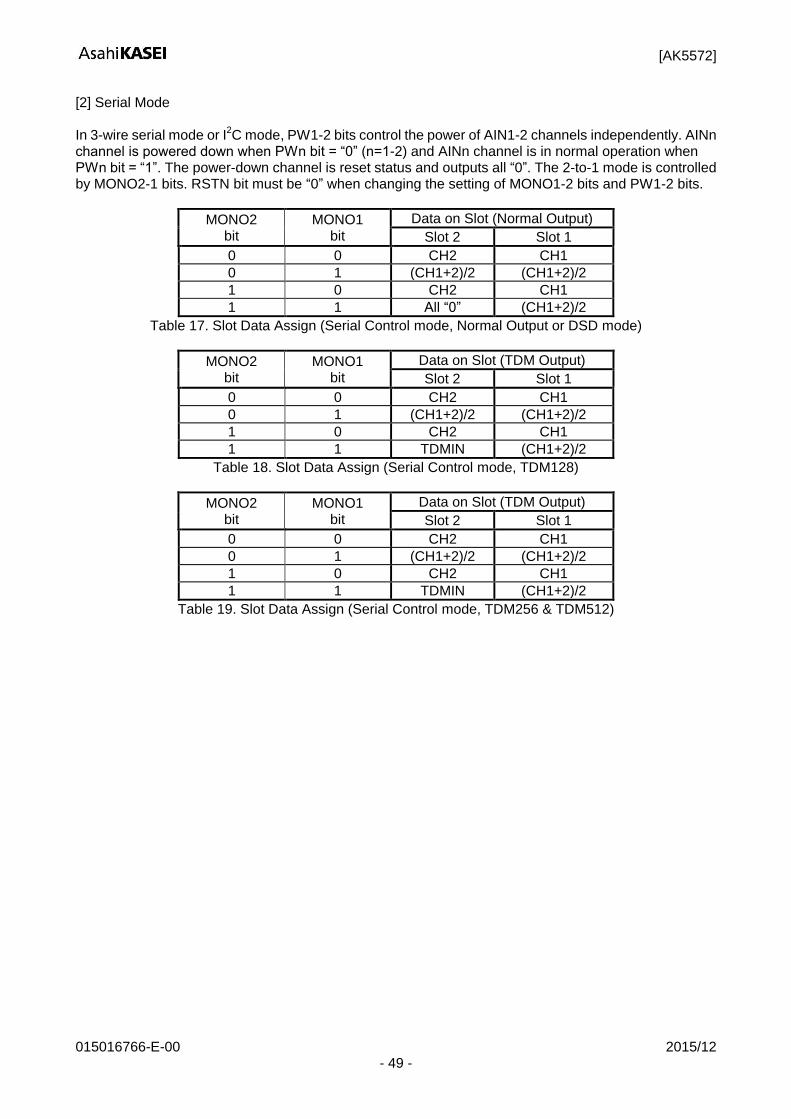
[AK5572]
015016766-E-00 2015/12 - 49 -
[2] Serial Mode In 3-wire serial mode or I
2C mode, PW1-2 bits control the power of AIN1-2 channels independently. AINn
channel is powered down when PWn bit = “0” (n=1-2) and AINn channel is in normal operation when PWn bit = “1”. The power-down channel is reset status and outputs all “0”. The 2-to-1 mode is controlled by MONO2-1 bits. RSTN bit must be “0” when changing the setting of MONO1-2 bits and PW1-2 bits.
MONO2 bit
MONO1 bit
Data on Slot (Normal Output)
Slot 2 Slot 1
0 0 CH2 CH1
0 1 (CH1+2)/2 (CH1+2)/2
1 0 CH2 CH1
1 1 All “0” (CH1+2)/2
Table 17. Slot Data Assign (Serial Control mode, Normal Output or DSD mode)
MONO2 bit
MONO1 bit
Data on Slot (TDM Output)
Slot 2 Slot 1
0 0 CH2 CH1
0 1 (CH1+2)/2 (CH1+2)/2
1 0 CH2 CH1
1 1 TDMIN (CH1+2)/2
Table 18. Slot Data Assign (Serial Control mode, TDM128)
MONO2 bit
MONO1 bit
Data on Slot (TDM Output)
Slot 2 Slot 1
0 0 CH2 CH1
0 1 (CH1+2)/2 (CH1+2)/2
1 0 CH2 CH1
1 1 TDMIN (CH1+2)/2
Table 19. Slot Data Assign (Serial Control mode, TDM256 & TDM512)
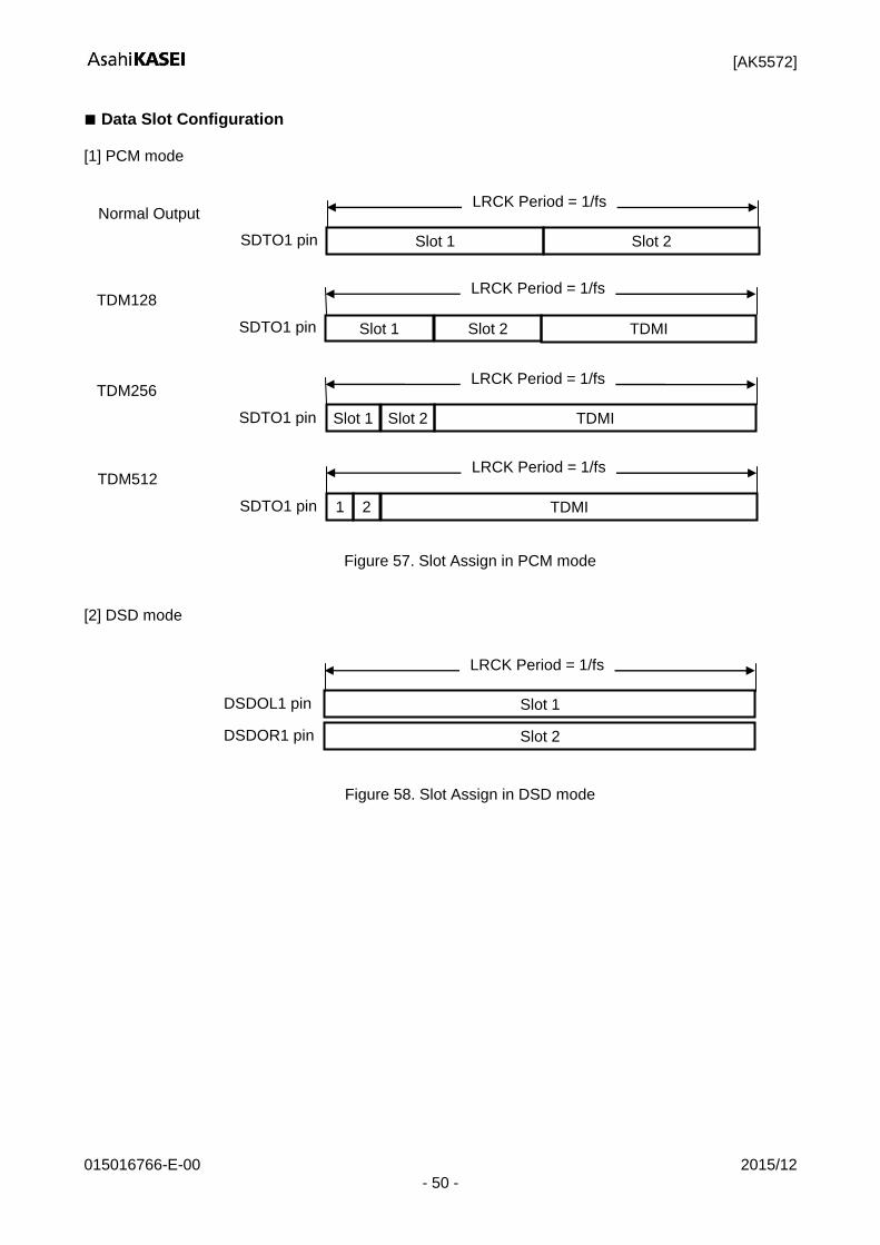
[AK5572]
015016766-E-00 2015/12 - 50 -
Data Slot Configuration
[1] PCM mode
Figure 57. Slot Assign in PCM mode [2] DSD mode
Figure 58. Slot Assign in DSD mode
DSDOL1 pin Slot 1
LRCK Period = 1/fs
Slot 2 DSDOR1 pin
SDTO1 pin Slot 1 Slot 2
Slot 1 SDTO1 pin
Normal Output
TDM128
Slot 2
LRCK Period = 1/fs
LRCK Period = 1/fs
Slot 1 SDTO1 pin
TDM256 LRCK Period = 1/fs
Slot 2 TDMI
1 SDTO1 pin
TDM512 LRCK Period = 1/fs
2 TDMI
TDMI
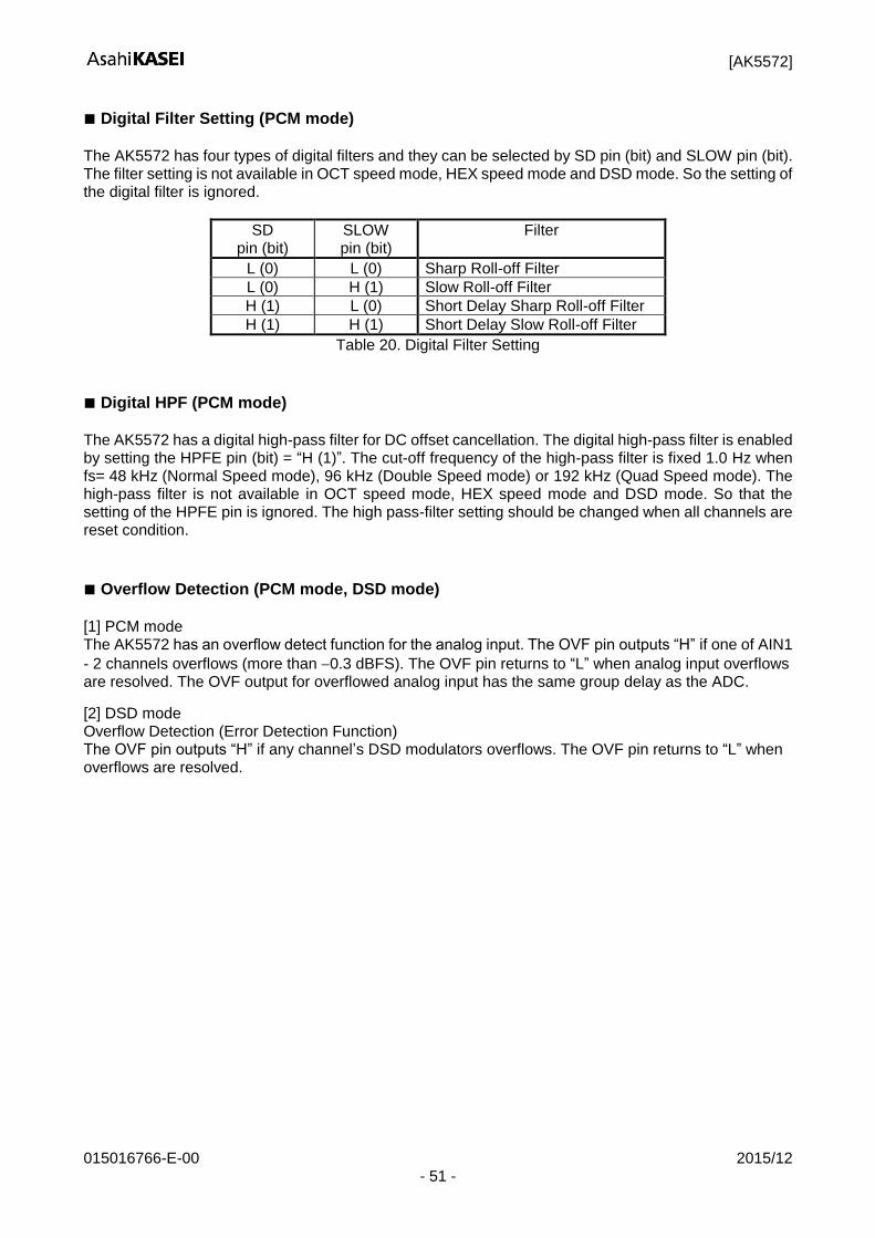
[AK5572]
015016766-E-00 2015/12 - 51 -
Digital Filter Setting (PCM mode)
The AK5572 has four types of digital filters and they can be selected by SD pin (bit) and SLOW pin (bit). The filter setting is not available in OCT speed mode, HEX speed mode and DSD mode. So the setting of the digital filter is ignored.
SD pin (bit)
SLOW pin (bit)
Filter
L (0) L (0) Sharp Roll-off Filter
L (0) H (1) Slow Roll-off Filter
H (1) L (0) Short Delay Sharp Roll-off Filter
H (1) H (1) Short Delay Slow Roll-off Filter
Table 20. Digital Filter Setting
Digital HPF (PCM mode)
The AK5572 has a digital high-pass filter for DC offset cancellation. The digital high-pass filter is enabled by setting the HPFE pin (bit) = “H (1)”. The cut-off frequency of the high-pass filter is fixed 1.0 Hz when fs= 48 kHz (Normal Speed mode), 96 kHz (Double Speed mode) or 192 kHz (Quad Speed mode). The high-pass filter is not available in OCT speed mode, HEX speed mode and DSD mode. So that the setting of the HPFE pin is ignored. The high pass-filter setting should be changed when all channels are reset condition.
Overflow Detection (PCM mode, DSD mode)
[1] PCM mode The AK5572 has an overflow detect function for the analog input. The OVF pin outputs “H” if one of AIN1
- 2 channels overflows (more than 0.3 dBFS). The OVF pin returns to “L” when analog input overflows are resolved. The OVF output for overflowed analog input has the same group delay as the ADC.
[2] DSD mode Overflow Detection (Error Detection Function) The OVF pin outputs “H” if any channel’s DSD modulators overflows. The OVF pin returns to “L” when overflows are resolved.
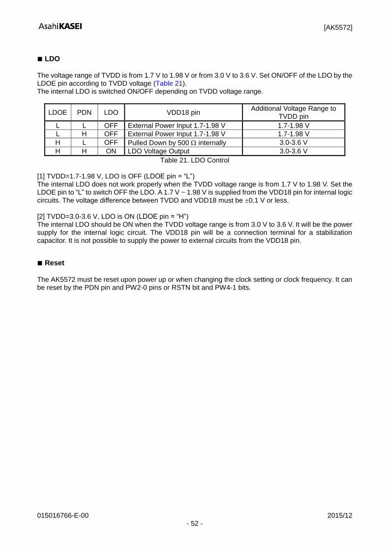
[AK5572]
015016766-E-00 2015/12 - 52 -
LDO
The voltage range of TVDD is from 1.7 V to 1.98 V or from 3.0 V to 3.6 V. Set ON/OFF of the LDO by the LDOE pin according to TVDD voltage (Table 21). The internal LDO is switched ON/OFF depending on TVDD voltage range.
LDOE PDN LDO VDD18 pin Additional Voltage Range to
TVDD pin
L L OFF External Power Input 1.7-1.98 V 1.7-1.98 V
L H OFF External Power Input 1.7-1.98 V 1.7-1.98 V
H L OFF Pulled Down by 500 internally 3.0-3.6 V
H H ON LDO Voltage Output 3.0-3.6 V
Table 21. LDO Control [1] TVDD=1.7-1.98 V, LDO is OFF (LDOE pin = “L”) The internal LDO does not work properly when the TVDD voltage range is from 1.7 V to 1.98 V. Set the LDOE pin to “L” to switch OFF the LDO. A 1.7 V ~ 1.98 V is supplied from the VDD18 pin for internal logic circuits. The voltage difference between TVDD and VDD18 must be ±0.1 V or less. [2] TVDD=3.0-3.6 V, LDO is ON (LDOE pin = “H”) The internal LDO should be ON when the TVDD voltage range is from 3.0 V to 3.6 V. It will be the power supply for the internal logic circuit. The VDD18 pin will be a connection terminal for a stabilization capacitor. It is not possible to supply the power to external circuits from the VDD18 pin.
Reset
The AK5572 must be reset upon power up or when changing the clock setting or clock frequency. It can be reset by the PDN pin and PW2-0 pins or RSTN bit and PW4-1 bits.
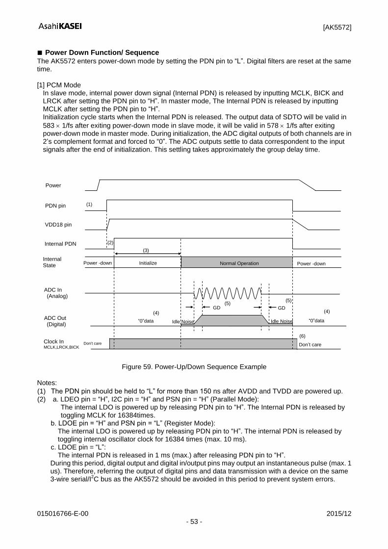
[AK5572]
015016766-E-00 2015/12 - 53 -
Power Down Function/ Sequence
The AK5572 enters power-down mode by setting the PDN pin to “L”. Digital filters are reset at the same time. [1] PCM Mode
In slave mode, internal power down signal (Internal PDN) is released by inputting MCLK, BICK and LRCK after setting the PDN pin to “H”. In master mode, The Internal PDN is released by inputting MCLK after setting the PDN pin to “H”. Initialization cycle starts when the Internal PDN is released. The output data of SDTO will be valid in
583 1/fs after exiting power-down mode in slave mode, it will be valid in 578 1/fs after exiting power-down mode in master mode. During initialization, the ADC digital outputs of both channels are in 2’s complement format and forced to “0”. The ADC outputs settle to data correspondent to the input signals after the end of initialization. This settling takes approximately the group delay time.
PDN pin
Power
Power -down Normal Operation
Clock In MCLK,LRCK,BICK
ADC In (Analog)
ADC Out (Digital)
Don’t care
“0”data
GD
(3)
(5)
(6)
GD (5)
“0”data
Don’t care
Internal State
(4) (4)
(1)
Internal PDN (2)
VDD18 pin
Initialize Power -down
Idle Noise Idle Noise
Figure 59. Power-Up/Down Sequence Example
Notes:
(1) The PDN pin should be held to “L” for more than 150 ns after AVDD and TVDD are powered up. (2) a. LDEO pin = “H”, I2C pin = “H” and PSN pin = “H” (Parallel Mode):
The internal LDO is powered up by releasing PDN pin to “H”. The Internal PDN is released by toggling MCLK for 16384times.
b. LDOE pin = “H” and PSN pin = “L” (Register Mode): The internal LDO is powered up by releasing PDN pin to “H”. The internal PDN is released by toggling internal oscillator clock for 16384 times (max. 10 ms).
c. LDOE pin = “L”: The internal PDN is released in 1 ms (max.) after releasing PDN pin to “H”.
During this period, digital output and digital in/output pins may output an instantaneous pulse (max. 1 us). Therefore, referring the output of digital pins and data transmission with a device on the same 3-wire serial/I
2C bus as the AK5572 should be avoided in this period to prevent system errors.
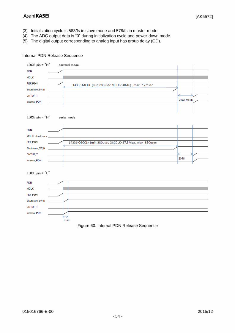
[AK5572]
015016766-E-00 2015/12 - 54 -
(3) Initialization cycle is 583/fs in slave mode and 578/fs in master mode.
(4) The ADC output data is “0” during initialization cycle and power-down mode.
(5) The digital output corresponding to analog input has group delay (GD). Internal PDN Release Sequence
Figure 60. Internal PDN Release Sequence
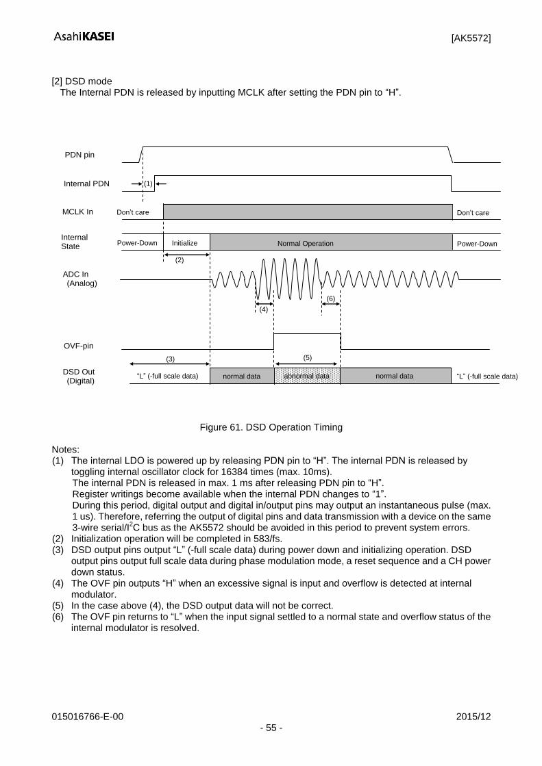
[AK5572]
015016766-E-00 2015/12 - 55 -
[2] DSD mode
The Internal PDN is released by inputting MCLK after setting the PDN pin to “H”.
PDN pin
Power-Down Normal Operation
MCLK In
ADC In (Analog)
DSD Out (Digital)
Don’t care
(3)
“L” (-full scale data)
Don’t care
Internal State
(4)
(1)
(2)
Initialize Power-Down
OVF-pin
normal data abnormal data normal data “L” (-full scale data)
(6)
(5)
Internal PDN
Figure 61. DSD Operation Timing
Notes: (1) The internal LDO is powered up by releasing PDN pin to “H”. The internal PDN is released by
toggling internal oscillator clock for 16384 times (max. 10ms). The internal PDN is released in max. 1 ms after releasing PDN pin to “H”. Register writings become available when the internal PDN changes to “1”. During this period, digital output and digital in/output pins may output an instantaneous pulse (max. 1 us). Therefore, referring the output of digital pins and data transmission with a device on the same 3-wire serial/I
2C bus as the AK5572 should be avoided in this period to prevent system errors.
(2) Initialization operation will be completed in 583/fs. (3) DSD output pins output “L” (-full scale data) during power down and initializing operation. DSD
output pins output full scale data during phase modulation mode, a reset sequence and a CH power down status.
(4) The OVF pin outputs “H” when an excessive signal is input and overflow is detected at internal modulator.
(5) In the case above (4), the DSD output data will not be correct. (6) The OVF pin returns to “L” when the input signal settled to a normal state and overflow status of the
internal modulator is resolved.
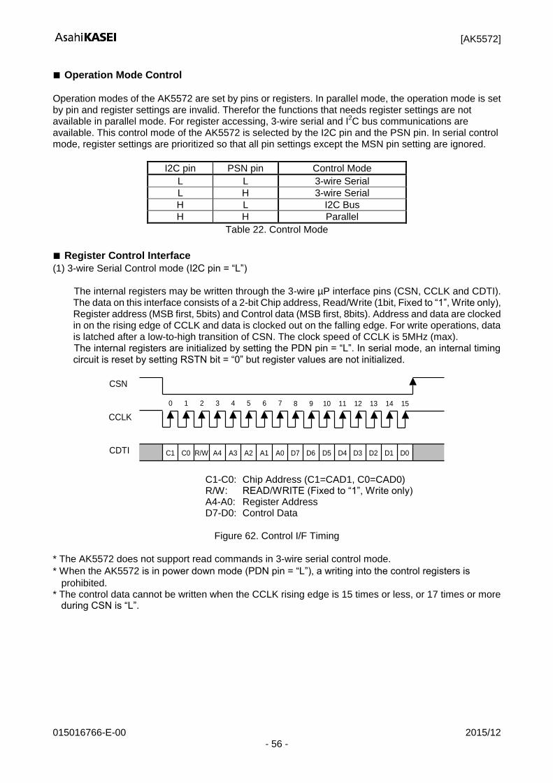
[AK5572]
015016766-E-00 2015/12 - 56 -
Operation Mode Control Operation modes of the AK5572 are set by pins or registers. In parallel mode, the operation mode is set by pin and register settings are invalid. Therefor the functions that needs register settings are not available in parallel mode. For register accessing, 3-wire serial and I
2C bus communications are
available. This control mode of the AK5572 is selected by the I2C pin and the PSN pin. In serial control mode, register settings are prioritized so that all pin settings except the MSN pin setting are ignored.
I2C pin PSN pin Control Mode
L L 3-wire Serial
L H 3-wire Serial
H L I2C Bus
H H Parallel
Table 22. Control Mode
Register Control Interface (1) 3-wire Serial Control mode (I2C pin = “L”)
The internal registers may be written through the 3-wire µP interface pins (CSN, CCLK and CDTI). The data on this interface consists of a 2-bit Chip address, Read/Write (1bit, Fixed to “1”, Write only), Register address (MSB first, 5bits) and Control data (MSB first, 8bits). Address and data are clocked in on the rising edge of CCLK and data is clocked out on the falling edge. For write operations, data is latched after a low-to-high transition of CSN. The clock speed of CCLK is 5MHz (max). The internal registers are initialized by setting the PDN pin = “L”. In serial mode, an internal timing circuit is reset by setting RSTN bit = “0” but register values are not initialized.
CDTI
CCLK
C1
0 1 2 3 4 5 6 7 8 9 10 11 12 13 14 15
D4D5D6D7A1A2A3A4R/WC0 A0 D0D1D2D3
CSN
C1-C0: Chip Address (C1=CAD1, C0=CAD0) R/W: READ/WRITE (Fixed to “1”, Write only) A4-A0: Register Address D7-D0: Control Data
Figure 62. Control I/F Timing
* The AK5572 does not support read commands in 3-wire serial control mode.
* When the AK5572 is in power down mode (PDN pin = “L”), a writing into the control registers is
prohibited. * The control data cannot be written when the CCLK rising edge is 15 times or less, or 17 times or more
during CSN is “L”.
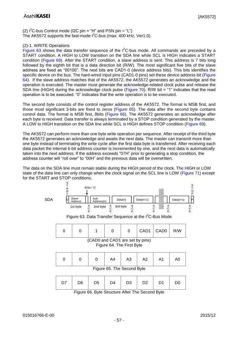
[AK5572]
015016766-E-00 2015/12 - 57 -
(2) I2C-bus Control mode (I2C pin = “H” and PSN pin = “L”)
The AK5572 supports the fast-mode I2C-bus (max: 400 kHz, Ver1.0).
(2)-1. WRITE Operations Figure 63 shows the data transfer sequence of the I
2C-bus mode. All commands are preceded by a
START condition. A HIGH to LOW transition on the SDA line while SCL is HIGH indicates a START condition (Figure 69). After the START condition, a slave address is sent. This address is 7 bits long followed by the eighth bit that is a data direction bit (R/W). The most significant five bits of the slave address are fixed as “00100”. The next bits are CAD1-0 (device address bits). This bits identifies the specific device on the bus. The hard-wired input pins (CAD1-0 pins) set these device address bit (Figure 64). If the slave address matches that of the AK5572, the AK5572 generates an acknowledge and the operation is executed. The master must generate the acknowledge-related clock pulse and release the SDA line (HIGH) during the acknowledge clock pulse (Figure 70). R/W bit = “1” indicates that the read operation is to be executed. “0” indicates that the write operation is to be executed. The second byte consists of the control register address of the AK5572. The format is MSB first, and those most significant 3-bits are fixed to zeros (Figure 65). The data after the second byte contains control data. The format is MSB first, 8bits (Figure 66). The AK5572 generates an acknowledge after each byte is received. Data transfer is always terminated by a STOP condition generated by the master. A LOW to HIGH transition on the SDA line while SCL is HIGH defines STOP condition (Figure 69). The AK5572 can perform more than one byte write operation per sequence. After receipt of the third byte the AK5572 generates an acknowledge and awaits the next data. The master can transmit more than one byte instead of terminating the write cycle after the first data byte is transferred. After receiving each data packet the internal 6-bit address counter is incremented by one, and the next data is automatically taken into the next address. If the address exceeds “07H” prior to generating a stop condition, the address counter will “roll over” to “00H” and the previous data will be overwritten. The data on the SDA line must remain stable during the HIGH period of the clock. The HIGH or LOW state of the data line can only change when the clock signal on the SCL line is LOW (Figure 71) except for the START and STOP conditions.
3rd byte 2nd byte 1st byte
SDA
START
ACK
ACK
S Slave Address
ACK
Sub Address(n)
Data(n) P
STOP
Data(n+x)
ACK
Data(n+1)
ACK
R/W= “0”
ACK
Figure 63. Data Transfer Sequence at the I2C-Bus Mode
0 0 1 0 0 CAD1 CAD0 R/W
(CAD0 and CAD1 are set by pins) Figure 64. The First Byte
0 0 0 A4 A3 A2 A1 A0
Figure 65. The Second Byte
D7 D6 D5 D4 D3 D2 D1 D0
Figure 66. Byte Structure After The Second Byte
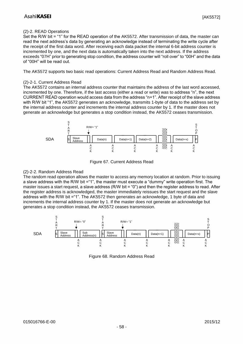
[AK5572]
015016766-E-00 2015/12 - 58 -
(2)-2. READ Operations Set the R/W bit = “1” for the READ operation of the AK5572. After transmission of data, the master can read the next address’s data by generating an acknowledge instead of terminating the write cycle after the receipt of the first data word. After receiving each data packet the internal 6-bit address counter is incremented by one, and the next data is automatically taken into the next address. If the address exceeds “07H” prior to generating stop condition, the address counter will “roll over” to “00H” and the data of “00H” will be read out. The AK5572 supports two basic read operations: Current Address Read and Random Address Read. (2)-2-1. Current Address Read The AK5572 contains an internal address counter that maintains the address of the last word accessed, incremented by one. Therefore, if the last access (either a read or write) was to address “n”, the next CURRENT READ operation would access data from the address “n+1”. After receipt of the slave address with R/W bit “1”, the AK5572 generates an acknowledge, transmits 1-byte of data to the address set by the internal address counter and increments the internal address counter by 1. If the master does not generate an acknowledge but generates a stop condition instead, the AK5572 ceases transmission.
SDA
START
ACK
ACK
S SlaveAddress
ACK
Data(n+1) P
STOP
Data(n+x)
ACK
Data(n+2)
ACK
R/W= “1”
ACK
Data(n)
Figure 67. Current Address Read
(2)-2-2. Random Address Read The random read operation allows the master to access any memory location at random. Prior to issuing a slave address with the R/W bit =“1”, the master must execute a “dummy” write operation first. The master issues a start request, a slave address (R/W bit = “0”) and then the register address to read. After the register address is acknowledged, the master immediately reissues the start request and the slave address with the R/W bit =“1”. The AK5572 then generates an acknowledge, 1 byte of data and increments the internal address counter by 1. If the master does not generate an acknowledge but generates a stop condition instead, the AK5572 ceases transmission.
SDA
START
ACK
ACK
S SlaveAddress
ACK
Data(n) P
STOP
Data(n+x)
ACK
Data(n+1)
ACK
R/W= “0”
ACK
SubAddress(n)
START
ACK
S SlaveAddress
R/W= “1”
Figure 68. Random Address Read
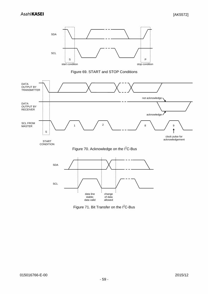
[AK5572]
015016766-E-00 2015/12 - 59 -
SCL
SDA
stop conditionstart condition
S P
Figure 69. START and STOP Conditions
SCL FROMMASTER
acknowledge
DATAOUTPUT BYTRANSMITTER
DATAOUTPUT BYRECEIVER
1 98
STARTCONDITION
not acknowledge
clock pulse foracknowledgement
S
2
Figure 70. Acknowledge on the I
2C-Bus
SCL
SDA
data linestable;
data valid
changeof dataallowed
Figure 71. Bit Transfer on the I
2C-Bus
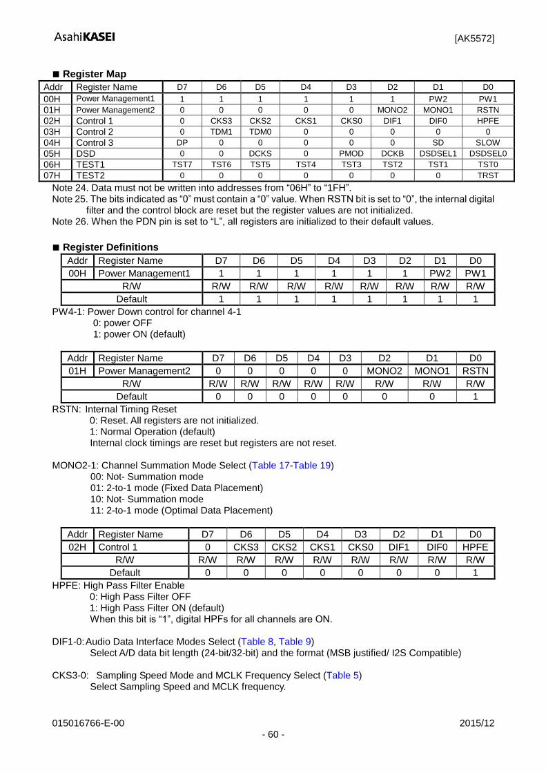
[AK5572]
015016766-E-00 2015/12 - 60 -
Register Map
Addr Register Name D7 D6 D5 D4 D3 D2 D1 D0
00H Power Management1 1 1 1 1 1 1 PW2 PW1
01H Power Management2 0 0 0 0 0 MONO2 MONO1 RSTN
02H Control 1 0 CKS3 CKS2 CKS1 CKS0 DIF1 DIF0 HPFE
03H Control 2 0 TDM1 TDM0 0 0 0 0 0
04H Control 3 DP 0 0 0 0 0 SD SLOW
05H DSD 0 0 DCKS 0 PMOD DCKB DSDSEL1 DSDSEL0
06H TEST1 TST7 TST6 TST5 TST4 TST3 TST2 TST1 TST0
07H TEST2 0 0 0 0 0 0 0 TRST
Note 24. Data must not be written into addresses from “06H” to “1FH”. Note 25. The bits indicated as “0” must contain a “0” value. When RSTN bit is set to “0”, the internal digital
filter and the control block are reset but the register values are not initialized. Note 26. When the PDN pin is set to “L”, all registers are initialized to their default values.
Register Definitions
Addr Register Name D7 D6 D5 D4 D3 D2 D1 D0
00H Power Management1 1 1 1 1 1 1 PW2 PW1
R/W R/W R/W R/W R/W R/W R/W R/W R/W
Default 1 1 1 1 1 1 1 1
PW4-1: Power Down control for channel 4-1 0: power OFF 1: power ON (default)
Addr Register Name D7 D6 D5 D4 D3 D2 D1 D0
01H Power Management2 0 0 0 0 0 MONO2 MONO1 RSTN
R/W R/W R/W R/W R/W R/W R/W R/W R/W
Default 0 0 0 0 0 0 0 1
RSTN: Internal Timing Reset 0: Reset. All registers are not initialized. 1: Normal Operation (default)
Internal clock timings are reset but registers are not reset. MONO2-1: Channel Summation Mode Select (Table 17-Table 19)
00: Not- Summation mode 01: 2-to-1 mode (Fixed Data Placement) 10: Not- Summation mode 11: 2-to-1 mode (Optimal Data Placement)
Addr Register Name D7 D6 D5 D4 D3 D2 D1 D0
02H Control 1 0 CKS3 CKS2 CKS1 CKS0 DIF1 DIF0 HPFE
R/W R/W R/W R/W R/W R/W R/W R/W R/W
Default 0 0 0 0 0 0 0 1
HPFE: High Pass Filter Enable 0: High Pass Filter OFF 1: High Pass Filter ON (default)
When this bit is “1”, digital HPFs for all channels are ON.
DIF1-0: Audio Data Interface Modes Select (Table 8, Table 9) Select A/D data bit length (24-bit/32-bit) and the format (MSB justified/ I2S Compatible)
CKS3-0: Sampling Speed Mode and MCLK Frequency Select (Table 5)
Select Sampling Speed and MCLK frequency.
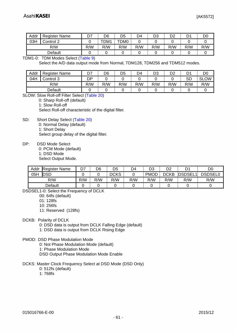
[AK5572]
015016766-E-00 2015/12 - 61 -
Addr Register Name D7 D6 D5 D4 D3 D2 D1 D0
03H Control 2 0 TDM1 TDM0 0 0 0 0 0
R/W R/W R/W R/W R/W R/W R/W R/W R/W
Default 0 0 0 0 0 0 0 0
TDM1-0: TDM Modes Select (Table 9) Select the A/D data output mode from Normal, TDM128, TDM256 and TDM512 modes.
Addr Register Name D7 D6 D5 D4 D3 D2 D1 D0
04H Control 3 DP 0 0 0 0 0 SD SLOW
R/W R/W R/W R/W R/W R/W R/W R/W R/W
Default 0 0 0 0 0 0 0 0
SLOW: Slow Roll-off Filter Select (Table 20) 0: Sharp Roll-off (default) 1: Slow Roll-off
Select Roll-off characteristic of the digital filter. SD: Short Delay Select (Table 20) 0: Normal Delay (default) 1: Short Delay
Select group delay of the digital filter. DP: DSD Mode Select 0: PCM Mode (default) 1: DSD Mode
Select Output Mode.
Addr Register Name D7 D6 D5 D4 D3 D2 D1 D0
05H DSD 0 0 DCKS 0 PMOD DCKB DSDSEL1 DSDSEL0
R/W R/W R/W R/W R/W R/W R/W R/W R/W
Default 0 0 0 0 0 0 0 0
DSDSEL1-0: Select the Frequency of DCLK 00: 64fs (default) 01: 128fs 10: 256fs 11: Reserved (128fs)
DCKB: Polarity of DCLK
0: DSD data is output from DCLK Falling Edge (default) 1: DSD data is output from DCLK Rising Edge
PMOD: DSD Phase Modulation Mode
0: Not Phase Modulation Mode (default) 1: Phase Modulation Mode DSD Output Phase Modulation Mode Enable
DCKS: Master Clock Frequency Select at DSD Mode (DSD Only)
0: 512fs (default) 1: 768fs
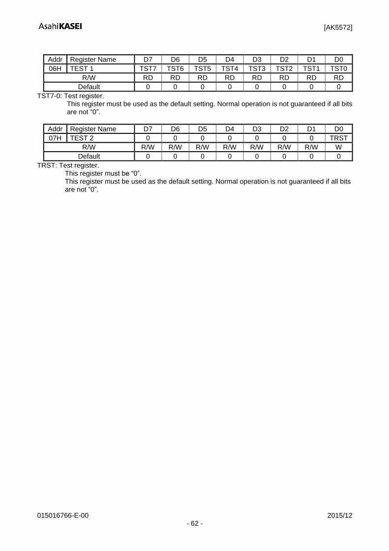
[AK5572]
015016766-E-00 2015/12 - 62 -
Addr Register Name D7 D6 D5 D4 D3 D2 D1 D0
06H TEST 1 TST7 TST6 TST5 TST4 TST3 TST2 TST1 TST0
R/W RD RD RD RD RD RD RD RD
Default 0 0 0 0 0 0 0 0
TST7-0: Test register. This register must be used as the default setting. Normal operation is not guaranteed if all bits are not “0”.
Addr Register Name D7 D6 D5 D4 D3 D2 D1 D0
07H TEST 2 0 0 0 0 0 0 0 TRST
R/W R/W R/W R/W R/W R/W R/W R/W W
Default 0 0 0 0 0 0 0 0
TRST: Test register. This register must be “0”. This register must be used as the default setting. Normal operation is not guaranteed if all bits are not “0”.
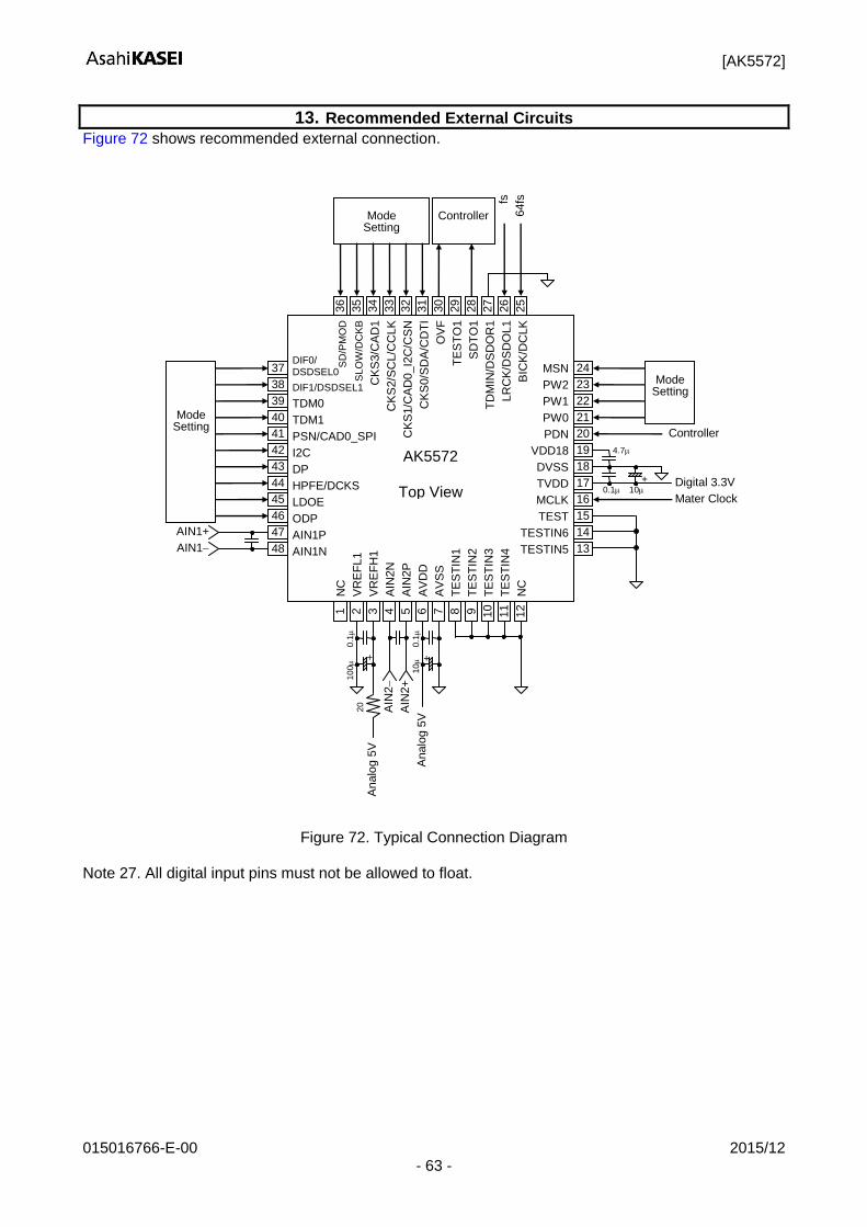
[AK5572]
015016766-E-00 2015/12 - 63 -
13. Recommended External Circuits
Figure 72 shows recommended external connection.
Figure 72. Typical Connection Diagram Note 27. All digital input pins must not be allowed to float.
1
DIF0/ DSDSEL0
DIF1/DSDSEL1
TDM0
TDM1
PSN/CAD0_SPI
I2C
DP
HPFE/DCKS
LDOE
ODP
AIN1P
AIN1N
2
3
4
5
6
7
8
9
10
11
12
13
14
15
16
17
18
19
20
21
22
23
24
36
35
34
33
32
31
30
29
28
27
26
25
48
47
46
45
44
43
42
41
40
39
38
37
4.7
+ 0.1 10
10
0
0
.1
0.1
1
0
+
+
Digital 3.3V
AIN
2
AIN
2+
AIN1
AIN1+
Analo
g 5
V
Analo
g 5
V
Mode
Setting
Mode Setting
Mode
Setting
Controller
Controller
Mater Clock fs
64fs
AK5572
Top View
20
SD
/PM
OD
SLO
W/D
CK
B
CK
S3/C
AD
1
CK
S2/S
CL/C
CLK
CK
S1/C
AD
0_I2
C/C
SN
CK
S0/S
DA
/CD
TI
OV
F
TE
ST
O1
SD
TO
1
TD
MIN
/DS
DO
R1
LR
CK
/DS
DO
L1
BIC
K/D
CLK
MSN
PW2
PW1
PW0
PDN
VDD18
DVSS
TVDD
MCLK
TEST
TESTIN6
TESTIN5
NC
VR
EF
L1
VR
EF
H1
AIN
2N
AIN
2P
AV
DD
AV
SS
TE
ST
IN1
TE
ST
IN2
TE
ST
IN3
TE
ST
IN4
NC
[AK5572]
015016766-E-00 2015/12 - 64 -
1. Grounding and Power Supply Decoupling The AK5572 requires careful attention to power supply and grounding arrangements. Normally AVDD and TVDD are supplied from analog supply of the system. The power-up sequence between AVDD1 and
TVDD are not critical when AVDD and TVDD are supplied separately. DVSS and AVSS must be
connected to the same analog ground plane. System analog ground and digital ground should be wired separately and connected together as close as possible to where the supplies are brought onto the printed circuit board. Decoupling capacitors for high frequency should be placed as near as possible to the supply pin.
2. Reference Voltage
The differential voltage between the VREFH1 pin and the VREFL1 pin is the common voltage of A/D conversion. The VREFL1 pins are normally connected to AVSS. In order to remove a high frequency noise, connect a 20 Ω resistor between the VREFH1 pins and analog 5 V supply, and connect a 0.1 μF ceramic capacitor in parallel with an 100 μF electrolytic capacitor between the VREFH1 pin and the VREFL1 pin. Especially the ceramic capacitor should be connected as close as possible to the pin. All digital signals, especially clocks, should be kept away from the VREFH1 and VREFL1 pins in order to avoid unwanted noise coupling into the AK5572.
3. Analog Inputs
The Analog input signal is differentially supplied into the modulator via the AINn+ and the AINn- pins (n= 1-2). The input voltage is the difference between the ALINn+ and ALINn- pins (n= 1-2). The full scale signal on each pin is nominally ±2.8 V (typ). A voltage from AVSS to AVDD can be input to the AK5572. The output code format is two’s complement. The internal HPF removes DC offset (including DC offset by the ADC itself). The AK5572 requires a +5 V analog supply voltage. Any voltage which exceeds the upper limit of
AVDD+0.3 V and lower limit of AVSS0.3 V and any current beyond 10 mA for the analog input pins should be avoided. Excessive currents to the input pins may damage the device. Hence input pins must be protected from signals at or beyond these limits. Use caution especially when using ±15 V for other analog circuits in the system.
[AK5572]
015016766-E-00 2015/12 - 65 -
4. External Analog Circuit Examples Figure 73 shows an input buffer circuit example 1. (1
st order HPF; fc= 0.70 Hz, 2
nd order LPF; fc= 351
kHz, gain= 14.5 dB). The analog signal is able to input through XLR or BNC connectors. (short JP1 and JP2 for BNC input, open JP1 and JP2 for XLR input). The input level of this circuit is 14.9 Vpp (AK5572: 2.8 Vpp Typ.). When using this circuit, analog characteristics at fs= 48 kHz is DR= 121 dB, S/(N+D)= 112 dB. The S/(N+D) characteristics of the AK5572 varies depending on DC bias current of the input signal. Set the DC bias voltage in a range from 0.49 x AVDD to 0.51 x AVDD for a better characteristic. * Film capacitors are recommended for the components shown as 15nF and 1 nF in the figure below.
4.7k
-
+ -
+
10 3.3k
620
-
+
10
620
Analog In
14.9Vpp
68µ
NJM5534
VA=+5
V VP=15
V
4.7k
10µ
+ 10k
10k
0.1µ
Bias
VA+
2.8Vpp
2.8Vpp
VP+
VP- Bias
1n * 3.3k
1n *
Bias
15n *
68µ
XLR
Vin-
Vin+
JP1
JP2
NJM5534
NJM5534
AK5572 AINn+
AK5572 AINn-
100p
100p
Figure 73. Input Buffer Example1
fin 1Hz 10Hz
Frequency Response 1.77dB 0.02dB
Table 23. Frequency Response of HPF
fin 20kHz 40kHz 80kHz 6.144MHz
Frequency Response 0.00dB 0.00dB 0.00dB 49.68dB
Table 24. Frequency Response of LPF
[AK5572]
015016766-E-00 2015/12 - 66 -
14. Package
Outline Dimensions
48-pin QFN (Unit mm)
Material & Lead Finish
Package molding compound: Epoxy resin Lead frame material: Cu Terminal surface treatment: Solder (Pb free) plate
Marking
1) Pin #1 indication 2) Date Code: XXXXXXX (7 digits) 3) Marketing Code: AK5572EN 4) AKM Logo
AKM AK5572EN XXXXXXX
1
C0.60M
AX
C
B
0.08
C
A
0.40±0.10
+0.07-0.05
0.20
0.02
+0.0
3-0
.02
7.00±0.10
6.75±0.10
7.0
0±
0.10
6.7
5±
0.10
5.1
5.1
0.85
+0.1
5-0
.05
0.500.23
M0.10 AB
[AK5572]
015016766-E-00 2015/12 - 67 -
15. Ordering Guide
AK5572EN 40 – 105 ºC 48-pin QFN AKD5572 Evaluation Board for AK5572
16. Revision History
Date (Y/M/D) Revision Reason Page Contents
15/12/15 00 First Edition
[AK5572]
015016766-E-00 2015/12 - 68 -
IMPORTANT NOTICE
0. Asahi Kasei Microdevices Corporation (“AKM”) reserves the right to make changes to the information contained in this document without notice. When you consider any use or application of AKM product stipulated in this document (“Product”), please make inquiries the sales office of AKM or authorized distributors as to current status of the Products.
1. All information included in this document are provided only to illustrate the operation and application examples of AKM Products. AKM neither makes warranties or representations with respect to the accuracy or completeness of the information contained in this document nor grants any license to any intellectual property rights or any other rights of AKM or any third party with respect to the information in this document. You are fully responsible for use of such information contained in this document in your product design or applications. AKM ASSUMES NO LIABILITY FOR ANY LOSSES INCURRED BY YOU OR THIRD PARTIES ARISING FROM THE USE OF SUCH INFORMATION IN YOUR PRODUCT DESIGN OR APPLICATIONS.
2. The Product is neither intended nor warranted for use in equipment or systems that require extraordinarily high levels of quality and/or reliability and/or a malfunction or failure of which may cause loss of human life, bodily injury, serious property damage or serious public impact, including but not limited to, equipment used in nuclear facilities, equipment used in the aerospace industry, medical equipment, equipment used for automobiles, trains, ships and other transportation, traffic signaling equipment, equipment used to control combustions or explosions, safety devices, elevators and escalators, devices related to electric power, and equipment used in finance-related fields. Do not use Product for the above use unless specifically agreed by AKM in writing.
3. Though AKM works continually to improve the Product’s quality and reliability, you are responsible for complying with safety standards and for providing adequate designs and safeguards for your hardware, software and systems which minimize risk and avoid situations in which a malfunction or failure of the Product could cause loss of human life, bodily injury or damage to property, including data loss or corruption.
4. Do not use or otherwise make available the Product or related technology or any information contained in this document for any military purposes, including without limitation, for the design, development, use, stockpiling or manufacturing of nuclear, chemical, or biological weapons or missile technology products (mass destruction weapons). When exporting the Products or related technology or any information contained in this document, you should comply with the applicable export control laws and regulations and follow the procedures required by such laws and regulations. The Products and related technology may not be used for or incorporated into any products or systems whose manufacture, use, or sale is prohibited under any applicable domestic or foreign laws or regulations.
5. Please contact AKM sales representative for details as to environmental matters such as the RoHS compatibility of the Product. Please use the Product in compliance with all applicable laws and regulations that regulate the inclusion or use of controlled substances, including without limitation, the EU RoHS Directive. AKM assumes no liability for damages or losses occurring as a result of noncompliance with applicable laws and regulations.
6. Resale of the Product with provisions different from the statement and/or technical features set forth in this document shall immediately void any warranty granted by AKM for the Product and shall not create or extend in any manner whatsoever, any liability of AKM.
7. This document may not be reproduced or duplicated, in any form, in whole or in part, without prior written consent of AKM.


![THERMAL BONDING OF POLYMER MICRODEVICES … · · 2013-02-27THERMAL BONDING OF POLYMER MICRODEVICES USING A PRESSURE -ASSISTED BOILING POINT CONTROL SYSTEM Taehyun Park 1, ... [Pa]](https://img.pdfslide.net/doc/110x75/5abf715d7f8b9aa15e8e0473/thermal-bonding-of-polymer-microdevices-bonding-of-polymer-microdevices-using.jpg)