Embed Size (px)
Citation preview
Altera Corporation
January 2005, AN 345-1.1
Altera Design Flow for LatticeSemiconductor Users
Application Note
Introduction Today’s CPLD designs require a simple, but effective design environment to decrease the designs’ time to market. The design environment must contain an integrated suite of tools that allows you to take your CPLD design from conception to implementation. Numerous CPLD design environments address these requirements, but this document explains the functions of the Quartus® II software developed by Altera® Corporation, and the ispLEVER software developed by Lattice Semiconductor. This application note compares the design suite contained in both software packages, and how each addresses the CPLD design requirements.
The Quartus II Approach to CPLD Designs
The Quartus II software contains two graphical user interfaces (GUI) for you to choose from. The first is the traditional Quartus II software look-and-feel. The second GUI is the MAX+PLUS® II look-and-feel. There are no functional differences between these two schemes. The only difference is the way each presents menu structures and icons.
f For more information on the MAX+PLUS II look-and-feel, refer to the Quartus II Design Flow for MAX+PLUS II Users chapter in Volume 1 of the Quartus II Handbook.
This application note presents all information with the MAX+PLUS II look-and-feel set. This scheme provides an ideal environment for CPLD designs.
1 The look-and-feel in the Quartus II software can be changed with the Customize dialog box (Tools menu).
Figure 1 shows the MAX+PLUS II GUI in the Quartus II software.
1
Altera Design Flow for Lattice Semiconductor Users
Figure 1. The MAX+PLUS II GUI
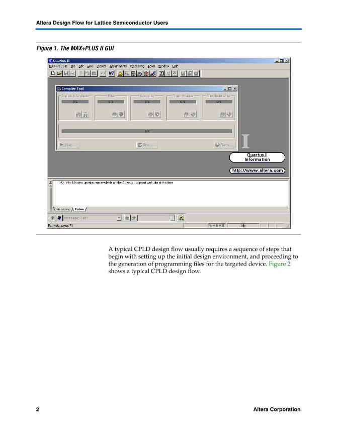
A typical CPLD design flow usually requires a sequence of steps that begin with setting up the initial design environment, and proceeding to the generation of programming files for the targeted device. Figure 2 shows a typical CPLD design flow.
2 Altera CorporationPreliminary
The Quartus II Approach to CPLD Designs
Figure 2. A Typical CPLD Design Flow
Both the Quartus II and ispLEVER software address each of the steps listed in Figure 2.
Design Entry
Synthesize and MapDesign Elements
Project Creation
Place and Route Design Resources
GenerateProgramming File
Typical CPLD Design Flow
Timing Analysis
Altera Corporation 3Preliminary
Altera Design Flow for Lattice Semiconductor Users
Basic CPLD Design Flow Using Quartus II and ispLever
The following section addresses each of the six steps involved in a typical CPLD design. Each will provide an overview of how the Quartus II software addresses each step, compared to the ispLEVER software.
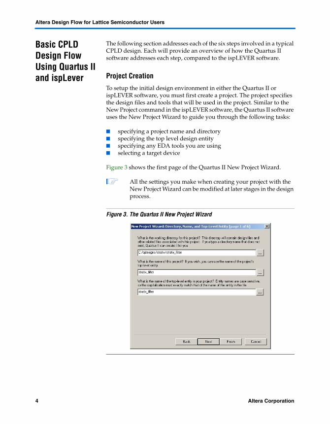
Project Creation
To setup the initial design environment in either the Quartus II or ispLEVER software, you must first create a project. The project specifies the design files and tools that will be used in the project. Similar to the New Project command in the ispLEVER software, the Quartus II software uses the New Project Wizard to guide you through the following tasks:
■ specifying a project name and directory■ specifying the top level design entity■ specifying any EDA tools you are using■ selecting a target device
Figure 3 shows the first page of the Quartus II New Project Wizard.
1 All the settings you make when creating your project with the New Project Wizard can be modified at later stages in the design process.
Figure 3. The Quartus II New Project Wizard
4 Altera CorporationPreliminary
Basic CPLD Design Flow Using Quartus II and ispLever
Design Entry
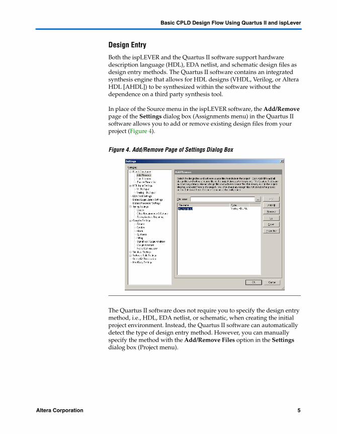
Both the ispLEVER and the Quartus II software support hardware description language (HDL), EDA netlist, and schematic design files as design entry methods. The Quartus II software contains an integrated synthesis engine that allows for HDL designs (VHDL, Verilog, or Altera HDL [AHDL]) to be synthesized within the software without the dependence on a third party synthesis tool.
In place of the Source menu in the ispLEVER software, the Add/Remove page of the Settings dialog box (Assignments menu) in the Quartus II software allows you to add or remove existing design files from your project (Figure 4).
Figure 4. Add/Remove Page of Settings Dialog Box
The Quartus II software does not require you to specify the design entry method, i.e., HDL, EDA netlist, or schematic, when creating the initial project environment. Instead, the Quartus II software can automatically detect the type of design entry method. However, you can manually specify the method with the Add/Remove Files option in the Settings dialog box (Project menu).
Altera Corporation 5Preliminary
Altera Design Flow for Lattice Semiconductor Users
HDL Design Entry
To create a new HDL design file in the Quartus II software, choose New (File menu) and select the type of file to create. To assist you in creating HDL designs, the Quartus II software provides templates for overall AHDL, VHDL and Verilog HDL file structures and constructs, including various logic functions and parameter declarations.
1 The HDL templates can be accessed with the Insert Template dialog box (Edit menu).
Also, the Quartus II Text Editor offers syntax coloring for highlighting HDL reserved words and comments.
f For more information on the Verilog and VHDL support in the Quartus II software, see the Quartus II Integrated Synthesis chapter in Volume 1 of The Quartus II Handbook.
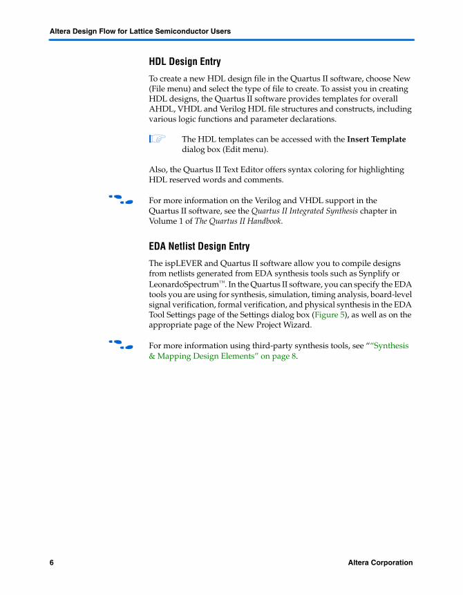
EDA Netlist Design Entry
The ispLEVER and Quartus II software allow you to compile designs from netlists generated from EDA synthesis tools such as Synplify or LeonardoSpectrum™. In the Quartus II software, you can specify the EDA tools you are using for synthesis, simulation, timing analysis, board-level signal verification, formal verification, and physical synthesis in the EDA Tool Settings page of the Settings dialog box (Figure 5), as well as on the appropriate page of the New Project Wizard.
f For more information using third-party synthesis tools, see ““Synthesis & Mapping Design Elements” on page 8.
6 Altera CorporationPreliminary
Basic CPLD Design Flow Using Quartus II and ispLever
Figure 5. The EDA Tool Settings Page of Settings Dialog Box
f For more information on using the Synplify and LeonardoSpectrum tools with the Quartus II software, see the Mentor Graphics LeonardoSpectrum Support chapter and the Synplicity Synplify & SynplifyPro Support chapter in The Quartus II Handbook.
Schematic Design Entry
In the Quartus II software, you can use Altera® design elements such as Boolean gates and registers, or you can create your own symbols from HDL or EDA netlist design entities. The Quartus II software also includes an extensive library of customizable megafunctions supplied with the software. These are added using representative schematic symbols customized using the MegaWizard® Plug-In Manager.
1 Altera and Altera Megafunction Partners Program (AMPPSM) partners offer a large selection of off-the-shelf megafunctions optimized for Altera devices. Designers can implement these parameterized blocks of intellectual property (IP) easily, reducing design and test time.
f See the “Quartus II MegaWizard Plug-In Manager” on page 16 for more information.
Altera Corporation 7Preliminary
Altera Design Flow for Lattice Semiconductor Users
You can also create a block design symbol from a VHDL design file, a Verilog HDL design file, an AHDL design file, or an EDA Netlist. To do this, choose Create/Update > Create Symbol Files for Current File (File menu). The symbol can than be added to your schematic design file.
Synthesis & Mapping Design Elements
The Quartus II software contains an integrated synthesis engine that provides full synthesis support for AHDL, VHDL, and Verilog HDL. The integrated synthesis engine is invoked whenever the Quartus II software encounters any of the three supported HDL languages. Because of this the Quartus II software can be used to compile CPLD designs without the need of a third-party EDA synthesis tool.
Along with the integrated synthesis support, the Quartus II software supports synthesized design files from a third-party EDA synthesis tool. Add EDIF (.edf) or Verilog Quartus Mapping (.vqm) netlist files to your Quartus II project with the Add/Remove option for compilation and fitting into an Altera device.
Design Assignments
Specifying design and device assignments assures that your design takes advantage of specific features of your targeted device architecture and meets performance goals. The ispLEVER software uses the Constraints Editor to create and edit constraints. The Quartus II Assignment Editor conveniently allows you to create, edit, and view constraints using a single centralized interface.
The Quartus II Assignment Editor
You use the Quartus II Assignment Editor to make timing and placement design constraints for your design. The Quartus II software dynamically validates the assignments whenever changes are made in the Assignment Editor, issuing errors or warnings for invalid assignments.
Adding or changing assignments is acknowledged with messages reported in the System tab of the Quartus II message utility window.
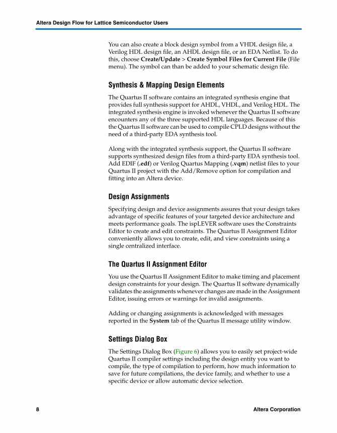
Settings Dialog Box
The Settings Dialog Box (Figure 6) allows you to easily set project-wide Quartus II compiler settings including the design entity you want to compile, the type of compilation to perform, how much information to save for future compilations, the device family, and whether to use a specific device or allow automatic device selection.
8 Altera CorporationPreliminary
Basic CPLD Design Flow Using Quartus II and ispLever
Figure 6. The Settings Dialog Box
1 You can also use the Device page of the Settings dialog box (Assignments menu) to select or change devices for your project.
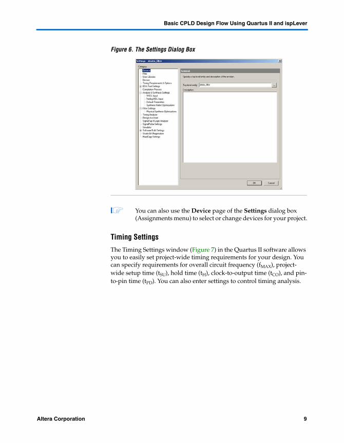
Timing Settings
The Timing Settings window (Figure 7) in the Quartus II software allows you to easily set project-wide timing requirements for your design. You can specify requirements for overall circuit frequency (fMAX), project-wide setup time (tSU), hold time (tH), clock-to-output time (tCO), and pin-to-pin time (tPD). You can also enter settings to control timing analysis.
Altera Corporation 9Preliminary
Altera Design Flow for Lattice Semiconductor Users
Figure 7. The Timing Settings Window
f For more information on the features of the Quartus II Timing Analyzer, see the Quartus II Timing Analysis chapter in Volume 3 of The Quartus II Handbook..
You can use the Assignment Editor to make individual timing assignments or to assign clock settings to a clock signal.
Place & Route of Design Resources
The ispLEVER software follows an implementation flow that generates a programming file from your CPLD design files. A similar flow exists within the Quartus II software known as the compilation flow. The compilation flow is the sequence and method by which the Quartus II software translates your design files, maps the translated design to device specific elements, places and routes the design in the device, and generates a programming file. These functions are performed by the Quartus II Analysis & Synthesis engine, Fitter, Assembler, and Timing Analyzer.
You can start the compilation flow at any point in the design process, whether or not you have completed making your project settings and constraints. In the Quartus II software, choose Start Compilation (Processing menu) to start the compilation process.
10 Altera CorporationPreliminary
Basic CPLD Design Flow Using Quartus II and ispLever
In the initial compilation phase, the Quartus II Analysis & Synthesis engine creates a database from your design files containing all necessary design information. A design rule check is performed on all design files in the project, ensuring that no boundary connectivity errors or syntax errors exist. This database is available for use for all subsequent steps in the compilation flow.
The Analysis & Synthesis engine optimizes your design for the targeted Altera CPLD and maps the design to the device. Mapping converts your design files into architecture-specific atoms that target device resources such as logic elements (LEs) or macrocells.
The Fitter places and routes the atoms created by the Analysis & Synthesis engine onto the selected device. The Fitter performs additional optimization to improve your design’s timing and resource usage based on timing constraints.
When an optimized fit is achieved, the Assembler generates the programming files for your design. The programming files contain all placement and routing information for your design and are used to program the target Altera device.
The Timing Analyzer performs a static timing analysis on every path in your design. This analysis allows you to identify critical paths and timing errors necessary to meet your design’s timing budget or achieve timing closure.
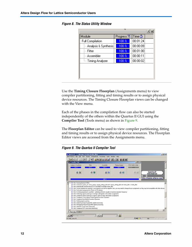
The optional Status utility window shows the progress of the current compilation (Figure 8). View the results of a compilation in the Compilation Report window (Processing menu). A report is generated after every compilation, and shows the design hierarchy, a compilation summary, statistics on the performance of the design, and a link to the floorplan view.
Altera Corporation 11Preliminary
Altera Design Flow for Lattice Semiconductor Users
Figure 8. The Status Utility Window
Use the Timing Closure Floorplan (Assignments menu) to view compiler partitioning, fitting and timing results or to assign physical device resources. The Timing Closure Floorplan views can be changed with the View menu.
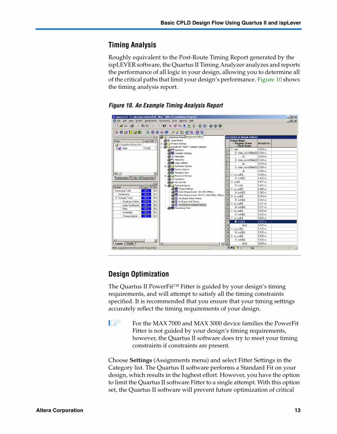
Each of the phases in the compilation flow can also be started independently of the others within the Quartus II GUI using the Compiler Tool (Tools menu) as shown in Figure 9.
The Floorplan Editor can be used to view compiler partitioning, fitting and timing results or to assign physical device resources. The Floorplan Editor views are accessed from the Assignments menu.
Figure 9. The Quartus II Compiler Tool
12 Altera CorporationPreliminary
Basic CPLD Design Flow Using Quartus II and ispLever
Timing Analysis
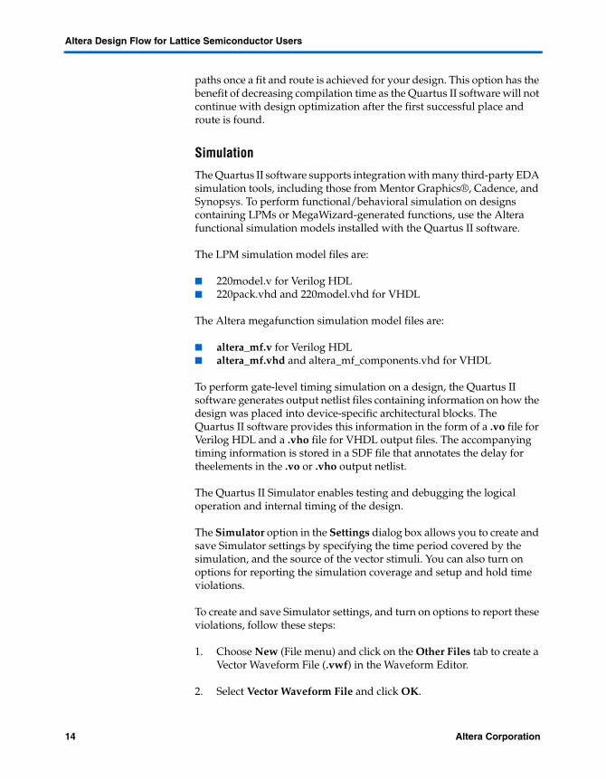
Roughly equivalent to the Post-Route Timing Report generated by the ispLEVER software, the Quartus II Timing Analyzer analyzes and reports the performance of all logic in your design, allowing you to determine all of the critical paths that limit your design’s performance. Figure 10 shows the timing analysis report.
Figure 10. An Example Timing Analysis Report
Design Optimization
The Quartus II PowerFit™ Fitter is guided by your design’s timing requirements, and will attempt to satisfy all the timing constraints specified. It is recommended that you ensure that your timing settings accurately reflect the timing requirements of your design.
1 For the MAX 7000 and MAX 3000 device families the PowerFit Fitter is not guided by your design’s timing requirements, however, the Quartus II software does try to meet your timing constraints if constraints are present.
Choose Settings (Assignments menu) and select Fitter Settings in the Category list. The Quartus II software performs a Standard Fit on your design, which results in the highest effort. However, you have the option to limit the Quartus II software Fitter to a single attempt. With this option set, the Quartus II software will prevent future optimization of critical
Altera Corporation 13Preliminary
Altera Design Flow for Lattice Semiconductor Users
paths once a fit and route is achieved for your design. This option has the benefit of decreasing compilation time as the Quartus II software will not continue with design optimization after the first successful place and route is found.
Simulation
The Quartus II software supports integration with many third-party EDA simulation tools, including those from Mentor Graphics®, Cadence, and Synopsys. To perform functional/behavioral simulation on designs containing LPMs or MegaWizard-generated functions, use the Altera functional simulation models installed with the Quartus II software.
The LPM simulation model files are:
■ 220model.v for Verilog HDL■ 220pack.vhd and 220model.vhd for VHDL
The Altera megafunction simulation model files are:
■ altera_mf.v for Verilog HDL■ altera_mf.vhd and altera_mf_components.vhd for VHDL
To perform gate-level timing simulation on a design, the Quartus II software generates output netlist files containing information on how the design was placed into device-specific architectural blocks. The Quartus II software provides this information in the form of a .vo file for Verilog HDL and a .vho file for VHDL output files. The accompanying timing information is stored in a SDF file that annotates the delay for theelements in the .vo or .vho output netlist.
The Quartus II Simulator enables testing and debugging the logical operation and internal timing of the design.
The Simulator option in the Settings dialog box allows you to create and save Simulator settings by specifying the time period covered by the simulation, and the source of the vector stimuli. You can also turn on options for reporting the simulation coverage and setup and hold time violations.
To create and save Simulator settings, and turn on options to report these violations, follow these steps:
1. Choose New (File menu) and click on the Other Files tab to create a Vector Waveform File (.vwf) in the Waveform Editor.
2. Select Vector Waveform File and click OK.
14 Altera CorporationPreliminary
Basic CPLD Design Flow Using Quartus II and ispLever
The .vwf file should contain the vector inputs for simulation, and the names of the outputs to be simulated.
3. Select the Automatically add pins to simulation output waveforms option on the Simulator section of the Settings dialog box (Assignments menu).
This option directs the Simulator to add waveforms to the simulation outputs for all the output pins in the project, and eliminates the need to manually enter the names of the output nodes you want to monitor.
a. Choose Start Simulation (Processing menu) to run the simulation.
4. Choose Simulation Report (Processing menu) to view the simulation results.
Device Programming
The Quartus II Programmer allows you to use programming files generated in the compilation flow to program or configure all Altera programmable logic devices and supported configuration devices.
To use the Quartus II Programmer to program or configure all Altera devices, follow these steps.
1. Choose Programmer (Tools menu) to Open the Programmer.
2. Select the appropriate programming mode in the Mode list of the Programmer window.
3. Click on the Hardware Setup... button to display the Hardware Setup dialog box.
4. Click on the Hardware Settings tab, and select a programming hardware setup from the Available hardware items: list.
5. In the Select Device dialog box, select a device family in the Device Family list and a device name in the Device Name list.
Altera Corporation 15Preliminary
Altera Design Flow for Lattice Semiconductor Users
Additional Quartus II Features
In addition to providing the standard set of tools required in any FPGA design flow, the Quartus II software provides additional features and tools to assist and enhance your design cycle.
Quartus II MegaWizard Plug-In Manager
In place of the Module/IP Manager available in the ispLEVER software, the Altera MegaWizard Plug-In Manager helps you create highly customized megafunctions that have been optimized for the device targeted by your design. These customizations draw on Altera-provided megafunctions, including library-of-parameterized-modules (LPM) functions, ranging from simple Boolean gates to complex memory structures.
The MegaWizard Plug-In Manager categorizes all supported modules into folders, named as follows:
■ arithmetic■ gates■ memory compiler■ storage
You can access the MegaWizard Plug-In Manager as a stand-alone tool or as an integrated tool in your Quartus II project. Table 1 provides a brief list of supported megafunctions.
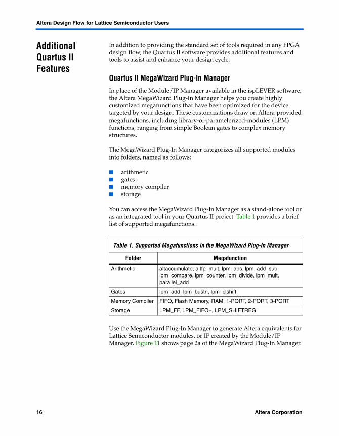
Use the MegaWizard Plug-In Manager to generate Altera equivalents for Lattice Semiconductor modules, or IP created by the Module/IP Manager. Figure 11 shows page 2a of the MegaWizard Plug-In Manager.
Table 1. Supported Megafunctions in the MegaWizard Plug-In Manager
Folder Megafunction
Arithmetic altaccumulate, altfp_mult, lpm_abs, lpm_add_sub, lpm_compare, lpm_counter, lpm_divide, lpm_mult, parallel_add
Gates lpm_add, lpm_bustri, lpm_clshift
Memory Compiler FIFO, Flash Memory, RAM: 1-PORT, 2-PORT, 3-PORT
Storage LPM_FF, LPM_FIFO+, LPM_SHIFTREG
16 Altera CorporationPreliminary
Additional Quartus II Features
Figure 11. MegaWizard Plug-In Manager
The MegaWizard Plug-In Manager automatically generates a Component Declaration file (.cmp) that can be used in VHDL Design Files (.vhd), and an AHDL Include File (.inc) that can be used in Text Design Files (.tdf) and Verilog Design Files (.v). The MegaWizard Plug-In Manager also creates a sample instantiation template with the extension _inst.tdf for AHDL designs, _inst.vhd for VHDL designs, and _inst.v for Verilog HDL designs. A sample declaration file with a _bb.v extension is also created for Verilog HDL designs. The sample files contain module and port declarations for the custom megafunction variation. A block symbol file (.bsf) is also created, which is a symbol representing the logic in a schematic file.
Scripting with Tcl and SDC In the Quartus II Software
The Quartus II graphical user interface (GUI) provides an easy way to access all features and commands offered by the software. However, as designs grow in resource utilization and complexity, the need to automate common tasks and to streamline the CPLD design flow becomes a requirement. The Quartus II software provides support for Tool Command Language (Tcl) and Synopsys Design Constraints (SDC) to help facilitate project assignments, compilation, and constraints. The following provides a brief description on the Quartus II software support of Tcl and SDC.
Altera Corporation 17Preliminary
Altera Design Flow for Lattice Semiconductor Users
f For more information on this subject, see the Tcl Scripting chapter in Volume 2 of The Quartus II Handbook.
The Quartus II software contains Tcl API functions that you can use to automate a variety of common tasks, such as making assignments, compiling designs, analyzing timing, and controlling simulation. The Quartus II software offers the following ways to run your Tcl scripts:
■ Interactively from the shell■ Using scripts in batch from the shell■ As a batch file from the DOS or UNIX prompt■ Directly from the command-line
Using Synopsys Design Constraints with the Quartus II Software
To ease the integration with third-party EDA synthesis tools, the Quartus II software supports the Synopsys Design Constraints (SDC) functions. Table 2 provides a brief list of supported SDC functions.
Table 2. Quartus II-Supported SDC Function (Part 1 of 2)
Command Description
create_clock Creates a base clock with the given name and waveform, and applies the clock to the specified clock pin list.
set_clock_latency Inserts a source latency into an existing base clock.
set_false_path Specifies that the timing paths that start from a designated start node and end at a designated destination node are false paths.
set_input_delay Specifies the external input delay of a set of input or bidirectional pins with respect to the designated clock.
remove_clock Removes all the clocks that are used in the current design if the -all option is specified.
create_generated_clock Creates a derived, or generated clock from the given clock source. A generated clock can be derived only from a base clock. The generated clock is always assumed to be propagated.
get_clocks Returns the listo of clock pins as specified in the <clock_pin_list>. The input list is returned as the output. When <no port list> is specified, the command returns nothing.
remove_input_delay Removes the specified input delay assignments from the current design.
remove_output_delay Removes the specified ouptut delay assignments from the current design.
reset_path Removes the specified timing path assignments from the current design. If neither the -setup or -hold option is specified, the noth setup and hold paths are removed.
set_false_path Specifies that the timing paths that start from the designated <from_pin_list> and end in the designated <to_pin_list> are false paths.
18 Altera CorporationPreliminary
Additional Quartus II Features
Altera Equivalents for Lattice ispLEVER Features
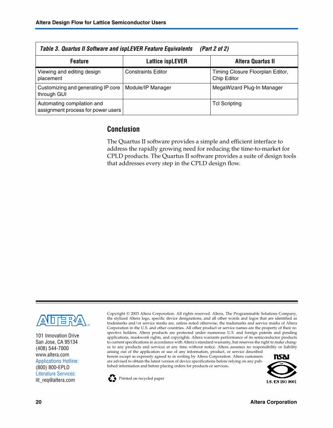
Table 3 lists the stages of the design flow, Lattice the ispLEVER software features used in each stage, and their equivalents in the Altera Quartus II software.
set_input_delay Specifies the external input delay of a set of input or bidir pins with respect to the designated clock. The delay applies to both the positive and negative edges of the clock. The specification is internally translated into the equivalent Quartus II software tSU requirements.
set_max_delay Specifies the maximum delay for the timing paths that start from the designated <from_pin_list> and end in the designated <to_pin_list>.
set_min_delay Specifies the minimum delay for the timing paths that start from the designated <from_pin_list> and end in the designated <to_pin_list>.
set_multicycle_path Specifies that the given timing paths have multicycle setup or hold delays with the number of cycles specified by the <path_multiplier>. That the meaning of multicycle hold differs between the Quartus II timing analysis and the Synopsys® PrimeTime software. Refer to the online Help for each software package for more information.
set_output_delay Specifies the external output delay of a set of output or bidir pins with respect to the designated clock. The delay applies to both the positive and negative edges of the clock. The specification is internally translated into the equivalent Quartus II software tCO requirements.
Table 2. Quartus II-Supported SDC Function (Part 2 of 2)
Command Description
Table 3. Quartus II Software and ispLEVER Feature Equivalents (Part 1 of 2)
Feature Lattice ispLEVER Altera Quartus II
Creating a new project File New Project New Project Wizard
Selecting target FPGA device Project Navigator Assignments > Device
Assignment timing, placement and I/O constraints
Constraints Editor Assignment Editor
Fitting and placing the design into the CPLD to meet the user requirements and generation of programming files for the configuration of the targeted CPLD
Compiling, Optimizing and Partitioning, Fitting
Database Builder, Logic Synthesizer, Fitter, Assembler, Timing Analyzer
Performing static timing analysis on post-fitted design
Place Timing Report Timing Analyzer
Functional and Timing Simulation Third-Party Simulation Tools or Native ispLEVER Simulator
Third-Party Simulation Tools or Native Quartus II Simulator
Generating device programming file Generate Bitstream Data Assembler
Altera Corporation 19Preliminary
Altera Design Flow for Lattice Semiconductor Users
Conclusion
The Quartus II software provides a simple and efficient interface to address the rapidly growing need for reducing the time-to-market for CPLD products. The Quartus II software provides a suite of design tools that addresses every step in the CPLD design flow.
Viewing and editing design placement
Constraints Editor Timing Closure Floorplan Editor, Chip Editor
Customizing and generating IP core through GUI
Module/IP Manager MegaWizard Plug-In Manager
Automating compilation and assignment process for power users
Tcl Scripting
Table 3. Quartus II Software and ispLEVER Feature Equivalents (Part 2 of 2)
Feature Lattice ispLEVER Altera Quartus II
20 Altera CorporationPreliminary
101 Innovation DriveSan Jose, CA 95134(408) 544-7000www.altera.comApplications Hotline:(800) 800-EPLDLiterature Services:[email protected]
Copyright © 2003 Altera Corporation. All rights reserved. Altera, The Programmable Solutions Company,the stylized Altera logo, specific device designations, and all other words and logos that are identified astrademarks and/or service marks are, unless noted otherwise, the trademarks and service marks of AlteraCorporation in the U.S. and other countries. All other product or service names are the property of their re-spective holders. Altera products are protected under numerous U.S. and foreign patents and pendingapplications, maskwork rights, and copyrights. Altera warrants performance of its semiconductor productsto current specifications in accordance with Altera's standard warranty, but reserves the right to make chang-es to any products and services at any time without notice. Altera assumes no responsibility or liabilityarising out of the application or use of any information, product, or service describedherein except as expressly agreed to in writing by Altera Corporation. Altera customersare advised to obtain the latest version of device specifications before relying on any pub-lished information and before placing orders for products or services.
Printed on recycled paper