Embed Size (px)
Citation preview
An Unobtrusive Debugging Methodology for Actel AX and RTAX-S FPGAs
Jonathan Alexander
Applications Consulting Manager
Actel Corporation
MAPLD 2004
2 182/MAPLD 2004Alexander
Logic Design Challenges Designs often don’t work the way they were intended to
the first time
Device Issues Timing Problems
External setup/hold Clock skew Cross-clock domain paths Software/Timing model bug Device speed (faster or slower than
expected)
Device Problems Damage due to electrical overstress (EOS) Defect Packaging
Non-Device Issues Signal Integrity
VIH/VIL
Ground/Vcc Bounce Cross Talk Termination Edge rates Power supply noise
Assembly Solder shorts Component orientation Component alignment
PCB Design or PCB Manufacturing Spacing rules Shorts/Opens
3 182/MAPLD 2004Alexander
Debugging Challenges Non-Device Issues
Signals can be directly probed on a PCB Power supplies can be probed Resistance can be measured Components can be replaced JTAG tests for continuity Must have test points and test headers for access to signals
Device Issues – ASIC Custom test vectors offer high coverage for the specific design
implemented Test points and test blocks built into device Limited access to internal nodes Long and expensive re-spins
4 182/MAPLD 2004Alexander
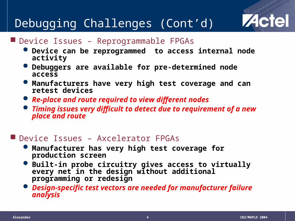
Debugging Challenges (Cont’d) Device Issues – Reprogrammable FPGAs
Device can be reprogrammed to access internal node activity Debuggers are available for pre-determined node access Manufacturers have very high test coverage and can retest
devices Re-place and route required to view different nodes Timing issues very difficult to detect due to requirement of a new
place and route
Device Issues – Axcelerator FPGAs Manufacturer has very high test coverage for production screen Built-in probe circuitry gives access to virtually every net in the
design without additional programming or redesign Design-specific test vectors are needed for manufacturer failure
analysis
5 182/MAPLD 2004Alexander
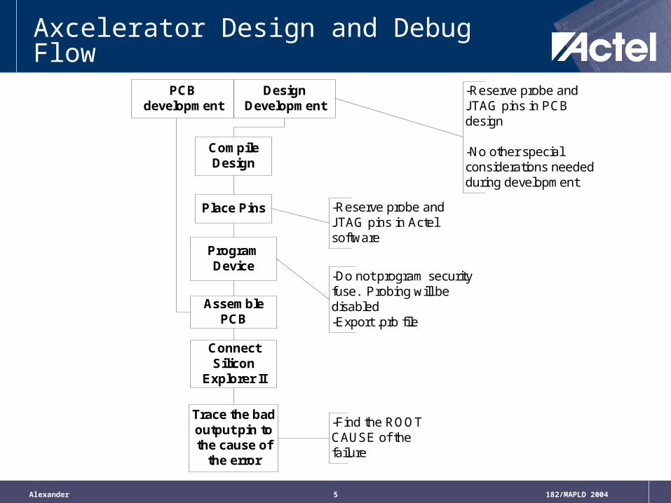
Axcelerator Design and Debug FlowDesign
Development
CompileDesign
-Reserve probe andJTAG pins in PCBdesign
-No other specialconsiderations neededduring development
-Reserve probe andJTAG pins in Actelsoftware
AssemblePCB
-Find the ROOTCAUSE of thefailure
Place Pins
PCBdevelopment
ProgramDevice
-Do not program securityfuse. Probing will bedisabled-Export .prb file
ConnectSilicon
Explorer II
Trace the badoutput pin tothe cause of
the error
6 182/MAPLD 2004Alexander
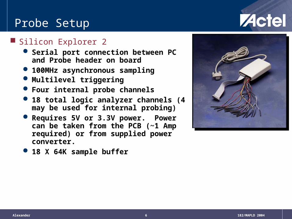
Probe Setup Silicon Explorer 2
Serial port connection between PC and Probe header on board
100MHz asynchronous sampling Multilevel triggering Four internal probe channels 18 total logic analyzer channels (4 may be
used for internal probing) Requires 5V or 3.3V power. Power can be
taken from the PCB (~1 Amp required) or from supplied power converter.
18 X 64K sample buffer
7 182/MAPLD 2004Alexander
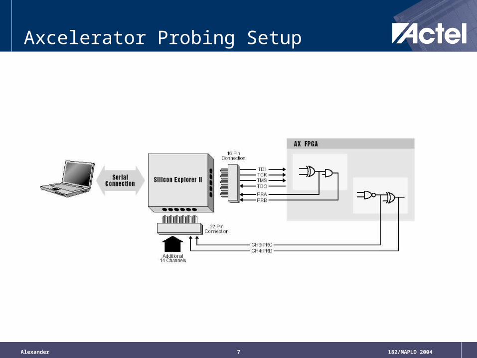
Axcelerator Probing Setup
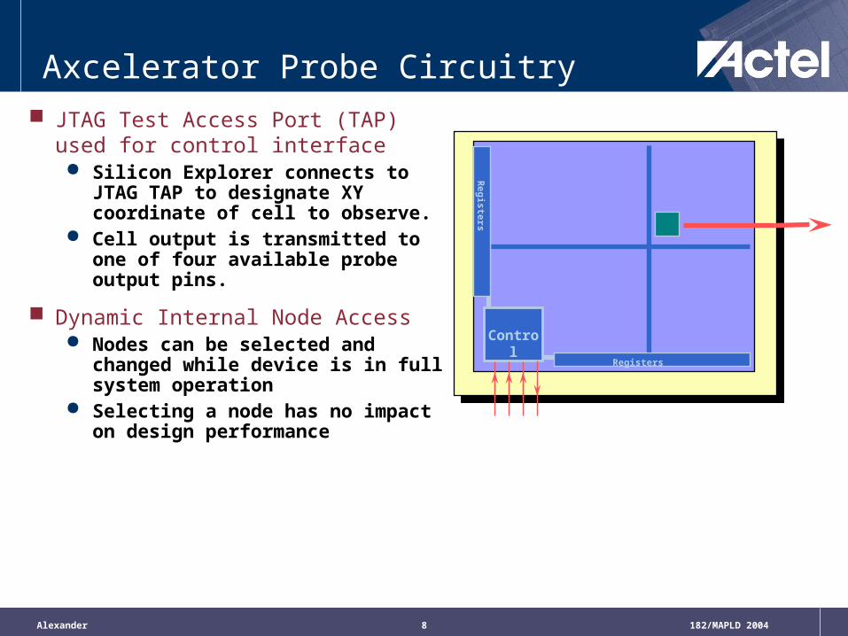
8 182/MAPLD 2004Alexander
Control
RegistersR
egisters
Axcelerator Probe Circuitry JTAG Test Access Port (TAP) used for
control interface Silicon Explorer connects to JTAG TAP
to designate XY coordinate of cell to observe.
Cell output is transmitted to one of four available probe output pins.
Dynamic Internal Node Access Nodes can be selected and changed
while device is in full system operation Selecting a node has no impact on
design performance
9 182/MAPLD 2004Alexander
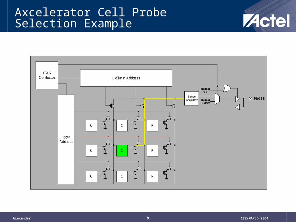
C
JTAGController
C
C
NormalOutput
PROBE
NormalOE
R
R
R
C
C
C
SenseAmplifier
RowAddress
Column Address
C
JTAGController
C
C
NormalOutput
PROBE
NormalOE
C
C
C
R
R
R
RowAddress
Column Address
SenseAmplifier
Axcelerator Cell Probe Selection Example
10 182/MAPLD 2004Alexander
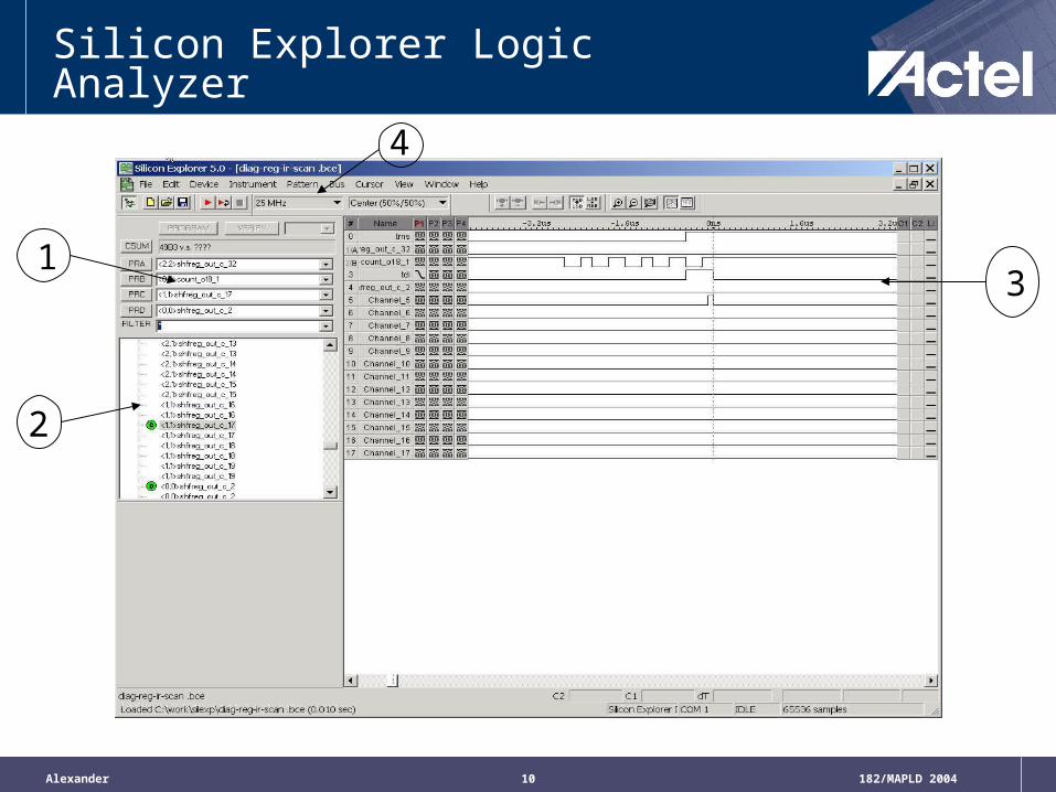
Silicon Explorer Logic Analyzer
2
13
4
11 182/MAPLD 2004Alexander
Silicon Explorer Logic Analyzer1. Probe Control
This section shows what signal each probe is assigned to This section will also shows what the Checksum of the device is, allowing
the user to verify that the device has been programmed with the correct design
2. Node Listing This section shows all the nets/nodes that can be probed
3. Waveform Viewer This is the window where all waveforms captured by the Silicon Explorer II
are displayed.
4. Menu This is where all the controls are located It allows manipulation of the waveforms
12 182/MAPLD 2004Alexander
Probe Performance Maximum observable signal speed
Worst case RTAX-S simulations show 100MHz signals can be observed without distortion
Typical case RTAX-S simulations show that up to 150MHz signals can be observed without distortion
13 182/MAPLD 2004Alexander
Probe Guidelines The Silicon Explorer gives access to internal nodes through
XY coordinates Built in logic analyzer can be used to view signals at 100MHz
sample rate Oscilloscope or other logic analyzer can connect to probe outputs
to view signals with higher resolution
Measuring delays The probe circuit is not designed to accurately reflect internal
delays. Only logic states and timing approximations should be considered
Errors due to timing can be observed such as hold and setup violations on a flip flop.
14 182/MAPLD 2004Alexander
Probe Guidelines Design Tips
Reserve the probe pins in Actel’s Designer software. This will prevent the probe pins from being used as IOs
Avoid assigning probe pins as inputs or bi-directionals. If the pins are needed for IO, use them only as non-critical outputs
Avoid assigning JTAG pins as inputs or bi-directionals. If the pins are needed for IO, use them only as non-critical outputs
Do not program the security fuse in the FPGA. This will disable the probe circuitry in the device.
The probe circuitry allows four simultaneous internal signals to be monitored with a maximum of two signals per tile.
70 Ohm series resistors are recommended on every probe connection
15 182/MAPLD 2004Alexander
Conclusion Real-time observation of internal nodes allows you to Find:
Timing violations Logic errors Large glitches
Un-obtrusive probe circuitry means: No need to re-place and route design No additional delay added to design when probing No FPGA logic gates needed