Embed Size (px)
Citation preview
AN00020TJA1050 high speed CAN transceiverRev. 02 — 10 November 2006 Application note
Document informationInfo ContentKeywords Controller Area Network (CAN), ISO11898, Transceiver, Physical Layer,
TJA1040, TJA1041, TJA1050, PCA82C250/C251
Abstract The TJA1050 is an advanced CAN transceiver for use in automotive and general industrial applications. It supports the differential bus signal representation being described in the international standard for in-vehicle high speed CAN applications (ISO11898). Controller Area Network (CAN) is a serial bus protocol being primarily intended for transmission of control related data between a number of bus nodes.
This application note provides information how to use the TJA1050 in high speed CAN applications. It is intended to provide basic technical information on the implementation of the Physical Medium Attachment in a CAN network according to the ISO11898 standard, using the transceiver TJA1050 from NXP Semiconductors. This product supports bit rates up to 1 Mbit/s over a two-wire differential bus line, which is the transmission medium being specified by the ISO11898 standard.
Typical application information, like aspects of EMC, supply voltage buffering, ground-offsets, unpowered transceiver, bus length and maximum number of nodes per network, is provided by this application note.
NXP Semiconductors AN00020TJA1050 high speed CAN transceiver
Revision historyRev Date Description
02 20061110 Updated version• The format of this application note has been redesigned to comply with the new identity
guidelines of NXP Semiconductors.• Legal texts have been adapted to the new company name where appropriate.• Update of Section 4.2 “Common mode choke”.• Update of Section 4.3 “ESD Protection”.
01 20000425 Initial version
AN00020_2 © NXP B.V. 2006. All rights reserved.
Application note Rev. 02 — 10 November 2006 2 of 26
Contact informationFor additional information, please visit: http://www.nxp.com
For sales office addresses, please send an email to: [email protected]
NXP Semiconductors AN00020TJA1050 high speed CAN transceiver
1. Introduction
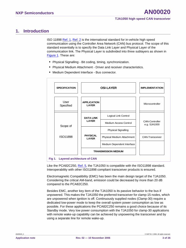
ISO 11898 Ref. 1, Ref. 2 is the international standard for in-vehicle high speed communication using the Controller Area Network (CAN) bus protocol. The scope of this standard essentially is to specify the Data Link Layer and Physical Layer of the communication link. The Physical Layer is subdivided into three sublayers as shown in Figure 1. These are:
• Physical Signalling - Bit coding, timing, synchronization.• Physical Medium Attachment - Driver and receiver characteristics.• Medium Dependent Interface - Bus connector.
Like the PCA82C250, Ref. 5, the TJA1050 is compatible with the ISO11898 standard. Interoperability with other ISO11898 compliant transceiver products is ensured.
Electromagnetic Compatibility (EMC) has been the main design target of the TJA1050. Considering the critical AM-band, emission could be decreased by more than 20 dB compared to the PCA82C250.
Besides EMC, another key item of the TJA1050 is its passive behavior to the bus if unpowered. This makes the TJA1050 the preferred transceiver for clamp-15 nodes, which are unpowered when ignition is off. Continuously supplied nodes (Clamp-30) require a dedicated low-power mode to keep the overall system power consumption as low as possible. For these applications the PCA82C250 remains a good choice because of its Standby mode. Very low power consumption with the TJA1050 for clamp-30 applications with remote wake-up capability can be achieved by unpowering the transceiver and by using a separate line for remote wake-up.
Fig 1. Layered architecture of CAN
APPLICATION
LAYER
DATA LINK
LAYER
PHYSICAL
LAYER
Logical Link Control
Medium Access Control
Physical Signalling
Physical Medium Attachment
Medium Dependent Interface
Scope of
ISO11898
UserSpecified
OSI-LAYERSPECIFICATION IMPLEMENTATION
Microcontroller
CAN-Controllere.g. SJA1000
CAN-Transceiver
TRANSMISSION MEDIUM
AN00020_2 © NXP B.V. 2006. All rights reserved.
Application note Rev. 02 — 10 November 2006 3 of 26
NXP Semiconductors AN00020TJA1050 high speed CAN transceiver
Pin compatibility between the TJA1050 and the PCA82C250 allows the TJA1050 to be used in existing applications without changing the PCB. The customer can immediately benefit from the outstanding performance of the TJA1050.
2. General application of high speed CAN transceiver
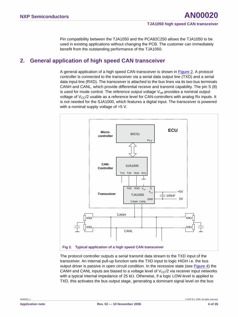
A general application of a high speed CAN transceiver is shown in Figure 2. A protocol controller is connected to the transceiver via a serial data output line (TXD) and a serial data input line (RXD). The transceiver is attached to the bus lines via its two bus terminals CANH and CANL, which provide differential receive and transmit capability. The pin S (8) is used for mode control. The reference output voltage Vref provides a nominal output voltage of VCC/2 usable as a reference level for CAN-controllers with analog Rx inputs. It is not needed for the SJA1000, which features a digital input. The transceiver is powered with a nominal supply voltage of +5 V.
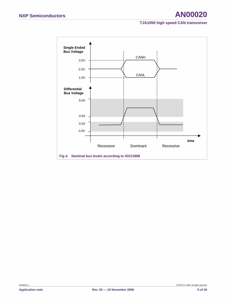
The protocol controller outputs a serial transmit data stream to the TXD input of the transceiver. An internal pull-up function sets the TXD input to logic HIGH i.e. the bus output driver is passive in open circuit condition. In the recessive state (see Figure 4) the CANH and CANL inputs are biased to a voltage level of VCC/2 via receiver input networks with a typical internal impedance of 25 kΩ. Otherwise, if a logic LOW-level is applied to TXD, this activates the bus output stage, generating a dominant signal level on the bus
Fig 2. Typical application of a high speed CAN transceiver
CANH CANLGND
TXD RXD Vref SVCC
Transceiver
60ΩCANH
CANL
SJA1000
TJA1050
ECU
+5V
0V100nF
TX1 TX0 RX0 RX1
CAN-
Controller
Micro-
controller80C51
Px,y
60Ω
60Ω
60Ω
AN00020_2 © NXP B.V. 2006. All rights reserved.
Application note Rev. 02 — 10 November 2006 4 of 26
NXP Semiconductors AN00020TJA1050 high speed CAN transceiver
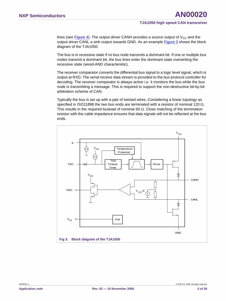
lines (see Figure 4). The output driver CANH provides a source output of VCC and the output driver CANL a sink output towards GND. As an example Figure 3 shows the block diagram of the TJA1050.
The bus is in recessive state if no bus node transmits a dominant bit. If one or multiple bus nodes transmit a dominant bit, the bus lines enter the dominant state overwriting the recessive state (wired-AND characteristic).
The receiver comparator converts the differential bus signal to a logic level signal, which is output at RXD. The serial receive data stream is provided to the bus protocol controller for decoding. The receiver comparator is always active i.e. it monitors the bus while the bus node is transmitting a message. This is required to support the non-destructive bit-by-bit arbitration scheme of CAN.
Typically the bus is set up with a pair of twisted wires. Considering a linear topology as specified in ISO11898 the two bus ends are terminated with a resistor of nominal 120 Ω. This results in the required busload of nominal 60 Ω. Close matching of the termination resistor with the cable impedance ensures that data signals will not be reflected at the bus ends.
Fig 3. Block diagram of the TJA1050
Driver
Vref
VCC
TemperatureProtection
TXDTimeout
Timer
VCC
VCC
/2
TXD
RXD
V
S
VCC
CANH
CANL
GND
ref
AN00020_2 © NXP B.V. 2006. All rights reserved.
Application note Rev. 02 — 10 November 2006 5 of 26
NXP Semiconductors AN00020TJA1050 high speed CAN transceiver
Fig 4. Nominal bus levels according to ISO11898
Differential
Bus Voltage
2.5V
3.5V
1.5V
Single Ended
Bus Voltage
0.9V
5.0V
0.5V
Dominant Recessive Recessive
CANH
CANL
time
1 0. V-
AN00020_2 © NXP B.V. 2006. All rights reserved.
Application note Rev. 02 — 10 November 2006 6 of 26
NXP Semiconductors AN00020TJA1050 high speed CAN transceiver
3. The TJA1050
3.1 Features
The main features of the TJA1050 are:
• Fully compatible with the ISO11898 standard• High speed (up to 1 Mbit/s)• Very low Electromagnetic Emission• Very high Electromagnetic Immunity• An unpowered node does not disturb the bus lines• Timeout protection at TXD against dominant bus clamping• Silent mode providing Listen-Only mode and “Babbling Idiot” protection• Bus bins protected against transients in an automotive environment• Input levels compatible with 3.3 V and 5 V devices• Thermally protected output drivers• Short-circuit proof to battery and ground• At least 110 nodes can be connected
3.2 Operation modes
The TJA1050 provides two modes of operation, which are controlled by the pin S.
• High speed mode• Silent mode
Variable slope control as used in the PCA82C250 is not supported. The TJA1050 features a fixed slope. Even so the excellent output stage symmetry results in a much better EMC performance compared to previous products.
3.2.1 High speed mode
The High speed mode is the normal operating mode and is selected by connecting pin S to ground. Due to an internal pull-down function (see Figure 3) it is the default mode if pin S is unconnected.
In this mode the bus output signals are switched as fast as possible with a fixed slope. It is the appropriate mode for achieving a maximum bit rate and/or bus length and provides minimum transceiver loop delays.
3.2.2 Silent mode
In Silent mode the transmitter is disabled regardless of the TXD input signal. The transceiver behaves as in non-transmitting state consuming the same supply current as in recessive state. The Silent mode is selected with a HIGH signal at pin S.
AN00020_2 © NXP B.V. 2006. All rights reserved.
Application note Rev. 02 — 10 November 2006 7 of 26
NXP Semiconductors AN00020TJA1050 high speed CAN transceiver
3.2.2.1 “Babbling idiot” protectionThe Silent mode allows a node to be set to a state, in which it is absolutely passive to the bus. It becomes necessary when a CAN-controller gets out of control and unintentionally sends messages (“Babbling idiot”), that claim the bus. Activating the Silent mode by the microcontroller allows the bus to be released even when there is no direct access from the microcontroller to the CAN-controller. The Silent mode is very useful for achieving high system reliability required by today’s electronic applications.
3.2.2.2 Listen-only modeIn Silent mode RXD monitors the bus lines as usual. Thus, the Silent mode provides a Listen-Only mode for diagnostic features. It ensures that a node does not influence the bus with dominant bits.
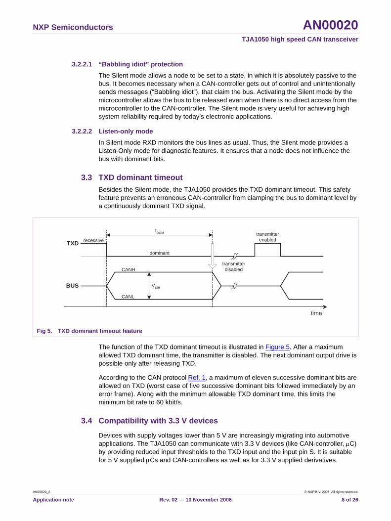
3.3 TXD dominant timeoutBesides the Silent mode, the TJA1050 provides the TXD dominant timeout. This safety feature prevents an erroneous CAN-controller from clamping the bus to dominant level by a continuously dominant TXD signal.
The function of the TXD dominant timeout is illustrated in Figure 5. After a maximum allowed TXD dominant time, the transmitter is disabled. The next dominant output drive is possible only after releasing TXD.
According to the CAN protocol Ref. 1, a maximum of eleven successive dominant bits are allowed on TXD (worst case of five successive dominant bits followed immediately by an error frame). Along with the minimum allowable TXD dominant time, this limits the minimum bit rate to 60 kbit/s.
3.4 Compatibility with 3.3 V devices
Devices with supply voltages lower than 5 V are increasingly migrating into automotive applications. The TJA1050 can communicate with 3.3 V devices (like CAN-controller, μC) by providing reduced input thresholds to the TXD input and the input pin S. It is suitable for 5 V supplied μCs and CAN-controllers as well as for 3.3 V supplied derivatives.
Fig 5. TXD dominant timeout feature
time
CANH
CANL
BUS
recessiveTXD
VDiff
tDOM
dominant
transmitterdisabled
transmitterenabled
AN00020_2 © NXP B.V. 2006. All rights reserved.
Application note Rev. 02 — 10 November 2006 8 of 26
NXP Semiconductors AN00020TJA1050 high speed CAN transceiver
However, the 3.3 V devices must be 5 V tolerant with respect to RXD and TXD, because of a pull-up resistor to VCC (5 V) at TXD inside the transceiver and a VCC-based push-pull stage for RXD.
4. EMC and ESD aspects
Achieving a high EMC performance is not only a matter of the transceiver, a careful system implementation (termination, topology, external circuitry) is also very important. This chapter presents some application hints with the aim of exploiting the outstanding EMC performance of the TJA1050.
4.1 Split termination concept
Practice has shown that effective reduction of emission can be achieved by a modified bus termination concept called split termination. In addition this concept contributes to higher immunity of the bus system.
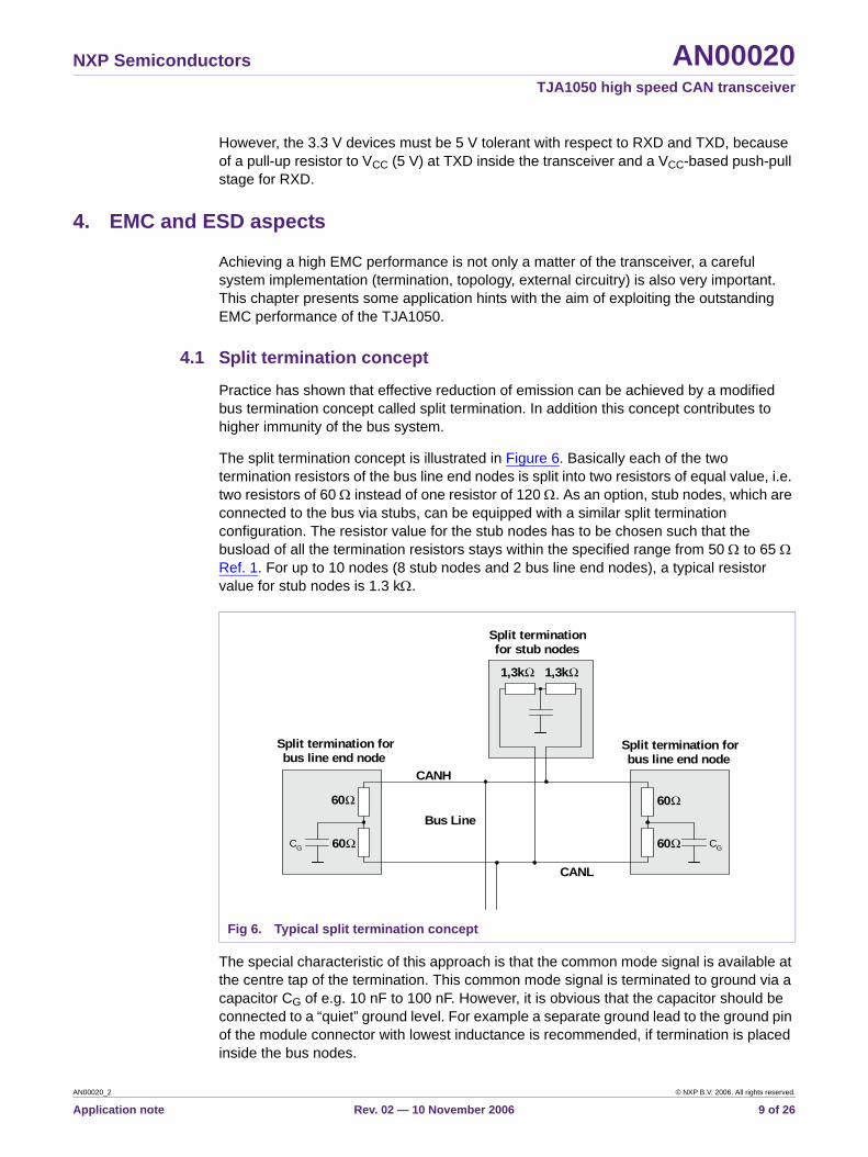
The split termination concept is illustrated in Figure 6. Basically each of the two termination resistors of the bus line end nodes is split into two resistors of equal value, i.e. two resistors of 60 Ω instead of one resistor of 120 Ω. As an option, stub nodes, which are connected to the bus via stubs, can be equipped with a similar split termination configuration. The resistor value for the stub nodes has to be chosen such that the busload of all the termination resistors stays within the specified range from 50 Ω to 65 Ω Ref. 1. For up to 10 nodes (8 stub nodes and 2 bus line end nodes), a typical resistor value for stub nodes is 1.3 kΩ.
The special characteristic of this approach is that the common mode signal is available at the centre tap of the termination. This common mode signal is terminated to ground via a capacitor CG of e.g. 10 nF to 100 nF. However, it is obvious that the capacitor should be connected to a “quiet” ground level. For example a separate ground lead to the ground pin of the module connector with lowest inductance is recommended, if termination is placed inside the bus nodes.
Fig 6. Typical split termination concept
Bus Line
CGCG
60Ω
60Ω
60Ω
60Ω
1,3kΩ 1,3kΩ
CANH
CANL
Split termination for
bus line end nodeSplit termination for
bus line end node
Split termination
for stub nodes
AN00020_2 © NXP B.V. 2006. All rights reserved.
Application note Rev. 02 — 10 November 2006 9 of 26
NXP Semiconductors AN00020TJA1050 high speed CAN transceiver
The TJA1050 itself has reached such a high symmetry level that symmetry aspects of the two bus lines to reference ground become more and more important. To exploit the excellent emission performance of the TJA1050, the matching tolerance between the split termination resistors at each ECU has to be considered.
It is worth noticing that the EMC performance of the TJA1050 has been optimized for use of the split termination without a choke. It is highly recommended to implement the split termination. The excellent output stage symmetry allows doing without chokes as shown by different emission measurements. If, however, the EMC performance is still not sufficient, there is the option to use additional measures like capacitors and common mode chokes.
4.2 Common mode chokeA common mode choke provides high impedance for common mode signals and low impedance for differential signals. Due to this, common mode signals produced by RF noise and/or by non-perfect transceiver driver symmetry are damped significantly. Common mode chokes help to reduce emission and to enhance immunity.
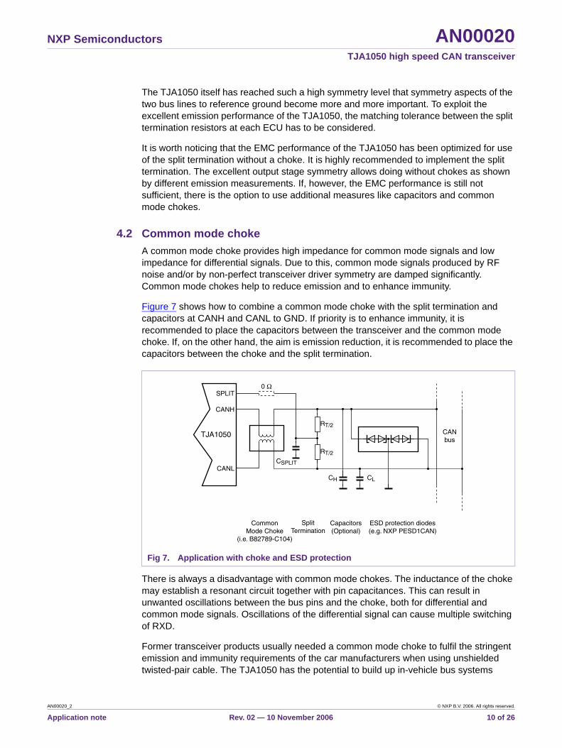
Figure 7 shows how to combine a common mode choke with the split termination and capacitors at CANH and CANL to GND. If priority is to enhance immunity, it is recommended to place the capacitors between the transceiver and the common mode choke. If, on the other hand, the aim is emission reduction, it is recommended to place the capacitors between the choke and the split termination.
There is always a disadvantage with common mode chokes. The inductance of the choke may establish a resonant circuit together with pin capacitances. This can result in unwanted oscillations between the bus pins and the choke, both for differential and common mode signals. Oscillations of the differential signal can cause multiple switching of RXD.
Former transceiver products usually needed a common mode choke to fulfil the stringent emission and immunity requirements of the car manufacturers when using unshielded twisted-pair cable. The TJA1050 has the potential to build up in-vehicle bus systems
Fig 7. Application with choke and ESD protection
TJA1050
CANH
CANL
CANbus
CSPLIT
RT/2
RT/2
CH CL
CommonMode Choke
(i.e. B82789-C104)
SplitTermination
Capacitors(Optional)
ESD protection diodes(e.g. NXP PESD1CAN)
SPLIT0 Ω
AN00020_2 © NXP B.V. 2006. All rights reserved.
Application note Rev. 02 — 10 November 2006 10 of 26
NXP Semiconductors AN00020TJA1050 high speed CAN transceiver
without chokes. Whether chokes are needed finally depends on the specific system implementation like the wiring harness and the symmetry of the two bus lines (matching tolerances of resistors and capacitors).
Besides the RF noise reduction, the so-called stray inductance (non-coupled portion of inductance) may establish a resonant circuit together with pin capacitance. This can result in unwanted resonance oscillations between the bus pins and the choke, both for differential and common mode signals, and in extra emission around the resonant frequency. To avoid such oscillations, it is highly recommended to use only chokes with a stray inductance lower than 500 nH. Bifilar wound chokes typically show an even lower stray inductance. As shown in Figure 7 the choke shall be placed close to the transceiver.
4.3 ESD ProtectionThe TJA1050 is designed to withstand ESD pulses of up to 4 kV according to the human body model at the bus pins CANH, CANL and pin SPLIT and thus typically does not need further external protection methods. Nevertheless, if much higher protection is required, external clamping devices can be applied to the CANH and CANL line.
NXP offers a dedicated protection device for the CAN bus, providing high robustness against ESD and automotive transients. The PESD1CAN protection diode, Ref. 9, featuring a very fast diode structure with very low capacitance (typ. 11 pF), is compliant to IEC61000-4-2 (level 4), thus allowing air and contact discharge of more than 15 kV and 8 kV, respectively. Tests at an independent test house have confirmed typically more than 20 kV ESD robustness for ECUs equipped with the PESD1CAN diode and a choke. To be most effective, the PESD1CAN diode should be placed close to the ECU connector as shown in Figure 7, while the choke should be placed close to the transceiver.
AN00020_2 © NXP B.V. 2006. All rights reserved.
Application note Rev. 02 — 10 November 2006 11 of 26
NXP Semiconductors AN00020TJA1050 high speed CAN transceiver
5. Power supply and recommended bypass capacitor
Typically, a bypass capacitor is used for buffering the required supply voltage. A well-dimensioned bypass capacitor also avoids high current peaks flowing into the ground leads, establishing a “quiet” signal ground for the transceiver.
5.1 Average and peak supply current
To properly dimension the VCC supply of the high speed CAN transceiver, two parameters have to be taken into account:
1. Average supply currentThe average supply current is needed to calculate the thermal load of the required VCC voltage regulator. It is estimated that a node is continuously sending messages with a duty cycle of 50 %.
2. Peak supply currentThe peak supply current might flow in the case of certain bus failure conditions for a certain time and has an impact on the power supply buffering.
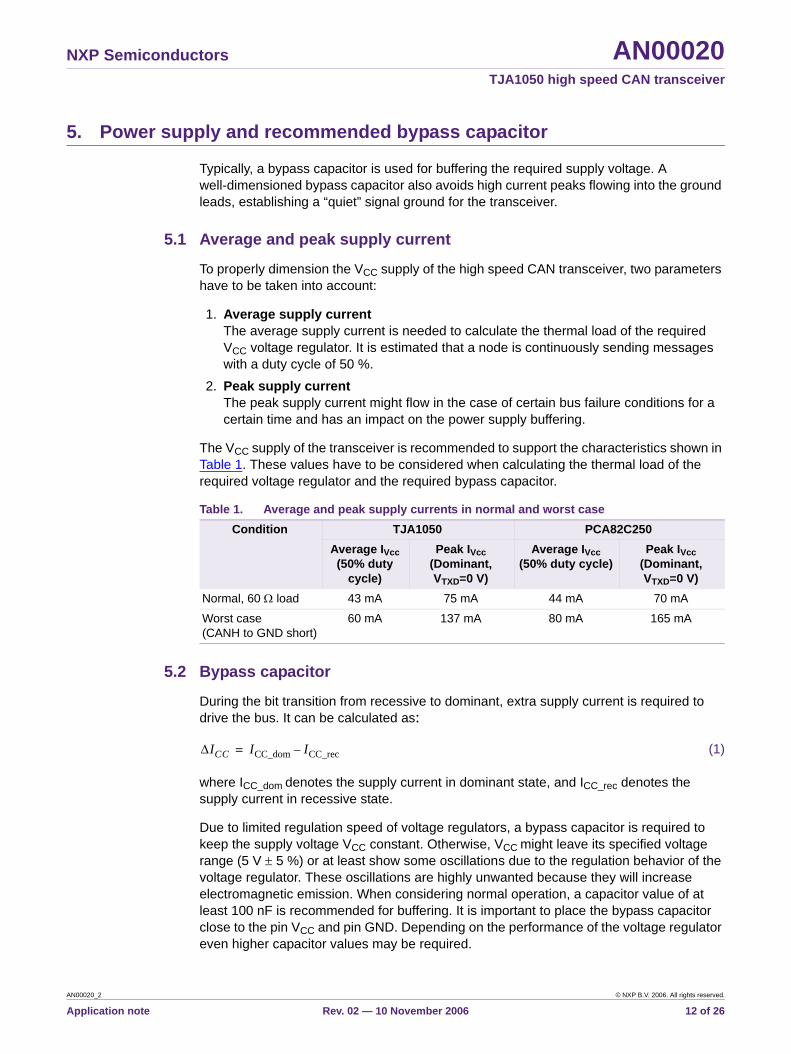
The VCC supply of the transceiver is recommended to support the characteristics shown in Table 1. These values have to be considered when calculating the thermal load of the required voltage regulator and the required bypass capacitor.
5.2 Bypass capacitor
During the bit transition from recessive to dominant, extra supply current is required to drive the bus. It can be calculated as:
(1)
where ICC_dom denotes the supply current in dominant state, and ICC_rec denotes the supply current in recessive state.
Due to limited regulation speed of voltage regulators, a bypass capacitor is required to keep the supply voltage VCC constant. Otherwise, VCC might leave its specified voltage range (5 V ± 5 %) or at least show some oscillations due to the regulation behavior of the voltage regulator. These oscillations are highly unwanted because they will increase electromagnetic emission. When considering normal operation, a capacitor value of at least 100 nF is recommended for buffering. It is important to place the bypass capacitor close to the pin VCC and pin GND. Depending on the performance of the voltage regulator even higher capacitor values may be required.
Table 1. Average and peak supply currents in normal and worst caseCondition TJA1050 PCA82C250
Average IVcc(50% duty
cycle)
Peak IVcc(Dominant, VTXD=0 V)
Average IVcc(50% duty cycle)
Peak IVcc(Dominant, VTXD=0 V)
Normal, 60 Ω load 43 mA 75 mA 44 mA 70 mA
Worst case(CANH to GND short)
60 mA 137 mA 80 mA 165 mA
ΔICC ICC_dom ICC_rec–=
AN00020_2 © NXP B.V. 2006. All rights reserved.
Application note Rev. 02 — 10 November 2006 12 of 26
NXP Semiconductors AN00020TJA1050 high speed CAN transceiver
6. Ground-offset aspects
Bus systems in automotive have to deal with ground-offsets between the various nodes. This means that each node can “see” different single-ended bus voltages on the bus lines according to their own ground level, whereas the differential bus voltage remains unaffected.
According to the data sheet of the TJA1050 Ref. 4 the maximum allowable single-ended voltage of CANH is +12 V, while the maximum allowable single-ended voltage of CANL is −12 V. With single-ended bus voltages within this range, it is guaranteed that the differential receiver threshold voltage lies between 0.5 V and 0.9 V. The allowable single-ended voltage range is known as the common mode range of the differential receiver.
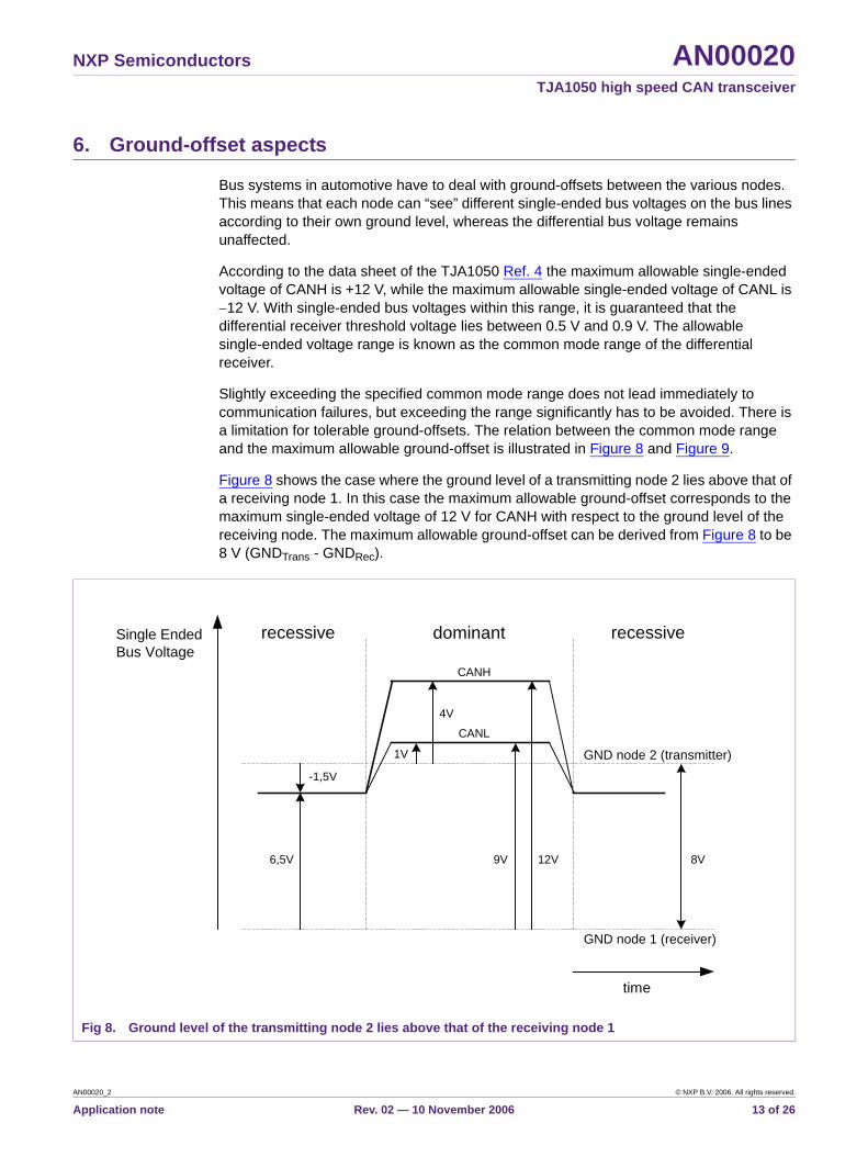
Slightly exceeding the specified common mode range does not lead immediately to communication failures, but exceeding the range significantly has to be avoided. There is a limitation for tolerable ground-offsets. The relation between the common mode range and the maximum allowable ground-offset is illustrated in Figure 8 and Figure 9.
Figure 8 shows the case where the ground level of a transmitting node 2 lies above that of a receiving node 1. In this case the maximum allowable ground-offset corresponds to the maximum single-ended voltage of 12 V for CANH with respect to the ground level of the receiving node. The maximum allowable ground-offset can be derived from Figure 8 to be 8 V (GNDTrans - GNDRec).
Fig 8. Ground level of the transmitting node 2 lies above that of the receiving node 1
Single EndedBus Voltage
GND node 2 (transmitter)
GND node 1 (receiver)
CANL
CANH
1V
9V 12V
4V
6,5V
-1,5V
recessive dominant recessive
8V
time
AN00020_2 © NXP B.V. 2006. All rights reserved.
Application note Rev. 02 — 10 November 2006 13 of 26
NXP Semiconductors AN00020TJA1050 high speed CAN transceiver
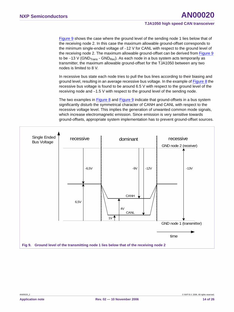
Figure 9 shows the case where the ground level of the sending node 1 lies below that of the receiving node 2. In this case the maximum allowable ground-offset corresponds to the minimum single-ended voltage of −12 V for CANL with respect to the ground level of the receiving node 2. The maximum allowable ground-offset can be derived from Figure 9 to be −13 V (GNDTrans - GNDRec). As each node in a bus system acts temporarily as transmitter, the maximum allowable ground-offset for the TJA1050 between any two nodes is limited to 8 V.
In recessive bus state each node tries to pull the bus lines according to their biasing and ground level, resulting in an average recessive bus voltage. In the example of Figure 8 the recessive bus voltage is found to be around 6.5 V with respect to the ground level of the receiving node and −1.5 V with respect to the ground level of the sending node.
The two examples in Figure 8 and Figure 9 indicate that ground-offsets in a bus system significantly disturb the symmetrical character of CANH and CANL with respect to the recessive voltage level. This implies the generation of unwanted common mode signals, which increase electromagnetic emission. Since emission is very sensitive towards ground-offsets, appropriate system implementation has to prevent ground-offset sources.
Fig 9. Ground level of the transmitting node 1 lies below that of the receiving node 2
Single EndedBus Voltage
time
GND node 2 (receiver)
GND node 1 (transmitter)
CANL
CANH
1V
-9V -13V
4V
6,5V
-6,5V
recessive dominant recessive
-12V
AN00020_2 © NXP B.V. 2006. All rights reserved.
Application note Rev. 02 — 10 November 2006 14 of 26
NXP Semiconductors AN00020TJA1050 high speed CAN transceiver
7. Unpowered transceiver
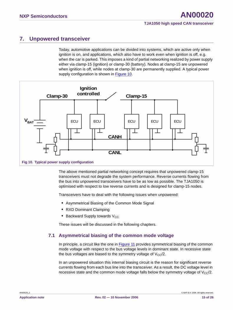
Today, automotive applications can be divided into systems, which are active only when ignition is on, and applications, which also have to work even when ignition is off, e.g. when the car is parked. This imposes a kind of partial networking realized by power supply either via clamp-15 (ignition) or clamp-30 (battery). Nodes at clamp-15 are unpowered when ignition is off, while nodes at clamp-30 are permanently supplied. A typical power supply configuration is shown in Figure 10.
The above mentioned partial networking concept requires that unpowered clamp-15 transceivers must not degrade the system performance. Reverse currents flowing from the bus into unpowered transceivers have to be as low as possible. The TJA1050 is optimised with respect to low reverse currents and is designed for clamp-15 nodes.
Transceivers have to deal with the following issues when unpowered:
• Asymmetrical Biasing of the Common Mode Signal• RXD Dominant Clamping• Backward Supply towards VCC
These issues will be discussed in the following chapters.
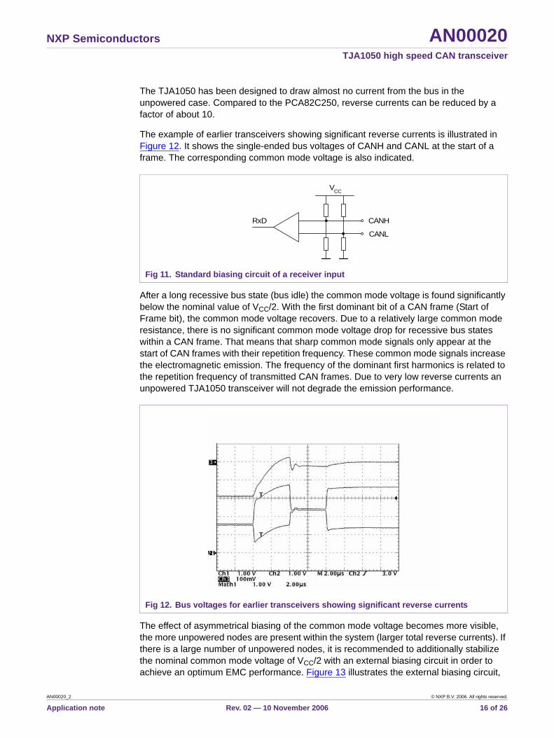
7.1 Asymmetrical biasing of the common mode voltage
In principle, a circuit like the one in Figure 11 provides symmetrical biasing of the common mode voltage with respect to the bus voltage levels in dominant state. In recessive state the bus voltages are biased to the symmetry voltage of VCC/2.
In an unpowered situation this internal biasing circuit is the reason for significant reverse currents flowing from each bus line into the transceiver. As a result, the DC voltage level in recessive state and the common mode voltage falls below the symmetry voltage of VCC/2.
Fig 10. Typical power supply configuration
VBAT
Clamp-30 Clamp-15
Ignition
controlled
ECU ECU ECU ECU ECU
CANH
CANL
AN00020_2 © NXP B.V. 2006. All rights reserved.
Application note Rev. 02 — 10 November 2006 15 of 26
NXP Semiconductors AN00020TJA1050 high speed CAN transceiver
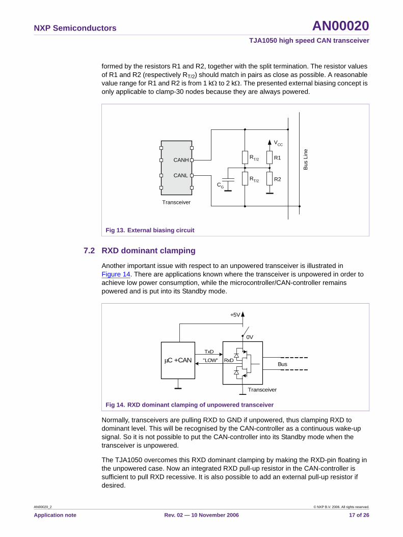
The TJA1050 has been designed to draw almost no current from the bus in the unpowered case. Compared to the PCA82C250, reverse currents can be reduced by a factor of about 10.
The example of earlier transceivers showing significant reverse currents is illustrated in Figure 12. It shows the single-ended bus voltages of CANH and CANL at the start of a frame. The corresponding common mode voltage is also indicated.
After a long recessive bus state (bus idle) the common mode voltage is found significantly below the nominal value of VCC/2. With the first dominant bit of a CAN frame (Start of Frame bit), the common mode voltage recovers. Due to a relatively large common mode resistance, there is no significant common mode voltage drop for recessive bus states within a CAN frame. That means that sharp common mode signals only appear at the start of CAN frames with their repetition frequency. These common mode signals increase the electromagnetic emission. The frequency of the dominant first harmonics is related to the repetition frequency of transmitted CAN frames. Due to very low reverse currents an unpowered TJA1050 transceiver will not degrade the emission performance.
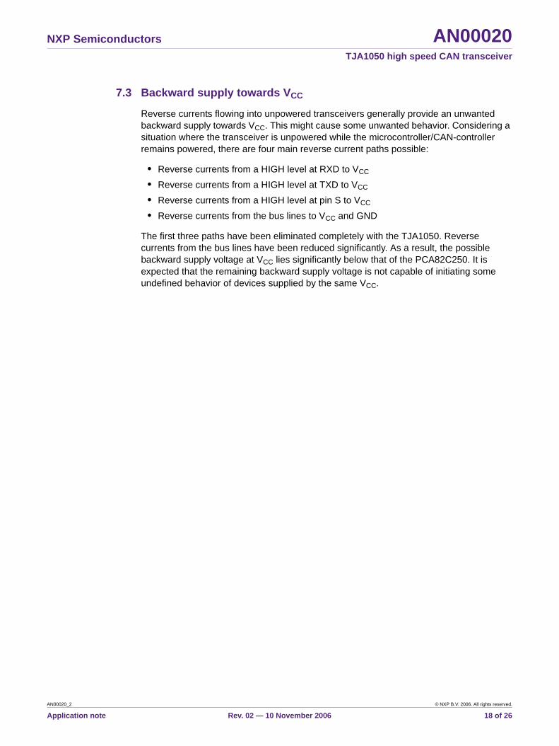
The effect of asymmetrical biasing of the common mode voltage becomes more visible, the more unpowered nodes are present within the system (larger total reverse currents). If there is a large number of unpowered nodes, it is recommended to additionally stabilize the nominal common mode voltage of VCC/2 with an external biasing circuit in order to achieve an optimum EMC performance. Figure 13 illustrates the external biasing circuit,
Fig 11. Standard biasing circuit of a receiver input
Fig 12. Bus voltages for earlier transceivers showing significant reverse currents
RxD CANH
CANL
VCC
AN00020_2 © NXP B.V. 2006. All rights reserved.
Application note Rev. 02 — 10 November 2006 16 of 26
NXP Semiconductors AN00020TJA1050 high speed CAN transceiver
formed by the resistors R1 and R2, together with the split termination. The resistor values of R1 and R2 (respectively RT/2) should match in pairs as close as possible. A reasonable value range for R1 and R2 is from 1 kΩ to 2 kΩ. The presented external biasing concept is only applicable to clamp-30 nodes because they are always powered.
7.2 RXD dominant clamping
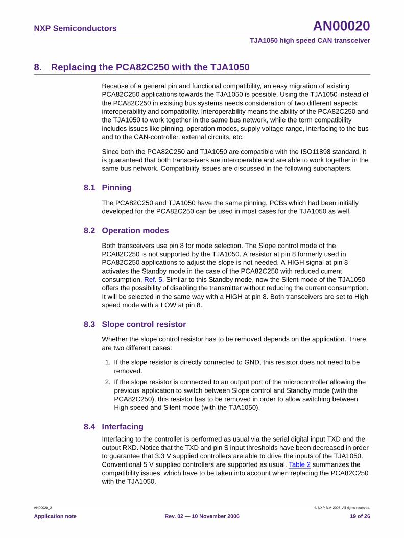
Another important issue with respect to an unpowered transceiver is illustrated in Figure 14. There are applications known where the transceiver is unpowered in order to achieve low power consumption, while the microcontroller/CAN-controller remains powered and is put into its Standby mode.
Normally, transceivers are pulling RXD to GND if unpowered, thus clamping RXD to dominant level. This will be recognised by the CAN-controller as a continuous wake-up signal. So it is not possible to put the CAN-controller into its Standby mode when the transceiver is unpowered.
The TJA1050 overcomes this RXD dominant clamping by making the RXD-pin floating in the unpowered case. Now an integrated RXD pull-up resistor in the CAN-controller is sufficient to pull RXD recessive. It is also possible to add an external pull-up resistor if desired.
Fig 13. External biasing circuit
CANH
CANL
Transceiver
Bus
Line
R1
VCC
R2CG
RT/2
RT/2
Fig 14. RXD dominant clamping of unpowered transceiver
μC +CAN
Transceiver
TxD
RxD
+5V
Bus"LOW"
0V
AN00020_2 © NXP B.V. 2006. All rights reserved.
Application note Rev. 02 — 10 November 2006 17 of 26
NXP Semiconductors AN00020TJA1050 high speed CAN transceiver
7.3 Backward supply towards VCC
Reverse currents flowing into unpowered transceivers generally provide an unwanted backward supply towards VCC. This might cause some unwanted behavior. Considering a situation where the transceiver is unpowered while the microcontroller/CAN-controller remains powered, there are four main reverse current paths possible:
• Reverse currents from a HIGH level at RXD to VCC
• Reverse currents from a HIGH level at TXD to VCC
• Reverse currents from a HIGH level at pin S to VCC
• Reverse currents from the bus lines to VCC and GND
The first three paths have been eliminated completely with the TJA1050. Reverse currents from the bus lines have been reduced significantly. As a result, the possible backward supply voltage at VCC lies significantly below that of the PCA82C250. It is expected that the remaining backward supply voltage is not capable of initiating some undefined behavior of devices supplied by the same VCC.
AN00020_2 © NXP B.V. 2006. All rights reserved.
Application note Rev. 02 — 10 November 2006 18 of 26
NXP Semiconductors AN00020TJA1050 high speed CAN transceiver
8. Replacing the PCA82C250 with the TJA1050
Because of a general pin and functional compatibility, an easy migration of existing PCA82C250 applications towards the TJA1050 is possible. Using the TJA1050 instead of the PCA82C250 in existing bus systems needs consideration of two different aspects: interoperability and compatibility. Interoperability means the ability of the PCA82C250 and the TJA1050 to work together in the same bus network, while the term compatibility includes issues like pinning, operation modes, supply voltage range, interfacing to the bus and to the CAN-controller, external circuits, etc.
Since both the PCA82C250 and TJA1050 are compatible with the ISO11898 standard, it is guaranteed that both transceivers are interoperable and are able to work together in the same bus network. Compatibility issues are discussed in the following subchapters.
8.1 Pinning
The PCA82C250 and TJA1050 have the same pinning. PCBs which had been initially developed for the PCA82C250 can be used in most cases for the TJA1050 as well.
8.2 Operation modes
Both transceivers use pin 8 for mode selection. The Slope control mode of the PCA82C250 is not supported by the TJA1050. A resistor at pin 8 formerly used in PCA82C250 applications to adjust the slope is not needed. A HIGH signal at pin 8 activates the Standby mode in the case of the PCA82C250 with reduced current consumption, Ref. 5. Similar to this Standby mode, now the Silent mode of the TJA1050 offers the possibility of disabling the transmitter without reducing the current consumption. It will be selected in the same way with a HIGH at pin 8. Both transceivers are set to High speed mode with a LOW at pin 8.
8.3 Slope control resistor
Whether the slope control resistor has to be removed depends on the application. There are two different cases:
1. If the slope resistor is directly connected to GND, this resistor does not need to be removed.
2. If the slope resistor is connected to an output port of the microcontroller allowing the previous application to switch between Slope control and Standby mode (with the PCA82C250), this resistor has to be removed in order to allow switching between High speed and Silent mode (with the TJA1050).
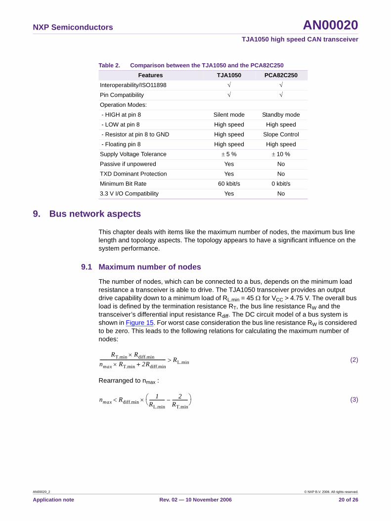
8.4 InterfacingInterfacing to the controller is performed as usual via the serial digital input TXD and the output RXD. Notice that the TXD and pin S input thresholds have been decreased in order to guarantee that 3.3 V supplied controllers are able to drive the inputs of the TJA1050. Conventional 5 V supplied controllers are supported as usual. Table 2 summarizes the compatibility issues, which have to be taken into account when replacing the PCA82C250 with the TJA1050.
AN00020_2 © NXP B.V. 2006. All rights reserved.
Application note Rev. 02 — 10 November 2006 19 of 26
NXP Semiconductors AN00020TJA1050 high speed CAN transceiver
9. Bus network aspects
This chapter deals with items like the maximum number of nodes, the maximum bus line length and topology aspects. The topology appears to have a significant influence on the system performance.
9.1 Maximum number of nodes
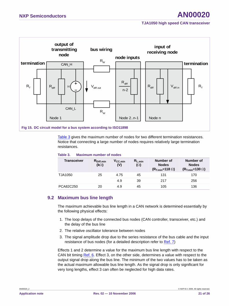
The number of nodes, which can be connected to a bus, depends on the minimum load resistance a transceiver is able to drive. The TJA1050 transceiver provides an output drive capability down to a minimum load of RL.min = 45 Ω for VCC > 4.75 V. The overall bus load is defined by the termination resistance RT, the bus line resistance RW and the transceiver’s differential input resistance Rdiff. The DC circuit model of a bus system is shown in Figure 15. For worst case consideration the bus line resistance RW is considered to be zero. This leads to the following relations for calculating the maximum number of nodes:
(2)
Rearranged to nmax :
(3)
Table 2. Comparison between the TJA1050 and the PCA82C250Features TJA1050 PCA82C250
Interoperability/ISO11898 √ √
Pin Compatibility √ √
Operation Modes:
- HIGH at pin 8 Silent mode Standby mode
- LOW at pin 8 High speed High speed
- Resistor at pin 8 to GND High speed Slope Control
- Floating pin 8 High speed High speed
Supply Voltage Tolerance ± 5 % ± 10 %
Passive if unpowered Yes No
TXD Dominant Protection Yes No
Minimum Bit Rate 60 kbit/s 0 kbit/s
3.3 V I/O Compatibility Yes No
RT.min Rdiff.min×nmax RT.min 2Rdiff.min+×------------------------------------------------------------ RL.min>
nmax Rdiff.min1
RL.min-------------- 2
RT.min--------------–⎝ ⎠
⎛ ⎞×<
AN00020_2 © NXP B.V. 2006. All rights reserved.
Application note Rev. 02 — 10 November 2006 20 of 26
NXP Semiconductors AN00020TJA1050 high speed CAN transceiver
Table 3 gives the maximum number of nodes for two different termination resistances. Notice that connecting a large number of nodes requires relatively large termination resistances.
9.2 Maximum bus line length
The maximum achievable bus line length in a CAN network is determined essentially by the following physical effects:
1. The loop delays of the connected bus nodes (CAN controller, transceiver, etc.) and the delay of the bus line
2. The relative oscillator tolerance between nodes3. The signal amplitude drop due to the series resistance of the bus cable and the input
resistance of bus nodes (for a detailed description refer to Ref. 7)
Effects 1 and 2 determine a value for the maximum bus line length with respect to the CAN bit timing Ref. 6. Effect 3, on the other side, determines a value with respect to the output signal drop along the bus line. The minimum of the two values has to be taken as the actual maximum allowable bus line length. As the signal drop is only significant for very long lengths, effect 3 can often be neglected for high data rates.
Fig 15. DC circuit model for a bus system according to ISO11898
terminationtermination
DC
CAN_H
CAN_L
RT RT
RW
RW
bus wiring
Vdiff.in
output of
transmitting
node
Vdiff.out
input of
receiving node
node inputs
Rdiff
n-2RdiffRdiff
Node 1 Node 2..n-1 Node n
Table 3. Maximum number of nodesTransceiver RDiff.min
(kΩ)VCC.min
(V)RL.min
(Ω)Number of
Nodes(RT.min=118 Ω)
Number of Nodes
(RT.min=130 Ω)TJA1050 25 4.75 45 131 170
4.9 39 217 256
PCA82C250 20 4.9 45 105 136
AN00020_2 © NXP B.V. 2006. All rights reserved.
Application note Rev. 02 — 10 November 2006 21 of 26
NXP Semiconductors AN00020TJA1050 high speed CAN transceiver
Table 4 gives the maximum bus line length for the bit rates 500 kbit/s and 250 kbit/s, along with values specified in some standards associated to CAN. The calculation is based on effects 1 and 2 assuming an oscillator tolerance of better than 0.15 %. Notice that the stated values only apply for a well-terminated linear topology. Bad signal quality because of improper termination can lower the maximum allowable bus length.
9.3 Topology aspects
The topology describes the wiring harness structure. Typical structures are linear, star- or multistar-like. In automotive, shielded or unshielded twisted pair cable usually functions as a transmission line. Transmission lines are generally characterized by the length-related resistance RLength, the specific line delay tdelay and the characteristic line impedance Z. Table 5 shows the physical media parameters specified in the ISO11898 and SAE J2284 standard Ref. 8 Notice that SAE J2284 specifies the twist rate in addition.
9.3.1 Ringing due to signal reflections
Transmission lines must be terminated with the characteristic line impedance, otherwise signal reflections will occur on the bus causing significant ringing. The topology has to be chosen such that reflections will be minimized. Often the topology is a trade-off between reflections and wiring constraints.
CAN is well prepared to deal with reflection ringing due to some useful protocol implementations:
1. Only recessive to dominant transitions are used for resynchronization.2. Resynchronization is allowed only once between two sample points, and only if a
recessive bit was sampled.3. The sample point is programmable to be close to the end of the bit time.
Table 4. Maximum bus line length for some standards and the TJA1050Specification Data rate
500 kbit/s 250 kbit/sSAE J2284 30 m -
DeviceNet 100 m 250 m
TJA1050 107 m 270 m
Table 5. Physical media parameters of a pair of wires (shielded or unshielded)Parameter Notation Unit ISO11898 SAE J2284
Min Nom Max Min Nom MaxImpedance Z Ω 95 120 140 108 120 132
Length-relatedresistance
RLength mΩ/m - 70 - - 70 -
Specific line delay tdelay ns/m - 5 - - 5.5 -
Twist rate rtwist twist/m - - - 33 - 50
AN00020_2 © NXP B.V. 2006. All rights reserved.
Application note Rev. 02 — 10 November 2006 22 of 26
NXP Semiconductors AN00020TJA1050 high speed CAN transceiver
9.3.2 Linear topology
Generally the high speed CAN standard ISO11898 defines a single line structure as network topology. The bus line is terminated at both ends with a single termination resistor. The nodes are connected via unterminated drop cables or stubs to the bus. To keep the ringing duration short compared to the bit time, the stub length should be as short as possible. For example the ISO11898 standard limits the stub length to 0.3 m. The corresponding SAE standard, J2284, recommends keeping the stub length below 1 m. To minimize standing waves, ECUs should not be placed equally spaced on the network and cable tail lengths should not all be the same length Ref. 8. Table 6 along with Figure 16 illustrates the topology requirements of the SAE J2284 standard.
In practice some deviation from the stringent topology proposals might be necessary, because longer stub lengths are needed. Essentially the maximum allowable stub length depends on the bit timing parameters, the trunk cable length and the accumulated drop cable length. For a rule of thumb calculation of the maximum allowable stub length refer to Ref. 7.
The star topology is neither covered by ISO11898 nor by SAE J2284. However, it is sometimes used in automotive applications to overcome wiring constraints within the car. Generally, the signal integrity suffers from a star topology compared to a linear topology. It is recommended to prove the feasibility of a specific topology in each case by simulations or measurements on a system setup.
Fig 16. Topology requirements of SAE J2284
Table 6. ECU topology requirements of SAE J2294Parameter Symbol Unit Minimum Nominal Maximum
ECU Cable Stub length
L1 m 0 - 1
In-Vehicle DLC Cable Stub Length
L2 m 0 - 1
Off-Board DLC Cable Stub Length
L3 m 0 - 5
Distance between any two ECUs
d m 0.1 - 30
ECU1 ECUn
ECU2
ECU3
ECUn-1
DLC
Off-Board ToolECU n-2
terminationterminationd
L1
L3
L2
trunk cable
AN00020_2 © NXP B.V. 2006. All rights reserved.
Application note Rev. 02 — 10 November 2006 23 of 26
NXP Semiconductors AN00020TJA1050 high speed CAN transceiver
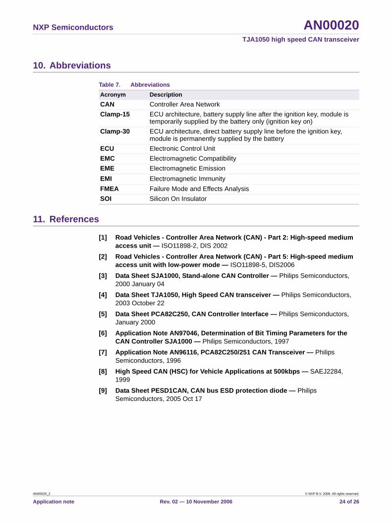
10. Abbreviations
11. References
[1] Road Vehicles - Controller Area Network (CAN) - Part 2: High-speed medium access unit — ISO11898-2, DIS 2002
[2] Road Vehicles - Controller Area Network (CAN) - Part 5: High-speed medium access unit with low-power mode — ISO11898-5, DIS2006
[3] Data Sheet SJA1000, Stand-alone CAN Controller — Philips Semiconductors, 2000 January 04
[4] Data Sheet TJA1050, High Speed CAN transceiver — Philips Semiconductors, 2003 October 22
[5] Data Sheet PCA82C250, CAN Controller Interface — Philips Semiconductors, January 2000
[6] Application Note AN97046, Determination of Bit Timing Parameters for the CAN Controller SJA1000 — Philips Semiconductors, 1997
[7] Application Note AN96116, PCA82C250/251 CAN Transceiver — Philips Semiconductors, 1996
[8] High Speed CAN (HSC) for Vehicle Applications at 500kbps — SAEJ2284, 1999
[9] Data Sheet PESD1CAN, CAN bus ESD protection diode — Philips Semiconductors, 2005 Oct 17
Table 7. AbbreviationsAcronym DescriptionCAN Controller Area NetworkClamp-15 ECU architecture, battery supply line after the ignition key, module is
temporarily supplied by the battery only (ignition key on)Clamp-30 ECU architecture, direct battery supply line before the ignition key,
module is permanently supplied by the batteryECU Electronic Control UnitEMC Electromagnetic CompatibilityEME Electromagnetic EmissionEMI Electromagnetic ImmunityFMEA Failure Mode and Effects AnalysisSOI Silicon On Insulator
AN00020_2 © NXP B.V. 2006. All rights reserved.
Application note Rev. 02 — 10 November 2006 24 of 26
NXP Semiconductors AN00020TJA1050 high speed CAN transceiver
12. Legal information
12.1 DefinitionsDraft — The document is a draft version only. The content is still under internal review and subject to formal approval, which may result in modifications or additions. NXP Semiconductors does not give any representations or warranties as to the accuracy or completeness of information included herein and shall have no liability for the consequences of use of such information.
12.2 DisclaimersGeneral — Information in this document is believed to be accurate and reliable. However, NXP Semiconductors does not give any representations or warranties, expressed or implied, as to the accuracy or completeness of such information and shall have no liability for the consequences of use of such information.
Right to make changes — NXP Semiconductors reserves the right to make changes to information published in this document, including without limitation specifications and product descriptions, at any time and without notice. This document supersedes and replaces all information supplied prior to the publication hereof.
Suitability for use — NXP Semiconductors products are not designed, authorized or warranted to be suitable for use in medical, military, aircraft, space or life support equipment, nor in applications where failure or malfunction of a NXP Semiconductors product can reasonably be expected to result in personal injury, death or severe property or environmental damage. NXP Semiconductors accepts no liability for inclusion and/or use of NXP Semiconductors products in such equipment or applications and therefore such inclusion and/or use is at the customer’s own risk.
Applications — Applications that are described herein for any of these products are for illustrative purposes only. NXP Semiconductors makes no representation or warranty that such applications will be suitable for the specified use without further testing or modification.
12.3 TrademarksNotice: All referenced brands, product names, service names and trademarks are the property of their respective owners.
AN00020_2 © NXP B.V. 2006. All rights reserved.
Application note Rev. 02 — 10 November 2006 25 of 26
NXP Semiconductors AN00020TJA1050 high speed CAN transceiver
13. Contents
1 Introduction . . . . . . . . . . . . . . . . . . . . . . . . . . . . 32 General application of high speed CAN
transceiver . . . . . . . . . . . . . . . . . . . . . . . . . . . . . 43 The TJA1050. . . . . . . . . . . . . . . . . . . . . . . . . . . . 73.1 Features . . . . . . . . . . . . . . . . . . . . . . . . . . . . . . 73.2 Operation modes . . . . . . . . . . . . . . . . . . . . . . . 73.2.1 High speed mode . . . . . . . . . . . . . . . . . . . . . . . 73.2.2 Silent mode. . . . . . . . . . . . . . . . . . . . . . . . . . . . 73.2.2.1 “Babbling idiot” protection. . . . . . . . . . . . . . . . . 83.2.2.2 Listen-only mode . . . . . . . . . . . . . . . . . . . . . . . 83.3 TXD dominant timeout . . . . . . . . . . . . . . . . . . . 83.4 Compatibility with 3.3 V devices . . . . . . . . . . . . 84 EMC and ESD aspects. . . . . . . . . . . . . . . . . . . . 94.1 Split termination concept . . . . . . . . . . . . . . . . . 94.2 Common mode choke . . . . . . . . . . . . . . . . . . 104.3 ESD Protection . . . . . . . . . . . . . . . . . . . . . . . . 115 Power supply and recommended bypass
capacitor . . . . . . . . . . . . . . . . . . . . . . . . . . . . . . 125.1 Average and peak supply current . . . . . . . . . . 125.2 Bypass capacitor . . . . . . . . . . . . . . . . . . . . . . 126 Ground-offset aspects. . . . . . . . . . . . . . . . . . . 137 Unpowered transceiver . . . . . . . . . . . . . . . . . . 157.1 Asymmetrical biasing of the common mode
voltage . . . . . . . . . . . . . . . . . . . . . . . . . . . . . . 157.2 RXD dominant clamping. . . . . . . . . . . . . . . . . 177.3 Backward supply towards VCC . . . . . . . . . . . . 188 Replacing the PCA82C250 with the TJA1050 198.1 Pinning . . . . . . . . . . . . . . . . . . . . . . . . . . . . . . 198.2 Operation modes . . . . . . . . . . . . . . . . . . . . . . 198.3 Slope control resistor . . . . . . . . . . . . . . . . . . . 198.4 Interfacing. . . . . . . . . . . . . . . . . . . . . . . . . . . . 199 Bus network aspects . . . . . . . . . . . . . . . . . . . . 209.1 Maximum number of nodes . . . . . . . . . . . . . . 209.2 Maximum bus line length . . . . . . . . . . . . . . . . 219.3 Topology aspects . . . . . . . . . . . . . . . . . . . . . . 229.3.1 Ringing due to signal reflections. . . . . . . . . . . 229.3.2 Linear topology . . . . . . . . . . . . . . . . . . . . . . . . 2310 Abbreviations. . . . . . . . . . . . . . . . . . . . . . . . . . 2411 References . . . . . . . . . . . . . . . . . . . . . . . . . . . . 2412 Legal information. . . . . . . . . . . . . . . . . . . . . . . 2512.1 Definitions. . . . . . . . . . . . . . . . . . . . . . . . . . . . 2512.2 Disclaimers . . . . . . . . . . . . . . . . . . . . . . . . . . . 2512.3 Trademarks. . . . . . . . . . . . . . . . . . . . . . . . . . . 2513 Contents . . . . . . . . . . . . . . . . . . . . . . . . . . . . . . 26
© NXP B.V. 2006. All rights reserved.For more information, please visit: http://www.nxp.comFor sales office addresses, please send an email to: [email protected]
Date of release: 10 November 2006Document identifier: AN00020_2
Please be aware that important notices concerning this document and the product(s)described herein, have been included in section ‘Legal information’.