Embed Size (px)
Citation preview

AN10897A guide to designing for ESD and EMCRev. 02 — 19 January 2010 Application note
Document informationInfo ContentKeywords ESD, EMC, PCB design
Abstract An introductory approach to designing for ESD. Understanding the ESD pulse, how passive components react over frequency, and PCB layout techniques are exposed.
NXP Semiconductors AN10897A guide to designing for ESD and EMC
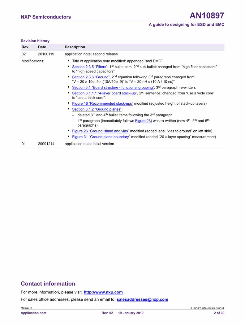
Revision historyRev Date Description
02 20100119 application note; second release
Modifications: • Title of application note modified: appended “and EMC”• Section 2.3.5 “Filters”, 1st bullet item, 2nd sub-bullet: changed from “high filter capacitors”
to “high speed capacitors”• Section 2.3.6 “Ground”, 2nd equation following 3rd paragraph changed from
“V = 20 × 10e−9 × (10A/10e−9)” to “V = 20 nH × (10 A / 10 ns)”• Section 3.1 “Board structure - functional grouping”: 3rd paragraph re-written.• Section 3.1.1.1 “4-layer board stack-up”, 2nd sentence: changed from “use a wide core”
to “use a thick core”.• Figure 18 “Recommended stack-ups” modified (adjusted height of stack-up layers)• Section 3.1.2 “Ground planes”:
– deleted 3rd and 4th bullet items following the 3rd paragraph.– 4th paragraph (immediately follows Figure 23) was re-written (now 4th, 5th and 6th
paragraphs).• Figure 26 “Ground island and vias” modified (added label “vias to ground” on left side).• Figure 31 “Ground plane boundary” modified (added “20 × layer spacing” measurement)
01 20091214 application note; initial version
AN10897_2 © NXP B.V. 2010. All rights reserved.
Application note Rev. 02 — 19 January 2010 2 of 30
Contact informationFor more information, please visit: http://www.nxp.com
For sales office addresses, please send an email to: [email protected]
NXP Semiconductors AN10897A guide to designing for ESD and EMC
1. Introduction
This application note is written to give the user an introductory approach to dealing with ESD. Be it a Pachinko machine or a washing machine or a hand held remote control, ESD is a threat to the operation of the system and it needs to be addressed head-on.
Given the nature of the product, it will be exposed to ESD events that range from the normal charge build-up in human beings using the equipment, charge build-up by moving parts (due to triboelectric charging), or by malicious attacks by individuals.
It is important to note that this manual is a set of guidelines that will improve the system immunity to ESD events and that it is not a guarantee that it will prevent an ESD event from altering the performance of your product or eliminating potential damage.
When it comes to ESD, keep the following quote from Og Mandino in mind: “Never has there been a map, however carefully executed to detail and scale, which carried its owner over even one inch of ground.” It is upon you to take action into implementing the recommendation presented and testing the results of the recommendation in your application. You must also test for ESD at various points in the design phase to guarantee performance of the final product.
2. The basics
2.1 The ESD pulse
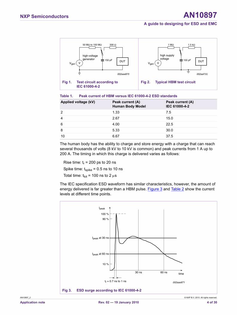
2.1.1 Characteristics of the ESD pulse—the IEC modelIn this guide the ESD pulse we will be referring to is the one defined in IEC 61000-4-2. The typical test circuit is shown in Figure 1 and the characteristics of the pulse is shown in Figure 4.
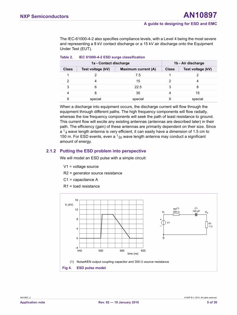
There are other specifications such as the Human Body Model (HBM) (see Figure 2 for typical HBM test circuit) and the Machine Model (MM). These models are device level specifications and are used to qualify IC components and intended for customer assembly production lines. Device-level ESD pulses (HBM, MM, CDM) and system-level ESD pulses (IEC) should be considered with separate test acceptance criteria. There is a disconnect in the EMC (ElectroMagnetic Compatibility) world between system manufacturers testing systems for upset and device manufacturers testing devices for failure. Some system level manufacturers are pushing device manufacturers to test semiconductor devices using system-level compliance standards—specifically, IEC 61000-4-2 for ESD (ElectroStatic Discharge). Product manufacturers would like to believe that if devices are qualified to IEC standard(s), finished products will likewise be qualified. Unfortunately, there is a fundamental difference between system-level and device-level testing. Table 1 shows a comparison between the peak current of HBM versus IEC 61000-4-2 standards.
AN10897_2 © NXP B.V. 2010. All rights reserved.
Application note Rev. 02 — 19 January 2010 3 of 30
NXP Semiconductors AN10897A guide to designing for ESD and EMC
The human body has the ability to charge and store energy with a charge that can reach several thousands of volts (8 kV to 10 kV is common) and peak currents from 1 A up to 200 A. The timing in which this charge is delivered varies as follows:
Rise time: tr = 200 ps to 20 nsSpike time: tspike = 0.5 ns to 10 nsTotal time: ttot = 100 ns to 2 µs
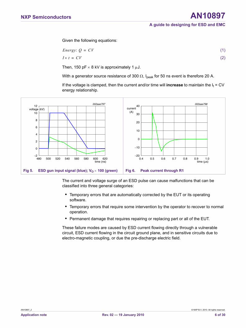
The IEC specification ESD waveform has similar characteristics, however, the amount of energy delivered is far greater than a HBM pulse. Figure 3 and Table 2 show the current levels at different time points.
Fig 1. Test circuit according to IEC 61000-4-2
Fig 2. Typical HBM test circuit
Table 1. Peak current of HBM versus IEC 61000-4-2 ESD standardsApplied voltage (kV) Peak current (A)
Human Body ModelPeak current (A) IEC 61000-4-2
2 1.33 7.5
4 2.67 15.0
6 4.00 22.5
8 5.33 30.0
10 6.67 37.5
Fig 3. ESD surge according to IEC 61000-4-2
DUT150 pF
330 Ω50 MΩ to 100 MΩ
VVgen
high-voltagegenerator
002aae870
DUT100 pF
1.5 kΩ1 MΩ
VVgen
high supplyvoltage
002aaf153
time60 ns30 ns
100 %
90 %
10 %
Ipeak at 60 ns
Ipeak at 30 ns
002aae871
Ipeak
tr = 0.7 ns to 1 ns
AN10897_2 © NXP B.V. 2010. All rights reserved.
Application note Rev. 02 — 19 January 2010 4 of 30
NXP Semiconductors AN10897A guide to designing for ESD and EMC
The IEC-61000-4-2 also specifies compliance levels, with a Level 4 being the most severe and representing a 8 kV contact discharge or a 15 kV air discharge onto the Equipment Under Test (EUT).
When a discharge into equipment occurs, the discharge current will flow through the equipment through different paths. The high frequency components will flow radially, whereas the low frequency components will seek the path of least resistance to ground. This current flow will excite any existing antennas (antennas are described later) in their path. The efficiency (gain) of these antennas are primarily dependent on their size. Since a 1⁄4 wave length antenna is very efficient, it can easily have a dimension of 1.5 cm to 150 m. For ESD events, even a 1⁄20 wave length antenna may conduct a significant amount of energy.
2.1.2 Putting the ESD problem into perspectiveWe will model an ESD pulse with a simple circuit:
V1 = voltage sourceR2 = generator source resistanceC1 = capacitance AR1 = load resistance
Table 2. IEC 61000-4-2 ESD surge classification1a - Contact discharge 1b - Air discharge
Class Test voltage (kV) Maximum current (A) Class Test voltage (kV)1 2 7.5 1 2
2 4 15 2 4
3 6 22.5 3 8
4 8 30 4 15
X special special X special
(1) NoiseKEN output coupling capacitor and 300 Ω source resistance
Fig 4. ESD pulse model
C1150 pF
R11 Ω
R2(1)
300 Ω
4
8
0
12
16
−4440 620500
Vi Vo
V1
560
Vi (kV)
time (ns)
AN10897_2 © NXP B.V. 2010. All rights reserved.
Application note Rev. 02 — 19 January 2010 5 of 30
NXP Semiconductors AN10897A guide to designing for ESD and EMC
Given the following equations:
(1)
(2)
Then, 150 pF × 8 kV is approximately 1 µJ.
With a generator source resistance of 300 Ω, Ipeak for 50 ns event is therefore 20 A.
If the voltage is clamped, then the current and/or time will increase to maintain the It = CV energy relationship.
The current and voltage surge of an ESD pulse can cause malfunctions that can be classified into three general categories:
• Temporary errors that are automatically corrected by the EUT or its operating software.
• Temporary errors that require some intervention by the operator to recover to normal operation.
• Permanent damage that requires repairing or replacing part or all of the EUT.
These failure modes are caused by ESD current flowing directly through a vulnerable circuit, ESD current flowing in the circuit ground plane, and in sensitive circuits due to electro-magnetic coupling, or due the pre-discharge electric field.
Energy: Q CV=
I t× CV=
Fig 5. ESD gun input signal (blue); VO × 100 (green) Fig 6. Peak current through R1
−2
12
time (ns)480 620500
002aae797
10
8
6
4
2
0
voltage (kV)
520 540 560 580 600−20
40
time (µs)0.4 1.0
002aae798
current(A)
0.5 0.6 0.7 0.8 0.9
−10
0
10
20
30
AN10897_2 © NXP B.V. 2010. All rights reserved.
Application note Rev. 02 — 19 January 2010 6 of 30
NXP Semiconductors AN10897A guide to designing for ESD and EMC
2.2 Effects and failure modes
2.2.1 Sources, paths and receptorsIn the field of EMI, interference can be broken down into:
• The source of interference• The receptor of the interference• The path of the interference
Sources can be microprocessors, video drivers, ESD, Audio amplifiers, power disturbances, lightning, motors, oscillators.
Receptors can be microprocessors, LED controllers, motor controllers, audio processors, reset circuits, low level analog, interrupt and control lines.
Paths can be divided into 2 categories:
• Radiated: EM fields, inductive or capacitive crosstalk• Conducted: Signal, power, ground traces
2.2.2 Unintentional antennasUnintentional antennas are formed in a system due to the signal carrying traces. For example you have:
• Transmission line• Dipole antenna; typically formed by cables (see Figure 7)• Loop antenna: typically found on PCBs due to layout (see Figure 8)• Slot antennas; typically found in PCBs due to cut/split ground planes (see Figure 9)
Critical components:
• Equal/opposite current minimize radiation.• Overall dimensions (i.e., 1⁄4 wavelength and area) are key parameters• Radiation varies with respect to current (I), frequency (f), area (A) or length (L).
Resonances can amplify the unwanted radiated emissions.
Fig 7. Dipole antenna Fig 8. Loop antenna Fig 9. Slot antenna
002aae962 002aae963 002aae964
metal layer
slot cut-out
AN10897_2 © NXP B.V. 2010. All rights reserved.
Application note Rev. 02 — 19 January 2010 7 of 30
NXP Semiconductors AN10897A guide to designing for ESD and EMC
If we consider the rapid rise time of an IEC61000-4-2 ESD pulse to be equivalent of 300 MHz, then from Table 3 you can see that a 5 cm trace is a critical length during an ESD event as it may be a very efficient λ / 20 antenna.
2.3 An overview of R, L, C and D components
2.3.1 Resistor (R) component characteristicsResistors serve to reduce current and dissipate as heat.
Since they provide a voltage drop at DC only, small value resistors (<100 Ω) in series are practical in applications.
A resistor’s end-to-end capacitance limits it overall impedance. A 1 MΩ resistor at DC is no longer the same at 100 MHz. Also, ESD voltages tend to arc across surface mount resistors, reducing their effectiveness. In this case, use carbon or thick film resistors for best results.
Resistors are low cost, but required values to limit I/O pin current will interfere with normal circuit operation. Example: to limit 6 kV ESD event current to 10 mA requires 600 kΩ resistor—not practical (ignoring IC peak current capability in this example).
2.3.2 Inductor (L) component characteristicsWire wound inductors are commonly used EMI filters. They are good to about 50 MHz. For ESD and EMI applications, a ferrite is preferred at the higher frequencies.
SMD ferrites are one-turn inductors that are very useful as frequency dependent resistors. They allow low frequency signals to pass, while blocking high frequency pulses (i.e., ESD, EFT) and dissipating energy as heat.
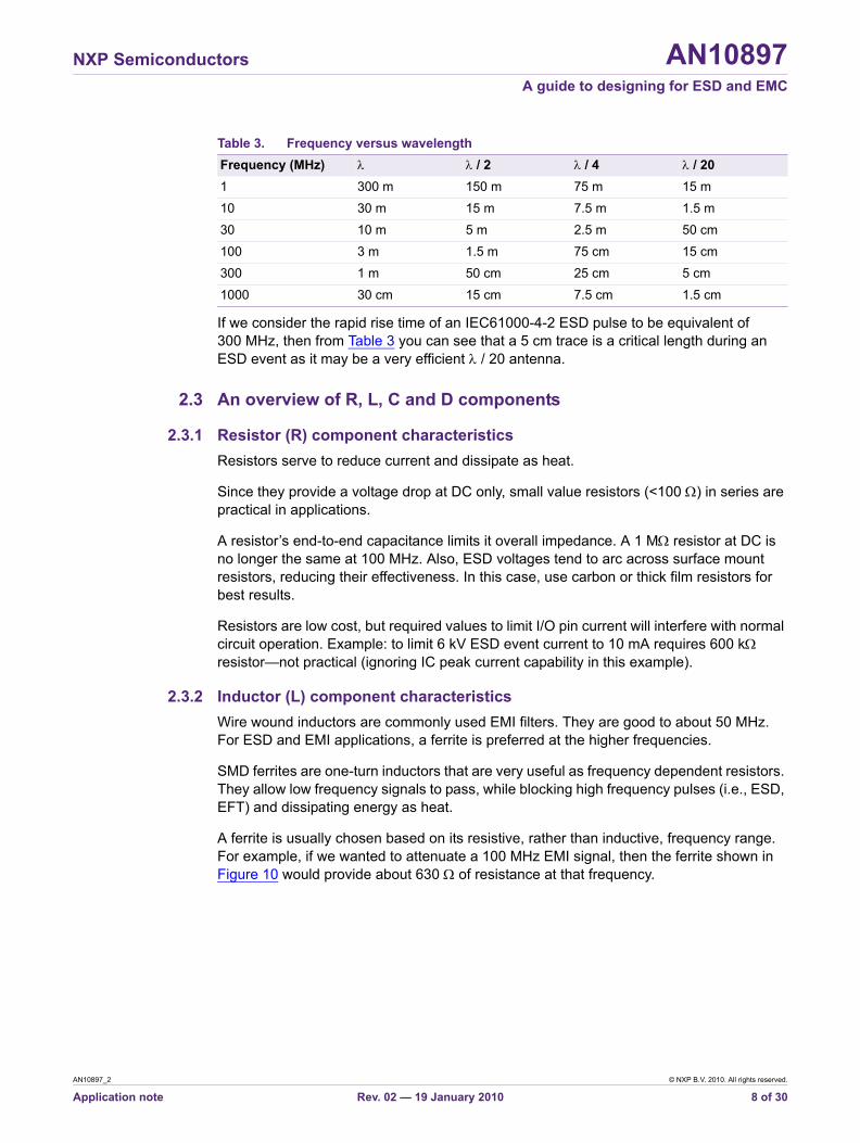
A ferrite is usually chosen based on its resistive, rather than inductive, frequency range. For example, if we wanted to attenuate a 100 MHz EMI signal, then the ferrite shown in Figure 10 would provide about 630 Ω of resistance at that frequency.
Table 3. Frequency versus wavelengthFrequency (MHz) λ λ / 2 λ / 4 λ / 201 300 m 150 m 75 m 15 m
10 30 m 15 m 7.5 m 1.5 m
30 10 m 5 m 2.5 m 50 cm
100 3 m 1.5 m 75 cm 15 cm
300 1 m 50 cm 25 cm 5 cm
1000 30 cm 15 cm 7.5 cm 1.5 cm
AN10897_2 © NXP B.V. 2010. All rights reserved.
Application note Rev. 02 — 19 January 2010 8 of 30
NXP Semiconductors AN10897A guide to designing for ESD and EMC
Ferrites have low impedance at typical system operating frequencies so they do not interfere with normal circuit operation. Ferrites also convert ESD energy to thermal energy very effectively.
2.3.3 Capacitor (C) component characteristicsCapacitors serve as filters. They can be used to filter the high frequency pulses produced by an ESD event. They also provide switching current to ICs and serve as energy storage bins that minimize voltage drop.
Capacitors are low cost and offer basic protection. There should be minimum one decoupling capacitor per IC on the board. More capacitors are better, and should be symmetrically placed around the ICs. Smaller size capacitors should be placed in parallel to larger capacitors to increase the frequency response.
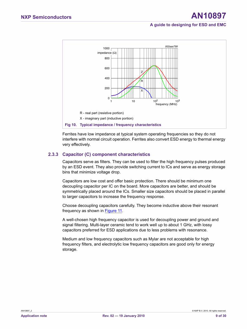
Choose decoupling capacitors carefully. They become inductive above their resonant frequency as shown in Figure 11.
A well-chosen high frequency capacitor is used for decoupling power and ground and signal filtering. Multi-layer ceramic tend to work well up to about 1 GHz, with lossy capacitors preferred for ESD applications due to less problems with resonance.
Medium and low frequency capacitors such as Mylar are not acceptable for high frequency filters, and electrolytic low frequency capacitors are good only for energy storage.
R - real part (resistive portion)X - imaginary part (inductive portion)
Fig 10. Typical impedance / frequency characteristics
002aae799
frequency (MHz)1 10310210
600
400
200
0
800
1000
impedance (Ω)
Z
R
X
AN10897_2 © NXP B.V. 2010. All rights reserved.
Application note Rev. 02 — 19 January 2010 9 of 30
NXP Semiconductors AN10897A guide to designing for ESD and EMC
(1) 1000 pF(2) 10000 pF(3) 100000 pF
Fig 11. GRM series (X7R char. 250 V)
Table 4. Capacitor selectionType Maximum frequencyaluminum electrolytic 100 kHz
tantalum electolytic 1 MHz
paper 5 MHz
mylar 10 MHz
polystyrene 500 MHz
mica 500 MHz
ceramic > 1 GHz
002aae800
frequency (Hz)103 106105104
1
10−1
102
10
103
Z(Ω)
10−2
(2)
(3)
(1)
AN10897_2 © NXP B.V. 2010. All rights reserved.
Application note Rev. 02 — 19 January 2010 10 of 30
NXP Semiconductors AN10897A guide to designing for ESD and EMC
2.3.4 Diodes (D)Zener diodes and transorbs (transient voltage suppression diodes) help divert current to power or ground rails away from IC and provide voltage clamping.
2.3.5 FiltersWhen constructing EMI filters consider the following:
• Filter components:– Shunt elements to be high speed capacitors– Use multi-layer ceramic capacitors with short lead lengths– Series elements to be resistors or ferrites.– Avoid use of low loss inductors; lossy ferrites are preferred, especially above
50 MHz.• Filter termination:
– The low-impedance capacitor should be connected to appropriate ground. Chassis ground for immunity (ESD), signal ground for emissions.
2.3.6 Ground‘Ground’ is a return path for current, usually a point to which circuit voltage is referenced.
A ground plane or trace is a dynamic element. There are no guarantees that any two points on the plane or trace will remain at the same potential during an ESD event.
For example, for 20 nH ground inductance (= 20 mm trace) and a 10 A pulse lasting for 10 ns:
V = L(di/dt)V = 20 nH × (10 A / 10 ns)V = 20 V enough to corrupt signals and cause major system problems
Circuit or signal ground — may be logic or analog ground. Cannot be relied upon to be at the same potential as adjacent PCB boards.
Ultra low capacitance double rail-to-rail ESD protection diode.
High-speed switching diodes divert current away from sensitive circuits.
Can be used to clamp voltages.
Fig 12. PRTR5V0U2AX Fig 13. BAV99 Fig 14. Zener diode
006aaa482
41
32
006aaa763
1 2
3
002aae801
AN10897_2 © NXP B.V. 2010. All rights reserved.
Application note Rev. 02 — 19 January 2010 11 of 30

NXP Semiconductors AN10897A guide to designing for ESD and EMC
Backplane or motherboard ground — common reference present on a board to which other boards are connected.Enclosure ground — safety ground connection to earth, may or may not be connected to chassis ground.Line neutral — In the USA, connected to earth ground at power entrance or an inverting transformers.
2.4 ESD mitigation
2.4.1 Hardware ESD management strategy
• ESD protection requires the peak voltage and current to be limited to safe levels for sufficiently short periods so as not to cause permanent damage to the chip.
• Damage is cumulative: 50 ESD events will cause more damage than a single ESD event or 3 ESD events (IEC spec).
• With no input ESD protection, either internal to the IC or augmented with external components when trying to meet more stringent tests, the IC will fail.
2.4.2 Software ESD management strategySoftware or firmware plays an important role in reducing the effects of ESD. Software is an effective way to recover from non-destructive ESD events.
As with a hardware ESD fix, a software ESD fix has its associated costs: increased development time, memory requirement, and processing time. This cost can be compared to a hardware fix alone, however, the redundancy that a software fix can provide may pay off in the future.
The general approach to writing robust software is to assume that the state of ports or registers has been unintentionally changed within a period of time. To address this, the programmer can:
1. Use refresh routines.2. Use checking and restoring.3. Unused interrupts return to main program.4. Use an internal or external watchdog timer.
Recommendations to improve system robustness:
• Always assume the data has been corrupted since the last access.• Use a hardware watchdog to reset the system in case of a hang-up.• Re-write all IO register data regularly to ensure system has correct data.• Unused interrupts should have a return to main.• Use checksums or CRC on large blocks of data.
AN10897_2 © NXP B.V. 2010. All rights reserved.
Application note Rev. 02 — 19 January 2010 12 of 30

NXP Semiconductors AN10897A guide to designing for ESD and EMC
2.4.2.1 RefreshWhen refreshing, checking for the validity of prior data is not conducted. The software simply re-writes data into registers that are required for proper operation. This is done even if the port/register has not been used since the last write.
When using refresh, keep in mind the order in which the refresh should occur. You must assume that the register values are incorrect, and that by enabling a port before setting its correct state may lead to undesired results.
2.4.2.2 Checking and restoringYou can also build in periodic checks to verify that all your components are running as programmed. For large blocks of data you can use checksums or Cyclic Redundancy Checks (CRC) for fast check. If these checks provide errors, then you must choose an appropriate recovery routine. You may want to restore only portions of your system or save data for diagnostics.
2.4.2.3 Unused interrupts and registersYou can cover the software ‘holes’ by placing all unused registers/ports in a known state. Pay special attention to unused interrupt vectors. A good practice is to place a ‘return to main’ statement in unused interrupt vectors, which allows the program to continue in case an ESD event causes the microcontroller to erroneously point to an unused interrupt.
2.4.2.4 Watchdog timersIn the event that the software enters an unrecoverable state, a watchdog timer can be used to force a reset or other recovery process.
External watchdog timers are also recommended. They come in stand-alone IC packages that can be used to recover the system if the host fails.
The key is to always leave a path for the software and hardware to return to a valid operating point so that it can continue execution.
AN10897_2 © NXP B.V. 2010. All rights reserved.
Application note Rev. 02 — 19 January 2010 13 of 30
NXP Semiconductors AN10897A guide to designing for ESD and EMC
3. A practical approach to schematic and PCB design
Electromagnetic compatibility and ESD immunity must be considered in the early design stage of a system. If ignored, problems encountered later in testing or in the field will become very difficult and expensive to fix.
A crucial element in EMC/ESD immunity is a solid PCB design. Good practices such as decoupling power and I/O lines to ground, voltage and frequency (bandwidth) limiting, wave shaping (edge-rate control), using negative feedback, refresh cycling, WDT, and fault tolerant software—all play collectively an important role in improving EMC and ESD immunity.
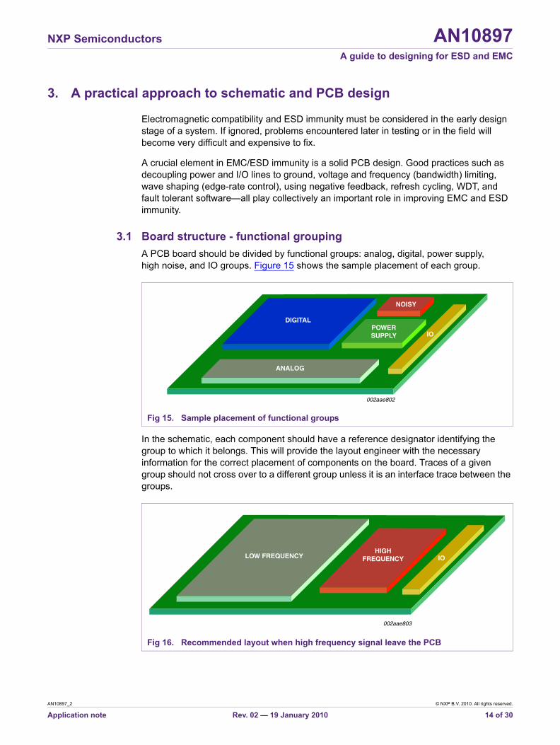
3.1 Board structure - functional groupingA PCB board should be divided by functional groups: analog, digital, power supply, high noise, and IO groups. Figure 15 shows the sample placement of each group.
In the schematic, each component should have a reference designator identifying the group to which it belongs. This will provide the layout engineer with the necessary information for the correct placement of components on the board. Traces of a given group should not cross over to a different group unless it is an interface trace between the groups.
Fig 15. Sample placement of functional groups
Fig 16. Recommended layout when high frequency signal leave the PCB
002aae802
DIGITALPOWERSUPPLY
ANALOG
NOISY
IO
002aae803
HIGHFREQUENCY IOLOW FREQUENCY
AN10897_2 © NXP B.V. 2010. All rights reserved.
Application note Rev. 02 — 19 January 2010 14 of 30
NXP Semiconductors AN10897A guide to designing for ESD and EMC
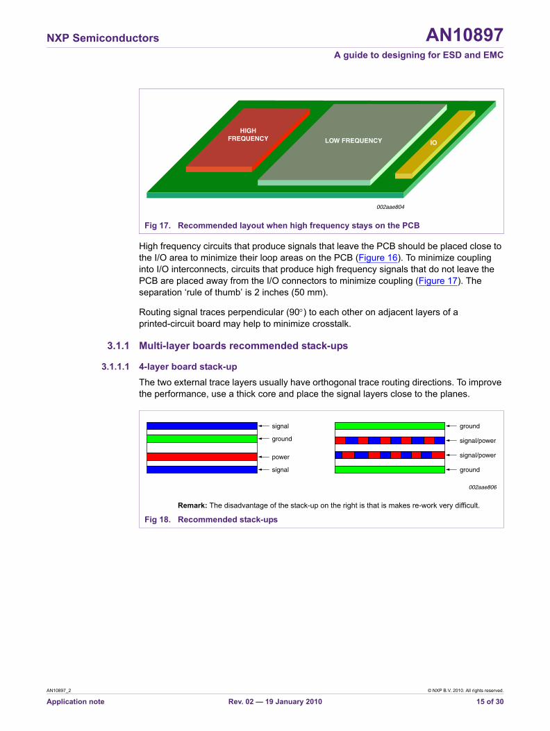
High frequency circuits that produce signals that leave the PCB should be placed close to the I/O area to minimize their loop areas on the PCB (Figure 16). To minimize coupling into I/O interconnects, circuits that produce high frequency signals that do not leave the PCB are placed away from the I/O connectors to minimize coupling (Figure 17). The separation ‘rule of thumb’ is 2 inches (50 mm).
Routing signal traces perpendicular (90°) to each other on adjacent layers of a printed-circuit board may help to minimize crosstalk.
3.1.1 Multi-layer boards recommended stack-ups
3.1.1.1 4-layer board stack-upThe two external trace layers usually have orthogonal trace routing directions. To improve the performance, use a thick core and place the signal layers close to the planes.
Fig 17. Recommended layout when high frequency stays on the PCB
002aae804
HIGHFREQUENCY
IOLOW FREQUENCY
Remark: The disadvantage of the stack-up on the right is that is makes re-work very difficult.
Fig 18. Recommended stack-ups
002aae806
signal
ground
power
signal
ground
signal/power
signal/power
ground
AN10897_2 © NXP B.V. 2010. All rights reserved.
Application note Rev. 02 — 19 January 2010 15 of 30
NXP Semiconductors AN10897A guide to designing for ESD and EMC
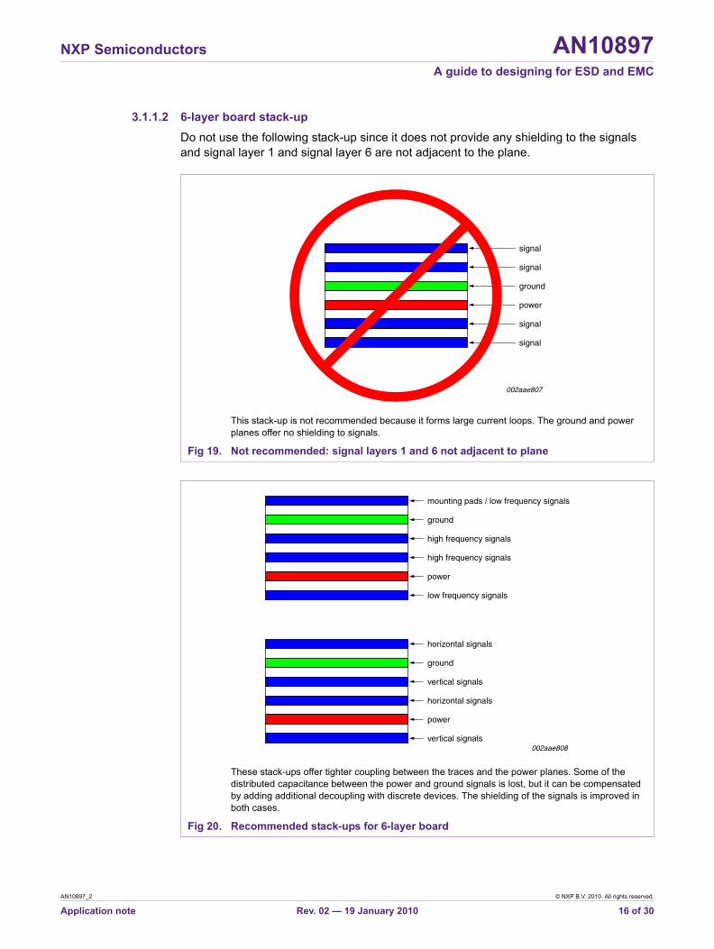
3.1.1.2 6-layer board stack-upDo not use the following stack-up since it does not provide any shielding to the signals and signal layer 1 and signal layer 6 are not adjacent to the plane.
This stack-up is not recommended because it forms large current loops. The ground and power planes offer no shielding to signals.
Fig 19. Not recommended: signal layers 1 and 6 not adjacent to plane
These stack-ups offer tighter coupling between the traces and the power planes. Some of the distributed capacitance between the power and ground signals is lost, but it can be compensated by adding additional decoupling with discrete devices. The shielding of the signals is improved in both cases.
Fig 20. Recommended stack-ups for 6-layer board
002aae807
signal
ground
power
signal
signal
signal
002aae808
mounting pads / low frequency signals
ground
high frequency signals
high frequency signals
power
low frequency signals
horizontal signals
ground
vertical signals
horizontal signals
power
vertical signals
AN10897_2 © NXP B.V. 2010. All rights reserved.
Application note Rev. 02 — 19 January 2010 16 of 30
NXP Semiconductors AN10897A guide to designing for ESD and EMC
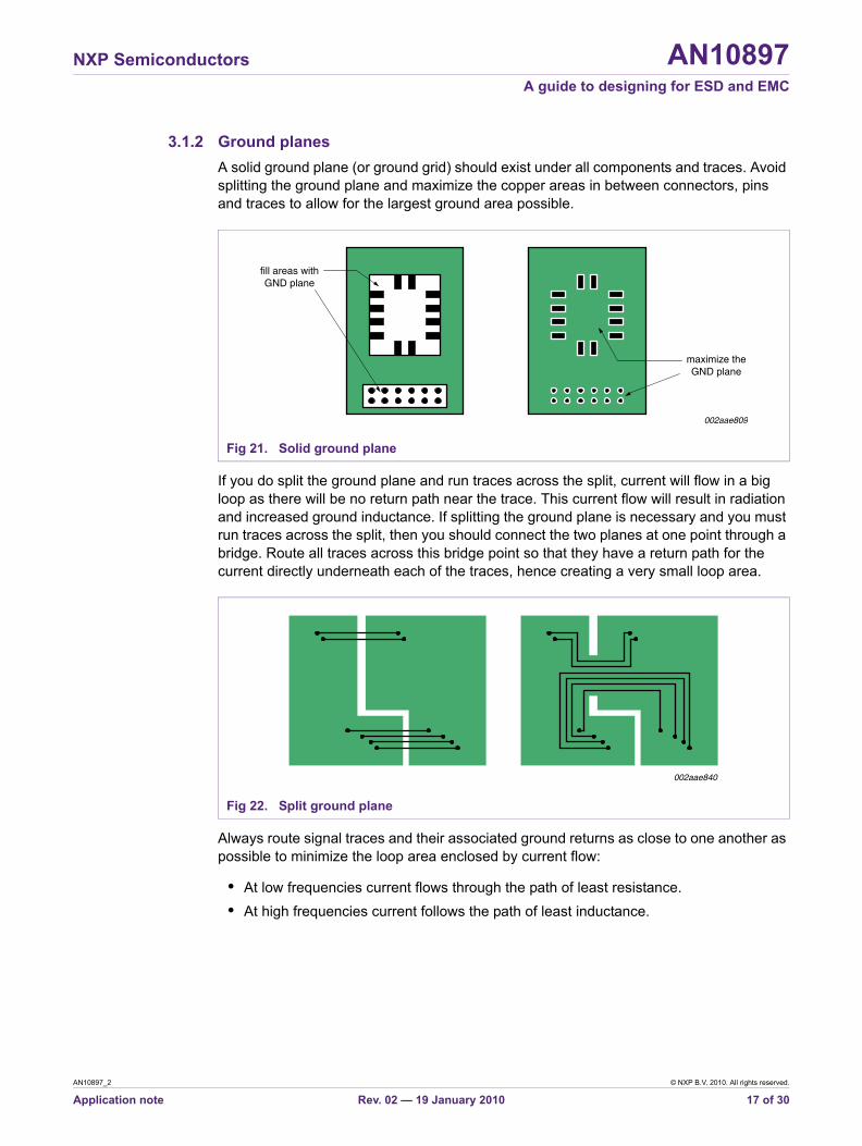
3.1.2 Ground planesA solid ground plane (or ground grid) should exist under all components and traces. Avoid splitting the ground plane and maximize the copper areas in between connectors, pins and traces to allow for the largest ground area possible.
If you do split the ground plane and run traces across the split, current will flow in a big loop as there will be no return path near the trace. This current flow will result in radiation and increased ground inductance. If splitting the ground plane is necessary and you must run traces across the split, then you should connect the two planes at one point through a bridge. Route all traces across this bridge point so that they have a return path for the current directly underneath each of the traces, hence creating a very small loop area.
Always route signal traces and their associated ground returns as close to one another as possible to minimize the loop area enclosed by current flow:
• At low frequencies current flows through the path of least resistance.• At high frequencies current follows the path of least inductance.
Fig 21. Solid ground plane
Fig 22. Split ground plane
002aae809
fill areas withGND plane
maximize theGND plane
002aae840
AN10897_2 © NXP B.V. 2010. All rights reserved.
Application note Rev. 02 — 19 January 2010 17 of 30
NXP Semiconductors AN10897A guide to designing for ESD and EMC
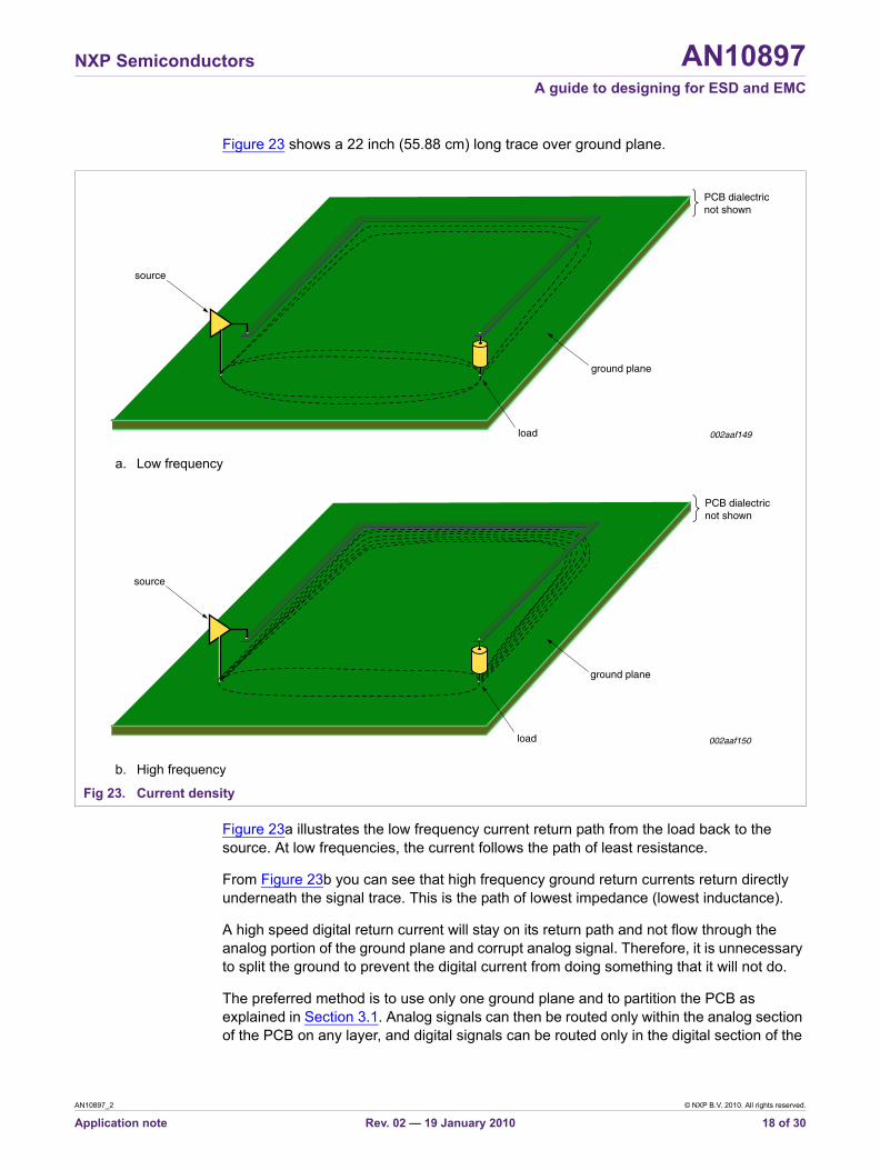
Figure 23 shows a 22 inch (55.88 cm) long trace over ground plane.
Figure 23a illustrates the low frequency current return path from the load back to the source. At low frequencies, the current follows the path of least resistance.
From Figure 23b you can see that high frequency ground return currents return directly underneath the signal trace. This is the path of lowest impedance (lowest inductance).
A high speed digital return current will stay on its return path and not flow through the analog portion of the ground plane and corrupt analog signal. Therefore, it is unnecessary to split the ground to prevent the digital current from doing something that it will not do.
The preferred method is to use only one ground plane and to partition the PCB as explained in Section 3.1. Analog signals can then be routed only within the analog section of the PCB on any layer, and digital signals can be routed only in the digital section of the
a. Low frequency
b. High frequency
Fig 23. Current density
002aaf149
source
load
ground plane
PCB dialectricnot shown
002aaf150
source
load
ground plane
PCB dialectricnot shown
AN10897_2 © NXP B.V. 2010. All rights reserved.
Application note Rev. 02 — 19 January 2010 18 of 30
NXP Semiconductors AN10897A guide to designing for ESD and EMC
PCB on any layer. Do not route digital signals in the analog section of the board, or visa versa. The ground return paths for analog, digital, or power should be carefully designed so that they do not flow through each other’s circuits.
All high frequency signal traces must be on layers adjacent to a plane.
Above 25 MHz, PCBs should have two (or more) ground planes.
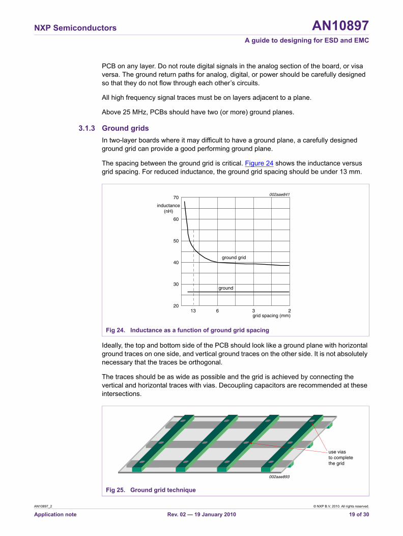
3.1.3 Ground gridsIn two-layer boards where it may difficult to have a ground plane, a carefully designed ground grid can provide a good performing ground plane.
The spacing between the ground grid is critical. Figure 24 shows the inductance versus grid spacing. For reduced inductance, the ground grid spacing should be under 13 mm.
Ideally, the top and bottom side of the PCB should look like a ground plane with horizontal ground traces on one side, and vertical ground traces on the other side. It is not absolutely necessary that the traces be orthogonal.
The traces should be as wide as possible and the grid is achieved by connecting the vertical and horizontal traces with vias. Decoupling capacitors are recommended at these intersections.
Fig 24. Inductance as a function of ground grid spacing
Fig 25. Ground grid technique
002aae841
grid spacing (mm)13 236
40
50
30
60
70
inductance(nH)
20
ground
ground grid
use viasto completethe grid
002aae893
AN10897_2 © NXP B.V. 2010. All rights reserved.
Application note Rev. 02 — 19 January 2010 19 of 30
NXP Semiconductors AN10897A guide to designing for ESD and EMC
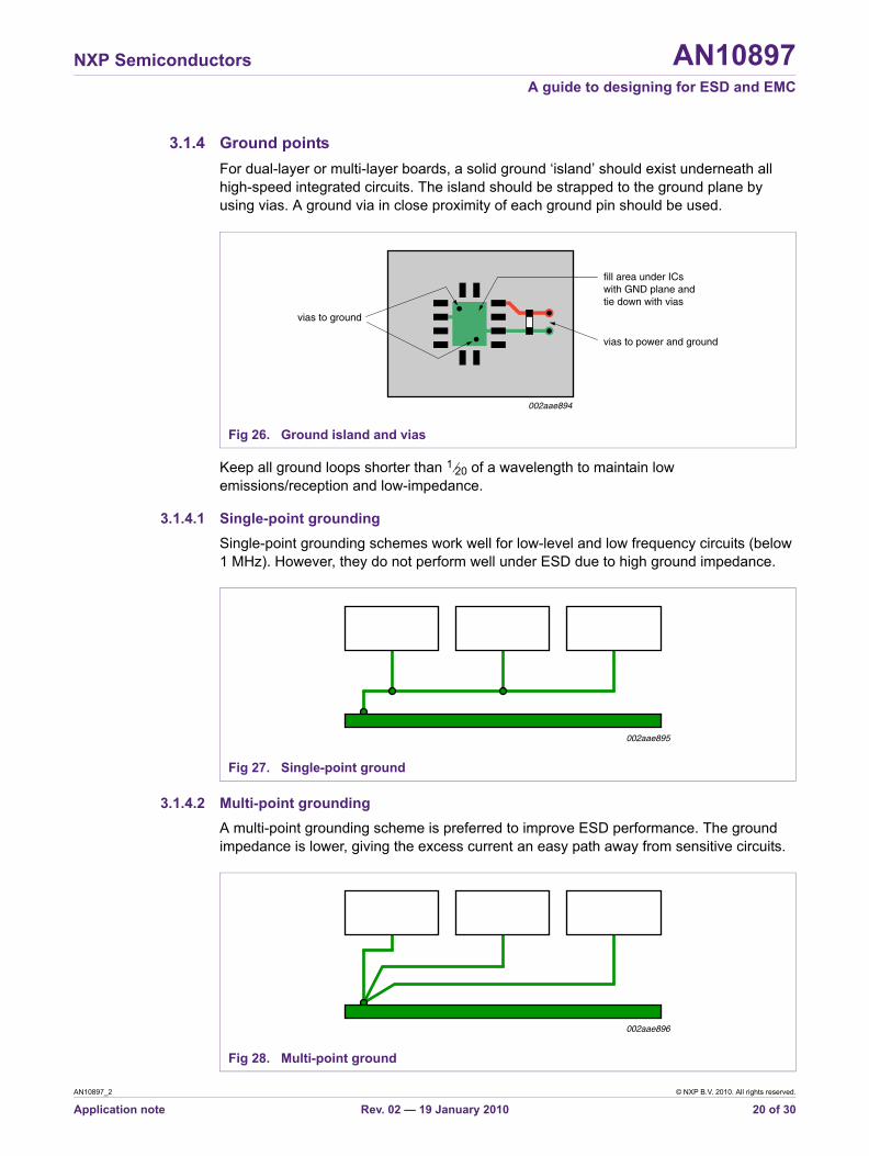
3.1.4 Ground pointsFor dual-layer or multi-layer boards, a solid ground ‘island’ should exist underneath all high-speed integrated circuits. The island should be strapped to the ground plane by using vias. A ground via in close proximity of each ground pin should be used.
Keep all ground loops shorter than 1⁄20 of a wavelength to maintain low emissions/reception and low-impedance.
3.1.4.1 Single-point groundingSingle-point grounding schemes work well for low-level and low frequency circuits (below 1 MHz). However, they do not perform well under ESD due to high ground impedance.
3.1.4.2 Multi-point groundingA multi-point grounding scheme is preferred to improve ESD performance. The ground impedance is lower, giving the excess current an easy path away from sensitive circuits.
Fig 26. Ground island and vias
002aae894
fill area under ICswith GND plane andtie down with vias
vias to power and ground
vias to ground
Fig 27. Single-point ground
002aae895
Fig 28. Multi-point ground
002aae896
AN10897_2 © NXP B.V. 2010. All rights reserved.
Application note Rev. 02 — 19 January 2010 20 of 30
NXP Semiconductors AN10897A guide to designing for ESD and EMC
3.1.4.3 Ground pins and interconnectGround pins should be evenly distributed across all connectors (board-to-board or board-to-cable). The number of connector ground pins should be determined prior to layout and should include the current capabilities of the connector as well as the current carrying capability of the cables connecting the boards.
A minimum of one ground-return track should be routed adjacent to each eight lines of address and data lines to minimize the loop area. You can increase the ratio to 1 : 5 for higher performance. All lines should be kept as short as possible. Route a ground trace adjacent to the Least Significant Bit (LSB) of address since this is usually a very active signal.
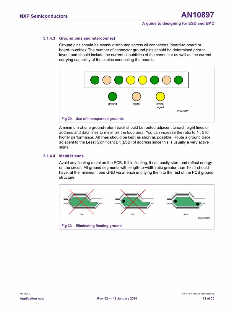
3.1.4.4 Metal islandsAvoid any floating metal on the PCB. If it is floating, it can easily store and reflect energy on the circuit. All ground segments with length-to-width ratio greater than 10 : 1 should have, at the minimum, one GND via at each end tying them to the rest of the PCB ground structure.
Fig 29. Use of interspersed grounds
002aae897
ground signal criticalsignal
Fig 30. Eliminating floating ground
no no yes002aae898
AN10897_2 © NXP B.V. 2010. All rights reserved.
Application note Rev. 02 — 19 January 2010 21 of 30
NXP Semiconductors AN10897A guide to designing for ESD and EMC
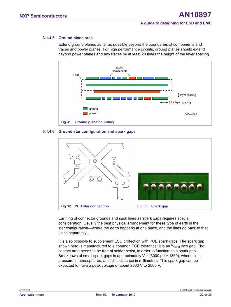
3.1.4.5 Ground plane areaExtend ground planes as far as possible beyond the boundaries of components and traces and power planes. For high performance circuits, ground planes should extend beyond power planes and any traces by at least 20 times the height of the layer spacing.
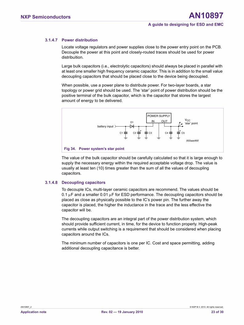
3.1.4.6 Ground star configuration and spark gaps
Earthing of connector grounds and such lines as spark gaps requires special consideration. Usually the best physical arrangement for these type of earth is the star configuration—where the earth happens at one place, and the lines go back to that place separately.
It is also possible to supplement ESD protection with PCB spark gaps. The spark gap shown here is manufactured to a common PCB tolerance: it is an 8⁄1000 inch gap. The contact area needs to be free of solder resist, in order to function as a spark gap. Breakdown of small spark gaps is approximately V = (3000 pd + 1350), where ‘p’ is pressure in atmospheres, and ‘d’ is distance in millimeters. This spark gap can be expected to have a peak voltage of about 2000 V to 2500 V.
Fig 31. Ground plane boundary
002aae899
layer spacing
tracks, components
PCB
ground
power
20 × layer spacing
Fig 32. PCB star connection Fig 33. Spark gap
AN10897_2 © NXP B.V. 2010. All rights reserved.
Application note Rev. 02 — 19 January 2010 22 of 30
NXP Semiconductors AN10897A guide to designing for ESD and EMC
3.1.4.7 Power distributionLocate voltage regulators and power supplies close to the power entry point on the PCB. Decouple the power at this point and closely-routed traces should be used for power distribuition.
Large bulk capacitors (i.e., electrolytic capacitors) should always be placed in parallel with at least one smaller high frequency ceramic capacitor. This is in addition to the small value decoupling capacitors that should be placed close to the device being decoupled.
When possible, use a power plane to distribute power. For two-layer boards, a star topology or power grid should be used. The ‘star’ point of power distribution should be the positive terminal of the bulk capacitor, which is the capacitor that stores the largest amount of energy to be delivered.
The value of the bulk capacitor should be carefully calculated so that it is large enough to supply the necessary energy within the required acceptable voltage drop. The value is usually at least ten (10) times greater than the sum of all the values of decoupling capacitors.
3.1.4.8 Decoupling capacitorsTo decouple ICs, multi-layer ceramic capacitors are recommend. The values should be 0.1 µF and a smaller 0.01 µF for ESD performance. The decoupling capacitors should be placed as close as physically possible to the IC’s power pin. The further away the capacitor is placed, the higher the inductance in the trace and the less effective the capacitor will be.
The decoupling capacitors are an integral part of the power distribution system, which should provide sufficient current, in time, for the device to function properly. High-peak currents while output switching is a requirement that should be considered when placing capacitors around the ICs.
The minimum number of capacitors is one per IC. Cost and space permitting, adding additional decoupling capacitance is better.
Fig 34. Power system’s star point
002aae900
C1
D1
C2 C3
POWER SUPPLY
IN OUT
C4 C5
VCC'star' point
battery input
AN10897_2 © NXP B.V. 2010. All rights reserved.
Application note Rev. 02 — 19 January 2010 23 of 30
NXP Semiconductors AN10897A guide to designing for ESD and EMC
3.1.4.9 Crosstalk and trace spacingTo prevent crosstalk, or coupling, traces carrying high current with fast rise/fall times (for example, under 10 ns) should maintain proper spacing from other traces that run in parallel to them, or have a ground guard trace in between them. This is particularly important if critical signals are close to the offending trace.
Power and ground signals should always be routed in parallel (side-by-side) or on top of each other (on adjacent layers) to minimize loop area, thus reducing loop impedance (Figure 35). This is especially important when constructing a power grid on a two-layer board.
Do not route power signals in parallel to high noise signals, as the noise may couple into the power plane. Choose the lowest power and slowest switching speed that meets the circuit requirements to minimize radiated emissions.
Power, ground, and signal traces on the PCB should be kept short and as wide as possible. Give special attention to pass-through signals on the boards as they may need a higher width-to-length ratio (minimum recommended is 1 : 10).
Placing ferrite beads on power traces may provide attenuation of unwanted signals above 1 MHz. When properly sized, these beads can be very effective in damping high-frequency switching transients or parasitic ringing due to line reflections without causing a DC loss.
Remark: Use caution, as using ferrites may impede AC current flow.
Devices such as Zener diodes, MOVs or transorbs should be placed at the power entry point to PCB, as their function is to limit/clip transients and spikes. Assure low-impedance connection to ground.
3.1.4.10 Power supply circuit placementAll Switching Mode Power Supply (SMPS) traces should ideally be routed on one layer of PCB with the SMPS reference plane placed directly on adjacent layer to minimize the loop area. Power switching and high current circuits should be kept separate from digital and low-level analog circuits.
Remark: Ground all the heat-sinks.
Fig 35. Power and ground routing
002aae903NO
GND VCC
YES
AN10897_2 © NXP B.V. 2010. All rights reserved.
Application note Rev. 02 — 19 January 2010 24 of 30
NXP Semiconductors AN10897A guide to designing for ESD and EMC
3.1.5 Digital circuit considerationsDigital clock connections are a source of EMI. They should be carefully routed on the PCB with all clock traces adjacent to a ground plane. No traces other than ground should run under crystals or any other inherently noisy circuits. Bury clock signals between power and ground planes whenever possible.
All critical nets, such as clocks, data strobes, etc., should be routed physically adjacent to ground traces or ground plane.
3.1.5.1 OscillatorsKeep oscillators and clock-generating ICs away from I/O connectors and close to the chips they service. Always choose the lowest clock frequency and slowest rise and fall time for digital signals that meet system requirements.
Filter (series terminate) the output of clock drivers to slow down their rise/fall times and to reduce ringing (typically 33 Ω to 70 Ω).
3.1.5.2 Digital busTerminators should be used for traces where the rise time is greater than twice the propagation delay.
Route differential signal lines adjacent to one another to take full advantage of magnetic field cancellation. Place ground guard traces on both sides of the entire length of the differential-pair signals.
Fig 36. Crystal/oscillator placement
002aae904
MICRO-PROCESSOR
CRYSTAL/OSCILLATOR
S
G
Fig 37. Minimizing digital bus length
002aae905
MICRO-PROCESSOR
CLOCK
LATCH
RAM
RAM
RAM
RAM
BUS
NO
MICRO-PROCESSOR
CLOCK
LATCH
RAMRAM
RAMRAM
BUS
YES
AN10897_2 © NXP B.V. 2010. All rights reserved.
Application note Rev. 02 — 19 January 2010 25 of 30
NXP Semiconductors AN10897A guide to designing for ESD and EMC
High-speed digital signals such as data, address, and control lines of microprocessors should be grouped together and located as far from the I/O connector as possible.
Controlling the rise and fall times, the duty cycle, and the fundamental frequency of switched signals may help to minimize harmonic generation. All unused IC inputs should be terminated to prevent unintentional random switching and noise generation.
Keep high-speed traces, control signals, interrupts and reset signals away from the edge of a PCB.
3.1.6 Analog circuit considerationsKeep all analog or peripheral circuitry as close to the I/O connector as possible, and away from high-speed digital, high current, or power switching circuits. Analog signals should be confined to analog section of PCB only with low-pass filtering always used on all analog inputs.
Ground guard traces should always be routed adjacent to analog signals. Attach the guard traces at both ends with vias to sending and receiving circuits’ ground.
If using suppression device across coils of relays and/or solenoids, the suppressor should be placed as close to the coil terminals as possible.
3.1.7 Shielding and cablesAll metallic shields of a system should be interconnected and grounded. Each shield should have a low-impedance contact to ground in at least two places in order to prevent its noise potential from coupling to the enclosed object. An ungrounded shield’s potential will vary with conditions and location, and therefore the noise coupled to the object inside will vary also.
Using twisted-pair wiring to the load should avoid creation of loop antennas that can radiate magnetic fields.
When routing a wire harness along sheet metal, keep it away from any openings as much as possible. Openings may act as slot antennas.
Use twisted-pair for sensitive low-frequency signals (below 1.0 MHz) and for circuits with impedances less than 1.0 kΩ to provide accurate reference voltages.
Coaxial cable should be used for transmission of RF (above 10 MHz) and where impedance match over a broad frequency range is important (such as video applications).
Circuits generating large, abrupt, current variations should be provided with a separate return lead to the ground in order to reduce transient pickup in other circuits.
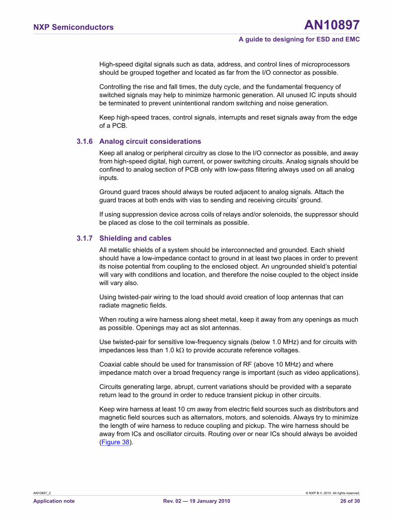
Keep wire harness at least 10 cm away from electric field sources such as distributors and magnetic field sources such as alternators, motors, and solenoids. Always try to minimize the length of wire harness to reduce coupling and pickup. The wire harness should be away from ICs and oscillator circuits. Routing over or near ICs should always be avoided (Figure 38).
AN10897_2 © NXP B.V. 2010. All rights reserved.
Application note Rev. 02 — 19 January 2010 26 of 30
NXP Semiconductors AN10897A guide to designing for ESD and EMC
Critical signals should never be placed on the outside conductors of wire harnesses including shielded ribbon cables.
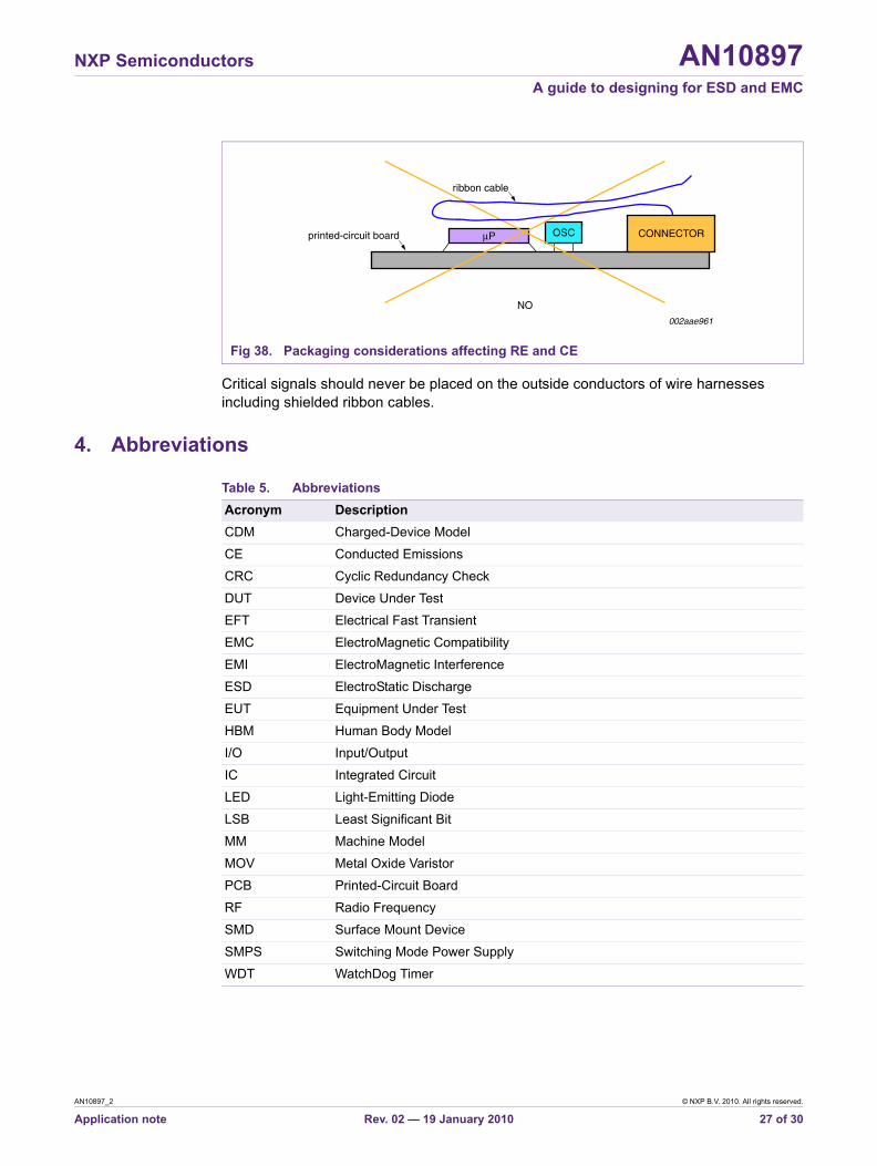
4. Abbreviations
Fig 38. Packaging considerations affecting RE and CE
002aae961
CONNECTOROSCµPprinted-circuit board
ribbon cable
NO
Table 5. AbbreviationsAcronym DescriptionCDM Charged-Device Model
CE Conducted Emissions
CRC Cyclic Redundancy Check
DUT Device Under Test
EFT Electrical Fast Transient
EMC ElectroMagnetic Compatibility
EMI ElectroMagnetic Interference
ESD ElectroStatic Discharge
EUT Equipment Under Test
HBM Human Body Model
I/O Input/Output
IC Integrated Circuit
LED Light-Emitting Diode
LSB Least Significant Bit
MM Machine Model
MOV Metal Oxide Varistor
PCB Printed-Circuit Board
RF Radio Frequency
SMD Surface Mount Device
SMPS Switching Mode Power Supply
WDT WatchDog Timer
AN10897_2 © NXP B.V. 2010. All rights reserved.
Application note Rev. 02 — 19 January 2010 27 of 30
NXP Semiconductors AN10897A guide to designing for ESD and EMC
5. References
[1] Electrostatic Discharge and Electronic Equipment — Warren Boxleinter; 1989; IEEE Press; ISBN 0-87942-244-0.
[2] ESD Immunity in System Designs, System Field Experiences and Effects of PWB Layout — Douglas Smith and Ed Nakauchi; Electrical Overstress/Electrostatic Discharge Symposium Proceedings 2000; IEEE Catalog No. 00TH8476, Ordering No EOS-22.
[3] EMC Design Guide — 2000, Henry W. Ott[4] EMC Design Issues in Appliances — November issue 2006; Conformity;
Ronald Brewer[5] EMC Guide for Printed Circuit Board — 2002; Ford Motor Company;
Document ES-3U5T-1B257-AA[6] The Designer’s Guide to Electromagnetic Compatibility — 2005; Daryl Gerke
and Bill Kimmel; published by Kimmel Gerke Associates, LTD.[7] Chip Monolithic Ceramic Capacitors — September 2009; Murata Manufacturing
Co.; Document Cat.No.C02E-15[8] Designing PCBs for ESD and EMI Compliance — 2009; Airborne Electronics[9] IEEE ‘Design Tips’: Resistive vs. Inductive Return Current Paths — 2008;
Bruce Archambeault, Ph.D., IEEE Fellow.
AN10897_2 © NXP B.V. 2010. All rights reserved.
Application note Rev. 02 — 19 January 2010 28 of 30
NXP Semiconductors AN10897A guide to designing for ESD and EMC
6. Legal information
6.1 DefinitionsDraft — The document is a draft version only. The content is still under internal review and subject to formal approval, which may result in modifications or additions. NXP Semiconductors does not give any representations or warranties as to the accuracy or completeness of information included herein and shall have no liability for the consequences of use of such information.
6.2 DisclaimersGeneral — Information in this document is believed to be accurate and reliable. However, NXP Semiconductors does not give any representations or warranties, expressed or implied, as to the accuracy or completeness of such information and shall have no liability for the consequences of use of such information.
Right to make changes — NXP Semiconductors reserves the right to make changes to information published in this document, including without limitation specifications and product descriptions, at any time and without notice. This document supersedes and replaces all information supplied prior to the publication hereof.
Suitability for use — NXP Semiconductors products are not designed, authorized or warranted to be suitable for use in medical, military, aircraft, space or life support equipment, nor in applications where failure or malfunction of an NXP Semiconductors product can reasonably be expected to result in personal injury, death or severe property or environmental damage. NXP Semiconductors accepts no liability for inclusion and/or use of NXP Semiconductors products in such equipment or applications and therefore such inclusion and/or use is at the customer’s own risk.
Applications — Applications that are described herein for any of these products are for illustrative purposes only. NXP Semiconductors makes no representation or warranty that such applications will be suitable for the specified use without further testing or modification.
Export control — This document as well as the item(s) described herein may be subject to export control regulations. Export might require a prior authorization from national authorities.
6.3 TrademarksNotice: All referenced brands, product names, service names and trademarks are the property of their respective owners.
AN10897_2 © NXP B.V. 2010. All rights reserved.
Application note Rev. 02 — 19 January 2010 29 of 30
NXP Semiconductors AN10897A guide to designing for ESD and EMC
7. Contents
1 Introduction . . . . . . . . . . . . . . . . . . . . . . . . . . . . 32 The basics . . . . . . . . . . . . . . . . . . . . . . . . . . . . . 32.1 The ESD pulse . . . . . . . . . . . . . . . . . . . . . . . . . 32.1.1 Characteristics of the ESD pulse—
the IEC model . . . . . . . . . . . . . . . . . . . . . . . . . . 32.1.2 Putting the ESD problem into perspective . . . . 52.2 Effects and failure modes . . . . . . . . . . . . . . . . . 72.2.1 Sources, paths and receptors. . . . . . . . . . . . . . 72.2.2 Unintentional antennas. . . . . . . . . . . . . . . . . . . 72.3 An overview of R, L, C and D components. . . . 82.3.1 Resistor (R) component characteristics . . . . . . 82.3.2 Inductor (L) component characteristics. . . . . . . 82.3.3 Capacitor (C) component characteristics . . . . . 92.3.4 Diodes (D) . . . . . . . . . . . . . . . . . . . . . . . . . . . 112.3.5 Filters . . . . . . . . . . . . . . . . . . . . . . . . . . . . . . . 112.3.6 Ground . . . . . . . . . . . . . . . . . . . . . . . . . . . . . . 112.4 ESD mitigation . . . . . . . . . . . . . . . . . . . . . . . . 122.4.1 Hardware ESD management strategy . . . . . . 122.4.2 Software ESD management strategy . . . . . . . 122.4.2.1 Refresh . . . . . . . . . . . . . . . . . . . . . . . . . . . . . . 132.4.2.2 Checking and restoring. . . . . . . . . . . . . . . . . . 132.4.2.3 Unused interrupts and registers . . . . . . . . . . . 132.4.2.4 Watchdog timers. . . . . . . . . . . . . . . . . . . . . . . 133 A practical approach to schematic and
PCB design. . . . . . . . . . . . . . . . . . . . . . . . . . . . 143.1 Board structure - functional grouping . . . . . . . 143.1.1 Multi-layer boards recommended
stack-ups . . . . . . . . . . . . . . . . . . . . . . . . . . . . 153.1.1.1 4-layer board stack-up . . . . . . . . . . . . . . . . . . 153.1.1.2 6-layer board stack-up . . . . . . . . . . . . . . . . . . 163.1.2 Ground planes . . . . . . . . . . . . . . . . . . . . . . . . 173.1.3 Ground grids. . . . . . . . . . . . . . . . . . . . . . . . . . 193.1.4 Ground points . . . . . . . . . . . . . . . . . . . . . . . . . 203.1.4.1 Single-point grounding . . . . . . . . . . . . . . . . . . 203.1.4.2 Multi-point grounding . . . . . . . . . . . . . . . . . . . 203.1.4.3 Ground pins and interconnect . . . . . . . . . . . . 213.1.4.4 Metal islands. . . . . . . . . . . . . . . . . . . . . . . . . . 213.1.4.5 Ground plane area . . . . . . . . . . . . . . . . . . . . . 223.1.4.6 Ground star configuration and spark gaps . . . 223.1.4.7 Power distribution . . . . . . . . . . . . . . . . . . . . . . 233.1.4.8 Decoupling capacitors . . . . . . . . . . . . . . . . . . 233.1.4.9 Crosstalk and trace spacing . . . . . . . . . . . . . . 243.1.4.10 Power supply circuit placement . . . . . . . . . . . 243.1.5 Digital circuit considerations . . . . . . . . . . . . . . 253.1.5.1 Oscillators. . . . . . . . . . . . . . . . . . . . . . . . . . . . 253.1.5.2 Digital bus . . . . . . . . . . . . . . . . . . . . . . . . . . . . 253.1.6 Analog circuit considerations . . . . . . . . . . . . . 26
3.1.7 Shielding and cables . . . . . . . . . . . . . . . . . . . 264 Abbreviations . . . . . . . . . . . . . . . . . . . . . . . . . 275 References. . . . . . . . . . . . . . . . . . . . . . . . . . . . 286 Legal information . . . . . . . . . . . . . . . . . . . . . . 296.1 Definitions . . . . . . . . . . . . . . . . . . . . . . . . . . . 296.2 Disclaimers . . . . . . . . . . . . . . . . . . . . . . . . . . 296.3 Trademarks . . . . . . . . . . . . . . . . . . . . . . . . . . 297 Contents. . . . . . . . . . . . . . . . . . . . . . . . . . . . . . 30
© NXP B.V. 2010. All rights reserved.For more information, please visit: http://www.nxp.comFor sales office addresses, please send an email to: [email protected]
Date of release: 19 January 2010Document identifier: AN10897_2
Please be aware that important notices concerning this document and the product(s)described herein, have been included in section ‘Legal information’.


![Protection Device - Farnell · Guidelines for optimized PCB design and assembly process available [2] 1.2 Application Examples[3] • ESD Protection of highly susceptible IC/ASICs](https://img.pdfslide.net/doc/110x75/605b21368b5f143fad3d17b8/protection-device-guidelines-for-optimized-pcb-design-and-assembly-process-available.jpg)


![TVS Diode - Farnell element14 · Guidelines for optimized PCB design and assembly process available [2] 1.2 Application Examples • ESD Protection of highly susceptible IC/ASICs](https://img.pdfslide.net/doc/110x75/605b21368b5f143fad3d17ba/tvs-diode-farnell-guidelines-for-optimized-pcb-design-and-assembly-process-available.jpg)