Embed Size (px)
Citation preview
ANALOG DESIGN FOR MANUFACTURABILITY: LITHOGRAPHY-AWARE
ANALOG LAYOUT RETARGETING
A Dissertation for Doctoral Research
In the
Faculty of Engineering & Applied Science
By
Xuan Dong, BSc, MSc
Submitted to
Supervisory Committee
Dr. Lihong Zhang (Supervisor)
Dr. Dennis Peters
Dr. Howard Heys
Faculty of Engineering & Applied Science
Memorial University of Newfoundland
St. John’s, NL
October 2017
i
Abstract
As transistor sizes shrink over time in the advanced nanometer technologies,
lithography effects have become a dominant contributor of integrated circuit (IC) yield
degradation. Random manufacturing variations, such as photolithographic defect or spot
defect, may cause fatal functional failures, while systematic process variations, such as
dose fluctuation and defocus, can result in wafer pattern distortions and in turn ruin
circuit performance. This dissertation is focused on yield optimization at the circuit
design stage or so-called design for manufacturability (DFM) with respect to analog ICs,
which has not yet been sufficiently addressed by traditional DFM solutions. On top of a
graph-based analog layout retargeting framework, in this dissertation the
photolithographic defects and lithography process variations are alleviated by
geometrical layout manipulation operations including wire widening, wire shifting,
process variation band (PV-band) shifting, and optical proximity correction (OPC). The
ultimate objective of this research is to develop efficient algorithms and methodologies in
order to achieve lithography-robust analog IC layout design without circuit performance
degradation.

ii
TABLE OF CONTENTS
Abstract ................................................................................................................................ i
TABLE OF CONTENTS .................................................................................................... ii
LIST OF FIGURES .............................................................................................................v
LIST OF TABLES ............................................................................................................ vii
Chapter 1 Introduction ....................................................................................................1
Chapter 2 Development and Challenges in Analog DFM ..............................................5
2.1 Recent DFM Optimization Targets in Analog Design Automation .......................... 5
2.1.1 Layout Dependent Effect .................................................................................... 5
2.1.2 Regularity ........................................................................................................... 6
2.1.3 Aging .................................................................................................................. 7
2.1.4 Summary ............................................................................................................. 8
2.2 Lithography Effects and State-of-the-Art Solutions ................................................. 8
2.2.1 Spot Defects ........................................................................................................ 8
2.2.2 Pattern Distortions ............................................................................................ 14
2.2.3 Process Variations ............................................................................................ 19
2.2.4 Summary ........................................................................................................... 21
Chapter 3 Spot-Defect-Aware Analog Layout Retargeting .........................................23
3.1 Analog Layout Retargeting ..................................................................................... 23
3.1.1 Analog Layout Retargeting Flow ..................................................................... 23
3.1.2 Constraint Graphs ............................................................................................. 24
3.1.3 Examples .......................................................................................................... 26
3.1.4 Summary ........................................................................................................... 31
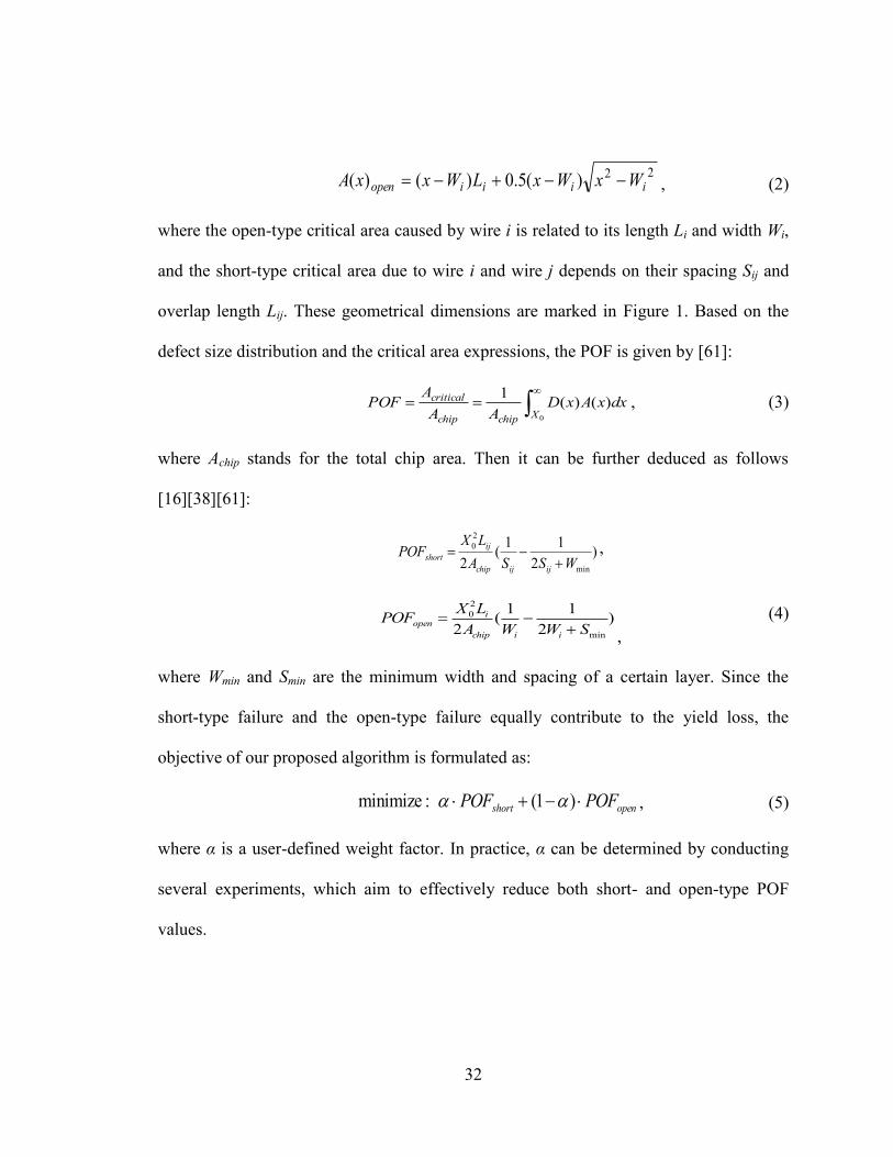
3.2 Lithography-Aware Yield Model for Spot Defects ................................................. 31
3.3 Spot-Defect-Aware Analog Layout Retargeting Flow ............................................ 33
iii
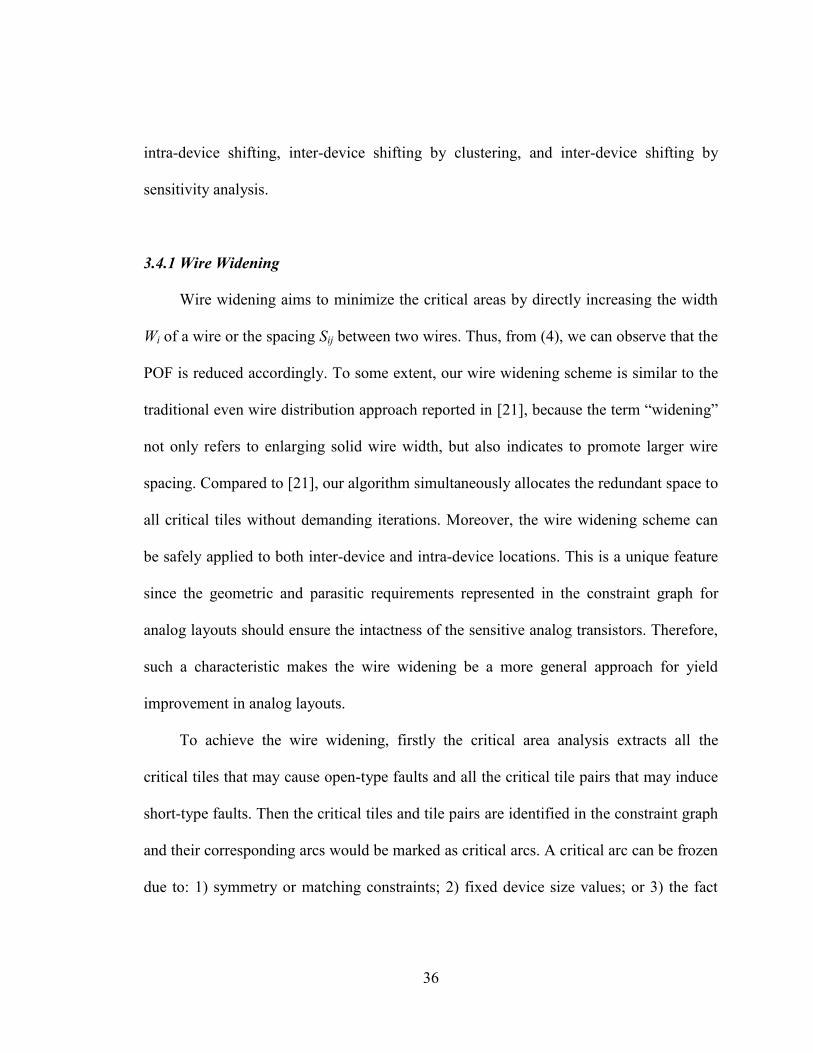
3.4 Optimization Techniques ........................................................................................ 35
3.4.1 Wire Widening ................................................................................................. 36
3.4.2 Intra-Device Wire Shifting ............................................................................... 42
3.4.3 Inter-Device Wire Shifting by Clustering ........................................................ 44
3.4.4 Inter-Device Wire Shifting by Sensitivity Analysis ......................................... 47
3.5 Experimental Results ............................................................................................... 48
3.6 Summary ................................................................................................................. 60
Chapter 4 PV-Aware OPC-Inclusive Analog Layout Retargeting ...............................62
4.1 Wafer Image Quality ............................................................................................... 63
4.1.1 Edge Placement Error ....................................................................................... 63
4.1.2 Mask Complexity ............................................................................................. 63
4.1.3 Modeling of PV-Band Quality ......................................................................... 65
4.1.4 Summary ........................................................................................................... 65
4.2 Optimizations by Wire Widening and Wire Shifting .............................................. 66
4.3 PV-Band Shifting .................................................................................................... 71
4.4 PV-Aware Rule-Based OPC (PVRB-OPC) ............................................................ 73
4.4.1 PVRB-OPC Flow ............................................................................................. 73
4.4.2 RB-OPC Algorithm .......................................................................................... 76
4.4.3 Experimental Results ........................................................................................ 80
4.4.4 Summary ........................................................................................................... 88
4.5 PV-Aware Hybrid OPC (PVH-OPC) ...................................................................... 89
4.5.1 PVH-OPC Flow ................................................................................................ 89
4.5.2 Hybrid OPC Algorithm .................................................................................... 90
4.5.3 Mask Simplification ......................................................................................... 94
4.5.4 Experimental Results ........................................................................................ 98
4.5.5 Summary ......................................................................................................... 101
4.6 Summary ............................................................................................................... 102
Chapter 5 PV-Aware Circuit Sizing Inclusive Analog Layout Retargeting ...............104
5.1 Deterministic Circuit Sizing .................................................................................. 106

iv
5.1.1 Traditional Deterministic Circuit Sizing Flow ............................................... 106
5.1.2 GBC Algorithm .............................................................................................. 108
5.2 PV-Aware Sizing-Inclusive Analog Layout Retargeting Flow ............................. 109
5.3 PV-Aware Circuit Sizing Algorithm ..................................................................... 111
5.3.1 PV Considerations .......................................................................................... 112
5.3.2 Modified GBC Exploration Algorithm........................................................... 113
5.3.3 Terminating Conditions .................................................................................. 118
5.4 Experimental Results ............................................................................................. 119
5.5 Summary ............................................................................................................... 123
Chapter 6 Conclusions ................................................................................................125
Chapter 7 Future Work ...............................................................................................128
Acknowledgments............................................................................................................130
References ........................................................................................................................131
Appendix Published/Prepared Papers .........................................................................138
v
LIST OF FIGURES
Figure 1. The Critical Areas Caused by Short- and Open-Type Spot Defects ................... 9 Figure 2. A Current Mirror Block. (a) Schematic. (b) Layout with Zoom-in Detailed
Printing Images. ................................................................................................................ 14 Figure 3. OPC example. (a) Before OPC. (b) After OPC. ................................................ 15
Figure 4. PV-Band on Polysilicon .................................................................................... 20 Figure 5. Conventional Analog Layout Retargeting Flow................................................ 24 Figure 6. Horizontal Constraint Graph Representation for Analog Layout Retargeting .. 26
Figure 7. Schematic of the Two-Stage Opamp in 0.25um technology ............................. 28 Figure 8. Original Layout of the Two-Stage Opamp in 0.25um technology .................... 28 Figure 9. Targeted Layout of the Two-Stage Opamp in 0.18um technology ................... 29
Figure 10. Schematic of the Cascode Opamp in 0.25um technology ............................... 29 Figure 11. Original Layout of the Cascode Opamp in 0.25um technology ...................... 30 Figure 12. Targeted Layout of the Cascode Opamp in 0.18um technology ..................... 30
Figure 13. Spot-Defect-Aware Analog Layout Retargeting Flow .................................... 33 Figure 14. Litho-Aware Optimization Flow ..................................................................... 34
Figure 15. Constraint Graph with Optimizable Arcs ........................................................ 37 Figure 16. Orthogonal Length in Wire Widening for Open-Type Faults ......................... 40 Figure 17. Critical Areas on a Single-finger Transistor. (a) Before Retargeting. (b) After
Retargeting. ....................................................................................................................... 43 Figure 18. Intra-Device Wire Shifting for a Multi-finger Transistor. (a) Before Shifting.
(b) After Shifting............................................................................................................... 43 Figure 19. Clustering and Sub-Graph. (a) Clustering. (b) Corresponding Graph............. 45
Figure 20. Sensitivity Analysis for Inter-Device Wire Shifting ....................................... 47 Figure 21. Short-Type Critical Areas in the Two-Stage Opamp Layout before
Lithography-Aware Optimization in 0.18um technology ................................................. 56 Figure 22. Short-Type Critical Areas in the Two-Stage Opamp Layout after Lithography-
Aware Optimization in 0.18um technology ...................................................................... 57 Figure 23. EPE Measurement with Gauge Segments ....................................................... 63
Figure 24. OPCed Mask Layout. (a) RB-OPC Result. (b) MB-OPC Result. ................... 64 Figure 25. Geometric Features of X, Y and W in PV-Band Quality Modeling ............... 65 Figure 26. A Large Short-Circuit Hotspot ........................................................................ 67 Figure 27. Hotspot Fragmentation .................................................................................... 68
Figure 28. PV-Band Shifting. (a) Original PV-Band. (b) After PV-Band Shifting with
Zoom-in Detailed PV-Band. ............................................................................................. 72 Figure 29. Proposed Analog Layout Retargeting with PVRB-OPC ................................. 74
Figure 30. Applied Rules in our RB-OPC ........................................................................ 77 Figure 31. The End-of-Line Rule ...................................................................................... 77 Figure 32. A Rule Conflict: (a) Apply Line-in-Parallel Rule, (b) Apply End-of-Line Rule.
........................................................................................................................................... 78
vi
Figure 33. Connection Fixing ........................................................................................... 80 Figure 34. Final Two-Stage Miller-Compensated Opamp Layout with Zoom-in Detailed
PV-Bands, OPCed Patterns and Printing Images ............................................................. 88 Figure 35. Proposed Analog Layout Retargeting Flow with PVH-OPC .......................... 90
Figure 36. Hybrid OPC Example. (a) Original Mask Layout and Wafer Image. (b) After
RB-OPC. (c) Local MB-OPC Region. (d) After Hybrid OPC. ........................................ 92 Figure 37. Mask Layout after OPC Process. (a) Mask Simplification Reported in [76]. (b)
Our Proposed Mask Simplification Method. .................................................................... 95 Figure 38. Boundary Curve Example ............................................................................. 109
Figure 39. Flow of Proposed PV-Aware Sizing-Inclusive Analog Layout Retargeting
with Hybrid OPC ............................................................................................................ 110
Figure 40. Tune λ based on the relative position of xopt and xest. (a) When xopt>xest. (b)
When xopt<xest. (c) When xopt≈xest. (d) Corresponding λ values on the boundary curve.116

vii
LIST OF TABLES
Table 1. Optimization Statistics on Metal-1 Layer ........................................................... 49 Table 2. Lithography-Aware Optimization Results in 0.18um Technology .................... 50 Table 3. Lithography-Aware Optimization Results in 90nm Technology ....................... 51 Table 4. Post-Layout Simulation Results.......................................................................... 59 Table 5. Experimental Results of Alternative OPC Approaches ...................................... 82
Table 6. Post-Layout Simulation Results.......................................................................... 85
Table 7. Monte Carlo Simulations on Opamps ................................................................. 87 Table 8. Experimental Results of Alternative OPC Approaches ...................................... 99
Table 9. Post-Layout Simulation Results........................................................................ 101
Table 10. Experimental Results of Alternative OPC Approaches .................................. 121
1
Chapter 1 Introduction
With the development of Computer-Aided Design (CAD) tools, integrated circuit
(IC) design considering manufacturing issues has been becoming more widely adopted in
modern nanometer CMOS technologies. Especially for analog IC designs, for which
circuit performance is highly sensitive to the physical structures and operating
environment, appropriate design for manufacturing (DFM) strategies can effectively
improve circuit manufacturability and reliability for chip yield enhancement. However,
not all of those issues, such as distinct lithography effects, are thoughtfully considered in
the area of analog DFM from the literature, because the analog layouts normally
constructed with larger geometric dimensions are much sparser compared to the digital
counterpart. As a result, if the digital lithography-aware DFM methods are directly
applied to analog circuits, the solutions are usually too aggressive and over-constrained.
In such a case, the algorithm runtime may unnecessarily increase and analog circuit
performance may even degrade, which actually lowers the overall chip yield.
Lithography is an indispensable IC manufacturing process which transfers patterns
on the mask layout onto the wafer. In modern CMOS technologies, 193nm lithography is
still the mainstream even in sub-45nm IC fabrication. When the technology node is below
100nm, the circuit performance becomes very vulnerable to defects and process
variations (PV) during the lithography process. The main reasons are: 1) the geometric
dimensions in an IC layout are comparable with the defect sizes; 2) layout patterns suffer
from serious distortions that may affect parasitic resistance and capacitance; and 3) a
2
small amount of pattern distortion may introduce a considerable mismatch to the circuit
device pairs that are supposed to be matched.
There is no doubt that analog layouts still inevitably shrink along with the advanced
technologies. It is not hard to see that the lithography-related manufacturability issues
above may occur to the modern analog layouts that are fabricated in the nanometer
technologies. Therefore, analog DFM solutions have to seriously address these problems
by using specific algorithms (i.e., distinct from digital ones), which can not only
preferably utilize the available space in the sparse analog layouts, but also achieve better
analog circuit performance preservation.
The main purpose of this dissertation is to fill the gap that the lithography-aware
DFM solutions for analog IC designs are currently missing. In particular, some
algorithms have been developed for analog IC yield improvement during physical design
with respect to lithography effects including photolithographic defects, pattern distortions
and PV-related mismatch. Naturally, physical design refers to building block placement
and interconnection routing where versatile layout pattern operations can take place to
maximize the chip yield. However, the complete physical design flow itself is a time-
consuming trial-and-error process. Combining it with the yield optimization algorithms
may further lower its efficiency.
Considering that an analog block is actually a fixed structure comprised of
intellectual property (IP), an IP retargeting platform, which is able to migrate an existing
layout into a new one with a different fabrication process or a new set of performance
3
specifications, seems to be a suitable option for adopting the DFM algorithms. The layout
retargeting scheme uses a layout template, which can: 1) preserve any intelligence from
the original layout, such as device matching, symmetry and circuit topology; 2) easily
adopt various layout pattern operations with expected optimization targets; and 3) quickly
create a target layout without any design rule violations. On top of the layout retargeting
platform, the newly developed DFM algorithms can be efficiently combined without
compromising the circuit performance but enhancing the chip yield.
Additionally, the layout retargeting scheme accepts a set of device sizes as input in
order to properly resize the target layout according to the target fabrication technology.
Therefore, if a DFM-related circuit sizing algorithm is integrated in the platform and the
retargeting operation is performed in an iterative manner, a versatile DFM-aware analog
layout synthesis methodology can be constructed and the chip yield enhancement would
be significant because a set of optimized device sizes can fundamentally enhance the
circuit robustness.
In this dissertation, an analog layout retargeting platform is arranged to embed the
proposed lithography-aware DFM strategies. The dissertation is organized as follows.
Chapter 2 describes the current development and challenges related to analog DFM.
Chapters 3 and 4 present the spot-defect-aware analog layout retargeting and the PV-
aware analog layout retargeting methodologies, respectively. Chapter 5 illustrates a
deterministic circuit sizing inclusive analog layout retargeting methodology, which is

4
also focused on lithography effects induced by pattern distortions and PV issues. Chapter
6 concludes this dissertation and Chapter 7 discusses the future work.
5
Chapter 2 Development and Challenges in Analog DFM
In advanced nanometer technology era, analog IC design is still a time-consuming
and error-prone process, mainly due to the sensitive analog circuit performance that can
be readily affected by various physical effects during chip fabrication. As a result, analog
IC designs and the related DFM process highly depend upon the analog CAD tools. In the
past, some experienced analog IC designers tended to believe that the analog CAD tools
can never be well-developed as its digital counterpart, because certain manual work with
human intuitions and aesthetics are always required in order to achieve high-quality
performance for the analog circuits. Nevertheless, an increasing number of analog CAD
solutions for DFM, which are mainly focused on circuit performance preservation in
order to improve the chip yield, have been proposed in the recent years. In this chapter,
the recent DFM optimization targets in analog design automation are firstly reviewed in
Section 2.1. Afterwards, three key lithography effects are introduced in Section 2.2,
where their negative impacts on modern analog IC designs and the corresponding
solutions to digital DFM are discussed.
2.1 Recent DFM Optimization Targets in Analog Design Automation
2.1.1 Layout Dependent Effect
Analog circuit performance degradations caused by layout dependent effects
(LDEs) have been widely observed in the literature [1][2][3][4]. LDEs refer to a series of
physical effects on transistors, such as well proximity effect (WPE) and length of
6
diffusion (LOD), which can result in deviations on both threshold voltage and electron
mobility. On the one hand, LDEs may significantly affect circuit performance even in the
old technology nodes. By using the operational amplifiers in [1][2] as an example, the
voltage gain improvements after LDE-aware optimizations are from 40.20dB to 46.25dB
in 90nm CMOS technology [1] and from 49.79dB to 50.40dB in 65nm [2] CMOS
technology, respectively. According to [2], more LDE sources are identified as critical
issues in the technologies advancing to 40nm and beyond. On the other hand, LDEs
should be carefully handled not only in physical design, but also in circuit sizing
algorithms in order to mitigate LDEs with optimal device dimensions and finger
numbers. Consequently, LDE-aware analog DFM schemes are extensively adopted in
transistor modeling [3], analog circuit sizing [4] and analog physical design [1].
2.1.2 Regularity
To improve the layout regularity, devices with similar aspect ratios are placed close
by in the floorplan. As a result, the layout after placement presents better routability and
manufacturability, less sensitivity to process variations and even smaller overall chip
areas [5]. For symmetry and matching current paths in an analog circuit, better
arrangement of positions and orientations of related devices can also enhance the circuit
performance [6]. In addition, if two transistors with the same type and aspect ratios are
placed adjacently, their active regions or well regions might be merged as a single
pattern. In that case, the related LDEs can also be alleviated to benefit the circuit
7
performance preservation. As [5] and [6] presents, regularity inclusive analog DFM
strategies are especially suitable for analog building block placement.
2.1.3 Aging
Beside chip manufacturability, circuit reliability problems caused by aging effects
are also a major contributor to analog circuit yield degradation. When a circuit works
over time, the electrical characteristics of transistors and interconnect wires may change
due to a series of physical effects caused by the charge carriers, such as hot-carrier
injection (HCI), negative bias temperature instability (NBTI) and electromigration (EM).
With respect to HCI and NBTI, an aging model is usually applied to estimate the
variations on threshold voltages of transistors, and to identify variation-sensitive circuit
components [7][8]. Those sensitive devices are then resized by using circuit sizing
algorithms so that the circuit lifetime can be effectively extended. EM is closely related
to interconnect wires with high current density, where the interconnect material may
move to cause fatal functional failures. It is very likely that starting from a certain degree
of EM, the circuit performance is going to degrade due to its impact on interconnect
resistance. Therefore, an EM-aware analog DFM process is usually combined with
interconnect routing algorithms [9], which can alleviate the EM effect by determining
preferred interconnect wire widths.
8
2.1.4 Summary
In this sub-section, several DFM optimization targets for analog design automation,
which are closely related to IC chip manufacturability and circuit reliability, have been
reviewed. All of those DFM targets and the corresponding optimization algorithms are
well studied because their negative impacts on analog circuit performance are obvious
and significant even in the old CMOS technologies. However, none of the existing
research is able to clearly present any lithography-related performance degradation of
analog ICs, which is increasingly important in the advanced nanometer technologies.
Therefore, several lithography effects and the way how they may degrade analog circuit
performance are explained in the next sub-section in detail.
2.2 Lithography Effects and State-of-the-Art Solutions
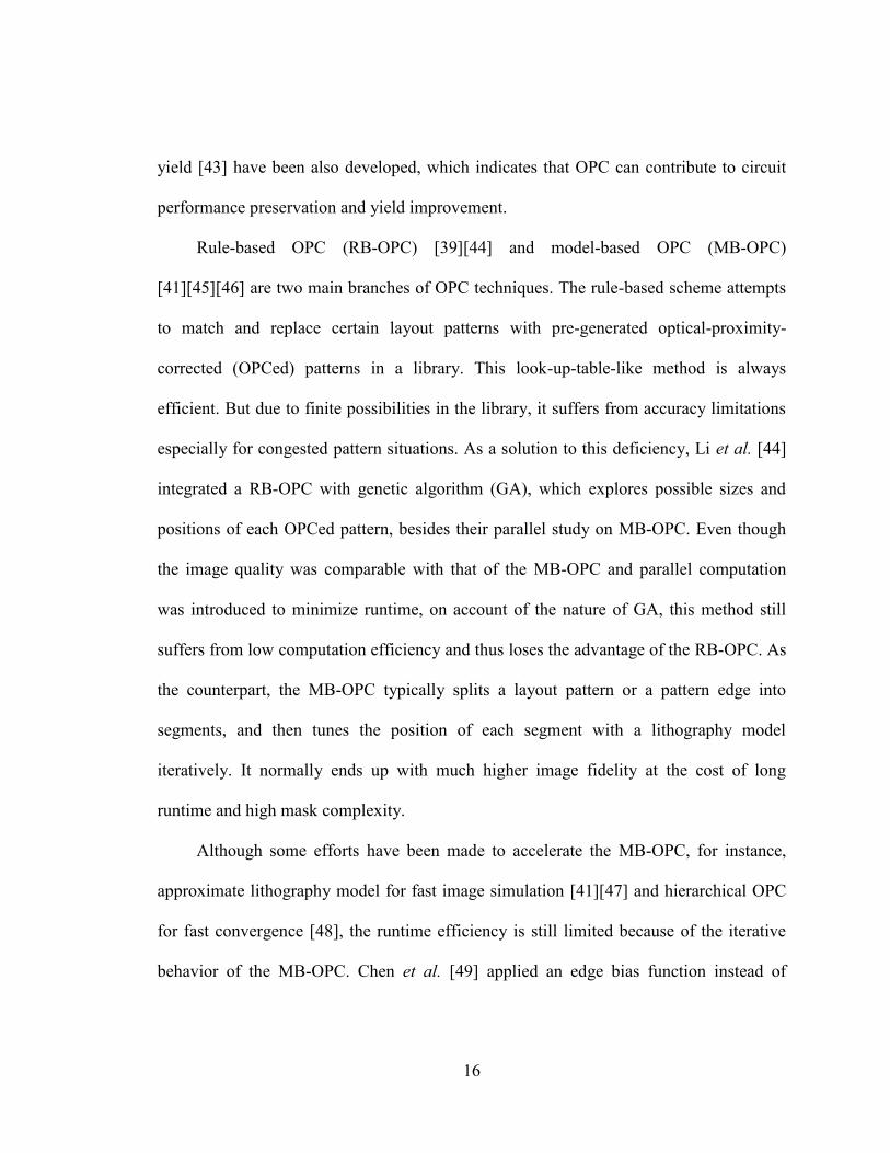
2.2.1 Spot Defects
The concept of spot defects was firstly introduced as a yield concern of IC in the
late 1960s at IBM Research Centre. From the 1970s, more attention has been paid, and
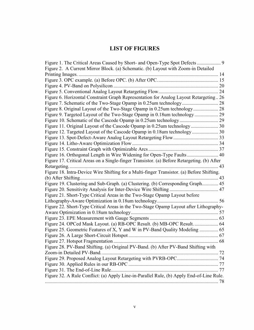
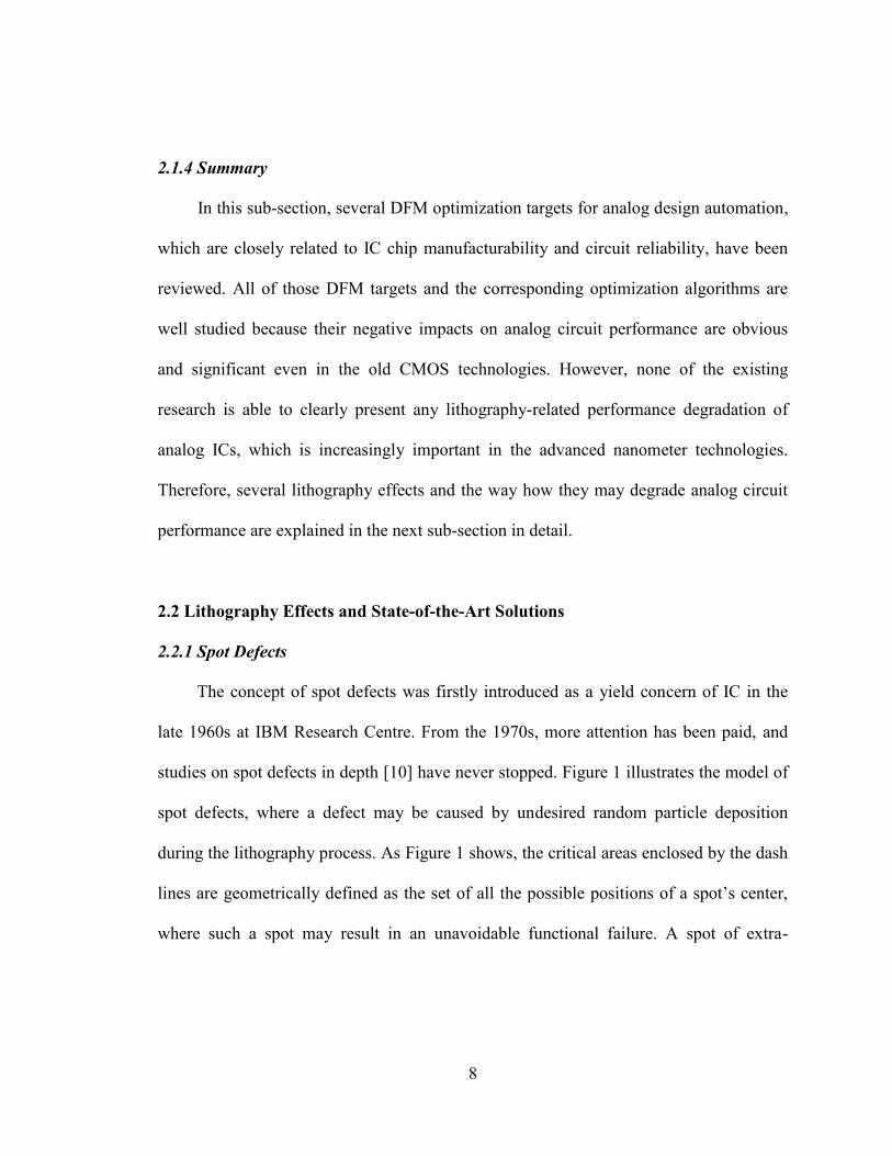
studies on spot defects in depth [10] have never stopped. Figure 1 illustrates the model of
spot defects, where a defect may be caused by undesired random particle deposition
during the lithography process. As Figure 1 shows, the critical areas enclosed by the dash
lines are geometrically defined as the set of all the possible positions of a spot’s center,
where such a spot may result in an unavoidable functional failure. A spot of extra-
9
material may bridge unconnected wires as a short-circuit failure, while a spot of missing-
material may obstruct a wire as an open-circuit failure.
Figure 1. The Critical Areas Caused by Short- and Open-Type Spot Defects
Based on the developed spot defect models, researchers have tried to come up with
defect tolerance algorithms and related CAD tools. These algorithms can be categorized
into routing [11][12][13][14][15][16][17] or post-routing [18][19] optimizations, and
yield-aware layout compaction [20][21][22][23].
Early routing approaches can be found in [11][12], which aimed to minimize the
critical areas by ordering the interconnects. The drawback of these methods is that the
defect size distribution is not considered and thus an incomplete defect model with only
single defect size has to be applied. Subsequently, various yield enhancement routing
schemes, such as detailed routing [13], global routing [14], or their combination [15],
appeared. However, the detailed routing normally has less flexibility that might limit its
10
capability in yield improvement, while the global routing cannot precisely calculate the
critical areas and thus is hard to obtain the optimal solution.
Afterwards track routing, an intermediate step between the detailed routing and
global routing, was proposed in [16]. It overcomes the previous problems and aims to
reduce probability of failure (POF) with a relative low time complexity. Nevertheless,
this routing approach is only focused on interconnects, while the yield loss introduced by
transistors is ignored. Another technique by using intra-cell routing can be found in [17],
where a grid-based router explores yield-improved patterns inside a standard-cell.
Although the intra-cell wiring faults due to spot defects are reduced, only the short-type
failures are considered in that work, similar to the previous ones [11][12][13]. On the
other side, compared to the routing methods above, the post-routing defect optimizations
are not that popular, since any unthoughtful post-processing operation for a layout [18] in
a mask data representation (e.g., GDSII or CIF) may cause unexpected overall critical
area increment [19].
The yield-aware layout compaction approaches attempt to include yield rules in the
layout synthesis. Allen et al. [20] introduced local design rules for layout manipulation,
which is effective for critical area minimization. But this method is not general to be
easily integrated into a regular defect tolerance tool. Chiluvuri and Koren [21] proposed a
more general compaction scheme to reduce circuit sensitivity of spot defects. The wires
not on the critical path are shifted to evenly arrange the wire spacing. In addition, this
method can also take open-type failures into account by allowing wire width
11
modification. Although an overall yield improvement can be achieved by this work,
several iterations are always required in order to better spread the wires, which might
limit the potency of the algorithm.
Bamji and Malavasi [22] adopted spot defect optimization in a graph-based
compaction. The total wire length is minimized together with the yield maximization by
using a longest-path algorithm followed by an enhanced network flow algorithm. While
the graph is a useful method for layout compaction, the network flow algorithm
complicates the graph structure and the graph in that work can only solve short-type yield
problems. Bourai and Shi [23] demonstrated a linear programming (LP) based
compaction flow to tackle the yield concerns. A series of geometric constraints are
induced in a second phase of the LP model and the critical area is minimized during the
layout compaction. However, the efficiency of the algorithm is limited by the LP method
itself. By using the extra yield constraints, the chip area increment tends to become
uncontrollable.
Unfortunately, all of the reviewed works above are related to digital IC and very
few works are dedicated to improving yield in analog layouts. Some circuit performance
modeling methods have been reported in [24][25] to deal with yield problems. As the
spot defects are handled in an early design stage, the layout effects cannot be involved.
Chien et al. [26] proposed lithography-aware placement for analog layout design. But
only a double-patterning-aware approach was actually discussed in that work.
Khademsameni and Syrzycki [27] proposed a method of generating multiple layout
12
topologies in order to find the best yield structure. In such a scenario, each layout with
different topology has to be verified cautiously. Obviously this is a time-consuming
process, and it is generally difficult to ensure the yield of the selected layout topology is
optimal.
Valuable efforts have been made recently on automated analog layout retargeting
and layout generation, where appropriate yield optimizations might be readily adopted.
Weng et al. [28] applied a slicing-tree representation in a template-based method to
achieve placement with multiple topologies for analog layouts. Chin et al. [29] further
extended this work by applying a scheme with the feature of template-based routing
preservation. Although these proposed prototyping approaches provide an opportunity to
explore layouts with different topologies, they tend to suffer from large deviation of
layouts, which imposes difficulty in ensuring optimal performance. Martins et al. [30]
introduced evolutionary algorithm into layout retargeting, which is a combination of
template-based and optimization-based approaches. Due to a large number of shapes in
the layout during evolution, the computational efficiency of this method is restricted. Not
limited to the traditional electronic design automation (EDA) schemes in analog layout
retargeting, some advanced design or automation techniques, such as sizing by gm/id [31]
and geometric programming [32], have been also deployed.
Zhang and Liu [33] proposed a symbolic-template-based analog layout retargeting
method for analog IP reuse. This method can facilitate advanced analog layout design or
reuse with the aid of a layout retargeting process. Unfortunately, none of the works above
13
attempt to address any yield problems in the analog layout retargeting process. As a
matter of fact, considering the era of advanced technologies, efficient and powerful
analog layout retargeting for IP reuse can become beneficial and acceptable by the analog
designers only if the yield of the chip is seriously considered.
Bearing such a motivation in mind, on the one hand, we realize that spot defects are
super critical per se for analog layouts. This has been discussed by a recently published
work about defect diagnosis [34], which shows the spot defects still frequently affect the
circuit function or performance in the state-of-the-art technologies. Once such a defect
occurs, it would be an intractable task to locate it in the product test. On the other hand,
we recognize that some models originally derived from digital IC perspective are still
available to be utilized for analog layouts. One example can be found in [35], which
presents yield improvement in analog layout by using defect distribution function
originally derived from [36], critical area analysis and yield loss function originally
derived from [37]. A more popular model for the yield loss function is the one with faults
probability analysis (e.g., POF in [38]), where the total chip area is considered.
Consequently, one aspect of this dissertation is to investigate the possibility of using
yield-aware algorithms or models (originally derived for digital IC) in the context of
analog layout retargeting, with respect to spot defect alleviation. The detailed spot-defect-
aware analog layout retargeting methodology will be explained in Chapter 3.
14
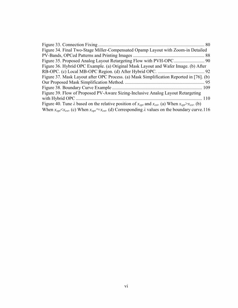
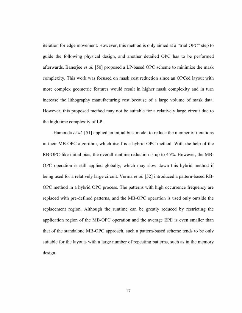
2.2.2 Pattern Distortions
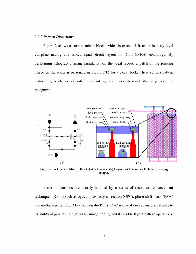
Figure 2 shows a current mirror block, which is extracted from an industry-level
complete analog and mixed-signal circuit layout in 45nm CMOS technology. By
performing lithography image simulation on the ideal layout, a patch of the printing
image on the wafer is presented in Figure 2(b) for a closer look, where serious pattern
distortions, such as end-of-line shrinking and isolated-island shrinking, can be
recognized.
Figure 2. A Current Mirror Block. (a) Schematic. (b) Layout with Zoom-in Detailed Printing
Images.
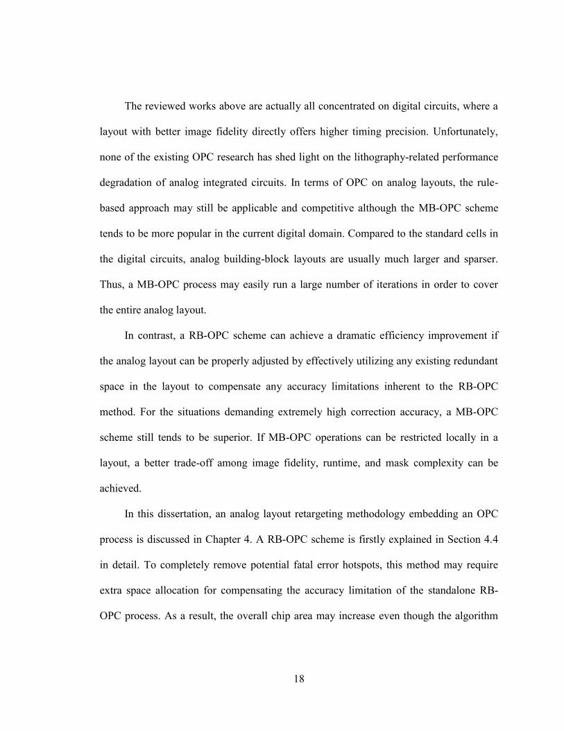
Pattern distortions are usually handled by a series of resolution enhancement
techniques (RETs) such as optical proximity correction (OPC), phase shift mask (PSM)
and multiple patterning (MP). Among the RETs, OPC is one of the key enablers thanks to
its ability of generating high wafer image fidelity and its visible layout pattern operations,
15
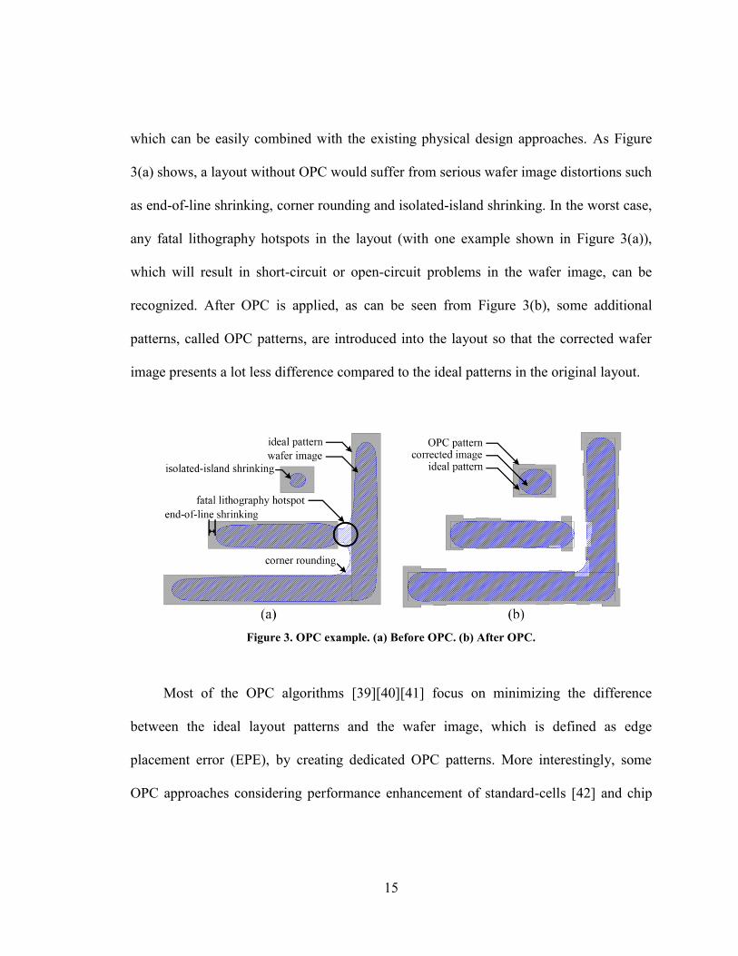
which can be easily combined with the existing physical design approaches. As Figure
3(a) shows, a layout without OPC would suffer from serious wafer image distortions such
as end-of-line shrinking, corner rounding and isolated-island shrinking. In the worst case,
any fatal lithography hotspots in the layout (with one example shown in Figure 3(a)),
which will result in short-circuit or open-circuit problems in the wafer image, can be
recognized. After OPC is applied, as can be seen from Figure 3(b), some additional
patterns, called OPC patterns, are introduced into the layout so that the corrected wafer
image presents a lot less difference compared to the ideal patterns in the original layout.
Figure 3. OPC example. (a) Before OPC. (b) After OPC.
Most of the OPC algorithms [39][40][41] focus on minimizing the difference
between the ideal layout patterns and the wafer image, which is defined as edge
placement error (EPE), by creating dedicated OPC patterns. More interestingly, some
OPC approaches considering performance enhancement of standard-cells [42] and chip
16
yield [43] have been also developed, which indicates that OPC can contribute to circuit
performance preservation and yield improvement.
Rule-based OPC (RB-OPC) [39][44] and model-based OPC (MB-OPC)
[41][45][46] are two main branches of OPC techniques. The rule-based scheme attempts
to match and replace certain layout patterns with pre-generated optical-proximity-
corrected (OPCed) patterns in a library. This look-up-table-like method is always
efficient. But due to finite possibilities in the library, it suffers from accuracy limitations
especially for congested pattern situations. As a solution to this deficiency, Li et al. [44]
integrated a RB-OPC with genetic algorithm (GA), which explores possible sizes and
positions of each OPCed pattern, besides their parallel study on MB-OPC. Even though
the image quality was comparable with that of the MB-OPC and parallel computation
was introduced to minimize runtime, on account of the nature of GA, this method still
suffers from low computation efficiency and thus loses the advantage of the RB-OPC. As
the counterpart, the MB-OPC typically splits a layout pattern or a pattern edge into
segments, and then tunes the position of each segment with a lithography model
iteratively. It normally ends up with much higher image fidelity at the cost of long
runtime and high mask complexity.
Although some efforts have been made to accelerate the MB-OPC, for instance,
approximate lithography model for fast image simulation [41][47] and hierarchical OPC
for fast convergence [48], the runtime efficiency is still limited because of the iterative
behavior of the MB-OPC. Chen et al. [49] applied an edge bias function instead of
17
iteration for edge movement. However, this method is only aimed at a “trial OPC” step to
guide the following physical design, and another detailed OPC has to be performed
afterwards. Banerjee et al. [50] proposed a LP-based OPC scheme to minimize the mask
complexity. This work was focused on mask cost reduction since an OPCed layout with
more complex geometric features would result in higher mask complexity and in turn
increase the lithography manufacturing cost because of a large volume of mask data.
However, this proposed method may not be suitable for a relatively large circuit due to
the high time complexity of LP.
Hamouda et al. [51] applied an initial bias model to reduce the number of iterations
in their MB-OPC algorithm, which itself is a hybrid OPC method. With the help of the
RB-OPC-like initial bias, the overall runtime reduction is up to 45%. However, the MB-
OPC operation is still applied globally, which may slow down this hybrid method if
being used for a relatively large circuit. Verma et al. [52] introduced a pattern-based RB-
OPC method in a hybrid OPC process. The patterns with high occurrence frequency are
replaced with pre-defined patterns, and the MB-OPC operation is used only outside the
replacement region. Although the runtime can be greatly reduced by restricting the
application region of the MB-OPC operation and the average EPE is even smaller than
that of the standalone MB-OPC approach, such a pattern-based scheme tends to be only
suitable for the layouts with a large number of repeating patterns, such as in the memory
design.
18
The reviewed works above are actually all concentrated on digital circuits, where a
layout with better image fidelity directly offers higher timing precision. Unfortunately,
none of the existing OPC research has shed light on the lithography-related performance
degradation of analog integrated circuits. In terms of OPC on analog layouts, the rule-
based approach may still be applicable and competitive although the MB-OPC scheme
tends to be more popular in the current digital domain. Compared to the standard cells in
the digital circuits, analog building-block layouts are usually much larger and sparser.
Thus, a MB-OPC process may easily run a large number of iterations in order to cover
the entire analog layout.
In contrast, a RB-OPC scheme can achieve a dramatic efficiency improvement if
the analog layout can be properly adjusted by effectively utilizing any existing redundant
space in the layout to compensate any accuracy limitations inherent to the RB-OPC
method. For the situations demanding extremely high correction accuracy, a MB-OPC
scheme still tends to be superior. If MB-OPC operations can be restricted locally in a
layout, a better trade-off among image fidelity, runtime, and mask complexity can be
achieved.
In this dissertation, an analog layout retargeting methodology embedding an OPC
process is discussed in Chapter 4. A RB-OPC scheme is firstly explained in Section 4.4
in detail. To completely remove potential fatal error hotspots, this method may require
extra space allocation for compensating the accuracy limitation of the standalone RB-
OPC process. As a result, the overall chip area may increase even though the algorithm
19
efficiency is superior. Alternatively, Section 4.5 presents a hybrid OPC scheme where a
high accuracy MB-OPC operation is performed locally after a global RB-OPC process.
Thanks to the applied MB-OPC process, no chip area increment will occur for this
method and a decent tradeoff can be achieved between algorithmic runtime and wafer
image quality.
2.2.3 Process Variations
Under different lithography process variation conditions due to light dosage and
focus deviation, the possible range of the wafer image is defined as process-variation-
band (PV-band). Figure 4 illustrates the PV simulation results on polysilicon layer of the
current mirror block in Figure 2. In the 45nm or below CMOS technology, the width of
the PV-band (i.e., the difference between the outer contour and the inner contour) may be
over 8nm with 100nm gate length when a dose range of ±2% and a defocus range of
±25nm are applied. In the worst case, such distortions may result in about 8.5% current
mismatch which would be a disaster if the current mirror is used as bias current or load in
a sensitive analog circuit.
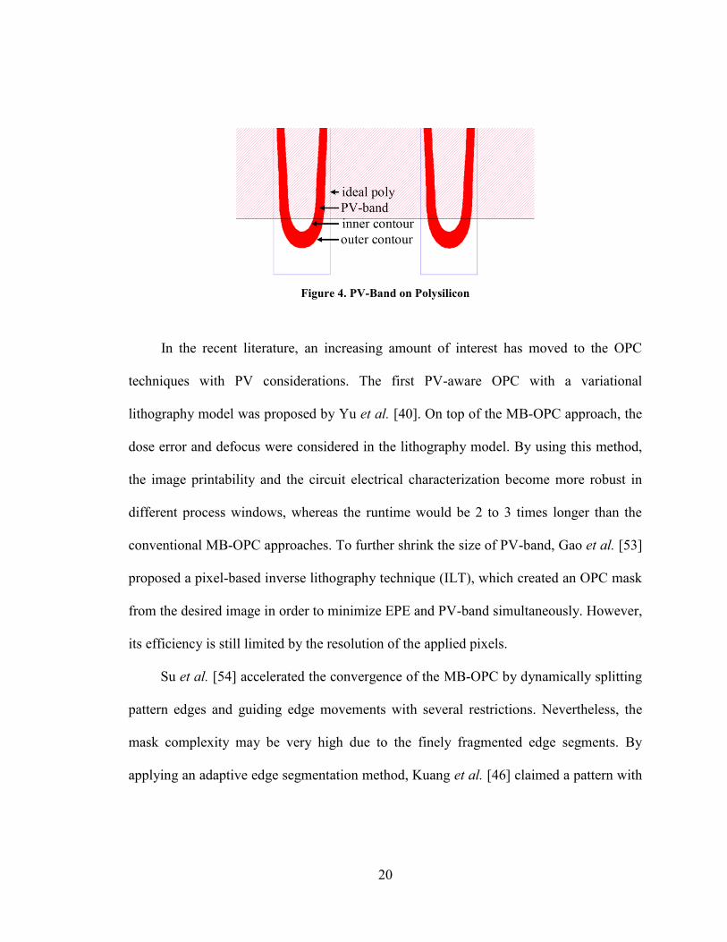
20
Figure 4. PV-Band on Polysilicon
In the recent literature, an increasing amount of interest has moved to the OPC
techniques with PV considerations. The first PV-aware OPC with a variational
lithography model was proposed by Yu et al. [40]. On top of the MB-OPC approach, the
dose error and defocus were considered in the lithography model. By using this method,
the image printability and the circuit electrical characterization become more robust in
different process windows, whereas the runtime would be 2 to 3 times longer than the
conventional MB-OPC approaches. To further shrink the size of PV-band, Gao et al. [53]
proposed a pixel-based inverse lithography technique (ILT), which created an OPC mask
from the desired image in order to minimize EPE and PV-band simultaneously. However,
its efficiency is still limited by the resolution of the applied pixels.
Su et al. [54] accelerated the convergence of the MB-OPC by dynamically splitting
pattern edges and guiding edge movements with several restrictions. Nevertheless, the
mask complexity may be very high due to the finely fragmented edge segments. By
applying an adaptive edge segmentation method, Kuang et al. [46] claimed a pattern with
21
more regular fragments (i.e., less number of edge segments or segments with larger
length) would have smaller PV-band area. Although the mask complexity can be
controlled with this scheme, it may restrict the solution space and in turn weaken the
image fidelity of the MB-OPC approach.
As discussed above, the conventional PV-aware OPC schemes attempt to shrink the
PV-band area, which would inevitably introduce higher mask complexity or very long
algorithmic runtime. Considering the PV-induced mismatch on transistors and the RB-
OPC process we applied, the PV considerations can be easily combined with the RB-
OPC operations without sophisticated lithography models and time-consuming iterations.
Therefore, in this dissertation, a dedicated PV-band operation in the context of analog
layout retargeting is integrated into the OPC algorithms, which will be explained in
Section 4.3 in detail. Its purpose is to preserve the analog circuit performance by using
specific rules, in order to alleviate the PV-introduced mismatch effects. By combining
with different OPC schemes, the complete optimization methods for pattern distortions
and PV-induced mismatch effects are thereafter called PV-aware rule-based OPC
(PVRB-OPC) in Section 4.4 and PV-aware hybrid OPC (PVH-OPC) in Section 4.5,
respectively.
2.2.4 Summary
It has been observed in this section that the lithography effects, such as spot defects,
pattern distortions and process variations, can readily cause analog circuit performance
22
deviation or even fatal functional failures. Although there are existing digital solutions
for alleviating lithography effects, they may unnecessarily cause algorithmic runtime
increment and performance degradation with respect to analog circuits. Dedicated
lithography-aware analog DFM solutions in the context of analog layout retargeting will
be explained in detail in the following chapters. Chapter 3 presents the spot defect
optimizations by using a series of layout pattern operations. Chapter 4 is focused on
pattern distortion and PV optimizations by using two different OPC schemes and a
special handling on PV-band. Chapter 5 further introduces a deterministic circuit sizing
algorithm in the layout retargeting platform to construct a versatile DFM-aware analog
layout synthesis methodology.
23
Chapter 3 Spot-Defect-Aware Analog Layout Retargeting
In this chapter, the analog DFM methodology for lithography-induced spot defect
optimization [55][56][57][58] is presented. Since all of our proposed DFM strategies are
implemented on top of the analog layout retargeting platform, the retargeting process for
DFM is firstly explained in Section 3.1. Throughout this dissertation, the layout pattern
operations, as well as some strategies used for OPC accuracy enhancement and circuit
sizing process, are achieved on the constraint graph. Afterwards, the spot defects are
modeled in Section 3.2 by using a defect size distribution function, geometrical critical
area analysis, and POF. Section 3.3 describes the proposed complete optimization flow.
The optimization techniques, including wire widening and wire shifting, are explained in
Sections 3.4. Section 3.5 reports the experimental results on the spot-defect-aware analog
layout retargeting methodology and Section 3.6 summarizes this chapter.
3.1 Analog Layout Retargeting
3.1.1 Analog Layout Retargeting Flow
Generally layout retargeting is to achieve a layout representation with high
operability in order to speed up the IP reuse process. Graph, which for example is used by
the layout compaction approach in [22], is such a powerful means that can hold the
original layout knowledge and meanwhile may accommodate new geometric
requirements or considerations. These new constraints in analog layout retargeting not
only include the regular design rules in the target technology, but also contain the strict
24
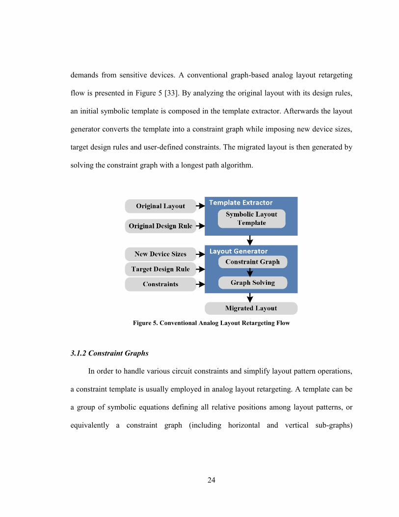
demands from sensitive devices. A conventional graph-based analog layout retargeting
flow is presented in Figure 5 [33]. By analyzing the original layout with its design rules,
an initial symbolic template is composed in the template extractor. Afterwards the layout
generator converts the template into a constraint graph while imposing new device sizes,
target design rules and user-defined constraints. The migrated layout is then generated by
solving the constraint graph with a longest path algorithm.
Figure 5. Conventional Analog Layout Retargeting Flow
3.1.2 Constraint Graphs
In order to handle various circuit constraints and simplify layout pattern operations,
a constraint template is usually employed in analog layout retargeting. A template can be
a group of symbolic equations defining all relative positions among layout patterns, or
equivalently a constraint graph (including horizontal and vertical sub-graphs)
25
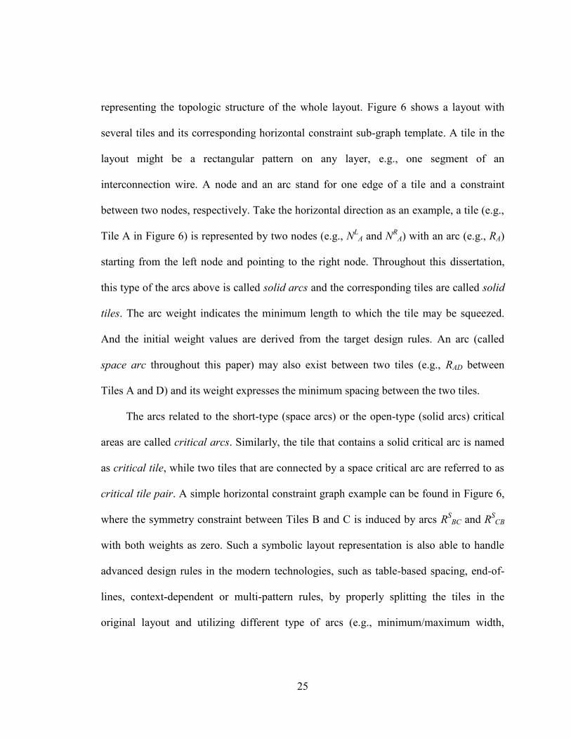
representing the topologic structure of the whole layout. Figure 6 shows a layout with
several tiles and its corresponding horizontal constraint sub-graph template. A tile in the
layout might be a rectangular pattern on any layer, e.g., one segment of an
interconnection wire. A node and an arc stand for one edge of a tile and a constraint
between two nodes, respectively. Take the horizontal direction as an example, a tile (e.g.,
Tile A in Figure 6) is represented by two nodes (e.g., NL
A and NR
A) with an arc (e.g., RA)
starting from the left node and pointing to the right node. Throughout this dissertation,
this type of the arcs above is called solid arcs and the corresponding tiles are called solid
tiles. The arc weight indicates the minimum length to which the tile may be squeezed.
And the initial weight values are derived from the target design rules. An arc (called
space arc throughout this paper) may also exist between two tiles (e.g., RAD between
Tiles A and D) and its weight expresses the minimum spacing between the two tiles.
The arcs related to the short-type (space arcs) or the open-type (solid arcs) critical
areas are called critical arcs. Similarly, the tile that contains a solid critical arc is named
as critical tile, while two tiles that are connected by a space critical arc are referred to as
critical tile pair. A simple horizontal constraint graph example can be found in Figure 6,
where the symmetry constraint between Tiles B and C is induced by arcs RS
BC and RSCB
with both weights as zero. Such a symbolic layout representation is also able to handle
advanced design rules in the modern technologies, such as table-based spacing, end-of-
lines, context-dependent or multi-pattern rules, by properly splitting the tiles in the
original layout and utilizing different type of arcs (e.g., minimum/maximum width,
26
overlap/extension length, or specialized distance arcs) among the nodes in the constraint
graph. In principle there should be no conflicting constraints allowed in the constraint
graph. Although a set of updated constraints may cause chip area increment of the layout,
no constraint violation should appear. If any conflicts occur due to user-specified
constraints, the longest-path algorithm would exit and present a warning message, which
should be perused and fixed by the user.
Figure 6. Horizontal Constraint Graph Representation for Analog Layout
Retargeting
3.1.3 Examples
Throughout this dissertation, one two-stage Miller-compensated operational
amplifier (opamp) and another single-end folded cascode opamp are utilized as example
test circuits to evaluate the developed algorithms. The rationale of such a choice includes
the following considerations:1) opamps are the most widely used building blocks in any
analog processing IC designs; 2) an opamp always includes some sensitive analog
building blocks (e.g., differential pair and current mirror) that require stringent analog
27
constraints. Therefore, an opamp is a good example to demonstrate the effectiveness of
an analog circuit optimization algorithm with respect to analog circuit performance; and
3) the layouts of the selected opamps are so general that most analog layout structures,
such as multi-finger transistors, passive devices, common-centroid structure and
symmetry device placement, can be found. If the proposed algorithms present positive
optimization results on the selected opamps, similar results should be expected from the
other analog circuits which can even be larger than an opamp. Consequently, these two
opamps are used as benchmark circuits throughout this dissertation to evaluate the
proposed methodologies. It is expected that the same conclusions hold if the proposed
methodologies are applied to any other analog circuits.
An opamp aims to achieve voltage amplification with a differential input and,
mostly, a single-ended output. In Figure 7 and Figure 10, the schematics of the two
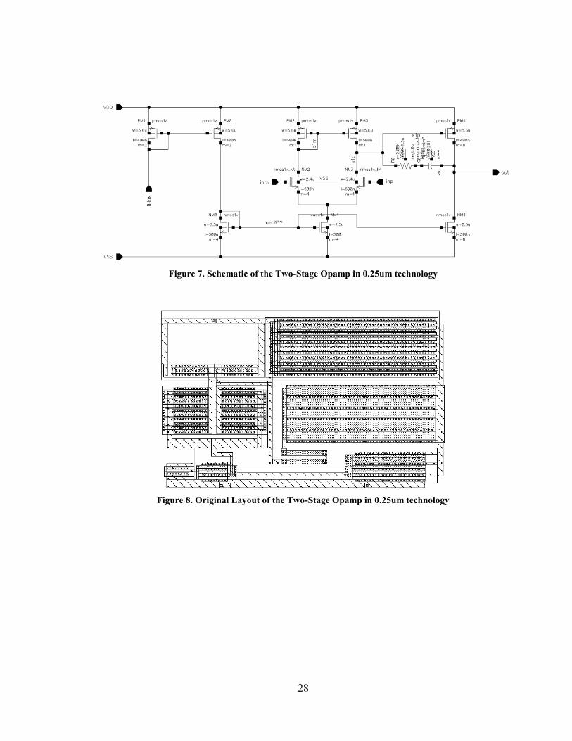
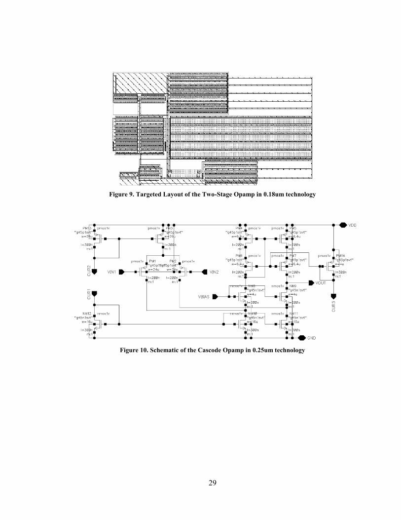
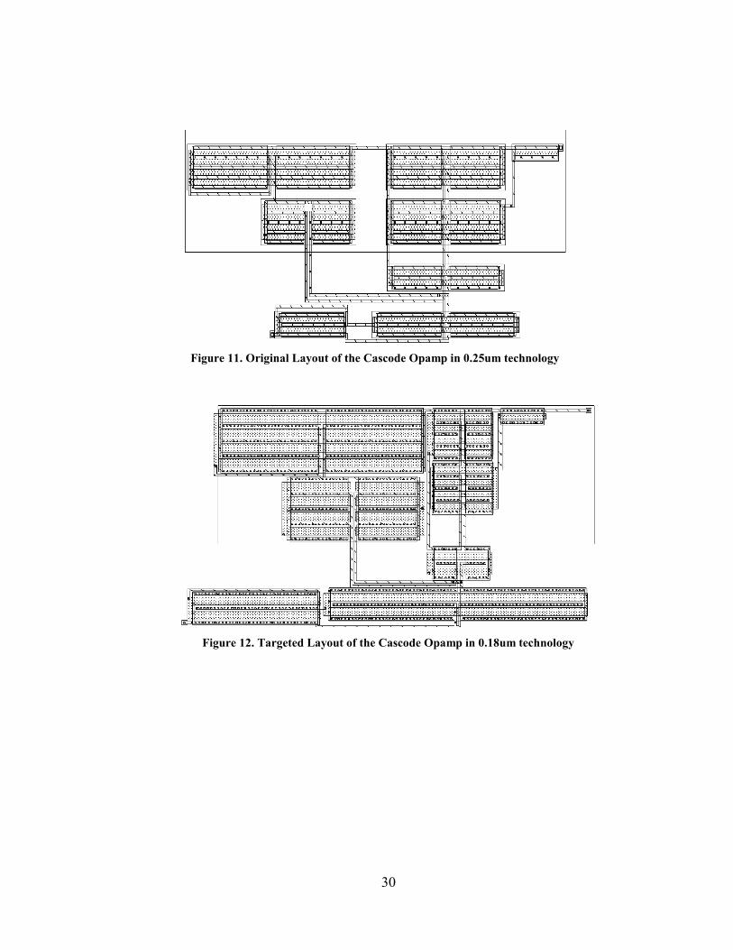
example test circuits in CMOS 0.25um technology are depicted. And their layouts in
CMOS 0.25um technology are shown in Figure 8 and Figure 11, respectively. By
performing a CMOS 0.25um-to-CMOS 0.18um analog layout retargeting process on the
two circuits, the corresponding target layouts are illustrated in Figure 9 and Figure 12,
respectively. Compared to the original layouts, the retargeted layouts show the same
circuit topologies but with different device sizes. It is noticeable that in any of those
layouts, one can readily identify certain redundant space, which can facilitate a number of
layout pattern operations and therefore positively contribute to analog circuit yield
improvement.
28
Figure 7. Schematic of the Two-Stage Opamp in 0.25um technology
Figure 8. Original Layout of the Two-Stage Opamp in 0.25um technology
29
Figure 9. Targeted Layout of the Two-Stage Opamp in 0.18um technology
Figure 10. Schematic of the Cascode Opamp in 0.25um technology
30
Figure 11. Original Layout of the Cascode Opamp in 0.25um technology
Figure 12. Targeted Layout of the Cascode Opamp in 0.18um technology
31
3.1.4 Summary
In this section, the analog layout retargeting platform and the applied constraint
graph during the retargeting process have been explained in detail. The graph template
not only preserves the circuit knowledge from the original layout, but also achieves
various layout pattern operations by tuning the arc weights. In the subsequent sections of
this chapter, different pattern operations will be illustrated with respect to the spot-defect-
aware optimizations, which effectively use the existing redundant space in the layout to
achieve chip yield improvement.
3.2 Lithography-Aware Yield Model for Spot Defects
To build an accurate and effective lithography-aware defect model with respect to
analog layouts, we apply the yield loss function considering POF. With an assumption of
uniform defect distribution across the whole chip, we deploy the defect size distribution
function D(x) as follows [59]:
32
0 /)( xXxD , if 0Xx , (1)
where x is the defect size and X0 is the minimum value of x that is derived from the
resolvability of the lithography system. By utilizing the geometrical approach in [60], one
can get a representation of the critical areas (as Figure 1 shows) as follows [59][61]:
22)(5.0)()( ijijijijshort SxSxLSxxA ,
32
22)(5.0)()( iiiiopen WxWxLWxxA , (2)
where the open-type critical area caused by wire i is related to its length Li and width Wi,
and the short-type critical area due to wire i and wire j depends on their spacing Sij and
overlap length Lij. These geometrical dimensions are marked in Figure 1. Based on the
defect size distribution and the critical area expressions, the POF is given by [61]:
0
)()(1
Xchipchip
critical dxxAxDAA
APOF , (3)
where Achip stands for the total chip area. Then it can be further deduced as follows
[16][38][61]:
)2
11(
2 min
2
0
WSSA
LXPOF
ijijchip
ij
short
,
)2
11(
2 min
2
0
SWWA
LXPOF
iichip
iopen
,
(4)
where Wmin and Smin are the minimum width and spacing of a certain layer. Since the
short-type failure and the open-type failure equally contribute to the yield loss, the
objective of our proposed algorithm is formulated as:
openshort POFPOF )1( :minimize , (5)
where α is a user-defined weight factor. In practice, α can be determined by conducting
several experiments, which aim to effectively reduce both short- and open-type POF
values.
33
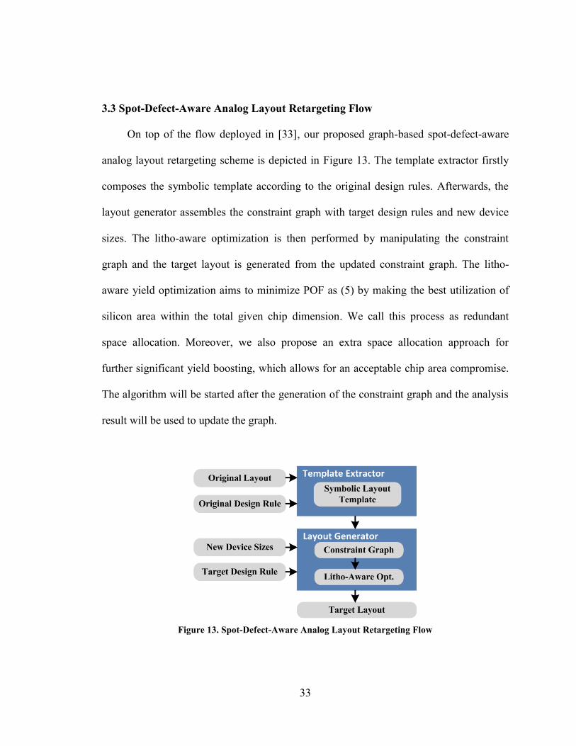
3.3 Spot-Defect-Aware Analog Layout Retargeting Flow
On top of the flow deployed in [33], our proposed graph-based spot-defect-aware
analog layout retargeting scheme is depicted in Figure 13. The template extractor firstly
composes the symbolic template according to the original design rules. Afterwards, the
layout generator assembles the constraint graph with target design rules and new device
sizes. The litho-aware optimization is then performed by manipulating the constraint
graph and the target layout is generated from the updated constraint graph. The litho-
aware yield optimization aims to minimize POF as (5) by making the best utilization of
silicon area within the total given chip dimension. We call this process as redundant
space allocation. Moreover, we also propose an extra space allocation approach for
further significant yield boosting, which allows for an acceptable chip area compromise.
The algorithm will be started after the generation of the constraint graph and the analysis
result will be used to update the graph.
Figure 13. Spot-Defect-Aware Analog Layout Retargeting Flow
34
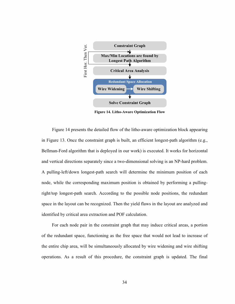
Figure 14. Litho-Aware Optimization Flow
Figure 14 presents the detailed flow of the litho-aware optimization block appearing
in Figure 13. Once the constraint graph is built, an efficient longest-path algorithm (e.g.,
Bellman-Ford algorithm that is deployed in our work) is executed. It works for horizontal
and vertical directions separately since a two-dimensional solving is an NP-hard problem.
A pulling-left/down longest-path search will determine the minimum position of each
node, while the corresponding maximum position is obtained by performing a pulling-
right/top longest-path search. According to the possible node positions, the redundant
space in the layout can be recognized. Then the yield flaws in the layout are analyzed and
identified by critical area extraction and POF calculation.
For each node pair in the constraint graph that may induce critical areas, a portion
of the redundant space, functioning as the free space that would not lead to increase of
the entire chip area, will be simultaneously allocated by wire widening and wire shifting
operations. As a result of this procedure, the constraint graph is updated. The final
35
component positions will then be determined by solving the constraint graph, which is to
run the longest-path algorithm one more time and fine-tune the component positions with
a post-processing scheme. This post-processing scheme, which we have developed on the
basis of a wire-length-minimization concept from [62], aims to minimize the total
interconnect length in the target layout. Rather than working individually, the following
two redundant space allocation schemes are appropriately combined: the wire widening
scheme distributes redundant space globally on each direction, while the wire shifting
scheme locally fine-tunes sensitive wires.
3.4 Optimization Techniques
During the lithography-aware analog layout retargeting flow, as Figure 14 shows,
we propose a redundant space allocation scheme including wire widening and wire
shifting. The wire widening scheme is concentrated on one dimensional space budget by
enlarging the wire width and wire spacing, first horizontally and then vertically.
However, the redundant space may not be fully utilized across the whole chip. To further
improve the redundant space utilization, we propose wire shifting optimization to
minimize wire overlap length. Normally, two adjacent tiles in the layout may introduce a
short-type critical area with the same dimension as their overlap length. If we could shift
one of them to the proper direction, the overlap Lij would decrease and also the POF for
the short-type faults according to (4). For wire shifting, we propose three main schemes:
36
intra-device shifting, inter-device shifting by clustering, and inter-device shifting by
sensitivity analysis.
3.4.1 Wire Widening
Wire widening aims to minimize the critical areas by directly increasing the width
Wi of a wire or the spacing Sij between two wires. Thus, from (4), we can observe that the
POF is reduced accordingly. To some extent, our wire widening scheme is similar to the
traditional even wire distribution approach reported in [21], because the term “widening”
not only refers to enlarging solid wire width, but also indicates to promote larger wire
spacing. Compared to [21], our algorithm simultaneously allocates the redundant space to
all critical tiles without demanding iterations. Moreover, the wire widening scheme can
be safely applied to both inter-device and intra-device locations. This is a unique feature
since the geometric and parasitic requirements represented in the constraint graph for
analog layouts should ensure the intactness of the sensitive analog transistors. Therefore,
such a characteristic makes the wire widening be a more general approach for yield
improvement in analog layouts.
To achieve the wire widening, firstly the critical area analysis extracts all the
critical tiles that may cause open-type faults and all the critical tile pairs that may induce
short-type faults. Then the critical tiles and tile pairs are identified in the constraint graph
and their corresponding arcs would be marked as critical arcs. A critical arc can be frozen
due to: 1) symmetry or matching constraints; 2) fixed device size values; or 3) the fact
37
that it belongs to the critical path of the layout (i.e., the longest path in the graph that
determines the whole layout dimension). In such a case, we keep its arc weight intact to
ensure all the constraints are satisfied within the same total chip area. Otherwise, the
critical arc is optimizable and a certain amount of redundant space can be added into its
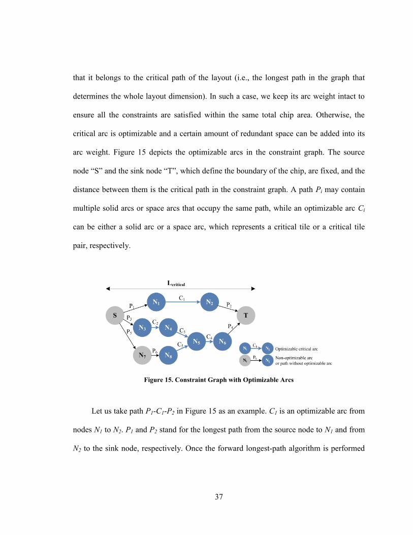
arc weight. Figure 15 depicts the optimizable arcs in the constraint graph. The source
node “S” and the sink node “T”, which define the boundary of the chip, are fixed, and the
distance between them is the critical path in the constraint graph. A path Pi may contain
multiple solid arcs or space arcs that occupy the same path, while an optimizable arc Ci
can be either a solid arc or a space arc, which represents a critical tile or a critical tile
pair, respectively.
Figure 15. Constraint Graph with Optimizable Arcs
Let us take path P1-C1-P2 in Figure 15 as an example. C1 is an optimizable arc from
nodes N1 to N2. P1 and P2 stand for the longest path from the source node to N1 and from
N2 to the sink node, respectively. Once the forward longest-path algorithm is performed
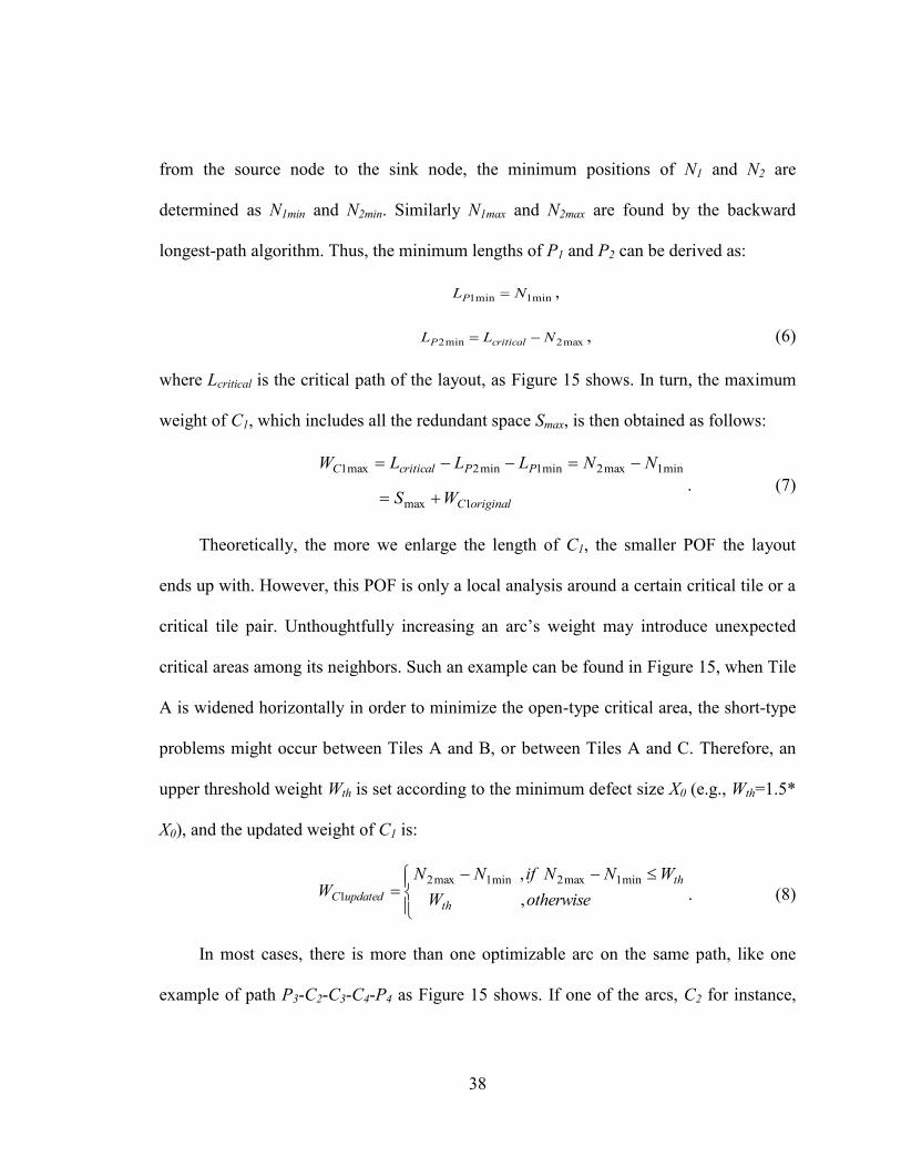
38
from the source node to the sink node, the minimum positions of N1 and N2 are
determined as N1min and N2min. Similarly N1max and N2max are found by the backward
longest-path algorithm. Thus, the minimum lengths of P1 and P2 can be derived as:
min1min1 NLP ,
max2min2 NLL criticalP , (6)
where Lcritical is the critical path of the layout, as Figure 15 shows. In turn, the maximum
weight of C1, which includes all the redundant space Smax, is then obtained as follows:
originalC
PPcriticalC
WS
NNLLLW
1max
min1max2min1min2max1
. (7)
Theoretically, the more we enlarge the length of C1, the smaller POF the layout
ends up with. However, this POF is only a local analysis around a certain critical tile or a
critical tile pair. Unthoughtfully increasing an arc’s weight may introduce unexpected
critical areas among its neighbors. Such an example can be found in Figure 15, when Tile
A is widened horizontally in order to minimize the open-type critical area, the short-type
problems might occur between Tiles A and B, or between Tiles A and C. Therefore, an
upper threshold weight Wth is set according to the minimum defect size X0 (e.g., Wth=1.5*
X0), and the updated weight of C1 is:
otherwiseW
WNNifNNW
th
th
updatedC ,
, min1max2min1max2
1 . (8)
In most cases, there is more than one optimizable arc on the same path, like one
example of path P3-C2-C3-C4-P4 as Figure 15 shows. If one of the arcs, C2 for instance,

39
takes all the redundant space in this path, then C3 and C4 have to keep the original
weights, which may result in a worse global POF. As the pseudo-code describes in
Algorithm 1, an allocation scheme is applied for this situation. On the one hand, each
space optimizable arc concerning short-type faults will get one portion of the total
redundant space in direct proportion to its original arc length LCi, as can be seen from
Line 5, where α is used to balance the optimization for short- and open-type faults. On
the other hand, for each solid optimizable arc with respect to open-type faults, redundant
space will be allocated based on the length Li of the related tile in the orthogonal
direction of the solid arc, as shown in Line 7.
Algorithm 1: Redundant space allocation for wire widening
1. Foreach optimizable arc Ci
2. Calculate the maximum redundant space Smax
3. Calculate the weighted longest path that contains this arc
WPlongest = α ∙ ∑ Sij + (1 – α) ∙ ∑ Li
4. If Ci is caused by short critical area
5. WCi = WCi + (α ∙ LCi ∙ Smax) / WPlongest
6. Else
7. WCi = WCi + (1 – α) ∙ Li ∙ Smax / WPlongest
8. End if
9. If WCi is larger than Wth
10. WCi = Wth
11. End if
12. End for
Figure 16 depicts the geometric dimensions by using Algorithm 1 for vertical wire
widening, where LCi is the length in the vertical direction while Li is the one in the
horizontal direction. The motivation for utilizing the orthogonal length in the context of
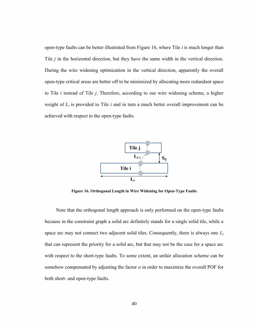
40
open-type faults can be better illustrated from Figure 16, where Tile i is much longer than
Tile j in the horizontal direction, but they have the same width in the vertical direction.
During the wire widening optimization in the vertical direction, apparently the overall
open-type critical areas are better off to be minimized by allocating more redundant space
to Tile i instead of Tile j. Therefore, according to our wire widening scheme, a higher
weight of Li is provided to Tile i and in turn a much better overall improvement can be
achieved with respect to the open-type faults.
Figure 16. Orthogonal Length in Wire Widening for Open-Type Faults
Note that the orthogonal length approach is only performed on the open-type faults
because in the constraint graph a solid arc definitely stands for a single solid tile, while a
space arc may not connect two adjacent solid tiles. Consequently, there is always one Li
that can represent the priority for a solid arc, but that may not be the case for a space arc
with respect to the short-type faults. To some extent, an unfair allocation scheme can be
somehow compensated by adjusting the factor α in order to maximize the overall POF for
both short- and open-type faults.
41
The terminology WPlongest in Line 3 of Algorithm 1, which has the maximum value
among all the paths that contain the optimizable arcs, is defined as the weighted longest
path in the constraint graph through the current arc Ci. It utilizes the same weight factor α
and is derived from a depth-first-search (DFS) algorithm, which is performed from the
current optimizable arc to the source node and the sink node, respectively. Although
WPlongest is no longer the real path length in the graph when the orthogonal length Li is
applied, this term ensures that the total allocated space stays within the range of the
maximum redundant space. The limitation set by Lines 9-10 regulates the arc weight
values according to (8).
Generally wire widening can effectively reduce POF by proper redundant space
allocation in a layout. However, in some cases, extremely limited or even no redundant
space is available in the constraint graph especially for the high-POF critical arcs (e.g., a
long tile or a tile pair with large overlap), which make the overall POF a lot more than
others. One solution to this type of highly congested situations would be to sort the
critical arcs by their local POF values and provide different widening weights according
to the order. Therefore, we propose one extra wire widening scheme as follows. The
weight for such arcs can be further enlarged as:
)( CithCiCi WWWW , if Cith WW , (9)
in order to minimize the local POF values. Although it does not necessarily always
consume all the available redundant space, an aggressive chip area increase may take
place. For this reason, factor β is used to control the worst-case increment within a
42
reasonable range (such as 1% of the total layout area), while the benefit for POF
reduction might be remarkable.
3.4.2 Intra-Device Wire Shifting
The structure of a transistor in analog layouts has much more flexibility compared
to its counterpart in digital circuits. Normally digital circuits utilize standard cells, each
of which can be treated as a fixed black box. However, with respect to analog circuits,
especially in analog layout retargeting where all components and interconnects would be
flattened, besides the width, length, finger number, or multiplier of a transistor that
should be fixed as demanded, all the other geometric dimensions can be modified if
following the technology design rules. Figure 17(a) presents a single-finger transistor
with only short-type critical area between the Metal-1 layer source and drain connections
(the tiles in blue color), while the poly tile (the tile in red color) is only used to visualize
the transistor representation. After layout retargeting, the metal wires shrink greatly to
become comparable to the minimum defect size. The poly tile may not be changed
considerably since its width is only determined by the new transistor sizes. As can be
seen from Figure 17(b), the critical area for short is reduced whereas the critical areas for
open emerge. By utilizing the wire widening approach described in Algorithm 1, the total
critical area inside a single-finger transistor may be minimized.
43
Figure 17. Critical Areas on a Single-finger Transistor. (a) Before Retargeting. (b) After
Retargeting.
Figure 18. Intra-Device Wire Shifting for a Multi-finger Transistor. (a) Before Shifting. (b) After
Shifting.
In contrast, the critical area analysis in a multi-finger transistor becomes a two-
dimensional problem. Figure 18 shows a multi-finger transistor with only Metal-1 layer
tiles. Here we assume that Tiles A, C and E are source connections and Tiles B and D are
drain connections. The critical areas may exist between Tile A/C and Tile B (the same
critical area as that in Figure 17(a)), between Tile B and Tile E, and also between Tile
A/C and Tile D. Because length Li (in the horizontal dimension) of Tile A or Tile B is
normally much larger than width Wi (in the vertical dimension) and spacing Sij (similar to
the geometric parameters in Figure 17(b)), the critical areas between Tile A/C and Tile B
44
can usually be minimized during wire widening in the vertical direction if redundant
space is available (the overlap between Tile A/C and Tile B remains unchanged), while
the critical areas between Tiles A/C and D or between Tiles B and E have a greater
chance to become a primary POF contributor. Therefore, we propose an intra-device
shifting scheme in order to reduce this type of critical areas. The scheme is similar to the
extra wire widening scheme described in (9):
)( CithCiCi WWWW , if Cith WW , (10)
where we apply a different factor γ to prevent aggressive shifting that may deteriorate the
local POF, and to control a potential chip area increment as that in (9). When we perform
the proposed intra-device wire shifting above by enlarging the arc weight between Tiles
A/C and D or between Tiles B and E, as Figure 18(b) shows, Tile A would be pushed
away from Tile D aligned with Tile C due to the matching constraints inside the device.
Obviously the resultant critical areas are significantly reduced in Figure 18(b) compared
to Figure 18(a).
3.4.3 Inter-Device Wire Shifting by Clustering
The inter-device wire shifting intends to handle interconnections among devices. In
Figure 19(a), the overlap between Tiles A and B is reduced if we shift Tile B rightward.
However, the overlap between Tiles B and C or D may increase at the same time, which
might lead to an even worse POF result. In the worst case, this operation may also
introduce a new critical area between Tiles B and E.
45
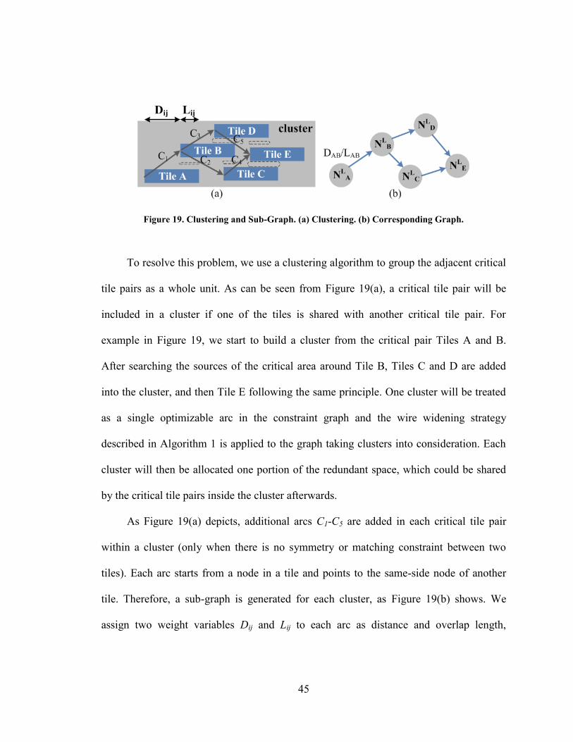
Figure 19. Clustering and Sub-Graph. (a) Clustering. (b) Corresponding Graph.
To resolve this problem, we use a clustering algorithm to group the adjacent critical
tile pairs as a whole unit. As can be seen from Figure 19(a), a critical tile pair will be
included in a cluster if one of the tiles is shared with another critical tile pair. For
example in Figure 19, we start to build a cluster from the critical pair Tiles A and B.
After searching the sources of the critical area around Tile B, Tiles C and D are added
into the cluster, and then Tile E following the same principle. One cluster will be treated
as a single optimizable arc in the constraint graph and the wire widening strategy
described in Algorithm 1 is applied to the graph taking clusters into consideration. Each
cluster will then be allocated one portion of the redundant space, which could be shared
by the critical tile pairs inside the cluster afterwards.
As Figure 19(a) depicts, additional arcs C1-C5 are added in each critical tile pair
within a cluster (only when there is no symmetry or matching constraint between two
tiles). Each arc starts from a node in a tile and points to the same-side node of another
tile. Therefore, a sub-graph is generated for each cluster, as Figure 19(b) shows. We
assign two weight variables Dij and Lij to each arc as distance and overlap length,

46
respectively. The pseudo code in Algorithm 2 lists the space allocation scheme in the
sub-graph, where the terminology SPlongest is defined as the longest path in the sub-graph
that contains the current arc Ci. The calculated sub-longest path SPlongest in Line 4 can
ensure that the overall allocated space inside the cluster will not exceed the given
maximum redundant space Smax for the cluster. The algorithm in Line 5 shows that each
Dij increases in proportion to the related Lij, which indicates that higher priority is applied
to more critical tile pairs with longer overlap. The weight Dij is updated either in Line 7
or Line 9, which can save the unused redundant space for being utilized by other
optimization schemes afterwards. Once Dij is enlarged, Lij will be reduced accordingly
since the sum of Dij and Lij equals the length of Tile i. In this way, the incremented
overlap within a cluster can be eliminated.
Algorithm 2: Redundant space allocation within a cluster
1. Obtain the allocated redundant space Smax for the cluster
2. Initialize the sub graph with the weights Dij and Lij
3. Foreach arc Ci in the sub-graph
4. Calculate the sub-longest path that contains this arc
SPlongest = ∑ Lij
5. Dnew = Smax ∙ Lij / SPlongest
6. If Dnew is smaller than Lij
7. Dij = Dij + Dnew
8. Else
9. Dij = Dij + Lij
10. End if
11. End for
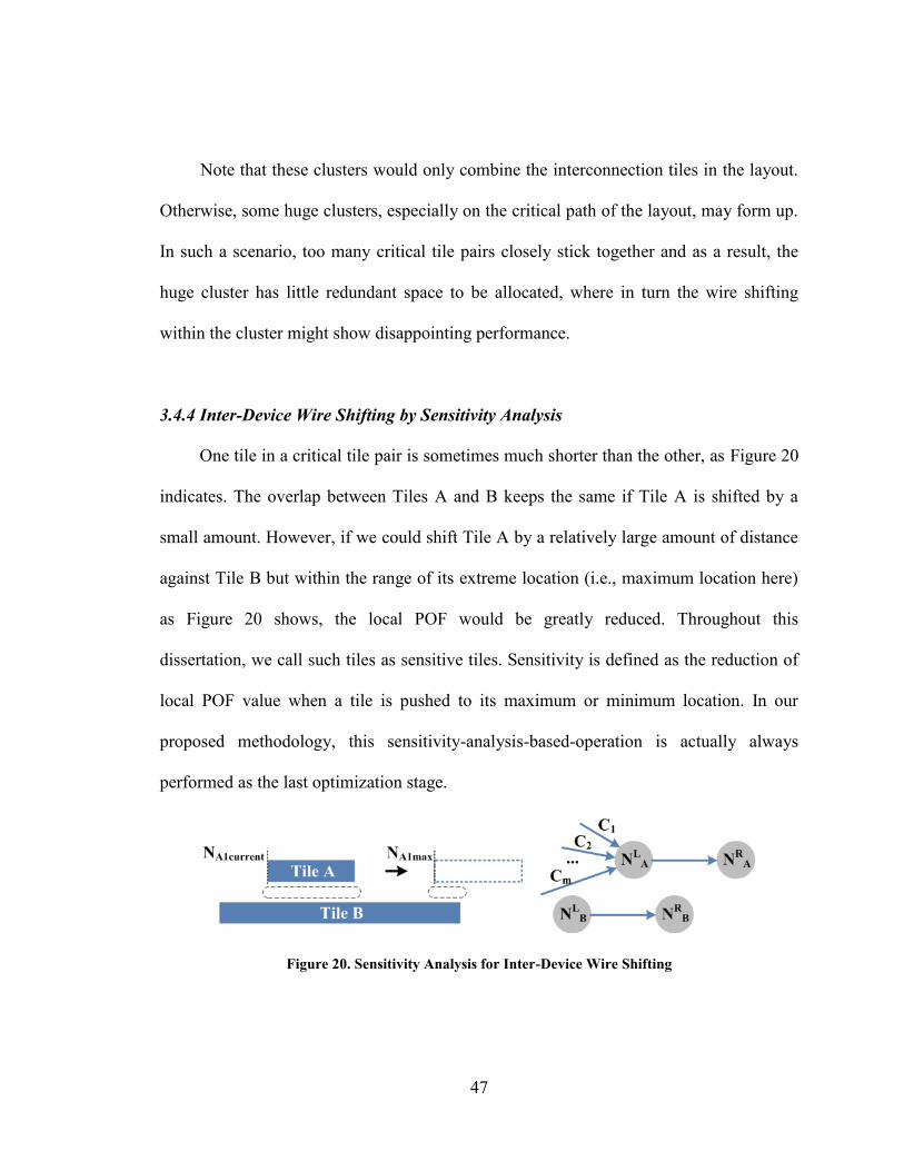
47
Note that these clusters would only combine the interconnection tiles in the layout.
Otherwise, some huge clusters, especially on the critical path of the layout, may form up.
In such a scenario, too many critical tile pairs closely stick together and as a result, the
huge cluster has little redundant space to be allocated, where in turn the wire shifting
within the cluster might show disappointing performance.
3.4.4 Inter-Device Wire Shifting by Sensitivity Analysis
One tile in a critical tile pair is sometimes much shorter than the other, as Figure 20
indicates. The overlap between Tiles A and B keeps the same if Tile A is shifted by a
small amount. However, if we could shift Tile A by a relatively large amount of distance
against Tile B but within the range of its extreme location (i.e., maximum location here)
as Figure 20 shows, the local POF would be greatly reduced. Throughout this
dissertation, we call such tiles as sensitive tiles. Sensitivity is defined as the reduction of
local POF value when a tile is pushed to its maximum or minimum location. In our
proposed methodology, this sensitivity-analysis-based-operation is actually always
performed as the last optimization stage.
Figure 20. Sensitivity Analysis for Inter-Device Wire Shifting
48
During the sensitivity analysis, every candidate tile (i.e., the shorter tile in an
interconnection critical tile pair that involves no other constraint) is assumed to be pushed
towards four directions, one at a time, if there is no obstacle ahead. Then the local POF is
recalculated to get its sensitivity value. Finally, the more sensitive candidates (i.e., their
sensitivity values are larger than a pre-defined threshold value) will be pushed away by
directly increasing the related arc weights. Figure 20 also includes the graph
representation of Tiles A and B on the right side. Arcs C1-Cm stand for the spacing
constraints between Tile A and any other related solid tiles. If Tile A is going to be
pushed rightward, all the arc weights of Ci (1≤i≤m) pointing to Node NL
A will be enlarged
by:
)( max AcurrentL
AL
CiCi NNWW , (11)
where σ is used to control the scope of shifting. If σ is 1, the tile will be pushed to one of
its physical limit.
3.5 Experimental Results
To evaluate the effectiveness of the spot defect optimization algorithm, the
proposed spot-defect-aware analog layout retargeting methodology was implemented in
C++. The optimization was performed on the two-stage Miller-compensated operational
amplifier (opamp) and single-end folded cascode opamp depicted in Section 3.1.3. The
layout retargeting for both circuits were conducted from CMOS 0.25um to CMOS
0.18um and 90nm technologies.

49
Table 1 reports the total number of tiles, short- and open-type critical arcs and
optimizable arcs on Metal-1 layer in the original two-stage opamp and cascode opamp
layouts. It is noticeable that the number of the open-type critical arcs is larger than the
total number of the tiles in the cascode opamp layout. The reason is that the tiles will be
represented by a horizontal graph and a vertical graph separately. Therefore, the
maximum number of solid arcs for a layout with N tiles should be 2*N.
Table 1. Optimization Statistics on Metal-1 Layer
Metal-1 Layer Two-Stage Opamp Cascode Opamp
Total Number of Tiles 98 106
Short-Type Critical Arcs 64 70
Short-Type Optimizable Arcs 33 54
Open-Type Critical Arcs 87 109
Open-Type Optimizable Arcs 70 100
We assume α=0.8 for the optimization weight of the short-type faults (thus, the
optimization weight of the open-type faults is 0.2), β=0.4 for the extra space allocation
for the open-type faults, γ=0.4 for the intra-device wire shifting for the short-type faults,
and σ=0.1 for the sensitivity-analysis-based optimization in order to avoid an aggressive
shift.
For the comparison purpose, we also implemented the yield-aware LP based
compaction approach in [23] and the step-wise (SW) wire distribution approach in [21],
both of which were integrated into our layout reuse tool. For the LP-based approach, the
layout is compacted by solving a LP model, which is largely different from our proposed
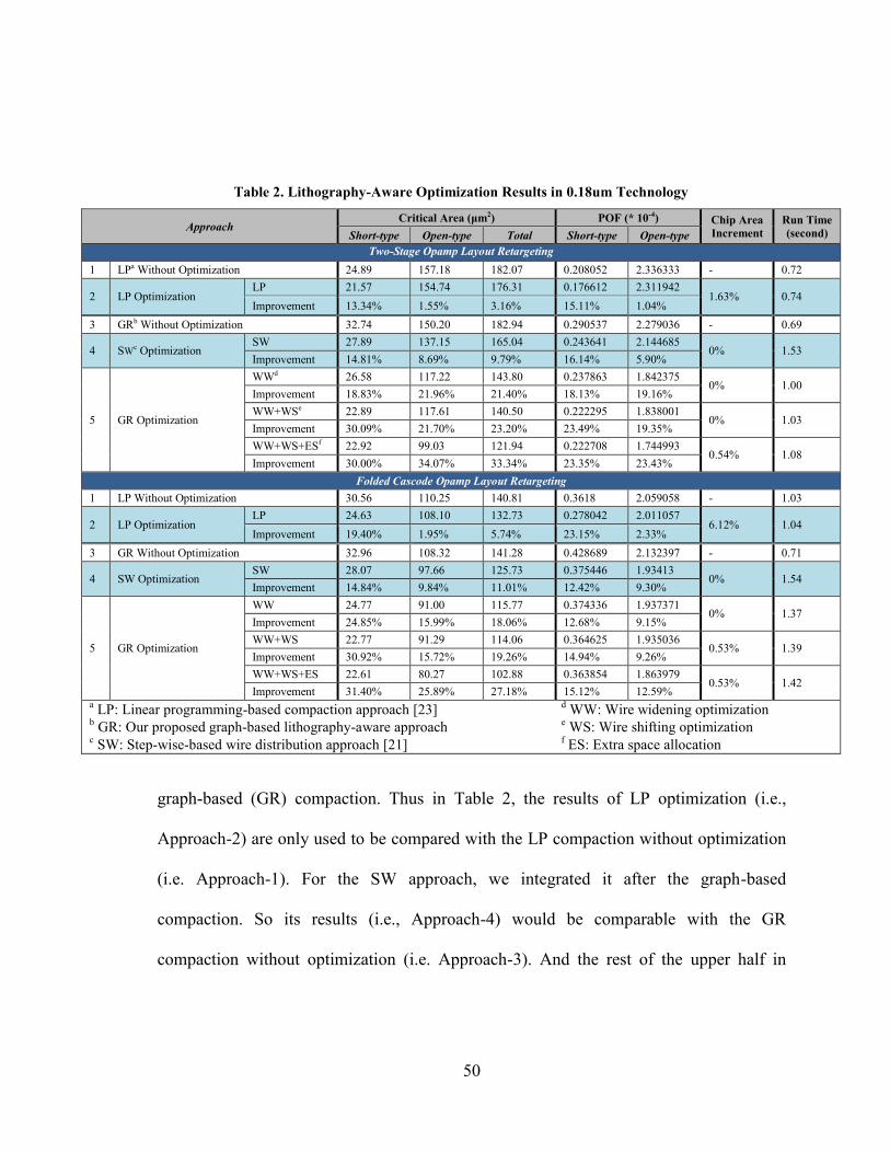
50
graph-based (GR) compaction. Thus in Table 2, the results of LP optimization (i.e.,
Approach-2) are only used to be compared with the LP compaction without optimization
(i.e. Approach-1). For the SW approach, we integrated it after the graph-based
compaction. So its results (i.e., Approach-4) would be comparable with the GR
compaction without optimization (i.e. Approach-3). And the rest of the upper half in
Table 2. Lithography-Aware Optimization Results in 0.18um Technology
Approach Critical Area (μm2) POF (* 10-4) Chip Area
Increment
Run Time
(second) Short-type Open-type Total Short-type Open-type
Two-Stage Opamp Layout Retargeting
1 LPa Without Optimization 24.89 157.18 182.07 0.208052 2.336333 - 0.72
2 LP Optimization LP 21.57 154.74 176.31 0.176612 2.311942
1.63% 0.74 Improvement 13.34% 1.55% 3.16% 15.11% 1.04%
3 GRb Without Optimization 32.74 150.20 182.94 0.290537 2.279036 - 0.69
4 SWc Optimization
SW 27.89 137.15 165.04 0.243641 2.144685 0% 1.53
Improvement 14.81% 8.69% 9.79% 16.14% 5.90%
5 GR Optimization
WWd 26.58 117.22 143.80 0.237863 1.842375 0% 1.00
Improvement 18.83% 21.96% 21.40% 18.13% 19.16%
WW+WSe 22.89 117.61 140.50 0.222295 1.838001 0% 1.03
Improvement 30.09% 21.70% 23.20% 23.49% 19.35%
WW+WS+ESf 22.92 99.03 121.94 0.222708 1.744993 0.54% 1.08
Improvement 30.00% 34.07% 33.34% 23.35% 23.43%
Folded Cascode Opamp Layout Retargeting
1 LP Without Optimization 30.56 110.25 140.81 0.3618 2.059058 - 1.03
2 LP Optimization LP 24.63 108.10 132.73 0.278042 2.011057
6.12% 1.04 Improvement 19.40% 1.95% 5.74% 23.15% 2.33%
3 GR Without Optimization 32.96 108.32 141.28 0.428689 2.132397 - 0.71
4 SW Optimization SW 28.07 97.66 125.73 0.375446 1.93413
0% 1.54 Improvement 14.84% 9.84% 11.01% 12.42% 9.30%
5 GR Optimization
WW 24.77 91.00 115.77 0.374336 1.937371 0% 1.37
Improvement 24.85% 15.99% 18.06% 12.68% 9.15%
WW+WS 22.77 91.29 114.06 0.364625 1.935036 0.53% 1.39
Improvement 30.92% 15.72% 19.26% 14.94% 9.26%
WW+WS+ES 22.61 80.27 102.88 0.363854 1.863979 0.53% 1.42
Improvement 31.40% 25.89% 27.18% 15.12% 12.59% a LP: Linear programming-based compaction approach [23]
d WW: Wire widening optimization
b GR: Our proposed graph-based lithography-aware approach
e WS: Wire shifting optimization
c SW: Step-wise-based wire distribution approach [21]
f ES: Extra space allocation
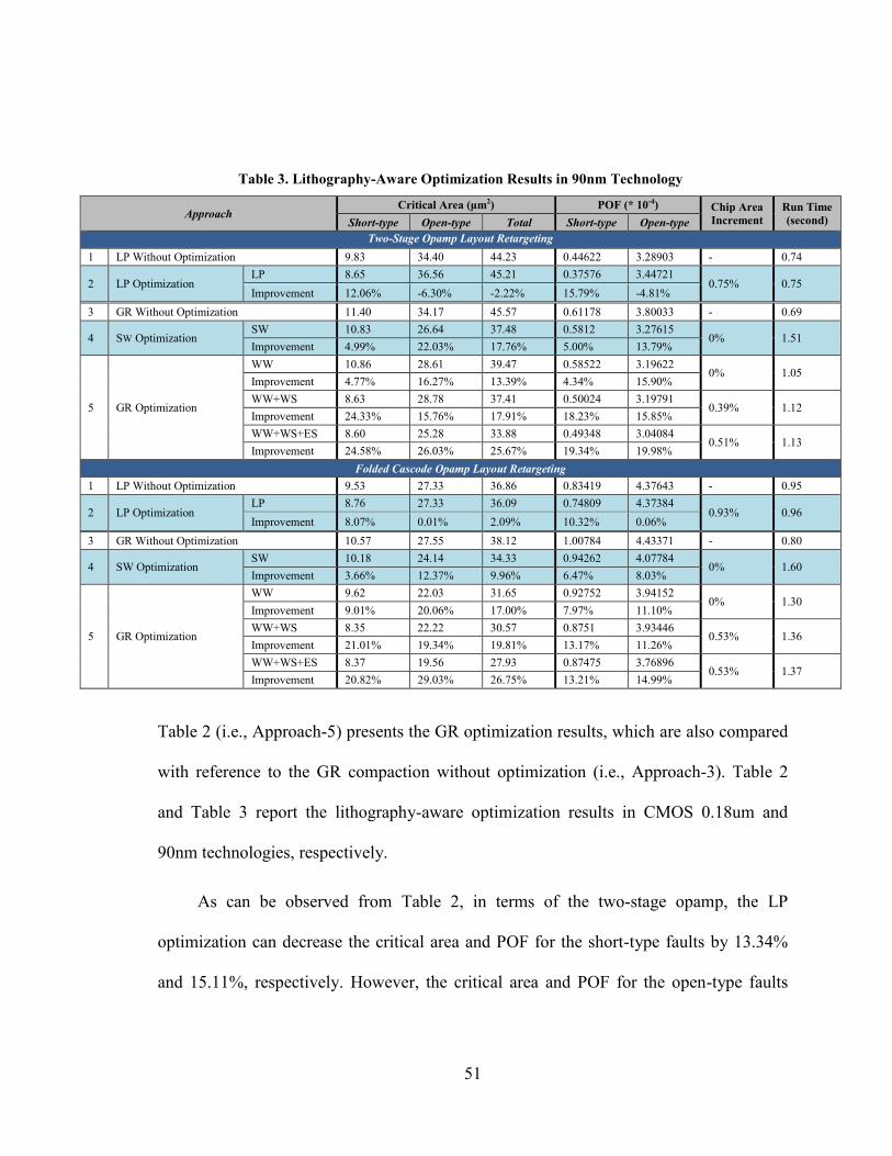
51
Table 2 (i.e., Approach-5) presents the GR optimization results, which are also compared
with reference to the GR compaction without optimization (i.e., Approach-3). Table 2
and Table 3 report the lithography-aware optimization results in CMOS 0.18um and
90nm technologies, respectively.
As can be observed from Table 2, in terms of the two-stage opamp, the LP
optimization can decrease the critical area and POF for the short-type faults by 13.34%
and 15.11%, respectively. However, the critical area and POF for the open-type faults
Table 3. Lithography-Aware Optimization Results in 90nm Technology
Approach Critical Area (μm2) POF (* 10-4) Chip Area
Increment
Run Time
(second) Short-type Open-type Total Short-type Open-type
Two-Stage Opamp Layout Retargeting
1 LP Without Optimization 9.83 34.40 44.23 0.44622 3.28903 - 0.74
2 LP Optimization LP 8.65 36.56 45.21 0.37576 3.44721
0.75% 0.75 Improvement 12.06% -6.30% -2.22% 15.79% -4.81%
3 GR Without Optimization 11.40 34.17 45.57 0.61178 3.80033 - 0.69
4 SW Optimization SW 10.83 26.64 37.48 0.5812 3.27615
0% 1.51 Improvement 4.99% 22.03% 17.76% 5.00% 13.79%
5 GR Optimization
WW 10.86 28.61 39.47 0.58522 3.19622 0% 1.05
Improvement 4.77% 16.27% 13.39% 4.34% 15.90%
WW+WS 8.63 28.78 37.41 0.50024 3.19791 0.39% 1.12
Improvement 24.33% 15.76% 17.91% 18.23% 15.85%
WW+WS+ES 8.60 25.28 33.88 0.49348 3.04084 0.51% 1.13
Improvement 24.58% 26.03% 25.67% 19.34% 19.98%
Folded Cascode Opamp Layout Retargeting
1 LP Without Optimization 9.53 27.33 36.86 0.83419 4.37643 - 0.95
2 LP Optimization LP 8.76 27.33 36.09 0.74809 4.37384
0.93% 0.96 Improvement 8.07% 0.01% 2.09% 10.32% 0.06%
3 GR Without Optimization 10.57 27.55 38.12 1.00784 4.43371 - 0.80
4 SW Optimization SW 10.18 24.14 34.33 0.94262 4.07784
0% 1.60 Improvement 3.66% 12.37% 9.96% 6.47% 8.03%
5 GR Optimization
WW 9.62 22.03 31.65 0.92752 3.94152 0% 1.30
Improvement 9.01% 20.06% 17.00% 7.97% 11.10%
WW+WS 8.35 22.22 30.57 0.8751 3.93446 0.53% 1.36
Improvement 21.01% 19.34% 19.81% 13.17% 11.26%
WW+WS+ES 8.37 19.56 27.93 0.87475 3.76896 0.53% 1.37
Improvement 20.82% 29.03% 26.75% 13.21% 14.99%
52
have only been improved by small amounts (1.55% and 1.04%, respectively), which
indicate a neglect of the open-type defects in the yield optimization. According to our
analysis, LP compaction scheme [23] is only focused on the short-type faults, where the
critical area minimization for the short-type faults is utilized as part of the LP objectives.
After layout compaction, the spacing among wires will be enlarged to some extent, while
the wire width remains the same or may even be squeezed due to the effort of maximally
resolving the short-type problems. In this way, the total critical area and the overall POF
may not be effectively improved.
The same phenomena can be observed in the cascode opamp experiments. The POF
for the short-type faults is improved by 23.15%, whereas that for the open-type faults is
only enhanced by 2.33%. Another issue caused by the LP compaction is a non-ignorable
chip area increment (1.63% and 6.12% for the two-stage opamp and cascode opamp,
respectively), which is much larger than that by using the GR compaction. This is most
likely a direct result of simply inducing the critical area minimization into the objective
but without thorough redundant space analysis and management. Obviously in most of
the cases, getting a more compact chip area is somewhat in conflict to obtaining a smaller
critical area.
With respect to the SW optimization, the method performs as a post-processing step
after the graph-based layout compaction. According to [21], we set the iteration limit as 5
and the algorithm works on the short-type and open-type optimizations simultaneously.
From Table 2, for the two-stage opamp, the SW approach can shrink the critical areas by
53
14.81% and 8.69%, while a total improvement of critical areas is 9.79%, which is quite
acceptable. The POF values are reduced by 16.14% and 5.90% for the short- and open-
type faults, respectively. The results demonstrate that the SW optimization has stronger
optimization capability for handling the short-type faults than the open-type faults. As a
post-processing algorithm, the SW approach moves wires (not on the critical path) based
on the redundant space information (generated by the longest-path algorithm on the
constraint graph), in order to achieve an even wire distribution. Although it is similar to
our redundant space allocation scheme, the SW compaction cannot control the weight of
the allocation and is thus hard to get a better tradeoff between the short-type and open-
type fault optimizations. Because the algorithm works only on interconnections, the
critical area inside transistors cannot be reduced. This partially causes diminished total
improvements for the SW method compared to our proposed GR optimizations. Such an
observation can also be witnessed by the results for the cascode opamp, where the POF
improvements are 12.42% and 9.30% for the short-type and open-type faults,
respectively.
In Table 2, we present three alternatives for the GR optimizations: wire widening
(WW), wire widening and wire shifting (WW+WS), and wire widening and wire shifting
plus applying extra space allocation (WW+WS+ES). The pure wire widening method
reports 18.13% POF reduction for the short-type faults and 19.16% POF reduction for the
open-type faults. And it is similar for the improvement of the critical areas, 18.83%
reduction for the short-type faults and 21.96% decrease for the open-type faults. Such a
54
remarkable contribution to alleviating the open-type fault problem is attributed to our
smart WW strategy, where the redundant space can be allocated to all the critical solid
tiles in proportion to their orthogonal dimension (as explained in Algorithm 1), instead of
simply being proportional to the arc length.
In this case, the longer tiles that introduce more open-type critical areas in the
layout can be effectively enlarged with higher priorities. Such a consideration for long
tiles can also be handled by the ES strategy whose effectiveness will be shown later from
the experimental perspective. For the cascode opamp retargeting by using WW, the POF
for the open-type faults is decreased by 9.15%, which is comparable to that in SW
optimization (i.e., 9.30%), while the POF for the short-type faults still shows a promising
improvement of 12.68%.
Based on the pure WW method, we further apply WS to make better utilization of
the redundant space. WS handles intra-device space allocation, inter-device WS and
sensitivity analysis, and it is mainly focused on the short-type fault problems. Therefore,
from Table 2 the POF for the short-type faults is significantly boosted from 18.13% to
23.49% in the two-stage opamp and from 12.68% to 14.94% in the cascode opamp. The
critical areas for the short-type faults are also greatly decreased by 30.09% and 30.92%,
compared to those (i.e., 18.83% for the two-stage opamp and 24.85% for the cascade
opamp, respectively) by the pure WW approach. Meanwhile, the results for the open-type
faults are slightly affected, because the WW and WS are performed simultaneously when
the constraint graph is solved.
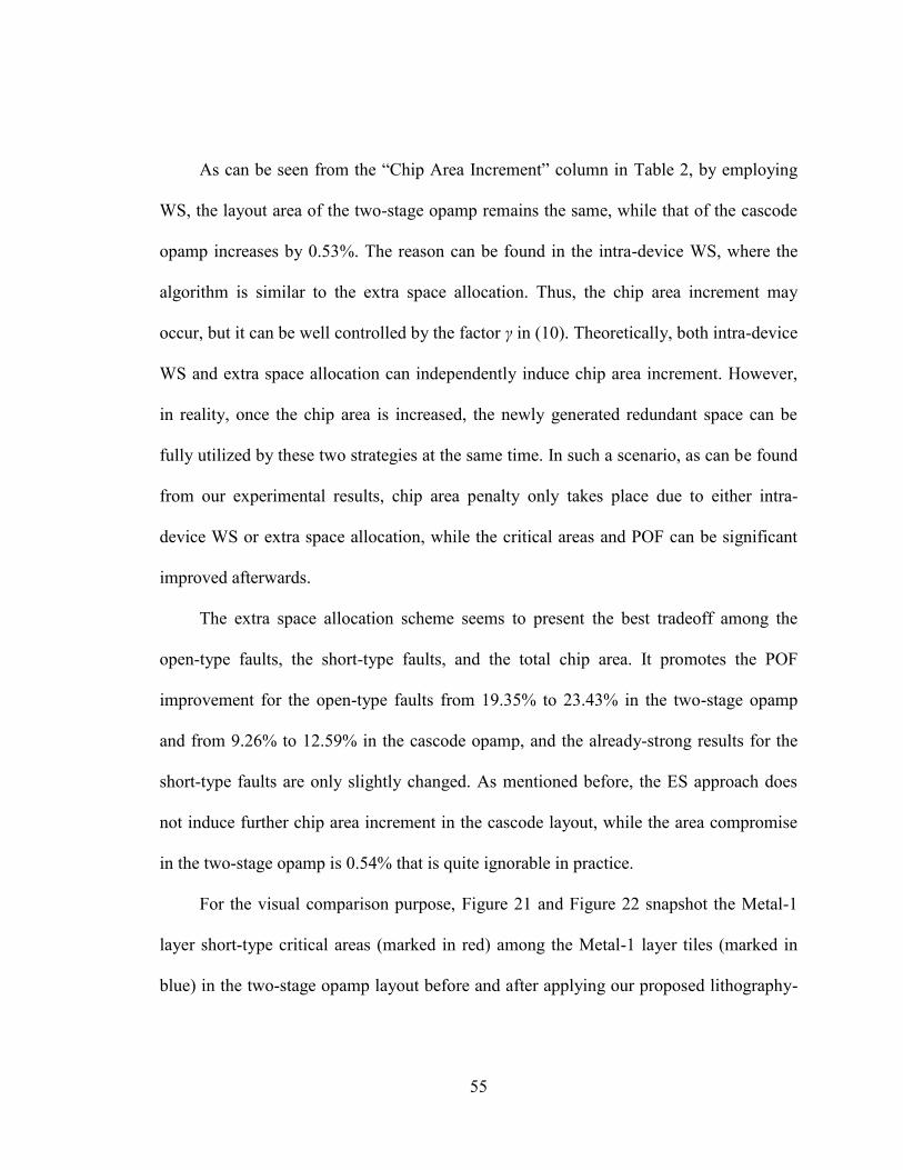
55
As can be seen from the “Chip Area Increment” column in Table 2, by employing
WS, the layout area of the two-stage opamp remains the same, while that of the cascode
opamp increases by 0.53%. The reason can be found in the intra-device WS, where the
algorithm is similar to the extra space allocation. Thus, the chip area increment may
occur, but it can be well controlled by the factor γ in (10). Theoretically, both intra-device
WS and extra space allocation can independently induce chip area increment. However,
in reality, once the chip area is increased, the newly generated redundant space can be
fully utilized by these two strategies at the same time. In such a scenario, as can be found
from our experimental results, chip area penalty only takes place due to either intra-
device WS or extra space allocation, while the critical areas and POF can be significant
improved afterwards.
The extra space allocation scheme seems to present the best tradeoff among the
open-type faults, the short-type faults, and the total chip area. It promotes the POF
improvement for the open-type faults from 19.35% to 23.43% in the two-stage opamp
and from 9.26% to 12.59% in the cascode opamp, and the already-strong results for the
short-type faults are only slightly changed. As mentioned before, the ES approach does
not induce further chip area increment in the cascode layout, while the area compromise
in the two-stage opamp is 0.54% that is quite ignorable in practice.
For the visual comparison purpose, Figure 21 and Figure 22 snapshot the Metal-1
layer short-type critical areas (marked in red) among the Metal-1 layer tiles (marked in
blue) in the two-stage opamp layout before and after applying our proposed lithography-
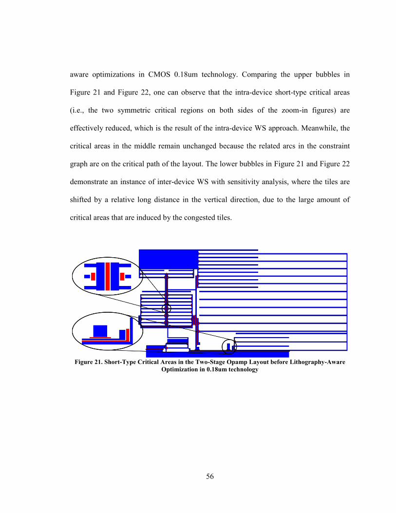
56
aware optimizations in CMOS 0.18um technology. Comparing the upper bubbles in
Figure 21 and Figure 22, one can observe that the intra-device short-type critical areas
(i.e., the two symmetric critical regions on both sides of the zoom-in figures) are
effectively reduced, which is the result of the intra-device WS approach. Meanwhile, the
critical areas in the middle remain unchanged because the related arcs in the constraint
graph are on the critical path of the layout. The lower bubbles in Figure 21 and Figure 22
demonstrate an instance of inter-device WS with sensitivity analysis, where the tiles are
shifted by a relative long distance in the vertical direction, due to the large amount of
critical areas that are induced by the congested tiles.
Figure 21. Short-Type Critical Areas in the Two-Stage Opamp Layout before Lithography-Aware
Optimization in 0.18um technology
57
Figure 22. Short-Type Critical Areas in the Two-Stage Opamp Layout after Lithography-Aware
Optimization in 0.18um technology
In terms of the computational time of the algorithms as reported in the last columns
in Table 2 and Table 3, the LP compaction with optimization consumes the least time,
due to relatively small problem size of the two example analog layouts and its simple
implementation in our platform. Once a larger layout is applied and more considerations
are adopted in the algorithm, this LP-based method is expected to experience longer run
time due to the nature of LP’s relatively high time complexity. The SW compaction
reports the longest run time due to its iteration nature. The proposed GR compaction
presents the best performance on run time when the graph scheme is used without
optimizations, while the yield-related algorithms increase the run time up to 0.44 and
0.71 seconds in the two-stage opamp and the cascode opamp, respectively, both of which
are practically acceptable.
The computational time of our proposed GR method is directly related to the size of
the constraint graph. Depending on the detailed implementation of the constraint-graph
58
search algorithm, the time complexity of our method is a function of the number of
nodes/arcs in the constraint graph, which is determined by the number of primary
components in the layout. Therefore, the optimizations would consume similar run time
in both CMOS 0.18um and 90nm technologies with respect to the same layout structure,
as exhibited in Table 2 and Table 3. In addition, the run time increment in a larger layout
with more components can be roughly predicted.
Compared to the lithography-aware optimizations in CMOS 0.18um technology, the
optimizations in CMOS 90nm technology exhibit similar performance as reported in
Table 3. It is observed that both standalone WW and SW approaches cannot achieve
satisfactory short-type POF improvement in both layouts, only 4.34% and 5.00% in the
two-stage opamp and 7.97% and 6.47% in the cascode opamp. Instead of technology-
dependent causes, we realize that this phenomenon is mainly due to limited redundant
space of the layouts in the horizontal and vertical directions. The algorithms, which work
on one direction first and then the other, such as standalone WW, SW, or even LP, cannot
easily improve both short-type and open-type POF at the same time. Therefore, we
perceive that only the LP compaction method can attain good performance on short-type
POF but at the significant cost of open-type POF degradation and chip area increment.
However, the short-type POF can be greatly improved once the WS scheme, which can
efficiently utilize the space in both directions, is applied. As shown in Table 3, it is
noticed that our proposed graph-based lithography-aware optimization can achieve the
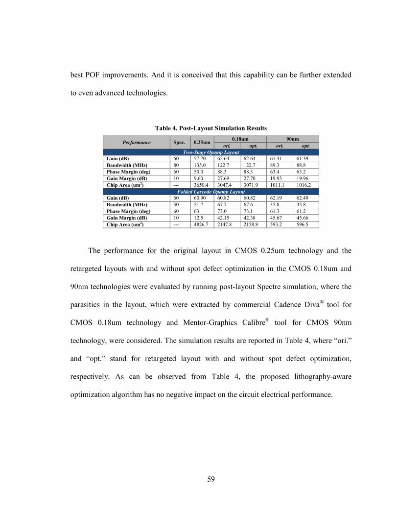
59
best POF improvements. And it is conceived that this capability can be further extended
to even advanced technologies.
Table 4. Post-Layout Simulation Results
Performance Spec. 0.25um 0.18um 90nm
ori. opt. ori. opt.
Two-Stage Opamp Layout
Gain (dB) 60 57.70 62.64 62.64 61.41 61.39
Bandwidth (MHz) 80 135.0 122.7 122.7 89.3 88.8
Phase Margin (deg) 60 50.0 88.3 88.3 63.4 63.2
Gain Margin (dB) 10 9.60 27.69 27.70 19.93 19.96
Chip Area (um2) --- 3650.4 3047.4 3071.9 1011.1 1016.2
Folded Cascode Opamp Layout
Gain (dB) 60 60.90 60.82 60.82 62.19 62.49
Bandwidth (MHz) 30 51.7 67.7 67.6 35.8 35.8
Phase Margin (deg) 60 63 73.0 73.1 61.3 61.2
Gain Margin (dB) 10 12.5 42.15 42.38 45.67 45.66
Chip Area (um2) --- 4826.7 2147.8 2158.8 593.2 596.5
The performance for the original layout in CMOS 0.25um technology and the
retargeted layouts with and without spot defect optimization in the CMOS 0.18um and
90nm technologies were evaluated by running post-layout Spectre simulation, where the
parasitics in the layout, which were extracted by commercial Cadence Diva® tool for
CMOS 0.18um technology and Mentor-Graphics Calibre® tool for CMOS 90nm
technology, were considered. The simulation results are reported in Table 4, where “ori.”
and “opt.” stand for retargeted layout with and without spot defect optimization,
respectively. As can be observed from Table 4, the proposed lithography-aware
optimization algorithm has no negative impact on the circuit electrical performance.
60
3.6 Summary
For DFM with respect to photolithographic defects, a lithography-aware analog
layout retargeting flow has been presented. The spot defect model is built based on a
classical defect size distribution function, geometrical critical area analysis, and POF.
The objective of our algorithm is to minimize POF by intelligent redundant space
allocation scheme during layout compaction. The optimizations handle the whole analog
layout area by global wire widening, intra-device wire shifting, and inter-device wire
shifting, which are achieved by updating the constraint-graph representation of the
layout. Moreover, an extra space allocation approach is applied to further reduce POF by
an inconsiderably small chip area increment. From our experimental results, the critical
area and POF values of the testing operational amplifiers are significantly improved in
the analog layout retargeting process.
Since spot defects may result in fatal functional failures in an analog circuit, by
using the proposed spot-defect-aware optimizations described in this chapter, the analog
circuit performance can be preserved so that the fatal errors are a lot less likely to occur.
However, other lithography effects, such as pattern distortions and process variations,
may not really cause fatal functional problems. Instead, certain circuit performance
degradation may occur, which would decrease the overall chip yield. In the following
chapters, optimizations with respect to PV-aware pattern distortions will be discussed.
Chapter 4 applies OPC schemes and special PV-band operations to alleviate pattern
distortions and preserve analog circuit performance in an efficient manner. Chapter 5

61
further introduces a deterministic circuit sizing algorithm to boost lithography-aware chip
yield.
62
Chapter 4 PV-Aware OPC-Inclusive Analog Layout Retargeting
In this chapter, the analog DFM methodology study will focus on PV-aware pattern
distortion optimizations. To achieve a decent trade-off among wafer image quality, layout
mask complexity, and algorithmic runtime, two different OPC strategies, standalone RB-
OPC Error! Reference source not found.[64] and hybrid OPC [65] (i.e., global RB-
PC plus local MB-OPC), are proposed and developed. Based on the unique features of
analog layouts, the accuracy limitation of RB-OPC is compensated by local wire
widening and wire shifting operations during layout retargeting, which are similar to
those described in Section 3.4 but with different operating targets. Combining with the
applied OPC schemes, an innovative PV-band shifting process is deployed to preserve
analog circuit performance against process variations.
Section 4.1 explains the criteria of evaluating the wafer image quality. Section 4.2
presents layout pattern operations on the constraint graph in order to compensate the
accuracy limitation of the RB-OPC process. Section 4.3 describes the PV-band shifting
scheme as a circuit performance enhancement technique. The complete PVRB-OPC and
the PVH-OPC methodologies are elaborated in Sections 4.4 and 4.5, respectively. Section
4.6 summarizes this chapter.
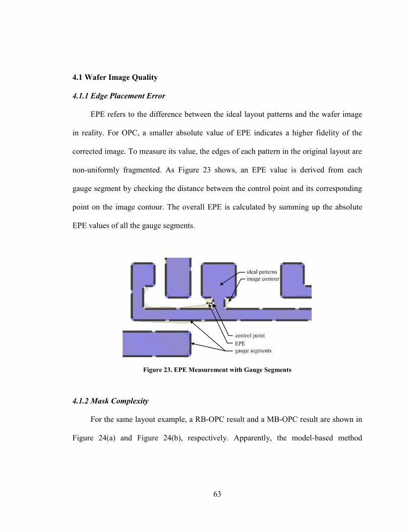
63
4.1 Wafer Image Quality
4.1.1 Edge Placement Error
EPE refers to the difference between the ideal layout patterns and the wafer image
in reality. For OPC, a smaller absolute value of EPE indicates a higher fidelity of the
corrected image. To measure its value, the edges of each pattern in the original layout are
non-uniformly fragmented. As Figure 23 shows, an EPE value is derived from each
gauge segment by checking the distance between the control point and its corresponding
point on the image contour. The overall EPE is calculated by summing up the absolute
EPE values of all the gauge segments.
Figure 23. EPE Measurement with Gauge Segments
4.1.2 Mask Complexity
For the same layout example, a RB-OPC result and a MB-OPC result are shown in
Figure 24(a) and Figure 24(b), respectively. Apparently, the model-based method
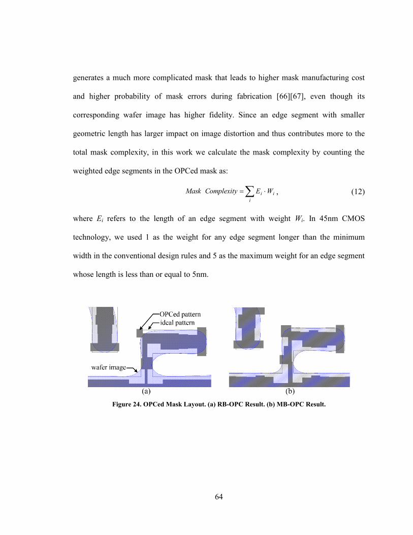
64
generates a much more complicated mask that leads to higher mask manufacturing cost
and higher probability of mask errors during fabrication [66][67], even though its
corresponding wafer image has higher fidelity. Since an edge segment with smaller
geometric length has larger impact on image distortion and thus contributes more to the
total mask complexity, in this work we calculate the mask complexity by counting the
weighted edge segments in the OPCed mask as:
i
i
i WEComplexityMask , (12)
where Ei refers to the length of an edge segment with weight Wi. In 45nm CMOS
technology, we used 1 as the weight for any edge segment longer than the minimum
width in the conventional design rules and 5 as the maximum weight for an edge segment
whose length is less than or equal to 5nm.
Figure 24. OPCed Mask Layout. (a) RB-OPC Result. (b) MB-OPC Result.
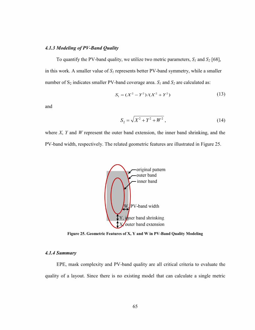
65
4.1.3 Modeling of PV-Band Quality
To quantify the PV-band quality, we utilize two metric parameters, S1 and S2 [68],
in this work. A smaller value of S1 represents better PV-band symmetry, while a smaller
number of S2 indicates smaller PV-band coverage area. S1 and S2 are calculated as:
)/()( 2222
1 YXYXS (13)
and
222
2 WYXS , (14)
where X, Y and W represent the outer band extension, the inner band shrinking, and the
PV-band width, respectively. The related geometric features are illustrated in Figure 25.
Figure 25. Geometric Features of X, Y and W in PV-Band Quality Modeling
4.1.4 Summary
EPE, mask complexity and PV-band quality are all critical criteria to evaluate the
quality of a layout. Since there is no existing model that can calculate a single metric

66
number based on those criteria with distinct weights, all of them will be applied
throughout this dissertation to present different trade-off strategies. In any schemes, the
circuit performance will be checked to maintain the analog circuit performance
preservation.
4.2 Optimizations by Wire Widening and Wire Shifting
Wire widening and wire shifting operations are used locally by contraposing
potential fatal lithography hotspots, which are derived from the lithography image
simulation. Ideally a hotspot would directly indicate a pair of tiles that may be bridged to
form a short circuit or one tile that may be broken to an open circuit. However, due to
irregularity of the wafer image, a hotspot, which is usually a complex polygon, may
cover a bunch of related or even unrelated tiles. For instance, Figure 26 depicts a short-
circuit hotspot, where a single reverse F-shape hotspot polygon exists among Tiles A-E.
In such a situation, a regular detection method cannot quickly discern between which pair
of tiles a short-circuit problem would likely take place. If we arbitrarily add an arc to
each pair of edges that are covered by the hotspot, the complexity of the graph would
unnecessarily increase and even unexpected chip area increment might emerge. Such
large hotspots, which can be frequently identified in congested layout scenario, may
easily mess up the constraint template during analog layout retargeting.
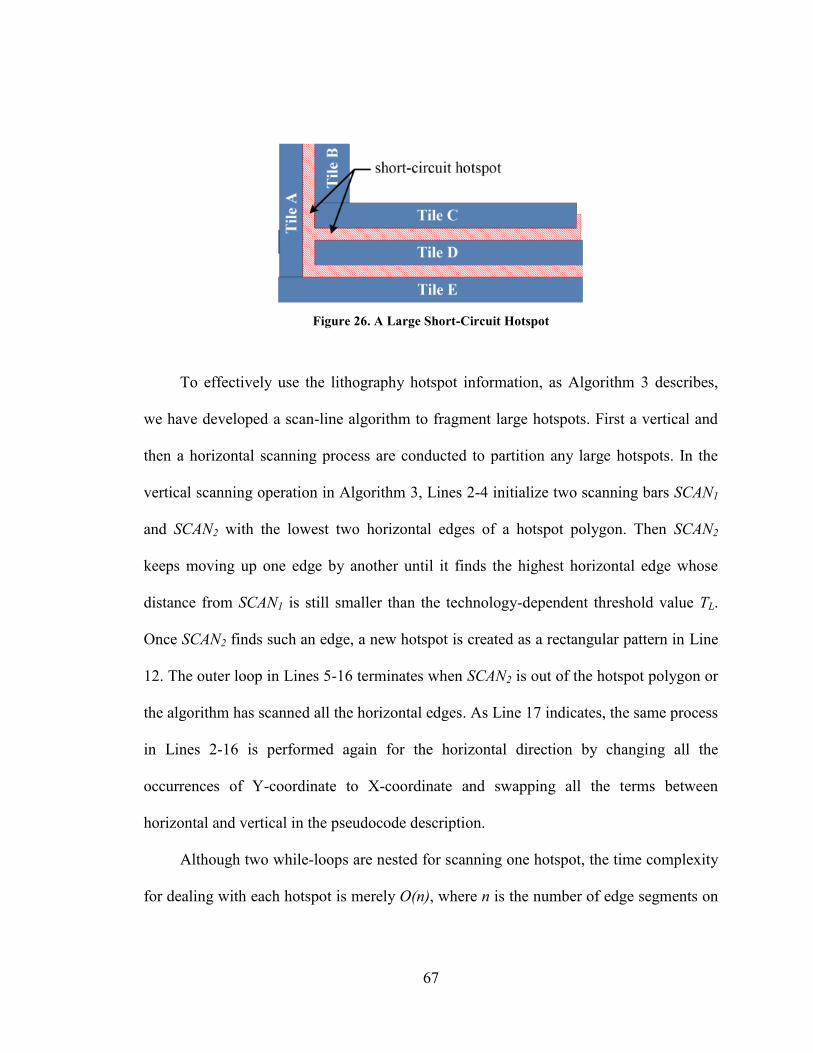
67
Figure 26. A Large Short-Circuit Hotspot
To effectively use the lithography hotspot information, as Algorithm 3 describes,
we have developed a scan-line algorithm to fragment large hotspots. First a vertical and
then a horizontal scanning process are conducted to partition any large hotspots. In the
vertical scanning operation in Algorithm 3, Lines 2-4 initialize two scanning bars SCAN1
and SCAN2 with the lowest two horizontal edges of a hotspot polygon. Then SCAN2
keeps moving up one edge by another until it finds the highest horizontal edge whose
distance from SCAN1 is still smaller than the technology-dependent threshold value TL.
Once SCAN2 finds such an edge, a new hotspot is created as a rectangular pattern in Line
12. The outer loop in Lines 5-16 terminates when SCAN2 is out of the hotspot polygon or
the algorithm has scanned all the horizontal edges. As Line 17 indicates, the same process
in Lines 2-16 is performed again for the horizontal direction by changing all the
occurrences of Y-coordinate to X-coordinate and swapping all the terms between
horizontal and vertical in the pseudocode description.
Although two while-loops are nested for scanning one hotspot, the time complexity
for dealing with each hotspot is merely O(n), where n is the number of edge segments on

68
the hotspot polygon since each edge is only scanned once. The number of large hotspots
depends on layout structure. Typically it is less than 20% of all the fatal lithography
hotspots in an analog circuit according to our experiments. Figure 27 demonstrates
fragmentation results for the huge short-circuit hotspot in Figure 26, where three separate
horizontal hotspots and another three unconnected vertical hotspots are generated by
Algorithm 3. Note that three generated hotspots are the rectangles with tiny size due to
the minor bumps around the vertices of the polygon. The tiles and related constraints
identified by those tiny hotspots can actually be covered by the other bigger hotspots. So
in practice ignoring these tiny hotspots would not necessarily impose a strong impact on
the final result.
Figure 27. Hotspot Fragmentation
69
Algorithm 3: Large lithography hotspot fragmentation
1. Foreach large hotspot polygon whose length or width is larger
than a technology-dependent threshold value TL
2. Sort all horizontal edges according to the Y-coordinates
3. SCAN1 = Y-coordinate of the lowest horizontal edge
4. SCAN2 = Y-coordinate of the edge immediately higher than SCAN1
5. While (SCAN2 ≠ NULL) // vertical scanning
6. If (SCAN2 - SCAN1 < TL)
7. While (SCAN2 - SCAN1 < TL && SCAN2 ≠ NULL)
8. temp = SCAN2
9. SCAN2 = Y-coordinate of the edge immediately
higher than SCAN2
10. End while
11. SCAN2 = temp
12. Create a new rectangular hotspot between SCAN1 and SCAN2
13. End if
14. SCAN1 = SCAN2
15. SCAN2 = Y-coordinate of the edge immediately
higher than SCAN1
16. End while
17. Repeat Lines 2-16 for the horizontal scanning operation
18. End for
According to the processed fatal lithograph hotspots, wire widening and wire
shifting operations can be effectively applied in the constraint graph. A typical wire
widening operation is to increase the weight of a solid arc when the related tile is covered
by an open-circuit hotspot. Similarly, a typical wire shifting operation is applied to a
space arc for compensating a short-circuit hotspot. In the same manner as described in
Section 3.4, we devise to allocate the redundant space according to the area of hotspot.
After enlargement, the related arc weight WRi for a hotspot is changed to:
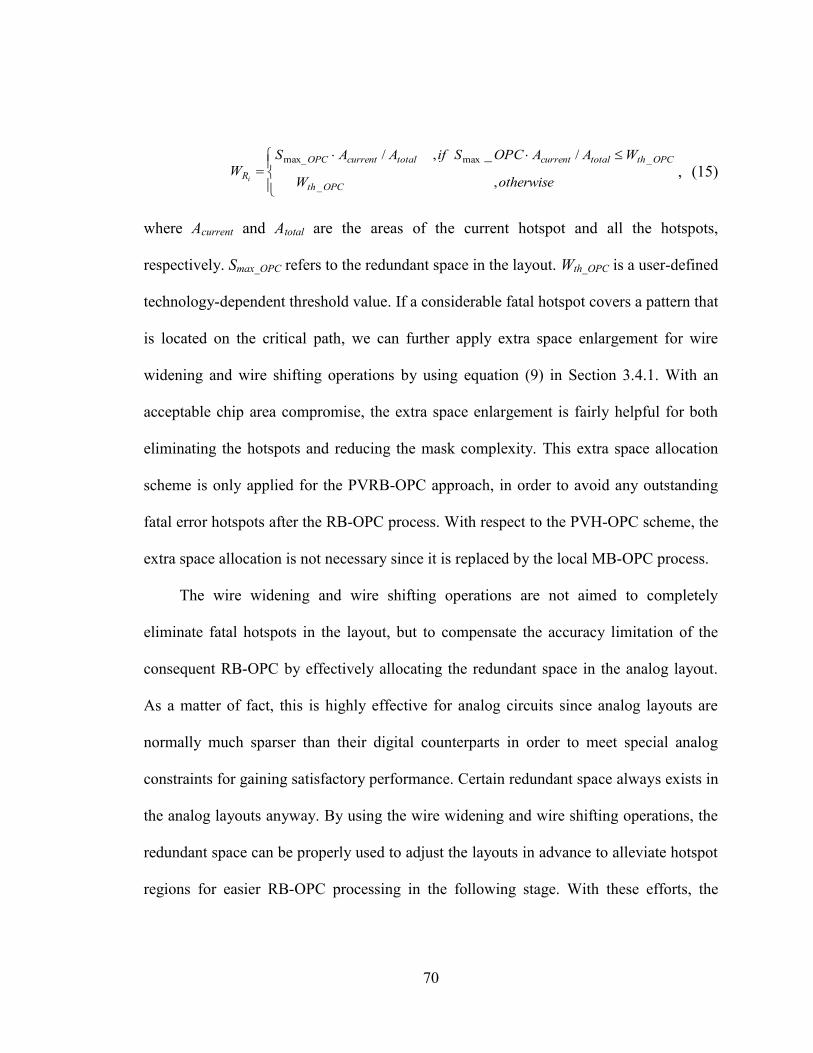
70
otherwiseW
WAAOPCSifAAS
WOPCth
OPCthtotalcurrenttotalcurrentOPC
Ri ,
/_,/
_
_maxmax_
, (15)
where Acurrent and Atotal are the areas of the current hotspot and all the hotspots,
respectively. Smax_OPC refers to the redundant space in the layout. Wth_OPC is a user-defined
technology-dependent threshold value. If a considerable fatal hotspot covers a pattern that
is located on the critical path, we can further apply extra space enlargement for wire
widening and wire shifting operations by using equation (9) in Section 3.4.1. With an
acceptable chip area compromise, the extra space enlargement is fairly helpful for both
eliminating the hotspots and reducing the mask complexity. This extra space allocation
scheme is only applied for the PVRB-OPC approach, in order to avoid any outstanding
fatal error hotspots after the RB-OPC process. With respect to the PVH-OPC scheme, the
extra space allocation is not necessary since it is replaced by the local MB-OPC process.
The wire widening and wire shifting operations are not aimed to completely
eliminate fatal hotspots in the layout, but to compensate the accuracy limitation of the
consequent RB-OPC by effectively allocating the redundant space in the analog layout.
As a matter of fact, this is highly effective for analog circuits since analog layouts are
normally much sparser than their digital counterparts in order to meet special analog
constraints for gaining satisfactory performance. Certain redundant space always exists in
the analog layouts anyway. By using the wire widening and wire shifting operations, the
redundant space can be properly used to adjust the layouts in advance to alleviate hotspot
regions for easier RB-OPC processing in the following stage. With these efforts, the
71
hotspot-prone regions can be minimized during the consequent analog layout retargeting.
This is also a helpful scheme for the PVH-OPC method.
4.3 PV-Band Shifting
With respect to analog layouts, the circuit performance can be affected by parasitic
values to some extent. On the other side, the device sizes are so dominantly critical that
any variation on the width or length of a transistor, especially matching devices (e.g.,
current mirrors or differential pairs), can readily degrade the circuit performance. To
address this issue, we have proposed an optimization scheme, named as PV-band
shifting, to prevent analog circuits from performance degradation induced by process
variation on transistor gates.
As Figure 28(a) shows, the inner band and the outer band can result in different
effective gate length values. In the worst case, one of the matching device falls into the
minimum gate length corresponding to the inner band and the other remains the
maximum gate length according to the outer band. This may even happen to adjacent
devices in the layout due to 1) dose variation contributed by source light or proximity
environment of the matching pair [69]; 2) defocus due to the imperfect planarization of
fabrication masks [43]; and 3) material defects such as spot defect [70] and bubble defect
[71]. In our algorithm, we not only focus on gate length (L) variation, but also consider
potential gate width (W) variation when L is small (e.g., L<150nm in our implementation)
or W is relatively small (e.g., W<500nm in our implementation). The image shrinking of
72
such a “slim” or “short” gate may result in W shortening. As Figure 28(a) shows, we
enlarge the extension distance between the poly region and the active region for small L
or W devices based on our defined OPC rules to guarantee an expected gate width from
wafer image. The extension amount is derived from a rule table built up according to the
line-end shrinking features on the poly region.
Figure 28. PV-Band Shifting. (a) Original PV-Band. (b) After PV-Band Shifting with Zoom-in
Detailed PV-Band.
Conventional PV-aware OPC, which is composed of a variational lithography
model considering dosage error and defocus, attempts to minimize variational edge
placement errors during MB-OPC iterations [40]. In contrast, we aim to shift the PV-
band so that the original pattern edge (i.e., the marked “original edge” inside the zoom-in
block) is equidistant from the outer band and the inner band, as Figure 28(b) shows. With
the PV-band information extracted from the image simulation run after the initial
73
retargeting, we fragment the poly regions and insert aid features for each segment
according to its corresponding PV-band size. This is also a rule-based approach that the
aid feature sizes can be quickly derived from a look-up-table.
The previous work on PV-aware OPC is normally aimed at shrinking the size of the
PV-band and making effort to move the image contour to approach the ideal layout
boundary. This would inevitably bring about expensive computation cost and high mask
complexity. Instead our proposed PV-band shifting scheme is devoted to shifting the PV
inner and outer bands besides the ideal gate edges, which can equivalently contribute to
the preservation of circuit performance but with much less computation effort and mask
complexity. Therefore, in this work the PV-band shifting scheme is deployed as an
efficient solution to alleviate process variation in analog circuits, which can be easily
integrated into the framework of our proposed analog layout retargeting with a RB-OPC
process.
4.4 PV-Aware Rule-Based OPC (PVRB-OPC)
4.4.1 PVRB-OPC Flow
Our proposed analog layout retargeting framework with PVRB-OPC is presented in
Figure 29. After the initial retargeting, we apply an efficient trial RB-OPC process on the
migrated layout. The OPCed layout from this trial stage represents a final layout but
without any local optimization, which can help identify actual potential hotspots in the
layout. We then perform an image simulation with process variation on the OPCed
74
migrated layout. From the simulation results, we extract fatal lithography hotspots that
may cause short-circuit and open-circuit problems among interconnects, and PV-bands
on transistor gates. Our algorithm effectively fragments the fatal hotspots for easy
identification of the related tiles.
Figure 29. Proposed Analog Layout Retargeting with PVRB-OPC
After that, the wire widening and wire shifting operations are conducted by
updating the constraint graph. Once the updated constraint graph is solved as the second
retargeting stage, the 2nd
migrated layout is manipulated by our proposed RB-OPC
algorithm, which serves as a post-processing stage of the layout retargeting process to
create OPCed layout with patterns appearing on the final mask. With respect to analog
75
layouts, symmetry and matching constraints are thoroughly handled by the layout
template to create identical device orientation, current flow and proximity environments
for symmetric or matching structures. This is not only an indispensable requirement of
analog layouts, but also would guarantee the same OPC operations can be performed on
those structures to reduce mismatch effects.
Even though both the constraint graph in the layout retargeting and the RB-OPC
algorithm play with rules, they will not be combined together since the former fully
respects the conventional design rules, whereas the latter one rarely complies with the
same design rules. The extra post-processing OPC stage actually simplifies the tile
operations and makes the optimization highly controllable. During the OPC processing,
the PV-band shifting is performed by using the PV analysis results obtained at the earlier
stage. Its main purpose is to preserve the circuit performance in different process
windows. Eventually, an OPCed layout is created as the output. Benefiting each other,
the analog layout retargeting approach and the RB-OPC are properly united to make the
proposed methodology effective but without iterations in this framework.
76
4.4.2 RB-OPC Algorithm
For a rule-based approach, the first thing to study is the rules. The more possibilities
a rule library can cover, the higher accuracy a RB-OPC approach can achieve. Even
though a rule library generation is a one-time effort, excessive elaboration on the various
rules in the library would reduce the algorithm efficiency. Based on [67] and [72], in this
work we have included six types of rules: line-in-parallel rule, island rule, end-of-line
rule, corner rule, isolated-line rule, and dense-line rule, which are depicted in Figure 30.
Figure 31 presents a specific example of the end-of-line rule, where the rectangle in blue
is the original pattern, the rectangles in grey represent some nearby patterns, and the
polygons in red illustrate the OPCed patterns. Within a certain range, the width w of the
original tile marked in blue and the related distances sx, sy1 and sy2 were firstly used to
create a group of test cases. We then applied high-accuracy MB-OPC on all test cases to
generate a rule library with various values of the other parameters in Figure 31 (i.e., a, b,
c1, c2, d1-d4, e1-e4, mw and ml) that represent the sizes and relative positions of the
OPCed patterns. When performing the RB-OPC algorithm, similar end-of-line patterns
are recognized by their corresponding w, sx, sy1 and sy2 values and then the original
rectangle tile is “replaced” by the end-of-line patterns (i.e., the five polygons in red in
Figure 31) with pre-defined geometric dimensions stored in the library.
77
Figure 30. Applied Rules in our RB-OPC
Figure 31. The End-of-Line Rule
During the RB-OPC, rule conflicts might emerge if the five types of rules are
applied in an arbitrary order. Figure 32, where the original patterns are drawn in blue and
the OPCed patterns are marked in red, presents a case study of rule conflicts when a line-
in-parallel rule takes effect on Tile A before using an end-of-line rule on Tile B. On Tile
A, a notch is firstly generated by the line-in-parallel rule according to the overlap length
d1 between Tile A and Tile B. Consequently, the actual space between them increases
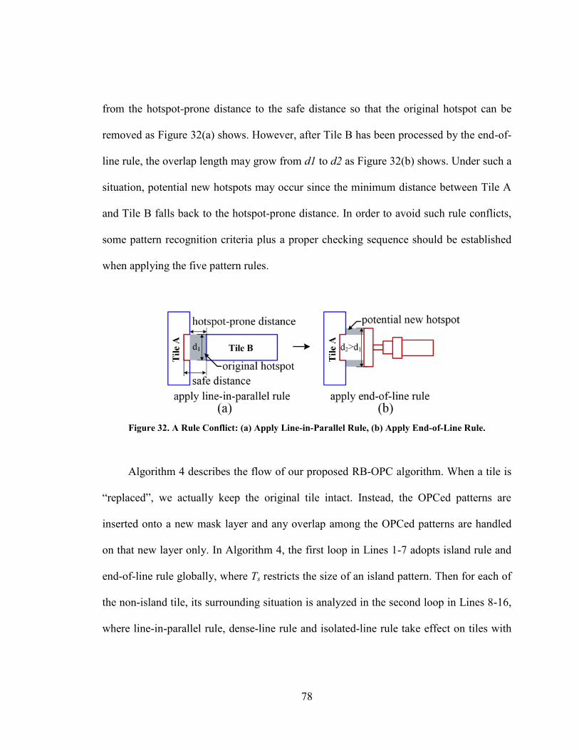
78
from the hotspot-prone distance to the safe distance so that the original hotspot can be
removed as Figure 32(a) shows. However, after Tile B has been processed by the end-of-
line rule, the overlap length may grow from d1 to d2 as Figure 32(b) shows. Under such a
situation, potential new hotspots may occur since the minimum distance between Tile A
and Tile B falls back to the hotspot-prone distance. In order to avoid such rule conflicts,
some pattern recognition criteria plus a proper checking sequence should be established
when applying the five pattern rules.
Figure 32. A Rule Conflict: (a) Apply Line-in-Parallel Rule, (b) Apply End-of-Line Rule.
Algorithm 4 describes the flow of our proposed RB-OPC algorithm. When a tile is
“replaced”, we actually keep the original tile intact. Instead, the OPCed patterns are
inserted onto a new mask layer and any overlap among the OPCed patterns are handled
on that new layer only. In Algorithm 4, the first loop in Lines 1-7 adopts island rule and
end-of-line rule globally, where Ts restricts the size of an island pattern. Then for each of
the non-island tile, its surrounding situation is analyzed in the second loop in Lines 8-16,
where line-in-parallel rule, dense-line rule and isolated-line rule take effect on tiles with

79
and without nearby patterns, respectively. Since the end-of-line patterns have been
processed in the first loop, in Line 9 the line-in-parallel rule checks the overlap length
based on the OPCed end-of-line patterns in order to avoid the rule conflicts as exposed in
Figure 32. Finally in the last loop of Lines 18-20, the corner rule is applied.
Algorithm 4: RB-OPC Algorithm
1. Foreach pattern in the original layout
2. If both width and length are smaller than threshold Ts
3. Apply the island rule
4. Else
5. Apply the end-of-line rule if no connecting patterns
are found near the line ends
6. End if
7. End for
8. Foreach non-island pattern edge in the original layout
9. If only one pattern in parallel is found
10. Apply the line-in-parallel rule considering the
corrected end-of-line patterns
11. Else if more than one pattern in parallel is found
12. Apply the dense-line rule considering the
corrected end-of-line patterns
13. Else
14. Apply the isolated-line rule
15. End if
16. End for
17. Fix all connection problems if any exist
18. Foreach corner pattern in the original layout
19. Apply the corner rule if a corner is recognized
20. End for
In Algorithm 4, Line 17 attempts to fix all the connection problems on the OPCed
mask layer before applying the corner rule. Figure 33 illustrates a corner example before
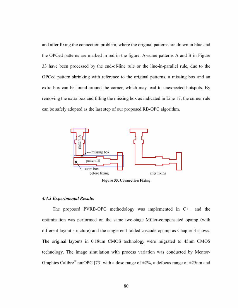
80
and after fixing the connection problem, where the original patterns are drawn in blue and
the OPCed patterns are marked in red in the figure. Assume patterns A and B in Figure
33 have been processed by the end-of-line rule or the line-in-parallel rule, due to the
OPCed pattern shrinking with reference to the original patterns, a missing box and an
extra box can be found around the corner, which may lead to unexpected hotspots. By
removing the extra box and filling the missing box as indicated in Line 17, the corner rule
can be safely adopted as the last step of our proposed RB-OPC algorithm.
Figure 33. Connection Fixing
4.4.3 Experimental Results
The proposed PVRB-OPC methodology was implemented in C++ and the
optimization was performed on the same two-stage Miller-compensated opamp (with
different layout structure) and the single-end folded cascode opamp as Chapter 3 shows.
The original layouts in 0.18um CMOS technology were migrated to 45nm CMOS
technology. The image simulation with process variation was conducted by Mentor-
Graphics Calibre®
nmOPC [73] with a dose range of ±2%, a defocus range of ±25nm and
81
a positive photoresist model [74]. According to our experiments, using either positive or
negative photoresist model would not affect the performance of our algorithm. The
pattern library for the RB-OPC was established on top of simulations and experiments
with nmOPC as well. In 45nm CMOS technology, we assume TL=120nm in Algorithm 3
as the threshold value for large lithography hotspots, Ts=120nm in Algorithm 4 as the
threshold value for detecting island patterns, Wth_OPC=100nm as the threshold of
enlargement for wire widening and wire shifting operations, and α=0.25 for extra space
enlargement by default.
We compare the results of our proposed methodology with alternative OPC
methods, which are listed in List II. All of the three OPC approaches were integrated into
our layout reuse and retargeting platform for a fair comparison. Table 5 presents the
results that were evaluated by EPE, mask complexity, number of fatal errors, chip area,
and runtime.
LIST II. ALTERNATIVE METHODS USED IN THE EXPERIMENTS
Method Description
GARB-OPC rule-based OPC approach with GA in [44]
MB-OPC model-based OPC algorithm by nmOPC
WW/WS, α=0 merely using wire widening and wire shift with zero
extra space enlargement
PVRB-OPC, α=0 our proposed rule-based OPC with zero extra space
enlargement
WW/WS, α=0.25 merely using wire widening and wire shift with
certain extra space enlargement
Complete PVRB-OPC our proposed rule-based OPC with PV-band shifting
operations
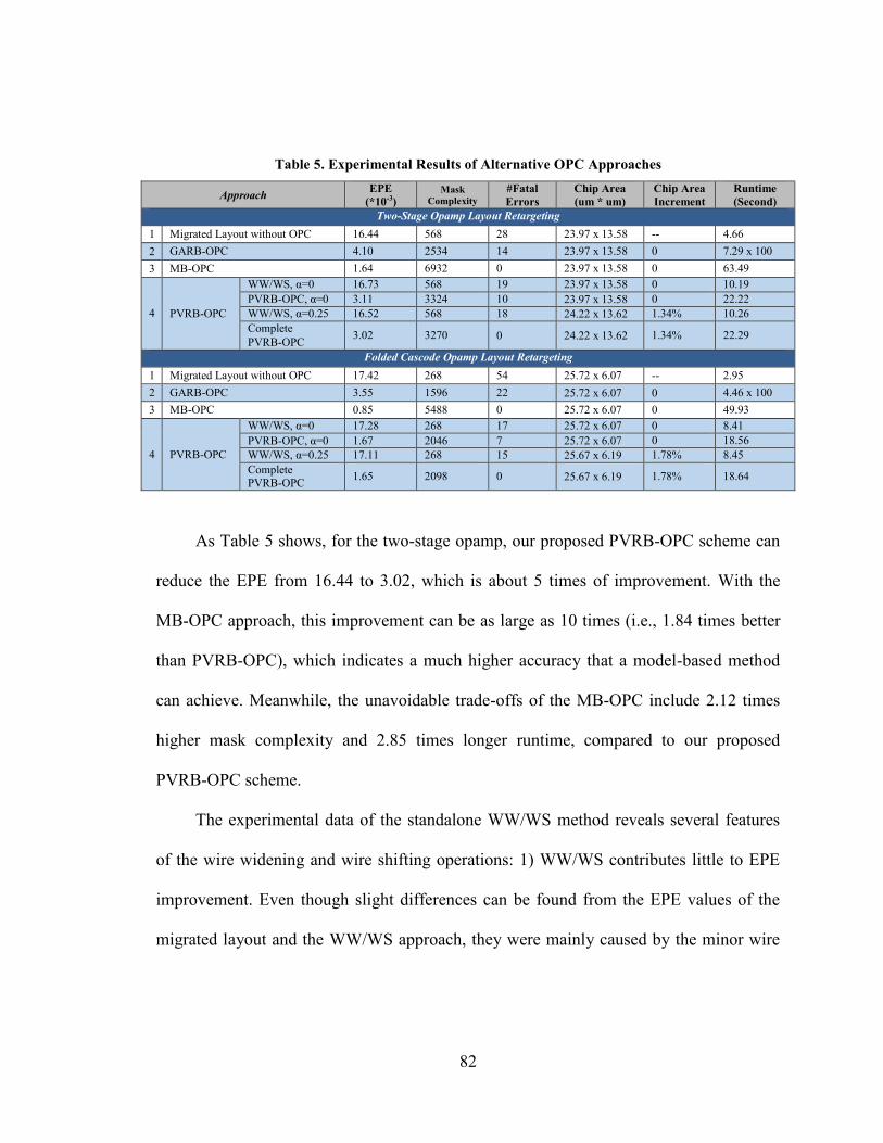
82
Table 5. Experimental Results of Alternative OPC Approaches
Approach EPE
(*10-3) Mask
Complexity
#Fatal
Errors
Chip Area
(um * um)
Chip Area
Increment
Runtime
(Second)
Two-Stage Opamp Layout Retargeting
1 Migrated Layout without OPC 16.44 568 28 23.97 x 13.58 -- 4.66
2 GARB-OPC 4.10 2534 14 23.97 x 13.58 0 7.29 x 100
3 MB-OPC 1.64 6932 0 23.97 x 13.58 0 63.49
4 PVRB-OPC
WW/WS, α=0 16.73 568 19 23.97 x 13.58 0 10.19
PVRB-OPC, α=0 3.11 3324 10 23.97 x 13.58 0 22.22
WW/WS, α=0.25 16.52 568 18 24.22 x 13.62 1.34% 10.26
Complete
PVRB-OPC 3.02 3270 0 24.22 x 13.62 1.34% 22.29
Folded Cascode Opamp Layout Retargeting
1 Migrated Layout without OPC 17.42 268 54 25.72 x 6.07 -- 2.95
2 GARB-OPC 3.55 1596 22 25.72 x 6.07 0 4.46 x 100
3 MB-OPC 0.85 5488 0 25.72 x 6.07 0 49.93
4 PVRB-OPC
WW/WS, α=0 17.28 268 17 25.72 x 6.07 0 8.41
PVRB-OPC, α=0 1.67 2046 7 25.72 x 6.07 0 18.56
WW/WS, α=0.25 17.11 268 15 25.67 x 6.19 1.78% 8.45
Complete
PVRB-OPC 1.65 2098 0 25.67 x 6.19 1.78% 18.64
As Table 5 shows, for the two-stage opamp, our proposed PVRB-OPC scheme can
reduce the EPE from 16.44 to 3.02, which is about 5 times of improvement. With the
MB-OPC approach, this improvement can be as large as 10 times (i.e., 1.84 times better
than PVRB-OPC), which indicates a much higher accuracy that a model-based method
can achieve. Meanwhile, the unavoidable trade-offs of the MB-OPC include 2.12 times
higher mask complexity and 2.85 times longer runtime, compared to our proposed
PVRB-OPC scheme.
The experimental data of the standalone WW/WS method reveals several features
of the wire widening and wire shifting operations: 1) WW/WS contributes little to EPE
improvement. Even though slight differences can be found from the EPE values of the
migrated layout and the WW/WS approach, they were mainly caused by the minor wire
83
operations during layout retargeting; 2) WW/WS will not increase the mask complexity
since they only affect the relative position among tiles but not the tile shapes; 3) WW/WS
cannot completely removed all fatal errors. However, these operations greatly reduce the
number of fatal error hotspots and potentially help the RB-OPC to eliminate hotspots.
This can be confirmed by the fact that the complete PVRB-OPC ends up with zero fatal
hotspot, which GARB-OPC cannot achieve; and 4) WW/WS may result in chip area
increment, which is the main trade-off by using extra space enlargement during the wire
widening and wire shifting operations. The increment level can be controlled within
1.34%, which is very moderate per se. If no extra space is allowed by using α=0, the
PVRB-OPC still presents an acceptable result that both EPE and mask complexity
slightly increase from 3.02 to 3.11 and from 3270 to 3324, respectively. In that case, no
chip area increment is reported and several fatal error hotspots can be found. Those
remaining hotspots are usually on the critical path in the layouts where more complicated
rules with higher accuracy and larger mask complexity may be required.
For the GARB-OPC approach, it achieves comparable EPE and mask complexity
compared to our proposed PVRB-OPC scheme. However, its total runtime is extremely
long even compared with MB-OPC. In [44], the original layout was actually
recommended to be decomposed into pieces, which were then handled by a parallel
computation scheme with up to 16 processes to accelerate the runtime of GARB-OPC. To
simplify the implementation in this work, we only used one CPU but decomposed the
layout into a 10 x 10 array. Then GA was performed on each of the layout segments. The
84
average runtime of GARB-OPC on each layout segment was about 7.29 seconds. This is
mainly due to the relatively long runtime of a GA algorithm. Similar results can be found
for the folded cascode opamp.
Now we report a quick experimental result about the current mirror example
discussed in Section 2.2.2. Originally the current mismatch is 8.56%, which can be
improved to 2.35% and 3.31% by using PVRB-OPC and MB-OPC, respectively. This
result exhibits that the PVRB-OPC method benefits from its effective PV-band handling
scheme compared to its counterpart.
Table 6 shows the post-layout simulation results on the processed layouts with
different OPC methods. We performed Spectre simulations on layout-extracted netlists
by using the vendor-provided 45nm CMOS technology process design kit (PDK). The
layout extraction was done by Cadence® PVS, which would calculate equivalent gate
width and length for transistors with non-rectangle gate images. In Table 6, the row with
the title of “Without OPC” stands for the traditional retargeting method [33] without the
OPC processing, while the row with the title of “PVRB-OPC” represents the proposed
Complete PVRB-OPC method that appears in Table 5. Minor manual modifications were
done on the results of GARB-OPC to remove some remaining fatal error hotspots. The
rows with the title of “pwc mismatch” after each OPC method report the post-layout
simulation results in the manually created pseudo worst-case mismatch scenario, where
the matching devices fall into different gate lengths according to the derived PV-bands.
Here “pwc” refers to “pseudo worst-case”.
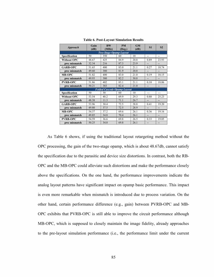
85
Table 6. Post-Layout Simulation Results
Approach Gain
(dB)
BW
(MHz)
PM
(Deg.)
GM
(dB) S1 S2
Two-Stage Opamp Layout
Specification 50 350 60 10 -- --
Without OPC 48.67 425 84.9 20.8 0.89 23.93
pwc mismatch 32.34 216 87.3 23.9 -- --
GARB-OPC 51.65 400 83.0 21.1 0.27 18.74
pwc mismatch 49.60 380 81.9 20.8 -- --
MB-OPC 51.82 400 83.0 21.0 0.19 18.15
pwc mismatch 49.93 380 82.2 30.8 -- --
PVRB-OPC 51.86 402 83.1 21.1 0.10 18.06
pwc mismatch 50.21 383 82.4 21.0 -- --
Folded Cascode Opamp Layout
Specification 50 30 60 10 --- ---
Without OPC 53.54 40.2 69.9 29.3 0.88 25.23
pwc mismatch 48.38 11.3 71.1 26.7 -- --
GARB-OPC 53.96 30.4 72.5 28.8 0.41 19.20
pwc mismatch 49.80 37.5 72.5 28.9 -- --
MB-OPC 54.37 37.2 69.6 26.1 0.36 19.16
pwc mismatch 49.85 34.8 70.4 26.1 -- --
PVRB-OPC 54.59 36.6 69.8 26.5 0.33 19.05
pwc mismatch 50.25 34.0 69.8 26.1 -- --
As Table 6 shows, if using the traditional layout retargeting method without the
OPC processing, the gain of the two-stage opamp, which is about 48.67db, cannot satisfy
the specification due to the parasitic and device size distortions. In contrast, both the RB-
OPC and the MB-OPC could alleviate such distortions and make the performance closely
above the specifications. On the one hand, the performance improvements indicate the
analog layout patterns have significant impact on opamp basic performance. This impact
is even more remarkable when mismatch is introduced due to process variation. On the
other hand, certain performance difference (e.g., gain) between PVRB-OPC and MB-
OPC exhibits that PVRB-OPC is still able to improve the circuit performance although
MB-OPC, which is supposed to closely maintain the image fidelity, already approaches
to the pre-layout simulation performance (i.e., the performance limit under the current
86
settings of device sizes in the two opamps, which is 52.02dB and 54.93dB for the gains
of the two-stage opamp and folded cascode opamp respectively for instance). Under the
pseudo worst-case mismatch conditions in Table 6, PVRB-OPC presented the best
preservation so that the specifications could be still satisfied, whereas GARB-OPC and
MB-OPC ended up with the post-layout gain values lower than the requirement.
Although all of the three OPC methods work on the same migrated layout, the
better performance of PVRB-OPC can be attributed to its pattern operations by 1) wire
widening and wire shifting, which can not only compensate the accuracy limitation of the
RB-OPC, but also diminish the coupling capacitance among the congested interconnects
to some extent; and 2) PV-band shifting, which achieves better PV-band quality. To
quantify the benefit of PV-band shifting, two more metric parameters, S1 and S2, are
introduced in Table 6. According to [68], a smaller value of S1 represents better PV-band
symmetry and a smaller number of S2 indicates smaller PV-band coverage area. As Table
6 shows, PVRB-OPC achieves the smallest S1 and S2 values, which are attributed to our
proposed PV-band shifting scheme. They also help unveil the reason why the circuit
performance with PVRB-OPC is better than those with the other OPC algorithms under
mismatch conditions. For the folded cascode opamp, the migrated layout without OPC
could satisfy the specifications. However, it exposed the same degradation when
mismatch was introduced due to process variation and similar results could be observed
for the other OPC methods. Therefore, we can conclude that our proposed PVRB-OPC is
more effective and efficient than both MB-OPC and GARB-OPC in terms of analog
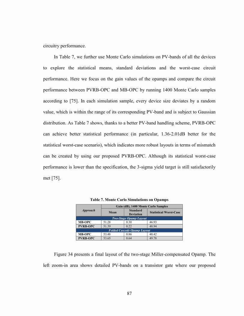
87
circuitry performance.
In Table 7, we further use Monte Carlo simulations on PV-bands of all the devices
to explore the statistical means, standard deviations and the worst-case circuit
performance. Here we focus on the gain values of the opamps and compare the circuit
performance between PVRB-OPC and MB-OPC by running 1400 Monte Carlo samples
according to [75]. In each simulation sample, every device size deviates by a random
value, which is within the range of its corresponding PV-band and is subject to Gaussian
distribution. As Table 7 shows, thanks to a better PV-band handling scheme, PVRB-OPC
can achieve better statistical performance (in particular, 1.36-2.01dB better for the
statistical worst-case scenario), which indicates more robust layouts in terms of mismatch
can be created by using our proposed PVRB-OPC. Although its statistical worst-case
performance is lower than the specification, the 3-sigma yield target is still satisfactorily
met [75].
Table 7. Monte Carlo Simulations on Opamps
Approach
Gain (dB), 1400 Monte Carlo Samples
Mean Standard
Deviation Statistical Worst-Case
Two-Stage Opamp Layout
MB-OPC 51.28 0.30 46.93
PVRB-OPC 51.39 0.22 48.94
Folded Cascode Opamp Layout
MB-OPC 53.48 0.86 48.42
PVRB-OPC 53.65 0.64 49.78
Figure 34 presents a final layout of the two-stage Miller-compensated Opamp. The
left zoom-in area shows detailed PV-bands on a transistor gate where our proposed
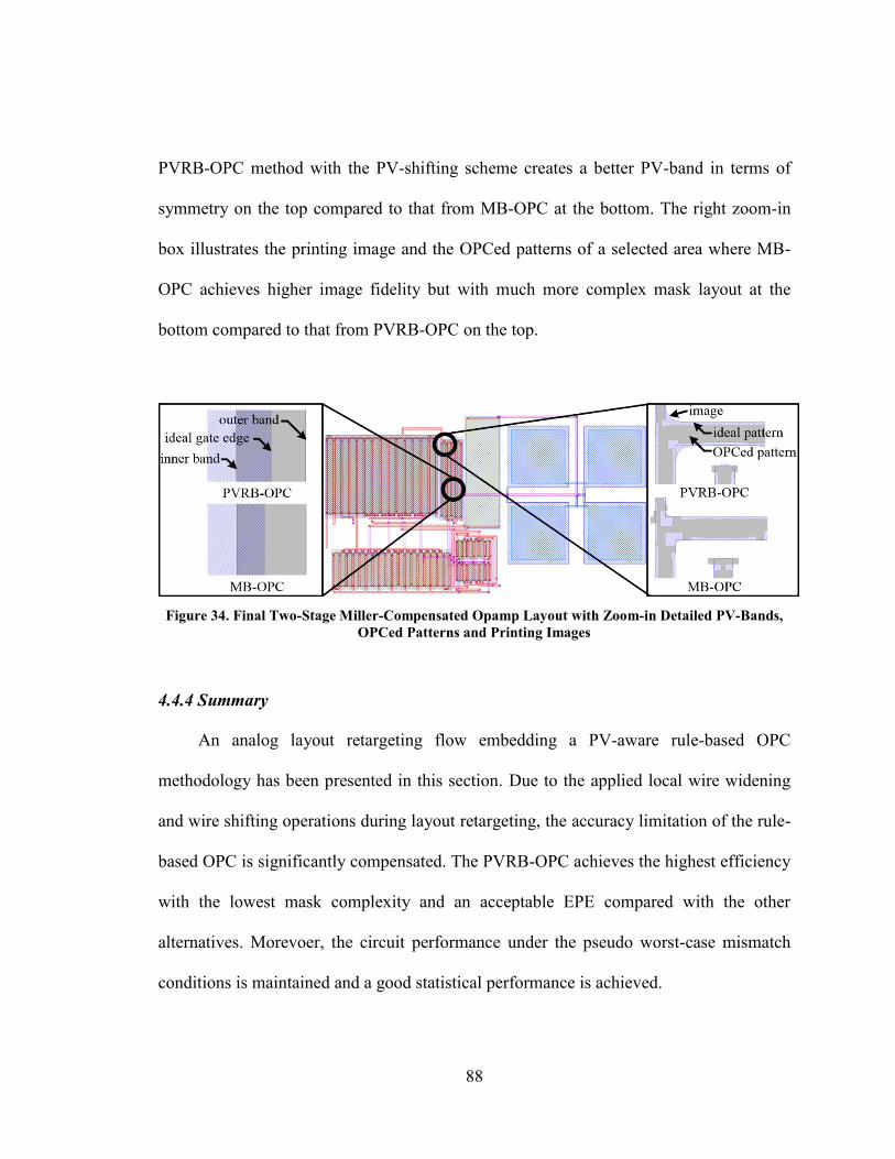
88
PVRB-OPC method with the PV-shifting scheme creates a better PV-band in terms of
symmetry on the top compared to that from MB-OPC at the bottom. The right zoom-in
box illustrates the printing image and the OPCed patterns of a selected area where MB-
OPC achieves higher image fidelity but with much more complex mask layout at the
bottom compared to that from PVRB-OPC on the top.
Figure 34. Final Two-Stage Miller-Compensated Opamp Layout with Zoom-in Detailed PV-Bands,
OPCed Patterns and Printing Images
4.4.4 Summary
An analog layout retargeting flow embedding a PV-aware rule-based OPC
methodology has been presented in this section. Due to the applied local wire widening
and wire shifting operations during layout retargeting, the accuracy limitation of the rule-
based OPC is significantly compensated. The PVRB-OPC achieves the highest efficiency
with the lowest mask complexity and an acceptable EPE compared with the other
alternatives. Morevoer, the circuit performance under the pseudo worst-case mismatch
conditions is maintained and a good statistical performance is achieved.
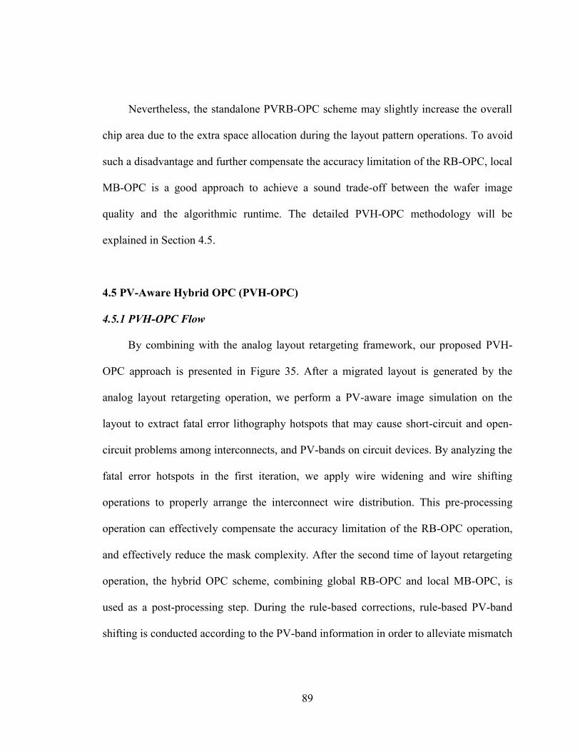
89
Nevertheless, the standalone PVRB-OPC scheme may slightly increase the overall
chip area due to the extra space allocation during the layout pattern operations. To avoid
such a disadvantage and further compensate the accuracy limitation of the RB-OPC, local
MB-OPC is a good approach to achieve a sound trade-off between the wafer image
quality and the algorithmic runtime. The detailed PVH-OPC methodology will be
explained in Section 4.5.
4.5 PV-Aware Hybrid OPC (PVH-OPC)
4.5.1 PVH-OPC Flow
By combining with the analog layout retargeting framework, our proposed PVH-
OPC approach is presented in Figure 35. After a migrated layout is generated by the
analog layout retargeting operation, we perform a PV-aware image simulation on the
layout to extract fatal error lithography hotspots that may cause short-circuit and open-
circuit problems among interconnects, and PV-bands on circuit devices. By analyzing the
fatal error hotspots in the first iteration, we apply wire widening and wire shifting
operations to properly arrange the interconnect wire distribution. This pre-processing
operation can effectively compensate the accuracy limitation of the RB-OPC operation,
and effectively reduce the mask complexity. After the second time of layout retargeting
operation, the hybrid OPC scheme, combining global RB-OPC and local MB-OPC, is
used as a post-processing step. During the rule-based corrections, rule-based PV-band
shifting is conducted according to the PV-band information in order to alleviate mismatch
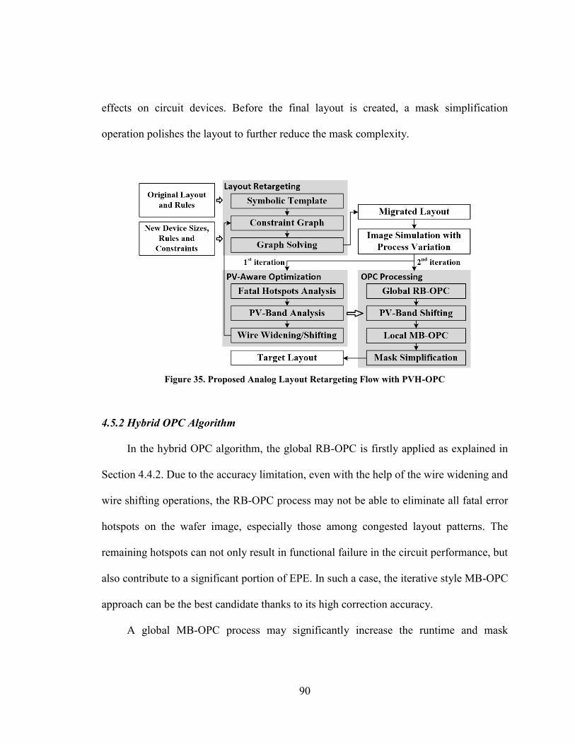
90
effects on circuit devices. Before the final layout is created, a mask simplification
operation polishes the layout to further reduce the mask complexity.
Figure 35. Proposed Analog Layout Retargeting Flow with PVH-OPC
4.5.2 Hybrid OPC Algorithm
In the hybrid OPC algorithm, the global RB-OPC is firstly applied as explained in
Section 4.4.2. Due to the accuracy limitation, even with the help of the wire widening and
wire shifting operations, the RB-OPC process may not be able to eliminate all fatal error
hotspots on the wafer image, especially those among congested layout patterns. The
remaining hotspots can not only result in functional failure in the circuit performance, but
also contribute to a significant portion of EPE. In such a case, the iterative style MB-OPC
approach can be the best candidate thanks to its high correction accuracy.
A global MB-OPC process may significantly increase the runtime and mask
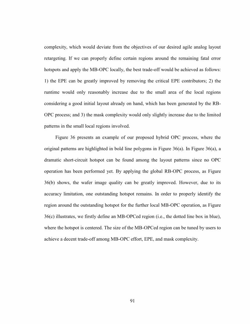
91
complexity, which would deviate from the objectives of our desired agile analog layout
retargeting. If we can properly define certain regions around the remaining fatal error
hotspots and apply the MB-OPC locally, the best trade-off would be achieved as follows:
1) the EPE can be greatly improved by removing the critical EPE contributors; 2) the
runtime would only reasonably increase due to the small area of the local regions
considering a good initial layout already on hand, which has been generated by the RB-
OPC process; and 3) the mask complexity would only slightly increase due to the limited
patterns in the small local regions involved.
Figure 36 presents an example of our proposed hybrid OPC process, where the
original patterns are highlighted in bold line polygons in Figure 36(a). In Figure 36(a), a
dramatic short-circuit hotspot can be found among the layout patterns since no OPC
operation has been performed yet. By applying the global RB-OPC process, as Figure
36(b) shows, the wafer image quality can be greatly improved. However, due to its
accuracy limitation, one outstanding hotspot remains. In order to properly identify the
region around the outstanding hotspot for the further local MB-OPC operation, as Figure
36(c) illustrates, we firstly define an MB-OPCed region (i.e., the dotted line box in blue),
where the hotspot is centered. The size of the MB-OPCed region can be tuned by users to
achieve a decent trade-off among MB-OPC effort, EPE, and mask complexity.
92
Figure 36. Hybrid OPC Example. (a) Original Mask Layout and Wafer Image. (b) After RB-
OPC. (c) Local MB-OPC Region. (d) After Hybrid OPC.
We then extend specific edges of the MB-OPCed region if the following two
conditions are simultaneously satisfied: 1) this edge crosses an existing layout pattern,
and 2) this edge is too close to any edge of the above existing layout pattern. For
instance, in Figure 36(c), the left and bottom edges are extended so that the MB-OPCed
region can completely cover those edges of the layout patterns. The extended MB-OPCed
region (i.e., the solid line box in blue in Figure 36(c)) specifies where the OPCed patterns
created by the MB-OPC operation are applied to replace those previously generated by
the RB-OPC operation. This extension can help ensure smooth boundary concatenation
among different OPCed patterns.
93
Based on the optical model of the image simulation, we further define a MB-OPC
region (as shown by the exterior black solid line box in Figure 36(c)) where the high-
accuracy MB-OPC operation is performed. Such a region is formed by extending the
previously derived MB-OPCed region up to half the amount of the optical diameter [52],
which indicates the area of kernel convolutions when calculating the light intensity. That
is to say, the relatively larger MB-OPC region defines the scope for running the accurate
MB-OPC operation, whereas the smaller MB-OPCed region specifies the pattern
replacement field for final result rendering.
Moreover, Verma et al. [52] proved that the MB-OPC runtime scales roughly in
proportion to the area where it is applied. According to our experimental results, the MB-
OPC regions only occupy less than 12% of the total chip area, which can thus contribute
to a significant reduction of the MB-OPC runtime. Figure 36(d) presents the final
example layout after the completion of the proposed hybrid OPC process. It can be
observed that the remaining hotspot has been eliminated, and the MB-OPCed patterns
inside the MB-OPCed region are smoothly combined with those RB-OPCed patterns
located outside the MB-OPCed region. Algorithm 5 presents the complete hybrid OPC
process, where the RB-OPC process in Line 1 has been explained in Algorithm 4 in
detail.
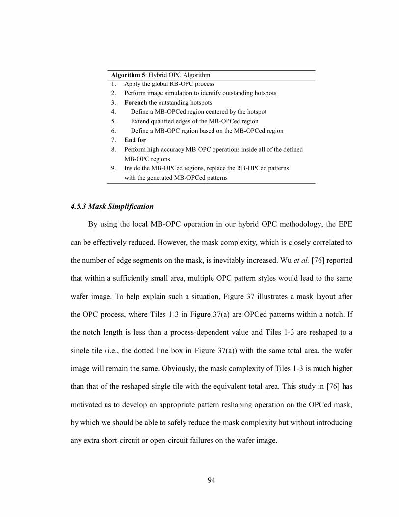
94
Algorithm 5: Hybrid OPC Algorithm
1. Apply the global RB-OPC process
2. Perform image simulation to identify outstanding hotspots
3. Foreach the outstanding hotspots
4. Define a MB-OPCed region centered by the hotspot
5. Extend qualified edges of the MB-OPCed region
6. Define a MB-OPC region based on the MB-OPCed region
7. End for
8. Perform high-accuracy MB-OPC operations inside all of the defined
MB-OPC regions
9. Inside the MB-OPCed regions, replace the RB-OPCed patterns
with the generated MB-OPCed patterns
4.5.3 Mask Simplification
By using the local MB-OPC operation in our hybrid OPC methodology, the EPE
can be effectively reduced. However, the mask complexity, which is closely correlated to
the number of edge segments on the mask, is inevitably increased. Wu et al. [76] reported
that within a sufficiently small area, multiple OPC pattern styles would lead to the same
wafer image. To help explain such a situation, Figure 37 illustrates a mask layout after
the OPC process, where Tiles 1-3 in Figure 37(a) are OPCed patterns within a notch. If
the notch length is less than a process-dependent value and Tiles 1-3 are reshaped to a
single tile (i.e., the dotted line box in Figure 37(a)) with the same total area, the wafer
image will remain the same. Obviously, the mask complexity of Tiles 1-3 is much higher
than that of the reshaped single tile with the equivalent total area. This study in [76] has
motivated us to develop an appropriate pattern reshaping operation on the OPCed mask,
by which we should be able to safely reduce the mask complexity but without introducing
any extra short-circuit or open-circuit failures on the wafer image.
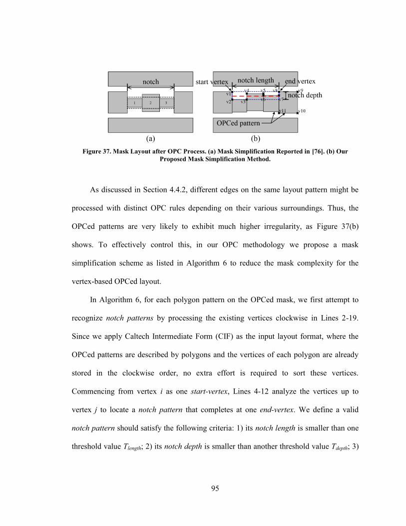
95
Figure 37. Mask Layout after OPC Process. (a) Mask Simplification Reported in [76]. (b) Our
Proposed Mask Simplification Method.
As discussed in Section 4.4.2, different edges on the same layout pattern might be
processed with distinct OPC rules depending on their various surroundings. Thus, the
OPCed patterns are very likely to exhibit much higher irregularity, as Figure 37(b)
shows. To effectively control this, in our OPC methodology we propose a mask
simplification scheme as listed in Algorithm 6 to reduce the mask complexity for the
vertex-based OPCed layout.
In Algorithm 6, for each polygon pattern on the OPCed mask, we first attempt to
recognize notch patterns by processing the existing vertices clockwise in Lines 2-19.
Since we apply Caltech Intermediate Form (CIF) as the input layout format, where the
OPCed patterns are described by polygons and the vertices of each polygon are already
stored in the clockwise order, no extra effort is required to sort these vertices.
Commencing from vertex i as one start-vertex, Lines 4-12 analyze the vertices up to
vertex j to locate a notch pattern that completes at one end-vertex. We define a valid
notch pattern should satisfy the following criteria: 1) its notch length is smaller than one
threshold value Tlength; 2) its notch depth is smaller than another threshold value Tdepth; 3)

96
from start-vertex to end-vertex, the direction is monotonous; and 4) depending on the
orientation of the notch pattern, the coordinates of both start-vertex and end-vertex along
the notch depth are either larger or smaller than those of any other vertices inside the
notch pattern. The direction is defined as the distribution trend of the vertices from start-
vertex to end-vertex. For instance, the direction is recognized as rightward monotonous if
each vertex has equal or larger X-coordinate compared to its previous vertices.
Algorithm 6: Mask Simplification Algorithm
1. Foreach polygon patterns on the OPCed layer
2. For (i = 0; i < vertexNumber; i++) // clockwise
3. initialize direction; j = i + 1; start-vertex = i;
notchLength = 0; notchDepth = 0; notchFound = 0;
4. While j <= vertexNumber
5. Based on the vertices between i and j,
update notchLength, notchDepth and direction;
6. If a “notch pattern” is found between vertices i and j
7. notchFound = 1; end-vertex = j;
8. Else if (notchLength > Tlength) or (notchDepth > Tdepth)
or (non-monotonous direction)
9. break;
10. End if
11. j = j + 1;
12. End while
13. If notchFound == 1
14. Reposition the vertices inside the “notch pattern”
between start-vertex and end-vertex;
15. i = end-vertex - 1;
16. Else
17. i = j - 1;
18. End if
19. End for
20. End for
Figure 37(b) illustrates a valid notch pattern located within the blue dotted line box,

97
whose vertices along with the others are clockwise marked from v1 to v11. In Figure
37(b), the start-vertex (i.e., vertex v1) is on the left of the end-vertex (i.e., vertex v8) due
to the inherent clockwise processing, and obviously their direction is rightward
monotonous. The fourth criterion above is also satisfied since the Y-coordinates of the
start-vertex and end-vertex along the notch depth (i.e., Y-axis) are the largest within the
notch pattern. In Algorithm 6, Line 6 attempts to identify a notch pattern between
vertices i and j by using the four criteria above. Once a qualified notch pattern is
detected, the end-vertex is updated in Line 7 and the process continues to explore a
potential larger notch pattern.
One example can be found in Figure 37(b), where the notch detection starts by
setting vertices i and j as vertices v1 and v2, respectively. When vertex j reaches vertex
v4, a valid notch pattern is found between vertices v1 and v4. Subsequently, vertex j
continues to explore and a larger notch pattern is then recognized between vertices v1
and v8. By further moving vertex j to vertices v9 or v11, in this specific example, the
notchLength between vertices v1 and v9 is larger than Tlength and the direction becomes
non-monotonous starting at vertex v11. Therefore, the largest notch pattern identified
between vertices v1 and v8 will be reshaped in Line 14 in Algorithm 6, which ensures the
overall pattern area inside the notch remains constant (i.e., the area between the red
dashed line and the original notch bottom line of the blue dotted line box in Figure 37(b)
is the same as the overall area of the original OPCed patterns inside the notch pattern).
The red dashed line in Figure 37(b) marks the bottom line of the reshaped notch, which
98
can obviously reduce the overall mask complexity to a significant extent in this example.
Since each vertex on the OPCed mask is usually scanned no more than two times due to
the relatively small value of Tlength, the time complexity of Algorithm 6 is merely O(n),
where n is the number of vertices in the layout that is linear to the mask complexity per
se.
4.5.4 Experimental Results
We implemented our PVRB-OPC methodology in C++ and the optimization was
performed on the same two-stage Miller-compensated opamp and the single-end folded
cascode opamp as Section 4.4.3 shows.
The original layouts in 0.18um CMOS technology were retargeted to 45nm CMOS
technology. The image simulation with process variation was performed by Mentor-
Graphics Calibre® nmOPC [73], a mainstream commercial OPC tool suite. In 45nm
CMOS technology, we assume Wth_OPC=100nm as the enlargement threshold amount for
the wire widening and wire shifting operations, Tlength=60nm and Tdepth=65nm in
Algorithm 6 as the threshold values for the notch length and notch depth, respectively.
The same experimental results of the GARB-OPC, the MB-OPC, and the PVRB-
OPC, as Section 4.4.3 describes, are used for comparison purpose. In Table 8, for our
proposed OPC methodology, the results by only using wire widening and wire shifting
(called WW/WS, for short) but without OPC are demonstrated separately similar to
Section 4.4.3. The PVRB-OPC and PVH-OPC schemes performed the PV-band shifting
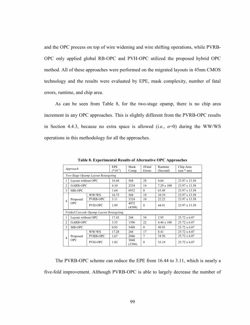
99
and the OPC process on top of wire widening and wire shifting operations, while PVRB-
OPC only applied global RB-OPC and PVH-OPC utilized the proposed hybrid OPC
method. All of these approaches were performed on the migrated layouts in 45nm CMOS
technology and the results were evaluated by EPE, mask complexity, number of fatal
errors, runtime, and chip area.
As can be seen from Table 8, for the two-stage opamp, there is no chip area
increment in any OPC approaches. This is slightly different from the PVRB-OPC results
in Section 4.4.3, because no extra space is allowed (i.e., α=0) during the WW/WS
operations in this methodology for all the approaches.
Table 8. Experimental Results of Alternative OPC Approaches
Approach EPE (*10-3)
Mask Comp.
#Fatal Errors
Runtime (Second)
Chip Area (um * um)
Two-Stage Opamp Layout Retargeting
1 Layout without OPC 16.44 568 28 4.66 23.97 x 13.58
2 GARB-OPC 4.10 2534 14 7.29 x 100 23.97 x 13.58
3 MB-OPC 1.64 6932 0 63.49 23.97 x 13.58
4 Proposed
OPC
WW/WS 16.73 568 19 10.19 23.97 x 13.58
PVRB-OPC 3.11 3324 10 22.22 23.97 x 13.58
PVH-OPC 1.89 4072
(4398) 0 44.91 23.97 x 13.58
Folded Cascode Opamp Layout Retargeting
1 Layout without OPC 17.42 268 54 2.95 25.72 x 6.07
2 GARB-OPC 3.55 1596 22 4.46 x 100 25.72 x 6.07
3 MB-OPC 0.85 5488 0 49.93 25.72 x 6.07
4 Proposed
OPC
WW/WS 17.28 268 17 8.41 25.72 x 6.07
PVRB-OPC 1.67 2046 7 18.56 25.72 x 6.07
PVH-OPC 1.02 3048
(3396) 0 35.19 25.72 x 6.07
The PVRB-OPC scheme can reduce the EPE from 16.44 to 3.11, which is nearly a
five-fold improvement. Although PVRB-OPC is able to largely decrease the number of
100
fatal error hotspots, there are still some remaining that need to be completely removed by
a dedicated post-processing operation. With the MB-OPC approach, this EPE
improvement can be as large as 10 times (i.e., 2 times better than PVRB-OPC), which
indicates a much higher resolution can be offered by this model-based method.
Meanwhile, the unavoidable trade-offs of MB-OPC include 2 times higher mask
complexity and 3 times longer runtime, compared to the PVRB-OPC scheme.
By using our proposed hybrid OPC method instead, compared to PVRB-OPC, our
proposed PVH-OPC can not only further improve the EPE by about 2 times that is
closely comparable with that of the pure MB-OPC operation, but also can successfully
remove all the remaining fatal error hotspots. Moreover, with the help of the mask
simplification scheme discussed in Section 4.5.3, the mask complexity of PVH-OPC
reduces from 4398 (i.e., the value in brackets) to 4072, which is about 7.4%
improvement. Similar experimental results can be observed from the folded cascode
opamp example in Table 8. For instance, our proposed mask simplification scheme can
contribute to 10.2% mask complexity reduction for the cascode opamp.
Table 9 presents the post-layout simulation results on the final layouts. The column
“PV-Band Quality” in Table 9 shows S1 and S2 values, which refer to PV-band symmetry
and PV-band coverage area, respectively [68]. Column “Circuit Performance” shows the
corresponding post-layout simulation results on nominal designs, while column “Monte
Carlo Samples” demonstrates statistical simulation results on voltage gain of the two
opamps when PV-induced mismatch occurs on all the circuit devices.
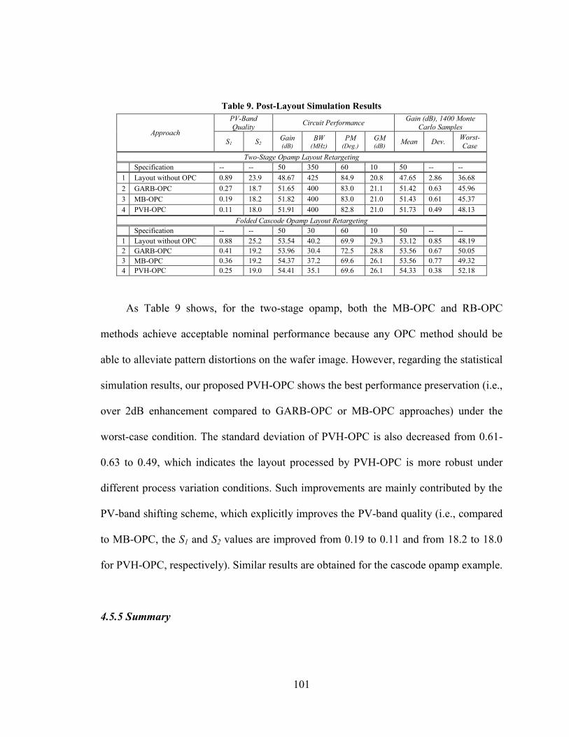
101
Table 9. Post-Layout Simulation Results
Approach
PV-Band
Quality Circuit Performance
Gain (dB), 1400 Monte
Carlo Samples
S1 S2 Gain (dB)
BW (MHz)
PM (Deg.)
GM (dB)
Mean Dev. Worst-
Case
Two-Stage Opamp Layout Retargeting
Specification -- -- 50 350 60 10 50 -- --
1 Layout without OPC 0.89 23.9 48.67 425 84.9 20.8 47.65 2.86 36.68
2 GARB-OPC 0.27 18.7 51.65 400 83.0 21.1 51.42 0.63 45.96
3 MB-OPC 0.19 18.2 51.82 400 83.0 21.0 51.43 0.61 45.37
4 PVH-OPC 0.11 18.0 51.91 400 82.8 21.0 51.73 0.49 48.13
Folded Cascode Opamp Layout Retargeting
Specification -- -- 50 30 60 10 50 -- --
1 Layout without OPC 0.88 25.2 53.54 40.2 69.9 29.3 53.12 0.85 48.19
2 GARB-OPC 0.41 19.2 53.96 30.4 72.5 28.8 53.56 0.67 50.05
3 MB-OPC 0.36 19.2 54.37 37.2 69.6 26.1 53.56 0.77 49.32
4 PVH-OPC 0.25 19.0 54.41 35.1 69.6 26.1 54.33 0.38 52.18
As Table 9 shows, for the two-stage opamp, both the MB-OPC and RB-OPC
methods achieve acceptable nominal performance because any OPC method should be
able to alleviate pattern distortions on the wafer image. However, regarding the statistical
simulation results, our proposed PVH-OPC shows the best performance preservation (i.e.,
over 2dB enhancement compared to GARB-OPC or MB-OPC approaches) under the
worst-case condition. The standard deviation of PVH-OPC is also decreased from 0.61-
0.63 to 0.49, which indicates the layout processed by PVH-OPC is more robust under
different process variation conditions. Such improvements are mainly contributed by the
PV-band shifting scheme, which explicitly improves the PV-band quality (i.e., compared
to MB-OPC, the S1 and S2 values are improved from 0.19 to 0.11 and from 18.2 to 18.0
for PVH-OPC, respectively). Similar results are obtained for the cascode opamp example.
4.5.5 Summary
102
Compared to the PVRB-OPC methodology, the PVH-OPC achieves smaller EPE
with larger mask complexity and longer algorithmic runtime. Although no significant
difference can be found between the circuit performances for the two methods, better
EPE is usually preferred if the increment of the mask complexity and the runtime is
acceptable. And the chip area increment is avoided because no aggressive layout pattern
operations are required during the PVH-OPC process. Additionally, the hybrid PVH-OPC
process presents a versatile scheme where the users are able to flexibly adjust the weights
between RB-OPC and MB-OPC by tuning the working regions of the local MB-OPC
process, in order to fit the tool into different applications.
4.6 Summary
For DFM with respect to PV-aware pattern distortions, PV-aware OPC-inclusive
analog layout retargeting methodologies have been presented. The main objective is to
develop an efficient and effective OPC algorithm especially for analog layouts. By local
wire widening and wire shifting operations during layout retargeting, the accuracy
limitation of the RB-OPC can be significantly compensated. Our proposed PV-band
shifting scheme can dedicatedly fix the images of circuit devices in order to alleviate PV-
band-induced mismatch effects. The PVRB-OPC scheme achieves the highest efficiency
with the lowest mask complexity and acceptable EPE compared with the other methods.
Alternatively, the PVH-OPC methodology can further improve the wafer image quality
by applying local MB-OPC post-processing operation after the global RB-OPC process.
103
Meanwhile, the chip area increment due to the extra space allocation is eliminated, and
the mask complexity increment due to MB-OPC is alleviated by a mask simplification
scheme. The circuit performance under the pseudo worst-case mismatch conditions is
maintained and good statistical performance is achieved due to our proposed smart PV-
band handling scheme. Our experimental results show that the proposed methodologies
outperform the other alternatives including a state-of-the-art commercial tool.
The analog layout retargeting platform creates a target layout by using a set of input
circuit sizes, which may not be suitable for yield considerations. Therefore, combining a
circuit sizing algorithm with the retargeting process can provide stronger capability of
DFM handling, and the circuit performance might be fundamentally improved. The next
chapter is going to present a circuit sizing inclusive analog layout retargeting
methodology for lithography-aware DFM, which functions as a complete analog layout
synthesis strategy.
104
Chapter 5 PV-Aware Circuit Sizing Inclusive Analog Layout
Retargeting
Since a set of device sizes can actually dominantly determine the circuit
performance, a PV-aware circuit sizing inclusive analog layout retargeting methodology
is introduced in this chapter. Evolutionary algorithm (EA) is a popular circuit sizing
scheme in the literature [77], which attempts to find the global optimal circuit sizes by
inheriting elite genes from previous generations. Due to its mutation and crossover
strategies, EA presents a superior ability of escaping from local optimal points in the
highly non-linear solution space. However, the EA-based sizing method is very time-
consuming because it usually requires a large size of population and generation.
Especially when post-layout effects, such as PV-aware pattern distortions, are considered
at the estimation of fitness, layout synthesis has to be performed on each individual
within a population. This would greatly reduce its efficiency if an EA-based sizing
method is utilized. Compared to the non-deterministic EA-based sizing approach,
Antreich et al. [78] proposed a deterministic circuit sizing algorithm, which can solve the
sizing problem much faster. With appropriate linearized approximations, this algorithm
explores the solution space along a specific direction based on circuit performance
gradients, and reaches a unique set of circuit sizes. As long as a reasonably suitable initial
sizing solution is provided, the deterministic sizing scheme would offer high efficiency
and applicability when layout synthesis is required for post-layout effect considerations
during the sizing process.
105
Analog layout synthesis acts as a bridge between pre-layout circuit design stage and
post-layout effects. By using an effective layout synthesis scheme, the circuit sizing
algorithms can thoughtfully handle the post-layout effects and in turn benefit the chip
yield. Habal and Graeb [79] proposed a layout-driven deterministic circuit sizing
platform. Multiple layouts with different topologies, each of which is synthesized from
scratch, are generated during the sizing process. Therefore, a number of pathological
layouts are inevitably created and the dedicated placement and routing algorithms may
somehow slow down the layout synthesis flow. Eissa et al. [80] proposed an electrical-
aware analog synthesis method by using a layout retargeting engine, which is highly
efficient for layout manipulation with post-layout effects. However, only stress effects
are discussed and no circuit sizing approach is included in that work. Chen et al. [31]
combined a gm/Id-based circuit sizing approach with a layout generation engine. However,
the real post-layout effects are not derived from the synthesized layout. Elshawy and
Dessouky [81] proposed a layout synthesis methodology with circuit sizing, where the
physical structure of each transistor is tuned with different folding topologies and
locations according to layout dependent effects. Although an initial circuit sizing is
performed, this process is not involved in the main optimization loop and therefore
cannot contribute to the yield improvement. Other versatile layout-aware sizing-inclusive
analog layout synthesis works can be found in [82]. Nevertheless, their utilized sizing
engines are still based on EA, which may limit the overall operational efficiency.
106
Since both circuit sizing and layout synthesis might be slow processes, the
combination of the deterministic circuit sizing algorithm and the layout retargeting
platform could be a good candidate for lithography-aware optimizations. In this chapter, a
deterministic circuit sizing algorithm is integrated into the analog layout retargeting
platform Error! Reference source not found.. To address the same lithography effects
s explained in Chapter 4, the hybrid OPC scheme with PV-band shifting is still applied
during the retargeting process. The background of the sizing algorithm is explained in
Section 5.1. Section 5.2 presents our proposed PV-aware sizing inclusive analog layout
retargeting flow. Section 5.3 illustrates the details of the dedicated PV-aware circuit
sizing algorithm and the experimental results are shown in Section 5.4. Section 5.5
summarizes this chapter.
5.1 Deterministic Circuit Sizing
5.1.1 Traditional Deterministic Circuit Sizing Flow
According to [78], the traditional deterministic circuit sizing algorithm can be
described as follows, where n represents the index of iteration and i refers to the ith
performance of a circuit.
1. Start with an initial set of device sizes sn, such as a set of transistor widths and
lengths, which are design parameters.
2. Linearize circuit performances fi with respect to design parameters sn:
)()()( nisnii ssfsfsf , (16)
107
where sfi represents the performance gradient.
3. Determine the worst-case process corner Pwc and calculate parameter distance
di(sn), which is defined as the minimum deviation of sn that is needed to shift
fi,Pwc(sn) to the constant specification fi,spec. According to the linear approximations
in Step 2, di(sn) can be derived as:
isspecinPini ffsfsdwc
/))(()( ,, . (17)
With reference to a given sn, a general expression of parameter distance di(s) can
be linearized as:
)()()( , nisnii ssgsdsd , (18)
where gs,i represents the gradient of parameter distance with respect to s.
4. To make the sizing robust in the worst-case process corner, the parameter
distance di(sn+1) should be maximized, while the size change ∆s=sn+1-sn should
not exceed the linear approximation. For simplicity, x will be used instead
of ∆s thereafter in this paper. Maximizing di(sn+1) within certain linear range is
equivalent to minimizing the following cost function:
0,))((exp:minimize 22 xxdi
i (19)
where factor α is a positive constant for scaling purposes and variable λ controls
the weight of x.
5. Find sn+1 by solving (19) with a generalized boundary curve (GBC) algorithm,
which can determine λ and x in a mathematical way.
108
6. Check terminating conditions. If such conditions are not satisfied, loop back to
Step 2 for the next iteration.
For our proposed PV-aware circuit sizing algorithm, the mismatch effects induced
by PV-band will be applied to determine the process corners in Step 3, which will be
discussed in Section 5.3.1 in detail.
5.1.2 GBC Algorithm
As Section 5.1.1 describes, in Step 5 the updated size sn+1 is calculated by using a
GBC algorithm originally developed in [86]. To solve the minimization problem in (19),
as Figure 38 depicts, a typical boundary curve is plotted based on (19) by sweeping λ.
The X axis and Y axis are transformed between 0 and 1 to represent the normalized size
change amount and the normalized objective improvement, respectively. The objective in
our proposed sizing algorithm is to maximize the PV-aware worst-case parameter
distance. When λ is infinite, according to (19), the size change has to be 0 in order to
minimize the cost function, and thus there is no improvement for the objective
performance. When λ is 0, the size change can be as large as possible. In such a situation,
the objective may be greatly improved, although a large error might be experienced due
to the linear approximation already laid down in Section 5.1.1. As claimed in [86], an
optimal point is located somewhere in the shadow region of Figure 38, where the circuit
sizes could be reasonably updated while effectively improving the objective with a
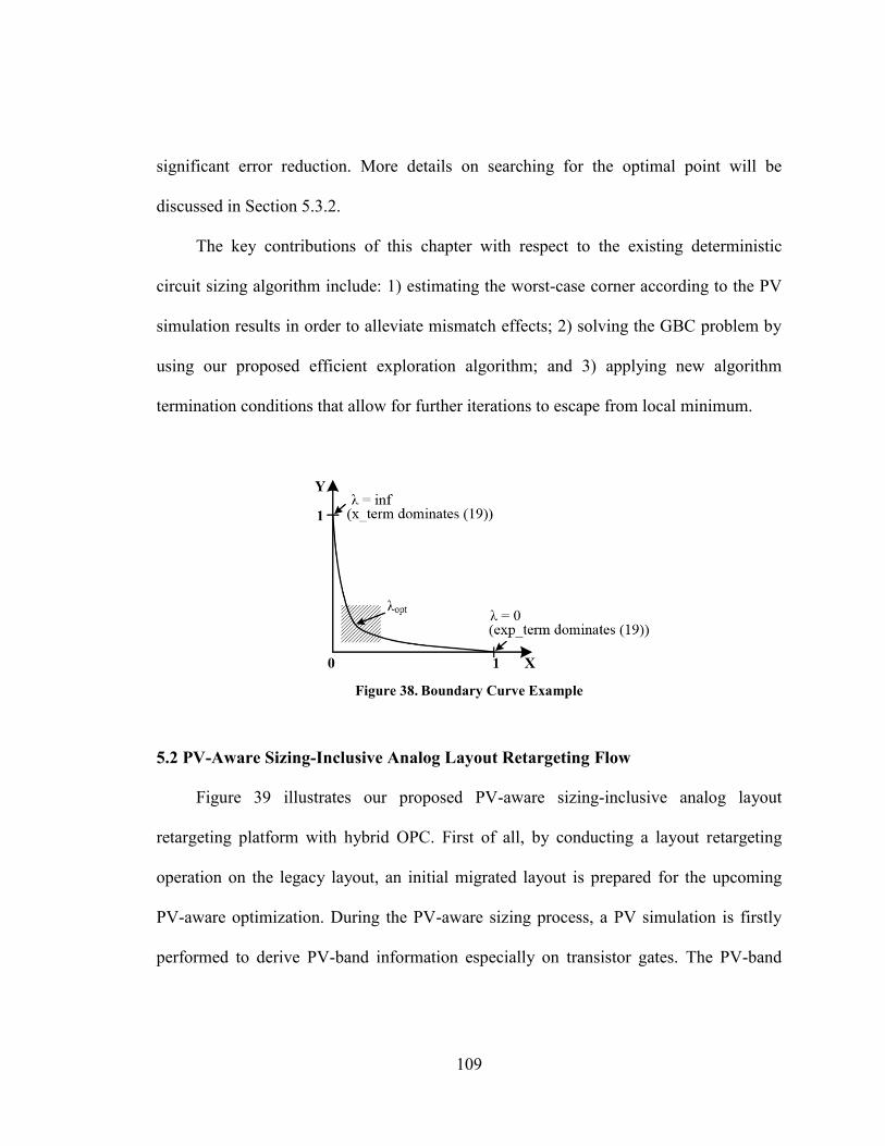
109
significant error reduction. More details on searching for the optimal point will be
discussed in Section 5.3.2.
The key contributions of this chapter with respect to the existing deterministic
circuit sizing algorithm include: 1) estimating the worst-case corner according to the PV
simulation results in order to alleviate mismatch effects; 2) solving the GBC problem by
using our proposed efficient exploration algorithm; and 3) applying new algorithm
termination conditions that allow for further iterations to escape from local minimum.
Figure 38. Boundary Curve Example
5.2 PV-Aware Sizing-Inclusive Analog Layout Retargeting Flow
Figure 39 illustrates our proposed PV-aware sizing-inclusive analog layout
retargeting platform with hybrid OPC. First of all, by conducting a layout retargeting
operation on the legacy layout, an initial migrated layout is prepared for the upcoming
PV-aware optimization. During the PV-aware sizing process, a PV simulation is firstly
performed to derive PV-band information especially on transistor gates. The PV-band
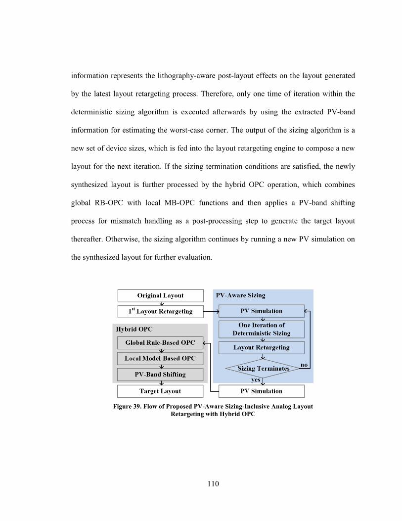
110
information represents the lithography-aware post-layout effects on the layout generated
by the latest layout retargeting process. Therefore, only one time of iteration within the
deterministic sizing algorithm is executed afterwards by using the extracted PV-band
information for estimating the worst-case corner. The output of the sizing algorithm is a
new set of device sizes, which is fed into the layout retargeting engine to compose a new
layout for the next iteration. If the sizing termination conditions are satisfied, the newly
synthesized layout is further processed by the hybrid OPC operation, which combines
global RB-OPC with local MB-OPC functions and then applies a PV-band shifting
process for mismatch handling as a post-processing step to generate the target layout
thereafter. Otherwise, the sizing algorithm continues by running a new PV simulation on
the synthesized layout for further evaluation.
Figure 39. Flow of Proposed PV-Aware Sizing-Inclusive Analog Layout
Retargeting with Hybrid OPC
111
Because the circuit sizing algorithm is deterministic, only one layout is synthesized
at each time of the PV-aware sizing iteration. Therefore, compared to the EA-based
sizing algorithms, our proposed method can significantly improve the operational
efficiency when such post-layout effects are considered. Moreover, in the conventional
analog layout retargeting flow, the new device sizes are always assumed to be already
available as a set of fine-tuned ones, which can guarantee the good correspondence
between the migrated layout and satisfactory circuit performance. By adding this sizing
algorithm into the layout synthesis flow, such a restriction is actually relaxed. As long as
the pre-layout circuit performance is close to the required specification, the layout created
by the first retargeting stage in Figure 39 would be treated as a good initial sizing point
for the PV-aware sizing algorithm. In addition, the sizing process can be accelerated in
comparison to the EA-based methods since the number of iterations might be
significantly reduced.
5.3 PV-Aware Circuit Sizing Algorithm
On top of the deterministic sizing algorithm as Section 5.1.1 describes, we
introduce the PV considerations to estimate the worst-case process corner Pwc in (17), and
propose a modified GBC exploration algorithm to enhance the minimization problem
solving in (19). Since the PV-band information presents the possible wafer image range
for all of the process conditions, our proposed circuit sizing algorithm is expected to find
112
a set of robust circuit sizes against PV-induced mismatch effects for the best circuit
performance preservation.
5.3.1 PV Considerations
To estimate Pwc in (17), a linearized approximation is made on circuit performance
with respect to PV conditions. By running a series of circuit SPICE simulations,
performance gradient jfi is calculated for each device feature j. And the worst-case
corner for this feature is:
otherwiseinnerBand
fifouterBandP
ij
wcj,
0,, (20)
A negative gradient value represents performance degradation when the feature size
is increased. Therefore, as (20) shows, the worst-case corner of this feature is the largest
possible feature size, which is the outer PV-band. The same rationale can be applied to
the positive gradient case. By calculating the worst-case process corner for each sensitive
design parameter in the design parameter set sn, the worst-case circuit performance
fi,Pwc(sn) is determined and in turn the parameter distance di(sn) can be computed according
to (17).
During the analog layout retargeting process, a group of user-defined constraints
(e.g., device symmetry or matching) is applied to the layout generation. These constraints
are not only necessary as the analog layout requirements for meeting the due electrical
specifications, but also offer valuable knowledge to guide the optimization algorithms. In
113
our proposed PV-aware sizing algorithm, the device matching constraints are checked
twice on analog circuit building blocks, such as current mirror, differential pair, or
common-centroid structures, to ensure: 1) when estimating the worst-case corners, the
matching devices must fall into the opposite extreme feature sizes according to the PV-
band; and 2) after one time of iteration in the sizing algorithm, the updated size sn+1 must
satisfy all of those constraints. The former operation guarantees the worst negative effects
are introduced into the circuit performance, and the latter one helps preserve the essential
analog circuit constraints. Once a conflict occurs within a device pair, the one with
smaller performance gradient will be modified to comply with the rule above.
5.3.2 Modified GBC Exploration Algorithm
As Section 5.1.2 describes, the optimal solution point on the boundary curve is
located in the shadow region of Figure 38. According to [87], this solution point can be
found by firstly plotting the curve, and then identifying the point with the smallest
curvature-radius. However, a large number of mathematical calculations and
approximations, i.e., deriving a group of λ values for curve plotting after solving a non-
linear optimization problem [87], are required on the GBC extraction, which might lower
the algorithmic efficiency.
In our proposed PV-aware deterministic sizing approach, a modified GBC
exploration algorithm is developed and applied as described below. For the cost function
114
(19) which is comprised of exp_term (i.e., ∑exp2(-α∙ di(x))) and x_term (i.e., λ∙x
2), we can
understand the minimization problem as:
inf,_
0,exp_dominatedis)18(
whentermx
whentermby , (21)
because if λ is 0, then the x_term is 0 and the cost function completely depends on the
exp_term. Similarly, if λ is infinitely large, x has to be as close as 0 to minimize (19), and
therefore a small fluctuation on the x_term can greatly affect the whole cost function.
These two dominating conditions can be equivalently identified on the boundary curve as
Figure 38 shows. By using (21), the problem of solving the GBC can be converted to
finding an optimal λ value (λopt) so that neither the exp_term nor the x_term dominates the
cost function in (19). Correspondingly, λopt should be located inside the shadow region in
Figure 38, while it uniquely determines an xopt value, which can minimize (19).
To efficiently solve (21), we firstly estimate an optimal value of x as xest, and
assume that the exp_term is equal to the x_term at xest, which indicates that the x_term
dominates the cost function in (19) for all x<xest (because when x is closer to 0, λ is closer
to λ=inf on the GBC) and the exp_term dominates when x>xest. Then we calculate λopt by
using the assumption above:
22 ))((exp estesti xxd . (22)
Afterwards, the precise optimal value xopt is computed by solving (19) with the fixed
value λopt. If xopt is larger than xest, according to our assumption above, the exp_term
dominates the cost function in the interval [xest, xopt], which results in the deviation
115
between xest and xopt. Therefore, we should move λ towards λ=inf, where the x_term
dominates (19), for compensation. Similarly, λ should be reduced towards λ=0 when xopt
is smaller than xest. Since the assumption in (22) may introduce certain errors due to the
natural difference between the exponential function (i.e., the exp_term) and the quadratic
function (i.e., the x_term), we further calculate the distance distopt between the optimal
point xopt on the GBC and the origin point as a golden rule. As proved by [87], the GBC
is always convex, which indicates that the feasible solution points on the GBC surely
have smaller distance to the origin. Thus by using the distance distopt, λ is always tuned
towards the correct direction to minimize any possible errors due to assumption (22).
This algorithm terminates when the difference between xest and xopt is small enough.
Figure 40 illustrates an exemplary process of tuning λ based on the relative
positions of xest and xopt, where the cross point of the exp_term and x_term curves
represents the estimated value xest, and the corresponding λopt and xopt are calculated
according to (22) and (19), respectively. In Figure 40(a), λ1 and xopt1 are firstly calculated
according to the initial estimation xest1. Since xopt1 is larger than xest1, λ1 should be
enlarged approaching the shadow region as Figure 40(d) presents. In the second iteration,
as Figure 40(b) shows, λ2 should be reduced since xopt2 is smaller than xest2. The large
exploration distance between λ1 and λ2 of Figure 40(d) indicates a relative large tuning
range is manageable among the algorithmic iterations. By using a dichotomous tuning
strategy, in this example the convergence occurs in the third iteration where λ3 is just
located inside the shadow region as Figure 40(d) shows. It can be observed from Figure
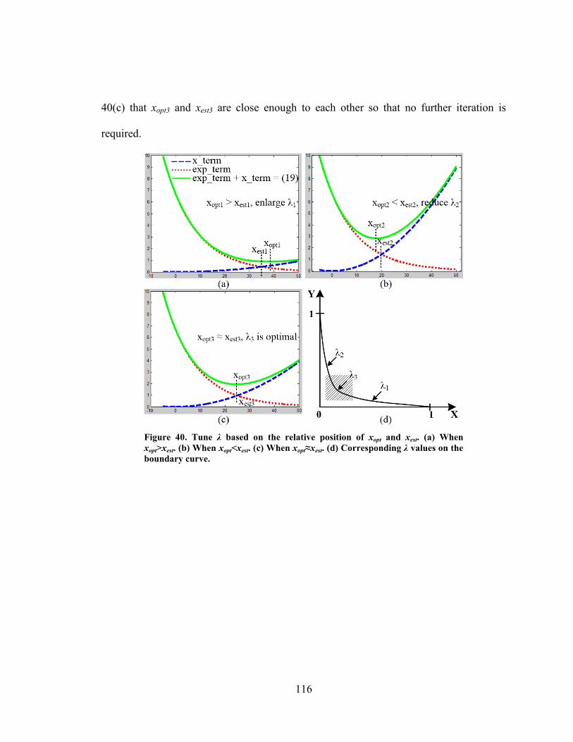
116
40(c) that xopt3 and xest3 are close enough to each other so that no further iteration is
required.
Figure 40. Tune λ based on the relative position of xopt and xest. (a) When
xopt>xest. (b) When xopt<xest. (c) When xopt≈xest. (d) Corresponding λ values on the
boundary curve.

117
Algorithm 7: Modified GBC Algorithm
1. leftBoundary = 0 ; rightBoundary = xmax ; j=0 ;
2. Estimate an initial size change xj_est = xmax/m ;
3. Calculate an initial λ value as λj by solving ∑exp2(-α∙ di(xj_est)) = λ∙xj_est
2 ;
4. Calculate the accurate size change xj at λj by solving
min(∑exp(-α∙ di(x))2 + λj∙x
2) ;
5. By using xj and λj, derive the corresponding point on GBC and calculate
its distance to the origin as distj
6. Record the final solution xopt= xj ; λopt = λj ; distopt = distj ;
7. While (1)
8. If (|xj - xj_est| < xth)
9. break ;
10. Else if (xj < xj_est)
11. leftBoundary = xj_est ;
12. Else
13. rightBoundary = xj_est ;
14. End if
15. xj+1_est = (leftBoundary + rightBoundary) / 2 ;
16. Calculate λj+1, xj+1 and distj+1 similar to Lines 3-5, respectively ;
17. If (distj+1 < distj)
18. xopt= xj+1 ; λopt = λj+1 ; distopt = distj+1 ;
19. End if
20. j = j+1 ;
21. End while
Our proposed modified GBC exploration algorithm is shown in Algorithm 7, where
x represents a set of size changes and j specifies the index of iterations. In Line 2, xj_est is
firstly estimated as a small portion of the maximum allowable size change xmax (i.e., m is
a relatively large constant). Then in Lines 3-5, we calculate λj, xj and distj, which
represent the candidate values for λopt, xopt and distopt, respectively. The mathematical
function solving in Line 4 is performed by using SageMath [88]. During the main loop in
Lines 7-21, instead of directly changing λ, we dichotomously tune the value of xest based
118
on the relative position between xopt and xest, because the values of λ are not evenly
distributed on the boundary curve. Once a smaller distance is found between the new
point on the GBC and the origin, the corresponding values are recorded in Line 18 as the
candidate solution. When the estimated size change xj_est is very close to the precise size
change xj within the user-defined threshold xth, the algorithm terminates. According to
our experiments, the sizing loop in our proposed modified GBC exploration flow usually
converge within a dozen iterations, which is favorably acceptable in terms of runtime in
practice.
5.3.3 Terminating Conditions
The terminating conditions in the PV-aware sizing algorithm include:
specnP fxfwc
)( 1 , (23)
or
0,)()( 1 nPnP xfxfwcwc
, (24)
or
)()(&...&)()(&)()( 21 nPnPnPnPnPnP xfxfxfxfxfxfwcwcwcwcwcwc
. (25)
Condition (23) represents that the new sizes are good enough for any worst-case
performance because we assume the performance should be larger than the specification,
while condition (24) denotes that the worst-case performance can hardly be further
improved, which is controlled by a user-specified vector β. Each element in β is
119
corresponding to one specific circuit performance, such as voltage gain or bandwidth of
an opamp. Conditions (23) and (24) are expected in most applications since a relatively
good initial sizing point is normally available at the first time of the analog layout
retargeting. In this situation, the sizing scheme actually serves as a fine-tuning step to
alleviate the mismatch effects for further yield improvement.
Moreover, we propose condition (25) as an additional user-configurable terminating
condition. If the worst-case performance has just decreased compared to the previous
iteration, the sizing algorithm is not necessary to be terminated right away. Instead, a
further user-defined number of iterations (i.e., γ more iterations in (25)) are still allowed.
This feature provides a chance for our proposed sizing algorithm to jump out of a local
minimum since the analog circuit sizing is naturally a highly non-linear problem. It
would be very helpful if the user: 1) suspects the initial sizing point is not reliable; 2)
attempts to quickly explore the sensitivities of different initial sizing points; or 3)
assumes that some design parameters are very sensitive to the mismatch effects induced
by PV-band.
5.4 Experimental Results
The proposed PV-aware sizing inclusive analog layout retargeting methodology
with hybrid OPC scheme was implemented in C++. The optimization was performed on
the same two-stage Miller-compensated opamp and the single-end folded cascode opamp
as explained in the previous chapters. The original layouts in 0.18um CMOS technology
120
were retargeted to 45nm CMOS technology. The image simulation with process variation
was conducted by Mentor-Graphics Calibre®
nmOPC [73] with a dose range of ±2% and
a defocus range of ±25nm. The pattern library for the RB-OPC was established on top of
simulations and experiments with nmOPC as well. In 45nm CMOS technology, we
assume α=0.01 as the scaling factor in (19), xth=0.5 in Algorithm 7 as the threshold value
for the difference between xest and xopt, β=0.2 as the threshold value in the terminating
condition (24), and γ=3 as the further number of iterations allowed in the terminating
condition (25).
In Table 10, we compare our proposed methodology with several alternative
approaches where the layout retargeting is performed. In Table 10, Approach-1
represents the conventional retargeting method without applying any PV-aware
optimization algorithms. In Approach-2, the standalone sizing algorithm works as
proposed in [79] without adopting OPC process. To show the effectiveness of our
proposed PV-aware hybrid OPC scheme (i.e., called PVH-OPC for Approach-4 in Table
10), we implemented a RB-OPC method with GA [44] (i.e., named GA-OPC for
Approach-3 in Table 10) and integrated it into our analog layout retargeting platform for
fair comparison. The results of the complete PV-aware sizing-inclusive analog layout
retargeting with hybrid OPC are listed in the rows of Approach-5 within Table 10.
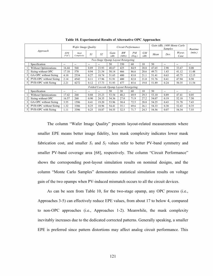
121
Table 10. Experimental Results of Alternative OPC Approaches
Approach
Wafer Image Quality Circuit Performance Gain (dB), 1400 Monte Carlo
Samples Runtime
(min.) EPE (*10-3)
Mask
Complexity S1 S2
Gain (dB)
BW (MHz)
PM (Deg.)
GM (dB)
Mean Dev. Worst-
Case
Two-Stage Opamp Layout Retargeting
Specification -- -- -- -- 50 350 60 10 50 -- -- --
1 Without Optimizations 16.44 568 0.89 23.93 48.67 425 84.9 20.8 47.65 2.98 33.67 0.08
2 Sizing without OPC 17.18 570 0.94 21.54 50.14 466 86.6 20.6 49.71 1.43 41.12 11.48
3 GA-OPC without Sizing 4.10 2534 0.27 18.74 51.65 400 83.0 21.1 51.41 0.63 45.75 12.15
4 PVH-OPC without Sizing 2.14 4542 0.11 17.96 51.91 400 82.8 21.0 51.76 0.41 47.94 0.50
5 PVH-OPC with Sizing 2.21 4272 0.12 17.73 51.93 477 85.6 19.8 51.89 0.24 50.35 11.54
Folded Cascode Opamp Layout Retargeting
Specification -- -- -- -- 50 30 60 10 50 -- -- --
1 Without Optimizations 17.42 268 0.88 25.23 53.54 40.2 69.9 29.3 53.10 0.89 47.41
41
0.05
2 Sizing without OPC 16.57 268 0.90 24.35 54.36 27.0 71.9 27.2 54.07 0.19 52.18 7.50
3 GA-OPC without Sizing 3.55 1596 0.41 19.20 53.96 30.4 72.5 28.8 54.25 0.43 51.78 7.43
4 PVH-OPC without Sizing 1.32 3386 0.25 18.96 54.41 35.1 69.6 26.1 54.33 0.38 52.43 0.35
5 PVH-OPC with Sizing 1.11 3396 0.25 18.87 54.55 32.5 71.7 24.3 54.56 0.07 54.34 7.55
The column “Wafer Image Quality” presents layout-related measurements where
smaller EPE means better image fidelity, less mask complexity indicates lower mask
fabrication cost, and smaller S1 and S2 values refer to better PV-band symmetry and
smaller PV-band coverage area [68], respectively. The column “Circuit Performance”
shows the corresponding post-layout simulation results on nominal designs, and the
column “Monte Carlo Samples” demonstrates statistical simulation results on voltage
gain of the two opamps when PV-induced mismatch occurs to all the circuit devices.
As can be seen from Table 10, for the two-stage opamp, any OPC process (i.e.,
Approaches 3-5) can effectively reduce EPE values, from about 17 to below 4, compared
to non-OPC approaches (i.e., Approaches 1-2). Meanwhile, the mask complexity
inevitably increases due to the dedicated corrected patterns. Generally speaking, a smaller
EPE is preferred since pattern distortions may affect analog circuit performance. This
122
effect can be verified by the fact that the OPC approaches end up with higher gain values
in both circuit nominal simulations and statistical simulations, when compared to the
non-OPC approaches. If considering the whole experimental results of Table 10 in this
regard, the only exception can be found in Approach-2 (i.e., sizing without OPC) of the
cascode opamp where the gain (i.e., 54.36dB) is larger than that of GA-OPC. However,
in that circuit run the bandwidth (i.e., 27.0MHz) cannot satisfy the specification of
30MHz, which is also caused by pattern distortions. Moreover, the OPC approaches
greatly improve PV-band quality with much smaller S1 and S2 values, which also alleviate
performance variations. Consequently, we can conclude that the OPC process is essential
for performance preservation of analog circuits.
For the two-stage opamp, our proposed PVH-OPC (i.e., Approach-4) can achieve
about 2 times better EPE improvement with acceptable mask complexity than the rule-
based GA-OPC approach (i.e., Approach-3). This improvement is mainly attributed to
applying the local MB-OPC operation, which can effectively fix remaining lithography
hotspot errors among congested layout patterns. In addition, due to the PV-band shifting
operation used in PVH-OPC, the PV-band symmetry is greatly improved (i.e., S1 reduces
from 0.27 to 0.11). In such a situation, the direct benefit can be found from the statistical
results where the worst-case gain of the PVH-OPC is more than 2dB better than that of
GA-OPC (i.e., 47.94dB versus 45.75dB). Moreover, compared to the low efficiency of
the GA-OPC approach, the runtime of the PVH-OPC is much favorable (i.e., 0.5 minutes
123
versus 12.15 minutes). This helps justify its applicability in our proposed complete
sizing-inclusive methodology.
With respect to the sizing algorithm, Approach-2 (i.e., sizing without OPC) in Table
10 can somehow improve the nominal performance and statistical performance compared
to the method without any optimizations (i.e., Approach-1). However, due to pattern
distortions, it cannot offer satisfactory performance achieved by the methods enclosing
OPC operations. Therefore, the benefit of sizing cannot be completely observed from
Approach-2 (i.e., sizing without OPC). With the help of our proposed PVH-OPC scheme,
in Approach-5 (i.e., PVH-OPC with Sizing), the advantages of the sizing algorithm can
be fully exhibited. In the statistical simulation results, the PVH-OPC method with sizing
capability can extraordinarily reduce the performance standard deviation to as low as
0.24dB and make the worst-case gain of 50.35dB for the two-stage opamp (at least
2.41dB higher than any other alternative methods), which is the only one satisfying the
specification of 50dB. Although the sizing algorithm itself takes about 11.48 minutes, by
combining with the efficient PVH-OPC method, the overall runtime of 12.04 minutes is
still practically acceptable. Similar observations can be derived from Table 10 about the
cascode opamp experimental results.
5.5 Summary
In this chapter, a PV-aware sizing-inclusive analog layout retargeting flow with
hybrid OPC methodology for yield improvement has been presented. By using the
124
efficient analog layout retargeting process as a layout synthesis approach, the
lithography-aware PV-induced effects are considered during a deterministic circuit sizing
process with a modified GBC algorithm. Thanks to the initial set of circuit sizes used for
the retargeting process, a good initial point is available to facilitate the convergence of
the deterministic sizing process. Afterwards, the same hybrid OPC scheme as Chapter 4
describes, which combines global RB-OPC and local MB-OPC, is applied to alleviate
pattern distortions with a sound trade-off among EPE, mask complexity and algorithmic
runtime. Our experimental results show that the proposed methodology can achieve
highly effective analog layout retargeting with the best wafer image quality and circuit
performance preservation by consuming acceptable runtime in practice.
125
Chapter 6 Conclusions
For the DFM strategies with respect to photolithographic defects, pattern distortions
and process variations, in this dissertation the impacts of those lithograph effects on
analog circuits, where spot defects can cause fatal functional failures and PV-aware
pattern distortions can result in parasitic deviations and device mismatch, have firstly
been introduced. By combining with an analog layout retargeting platform, spot defect
optimizations, PV-aware OPC schemes and circuit-sizing-inclusive PV optimizations
have then been presented. The main contribution of this dissertation is the developed
algorithms and methodologies which achieve lithography-robust analog IC layout design
without circuit performance degradation.
The analog layout retargeting platform can efficiently create a target layout based
on an existing analog IP block. During the retargeting process, various layout pattern
operations with DFM considerations can be easily adopted onto the constraint graphs by
tuning the related arc weights. By modifying the circuit device sizes, the layout
retargeting platform is able to work iteratively so that a layout with actual physical
information can be generated at each iteration for accurate circuit simulation and precise
yield evaluation. Thanks to the analog layout retargeting platform, all of the optimization
methodologies achieve high efficiency with significant yield improvement.
The spot defect optimizations apply global wire widening and local wire shifting
according to the geometric critical area analysis. Those layout pattern operations use the
existing redundant space in the layout and update the constraint graphs without
126
introducing design rule violation in the circuit. By shrinking the critical areas among
interconnect wires and circuit devices for both short-type and open-type failures, the POF
value can be effectively reduced. Additionally, extra space allocation is optionally
allowed to further reduce POF with a trade-off of negligibly small chip area increment.
The experimental results show that more than 10% of POF improvement can be achieved
by using the proposed spot defect optimizations.
The PVRB-OPC flow applies a RB-OPC process on the migrated layout as a post-
processing approach. The accuracy limitation of the RB-OPC is compensated by similar
layout pattern operations as those used for the spot defect optimizations. The PV-band-
induced device mismatch is alleviated by a PV-band shifting scheme, which is dedicated
to shift the PV-band of sensitive device pairs. Although extra space may be required to
eliminate all lithography hotspots, the proposed PVRB-OPC approach presents
experimental results with high efficiency, low mask complexity and acceptable EPE
values. Alternatively, by applying local MB-OPC after the global RB-OPC process, the
PVH-OPC flow can further improve the wafer image quality. During the PVH-OPC
process, any chip area increment due to the extra space allocation is avoided, and the
mask complexity increment due to the local MB-OPC is alleviated by a mask
simplification scheme. The experimental results show that, with double algorithmic
runtime and 30% increment of mask complexity, the EPE can be reduced by more than
30% without any chip area increase. Moreover, the overall algorithmic runtime, which is
below one minute for the test circuits, is still acceptable in practice.
127
In terms of the PV-aware sizing-inclusive analog layout retargeting method, a
deterministic circuit sizing approach with a modified GBC algorithm is applied to further
boost the lithography-aware chip yield. The circuit sizing algorithm is dedicated to PV-
aware optimizations and the main target is to create a robust circuit against PV-induced
mismatch. The experimental results present superior circuit performance improvement
especially in statistical performance deviation reduction, which indicates the circuit
robustness improvement thanks to resizing. Combining with the circuit sizing algorithm,
the layout retargeting platform works as a complete analog layout synthesis strategy.
Therefore, it can not only be used for lithography-aware DFM considerations, but also be
able to deal with a broad range of optimization targets.
In this dissertation, the results of the investigations about the lithography-aware
yield improvement in the advanced nanometer technologies are helpful for developing
innovative CAD tools for analog IC DFM. Such tools can effectively assist analog
designers to achieve analog circuit designs with higher robustness, and in turn to better
meet the time-to-market and quality-of-result requirements.
128
Chapter 7 Future Work
Although the analog layout retargeting platform is able to preserve the circuit
topology by a constraint template to ensure acceptable circuit performance, its flexibility
can be further improved because changing the circuit topology is sometimes useful and
even necessary in different technology nodes or applications. In that case, building block
placement and interconnect routing algorithms can be combined with the constraint
graphs in order to make the circuit structure highly flexible and configurable. Those
algorithms may work locally on the constraint graphs so that the sensitive devices and
interconnect wires can be modified based on the circuit performance, and the whole
layout retargeting platform can still efficiently create a target layout by consuming
acceptable algorithmic runtime.
The proposed OPC strategies are very general schemes for analog circuits. If
dedicated OPC rules are developed for advanced technologies to compensate potential
accuracy limitations, these OPC strategies can be easily extended for advanced
technologies even with the next generation of lithography, such as extreme ultra-violate
lithography (EUVL). In EUVL, the wavelength of the source light dramatically decreases
down to 13.5nm compared to the current lithography with 193nm wavelength.
Nevertheless, similar OPC schemes are still essential to print smaller wafer feature sizes
and to handle the newly emerging physical effects in EUVL (e.g., shadowing effect).
Considering the combined circuit sizing algorithm and the layout template
representation, the DFM-aware layout retargeting process can also be applied to the next
129
generation of devices, such as FinFET. Although the device structures and the related
design rules of FinFET are much different from the traditional CMOS technology, if the
template can compose a device as a single graph node, this methodology would be able to
migrate CMOS circuits to FinFET circuits with completely different design requirements.
Such a versatile analog layout synthesis scheme is an inevitable trend for FinFET circuit
designs, since by using FinFET structures, standalone schematic design without physical
information is not sufficient to precisely simulate the circuit performance. Better
development in analog CAD tools would rely on those layout synthesis approaches that
can thoughtfully consider yield-related DFM issues.

130
Acknowledgments
This research was supported in part by the Natural Sciences and Engineering
Research Council of Canada (NSERC), Canada Foundation for Innovation (CFI),
Research and Development Corporation (RDC) of Newfoundland and Labrador (through
its Industrial Research and Innovation Fund and ArcticTECH R&D Award), and
Memorial University of Newfoundland.
131
References
[1] H. C. Ou, K. H. Tseng, J. Y. Liu, I. P. We and Y. W. Chang, “Layout-Dependent Effects-Aware
Analytical Analog Placement,” IEEE Trans. on Computer-Aided Design of Integrated Circuits and
Systems, pp. 107-110, 2016.
[2] I. Mohammed, K. E. Kenawy and M. Dessouky, “Layout Dependent Effects Mitigation in Current
Mirrors,” in Proc. Fourth International Japan-Egypt Conference on Electronics, Communications
and Computers, 2016.
[3] J. C. Guo, Y. Z. Lo and J. R. Ou, “The Impact of Layout Dependent Effects on Mobility and Flicker
Noise in Nanoscale Multifinger nMOSFETs for RF and Analog Design,” in Proc. IEEE MTT-S
International Microwave Symposium, pp. 1-4, 2016.
[4] A. K. Sharma, N. Mishra, N. Alam, S. Dasgupta and A. Bulusu, “Pre-Layout Estimation of
Performance and Design of Basic Analog Circuits in Stress Enabled Technologies,” in Proc. 19th
International Symposium on VLSI Design and Test, pp. 1-6, 2015.
[5] P. Y. Chou, H. C. Ou and Y. W. Chang, “Heterogeneous B∗-trees for Analog Placement with
Symmetry and Regularity Considerations,” in IEEE/ACM International Conference on Computer-
Aided Design, pp. 512-516, Nov. 2011.
[6] P. H. Wu, M. P. H. Lin, T. C. Chen, C. F. Yeh, T. Y. Ho and B. D. Liu, “Exploring Feasibilities of
Symmetry Islands and Monotonic Current Paths in Slicing Trees for Analog Placement,” IEEE Trans.
on Computer-Aided Design of Integrated Circuits and Systems, vol. 33, no. 6, pp. 879-892, 2014.
[7] D. Chang, J. N. Kitchen, B. Bakkaloglu, S. Kiaei and S. Ozev, “Design-Time Reliability
Enhancement Using Hotspot Identification for RF Circuits,” IEEE Trans. on Very Large Scale
Integration Systems, vol. 24, no. 3, pp. 1179-1183, 2016.
[8] C. N. J. Liu, Y. L. Chen, T. Y. Liu and T. C. Chen, “Reliability-Aware Design Automation Flow for
Analog Circuits,” in Proc. International SoC Design Conference, pp. 1-2, Nov. 2015.
[9] R. Martins, N. Lourenco, A. Canelas and N. Horta, “Electromigration-Aware and IR-Drop Avoidance
Routing in Analog Multiport Terminal Structures,” in Proc. Design, Automation and Test in Europe
Conference and Exhibition, pp. 1-6, Mar. 2014.
[10] T. Yanagawa, “Yield Degradation of Integrated Circuits Due to Spot Defects,” IEEE Trans. on
Electron Devices, vol. 19, no. 2, pp. 190-197, Feb. 1972.
[11] A. Pitaksanonkul, S. Thanawastien, C. Lursinsap, and J.A. Gandhi, “DTR: A Defect-Tolerant Routing
Algorithm,” in Proc. 26th
Conference on Design Automation, pp. 795-798, Jun. 1989.
[12] S. Y. Kuo, “YOR: A Yield-Optimizing Routing Algorithm by Minimizing Critical Areas and Vias,”
IEEE Trans. on Computer-Aided Design of Integrated Circuits and Systems, vol. 12, no. 9, pp. 1303-
1311, Sep. 1993.
132
[13] A. Tyagi and A. Bayoumi, “ULSI Design-for-Manufacturability: A Yield Enhancement Approach,”
in Proc. 3rd International Conference on the Economics of Design, Test, and Manufacturing, pp. 80-
89, May 1994.
[14] D. Muller, “Optimizing Yield in Global Routing,” in Proc. IEEE/ACM International Conference on
Computer-Aided Design, pp. 480-486, Nov. 2006.
[15] J. P. Bickford, J. D. Hibbeler, D. Muller, S. Peyer and V. S. Kumar, “Optimizing Product Yield using
Manufacturing Defect Weights,” in Proc. 23rd Annual SEMI Advanced Semiconductor
Manufacturing Conference, pp. 16-20, May 2012.
[16] M. Cho, H. Xiang, R. Puri and D. Z. Pan, “Track Routing and Optimization for Yield,” IEEE Trans.
on Computer-Aided Design of Integrated Circuits and Systems, vol. 27, no. 5, pp. 872-876, 2008.
[17] T. Iizuka, M. Ikeda, and K. Asada, “Exact Wiring Fault Minimization via Comprehensive Layout
Synthesis for CMOS Logic Cells,” in Proc. 5th International Symposium on Quality Electronic
Design, pp. 377-380, 2004.
[18] J. Z. Su and W. W. Dai, “Post-Route Optimization for Improved Yield using a Rubber-Band Wiring
Model,” in Proc. IEEE/ACM International Conference on Computer-Aided Design, pp. 700-706,
Nov. 1997.
[19] G. A. Allen, “Targeted Layout Modifications for Semiconductor Yield/Reliability Enhancement,”
IEEE Trans. on Semiconductor Manufacturing, vol. 17, no. 4, pp. 573-581, Nov. 2004.
[20] G. A. Allen, A. J. Walton and R. J. Holwill, “A Yield Improvement Technique for IC Layout using
Local Design Rules,” IEEE Trans. on Computer-Aided Design of Integrated Circuits and Systems,
vol. 11, no. 11, pp. 1355-1362, Nov. 1992.
[21] V. K. R. Chiluvuri and I. Koren, “Layout-Synthesis Techniques for Yield Enhancement,” IEEE
Trans. on Semiconductor Manufacturing, vol. 8, no. 2, pp. 178-187, May 1995.
[22] C. Bamji and E. Malavasi, “Enhanced Network Flow Algorithm for Yield Optimization,” in Proc.
33rd Design Automation Conference, pp. 746-751, Jun. 1996.
[23] Y. Bourai and C. –J. R. Shi, “Layout Compaction for Yield Optimization vis Critical Area
Minimization,” in Proc. Design, Automation and Test in Europe Conference and Exhibition, pp. 122-
127, 2000.
[24] X. Li, P. Gopalakrishnan, Y. Xu and L. T. Pileggi, “Robust Analog/RF Circuit Design with
Projection-Based Posynomial Modeling,” in Proc. IEEE/ACM International Conference on Computer
Aided Design, pp. 855-862, Nov. 2004.
[25] G. Yu and P. Li, “Yield-Aware Analog Integrated Circuit Optimization using Geostatistics Motivated
Performance Modeling,” in IEEE/ACM International Conference on Computer-Aided Design, pp.
464-469, Nov. 2007.
[26] H. -C. C. Chien, H. -C. Ou, T. -C. Chen, T. -Y. Kuan and Y. -W. Chang, “Double Patterning
Lithography-Aware Analog Placement,” in Proc. IEEE Design Automation Conference, pp. 1-6,
2013.
133
[27] P. Khademsameni and M. Syrzycki, “Manufacturability Analysis of Analog CMOS ICs through
Examination of Multiple Layout Solutions,” in 17th
IEEE International Symposium on Defect and
Fault Tolerance in VLSI Systems, pp. 3-11, 2002.
[28] Y. P. Weng, H. M. Chen, T. C. Chen, P. C. Pan, C. H. Chen and W. Z. Chen, “Fast Analog Layout
Prototyping for Nanometer Design Migration,” in Proc. IEEE/ACM International Conference on
Computer-Aided Design, pp. 517-522, Nov. 2011.
[29] C. Y. Chin, P. C. Pan, H. M. Chen, T. C. Chen and J. C. Lin, “Efficient Analog Layout Prototyping
by Layout Reuse with Routing Preservation,” in Proc. IEEE/ACM International Conference on
Computer Aided Design, pp. 40-47, Nov. 2013.
[30] R. Martins, N. Lourenco and N. Horta, “LAYGEN II—Automatic Layout Generation of Analog
Integrated Circuit,” IEEE Trans. on Computer-Aided Design of Integrated Circuits and Systems, vol.
32, no. 11, pp. 1641-1654, Nov. 2013.
[31] Y. L. Chen, Y. C. Ding, Y. C. Liao, H. J. Chang and C. N. J. Liu, “A Layout-Aware Automatic Sizing
Approach for Retargeting Analog Integrated Circuits,” in Proc. International Symposium on VLSI
Design, Automation, and Test, pp. 1-4, 2013.
[32] S. Wang, X. Fan, S. Zhang and J. Ming, “Analog Layout Retargeting with Geometric Programming
and Constrains Symbolization Method,” in Proc. IEEE International Symposium on Circuits and
Systems, pp. 353-356, May 2012.
[33] L. Zhang and Z. Liu, “Directly Performance-Constrained Template-Based Layout Retargeting and
Optimization for Analog Integrated Circuits,” Integration, the VLSI Journal, pp. 1-11, 2011.
[34] K. Huang, H. G. Stratigopoulos, S. Mir, C. Hora, Y. Xing and B. Kruseman, “Diagnosis of Local
Spot Defects in Analog Circuits,” IEEE Trans. on Instrumentation and Measurement, vol. 61, no. 10,
pp. 2701-2712, May 2012.
[35] P. Khademsameni and M. Syrzycki, “Manufacturability Analysis of Analog CMOS ICs through
Examination of Multiple Layout Solutions,” in Proc. Defect and Fault Tolerance on VLSI Systems,
pp. 3-11, 2002.
[36] C. H. Stapper, “Modeling of Defects in Integrated Circuit Photolithographic Patterns,” IBM Journal
of Research and Development, vol. 28, no. 4, pp. 461-475, July 1984.
[37] W. Maly and J. Deszczka, “Yield Estimation Model for VLSI Artwork Evaluation,” Electronics
Letters, vol. 19, no. 6, pp. 226-227, Mar. 1983.
[38] E. P. Huijbregts, H. Xue and J. A. G. Jess, “Routing for Reliable Manufacturing,” IEEE Trans. on
Semiconductor Manufacturing, vol. 8, no. 2, pp. 188-194, May 1995.
[39] J. S. Park, C. H. Park, S. U. Rhie, Y. H. Kim, M. H. Yoo, J. T. Kong, H. W. Kim and S. I. Yoo, “An
Efficient Rule-based OPC Approach Using a DRC Tool for 0.18 μm ASIC,” in Proc. 1st International
Symposium on Quality Electronic Design, pp. 81-85, Mar. 2000.
134
[40] P. Yu, S. X. Shi and D. Z. Pan, “Process Variation Aware OPC with Variational Lithography
Modeling,” in Proc. 43rd
ACM/IEEE Design Automation Conference, pp. 785-790, July 2006.
[41] R. Rodrigues, A. Sreedhar and S. Kundu, “Optical Lithography Simulation using Wavelet Transform,”
in Proc. IEEE International Conference on Computer Design, pp. 427-432, Oct. 2009.
[42] S. H. The, C. H. Heng and A. Tay, “Performance-Based Optical Proximity Correction Methodology,”
IEEE Trans. on Computer-Aided Design of Integrated Circuits and Systems, vol. 29, no. 1, pp. 51-64,
Jan. 2010.
[43] P. Gupta, A. B. Kahng, C. H. Park, K. Samadi and X. Xu, “Wafer Topography-Aware Optical
Proximity Correction,” IEEE Trans. on Computer-Aided Design of Integrated Circuits and Systems,
vol. 25, no. 12, pp. 2747-2756, 2006.
[44] Y. Li, S. M. Yu and Y. L. Li, “Intelligent optical proximity correction using genetic algorithm with
model- and rule-based approaches,” Computational Materials Science, vol. 45, no. 1, pp. 65-76, Mar.
2009.
[45] S. Banerjee, K. B. Agarwal and M. Orshansky, “SMATO: Simultaneous Mask and Target
Optimization for Improving Lithographic Process Window,” in Proc. IEEE/ACM International
Conference on Computer-Aided Design, pp. 100-106, Nov. 2010.
[46] J. Kuang, W. K. Chow and E. F. Y. Young, “A Robust Approach for Process Variation Aware Mask
Optimization,” in Proc. Design, Automation and Test in Europe Conference and Exhibition, pp. 1591-
1594, Mar. 2015.
[47] T. M. Ferla, G. Flach and R. Reis, “A Tool to Simulate Optical Lithography in NanoCMOS,” in Proc.
IEEE International Instrumentation and Measurement Technology Conference, pp. 1471-1474, May
2014.
[48] Y. Zhang and Z. Shi, “A New Method of Implementing Hierarchical OPC,” in Proc. 8th
International
Symposium on Quality Electronic Design, pp. 788-794, Mar. 2007.
[49] Y. Chen, Z. Shi and X. Yan, “An Automated and Fast OPC Algorithm for OPC-Aware Layout
Design,” in Proc. 8th
International Symposium on Quality Electronic Design, pp. 782-787, Mar. 2007.
[50] S. Banerjee, P. Elakkumanan, L. W. Liebmann and M. Orshansky, “Electrically Driven Optical
Proximity Correction Based on Linear Programming,” in Proc. IEEE/ACM International Conference
on Computer-Aided Design, pp. 473-479, Nov. 2008.
[51] A. Hamouda, M. Anis and K. S. Karim, “Model-Based Initial Bias (MIB): Toward a Single-Iteration
Optical Proximity Correction,” IEEE Trans. on Computer-Aided Design of Integrated Circuits and
Systems, vol. 35, no. 10, pp. 1630-1639, 2016.
[52] P. Verma, F. Batarseh, S. Somani, J. Wang, S. McGowan and S. Madhavan, “Pattern-Based Pre-OPC
Operation to Improve Model-Based OPC Runtime,” in Proc. of SPIE 9235, 923506, 2014.
[53] J. R. Gao, X. Xu, B. Yu and D. Z. Pan, “MOSAIC: Mask Optimizing Solution With Process Window
Aware Inverse Correction,” in Proc. 51st ACM/EDAC/IEEE Design Automation Conference, pp. 1-6,
Jun. 2014.
135
[54] Y. H. Su, Y. C. Huang, L. C. Tsai, Y. W. Chang and S. Banerjee, “Fast Lithographic Mask
Optimization Considering Process Variation,” in IEEE/ACM International Conference on Computer-
Aided Design, pp. 230-237, Nov. 2014.
[55] X. Dong and L. Zhang, “Lithography-Aware Analog Layout Retargeting,” IEEE
Transactions on Computer-Aided Design of Integrated Circuits and Systems, vol. 35, no. 2,
pp. 232-245, 2016.
[56] X. Dong and L. Zhang, “Advanced Nanometer Technology Analog Layout Retargeting for
Lithography Friendly Design,” in Proc. IEEE International Symposium on Circuits and
Systems, pp. 1262 – 1265, 2016.
[57] X. Dong and L. Zhang, “Lithography-Friendly Analog Layout Migration,” in Proc. IEEE
International Symposium on Circuits and Systems, pp. 2137 – 2140, 2015.
[58] X. Dong and L. Zhang, “Lithography-Friendly Analog Layout Migration,” in Proc. IEEE
International Symposium on Circuits and Systems, pp. 2137 – 2140, 2015.
[59] C. H. Stapper, “Modeling of Defects in Integrated Circuit Photolithographic Patterns,” IBM Journal
of Research and Development, vol. 28, no. 4, pp. 461-475, July 1984.
[60] W. Maly, “Modeling of Lithography Related Yield Losses for CAD of VLSI Circuits,” IEEE Trans.
on Computer-Aided Design of Integrated Circuits and Systems, vol. 4, no. 3, pp. 166-177, 1985.
[61] I. Koren and C. M. Krishna, Fault-Tolerant Systems, Morgan-Kaufman, San Francisco, CA, 2007.
[62] G. Lakhani and R. Varadarajan, “A Wire-Length Minimization Algorithm for Circuit Layout
Compaction,” in IEEE International Symposium on Circuits and Systems, pp. 276-279, May 1987.
[63] X. Dong and L. Zhang, “Process-Variation-Aware Rule-Based Optical Proximity Correction
for Analog Layout Migration,” IEEE Transactions on Computer-Aided Design of Integrated
Circuits and Systems, vol. 36, no. 8, pp. 1395-1405, 2017.
[64] X. Dong and L. Zhang, “Analog Layout Retargeting with Process-Variation-Aware Rule-
Based OPC,” in Proc. IEEE International Symposium on Circuits and Systems, 2017 in
press.
[65] X. Dong and L. Zhang, “Analog Layout Retargeting with Process-Variation-Aware Hybrid
Optical Proximity Correction,” IEEE Transactions on Very Large Scale Integration Systems,
submitted for review.
[66] P. Gupta, A. B. Kahng, D. Sylvester and J. Yang, “Performance-Driven OPC for Mask Cost
Reduction,” in Proc. 6th
International Symposium on Quality Electronic Design, pp. 270-275, Mar.
2005.
[67] X. Ma and G. R. Arce, Computational Lithography, John Wiley & Sons, Inc., Hoboken, New Jersey,
2010.
136
[68] M. Fakhry, H. Maaty and A. Seoud, “Introducing Process Variability Score for Process Window
OPC,” Proc. SPIE, vol. 7488, 748836, 2009.
[69] A. Sreedhar, Managing Lithographic Variations in Design, Reliability, and Test Using Statistical
Techniques, PhD thesis, University of Massachusetts - Amherst, 2011.
[70] X. Liu, W. He, Q. Zhang and H. Hu, “Study on Immersion Defectivity of Hole-Layer Patterns in
Advanced Nodes,” in 2016 China Semiconductor Technology International Conference, pp. 1-3, Mar.
2016.
[71] Y. Wei, “Bubble and Antibubble Defects in 193i Lithography,” SPIE Newsroom, DOI:
10.1117/2.1200801.0975, Jan. 2008.
[72] R. Shi, Y. Cai, X. Hong, W. Wu and C. Yang, “The Selection and Creation of the Rules in Rules-
Based Optical Proximity Correction,” in Proc. 4th
International Conference on ASIC, pp. 50-53, Oct.
2001.
[73] Mentor-Graphics Calibre® nmOPC:
https://www.mentor.com/products/ic-manufacturing/computational-lithography/calibre-nmopc.
[74] C. Mack, Fundamental Principles of Optical Lithography: The Science of Microfabrication, John
Wiley & Sons, Ltd, Chichester, West Sussex, England, 2007.
[75] T. McConaghy, K. Breen, J. Dyck and A. Gupta, Variation-Aware Design of Custom Integrated
Circuits: A Hands-on Field Guide, Springer-Verlag New York, 2013.
[76] Q. Wu, L. Yue and Y. Li, “A Simulation Study on Two-Dimensional Patterns with Different Post-
OPC Mask Variations,” in Proc. China Semiconductor Technology International Conference, Mar.
2016.
[77] I. Canturk and N. Kahraman, “Comparative Analog Circuit Design Automation Based on Multi-
Objective Evolutionary Algorithms: an Application on CMOS Opamp,” in Proc. 38th
International
Conference on Telecommunications and Signal Processing, July 2015.
[78] K. Antreich, J. Eckmueller, H. Graeb, M. Pronath, F. Schenkel, R. Schwencker and S. Zizala,
“WiCkeD: Analog Circuit Synthesis Incorporating Mismatch,” in Proc. IEEE Custom Integrated
Circuits Conference, pp. 217-220, May. 2000.
[79] H. Habal and H. Graeb, “Constraint-Based Layout-Driven Sizing of Analog Circuits,” IEEE Trans.
on Computer-Aided Design of Integrated Circuits and Systems, vol. 30, no. 8, pp. 1089-1102, Aug.
2011.
[80] H. Eissa, R. F. Salem, A. Arafa, S. Hany, A. E. Mously, M. Dessouky, D. Nairn and M. Anis,
“Parametric DFM Solution for Analog Circuits: Electrical-Driven Hotspot Detection, Analysis, and
Correction Flow,” IEEE Trans. on Very Large Scale Integration Systems, vol. 21, no. 5, pp. 807-820,
May. 2013.
137
[81] M. Elshawy and M. Dessouky, “Incremental Layout-Aware Analog Design Methodology,” in Proc.
IEEE International Conference on Electronics, Circuits, and Systems, pp. 486-489, Dec. 2015.
[82] R. Martins, N. Lourenco, A. Canelas, R. Povoa and N. Horta, “AIDA: Robust Layout-Aware
Synthesis of Analog ICs Including Sizing and Layout Generation,” in Proc. International Conference
on Synthesis, Modeling, Analysis and Simulation Methods and Applications to Circuit Design, Sep.
2015.
[83] X. Dong and L. Zhang, “PV-Aware Sizing-Inclusive Analog Layout Retargeting with
Optical Proximity Correction,” in preparation for submission to ACM Transactions on
Design Automation of Electronic Systems.
[84] F. Stas, G. D. Streel and D. Bol, “Sizing and Layout Integrated Optimizer for 28nm Analog Circuits
using Digital PnR Tools,” in Proc. 14th
IEEE International New Circuits and Systems Conference,
Jun. 2016.
[85] G. Berkol, A. Unutulmaz, E. Afacan, G. Dundar, F. V. Fernandez, A. E. Pusane and F. Baskaya, “A
Two-Step Layout-in-the-Loop Design Automation Tool,” in Proc. 13th
IEEE International New
Circuits and Systems Conference, Jun. 2015.
[86] R. Schwencker, F. Schenkel, H. Graeb and K. Antreich, “The Generalized Boundary Curve-A
Common Method for Automatic Nominal Design and Design Centering of Analog Circuits,” in Proc.
Design, Automation and Test in Europe Conference and Exhibition, pp. 718-723, Mar. 2000.
[87] F. Pornbacher, “A New Method Supporting the Nominal Design of Analog Integrated Circuits with
Regard to Constraints,” in Proc. European Conference on Circuit Theory and Design, pp. 614-618,
Sep. 1989.
[88] [Online]. Available: https://www.sagemath.org
138
Appendix Published/Prepared Papers
[1] X. Dong and L. Zhang, “Analog Layout Retargeting with Process-Variation-Aware Hybrid
Optical Proximity Correction,” IEEE Transactions on Very Large Scale Integration Systems,
submitted for review.
[2] X. Dong and L. Zhang, “PV-Aware Sizing-Inclusive Analog Layout Retargeting with Optical
Proximity Correction,” in preparation for submission to ACM Transactions on Design
Automation of Electronic Systems.
[3] X. Dong and L. Zhang, “Process-Variation-Aware Rule-Based Optical Proximity Correction
for Analog Layout Migration,” IEEE Transactions on Computer-Aided Design of Integrated
Circuits and Systems, vol. 36, no. 8, pp. 1395-1405, 2017.
[4] X. Dong and L. Zhang, “Lithography-Aware Analog Layout Retargeting,” IEEE
Transactions on Computer-Aided Design of Integrated Circuits and Systems, vol. 35, no. 2,
pp. 232-245, 2016.
[5] X. Dong and L. Zhang, “Analog Layout Retargeting with Process-Variation-Aware Rule-
Based OPC,” in Proc. IEEE International Symposium on Circuits and Systems, 2017 in press.
[6] X. Dong and L. Zhang, “Advanced Nanometer Technology Analog Layout Retargeting for
Lithography Friendly Design,” in Proc. IEEE International Symposium on Circuits and
Systems, pp. 1262 – 1265, 2016.
[7] X. Dong and L. Zhang, “Lithography-Friendly Analog Layout Migration,” in Proc. IEEE
International Symposium on Circuits and Systems, pp. 2137 – 2140, 2015.
[8] X. Dong and L. Zhang, “A Case Study on Yield Improvement for Analog Layout Migration,”
in Newfoundland Electrical and Computer Engineering Conference (NECEC), Nov. 2014.