Embed Size (px)
Citation preview
Department of Energy and Environment CHALMERS UNIVERSITY OF TECHNOLOGY Gothenburg, Sweden 2014
Analysis of the Output Impedance from Switched DC/DC Converters Development of a new Measurement Method Using a Programmable Load Master’s thesis in Electrical Power Engineering
GUSTAV HANSSON MARCUS UUSSALU

Analysis of the Output Impedance from Switched DC/DCConverters
Development of a new Measurement Method Using a Programmable Load
GUSTAV HANSSONMARCUS UUSSALU
Department of Energy and EnvironmentDivision of Electric Power Engineering
CHALMERS UNIVERSITY OF TECHNOLOGYGöteborg, Sweden 2014

Analysis of the Output Impedance from Switched DC/DC ConvertersDevelopment of a new Measurement Method Using a Programmable LoadGUSTAV HANSSONMARCUS UUSSALU
© GUSTAV HANSSONMARCUS UUSSALU, 2014
Department of Energy and EnvironmentDivision of Electric Power EngineeringChalmers University of TechnologySE-412 96 GöteborgSwedenTelephone +46 (0)31 772 1000
Cover: A picture of the PuLS taken for Ericsson AB.
Chalmers Bibliotek, ReproserviceGöteborg, Sweden 2014
Analysis of the Output Impedance from Switched DC/DC ConvertersDevelopment of a new Measurement Method Using a Programmable LoadGUSTAV HANSSONMARCUS UUSSALUDepartment of Energy and EnvironmentDivision of Electric Power EngineeringChalmers University of Technology
Abstract
The PuLS is a product used at Ericsson AB for performance testing of switched DC/DC converters byapplying pulse shaped current waveforms. In this thesis, the PuLS is redesigned to be able to measureoutput impedance of switched DC/DC converters by drawing a sinusoidally shaped current while meas-uring the output voltage ripple. Existing measurement methods are investigated, the theoretical outputimpedance of a buck converter is calculated and simulations of two buck converters are implemented.
Output impedance measurements of two buck converters are done using the redesigned PuLS. The res-ults are compared with an existing impedance measurement method as well as simulations of the buckconverters. It is shown that the PuLS is able to measure the output impedance of switched DC/DC con-verters at frequencies up to 80 kHz with results close to both the simulation and the previously mademeasurements. At frequencies greater than 80 kHz, the PuLS measurements shows a greater impedancecompared to the simulation and the previously made measurements. When measuring passive compon-ents it is shown that the PuLS can measure impedance in the frequency range of 0.5-500 kHz.
Index Terms: Active load, Electronic load, Converter, Output impedance, Frequency response.
iii

iv

Acknowledgements
Firstly, we would sincerely like to thank our supervisors Andreas Karvonen, Lukas Rosén and BaharMotlagh for their time and effort guiding us during our thesis work. We would also like to thank ourexaminer Torbjörn Thiringer as well as the Power Solutions department for providing the supplies andequipment needed during the thesis work. This thesis has been carried out at Ericsson AB with supportfrom the Department of Energy and Environment at Chalmers University of Technology. Lastly, Wewould like to thank all other contributes to the thesis not mentioned.
Gustav HanssonMarcus UussaluGöteborg, Sweden, 2014
v

vi

Abbreviations
AC Alternating CurrentADC Analogue to Digital ConverterDAC Digital to Analog ConverterDC Direct CurrentDMA Direct Memory AccessDUT Device Under TestFPGA Field Programmable Gate ArrayFRA Frequency Response AnalyserGUI Graphical User InterfaceIC Integrated CircuitLSB Least Significant BitMOSFET Metal Oxide Semiconductor Field Effect TransistorMSB Most Significant BitPCB Printed Circuit BoardPMBus Power Management BusPuLS Programmable Micro LoadPWM Pulse Width ModulationSAADC Successive Approximation ADC
vii

viii

Contents
Abstract iii
Acknowledgements v
Abbreviations vii
Contents x
1 Introduction 1
1.1 Background . . . . . . . . . . . . . . . . . . . . . . . . . . . . . . . . . . . . . . . . . 1
1.2 Previous Work . . . . . . . . . . . . . . . . . . . . . . . . . . . . . . . . . . . . . . . . 1
1.3 Purpose & Objectives . . . . . . . . . . . . . . . . . . . . . . . . . . . . . . . . . . . . 2
2 Background 3
2.1 Basic Theory of a Buck Converter . . . . . . . . . . . . . . . . . . . . . . . . . . . . . 3
2.2 Control of Buck Converters . . . . . . . . . . . . . . . . . . . . . . . . . . . . . . . . . 5
2.3 Theoretical Output Impedance of a Simple Buck Converter . . . . . . . . . . . . . . . . 5
2.4 Existing measurement methods . . . . . . . . . . . . . . . . . . . . . . . . . . . . . . . 7
2.4.1 The IEC60478-4 Method . . . . . . . . . . . . . . . . . . . . . . . . . . . . . . 8
2.4.2 The Venable Method . . . . . . . . . . . . . . . . . . . . . . . . . . . . . . . . 9
2.4.3 The Ridley and Agilent Method . . . . . . . . . . . . . . . . . . . . . . . . . . 9
2.4.4 The Ridley Method . . . . . . . . . . . . . . . . . . . . . . . . . . . . . . . . . 10
2.5 The PuLS Measurement System . . . . . . . . . . . . . . . . . . . . . . . . . . . . . . 10
2.5.1 Analog to Digital Converter . . . . . . . . . . . . . . . . . . . . . . . . . . . . 11
2.5.2 Digital to Analog Converter . . . . . . . . . . . . . . . . . . . . . . . . . . . . 12
3 The Current PuLS 13
3.1 Specification . . . . . . . . . . . . . . . . . . . . . . . . . . . . . . . . . . . . . . . . 13
3.2 Hardware & Software . . . . . . . . . . . . . . . . . . . . . . . . . . . . . . . . . . . . 14
3.3 Comparison with other programmable loads . . . . . . . . . . . . . . . . . . . . . . . . 15
3.4 Using the PuLS to Measure the Output Impedance . . . . . . . . . . . . . . . . . . . . . 16
ix
4 Redesign of the PuLS 17
4.1 Hardware . . . . . . . . . . . . . . . . . . . . . . . . . . . . . . . . . . . . . . . . . . 17
4.2 Software . . . . . . . . . . . . . . . . . . . . . . . . . . . . . . . . . . . . . . . . . . . 17
4.3 Graphical User Interface . . . . . . . . . . . . . . . . . . . . . . . . . . . . . . . . . . 19
4.4 Limitations . . . . . . . . . . . . . . . . . . . . . . . . . . . . . . . . . . . . . . . . . 19
4.4.1 Slew Rate . . . . . . . . . . . . . . . . . . . . . . . . . . . . . . . . . . . . . . 19
4.4.2 DMA to DAC Output Frequency . . . . . . . . . . . . . . . . . . . . . . . . . . 20
5 PuLS Verification Measurements 23
5.1 Verification of the Sine Wave created by the PuLS . . . . . . . . . . . . . . . . . . . . . 23
5.2 Verification of the PuLS Voltage Measurement . . . . . . . . . . . . . . . . . . . . . . . 25
5.3 Reference Inductor Measurements . . . . . . . . . . . . . . . . . . . . . . . . . . . . . 26
6 Simulations 29
7 Analysis of the PuLS Output Impedance Measuring System 33
7.1 Measurement Setup . . . . . . . . . . . . . . . . . . . . . . . . . . . . . . . . . . . . . 33
7.1.1 The Reference Measurement Setup . . . . . . . . . . . . . . . . . . . . . . . . 33
7.1.2 The PuLS Measurement Setup . . . . . . . . . . . . . . . . . . . . . . . . . . . 34
7.2 Output Impedance Measurements . . . . . . . . . . . . . . . . . . . . . . . . . . . . . 34
7.2.1 Measurement Results . . . . . . . . . . . . . . . . . . . . . . . . . . . . . . . . 34
7.2.2 Analysis of the Control Systems Effect on the Output Impedance . . . . . . . . 36
8 Conclusion 39
9 Future Work 41
References 43
x
1 Introduction
Over 40 percent of the worlds mobile data traffic passes through Ericsson AB networks. These networks,located in more than 180 countries, ramifies into millions of telecommunication sites. Switching DC/DCconverters feeding amplifiers and other loads in the base stations at these sites are under constant devel-opment in order to improve efficiency and performance. Accurate testing of developed converters is anecessity to guarantee wanted specifications, a process that can be time consuming [1].
This master thesis is dedicated to shorten the verification process of developed converters saving bothtime and spendings. This is done by implementing an active electronic load as an impedance measuringdevice.
1.1 Background
The PuLS (Programmable Micro Load) is a small digital active load that is used for verification andtesting of switched DC/DC converters developed at Ericsson using pulsed loads with controllable slewrates. As digital loads such as FPGAs (Field Programmable Gate Array) and microcontrollers gets fasterand are using higher currents, it is necessary that the performance of the converters feeding these loadsare verified for these fast variations. To ensure sufficiently low voltage variations on the output, theoutput impedance needs to be analysed in the frequency domain. Low output impedance of the designis crucial since any current change will result in a voltage ripple determined by the magnitude of theimpedance. Other important design parameters are performance of the feedback loop for the regulator toensure a fast and stable response of load variations and a well tuned output filter. The output filter cannot be too large since it could affect the output impedance in a negative way and would make the systemtoo slow, big and expensive [2].
Measuring the output impedance of a converter is a complicated procedure and can consume a lot oftime and effort. To measure the output impedance, either a complete measuring system e.g. Venableor large set-ups with function generators, amplifiers and oscilloscopes/network analysers can be used.The system from Venable is automatic but is quite big and very expensive while other set-ups withoscilloscopes need to be analysed manually for each frequency tested. The observed output impedanceis a combination of the output filter and the feedback loop as well as parasitic effects in the circuit.
The current version of the PuLS can only be used to draw a pulsed load. The purpose of this thesis is toinvestigate if the PuLS could be used as an output impedance measurement device. If it could be used,the advantages could be the easy setup, small size, low parasitic inductance mounting close to the load,fast measurement results and low cost.
1.2 Previous Work
There are several documented ways to measure the output impedance of a converter, although most ofthem are very alike. The common way to obtain the frequency response of the output impedance is toload a DC current and either inject or load an AC signal. By using this method, the AC characteristicsof the output impedance can be obtained for different load levels by changing the DC current amplitudeand the frequency of the AC signal.
The reason why the PuLS was developed is the slew rate limitation of commonly used active loads, suchas the Chroma 63103A. To connect these big loads, long cables are usually required. These cables oftenhave a relatively large inductance which limits the slew rate. Since the PuLS is a small compact circuitand is directly installed on the DUT (Device Under Test) during testing, the interconnection inductanceis much lower. Another advantage with the PuLS is the easy configuration software. The software isused to control the slew rate, the amplitude and the duration time and the time between the pulses.
1
1.3 Purpose & Objectives
Since new IC (Integrated Circuit) loads e.g. FPGAs are very fast, the current used by them changesrapidly during operation. This means that high demand is put on the converters in terms of stability andspeed at various frequencies. To be able to meet these demands, analysis of the converter output imped-ance is important. The frequency response is not only used to see that the magnitude of the impedanceis low enough, it can also be used to see in which frequency range the controller operates in its stableregion [2].
The purpose of this thesis is to investigate if the PuLS can be used as an output impedance measure-ment device for converters, and if so, how reliable the measurements are. Many impedance measurementsetups are big and connected with long cables that increase the inductance of the circuit which affectsthe measurement results. The procedure is also time consuming, a working prototype could save timeregarding the verification process of developed converters if a output impedance characteristic is reques-ted.
2
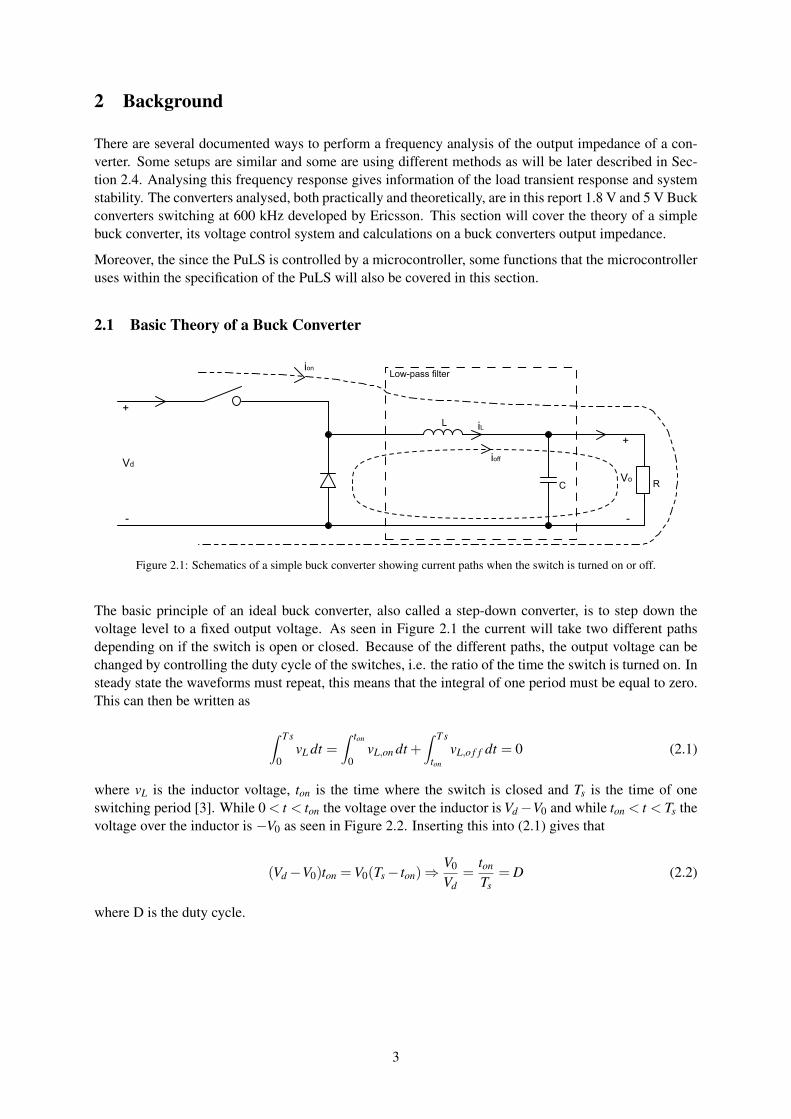
2 Background
There are several documented ways to perform a frequency analysis of the output impedance of a con-verter. Some setups are similar and some are using different methods as will be later described in Sec-tion 2.4. Analysing this frequency response gives information of the load transient response and systemstability. The converters analysed, both practically and theoretically, are in this report 1.8 V and 5 V Buckconverters switching at 600 kHz developed by Ericsson. This section will cover the theory of a simplebuck converter, its voltage control system and calculations on a buck converters output impedance.
Moreover, the since the PuLS is controlled by a microcontroller, some functions that the microcontrolleruses within the specification of the PuLS will also be covered in this section.
2.1 Basic Theory of a Buck Converter
L
C R
iL
Low-pass filterion
ioff
+
-
Vd
+
-
Vo
Figure 2.1: Schematics of a simple buck converter showing current paths when the switch is turned on or off.
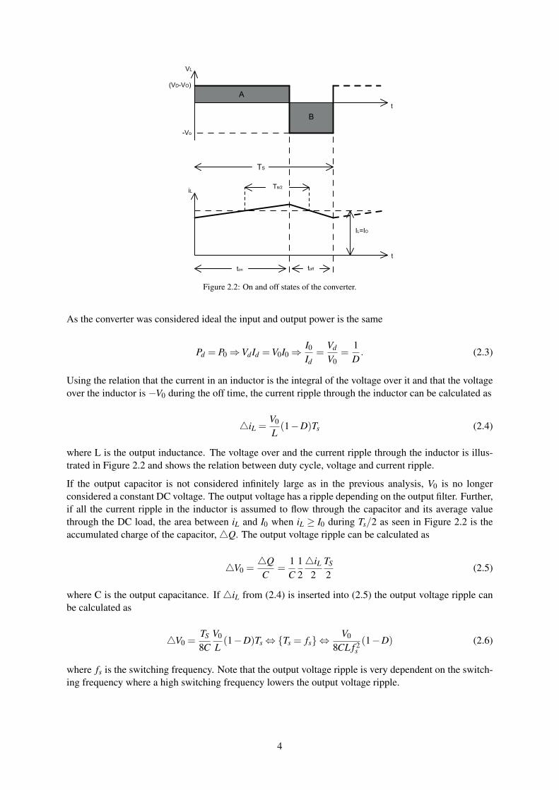
The basic principle of an ideal buck converter, also called a step-down converter, is to step down thevoltage level to a fixed output voltage. As seen in Figure 2.1 the current will take two different pathsdepending on if the switch is open or closed. Because of the different paths, the output voltage can bechanged by controlling the duty cycle of the switches, i.e. the ratio of the time the switch is turned on. Insteady state the waveforms must repeat, this means that the integral of one period must be equal to zero.This can then be written as
∫ T s
0vL dt =
∫ ton
0vL,on dt +
∫ T s
ton
vL,o f f dt = 0 (2.1)
where vL is the inductor voltage, ton is the time where the switch is closed and Ts is the time of oneswitching period [3]. While 0 < t < ton the voltage over the inductor is Vd−V0 and while ton < t < Ts thevoltage over the inductor is −V0 as seen in Figure 2.2. Inserting this into (2.1) gives that
(Vd−V0)ton =V0(Ts− ton)⇒V0
Vd=
ton
Ts= D (2.2)
where D is the duty cycle.
3
A
B
TS
VL
t
t
iLTs/2
(VD-VO)
-Vo
ton toff
IL=IO
Figure 2.2: On and off states of the converter.
As the converter was considered ideal the input and output power is the same
Pd = P0⇒VdId =V0I0⇒I0
Id=
Vd
V0=
1D. (2.3)
Using the relation that the current in an inductor is the integral of the voltage over it and that the voltageover the inductor is −V0 during the off time, the current ripple through the inductor can be calculated as
4iL =V0
L(1−D)Ts (2.4)
where L is the output inductance. The voltage over and the current ripple through the inductor is illus-trated in Figure 2.2 and shows the relation between duty cycle, voltage and current ripple.
If the output capacitor is not considered infinitely large as in the previous analysis, V0 is no longerconsidered a constant DC voltage. The output voltage has a ripple depending on the output filter. Further,if all the current ripple in the inductor is assumed to flow through the capacitor and its average valuethrough the DC load, the area between iL and I0 when iL ≥ I0 during Ts/2 as seen in Figure 2.2 is theaccumulated charge of the capacitor,4Q. The output voltage ripple can be calculated as
4V0 =4QC
=1C
124iL
2TS
2(2.5)
where C is the output capacitance. If 4iL from (2.4) is inserted into (2.5) the output voltage ripple canbe calculated as
4V0 =TS
8CV0
L(1−D)Ts⇔Ts = fs⇔
V0
8CL f 2s(1−D) (2.6)
where fs is the switching frequency. Note that the output voltage ripple is very dependent on the switch-ing frequency where a high switching frequency lowers the output voltage ripple.
4
2.2 Control of Buck Converters
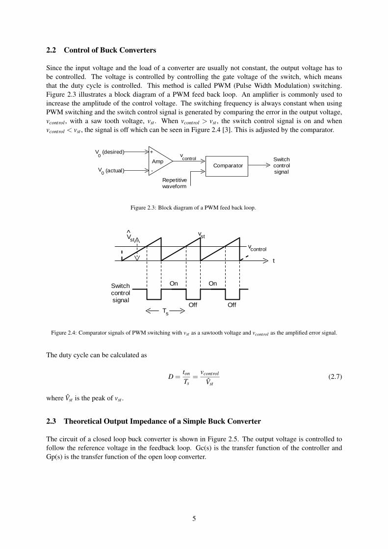
Since the input voltage and the load of a converter are usually not constant, the output voltage has tobe controlled. The voltage is controlled by controlling the gate voltage of the switch, which meansthat the duty cycle is controlled. This method is called PWM (Pulse Width Modulation) switching.Figure 2.3 illustrates a block diagram of a PWM feed back loop. An amplifier is commonly used toincrease the amplitude of the control voltage. The switching frequency is always constant when usingPWM switching and the switch control signal is generated by comparing the error in the output voltage,vcontrol , with a saw tooth voltage, vst . When vcontrol > vst , the switch control signal is on and whenvcontrol < vst , the signal is off which can be seen in Figure 2.4 [3]. This is adjusted by the comparator.
Amp
+
-
V (desired)
V (actual)0
0 vcontrol
Comparator
Repetitivewaveform
Switchcontrolsignal
Figure 2.3: Block diagram of a PWM feed back loop.
t
vcontrol
stvV
On On
Off Off
Switchcontrolsignal
st
sT
Figure 2.4: Comparator signals of PWM switching with vst as a sawtooth voltage and vcontrol as the amplified error signal.
The duty cycle can be calculated as
D =ton
Ts=
vcontrol
Vst(2.7)
where Vst is the peak of vst .
2.3 Theoretical Output Impedance of a Simple Buck Converter
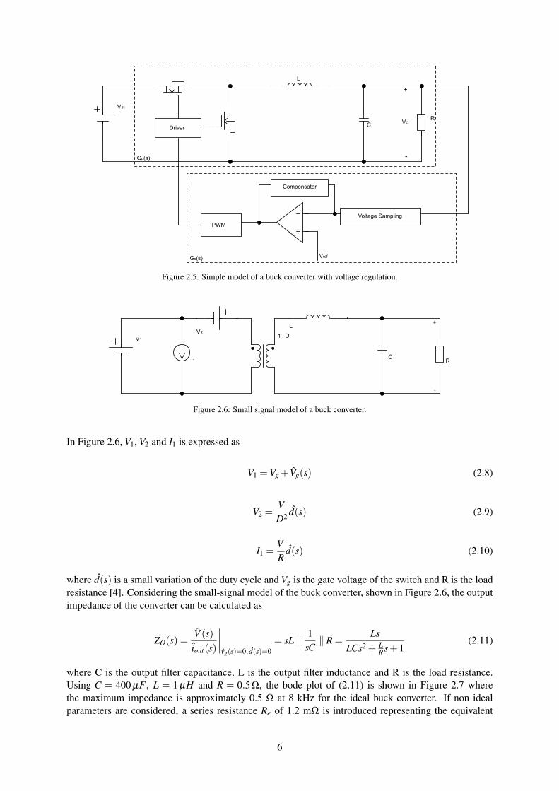
The circuit of a closed loop buck converter is shown in Figure 2.5. The output voltage is controlled tofollow the reference voltage in the feedback loop. Gc(s) is the transfer function of the controller andGp(s) is the transfer function of the open loop converter.
5
VIN
L
CR
Compensator
PWM
Voltage Sampling
VrefGc(s)
Gp(s)
Driver
+
-
VO
Figure 2.5: Simple model of a buck converter with voltage regulation.
V1
L
CR
V2
1 : D
I1
+
-
Figure 2.6: Small signal model of a buck converter.
In Figure 2.6, V1, V2 and I1 is expressed as
V1 =Vg +Vg(s) (2.8)
V2 =VD2 d(s) (2.9)
I1 =VR
d(s) (2.10)
where d(s) is a small variation of the duty cycle and Vg is the gate voltage of the switch and R is the loadresistance [4]. Considering the small-signal model of the buck converter, shown in Figure 2.6, the outputimpedance of the converter can be calculated as
ZO(s) =V (s)
iout(s)
∣∣∣∣vg(s)=0, d(s)=0
= sL ‖ 1sC‖ R =
LsLCs2 + L
R s+1(2.11)
where C is the output filter capacitance, L is the output filter inductance and R is the load resistance.Using C = 400 µF , L = 1 µH and R = 0.5Ω, the bode plot of (2.11) is shown in Figure 2.7 wherethe maximum impedance is approximately 0.5 Ω at 8 kHz for the ideal buck converter. If non idealparameters are considered, a series resistance Re of 1.2 mΩ is introduced representing the equivalent
6
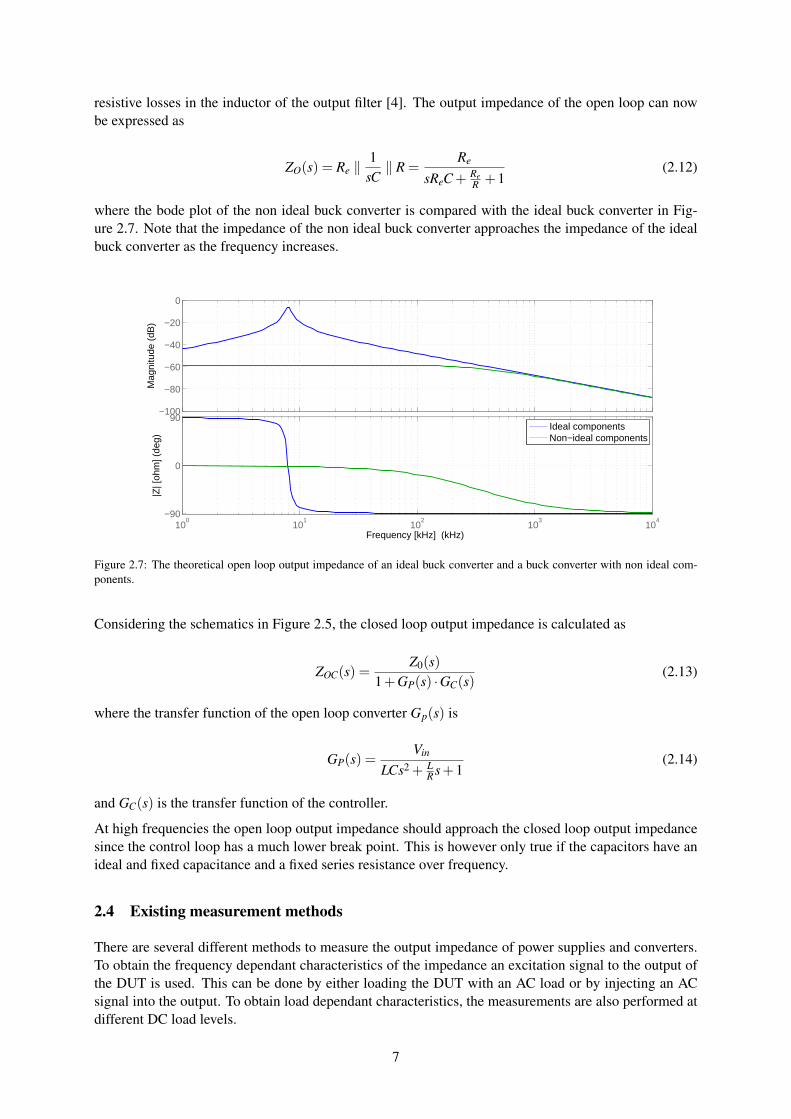
resistive losses in the inductor of the output filter [4]. The output impedance of the open loop can nowbe expressed as
ZO(s) = Re ‖1
sC‖ R =
Re
sReC+ ReR +1
(2.12)
where the bode plot of the non ideal buck converter is compared with the ideal buck converter in Fig-ure 2.7. Note that the impedance of the non ideal buck converter approaches the impedance of the idealbuck converter as the frequency increases.
−100
−80
−60
−40
−20
0
Mag
nitu
de (
dB)
100
101
102
103
104
−90
0
90
|Z| [
ohm
] (de
g)
Frequency [kHz] (kHz)
Ideal componentsNon−ideal components
Figure 2.7: The theoretical open loop output impedance of an ideal buck converter and a buck converter with non ideal com-ponents.
Considering the schematics in Figure 2.5, the closed loop output impedance is calculated as
ZOC(s) =Z0(s)
1+GP(s) ·GC(s)(2.13)
where the transfer function of the open loop converter Gp(s) is
GP(s) =Vin
LCs2 + LR s+1
(2.14)
and GC(s) is the transfer function of the controller.
At high frequencies the open loop output impedance should approach the closed loop output impedancesince the control loop has a much lower break point. This is however only true if the capacitors have anideal and fixed capacitance and a fixed series resistance over frequency.
2.4 Existing measurement methods
There are several different methods to measure the output impedance of power supplies and converters.To obtain the frequency dependant characteristics of the impedance an excitation signal to the output ofthe DUT is used. This can be done by either loading the DUT with an AC load or by injecting an ACsignal into the output. To obtain load dependant characteristics, the measurements are also performed atdifferent DC load levels.
7
All of the methods studied are executed in a similar way and can be simplified in an equivalent circuitshown in Figure 2.8 where Z0 is the output impedance of the DUT, v0 is the output voltage of the DUTand i0 is the current waveform created by an oscillating load/source.
+
-Vd
Z0
+
V0
-
i0
Dynamic load/supplyDUT
Figure 2.8: Simplified circuit of the general output impedance measurement.
The output current (i0) consists of two parts as
i0 = I0,DC + i0,AC (2.15)
where I0,DC is a DC offset and i0,AC is a sinusoidal AC. From Figure 2.8, the output voltage of the DUTcan be calculated using
v0 =Vd−Z0i0 =Vd−Z0(I0,DC + i0,AC) (2.16)
where Vd is the input voltage of the DUT. If only the AC component, i.e. the peak to peak value, of theoutput voltage is considered, the AC-component can be expressed as
v0,AC = |Z0| i0,AC⇔ |Z0|=v0,AC
i0,AC. (2.17)
Thus, the output impedance for a certain frequency is calculated by dividing the AC component of theoutput voltage of the DUT with the AC component of the generated current. Depending on the DC offsetamplitude, I0,DC, the output impedance is given for different output current levels. This is importantsince the output current affects the components creating different parasitic effects.
2.4.1 The IEC60478-4 Method
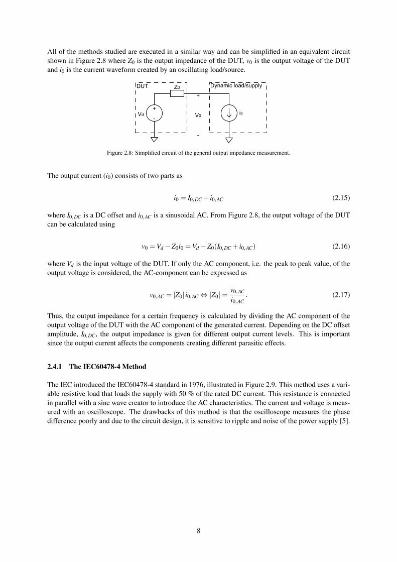
The IEC introduced the IEC60478-4 standard in 1976, illustrated in Figure 2.9. This method uses a vari-able resistive load that loads the supply with 50 % of the rated DC current. This resistance is connectedin parallel with a sine wave creator to introduce the AC characteristics. The current and voltage is meas-ured with an oscilloscope. The drawbacks of this method is that the oscilloscope measures the phasedifference poorly and due to the circuit design, it is sensitive to ripple and noise of the power supply [5].
8
Rm
Rvar
ModulatorDUT
Oscilloscope
CH2CH1
Vs
Vs
+
-
Figure 2.9: Measurement method presented in IEC60478-4.
2.4.2 The Venable Method
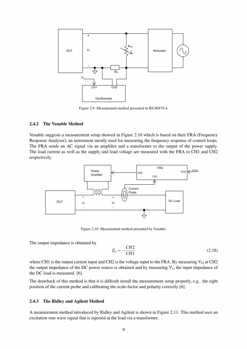
Venable suggests a measurement setup showed in Figure 2.10 which is based on their FRA (FrequencyResponse Analyser), an instrument mostly used for measuring the frequency response of control loops.The FRA sends an AC signal via an amplifier and a transformer to the output of the power supply.The load current as well as the supply and load voltage are measured with the FRA to CH1 and CH2respectively.
DUT
Power
Amplifier
FRA
OSC
CH1
CH2
DC LoadVS VO
+
-
+
-
Current
Probe
Vs,Vo
Figure 2.10: Measurement method presented by Venable.
The output impedance is obtained by
Zo =−CH2CH1
(2.18)
where CH1 is the output current input and CH2 is the voltage input to the FRA. By measuring VO at CH2the output impedance of the DC power source is obtained and by measuring Vs, the input impedance ofthe DC load is measured. [6].
The drawback of this method is that it is difficult install the measurement setup properly, e.g.. the rightposition of the current probe and calibrating the scale-factor and polarity correctly [6].
2.4.3 The Ridley and Agilent Method
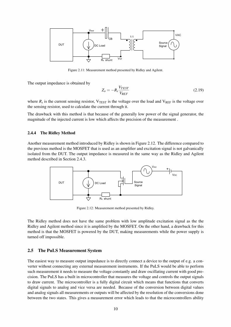
A measurement method introduced by Ridley and Agilent is shown in Figure 2.11. This method uses anexcitation sine wave signal that is injected at the load via a transformer.
9
VAC
Rs shunt
CB1:1
Source
Signal
Vref
DC Load
Vtest
DUT
Figure 2.11: Measurement method presented by Ridley and Agilent.
The output impedance is obtained by
Zo =−RsVT EST
VREF(2.19)
where Rs is the current sensing resistor, VTEST is the voltage over the load and VREF is the voltage overthe sensing resistor, used to calculate the current through it.
The drawback with this method is that because of the generally low power of the signal generator, themagnitude of the injected current is low which affects the precision of the measurement .
2.4.4 The Ridley Method
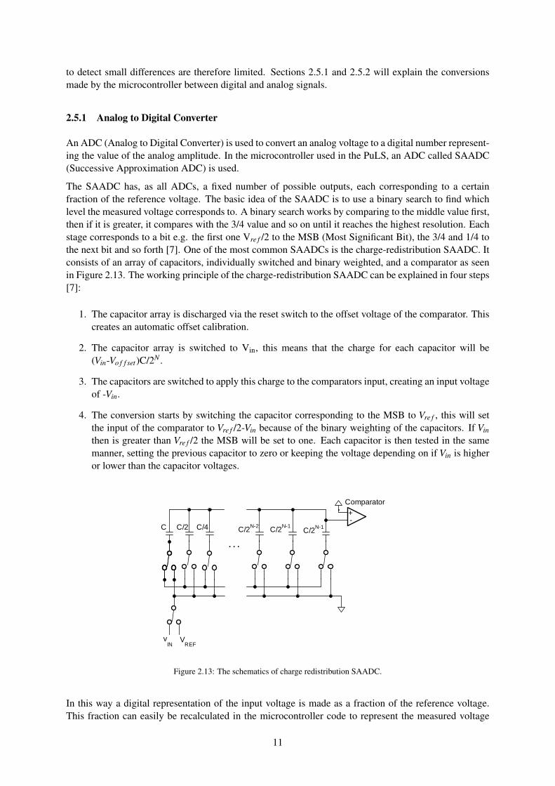
Another measurement method introduced by Ridley is shown in Figure 2.12. The difference compared tothe previous method is the MOSFET that is used as an amplifier and excitation signal is not galvanicallyisolated from the DUT. The output impedance is measured in the same way as the Ridley and Agilentmethod described in Section 2.4.3.
VAC
Rs shunt
VDC
DUT DC Load Source
Signal
Figure 2.12: Measurement method presented by Ridley.
The Ridley method does not have the same problem with low amplitude excitation signal as the theRidley and Agilent method since it is amplified by the MOSFET. On the other hand, a drawback for thismethod is that the MOSFET is powered by the DUT, making measurements while the power supply isturned off impossible.
2.5 The PuLS Measurement System
The easiest way to measure output impedance is to directly connect a device to the output of e.g. a con-verter without connecting any external measurement instruments. If the PuLS would be able to performsuch measurement it needs to measure the voltage constantly and draw oscillating current with good pre-cision. The PuLS has a built in microcontroller that measures the voltage and controls the output signalsto draw current. The microcontroller is a fully digital circuit which means that functions that convertsdigital signals to analog and vice versa are needed. Because of the conversion between digital valuesand analog signals all measurements or outputs will be affected by the resolution of the conversions donebetween the two states. This gives a measurement error which leads to that the microcontrollers ability
10
to detect small differences are therefore limited. Sections 2.5.1 and 2.5.2 will explain the conversionsmade by the microcontroller between digital and analog signals.
2.5.1 Analog to Digital Converter
An ADC (Analog to Digital Converter) is used to convert an analog voltage to a digital number represent-ing the value of the analog amplitude. In the microcontroller used in the PuLS, an ADC called SAADC(Successive Approximation ADC) is used.
The SAADC has, as all ADCs, a fixed number of possible outputs, each corresponding to a certainfraction of the reference voltage. The basic idea of the SAADC is to use a binary search to find whichlevel the measured voltage corresponds to. A binary search works by comparing to the middle value first,then if it is greater, it compares with the 3/4 value and so on until it reaches the highest resolution. Eachstage corresponds to a bit e.g. the first one Vre f /2 to the MSB (Most Significant Bit), the 3/4 and 1/4 tothe next bit and so forth [7]. One of the most common SAADCs is the charge-redistribution SAADC. Itconsists of an array of capacitors, individually switched and binary weighted, and a comparator as seenin Figure 2.13. The working principle of the charge-redistribution SAADC can be explained in four steps[7]:
1. The capacitor array is discharged via the reset switch to the offset voltage of the comparator. Thiscreates an automatic offset calibration.
2. The capacitor array is switched to Vin, this means that the charge for each capacitor will be(Vin-Vo f f set)C/2N .
3. The capacitors are switched to apply this charge to the comparators input, creating an input voltageof -Vin.
4. The conversion starts by switching the capacitor corresponding to the MSB to Vre f , this will setthe input of the comparator to Vre f /2-Vin because of the binary weighting of the capacitors. If Vin
then is greater than Vre f /2 the MSB will be set to one. Each capacitor is then tested in the samemanner, setting the previous capacitor to zero or keeping the voltage depending on if Vin is higheror lower than the capacitor voltages.
. . .
+-
Comparator
C C/2 C/4
v VIN REF
C/2N-2 C/2N-1C/2N-1
Figure 2.13: The schematics of charge redistribution SAADC.
In this way a digital representation of the input voltage is made as a fraction of the reference voltage.This fraction can easily be recalculated in the microcontroller code to represent the measured voltage
11
cancelling both external scaling and the scaling done in the ADC [7]. The ADC conversion leads atrade-off between how good the resolution can be and how large the measurable range of the input signalis.
2.5.2 Digital to Analog Converter
A DAC (Digital to Analog Converter) is a converter from a digital number to an analog signal, such as avoltage. This can be done in different ways, e.g. using PWM, oversampling or binary weighted switchedresistors.
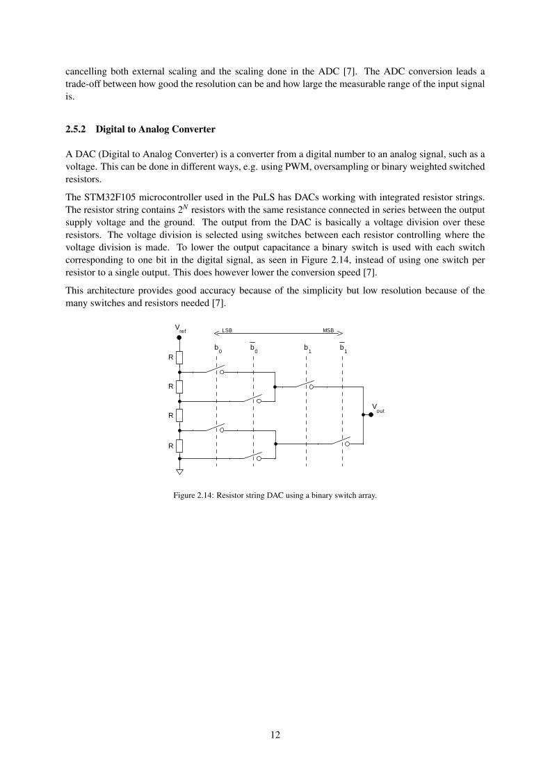
The STM32F105 microcontroller used in the PuLS has DACs working with integrated resistor strings.The resistor string contains 2N resistors with the same resistance connected in series between the outputsupply voltage and the ground. The output from the DAC is basically a voltage division over theseresistors. The voltage division is selected using switches between each resistor controlling where thevoltage division is made. To lower the output capacitance a binary switch is used with each switchcorresponding to one bit in the digital signal, as seen in Figure 2.14, instead of using one switch perresistor to a single output. This does however lower the conversion speed [7].
This architecture provides good accuracy because of the simplicity but low resolution because of themany switches and resistors needed [7].
Vref
Vout
R
R
R
R
b0
b0
b1
b1
LSB MSB
Figure 2.14: Resistor string DAC using a binary switch array.
12
3 The Current PuLS
PuLS is currently a working product at Ericsson, it is used for testing and verification of DC/DC con-verters. In its current form, it can only be used as a pulsed load.
3.1 Specification
The PuLS can create current pulse shapes with three different current levels between 0.5 and 45 A withrise and fall slew rates up to 20 A/µs. Each pulse can have a duration of 10-9999 µs and a delay timeof 5-1000 ms between each pulse. In its present state, it can only handle load characteristics consistingof one pulse per period with a maximum duty cycle of 50 % and voltages under 20 V [8]. One of thebiggest benefits with using the PuLS compared to the active loads used today is that the PuLS is directlyinstalled on the PCB to minimize inductance leading to faster slew rate of the pulses. The PuLS can bepowered either through the USB cable or through the PMBus (Power Management Bus) cable. SeveralPuLS units can also be connected to one controlling computer via the PMBus and can be set to triggersimultaneously [8].
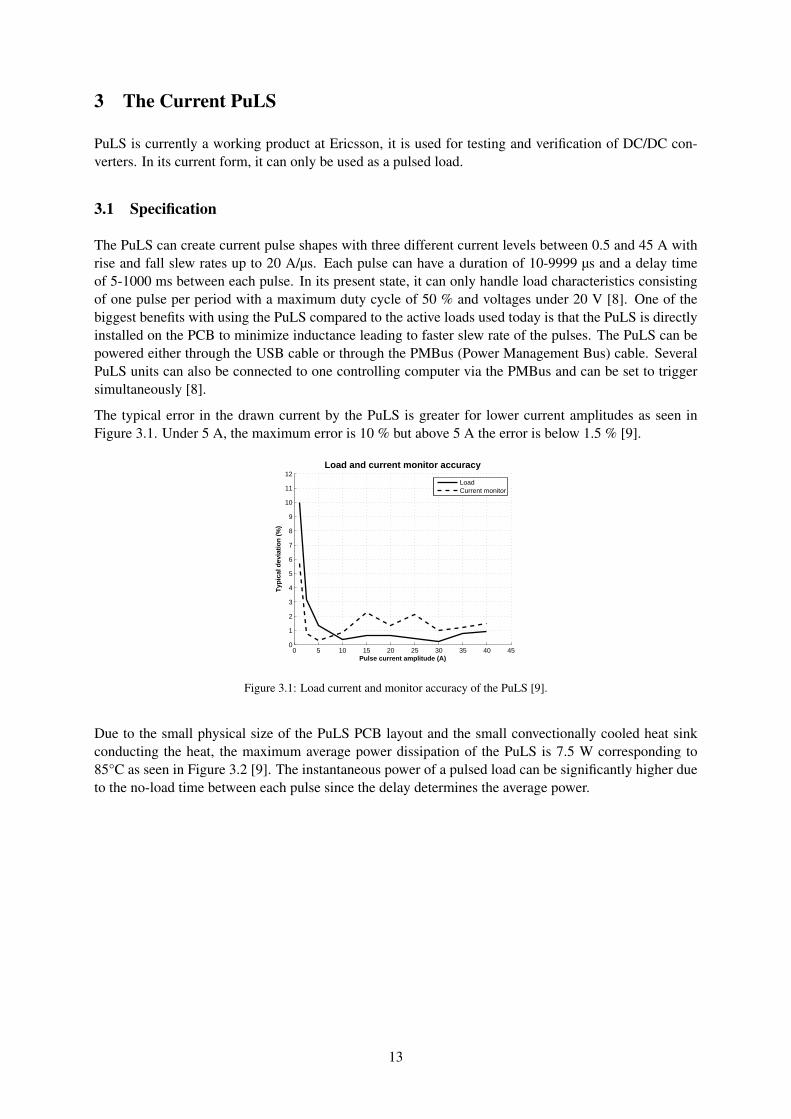
The typical error in the drawn current by the PuLS is greater for lower current amplitudes as seen inFigure 3.1. Under 5 A, the maximum error is 10 % but above 5 A the error is below 1.5 % [9].
0 5 10 15 20 25 30 35 40 450
1
2
3
4
5
6
7
8
9
10
11
12
Pulse current amplitude (A)
Typ
ical
dev
iati
on
(%
)
Load and current monitor accuracy
LoadCurrent monitor
Figure 3.1: Load current and monitor accuracy of the PuLS [9].
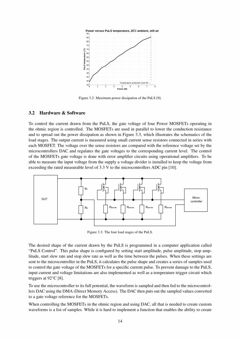
Due to the small physical size of the PuLS PCB layout and the small convectionally cooled heat sinkconducting the heat, the maximum average power dissipation of the PuLS is 7.5 W corresponding to85°C as seen in Figure 3.2 [9]. The instantaneous power of a pulsed load can be significantly higher dueto the no-load time between each pulse since the delay determines the average power.
13
0 1 2 3 4 5 6 7 825
30
35
40
45
50
55
60
65
70
75
80
85
90
Power (W)
Pu
LS
tem
per
atu
re (
° C)
Power versus PuLS temperature, 25°C ambient, still air
Temperature protection shut off →
Figure 3.2: Maximum power dissipation of the PuLS [9].
3.2 Hardware & Software
To control the current drawn from the PuLS, the gate voltage of four Power MOSFETs operating inthe ohmic region is controlled. The MOSFETs are used in parallel to lower the conduction resistanceand to spread out the power dissipation as shown in Figure 3.3, which illustrates the schematics of theload stages. The output current is measured using small current sense resistors connected in series witheach MOSFET. The voltage over the sense resistors are compared with the reference voltage set by themicrocontrollers DAC and regulates the gate voltages to the corresponding current level. The controlof the MOSFETs gate voltage is done with error amplifier circuits using operational amplifiers. To beable to measure the input voltage from the supply a voltage divider is installed to keep the voltage fromexceeding the rated measurable level of 3.3 V to the microcontrollers ADC pin [10].
Rsense Rsense Rsense Rsense
R1
R2
DUTMicro-
controller
Figure 3.3: The four load stages of the PuLS.
The desired shape of the current drawn by the PuLS is programmed in a computer application called“PuLS Control”. This pulse shape is configured by setting start amplitude, pulse amplitude, stop amp-litude, start slew rate and stop slew rate as well as the time between the pulses. When these settings aresent to the microcontroller in the PuLS, it calculates the pulse shape and creates a series of samples usedto control the gate voltage of the MOSFETs for a specific current pulse. To prevent damage to the PuLS,input current and voltage limitations are also implemented as well as a temperature trigger circuit whichtriggers at 92°C [8].
To use the microcontroller to its full potential, the waveform is sampled and then fed to the microcontrol-lers DAC using the DMA (Direct Memory Access). The DAC then puts out the sampled values convertedto a gate voltage reference for the MOSFETs.
When controlling the MOSFETs in the ohmic region and using DAC, all that is needed to create customwaveforms is a list of samples. While it is hard to implement a function that enables the ability to create
14
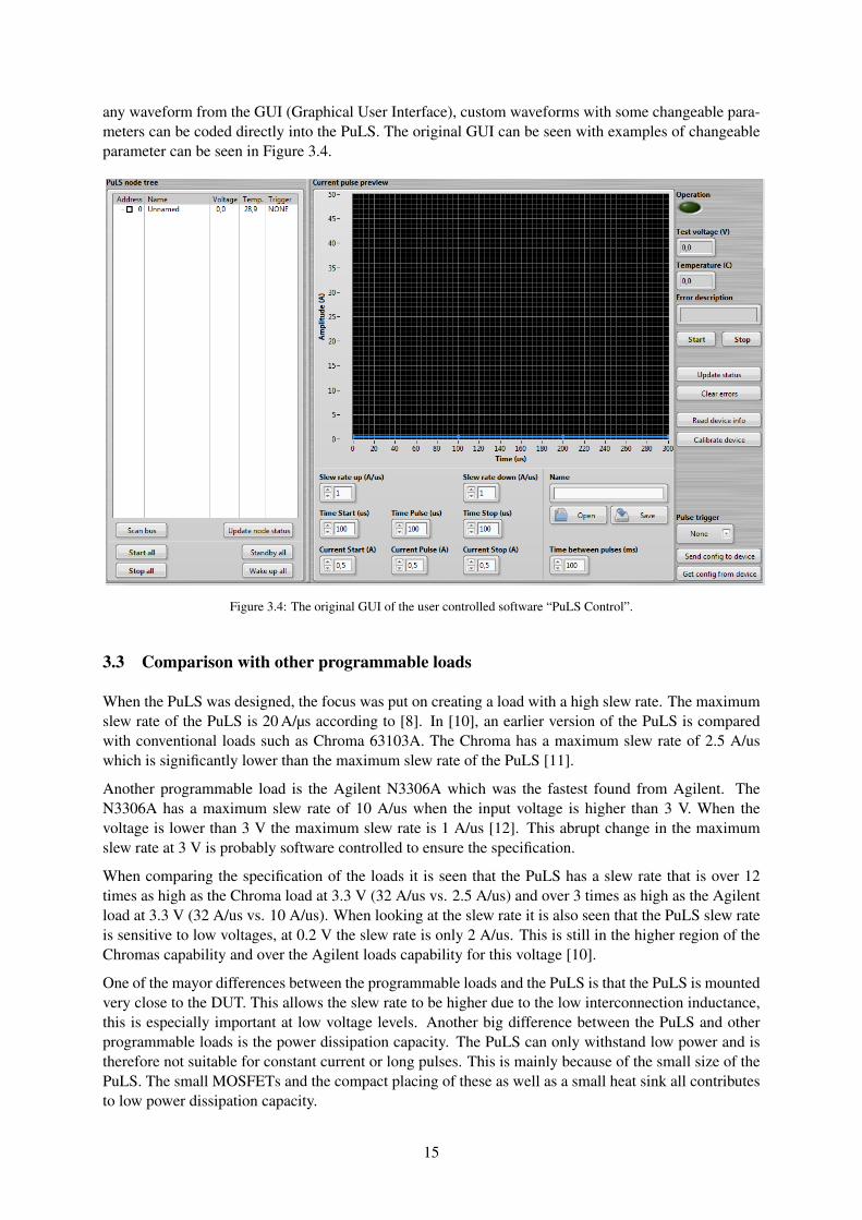
any waveform from the GUI (Graphical User Interface), custom waveforms with some changeable para-meters can be coded directly into the PuLS. The original GUI can be seen with examples of changeableparameter can be seen in Figure 3.4.
Figure 3.4: The original GUI of the user controlled software “PuLS Control”.
3.3 Comparison with other programmable loads
When the PuLS was designed, the focus was put on creating a load with a high slew rate. The maximumslew rate of the PuLS is 20 A/µs according to [8]. In [10], an earlier version of the PuLS is comparedwith conventional loads such as Chroma 63103A. The Chroma has a maximum slew rate of 2.5 A/uswhich is significantly lower than the maximum slew rate of the PuLS [11].
Another programmable load is the Agilent N3306A which was the fastest found from Agilent. TheN3306A has a maximum slew rate of 10 A/us when the input voltage is higher than 3 V. When thevoltage is lower than 3 V the maximum slew rate is 1 A/us [12]. This abrupt change in the maximumslew rate at 3 V is probably software controlled to ensure the specification.
When comparing the specification of the loads it is seen that the PuLS has a slew rate that is over 12times as high as the Chroma load at 3.3 V (32 A/us vs. 2.5 A/us) and over 3 times as high as the Agilentload at 3.3 V (32 A/us vs. 10 A/us). When looking at the slew rate it is also seen that the PuLS slew rateis sensitive to low voltages, at 0.2 V the slew rate is only 2 A/us. This is still in the higher region of theChromas capability and over the Agilent loads capability for this voltage [10].
One of the mayor differences between the programmable loads and the PuLS is that the PuLS is mountedvery close to the DUT. This allows the slew rate to be higher due to the low interconnection inductance,this is especially important at low voltage levels. Another big difference between the PuLS and otherprogrammable loads is the power dissipation capacity. The PuLS can only withstand low power and istherefore not suitable for constant current or long pulses. This is mainly because of the small size of thePuLS. The small MOSFETs and the compact placing of these as well as a small heat sink all contributesto low power dissipation capacity.
15

3.4 Using the PuLS to Measure the Output Impedance
The original PuLS can only draw pulse shaped loads but if the current PuLS would be able to draw asinusoidal current, it could be used as a excitation sine wave signal for output impedance measurements.Since the microcontroller can measure voltage it is possible to extract the voltage over the DUT whileit draws the load creating a possibility to measure output impedance. If the frequency of the excitationsine wave can be swept, the output impedance of each frequency could be calculated and automaticallycreate a table of values from the measurements. A drawback with using the PuLS to measure the outputimpedance is that it is not possible to measure the phase. Another drawback is that the DUT has to be onduring the testing, and therefore the output filter alone can not be measured.
The PuLS is able to draw loads up to 45 A. This means that it can draw a very large excitation current.According to [13] a high excitation current is needed when measuring the output impedance on devicesthat have a high rated output currents or have very low impedance, such as batteries.
16
4 Redesign of the PuLS
To be able to measure the output impedance of converters or power supplies, changes in both the hard-ware and the software of the PuLS had to be made. These changes will be explained in this section.
4.1 Hardware
The maximum frequency of the current sine waves that the PuLS will draw is limited to 500 kHz in thisthesis. This is because the current waveform becomes distorted and the voltage measurement is too slowto measure over 500 kHz. This is explained more in depth in Section 4.4.
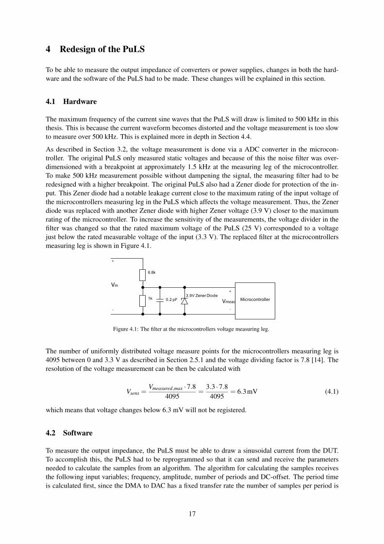
As described in Section 3.2, the voltage measurement is done via a ADC converter in the microcon-troller. The original PuLS only measured static voltages and because of this the noise filter was over-dimensioned with a breakpoint at approximately 1.5 kHz at the measuring leg of the microcontroller.To make 500 kHz measurement possible without dampening the signal, the measuring filter had to beredesigned with a higher breakpoint. The original PuLS also had a Zener diode for protection of the in-put. This Zener diode had a notable leakage current close to the maximum rating of the input voltage ofthe microcontrollers measuring leg in the PuLS which affects the voltage measurement. Thus, the Zenerdiode was replaced with another Zener diode with higher Zener voltage (3.9 V) closer to the maximumrating of the microcontroller. To increase the sensitivity of the measurements, the voltage divider in thefilter was changed so that the rated maximum voltage of the PuLS (25 V) corresponded to a voltagejust below the rated measurable voltage of the input (3.3 V). The replaced filter at the microcontrollersmeasuring leg is shown in Figure 4.1.
6.8k
1k3.9V Zener Diode
0.2 pF
Vin
+
-
Vmeas
+
-
Microcontroller
Figure 4.1: The filter at the microcontrollers voltage measuring leg.
The number of uniformly distributed voltage measure points for the microcontrollers measuring leg is4095 between 0 and 3.3 V as described in Section 2.5.1 and the voltage dividing factor is 7.8 [14]. Theresolution of the voltage measurement can be then be calculated with
Vsens =Vmeasured,max ·7.8
4095=
3.3 ·7.84095
= 6.3mV (4.1)
which means that voltage changes below 6.3 mV will not be registered.
4.2 Software
To measure the output impedance, the PuLS must be able to draw a sinusoidal current from the DUT.To accomplish this, the PuLS had to be reprogrammed so that it can send and receive the parametersneeded to calculate the samples from an algorithm. The algorithm for calculating the samples receivesthe following input variables; frequency, amplitude, number of periods and DC-offset. The period timeis calculated first, since the DMA to DAC has a fixed transfer rate the number of samples per period is
17
calculated by multiplying the period time with the transfer rate. The sine wave samples is then calculatedas
y(n) = A · sin(2π
kn− π
2)+O (4.2)
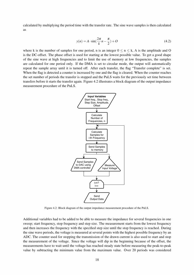
where k is the number of samples for one period, n is an integer 0 ≤ n ≤ k, A is the amplitude and Ois the DC-offset. The phase offset is used for starting at the lowest possible value. To get a good shapeof the sine wave at high frequencies and to limit the use of memory at low frequencies, the samplesare calculated for one period only. If the DMA is set to circular mode, the output will automaticallyrepeat the sample array until it is turned off. After each transfer, the flag “Transfer complete” is set.When the flag is detected a counter is increased by one and the flag is cleared. When the counter reachesthe set number of periods the transfer is stopped and the PuLS waits for the previously set time betweentransfers before it starts the transfer again. Figure 4.2 illustrates a block diagram of the output impedancemeasurement procedure of the PuLS.
Start freq., Stop freq.,Step Size, Amplitude,
Offset
Input Variables
CalculateNumber of
Frequencies, n
CalculateSamples for
i:th Frequency
Send Samplesto memory
Send Samples to DAC using
DMA controllerMeasure
Input Voltage
i=n?i++
SendOutput Data
Figure 4.2: Block diagram of the output impedance measurement procedure of the PuLS.
Additional variables had to be added to be able to measure the impedance for several frequencies in onesweep; start frequency, stop frequency and step size. The measurement starts from the lowest frequencyand then increases the frequency with the specified step size until the stop frequency is reached. Duringthe sine wave periods, the voltage is measured at several points with the highest possible frequency by anADC. The counter used for stopping the transmission of the drawn current is also used to start and stopthe measurement of the voltage. Since the voltage will dip in the beginning because of the offset, themeasurements have to wait until the voltage has reached steady state before measuring the peak-to-peakvalue by subtracting the minimum value from the maximum value. Over 20 periods was considered
18
sufficient to reach steady state for frequencies up to 500 kHz. The voltage measurement gather samplingpoints at a certain frequency limited by the microcontroller to approximately 850 kHz [14]. Because ofthis limitation, the voltage must be measured over several periods to be able to reach a sufficient numberof points to extract the maximum and minimum values of the voltage wave form. The number of periodswhere the voltage measurement is on were chosen to 20 periods in the end of the transmission whichmeans that the total number of periods of each transmission is 40 periods.
4.3 Graphical User Interface
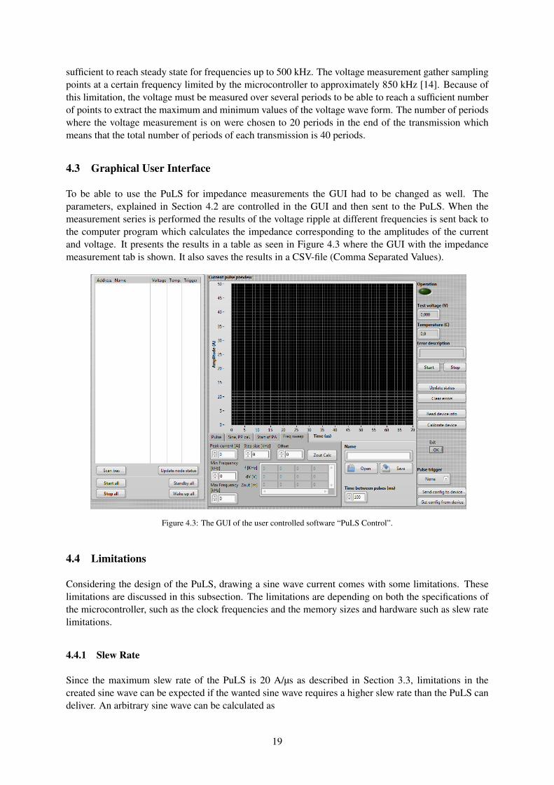
To be able to use the PuLS for impedance measurements the GUI had to be changed as well. Theparameters, explained in Section 4.2 are controlled in the GUI and then sent to the PuLS. When themeasurement series is performed the results of the voltage ripple at different frequencies is sent back tothe computer program which calculates the impedance corresponding to the amplitudes of the currentand voltage. It presents the results in a table as seen in Figure 4.3 where the GUI with the impedancemeasurement tab is shown. It also saves the results in a CSV-file (Comma Separated Values).
Figure 4.3: The GUI of the user controlled software “PuLS Control”.
4.4 Limitations
Considering the design of the PuLS, drawing a sine wave current comes with some limitations. Theselimitations are discussed in this subsection. The limitations are depending on both the specifications ofthe microcontroller, such as the clock frequencies and the memory sizes and hardware such as slew ratelimitations.
4.4.1 Slew Rate
Since the maximum slew rate of the PuLS is 20 A/µs as described in Section 3.3, limitations in thecreated sine wave can be expected if the wanted sine wave requires a higher slew rate than the PuLS candeliver. An arbitrary sine wave can be calculated as
19
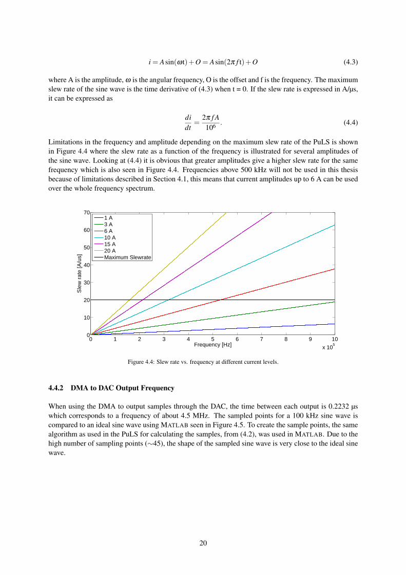
i = Asin(ωt)+O = Asin(2π f t)+O (4.3)
where A is the amplitude, ω is the angular frequency, O is the offset and f is the frequency. The maximumslew rate of the sine wave is the time derivative of (4.3) when t = 0. If the slew rate is expressed in A/µs,it can be expressed as
didt
=2π f A106 . (4.4)
Limitations in the frequency and amplitude depending on the maximum slew rate of the PuLS is shownin Figure 4.4 where the slew rate as a function of the frequency is illustrated for several amplitudes ofthe sine wave. Looking at (4.4) it is obvious that greater amplitudes give a higher slew rate for the samefrequency which is also seen in Figure 4.4. Frequencies above 500 kHz will not be used in this thesisbecause of limitations described in Section 4.1, this means that current amplitudes up to 6 A can be usedover the whole frequency spectrum.
0 1 2 3 4 5 6 7 8 9 10
x 105
0
10
20
30
40
50
60
70
Frequency [Hz]
Sle
w r
ate
[A/u
s]
1 A3 A6 A10 A15 A20 AMaximum Slewrate
Figure 4.4: Slew rate vs. frequency at different current levels.
4.4.2 DMA to DAC Output Frequency
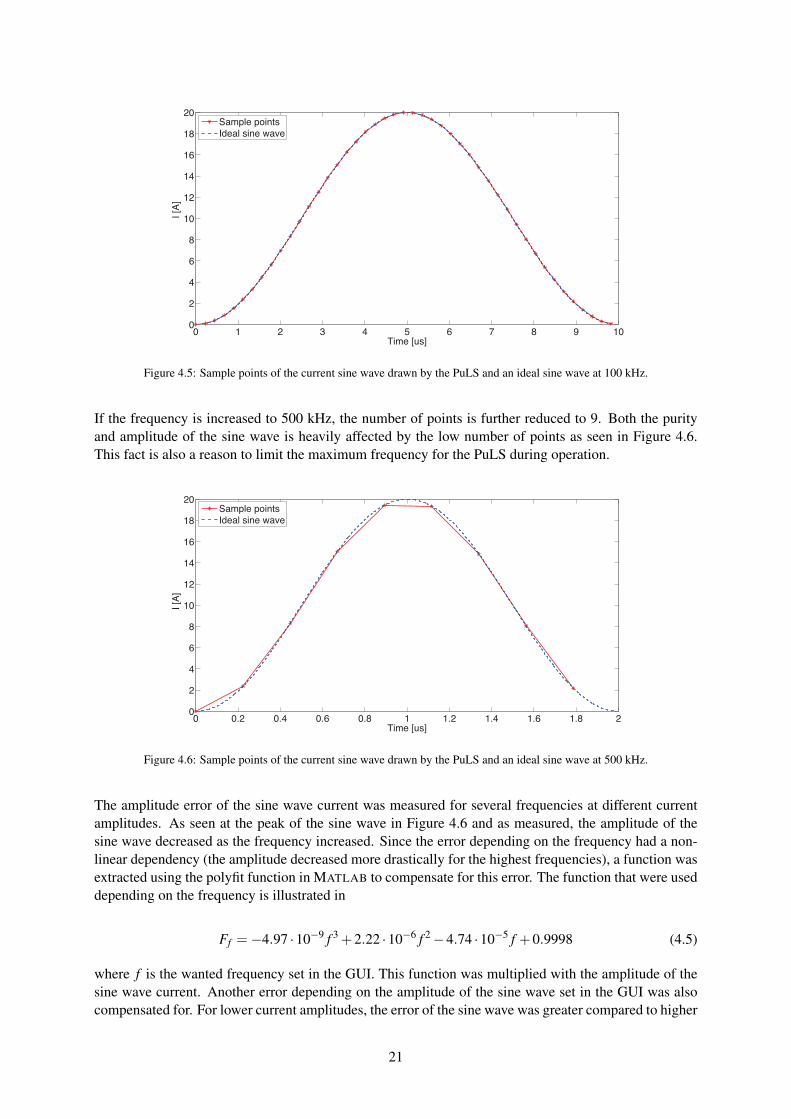
When using the DMA to output samples through the DAC, the time between each output is 0.2232 µswhich corresponds to a frequency of about 4.5 MHz. The sampled points for a 100 kHz sine wave iscompared to an ideal sine wave using MATLAB seen in Figure 4.5. To create the sample points, the samealgorithm as used in the PuLS for calculating the samples, from (4.2), was used in MATLAB. Due to thehigh number of sampling points (∼45), the shape of the sampled sine wave is very close to the ideal sinewave.
20
0 1 2 3 4 5 6 7 8 9 100
2
4
6
8
10
12
14
16
18
20
Time [us]
I [A
]
Sample points
Ideal sine wave
Figure 4.5: Sample points of the current sine wave drawn by the PuLS and an ideal sine wave at 100 kHz.
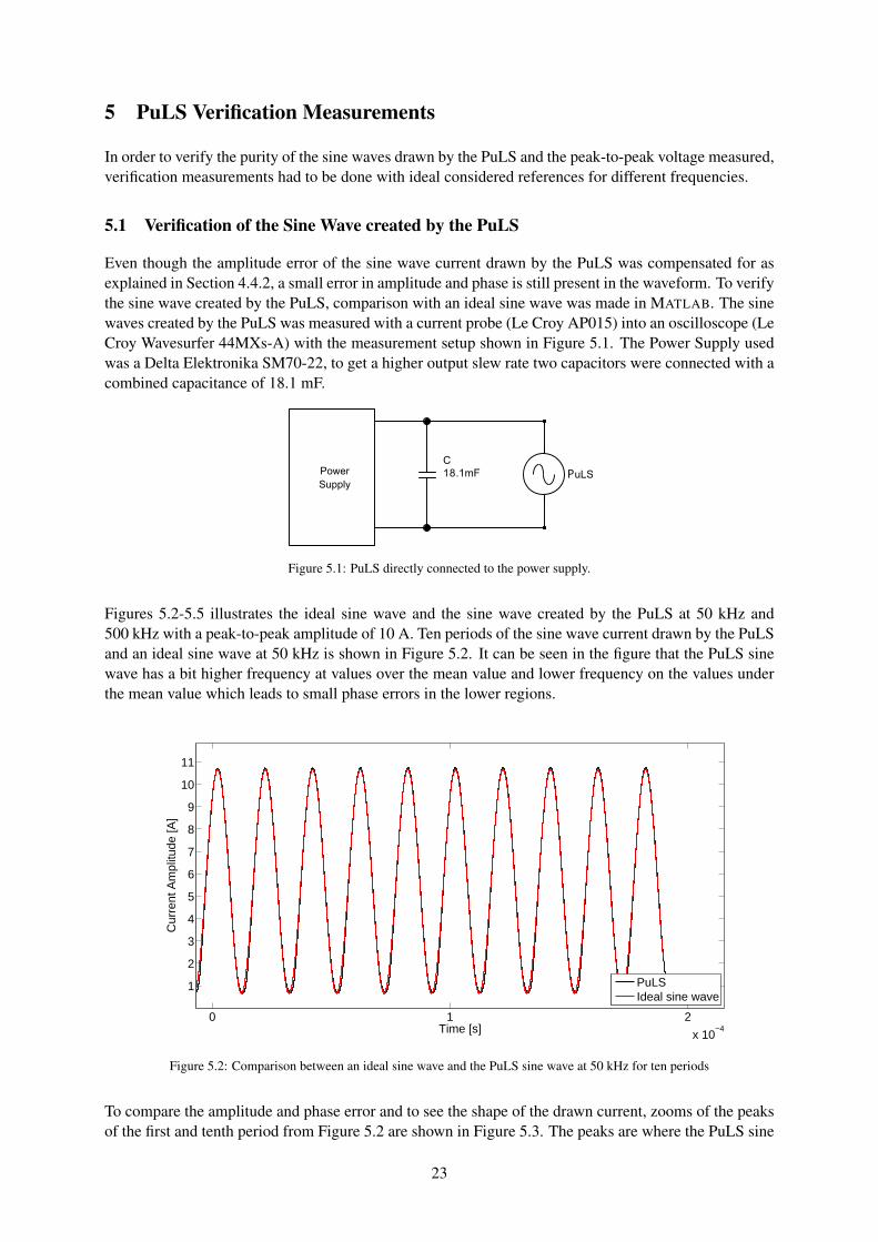
If the frequency is increased to 500 kHz, the number of points is further reduced to 9. Both the purityand amplitude of the sine wave is heavily affected by the low number of points as seen in Figure 4.6.This fact is also a reason to limit the maximum frequency for the PuLS during operation.
0 0.2 0.4 0.6 0.8 1 1.2 1.4 1.6 1.8 20
2
4
6
8
10
12
14
16
18
20
Time [us]
I [A
]
Sample points
Ideal sine wave
Figure 4.6: Sample points of the current sine wave drawn by the PuLS and an ideal sine wave at 500 kHz.
The amplitude error of the sine wave current was measured for several frequencies at different currentamplitudes. As seen at the peak of the sine wave in Figure 4.6 and as measured, the amplitude of thesine wave decreased as the frequency increased. Since the error depending on the frequency had a non-linear dependency (the amplitude decreased more drastically for the highest frequencies), a function wasextracted using the polyfit function in MATLAB to compensate for this error. The function that were useddepending on the frequency is illustrated in
Ff =−4.97 ·10−9 f 3 +2.22 ·10−6 f 2−4.74 ·10−5 f +0.9998 (4.5)
where f is the wanted frequency set in the GUI. This function was multiplied with the amplitude of thesine wave current. Another error depending on the amplitude of the sine wave set in the GUI was alsocompensated for. For lower current amplitudes, the error of the sine wave was greater compared to higher
21

current amplitudes. In the same way as the frequency compensation in (4.5), a function using the polyfitfunction in MATLAB was extracted as
FA =−3.6 ·10−4I4p−p +0.0122I3
p−p−0.1417I2p−p +0.7922Ip−p +0.3887 (4.6)
where Ip-p is the wanted current amplitude set in the GUI. This function was added to the set amplitudeof the current.
In addition to the limitations at higher frequencies, the fixed sampling rate of the DMA and DAC createsproblems at low frequencies. At frequencies lower than 500 Hz, the DMA memory is too small to handleall the sampling points and will not work. Therefore the minimum frequency when creating sine wavesis limited to 500 Hz.
22
5 PuLS Verification Measurements
In order to verify the purity of the sine waves drawn by the PuLS and the peak-to-peak voltage measured,verification measurements had to be done with ideal considered references for different frequencies.
5.1 Verification of the Sine Wave created by the PuLS
Even though the amplitude error of the sine wave current drawn by the PuLS was compensated for asexplained in Section 4.4.2, a small error in amplitude and phase is still present in the waveform. To verifythe sine wave created by the PuLS, comparison with an ideal sine wave was made in MATLAB. The sinewaves created by the PuLS was measured with a current probe (Le Croy AP015) into an oscilloscope (LeCroy Wavesurfer 44MXs-A) with the measurement setup shown in Figure 5.1. The Power Supply usedwas a Delta Elektronika SM70-22, to get a higher output slew rate two capacitors were connected with acombined capacitance of 18.1 mF.
18.1mF
CPower
SupplyPuLS
Figure 5.1: PuLS directly connected to the power supply.
Figures 5.2-5.5 illustrates the ideal sine wave and the sine wave created by the PuLS at 50 kHz and500 kHz with a peak-to-peak amplitude of 10 A. Ten periods of the sine wave current drawn by the PuLSand an ideal sine wave at 50 kHz is shown in Figure 5.2. It can be seen in the figure that the PuLS sinewave has a bit higher frequency at values over the mean value and lower frequency on the values underthe mean value which leads to small phase errors in the lower regions.
0 1 2
x 10−4
1
2
3
4
5
6
7
8
9
10
11
Time [s]
Cur
rent
Am
plitu
de [A
]
PuLSIdeal sine wave
Figure 5.2: Comparison between an ideal sine wave and the PuLS sine wave at 50 kHz for ten periods
To compare the amplitude and phase error and to see the shape of the drawn current, zooms of the peaksof the first and tenth period from Figure 5.2 are shown in Figure 5.3. The peaks are where the PuLS sine
23
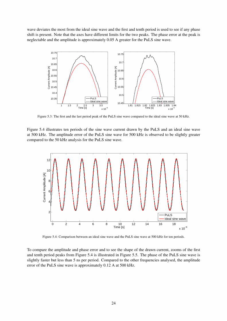
wave deviates the most from the ideal sine wave and the first and tenth period is used to see if any phaseshift is present. Note that the axes have different limits for the two peaks. The phase error at the peak isneglectable and the amplitude is approximately 0.05 A greater for the PuLS sine wave.
1 1.5 2 2.5 3 3.5
x 10−6
10.35
10.4
10.45
10.5
10.55
10.6
10.65
10.7
10.75
Time [s]
Cur
rent
Am
plitu
de [A
]
PuLSIdeal sine wave
1.81 1.815 1.82 1.825 1.83 1.835 1.84
x 10−4
10.45
10.5
10.55
10.6
10.65
10.7
10.75
Time [s]
Cur
rent
Am
plitu
de [A
]
PuLSIdeal sine wave
Figure 5.3: The first and the last period peak of the PuLS sine wave compared to the ideal sine wave at 50 kHz.
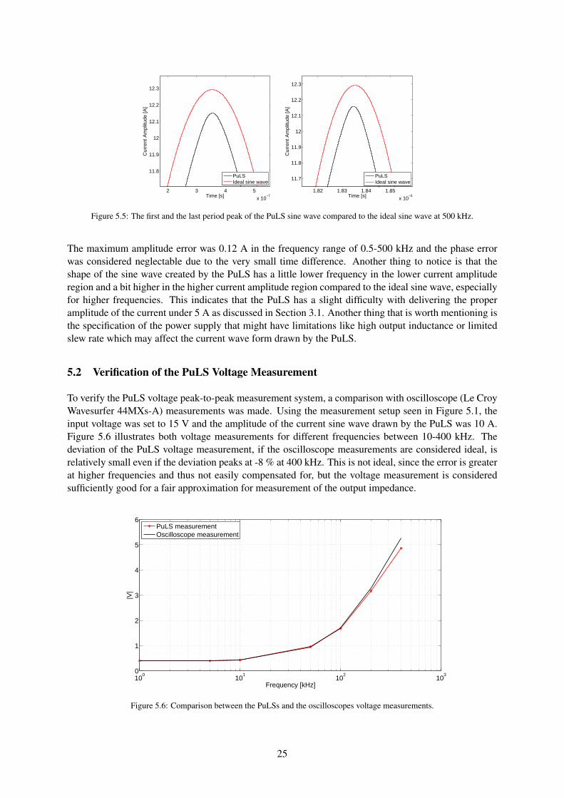
Figure 5.4 illustrates ten periods of the sine wave current drawn by the PuLS and an ideal sine waveat 500 kHz. The amplitude error of the PuLS sine wave for 500 kHz is observed to be slightly greatercompared to the 50 kHz analysis for the PuLS sine wave.
0 2 4 6 8 10 12 14 16 18
x 10−6
2
4
6
8
10
12
Time [s]
Cur
rent
Am
plitu
de [A
]
PuLSIdeal sine wave
Figure 5.4: Comparison between an ideal sine wave and the PuLS sine wave at 500 kHz for ten periods.
To compare the amplitude and phase error and to see the shape of the drawn current, zooms of the firstand tenth period peaks from Figure 5.4 is illustrated in Figure 5.5. The phase of the PuLS sine wave isslightly faster but less than 5 ns per period. Compared to the other frequencies analysed, the amplitudeerror of the PuLS sine wave is approximately 0.12 A at 500 kHz.
24
2 3 4 5
x 10−7
11.8
11.9
12
12.1
12.2
12.3
Time [s]
Cur
rent
Am
plitu
de [A
]
PuLSIdeal sine wave
1.82 1.83 1.84 1.85
x 10−5
11.7
11.8
11.9
12
12.1
12.2
12.3
Time [s]
Cur
rent
Am
plitu
de [A
]
PuLSIdeal sine wave
Figure 5.5: The first and the last period peak of the PuLS sine wave compared to the ideal sine wave at 500 kHz.
The maximum amplitude error was 0.12 A in the frequency range of 0.5-500 kHz and the phase errorwas considered neglectable due to the very small time difference. Another thing to notice is that theshape of the sine wave created by the PuLS has a little lower frequency in the lower current amplituderegion and a bit higher in the higher current amplitude region compared to the ideal sine wave, especiallyfor higher frequencies. This indicates that the PuLS has a slight difficulty with delivering the properamplitude of the current under 5 A as discussed in Section 3.1. Another thing that is worth mentioning isthe specification of the power supply that might have limitations like high output inductance or limitedslew rate which may affect the current wave form drawn by the PuLS.
5.2 Verification of the PuLS Voltage Measurement
To verify the PuLS voltage peak-to-peak measurement system, a comparison with oscilloscope (Le CroyWavesurfer 44MXs-A) measurements was made. Using the measurement setup seen in Figure 5.1, theinput voltage was set to 15 V and the amplitude of the current sine wave drawn by the PuLS was 10 A.Figure 5.6 illustrates both voltage measurements for different frequencies between 10-400 kHz. Thedeviation of the PuLS voltage measurement, if the oscilloscope measurements are considered ideal, isrelatively small even if the deviation peaks at -8 % at 400 kHz. This is not ideal, since the error is greaterat higher frequencies and thus not easily compensated for, but the voltage measurement is consideredsufficiently good for a fair approximation for measurement of the output impedance.
100
101
102
103
0
1
2
3
4
5
6
Frequency [kHz]
|V|
PuLS measurementOscilloscope measurement
Figure 5.6: Comparison between the PuLSs and the oscilloscopes voltage measurements.
25
5.3 Reference Inductor Measurements
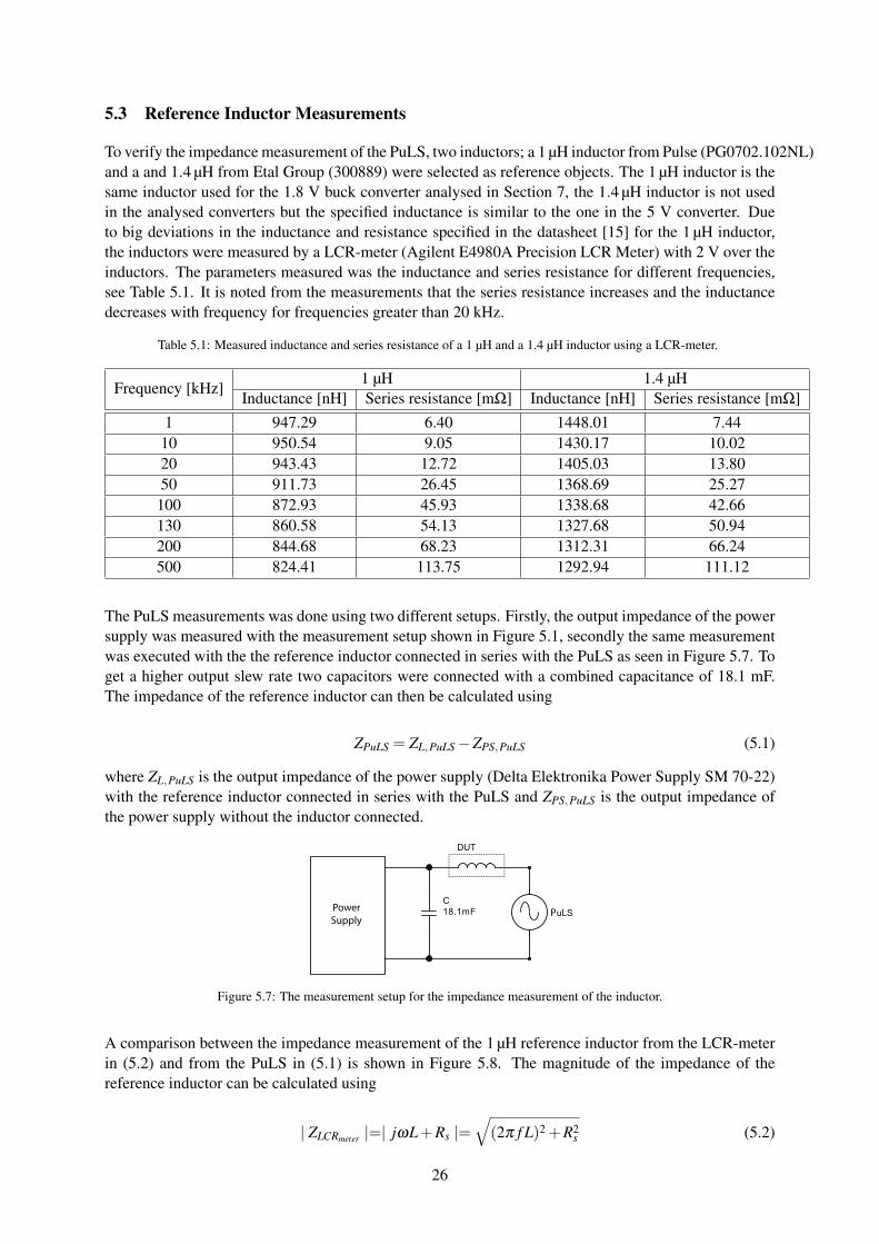
To verify the impedance measurement of the PuLS, two inductors; a 1 µH inductor from Pulse (PG0702.102NL)and a and 1.4 µH from Etal Group (300889) were selected as reference objects. The 1 µH inductor is thesame inductor used for the 1.8 V buck converter analysed in Section 7, the 1.4 µH inductor is not usedin the analysed converters but the specified inductance is similar to the one in the 5 V converter. Dueto big deviations in the inductance and resistance specified in the datasheet [15] for the 1 µH inductor,the inductors were measured by a LCR-meter (Agilent E4980A Precision LCR Meter) with 2 V over theinductors. The parameters measured was the inductance and series resistance for different frequencies,see Table 5.1. It is noted from the measurements that the series resistance increases and the inductancedecreases with frequency for frequencies greater than 20 kHz.
Table 5.1: Measured inductance and series resistance of a 1 µH and a 1.4 µH inductor using a LCR-meter.
Frequency [kHz]1 µH 1.4 µH
Inductance [nH] Series resistance [mΩ] Inductance [nH] Series resistance [mΩ]1 947.29 6.40 1448.01 7.4410 950.54 9.05 1430.17 10.0220 943.43 12.72 1405.03 13.8050 911.73 26.45 1368.69 25.27100 872.93 45.93 1338.68 42.66130 860.58 54.13 1327.68 50.94200 844.68 68.23 1312.31 66.24500 824.41 113.75 1292.94 111.12
The PuLS measurements was done using two different setups. Firstly, the output impedance of the powersupply was measured with the measurement setup shown in Figure 5.1, secondly the same measurementwas executed with the the reference inductor connected in series with the PuLS as seen in Figure 5.7. Toget a higher output slew rate two capacitors were connected with a combined capacitance of 18.1 mF.The impedance of the reference inductor can then be calculated using
ZPuLS = ZL,PuLS−ZPS,PuLS (5.1)
where ZL,PuLS is the output impedance of the power supply (Delta Elektronika Power Supply SM 70-22)with the reference inductor connected in series with the PuLS and ZPS,PuLS is the output impedance ofthe power supply without the inductor connected.
18.1mF
C
PuLS
DUT
Power
Supply
Figure 5.7: The measurement setup for the impedance measurement of the inductor.
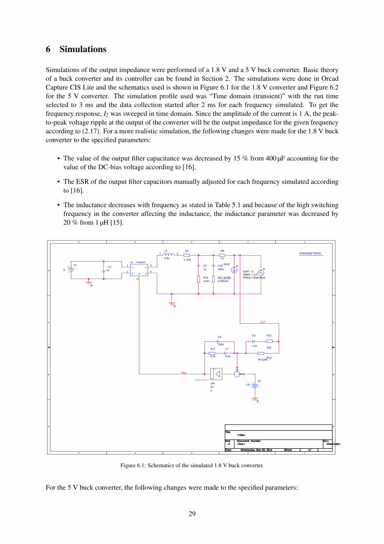
A comparison between the impedance measurement of the 1 µH reference inductor from the LCR-meterin (5.2) and from the PuLS in (5.1) is shown in Figure 5.8. The magnitude of the impedance of thereference inductor can be calculated using
| ZLCRmeter |=| jωL+Rs |=√(2π f L)2 +R2
s (5.2)
26
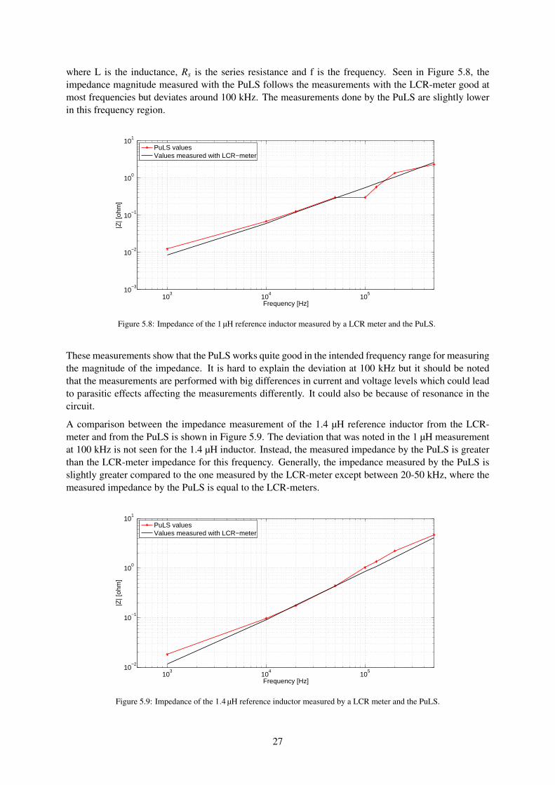
where L is the inductance, Rs is the series resistance and f is the frequency. Seen in Figure 5.8, theimpedance magnitude measured with the PuLS follows the measurements with the LCR-meter good atmost frequencies but deviates around 100 kHz. The measurements done by the PuLS are slightly lowerin this frequency region.
103
104
105
10−3
10−2
10−1
100
101
Frequency [Hz]
|Z| [
ohm
]
PuLS valuesValues measured with LCR−meter
Figure 5.8: Impedance of the 1 µH reference inductor measured by a LCR meter and the PuLS.
These measurements show that the PuLS works quite good in the intended frequency range for measuringthe magnitude of the impedance. It is hard to explain the deviation at 100 kHz but it should be notedthat the measurements are performed with big differences in current and voltage levels which could leadto parasitic effects affecting the measurements differently. It could also be because of resonance in thecircuit.
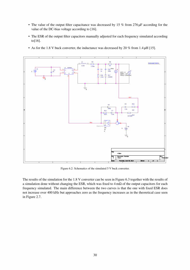
A comparison between the impedance measurement of the 1.4 µH reference inductor from the LCR-meter and from the PuLS is shown in Figure 5.9. The deviation that was noted in the 1 µH measurementat 100 kHz is not seen for the 1.4 µH inductor. Instead, the measured impedance by the PuLS is greaterthan the LCR-meter impedance for this frequency. Generally, the impedance measured by the PuLS isslightly greater compared to the one measured by the LCR-meter except between 20-50 kHz, where themeasured impedance by the PuLS is equal to the LCR-meters.
103
104
105
10−2
10−1
100
101
Frequency [Hz]
|Z| [
ohm
]
PuLS valuesValues measured with LCR−meter
Figure 5.9: Impedance of the 1.4 µH reference inductor measured by a LCR meter and the PuLS.
27

28
6 Simulations
Simulations of the output impedance were performed of a 1.8 V and a 5 V buck converter. Basic theoryof a buck converter and its controller can be found in Section 2. The simulations were done in OrcadCapture CIS Lite and the schematics used is shown in Figure 6.1 for the 1.8 V converter and Figure 6.2for the 5 V converter. The simulation profile used was “Time domain (transient)” with the run timeselected to 3 ms and the data collection started after 2 ms for each frequency simulated. To get thefrequency response, I2 was sweeped in time domain. Since the amplitude of the current is 1 A, the peak-to-peak voltage ripple at the output of the converter will be the output impedance for the given frequencyaccording to (2.17). For a more realistic simulation, the following changes were made for the 1.8 V buckconverter to the specified parameters:
• The value of the output filter capacitance was decreased by 15 % from 400 µF accounting for thevalue of the DC-bias voltage according to [16].
• The ESR of the output filter capacitors manually adjusted for each frequency simulated accordingto [16].
• The inductance decreases with frequency as stated in Table 5.1 and because of the high switchingfrequency in the converter affecting the inductance, the inductance parameter was decreased by20 % from 1 µH [15].
5
5
4
4
3
3
2
2
1
1
D D
C C
B B
A A
Regulator
OUT
Reg
0
0
0
Title
Size Document Number Rev
Date: Sheet o f
<Doc> <RevCode>
<Title>
A
1 1Wednesday, May 28, 2014
Title
Size Document Number Rev
Date: Sheet o f
<Doc> <RevCode>
<Title>
A
1 1Wednesday, May 28, 2014
Title
Size Document Number Rev
Date: Sheet o f
<Doc> <RevCode>
<Title>
A
1 1Wednesday, May 28, 2014
R15
490
C9
1.5n
R1345.620k
R2
1.76m
R12
8.2k
C26u
I10Adc
PARAMETERS:
C8
150p
C7
3.3n
R162.5m
C10340u
C31u
R8
1u
10k100
R17 (ESR)0.0012/4
U1 PWMBCK
11
22
33
44
55
I2IOFF = 0
FREQ = frekvensIAMPL = 1A
V61.8
L2
0.8u
1 2
V1
5
Figure 6.1: Schematics of the simulated 1.8 V buck converter.
For the 5 V buck converter, the following changes were made to the specified parameters:
29
• The value of the output filter capacitance was decreased by 15 % from 276 µF according for thevalue of the DC-bias voltage according to [16].
• The ESR of the output filter capacitors manually adjusted for each frequency simulated accordingto[16].
• As for the 1.8 V buck converter, the inductance was decreased by 20 % from 1.4 µH [15].
5
5
4
4
3
3
2
2
1
1
D D
C C
B B
A A
Regulator
OUT
Reg
0
0
0
Title
Size Document Number Rev
Date: Sheet o f
<Doc> <RevCode>
<Title>
A
1 1Thursday, June 05, 2014
Title
Size Document Number Rev
Date: Sheet o f
<Doc> <RevCode>
<Title>
A
1 1Thursday, June 05, 2014
Title
Size Document Number Rev
Date: Sheet o f
<Doc> <RevCode>
<Title>
A
1 1Thursday, June 05, 2014
C9
1.5n
R15
410
R2
1.76m
R1342.920k
C26u
R12
8.2k
C8
150p
PARAMETERS:
I10Adc
C7
3.3n
C10240u
R162.5m
10k100
R8
1u
C31u
U1 PWMBCK
11
22
33
44
55 R17
0.004/6
I2IOFF = 0
FREQ = frekvensIAMPL = 1A
V65
V1
5
L2
1.12u
1 2
Figure 6.2: Schematics of the simulated 5 V buck converter.
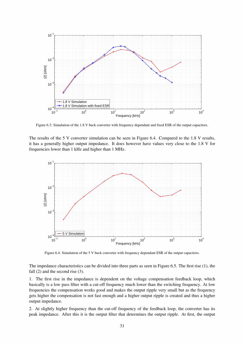
The results of the simulation for the 1.8 V converter can be seen in Figure 6.3 together with the results ofa simulation done without changing the ESR, which was fixed to 4 mΩ of the output capacitors for eachfrequency simulated. The main difference between the two curves is that the one with fixed ESR doesnot increase over 400 kHz but approaches zero as the frequency increases as in the theoretical case seenin Figure 2.7.
30
10−1
100
101
102
103
104
10−4
10−3
10−2
10−1
Frequency [kHz]
|Z| [
ohm
]
1.8 V Simulation1.8 V Simulation with fixed ESR
Figure 6.3: Simulation of the 1.8 V buck converter with frequency dependant and fixed ESR of the output capacitors.
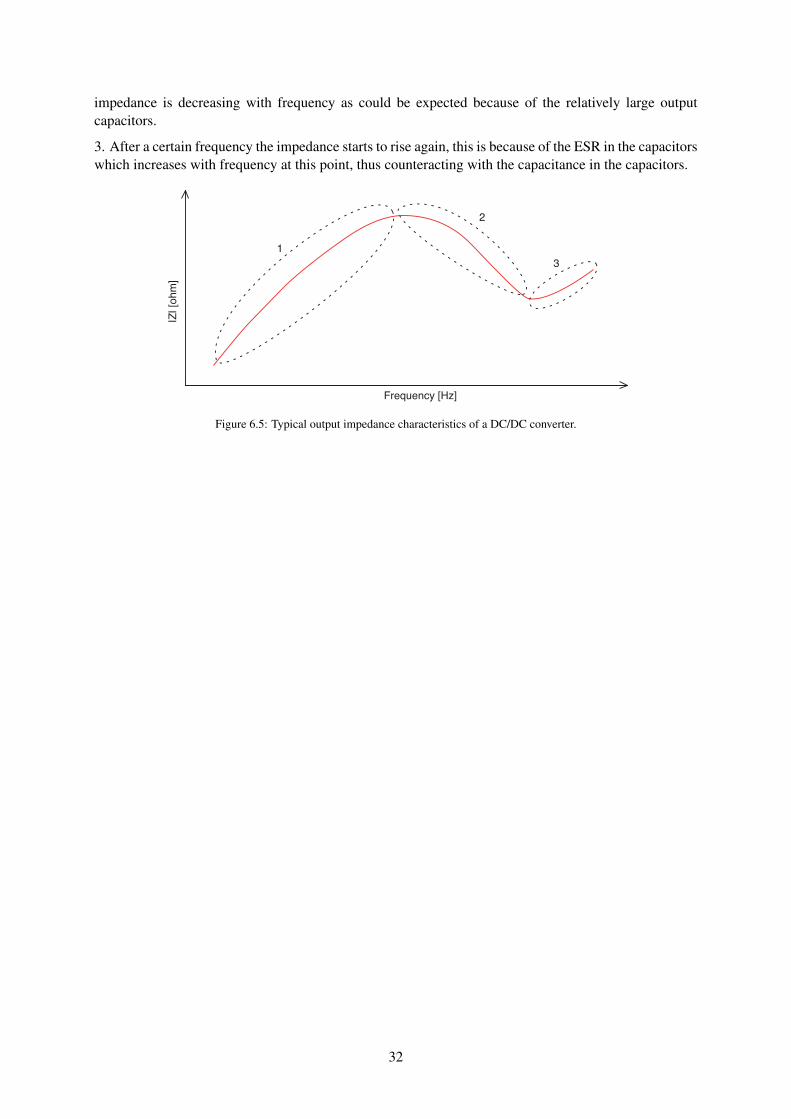
The results of the 5 V converter simulation can be seen in Figure 6.4. Compared to the 1.8 V results,it has a generally higher output impedance. It does however have values very close to the 1.8 V forfrequencies lower than 1 kHz and higher than 1 MHz.
10−1
100
101
102
103
104
10−4
10−3
10−2
10−1
Frequency [kHz]
|Z| [
ohm
]
5 V Simulation
Figure 6.4: Simulation of the 5 V buck converter with frequency dependant ESR of the output capacitors.
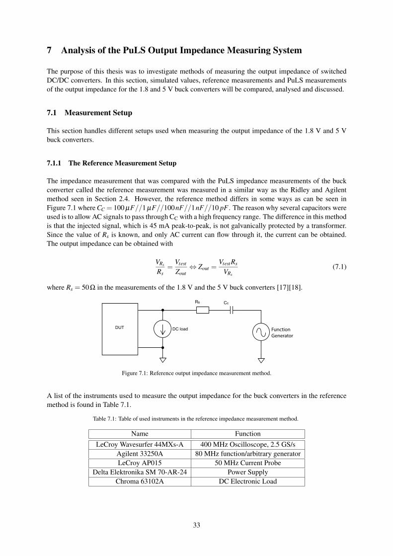
The impedance characteristics can be divided into three parts as seen in Figure 6.5. The first rise (1), thefall (2) and the second rise (3).
1. The first rise in the impedance is dependent on the voltage compensation feedback loop, whichbasically is a low pass filter with a cut-off frequency much lower than the switching frequency. At lowfrequencies the compensation works good and makes the output ripple very small but as the frequencygets higher the compensation is not fast enough and a higher output ripple is created and thus a higheroutput impedance.
2. At slightly higher frequency than the cut-off frequency of the feedback loop, the converter has itspeak impedance. After this it is the output filter that determines the output ripple. At first, the output
31
impedance is decreasing with frequency as could be expected because of the relatively large outputcapacitors.
3. After a certain frequency the impedance starts to rise again, this is because of the ESR in the capacitorswhich increases with frequency at this point, thus counteracting with the capacitance in the capacitors.
Frequency [Hz]
|Z| [o
hm
]
1
2
3
Figure 6.5: Typical output impedance characteristics of a DC/DC converter.
32
7 Analysis of the PuLS Output Impedance Measuring System
The purpose of this thesis was to investigate methods of measuring the output impedance of switchedDC/DC converters. In this section, simulated values, reference measurements and PuLS measurementsof the output impedance for the 1.8 and 5 V buck converters will be compared, analysed and discussed.
7.1 Measurement Setup
This section handles different setups used when measuring the output impedance of the 1.8 V and 5 Vbuck converters.
7.1.1 The Reference Measurement Setup
The impedance measurement that was compared with the PuLS impedance measurements of the buckconverter called the reference measurement was measured in a similar way as the Ridley and Agilentmethod seen in Section 2.4. However, the reference method differs in some ways as can be seen inFigure 7.1 where CC = 100 µF//1 µF//100nF//1nF//10 pF . The reason why several capacitors wereused is to allow AC signals to pass through CC with a high frequency range. The difference in this methodis that the injected signal, which is 45 mA peak-to-peak, is not galvanically protected by a transformer.Since the value of Rs is known, and only AC current can flow through it, the current can be obtained.The output impedance can be obtained with
VRs
Rs=
Vtest
Zout⇔ Zout =
VtestRs
VRs
(7.1)
where Rs = 50Ω in the measurements of the 1.8 V and the 5 V buck converters [17][18].
Rs Cc
DUTFunction
Generator
DC load
Figure 7.1: Reference output impedance measurement method.
A list of the instruments used to measure the output impedance for the buck converters in the referencemethod is found in Table 7.1.
Table 7.1: Table of used instruments in the reference impedance measurement method.
Name FunctionLeCroy Wavesurfer 44MXs-A 400 MHz Oscilloscope, 2.5 GS/s
Agilent 33250A 80 MHz function/arbitrary generatorLeCroy AP015 50 MHz Current Probe
Delta Elektronika SM 70-AR-24 Power SupplyChroma 63102A DC Electronic Load
33
7.1.2 The PuLS Measurement Setup
The PuLS impedance measurement method is measured with the setup found in Figure 7.2 and theinstruments used for the measurement is listed in Table 7.2. As seen in the table the only instrumentneeded to measure the output impedance is a power supply that supplies the DUT.
PuLSPower
SupplyDUT
Figure 7.2: PuLS connected to the DC/DC converter.
Table 7.2: Table of used instruments in the PuLS impedance measurement method.
Name FunctionPuLS Programmable Electronic Load
Delta Elektronika SM 70-22 Power Supply
7.2 Output Impedance Measurements
This section presents the results and analysis of the output impedance measurements of the 1.8 V andthe 5 V buck converters made by the PuLS. The measurement by the PuLS is also compared with thereference measurement method and simulated values of the impedance.
7.2.1 Measurement Results
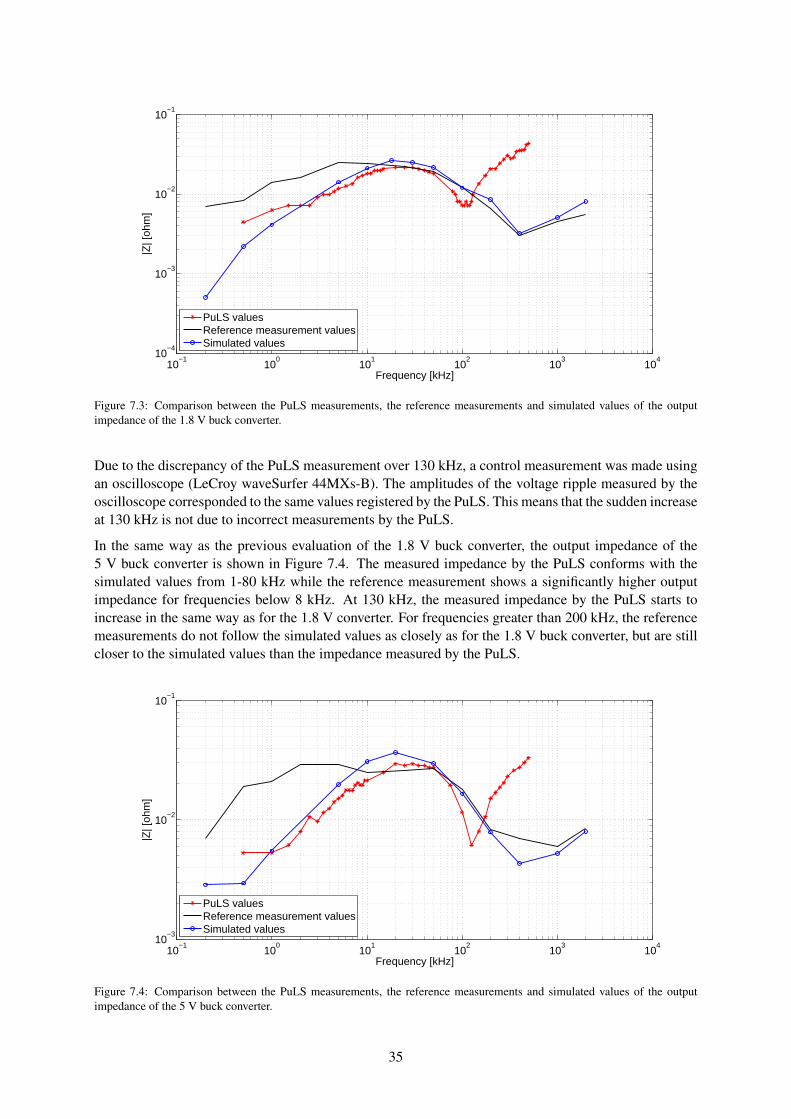
A comparison between the PuLS measurement, the reference measurement and the simulated values ofthe output impedance of the 1.8 V buck converter is shown in Figure 7.3. The amplitude of the sine wavecurrent drawn by the PuLS was 7 A. For frequencies below 10 kHz, the PuLS measurements conformswith the simulated values more than the reference method which measured a higher output impedance.Between 10 - 80 kHz, the impedance curves are very similar but at 130 kHz the PuLS measurement of theoutput impedance starts to increase in comparison to the simulated values and the reference measurementwhich continues to decrease to approximately 400 kHz.
34
10−1
100
101
102
103
104
10−4
10−3
10−2
10−1
Frequency [kHz]
|Z| [
ohm
]
PuLS valuesReference measurement valuesSimulated values
Figure 7.3: Comparison between the PuLS measurements, the reference measurements and simulated values of the outputimpedance of the 1.8 V buck converter.
Due to the discrepancy of the PuLS measurement over 130 kHz, a control measurement was made usingan oscilloscope (LeCroy waveSurfer 44MXs-B). The amplitudes of the voltage ripple measured by theoscilloscope corresponded to the same values registered by the PuLS. This means that the sudden increaseat 130 kHz is not due to incorrect measurements by the PuLS.
In the same way as the previous evaluation of the 1.8 V buck converter, the output impedance of the5 V buck converter is shown in Figure 7.4. The measured impedance by the PuLS conforms with thesimulated values from 1-80 kHz while the reference measurement shows a significantly higher outputimpedance for frequencies below 8 kHz. At 130 kHz, the measured impedance by the PuLS starts toincrease in the same way as for the 1.8 V converter. For frequencies greater than 200 kHz, the referencemeasurements do not follow the simulated values as closely as for the 1.8 V buck converter, but are stillcloser to the simulated values than the impedance measured by the PuLS.
10−1
100
101
102
103
104
10−3
10−2
10−1
Frequency [kHz]
|Z| [
ohm
]
PuLS valuesReference measurement valuesSimulated values
Figure 7.4: Comparison between the PuLS measurements, the reference measurements and simulated values of the outputimpedance of the 5 V buck converter.
35
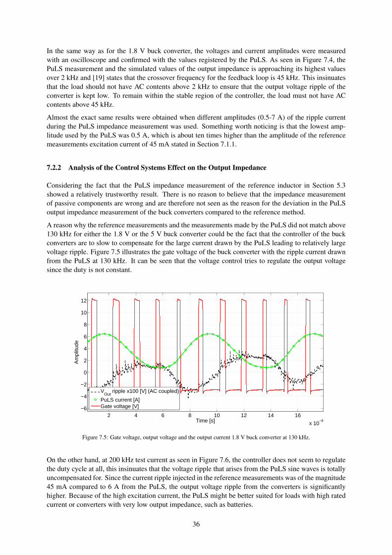
In the same way as for the 1.8 V buck converter, the voltages and current amplitudes were measuredwith an oscilloscope and confirmed with the values registered by the PuLS. As seen in Figure 7.4, thePuLS measurement and the simulated values of the output impedance is approaching its highest valuesover 2 kHz and [19] states that the crossover frequency for the feedback loop is 45 kHz. This insinuatesthat the load should not have AC contents above 2 kHz to ensure that the output voltage ripple of theconverter is kept low. To remain within the stable region of the controller, the load must not have ACcontents above 45 kHz.
Almost the exact same results were obtained when different amplitudes (0.5-7 A) of the ripple currentduring the PuLS impedance measurement was used. Something worth noticing is that the lowest amp-litude used by the PuLS was 0.5 A, which is about ten times higher than the amplitude of the referencemeasurements excitation current of 45 mA stated in Section 7.1.1.
7.2.2 Analysis of the Control Systems Effect on the Output Impedance
Considering the fact that the PuLS impedance measurement of the reference inductor in Section 5.3showed a relatively trustworthy result. There is no reason to believe that the impedance measurementof passive components are wrong and are therefore not seen as the reason for the deviation in the PuLSoutput impedance measurement of the buck converters compared to the reference method.
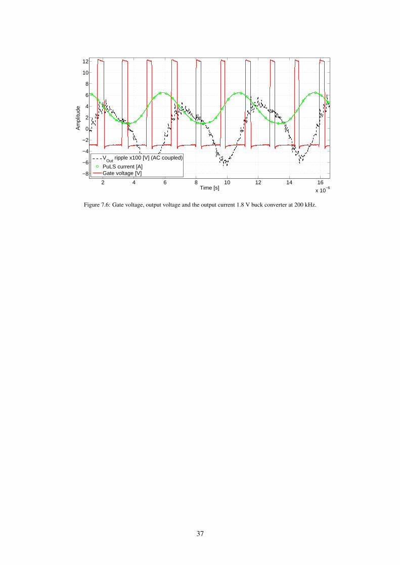
A reason why the reference measurements and the measurements made by the PuLS did not match above130 kHz for either the 1.8 V or the 5 V buck converter could be the fact that the controller of the buckconverters are to slow to compensate for the large current drawn by the PuLS leading to relatively largevoltage ripple. Figure 7.5 illustrates the gate voltage of the buck converter with the ripple current drawnfrom the PuLS at 130 kHz. It can be seen that the voltage control tries to regulate the output voltagesince the duty is not constant.
2 4 6 8 10 12 14 16
x 10−6
−6
−4
−2
0
2
4
6
8
10
12
Time [s]
Am
plitu
de
VOut
ripple x100 [V] (AC coupled)
PuLS current [A]Gate voltage [V]
Figure 7.5: Gate voltage, output voltage and the output current 1.8 V buck converter at 130 kHz.
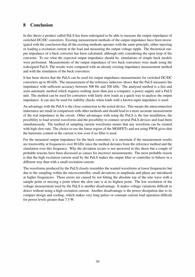
On the other hand, at 200 kHz test current as seen in Figure 7.6, the controller does not seem to regulatethe duty cycle at all, this insinuates that the voltage ripple that arises from the PuLS sine waves is totallyuncompensated for. Since the current ripple injected in the reference measurements was of the magnitude45 mA compared to 6 A from the PuLS, the output voltage ripple from the converters is significantlyhigher. Because of the high excitation current, the PuLS might be better suited for loads with high ratedcurrent or converters with very low output impedance, such as batteries.
36
2 4 6 8 10 12 14 16
x 10−6
−8
−6
−4
−2
0
2
4
6
8
10
12
Time [s]
Am
plitu
de
VOut
ripple x100 [V] (AC coupled)
PuLS current [A]Gate voltage [V]
Figure 7.6: Gate voltage, output voltage and the output current 1.8 V buck converter at 200 kHz.
37

38
8 Conclusion
In this thesis a product called PuLS has been redesigned to be able to measure the output impedance ofswitched DC/DC converters. Existing measurement methods of the output impedance have been invest-igated with the conclusion that all the existing methods operates with the same principle, either injectingor loading a excitation current at the load and measuring the output voltage ripple. The theoretical out-put impedance of a buck converter has been calculated, although only considering the open loop of theconverter. To see what the expected output impedance should be, simulations of simple buck modelswere performed. Measurements of the output impedance of two buck converters were made using theredesigned PuLS. The results were compared with an already existing impedance measurement methodand with the simulation of the buck converters.
It has been shown that the PuLS can be used for output impedance measurements for switched DC/DCconverters up to 80 kHz. The measurement of the reference inductors shows that the PuLS measures theimpedance with sufficient accuracy between 500 Hz and 500 kHz. The analysed method is a fast andsemi-automatic method which requires nothing more than just a computer, a power supply and a PuLSunit. The method can be used for converters with fairly slow loads as a quick way to analyse the outputimpedance. It can also be used for stability checks when loads with a known input impedance is used.
An advantage with the PuLS is the close connection to the tested device. This means the interconnectioninductance are small in comparison with other methods and should lead to a more accurate measurementof the real impedance in the circuit. Other advantages with using the PuLS is the fast installation, thepossibility to load several waveforms and the possibility to connect several PuLS devices and load themsimultaneously. The method of sampling current waveforms means that any waveform can be createdwith high slew-rate. The choice to use the linear region of the MOSFETs and not using PWM gives thatthe harmonic content in the current is low even if no filter is used.
For the measured output impedance for the buck converters, it is uncertain if the measurement resultsare trustworthy at frequencies over 80 kHz since the method deviates from the reference method and thesimulation over this frequency. Why the deviation occurs is not answered in this thesis but a couple ofprobable reasons have been discussed as causes for incorrect measurements. The most probable reasonis that the high excitation current used by the PuLS makes the output filter or controller to behave in adifferent way than with a small excitation current.
The waveforms produced by the PuLS closely resembles the wanted waveforms at lower frequencies butdue to the sampling within the microcontroller, small deviations in amplitude and phase are introducedat higher frequencies. These errors are caused by not hitting the absolute top of the sine wave with asample point or missing a point where the slew rate is at its highest point. The low resolution of thevoltage measurement used by the PuLS is another disadvantage. It makes voltage variations difficult todetect without using a high excitation current. Another disadvantage is the power dissipation due to itscompact design and cooling, which makes very long pulses or constant current load operation difficultfor power levels greater than 7.5 W.
39

40
9 Future Work
The PuLS voltage measuring system is insensitive to very small voltage variations. To improve thesensitivity of the measurement, an additional circuit can be added to the design that only measures theripple voltage. This can be done with an AC filter which consists of a transformer or capacitors to filterout the DC voltages. Using an AC filter would mean that only the ripple voltage would be measured anda higher resolution can be used. Since the maximum input voltage to the microcontroller is 3.3 V, thevoltage dividing circuit would rather increase the ripple voltage magnitude since it most often is in themV range for switched DC/DC converters.
When considering the different current waveforms created by the PuLS, it is clear how flexible it can beas an arbitrary waveform current load. Practically any waveform can be drawn with some modificationto the software of the PuLS. This ability to draw any current waveform can be used to simulate a variousnumber of loads to certify requirements of many devices. The easiest way to create any waveform wantedis to adjust a graphical representation of the current shape in the GUI. To implement this, an algorithmfor loading the sample points to the DMA is needed to be able to replicate the current set in the GUI.
The original as well as the redesigned PuLS can only draw positive current. If the PuLS would be ableto inject current or create a sine wave with zero offset, the measurements could be performed on nonoperating converters. This would mean that an external power source would have to be implemented andwith that a complete redesign of the PuLS to e.g. a four-quadrant converter is needed.
The DMA to DAC transfer rate of the microcontroller used in this thesis was 4.5 MHz. Due to the lownumber of points in the sine wave current drawn by the PuLS at higher frequencies, a microcontrollerwith a faster DMA to DAC transfer rate can be used to increase the quality of the sampled sine wave. Inthis way, the amplitude error might be decreased. Further, the minimum frequency of the current drawnfrom the PuLS is 500 Hz. To be able to draw currents below this frequency, the transfer rate has to belowered or the memory of the controller increased. From an output impedance point of view, frequenciesunder 500 Hz are not usually cared for but such low frequencies can be used for impedance measurementof other devices such as passive components.
41

42
References
[1] Ericsson AB. (2014, February 18) Company facts. [Online]. Available: http://www.ericsson.com/thecompany/company_facts
[2] A. Technologies, “Evaluating DC-DC Converters with LF Network Analyzer,” 2008.
[3] W. P. Robbins, N. Mohan, and T. M. Undeland, Power Electronics, B. Zobrist, Ed. John Wiley &Sons, Inc., 2003.
[4] T. Instruments, “Understanding buck power stages in switchmode power supplies,” p. 36, 1999.
[5] “IEC60478-4 Stabilized Power Supplies, dc output Part 4; Tests other than radio-frequency inter-ference,” Jan 1976.
[6] Using the Venable windows software version 4, Venable, 2007.
[7] R. J. Baker, CMOS Circuit Design, Layout and Simulation, L. Hanzo, Ed. Wiley, IEEE, 2010.
[8] PuLS - Programmable Micro Load User Manual V1.2, Ericsson AB, 2013.
[9] Ericsson AB, “ROA 128 5552 series Electronic Loads, Input 0.2-20 V, Current up to 45 A /25 W,”technical Specification.
[10] L. Rosén and S. Samini, “Small electronic load - design and analysis of a small electronic load fortesting on-board dc/dc converters,” diploma thesis, Chalmers University of Technology, 2012.
[11] Programmable DC Electronic Load, model 6310A series, Datasheet, Chroma. [Online]. Available:www.chromausa.com/pdf/Br-6310A-dcload-102013.pdf
[12] Agilent N3300 series DC electronics loads, Datasheet, Agilent, 2005.
[13] Y. Panov and M. JovanovicŽ, “Practical issues of input/output impedance measurements in switch-ing power supplies and application of measured data to stability analysis,” 2004.
[14] RM0008 Reference Manual, STMicroelectronics, 2009.
[15] Pulse. (2009) Smt power inductors round wire coils - pg0702nl. [Online]. Available:http://productfinder.pulseeng.com/products/datasheets/P667.pdf
[16] muRata. (2005, Aug) Capacitor Data Sheet GRM32ER60J107ME20. [Online]. Available:http://psearch.murata.com/capacitor/product/GRM32ER60J107ME20%23.pdf
[17] Calex. (2001) Understanding power impedance supply for optimum decoupling. [Online].Available: http://www.calex.com/pdf/3power_impedance.pdf
[18] M. Ma, “Dc/dc output impedance measurement in pl5,” March 2013, ericsson Internal.
[19] Ericsson AB, “ROZ 105 05: Buck external FET’s TPS40304.”
[20] ——, “Measurement Preview,” 2013, test results of the PuLS.
[21] M. Liu, H. Yuan, Y. Sun, and C. Yang, “Research on measurement of dc power supply impedance,”The ninth conference on electronic measurement & instruments, 2009.
43