Embed Size (px)
Citation preview
118
APPENDIX I
PIC 16F877 - MICROCONTROLLER
A1.1 CONCEPTS OF MICROCONTROLLER
Microcontroller is a general purpose device, which integrates a
number of the components of a microprocessor system on to single chip. It
has inbuilt CPU, memory and peripherals to make it as a mini computer. A
microcontroller combines on to the same microchip:
1) The CPU core
2) Memory (both ROM and RAM)
3) Some parallel digital I/O
Microcontrollers will combine other devices such as:
1) A timer module to allow the microcontroller to perform tasks
for certain time periods.
2) A serial I/O port to allow data to flow between the controller
and other devices such as a PIC or another microcontroller.
3) An ADC to allow the microcontroller to accept analogue input
data for processing.
119
Microcontrollers are :
1) Smaller in size
2) Consumes less power
3) Inexpensive
Micro controller is a stand alone unit ,which can perform functions
on its own without any requirement for additional hardware like I/O ports
and external memory. The heart of the microcontroller is the CPU core.
In the past, this has traditionally been based on a 8-bit
microprocessor unit. For example Motorola uses a basic 6800 microprocessor
core in their 6805/6808 microcontroller devices. In the recent years,
microcontrollers have been developed around specifically designed CPU
cores, for example the microchip PIC range of microcontrollers.
A1.2 INTRODUCTION TO PIC
The microcontroller that has been used for this project is from PIC
series. PIC microcontroller is the first RISC based microcontroller fabricated
in Complimentary Metal Oxide Semiconductor (CMOS) that uses separate
bus for instruction and data allowing simultaneous access of program and data
memory.
The main advantage of CMOS and RISC combination is low power
consumption resulting in a very small chip size with a small pin count. The
main advantage of CMOS is that it has immunity to noise than other
fabrication techniques.

120
A1.2.1 Memory
Various microcontrollers offer different kinds of memories.
EEPROM, EPROM, FLASH etc. are some of the memories of which FLASH
is the most recently developed.
Technology that is used in PIC 16F87x is flash technology, so that
data is retained even when the power is switched off. Easy Programming
and Erasing are other features of PIC 16F87x.
A1.2.2 PIC Start Plus Programmer
The PIC start plus development system from microchip technology
provides the product development engineer with a highly flexible low cost
microcontroller design tool set for all microchip PIC micro devices. The PIC
start plus development system includes PIC start plus development
programmer.
The PIC start plus programmer gives the product developer ability
to program user software in to any of the supported microcontrollers. The PIC
start plus software running under MP Lab provides for full interactive control
over the programmer.
A1.2.3 Special Features of PIC Microcontroller
High-performance RISC CPU
Only 35 single word instructions to learn
All single cycle instructions except for program branches
which are two cycle
Operating speed: DC - 20 MHz clock input
121
DC - 200 ns instruction cycle
Up to 8K x 14 words of Flash Program Memory
Up to 368 x 8 bytes of Data Memory (RAM)
Up to 256 x 8 bytes of EEPROM data memory
Pin out compatible to the PIC16C73/74/76/77
Interrupt capability (up to 14 internal/external
Eight level deep hardware stack
Direct, indirect, and relative addressing modes
Power-on Reset (POR)
Power-up Timer (PWRT) and Oscillator Start-up Timer
(OST)
Watchdog Timer (WDT) with its own on-chip RC Oscillator
for reliable operation
Programmable code-protection
Power saving SLEEP mode
Selectable oscillator options
Low-power, high-speed CMOS EPROM/EEPROM
technology
Fully static design
In-Circuit Serial Programming (ICSP) via two pins
Only single 5V source needed for programming capability
In-Circuit Debugging via two pins
Processor read/write access to program memory
Wide operating voltage range: 2.5V to 5.5V
122
High Sink/Source Current: 25 mA
Commercial and Industrial temperature ranges
Low-power consumption:
< 2mA typical @ 5V, 4 MHz
20mA typical @ 3V, 32 kHz
< 1mA typical standby current
A1.2.4 Peripheral Features
Timer0: 8-bit timer/counter with 8-bit prescaler
Timer1: 16-bit timer/counter with prescaler, can be incremented
during sleep via external crystal/clock
Timer2: 8-bit timer/counter with 8-bit period register, prescaler
and postscaler
Two Capture, Compare, PWM modules
Capture is 16-bit, max resolution is 12.5 ns,
Compare is 16-bit, max resolution is 200 ns,
PWM max. resolution is 10-bit
10-bit multi-channel Analog-to-Digital converter
Synchronous Serial Port (SSP) with SPI. (Master Mode) and
I2C. (Master/Slave)
Universal Synchronous Asynchronous Receiver Transmitter
(USART/SCI) with
9- bit address detection.
Brown-out detection circuitry for Brown-out Reset (BOR)
123
Note
1. This buffer is a Schmitt Trigger input when configured as an
external interrupt
2. This buffer is a Schmitt Trigger input when used in serial
programming mode.
3. This buffer is a Schmitt Trigger input when configured as general
purpose I/O and a TTL input when used in the Parallel Slave Port
mode (for interfacing to a microprocessor bus).
4. This buffer is a Schmitt Trigger input when configured in RC
oscillator mode and a CMOS input otherwise.
Legend: I = input O = output I/O = input/output P = power
— = Not used TTL = TTL input ST = Schmitt Trigger input
A1.2.5 I/O Ports
Some pins for these I/O ports are multiplexed with an alternate
function for the peripheral features on the device. In general, when a
peripheral is enabled, that pin may not be used as a general purpose I/O pin.
A1.2.6 Porta and the Trisa Register
PORTA is a 6-bit wide bi-directional port. The corresponding data
direction register is TRISA. Setting a TRISA bit (=1) will make the
corresponding PORTA pin an input, i.e., put the corresponding output driver
in a Hi-impedance mode. Clearing a TRISA bit (=0) will make the
corresponding PORTA pin an output, i.e., put the contents of the output latch
on the selected pin. Reading the PORTA register reads the status of the pins
whereas writing to it will write to the port latch. All write operations are read-
modify-write operations. Therefore a write to a port implies that the port pins
124
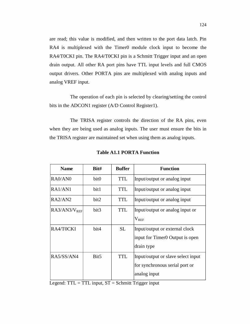
are read; this value is modified, and then written to the port data latch. Pin
RA4 is multiplexed with the Timer0 module clock input to become the
RA4/T0CKI pin. The RA4/T0CKI pin is a Schmitt Trigger input and an open
drain output. All other RA port pins have TTL input levels and full CMOS
output drivers. Other PORTA pins are multiplexed with analog inputs and
analog VREF input.
The operation of each pin is selected by clearing/setting the control
bits in the ADCON1 register (A/D Control Register1).
The TRISA register controls the direction of the RA pins, even
when they are being used as analog inputs. The user must ensure the bits in
the TRISA register are maintained set when using them as analog inputs.
Table A1.1 PORTA Function
Name Bit# Buffer Function
RA0/AN0 bit0 TTL Input/output or analog input
RA1/AN1 bit1 TTL Input/output or analog input
RA2/AN2 bit2 TTL Input/output or analog input
RA3/AN3/VREF bit3 TTL Input/output or analog input or
VREF
RA4/T0CKI bit4 SL Input/output or external clock
input for Timer0 Output is open
drain type
RA5/SS/AN4 Bit5 TTL Input/output or slave select input
for synchronous serial port or
analog input
Legend: TTL = TTL input, ST = Schmitt Trigger input
125
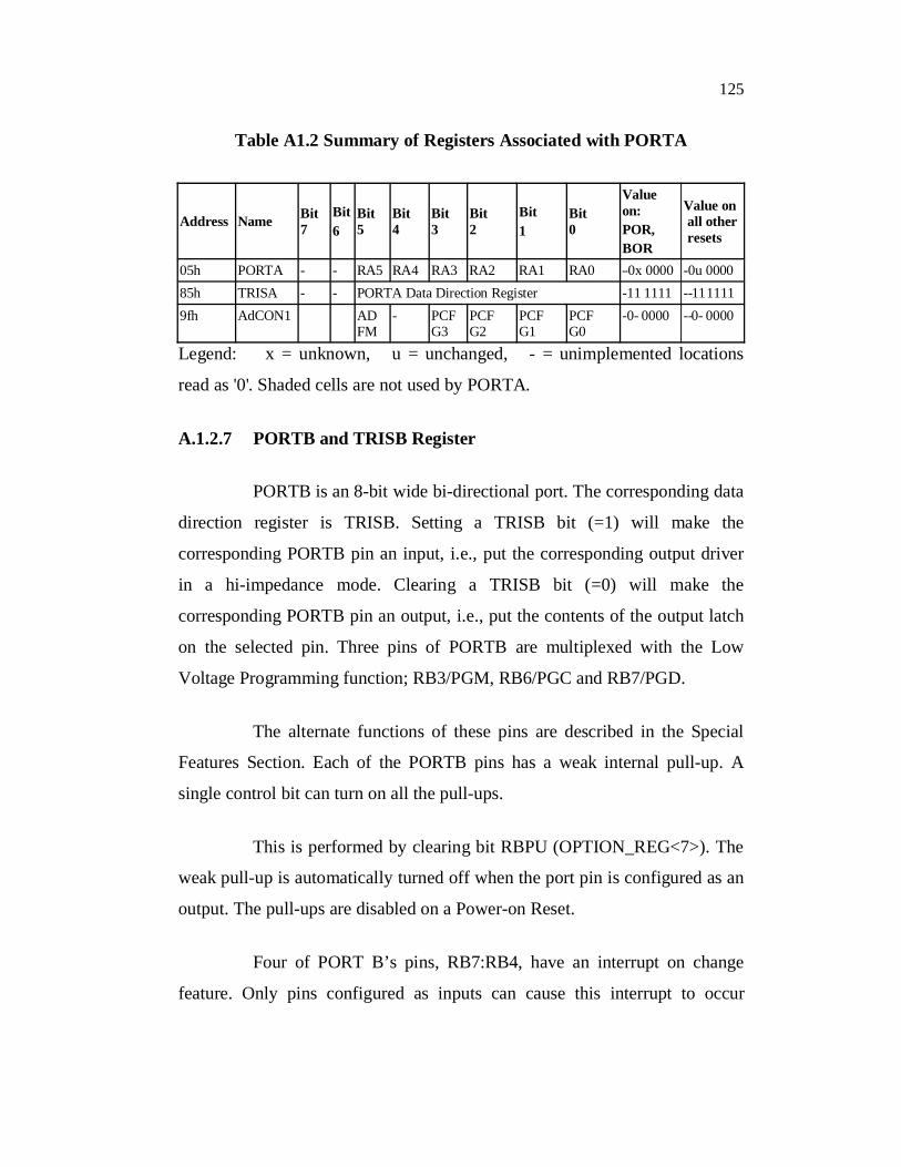
Table A1.2 Summary of Registers Associated with PORTA
Address Name Bit7
Bit6
Bit5
Bit4
Bit3
Bit2
Bit1
Bit0
Valueon:POR,BOR
Value onall otherresets
05h PORTA - - RA5 RA4 RA3 RA2 RA1 RA0 --0x 0000 -0u 000085h TRISA - - PORTA Data Direction Register -11 1111 --1111119fh AdCON1 AD
FM- PCF
G3PCFG2
PCFG1
PCFG0
-0- 0000 --0- 0000
Legend: x = unknown, u = unchanged, - = unimplemented locations
read as '0'. Shaded cells are not used by PORTA.
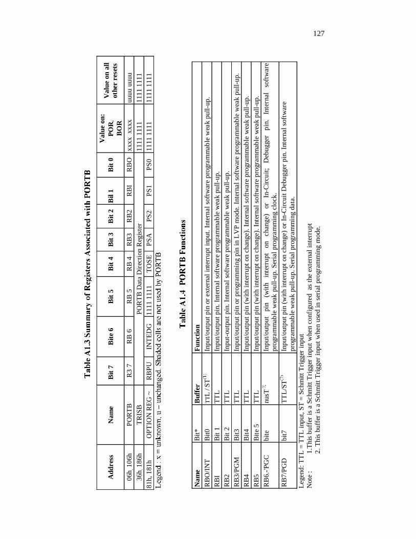
A.1.2.7 PORTB and TRISB Register
PORTB is an 8-bit wide bi-directional port. The corresponding data
direction register is TRISB. Setting a TRISB bit (=1) will make the
corresponding PORTB pin an input, i.e., put the corresponding output driver
in a hi-impedance mode. Clearing a TRISB bit (=0) will make the
corresponding PORTB pin an output, i.e., put the contents of the output latch
on the selected pin. Three pins of PORTB are multiplexed with the Low
Voltage Programming function; RB3/PGM, RB6/PGC and RB7/PGD.
The alternate functions of these pins are described in the Special
Features Section. Each of the PORTB pins has a weak internal pull-up. A
single control bit can turn on all the pull-ups.
This is performed by clearing bit RBPU (OPTION_REG<7>). The
weak pull-up is automatically turned off when the port pin is configured as an
output. The pull-ups are disabled on a Power-on Reset.
Four of PORT B’s pins, RB7:RB4, have an interrupt on change
feature. Only pins configured as inputs can cause this interrupt to occur
126
(i.e. any RB7:RB4 pin configured as an output is excluded from the interrupt
on change comparison).
1) The input pins (of RB7:RB4) are compared with the old value
latched on the last read of PORTB. The “mismatch” outputs of
RB7:RB4 are OR’ed together to generate the RB Port Change
Interrupt with flag bit RBIF (INTCON<0>).
2) This interrupt can wake the device from SLEEP. The user, in
the interrupt service routine, can clear the interrupt in the
following manner:
Any read or write of PORTB. This will end the mismatch
condition.
Clear flag bit RBIF. A mismatch condition will continue to
set flag bit RBIF.
Reading PORTB will end the mismatch condition, and
allow flag bit RBIF to be cleared.
The interrupt on change feature is recommended for wake-
up on key depression operation and operations where
PORTB is only used for the interrupt on change feature.
Polling of PORTB is not recommended while using the interrupt on
change feature.
This interrupt on mismatch feature, together with software
configurable pull-ups on these four pins, allow easy interface to a keypad and
make it possible for wake-up on key depression.
127
Add
ress
Nam
eB
it 7
Bite
6B
it 5
Bit
4 B
it 3
Bit
2 B
il 1
Bit
0V
alue
on:
POR
BO
R
Val
ue o
n al
lot
her
rese
ts
06h
106h
PORT
BR
3 7
RB
6R
B 5
RB
4 R
B3
RB
2 R
BI
RB
O
xxxx
xxxx
uuuu
uuu
u36
h 18
6hTR
ISB
POR
TB D
ata
Dire
ctio
n R
egist
er11
1111
1111
1111
1181
h, 1
81h
OPT
ION
REG
~
RB
PU
INTE
DG
11
1111
11
TOSE
PS
A
PS2
PS1
PS0
1111
1111
1111
1111
Nam
eBi
t*B
uffe
rFu
nctio
nR
BO/IN
TBi
t0TT
L/S
TIn
put/o
utpu
t pin
or e
xter
nal i
nter
rupt
inpu
t. In
tern
al so
ftwar
e pr
ogra
mm
able
wea
k pu
ll-up
.R
BIBi
t 1TT
LIn
put/o
utpu
t pin
. Int
erna
l sof
twar
e pr
ogra
mm
able
wea
k pu
ll-up
.R
B2Bi
t 2TT
LIn
put-o
utpu
t pin
. Int
erna
l sof
twar
e pr
ogra
mm
able
wea
k pu
ll-up
.R
B3/P
GM
Bit3
TTL
Inpu
t/out
put p
in o
r pro
gram
min
g pi
n in
LV
P m
ode.
Inte
rnal
softw
are
prog
ram
mab
le w
eak
pull-
up.
RB4
Bit4
TTL
Inpu
t/out
put p
in (w
ith in
terr
upt o
n ch
ange
). In
tern
al so
ftwar
e pr
ogra
mm
able
wea
k pu
ll-up
.R
B5Bi
te 5
TTL
Inpu
t/out
put p
in (w
ith in
terr
upt o
n ch
ange
). In
tern
al so
ftwar
e pr
ogra
mm
able
wea
k pu
ll-up
.R
B6.
-'PG
C
bite
nusT
Inpu
t/out
put
pin
(with
in
terr
upt
on
chan
ge)
or
In-C
ircui
t; D
ebug
ger
pin.
In
tern
al
softw
are
prog
ram
mab
le w
eak
pull-
up. S
eria
l pro
gram
min
g cl
ock.
RB7
/PG
Dbi
t7TT
L/ST
Inpu
t/out
put p
in (w
ith in
terr
upt o
n ch
ange
) or I
n-C
ircui
t Deb
ugge
r pin
. Int
erna
l sof
twar
epr
ogra
mm
able
wea
k pu
ll-up
. Ser
ial p
rogr
amm
ing
data
.Le
gend
: TTL
= T
TL in
put,
ST =
Sch
mitt
Trig
ger i
nput
Not
e :
1.Th
is bu
ffer
is a
Sch
mitt
Trig
ger i
nput
whe
n co
nfig
ured
as t
he e
xter
nal i
nter
rupt
2. T
his b
uffe
r is a
Sch
mitt
Trig
ger i
nput
whe
n us
ed in
seria
l pro
gram
min
g m
ode.
128
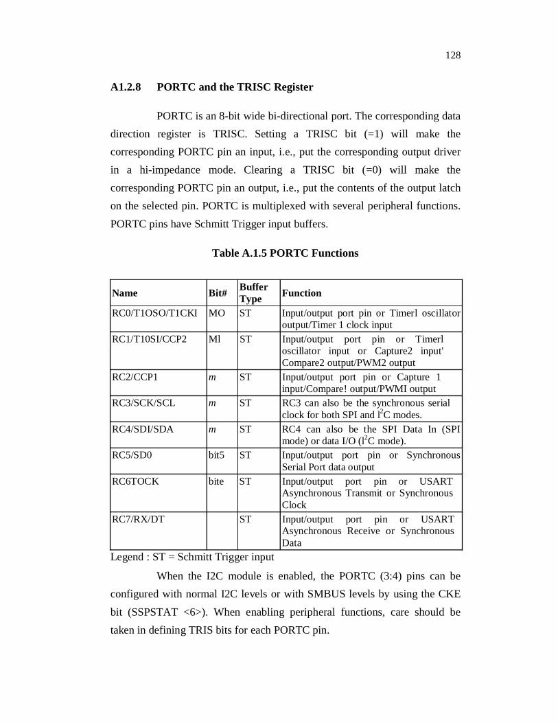
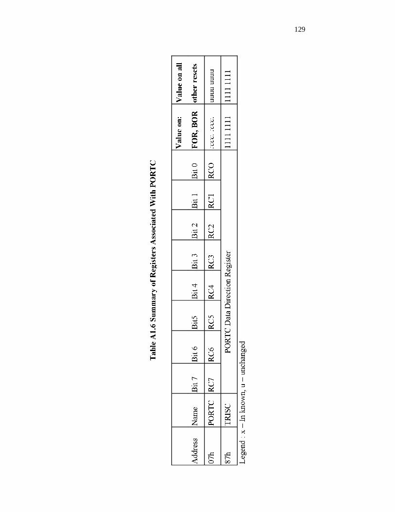
A1.2.8 PORTC and the TRISC Register
PORTC is an 8-bit wide bi-directional port. The corresponding datadirection register is TRISC. Setting a TRISC bit (=1) will make thecorresponding PORTC pin an input, i.e., put the corresponding output driverin a hi-impedance mode. Clearing a TRISC bit (=0) will make thecorresponding PORTC pin an output, i.e., put the contents of the output latchon the selected pin. PORTC is multiplexed with several peripheral functions.PORTC pins have Schmitt Trigger input buffers.
Table A.1.5 PORTC Functions
Name Bit# BufferType Function
RC0/T1OSO/T1CKI MO ST Input/output port pin or Timerl oscillatoroutput/Timer 1 clock input
RC1/T10SI/CCP2 Ml ST Input/output port pin or Timerloscillator input or Capture2 input'Compare2 output/PWM2 output
RC2/CCP1 m ST Input/output port pin or Capture 1input/Compare! output/PWMI output
RC3/SCK/SCL m ST RC3 can also be the synchronous serialclock for both SPI and l2C modes.
RC4/SDI/SDA m ST RC4 can also be the SPI Data In (SPImode) or data I/O (l2C mode).
RC5/SD0 bit5 ST Input/output port pin or SynchronousSerial Port data output
RC6TOCK bite ST Input/output port pin or USARTAsynchronous Transmit or SynchronousClock
RC7/RX/DT ST Input/output port pin or USARTAsynchronous Receive or SynchronousData
Legend : ST = Schmitt Trigger input
When the I2C module is enabled, the PORTC (3:4) pins can beconfigured with normal I2C levels or with SMBUS levels by using the CKEbit (SSPSTAT <6>). When enabling peripheral functions, care should betaken in defining TRIS bits for each PORTC pin.
129
130
Some peripherals override the TRIS bit to make a pin an output, while otherperipherals override the TRIS bit to make a pin an input. Since the TRIS bitoverride is in effect while the peripheral is enabled, read-modify writeinstructions (BSF, BCF, XORWF) with TRISC as destination should beavoided. The user should refer to the corresponding peripheral section for thecorrect TRIS bit settings.
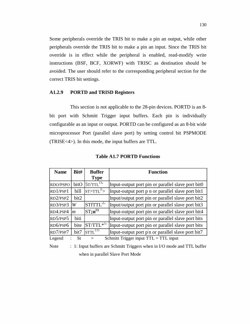
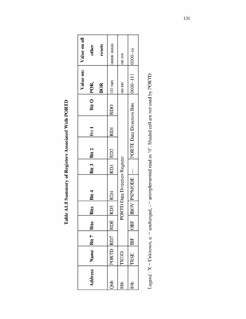
A1.2.9 PORTD and TRISD Registers
This section is not applicable to the 28-pin devices. PORTD is an 8-
bit port with Schmitt Trigger input buffers. Each pin is individually
configurable as an input or output. PORTD can be configured as an 8-bit wide
microprocessor Port (parallel slave port) by setting control bit PSPMODE
(TRISE<4>). In this mode, the input buffers are TTL.
Table A1.7 PORTD Functions
Name Bit# BufferType
Function
RDO/PSPO bitO 5T/TTL11' Input-output port pin or parallel slave port bit0RD1/PSP1 bill ST>TTL|1> Input-output port p n or parallel slave port bit1RD2/PSP2 bit2 Input/output port pin or parallel slave port bit2RD3/PSP3 W STfTTL'1' Input/output port pin or parallel slave port bit3RD4.PSP4 m ST;n|1) Input-output port pin or parallel slave port bit4RD5/PSP5 biti Input-output port pin or parallel slave port bitsRD6/PSP6 bite ST/TTL*1' Input-output port pin or parallel slave port bitsRD7/PSP7 bit7 STTL111 Input-output port p:n or parallel slave port bit7Legend : St = Schmitt Trigger input TTL = TTL input
Note : 1: Input buffers are Schmitt Triggers when in I/O mode and TTL buffer
when in parallel Slave Port Mode
131
132
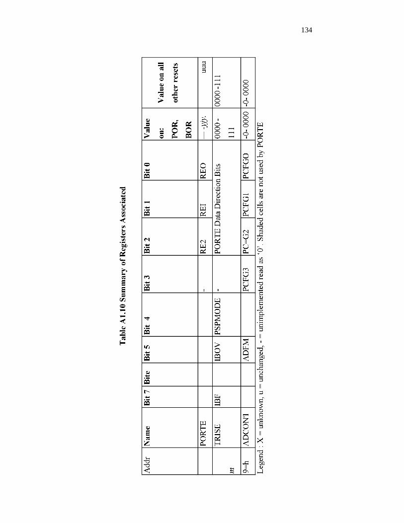
A1.2.10 PORTE and TRISE Register
PORTE has three pins RE0/RD/AN5, RE1/WR/AN6 and
RE2/CS/AN7, which are individually configurable as inputs or outputs. These
pins have Schmitt Trigger input buffers.
The PORTE pins become control inputs for the microprocessor port
when bit PSPMODE (TRISE<4>) is set. In this mode, the user must make sure
that the TRISE<2:0> bits are set (pins are configured as digital inputs). Ensure
ADCON1 is configured for digital I/O. In this mode the input buffers are TTL.
PORTE pins are multiplexed with analog inputs. When selected as
an analog input, these pins will read as '0's. TRISE controls the direction of
the RE pins, even when they are being used as analog inputs. The user must
make sure to keep the pins configured as inputs when using them as analog
inputs.
Table A1.9 PORTE Functions
Name Bitff Buffer
Type
Function
RE0/RD/AN5 bis ST..'TTL(1) Input/output port pin or read control input
in parallel slave port mode or
analog input:
RD
1 = Not a read operation
0 = Read operation. Reads PORTD
register (if chip selected)
133
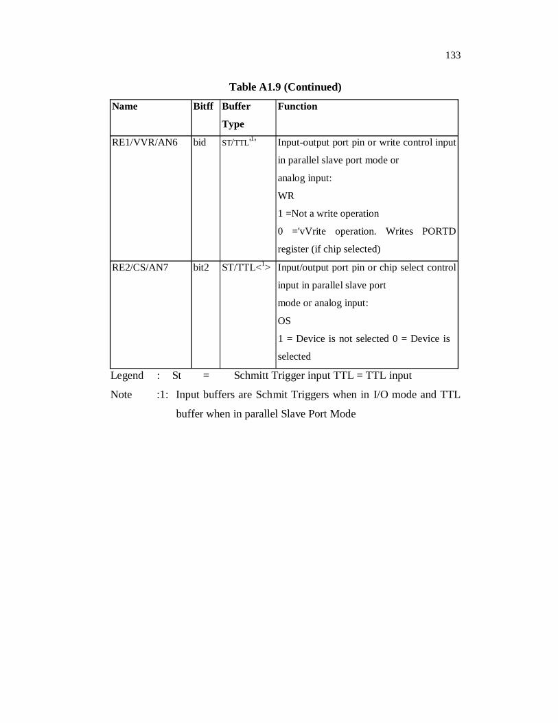
Table A1.9 (Continued)
Name Bitff Buffer
Type
Function
RE1/VVR/AN6 bid ST/TTL'1' Input-output port pin or write control input
in parallel slave port mode or
analog input:
WR
1 =Not a write operation
0 ='vVrite operation. Writes PORTD
register (if chip selected)
RE2/CS/AN7 bit2 ST/TTL<1> Input/output port pin or chip select control
input in parallel slave port
mode or analog input:
OS
1 = Device is not selected 0 = Device is
selected
Legend : St = Schmitt Trigger input TTL = TTL input
Note :1: Input buffers are Schmit Triggers when in I/O mode and TTL
buffer when in parallel Slave Port Mode
134
135
A1.2.11 Memory Organisation
There are three memory blocks in each of the PIC16F87x MUC’s.
The program memory and Data Memory have separate buses so that
concurrent access can occur.
All instructions are executed within one single instruction cycle,
unless a conditional test is true or the program counter is changed as a result
of an instruction.
1) In this case, the execution takes two instruction cycles with
the second cycle executed as a NOP.
2) One instruction cycle consists of four oscillator periods.
3) Thus, for an oscillator frequency of 4 MHz, the normal
instruction execution time is 1 ms.
If a conditional test is true or the program counter is changed as a
result of an instruction, then the instruction execution time is 2 ms.
136
APPENDIX 2
PROGRAMMING
The Assembly program is written using Keil software for
displaying triggering pulse frequency measurement given to the MOSFET for
producing variable voltage:
sbit LCD_RS at RB4_bit;
sbit LCD_EN at RB5_bit;
sbit LCD_D4 at RB0_bit;
sbit LCD_D5 at RB1_bit;
sbit LCD_D6 at RB2_bit;
sbit LCD_D7 at RB3_bit;
sbit LCD_RS_Direction at TRISB4_bit;
sbit LCD_EN_Direction at TRISB5_bit;
sbit LCD_D4_Direction at TRISB0_bit;
sbit LCD_D5_Direction at TRISB1_bit;
sbit LCD_D6_Direction at TRISB2_bit;
sbit LCD_D7_Direction at TRISB3_bit;
char txt1[] = "T=";
char txt2[] = "Sec";
char i;
void Move_Delay() {
Delay_ms(500);
137
}
void main() {
unsigned char value,value1,g,h,TE,TE1;
TRISC=0X01;
TRISD=0x00;
TRISB=0x00;
T1CON=0X00;
Lcd_Init(); // Initialize LCD
Lcd_Cmd(_LCD_CLEAR); // Clear display
Lcd_Cmd(_LCD_BLINK_CURSOR_ON); // Cursor off
Lcd_Out(1,1,txt1); // Write text in first row
Lcd_Out(1,6,txt2);
Delay_ms(200);
while(1)
{
if(PIR1.TMR1IF==1)
{
TMR1H =0x00;
TMR1L=0X00;
T1CON.TMR1ON=0;
}
if(PIR1.TMR1IF==0)
{
/*value=TMR1L ;
h=value & 0x0f;
g=value& 0xf0;
g=g>>4;*/
/*PORTB=h|0x30;
delay_ms(10);
138
PORTB=g|0x30;*/
value1=TMR1l;
h=value1 & 0x0f;
g=value1 & 0xf0;
g=g>>4;
TE=g|0x30;
TE1=h|0x30;
Lcd_Out(1,3,TE);
Delay_ms(200);
Lcd_Out(1,4,TE1);
Delay_ms(200);
/*PORTD=h|0x30;
delay_ms(10);
PORTD=g|0x30;*/
}
T1CON.TMR1ON=1;
PIR1.TMR1IF=0;
}
}
In ASM
Just to count the pulse alone
LIST p=16F877 ; PIC16F844 is the target processor
#include "P16F877.INC" ; Include header file
BSF STATUS,RP0
MOVLW 0X01
MOVWF TRISC
MOVLW 0X00
MOVWF TRISD
MOVWF TRISB

139
BCF STATUS,RP0
MOVLW 0X00
MOVWF T1CON
HERE:MOVLW 0X00
MOVWF TMR1H
MOVLW 0X00
MOVWF TMR1L
BCF PIR1,TMR1IF
BSF T1CON,TMR1ON
AGAIN: MOVF TMR1H,W
MOVWF PORTD
MOVF TMR1L,W
MOVWF PORTB
BTFSS PIR1,TMR1IF
GOTO AGAIN
BCF T1CON,TMR1ON
GOTO HERE
END
140
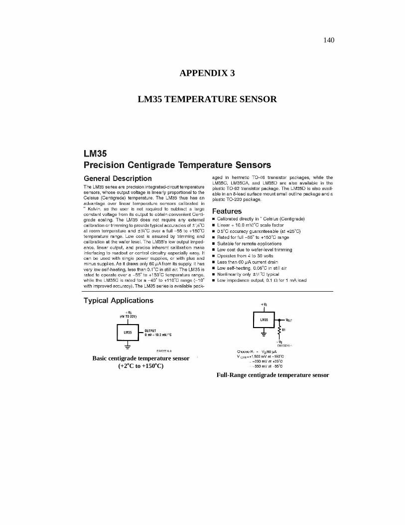
APPENDIX 3
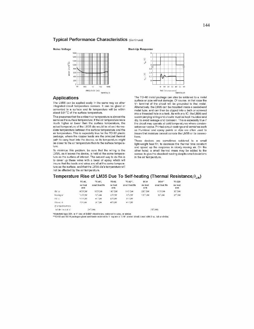
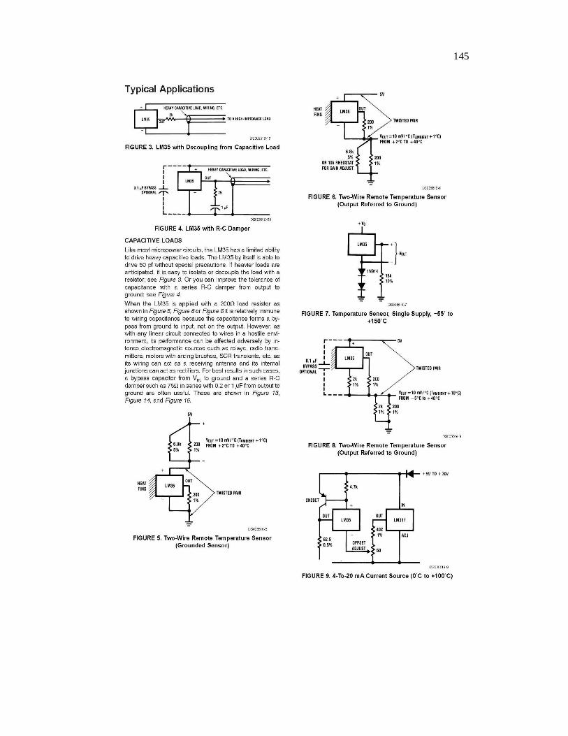
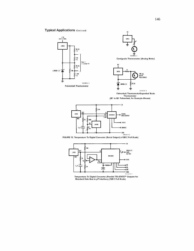
LM35 TEMPERATURE SENSOR
Basic centigrade temperature sensor(+2oC to +150oC)
Full-Range centigrade temperature sensor
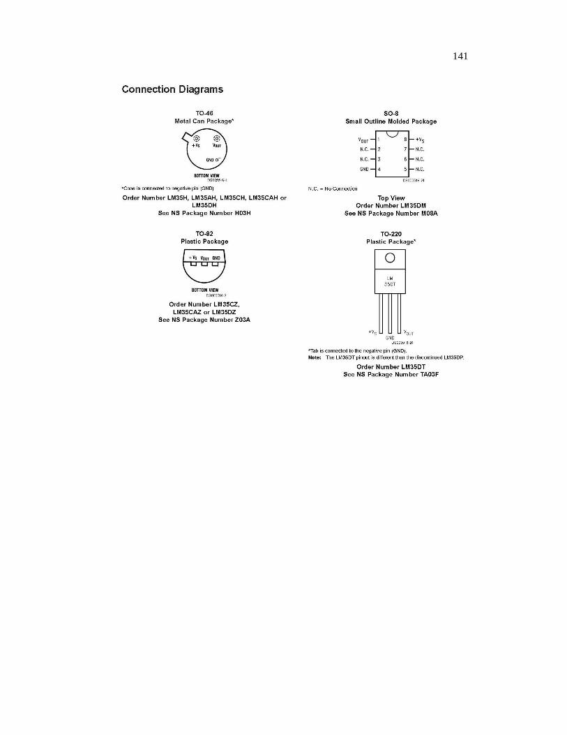
141
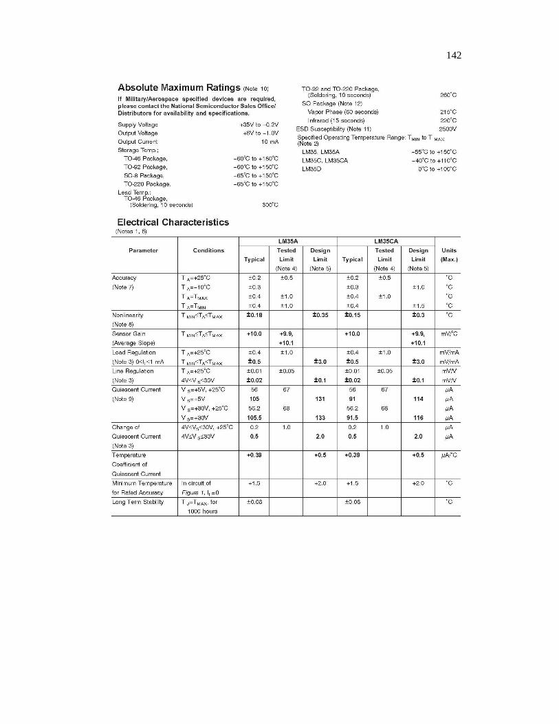
142
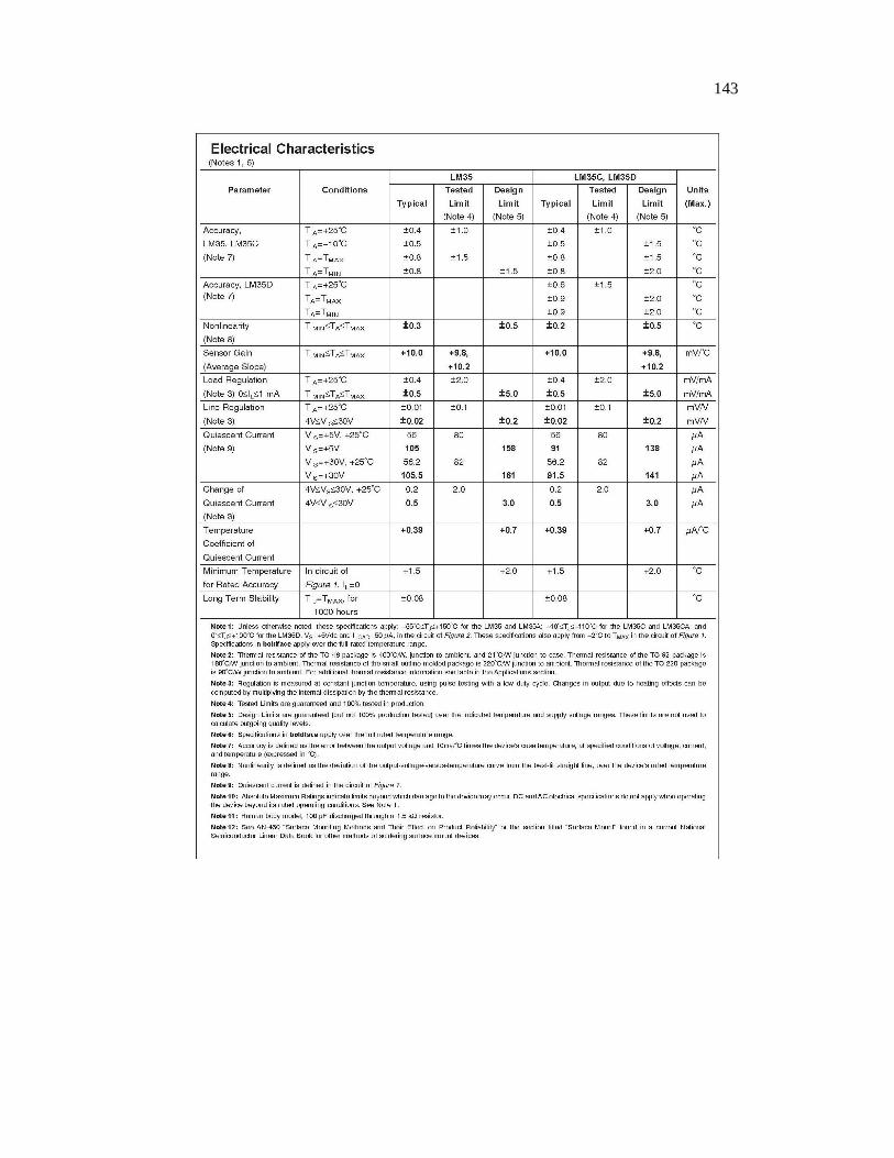
143
144
145
146
147
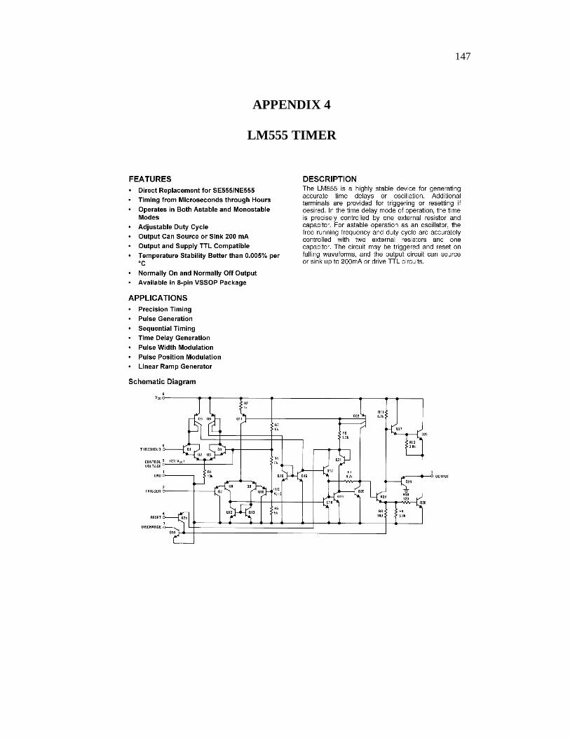
APPENDIX 4
LM555 TIMER
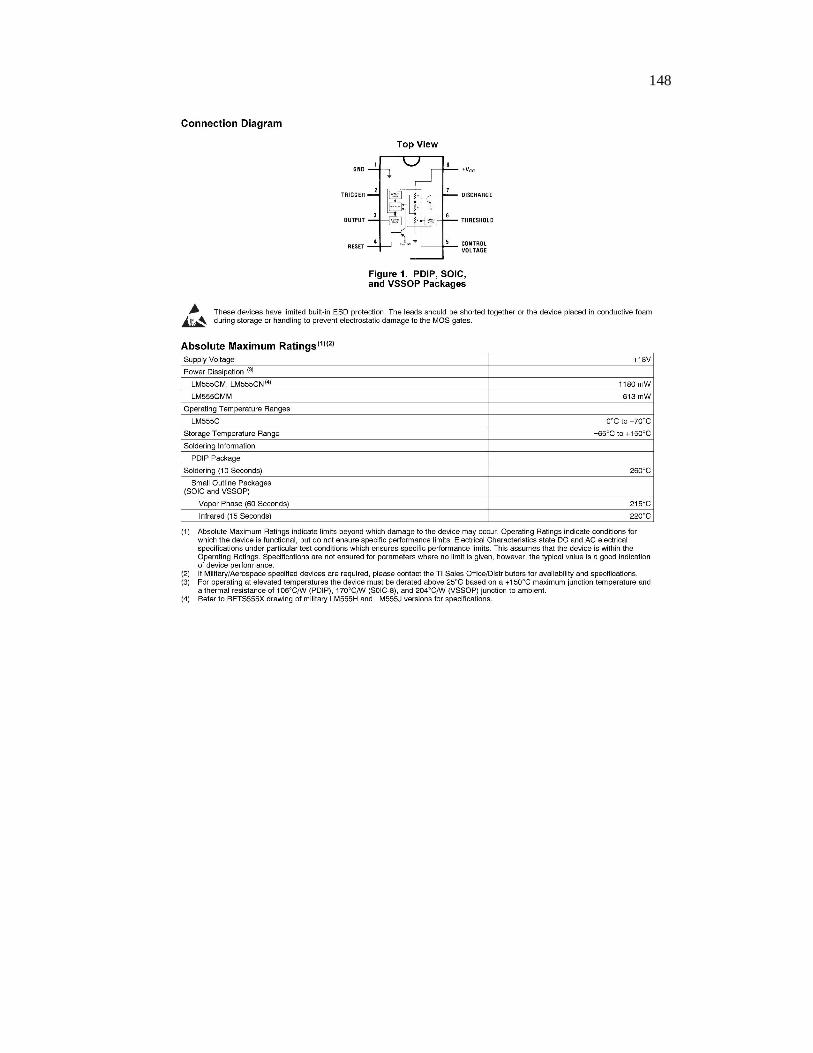
148
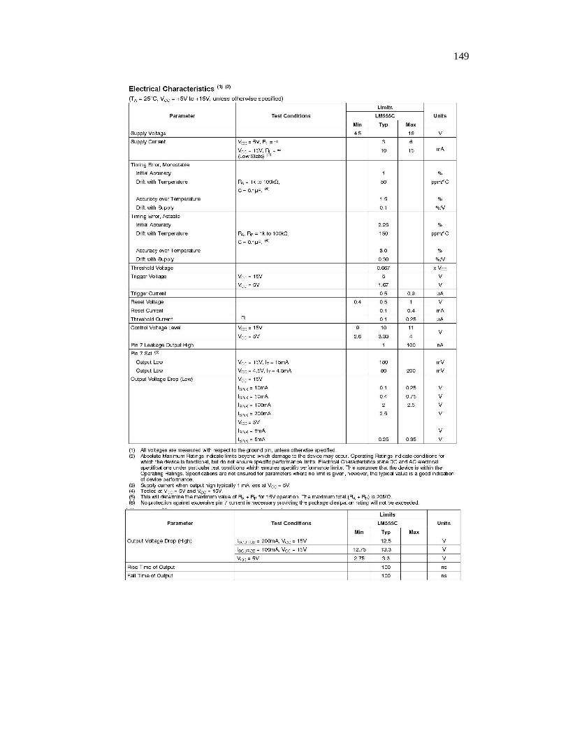
149
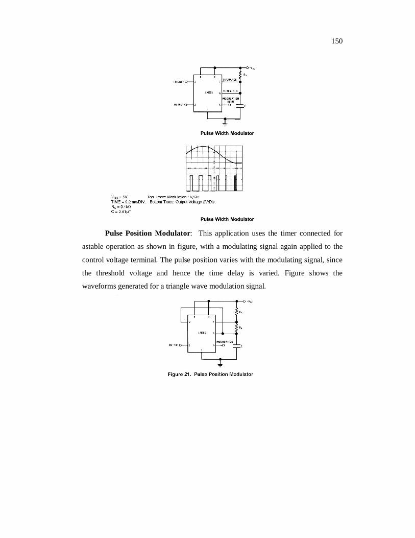
150
Pulse Position Modulator: This application uses the timer connected for
astable operation as shown in figure, with a modulating signal again applied to the
control voltage terminal. The pulse position varies with the modulating signal, since
the threshold voltage and hence the time delay is varied. Figure shows the
waveforms generated for a triangle wave modulation signal.
151
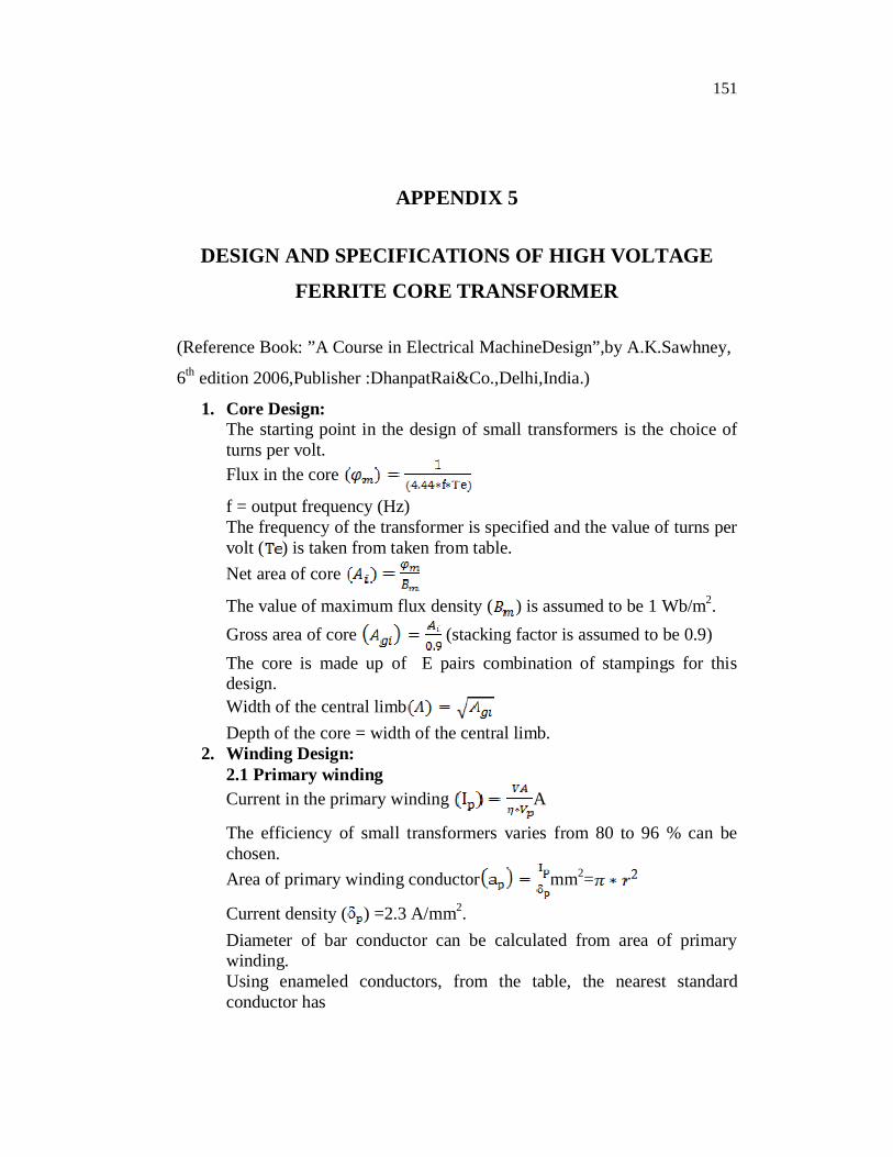
APPENDIX 5
DESIGN AND SPECIFICATIONS OF HIGH VOLTAGE
FERRITE CORE TRANSFORMER
(Reference Book: ”A Course in Electrical MachineDesign”,by A.K.Sawhney,
6th edition 2006,Publisher :DhanpatRai&Co.,Delhi,India.)
1. Core Design:The starting point in the design of small transformers is the choice ofturns per volt.Flux in the core
f = output frequency (Hz)The frequency of the transformer is specified and the value of turns pervolt ( ) is taken from taken from table.Net area of core
The value of maximum flux density ( ) is assumed to be 1 Wb/m2.Gross area of core (stacking factor is assumed to be 0.9)The core is made up of E pairs combination of stampings for thisdesign.Width of the central limbDepth of the core = width of the central limb.
2. Winding Design:2.1 Primary windingCurrent in the primary winding A
The efficiency of small transformers varies from 80 to 96 % can bechosen.Area of primary winding conductor mm2=
Current density ( ) =2.3 A/mm2.Diameter of bar conductor can be calculated from area of primarywinding.Using enameled conductors, from the table, the nearest standardconductor has
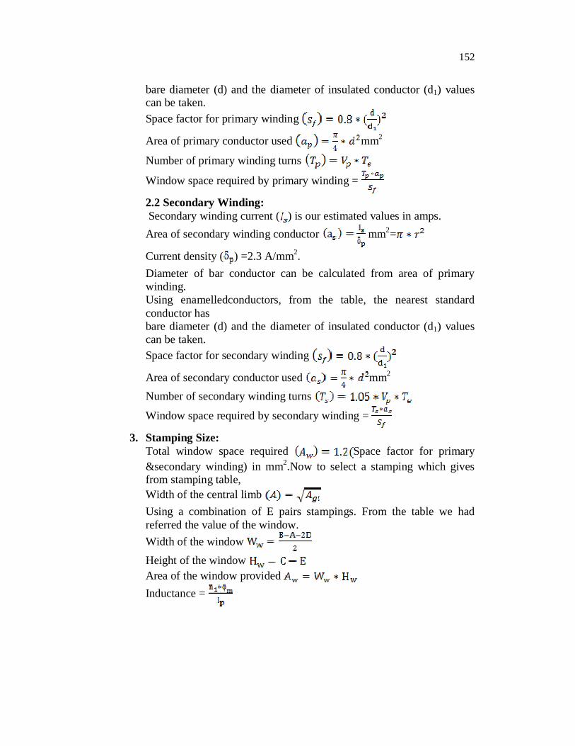
152
bare diameter (d) and the diameter of insulated conductor (d1) valuescan be taken.Space factor for primary winding
Area of primary conductor used mm2
Number of primary winding turns
Window space required by primary winding =
2.2 Secondary Winding: Secondary winding current ( ) is our estimated values in amps.Area of secondary winding conductor mm2=
Current density ( ) =2.3 A/mm2.Diameter of bar conductor can be calculated from area of primarywinding.Using enamelledconductors, from the table, the nearest standardconductor hasbare diameter (d) and the diameter of insulated conductor (d1) valuescan be taken.Space factor for secondary winding
Area of secondary conductor used mm2
Number of secondary winding turns
Window space required by secondary winding =
3. Stamping Size:Total window space required Space factor for primary&secondary winding) in mm2.Now to select a stamping which givesfrom stamping table,Width of the central limbUsing a combination of E pairs stampings. From the table we hadreferred the value of the window.Width of the windowHeight of the windowArea of the window providedInductance =
153
APPENDIX 6
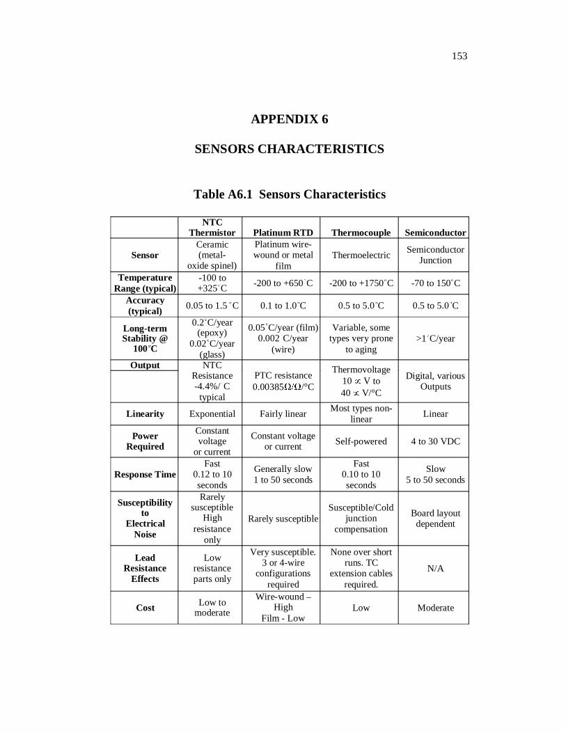
SENSORS CHARACTERISTICS
Table A6.1 Sensors Characteristics
NTCThermistor Platinum RTD Thermocouple Semiconductor
SensorCeramic(metal-
oxide spinel)
Platinum wire-wound or metal
filmThermoelectric Semiconductor
Junction
TemperatureRange (typical)
-100 to+325 C -200 to +650 C -200 to +1750 C -70 to 150 C
Accuracy(typical) 0.05 to 1.5 C 0.1 to 1.0 C 0.5 to 5.0 C 0.5 to 5.0 C
Long-termStability @
100 C
0.2 C/year(epoxy)
0.02 C/year(glass)
0.05 C/year (film)0.002 C/year
(wire)
Variable, sometypes very prone
to aging>1 C/year
Output NTCResistance-4.4%/ C
typical
PTC resistance0.00385 /°C
Thermovoltage10 V to40 V/°C
Digital, variousOutputs
Linearity Exponential Fairly linear Most types non-linear Linear
PowerRequired
Constantvoltage
or current
Constant voltageor current Self-powered 4 to 30 VDC
Response TimeFast
0.12 to 10seconds
Generally slow1 to 50 seconds
Fast0.10 to 10seconds
Slow5 to 50 seconds
Susceptibilityto
ElectricalNoise
Rarelysusceptible
Highresistance
only
Rarely susceptibleSusceptible/Cold
junctioncompensation
Board layoutdependent
LeadResistance
Effects
Lowresistanceparts only
Very susceptible.3 or 4-wire
configurationsrequired
None over shortruns. TC
extension cablesrequired.
N/A
Cost Low tomoderate
Wire-wound –High
Film - LowLow Moderate

154
Table A6.2 Sensors Advantages and Disadvantages
NTCThermistor Platinum RTD Thermocouple Semiconductor
Sensor Ceramic (metal-oxide spinel)
Platinum wire-wound or metalfilm
Thermoelectric SemiconductorJunction
Advantages • Sensitivity• Accuracy• Cost• Rugged• Flexible• Packages• Hermetic Seal• Surface Mount
• Accuracy• Stability• Linearity
• Temperature• Range• Self-Powered• No Self-heat• Rugged
• Ease of Use• Board
Mounting• Rugged• Overall Cost
Disadvantages • Non-linearity• Self-heating• Moisture
failures (non-glass only)
• Leadresistanceerror
• Response time• Vibration
resistance• Size• Package• limitations
• Cold-junctioncompensation
• Accuracy• Stability• TC extension
leads
• Accuracy• Limited
applications• Stability• Response time
Each of the major types of sensors above differs in their basic theory
of operation. Temperature ranges vary for each sensor type. Accuracy
depends upon basic sensor characteristics. Generally the better the accuracy,
the higher the price.
Long-term stability is defined by how consistently a sensor
maintains its accuracy over time. Stability is dictated by basic physical
properties of the sensor. Stability is typically worsened by exposure to high
temperatures. Wire-wound platinum and glass encapsulated thermistors are
the most stable sensor types. Thermocouples and semiconductors are the least
stable.
Sensor outputs vary by type. Thermistors change resistance
inversely proportionally with temperature, thus the name negative
temperature coefficient (NTC). Base metals such as platinum have positive
155
temperature coefficients (PTC). Thermocouples have low milli-volt outputs
that change with temperature. Semiconductors are typically conditioned and
come in a variety of digital outputs.
Linearity defines how well over a range of temperature a sensor’s
output consistently changes. Thermistors are exponentially non-linear,
exhibiting a much higher sensitivity at low temperatures than at high
temperatures. Linearity of a sensor has become less of an issue over time, as
microprocessors are more widely used in sensor signal conditioning circuits.
When powering, both thermistors and platinum elements require
constant voltage or constant currents. Power regulation is important to limit
self-heat in either thermistors or platinum RTDs. Current regulation is not as
critical for semiconductors. Thermocouples generate a voltage output.
Response time, or how quickly a sensor indicates temperature, is
dependent on the size and mass of the sensor element (assuming no predictive
method is used). Semiconductors are the slowest responding. Platinum wire-
wound elements are next slowest. Platinum film, thermistors and
thermocouples are available in small packages, and thus have high-speed
options. Glass micro-beads are the fastest responding thermistor
configuration.
Electrical noise inducing errors in temperature indication is a
problem mostly with thermocouples. Thermistors with very high resistances
may present a problem in some cases.
Lead resistance may cause an error offset in resistive devices such as
thermistors or RTDs. This effect is more pronounced with low resistance
devices such as 100 platinum elements or low resistance thermistors. For
platinum, 3 or 4-wire lead configurations are used to eliminate the problem.

156
For thermistors, typically choosing a higher resistance value eliminates the
effect. Thermocouples must use extension leads and connectors of the same
material as the leads themselves or an error may be introduced.
Although thermocouples are the least expensive and the most widely
used sensor, an NTC thermistor generally provides the greatest value for its
price. Each sensor type has advantages and disadvantages. For thermistors,
the major advantages are:
Sensitivity: This allows thermistors to sense very small changes in
temperature.
Accuracy: Thermistors offer both high absolute accuracy and
interchangeability.
Cost: For the high performance they offer, thermistors are very cost-
effective.
Ruggedness: Because of their construction, thermistors are very
rugged.
Flexibility: Thermistors can be configured into a wide variety of
physical forms, including very small packages.
Hermetic Seal: Glass encapsulation provides a hermetic package,
eliminating moisture induced sensor failure.
Surface Mount: A wide range of sizes and resistance tolerances are
available.
Of the thermistor disadvantages, typically only self-heating is a
design consideration. Proper care must be taken to limit the sensing current to
a low enough value that self-heat error is minimized to an acceptable value.
Non-linearity can be addressed by software or by circuitry, and
moisture induced failure by glass encapsulation.

157
All sensors have specific advantages and disadvantages. For a
successful project, the key is to match the sensor capabilities with the
application. If you would like assistance in deciding if a thermistor is the best
design option, please contact MEAS application engineers.