Embed Size (px)
Citation preview
Pergamon Solid-State Electronics Vol. 41, No. I1, pp. 1803-1809, 1997
© 1997 Elsevier Science Ltd. All rights reserved Printed in Great Britain
P l h S0038-1101(97)00153-6 0038q 101/97 $17.00 + 0.00
APPLICATIONS OF BIFURCATION THEORY TO THYRISTOR TURN-ON AND TURN-OFF
J. P A I S A N A and H. A B R E U SANTOS
lnstituto Superior Trcnico, Centro de Electrotecnia Terrica e Medidas Elrctricas, Lisbon Technical University, Portugal
(Received 16 October 1996; in revised form 18 February 1997)
Abstract We present a simple thyristor model that uses the gate voltage as the dependent variable and makes it possible to analyse the transverse behaviour of the device. The model leads to parabolic non linear partial differential equations in space and time, which are similar to Fisher's equation. A stationary analysis using bifurcation theory shows the existence of two stationary stable equilibrium points corresponding to the off- and on-state of the thyristor having in between an unstable point. A critical length, below which transverse non uniform current densities are not possible, is also predicted. A dynamical analysis in terms of wave type solutions shows that the steeper the wave front is, the smaller the propagation velocity. A numerical solution of the equations with more realistic boundary conditions, i.e., a cathode short-circuit and a turn on voltage at the gate, predicts that the conducting zone propagates with a velocity which is proportional to the anode voltage. This result unifies two previous expressions for the velocity in terms of the current that were obtained by two different groups on an experimental basis. © 1997 Elsevier Science Ltd
NOTATION
A II results are in SI units except current densities (,4 cm- 2) and carrier concentrations (cm --~)
D,, Dp, D, electron, hole and ambipolar diffusion co- efficients
Go~ turn-off GTO gain it.2.3 junction currents iG, iA, iK gate, anode and cathode currents /s~._,.~ saturation currents of the junctions JoL_,,~ injection current densities of the corresponding
junctions JDM stationary conduction current density Jsl.2.3 saturation current densities of the correspond-
ing junctions L,, critical length L,, Lc, ambipolar and effective conduction lengths Lx length of the effective cathode emitter q electronic charge q~, forward component of the charge density in the
p base qF, qR forward and reverse components of the total
excess charge in the p base S effective area of the device t time co-ordinate T absolute temperature uk._,.3 junction voltages uA anode voltage ur thermal voltage WBp p base width vs turn-on spreading velocity x co-ordinate parallel to the cathode junction
plane y co-ordinate normal to the cathode junction
plane z~ width of the device in the z direction
Greek letters
~tRp inverse current gain for the npn transistor • ~p, ~v, forward current gains for the. npn and pnp
transistors fl~p forward common emitter current gain for the
npn transistor r3 total transit time in the p base a~p conductivity of the p base ~ lifetime of the excess charge carriers in the p
base ~., rr electron and hole minority carrier lifetimes #,, #~ electron and hole mobilities
Dimensionless (normalised) quantitites
= 2x/Lx - 1 = x / L .
re = tlr~ c = vs~lL~
U = U31ur J = Jo.qJD
1. INTRODUCTION
A non-homogeneous carrier dis t r ibut ion in the emitter of b ipolar devices, generally called emitter- crowding, was extensively studied bo th in transis- tors[l], and thyristors[2,3] for several injection and bounda ry condit ions. However, as far as we know, the effects of positive feedback on the grouping of the carriers has deserved little at tent ion.
Most of the recent studies on thyris tor dynamics rely on the numerical solution of the cont inui ty equat ion for electrons and holes together with
1803
1804 J. Paisana and H. Abreu Santos
Poisson's and heat equations, with many details included[4]. Although undoubtedly important, namely because quantitative agreement with exper- imental data can be obtained by parameter fitting, this approach requires powerful computing resources and generally makes it impossible to draw fundamen- tal conclusions.
In the present article we propose a simple thyristor model that does not compete with the above mentioned ones that use finite difference or finite element techniques. Our approach is complementary. By adequate simplifications, which put aside many of the details but which are expected to preserve the essential, we are able to use bifurcation theory and are led to a non-linear parabolic partial differential equation usually known as Fisher's equation[5]. This equation was used extensively to study reaction- diffusion phenomena in biological and chemical processes[6,7] but, as far as we know, not in the frame of thyristors. This will allow us to consider plasma spreading as a wave front from whose properties several interesting conclusions can be drawn.
2. THE TWO-DIMENSIONAL THYRISTOR MODEL AND THE EQUATIONS
The geometry of the thyristor in the (x, y) plane, being y the longitudinal direction, was assumed rectangular as shown in Fig. l(a). The short-circuit in this figure does not exist in our analysis of the GTO. The bi-dimensional aspects were obtained as in [8] by considering several thyristor elements with a common anode and cathode and whose bases are separated by resistances as in Fig. l(b). As it is shown in the appendix, each of these elemental thyristors uses a
L. hort
J2 (a) Ji
IKJ u
G 31 'Ki '
iGi j
I I ,~i, iA~
K
,u,, j , J [
/ " T " A
Co)
Fig. I. (a) Schematic representation of a pnpn device with a cathode-base short. The later does not apply for the GTO. (b) Bidimensional model of the thyristor, composed by N sections of one-dimensional p-n-p-n cbmponents laterally
connected with conductances.
one-dimensional model based on the well known two complementary transistor association[9]. Each of the transistors was described in terms of concentrated parameters corresponding to the dynamic charge control[10] and Ebers-Moll[ l i ] models. In the appendix, following the suggestion given by [I 2], we also take into account the dependence of the transit time on the drift-field in the base. A further simplification was to consider that the npn and the pnp transistors were the same if we changed electrons with holes and donors with acceptors, i.e., we assumed that both carriers have the same mobility, the donor and corresponding acceptor concentrations are the same, as well as the geometry, and that two gates exist, one connected to the p base as usual and the other connected to the n base. This makes it possible to analyse only half of the structure, while it is expected to preserve the essential behaviour. From now on the device will be referred as anti-symmetric thyristor.
With the previously mentioned modelling and when the width of each elemental thyristor Ax tends to zero we obtain eqn (A9), as shown in the appendix. For the stationary regime, when the central junction is reverse biased and by using the dimensionless variables ~ = 2x /Lx - 1, U = U~/ut we can write;
d-'U d~ 2 + ~.f(U) = 0 (1)
where;
and
f (U) = e t - 1 (2)
6 - 2(~Fp- 1)Js3L~ 4 WBpaBoUr (3)
This is a non linear, second order elliptic equation which was used first in combustion theory[13] and later to study carrier accumulation in the base of bipolar transistors[l], always for 6 < 0. In the present article we are mainly interested in solutions for 6 > 0.
In a similar way, if we consider that the central junction is forward biased we obtain from (A9);
d:U + 6J(U) - ?6f(U) = 0 (4)
w h e r e f a n d 6 are defined as before and 7 is given by;
1 - ~Rp as_, ~.A l 2ct~p- 1 js3e ,,+ (5)
For high level injection, by considering the dimensionless variables ~ = x/Lec, J = Jm/J t , M,
re = t/z; (r; = " r 3 / ( 2 ~ v o - 1)) where;
L~ L~,r = flvo - 1 (6)
JS3 tA JDM - - ~Fp " - - ) 2 t'A ~r, ~ e ,,r (7)
Applications of bifurcation theory
5
* " 4 0
o
0
=0.25
//
" 5=-0.5
1 -0.5 0 .0 0 .5 1.0
Normal ised transverse co-ordinate
(a)
4
3
2
1
I • -.25
"..'¢, '..,
" .J ~iA' . . . . . . . . . . . .
. . . . .
--,'---I"5--, i , I ," 0. .25 .5 .75 8c
Parameter 8
(b)
I 1.
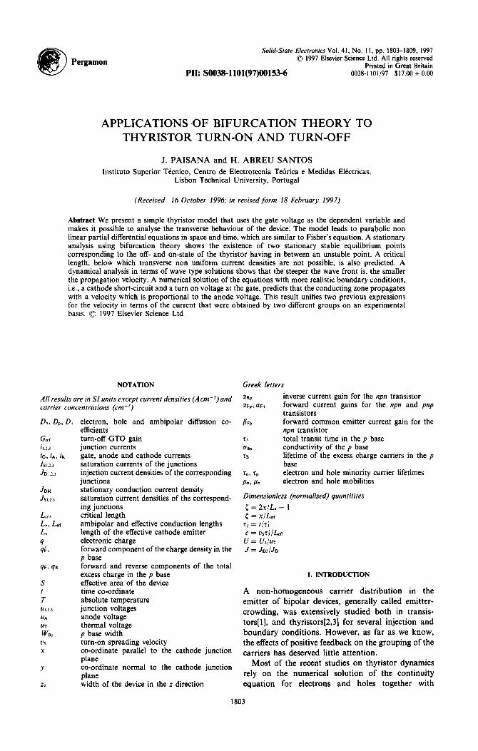
Fig. 2. (a) Spatial distributions of the normalised cathode junction voltage U(() corresponding to the normalised gate-cathode voltage 6:o = 1 and to the parameter values 6 = 0.25 (dashed line) and 6 = 0.5 (full line). (b) Bifurcation diagrams (6, II UII) for three values of U0.6~ is the bifurcation value for U0 = 0.
1805
and with T~ depending on the current density JD3 as (AI5), we obtain from (A16);
O2j d j ~ , - k J . ( J - 1) + ~ (8)
with q = 2 and k = JDM/JO3O. For a constant 33 we have k = 1 and r / = 1 which is Fisher's equation[5].
3. STATIONARY RESULTS: BIFURCATION POINTS AND THE MINIMUM LENGTH FOR SQUEEZING
We will start by analysing the gate turn-on of a thyristor with a cathode short-circuit. Accordingly we will use eqn (1), since the central junction is reverse biased, and the Dirichlet conditions for the normalised voltage;
U = U 0 a t ( = 1 (at the gate) (9a)
U=O at ( = l
(at the gate-cathode short-circuit) (9b)
In Fig. 2(a) we see the distributions of the normal- ised cathode junction voltage U in the normalised space ( corresponding to a given gate voltage U0 and two different values of 6 expressed by (3). There are two possible distributions associated with each 6. Both are non uniform and have an extremum, [[ UH. In Fig. 2(b) we see, taking the gate voltage U0 constant, that if we change the construction parameter 6 we can obtain several II uII values. Points A and B in Fig. 2(a) correspond to A' and B' in Fig. 2(b). If we increased 6 by device construction, the two distributions in Fig. 2(a) would merge into one another and we would reach point C ' in Fig. 2(b), the bifurcation point. Whatever the U0 value is, a bifurcation point exists, associated with turn-on, for which dltUll/d6 tends to infinity. For U0 = 0 this is
the Frank-Kamenetskii value 6c ~ 0.878113]. Using stability criteria[14], we can conclude that all the stationary states on the lower branch, where dllUll/d6 >10, are stable. The upper branch, with dll UII/d6 >~ O, corresponds to u ( O unstable solutions such as A'.
If we diminish 6 we increase the gate voltage for turn-on. For ~i < 0, that is for ~Fp < 0.5 in our structure, only a stable branch of solutions exists corresponding to the classical emitter crowding.
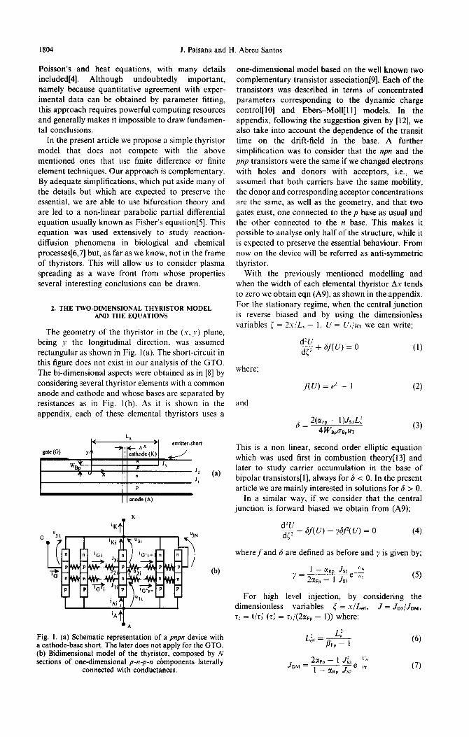
Previous results were for U,. < 0. When the central junction is forward biased eqn (4) instead of (1) applies. Results for forward and reverse bias can be seen on Fig. 3 for U0 = 0. Given (4) a third branch exists, with stable solutions which correspond to the
6,
O
O
0 0
Fig. 3.
' C )
+
| . J • s~ 0.2 ~.4 0.6 ~.8 8c i
Parameter 8
Bifurcation diagram (&l l f l l ) for Uo=O and 7 = 0.03. A, B, C, are equilibrium points corresponding to 6 = 0.6 and 6~, 6: are the bifurcation points for turn-on and
turn-off respectively.
1806 J. Paisana and H. Abreu Santos
thyristor on state. We also have a second bifurcation point, 6:, that corresponds to turn-off.
We will next analyse turn-off in the GTO. Therefore, the cathode short-circuit will be aban- doned and we will consider high level injection. We will use eqn (8), with boundary conditions J = 0 at
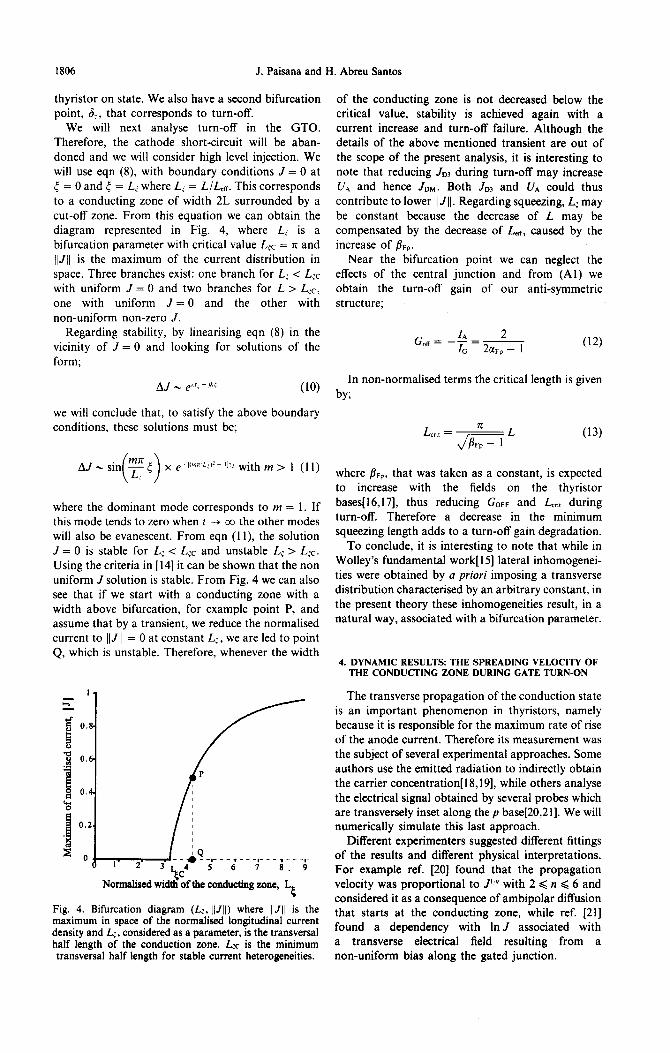
= 0 and ~ = L: where L: = L/Len. This corresponds to a conducting zone of width 2L surrounded by a cut-off zone. From this equation we can obtain the diagram represented in Fig. 4, where L: is a bifurcation parameter with critical value L¢c= n and IIJII is the maximum of the current distribution in space. Three branches exist: one branch for L¢ <L¢c with uniform J = 0 and two branches for L > L¢c, one with uniform J = 0 and the other with non-uniform non-zero J.
Regarding stability, by linearising eqn (8) in the vicinity of J - - 0 and looking for solutions of the form;
AJ ~ e ~ +/k~ (10)
we will conclude that, to satisfy the above boundary conditions, these solutions must be;
(me) A J ~ s m ~ x , w i t h m > 1 (11)
where the dominant mode corresponds to m = 1. If this mode tends to zero when t ---, oo the other modes will also be evanescent. From eqn ( l l ) , the solution J = 0 is stable for L¢ <L¢c and unstable L¢ > L~c. Using the criteria in [14] it can be shown that the non uniform J solution is stable. From Fig. 4 we can also see that if we start with a conducting zone with a width above bifurcation, for example point P, and assume that by a transient, we reduce the normalised current to IlJlr = 0 at constant L¢, we are led to point Q, which is unstable. Therefore, whenever the width
l
0.~
"o 0.6.
0.4. I:I
.~ 0.2
~ o I" 2" 3" .~c 4 5 6 7 s. 9
Normalised widtli of the conducting zone, L~
Fig. 4. Bifurcation diagram (L¢, ]lJII) where IIJII is the maximum in space of the normalised longitudinal current density and L¢, considered as a parameter, is the transversal half length of the conduction zone. L:c is the minimum transversal half length for stable current heterogeneities.
of the conducting zone is not decreased below the critical value, stability is achieved again with a current increase and turn-off failure. Although the details of the above mentioned transient are out of the scope of the present analysis, it is interesting to note that reducing JD3 during turn-off may increase UA and hence JDM. Both Jo.~ and UA could thus contribute to lower II JII. Regarding squeezing, L¢ may be constant because the decrease of L may be compensated by the decrease of Lo,, caused by the increase of fl~p.
Near the bifurcation point we can neglect the effects of the central junct ion and from (Al) we obtain the turn-off gain of our anti-symmetric structure;
/A 2 Go~= I G - 2~Fp-- 1 (12)
In non-normalised terms the critical length is given by;
L.i, - f lF.x/ /~p _ 1 L (13)
where flFp, that was taken as a constant, is expected to increase with the fields on the thyristor bases[16,17], thus reducing Govv and L,i, during turn-off. Therefore a decrease in the minimum squeezing length adds to a turn-off gain degradation.
To conclude, it is interesting to note that while in Wolley's fundamental work[15] lateral inhomogenei- ties were obtained by a priori imposing a transverse distribution characterised by an arbitrary constant, in the present theory these inhomogeneities result, in a natural way, associated with a bifurcation parameter.
4. DYNAMIC RESULTS: THE SPREADING VELOCITY OF THE CONDUCTING ZONE DURING GATE TURN-ON
The transverse propagation of the conduction state is an important phenomenon in thyristors, namely because it is responsible for the maximum rate of rise of the anode current. Therefore its measurement was the subject of several experimental approaches. Some authors use the emitted radiation to indirectly obtain the carrier concentration[i 8,19], while others analyse the electrical signal obtained by several probes which are transversely inset along the p base[20,21 ]. We will numerically simulate this last approach.
Different experimenters suggested different fittings of the results and different physical interpretations. For example ref. [20] found that the propagation velocity was proportional to J~" with 2 ~< n ~< 6 and considered it as a consequence of ambipolar diffusion that starts at the conducting zone, while ref. [21] found a dependency with ln J associated with a transverse electrical field resulting from a non-uniform bias along the gated junction.
Applications of
In our analysis, firstly we will study a laterally indefinite structure and impose a travelling wave solution of the form;
J(~, z¢) = ~t(Z), Z = ~ - cr~ (14)
where c is the wave speed. Substituting (14) into (8) with k = 1 and r / = 1 we obtain;
d2,., q d~9 ~5_, + c ~ + oa(l - - , 9 ) = 0 (15)
The turn-on propagation will assume the character- istics of a wavefront travelling in the axes positive direction (c ~> 0) if 8 satisfies the conditions;
lim O(Z) = 0 lim 8(Z) = 1 (16)
where O = 0 and 9 = 1 are the equilibrium point solutions of the wave equation. These can be associated with the blocking and conduction states.
Many details and conclusions regarding travelling wavefront solutions of(15) can be found in [6,7]. The more important characteristics of these waves hardly depend on the nature of the equilibrium points, on the steepness of its leading edge or on the initial conditions. After linearising eqn (15) in the vicinity of
= 0, a stability analysis shows that a wave solution is possible if c >/2, i.e., in normalised terms, if the wave speed is;
2 Len = 2V/(flF p -- 1 ) -~ (17)
In this range, the faster the waves move the less steep the wavefront is. The analysis of the wave speed dependence on the initial conditions for J , as ¢ ~ @, can be seen in [22]. This study also shows that the flatter the J current density profile for re = 0 is, the greater the wavefront speed.
The above mentioned results refer to constant r3 and are similar to those obtained by Bergman[23]. They predict that the speed of the wave does not depend on the current density of the conduction zone, which is experimentally known to be false. Results are rather different if we consider the dependency of 33 on JD3. Using Nagumo's procedure[24] for the determination of the speed of the wavefront solution we obtain from (8);
(JDM'~ I'2 Lee: (18) vs = 3;-S
This is the experimental dependency Vs ~ Jg-'[18]. So far our results derive from imposing wave type
solutions on partial differential equations and assume that the transverse dimension of the device is infinite. To lift this restriction the results that follow were obtained by solving self consistently the coupled continuity equations for electrons and holes together with Poisson's equation by using a finite differences scheme. To the best of our knowledge, these
bifurcation theory
4 L gate contact
x
Px
0
ca~ode short
t
160 :60 36o 4oo Transverse co-ordinate, x (~m)
1807
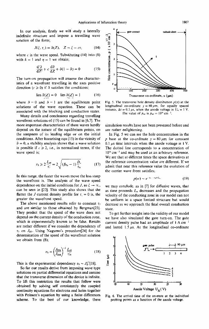
500
Fig. 5. The transverse hole density distribution p(x) at the longitudinal co-ordinate y = 80 pm, for equally spaced instants, At = 0.1 /ts, when the anode voltage is UA = 1 V.
The value of pr~r is p,~f= 10 ~6 cm -3.
simulation results have not been presented before and are rather enlightening.
In Fig. 5 we can see the hole concentration in the p base at the co-ordinate y = 80/~m for constant 0.1 #s time intervals when the anode voltage is 1 V. The dotted line corresponds to a concentration of 10 ~6 cm -3 and may be used as an arbitrary reference. We see that at different times the space derivatives at the reference concentration value are different. If we admit that near this reference value the evolution of the carrier wave front satisfies;
p(w) ~ e -~-'-'s'< (19)
we may conclude, as in [7] for diffusive waves, that as time proceeds Lw decreases and the propagation velocity of the conducting zone in our model can not be uniform in a space limited structure but would decrease as we approach the final overall conduction state.
To get further insight into the validity of our model we have also simulated the gate turn-on. The gate current density pulse had an amplitude of 1 A cm --~ and lasted 1.5/~s. At the longitudinal co-ordinate
gate pulse ', ~ 90 I-tin
3 4
Anode Voltage UA(V)
Fig. 6. The arrival time of the on-state at the individual probing points as a function of the anode voltage.
1808
"C 45c
E
.~ 35(3 o O
¢ I 0 • ~ 25o
I : u
~ 150
50 0.5
J. Paisana and H. Abreu Santos
2 v23 v34 • •
i , i
i i i
. 1 2 3 4
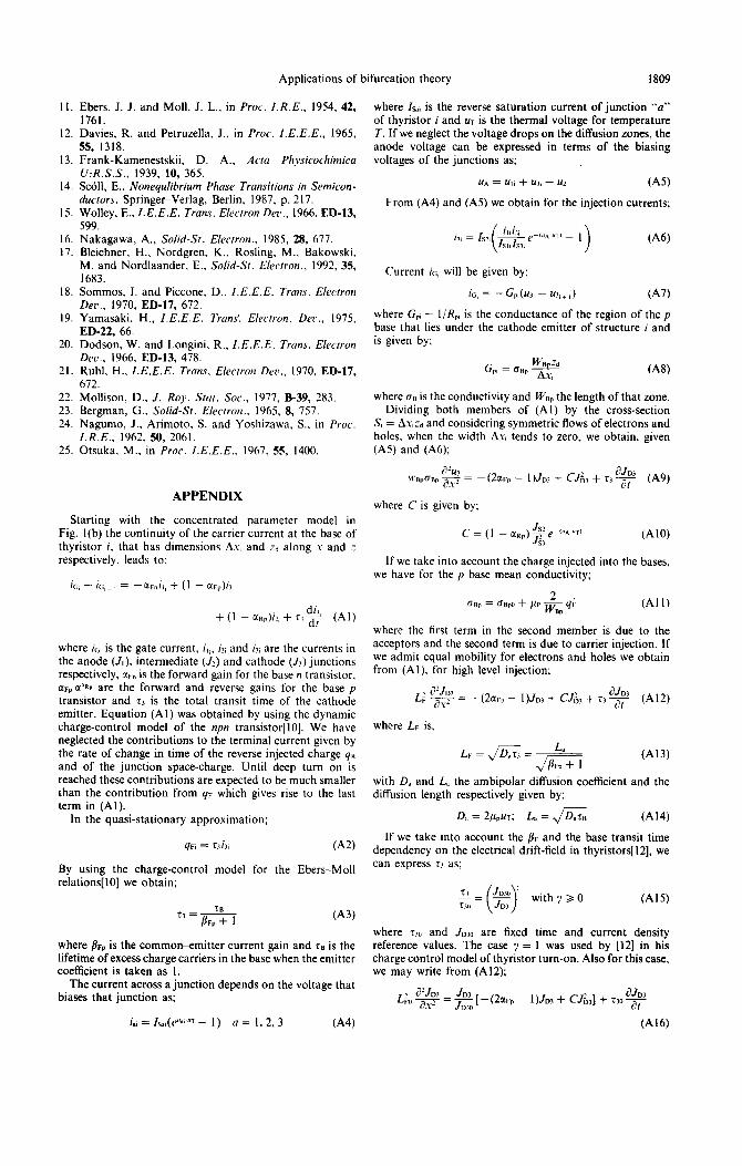
Fig. 7. The velocity of propagation of the
/.o 1'.5 3.0 Anode voltage U A ( V )
on-state as a function of the anode voltage.
y = 80 #m we have, at several x co-ordinates acting as simulation probing points separated by 90/~m and starting at x, = 140 #m from the gate, registered the instants at which the carrier concentration crossed the reference value of 1016cm -3 for several fixed anode voltages. The results are presented in Fig. 6.
We can see from Fig. 6 that the local turn-on time decreases as the anode voltage increases, the effect being more pronounced at lower voltages. Using these results the conduction zone spreading velocity as a function of the anode voltage is represented in Fig. 7 for several probing zones. We conclude that the spreading velocity is proportional to the anode voltage UA. This dependency may be considered as a generalisation of the two above mentioned results obtained by other authors[20,21]. In fact, for low voltages and for the conduction stationary situation, when the longitudinal electric field is less meaningful, it can be shown that UA ~ In J while for high voltages we have UA ~ J' 2125].
5. CONCLUSIONS
We have established a simple model which analyses thyristor behaviour in terms of the gate voltage instead of, as it is common practice, the gate current. Our simplified approach makes it possible to use bifurcation theory.
The device we have considered is double gated and assumes that electrons and holes behave symmetri- cally. This makes it possible to study only half of the device thus reducing computing times by half, which is specially meaningful when finite differences or finite elements methods are used.
Although von Neumann boundary conditions could be dealt with using our model, all transverse boundary conditions have been taken as a Dirichlet type and correspond to either gate voltage or zero longitudinal current.
When considering high level injection our model leads to Fisher's equation. For the stationary regime
it was possible to draw two important conclusions. First, there is a minimum transverse length below which current non uniformity is not possible. This length is of the order of the diffusion length and if the transverse dimensions of the device are smaller than that value no squeezing of the conduction zone will take place during turn-off. Second, even if by device design the critical transverse length is increased the current density that can be cut off tends to saturate for a given Ic. Analysing wave-type solutions made it possible to establish that the steeper the turned-on zone wavefront the smaller the propagation velocity. The above results apply if a constant gain flvp is assumed. Nevertheless the expressions we obtained give insight into the effect which a field dependent gain has on the transverse carrier distribution.
Using a finite differences method we have numerically simulated an experimental technique and, from gate turn-on results, we predict the existence of a conducting zone with a wavelike transverse propagation velocity that is proportional to the anode voltage. This result unifies two different expressions obtained by two independent groups to fit experimental data.
R E F E R E N C E S
I. Fletcher, N. H., in Proc. I.R.E., 1955, 43, 551. 2. Gentry, F. E., Scace, R. I. and Flowers, J. K. in Proc.
I.E.E.E., 1965, 53, 355. 3. Fulop, W. and Joadat-Ghassabi, M. R., Solid-St.
Electron., 1978, 21, 361. 4. Brand, H. and Selberherr, S., I.E.E.E. Trans. Electron
Dev., 1995, ED-42, 2137. 5. Fisher, R. A., Ann. Eugenics, 1937, 7, 353. 6. Murray, J. D., Mathematical Biology, Springer-Verlag,
Berlin, 1989 p. 277. 7. Sachdev, P. L., Nonlinear Diffusive Waves, Cambridge
University Press, Cambridge, p. 103. 8. Kurata, Numerical Analysis for Semiconductor Devices,
Lexington Books, 1982, p. 207. 9. Ebers, J. J., in Proc. I.R.E., 1952, 40, 1361.
10. Gray, P. and Searle, C., Electronic Principles, Physics Models and Circuits, John Wiley, New York, pp. 753.
Applications of bifurcation theory 1809
I1. Ebers, J. J. and Moll, J. L., in Proc. I .R.E., 1954, 42, 1761.
12. Davies, R. and Petruzella, J., in Proc. I .E.E.E., 1965, 55, 1318.
13. Frank-Kamenestskii, D. A., Acta Physieochimiea U..R.S.S., 1939, 10, 365.
14. Sc611, E., Nonequlibrium Phase Transitions in Semicon- ductors, Springer-Verlag, Berlin, 1987, p. 217.
15. Wolley, E., 1.E.E.E. Trans. Electron Dev., 1966, ED-13, 599.
16. Nakagawa, A., Solid-St. Electron., 1985, 28, 677. 17. Bleichner, H., Nordgren, K., Rosling, M., Bakowski,
M. and Nordlaander, E., Solid-St. Electron., 1992, 35, 1683.
18. Sommos, I. and Piccone, D., 1.E.E.E. Trans. Electron Dev., 1970, ED-17, 672.
19. Yamasaki, H., I .E.E.E. Trans'. Electron. Dev., 1975, ED-22, 66.
20. Dodson, W. and Longini, R., I .E.E.E. Trans. Electron Dev., 1966, ED-13, 478.
21. Ruhl, H., I .E.E.E. Trans. Electron Dev., 1970, ED-17, 672.
22. Mollison, D., J. Roy. Stat. Soc., 1977, B-39, 283. 23. Bergman, G., Solid-St. Electron., 1965, 8, 757. 24. Nagumo, J., Arimoto, S. and Yoshizawa, S., in Proc.
I . R E . , 1962, 50, 2061. 25. Otsuka, M., in Proc. I.E.E.E., 1967, 55, 1400.
A P P E N D I X
Starting with the concentrated parameter model in Fig. l(b) the continuity of the carrier current at the base of thyristor i, that has dimensions Ax, and -~ along x and z respectively, leads to;
iGi - - i6~+~ = -~ . i~ , + (1 - - ~vp)i3~
+ (1 - ~Rp)i2, + r3 d~ (A1)
where iG~ is the gate current, i~, i2, and i3i are the currents in the anode (J0, intermediate (J,) and cathode (J3)junctions respectively, ~tv, is the forward gain for the base n transistor, Ctrp ct~R, are the forward and reverse gains for the base p transistor and r3 is the total transit time of the cathode emitter. Equation (A1) was obtained by using the dynamic charge-control model of the npn transistor[10]. We have neglected the contributions to the terminal current given by the rate of change in time of the reverse injected charge qR and of the junction space-charge. Until deep turn on is reached these contributions are expected to be much smaller than the contribution from qv which gives rise to the last term in (Al).
In the quasi-stationary approximation;
qw = r3i3~ (A2)
By using the charge-control model for the Ebers-Moll relations[10] we obtain;
rB (A3) z3 -- flFp + 1
where fl~a is the common-emitter current gain and za is the lifetime of excess charge carriers in the base when the emitter coefficient is taken as 1.
The current across a junction depends on the voltage that biases that junction as;
&i = Is~i(e ''~i ,~r _ 1 ) a = 1, 2, 3 (A4)
where Is~, is the reverse saturation current of junction "a" of thyristor i and UT is the thermal voltage for temperature T. If we neglect the voltage drops on the diffusion zones, the anode voltage can be expressed in terms of the biasing voltages of the junctions as;
u~ = u, + u3~ - u2 (A5)
From (A4) and (AS) we obtain for the injection currents;
i t i i ~ i t A ~rl i~i_ = I s _ , i ' ~ \ s,ils,, e . . . . . 1 ) (A6)
Current i6~ will be given by;
i6, = - Gpi(u3~ - u3, +,) (AT)
where G,, = liRa, is the conductance of the region of the p base that lies under the cathode emitter of structure i and is given by;
W a p Z d Gp, = trap Ax~ (A8)
where aB is the conductivity and WBp the length of that zone. Dividing both members of (AI) by the cross-section
S~ = Ax~zd and considering symmetric flows of electrons and holes, when the width Ax~ tends to zero, we obtain, given (A5) and (A6);
~2U~ t3,JD~ Wapaap ~.~_; = --(2~Fp -- l)Jm + CJD3 + z ~ T t (A9)
where C is given by;
, Js2 ~ A r[} C = ( 1 --CtRp)~-, e " ' (Al0) Jg3
If we take into account the charge injected into the bases, we have for the p base mean conductivity;
2 aap = aapo + pv Ws--~p q~ (A11)
where the first term in the second member is due to the acceptors and the second term is due to carrier injection. If we admit equal mobility for electrons and holes we obtain from (Al), for high level injection;
t32Jm ~JD3 LF ~ = --(2~Fp -- l)Jo~ + CJ~3 + z3 ¢-~-- (AI2)
where LF is;
L, (A13)
with D~ and L the ambipolar diffusion coefficient and the diffusion length respectively given by;
D,, = 2 / / p U T ; L, = Dx//-D~:~ (AI4)
If we take into account the fir and the base transit time dependency on the electrical drift-field in thyristors[12], we can express r3 as;
-c~ = : Jo~:" with ~/> 0 (A15) ~,,, \J~)
where z30 and Jm0 are fixed time and current density reference values. The case 7 = 1 was used by [12] in his charge control model of thyristor turn-on. Also for this case, we may write from (AI2);
L, ~ 2 J o 3 Jo3 ~ ,~ t~JD~
(a l6 )