Embed Size (px)
Citation preview
This is information on a product in full production.
August 2016 DocID15818 Rev 15 1/184
STM32F205xx STM32F207xx
ARM®-based 32-bit MCU, 150DMIPs, up to 1 MB Flash/128+4KB RAM, USB OTG HS/FS, Ethernet, 17 TIMs, 3 ADCs, 15 comm. interfaces & camera
Datasheet - production data
Features
• Core: ARM® 32-bit Cortex®-M3 CPU (120 MHz max) with Adaptive real-time accelerator (ART Accelerator™) allowing 0-wait state execution performance from Flash memory, MPU, 150 DMIPS/1.25 DMIPS/MHz (Dhrystone 2.1)
• Memories
– Up to 1 Mbyte of Flash memory
– 512 bytes of OTP memory
– Up to 128 + 4 Kbytes of SRAM
– Flexible static memory controller that supports Compact Flash, SRAM, PSRAM, NOR and NAND memories
– LCD parallel interface, 8080/6800 modes
• Clock, reset and supply management
– From 1.8 to 3.6 V application supply + I/Os
– POR, PDR, PVD and BOR
– 4 to 26 MHz crystal oscillator
– Internal 16 MHz factory-trimmed RC
– 32 kHz oscillator for RTC with calibration
– Internal 32 kHz RC with calibration
• Low-power modes
– Sleep, Stop and Standby modes
– VBAT supply for RTC, 20 × 32 bit backup registers, and optional 4 KB backup SRAM
• 3 × 12-bit, 0.5 µs ADCs with up to 24 channels and up to 6 MSPS in triple interleaved mode
• 2 × 12-bit D/A converters
• General-purpose DMA: 16-stream controller with centralized FIFOs and burst support
• Up to 17 timers
– Up to twelve 16-bit and two 32-bit timers, up to 120 MHz, each with up to four IC/OC/PWM or pulse counter and quadrature (incremental) encoder input
•
• Debug mode: Serial wire debug (SWD), JTAG, and Cortex®-M3 Embedded Trace Macrocell™
• Up to 140 I/O ports with interrupt capability:
– Up to 136 fast I/Os up to 60 MHz
– Up to 138 5 V-tolerant I/Os
• Up to 15 communication interfaces
– Up to 3 × I2C interfaces (SMBus/PMBus)
– Up to four USARTs and two UARTs (7.5 Mbit/s, ISO 7816 interface, LIN, IrDA, modem control)
– Up to three SPIs (30 Mbit/s), two with muxed I2S to achieve audio class accuracy via audio PLL or external PLL
– 2 × CAN interfaces (2.0B Active)
– SDIO interface
• Advanced connectivity
– USB 2.0 full-speed device/host/OTG controller with on-chip PHY
– USB 2.0 high-speed/full-speed device/host/OTG controller with dedicated DMA, on-chip full-speed PHY and ULPI
– 10/100 Ethernet MAC with dedicated DMA: supports IEEE 1588v2 hardware, MII/RMII
• 8- to 14-bit parallel camera interface (48 Mbyte/s max.)
• CRC calculation unit
• 96-bit unique ID
LQFP64 (10 × 10 mm)
LQFP100 (14 × 14 mm)
LQFP144 (20 × 20 mm)
LQFP176 (24 × 24 mm)
UFBGA176 (10 × 10 mm)
WLCSP64+2(0.400 mm pitch)
www.st.com
STM32F20xxx
2/184 DocID15818 Rev 15
Table 1. Device summary
Reference Part numbers
STM32F205xxSTM32F205RB, STM32F205RC, STM32F205RE, STM32F205RF, STM32F205RG STM32F205VB, STM32F205VC, STM32F205VE, STM32F205VF, STM32F205VG STM32F205ZC, STM32F205ZE, STM32F205ZF, STM32F205ZG
STM32F207xxSTM32F207IC, STM32F207IE, STM32F207IF, STM32F207IG STM32F207VC, STM32F207VE, STM32F207VF, STM32F207VG STM32F207ZC, STM32F207ZE, STM32F207ZF, STM32F207ZG
DocID15818 Rev 15 3/184
STM32F20xxx Contents
6
Contents
1 Introduction . . . . . . . . . . . . . . . . . . . . . . . . . . . . . . . . . . . . . . . . . . . . . . . 13
2 Description . . . . . . . . . . . . . . . . . . . . . . . . . . . . . . . . . . . . . . . . . . . . . . . . 14
2.1 Full compatibility throughout the family . . . . . . . . . . . . . . . . . . . . . . . . . . 18
3 Functional overview . . . . . . . . . . . . . . . . . . . . . . . . . . . . . . . . . . . . . . . . 21
3.1 ARM® Cortex®-M3 core with embedded Flash and SRAM . . . . . . . . . . . 21
3.2 Adaptive real-time memory accelerator (ART Accelerator™) . . . . . . . . . 21
3.3 Memory protection unit . . . . . . . . . . . . . . . . . . . . . . . . . . . . . . . . . . . . . . . 21
3.4 Embedded Flash memory . . . . . . . . . . . . . . . . . . . . . . . . . . . . . . . . . . . . 22
3.5 CRC (cyclic redundancy check) calculation unit . . . . . . . . . . . . . . . . . . . 22
3.6 Embedded SRAM . . . . . . . . . . . . . . . . . . . . . . . . . . . . . . . . . . . . . . . . . . . 22
3.7 Multi-AHB bus matrix . . . . . . . . . . . . . . . . . . . . . . . . . . . . . . . . . . . . . . . . 22
3.8 DMA controller (DMA) . . . . . . . . . . . . . . . . . . . . . . . . . . . . . . . . . . . . . . . 23
3.9 Flexible static memory controller (FSMC) . . . . . . . . . . . . . . . . . . . . . . . . 24
3.10 Nested vectored interrupt controller (NVIC) . . . . . . . . . . . . . . . . . . . . . . . 24
3.11 External interrupt/event controller (EXTI) . . . . . . . . . . . . . . . . . . . . . . . . . 25
3.12 Clocks and startup . . . . . . . . . . . . . . . . . . . . . . . . . . . . . . . . . . . . . . . . . . 25
3.13 Boot modes . . . . . . . . . . . . . . . . . . . . . . . . . . . . . . . . . . . . . . . . . . . . . . . 25
3.14 Power supply schemes . . . . . . . . . . . . . . . . . . . . . . . . . . . . . . . . . . . . . . 25
3.15 Power supply supervisor . . . . . . . . . . . . . . . . . . . . . . . . . . . . . . . . . . . . . 26
3.16 Voltage regulator . . . . . . . . . . . . . . . . . . . . . . . . . . . . . . . . . . . . . . . . . . . 26
3.16.1 Regulator ON . . . . . . . . . . . . . . . . . . . . . . . . . . . . . . . . . . . . . . . . . . . . . 26
3.16.2 Regulator OFF . . . . . . . . . . . . . . . . . . . . . . . . . . . . . . . . . . . . . . . . . . . . 27
3.16.3 Regulator ON/OFF and internal reset ON/OFF availability . . . . . . . . . . 31
3.17 Real-time clock (RTC), backup SRAM and backup registers . . . . . . . . . . 31
3.18 Low-power modes . . . . . . . . . . . . . . . . . . . . . . . . . . . . . . . . . . . . . . . . . . 32
3.19 VBAT operation . . . . . . . . . . . . . . . . . . . . . . . . . . . . . . . . . . . . . . . . . . . . . 32
3.20 Timers and watchdogs . . . . . . . . . . . . . . . . . . . . . . . . . . . . . . . . . . . . . . . 33
3.20.1 Advanced-control timers (TIM1, TIM8) . . . . . . . . . . . . . . . . . . . . . . . . . 33
3.20.2 General-purpose timers (TIMx) . . . . . . . . . . . . . . . . . . . . . . . . . . . . . . . 34
3.20.3 Basic timers TIM6 and TIM7 . . . . . . . . . . . . . . . . . . . . . . . . . . . . . . . . . 34
Contents STM32F20xxx
4/184 DocID15818 Rev 15
3.20.4 Independent watchdog . . . . . . . . . . . . . . . . . . . . . . . . . . . . . . . . . . . . . 35
3.20.5 Window watchdog . . . . . . . . . . . . . . . . . . . . . . . . . . . . . . . . . . . . . . . . . 35
3.20.6 SysTick timer . . . . . . . . . . . . . . . . . . . . . . . . . . . . . . . . . . . . . . . . . . . . . 35
3.21 Inter-integrated circuit interface (I²C) . . . . . . . . . . . . . . . . . . . . . . . . . . . . 35
3.22 Universal synchronous/asynchronous receiver transmitters (UARTs/USARTs) . . . . . . . . . . . . . . . . . . . . . . . . . . . . . . . . . . . . . . . . . . . 35
3.23 Serial peripheral interface (SPI) . . . . . . . . . . . . . . . . . . . . . . . . . . . . . . . . 36
3.24 Inter-integrated sound (I2S) . . . . . . . . . . . . . . . . . . . . . . . . . . . . . . . . . . . 36
3.25 SDIO . . . . . . . . . . . . . . . . . . . . . . . . . . . . . . . . . . . . . . . . . . . . . . . . . . . . 36
3.26 Ethernet MAC interface with dedicated DMA and IEEE 1588 support . . . 37
3.27 Controller area network (CAN) . . . . . . . . . . . . . . . . . . . . . . . . . . . . . . . . . 37
3.28 Universal serial bus on-the-go full-speed (OTG_FS) . . . . . . . . . . . . . . . . 38
3.29 Universal serial bus on-the-go high-speed (OTG_HS) . . . . . . . . . . . . . . . 38
3.30 Audio PLL (PLLI2S) . . . . . . . . . . . . . . . . . . . . . . . . . . . . . . . . . . . . . . . . . 39
3.31 Digital camera interface (DCMI) . . . . . . . . . . . . . . . . . . . . . . . . . . . . . . . . 39
3.32 True random number generator (RNG) . . . . . . . . . . . . . . . . . . . . . . . . . . 39
3.33 GPIOs (general-purpose inputs/outputs) . . . . . . . . . . . . . . . . . . . . . . . . . 39
3.34 ADCs (analog-to-digital converters) . . . . . . . . . . . . . . . . . . . . . . . . . . . . . 40
3.35 DAC (digital-to-analog converter) . . . . . . . . . . . . . . . . . . . . . . . . . . . . . . . 40
3.36 Temperature sensor . . . . . . . . . . . . . . . . . . . . . . . . . . . . . . . . . . . . . . . . . 40
3.37 Serial wire JTAG debug port (SWJ-DP) . . . . . . . . . . . . . . . . . . . . . . . . . . 41
3.38 Embedded Trace Macrocell™ . . . . . . . . . . . . . . . . . . . . . . . . . . . . . . . . . 41
4 Pinouts and pin description . . . . . . . . . . . . . . . . . . . . . . . . . . . . . . . . . . 42
5 Memory mapping . . . . . . . . . . . . . . . . . . . . . . . . . . . . . . . . . . . . . . . . . . . 67
6 Electrical characteristics . . . . . . . . . . . . . . . . . . . . . . . . . . . . . . . . . . . . 69
6.1 Parameter conditions . . . . . . . . . . . . . . . . . . . . . . . . . . . . . . . . . . . . . . . . 69
6.1.1 Minimum and maximum values . . . . . . . . . . . . . . . . . . . . . . . . . . . . . . . 69
6.1.2 Typical values . . . . . . . . . . . . . . . . . . . . . . . . . . . . . . . . . . . . . . . . . . . . 69
6.1.3 Typical curves . . . . . . . . . . . . . . . . . . . . . . . . . . . . . . . . . . . . . . . . . . . . 69
6.1.4 Loading capacitor . . . . . . . . . . . . . . . . . . . . . . . . . . . . . . . . . . . . . . . . . 69
6.1.5 Pin input voltage . . . . . . . . . . . . . . . . . . . . . . . . . . . . . . . . . . . . . . . . . . 69
6.1.6 Power supply scheme . . . . . . . . . . . . . . . . . . . . . . . . . . . . . . . . . . . . . . 70
DocID15818 Rev 15 5/184
STM32F20xxx Contents
6
6.1.7 Current consumption measurement . . . . . . . . . . . . . . . . . . . . . . . . . . . 71
6.2 Absolute maximum ratings . . . . . . . . . . . . . . . . . . . . . . . . . . . . . . . . . . . . 71
6.3 Operating conditions . . . . . . . . . . . . . . . . . . . . . . . . . . . . . . . . . . . . . . . . 72
6.3.1 General operating conditions . . . . . . . . . . . . . . . . . . . . . . . . . . . . . . . . . 72
6.3.2 VCAP1/VCAP2 external capacitor . . . . . . . . . . . . . . . . . . . . . . . . . . . . . 75
6.3.3 Operating conditions at power-up / power-down (regulator ON) . . . . . . 76
6.3.4 Operating conditions at power-up / power-down (regulator OFF) . . . . . 76
6.3.5 Embedded reset and power control block characteristics . . . . . . . . . . . 77
6.3.6 Supply current characteristics . . . . . . . . . . . . . . . . . . . . . . . . . . . . . . . . 78
6.3.7 Wakeup time from low-power mode . . . . . . . . . . . . . . . . . . . . . . . . . . . 89
6.3.8 External clock source characteristics . . . . . . . . . . . . . . . . . . . . . . . . . . . 90
6.3.9 Internal clock source characteristics . . . . . . . . . . . . . . . . . . . . . . . . . . . 93
6.3.10 PLL characteristics . . . . . . . . . . . . . . . . . . . . . . . . . . . . . . . . . . . . . . . . 95
6.3.11 PLL spread spectrum clock generation (SSCG) characteristics . . . . . . 98
6.3.12 Memory characteristics . . . . . . . . . . . . . . . . . . . . . . . . . . . . . . . . . . . . . 99
6.3.13 EMC characteristics . . . . . . . . . . . . . . . . . . . . . . . . . . . . . . . . . . . . . . . 101
6.3.14 Absolute maximum ratings (electrical sensitivity) . . . . . . . . . . . . . . . . 103
6.3.15 I/O current injection characteristics . . . . . . . . . . . . . . . . . . . . . . . . . . . 104
6.3.16 I/O port characteristics . . . . . . . . . . . . . . . . . . . . . . . . . . . . . . . . . . . . . 105
6.3.17 NRST pin characteristics . . . . . . . . . . . . . . . . . . . . . . . . . . . . . . . . . . . 110
6.3.18 TIM timer characteristics . . . . . . . . . . . . . . . . . . . . . . . . . . . . . . . . . . . 111
6.3.19 Communications interfaces . . . . . . . . . . . . . . . . . . . . . . . . . . . . . . . . . 112
6.3.20 12-bit ADC characteristics . . . . . . . . . . . . . . . . . . . . . . . . . . . . . . . . . . 125
6.3.21 DAC electrical characteristics . . . . . . . . . . . . . . . . . . . . . . . . . . . . . . . 129
6.3.22 Temperature sensor characteristics . . . . . . . . . . . . . . . . . . . . . . . . . . . 131
6.3.23 VBAT monitoring characteristics . . . . . . . . . . . . . . . . . . . . . . . . . . . . . . 132
6.3.24 Embedded reference voltage . . . . . . . . . . . . . . . . . . . . . . . . . . . . . . . . 132
6.3.25 FSMC characteristics . . . . . . . . . . . . . . . . . . . . . . . . . . . . . . . . . . . . . . 132
6.3.26 Camera interface (DCMI) timing specifications . . . . . . . . . . . . . . . . . . 150
6.3.27 SD/SDIO MMC card host interface (SDIO) characteristics . . . . . . . . . 150
6.3.28 RTC characteristics . . . . . . . . . . . . . . . . . . . . . . . . . . . . . . . . . . . . . . . 151
7 Package information . . . . . . . . . . . . . . . . . . . . . . . . . . . . . . . . . . . . . . . 152
7.1 LQFP64 package information . . . . . . . . . . . . . . . . . . . . . . . . . . . . . . . . . 152
7.2 WLCSP64+2 package information . . . . . . . . . . . . . . . . . . . . . . . . . . . . . 154
7.3 LQFP100 package information . . . . . . . . . . . . . . . . . . . . . . . . . . . . . . . . 156
Contents STM32F20xxx
6/184 DocID15818 Rev 15
7.4 LQFP144 package information . . . . . . . . . . . . . . . . . . . . . . . . . . . . . . . . 159
7.5 LQFP176 package information . . . . . . . . . . . . . . . . . . . . . . . . . . . . . . . . 163
7.6 UFBGA176+25 package information . . . . . . . . . . . . . . . . . . . . . . . . . . . 166
7.7 Thermal characteristics . . . . . . . . . . . . . . . . . . . . . . . . . . . . . . . . . . . . . 169
8 Ordering information . . . . . . . . . . . . . . . . . . . . . . . . . . . . . . . . . . . . . . 170
9 Revision history . . . . . . . . . . . . . . . . . . . . . . . . . . . . . . . . . . . . . . . . . . 171
DocID15818 Rev 15 7/184
STM32F20xxx List of tables
9
List of tables
Table 1. Device summary . . . . . . . . . . . . . . . . . . . . . . . . . . . . . . . . . . . . . . . . . . . . . . . . . . . . . . . . . . 2Table 2. STM32F205xx features and peripheral counts . . . . . . . . . . . . . . . . . . . . . . . . . . . . . . . . . . 15Table 3. STM32F207xx features and peripheral counts . . . . . . . . . . . . . . . . . . . . . . . . . . . . . . . . . . 16Table 4. Regulator ON/OFF and internal reset ON/OFF availability. . . . . . . . . . . . . . . . . . . . . . . . . 31Table 5. Timer feature comparison. . . . . . . . . . . . . . . . . . . . . . . . . . . . . . . . . . . . . . . . . . . . . . . . . . 33Table 6. USART feature comparison . . . . . . . . . . . . . . . . . . . . . . . . . . . . . . . . . . . . . . . . . . . . . . . . 36Table 7. Legend/abbreviations used in the pinout table . . . . . . . . . . . . . . . . . . . . . . . . . . . . . . . . . . 46Table 8. STM32F20x pin and ball definitions . . . . . . . . . . . . . . . . . . . . . . . . . . . . . . . . . . . . . . . . . . 47Table 9. FSMC pin definition . . . . . . . . . . . . . . . . . . . . . . . . . . . . . . . . . . . . . . . . . . . . . . . . . . . . . . 58Table 10. Alternate function mapping . . . . . . . . . . . . . . . . . . . . . . . . . . . . . . . . . . . . . . . . . . . . . . . . . 61Table 11. Voltage characteristics . . . . . . . . . . . . . . . . . . . . . . . . . . . . . . . . . . . . . . . . . . . . . . . . . . . . 71Table 12. Current characteristics . . . . . . . . . . . . . . . . . . . . . . . . . . . . . . . . . . . . . . . . . . . . . . . . . . . . 72Table 13. Thermal characteristics. . . . . . . . . . . . . . . . . . . . . . . . . . . . . . . . . . . . . . . . . . . . . . . . . . . . 72Table 14. General operating conditions . . . . . . . . . . . . . . . . . . . . . . . . . . . . . . . . . . . . . . . . . . . . . . . 72Table 15. Limitations depending on the operating power supply range . . . . . . . . . . . . . . . . . . . . . . . 74Table 16. VCAP1/VCAP2 operating conditions . . . . . . . . . . . . . . . . . . . . . . . . . . . . . . . . . . . . . . . . . 75Table 17. Operating conditions at power-up / power-down (regulator ON) . . . . . . . . . . . . . . . . . . . . 76Table 18. Operating conditions at power-up / power-down (regulator OFF). . . . . . . . . . . . . . . . . . . . 76Table 19. Embedded reset and power control block characteristics. . . . . . . . . . . . . . . . . . . . . . . . . . 77Table 20. Typical and maximum current consumption in Run mode, code with data processing
running from Flash memory (ART accelerator enabled) or RAM . . . . . . . . . . . . . . . . . . . 79Table 21. Typical and maximum current consumption in Run mode, code with data processing
running from Flash memory (ART accelerator disabled) . . . . . . . . . . . . . . . . . . . . . . . . . . 80Table 22. Typical and maximum current consumption in Sleep mode . . . . . . . . . . . . . . . . . . . . . . . . 83Table 23. Typical and maximum current consumptions in Stop mode . . . . . . . . . . . . . . . . . . . . . . . . 85Table 24. Typical and maximum current consumptions in Standby mode . . . . . . . . . . . . . . . . . . . . . 86Table 25. Typical and maximum current consumptions in VBAT mode. . . . . . . . . . . . . . . . . . . . . . . . 86Table 26. Peripheral current consumption . . . . . . . . . . . . . . . . . . . . . . . . . . . . . . . . . . . . . . . . . . . . . 87Table 27. Low-power mode wakeup timings . . . . . . . . . . . . . . . . . . . . . . . . . . . . . . . . . . . . . . . . . . . 89Table 28. High-speed external user clock characteristics. . . . . . . . . . . . . . . . . . . . . . . . . . . . . . . . . . 90Table 29. Low-speed external user clock characteristics . . . . . . . . . . . . . . . . . . . . . . . . . . . . . . . . . . 90Table 30. HSE 4-26 MHz oscillator characteristics . . . . . . . . . . . . . . . . . . . . . . . . . . . . . . . . . . . . . . 92Table 31. LSE oscillator characteristics (fLSE = 32.768 kHz) . . . . . . . . . . . . . . . . . . . . . . . . . . . . . . . 93Table 32. HSI oscillator characteristics . . . . . . . . . . . . . . . . . . . . . . . . . . . . . . . . . . . . . . . . . . . . . . . 93Table 33. LSI oscillator characteristics . . . . . . . . . . . . . . . . . . . . . . . . . . . . . . . . . . . . . . . . . . . . . . . 94Table 34. Main PLL characteristics. . . . . . . . . . . . . . . . . . . . . . . . . . . . . . . . . . . . . . . . . . . . . . . . . . . 95Table 35. PLLI2S (audio PLL) characteristics . . . . . . . . . . . . . . . . . . . . . . . . . . . . . . . . . . . . . . . . . . 96Table 36. SSCG parameters constraint . . . . . . . . . . . . . . . . . . . . . . . . . . . . . . . . . . . . . . . . . . . . . . . 98Table 37. Flash memory characteristics . . . . . . . . . . . . . . . . . . . . . . . . . . . . . . . . . . . . . . . . . . . . . . 100Table 38. Flash memory programming. . . . . . . . . . . . . . . . . . . . . . . . . . . . . . . . . . . . . . . . . . . . . . . 100Table 39. Flash memory programming with VPP . . . . . . . . . . . . . . . . . . . . . . . . . . . . . . . . . . . . . . . . . . . . . . . . . . 101Table 40. Flash memory endurance and data retention . . . . . . . . . . . . . . . . . . . . . . . . . . . . . . . . . . 101Table 41. EMS characteristics . . . . . . . . . . . . . . . . . . . . . . . . . . . . . . . . . . . . . . . . . . . . . . . . . . . . . 102Table 42. EMI characteristics . . . . . . . . . . . . . . . . . . . . . . . . . . . . . . . . . . . . . . . . . . . . . . . . . . . . . . 103Table 43. ESD absolute maximum ratings . . . . . . . . . . . . . . . . . . . . . . . . . . . . . . . . . . . . . . . . . . . . 103Table 44. Electrical sensitivities . . . . . . . . . . . . . . . . . . . . . . . . . . . . . . . . . . . . . . . . . . . . . . . . . . . . 104Table 45. I/O current injection susceptibility . . . . . . . . . . . . . . . . . . . . . . . . . . . . . . . . . . . . . . . . . . . 104Table 46. I/O static characteristics . . . . . . . . . . . . . . . . . . . . . . . . . . . . . . . . . . . . . . . . . . . . . . . . . . 105
List of tables STM32F20xxx
8/184 DocID15818 Rev 15
Table 47. Output voltage characteristics . . . . . . . . . . . . . . . . . . . . . . . . . . . . . . . . . . . . . . . . . . . . . 108Table 48. I/O AC characteristics . . . . . . . . . . . . . . . . . . . . . . . . . . . . . . . . . . . . . . . . . . . . . . . . . . . . 108Table 49. NRST pin characteristics . . . . . . . . . . . . . . . . . . . . . . . . . . . . . . . . . . . . . . . . . . . . . . . . . 110Table 50. Characteristics of TIMx connected to the APB1 domain . . . . . . . . . . . . . . . . . . . . . . . . . 111Table 51. Characteristics of TIMx connected to the APB2 domain . . . . . . . . . . . . . . . . . . . . . . . . . 112Table 52. I2C characteristics. . . . . . . . . . . . . . . . . . . . . . . . . . . . . . . . . . . . . . . . . . . . . . . . . . . . . . . 113Table 53. SCL frequency (fPCLK1= 30 MHz.,VDD = 3.3 V) . . . . . . . . . . . . . . . . . . . . . . . . . . . . . . . . 114Table 54. SPI characteristics . . . . . . . . . . . . . . . . . . . . . . . . . . . . . . . . . . . . . . . . . . . . . . . . . . . . . . 115Table 55. I2S characteristics. . . . . . . . . . . . . . . . . . . . . . . . . . . . . . . . . . . . . . . . . . . . . . . . . . . . . . . 118Table 56. USB OTG FS startup time . . . . . . . . . . . . . . . . . . . . . . . . . . . . . . . . . . . . . . . . . . . . . . . . 120Table 57. USB OTG FS DC electrical characteristics. . . . . . . . . . . . . . . . . . . . . . . . . . . . . . . . . . . . 120Table 58. USB OTG FS electrical characteristics . . . . . . . . . . . . . . . . . . . . . . . . . . . . . . . . . . . . . . . 121Table 59. USB HS DC electrical characteristics . . . . . . . . . . . . . . . . . . . . . . . . . . . . . . . . . . . . . . . . 121Table 60. Clock timing parameters . . . . . . . . . . . . . . . . . . . . . . . . . . . . . . . . . . . . . . . . . . . . . . . . . . 121Table 61. ULPI timing . . . . . . . . . . . . . . . . . . . . . . . . . . . . . . . . . . . . . . . . . . . . . . . . . . . . . . . . . . . . 122Table 62. Ethernet DC electrical characteristics . . . . . . . . . . . . . . . . . . . . . . . . . . . . . . . . . . . . . . . . 122Table 63. Dynamics characteristics: Ethernet MAC signals for SMI. . . . . . . . . . . . . . . . . . . . . . . . . 123Table 64. Dynamics characteristics: Ethernet MAC signals for RMII . . . . . . . . . . . . . . . . . . . . . . . . 123Table 65. Dynamics characteristics: Ethernet MAC signals for MII . . . . . . . . . . . . . . . . . . . . . . . . . 124Table 66. ADC characteristics . . . . . . . . . . . . . . . . . . . . . . . . . . . . . . . . . . . . . . . . . . . . . . . . . . . . . 125Table 67. ADC accuracy . . . . . . . . . . . . . . . . . . . . . . . . . . . . . . . . . . . . . . . . . . . . . . . . . . . . . . . . . 126Table 68. DAC characteristics . . . . . . . . . . . . . . . . . . . . . . . . . . . . . . . . . . . . . . . . . . . . . . . . . . . . . 129Table 69. Temperature sensor characteristics . . . . . . . . . . . . . . . . . . . . . . . . . . . . . . . . . . . . . . . . . 131Table 70. VBAT monitoring characteristics . . . . . . . . . . . . . . . . . . . . . . . . . . . . . . . . . . . . . . . . . . . . 132Table 71. Embedded internal reference voltage. . . . . . . . . . . . . . . . . . . . . . . . . . . . . . . . . . . . . . . . 132Table 72. Asynchronous non-multiplexed SRAM/PSRAM/NOR read timings . . . . . . . . . . . . . . . . . 133Table 73. Asynchronous non-multiplexed SRAM/PSRAM/NOR write timings . . . . . . . . . . . . . . . . . 134Table 74. Asynchronous multiplexed PSRAM/NOR read timings. . . . . . . . . . . . . . . . . . . . . . . . . . . 135Table 75. Asynchronous multiplexed PSRAM/NOR write timings . . . . . . . . . . . . . . . . . . . . . . . . . . 136Table 76. Synchronous multiplexed NOR/PSRAM read timings . . . . . . . . . . . . . . . . . . . . . . . . . . . 138Table 77. Synchronous multiplexed PSRAM write timings. . . . . . . . . . . . . . . . . . . . . . . . . . . . . . . . 139Table 78. Synchronous non-multiplexed NOR/PSRAM read timings . . . . . . . . . . . . . . . . . . . . . . . . 140Table 79. Synchronous non-multiplexed PSRAM write timings . . . . . . . . . . . . . . . . . . . . . . . . . . . . 141Table 80. Switching characteristics for PC Card/CF read and write cycles in
attribute/common space . . . . . . . . . . . . . . . . . . . . . . . . . . . . . . . . . . . . . . . . . . . . . . . . . . 146Table 81. Switching characteristics for PC Card/CF read and write cycles in I/O space . . . . . . . . . 147Table 82. Switching characteristics for NAND Flash read cycles . . . . . . . . . . . . . . . . . . . . . . . . . . . 149Table 83. Switching characteristics for NAND Flash write cycles. . . . . . . . . . . . . . . . . . . . . . . . . . . 150Table 84. DCMI characteristics. . . . . . . . . . . . . . . . . . . . . . . . . . . . . . . . . . . . . . . . . . . . . . . . . . . . . 150Table 85. SD/MMC characteristics . . . . . . . . . . . . . . . . . . . . . . . . . . . . . . . . . . . . . . . . . . . . . . . . . . 151Table 86. RTC characteristics . . . . . . . . . . . . . . . . . . . . . . . . . . . . . . . . . . . . . . . . . . . . . . . . . . . . . 151Table 87. LQFP64 - 64-pin, 10 x 10 mm low-profile quad flat
package mechanical data . . . . . . . . . . . . . . . . . . . . . . . . . . . . . . . . . . . . . . . . . . . . . . . . . 152Table 88. WLCSP64+2 - 66-ball, 4.539 x 4.911 mm, 0.4 mm pitch wafer level chip scale
package mechanical data . . . . . . . . . . . . . . . . . . . . . . . . . . . . . . . . . . . . . . . . . . . . . . . . . 154Table 89. WLCSP64 recommended PCB design rules (0.4 mm pitch) . . . . . . . . . . . . . . . . . . . . . . 155Table 90. LQPF100 - 100-pin, 14 x 14 mm low-profile quad flat package
mechanical data . . . . . . . . . . . . . . . . . . . . . . . . . . . . . . . . . . . . . . . . . . . . . . . . . . . . . . . . 156Table 91. LQFP144 - 144-pin, 20 x 20 mm low-profile quad flat package
mechanical data . . . . . . . . . . . . . . . . . . . . . . . . . . . . . . . . . . . . . . . . . . . . . . . . . . . . . . . . 160Table 92. LQFP176 - 176-pin, 24 x 24 mm low profile quad flat package
mechanical data . . . . . . . . . . . . . . . . . . . . . . . . . . . . . . . . . . . . . . . . . . . . . . . . . . . . . . . . 163
DocID15818 Rev 15 9/184
STM32F20xxx List of tables
9
Table 93. UFBGA176+25, - 201-ball, 10 x 10 mm, 0.65 mm pitch, ultra fine pitch ball grid array package mechanical data. . . . . . . . . . . . . . . . . . . . . . . . . . 166
Table 94. UFBGA176+25 recommended PCB design rules (0.65 mm pitch BGA) . . . . . . . . . . . . . 167Table 95. Package thermal characteristics . . . . . . . . . . . . . . . . . . . . . . . . . . . . . . . . . . . . . . . . . . . . 169Table 96. Ordering information scheme . . . . . . . . . . . . . . . . . . . . . . . . . . . . . . . . . . . . . . . . . . . . . . 170Table 97. Document revision history . . . . . . . . . . . . . . . . . . . . . . . . . . . . . . . . . . . . . . . . . . . . . . . . 171
List of figures STM32F20xxx
10/184 DocID15818 Rev 15
List of figures
Figure 1. Compatible board design between STM32F10x and STM32F2xx for LQFP64 package. . . . . . . . . . . . . . . . . . . . . . . . . . . . . . . . . . . . . . . . . . . . . . . . . . . . . . 18
Figure 2. Compatible board design between STM32F10x and STM32F2xx for LQFP100 package. . . . . . . . . . . . . . . . . . . . . . . . . . . . . . . . . . . . . . . . . . . . . . . . . . . . . 19
Figure 3. Compatible board design between STM32F10x and STM32F2xx for LQFP144 package. . . . . . . . . . . . . . . . . . . . . . . . . . . . . . . . . . . . . . . . . . . . . . . . . . . . . 19
Figure 4. STM32F20x block diagram. . . . . . . . . . . . . . . . . . . . . . . . . . . . . . . . . . . . . . . . . . . . . . . . . 20Figure 5. Multi-AHB matrix . . . . . . . . . . . . . . . . . . . . . . . . . . . . . . . . . . . . . . . . . . . . . . . . . . . . . . . . . 23Figure 6. Regulator OFF/internal reset ON . . . . . . . . . . . . . . . . . . . . . . . . . . . . . . . . . . . . . . . . . . . . 28Figure 7. Regulator OFF/internal reset OFF . . . . . . . . . . . . . . . . . . . . . . . . . . . . . . . . . . . . . . . . . . . 29Figure 8. Startup in regulator OFF: slow VDD slope,
power-down reset risen after VCAP_1/VCAP_2 stabilization . . . . . . . . . . . . . . . . . . . . . . . . . 30Figure 9. Startup in regulator OFF: fast VDD slope,
power-down reset risen before VCAP_1/VCAP_2 stabilization. . . . . . . . . . . . . . . . . . . . . . . . 30Figure 10. STM32F20x LQFP64 pinout . . . . . . . . . . . . . . . . . . . . . . . . . . . . . . . . . . . . . . . . . . . . . . . . 42Figure 11. STM32F20x WLCSP64+2 ballout. . . . . . . . . . . . . . . . . . . . . . . . . . . . . . . . . . . . . . . . . . . . 42Figure 12. STM32F20x LQFP100 pinout . . . . . . . . . . . . . . . . . . . . . . . . . . . . . . . . . . . . . . . . . . . . . . . 43Figure 13. STM32F20x LQFP144 pinout . . . . . . . . . . . . . . . . . . . . . . . . . . . . . . . . . . . . . . . . . . . . . . . 44Figure 14. STM32F20x LQFP176 pinout . . . . . . . . . . . . . . . . . . . . . . . . . . . . . . . . . . . . . . . . . . . . . . . 45Figure 15. STM32F20x UFBGA176 ballout . . . . . . . . . . . . . . . . . . . . . . . . . . . . . . . . . . . . . . . . . . . . . 46Figure 16. Memory map. . . . . . . . . . . . . . . . . . . . . . . . . . . . . . . . . . . . . . . . . . . . . . . . . . . . . . . . . . . . 68Figure 17. Pin loading conditions. . . . . . . . . . . . . . . . . . . . . . . . . . . . . . . . . . . . . . . . . . . . . . . . . . . . . 69Figure 18. Pin input voltage . . . . . . . . . . . . . . . . . . . . . . . . . . . . . . . . . . . . . . . . . . . . . . . . . . . . . . . . . 69Figure 19. Power supply scheme . . . . . . . . . . . . . . . . . . . . . . . . . . . . . . . . . . . . . . . . . . . . . . . . . . . . 70Figure 20. Current consumption measurement scheme . . . . . . . . . . . . . . . . . . . . . . . . . . . . . . . . . . . 71Figure 21. Number of wait states versus fCPU and VDD range. . . . . . . . . . . . . . . . . . . . . . . . . . . . . . . 75Figure 22. External capacitor CEXT . . . . . . . . . . . . . . . . . . . . . . . . . . . . . . . . . . . . . . . . . . . . . . . . . . . 75Figure 23. Typical current consumption vs. temperature, Run mode, code with data
processing running from RAM, and peripherals ON . . . . . . . . . . . . . . . . . . . . . . . . . . . . . . 81Figure 24. Typical current consumption vs. temperature, Run mode, code with data
processing running from RAM, and peripherals OFF . . . . . . . . . . . . . . . . . . . . . . . . . . . . . 81Figure 25. Typical current consumption vs. temperature, Run mode, code with data
processing running from Flash, ART accelerator OFF, peripherals ON . . . . . . . . . . . . . . . 82Figure 26. Typical current consumption vs. temperature, Run mode, code with data
processing running from Flash, ART accelerator OFF, peripherals OFF . . . . . . . . . . . . . . 82Figure 27. Typical current consumption vs. temperature in Sleep mode,
peripherals ON . . . . . . . . . . . . . . . . . . . . . . . . . . . . . . . . . . . . . . . . . . . . . . . . . . . . . . . . . . 84Figure 28. Typical current consumption vs. temperature in Sleep mode,
peripherals OFF . . . . . . . . . . . . . . . . . . . . . . . . . . . . . . . . . . . . . . . . . . . . . . . . . . . . . . . . . 84Figure 29. Typical current consumption vs. temperature in Stop mode. . . . . . . . . . . . . . . . . . . . . . . . 85Figure 30. High-speed external clock source AC timing diagram . . . . . . . . . . . . . . . . . . . . . . . . . . . . 91Figure 31. Low-speed external clock source AC timing diagram. . . . . . . . . . . . . . . . . . . . . . . . . . . . . 91Figure 32. Typical application with an 8 MHz crystal . . . . . . . . . . . . . . . . . . . . . . . . . . . . . . . . . . . . . . 92Figure 33. Typical application with a 32.768 kHz crystal . . . . . . . . . . . . . . . . . . . . . . . . . . . . . . . . . . . 93Figure 34. ACCHSI versus temperature . . . . . . . . . . . . . . . . . . . . . . . . . . . . . . . . . . . . . . . . . . . . . . . . 94Figure 35. ACCLSI versus temperature . . . . . . . . . . . . . . . . . . . . . . . . . . . . . . . . . . . . . . . . . . . . . . . . 95Figure 36. PLL output clock waveforms in center spread mode . . . . . . . . . . . . . . . . . . . . . . . . . . . . . 99Figure 37. PLL output clock waveforms in down spread mode . . . . . . . . . . . . . . . . . . . . . . . . . . . . . . 99
DocID15818 Rev 15 11/184
STM32F20xxx List of figures
12
Figure 38. FT I/O input characteristics. . . . . . . . . . . . . . . . . . . . . . . . . . . . . . . . . . . . . . . . . . . . . . . . 107Figure 39. I/O AC characteristics definition . . . . . . . . . . . . . . . . . . . . . . . . . . . . . . . . . . . . . . . . . . . . 110Figure 40. Recommended NRST pin protection . . . . . . . . . . . . . . . . . . . . . . . . . . . . . . . . . . . . . . . . 110Figure 41. I2C bus AC waveforms and measurement circuit . . . . . . . . . . . . . . . . . . . . . . . . . . . . . . . 114Figure 42. SPI timing diagram - slave mode and CPHA = 0 . . . . . . . . . . . . . . . . . . . . . . . . . . . . . . . 116Figure 43. SPI timing diagram - slave mode and CPHA = 1 . . . . . . . . . . . . . . . . . . . . . . . . . . . . . . . 116Figure 44. SPI timing diagram - master mode . . . . . . . . . . . . . . . . . . . . . . . . . . . . . . . . . . . . . . . . . . 117Figure 45. I2S slave timing diagram (Philips protocol)(1) . . . . . . . . . . . . . . . . . . . . . . . . . . . . . . . . . . 119Figure 46. I2S master timing diagram (Philips protocol)(1) . . . . . . . . . . . . . . . . . . . . . . . . . . . . . . . . . 119Figure 47. USB OTG FS timings: definition of data signal rise and fall time . . . . . . . . . . . . . . . . . . . 121Figure 48. ULPI timing diagram . . . . . . . . . . . . . . . . . . . . . . . . . . . . . . . . . . . . . . . . . . . . . . . . . . . . . 122Figure 49. Ethernet SMI timing diagram . . . . . . . . . . . . . . . . . . . . . . . . . . . . . . . . . . . . . . . . . . . . . . 123Figure 50. Ethernet RMII timing diagram . . . . . . . . . . . . . . . . . . . . . . . . . . . . . . . . . . . . . . . . . . . . . . 123Figure 51. Ethernet MII timing diagram . . . . . . . . . . . . . . . . . . . . . . . . . . . . . . . . . . . . . . . . . . . . . . . 124Figure 52. ADC accuracy characteristics . . . . . . . . . . . . . . . . . . . . . . . . . . . . . . . . . . . . . . . . . . . . . . 127Figure 53. Typical connection diagram using the ADC . . . . . . . . . . . . . . . . . . . . . . . . . . . . . . . . . . . 127Figure 54. Power supply and reference decoupling (VREF+ not connected to VDDA). . . . . . . . . . . . . 128Figure 55. Power supply and reference decoupling (VREF+ connected to VDDA). . . . . . . . . . . . . . . . 129Figure 56. 12-bit buffered/non-buffered DAC. . . . . . . . . . . . . . . . . . . . . . . . . . . . . . . . . . . . . . . . . . . 131Figure 57. Asynchronous non-multiplexed SRAM/PSRAM/NOR read waveforms . . . . . . . . . . . . . . 133Figure 58. Asynchronous non-multiplexed SRAM/PSRAM/NOR write waveforms . . . . . . . . . . . . . . 134Figure 59. Asynchronous multiplexed PSRAM/NOR read waveforms. . . . . . . . . . . . . . . . . . . . . . . . 135Figure 60. Asynchronous multiplexed PSRAM/NOR write waveforms . . . . . . . . . . . . . . . . . . . . . . . 136Figure 61. Synchronous multiplexed NOR/PSRAM read timings . . . . . . . . . . . . . . . . . . . . . . . . . . . 138Figure 62. Synchronous multiplexed PSRAM write timings. . . . . . . . . . . . . . . . . . . . . . . . . . . . . . . . 139Figure 63. Synchronous non-multiplexed NOR/PSRAM read timings . . . . . . . . . . . . . . . . . . . . . . . . 140Figure 64. Synchronous non-multiplexed PSRAM write timings . . . . . . . . . . . . . . . . . . . . . . . . . . . . 141Figure 65. PC Card/CompactFlash controller waveforms for common memory read access . . . . . . 143Figure 66. PC Card/CompactFlash controller waveforms for common memory write access . . . . . . 143Figure 67. PC Card/CompactFlash controller waveforms for attribute memory read access . . . . . . 144Figure 68. PC Card/CompactFlash controller waveforms for attribute memory write access . . . . . . 145Figure 69. PC Card/CompactFlash controller waveforms for I/O space read access . . . . . . . . . . . . 145Figure 70. PC Card/CompactFlash controller waveforms for I/O space write access . . . . . . . . . . . . 146Figure 71. NAND controller waveforms for read access . . . . . . . . . . . . . . . . . . . . . . . . . . . . . . . . . . 148Figure 72. NAND controller waveforms for write access . . . . . . . . . . . . . . . . . . . . . . . . . . . . . . . . . . 148Figure 73. NAND controller waveforms for common memory read access . . . . . . . . . . . . . . . . . . . . 149Figure 74. NAND controller waveforms for common memory write access. . . . . . . . . . . . . . . . . . . . 149Figure 75. SDIO high-speed mode . . . . . . . . . . . . . . . . . . . . . . . . . . . . . . . . . . . . . . . . . . . . . . . . . . 150Figure 76. SD default mode . . . . . . . . . . . . . . . . . . . . . . . . . . . . . . . . . . . . . . . . . . . . . . . . . . . . . . . . 151Figure 77. LQFP64 - 64-pin, 10 x 10 mm low-profile quad flat package outline . . . . . . . . . . . . . . . . 152Figure 78. LQFP64 - 64-pin, 10 x 10 mm low-profile quad flat package
recommended footprint . . . . . . . . . . . . . . . . . . . . . . . . . . . . . . . . . . . . . . . . . . . . . . . . . . . 153Figure 79. WLCSP64+2 - 66-ball, 3.639 x 3.971 mm, 0.4 mm pitch wafer level chip scale
package outline. . . . . . . . . . . . . . . . . . . . . . . . . . . . . . . . . . . . . . . . . . . . . . . . . . . . . . . . . 154Figure 80. WLCSP64+2 - 66-ball, 4.539 x 4.911 mm, 0.4 mm pitch wafer level chip scale
package recommended footprint . . . . . . . . . . . . . . . . . . . . . . . . . . . . . . . . . . . . . . . . . . . 155Figure 81. LQFP100 - 100-pin, 14 x 14 mm low-profile quad flat package outline . . . . . . . . . . . . . . 156Figure 82. LQFP100 - 100-pin, 14 x 14 mm low-profile quad flat
recommended footprint . . . . . . . . . . . . . . . . . . . . . . . . . . . . . . . . . . . . . . . . . . . . . . . . . . . 157Figure 83. LQFP100 marking (package top view) . . . . . . . . . . . . . . . . . . . . . . . . . . . . . . . . . . . . . . 158Figure 84. LQFP144 - 144-pin, 20 x 20 mm low-profile quad flat package outline . . . . . . . . . . . . . . 159Figure 85. LQFP144 - 144-pin,20 x 20 mm low-profile quad flat package
List of figures STM32F20xxx
12/184 DocID15818 Rev 15
recommended footprint . . . . . . . . . . . . . . . . . . . . . . . . . . . . . . . . . . . . . . . . . . . . . . . . . . . 161Figure 86. LQFP144 marking (package top view) . . . . . . . . . . . . . . . . . . . . . . . . . . . . . . . . . . . . . . 162Figure 87. LQFP176 - 176-pin, 24 x 24 mm low profile quad flat package outline . . . . . . . . . . . . . . 163Figure 88. LQFP176 - 176-pin, 24 x 24 mm low profile quad flat package
recommended footprint . . . . . . . . . . . . . . . . . . . . . . . . . . . . . . . . . . . . . . . . . . . . . . . . . . . 165Figure 89. UFBGA176+25 - 201-ball, 10 x 10 mm, 0.65 mm pitch,
ultra fine pitch ball grid array package outline . . . . . . . . . . . . . . . . . . . . . . . . . . . . . . . . . 166Figure 90. UFBGA176+25 - 201-ball, 10 x 10 mm, 0.65 mm pitch, ultra fine pitch ball
grid array package recommended footprint . . . . . . . . . . . . . . . . . . . . . . . . . . . . . . . . . . . 167Figure 91. UFBGA176+25 marking (package top view) . . . . . . . . . . . . . . . . . . . . . . . . . . . . . . . . . . 168
DocID15818 Rev 15 13/184
STM32F20xxx Introduction
183
1 Introduction
This datasheet provides the description of the STM32F205xx and STM32F207xx lines of microcontrollers. For more details on the whole STMicroelectronics STM32 family, refer to Section 2.1: Full compatibility throughout the family.
The STM32F205xx and STM32F207xx datasheet should be read in conjunction with the STM32F20x/STM32F21x reference manual. They will be referred to as STM32F20x devices throughout the document.
For information on programming, erasing and protection of the internal Flash memory, refer to the STM32F20x/STM32F21x Flash programming manual (PM0059).
The reference and Flash programming manuals are both available from the STMicroelectronics website www.st.com.
For information on the Cortex®-M3 core refer to the Cortex®-M3 Technical Reference Manual, available from the www.arm.com website.
Description STM32F20xxx
14/184 DocID15818 Rev 15
2 Description
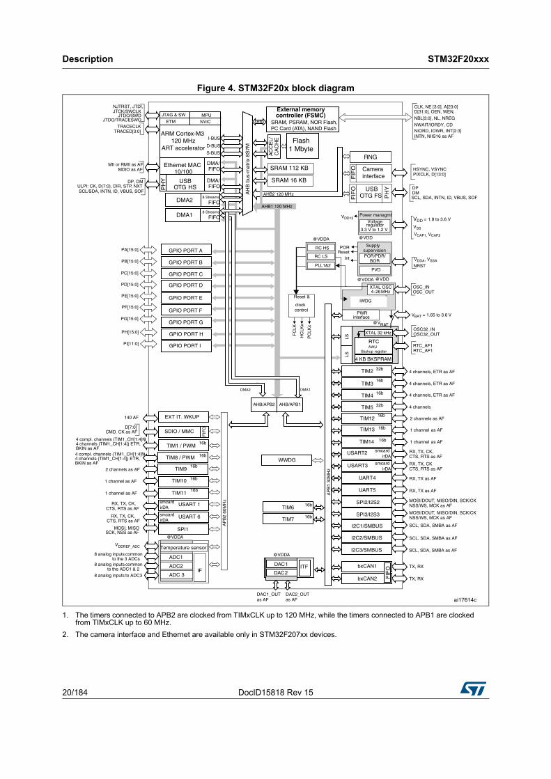
The STM32F20x family is based on the high-performance ARM® Cortex®-M3 32-bit RISC core operating at a frequency of up to 120 MHz. The family incorporates high-speed embedded memories (Flash memory up to 1 Mbyte, up to 128 Kbytes of system SRAM), up to 4 Kbytes of backup SRAM, and an extensive range of enhanced I/Os and peripherals connected to two APB buses, three AHB buses and a 32-bit multi-AHB bus matrix.
The devices also feature an adaptive real-time memory accelerator (ART Accelerator™) that allows to achieve a performance equivalent to 0 wait state program execution from Flash memory at a CPU frequency up to 120 MHz. This performance has been validated using the CoreMark® benchmark.
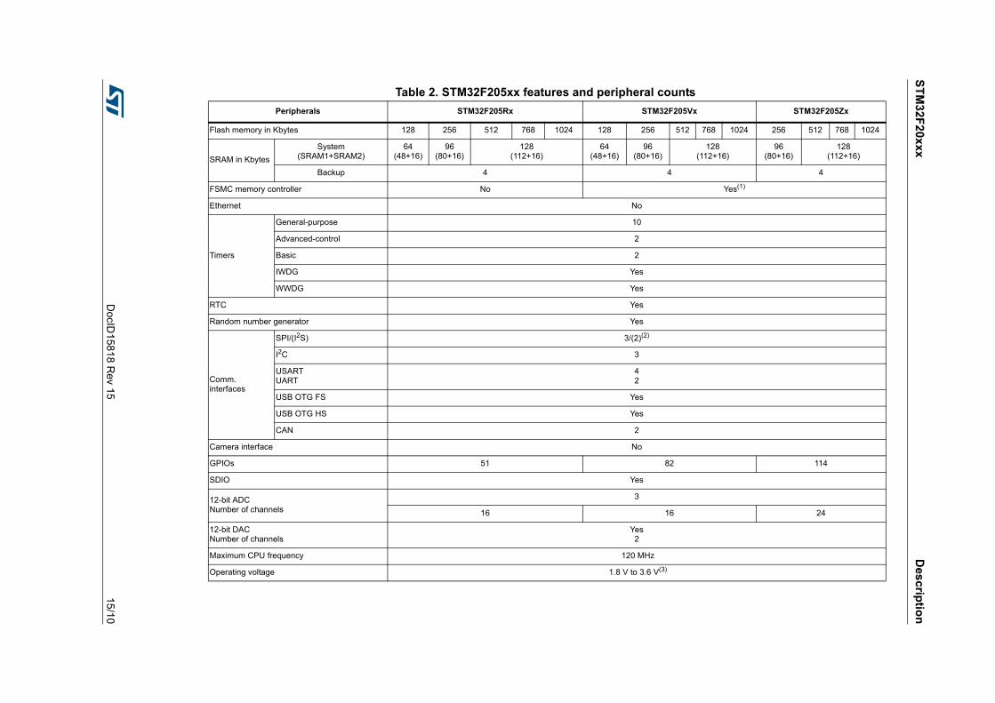
All devices offer three 12-bit ADCs, two DACs, a low-power RTC, twelve general-purpose 16-bit timers including two PWM timers for motor control, two general-purpose 32-bit timers. a true number random generator (RNG). They also feature standard and advanced communication interfaces. New advanced peripherals include an SDIO, an enhanced flexible static memory control (FSMC) interface (for devices offered in packages of 100 pins and more), and a camera interface for CMOS sensors. The devices also feature standard peripherals.
• Up to three I2Cs
• Three SPIs, two I2Ss. To achieve audio class accuracy, the I2S peripherals can be clocked via a dedicated internal audio PLL or via an external PLL to allow synchronization.
• Four USARTs and two UARTs
• A USB OTG high-speed with full-speed capability (with the ULPI)
• A second USB OTG (full-speed)
• Two CANs
• An SDIO interface
• Ethernet and camera interface available on STM32F207xx devices only.
Note: The STM32F205xx and STM32F207xx devices operate in the –40 to +105 °C temperature range from a 1.8 V to 3.6 V power supply. On devices in WLCSP64+2 package, if IRROFF is set to VDD, the supply voltage can drop to 1.7 V when the device operates in the 0 to 70 °C temperature range using an external power supply supervisor (see Section 3.16).
A comprehensive set of power-saving modes allow the design of low-power applications.
STM32F205xx and STM32F207xx devices are offered in various packages ranging from 64 pins to 176 pins. The set of included peripherals changes with the device chosen.These features make the STM32F205xx and STM32F207xx microcontroller family suitable for a wide range of applications:
• Motor drive and application control
• Medical equipment
• Industrial applications: PLC, inverters, circuit breakers
• Printers, and scanners
• Alarm systems, video intercom, and HVAC
• Home audio appliances
Figure 4 shows the general block diagram of the device family.
ST
M3
2F2
0xxx
Des
crip
tion
DocID
15818 R
ev 1515
/10
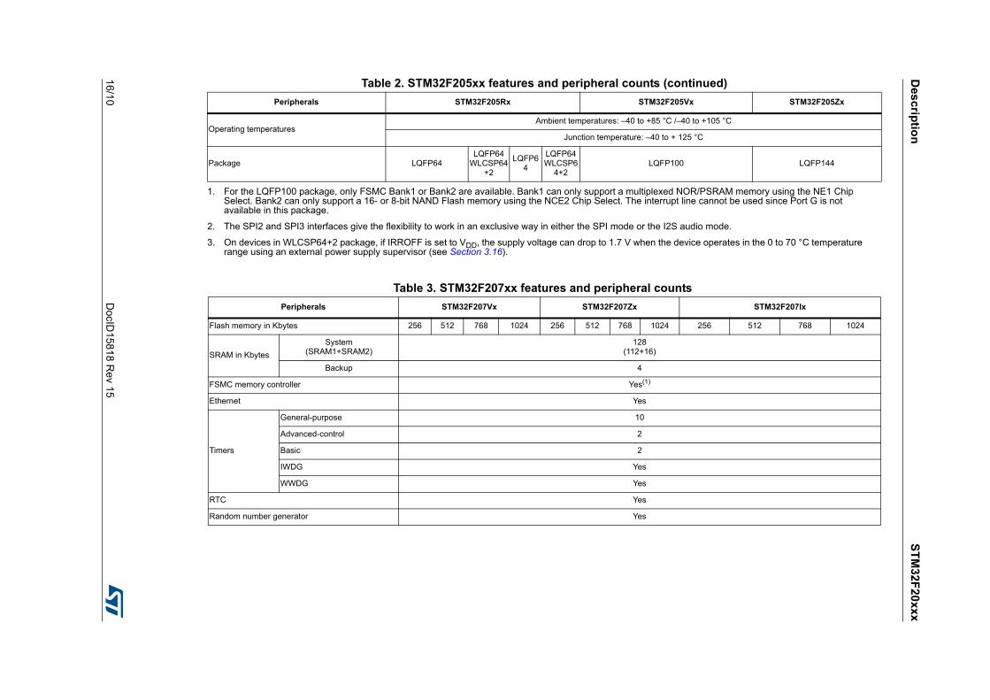
Table 2. STM32F205xx features and peripheral counts
Peripherals STM32F205Rx STM32F205Vx STM32F205Zx
Flash memory in Kbytes 128 256 512 768 1024 128 256 512 768 1024 256 512 768 1024
SRAM in Kbytes
System(SRAM1+SRAM2)
64(48+16)
96(80+16)
128(112+16)
64(48+16)
96(80+16)
128(112+16)
96(80+16)
128 (112+16)
Backup 4 4 4
FSMC memory controller No Yes(1)
Ethernet No
Timers
General-purpose 10
Advanced-control 2
Basic 2
IWDG Yes
WWDG Yes
RTC Yes
Random number generator Yes
Comm. interfaces
SPI/(I2S) 3/(2)(2)
I2C 3
USART UART
42
USB OTG FS Yes
USB OTG HS Yes
CAN 2
Camera interface No
GPIOs 51 82 114
SDIO Yes
12-bit ADC Number of channels
3
16 16 24
12-bit DAC Number of channels
Yes2
Maximum CPU frequency 120 MHz
Operating voltage 1.8 V to 3.6 V(3)
Des
criptio
nS
TM
32F
20xx
x
16/1
0D
ocID158
18 Rev 15
Operating temperaturesAmbient temperatures: –40 to +85 °C /–40 to +105 °C
Junction temperature: –40 to + 125 °C
Package LQFP64LQFP64
WLCSP64+2
LQFP64
LQFP64WLCSP6
4+2LQFP100 LQFP144
1. For the LQFP100 package, only FSMC Bank1 or Bank2 are available. Bank1 can only support a multiplexed NOR/PSRAM memory using the NE1 Chip Select. Bank2 can only support a 16- or 8-bit NAND Flash memory using the NCE2 Chip Select. The interrupt line cannot be used since Port G is not available in this package.
2. The SPI2 and SPI3 interfaces give the flexibility to work in an exclusive way in either the SPI mode or the I2S audio mode.
3. On devices in WLCSP64+2 package, if IRROFF is set to VDD, the supply voltage can drop to 1.7 V when the device operates in the 0 to 70 °C temperature range using an external power supply supervisor (see Section 3.16).
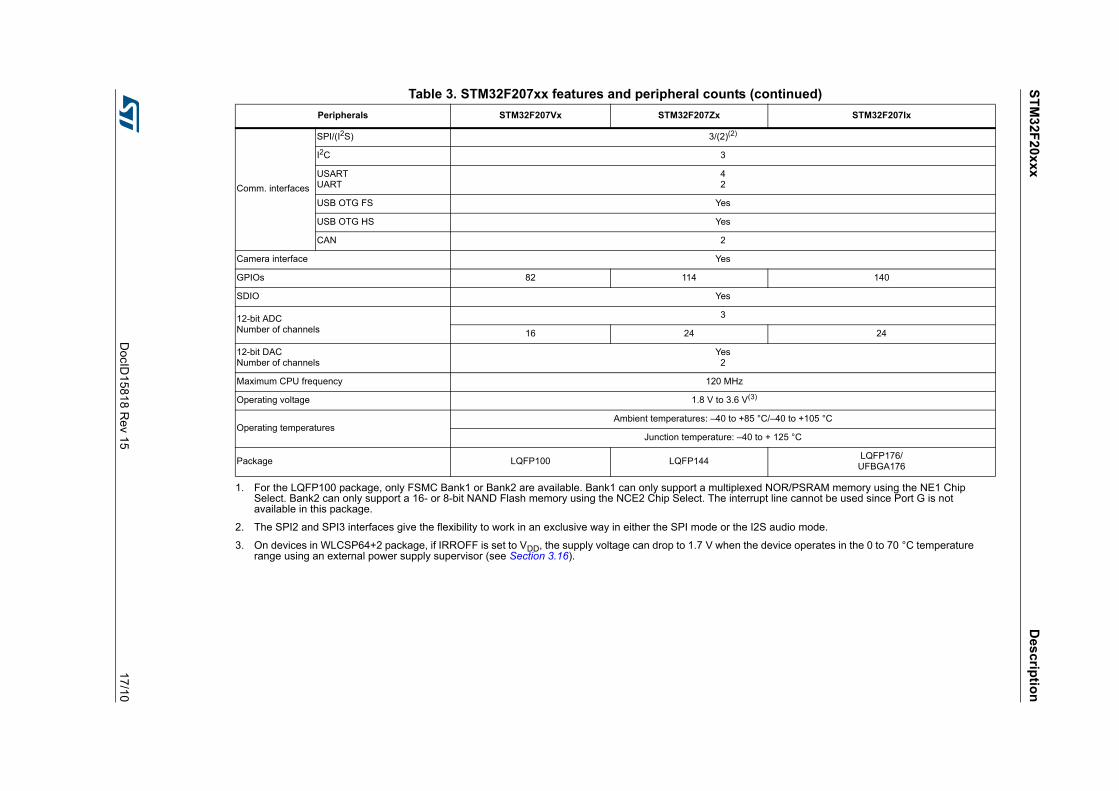
Table 3. STM32F207xx features and peripheral counts
Peripherals STM32F207Vx STM32F207Zx STM32F207Ix
Flash memory in Kbytes 256 512 768 1024 256 512 768 1024 256 512 768 1024
SRAM in Kbytes
System(SRAM1+SRAM2)
128 (112+16)
Backup 4
FSMC memory controller Yes(1)
Ethernet Yes
Timers
General-purpose 10
Advanced-control 2
Basic 2
IWDG Yes
WWDG Yes
RTC Yes
Random number generator Yes
Table 2. STM32F205xx features and peripheral counts (continued)
Peripherals STM32F205Rx STM32F205Vx STM32F205Zx
ST
M3
2F2
0xxx
Des
crip
tion
DocID
15818 R
ev 1517
/10
Comm. interfaces
SPI/(I2S) 3/(2)(2)
I2C 3
USART UART
42
USB OTG FS Yes
USB OTG HS Yes
CAN 2
Camera interface Yes
GPIOs 82 114 140
SDIO Yes
12-bit ADC Number of channels
3
16 24 24
12-bit DAC Number of channels
Yes2
Maximum CPU frequency 120 MHz
Operating voltage 1.8 V to 3.6 V(3)
Operating temperaturesAmbient temperatures: –40 to +85 °C/–40 to +105 °C
Junction temperature: –40 to + 125 °C
Package LQFP100 LQFP144LQFP176/
UFBGA176
1. For the LQFP100 package, only FSMC Bank1 or Bank2 are available. Bank1 can only support a multiplexed NOR/PSRAM memory using the NE1 Chip Select. Bank2 can only support a 16- or 8-bit NAND Flash memory using the NCE2 Chip Select. The interrupt line cannot be used since Port G is not available in this package.
2. The SPI2 and SPI3 interfaces give the flexibility to work in an exclusive way in either the SPI mode or the I2S audio mode.
3. On devices in WLCSP64+2 package, if IRROFF is set to VDD, the supply voltage can drop to 1.7 V when the device operates in the 0 to 70 °C temperature range using an external power supply supervisor (see Section 3.16).
Table 3. STM32F207xx features and peripheral counts (continued)
Peripherals STM32F207Vx STM32F207Zx STM32F207Ix
Description STM32F20xxx
18/184 DocID15818 Rev 15
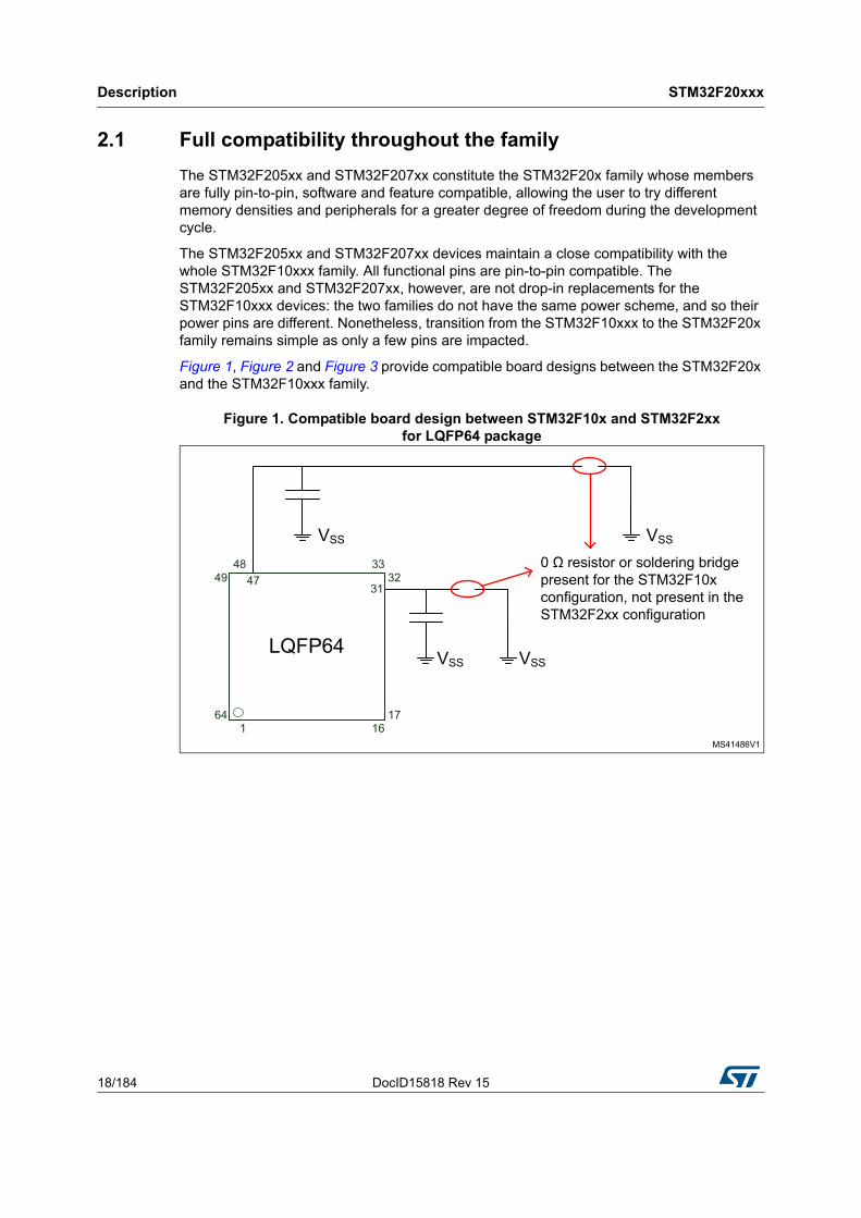
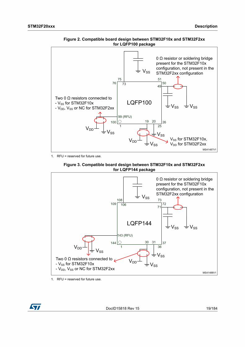
2.1 Full compatibility throughout the family
The STM32F205xx and STM32F207xx constitute the STM32F20x family whose members are fully pin-to-pin, software and feature compatible, allowing the user to try different memory densities and peripherals for a greater degree of freedom during the development cycle.
The STM32F205xx and STM32F207xx devices maintain a close compatibility with the whole STM32F10xxx family. All functional pins are pin-to-pin compatible. The STM32F205xx and STM32F207xx, however, are not drop-in replacements for the STM32F10xxx devices: the two families do not have the same power scheme, and so their power pins are different. Nonetheless, transition from the STM32F10xxx to the STM32F20x family remains simple as only a few pins are impacted.
Figure 1, Figure 2 and Figure 3 provide compatible board designs between the STM32F20x and the STM32F10xxx family.
Figure 1. Compatible board design between STM32F10x and STM32F2xxfor LQFP64 package
DocID15818 Rev 15 19/184
STM32F20xxx Description
183
Figure 2. Compatible board design between STM32F10x and STM32F2xxfor LQFP100 package
1. RFU = reserved for future use.
Figure 3. Compatible board design between STM32F10x and STM32F2xxfor LQFP144 package
1. RFU = reserved for future use.
Description STM32F20xxx
20/184 DocID15818 Rev 15
Figure 4. STM32F20x block diagram
1. The timers connected to APB2 are clocked from TIMxCLK up to 120 MHz, while the timers connected to APB1 are clocked from TIMxCLK up to 60 MHz.
2. The camera interface and Ethernet are available only in STM32F207xx devices.
DocID15818 Rev 15 21/184
STM32F20xxx Functional overview
183
3 Functional overview
3.1 ARM® Cortex®-M3 core with embedded Flash and SRAM
The ARM® Cortex®-M3 processor is the latest generation of ARM processors for embedded systems. It was developed to provide a low-cost platform that meets the needs of MCU implementation, with a reduced pin count and low-power consumption, while delivering outstanding computational performance and an advanced response to interrupts.
The ARM® Cortex®-M3 32-bit RISC processor features exceptional code-efficiency, delivering the high-performance expected from an ARM core in the memory size usually associated with 8- and 16-bit devices.
With its embedded ARM® core, the STM32F20x family is compatible with all ARM® tools and software.
Figure 4 shows the general block diagram of the STM32F20x family.
3.2 Adaptive real-time memory accelerator (ART Accelerator™)
The ART Accelerator™ is a memory accelerator which is optimized for STM32 industry-standard ARM® Cortex®-M3 processors. It balances the inherent performance advantage of the ARM® Cortex®-M3 over Flash memory technologies, which normally requires the processor to wait for the Flash memory at higher operating frequencies.
To release the processor full 150 DMIPS performance at this frequency, the accelerator implements an instruction prefetch queue and branch cache which increases program execution speed from the 128-bit Flash memory. Based on CoreMark® benchmark, the performance achieved thanks to the ART accelerator is equivalent to 0 wait state program execution from Flash memory at a CPU frequency up to 120 MHz.
3.3 Memory protection unit
The memory protection unit (MPU) is used to manage the CPU accesses to memory to prevent one task to accidentally corrupt the memory or resources used by any other active task. This memory area is organized into up to 8 protected areas that can in turn be divided up into 8 subareas. The protection area sizes are between 32 bytes and the whole 4 gigabytes of addressable memory.
The MPU is especially helpful for applications where some critical or certified code has to be protected against the misbehavior of other tasks. It is usually managed by an RTOS (real-time operating system). If a program accesses a memory location that is prohibited by the MPU, the RTOS can detect it and take action. In an RTOS environment, the kernel can dynamically update the MPU area setting, based on the process to be executed.
The MPU is optional and can be bypassed for applications that do not need it.
Functional overview STM32F20xxx
22/184 DocID15818 Rev 15
3.4 Embedded Flash memory
The STM32F20x devices embed a 128-bit wide Flash memory of 128 Kbytes, 256 Kbytes, 512 Kbytes, 768 Kbytes or 1 Mbyte available for storing programs and data.
The devices also feature 512 bytes of OTP memory that can be used to store critical user data such as Ethernet MAC addresses or cryptographic keys.
3.5 CRC (cyclic redundancy check) calculation unit
The CRC (cyclic redundancy check) calculation unit is used to get a CRC code from a 32-bit data word and a fixed generator polynomial.
Among other applications, CRC-based techniques are used to verify data transmission or storage integrity. In the scope of the EN/IEC 60335-1 standard, they offer a means of verifying the Flash memory integrity. The CRC calculation unit helps compute a software signature during runtime, to be compared with a reference signature generated at link-time and stored at a given memory location.
3.6 Embedded SRAM
All STM32F20x products embed:
• Up to 128 Kbytes of system SRAM accessed (read/write) at CPU clock speed with 0 wait states
• 4 Kbytes of backup SRAM.
The content of this area is protected against possible unwanted write accesses, and is retained in Standby or VBAT mode.
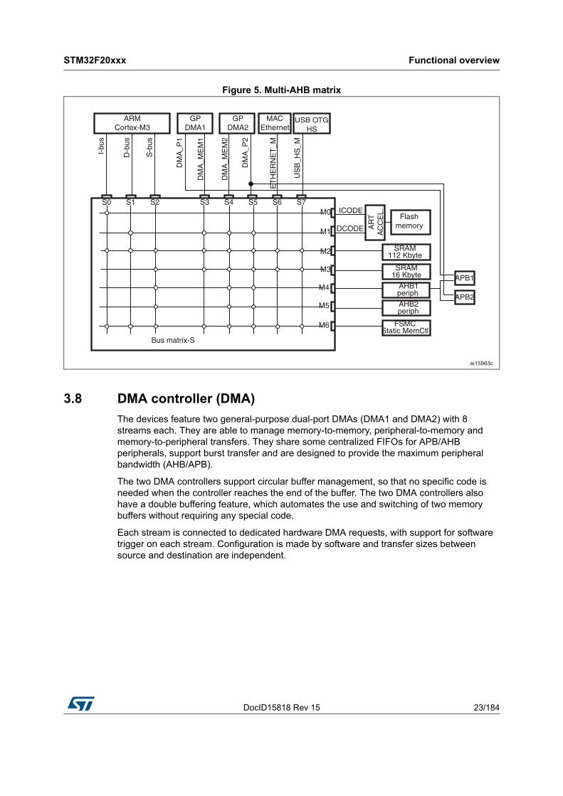
3.7 Multi-AHB bus matrix
The 32-bit multi-AHB bus matrix interconnects all the masters (CPU, DMAs, Ethernet, USB HS) and the slaves (Flash memory, RAM, FSMC, AHB and APB peripherals) and ensures a seamless and efficient operation even when several high-speed peripherals work simultaneously.
DocID15818 Rev 15 23/184
STM32F20xxx Functional overview
183
Figure 5. Multi-AHB matrix
3.8 DMA controller (DMA)
The devices feature two general-purpose dual-port DMAs (DMA1 and DMA2) with 8 streams each. They are able to manage memory-to-memory, peripheral-to-memory and memory-to-peripheral transfers. They share some centralized FIFOs for APB/AHB peripherals, support burst transfer and are designed to provide the maximum peripheral bandwidth (AHB/APB).
The two DMA controllers support circular buffer management, so that no specific code is needed when the controller reaches the end of the buffer. The two DMA controllers also have a double buffering feature, which automates the use and switching of two memory buffers without requiring any special code.
Each stream is connected to dedicated hardware DMA requests, with support for software trigger on each stream. Configuration is made by software and transfer sizes between source and destination are independent.
Functional overview STM32F20xxx
24/184 DocID15818 Rev 15
The DMA can be used with the main peripherals:
• SPI and I2S
• I2C
• USART and UART
• General-purpose, basic and advanced-control timers TIMx
• DAC
• SDIO
• Camera interface (DCMI)
• ADC.
3.9 Flexible static memory controller (FSMC)
The FSMC is embedded in all STM32F20x devices. It has four Chip Select outputs supporting the following modes: PC Card/Compact Flash, SRAM, PSRAM, NOR Flash and NAND Flash.
Functionality overview:
• Write FIFO
• Code execution from external memory except for NAND Flash and PC Card
• Maximum frequency (fHCLK) for external access is 60 MHz
LCD parallel interface
The FSMC can be configured to interface seamlessly with most graphic LCD controllers. It supports the Intel 8080 and Motorola 6800 modes, and is flexible enough to adapt to specific LCD interfaces. This LCD parallel interface capability makes it easy to build cost-effective graphic applications using LCD modules with embedded controllers or high performance solutions using external controllers with dedicated acceleration.
3.10 Nested vectored interrupt controller (NVIC)
The STM32F20x devices embed a nested vectored interrupt controller able to manage 16 priority levels, and handle up to 81 maskable interrupt channels plus the 16 interrupt lines of the Cortex®-M3.
The NVIC main features are the following:
• Closely coupled NVIC gives low-latency interrupt processing
• Interrupt entry vector table address passed directly to the core
• Closely coupled NVIC core interface
• Allows early processing of interrupts
• Processing of late arriving, higher-priority interrupts
• Support tail chaining
• Processor state automatically saved
• Interrupt entry restored on interrupt exit with no instruction overhead
This hardware block provides flexible interrupt management features with minimum interrupt latency.
DocID15818 Rev 15 25/184
STM32F20xxx Functional overview
183
3.11 External interrupt/event controller (EXTI)
The external interrupt/event controller consists of 23 edge-detector lines used to generate interrupt/event requests. Each line can be independently configured to select the trigger event (rising edge, falling edge, both) and can be masked independently. A pending register maintains the status of the interrupt requests. The EXTI can detect an external line with a pulse width shorter than the Internal APB2 clock period. Up to 140 GPIOs can be connected to the 16 external interrupt lines.
3.12 Clocks and startup
On reset the 16 MHz internal RC oscillator is selected as the default CPU clock. The 16 MHz internal RC oscillator is factory-trimmed to offer 1% accuracy. The application can then select as system clock either the RC oscillator or an external 4-26 MHz clock source. This clock is monitored for failure. If failure is detected, the system automatically switches back to the internal RC oscillator and a software interrupt is generated (if enabled). Similarly, full interrupt management of the PLL clock entry is available when necessary (for example if an indirectly used external oscillator fails).
The advanced clock controller clocks the core and all peripherals using a single crystal or oscillator. In particular, the ethernet and USB OTG FS peripherals can be clocked by the system clock.
Several prescalers and PLLs allow the configuration of the three AHB buses, the high-speed APB (APB2) and the low-speed APB (APB1) domains. The maximum frequency of the three AHB buses is 120 MHz and the maximum frequency the high-speed APB domains is 60 MHz. The maximum allowed frequency of the low-speed APB domain is 30 MHz.
The devices embed a dedicate PLL (PLLI2S) that allow them to achieve audio class performance. In this case, the I2S master clock can generate all standard sampling frequencies from 8 kHz to 192 kHz.
3.13 Boot modes
At startup, boot pins are used to select one out of three boot options:
• Boot from user Flash
• Boot from system memory
• Boot from embedded SRAM
The boot loader is located in system memory. It is used to reprogram the Flash memory by using USART1 (PA9/PA10), USART3 (PC10/PC11 or PB10/PB11), CAN2 (PB5/PB13), USB OTG FS in Device mode (PA11/PA12) through DFU (device firmware upgrade).
3.14 Power supply schemes
• VDD = 1.8 to 3.6 V: external power supply for I/Os and the internal regulator (when enabled), provided externally through VDD pins. On devices in WLCSP64+2 package, if IRROFF is set to VDD, the supply voltage can drop to 1.7 V when the device operates
Functional overview STM32F20xxx
26/184 DocID15818 Rev 15
in the 0 to 70 °C temperature range using an external power supply supervisor (see Section 3.16).
• VSSA, VDDA = 1.8 to 3.6 V: external analog power supplies for ADC, DAC, Reset blocks, RCs and PLL. VDDA and VSSA must be connected to VDD and VSS, respectively.
• VBAT = 1.65 to 3.6 V: power supply for RTC, external clock, 32 kHz oscillator and backup registers (through power switch) when VDD is not present.
Refer to Figure 19: Power supply scheme for more details.
3.15 Power supply supervisor
The devices have an integrated power-on reset (POR) / power-down reset (PDR) circuitry coupled with a Brownout reset (BOR) circuitry.
At power-on, POR/PDR is always active and ensures proper operation starting from 1.8 V. After the 1.8 V POR threshold level is reached, the option byte loading process starts, either to confirm or modify default BOR threshold levels, or to disable BOR permanently. Three BOR thresholds are available through option bytes.
The device remains in reset mode when VDD is below a specified threshold, VPOR/PDR or VBOR, without the need for an external reset circuit. On devices in WLCSP64+2 package, the BOR, POR and PDR features can be disabled by setting IRROFF pin to VDD. In this mode an external power supply supervisor is required (see Section 3.16).
The devices also feature an embedded programmable voltage detector (PVD) that monitors the VDD/VDDA power supply and compares it to the VPVD threshold. An interrupt can be generated when VDD/VDDA drops below the VPVD threshold and/or when VDD/VDDA is higher than the VPVD threshold. The interrupt service routine can then generate a warning message and/or put the MCU into a safe state. The PVD is enabled by software.
3.16 Voltage regulator
The regulator has five operating modes:
• Regulator ON
– Main regulator mode (MR)
– Low-power regulator (LPR)
– Power-down
• Regulator OFF
– Regulator OFF/internal reset ON
– Regulator OFF/internal reset OFF
3.16.1 Regulator ON
The regulator ON modes are activated by default on LQFP packages.On WLCSP64+2 package, they are activated by connecting both REGOFF and IRROFF pins to VSS, while only REGOFF must be connected to VSS on UFBGA176 package (IRROFF is not available).
VDD minimum value is 1.8 V.
DocID15818 Rev 15 27/184
STM32F20xxx Functional overview
183
There are three power modes configured by software when the regulator is ON:
• MR is used in the nominal regulation mode
• LPR is used in Stop modes
The LP regulator mode is configured by software when entering Stop mode.
• Power-down is used in Standby mode.
The Power-down mode is activated only when entering Standby mode. The regulator output is in high impedance and the kernel circuitry is powered down, inducing zero consumption. The contents of the registers and SRAM are lost).
Two external ceramic capacitors should be connected on VCAP_1 and VCAP_2 pin. Refer to Figure 19: Power supply scheme and Table 16: VCAP1/VCAP2 operating conditions.
All packages have the regulator ON feature.
3.16.2 Regulator OFF
This feature is available only on packages featuring the REGOFF pin. The regulator is disabled by holding REGOFF high. The regulator OFF mode allows to supply externally a V12 voltage source through VCAP_1 and VCAP_2 pins.
The two 2.2 µF ceramic capacitors should be replaced by two 100 nF decoupling capacitors. Refer to Figure 19: Power supply scheme.
When the regulator is OFF, there is no more internal monitoring on V12. An external power supply supervisor should be used to monitor the V12 of the logic power domain. PA0 pin should be used for this purpose, and act as power-on reset on V12 power domain.
In regulator OFF mode, the following features are no more supported:
• PA0 cannot be used as a GPIO pin since it allows to reset the part of the 1.2 V logic power domain which is not reset by the NRST pin.
• As long as PA0 is kept low, the debug mode cannot be used at power-on reset. As a consequence, PA0 and NRST pins must be managed separately if the debug connection at reset or pre-reset is required.
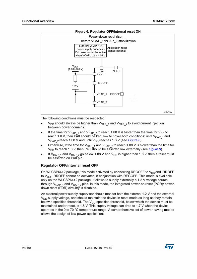
Regulator OFF/internal reset ON
On WLCSP64+2 package, this mode is activated by connecting REGOFF pin to VDD and IRROFF pin to VSS. On UFBGA176 package, only REGOFF must be connected to VDD (IRROFF not available). In this mode, VDD/VDDA minimum value is 1.8 V.
The regulator OFF/internal reset ON mode allows to supply externally a 1.2 V voltage source through VCAP_1 and VCAP_2 pins, in addition to VDD.
Functional overview STM32F20xxx
28/184 DocID15818 Rev 15
Figure 6. Regulator OFF/internal reset ON
The following conditions must be respected:
• VDD should always be higher than VCAP_1 and VCAP_2 to avoid current injection between power domains.
• If the time for VCAP_1 and VCAP_2 to reach 1.08 V is faster than the time for VDD to reach 1.8 V, then PA0 should be kept low to cover both conditions: until VCAP_1 and VCAP_2 reach 1.08 V and until VDD reaches 1.8 V (see Figure 8).
• Otherwise, If the time for VCAP_1 and VCAP_2 to reach 1.08 V is slower than the time for VDD to reach 1.8 V, then PA0 should be asserted low externally (see Figure 9).
• If VCAP_1 and VCAP_2 go below 1.08 V and VDD is higher than 1.8 V, then a reset must be asserted on PA0 pin.
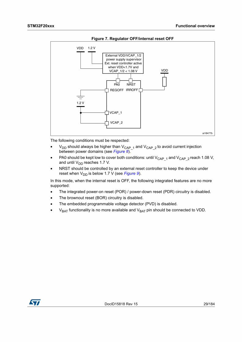
Regulator OFF/internal reset OFF
On WLCSP64+2 package, this mode activated by connecting REGOFF to VSS and IRROFF to VDD. IRROFF cannot be activated in conjunction with REGOFF. This mode is available only on the WLCSP64+2 package. It allows to supply externally a 1.2 V voltage source through VCAP_1 and VCAP_2 pins. In this mode, the integrated power-on reset (POR)/ power-down reset (PDR) circuitry is disabled.
An external power supply supervisor should monitor both the external 1.2 V and the external VDD supply voltage, and should maintain the device in reset mode as long as they remain below a specified threshold. The VDD specified threshold, below which the device must be maintained under reset, is 1.8 V. This supply voltage can drop to 1.7 V when the device operates in the 0 to 70 °C temperature range. A comprehensive set of power-saving modes allows the design of low-power applications.
DocID15818 Rev 15 29/184
STM32F20xxx Functional overview
183
Figure 7. Regulator OFF/internal reset OFF
The following conditions must be respected:
• VDD should always be higher than VCAP_1 and VCAP_2 to avoid current injection between power domains (see Figure 8).
• PA0 should be kept low to cover both conditions: until VCAP_1 and VCAP_2 reach 1.08 V, and until VDD reaches 1.7 V.
• NRST should be controlled by an external reset controller to keep the device under reset when VDD is below 1.7 V (see Figure 9).
In this mode, when the internal reset is OFF, the following integrated features are no more supported:
• The integrated power-on reset (POR) / power-down reset (PDR) circuitry is disabled.
• The brownout reset (BOR) circuitry is disabled.
• The embedded programmable voltage detector (PVD) is disabled.
• VBAT functionality is no more available and VBAT pin should be connected to VDD.
Functional overview STM32F20xxx
30/184 DocID15818 Rev 15
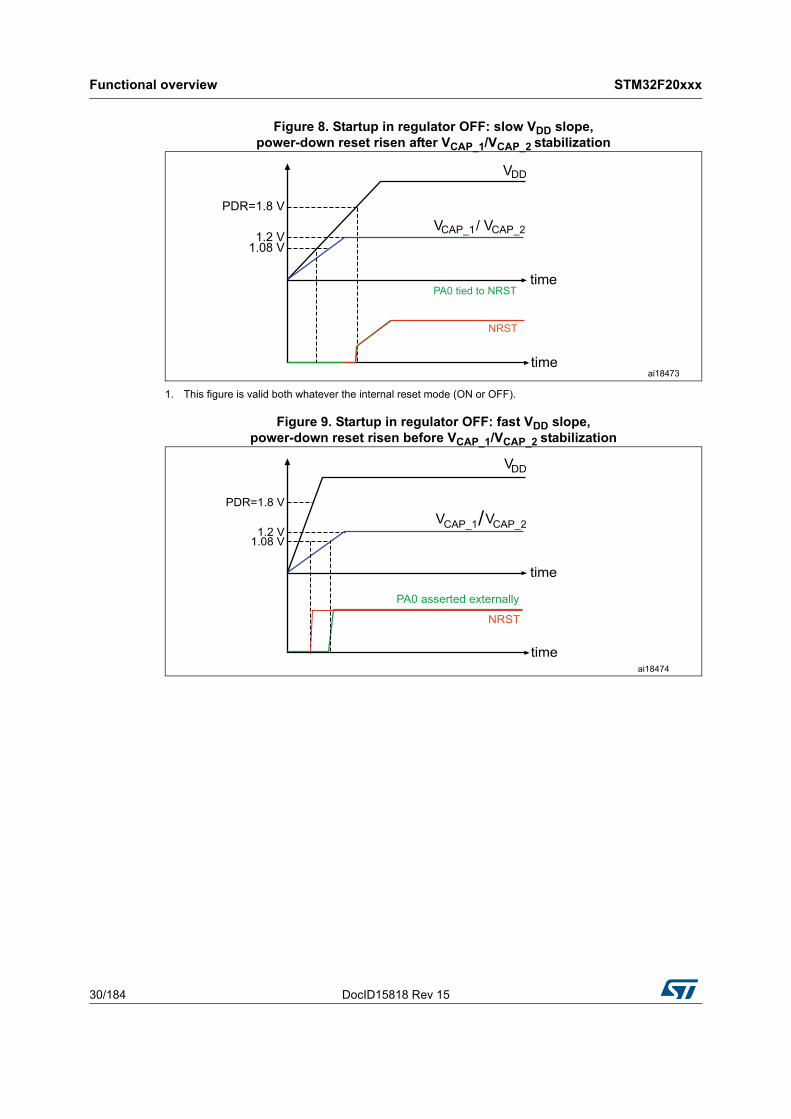
Figure 8. Startup in regulator OFF: slow VDD slope,power-down reset risen after VCAP_1/VCAP_2 stabilization
1. This figure is valid both whatever the internal reset mode (ON or OFF).
Figure 9. Startup in regulator OFF: fast VDD slope,power-down reset risen before VCAP_1/VCAP_2 stabilization
DocID15818 Rev 15 31/184
STM32F20xxx Functional overview
183
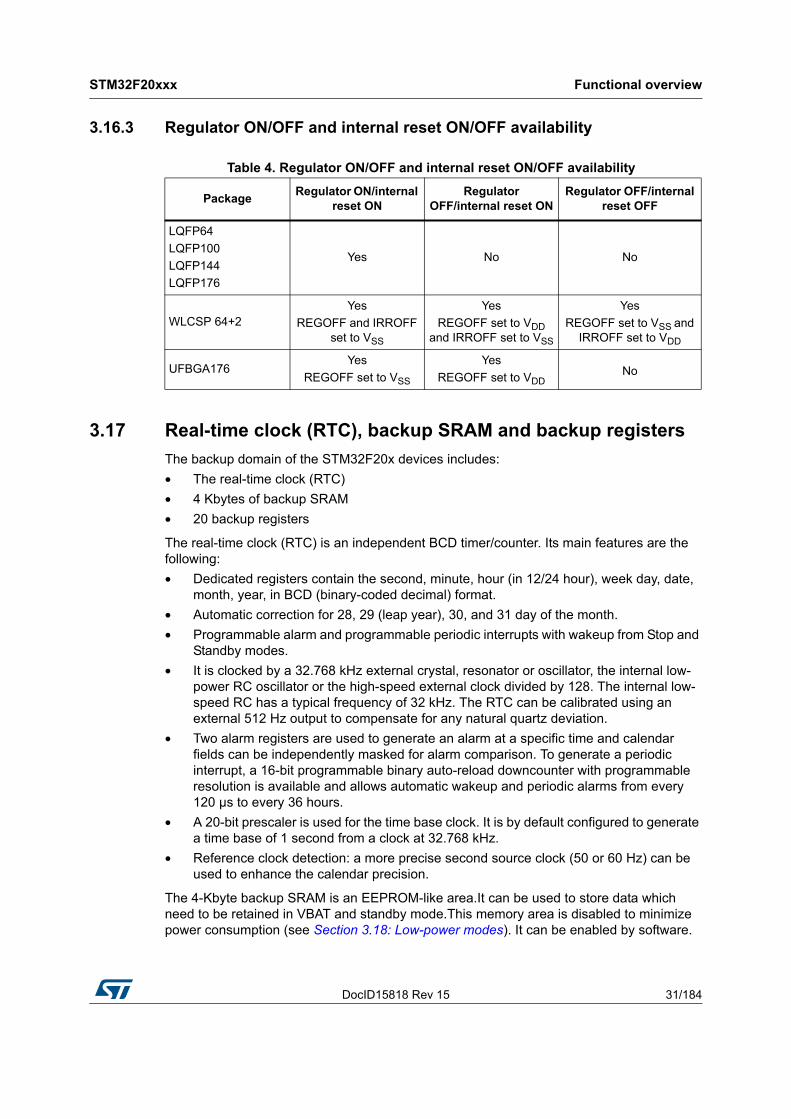
3.16.3 Regulator ON/OFF and internal reset ON/OFF availability
3.17 Real-time clock (RTC), backup SRAM and backup registers
The backup domain of the STM32F20x devices includes:
• The real-time clock (RTC)
• 4 Kbytes of backup SRAM
• 20 backup registers
The real-time clock (RTC) is an independent BCD timer/counter. Its main features are the following:
• Dedicated registers contain the second, minute, hour (in 12/24 hour), week day, date, month, year, in BCD (binary-coded decimal) format.
• Automatic correction for 28, 29 (leap year), 30, and 31 day of the month.
• Programmable alarm and programmable periodic interrupts with wakeup from Stop and Standby modes.
• It is clocked by a 32.768 kHz external crystal, resonator or oscillator, the internal low-power RC oscillator or the high-speed external clock divided by 128. The internal low-speed RC has a typical frequency of 32 kHz. The RTC can be calibrated using an external 512 Hz output to compensate for any natural quartz deviation.
• Two alarm registers are used to generate an alarm at a specific time and calendar fields can be independently masked for alarm comparison. To generate a periodic interrupt, a 16-bit programmable binary auto-reload downcounter with programmable resolution is available and allows automatic wakeup and periodic alarms from every 120 µs to every 36 hours.
• A 20-bit prescaler is used for the time base clock. It is by default configured to generate a time base of 1 second from a clock at 32.768 kHz.
• Reference clock detection: a more precise second source clock (50 or 60 Hz) can be used to enhance the calendar precision.
The 4-Kbyte backup SRAM is an EEPROM-like area.It can be used to store data which need to be retained in VBAT and standby mode.This memory area is disabled to minimize power consumption (see Section 3.18: Low-power modes). It can be enabled by software.
Table 4. Regulator ON/OFF and internal reset ON/OFF availability
PackageRegulator ON/internal
reset ONRegulator
OFF/internal reset ONRegulator OFF/internal
reset OFF
LQFP64
LQFP100
LQFP144
LQFP176
Yes No No
WLCSP 64+2Yes
REGOFF and IRROFF set to VSS
Yes
REGOFF set to VDD and IRROFF set to VSS
Yes
REGOFF set to VSS and IRROFF set to VDD
UFBGA176Yes
REGOFF set to VSS
Yes
REGOFF set to VDDNo
Functional overview STM32F20xxx
32/184 DocID15818 Rev 15
The backup registers are 32-bit registers used to store 80 bytes of user application data when VDD power is not present. Backup registers are not reset by a system, a power reset, or when the device wakes up from the Standby mode (see Section 3.18: Low-power modes).
Like backup SRAM, the RTC and backup registers are supplied through a switch that is powered either from the VDD supply when present or the VBAT pin.
3.18 Low-power modes
The STM32F20x family supports three low-power modes to achieve the best compromise between low-power consumption, short startup time and available wakeup sources:
• Sleep mode
In Sleep mode, only the CPU is stopped. All peripherals continue to operate and can wake up the CPU when an interrupt/event occurs.
• Stop mode
The Stop mode achieves the lowest power consumption while retaining the contents of SRAM and registers. All clocks in the 1.2 V domain are stopped, the PLL, the HSI RC and the HSE crystal oscillators are disabled. The voltage regulator can also be put either in normal or in low-power mode.
The device can be woken up from the Stop mode by any of the EXTI line. The EXTI line source can be one of the 16 external lines, the PVD output, the RTC alarm / wakeup / tamper / time stamp events, the USB OTG FS/HS wakeup or the Ethernet wakeup.
• Standby mode
The Standby mode is used to achieve the lowest power consumption. The internal voltage regulator is switched off so that the entire 1.2 V domain is powered off. The PLL, the HSI RC and the HSE crystal oscillators are also switched off. After entering Standby mode, the SRAM and register contents are lost except for registers in the backup domain and the backup SRAM when selected.
The device exits the Standby mode when an external reset (NRST pin), an IWDG reset, a rising edge on the WKUP pin, or an RTC alarm / wakeup / tamper /time stamp event occurs.
Note: The RTC, the IWDG, and the corresponding clock sources are not stopped when the device enters the Stop or Standby mode.
3.19 VBAT operation
The VBAT pin allows to power the device VBAT domain from an external battery or an external supercapacitor.
VBAT operation is activated when VDD is not present.
The VBAT pin supplies the RTC, the backup registers and the backup SRAM.
Note: When the microcontroller is supplied from VBAT, external interrupts and RTC alarm/events do not exit it from VBAT operation.
When using WLCSP64+2 package, if IRROFF pin is connected to VDD, the VBAT functionality is no more available and VBAT pin should be connected to VDD.
DocID15818 Rev 15 33/184
STM32F20xxx Functional overview
183
3.20 Timers and watchdogs
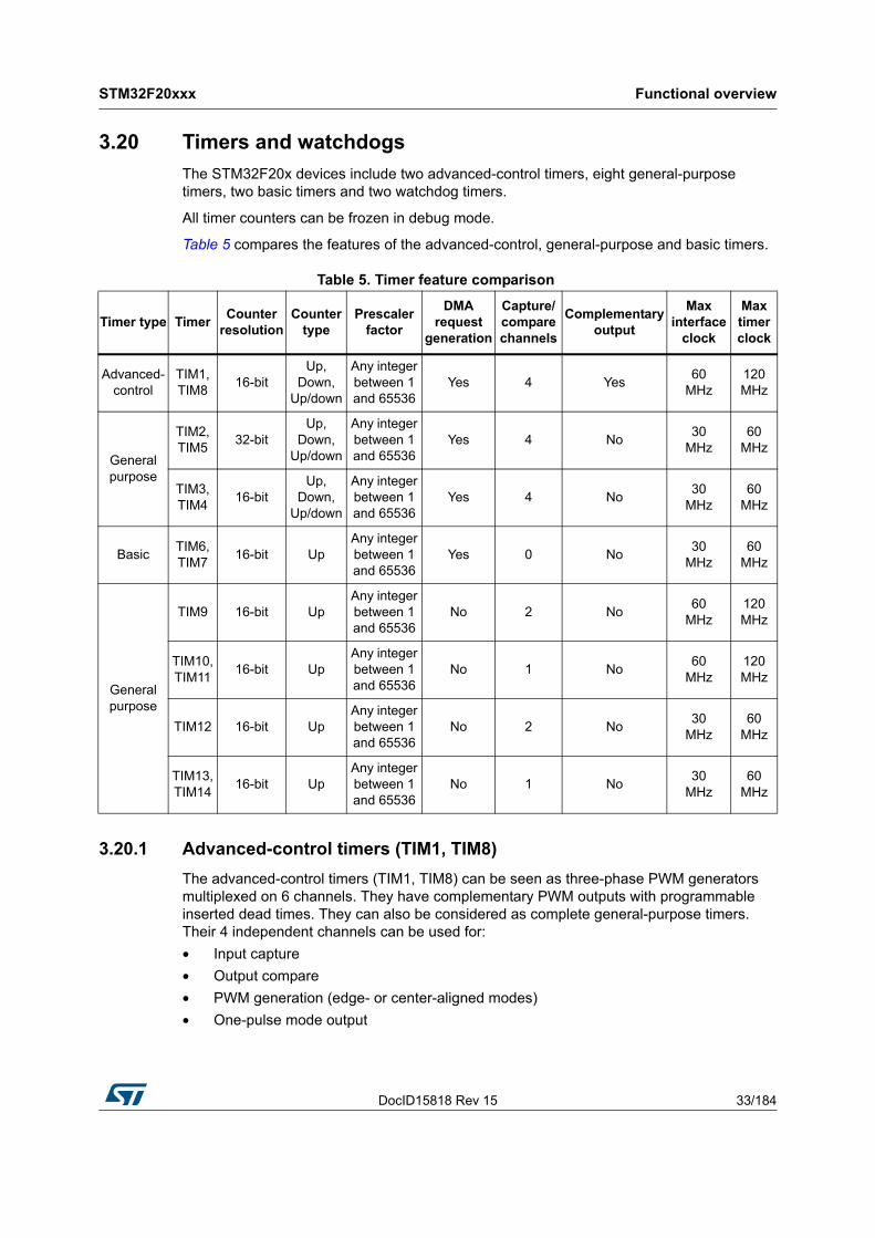
The STM32F20x devices include two advanced-control timers, eight general-purpose timers, two basic timers and two watchdog timers.
All timer counters can be frozen in debug mode.
Table 5 compares the features of the advanced-control, general-purpose and basic timers.
3.20.1 Advanced-control timers (TIM1, TIM8)
The advanced-control timers (TIM1, TIM8) can be seen as three-phase PWM generators multiplexed on 6 channels. They have complementary PWM outputs with programmable inserted dead times. They can also be considered as complete general-purpose timers. Their 4 independent channels can be used for:
• Input capture
• Output compare
• PWM generation (edge- or center-aligned modes)
• One-pulse mode output
Table 5. Timer feature comparison
Timer type TimerCounter
resolutionCounter
typePrescaler
factor
DMA request
generation
Capture/compare channels
Complementary output
Max interface
clock
Max timer clock
Advanced-control
TIM1, TIM8
16-bitUp,
Down, Up/down
Any integer between 1 and 65536
Yes 4 Yes60
MHz120 MHz
General purpose
TIM2, TIM5
32-bitUp,
Down, Up/down
Any integer between 1 and 65536
Yes 4 No30
MHz60
MHz
TIM3, TIM4
16-bitUp,
Down, Up/down
Any integer between 1 and 65536
Yes 4 No30
MHz60
MHz
BasicTIM6, TIM7
16-bit UpAny integer between 1 and 65536
Yes 0 No30
MHz60
MHz
General purpose
TIM9 16-bit UpAny integer between 1 and 65536
No 2 No60
MHz120 MHz
TIM10, TIM11
16-bit UpAny integer between 1 and 65536
No 1 No60
MHz120 MHz
TIM12 16-bit UpAny integer between 1 and 65536
No 2 No30
MHz60
MHz
TIM13, TIM14
16-bit UpAny integer between 1 and 65536
No 1 No30
MHz60
MHz
Functional overview STM32F20xxx
34/184 DocID15818 Rev 15
If configured as standard 16-bit timers, they have the same features as the general-purpose TIMx timers. If configured as 16-bit PWM generators, they have full modulation capability (0-100%).
The TIM1 and TIM8 counters can be frozen in debug mode. Many of the advanced-control timer features are shared with those of the standard TIMx timers which have the same architecture. The advanced-control timer can therefore work together with the TIMx timers via the Timer Link feature for synchronization or event chaining.
3.20.2 General-purpose timers (TIMx)
There are ten synchronizable general-purpose timers embedded in the STM32F20x devices (see Table 5 for differences).
TIM2, TIM3, TIM4, TIM5
The STM32F20x include 4 full-featured general-purpose timers. TIM2 and TIM5 are 32-bit timers, and TIM3 and TIM4 are 16-bit timers. The TIM2 and TIM5 timers are based on a 32-bit auto-reload up/downcounter and a 16-bit prescaler. The TIM3 and TIM4 timers are based on a 16-bit auto-reload up/downcounter and a 16-bit prescaler. They all feature 4 independent channels for input capture/output compare, PWM or one-pulse mode output. This gives up to 16 input capture/output compare/PWMs on the largest packages.
The TIM2, TIM3, TIM4, TIM5 general-purpose timers can work together, or with the other general-purpose timers and the advanced-control timers TIM1 and TIM8 via the Timer Link feature for synchronization or event chaining.
The counters of TIM2, TIM3, TIM4, TIM5 can be frozen in debug mode. Any of these general-purpose timers can be used to generate PWM outputs.
TIM2, TIM3, TIM4, TIM5 all have independent DMA request generation. They are capable of handling quadrature (incremental) encoder signals and the digital outputs from 1 to 4 hall-effect sensors.
TIM10, TIM11 and TIM9
These timers are based on a 16-bit auto-reload upcounter and a 16-bit prescaler. TIM10 and TIM11 feature one independent channel, whereas TIM9 has two independent channels for input capture/output compare, PWM or one-pulse mode output. They can be synchronized with the TIM2, TIM3, TIM4, TIM5 full-featured general-purpose timers. They can also be used as simple time bases.
TIM12, TIM13 and TIM14
These timers are based on a 16-bit auto-reload upcounter and a 16-bit prescaler. TIM13 and TIM14 feature one independent channel, whereas TIM12 has two independent channels for input capture/output compare, PWM or one-pulse mode output. They can be synchronized with the TIM2, TIM3, TIM4, TIM5 full-featured general-purpose timers.
They can also be used as simple time bases.
3.20.3 Basic timers TIM6 and TIM7
These timers are mainly used for DAC trigger and waveform generation. They can also be used as a generic 16-bit time base.
DocID15818 Rev 15 35/184
STM32F20xxx Functional overview
183
3.20.4 Independent watchdog
The independent watchdog is based on a 12-bit downcounter and 8-bit prescaler. It is clocked from an independent 32 kHz internal RC and as it operates independently from the main clock, it can operate in Stop and Standby modes. It can be used either as a watchdog to reset the device when a problem occurs, or as a free-running timer for application timeout management. It is hardware- or software-configurable through the option bytes. The counter can be frozen in debug mode.
3.20.5 Window watchdog
The window watchdog is based on a 7-bit downcounter that can be set as free-running. It can be used as a watchdog to reset the device when a problem occurs. It is clocked from the main clock. It has an early warning interrupt capability and the counter can be frozen in debug mode.
3.20.6 SysTick timer
This timer is dedicated to real-time operating systems, but could also be used as a standard downcounter. It features:
• A 24-bit downcounter
• Autoreload capability
• Maskable system interrupt generation when the counter reaches 0
• Programmable clock source
3.21 Inter-integrated circuit interface (I²C)
Up to three I2C bus interfaces can operate in multimaster and slave modes. They can support the Standard- and Fast-modes. They support the 7/10-bit addressing mode and the 7-bit dual addressing mode (as slave). A hardware CRC generation/verification is embedded.
They can be served by DMA and they support SMBus 2.0/PMBus.
3.22 Universal synchronous/asynchronous receiver transmitters (UARTs/USARTs)
The STM32F20x devices embed four universal synchronous/asynchronous receiver transmitters (USART1, USART2, USART3 and USART6) and two universal asynchronous receiver transmitters (UART4 and UART5).
These six interfaces provide asynchronous communication, IrDA SIR ENDEC support, multiprocessor communication mode, single-wire half-duplex communication mode and have LIN Master/Slave capability. The USART1 and USART6 interfaces are able to communicate at speeds of up to 7.5 Mbit/s. The other available interfaces communicate at up to 3.75 Mbit/s.
USART1, USART2, USART3 and USART6 also provide hardware management of the CTS and RTS signals, Smart Card mode (ISO 7816 compliant) and SPI-like communication capability. All interfaces can be served by the DMA controller.
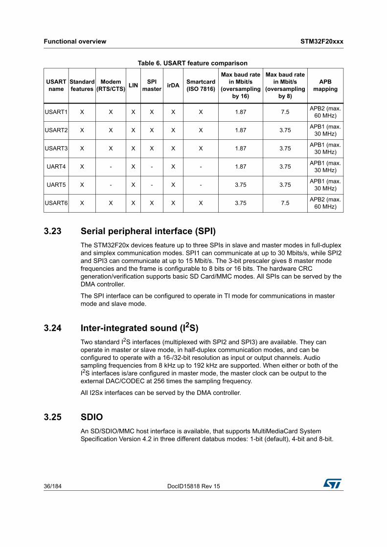
Functional overview STM32F20xxx
36/184 DocID15818 Rev 15
3.23 Serial peripheral interface (SPI)
The STM32F20x devices feature up to three SPIs in slave and master modes in full-duplex and simplex communication modes. SPI1 can communicate at up to 30 Mbits/s, while SPI2 and SPI3 can communicate at up to 15 Mbit/s. The 3-bit prescaler gives 8 master mode frequencies and the frame is configurable to 8 bits or 16 bits. The hardware CRC generation/verification supports basic SD Card/MMC modes. All SPIs can be served by the DMA controller.
The SPI interface can be configured to operate in TI mode for communications in master mode and slave mode.
3.24 Inter-integrated sound (I2S)
Two standard I2S interfaces (multiplexed with SPI2 and SPI3) are available. They can operate in master or slave mode, in half-duplex communication modes, and can be configured to operate with a 16-/32-bit resolution as input or output channels. Audio sampling frequencies from 8 kHz up to 192 kHz are supported. When either or both of the I2S interfaces is/are configured in master mode, the master clock can be output to the external DAC/CODEC at 256 times the sampling frequency.
All I2Sx interfaces can be served by the DMA controller.
3.25 SDIO
An SD/SDIO/MMC host interface is available, that supports MultiMediaCard System Specification Version 4.2 in three different databus modes: 1-bit (default), 4-bit and 8-bit.
Table 6. USART feature comparison
USART name
Standard features
Modem (RTS/CTS)
LINSPI
masterirDA
Smartcard (ISO 7816)
Max baud rate in Mbit/s
(oversampling by 16)
Max baud rate in Mbit/s
(oversampling by 8)
APB mapping
USART1 X X X X X X 1.87 7.5APB2 (max.
60 MHz)
USART2 X X X X X X 1.87 3.75APB1 (max.
30 MHz)
USART3 X X X X X X 1.87 3.75APB1 (max.
30 MHz)
UART4 X - X - X - 1.87 3.75APB1 (max.
30 MHz)
UART5 X - X - X - 3.75 3.75APB1 (max.
30 MHz)
USART6 X X X X X X 3.75 7.5APB2 (max.
60 MHz)
DocID15818 Rev 15 37/184
STM32F20xxx Functional overview
183
The interface allows data transfer at up to 48 MHz in 8-bit mode, and is compliant with the SD Memory Card Specification Version 2.0.
The SDIO Card Specification Version 2.0 is also supported with two different databus modes: 1-bit (default) and 4-bit.
The current version supports only one SD/SDIO/MMC4.2 card at any one time and a stack of MMC4.1 or previous.
In addition to SD/SDIO/MMC, this interface is fully compliant with the CE-ATA digital protocol Rev1.1.
3.26 Ethernet MAC interface with dedicated DMA and IEEE 1588 support
Peripheral available only on the STM32F207xx devices.
The STM32F207xx devices provide an IEEE-802.3-2002-compliant media access controller (MAC) for ethernet LAN communications through an industry-standard medium-independent interface (MII) or a reduced medium-independent interface (RMII). The STM32F207xx requires an external physical interface device (PHY) to connect to the physical LAN bus (twisted-pair, fiber, etc.). the PHY is connected to the STM32F207xx MII port using 17 signals for MII or 9 signals for RMII, and can be clocked using the 25 MHz (MII) or 50 MHz (RMII) output from the STM32F207xx.
The STM32F207xx includes the following features:
• Supports 10 and 100 Mbit/s rates
• Dedicated DMA controller allowing high-speed transfers between the dedicated SRAM and the descriptors (see the STM32F20x and STM32F21x reference manual for details)
• Tagged MAC frame support (VLAN support)
• Half-duplex (CSMA/CD) and full-duplex operation
• MAC control sublayer (control frames) support
• 32-bit CRC generation and removal
• Several address filtering modes for physical and multicast address (multicast and group addresses)
• 32-bit status code for each transmitted or received frame
• Internal FIFOs to buffer transmit and receive frames. The transmit FIFO and the receive FIFO are both 2 Kbytes, that is 4 Kbytes in total
• Supports hardware PTP (precision time protocol) in accordance with IEEE 1588 2008 (PTP V2) with the time stamp comparator connected to the TIM2 input
• Triggers interrupt when system time becomes greater than target time
3.27 Controller area network (CAN)
The two CANs are compliant with the 2.0A and B (active) specifications with a bitrate up to 1 Mbit/s. They can receive and transmit standard frames with 11-bit identifiers as well as extended frames with 29-bit identifiers. Each CAN has three transmit mailboxes, two receive FIFOS with 3 stages and 28 shared scalable filter banks (all of them can be used even if one
Functional overview STM32F20xxx
38/184 DocID15818 Rev 15
CAN is used). The 256 bytes of SRAM which are allocated for each CAN are not shared with any other peripheral.
3.28 Universal serial bus on-the-go full-speed (OTG_FS)
The devices embed an USB OTG full-speed device/host/OTG peripheral with integrated transceivers. The USB OTG FS peripheral is compliant with the USB 2.0 specification and with the OTG 1.0 specification. It has software-configurable endpoint setting and supports suspend/resume. The USB OTG full-speed controller requires a dedicated 48 MHz clock that is generated by a PLL connected to the HSE oscillator. The major features are:
• Combined Rx and Tx FIFO size of 320 × 35 bits with dynamic FIFO sizing
• Supports the session request protocol (SRP) and host negotiation protocol (HNP)
• 4 bidirectional endpoints
• 8 host channels with periodic OUT support
• HNP/SNP/IP inside (no need for any external resistor)
• For OTG/Host modes, a power switch is needed in case bus-powered devices are connected
• Internal FS OTG PHY support
3.29 Universal serial bus on-the-go high-speed (OTG_HS)
The STM32F20x devices embed a USB OTG high-speed (up to 480 Mb/s) device/host/OTG peripheral. The USB OTG HS supports both full-speed and high-speed operations. It integrates the transceivers for full-speed operation (12 MB/s) and features a UTMI low-pin interface (ULPI) for high-speed operation (480 MB/s). When using the USB OTG HS in HS mode, an external PHY device connected to the ULPI is required.
The USB OTG HS peripheral is compliant with the USB 2.0 specification and with the OTG 1.0 specification. It has software-configurable endpoint setting and supports suspend/resume. The USB OTG full-speed controller requires a dedicated 48 MHz clock that is generated by a PLL connected to the HSE oscillator. The major features are:
• Combined Rx and Tx FIFO size of 1024× 35 bits with dynamic FIFO sizing
• Supports the session request protocol (SRP) and host negotiation protocol (HNP)
• 6 bidirectional endpoints
• 12 host channels with periodic OUT support
• Internal FS OTG PHY support
• External HS or HS OTG operation supporting ULPI in SDR mode. The OTG PHY is connected to the microcontroller ULPI port through 12 signals. It can be clocked using the 60 MHz output.
• Internal USB DMA
• HNP/SNP/IP inside (no need for any external resistor)
• For OTG/Host modes, a power switch is needed in case bus-powered devices are connected
DocID15818 Rev 15 39/184
STM32F20xxx Functional overview
183
3.30 Audio PLL (PLLI2S)
The devices feature an additional dedicated PLL for audio I2S application. It allows to achieve error-free I2S sampling clock accuracy without compromising on the CPU performance, while using USB peripherals.
The PLLI2S configuration can be modified to manage an I2S sample rate change without disabling the main PLL (PLL) used for CPU, USB and Ethernet interfaces.
The audio PLL can be programmed with very low error to obtain sampling rates ranging from 8 kHz to 192 kHz.
In addition to the audio PLL, a master clock input pin can be used to synchronize the I2S flow with an external PLL (or Codec output).
3.31 Digital camera interface (DCMI)
The camera interface is not available in STM32F205xx devices.
STM32F207xx products embed a camera interface that can connect with camera modules and CMOS sensors through an 8-bit to 14-bit parallel interface, to receive video data. The camera interface can sustain up to 27 Mbyte/s at 27 MHz or 48 Mbyte/s at 48 MHz. It features:
• Programmable polarity for the input pixel clock and synchronization signals
• Parallel data communication can be 8-, 10-, 12- or 14-bit
• Supports 8-bit progressive video monochrome or raw Bayer format, YCbCr 4:2:2 progressive video, RGB 565 progressive video or compressed data (like JPEG)
• Supports continuous mode or snapshot (a single frame) mode
• Capability to automatically crop the image
3.32 True random number generator (RNG)
All STM32F2xxx products embed a true RNG that delivers 32-bit random numbers produced by an integrated analog circuit.
3.33 GPIOs (general-purpose inputs/outputs)
Each of the GPIO pins can be configured by software as output (push-pull or open-drain, with or without pull-up or pull-down), as input (floating, with or without pull-up or pull-down) or as peripheral alternate function. Most of the GPIO pins are shared with digital or analog alternate functions. All GPIOs are high-current-capable and have speed selection to better manage internal noise, power consumption and electromagnetic emission.
The I/O alternate function configuration can be locked if needed by following a specific sequence in order to avoid spurious writing to the I/Os registers.
To provide fast I/O handling, the GPIOs are on the fast AHB1 bus with a clock up to 120 MHz that leads to a maximum I/O toggling speed of 60 MHz.
Functional overview STM32F20xxx
40/184 DocID15818 Rev 15
3.34 ADCs (analog-to-digital converters)
Three 12-bit analog-to-digital converters are embedded and each ADC shares up to 16 external channels, performing conversions in the single-shot or scan mode. In scan mode, automatic conversion is performed on a selected group of analog inputs.
Additional logic functions embedded in the ADC interface allow:
• Simultaneous sample and hold
• Interleaved sample and hold
The ADC can be served by the DMA controller. An analog watchdog feature allows very precise monitoring of the converted voltage of one, some or all selected channels. An interrupt is generated when the converted voltage is outside the programmed thresholds.
The events generated by the timers TIM1, TIM2, TIM3, TIM4, TIM5 and TIM8 can be internally connected to the ADC start trigger and injection trigger, respectively, to allow the application to synchronize A/D conversion and timers.
3.35 DAC (digital-to-analog converter)
The two 12-bit buffered DAC channels can be used to convert two digital signals into two analog voltage signal outputs. The design structure is composed of integrated resistor strings and an amplifier in inverting configuration.
This dual digital Interface supports the following features:
• two DAC converters: one for each output channel
• 8-bit or 12-bit monotonic output
• left or right data alignment in 12-bit mode
• synchronized update capability
• noise-wave generation
• triangular-wave generation
• dual DAC channel independent or simultaneous conversions
• DMA capability for each channel
• external triggers for conversion
• input voltage reference VREF+
Eight DAC trigger inputs are used in the device. The DAC channels are triggered through the timer update outputs that are also connected to different DMA streams.
3.36 Temperature sensor
The temperature sensor has to generate a voltage that varies linearly with temperature. The conversion range is between 1.8 and 3.6 V. The temperature sensor is internally connected to the ADC1_IN16 input channel which is used to convert the sensor output voltage into a digital value.
As the offset of the temperature sensor varies from chip to chip due to process variation, the internal temperature sensor is mainly suitable for applications that detect temperature changes instead of absolute temperatures. If an accurate temperature reading is needed, then an external temperature sensor part should be used.
DocID15818 Rev 15 41/184
STM32F20xxx Functional overview
183
3.37 Serial wire JTAG debug port (SWJ-DP)
The ARM SWJ-DP interface is embedded, and is a combined JTAG and serial wire debug port that enables either a serial wire debug or a JTAG probe to be connected to the target. The JTAG TMS and TCK pins are shared with SWDIO and SWCLK, respectively, and a specific sequence on the TMS pin is used to switch between JTAG-DP and SW-DP.
3.38 Embedded Trace Macrocell™
The ARM Embedded Trace Macrocell provides a greater visibility of the instruction and data flow inside the CPU core by streaming compressed data at a very high rate from the STM32F20x through a small number of ETM pins to an external hardware trace port analyzer (TPA) device. The TPA is connected to a host computer using USB, Ethernet, or any other high-speed channel. Real-time instruction and data flow activity can be recorded and then formatted for display on the host computer that runs the debugger software. TPA hardware is commercially available from common development tool vendors.
The Embedded Trace Macrocell operates with third party debugger software tools.
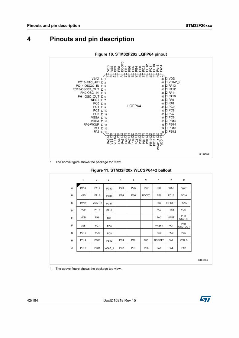
Pinouts and pin description STM32F20xxx
42/184 DocID15818 Rev 15
4 Pinouts and pin description
Figure 10. STM32F20x LQFP64 pinout
1. The above figure shows the package top view.
Figure 11. STM32F20x WLCSP64+2 ballout
1. The above figure shows the package top view.
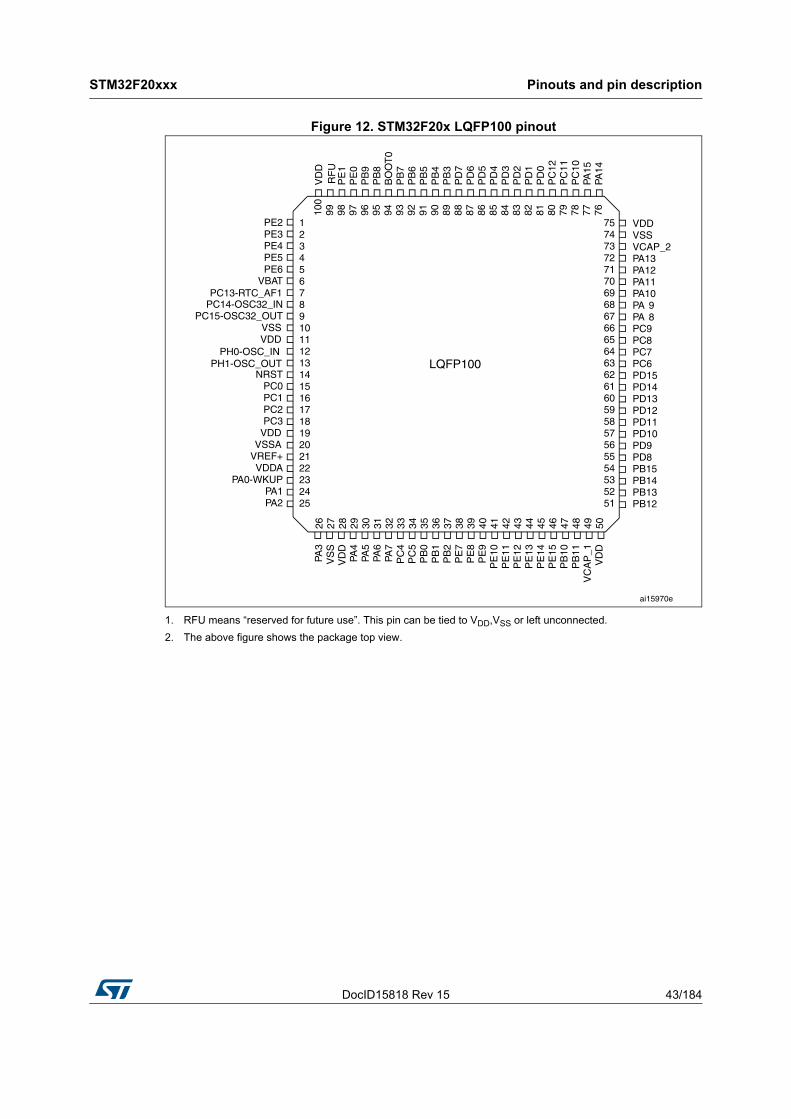
DocID15818 Rev 15 43/184
STM32F20xxx Pinouts and pin description
183
Figure 12. STM32F20x LQFP100 pinout
1. RFU means “reserved for future use”. This pin can be tied to VDD,VSS or left unconnected.
2. The above figure shows the package top view.
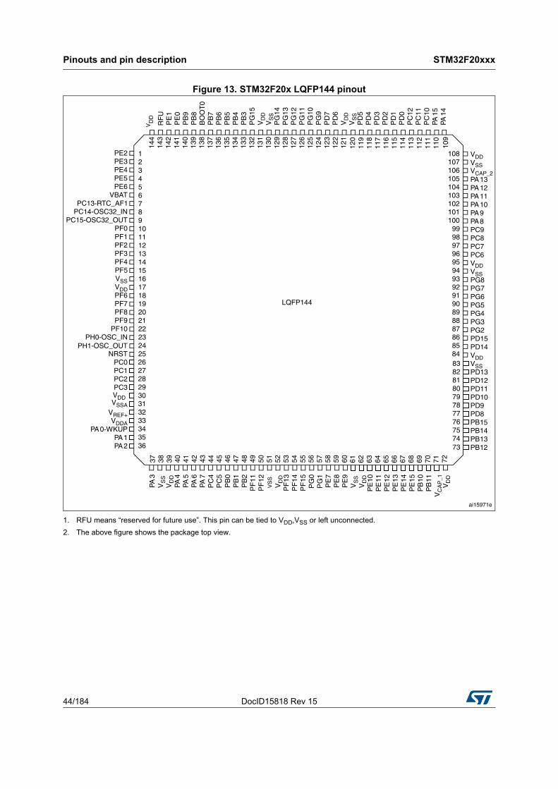
Pinouts and pin description STM32F20xxx
44/184 DocID15818 Rev 15
Figure 13. STM32F20x LQFP144 pinout
1. RFU means “reserved for future use”. This pin can be tied to VDD,VSS or left unconnected.
2. The above figure shows the package top view.
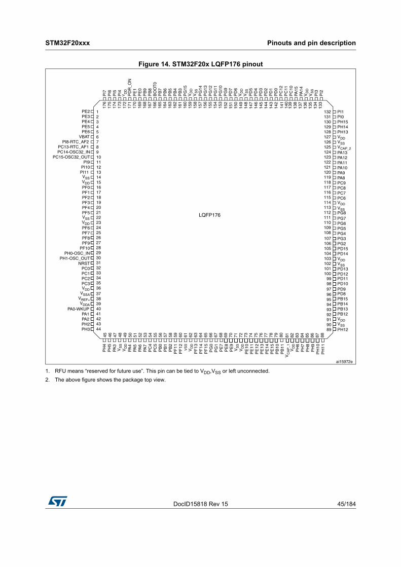
DocID15818 Rev 15 45/184
STM32F20xxx Pinouts and pin description
183
Figure 14. STM32F20x LQFP176 pinout
1. RFU means “reserved for future use”. This pin can be tied to VDD,VSS or left unconnected.
2. The above figure shows the package top view.
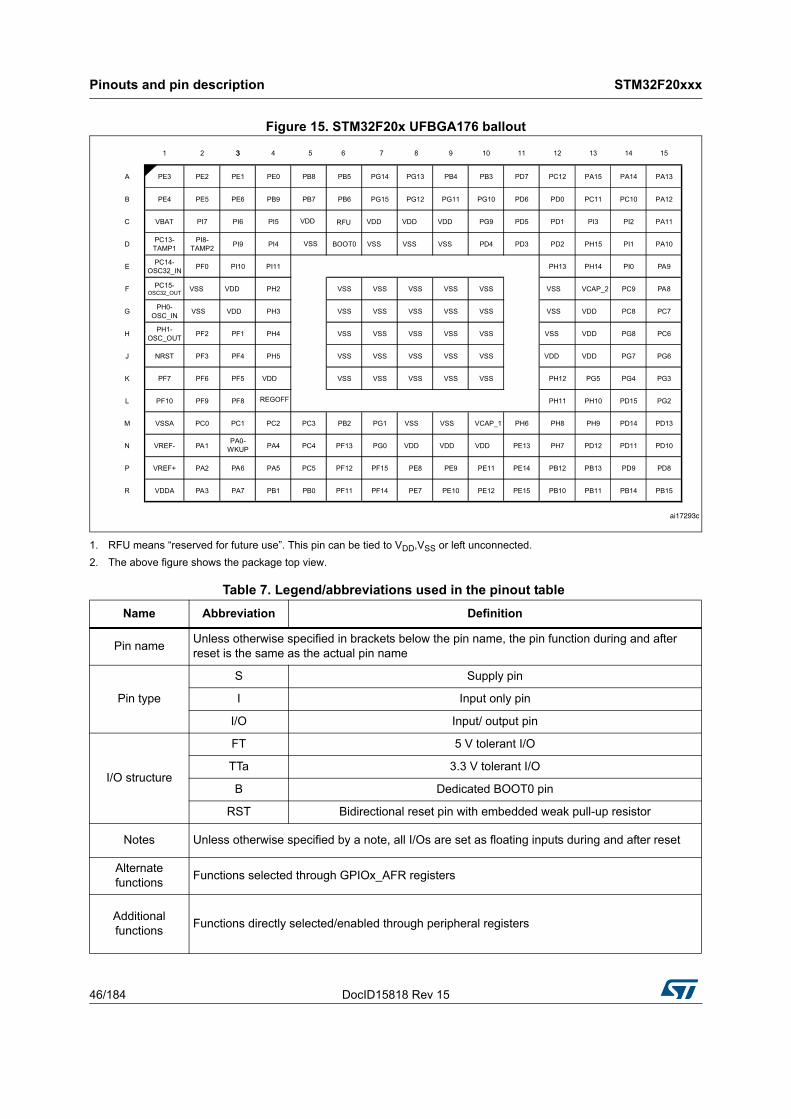
Pinouts and pin description STM32F20xxx
46/184 DocID15818 Rev 15
Figure 15. STM32F20x UFBGA176 ballout
1. RFU means “reserved for future use”. This pin can be tied to VDD,VSS or left unconnected.
2. The above figure shows the package top view.
Table 7. Legend/abbreviations used in the pinout table
Name Abbreviation Definition
Pin nameUnless otherwise specified in brackets below the pin name, the pin function during and after reset is the same as the actual pin name
Pin type
S Supply pin
I Input only pin
I/O Input/ output pin
I/O structure
FT 5 V tolerant I/O
TTa 3.3 V tolerant I/O
B Dedicated BOOT0 pin
RST Bidirectional reset pin with embedded weak pull-up resistor
Notes Unless otherwise specified by a note, all I/Os are set as floating inputs during and after reset
Alternate functions
Functions selected through GPIOx_AFR registers
Additional functions
Functions directly selected/enabled through peripheral registers
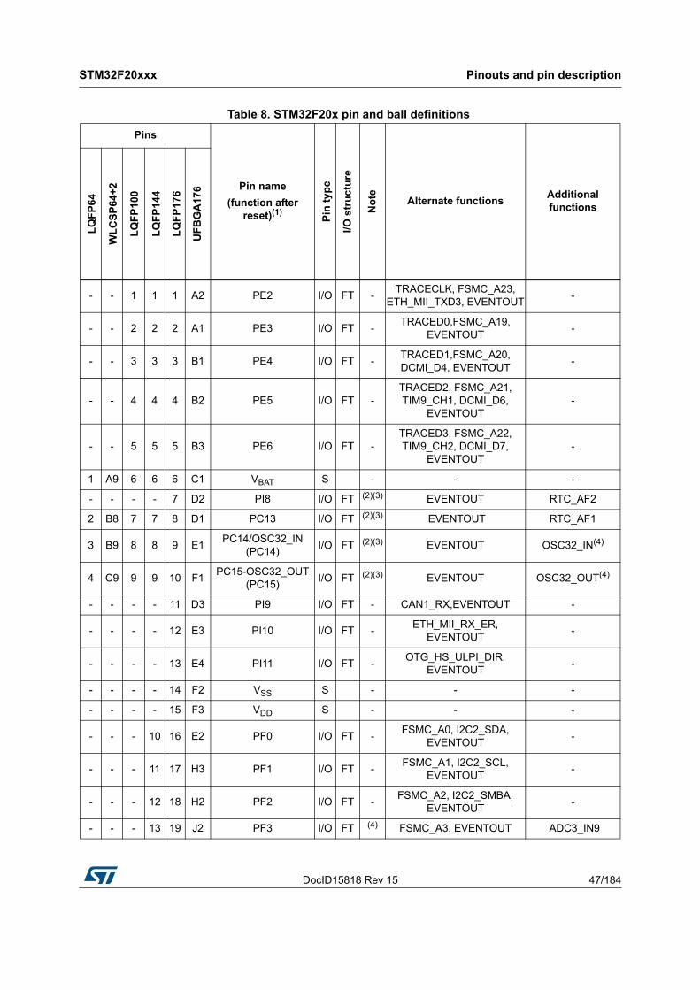
DocID15818 Rev 15 47/184
STM32F20xxx Pinouts and pin description
183
Table 8. STM32F20x pin and ball definitions
Pins
Pin name
(function after reset)(1)
Pin
typ
e
I/O s
tru
ctu
re
No
te Alternate functionsAdditional functions
LQ
FP
64
WL
CS
P64
+2
LQ
FP
100
LQ
FP
144
LQ
FP
176
UF
BG
A1
76
- - 1 1 1 A2 PE2 I/O FT -TRACECLK, FSMC_A23,
ETH_MII_TXD3, EVENTOUT-
- - 2 2 2 A1 PE3 I/O FT -TRACED0,FSMC_A19,
EVENTOUT-
- - 3 3 3 B1 PE4 I/O FT -TRACED1,FSMC_A20, DCMI_D4, EVENTOUT
-
- - 4 4 4 B2 PE5 I/O FT -TRACED2, FSMC_A21, TIM9_CH1, DCMI_D6,
EVENTOUT-
- - 5 5 5 B3 PE6 I/O FT -TRACED3, FSMC_A22, TIM9_CH2, DCMI_D7,
EVENTOUT-
1 A9 6 6 6 C1 VBAT S - - -
- - - - 7 D2 PI8 I/O FT (2)(3) EVENTOUT RTC_AF2
2 B8 7 7 8 D1 PC13 I/O FT (2)(3) EVENTOUT RTC_AF1
3 B9 8 8 9 E1PC14/OSC32_IN
(PC14)I/O FT (2)(3) EVENTOUT OSC32_IN(4)
4 C9 9 9 10 F1PC15-OSC32_OUT
(PC15)I/O FT (2)(3) EVENTOUT OSC32_OUT(4)
- - - - 11 D3 PI9 I/O FT - CAN1_RX,EVENTOUT -
- - - - 12 E3 PI10 I/O FT -ETH_MII_RX_ER,
EVENTOUT-
- - - - 13 E4 PI11 I/O FT -OTG_HS_ULPI_DIR,
EVENTOUT-
- - - - 14 F2 VSS S - - -
- - - - 15 F3 VDD S - - -
- - - 10 16 E2 PF0 I/O FT -FSMC_A0, I2C2_SDA,
EVENTOUT-
- - - 11 17 H3 PF1 I/O FT -FSMC_A1, I2C2_SCL,
EVENTOUT-
- - - 12 18 H2 PF2 I/O FT -FSMC_A2, I2C2_SMBA,
EVENTOUT-
- - - 13 19 J2 PF3 I/O FT (4) FSMC_A3, EVENTOUT ADC3_IN9
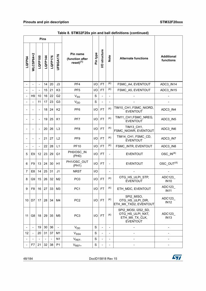
Pinouts and pin description STM32F20xxx
48/184 DocID15818 Rev 15
- - - 14 20 J3 PF4 I/O FT (4) FSMC_A4, EVENTOUT ADC3_IN14
- - - 15 21 K3 PF5 I/O FT (4) FSMC_A5, EVENTOUT ADC3_IN15
- H9 10 16 22 G2 VSS S - - - -
- - 11 17 23 G3 VDD S - - - -
- - - 18 24 K2 PF6 I/O FT (4) TIM10_CH1, FSMC_NIORD, EVENTOUT
ADC3_IN4
- - - 19 25 K1 PF7 I/O FT (4) TIM11_CH1,FSMC_NREG, EVENTOUT
ADC3_IN5
- - - 20 26 L3 PF8 I/O FT (4) TIM13_CH1, FSMC_NIOWR, EVENTOUT
ADC3_IN6
- - - 21 27 L2 PF9 I/O FT (4) TIM14_CH1, FSMC_CD, EVENTOUT
ADC3_IN7
- - - 22 28 L1 PF10 I/O FT (4) FSMC_INTR, EVENTOUT ADC3_IN8
5 E9 12 23 29 G1PH0/OSC_IN
(PH0)I/O FT - EVENTOUT OSC_IN(4)
6 F9 13 24 30 H1PH1/OSC_OUT
(PH1)I/O FT - EVENTOUT OSC_OUT(4)
7 E8 14 25 31 J1 NRST I/O - - -
8 G9 15 26 32 M2 PC0 I/O FT (4) OTG_HS_ULPI_STP, EVENTOUT
ADC123_IN10
9 F8 16 27 33 M3 PC1 I/O FT (4) ETH_MDC, EVENTOUTADC123_
IN11
10 D7 17 28 34 M4 PC2 I/O FT (4)SPI2_MISO,
OTG_HS_ULPI_DIR, ETH_MII_TXD2, EVENTOUT
ADC123_IN12
11 G8 18 29 35 M5 PC3 I/O FT (4)
SPI2_MOSI, I2S2_SD, OTG_HS_ULPI_NXT, ETH_MII_TX_CLK,
EVENTOUT
ADC123_IN13
- - 19 30 36 - VDD S - - - -
12 - 20 31 37 M1 VSSA S - - - -
- - - - - N1 VREF- S - - - -
- F7 21 32 38 P1 VREF+ S - - - -
Table 8. STM32F20x pin and ball definitions (continued)
Pins
Pin name
(function after reset)(1)
Pin
typ
e
I/O s
tru
ctu
re
No
te Alternate functionsAdditional functions
LQ
FP
64
WL
CS
P64
+2
LQ
FP
100
LQ
FP
144
LQ
FP
176
UF
BG
A17
6

DocID15818 Rev 15 49/184
STM32F20xxx Pinouts and pin description
183
13 - 22 33 39 R1 VDDA S - - - -
14 E7 23 34 40 N3PA0-WKUP
(PA0)I/O FT (4)(5)
USART2_CTS, UART4_TX, ETH_MII_CRS,
TIM2_CH1_ETR,TIM5_CH1, TIM8_ETR,
EVENTOUT
ADC123_IN0, WKUP
15 H8 24 35 41 N2 PA1 I/O FT (4)
USART2_RTS, UART4_RX,ETH_RMII_REF_CLK,
ETH_MII_RX_CLK, TIM5_CH2, TIM2_CH2,
EVENTOUT
ADC123_IN1
16 J9 25 36 42 P2 PA2 I/O FT (4)USART2_TX,TIM5_CH3, TIM9_CH1, TIM2_CH3,
ETH_MDIO, EVENTOUTADC123_IN2
- - - - 43 F4 PH2 I/O FT - ETH_MII_CRS, EVENTOUT -
- - - - 44 G4 PH3 I/O FT - ETH_MII_COL, EVENTOUT -
- - - - 45 H4 PH4 I/O FT -I2C2_SCL,
OTG_HS_ULPI_NXT, EVENTOUT
-
- - - - 46 J4 PH5 I/O FT - I2C2_SDA, EVENTOUT -
17 G7 26 37 47 R2 PA3 I/O FT (4)
USART2_RX, TIM5_CH4, TIM9_CH2, TIM2_CH4,
OTG_HS_ULPI_D0, ETH_MII_COL, EVENTOUT
ADC123_IN3
18 F1 27 38 48 - VSS S - - - -
H7 L4 REGOFF I/O - - - -
19 E1 28 39 49 K4 VDD S - - - -
20 J8 29 40 50 N4 PA4 I/O TTa (4)
SPI1_NSS, SPI3_NSS, USART2_CK,
DCMI_HSYNC, OTG_HS_SOF, I2S3_WS,
EVENTOUT
ADC12_IN4, DAC_OUT1
21 H6 30 41 51 P4 PA5 I/O TTa (4)
SPI1_SCK, OTG_HS_ULPI_CK,
TIM2_CH1_ETR, TIM8_CH1N, EVENTOUT
ADC12_IN5, DAC_OUT2
Table 8. STM32F20x pin and ball definitions (continued)
Pins
Pin name
(function after reset)(1)
Pin
typ
e
I/O s
tru
ctu
re
No
te Alternate functionsAdditional functions
LQ
FP
64
WL
CS
P64
+2
LQ
FP
100
LQ
FP
144
LQ
FP
176
UF
BG
A17
6
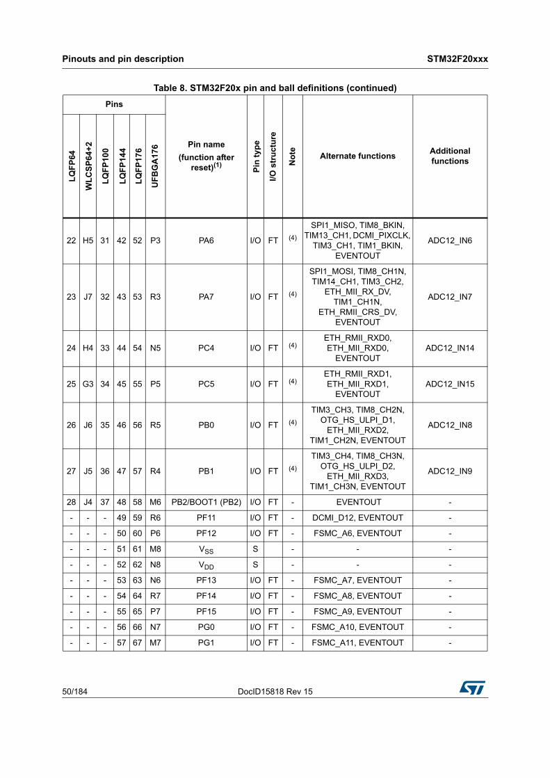
Pinouts and pin description STM32F20xxx
50/184 DocID15818 Rev 15
22 H5 31 42 52 P3 PA6 I/O FT (4)
SPI1_MISO, TIM8_BKIN, TIM13_CH1, DCMI_PIXCLK,
TIM3_CH1, TIM1_BKIN, EVENTOUT
ADC12_IN6
23 J7 32 43 53 R3 PA7 I/O FT (4)
SPI1_MOSI, TIM8_CH1N, TIM14_CH1, TIM3_CH2,
ETH_MII_RX_DV, TIM1_CH1N,
ETH_RMII_CRS_DV, EVENTOUT
ADC12_IN7
24 H4 33 44 54 N5 PC4 I/O FT (4)ETH_RMII_RXD0, ETH_MII_RXD0,
EVENTOUTADC12_IN14
25 G3 34 45 55 P5 PC5 I/O FT (4)ETH_RMII_RXD1, ETH_MII_RXD1,
EVENTOUTADC12_IN15
26 J6 35 46 56 R5 PB0 I/O FT (4)
TIM3_CH3, TIM8_CH2N, OTG_HS_ULPI_D1,
ETH_MII_RXD2, TIM1_CH2N, EVENTOUT
ADC12_IN8
27 J5 36 47 57 R4 PB1 I/O FT (4)
TIM3_CH4, TIM8_CH3N, OTG_HS_ULPI_D2,
ETH_MII_RXD3, TIM1_CH3N, EVENTOUT
ADC12_IN9
28 J4 37 48 58 M6 PB2/BOOT1 (PB2) I/O FT - EVENTOUT -
- - - 49 59 R6 PF11 I/O FT - DCMI_D12, EVENTOUT -
- - - 50 60 P6 PF12 I/O FT - FSMC_A6, EVENTOUT -
- - - 51 61 M8 VSS S - - -
- - - 52 62 N8 VDD S - - -
- - - 53 63 N6 PF13 I/O FT - FSMC_A7, EVENTOUT -
- - - 54 64 R7 PF14 I/O FT - FSMC_A8, EVENTOUT -
- - - 55 65 P7 PF15 I/O FT - FSMC_A9, EVENTOUT -
- - - 56 66 N7 PG0 I/O FT - FSMC_A10, EVENTOUT -
- - - 57 67 M7 PG1 I/O FT - FSMC_A11, EVENTOUT -
Table 8. STM32F20x pin and ball definitions (continued)
Pins
Pin name
(function after reset)(1)
Pin
typ
e
I/O s
tru
ctu
re
No
te Alternate functionsAdditional functions
LQ
FP
64
WL
CS
P64
+2
LQ
FP
100
LQ
FP
144
LQ
FP
176
UF
BG
A17
6
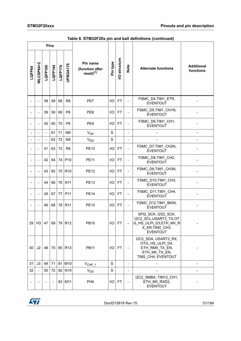
DocID15818 Rev 15 51/184
STM32F20xxx Pinouts and pin description
183
- - 38 58 68 R8 PE7 I/O FT -FSMC_D4,TIM1_ETR,
EVENTOUT-
- - 39 59 69 P8 PE8 I/O FT -FSMC_D5,TIM1_CH1N,
EVENTOUT-
- - 40 60 70 P9 PE9 I/O FT -FSMC_D6,TIM1_CH1,
EVENTOUT-
- - - 61 71 M9 VSS S - - -
- - - 62 72 N9 VDD S - - -
- - 41 63 73 R9 PE10 I/O FT -FSMC_D7,TIM1_CH2N,
EVENTOUT-
- - 42 64 74 P10 PE11 I/O FT -FSMC_D8,TIM1_CH2,
EVENTOUT-
- - 43 65 75 R10 PE12 I/O FT -FSMC_D9,TIM1_CH3N,
EVENTOUT-
- - 44 66 76 N11 PE13 I/O FT -FSMC_D10,TIM1_CH3,
EVENTOUT-
- - 45 67 77 P11 PE14 I/O FT -FSMC_D11,TIM1_CH4,
EVENTOUT-
- - 46 68 78 R11 PE15 I/O FT -FSMC_D12,TIM1_BKIN,
EVENTOUT-
29 H3 47 69 79 R12 PB10 I/O FT -
SPI2_SCK, I2S2_SCK, I2C2_SCL,USART3_TX,OTG_HS_ULPI_D3,ETH_MII_R
X_ER,TIM2_CH3, EVENTOUT
-
30 J2 48 70 80 R13 PB11 I/O FT -
I2C2_SDA, USART3_RX, OTG_HS_ULPI_D4, ETH_RMII_TX_EN, ETH_MII_TX_EN,
TIM2_CH4, EVENTOUT
-
31 J3 49 71 81 M10 VCAP_1 S - - -
32 - 50 72 82 N10 VDD S - - -
- - - - 83 M11 PH6 I/O FT -I2C2_SMBA, TIM12_CH1,
ETH_MII_RXD2, EVENTOUT
-
Table 8. STM32F20x pin and ball definitions (continued)
Pins
Pin name
(function after reset)(1)
Pin
typ
e
I/O s
tru
ctu
re
No
te Alternate functionsAdditional functions
LQ
FP
64
WL
CS
P64
+2
LQ
FP
100
LQ
FP
144
LQ
FP
176
UF
BG
A17
6
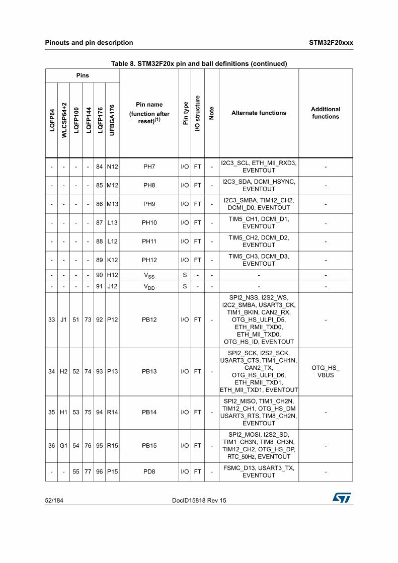
Pinouts and pin description STM32F20xxx
52/184 DocID15818 Rev 15
- - - - 84 N12 PH7 I/O FT -I2C3_SCL, ETH_MII_RXD3,
EVENTOUT-
- - - - 85 M12 PH8 I/O FT -I2C3_SDA, DCMI_HSYNC,
EVENTOUT-
- - - - 86 M13 PH9 I/O FT -I2C3_SMBA, TIM12_CH2,
DCMI_D0, EVENTOUT-
- - - - 87 L13 PH10 I/O FT -TIM5_CH1, DCMI_D1,
EVENTOUT-
- - - - 88 L12 PH11 I/O FT -TIM5_CH2, DCMI_D2,
EVENTOUT-
- - - - 89 K12 PH12 I/O FT -TIM5_CH3, DCMI_D3,
EVENTOUT-
- - - - 90 H12 VSS S - - - -
- - - - 91 J12 VDD S - - - -
33 J1 51 73 92 P12 PB12 I/O FT -
SPI2_NSS, I2S2_WS, I2C2_SMBA, USART3_CK,
TIM1_BKIN, CAN2_RX, OTG_HS_ULPI_D5, ETH_RMII_TXD0, ETH_MII_TXD0,
OTG_HS_ID, EVENTOUT
-
34 H2 52 74 93 P13 PB13 I/O FT -
SPI2_SCK, I2S2_SCK, USART3_CTS, TIM1_CH1N,
CAN2_TX, OTG_HS_ULPI_D6, ETH_RMII_TXD1,
ETH_MII_TXD1, EVENTOUT
OTG_HS_VBUS
35 H1 53 75 94 R14 PB14 I/O FT -
SPI2_MISO, TIM1_CH2N, TIM12_CH1, OTG_HS_DM
USART3_RTS, TIM8_CH2N, EVENTOUT
-
36 G1 54 76 95 R15 PB15 I/O FT -
SPI2_MOSI, I2S2_SD, TIM1_CH3N, TIM8_CH3N, TIM12_CH2, OTG_HS_DP,
RTC_50Hz, EVENTOUT
-
- - 55 77 96 P15 PD8 I/O FT -FSMC_D13, USART3_TX,
EVENTOUT-
Table 8. STM32F20x pin and ball definitions (continued)
Pins
Pin name
(function after reset)(1)
Pin
typ
e
I/O s
tru
ctu
re
No
te Alternate functionsAdditional functions
LQ
FP
64
WL
CS
P64
+2
LQ
FP
100
LQ
FP
144
LQ
FP
176
UF
BG
A17
6
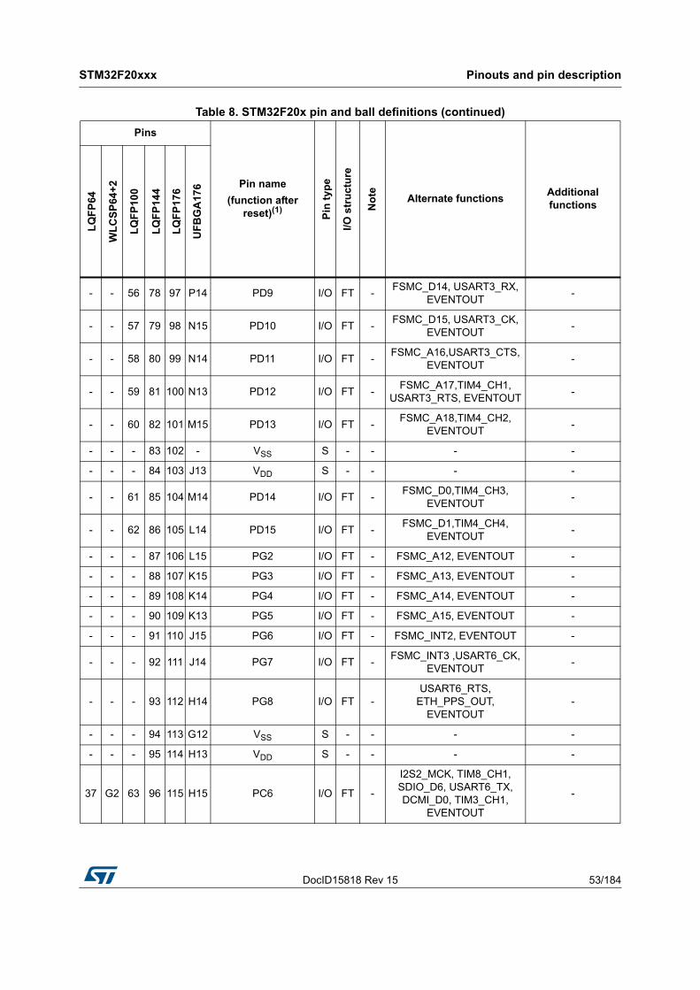
DocID15818 Rev 15 53/184
STM32F20xxx Pinouts and pin description
183
- - 56 78 97 P14 PD9 I/O FT -FSMC_D14, USART3_RX,
EVENTOUT-
- - 57 79 98 N15 PD10 I/O FT -FSMC_D15, USART3_CK,
EVENTOUT-
- - 58 80 99 N14 PD11 I/O FT -FSMC_A16,USART3_CTS,
EVENTOUT-
- - 59 81 100 N13 PD12 I/O FT -FSMC_A17,TIM4_CH1,
USART3_RTS, EVENTOUT-
- - 60 82 101 M15 PD13 I/O FT -FSMC_A18,TIM4_CH2,
EVENTOUT-
- - - 83 102 - VSS S - - - -
- - - 84 103 J13 VDD S - - - -
- - 61 85 104 M14 PD14 I/O FT -FSMC_D0,TIM4_CH3,
EVENTOUT-
- - 62 86 105 L14 PD15 I/O FT -FSMC_D1,TIM4_CH4,
EVENTOUT-
- - - 87 106 L15 PG2 I/O FT - FSMC_A12, EVENTOUT -
- - - 88 107 K15 PG3 I/O FT - FSMC_A13, EVENTOUT -
- - - 89 108 K14 PG4 I/O FT - FSMC_A14, EVENTOUT -
- - - 90 109 K13 PG5 I/O FT - FSMC_A15, EVENTOUT -
- - - 91 110 J15 PG6 I/O FT - FSMC_INT2, EVENTOUT -
- - - 92 111 J14 PG7 I/O FT -FSMC_INT3 ,USART6_CK,
EVENTOUT-
- - - 93 112 H14 PG8 I/O FT -USART6_RTS,
ETH_PPS_OUT, EVENTOUT
-
- - - 94 113 G12 VSS S - - - -
- - - 95 114 H13 VDD S - - - -
37 G2 63 96 115 H15 PC6 I/O FT -
I2S2_MCK, TIM8_CH1, SDIO_D6, USART6_TX, DCMI_D0, TIM3_CH1,
EVENTOUT
-
Table 8. STM32F20x pin and ball definitions (continued)
Pins
Pin name
(function after reset)(1)
Pin
typ
e
I/O s
tru
ctu
re
No
te Alternate functionsAdditional functions
LQ
FP
64
WL
CS
P64
+2
LQ
FP
100
LQ
FP
144
LQ
FP
176
UF
BG
A17
6
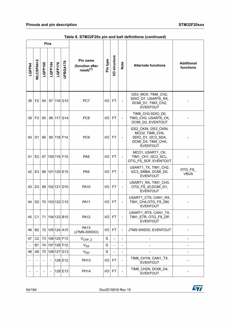
Pinouts and pin description STM32F20xxx
54/184 DocID15818 Rev 15
38 F2 64 97 116 G15 PC7 I/O FT -
I2S3_MCK, TIM8_CH2, SDIO_D7, USART6_RX, DCMI_D1, TIM3_CH2,
EVENTOUT
-
39 F3 65 98 117 G14 PC8 I/O FT -TIM8_CH3,SDIO_D0,
TIM3_CH3, USART6_CK, DCMI_D2, EVENTOUT
-
40 D1 66 99 118 F14 PC9 I/O FT -
I2S2_CKIN, I2S3_CKIN, MCO2, TIM8_CH4,
SDIO_D1, I2C3_SDA, DCMI_D3, TIM3_CH4,
EVENTOUT
-
41 E2 67 100 119 F15 PA8 I/O FT -MCO1, USART1_CK,
TIM1_CH1, I2C3_SCL, OTG_FS_SOF, EVENTOUT
-
42 E3 68 101 120 E15 PA9 I/O FT -USART1_TX, TIM1_CH2, I2C3_SMBA, DCMI_D0,
EVENTOUT
OTG_FS_VBUS
43 D3 69 102 121 D15 PA10 I/O FT -USART1_RX, TIM1_CH3, OTG_FS_ID,DCMI_D1,
EVENTOUT-
44 D2 70 103 122 C15 PA11 I/O FT -USART1_CTS, CAN1_RX, TIM1_CH4,OTG_FS_DM,
EVENTOUT-
45 C1 71 104 123 B15 PA12 I/O FT -USART1_RTS, CAN1_TX, TIM1_ETR, OTG_FS_DP,
EVENTOUT-
46 B2 72 105 124 A15PA13
(JTMS-SWDIO)I/O FT - JTMS-SWDIO, EVENTOUT -
47 C2 73 106 125 F13 VCAP_2 S - - - -
- B1 74 107 126 F12 VSS S - - - -
48 A8 75 108 127 G13 VDD S - - - -
- - - - 128 E12 PH13 I/O FT -TIM8_CH1N, CAN1_TX,
EVENTOUT-
- - - - 129 E13 PH14 I/O FT -TIM8_CH2N, DCMI_D4,
EVENTOUT-
Table 8. STM32F20x pin and ball definitions (continued)
Pins
Pin name
(function after reset)(1)
Pin
typ
e
I/O s
tru
ctu
re
No
te Alternate functionsAdditional functions
LQ
FP
64
WL
CS
P64
+2
LQ
FP
100
LQ
FP
144
LQ
FP
176
UF
BG
A17
6
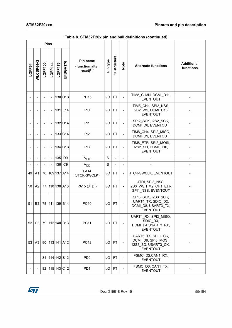
DocID15818 Rev 15 55/184
STM32F20xxx Pinouts and pin description
183
- - - - 130 D13 PH15 I/O FT -TIM8_CH3N, DCMI_D11,
EVENTOUT-
- - - - 131 E14 PI0 I/O FT -TIM5_CH4, SPI2_NSS, I2S2_WS, DCMI_D13,
EVENTOUT-
- - - - 132 D14 PI1 I/O FT -SPI2_SCK, I2S2_SCK, DCMI_D8, EVENTOUT
-
- - - - 133 C14 PI2 I/O FT -TIM8_CH4 ,SPI2_MISO, DCMI_D9, EVENTOUT
-
- - - - 134 C13 PI3 I/O FT -TIM8_ETR, SPI2_MOSI,
I2S2_SD, DCMI_D10, EVENTOUT
-
- - - - 135 D9 VSS S - - - -
- - - - 136 C9 VDD S - - - -
49 A1 76 109 137 A14PA14
(JTCK-SWCLK)I/O FT - JTCK-SWCLK, EVENTOUT -
50 A2 77 110 138 A13 PA15 (JTDI) I/O FT -JTDI, SPI3_NSS,
I2S3_WS,TIM2_CH1_ETR, SPI1_NSS, EVENTOUT
-
51 B3 78 111 139 B14 PC10 I/O FT -
SPI3_SCK, I2S3_SCK, UART4_TX, SDIO_D2,
DCMI_D8, USART3_TX, EVENTOUT
-
52 C3 79 112 140 B13 PC11 I/O FT -
UART4_RX, SPI3_MISO, SDIO_D3,
DCMI_D4,USART3_RX, EVENTOUT
-
53 A3 80 113 141 A12 PC12 I/O FT -
UART5_TX, SDIO_CK, DCMI_D9, SPI3_MOSI, I2S3_SD, USART3_CK,
EVENTOUT
-
- - 81 114 142 B12 PD0 I/O FT -FSMC_D2,CAN1_RX,
EVENTOUT-
- - 82 115 143 C12 PD1 I/O FT -FSMC_D3, CAN1_TX,
EVENTOUT-
Table 8. STM32F20x pin and ball definitions (continued)
Pins
Pin name
(function after reset)(1)
Pin
typ
e
I/O s
tru
ctu
re
No
te Alternate functionsAdditional functions
LQ
FP
64
WL
CS
P64
+2
LQ
FP
100
LQ
FP
144
LQ
FP
176
UF
BG
A17
6
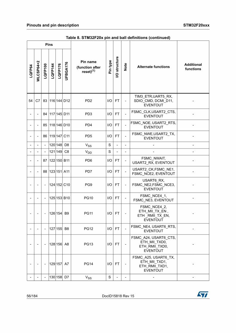
Pinouts and pin description STM32F20xxx
56/184 DocID15818 Rev 15
54 C7 83 116 144 D12 PD2 I/O FT -TIM3_ETR,UART5_RX, SDIO_CMD, DCMI_D11,
EVENTOUT-
- - 84 117 145 D11 PD3 I/O FT -FSMC_CLK,USART2_CTS,
EVENTOUT-
- - 85 118 146 D10 PD4 I/O FT -FSMC_NOE, USART2_RTS,
EVENTOUT-
- - 86 119 147 C11 PD5 I/O FT -FSMC_NWE,USART2_TX,
EVENTOUT-
- - - 120 148 D8 VSS S - - - -
- - - 121 149 C8 VDD S - - - -
- - 87 122 150 B11 PD6 I/O FT -FSMC_NWAIT,
USART2_RX, EVENTOUT-
- - 88 123 151 A11 PD7 I/O FT -USART2_CK,FSMC_NE1,FSMC_NCE2, EVENTOUT
-
- - - 124 152 C10 PG9 I/O FT -USART6_RX,
FSMC_NE2,FSMC_NCE3, EVENTOUT
-
- - - 125 153 B10 PG10 I/O FT -FSMC_NCE4_1,
FSMC_NE3, EVENTOUT-
- - - 126 154 B9 PG11 I/O FT -
FSMC_NCE4_2, ETH_MII_TX_EN ,
ETH _RMII_TX_EN, EVENTOUT
-
- - - 127 155 B8 PG12 I/O FT -FSMC_NE4, USART6_RTS,
EVENTOUT-
- - - 128 156 A8 PG13 I/O FT -
FSMC_A24, USART6_CTS, ETH_MII_TXD0,
ETH_RMII_TXD0, EVENTOUT
-
- - - 129 157 A7 PG14 I/O FT -
FSMC_A25, USART6_TX, ETH_MII_TXD1,
ETH_RMII_TXD1, EVENTOUT
-
- - - 130 158 D7 VSS S - - - -
Table 8. STM32F20x pin and ball definitions (continued)
Pins
Pin name
(function after reset)(1)
Pin
typ
e
I/O s
tru
ctu
re
No
te Alternate functionsAdditional functions
LQ
FP
64
WL
CS
P64
+2
LQ
FP
100
LQ
FP
144
LQ
FP
176
UF
BG
A17
6
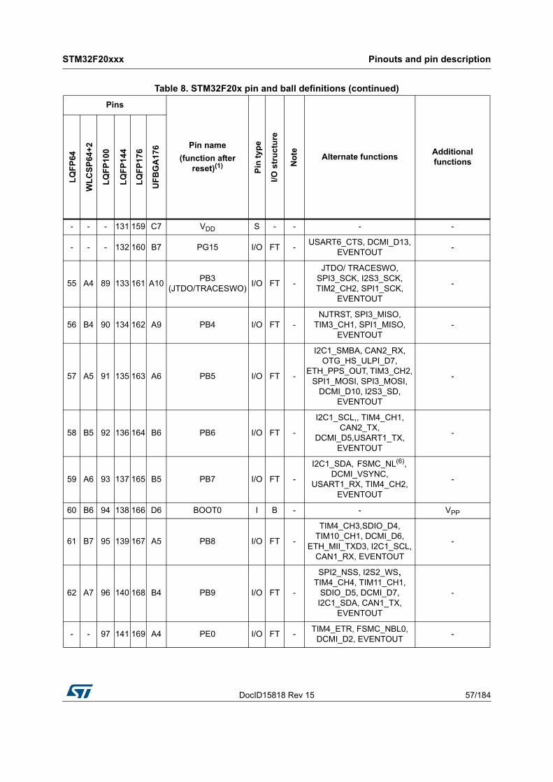
DocID15818 Rev 15 57/184
STM32F20xxx Pinouts and pin description
183
- - - 131 159 C7 VDD S - - - -
- - - 132 160 B7 PG15 I/O FT -USART6_CTS, DCMI_D13,
EVENTOUT-
55 A4 89 133 161 A10PB3
(JTDO/TRACESWO)I/O FT -
JTDO/ TRACESWO, SPI3_SCK, I2S3_SCK, TIM2_CH2, SPI1_SCK,
EVENTOUT
-
56 B4 90 134 162 A9 PB4 I/O FT -NJTRST, SPI3_MISO,
TIM3_CH1, SPI1_MISO, EVENTOUT
-
57 A5 91 135 163 A6 PB5 I/O FT -
I2C1_SMBA, CAN2_RX, OTG_HS_ULPI_D7,
ETH_PPS_OUT, TIM3_CH2, SPI1_MOSI, SPI3_MOSI,
DCMI_D10, I2S3_SD, EVENTOUT
-
58 B5 92 136 164 B6 PB6 I/O FT -
I2C1_SCL,, TIM4_CH1, CAN2_TX,
DCMI_D5,USART1_TX, EVENTOUT
-
59 A6 93 137 165 B5 PB7 I/O FT -
I2C1_SDA, FSMC_NL(6), DCMI_VSYNC,
USART1_RX, TIM4_CH2, EVENTOUT
-
60 B6 94 138 166 D6 BOOT0 I B - - VPP
61 B7 95 139 167 A5 PB8 I/O FT -
TIM4_CH3,SDIO_D4, TIM10_CH1, DCMI_D6,
ETH_MII_TXD3, I2C1_SCL, CAN1_RX, EVENTOUT
-
62 A7 96 140 168 B4 PB9 I/O FT -
SPI2_NSS, I2S2_WS, TIM4_CH4, TIM11_CH1,
SDIO_D5, DCMI_D7, I2C1_SDA, CAN1_TX,
EVENTOUT
-
- - 97 141 169 A4 PE0 I/O FT -TIM4_ETR, FSMC_NBL0,
DCMI_D2, EVENTOUT-
Table 8. STM32F20x pin and ball definitions (continued)
Pins
Pin name
(function after reset)(1)
Pin
typ
e
I/O s
tru
ctu
re
No
te Alternate functionsAdditional functions
LQ
FP
64
WL
CS
P64
+2
LQ
FP
100
LQ
FP
144
LQ
FP
176
UF
BG
A17
6
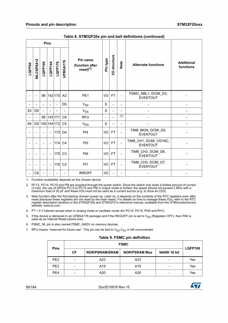
Pinouts and pin description STM32F20xxx
58/184 DocID15818 Rev 15
- - 98 142 170 A3 PE1 I/O FT -FSMC_NBL1, DCMI_D3,
EVENTOUT-
- - - - - D5 VSS S - - - -
63 D8 - - - - VSS S - - - -
- - 99 143 171 C6 RFU - - (7) - -
64 D9 100 144 172 C5 VDD S - - - -
- - - - 173 D4 PI4 I/O FT -TIM8_BKIN, DCMI_D5,
EVENTOUT-
- - - - 174 C4 PI5 I/O FT -TIM8_CH1, DCMI_VSYNC,
EVENTOUT-
- - - - 175 C3 PI6 I/O FT -TIM8_CH2, DCMI_D6,
EVENTOUT-
- - - - 176 C2 PI7 I/O FT -TIM8_CH3, DCMI_D7,
EVENTOUT-
- C8 - - - - IRROFF I/O - - - -
1. Function availability depends on the chosen device.
2. PC13, PC14, PC15 and PI8 are supplied through the power switch. Since the switch only sinks a limited amount of current (3 mA), the use of GPIOs PC13 to PC15 and PI8 in output mode is limited: the speed should not exceed 2 MHz with a maximum load of 30 pF and these I/Os must not be used as a current source (e.g. to drive an LED).
3. Main function after the first backup domain power-up. Later on, it depends on the contents of the RTC registers even after reset (because these registers are not reset by the main reset). For details on how to manage these I/Os, refer to the RTC register description sections in the STM32F20x and STM32F21x reference manual, available from the STMicroelectronics website: www.st.com.
4. FT = 5 V tolerant except when in analog mode or oscillator mode (for PC14, PC15, PH0 and PH1).
5. If the device is delivered in an UFBGA176 package and if the REGOFF pin is set to VDD (Regulator OFF), then PA0 is used as an internal Reset (active low).
6. FSMC_NL pin is also named FSMC_NADV on memory devices.
7. RFU means “reserved for future use”. This pin can be tied to VDD,VSS or left unconnected.
Table 8. STM32F20x pin and ball definitions (continued)
Pins
Pin name
(function after reset)(1)
Pin
typ
e
I/O s
tru
ctu
re
No
te Alternate functionsAdditional functions
LQ
FP
64
WL
CS
P64
+2
LQ
FP
100
LQ
FP
144
LQ
FP
176
UF
BG
A17
6
Table 9. FSMC pin definition
PinsFSMC
LQFP100CF NOR/PSRAM/SRAM NOR/PSRAM Mux NAND 16 bit
PE2 - A23 A23 - Yes
PE3 - A19 A19 - Yes
PE4 - A20 A20 - Yes
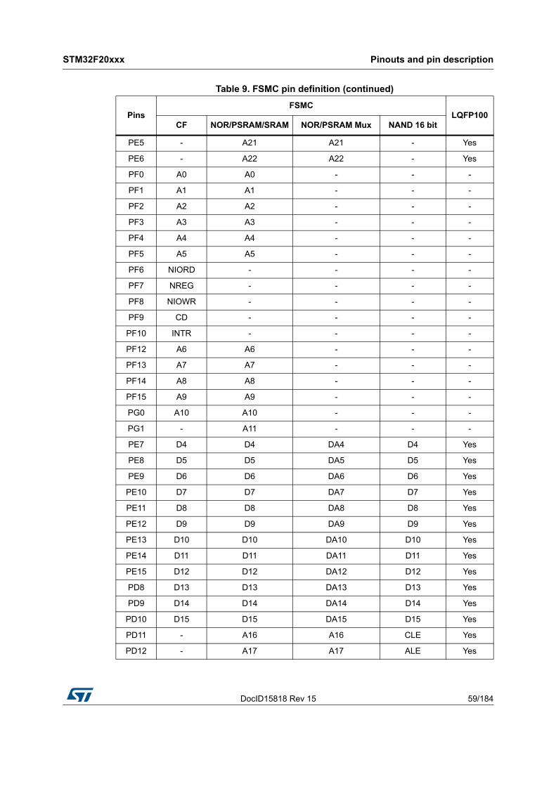
DocID15818 Rev 15 59/184
STM32F20xxx Pinouts and pin description
183
PE5 - A21 A21 - Yes
PE6 - A22 A22 - Yes
PF0 A0 A0 - - -
PF1 A1 A1 - - -
PF2 A2 A2 - - -
PF3 A3 A3 - - -
PF4 A4 A4 - - -
PF5 A5 A5 - - -
PF6 NIORD - - - -
PF7 NREG - - - -
PF8 NIOWR - - - -
PF9 CD - - - -
PF10 INTR - - - -
PF12 A6 A6 - - -
PF13 A7 A7 - - -
PF14 A8 A8 - - -
PF15 A9 A9 - - -
PG0 A10 A10 - - -
PG1 - A11 - - -
PE7 D4 D4 DA4 D4 Yes
PE8 D5 D5 DA5 D5 Yes
PE9 D6 D6 DA6 D6 Yes
PE10 D7 D7 DA7 D7 Yes
PE11 D8 D8 DA8 D8 Yes
PE12 D9 D9 DA9 D9 Yes
PE13 D10 D10 DA10 D10 Yes
PE14 D11 D11 DA11 D11 Yes
PE15 D12 D12 DA12 D12 Yes
PD8 D13 D13 DA13 D13 Yes
PD9 D14 D14 DA14 D14 Yes
PD10 D15 D15 DA15 D15 Yes
PD11 - A16 A16 CLE Yes
PD12 - A17 A17 ALE Yes
Table 9. FSMC pin definition (continued)
PinsFSMC
LQFP100CF NOR/PSRAM/SRAM NOR/PSRAM Mux NAND 16 bit
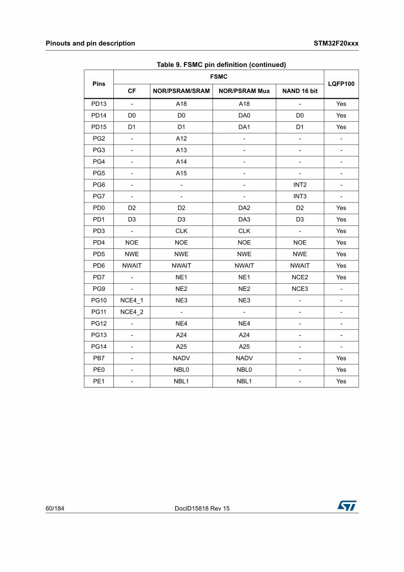
Pinouts and pin description STM32F20xxx
60/184 DocID15818 Rev 15
PD13 - A18 A18 - Yes
PD14 D0 D0 DA0 D0 Yes
PD15 D1 D1 DA1 D1 Yes
PG2 - A12 - - -
PG3 - A13 - - -
PG4 - A14 - - -
PG5 - A15 - - -
PG6 - - - INT2 -
PG7 - - - INT3 -
PD0 D2 D2 DA2 D2 Yes
PD1 D3 D3 DA3 D3 Yes
PD3 - CLK CLK - Yes
PD4 NOE NOE NOE NOE Yes
PD5 NWE NWE NWE NWE Yes
PD6 NWAIT NWAIT NWAIT NWAIT Yes
PD7 - NE1 NE1 NCE2 Yes
PG9 - NE2 NE2 NCE3 -
PG10 NCE4_1 NE3 NE3 - -
PG11 NCE4_2 - - - -
PG12 - NE4 NE4 - -
PG13 - A24 A24 - -
PG14 - A25 A25 - -
PB7 - NADV NADV - Yes
PE0 - NBL0 NBL0 - Yes
PE1 - NBL1 NBL1 - Yes
Table 9. FSMC pin definition (continued)
PinsFSMC
LQFP100CF NOR/PSRAM/SRAM NOR/PSRAM Mux NAND 16 bit
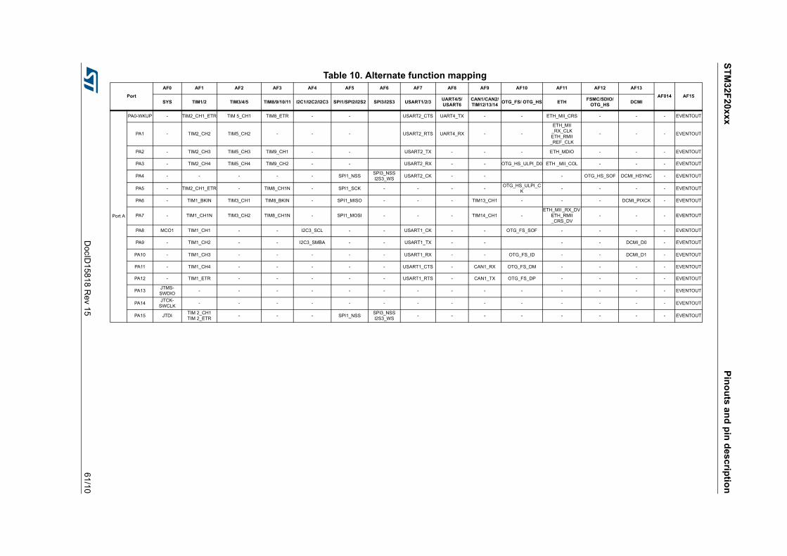
ST
M3
2F2
0xxx
Pin
ou
ts a
nd
pin
des
crip
tion
DocID
15818 R
ev 1561
/10
Table 10. Alternate function mapping
Port
AF0 AF1 AF2 AF3 AF4 AF5 AF6 AF7 AF8 AF9 AF10 AF11 AF12 AF13
AF014 AF15SYS TIM1/2 TIM3/4/5 TIM8/9/10/11 I2C1/I2C2/I2C3 SPI1/SPI2/I2S2 SPI3/I2S3 USART1/2/3
UART4/5/USART6
CAN1/CAN2/TIM12/13/14
OTG_FS/ OTG_HS ETHFSMC/SDIO/
OTG_HSDCMI
Port A
PA0-WKUP - TIM2_CH1_ETR TIM 5_CH1 TIM8_ETR - - USART2_CTS UART4_TX - - ETH_MII_CRS - - - EVENTOUT
PA1 - TIM2_CH2 TIM5_CH2 - - - USART2_RTS UART4_RX - -
ETH_MII _RX_CLKETH_RMII _REF_CLK
- - - EVENTOUT
PA2 - TIM2_CH3 TIM5_CH3 TIM9_CH1 - - USART2_TX - - - ETH_MDIO - - - EVENTOUT
PA3 - TIM2_CH4 TIM5_CH4 TIM9_CH2 - - USART2_RX - - OTG_HS_ULPI_D0 ETH _MII_COL - - - EVENTOUT
PA4 - - - - - SPI1_NSS SPI3_NSS I2S3_WS
USART2_CK - - - OTG_HS_SOF DCMI_HSYNC - EVENTOUT
PA5 - TIM2_CH1_ETR - TIM8_CH1N - SPI1_SCK - - - -OTG_HS_ULPI_C
K - - - - EVENTOUT
PA6 - TIM1_BKIN TIM3_CH1 TIM8_BKIN - SPI1_MISO - - - TIM13_CH1 - - - DCMI_PIXCK - EVENTOUT
PA7 - TIM1_CH1N TIM3_CH2 TIM8_CH1N - SPI1_MOSI - - - TIM14_CH1 -ETH_MII _RX_DV
ETH_RMII _CRS_DV
- - - EVENTOUT
PA8 MCO1 TIM1_CH1 - - I2C3_SCL - - USART1_CK - - OTG_FS_SOF - - - - EVENTOUT
PA9 - TIM1_CH2 - - I2C3_SMBA - - USART1_TX - - - - DCMI_D0 - EVENTOUT
PA10 - TIM1_CH3 - - - - - USART1_RX - - OTG_FS_ID - - DCMI_D1 - EVENTOUT
PA11 - TIM1_CH4 - - - - - USART1_CTS - CAN1_RX OTG_FS_DM - - - - EVENTOUT
PA12 - TIM1_ETR - - - - - USART1_RTS - CAN1_TX OTG_FS_DP - - - - EVENTOUT
PA13JTMS-SWDIO
- - - - - - - - - - - - - - EVENTOUT
PA14JTCK-
SWCLK - - - - - - - - - - - - - - EVENTOUT
PA15 JTDI TIM 2_CH1 TIM 2_ETR
- - - SPI1_NSS SPI3_NSS I2S3_WS
- - - - - - - - EVENTOUT
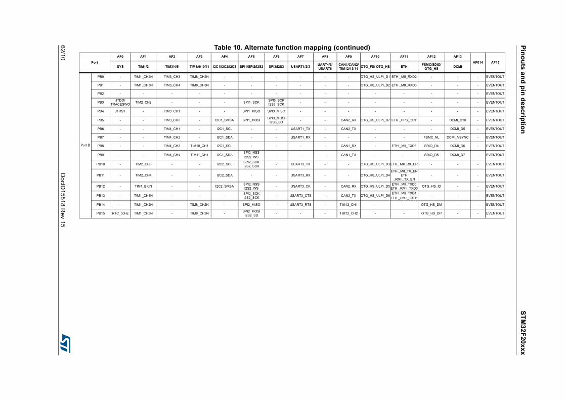
Pin
ou
ts a
nd
pin
de
scrip
tion
ST
M32
F20
xxx
62/1
0D
ocID158
18 Rev 15
Port B
PB0 - TIM1_CH2N TIM3_CH3 TIM8_CH2N - - - - - - OTG_HS_ULPI_D1 ETH _MII_RXD2 - - - EVENTOUT
PB1 - TIM1_CH3N TIM3_CH4 TIM8_CH3N - - - - - - OTG_HS_ULPI_D2 ETH _MII_RXD3 - - - EVENTOUT
PB2 - - - - - - - - - - - - - - - EVENTOUT
PB3JTDO/
TRACESWO TIM2_CH2 - - - SPI1_SCK
SPI3_SCK I2S3_SCK
- - - - - - - - EVENTOUT
PB4 JTRST - TIM3_CH1 - - SPI1_MISO SPI3_MISO - - - - - - - - EVENTOUT
PB5 - - TIM3_CH2 - I2C1_SMBA SPI1_MOSI SPI3_MOSI
I2S3_SD - - CAN2_RX OTG_HS_ULPI_D7 ETH _PPS_OUT - DCMI_D10 - EVENTOUT
PB6 - - TIM4_CH1 - I2C1_SCL - - USART1_TX - CAN2_TX - - - DCMI_D5 - EVENTOUT
PB7 - - TIM4_CH2 - I2C1_SDA - - USART1_RX - - - - FSMC_NL DCMI_VSYNC - EVENTOUT
PB8 - - TIM4_CH3 TIM10_CH1 I2C1_SCL - - - - CAN1_RX - ETH _MII_TXD3 SDIO_D4 DCMI_D6 - EVENTOUT
PB9 - - TIM4_CH4 TIM11_CH1 I2C1_SDA SPI2_NSS
I2S2_WS - - - CAN1_TX - - SDIO_D5 DCMI_D7 - EVENTOUT
PB10 - TIM2_CH3 - - I2C2_SCL SPI2_SCK I2S2_SCK
- USART3_TX - - OTG_HS_ULPI_D3 ETH_ MII_RX_ER - - - EVENTOUT
PB11 - TIM2_CH4 - - I2C2_SDA - - USART3_RX - - OTG_HS_ULPI_D4 ETH _MII_TX_EN
ETH _RMII_TX_EN
- - - EVENTOUT
PB12 - TIM1_BKIN - - I2C2_SMBASPI2_NSS I2S2_WS
- USART3_CK - CAN2_RX OTG_HS_ULPI_D5 ETH _MII_TXD0
ETH _RMII_TXD0OTG_HS_ID - - EVENTOUT
PB13 - TIM1_CH1N - - -SPI2_SCK I2S2_SCK
- USART3_CTS - CAN2_TX OTG_HS_ULPI_D6 ETH _MII_TXD1
ETH _RMII_TXD1 - - - EVENTOUT
PB14 - TIM1_CH2N - TIM8_CH2N - SPI2_MISO - USART3_RTS - TIM12_CH1 - - OTG_HS_DM - - EVENTOUT
PB15 RTC_50Hz TIM1_CH3N - TIM8_CH3N -SPI2_MOSI
I2S2_SD - - - TIM12_CH2 - - OTG_HS_DP - - EVENTOUT
Table 10. Alternate function mapping (continued)
Port
AF0 AF1 AF2 AF3 AF4 AF5 AF6 AF7 AF8 AF9 AF10 AF11 AF12 AF13
AF014 AF15SYS TIM1/2 TIM3/4/5 TIM8/9/10/11 I2C1/I2C2/I2C3 SPI1/SPI2/I2S2 SPI3/I2S3 USART1/2/3
UART4/5/USART6
CAN1/CAN2/TIM12/13/14
OTG_FS/ OTG_HS ETHFSMC/SDIO/
OTG_HSDCMI
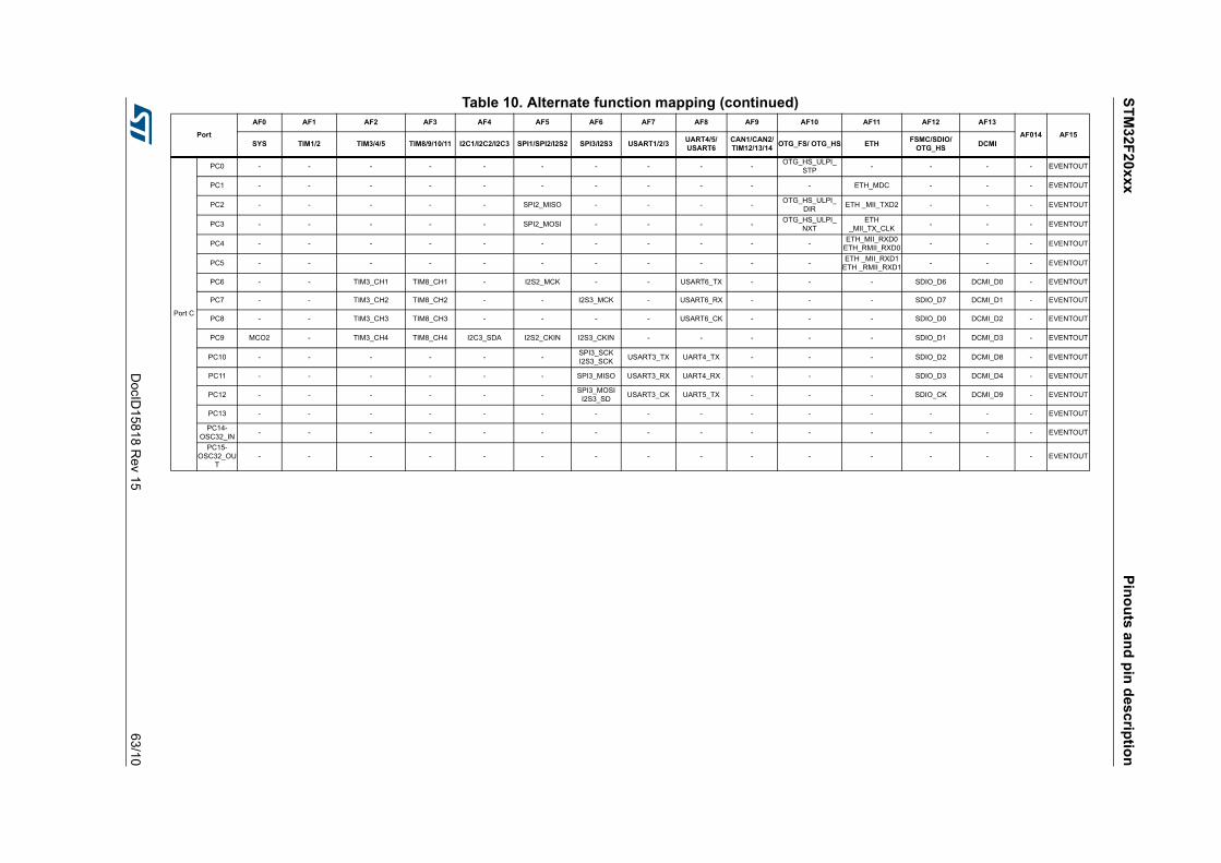
ST
M3
2F2
0xxx
Pin
ou
ts a
nd
pin
des
crip
tion
DocID
15818 R
ev 1563
/10
Port C
PC0 - - - - - - - - - -OTG_HS_ULPI_
STP - - - - EVENTOUT
PC1 - - - - - - - - - - - ETH_MDC - - - EVENTOUT
PC2 - - - - - SPI2_MISO - - - -OTG_HS_ULPI_
DIR ETH _MII_TXD2 - - - EVENTOUT
PC3 - - - - - SPI2_MOSI - - - -OTG_HS_ULPI_
NXT ETH
_MII_TX_CLK- - - EVENTOUT
PC4 - - - - - - - - - - -ETH_MII_RXD0
ETH_RMII_RXD0- - - EVENTOUT
PC5 - - - - - - - - - - -ETH _MII_RXD1
ETH _RMII_RXD1- - - EVENTOUT
PC6 - - TIM3_CH1 TIM8_CH1 - I2S2_MCK - - USART6_TX - - - SDIO_D6 DCMI_D0 - EVENTOUT
PC7 - - TIM3_CH2 TIM8_CH2 - - I2S3_MCK - USART6_RX - - - SDIO_D7 DCMI_D1 - EVENTOUT
PC8 - - TIM3_CH3 TIM8_CH3 - - - - USART6_CK - - - SDIO_D0 DCMI_D2 - EVENTOUT
PC9 MCO2 - TIM3_CH4 TIM8_CH4 I2C3_SDA I2S2_CKIN I2S3_CKIN - - - - - SDIO_D1 DCMI_D3 - EVENTOUT
PC10 - - - - - -SPI3_SCK I2S3_SCK
USART3_TX UART4_TX - - - SDIO_D2 DCMI_D8 - EVENTOUT
PC11 - - - - - - SPI3_MISO USART3_RX UART4_RX - - - SDIO_D3 DCMI_D4 - EVENTOUT
PC12 - - - - - -SPI3_MOSI
I2S3_SD USART3_CK UART5_TX - - - SDIO_CK DCMI_D9 - EVENTOUT
PC13 - - - - - - - - - - - - - - - EVENTOUT
PC14-OSC32_IN
- - - - - - - - - - - - - - - EVENTOUT
PC15-OSC32_OU
T- - - - - - - - - - - - - - - EVENTOUT
Table 10. Alternate function mapping (continued)
Port
AF0 AF1 AF2 AF3 AF4 AF5 AF6 AF7 AF8 AF9 AF10 AF11 AF12 AF13
AF014 AF15SYS TIM1/2 TIM3/4/5 TIM8/9/10/11 I2C1/I2C2/I2C3 SPI1/SPI2/I2S2 SPI3/I2S3 USART1/2/3
UART4/5/USART6
CAN1/CAN2/TIM12/13/14
OTG_FS/ OTG_HS ETHFSMC/SDIO/
OTG_HSDCMI
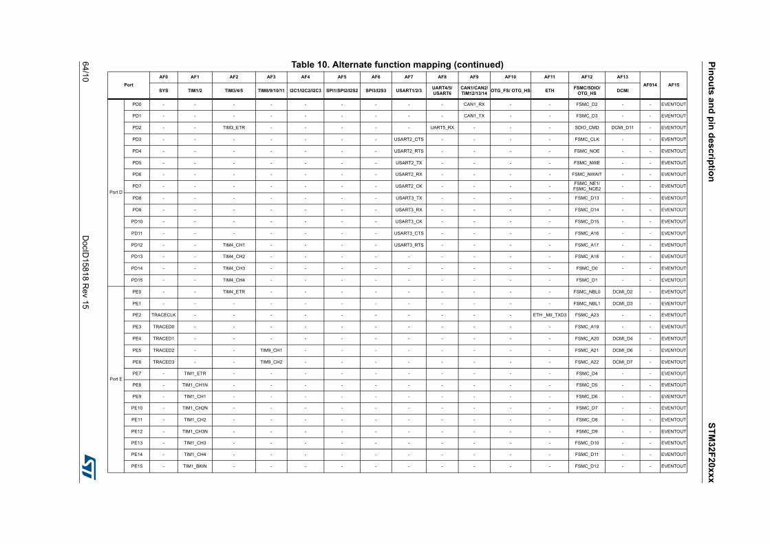
Pin
ou
ts a
nd
pin
de
scrip
tion
ST
M32
F20
xxx
64/1
0D
ocID158
18 Rev 15
Port D
PD0 - - - - - - - - - CAN1_RX - - FSMC_D2 - - EVENTOUT
PD1 - - - - - - - - - CAN1_TX - - FSMC_D3 - - EVENTOUT
PD2 - - TIM3_ETR - - - - - UART5_RX - - - SDIO_CMD DCMI_D11 - EVENTOUT
PD3 - - - - - - - USART2_CTS - - - - FSMC_CLK - - EVENTOUT
PD4 - - - - - - - USART2_RTS - - - - FSMC_NOE - - EVENTOUT
PD5 - - - - - - - USART2_TX - - - - FSMC_NWE - - EVENTOUT
PD6 - - - - - - - USART2_RX - - - - FSMC_NWAIT - - EVENTOUT
PD7 - - - - - - - USART2_CK - - - -FSMC_NE1/FSMC_NCE2
- - EVENTOUT
PD8 - - - - - - - USART3_TX - - - - FSMC_D13 - - EVENTOUT
PD9 - - - - - - - USART3_RX - - - - FSMC_D14 - - EVENTOUT
PD10 - - - - - - - USART3_CK - - - - FSMC_D15 - - EVENTOUT
PD11 - - - - - - - USART3_CTS - - - - FSMC_A16 - - EVENTOUT
PD12 - - TIM4_CH1 - - - - USART3_RTS - - - - FSMC_A17 - - EVENTOUT
PD13 - - TIM4_CH2 - - - - - - - - - FSMC_A18 - - EVENTOUT
PD14 - - TIM4_CH3 - - - - - - - - - FSMC_D0 - - EVENTOUT
PD15 - - TIM4_CH4 - - - - - - - - - FSMC_D1 - - EVENTOUT
Port E
PE0 - - TIM4_ETR - - - - - - - - - FSMC_NBL0 DCMI_D2 - EVENTOUT
PE1 - - - - - - - - - - - - FSMC_NBL1 DCMI_D3 - EVENTOUT
PE2 TRACECLK - - - - - - - - - - ETH _MII_TXD3 FSMC_A23 - - EVENTOUT
PE3 TRACED0 - - - - - - - - - - - FSMC_A19 - - EVENTOUT
PE4 TRACED1 - - - - - - - - - - - FSMC_A20 DCMI_D4 - EVENTOUT
PE5 TRACED2 - - TIM9_CH1 - - - - - - - - FSMC_A21 DCMI_D6 - EVENTOUT
PE6 TRACED3 - - TIM9_CH2 - - - - - - - - FSMC_A22 DCMI_D7 - EVENTOUT
PE7 - TIM1_ETR - - - - - - - - - - FSMC_D4 - - EVENTOUT
PE8 - TIM1_CH1N - - - - - - - - - - FSMC_D5 - - EVENTOUT
PE9 - TIM1_CH1 - - - - - - - - - - FSMC_D6 - - EVENTOUT
PE10 - TIM1_CH2N - - - - - - - - - - FSMC_D7 - - EVENTOUT
PE11 - TIM1_CH2 - - - - - - - - - - FSMC_D8 - - EVENTOUT
PE12 - TIM1_CH3N - - - - - - - - - - FSMC_D9 - - EVENTOUT
PE13 - TIM1_CH3 - - - - - - - - - - FSMC_D10 - - EVENTOUT
PE14 - TIM1_CH4 - - - - - - - - - - FSMC_D11 - - EVENTOUT
PE15 - TIM1_BKIN - - - - - - - - - - FSMC_D12 - - EVENTOUT
Table 10. Alternate function mapping (continued)
Port
AF0 AF1 AF2 AF3 AF4 AF5 AF6 AF7 AF8 AF9 AF10 AF11 AF12 AF13
AF014 AF15SYS TIM1/2 TIM3/4/5 TIM8/9/10/11 I2C1/I2C2/I2C3 SPI1/SPI2/I2S2 SPI3/I2S3 USART1/2/3
UART4/5/USART6
CAN1/CAN2/TIM12/13/14
OTG_FS/ OTG_HS ETHFSMC/SDIO/
OTG_HSDCMI
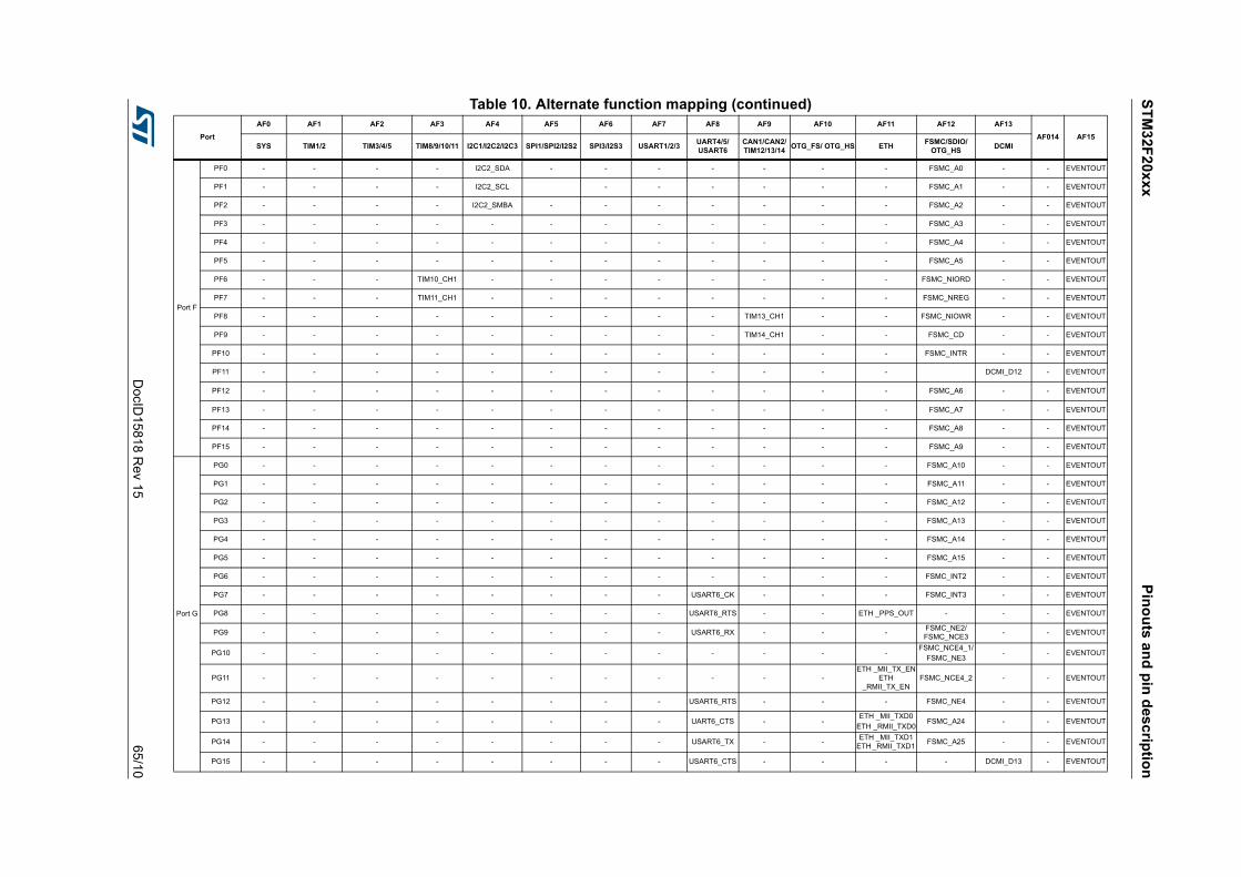
ST
M3
2F2
0xxx
Pin
ou
ts a
nd
pin
des
crip
tion
DocID
15818 R
ev 1565
/10
Port F
PF0 - - - - I2C2_SDA - - - - - - - FSMC_A0 - - EVENTOUT
PF1 - - - - I2C2_SCL - - - - - - FSMC_A1 - - EVENTOUT
PF2 - - - - I2C2_SMBA - - - - - - - FSMC_A2 - - EVENTOUT
PF3 - - - - - - - - - - - - FSMC_A3 - - EVENTOUT
PF4 - - - - - - - - - - - - FSMC_A4 - - EVENTOUT
PF5 - - - - - - - - - - - - FSMC_A5 - - EVENTOUT
PF6 - - - TIM10_CH1 - - - - - - - - FSMC_NIORD - - EVENTOUT
PF7 - - - TIM11_CH1 - - - - - - - - FSMC_NREG - - EVENTOUT
PF8 - - - - - - - - - TIM13_CH1 - - FSMC_NIOWR - - EVENTOUT
PF9 - - - - - - - - - TIM14_CH1 - - FSMC_CD - - EVENTOUT
PF10 - - - - - - - - - - - - FSMC_INTR - - EVENTOUT
PF11 - - - - - - - - - - - - DCMI_D12 - EVENTOUT
PF12 - - - - - - - - - - - - FSMC_A6 - - EVENTOUT
PF13 - - - - - - - - - - - - FSMC_A7 - - EVENTOUT
PF14 - - - - - - - - - - - - FSMC_A8 - - EVENTOUT
PF15 - - - - - - - - - - - - FSMC_A9 - - EVENTOUT
Port G
PG0 - - - - - - - - - - - - FSMC_A10 - - EVENTOUT
PG1 - - - - - - - - - - - - FSMC_A11 - - EVENTOUT
PG2 - - - - - - - - - - - - FSMC_A12 - - EVENTOUT
PG3 - - - - - - - - - - - - FSMC_A13 - - EVENTOUT
PG4 - - - - - - - - - - - - FSMC_A14 - - EVENTOUT
PG5 - - - - - - - - - - - - FSMC_A15 - - EVENTOUT
PG6 - - - - - - - - - - - - FSMC_INT2 - - EVENTOUT
PG7 - - - - - - - - USART6_CK - - - FSMC_INT3 - - EVENTOUT
PG8 - - - - - - - - USART6_RTS - - ETH _PPS_OUT - - - EVENTOUT
PG9 - - - - - - - - USART6_RX - - -FSMC_NE2/FSMC_NCE3
- - EVENTOUT
PG10 - - - - - - - - - - - -FSMC_NCE4_1/
FSMC_NE3 - - EVENTOUT
PG11 - - - - - - - - - - -ETH _MII_TX_EN
ETH _RMII_TX_EN
FSMC_NCE4_2 - - EVENTOUT
PG12 - - - - - - - - USART6_RTS - - - FSMC_NE4 - - EVENTOUT
PG13 - - - - - - - - UART6_CTS - -ETH _MII_TXD0
ETH _RMII_TXD0FSMC_A24 - - EVENTOUT
PG14 - - - - - - - - USART6_TX - -ETH _MII_TXD1
ETH _RMII_TXD1 FSMC_A25 - - EVENTOUT
PG15 - - - - - - - - USART6_CTS - - - - DCMI_D13 - EVENTOUT
Table 10. Alternate function mapping (continued)
Port
AF0 AF1 AF2 AF3 AF4 AF5 AF6 AF7 AF8 AF9 AF10 AF11 AF12 AF13
AF014 AF15SYS TIM1/2 TIM3/4/5 TIM8/9/10/11 I2C1/I2C2/I2C3 SPI1/SPI2/I2S2 SPI3/I2S3 USART1/2/3
UART4/5/USART6
CAN1/CAN2/TIM12/13/14
OTG_FS/ OTG_HS ETHFSMC/SDIO/
OTG_HSDCMI
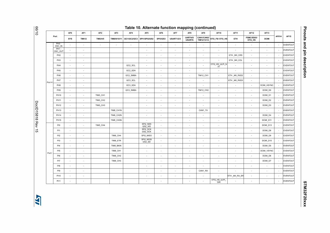
Pin
ou
ts a
nd
pin
de
scrip
tion
ST
M32
F20
xxx
66/1
0D
ocID158
18 Rev 15
Port H
PH0 - OSC_IN
- - - - - - - - - - - - - - - EVENTOUT
PH1 - OSC_OUT
- - - - - - - - - - - - EVENTOUT
PH2 - - - - - - - - ETH _MII_CRS - - - EVENTOUT
PH3 - - - - - - - - ETH _MII_COL - - - EVENTOUT
PH4 - - I2C2_SCL - - - - -OTG_HS_ULPI_N
XT - - - - EVENTOUT
PH5 - - I2C2_SDA - - - - - - - - - - EVENTOUT
PH6 - - I2C2_SMBA - - - - TIM12_CH1 - ETH _MII_RXD2 - - - EVENTOUT
PH7 - - I2C3_SCL - - - - - - ETH _MII_RXD3 - - - EVENTOUT
PH8 - - I2C3_SDA - - - - - - - - DCMI_HSYNC - EVENTOUT
PH9 - - I2C3_SMBA - - - - TIM12_CH2 - - - DCMI_D0 - EVENTOUT
PH10 - - TIM5_CH1 - - - - - - - - DCMI_D1 - EVENTOUT
PH11 - - TIM5_CH2 - - - - - - - - DCMI_D2 - EVENTOUT
PH12 - - TIM5_CH3 - - - - - - - - DCMI_D3 - EVENTOUT
PH13 - - TIM8_CH1N - - - - CAN1_TX - - - - - EVENTOUT
PH14 - - TIM8_CH2N - - - - - - - - DCMI_D4 - EVENTOUT
PH15 - - TIM8_CH3N - - - - - - - - DCMI_D11 - EVENTOUT
Port I
PI0 - - TIM5_CH4 SPI2_NSS I2S2_WS
- - - - - - - DCMI_D13 - EVENTOUT
PI1 - -SPI2_SCK I2S2_SCK
- - - - - - - DCMI_D8 - EVENTOUT
PI2 - - TIM8_CH4 SPI2_MISO - - - - - - - DCMI_D9 - EVENTOUT
PI3 - - TIM8_ETR SPI2_MOSI
I2S2_SD - - - - - - - DCMI_D10 - EVENTOUT
PI4 - - TIM8_BKIN - - - - - - - - DCMI_D5 - EVENTOUT
PI5 - - TIM8_CH1 - - - - - - - - DCMI_VSYNC - EVENTOUT
PI6 - - TIM8_CH2 - - - - - - - - DCMI_D6 - EVENTOUT
PI7 - - TIM8_CH3 - - - - - - - - DCMI_D7 - EVENTOUT
PI8 - - - - - - - - - - - - EVENTOUT
PI9 - - - - - - CAN1_RX - - - - - EVENTOUT
PI10 - - - - - - - - ETH _MII_RX_ER - - - EVENTOUT
PI11 - - - - - - -OTG_HS_ULPI_
DIR - - - - EVENTOUT
Table 10. Alternate function mapping (continued)
Port
AF0 AF1 AF2 AF3 AF4 AF5 AF6 AF7 AF8 AF9 AF10 AF11 AF12 AF13
AF014 AF15SYS TIM1/2 TIM3/4/5 TIM8/9/10/11 I2C1/I2C2/I2C3 SPI1/SPI2/I2S2 SPI3/I2S3 USART1/2/3
UART4/5/USART6
CAN1/CAN2/TIM12/13/14
OTG_FS/ OTG_HS ETHFSMC/SDIO/
OTG_HSDCMI
DocID15818 Rev 15 67/184
STM32F20xxx Memory mapping
183
5 Memory mapping
The memory map is shown in Figure 16.
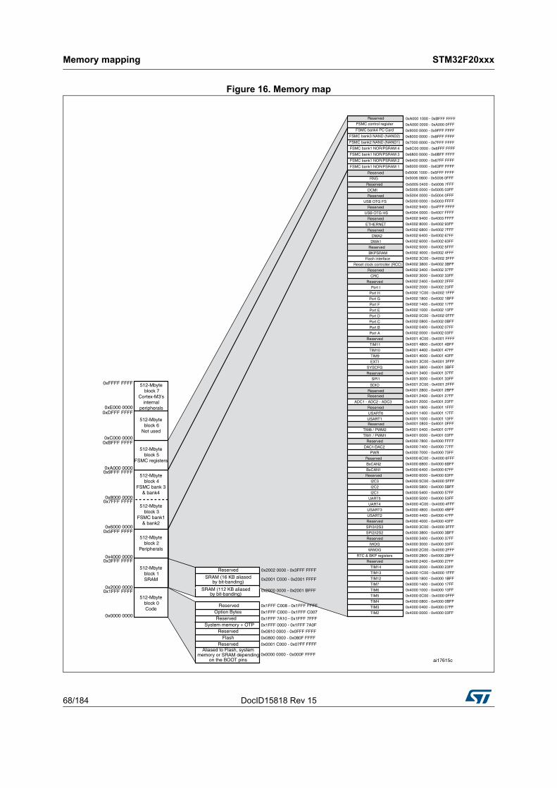
Memory mapping STM32F20xxx
68/184 DocID15818 Rev 15
Figure 16. Memory map
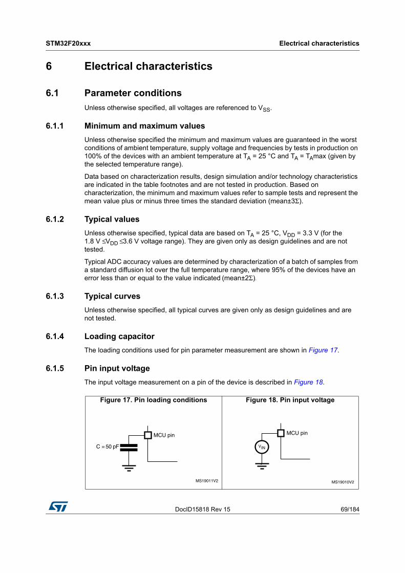
DocID15818 Rev 15 69/184
STM32F20xxx Electrical characteristics
183
6 Electrical characteristics
6.1 Parameter conditions
Unless otherwise specified, all voltages are referenced to VSS.
6.1.1 Minimum and maximum values
Unless otherwise specified the minimum and maximum values are guaranteed in the worst conditions of ambient temperature, supply voltage and frequencies by tests in production on 100% of the devices with an ambient temperature at TA = 25 °C and TA = TAmax (given by the selected temperature range).
Data based on characterization results, design simulation and/or technology characteristics are indicated in the table footnotes and are not tested in production. Based on characterization, the minimum and maximum values refer to sample tests and represent the mean value plus or minus three times the standard deviation (mean±3Σ).
6.1.2 Typical values
Unless otherwise specified, typical data are based on TA = 25 °C, VDD = 3.3 V (for the 1.8 V ≤ VDD ≤ 3.6 V voltage range). They are given only as design guidelines and are not tested.
Typical ADC accuracy values are determined by characterization of a batch of samples from a standard diffusion lot over the full temperature range, where 95% of the devices have an error less than or equal to the value indicated (mean±2Σ).
6.1.3 Typical curves
Unless otherwise specified, all typical curves are given only as design guidelines and are not tested.
6.1.4 Loading capacitor
The loading conditions used for pin parameter measurement are shown in Figure 17.
6.1.5 Pin input voltage
The input voltage measurement on a pin of the device is described in Figure 18.
Figure 17. Pin loading conditions Figure 18. Pin input voltage
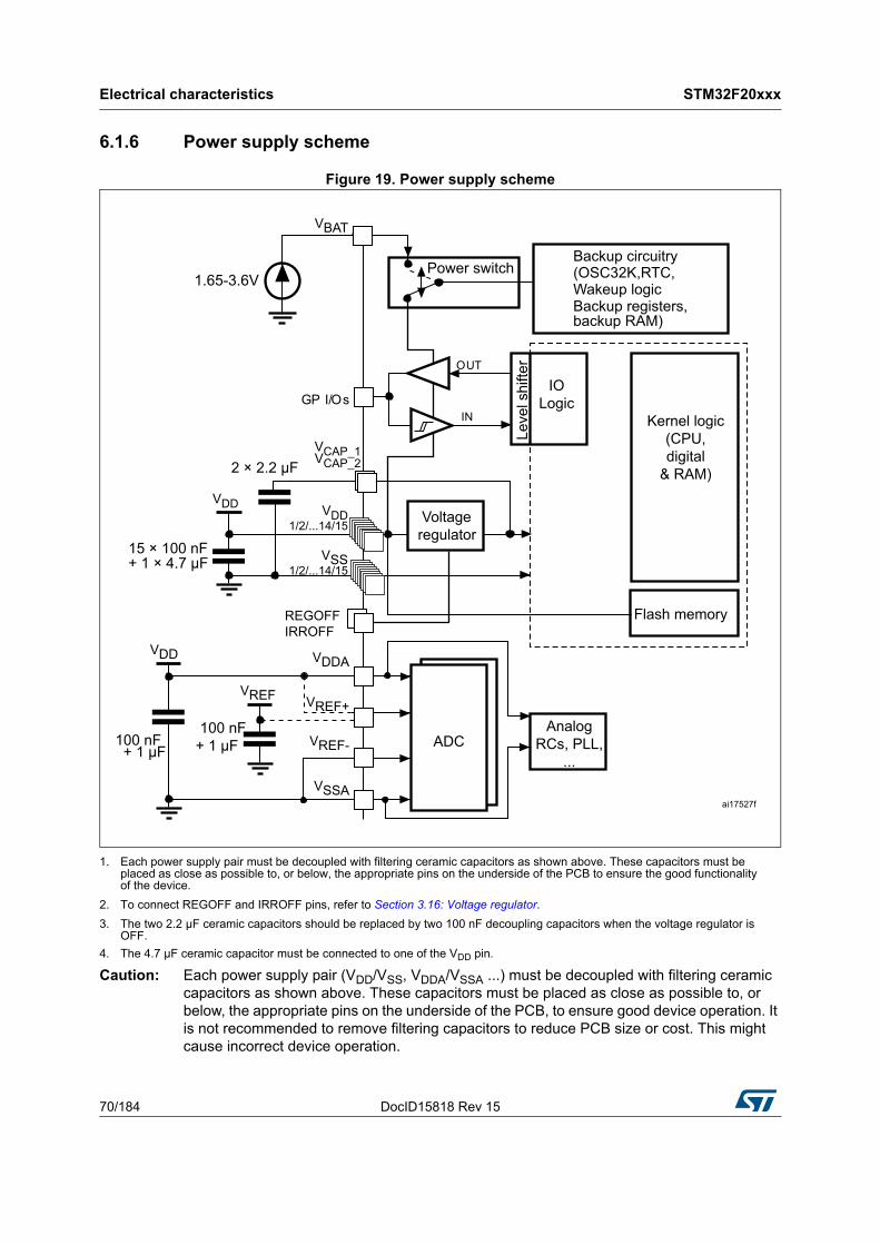
Electrical characteristics STM32F20xxx
70/184 DocID15818 Rev 15
6.1.6 Power supply scheme
Figure 19. Power supply scheme
1. Each power supply pair must be decoupled with filtering ceramic capacitors as shown above. These capacitors must be placed as close as possible to, or below, the appropriate pins on the underside of the PCB to ensure the good functionality of the device.
2. To connect REGOFF and IRROFF pins, refer to Section 3.16: Voltage regulator.
3. The two 2.2 µF ceramic capacitors should be replaced by two 100 nF decoupling capacitors when the voltage regulator is OFF.
4. The 4.7 µF ceramic capacitor must be connected to one of the VDD pin.
Caution: Each power supply pair (VDD/VSS, VDDA/VSSA ...) must be decoupled with filtering ceramic capacitors as shown above. These capacitors must be placed as close as possible to, or below, the appropriate pins on the underside of the PCB, to ensure good device operation. It is not recommended to remove filtering capacitors to reduce PCB size or cost. This might cause incorrect device operation.
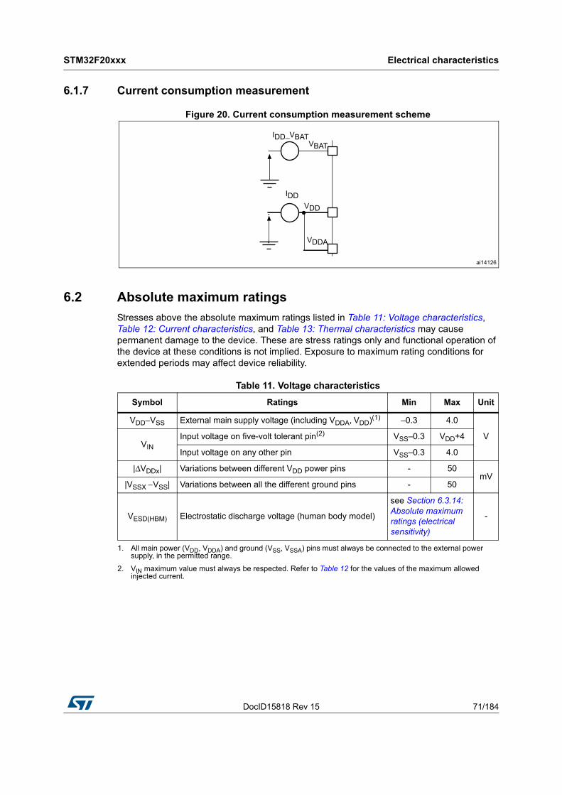
DocID15818 Rev 15 71/184
STM32F20xxx Electrical characteristics
183
6.1.7 Current consumption measurement
Figure 20. Current consumption measurement scheme
6.2 Absolute maximum ratings
Stresses above the absolute maximum ratings listed in Table 11: Voltage characteristics, Table 12: Current characteristics, and Table 13: Thermal characteristics may cause permanent damage to the device. These are stress ratings only and functional operation of the device at these conditions is not implied. Exposure to maximum rating conditions for extended periods may affect device reliability.
Table 11. Voltage characteristics
Symbol Ratings Min Max Unit
VDD–VSS External main supply voltage (including VDDA, VDD)(1)
1. All main power (VDD, VDDA) and ground (VSS, VSSA) pins must always be connected to the external power supply, in the permitted range.
–0.3 4.0
VVIN
Input voltage on five-volt tolerant pin(2)
2. VIN maximum value must always be respected. Refer to Table 12 for the values of the maximum allowed injected current.
VSS–0.3 VDD+4
Input voltage on any other pin VSS–0.3 4.0
|ΔVDDx| Variations between different VDD power pins - 50mV
|VSSX − VSS| Variations between all the different ground pins - 50
VESD(HBM) Electrostatic discharge voltage (human body model)
see Section 6.3.14: Absolute maximum ratings (electrical sensitivity)
-
Electrical characteristics STM32F20xxx
72/184 DocID15818 Rev 15
6.3 Operating conditions
6.3.1 General operating conditions
Table 12. Current characteristics
Symbol Ratings Max Unit
IVDD Total current into VDD power lines (source)(1)
1. All main power (VDD, VDDA) and ground (VSS, VSSA) pins must always be connected to the external power supply, in the permitted range.
120
mA
IVSS Total current out of VSS ground lines (sink)(1) 120
IIOOutput current sunk by any I/O and control pin 25
Output current source by any I/Os and control pin 25
IINJ(PIN) (2)
2. Negative injection disturbs the analog performance of the device. See note in Section 6.3.20: 12-bit ADC characteristics.
Injected current on five-volt tolerant I/O(3)
3. Positive injection is not possible on these I/Os. A negative injection is induced by VIN<VSS. IINJ(PIN) must never be exceeded. Refer to Table 11 for the values of the maximum allowed input voltage.
–5/+0
Injected current on any other pin(4)
4. A positive injection is induced by VIN>VDD while a negative injection is induced by VIN<VSS. IINJ(PIN) must never be exceeded. Refer to Table 11 for the values of the maximum allowed input voltage.
±5
ΣIINJ(PIN)(4) Total injected current (sum of all I/O and control pins)(5)
5. When several inputs are submitted to a current injection, the maximum ΣIINJ(PIN) is the absolute sum of the positive and negative injected currents (instantaneous values).
±25
Table 13. Thermal characteristics
Symbol Ratings Value Unit
TSTG Storage temperature range –65 to +150 °C
TJ Maximum junction temperature 125 °C
Table 14. General operating conditions
Symbol Parameter Conditions Min Max Unit
fHCLK Internal AHB clock frequency - 0 120
MHzfPCLK1 Internal APB1 clock frequency - 0 30
fPCLK2 Internal APB2 clock frequency - 0 60
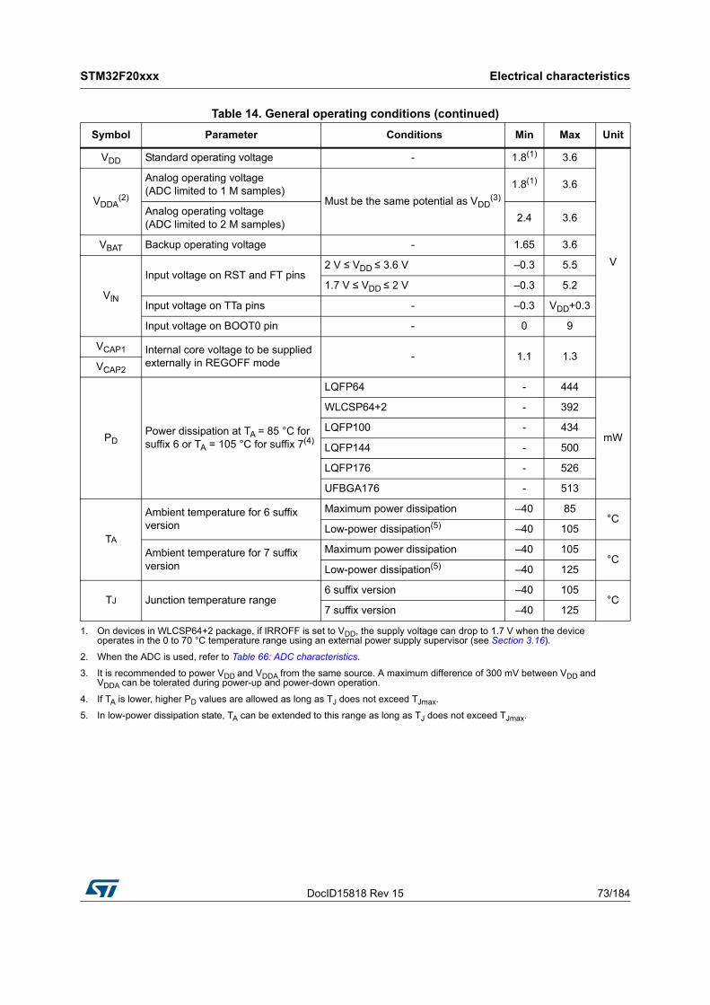
DocID15818 Rev 15 73/184
STM32F20xxx Electrical characteristics
183
VDD Standard operating voltage - 1.8(1) 3.6
V
VDDA(2)
Analog operating voltage (ADC limited to 1 M samples)
Must be the same potential as VDD(3)
1.8(1) 3.6
Analog operating voltage (ADC limited to 2 M samples)
2.4 3.6
VBAT Backup operating voltage - 1.65 3.6
VIN
Input voltage on RST and FT pins2 V ≤ VDD ≤ 3.6 V –0.3 5.5
1.7 V ≤ VDD ≤ 2 V –0.3 5.2
Input voltage on TTa pins - –0.3 VDD+0.3
Input voltage on BOOT0 pin - 0 9
VCAP1 Internal core voltage to be supplied externally in REGOFF mode
- 1.1 1.3VCAP2
PDPower dissipation at TA = 85 °C for suffix 6 or TA = 105 °C for suffix 7(4)
LQFP64 - 444
mW
WLCSP64+2 - 392
LQFP100 - 434
LQFP144 - 500
LQFP176 - 526
UFBGA176 - 513
TA
Ambient temperature for 6 suffix version
Maximum power dissipation –40 85°C
Low-power dissipation(5) –40 105
Ambient temperature for 7 suffix version
Maximum power dissipation –40 105°C
Low-power dissipation(5) –40 125
TJ Junction temperature range6 suffix version –40 105
°C7 suffix version –40 125
1. On devices in WLCSP64+2 package, if IRROFF is set to VDD, the supply voltage can drop to 1.7 V when the device operates in the 0 to 70 °C temperature range using an external power supply supervisor (see Section 3.16).
2. When the ADC is used, refer to Table 66: ADC characteristics.
3. It is recommended to power VDD and VDDA from the same source. A maximum difference of 300 mV between VDD and VDDA can be tolerated during power-up and power-down operation.
4. If TA is lower, higher PD values are allowed as long as TJ does not exceed TJmax.
5. In low-power dissipation state, TA can be extended to this range as long as TJ does not exceed TJmax.
Table 14. General operating conditions (continued)
Symbol Parameter Conditions Min Max Unit
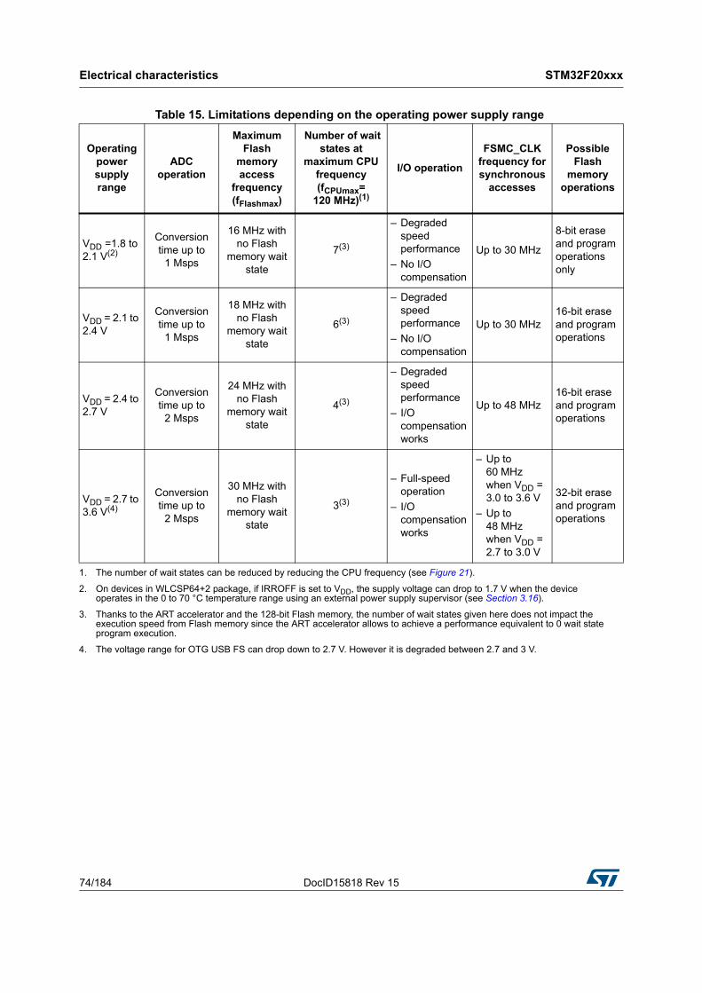
Electrical characteristics STM32F20xxx
74/184 DocID15818 Rev 15
Table 15. Limitations depending on the operating power supply range
Operating power supply range
ADC operation
Maximum Flash
memory access
frequency (fFlashmax)
Number of wait states at
maximum CPU frequency (fCPUmax=
120 MHz)(1)
I/O operation
FSMC_CLK frequency for synchronous
accesses
Possible Flash
memory operations
VDD =1.8 to 2.1 V(2)
Conversion time up to
1 Msps
16 MHz with no Flash
memory wait state
7(3)
– Degraded speed performance
– No I/O compensation
Up to 30 MHz
8-bit erase and program operations only
VDD = 2.1 to 2.4 V
Conversion time up to
1 Msps
18 MHz with no Flash
memory wait state
6(3)
– Degraded speed performance
– No I/O compensation
Up to 30 MHz16-bit erase and program operations
VDD = 2.4 to 2.7 V
Conversion time up to
2 Msps
24 MHz with no Flash
memory wait state
4(3)
– Degraded speed performance
– I/O compensation works
Up to 48 MHz16-bit erase and program operations
VDD = 2.7 to 3.6 V(4)
Conversion time up to
2 Msps
30 MHz with no Flash
memory wait state
3(3)
– Full-speed operation
– I/O compensation works
– Up to 60 MHz when VDD = 3.0 to 3.6 V
– Up to 48 MHz when VDD = 2.7 to 3.0 V
32-bit erase and program operations
1. The number of wait states can be reduced by reducing the CPU frequency (see Figure 21).
2. On devices in WLCSP64+2 package, if IRROFF is set to VDD, the supply voltage can drop to 1.7 V when the device operates in the 0 to 70 °C temperature range using an external power supply supervisor (see Section 3.16).
3. Thanks to the ART accelerator and the 128-bit Flash memory, the number of wait states given here does not impact the execution speed from Flash memory since the ART accelerator allows to achieve a performance equivalent to 0 wait state program execution.
4. The voltage range for OTG USB FS can drop down to 2.7 V. However it is degraded between 2.7 and 3 V.
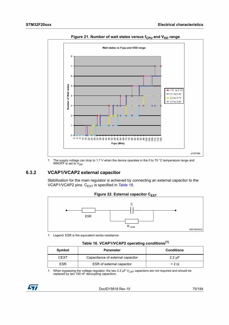
DocID15818 Rev 15 75/184
STM32F20xxx Electrical characteristics
183
Figure 21. Number of wait states versus fCPU and VDD range
1. The supply voltage can drop to 1.7 V when the device operates in the 0 to 70 °C temperature range and IRROFF is set to VDD.
6.3.2 VCAP1/VCAP2 external capacitor
Stabilization for the main regulator is achieved by connecting an external capacitor to the VCAP1/VCAP2 pins. CEXT is specified in Table 16.
Figure 22. External capacitor CEXT
1. Legend: ESR is the equivalent series resistance.
Table 16. VCAP1/VCAP2 operating conditions(1)
1. When bypassing the voltage regulator, the two 2.2 µF VCAP capacitors are not required and should be replaced by two 100 nF decoupling capacitors.
Symbol Parameter Conditions
CEXT Capacitance of external capacitor 2.2 µF
ESR ESR of external capacitor < 2 Ω
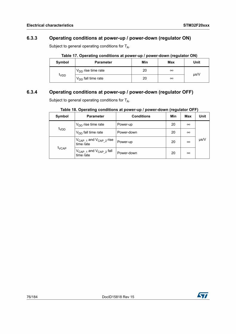
Electrical characteristics STM32F20xxx
76/184 DocID15818 Rev 15
6.3.3 Operating conditions at power-up / power-down (regulator ON)
Subject to general operating conditions for TA.
Table 17. Operating conditions at power-up / power-down (regulator ON)
6.3.4 Operating conditions at power-up / power-down (regulator OFF)
Subject to general operating conditions for TA.
Table 18. Operating conditions at power-up / power-down (regulator OFF)
Symbol Parameter Min Max Unit
tVDD
VDD rise time rate 20 ∞µs/V
VDD fall time rate 20 ∞
Symbol Parameter Conditions Min Max Unit
tVDD
VDD rise time rate Power-up 20 ∞
µs/V
VDD fall time rate Power-down 20 ∞
tVCAP
VCAP_1 and VCAP_2 rise time rate
Power-up 20 ∞
VCAP_1 and VCAP_2 fall time rate
Power-down 20 ∞
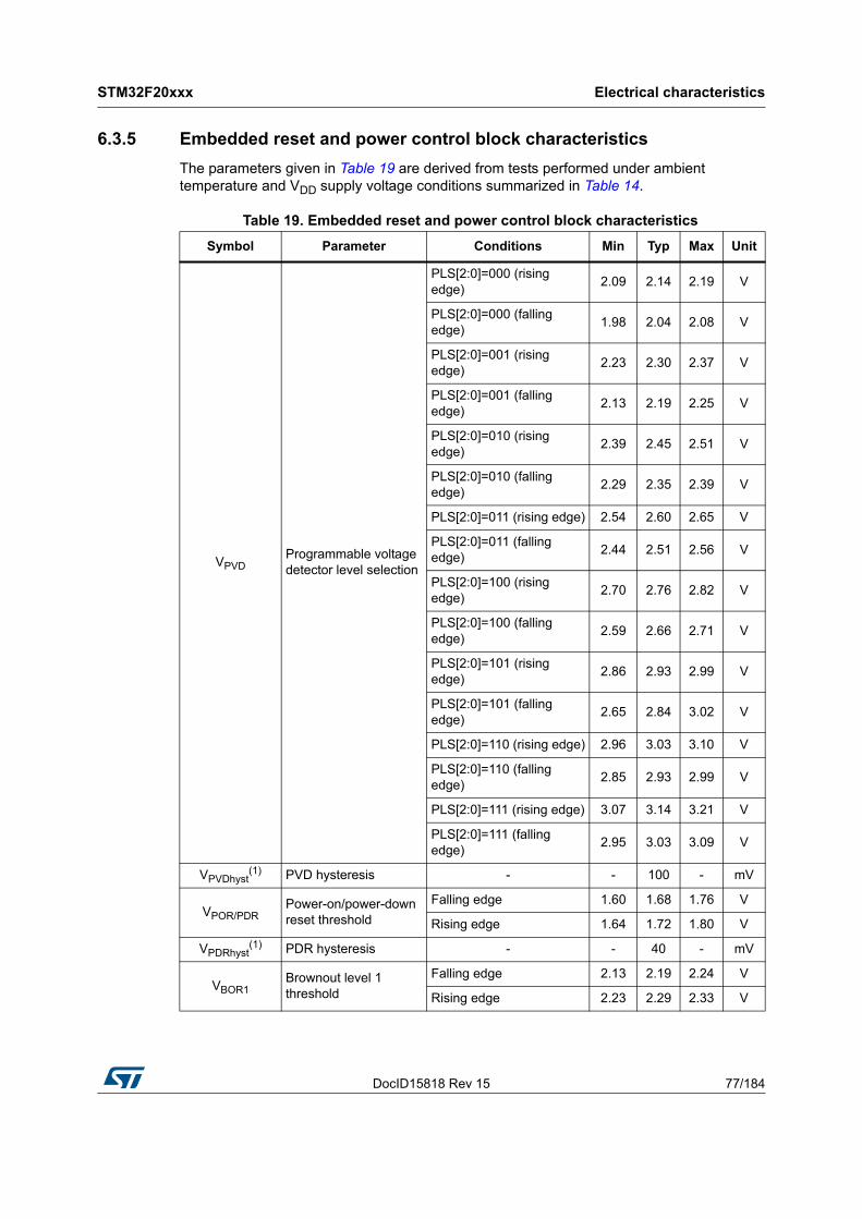
DocID15818 Rev 15 77/184
STM32F20xxx Electrical characteristics
183
6.3.5 Embedded reset and power control block characteristics
The parameters given in Table 19 are derived from tests performed under ambient temperature and VDD supply voltage conditions summarized in Table 14.
Table 19. Embedded reset and power control block characteristics
Symbol Parameter Conditions Min Typ Max Unit
VPVDProgrammable voltage detector level selection
PLS[2:0]=000 (rising edge)
2.09 2.14 2.19 V
PLS[2:0]=000 (falling edge)
1.98 2.04 2.08 V
PLS[2:0]=001 (rising edge)
2.23 2.30 2.37 V
PLS[2:0]=001 (falling edge)
2.13 2.19 2.25 V
PLS[2:0]=010 (rising edge)
2.39 2.45 2.51 V
PLS[2:0]=010 (falling edge)
2.29 2.35 2.39 V
PLS[2:0]=011 (rising edge) 2.54 2.60 2.65 V
PLS[2:0]=011 (falling edge)
2.44 2.51 2.56 V
PLS[2:0]=100 (rising edge)
2.70 2.76 2.82 V
PLS[2:0]=100 (falling edge)
2.59 2.66 2.71 V
PLS[2:0]=101 (rising edge)
2.86 2.93 2.99 V
PLS[2:0]=101 (falling edge)
2.65 2.84 3.02 V
PLS[2:0]=110 (rising edge) 2.96 3.03 3.10 V
PLS[2:0]=110 (falling edge)
2.85 2.93 2.99 V
PLS[2:0]=111 (rising edge) 3.07 3.14 3.21 V
PLS[2:0]=111 (falling edge)
2.95 3.03 3.09 V
VPVDhyst(1) PVD hysteresis - - 100 - mV
VPOR/PDRPower-on/power-down reset threshold
Falling edge 1.60 1.68 1.76 V
Rising edge 1.64 1.72 1.80 V
VPDRhyst(1) PDR hysteresis - - 40 - mV
VBOR1Brownout level 1 threshold
Falling edge 2.13 2.19 2.24 V
Rising edge 2.23 2.29 2.33 V
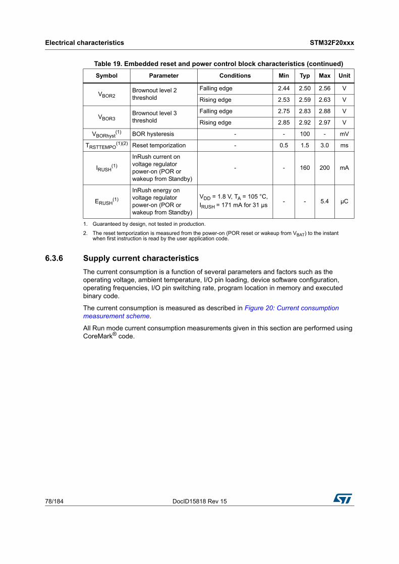
Electrical characteristics STM32F20xxx
78/184 DocID15818 Rev 15
6.3.6 Supply current characteristics
The current consumption is a function of several parameters and factors such as the operating voltage, ambient temperature, I/O pin loading, device software configuration, operating frequencies, I/O pin switching rate, program location in memory and executed binary code.
The current consumption is measured as described in Figure 20: Current consumption measurement scheme.
All Run mode current consumption measurements given in this section are performed using CoreMark® code.
VBOR2Brownout level 2 threshold
Falling edge 2.44 2.50 2.56 V
Rising edge 2.53 2.59 2.63 V
VBOR3Brownout level 3 threshold
Falling edge 2.75 2.83 2.88 V
Rising edge 2.85 2.92 2.97 V
VBORhyst(1) BOR hysteresis - - 100 - mV
TRSTTEMPO(1)(2) Reset temporization - 0.5 1.5 3.0 ms
IRUSH(1)
InRush current on voltage regulator power-on (POR or wakeup from Standby)
- - 160 200 mA
ERUSH(1)
InRush energy on voltage regulator power-on (POR or wakeup from Standby)
VDD = 1.8 V, TA = 105 °C,
IRUSH = 171 mA for 31 µs- - 5.4 µC
1. Guaranteed by design, not tested in production.
2. The reset temporization is measured from the power-on (POR reset or wakeup from VBAT) to the instant when first instruction is read by the user application code.
Table 19. Embedded reset and power control block characteristics (continued)
Symbol Parameter Conditions Min Typ Max Unit
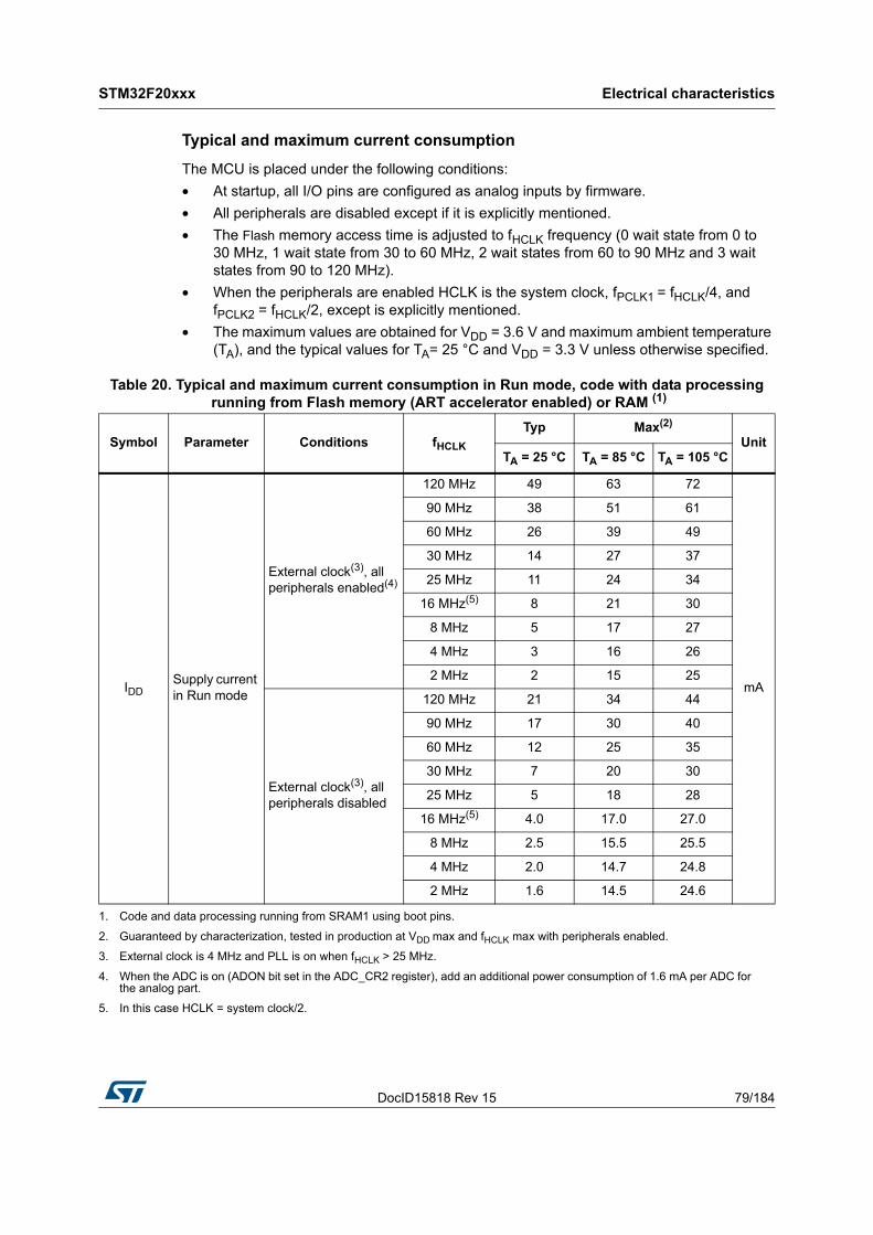
DocID15818 Rev 15 79/184
STM32F20xxx Electrical characteristics
183
Typical and maximum current consumption
The MCU is placed under the following conditions:
• At startup, all I/O pins are configured as analog inputs by firmware.
• All peripherals are disabled except if it is explicitly mentioned.
• The Flash memory access time is adjusted to fHCLK frequency (0 wait state from 0 to 30 MHz, 1 wait state from 30 to 60 MHz, 2 wait states from 60 to 90 MHz and 3 wait states from 90 to 120 MHz).
• When the peripherals are enabled HCLK is the system clock, fPCLK1 = fHCLK/4, and fPCLK2 = fHCLK/2, except is explicitly mentioned.
• The maximum values are obtained for VDD = 3.6 V and maximum ambient temperature (TA), and the typical values for TA= 25 °C and VDD = 3.3 V unless otherwise specified.
Table 20. Typical and maximum current consumption in Run mode, code with data processing running from Flash memory (ART accelerator enabled) or RAM (1)
Symbol Parameter Conditions fHCLK
Typ Max(2)
UnitTA = 25 °C TA = 85 °C TA = 105 °C
IDDSupply current in Run mode
External clock(3), all peripherals enabled(4)
120 MHz 49 63 72
mA
90 MHz 38 51 61
60 MHz 26 39 49
30 MHz 14 27 37
25 MHz 11 24 34
16 MHz(5) 8 21 30
8 MHz 5 17 27
4 MHz 3 16 26
2 MHz 2 15 25
External clock(3), all peripherals disabled
120 MHz 21 34 44
90 MHz 17 30 40
60 MHz 12 25 35
30 MHz 7 20 30
25 MHz 5 18 28
16 MHz(5) 4.0 17.0 27.0
8 MHz 2.5 15.5 25.5
4 MHz 2.0 14.7 24.8
2 MHz 1.6 14.5 24.6
1. Code and data processing running from SRAM1 using boot pins.
2. Guaranteed by characterization, tested in production at VDD max and fHCLK max with peripherals enabled.
3. External clock is 4 MHz and PLL is on when fHCLK > 25 MHz.
4. When the ADC is on (ADON bit set in the ADC_CR2 register), add an additional power consumption of 1.6 mA per ADC for the analog part.
5. In this case HCLK = system clock/2.
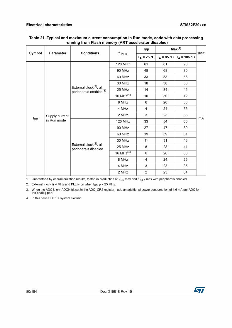
Electrical characteristics STM32F20xxx
80/184 DocID15818 Rev 15
Table 21. Typical and maximum current consumption in Run mode, code with data processing running from Flash memory (ART accelerator disabled)
Symbol Parameter Conditions fHCLK
Typ Max(1)
UnitTA = 25 °C TA = 85 °C TA = 105 °C
IDDSupply current in Run mode
External clock(2), all peripherals enabled(3)
120 MHz 61 81 93
mA
90 MHz 48 68 80
60 MHz 33 53 65
30 MHz 18 38 50
25 MHz 14 34 46
16 MHz(4) 10 30 42
8 MHz 6 26 38
4 MHz 4 24 36
2 MHz 3 23 35
External clock(2), all peripherals disabled
120 MHz 33 54 66
90 MHz 27 47 59
60 MHz 19 39 51
30 MHz 11 31 43
25 MHz 8 28 41
16 MHz(4) 6 26 38
8 MHz 4 24 36
4 MHz 3 23 35
2 MHz 2 23 34
1. Guaranteed by characterization results, tested in production at VDD max and fHCLK max with peripherals enabled.
2. External clock is 4 MHz and PLL is on when fHCLK > 25 MHz.
3. When the ADC is on (ADON bit set in the ADC_CR2 register), add an additional power consumption of 1.6 mA per ADC for the analog part.
4. In this case HCLK = system clock/2.
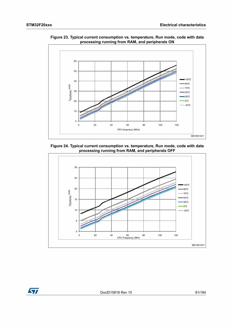
DocID15818 Rev 15 81/184
STM32F20xxx Electrical characteristics
183
Figure 23. Typical current consumption vs. temperature, Run mode, code with dataprocessing running from RAM, and peripherals ON
Figure 24. Typical current consumption vs. temperature, Run mode, code with dataprocessing running from RAM, and peripherals OFF
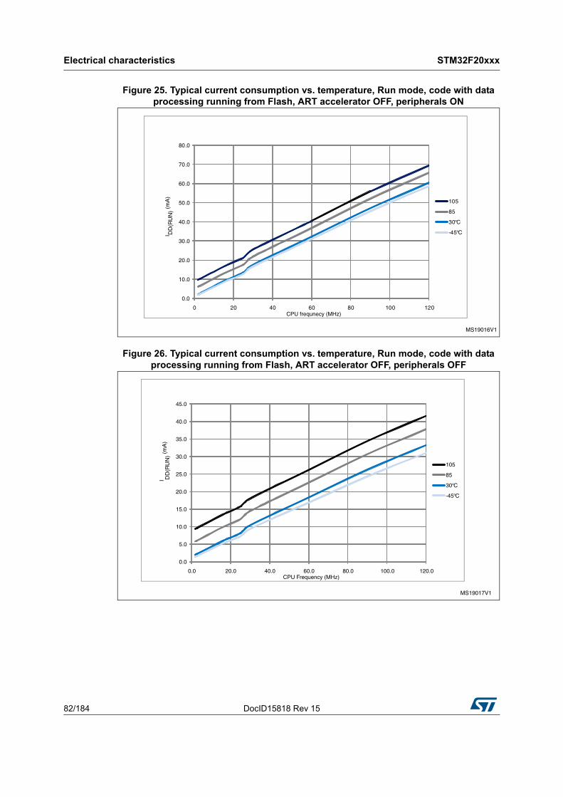
Electrical characteristics STM32F20xxx
82/184 DocID15818 Rev 15
Figure 25. Typical current consumption vs. temperature, Run mode, code with dataprocessing running from Flash, ART accelerator OFF, peripherals ON
Figure 26. Typical current consumption vs. temperature, Run mode, code with dataprocessing running from Flash, ART accelerator OFF, peripherals OFF
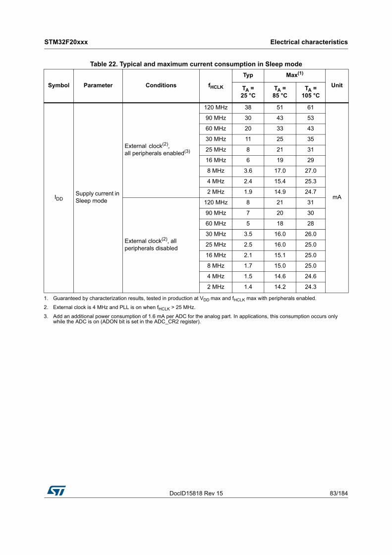
DocID15818 Rev 15 83/184
STM32F20xxx Electrical characteristics
183
Table 22. Typical and maximum current consumption in Sleep mode
Symbol Parameter Conditions fHCLK
Typ Max(1)
UnitTA = 25 °C
TA = 85 °C
TA = 105 °C
IDDSupply current in Sleep mode
External clock(2), all peripherals enabled(3)
120 MHz 38 51 61
mA
90 MHz 30 43 53
60 MHz 20 33 43
30 MHz 11 25 35
25 MHz 8 21 31
16 MHz 6 19 29
8 MHz 3.6 17.0 27.0
4 MHz 2.4 15.4 25.3
2 MHz 1.9 14.9 24.7
External clock(2), all peripherals disabled
120 MHz 8 21 31
90 MHz 7 20 30
60 MHz 5 18 28
30 MHz 3.5 16.0 26.0
25 MHz 2.5 16.0 25.0
16 MHz 2.1 15.1 25.0
8 MHz 1.7 15.0 25.0
4 MHz 1.5 14.6 24.6
2 MHz 1.4 14.2 24.3
1. Guaranteed by characterization results, tested in production at VDD max and fHCLK max with peripherals enabled.
2. External clock is 4 MHz and PLL is on when fHCLK > 25 MHz.
3. Add an additional power consumption of 1.6 mA per ADC for the analog part. In applications, this consumption occurs only while the ADC is on (ADON bit is set in the ADC_CR2 register).
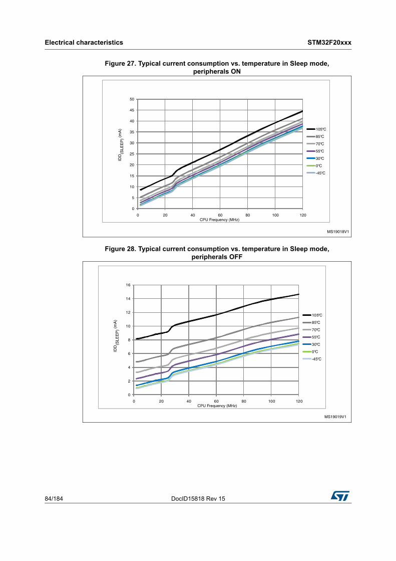
Electrical characteristics STM32F20xxx
84/184 DocID15818 Rev 15
Figure 27. Typical current consumption vs. temperature in Sleep mode,peripherals ON
Figure 28. Typical current consumption vs. temperature in Sleep mode,peripherals OFF
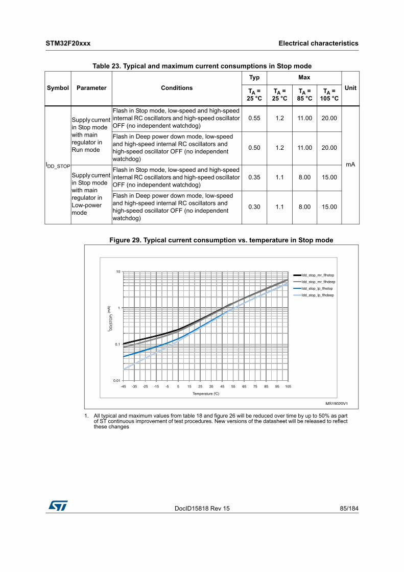
DocID15818 Rev 15 85/184
STM32F20xxx Electrical characteristics
183
Figure 29. Typical current consumption vs. temperature in Stop mode
1. All typical and maximum values from table 18 and figure 26 will be reduced over time by up to 50% as part of ST continuous improvement of test procedures. New versions of the datasheet will be released to reflect these changes
Table 23. Typical and maximum current consumptions in Stop mode
Symbol Parameter Conditions
Typ Max
UnitTA = 25 °C
TA = 25 °C
TA = 85 °C
TA = 105 °C
IDD_STOP
Supply current in Stop mode with main regulator in Run mode
Flash in Stop mode, low-speed and high-speed internal RC oscillators and high-speed oscillator OFF (no independent watchdog)
0.55 1.2 11.00 20.00
mA
Flash in Deep power down mode, low-speed and high-speed internal RC oscillators and high-speed oscillator OFF (no independent watchdog)
0.50 1.2 11.00 20.00
Supply current in Stop mode with main regulator in Low-power mode
Flash in Stop mode, low-speed and high-speed internal RC oscillators and high-speed oscillator OFF (no independent watchdog)
0.35 1.1 8.00 15.00
Flash in Deep power down mode, low-speed and high-speed internal RC oscillators and high-speed oscillator OFF (no independent watchdog)
0.30 1.1 8.00 15.00
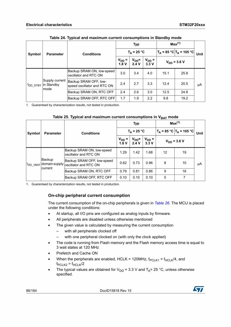
Electrical characteristics STM32F20xxx
86/184 DocID15818 Rev 15
On-chip peripheral current consumption
The current consumption of the on-chip peripherals is given in Table 26. The MCU is placed under the following conditions:
• At startup, all I/O pins are configured as analog inputs by firmware.
• All peripherals are disabled unless otherwise mentioned
• The given value is calculated by measuring the current consumption
– with all peripherals clocked off
– with one peripheral clocked on (with only the clock applied)
• The code is running from Flash memory and the Flash memory access time is equal to 3 wait states at 120 MHz
• Prefetch and Cache ON
• When the peripherals are enabled, HCLK = 120MHz, fPCLK1 = fHCLK/4, and fPCLK2 = fHCLK/2
• The typical values are obtained for VDD = 3.3 V and TA= 25 °C, unless otherwise specified.
Table 24. Typical and maximum current consumptions in Standby mode
Symbol Parameter Conditions
Typ Max(1)
UnitTA = 25 °C TA = 85 °C TA = 105 °C
VDD = 1.8 V
VDD= 2.4 V
VDD = 3.3 V
VDD = 3.6 V
IDD_STBY
Supply current in Standby mode
Backup SRAM ON, low-speed oscillator and RTC ON
3.0 3.4 4.0 15.1 25.8
µABackup SRAM OFF, low-speed oscillator and RTC ON
2.4 2.7 3.3 12.4 20.5
Backup SRAM ON, RTC OFF 2.4 2.6 3.0 12.5 24.8
Backup SRAM OFF, RTC OFF 1.7 1.9 2.2 9.8 19.2
1. Guaranteed by characterization results, not tested in production.
Table 25. Typical and maximum current consumptions in VBAT mode
Symbol Parameter Conditions
Typ Max(1)
UnitTA = 25 °C TA = 85 °C TA = 105 °C
VDD = 1.8 V
VDD= 2.4 V
VDD = 3.3 V
VDD = 3.6 V
IDD_VBAT
Backup domain supply current
Backup SRAM ON, low-speed oscillator and RTC ON
1.29 1.42 1.68 12 19
µABackup SRAM OFF, low-speed oscillator and RTC ON
0.62 0.73 0.96 8 10
Backup SRAM ON, RTC OFF 0.79 0.81 0.86 9 16
Backup SRAM OFF, RTC OFF 0.10 0.10 0.10 5 7
1. Guaranteed by characterization results, not tested in production.
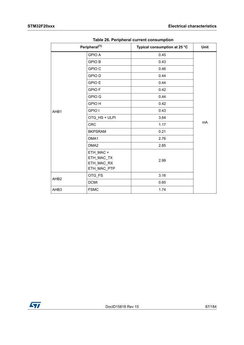
DocID15818 Rev 15 87/184
STM32F20xxx Electrical characteristics
183
Table 26. Peripheral current consumption
Peripheral(1) Typical consumption at 25 °C Unit
AHB1
GPIO A 0.45
mA
GPIO B 0.43
GPIO C 0.46
GPIO D 0.44
GPIO E 0.44
GPIO F 0.42
GPIO G 0.44
GPIO H 0.42
GPIO I 0.43
OTG_HS + ULPI 3.64
CRC 1.17
BKPSRAM 0.21
DMA1 2.76
DMA2 2.85
ETH_MAC +
ETH_MAC_TX
ETH_MAC_RX
ETH_MAC_PTP
2.99
AHB2OTG_FS 3.16
DCMI 0.60
AHB3 FSMC 1.74
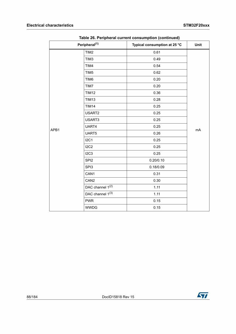
Electrical characteristics STM32F20xxx
88/184 DocID15818 Rev 15
APB1
TIM2 0.61
mA
TIM3 0.49
TIM4 0.54
TIM5 0.62
TIM6 0.20
TIM7 0.20
TIM12 0.36
TIM13 0.28
TIM14 0.25
USART2 0.25
USART3 0.25
UART4 0.25
UART5 0.26
I2C1 0.25
I2C2 0.25
I2C3 0.25
SPI2 0.20/0.10
SPI3 0.18/0.09
CAN1 0.31
CAN2 0.30
DAC channel 1(2) 1.11
DAC channel 1(3) 1.11
PWR 0.15
WWDG 0.15
Table 26. Peripheral current consumption (continued)
Peripheral(1) Typical consumption at 25 °C Unit
DocID15818 Rev 15 89/184
STM32F20xxx Electrical characteristics
183
6.3.7 Wakeup time from low-power mode
The wakeup times given in Table 27 is measured on a wakeup phase with a 16 MHz HSI RC oscillator. The clock source used to wake up the device depends from the current operating mode:
• Stop or Standby mode: the clock source is the RC oscillator
• Sleep mode: the clock source is the clock that was set before entering Sleep mode.
All timings are derived from tests performed under ambient temperature and VDD supply voltage conditions summarized in Table 14.
APB2
SDIO 0.69
mA
TIM1 1.06
TIM8 1.03
TIM9 0.58
TIM10 0.37
TIM11 0.39
ADC1(4) 2.13
ADC2(4) 2.04
ADC3(4) 2.12
SPI1 1.20
USART1 0.38
USART6 0.37
1. External clock is 25 MHz (HSE oscillator with 25 MHz crystal) and PLL is on.
2. EN1 bit is set in DAC_CR register.
3. EN2 bit is set in DAC_CR register.
4. fADC = fPCLK2/2, ADON bit set in ADC_CR2 register.
Table 26. Peripheral current consumption (continued)
Peripheral(1) Typical consumption at 25 °C Unit
Table 27. Low-power mode wakeup timings
Symbol Parameter Min(1) Typ(1) Max(1) Unit
tWUSLEEP(2) Wakeup from Sleep mode - 1 - µs
tWUSTOP(2)
Wakeup from Stop mode (regulator in Run mode) - 13 -
µsWakeup from Stop mode (regulator in low-power mode) - 17 40
Wakeup from Stop mode (regulator in low-power mode and Flash memory in Deep power down mode)
- 110 -
tWUSTDBY(2)(3) Wakeup from Standby mode 260 375 480 µs
1. Guaranteed by characterization results, not tested in production.
2. The wakeup times are measured from the wakeup event to the point in which the application code reads the first instruction.3. tWUSTDBY minimum and maximum values are given at 105 °C and –45 °C, respectively.
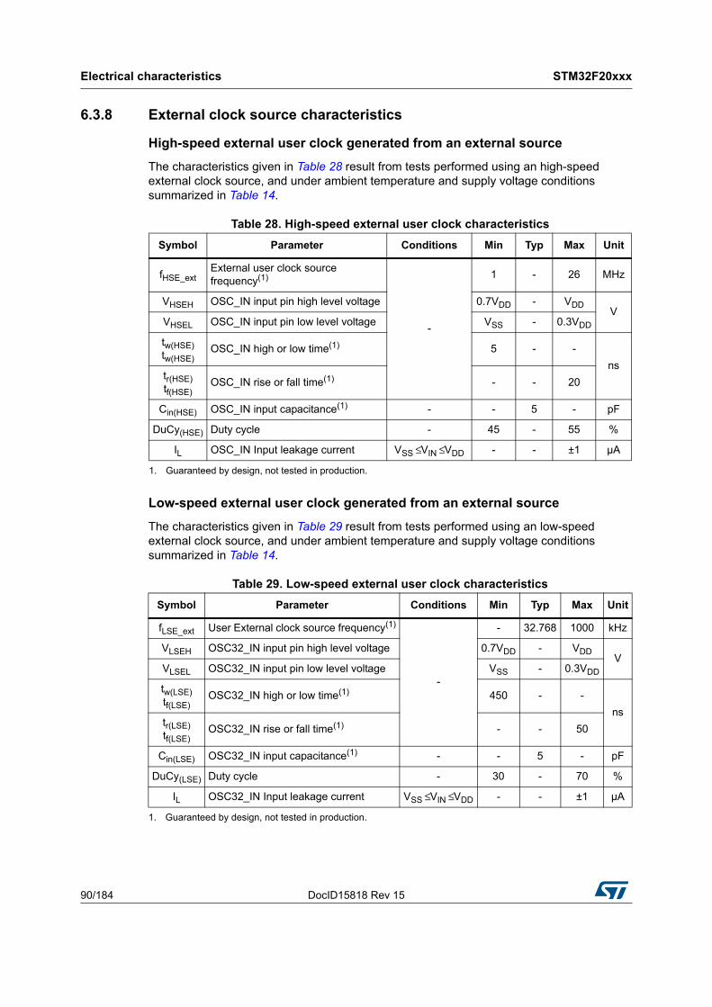
Electrical characteristics STM32F20xxx
90/184 DocID15818 Rev 15
6.3.8 External clock source characteristics
High-speed external user clock generated from an external source
The characteristics given in Table 28 result from tests performed using an high-speed external clock source, and under ambient temperature and supply voltage conditions summarized in Table 14.
Low-speed external user clock generated from an external source
The characteristics given in Table 29 result from tests performed using an low-speed external clock source, and under ambient temperature and supply voltage conditions summarized in Table 14.
Table 28. High-speed external user clock characteristics
Symbol Parameter Conditions Min Typ Max Unit
fHSE_extExternal user clock source frequency(1)
-
1 - 26 MHz
VHSEH OSC_IN input pin high level voltage 0.7VDD - VDDV
VHSEL OSC_IN input pin low level voltage VSS - 0.3VDD
tw(HSE)tw(HSE)
OSC_IN high or low time(1)
1. Guaranteed by design, not tested in production.
5 - -
nstr(HSE)tf(HSE)
OSC_IN rise or fall time(1) - - 20
Cin(HSE) OSC_IN input capacitance(1) - - 5 - pF
DuCy(HSE) Duty cycle - 45 - 55 %
IL OSC_IN Input leakage current VSS ≤ VIN ≤ VDD - - ±1 µA
Table 29. Low-speed external user clock characteristics
Symbol Parameter Conditions Min Typ Max Unit
fLSE_ext User External clock source frequency(1)
1. Guaranteed by design, not tested in production.
-
- 32.768 1000 kHz
VLSEH OSC32_IN input pin high level voltage 0.7VDD - VDDV
VLSEL OSC32_IN input pin low level voltage VSS - 0.3VDD
tw(LSE)tf(LSE)
OSC32_IN high or low time(1) 450 - -
nstr(LSE)tf(LSE)
OSC32_IN rise or fall time(1) - - 50
Cin(LSE) OSC32_IN input capacitance(1) - - 5 - pF
DuCy(LSE) Duty cycle - 30 - 70 %
IL OSC32_IN Input leakage current VSS ≤ VIN ≤ VDD - - ±1 µA
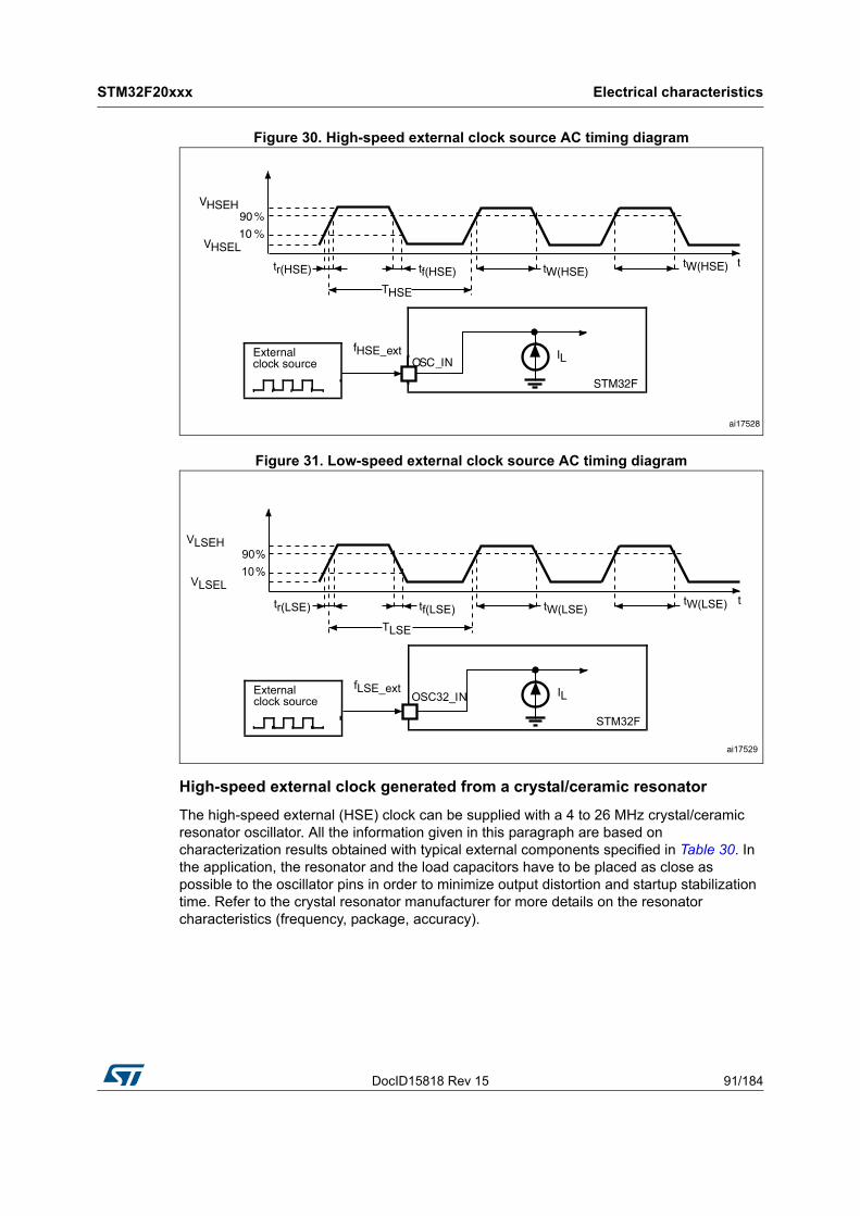
DocID15818 Rev 15 91/184
STM32F20xxx Electrical characteristics
183
Figure 30. High-speed external clock source AC timing diagram
Figure 31. Low-speed external clock source AC timing diagram
High-speed external clock generated from a crystal/ceramic resonator
The high-speed external (HSE) clock can be supplied with a 4 to 26 MHz crystal/ceramic resonator oscillator. All the information given in this paragraph are based on characterization results obtained with typical external components specified in Table 30. In the application, the resonator and the load capacitors have to be placed as close as possible to the oscillator pins in order to minimize output distortion and startup stabilization time. Refer to the crystal resonator manufacturer for more details on the resonator characteristics (frequency, package, accuracy).
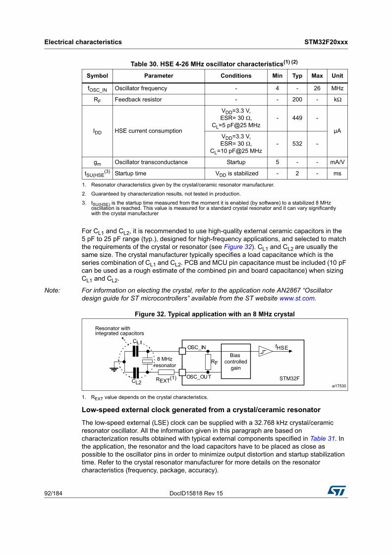
Electrical characteristics STM32F20xxx
92/184 DocID15818 Rev 15
For CL1 and CL2, it is recommended to use high-quality external ceramic capacitors in the 5 pF to 25 pF range (typ.), designed for high-frequency applications, and selected to match the requirements of the crystal or resonator (see Figure 32). CL1 and CL2 are usually the same size. The crystal manufacturer typically specifies a load capacitance which is the series combination of CL1 and CL2. PCB and MCU pin capacitance must be included (10 pF can be used as a rough estimate of the combined pin and board capacitance) when sizing CL1 and CL2.
Note: For information on electing the crystal, refer to the application note AN2867 “Oscillator design guide for ST microcontrollers” available from the ST website www.st.com.
Figure 32. Typical application with an 8 MHz crystal
1. REXT value depends on the crystal characteristics.
Low-speed external clock generated from a crystal/ceramic resonator
The low-speed external (LSE) clock can be supplied with a 32.768 kHz crystal/ceramic resonator oscillator. All the information given in this paragraph are based on characterization results obtained with typical external components specified in Table 31. In the application, the resonator and the load capacitors have to be placed as close as possible to the oscillator pins in order to minimize output distortion and startup stabilization time. Refer to the crystal resonator manufacturer for more details on the resonator characteristics (frequency, package, accuracy).
Table 30. HSE 4-26 MHz oscillator characteristics(1) (2)
1. Resonator characteristics given by the crystal/ceramic resonator manufacturer.
2. Guaranteed by characterization results, not tested in production.
Symbol Parameter Conditions Min Typ Max Unit
fOSC_IN Oscillator frequency - 4 - 26 MHz
RF Feedback resistor - - 200 - kΩ
IDD HSE current consumption
VDD=3.3 V, ESR= 30 Ω,
CL=5 pF@25 MHz- 449 -
µAVDD=3.3 V, ESR= 30 Ω,
CL=10 pF@25 MHz- 532 -
gm Oscillator transconductance Startup 5 - - mA/V
tSU(HSE(3)
3. tSU(HSE) is the startup time measured from the moment it is enabled (by software) to a stabilized 8 MHz oscillation is reached. This value is measured for a standard crystal resonator and it can vary significantly with the crystal manufacturer
Startup time VDD is stabilized - 2 - ms
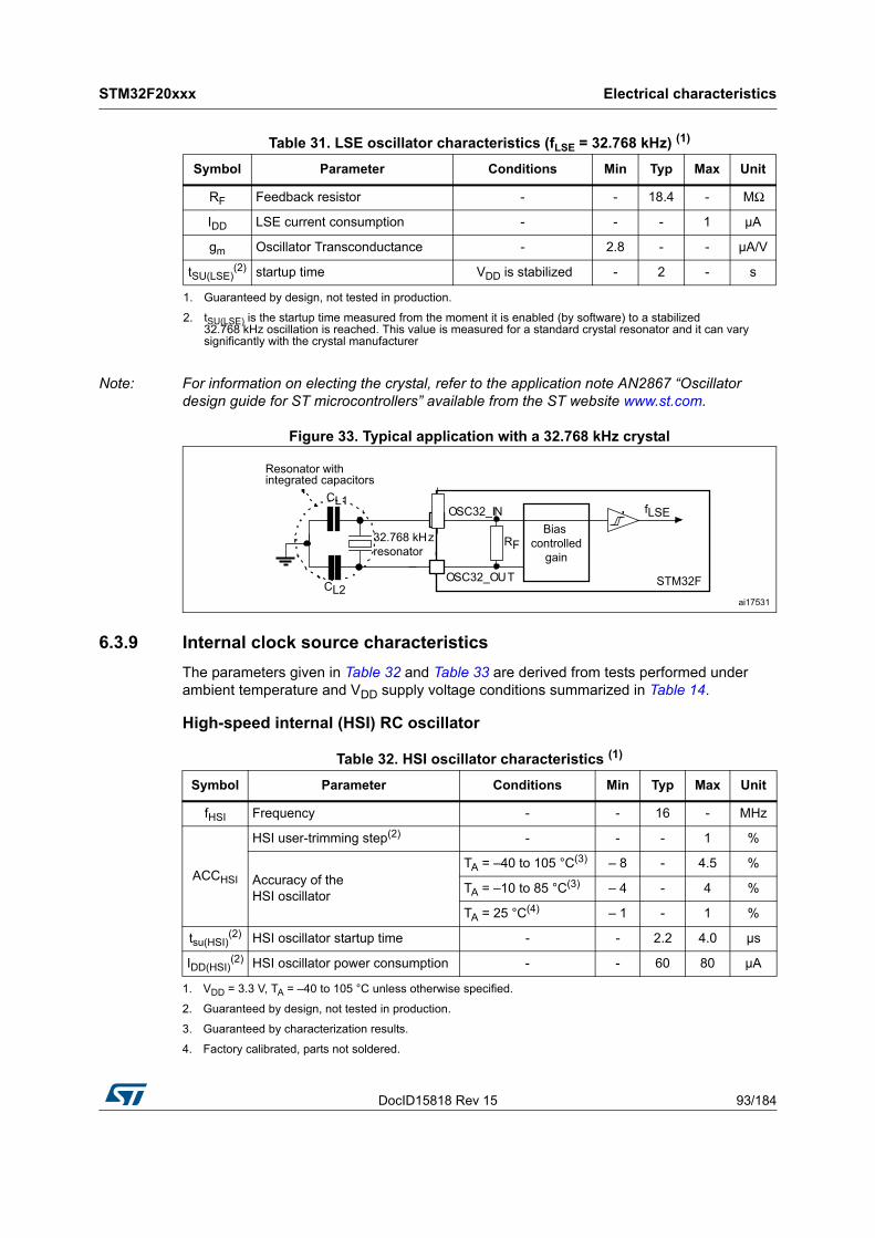
DocID15818 Rev 15 93/184
STM32F20xxx Electrical characteristics
183
Note: For information on electing the crystal, refer to the application note AN2867 “Oscillator design guide for ST microcontrollers” available from the ST website www.st.com.
Figure 33. Typical application with a 32.768 kHz crystal
6.3.9 Internal clock source characteristics
The parameters given in Table 32 and Table 33 are derived from tests performed under ambient temperature and VDD supply voltage conditions summarized in Table 14.
High-speed internal (HSI) RC oscillator
Table 31. LSE oscillator characteristics (fLSE = 32.768 kHz) (1)
1. Guaranteed by design, not tested in production.
Symbol Parameter Conditions Min Typ Max Unit
RF Feedback resistor - - 18.4 - MΩ
IDD LSE current consumption - - - 1 µA
gm Oscillator Transconductance - 2.8 - - µA/V
tSU(LSE)(2)
2. tSU(LSE) is the startup time measured from the moment it is enabled (by software) to a stabilized 32.768 kHz oscillation is reached. This value is measured for a standard crystal resonator and it can vary significantly with the crystal manufacturer
startup time VDD is stabilized - 2 - s
Table 32. HSI oscillator characteristics (1)
1. VDD = 3.3 V, TA = –40 to 105 °C unless otherwise specified.
Symbol Parameter Conditions Min Typ Max Unit
fHSI Frequency - - 16 - MHz
ACCHSI
HSI user-trimming step(2)
2. Guaranteed by design, not tested in production.
- - - 1 %
Accuracy of the HSI oscillator
TA = –40 to 105 °C(3)
3. Guaranteed by characterization results.
– 8 - 4.5 %
TA = –10 to 85 °C(3) – 4 - 4 %
TA = 25 °C(4)
4. Factory calibrated, parts not soldered.
– 1 - 1 %
tsu(HSI)(2) HSI oscillator startup time - - 2.2 4.0 µs
IDD(HSI)(2) HSI oscillator power consumption - - 60 80 µA
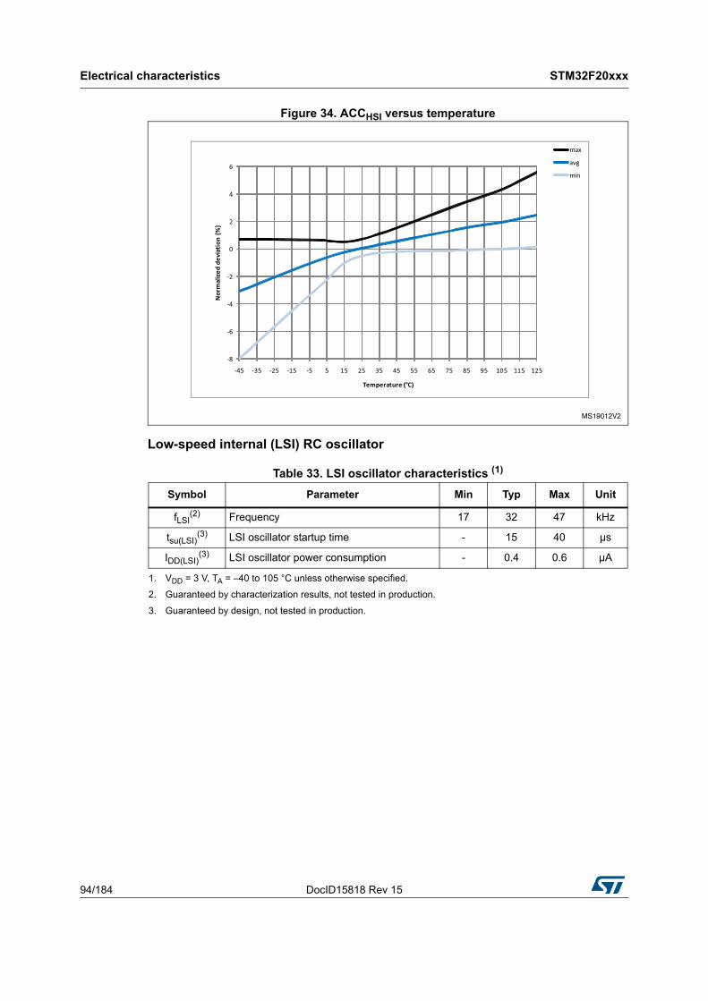
Electrical characteristics STM32F20xxx
94/184 DocID15818 Rev 15
Figure 34. ACCHSI versus temperature
Low-speed internal (LSI) RC oscillator
Table 33. LSI oscillator characteristics (1)
1. VDD = 3 V, TA = –40 to 105 °C unless otherwise specified.
Symbol Parameter Min Typ Max Unit
fLSI(2)
2. Guaranteed by characterization results, not tested in production.
Frequency 17 32 47 kHz
tsu(LSI)(3)
3. Guaranteed by design, not tested in production.
LSI oscillator startup time - 15 40 µs
IDD(LSI)(3) LSI oscillator power consumption - 0.4 0.6 µA
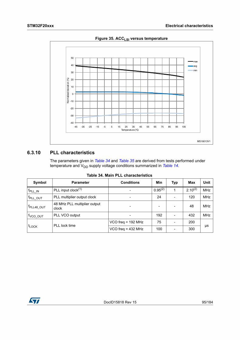
DocID15818 Rev 15 95/184
STM32F20xxx Electrical characteristics
183
Figure 35. ACCLSI versus temperature
6.3.10 PLL characteristics
The parameters given in Table 34 and Table 35 are derived from tests performed under temperature and VDD supply voltage conditions summarized in Table 14.
Table 34. Main PLL characteristics
Symbol Parameter Conditions Min Typ Max Unit
fPLL_IN PLL input clock(1) - 0.95(2) 1 2.10(2) MHz
fPLL_OUT PLL multiplier output clock - 24 - 120 MHz
fPLL48_OUT48 MHz PLL multiplier output clock
- - - 48 MHz
fVCO_OUT PLL VCO output - 192 - 432 MHz
tLOCK PLL lock timeVCO freq = 192 MHz 75 - 200
µsVCO freq = 432 MHz 100 - 300
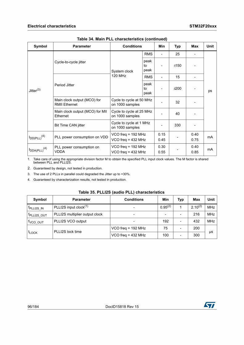
Electrical characteristics STM32F20xxx
96/184 DocID15818 Rev 15
Jitter(3)
Cycle-to-cycle jitter
System clock 120 MHz
RMS - 25 -
ps
peak to peak
- ±150 -
Period Jitter
RMS - 15 -
peak to peak
- ±200 -
Main clock output (MCO) for RMII Ethernet
Cycle to cycle at 50 MHz on 1000 samples
- 32 -
Main clock output (MCO) for MII Ethernet
Cycle to cycle at 25 MHz on 1000 samples
- 40 -
Bit Time CAN jitterCycle to cycle at 1 MHz on 1000 samples
- 330 -
IDD(PLL)(4) PLL power consumption on VDD
VCO freq = 192 MHz
VCO freq = 432 MHz
0.15
0.45-
0.40
0.75mA
IDDA(PLL)(4) PLL power consumption on
VDDAVCO freq = 192 MHz
VCO freq = 432 MHz
0.30
0.55-
0.40
0.85mA
1. Take care of using the appropriate division factor M to obtain the specified PLL input clock values. The M factor is shared between PLL and PLLI2S.
2. Guaranteed by design, not tested in production.
3. The use of 2 PLLs in parallel could degraded the Jitter up to +30%.
4. Guaranteed by characterization results, not tested in production.
Table 34. Main PLL characteristics (continued)
Symbol Parameter Conditions Min Typ Max Unit
Table 35. PLLI2S (audio PLL) characteristics
Symbol Parameter Conditions Min Typ Max Unit
fPLLI2S_IN PLLI2S input clock(1) - 0.95(2) 1 2.10(2) MHz
fPLLI2S_OUT PLLI2S multiplier output clock - - - 216 MHz
fVCO_OUT PLLI2S VCO output - 192 - 432 MHz
tLOCK PLLI2S lock timeVCO freq = 192 MHz 75 - 200
µsVCO freq = 432 MHz 100 - 300
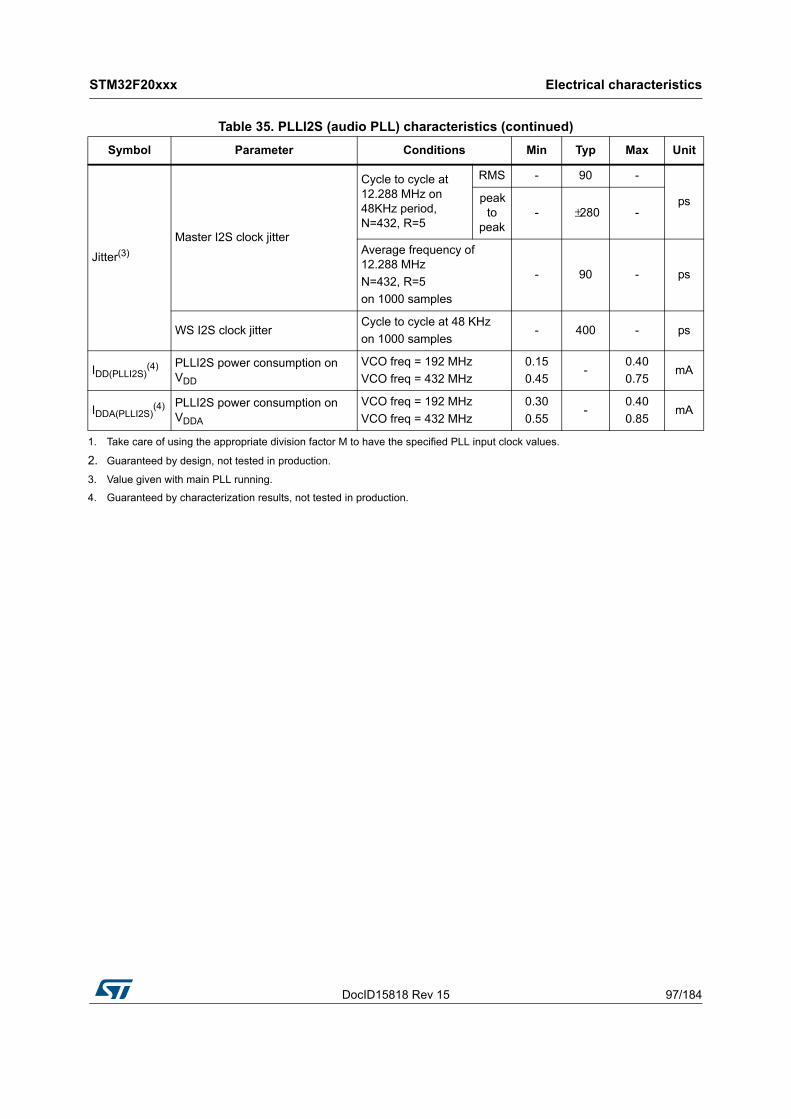
DocID15818 Rev 15 97/184
STM32F20xxx Electrical characteristics
183
Jitter(3)
Master I2S clock jitter
Cycle to cycle at 12.288 MHz on 48KHz period, N=432, R=5
RMS - 90 -
ps peak to
peak- ±280 -
Average frequency of 12.288 MHz
N=432, R=5
on 1000 samples
- 90 - ps
WS I2S clock jitterCycle to cycle at 48 KHz
on 1000 samples- 400 - ps
IDD(PLLI2S)(4) PLLI2S power consumption on
VDD
VCO freq = 192 MHz
VCO freq = 432 MHz
0.15
0.45-
0.40
0.75mA
IDDA(PLLI2S)(4) PLLI2S power consumption on
VDDA
VCO freq = 192 MHz
VCO freq = 432 MHz
0.30
0.55-
0.40
0.85mA
1. Take care of using the appropriate division factor M to have the specified PLL input clock values.
2. Guaranteed by design, not tested in production.
3. Value given with main PLL running.
4. Guaranteed by characterization results, not tested in production.
Table 35. PLLI2S (audio PLL) characteristics (continued)
Symbol Parameter Conditions Min Typ Max Unit
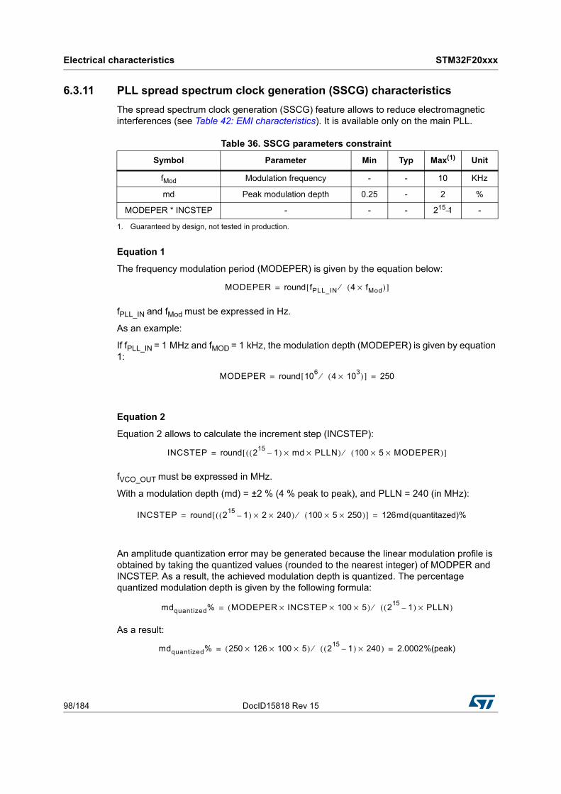
Electrical characteristics STM32F20xxx
98/184 DocID15818 Rev 15
6.3.11 PLL spread spectrum clock generation (SSCG) characteristics
The spread spectrum clock generation (SSCG) feature allows to reduce electromagnetic interferences (see Table 42: EMI characteristics). It is available only on the main PLL.
Equation 1
The frequency modulation period (MODEPER) is given by the equation below:
fPLL_IN and fMod must be expressed in Hz.
As an example:
If fPLL_IN = 1 MHz and fMOD = 1 kHz, the modulation depth (MODEPER) is given by equation 1:
Equation 2
Equation 2 allows to calculate the increment step (INCSTEP):
fVCO_OUT must be expressed in MHz.
With a modulation depth (md) = ±2 % (4 % peak to peak), and PLLN = 240 (in MHz):
An amplitude quantization error may be generated because the linear modulation profile is obtained by taking the quantized values (rounded to the nearest integer) of MODPER and INCSTEP. As a result, the achieved modulation depth is quantized. The percentage quantized modulation depth is given by the following formula:
As a result:
Table 36. SSCG parameters constraint
Symbol Parameter Min Typ Max(1)
1. Guaranteed by design, not tested in production.
Unit
fMod Modulation frequency - - 10 KHz
md Peak modulation depth 0.25 - 2 %
MODEPER * INCSTEP - - - 215−1 -
MODEPER round fPLL_IN 4 fMod×( )⁄[ ]=
MODEPER round 106
4 103×( )⁄[ ] 250= =
INCSTEP round 215
1–( ) md PLLN××( ) 100 5× MODEPER×( )⁄[ ]=
INCSTEP round 215
1–( ) 2 240××( ) 100 5× 250×( )⁄[ ] 126md(quantitazed)%= =
mdquantized% MODEPER INCSTEP× 100× 5×( ) 215
1–( ) PLLN×( )⁄=
mdquantized% 250 126× 100× 5×( ) 215
1–( ) 240×( )⁄ 2.0002%(peak)= =
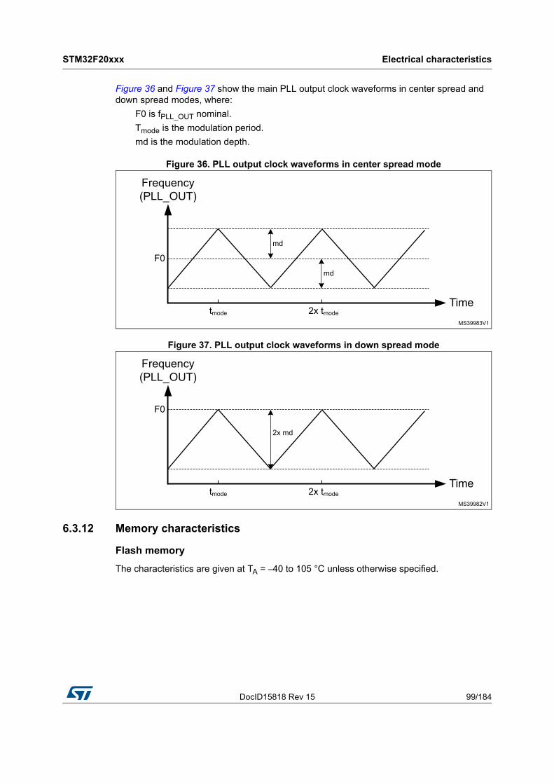
DocID15818 Rev 15 99/184
STM32F20xxx Electrical characteristics
183
Figure 36 and Figure 37 show the main PLL output clock waveforms in center spread and down spread modes, where:
F0 is fPLL_OUT nominal.
Tmode is the modulation period.
md is the modulation depth.
Figure 36. PLL output clock waveforms in center spread mode
Figure 37. PLL output clock waveforms in down spread mode
6.3.12 Memory characteristics
Flash memory
The characteristics are given at TA = –40 to 105 °C unless otherwise specified.
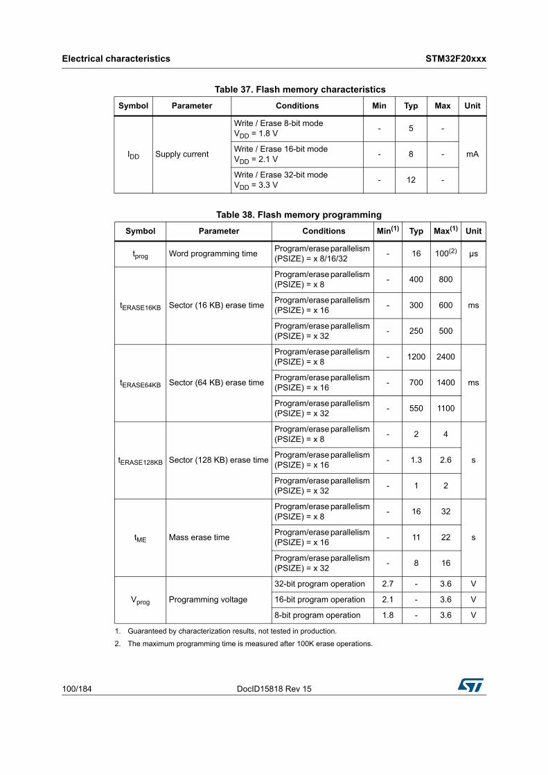
Electrical characteristics STM32F20xxx
100/184 DocID15818 Rev 15
Table 37. Flash memory characteristics
Symbol Parameter Conditions Min Typ Max Unit
IDD Supply current
Write / Erase 8-bit mode VDD = 1.8 V
- 5 -
mAWrite / Erase 16-bit mode VDD = 2.1 V
- 8 -
Write / Erase 32-bit mode VDD = 3.3 V
- 12 -
Table 38. Flash memory programming
Symbol Parameter Conditions Min(1) Typ Max(1)
1. Guaranteed by characterization results, not tested in production.
Unit
tprog Word programming timeProgram/erase parallelism (PSIZE) = x 8/16/32
- 16 100(2)
2. The maximum programming time is measured after 100K erase operations.
µs
tERASE16KB Sector (16 KB) erase time
Program/erase parallelism (PSIZE) = x 8
- 400 800
msProgram/erase parallelism (PSIZE) = x 16
- 300 600
Program/erase parallelism (PSIZE) = x 32
- 250 500
tERASE64KB Sector (64 KB) erase time
Program/erase parallelism (PSIZE) = x 8
- 1200 2400
msProgram/erase parallelism (PSIZE) = x 16
- 700 1400
Program/erase parallelism (PSIZE) = x 32
- 550 1100
tERASE128KB Sector (128 KB) erase time
Program/erase parallelism (PSIZE) = x 8
- 2 4
sProgram/erase parallelism (PSIZE) = x 16
- 1.3 2.6
Program/erase parallelism (PSIZE) = x 32
- 1 2
tME Mass erase time
Program/erase parallelism (PSIZE) = x 8
- 16 32
sProgram/erase parallelism (PSIZE) = x 16
- 11 22
Program/erase parallelism (PSIZE) = x 32
- 8 16
Vprog Programming voltage
32-bit program operation 2.7 - 3.6 V
16-bit program operation 2.1 - 3.6 V
8-bit program operation 1.8 - 3.6 V
DocID15818 Rev 15 101/184
STM32F20xxx Electrical characteristics
183
Table 40. Flash memory endurance and data retention
6.3.13 EMC characteristics
Susceptibility tests are performed on a sample basis during device characterization.
Functional EMS (electromagnetic susceptibility)
While a simple application is executed on the device (toggling 2 LEDs through I/O ports). the device is stressed by two electromagnetic events until a failure occurs. The failure is indicated by the LEDs:
• Electrostatic discharge (ESD) (positive and negative) is applied to all device pins until a functional disturbance occurs. This test is compliant with the IEC 61000-4-2 standard.
• FTB: A burst of fast transient voltage (positive and negative) is applied to VDD and VSS through a 100 pF capacitor, until a functional disturbance occurs. This test is compliant with the IEC 61000-4-4 standard.
A device reset allows normal operations to be resumed.
Table 39. Flash memory programming with VPP
Symbol Parameter Conditions Min(1) Typ Max(1)
1. Guaranteed by design, not tested in production.
Unit
tprog Double word programming
TA = 0 to +40 °C
VDD = 3.3 V
VPP = 8.5 V
- 16 100(2)
2. The maximum programming time is measured after 100K erase operations.
µs
tERASE16KB Sector (16 KB) erase time - 230 -
mstERASE64KB Sector (64 KB) erase time - 490 -
tERASE128KB Sector (128 KB) erase time - 875 -
tME Mass erase time - 6.9 - s
Vprog Programming voltage - 2.7 - 3.6 V
VPP VPP voltage range - 7 - 9 V
IPPMinimum current sunk on the VPP pin
- 10 - - mA
tVPP(3)
3. VPP should only be connected during programming/erasing.
Cumulative time during which VPP is applied
- - - 1 hour
Symbol Parameter ConditionsValue
UnitMin(1)
1. Guaranteed by characterization results, not tested in production.
NEND EnduranceTA = –40 to +85 °C (6 suffix versions)
TA = –40 to +105 °C (7 suffix versions)10 kcycles
tRET Data retention
1 kcycle(2) at TA = 85 °C
2. Cycling performed over the whole temperature range.
30
Years1 kcycle(2) at TA = 105 °C 10
10 kcycles(2) at TA = 55 °C 20
Electrical characteristics STM32F20xxx
102/184 DocID15818 Rev 15
The test results are given in Table 41. They are based on the EMS levels and classes defined in application note AN1709.
Designing hardened software to avoid noise problems
EMC characterization and optimization are performed at component level with a typical application environment and simplified MCU software. It should be noted that good EMC performance is highly dependent on the user application and the software in particular.
Therefore it is recommended that the user applies EMC software optimization and prequalification tests in relation with the EMC level requested for his application.
Software recommendations
The software flowchart must include the management of runaway conditions such as:
• Corrupted program counter
• Unexpected reset
• Critical Data corruption (control registers...)
Prequalification trials
Most of the common failures (unexpected reset and program counter corruption) can be reproduced by manually forcing a low state on the NRST pin or the Oscillator pins for 1 second.
To complete these trials, ESD stress can be applied directly on the device, over the range of specification values. When unexpected behavior is detected, the software can be hardened to prevent unrecoverable errors occurring (see application note AN1015).
Table 41. EMS characteristics
Symbol Parameter ConditionsLevel/Class
VFESDVoltage limits to be applied on any I/O pin to induce a functional disturbance
VDD = 3.3 V, LQFP176, TA = +25 °C, fHCLK = 120 MHz, conforms to IEC 61000-4-2
2B
VEFTB
Fast transient voltage burst limits to be applied through 100 pF on VDD and VSS pins to induce a functional disturbance
VDD = 3.3 V, LQFP176, TA = +25 °C, fHCLK = 120 MHz, conforms to IEC 61000-4-2
4A
DocID15818 Rev 15 103/184
STM32F20xxx Electrical characteristics
183
Electromagnetic Interference (EMI)
The electromagnetic field emitted by the device are monitored while a simple application, executing EEMBC® code, is running. This emission test is compliant with SAE IEC61967-2 standard which specifies the test board and the pin loading.
6.3.14 Absolute maximum ratings (electrical sensitivity)
Based on three different tests (ESD, LU) using specific measurement methods, the device is stressed in order to determine its performance in terms of electrical sensitivity.
Electrostatic discharge (ESD)
Electrostatic discharges (a positive then a negative pulse separated by 1 second) are applied to the pins of each sample according to each pin combination. The sample size depends on the number of supply pins in the device (3 parts × (n+1) supply pins). This test conforms to the JESD22-A114/C101 standard.
Table 42. EMI characteristics
Symbol Parameter ConditionsMonitored
frequency band
Max vs. [fHSE/fCPU]
Unit
25/120 MHz
SEMI Peak level
VDD = 3.3 V, TA = 25 °C, LQFP176 package, conforming to SAE J1752/3 EEMBC, code running with ART enabled, peripheral clock disabled
0.1 to 30 MHz
25 dBµV30 to 130 MHz
130 MHz to 1GHz
SAE EMI Level 4 -
VDD = 3.3 V, TA = 25 °C, LQFP176 package, conforming to SAE J1752/3 EEMBC, code running with ART enabled, PLL spread spectrum enabled, peripheral clock disabled
0.1 to 30 MHz 28
dBµV30 to 130 MHz 26
130 MHz to 1GHz 22
SAE EMI level 4 -
Table 43. ESD absolute maximum ratings
Symbol Ratings Conditions ClassMaximum value(1) Unit
VESD(HBM)
Electrostatic discharge voltage (human body model)
TA = +25 °C conforming to JESD22-A114 2 2000(2)
V
VESD(CDM)
Electrostatic discharge voltage (charge device model)
TA = +25 °C conforming to JESD22-C101 II 500
1. Guaranteed by characterization results, not tested in production.
2. On VBAT pin, VESD(HBM) is limited to 1000 V.
Electrical characteristics STM32F20xxx
104/184 DocID15818 Rev 15
Static latch-up
Two complementary static tests are required on six parts to assess the latch-up performance:
• A supply overvoltage is applied to each power supply pin
• A current injection is applied to each input, output and configurable I/O pin
These tests are compliant with EIA/JESD 78A IC latch-up standard.
6.3.15 I/O current injection characteristics
As a general rule, current injection to the I/O pins, due to external voltage below VSS or above VDD (for standard, 3 V-capable I/O pins) should be avoided during normal product operation. However, in order to give an indication of the robustness of the microcontroller in cases when abnormal injection accidentally happens, susceptibility tests are performed on a sample basis during device characterization.
Functional susceptibilty to I/O current injection
While a simple application is executed on the device, the device is stressed by injecting current into the I/O pins programmed in floating input mode. While current is injected into the I/O pin, one at a time, the device is checked for functional failures.
The failure is indicated by an out of range parameter: ADC error above a certain limit (>5 LSB TUE), out of spec current injection on adjacent pins or other functional failure (for example reset, oscillator frequency deviation).
The test results are given in Table 45.
Note: It is recommended to add a Schottky diode (pin to ground) to analog pins which may potentially inject negative currents.
Table 44. Electrical sensitivities
Symbol Parameter Conditions Class
LU Static latch-up class TA = +105 °C conforming to JESD78A II level A
Table 45. I/O current injection susceptibility(1)
1. NA stands for “not applicable”.
Symbol Description
Functional susceptibility
UnitNegative injection
Positive injection
IINJ
Injected current on BOOT0 pin –0 NA
mAInjected current on NRST pin –0 NA
Injected current on TTa pins: PA4 and PA5 –0 +5
Injected current on all FT pins –5 NA
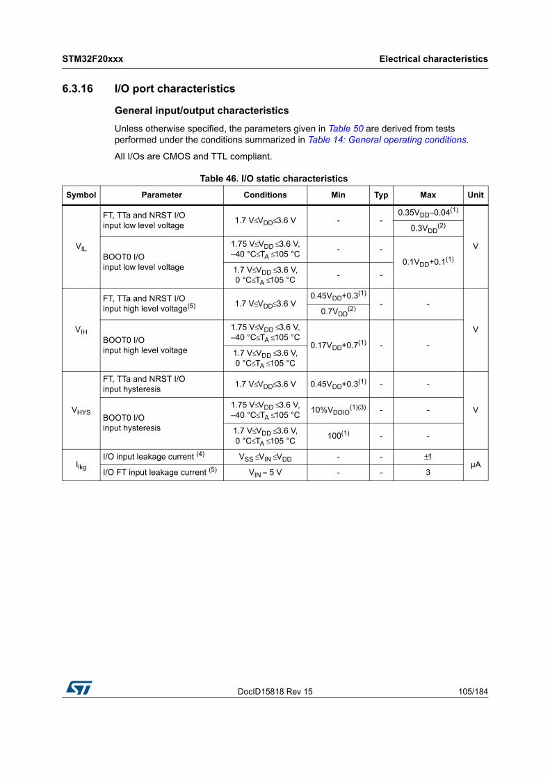
DocID15818 Rev 15 105/184
STM32F20xxx Electrical characteristics
183
6.3.16 I/O port characteristics
General input/output characteristics
Unless otherwise specified, the parameters given in Table 50 are derived from tests performed under the conditions summarized in Table 14: General operating conditions.
All I/Os are CMOS and TTL compliant.
Table 46. I/O static characteristics
Symbol Parameter Conditions Min Typ Max Unit
VIL
FT, TTa and NRST I/O input low level voltage
1.7 V≤ VDD≤ 3.6 V - -0.35VDD–0.04(1)
V
0.3VDD(2)
BOOT0 I/O input low level voltage
1.75 V≤ VDD ≤ 3.6 V, –40 °C≤ TA ≤ 105 °C
- -
0.1VDD+0.1(1)
1.7 V≤ VDD ≤ 3.6 V, 0 °C≤ TA ≤ 105 °C
- -
VIH
FT, TTa and NRST I/O input high level voltage(5) 1.7 V≤ VDD≤ 3.6 V
0.45VDD+0.3(1)
- -
V
0.7VDD(2)
BOOT0 I/O input high level voltage
1.75 V≤ VDD ≤ 3.6 V, –40 °C≤ TA ≤ 105 °C
0.17VDD+0.7(1) - -1.7 V≤ VDD ≤ 3.6 V, 0 °C≤ TA ≤ 105 °C
VHYS
FT, TTa and NRST I/O input hysteresis
1.7 V≤ VDD≤ 3.6 V 0.45VDD+0.3(1) - -
VBOOT0 I/O input hysteresis
1.75 V≤ VDD ≤ 3.6 V, –40 °C≤ TA ≤ 105 °C
10%VDDIO(1)(3) - -
1.7 V≤ VDD ≤ 3.6 V, 0 °C≤ TA ≤ 105 °C
100(1) - -
Ilkg
I/O input leakage current (4) VSS ≤ VIN ≤ VDD - - ±1µA
I/O FT input leakage current (5) VIN = 5 V - - 3
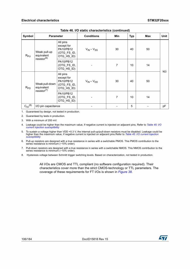
Electrical characteristics STM32F20xxx
106/184 DocID15818 Rev 15
All I/Os are CMOS and TTL compliant (no software configuration required). Their characteristics cover more than the strict CMOS-technology or TTL parameters. The coverage of these requirements for FT I/Os is shown in Figure 38.
RPU
Weak pull-up equivalent resistor(6)
All pins except for PA10/PB12 (OTG_FS_ID,OTG_HS_ID)
VIN = VSS 30 40 50
kΩ
PA10/PB12 (OTG_FS_ID,OTG_HS_ID)
- 7 10 14
RPD
Weak pull-down equivalent resistor(7)
All pins except for PA10/PB12 (OTG_FS_ID,OTG_HS_ID)
VIN = VDD 30 40 50
PA10/PB12 (OTG_FS_ID,OTG_HS_ID)
- 7 10 14
CIO(8) I/O pin capacitance - - 5 - pF
1. Guaranteed by design, not tested in production.
2. Guaranteed by tests in production.
3. With a minimum of 200 mV.
4. Leakage could be higher than the maximum value, if negative current is injected on adjacent pins, Refer to Table 45: I/O current injection susceptibility
5. To sustain a voltage higher than VDD +0.3 V, the internal pull-up/pull-down resistors must be disabled. Leakage could be higher than the maximum value, if negative current is injected on adjacent pins.Refer to Table 45: I/O current injection susceptibility
6. Pull-up resistors are designed with a true resistance in series with a switchable PMOS. This PMOS contribution to the series resistance is minimum (~10% order).
7. Pull-down resistors are designed with a true resistance in series with a switchable NMOS. This NMOS contribution to the series resistance is minimum (~10% order).
8. Hysteresis voltage between Schmitt trigger switching levels. Based on characterization, not tested in production.
Table 46. I/O static characteristics (continued)
Symbol Parameter Conditions Min Typ Max Unit
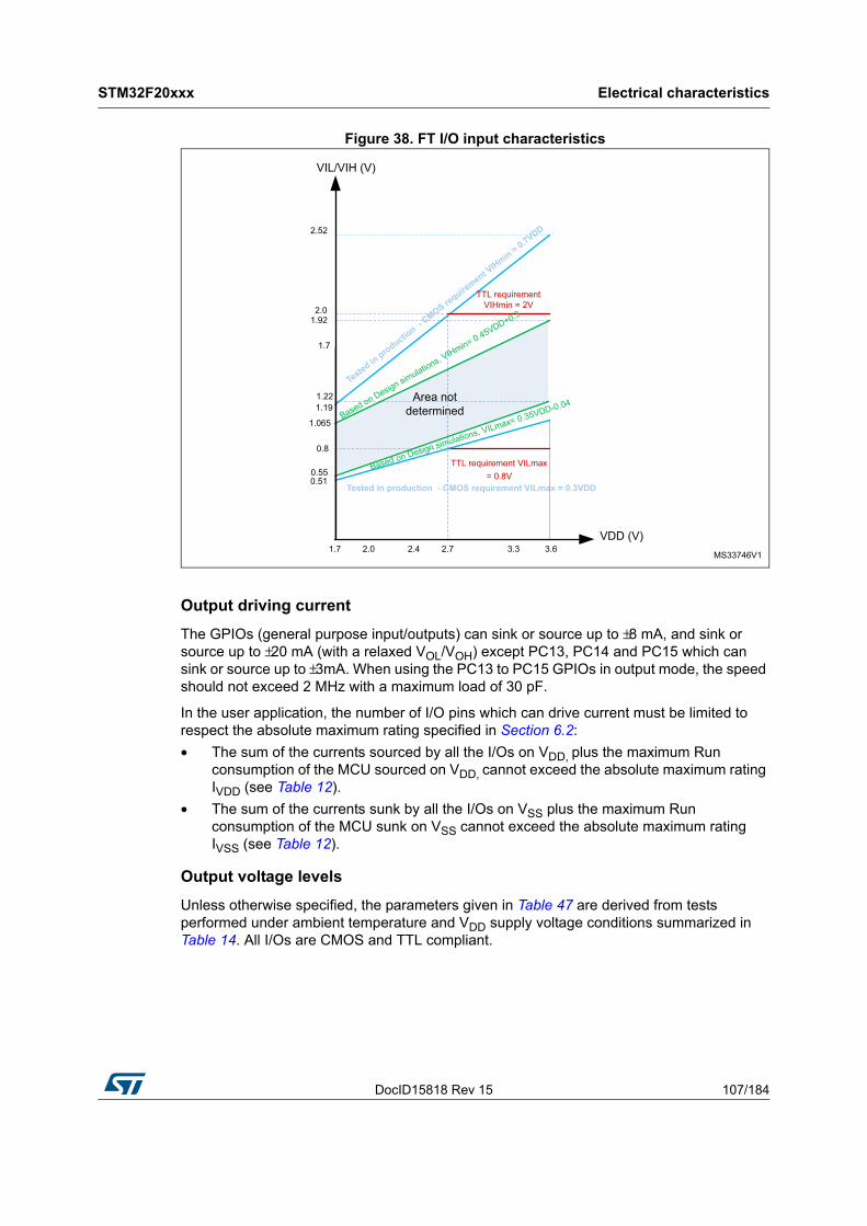
DocID15818 Rev 15 107/184
STM32F20xxx Electrical characteristics
183
Figure 38. FT I/O input characteristics
Output driving current
The GPIOs (general purpose input/outputs) can sink or source up to ±8 mA, and sink or source up to ±20 mA (with a relaxed VOL/VOH) except PC13, PC14 and PC15 which can sink or source up to ±3mA. When using the PC13 to PC15 GPIOs in output mode, the speed should not exceed 2 MHz with a maximum load of 30 pF.
In the user application, the number of I/O pins which can drive current must be limited to respect the absolute maximum rating specified in Section 6.2:
• The sum of the currents sourced by all the I/Os on VDD, plus the maximum Run consumption of the MCU sourced on VDD, cannot exceed the absolute maximum rating IVDD (see Table 12).
• The sum of the currents sunk by all the I/Os on VSS plus the maximum Run consumption of the MCU sunk on VSS cannot exceed the absolute maximum rating IVSS (see Table 12).
Output voltage levels
Unless otherwise specified, the parameters given in Table 47 are derived from tests performed under ambient temperature and VDD supply voltage conditions summarized in Table 14. All I/Os are CMOS and TTL compliant.
Electrical characteristics STM32F20xxx
108/184 DocID15818 Rev 15
Input/output AC characteristics
The definition and values of input/output AC characteristics are given in Figure 39 and Table 48, respectively.
Unless otherwise specified, the parameters given in Table 48 are derived from tests performed under the ambient temperature and VDD supply voltage conditions summarized in Table 14.
Table 47. Output voltage characteristics(1)
1. PC13, PC14, PC15 and PI8 are supplied through the power switch. Since the switch only sinks a limited amount of current (3 mA), the use of GPIOs PC13 to PC15 and PI8 in output mode is limited: the speed should not exceed 2 MHz with a maximum load of 30 pF and these I/Os must not be used as a current source (e.g. to drive an LED).
Symbol Parameter Conditions Min Max Unit
VOL(2)
2. The IIO current sunk by the device must always respect the absolute maximum rating specified in Table 12 and the sum of IIO (I/O ports and control pins) must not exceed IVSS.
Output low level voltage for an I/O pin when 8 pins are sunk at same time CMOS ports
IIO = +8 mA
2.7 V < VDD < 3.6 V
- 0.4
V
VOH(3)
3. The IIO current sourced by the device must always respect the absolute maximum rating specified in Table 12 and the sum of IIO (I/O ports and control pins) must not exceed IVDD.
Output high level voltage for an I/O pin when 8 pins are sourced at same time
VDD–0.4 -
VOL (2) Output low level voltage for an I/O pin
when 8 pins are sunk at same time TTL ports
IIO =+ 8mA
2.7 V < VDD < 3.6 V
- 0.4
V
VOH (3) Output high level voltage for an I/O pin
when 8 pins are sourced at same time2.4 -
VOL(2)(4)
4. Guaranteed by characterization results, not tested in production.
Output low level voltage for an I/O pin when 8 pins are sunk at same time IIO = +20 mA
2.7 V < VDD < 3.6 V
- 1.3
V
VOH(3)(4) Output high level voltage for an I/O pin
when 8 pins are sourced at same timeVDD–1.3 -
VOL(2)(4) Output low level voltage for an I/O pin
when 8 pins are sunk at same time IIO = +6 mA
2 V < VDD < 2.7 V
- 0.4
V
VOH(3)(4) Output high level voltage for an I/O pin
when 8 pins are sourced at same timeVDD–0.4 -
Table 48. I/O AC characteristics(1)
OSPEEDRy[1:0] bit value(1)
Symbol Parameter Conditions Min Typ Max Unit
00
fmax(IO)out Maximum frequency(2)
CL = 50 pF, VDD > 2.70 V - - 4
MHzCL = 50 pF, VDD > 1.8 V - - 2
CL = 10 pF, VDD > 2.70 V - - 8
CL = 10 pF, VDD > 1.8 V - - 4
tf(IO)out/tr(IO)out
Output high to low level fall time and output low to high level rise time
CL = 50 pF, VDD = 1.8 V to 3.6 V
- - 100 ns
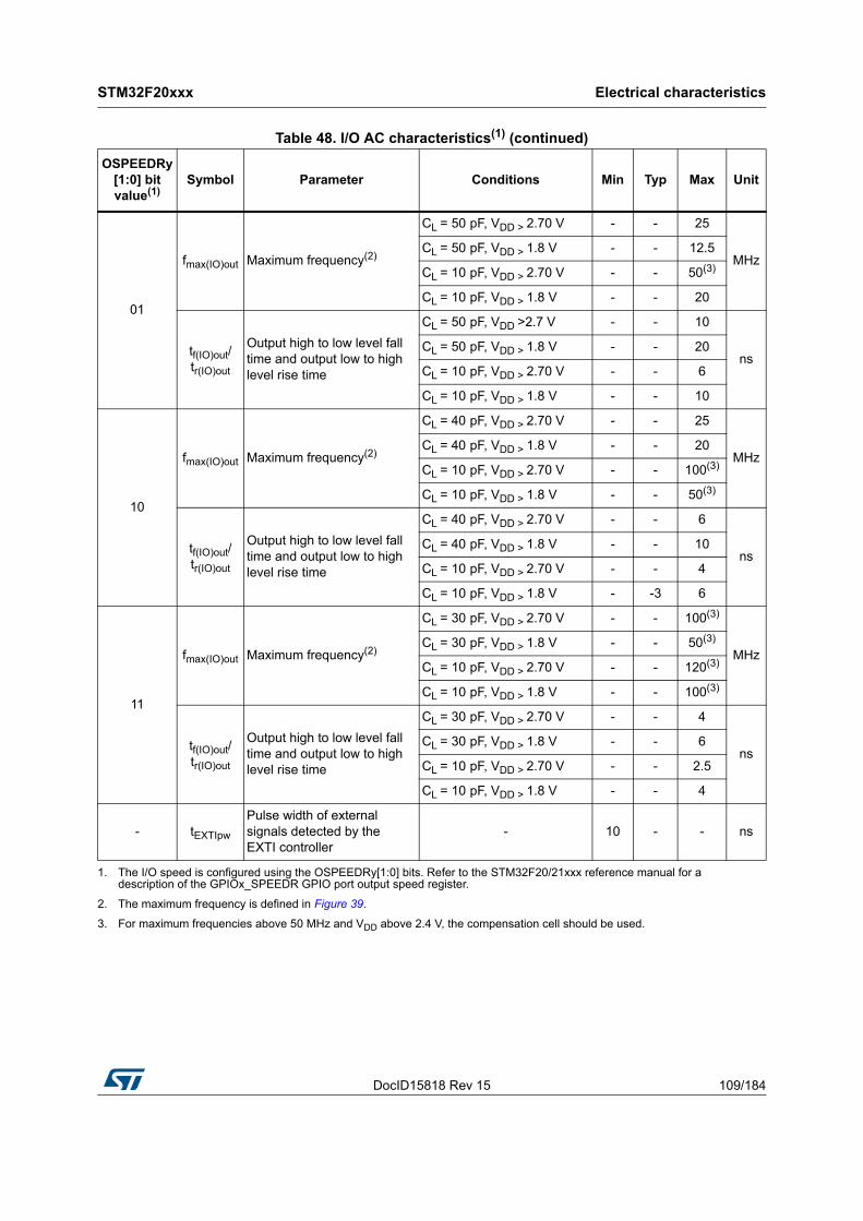
DocID15818 Rev 15 109/184
STM32F20xxx Electrical characteristics
183
01
fmax(IO)out Maximum frequency(2)
CL = 50 pF, VDD > 2.70 V - - 25
MHzCL = 50 pF, VDD > 1.8 V - - 12.5
CL = 10 pF, VDD > 2.70 V - - 50(3)
CL = 10 pF, VDD > 1.8 V - - 20
tf(IO)out/tr(IO)out
Output high to low level fall time and output low to high level rise time
CL = 50 pF, VDD >2.7 V - - 10
nsCL = 50 pF, VDD > 1.8 V - - 20
CL = 10 pF, VDD > 2.70 V - - 6
CL = 10 pF, VDD > 1.8 V - - 10
10
fmax(IO)out Maximum frequency(2)
CL = 40 pF, VDD > 2.70 V - - 25
MHzCL = 40 pF, VDD > 1.8 V - - 20
CL = 10 pF, VDD > 2.70 V - - 100(3)
CL = 10 pF, VDD > 1.8 V - - 50(3)
tf(IO)out/tr(IO)out
Output high to low level fall time and output low to high level rise time
CL = 40 pF, VDD > 2.70 V - - 6
nsCL = 40 pF, VDD > 1.8 V - - 10
CL = 10 pF, VDD > 2.70 V - - 4
CL = 10 pF, VDD > 1.8 V - -3 6
11
fmax(IO)out Maximum frequency(2)
CL = 30 pF, VDD > 2.70 V - - 100(3)
MHzCL = 30 pF, VDD > 1.8 V - - 50(3)
CL = 10 pF, VDD > 2.70 V - - 120(3)
CL = 10 pF, VDD > 1.8 V - - 100(3)
tf(IO)out/tr(IO)out
Output high to low level fall time and output low to high level rise time
CL = 30 pF, VDD > 2.70 V - - 4
nsCL = 30 pF, VDD > 1.8 V - - 6
CL = 10 pF, VDD > 2.70 V - - 2.5
CL = 10 pF, VDD > 1.8 V - - 4
- tEXTIpw
Pulse width of external signals detected by the EXTI controller
- 10 - - ns
1. The I/O speed is configured using the OSPEEDRy[1:0] bits. Refer to the STM32F20/21xxx reference manual for a description of the GPIOx_SPEEDR GPIO port output speed register.
2. The maximum frequency is defined in Figure 39.
3. For maximum frequencies above 50 MHz and VDD above 2.4 V, the compensation cell should be used.
Table 48. I/O AC characteristics(1) (continued)
OSPEEDRy[1:0] bit value(1)
Symbol Parameter Conditions Min Typ Max Unit
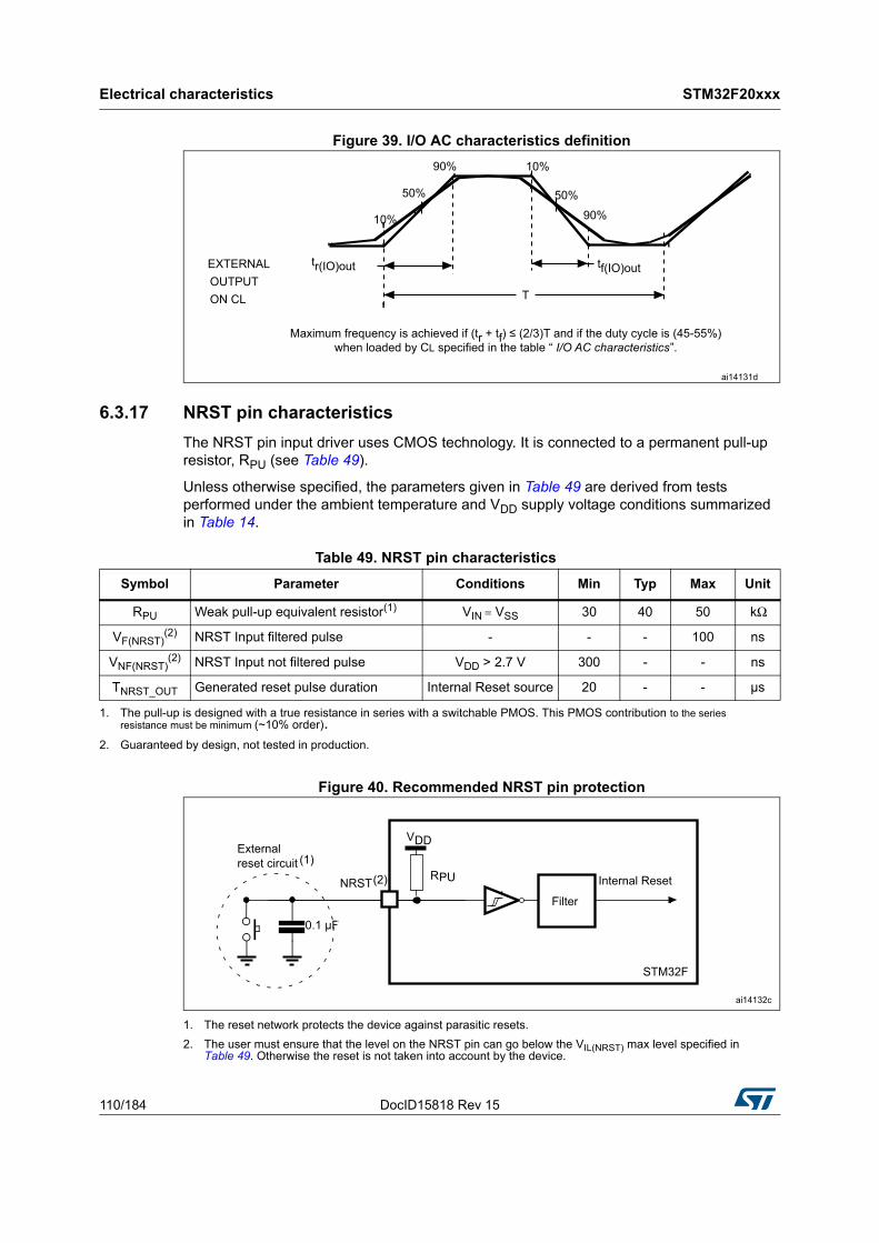
Electrical characteristics STM32F20xxx
110/184 DocID15818 Rev 15
Figure 39. I/O AC characteristics definition
6.3.17 NRST pin characteristics
The NRST pin input driver uses CMOS technology. It is connected to a permanent pull-up resistor, RPU (see Table 49).
Unless otherwise specified, the parameters given in Table 49 are derived from tests performed under the ambient temperature and VDD supply voltage conditions summarized in Table 14.
Figure 40. Recommended NRST pin protection
1. The reset network protects the device against parasitic resets.
2. The user must ensure that the level on the NRST pin can go below the VIL(NRST) max level specified in Table 49. Otherwise the reset is not taken into account by the device.
Table 49. NRST pin characteristics
Symbol Parameter Conditions Min Typ Max Unit
RPU Weak pull-up equivalent resistor(1) VIN = VSS 30 40 50 kΩ
VF(NRST)(2) NRST Input filtered pulse - - - 100 ns
VNF(NRST)(2) NRST Input not filtered pulse VDD > 2.7 V 300 - - ns
TNRST_OUT Generated reset pulse duration Internal Reset source 20 - - µs
1. The pull-up is designed with a true resistance in series with a switchable PMOS. This PMOS contribution to the series resistance must be minimum (~10% order).
2. Guaranteed by design, not tested in production.
DocID15818 Rev 15 111/184
STM32F20xxx Electrical characteristics
183
6.3.18 TIM timer characteristics
The parameters given in Table 50 and Table 51 are guaranteed by design.
Refer to Section 6.3.16: I/O port characteristics for details on the input/output alternate function characteristics (output compare, input capture, external clock, PWM output).
Table 50. Characteristics of TIMx connected to the APB1 domain(1)
1. TIMx is used as a general term to refer to the TIM2, TIM3, TIM4, TIM5, TIM6, TIM7, and TIM12 timers.
Symbol Parameter Conditions Min Max Unit
tres(TIM) Timer resolution time
AHB/APB1 prescaler distinct from 1, fTIMxCLK =
60 MHz
1 - tTIMxCLK
16.7 - ns
AHB/APB1 prescaler = 1, fTIMxCLK = 30 MHz
1 - tTIMxCLK
33.3 - ns
fEXTTimer external clock frequency on CH1 to CH4
fTIMxCLK = 60 MHz
APB1= 30 MHz
0 fTIMxCLK/2 MHz
0 30 MHz
ResTIM Timer resolution - 16/32 bit
tCOUNTER
16-bit counter clock period when internal clock is selected
1 65536 tTIMxCLK
0.0167 1092 µs
32-bit counter clock period when internal clock is selected
1 - tTIMxCLK
0.0167 71582788 µs
tMAX_COUNT Maximum possible count- 65536 × 65536 tTIMxCLK
- 71.6 s
Electrical characteristics STM32F20xxx
112/184 DocID15818 Rev 15
6.3.19 Communications interfaces
I2C interface characteristics
STM32F205xx and STM32F207xx I2C interface meets the requirements of the standard I2C communication protocol with the following restrictions: the I/O pins SDA and SCL are mapped to are not “true” open-drain. When configured as open-drain, the PMOS connected between the I/O pin and VDD is disabled, but is still present.
The I2C characteristics are described in Table 52. Refer also to Section 6.3.16: I/O port characteristics for more details on the input/output alternate function characteristics (SDA and SCL).
Table 51. Characteristics of TIMx connected to the APB2 domain(1)
1. TIMx is used as a general term to refer to the TIM1, TIM8, TIM9, TIM10, and TIM11 timers.
Symbol Parameter Conditions Min Max Unit
tres(TIM) Timer resolution time
AHB/APB2 prescaler distinct from 1, fTIMxCLK =
120 MHz
1 - tTIMxCLK
8.3 - ns
AHB/APB2 prescaler = 1, fTIMxCLK = 60 MHz
1 - tTIMxCLK
16.7 - ns
fEXTTimer external clock frequency on CH1 to CH4
fTIMxCLK = 120 MHz
APB2 = 60 MHz
0 fTIMxCLK/2 MHz
0 60 MHz
ResTIM Timer resolution - 16 bit
tCOUNTER
16-bit counter clock period when internal clock is selected
1 65536 tTIMxCLK
0.0083 546 µs
tMAX_COUNT Maximum possible count- 65536 × 65536 tTIMxCLK
- 35.79 s
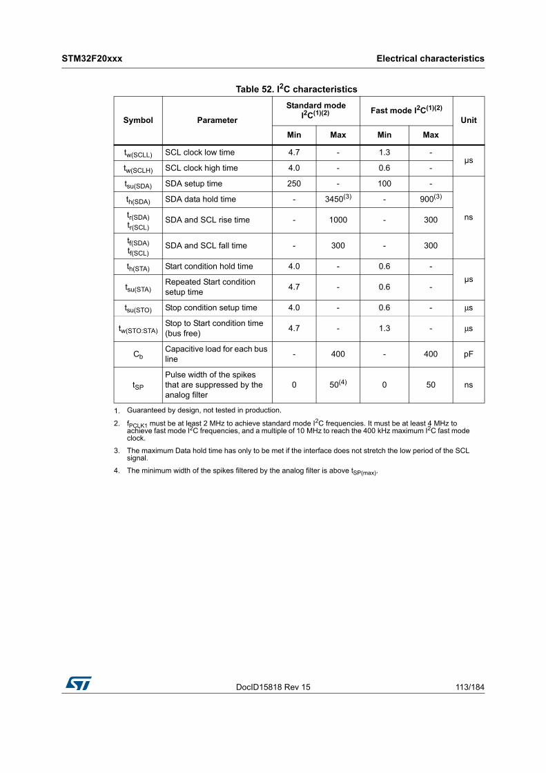
DocID15818 Rev 15 113/184
STM32F20xxx Electrical characteristics
183
Table 52. I2C characteristics
Symbol Parameter
Standard mode I2C(1)(2)
1. Guaranteed by design, not tested in production.
Fast mode I2C(1)(2)
2. fPCLK1 must be at least 2 MHz to achieve standard mode I2C frequencies. It must be at least 4 MHz to achieve fast mode I2C frequencies, and a multiple of 10 MHz to reach the 400 kHz maximum I2C fast mode clock.
Unit
Min Max Min Max
tw(SCLL) SCL clock low time 4.7 - 1.3 -µs
tw(SCLH) SCL clock high time 4.0 - 0.6 -
tsu(SDA) SDA setup time 250 - 100 -
ns
th(SDA) SDA data hold time - 3450(3) - 900(3)
3. The maximum Data hold time has only to be met if the interface does not stretch the low period of the SCL signal.
tr(SDA)tr(SCL)
SDA and SCL rise time - 1000 - 300
tf(SDA)tf(SCL)
SDA and SCL fall time - 300 - 300
th(STA) Start condition hold time 4.0 - 0.6 -
µstsu(STA)
Repeated Start condition setup time
4.7 - 0.6 -
tsu(STO) Stop condition setup time 4.0 - 0.6 - μs
tw(STO:STA)Stop to Start condition time (bus free)
4.7 - 1.3 - μs
CbCapacitive load for each bus line
- 400 - 400 pF
tSP
Pulse width of the spikes that are suppressed by the analog filter
0 50(4)
4. The minimum width of the spikes filtered by the analog filter is above tSP(max).
0 50 ns
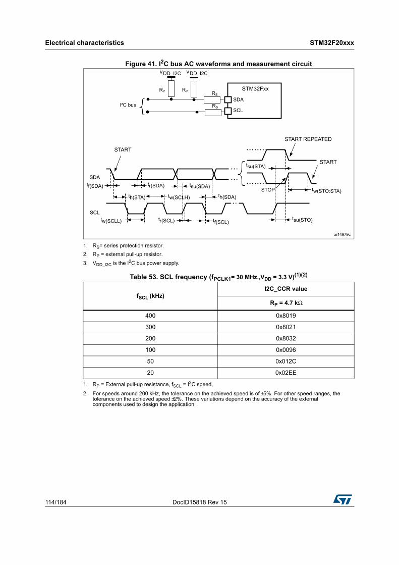
Electrical characteristics STM32F20xxx
114/184 DocID15818 Rev 15
Figure 41. I2C bus AC waveforms and measurement circuit
1. RS= series protection resistor.
2. RP = external pull-up resistor.
3. VDD_I2C is the I2C bus power supply.
Table 53. SCL frequency (fPCLK1= 30 MHz.,VDD = 3.3 V)(1)(2)
1. RP = External pull-up resistance, fSCL = I2C speed,
2. For speeds around 200 kHz, the tolerance on the achieved speed is of ±5%. For other speed ranges, the tolerance on the achieved speed ±2%. These variations depend on the accuracy of the external components used to design the application.
fSCL (kHz)I2C_CCR value
RP = 4.7 kΩ
400 0x8019
300 0x8021
200 0x8032
100 0x0096
50 0x012C
20 0x02EE
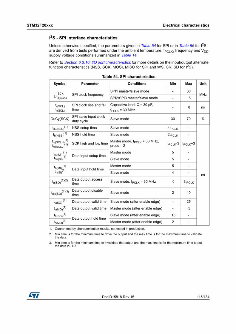
DocID15818 Rev 15 115/184
STM32F20xxx Electrical characteristics
183
I2S - SPI interface characteristics
Unless otherwise specified, the parameters given in Table 54 for SPI or in Table 55 for I2S are derived from tests performed under the ambient temperature, fPCLKx frequency and VDD supply voltage conditions summarized in Table 14.
Refer to Section 6.3.16: I/O port characteristics for more details on the input/output alternate function characteristics (NSS, SCK, MOSI, MISO for SPI and WS, CK, SD for I2S).
Table 54. SPI characteristics
Symbol Parameter Conditions Min Max Unit
fSCK1/tc(SCK)
SPI clock frequencySPI1 master/slave mode - 30
MHzSPI2/SPI3 master/slave mode - 15
tr(SCL)tf(SCL)
SPI clock rise and fall time
Capacitive load: C = 30 pF,
fPCLK = 30 MHz- 8 ns
DuCy(SCK)SPI slave input clock duty cycle
Slave mode 30 70 %
tsu(NSS)(1)
1. Guaranteed by characterization results, not tested in production.
NSS setup time Slave mode 4tPCLK -
ns
th(NSS)(1) NSS hold time Slave mode 2tPCLK -
tw(SCLH)(1)
tw(SCLL)(1) SCK high and low time
Master mode, fPCLK = 30 MHz, presc = 2
tPCLK-3 tPCLK+3
tsu(MI) (1)
tsu(SI)(1) Data input setup time
Master mode 5 -
Slave mode 5 -
th(MI) (1)
th(SI)(1) Data input hold time
Master mode 5 -
Slave mode 4 -
ta(SO)(1)(2)
2. Min time is for the minimum time to drive the output and the max time is for the maximum time to validate the data.
Data output access time
Slave mode, fPCLK = 30 MHz 0 3tPCLK
tdis(SO)(1)(3)
3. Min time is for the minimum time to invalidate the output and the max time is for the maximum time to put the data in Hi-Z
Data output disable time
Slave mode 2 10
tv(SO) (1) Data output valid time Slave mode (after enable edge) - 25
tv(MO)(1) Data output valid time Master mode (after enable edge) - 5
th(SO)(1)
Data output hold timeSlave mode (after enable edge) 15 -
th(MO)(1) Master mode (after enable edge) 2 -
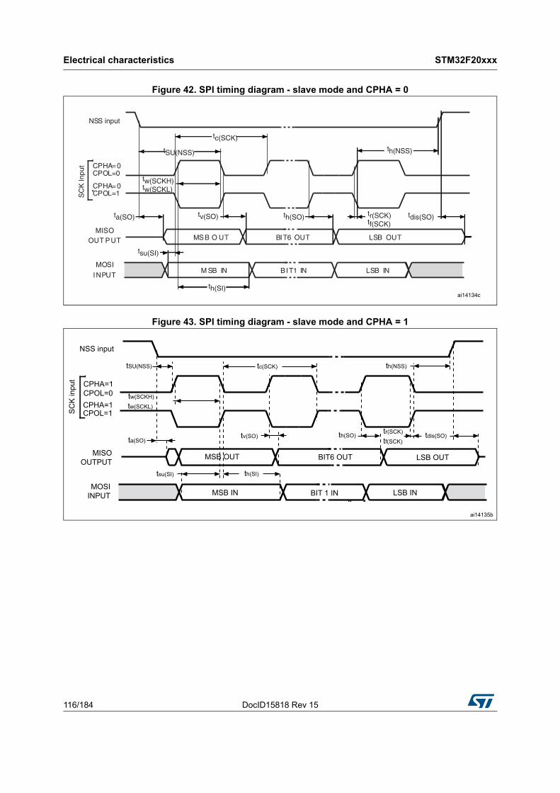
Electrical characteristics STM32F20xxx
116/184 DocID15818 Rev 15
Figure 42. SPI timing diagram - slave mode and CPHA = 0
Figure 43. SPI timing diagram - slave mode and CPHA = 1
ai14134c
SC
K In
put CPHA=0
MOSI
INPUT
MISOOUT PUT
CPHA=0
MSB O UT
M SB IN
BIT6 OUT
LSB IN
LSB OUT
CPOL=0
CPOL=1
BIT1 IN
NSS input
tSU(NSS)
tc(SCK)
th(NSS)
ta(SO)
tw(SCKH)tw(SCKL)
tv(SO) th(SO) tr(SCK)tf(SCK)
tdis(SO)
tsu(SI)
th(SI)
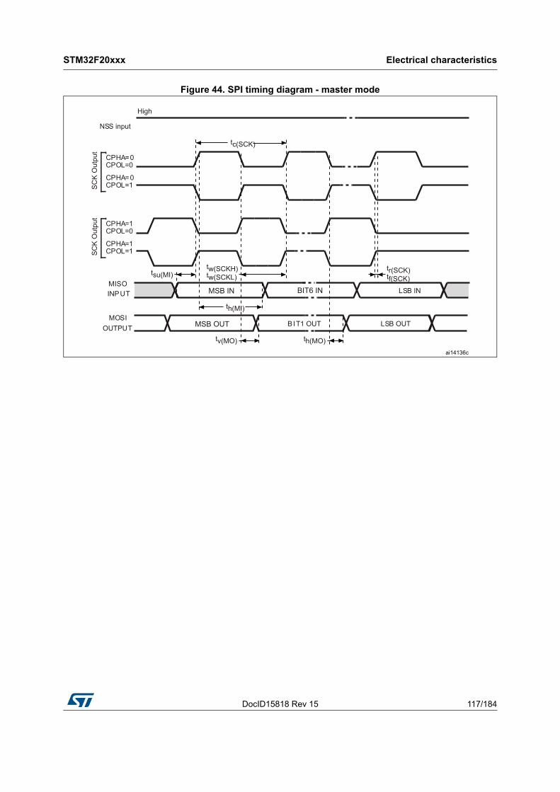
DocID15818 Rev 15 117/184
STM32F20xxx Electrical characteristics
183
Figure 44. SPI timing diagram - master mode
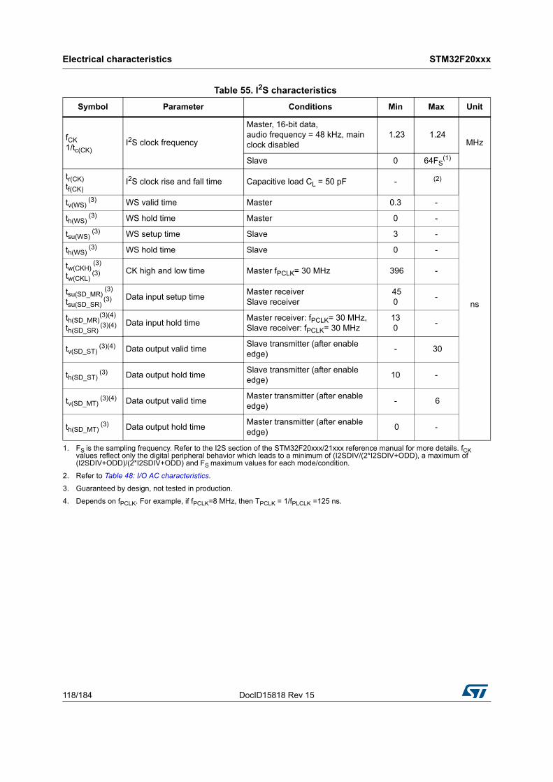
Electrical characteristics STM32F20xxx
118/184 DocID15818 Rev 15
Table 55. I2S characteristics
Symbol Parameter Conditions Min Max Unit
fCK 1/tc(CK)
I2S clock frequency
Master, 16-bit data, audio frequency = 48 kHz, main clock disabled
1.23 1.24MHz
Slave 0 64FS(1)
tr(CK) tf(CK)
I2S clock rise and fall time Capacitive load CL = 50 pF - (2)
ns
tv(WS) (3) WS valid time Master 0.3 -
th(WS) (3) WS hold time Master 0 -
tsu(WS) (3) WS setup time Slave 3 -
th(WS) (3) WS hold time Slave 0 -
tw(CKH) (3)
tw(CKL) (3) CK high and low time Master fPCLK= 30 MHz 396 -
tsu(SD_MR) (3)
tsu(SD_SR) (3) Data input setup time
Master receiver Slave receiver
450
-
th(SD_MR)(3)(4)
th(SD_SR) (3)(4) Data input hold time
Master receiver: fPCLK= 30 MHz, Slave receiver: fPCLK= 30 MHz
130
-
tv(SD_ST) (3)(4) Data output valid time
Slave transmitter (after enable edge)
- 30
th(SD_ST) (3) Data output hold time
Slave transmitter (after enable edge)
10 -
tv(SD_MT) (3)(4) Data output valid time
Master transmitter (after enable edge)
- 6
th(SD_MT) (3) Data output hold time
Master transmitter (after enable edge)
0 -
1. FS is the sampling frequency. Refer to the I2S section of the STM32F20xxx/21xxx reference manual for more details. fCK values reflect only the digital peripheral behavior which leads to a minimum of (I2SDIV/(2*I2SDIV+ODD), a maximum of (I2SDIV+ODD)/(2*I2SDIV+ODD) and FS maximum values for each mode/condition.
2. Refer to Table 48: I/O AC characteristics.
3. Guaranteed by design, not tested in production.
4. Depends on fPCLK. For example, if fPCLK=8 MHz, then TPCLK = 1/fPLCLK =125 ns.
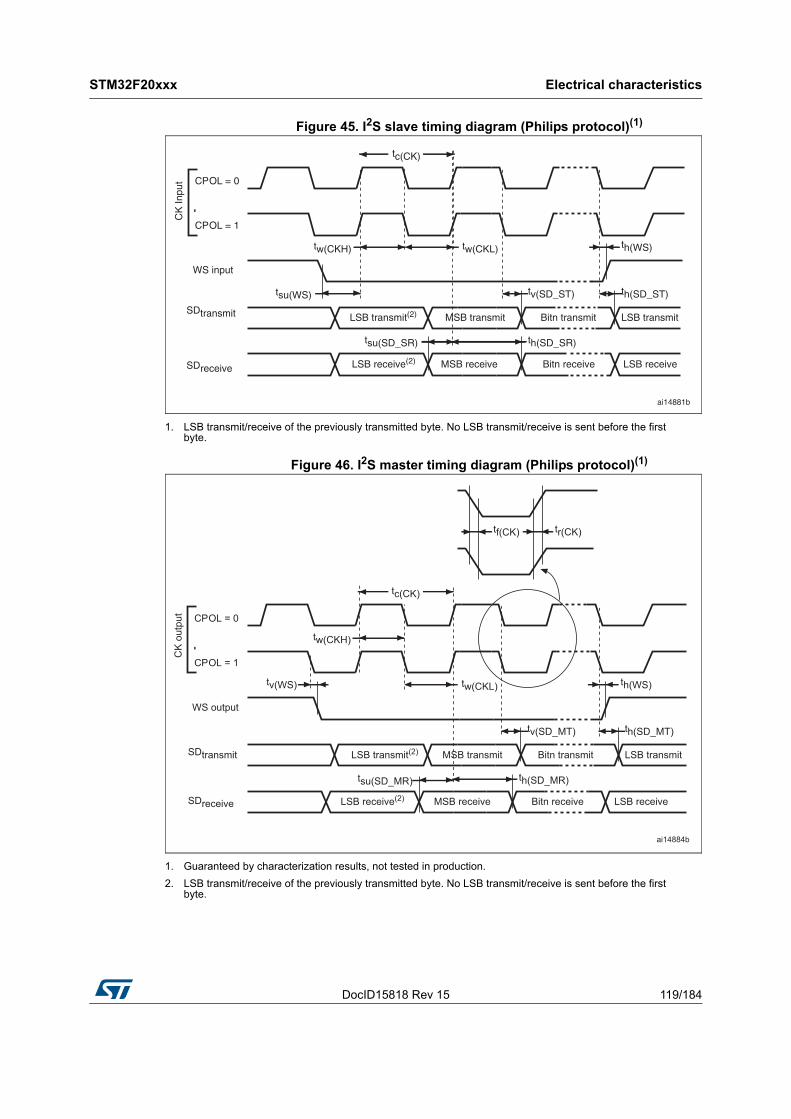
DocID15818 Rev 15 119/184
STM32F20xxx Electrical characteristics
183
Figure 45. I2S slave timing diagram (Philips protocol)(1)
1. LSB transmit/receive of the previously transmitted byte. No LSB transmit/receive is sent before the first byte.
Figure 46. I2S master timing diagram (Philips protocol)(1)
1. Guaranteed by characterization results, not tested in production.
2. LSB transmit/receive of the previously transmitted byte. No LSB transmit/receive is sent before the first byte.
CK
Inpu
t CPOL = 0
CPOL = 1
tc(CK)
WS input
SDtransmit
SDreceive
tw(CKH) tw(CKL)
tsu(WS) tv(SD_ST) th(SD_ST)
th(WS)
tsu(SD_SR) th(SD_SR)
MSB receive Bitn receive LSB receive
MSB transmit Bitn transmit LSB transmit
ai14881b
LSB receive(2)
LSB transmit(2)
CK
out
put CPOL = 0
CPOL = 1
tc(CK)
WS output
SDreceive
SDtransmit
tw(CKH)
tw(CKL)
tsu(SD_MR)
tv(SD_MT) th(SD_MT)
th(WS)
th(SD_MR)
MSB receive Bitn receive LSB receive
MSB transmit Bitn transmit LSB transmit
ai14884b
tf(CK) tr(CK)
tv(WS)
LSB receive(2)
LSB transmit(2)
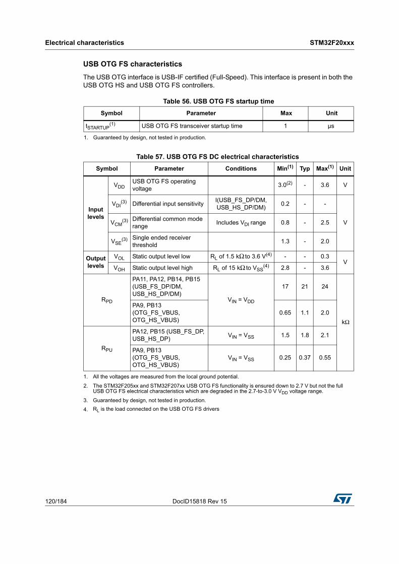
Electrical characteristics STM32F20xxx
120/184 DocID15818 Rev 15
USB OTG FS characteristics
The USB OTG interface is USB-IF certified (Full-Speed). This interface is present in both the USB OTG HS and USB OTG FS controllers.
Table 56. USB OTG FS startup time
Symbol Parameter Max Unit
tSTARTUP(1)
1. Guaranteed by design, not tested in production.
USB OTG FS transceiver startup time 1 µs
Table 57. USB OTG FS DC electrical characteristics
Symbol Parameter Conditions Min(1)
1. All the voltages are measured from the local ground potential.
Typ Max(1) Unit
Input levels
VDDUSB OTG FS operating voltage
3.0(2)
2. The STM32F205xx and STM32F207xx USB OTG FS functionality is ensured down to 2.7 V but not the full USB OTG FS electrical characteristics which are degraded in the 2.7-to-3.0 V VDD voltage range.
- 3.6 V
VDI(3)
3. Guaranteed by design, not tested in production.
Differential input sensitivityI(USB_FS_DP/DM, USB_HS_DP/DM)
0.2 - -
VVCM(3) Differential common mode
rangeIncludes VDI range 0.8 - 2.5
VSE(3) Single ended receiver
threshold1.3 - 2.0
Output levels
VOL Static output level low RL of 1.5 kΩ to 3.6 V(4)
4. RL is the load connected on the USB OTG FS drivers
- - 0.3V
VOH Static output level high RL of 15 kΩ to VSS(4) 2.8 - 3.6
RPD
PA11, PA12, PB14, PB15 (USB_FS_DP/DM, USB_HS_DP/DM)
VIN = VDD
17 21 24
kΩ
PA9, PB13 (OTG_FS_VBUS, OTG_HS_VBUS)
0.65 1.1 2.0
RPU
PA12, PB15 (USB_FS_DP, USB_HS_DP)
VIN = VSS 1.5 1.8 2.1
PA9, PB13 (OTG_FS_VBUS, OTG_HS_VBUS)
VIN = VSS 0.25 0.37 0.55
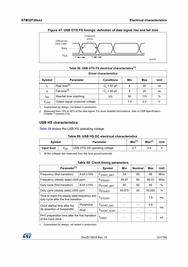
DocID15818 Rev 15 121/184
STM32F20xxx Electrical characteristics
183
Figure 47. USB OTG FS timings: definition of data signal rise and fall time
USB HS characteristics
Table 59 shows the USB HS operating voltage.
Table 58. USB OTG FS electrical characteristics(1)
1. Guaranteed by design, not tested in production.
Driver characteristics
Symbol Parameter Conditions Min Max Unit
tr Rise time(2)
2. Measured from 10% to 90% of the data signal. For more detailed informations, refer to USB Specification - Chapter 7 (version 2.0).
CL = 50 pF 4 20 ns
tf Fall time(2) CL = 50 pF 4 20 ns
trfm Rise/fall time matching tr/tf 90 110 %
VCRS Output signal crossover voltage - 1.3 2.0 V
Table 59. USB HS DC electrical characteristics
Symbol Parameter Min(1)
1. All the voltages are measured from the local ground potential.
Max(1) Unit
Input level VDD USB OTG HS operating voltage 2.7 3.6 V
Table 60. Clock timing parameters
Parameter(1)
1. Guaranteed by design, not tested in production.
Symbol Min Nominal Max Unit
Frequency (first transition) 8-bit ±10% FSTART_8BIT 54 60 66 MHz
Frequency (steady state) ±500 ppm FSTEADY 59.97 60 60.03 MHz
Duty cycle (first transition) 8-bit ±10% DSTART_8BIT 40 50 60 %
Duty cycle (steady state) ±500 ppm DSTEADY 49.975 50 50.025 %
Time to reach the steady state frequency and duty cycle after the first transition
TSTEADY - - 1.4 ms
Clock startup time after the de-assertion of SuspendM
Peripheral TSTART_DEV - - 5.6ms
Host TSTART_HOST - - -
PHY preparation time after the first transition of the input clock
TPREP - - - µs
ai14137tf
Differen tialData L ines
VSS
VCRS
tr
Crossoverpoints
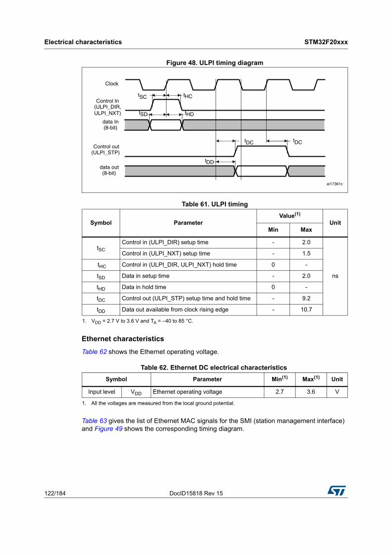
Electrical characteristics STM32F20xxx
122/184 DocID15818 Rev 15
Figure 48. ULPI timing diagram
Ethernet characteristics
Table 62 shows the Ethernet operating voltage.
Table 63 gives the list of Ethernet MAC signals for the SMI (station management interface) and Figure 49 shows the corresponding timing diagram.
Table 61. ULPI timing
Symbol ParameterValue(1)
1. VDD = 2.7 V to 3.6 V and TA = –40 to 85 °C.
UnitMin Max
tSC
Control in (ULPI_DIR) setup time - 2.0
ns
Control in (ULPI_NXT) setup time - 1.5
tHC Control in (ULPI_DIR, ULPI_NXT) hold time 0 -
tSD Data in setup time - 2.0
tHD Data in hold time 0 -
tDC Control out (ULPI_STP) setup time and hold time - 9.2
tDD Data out available from clock rising edge - 10.7
Table 62. Ethernet DC electrical characteristics
Symbol Parameter Min(1)
1. All the voltages are measured from the local ground potential.
Max(1) Unit
Input level VDD Ethernet operating voltage 2.7 3.6 V
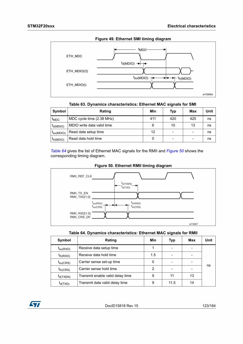
DocID15818 Rev 15 123/184
STM32F20xxx Electrical characteristics
183
Figure 49. Ethernet SMI timing diagram
Table 64 gives the list of Ethernet MAC signals for the RMII and Figure 50 shows the corresponding timing diagram.
Figure 50. Ethernet RMII timing diagram
Table 63. Dynamics characteristics: Ethernet MAC signals for SMI
Symbol Rating Min Typ Max Unit
tMDC MDC cycle time (2.38 MHz) 411 420 425 ns
td(MDIO) MDIO write data valid time 6 10 13 ns
tsu(MDIO) Read data setup time 12 - - ns
th(MDIO) Read data hold time 0 - - ns
Table 64. Dynamics characteristics: Ethernet MAC signals for RMII
Symbol Rating Min Typ Max Unit
tsu(RXD) Receive data setup time 1 - -
ns
tih(RXD) Receive data hold time 1.5 - -
tsu(CRS) Carrier sense set-up time 0 - -
tih(CRS) Carrier sense hold time 2 - -
td(TXEN) Transmit enable valid delay time 9 11 13
td(TXD) Transmit data valid delay time 9 11.5 14
RMII_REF_CLK
RMII_TX_ENRMII_TXD[1:0]
RMII_RXD[1:0]RMII_CRS_DV
td(TXEN)td(TXD)
tsu(RXD)tsu(CRS)
tih(RXD)tih(CRS)
ai15667
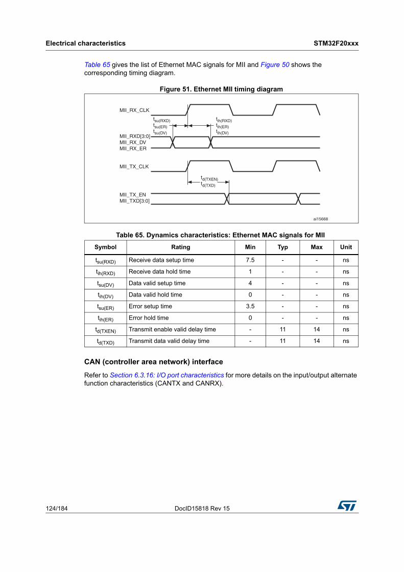
Electrical characteristics STM32F20xxx
124/184 DocID15818 Rev 15
Table 65 gives the list of Ethernet MAC signals for MII and Figure 50 shows the corresponding timing diagram.
Figure 51. Ethernet MII timing diagram
CAN (controller area network) interface
Refer to Section 6.3.16: I/O port characteristics for more details on the input/output alternate function characteristics (CANTX and CANRX).
Table 65. Dynamics characteristics: Ethernet MAC signals for MII
Symbol Rating Min Typ Max Unit
tsu(RXD) Receive data setup time 7.5 - - ns
tih(RXD) Receive data hold time 1 - - ns
tsu(DV) Data valid setup time 4 - - ns
tih(DV) Data valid hold time 0 - - ns
tsu(ER) Error setup time 3.5 - - ns
tih(ER) Error hold time 0 - - ns
td(TXEN) Transmit enable valid delay time - 11 14 ns
td(TXD) Transmit data valid delay time - 11 14 ns
MII_RX_CLK
MII_RXD[3:0]MII_RX_DVMII_RX_ER
td(TXEN)td(TXD)
tsu(RXD)tsu(ER)tsu(DV)
tih(RXD)tih(ER)tih(DV)
ai15668
MII_TX_CLK
MII_TX_ENMII_TXD[3:0]
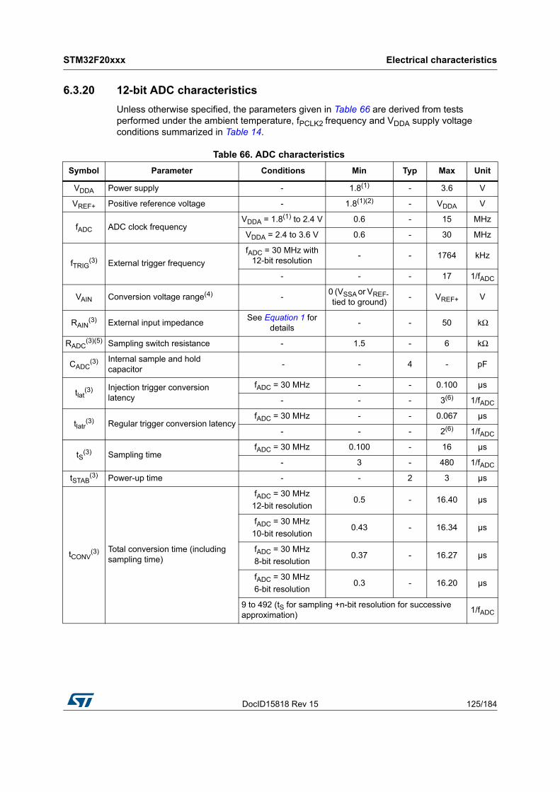
DocID15818 Rev 15 125/184
STM32F20xxx Electrical characteristics
183
6.3.20 12-bit ADC characteristics
Unless otherwise specified, the parameters given in Table 66 are derived from tests performed under the ambient temperature, fPCLK2 frequency and VDDA supply voltage conditions summarized in Table 14.
Table 66. ADC characteristics
Symbol Parameter Conditions Min Typ Max Unit
VDDA Power supply - 1.8(1) - 3.6 V
VREF+ Positive reference voltage - 1.8(1)(2) - VDDA V
fADC ADC clock frequencyVDDA = 1.8(1) to 2.4 V 0.6 - 15 MHz
VDDA = 2.4 to 3.6 V 0.6 - 30 MHz
fTRIG(3) External trigger frequency
fADC = 30 MHz with 12-bit resolution
- - 1764 kHz
- - - 17 1/fADC
VAIN Conversion voltage range(4) -0 (VSSA or VREF- tied to ground)
- VREF+ V
RAIN(3) External input impedance
See Equation 1 for details
- - 50 kΩ
RADC(3)(5) Sampling switch resistance - 1.5 - 6 kΩ
CADC(3) Internal sample and hold
capacitor - - 4 - pF
tlat(3) Injection trigger conversion
latency
fADC = 30 MHz - - 0.100 µs
- - - 3(6) 1/fADC
tlatr(3) Regular trigger conversion latency
fADC = 30 MHz - - 0.067 µs
- - - 2(6) 1/fADC
tS(3) Sampling time
fADC = 30 MHz 0.100 - 16 µs
- 3 - 480 1/fADC
tSTAB(3) Power-up time - - 2 3 µs
tCONV(3) Total conversion time (including
sampling time)
fADC = 30 MHz
12-bit resolution0.5 - 16.40 µs
fADC = 30 MHz
10-bit resolution0.43 - 16.34 µs
fADC = 30 MHz
8-bit resolution0.37 - 16.27 µs
fADC = 30 MHz
6-bit resolution0.3 - 16.20 µs
9 to 492 (tS for sampling +n-bit resolution for successive approximation)
1/fADC
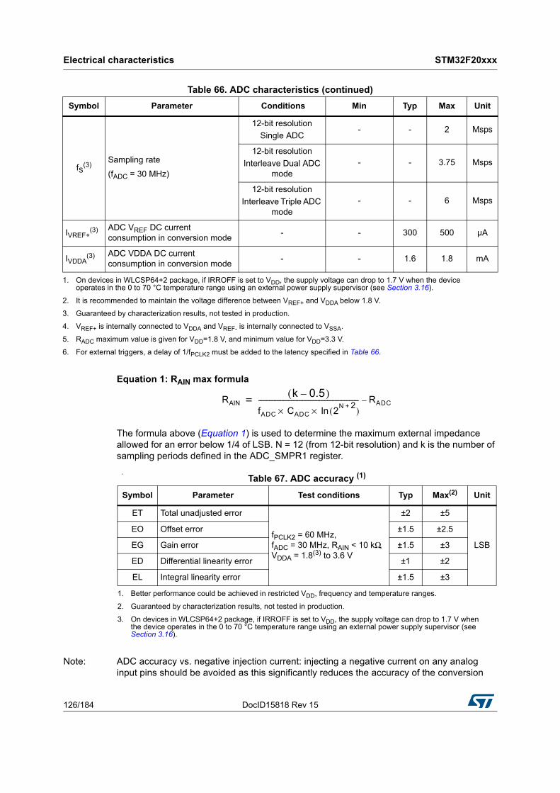
Electrical characteristics STM32F20xxx
126/184 DocID15818 Rev 15
Equation 1: RAIN max formula
The formula above (Equation 1) is used to determine the maximum external impedance allowed for an error below 1/4 of LSB. N = 12 (from 12-bit resolution) and k is the number of sampling periods defined in the ADC_SMPR1 register.
a
Note: ADC accuracy vs. negative injection current: injecting a negative current on any analog input pins should be avoided as this significantly reduces the accuracy of the conversion
fS(3)
Sampling rate
(fADC = 30 MHz)
12-bit resolution
Single ADC- - 2 Msps
12-bit resolution
Interleave Dual ADC mode
- - 3.75 Msps
12-bit resolution
Interleave Triple ADC mode
- - 6 Msps
IVREF+(3) ADC VREF DC current
consumption in conversion mode - - 300 500 µA
IVDDA(3) ADC VDDA DC current
consumption in conversion mode - - 1.6 1.8 mA
1. On devices in WLCSP64+2 package, if IRROFF is set to VDD, the supply voltage can drop to 1.7 V when the device operates in the 0 to 70 °C temperature range using an external power supply supervisor (see Section 3.16).
2. It is recommended to maintain the voltage difference between VREF+ and VDDA below 1.8 V.
3. Guaranteed by characterization results, not tested in production.
4. VREF+ is internally connected to VDDA and VREF- is internally connected to VSSA.
5. RADC maximum value is given for VDD=1.8 V, and minimum value for VDD=3.3 V.
6. For external triggers, a delay of 1/fPCLK2 must be added to the latency specified in Table 66.
Table 66. ADC characteristics (continued)
Symbol Parameter Conditions Min Typ Max Unit
Table 67. ADC accuracy (1)
1. Better performance could be achieved in restricted VDD, frequency and temperature ranges.
Symbol Parameter Test conditions Typ Max(2)
2. Guaranteed by characterization results, not tested in production.
Unit
ET Total unadjusted error
fPCLK2 = 60 MHz, fADC = 30 MHz, RAIN < 10 kΩ, VDDA = 1.8(3) to 3.6 V
3. On devices in WLCSP64+2 package, if IRROFF is set to VDD, the supply voltage can drop to 1.7 V when the device operates in the 0 to 70 °C temperature range using an external power supply supervisor (see Section 3.16).
±2 ±5
LSB
EO Offset error ±1.5 ±2.5
EG Gain error ±1.5 ±3
ED Differential linearity error ±1 ±2
EL Integral linearity error ±1.5 ±3
RAINk 0.5–( )
fADC CADC 2N 2+( )ln××
---------------------------------------------------------------- RADC–=
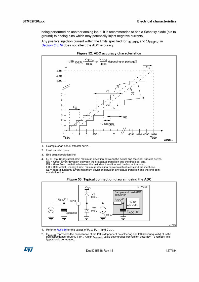
DocID15818 Rev 15 127/184
STM32F20xxx Electrical characteristics
183
being performed on another analog input. It is recommended to add a Schottky diode (pin to ground) to analog pins which may potentially inject negative currents.
Any positive injection current within the limits specified for IINJ(PIN) and ΣIINJ(PIN) in Section 6.3.16 does not affect the ADC accuracy.
Figure 52. ADC accuracy characteristics
1. Example of an actual transfer curve.
2. Ideal transfer curve.
3. End point correlation line.
4. ET = Total Unadjusted Error: maximum deviation between the actual and the ideal transfer curves. EO = Offset Error: deviation between the first actual transition and the first ideal one. EG = Gain Error: deviation between the last ideal transition and the last actual one. ED = Differential Linearity Error: maximum deviation between actual steps and the ideal one. EL = Integral Linearity Error: maximum deviation between any actual transition and the end point correlation line.
Figure 53. Typical connection diagram using the ADC
1. Refer to Table 66 for the values of RAIN, RADC and CADC.
2. Cparasitic represents the capacitance of the PCB (dependent on soldering and PCB layout quality) plus the pad capacitance (roughly 7 pF). A high Cparasitic value downgrades conversion accuracy. To remedy this, fADC should be reduced.
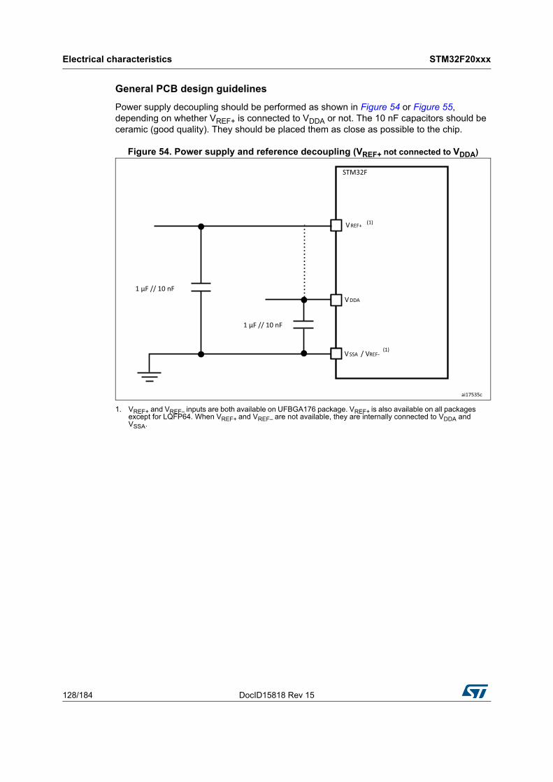
Electrical characteristics STM32F20xxx
128/184 DocID15818 Rev 15
General PCB design guidelines
Power supply decoupling should be performed as shown in Figure 54 or Figure 55, depending on whether VREF+ is connected to VDDA or not. The 10 nF capacitors should be ceramic (good quality). They should be placed them as close as possible to the chip.
Figure 54. Power supply and reference decoupling (VREF+ not connected to VDDA)
1. VREF+ and VREF– inputs are both available on UFBGA176 package. VREF+ is also available on all packages except for LQFP64. When VREF+ and VREF– are not available, they are internally connected to VDDA and VSSA.
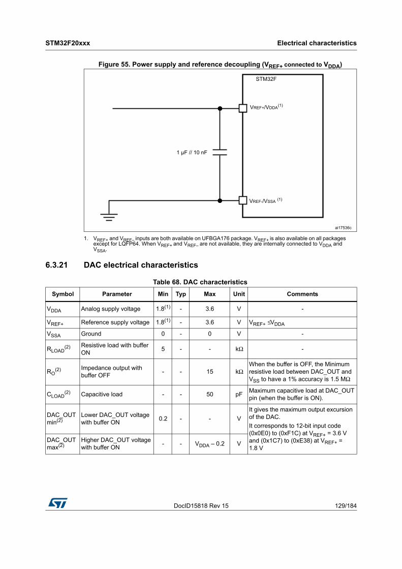
DocID15818 Rev 15 129/184
STM32F20xxx Electrical characteristics
183
Figure 55. Power supply and reference decoupling (VREF+ connected to VDDA)
1. VREF+ and VREF– inputs are both available on UFBGA176 package. VREF+ is also available on all packages except for LQFP64. When VREF+ and VREF– are not available, they are internally connected to VDDA and VSSA.
6.3.21 DAC electrical characteristics
Table 68. DAC characteristics
Symbol Parameter Min Typ Max Unit Comments
VDDA Analog supply voltage 1.8(1) - 3.6 V -
VREF+ Reference supply voltage 1.8(1) - 3.6 V VREF+ ≤ VDDA
VSSA Ground 0 - 0 V -
RLOAD(2) Resistive load with buffer
ON5 - - kΩ -
RO(2) Impedance output with
buffer OFF- - 15 kΩ
When the buffer is OFF, the Minimum resistive load between DAC_OUT and VSS to have a 1% accuracy is 1.5 MΩ
CLOAD(2) Capacitive load - - 50 pF
Maximum capacitive load at DAC_OUT pin (when the buffer is ON).
DAC_OUT min(2)
Lower DAC_OUT voltage with buffer ON
0.2 - - V
It gives the maximum output excursion of the DAC.
It corresponds to 12-bit input code (0x0E0) to (0xF1C) at VREF+ = 3.6 V and (0x1C7) to (0xE38) at VREF+ = 1.8 V
DAC_OUT max(2)
Higher DAC_OUT voltage with buffer ON
- - VDDA – 0.2 V
Electrical characteristics STM32F20xxx
130/184 DocID15818 Rev 15
DAC_OUT min(2)
Lower DAC_OUT voltage with buffer OFF
- 0.5 - mVIt gives the maximum output excursion of the DAC.DAC_OUT
max(2)Higher DAC_OUT voltage with buffer OFF
- - VREF+ – 1LSB V
IVREF+(4)
DAC DC VREF current consumption in quiescent mode (Standby mode)
- 170 240
µA
With no load, worst code (0x800) at VREF+ = 3.6 V in terms of DC consumption on the inputs
- 50 75With no load, worst code (0xF1C) at VREF+ = 3.6 V in terms of DC consumption on the inputs
IDDA(4)
DAC DC VDDA current consumption in quiescent mode(3)
- 280 380 µAWith no load, middle code (0x800) on the inputs
- 475 625 µAWith no load, worst code (0xF1C) at VREF+ = 3.6 V in terms of DC consumption on the inputs
DNL(4)Differential non linearity Difference between two consecutive code-1LSB)
- - ±0.5 LSBGiven for the DAC in 10-bit configuration.
- - ±2 LSBGiven for the DAC in 12-bit configuration.
INL(4)
Integral non linearity (difference between measured value at Code i and the value at Code i on a line drawn between Code 0 and last Code 1023)
- - ±1 LSBGiven for the DAC in 10-bit configuration.
- - ±4 LSBGiven for the DAC in 12-bit configuration.
Offset(4)
Offset error
(difference between measured value at Code (0x800) and the ideal value = VREF+/2)
- - ±10 mV -
- - ±3 LSBGiven for the DAC in 10-bit at VREF+ = 3.6 V
- - ±12 LSBGiven for the DAC in 12-bit at VREF+ = 3.6 V
Gain error(4) Gain error - - ±0.5 %
Given for the DAC in 12-bit configuration
tSETTLING(4)
Settling time (full scale: for a 10-bit input code transition between the lowest and the highest input codes when DAC_OUT reaches final value ±4LSB
- 3 6 µsCLOAD ≤ 50 pF, RLOAD ≥ 5 kΩ
THD(4) Total Harmonic Distortion
Buffer ON- - - dB
CLOAD ≤ 50 pF, RLOAD ≥ 5 kΩ
Table 68. DAC characteristics (continued)
Symbol Parameter Min Typ Max Unit Comments
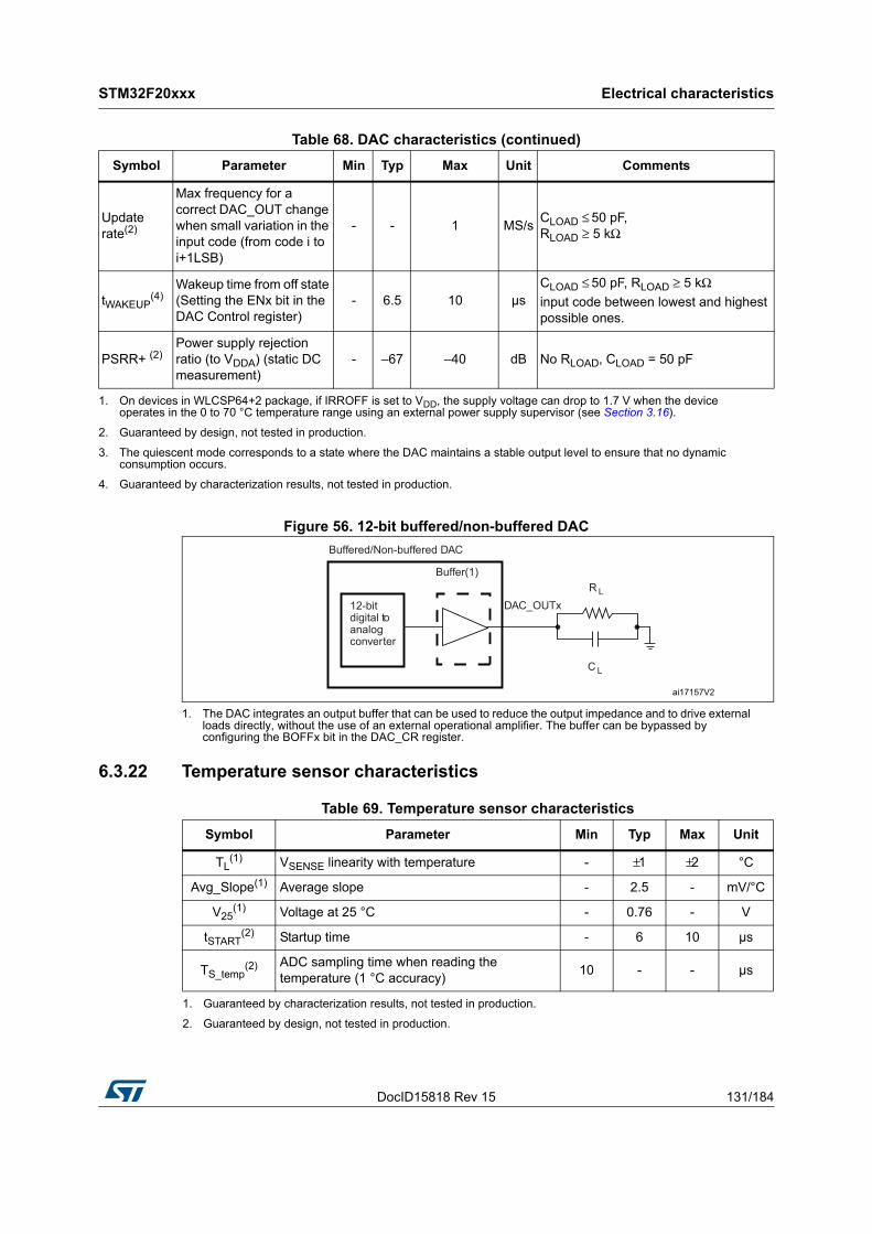
DocID15818 Rev 15 131/184
STM32F20xxx Electrical characteristics
183
Figure 56. 12-bit buffered/non-buffered DAC
1. The DAC integrates an output buffer that can be used to reduce the output impedance and to drive external loads directly, without the use of an external operational amplifier. The buffer can be bypassed by configuring the BOFFx bit in the DAC_CR register.
6.3.22 Temperature sensor characteristics
Update rate(2)
Max frequency for a correct DAC_OUT change when small variation in the input code (from code i to i+1LSB)
- - 1 MS/sCLOAD ≤ 50 pF, RLOAD ≥ 5 kΩ
tWAKEUP(4)
Wakeup time from off state (Setting the ENx bit in the DAC Control register)
- 6.5 10 µsCLOAD ≤ 50 pF, RLOAD ≥ 5 kΩinput code between lowest and highest possible ones.
PSRR+ (2)Power supply rejection ratio (to VDDA) (static DC measurement)
- –67 –40 dB No RLOAD, CLOAD = 50 pF
1. On devices in WLCSP64+2 package, if IRROFF is set to VDD, the supply voltage can drop to 1.7 V when the device operates in the 0 to 70 °C temperature range using an external power supply supervisor (see Section 3.16).
2. Guaranteed by design, not tested in production.
3. The quiescent mode corresponds to a state where the DAC maintains a stable output level to ensure that no dynamic consumption occurs.
4. Guaranteed by characterization results, not tested in production.
Table 68. DAC characteristics (continued)
Symbol Parameter Min Typ Max Unit Comments
R L
C L
Buffered/Non-buffered DAC
DAC_OUTx
Buffer(1)
12-bit digital to analog converter
ai17157V2
Table 69. Temperature sensor characteristics
Symbol Parameter Min Typ Max Unit
TL(1)
1. Guaranteed by characterization results, not tested in production.
VSENSE linearity with temperature - ±1 ±2 °C
Avg_Slope(1) Average slope - 2.5 - mV/°C
V25(1) Voltage at 25 °C - 0.76 - V
tSTART(2)
2. Guaranteed by design, not tested in production.
Startup time - 6 10 µs
TS_temp(2) ADC sampling time when reading the
temperature (1 °C accuracy)10 - - µs
Electrical characteristics STM32F20xxx
132/184 DocID15818 Rev 15
6.3.23 VBAT monitoring characteristics
6.3.24 Embedded reference voltage
The parameters given in Table 71 are derived from tests performed under ambient temperature and VDD supply voltage conditions summarized in Table 14.
6.3.25 FSMC characteristics
Asynchronous waveforms and timings
Figure 57 through Figure 60 represent asynchronous waveforms and Table 72 through Table 75 provide the corresponding timings. The results shown in these tables are obtained with the following FSMC configuration:
• AddressSetupTime = 1
• AddressHoldTime = 1
• DataSetupTime = 1
• BusTurnAroundDuration = 0x0
In all timing tables, the THCLK is the HCLK clock period.
Table 70. VBAT monitoring characteristics
Symbol Parameter Min Typ Max Unit
R Resistor bridge for VBAT - 50 - KΩ
Q Ratio on VBAT measurement - 2 -
Er(1)
1. Guaranteed by design, not tested in production.
Error on Q –1 - +1 %
TS_vbat(2)(2)
2. Shortest sampling time can be determined in the application by multiple iterations.
ADC sampling time when reading the VBAT
(1 mV accuracy) 5 - - µs
Table 71. Embedded internal reference voltage
Symbol Parameter Conditions Min Typ Max Unit
VREFINT Internal reference voltage –40 °C < TA < +105 °C 1.18 1.21 1.24 V
TS_vrefint(1)
1. Shortest sampling time can be determined in the application by multiple iterations.
ADC sampling time when reading the internal reference voltage
- 10 - - µs
VRERINT_s(2)
2. Guaranteed by design, not tested in production.
Internal reference voltage spread over the temperature range
VDD = 3 V - 3 5 mV
TCoeff(2) Temperature coefficient - - 30 50 ppm/°C
tSTART(2) Startup time - - 6 10 µs
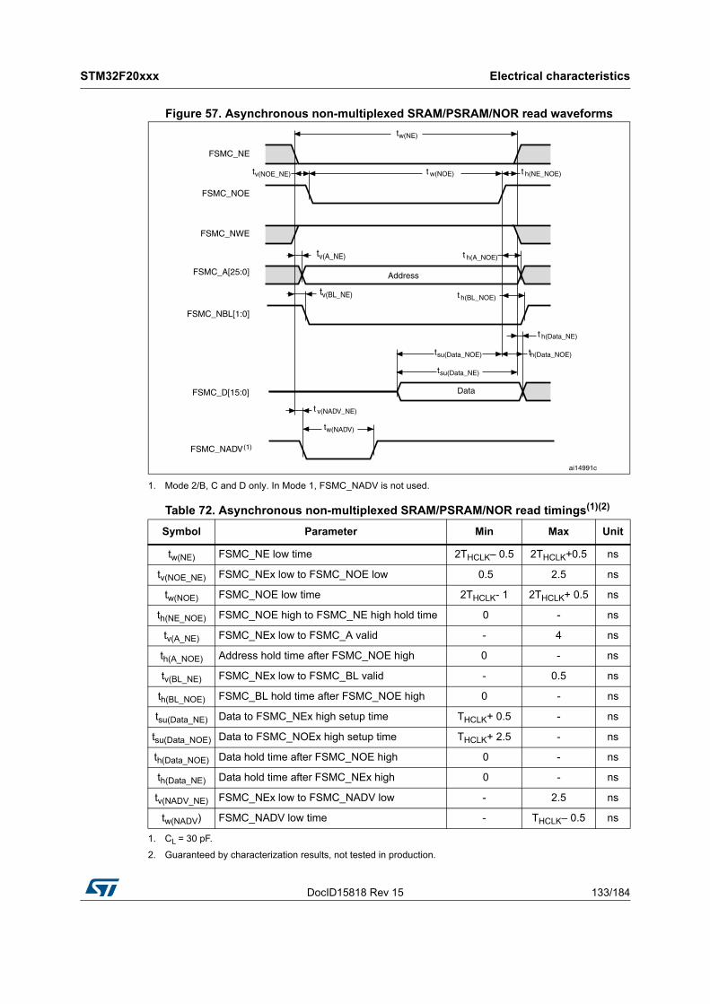
DocID15818 Rev 15 133/184
STM32F20xxx Electrical characteristics
183
Figure 57. Asynchronous non-multiplexed SRAM/PSRAM/NOR read waveforms
1. Mode 2/B, C and D only. In Mode 1, FSMC_NADV is not used.
Table 72. Asynchronous non-multiplexed SRAM/PSRAM/NOR read timings(1)(2)
1. CL = 30 pF.
2. Guaranteed by characterization results, not tested in production.
Symbol Parameter Min Max Unit
tw(NE) FSMC_NE low time 2THCLK– 0.5 2THCLK+0.5 ns
tv(NOE_NE) FSMC_NEx low to FSMC_NOE low 0.5 2.5 ns
tw(NOE) FSMC_NOE low time 2THCLK- 1 2THCLK+ 0.5 ns
th(NE_NOE) FSMC_NOE high to FSMC_NE high hold time 0 - ns
tv(A_NE) FSMC_NEx low to FSMC_A valid - 4 ns
th(A_NOE) Address hold time after FSMC_NOE high 0 - ns
tv(BL_NE) FSMC_NEx low to FSMC_BL valid - 0.5 ns
th(BL_NOE) FSMC_BL hold time after FSMC_NOE high 0 - ns
tsu(Data_NE) Data to FSMC_NEx high setup time THCLK+ 0.5 - ns
tsu(Data_NOE) Data to FSMC_NOEx high setup time THCLK+ 2.5 - ns
th(Data_NOE) Data hold time after FSMC_NOE high 0 - ns
th(Data_NE) Data hold time after FSMC_NEx high 0 - ns
tv(NADV_NE) FSMC_NEx low to FSMC_NADV low - 2.5 ns
tw(NADV) FSMC_NADV low time - THCLK– 0.5 ns
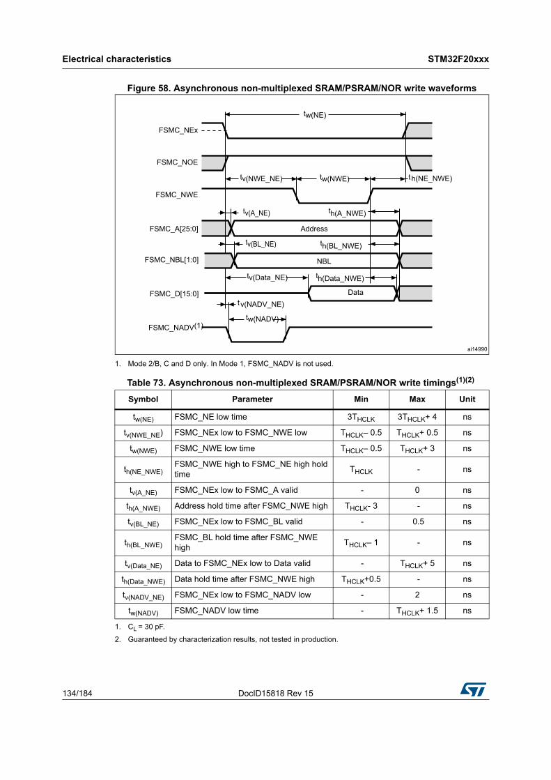
Electrical characteristics STM32F20xxx
134/184 DocID15818 Rev 15
Figure 58. Asynchronous non-multiplexed SRAM/PSRAM/NOR write waveforms
1. Mode 2/B, C and D only. In Mode 1, FSMC_NADV is not used.
Table 73. Asynchronous non-multiplexed SRAM/PSRAM/NOR write timings(1)(2)
1. CL = 30 pF.
2. Guaranteed by characterization results, not tested in production.
Symbol Parameter Min Max Unit
tw(NE) FSMC_NE low time 3THCLK 3THCLK+ 4 ns
tv(NWE_NE) FSMC_NEx low to FSMC_NWE low THCLK– 0.5 THCLK+ 0.5 ns
tw(NWE) FSMC_NWE low time THCLK– 0.5 THCLK+ 3 ns
th(NE_NWE)FSMC_NWE high to FSMC_NE high hold time
THCLK - ns
tv(A_NE) FSMC_NEx low to FSMC_A valid - 0 ns
th(A_NWE) Address hold time after FSMC_NWE high THCLK- 3 - ns
tv(BL_NE) FSMC_NEx low to FSMC_BL valid - 0.5 ns
th(BL_NWE)FSMC_BL hold time after FSMC_NWE high
THCLK– 1 - ns
tv(Data_NE) Data to FSMC_NEx low to Data valid - THCLK+ 5 ns
th(Data_NWE) Data hold time after FSMC_NWE high THCLK+0.5 - ns
tv(NADV_NE) FSMC_NEx low to FSMC_NADV low - 2 ns
tw(NADV) FSMC_NADV low time - THCLK+ 1.5 ns
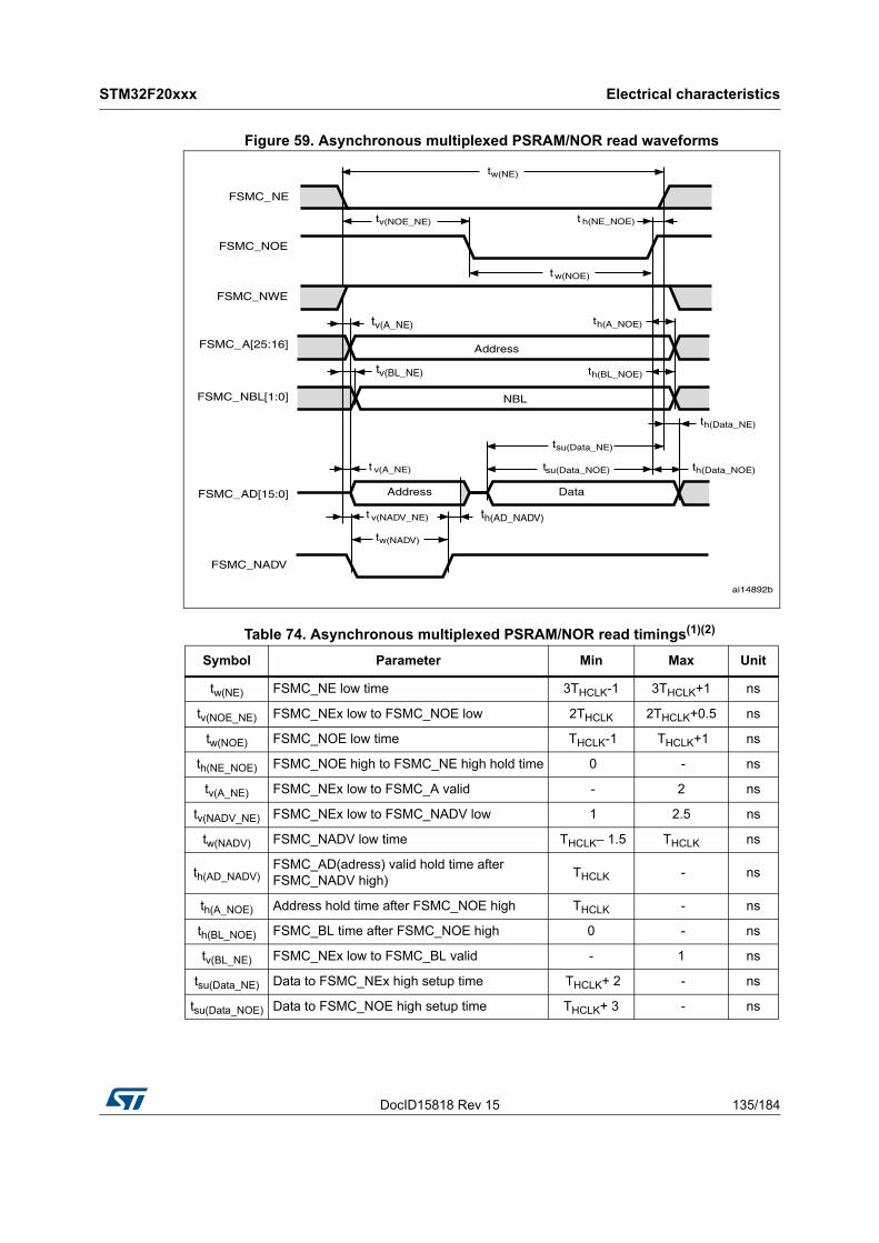
DocID15818 Rev 15 135/184
STM32F20xxx Electrical characteristics
183
Figure 59. Asynchronous multiplexed PSRAM/NOR read waveforms
Table 74. Asynchronous multiplexed PSRAM/NOR read timings(1)(2)
Symbol Parameter Min Max Unit
tw(NE) FSMC_NE low time 3THCLK-1 3THCLK+1 ns
tv(NOE_NE) FSMC_NEx low to FSMC_NOE low 2THCLK 2THCLK+0.5 ns
tw(NOE) FSMC_NOE low time THCLK-1 THCLK+1 ns
th(NE_NOE) FSMC_NOE high to FSMC_NE high hold time 0 - ns
tv(A_NE) FSMC_NEx low to FSMC_A valid - 2 ns
tv(NADV_NE) FSMC_NEx low to FSMC_NADV low 1 2.5 ns
tw(NADV) FSMC_NADV low time THCLK– 1.5 THCLK ns
th(AD_NADV)FSMC_AD(adress) valid hold time after FSMC_NADV high)
THCLK - ns
th(A_NOE) Address hold time after FSMC_NOE high THCLK - ns
th(BL_NOE) FSMC_BL time after FSMC_NOE high 0 - ns
tv(BL_NE) FSMC_NEx low to FSMC_BL valid - 1 ns
tsu(Data_NE) Data to FSMC_NEx high setup time THCLK+ 2 - ns
tsu(Data_NOE) Data to FSMC_NOE high setup time THCLK+ 3 - ns
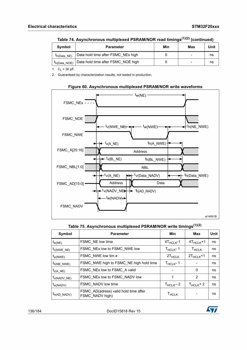
Electrical characteristics STM32F20xxx
136/184 DocID15818 Rev 15
Figure 60. Asynchronous multiplexed PSRAM/NOR write waveforms
th(Data_NE) Data hold time after FSMC_NEx high 0 - ns
th(Data_NOE) Data hold time after FSMC_NOE high 0 - ns
1. CL = 30 pF.
2. Guaranteed by characterization results, not tested in production.
Table 75. Asynchronous multiplexed PSRAM/NOR write timings(1)(2)
Symbol Parameter Min Max Unit
tw(NE) FSMC_NE low time 4THCLK-1 4THCLK+1 ns
tv(NWE_NE) FSMC_NEx low to FSMC_NWE low THCLK- 1 THCLK ns
tw(NWE) FSMC_NWE low tim e 2THCLK 2THCLK+1 ns
th(NE_NWE) FSMC_NWE high to FSMC_NE high hold time THCLK- 1 - ns
tv(A_NE) FSMC_NEx low to FSMC_A valid - 0 ns
tv(NADV_NE) FSMC_NEx low to FSMC_NADV low 1 2 ns
tw(NADV) FSMC_NADV low time THCLK– 2 THCLK+ 2 ns
th(AD_NADV)FSMC_AD(adress) valid hold time after FSMC_NADV high)
THCLK - ns
Table 74. Asynchronous multiplexed PSRAM/NOR read timings(1)(2) (continued)
Symbol Parameter Min Max Unit
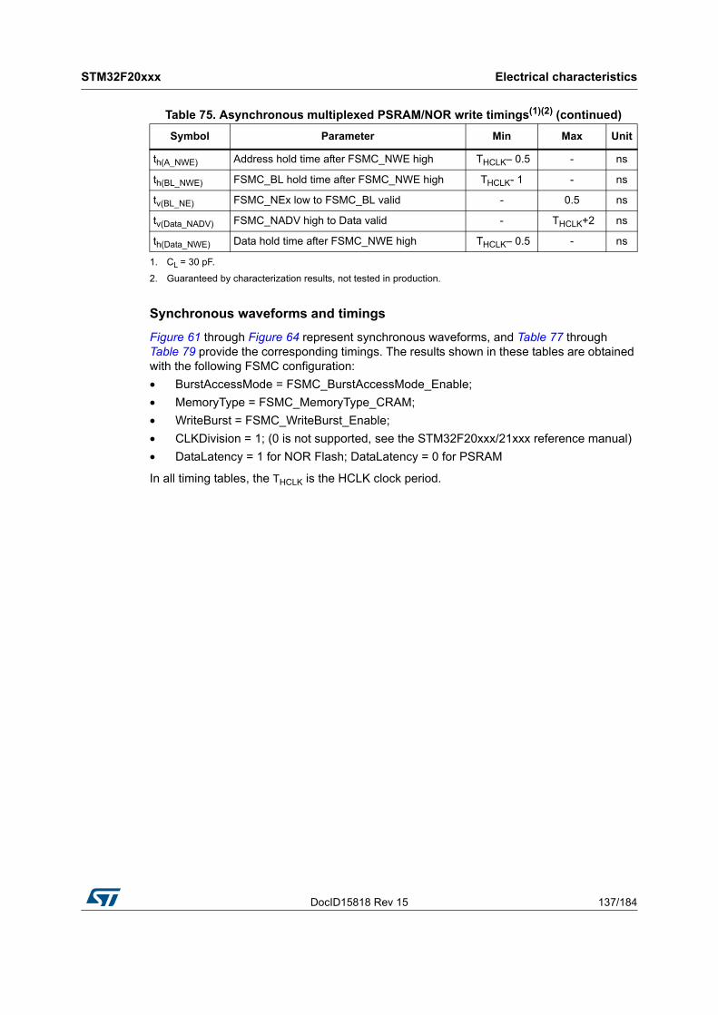
DocID15818 Rev 15 137/184
STM32F20xxx Electrical characteristics
183
Synchronous waveforms and timings
Figure 61 through Figure 64 represent synchronous waveforms, and Table 77 through Table 79 provide the corresponding timings. The results shown in these tables are obtained with the following FSMC configuration:
• BurstAccessMode = FSMC_BurstAccessMode_Enable;
• MemoryType = FSMC_MemoryType_CRAM;
• WriteBurst = FSMC_WriteBurst_Enable;
• CLKDivision = 1; (0 is not supported, see the STM32F20xxx/21xxx reference manual)
• DataLatency = 1 for NOR Flash; DataLatency = 0 for PSRAM
In all timing tables, the THCLK is the HCLK clock period.
th(A_NWE) Address hold time after FSMC_NWE high THCLK– 0.5 - ns
th(BL_NWE) FSMC_BL hold time after FSMC_NWE high THCLK- 1 - ns
tv(BL_NE) FSMC_NEx low to FSMC_BL valid - 0.5 ns
tv(Data_NADV) FSMC_NADV high to Data valid - THCLK+2 ns
th(Data_NWE) Data hold time after FSMC_NWE high THCLK– 0.5 - ns
1. CL = 30 pF.
2. Guaranteed by characterization results, not tested in production.
Table 75. Asynchronous multiplexed PSRAM/NOR write timings(1)(2) (continued)
Symbol Parameter Min Max Unit
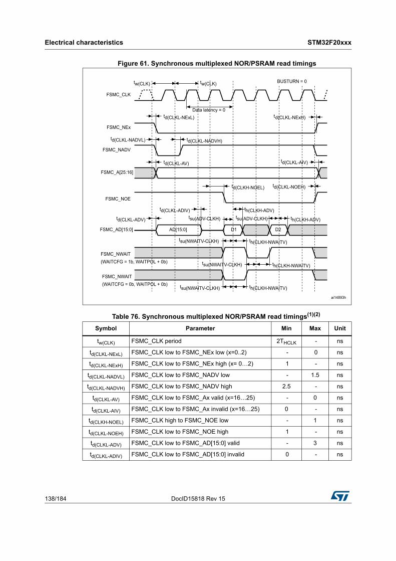
Electrical characteristics STM32F20xxx
138/184 DocID15818 Rev 15
Figure 61. Synchronous multiplexed NOR/PSRAM read timings
Table 76. Synchronous multiplexed NOR/PSRAM read timings(1)(2)
Symbol Parameter Min Max Unit
tw(CLK) FSMC_CLK period 2THCLK - ns
td(CLKL-NExL) FSMC_CLK low to FSMC_NEx low (x=0..2) - 0 ns
td(CLKL-NExH) FSMC_CLK low to FSMC_NEx high (x= 0…2) 1 - ns
td(CLKL-NADVL) FSMC_CLK low to FSMC_NADV low - 1.5 ns
td(CLKL-NADVH) FSMC_CLK low to FSMC_NADV high 2.5 - ns
td(CLKL-AV) FSMC_CLK low to FSMC_Ax valid (x=16…25) - 0 ns
td(CLKL-AIV) FSMC_CLK low to FSMC_Ax invalid (x=16…25) 0 - ns
td(CLKH-NOEL) FSMC_CLK high to FSMC_NOE low - 1 ns
td(CLKL-NOEH) FSMC_CLK low to FSMC_NOE high 1 - ns
td(CLKL-ADV) FSMC_CLK low to FSMC_AD[15:0] valid - 3 ns
td(CLKL-ADIV) FSMC_CLK low to FSMC_AD[15:0] invalid 0 - ns
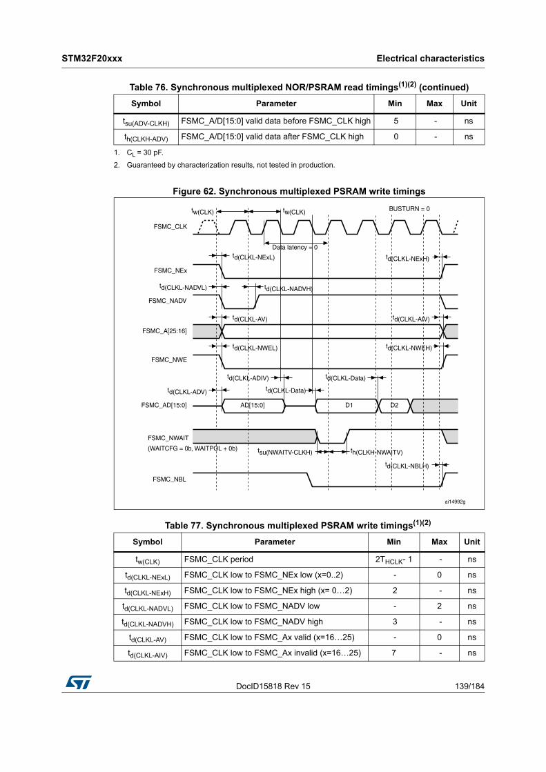
DocID15818 Rev 15 139/184
STM32F20xxx Electrical characteristics
183
Figure 62. Synchronous multiplexed PSRAM write timings
tsu(ADV-CLKH) FSMC_A/D[15:0] valid data before FSMC_CLK high 5 - ns
th(CLKH-ADV) FSMC_A/D[15:0] valid data after FSMC_CLK high 0 - ns
1. CL = 30 pF.
2. Guaranteed by characterization results, not tested in production.
Table 77. Synchronous multiplexed PSRAM write timings(1)(2)
Symbol Parameter Min Max Unit
tw(CLK) FSMC_CLK period 2THCLK- 1 - ns
td(CLKL-NExL) FSMC_CLK low to FSMC_NEx low (x=0..2) - 0 ns
td(CLKL-NExH) FSMC_CLK low to FSMC_NEx high (x= 0…2) 2 - ns
td(CLKL-NADVL) FSMC_CLK low to FSMC_NADV low - 2 ns
td(CLKL-NADVH) FSMC_CLK low to FSMC_NADV high 3 - ns
td(CLKL-AV) FSMC_CLK low to FSMC_Ax valid (x=16…25) - 0 ns
td(CLKL-AIV) FSMC_CLK low to FSMC_Ax invalid (x=16…25) 7 - ns
Table 76. Synchronous multiplexed NOR/PSRAM read timings(1)(2) (continued)
Symbol Parameter Min Max Unit
Electrical characteristics STM32F20xxx
140/184 DocID15818 Rev 15
Figure 63. Synchronous non-multiplexed NOR/PSRAM read timings
td(CLKL-NWEL) FSMC_CLK low to FSMC_NWE low - 1 ns
td(CLKL-NWEH) FSMC_CLK low to FSMC_NWE high 0 - ns
td(CLKL-ADIV) FSMC_CLK low to FSMC_AD[15:0] invalid 0 - ns
td(CLKL-DATA) FSMC_A/D[15:0] valid data after FSMC_CLK low - 2 ns
td(CLKL-NBLH) FSMC_CLK low to FSMC_NBL high 0.5 - ns
1. CL = 30 pF.
2. Guaranteed by characterization results, not tested in production.
Table 78. Synchronous non-multiplexed NOR/PSRAM read timings(1)(2)
Symbol Parameter Min Max Unit
tw(CLK) FSMC_CLK period 2THCLK - ns
td(CLKL-NExL) FSMC_CLK low to FSMC_NEx low (x=0..2) - 0 ns
td(CLKL-NExH) FSMC_CLK low to FSMC_NEx high (x= 0…2) 1 - ns
td(CLKL-NADVL) FSMC_CLK low to FSMC_NADV low - 2.5 ns
Table 77. Synchronous multiplexed PSRAM write timings(1)(2) (continued)
Symbol Parameter Min Max Unit
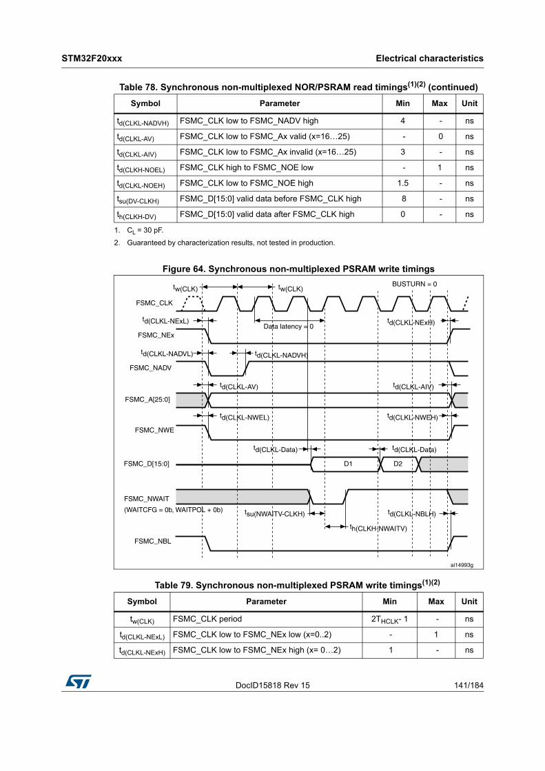
DocID15818 Rev 15 141/184
STM32F20xxx Electrical characteristics
183
Figure 64. Synchronous non-multiplexed PSRAM write timings
td(CLKL-NADVH) FSMC_CLK low to FSMC_NADV high 4 - ns
td(CLKL-AV) FSMC_CLK low to FSMC_Ax valid (x=16…25) - 0 ns
td(CLKL-AIV) FSMC_CLK low to FSMC_Ax invalid (x=16…25) 3 - ns
td(CLKH-NOEL) FSMC_CLK high to FSMC_NOE low - 1 ns
td(CLKL-NOEH) FSMC_CLK low to FSMC_NOE high 1.5 - ns
tsu(DV-CLKH) FSMC_D[15:0] valid data before FSMC_CLK high 8 - ns
th(CLKH-DV) FSMC_D[15:0] valid data after FSMC_CLK high 0 - ns
1. CL = 30 pF.
2. Guaranteed by characterization results, not tested in production.
Table 79. Synchronous non-multiplexed PSRAM write timings(1)(2)
Symbol Parameter Min Max Unit
tw(CLK) FSMC_CLK period 2THCLK- 1 - ns
td(CLKL-NExL) FSMC_CLK low to FSMC_NEx low (x=0..2) - 1 ns
td(CLKL-NExH) FSMC_CLK low to FSMC_NEx high (x= 0…2) 1 - ns
Table 78. Synchronous non-multiplexed NOR/PSRAM read timings(1)(2) (continued)
Symbol Parameter Min Max Unit
Electrical characteristics STM32F20xxx
142/184 DocID15818 Rev 15
PC Card/CompactFlash controller waveforms and timings
Figure 65 through Figure 70 represent synchronous waveforms, with Table 80 and Table 81 providing the corresponding timings. The results shown in these table are obtained with the following FSMC configuration:
• COM.FSMC_SetupTime = 0x04;
• COM.FSMC_WaitSetupTime = 0x07;
• COM.FSMC_HoldSetupTime = 0x04;
• COM.FSMC_HiZSetupTime = 0x00;
• ATT.FSMC_SetupTime = 0x04;
• ATT.FSMC_WaitSetupTime = 0x07;
• ATT.FSMC_HoldSetupTime = 0x04;
• ATT.FSMC_HiZSetupTime = 0x00;
• IO.FSMC_SetupTime = 0x04;
• IO.FSMC_WaitSetupTime = 0x07;
• IO.FSMC_HoldSetupTime = 0x04;
• IO.FSMC_HiZSetupTime = 0x00;
• TCLRSetupTime = 0;
• TARSetupTime = 0;
In all timing tables, the THCLK is the HCLK clock period.
td(CLKL-
NADVL)FSMC_CLK low to FSMC_NADV low - 5 ns
td(CLKL-
NADVH)FSMC_CLK low to FSMC_NADV high 6 - ns
td(CLKL-AV) FSMC_CLK low to FSMC_Ax valid (x=16…25) - 0 ns
td(CLKL-AIV) FSMC_CLK low to FSMC_Ax invalid (x=16…25) 8 - ns
td(CLKL-NWEL) FSMC_CLK low to FSMC_NWE low - 1 ns
td(CLKL-NWEH) FSMC_CLK low to FSMC_NWE high 1 - ns
td(CLKL-Data) FSMC_D[15:0] valid data after FSMC_CLK low - 2 ns
td(CLKL-NBLH) FSMC_CLK low to FSMC_NBL high 2 - ns
1. CL = 30 pF.
2. Guaranteed by characterization results, not tested in production.
Table 79. Synchronous non-multiplexed PSRAM write timings(1)(2) (continued)
Symbol Parameter Min Max Unit
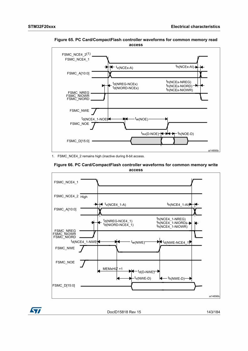
DocID15818 Rev 15 143/184
STM32F20xxx Electrical characteristics
183
Figure 65. PC Card/CompactFlash controller waveforms for common memory read access
1. FSMC_NCE4_2 remains high (inactive during 8-bit access.
Figure 66. PC Card/CompactFlash controller waveforms for common memory write access
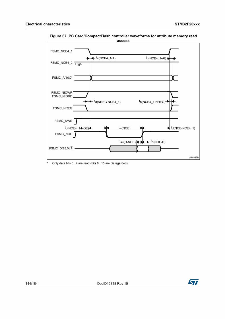
Electrical characteristics STM32F20xxx
144/184 DocID15818 Rev 15
Figure 67. PC Card/CompactFlash controller waveforms for attribute memory read access
1. Only data bits 0...7 are read (bits 8...15 are disregarded).
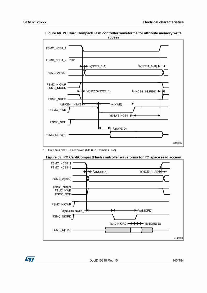
DocID15818 Rev 15 145/184
STM32F20xxx Electrical characteristics
183
Figure 68. PC Card/CompactFlash controller waveforms for attribute memory write access
1. Only data bits 0...7 are driven (bits 8...15 remains Hi-Z).
Figure 69. PC Card/CompactFlash controller waveforms for I/O space read access
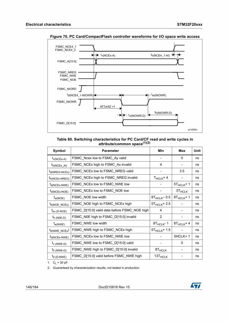
Electrical characteristics STM32F20xxx
146/184 DocID15818 Rev 15
Figure 70. PC Card/CompactFlash controller waveforms for I/O space write access
Table 80. Switching characteristics for PC Card/CF read and write cycles in attribute/common space(1)(2)
1. CL = 30 pF.
2. Guaranteed by characterization results, not tested in production.
Symbol Parameter Min Max Unit
tv(NCEx-A) FSMC_Ncex low to FSMC_Ay valid - 0 ns
th(NCEx_AI) FSMC_NCEx high to FSMC_Ax invalid 4 - ns
td(NREG-NCEx) FSMC_NCEx low to FSMC_NREG valid - 3.5 ns
th(NCEx-NREG) FSMC_NCEx high to FSMC_NREG invalid THCLK+ 4 - ns
td(NCEx-NWE) FSMC_NCEx low to FSMC_NWE low - 5THCLK+ 1 ns
td(NCEx-NOE) FSMC_NCEx low to FSMC_NOE low - 5THCLK ns
tw(NOE) FSMC_NOE low width 8THCLK– 0.5 8THCLK+ 1 ns
td(NOE_NCEx) FSMC_NOE high to FSMC_NCEx high 5THCLK+ 2.5 - ns
tsu (D-NOE) FSMC_D[15:0] valid data before FSMC_NOE high 4 - ns
th (N0E-D) FSMC_N0E high to FSMC_D[15:0] invalid 2 - ns
tw(NWE) FSMC_NWE low width 8THCLK- 1 8THCLK+ 4 ns
td(NWE_NCEx) FSMC_NWE high to FSMC_NCEx high 5THCLK+ 1.5 - ns
td(NCEx-NWE) FSMC_NCEx low to FSMC_NWE low - 5HCLK+ 1 ns
tv (NWE-D) FSMC_NWE low to FSMC_D[15:0] valid - 0 ns
th (NWE-D) FSMC_NWE high to FSMC_D[15:0] invalid 8THCLK - ns
td (D-NWE) FSMC_D[15:0] valid before FSMC_NWE high 13THCLK - ns
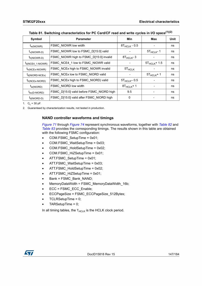
DocID15818 Rev 15 147/184
STM32F20xxx Electrical characteristics
183
NAND controller waveforms and timings
Figure 71 through Figure 74 represent synchronous waveforms, together with Table 82 and Table 83 provides the corresponding timings. The results shown in this table are obtained with the following FSMC configuration:
• COM.FSMC_SetupTime = 0x01;
• COM.FSMC_WaitSetupTime = 0x03;
• COM.FSMC_HoldSetupTime = 0x02;
• COM.FSMC_HiZSetupTime = 0x01;
• ATT.FSMC_SetupTime = 0x01;
• ATT.FSMC_WaitSetupTime = 0x03;
• ATT.FSMC_HoldSetupTime = 0x02;
• ATT.FSMC_HiZSetupTime = 0x01;
• Bank = FSMC_Bank_NAND;
• MemoryDataWidth = FSMC_MemoryDataWidth_16b;
• ECC = FSMC_ECC_Enable;
• ECCPageSize = FSMC_ECCPageSize_512Bytes;
• TCLRSetupTime = 0;
• TARSetupTime = 0;
In all timing tables, the THCLK is the HCLK clock period.
Table 81. Switching characteristics for PC Card/CF read and write cycles in I/O space(1)(2)
Symbol Parameter Min Max Unit
tw(NIOWR) FSMC_NIOWR low width 8THCLK - 0.5 - ns
tv(NIOWR-D) FSMC_NIOWR low to FSMC_D[15:0] valid - 5THCLK- 1 ns
th(NIOWR-D) FSMC_NIOWR high to FSMC_D[15:0] invalid 8THCLK- 3 - ns
td(NCE4_1-NIOWR) FSMC_NCE4_1 low to FSMC_NIOWR valid - 5THCLK+ 1.5 ns
th(NCEx-NIOWR) FSMC_NCEx high to FSMC_NIOWR invalid 5THCLK - ns
td(NIORD-NCEx) FSMC_NCEx low to FSMC_NIORD valid - 5THCLK+ 1 ns
th(NCEx-NIORD) FSMC_NCEx high to FSMC_NIORD) valid 5THCLK– 0.5 - ns
tw(NIORD) FSMC_NIORD low width 8THCLK+ 1 - ns
tsu(D-NIORD) FSMC_D[15:0] valid before FSMC_NIORD high 9.5 - ns
td(NIORD-D) FSMC_D[15:0] valid after FSMC_NIORD high 0 - ns
1. CL = 30 pF.
2. Guaranteed by characterization results, not tested in production.
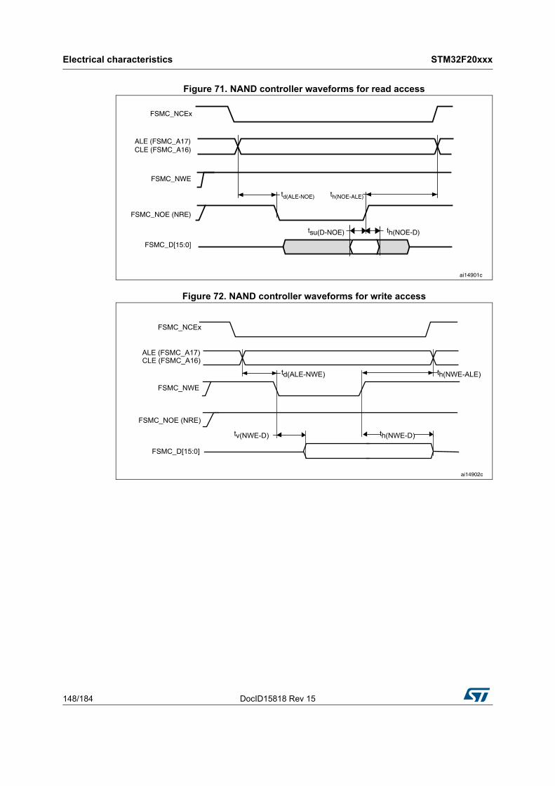
Electrical characteristics STM32F20xxx
148/184 DocID15818 Rev 15
Figure 71. NAND controller waveforms for read access
Figure 72. NAND controller waveforms for write access
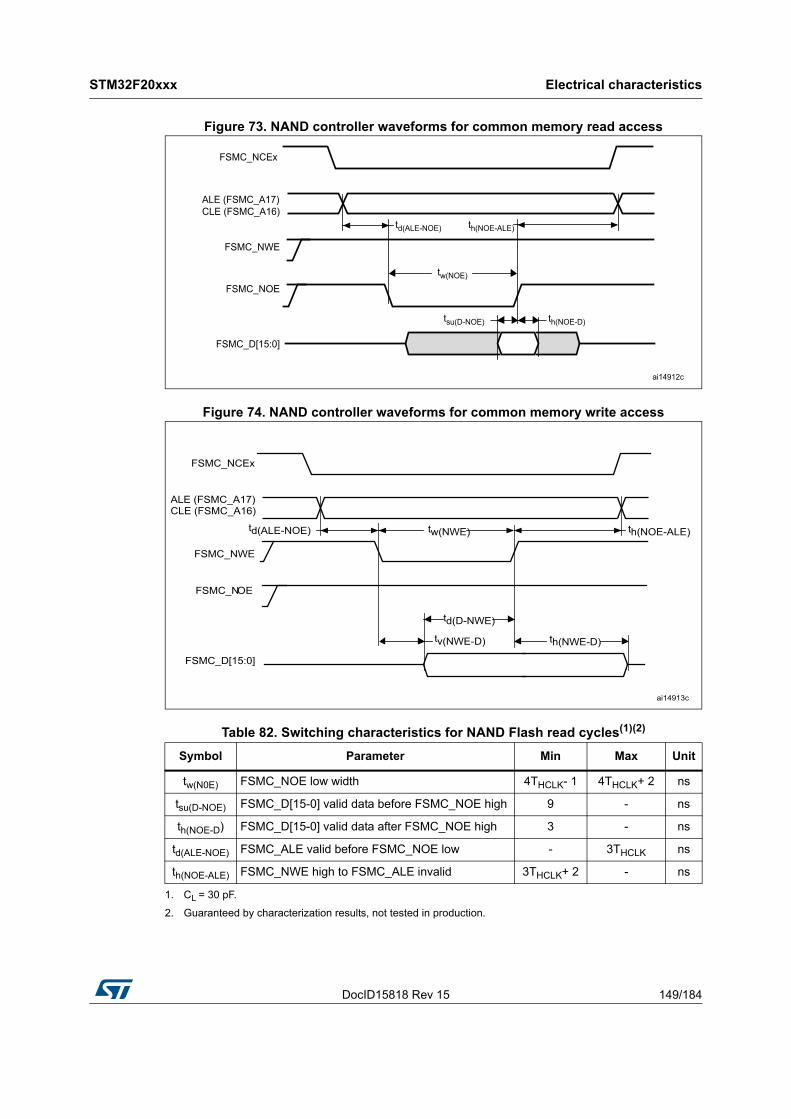
DocID15818 Rev 15 149/184
STM32F20xxx Electrical characteristics
183
Figure 73. NAND controller waveforms for common memory read access
Figure 74. NAND controller waveforms for common memory write access
Table 82. Switching characteristics for NAND Flash read cycles(1)(2)
1. CL = 30 pF.
2. Guaranteed by characterization results, not tested in production.
Symbol Parameter Min Max Unit
tw(N0E) FSMC_NOE low width 4THCLK- 1 4THCLK+ 2 ns
tsu(D-NOE) FSMC_D[15-0] valid data before FSMC_NOE high 9 - ns
th(NOE-D) FSMC_D[15-0] valid data after FSMC_NOE high 3 - ns
td(ALE-NOE) FSMC_ALE valid before FSMC_NOE low - 3THCLK ns
th(NOE-ALE) FSMC_NWE high to FSMC_ALE invalid 3THCLK+ 2 - ns
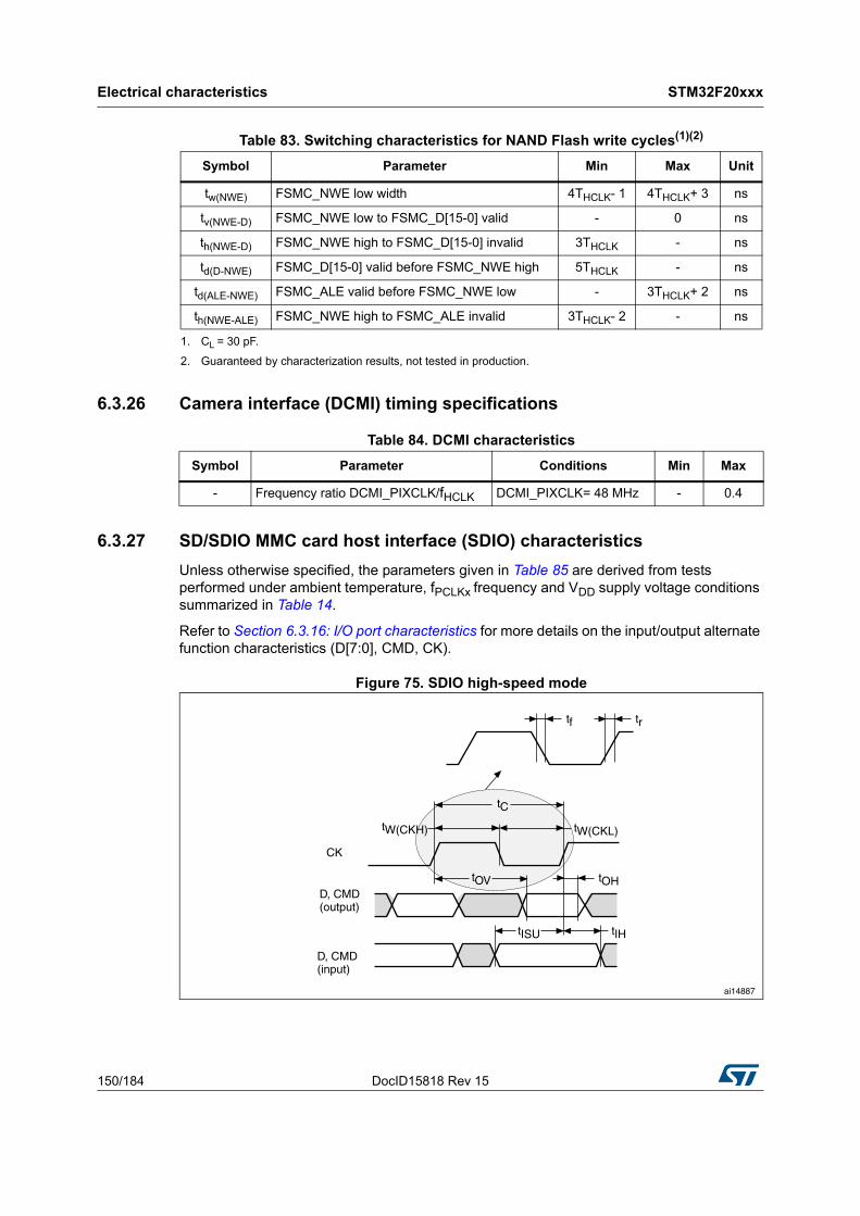
Electrical characteristics STM32F20xxx
150/184 DocID15818 Rev 15
6.3.26 Camera interface (DCMI) timing specifications
6.3.27 SD/SDIO MMC card host interface (SDIO) characteristics
Unless otherwise specified, the parameters given in Table 85 are derived from tests performed under ambient temperature, fPCLKx frequency and VDD supply voltage conditions summarized in Table 14.
Refer to Section 6.3.16: I/O port characteristics for more details on the input/output alternate function characteristics (D[7:0], CMD, CK).
Figure 75. SDIO high-speed mode
Table 83. Switching characteristics for NAND Flash write cycles(1)(2)
1. CL = 30 pF.
2. Guaranteed by characterization results, not tested in production.
Symbol Parameter Min Max Unit
tw(NWE) FSMC_NWE low width 4THCLK- 1 4THCLK+ 3 ns
tv(NWE-D) FSMC_NWE low to FSMC_D[15-0] valid - 0 ns
th(NWE-D) FSMC_NWE high to FSMC_D[15-0] invalid 3THCLK - ns
td(D-NWE) FSMC_D[15-0] valid before FSMC_NWE high 5THCLK - ns
td(ALE-NWE) FSMC_ALE valid before FSMC_NWE low - 3THCLK+ 2 ns
th(NWE-ALE) FSMC_NWE high to FSMC_ALE invalid 3THCLK- 2 - ns
Table 84. DCMI characteristics
Symbol Parameter Conditions Min Max
- Frequency ratio DCMI_PIXCLK/fHCLK DCMI_PIXCLK= 48 MHz - 0.4
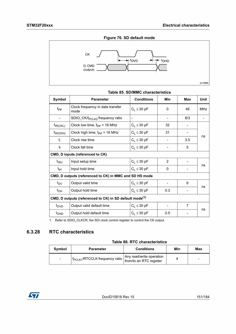
DocID15818 Rev 15 151/184
STM32F20xxx Electrical characteristics
183
Figure 76. SD default mode
6.3.28 RTC characteristics
Table 85. SD/MMC characteristics
Symbol Parameter Conditions Min Max Unit
fPPClock frequency in data transfer mode
CL ≤ 30 pF 0 48 MHz
- SDIO_CK/fPCLK2 frequency ratio - - 8/3 -
tW(CKL) Clock low time, fPP = 16 MHz CL ≤ 30 pF 32 -
nstW(CKH) Clock high time, fPP = 16 MHz CL ≤ 30 pF 31 -
tr Clock rise time CL ≤ 30 pF - 3.5
tf Clock fall time CL ≤ 30 pF - 5
CMD, D inputs (referenced to CK)
tISU Input setup time CL ≤ 30 pF 2 -ns
tIH Input hold time CL ≤ 30 pF 0 -
CMD, D outputs (referenced to CK) in MMC and SD HS mode
tOV Output valid time CL ≤ 30 pF - 6ns
tOH Output hold time CL ≤ 30 pF 0.3 -
CMD, D outputs (referenced to CK) in SD default mode(1)
1. Refer to SDIO_CLKCR, the SDI clock control register to control the CK output.
tOVD Output valid default time CL ≤ 30 pF - 7ns
tOHD Output hold default time CL ≤ 30 pF 0.5 -
Table 86. RTC characteristics
Symbol Parameter Conditions Min Max
- fPCLK1/RTCCLK frequency ratioAny read/write operation from/to an RTC register
4 -
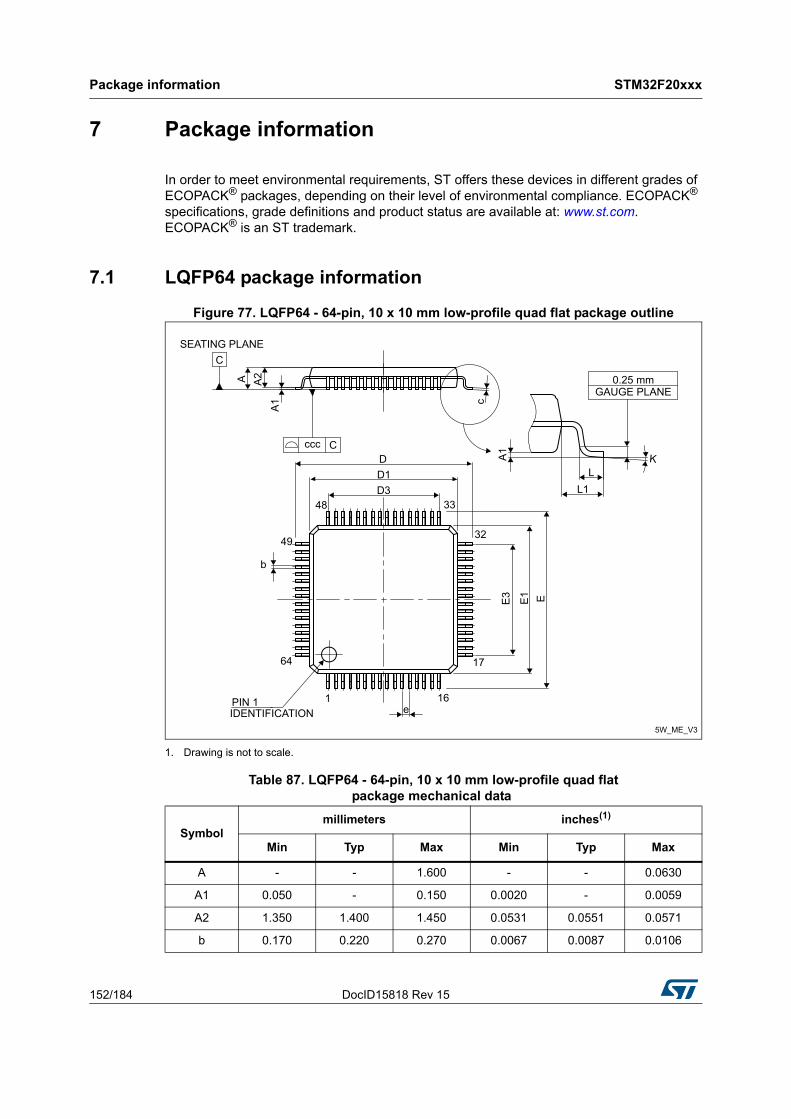
Package information STM32F20xxx
152/184 DocID15818 Rev 15
7 Package information
In order to meet environmental requirements, ST offers these devices in different grades of ECOPACK® packages, depending on their level of environmental compliance. ECOPACK® specifications, grade definitions and product status are available at: www.st.com. ECOPACK® is an ST trademark.
7.1 LQFP64 package information
Figure 77. LQFP64 - 64-pin, 10 x 10 mm low-profile quad flat package outline
1. Drawing is not to scale.
Table 87. LQFP64 - 64-pin, 10 x 10 mm low-profile quad flatpackage mechanical data
Symbolmillimeters inches(1)
Min Typ Max Min Typ Max
A - - 1.600 - - 0.0630
A1 0.050 - 0.150 0.0020 - 0.0059
A2 1.350 1.400 1.450 0.0531 0.0551 0.0571
b 0.170 0.220 0.270 0.0067 0.0087 0.0106
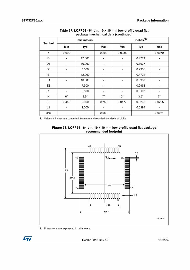
DocID15818 Rev 15 153/184
STM32F20xxx Package information
183
Figure 78. LQFP64 - 64-pin, 10 x 10 mm low-profile quad flat packagerecommended footprint
1. Dimensions are expressed in millimeters.
c 0.090 - 0.200 0.0035 - 0.0079
D - 12.000 - - 0.4724 -
D1 - 10.000 - - 0.3937 -
D3 - 7.500 - - 0.2953 -
E - 12.000 - - 0.4724 -
E1 - 10.000 - - 0.3937 -
E3 - 7.500 - - 0.2953 -
e - 0.500 - - 0.0197 -
K 0° 3.5° 7° 0° 3.5° 7°
L 0.450 0.600 0.750 0.0177 0.0236 0.0295
L1 - 1.000 - - 0.0394 -
ccc - - 0.080 - - 0.0031
1. Values in inches are converted from mm and rounded to 4 decimal digits.
Table 87. LQFP64 - 64-pin, 10 x 10 mm low-profile quad flatpackage mechanical data (continued)
Symbolmillimeters inches(1)
Min Typ Max Min Typ Max
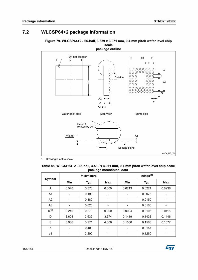
Package information STM32F20xxx
154/184 DocID15818 Rev 15
7.2 WLCSP64+2 package information
Figure 79. WLCSP64+2 - 66-ball, 3.639 x 3.971 mm, 0.4 mm pitch wafer level chip scale
package outline
1. Drawing is not to scale.
Table 88. WLCSP64+2 - 66-ball, 4.539 x 4.911 mm, 0.4 mm pitch wafer level chip scale package mechanical data
Symbolmillimeters inches(1)
Min Typ Max Min Typ Max
A 0.540 0.570 0.600 0.0213 0.0224 0.0236
A1 - 0.190 - - 0.0075 -
A2 - 0.380 - - 0.0150 -
A3 - 0.025 - - 0.0100 -
b(2) 0.240 0.270 0.300 0.0094 0.0106 0.0118
D 3.604 3.639 3.674 0.1419 0.1433 0.1446
E 3.936 3.971 4.006 0.1550 0.1563 0.1577
e - 0.400 - - 0.0157 -
e1 - 3.200 - - 0.1260 -
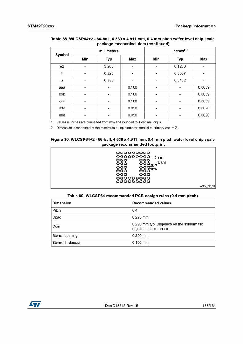
DocID15818 Rev 15 155/184
STM32F20xxx Package information
183
Figure 80. WLCSP64+2 - 66-ball, 4.539 x 4.911 mm, 0.4 mm pitch wafer level chip scale package recommended footprint
e2 - 3.200 - - 0.1260 -
F - 0.220 - - 0.0087 -
G - 0.386 - - 0.0152 -
aaa - - 0.100 - - 0.0039
bbb - - 0.100 - - 0.0039
ccc - - 0.100 - - 0.0039
ddd - - 0.050 - - 0.0020
eee - - 0.050 - - 0.0020
1. Values in inches are converted from mm and rounded to 4 decimal digits.
2. Dimension is measured at the maximum bump diameter parallel to primary datum Z.
Table 89. WLCSP64 recommended PCB design rules (0.4 mm pitch)
Dimension Recommended values
Pitch 0.4
Dpad 0.225 mm
Dsm0.290 mm typ. (depends on the soldermask registration tolerance)
Stencil opening 0.250 mm
Stencil thickness 0.100 mm
Table 88. WLCSP64+2 - 66-ball, 4.539 x 4.911 mm, 0.4 mm pitch wafer level chip scale package mechanical data (continued)
Symbolmillimeters inches(1)
Min Typ Max Min Typ Max
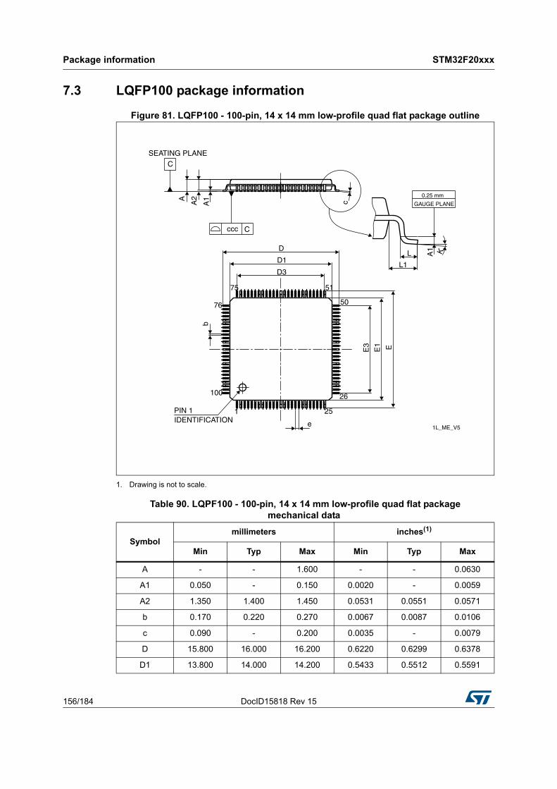
Package information STM32F20xxx
156/184 DocID15818 Rev 15
7.3 LQFP100 package information
Figure 81. LQFP100 - 100-pin, 14 x 14 mm low-profile quad flat package outline
1. Drawing is not to scale.
Table 90. LQPF100 - 100-pin, 14 x 14 mm low-profile quad flat packagemechanical data
Symbolmillimeters inches(1)
Min Typ Max Min Typ Max
A - - 1.600 - - 0.0630
A1 0.050 - 0.150 0.0020 - 0.0059
A2 1.350 1.400 1.450 0.0531 0.0551 0.0571
b 0.170 0.220 0.270 0.0067 0.0087 0.0106
c 0.090 - 0.200 0.0035 - 0.0079
D 15.800 16.000 16.200 0.6220 0.6299 0.6378
D1 13.800 14.000 14.200 0.5433 0.5512 0.5591
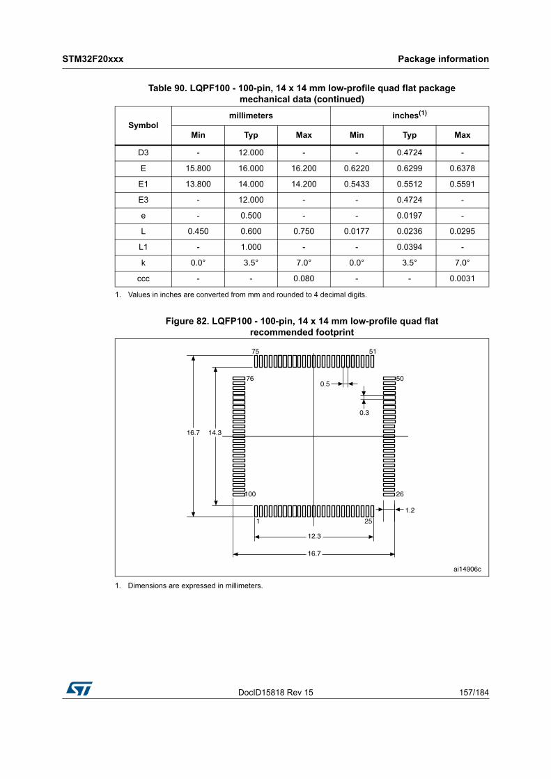
DocID15818 Rev 15 157/184
STM32F20xxx Package information
183
Figure 82. LQFP100 - 100-pin, 14 x 14 mm low-profile quad flatrecommended footprint
1. Dimensions are expressed in millimeters.
D3 - 12.000 - - 0.4724 -
E 15.800 16.000 16.200 0.6220 0.6299 0.6378
E1 13.800 14.000 14.200 0.5433 0.5512 0.5591
E3 - 12.000 - - 0.4724 -
e - 0.500 - - 0.0197 -
L 0.450 0.600 0.750 0.0177 0.0236 0.0295
L1 - 1.000 - - 0.0394 -
k 0.0° 3.5° 7.0° 0.0° 3.5° 7.0°
ccc - - 0.080 - - 0.0031
1. Values in inches are converted from mm and rounded to 4 decimal digits.
Table 90. LQPF100 - 100-pin, 14 x 14 mm low-profile quad flat packagemechanical data (continued)
Symbolmillimeters inches(1)
Min Typ Max Min Typ Max
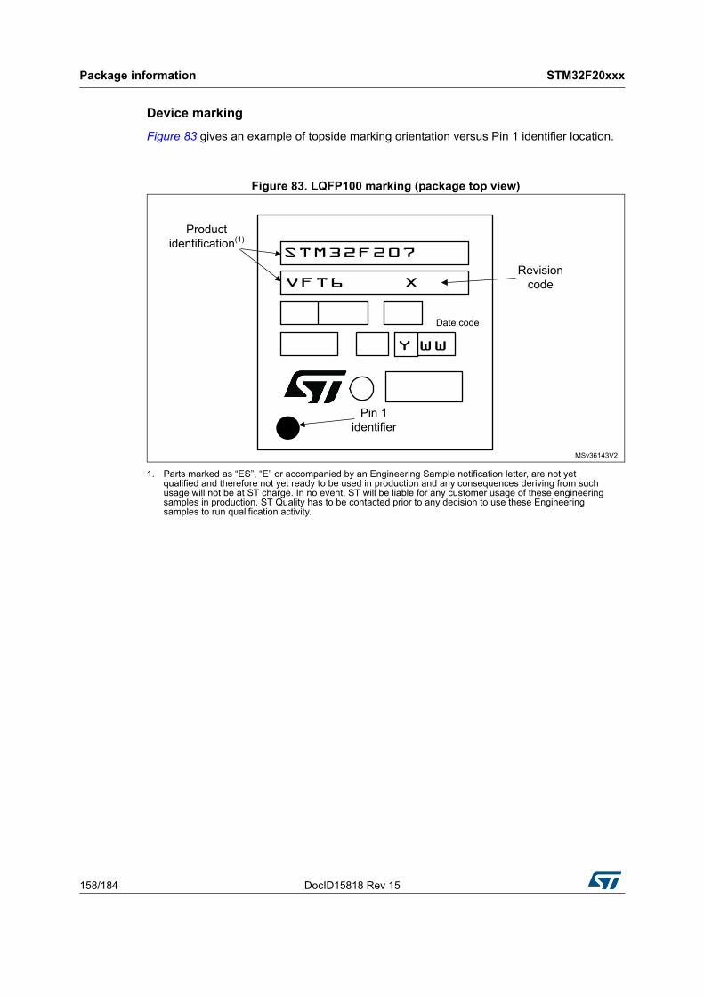
Package information STM32F20xxx
158/184 DocID15818 Rev 15
Device marking
Figure 83 gives an example of topside marking orientation versus Pin 1 identifier location.
Figure 83. LQFP100 marking (package top view)
1. Parts marked as “ES”, “E” or accompanied by an Engineering Sample notification letter, are not yet qualified and therefore not yet ready to be used in production and any consequences deriving from such usage will not be at ST charge. In no event, ST will be liable for any customer usage of these engineering samples in production. ST Quality has to be contacted prior to any decision to use these Engineering samples to run qualification activity.
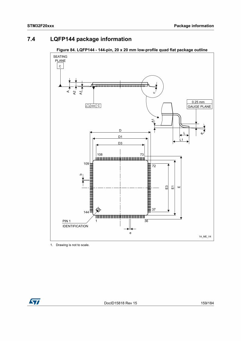
DocID15818 Rev 15 159/184
STM32F20xxx Package information
183
7.4 LQFP144 package information
Figure 84. LQFP144 - 144-pin, 20 x 20 mm low-profile quad flat package outline
1. Drawing is not to scale.
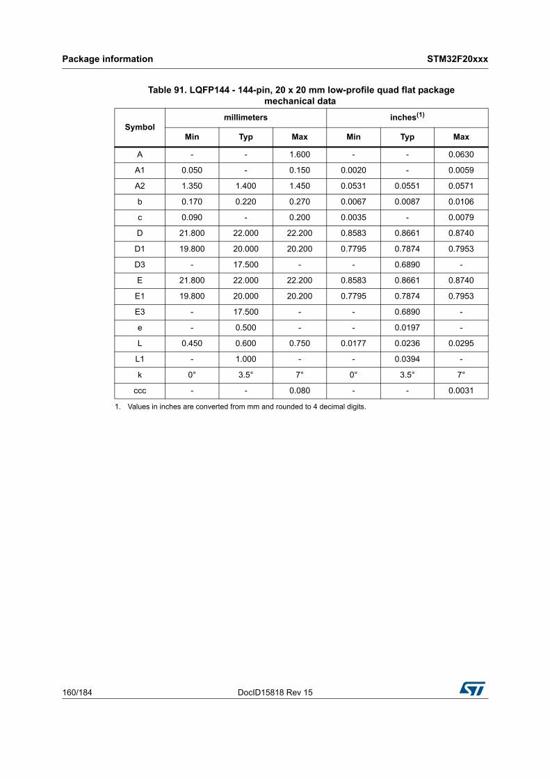
Package information STM32F20xxx
160/184 DocID15818 Rev 15
Table 91. LQFP144 - 144-pin, 20 x 20 mm low-profile quad flat packagemechanical data
Symbolmillimeters inches(1)
1. Values in inches are converted from mm and rounded to 4 decimal digits.
Min Typ Max Min Typ Max
A - - 1.600 - - 0.0630
A1 0.050 - 0.150 0.0020 - 0.0059
A2 1.350 1.400 1.450 0.0531 0.0551 0.0571
b 0.170 0.220 0.270 0.0067 0.0087 0.0106
c 0.090 - 0.200 0.0035 - 0.0079
D 21.800 22.000 22.200 0.8583 0.8661 0.8740
D1 19.800 20.000 20.200 0.7795 0.7874 0.7953
D3 - 17.500 - - 0.6890 -
E 21.800 22.000 22.200 0.8583 0.8661 0.8740
E1 19.800 20.000 20.200 0.7795 0.7874 0.7953
E3 - 17.500 - - 0.6890 -
e - 0.500 - - 0.0197 -
L 0.450 0.600 0.750 0.0177 0.0236 0.0295
L1 - 1.000 - - 0.0394 -
k 0° 3.5° 7° 0° 3.5° 7°
ccc - - 0.080 - - 0.0031
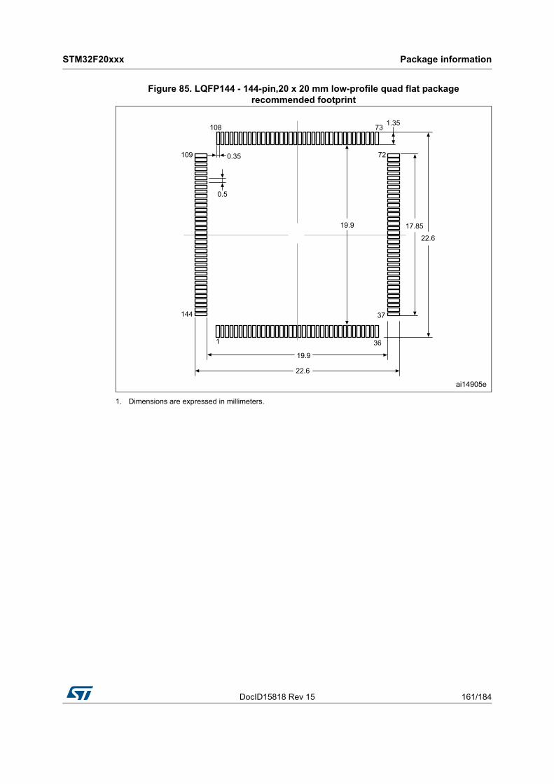
DocID15818 Rev 15 161/184
STM32F20xxx Package information
183
Figure 85. LQFP144 - 144-pin,20 x 20 mm low-profile quad flat packagerecommended footprint
1. Dimensions are expressed in millimeters.
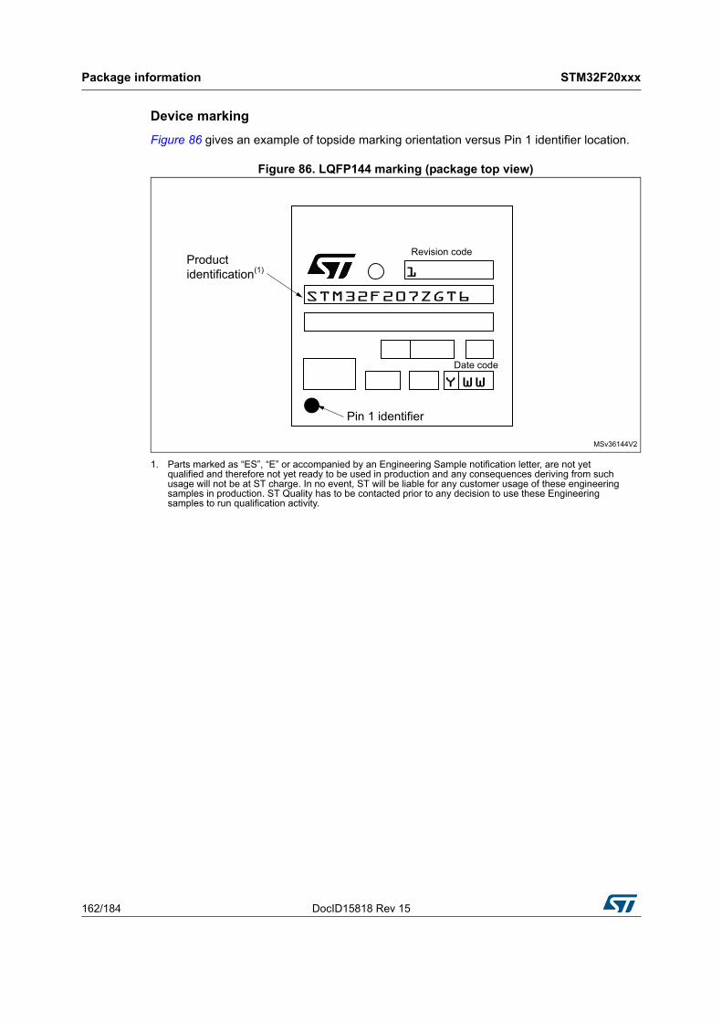
Package information STM32F20xxx
162/184 DocID15818 Rev 15
Device marking
Figure 86 gives an example of topside marking orientation versus Pin 1 identifier location.
Figure 86. LQFP144 marking (package top view)
1. Parts marked as “ES”, “E” or accompanied by an Engineering Sample notification letter, are not yet qualified and therefore not yet ready to be used in production and any consequences deriving from such usage will not be at ST charge. In no event, ST will be liable for any customer usage of these engineering samples in production. ST Quality has to be contacted prior to any decision to use these Engineering samples to run qualification activity.
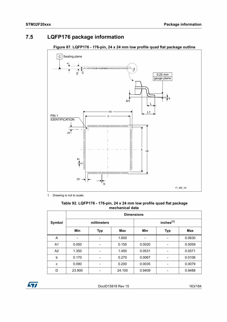
DocID15818 Rev 15 163/184
STM32F20xxx Package information
183
7.5 LQFP176 package information
Figure 87. LQFP176 - 176-pin, 24 x 24 mm low profile quad flat package outline
1. Drawing is not to scale.
Table 92. LQFP176 - 176-pin, 24 x 24 mm low profile quad flat packagemechanical data
Symbol
Dimensions
millimeters inches(1)
Min Typ Max Min Typ Max
A - - 1.600 - - 0.0630
A1 0.050 - 0.150 0.0020 - 0.0059
A2 1.350 - 1.450 0.0531 - 0.0571
b 0.170 - 0.270 0.0067 - 0.0106
c 0.090 - 0.200 0.0035 - 0.0079
D 23.900 - 24.100 0.9409 - 0.9488
Package information STM32F20xxx
164/184 DocID15818 Rev 15
HD 25.900 - 26.100 1.0197 - 1.0276
ZD - 1.250 - - 0.0492 -
E 23.900 - 24.100 0.9409 - 0.9488
HE 25.900 - 26.100 1.0197 - 1.0276
ZE - 1.250 - - 0.0492 -
e - 0.500 - - 0.0197 -
L(2) 0.450 - 0.750 0.0177 - 0.0295
L1 - 1.000 - - 0.0394 -
k 0° - 7° 0° - 7°
ccc - - 0.080 - - 0.0031
1. Values in inches are converted from mm and rounded to 4 decimal digits.
2. L dimension is measured at gauge plane at 0.25 mm above the seating plane.
Table 92. LQFP176 - 176-pin, 24 x 24 mm low profile quad flat packagemechanical data (continued)
Symbol
Dimensions
millimeters inches(1)
Min Typ Max Min Typ Max
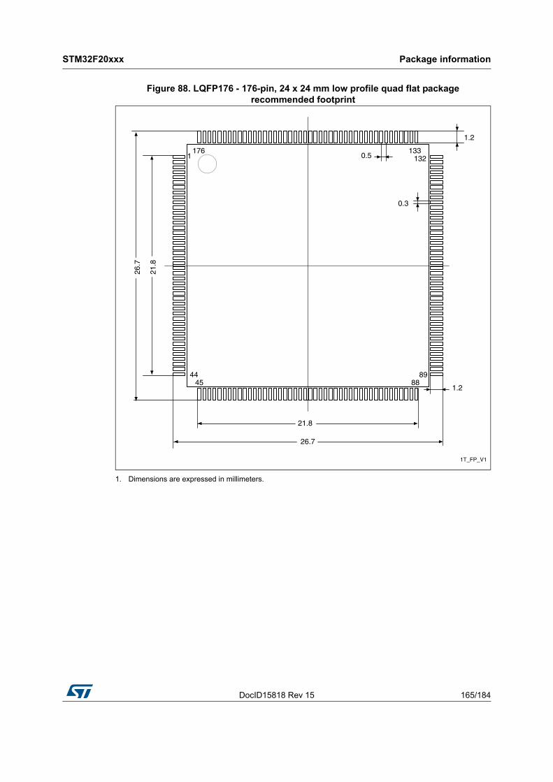
DocID15818 Rev 15 165/184
STM32F20xxx Package information
183
Figure 88. LQFP176 - 176-pin, 24 x 24 mm low profile quad flat packagerecommended footprint
1. Dimensions are expressed in millimeters.
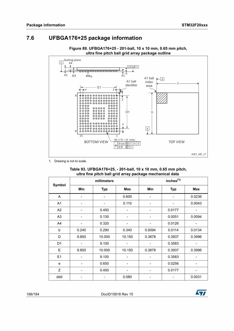
Package information STM32F20xxx
166/184 DocID15818 Rev 15
7.6 UFBGA176+25 package information
Figure 89. UFBGA176+25 - 201-ball, 10 x 10 mm, 0.65 mm pitch,ultra fine pitch ball grid array package outline
1. Drawing is not to scale.
Table 93. UFBGA176+25, - 201-ball, 10 x 10 mm, 0.65 mm pitch,ultra fine pitch ball grid array package mechanical data
Symbolmillimeters inches(1)
Min Typ Max Min Typ Max
A - - 0.600 - - 0.0236
A1 - - 0.110 - - 0.0043
A2 - 0.450 - - 0.0177 -
A3 - 0.130 - - 0.0051 0.0094
A4 - 0.320 - - 0.0126 -
b 0.240 0.290 0.340 0.0094 0.0114 0.0134
D 9.850 10.000 10.150 0.3878 0.3937 0.3996
D1 - 9.100 - - 0.3583 -
E 9.850 10.000 10.150 0.3878 0.3937 0.3996
E1 - 9.100 - - 0.3583 -
e - 0.650 - - 0.0256 -
Z - 0.450 - - 0.0177 -
ddd - - 0.080 - - 0.0031
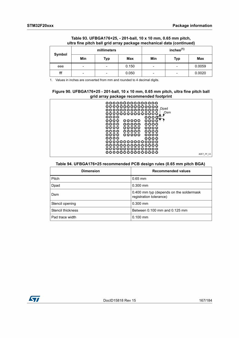
DocID15818 Rev 15 167/184
STM32F20xxx Package information
183
Figure 90. UFBGA176+25 - 201-ball, 10 x 10 mm, 0.65 mm pitch, ultra fine pitch ballgrid array package recommended footprint
eee - - 0.150 - - 0.0059
fff - - 0.050 - - 0.0020
1. Values in inches are converted from mm and rounded to 4 decimal digits.
Table 94. UFBGA176+25 recommended PCB design rules (0.65 mm pitch BGA)
Dimension Recommended values
Pitch 0.65 mm
Dpad 0.300 mm
Dsm0.400 mm typ (depends on the soldermask registration tolerance)
Stencil opening 0.300 mm
Stencil thickness Between 0.100 mm and 0.125 mm
Pad trace width 0.100 mm
Table 93. UFBGA176+25, - 201-ball, 10 x 10 mm, 0.65 mm pitch,ultra fine pitch ball grid array package mechanical data (continued)
Symbolmillimeters inches(1)
Min Typ Max Min Typ Max
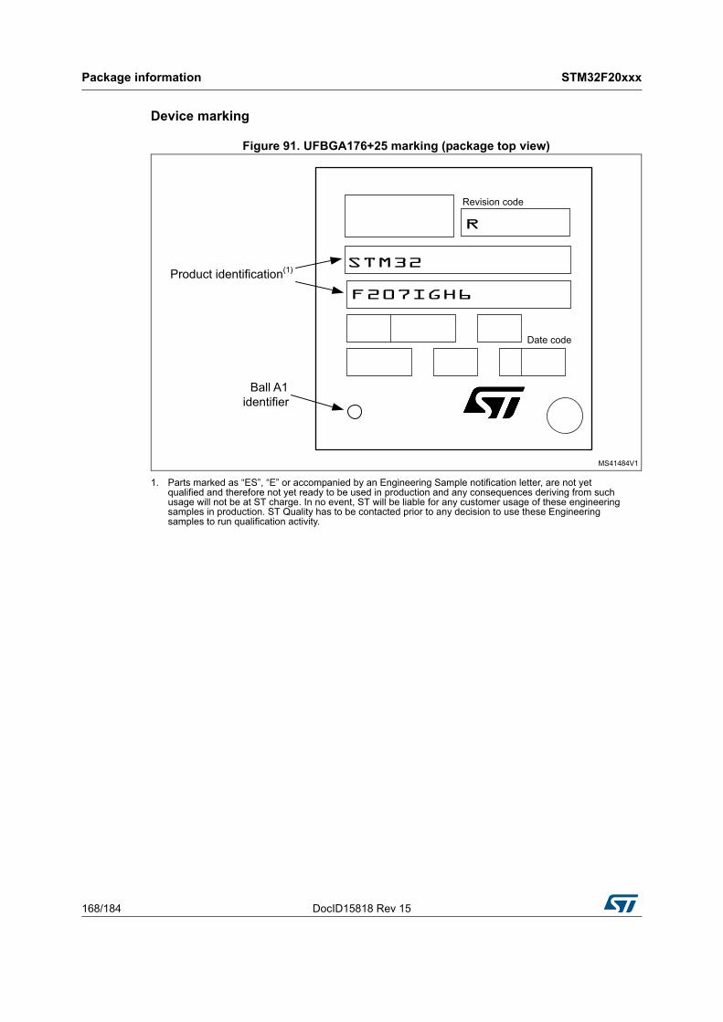
Package information STM32F20xxx
168/184 DocID15818 Rev 15
Device marking
Figure 91. UFBGA176+25 marking (package top view)
1. Parts marked as “ES”, “E” or accompanied by an Engineering Sample notification letter, are not yet qualified and therefore not yet ready to be used in production and any consequences deriving from such usage will not be at ST charge. In no event, ST will be liable for any customer usage of these engineering samples in production. ST Quality has to be contacted prior to any decision to use these Engineering samples to run qualification activity.
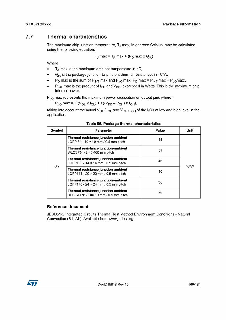
DocID15818 Rev 15 169/184
STM32F20xxx Package information
183
7.7 Thermal characteristics
The maximum chip-junction temperature, TJ max, in degrees Celsius, may be calculated using the following equation:
TJ max = TA max + (PD max x ΘJA)
Where:
• TA max is the maximum ambient temperature in ° C,
• ΘJA is the package junction-to-ambient thermal resistance, in ° C/W,
• PD max is the sum of PINT max and PI/O max (PD max = PINT max + PI/Omax),
• PINT max is the product of IDD and VDD, expressed in Watts. This is the maximum chip internal power.
PI/O max represents the maximum power dissipation on output pins where:
PI/O max = Σ (VOL × IOL) + Σ((VDD – VOH) × IOH),
taking into account the actual VOL / IOL and VOH / IOH of the I/Os at low and high level in the application.
Reference document
JESD51-2 Integrated Circuits Thermal Test Method Environment Conditions - Natural Convection (Still Air). Available from www.jedec.org.
Table 95. Package thermal characteristics
Symbol Parameter Value Unit
ΘJA
Thermal resistance junction-ambient LQFP 64 - 10 × 10 mm / 0.5 mm pitch
45
°C/W
Thermal resistance junction-ambient WLCSP64+2 - 0.400 mm pitch
51
Thermal resistance junction-ambient LQFP100 - 14 × 14 mm / 0.5 mm pitch
46
Thermal resistance junction-ambient LQFP144 - 20 × 20 mm / 0.5 mm pitch
40
Thermal resistance junction-ambient LQFP176 - 24 × 24 mm / 0.5 mm pitch
38
Thermal resistance junction-ambient UFBGA176 - 10× 10 mm / 0.5 mm pitch
39
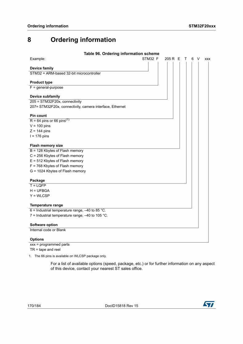
Ordering information STM32F20xxx
170/184 DocID15818 Rev 15
8 Ordering information
For a list of available options (speed, package, etc.) or for further information on any aspect of this device, contact your nearest ST sales office.
Table 96. Ordering information schemeExample: STM32 F 205 R E T 6 V xxx
Device familySTM32 = ARM-based 32-bit microcontroller
Product typeF = general-purpose
Device subfamily205 = STM32F20x, connectivity 207= STM32F20x, connectivity, camera interface, Ethernet
Pin countR = 64 pins or 66 pins(1)
V = 100 pinsZ = 144 pinsI = 176 pins
Flash memory sizeB = 128 Kbytes of Flash memoryC = 256 Kbytes of Flash memoryE = 512 Kbytes of Flash memoryF = 768 Kbytes of Flash memoryG = 1024 Kbytes of Flash memory
PackageT = LQFPH = UFBGAY = WLCSP
Temperature range6 = Industrial temperature range, –40 to 85 °C.7 = Industrial temperature range, –40 to 105 °C.
Software optionInternal code or Blank
Optionsxxx = programmed partsTR = tape and reel
1. The 66 pins is available on WLCSP package only.
DocID15818 Rev 15 171/184
STM32F20xxx Revision history
183
9 Revision history
Table 97. Document revision history
Date Revision Changes
05-Jun-2009 1 Initial release.
09-Oct-2009 2
Document status promoted from Target specification to Preliminary data.
In Table 8: STM32F20x pin and ball definitions:
– Note 4 updated
– VDD_SA and VDD_3 pins inverted (Figure 12: STM32F20x LQFP100 pinout, Figure 13: STM32F20x LQFP144 pinout and Figure 14: STM32F20x LQFP176 pinout corrected accordingly).
Section : In order to meet environmental requirements, ST offers these devices in different grades of ECOPACK® packages, depending on their level of environmental compliance. ECOPACK® specifications, grade definitions and product status are available at: www.st.com. ECOPACK® is an ST trademark. changed to LQFP with no exposed pad.
01-Feb-2010 3
LFBGA144 package removed. STM32F203xx part numbers removed. Part numbers with 128 and 256 Kbyte Flash densities added.
Encryption features removed.
PC13-TAMPER-RTC renamed to PC13-RTC_AF1 and PI8-TAMPER-RTC renamed to PI8-RTC_AF2.
13-Jul-2010 4
Renamed high-speed SRAM, system SRAM.
Removed combination: 128 KBytes Flash memory in LQFP144.
Added UFBGA176 package. Added note 1 related to LQFP176 package in Table 2, Figure 14, and Table 96.
Added information on ART accelerator and audio PLL (PLLI2S).
Added Table 6: USART feature comparison.
Several updates on Table 8: STM32F20x pin and ball definitions and Table 10: Alternate function mapping. ADC, DAC, oscillator, RTC_AF, WKUP and VBUS signals removed from alternate functions and moved to the “other functions” column in Table 8: STM32F20x pin and ball definitions.
TRACESWO added in Figure 4: STM32F20x block diagram, Table 8: STM32F20x pin and ball definitions, and Table 10: Alternate function mapping.
XTAL oscillator frequency updated on cover page, in Figure 4: STM32F20x block diagram and in Section 3.11: External interrupt/event controller (EXTI).
Updated list of peripherals used for boot mode in Section 3.13: Boot modes.
Added Regulator bypass mode in Section 3.16: Voltage regulator, and Section 6.3.4: Operating conditions at power-up / power-down (regulator OFF).
Updated Section 3.17: Real-time clock (RTC), backup SRAM and backup registers.
Added Note Note: in Section 3.18: Low-power modes.
Added SPI TI protocol in Section 3.23: Serial peripheral interface (SPI).
Revision history STM32F20xxx
172/184 DocID15818 Rev 15
13-Jul-20104
(continued)
Added USB OTG_FS features in Section 3.28: Universal serial bus on-the-go full-speed (OTG_FS).
Updated VCAP_1 and VCAP_2 capacitor value to 2.2 µF in Figure 19: Power supply scheme.
Removed DAC, modified ADC limitations, and updated I/O compensation for 1.8 to 2.1 V range in Table 15: Limitations depending on the operating power supply range.
Added VBORL, VBORM, VBORH and IRUSH in Table 19: Embedded reset and power control block characteristics.
Removed table Typical current consumption in Sleep mode with Flash memory in Deep power down mode. Merged typical and maximum current consumption sections and added Table 21: Typical and maximum current consumption in Run mode, code with data processing running from Flash memory (ART accelerator disabled), Table 20: Typical and maximum current consumption in Run mode, code with data processing running from Flash memory (ART accelerator enabled) or RAM, Table 22: Typical and maximum current consumption in Sleep mode, Table 23: Typical and maximum current consumptions in Stop mode, Table 24: Typical and maximum current consumptions in Standby mode, and Table 25: Typical and maximum current consumptions in VBAT mode.
Update Table 34: Main PLL characteristics and added Section 6.3.11: PLL spread spectrum clock generation (SSCG) characteristics.
Added Note 8 for CIO in Table 48: I/O AC characteristics.
Updated Section 6.3.18: TIM timer characteristics.
Added TNRST_OUT in Table 49: NRST pin characteristics.
Updated Table 52: I2C characteristics.
Removed 8-bit data in and data out waveforms from Figure 48: ULPI timing diagram.
Removed note related to ADC calibration in Table 67. Section 6.3.20: 12-bit ADC characteristics: ADC characteristics tables merged into one single table; tables ADC conversion time and ADC accuracy removed.
Updated Table 68: DAC characteristics.
Updated Section 6.3.22: Temperature sensor characteristics and Section 6.3.23: VBAT monitoring characteristics.
Update Section 6.3.26: Camera interface (DCMI) timing specifications.
Added Section 6.3.27: SD/SDIO MMC card host interface (SDIO) characteristics, and Section 6.3.28: RTC characteristics.
Added Section 7.7: Thermal characteristics. Updated Table 91: LQFP176 - Low profile quad flat package 24 × 24 × 1.4 mm package mechanical data and Figure 86: LQFP176 - Low profile quad flat package 24 × 24 × 1.4 mm, package outline.
Changed tape and reel code to TX in Table 96: Ordering information scheme.
Added Table 101: Main applications versus package for STM32F2xxx microcontrollers. Updated figures in Appendix A.2: USB OTG full speed (FS) interface solutions and A.3: USB OTG high speed (HS) interface solutions. Updated Figure 94: Audio player solution using PLL, PLLI2S, USB and 1 crystal and Figure 95: Audio PLL (PLLI2S) providing accurate I2S clock.
Table 97. Document revision history (continued)
Date Revision Changes
DocID15818 Rev 15 173/184
STM32F20xxx Revision history
183
25-Nov-2010 5
Update I/Os in Section : Features.
Added WLCSP64+2 package. Added note 1 related to LQFP176 on cover page.
Added trademark for ART accelerator. Updated Section 3.2: Adaptive real-time memory accelerator (ART Accelerator™).
Updated Figure 5: Multi-AHB matrix.
Added case of BOR inactivation using IRROFF on WLCSP devices in Section 3.15: Power supply supervisor.
Reworked Section 3.16: Voltage regulator to clarify regulator off modes. Renamed PDROFF, IRROFF in the whole document.
Added Section 3.19: VBAT operation.
Updated LIN and IrDA features for UART4/5 in Table 6: USART feature comparison.
Table 8: STM32F20x pin and ball definitions: Modified VDD_3 pin, and added note related to the FSMC_NL pin; renamed BYPASS-REG REGOFF, and add IRROFF pin; renamed USART4/5 UART4/5. USART4 pins renamed UART4.
Changed VSS_SA to VSS, and VDD_SA pin reserved for future use.
Updated maximum HSE crystal frequency to 26 MHz.
Section 6.2: Absolute maximum ratings: Updated VIN minimum and maximum values and note related to five-volt tolerant inputs in Table 11: Voltage characteristics. Updated IINJ(PIN) maximum values and related notes in Table 12: Current characteristics.
Updated VDDA minimum value in Table 14: General operating conditions.
Added Note 2 and updated Maximum CPU frequency in Table 15: Limitations depending on the operating power supply range, and added Figure 21: Number of wait states versus fCPU and VDD range.
Added brownout level 1, 2, and 3 thresholds in Table 19: Embedded reset and power control block characteristics.
Changed fOSC_IN maximum value in Table 30: HSE 4-26 MHz oscillator characteristics.
Changed fPLL_IN maximum value in Table 34: Main PLL characteristics, and updated jitter parameters in Table 35: PLLI2S (audio PLL) characteristics.
Section 6.3.16: I/O port characteristics: updated VIH and VIL in Table 48: I/O AC characteristics.
Added Note 1 below Table 47: Output voltage characteristics.
Updated RPD and RPU parameter description in Table 57: USB OTG FS DC electrical characteristics.
Updated VREF+ minimum value in Table 66: ADC characteristics.
Updated Table 71: Embedded internal reference voltage.
Removed Ethernet and USB2 for 64-pin devices in Table 101: Main applications versus package for STM32F2xxx microcontrollers.
Added A.2: USB OTG full speed (FS) interface solutions, removed “OTG FS connection with external PHY” figure, updated Figure 87, Figure 88, and Figure 90 to add STULPI01B.
Table 97. Document revision history (continued)
Date Revision Changes
Revision history STM32F20xxx
174/184 DocID15818 Rev 15
22-Apr-2011 6
Changed datasheet status to “Full Datasheet”.
Introduced concept of SRAM1 and SRAM2.
LQFP176 package now in production and offered only for 256 Kbyte and 1 Mbyte devices. Availability of WLCSP64+2 package limited to 512 Kbyte and 1 Mbyte devices.
Updated Figure 3: Compatible board design between STM32F10x and STM32F2xx for LQFP144 package and Figure 2: Compatible board design between STM32F10x and STM32F2xx for LQFP100 package.
Added camera interface for STM32F207Vx devices in Table 2: STM32F205xx features and peripheral counts.
Removed 16 MHz internal RC oscillator accuracy in Section 3.12: Clocks and startup.
Updated Section 3.16: Voltage regulator.
Modified I2S sampling frequency range in Section 3.12: Clocks and startup, Section 3.24: Inter-integrated sound (I2S), and Section 3.30: Audio PLL (PLLI2S).
Updated Section 3.17: Real-time clock (RTC), backup SRAM and backup registers and description of TIM2 and TIM5 in Section 3.20.2: General-purpose timers (TIMx).
Modified maximum baud rate (oversampling by 16) for USART1 in Table 6: USART feature comparison.
Updated note related to RFU pin below Figure 12: STM32F20x LQFP100 pinout, Figure 13: STM32F20x LQFP144 pinout, Figure 14: STM32F20x LQFP176 pinout, Figure 15: STM32F20x UFBGA176 ballout, and Table 8: STM32F20x pin and ball definitions.
In Table 8: STM32F20x pin and ball definitions,:changed I2S2_CK and I2S3_CK to I2S2_SCK and I2S3_SCK, respectively; added PA15 and TT (3.6 V tolerant I/O).
Added RTC_50Hz as PB15 alternate function in Table 8: STM32F20x pin and ball definitions and Table 10: Alternate function mapping.
Removed ETH _RMII_TX_CLK for PC3/AF11 in Table 10: Alternate function mapping.
Updated Table 11: Voltage characteristics and Table 12: Current characteristics.
TSTG updated to –65 to +150 in Table 13: Thermal characteristics.
Added CEXT, ESL, and ESR in Table 14: General operating conditions as well as Section 6.3.2: VCAP1/VCAP2 external capacitor.
Modified Note 4 in Table 15: Limitations depending on the operating power supply range.
Updated Table 17: Operating conditions at power-up / power-down (regulator ON), and Table 18: Operating conditions at power-up / power-down (regulator OFF).
Added OSC_OUT pin in Figure 17: Pin loading conditions. and Figure 18: Pin input voltage.
Updated Figure 19: Power supply scheme to add IRROFF and REGOFF pins and modified notes.
Updated VPVD, VBOR1, VBOR2, VBOR3, TRSTTEMPO typical value, and IRUSH, added ERUSH and Note 2 in Table 19: Embedded reset and power control block characteristics.
Table 97. Document revision history (continued)
Date Revision Changes
DocID15818 Rev 15 175/184
STM32F20xxx Revision history
183
22-Apr-20116
(continued)
Updated Typical and maximum current consumption conditions, as well as Table 21: Typical and maximum current consumption in Run mode, code with data processing running from Flash memory (ART accelerator disabled) and Table 20: Typical and maximum current consumption in Run mode, code with data processing running from Flash memory (ART accelerator enabled) or RAM. Added Figure 23, Figure 24, Figure 25, and Figure 26.
Updated Table 22: Typical and maximum current consumption in Sleep mode, and added Figure 27 and Figure 28.
Updated Table 23: Typical and maximum current consumptions in Stop mode. Added Figure 29: Typical current consumption vs. temperature in Stop mode.
Updated Table 24: Typical and maximum current consumptions in Standby mode and Table 25: Typical and maximum current consumptions in VBAT mode.
Updated On-chip peripheral current consumption conditions and Table 26: Peripheral current consumption.
Updated tWUSTDBY and tWUSTOP, and added Note 3 in Table 27: Low-power mode wakeup timings.
Maximum fHSE_ext and minimum tw(HSE) values updated in Table 28: High-speed external user clock characteristics.
Updated C and gm in Table 30: HSE 4-26 MHz oscillator characteristics. Updated RF, I2, gm, and tsu(LSE) in Table 31: LSE oscillator characteristics (fLSE = 32.768 kHz).
Added Note 1 and updated ACCHSI, IDD(HSI, and tsu(HSI) in Table 32: HSI oscillator characteristics. Added Figure 34: ACCHSI versus temperature.
Updated fLSI, tsu(LSI) and IDD(LSI) in Table 33: LSI oscillator characteristics. Added Figure 35: ACCLSI versus temperature
Table 34: Main PLL characteristics: removed note 1, updated tLOCK, jitter, IDD(PLL) and IDDA(PLL), added Note 2 for fPLL_IN minimum and maximum values.
Table 35: PLLI2S (audio PLL) characteristics: removed note 1, updated tLOCK, jitter, IDD(PLLI2S) and IDDA(PLLI2S), added Note 2 for fPLLI2S_IN minimum and maximum values.
Added Note 1 in Table 36: SSCG parameters constraint.
Updated Table 37: Flash memory characteristics. Modified Table 38: Flash memory programming and added Note 2 for tprog. Updated tprog and added Note 1 in Table 39: Flash memory programming with VPP.
Modified Figure 40: Recommended NRST pin protection.
Updated Table 42: EMI characteristics and EMI monitoring conditions in Section : Electromagnetic Interference (EMI). Added Note 2 related to VESD(HBM)in Table 43: ESD absolute maximum ratings.
Updated Table 48: I/O AC characteristics.
Added Section 6.3.15: I/O current injection characteristics.
Modified maximum frequency values and conditions in Table 48: I/O AC characteristics.
Updated tres(TIM) in Table 50: Characteristics of TIMx connected to the APB1 domain. Modified tres(TIM) and fEXT Table 51: Characteristics of TIMx connected to the APB2 domain.
Table 97. Document revision history (continued)
Date Revision Changes
Revision history STM32F20xxx
176/184 DocID15818 Rev 15
22-Apr-20116
(continued)
Changed tw(SCKH) to tw(SCLH), tw(SCKL) to tw(SCLL), tr(SCK) to tr(SCL), and tf(SCK) to tf(SCL) in Table 52: I2C characteristics and in Figure 41: I2C bus AC waveforms and measurement circuit.
Added Table 57: USB OTG FS DC electrical characteristics and updated Table 58: USB OTG FS electrical characteristics.
Updated VDD minimum value in Table 62: Ethernet DC electrical characteristics.
Updated Table 66: ADC characteristics and RAIN equation.
Updated RAIN equation. Updated Table 68: DAC characteristics.
Updated tSTART in Table 69: Temperature sensor characteristics.
Updated R typical value in Table 70: VBAT monitoring characteristics.
Updated Table 71: Embedded internal reference voltage.
Modified FSMC_NOE waveform in Figure 57: Asynchronous non-multiplexed SRAM/PSRAM/NOR read waveforms. Shifted end of FSMC_NEx/NADV/addresses/NWE/NOE/NWAIT of a half FSMC_CLK period, changed td(CLKH-NExH) to td(CLKL-NExH), td(CLKH-AIV) to td(CLKL-
AIV), td(CLKH-NOEH) to td(CLKL-NOEH), and td(CLKH-NWEH) to td(CLKL-NWEH), and updated data latency from 1 to 0 in Figure 61: Synchronous multiplexed NOR/PSRAM read timings, Figure 62: Synchronous multiplexed PSRAM write timings, Figure 63: Synchronous non-multiplexed NOR/PSRAM read timings, and Figure 64: Synchronous non-multiplexed PSRAM write timings,
Changed td(CLKH-NExH) to td(CLKL-NExH), td(CLKH-AIV) to td(CLKL-AIV), td(CLKH-NOEH) to td(CLKL-NOEH), td(CLKH-NWEH) to td(CLKL-NWEH), and modified tw(CLK) minimum value in Table 76, Table 77, Table 78, and Table 79.
Updated note 2 in Table 72, Table 73, Table 74, Table 75, Table 76, Table 77, Table 78, and Table 79.
Modified th(NIOWR-D) in Figure 70: PC Card/CompactFlash controller waveforms for I/O space write access.
Modified FSMC_NCEx signal in Figure 71: NAND controller waveforms for read access, Figure 72: NAND controller waveforms for write access, Figure 73: NAND controller waveforms for common memory read access, and Figure 74: NAND controller waveforms for common memory write access
Specified Full speed (FS) mode for Figure 89: USB OTG HS peripheral-only connection in FS mode and Figure 90: USB OTG HS host-only connection in FS mode.
Table 97. Document revision history (continued)
Date Revision Changes
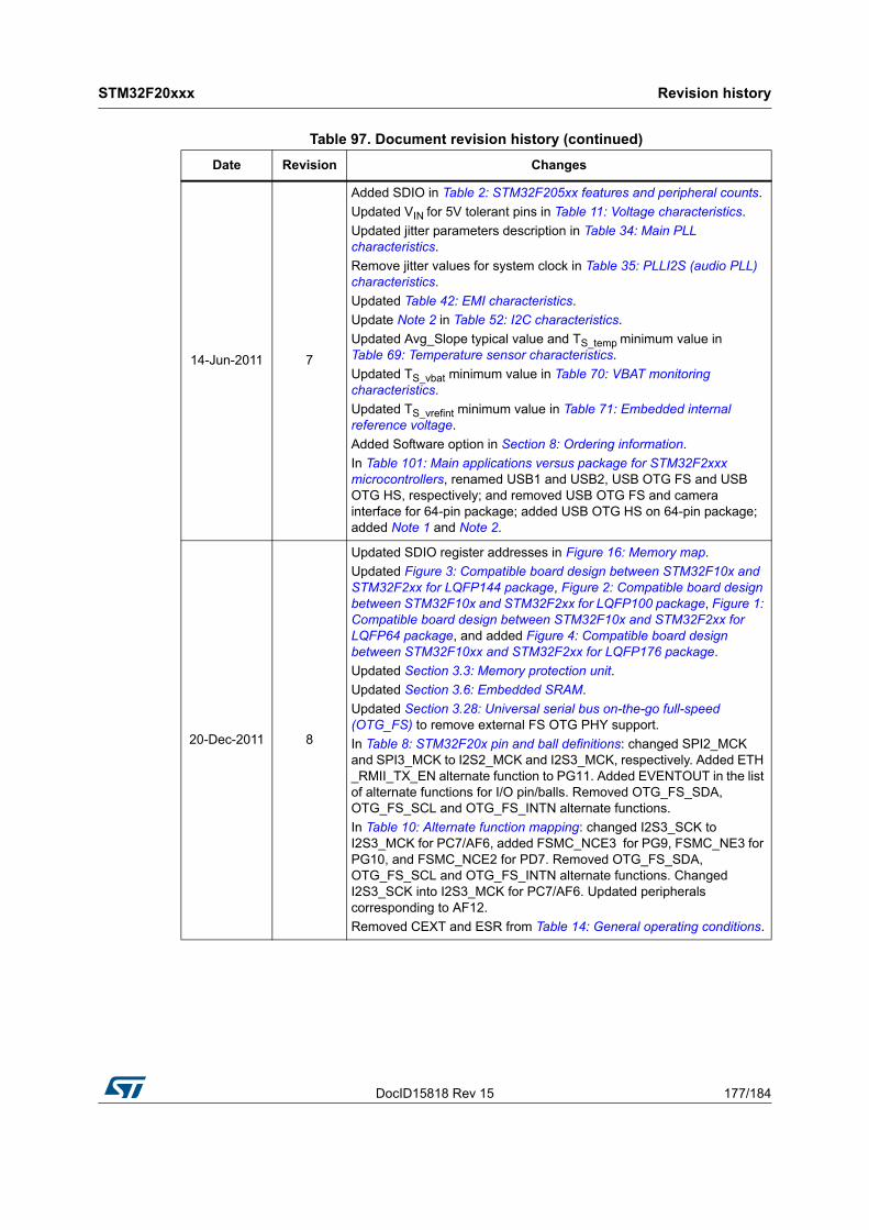
DocID15818 Rev 15 177/184
STM32F20xxx Revision history
183
14-Jun-2011 7
Added SDIO in Table 2: STM32F205xx features and peripheral counts.
Updated VIN for 5V tolerant pins in Table 11: Voltage characteristics.
Updated jitter parameters description in Table 34: Main PLL characteristics.
Remove jitter values for system clock in Table 35: PLLI2S (audio PLL) characteristics.
Updated Table 42: EMI characteristics.
Update Note 2 in Table 52: I2C characteristics.
Updated Avg_Slope typical value and TS_temp minimum value in Table 69: Temperature sensor characteristics.
Updated TS_vbat minimum value in Table 70: VBAT monitoring characteristics.
Updated TS_vrefint minimum value in Table 71: Embedded internal reference voltage.
Added Software option in Section 8: Ordering information.
In Table 101: Main applications versus package for STM32F2xxx microcontrollers, renamed USB1 and USB2, USB OTG FS and USB OTG HS, respectively; and removed USB OTG FS and camera interface for 64-pin package; added USB OTG HS on 64-pin package; added Note 1 and Note 2.
20-Dec-2011 8
Updated SDIO register addresses in Figure 16: Memory map.
Updated Figure 3: Compatible board design between STM32F10x and STM32F2xx for LQFP144 package, Figure 2: Compatible board design between STM32F10x and STM32F2xx for LQFP100 package, Figure 1: Compatible board design between STM32F10x and STM32F2xx for LQFP64 package, and added Figure 4: Compatible board design between STM32F10xx and STM32F2xx for LQFP176 package.
Updated Section 3.3: Memory protection unit.
Updated Section 3.6: Embedded SRAM.
Updated Section 3.28: Universal serial bus on-the-go full-speed (OTG_FS) to remove external FS OTG PHY support.
In Table 8: STM32F20x pin and ball definitions: changed SPI2_MCK and SPI3_MCK to I2S2_MCK and I2S3_MCK, respectively. Added ETH _RMII_TX_EN alternate function to PG11. Added EVENTOUT in the list of alternate functions for I/O pin/balls. Removed OTG_FS_SDA, OTG_FS_SCL and OTG_FS_INTN alternate functions.
In Table 10: Alternate function mapping: changed I2S3_SCK to I2S3_MCK for PC7/AF6, added FSMC_NCE3 for PG9, FSMC_NE3 for PG10, and FSMC_NCE2 for PD7. Removed OTG_FS_SDA, OTG_FS_SCL and OTG_FS_INTN alternate functions. Changed I2S3_SCK into I2S3_MCK for PC7/AF6. Updated peripherals corresponding to AF12.
Removed CEXT and ESR from Table 14: General operating conditions.
Table 97. Document revision history (continued)
Date Revision Changes
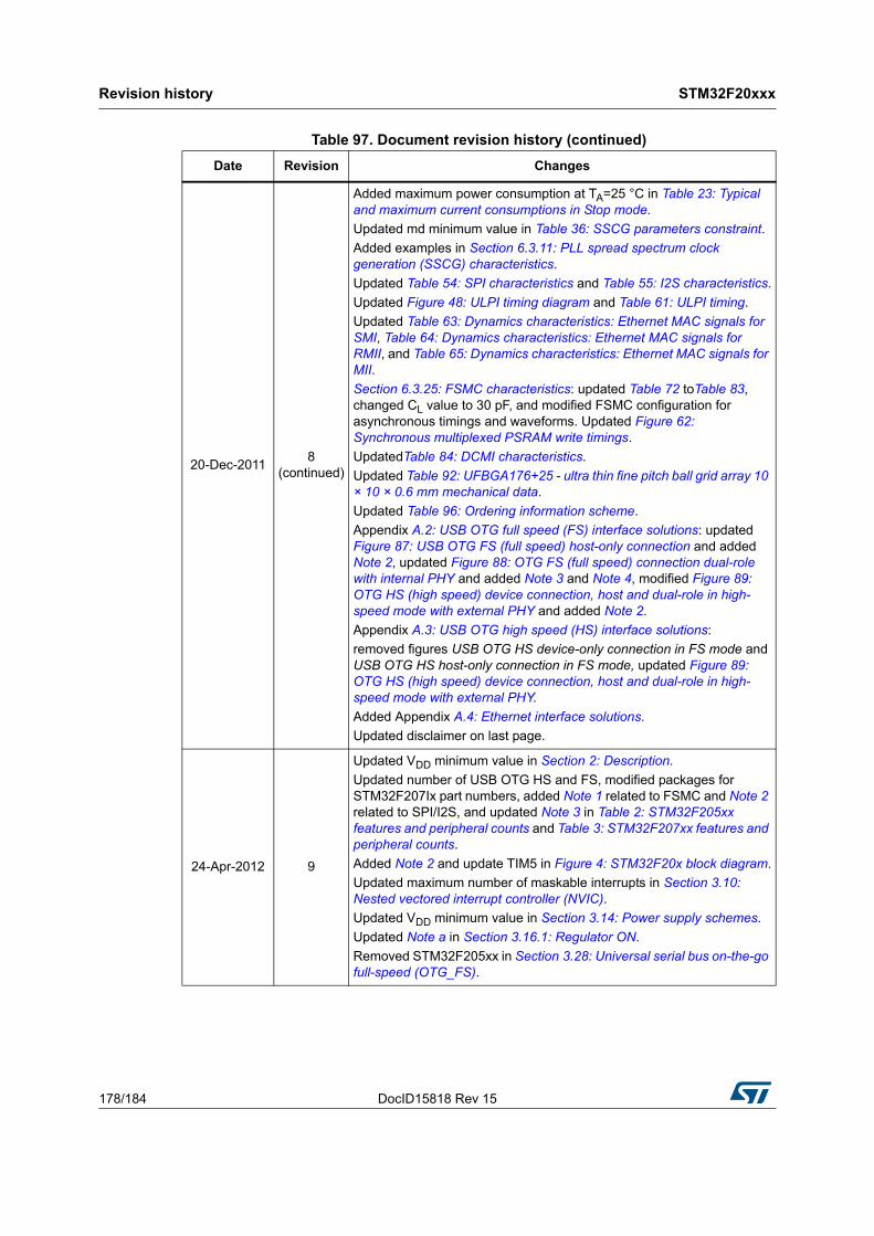
Revision history STM32F20xxx
178/184 DocID15818 Rev 15
20-Dec-20118
(continued)
Added maximum power consumption at TA=25 °C in Table 23: Typical and maximum current consumptions in Stop mode.
Updated md minimum value in Table 36: SSCG parameters constraint.
Added examples in Section 6.3.11: PLL spread spectrum clock generation (SSCG) characteristics.
Updated Table 54: SPI characteristics and Table 55: I2S characteristics.
Updated Figure 48: ULPI timing diagram and Table 61: ULPI timing.
Updated Table 63: Dynamics characteristics: Ethernet MAC signals for SMI, Table 64: Dynamics characteristics: Ethernet MAC signals for RMII, and Table 65: Dynamics characteristics: Ethernet MAC signals for MII.
Section 6.3.25: FSMC characteristics: updated Table 72 toTable 83, changed CL value to 30 pF, and modified FSMC configuration for asynchronous timings and waveforms. Updated Figure 62: Synchronous multiplexed PSRAM write timings.
UpdatedTable 84: DCMI characteristics.
Updated Table 92: UFBGA176+25 - ultra thin fine pitch ball grid array 10 × 10 × 0.6 mm mechanical data.
Updated Table 96: Ordering information scheme.
Appendix A.2: USB OTG full speed (FS) interface solutions: updated Figure 87: USB OTG FS (full speed) host-only connection and added Note 2, updated Figure 88: OTG FS (full speed) connection dual-role with internal PHY and added Note 3 and Note 4, modified Figure 89: OTG HS (high speed) device connection, host and dual-role in high-speed mode with external PHY and added Note 2.
Appendix A.3: USB OTG high speed (HS) interface solutions:
removed figures USB OTG HS device-only connection in FS mode and USB OTG HS host-only connection in FS mode, updated Figure 89: OTG HS (high speed) device connection, host and dual-role in high-speed mode with external PHY.
Added Appendix A.4: Ethernet interface solutions.
Updated disclaimer on last page.
24-Apr-2012 9
Updated VDD minimum value in Section 2: Description.
Updated number of USB OTG HS and FS, modified packages for STM32F207Ix part numbers, added Note 1 related to FSMC and Note 2 related to SPI/I2S, and updated Note 3 in Table 2: STM32F205xx features and peripheral counts and Table 3: STM32F207xx features and peripheral counts.
Added Note 2 and update TIM5 in Figure 4: STM32F20x block diagram.
Updated maximum number of maskable interrupts in Section 3.10: Nested vectored interrupt controller (NVIC).
Updated VDD minimum value in Section 3.14: Power supply schemes.
Updated Note a in Section 3.16.1: Regulator ON.
Removed STM32F205xx in Section 3.28: Universal serial bus on-the-go full-speed (OTG_FS).
Table 97. Document revision history (continued)
Date Revision Changes
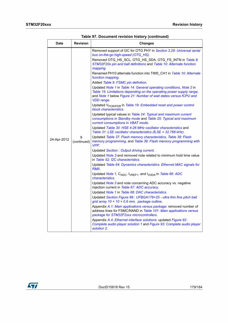
DocID15818 Rev 15 179/184
STM32F20xxx Revision history
183
24-Apr-20129
(continued)
Removed support of I2C for OTG PHY in Section 3.29: Universal serial bus on-the-go high-speed (OTG_HS).
Removed OTG_HS_SCL, OTG_HS_SDA, OTG_FS_INTN in Table 8: STM32F20x pin and ball definitions and Table 10: Alternate function mapping.
Renamed PH10 alternate function into TIM5_CH1 in Table 10: Alternate function mapping.
Added Table 9: FSMC pin definition.
Updated Note 1 in Table 14: General operating conditions, Note 2 in Table 15: Limitations depending on the operating power supply range, and Note 1 below Figure 21: Number of wait states versus fCPU and VDD range.
Updated VPOR/PDR in Table 19: Embedded reset and power control block characteristics.
Updated typical values in Table 24: Typical and maximum current consumptions in Standby mode and Table 25: Typical and maximum current consumptions in VBAT mode.
Updated Table 30: HSE 4-26 MHz oscillator characteristics and Table 31: LSE oscillator characteristics (fLSE = 32.768 kHz).
Updated Table 37: Flash memory characteristics, Table 38: Flash memory programming, and Table 39: Flash memory programming with VPP.
Updated Section : Output driving current.
Updated Note 3 and removed note related to minimum hold time value in Table 52: I2C characteristics.
Updated Table 64: Dynamics characteristics: Ethernet MAC signals for RMII.
Updated Note 1, CADC, IVREF+, and IVDDA in Table 66: ADC characteristics.
Updated Note 3 and note concerning ADC accuracy vs. negative injection current in Table 67: ADC accuracy.
Updated Note 1 in Table 68: DAC characteristics.
Updated Section Figure 88.: UFBGA176+25 - ultra thin fine pitch ball grid array 10 × 10 × 0.6 mm, package outline.
Appendix A.1: Main applications versus package: removed number of address lines for FSMC/NAND in Table 101: Main applications versus package for STM32F2xxx microcontrollers.
Appendix A.4: Ethernet interface solutions: updated Figure 92: Complete audio player solution 1 and Figure 93: Complete audio player solution 2.
Table 97. Document revision history (continued)
Date Revision Changes
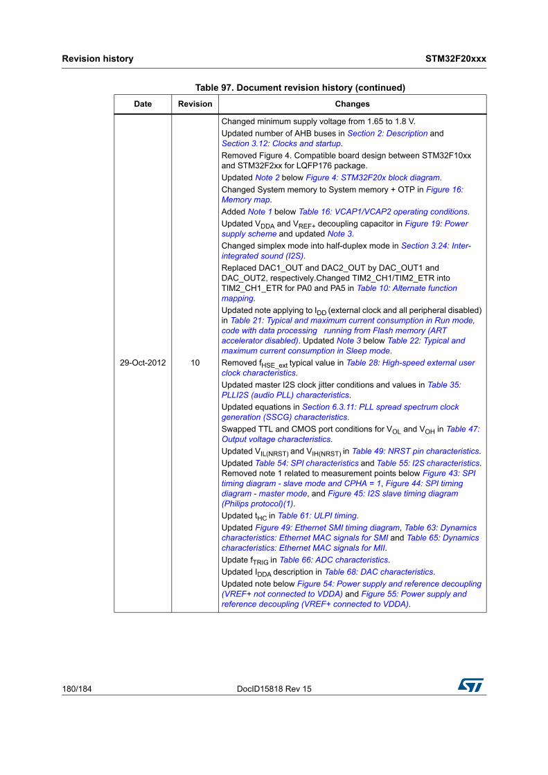
Revision history STM32F20xxx
180/184 DocID15818 Rev 15
29-Oct-2012 10
Changed minimum supply voltage from 1.65 to 1.8 V.
Updated number of AHB buses in Section 2: Description and Section 3.12: Clocks and startup.
Removed Figure 4. Compatible board design between STM32F10xx and STM32F2xx for LQFP176 package.
Updated Note 2 below Figure 4: STM32F20x block diagram.
Changed System memory to System memory + OTP in Figure 16: Memory map.
Added Note 1 below Table 16: VCAP1/VCAP2 operating conditions.
Updated VDDA and VREF+ decoupling capacitor in Figure 19: Power supply scheme and updated Note 3.
Changed simplex mode into half-duplex mode in Section 3.24: Inter-integrated sound (I2S).
Replaced DAC1_OUT and DAC2_OUT by DAC_OUT1 and DAC_OUT2, respectively.Changed TIM2_CH1/TIM2_ETR into TIM2_CH1_ETR for PA0 and PA5 in Table 10: Alternate function mapping.
Updated note applying to IDD (external clock and all peripheral disabled) in Table 21: Typical and maximum current consumption in Run mode, code with data processing running from Flash memory (ART accelerator disabled). Updated Note 3 below Table 22: Typical and maximum current consumption in Sleep mode.
Removed fHSE_ext typical value in Table 28: High-speed external user clock characteristics.
Updated master I2S clock jitter conditions and values in Table 35: PLLI2S (audio PLL) characteristics.
Updated equations in Section 6.3.11: PLL spread spectrum clock generation (SSCG) characteristics.
Swapped TTL and CMOS port conditions for VOL and VOH in Table 47: Output voltage characteristics.
Updated VIL(NRST) and VIH(NRST) in Table 49: NRST pin characteristics.
Updated Table 54: SPI characteristics and Table 55: I2S characteristics. Removed note 1 related to measurement points below Figure 43: SPI timing diagram - slave mode and CPHA = 1, Figure 44: SPI timing diagram - master mode, and Figure 45: I2S slave timing diagram (Philips protocol)(1).
Updated tHC in Table 61: ULPI timing.
Updated Figure 49: Ethernet SMI timing diagram, Table 63: Dynamics characteristics: Ethernet MAC signals for SMI and Table 65: Dynamics characteristics: Ethernet MAC signals for MII.
Update fTRIG in Table 66: ADC characteristics.
Updated IDDA description in Table 68: DAC characteristics.
Updated note below Figure 54: Power supply and reference decoupling (VREF+ not connected to VDDA) and Figure 55: Power supply and reference decoupling (VREF+ connected to VDDA).
Table 97. Document revision history (continued)
Date Revision Changes
DocID15818 Rev 15 181/184
STM32F20xxx Revision history
183
29-Oct-201210
(continued)
Replaced td(CLKL-NOEL) by td(CLKH-NOEL) in Table 76: Synchronous multiplexed NOR/PSRAM read timings, Table 78: Synchronous non-multiplexed NOR/PSRAM read timings, Figure 61: Synchronous multiplexed NOR/PSRAM read timings and Figure 63: Synchronous non-multiplexed NOR/PSRAM read timings.
Added Figure 87: LQFP176 recommended footprint.
Added Note 2 below Figure 86: Regulator OFF/internal reset ON.
Updated device subfamily in Table 96: Ordering information scheme.
Remove reference to note 2 for USB IOTG FS in Table 101: Main applications versus package for STM32F2xxx microcontrollers.
Table 97. Document revision history (continued)
Date Revision Changes
Revision history STM32F20xxx
182/184 DocID15818 Rev 15
04-Nov-2013 11
In the whole document, updated notes related to WLCSP64+2 usage with IRROFF set to VDD. Updated Section 3.14: Power supply schemes, Section 3.15: Power supply supervisor, Section 3.16.1: Regulator ON and Section 3.16.2: Regulator OFF. Added Section 3.16.3: Regulator ON/OFF and internal reset ON/OFF availability. Added note related to WLCSP64+2 package.
Restructured RTC features and added reference clock detection in Section 3.17: Real-time clock (RTC), backup SRAM and backup registers.
Added note indicating the package view below Figure 10: STM32F20x LQFP64 pinout, Figure 12: STM32F20x LQFP100 pinout, Figure 13: STM32F20x LQFP144 pinout, and Figure 14: STM32F20x LQFP176 pinout.
Added Table 7: Legend/abbreviations used in the pinout table. Table 8: STM32F20x pin and ball definitions: content reformatted; removed indexes on VSS and VDD; updated PA4, PA5, PA6, PC4, BOOT0; replaced DCMI_12 by DCMI_D12, TIM8_CHIN by TIM8_CH1N, ETH_MII_RX_D0 by ETH_MII_RXD0, ETH_MII_RX_D1 by ETH_MII_RXD1, ETH_RMII_RX_D0 by ETH_RMII_RXD0, ETH_RMII_RX_D1 by ETH_RMII_RXD1, and RMII_CRS_DV by ETH_RMII_CRS_DV.
Table 10: Alternate function mapping: replaced FSMC_BLN1 by FSMC_NBL1, added EVENTOUT as AF15 alternated function for PC13, PC14, PC15, PH0, PH1, and PI8.
Updated Figure 17: Pin loading conditions and Figure 18: Pin input voltage.
Added VIN in Table 14: General operating conditions.
Removed note applying to VPOR/PDR minimum value in Table 19: Embedded reset and power control block characteristics.
Updated notes related to CL1 and CL2 in Section : Low-speed external clock generated from a crystal/ceramic resonator.
Updated conditions in Table 41: EMS characteristics. Updated Table 42: EMI characteristics. Updated VIL, VIH and VHys in Table 46: I/O static characteristics. Added Section : Output driving currentand updated Figure 39: I/O AC characteristics definition.
Updated VIL(NRST) and VIH(NRST) in Table 49: NRST pin characteristics, updated Figure 39: I/O AC characteristics definition.
Removed tests conditions in Section : I2C interface characteristics. Updated Table 52: I2C characteristics and Figure 41: I2C bus AC waveforms and measurement circuit.
Updated IVREF+ and IVDDA in Table 66: ADC characteristics. Updated Offset comments in Table 68: DAC characteristics.
Updated minimum th(CLKH-DV) value in Table 78: Synchronous non-multiplexed NOR/PSRAM read timings.
Table 97. Document revision history (continued)
Date Revision Changes
DocID15818 Rev 15 183/184
STM32F20xxx Revision history
183
04-Nov-201311
(continued)
Removed Appendix A Application block diagrams.
Updated Figure 77: LQFP64 – 10 x 10 mm 64 pin low-profile quad flat package outline and Table 87: LQFP64 – 10 x 10 mm 64 pin low-profile quad flat package mechanical data. Updated Figure 80: LQFP100, 14 x 14 mm 100-pin low-profile quad flat package outline, Figure 83: LQFP144, 20 x 20 mm, 144-pin low-profile quad flat package outline, Figure 86: LQFP176 - Low profile quad flat package 24 × 24 × 1.4 mm, package outline. Updated Figure 88: UFBGA176+25 - ultra thin fine pitch ball grid array 10 × 10 × 0.6 mm, package outline and Figure 88: UFBGA176+25 - ultra thin fine pitch ball grid array 10 × 10 × 0.6 mm, package outline.
27-Oct-2014 12
Updated VBAT voltage range in Figure 19: Power supply scheme. Added caution note in Section 6.1.6: Power supply scheme.
Updated VIN in Table 14: General operating conditions.
Removed note 1 in Table 23: Typical and maximum current consumptions in Stop mode.
Updated Table 45: I/O current injection susceptibility, Section 6.3.16: I/O port characteristics and Section 6.3.17: NRST pin characteristics.
Removed note 3 in Table 69: Temperature sensor characteristics.
Updated Figure 79: WLCSP64+2 - 0.400 mm pitch wafer level chip size package outline and Table 88: WLCSP64+2 - 0.400 mm pitch wafer level chip size package mechanical data. Added Figure 83: LQFP100 marking (package top view) and Figure 86: LQFP144 marking (package top view).
2-Feb-2016 13
Updated Section 1: Introduction.
Updated Table 32: HSI oscillator characteristics and its footnotes.
Updated Figure 36: PLL output clock waveforms in center spread mode, Figure 37: PLL output clock waveforms in down spread mode,
Figure 54: Power supply and reference decoupling (VREF+ not connected to VDDA) and Figure 55: Power supply and reference decoupling (VREF+ connected to VDDA).
Updated Section 7: Package information and its subsections.
24-Jun-2016 14
Updated figures 1, 2 and 3 in Section 2.1: Full compatibility throughout the family.
Updated Device marking and Figure 83 in Section 7.3: LQFP100 package information.
Updated Device marking and Figure 86 in Section 7.4: LQFP144 package information.
Updated Section 7.6: UFBGA176+25 package information with introduction of Device marking and Figure 91.
Updated Table 96: Ordering information scheme.
11-Aug-2016 15
Updated Features, Section 7.2: WLCSP64+2 package information and title of Section 8: Ordering information.
Updated Figure 54: Power supply and reference decoupling (VREF+ not connected to VDDA).
Table 97. Document revision history (continued)
Date Revision Changes
STM32F20xxx
184/184 DocID15818 Rev 15
IMPORTANT NOTICE – PLEASE READ CAREFULLY
STMicroelectronics NV and its subsidiaries (“ST”) reserve the right to make changes, corrections, enhancements, modifications, and improvements to ST products and/or to this document at any time without notice. Purchasers should obtain the latest relevant information on ST products before placing orders. ST products are sold pursuant to ST’s terms and conditions of sale in place at the time of order acknowledgement.
Purchasers are solely responsible for the choice, selection, and use of ST products and ST assumes no liability for application assistance or the design of Purchasers’ products.
No license, express or implied, to any intellectual property right is granted by ST herein.
Resale of ST products with provisions different from the information set forth herein shall void any warranty granted by ST for such product.
ST and the ST logo are trademarks of ST. All other product or service names are the property of their respective owners.
Information in this document supersedes and replaces information previously supplied in any prior versions of this document.
© 2016 STMicroelectronics – All rights reserved