Embed Size (px)
Citation preview
This is information on a product in full production.
November 2018 DS12232 Rev 2 1/136
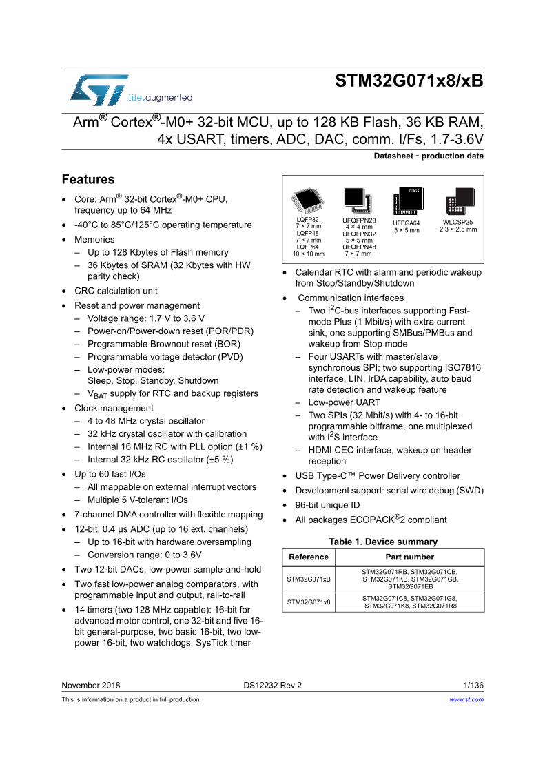
STM32G071x8/xB
Arm® Cortex®-M0+ 32-bit MCU, up to 128 KB Flash, 36 KB RAM, 4x USART, timers, ADC, DAC, comm. I/Fs, 1.7-3.6V
Datasheet - production data
Features
• Core: Arm® 32-bit Cortex®-M0+ CPU, frequency up to 64 MHz
• -40°C to 85°C/125°C operating temperature
• Memories
– Up to 128 Kbytes of Flash memory
– 36 Kbytes of SRAM (32 Kbytes with HW parity check)
• CRC calculation unit
• Reset and power management
– Voltage range: 1.7 V to 3.6 V
– Power-on/Power-down reset (POR/PDR)
– Programmable Brownout reset (BOR)
– Programmable voltage detector (PVD)
– Low-power modes: Sleep, Stop, Standby, Shutdown
– VBAT supply for RTC and backup registers
• Clock management
– 4 to 48 MHz crystal oscillator
– 32 kHz crystal oscillator with calibration
– Internal 16 MHz RC with PLL option (±1 %)
– Internal 32 kHz RC oscillator (±5 %)
• Up to 60 fast I/Os
– All mappable on external interrupt vectors
– Multiple 5 V-tolerant I/Os
• 7-channel DMA controller with flexible mapping
• 12-bit, 0.4 µs ADC (up to 16 ext. channels)
– Up to 16-bit with hardware oversampling
– Conversion range: 0 to 3.6V
• Two 12-bit DACs, low-power sample-and-hold
• Two fast low-power analog comparators, with programmable input and output, rail-to-rail
• 14 timers (two 128 MHz capable): 16-bit for advanced motor control, one 32-bit and five 16-bit general-purpose, two basic 16-bit, two low-power 16-bit, two watchdogs, SysTick timer
• Calendar RTC with alarm and periodic wakeup from Stop/Standby/Shutdown
• Communication interfaces
– Two I2C-bus interfaces supporting Fast-mode Plus (1 Mbit/s) with extra current sink, one supporting SMBus/PMBus and wakeup from Stop mode
– Four USARTs with master/slave synchronous SPI; two supporting ISO7816 interface, LIN, IrDA capability, auto baud rate detection and wakeup feature
– Low-power UART
– Two SPIs (32 Mbit/s) with 4- to 16-bit programmable bitframe, one multiplexed with I2S interface
– HDMI CEC interface, wakeup on header reception
• USB Type-C™ Power Delivery controller
• Development support: serial wire debug (SWD)
• 96-bit unique ID
• All packages ECOPACK®2 compliant
Table 1. Device summary
Reference Part number
STM32G071xBSTM32G071RB, STM32G071CB, STM32G071KB, STM32G071GB,
STM32G071EB
STM32G071x8STM32G071C8, STM32G071G8, STM32G071K8, STM32G071R8
LQFP64 UFQFPN48
UFQFPN32
UFQFPN28
LQFP48
LQFP32 WLCSP252.3 × 2.5 mm
UFBGA645 × 5 mm
10 × 10 mm
7 × 7 mm
7 × 7 mm
7 × 7 mm
5 × 5 mm
4 × 4 mm
www.st.com
Contents STM32G071x8/xB
2/136 DS12232 Rev 2
Contents
1 Introduction . . . . . . . . . . . . . . . . . . . . . . . . . . . . . . . . . . . . . . . . . . . . . . . 10
2 Description . . . . . . . . . . . . . . . . . . . . . . . . . . . . . . . . . . . . . . . . . . . . . . . . 11
3 Functional overview . . . . . . . . . . . . . . . . . . . . . . . . . . . . . . . . . . . . . . . . 14
3.1 Arm® Cortex®-M0+ core with MPU . . . . . . . . . . . . . . . . . . . . . . . . . . . . . 14
3.2 Memory protection unit . . . . . . . . . . . . . . . . . . . . . . . . . . . . . . . . . . . . . . . 14
3.3 Embedded Flash memory . . . . . . . . . . . . . . . . . . . . . . . . . . . . . . . . . . . . 14
3.4 Embedded SRAM . . . . . . . . . . . . . . . . . . . . . . . . . . . . . . . . . . . . . . . . . . . 15
3.5 Boot modes . . . . . . . . . . . . . . . . . . . . . . . . . . . . . . . . . . . . . . . . . . . . . . . 16
3.6 Cyclic redundancy check calculation unit (CRC) . . . . . . . . . . . . . . . . . . . 16
3.7 Power supply management . . . . . . . . . . . . . . . . . . . . . . . . . . . . . . . . . . . 16
3.7.1 Power supply schemes . . . . . . . . . . . . . . . . . . . . . . . . . . . . . . . . . . . . . 16
3.7.2 Power supply supervisor . . . . . . . . . . . . . . . . . . . . . . . . . . . . . . . . . . . . 17
3.7.3 Voltage regulator . . . . . . . . . . . . . . . . . . . . . . . . . . . . . . . . . . . . . . . . . . 18
3.7.4 Low-power modes . . . . . . . . . . . . . . . . . . . . . . . . . . . . . . . . . . . . . . . . . 18
3.7.5 Reset mode . . . . . . . . . . . . . . . . . . . . . . . . . . . . . . . . . . . . . . . . . . . . . . 19
3.7.6 VBAT operation . . . . . . . . . . . . . . . . . . . . . . . . . . . . . . . . . . . . . . . . . . . 19
3.8 Interconnect of peripherals . . . . . . . . . . . . . . . . . . . . . . . . . . . . . . . . . . . . 20
3.9 Clocks and startup . . . . . . . . . . . . . . . . . . . . . . . . . . . . . . . . . . . . . . . . . . 21
3.10 General-purpose inputs/outputs (GPIOs) . . . . . . . . . . . . . . . . . . . . . . . . . 21
3.11 Direct memory access controller (DMA) . . . . . . . . . . . . . . . . . . . . . . . . . . 22
3.12 Interrupts and events . . . . . . . . . . . . . . . . . . . . . . . . . . . . . . . . . . . . . . . . 23
3.12.1 Nested vectored interrupt controller (NVIC) . . . . . . . . . . . . . . . . . . . . . . 23
3.12.2 Extended interrupt/event controller (EXTI) . . . . . . . . . . . . . . . . . . . . . . 24
3.13 Analog-to-digital converter (ADC) . . . . . . . . . . . . . . . . . . . . . . . . . . . . . . 24
3.13.1 Temperature sensor . . . . . . . . . . . . . . . . . . . . . . . . . . . . . . . . . . . . . . . . 25
3.13.2 Internal voltage reference (VREFINT) . . . . . . . . . . . . . . . . . . . . . . . . . . 25
3.13.3 VBAT battery voltage monitoring . . . . . . . . . . . . . . . . . . . . . . . . . . . . . . 25
3.14 Digital-to-analog converter (DAC) . . . . . . . . . . . . . . . . . . . . . . . . . . . . . . 25
3.15 Voltage reference buffer (VREFBUF) . . . . . . . . . . . . . . . . . . . . . . . . . . . . 26
3.16 Comparators (COMP) . . . . . . . . . . . . . . . . . . . . . . . . . . . . . . . . . . . . . . . 26
DS12232 Rev 2 3/136
STM32G071x8/xB Contents
5
3.17 Timers and watchdogs . . . . . . . . . . . . . . . . . . . . . . . . . . . . . . . . . . . . . . . 26
3.17.1 Advanced-control timer (TIM1) . . . . . . . . . . . . . . . . . . . . . . . . . . . . . . . 27
3.17.2 General-purpose timers (TIM2, TIM3, TIM14, TIM15, TIM16, TIM17) . . 28
3.17.3 Basic timers (TIM6 and TIM7) . . . . . . . . . . . . . . . . . . . . . . . . . . . . . . . . 28
3.17.4 Low-power timers (LPTIM1 and LPTIM2) . . . . . . . . . . . . . . . . . . . . . . . 28
3.17.5 Independent watchdog (IWDG) . . . . . . . . . . . . . . . . . . . . . . . . . . . . . . . 29
3.17.6 System window watchdog (WWDG) . . . . . . . . . . . . . . . . . . . . . . . . . . . 29
3.17.7 SysTick timer . . . . . . . . . . . . . . . . . . . . . . . . . . . . . . . . . . . . . . . . . . . . . 29
3.18 Real-time clock (RTC), tamper (TAMP) and backup registers . . . . . . . . . 29
3.19 Inter-integrated circuit interface (I2C) . . . . . . . . . . . . . . . . . . . . . . . . . . . . 30
3.20 Universal synchronous/asynchronous receiver transmitter (USART) . . . 31
3.21 Low-power universal asynchronous receiver transmitter (LPUART) . . . . 32
3.22 Serial peripheral interface (SPI) . . . . . . . . . . . . . . . . . . . . . . . . . . . . . . . . 33
3.23 USB Type-C™ Power Delivery controller . . . . . . . . . . . . . . . . . . . . . . . . . 33
3.24 Development support . . . . . . . . . . . . . . . . . . . . . . . . . . . . . . . . . . . . . . . . 34
3.24.1 Serial wire debug port (SW-DP) . . . . . . . . . . . . . . . . . . . . . . . . . . . . . . . 34
4 Pinouts, pin description and alternate functions . . . . . . . . . . . . . . . . . 35
5 Electrical characteristics . . . . . . . . . . . . . . . . . . . . . . . . . . . . . . . . . . . . 53
5.1 Parameter conditions . . . . . . . . . . . . . . . . . . . . . . . . . . . . . . . . . . . . . . . . 53
5.1.1 Minimum and maximum values . . . . . . . . . . . . . . . . . . . . . . . . . . . . . . . 53
5.1.2 Typical values . . . . . . . . . . . . . . . . . . . . . . . . . . . . . . . . . . . . . . . . . . . . 53
5.1.3 Typical curves . . . . . . . . . . . . . . . . . . . . . . . . . . . . . . . . . . . . . . . . . . . . 53
5.1.4 Loading capacitor . . . . . . . . . . . . . . . . . . . . . . . . . . . . . . . . . . . . . . . . . 53
5.1.5 Pin input voltage . . . . . . . . . . . . . . . . . . . . . . . . . . . . . . . . . . . . . . . . . . 53
5.1.6 Power supply scheme . . . . . . . . . . . . . . . . . . . . . . . . . . . . . . . . . . . . . . 54
5.1.7 Current consumption measurement . . . . . . . . . . . . . . . . . . . . . . . . . . . 54
5.2 Absolute maximum ratings . . . . . . . . . . . . . . . . . . . . . . . . . . . . . . . . . . . . 55
5.3 Operating conditions . . . . . . . . . . . . . . . . . . . . . . . . . . . . . . . . . . . . . . . . 56
5.3.1 General operating conditions . . . . . . . . . . . . . . . . . . . . . . . . . . . . . . . . . 56
5.3.2 Operating conditions at power-up / power-down . . . . . . . . . . . . . . . . . . 57
5.3.3 Embedded reset and power control block characteristics . . . . . . . . . . . 57
5.3.4 Embedded voltage reference . . . . . . . . . . . . . . . . . . . . . . . . . . . . . . . . . 59
5.3.5 Supply current characteristics . . . . . . . . . . . . . . . . . . . . . . . . . . . . . . . . 60
Contents STM32G071x8/xB
4/136 DS12232 Rev 2
5.3.6 Wakeup time from low-power modes and voltage scaling transition times . . . . . . . . . . . . . . . . . . . . . . . . . . . . . . . . . . . . . . . . . . . . 68
5.3.7 External clock source characteristics . . . . . . . . . . . . . . . . . . . . . . . . . . . 70
5.3.8 Internal clock source characteristics . . . . . . . . . . . . . . . . . . . . . . . . . . . 74
5.3.9 PLL characteristics . . . . . . . . . . . . . . . . . . . . . . . . . . . . . . . . . . . . . . . . . 76
5.3.10 Flash memory characteristics . . . . . . . . . . . . . . . . . . . . . . . . . . . . . . . . 76
5.3.11 EMC characteristics . . . . . . . . . . . . . . . . . . . . . . . . . . . . . . . . . . . . . . . . 77
5.3.12 Electrical sensitivity characteristics . . . . . . . . . . . . . . . . . . . . . . . . . . . . 79
5.3.13 I/O current injection characteristics . . . . . . . . . . . . . . . . . . . . . . . . . . . . 80
5.3.14 I/O port characteristics . . . . . . . . . . . . . . . . . . . . . . . . . . . . . . . . . . . . . . 81
5.3.15 NRST input characteristics . . . . . . . . . . . . . . . . . . . . . . . . . . . . . . . . . . 85
5.3.16 Analog switch booster . . . . . . . . . . . . . . . . . . . . . . . . . . . . . . . . . . . . . . 86
5.3.17 Analog-to-digital converter characteristics . . . . . . . . . . . . . . . . . . . . . . . 86
5.3.18 Digital-to-analog converter characteristics . . . . . . . . . . . . . . . . . . . . . . . 94
5.3.19 Voltage reference buffer characteristics . . . . . . . . . . . . . . . . . . . . . . . . 98
5.3.20 Comparator characteristics . . . . . . . . . . . . . . . . . . . . . . . . . . . . . . . . . . 99
5.3.21 Temperature sensor characteristics . . . . . . . . . . . . . . . . . . . . . . . . . . . 100
5.3.22 VBAT monitoring characteristics . . . . . . . . . . . . . . . . . . . . . . . . . . . . . . 101
5.3.23 Timer characteristics . . . . . . . . . . . . . . . . . . . . . . . . . . . . . . . . . . . . . . 101
5.3.24 Characteristics of communication interfaces . . . . . . . . . . . . . . . . . . . . 102
5.3.25 UCPD characteristics . . . . . . . . . . . . . . . . . . . . . . . . . . . . . . . . . . . . . . 109
6 Package information . . . . . . . . . . . . . . . . . . . . . . . . . . . . . . . . . . . . . . . 110
6.1 LQFP64 package information . . . . . . . . . . . . . . . . . . . . . . . . . . . . . . . . . .110
6.2 UFBGA64 package information . . . . . . . . . . . . . . . . . . . . . . . . . . . . . . . .113
6.3 LQFP48 package information . . . . . . . . . . . . . . . . . . . . . . . . . . . . . . . . . .116
6.4 UFQFPN48 package information . . . . . . . . . . . . . . . . . . . . . . . . . . . . . . .119
6.5 LQFP32 package information . . . . . . . . . . . . . . . . . . . . . . . . . . . . . . . . . 122
6.6 UFQFPN32 package information . . . . . . . . . . . . . . . . . . . . . . . . . . . . . . 125
6.7 UFQFPN28 package information . . . . . . . . . . . . . . . . . . . . . . . . . . . . . . 127
6.8 WLCSP25 package information . . . . . . . . . . . . . . . . . . . . . . . . . . . . . . . 129
6.9 Thermal characteristics . . . . . . . . . . . . . . . . . . . . . . . . . . . . . . . . . . . . . 132
6.9.1 Reference document . . . . . . . . . . . . . . . . . . . . . . . . . . . . . . . . . . . . . . 132
6.9.2 Selecting the product temperature range . . . . . . . . . . . . . . . . . . . . . . 132
7 Ordering information . . . . . . . . . . . . . . . . . . . . . . . . . . . . . . . . . . . . . . 134
DS12232 Rev 2 5/136
STM32G071x8/xB Contents
5
8 Revision history . . . . . . . . . . . . . . . . . . . . . . . . . . . . . . . . . . . . . . . . . . 135
List of tables STM32G071x8/xB
6/136 DS12232 Rev 2
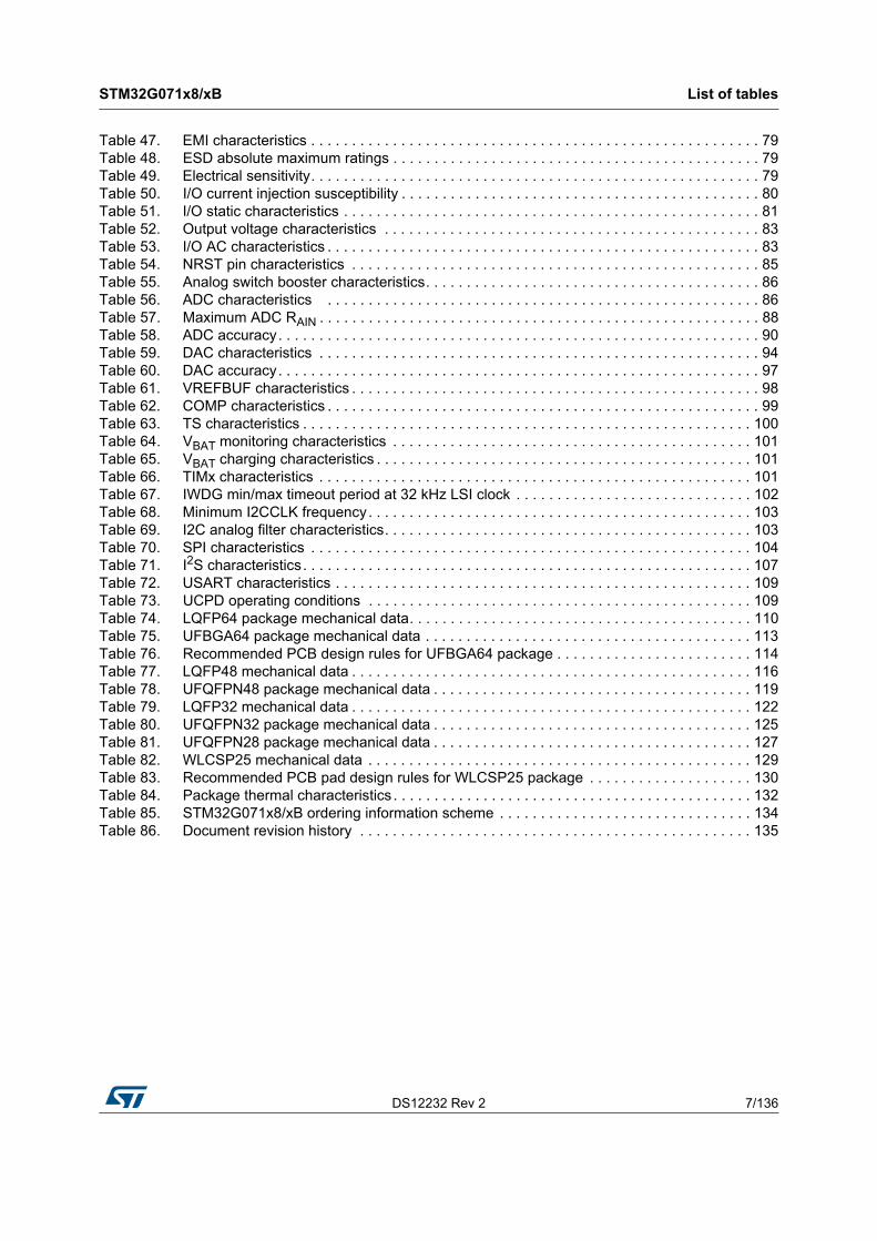
List of tables
Table 1. Device summary . . . . . . . . . . . . . . . . . . . . . . . . . . . . . . . . . . . . . . . . . . . . . . . . . . . . . . . . . . 1Table 2. STM32G071x8/xB family device features and peripheral counts . . . . . . . . . . . . . . . . . . . . 12Table 3. Access status versus readout protection level and execution modes. . . . . . . . . . . . . . . . . 15Table 4. Interconnect of STM32G071x8/xB peripherals . . . . . . . . . . . . . . . . . . . . . . . . . . . . . . . . . . 20Table 5. Temperature sensor calibration values. . . . . . . . . . . . . . . . . . . . . . . . . . . . . . . . . . . . . . . . 25Table 6. Internal voltage reference calibration values . . . . . . . . . . . . . . . . . . . . . . . . . . . . . . . . . . . 25Table 7. Timer feature comparison. . . . . . . . . . . . . . . . . . . . . . . . . . . . . . . . . . . . . . . . . . . . . . . . . . 27Table 8. I2C implementation . . . . . . . . . . . . . . . . . . . . . . . . . . . . . . . . . . . . . . . . . . . . . . . . . . . . . . 31Table 9. USART implementation . . . . . . . . . . . . . . . . . . . . . . . . . . . . . . . . . . . . . . . . . . . . . . . . . . . 32Table 10. SPI/I2S implementation . . . . . . . . . . . . . . . . . . . . . . . . . . . . . . . . . . . . . . . . . . . . . . . . . . . 33Table 11. Terms and symbols used in Table 12 . . . . . . . . . . . . . . . . . . . . . . . . . . . . . . . . . . . . . . . . . 40Table 12. Pin assignment and description . . . . . . . . . . . . . . . . . . . . . . . . . . . . . . . . . . . . . . . . . . . . . 40Table 13. Port A alternate function mapping . . . . . . . . . . . . . . . . . . . . . . . . . . . . . . . . . . . . . . . . . . . 49Table 14. Port B alternate function mapping . . . . . . . . . . . . . . . . . . . . . . . . . . . . . . . . . . . . . . . . . . . 50Table 15. Port C alternate function mapping . . . . . . . . . . . . . . . . . . . . . . . . . . . . . . . . . . . . . . . . . . . 51Table 16. Port D alternate function mapping . . . . . . . . . . . . . . . . . . . . . . . . . . . . . . . . . . . . . . . . . . . 52Table 17. Port F alternate function mapping. . . . . . . . . . . . . . . . . . . . . . . . . . . . . . . . . . . . . . . . . . . . 52Table 18. Voltage characteristics . . . . . . . . . . . . . . . . . . . . . . . . . . . . . . . . . . . . . . . . . . . . . . . . . . . . 55Table 19. Current characteristics . . . . . . . . . . . . . . . . . . . . . . . . . . . . . . . . . . . . . . . . . . . . . . . . . . . . 55Table 20. Thermal characteristics. . . . . . . . . . . . . . . . . . . . . . . . . . . . . . . . . . . . . . . . . . . . . . . . . . . . 56Table 21. General operating conditions . . . . . . . . . . . . . . . . . . . . . . . . . . . . . . . . . . . . . . . . . . . . . . . 56Table 22. Operating conditions at power-up / power-down . . . . . . . . . . . . . . . . . . . . . . . . . . . . . . . . 57Table 23. Embedded reset and power control block characteristics. . . . . . . . . . . . . . . . . . . . . . . . . . 57Table 24. Embedded internal voltage reference. . . . . . . . . . . . . . . . . . . . . . . . . . . . . . . . . . . . . . . . . 59Table 25. Current consumption in Run and Low-power run modes
at different die temperatures . . . . . . . . . . . . . . . . . . . . . . . . . . . . . . . . . . . . . . . . . . . . . . . 61Table 26. Typical current consumption in Run and Low-power run modes,
depending on code executed . . . . . . . . . . . . . . . . . . . . . . . . . . . . . . . . . . . . . . . . . . . . . . . 62Table 27. Current consumption in Sleep and Low-power sleep modes . . . . . . . . . . . . . . . . . . . . . . . 63Table 28. Current consumption in Stop 0 mode . . . . . . . . . . . . . . . . . . . . . . . . . . . . . . . . . . . . . . . . . 63Table 29. Current consumption in Stop 1 mode . . . . . . . . . . . . . . . . . . . . . . . . . . . . . . . . . . . . . . . . . 64Table 30. Current consumption in Standby mode . . . . . . . . . . . . . . . . . . . . . . . . . . . . . . . . . . . . . . . 64Table 31. Current consumption in Shutdown mode . . . . . . . . . . . . . . . . . . . . . . . . . . . . . . . . . . . . . . 65Table 32. Current consumption in VBAT mode . . . . . . . . . . . . . . . . . . . . . . . . . . . . . . . . . . . . . . . . . 65Table 33. Current consumption of peripherals . . . . . . . . . . . . . . . . . . . . . . . . . . . . . . . . . . . . . . . . . . 67Table 34. Low-power mode wakeup times . . . . . . . . . . . . . . . . . . . . . . . . . . . . . . . . . . . . . . . . . . . . . 68Table 35. Regulator mode transition times . . . . . . . . . . . . . . . . . . . . . . . . . . . . . . . . . . . . . . . . . . . . . 69Table 36. Wakeup time using LPUART . . . . . . . . . . . . . . . . . . . . . . . . . . . . . . . . . . . . . . . . . . . . . . . 70Table 37. High-speed external user clock characteristics. . . . . . . . . . . . . . . . . . . . . . . . . . . . . . . . . . 70Table 38. Low-speed external user clock characteristics . . . . . . . . . . . . . . . . . . . . . . . . . . . . . . . . . . 71Table 39. HSE oscillator characteristics . . . . . . . . . . . . . . . . . . . . . . . . . . . . . . . . . . . . . . . . . . . . . . . 72Table 40. LSE oscillator characteristics (fLSE = 32.768 kHz) . . . . . . . . . . . . . . . . . . . . . . . . . . . . . . . 73Table 41. HSI16 oscillator characteristics. . . . . . . . . . . . . . . . . . . . . . . . . . . . . . . . . . . . . . . . . . . . . . 74Table 42. LSI oscillator characteristics . . . . . . . . . . . . . . . . . . . . . . . . . . . . . . . . . . . . . . . . . . . . . . . . 75Table 43. PLL characteristics . . . . . . . . . . . . . . . . . . . . . . . . . . . . . . . . . . . . . . . . . . . . . . . . . . . . . . . 76Table 44. Flash memory characteristics . . . . . . . . . . . . . . . . . . . . . . . . . . . . . . . . . . . . . . . . . . . . . . . 76Table 45. Flash memory endurance and data retention . . . . . . . . . . . . . . . . . . . . . . . . . . . . . . . . . . . 77Table 46. EMS characteristics . . . . . . . . . . . . . . . . . . . . . . . . . . . . . . . . . . . . . . . . . . . . . . . . . . . . . . 78
DS12232 Rev 2 7/136
STM32G071x8/xB List of tables
7
Table 47. EMI characteristics . . . . . . . . . . . . . . . . . . . . . . . . . . . . . . . . . . . . . . . . . . . . . . . . . . . . . . . 79Table 48. ESD absolute maximum ratings . . . . . . . . . . . . . . . . . . . . . . . . . . . . . . . . . . . . . . . . . . . . . 79Table 49. Electrical sensitivity. . . . . . . . . . . . . . . . . . . . . . . . . . . . . . . . . . . . . . . . . . . . . . . . . . . . . . . 79Table 50. I/O current injection susceptibility . . . . . . . . . . . . . . . . . . . . . . . . . . . . . . . . . . . . . . . . . . . . 80Table 51. I/O static characteristics . . . . . . . . . . . . . . . . . . . . . . . . . . . . . . . . . . . . . . . . . . . . . . . . . . . 81Table 52. Output voltage characteristics . . . . . . . . . . . . . . . . . . . . . . . . . . . . . . . . . . . . . . . . . . . . . . 83Table 53. I/O AC characteristics . . . . . . . . . . . . . . . . . . . . . . . . . . . . . . . . . . . . . . . . . . . . . . . . . . . . . 83Table 54. NRST pin characteristics . . . . . . . . . . . . . . . . . . . . . . . . . . . . . . . . . . . . . . . . . . . . . . . . . . 85Table 55. Analog switch booster characteristics. . . . . . . . . . . . . . . . . . . . . . . . . . . . . . . . . . . . . . . . . 86Table 56. ADC characteristics . . . . . . . . . . . . . . . . . . . . . . . . . . . . . . . . . . . . . . . . . . . . . . . . . . . . . 86Table 57. Maximum ADC RAIN . . . . . . . . . . . . . . . . . . . . . . . . . . . . . . . . . . . . . . . . . . . . . . . . . . . . . . 88Table 58. ADC accuracy. . . . . . . . . . . . . . . . . . . . . . . . . . . . . . . . . . . . . . . . . . . . . . . . . . . . . . . . . . . 90Table 59. DAC characteristics . . . . . . . . . . . . . . . . . . . . . . . . . . . . . . . . . . . . . . . . . . . . . . . . . . . . . . 94Table 60. DAC accuracy. . . . . . . . . . . . . . . . . . . . . . . . . . . . . . . . . . . . . . . . . . . . . . . . . . . . . . . . . . . 97Table 61. VREFBUF characteristics . . . . . . . . . . . . . . . . . . . . . . . . . . . . . . . . . . . . . . . . . . . . . . . . . . 98Table 62. COMP characteristics . . . . . . . . . . . . . . . . . . . . . . . . . . . . . . . . . . . . . . . . . . . . . . . . . . . . . 99Table 63. TS characteristics . . . . . . . . . . . . . . . . . . . . . . . . . . . . . . . . . . . . . . . . . . . . . . . . . . . . . . . 100Table 64. VBAT monitoring characteristics . . . . . . . . . . . . . . . . . . . . . . . . . . . . . . . . . . . . . . . . . . . . 101Table 65. VBAT charging characteristics . . . . . . . . . . . . . . . . . . . . . . . . . . . . . . . . . . . . . . . . . . . . . . 101Table 66. TIMx characteristics . . . . . . . . . . . . . . . . . . . . . . . . . . . . . . . . . . . . . . . . . . . . . . . . . . . . . 101Table 67. IWDG min/max timeout period at 32 kHz LSI clock . . . . . . . . . . . . . . . . . . . . . . . . . . . . . 102Table 68. Minimum I2CCLK frequency. . . . . . . . . . . . . . . . . . . . . . . . . . . . . . . . . . . . . . . . . . . . . . . 103Table 69. I2C analog filter characteristics. . . . . . . . . . . . . . . . . . . . . . . . . . . . . . . . . . . . . . . . . . . . . 103Table 70. SPI characteristics . . . . . . . . . . . . . . . . . . . . . . . . . . . . . . . . . . . . . . . . . . . . . . . . . . . . . . 104Table 71. I2S characteristics. . . . . . . . . . . . . . . . . . . . . . . . . . . . . . . . . . . . . . . . . . . . . . . . . . . . . . . 107Table 72. USART characteristics . . . . . . . . . . . . . . . . . . . . . . . . . . . . . . . . . . . . . . . . . . . . . . . . . . . 109Table 73. UCPD operating conditions . . . . . . . . . . . . . . . . . . . . . . . . . . . . . . . . . . . . . . . . . . . . . . . 109Table 74. LQFP64 package mechanical data. . . . . . . . . . . . . . . . . . . . . . . . . . . . . . . . . . . . . . . . . . 110Table 75. UFBGA64 package mechanical data . . . . . . . . . . . . . . . . . . . . . . . . . . . . . . . . . . . . . . . . 113Table 76. Recommended PCB design rules for UFBGA64 package . . . . . . . . . . . . . . . . . . . . . . . . 114Table 77. LQFP48 mechanical data . . . . . . . . . . . . . . . . . . . . . . . . . . . . . . . . . . . . . . . . . . . . . . . . . 116Table 78. UFQFPN48 package mechanical data . . . . . . . . . . . . . . . . . . . . . . . . . . . . . . . . . . . . . . . 119Table 79. LQFP32 mechanical data . . . . . . . . . . . . . . . . . . . . . . . . . . . . . . . . . . . . . . . . . . . . . . . . . 122Table 80. UFQFPN32 package mechanical data . . . . . . . . . . . . . . . . . . . . . . . . . . . . . . . . . . . . . . . 125Table 81. UFQFPN28 package mechanical data . . . . . . . . . . . . . . . . . . . . . . . . . . . . . . . . . . . . . . . 127Table 82. WLCSP25 mechanical data . . . . . . . . . . . . . . . . . . . . . . . . . . . . . . . . . . . . . . . . . . . . . . . 129Table 83. Recommended PCB pad design rules for WLCSP25 package . . . . . . . . . . . . . . . . . . . . 130Table 84. Package thermal characteristics . . . . . . . . . . . . . . . . . . . . . . . . . . . . . . . . . . . . . . . . . . . . 132Table 85. STM32G071x8/xB ordering information scheme . . . . . . . . . . . . . . . . . . . . . . . . . . . . . . . 134Table 86. Document revision history . . . . . . . . . . . . . . . . . . . . . . . . . . . . . . . . . . . . . . . . . . . . . . . . 135
List of figures STM32G071x8/xB
8/136 DS12232 Rev 2
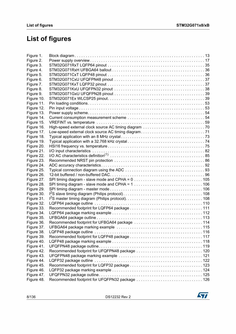
List of figures
Figure 1. Block diagram . . . . . . . . . . . . . . . . . . . . . . . . . . . . . . . . . . . . . . . . . . . . . . . . . . . . . . . . . . . 13Figure 2. Power supply overview . . . . . . . . . . . . . . . . . . . . . . . . . . . . . . . . . . . . . . . . . . . . . . . . . . . . 17Figure 3. STM32G071RxT LQFP64 pinout . . . . . . . . . . . . . . . . . . . . . . . . . . . . . . . . . . . . . . . . . . . . 35Figure 4. STM32G071RxH UFBGA64 ballout . . . . . . . . . . . . . . . . . . . . . . . . . . . . . . . . . . . . . . . . . . 36Figure 5. STM32G071CxT LQFP48 pinout . . . . . . . . . . . . . . . . . . . . . . . . . . . . . . . . . . . . . . . . . . . . 36Figure 6. STM32G071CxU UFQFPN48 pinout . . . . . . . . . . . . . . . . . . . . . . . . . . . . . . . . . . . . . . . . . 37Figure 7. STM32G071KxT LQFP32 pinout . . . . . . . . . . . . . . . . . . . . . . . . . . . . . . . . . . . . . . . . . . . . 37Figure 8. STM32G071KxU UFQFPN32 pinout . . . . . . . . . . . . . . . . . . . . . . . . . . . . . . . . . . . . . . . . . 38Figure 9. STM32G071GxU UFQFPN28 pinout . . . . . . . . . . . . . . . . . . . . . . . . . . . . . . . . . . . . . . . . . 39Figure 10. STM32G071Ex WLCSP25 pinout. . . . . . . . . . . . . . . . . . . . . . . . . . . . . . . . . . . . . . . . . . . . 39Figure 11. Pin loading conditions. . . . . . . . . . . . . . . . . . . . . . . . . . . . . . . . . . . . . . . . . . . . . . . . . . . . . 53Figure 12. Pin input voltage . . . . . . . . . . . . . . . . . . . . . . . . . . . . . . . . . . . . . . . . . . . . . . . . . . . . . . . . . 53Figure 13. Power supply scheme. . . . . . . . . . . . . . . . . . . . . . . . . . . . . . . . . . . . . . . . . . . . . . . . . . . . . 54Figure 14. Current consumption measurement scheme . . . . . . . . . . . . . . . . . . . . . . . . . . . . . . . . . . . 54Figure 15. VREFINT vs. temperature . . . . . . . . . . . . . . . . . . . . . . . . . . . . . . . . . . . . . . . . . . . . . . . . . 59Figure 16. High-speed external clock source AC timing diagram . . . . . . . . . . . . . . . . . . . . . . . . . . . . 70Figure 17. Low-speed external clock source AC timing diagram. . . . . . . . . . . . . . . . . . . . . . . . . . . . . 71Figure 18. Typical application with an 8 MHz crystal . . . . . . . . . . . . . . . . . . . . . . . . . . . . . . . . . . . . . . 73Figure 19. Typical application with a 32.768 kHz crystal . . . . . . . . . . . . . . . . . . . . . . . . . . . . . . . . . . . 74Figure 20. HSI16 frequency vs. temperature . . . . . . . . . . . . . . . . . . . . . . . . . . . . . . . . . . . . . . . . . . . . 75Figure 21. I/O input characteristics . . . . . . . . . . . . . . . . . . . . . . . . . . . . . . . . . . . . . . . . . . . . . . . . . . . 82Figure 22. I/O AC characteristics definition(1) . . . . . . . . . . . . . . . . . . . . . . . . . . . . . . . . . . . . . . . . . . . 85Figure 23. Recommended NRST pin protection . . . . . . . . . . . . . . . . . . . . . . . . . . . . . . . . . . . . . . . . . 86Figure 24. ADC accuracy characteristics . . . . . . . . . . . . . . . . . . . . . . . . . . . . . . . . . . . . . . . . . . . . . . . 92Figure 25. Typical connection diagram using the ADC . . . . . . . . . . . . . . . . . . . . . . . . . . . . . . . . . . . . 93Figure 26. 12-bit buffered / non-buffered DAC. . . . . . . . . . . . . . . . . . . . . . . . . . . . . . . . . . . . . . . . . . . 96Figure 27. SPI timing diagram - slave mode and CPHA = 0 . . . . . . . . . . . . . . . . . . . . . . . . . . . . . . . 105Figure 28. SPI timing diagram - slave mode and CPHA = 1 . . . . . . . . . . . . . . . . . . . . . . . . . . . . . . . 106Figure 29. SPI timing diagram - master mode . . . . . . . . . . . . . . . . . . . . . . . . . . . . . . . . . . . . . . . . . . 106Figure 30. I2S slave timing diagram (Philips protocol) . . . . . . . . . . . . . . . . . . . . . . . . . . . . . . . . . . . . 108Figure 31. I2S master timing diagram (Philips protocol). . . . . . . . . . . . . . . . . . . . . . . . . . . . . . . . . . . 108Figure 32. LQFP64 package outline . . . . . . . . . . . . . . . . . . . . . . . . . . . . . . . . . . . . . . . . . . . . . . . . . 110Figure 33. Recommended footprint for LQFP64 package . . . . . . . . . . . . . . . . . . . . . . . . . . . . . . . . . 111Figure 34. LQFP64 package marking example . . . . . . . . . . . . . . . . . . . . . . . . . . . . . . . . . . . . . . . . . 112Figure 35. UFBGA64 package outline . . . . . . . . . . . . . . . . . . . . . . . . . . . . . . . . . . . . . . . . . . . . . . . . 113Figure 36. Recommended footprint for UFBGA64 package . . . . . . . . . . . . . . . . . . . . . . . . . . . . . . . 114Figure 37. UFBGA64 package marking example . . . . . . . . . . . . . . . . . . . . . . . . . . . . . . . . . . . . . . . 115Figure 38. LQFP48 package outline . . . . . . . . . . . . . . . . . . . . . . . . . . . . . . . . . . . . . . . . . . . . . . . . . 116Figure 39. Recommended footprint for LQFP48 package . . . . . . . . . . . . . . . . . . . . . . . . . . . . . . . . . 117Figure 40. LQFP48 package marking example . . . . . . . . . . . . . . . . . . . . . . . . . . . . . . . . . . . . . . . . . 118Figure 41. UFQFPN48 package outline. . . . . . . . . . . . . . . . . . . . . . . . . . . . . . . . . . . . . . . . . . . . . . . 119Figure 42. Recommended footprint for UFQFPN48 package . . . . . . . . . . . . . . . . . . . . . . . . . . . . . . 120Figure 43. UFQFPN48 package marking example . . . . . . . . . . . . . . . . . . . . . . . . . . . . . . . . . . . . . . 121Figure 44. LQFP32 package outline . . . . . . . . . . . . . . . . . . . . . . . . . . . . . . . . . . . . . . . . . . . . . . . . . 122Figure 45. Recommended footprint for LQFP32 package . . . . . . . . . . . . . . . . . . . . . . . . . . . . . . . . . 123Figure 46. LQFP32 package marking example . . . . . . . . . . . . . . . . . . . . . . . . . . . . . . . . . . . . . . . . . 124Figure 47. UFQFPN32 package outline. . . . . . . . . . . . . . . . . . . . . . . . . . . . . . . . . . . . . . . . . . . . . . . 125Figure 48. Recommended footprint for UFQFPN32 package . . . . . . . . . . . . . . . . . . . . . . . . . . . . . . 126
DS12232 Rev 2 9/136
STM32G071x8/xB List of figures
9
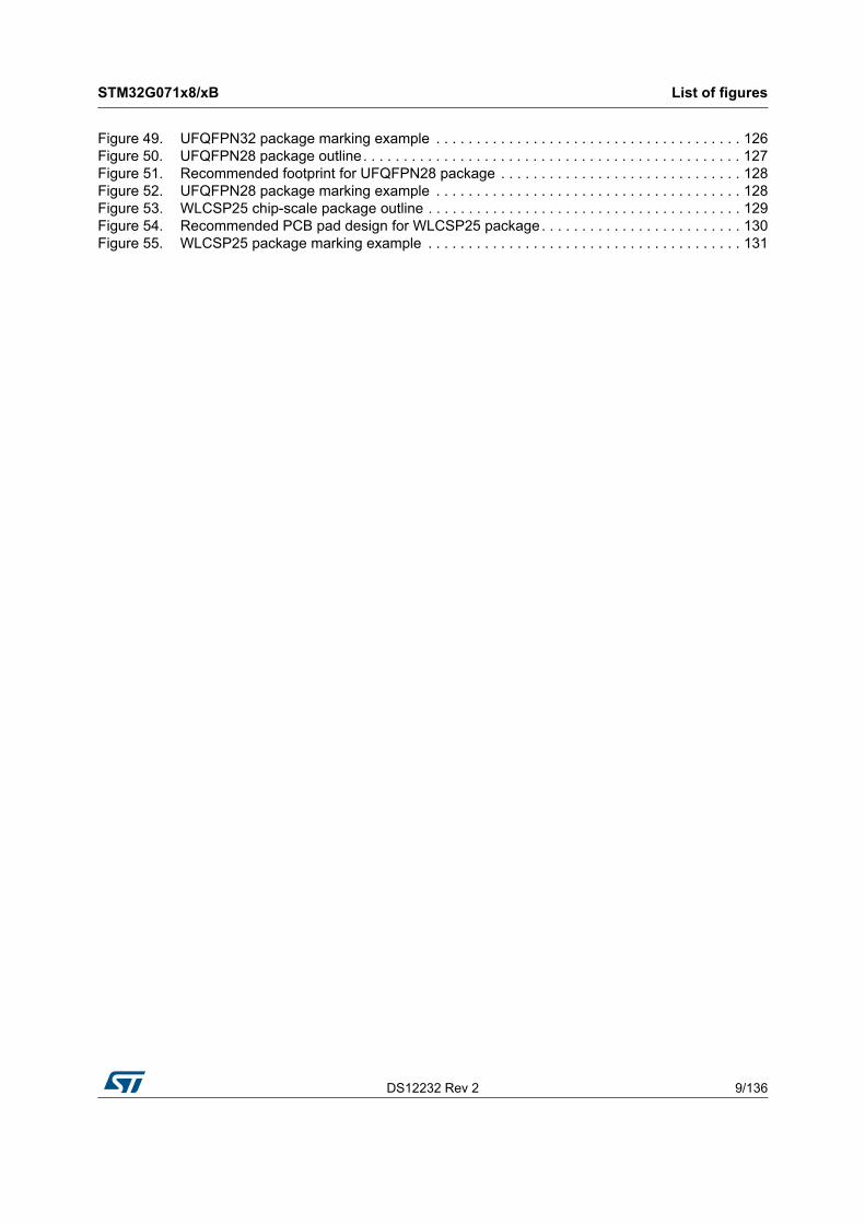
Figure 49. UFQFPN32 package marking example . . . . . . . . . . . . . . . . . . . . . . . . . . . . . . . . . . . . . . 126Figure 50. UFQFPN28 package outline. . . . . . . . . . . . . . . . . . . . . . . . . . . . . . . . . . . . . . . . . . . . . . . 127Figure 51. Recommended footprint for UFQFPN28 package . . . . . . . . . . . . . . . . . . . . . . . . . . . . . . 128Figure 52. UFQFPN28 package marking example . . . . . . . . . . . . . . . . . . . . . . . . . . . . . . . . . . . . . . 128Figure 53. WLCSP25 chip-scale package outline . . . . . . . . . . . . . . . . . . . . . . . . . . . . . . . . . . . . . . . 129Figure 54. Recommended PCB pad design for WLCSP25 package. . . . . . . . . . . . . . . . . . . . . . . . . 130Figure 55. WLCSP25 package marking example . . . . . . . . . . . . . . . . . . . . . . . . . . . . . . . . . . . . . . . 131
Introduction STM32G071x8/xB
10/136 DS12232 Rev 2
1 Introduction
This document provides information on STM32G071x8/xB microcontrollers, such as description, functional overview, pin assignment and definition, electrical characteristics, packaging, and ordering codes.
Information on memory mapping and control registers is object of reference manual.
Information on Arm®(a) Cortex®-M0+ core is available from the www.arm.com website.
a. Arm is a registered trademark of Arm Limited (or its subsidiaries) in the US and/or elsewhere.
DS12232 Rev 2 11/136
STM32G071x8/xB Description
34
2 Description
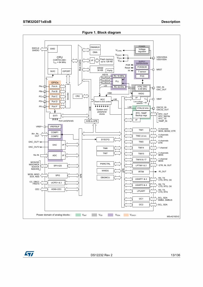
The STM32G071x8/xB mainstream microcontrollers are based on high-performance Arm® Cortex®-M0+ 32-bit RISC core operating at up to 64 MHz frequency. Offering a high level of integration, they are suitable for a wide range of applications in consumer, industrial and appliance domains and ready for the Internet of Things (IoT) solutions.
The devices incorporate a memory protection unit (MPU), high-speed embedded memories (up to 128 Kbytes of Flash program memory and 36 Kbytes of SRAM), DMA and an extensive range of system functions, enhanced I/Os and peripherals. The devices offer standard communication interfaces (two I2Cs, two SPIs / one I2S, one HDMI CEC and four USARTs), one 12-bit ADC (2.5 MSps) with up to 19 channels, one 12-bit DAC with two channels, two fast comparators, an internal voltage reference buffer, a low-power RTC, an advanced control PWM timer running at up to double the CPU frequency, five general-purpose 16-bit timers with one running at up to double the CPU frequency, a 32-bit general-purpose timer, two basic and two low-power 16-bit timers, two watchdog timers, and a SysTick timer. The STM32G071x8/xB devices provide a fully integrated USB Type-C Power Delivery controller.
The devices operate within ambient temperatures from -40 to 125°C. They can operate with supply voltages from 1.7 V to 3.6 V. Optimized dynamic consumption combined with a comprehensive set of power-saving modes, low-power timers and low-power UART, allows the design of low-power applications.
VBAT direct battery input allows keeping RTC and backup registers powered.
The devices come in packages with 28 to 64 pins.
Description STM32G071x8/xB
12/136 DS12232 Rev 2
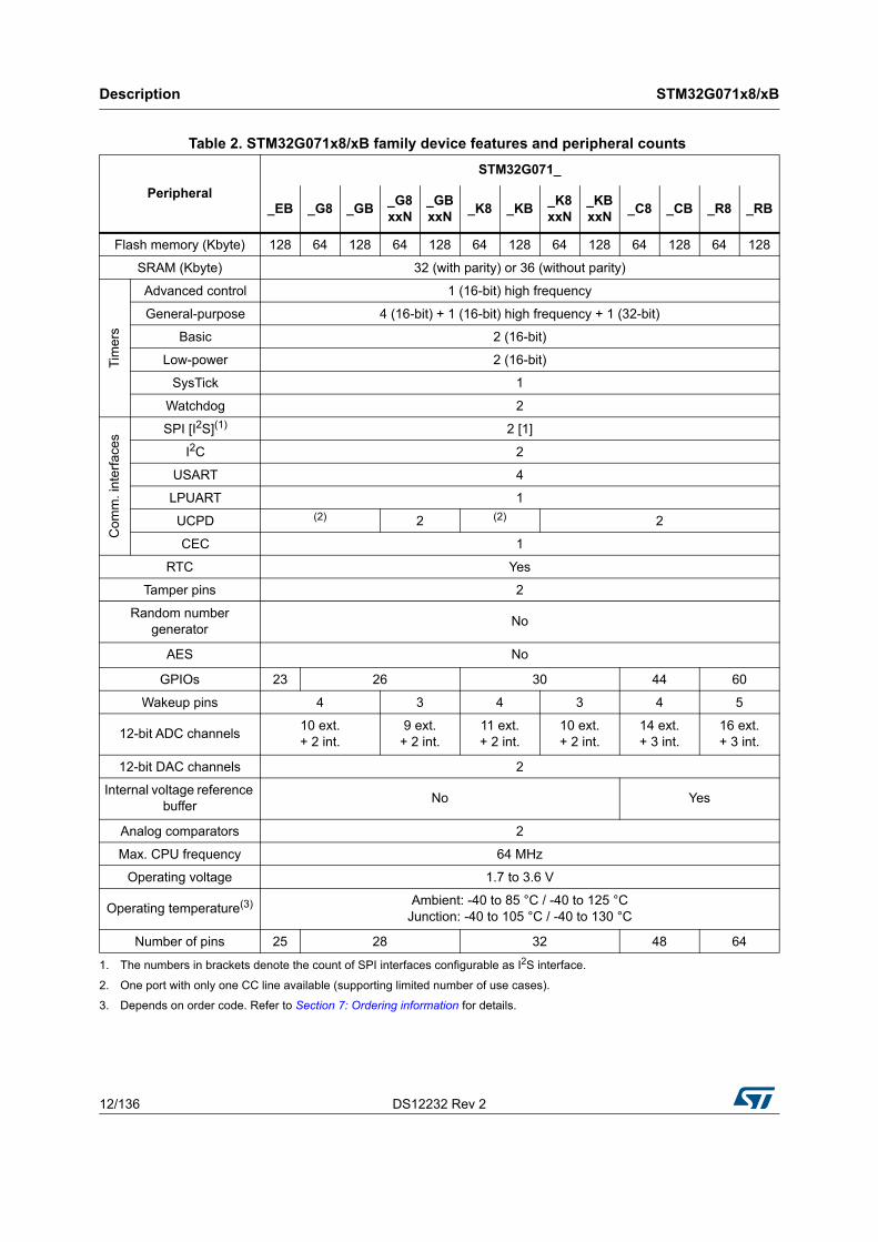
Table 2. STM32G071x8/xB family device features and peripheral counts
Peripheral
STM32G071_
_EB _G8 _GB_G8xxN
_GBxxN
_K8 _KB_K8xxN
_KBxxN
_C8 _CB _R8 _RB
Flash memory (Kbyte) 128 64 128 64 128 64 128 64 128 64 128 64 128
SRAM (Kbyte) 32 (with parity) or 36 (without parity)
Tim
ers
Advanced control 1 (16-bit) high frequency
General-purpose 4 (16-bit) + 1 (16-bit) high frequency + 1 (32-bit)
Basic 2 (16-bit)
Low-power 2 (16-bit)
SysTick 1
Watchdog 2
Com
m. i
nter
face
s
SPI [I2S](1) 2 [1]
I2C 2
USART 4
LPUART 1
UCPD (2) 2 (2) 2
CEC 1
RTC Yes
Tamper pins 2
Random number generator
No
AES No
GPIOs 23 26 30 44 60
Wakeup pins 4 3 4 3 4 5
12-bit ADC channels10 ext.+ 2 int.
9 ext.+ 2 int.
11 ext.+ 2 int.
10 ext.+ 2 int.
14 ext.+ 3 int.
16 ext.+ 3 int.
12-bit DAC channels 2
Internal voltage reference buffer
No Yes
Analog comparators 2
Max. CPU frequency 64 MHz
Operating voltage 1.7 to 3.6 V
Operating temperature(3) Ambient: -40 to 85 °C / -40 to 125 °CJunction: -40 to 105 °C / -40 to 130 °C
Number of pins 25 28 32 48 64
1. The numbers in brackets denote the count of SPI interfaces configurable as I2S interface.
2. One port with only one CC line available (supporting limited number of use cases).
3. Depends on order code. Refer to Section 7: Ordering information for details.
DS12232 Rev 2 13/136
STM32G071x8/xB Description
34
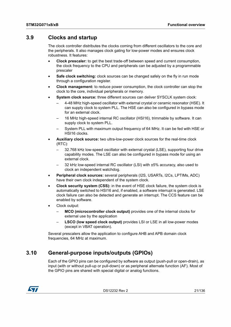
Figure 1. Block diagram
MSv42182V2
UCPDUSART3/4
USART1/2
LPTIMER 1/2
TIMER 16/17
Power domain of analog blocks : VBAT
4 channelsBKIN, BKIN2, ETR
System and peripheral
clocks
PAx
PBx
PCx
PFx
MOSI/SDMISO/MCK
SCK/CKNSS/WS
SWCLKSWDIO
16x IN
OSC_INOSC_OUT
VBAT
OSC32_IN OSC32_OUT
RTC_OUT RTC_REFINRTC_TS
MOSI, MISO SCK, NSS
HSI16
LSI
PLLPCLK
VDD
IR_OUT
1 channelBKIN
ETR, IN, OUT
1 channel
4 channelsETR
4 channelsETR
CPUCORTEX-M0+fmax = 64 MHz
SWD
NVIC
EXTI
SPI1/I2S
SPI2
AHB-to-APB
RCCReset & clock control
I/F
XTAL OSC4-48 MHz
IWDG
SRAM36 KB
I/FADC
RTC, TAMPBackup regs
I/F
RC 16 MHz
RC 32 kHz
PLL
deco
der
XTAL32 kHz
Bus
mat
rix I/F
VDD
2 channelsBKIN
RX, TXCTS, RTS, CK
RX, TXCTS, RTS, CK
CEC
TIM6
TIM7
COMP1
COMP2IN+, IN-,
OUT
Port D
Port C
Port B
Port A
VDDA
SUPPLY SUPERVISION
POWER
VCORE
PORReset
Int
VDD/VDDAVSS/VSSA
NRST
PVD
POR/BOR
Voltageregulator
USART3 & 4
USART1 & 2
LPTIM1 & 2
TIM16 & 17
TIM15
TIM14
TIM3
TIM2 (32-bit)
TIM1
GPIOs
IOPORT
HSE
PLLQCLKPLLRCLK
LSE
LSE
T sensor
RX, TX,CTS, RTSLPUART
TAMP_IN
AP
B
AP
B
AH
B
CC, DBCCFRSTX UCPD1 & 2
HDMI-CEC
VREFBUF
DAC I/FDAC_OUT1
DAC_OUT2
CRC
VREF+
SCL, SDA
SCL, SDASMBA, SMBUSI2C1
I2C2
DBGMCU
WWDG
PWRCTRL
SYSCFG
DMA
DMAMUX
Port F
PDx
VDDA VDDIO1
Low-voltage detector
VDD
Parity
Flash memory up to 128 KB
VDDIO1
IRTIM
from peripherals
Functional overview STM32G071x8/xB
14/136 DS12232 Rev 2
3 Functional overview
3.1 Arm® Cortex®-M0+ core with MPU
The Cortex-M0+ is an entry-level 32-bit Arm Cortex processor designed for a broad range of embedded applications. It offers significant benefits to developers, including:
• a simple architecture, easy to learn and program
• ultra-low power, energy-efficient operation
• excellent code density
• deterministic, high-performance interrupt handling
• upward compatibility with Cortex-M processor family
• platform security robustness, with integrated Memory Protection Unit (MPU).
The Cortex-M0+ processor is built on a highly area- and power-optimized 32-bit core, with a 2-stage pipeline Von Neumann architecture. The processor delivers exceptional energy efficiency through a small but powerful instruction set and extensively optimized design, providing high-end processing hardware including a single-cycle multiplier.
The Cortex-M0+ processor provides the exceptional performance expected of a modern 32-bit architecture, with a higher code density than other 8-bit and 16-bit microcontrollers.
Owing to embedded Arm core, the STM32G071x8/xB devices are compatible with Arm tools and software.
The Cortex-M0+ is tightly coupled with a nested vectored interrupt controller (NVIC) described in Section 3.12.1.
3.2 Memory protection unit
The memory protection unit (MPU) is used to manage the CPU accesses to memory to prevent one task to accidentally corrupt the memory or resources used by any other active task.
The MPU is especially helpful for applications where some critical or certified code has to be protected against the misbehavior of other tasks. It is usually managed by an RTOS (real-time operating system). If a program accesses a memory location that is prohibited by the MPU, the RTOS can detect it and take action. In an RTOS environment, the kernel can dynamically update the MPU area setting, based on the process to be executed.
The MPU is optional and can be bypassed for applications that do not need it.
3.3 Embedded Flash memory
STM32G071x8/xB devices feature up to 128 Kbytes of embedded Flash memory available for storing code and data.
DS12232 Rev 2 15/136
STM32G071x8/xB Functional overview
34
Flexible protections can be configured thanks to option bytes:
• Readout protection (RDP) to protect the whole memory. Three levels are available:
– Level 0: no readout protection
– Level 1: memory readout protection: the Flash memory cannot be read from or written to if either debug features are connected, boot in RAM or bootloader is selected
– Level 2: chip readout protection: debug features (Cortex-M0+ serial wire), boot in RAM and bootloader selection are disabled. This selection is irreversible.
• Write protection (WRP): the protected area is protected against erasing and programming. Two areas per bank can be selected, with 2-Kbyte granularity.
• Proprietary code readout protection (PCROP): a part of the Flash memory can be protected against read and write from third parties. The protected area is execute-only: it can only be reached by the STM32 CPU as instruction code, while all other accesses (DMA, debug and CPU data read, write and erase) are strictly prohibited. An additional option bit (PCROP_RDP) determines whether the PCROP area is erased or not when the RDP protection is changed from Level 1 to Level 0.
The whole non-volatile memory embeds the error correction code (ECC) feature supporting:
• single error detection and correction
• double error detection
• readout of the ECC fail address from the ECC register
3.4 Embedded SRAM
STM32G071x8/xB devices have 32 Kbytes of embedded SRAM with parity. Hardware parity check allows memory data errors to be detected, which contributes to increasing functional safety of applications.
When the parity protection is not required because the application is not safety-critical, the parity memory bits can be used as additional SRAM, to increase its total size to 36 Kbytes.
The memory can be read/write-accessed at CPU clock speed, with 0 wait states.
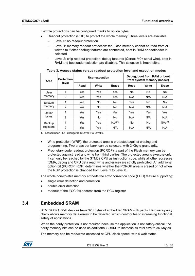
Table 3. Access status versus readout protection level and execution modes
AreaProtection
level
User execution Debug, boot from RAM or boot from system memory (loader)
Read Write Erase Read Write Erase
User memory
1 Yes Yes Yes No No No
2 Yes Yes Yes N/A N/A N/A
System memory
1 Yes No No Yes No No
2 Yes No No N/A N/A N/A
Option bytes
1 Yes Yes Yes Yes Yes Yes
2 Yes No No N/A N/A N/A
Backup registers
1 Yes Yes N/A(1)
1. Erased upon RDP change from Level 1 to Level 0.
No No N/A(1)
2 Yes Yes N/A N/A N/A N/A
Functional overview STM32G071x8/xB
16/136 DS12232 Rev 2
3.5 Boot modes
At startup, the boot pin and boot selector option bit are used to select one of the three boot options:
• boot from User Flash memory
• boot from System memory
• boot from embedded SRAM
The boot pin is shared with a standard GPIO and can be disabled through the boot selector option bit. The boot loader is located in System memory. It manages the Flash memory reprogramming through USART on pins PA9/PA10, PC10/PC11 or PA2/PA3, through I2C-bus on pins PB6/PB7 or PB10/PB11, or through SPI on pins PA4/PA5/PA6/PA7 or PB12/PB13/PB14/PB15.
3.6 Cyclic redundancy check calculation unit (CRC)
The CRC (cyclic redundancy check) calculation unit is used to get a CRC code using a configurable generator polynomial value and size.
Among other applications, CRC-based techniques are used to verify data transmission or storage integrity. In the scope of the EN/IEC 60335-1 standard, they offer a means of verifying the Flash memory integrity. The CRC calculation unit helps compute a signature of the software during runtime, to be compared with a reference signature generated at link time and stored at a given memory location.
3.7 Power supply management
3.7.1 Power supply schemes
The STM32G071x8/xB devices require a 1.7 V to 3.6 V operating supply voltage (VDD). Several different power supplies are provided to specific peripherals:
• VDD = 1.7 (2.0) to 3.6 V
VDD is the external power supply for the internal regulator and the system analog such as reset, power management and internal clocks. It is provided externally through VDD/VDDA pin.
The minimum voltage of 1.7 V corresponds to power-on reset release threshold VPOR(MAX). Once this threshold is crossed and power-on reset is released, the functionality is guaranteed down to power-down reset threshold VPDR(MIN).
• VDDA = 2.0 V (ADC and COMP) / 1.8 V (DAC) / 2.4 V (VREFBUF) to 3.6 V
VDDA is the analog power supply for the A/D converter, D/A converter, voltage reference buffer and comparators. VDDA voltage level is identical to VDD voltage as it is provided externally through VDD/VDDA pin.
• VDDIO1 = VDD
VDDIO1 is the power supply for the I/Os. VDDIO1 voltage level is identical to VDD voltage as it is provided externally through VDD/VDDA pin.
• VBAT = 1.55 V to 3.6 V
VBAT is the power supply (through a power switch) for RTC, TAMP, low-speed external 32.768 kHz oscillator and backup registers when VDD is not present. VBAT is provided
DS12232 Rev 2 17/136
STM32G071x8/xB Functional overview
34
externally through VBAT pin. When this pin is not available on the package, VBAT bonding pad is internally bonded to the VDD/VDDA pin.
• VREF+ is the input reference voltage for the ADC and DAC, or the output of the internal voltage reference buffer (when enabled). When VDDA < 2 V, VREF+ must be equal to VDDA. When VDDA ≥ 2 V, VREF+ must be between 2 V and VDDA. It can be grounded when the ADC and DAC are not active.
The internal voltage reference buffer supports two output voltages, which is configured with VRS bit of the VREFBUF_CSR register:
– VREF+ around 2.048 V (requiring VDDA equal to or higher than 2.4 V)
– VREF+ around 2.5 V (requiring VDDA equal to or higher than 2.8 V)
VREF+ is delivered through VREF+ pin. On packages without VREF+ pin, VREF+ is internally connected with VDD, and the internal voltage reference buffer must be kept disabled (refer to datasheets for package pinout description).
• VCORE
An embedded linear voltage regulator is used to supply the VCORE internal digital power. VCORE is the power supply for digital peripherals, SRAM and Flash memory. The Flash memory is also supplied with VDD.
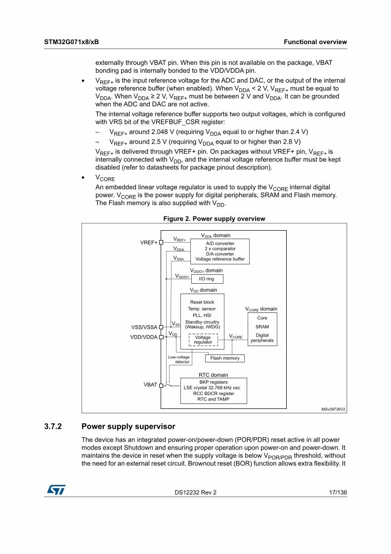
Figure 2. Power supply overview
3.7.2 Power supply supervisor
The device has an integrated power-on/power-down (POR/PDR) reset active in all power modes except Shutdown and ensuring proper operation upon power-on and power-down. It maintains the device in reset when the supply voltage is below VPOR/PDR threshold, without the need for an external reset circuit. Brownout reset (BOR) function allows extra flexibility. It
MSv39736V2
VDDA domain
RTC domain
D/A converter
A/D converter
Standby circuitry (Wakeup, IWDG)
Voltage regulator
Core
SRAM
Digitalperipherals
Low-voltage detector
LSE crystal 32.768 kHz oscBKP registers
RCC BDCR registerRTC and TAMP
2 x comparator
Voltage reference buffer
I/O ring
VCORE domainTemp. sensorReset block
PLL, HSI
Flash memory
VDDIO1
VREF+
VDD domain
VCORE
VSS/VSSA
VDD/VDDA
VBAT
VDDA
VREF+
VSSA
VSS
VDD
VDDIO1 domain
Functional overview STM32G071x8/xB
18/136 DS12232 Rev 2
can be enabled and configured through option bytes, by selecting one of four thresholds for rising VDD and other four for falling VDD.
The device also features an embedded programmable voltage detector (PVD) that monitors the VDD power supply and compares it to VPVD threshold. It allows generating an interrupt when VDD level crosses the VPVD threshold, selectively while falling, while rising, or while falling and rising. The interrupt service routine can then generate a warning message and/or put the MCU into a safe state. The PVD is enabled by software.
3.7.3 Voltage regulator
Two embedded linear voltage regulators, main regulator (MR) and low-power regulator (LPR), supply most of digital circuitry in the device.
The MR is used in Run and Sleep modes. The LPR is used in Low-power run, Low-power sleep and Stop modes.
In Standby and Shutdown modes, both regulators are powered down and their outputs set in high-impedance state, such as to bring their current consumption close to zero. However, SRAM data retention is possible in Standby mode, in which case the LPR remains active and it only supplies the SRAM.
3.7.4 Low-power modes
By default, the microcontroller is in Run mode after system or power reset. It is up to the user to select one of the low-power modes described below:
• Sleep mode
In Sleep mode, only the CPU is stopped. All peripherals continue to operate and can wake up the CPU when an interrupt/event occurs.
• Low-power run mode
This mode is achieved with VCORE supplied by the low-power regulator to minimize the regulator's operating current. The code can be executed from SRAM or from Flash, and the CPU frequency is limited to 2 MHz. The peripherals with independent clock can be clocked by HSI16.
• Low-power sleep mode
This mode is entered from the low-power run mode. Only the CPU clock is stopped. When wakeup is triggered by an event or an interrupt, the system reverts to the Low-power run mode.
• Stop 0 and Stop 1 modes
In Stop 0 and Stop 1 modes, the device achieves the lowest power consumption while retaining the SRAM and register contents. All clocks in the VCORE domain are stopped. The PLL, as well as the HSI16 RC oscillator and the HSE crystal oscillator are disabled. The LSE or LSI keep running. The RTC can remain active (Stop mode with RTC, Stop mode without RTC).
Some peripherals with wakeup capability can enable the HSI16 RC during Stop mode, so as to get clock for processing the wakeup event. The main regulator remains active in Stop 0 mode while it is turned off in Stop 1 mode.
• Standby mode
The Standby mode is used to achieve the lowest power consumption, with POR/PDR always active in this mode. The main regulator is switched off to power down VCORE domain. The low-power regulator is either switched off or kept active. In the latter case,
DS12232 Rev 2 19/136
STM32G071x8/xB Functional overview
34
it only supplies SRAM to ensure data retention. The PLL, as well as the HSI16 RC oscillator and the HSE crystal oscillator are also powered down. The RTC can remain active (Standby mode with RTC, Standby mode without RTC).
For each I/O, the software can determine whether a pull-up, a pull-down or no resistor shall be applied to that I/O during Standby mode.
Upon entering Standby mode, register contents are lost except for registers in the RTC domain and standby circuitry. The SRAM contents can be retained through register setting.
The device exits Standby mode upon external reset event (NRST pin), IWDG reset event, wakeup event (WKUP pin, configurable rising or falling edge) or RTC event (alarm, periodic wakeup, timestamp, tamper), or when a failure is detected on LSE (CSS on LSE).
• Shutdown mode
The Shutdown mode allows to achieve the lowest power consumption. The internal regulator is switched off to power down the VCORE domain. The PLL, as well as the HSI16 and LSI RC-oscillators and HSE crystal oscillator are also powered down. The RTC can remain active (Shutdown mode with RTC, Shutdown mode without RTC).
The BOR is not available in Shutdown mode. No power voltage monitoring is possible in this mode. Therefore, switching to RTC domain is not supported.
SRAM and register contents are lost except for registers in the RTC domain.
The device exits Shutdown mode upon external reset event (NRST pin), IWDG reset event, wakeup event (WKUP pin, configurable rising or falling edge) or RTC event (alarm, periodic wakeup, timestamp, tamper).
3.7.5 Reset mode
During and upon exiting reset, the schmitt triggers of I/Os are disabled so as to reduce power consumption. In addition, when the reset source is internal, the built-in pull-up resistor on NRST pin is deactivated.
3.7.6 VBAT operation
The VBAT power domain, consuming very little energy, includes RTC, and LSE oscillator and backup registers.
In VBAT mode, the RTC domain is supplied from VBAT pin. The power source can be, for example, an external battery or an external supercapacitor. Two anti-tamper detection pins are available.
The RTC domain can also be supplied from VDD/VDDA pin.
By means of a built-in switch, an internal voltage supervisor allows automatic switching of RTC domain powering between VDD and voltage from VBAT pin to ensure that the supply voltage of the RTC domain (VBAT) remains within valid operating conditions. If both voltages are valid, the RTC domain is supplied from VDD/VDDA pin.
An internal circuit for charging the battery on VBAT pin can be activated if the VDD voltage is within a valid range.
Note: External interrupts and RTC alarm/events cannot cause the microcontroller to exit the VBAT mode, as in that mode the VDD is not within a valid range.
Functional overview STM32G071x8/xB
20/136 DS12232 Rev 2
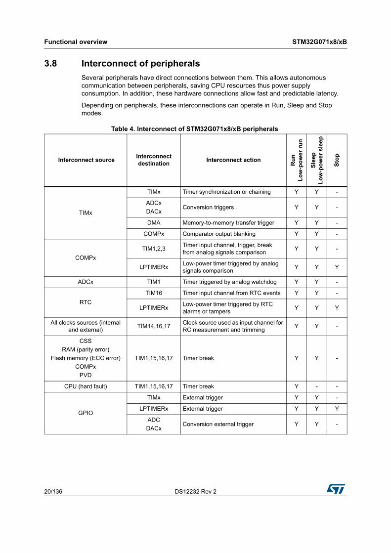
3.8 Interconnect of peripherals
Several peripherals have direct connections between them. This allows autonomous communication between peripherals, saving CPU resources thus power supply consumption. In addition, these hardware connections allow fast and predictable latency.
Depending on peripherals, these interconnections can operate in Run, Sleep and Stop modes.
Table 4. Interconnect of STM32G071x8/xB peripherals
Interconnect sourceInterconnect destination
Interconnect action
Ru
n
Lo
w-p
ow
er r
un
Sle
epL
ow
-po
we
r s
leep
Sto
p
TIMx
TIMx Timer synchronization or chaining Y Y -
ADCx
DACxConversion triggers Y Y -
DMA Memory-to-memory transfer trigger Y Y -
COMPx Comparator output blanking Y Y -
COMPx
TIM1,2,3Timer input channel, trigger, break from analog signals comparison
Y Y -
LPTIMERxLow-power timer triggered by analog signals comparison
Y Y Y
ADCx TIM1 Timer triggered by analog watchdog Y Y -
RTC
TIM16 Timer input channel from RTC events Y Y -
LPTIMERxLow-power timer triggered by RTC alarms or tampers
Y Y Y
All clocks sources (internal and external)
TIM14,16,17Clock source used as input channel for RC measurement and trimming
Y Y -
CSS
RAM (parity error)
Flash memory (ECC error)
COMPx
PVD
TIM1,15,16,17 Timer break Y Y -
CPU (hard fault) TIM1,15,16,17 Timer break Y - -
GPIO
TIMx External trigger Y Y -
LPTIMERx External trigger Y Y Y
ADC
DACxConversion external trigger Y Y -
DS12232 Rev 2 21/136
STM32G071x8/xB Functional overview
34
3.9 Clocks and startup
The clock controller distributes the clocks coming from different oscillators to the core and the peripherals. It also manages clock gating for low-power modes and ensures clock robustness. It features:
• Clock prescaler: to get the best trade-off between speed and current consumption, the clock frequency to the CPU and peripherals can be adjusted by a programmable prescaler
• Safe clock switching: clock sources can be changed safely on the fly in run mode through a configuration register.
• Clock management: to reduce power consumption, the clock controller can stop the clock to the core, individual peripherals or memory.
• System clock source: three different sources can deliver SYSCLK system clock:
– 4-48 MHz high-speed oscillator with external crystal or ceramic resonator (HSE). It can supply clock to system PLL. The HSE can also be configured in bypass mode for an external clock.
– 16 MHz high-speed internal RC oscillator (HSI16), trimmable by software. It can supply clock to system PLL.
– System PLL with maximum output frequency of 64 MHz. It can be fed with HSE or HSI16 clocks.
• Auxiliary clock source: two ultra-low-power clock sources for the real-time clock (RTC):
– 32.768 kHz low-speed oscillator with external crystal (LSE), supporting four drive capability modes. The LSE can also be configured in bypass mode for using an external clock.
– 32 kHz low-speed internal RC oscillator (LSI) with ±5% accuracy, also used to clock an independent watchdog.
• Peripheral clock sources: several peripherals (I2S, USARTs, I2Cs, LPTIMs, ADC) have their own clock independent of the system clock.
• Clock security system (CSS): in the event of HSE clock failure, the system clock is automatically switched to HSI16 and, if enabled, a software interrupt is generated. LSE clock failure can also be detected and generate an interrupt. The CCS feature can be enabled by software.
• Clock output:
– MCO (microcontroller clock output) provides one of the internal clocks for external use by the application
– LSCO (low speed clock output) provides LSI or LSE in all low-power modes (except in VBAT operation).
Several prescalers allow the application to configure AHB and APB domain clock frequencies, 64 MHz at maximum.
3.10 General-purpose inputs/outputs (GPIOs)
Each of the GPIO pins can be configured by software as output (push-pull or open-drain), as input (with or without pull-up or pull-down) or as peripheral alternate function (AF). Most of the GPIO pins are shared with special digital or analog functions.
Functional overview STM32G071x8/xB
22/136 DS12232 Rev 2
Through a specific sequence, this special function configuration of I/Os can be locked, such as to avoid spurious writing to I/O control registers.
3.11 Direct memory access controller (DMA)
Direct memory access (DMA) controller transfers data from a source to a destination, without making it transit through the CPU. DMA transfers are highly efficient; they save CPU resources and facilitate time-critical processing.
The source and the destination of a DMA transfer can be a peripheral or a memory.
The DMA transfer source and destination data types can be programmed independently. If different, the DMA controller performs data type conversion and adapts the addressing at the source and at the destination to their respective data types.
DMA transfer size is the number of DMA transfer cycles to execute, programmable by software. One cycle transfers one data item of selected data type from the DMA transfer source to the DMA transfer destination. The DMA transfer starts at pre-programmed source and destination base addresses. It ends at source and destination addresses that depend on the DMA transfer size, source and destination data types, and on activation of address auto-increment operation.
The DMA transfer starts upon a request from a peripheral or, in the specific case of memory-to-memory transfer, it starts when enabled by software.
The DMA controller executes one DMA transfer cycle per DMA transfer request from a peripheral, until the total number of cycles reaches the pre-programmed DMA transfer size. The circular mode of operation allows to repeat the DMA transfer infinitely, without software intervention.
In the specific case of memory-to-memory transfer, the DMA controller executes, if enabled by the software, the pre-programmed amount of cycles.
The DMA controller provides distinct DMA transfer channels. The channels can be individually configured in term of source and destination location, DMA transfer size, data type, priority level and operating mode. The DMA controller opens one channel at a time, according to channel priorities.
Features of the DMA controller:
• 7 DMA transfer channels, independently configurable by software
• Per-channel DMA transfer trigger upon request from a peripheral
• Per-channel DMA transfer triggered by software (memory-to-memory mode)
• Programmable channel priority levels: very high, high, medium and low
• By-default (hardware) channel priority levels, to arbitrate concurrent requests from channels with identical programmable priority levels
• Byte (8-bit unit), half-word (16-bit unit) and word (32-bit unit) DMA transfer data types, programmable independently for the source and the destination
DS12232 Rev 2 23/136
STM32G071x8/xB Functional overview
34
• Automatic alignment of DMA transfer source and destination addresses according to their respective data types
• Circular operating mode support
• DMA Half Transfer, DMA Transfer Complete and DMA Transfer Error flags, logically OR-ed together in a single interrupt request per channel
• Memory-to-memory, peripheral-to-memory, memory-to-peripheral and peripheral-to-peripheral DMA transfer types
• DMA transfer size programmable up to 65535 DMA transfer cycles
• Access to Flash memory, SRAM, APB and AHB peripherals as source and destination
3.12 Interrupts and events
The device flexibly manages events causing interrupts of linear program execution, called exceptions. The Cortex-M0+ processor core, a nested vectored interrupt controller (NVIC) and an extended interrupt/event controller (EXTI) are the assets contributing to handling the exceptions. Exceptions include core-internal events such as, for example, a division by zero and, core-external events such as logical level changes on physical lines. Exceptions result in interrupting the program flow, executing an interrupt service routine (ISR) then resuming the original program flow.
The processor context (contents of program pointer and status registers) is stacked upon program interrupt and unstacked upon program resume, by hardware. This avoids context stacking and unstacking in the interrupt service routines (ISRs) by software, thus saving time, code and power. The ability to abandon and restart load-multiple and store-multiple operations significantly increases the device’s responsiveness in processing exceptions.
3.12.1 Nested vectored interrupt controller (NVIC)
The configurable nested vectored interrupt controller is tightly coupled with the core. It handles physical line events associated with a non-maskable interrupt (NMI) and maskable interrupts, and Cortex-M0+ exceptions. It provides flexible priority management.
The tight coupling of the processor core with NVIC significantly reduces the latency between interrupt events and start of corresponding interrupt service routines (ISRs). The ISR vectors are listed in a vector table, stored in the NVIC at a base address. The vector address of an ISR to execute is hardware-built from the vector table base address and the ISR order number used as offset.
If a higher-priority interrupt event happens while a lower-priority interrupt event occurring just before is waiting for being served, the later-arriving higher-priority interrupt event is served first. Another optimization is called tail-chaining. Upon a return from a higher-priority ISR then start of a pending lower-priority ISR, the unnecessary processor context unstacking and stacking is skipped. This reduces latency and contributes to power efficiency.
Functional overview STM32G071x8/xB
24/136 DS12232 Rev 2
Features of the NVIC:
• Low-latency interrupt processing
• 4 priority levels
• Handling of a non-maskable interrupt (NMI)
• Handling of 32 maskable interrupt lines
• Handling of 10 Cortex-M0+ exceptions
• Later-arriving higher-priority interrupt processed first
• Tail-chaining
• Interrupt vector retrieval by hardware
3.12.2 Extended interrupt/event controller (EXTI)
The extended interrupt/event controller adds flexibility in handling physical line events and allows identifying wake-up events at processor wakeup from Stop mode.
The EXTI controller has 33 channels, of which 16 with rising, falling or rising and falling edge detector capability. Any GPIO and a few peripheral signals can be connected to these channels.
The channels can be independently masked.
The EXTI controller can capture pulses shorter than the internal clock period.
A register in the EXTI controller latches every event even in Stop mode, which allows the software to identify the origin of the processor's wake-up from Stop mode or, to identify the GPIO and the edge event having caused an interrupt.
3.13 Analog-to-digital converter (ADC)
A native 12-bit analog-to-digital converter is embedded into STM32G071x8/xB devices. It can be extended to 16-bit resolution through hardware oversampling. The ADC has up to 16 external channels and 3 internal channels (temperature sensor, voltage reference, VBAT monitoring). It performs conversions in single-shot or scan mode. In scan mode, automatic conversion is performed on a selected group of analog inputs.
The ADC frequency is independent from the CPU frequency, allowing maximum sampling rate of ~2 MSps even with a low CPU speed. An auto-shutdown function guarantees that the ADC is powered off except during the active conversion phase.
The ADC can be served by the DMA controller. It can operate in the whole VDD supply range.
The ADC features a hardware oversampler up to 256 samples, improving the resolution to 16 bits (refer to AN2668).
An analog watchdog feature allows very precise monitoring of the converted voltage of one, some or all scanned channels. An interrupt is generated when the converted voltage is outside the programmed thresholds.
The events generated by the general-purpose timers (TIMx) can be internally connected to the ADC start triggers, to allow the application to synchronize A/D conversions with timers.
DS12232 Rev 2 25/136
STM32G071x8/xB Functional overview
34
3.13.1 Temperature sensor
The temperature sensor (TS) generates a voltage VTS that varies linearly with temperature.
The temperature sensor is internally connected to an ADC input to convert the sensor output voltage into a digital value.
The sensor provides good linearity but it has to be calibrated to obtain good overall accuracy of the temperature measurement. As the offset of the temperature sensor may vary from part to part due to process variation, the uncalibrated internal temperature sensor is suitable only for relative temperature measurements.
To improve the accuracy of the temperature sensor, each part is individually factory-calibrated by ST. The resulting calibration data are stored in the part’s System memory, accessible in read-only mode.
3.13.2 Internal voltage reference (VREFINT)
The internal voltage reference (VREFINT) provides a stable (bandgap) voltage output for the ADC and comparators. VREFINT is internally connected to an ADC input. The VREFINT voltage is individually precisely measured for each part by ST during production test and stored in the part’s System memory. It is accessible in read-only mode.
3.13.3 VBAT battery voltage monitoring
This embedded hardware feature allows the application to measure the VBAT battery voltage using an internal ADC input. As the VBAT voltage may be higher than VDDA and thus outside the ADC input range, the VBAT pin is internally connected to a bridge divider by 3. As a consequence, the converted digital value is one third the VBAT voltage.
3.14 Digital-to-analog converter (DAC)
The 2-channel 12-bit buffered DAC converts a digital value into an analog voltage available on the channel output. The architecture of either channel is based on integrated resistor string and an inverting amplifier. The digital circuitry is common for both channels.
Table 5. Temperature sensor calibration values
Calibration value name Description Memory address
TS_CAL1TS ADC raw data acquired at a temperature of 30 °C (± 5 °C), VDDA = VREF+ = 3.0 V (± 10 mV)
0x1FFF 75A8 - 0x1FFF 75A9
TS_CAL2TS ADC raw data acquired at a temperature of 130 °C (± 5 °C), VDDA = VREF+ = 3.0 V (± 10 mV)
0x1FFF 75CA - 0x1FFF 75CB
Table 6. Internal voltage reference calibration values
Calibration value name Description Memory address
VREFINTRaw data acquired at a temperature of 30 °C (± 5 °C), VDDA = VREF+ = 3.0 V (± 10 mV)
0x1FFF 75AA - 0x1FFF 75AB
Functional overview STM32G071x8/xB
26/136 DS12232 Rev 2
Features of the DAC:
• Two DAC output channels
• 8-bit or 12-bit output mode
• Buffer offset calibration (factory and user trimming)
• Left or right data alignment in 12-bit mode
• Synchronized update capability
• Noise-wave generation
• Triangular-wave generation
• Independent or simultaneous conversion for DAC channels
• DMA capability for either DAC channel
• Triggering with timer events, synchronized with DMA
• Triggering with external events
• Sample-and-hold low-power mode, with internal or external capacitor
3.15 Voltage reference buffer (VREFBUF)
When enabled, an embedded buffer provides the internal reference voltage to analog blocks (for example ADC) and to VREF+ pin for external components.
The internal voltage reference buffer supports two voltages:
• 2.048 V
• 2.5 V
An external voltage reference can be provided through the VREF+ pin when the internal voltage reference buffer is disabled.
On some packages, the VREF+ pad of the silicon die is double-bonded with supply pad to common VDD/VDDA pin and so the internal voltage reference buffer cannot be used.
3.16 Comparators (COMP)
Two embedded rail-to-rail analog comparators have programmable reference voltage (internal or external), hysteresis, speed (low for low-power) and output polarity.
The reference voltage can be one of the following:
• external, from an I/O
• internal, from DAC
• internal reference voltage (VREFINT) or its submultiple (1/4, 1/2, 3/4)
The comparators can wake up the device from Stop mode, generate interrupts, breaks or triggers for the timers and can be also combined into a window comparator.
3.17 Timers and watchdogs
The device includes an advanced-control timer, six general-purpose timers, two basic timers, two low-power timers, two watchdog timers and a SysTick timer. Table 7 compares features of the advanced control, general purpose and basic timers.
DS12232 Rev 2 27/136
STM32G071x8/xB Functional overview
34
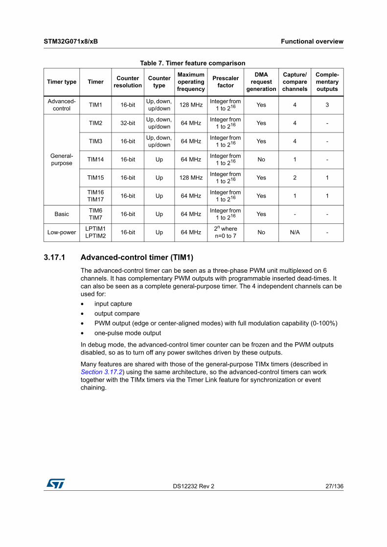
3.17.1 Advanced-control timer (TIM1)
The advanced-control timer can be seen as a three-phase PWM unit multiplexed on 6 channels. It has complementary PWM outputs with programmable inserted dead-times. It can also be seen as a complete general-purpose timer. The 4 independent channels can be used for:
• input capture
• output compare
• PWM output (edge or center-aligned modes) with full modulation capability (0-100%)
• one-pulse mode output
In debug mode, the advanced-control timer counter can be frozen and the PWM outputs disabled, so as to turn off any power switches driven by these outputs.
Many features are shared with those of the general-purpose TIMx timers (described in Section 3.17.2) using the same architecture, so the advanced-control timers can work together with the TIMx timers via the Timer Link feature for synchronization or event chaining.
Table 7. Timer feature comparison
Timer type TimerCounter
resolutionCounter
type
Maximum operating frequency
Prescaler factor
DMA request
generation
Capture/compare channels
Comple-mentary outputs
Advanced- control
TIM1 16-bitUp, down, up/down
128 MHzInteger from
1 to 216 Yes 4 3
General-purpose
TIM2 32-bitUp, down, up/down
64 MHzInteger from
1 to 216 Yes 4 -
TIM3 16-bitUp, down, up/down
64 MHzInteger from
1 to 216 Yes 4 -
TIM14 16-bit Up 64 MHzInteger from
1 to 216 No 1 -
TIM15 16-bit Up 128 MHzInteger from
1 to 216 Yes 2 1
TIM16TIM17
16-bit Up 64 MHzInteger from
1 to 216 Yes 1 1
BasicTIM6TIM7
16-bit Up 64 MHzInteger from
1 to 216 Yes - -
Low-powerLPTIM1 LPTIM2
16-bit Up 64 MHz2n wheren=0 to 7
No N/A -
Functional overview STM32G071x8/xB
28/136 DS12232 Rev 2
3.17.2 General-purpose timers (TIM2, TIM3, TIM14, TIM15, TIM16, TIM17)
There are six synchronizable general-purpose timers embedded in the device (refer to Table 7 for comparison). Each general-purpose timer can be used to generate PWM outputs or act as a simple timebase.
• TIM2 and TIM3
These are full-featured general-purpose timers:
– TIM2 with 32-bit auto-reload up/downcounter and 16-bit prescaler
– TIM3 with 16-bit auto-reload up/downcounter and 16-bit prescaler
They have four independent channels for input capture/output compare, PWM or one-pulse mode output. They can operate together or in combination with other general-purpose timers via the Timer Link feature for synchronization or event chaining. They can generate independent DMA request and support quadrature encoders. Their counters can be frozen in debug mode.
• TIM14
This timer is based on a 16-bit auto-reload upcounter and a 16-bit prescaler. It has one channel for input capture/output compare, PWM output or one-pulse mode output. Its counter can be frozen in debug mode.
• TIM15, 16 and 17
These are general-purpose timers featuring:
– 16-bit auto-reload upcounter and 16-bit prescaler
– 2 channels and 1 complementary channel for TIM15
– 1 channel and 1 complementary channel for TIM16 and TIM17
All channels can be used for input capture/output compare, PWM or one-pulse mode output. The timers can operate together via the Timer Link feature for synchronization or event chaining. They can generate independent DMA request. Their counters can be frozen in debug mode.
3.17.3 Basic timers (TIM6 and TIM7)
3.17.4 Low-power timers (LPTIM1 and LPTIM2)
These timers have an independent clock. When fed with LSE, LSI or external clock, they keep running in Stop mode and they can wake up the system from it.
These timers are mainly used for triggering DAC conversions. They can also be used as generic 16-bit timebases.
DS12232 Rev 2 29/136
STM32G071x8/xB Functional overview
34
Features of LPTIM1 and LPTIM2:
• 16-bit up counter with 16-bit autoreload register
• 16-bit compare register
• Configurable output (pulse, PWM)
• Continuous/one-shot mode
• Selectable software/hardware input trigger
• Selectable clock source:
– Internal: LSE, LSI, HSI16 or APB clocks
– External: over LPTIM input (working even with no internal clock source running, used by pulse counter application)
• Programmable digital glitch filter
• Encoder mode
3.17.5 Independent watchdog (IWDG)
The independent watchdog is based on an 8-bit prescaler and 12-bit downcounter with user-defined refresh window. It is clocked from an independent 32 kHz internal RC (LSI). Independent of the main clock, it can operate in Stop and Standby modes. It can be used either as a watchdog to reset the device when a problem occurs, or as a free-running timer for application timeout management. It is hardware- or software-configurable through the option bytes. Its counter can be frozen in debug mode.
3.17.6 System window watchdog (WWDG)
The window watchdog is based on a 7-bit downcounter that can be set as free-running. It can be used as a watchdog to reset the device when a problem occurs. It is clocked by the system clock. It has an early-warning interrupt capability. Its counter can be frozen in debug mode.
3.17.7 SysTick timer
This timer is dedicated to real-time operating systems, but it can also be used as a standard down counter.
Features of SysTick timer:
• 24-bit down counter
• Autoreload capability
• Maskable system interrupt generation when the counter reaches 0
• Programmable clock source
3.18 Real-time clock (RTC), tamper (TAMP) and backup registers
The device embeds an RTC and five 32-bit backup registers, located in the RTC domain of the silicon die.
The ways of powering the RTC domain are described in Section 3.7.6.
The RTC is an independent BCD timer/counter.
Functional overview STM32G071x8/xB
30/136 DS12232 Rev 2
Features of the RTC:
• Calendar with subsecond, seconds, minutes, hours (12 or 24 format), week day, date, month, year, in BCD (binary-coded decimal) format
• Automatic correction for 28, 29 (leap year), 30, and 31 days of the month
• Programmable alarm
• On-the-fly correction from 1 to 32767 RTC clock pulses, usable for synchronization with a master clock
• Reference clock detection - a more precise second-source clock (50 or 60 Hz) can be used to improve the calendar precision
• Digital calibration circuit with 0.95 ppm resolution, to compensate for quartz crystal inaccuracy
• Two anti-tamper detection pins with programmable filter
• Timestamp feature to save a calendar snapshot, triggered by an event on the timestamp pin, a tamper event or by switching to VBAT mode
• 17-bit auto-reload wakeup timer (WUT) for periodic events, with programmable resolution and period
• Multiple clock sources and references:
– A 32.768 kHz external crystal (LSE)
– An external resonator or oscillator (LSE)
– The internal low-power RC oscillator (LSI, with typical frequency of 32 kHz)
– The high-speed external clock (HSE) divided by 32
When clocked by LSE, the RTC operates in VBAT mode and in all low-power modes. When clocked by LSI, the RTC does not operate in VBAT mode, but it does in low-power modes except for the Shutdown mode.
All RTC events (Alarm, WakeUp Timer, Timestamp or Tamper) can generate an interrupt and wake the device up from the low-power modes.
The backup registers allow keeping 20 bytes of user application data in the event of VDD failure, if a valid backup supply voltage is provided on VBAT pin. They are not affected by the system reset, power reset, and upon the device’s wakeup from Standby or Shutdown modes.
3.19 Inter-integrated circuit interface (I2C)
The device embeds two I2C-bus peripherals I2C1 and I2C2. Refer to Table 8 for the features.
The I2C-bus interface handles communication between the microcontroller and the serial I2C-bus. It controls all I2C-bus-specific sequencing, protocol, arbitration and timing.
DS12232 Rev 2 31/136
STM32G071x8/xB Functional overview
34
Features of the I2C peripheral:
• I2C-bus specification and user manual rev. 5 compatibility:
– Slave and master modes, multimaster capability
– Standard-mode (Sm), with a bitrate up to 100 kbit/s
– Fast-mode (Fm), with a bitrate up to 400 kbit/s
– Fast-mode Plus (Fm+), with a bitrate up to 1 Mbit/s and extra output drive I/Os
– 7-bit and 10-bit addressing mode, multiple 7-bit slave addresses
– Programmable setup and hold times
– Clock stretching
• System management bus (SMBus) specification rev 2.0 compatibility:
– Hardware PEC (packet error checking) generation and verification with ACK control
– Address resolution protocol (ARP) support
– SMBus alert
• Power system management protocol (PMBus™) specification rev 1.1 compatibility
• Independent clock: a choice of independent clock sources allowing the I2C communication speed to be independent of the PCLK reprogramming
• Wakeup from Stop mode on address match
• Programmable analog and digital noise filters
• 1-byte buffer with DMA capability
3.20 Universal synchronous/asynchronous receiver transmitter (USART)
The device embeds universal synchronous/asynchronous receivers/transmitters (USART1, USART2, USART3, USART4) that communicate at speeds of up to 6 Mbit/s.
They provide hardware management of the CTS, RTS and RS485 DE signals, multiprocessor communication mode, master synchronous communication and single-wire half-duplex communication mode. Some can also support SmartCard communication (ISO 7816), IrDA SIR ENDEC, LIN Master/Slave capability and auto baud rate feature, and have
Table 8. I2C implementation
I2C features(1)
1. X: supported
I2C1 I2C2
Standard mode (up to 100 kbit/s) X X
Fast mode (up to 400 kbit/s) X X
Fast Mode Plus (up to 1 Mbit/s) with extra output drive I/Os X X
Programmable analog and digital noise filters X X
SMBus/PMBus hardware support X -
Independent clock X -
Wakeup from Stop mode on address match X -
Functional overview STM32G071x8/xB
32/136 DS12232 Rev 2
a clock domain independent of the CPU clock, which allows them to wake up the MCU from Stop mode. The wakeup events from Stop mode are programmable and can be:
• start bit detection
• any received data frame
• a specific programmed data frame
All USART interfaces can be served by the DMA controller.
3.21 Low-power universal asynchronous receiver transmitter (LPUART)
The device embeds one Low-Power UART. The LPUART supports asynchronous serial communication with minimum power consumption. It supports half duplex single wire communication and modem operations (CTS/RTS). It allows multiprocessor communication.
The LPUART has a clock domain independent from the CPU clock, and can wakeup the system from Stop mode. The wakeup events from Stop mode are programmable and can be:
• start bit detection
• any received data frame
• a specific programmed data frame
Only a 32.768 kHz clock (LSE) is needed to allow LPUART communication up to 9600 baud. Therefore, even in Stop mode, the LPUART can wait for an incoming frame while having an extremely low energy consumption. Higher speed clock can be used to reach higher baudrates.
Table 9. USART implementation
USART modes/features(1)
1. X: supported
USART1USART2
USART3USART4
Hardware flow control for modem X X
Continuous communication using DMA X X
Multiprocessor communication X X
Synchronous mode X X
Smartcard mode X -
Single-wire half-duplex communication X X
IrDA SIR ENDEC block X -
LIN mode X -
Dual clock domain and wakeup from Stop mode X -
Receiver timeout interrupt X -
Modbus communication X -
Auto baud rate detection X -
Driver Enable X X
DS12232 Rev 2 33/136
STM32G071x8/xB Functional overview
34
The LPUART interface can be served by the DMA controller.
3.22 Serial peripheral interface (SPI)
Two SPI interfaces allow communication at up to 32 Mbits/s in master and slave modes. It supports half-duplex, full-duplex and simplex communications. A 3-bit prescaler gives 8 master mode frequencies. The frame size is configurable from 4 bits to 16 bits. The SPI interfaces support NSS pulse mode, TI mode and hardware CRC calculation.
The SPI interfaces can be served by the DMA controller.
One standard I2S interface (multiplexed with SPI1) supporting four different audio standards can operate as master or slave, in half-duplex communication mode. It can be configured to transfer 16 and 24 or 32 bits with 16-bit or 32-bit data resolution and synchronized by a specific signal. Audio sampling frequency from 8 kHz up to 192 kHz can be set by an 8-bit programmable linear prescaler. When operating in master mode, it can output a clock for an external audio component at 256 times the sampling frequency.
3.23 USB Type-C™ Power Delivery controller
The device embeds two controllers (UCPD1 and UCPD2) compliant with USB Type-C Rev. 1.2 and USB Power Delivery Rev. 3.0 specifications.
The controllers use specific I/Os supporting the USB Type-C and USB Power Delivery requirements, featuring:
• USB Type-C pull-up (Rp, all values) and pull-down (Rd) resistors
• “Dead battery” support
• USB Power Delivery message transmission and reception
• FRS (fast role swap) support
Table 10. SPI/I2S implementation
SPI features(1)
1. X = supported.
SPI1 SPI2
Hardware CRC calculation X X
Rx/Tx FIFO X X
NSS pulse mode X X
I2S mode X -
TI mode X X
Functional overview STM32G071x8/xB
34/136 DS12232 Rev 2
The digital controller handles notably:
• USB Type-C level detection with de-bounce, generating interrupts
• FRS detection, generating an interrupt
• byte-level interface for USB Power Delivery payload, generating interrupts (DMA compatible)
• USB Power Delivery timing dividers (including a clock pre-scaler)
• CRC generation/checking
• 4b5b encode/decode
• ordered sets (with a programmable ordered set mask at receive)
• frequency recovery in receiver during preamble
The interface offers low-power operation compatible with Stop mode, maintaining the capacity to detect incoming USB Power Delivery messages and FRS signaling.
3.24 Development support
3.24.1 Serial wire debug port (SW-DP)
An Arm SW-DP interface is provided to allow a serial wire debugging tool to be connected to the MCU.
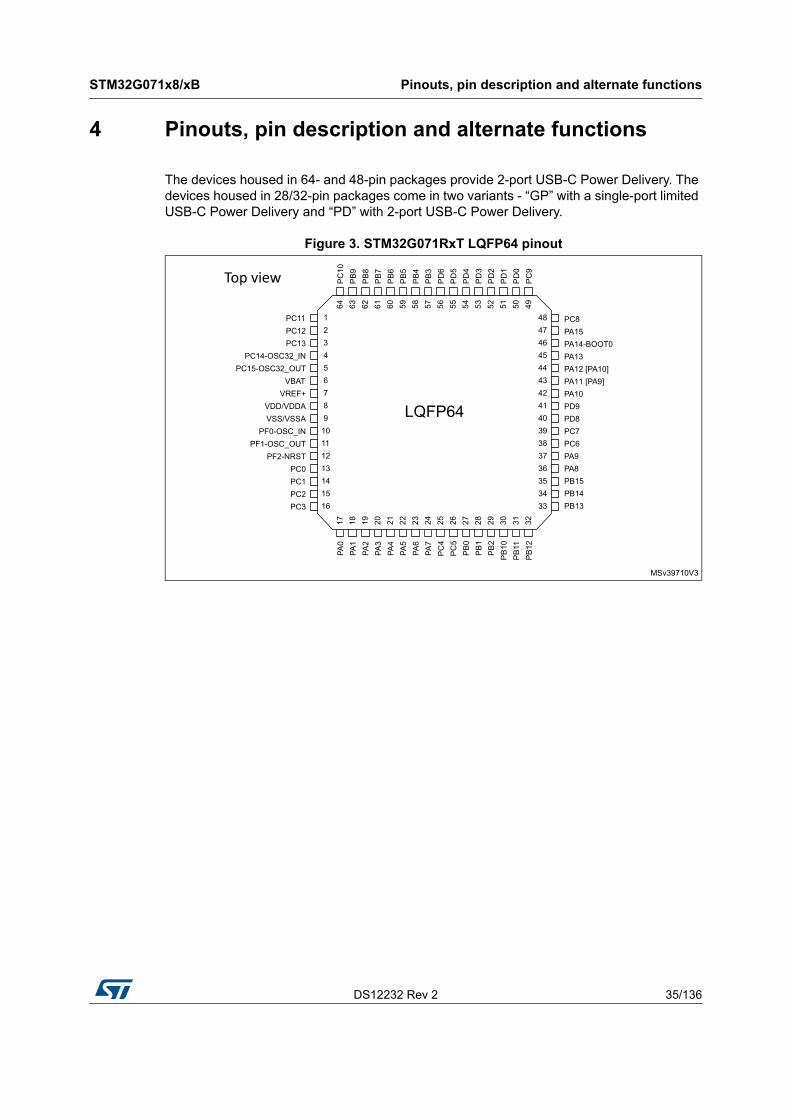
DS12232 Rev 2 35/136
STM32G071x8/xB Pinouts, pin description and alternate functions
52
4 Pinouts, pin description and alternate functions
The devices housed in 64- and 48-pin packages provide 2-port USB-C Power Delivery. The devices housed in 28/32-pin packages come in two variants - “GP” with a single-port limited USB-C Power Delivery and “PD” with 2-port USB-C Power Delivery.
Figure 3. STM32G071RxT LQFP64 pinout
MSv39710V3
PA0
PA1
PA2
PA3
PA4
PA5
PA6
PA7
PC
4P
C5
PB
0P
B1
PB
2P
B10
PB
11P
B12
PC11PC12PC13
PC14-OSC32_INPC15-OSC32_OUT
VBATVREF+
VDD/VDDAVSS/VSSA
PF2-NRST
PF0-OSC_INPF1-OSC_OUT
PC0PC1PC2PC3
PC8PA15PA14-BOOT0PA13PA12 [PA10]PA11 [PA9]PA10PD9PD8PC7PC6PA9PA8PB15PB14PB13
PC
9P
D0
PD
1P
D2
PD
3P
D4
PD
5P
D6
PB
3P
B4
PB
5P
B6
PB
7P
B8
PB
9P
C10Top view
LQFP64
1
3456789
10111213141516
248
4645444342414039383736353433
47
55 53 52 51 50 4956 5461 59 5764 63 62 60 58
26 28 29 30 31 3225 2720 22 2417 18 19 21 23
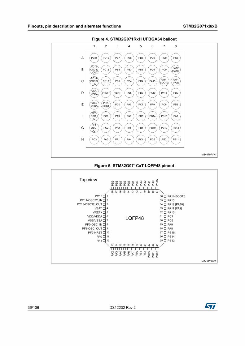
Pinouts, pin description and alternate functions STM32G071x8/xB
36/136 DS12232 Rev 2
Figure 4. STM32G071RxH UFBGA64 ballout
Figure 5. STM32G071CxT LQFP48 pinout
MSv47971V1
A
B
C
D
E
VDD/VDDA VREF+ VBAT PB5 PD3
VSS/VSSA
PF2-NRST PC0 PA7 PC7
PF0-OSC_I
NPC1 PA3 PA6 PB0
PF1-OSC_OUT
PC2 PA2 PA5 PB1
PC3 PA0 PA1 PA4 PC4
PC11 PC10 PB7 PB6 PD6
PC15-OSC32_OUT
PC12 PB8 PB3 PD5
PC14-OSC32
_INPC13 PB9 PB4 PD4
PA10 PA13 PD9
PA9 PC6 PD8
PB14 PB15 PA8
PB10 PB12 PB13
PC5 PB2 PB11
PD2 PD0 PC8
PD1 PC9 PA12 [PA10]
PA15 PA14-BOOT0
PA11 [PA9]
1 2 3 4 5 6 7 8
F
G
H
MSv39711V3
PA2
PA3
PA4
PA5
PA6
PA7
PB
0P
B1
PB
2P
B10
PB
11P
B12
PC13PC14-OSC32_IN
PC15-OSC32_OUTVBAT
VREF+VDD/VDDAVSS/VSSA
PF2-NRST
PF0-OSC_INPF1-OSC_OUT
PA0PA1
PA14-BOOT0PA13PA12 [PA10]PA11 [PA9]PA10PC7PC6PA9PA8PB15PB14PB13
PA15
PD
0P
D1
PD
2P
D3
PB
3P
B4
PB
5P
B6
PB
7P
B8
PB
9Top view
LQFP48
123456789101112
363534333231302928272625
39 3740 3845 43 4148 47 46 44 42
22 2421 2316 18 2013 14 15 17 19
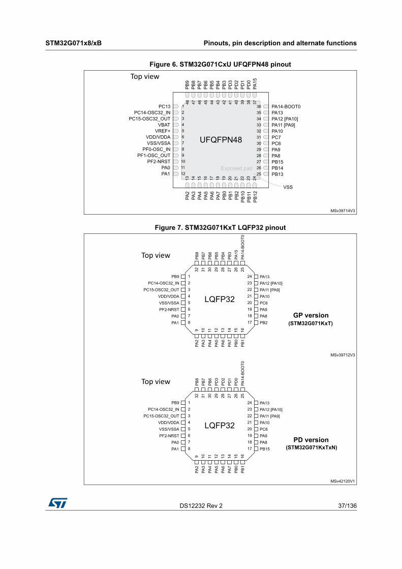
DS12232 Rev 2 37/136
STM32G071x8/xB Pinouts, pin description and alternate functions
52
Figure 6. STM32G071CxU UFQFPN48 pinout
Figure 7. STM32G071KxT LQFP32 pinout
Exposed pad
MSv39714V3
Top view
Exposed pad
UFQFPN48
123456789
101112
363534333231302928272625
39 3740 3845 43 4148 47 46 44 42
22 2421 2316 18 2013 14 15 17 19
VSSPA
2PA
3PA
4PA
5PA
6PA
7P
B0
PB
1P
B2
PB
10P
B11
PB
12
PC13PC14-OSC32_IN
PC15-OSC32_OUTVBAT
VREF+VDD/VDDAVSS/VSSA
PF2-NRST
PF0-OSC_INPF1-OSC_OUT
PA0PA1
PA14-BOOT0PA13PA12 [PA10]PA11 [PA9]PA10PC7PC6PA9PA8PB15PB14PB13
PA15
PD
0P
D1
PD
2P
D3
PB
3P
B4
PB
5P
B6
PB
7P
B8
PB
9
MSv42120V1
PA2
PA3
PA4
PA5
PA6
PA7
PB
0P
B1
PB9PC14-OSC32_IN
PC15-OSC32_OUTVDD/VDDAVSS/VSSAPF2-NRST
PA0PA1
PA13PA12 [PA10]PA11 [PA9]PA10PC6PA9PA8PB15
PA14
-BO
OT0
PD
0P
D1
PD
2P
D3
PB
6P
B7
PB
8Top view
LQFP32
12345678
2423222120191817
29 27 2532 31 30 28 26
12 14 169 10 11 13 15
MSv39712V3
PA2
PA3
PA4
PA5
PA6
PA7
PB
0P
B1
PB9PC14-OSC32_IN
PC15-OSC32_OUTVDD/VDDAVSS/VSSAPF2-NRST
PA0PA1
PA13PA12 [PA10]PA11 [PA9]PA10PC6PA9PA8PB2
PA14
-BO
OT0
PA15
PB
3P
B4
PB
5P
B6
PB
7P
B8Top view
LQFP32
12345678
2423222120191817
29 27 2532 31 30 28 26
12 14 169 10 11 13 15
GP version
PD version(STM32G071KxTxN)
(STM32G071KxT)
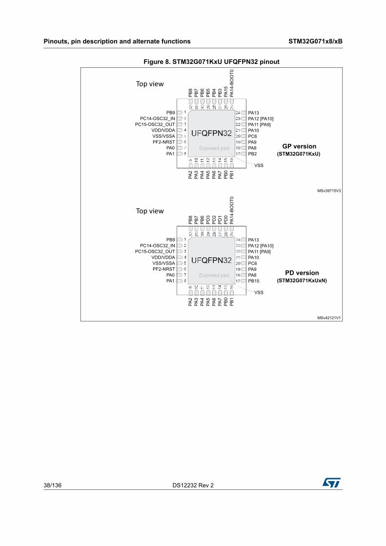
Pinouts, pin description and alternate functions STM32G071x8/xB
38/136 DS12232 Rev 2
Figure 8. STM32G071KxU UFQFPN32 pinout
MSv42121V1
PA2
PA3
PA4
PA5
PA6
PA7
PB
0P
B1
PB9PC14-OSC32_IN
PC15-OSC32_OUTVDD/VDDAVSS/VSSAPF2-NRST
PA0PA1
PA13PA12 [PA10]PA11 [PA9]PA10PC6PA9PA8PB15
PA14
-BO
OT0
PD
0P
D1
PD
2P
D3
PB
6P
B7
PB
8
Top view
UFQFPN32
12345678
2423222120191817
29 27 2532 31 30 28 26
12 14 169 10 11 13 15
VSS
MSv39715V3PA
2PA
3PA
4PA
5PA
6PA
7P
B0
PB
1
PB9PC14-OSC32_IN
PC15-OSC32_OUTVDD/VDDAVSS/VSSAPF2-NRST
PA0PA1
PA13PA12 [PA10]PA11 [PA9]PA10PC6PA9PA8PB2
PA14
-BO
OT0
PA15
PB
3P
B4
PB
5P
B6
PB
7P
B8
Top view
UFQFPN32
12345678
2423222120191817
29 27 2532 31 30 28 26
12 14 169 10 11 13 15
VSS
GP version
PD version(STM32G071KxUxN)
(STM32G071KxU)
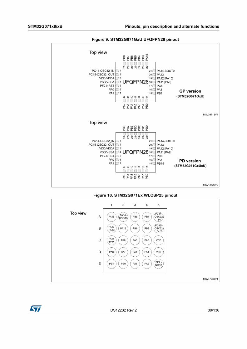
DS12232 Rev 2 39/136
STM32G071x8/xB Pinouts, pin description and alternate functions
52
Figure 9. STM32G071GxU UFQFPN28 pinout
Figure 10. STM32G071Ex WLCSP25 pinout
MSv42122V2
PA2
PA3
PA4
PA5
PA6
PA7
PB
0
PC14-OSC32_INPC15-OSC32_OUT
VDD/VDDAVSS/VSSAPF2-NRST
PA0PA1
PA14-BOOT0PA13PA12 [PA10]PA11 [PA9]PC6PA8PB15
PD
0P
D1
PD
2P
D3
PB
6P
B7
PB
8Top view
UFQFPN28
1234567
21201918171615
25 2328 27 26 24 22
11 138 9 10 12 14
MSv39713V4
PA2
PA3
PA4
PA5
PA6
PA7
PB
0
PC14-OSC32_INPC15-OSC32_OUT
VDD/VDDAVSS/VSSAPF2-NRST
PA0PA1
PA14-BOOT0PA13PA12 [PA10]PA11 [PA9]PC6PA8PB1
PA15
PB
3P
B4
PB
5P
B6
PB
7P
B8
Top view
UFQFPN28
1234567
21201918171615
25 2328 27 26 24 22
11 138 9 10 12 14
GP version
PD version(STM32G071GxUxN)
(STM32G071GxU)
MSv47938V1
1 2 3 4 5
A
B
C
D
E
PA15 PA14-BOOT0 PB5 PB7
PC14-OSC32
_IN
PA12 [PA10] PA13 PB6 PB8
PC15-OSC32_OUT
PA11 [PA9] PA6 PA3 PA0 VDD
PA8 PA7 PA4 PA1 VSS
PB1 PB0 PA5 PA2 PF2 - NRST
Top view
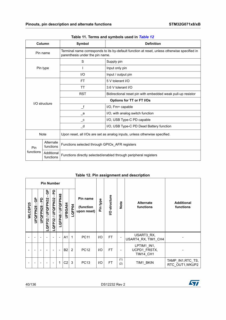
Pinouts, pin description and alternate functions STM32G071x8/xB
40/136 DS12232 Rev 2
Table 11. Terms and symbols used in Table 12
Column Symbol Definition
Pin nameTerminal name corresponds to its by-default function at reset, unless otherwise specified in parenthesis under the pin name.
Pin type
S Supply pin
I Input only pin
I/O Input / output pin
I/O structure
FT 5 V tolerant I/O
TT 3.6 V tolerant I/O
RST Bidirectional reset pin with embedded weak pull-up resistor
Options for TT or FT I/Os
_f I/O, Fm+ capable
_a I/O, with analog switch function
_c I/O, USB Type-C PD capable
_d I/O, USB Type-C PD Dead Battery function
Note Upon reset, all I/Os are set as analog inputs, unless otherwise specified.
Pin functions
Alternate functions
Functions selected through GPIOx_AFR registers
Additional functions
Functions directly selected/enabled through peripheral registers
Table 12. Pin assignment and description
Pin Number
Pin name
(function upon reset) P
in t
ype
I/O s
tru
ctu
re
No
te Alternatefunctions
Additionalfunctions
WL
CS
P25
UF
QF
PN
28 -
GP
UF
QF
PN
28 -
PD
LQ
FP
32 /
UF
QF
PN
32 -
GP
LQ
FP
32 /
UF
QF
PN
32 -
PD
LQ
FP
48
/ UF
QF
PN
48
UF
BG
A6
4
LQ
FP
64
- - - - - - A1 1 PC11 I/O FT -USART3_RX,
USART4_RX, TIM1_CH4-
- - - - - - B2 2 PC12 I/O FT -LPTIM1_IN1,
UCPD1_FRSTX, TIM14_CH1
-
- - - - - 1 C2 3 PC13 I/O FT(1)
(2) TIM1_BKINTAMP_IN1,RTC_TS,RTC_OUT1,WKUP2
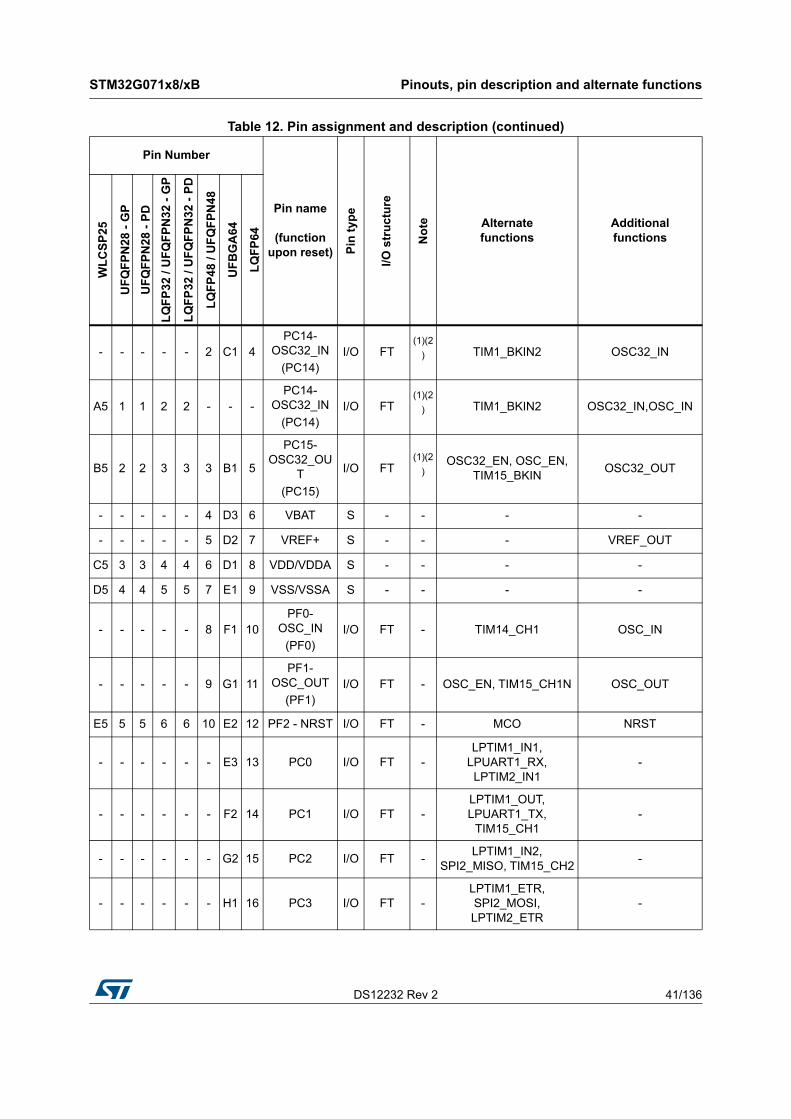
DS12232 Rev 2 41/136
STM32G071x8/xB Pinouts, pin description and alternate functions
52
- - - - - 2 C1 4PC14-
OSC32_IN
(PC14)I/O FT
(1)(2
) TIM1_BKIN2 OSC32_IN
A5 1 1 2 2 - - -PC14-
OSC32_IN
(PC14)I/O FT
(1)(2
) TIM1_BKIN2 OSC32_IN,OSC_IN
B5 2 2 3 3 3 B1 5
PC15-OSC32_OU
T
(PC15)
I/O FT(1)(2
)OSC32_EN, OSC_EN,
TIM15_BKINOSC32_OUT
- - - - - 4 D3 6 VBAT S - - - -
- - - - - 5 D2 7 VREF+ S - - - VREF_OUT
C5 3 3 4 4 6 D1 8 VDD/VDDA S - - - -
D5 4 4 5 5 7 E1 9 VSS/VSSA S - - - -
- - - - - 8 F1 10PF0-
OSC_IN
(PF0)I/O FT - TIM14_CH1 OSC_IN
- - - - - 9 G1 11PF1-
OSC_OUT
(PF1)I/O FT - OSC_EN, TIM15_CH1N OSC_OUT
E5 5 5 6 6 10 E2 12 PF2 - NRST I/O FT - MCO NRST
- - - - - - E3 13 PC0 I/O FT -LPTIM1_IN1,
LPUART1_RX, LPTIM2_IN1
-
- - - - - - F2 14 PC1 I/O FT -LPTIM1_OUT, LPUART1_TX,
TIM15_CH1-
- - - - - - G2 15 PC2 I/O FT -LPTIM1_IN2,
SPI2_MISO, TIM15_CH2-
- - - - - - H1 16 PC3 I/O FT -LPTIM1_ETR, SPI2_MOSI, LPTIM2_ETR
-
Table 12. Pin assignment and description (continued)
Pin Number
Pin name
(function upon reset) P
in t
ype
I/O s
tru
ctu
re
No
te Alternatefunctions
Additionalfunctions
WL
CS
P25
UF
QF
PN
28 -
GP
UF
QF
PN
28 -
PD
LQ
FP
32 /
UF
QF
PN
32 -
GP
LQ
FP
32 /
UF
QF
PN
32 -
PD
LQ
FP
48
/ UF
QF
PN
48
UF
BG
A64
LQ
FP
64
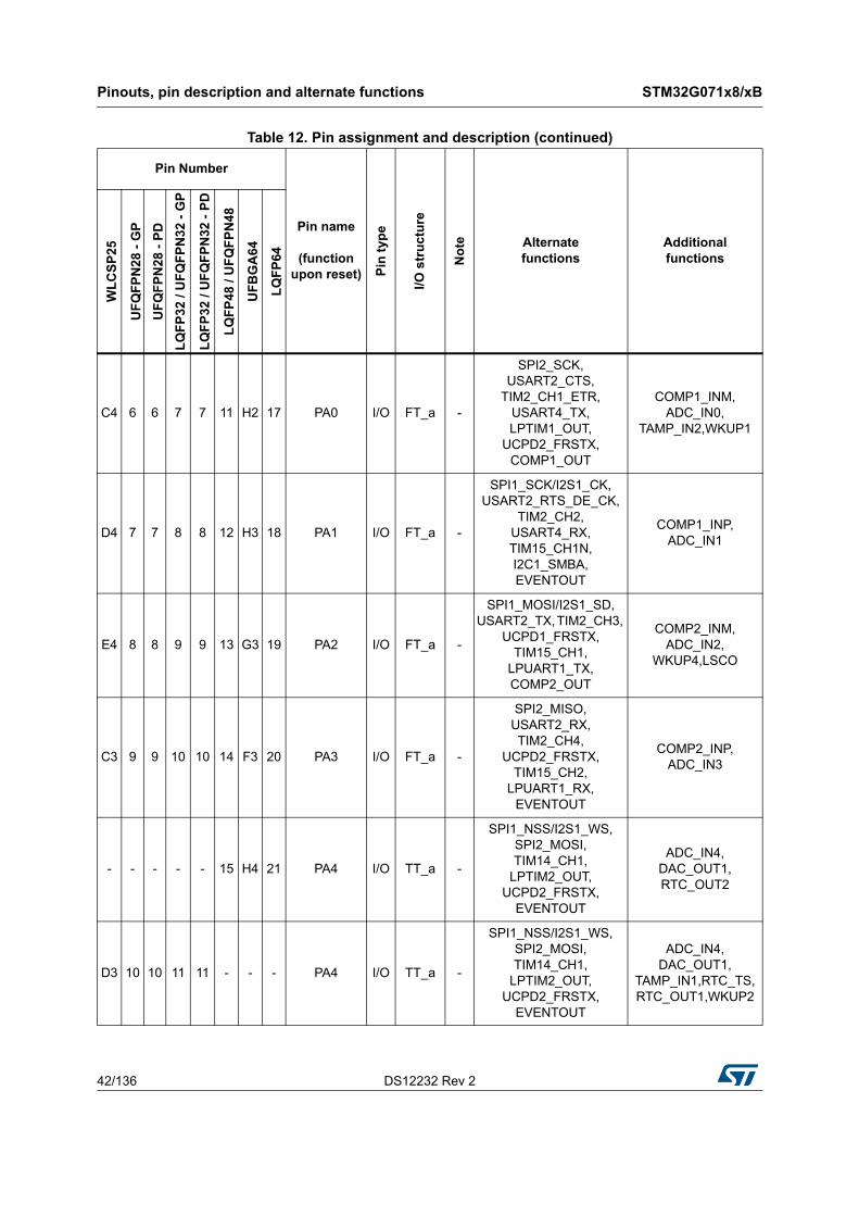
Pinouts, pin description and alternate functions STM32G071x8/xB
42/136 DS12232 Rev 2
C4 6 6 7 7 11 H2 17 PA0 I/O FT_a -
SPI2_SCK, USART2_CTS,
TIM2_CH1_ETR, USART4_TX, LPTIM1_OUT,
UCPD2_FRSTX, COMP1_OUT
COMP1_INM, ADC_IN0,
TAMP_IN2,WKUP1
D4 7 7 8 8 12 H3 18 PA1 I/O FT_a -
SPI1_SCK/I2S1_CK, USART2_RTS_DE_CK,
TIM2_CH2, USART4_RX, TIM15_CH1N, I2C1_SMBA, EVENTOUT
COMP1_INP, ADC_IN1
E4 8 8 9 9 13 G3 19 PA2 I/O FT_a -
SPI1_MOSI/I2S1_SD, USART2_TX, TIM2_CH3,
UCPD1_FRSTX, TIM15_CH1,
LPUART1_TX, COMP2_OUT
COMP2_INM, ADC_IN2,
WKUP4,LSCO
C3 9 9 10 10 14 F3 20 PA3 I/O FT_a -
SPI2_MISO, USART2_RX, TIM2_CH4,
UCPD2_FRSTX, TIM15_CH2,
LPUART1_RX, EVENTOUT
COMP2_INP, ADC_IN3
- - - - - 15 H4 21 PA4 I/O TT_a -
SPI1_NSS/I2S1_WS, SPI2_MOSI, TIM14_CH1,
LPTIM2_OUT, UCPD2_FRSTX,
EVENTOUT
ADC_IN4, DAC_OUT1, RTC_OUT2
D3 10 10 11 11 - - - PA4 I/O TT_a -
SPI1_NSS/I2S1_WS, SPI2_MOSI, TIM14_CH1,
LPTIM2_OUT, UCPD2_FRSTX,
EVENTOUT
ADC_IN4, DAC_OUT1,
TAMP_IN1,RTC_TS,RTC_OUT1,WKUP2
Table 12. Pin assignment and description (continued)
Pin Number
Pin name
(function upon reset) P
in t
ype
I/O s
tru
ctu
re
No
te Alternatefunctions
Additionalfunctions
WL
CS
P25
UF
QF
PN
28 -
GP
UF
QF
PN
28 -
PD
LQ
FP
32 /
UF
QF
PN
32 -
GP
LQ
FP
32 /
UF
QF
PN
32 -
PD
LQ
FP
48
/ UF
QF
PN
48
UF
BG
A64
LQ
FP
64
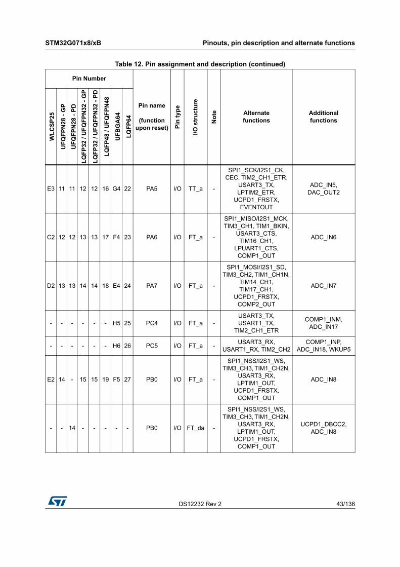
DS12232 Rev 2 43/136
STM32G071x8/xB Pinouts, pin description and alternate functions
52
E3 11 11 12 12 16 G4 22 PA5 I/O TT_a -
SPI1_SCK/I2S1_CK, CEC, TIM2_CH1_ETR,
USART3_TX, LPTIM2_ETR,
UCPD1_FRSTX, EVENTOUT
ADC_IN5, DAC_OUT2
C2 12 12 13 13 17 F4 23 PA6 I/O FT_a -
SPI1_MISO/I2S1_MCK, TIM3_CH1, TIM1_BKIN,
USART3_CTS, TIM16_CH1,
LPUART1_CTS, COMP1_OUT
ADC_IN6
D2 13 13 14 14 18 E4 24 PA7 I/O FT_a -
SPI1_MOSI/I2S1_SD, TIM3_CH2, TIM1_CH1N,
TIM14_CH1, TIM17_CH1,
UCPD1_FRSTX, COMP2_OUT
ADC_IN7
- - - - - - H5 25 PC4 I/O FT_a -USART3_TX, USART1_TX,
TIM2_CH1_ETR
COMP1_INM, ADC_IN17
- - - - - - H6 26 PC5 I/O FT_a -USART3_RX,
USART1_RX, TIM2_CH2COMP1_INP,
ADC_IN18, WKUP5
E2 14 - 15 15 19 F5 27 PB0 I/O FT_a -
SPI1_NSS/I2S1_WS, TIM3_CH3, TIM1_CH2N,
USART3_RX, LPTIM1_OUT,
UCPD1_FRSTX, COMP1_OUT
ADC_IN8
- - 14 - - - - - PB0 I/O FT_da -
SPI1_NSS/I2S1_WS, TIM3_CH3, TIM1_CH2N,
USART3_RX, LPTIM1_OUT,
UCPD1_FRSTX, COMP1_OUT
UCPD1_DBCC2, ADC_IN8
Table 12. Pin assignment and description (continued)
Pin Number
Pin name
(function upon reset) P
in t
ype
I/O s
tru
ctu
re
No
te Alternatefunctions
Additionalfunctions
WL
CS
P25
UF
QF
PN
28 -
GP
UF
QF
PN
28 -
PD
LQ
FP
32 /
UF
QF
PN
32 -
GP
LQ
FP
32 /
UF
QF
PN
32 -
PD
LQ
FP
48
/ UF
QF
PN
48
UF
BG
A64
LQ
FP
64
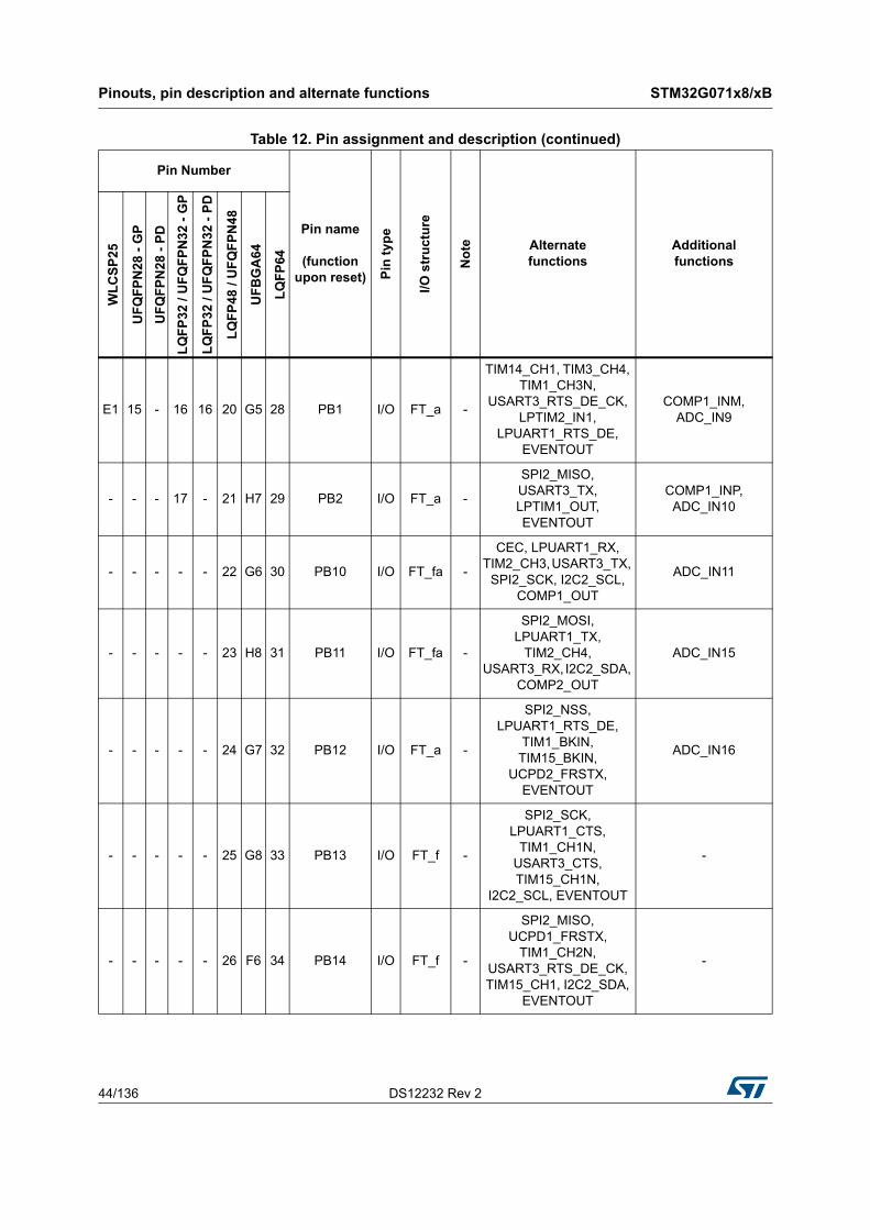
Pinouts, pin description and alternate functions STM32G071x8/xB
44/136 DS12232 Rev 2
E1 15 - 16 16 20 G5 28 PB1 I/O FT_a -
TIM14_CH1, TIM3_CH4, TIM1_CH3N,
USART3_RTS_DE_CK, LPTIM2_IN1,
LPUART1_RTS_DE, EVENTOUT
COMP1_INM, ADC_IN9
- - - 17 - 21 H7 29 PB2 I/O FT_a -
SPI2_MISO, USART3_TX, LPTIM1_OUT, EVENTOUT
COMP1_INP, ADC_IN10
- - - - - 22 G6 30 PB10 I/O FT_fa -
CEC, LPUART1_RX, TIM2_CH3, USART3_TX,
SPI2_SCK, I2C2_SCL, COMP1_OUT
ADC_IN11
- - - - - 23 H8 31 PB11 I/O FT_fa -
SPI2_MOSI, LPUART1_TX,
TIM2_CH4, USART3_RX, I2C2_SDA,
COMP2_OUT
ADC_IN15
- - - - - 24 G7 32 PB12 I/O FT_a -
SPI2_NSS, LPUART1_RTS_DE,
TIM1_BKIN, TIM15_BKIN,
UCPD2_FRSTX, EVENTOUT
ADC_IN16
- - - - - 25 G8 33 PB13 I/O FT_f -
SPI2_SCK, LPUART1_CTS,
TIM1_CH1N, USART3_CTS, TIM15_CH1N,
I2C2_SCL, EVENTOUT
-
- - - - - 26 F6 34 PB14 I/O FT_f -
SPI2_MISO, UCPD1_FRSTX,
TIM1_CH2N, USART3_RTS_DE_CK, TIM15_CH1, I2C2_SDA,
EVENTOUT
-
Table 12. Pin assignment and description (continued)
Pin Number
Pin name
(function upon reset) P
in t
ype
I/O s
tru
ctu
re
No
te Alternatefunctions
Additionalfunctions
WL
CS
P25
UF
QF
PN
28 -
GP
UF
QF
PN
28 -
PD
LQ
FP
32 /
UF
QF
PN
32 -
GP
LQ
FP
32 /
UF
QF
PN
32 -
PD
LQ
FP
48
/ UF
QF
PN
48
UF
BG
A64
LQ
FP
64
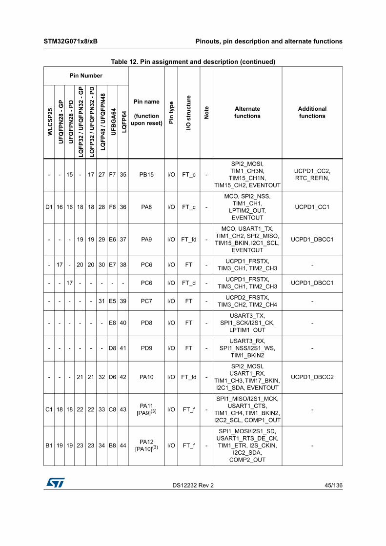
DS12232 Rev 2 45/136
STM32G071x8/xB Pinouts, pin description and alternate functions
52
- - 15 - 17 27 F7 35 PB15 I/O FT_c -
SPI2_MOSI, TIM1_CH3N, TIM15_CH1N,
TIM15_CH2, EVENTOUT
UCPD1_CC2, RTC_REFIN,
D1 16 16 18 18 28 F8 36 PA8 I/O FT_c -
MCO, SPI2_NSS, TIM1_CH1,
LPTIM2_OUT, EVENTOUT
UCPD1_CC1
- - - 19 19 29 E6 37 PA9 I/O FT_fd -
MCO, USART1_TX, TIM1_CH2, SPI2_MISO, TIM15_BKIN, I2C1_SCL,
EVENTOUT
UCPD1_DBCC1
- 17 - 20 20 30 E7 38 PC6 I/O FT -UCPD1_FRSTX,
TIM3_CH1, TIM2_CH3-
- - 17 - - - - - PC6 I/O FT_d -UCPD1_FRSTX,
TIM3_CH1, TIM2_CH3UCPD1_DBCC1
- - - - - 31 E5 39 PC7 I/O FT -UCPD2_FRSTX,
TIM3_CH2, TIM2_CH4-
- - - - - - E8 40 PD8 I/O FT -USART3_TX,
SPI1_SCK/I2S1_CK, LPTIM1_OUT
-
- - - - - - D8 41 PD9 I/O FT -USART3_RX,
SPI1_NSS/I2S1_WS, TIM1_BKIN2
-
- - - 21 21 32 D6 42 PA10 I/O FT_fd -
SPI2_MOSI, USART1_RX,
TIM1_CH3, TIM17_BKIN, I2C1_SDA, EVENTOUT
UCPD1_DBCC2
C1 18 18 22 22 33 C8 43PA11
[PA9](3) I/O FT_f -
SPI1_MISO/I2S1_MCK, USART1_CTS,
TIM1_CH4, TIM1_BKIN2, I2C2_SCL, COMP1_OUT
-
B1 19 19 23 23 34 B8 44PA12
[PA10](3) I/O FT_f -
SPI1_MOSI/I2S1_SD, USART1_RTS_DE_CK, TIM1_ETR, I2S_CKIN,
I2C2_SDA, COMP2_OUT
-
Table 12. Pin assignment and description (continued)
Pin Number
Pin name
(function upon reset) P
in t
ype
I/O s
tru
ctu
re
No
te Alternatefunctions
Additionalfunctions
WL
CS
P25
UF
QF
PN
28 -
GP
UF
QF
PN
28 -
PD
LQ
FP
32 /
UF
QF
PN
32 -
GP
LQ
FP
32 /
UF
QF
PN
32 -
PD
LQ
FP
48
/ UF
QF
PN
48
UF
BG
A64
LQ
FP
64
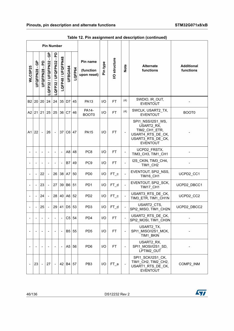
Pinouts, pin description and alternate functions STM32G071x8/xB
46/136 DS12232 Rev 2
B2 20 20 24 24 35 D7 45 PA13 I/O FT (4) SWDIO, IR_OUT, EVENTOUT
-
A2 21 21 25 25 36 C7 46PA14-
BOOT0I/O FT (4) SWCLK, USART2_TX,
EVENTOUTBOOT0
A1 22 - 26 - 37 C6 47 PA15 I/O FT -
SPI1_NSS/I2S1_WS, USART2_RX,
TIM2_CH1_ETR, USART4_RTS_DE_CK, USART3_RTS_DE_CK,
EVENTOUT
-
- - - - - - A8 48 PC8 I/O FT -UCPD2_FRSTX,
TIM3_CH3, TIM1_CH1-
- - - - - - B7 49 PC9 I/O FT -I2S_CKIN, TIM3_CH4,
TIM1_CH2-
- - 22 - 26 38 A7 50 PD0 I/O FT_c -EVENTOUT, SPI2_NSS,
TIM16_CH1UCPD2_CC1
- - 23 - 27 39 B6 51 PD1 I/O FT_d -EVENTOUT, SPI2_SCK,
TIM17_CH1UCPD2_DBCC1
- - 24 - 28 40 A6 52 PD2 I/O FT_c -USART3_RTS_DE_CK, TIM3_ETR, TIM1_CH1N
UCPD2_CC2
- - 25 - 29 41 D5 53 PD3 I/O FT_d -USART2_CTS,
SPI2_MISO, TIM1_CH2NUCPD2_DBCC2
- - - - - - C5 54 PD4 I/O FT -USART2_RTS_DE_CK,
SPI2_MOSI, TIM1_CH3N-
- - - - - - B5 55 PD5 I/O FT -USART2_TX,
SPI1_MISO/I2S1_MCK, TIM1_BKIN
-
- - - - - - A5 56 PD6 I/O FT -USART2_RX,
SPI1_MOSI/I2S1_SD, LPTIM2_OUT
-
- 23 - 27 - 42 B4 57 PB3 I/O FT_a -
SPI1_SCK/I2S1_CK, TIM1_CH2, TIM2_CH2, USART1_RTS_DE_CK,
EVENTOUT
COMP2_INM
Table 12. Pin assignment and description (continued)
Pin Number
Pin name
(function upon reset) P
in t
ype
I/O s
tru
ctu
re
No
te Alternatefunctions
Additionalfunctions
WL
CS
P25
UF
QF
PN
28 -
GP
UF
QF
PN
28 -
PD
LQ
FP
32 /
UF
QF
PN
32 -
GP
LQ
FP
32 /
UF
QF
PN
32 -
PD
LQ
FP
48
/ UF
QF
PN
48
UF
BG
A64
LQ
FP
64
DS12232 Rev 2 47/136
STM32G071x8/xB Pinouts, pin description and alternate functions
52
- 24 - 28 - 43 C4 58 PB4 I/O FT_a -
SPI1_MISO/I2S1_MCK, TIM3_CH1,
USART1_CTS, TIM17_BKIN, EVENTOUT
COMP2_INP
A3 25 - 29 - 44 D4 59 PB5 I/O FT -
SPI1_MOSI/I2S1_SD, TIM3_CH2, TIM16_BKIN,
LPTIM1_IN1, I2C1_SMBA, COMP2_OUT
WKUP6
B3 26 26 30 30 45 A4 60 PB6 I/O FT_fa -
USART1_TX, TIM1_CH3, TIM16_CH1N, SPI2_MISO,
LPTIM1_ETR, I2C1_SCL, EVENTOUT
COMP2_INP
A4 27 27 31 31 46 A3 61 PB7 I/O FT_fa -
USART1_RX, SPI2_MOSI,
TIM17_CH1N, USART4_CTS,
LPTIM1_IN2, I2C1_SDA, EVENTOUT
COMP2_INM, PVD_IN
B4 28 28 32 32 47 B3 62 PB8 I/O FT_f -
CEC, SPI2_SCK, TIM16_CH1, USART3_TX,
TIM15_BKIN, I2C1_SCL, EVENTOUT
-
- - - 1 1 48 C3 63 PB9 I/O FT_f -
IR_OUT, UCPD2_FRSTX,
TIM17_CH1, USART3_RX,
SPI2_NSS, I2C1_SDA, EVENTOUT
-
- - - - - - A2 64 PC10 I/O FT -USART3_TX,
USART4_TX, TIM1_CH3-
Table 12. Pin assignment and description (continued)
Pin Number
Pin name
(function upon reset) P
in t
ype
I/O s
tru
ctu
re
No
te Alternatefunctions
Additionalfunctions
WL
CS
P25
UF
QF
PN
28 -
GP
UF
QF
PN
28 -
PD
LQ
FP
32 /
UF
QF
PN
32 -
GP
LQ
FP
32 /
UF
QF
PN
32 -
PD
LQ
FP
48
/ UF
QF
PN
48
UF
BG
A64
LQ
FP
64
Pinouts, pin description and alternate functions STM32G071x8/xB
48/136 DS12232 Rev 2
1. PC13, PC14 and PC15 are supplied through the power switch. Since the switch only sinks a limited amount of current (3 mA), the use of GPIOs PC13 to PC15 in output mode is limited:
- The speed should not exceed 2 MHz with a maximum load of 30 pF
- These GPIOs must not be used as current sources (for example to drive an LED).
2. After a RTC domain power-up, PC13, PC14 and PC15 operate as GPIOs. Their function then depends on the content of the RTC registers. The RTC registers are not reset upon system reset. For details on how to manage these GPIOs, refer to the RTC domain and RTC register descriptions in the RM0444 reference manual.
3. Pin pair PA9/PA10 can be remapped in place of pin pair PA11/PA12 (default mapping), using SYSCFG_CFGR1 register.
4. Upon reset, these pins are configured as SW debug alternate functions, and the internal pull-up on PA13 pin and the internal pull-down on PA14 pin are activated.
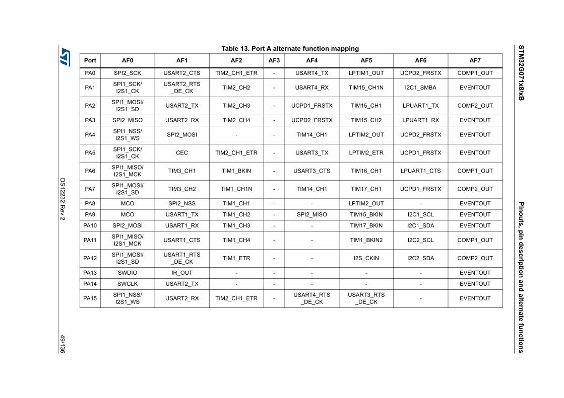
ST
M3
2G07
1x8
/xB
Pin
ou
ts, p
in d
escrip
tion
an
d a
ltern
ate
fun
ctio
ns
DS
1223
2 Rev 2
49/136
Table 13. Port A alternate function mapping
Port AF0 AF1 AF2 AF3 AF4 AF5 AF6 AF7
PA0 SPI2_SCK USART2_CTS TIM2_CH1_ETR - USART4_TX LPTIM1_OUT UCPD2_FRSTX COMP1_OUT
PA1SPI1_SCK/I2S1_CK
USART2_RTS_DE_CK
TIM2_CH2 - USART4_RX TIM15_CH1N I2C1_SMBA EVENTOUT
PA2SPI1_MOSI/
I2S1_SDUSART2_TX TIM2_CH3 - UCPD1_FRSTX TIM15_CH1 LPUART1_TX COMP2_OUT
PA3 SPI2_MISO USART2_RX TIM2_CH4 - UCPD2_FRSTX TIM15_CH2 LPUART1_RX EVENTOUT
PA4SPI1_NSS/I2S1_WS
SPI2_MOSI - - TIM14_CH1 LPTIM2_OUT UCPD2_FRSTX EVENTOUT
PA5SPI1_SCK/I2S1_CK
CEC TIM2_CH1_ETR - USART3_TX LPTIM2_ETR UCPD1_FRSTX EVENTOUT
PA6SPI1_MISO/I2S1_MCK
TIM3_CH1 TIM1_BKIN - USART3_CTS TIM16_CH1 LPUART1_CTS COMP1_OUT
PA7SPI1_MOSI/
I2S1_SDTIM3_CH2 TIM1_CH1N - TIM14_CH1 TIM17_CH1 UCPD1_FRSTX COMP2_OUT
PA8 MCO SPI2_NSS TIM1_CH1 - - LPTIM2_OUT - EVENTOUT
PA9 MCO USART1_TX TIM1_CH2 - SPI2_MISO TIM15_BKIN I2C1_SCL EVENTOUT
PA10 SPI2_MOSI USART1_RX TIM1_CH3 - - TIM17_BKIN I2C1_SDA EVENTOUT
PA11SPI1_MISO/I2S1_MCK
USART1_CTS TIM1_CH4 - - TIM1_BKIN2 I2C2_SCL COMP1_OUT
PA12SPI1_MOSI/
I2S1_SDUSART1_RTS
_DE_CKTIM1_ETR - - I2S_CKIN I2C2_SDA COMP2_OUT
PA13 SWDIO IR_OUT - - - - - EVENTOUT
PA14 SWCLK USART2_TX - - - - - EVENTOUT
PA15SPI1_NSS/I2S1_WS
USART2_RX TIM2_CH1_ETR -USART4_RTS
_DE_CKUSART3_RTS
_DE_CK- EVENTOUT
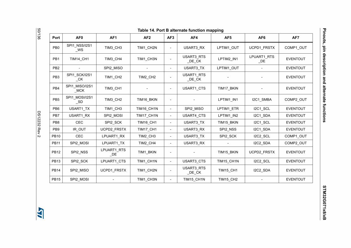
Pin
ou
ts, p
in d
esc
riptio
n a
nd
altern
ate
fun
ctio
ns
ST
M32
G0
71x
8/xB
50/1
36D
S1
2232 R
ev 2
Table 14. Port B alternate function mapping
Port AF0 AF1 AF2 AF3 AF4 AF5 AF6 AF7
PB0SPI1_NSS/I2S1
_WSTIM3_CH3 TIM1_CH2N - USART3_RX LPTIM1_OUT UCPD1_FRSTX COMP1_OUT
PB1 TIM14_CH1 TIM3_CH4 TIM1_CH3N -USART3_RTS
_DE_CKLPTIM2_IN1
LPUART1_RTS_DE
EVENTOUT
PB2 - SPI2_MISO - - USART3_TX LPTIM1_OUT - EVENTOUT
PB3SPI1_SCK/I2S1
_CKTIM1_CH2 TIM2_CH2 -
USART1_RTS_DE_CK
- - EVENTOUT
PB4SPI1_MISO/I2S1
_MCKTIM3_CH1 - - USART1_CTS TIM17_BKIN - EVENTOUT
PB5SPI1_MOSI/I2S1
_SDTIM3_CH2 TIM16_BKIN - - LPTIM1_IN1 I2C1_SMBA COMP2_OUT
PB6 USART1_TX TIM1_CH3 TIM16_CH1N - SPI2_MISO LPTIM1_ETR I2C1_SCL EVENTOUT
PB7 USART1_RX SPI2_MOSI TIM17_CH1N - USART4_CTS LPTIM1_IN2 I2C1_SDA EVENTOUT
PB8 CEC SPI2_SCK TIM16_CH1 - USART3_TX TIM15_BKIN I2C1_SCL EVENTOUT
PB9 IR_OUT UCPD2_FRSTX TIM17_CH1 - USART3_RX SPI2_NSS I2C1_SDA EVENTOUT
PB10 CEC LPUART1_RX TIM2_CH3 - USART3_TX SPI2_SCK I2C2_SCL COMP1_OUT
PB11 SPI2_MOSI LPUART1_TX TIM2_CH4 - USART3_RX - I2C2_SDA COMP2_OUT
PB12 SPI2_NSSLPUART1_RTS
_DETIM1_BKIN - - TIM15_BKIN UCPD2_FRSTX EVENTOUT
PB13 SPI2_SCK LPUART1_CTS TIM1_CH1N - USART3_CTS TIM15_CH1N I2C2_SCL EVENTOUT
PB14 SPI2_MISO UCPD1_FRSTX TIM1_CH2N -USART3_RTS
_DE_CKTIM15_CH1 I2C2_SDA EVENTOUT
PB15 SPI2_MOSI - TIM1_CH3N - TIM15_CH1N TIM15_CH2 - EVENTOUT
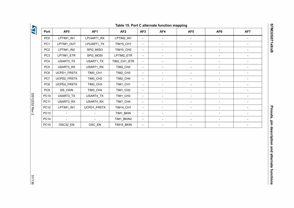
ST
M3
2G07
1x8
/xB
Pin
ou
ts, p
in d
escrip
tion
an
d a
ltern
ate
fun
ctio
ns
DS
1223
2 Rev 2
51/136
Table 15. Port C alternate function mapping
Port AF0 AF1 AF2 AF3 AF4 AF5 AF6 AF7
PC0 LPTIM1_IN1 LPUART1_RX LPTIM2_IN1 - - - - -
PC1 LPTIM1_OUT LPUART1_TX TIM15_CH1 - - - - -
PC2 LPTIM1_IN2 SPI2_MISO TIM15_CH2 - - - - -
PC3 LPTIM1_ETR SPI2_MOSI LPTIM2_ETR - - - - -
PC4 USART3_TX USART1_TX TIM2_CH1_ETR - - - - -
PC5 USART3_RX USART1_RX TIM2_CH2 - - - - -
PC6 UCPD1_FRSTX TIM3_CH1 TIM2_CH3 - - - - -
PC7 UCPD2_FRSTX TIM3_CH2 TIM2_CH4 - - - - -
PC8 UCPD2_FRSTX TIM3_CH3 TIM1_CH1 - - - - -
PC9 I2S_CKIN TIM3_CH4 TIM1_CH2 - - - - -
PC10 USART3_TX USART4_TX TIM1_CH3 - - - - -
PC11 USART3_RX USART4_RX TIM1_CH4 - - - - -
PC12 LPTIM1_IN1 UCPD1_FRSTX TIM14_CH1 - - - - -
PC13 - - TIM1_BKIN - - - - -
PC14 - - TIM1_BKIN2 - - - - -
PC15 OSC32_EN OSC_EN TIM15_BKIN - - - - -
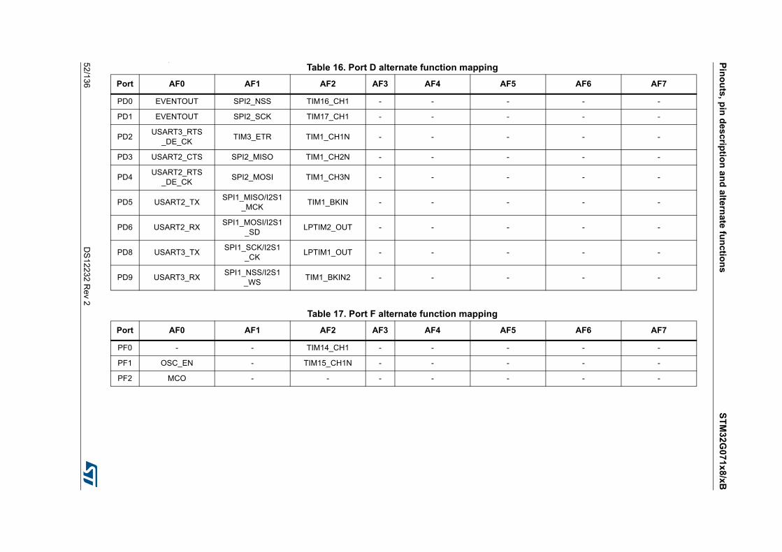
Pin
ou
ts, p
in d
esc
riptio
n a
nd
altern
ate
fun
ctio
ns
ST
M32
G0
71x
8/xB
52/1
36D
S1
2232 R
ev 2
*
Table 16. Port D alternate function mapping
Port AF0 AF1 AF2 AF3 AF4 AF5 AF6 AF7
PD0 EVENTOUT SPI2_NSS TIM16_CH1 - - - - -
PD1 EVENTOUT SPI2_SCK TIM17_CH1 - - - - -
PD2USART3_RTS
_DE_CKTIM3_ETR TIM1_CH1N - - - - -
PD3 USART2_CTS SPI2_MISO TIM1_CH2N - - - - -
PD4USART2_RTS
_DE_CKSPI2_MOSI TIM1_CH3N - - - - -
PD5 USART2_TXSPI1_MISO/I2S1
_MCKTIM1_BKIN - - - - -
PD6 USART2_RXSPI1_MOSI/I2S1
_SDLPTIM2_OUT - - - - -
PD8 USART3_TXSPI1_SCK/I2S1
_CKLPTIM1_OUT - - - - -
PD9 USART3_RXSPI1_NSS/I2S1
_WSTIM1_BKIN2 - - - - -
Table 17. Port F alternate function mapping
Port AF0 AF1 AF2 AF3 AF4 AF5 AF6 AF7
PF0 - - TIM14_CH1 - - - - -
PF1 OSC_EN - TIM15_CH1N - - - - -
PF2 MCO - - - - - - -
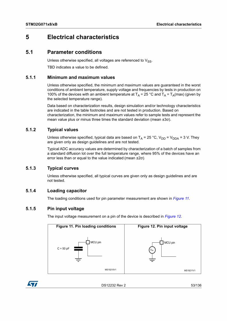
DS12232 Rev 2 53/136
STM32G071x8/xB Electrical characteristics
109
5 Electrical characteristics
5.1 Parameter conditions
Unless otherwise specified, all voltages are referenced to VSS.
TBD indicates a value to be defined.
5.1.1 Minimum and maximum values
Unless otherwise specified, the minimum and maximum values are guaranteed in the worst conditions of ambient temperature, supply voltage and frequencies by tests in production on 100% of the devices with an ambient temperature at TA = 25 °C and TA = TA(max) (given by the selected temperature range).
Data based on characterization results, design simulation and/or technology characteristics are indicated in the table footnotes and are not tested in production. Based on characterization, the minimum and maximum values refer to sample tests and represent the mean value plus or minus three times the standard deviation (mean ±3σ).
5.1.2 Typical values
Unless otherwise specified, typical data are based on TA = 25 °C, VDD = VDDA = 3 V. They are given only as design guidelines and are not tested.
Typical ADC accuracy values are determined by characterization of a batch of samples from a standard diffusion lot over the full temperature range, where 95% of the devices have an error less than or equal to the value indicated (mean ±2σ).
5.1.3 Typical curves
Unless otherwise specified, all typical curves are given only as design guidelines and are not tested.
5.1.4 Loading capacitor
The loading conditions used for pin parameter measurement are shown in Figure 11.
5.1.5 Pin input voltage
The input voltage measurement on a pin of the device is described in Figure 12.
Figure 11. Pin loading conditions Figure 12. Pin input voltage
MS19210V1
MCU pin
C = 50 pF
MS19211V1
MCU pin
VIN
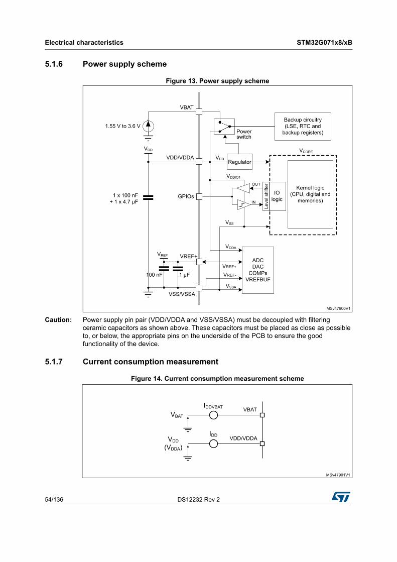
Electrical characteristics STM32G071x8/xB
54/136 DS12232 Rev 2
5.1.6 Power supply scheme
Figure 13. Power supply scheme
Caution: Power supply pin pair (VDD/VDDA and VSS/VSSA) must be decoupled with filtering ceramic capacitors as shown above. These capacitors must be placed as close as possible to, or below, the appropriate pins on the underside of the PCB to ensure the good functionality of the device.
5.1.7 Current consumption measurement
Figure 14. Current consumption measurement scheme
MSv47900V1
VDD
Backup circuitry(LSE, RTC and
backup registers)
Kernel logic(CPU, digital and
memories)
Leve
l shi
fter
IOlogicIN
OUT
Regulator
GPIOs
1.55 V to 3.6 V
1 x 100 nF+ 1 x 4.7 μF
VDD/VDDA
VBAT
VCORE
Power switch
VDDIO1
ADCDAC
COMPsVREFBUF
VREF+
VREF-
VSS/VSSA
VREF
100 nF 1 μF
VSS
VSSA
VDDA
VDD
VREF+
MSv47901V1
IDDVBAT
VBAT
IDDVDD
(VDDA)
VBAT
VDD/VDDA
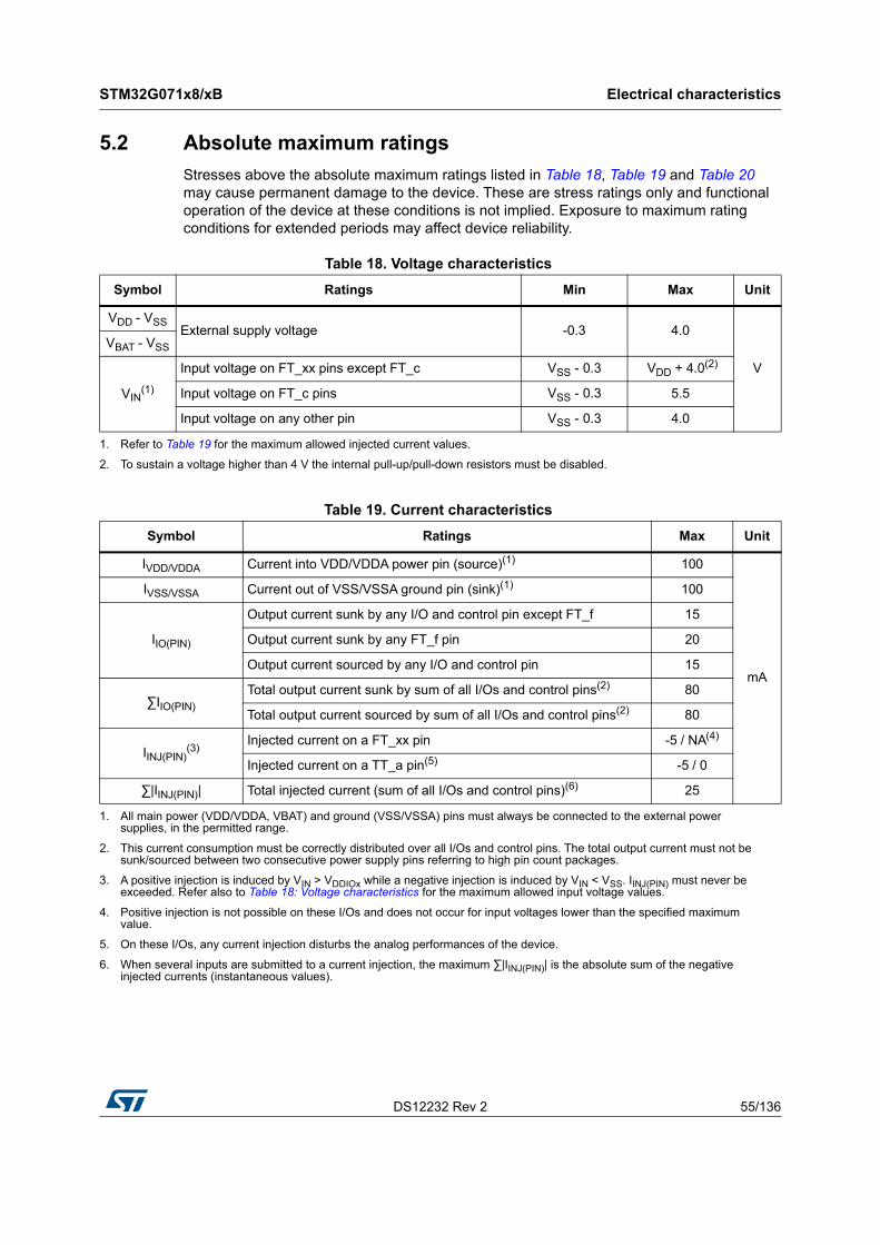
DS12232 Rev 2 55/136
STM32G071x8/xB Electrical characteristics
109
5.2 Absolute maximum ratings
Stresses above the absolute maximum ratings listed in Table 18, Table 19 and Table 20 may cause permanent damage to the device. These are stress ratings only and functional operation of the device at these conditions is not implied. Exposure to maximum rating conditions for extended periods may affect device reliability.
Table 18. Voltage characteristics
Symbol Ratings Min Max Unit
VDD - VSSExternal supply voltage -0.3 4.0
V
VBAT - VSS
VIN(1)
Input voltage on FT_xx pins except FT_c VSS - 0.3 VDD + 4.0(2)
Input voltage on FT_c pins VSS - 0.3 5.5
Input voltage on any other pin VSS - 0.3 4.0
1. Refer to Table 19 for the maximum allowed injected current values.
2. To sustain a voltage higher than 4 V the internal pull-up/pull-down resistors must be disabled.
Table 19. Current characteristics
Symbol Ratings Max Unit
IVDD/VDDA Current into VDD/VDDA power pin (source)(1) 100
mA
IVSS/VSSA Current out of VSS/VSSA ground pin (sink)(1) 100
IIO(PIN)
Output current sunk by any I/O and control pin except FT_f 15
Output current sunk by any FT_f pin 20
Output current sourced by any I/O and control pin 15
∑IIO(PIN)
Total output current sunk by sum of all I/Os and control pins(2) 80
Total output current sourced by sum of all I/Os and control pins(2) 80
IINJ(PIN)(3)
Injected current on a FT_xx pin -5 / NA(4)
Injected current on a TT_a pin(5) -5 / 0
∑|IINJ(PIN)| Total injected current (sum of all I/Os and control pins)(6) 25
1. All main power (VDD/VDDA, VBAT) and ground (VSS/VSSA) pins must always be connected to the external power supplies, in the permitted range.
2. This current consumption must be correctly distributed over all I/Os and control pins. The total output current must not be sunk/sourced between two consecutive power supply pins referring to high pin count packages.
3. A positive injection is induced by VIN > VDDIOx while a negative injection is induced by VIN < VSS. IINJ(PIN) must never be exceeded. Refer also to Table 18: Voltage characteristics for the maximum allowed input voltage values.
4. Positive injection is not possible on these I/Os and does not occur for input voltages lower than the specified maximum value.
5. On these I/Os, any current injection disturbs the analog performances of the device.
6. When several inputs are submitted to a current injection, the maximum ∑|IINJ(PIN)| is the absolute sum of the negative injected currents (instantaneous values).
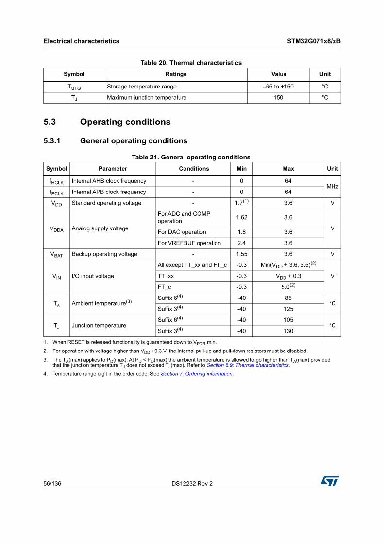
Electrical characteristics STM32G071x8/xB
56/136 DS12232 Rev 2
5.3 Operating conditions
5.3.1 General operating conditions
Table 20. Thermal characteristics
Symbol Ratings Value Unit
TSTG Storage temperature range –65 to +150 °C
TJ Maximum junction temperature 150 °C
Table 21. General operating conditions
Symbol Parameter Conditions Min Max Unit
fHCLK Internal AHB clock frequency - 0 64MHz
fPCLK Internal APB clock frequency - 0 64
VDD Standard operating voltage - 1.7(1) 3.6 V
VDDA Analog supply voltage
For ADC and COMP operation
1.62 3.6
VFor DAC operation 1.8 3.6
For VREFBUF operation 2.4 3.6
VBAT Backup operating voltage - 1.55 3.6 V
VIN I/O input voltage
All except TT_xx and FT_c -0.3 Min(VDD + 3.6, 5.5)(2)
VTT_xx -0.3 VDD + 0.3
FT_c -0.3 5.0(2)
TA Ambient temperature(3)Suffix 6(4) -40 85
°CSuffix 3(4) -40 125
TJ Junction temperatureSuffix 6(4) -40 105
°CSuffix 3(4) -40 130
1. When RESET is released functionality is guaranteed down to VPDR min.
2. For operation with voltage higher than VDD +0.3 V, the internal pull-up and pull-down resistors must be disabled.
3. The TA(max) applies to PD(max). At PD < PD(max) the ambient temperature is allowed to go higher than TA(max) provided that the junction temperature TJ does not exceed TJ(max). Refer to Section 6.9: Thermal characteristics.
4. Temperature range digit in the order code. See Section 7: Ordering information.
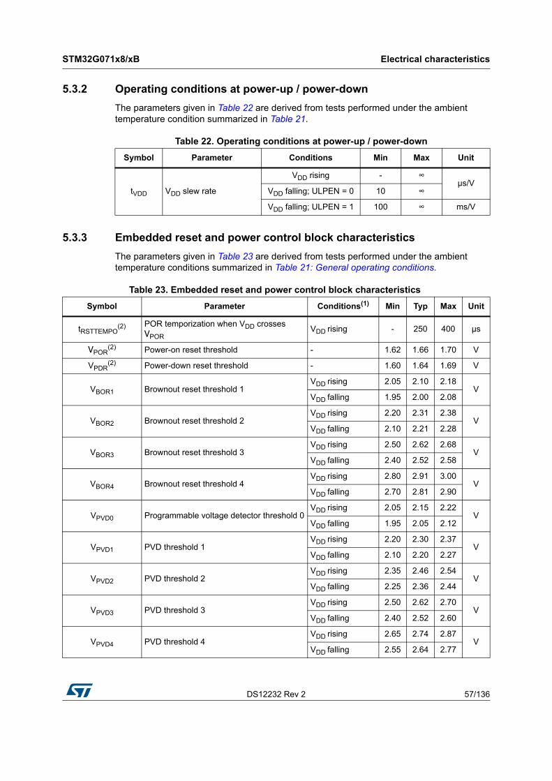
DS12232 Rev 2 57/136
STM32G071x8/xB Electrical characteristics
109
5.3.2 Operating conditions at power-up / power-down
The parameters given in Table 22 are derived from tests performed under the ambient temperature condition summarized in Table 21.
5.3.3 Embedded reset and power control block characteristics
The parameters given in Table 23 are derived from tests performed under the ambient temperature conditions summarized in Table 21: General operating conditions.
Table 22. Operating conditions at power-up / power-down
Symbol Parameter Conditions Min Max Unit
tVDD VDD slew rate
VDD rising - ∞µs/V
VDD falling; ULPEN = 0 10 ∞
VDD falling; ULPEN = 1 100 ∞ ms/V
Table 23. Embedded reset and power control block characteristics
Symbol Parameter Conditions(1) Min Typ Max Unit
tRSTTEMPO(2) POR temporization when VDD crosses
VPORVDD rising - 250 400 μs
VPOR(2) Power-on reset threshold - 1.62 1.66 1.70 V
VPDR(2) Power-down reset threshold - 1.60 1.64 1.69 V
VBOR1 Brownout reset threshold 1VDD rising 2.05 2.10 2.18
VVDD falling 1.95 2.00 2.08
VBOR2 Brownout reset threshold 2VDD rising 2.20 2.31 2.38
VVDD falling 2.10 2.21 2.28
VBOR3 Brownout reset threshold 3VDD rising 2.50 2.62 2.68
VVDD falling 2.40 2.52 2.58
VBOR4 Brownout reset threshold 4VDD rising 2.80 2.91 3.00
VVDD falling 2.70 2.81 2.90
VPVD0 Programmable voltage detector threshold 0VDD rising 2.05 2.15 2.22
VVDD falling 1.95 2.05 2.12
VPVD1 PVD threshold 1VDD rising 2.20 2.30 2.37
VVDD falling 2.10 2.20 2.27
VPVD2 PVD threshold 2VDD rising 2.35 2.46 2.54
VVDD falling 2.25 2.36 2.44
VPVD3 PVD threshold 3VDD rising 2.50 2.62 2.70
VVDD falling 2.40 2.52 2.60
VPVD4 PVD threshold 4VDD rising 2.65 2.74 2.87
VVDD falling 2.55 2.64 2.77
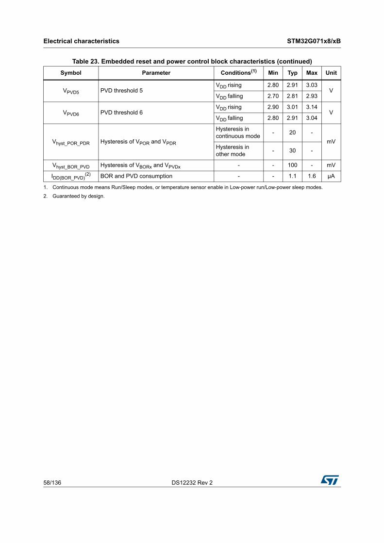
Electrical characteristics STM32G071x8/xB
58/136 DS12232 Rev 2
VPVD5 PVD threshold 5VDD rising 2.80 2.91 3.03
VVDD falling 2.70 2.81 2.93
VPVD6 PVD threshold 6VDD rising 2.90 3.01 3.14
VVDD falling 2.80 2.91 3.04
Vhyst_POR_PDR Hysteresis of VPOR and VPDR
Hysteresis in continuous mode
- 20 -
mVHysteresis in other mode
- 30 -
Vhyst_BOR_PVD Hysteresis of VBORx and VPVDx - - 100 - mV
IDD(BOR_PVD)(2) BOR and PVD consumption - - 1.1 1.6 µA
1. Continuous mode means Run/Sleep modes, or temperature sensor enable in Low-power run/Low-power sleep modes.
2. Guaranteed by design.
Table 23. Embedded reset and power control block characteristics (continued)
Symbol Parameter Conditions(1) Min Typ Max Unit
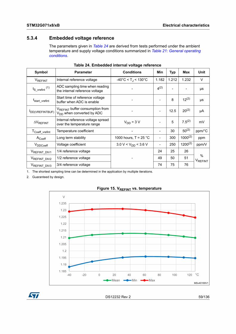
DS12232 Rev 2 59/136
STM32G071x8/xB Electrical characteristics
109
5.3.4 Embedded voltage reference
The parameters given in Table 24 are derived from tests performed under the ambient temperature and supply voltage conditions summarized in Table 21: General operating conditions.
Figure 15. VREFINT vs. temperature
Table 24. Embedded internal voltage reference
Symbol Parameter Conditions Min Typ Max Unit
VREFINT Internal reference voltage -40°C < TJ < 130°C 1.182 1.212 1.232 V
tS_vrefint (1) ADC sampling time when reading
the internal reference voltage- 4(2) - - µs
tstart_vrefintStart time of reference voltage buffer when ADC is enable
- - 8 12(2) µs
IDD(VREFINTBUF)VREFINT buffer consumption from VDD when converted by ADC
- - 12.5 20(2) µA
∆VREFINTInternal reference voltage spread over the temperature range
VDD = 3 V - 5 7.5(2) mV
TCoeff_vrefint Temperature coefficient - - 30 50(2) ppm/°C
ACoeff Long term stability 1000 hours, T = 25 °C - 300 1000(2) ppm
VDDCoeff Voltage coefficient 3.0 V < VDD < 3.6 V - 250 1200(2) ppm/V
VREFINT_DIV1 1/4 reference voltage
-
24 25 26%
VREFINTVREFINT_DIV2 1/2 reference voltage 49 50 51
VREFINT_DIV3 3/4 reference voltage 74 75 76
1. The shortest sampling time can be determined in the application by multiple iterations.
2. Guaranteed by design.
MSv40169V1
1.185
1.19
1.195
1.2
1.205
1.21
1.215
1.22
1.225
1.23
1.235
-40 -20 0 20 40 60 80 100 120
V
°C
Mean Min Max
Electrical characteristics STM32G071x8/xB
60/136 DS12232 Rev 2
5.3.5 Supply current characteristics
The current consumption is a function of several parameters and factors such as the operating voltage, ambient temperature, I/O pin loading, device software configuration, operating frequencies, I/O pin switching rate, program location in memory and executed binary code.
The current consumption is measured as described in Figure 14: Current consumption measurement scheme.
Typical and maximum current consumption
The MCU is placed under the following conditions:
• All I/O pins are in analog input mode
• All peripherals are disabled except when explicitly mentioned
• The Flash memory access time is adjusted with the minimum wait states number, depending on the fHCLK frequency (refer to the table “Number of wait states according to CPU clock (HCLK) frequency” available in the RM0444 reference manual).
• When the peripherals are enabled fPCLK = fHCLK
• For Flash memory and shared peripherals fPCLK = fHCLK = fHCLKS
Unless otherwise stated, values given in Table 25 through Table 31 are derived from tests performed under ambient temperature and supply voltage conditions summarized in Table 21: General operating conditions.
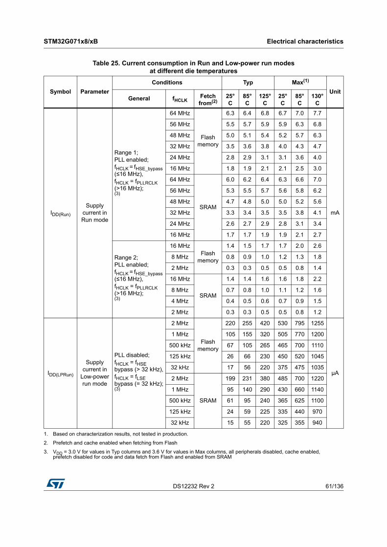
DS12232 Rev 2 61/136
STM32G071x8/xB Electrical characteristics
109
Table 25. Current consumption in Run and Low-power run modes at different die temperatures
Symbol Parameter
Conditions Typ Max(1)
UnitGeneral fHCLK
Fetch from(2)
25°C
85°C
125°C
25°C
85°C
130°C
IDD(Run)
Supply current in Run mode
Range 1; PLL enabled; fHCLK = fHSE_bypass (≤16 MHz), fHCLK = fPLLRCLK (>16 MHz); (3)
64 MHz
Flash memory
6.3 6.4 6.8 6.7 7.0 7.7
mA
56 MHz 5.5 5.7 5.9 5.9 6.3 6.8
48 MHz 5.0 5.1 5.4 5.2 5.7 6.3
32 MHz 3.5 3.6 3.8 4.0 4.3 4.7
24 MHz 2.8 2.9 3.1 3.1 3.6 4.0
16 MHz 1.8 1.9 2.1 2.1 2.5 3.0
64 MHz
SRAM
6.0 6.2 6.4 6.3 6.6 7.0
56 MHz 5.3 5.5 5.7 5.6 5.8 6.2
48 MHz 4.7 4.8 5.0 5.0 5.2 5.6
32 MHz 3.3 3.4 3.5 3.5 3.8 4.1
24 MHz 2.6 2.7 2.9 2.8 3.1 3.4
16 MHz 1.7 1.7 1.9 1.9 2.1 2.7
Range 2; PLL enabled; fHCLK = fHSE_bypass (≤16 MHz), fHCLK = fPLLRCLK (>16 MHz); (3)
16 MHzFlash
memory
1.4 1.5 1.7 1.7 2.0 2.6
8 MHz 0.8 0.9 1.0 1.2 1.3 1.8
2 MHz 0.3 0.3 0.5 0.5 0.8 1.4
16 MHz
SRAM
1.4 1.4 1.6 1.6 1.8 2.2
8 MHz 0.7 0.8 1.0 1.1 1.2 1.6
4 MHz 0.4 0.5 0.6 0.7 0.9 1.5
2 MHz 0.3 0.3 0.5 0.5 0.8 1.2
IDD(LPRun)
Supply current in
Low-power run mode
PLL disabled; fHCLK = fHSE bypass (> 32 kHz), fHCLK = fLSE bypass (= 32 kHz); (3)
2 MHz
Flash memory
220 255 420 530 795 1255
µA
1 MHz 105 155 320 505 770 1200
500 kHz 67 105 265 465 700 1110
125 kHz 26 66 230 450 520 1045
32 kHz 17 56 220 375 475 1035
2 MHz
SRAM
199 231 380 485 700 1220
1 MHz 95 140 290 430 660 1140
500 kHz 61 95 240 365 625 1100
125 kHz 24 59 225 335 440 970
32 kHz 15 55 220 325 355 940
1. Based on characterization results, not tested in production.
2. Prefetch and cache enabled when fetching from Flash
3. VDD = 3.0 V for values in Typ columns and 3.6 V for values in Max columns, all peripherals disabled, cache enabled, prefetch disabled for code and data fetch from Flash and enabled from SRAM
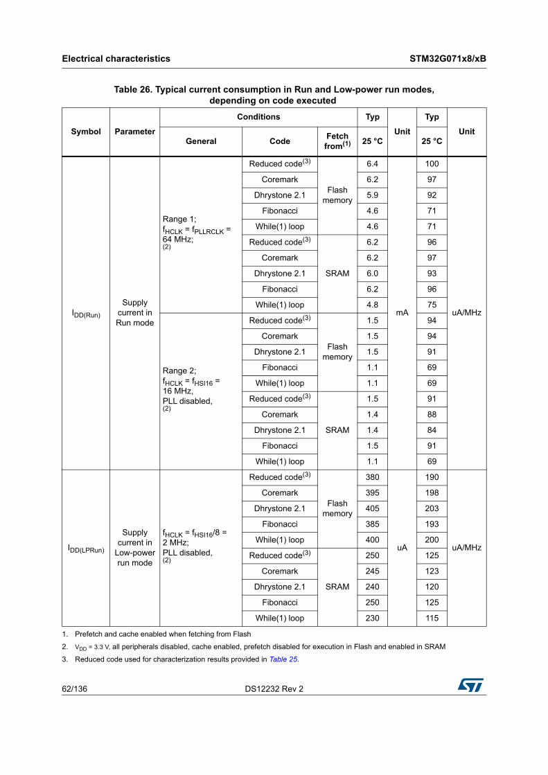
Electrical characteristics STM32G071x8/xB
62/136 DS12232 Rev 2
Table 26. Typical current consumption in Run and Low-power run modes,depending on code executed
Symbol Parameter
Conditions Typ
Unit
Typ
UnitGeneral Code
Fetch from(1) 25 °C 25 °C
IDD(Run)
Supply current in Run mode
Range 1; fHCLK = fPLLRCLK = 64 MHz; (2)
Reduced code(3)
Flash memory
6.4
mA
100
uA/MHz
Coremark 6.2 97
Dhrystone 2.1 5.9 92
Fibonacci 4.6 71
While(1) loop 4.6 71
Reduced code(3)
SRAM
6.2 96
Coremark 6.2 97
Dhrystone 2.1 6.0 93
Fibonacci 6.2 96
While(1) loop 4.8 75
Range 2; fHCLK = fHSI16 = 16 MHz, PLL disabled, (2)
Reduced code(3)
Flash memory
1.5 94
Coremark 1.5 94
Dhrystone 2.1 1.5 91
Fibonacci 1.1 69
While(1) loop 1.1 69
Reduced code(3)
SRAM
1.5 91
Coremark 1.4 88
Dhrystone 2.1 1.4 84
Fibonacci 1.5 91
While(1) loop 1.1 69
IDD(LPRun)
Supply current in
Low-power run mode
fHCLK = fHSI16/8 = 2 MHz; PLL disabled, (2)
Reduced code(3)
Flash memory
380
uA
190
uA/MHz
Coremark 395 198
Dhrystone 2.1 405 203
Fibonacci 385 193
While(1) loop 400 200
Reduced code(3)
SRAM
250 125
Coremark 245 123
Dhrystone 2.1 240 120
Fibonacci 250 125
While(1) loop 230 115
1. Prefetch and cache enabled when fetching from Flash
2. VDD = 3.3 V, all peripherals disabled, cache enabled, prefetch disabled for execution in Flash and enabled in SRAM
3. Reduced code used for characterization results provided in Table 25.
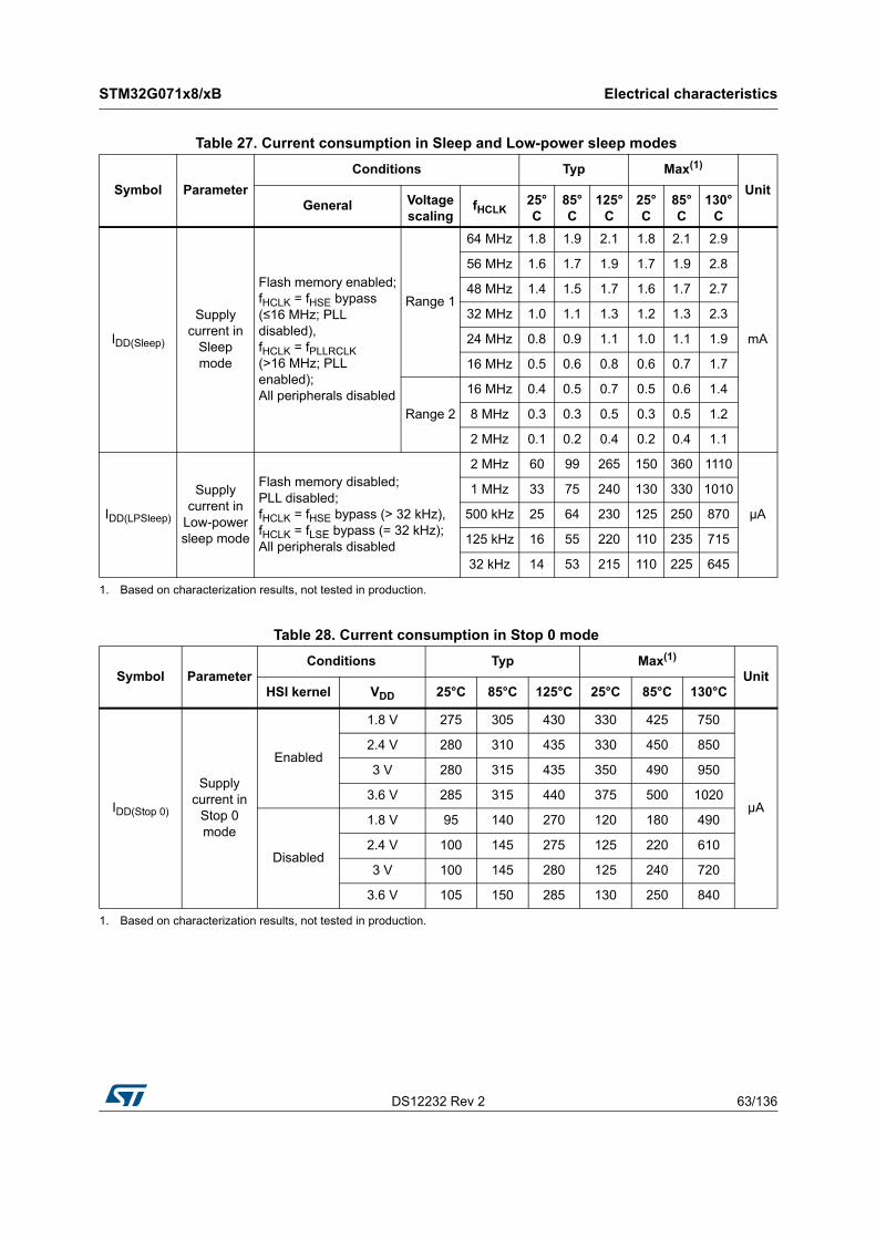
DS12232 Rev 2 63/136
STM32G071x8/xB Electrical characteristics
109
Table 27. Current consumption in Sleep and Low-power sleep modes
Symbol Parameter
Conditions Typ Max(1)
UnitGeneral Voltage
scalingfHCLK
25°C
85°C
125°C
25°C
85°C
130°C
IDD(Sleep)
Supply current in
Sleep mode
Flash memory enabled; fHCLK = fHSE bypass (≤16 MHz; PLL disabled), fHCLK = fPLLRCLK (>16 MHz; PLL enabled); All peripherals disabled
Range 1
64 MHz 1.8 1.9 2.1 1.8 2.1 2.9
mA
56 MHz 1.6 1.7 1.9 1.7 1.9 2.8
48 MHz 1.4 1.5 1.7 1.6 1.7 2.7
32 MHz 1.0 1.1 1.3 1.2 1.3 2.3
24 MHz 0.8 0.9 1.1 1.0 1.1 1.9
16 MHz 0.5 0.6 0.8 0.6 0.7 1.7
Range 2
16 MHz 0.4 0.5 0.7 0.5 0.6 1.4
8 MHz 0.3 0.3 0.5 0.3 0.5 1.2
2 MHz 0.1 0.2 0.4 0.2 0.4 1.1
IDD(LPSleep)
Supply current in
Low-power sleep mode
Flash memory disabled; PLL disabled; fHCLK = fHSE bypass (> 32 kHz), fHCLK = fLSE bypass (= 32 kHz); All peripherals disabled
2 MHz 60 99 265 150 360 1110
µA
1 MHz 33 75 240 130 330 1010
500 kHz 25 64 230 125 250 870
125 kHz 16 55 220 110 235 715
32 kHz 14 53 215 110 225 645
1. Based on characterization results, not tested in production.
Table 28. Current consumption in Stop 0 mode
Symbol ParameterConditions Typ Max(1)
UnitHSI kernel VDD 25°C 85°C 125°C 25°C 85°C 130°C
IDD(Stop 0)
Supply current in
Stop 0 mode
Enabled
1.8 V 275 305 430 330 425 750
µA
2.4 V 280 310 435 330 450 850
3 V 280 315 435 350 490 950
3.6 V 285 315 440 375 500 1020
Disabled
1.8 V 95 140 270 120 180 490
2.4 V 100 145 275 125 220 610
3 V 100 145 280 125 240 720
3.6 V 105 150 285 130 250 840
1. Based on characterization results, not tested in production.
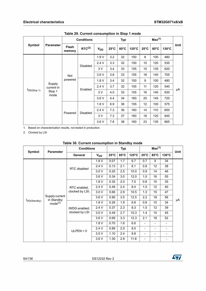
Electrical characteristics STM32G071x8/xB
64/136 DS12232 Rev 2
Table 29. Current consumption in Stop 1 mode
Symbol Parameter
Conditions Typ Max(1)
UnitFlash
memoryRTC(2) VDD 25°C 85°C 125°C 25°C 85°C 130°C
IDD(Stop 1)
Supply current in
Stop 1 mode
Not powered
Disabled
1.8 V 3.2 32 150 8 100 480
µA
2.4 V 3.3 32 150 10 120 535
3 V 3.4 33 155 15 135 620
3.6 V 3.8 33 155 18 140 705
Enabled
1.8 V 3.4 32 150 9 100 480
2.4 V 3.7 32 155 11 120 540
3 V 4.0 33 155 16 140 630
3.6 V 4.4 34 160 20 145 720
Powered Disabled
1.8 V 6.9 36 155 12 100 575
2.4 V 7.3 36 160 14 110 600
3 V 7.3 37 160 18 120 645
3.6 V 7.8 38 160 23 135 665
1. Based on characterization results, not tested in production.
2. Clocked by LSI
Table 30. Current consumption in Standby mode
Symbol ParameterConditions Typ Max(1)
UnitGeneral VDD 25°C 85°C 125°C 25°C 85°C 130°C
IDD(Standby)
Supply current in Standby
mode(2)
RTC disabled
1.8 V 0.07 1.7 6.7 0.7 9 34
µA
2.4 V 0.13 2.1 8.1 0.8 12 38
3.0 V 0.20 2.5 10.0 0.9 14 46
3.6 V 0.34 3.0 12.0 1.0 16 55
RTC enabled, clocked by LSI;
1.8 V 0.35 2.0 7.0 0.8 10 35
2.4 V 0.49 2.4 8.4 1.0 12 40
3.0 V 0.66 2.9 10.5 1.3 15 47
3.6 V 0.90 3.5 12.5 2.2 18 56
IWDG enabled, clocked by LSI
1.8 V 0.26 1.9 6.8 0.8 10 34
2.4 V 0.37 2.3 8.3 1.0 12 39
3.0 V 0.49 2.7 10.3 1.4 15 45
3.6 V 0.69 3.3 12.3 2.1 18 52
ULPEN = 0
1.8 V 0.70 1.6 6.6 - - -
2.4 V 0.89 2.0 8.0 - - -
3.0 V 1.10 2.4 9.8 - - -
3.6 V 1.30 2.9 11.8 - - -
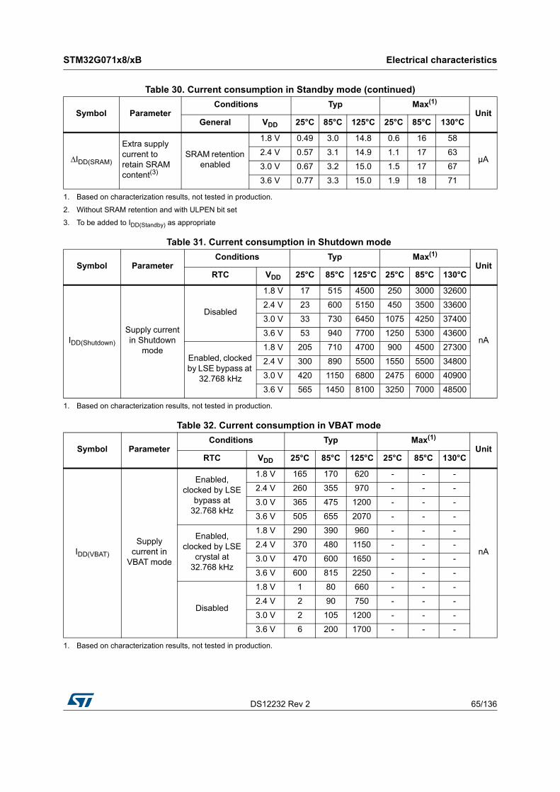
DS12232 Rev 2 65/136
STM32G071x8/xB Electrical characteristics
109
∆IDD(SRAM)
Extra supply current to retain SRAM content(3)
SRAM retention enabled
1.8 V 0.49 3.0 14.8 0.6 16 58
µA2.4 V 0.57 3.1 14.9 1.1 17 63
3.0 V 0.67 3.2 15.0 1.5 17 67
3.6 V 0.77 3.3 15.0 1.9 18 71
1. Based on characterization results, not tested in production.
2. Without SRAM retention and with ULPEN bit set
3. To be added to IDD(Standby) as appropriate
Table 30. Current consumption in Standby mode (continued)
Symbol ParameterConditions Typ Max(1)
UnitGeneral VDD 25°C 85°C 125°C 25°C 85°C 130°C
Table 31. Current consumption in Shutdown mode
Symbol ParameterConditions Typ Max(1)
UnitRTC VDD 25°C 85°C 125°C 25°C 85°C 130°C
IDD(Shutdown)
Supply current in Shutdown
mode
Disabled
1.8 V 17 515 4500 250 3000 32600
nA
2.4 V 23 600 5150 450 3500 33600
3.0 V 33 730 6450 1075 4250 37400
3.6 V 53 940 7700 1250 5300 43600
Enabled, clocked by LSE bypass at
32.768 kHz
1.8 V 205 710 4700 900 4500 27300
2.4 V 300 890 5500 1550 5500 34800
3.0 V 420 1150 6800 2475 6000 40900
3.6 V 565 1450 8100 3250 7000 48500
1. Based on characterization results, not tested in production.
Table 32. Current consumption in VBAT mode
Symbol ParameterConditions Typ Max(1)
UnitRTC VDD 25°C 85°C 125°C 25°C 85°C 130°C
IDD(VBAT)
Supply current in
VBAT mode
Enabled, clocked by LSE
bypass at 32.768 kHz
1.8 V 165 170 620 - - -
nA
2.4 V 260 355 970 - - -
3.0 V 365 475 1200 - - -
3.6 V 505 655 2070 - - -
Enabled, clocked by LSE
crystal at32.768 kHz
1.8 V 290 390 960 - - -
2.4 V 370 480 1150 - - -
3.0 V 470 600 1650 - - -
3.6 V 600 815 2250 - - -
Disabled
1.8 V 1 80 660 - - -
2.4 V 2 90 750 - - -
3.0 V 2 105 1200 - - -
3.6 V 6 200 1700 - - -
1. Based on characterization results, not tested in production.
Electrical characteristics STM32G071x8/xB
66/136 DS12232 Rev 2
I/O system current consumption
The current consumption of the I/O system has two components: static and dynamic.
I/O static current consumption
All the I/Os used as inputs with pull-up generate current consumption when the pin is externally held low. The value of this current consumption can be simply computed by using the pull-up/pull-down resistors values given in Table 51: I/O static characteristics.
For the output pins, any external pull-down or external load must also be considered to estimate the current consumption.
Additional I/O current consumption is due to I/Os configured as inputs if an intermediate voltage level is externally applied. This current consumption is caused by the input Schmitt trigger circuits used to discriminate the input value. Unless this specific configuration is required by the application, this supply current consumption can be avoided by configuring these I/Os in analog mode. This is notably the case of ADC input pins which should be configured as analog inputs.
Caution: Any floating input pin can also settle to an intermediate voltage level or switch inadvertently, as a result of external electromagnetic noise. To avoid current consumption related to floating pins, they must either be configured in analog mode, or forced internally to a definite digital value. This can be done either by using pull-up/down resistors or by configuring the pins in output mode.
I/O dynamic current consumption
In addition to the internal peripheral current consumption measured previously (see Table 33: Current consumption of peripherals, the I/Os used by an application also contribute to the current consumption. When an I/O pin switches, it uses the current from the I/O supply voltage to supply the I/O pin circuitry and to charge/discharge the capacitive load (internal or external) connected to the pin:
where
ISW is the current sunk by a switching I/O to charge/discharge the capacitive load
VDDIO1 is the I/O supply voltage
fSW is the I/O switching frequency
C is the total capacitance seen by the I/O pin: C = CINT+ CEXT + CS
CS is the PCB board capacitance including the pad pin.
The test pin is configured in push-pull output mode and is toggled by software at a fixed frequency.
ISW VDDIO1 fSW C××=
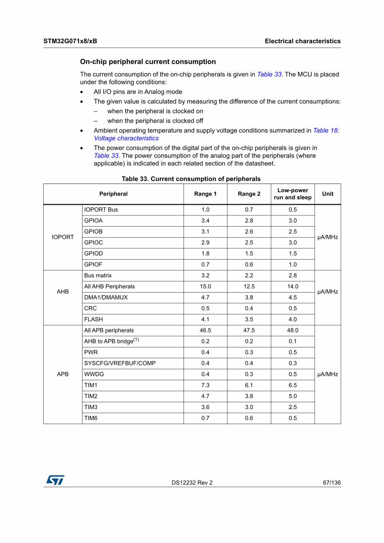
DS12232 Rev 2 67/136
STM32G071x8/xB Electrical characteristics
109
On-chip peripheral current consumption
The current consumption of the on-chip peripherals is given in Table 33. The MCU is placed under the following conditions:
• All I/O pins are in Analog mode
• The given value is calculated by measuring the difference of the current consumptions:
– when the peripheral is clocked on
– when the peripheral is clocked off
• Ambient operating temperature and supply voltage conditions summarized in Table 18: Voltage characteristics
• The power consumption of the digital part of the on-chip peripherals is given in Table 33. The power consumption of the analog part of the peripherals (where applicable) is indicated in each related section of the datasheet.
Table 33. Current consumption of peripherals
Peripheral Range 1 Range 2Low-power
run and sleepUnit
IOPORT
IOPORT Bus 1.0 0.7 0.5
µA/MHz
GPIOA 3.4 2.8 3.0
GPIOB 3.1 2.6 2.5
GPIOC 2.9 2.5 3.0
GPIOD 1.8 1.5 1.5
GPIOF 0.7 0.6 1.0
AHB
Bus matrix 3.2 2.2 2.8
µA/MHzAll AHB Peripherals 15.0 12.5 14.0
DMA1/DMAMUX 4.7 3.8 4.5
CRC 0.5 0.4 0.5
FLASH 4.1 3.5 4.0
APB
All APB peripherals 46.5 47.5 48.0
µA/MHz
AHB to APB bridge(1) 0.2 0.2 0.1
PWR 0.4 0.3 0.5
SYSCFG/VREFBUF/COMP 0.4 0.4 0.3
WWDG 0.4 0.3 0.5
TIM1 7.3 6.1 6.5
TIM2 4.7 3.8 5.0
TIM3 3.6 3.0 2.5
TIM6 0.7 0.6 0.5
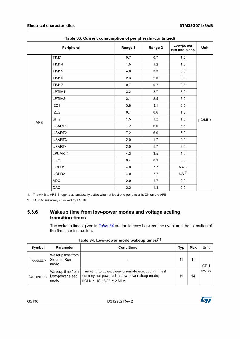
Electrical characteristics STM32G071x8/xB
68/136 DS12232 Rev 2
5.3.6 Wakeup time from low-power modes and voltage scaling transition times
The wakeup times given in Table 34 are the latency between the event and the execution of the first user instruction.
APB
TIM7 0.7 0.7 1.0
µA/MHz
TIM14 1.5 1.2 1.5
TIM15 4.0 3.3 3.0
TIM16 2.3 2.0 2.0
TIM17 0.7 0.7 0.5
LPTIM1 3.2 2.7 3.0
LPTIM2 3.1 2.5 3.0
I2C1 3.8 3.1 3.5
I2C2 0.7 0.6 1.0
SPI2 1.5 1.2 1.0
USART1 7.2 6.0 6.5
USART2 7.2 6.0 6.0
USART3 2.0 1.7 2.0
USART4 2.0 1.7 2.0
LPUART1 4.3 3.5 4.0
CEC 0.4 0.3 0.5
UCPD1 4.0 7.7 NA(2)
UCPD2 4.0 7.7 NA(2)
ADC 2.0 1.7 2.0
DAC 2.2 1.8 2.0
1. The AHB to APB Bridge is automatically active when at least one peripheral is ON on the APB.
2. UCPDx are always clocked by HSI16.
Table 33. Current consumption of peripherals (continued)
Peripheral Range 1 Range 2Low-power
run and sleepUnit
Table 34. Low-power mode wakeup times(1)
Symbol Parameter Conditions Typ Max Unit
tWUSLEEP
Wakeup time from Sleep to Run mode
- 11 11
CPUcycles
tWULPSLEEP
Wakeup time from Low-power sleep mode
Transiting to Low-power-run-mode execution in Flash memory not powered in Low-power sleep mode;
HCLK = HSI16 / 8 = 2 MHz11 14
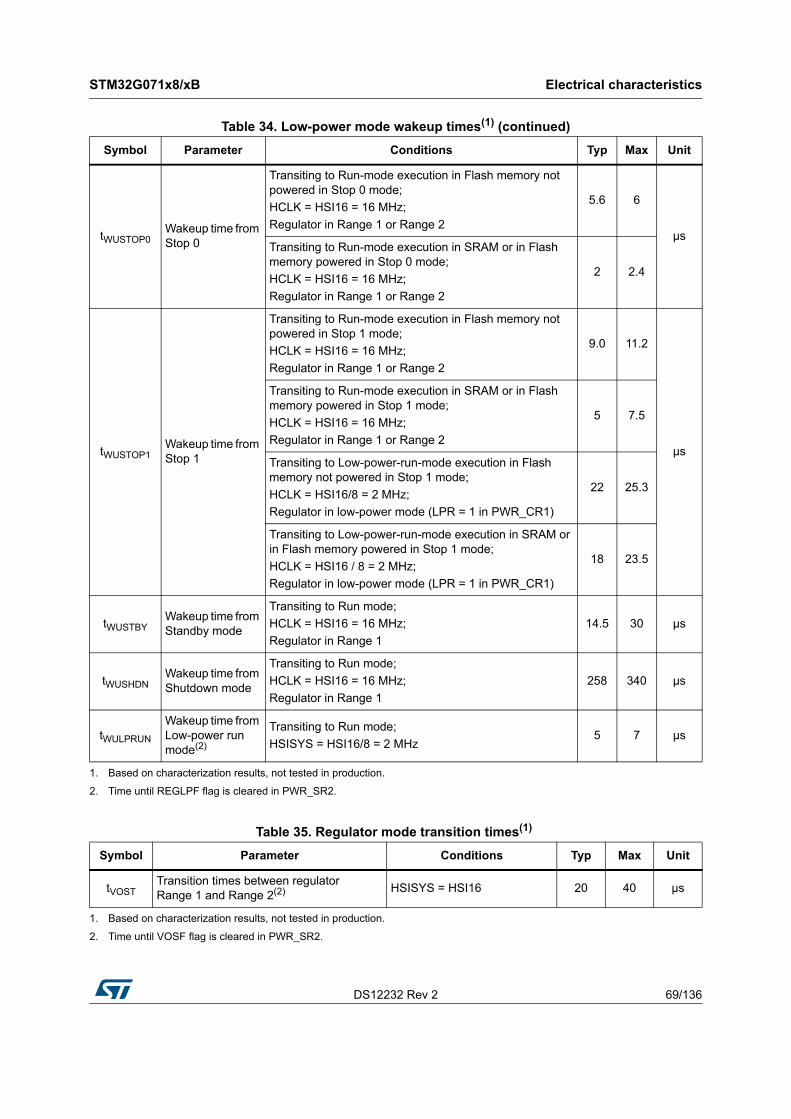
DS12232 Rev 2 69/136
STM32G071x8/xB Electrical characteristics
109
tWUSTOP0Wakeup time from Stop 0
Transiting to Run-mode execution in Flash memory not powered in Stop 0 mode;
HCLK = HSI16 = 16 MHz;
Regulator in Range 1 or Range 2
5.6 6
µsTransiting to Run-mode execution in SRAM or in Flash memory powered in Stop 0 mode;
HCLK = HSI16 = 16 MHz;
Regulator in Range 1 or Range 2
2 2.4
tWUSTOP1Wakeup time from Stop 1
Transiting to Run-mode execution in Flash memory not powered in Stop 1 mode;
HCLK = HSI16 = 16 MHz;
Regulator in Range 1 or Range 2
9.0 11.2
µs
Transiting to Run-mode execution in SRAM or in Flash memory powered in Stop 1 mode;
HCLK = HSI16 = 16 MHz;
Regulator in Range 1 or Range 2
5 7.5
Transiting to Low-power-run-mode execution in Flash memory not powered in Stop 1 mode;
HCLK = HSI16/8 = 2 MHz;
Regulator in low-power mode (LPR = 1 in PWR_CR1)
22 25.3
Transiting to Low-power-run-mode execution in SRAM or in Flash memory powered in Stop 1 mode;
HCLK = HSI16 / 8 = 2 MHz;
Regulator in low-power mode (LPR = 1 in PWR_CR1)
18 23.5
tWUSTBYWakeup time from Standby mode
Transiting to Run mode;
HCLK = HSI16 = 16 MHz;
Regulator in Range 1
14.5 30 µs
tWUSHDNWakeup time from Shutdown mode
Transiting to Run mode;
HCLK = HSI16 = 16 MHz;
Regulator in Range 1
258 340 µs
tWULPRUN
Wakeup time from Low-power run mode(2)
Transiting to Run mode;
HSISYS = HSI16/8 = 2 MHz5 7 µs
1. Based on characterization results, not tested in production.
2. Time until REGLPF flag is cleared in PWR_SR2.
Table 34. Low-power mode wakeup times(1) (continued)
Symbol Parameter Conditions Typ Max Unit
Table 35. Regulator mode transition times(1)
Symbol Parameter Conditions Typ Max Unit
tVOSTTransition times between regulator Range 1 and Range 2(2) HSISYS = HSI16 20 40 µs
1. Based on characterization results, not tested in production.
2. Time until VOSF flag is cleared in PWR_SR2.
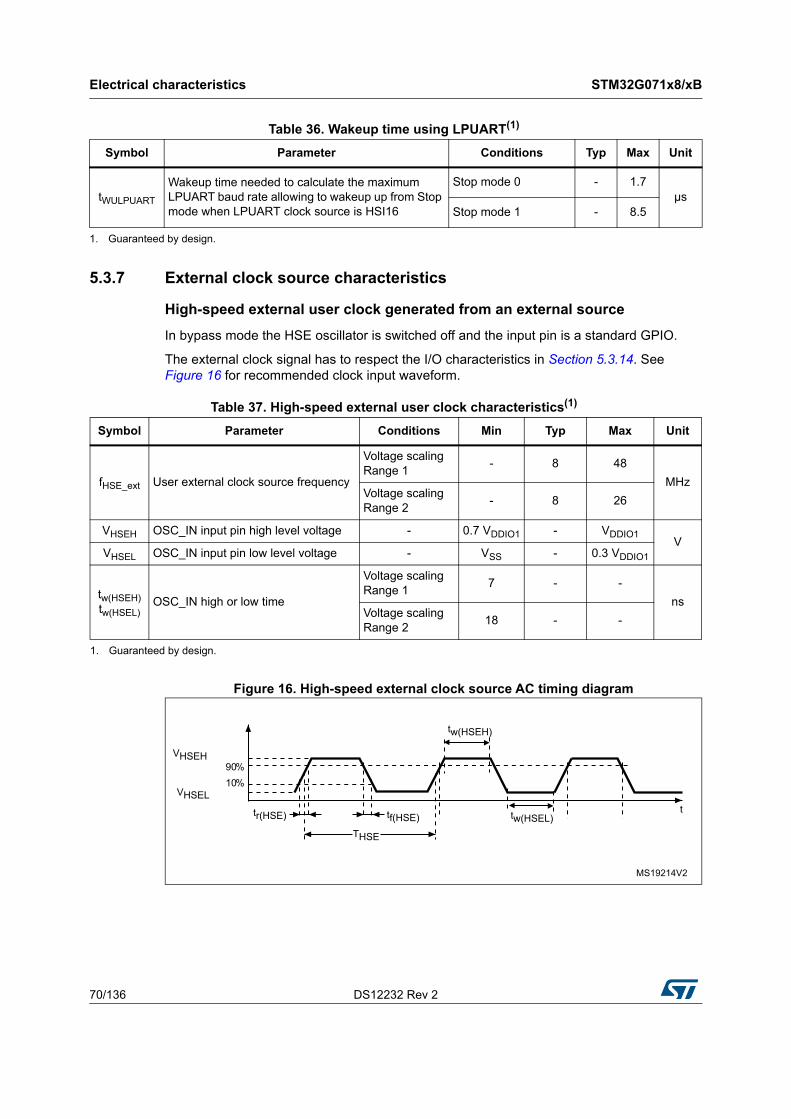
Electrical characteristics STM32G071x8/xB
70/136 DS12232 Rev 2
5.3.7 External clock source characteristics
High-speed external user clock generated from an external source
In bypass mode the HSE oscillator is switched off and the input pin is a standard GPIO.
The external clock signal has to respect the I/O characteristics in Section 5.3.14. See Figure 16 for recommended clock input waveform.
Figure 16. High-speed external clock source AC timing diagram
Table 36. Wakeup time using LPUART(1)
Symbol Parameter Conditions Typ Max Unit
tWULPUART
Wakeup time needed to calculate the maximum LPUART baud rate allowing to wakeup up from Stop mode when LPUART clock source is HSI16
Stop mode 0 - 1.7µs
Stop mode 1 - 8.5
1. Guaranteed by design.
Table 37. High-speed external user clock characteristics(1)
Symbol Parameter Conditions Min Typ Max Unit
fHSE_ext User external clock source frequency
Voltage scaling Range 1
- 8 48
MHzVoltage scaling Range 2
- 8 26
VHSEH OSC_IN input pin high level voltage - 0.7 VDDIO1 - VDDIO1V
VHSEL OSC_IN input pin low level voltage - VSS - 0.3 VDDIO1
tw(HSEH)tw(HSEL)
OSC_IN high or low time
Voltage scaling Range 1
7 - -
nsVoltage scaling Range 2
18 - -
1. Guaranteed by design.
MS19214V2
VHSEH
tf(HSE)
90%10%
THSE
ttr(HSE)
VHSEL
tw(HSEH)
tw(HSEL)
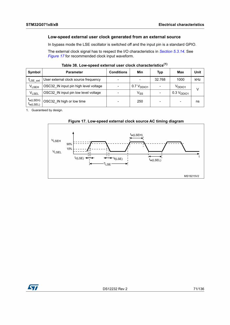
DS12232 Rev 2 71/136
STM32G071x8/xB Electrical characteristics
109
Low-speed external user clock generated from an external source
In bypass mode the LSE oscillator is switched off and the input pin is a standard GPIO.
The external clock signal has to respect the I/O characteristics in Section 5.3.14. See Figure 17 for recommended clock input waveform.
Figure 17. Low-speed external clock source AC timing diagram
Table 38. Low-speed external user clock characteristics(1)
Symbol Parameter Conditions Min Typ Max Unit
fLSE_ext User external clock source frequency - - 32.768 1000 kHz
VLSEH OSC32_IN input pin high level voltage - 0.7 VDDIO1 - VDDIO1V
VLSEL OSC32_IN input pin low level voltage - VSS - 0.3 VDDIO1
tw(LSEH)tw(LSEL)
OSC32_IN high or low time - 250 - - ns
1. Guaranteed by design.
MS19215V2
VLSEH
tf(LSE)
90%10%
TLSE
ttr(LSE)
VLSEL
tw(LSEH)
tw(LSEL)
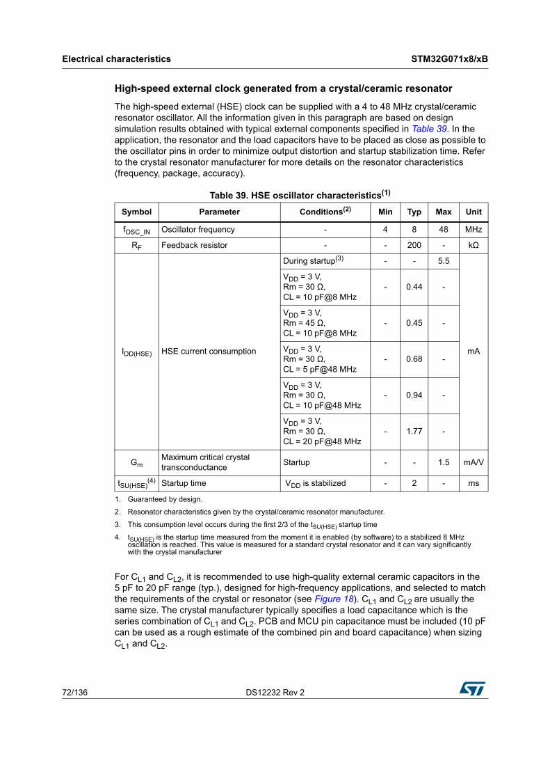
Electrical characteristics STM32G071x8/xB
72/136 DS12232 Rev 2
High-speed external clock generated from a crystal/ceramic resonator
The high-speed external (HSE) clock can be supplied with a 4 to 48 MHz crystal/ceramic resonator oscillator. All the information given in this paragraph are based on design simulation results obtained with typical external components specified in Table 39. In the application, the resonator and the load capacitors have to be placed as close as possible to the oscillator pins in order to minimize output distortion and startup stabilization time. Refer to the crystal resonator manufacturer for more details on the resonator characteristics (frequency, package, accuracy).
For CL1 and CL2, it is recommended to use high-quality external ceramic capacitors in the 5 pF to 20 pF range (typ.), designed for high-frequency applications, and selected to match the requirements of the crystal or resonator (see Figure 18). CL1 and CL2 are usually the same size. The crystal manufacturer typically specifies a load capacitance which is the series combination of CL1 and CL2. PCB and MCU pin capacitance must be included (10 pF can be used as a rough estimate of the combined pin and board capacitance) when sizing CL1 and CL2.
Table 39. HSE oscillator characteristics(1)
1. Guaranteed by design.
Symbol Parameter Conditions(2)
2. Resonator characteristics given by the crystal/ceramic resonator manufacturer.
Min Typ Max Unit
fOSC_IN Oscillator frequency - 4 8 48 MHz
RF Feedback resistor - - 200 - kΩ
IDD(HSE) HSE current consumption
During startup(3)
3. This consumption level occurs during the first 2/3 of the tSU(HSE) startup time
- - 5.5
mA
VDD = 3 V, Rm = 30 Ω, CL = 10 pF@8 MHz
- 0.44 -
VDD = 3 V, Rm = 45 Ω, CL = 10 pF@8 MHz
- 0.45 -
VDD = 3 V, Rm = 30 Ω, CL = 5 pF@48 MHz
- 0.68 -
VDD = 3 V, Rm = 30 Ω, CL = 10 pF@48 MHz
- 0.94 -
VDD = 3 V, Rm = 30 Ω, CL = 20 pF@48 MHz
- 1.77 -
Gm Maximum critical crystal transconductance
Startup - - 1.5 mA/V
tSU(HSE)(4)
4. tSU(HSE) is the startup time measured from the moment it is enabled (by software) to a stabilized 8 MHz oscillation is reached. This value is measured for a standard crystal resonator and it can vary significantly with the crystal manufacturer
Startup time VDD is stabilized - 2 - ms
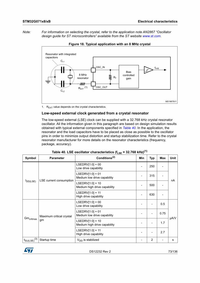
DS12232 Rev 2 73/136
STM32G071x8/xB Electrical characteristics
109
Note: For information on selecting the crystal, refer to the application note AN2867 “Oscillator design guide for ST microcontrollers” available from the ST website www.st.com.
Figure 18. Typical application with an 8 MHz crystal
1. REXT value depends on the crystal characteristics.
Low-speed external clock generated from a crystal resonator
The low-speed external (LSE) clock can be supplied with a 32.768 kHz crystal resonator oscillator. All the information given in this paragraph are based on design simulation results obtained with typical external components specified in Table 40. In the application, the resonator and the load capacitors have to be placed as close as possible to the oscillator pins in order to minimize output distortion and startup stabilization time. Refer to the crystal resonator manufacturer for more details on the resonator characteristics (frequency, package, accuracy).
MS19876V1
(1)
OSC_IN
OSC_OUT
RF
Bias controlled
gain
fHSE
REXT
8 MHz resonator
Resonator with integrated capacitors
CL1
CL2
Table 40. LSE oscillator characteristics (fLSE = 32.768 kHz)(1)
Symbol Parameter Conditions(2) Min Typ Max Unit
IDD(LSE) LSE current consumption
LSEDRV[1:0] = 00 Low drive capability
- 250 -
nA
LSEDRV[1:0] = 01 Medium low drive capability
- 315 -
LSEDRV[1:0] = 10 Medium high drive capability
- 500 -
LSEDRV[1:0] = 11 High drive capability
- 630 -
GmcritmaxMaximum critical crystal gm
LSEDRV[1:0] = 00 Low drive capability
- - 0.5
µA/V
LSEDRV[1:0] = 01 Medium low drive capability
- - 0.75
LSEDRV[1:0] = 10 Medium high drive capability
- - 1.7
LSEDRV[1:0] = 11 High drive capability
- - 2.7
tSU(LSE)(3) Startup time VDD is stabilized - 2 - s
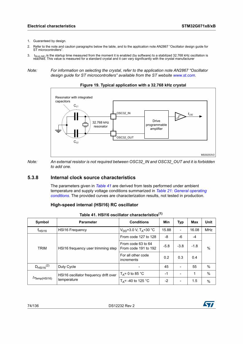
Electrical characteristics STM32G071x8/xB
74/136 DS12232 Rev 2
Note: For information on selecting the crystal, refer to the application note AN2867 “Oscillator design guide for ST microcontrollers” available from the ST website www.st.com.
Figure 19. Typical application with a 32.768 kHz crystal
Note: An external resistor is not required between OSC32_IN and OSC32_OUT and it is forbidden to add one.
5.3.8 Internal clock source characteristics
The parameters given in Table 41 are derived from tests performed under ambient temperature and supply voltage conditions summarized in Table 21: General operating conditions. The provided curves are characterization results, not tested in production.
High-speed internal (HSI16) RC oscillator
1. Guaranteed by design.
2. Refer to the note and caution paragraphs below the table, and to the application note AN2867 “Oscillator design guide for ST microcontrollers”.
3. tSU(LSE) is the startup time measured from the moment it is enabled (by software) to a stabilized 32.768 kHz oscillation is reached. This value is measured for a standard crystal and it can vary significantly with the crystal manufacturer
MS30253V2
OSC32_IN
OSC32_OUT
Drive programmable
amplifier
fLSE
32.768 kHz resonator
Resonator with integrated capacitors
CL1
CL2
Table 41. HSI16 oscillator characteristics(1)
Symbol Parameter Conditions Min Typ Max Unit
fHSI16 HSI16 Frequency VDD=3.0 V, TA=30 °C 15.88 - 16.08 MHz
TRIM HSI16 frequency user trimming step
From code 127 to 128 -8 -6 -4
%From code 63 to 64 From code 191 to 192
-5.8 -3.8 -1.8
For all other code increments
0.2 0.3 0.4
DHSI16(2) Duty Cycle - 45 - 55 %
∆Temp(HSI16)HSI16 oscillator frequency drift over temperature
TA= 0 to 85 °C -1 - 1 %
TA= -40 to 125 °C -2 - 1.5 %
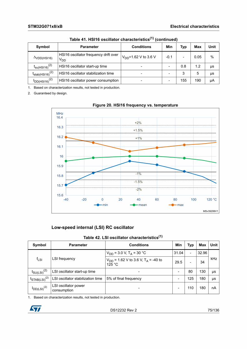
DS12232 Rev 2 75/136
STM32G071x8/xB Electrical characteristics
109
Figure 20. HSI16 frequency vs. temperature
Low-speed internal (LSI) RC oscillator
∆VDD(HSI16)HSI16 oscillator frequency drift over VDD
VDD=1.62 V to 3.6 V -0.1 - 0.05 %
tsu(HSI16)(2) HSI16 oscillator start-up time - - 0.8 1.2 μs
tstab(HSI16)(2) HSI16 oscillator stabilization time - - 3 5 μs
IDD(HSI16)(2) HSI16 oscillator power consumption - - 155 190 μA
1. Based on characterization results, not tested in production.
2. Guaranteed by design.
Table 41. HSI16 oscillator characteristics(1) (continued)
Symbol Parameter Conditions Min Typ Max Unit
MSv39299V1
15.6
15.7
15.8
15.9
16
16.1
16.2
16.3
16.4MHz
min mean max
+1%
-1%
+2%
-2%
+1.5%
-1.5%
-40 -20 0 20 40 60 80 100 120 °C
Table 42. LSI oscillator characteristics(1)
Symbol Parameter Conditions Min Typ Max Unit
fLSI LSI frequency
VDD = 3.0 V, TA = 30 °C 31.04 - 32.96
kHzVDD = 1.62 V to 3.6 V, TA = -40 to 125 °C
29.5 - 34
tSU(LSI)(2) LSI oscillator start-up time - - 80 130 μs
tSTAB(LSI)(2) LSI oscillator stabilization time 5% of final frequency - 125 180 μs
IDD(LSI)(2) LSI oscillator power
consumption- - 110 180 nA
1. Based on characterization results, not tested in production.
Electrical characteristics STM32G071x8/xB
76/136 DS12232 Rev 2
5.3.9 PLL characteristics
The parameters given in Table 43 are derived from tests performed under temperature and VDD supply voltage conditions summarized in Table 21: General operating conditions.
5.3.10 Flash memory characteristics
2. Guaranteed by design.
Table 43. PLL characteristics(1)
Symbol Parameter Conditions Min Typ Max Unit
fPLL_IN PLL input clock frequency(2) - 2.66 - 16 MHz
DPLL_IN PLL input clock duty cycle - 45 - 55 %
fPLL_P_OUT PLL multiplier output clock PVoltage scaling Range 1 3.09 - 122
MHzVoltage scaling Range 2 3.09 - 40
fPLL_Q_OUT PLL multiplier output clock QVoltage scaling Range 1 12 - 128
MHzVoltage scaling Range 2 12 - 33
fPLL_R_OUT PLL multiplier output clock RVoltage scaling Range 1 12 - 64
MHzVoltage scaling Range 2 12 - 16
fVCO_OUT PLL VCO outputVoltage scaling Range 1 96 - 344
MHzVoltage scaling Range 2 96 - 128
tLOCK PLL lock time - - 15 40 μs
JitterRMS cycle-to-cycle jitter
System clock 56 MHz- 50 -
±psRMS period jitter - 40 -
IDD(PLL)PLL power consumption on VDD
(1)
VCO freq = 96 MHz - 200 260
μAVCO freq = 192 MHz - 300 380
VCO freq = 344 MHz - 520 650
1. Guaranteed by design.
2. Take care of using the appropriate division factor M to obtain the specified PLL input clock values. The M factor is shared between the two PLLs.
Table 44. Flash memory characteristics(1)
Symbol Parameter Conditions Typ Max Unit
tprog 64-bit programming time - 85 125 µs
tprog_rowRow (32 double word) programming time
Normal programming 2.7 4.6
ms
Fast programming 1.7 2.8
tprog_page Page (2 Kbyte) programming timeNormal programming 21.8 36.6
Fast programming 13.7 22.4
tERASE Page (2 Kbyte) erase time - 22.0 40.0
DS12232 Rev 2 77/136
STM32G071x8/xB Electrical characteristics
109
5.3.11 EMC characteristics
Susceptibility tests are performed on a sample basis during device characterization.
Functional EMS (electromagnetic susceptibility)
While a simple application is executed on the device (toggling 2 LEDs through I/O ports). the device is stressed by two electromagnetic events until a failure occurs. The failure is indicated by the LEDs:
• Electrostatic discharge (ESD) (positive and negative) is applied to all device pins until a functional disturbance occurs. This test is compliant with the IEC 61000-4-2 standard.
• FTB: A Burst of Fast Transient voltage (positive and negative) is applied to VDD and VSS through a 100 pF capacitor, until a functional disturbance occurs. This test is compliant with the IEC 61000-4-4 standard.
A device reset allows normal operations to be resumed.
tprog_bankBank (128 Kbyte(2)) programming time
Normal programming 1.4 2.4s
Fast programming 0.9 1.4
tME Mass erase time - 22.1 40.1 ms
IDD(FlashA) Average consumption from VDD
Programming 3 -
mAPage erase 3 -
Mass erase 3 -
IDD(FlashP) Maximum current (peak)
Programming, 2 µs peak duration
7 -
mAErase, 41 µs peak duration
7 -
1. Guaranteed by design.
2. Values provided also apply to devices with less Flash memory than one 128 Kbyte bank
Table 45. Flash memory endurance and data retention
Symbol Parameter Conditions Min(1)
1. Guaranteed by characterization results.
Unit
NEND Endurance TA = -40 to +105 °C 10 kcycles
tRET Data retention
1 kcycle(2) at TA = 85 °C
2. Cycling performed over the whole temperature range.
30
Years
1 kcycle(2) at TA = 105 °C 15
1 kcycle(2) at TA = 125 °C 7
10 kcycles(2) at TA = 55 °C 30
10 kcycles(2) at TA = 85 °C 15
10 kcycles(2) at TA = 105 °C 10
Table 44. Flash memory characteristics(1) (continued)
Symbol Parameter Conditions Typ Max Unit
Electrical characteristics STM32G071x8/xB
78/136 DS12232 Rev 2
The test results are given in Table 46. They are based on the EMS levels and classes defined in application note AN1709.
Designing hardened software to avoid noise problems
EMC characterization and optimization are performed at component level with a typical application environment and simplified MCU software. It should be noted that good EMC performance is highly dependent on the user application and the software in particular.
Therefore it is recommended that the user applies EMC software optimization and prequalification tests in relation with the EMC level requested for his application.
Software recommendations
The software flowchart must include the management of runaway conditions such as:
• corrupted program counter
• unexpected reset
• critical data corruption (for example control registers)
Prequalification trials
Most of the common failures (unexpected reset and program counter corruption) can be reproduced by manually forcing a low state on the NRST pin or the Oscillator pins for 1 second.
To complete these trials, ESD stress can be applied directly on the device, over the range of specification values. When unexpected behavior is detected, the software can be hardened to prevent unrecoverable errors occurring (see application note AN1015).
Electromagnetic Interference (EMI)
The electromagnetic field emitted by the device are monitored while a simple application is executed (toggling 2 LEDs through the I/O ports). This emission test is compliant with IEC 61967-2 standard which specifies the test board and the pin loading.
Table 46. EMS characteristics
Symbol Parameter ConditionsLevel/Class
VFESDVoltage limits to be applied on any I/O pin to induce a functional disturbance
VDD = 3.3 V, TA = +25 °C, fHCLK = 64 MHz, LQFP64, conforming to IEC 61000-4-2
2B
VEFTB
Fast transient voltage burst limits to be applied through 100 pF on VDD and VSS pins to induce a functional disturbance
VDD = 3.3 V, TA = +25 °C, fHCLK = 64 MHz, LQFP64, conforming to IEC 61000-4-4
5A
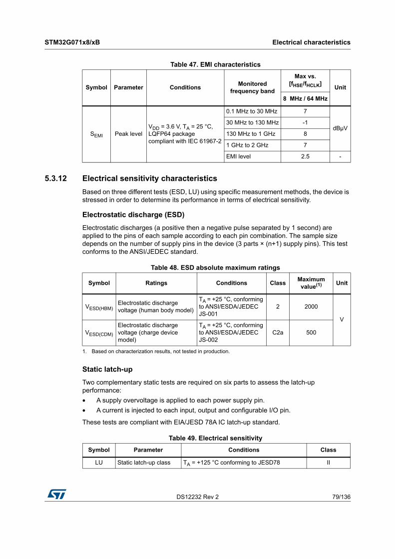
DS12232 Rev 2 79/136
STM32G071x8/xB Electrical characteristics
109
5.3.12 Electrical sensitivity characteristics
Based on three different tests (ESD, LU) using specific measurement methods, the device is stressed in order to determine its performance in terms of electrical sensitivity.
Electrostatic discharge (ESD)
Electrostatic discharges (a positive then a negative pulse separated by 1 second) are applied to the pins of each sample according to each pin combination. The sample size depends on the number of supply pins in the device (3 parts × (n+1) supply pins). This test conforms to the ANSI/JEDEC standard.
Static latch-up
Two complementary static tests are required on six parts to assess the latch-up performance:
• A supply overvoltage is applied to each power supply pin.
• A current is injected to each input, output and configurable I/O pin.
These tests are compliant with EIA/JESD 78A IC latch-up standard.
Table 47. EMI characteristics
Symbol Parameter ConditionsMonitored
frequency band
Max vs. [fHSE/fHCLK]
Unit
8 MHz / 64 MHz
SEMI Peak levelVDD = 3.6 V, TA = 25 °C, LQFP64 package compliant with IEC 61967-2
0.1 MHz to 30 MHz 7
dBµV30 MHz to 130 MHz -1
130 MHz to 1 GHz 8
1 GHz to 2 GHz 7
EMI level 2.5 -
Table 48. ESD absolute maximum ratings
Symbol Ratings Conditions ClassMaximum value(1)
1. Based on characterization results, not tested in production.
Unit
VESD(HBM)Electrostatic discharge voltage (human body model)
TA = +25 °C, conforming to ANSI/ESDA/JEDEC JS-001
2 2000
V
VESD(CDM)
Electrostatic discharge voltage (charge device model)
TA = +25 °C, conforming to ANSI/ESDA/JEDEC JS-002
C2a 500
Table 49. Electrical sensitivity
Symbol Parameter Conditions Class
LU Static latch-up class TA = +125 °C conforming to JESD78 II
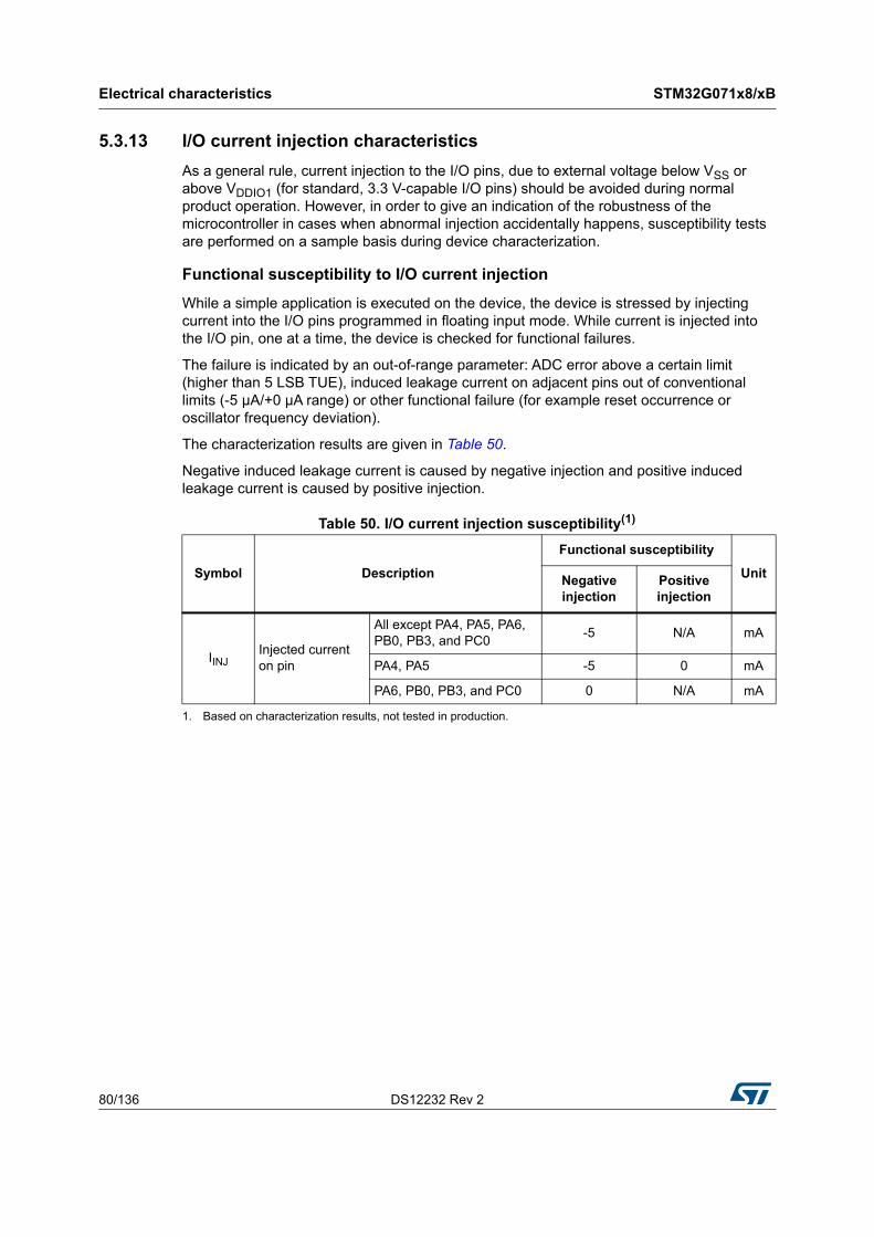
Electrical characteristics STM32G071x8/xB
80/136 DS12232 Rev 2
5.3.13 I/O current injection characteristics
As a general rule, current injection to the I/O pins, due to external voltage below VSS or above VDDIO1 (for standard, 3.3 V-capable I/O pins) should be avoided during normal product operation. However, in order to give an indication of the robustness of the microcontroller in cases when abnormal injection accidentally happens, susceptibility tests are performed on a sample basis during device characterization.
Functional susceptibility to I/O current injection
While a simple application is executed on the device, the device is stressed by injecting current into the I/O pins programmed in floating input mode. While current is injected into the I/O pin, one at a time, the device is checked for functional failures.
The failure is indicated by an out-of-range parameter: ADC error above a certain limit (higher than 5 LSB TUE), induced leakage current on adjacent pins out of conventional limits (-5 µA/+0 µA range) or other functional failure (for example reset occurrence or oscillator frequency deviation).
The characterization results are given in Table 50.
Negative induced leakage current is caused by negative injection and positive induced leakage current is caused by positive injection.
Table 50. I/O current injection susceptibility(1)
1. Based on characterization results, not tested in production.
Symbol Description
Functional susceptibility
UnitNegative injection
Positive injection
IINJInjected current on pin
All except PA4, PA5, PA6, PB0, PB3, and PC0
-5 N/A mA
PA4, PA5 -5 0 mA
PA6, PB0, PB3, and PC0 0 N/A mA
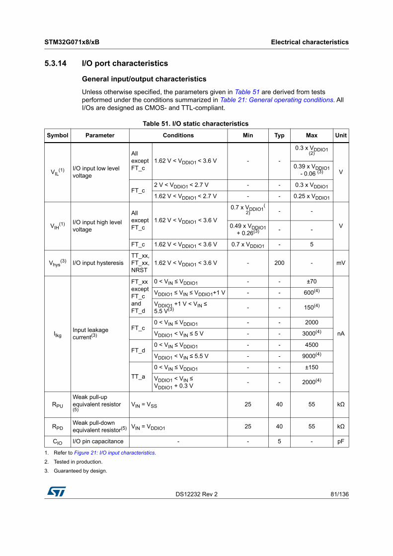
DS12232 Rev 2 81/136
STM32G071x8/xB Electrical characteristics
109
5.3.14 I/O port characteristics
General input/output characteristics
Unless otherwise specified, the parameters given in Table 51 are derived from tests performed under the conditions summarized in Table 21: General operating conditions. All I/Os are designed as CMOS- and TTL-compliant.
Table 51. I/O static characteristics
Symbol Parameter Conditions Min Typ Max Unit
VIL(1) I/O input low level
voltage
All except FT_c
1.62 V < VDDIO1 < 3.6 V - -
0.3 x VDDIO1 (2)
V0.39 x VDDIO1
- 0.06 (3)
FT_c2 V < VDDIO1 < 2.7 V - - 0.3 x VDDIO1
1.62 V < VDDIO1 < 2.7 V - - 0.25 x VDDIO1
VIH(1) I/O input high level
voltage
All except FT_c
1.62 V < VDDIO1 < 3.6 V
0.7 x VDDIO1(
2) - -
V0.49 x VDDIO1+ 0.26(3) - -
FT_c 1.62 V < VDDIO1 < 3.6 V 0.7 x VDDIO1 - 5
Vhys(3) I/O input hysteresis
TT_xx, FT_xx, NRST
1.62 V < VDDIO1 < 3.6 V - 200 - mV
IlkgInput leakage current(3)
FT_xx except FT_c and FT_d
0 < VIN ≤ VDDIO1 - - ±70
nA
VDDIO1 ≤ VIN ≤ VDDIO1+1 V - - 600(4)
VDDIO1 +1 V < VIN ≤ 5.5 V(3) - - 150(4)
FT_c0 < VIN ≤ VDDIO1 - - 2000
VDDIO1 < VIN ≤ 5 V - - 3000(4)
FT_d0 < VIN ≤ VDDIO1 - - 4500
VDDIO1 < VIN ≤ 5.5 V - - 9000(4)
TT_a
0 < VIN ≤ VDDIO1 - - ±150
VDDIO1 < VIN ≤ VDDIO1 + 0.3 V
- - 2000(4)
RPU
Weak pull-up equivalent resistor (5)
VIN = VSS 25 40 55 kΩ
RPDWeak pull-down equivalent resistor(5) VIN = VDDIO1 25 40 55 kΩ
CIO I/O pin capacitance - - 5 - pF
1. Refer to Figure 21: I/O input characteristics.
2. Tested in production.
3. Guaranteed by design.
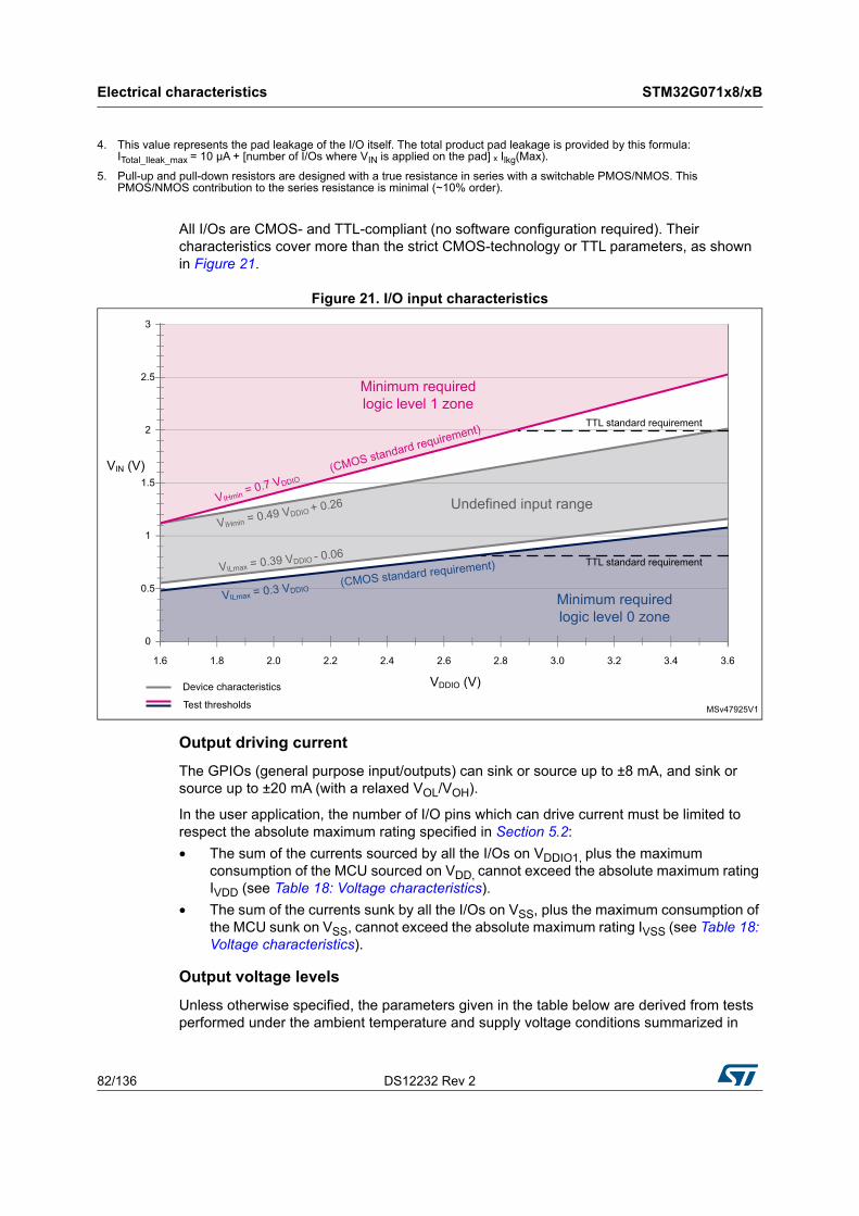
Electrical characteristics STM32G071x8/xB
82/136 DS12232 Rev 2
All I/Os are CMOS- and TTL-compliant (no software configuration required). Their characteristics cover more than the strict CMOS-technology or TTL parameters, as shown in Figure 21.
Figure 21. I/O input characteristics
Output driving current
The GPIOs (general purpose input/outputs) can sink or source up to ±8 mA, and sink or source up to ±20 mA (with a relaxed VOL/VOH).
In the user application, the number of I/O pins which can drive current must be limited to respect the absolute maximum rating specified in Section 5.2:
• The sum of the currents sourced by all the I/Os on VDDIO1, plus the maximum consumption of the MCU sourced on VDD, cannot exceed the absolute maximum rating IVDD (see Table 18: Voltage characteristics).
• The sum of the currents sunk by all the I/Os on VSS, plus the maximum consumption of the MCU sunk on VSS, cannot exceed the absolute maximum rating IVSS (see Table 18: Voltage characteristics).
Output voltage levels
Unless otherwise specified, the parameters given in the table below are derived from tests performed under the ambient temperature and supply voltage conditions summarized in
4. This value represents the pad leakage of the I/O itself. The total product pad leakage is provided by this formula: ITotal_Ileak_max = 10 µA + [number of I/Os where VIN is applied on the pad] ₓ Ilkg(Max).
5. Pull-up and pull-down resistors are designed with a true resistance in series with a switchable PMOS/NMOS. This PMOS/NMOS contribution to the series resistance is minimal (~10% order).
MSv47925V1
1.6 1.8 2.0 2.2 2.4 2.6 2.8 3.0 3.2 3.4 3.6
0
0.5
1
1.5
2
2.5
3
Minimum required logic level 1 zone
Minimum required logic level 0 zone
VIHmin = 0.7 VDDIO (CMOS standard requirement)
VILmax = 0.3 VDDIO (CMOS standard requirement)
Undefined input rangeVIHmin = 0.49 VDDIO + 0.26
VILmax = 0.39 VDDIO - 0.06
VIN (V)
VDDIO (V)
TTL standard requirement
TTL standard requirement
Device characteristics
Test thresholds
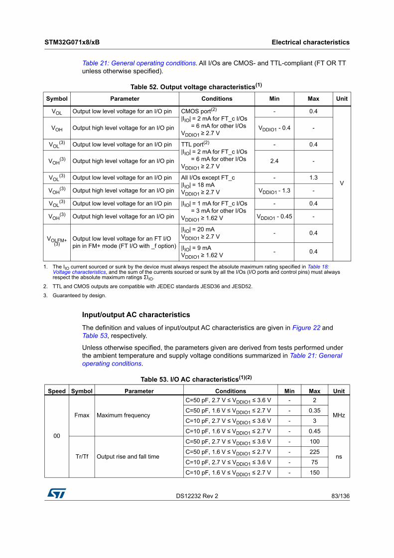
DS12232 Rev 2 83/136
STM32G071x8/xB Electrical characteristics
109
Table 21: General operating conditions. All I/Os are CMOS- and TTL-compliant (FT OR TT unless otherwise specified).
Input/output AC characteristics
The definition and values of input/output AC characteristics are given in Figure 22 and Table 53, respectively.
Unless otherwise specified, the parameters given are derived from tests performed under the ambient temperature and supply voltage conditions summarized in Table 21: General operating conditions.
Table 52. Output voltage characteristics(1)
Symbol Parameter Conditions Min Max Unit
VOL Output low level voltage for an I/O pin CMOS port(2) |IIO| = 2 mA for FT_c I/Os = 6 mA for other I/Os VDDIO1 ≥ 2.7 V
- 0.4
V
VOH Output high level voltage for an I/O pin VDDIO1 - 0.4 -
VOL(3) Output low level voltage for an I/O pin TTL port(2)
|IIO| = 2 mA for FT_c I/Os = 6 mA for other I/Os VDDIO1 ≥ 2.7 V
- 0.4
VOH(3) Output high level voltage for an I/O pin 2.4 -
VOL(3) Output low level voltage for an I/O pin All I/Os except FT_c
|IIO| = 18 mA VDDIO1 ≥ 2.7 V
- 1.3
VOH(3) Output high level voltage for an I/O pin VDDIO1 - 1.3 -
VOL(3) Output low level voltage for an I/O pin |IIO| = 1 mA for FT_c I/Os
= 3 mA for other I/Os VDDIO1 ≥ 1.62 V
- 0.4
VOH(3) Output high level voltage for an I/O pin VDDIO1 - 0.45 -
VOLFM+(3)
Output low level voltage for an FT I/O pin in FM+ mode (FT I/O with _f option)
|IIO| = 20 mA VDDIO1 ≥ 2.7 V
- 0.4
|IIO| = 9 mA VDDIO1 ≥ 1.62 V
- 0.4
1. The IIO current sourced or sunk by the device must always respect the absolute maximum rating specified in Table 18: Voltage characteristics, and the sum of the currents sourced or sunk by all the I/Os (I/O ports and control pins) must always respect the absolute maximum ratings ΣIIO.
2. TTL and CMOS outputs are compatible with JEDEC standards JESD36 and JESD52.
3. Guaranteed by design.
Table 53. I/O AC characteristics(1)(2)
Speed Symbol Parameter Conditions Min Max Unit
00
Fmax Maximum frequency
C=50 pF, 2.7 V ≤ VDDIO1 ≤ 3.6 V - 2
MHzC=50 pF, 1.6 V ≤ VDDIO1 ≤ 2.7 V - 0.35
C=10 pF, 2.7 V ≤ VDDIO1 ≤ 3.6 V - 3
C=10 pF, 1.6 V ≤ VDDIO1 ≤ 2.7 V - 0.45
Tr/Tf Output rise and fall time
C=50 pF, 2.7 V ≤ VDDIO1 ≤ 3.6 V - 100
nsC=50 pF, 1.6 V ≤ VDDIO1 ≤ 2.7 V - 225
C=10 pF, 2.7 V ≤ VDDIO1 ≤ 3.6 V - 75
C=10 pF, 1.6 V ≤ VDDIO1 ≤ 2.7 V - 150
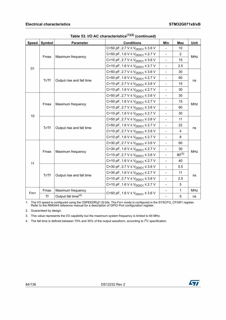
Electrical characteristics STM32G071x8/xB
84/136 DS12232 Rev 2
01
Fmax Maximum frequency
C=50 pF, 2.7 V ≤ VDDIO1 ≤ 3.6 V - 10
MHzC=50 pF, 1.6 V ≤ VDDIO1 ≤ 2.7 V - 2
C=10 pF, 2.7 V ≤ VDDIO1 ≤ 3.6 V - 15
C=10 pF, 1.6 V ≤ VDDIO1 ≤ 2.7 V - 2.5
Tr/Tf Output rise and fall time
C=50 pF, 2.7 V ≤ VDDIO1 ≤ 3.6 V - 30
nsC=50 pF, 1.6 V ≤ VDDIO1 ≤ 2.7 V - 60
C=10 pF, 2.7 V ≤ VDDIO1 ≤ 3.6 V - 15
C=10 pF, 1.6 V ≤ VDDIO1 ≤ 2.7 V - 30
10
Fmax Maximum frequency
C=50 pF, 2.7 V ≤ VDDIO1 ≤ 3.6 V - 30
MHzC=50 pF, 1.6 V ≤ VDDIO1 ≤ 2.7 V - 15
C=10 pF, 2.7 V ≤ VDDIO1 ≤ 3.6 V - 60
C=10 pF, 1.6 V ≤ VDDIO1 ≤ 2.7 V - 30
Tr/Tf Output rise and fall time
C=50 pF, 2.7 V ≤ VDDIO1 ≤ 3.6 V - 11
nsC=50 pF, 1.6 V ≤ VDDIO1 ≤ 2.7 V - 22
C=10 pF, 2.7 V ≤ VDDIO1 ≤ 3.6 V - 4
C=10 pF, 1.6 V ≤ VDDIO1 ≤ 2.7 V - 8
11
Fmax Maximum frequency
C=30 pF, 2.7 V ≤ VDDIO1 ≤ 3.6 V - 60
MHzC=30 pF, 1.6 V ≤ VDDIO1 ≤ 2.7 V - 30
C=10 pF, 2.7 V ≤ VDDIO1 ≤ 3.6 V - 80(3)
C=10 pF, 1.6 V ≤ VDDIO1 ≤ 2.7 V - 40
Tr/Tf Output rise and fall time
C=30 pF, 2.7 V ≤ VDDIO1 ≤ 3.6 V - 5.5
nsC=30 pF, 1.6 V ≤ VDDIO1 ≤ 2.7 V - 11
C=10 pF, 2.7 V ≤ VDDIO1 ≤ 3.6 V - 2.5
C=10 pF, 1.6 V ≤ VDDIO1 ≤ 2.7 V - 5
Fm+Fmax Maximum frequency
C=50 pF, 1.6 V ≤ VDDIO1 ≤ 3.6 V- 1 MHz
Tf Output fall time(4) - 5 ns
1. The I/O speed is configured using the OSPEEDRy[1:0] bits. The Fm+ mode is configured in the SYSCFG_CFGR1 register. Refer to the RM0444 reference manual for a description of GPIO Port configuration register.
2. Guaranteed by design.
3. This value represents the I/O capability but the maximum system frequency is limited to 64 MHz.
4. The fall time is defined between 70% and 30% of the output waveform, according to I2C specification.
Table 53. I/O AC characteristics(1)(2) (continued)
Speed Symbol Parameter Conditions Min Max Unit
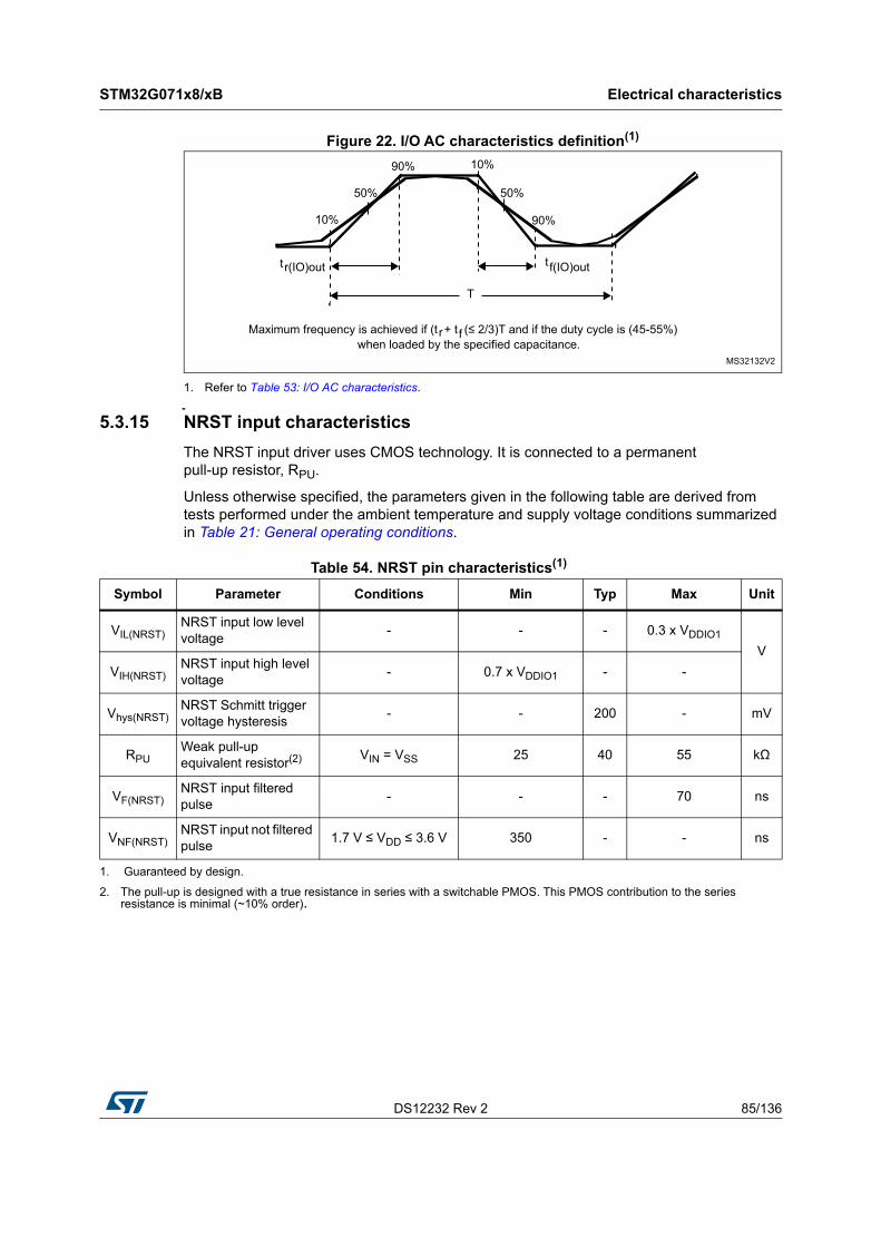
DS12232 Rev 2 85/136
STM32G071x8/xB Electrical characteristics
109
Figure 22. I/O AC characteristics definition(1)
1. Refer to Table 53: I/O AC characteristics.
5.3.15 NRST input characteristics
The NRST input driver uses CMOS technology. It is connected to a permanent pull-up resistor, RPU.
Unless otherwise specified, the parameters given in the following table are derived from tests performed under the ambient temperature and supply voltage conditions summarized in Table 21: General operating conditions.
MS32132V2
T
10%
50%
90% 10%
50%
90%
Maximum frequency is achieved if (t + t (≤ 2/3)T and if the duty cycle is (45-55%)when loaded by the specified capacitance.
r f
r(IO)outt f(IO)outt
Table 54. NRST pin characteristics(1)
Symbol Parameter Conditions Min Typ Max Unit
VIL(NRST)NRST input low level voltage
- - - 0.3 x VDDIO1
V
VIH(NRST)NRST input high level voltage
- 0.7 x VDDIO1 - -
Vhys(NRST)NRST Schmitt trigger voltage hysteresis
- - 200 - mV
RPUWeak pull-up equivalent resistor(2) VIN = VSS 25 40 55 kΩ
VF(NRST) NRST input filtered
pulse- - - 70 ns
VNF(NRST)NRST input not filtered pulse
1.7 V ≤ VDD ≤ 3.6 V 350 - - ns
1. Guaranteed by design.
2. The pull-up is designed with a true resistance in series with a switchable PMOS. This PMOS contribution to the series resistance is minimal (~10% order).
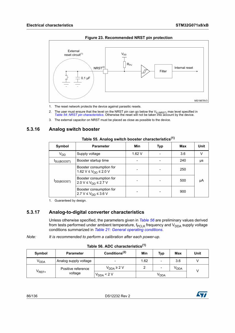
Electrical characteristics STM32G071x8/xB
86/136 DS12232 Rev 2
Figure 23. Recommended NRST pin protection
1. The reset network protects the device against parasitic resets.
2. The user must ensure that the level on the NRST pin can go below the VIL(NRST) max level specified in Table 54: NRST pin characteristics. Otherwise the reset will not be taken into account by the device.
3. The external capacitor on NRST must be placed as close as possible to the device.
5.3.16 Analog switch booster
5.3.17 Analog-to-digital converter characteristics
Unless otherwise specified, the parameters given in Table 56 are preliminary values derived from tests performed under ambient temperature, fPCLK frequency and VDDA supply voltage conditions summarized in Table 21: General operating conditions.
Note: It is recommended to perform a calibration after each power-up.
MS19878V3
RPU
VDD
Internal reset
Externalreset circuit(1)
NRST(2)
Filter
0.1 μF
Table 55. Analog switch booster characteristics(1)
1. Guaranteed by design.
Symbol Parameter Min Typ Max Unit
VDD Supply voltage 1.62 V - 3.6 V
tSU(BOOST) Booster startup time - - 240 µs
IDD(BOOST)
Booster consumption for 1.62 V ≤ VDD ≤ 2.0 V
- - 250
µABooster consumption for 2.0 V ≤ VDD ≤ 2.7 V
- - 500
Booster consumption for 2.7 V ≤ VDD ≤ 3.6 V
- - 900
Table 56. ADC characteristics(1)
Symbol Parameter Conditions(2) Min Typ Max Unit
VDDA Analog supply voltage - 1.62 - 3.6 V
VREF+ Positive reference
voltage
VDDA ≥ 2 V 2 - VDDA V
VDDA < 2 V VDDA
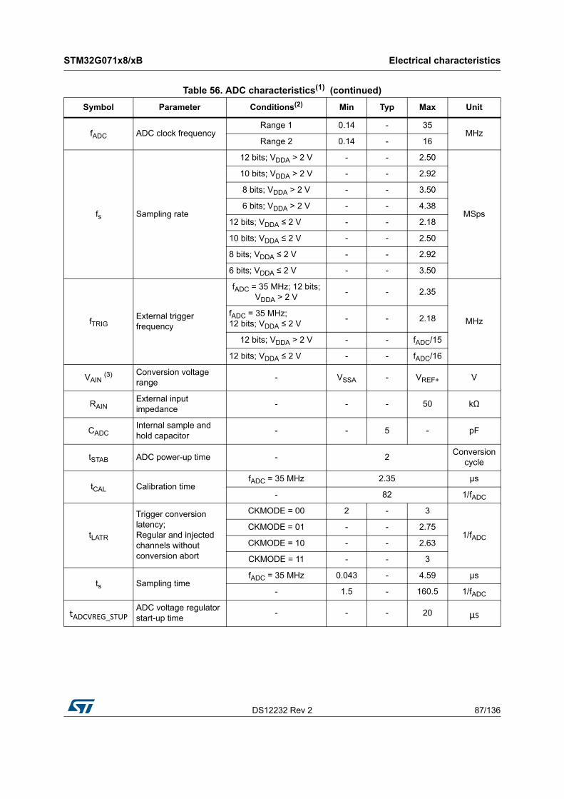
DS12232 Rev 2 87/136
STM32G071x8/xB Electrical characteristics
109
fADC ADC clock frequencyRange 1 0.14 - 35
MHzRange 2 0.14 - 16
fs Sampling rate
12 bits; VDDA > 2 V - - 2.50
MSps
10 bits; VDDA > 2 V - - 2.92
8 bits; VDDA > 2 V - - 3.50
6 bits; VDDA > 2 V - - 4.38
12 bits; VDDA ≤ 2 V - - 2.18
10 bits; VDDA ≤ 2 V - - 2.50
8 bits; VDDA ≤ 2 V - - 2.92
6 bits; VDDA ≤ 2 V - - 3.50
fTRIGExternal trigger frequency
fADC = 35 MHz; 12 bits; VDDA > 2 V
- - 2.35
MHzfADC = 35 MHz; 12 bits; VDDA ≤ 2 V
- - 2.18
12 bits; VDDA > 2 V - - fADC/15
12 bits; VDDA ≤ 2 V - - fADC/16
VAIN (3) Conversion voltage range
- VSSA - VREF+ V
RAINExternal input impedance
- - - 50 kΩ
CADCInternal sample and hold capacitor
- - 5 - pF
tSTAB ADC power-up time - 2Conversion
cycle
tCAL Calibration timefADC = 35 MHz 2.35 µs
- 82 1/fADC
tLATR
Trigger conversion latency; Regular and injected channels without conversion abort
CKMODE = 00 2 - 3
1/fADC
CKMODE = 01 - - 2.75
CKMODE = 10 - - 2.63
CKMODE = 11 - - 3
ts Sampling timefADC = 35 MHz 0.043 - 4.59 µs
- 1.5 - 160.5 1/fADC
tADCVREG_STUPADC voltage regulator start-up time
- - - 20 µs
Table 56. ADC characteristics(1) (continued)
Symbol Parameter Conditions(2) Min Typ Max Unit
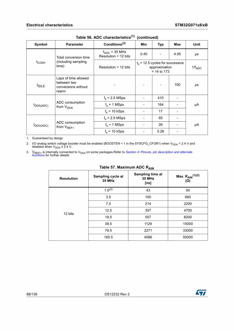
Electrical characteristics STM32G071x8/xB
88/136 DS12232 Rev 2
tCONV
Total conversion time (including sampling time)
fADC = 35 MHzResolution = 12 bits
0.40 - 4.95 µs
Resolution = 12 bitsts + 12.5 cycles for successive
approximation= 14 to 173
1/fADC
tIDLE
Laps of time allowed between two conversions without rearm
- - - 100 µs
IDDA(ADC)ADC consumption from VDDA
fs = 2.5 MSps - 410 -
µAfs = 1 MSps - 164 -
fs = 10 kSps - 17 -
IDDV(ADC)ADC consumption from VREF+
fs = 2.5 MSps - 65 -
µAfs = 1 MSps - 26 -
fs = 10 kSps - 0.26 -
1. Guaranteed by design
2. I/O analog switch voltage booster must be enabled (BOOSTEN = 1 in the SYSCFG_CFGR1) when VDDA < 2.4 V and disabled when VDDA ≥ 2.4 V.
3. VREF+ is internally connected to VDDA on some packages.Refer to Section 4: Pinouts, pin description and alternate functions for further details.
Table 56. ADC characteristics(1) (continued)
Symbol Parameter Conditions(2) Min Typ Max Unit
Table 57. Maximum ADC RAIN .
ResolutionSampling cycle at
35 MHz
Sampling time at 35 MHz
[ns]
Max. RAIN(1)(2)
(Ω)
12 bits
1.5(3) 43 50
3.5 100 680
7.5 214 2200
12.5 357 4700
19.5 557 8200
39.5 1129 15000
79.5 2271 33000
160.5 4586 50000
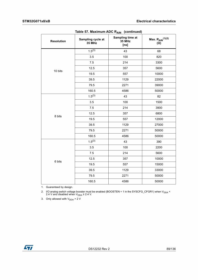
DS12232 Rev 2 89/136
STM32G071x8/xB Electrical characteristics
109
10 bits
1.5(3) 43 68
3.5 100 820
7.5 214 3300
12.5 357 5600
19.5 557 10000
39.5 1129 22000
79.5 2271 39000
160.5 4586 50000
8 bits
1.5(3) 43 82
3.5 100 1500
7.5 214 3900
12.5 357 6800
19.5 557 12000
39.5 1129 27000
79.5 2271 50000
160.5 4586 50000
6 bits
1.5(3) 43 390
3.5 100 2200
7.5 214 5600
12.5 357 10000
19.5 557 15000
39.5 1129 33000
79.5 2271 50000
160.5 4586 50000
1. Guaranteed by design.
2. I/O analog switch voltage booster must be enabled (BOOSTEN = 1 in the SYSCFG_CFGR1) when VDDA < 2.4 V and disabled when VDDA ≥ 2.4 V.
3. Only allowed with VDDA > 2 V
Table 57. Maximum ADC RAIN . (continued)
ResolutionSampling cycle at
35 MHz
Sampling time at 35 MHz
[ns]
Max. RAIN(1)(2)
(Ω)
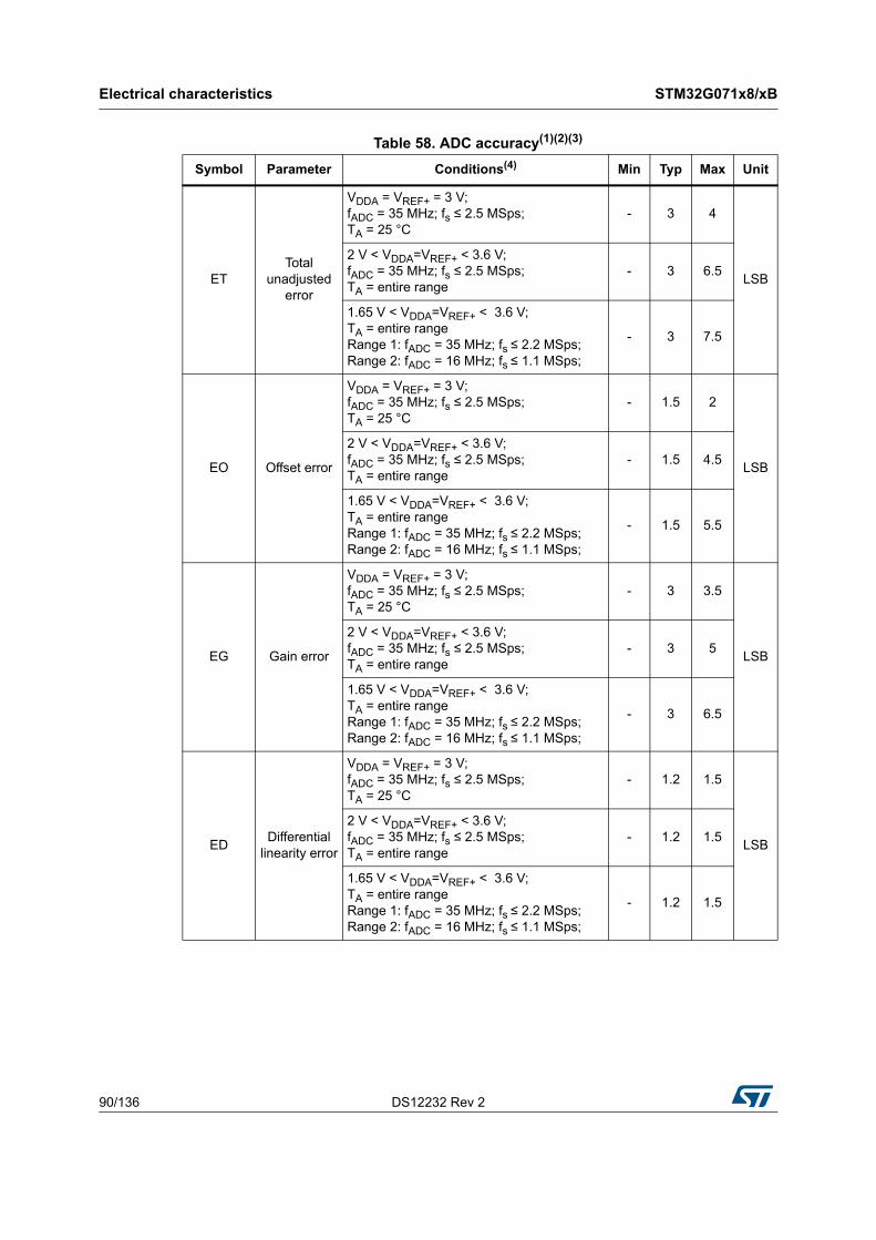
Electrical characteristics STM32G071x8/xB
90/136 DS12232 Rev 2
Table 58. ADC accuracy(1)(2)(3)
Symbol Parameter Conditions(4) Min Typ Max Unit
ETTotal
unadjusted error
VDDA = VREF+ = 3 V; fADC = 35 MHz; fs ≤ 2.5 MSps; TA = 25 °C
- 3 4
LSB
2 V < VDDA=VREF+ < 3.6 V; fADC = 35 MHz; fs ≤ 2.5 MSps; TA = entire range
- 3 6.5
1.65 V < VDDA=VREF+ < 3.6 V; TA = entire range Range 1: fADC = 35 MHz; fs ≤ 2.2 MSps; Range 2: fADC = 16 MHz; fs ≤ 1.1 MSps;
- 3 7.5
EO Offset error
VDDA = VREF+ = 3 V; fADC = 35 MHz; fs ≤ 2.5 MSps; TA = 25 °C
- 1.5 2
LSB
2 V < VDDA=VREF+ < 3.6 V; fADC = 35 MHz; fs ≤ 2.5 MSps; TA = entire range
- 1.5 4.5
1.65 V < VDDA=VREF+ < 3.6 V; TA = entire range Range 1: fADC = 35 MHz; fs ≤ 2.2 MSps; Range 2: fADC = 16 MHz; fs ≤ 1.1 MSps;
- 1.5 5.5
EG Gain error
VDDA = VREF+ = 3 V; fADC = 35 MHz; fs ≤ 2.5 MSps; TA = 25 °C
- 3 3.5
LSB
2 V < VDDA=VREF+ < 3.6 V; fADC = 35 MHz; fs ≤ 2.5 MSps; TA = entire range
- 3 5
1.65 V < VDDA=VREF+ < 3.6 V; TA = entire range Range 1: fADC = 35 MHz; fs ≤ 2.2 MSps; Range 2: fADC = 16 MHz; fs ≤ 1.1 MSps;
- 3 6.5
EDDifferential
linearity error
VDDA = VREF+ = 3 V; fADC = 35 MHz; fs ≤ 2.5 MSps; TA = 25 °C
- 1.2 1.5
LSB
2 V < VDDA=VREF+ < 3.6 V; fADC = 35 MHz; fs ≤ 2.5 MSps; TA = entire range
- 1.2 1.5
1.65 V < VDDA=VREF+ < 3.6 V; TA = entire range Range 1: fADC = 35 MHz; fs ≤ 2.2 MSps; Range 2: fADC = 16 MHz; fs ≤ 1.1 MSps;
- 1.2 1.5
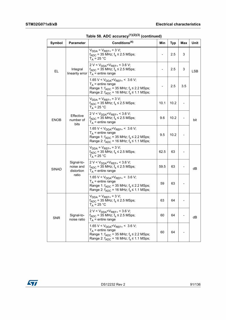
DS12232 Rev 2 91/136
STM32G071x8/xB Electrical characteristics
109
ELIntegral
linearity error
VDDA = VREF+ = 3 V; fADC = 35 MHz; fs ≤ 2.5 MSps; TA = 25 °C
- 2.5 3
LSB
2 V < VDDA=VREF+ < 3.6 V; fADC = 35 MHz; fs ≤ 2.5 MSps; TA = entire range
- 2.5 3
1.65 V < VDDA=VREF+ < 3.6 V; TA = entire range Range 1: fADC = 35 MHz; fs ≤ 2.2 MSps; Range 2: fADC = 16 MHz; fs ≤ 1.1 MSps;
- 2.5 3.5
ENOBEffective
number of bits
VDDA = VREF+ = 3 V; fADC = 35 MHz; fs ≤ 2.5 MSps; TA = 25 °C
10.1 10.2 -
bit
2 V < VDDA=VREF+ < 3.6 V; fADC = 35 MHz; fs ≤ 2.5 MSps; TA = entire range
9.6 10.2 -
1.65 V < VDDA=VREF+ < 3.6 V; TA = entire range Range 1: fADC = 35 MHz; fs ≤ 2.2 MSps; Range 2: fADC = 16 MHz; fs ≤ 1.1 MSps;
9.5 10.2 -
SINAD
Signal-to-noise and distortion
ratio
VDDA = VREF+ = 3 V; fADC = 35 MHz; fs ≤ 2.5 MSps; TA = 25 °C
62.5 63 -
dB
2 V < VDDA=VREF+ < 3.6 V; fADC = 35 MHz; fs ≤ 2.5 MSps; TA = entire range
59.5 63 -
1.65 V < VDDA=VREF+ < 3.6 V; TA = entire range Range 1: fADC = 35 MHz; fs ≤ 2.2 MSps; Range 2: fADC = 16 MHz; fs ≤ 1.1 MSps;
59 63 -
SNRSignal-to-noise ratio
VDDA = VREF+ = 3 V; fADC = 35 MHz; fs ≤ 2.5 MSps; TA = 25 °C
63 64 -
dB
2 V < VDDA=VREF+ < 3.6 V; fADC = 35 MHz; fs ≤ 2.5 MSps; TA = entire range
60 64 -
1.65 V < VDDA=VREF+ < 3.6 V; TA = entire range Range 1: fADC = 35 MHz; fs ≤ 2.2 MSps; Range 2: fADC = 16 MHz; fs ≤ 1.1 MSps;
60 64 -
Table 58. ADC accuracy(1)(2)(3) (continued)
Symbol Parameter Conditions(4) Min Typ Max Unit
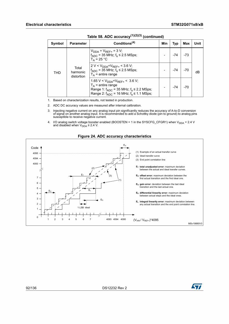
Electrical characteristics STM32G071x8/xB
92/136 DS12232 Rev 2
Figure 24. ADC accuracy characteristics
THD
Total harmonic distortion
VDDA = VREF+ = 3 V; fADC = 35 MHz; fs ≤ 2.5 MSps; TA = 25 °C
- -74 -73
dB
2 V < VDDA=VREF+ < 3.6 V; fADC = 35 MHz; fs ≤ 2.5 MSps; TA = entire range
- -74 -70
1.65 V < VDDA=VREF+ < 3.6 V; TA = entire range Range 1: fADC = 35 MHz; fs ≤ 2.2 MSps; Range 2: fADC = 16 MHz; fs ≤ 1.1 MSps;
- -74 -70
1. Based on characterization results, not tested in production.
2. ADC DC accuracy values are measured after internal calibration.
3. Injecting negative current on any analog input pin significantly reduces the accuracy of A-to-D conversion of signal on another analog input. It is recommended to add a Schottky diode (pin to ground) to analog pins susceptible to receive negative current.
4. I/O analog switch voltage booster enabled (BOOSTEN = 1 in the SYSCFG_CFGR1) when VDDA < 2.4 V and disabled when VDDA ≥ 2.4 V.
Table 58. ADC accuracy(1)(2)(3) (continued)
Symbol Parameter Conditions(4) Min Typ Max Unit
MSv19880V3
(1) Example of an actual transfer curve
(2) Ideal transfer curve
(3) End point correlation line
4095
4094
4093
7
6
5
4
3
2
1
02 3 4 5 61 7 4093 4094 4095
ED
1 LSB ideal
(1)
(3)
(2)
EL
ET
EG
EO
Code
(VAIN / VREF+)*4095
ET total unadjusted error: maximum deviation between the actual and ideal transfer curves.
EG gain error: deviation between the last ideal transition and the last actual one.
ED differential linearity error: maximum deviation between actual steps and the ideal ones.
EL integral linearity error: maximum deviation between any actual transition and the end point correlation line.
EO offset error: maximum deviation between the first actual transition and the first ideal one.
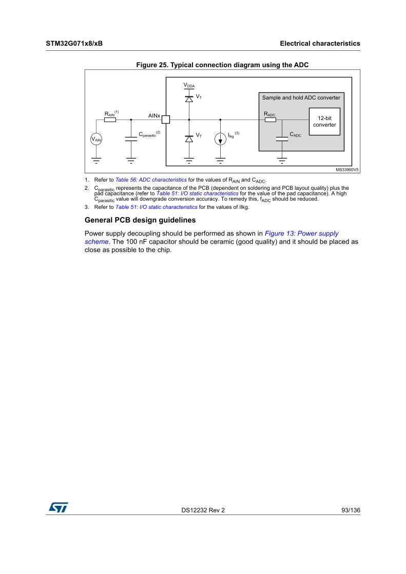
DS12232 Rev 2 93/136
STM32G071x8/xB Electrical characteristics
109
Figure 25. Typical connection diagram using the ADC
1. Refer to Table 56: ADC characteristics for the values of RAIN and CADC.
2. Cparasitic represents the capacitance of the PCB (dependent on soldering and PCB layout quality) plus the pad capacitance (refer to Table 51: I/O static characteristics for the value of the pad capacitance). A high Cparasitic value will downgrade conversion accuracy. To remedy this, fADC should be reduced.
3. Refer to Table 51: I/O static characteristics for the values of Ilkg.
General PCB design guidelines
Power supply decoupling should be performed as shown in Figure 13: Power supply scheme. The 100 nF capacitor should be ceramic (good quality) and it should be placed as close as possible to the chip.
MS33900V5
Sample and hold ADC converter
12-bit converter
Cparasitic(2) Ilkg
(3) VT CADC
VDDA
RAIN(1)
VAIN
VT
AINx RADC
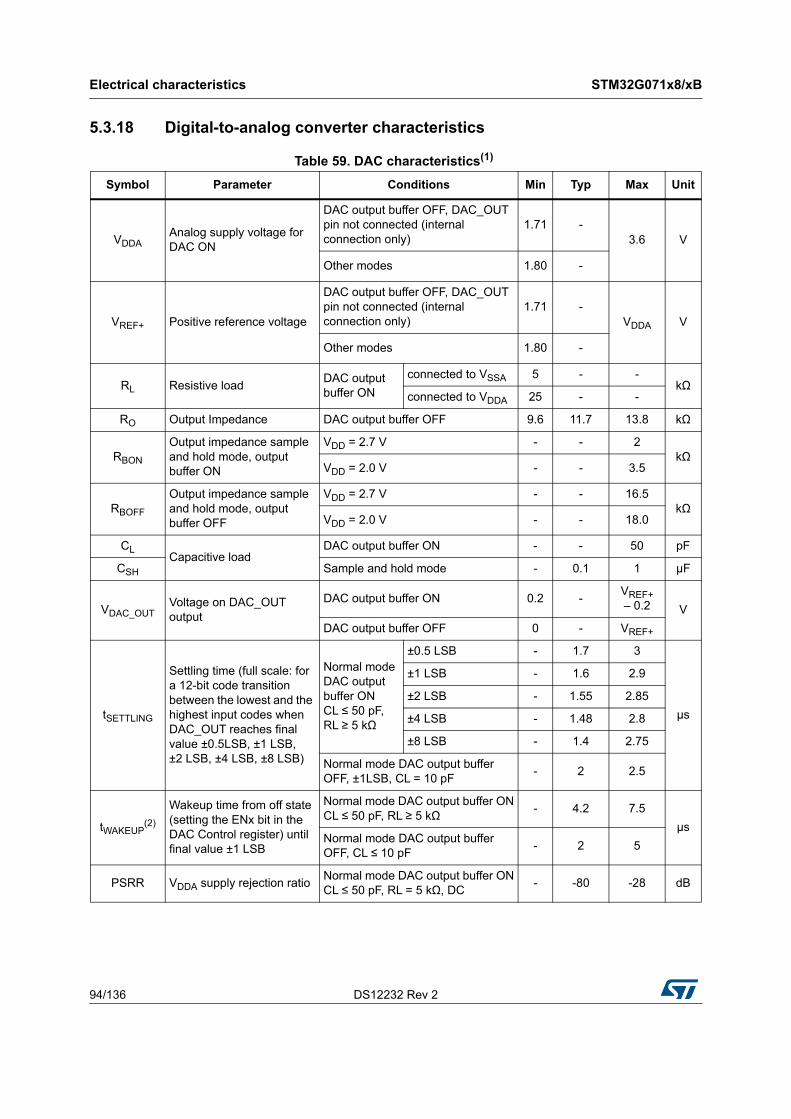
Electrical characteristics STM32G071x8/xB
94/136 DS12232 Rev 2
5.3.18 Digital-to-analog converter characteristics
Table 59. DAC characteristics(1)
Symbol Parameter Conditions Min Typ Max Unit
VDDAAnalog supply voltage for DAC ON
DAC output buffer OFF, DAC_OUT pin not connected (internal connection only)
1.71 -3.6 V
Other modes 1.80 -
VREF+ Positive reference voltage
DAC output buffer OFF, DAC_OUT pin not connected (internal connection only)
1.71 -VDDA V
Other modes 1.80 -
RL Resistive loadDAC output buffer ON
connected to VSSA 5 - -kΩ
connected to VDDA 25 - -
RO Output Impedance DAC output buffer OFF 9.6 11.7 13.8 kΩ
RBON
Output impedance sample and hold mode, output buffer ON
VDD = 2.7 V - - 2kΩ
VDD = 2.0 V - - 3.5
RBOFF
Output impedance sample and hold mode, output buffer OFF
VDD = 2.7 V - - 16.5kΩ
VDD = 2.0 V - - 18.0
CLCapacitive load
DAC output buffer ON - - 50 pF
CSH Sample and hold mode - 0.1 1 µF
VDAC_OUTVoltage on DAC_OUT output
DAC output buffer ON 0.2 -VREF+ – 0.2 V
DAC output buffer OFF 0 - VREF+
tSETTLING
Settling time (full scale: for a 12-bit code transition between the lowest and the highest input codes when DAC_OUT reaches final value ±0.5LSB, ±1 LSB, ±2 LSB, ±4 LSB, ±8 LSB)
Normal mode DAC output buffer ON CL ≤ 50 pF, RL ≥ 5 kΩ
±0.5 LSB - 1.7 3
µs
±1 LSB - 1.6 2.9
±2 LSB - 1.55 2.85
±4 LSB - 1.48 2.8
±8 LSB - 1.4 2.75
Normal mode DAC output buffer OFF, ±1LSB, CL = 10 pF
- 2 2.5
tWAKEUP(2)
Wakeup time from off state (setting the ENx bit in the DAC Control register) until final value ±1 LSB
Normal mode DAC output buffer ON CL ≤ 50 pF, RL ≥ 5 kΩ
- 4.2 7.5
µsNormal mode DAC output buffer OFF, CL ≤ 10 pF
- 2 5
PSRR VDDA supply rejection ratioNormal mode DAC output buffer ON CL ≤ 50 pF, RL = 5 kΩ, DC
- -80 -28 dB
DS12232 Rev 2 95/136
STM32G071x8/xB Electrical characteristics
109
TW_to_W
Minimum time between two consecutive writes into the DAC_DORx register to guarantee a correct DAC_OUT for a small variation of the input code (1 LSB)
DAC_MCR:MODEx[2:0] = 000 or 001 CL ≤ 50 pF; RL ≥ 5 kΩ
1 - -
µsDAC_MCR:MODEx[2:0] = 010 or 011 CL ≤ 10 pF
1.4 - -
tSAMP
Sampling time in sample and hold mode (code transition between the lowest input code and the highest input code when DACOUT reaches final value ±1LSB)
DAC_OUT pin connected
DAC output buffer ON, CSH = 100 nF
- 0.7 3.5
msDAC output buffer OFF, CSH = 100 nF
- 10.5 18
DAC_OUT pin not connected (internal connection only)
DAC output buffer OFF
- 2 3.5 µs
Ileak Output leakage currentSample and hold mode, DAC_OUT pin connected
- - -(3) nA
CIintInternal sample and hold capacitor
- 5.2 7 8.8 pF
tTRIM Middle code offset trim time DAC output buffer ON 50 - - µs
VoffsetMiddle code offset for 1 trim code step
VREF+ = 3.6 V - 1500 -µV
VREF+ = 1.8 V - 750 -
IDDA(DAC)DAC consumption from VDDA
DAC output buffer ON
No load, middle code (0x800)
- 315 500
µA
No load, worst code (0xF1C)
- 450 670
DAC output buffer OFF
No load, middle code (0x800)
- - 0.2
Sample and hold mode, CSH = 100 nF
-315 ₓ
Ton/(Ton+Toff)
(4)
670 ₓTon/(Ton+
Toff)(4)
Table 59. DAC characteristics(1) (continued)
Symbol Parameter Conditions Min Typ Max Unit
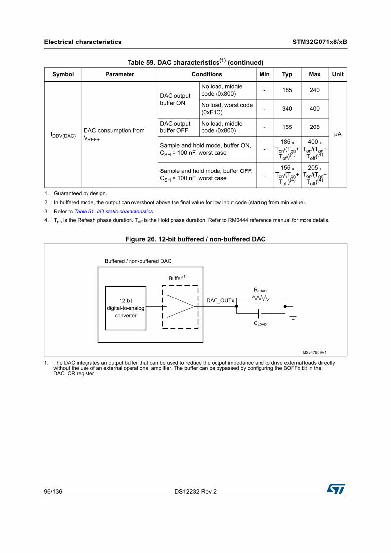
Electrical characteristics STM32G071x8/xB
96/136 DS12232 Rev 2
Figure 26. 12-bit buffered / non-buffered DAC
1. The DAC integrates an output buffer that can be used to reduce the output impedance and to drive external loads directly without the use of an external operational amplifier. The buffer can be bypassed by configuring the BOFFx bit in the DAC_CR register.
IDDV(DAC)DAC consumption from VREF+
DAC output buffer ON
No load, middle code (0x800)
- 185 240
µA
No load, worst code (0xF1C)
- 340 400
DAC output buffer OFF
No load, middle code (0x800)
- 155 205
Sample and hold mode, buffer ON, CSH = 100 nF, worst case
-185 ₓ
Ton/(Ton+Toff)
(4)
400 ₓTon/(Ton+
Toff)(4)
Sample and hold mode, buffer OFF, CSH = 100 nF, worst case
-155 ₓ
Ton/(Ton+Toff)
(4)
205 ₓTon/(Ton+
Toff)(4)
1. Guaranteed by design.
2. In buffered mode, the output can overshoot above the final value for low input code (starting from min value).
3. Refer to Table 51: I/O static characteristics.
4. Ton is the Refresh phase duration. Toff is the Hold phase duration. Refer to RM0444 reference manual for more details.
Table 59. DAC characteristics(1) (continued)
Symbol Parameter Conditions Min Typ Max Unit
MSv47959V1
12-bit digital-to-analog
converter
Buffered / non-buffered DAC
DAC_OUTx
RLOAD
CLOAD
Buffer(1)
DS12232 Rev 2 97/136
STM32G071x8/xB Electrical characteristics
109
.
Table 60. DAC accuracy(1)
Symbol Parameter Conditions Min Typ Max Unit
DNLDifferential non linearity (2)
DAC output buffer ON - - ±2
LSB
DAC output buffer OFF - - ±2
- monotonicity 10 bits guaranteed
INLIntegral non linearity(3)
DAC output buffer ON CL ≤ 50 pF, RL ≥ 5 kΩ
- - ±4
DAC output buffer OFF CL ≤ 50 pF, no RL
- - ±4
OffsetOffset error at code 0x800(3)
DAC output buffer ON CL ≤ 50 pF, RL ≥ 5 kΩ
VREF+ = 3.6 V - - ±12
VREF+ = 1.8 V - - ±25
DAC output buffer OFF CL ≤ 50 pF, no RL
- - ±8
Offset1Offset error at code 0x001(4)
DAC output buffer OFF CL ≤ 50 pF, no RL
- - ±5
OffsetCalOffset Error at code 0x800 after calibration
DAC output buffer ON CL ≤ 50 pF, RL ≥ 5 kΩ
VREF+ = 3.6 V - - ±5
VREF+ = 1.8 V - - ±7
Gain Gain error(5)
DAC output buffer ON CL ≤ 50 pF, RL ≥ 5 kΩ
- - ±0.5
%DAC output buffer OFF CL ≤ 50 pF, no RL
- - ±0.5
TUETotal unadjusted error
DAC output buffer ON CL ≤ 50 pF, RL ≥ 5 kΩ
- - ±30
LSBDAC output buffer OFF CL ≤ 50 pF, no RL
- - ±12
TUECal
Total unadjusted error after calibration
DAC output buffer ON CL ≤ 50 pF, RL ≥ 5 kΩ
- - ±23 LSB
SNRSignal-to-noise ratio
DAC output buffer ON CL ≤ 50 pF, RL ≥ 5 kΩ 1 kHz, BW 500 kHz
- 71.2 -
dBDAC output buffer OFF CL ≤ 50 pF, no RL, 1 kHz BW 500 kHz
- 71.6 -
THDTotal harmonic distortion
DAC output buffer ON CL ≤ 50 pF, RL ≥ 5 kΩ, 1 kHz
- -78 -
dBDAC output buffer OFF CL ≤ 50 pF, no RL, 1 kHz
- -79 -
Electrical characteristics STM32G071x8/xB
98/136 DS12232 Rev 2
5.3.19 Voltage reference buffer characteristics
SINADSignal-to-noise and distortion ratio
DAC output buffer ON CL ≤ 50 pF, RL ≥ 5 kΩ, 1 kHz
- 70.4 -
dBDAC output buffer OFF CL ≤ 50 pF, no RL, 1 kHz
- 71 -
ENOBEffective number of bits
DAC output buffer ON CL ≤ 50 pF, RL ≥ 5 kΩ, 1 kHz
- 11.4 -
bitsDAC output buffer OFF CL ≤ 50 pF, no RL, 1 kHz
- 11.5 -
1. Guaranteed by design.
2. Difference between two consecutive codes - 1 LSB.
3. Difference between measured value at Code i and the value at Code i on a line drawn between Code 0 and last Code 4095.
4. Difference between the value measured at Code (0x001) and the ideal value.
5. Difference between ideal slope of the transfer function and measured slope computed from code 0x000 and 0xFFF when buffer is OFF, and from code giving 0.2 V and (VREF+ – 0.2) V when buffer is ON.
Table 60. DAC accuracy(1) (continued)
Symbol Parameter Conditions Min Typ Max Unit
Table 61. VREFBUF characteristics(1)
Symbol Parameter Conditions Min Typ Max Unit
VDDAAnalog supply voltage
Normal modeVRS = 0 2.4 - 3.6
V
VRS = 1 2.8 - 3.6
Degraded mode(2)VRS = 0 1.65 - 2.4
VRS = 1 1.65 - 2.8
VREFBUF_
OUT
Voltage reference output
Normal modeVRS = 0 2.046(3) 2.048 2.049(3)
VRS = 1 2.498(3) 2.5 2.502(3)
Degraded mode(2)VRS = 0 VDDA-150 mV - VDDA
VRS = 1 VDDA-150 mV - VDDA
TRIMTrim step resolution
- - - ±0.05 ±0.1 %
CL Load capacitor - - 0.5 1 1.5 µF
esrEquivalent Serial Resistor of Cload
- - - - 2 Ω
IloadStatic load current
- - - - 4 mA
Iline_reg Line regulation 2.8 V ≤ VDDA ≤ 3.6 VIload = 500 µA - 200 1000
ppm/VIload = 4 mA - 100 500
Iload_reg Load regulation 500 μA ≤ Iload ≤4 mA Normal mode - 50 500 ppm/mA
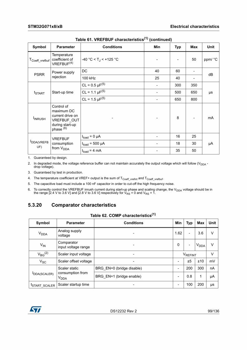
DS12232 Rev 2 99/136
STM32G071x8/xB Electrical characteristics
109
5.3.20 Comparator characteristics
TCoeff_vrefbuf
Temperature coefficient of VREFBUF(4)
-40 °C < TJ < +125 °C - - 50 ppm/ °C
PSRRPower supply rejection
DC 40 60 -dB
100 kHz 25 40 -
tSTART Start-up time
CL = 0.5 µF(5) - 300 350
µsCL = 1.1 µF(5) - 500 650
CL = 1.5 µF(5) - 650 800
IINRUSH
Control of maximum DC current drive on VREFBUF_OUT during start-up phase (6)
- - 8 - mA
IDDA(VREFB
UF)
VREFBUF consumption from VDDA
Iload = 0 µA - 16 25
µAIload = 500 µA - 18 30
Iload = 4 mA - 35 50
1. Guaranteed by design.
2. In degraded mode, the voltage reference buffer can not maintain accurately the output voltage which will follow (VDDA - drop voltage).
3. Guaranteed by test in production.
4. The temperature coefficient at VREF+ output is the sum of TCoeff_vrefint and TCoeff_vrefbuf.
5. The capacitive load must include a 100 nF capacitor in order to cut-off the high frequency noise.
6. To correctly control the VREFBUF inrush current during start-up phase and scaling change, the VDDA voltage should be in the range [2.4 V to 3.6 V] and [2.8 V to 3.6 V] respectively for VRS = 0 and VRS = 1.
Table 61. VREFBUF characteristics(1) (continued)
Symbol Parameter Conditions Min Typ Max Unit
Table 62. COMP characteristics(1)
Symbol Parameter Conditions Min Typ Max Unit
VDDAAnalog supply voltage
- 1.62 - 3.6 V
VINComparator input voltage range
- 0 - VDDA V
VBG(2) Scaler input voltage - VREFINT V
VSC Scaler offset voltage - - ±5 ±10 mV
IDDA(SCALER)
Scaler static consumption from VDDA
BRG_EN=0 (bridge disable) - 200 300 nA
BRG_EN=1 (bridge enable) - 0.8 1 µA
tSTART_SCALER Scaler startup time - - 100 200 µs
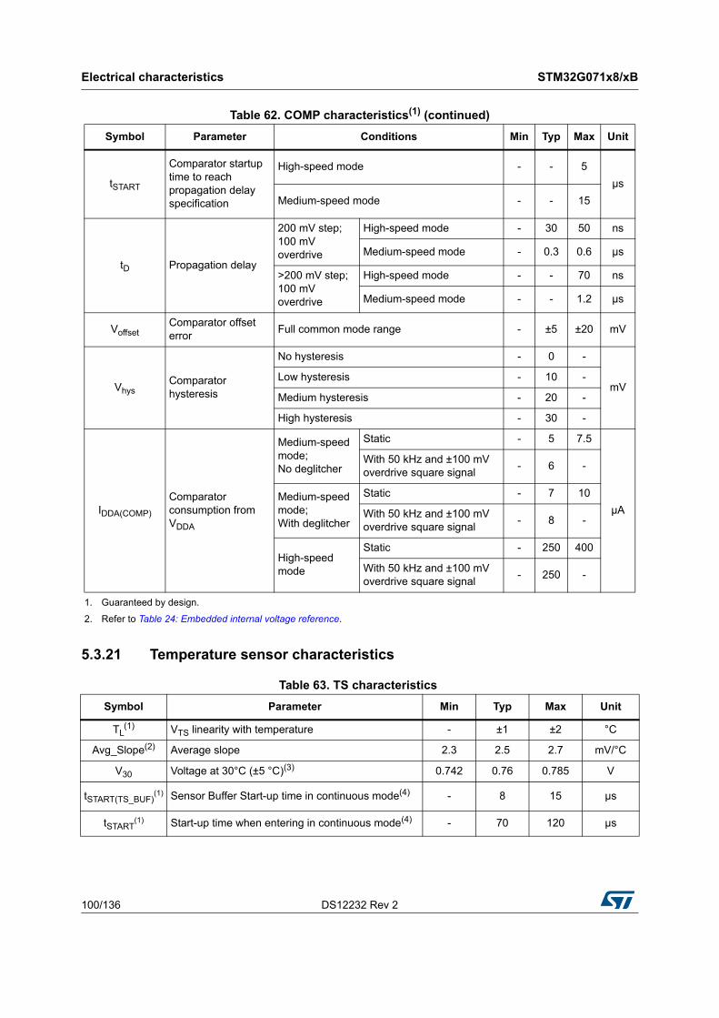
Electrical characteristics STM32G071x8/xB
100/136 DS12232 Rev 2
5.3.21 Temperature sensor characteristics
tSTART
Comparator startup time to reach propagation delay specification
High-speed mode - - 5
µs
Medium-speed mode - - 15
tD Propagation delay
200 mV step; 100 mV overdrive
High-speed mode - 30 50 ns
Medium-speed mode - 0.3 0.6 µs
>200 mV step; 100 mV overdrive
High-speed mode - - 70 ns
Medium-speed mode - - 1.2 µs
VoffsetComparator offset error
Full common mode range - ±5 ±20 mV
VhysComparator hysteresis
No hysteresis - 0 -
mVLow hysteresis - 10 -
Medium hysteresis - 20 -
High hysteresis - 30 -
IDDA(COMP)
Comparator consumption from VDDA
Medium-speed mode; No deglitcher
Static - 5 7.5
µA
With 50 kHz and ±100 mV overdrive square signal
- 6 -
Medium-speed mode; With deglitcher
Static - 7 10
With 50 kHz and ±100 mV overdrive square signal
- 8 -
High-speed mode
Static - 250 400
With 50 kHz and ±100 mV overdrive square signal
- 250 -
1. Guaranteed by design.
2. Refer to Table 24: Embedded internal voltage reference.
Table 62. COMP characteristics(1) (continued)
Symbol Parameter Conditions Min Typ Max Unit
Table 63. TS characteristics
Symbol Parameter Min Typ Max Unit
TL(1) VTS linearity with temperature - ±1 ±2 °C
Avg_Slope(2) Average slope 2.3 2.5 2.7 mV/°C
V30 Voltage at 30°C (±5 °C)(3) 0.742 0.76 0.785 V
tSTART(TS_BUF)(1) Sensor Buffer Start-up time in continuous mode(4) - 8 15 µs
tSTART(1) Start-up time when entering in continuous mode(4) - 70 120 µs
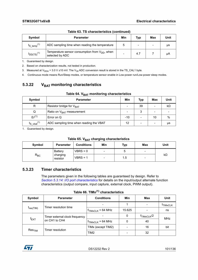
DS12232 Rev 2 101/136
STM32G071x8/xB Electrical characteristics
109
5.3.22 VBAT monitoring characteristics
5.3.23 Timer characteristics
The parameters given in the following tables are guaranteed by design. Refer to Section 5.3.14: I/O port characteristics for details on the input/output alternate function characteristics (output compare, input capture, external clock, PWM output).
tS_temp(1) ADC sampling time when reading the temperature 5 - - µs
IDD(TS)(1) Temperature sensor consumption from VDD, when
selected by ADC- 4.7 7 µA
1. Guaranteed by design.
2. Based on characterization results, not tested in production.
3. Measured at VDDA = 3.0 V ±10 mV. The V30 ADC conversion result is stored in the TS_CAL1 byte.
4. Continuous mode means Run/Sleep modes, or temperature sensor enable in Low-power run/Low-power sleep modes.
Table 63. TS characteristics (continued)
Symbol Parameter Min Typ Max Unit
Table 64. VBAT monitoring characteristics
Symbol Parameter Min Typ Max Unit
R Resistor bridge for VBAT - 39 - kΩ
Q Ratio on VBAT measurement - 3 - -
Er(1) Error on Q -10 - 10 %
tS_vbat(1) ADC sampling time when reading the VBAT 12 - - µs
1. Guaranteed by design.
Table 65. VBAT charging characteristics
Symbol Parameter Conditions Min Typ Max Unit
RBC
Battery charging resistor
VBRS = 0 - 5 -kΩ
VBRS = 1 - 1.5 -
Table 66. TIMx(1) characteristics
Symbol Parameter Conditions Min Max Unit
tres(TIM) Timer resolution time- 1 - tTIMxCLK
fTIMxCLK = 64 MHz 15.625 - ns
fEXTTimer external clock frequency on CH1 to CH4
- 0 fTIMxCLK/2MHz
fTIMxCLK = 64 MHz 0 40
ResTIM Timer resolutionTIMx (except TIM2) - 16 bit
TIM2 - 32
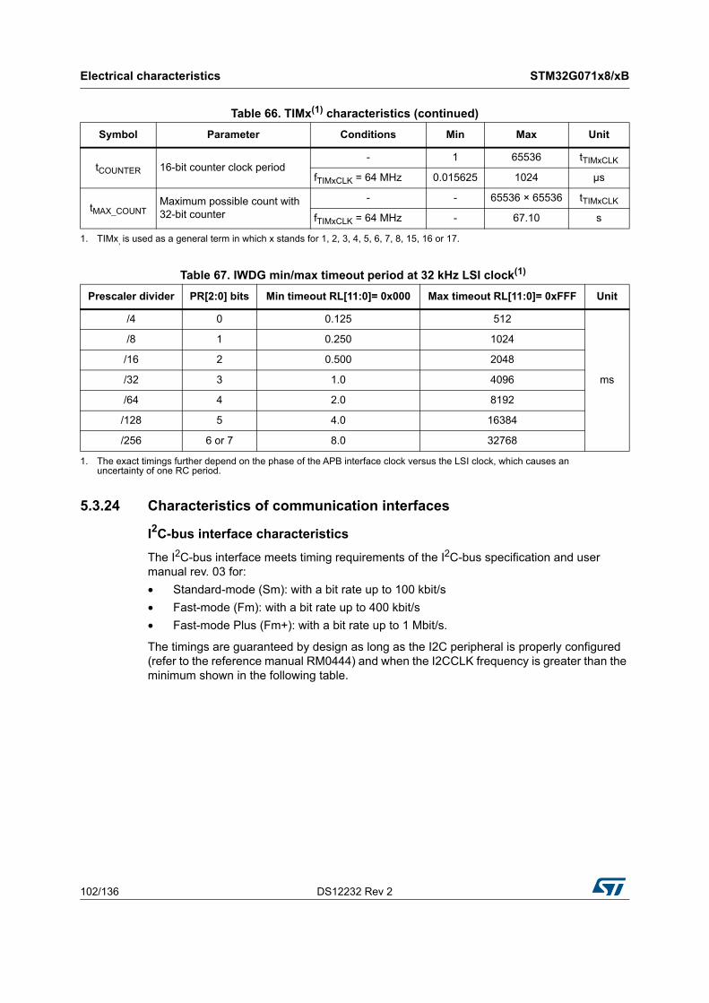
Electrical characteristics STM32G071x8/xB
102/136 DS12232 Rev 2
5.3.24 Characteristics of communication interfaces
I2C-bus interface characteristics
The I2C-bus interface meets timing requirements of the I2C-bus specification and user manual rev. 03 for:
• Standard-mode (Sm): with a bit rate up to 100 kbit/s
• Fast-mode (Fm): with a bit rate up to 400 kbit/s
• Fast-mode Plus (Fm+): with a bit rate up to 1 Mbit/s.
The timings are guaranteed by design as long as the I2C peripheral is properly configured (refer to the reference manual RM0444) and when the I2CCLK frequency is greater than the minimum shown in the following table.
tCOUNTER 16-bit counter clock period- 1 65536 tTIMxCLK
fTIMxCLK = 64 MHz 0.015625 1024 µs
tMAX_COUNTMaximum possible count with 32-bit counter
- - 65536 × 65536 tTIMxCLK
fTIMxCLK = 64 MHz - 67.10 s
1. TIMx, is used as a general term in which x stands for 1, 2, 3, 4, 5, 6, 7, 8, 15, 16 or 17.
Table 66. TIMx(1) characteristics (continued)
Symbol Parameter Conditions Min Max Unit
Table 67. IWDG min/max timeout period at 32 kHz LSI clock(1)
Prescaler divider PR[2:0] bits Min timeout RL[11:0]= 0x000 Max timeout RL[11:0]= 0xFFF Unit
/4 0 0.125 512
ms
/8 1 0.250 1024
/16 2 0.500 2048
/32 3 1.0 4096
/64 4 2.0 8192
/128 5 4.0 16384
/256 6 or 7 8.0 32768
1. The exact timings further depend on the phase of the APB interface clock versus the LSI clock, which causes an uncertainty of one RC period.
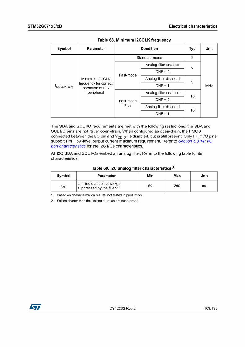
DS12232 Rev 2 103/136
STM32G071x8/xB Electrical characteristics
109
The SDA and SCL I/O requirements are met with the following restrictions: the SDA and SCL I/O pins are not “true” open-drain. When configured as open-drain, the PMOS connected between the I/O pin and VDDIO1 is disabled, but is still present. Only FT_f I/O pins support Fm+ low-level output current maximum requirement. Refer to Section 5.3.14: I/O port characteristics for the I2C I/Os characteristics.
All I2C SDA and SCL I/Os embed an analog filter. Refer to the following table for its characteristics:
Table 68. Minimum I2CCLK frequency
Symbol Parameter Condition Typ Unit
fI2CCLK(min)
Minimum I2CCLK frequency for correct
operation of I2C peripheral
Standard-mode 2
MHz
Fast-mode
Analog filter enabled9
DNF = 0
Analog filter disabled9
DNF = 1
Fast-mode Plus
Analog filter enabled18
DNF = 0
Analog filter disabled16
DNF = 1
Table 69. I2C analog filter characteristics(1)
1. Based on characterization results, not tested in production.
Symbol Parameter Min Max Unit
tAFLimiting duration of spikes suppressed by the filter(2)
2. Spikes shorter than the limiting duration are suppressed.
50 260 ns
Electrical characteristics STM32G071x8/xB
104/136 DS12232 Rev 2
SPI/I2S characteristics
Unless otherwise specified, the parameters given in Table 70 for SPI are derived from tests performed under the ambient temperature, fPCLKx frequency and supply voltage conditions summarized in Table 21: General operating conditions. The additional general conditions are:
• OSPEEDRy[1:0] set to 11 (output speed)
• capacitive load C = 30 pF
• measurement points at CMOS levels: 0.5 x VDD
Refer to Section 5.3.14: I/O port characteristics for more details on the input/output alternate function characteristics (NSS, SCK, MOSI, MISO for SPI).
Table 70. SPI characteristics(1)
Symbol Parameter Conditions Min Typ Max Unit
fSCK1/tc(SCK)
SPI clock frequency
Master mode 1.65 < VDD < 3.6 V Range 1
- -
32
MHz
Master transmitter 1.65 < VDD < 3.6 V Range 1
32
Slave receiver 1.65 < VDD < 3.6 V Range 1
32
Slave transmitter/full duplex 2.7 < VDD < 3.6 V Range 1
32
Slave transmitter/full duplex 1.65 < VDD < 3.6 V Range 1
23
1.65 < VDD < 3.6 V Range 2
8
tsu(NSS) NSS setup time Slave mode, SPI prescaler = 2 4 ₓ TPCLK - - ns
th(NSS) NSS hold time Slave mode, SPI prescaler = 2 2 ₓ TPCLK - - ns
tw(SCKH) SCK high time Master mode TPCLK- 1.5
TPCLKTPCLK+ 1.5
ns
tw(SCKL) SCK low time Master mode TPCLK- 1.5
TPCLKTPCLK+ 1.5
ns
tsu(MI)Master data input setup time
- 1 - - ns
tsu(SI)Slave data input setup time
- 1 - - ns
th(MI)Master data input hold time
- 5 - - ns
th(SI)Slave data input hold time
- 1 - - ns
ta(SO) Data output access time Slave mode 9 - 34 ns
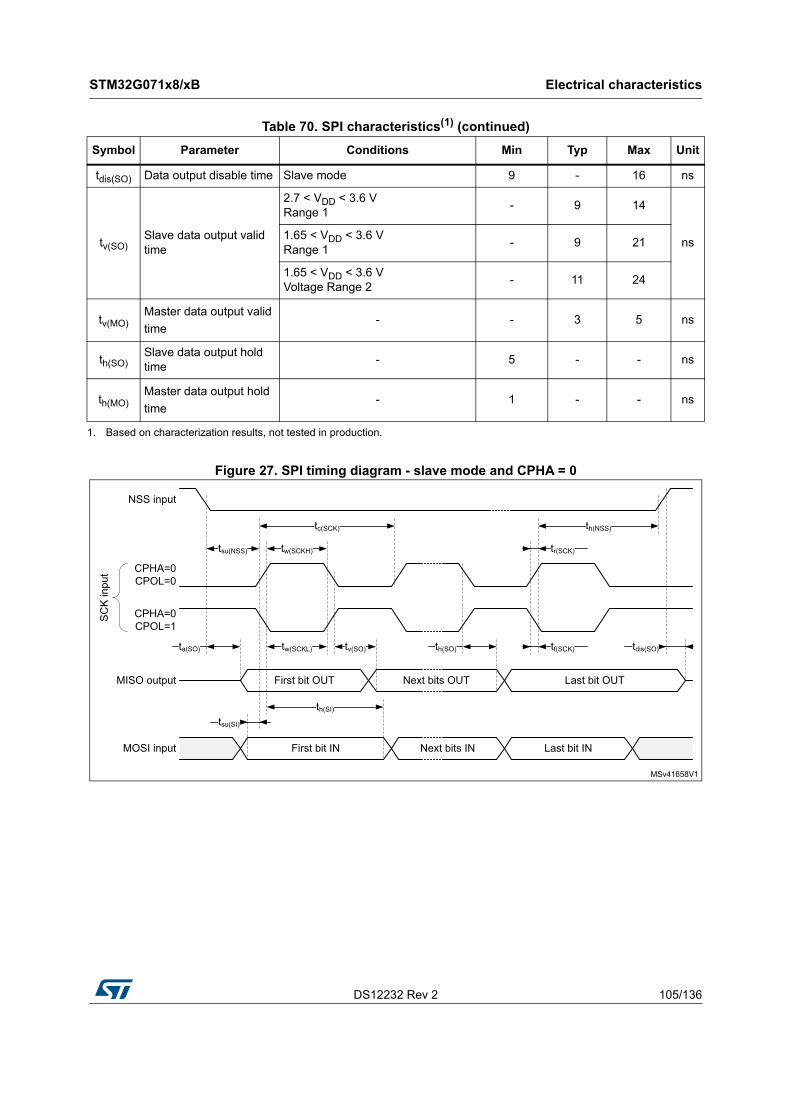
DS12232 Rev 2 105/136
STM32G071x8/xB Electrical characteristics
109
Figure 27. SPI timing diagram - slave mode and CPHA = 0
tdis(SO) Data output disable time Slave mode 9 - 16 ns
tv(SO)Slave data output valid time
2.7 < VDD < 3.6 V Range 1
- 9 14
ns1.65 < VDD < 3.6 V Range 1
- 9 21
1.65 < VDD < 3.6 V Voltage Range 2
- 11 24
tv(MO)Master data output valid
time- - 3 5 ns
th(SO)Slave data output hold time
- 5 - - ns
th(MO)Master data output hold
time- 1 - - ns
1. Based on characterization results, not tested in production.
Table 70. SPI characteristics(1) (continued)
Symbol Parameter Conditions Min Typ Max Unit
MSv41658V1
NSS input
CPHA=0CPOL=0
SC
K in
put
CPHA=0CPOL=1
MISO output
MOSI input
tsu(SI)
th(SI)
tw(SCKL)
tw(SCKH)
tc(SCK)
tr(SCK)
th(NSS)
tdis(SO)
tsu(NSS)
ta(SO) tv(SO)
Next bits IN
Last bit OUT
First bit IN
First bit OUT Next bits OUT
th(SO) tf(SCK)
Last bit IN
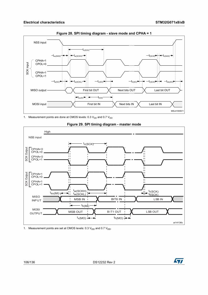
Electrical characteristics STM32G071x8/xB
106/136 DS12232 Rev 2
Figure 28. SPI timing diagram - slave mode and CPHA = 1
1. Measurement points are done at CMOS levels: 0.3 VDD and 0.7 VDD.
Figure 29. SPI timing diagram - master mode
1. Measurement points are set at CMOS levels: 0.3 VDD and 0.7 VDD.
MSv41659V1
NSS input
CPHA=1CPOL=0
SC
K in
put
CPHA=1CPOL=1
MISO output
MOSI input
tsu(SI) th(SI)
tw(SCKL)
tw(SCKH)tsu(NSS)
tc(SCK)
ta(SO) tv(SO)
First bit OUT Next bits OUT
Next bits IN
Last bit OUT
th(SO) tr(SCK)
tf(SCK) th(NSS)
tdis(SO)
First bit IN Last bit IN
ai14136c
SCK
Out
put
CPHA=0
MOSIOUTPUT
MISOINPUT
CPHA=0
LSB OUT
LSB IN
CPOL=0
CPOL=1
BIT1 OUT
NSS input
tc(SCK)
tw(SCKH)tw(SCKL)
tr(SCK)tf(SCK)
th(MI)
High
SCK
Out
put
CPHA=1
CPHA=1
CPOL=0
CPOL=1
tsu(MI)
tv(MO) th(MO)
MSB IN BIT6 IN
MSB OUT
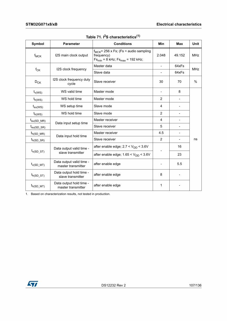
DS12232 Rev 2 107/136
STM32G071x8/xB Electrical characteristics
109
Table 71. I2S characteristics(1)
Symbol Parameter Conditions Min Max Unit
fMCK I2S main clock output fMCK= 256 x Fs; (Fs = audio sampling frequency) Fsmin = 8 kHz; Fsmax = 192 kHz;
2.048 49.152 MHz
fCK I2S clock frequency Master data - 64xFs
MHzSlave data - 64xFs
DCKI2S clock frequency duty
cycle Slave receiver 30 70 %
tv(WS) WS valid time Master mode - 8
ns
th(WS) WS hold time Master mode 2 -
tsu(WS) WS setup time Slave mode 4 -
th(WS) WS hold time Slave mode 2 -
tsu(SD_MR)Data input setup time
Master receiver 4 -
tsu(SD_SR) Slave receiver 5 -
th(SD_MR)Data input hold time
Master receiver 4.5 -
th(SD_SR) Slave receiver 2 -
tv(SD_ST)Data output valid time -
slave transmitter
after enable edge; 2.7 < VDD < 3.6V -
16
after enable edge; 1.65 < VDD < 3.6V 23
tv(SD_MT)Data output valid time -
master transmitterafter enable edge - 5.5
th(SD_ST)Data output hold time -
slave transmitterafter enable edge 8 -
th(SD_MT)Data output hold time -
master transmitterafter enable edge 1 -
1. Based on characterization results, not tested in production.
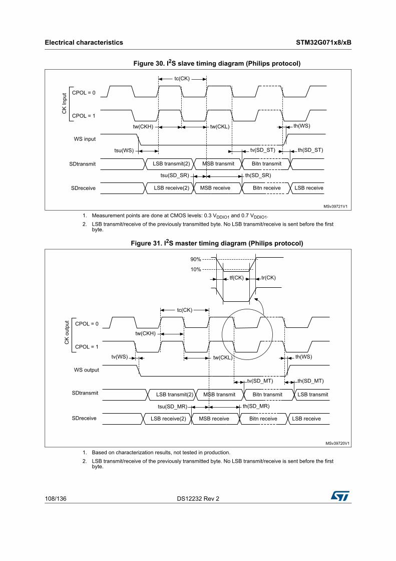
Electrical characteristics STM32G071x8/xB
108/136 DS12232 Rev 2
Figure 30. I2S slave timing diagram (Philips protocol)
1. Measurement points are done at CMOS levels: 0.3 VDDIO1 and 0.7 VDDIO1.
2. LSB transmit/receive of the previously transmitted byte. No LSB transmit/receive is sent before the first byte.
Figure 31. I2S master timing diagram (Philips protocol)
1. Based on characterization results, not tested in production.
2. LSB transmit/receive of the previously transmitted byte. No LSB transmit/receive is sent before the first byte.
MSv39721V1
CK
Inpu
t CPOL = 0
CPOL = 1
tc(CK)
WS input
SDtransmit
SDreceive
tw(CKH) tw(CKL)
tsu(WS) tv(SD_ST) th(SD_ST)
th(WS)
tsu(SD_SR) th(SD_SR)
MSB receive Bitn receive LSB receive
MSB transmit Bitn transmit
LSB receive(2)
LSB transmit(2)
MSv39720V1
CK
out
put CPOL = 0
CPOL = 1
tc(CK)
WS output
SDreceive
SDtransmit
tw(CKH)
tw(CKL)
tsu(SD_MR)
tv(SD_MT) th(SD_MT)
th(WS)
th(SD_MR)
MSB receive Bitn receive LSB receive
MSB transmit Bitn transmit LSB transmit
tf(CK) tr(CK)
tv(WS)
LSB receive(2)
LSB transmit(2)
10%
90%
DS12232 Rev 2 109/136
STM32G071x8/xB Electrical characteristics
109
USART characteristics
Unless otherwise specified, the parameters given in Table 72 for USART are derived from tests performed under the ambient temperature, fPCLKx frequency and supply voltage conditions summarized in Table 21: General operating conditions. The additional general conditions are:
• OSPEEDRy[1:0] set to 10 (output speed)
• capacitive load C = 30 pF
• measurement points at CMOS levels: 0.5 x VDD
Refer to Section 5.3.14: I/O port characteristics for more details on the input/output alternate function characteristics (NSS, CK, TX, and RX for USART).
5.3.25 UCPD characteristics
UCPD1 and UCPD2 controllers comply with USB Type-C Rev.1.2 and USB Power Delivery Rev. 3.0 specifications.
Table 72. USART characteristics
Symbol Parameter Conditions Min Typ Max Unit
fCK USART clock frequencyMaster mode - - 8
MHzSlave mode - - 21
tsu(NSS) NSS setup time Slave mode tker + 2 - -
ns
th(NSS) NSS hold time Slave mode 2 - -
tw(CKH) CK high timeMaster mode
1 / fCK / 2 - 1
1 / fCK / 21 / fCK / 2
+ 1tw(CKL) CK low time
tsu(RX) Data input setup timeMaster mode tker + 2 - -
Slave mode 4 - -
th(RX) Data input hold timeMaster mode 1 - -
Slave mode 0.5 - -
tv(TX) Data output valid timeMaster mode - 0.5 1
Slave mode - 10 19
th(TX) Data output hold timeMaster mode 0 - -
Slave mode 7 - -
Table 73. UCPD operating conditions
Symbol Parameter Conditions Min Typ Max Unit
VDDUCPD operating supply voltage
Sink mode only 3.0 3.3 3.6 V
Sink and source mode 3.135 3.3 3.465 V
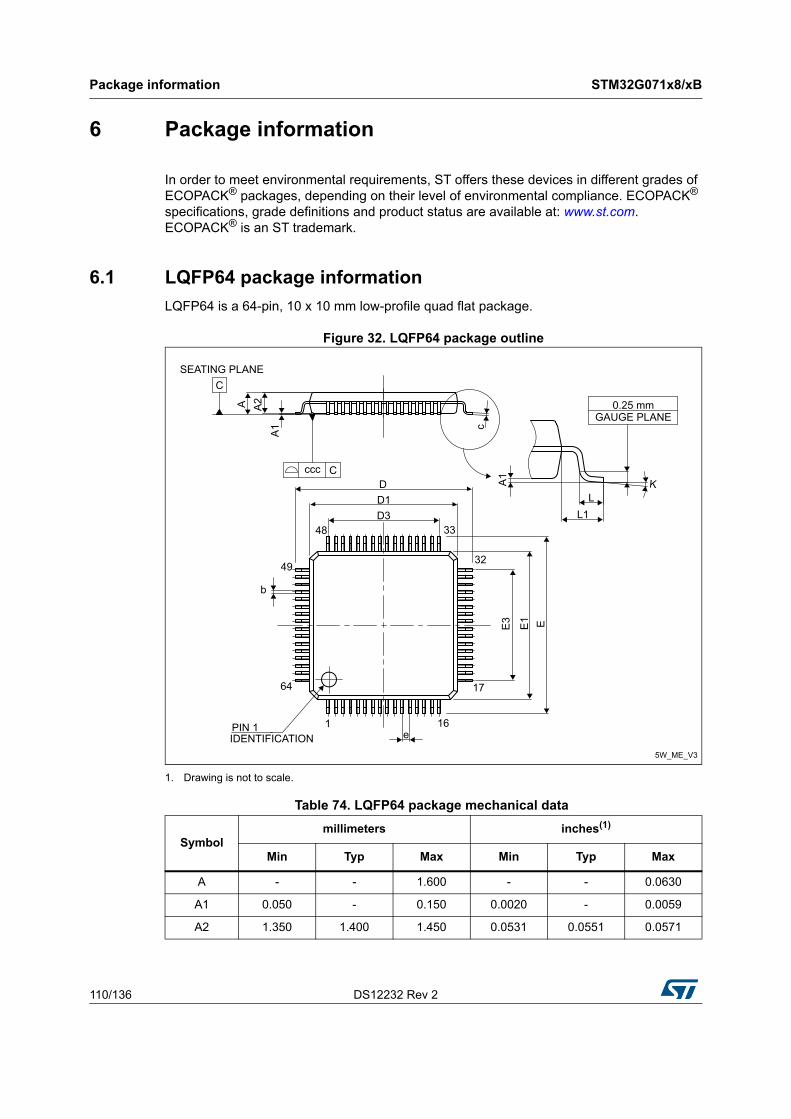
Package information STM32G071x8/xB
110/136 DS12232 Rev 2
6 Package information
In order to meet environmental requirements, ST offers these devices in different grades of ECOPACK® packages, depending on their level of environmental compliance. ECOPACK® specifications, grade definitions and product status are available at: www.st.com. ECOPACK® is an ST trademark.
6.1 LQFP64 package information
LQFP64 is a 64-pin, 10 x 10 mm low-profile quad flat package.
Figure 32. LQFP64 package outline
1. Drawing is not to scale.
Table 74. LQFP64 package mechanical data
Symbolmillimeters inches(1)
Min Typ Max Min Typ Max
A - - 1.600 - - 0.0630
A1 0.050 - 0.150 0.0020 - 0.0059
A2 1.350 1.400 1.450 0.0531 0.0551 0.0571
5W_ME_V3
A1
A2A
SEATING PLANE
ccc C
b
C
c
A1
LL1
K
IDENTIFICATIONPIN 1
DD1D3
e1 16
17
32
3348
49
64
E3 E1 E
GAUGE PLANE0.25 mm
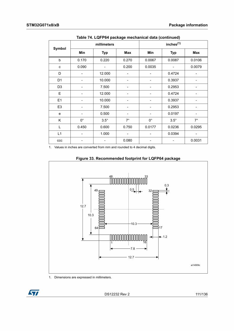
DS12232 Rev 2 111/136
STM32G071x8/xB Package information
133
Figure 33. Recommended footprint for LQFP64 package
1. Dimensions are expressed in millimeters.
b 0.170 0.220 0.270 0.0067 0.0087 0.0106
c 0.090 - 0.200 0.0035 - 0.0079
D - 12.000 - - 0.4724 -
D1 - 10.000 - - 0.3937 -
D3 - 7.500 - - 0.2953 -
E - 12.000 - - 0.4724 -
E1 - 10.000 - - 0.3937 -
E3 - 7.500 - - 0.2953 -
e - 0.500 - - 0.0197 -
K 0° 3.5° 7° 0° 3.5° 7°
L 0.450 0.600 0.750 0.0177 0.0236 0.0295
L1 - 1.000 - - 0.0394 -
ccc - - 0.080 - - 0.0031
1. Values in inches are converted from mm and rounded to 4 decimal digits.
Table 74. LQFP64 package mechanical data (continued)
Symbolmillimeters inches(1)
Min Typ Max Min Typ Max
48
3249
64 17
1 16
1.2
0.3
33
10.3
12.7
10.3
0.5
7.8
12.7
ai14909c
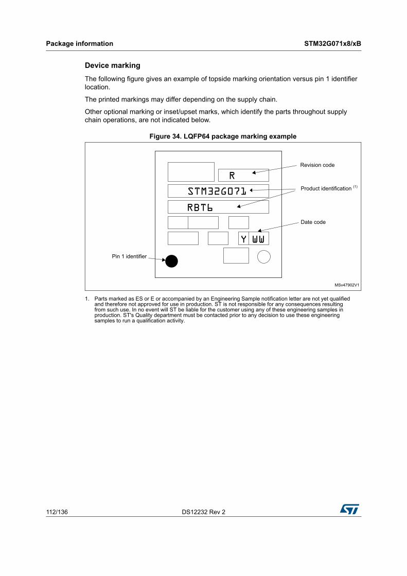
Package information STM32G071x8/xB
112/136 DS12232 Rev 2
Device marking
The following figure gives an example of topside marking orientation versus pin 1 identifier location.
The printed markings may differ depending on the supply chain.
Other optional marking or inset/upset marks, which identify the parts throughout supply chain operations, are not indicated below.
Figure 34. LQFP64 package marking example
1. Parts marked as ES or E or accompanied by an Engineering Sample notification letter are not yet qualified and therefore not approved for use in production. ST is not responsible for any consequences resulting from such use. In no event will ST be liable for the customer using any of these engineering samples in production. ST's Quality department must be contacted prior to any decision to use these engineering samples to run a qualification activity.
MSv47902V1
Product identification (1)
Pin 1 identifier
Revision code
Date code
STM32G071
RBT6
Y WW
R
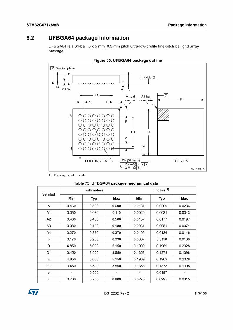
DS12232 Rev 2 113/136
STM32G071x8/xB Package information
133
6.2 UFBGA64 package information
UFBGA64 is a 64-ball, 5 x 5 mm, 0.5 mm pitch ultra-low-profile fine-pitch ball grid array package.
Figure 35. UFBGA64 package outline
1. Drawing is not to scale.
A019_ME_V1
Seating plane
A1
e F
F
D
H
Øb (64 balls)
A
E
TOP VIEWBOTTOM VIEW18
e
A
Y
X
Z
ddd Z
D1
E1
eee Z Y Xfff
ØØ
MM Z
A3A4
A1 ball identifier
A1 ball index area
A2
Table 75. UFBGA64 package mechanical data
Symbolmillimeters inches(1)
Min Typ Max Min Typ Max
A 0.460 0.530 0.600 0.0181 0.0209 0.0236
A1 0.050 0.080 0.110 0.0020 0.0031 0.0043
A2 0.400 0.450 0.500 0.0157 0.0177 0.0197
A3 0.080 0.130 0.180 0.0031 0.0051 0.0071
A4 0.270 0.320 0.370 0.0106 0.0126 0.0146
b 0.170 0.280 0.330 0.0067 0.0110 0.0130
D 4.850 5.000 5.150 0.1909 0.1969 0.2028
D1 3.450 3.500 3.550 0.1358 0.1378 0.1398
E 4.850 5.000 5.150 0.1909 0.1969 0.2028
E1 3.450 3.500 3.550 0.1358 0.1378 0.1398
e - 0.500 - - 0.0197 -
F 0.700 0.750 0.800 0.0276 0.0295 0.0315
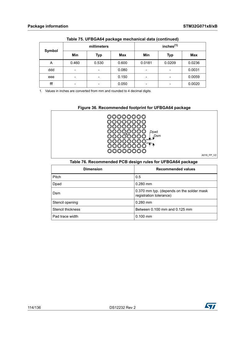
Package information STM32G071x8/xB
114/136 DS12232 Rev 2
Figure 36. Recommended footprint for UFBGA64 package
ddd - - 0.080 - - 0.0031
eee - - 0.150 - - 0.0059
fff - - 0.050 - - 0.0020
1. Values in inches are converted from mm and rounded to 4 decimal digits.
Table 75. UFBGA64 package mechanical data (continued)
Symbolmillimeters inches(1)
Min Typ Max Min Typ Max
A 0.460 0.530 0.600 0.0181 0.0209 0.0236
Table 76. Recommended PCB design rules for UFBGA64 package
Dimension Recommended values
Pitch 0.5
Dpad 0.280 mm
Dsm0.370 mm typ. (depends on the solder mask registration tolerance)
Stencil opening 0.280 mm
Stencil thickness Between 0.100 mm and 0.125 mm
Pad trace width 0.100 mm
A019_FP_V2
DpadDsm
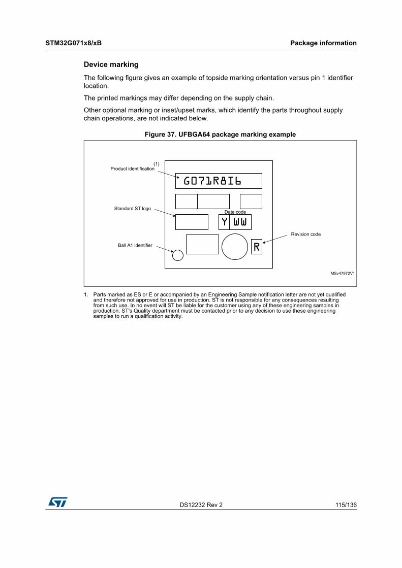
DS12232 Rev 2 115/136
STM32G071x8/xB Package information
133
Device marking
The following figure gives an example of topside marking orientation versus pin 1 identifier location.
The printed markings may differ depending on the supply chain.
Other optional marking or inset/upset marks, which identify the parts throughout supply chain operations, are not indicated below.
Figure 37. UFBGA64 package marking example
1. Parts marked as ES or E or accompanied by an Engineering Sample notification letter are not yet qualified and therefore not approved for use in production. ST is not responsible for any consequences resulting from such use. In no event will ST be liable for the customer using any of these engineering samples in production. ST's Quality department must be contacted prior to any decision to use these engineering samples to run a qualification activity.
MSv47972V1
Revision code
Y WW
G071R8I6
R
Date code
Product identification(1)
Ball A1 identifier
Standard ST logo
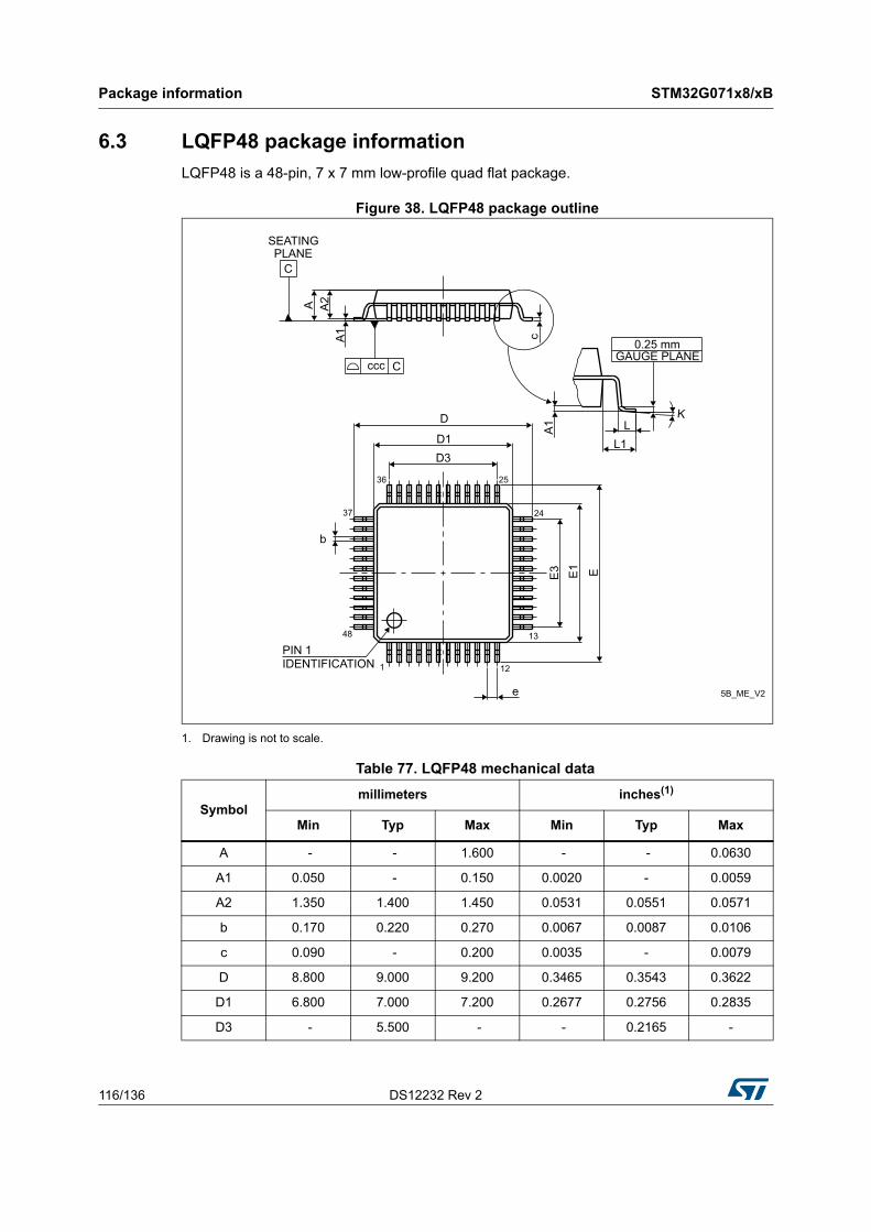
Package information STM32G071x8/xB
116/136 DS12232 Rev 2
6.3 LQFP48 package information
LQFP48 is a 48-pin, 7 x 7 mm low-profile quad flat package.
Figure 38. LQFP48 package outline
1. Drawing is not to scale.
Table 77. LQFP48 mechanical data
Symbolmillimeters inches(1)
Min Typ Max Min Typ Max
A - - 1.600 - - 0.0630
A1 0.050 - 0.150 0.0020 - 0.0059
A2 1.350 1.400 1.450 0.0531 0.0551 0.0571
b 0.170 0.220 0.270 0.0067 0.0087 0.0106
c 0.090 - 0.200 0.0035 - 0.0079
D 8.800 9.000 9.200 0.3465 0.3543 0.3622
D1 6.800 7.000 7.200 0.2677 0.2756 0.2835
D3 - 5.500 - - 0.2165 -
5B_ME_V2
PIN 1IDENTIFICATION
ccc C
C
D3
0.25 mmGAUGE PLANE
b
A1
A A2
cA
1
L1LD
D1
E3 E1 E
e
121
13
24
2536
37
48
SEATINGPLANE
K
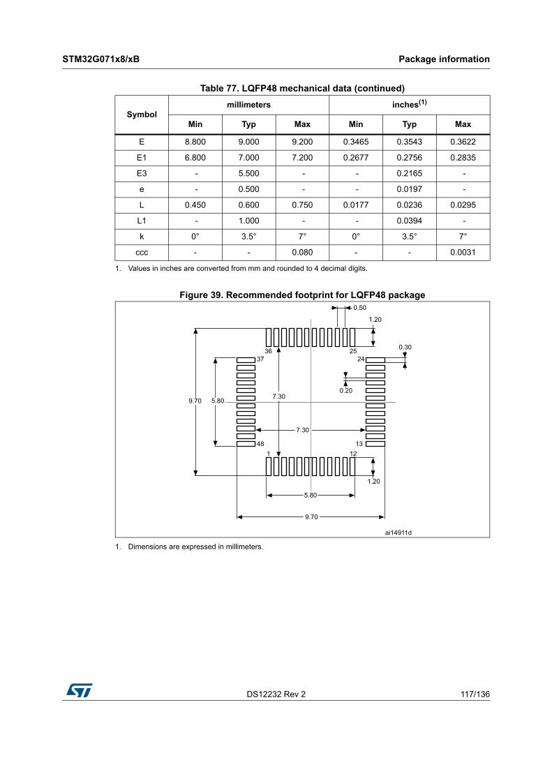
DS12232 Rev 2 117/136
STM32G071x8/xB Package information
133
Figure 39. Recommended footprint for LQFP48 package
1. Dimensions are expressed in millimeters.
E 8.800 9.000 9.200 0.3465 0.3543 0.3622
E1 6.800 7.000 7.200 0.2677 0.2756 0.2835
E3 - 5.500 - - 0.2165 -
e - 0.500 - - 0.0197 -
L 0.450 0.600 0.750 0.0177 0.0236 0.0295
L1 - 1.000 - - 0.0394 -
k 0° 3.5° 7° 0° 3.5° 7°
ccc - - 0.080 - - 0.0031
1. Values in inches are converted from mm and rounded to 4 decimal digits.
Table 77. LQFP48 mechanical data (continued)
Symbolmillimeters inches(1)
Min Typ Max Min Typ Max
9.70 5.80 7.30
12
24
0.20
7.30
1
3736
1.20
5.80
9.70
0.3025
1.20
0.50
ai14911d
1348
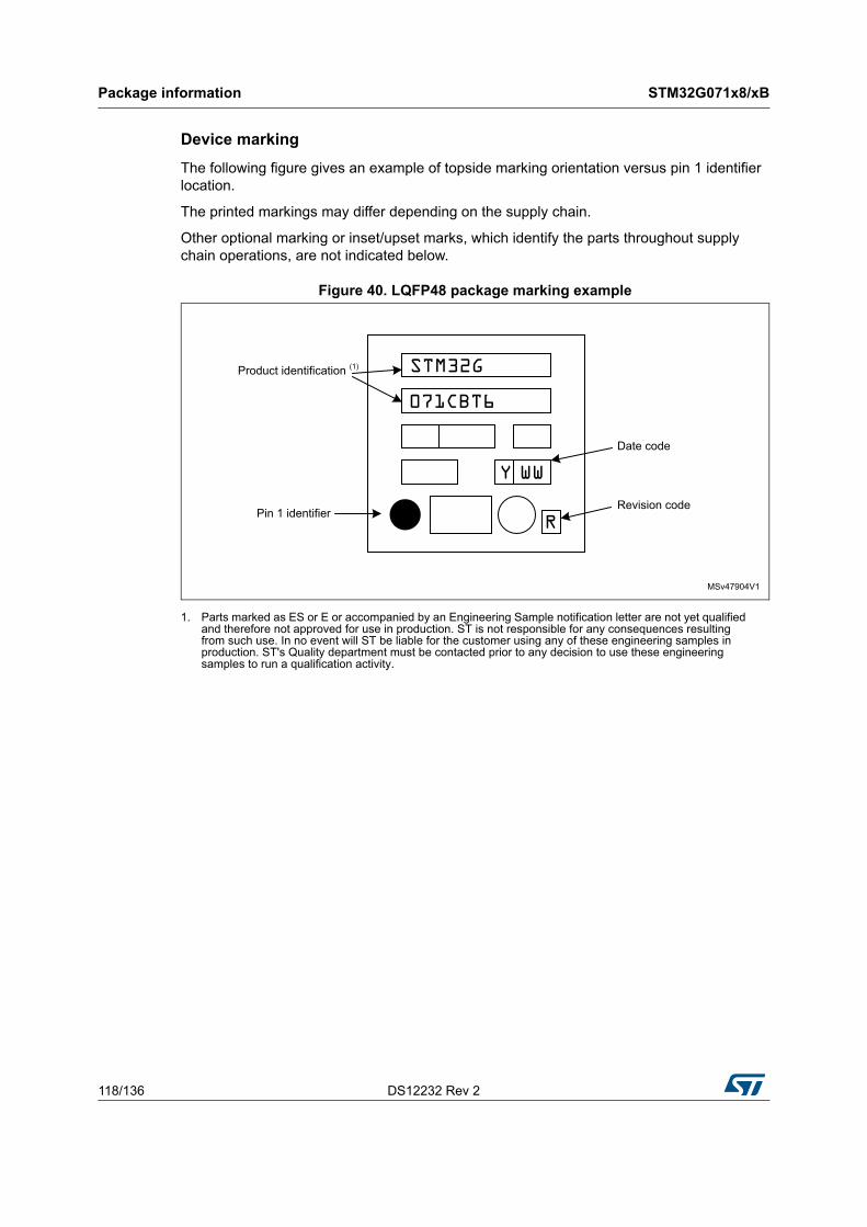
Package information STM32G071x8/xB
118/136 DS12232 Rev 2
Device marking
The following figure gives an example of topside marking orientation versus pin 1 identifier location.
The printed markings may differ depending on the supply chain.
Other optional marking or inset/upset marks, which identify the parts throughout supply chain operations, are not indicated below.
Figure 40. LQFP48 package marking example
1. Parts marked as ES or E or accompanied by an Engineering Sample notification letter are not yet qualified and therefore not approved for use in production. ST is not responsible for any consequences resulting from such use. In no event will ST be liable for the customer using any of these engineering samples in production. ST's Quality department must be contacted prior to any decision to use these engineering samples to run a qualification activity.
STM32G
MSv47904V1
071CBT6
R
Y WW
Product identification (1)
Revision code
Date code
Pin 1 identifier
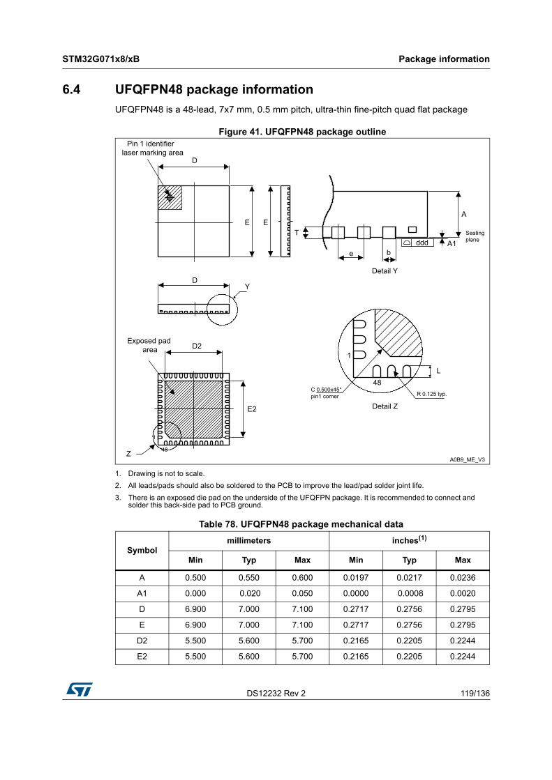
DS12232 Rev 2 119/136
STM32G071x8/xB Package information
133
6.4 UFQFPN48 package information
UFQFPN48 is a 48-lead, 7x7 mm, 0.5 mm pitch, ultra-thin fine-pitch quad flat package
Figure 41. UFQFPN48 package outline
1. Drawing is not to scale.
2. All leads/pads should also be soldered to the PCB to improve the lead/pad solder joint life.
3. There is an exposed die pad on the underside of the UFQFPN package. It is recommended to connect and solder this back-side pad to PCB ground.
Table 78. UFQFPN48 package mechanical data
Symbolmillimeters inches(1)
Min Typ Max Min Typ Max
A 0.500 0.550 0.600 0.0197 0.0217 0.0236
A1 0.000 0.020 0.050 0.0000 0.0008 0.0020
D 6.900 7.000 7.100 0.2717 0.2756 0.2795
E 6.900 7.000 7.100 0.2717 0.2756 0.2795
D2 5.500 5.600 5.700 0.2165 0.2205 0.2244
E2 5.500 5.600 5.700 0.2165 0.2205 0.2244
A0B9_ME_V3
D
Pin 1 identifierlaser marking area
E E
DY
D2
E2
Exposed pad area
Z
1
48
Detail Z
R 0.125 typ.
1
48L
C 0.500x45°pin1 corner
A
Seating planeA1
beddd
Detail Y
T
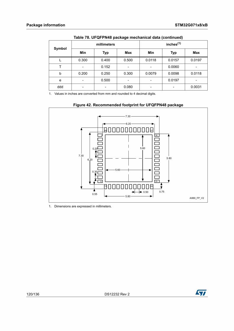
Package information STM32G071x8/xB
120/136 DS12232 Rev 2
Figure 42. Recommended footprint for UFQFPN48 package
1. Dimensions are expressed in millimeters.
L 0.300 0.400 0.500 0.0118 0.0157 0.0197
T - 0.152 - - 0.0060 -
b 0.200 0.250 0.300 0.0079 0.0098 0.0118
e - 0.500 - - 0.0197 -
ddd - - 0.080 - - 0.0031
1. Values in inches are converted from mm and rounded to 4 decimal digits.
Table 78. UFQFPN48 package mechanical data (continued)
Symbolmillimeters inches(1)
Min Typ Max Min Typ Max
7.30
7.30
0.20
0.30
0.550.50
5.80
6.20
6.20
5.60
5.60
5.80
0.75
A0B9_FP_V2
48
1
12
13 24
25
36
37
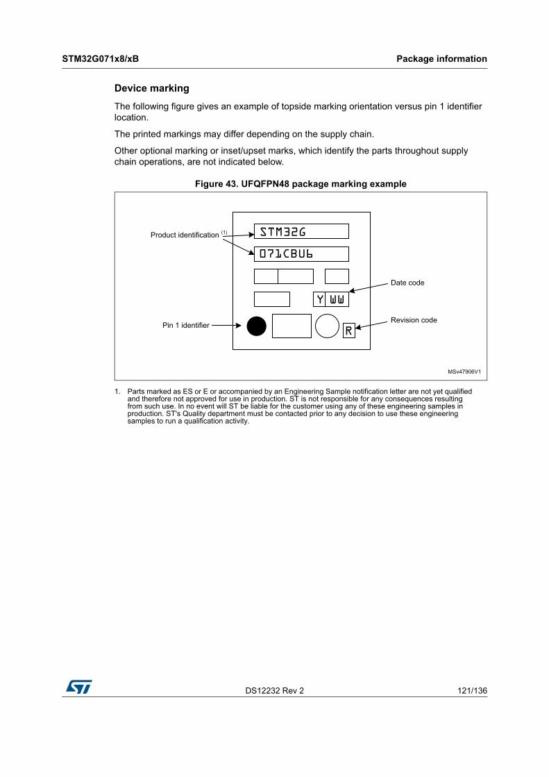
DS12232 Rev 2 121/136
STM32G071x8/xB Package information
133
Device marking
The following figure gives an example of topside marking orientation versus pin 1 identifier location.
The printed markings may differ depending on the supply chain.
Other optional marking or inset/upset marks, which identify the parts throughout supply chain operations, are not indicated below.
Figure 43. UFQFPN48 package marking example
1. Parts marked as ES or E or accompanied by an Engineering Sample notification letter are not yet qualified and therefore not approved for use in production. ST is not responsible for any consequences resulting from such use. In no event will ST be liable for the customer using any of these engineering samples in production. ST's Quality department must be contacted prior to any decision to use these engineering samples to run a qualification activity.
STM32G
MSv47906V1
071CBU6
R
Y WW
Product identification (1)
Revision code
Date code
Pin 1 identifier
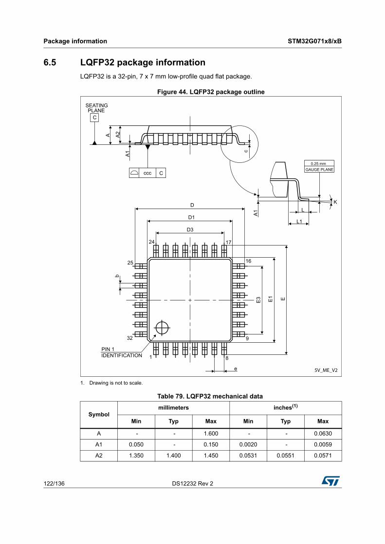
Package information STM32G071x8/xB
122/136 DS12232 Rev 2
6.5 LQFP32 package information
LQFP32 is a 32-pin, 7 x 7 mm low-profile quad flat package.
Figure 44. LQFP32 package outline
1. Drawing is not to scale.
Table 79. LQFP32 mechanical data
Symbolmillimeters inches(1)
Min Typ Max Min Typ Max
A - - 1.600 - - 0.0630
A1 0.050 - 0.150 0.0020 - 0.0059
A2 1.350 1.400 1.450 0.0531 0.0551 0.0571
D
D1
D3
E3 E1 E
1 8
9
16
1724
25
32
A1
L1
LK
A1
A2A
c
b
GAUGE PLANE0.25 mm
SEATINGPLANE
C
PIN 1IDENTIFICATION
ccc C
5V_ME_V2e
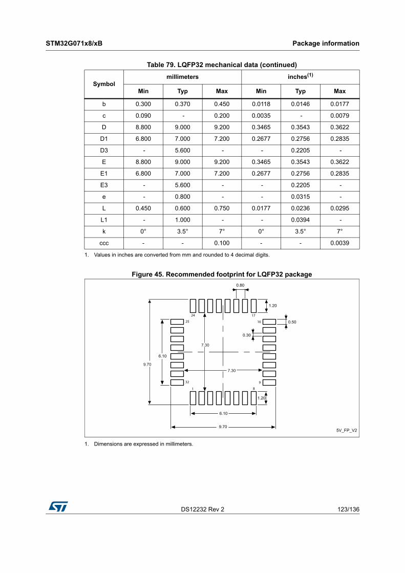
DS12232 Rev 2 123/136
STM32G071x8/xB Package information
133
Figure 45. Recommended footprint for LQFP32 package
1. Dimensions are expressed in millimeters.
b 0.300 0.370 0.450 0.0118 0.0146 0.0177
c 0.090 - 0.200 0.0035 - 0.0079
D 8.800 9.000 9.200 0.3465 0.3543 0.3622
D1 6.800 7.000 7.200 0.2677 0.2756 0.2835
D3 - 5.600 - - 0.2205 -
E 8.800 9.000 9.200 0.3465 0.3543 0.3622
E1 6.800 7.000 7.200 0.2677 0.2756 0.2835
E3 - 5.600 - - 0.2205 -
e - 0.800 - - 0.0315 -
L 0.450 0.600 0.750 0.0177 0.0236 0.0295
L1 - 1.000 - - 0.0394 -
k 0° 3.5° 7° 0° 3.5° 7°
ccc - - 0.100 - - 0.0039
1. Values in inches are converted from mm and rounded to 4 decimal digits.
Table 79. LQFP32 mechanical data (continued)
Symbolmillimeters inches(1)
Min Typ Max Min Typ Max
5V_FP_V2
1 8
9
16
1724
25
32
9.70
7.30
7.30
1.20
0.30
0.50
1.20
6.10
9.70
0.80
6.10

Package information STM32G071x8/xB
124/136 DS12232 Rev 2
Device marking
The following figure gives an example of topside marking orientation versus pin 1 identifier location.
The printed markings may differ depending on the supply chain.
Other optional marking or inset/upset marks, which identify the parts throughout supply chain operations, are not indicated below.
Figure 46. LQFP32 package marking example
1. Parts marked as ES or E or accompanied by an Engineering Sample notification letter are not yet qualified and therefore not approved for use in production. ST is not responsible for any consequences resulting from such use. In no event will ST be liable for the customer using any of these engineering samples in production. ST's Quality department must be contacted prior to any decision to use these engineering samples to run a qualification activity.
STM32G
MSv47908V1
071KBT6
R
Y WW
Product identification (1)
Revision code
Date code
Pin 1 identifier
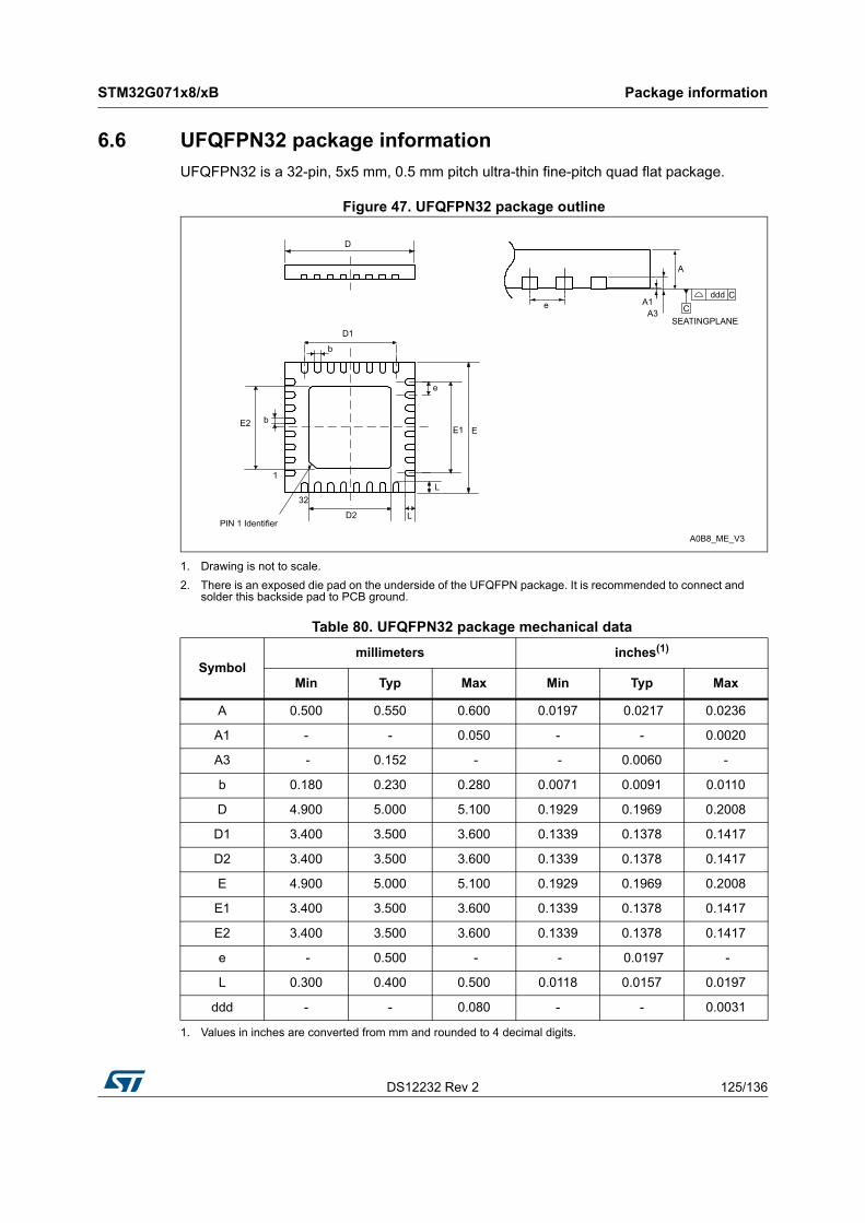
DS12232 Rev 2 125/136
STM32G071x8/xB Package information
133
6.6 UFQFPN32 package information
UFQFPN32 is a 32-pin, 5x5 mm, 0.5 mm pitch ultra-thin fine-pitch quad flat package.
Figure 47. UFQFPN32 package outline
1. Drawing is not to scale.
2. There is an exposed die pad on the underside of the UFQFPN package. It is recommended to connect and solder this backside pad to PCB ground.
Table 80. UFQFPN32 package mechanical data
Symbolmillimeters inches(1)
1. Values in inches are converted from mm and rounded to 4 decimal digits.
Min Typ Max Min Typ Max
A 0.500 0.550 0.600 0.0197 0.0217 0.0236
A1 - - 0.050 - - 0.0020
A3 - 0.152 - - 0.0060 -
b 0.180 0.230 0.280 0.0071 0.0091 0.0110
D 4.900 5.000 5.100 0.1929 0.1969 0.2008
D1 3.400 3.500 3.600 0.1339 0.1378 0.1417
D2 3.400 3.500 3.600 0.1339 0.1378 0.1417
E 4.900 5.000 5.100 0.1929 0.1969 0.2008
E1 3.400 3.500 3.600 0.1339 0.1378 0.1417
E2 3.400 3.500 3.600 0.1339 0.1378 0.1417
e - 0.500 - - 0.0197 -
L 0.300 0.400 0.500 0.0118 0.0157 0.0197
ddd - - 0.080 - - 0.0031
A0B8_ME_V3
1
32
PIN 1 Identifier
SEATINGPLANEC
Cddd
A
A1A3
e
b
D1
bE2
L
e
E1 E
D2 L
D
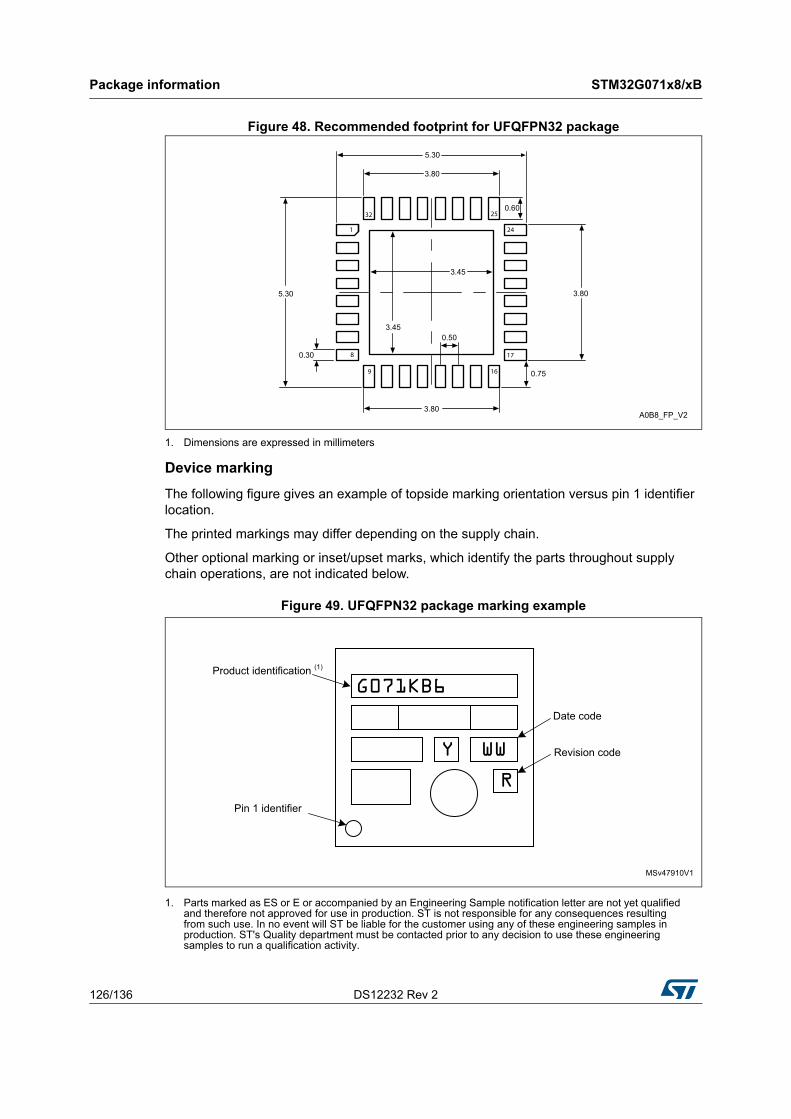
Package information STM32G071x8/xB
126/136 DS12232 Rev 2
Figure 48. Recommended footprint for UFQFPN32 package
1. Dimensions are expressed in millimeters
Device marking
The following figure gives an example of topside marking orientation versus pin 1 identifier location.
The printed markings may differ depending on the supply chain.
Other optional marking or inset/upset marks, which identify the parts throughout supply chain operations, are not indicated below.
Figure 49. UFQFPN32 package marking example
1. Parts marked as ES or E or accompanied by an Engineering Sample notification letter are not yet qualified and therefore not approved for use in production. ST is not responsible for any consequences resulting from such use. In no event will ST be liable for the customer using any of these engineering samples in production. ST's Quality department must be contacted prior to any decision to use these engineering samples to run a qualification activity.
A0B8_FP_V2
5.30
3.80
0.60
3.45
0.503.45
3.80
0.75
3.80
0.30
5.30
16
17
9
8
1
2532
24
MSv47910V1
G071KB6
R
Y WW
Product identification (1)
Date code
Revision code
Pin 1 identifier
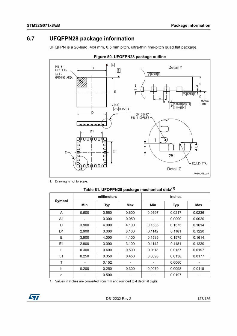
DS12232 Rev 2 127/136
STM32G071x8/xB Package information
133
6.7 UFQFPN28 package information
UFQFPN is a 28-lead, 4x4 mm, 0.5 mm pitch, ultra-thin fine-pitch quad flat package.
Figure 50. UFQFPN28 package outline
1. Drawing is not to scale.
Table 81. UFQFPN28 package mechanical data(1)
1. Values in inches are converted from mm and rounded to 4 decimal digits.
Symbolmillimeters inches
Min Typ Max Min Typ Max
A 0.500 0.550 0.600 0.0197 0.0217 0.0236
A1 - 0.000 0.050 - 0.0000 0.0020
D 3.900 4.000 4.100 0.1535 0.1575 0.1614
D1 2.900 3.000 3.100 0.1142 0.1181 0.1220
E 3.900 4.000 4.100 0.1535 0.1575 0.1614
E1 2.900 3.000 3.100 0.1142 0.1181 0.1220
L 0.300 0.400 0.500 0.0118 0.0157 0.0197
L1 0.250 0.350 0.450 0.0098 0.0138 0.0177
T - 0.152 - - 0.0060 -
b 0.200 0.250 0.300 0.0079 0.0098 0.0118
e - 0.500 - - 0.0197 -
A0B0_ME_V5
D1
E1
D
E
Detail Z
Detail Y
D
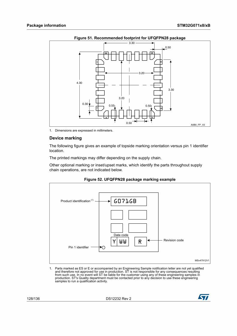
Package information STM32G071x8/xB
128/136 DS12232 Rev 2
Figure 51. Recommended footprint for UFQFPN28 package
1. Dimensions are expressed in millimeters.
Device marking
The following figure gives an example of topside marking orientation versus pin 1 identifier location.
The printed markings may differ depending on the supply chain.
Other optional marking or inset/upset marks, which identify the parts throughout supply chain operations, are not indicated below.
Figure 52. UFQFPN28 package marking example
1. Parts marked as ES or E or accompanied by an Engineering Sample notification letter are not yet qualified and therefore not approved for use in production. ST is not responsible for any consequences resulting from such use. In no event will ST be liable for the customer using any of these engineering samples in production. ST's Quality department must be contacted prior to any decision to use these engineering samples to run a qualification activity.
MSv47912V1
Product identification (1)
Date codeRevision code
G071GB
RY WWPin 1 identifier
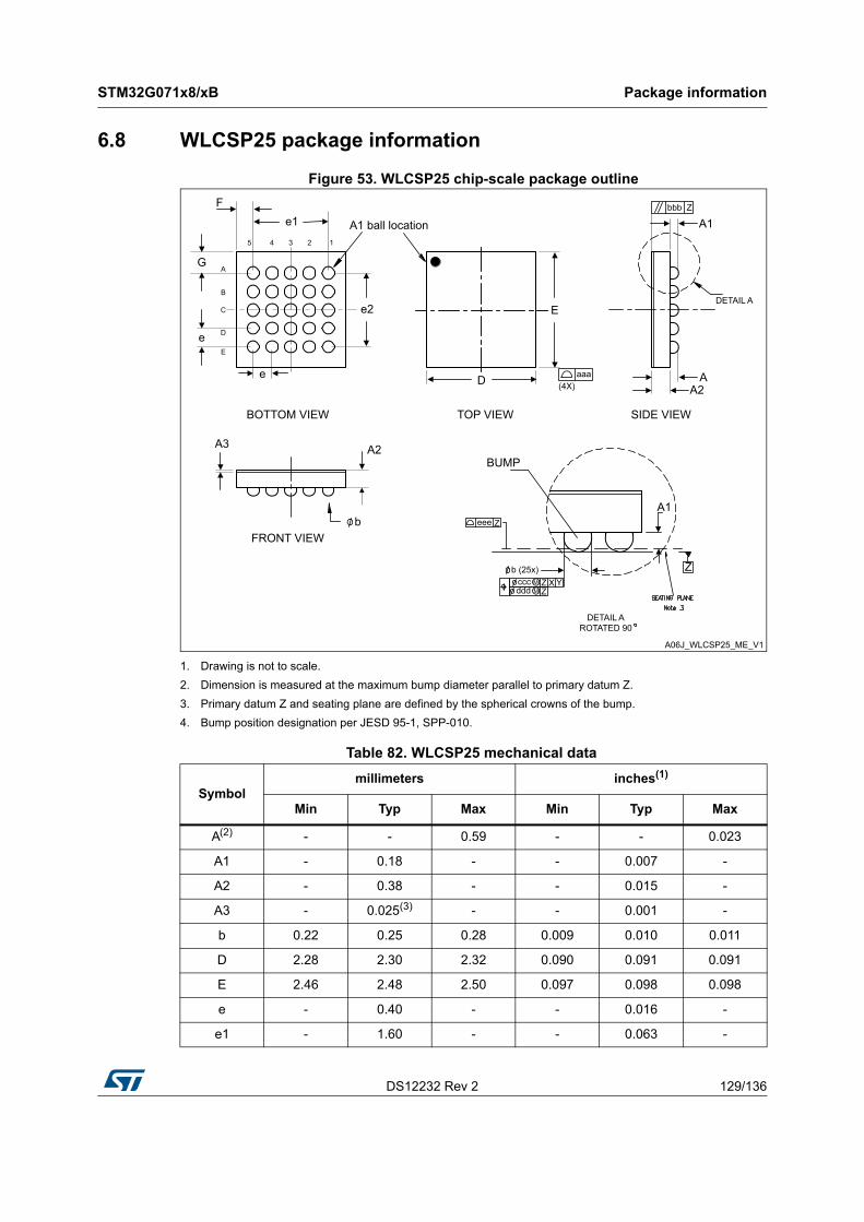
DS12232 Rev 2 129/136
STM32G071x8/xB Package information
133
6.8 WLCSP25 package information
Figure 53. WLCSP25 chip-scale package outline
1. Drawing is not to scale.
2. Dimension is measured at the maximum bump diameter parallel to primary datum Z.
3. Primary datum Z and seating plane are defined by the spherical crowns of the bump.
4. Bump position designation per JESD 95-1, SPP-010.
Table 82. WLCSP25 mechanical data
Symbolmillimeters inches(1)
Min Typ Max Min Typ Max
A(2) - - 0.59 - - 0.023
A1 - 0.18 - - 0.007 -
A2 - 0.38 - - 0.015 -
A3 - 0.025(3) - - 0.001 -
b 0.22 0.25 0.28 0.009 0.010 0.011
D 2.28 2.30 2.32 0.090 0.091 0.091
E 2.46 2.48 2.50 0.097 0.098 0.098
e - 0.40 - - 0.016 -
e1 - 1.60 - - 0.063 -
A06J_WLCSP25_ME_V1
Z
A
B
C
D
E
2 1345
G
e
e
e2
e1F
A1 ball location
D
E
aaa(4X)
BOTTOM VIEW TOP VIEW
AA2
A1bbb Z
DETAIL A
A3 A2
bFRONT VIEW
SIDE VIEW
DETAIL AROTATED 90
BUMP
eee Z
b (25x)ccc Z YXddd Z
MM
A1
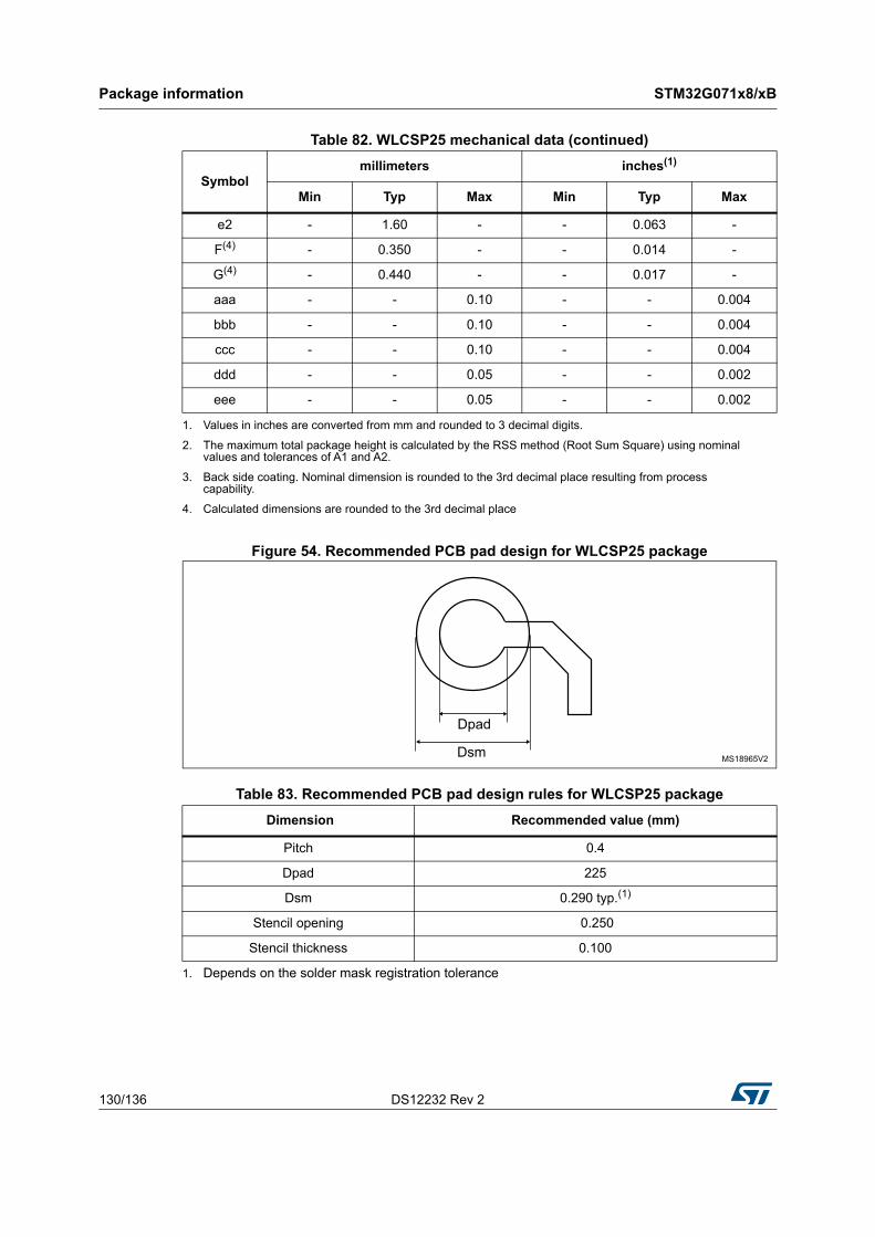
Package information STM32G071x8/xB
130/136 DS12232 Rev 2
Figure 54. Recommended PCB pad design for WLCSP25 package
e2 - 1.60 - - 0.063 -
F(4) - 0.350 - - 0.014 -
G(4) - 0.440 - - 0.017 -
aaa - - 0.10 - - 0.004
bbb - - 0.10 - - 0.004
ccc - - 0.10 - - 0.004
ddd - - 0.05 - - 0.002
eee - - 0.05 - - 0.002
1. Values in inches are converted from mm and rounded to 3 decimal digits.
2. The maximum total package height is calculated by the RSS method (Root Sum Square) using nominal values and tolerances of A1 and A2.
3. Back side coating. Nominal dimension is rounded to the 3rd decimal place resulting from process capability.
4. Calculated dimensions are rounded to the 3rd decimal place
Table 83. Recommended PCB pad design rules for WLCSP25 package
Dimension Recommended value (mm)
Pitch 0.4
Dpad 225
Dsm 0.290 typ.(1)
1. Depends on the solder mask registration tolerance
Stencil opening 0.250
Stencil thickness 0.100
Table 82. WLCSP25 mechanical data (continued)
Symbolmillimeters inches(1)
Min Typ Max Min Typ Max
MS18965V2Dsm
Dpad
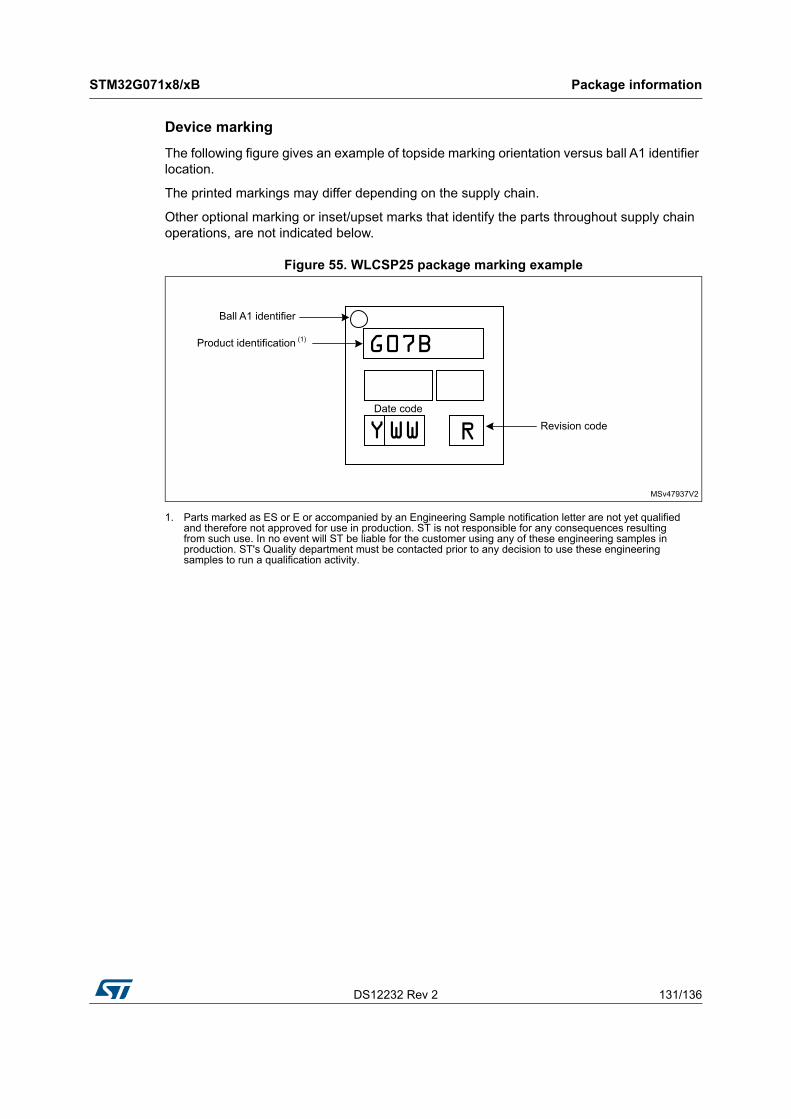
DS12232 Rev 2 131/136
STM32G071x8/xB Package information
133
Device marking
The following figure gives an example of topside marking orientation versus ball A1 identifier location.
The printed markings may differ depending on the supply chain.
Other optional marking or inset/upset marks that identify the parts throughout supply chain operations, are not indicated below.
Figure 55. WLCSP25 package marking example
1. Parts marked as ES or E or accompanied by an Engineering Sample notification letter are not yet qualified and therefore not approved for use in production. ST is not responsible for any consequences resulting from such use. In no event will ST be liable for the customer using any of these engineering samples in production. ST's Quality department must be contacted prior to any decision to use these engineering samples to run a qualification activity.
MSv47937V2
Product identification (1)
Date codeRevision code
G07B
RYWW
Ball A1 identifier
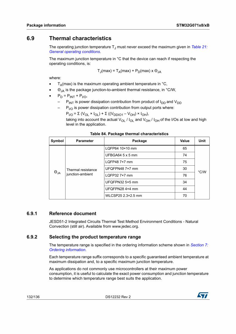
Package information STM32G071x8/xB
132/136 DS12232 Rev 2
6.9 Thermal characteristics
The operating junction temperature TJ must never exceed the maximum given in Table 21: General operating conditions.
The maximum junction temperature in °C that the device can reach if respecting the operating conditions, is:
TJ(max) = TA(max) + PD(max) x ΘJA
where:
• TA(max) is the maximum operating ambient temperature in °C,
• ΘJA is the package junction-to-ambient thermal resistance, in °C/W,
• PD = PINT + PI/O,
– PINT is power dissipation contribution from product of IDD and VDD
– PI/O is power dissipation contribution from output ports where:
PI/O = Σ (VOL × IOL) + Σ ((VDDIO1 – VOH) × IOH),
taking into account the actual VOL / IOL and VOH / IOH of the I/Os at low and high level in the application.
6.9.1 Reference document
JESD51-2 Integrated Circuits Thermal Test Method Environment Conditions - Natural Convection (still air). Available from www.jedec.org.
6.9.2 Selecting the product temperature range
The temperature range is specified in the ordering information scheme shown in Section 7: Ordering information.
Each temperature range suffix corresponds to a specific guaranteed ambient temperature at maximum dissipation and, to a specific maximum junction temperature.
As applications do not commonly use microcontrollers at their maximum power consumption, it is useful to calculate the exact power consumption and junction temperature to determine which temperature range best suits the application.
Table 84. Package thermal characteristics
Symbol Parameter Package Value Unit
ΘJAThermal resistance junction-ambient
LQFP64 10×10 mm 65
°C/W
UFBGA64 5 x 5 mm 74
LQFP48 7×7 mm 75
UFQFPN48 7×7 mm 30
LQFP32 7×7 mm 76
UFQFPN32 5×5 mm 34
UFQFPN28 4×4 mm 44
WLCSP25 2.3×2.5 mm 70
DS12232 Rev 2 133/136
STM32G071x8/xB Package information
133
The following example shows how to calculate the temperature range needed for a given application.
Example:
Assuming the following worst application conditions:
• ambient temperature TA = 50 °C (measured according to JESD51-2)
• IDD = 50 mA; VDD = 3.6 V
• 20 I/Os simultaneously used as output at low level with IOL = 8 mA (VOL= 0.4 V), and
• 8 I/Os simultaneously used as output at low level with IOL = 20 mA (VOL= 1.3 V),
the power consumption from power supply PINT is:
PINT = 50 mA × 3.6 V= 118 mW,
the power loss through I/Os PIO is
PIO = 20 × 8 mA × 0.4 V + 8 × 20 mA × 1.3 V = 272 mW,
and the total power PD to dissipate is:
PD = 180 mW + 272 mW = 452 mW
For product in LQFP48 with ΘJA= 75°C/W, the junction temperature stabilizes at:
TJ = 50°C + (75°C/W × 452 mW) = 50 °C + 33.9 °C = 83.9°C
As a conclusion, product version with suffix 6 (maximum allowed TJ = 105° C) is sufficient for this application.
If the same application was used in a hot environment with maximum TA greater than 71°C, the junction temperature would exceed 105°C and the product version with suffix 3 (maximum allowed TJ = 125° C) would have to be ordered. See Section 7: Ordering information.
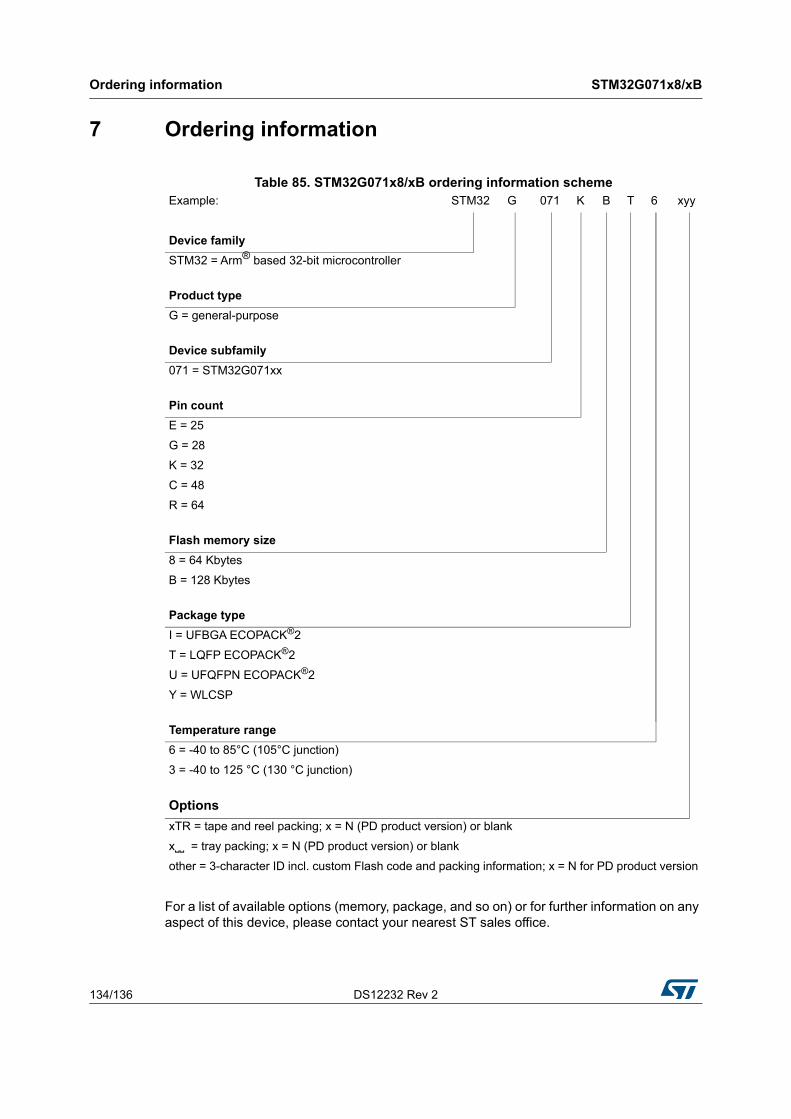
Ordering information STM32G071x8/xB
134/136 DS12232 Rev 2
7 Ordering information
For a list of available options (memory, package, and so on) or for further information on any aspect of this device, please contact your nearest ST sales office.
Table 85. STM32G071x8/xB ordering information schemeExample: STM32 G 071 K B T 6 xyy
Device family
STM32 = Arm® based 32-bit microcontroller
Product type
G = general-purpose
Device subfamily
071 = STM32G071xx
Pin count
E = 25
G = 28
K = 32
C = 48
R = 64
Flash memory size
8 = 64 Kbytes
B = 128 Kbytes
Package type
I = UFBGA ECOPACK®2
T = LQFP ECOPACK®2
U = UFQFPN ECOPACK®2
Y = WLCSP
Temperature range
6 = -40 to 85°C (105°C junction)
3 = -40 to 125 °C (130 °C junction)
Options
xTR = tape and reel packing; x = N (PD product version) or blank
x˽˽ = tray packing; x = N (PD product version) or blank
other = 3-character ID incl. custom Flash code and packing information; x = N for PD product version
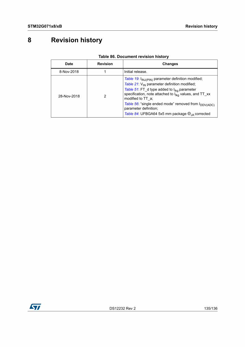
DS12232 Rev 2 135/136
STM32G071x8/xB Revision history
135
8 Revision history
Table 86. Document revision history
Date Revision Changes
8-Nov-2018 1 Initial release.
28-Nov-2018 2
Table 19: IINJ(PIN) parameter definition modified;
Table 21: VIN parameter definition modified;
Table 51: FT_d type added to Ilkg parameter specification, note attached to Ilkg values, and TT_xx modified to TT_a;
Table 56: “single ended mode” removed from IDDV(ADC) parameter definition;
Table 84: UFBGA64 5x5 mm package ΘJA corrected
STM32G071x8/xB
136/136 DS12232 Rev 2
IMPORTANT NOTICE – PLEASE READ CAREFULLY
STMicroelectronics NV and its subsidiaries (“ST”) reserve the right to make changes, corrections, enhancements, modifications, and improvements to ST products and/or to this document at any time without notice. Purchasers should obtain the latest relevant information on ST products before placing orders. ST products are sold pursuant to ST’s terms and conditions of sale in place at the time of order acknowledgement.
Purchasers are solely responsible for the choice, selection, and use of ST products and ST assumes no liability for application assistance or the design of Purchasers’ products.
No license, express or implied, to any intellectual property right is granted by ST herein.
Resale of ST products with provisions different from the information set forth herein shall void any warranty granted by ST for such product.
ST and the ST logo are trademarks of ST. All other product or service names are the property of their respective owners.
Information in this document supersedes and replaces information previously supplied in any prior versions of this document.
© 2018 STMicroelectronics – All rights reserved