Embed Size (px)
Citation preview
This is information on a product in full production.
May 2014 DocID025147 Rev 2 1/135
STM32F302x6/x8
ARM® Cortex®-M4 32-bit MCU+FPU, up to 64 KB Flash, 16 KB SRAM, ADC, DAC, USB, CAN, COMP, Op-Amp, 2.0 - 3.6 V
Datasheet - production data
Features Core: ARM 32-bit Cortex-M4 CPU with FPU
(72 MHz max.), single-cycle multiplication and HW division, DSP instruction
Memories – 32 to 64 Kbyte of Flash memory– 16 Kbyte of SRAM on data bus
CRC calculation unit Reset and power management
– VDD, VDDA voltage range: 2.0 to 3.6 V – Power-on/Power down reset (POR/PDR)– Programmable voltage detector (PVD) – Low-power: Sleep, Stop, and Standby – VBAT supply for RTC and backup registers
Clock management – 4 to 32 MHz crystal oscillator – 32 kHz oscillator for RTC with calibration – Internal 8 MHz RC with x 16 PLL option– Internal 40 kHz oscillator
Up to 51 fast I/O ports, all mappable on external interrupt vectors, several 5 V-tolerant
7-channel DMA controller supporting timers, ADCs, SPIs, I2Cs, USARTs and DAC
1 × ADC 0.20 μs (up to 15 channels) with selectable resolution of 12/10/8/6 bits, 0 to 3.6 V conversion range, single ended/differential mode, separate analog supply from 2.0 to 3.6 V
Temperature sensor 1 x 12-bit DAC channel with analog supply from
2.4 to 3.6 V Three fast rail-to-rail analog comparators with
analog supply from 2.0 to 3.6 V 1 x operational amplifier that can be used in
PGA mode, all terminal accessible with analog supply from 2.4 to 3.6 V
Up to 18 capacitive sensing channels supporting touchkey, linear and rotary sensors
Up to 9 timers– One 32-bit timer with up to 4 IC/OC/PWM
or pulse counter and quadrature (incremental) encoder input
– One 16-bit 6-channel advanced-control timer, with up to 6 PWM channels, deadtime generation and emergency stop
– Three 16-bit timers with IC/OC/OCN or PWM, deadtime gen. and emergency stop
– One 16-bit basic timer to drive the DAC– 2 watchdog timers (independent, window)– SysTick timer: 24-bit downcounter
Calendar RTC with alarm, periodic wakeup from Stop/Standby
Communication interfaces– Three I2Cs with 20 mA current sink to
support Fast mode plus – Up to 3 USARTs, 1 with ISO 7816 I/F,
autobaudrate detect and Dual clock domain
– Up to two SPIs with multiplexed full duplex I2S
– USB 2.0 full-speed interface – 1 x CAN interface (2.0B Active) – Infrared transmitter
Serial wire debug (SWD), JTAG 96-bit unique ID
Table 1. Device summaryReference Part number
STM32F302x6 STM32F302R6, STM32F302C6, STM32F302K6
STM32F302x8 STM32F302R8, STM32F302C8, STM32F302K8
LQFP48 (7 x 7 mm)LQFP64 (10 x 10 mm)
UFQFPN32(5 x 5 mm)
WLCSP49(3.4 x 3.4 mm)
www.st.com
Contents STM32F302x6/x8
2/135 DocID025147 Rev 2
Contents
1 Introduction . . . . . . . . . . . . . . . . . . . . . . . . . . . . . . . . . . . . . . . . . . . . . . . . 8
2 Description . . . . . . . . . . . . . . . . . . . . . . . . . . . . . . . . . . . . . . . . . . . . . . . . . 9
3 Functional overview . . . . . . . . . . . . . . . . . . . . . . . . . . . . . . . . . . . . . . . . 123.1 ARM® Cortex®-M4 core with FPU, embedded Flash and SRAM . . . . . . . 12
3.2 Memories . . . . . . . . . . . . . . . . . . . . . . . . . . . . . . . . . . . . . . . . . . . . . . . . . 123.2.1 Embedded Flash memory . . . . . . . . . . . . . . . . . . . . . . . . . . . . . . . . . . . 12
3.2.2 Embedded SRAM . . . . . . . . . . . . . . . . . . . . . . . . . . . . . . . . . . . . . . . . . 12
3.3 Boot modes . . . . . . . . . . . . . . . . . . . . . . . . . . . . . . . . . . . . . . . . . . . . . . . 12
3.4 Cyclic redundancy check calculation unit (CRC) . . . . . . . . . . . . . . . . . . . 13
3.5 Power management . . . . . . . . . . . . . . . . . . . . . . . . . . . . . . . . . . . . . . . . . 133.5.1 Power supply schemes . . . . . . . . . . . . . . . . . . . . . . . . . . . . . . . . . . . . . 13
3.5.2 Power supply supervisor . . . . . . . . . . . . . . . . . . . . . . . . . . . . . . . . . . . . 13
3.5.3 Voltage regulator . . . . . . . . . . . . . . . . . . . . . . . . . . . . . . . . . . . . . . . . . . 14
3.5.4 Low-power modes . . . . . . . . . . . . . . . . . . . . . . . . . . . . . . . . . . . . . . . . . 14
3.6 Interconnect matrix . . . . . . . . . . . . . . . . . . . . . . . . . . . . . . . . . . . . . . . . . . 14
3.7 Clocks and startup . . . . . . . . . . . . . . . . . . . . . . . . . . . . . . . . . . . . . . . . . . 16
3.8 General-purpose inputs/outputs (GPIOs) . . . . . . . . . . . . . . . . . . . . . . . . . 18
3.9 Direct memory access (DMA) . . . . . . . . . . . . . . . . . . . . . . . . . . . . . . . . . 18
3.10 Interrupts and events . . . . . . . . . . . . . . . . . . . . . . . . . . . . . . . . . . . . . . . . 183.10.1 Nested vectored interrupt controller (NVIC) . . . . . . . . . . . . . . . . . . . . . . 18
3.11 Fast analog-to-digital converter (ADC) . . . . . . . . . . . . . . . . . . . . . . . . . . . 193.11.1 Temperature sensor . . . . . . . . . . . . . . . . . . . . . . . . . . . . . . . . . . . . . . . . 19
3.11.2 Internal voltage reference (VREFINT) . . . . . . . . . . . . . . . . . . . . . . . . . . . 19
3.11.3 VBAT battery voltage monitoring . . . . . . . . . . . . . . . . . . . . . . . . . . . . . . . 20
3.12 Digital-to-analog converter (DAC) . . . . . . . . . . . . . . . . . . . . . . . . . . . . . . 20
3.13 Operational amplifier (OPAMP) . . . . . . . . . . . . . . . . . . . . . . . . . . . . . . . . 20
3.14 Ultra-fast comparators (COMP) . . . . . . . . . . . . . . . . . . . . . . . . . . . . . . . . 20
3.15 Timers and watchdogs . . . . . . . . . . . . . . . . . . . . . . . . . . . . . . . . . . . . . . . 213.15.1 Advanced timer (TIM1) . . . . . . . . . . . . . . . . . . . . . . . . . . . . . . . . . . . . . 21
3.15.2 General-purpose timers (TIM2, TIM15, TIM16, TIM17) . . . . . . . . . . . . . 22
3.15.3 Basic timer (TIM6) . . . . . . . . . . . . . . . . . . . . . . . . . . . . . . . . . . . . . . . . . 22
DocID025147 Rev 2 3/135
STM32F302x6/x8 Contents
4
3.15.4 Independent watchdog (IWDG) . . . . . . . . . . . . . . . . . . . . . . . . . . . . . . . 23
3.15.5 Window watchdog (WWDG) . . . . . . . . . . . . . . . . . . . . . . . . . . . . . . . . . 23
3.15.6 SysTick timer . . . . . . . . . . . . . . . . . . . . . . . . . . . . . . . . . . . . . . . . . . . . . 23
3.16 Real-time clock (RTC) and backup registers . . . . . . . . . . . . . . . . . . . . . . 23
3.17 Inter-integrated circuit interfaces (I2C) . . . . . . . . . . . . . . . . . . . . . . . . . . . 25
3.18 Universal synchronous/asynchronous receiver transmitter (USART) . . . 26
3.19 Serial peripheral interfaces (SPI)/Inter-integrated sound interfaces (I2S) . . . . . . . . . . . . . . . . . . . . . . . . . . . . . . . . . . . . . . . . . . . . . 26
3.20 Controller area network (CAN) . . . . . . . . . . . . . . . . . . . . . . . . . . . . . . . . . 27
3.21 Universal serial bus (USB) . . . . . . . . . . . . . . . . . . . . . . . . . . . . . . . . . . . . 27
3.22 Touch sensing controller (TSC) . . . . . . . . . . . . . . . . . . . . . . . . . . . . . . . . 27
3.23 Infrared transmitter . . . . . . . . . . . . . . . . . . . . . . . . . . . . . . . . . . . . . . . . . . 29
3.24 Development support . . . . . . . . . . . . . . . . . . . . . . . . . . . . . . . . . . . . . . . . 303.24.1 Serial wire JTAG debug port (SWJ-DP) . . . . . . . . . . . . . . . . . . . . . . . . . 30
4 Pinouts and pin description . . . . . . . . . . . . . . . . . . . . . . . . . . . . . . . . . . 31
5 Memory mapping . . . . . . . . . . . . . . . . . . . . . . . . . . . . . . . . . . . . . . . . . . . 48
6 Electrical characteristics . . . . . . . . . . . . . . . . . . . . . . . . . . . . . . . . . . . . 526.1 Parameter conditions . . . . . . . . . . . . . . . . . . . . . . . . . . . . . . . . . . . . . . . . 52
6.1.1 Minimum and maximum values . . . . . . . . . . . . . . . . . . . . . . . . . . . . . . . 52
6.1.2 Typical values . . . . . . . . . . . . . . . . . . . . . . . . . . . . . . . . . . . . . . . . . . . . 52
6.1.3 Typical curves . . . . . . . . . . . . . . . . . . . . . . . . . . . . . . . . . . . . . . . . . . . . 52
6.1.4 Loading capacitor . . . . . . . . . . . . . . . . . . . . . . . . . . . . . . . . . . . . . . . . . 52
6.1.5 Pin input voltage . . . . . . . . . . . . . . . . . . . . . . . . . . . . . . . . . . . . . . . . . . 52
6.1.6 Power supply scheme . . . . . . . . . . . . . . . . . . . . . . . . . . . . . . . . . . . . . . 53
6.1.7 Current consumption measurement . . . . . . . . . . . . . . . . . . . . . . . . . . . 54
6.2 Absolute maximum ratings . . . . . . . . . . . . . . . . . . . . . . . . . . . . . . . . . . . . 55
6.3 Operating conditions . . . . . . . . . . . . . . . . . . . . . . . . . . . . . . . . . . . . . . . . 576.3.1 General operating conditions . . . . . . . . . . . . . . . . . . . . . . . . . . . . . . . . . 57
6.3.2 Operating conditions at power-up / power-down . . . . . . . . . . . . . . . . . . 58
6.3.3 Embedded reset and power control block characteristics . . . . . . . . . . . 58
6.3.4 Embedded reference voltage . . . . . . . . . . . . . . . . . . . . . . . . . . . . . . . . . 60
6.3.5 Supply current characteristics . . . . . . . . . . . . . . . . . . . . . . . . . . . . . . . . 60
6.3.6 Wakeup time from low-power mode . . . . . . . . . . . . . . . . . . . . . . . . . . . 72
Contents STM32F302x6/x8
4/135 DocID025147 Rev 2
6.3.7 External clock source characteristics . . . . . . . . . . . . . . . . . . . . . . . . . . . 73
6.3.8 Internal clock source characteristics . . . . . . . . . . . . . . . . . . . . . . . . . . . 79
6.3.9 PLL characteristics . . . . . . . . . . . . . . . . . . . . . . . . . . . . . . . . . . . . . . . . 80
6.3.10 Memory characteristics . . . . . . . . . . . . . . . . . . . . . . . . . . . . . . . . . . . . . 81
6.3.11 EMC characteristics . . . . . . . . . . . . . . . . . . . . . . . . . . . . . . . . . . . . . . . . 82
6.3.12 Electrical sensitivity characteristics . . . . . . . . . . . . . . . . . . . . . . . . . . . . 83
6.3.13 I/O current injection characteristics . . . . . . . . . . . . . . . . . . . . . . . . . . . . 84
6.3.14 I/O port characteristics . . . . . . . . . . . . . . . . . . . . . . . . . . . . . . . . . . . . . . 85
6.3.15 NRST pin characteristics . . . . . . . . . . . . . . . . . . . . . . . . . . . . . . . . . . . . 90
6.3.16 Timer characteristics . . . . . . . . . . . . . . . . . . . . . . . . . . . . . . . . . . . . . . . 91
6.3.17 Communications interfaces . . . . . . . . . . . . . . . . . . . . . . . . . . . . . . . . . . 93
6.3.18 ADC characteristics . . . . . . . . . . . . . . . . . . . . . . . . . . . . . . . . . . . . . . . 101
6.3.19 DAC electrical specifications . . . . . . . . . . . . . . . . . . . . . . . . . . . . . . . . 109
6.3.20 Comparator characteristics . . . . . . . . . . . . . . . . . . . . . . . . . . . . . . . . . 110
6.3.21 Operational amplifier characteristics . . . . . . . . . . . . . . . . . . . . . . . . . . 112
6.3.22 Temperature sensor characteristics . . . . . . . . . . . . . . . . . . . . . . . . . . . 115
6.3.23 VBAT monitoring characteristics . . . . . . . . . . . . . . . . . . . . . . . . . . . . . . 115
7 Package characteristics . . . . . . . . . . . . . . . . . . . . . . . . . . . . . . . . . . . . 1167.1 Package mechanical data . . . . . . . . . . . . . . . . . . . . . . . . . . . . . . . . . . . 116
7.2 Thermal characteristics . . . . . . . . . . . . . . . . . . . . . . . . . . . . . . . . . . . . . 1307.2.1 Reference document . . . . . . . . . . . . . . . . . . . . . . . . . . . . . . . . . . . . . . 130
7.2.2 Selecting the product temperature range . . . . . . . . . . . . . . . . . . . . . . 131
8 Part numbering . . . . . . . . . . . . . . . . . . . . . . . . . . . . . . . . . . . . . . . . . . . 133
9 Revision history . . . . . . . . . . . . . . . . . . . . . . . . . . . . . . . . . . . . . . . . . . 134
DocID025147 Rev 2 5/135
STM32F302x6/x8 List of tables
6
List of tables
Table 1. Device summary . . . . . . . . . . . . . . . . . . . . . . . . . . . . . . . . . . . . . . . . . . . . . . . . . . . . . . . . . . 1Table 2. STM32F302x6/x8 device features and peripheral counts. . . . . . . . . . . . . . . . . . . . . . . . . . 10Table 3. STM32F302x6/x8 peripheral interconnect matrix . . . . . . . . . . . . . . . . . . . . . . . . . . . . . . . . 15Table 4. Timer feature comparison. . . . . . . . . . . . . . . . . . . . . . . . . . . . . . . . . . . . . . . . . . . . . . . . . . 21Table 5. Comparison of I2C analog and digital filters . . . . . . . . . . . . . . . . . . . . . . . . . . . . . . . . . . . . 25Table 6. STM32F302x6/x8 I2C implementation . . . . . . . . . . . . . . . . . . . . . . . . . . . . . . . . . . . . . . . . 25Table 7. USART features . . . . . . . . . . . . . . . . . . . . . . . . . . . . . . . . . . . . . . . . . . . . . . . . . . . . . . . . . 26Table 8. STM32F302x6/x8 SPI/I2S implementation. . . . . . . . . . . . . . . . . . . . . . . . . . . . . . . . . . . . . 27Table 9. Capacitive sensing GPIOs available on STM32F302x6/x8 devices . . . . . . . . . . . . . . . . . . 28Table 10. No. of capacitive sensing channels available on
STM32F302x6/x8 devices . . . . . . . . . . . . . . . . . . . . . . . . . . . . . . . . . . . . . . . . . . . . . . . . . 28Table 11. Legend/abbreviations used in the pinout table . . . . . . . . . . . . . . . . . . . . . . . . . . . . . . . . . . 34Table 12. STM32F302x6/x8 pin definitions. . . . . . . . . . . . . . . . . . . . . . . . . . . . . . . . . . . . . . . . . . . . . 35Table 13. Alternate functions for Port A . . . . . . . . . . . . . . . . . . . . . . . . . . . . . . . . . . . . . . . . . . . . . . . 42Table 14. Alternate functions for Port B . . . . . . . . . . . . . . . . . . . . . . . . . . . . . . . . . . . . . . . . . . . . . . . 44Table 15. Alternate functions for Port C . . . . . . . . . . . . . . . . . . . . . . . . . . . . . . . . . . . . . . . . . . . . . . . 46Table 16. Alternate functions for Port D . . . . . . . . . . . . . . . . . . . . . . . . . . . . . . . . . . . . . . . . . . . . . . . 47Table 17. Alternate functions for Port F . . . . . . . . . . . . . . . . . . . . . . . . . . . . . . . . . . . . . . . . . . . . . . . 47Table 18. STM32F302x6/x8 peripheral register boundary addresses . . . . . . . . . . . . . . . . . . . . . . . . 49Table 19. Voltage characteristics . . . . . . . . . . . . . . . . . . . . . . . . . . . . . . . . . . . . . . . . . . . . . . . . . . . . 55Table 20. Current characteristics . . . . . . . . . . . . . . . . . . . . . . . . . . . . . . . . . . . . . . . . . . . . . . . . . . . . 56Table 21. Thermal characteristics. . . . . . . . . . . . . . . . . . . . . . . . . . . . . . . . . . . . . . . . . . . . . . . . . . . . 56Table 22. General operating conditions . . . . . . . . . . . . . . . . . . . . . . . . . . . . . . . . . . . . . . . . . . . . . . . 57Table 23. Operating conditions at power-up / power-down . . . . . . . . . . . . . . . . . . . . . . . . . . . . . . . . 58Table 24. Embedded reset and power control block characteristics. . . . . . . . . . . . . . . . . . . . . . . . . . 58Table 25. Programmable voltage detector characteristics . . . . . . . . . . . . . . . . . . . . . . . . . . . . . . . . . 59Table 26. Embedded internal reference voltage. . . . . . . . . . . . . . . . . . . . . . . . . . . . . . . . . . . . . . . . . 60Table 27. Internal reference voltage calibration values . . . . . . . . . . . . . . . . . . . . . . . . . . . . . . . . . . . 60Table 28. Typical and maximum current consumption from VDD supply at VDD = 3.6V . . . . . . . . . . 61Table 29. Typical and maximum current consumption from the VDDA supply . . . . . . . . . . . . . . . . . . 63Table 30. Typical and maximum VDD consumption in Stop and Standby modes. . . . . . . . . . . . . . . . 63Table 31. Typical and maximum VDDA consumption in Stop and Standby modes. . . . . . . . . . . . . . . 64Table 32. Typical and maximum current consumption from VBAT supply. . . . . . . . . . . . . . . . . . . . . . 64Table 33. Typical current consumption in Run mode, code with data processing running from Flash66Table 34. Typical current consumption in Sleep mode, code running from Flash or RAM. . . . . . . . . 67Table 35. Switching output I/O current consumption . . . . . . . . . . . . . . . . . . . . . . . . . . . . . . . . . . . . . 69Table 36. Peripheral current consumption . . . . . . . . . . . . . . . . . . . . . . . . . . . . . . . . . . . . . . . . . . . . . 71Table 37. Low-power mode wakeup timings. . . . . . . . . . . . . . . . . . . . . . . . . . . . . . . . . . . . . . . . . . . . 72Table 38. High-speed external user clock characteristics. . . . . . . . . . . . . . . . . . . . . . . . . . . . . . . . . . 73Table 39. Low-speed external user clock characteristics . . . . . . . . . . . . . . . . . . . . . . . . . . . . . . . . . . 74Table 40. HSE oscillator characteristics . . . . . . . . . . . . . . . . . . . . . . . . . . . . . . . . . . . . . . . . . . . . . . . 75Table 41. LSE oscillator characteristics (fLSE = 32.768 kHz) . . . . . . . . . . . . . . . . . . . . . . . . . . . . . . . 77Table 42. HSI oscillator characteristics. . . . . . . . . . . . . . . . . . . . . . . . . . . . . . . . . . . . . . . . . . . . . . . . 79Table 43. LSI oscillator characteristics . . . . . . . . . . . . . . . . . . . . . . . . . . . . . . . . . . . . . . . . . . . . . . . . 80Table 44. PLL characteristics . . . . . . . . . . . . . . . . . . . . . . . . . . . . . . . . . . . . . . . . . . . . . . . . . . . . . . . 80Table 45. Flash memory characteristics . . . . . . . . . . . . . . . . . . . . . . . . . . . . . . . . . . . . . . . . . . . . . . . 81Table 46. Flash memory endurance and data retention . . . . . . . . . . . . . . . . . . . . . . . . . . . . . . . . . . . 81Table 47. EMS characteristics . . . . . . . . . . . . . . . . . . . . . . . . . . . . . . . . . . . . . . . . . . . . . . . . . . . . . . 82
List of tables STM32F302x6/x8
6/135 DocID025147 Rev 2
Table 48. EMI characteristics . . . . . . . . . . . . . . . . . . . . . . . . . . . . . . . . . . . . . . . . . . . . . . . . . . . . . . . 83Table 49. ESD absolute maximum ratings . . . . . . . . . . . . . . . . . . . . . . . . . . . . . . . . . . . . . . . . . . . . . 83Table 50. Electrical sensitivities . . . . . . . . . . . . . . . . . . . . . . . . . . . . . . . . . . . . . . . . . . . . . . . . . . . . . 84Table 51. I/O current injection susceptibility . . . . . . . . . . . . . . . . . . . . . . . . . . . . . . . . . . . . . . . . . . . . 84Table 52. I/O static characteristics . . . . . . . . . . . . . . . . . . . . . . . . . . . . . . . . . . . . . . . . . . . . . . . . . . . 85Table 53. Output voltage characteristics. . . . . . . . . . . . . . . . . . . . . . . . . . . . . . . . . . . . . . . . . . . . . . . 88Table 54. I/O AC characteristics . . . . . . . . . . . . . . . . . . . . . . . . . . . . . . . . . . . . . . . . . . . . . . . . . . . . . 89Table 55. NRST pin characteristics . . . . . . . . . . . . . . . . . . . . . . . . . . . . . . . . . . . . . . . . . . . . . . . . . . 90Table 56. TIMx characteristics . . . . . . . . . . . . . . . . . . . . . . . . . . . . . . . . . . . . . . . . . . . . . . . . . . . . . . 91Table 57. IWDG min/max timeout period at 40 kHz (LSI) . . . . . . . . . . . . . . . . . . . . . . . . . . . . . . . . . 92Table 58. WWDG min-max timeout value @72 MHz (PCLK). . . . . . . . . . . . . . . . . . . . . . . . . . . . . . . 92Table 59. I2C analog filter characteristics. . . . . . . . . . . . . . . . . . . . . . . . . . . . . . . . . . . . . . . . . . . . . . 93Table 60. SPI characteristics . . . . . . . . . . . . . . . . . . . . . . . . . . . . . . . . . . . . . . . . . . . . . . . . . . . . . . . 94Table 61. I2S characteristics. . . . . . . . . . . . . . . . . . . . . . . . . . . . . . . . . . . . . . . . . . . . . . . . . . . . . . . . 96Table 62. USB startup time. . . . . . . . . . . . . . . . . . . . . . . . . . . . . . . . . . . . . . . . . . . . . . . . . . . . . . . . . 99Table 63. USB DC electrical characteristics . . . . . . . . . . . . . . . . . . . . . . . . . . . . . . . . . . . . . . . . . . . 100Table 64. USB: Full-speed electrical characteristics. . . . . . . . . . . . . . . . . . . . . . . . . . . . . . . . . . . . . 101Table 65. ADC characteristics . . . . . . . . . . . . . . . . . . . . . . . . . . . . . . . . . . . . . . . . . . . . . . . . . . . . . 101Table 66. Maximum ADC RAIN . . . . . . . . . . . . . . . . . . . . . . . . . . . . . . . . . . . . . . . . . . . . . . . . . . . . 102Table 67. ADC accuracy - limited test conditions . . . . . . . . . . . . . . . . . . . . . . . . . . . . . . . . . . . . . . . 104Table 68. ADC accuracy . . . . . . . . . . . . . . . . . . . . . . . . . . . . . . . . . . . . . . . . . . . . . . . . . . . . . . . . . 106Table 69. ADC accuracy. . . . . . . . . . . . . . . . . . . . . . . . . . . . . . . . . . . . . . . . . . . . . . . . . . . . . . . . . . 107Table 70. DAC characteristics . . . . . . . . . . . . . . . . . . . . . . . . . . . . . . . . . . . . . . . . . . . . . . . . . . . . . 109Table 71. Comparator characteristics . . . . . . . . . . . . . . . . . . . . . . . . . . . . . . . . . . . . . . . . . . . . . . . . 110Table 72. Operational amplifier characteristics. . . . . . . . . . . . . . . . . . . . . . . . . . . . . . . . . . . . . . . . . 112Table 73. TS characteristics . . . . . . . . . . . . . . . . . . . . . . . . . . . . . . . . . . . . . . . . . . . . . . . . . . . . . . . 115Table 74. Temperature sensor calibration values. . . . . . . . . . . . . . . . . . . . . . . . . . . . . . . . . . . . . . . 115Table 75. VBAT monitoring characteristics . . . . . . . . . . . . . . . . . . . . . . . . . . . . . . . . . . . . . . . . . . . . 115Table 76. WLCSP49 wafer level chip size package mechanical data . . . . . . . . . . . . . . . . . . . . . . . 118Table 77. LQFP64 – 10 x 10 mm 64 pin low-profile quad flat package mechanical data . . . . . . . . . 121Table 78. LQFP48 – 7 x 7mm, 48-pin low-profile quad flat package mechanical data. . . . . . . . . . . 124Table 79. 32-lead, ultra thin, fine pitch quad flat no-lead package mechanical data . . . . . . . . . . . . 127Table 80. Package thermal characteristics . . . . . . . . . . . . . . . . . . . . . . . . . . . . . . . . . . . . . . . . . . . . 130Table 81. Ordering information scheme . . . . . . . . . . . . . . . . . . . . . . . . . . . . . . . . . . . . . . . . . . . . . . 133Table 82. Document revision history. . . . . . . . . . . . . . . . . . . . . . . . . . . . . . . . . . . . . . . . . . . . . . . . . 134
DocID025147 Rev 2 7/135
STM32F302x6/x8 List of figures
7
List of figures
Figure 1. STM32F302x6/x8 block diagram . . . . . . . . . . . . . . . . . . . . . . . . . . . . . . . . . . . . . . . . . . . . 11Figure 2. Clock tree . . . . . . . . . . . . . . . . . . . . . . . . . . . . . . . . . . . . . . . . . . . . . . . . . . . . . . . . . . . . . . 17Figure 3. Infrared transmitter . . . . . . . . . . . . . . . . . . . . . . . . . . . . . . . . . . . . . . . . . . . . . . . . . . . . . . . 29Figure 4. STM32F302x6/x8 UFQFN32 pinout . . . . . . . . . . . . . . . . . . . . . . . . . . . . . . . . . . . . . . . . . . 31Figure 5. STM32F302x6/x8 LQFP48 pinout . . . . . . . . . . . . . . . . . . . . . . . . . . . . . . . . . . . . . . . . . . . 31Figure 6. STM32F302x6/x8 LQFP64 pinout . . . . . . . . . . . . . . . . . . . . . . . . . . . . . . . . . . . . . . . . . . . 32Figure 7. STM32F302x6/x8 WLCSP49 ballout . . . . . . . . . . . . . . . . . . . . . . . . . . . . . . . . . . . . . . . . . 33Figure 8. STM32F302x6/x8 memory mapping. . . . . . . . . . . . . . . . . . . . . . . . . . . . . . . . . . . . . . . . . . 48Figure 9. Pin loading conditions. . . . . . . . . . . . . . . . . . . . . . . . . . . . . . . . . . . . . . . . . . . . . . . . . . . . . 52Figure 10. Pin input voltage . . . . . . . . . . . . . . . . . . . . . . . . . . . . . . . . . . . . . . . . . . . . . . . . . . . . . . . . . 52Figure 11. Power supply scheme. . . . . . . . . . . . . . . . . . . . . . . . . . . . . . . . . . . . . . . . . . . . . . . . . . . . . 53Figure 12. Current consumption measurement scheme . . . . . . . . . . . . . . . . . . . . . . . . . . . . . . . . . . . 54Figure 13. Typical VBAT current consumption (LSE and RTC ON/LSEDRV[1:0] = ’00’) . . . . . . . . . . . 65Figure 14. High-speed external clock source AC timing diagram . . . . . . . . . . . . . . . . . . . . . . . . . . . . 73Figure 15. Low-speed external clock source AC timing diagram. . . . . . . . . . . . . . . . . . . . . . . . . . . . . 74Figure 16. Typical application with an 8 MHz crystal . . . . . . . . . . . . . . . . . . . . . . . . . . . . . . . . . . . . . . 76Figure 17. Typical application with a 32.768 kHz crystal . . . . . . . . . . . . . . . . . . . . . . . . . . . . . . . . . . . 78Figure 18. HSI oscillator accuracy characterization results . . . . . . . . . . . . . . . . . . . . . . . . . . . . . . . . . 79Figure 19. TC and TTa I/O input characteristics - CMOS port . . . . . . . . . . . . . . . . . . . . . . . . . . . . . . . 86Figure 20. TC and TTa I/O input characteristics - TTL port . . . . . . . . . . . . . . . . . . . . . . . . . . . . . . . . . 86Figure 21. Five volt tolerant (FT and FTf) I/O input characteristics - CMOS port. . . . . . . . . . . . . . . . . 86Figure 22. Five volt tolerant (FT and FTf) I/O input characteristics - TTL port . . . . . . . . . . . . . . . . . . . 87Figure 23. I/O AC characteristics definition . . . . . . . . . . . . . . . . . . . . . . . . . . . . . . . . . . . . . . . . . . . . . 90Figure 24. Recommended NRST pin protection . . . . . . . . . . . . . . . . . . . . . . . . . . . . . . . . . . . . . . . . . 91Figure 25. SPI timing diagram - slave mode and CPHA = 0 . . . . . . . . . . . . . . . . . . . . . . . . . . . . . . . . 95Figure 26. SPI timing diagram - slave mode and CPHA = 1(1) . . . . . . . . . . . . . . . . . . . . . . . . . . . . . . 95Figure 27. SPI timing diagram - master mode(1) . . . . . . . . . . . . . . . . . . . . . . . . . . . . . . . . . . . . . . . . . 96Figure 28. I2S slave timing diagram (Philips protocol)(1) . . . . . . . . . . . . . . . . . . . . . . . . . . . . . . . . . . . 98Figure 29. I2S master timing diagram (Philips protocol)(1) . . . . . . . . . . . . . . . . . . . . . . . . . . . . . . . . . . 98Figure 30. USB timings: definition of data signal rise and fall time . . . . . . . . . . . . . . . . . . . . . . . . . . 100Figure 31. ADC accuracy characteristics . . . . . . . . . . . . . . . . . . . . . . . . . . . . . . . . . . . . . . . . . . . . . . 108Figure 32. Typical connection diagram using the ADC . . . . . . . . . . . . . . . . . . . . . . . . . . . . . . . . . . . 108Figure 33. 12-bit buffered /non-buffered DAC . . . . . . . . . . . . . . . . . . . . . . . . . . . . . . . . . . . . . . . . . . 110Figure 34. OPAMP Voltage Noise versus Frequency . . . . . . . . . . . . . . . . . . . . . . . . . . . . . . . . . . . . 114Figure 35. WLCSP49 wafer level chip size package . . . . . . . . . . . . . . . . . . . . . . . . . . . . . . . . . . . . . 117Figure 36. WLCSP49 package top view . . . . . . . . . . . . . . . . . . . . . . . . . . . . . . . . . . . . . . . . . . . . . . 119Figure 37. LQFP64 – 10 x 10 mm 64 pin low-profile quad flat package outline. . . . . . . . . . . . . . . . . 120Figure 38. LQFP64 recommended footprint. . . . . . . . . . . . . . . . . . . . . . . . . . . . . . . . . . . . . . . . . . . . 121Figure 39. LQFP64 package top view . . . . . . . . . . . . . . . . . . . . . . . . . . . . . . . . . . . . . . . . . . . . . . . . 122Figure 40. LQFP48 – 7 x 7mm, 48-pin low-profile quad flat package outline . . . . . . . . . . . . . . . . . . 123Figure 41. LQFP48 recommended footprint. . . . . . . . . . . . . . . . . . . . . . . . . . . . . . . . . . . . . . . . . . . . 125Figure 42. LQFP48 package top view . . . . . . . . . . . . . . . . . . . . . . . . . . . . . . . . . . . . . . . . . . . . . . . . 126Figure 43. 32-lead, ultra thin, fine pitch quad flat no-lead package (5 x 5) . . . . . . . . . . . . . . . . . . . . 127Figure 44. UFQFPN32 recommended footprint . . . . . . . . . . . . . . . . . . . . . . . . . . . . . . . . . . . . . . . . . 128Figure 45. UFQFPN32 package top view . . . . . . . . . . . . . . . . . . . . . . . . . . . . . . . . . . . . . . . . . . . . . 129
Introduction STM32F302x6/x8
8/135 DocID025147 Rev 2
1 Introduction
This datasheet provides the ordering information and mechanical device characteristics of the STM32F302x6/x8 microcontrollers.
This datasheet should be read in conjunction with the STM32F302xx advanced ARM-based 32-bit MCUs reference manual (RM0365). The reference manual is available from the STMicroelectronics website www.st.com.
For information on the ARM Cortex-M4 core, please refer to the Cortex-M4 Technical Reference Manual, available from ARM website www.arm.com.
DocID025147 Rev 2 9/135
STM32F302x6/x8 Description
51
2 Description
The STM32F302x6/x8 family is based on the high-performance ARM Cortex-M4 32-bit RISC core operating at a frequency of up to 72 MHz and embedding a floating point unit (FPU). The family incorporates high-speed embedded memories (up to 64 Kbyte of Flash memory, 16 Kbytes of SRAM), and an extensive range of enhanced I/Os and peripherals connected to two APB buses.
The devices offer a fast 12-bit ADC (5 Msps), three comparators, an operational amplifier, up to 18 capacitive sensing channels, one DAC channel, a low-power RTC, one general-purpose 32-bit timer, one timer dedicated to motor control, and up to three general-purpose 16-bit timers, and one timer to drive the DAC. They also feature standard and advanced communication interfaces: three I2Cs, up to three USARTs, up to two SPIs with multiplexed full-duplex I2S, a USB FS device, a CAN, and an infrared transmitter.
The STM32F302x6/x8 family operates in the –40 to +85°C and –40 to +105°C temperature ranges from at a 2.0 to 3.6 V power supply. A comprehensive set of power-saving mode allows the design of low-power applications.
The STM32F302x6/x8 family offers devices in 32-, 48-, 49- and 64-pin packages.
The set of included peripherals changes with the device chosen.
Description STM32F302x6/x8
10/135 DocID025147 Rev 2
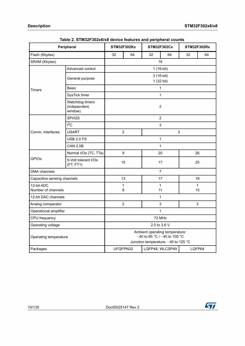
Table 2. STM32F302x6/x8 device features and peripheral counts Peripheral STM32F302Kx STM32F302Cx STM32F302Rx
Flash (Kbytes) 32 64 32 64 32 64
SRAM (Kbytes) 16
Timers
Advanced control 1 (16-bit)
General purpose3 (16-bit)1 (32 bit)
Basic 1
SysTick timer 1
Watchdog timers (independent, window)
2
Comm. interfaces
SPI/I2S 2
I2C 3
USART 2 3
USB 2.0 FS 1
CAN 2.0B 1
GPIOsNormal I/Os (TC, TTa) 9 20 26
5-Volt tolerant I/Os (FT, FT1) 15 17 25
DMA channels 7
Capacitive sensing channels 13 17 18
12-bit ADC Number of channels
18
111
115
12-bit DAC channels 1
Analog comparator 2 3 3
Operational amplifier 1
CPU frequency 72 MHz
Operating voltage 2.0 to 3.6 V
Operating temperatureAmbient operating temperature:
- 40 to 85 °C / - 40 to 105 °CJunction temperature: - 40 to 125 °C
Packages UFQFPN32 LQFP48, WLCSP49 LQFP64
DocID025147 Rev 2 11/135
STM32F302x6/x8 Description
51
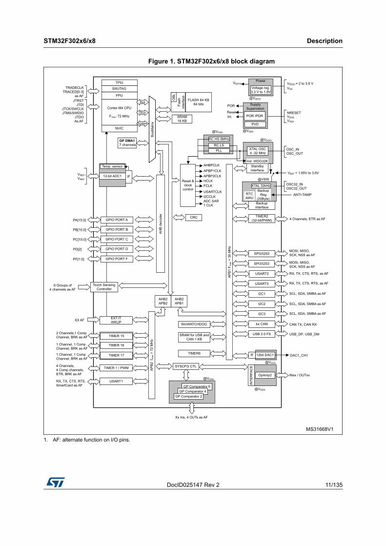
Figure 1. STM32F302x6/x8 block diagram
1. AF: alternate function on I/O pins.
Functional overview STM32F302x6/x8
12/135 DocID025147 Rev 2
3 Functional overview
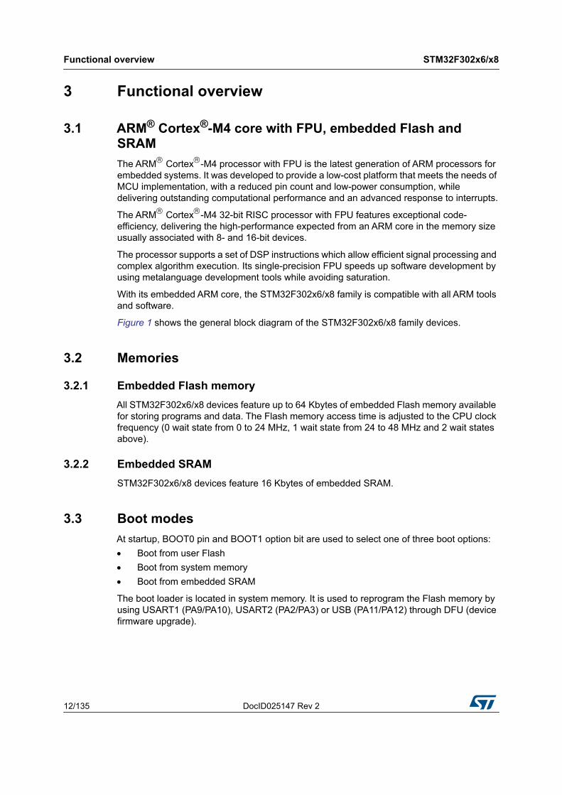
3.1 ARM® Cortex®-M4 core with FPU, embedded Flash and SRAMThe ARM Cortex-M4 processor with FPU is the latest generation of ARM processors for embedded systems. It was developed to provide a low-cost platform that meets the needs of MCU implementation, with a reduced pin count and low-power consumption, while delivering outstanding computational performance and an advanced response to interrupts.
The ARM Cortex-M4 32-bit RISC processor with FPU features exceptional code-efficiency, delivering the high-performance expected from an ARM core in the memory size usually associated with 8- and 16-bit devices.
The processor supports a set of DSP instructions which allow efficient signal processing and complex algorithm execution. Its single-precision FPU speeds up software development by using metalanguage development tools while avoiding saturation.
With its embedded ARM core, the STM32F302x6/x8 family is compatible with all ARM tools and software.
Figure 1 shows the general block diagram of the STM32F302x6/x8 family devices.
3.2 Memories
3.2.1 Embedded Flash memoryAll STM32F302x6/x8 devices feature up to 64 Kbytes of embedded Flash memory available for storing programs and data. The Flash memory access time is adjusted to the CPU clock frequency (0 wait state from 0 to 24 MHz, 1 wait state from 24 to 48 MHz and 2 wait states above).
3.2.2 Embedded SRAMSTM32F302x6/x8 devices feature 16 Kbytes of embedded SRAM.
3.3 Boot modesAt startup, BOOT0 pin and BOOT1 option bit are used to select one of three boot options: Boot from user Flash Boot from system memory Boot from embedded SRAM
The boot loader is located in system memory. It is used to reprogram the Flash memory by using USART1 (PA9/PA10), USART2 (PA2/PA3) or USB (PA11/PA12) through DFU (device firmware upgrade).
DocID025147 Rev 2 13/135
STM32F302x6/x8 Functional overview
51
3.4 Cyclic redundancy check calculation unit (CRC)The CRC (cyclic redundancy check) calculation unit is used to get a CRC code using a configurable generator polynomial value and size.
Among other applications, CRC-based techniques are used to verify data transmission or storage integrity. In the scope of the EN/IEC 60335-1 standard, they offer a means of verifying the Flash memory integrity. The CRC calculation unit helps compute a signature of the software during runtime, to be compared with a reference signature generated at linktime and stored at a given memory location.
3.5 Power management
3.5.1 Power supply schemes VSS, VDD = 2.0 to 3.6 V: external power supply for I/Os and the internal regulator. It is
provided externally through VDD pins. VSSA, VDDA = 2.0 to 3.6 V: external analog power supply for ADC, DAC, comparators,
operational amplifier, reset blocks, RCs and PLL (minimum voltage to be applied to VDDA is 2.4 V when the DAC and operational amplifier are used). The VDDA voltage level must be always greater or equal to the VDD voltage level and must be provided first.
VBAT = 1.65 to 3.6 V: power supply for RTC, external clock 32 kHz oscillator and backup registers (through power switch) when VDD is not present.
3.5.2 Power supply supervisorThe device has an integrated power-on reset (POR) and power-down reset (PDR) circuits. They are always active, and ensure proper operation above a threshold of 2 V. The device remains in reset mode when the monitored supply voltage is below a specified threshold, VPOR/PDR, without the need for an external reset circuit. The POR monitors only the VDD supply voltage. During the startup phase it is required
that VDDA should arrive first and be greater than or equal to VDD. The PDR monitors both the VDD and VDDA supply voltages, however the VDDA power
supply supervisor can be disabled (by programming a dedicated Option bit) to reduce the power consumption if the application design ensures that VDDA is higher than or equal to VDD.
The device features an embedded programmable voltage detector (PVD) that monitors the VDD power supply and compares it to the VPVD threshold. An interrupt can be generated when VDD drops below the VPVD threshold and/or when VDD is higher than the VPVD threshold. The interrupt service routine can then generate a warning message and/or put the MCU into a safe state. The PVD is enabled by software.
Functional overview STM32F302x6/x8
14/135 DocID025147 Rev 2
3.5.3 Voltage regulatorThe regulator has three operation modes: main (MR), low-power (LPR), and power-down. The MR mode is used in the nominal regulation mode (Run) The LPR mode is used in Stop mode. The power-down mode is used in Standby mode: the regulator output is in high
impedance, and the kernel circuitry is powered down thus inducing zero consumption.
The voltage regulator is always enabled after reset. It is disabled in Standby mode.
3.5.4 Low-power modesThe STM32F302x6/x8 supports three low-power modes to achieve the best compromise between low power consumption, short startup time and available wakeup sources: Sleep mode
In Sleep mode, only the CPU is stopped. All peripherals continue to operate and can wake up the CPU when an interrupt/event occurs.
Stop modeStop mode achieves the lowest power consumption while retaining the content of SRAM and registers. All clocks in the 1.8 V domain are stopped, the PLL, the HSI RC and the HSE crystal oscillators are disabled. The voltage regulator can also be put either in normal or in low-power mode.The device can be woken up from Stop mode by any of the EXTI line. The EXTI line source can be one of the 16 external lines, the PVD output, the USB wakeup, the RTC alarm, COMPx, I2C or USARTx.
Standby modeThe Standby mode is used to achieve the lowest power consumption. The internal voltage regulator is switched off so that the entire 1.8 V domain is powered off. The PLL, the HSI RC and the HSE crystal oscillators are also switched off. After entering Standby mode, SRAM and register contents are lost except for registers in the Backup domain and Standby circuitry.The device exits Standby mode when an external reset (NRST pin), an IWDG reset, a rising edge on the WKUP pin, or an RTC alarm occurs.
Note: The RTC, the IWDG, and the corresponding clock sources are not stopped by entering Stop or Standby mode.
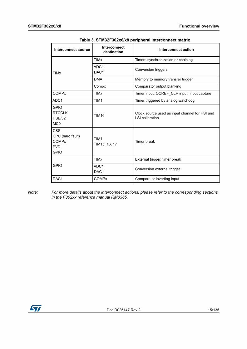
3.6 Interconnect matrixSeveral peripherals have direct connections between them. This allows autonomous communication between peripherals, saving CPU resources thus power supply consumption. In addition, these hardware connections allow fast and predictable latency.
DocID025147 Rev 2 15/135
STM32F302x6/x8 Functional overview
51
Note: For more details about the interconnect actions, please refer to the corresponding sections in the F302xx reference manual RM0365.
Table 3. STM32F302x6/x8 peripheral interconnect matrix
Interconnect source Interconnect destination Interconnect action
TIMx
TIMx Timers synchronization or chaining
ADC1DAC1
Conversion triggers
DMA Memory to memory transfer trigger
Compx Comparator output blanking
COMPx TIMx Timer input: OCREF_CLR input, input capture
ADC1 TIM1 Timer triggered by analog watchdog
GPIORTCCLKHSE/32MC0
TIM16 Clock source used as input channel for HSI and LSI calibration
CSSCPU (hard fault)COMPxPVDGPIO
TIM1TIM15, 16, 17
Timer break
GPIO
TIMx External trigger, timer break
ADC1DAC1
Conversion external trigger
DAC1 COMPx Comparator inverting input
Functional overview STM32F302x6/x8
16/135 DocID025147 Rev 2
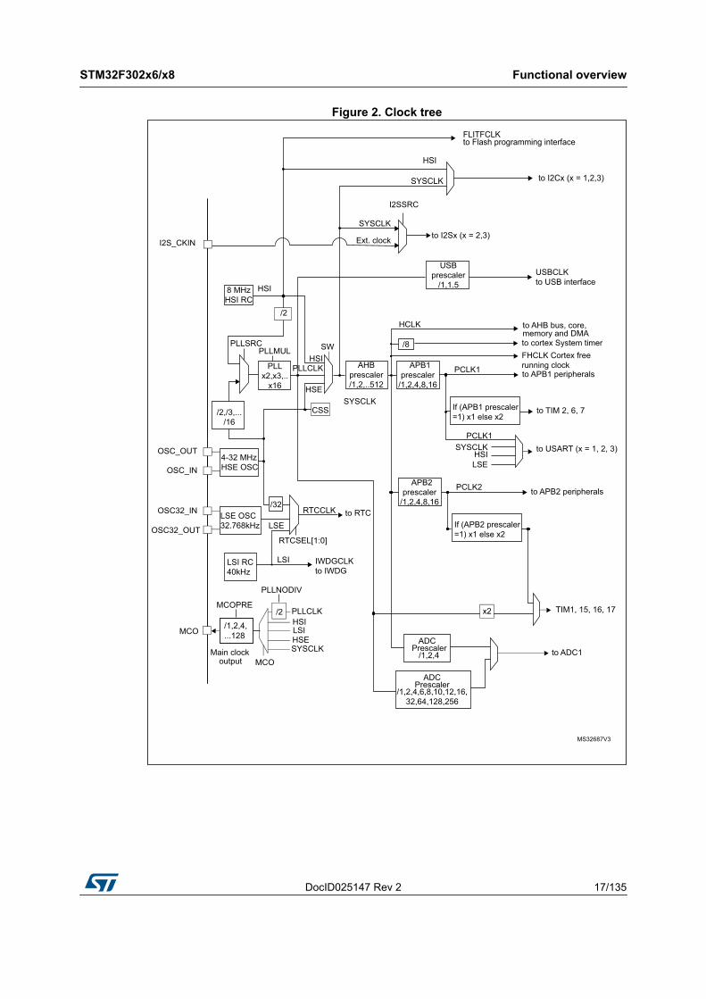
3.7 Clocks and startupSystem clock selection is performed on startup, however the internal RC 8 MHz oscillator is selected as default CPU clock on reset. An external 4-32 MHz clock can be selected, in which case it is monitored for failure. If failure is detected, the system automatically switches back to the internal RC oscillator. A software interrupt is generated if enabled. Similarly, full interrupt management of the PLL clock entry is available when necessary (for example with failure of an indirectly used external oscillator).
Several prescalers allow to configure the AHB frequency, the high speed APB (APB2) and the low speed APB (APB1) domains. The maximum frequency of the AHB and the high speed APB domains is 72 MHz, while the maximum allowed frequency of the low speed APB domain is 36 MHz.
The advanced clock controller clocks the core and all peripherals using a single crystal or oscillator. To achieve audio class performance, an audio crystal can be used.
DocID025147 Rev 2 17/135
STM32F302x6/x8 Functional overview
51
Figure 2. Clock tree
Functional overview STM32F302x6/x8
18/135 DocID025147 Rev 2
3.8 General-purpose inputs/outputs (GPIOs)Each of the GPIO pins can be configured by software as output (push-pull or open-drain), as input (with or without pull-up or pull-down) or as peripheral alternate function. Most of the GPIO pins are shared with digital or analog alternate functions. All GPIOs are high current capable except for analog inputs.
The I/Os alternate function configuration can be locked if needed following a specific sequence in order to avoid spurious writing to the I/Os registers.
Fast I/O handling allows I/O toggling up to 36 MHz.
3.9 Direct memory access (DMA)The flexible general-purpose DMA is able to manage memory-to-memory, peripheral-to-memory and memory-to-peripheral transfers. The DMA controller supports circular buffer management, avoiding the generation of interrupts when the controller reaches the end of the buffer.
Each of the 7 DMA channels is connected to dedicated hardware DMA requests, with software trigger support for each channel. Configuration is done by software and transfer sizes between source and destination are independent.
The DMA can be used with the main peripherals: SPI, I2C, USART, timers, DAC and ADC.
3.10 Interrupts and events
3.10.1 Nested vectored interrupt controller (NVIC)The STM32F302x6/x8 devices embed a nested vectored interrupt controller (NVIC) able to handle up to 60 maskable interrupt channels and 16 priority levels.
The NVIC benefits are the following: Closely coupled NVIC gives low latency interrupt processing Interrupt entry vector table address passed directly to the core Closely coupled NVIC core interface Allows early processing of interrupts Processing of late arriving higher priority interrupts Support for tail chaining Processor state automatically saved Interrupt entry restored on interrupt exit with no instruction overhead
The NVIC hardware block provides flexible interrupt management features with minimal interrupt latency.
DocID025147 Rev 2 19/135
STM32F302x6/x8 Functional overview
51
3.11 Fast analog-to-digital converter (ADC)An analog-to-digital converter, with selectable resolution between 12 and 6 bit, is embedded in the STM32F302x6/x8 family devices. The ADC has up to 15 external channels performing conversions in single-shot or scan modes. Channels can be configured to be either single-ended input or differential input. In scan mode, automatic conversion is performed on a selected group of analog inputs.
Additional logic functions embedded in the ADC interface allow: Simultaneous sample and hold Single-shunt phase current reading techniques.
The ADC can be served by the DMA controller.
Three analog watchdogs are available. The analog watchdog feature allows very precise monitoring of the converted voltage of one, some or all selected channels. An interrupt is generated when the converted voltage is outside the programmed thresholds.
The events generated by the general-purpose timers (TIMx) and the advanced-control timer (TIM1) can be internally connected to the ADC start trigger and injection trigger, respectively, to allow the application to synchronize A/D conversion and timers.
3.11.1 Temperature sensorThe temperature sensor (TS) generates a voltage VSENSE that varies linearly with temperature.
The temperature sensor is internally connected to the ADC1_IN16 input channel which is used to convert the sensor output voltage into a digital value.
The sensor provides good linearity but it has to be calibrated to obtain good overall accuracy of the temperature measurement. As the offset of the temperature sensor varies from chip to chip due to process variation, the uncalibrated internal temperature sensor is suitable for applications that detect temperature changes only.
To improve the accuracy of the temperature sensor measurement, each device is individually factory-calibrated by ST. The temperature sensor factory calibration data are stored by ST in the system memory area, accessible in read-only mode.
3.11.2 Internal voltage reference (VREFINT)
The internal voltage reference (VREFINT) provides a stable (bandgap) voltage output for the ADC and Comparators. VREFINT is internally connected to the ADC1_IN18 input channel. The precise voltage of VREFINT is individually measured for each part by ST during production test and stored in the system memory area. It is accessible in read-only mode.
Functional overview STM32F302x6/x8
20/135 DocID025147 Rev 2
3.11.3 VBAT battery voltage monitoring
This embedded hardware feature allows the application to measure the VBAT battery voltage using the internal ADC channel ADC1_IN17. As the VBAT voltage may be higher than VDDA, and thus outside the ADC input range, the VBAT pin is internally connected to a bridge divider by 2. As a consequence, the converted digital value is half the VBAT voltage.
3.12 Digital-to-analog converter (DAC)One 12-bit buffered DAC channel (DAC1_OUT1) can be used to convert digital signals into analog voltage signal outputs. The chosen design structure is composed of integrated resistor strings and an amplifier in inverting configuration.
This digital interface supports the following features: One DAC output channel 8-bit or 12-bit monotonic output Left or right data alignment in 12-bit mode Synchronized update capability Noise-wave generation Triangular-wave generation DMA capability External triggers for conversion
3.13 Operational amplifier (OPAMP)The STM32F302x6/x8 embeds one operational amplifier with external or internal follower routing and PGA capability (or even amplifier and filter capability with external components). When the operational amplifier is selected, an external ADC channel is used to enable output measurement.
The operational amplifier features: 8.2 MHz bandwidth 0.5 mA output capability Rail-to-rail input/output In PGA mode, the gain can be programmed to be 2, 4, 8 or 16.
3.14 Ultra-fast comparators (COMP)The STM32F302x6/x8 devices embed three ultra-fast rail-to-rail comparators which offer the features below: Programmable internal or external reference voltage Selectable output polarity.

DocID025147 Rev 2 21/135
STM32F302x6/x8 Functional overview
51
The reference voltage can be one of the following: External I/O DAC output Internal reference voltage or submultiple (1/4, 1/2, 3/4). Refer to Table 24: Embedded
reset and power control block characteristics for the value and precision of the internal reference voltage.
All comparators can wake up from STOP mode, and also generate interrupts and breaks for the timers.
3.15 Timers and watchdogsThe STM32F302x6/x8 includes advanced control timer, up to general-purpose timers, basic timer, two watchdog timers and a SysTick timer. The table below compares the features of the advanced control, general purpose and basic timers.
3.15.1 Advanced timer (TIM1)The advanced-control timer can each be seen as a three-phase PWM multiplexed on 6 channels. They have complementary PWM outputs with programmable inserted dead-
Table 4. Timer feature comparison
Timer type Timer Counter resolution
Counter type
Prescaler factor
DMA request
generation
Capture/compare Channels
Complementary outputs
Advanced control TIM1(1) 16-bit Up, Down,
Up/Down
Any integer between 1 and 65536
Yes 4 Yes
General-purpose
TIM2 32-bit Up, Down, Up/Down
Any integer between 1 and 65536
Yes 4 No
TIM15(1) 16-bit UpAny integer between 1 and 65536
Yes 2 1
TIM16(1), TIM17(1) 16-bit Up
Any integer between 1 and 65536
Yes 1 1
Basic TIM6 16-bit UpAny integer between 1 and 65536
Yes 0 No
1. TIM1/15/16/17 can be clocked from the PLL running at 144 MHz when the system clock source is the PLL and AHB or APB2 subsystem clocks are not divided by more than 2 cumulatively.
Functional overview STM32F302x6/x8
22/135 DocID025147 Rev 2
times. They can also be seen as complete general-purpose timers. The 4 independent channels can be used for: Input capture Output compare PWM generation (edge or center-aligned modes) with full modulation capability (0-
100%) One-pulse mode output
In debug mode, the advanced-control timer counter can be frozen and the PWM outputs disabled to turn off any power switches driven by these outputs.
Many features are shared with those of the general-purpose TIM timers (described in Section 3.15.2 using the same architecture, so the advanced-control timers can work together with the TIM timers via the Timer Link feature for synchronization or event chaining.
3.15.2 General-purpose timers (TIM2, TIM15, TIM16, TIM17)There are up to four synchronizable general-purpose timers embedded in the STM32F302x6/x8 (see Table 4 for differences). Each general-purpose timer can be used to generate PWM outputs, or act as a simple time base.
TIM2
TIM2 has a 32-bit auto-reload up/downcounter and 32-bit prescaler
It features 4 independent channels for input capture/output compare, PWM or one-pulse mode output. It can work together, or with the other general-purpose timers via the Timer Link feature for synchronization or event chaining.
The counter can be frozen in debug mode.
It has independent DMA request generation and supports quadrature encoders.
TIM15, TIM16 and TIM 17
These three timers general-purpose timers with mid-range features:
They have 16-bit auto-reload upcounters and 16-bit prescalers. TIM15 has 2 channels and 1 complementary channel TIM16 and TIM17 have 1 channel and 1 complementary channel
All channels can be used for input capture/output compare, PWM or one-pulse mode output.
The timers can work together via the Timer Link feature for synchronization or event chaining. The timers have independent DMA request generation.
The counters can be frozen in debug mode.
3.15.3 Basic timer (TIM6)This timer is mainly used for DAC trigger generation. It can also be used as a generic 16-bit time base.
DocID025147 Rev 2 23/135
STM32F302x6/x8 Functional overview
51
3.15.4 Independent watchdog (IWDG)The independent watchdog is based on a 12-bit downcounter and 8-bit prescaler. It is clocked from an independent 40 kHz internal RC and as it operates independently from the main clock, it can operate in Stop and Standby modes. It can be used either as a watchdog to reset the device when a problem occurs, or as a free running timer for application timeout management. It is hardware or software configurable through the option bytes. The counter can be frozen in debug mode.
3.15.5 Window watchdog (WWDG)The window watchdog is based on a 7-bit downcounter that can be set as free running. It can be used as a watchdog to reset the device when a problem occurs. It is clocked from the main clock. It has an early warning interrupt capability and the counter can be frozen in debug mode.
3.15.6 SysTick timerThis timer is dedicated to real-time operating systems, but could also be used as a standard down counter. It features: A 24-bit down counter Autoreload capability Maskable system interrupt generation when the counter reaches 0. Programmable clock source
3.16 Real-time clock (RTC) and backup registersThe RTC and the 20 backup registers are supplied through a switch that takes power from either the VDD supply when present or the VBAT pin. The backup registers are five 32-bit registers used to store 20 bytes of user application data when VDD power is not present.
They are not reset by a system or power reset, or when the device wakes up from Standby mode.
The RTC is an independent BCD timer/counter. It supports the following features: Calendar with subsecond, seconds, minutes, hours (12 or 24 format), week day, date,
month, year, in BCD (binary-coded decimal) format. Automatic correction for 28, 29 (leap year), 30, and 31 days of the month. Two programmable alarms with wake up from Stop and Standby mode capability. On-the-fly correction from 1 to 32767 RTC clock pulses. This can be used to
synchronize it with a master clock. Digital calibration circuit with 1 ppm resolution, to compensate for quartz crystal
inaccuracy. Two anti-tamper detection pins with programmable filter. The MCU can be woken up
from Stop and Standby modes on tamper event detection. Timestamp feature which can be used to save the calendar content. This function can
be triggered by an event on the timestamp pin, or by a tamper event. The MCU can be woken up from Stop and Standby modes on timestamp event detection.
17-bit Auto-reload counter for periodic interrupt with wakeup from STOP/STANDBY capability.
Functional overview STM32F302x6/x8
24/135 DocID025147 Rev 2
The RTC clock sources can be: A 32.768 kHz external crystal A resonator or oscillator The internal low-power RC oscillator (typical frequency of 40 kHz) The high-speed external clock divided by 32.
DocID025147 Rev 2 25/135
STM32F302x6/x8 Functional overview
51
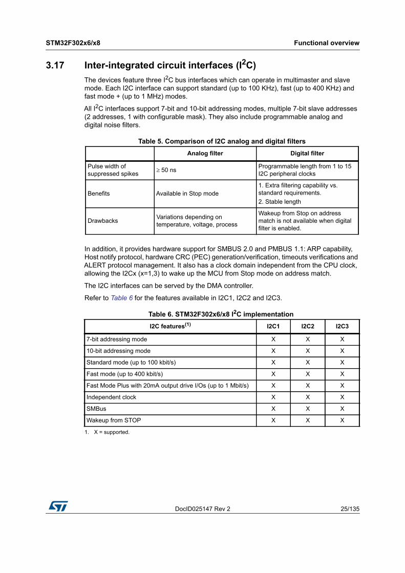
3.17 Inter-integrated circuit interfaces (I2C)The devices feature three I2C bus interfaces which can operate in multimaster and slave mode. Each I2C interface can support standard (up to 100 KHz), fast (up to 400 KHz) and fast mode + (up to 1 MHz) modes.
All I2C interfaces support 7-bit and 10-bit addressing modes, multiple 7-bit slave addresses (2 addresses, 1 with configurable mask). They also include programmable analog and digital noise filters.
In addition, it provides hardware support for SMBUS 2.0 and PMBUS 1.1: ARP capability, Host notify protocol, hardware CRC (PEC) generation/verification, timeouts verifications and ALERT protocol management. It also has a clock domain independent from the CPU clock, allowing the I2Cx (x=1,3) to wake up the MCU from Stop mode on address match.
The I2C interfaces can be served by the DMA controller.
Refer to Table 6 for the features available in I2C1, I2C2 and I2C3.
Table 5. Comparison of I2C analog and digital filtersAnalog filter Digital filter
Pulse width of suppressed spikes 50 ns Programmable length from 1 to 15
I2C peripheral clocks
Benefits Available in Stop mode1. Extra filtering capability vs. standard requirements.2. Stable length
Drawbacks Variations depending on temperature, voltage, process
Wakeup from Stop on address match is not available when digital filter is enabled.
Table 6. STM32F302x6/x8 I2C implementation I2C features(1)
1. X = supported.
I2C1 I2C2 I2C3
7-bit addressing mode X X X
10-bit addressing mode X X X
Standard mode (up to 100 kbit/s) X X X
Fast mode (up to 400 kbit/s) X X X
Fast Mode Plus with 20mA output drive I/Os (up to 1 Mbit/s) X X X
Independent clock X X X
SMBus X X X
Wakeup from STOP X X X
Functional overview STM32F302x6/x8
26/135 DocID025147 Rev 2
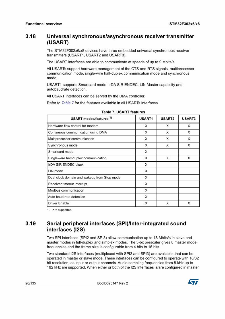
3.18 Universal synchronous/asynchronous receiver transmitter (USART)The STM32F302x6/x8 devices have three embedded universal synchronous receiver transmitters (USART1, USART2 and USART3).
The USART interfaces are able to communicate at speeds of up to 9 Mbits/s.
All USARTs support hardware management of the CTS and RTS signals, multiprocessor communication mode, single-wire half-duplex communication mode and synchronous mode.
USART1 supports Smartcard mode, IrDA SIR ENDEC, LIN Master capability and autobaudrate detection.
All USART interfaces can be served by the DMA controller.
Refer to Table 7 for the features available in all USARTs interfaces.
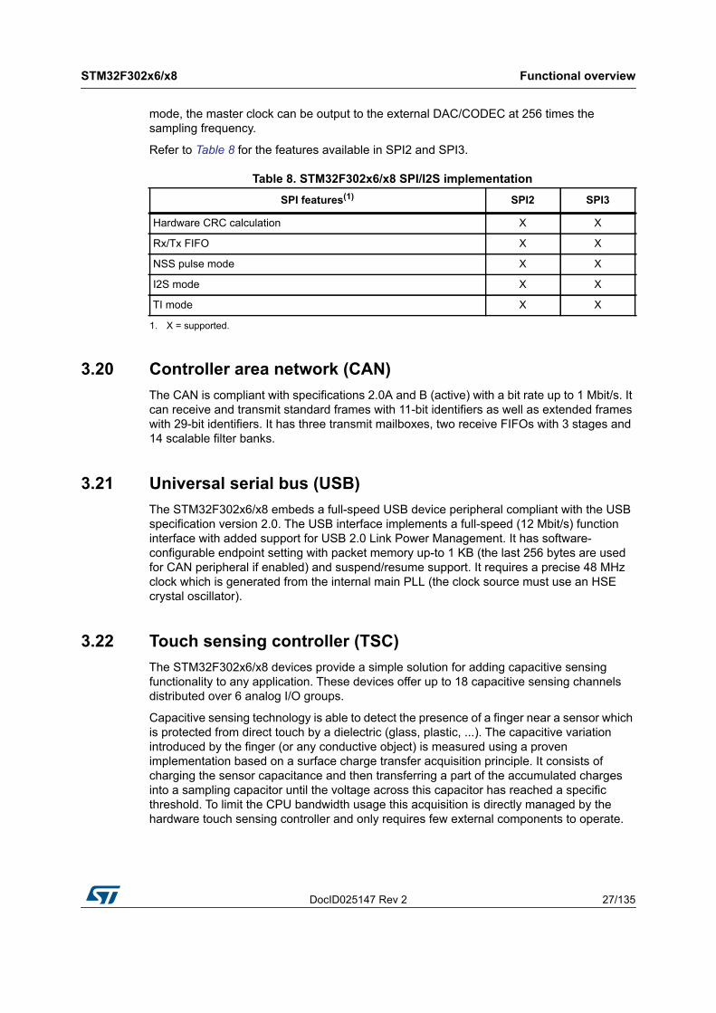
3.19 Serial peripheral interfaces (SPI)/Inter-integrated sound interfaces (I2S)Two SPI interfaces (SPI2 and SPI3) allow communication up to 18 Mbits/s in slave and master modes in full-duplex and simplex modes. The 3-bit prescaler gives 8 master mode frequencies and the frame size is configurable from 4 bits to 16 bits.
Two standard I2S interfaces (multiplexed with SPI2 and SPI3) are available, that can be operated in master or slave mode. These interfaces can be configured to operate with 16/32 bit resolution, as input or output channels. Audio sampling frequencies from 8 kHz up to 192 kHz are supported. When either or both of the I2S interfaces is/are configured in master
Table 7. USART featuresUSART modes/features(1)
1. X = supported.
USART1 USART2 USART3
Hardware flow control for modem X X X
Continuous communication using DMA X X X
Multiprocessor communication X X X
Synchronous mode X X X
Smartcard mode X
Single-wire half-duplex communication X X X
IrDA SIR ENDEC block X
LIN mode X
Dual clock domain and wakeup from Stop mode X
Receiver timeout interrupt X
Modbus communication X
Auto baud rate detection X
Driver Enable X X X
DocID025147 Rev 2 27/135
STM32F302x6/x8 Functional overview
51
mode, the master clock can be output to the external DAC/CODEC at 256 times the sampling frequency.
Refer to Table 8 for the features available in SPI2 and SPI3.
3.20 Controller area network (CAN)The CAN is compliant with specifications 2.0A and B (active) with a bit rate up to 1 Mbit/s. It can receive and transmit standard frames with 11-bit identifiers as well as extended frames with 29-bit identifiers. It has three transmit mailboxes, two receive FIFOs with 3 stages and 14 scalable filter banks.
3.21 Universal serial bus (USB)The STM32F302x6/x8 embeds a full-speed USB device peripheral compliant with the USB specification version 2.0. The USB interface implements a full-speed (12 Mbit/s) function interface with added support for USB 2.0 Link Power Management. It has software-configurable endpoint setting with packet memory up-to 1 KB (the last 256 bytes are used for CAN peripheral if enabled) and suspend/resume support. It requires a precise 48 MHz clock which is generated from the internal main PLL (the clock source must use an HSE crystal oscillator).
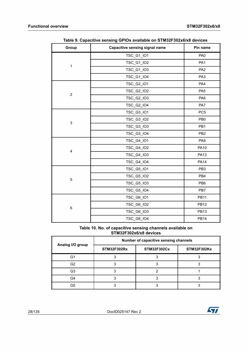
3.22 Touch sensing controller (TSC)The STM32F302x6/x8 devices provide a simple solution for adding capacitive sensing functionality to any application. These devices offer up to 18 capacitive sensing channels distributed over 6 analog I/O groups.
Capacitive sensing technology is able to detect the presence of a finger near a sensor which is protected from direct touch by a dielectric (glass, plastic, ...). The capacitive variation introduced by the finger (or any conductive object) is measured using a proven implementation based on a surface charge transfer acquisition principle. It consists of charging the sensor capacitance and then transferring a part of the accumulated charges into a sampling capacitor until the voltage across this capacitor has reached a specific threshold. To limit the CPU bandwidth usage this acquisition is directly managed by the hardware touch sensing controller and only requires few external components to operate.
Table 8. STM32F302x6/x8 SPI/I2S implementationSPI features(1)
1. X = supported.
SPI2 SPI3
Hardware CRC calculation X X
Rx/Tx FIFO X X
NSS pulse mode X X
I2S mode X X
TI mode X X
Functional overview STM32F302x6/x8
28/135 DocID025147 Rev 2
Table 9. Capacitive sensing GPIOs available on STM32F302x6/x8 devices Group Capacitive sensing signal name Pin name
1
TSC_G1_IO1 PA0
TSC_G1_IO2 PA1
TSC_G1_IO3 PA2
TSC_G1_IO4 PA3
2
TSC_G2_IO1 PA4
TSC_G2_IO2 PA5
TSC_G2_IO3 PA6
TSC_G2_IO4 PA7
3
TSC_G3_IO1 PC5
TSC_G3_IO2 PB0
TSC_G3_IO3 PB1
TSC_G3_IO4 PB2
4
TSC_G4_IO1 PA9
TSC_G4_IO2 PA10
TSC_G4_IO3 PA13
TSC_G4_IO4 PA14
5
TSC_G5_IO1 PB3
TSC_G5_IO2 PB4
TSC_G5_IO3 PB6
TSC_G5_IO4 PB7
6
TSC_G6_IO1 PB11
TSC_G6_IO2 PB12
TSC_G6_IO3 PB13
TSC_G6_IO4 PB14
Table 10. No. of capacitive sensing channels available onSTM32F302x6/x8 devices
Analog I/O groupNumber of capacitive sensing channels
STM32F302Rx STM32F302Cx STM32F302Kx
G1 3 3 3
G2 3 3 3
G3 3 2 1
G4 3 3 3
G5 3 3 3
DocID025147 Rev 2 29/135
STM32F302x6/x8 Functional overview
51
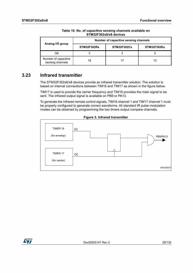
3.23 Infrared transmitterThe STM32F302x6/x8 devices provide an infrared transmitter solution. The solution is based on internal connections between TIM16 and TIM17 as shown in the figure below.
TIM17 is used to provide the carrier frequency and TIM16 provides the main signal to be sent. The infrared output signal is available on PB9 or PA13.
To generate the infrared remote control signals, TIM16 channel 1 and TIM17 channel 1 must be properly configured to generate correct waveforms. All standard IR pulse modulation modes can be obtained by programming the two timers output compare channels.
Figure 3. Infrared transmitter
G6 3 3 0
Number of capacitive sensing channels 18 17 13
Table 10. No. of capacitive sensing channels available onSTM32F302x6/x8 devices
Analog I/O groupNumber of capacitive sensing channels
STM32F302Rx STM32F302Cx STM32F302Kx
Functional overview STM32F302x6/x8
30/135 DocID025147 Rev 2
3.24 Development support
3.24.1 Serial wire JTAG debug port (SWJ-DP)The ARM SWJ-DP Interface is embedded, and is a combined JTAG and serial wire debug port that enables either a serial wire debug or a JTAG probe to be connected to the target.
The JTAG TMS and TCK pins are shared respectively with SWDIO and SWCLK and a specific sequence on the TMS pin is used to switch between JTAG-DP and SW-DP.
DocID025147 Rev 2 31/135
STM32F302x6/x8 Pinouts and pin description
51
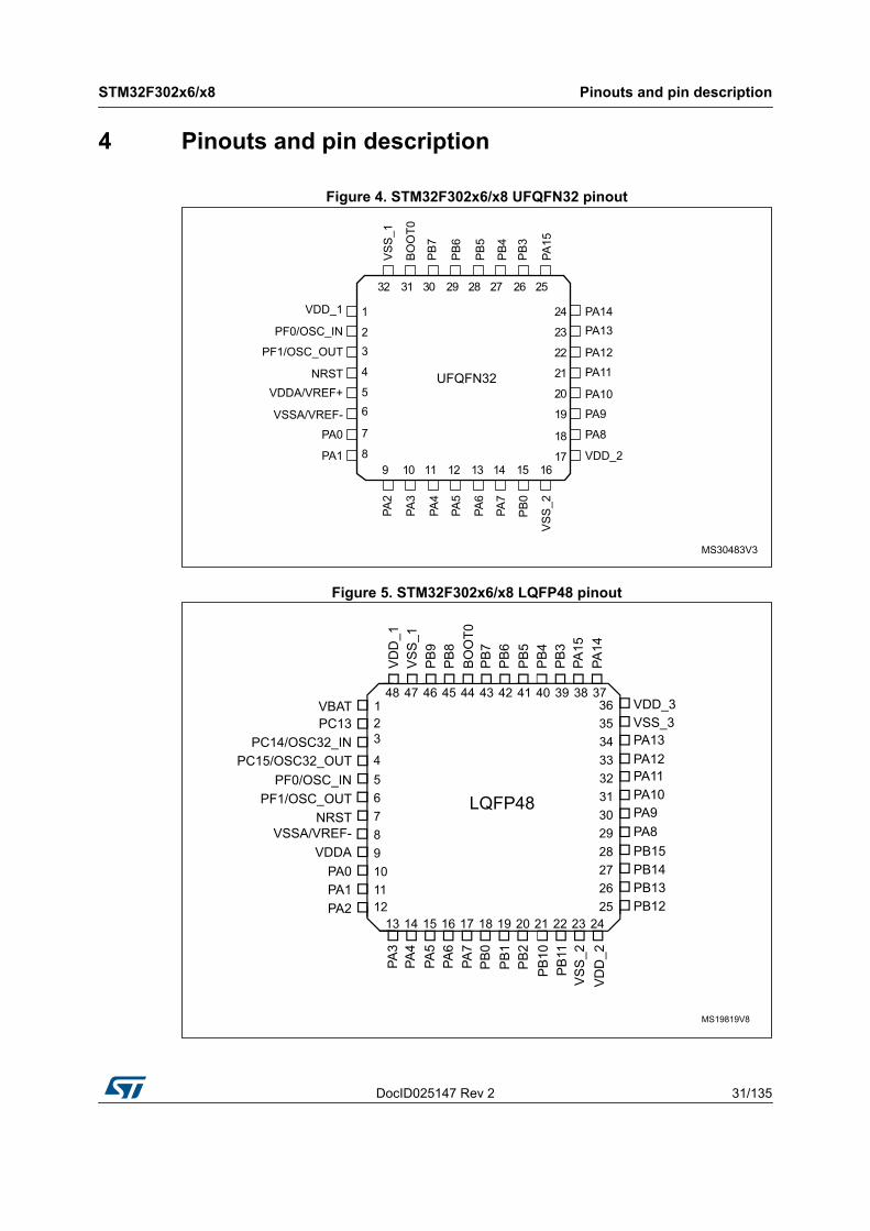
4 Pinouts and pin description
Figure 4. STM32F302x6/x8 UFQFN32 pinout
Figure 5. STM32F302x6/x8 LQFP48 pinout
Pinouts and pin description STM32F302x6/x8
32/135 DocID025147 Rev 2
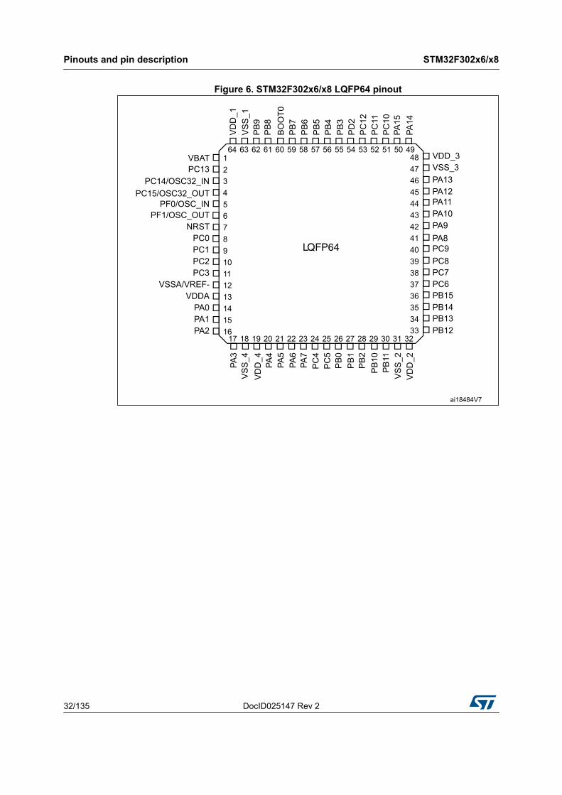
Figure 6. STM32F302x6/x8 LQFP64 pinout
DocID025147 Rev 2 33/135
STM32F302x6/x8 Pinouts and pin description
51
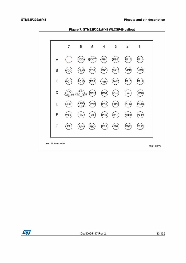
Figure 7. STM32F302x6/x8 WLCSP49 ballout
Pinouts and pin description STM32F302x6/x8
34/135 DocID025147 Rev 2
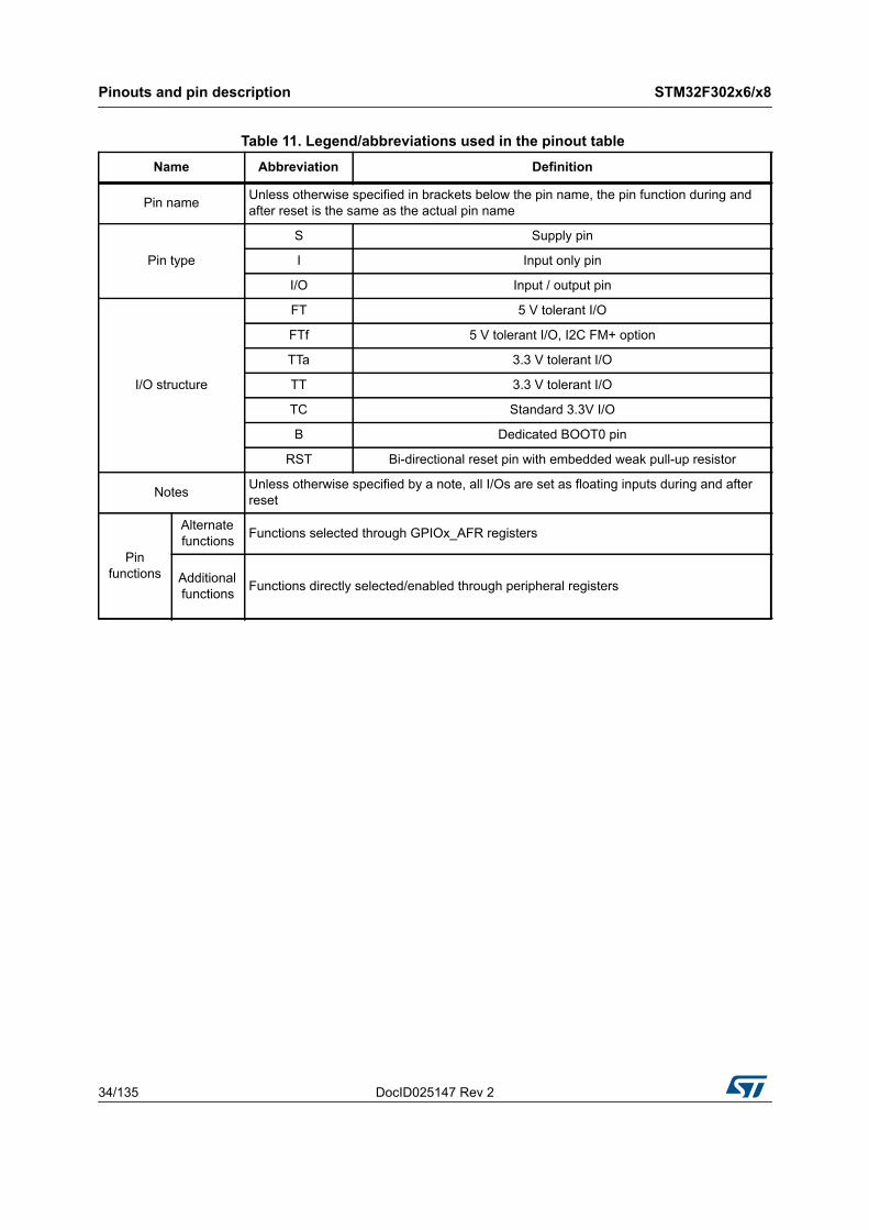
Table 11. Legend/abbreviations used in the pinout table Name Abbreviation Definition
Pin name Unless otherwise specified in brackets below the pin name, the pin function during and after reset is the same as the actual pin name
Pin type
S Supply pin
I Input only pin
I/O Input / output pin
I/O structure
FT 5 V tolerant I/O
FTf 5 V tolerant I/O, I2C FM+ option
TTa 3.3 V tolerant I/O
TT 3.3 V tolerant I/O
TC Standard 3.3V I/O
B Dedicated BOOT0 pin
RST Bi-directional reset pin with embedded weak pull-up resistor
Notes Unless otherwise specified by a note, all I/Os are set as floating inputs during and after reset
Pin functions
Alternate functions Functions selected through GPIOx_AFR registers
Additional functions Functions directly selected/enabled through peripheral registers
STM32F302x6/x8
Pinouts and pin description
DocID
025147 Rev 2
35/135
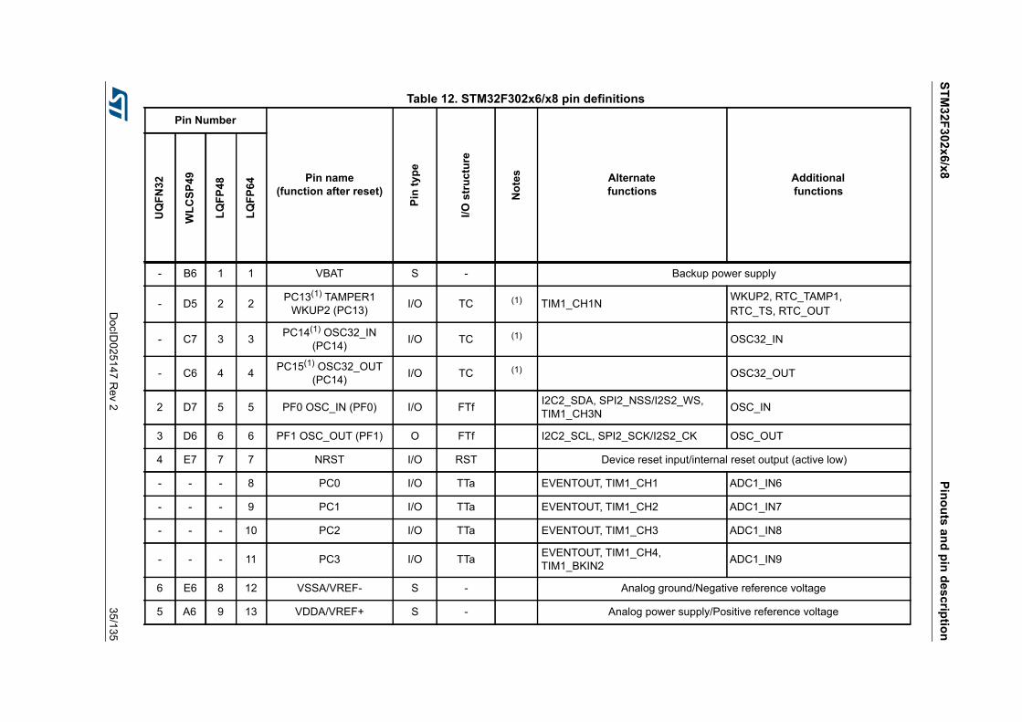
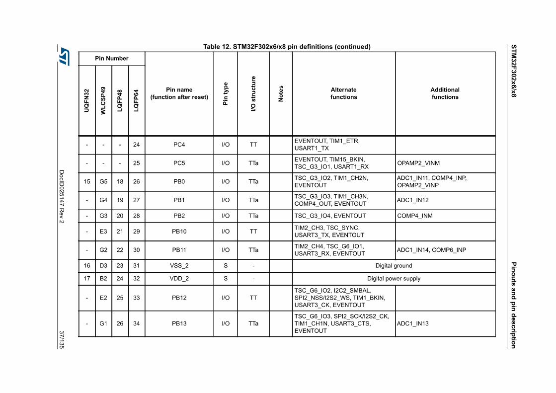
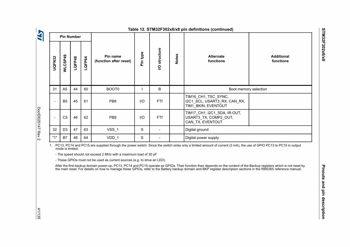
Table 12. STM32F302x6/x8 pin definitions
Pin Number
Pin name (function after reset)
Pin
type
I/O s
truc
ture
Not
es Alternatefunctions
Additionalfunctions
UQ
FN32
WLC
SP49
LQFP
48
LQFP
64
- B6 1 1 VBAT S - Backup power supply
- D5 2 2 PC13(1) TAMPER1 WKUP2 (PC13) I/O TC (1) TIM1_CH1N
WKUP2, RTC_TAMP1,RTC_TS, RTC_OUT
- C7 3 3 PC14(1) OSC32_IN (PC14) I/O TC (1) OSC32_IN
- C6 4 4 PC15(1) OSC32_OUT (PC14) I/O TC (1) OSC32_OUT
2 D7 5 5 PF0 OSC_IN (PF0) I/O FTf I2C2_SDA, SPI2_NSS/I2S2_WS, TIM1_CH3N OSC_IN
3 D6 6 6 PF1 OSC_OUT (PF1) O FTf I2C2_SCL, SPI2_SCK/I2S2_CK OSC_OUT
4 E7 7 7 NRST I/O RST Device reset input/internal reset output (active low)
- - - 8 PC0 I/O TTa EVENTOUT, TIM1_CH1 ADC1_IN6
- - - 9 PC1 I/O TTa EVENTOUT, TIM1_CH2 ADC1_IN7
- - - 10 PC2 I/O TTa EVENTOUT, TIM1_CH3 ADC1_IN8
- - - 11 PC3 I/O TTa EVENTOUT, TIM1_CH4, TIM1_BKIN2 ADC1_IN9
6 E6 8 12 VSSA/VREF- S - Analog ground/Negative reference voltage
5 A6 9 13 VDDA/VREF+ S - Analog power supply/Positive reference voltage
Pinouts and pin descriptionSTM
32F302x6/x8
36/135D
ocID025147 R
ev 2
7 F6 10 14 PA0 -TAMPER2-WKUP1 I/O TTaTIM2_CH1/TIM2_ETR, TSC_G1_IO1, USART2_CTS, EVENTOUT
ADC1_IN1, RTC_TAMP2, WKUP1
8 G7 11 15 PA1 I/O TTaRTC_REFIN, TIM2_CH2, TSC_G1_IO2, USART2_RTS, TIM15_CH1N, EVENTOUT
ADC1_IN2
9 E5 12 16 PA2 I/O TTaTIM2_CH3, TSC_G1_IO3, USART2_TX, COMP2_OUT, TIM15_CH1, EVENTOUT
ADC1_IN3, COMP2_INM
10 E4 13 17 PA3 I/O TTaTIM2_CH4, TSC_G1_IO4, USART2_RX, TIM15_CH2, EVENTOUT
ADC1_IN4
- F7 - 18 VSS_4 S -
- F2 - 19 VDD_4 S -
11 G6 14 20 PA4 I/O TTa TSC_G2_IO1, SPI3_NSS/I2S3_WS, USART2_CK, EVENTOUT
ADC1_IN5, DAC1_OUT1, COMP2_INM, COMP4_INM, COMP6_INM
12 F5 15 21 PA5 I/O TTa TIM2_CH1/TIM2_ETR, TSC_G2_IO2, EVENTOUT OPAMP2_VINM
13 F4 16 22 PA6 I/O TTa TIM16_CH1, TSC_G2_IO3, TIM1_BKIN, EVENTOUT ADC1_IN10, OPAMP2_VOUT
14 F3 17 23 PA7 I/O TTa TIM17_CH1, TSC_G2_IO4, TIM1_CH1N, EVENTOUT
ADC1_IN15, COMP2_INP, OPAMP2_VINP
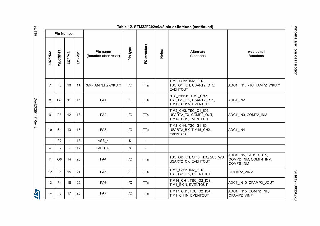
Table 12. STM32F302x6/x8 pin definitions (continued)Pin Number
Pin name (function after reset)
Pin
type
I/O s
truc
ture
Not
es Alternatefunctions
Additionalfunctions
UQ
FN32
WLC
SP49
LQFP
48
LQFP
64
STM32F302x6/x8
Pinouts and pin description
DocID
025147 Rev 2
37/135
- - - 24 PC4 I/O TT EVENTOUT, TIM1_ETR, USART1_TX
- - - 25 PC5 I/O TTa EVENTOUT, TIM15_BKIN, TSC_G3_IO1, USART1_RX OPAMP2_VINM
15 G5 18 26 PB0 I/O TTa TSC_G3_IO2, TIM1_CH2N, EVENTOUT
ADC1_IN11, COMP4_INP, OPAMP2_VINP
- G4 19 27 PB1 I/O TTa TSC_G3_IO3, TIM1_CH3N, COMP4_OUT, EVENTOUT ADC1_IN12
- G3 20 28 PB2 I/O TTa TSC_G3_IO4, EVENTOUT COMP4_INM
- E3 21 29 PB10 I/O TT TIM2_CH3, TSC_SYNC, USART3_TX, EVENTOUT
- G2 22 30 PB11 I/O TTa TIM2_CH4, TSC_G6_IO1, USART3_RX, EVENTOUT ADC1_IN14, COMP6_INP
16 D3 23 31 VSS_2 S - Digital ground
17 B2 24 32 VDD_2 S - Digital power supply
- E2 25 33 PB12 I/O TTTSC_G6_IO2, I2C2_SMBAL, SPI2_NSS/I2S2_WS, TIM1_BKIN, USART3_CK, EVENTOUT
- G1 26 34 PB13 I/O TTaTSC_G6_IO3, SPI2_SCK/I2S2_CK, TIM1_CH1N, USART3_CTS, EVENTOUT
ADC1_IN13
Table 12. STM32F302x6/x8 pin definitions (continued)Pin Number
Pin name (function after reset)
Pin
type
I/O s
truc
ture
Not
es Alternatefunctions
Additionalfunctions
UQ
FN32
WLC
SP49
LQFP
48
LQFP
64
Pinouts and pin descriptionSTM
32F302x6/x8
38/135D
ocID025147 R
ev 2
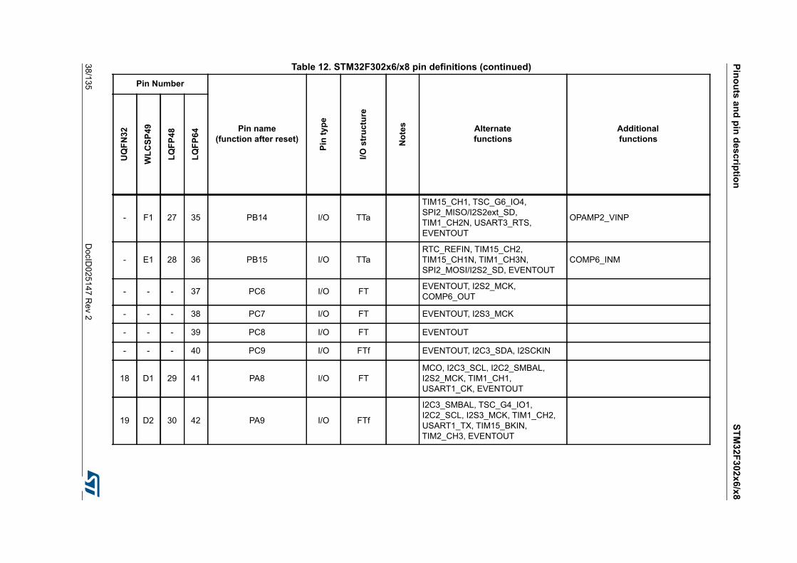
- F1 27 35 PB14 I/O TTa
TIM15_CH1, TSC_G6_IO4, SPI2_MISO/I2S2ext_SD, TIM1_CH2N, USART3_RTS, EVENTOUT
OPAMP2_VINP
- E1 28 36 PB15 I/O TTaRTC_REFIN, TIM15_CH2, TIM15_CH1N, TIM1_CH3N, SPI2_MOSI/I2S2_SD, EVENTOUT
COMP6_INM
- - - 37 PC6 I/O FT EVENTOUT, I2S2_MCK, COMP6_OUT
- - - 38 PC7 I/O FT EVENTOUT, I2S3_MCK
- - - 39 PC8 I/O FT EVENTOUT
- - - 40 PC9 I/O FTf EVENTOUT, I2C3_SDA, I2SCKIN
18 D1 29 41 PA8 I/O FTMCO, I2C3_SCL, I2C2_SMBAL, I2S2_MCK, TIM1_CH1, USART1_CK, EVENTOUT
19 D2 30 42 PA9 I/O FTf
I2C3_SMBAL, TSC_G4_IO1, I2C2_SCL, I2S3_MCK, TIM1_CH2, USART1_TX, TIM15_BKIN, TIM2_CH3, EVENTOUT
Table 12. STM32F302x6/x8 pin definitions (continued)Pin Number
Pin name (function after reset)
Pin
type
I/O s
truc
ture
Not
es Alternatefunctions
Additionalfunctions
UQ
FN32
WLC
SP49
LQFP
48
LQFP
64
STM32F302x6/x8
Pinouts and pin description
DocID
025147 Rev 2
39/135
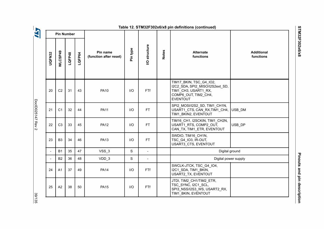
20 C2 31 43 PA10 I/O FTf
TIM17_BKIN, TSC_G4_IO2, I2C2_SDA, SPI2_MISO/I2S2ext_SD, TIM1_CH3, USART1_RX, COMP6_OUT, TIM2_CH4, EVENTOUT
21 C1 32 44 PA11 I/O FTSPI2_MOSI/I2S2_SD, TIM1_CH1N, USART1_CTS, CAN_RX,TIM1_CH4, TIM1_BKIN2, EVENTOUT
USB_DM
22 C3 33 45 PA12 I/O FTTIM16_CH1, I2SCKIN, TIM1_CH2N, USART1_RTS, COMP2_OUT, CAN_TX, TIM1_ETR, EVENTOUT
USB_DP
23 B3 34 46 PA13 I/O FTSWDIO, TIM16_CH1N, TSC_G4_IO3, IR-OUT, USART3_CTS, EVENTOUT
- B1 35 47 VSS_3 S - Digital ground
- B2 36 48 VDD_3 S - Digital power supply
24 A1 37 49 PA14 I/O FTfSWCLK-JTCK, TSC_G4_IO4, I2C1_SDA, TIM1_BKIN, USART2_TX, EVENTOUT
25 A2 38 50 PA15 I/O FTf
JTDI, TIM2_CH1/TIM2_ETR, TSC_SYNC, I2C1_SCL, SPI3_NSS/I2S3_WS, USART2_RX, TIM1_BKIN, EVENTOUT
Table 12. STM32F302x6/x8 pin definitions (continued)Pin Number
Pin name (function after reset)
Pin
type
I/O s
truc
ture
Not
es Alternatefunctions
Additionalfunctions
UQ
FN32
WLC
SP49
LQFP
48
LQFP
64
Pinouts and pin descriptionSTM
32F302x6/x8
40/135D
ocID025147 R
ev 2
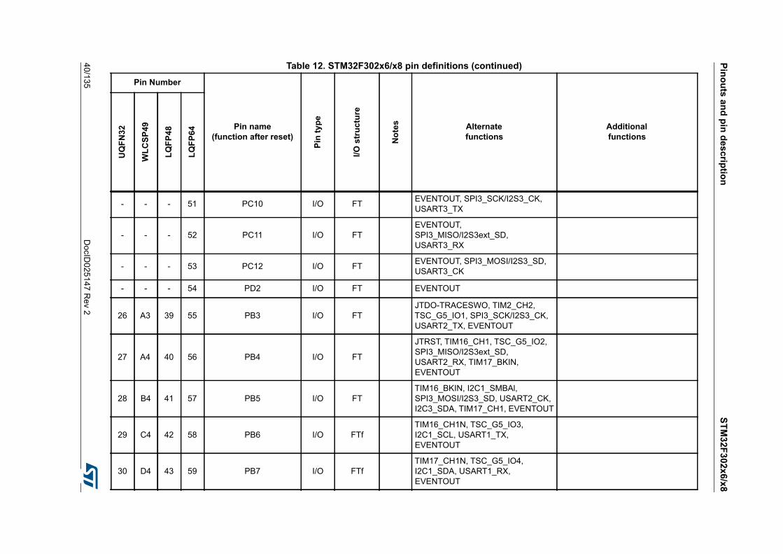
- - - 51 PC10 I/O FT EVENTOUT, SPI3_SCK/I2S3_CK, USART3_TX
- - - 52 PC11 I/O FTEVENTOUT, SPI3_MISO/I2S3ext_SD, USART3_RX
- - - 53 PC12 I/O FT EVENTOUT, SPI3_MOSI/I2S3_SD, USART3_CK
- - - 54 PD2 I/O FT EVENTOUT
26 A3 39 55 PB3 I/O FTJTDO-TRACESWO, TIM2_CH2, TSC_G5_IO1, SPI3_SCK/I2S3_CK, USART2_TX, EVENTOUT
27 A4 40 56 PB4 I/O FT
JTRST, TIM16_CH1, TSC_G5_IO2, SPI3_MISO/I2S3ext_SD, USART2_RX, TIM17_BKIN, EVENTOUT
28 B4 41 57 PB5 I/O FTTIM16_BKIN, I2C1_SMBAl, SPI3_MOSI/I2S3_SD, USART2_CK, I2C3_SDA, TIM17_CH1, EVENTOUT
29 C4 42 58 PB6 I/O FTfTIM16_CH1N, TSC_G5_IO3, I2C1_SCL, USART1_TX, EVENTOUT
30 D4 43 59 PB7 I/O FTfTIM17_CH1N, TSC_G5_IO4, I2C1_SDA, USART1_RX, EVENTOUT
Table 12. STM32F302x6/x8 pin definitions (continued)Pin Number
Pin name (function after reset)
Pin
type
I/O s
truc
ture
Not
es Alternatefunctions
Additionalfunctions
UQ
FN32
WLC
SP49
LQFP
48
LQFP
64
STM32F302x6/x8
Pinouts and pin description
DocID
025147 Rev 2
41/135
31 A5 44 60 BOOT0 I B Boot memory selection
- B5 45 61 PB8 I/O FTfTIM16_CH1, TSC_SYNC, I2C1_SCL, USART3_RX, CAN_RX, TIM1_BKIN, EVENTOUT
- C5 46 62 PB9 I/O FTfTIM17_CH1, I2C1_SDA, IR-OUT, USART3_TX, COMP2_OUT, CAN_TX, EVENTOUT
32 D3 47 63 VSS_1 S - Digital ground
"1" B7 48 64 VDD_1 S - Digital power supply
1. PC13, PC14 and PC15 are supplied through the power switch. Since the switch sinks only a limited amount of current (3 mA), the use of GPIO PC13 to PC15 in output mode is limited:
- The speed should not exceed 2 MHz with a maximum load of 30 pF
- These GPIOs must not be used as current sources (e.g. to drive an LED).
After the first backup domain power-up, PC13, PC14 and PC15 operate as GPIOs. Their function then depends on the content of the Backup registers which is not reset by the main reset. For details on how to manage these GPIOs, refer to the Battery backup domain and BKP register description sections in the RM0365 reference manual.
Table 12. STM32F302x6/x8 pin definitions (continued)Pin Number
Pin name (function after reset)
Pin
type
I/O s
truc
ture
Not
es Alternatefunctions
Additionalfunctions
UQ
FN32
WLC
SP49
LQFP
48
LQFP
64
Pinouts and pin descriptionSTM
32F302x6/x8
42/135D
ocID025147 R
ev 2
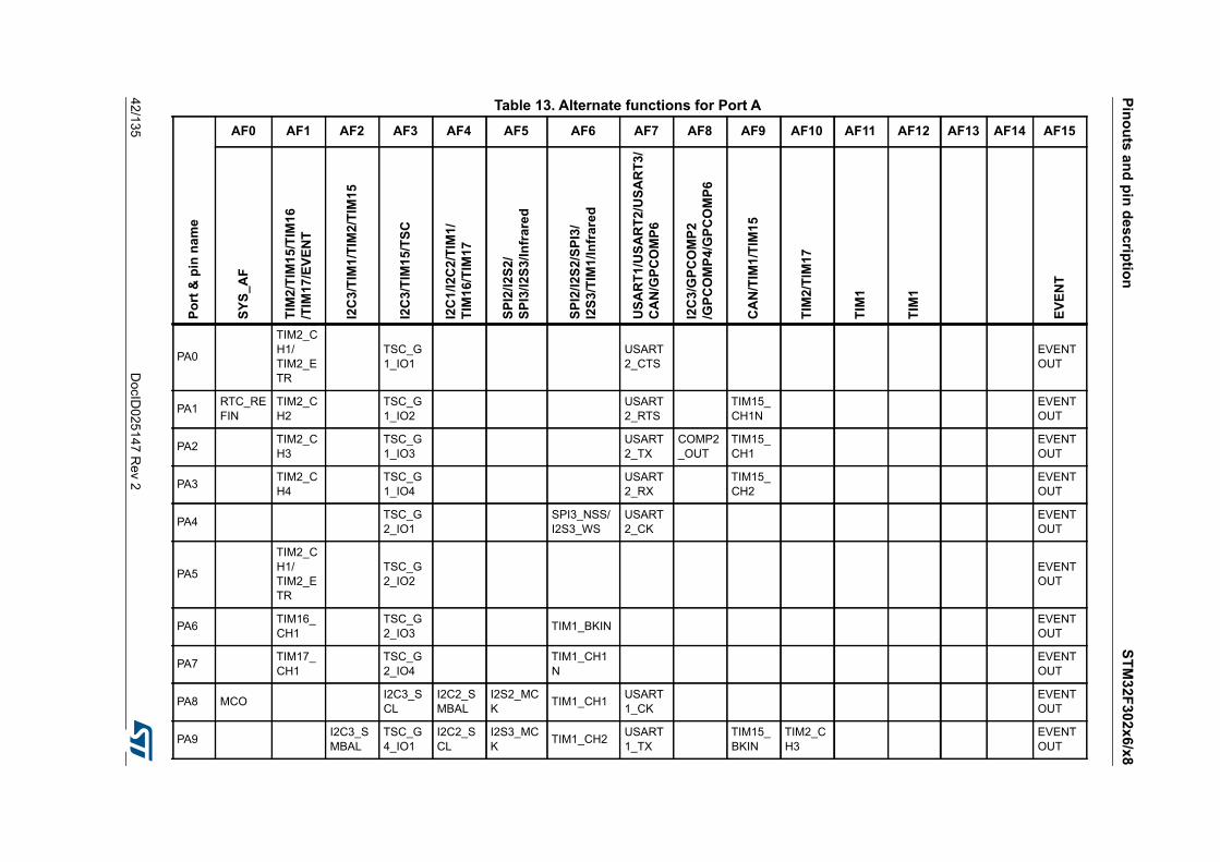
Table 13. Alternate functions for Port A
Port
& p
in n
ame
AF0 AF1 AF2 AF3 AF4 AF5 AF6 AF7 AF8 AF9 AF10 AF11 AF12 AF13 AF14 AF15
SYS_
AF
TIM
2/TI
M15
/TIM
16
/TIM
17/E
VEN
T
I2C
3/TI
M1/
TIM
2/TI
M15
I2C
3/TI
M15
/TSC
I2C
1/I2
C2/
TIM
1/
TIM
16/T
IM17
SPI2
/I2S2
/ SP
I3/I2
S3/In
frar
ed
SPI2
/I2S2
/SPI
3/
I2S3
/TIM
1/In
frar
ed
USA
RT1
/USA
RT2
/USA
RT3
/ C
AN
/GPC
OM
P6
I2C
3/G
PCO
MP2
/G
PCO
MP4
/GPC
OM
P6
CA
N/T
IM1/
TIM
15
TIM
2/TI
M17
TIM
1
TIM
1
EVEN
T
PA0
TIM2_CH1/ TIM2_ETR
TSC_G1_IO1
USART2_CTS
EVENTOUT
PA1 RTC_REFIN
TIM2_CH2
TSC_G1_IO2
USART2_RTS
TIM15_CH1N
EVENTOUT
PA2 TIM2_CH3
TSC_G1_IO3
USART2_TX
COMP2_OUT
TIM15_CH1
EVENTOUT
PA3 TIM2_CH4
TSC_G1_IO4
USART2_RX
TIM15_CH2
EVENTOUT
PA4 TSC_G2_IO1
SPI3_NSS/ I2S3_WS
USART2_CK
EVENTOUT
PA5
TIM2_CH1/ TIM2_ETR
TSC_G2_IO2
EVENTOUT
PA6 TIM16_CH1
TSC_G2_IO3 TIM1_BKIN EVENT
OUT
PA7 TIM17_CH1
TSC_G2_IO4
TIM1_CH1N
EVENTOUT
PA8 MCO I2C3_SCL
I2C2_SMBAL
I2S2_MCK TIM1_CH1 USART
1_CKEVENTOUT
PA9 I2C3_SMBAL
TSC_G4_IO1
I2C2_SCL
I2S3_MCK TIM1_CH2 USART
1_TXTIM15_BKIN
TIM2_CH3
EVENTOUT
STM32F302x6/x8
Pinouts and pin description
DocID
025147 Rev 2
43/135
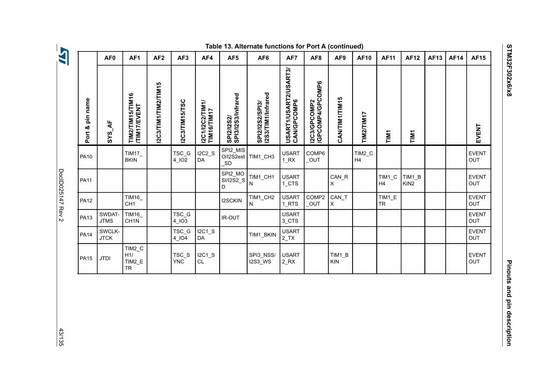
PA10 TIM17_BKIN
TSC_G4_IO2
I2C2_SDA
SPI2_MISO/I2S2ext_SD
TIM1_CH3 USART1_RX
COMP6_OUT
TIM2_CH4
EVENTOUT
PA11SPI2_MOSI/I2S2_SD
TIM1_CH1N
USART1_CTS
CAN_RX
TIM1_CH4
TIM1_BKIN2
EVENTOUT
PA12 TIM16_CH1 I2SCKIN TIM1_CH2
NUSART1_RTS
COMP2_OUT
CAN_TX
TIM1_ETR
EVENTOUT
PA13 SWDAT-JTMS
TIM16_CH1N
TSC_G4_IO3 IR-OUT USART
3_CTSEVENTOUT
PA14 SWCLK-JTCK
TSC_G4_IO4
I2C1_SDA TIM1_BKIN USART
2_TXEVENTOUT
PA15 JTDI
TIM2_CH1/ TIM2_ETR
TSC_SYNC
I2C1_SCL
SPI3_NSS/ I2S3_WS
USART2_RX
TIM1_BKIN
EVENTOUT
Table 13. Alternate functions for Port A (continued)
Port
& p
in n
ame
AF0 AF1 AF2 AF3 AF4 AF5 AF6 AF7 AF8 AF9 AF10 AF11 AF12 AF13 AF14 AF15
SYS_
AF
TIM
2/TI
M15
/TIM
16
/TIM
17/E
VEN
T
I2C
3/TI
M1/
TIM
2/TI
M15
I2C
3/TI
M15
/TSC
I2C
1/I2
C2/
TIM
1/
TIM
16/T
IM17
SPI2
/I2S2
/ SP
I3/I2
S3/In
frar
ed
SPI2
/I2S2
/SPI
3/
I2S3
/TIM
1/In
frar
ed
USA
RT1
/USA
RT2
/USA
RT3
/ C
AN
/GPC
OM
P6
I2C
3/G
PCO
MP2
/G
PCO
MP4
/GPC
OM
P6
CA
N/T
IM1/
TIM
15
TIM
2/TI
M17
TIM
1
TIM
1
EVEN
T
Pinouts and pin descriptionSTM
32F302x6/x8
44/135D
ocID025147 R
ev 2
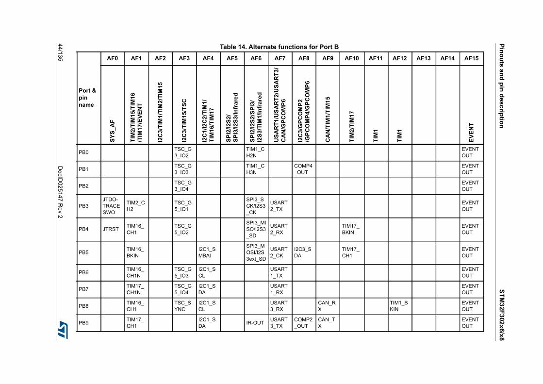
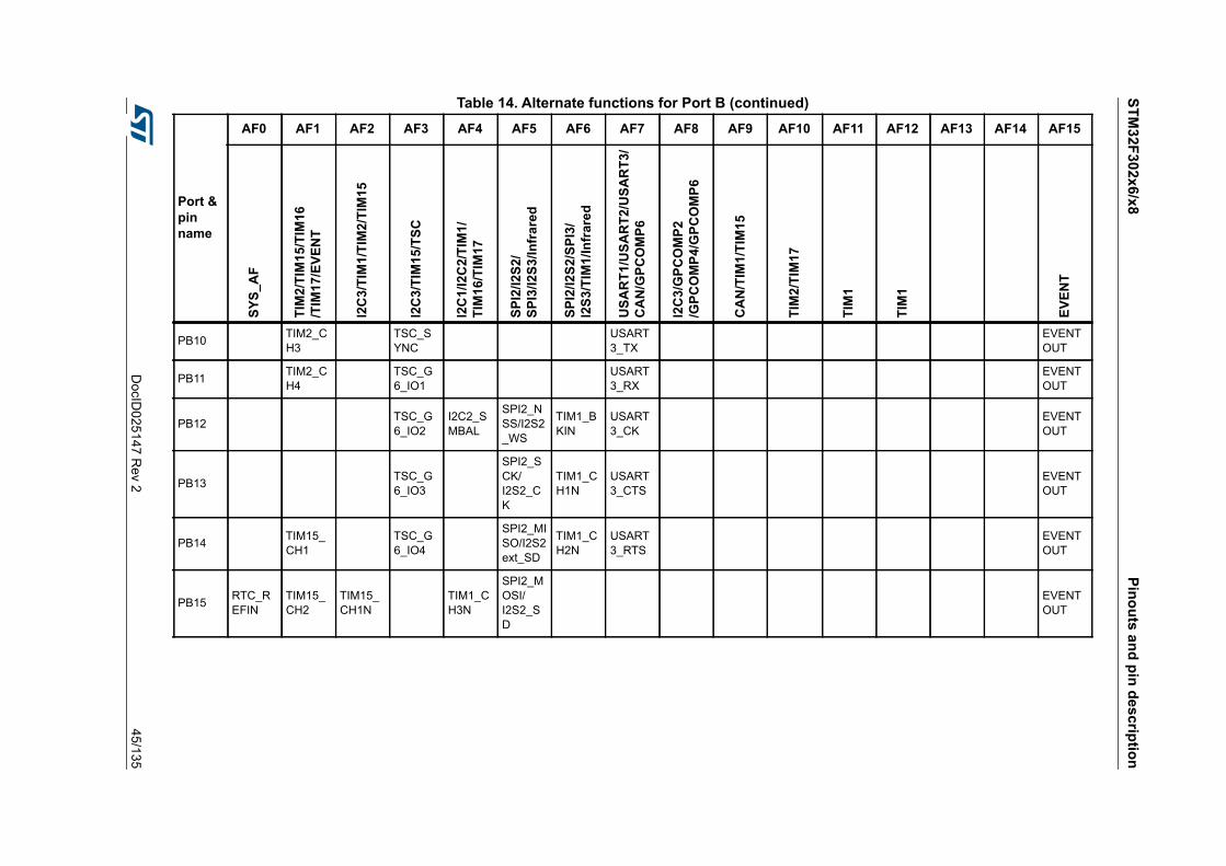
Table 14. Alternate functions for Port B
Port & pin name
AF0 AF1 AF2 AF3 AF4 AF5 AF6 AF7 AF8 AF9 AF10 AF11 AF12 AF13 AF14 AF15
SYS_
AF
TIM
2/TI
M15
/TIM
16
/TIM
17/E
VEN
T
I2C
3/TI
M1/
TIM
2/TI
M15
I2C
3/TI
M15
/TSC
I2C
1/I2
C2/
TIM
1/
TIM
16/T
IM17
SPI2
/I2S2
/ SP
I3/I2
S3/In
frar
ed
SPI2
/I2S2
/SPI
3/
I2S3
/TIM
1/In
frar
ed
USA
RT1
/USA
RT2
/USA
RT3
/ C
AN
/GPC
OM
P6
I2C
3/G
PCO
MP2
/G
PCO
MP4
/GPC
OM
P6
CA
N/T
IM1/
TIM
15
TIM
2/TI
M17
TIM
1
TIM
1
EVEN
T
PB0 TSC_G3_IO2
TIM1_CH2N
EVENTOUT
PB1 TSC_G3_IO3
TIM1_CH3N
COMP4_OUT
EVENTOUT
PB2 TSC_G3_IO4
EVENTOUT
PB3JTDO-TRACESWO
TIM2_CH2
TSC_G5_IO1
SPI3_SCK/I2S3_CK
USART2_TX
EVENTOUT
PB4 JTRST TIM16_CH1
TSC_G5_IO2
SPI3_MISO/I2S3_SD
USART2_RX
TIM17_BKIN
EVENTOUT
PB5 TIM16_BKIN
I2C1_SMBAl
SPI3_MOSI/I2S3ext_SD
USART2_CK
I2C3_SDA
TIM17_CH1
EVENTOUT
PB6 TIM16_CH1N
TSC_G5_IO3
I2C1_SCL
USART1_TX
EVENTOUT
PB7 TIM17_CH1N
TSC_G5_IO4
I2C1_SDA
USART1_RX
EVENTOUT
PB8 TIM16_CH1
TSC_SYNC
I2C1_SCL
USART3_RX
CAN_RX
TIM1_BKIN
EVENTOUT
PB9 TIM17_CH1
I2C1_SDA IR-OUT USART
3_TXCOMP2_OUT
CAN_TX
EVENTOUT
STM32F302x6/x8
Pinouts and pin description
DocID
025147 Rev 2
45/135
PB10 TIM2_CH3
TSC_SYNC
USART3_TX
EVENTOUT
PB11 TIM2_CH4
TSC_G6_IO1
USART3_RX
EVENTOUT
PB12 TSC_G6_IO2
I2C2_SMBAL
SPI2_NSS/I2S2_WS
TIM1_BKIN
USART3_CK
EVENTOUT
PB13 TSC_G6_IO3
SPI2_SCK/ I2S2_CK
TIM1_CH1N
USART3_CTS
EVENTOUT
PB14 TIM15_CH1
TSC_G6_IO4
SPI2_MISO/I2S2ext_SD
TIM1_CH2N
USART3_RTS
EVENTOUT
PB15 RTC_REFIN
TIM15_CH2
TIM15_CH1N
TIM1_CH3N
SPI2_MOSI/ I2S2_SD
EVENTOUT
Table 14. Alternate functions for Port B (continued)
Port & pin name
AF0 AF1 AF2 AF3 AF4 AF5 AF6 AF7 AF8 AF9 AF10 AF11 AF12 AF13 AF14 AF15
SYS_
AF
TIM
2/TI
M15
/TIM
16
/TIM
17/E
VEN
T
I2C
3/TI
M1/
TIM
2/TI
M15
I2C
3/TI
M15
/TSC
I2C
1/I2
C2/
TIM
1/
TIM
16/T
IM17
SPI2
/I2S2
/ SP
I3/I2
S3/In
frar
ed
SPI2
/I2S2
/SPI
3/
I2S3
/TIM
1/In
frar
ed
USA
RT1
/USA
RT2
/USA
RT3
/ C
AN
/GPC
OM
P6
I2C
3/G
PCO
MP2
/G
PCO
MP4
/GPC
OM
P6
CA
N/T
IM1/
TIM
15
TIM
2/TI
M17
TIM
1
TIM
1
EVEN
T
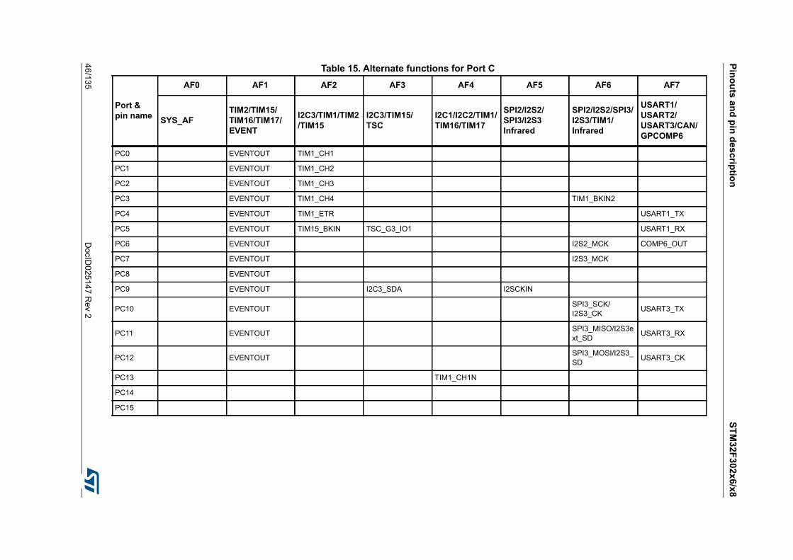
Pinouts and pin descriptionSTM
32F302x6/x8
46/135D
ocID025147 R
ev 2
Table 15. Alternate functions for Port C
Port & pin name
AF0 AF1 AF2 AF3 AF4 AF5 AF6 AF7
SYS_AFTIM2/TIM15/ TIM16/TIM17/ EVENT
I2C3/TIM1/TIM2/TIM15
I2C3/TIM15/ TSC
I2C1/I2C2/TIM1/ TIM16/TIM17
SPI2/I2S2/ SPI3/I2S3 Infrared
SPI2/I2S2/SPI3/ I2S3/TIM1/ Infrared
USART1/ USART2/ USART3/CAN/ GPCOMP6
PC0 EVENTOUT TIM1_CH1
PC1 EVENTOUT TIM1_CH2
PC2 EVENTOUT TIM1_CH3
PC3 EVENTOUT TIM1_CH4 TIM1_BKIN2
PC4 EVENTOUT TIM1_ETR USART1_TX
PC5 EVENTOUT TIM15_BKIN TSC_G3_IO1 USART1_RX
PC6 EVENTOUT I2S2_MCK COMP6_OUT
PC7 EVENTOUT I2S3_MCK
PC8 EVENTOUT
PC9 EVENTOUT I2C3_SDA I2SCKIN
PC10 EVENTOUT SPI3_SCK/ I2S3_CK USART3_TX
PC11 EVENTOUT SPI3_MISO/I2S3ext_SD USART3_RX
PC12 EVENTOUT SPI3_MOSI/I2S3_SD USART3_CK
PC13 TIM1_CH1N
PC14
PC15
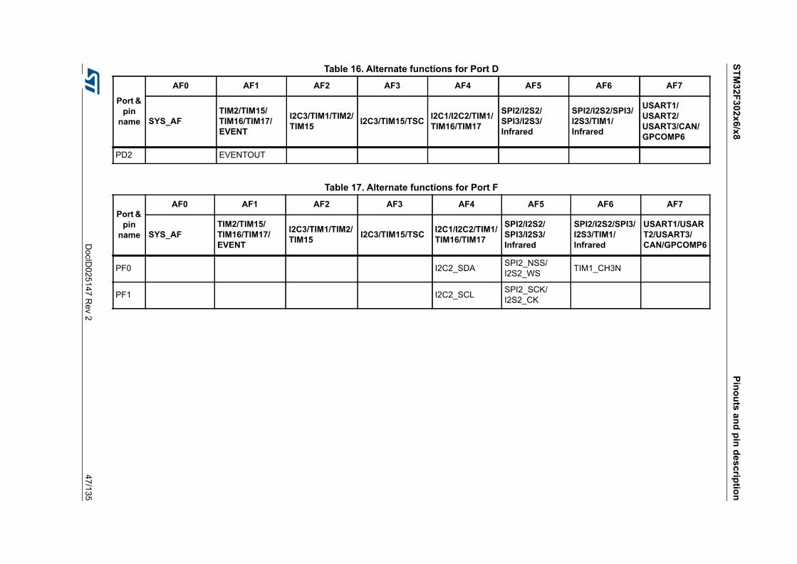
STM32F302x6/x8
Pinouts and pin description
DocID
025147 Rev 2
47/135
Table 16. Alternate functions for Port D
Port & pin
name
AF0 AF1 AF2 AF3 AF4 AF5 AF6 AF7
SYS_AFTIM2/TIM15/ TIM16/TIM17/ EVENT
I2C3/TIM1/TIM2/TIM15 I2C3/TIM15/TSC I2C1/I2C2/TIM1/
TIM16/TIM17
SPI2/I2S2/ SPI3/I2S3/ Infrared
SPI2/I2S2/SPI3/ I2S3/TIM1/ Infrared
USART1/ USART2/ USART3/CAN/ GPCOMP6
PD2 EVENTOUT
Table 17. Alternate functions for Port F
Port & pin
name
AF0 AF1 AF2 AF3 AF4 AF5 AF6 AF7
SYS_AFTIM2/TIM15/ TIM16/TIM17/ EVENT
I2C3/TIM1/TIM2/TIM15 I2C3/TIM15/TSC I2C1/I2C2/TIM1/
TIM16/TIM17
SPI2/I2S2/ SPI3/I2S3/ Infrared
SPI2/I2S2/SPI3/ I2S3/TIM1/ Infrared
USART1/USART2/USART3/ CAN/GPCOMP6
PF0 I2C2_SDA SPI2_NSS/ I2S2_WS TIM1_CH3N
PF1 I2C2_SCL SPI2_SCK/ I2S2_CK
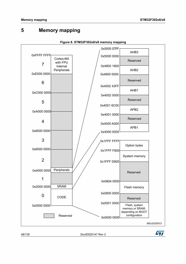
Memory mapping STM32F302x6/x8
48/135 DocID025147 Rev 2
5 Memory mapping
Figure 8. STM32F302x6/x8 memory mapping
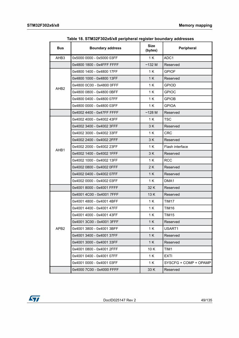
DocID025147 Rev 2 49/135
STM32F302x6/x8 Memory mapping
51
Table 18. STM32F302x6/x8 peripheral register boundary addresses
Bus Boundary address Size(bytes) Peripheral
AHB3 0x5000 0000 - 0x5000 03FF 1 K ADC1
0x4800 1800 - 0x4FFF FFFF ~132 M Reserved
AHB2
0x4800 1400 - 0x4800 17FF 1 K GPIOF
0x4800 1000 - 0x4800 13FF 1 K Reserved
0x4800 0C00 - 0x4800 0FFF 1 K GPIOD
0x4800 0800 - 0x4800 0BFF 1 K GPIOC
0x4800 0400 - 0x4800 07FF 1 K GPIOB
0x4800 0000 - 0x4800 03FF 1 K GPIOA
0x4002 4400 - 0x47FF FFFF ~128 M Reserved
AHB1
0x4002 4000 - 0x4002 43FF 1 K TSC
0x4002 3400 - 0x4002 3FFF 3 K Reserved
0x4002 3000 - 0x4002 33FF 1 K CRC
0x4002 2400 - 0x4002 2FFF 3 K Reserved
0x4002 2000 - 0x4002 23FF 1 K Flash interface
0x4002 1400 - 0x4002 1FFF 3 K Reserved
0x4002 1000 - 0x4002 13FF 1 K RCC
0x4002 0800 - 0x4002 0FFF 2 K Reserved
0x4002 0400 - 0x4002 07FF 1 K Reserved
0x4002 0000 - 0x4002 03FF 1 K DMA1
0x4001 8000 - 0x4001 FFFF 32 K Reserved
APB2
0x4001 4C00 - 0x4001 7FFF 13 K Reserved
0x4001 4800 - 0x4001 4BFF 1 K TIM17
0x4001 4400 - 0x4001 47FF 1 K TIM16
0x4001 4000 - 0x4001 43FF 1 K TIM15
0x4001 3C00 - 0x4001 3FFF 1 K Reserved
0x4001 3800 - 0x4001 3BFF 1 K USART1
0x4001 3400 - 0x4001 37FF 1 K Reserved
0x4001 3000 - 0x4001 33FF 1 K Reserved
0x4001 0800 - 0x4001 2FFF 10 K TIM1
0x4001 0400 - 0x4001 07FF 1 K EXTI
0x4001 0000 - 0x4001 03FF 1 K SYSCFG + COMP + OPAMP
0x4000 7C00 - 0x4000 FFFF 33 K Reserved
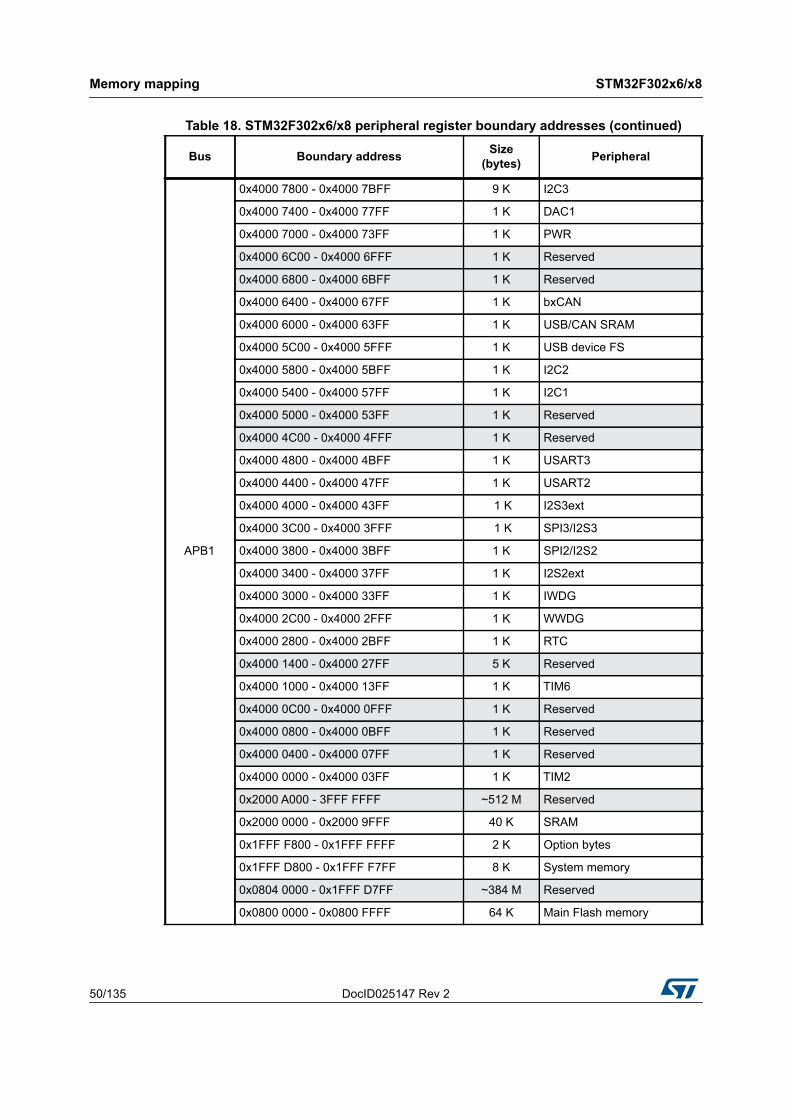
Memory mapping STM32F302x6/x8
50/135 DocID025147 Rev 2
APB1
0x4000 7800 - 0x4000 7BFF 9 K I2C3
0x4000 7400 - 0x4000 77FF 1 K DAC1
0x4000 7000 - 0x4000 73FF 1 K PWR
0x4000 6C00 - 0x4000 6FFF 1 K Reserved
0x4000 6800 - 0x4000 6BFF 1 K Reserved
0x4000 6400 - 0x4000 67FF 1 K bxCAN
0x4000 6000 - 0x4000 63FF 1 K USB/CAN SRAM
0x4000 5C00 - 0x4000 5FFF 1 K USB device FS
0x4000 5800 - 0x4000 5BFF 1 K I2C2
0x4000 5400 - 0x4000 57FF 1 K I2C1
0x4000 5000 - 0x4000 53FF 1 K Reserved
0x4000 4C00 - 0x4000 4FFF 1 K Reserved
0x4000 4800 - 0x4000 4BFF 1 K USART3
0x4000 4400 - 0x4000 47FF 1 K USART2
0x4000 4000 - 0x4000 43FF 1 K I2S3ext
0x4000 3C00 - 0x4000 3FFF 1 K SPI3/I2S3
0x4000 3800 - 0x4000 3BFF 1 K SPI2/I2S2
0x4000 3400 - 0x4000 37FF 1 K I2S2ext
0x4000 3000 - 0x4000 33FF 1 K IWDG
0x4000 2C00 - 0x4000 2FFF 1 K WWDG
0x4000 2800 - 0x4000 2BFF 1 K RTC
0x4000 1400 - 0x4000 27FF 5 K Reserved
0x4000 1000 - 0x4000 13FF 1 K TIM6
0x4000 0C00 - 0x4000 0FFF 1 K Reserved
0x4000 0800 - 0x4000 0BFF 1 K Reserved
0x4000 0400 - 0x4000 07FF 1 K Reserved
0x4000 0000 - 0x4000 03FF 1 K TIM2
0x2000 A000 - 3FFF FFFF ~512 M Reserved
0x2000 0000 - 0x2000 9FFF 40 K SRAM
0x1FFF F800 - 0x1FFF FFFF 2 K Option bytes
0x1FFF D800 - 0x1FFF F7FF 8 K System memory
0x0804 0000 - 0x1FFF D7FF ~384 M Reserved
0x0800 0000 - 0x0800 FFFF 64 K Main Flash memory
Table 18. STM32F302x6/x8 peripheral register boundary addresses (continued)
Bus Boundary address Size(bytes) Peripheral
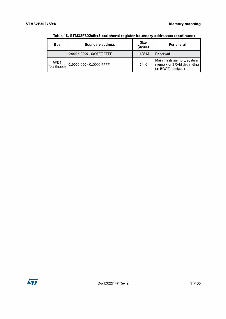
DocID025147 Rev 2 51/135
STM32F302x6/x8 Memory mapping
51
0x0004 0000 - 0x07FF FFFF ~128 M Reserved
APB1 (continued) 0x0000 000 - 0x0000 FFFF 64 K
Main Flash memory, system memory or SRAM depending on BOOT configuration
Table 18. STM32F302x6/x8 peripheral register boundary addresses (continued)
Bus Boundary address Size(bytes) Peripheral
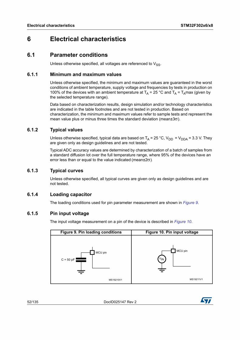
Electrical characteristics STM32F302x6/x8
52/135 DocID025147 Rev 2
6 Electrical characteristics
6.1 Parameter conditionsUnless otherwise specified, all voltages are referenced to VSS.
6.1.1 Minimum and maximum valuesUnless otherwise specified, the minimum and maximum values are guaranteed in the worst conditions of ambient temperature, supply voltage and frequencies by tests in production on 100% of the devices with an ambient temperature at TA = 25 °C and TA = TAmax (given by the selected temperature range).
Data based on characterization results, design simulation and/or technology characteristics are indicated in the table footnotes and are not tested in production. Based on characterization, the minimum and maximum values refer to sample tests and represent the mean value plus or minus three times the standard deviation (mean±3).
6.1.2 Typical valuesUnless otherwise specified, typical data are based on TA = 25 °C, VDD = VDDA = 3.3 V. They are given only as design guidelines and are not tested.
Typical ADC accuracy values are determined by characterization of a batch of samples from a standard diffusion lot over the full temperature range, where 95% of the devices have an error less than or equal to the value indicated (mean±2).
6.1.3 Typical curvesUnless otherwise specified, all typical curves are given only as design guidelines and are not tested.
6.1.4 Loading capacitorThe loading conditions used for pin parameter measurement are shown in Figure 9.
6.1.5 Pin input voltageThe input voltage measurement on a pin of the device is described in Figure 10.
Figure 9. Pin loading conditions Figure 10. Pin input voltage
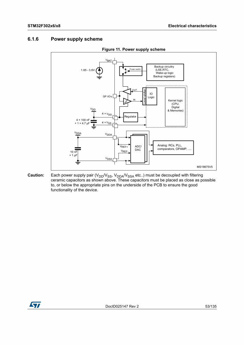
DocID025147 Rev 2 53/135
STM32F302x6/x8 Electrical characteristics
115
6.1.6 Power supply scheme
Figure 11. Power supply scheme
Caution: Each power supply pair (VDD/VSS, VDDA/VSSA etc..) must be decoupled with filtering ceramic capacitors as shown above. These capacitors must be placed as close as possible to, or below the appropriate pins on the underside of the PCB to ensure the good functionality of the device.
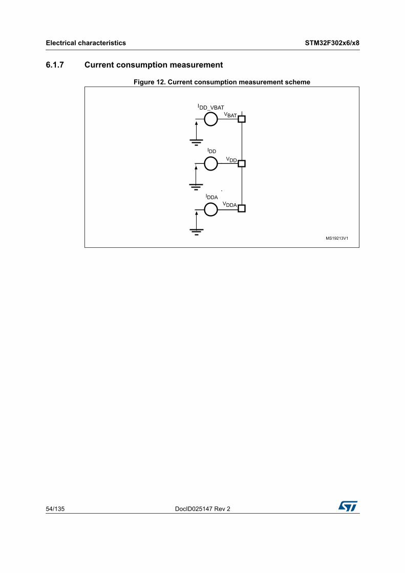
Electrical characteristics STM32F302x6/x8
54/135 DocID025147 Rev 2
6.1.7 Current consumption measurement
Figure 12. Current consumption measurement scheme
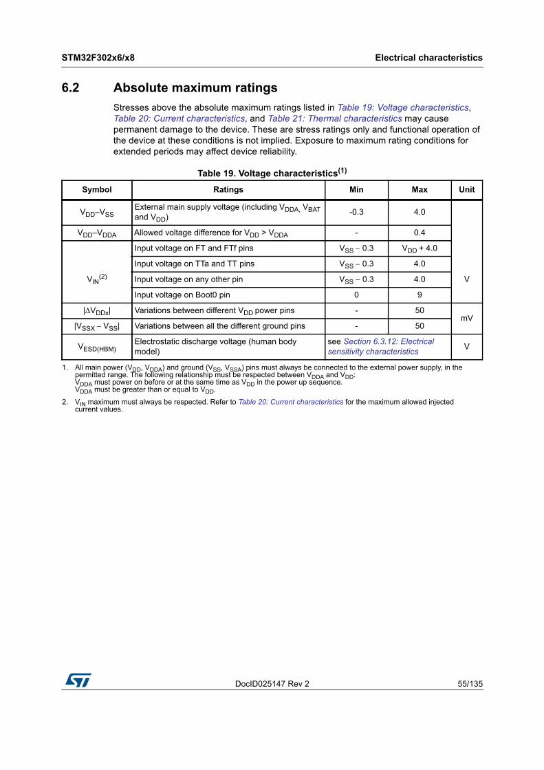
DocID025147 Rev 2 55/135
STM32F302x6/x8 Electrical characteristics
115
6.2 Absolute maximum ratingsStresses above the absolute maximum ratings listed in Table 19: Voltage characteristics, Table 20: Current characteristics, and Table 21: Thermal characteristics may cause permanent damage to the device. These are stress ratings only and functional operation of the device at these conditions is not implied. Exposure to maximum rating conditions for extended periods may affect device reliability.
Table 19. Voltage characteristics(1)
Symbol Ratings Min Max Unit
VDD–VSSExternal main supply voltage (including VDDA, VBAT and VDD) -0.3 4.0
V
VDD–VDDA Allowed voltage difference for VDD > VDDA - 0.4
VIN(2)
Input voltage on FT and FTf pins VSS 0.3 VDD + 4.0
Input voltage on TTa and TT pins VSS 0.3 4.0
Input voltage on any other pin VSS 0.3 4.0
Input voltage on Boot0 pin 0 9
|VDDx| Variations between different VDD power pins - 50mV
|VSSX VSS| Variations between all the different ground pins - 50
VESD(HBM)Electrostatic discharge voltage (human body model)
see Section 6.3.12: Electrical sensitivity characteristics V
1. All main power (VDD, VDDA) and ground (VSS, VSSA) pins must always be connected to the external power supply, in the permitted range. The following relationship must be respected between VDDA and VDD: VDDA must power on before or at the same time as VDD in the power up sequence. VDDA must be greater than or equal to VDD.
2. VIN maximum must always be respected. Refer to Table 20: Current characteristics for the maximum allowed injected current values.
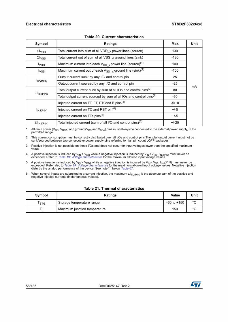
Electrical characteristics STM32F302x6/x8
56/135 DocID025147 Rev 2
Table 20. Current characteristicsSymbol Ratings Max. Unit
IVDD Total current into sum of all VDD_x power lines (source) 130
mA
IVSS Total current out of sum of all VSS_x ground lines (sink) -130
IVDD Maximum current into each VDD_x power line (source)(1) 100
IVSS Maximum current out of each VSS _x ground line (sink)(1) -100
IIO(PIN)Output current sunk by any I/O and control pin 25
Output current sourced by any I/O and control pin -25
IIO(PIN)Total output current sunk by sum of all IOs and control pins(2) 80
Total output current sourced by sum of all IOs and control pins(2) -80
IINJ(PIN)
Injected current on TT, FT, FTf and B pins(3) -5/+0
Injected current on TC and RST pin(4) +/-5
Injected current on TTa pins(5) +/-5
IINJ(PIN) Total injected current (sum of all I/O and control pins)(6) +/-25
1. All main power (VDD, VDDA) and ground (VSS and VSSA) pins must always be connected to the external power supply, in the permitted range.
2. This current consumption must be correctly distributed over all I/Os and control pins.The total output current must not be sunk/sourced between two consecutive power supply pins referring to high pin count LQFP packages.
3. Positive injection is not possible on these I/Os and does not occur for input voltages lower than the specified maximum value.
4. A positive injection is induced by VIN > VDD while a negative injection is induced by VIN< VSS. IINJ(PIN) must never be exceeded. Refer to Table 19: Voltage characteristics for the maximum allowed input voltage values.
5. A positive injection is induced by VIN > VDDA while a negative injection is induced by VIN< VSS. IINJ(PIN) must never be exceeded. Refer also to Table 19: Voltage characteristics for the maximum allowed input voltage values. Negative injection disturbs the analog performance of the device. See note (2) below Table 67.
6. When several inputs are submitted to a current injection, the maximum IINJ(PIN) is the absolute sum of the positive and negative injected currents (instantaneous values).
Table 21. Thermal characteristicsSymbol Ratings Value Unit
TSTG Storage temperature range –65 to +150 °C
TJ Maximum junction temperature 150 °C
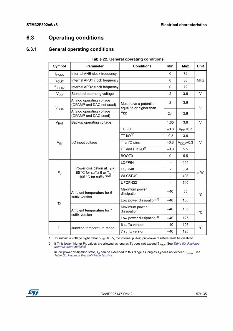
DocID025147 Rev 2 57/135
STM32F302x6/x8 Electrical characteristics
115
6.3 Operating conditions
6.3.1 General operating conditions
Table 22. General operating conditionsSymbol Parameter Conditions Min Max Unit
fHCLK Internal AHB clock frequency 0 72
MHzfPCLK1 Internal APB1 clock frequency 0 36
fPCLK2 Internal APB2 clock frequency 0 72
VDD Standard operating voltage 2 3.6 V
VDDA
Analog operating voltage (OPAMP and DAC not used) Must have a potential
equal to or higher than VDD
2 3.6V
Analog operating voltage (OPAMP and DAC used) 2.4 3.6
VBAT Backup operating voltage 1.65 3.6 V
VIN I/O input voltage
TC I/O –0.3 VDD+0.3
V
TT I/O(1) -0.3 3.6
TTa I/O pins –0.3 VDDA+0.3
FT and FTf I/O(1)
1. To sustain a voltage higher than VDD+0.3 V, the internal pull-up/pull-down resistors must be disabled.
–0.3 5.5
BOOT0 0 5.5
PD
Power dissipation at TA = 85 °C for suffix 6 or TA =
105 °C for suffix 7(2)
2. If TA is lower, higher PD values are allowed as long as TJ does not exceed TJmax. See Table 80: Package thermal characteristics.
LQFP64 - 444
mWLQFP48 - 364
WLCSP49 - 408
UFQFN32 - 540
TA
Ambient temperature for 6 suffix version
Maximum power dissipation –40 85
°CLow power dissipation(3)
3. In low power dissipation state, TA can be extended to this range as long as TJ does not exceed TJmax. See Table 80: Package thermal characteristics
–40 105
Ambient temperature for 7 suffix version
Maximum power dissipation –40 105
°CLow power dissipation(3) –40 125
TJ Junction temperature range6 suffix version –40 105
°C7 suffix version –40 125
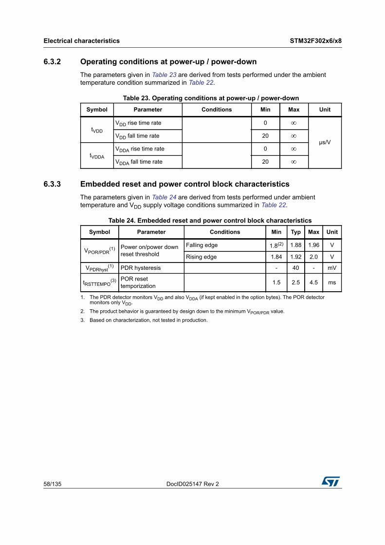
Electrical characteristics STM32F302x6/x8
58/135 DocID025147 Rev 2
6.3.2 Operating conditions at power-up / power-downThe parameters given in Table 23 are derived from tests performed under the ambient temperature condition summarized in Table 22.
6.3.3 Embedded reset and power control block characteristicsThe parameters given in Table 24 are derived from tests performed under ambient temperature and VDD supply voltage conditions summarized in Table 22.
Table 23. Operating conditions at power-up / power-downSymbol Parameter Conditions Min Max Unit
tVDD
VDD rise time rate 0
μs/VVDD fall time rate 20
tVDDA
VDDA rise time rate 0
VDDA fall time rate 20
Table 24. Embedded reset and power control block characteristics Symbol Parameter Conditions Min Typ Max Unit
VPOR/PDR(1)
1. The PDR detector monitors VDD and also VDDA (if kept enabled in the option bytes). The POR detector monitors only VDD.
Power on/power down reset threshold
Falling edge 1.8(2)
2. The product behavior is guaranteed by design down to the minimum VPOR/PDR value.
1.88 1.96 V
Rising edge 1.84 1.92 2.0 V
VPDRhyst(1) PDR hysteresis - 40 - mV
tRSTTEMPO(3)
3. Based on characterization, not tested in production.
POR reset temporization 1.5 2.5 4.5 ms
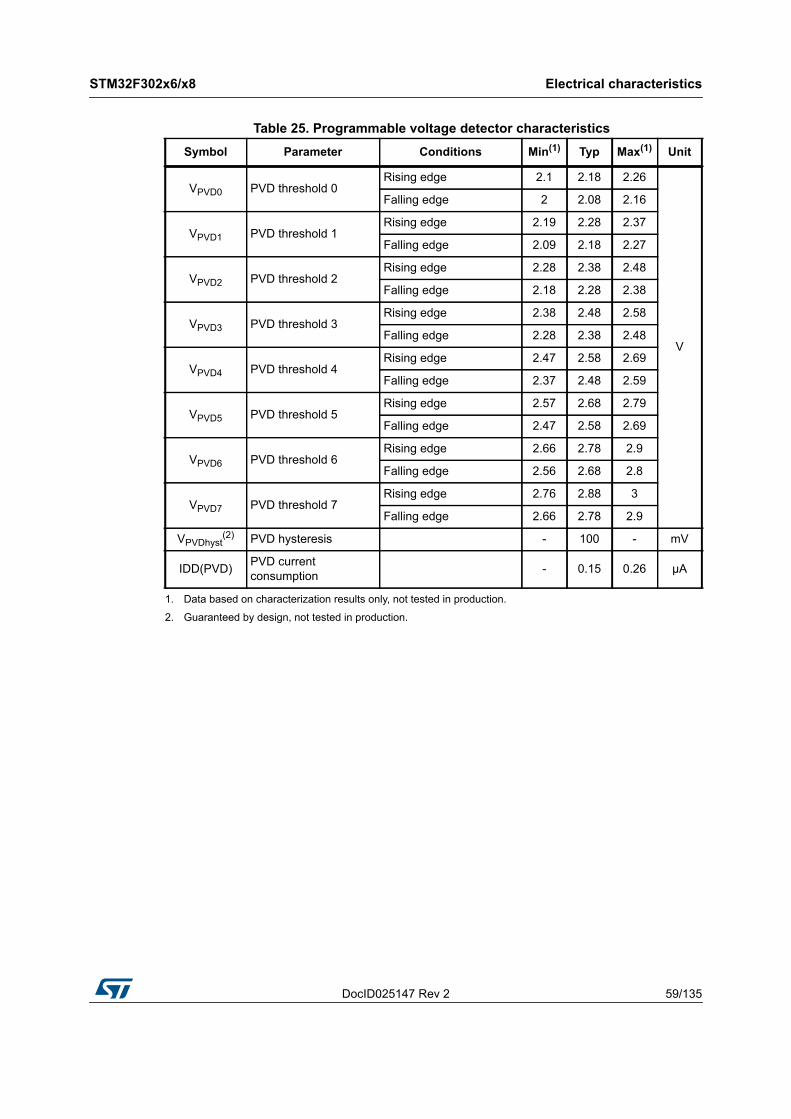
DocID025147 Rev 2 59/135
STM32F302x6/x8 Electrical characteristics
115
Table 25. Programmable voltage detector characteristics Symbol Parameter Conditions Min(1)
1. Data based on characterization results only, not tested in production.
Typ Max(1) Unit
VPVD0 PVD threshold 0Rising edge 2.1 2.18 2.26
V
Falling edge 2 2.08 2.16
VPVD1 PVD threshold 1Rising edge 2.19 2.28 2.37
Falling edge 2.09 2.18 2.27
VPVD2 PVD threshold 2Rising edge 2.28 2.38 2.48
Falling edge 2.18 2.28 2.38
VPVD3 PVD threshold 3Rising edge 2.38 2.48 2.58
Falling edge 2.28 2.38 2.48
VPVD4 PVD threshold 4Rising edge 2.47 2.58 2.69
Falling edge 2.37 2.48 2.59
VPVD5 PVD threshold 5Rising edge 2.57 2.68 2.79
Falling edge 2.47 2.58 2.69
VPVD6 PVD threshold 6Rising edge 2.66 2.78 2.9
Falling edge 2.56 2.68 2.8
VPVD7 PVD threshold 7Rising edge 2.76 2.88 3
Falling edge 2.66 2.78 2.9
VPVDhyst(2)
2. Guaranteed by design, not tested in production.
PVD hysteresis - 100 - mV
IDD(PVD) PVD current consumption - 0.15 0.26 μA
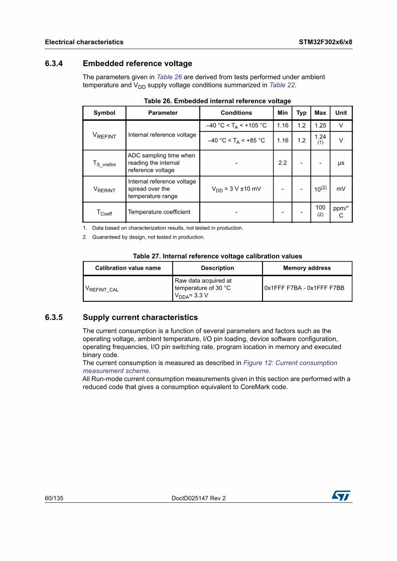
Electrical characteristics STM32F302x6/x8
60/135 DocID025147 Rev 2
6.3.4 Embedded reference voltageThe parameters given in Table 26 are derived from tests performed under ambient temperature and VDD supply voltage conditions summarized in Table 22.
6.3.5 Supply current characteristicsThe current consumption is a function of several parameters and factors such as the operating voltage, ambient temperature, I/O pin loading, device software configuration, operating frequencies, I/O pin switching rate, program location in memory and executed binary code. The current consumption is measured as described in Figure 12: Current consumption measurement scheme. All Run-mode current consumption measurements given in this section are performed with a reduced code that gives a consumption equivalent to CoreMark code.
Table 26. Embedded internal reference voltageSymbol Parameter Conditions Min Typ Max Unit
VREFINT Internal reference voltage–40 °C < TA < +105 °C 1.16 1.2 1.25 V
–40 °C < TA < +85 °C 1.16 1.2 1.24(1)
1. Data based on characterization results, not tested in production.
V
TS_vrefint
ADC sampling time when reading the internal reference voltage
- 2.2 - - μs
VRERINT
Internal reference voltage spread over the temperature range
VDD = 3 V ±10 mV - - 10(2)
2. Guaranteed by design, not tested in production.
mV
TCoeff Temperature coefficient - - -100(2)
ppm/°C
Table 27. Internal reference voltage calibration valuesCalibration value name Description Memory address
VREFINT_CAL
Raw data acquired at temperature of 30 °C VDDA= 3.3 V
0x1FFF F7BA - 0x1FFF F7BB
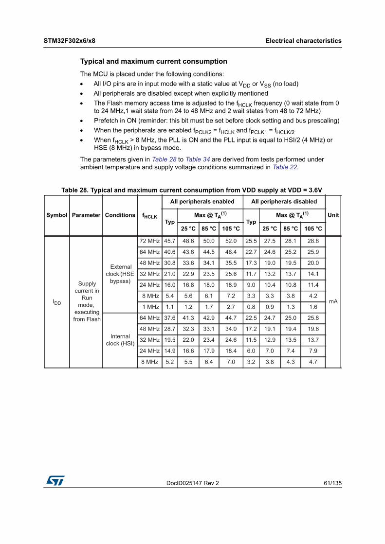
DocID025147 Rev 2 61/135
STM32F302x6/x8 Electrical characteristics
115
Typical and maximum current consumption
The MCU is placed under the following conditions: All I/O pins are in input mode with a static value at VDD or VSS (no load) All peripherals are disabled except when explicitly mentioned The Flash memory access time is adjusted to the fHCLK frequency (0 wait state from 0
to 24 MHz,1 wait state from 24 to 48 MHz and 2 wait states from 48 to 72 MHz) Prefetch in ON (reminder: this bit must be set before clock setting and bus prescaling) When the peripherals are enabled fPCLK2 = fHCLK and fPCLK1 = fHCLK/2 When fHCLK > 8 MHz, the PLL is ON and the PLL input is equal to HSI/2 (4 MHz) or
HSE (8 MHz) in bypass mode.
The parameters given in Table 28 to Table 34 are derived from tests performed under ambient temperature and supply voltage conditions summarized in Table 22.
Table 28. Typical and maximum current consumption from VDD supply at VDD = 3.6V
Symbol Parameter Conditions fHCLK
All peripherals enabled All peripherals disabled
UnitTyp
Max @ TA(1)
TypMax @ TA
(1)
25 °C 85 °C 105 °C 25 °C 85 °C 105 °C
IDD
Supply current in
Run mode,
executing from Flash
External clock (HSE
bypass)
72 MHz 45.7 48.6 50.0 52.0 25.5 27.5 28.1 28.8
mA
64 MHz 40.6 43.6 44.5 46.4 22.7 24.6 25.2 25.9
48 MHz 30.8 33.6 34.1 35.5 17.3 19.0 19.5 20.0
32 MHz 21.0 22.9 23.5 25.6 11.7 13.2 13.7 14.1
24 MHz 16.0 16.8 18.0 18.9 9.0 10.4 10.8 11.4
8 MHz 5.4 5.6 6.1 7.2 3.3 3.3 3.8 4.2
1 MHz 1.1 1.2 1.7 2.7 0.8 0.9 1.3 1.6
Internal clock (HSI)
64 MHz 37.6 41.3 42.9 44.7 22.5 24.7 25.0 25.8
48 MHz 28.7 32.3 33.1 34.0 17.2 19.1 19.4 19.6
32 MHz 19.5 22.0 23.4 24.6 11.5 12.9 13.5 13.7
24 MHz 14.9 16.6 17.9 18.4 6.0 7.0 7.4 7.9
8 MHz 5.2 5.5 6.4 7.0 3.2 3.8 4.3 4.7
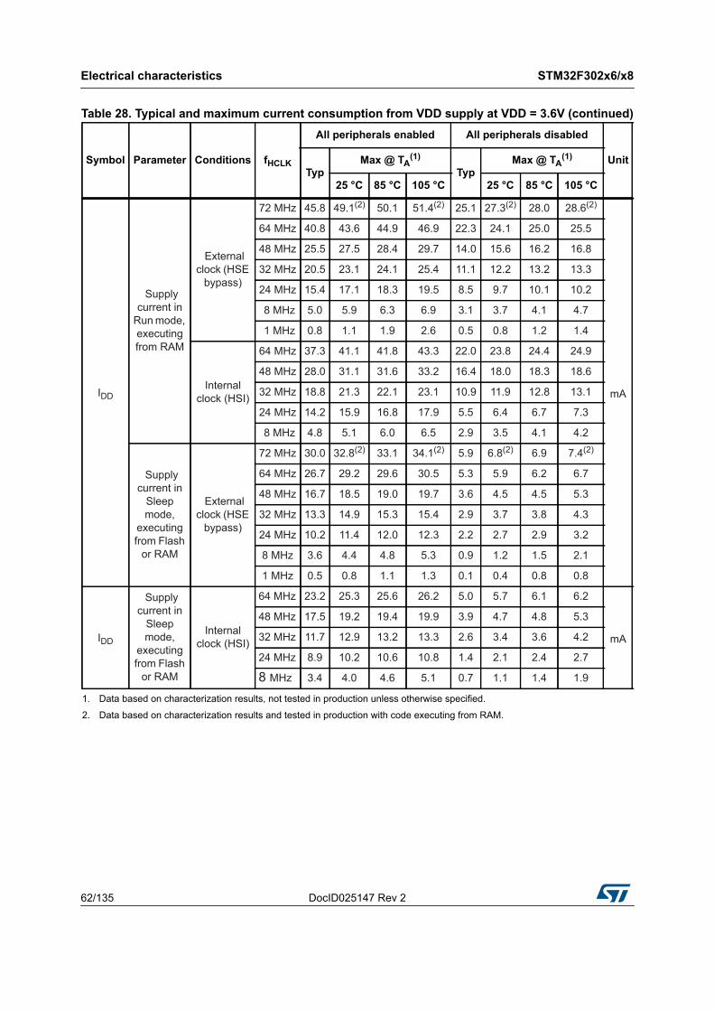
Electrical characteristics STM32F302x6/x8
62/135 DocID025147 Rev 2
IDD
Supply current in
Run mode, executing from RAM
External clock (HSE
bypass)
72 MHz 45.8 49.1(2) 50.1 51.4(2) 25.1 27.3(2) 28.0 28.6(2)
mA
64 MHz 40.8 43.6 44.9 46.9 22.3 24.1 25.0 25.5
48 MHz 25.5 27.5 28.4 29.7 14.0 15.6 16.2 16.8
32 MHz 20.5 23.1 24.1 25.4 11.1 12.2 13.2 13.3
24 MHz 15.4 17.1 18.3 19.5 8.5 9.7 10.1 10.2
8 MHz 5.0 5.9 6.3 6.9 3.1 3.7 4.1 4.7
1 MHz 0.8 1.1 1.9 2.6 0.5 0.8 1.2 1.4
Internal clock (HSI)
64 MHz 37.3 41.1 41.8 43.3 22.0 23.8 24.4 24.9
48 MHz 28.0 31.1 31.6 33.2 16.4 18.0 18.3 18.6
32 MHz 18.8 21.3 22.1 23.1 10.9 11.9 12.8 13.1
24 MHz 14.2 15.9 16.8 17.9 5.5 6.4 6.7 7.3
8 MHz 4.8 5.1 6.0 6.5 2.9 3.5 4.1 4.2
Supply current in
Sleep mode,
executing from Flash
or RAM
External clock (HSE
bypass)
72 MHz 30.0 32.8(2) 33.1 34.1(2) 5.9 6.8(2) 6.9 7.4(2)
64 MHz 26.7 29.2 29.6 30.5 5.3 5.9 6.2 6.7
48 MHz 16.7 18.5 19.0 19.7 3.6 4.5 4.5 5.3
32 MHz 13.3 14.9 15.3 15.4 2.9 3.7 3.8 4.3
24 MHz 10.2 11.4 12.0 12.3 2.2 2.7 2.9 3.2
8 MHz 3.6 4.4 4.8 5.3 0.9 1.2 1.5 2.1
1 MHz 0.5 0.8 1.1 1.3 0.1 0.4 0.8 0.8
IDD
Supply current in
Sleep mode,
executing from Flash
or RAM
Internal clock (HSI)
64 MHz 23.2 25.3 25.6 26.2 5.0 5.7 6.1 6.2
mA
48 MHz 17.5 19.2 19.4 19.9 3.9 4.7 4.8 5.3
32 MHz 11.7 12.9 13.2 13.3 2.6 3.4 3.6 4.2
24 MHz 8.9 10.2 10.6 10.8 1.4 2.1 2.4 2.7
8 MHz 3.4 4.0 4.6 5.1 0.7 1.1 1.4 1.9
1. Data based on characterization results, not tested in production unless otherwise specified.
2. Data based on characterization results and tested in production with code executing from RAM.
Table 28. Typical and maximum current consumption from VDD supply at VDD = 3.6V (continued)
Symbol Parameter Conditions fHCLK
All peripherals enabled All peripherals disabled
UnitTyp
Max @ TA(1)
TypMax @ TA
(1)
25 °C 85 °C 105 °C 25 °C 85 °C 105 °C
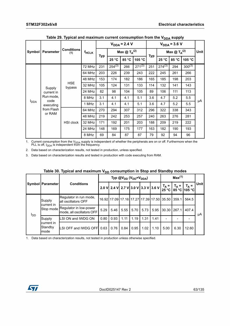
DocID025147 Rev 2 63/135
STM32F302x6/x8 Electrical characteristics
115
Table 29. Typical and maximum current consumption from the VDDA supply
Symbol Parameter Conditions(1) fHCLK
VDDA = 2.4 V VDDA = 3.6 V
UnitTyp
Max @ TA(2)
TypMax @ TA
(2)
25 °C 85 °C 105 °C 25 °C 85 °C 105 °C
IDDA
Supply current in
Run mode, code
executing from Flash
or RAM
HSE bypass
72 MHz 231 254(3) 266 271(3) 251 274(3) 294 300(3)
μA
64 MHz 203 226 239 243 222 245 261 266
48 MHz 153 174 182 186 165 185 198 203
32 MHz 105 124 131 133 114 132 141 143
24 MHz 82 98 104 105 89 106 111 113
8 MHz 3.1 4.1 4.1 5.1 3.6 4.7 5.2 5.5
1 MHz 3.1 4.1 4.1 5.1 3.6 4.7 5.2 5.5
HSI clock
64 MHz 270 294 307 312 296 322 338 343
48 MHz 219 242 253 257 240 263 276 281
32 MHz 171 192 201 203 188 209 219 222
24 MHz 148 169 175 177 163 182 190 193
8 MHz 69 84 87 87 79 92 94 96
1. Current consumption from the VDDA supply is independent of whether the peripherals are on or off. Furthermore when the PLL is off, IDDA is independent from the frequency.
2. Data based on characterization results, not tested in production, unless specified.
3. Data based on characterization results and tested in production with code executing from RAM.
Table 30. Typical and maximum VDD consumption in Stop and Standby modes
Symbol Parameter Conditions
Typ @VDD (VDD=VDDA) Max(1)
Unit 2.0 V 2.4 V 2.7 V 3.0 V 3.3 V 3.6 V TA =
25 °CTA = 85 °C
TA = 105 °C
IDD
Supply current in Stop mode
Regulator in run mode, all oscillators OFF 16.92 17.09 17.16 17.27 17.39 17.50 35.50 359.1 564.5
μA
Regulator in low-power mode, all oscillators OFF 5.29 5.46 5.55 5.70 5.73 5.95 30.30 267.1 407.4
Supply current in Standby mode
LSI ON and IWDG ON 0.80 0.93 1.11 1.19 1.31 1.41 - - -
LSI OFF and IWDG OFF 0.63 0.76 0.84 0.95 1.02 1.10 5.00 6.30 12.60
1. Data based on characterization results, not tested in production unless otherwise specified.
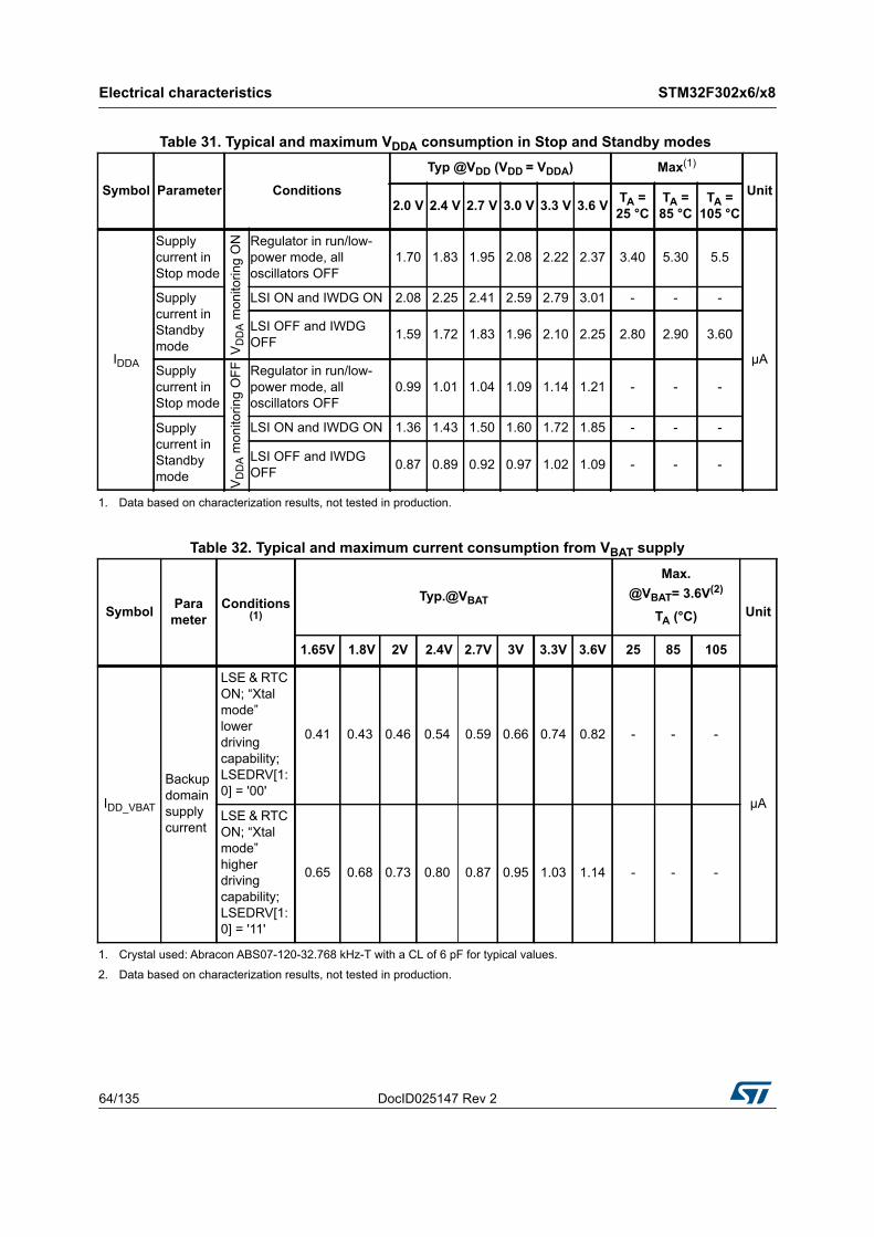
Electrical characteristics STM32F302x6/x8
64/135 DocID025147 Rev 2
Table 31. Typical and maximum VDDA consumption in Stop and Standby modes
Symbol Parameter Conditions
Typ @VDD (VDD = VDDA) Max(1)
Unit2.0 V 2.4 V 2.7 V 3.0 V 3.3 V 3.6 V TA =
25 °CTA = 85 °C
TA = 105 °C
IDDA
Supply current in Stop mode
VD
DA m
onito
ring
ON Regulator in run/low-
power mode, all oscillators OFF
1.70 1.83 1.95 2.08 2.22 2.37 3.40 5.30 5.5
μA
Supply current in Standby mode
LSI ON and IWDG ON 2.08 2.25 2.41 2.59 2.79 3.01 - - -
LSI OFF and IWDG OFF 1.59 1.72 1.83 1.96 2.10 2.25 2.80 2.90 3.60
Supply current in Stop mode
VD
DA m
onito
ring
OFF Regulator in run/low-
power mode, all oscillators OFF
0.99 1.01 1.04 1.09 1.14 1.21 - - -
Supply current in Standby mode
LSI ON and IWDG ON 1.36 1.43 1.50 1.60 1.72 1.85 - - -
LSI OFF and IWDG OFF 0.87 0.89 0.92 0.97 1.02 1.09 - - -
1. Data based on characterization results, not tested in production.
Table 32. Typical and maximum current consumption from VBAT supply
Symbol Parameter
Conditions(1)
Typ.@VBAT
Max.@VBAT= 3.6V(2)
TA (°C) Unit
1.65V 1.8V 2V 2.4V 2.7V 3V 3.3V 3.6V 25 85 105
IDD_VBAT
Backup domain supply current
LSE & RTC ON; “Xtal mode” lower driving capability; LSEDRV[1:0] = '00'
0.41 0.43 0.46 0.54 0.59 0.66 0.74 0.82 - - -
μALSE & RTC ON; “Xtal mode” higher driving capability; LSEDRV[1:0] = '11'
0.65 0.68 0.73 0.80 0.87 0.95 1.03 1.14 - - -
1. Crystal used: Abracon ABS07-120-32.768 kHz-T with a CL of 6 pF for typical values.
2. Data based on characterization results, not tested in production.
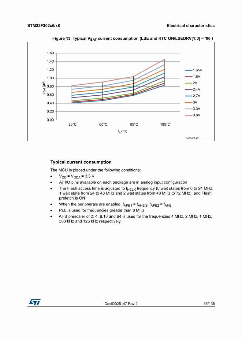
DocID025147 Rev 2 65/135
STM32F302x6/x8 Electrical characteristics
115
Figure 13. Typical VBAT current consumption (LSE and RTC ON/LSEDRV[1:0] = ’00’)
Typical current consumption
The MCU is placed under the following conditions: VDD = VDDA = 3.3 V All I/O pins available on each package are in analog input configuration The Flash access time is adjusted to fHCLK frequency (0 wait states from 0 to 24 MHz,
1 wait state from 24 to 48 MHz and 2 wait states from 48 MHz to 72 MHz), and Flash prefetch is ON
When the peripherals are enabled, fAPB1 = fAHB/2, fAPB2 = fAHB PLL is used for frequencies greater than 8 MHz AHB prescaler of 2, 4, 8,16 and 64 is used for the frequencies 4 MHz, 2 MHz, 1 MHz,
500 kHz and 125 kHz respectively.
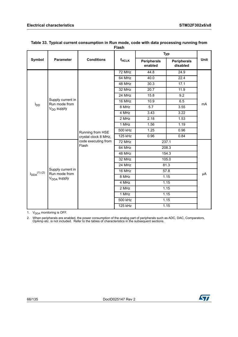
Electrical characteristics STM32F302x6/x8
66/135 DocID025147 Rev 2
Table 33. Typical current consumption in Run mode, code with data processing running from Flash
Symbol Parameter Conditions fHCLK
TypUnitPeripherals
enabledPeripherals
disabled
IDD
Supply current in Run mode from VDD supply
Running from HSE crystal clock 8 MHz, code executing from Flash
72 MHz 44.8 24.9
mA
64 MHz 40.0 22.448 MHz 30.3 17.132 MHz 20.7 11.924 MHz 15.8 9.216 MHz 10.9 6.58 MHz 5.7 3.554 MHz 3.43 3.222 MHz 2.18 1.531 MHz 1.56 1.19
500 kHz 1.25 0.96125 kHz 0.96 0.84
IDDA(1)
(2)
Supply current in Run mode from VDDA supply
72 MHz 237.1
μA
64 MHz 208.348 MHz 154.332 MHz 105.024 MHz 81.316 MHz 57.88 MHz 1.154 MHz 1.152 MHz 1.151 MHz 1.15
500 kHz 1.15125 kHz 1.15
1. VDDA monitoring is OFF.
2. When peripherals are enabled, the power consumption of the analog part of peripherals such as ADC, DAC, Comparators, OpAmp etc. is not included. Refer to the tables of characteristics in the subsequent sections.
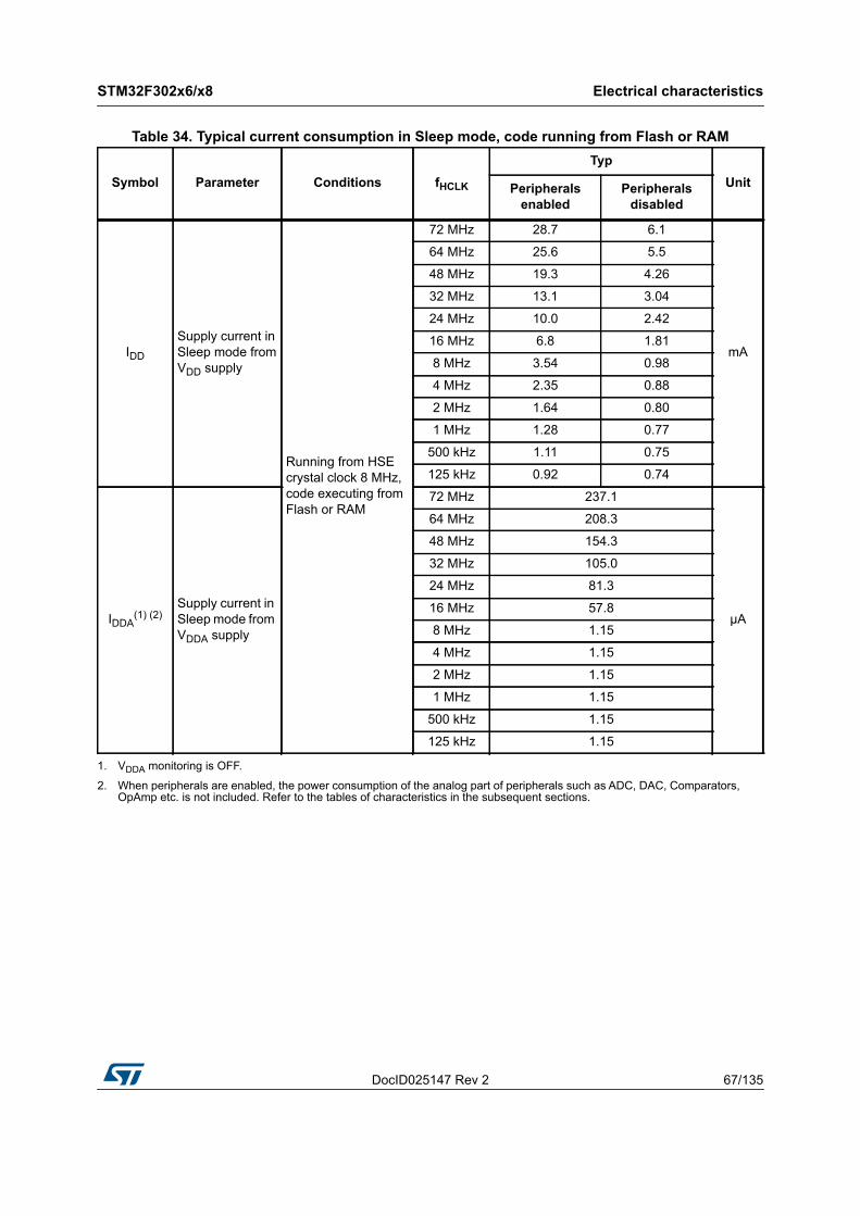
DocID025147 Rev 2 67/135
STM32F302x6/x8 Electrical characteristics
115
Table 34. Typical current consumption in Sleep mode, code running from Flash or RAM
Symbol Parameter Conditions fHCLK
TypUnitPeripherals
enabledPeripherals
disabled
IDD
Supply current in Sleep mode from VDD supply
Running from HSE crystal clock 8 MHz, code executing from Flash or RAM
72 MHz 28.7 6.1
mA
64 MHz 25.6 5.5
48 MHz 19.3 4.26
32 MHz 13.1 3.04
24 MHz 10.0 2.42
16 MHz 6.8 1.81
8 MHz 3.54 0.98
4 MHz 2.35 0.88
2 MHz 1.64 0.80
1 MHz 1.28 0.77
500 kHz 1.11 0.75
125 kHz 0.92 0.74
IDDA(1)
(2)
Supply current in Sleep mode from VDDA supply
72 MHz 237.1
μA
64 MHz 208.3
48 MHz 154.3
32 MHz 105.0
24 MHz 81.3
16 MHz 57.8
8 MHz 1.15
4 MHz 1.15
2 MHz 1.15
1 MHz 1.15
500 kHz 1.15
125 kHz 1.15
1. VDDA monitoring is OFF.
2. When peripherals are enabled, the power consumption of the analog part of peripherals such as ADC, DAC, Comparators, OpAmp etc. is not included. Refer to the tables of characteristics in the subsequent sections.
Electrical characteristics STM32F302x6/x8
68/135 DocID025147 Rev 2
I/O system current consumption
The current consumption of the I/O system has two components: static and dynamic.
I/O static current consumption
All the I/Os used as inputs with pull-up generate current consumption when the pin is externally held low. The value of this current consumption can be simply computed by using the pull-up/pull-down resistors values given in Table 52: I/O static characteristics.
For the output pins, any external pull-down or external load must also be considered to estimate the current consumption.
Additional I/O current consumption is due to I/Os configured as inputs if an intermediate voltage level is externally applied. This current consumption is caused by the input Schmitt trigger circuits used to discriminate the input value. Unless this specific configuration is required by the application, this supply current consumption can be avoided by configuring these I/Os in analog mode. This is notably the case of ADC input pins which should be configured as analog inputs.
Caution: Any floating input pin can also settle to an intermediate voltage level or switch inadvertently, as a result of external electromagnetic noise. To avoid current consumption related to floating pins, they must either be configured in analog mode, or forced internally to a definite digital value. This can be done either by using pull-up/down resistors or by configuring the pins in output mode.
I/O dynamic current consumption
In addition to the internal peripheral current consumption (seeTable 36: Peripheral current consumption), the I/Os used by an application also contribute to the current consumption. When an I/O pin switches, it uses the current from the MCU supply voltage to supply the I/O pin circuitry and to charge/discharge the capacitive load (internal or external) connected to the pin:
ISW VDD fSW C=
whereISW is the current sunk by a switching I/O to charge/discharge the capacitive loadVDD is the MCU supply voltagefSW is the I/O switching frequencyC is the total capacitance seen by the I/O pin: C = CINT+ CEXT+CS
The test pin is configured in push-pull output mode and is toggled by software at a fixed frequency.
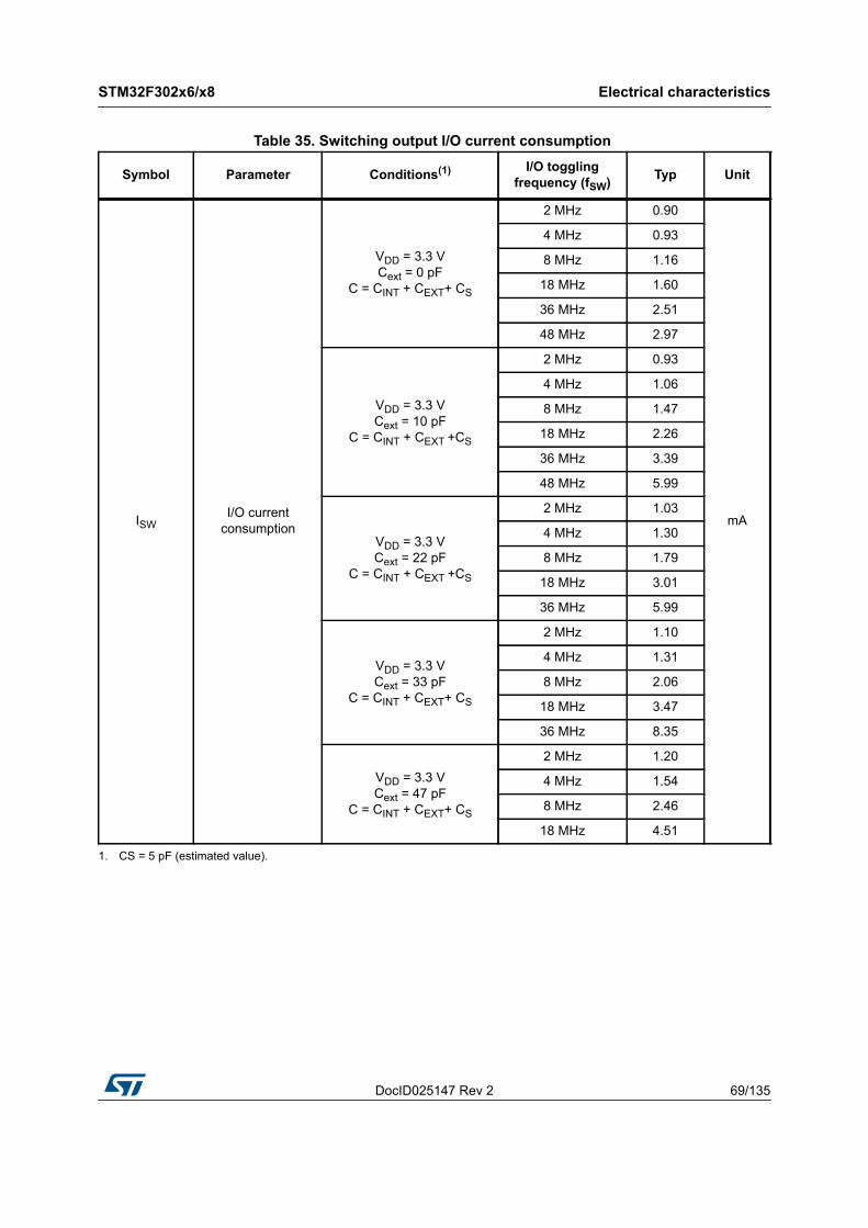
DocID025147 Rev 2 69/135
STM32F302x6/x8 Electrical characteristics
115
Table 35. Switching output I/O current consumption
Symbol Parameter Conditions(1) I/O toggling frequency (fSW) Typ Unit
ISWI/O current
consumption
VDD = 3.3 VCext = 0 pF
C = CINT + CEXT+ CS
2 MHz 0.90
mA
4 MHz 0.93
8 MHz 1.16
18 MHz 1.60
36 MHz 2.51
48 MHz 2.97
VDD = 3.3 VCext = 10 pF
C = CINT + CEXT +CS
2 MHz 0.93
4 MHz 1.06
8 MHz 1.47
18 MHz 2.26
36 MHz 3.39
48 MHz 5.99
VDD = 3.3 VCext = 22 pF
C = CINT + CEXT +CS
2 MHz 1.03
4 MHz 1.30
8 MHz 1.79
18 MHz 3.01
36 MHz 5.99
VDD = 3.3 VCext = 33 pF
C = CINT + CEXT+ CS
2 MHz 1.10
4 MHz 1.31
8 MHz 2.06
18 MHz 3.47
36 MHz 8.35
VDD = 3.3 VCext = 47 pF
C = CINT + CEXT+ CS
2 MHz 1.20
4 MHz 1.54
8 MHz 2.46
18 MHz 4.51
1. CS = 5 pF (estimated value).
Electrical characteristics STM32F302x6/x8
70/135 DocID025147 Rev 2
On-chip peripheral current consumption
The MCU is placed under the following conditions: all I/O pins are in analog input configuration all peripherals are disabled unless otherwise mentioned the given value is calculated by measuring the current consumption
– with all peripherals clocked off– with only one peripheral clocked on
ambient operating temperature at 25°C and VDD = VDDA = 3.3 V.
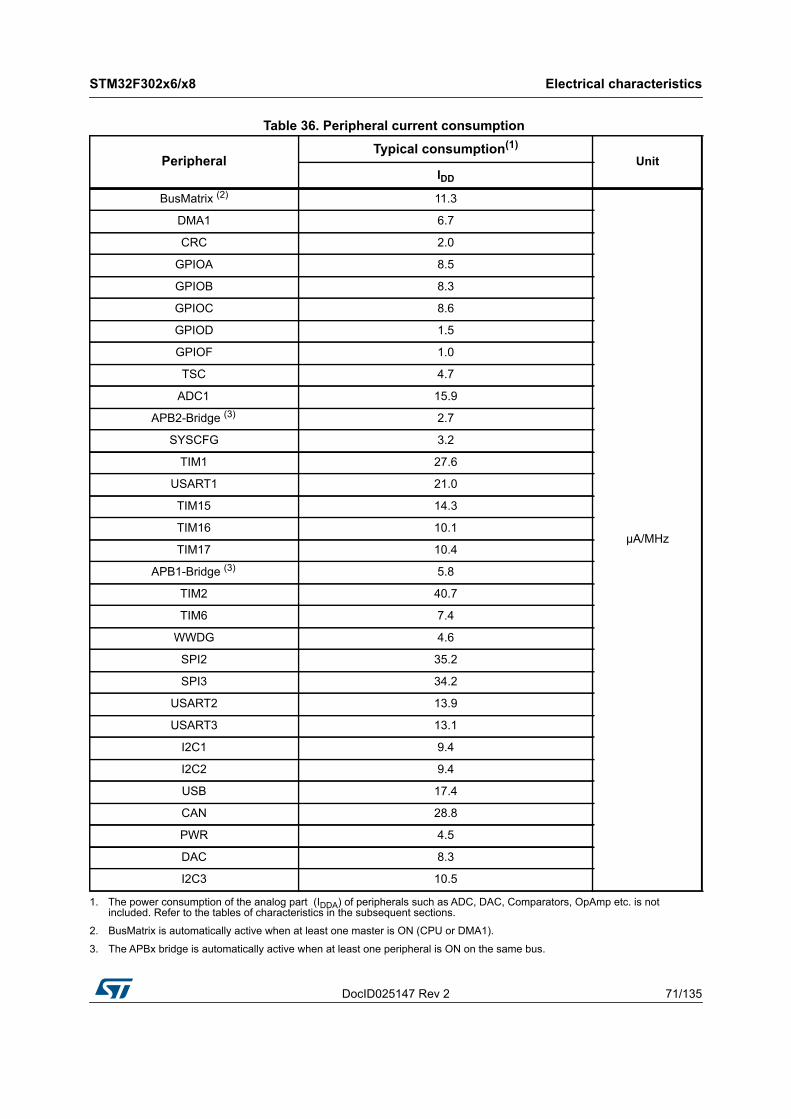
DocID025147 Rev 2 71/135
STM32F302x6/x8 Electrical characteristics
115
Table 36. Peripheral current consumption
PeripheralTypical consumption(1)
UnitIDD
BusMatrix (2) 11.3
μA/MHz
DMA1 6.7
CRC 2.0
GPIOA 8.5
GPIOB 8.3
GPIOC 8.6
GPIOD 1.5
GPIOF 1.0
TSC 4.7
ADC1 15.9
APB2-Bridge (3) 2.7
SYSCFG 3.2
TIM1 27.6
USART1 21.0
TIM15 14.3
TIM16 10.1
TIM17 10.4
APB1-Bridge (3) 5.8
TIM2 40.7
TIM6 7.4
WWDG 4.6
SPI2 35.2
SPI3 34.2
USART2 13.9
USART3 13.1
I2C1 9.4
I2C2 9.4
USB 17.4
CAN 28.8
PWR 4.5
DAC 8.3
I2C3 10.5
1. The power consumption of the analog part (IDDA) of peripherals such as ADC, DAC, Comparators, OpAmp etc. is not included. Refer to the tables of characteristics in the subsequent sections.
2. BusMatrix is automatically active when at least one master is ON (CPU or DMA1).
3. The APBx bridge is automatically active when at least one peripheral is ON on the same bus.
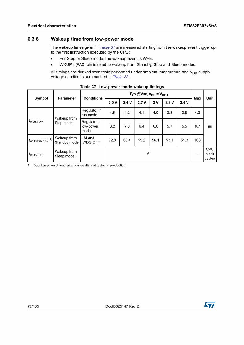
Electrical characteristics STM32F302x6/x8
72/135 DocID025147 Rev 2
6.3.6 Wakeup time from low-power modeThe wakeup times given in Table 37 are measured starting from the wakeup event trigger up to the first instruction executed by the CPU: For Stop or Sleep mode: the wakeup event is WFE. WKUP1 (PA0) pin is used to wakeup from Standby, Stop and Sleep modes.
All timings are derived from tests performed under ambient temperature and VDD supply voltage conditions summarized in Table 22.
Table 37. Low-power mode wakeup timings
Symbol Parameter Conditions Typ @VDD, VDD = VDDA
Max Unit 2.0 V 2.4 V 2.7 V 3 V 3.3 V 3.6 V
tWUSTOPWakeup from Stop mode
Regulator in run mode 4.5 4.2 4.1 4.0 3.8 3.8 4.3
μsRegulator in low-power mode
8.2 7.0 6.4 6.0 5.7 5.5 8.7
tWUSTANDBY(1) Wakeup from
Standby modeLSI and IWDG OFF 72.8 63.4 59.2 56.1 53.1 51.3 103
tWUSLEEPWakeup from Sleep mode 6 -
CPU clock cycles
1. Data based on characterization results, not tested in production.
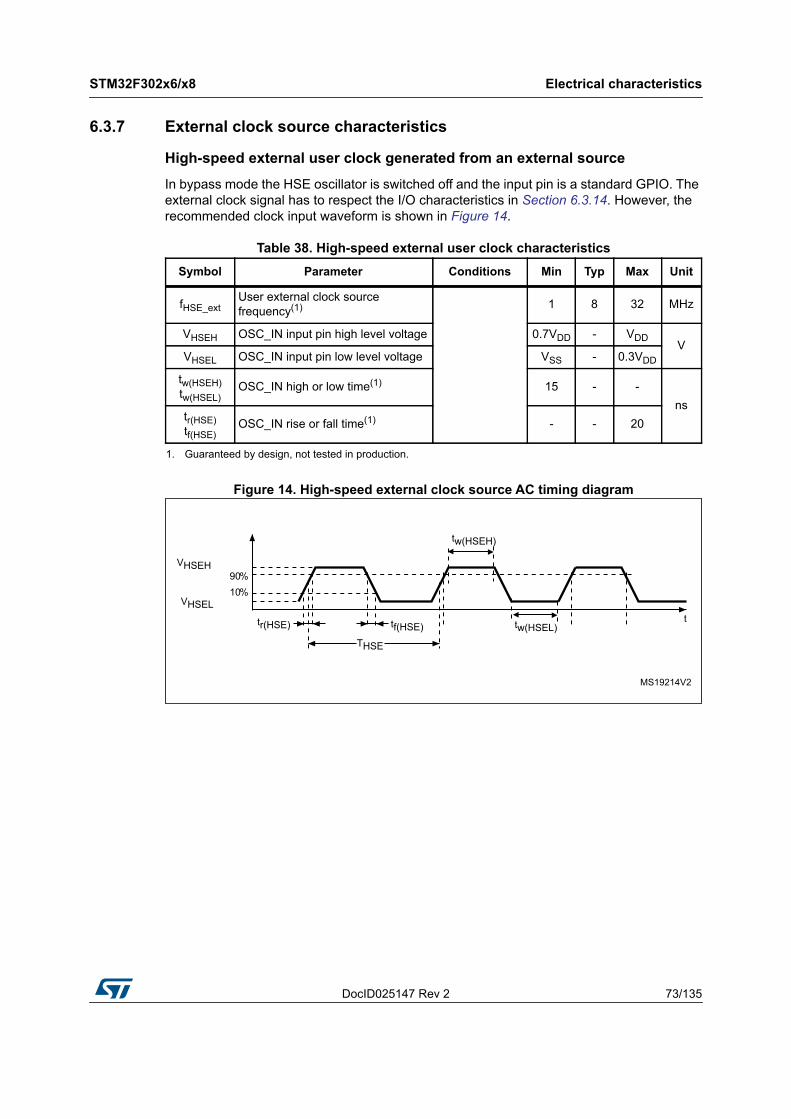
DocID025147 Rev 2 73/135
STM32F302x6/x8 Electrical characteristics
115
6.3.7 External clock source characteristics
High-speed external user clock generated from an external source
In bypass mode the HSE oscillator is switched off and the input pin is a standard GPIO. The external clock signal has to respect the I/O characteristics in Section 6.3.14. However, the recommended clock input waveform is shown in Figure 14.
Figure 14. High-speed external clock source AC timing diagram
Table 38. High-speed external user clock characteristicsSymbol Parameter Conditions Min Typ Max Unit
fHSE_extUser external clock source frequency(1)
1. Guaranteed by design, not tested in production.
1 8 32 MHz
VHSEH OSC_IN input pin high level voltage 0.7VDD - VDDV
VHSEL OSC_IN input pin low level voltage VSS - 0.3VDD
tw(HSEH)tw(HSEL)
OSC_IN high or low time(1) 15 - -ns
tr(HSE)tf(HSE)
OSC_IN rise or fall time(1) - - 20
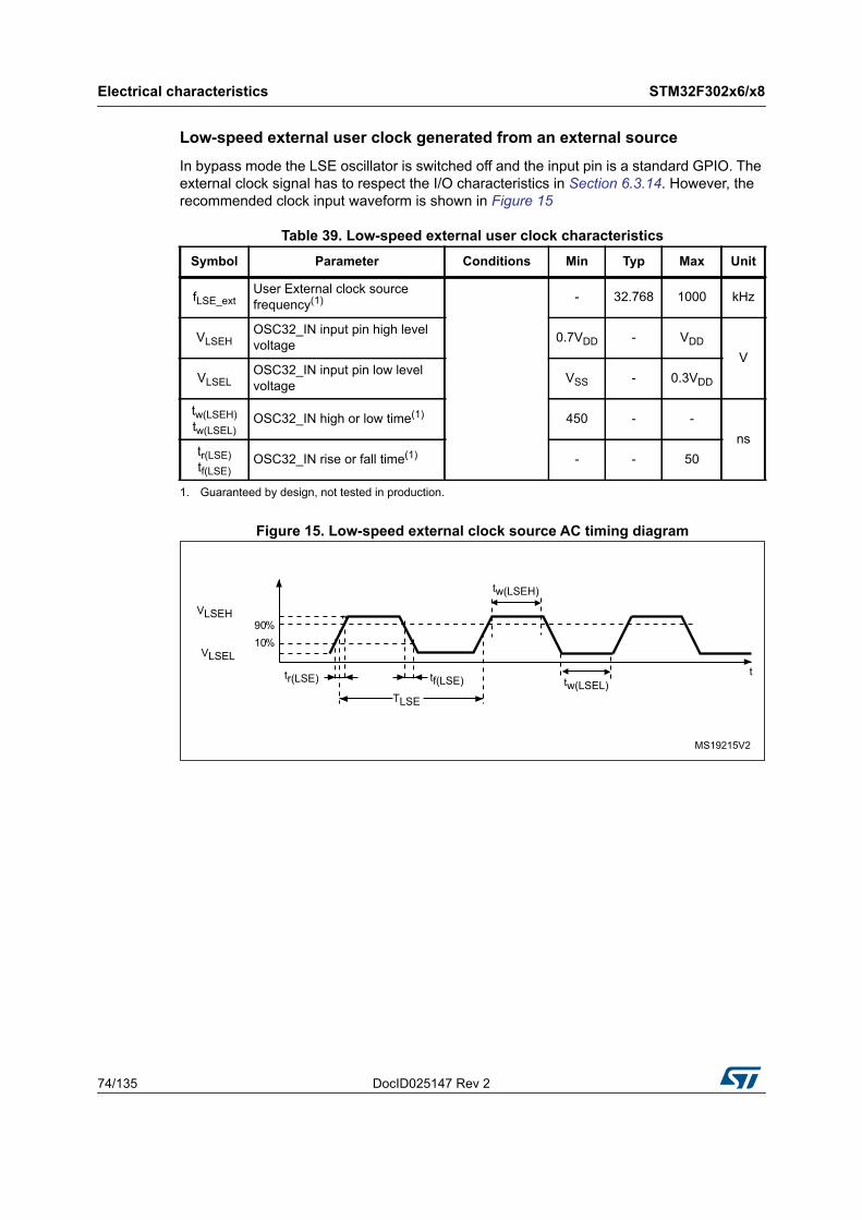
Electrical characteristics STM32F302x6/x8
74/135 DocID025147 Rev 2
Low-speed external user clock generated from an external source
In bypass mode the LSE oscillator is switched off and the input pin is a standard GPIO. The external clock signal has to respect the I/O characteristics in Section 6.3.14. However, the recommended clock input waveform is shown in Figure 15
Figure 15. Low-speed external clock source AC timing diagram
Table 39. Low-speed external user clock characteristicsSymbol Parameter Conditions Min Typ Max Unit
fLSE_extUser External clock source frequency(1)
1. Guaranteed by design, not tested in production.
- 32.768 1000 kHz
VLSEHOSC32_IN input pin high level voltage 0.7VDD - VDD
VVLSEL
OSC32_IN input pin low level voltage VSS - 0.3VDD
tw(LSEH)tw(LSEL)
OSC32_IN high or low time(1) 450 - -ns
tr(LSE)tf(LSE)
OSC32_IN rise or fall time(1) - - 50
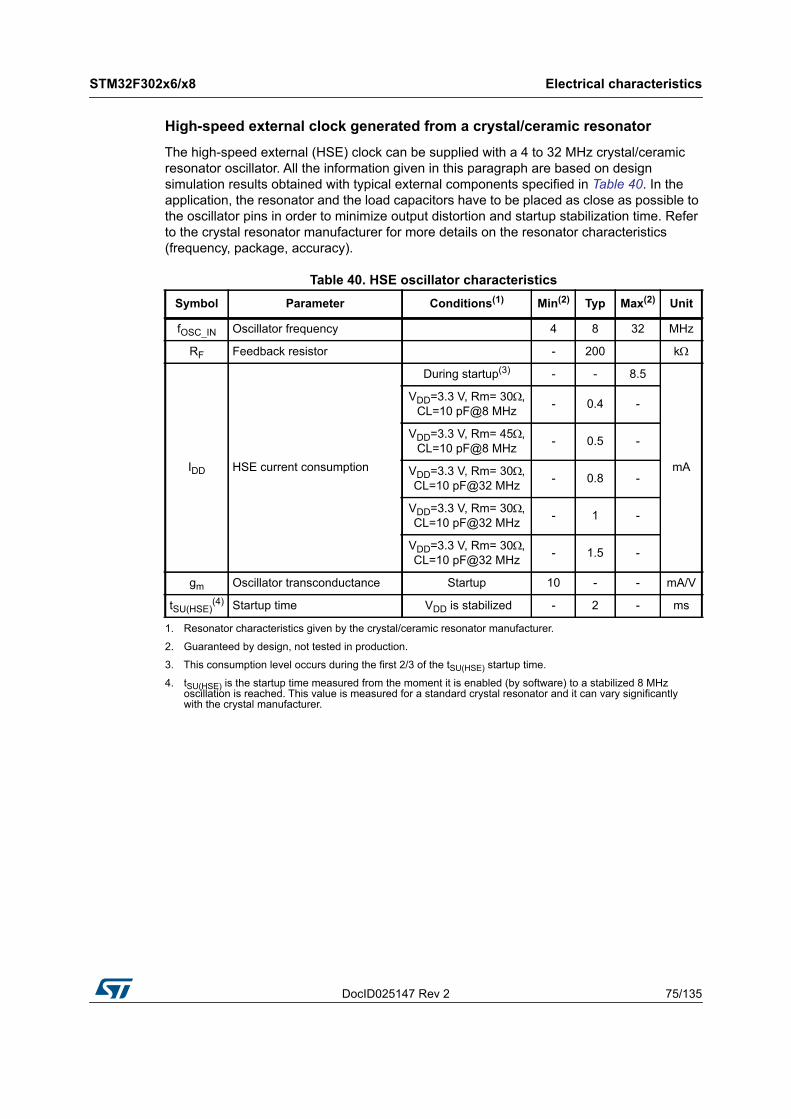
DocID025147 Rev 2 75/135
STM32F302x6/x8 Electrical characteristics
115
High-speed external clock generated from a crystal/ceramic resonator
The high-speed external (HSE) clock can be supplied with a 4 to 32 MHz crystal/ceramic resonator oscillator. All the information given in this paragraph are based on design simulation results obtained with typical external components specified in Table 40. In the application, the resonator and the load capacitors have to be placed as close as possible to the oscillator pins in order to minimize output distortion and startup stabilization time. Refer to the crystal resonator manufacturer for more details on the resonator characteristics (frequency, package, accuracy).
Table 40. HSE oscillator characteristicsSymbol Parameter Conditions(1)
1. Resonator characteristics given by the crystal/ceramic resonator manufacturer.
Min(2)
2. Guaranteed by design, not tested in production.
Typ Max(2) Unit
fOSC_IN Oscillator frequency 4 8 32 MHz
RF Feedback resistor - 200 k
IDD HSE current consumption
During startup(3)
3. This consumption level occurs during the first 2/3 of the tSU(HSE) startup time.
- - 8.5
mA
VDD=3.3 V, Rm= 30,CL=10 pF@8 MHz - 0.4 -
VDD=3.3 V, Rm= 45,CL=10 pF@8 MHz - 0.5 -
VDD=3.3 V, Rm= 30,CL=10 pF@32 MHz - 0.8 -
VDD=3.3 V, Rm= 30,CL=10 pF@32 MHz - 1 -
VDD=3.3 V, Rm= 30,CL=10 pF@32 MHz - 1.5 -
gm Oscillator transconductance Startup 10 - - mA/V
tSU(HSE)(4)
4. tSU(HSE) is the startup time measured from the moment it is enabled (by software) to a stabilized 8 MHz oscillation is reached. This value is measured for a standard crystal resonator and it can vary significantly with the crystal manufacturer.
Startup time VDD is stabilized - 2 - ms
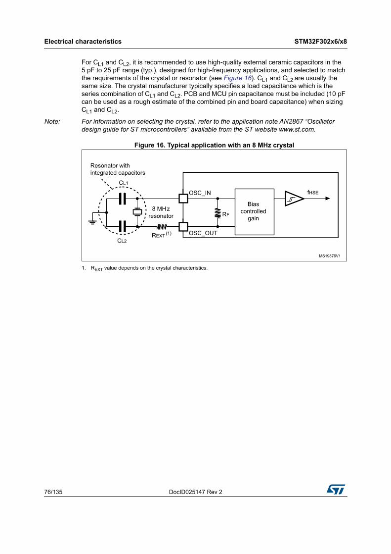
Electrical characteristics STM32F302x6/x8
76/135 DocID025147 Rev 2
For CL1 and CL2, it is recommended to use high-quality external ceramic capacitors in the 5 pF to 25 pF range (typ.), designed for high-frequency applications, and selected to match the requirements of the crystal or resonator (see Figure 16). CL1 and CL2 are usually the same size. The crystal manufacturer typically specifies a load capacitance which is the series combination of CL1 and CL2. PCB and MCU pin capacitance must be included (10 pF can be used as a rough estimate of the combined pin and board capacitance) when sizing CL1 and CL2.
Note: For information on selecting the crystal, refer to the application note AN2867 “Oscillator design guide for ST microcontrollers” available from the ST website www.st.com.
Figure 16. Typical application with an 8 MHz crystal
1. REXT value depends on the crystal characteristics.
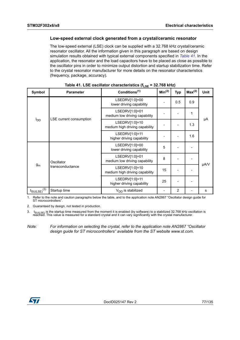
DocID025147 Rev 2 77/135
STM32F302x6/x8 Electrical characteristics
115
Low-speed external clock generated from a crystal/ceramic resonator
The low-speed external (LSE) clock can be supplied with a 32.768 kHz crystal/ceramic resonator oscillator. All the information given in this paragraph are based on design simulation results obtained with typical external components specified in Table 41. In the application, the resonator and the load capacitors have to be placed as close as possible to the oscillator pins in order to minimize output distortion and startup stabilization time. Refer to the crystal resonator manufacturer for more details on the resonator characteristics (frequency, package, accuracy).
Note: For information on selecting the crystal, refer to the application note AN2867 “Oscillator design guide for ST microcontrollers” available from the ST website www.st.com.
Table 41. LSE oscillator characteristics (fLSE = 32.768 kHz) Symbol Parameter Conditions(1) Min(2) Typ Max(2) Unit
IDD LSE current consumption
LSEDRV[1:0]=00lower driving capability - 0.5 0.9
μA
LSEDRV[1:0]=01medium low driving capability - - 1
LSEDRV[1:0]=10medium high driving capability - - 1.3
LSEDRV[1:0]=11higher driving capability - - 1.6
gmOscillator transconductance
LSEDRV[1:0]=00lower driving capability 5 - -
μA/V
LSEDRV[1:0]=01medium low driving capability 8 - -
LSEDRV[1:0]=10medium high driving capability 15 - -
LSEDRV[1:0]=11higher driving capability 25 - -
tSU(LSE)(3) Startup time VDD is stabilized - 2 - s
1. Refer to the note and caution paragraphs below the table, and to the application note AN2867 “Oscillator design guide for ST microcontrollers”.
2. Guaranteed by design, not tested in production.
3. tSU(LSE) is the startup time measured from the moment it is enabled (by software) to a stabilized 32.768 kHz oscillation is reached. This value is measured for a standard crystal and it can vary significantly with the crystal manufacturer.
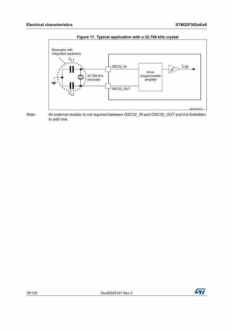
Electrical characteristics STM32F302x6/x8
78/135 DocID025147 Rev 2
Figure 17. Typical application with a 32.768 kHz crystal
Note: An external resistor is not required between OSC32_IN and OSC32_OUT and it is forbidden to add one.
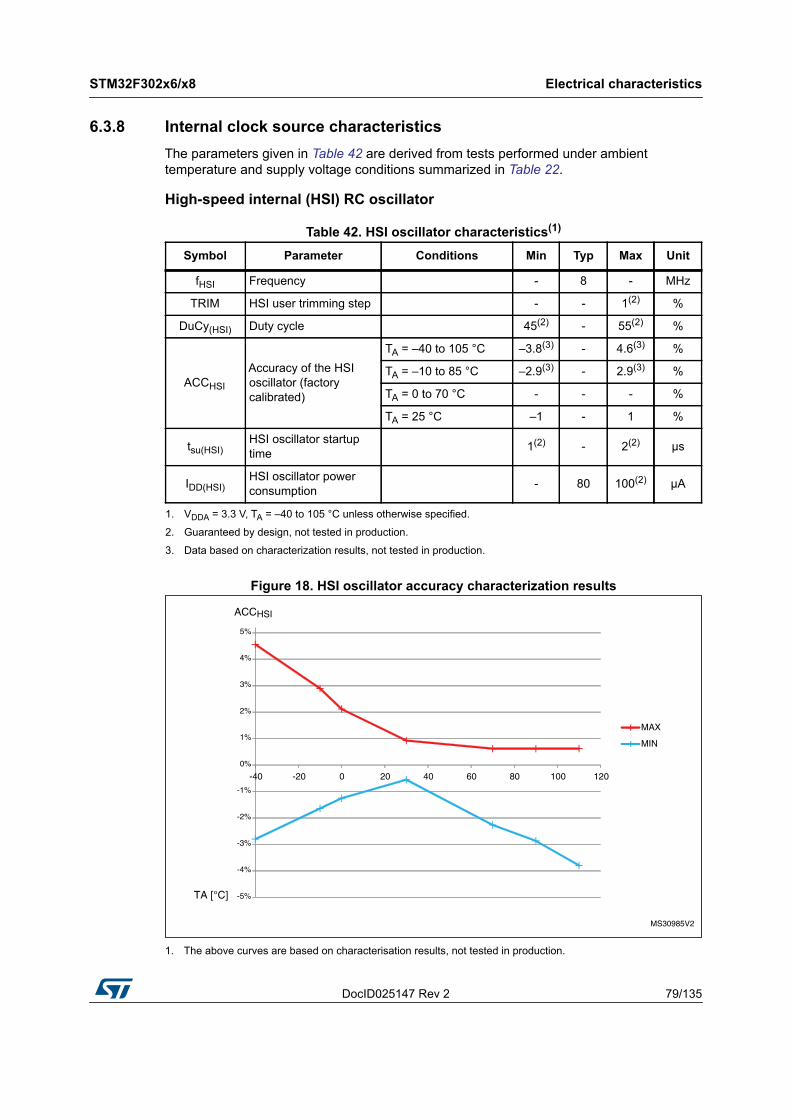
DocID025147 Rev 2 79/135
STM32F302x6/x8 Electrical characteristics
115
6.3.8 Internal clock source characteristicsThe parameters given in Table 42 are derived from tests performed under ambient temperature and supply voltage conditions summarized in Table 22.
High-speed internal (HSI) RC oscillator
Figure 18. HSI oscillator accuracy characterization results
1. The above curves are based on characterisation results, not tested in production.
Table 42. HSI oscillator characteristics(1)
1. VDDA = 3.3 V, TA = –40 to 105 °C unless otherwise specified.
Symbol Parameter Conditions Min Typ Max Unit
fHSI Frequency - 8 - MHz
TRIM HSI user trimming step - - 1(2)
2. Guaranteed by design, not tested in production.
%
DuCy(HSI) Duty cycle 45(2) - 55(2) %
ACCHSI
Accuracy of the HSI oscillator (factory calibrated)
TA = –40 to 105 °C –3.8(3)
3. Data based on characterization results, not tested in production.
- 4.6(3) %
TA = –10 to 85 °C –2.9(3) - 2.9(3) %
TA = 0 to 70 °C - - - %
TA = 25 °C –1 - 1 %
tsu(HSI)HSI oscillator startup time 1(2) - 2(2) μs
IDD(HSI)HSI oscillator power consumption - 80 100(2) μA
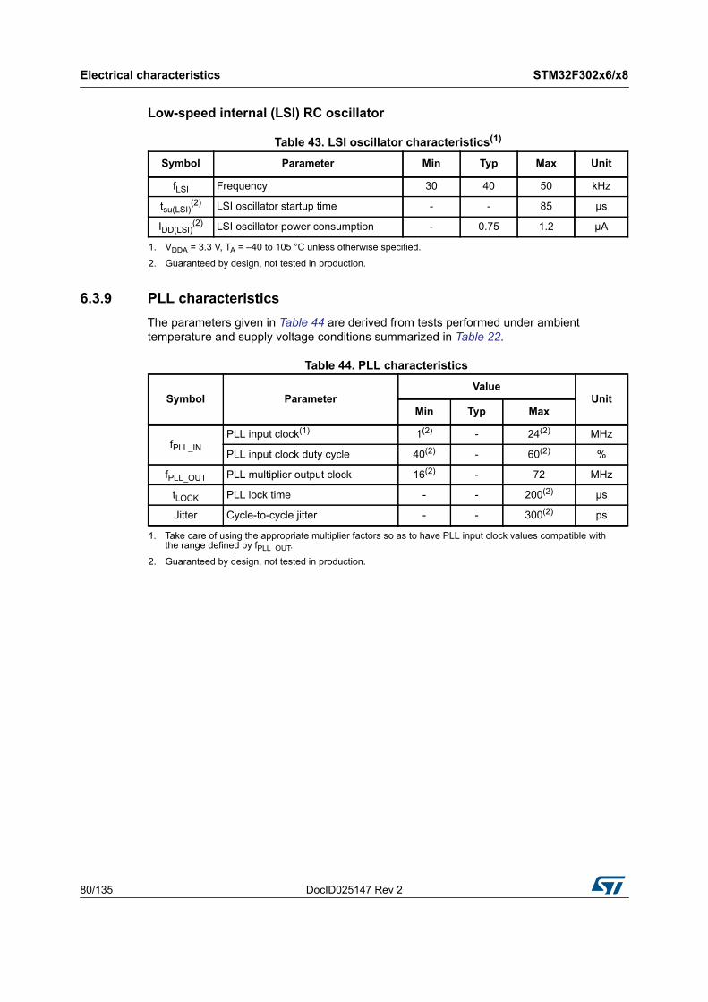
Electrical characteristics STM32F302x6/x8
80/135 DocID025147 Rev 2
Low-speed internal (LSI) RC oscillator
6.3.9 PLL characteristicsThe parameters given in Table 44 are derived from tests performed under ambient temperature and supply voltage conditions summarized in Table 22.
Table 43. LSI oscillator characteristics(1)
1. VDDA = 3.3 V, TA = –40 to 105 °C unless otherwise specified.
Symbol Parameter Min Typ Max Unit
fLSI Frequency 30 40 50 kHz
tsu(LSI)(2)
2. Guaranteed by design, not tested in production.
LSI oscillator startup time - - 85 μs
IDD(LSI)(2) LSI oscillator power consumption - 0.75 1.2 μA
Table 44. PLL characteristics
Symbol ParameterValue
UnitMin Typ Max
fPLL_INPLL input clock(1)
1. Take care of using the appropriate multiplier factors so as to have PLL input clock values compatible with the range defined by fPLL_OUT.
1(2) - 24(2) MHz
PLL input clock duty cycle 40(2) - 60(2) %
fPLL_OUT PLL multiplier output clock 16(2) - 72 MHz
tLOCK PLL lock time - - 200(2) μs
Jitter Cycle-to-cycle jitter - - 300(2)
2. Guaranteed by design, not tested in production.
ps
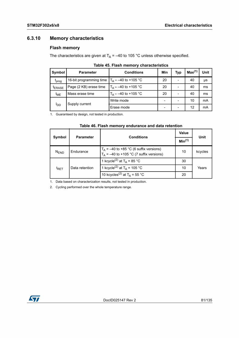
DocID025147 Rev 2 81/135
STM32F302x6/x8 Electrical characteristics
115
6.3.10 Memory characteristics
Flash memory
The characteristics are given at TA = –40 to 105 °C unless otherwise specified.
Table 45. Flash memory characteristicsSymbol Parameter Conditions Min Typ Max(1)
1. Guaranteed by design, not tested in production.
Unit
tprog 16-bit programming time TA–40 to +105 °C 20 - 40 μs
tERASE Page (2 KB) erase time TA –40 to +105 °C 20 - 40 ms
tME Mass erase time TA –40 to +105 °C 20 - 40 ms
IDD Supply current Write mode - - 10 mA
Erase mode - - 12 mA
Table 46. Flash memory endurance and data retention
Symbol Parameter ConditionsValue
UnitMin(1)
1. Data based on characterization results, not tested in production.
NEND EnduranceTA = –40 to +85 °C (6 suffix versions)TA = –40 to +105 °C (7 suffix versions)
10 kcycles
tRET Data retention
1 kcycle(2) at TA = 85 °C
2. Cycling performed over the whole temperature range.
30
Years1 kcycle(2) at TA = 105 °C 10
10 kcycles(2) at TA = 55 °C 20
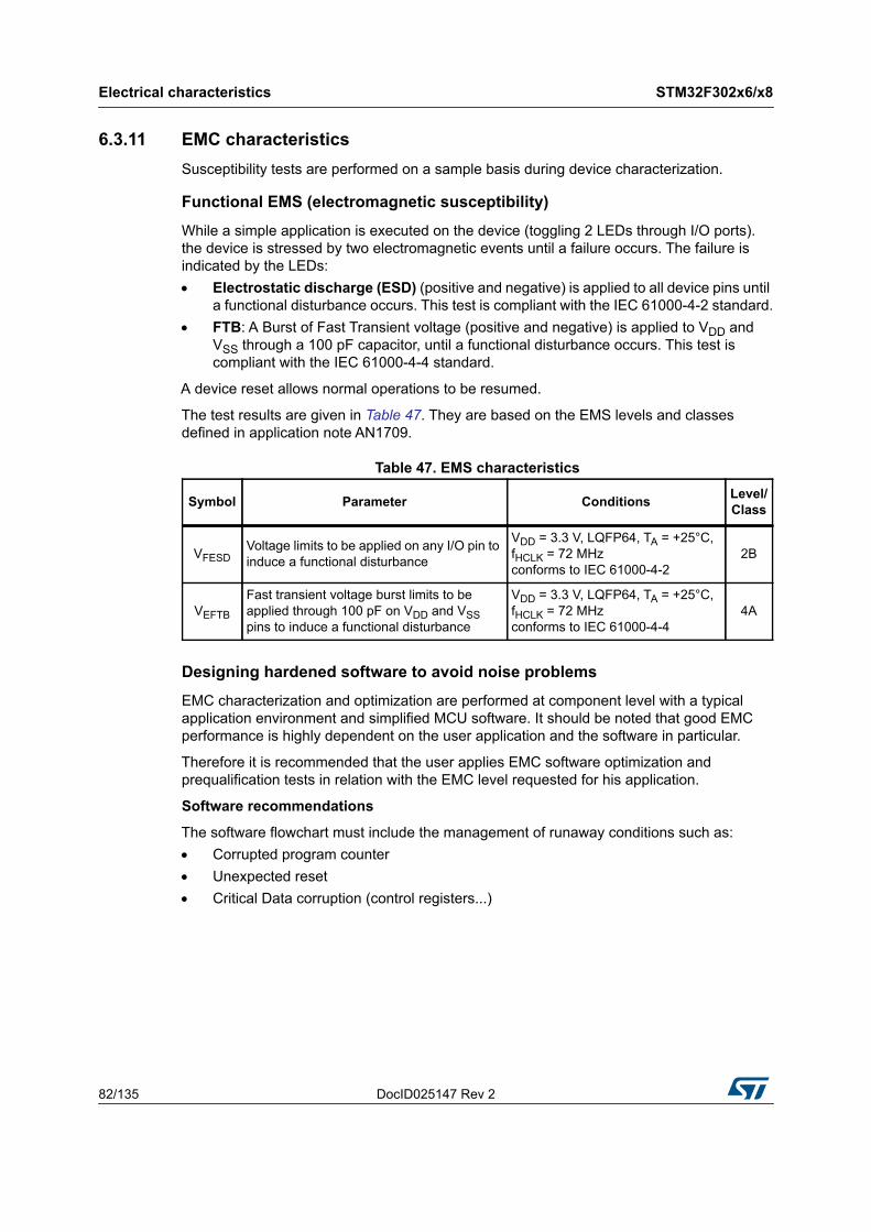
Electrical characteristics STM32F302x6/x8
82/135 DocID025147 Rev 2
6.3.11 EMC characteristicsSusceptibility tests are performed on a sample basis during device characterization.
Functional EMS (electromagnetic susceptibility)
While a simple application is executed on the device (toggling 2 LEDs through I/O ports). the device is stressed by two electromagnetic events until a failure occurs. The failure is indicated by the LEDs: Electrostatic discharge (ESD) (positive and negative) is applied to all device pins until
a functional disturbance occurs. This test is compliant with the IEC 61000-4-2 standard. FTB: A Burst of Fast Transient voltage (positive and negative) is applied to VDD and
VSS through a 100 pF capacitor, until a functional disturbance occurs. This test is compliant with the IEC 61000-4-4 standard.
A device reset allows normal operations to be resumed.
The test results are given in Table 47. They are based on the EMS levels and classes defined in application note AN1709.
Designing hardened software to avoid noise problems
EMC characterization and optimization are performed at component level with a typical application environment and simplified MCU software. It should be noted that good EMC performance is highly dependent on the user application and the software in particular.
Therefore it is recommended that the user applies EMC software optimization and prequalification tests in relation with the EMC level requested for his application.
Software recommendations
The software flowchart must include the management of runaway conditions such as: Corrupted program counter Unexpected reset Critical Data corruption (control registers...)
Table 47. EMS characteristics
Symbol Parameter Conditions Level/Class
VFESDVoltage limits to be applied on any I/O pin to induce a functional disturbance
VDD = 3.3 V, LQFP64, TA = +25°C, fHCLK = 72 MHz conforms to IEC 61000-4-2
2B
VEFTB
Fast transient voltage burst limits to be applied through 100 pF on VDD and VSS pins to induce a functional disturbance
VDD = 3.3 V, LQFP64, TA = +25°C, fHCLK = 72 MHz conforms to IEC 61000-4-4
4A
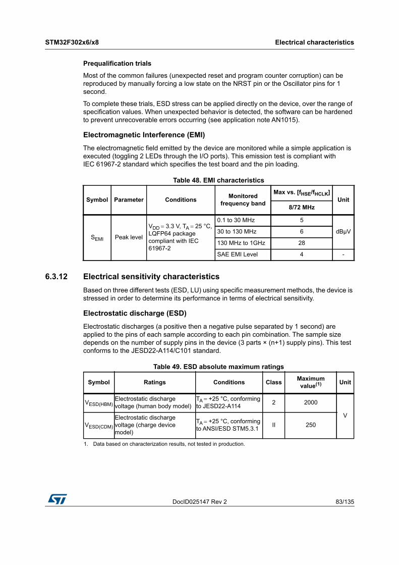
DocID025147 Rev 2 83/135
STM32F302x6/x8 Electrical characteristics
115
Prequalification trials
Most of the common failures (unexpected reset and program counter corruption) can be reproduced by manually forcing a low state on the NRST pin or the Oscillator pins for 1 second.
To complete these trials, ESD stress can be applied directly on the device, over the range of specification values. When unexpected behavior is detected, the software can be hardened to prevent unrecoverable errors occurring (see application note AN1015).
Electromagnetic Interference (EMI)
The electromagnetic field emitted by the device are monitored while a simple application is executed (toggling 2 LEDs through the I/O ports). This emission test is compliant with IEC 61967-2 standard which specifies the test board and the pin loading.
6.3.12 Electrical sensitivity characteristicsBased on three different tests (ESD, LU) using specific measurement methods, the device is stressed in order to determine its performance in terms of electrical sensitivity.
Electrostatic discharge (ESD)
Electrostatic discharges (a positive then a negative pulse separated by 1 second) are applied to the pins of each sample according to each pin combination. The sample size depends on the number of supply pins in the device (3 parts × (n+1) supply pins). This test conforms to the JESD22-A114/C101 standard.
Table 48. EMI characteristics
Symbol Parameter Conditions Monitoredfrequency band
Max vs. [fHSE/fHCLK]Unit
8/72 MHz
SEMI Peak level
VDD 3.3 V, TA 25 °C, LQFP64 package compliant with IEC 61967-2
0.1 to 30 MHz 5
dBμV30 to 130 MHz 6
130 MHz to 1GHz 28
SAE EMI Level 4 -
Table 49. ESD absolute maximum ratings
Symbol Ratings Conditions Class Maximum value(1)
1. Data based on characterization results, not tested in production.
Unit
VESD(HBM)Electrostatic discharge voltage (human body model)
TA +25 °C, conforming to JESD22-A114 2 2000
VVESD(CDM)
Electrostatic discharge voltage (charge device model)
TA +25 °C, conforming to ANSI/ESD STM5.3.1 II 250
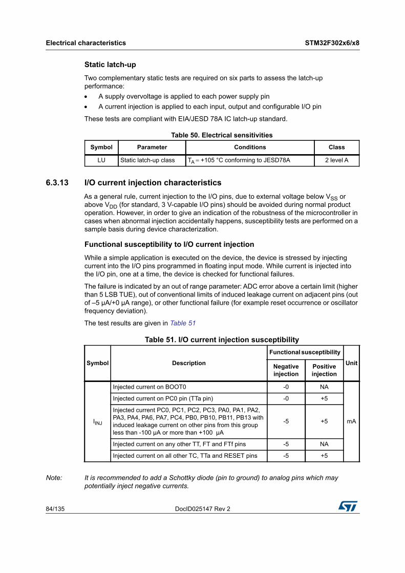
Electrical characteristics STM32F302x6/x8
84/135 DocID025147 Rev 2
Static latch-up
Two complementary static tests are required on six parts to assess the latch-up performance: A supply overvoltage is applied to each power supply pin A current injection is applied to each input, output and configurable I/O pin
These tests are compliant with EIA/JESD 78A IC latch-up standard.
6.3.13 I/O current injection characteristicsAs a general rule, current injection to the I/O pins, due to external voltage below VSS or above VDD (for standard, 3 V-capable I/O pins) should be avoided during normal product operation. However, in order to give an indication of the robustness of the microcontroller in cases when abnormal injection accidentally happens, susceptibility tests are performed on a sample basis during device characterization.
Functional susceptibility to I/O current injection
While a simple application is executed on the device, the device is stressed by injecting current into the I/O pins programmed in floating input mode. While current is injected into the I/O pin, one at a time, the device is checked for functional failures.
The failure is indicated by an out of range parameter: ADC error above a certain limit (higher than 5 LSB TUE), out of conventional limits of induced leakage current on adjacent pins (out of –5 μA/+0 μA range), or other functional failure (for example reset occurrence or oscillator frequency deviation).
The test results are given in Table 51
Note: It is recommended to add a Schottky diode (pin to ground) to analog pins which may potentially inject negative currents.
Table 50. Electrical sensitivitiesSymbol Parameter Conditions Class
LU Static latch-up class TA +105 °C conforming to JESD78A 2 level A
Table 51. I/O current injection susceptibility
Symbol Description
Functional susceptibility
UnitNegative injection
Positive injection
IINJ
Injected current on BOOT0 -0 NA
mA
Injected current on PC0 pin (TTa pin) -0 +5
Injected current PC0, PC1, PC2, PC3, PA0, PA1, PA2, PA3, PA4, PA6, PA7, PC4, PB0, PB10, PB11, PB13 with induced leakage current on other pins from this group less than -100 μA or more than +100 μA
-5 +5
Injected current on any other TT, FT and FTf pins -5 NA
Injected current on all other TC, TTa and RESET pins -5 +5
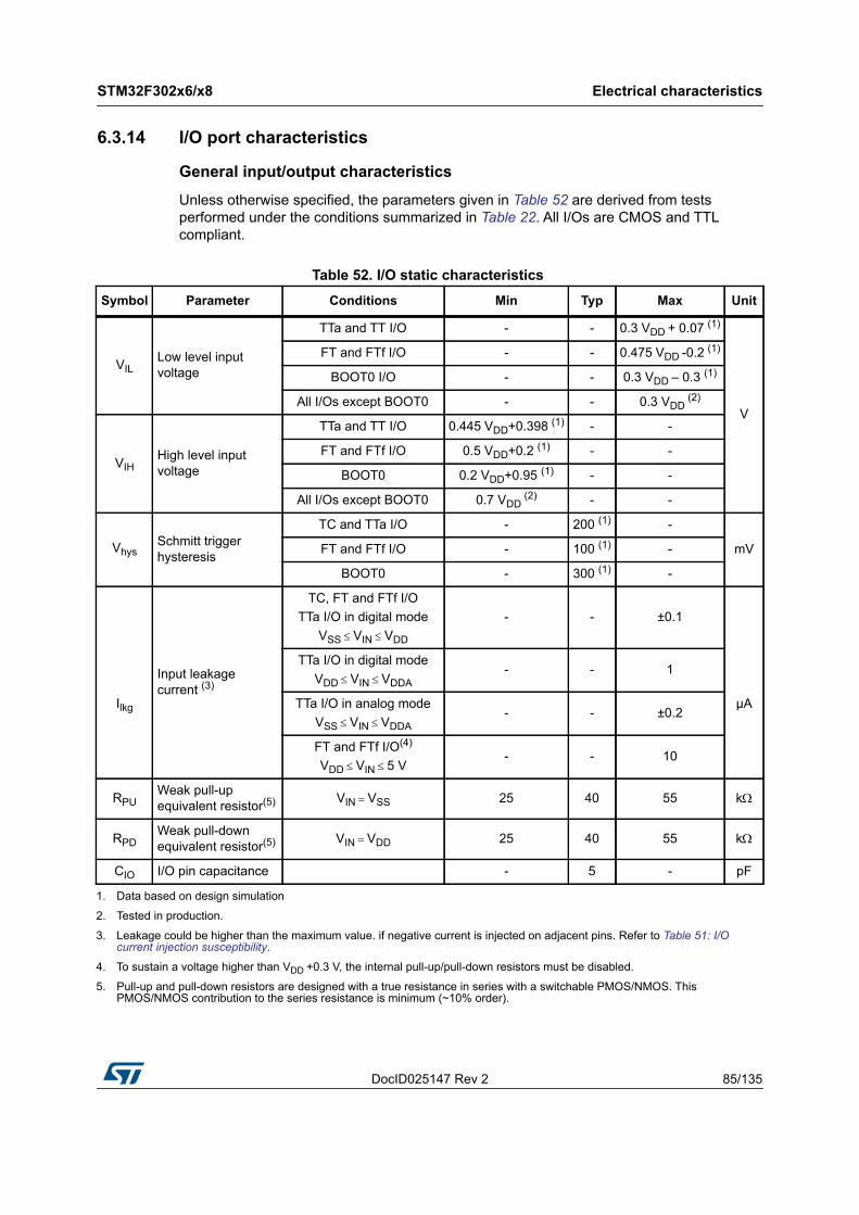
DocID025147 Rev 2 85/135
STM32F302x6/x8 Electrical characteristics
115
6.3.14 I/O port characteristics
General input/output characteristics
Unless otherwise specified, the parameters given in Table 52 are derived from tests performed under the conditions summarized in Table 22. All I/Os are CMOS and TTL compliant.
Table 52. I/O static characteristics Symbol Parameter Conditions Min Typ Max Unit
VILLow level input voltage
TTa and TT I/O - - 0.3 VDD + 0.07 (1)
V
FT and FTf I/O - - 0.475 VDD -0.2 (1)
BOOT0 I/O - - 0.3 VDD – 0.3 (1)
All I/Os except BOOT0 - - 0.3 VDD (2)
VIHHigh level input voltage
TTa and TT I/O 0.445 VDD+0.398 (1) - -
FT and FTf I/O 0.5 VDD+0.2 (1) - -
BOOT0 0.2 VDD+0.95 (1) - -
All I/Os except BOOT0 0.7 VDD (2) - -
VhysSchmitt trigger hysteresis
TC and TTa I/O - 200 (1) -
mVFT and FTf I/O - 100 (1) -
BOOT0 - 300 (1) -
Ilkg
Input leakage current (3)
TC, FT and FTf I/OTTa I/O in digital mode
VSS VIN VDD
- - ±0.1
μA
TTa I/O in digital modeVDD VIN VDDA
- - 1
TTa I/O in analog modeVSS VIN VDDA
- - ±0.2
FT and FTf I/O(4)
VDD VIN 5 V- - 10
RPUWeak pull-up equivalent resistor(5) VIN VSS 25 40 55 k
RPDWeak pull-down equivalent resistor(5) VIN VDD 25 40 55 k
CIO I/O pin capacitance - 5 - pF
1. Data based on design simulation
2. Tested in production.
3. Leakage could be higher than the maximum value. if negative current is injected on adjacent pins. Refer to Table 51: I/O current injection susceptibility.
4. To sustain a voltage higher than VDD +0.3 V, the internal pull-up/pull-down resistors must be disabled.
5. Pull-up and pull-down resistors are designed with a true resistance in series with a switchable PMOS/NMOS. This PMOS/NMOS contribution to the series resistance is minimum (~10% order).
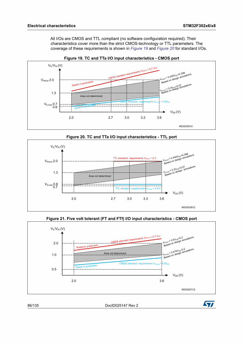
Electrical characteristics STM32F302x6/x8
86/135 DocID025147 Rev 2
All I/Os are CMOS and TTL compliant (no software configuration required). Their characteristics cover more than the strict CMOS-technology or TTL parameters. The coverage of these requirements is shown in Figure 19 and Figure 20 for standard I/Os.
Figure 19. TC and TTa I/O input characteristics - CMOS port
Figure 20. TC and TTa I/O input characteristics - TTL port
Figure 21. Five volt tolerant (FT and FTf) I/O input characteristics - CMOS port
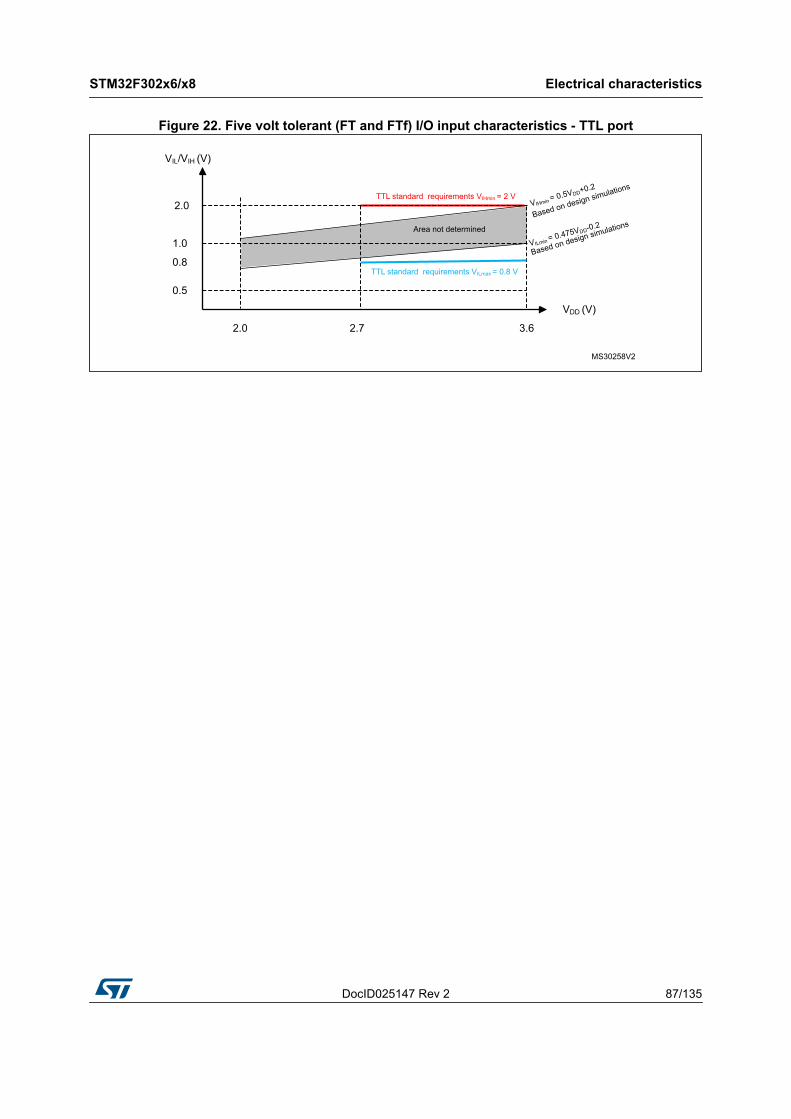
DocID025147 Rev 2 87/135
STM32F302x6/x8 Electrical characteristics
115
Figure 22. Five volt tolerant (FT and FTf) I/O input characteristics - TTL port
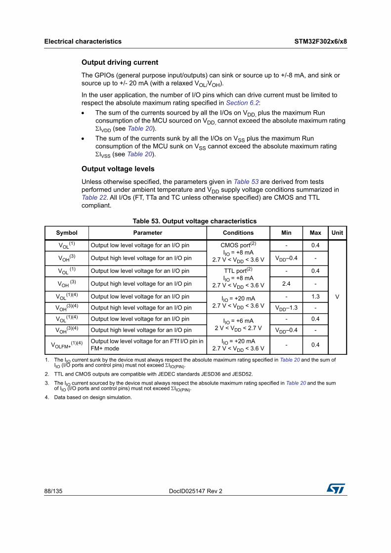
Electrical characteristics STM32F302x6/x8
88/135 DocID025147 Rev 2
Output driving current
The GPIOs (general purpose input/outputs) can sink or source up to +/-8 mA, and sink or source up to +/- 20 mA (with a relaxed VOL/VOH).
In the user application, the number of I/O pins which can drive current must be limited to respect the absolute maximum rating specified in Section 6.2: The sum of the currents sourced by all the I/Os on VDD, plus the maximum Run
consumption of the MCU sourced on VDD, cannot exceed the absolute maximum rating IVDD (see Table 20).
The sum of the currents sunk by all the I/Os on VSS plus the maximum Run consumption of the MCU sunk on VSS cannot exceed the absolute maximum rating IVSS (see Table 20).
Output voltage levels
Unless otherwise specified, the parameters given in Table 53 are derived from tests performed under ambient temperature and VDD supply voltage conditions summarized in Table 22. All I/Os (FT, TTa and TC unless otherwise specified) are CMOS and TTL compliant.
Table 53. Output voltage characteristics Symbol Parameter Conditions Min Max Unit
VOL(1) Output low level voltage for an I/O pin CMOS port(2)
IIO = +8 mA2.7 V < VDD < 3.6 V
- 0.4
V
VOH(3) Output high level voltage for an I/O pin VDD–0.4 -
VOL (1) Output low level voltage for an I/O pin TTL port(2)
IIO = +8 mA2.7 V < VDD < 3.6 V
- 0.4
VOH (3) Output high level voltage for an I/O pin 2.4 -
VOL(1)(4) Output low level voltage for an I/O pin IIO = +20 mA
2.7 V < VDD < 3.6 V- 1.3
VOH(3)(4) Output high level voltage for an I/O pin VDD–1.3 -
VOL(1)(4) Output low level voltage for an I/O pin IIO = +6 mA
2 V < VDD < 2.7 V- 0.4
VOH(3)(4) Output high level voltage for an I/O pin VDD–0.4 -
VOLFM+(1)(4) Output low level voltage for an FTf I/O pin in
FM+ modeIIO = +20 mA
2.7 V < VDD < 3.6 V - 0.4
1. The IIO current sunk by the device must always respect the absolute maximum rating specified in Table 20 and the sum of IIO (I/O ports and control pins) must not exceed IIO(PIN).
2. TTL and CMOS outputs are compatible with JEDEC standards JESD36 and JESD52.
3. The IIO current sourced by the device must always respect the absolute maximum rating specified in Table 20 and the sum of IIO (I/O ports and control pins) must not exceed IIO(PIN).
4. Data based on design simulation.
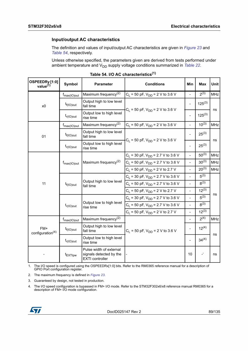
DocID025147 Rev 2 89/135
STM32F302x6/x8 Electrical characteristics
115
Input/output AC characteristics
The definition and values of input/output AC characteristics are given in Figure 23 and Table 54, respectively.
Unless otherwise specified, the parameters given are derived from tests performed under ambient temperature and VDD supply voltage conditions summarized in Table 22.
Table 54. I/O AC characteristics(1) OSPEEDRy [1:0]
value(1) Symbol Parameter Conditions Min Max Unit
x0
fmax(IO)out Maximum frequency(2) CL = 50 pF, VDD = 2 V to 3.6 V - 2(3) MHz
tf(IO)outOutput high to low level fall time
CL = 50 pF, VDD = 2 V to 3.6 V- 125(3)
nstr(IO)out
Output low to high level rise time - 125(3)
01
fmax(IO)out Maximum frequency(2) CL = 50 pF, VDD = 2 V to 3.6 V - 10(3) MHz
tf(IO)outOutput high to low level fall time
CL = 50 pF, VDD = 2 V to 3.6 V- 25(3)
nstr(IO)out
Output low to high level rise time - 25(3)
11
fmax(IO)out Maximum frequency(2)
CL = 30 pF, VDD = 2.7 V to 3.6 V - 50(3) MHz
CL = 50 pF, VDD = 2.7 V to 3.6 V - 30(3) MHz
CL = 50 pF, VDD = 2 V to 2.7 V - 20(3) MHz
tf(IO)outOutput high to low level fall time
CL = 30 pF, VDD = 2.7 V to 3.6 V - 5(3)
ns
CL = 50 pF, VDD = 2.7 V to 3.6 V - 8(3)
CL = 50 pF, VDD = 2 V to 2.7 V - 12(3)
tr(IO)outOutput low to high level rise time
CL = 30 pF, VDD = 2.7 V to 3.6 V - 5(3)
CL = 50 pF, VDD = 2.7 V to 3.6 V - 8(3)
CL = 50 pF, VDD = 2 V to 2.7 V - 12(3)
FM+ configuration(4)
fmax(IO)out Maximum frequency(2)
CL = 50 pF, VDD = 2 V to 3.6 V
- 2(4) MHz
tf(IO)outOutput high to low level fall time - 12(4)
nstr(IO)out
Output low to high level rise time - 34(4)
- tEXTIpw
Pulse width of external signals detected by the EXTI controller
- 10 -‘ ns
1. The I/O speed is configured using the OSPEEDRx[1:0] bits. Refer to the RM0365 reference manual for a description of GPIO Port configuration register.
2. The maximum frequency is defined in Figure 23.
3. Guaranteed by design, not tested in production.
4. The I/O speed configuration is bypassed in FM+ I/O mode. Refer to the STM32F302x6/x8 reference manual RM0365 for a description of FM+ I/O mode configuration.
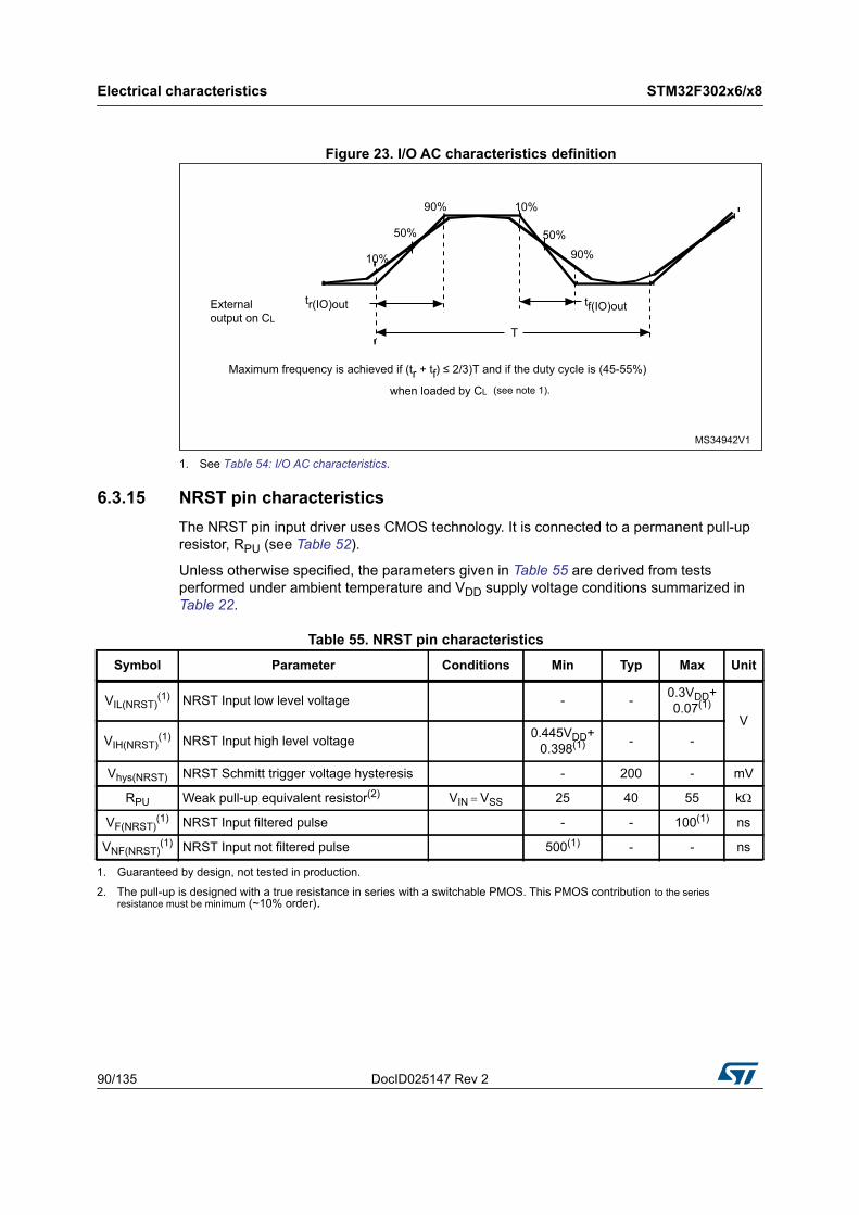
Electrical characteristics STM32F302x6/x8
90/135 DocID025147 Rev 2
Figure 23. I/O AC characteristics definition
1. See Table 54: I/O AC characteristics.
6.3.15 NRST pin characteristicsThe NRST pin input driver uses CMOS technology. It is connected to a permanent pull-up resistor, RPU (see Table 52).
Unless otherwise specified, the parameters given in Table 55 are derived from tests performed under ambient temperature and VDD supply voltage conditions summarized in Table 22.
Table 55. NRST pin characteristics Symbol Parameter Conditions Min Typ Max Unit
VIL(NRST)(1) NRST Input low level voltage - - 0.3VDD+
0.07(1)
VVIH(NRST)
(1) NRST Input high level voltage 0.445VDD+0.398(1) - -
Vhys(NRST) NRST Schmitt trigger voltage hysteresis - 200 - mV
RPU Weak pull-up equivalent resistor(2) VIN VSS 25 40 55 k
VF(NRST)(1) NRST Input filtered pulse - - 100(1) ns
VNF(NRST)(1) NRST Input not filtered pulse 500(1) - - ns
1. Guaranteed by design, not tested in production.
2. The pull-up is designed with a true resistance in series with a switchable PMOS. This PMOS contribution to the series resistance must be minimum (~10% order).
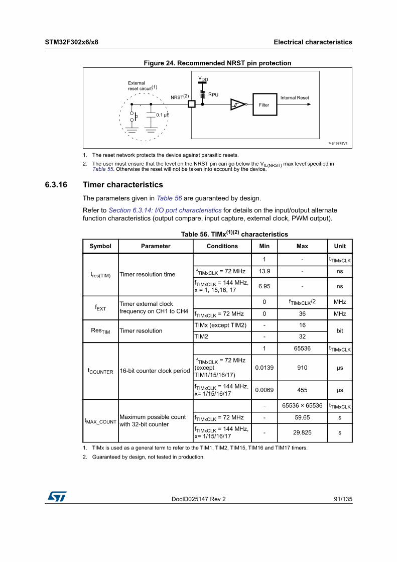
DocID025147 Rev 2 91/135
STM32F302x6/x8 Electrical characteristics
115
Figure 24. Recommended NRST pin protection
1. The reset network protects the device against parasitic resets.2. The user must ensure that the level on the NRST pin can go below the VIL(NRST) max level specified in
Table 55. Otherwise the reset will not be taken into account by the device.
6.3.16 Timer characteristicsThe parameters given in Table 56 are guaranteed by design.
Refer to Section 6.3.14: I/O port characteristics for details on the input/output alternate function characteristics (output compare, input capture, external clock, PWM output).
Table 56. TIMx(1)(2) characteristics
1. TIMx is used as a general term to refer to the TIM1, TIM2, TIM15, TIM16 and TIM17 timers.
2. Guaranteed by design, not tested in production.
Symbol Parameter Conditions Min Max Unit
tres(TIM) Timer resolution time
1 - tTIMxCLK
fTIMxCLK = 72 MHz 13.9 - ns
fTIMxCLK = 144 MHz, x = 1, 15,16, 17 6.95 - ns
fEXTTimer external clock frequency on CH1 to CH4
0 fTIMxCLK/2 MHz
fTIMxCLK = 72 MHz 0 36 MHz
ResTIM Timer resolutionTIMx (except TIM2) - 16
bitTIM2 - 32
tCOUNTER 16-bit counter clock period
1 65536 tTIMxCLK
fTIMxCLK = 72 MHz (except TIM1/15/16/17)
0.0139 910 μs
fTIMxCLK = 144 MHz, x= 1/15/16/17 0.0069 455 μs
tMAX_COUNTMaximum possible count with 32-bit counter
- 65536 × 65536 tTIMxCLK
fTIMxCLK = 72 MHz - 59.65 s
fTIMxCLK = 144 MHz, x= 1/15/16/17 - 29.825 s
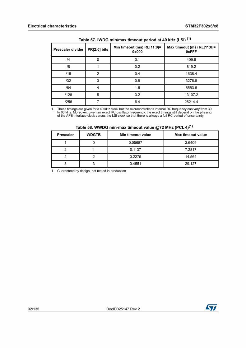
Electrical characteristics STM32F302x6/x8
92/135 DocID025147 Rev 2
Table 57. IWDG min/max timeout period at 40 kHz (LSI) (1)
1. These timings are given for a 40 kHz clock but the microcontroller’s internal RC frequency can vary from 30 to 60 kHz. Moreover, given an exact RC oscillator frequency, the exact timings still depend on the phasing of the APB interface clock versus the LSI clock so that there is always a full RC period of uncertainty.
Prescaler divider PR[2:0] bits Min timeout (ms) RL[11:0]= 0x000
Max timeout (ms) RL[11:0]= 0xFFF
/4 0 0.1 409.6
/8 1 0.2 819.2
/16 2 0.4 1638.4
/32 3 0.8 3276.8
/64 4 1.6 6553.6
/128 5 3.2 13107.2
/256 7 6.4 26214.4
Table 58. WWDG min-max timeout value @72 MHz (PCLK)(1)
1. Guaranteed by design, not tested in production.
Prescaler WDGTB Min timeout value Max timeout value
1 0 0.05687 3.6409
2 1 0.1137 7.2817
4 2 0.2275 14.564
8 3 0.4551 29.127
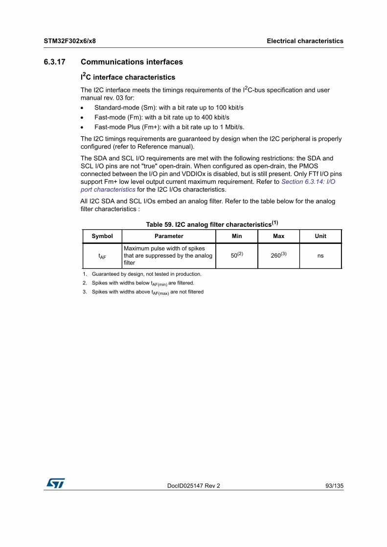
DocID025147 Rev 2 93/135
STM32F302x6/x8 Electrical characteristics
115
6.3.17 Communications interfaces
I2C interface characteristics
The I2C interface meets the timings requirements of the I2C-bus specification and user manual rev. 03 for: Standard-mode (Sm): with a bit rate up to 100 kbit/s Fast-mode (Fm): with a bit rate up to 400 kbit/s Fast-mode Plus (Fm+): with a bit rate up to 1 Mbit/s.
The I2C timings requirements are guaranteed by design when the I2C peripheral is properly configured (refer to Reference manual).
The SDA and SCL I/O requirements are met with the following restrictions: the SDA and SCL I/O pins are not "true" open-drain. When configured as open-drain, the PMOS connected between the I/O pin and VDDIOx is disabled, but is still present. Only FTf I/O pins support Fm+ low level output current maximum requirement. Refer to Section 6.3.14: I/O port characteristics for the I2C I/Os characteristics.
All I2C SDA and SCL I/Os embed an analog filter. Refer to the table below for the analog filter characteristics :
Table 59. I2C analog filter characteristics(1)
1. Guaranteed by design, not tested in production.
Symbol Parameter Min Max Unit
tAF
Maximum pulse width of spikes that are suppressed by the analog filter
50(2)
2. Spikes with widths below tAF(min) are filtered.
260(3)
3. Spikes with widths above tAF(max) are not filtered
ns
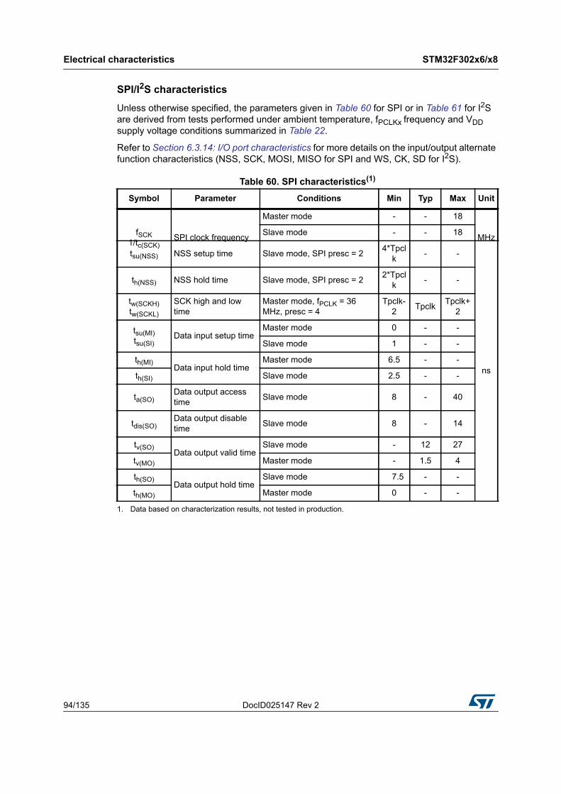
Electrical characteristics STM32F302x6/x8
94/135 DocID025147 Rev 2
SPI/I2S characteristics
Unless otherwise specified, the parameters given in Table 60 for SPI or in Table 61 for I2S are derived from tests performed under ambient temperature, fPCLKx frequency and VDD supply voltage conditions summarized in Table 22.
Refer to Section 6.3.14: I/O port characteristics for more details on the input/output alternate function characteristics (NSS, SCK, MOSI, MISO for SPI and WS, CK, SD for I2S).
Table 60. SPI characteristics(1)
1. Data based on characterization results, not tested in production.
Symbol Parameter Conditions Min Typ Max Unit
fSCK1/tc(SCK)
SPI clock frequency
Master mode - - 18
MHzSlave mode - - 18
tsu(NSS) NSS setup time Slave mode, SPI presc = 2 4*Tpclk - -
ns
th(NSS) NSS hold time Slave mode, SPI presc = 2 2*Tpclk - -
tw(SCKH)tw(SCKL)
SCK high and low time
Master mode, fPCLK = 36 MHz, presc = 4
Tpclk-2 Tpclk Tpclk+
2
tsu(MI) tsu(SI)
Data input setup timeMaster mode 0 - -
Slave mode 1 - -
th(MI) Data input hold time
Master mode 6.5 - -
th(SI) Slave mode 2.5 - -
ta(SO)Data output access time Slave mode 8 - 40
tdis(SO)Data output disable time Slave mode 8 - 14
tv(SO) Data output valid time
Slave mode - 12 27
tv(MO) Master mode - 1.5 4
th(SO)Data output hold time
Slave mode 7.5 - -
th(MO) Master mode 0 - -
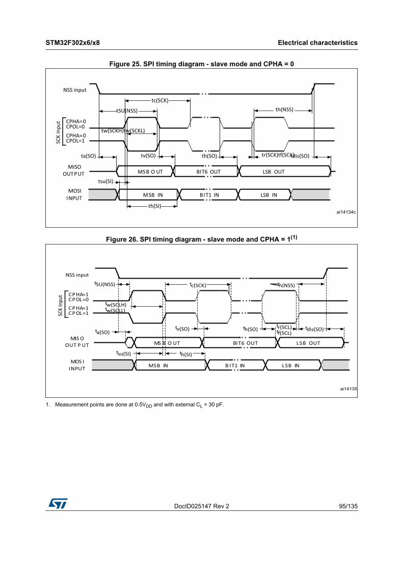
DocID025147 Rev 2 95/135
STM32F302x6/x8 Electrical characteristics
115
Figure 25. SPI timing diagram - slave mode and CPHA = 0
Figure 26. SPI timing diagram - slave mode and CPHA = 1(1)
1. Measurement points are done at 0.5VDD and with external CL = 30 pF.
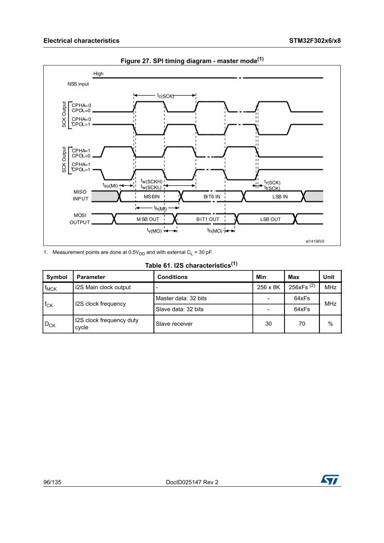
Electrical characteristics STM32F302x6/x8
96/135 DocID025147 Rev 2
Figure 27. SPI timing diagram - master mode(1)
1. Measurement points are done at 0.5VDD and with external CL = 30 pF.
Table 61. I2S characteristics(1)
Symbol Parameter Conditions Min Max Unit
fMCK I2S Main clock output - 256 x 8K 256xFs (2) MHz
fCK I2S clock frequency Master data: 32 bits - 64xFs
MHzSlave data: 32 bits - 64xFs
DCKI2S clock frequency duty cycle Slave receiver 30 70 %
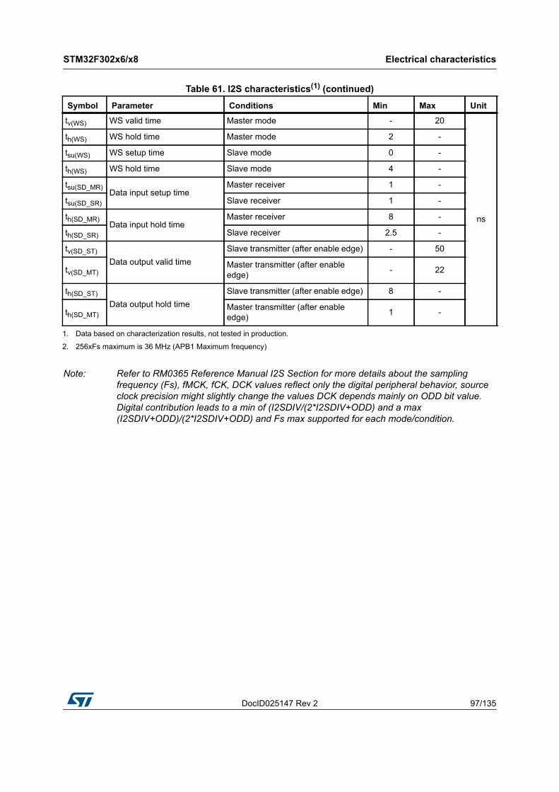
DocID025147 Rev 2 97/135
STM32F302x6/x8 Electrical characteristics
115
Note: Refer to RM0365 Reference Manual I2S Section for more details about the sampling frequency (Fs), fMCK, fCK, DCK values reflect only the digital peripheral behavior, source clock precision might slightly change the values DCK depends mainly on ODD bit value. Digital contribution leads to a min of (I2SDIV/(2*I2SDIV+ODD) and a max (I2SDIV+ODD)/(2*I2SDIV+ODD) and Fs max supported for each mode/condition.
tv(WS) WS valid time Master mode - 20
ns
th(WS) WS hold time Master mode 2 -
tsu(WS) WS setup time Slave mode 0 -
th(WS) WS hold time Slave mode 4 -
tsu(SD_MR)Data input setup time
Master receiver 1 -
tsu(SD_SR) Slave receiver 1 -
th(SD_MR)Data input hold time
Master receiver 8 -
th(SD_SR) Slave receiver 2.5 -
tv(SD_ST)Data output valid time
Slave transmitter (after enable edge) - 50
tv(SD_MT)Master transmitter (after enable edge) - 22
th(SD_ST)Data output hold time
Slave transmitter (after enable edge) 8 -
th(SD_MT)Master transmitter (after enable edge) 1 -
1. Data based on characterization results, not tested in production.
2. 256xFs maximum is 36 MHz (APB1 Maximum frequency)
Table 61. I2S characteristics(1) (continued)
Symbol Parameter Conditions Min Max Unit
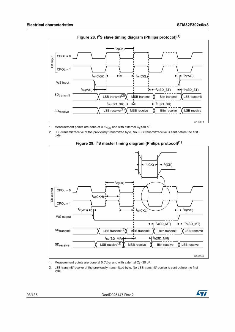
Electrical characteristics STM32F302x6/x8
98/135 DocID025147 Rev 2
Figure 28. I2S slave timing diagram (Philips protocol)(1)
1. Measurement points are done at 0.5VDD and with external CL=30 pF.2. LSB transmit/receive of the previously transmitted byte. No LSB transmit/receive is sent before the first
byte.
Figure 29. I2S master timing diagram (Philips protocol)(1)
1. Measurement points are done at 0.5VDD and with external CL=30 pF.2. LSB transmit/receive of the previously transmitted byte. No LSB transmit/receive is sent before the first
byte.
DocID025147 Rev 2 99/135
STM32F302x6/x8 Electrical characteristics
115
USB characteristics
Table 62. USB startup timeSymbol Parameter Max Unit
tSTARTUP(1)
1. Guaranteed by design, not tested in production.
USB transceiver startup time 1 μs
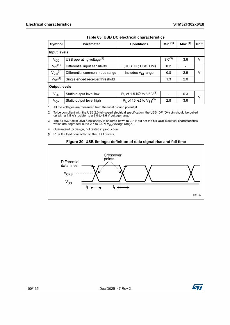
Electrical characteristics STM32F302x6/x8
100/135 DocID025147 Rev 2
Figure 30. USB timings: definition of data signal rise and fall time
Table 63. USB DC electrical characteristics Symbol Parameter Conditions Min.(1)
1. All the voltages are measured from the local ground potential.
Max.(1) Unit
Input levels
VDD USB operating voltage(2)
2. To be compliant with the USB 2.0 full-speed electrical specification, the USB_DP (D+) pin should be pulled up with a 1.5 k resistor to a 3.0-to-3.6 V voltage range.
3.0(3)
3. The STM32F3xxx USB functionality is ensured down to 2.7 V but not the full USB electrical characteristics which are degraded in the 2.7-to-3.0 V VDD voltage range.
3.6 V
VDI(4)
4. Guaranteed by design, not tested in production.
Differential input sensitivity I(USB_DP, USB_DM) 0.2 -
VVCM(4) Differential common mode range Includes VDI range 0.8 2.5
VSE(4) Single ended receiver threshold 1.3 2.0
Output levels
VOL Static output level low RL of 1.5 k to 3.6 V(5)
5. RL is the load connected on the USB drivers.
- 0.3V
VOH Static output level high RL of 15 k to VSS(5) 2.8 3.6
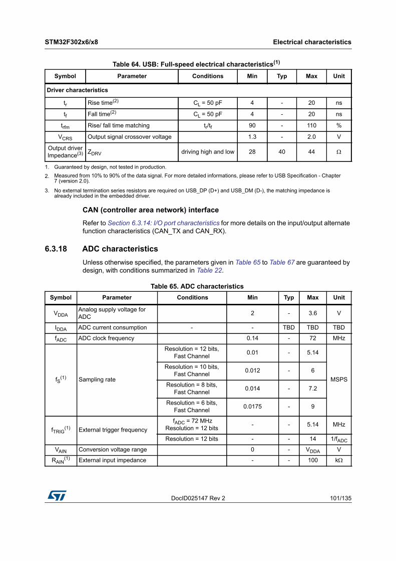
DocID025147 Rev 2 101/135
STM32F302x6/x8 Electrical characteristics
115
CAN (controller area network) interface
Refer to Section 6.3.14: I/O port characteristics for more details on the input/output alternate function characteristics (CAN_TX and CAN_RX).
6.3.18 ADC characteristicsUnless otherwise specified, the parameters given in Table 65 to Table 67 are guaranteed by design, with conditions summarized in Table 22.
Table 64. USB: Full-speed electrical characteristics(1) Symbol Parameter Conditions Min Typ Max Unit
Driver characteristics
tr Rise time(2) CL = 50 pF 4 - 20 ns
tf Fall time(2) CL = 50 pF 4 - 20 ns
trfm Rise/ fall time matching tr/tf 90 - 110 %
VCRS Output signal crossover voltage 1.3 - 2.0 V
Output driverImpedance(3) ZDRV driving high and low 28 40 44
1. Guaranteed by design, not tested in production.
2. Measured from 10% to 90% of the data signal. For more detailed informations, please refer to USB Specification - Chapter 7 (version 2.0).
3. No external termination series resistors are required on USB_DP (D+) and USB_DM (D-), the matching impedance is already included in the embedded driver.
Table 65. ADC characteristics Symbol Parameter Conditions Min Typ Max Unit
VDDAAnalog supply voltage for ADC 2 - 3.6 V
IDDA ADC current consumption - - TBD TBD TBD
fADC ADC clock frequency 0.14 - 72 MHz
fS(1) Sampling rate
Resolution = 12 bits, Fast Channel 0.01 - 5.14
MSPS
Resolution = 10 bits, Fast Channel 0.012 - 6
Resolution = 8 bits, Fast Channel 0.014 - 7.2
Resolution = 6 bits, Fast Channel 0.0175 - 9
fTRIG(1) External trigger frequency
fADC = 72 MHzResolution = 12 bits - - 5.14 MHz
Resolution = 12 bits - - 14 1/fADC
VAIN Conversion voltage range 0 - VDDA V
RAIN(1) External input impedance - - 100 k
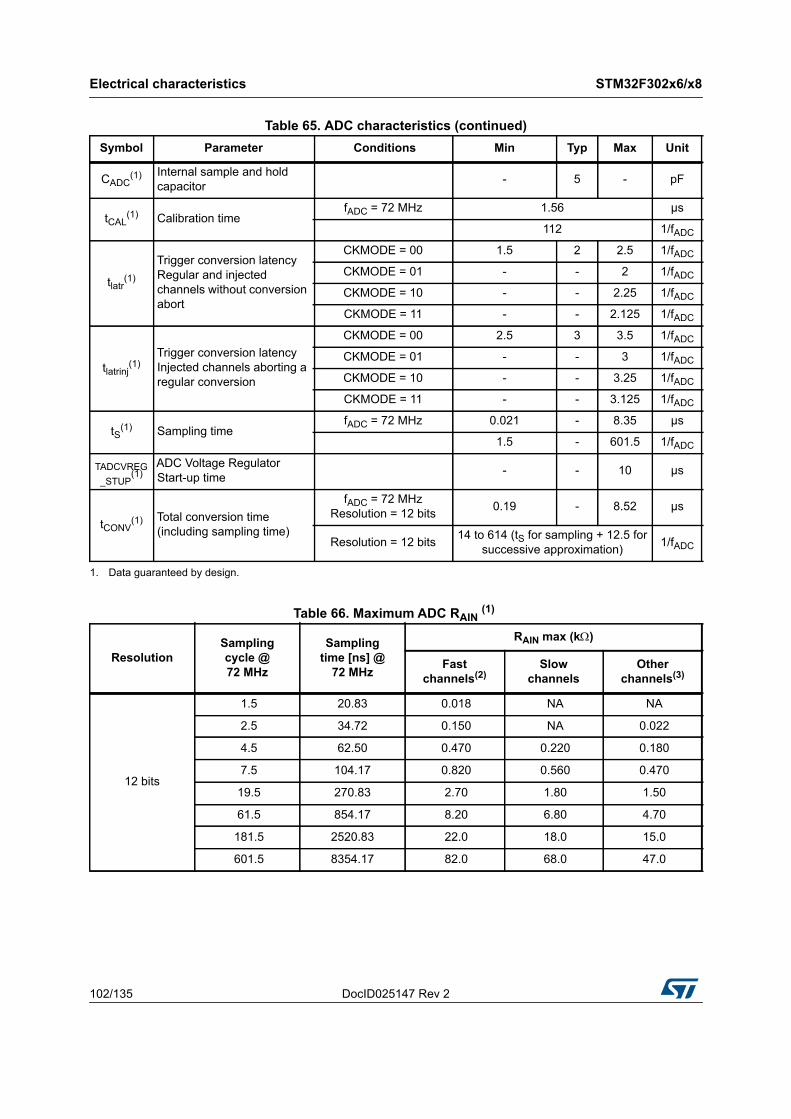
Electrical characteristics STM32F302x6/x8
102/135 DocID025147 Rev 2
CADC(1) Internal sample and hold
capacitor - 5 - pF
tCAL(1) Calibration time
fADC = 72 MHz 1.56 μs
112 1/fADC
tlatr(1)
Trigger conversion latency Regular and injected channels without conversion abort
CKMODE = 00 1.5 2 2.5 1/fADC
CKMODE = 01 - - 2 1/fADC
CKMODE = 10 - - 2.25 1/fADC
CKMODE = 11 - - 2.125 1/fADC
tlatrinj(1)
Trigger conversion latency Injected channels aborting a regular conversion
CKMODE = 00 2.5 3 3.5 1/fADC
CKMODE = 01 - - 3 1/fADC
CKMODE = 10 - - 3.25 1/fADC
CKMODE = 11 - - 3.125 1/fADC
tS(1) Sampling timefADC = 72 MHz 0.021 - 8.35 μs
1.5 - 601.5 1/fADC
TADCVREG_STUP
(1)ADC Voltage Regulator Start-up time - - 10 μs
tCONV(1) Total conversion time
(including sampling time)
fADC = 72 MHzResolution = 12 bits 0.19 - 8.52 μs
Resolution = 12 bits 14 to 614 (tS for sampling + 12.5 forsuccessive approximation) 1/fADC
1. Data guaranteed by design.
Table 65. ADC characteristics (continued)Symbol Parameter Conditions Min Typ Max Unit
Table 66. Maximum ADC RAIN (1)
ResolutionSamplingcycle @72 MHz
Samplingtime [ns] @
72 MHz
RAIN max (k)
Fast channels(2)
Slowchannels
Otherchannels(3)
12 bits
1.5 20.83 0.018 NA NA
2.5 34.72 0.150 NA 0.022
4.5 62.50 0.470 0.220 0.180
7.5 104.17 0.820 0.560 0.470
19.5 270.83 2.70 1.80 1.50
61.5 854.17 8.20 6.80 4.70
181.5 2520.83 22.0 18.0 15.0
601.5 8354.17 82.0 68.0 47.0
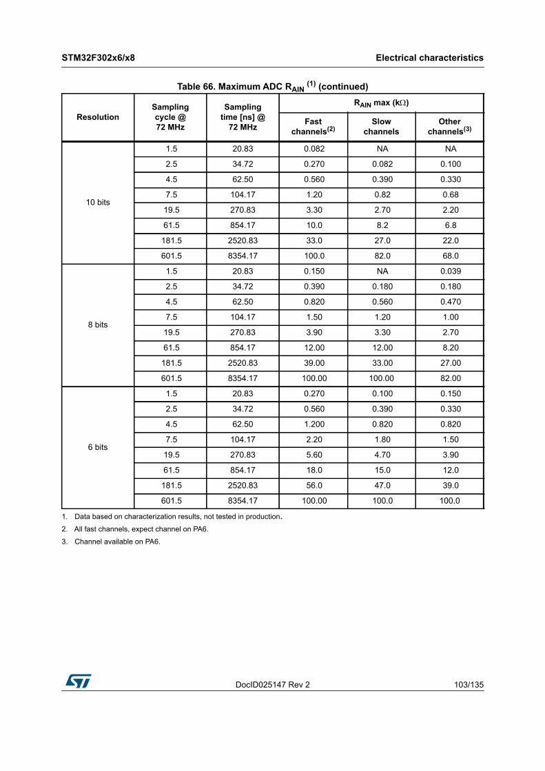
DocID025147 Rev 2 103/135
STM32F302x6/x8 Electrical characteristics
115
10 bits
1.5 20.83 0.082 NA NA
2.5 34.72 0.270 0.082 0.100
4.5 62.50 0.560 0.390 0.330
7.5 104.17 1.20 0.82 0.68
19.5 270.83 3.30 2.70 2.20
61.5 854.17 10.0 8.2 6.8
181.5 2520.83 33.0 27.0 22.0
601.5 8354.17 100.0 82.0 68.0
8 bits
1.5 20.83 0.150 NA 0.039
2.5 34.72 0.390 0.180 0.180
4.5 62.50 0.820 0.560 0.470
7.5 104.17 1.50 1.20 1.00
19.5 270.83 3.90 3.30 2.70
61.5 854.17 12.00 12.00 8.20
181.5 2520.83 39.00 33.00 27.00
601.5 8354.17 100.00 100.00 82.00
6 bits
1.5 20.83 0.270 0.100 0.150
2.5 34.72 0.560 0.390 0.330
4.5 62.50 1.200 0.820 0.820
7.5 104.17 2.20 1.80 1.50
19.5 270.83 5.60 4.70 3.90
61.5 854.17 18.0 15.0 12.0
181.5 2520.83 56.0 47.0 39.0
601.5 8354.17 100.00 100.0 100.0
1. Data based on characterization results, not tested in production.2. All fast channels, expect channel on PA6.
3. Channel available on PA6.
Table 66. Maximum ADC RAIN (1) (continued)
ResolutionSamplingcycle @72 MHz
Samplingtime [ns] @
72 MHz
RAIN max (k)
Fast channels(2)
Slowchannels
Otherchannels(3)
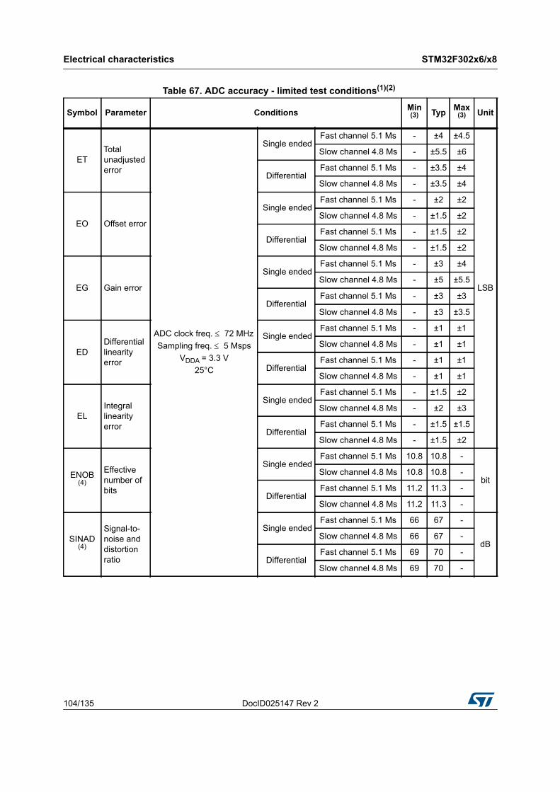
Electrical characteristics STM32F302x6/x8
104/135 DocID025147 Rev 2
Table 67. ADC accuracy - limited test conditions(1)(2)
Symbol Parameter Conditions Min(3) Typ Max
(3) Unit
ETTotal unadjusted error
ADC clock freq. 72 MHzSampling freq. 5 Msps
VDDA = 3.3 V25°C
Single endedFast channel 5.1 Ms - ±4 ±4.5
LSB
Slow channel 4.8 Ms - ±5.5 ±6
DifferentialFast channel 5.1 Ms - ±3.5 ±4
Slow channel 4.8 Ms - ±3.5 ±4
EO Offset error
Single endedFast channel 5.1 Ms - ±2 ±2
Slow channel 4.8 Ms - ±1.5 ±2
DifferentialFast channel 5.1 Ms - ±1.5 ±2
Slow channel 4.8 Ms - ±1.5 ±2
EG Gain error
Single endedFast channel 5.1 Ms - ±3 ±4
Slow channel 4.8 Ms - ±5 ±5.5
DifferentialFast channel 5.1 Ms - ±3 ±3
Slow channel 4.8 Ms - ±3 ±3.5
EDDifferential linearity error
Single endedFast channel 5.1 Ms - ±1 ±1
Slow channel 4.8 Ms - ±1 ±1
DifferentialFast channel 5.1 Ms - ±1 ±1
Slow channel 4.8 Ms - ±1 ±1
ELIntegral linearity error
Single endedFast channel 5.1 Ms - ±1.5 ±2
Slow channel 4.8 Ms - ±2 ±3
DifferentialFast channel 5.1 Ms - ±1.5 ±1.5
Slow channel 4.8 Ms - ±1.5 ±2
ENOB(4)
Effective number of bits
Single endedFast channel 5.1 Ms 10.8 10.8 -
bitSlow channel 4.8 Ms 10.8 10.8 -
DifferentialFast channel 5.1 Ms 11.2 11.3 -
Slow channel 4.8 Ms 11.2 11.3 -
SINAD(4)
Signal-to-noise and distortion ratio
Single endedFast channel 5.1 Ms 66 67 -
dBSlow channel 4.8 Ms 66 67 -
DifferentialFast channel 5.1 Ms 69 70 -
Slow channel 4.8 Ms 69 70 -
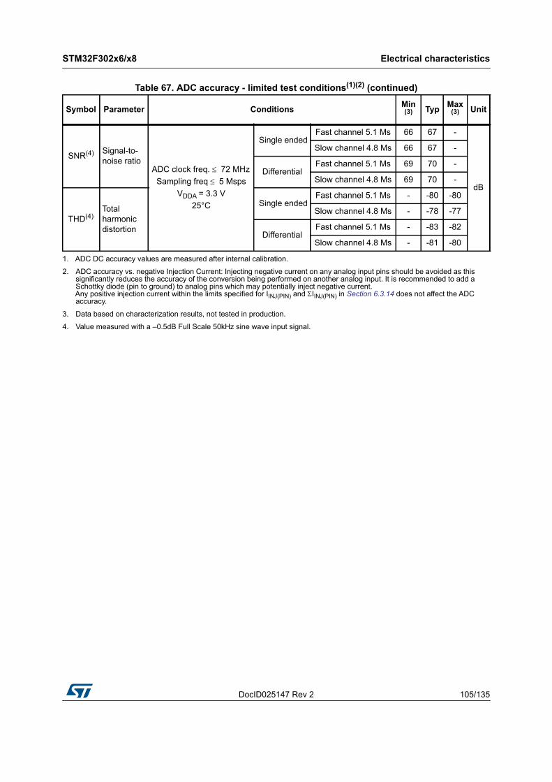
DocID025147 Rev 2 105/135
STM32F302x6/x8 Electrical characteristics
115
SNR(4) Signal-to-noise ratio
ADC clock freq. 72 MHzSampling freq 5 Msps
VDDA = 3.3 V25°C
Single endedFast channel 5.1 Ms 66 67 -
dB
Slow channel 4.8 Ms 66 67 -
DifferentialFast channel 5.1 Ms 69 70 -
Slow channel 4.8 Ms 69 70 -
THD(4)Total harmonic distortion
Single endedFast channel 5.1 Ms - -80 -80
Slow channel 4.8 Ms - -78 -77
DifferentialFast channel 5.1 Ms - -83 -82
Slow channel 4.8 Ms - -81 -80
1. ADC DC accuracy values are measured after internal calibration.
2. ADC accuracy vs. negative Injection Current: Injecting negative current on any analog input pins should be avoided as this significantly reduces the accuracy of the conversion being performed on another analog input. It is recommended to add a Schottky diode (pin to ground) to analog pins which may potentially inject negative current. Any positive injection current within the limits specified for IINJ(PIN) and IINJ(PIN) in Section 6.3.14 does not affect the ADC accuracy.
3. Data based on characterization results, not tested in production.
4. Value measured with a –0.5dB Full Scale 50kHz sine wave input signal.
Table 67. ADC accuracy - limited test conditions(1)(2) (continued)
Symbol Parameter Conditions Min(3) Typ Max
(3) Unit

Electrical characteristics STM32F302x6/x8
106/135 DocID025147 Rev 2
l
Table 68. ADC accuracy (1)(2)(3)
Symbol Parameter Conditions Min(4) Max(4) Unit
ETTotal unadjusted error
ADC clock freq. 72 MHz,Sampling freq. 5 Msps
2.0 V VDDA 3.6 V
Single endedFast channel 5.1 Ms - ±6.5
LSB
Slow channel 4.8 Ms - ±6.5
DifferentialFast channel 5.1 Ms - ±4
Slow channel 4.8 Ms - ±4.5
EO Offset error
Single endedFast channel 5.1 Ms - ±3
Slow channel 4.8 Ms - ±3
DifferentialFast channel 5.1 Ms - ±2.5
Slow channel 4.8 Ms - ±2.5
EG Gain error
Single endedFast channel 5.1 Ms - ±6
Slow channel 4.8 Ms - ±6
DifferentialFast channel 5.1 Ms - ±3.5
Slow channel 4.8 Ms - ±4
EDDifferential linearity error
Single endedFast channel 5.1 Ms - ±1.5
Slow channel 4.8 Ms - ±1.5
DifferentialFast channel 5.1 Ms - ±1.5
Slow channel 4.8 Ms - ±1.5
ELIntegral linearity error
Single endedFast channel 5.1 Ms - ±3
Slow channel 4.8 Ms - ±3.5
DifferentialFast channel 5.1 Ms - ±2
Slow channel 4.8 Ms - ±2.5
ENOB(5)
Effective number of bits
Single endedFast channel 5.1 Ms 10.4 -
bitsSlow channel 4.8 Ms 10.4 -
DifferentialFast channel 5.1 Ms 10.8 -
Slow channel 4.8 Ms 10.8 -
SINAD(5)
Signal-to-noise and distortion ratio
Single endedFast channel 5.1 Ms 64 -
dBSlow channel 4.8 Ms 63 -
DifferentialFast channel 5.1 Ms 67 -
Slow channel 4.8 Ms 67 -
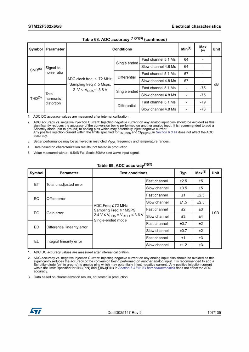
DocID025147 Rev 2 107/135
STM32F302x6/x8 Electrical characteristics
115
SNR(5) Signal-to-noise ratio
ADC clock freq. 72 MHz,Sampling freq 5 Msps,
2 V VDDA 3.6 V
Single endedFast channel 5.1 Ms 64 -
dB
Slow channel 4.8 Ms 64 -
DifferentialFast channel 5.1 Ms 67 -
Slow channel 4.8 Ms 67 -
THD(5)Total harmonic distortion
Single endedFast channel 5.1 Ms - -75
Slow channel 4.8 Ms - -75
DifferentialFast channel 5.1 Ms - -79
Slow channel 4.8 Ms - -78
1. ADC DC accuracy values are measured after internal calibration.
2. ADC accuracy vs. negative Injection Current: Injecting negative current on any analog input pins should be avoided as this significantly reduces the accuracy of the conversion being performed on another analog input. It is recommended to add a Schottky diode (pin to ground) to analog pins which may potentially inject negative current. Any positive injection current within the limits specified for IINJ(PIN) and IINJ(PIN) in Section 6.3.14 does not affect the ADC accuracy.
3. Better performance may be achieved in restricted VDDA, frequency and temperature ranges.
4. Data based on characterization results, not tested in production.
5. Value measured with a –0.5dB Full Scale 50kHz sine wave input signall.
Table 68. ADC accuracy (1)(2)(3) (continued)
Symbol Parameter Conditions Min(4) Max(4) Unit
Table 69. ADC accuracy(1)(2)
Symbol Parameter Test conditions Typ Max(3) Unit
ET Total unadjusted error
ADC Freq ≤ 72 MHz Sampling Freq ≤ 1MSPS 2.4 V ≤ VDDA = VREF+ ≤ 3.6 VSingle-ended mode
Fast channel ±2.5 ±5
LSB
Slow channel ±3.5 ±5
EO Offset errorFast channel ±1 ±2.5
Slow channel ±1.5 ±2.5
EG Gain errorFast channel ±2 ±3
Slow channel ±3 ±4
ED Differential linearity errorFast channel ±0.7 ±2
Slow channel ±0.7 ±2
EL Integral linearity errorFast channel ±1 ±3
Slow channel ±1.2 ±3
1. ADC DC accuracy values are measured after internal calibration.
2. ADC accuracy vs. negative Injection Current: Injecting negative current on any analog input pins should be avoided as this significantly reduces the accuracy of the conversion being performed on another analog input. It is recommended to add a Schottky diode (pin to ground) to analog pins which may potentially inject negative current.. Any positive injection current within the limits specified for IINJ(PIN) and ∑IINJ(PIN) in Section 6.3.14: I/O port characteristics does not affect the ADC accuracy.
3. Data based on characterization results, not tested in production.
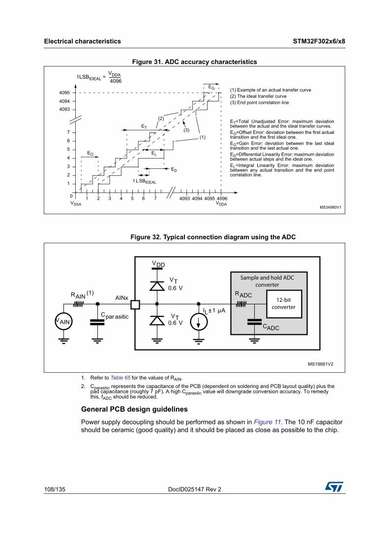
Electrical characteristics STM32F302x6/x8
108/135 DocID025147 Rev 2
Figure 31. ADC accuracy characteristics
Figure 32. Typical connection diagram using the ADC
1. Refer to Table 65 for the values of RAIN.2. Cparasitic represents the capacitance of the PCB (dependent on soldering and PCB layout quality) plus the
pad capacitance (roughly 7 pF). A high Cparasitic value will downgrade conversion accuracy. To remedy this, fADC should be reduced.
General PCB design guidelines
Power supply decoupling should be performed as shown in Figure 11. The 10 nF capacitor should be ceramic (good quality) and it should be placed as close as possible to the chip.
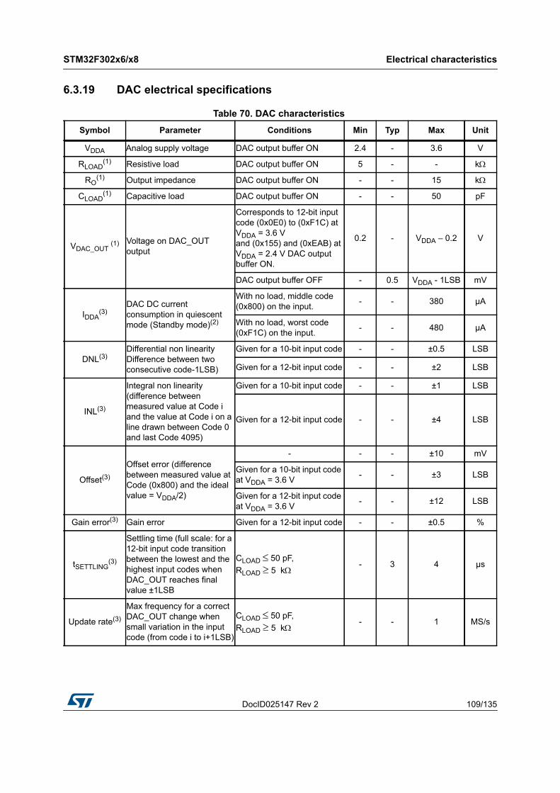
DocID025147 Rev 2 109/135
STM32F302x6/x8 Electrical characteristics
115
6.3.19 DAC electrical specifications
Table 70. DAC characteristics Symbol Parameter Conditions Min Typ Max Unit
VDDA Analog supply voltage DAC output buffer ON 2.4 - 3.6 V
RLOAD(1) Resistive load DAC output buffer ON 5 - - k
RO(1) Output impedance DAC output buffer ON - - 15 k
CLOAD(1) Capacitive load DAC output buffer ON - - 50 pF
VDAC_OUT (1) Voltage on DAC_OUT output
Corresponds to 12-bit input code (0x0E0) to (0xF1C) at VDDA = 3.6 V and (0x155) and (0xEAB) at VDDA = 2.4 V DAC output buffer ON.
0.2 - VDDA – 0.2 V
DAC output buffer OFF - 0.5 VDDA - 1LSB mV
IDDA(3)
DAC DC current consumption in quiescent mode (Standby mode)(2)
With no load, middle code (0x800) on the input. - - 380 μA
With no load, worst code (0xF1C) on the input. - - 480 μA
DNL(3)Differential non linearity Difference between two consecutive code-1LSB)
Given for a 10-bit input code - - ±0.5 LSB
Given for a 12-bit input code - - ±2 LSB
INL(3)
Integral non linearity (difference between measured value at Code i and the value at Code i on a line drawn between Code 0 and last Code 4095)
Given for a 10-bit input code - - ±1 LSB
Given for a 12-bit input code - - ±4 LSB
Offset(3)
Offset error (difference between measured value at Code (0x800) and the ideal value = VDDA/2)
- - - ±10 mV
Given for a 10-bit input code at VDDA = 3.6 V - - ±3 LSB
Given for a 12-bit input code at VDDA = 3.6 V - - ±12 LSB
Gain error(3) Gain error Given for a 12-bit input code - - ±0.5 %
tSETTLING(3)
Settling time (full scale: for a 12-bit input code transition between the lowest and the highest input codes when DAC_OUT reaches final value ±1LSB
CLOAD 50 pF, RLOAD 5 k
- 3 4 μs
Update rate(3)
Max frequency for a correct DAC_OUT change when small variation in the input code (from code i to i+1LSB)
CLOAD 50 pF, RLOAD 5 k
- - 1 MS/s
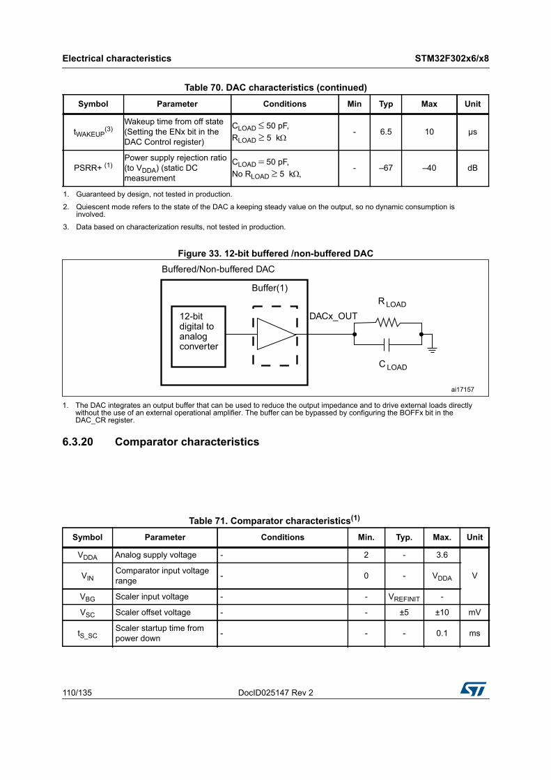
Electrical characteristics STM32F302x6/x8
110/135 DocID025147 Rev 2
Figure 33. 12-bit buffered /non-buffered DAC
1. The DAC integrates an output buffer that can be used to reduce the output impedance and to drive external loads directly without the use of an external operational amplifier. The buffer can be bypassed by configuring the BOFFx bit in the DAC_CR register.
6.3.20 Comparator characteristics
tWAKEUP(3)
Wakeup time from off state (Setting the ENx bit in the DAC Control register)
CLOAD 50 pF, RLOAD 5 k
- 6.5 10 μs
PSRR+ (1)Power supply rejection ratio (to VDDA) (static DC measurement
CLOAD 50 pF, No RLOAD 5 k
- –67 –40 dB
1. Guaranteed by design, not tested in production.
2. Quiescent mode refers to the state of the DAC a keeping steady value on the output, so no dynamic consumption is involved.
3. Data based on characterization results, not tested in production.
Table 70. DAC characteristics (continued)Symbol Parameter Conditions Min Typ Max Unit
Table 71. Comparator characteristics(1) Symbol Parameter Conditions Min. Typ. Max. Unit
VDDA Analog supply voltage - 2 - 3.6
VVINComparator input voltage range - 0 - VDDA
VBG Scaler input voltage - - VREFINIT -
VSC Scaler offset voltage - - ±5 ±10 mV
tS_SCScaler startup time from power down - - - 0.1 ms
DocID025147 Rev 2 111/135
STM32F302x6/x8 Electrical characteristics
115
tSTART Comparator startup time VDDA 2.7 V - - 4
μsVDDA 2.7 V - - 10
tD
Propagation delay for 200 mV step with 100 mV overdrive
VDDA 2.7 V - 25 28
nsVDDA 2.7 V - 28 30
Propagation delay for full range step with 100 mV overdrive
VDDA 2.7 V - 32 35
VDDA 2.7 V - 35 40
VOFFSET Comparator offset errorVDDA 2.7 V - 5 10
mVVDDA 2.7 V - - 25
TVOFFSET Total offset variation Full temperature range - - 3 mV
IDD(COMP)COMP current consumption - - 400 600 μA
1. Guaranteed by design, not tested in production.
Table 71. Comparator characteristics(1) (continued)Symbol Parameter Conditions Min. Typ. Max. Unit
Electrical characteristics STM32F302x6/x8
112/135 DocID025147 Rev 2
6.3.21 Operational amplifier characteristics
Table 72. Operational amplifier characteristics(1) Symbol Parameter Condition Min Typ Max Unit
VDDA Analog supply voltage - 2.4 - 3.6 V
CMIR Common mode input range - 0 - VDDA V
VIOFFSET Input offset voltage
Maximum calibration range
25°C, No Load on output. - - 4
mV
All voltage/Temp. - - 6
After offset calibration
25°C, No Load on output. - - 1.6
All voltage/Temp. - - 3
VIOFFSET Input offset voltage drift - - 5 - μV/°C
ILOAD Drive current - - - 500 μA
IDDOPAMP Consumption No load, quiescent mode - 690 1450 μA
CMRR Common mode rejection ratio - - 90 - dB
PSRR Power supply rejection ratio DC 73 117 - dB
GBW Bandwidth - - 8.2 - MHz
SR Slew rate - - 4.7 - V/μs
RLOAD Resistive load - 4 - - k
CLOAD Capacitive load - - - 50 pF
VOHSAT High saturation voltage
Rload = min, Input at VDDA. - - 100
mV
Rload = 20K, Input at VDDA. - - 20
VOLSAT Low saturation voltage
Rload = min, input at 0V - - 100
Rload = 20K, input at 0V. - - 20
m Phase margin - - 62 - °
tOFFTRIM
Offset trim time: during calibration, minimum time needed between two steps to have 1 mV accuracy
- - - 2 ms
tWAKEUP Wake up time from OFF state.
CLOAD 50 pf, RLOAD 4 kFollower configuration
- 2.8 5 μs
tS_OPAM_VOUT ADC sampling time when reading the OPAMP output 400 - - ns
DocID025147 Rev 2 113/135
STM32F302x6/x8 Electrical characteristics
115
PGA gain Non inverting gain value -
- 2 -
- 4 -
- 8 -
- 16 -
RnetworkR2/R1 internal resistance values in PGA mode (2)
Gain=2 - 5.4/5.4 -
kGain=4 - 16.2/5.4 -
Gain=8 - 37.8/5.4 -
Gain=16 - 40.5/2.7 -
PGA gain error PGA gain error - -1% - 1%
Ibias OPAMP input bias current - - - 0.2(3) μA
PGA BW PGA bandwidth for different non inverting gain
PGA Gain = 2, Cload = 50pF, Rload = 4 K
- 4 -
MHz
PGA Gain = 4, Cload = 50pF, Rload = 4 K
- 2 -
PGA Gain = 8, Cload = 50pF, Rload = 4 K
- 1 -
PGA Gain = 16, Cload = 50pF, Rload = 4 K
- 0.5 -
en Voltage noise density
@ 1KHz, Output loaded with 4 K
- 109 -
@ 10KHz, Output loaded with 4 K
- 43 -
1. Guaranteed by design, not tested in production.
2. R2 is the internal resistance between OPAMP output and OPAMP inverting input. R1 is the internal resistance between OPAMP inverting input and ground. The PGA gain =1+R2/R1
3. Mostly TTa I/O leakage, when used in analog mode.
Table 72. Operational amplifier characteristics(1) (continued)Symbol Parameter Condition Min Typ Max Unit
nVHz
-----------
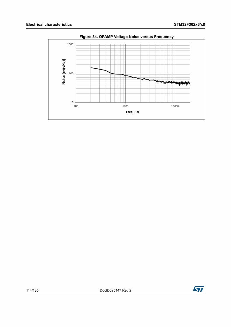
Electrical characteristics STM32F302x6/x8
114/135 DocID025147 Rev 2
Figure 34. OPAMP Voltage Noise versus Frequency
DocID025147 Rev 2 115/135
STM32F302x6/x8 Electrical characteristics
115
6.3.22 Temperature sensor characteristics
6.3.23 VBAT monitoring characteristics
Table 73. TS characteristicsSymbol Parameter Min Typ Max Unit
TL(1)
1. Guaranteed by design, not tested in production.
VSENSE linearity with temperature - 1 2 °C
Avg_Slope(1) Average slope 4.0 4.3 4.6 mV/°C
V25 Voltage at 25 °C 1.34 1.43 1.52 V
tSTART(1) Startup time 4 - 10 μs
TS_temp(1)(2)
2. Shortest sampling time can be determined in the application by multiple iterations.
ADC sampling time when reading the temperature 2.2 - - μs
Table 74. Temperature sensor calibration valuesCalibration value name Description Memory address
TS_CAL1TS ADC raw data acquired at temperature of 30 °C, VDDA= 3.3 V
0x1FFF F7B8 - 0x1FFF F7B9
TS_CAL2TS ADC raw data acquired at temperature of 110 °C VDDA= 3.3 V
0x1FFF F7C2 - 0x1FFF F7C3
Table 75. VBAT monitoring characteristicsSymbol Parameter Min Typ Max Unit
R Resistor bridge for VBAT - 50 - K
Q Ratio on VBAT measurement - 2 -
Er(1)
1. Guaranteed by design, not tested in production.
Error on Q -1 - +1 %
TS_vbat(1)(2)
2. Shortest sampling time can be determined in the application by multiple iterations.
ADC sampling time when reading the VBAT1mV accuracy
2.2 - - μs
Package characteristics STM32F302x6/x8
116/135 DocID025147 Rev 2
7 Package characteristics
7.1 Package mechanical dataIn order to meet environmental requirements, ST offers these devices in different grades of ECOPACK® packages, depending on their level of environmental compliance. ECOPACK® specifications, grade definitions and product status are available at: www.st.com. ECOPACK® is an ST trademark.
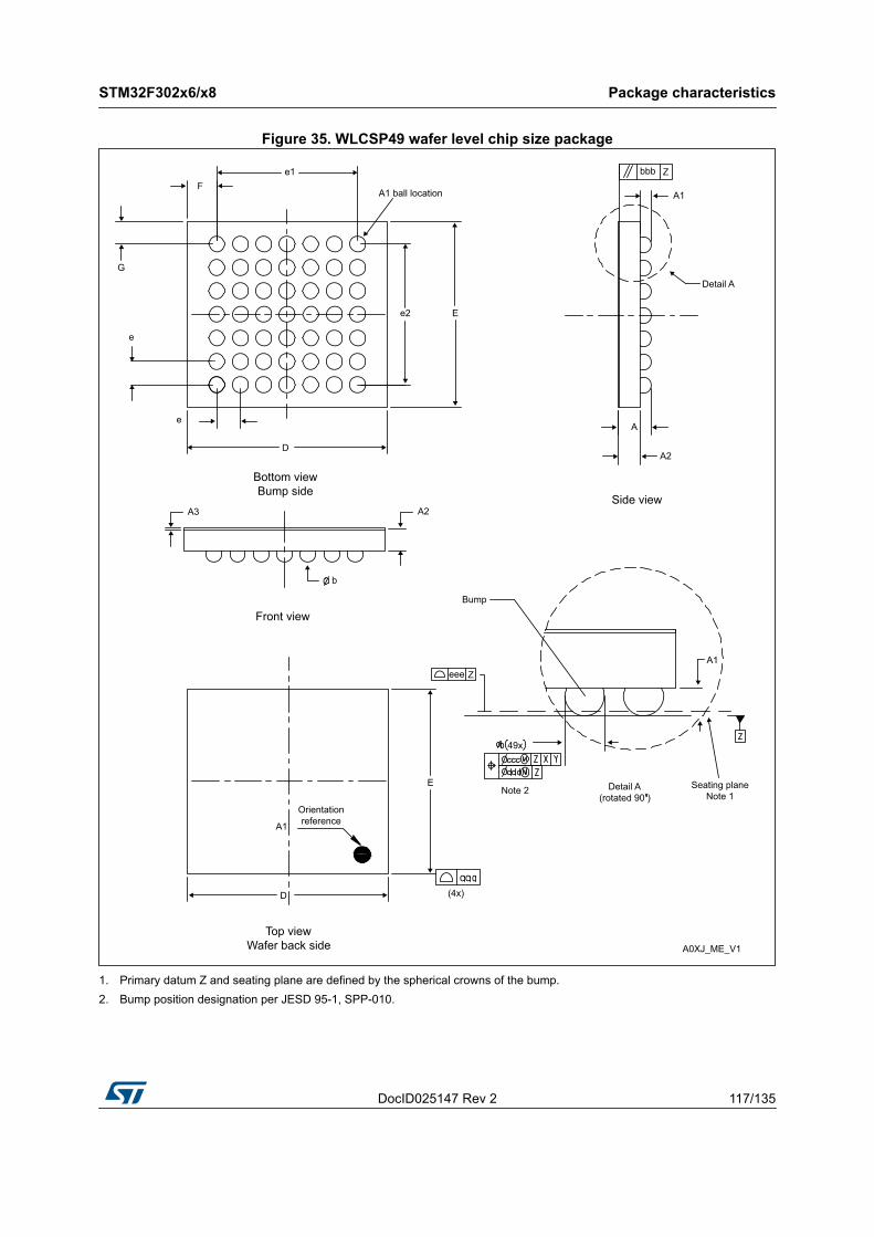
DocID025147 Rev 2 117/135
STM32F302x6/x8 Package characteristics
132
Figure 35. WLCSP49 wafer level chip size package
1. Primary datum Z and seating plane are defined by the spherical crowns of the bump.2. Bump position designation per JESD 95-1, SPP-010.
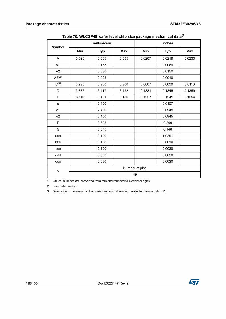
Package characteristics STM32F302x6/x8
118/135 DocID025147 Rev 2
Table 76. WLCSP49 wafer level chip size package mechanical data(1)
1. Values in inches are converted from mm and rounded to 4 decimal digits.
Symbolmillimeters inches
Min Typ Max Min Typ Max
A 0.525 0.555 0.585 0.0207 0.0219 0.0230
A1 0.175 0.0069
A2 0.380 0.0150
A3(2)
2. Back side coating
0.025 0.0010
b(3)
3. Dimension is measured at the maximum bump diameter parallel to primary datum Z.
0.220 0.250 0.280 0.0087 0.0098 0.0110
D 3.382 3.417 3.452 0.1331 0.1345 0.1359
E 3.116 3.151 3.186 0.1227 0.1241 0.1254
e 0.400 0.0157
e1 2.400 0.0945
e2 2.400 0.0945
F 0.508 0.200
G 0.375 0.148
aaa 0.100 1.9291
bbb 0.100 0.0039
ccc 0.100 0.0039
ddd 0.050 0.0020
eee 0.050 0.0020
NNumber of pins
49
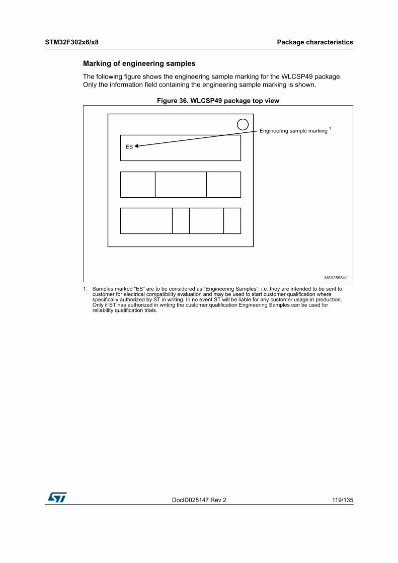
DocID025147 Rev 2 119/135
STM32F302x6/x8 Package characteristics
132
Marking of engineering samples
The following figure shows the engineering sample marking for the WLCSP49 package. Only the information field containing the engineering sample marking is shown.
Figure 36. WLCSP49 package top view
1. Samples marked “ES” are to be considered as “Engineering Samples”: i.e. they are intended to be sent to customer for electrical compatibility evaluation and may be used to start customer qualification where specifically authorized by ST in writing. In no event ST will be liable for any customer usage in production. Only if ST has authorized in writing the customer qualification Engineering Samples can be used for reliability qualification trials.
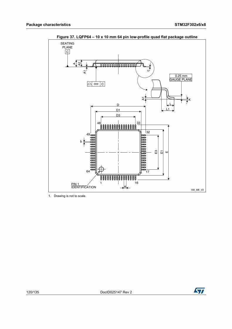
Package characteristics STM32F302x6/x8
120/135 DocID025147 Rev 2
Figure 37. LQFP64 – 10 x 10 mm 64 pin low-profile quad flat package outline
1. Drawing is not to scale.
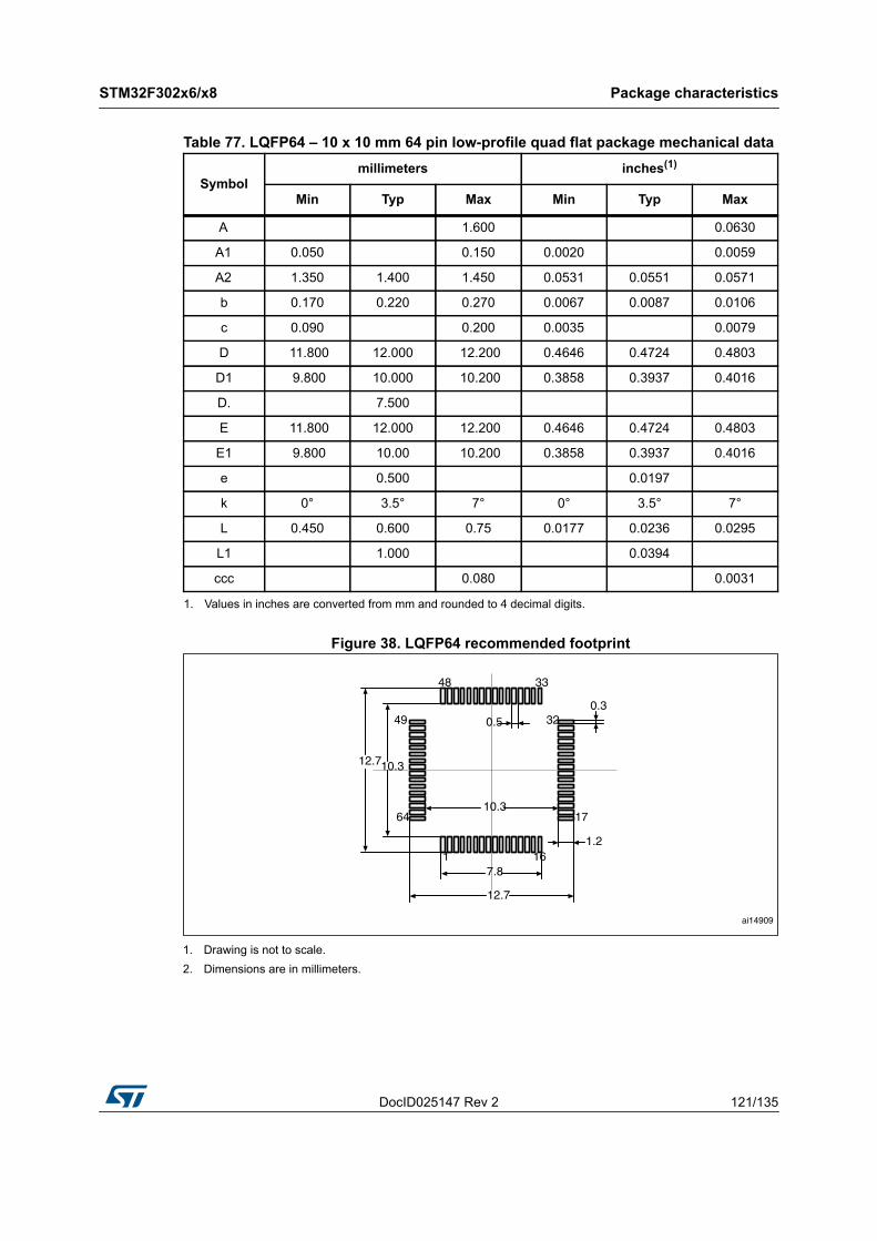
DocID025147 Rev 2 121/135
STM32F302x6/x8 Package characteristics
132
Figure 38. LQFP64 recommended footprint
1. Drawing is not to scale.2. Dimensions are in millimeters.
Table 77. LQFP64 – 10 x 10 mm 64 pin low-profile quad flat package mechanical data
Symbolmillimeters inches(1)
1. Values in inches are converted from mm and rounded to 4 decimal digits.
Min Typ Max Min Typ Max
A 1.600 0.0630
A1 0.050 0.150 0.0020 0.0059
A2 1.350 1.400 1.450 0.0531 0.0551 0.0571
b 0.170 0.220 0.270 0.0067 0.0087 0.0106
c 0.090 0.200 0.0035 0.0079
D 11.800 12.000 12.200 0.4646 0.4724 0.4803
D1 9.800 10.000 10.200 0.3858 0.3937 0.4016
D. 7.500
E 11.800 12.000 12.200 0.4646 0.4724 0.4803
E1 9.800 10.00 10.200 0.3858 0.3937 0.4016
e 0.500 0.0197
k 0° 3.5° 7° 0° 3.5° 7°
L 0.450 0.600 0.75 0.0177 0.0236 0.0295
L1 1.000 0.0394
ccc 0.080 0.0031
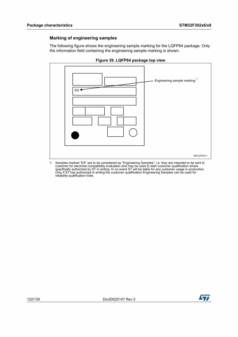
Package characteristics STM32F302x6/x8
122/135 DocID025147 Rev 2
Marking of engineering samples
The following figure shows the engineering sample marking for the LQFP64 package. Only the information field containing the engineering sample marking is shown.
Figure 39. LQFP64 package top view
1. Samples marked “ES” are to be considered as “Engineering Samples”: i.e. they are intended to be sent to customer for electrical compatibility evaluation and may be used to start customer qualification where specifically authorized by ST in writing. In no event ST will be liable for any customer usage in production. Only if ST has authorized in writing the customer qualification Engineering Samples can be used for reliability qualification trials.
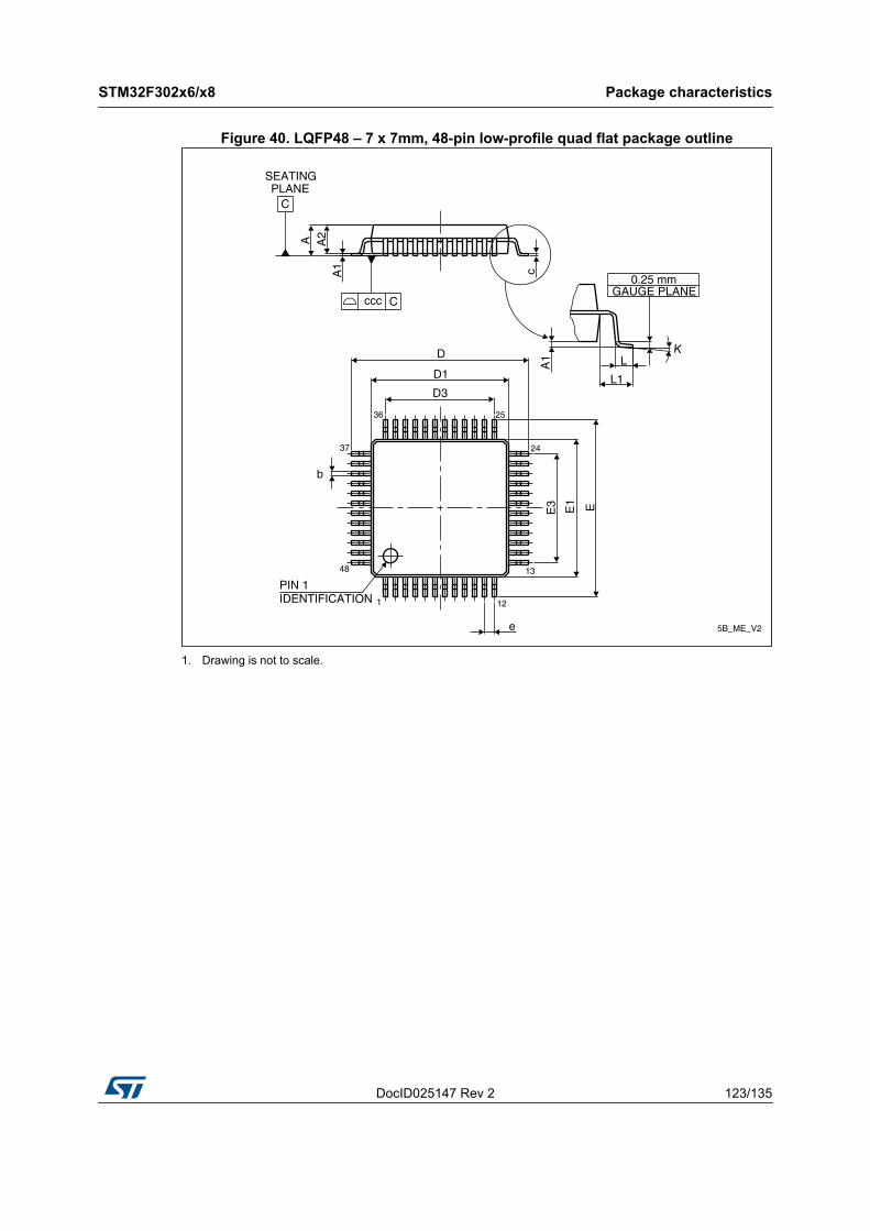
DocID025147 Rev 2 123/135
STM32F302x6/x8 Package characteristics
132
Figure 40. LQFP48 – 7 x 7mm, 48-pin low-profile quad flat package outline
1. Drawing is not to scale.
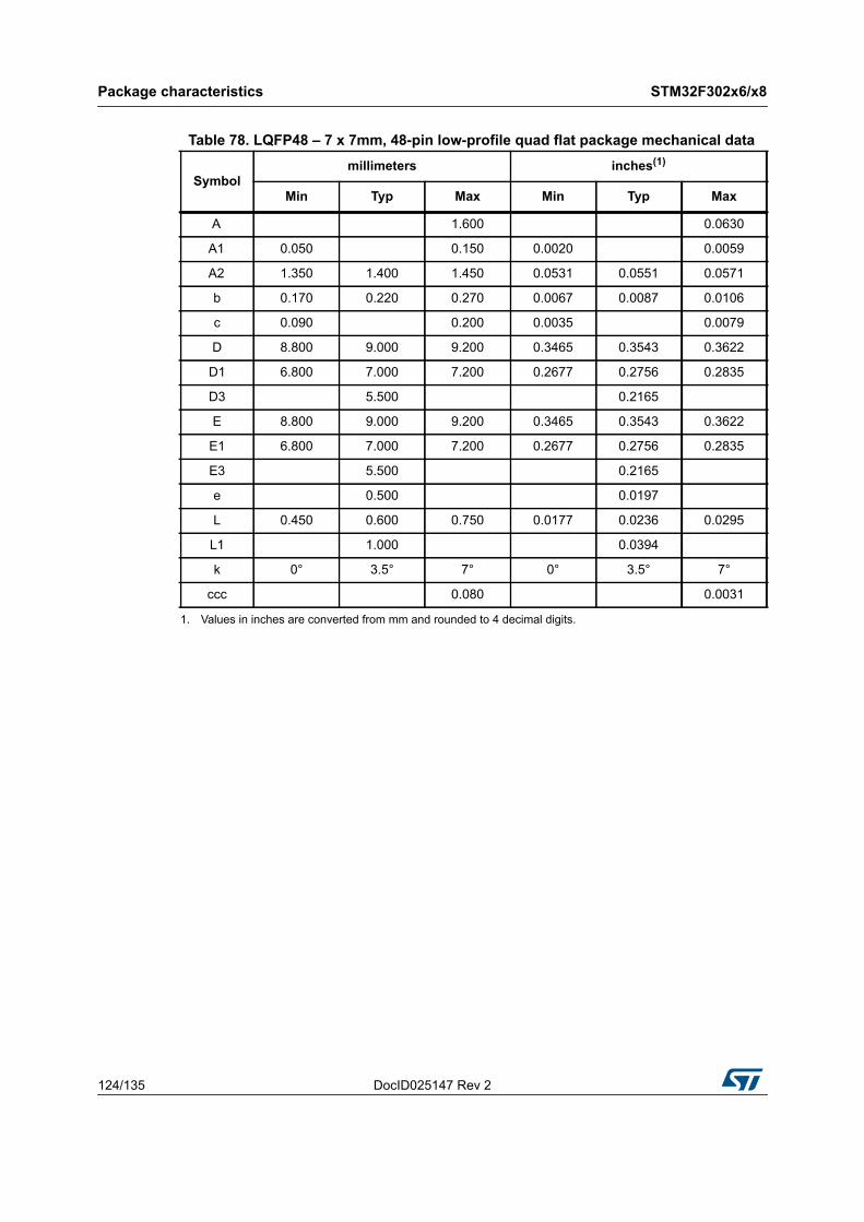
Package characteristics STM32F302x6/x8
124/135 DocID025147 Rev 2
Table 78. LQFP48 – 7 x 7mm, 48-pin low-profile quad flat package mechanical data
Symbolmillimeters inches(1)
1. Values in inches are converted from mm and rounded to 4 decimal digits.
Min Typ Max Min Typ Max
A 1.600 0.0630
A1 0.050 0.150 0.0020 0.0059
A2 1.350 1.400 1.450 0.0531 0.0551 0.0571
b 0.170 0.220 0.270 0.0067 0.0087 0.0106
c 0.090 0.200 0.0035 0.0079
D 8.800 9.000 9.200 0.3465 0.3543 0.3622
D1 6.800 7.000 7.200 0.2677 0.2756 0.2835
D3 5.500 0.2165
E 8.800 9.000 9.200 0.3465 0.3543 0.3622
E1 6.800 7.000 7.200 0.2677 0.2756 0.2835
E3 5.500 0.2165
e 0.500 0.0197
L 0.450 0.600 0.750 0.0177 0.0236 0.0295
L1 1.000 0.0394
k 0° 3.5° 7° 0° 3.5° 7°
ccc 0.080 0.0031
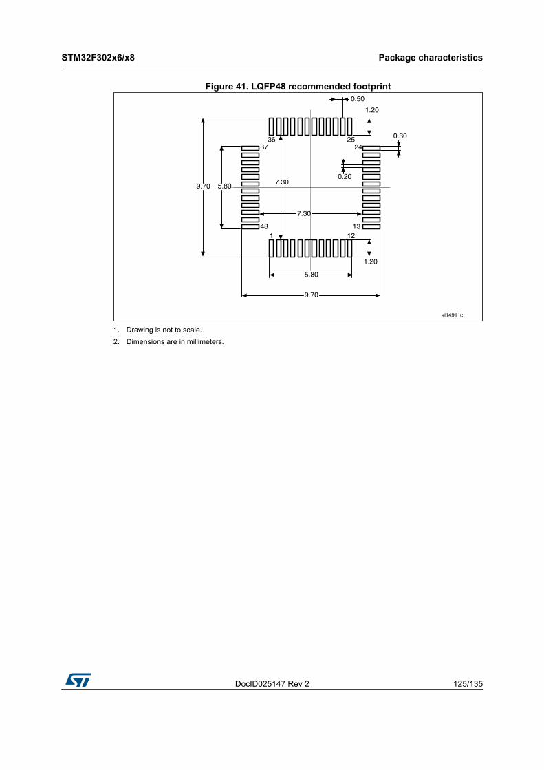
DocID025147 Rev 2 125/135
STM32F302x6/x8 Package characteristics
132
Figure 41. LQFP48 recommended footprint
1. Drawing is not to scale.2. Dimensions are in millimeters.
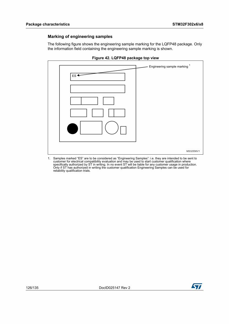
Package characteristics STM32F302x6/x8
126/135 DocID025147 Rev 2
Marking of engineering samples
The following figure shows the engineering sample marking for the LQFP48 package. Only the information field containing the engineering sample marking is shown.
Figure 42. LQFP48 package top view
1. Samples marked “ES” are to be considered as “Engineering Samples”: i.e. they are intended to be sent to customer for electrical compatibility evaluation and may be used to start customer qualification where specifically authorized by ST in writing. In no event ST will be liable for any customer usage in production. Only if ST has authorized in writing the customer qualification Engineering Samples can be used for reliability qualification trials.
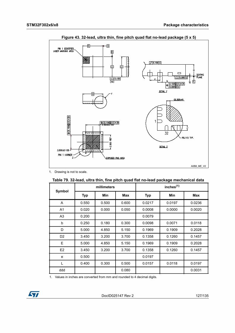
DocID025147 Rev 2 127/135
STM32F302x6/x8 Package characteristics
132
Figure 43. 32-lead, ultra thin, fine pitch quad flat no-lead package (5 x 5)
1. Drawing is not to scale.
Table 79. 32-lead, ultra thin, fine pitch quad flat no-lead package mechanical data
Symbolmillimeters inches(1)
1. Values in inches are converted from mm and rounded to 4 decimal digits.
Typ Min Max Typ Min Max
A 0.550 0.500 0.600 0.0217 0.0197 0.0236
A1 0.020 0.000 0.050 0.0008 0.0000 0.0020
A3 0.200 0.0079
b 0.250 0.180 0.300 0.0098 0.0071 0.0118
D 5.000 4.850 5.150 0.1969 0.1909 0.2028
D2 3.450 3.200 3.700 0.1358 0.1260 0.1457
E 5.000 4.850 5.150 0.1969 0.1909 0.2028
E2 3.450 3.200 3.700 0.1358 0.1260 0.1457
e 0.500 0.0197
L 0.400 0.300 0.500 0.0157 0.0118 0.0197
ddd 0.080 0.0031

Package characteristics STM32F302x6/x8
128/135 DocID025147 Rev 2
Figure 44. UFQFPN32 recommended footprint
1. Drawing is not to scale.2. Dimensions are in millimeters.
A0B8_FP_V2
5.30
3.80
0.60
3.45
0.503.45
3.80
0.75
3.80
0.30
5.30
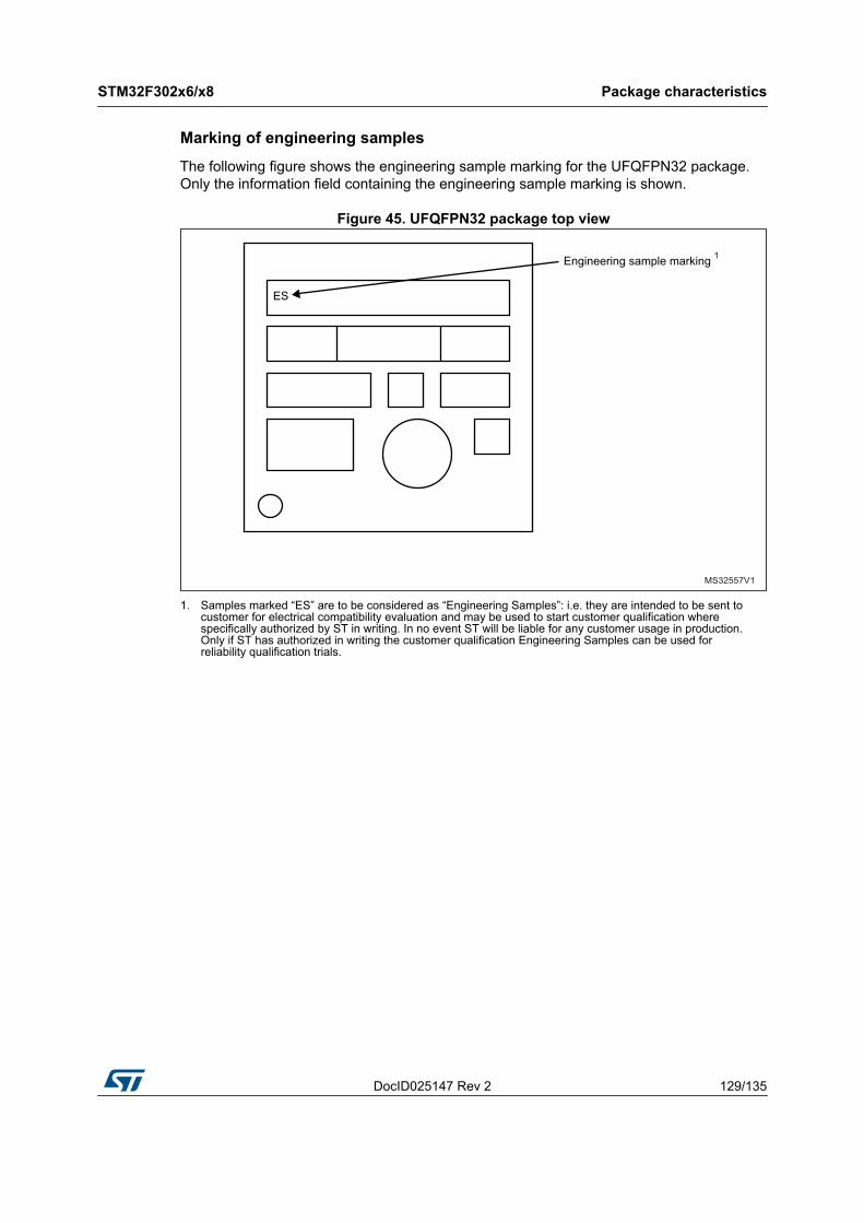
DocID025147 Rev 2 129/135
STM32F302x6/x8 Package characteristics
132
Marking of engineering samples
The following figure shows the engineering sample marking for the UFQFPN32 package. Only the information field containing the engineering sample marking is shown.
Figure 45. UFQFPN32 package top view
1. Samples marked “ES” are to be considered as “Engineering Samples”: i.e. they are intended to be sent to customer for electrical compatibility evaluation and may be used to start customer qualification where specifically authorized by ST in writing. In no event ST will be liable for any customer usage in production. Only if ST has authorized in writing the customer qualification Engineering Samples can be used for reliability qualification trials.
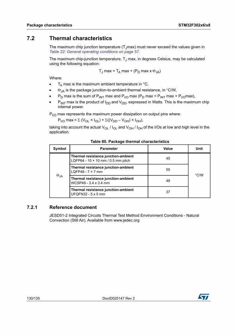
Package characteristics STM32F302x6/x8
130/135 DocID025147 Rev 2
7.2 Thermal characteristicsThe maximum chip junction temperature (TJmax) must never exceed the values given in Table 22: General operating conditions on page 57.
The maximum chip-junction temperature, TJ max, in degrees Celsius, may be calculated using the following equation:
TJ max = TA max + (PD max x JA)
Where: TA max is the maximum ambient temperature in °C, JA is the package junction-to-ambient thermal resistance, in C/W, PD max is the sum of PINT max and PI/O max (PD max = PINT max + PI/Omax), PINT max is the product of IDD and VDD, expressed in Watts. This is the maximum chip
internal power.
PI/O max represents the maximum power dissipation on output pins where:PI/O max = (VOL × IOL) + ((VDD – VOH) × IOH),
taking into account the actual VOL / IOL and VOH / IOH of the I/Os at low and high level in the application.
7.2.1 Reference documentJESD51-2 Integrated Circuits Thermal Test Method Environment Conditions - Natural Convection (Still Air). Available from www.jedec.org
Table 80. Package thermal characteristicsSymbol Parameter Value Unit
JA
Thermal resistance junction-ambient LQFP64 - 10 × 10 mm / 0.5 mm pitch 45
°C/W
Thermal resistance junction-ambient LQFP48 - 7 × 7 mm 55
Thermal resistance junction-ambient WCSP49 - 3.4 x 3.4 mm 49
Thermal resistance junction-ambient UFQFN32 - 5 x 5 mm 37
DocID025147 Rev 2 131/135
STM32F302x6/x8 Package characteristics
132
7.2.2 Selecting the product temperature rangeWhen ordering the microcontroller, the temperature range is specified in the ordering information scheme shown in Section 8: Part numbering.
Each temperature range suffix corresponds to a specific guaranteed ambient temperature at maximum dissipation and, to a specific maximum junction temperature.
As applications do not commonly use the STM32F302x6/x8 at maximum dissipation, it is useful to calculate the exact power consumption and junction temperature to determine which temperature range will be best suited to the application.
The following examples show how to calculate the temperature range needed for a given application.
Example 1: High-performance application
Assuming the following application conditions:Maximum ambient temperature TAmax = 82 °C (measured according to JESD51-2), IDDmax = 50 mA, VDD = 3.5 V, maximum 3 I/Os used at the same time in output at low level with IOL = 8 mA, VOL= 0.4 V and maximum 2 I/Os used at the same time in output at low level with IOL = 20 mA, VOL= 1.3 VPINTmax = 50 mA × 3.5 V= 175 mWPIOmax = 3 × 8 mA × 0.4 V + 2 × 20 mA × 1.3 V = 61.6 mWThis gives: PINTmax = 175 mW and PIOmax = 61.6 mW:PDmax = 175 + 61.6 = 236.6 mW
Thus: PDmax = 236.6 mW
Using the values obtained in Table 80 TJmax is calculated as follows:– For LQFP64, 45°C/W TJmax = 82 °C + (45°C/W × 236.6 mW) = 82°C + 10.65 °C = 92.65°C
This is within the range of the suffix 6 version parts (–40 < TJ < 105 °C).
In this case, parts must be ordered at least with the temperature range suffix 6 (see Section 8: Part numbering).
Package characteristics STM32F302x6/x8
132/135 DocID025147 Rev 2
Example 2: High-temperature application
Using the same rules, it is possible to address applications that run at high ambient temperatures with a low dissipation, as long as junction temperature TJ remains within the specified range.
Assuming the following application conditions:Maximum ambient temperature TAmax = 115 °C (measured according to JESD51-2), IDDmax = 20 mA, VDD = 3.5 V, maximum 9 I/Os used at the same time in output at low level with IOL = 8 mA, VOL= 0.4 VPINTmax = 20 mA × 3.5 V= 70 mWPIOmax = 9 × 8 mA × 0.4 V = 28.8 mWThis gives: PINTmax = 70 mW and PIOmax = 28.8 mW:PDmax = 70 + 28.8 = 98.8 mW
Thus: PDmax = 98.8 mW
Using the values obtained in Table 80 TJmax is calculated as follows:– For LQFP100, 45°C/W TJmax = 115°C + (45°C/W × 98.8 mW) = 115 °C + 4.44°C = 119.44°C
This is within the range of the suffix 7 version parts (–40 < TJ < 125 °C).
In this case, parts must be ordered at least with the temperature range suffix 7 (see Section 8: Part numbering).
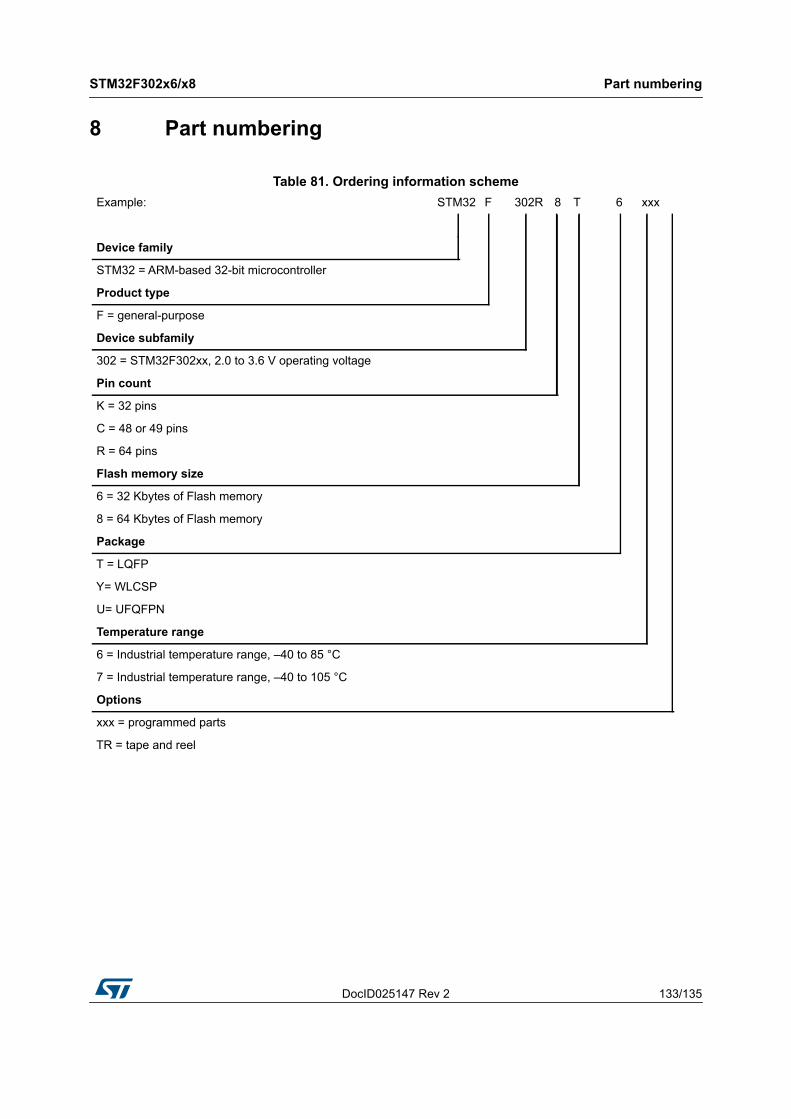
DocID025147 Rev 2 133/135
STM32F302x6/x8 Part numbering
133
8 Part numbering
Table 81. Ordering information schemeExample: STM32 F 302R 8 T 6 xxx
Device family
STM32 = ARM-based 32-bit microcontroller
Product type
F = general-purpose
Device subfamily
302 = STM32F302xx, 2.0 to 3.6 V operating voltage
Pin count
K = 32 pins
C = 48 or 49 pins
R = 64 pins
Flash memory size
6 = 32 Kbytes of Flash memory
8 = 64 Kbytes of Flash memory
Package
T = LQFP
Y= WLCSP
U= UFQFPN
Temperature range
6 = Industrial temperature range, –40 to 85 °C
7 = Industrial temperature range, –40 to 105 °C
Options
xxx = programmed parts
TR = tape and reel
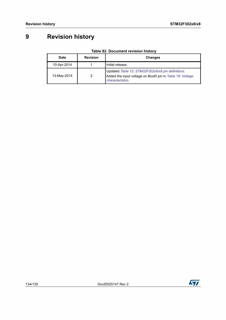
Revision history STM32F302x6/x8
134/135 DocID025147 Rev 2
9 Revision history
Table 82. Document revision history
Date Revision Changes
10-Apr-2014 1 Initial release.
13-May-2014 2Updated Table 12: STM32F302x6/x8 pin definitions.Added the input voltage on Boot0 pin in Table 19: Voltage characteristics.
DocID025147 Rev 2 135/135
STM32F302x6/x8
135
Please Read Carefully:
Information in this document is provided solely in connection with ST products. STMicroelectronics NV and its subsidiaries (“ST”) reserve the right to make changes, corrections, modifications or improvements, to this document, and the products and services described herein at any time, without notice.
All ST products are sold pursuant to ST’s terms and conditions of sale.
Purchasers are solely responsible for the choice, selection and use of the ST products and services described herein, and ST assumes no liability whatsoever relating to the choice, selection or use of the ST products and services described herein.
No license, express or implied, by estoppel or otherwise, to any intellectual property rights is granted under this document. If any part of this document refers to any third party products or services it shall not be deemed a license grant by ST for the use of such third party products or services, or any intellectual property contained therein or considered as a warranty covering the use in any manner whatsoever of such third party products or services or any intellectual property contained therein.
UNLESS OTHERWISE SET FORTH IN ST’S TERMS AND CONDITIONS OF SALE ST DISCLAIMS ANY EXPRESS OR IMPLIED WARRANTY WITH RESPECT TO THE USE AND/OR SALE OF ST PRODUCTS INCLUDING WITHOUT LIMITATION IMPLIED WARRANTIES OF MERCHANTABILITY, FITNESS FOR A PARTICULAR PURPOSE (AND THEIR EQUIVALENTS UNDER THE LAWS OF ANY JURISDICTION), OR INFRINGEMENT OF ANY PATENT, COPYRIGHT OR OTHER INTELLECTUAL PROPERTY RIGHT.
ST PRODUCTS ARE NOT DESIGNED OR AUTHORIZED FOR USE IN: (A) SAFETY CRITICAL APPLICATIONS SUCH AS LIFE SUPPORTING, ACTIVE IMPLANTED DEVICES OR SYSTEMS WITH PRODUCT FUNCTIONAL SAFETY REQUIREMENTS; (B) AERONAUTIC APPLICATIONS; (C) AUTOMOTIVE APPLICATIONS OR ENVIRONMENTS, AND/OR (D) AEROSPACE APPLICATIONS OR ENVIRONMENTS. WHERE ST PRODUCTS ARE NOT DESIGNED FOR SUCH USE, THE PURCHASER SHALL USE PRODUCTS AT PURCHASER’S SOLE RISK, EVEN IF ST HAS BEEN INFORMED IN WRITING OF SUCH USAGE, UNLESS A PRODUCT IS EXPRESSLY DESIGNATED BY ST AS BEING INTENDED FOR “AUTOMOTIVE, AUTOMOTIVE SAFETY OR MEDICAL” INDUSTRY DOMAINS ACCORDING TO ST PRODUCT DESIGN SPECIFICATIONS. PRODUCTS FORMALLY ESCC, QML OR JAN QUALIFIED ARE DEEMED SUITABLE FOR USE IN AEROSPACE BY THE CORRESPONDING GOVERNMENTAL AGENCY.
Resale of ST products with provisions different from the statements and/or technical features set forth in this document shall immediately void any warranty granted by ST for the ST product or service described herein and shall not create or extend in any manner whatsoever, any liability of ST.
ST and the ST logo are trademarks or registered trademarks of ST in various countries.Information in this document supersedes and replaces all information previously supplied.
The ST logo is a registered trademark of STMicroelectronics. All other names are the property of their respective owners.
© 2014 STMicroelectronics - All rights reserved
STMicroelectronics group of companies
Australia - Belgium - Brazil - Canada - China - Czech Republic - Finland - France - Germany - Hong Kong - India - Israel - Italy - Japan - Malaysia - Malta - Morocco - Philippines - Singapore - Spain - Sweden - Switzerland - United Kingdom - United States of America
www.st.com