Embed Size (px)
Citation preview
This is information on a product in full production.
November 2015 DocID027107 Rev 5 1/201
STM32F446xC/E
ARM® Cortex®-M4 32b MCU+FPU, 225DMIPS, up to 512kB Flash/128+4KB RAM, USB OTG HS/FS, 17 TIMs, 3 ADCs, 20 comm. interfaces
Datasheet - production data
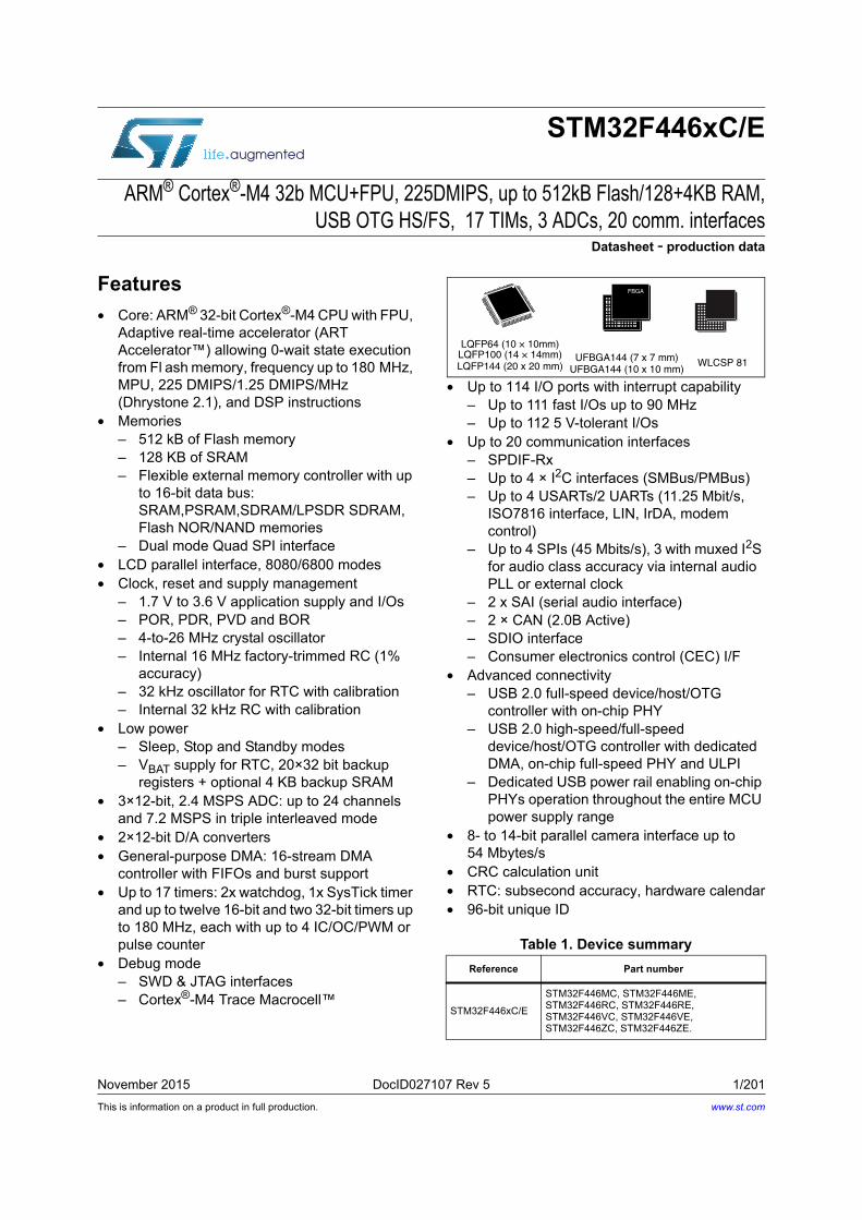
Features
• Core: ARM® 32-bit Cortex®-M4 CPU with FPU, Adaptive real-time accelerator (ART Accelerator™) allowing 0-wait state execution from Fl ash memory, frequency up to 180 MHz, MPU, 225 DMIPS/1.25 DMIPS/MHz (Dhrystone 2.1), and DSP instructions
• Memories– 512 kB of Flash memory– 128 KB of SRAM– Flexible external memory controller with up
to 16-bit data bus: SRAM,PSRAM,SDRAM/LPSDR SDRAM, Flash NOR/NAND memories
– Dual mode Quad SPI interface• LCD parallel interface, 8080/6800 modes• Clock, reset and supply management
– 1.7 V to 3.6 V application supply and I/Os– POR, PDR, PVD and BOR– 4-to-26 MHz crystal oscillator– Internal 16 MHz factory-trimmed RC (1%
accuracy)– 32 kHz oscillator for RTC with calibration– Internal 32 kHz RC with calibration
• Low power– Sleep, Stop and Standby modes– VBAT supply for RTC, 20×32 bit backup
registers + optional 4 KB backup SRAM• 3×12-bit, 2.4 MSPS ADC: up to 24 channels
and 7.2 MSPS in triple interleaved mode• 2×12-bit D/A converters• General-purpose DMA: 16-stream DMA
controller with FIFOs and burst support• Up to 17 timers: 2x watchdog, 1x SysTick timer
and up to twelve 16-bit and two 32-bit timers up to 180 MHz, each with up to 4 IC/OC/PWM or pulse counter
• Debug mode– SWD & JTAG interfaces– Cortex®-M4 Trace Macrocell™
• Up to 114 I/O ports with interrupt capability– Up to 111 fast I/Os up to 90 MHz– Up to 112 5 V-tolerant I/Os
• Up to 20 communication interfaces– SPDIF-Rx– Up to 4 × I2C interfaces (SMBus/PMBus)– Up to 4 USARTs/2 UARTs (11.25 Mbit/s,
ISO7816 interface, LIN, IrDA, modem control)
– Up to 4 SPIs (45 Mbits/s), 3 with muxed I2S for audio class accuracy via internal audio PLL or external clock
– 2 x SAI (serial audio interface)– 2 × CAN (2.0B Active) – SDIO interface– Consumer electronics control (CEC) I/F
• Advanced connectivity– USB 2.0 full-speed device/host/OTG
controller with on-chip PHY– USB 2.0 high-speed/full-speed
device/host/OTG controller with dedicated DMA, on-chip full-speed PHY and ULPI
– Dedicated USB power rail enabling on-chip PHYs operation throughout the entire MCU power supply range
• 8- to 14-bit parallel camera interface up to 54 Mbytes/s
• CRC calculation unit• RTC: subsecond accuracy, hardware calendar• 96-bit unique ID
Table 1. Device summary
Reference Part number
STM32F446xC/E
STM32F446MC, STM32F446ME,STM32F446RC, STM32F446RE,STM32F446VC, STM32F446VE,STM32F446ZC, STM32F446ZE.
LQFP64 (10 × 10mm)LQFP100 (14 × 14mm)LQFP144 (20 x 20 mm)
UFBGA144 (7 x 7 mm)UFBGA144 (10 x 10 mm)
WLCSP 81
www.st.com
Contents STM32F446xC/E
2/201 DocID027107 Rev 5
Contents
1 Introduction . . . . . . . . . . . . . . . . . . . . . . . . . . . . . . . . . . . . . . . . . . . . . . . 11
2 Description . . . . . . . . . . . . . . . . . . . . . . . . . . . . . . . . . . . . . . . . . . . . . . . . 12
2.1 Compatibility with STM32F4 family . . . . . . . . . . . . . . . . . . . . . . . . . . . . . 14
3 Functional overview . . . . . . . . . . . . . . . . . . . . . . . . . . . . . . . . . . . . . . . . 17
3.1 ARM® Cortex®-M4 with FPU and embedded Flash and SRAM . . . . . . . 17
3.2 Adaptive real-time memory accelerator (ART Accelerator™) . . . . . . . . . 17
3.3 Memory protection unit . . . . . . . . . . . . . . . . . . . . . . . . . . . . . . . . . . . . . . . 17
3.4 Embedded Flash memory . . . . . . . . . . . . . . . . . . . . . . . . . . . . . . . . . . . . 18
3.5 CRC (cyclic redundancy check) calculation unit . . . . . . . . . . . . . . . . . . . 18
3.6 Embedded SRAM . . . . . . . . . . . . . . . . . . . . . . . . . . . . . . . . . . . . . . . . . . . 18
3.7 Multi-AHB bus matrix . . . . . . . . . . . . . . . . . . . . . . . . . . . . . . . . . . . . . . . . 18
3.8 DMA controller (DMA) . . . . . . . . . . . . . . . . . . . . . . . . . . . . . . . . . . . . . . . 19
3.9 Flexible memory controller (FMC) . . . . . . . . . . . . . . . . . . . . . . . . . . . . . . 20
3.10 Quad SPI memory interface (QUADSPI) . . . . . . . . . . . . . . . . . . . . . . . . . 20
3.11 Nested vectored interrupt controller (NVIC) . . . . . . . . . . . . . . . . . . . . . . . 21
3.12 External interrupt/event controller (EXTI) . . . . . . . . . . . . . . . . . . . . . . . . . 21
3.13 Clocks and startup . . . . . . . . . . . . . . . . . . . . . . . . . . . . . . . . . . . . . . . . . . 21
3.14 Boot modes . . . . . . . . . . . . . . . . . . . . . . . . . . . . . . . . . . . . . . . . . . . . . . . 22
3.15 Power supply schemes . . . . . . . . . . . . . . . . . . . . . . . . . . . . . . . . . . . . . . 22
3.16 Power supply supervisor . . . . . . . . . . . . . . . . . . . . . . . . . . . . . . . . . . . . . 23
3.16.1 Internal reset ON . . . . . . . . . . . . . . . . . . . . . . . . . . . . . . . . . . . . . . . . . . 23
3.16.2 Internal reset OFF . . . . . . . . . . . . . . . . . . . . . . . . . . . . . . . . . . . . . . . . . 23
3.17 Voltage regulator . . . . . . . . . . . . . . . . . . . . . . . . . . . . . . . . . . . . . . . . . . . 24
3.17.1 Regulator ON . . . . . . . . . . . . . . . . . . . . . . . . . . . . . . . . . . . . . . . . . . . . . 24
3.17.2 Regulator OFF . . . . . . . . . . . . . . . . . . . . . . . . . . . . . . . . . . . . . . . . . . . . 25
3.17.3 Regulator ON/OFF and internal reset ON/OFF availability . . . . . . . . . . 27
3.18 Real-time clock (RTC), backup SRAM and backup registers . . . . . . . . . . 28
3.19 Low-power modes . . . . . . . . . . . . . . . . . . . . . . . . . . . . . . . . . . . . . . . . . . 29
3.20 VBAT operation . . . . . . . . . . . . . . . . . . . . . . . . . . . . . . . . . . . . . . . . . . . . . 29
3.21 Timers and watchdogs . . . . . . . . . . . . . . . . . . . . . . . . . . . . . . . . . . . . . . . 31
DocID027107 Rev 5 3/201
STM32F446xC/E Contents
5
3.21.1 Advanced-control timers (TIM1, TIM8) . . . . . . . . . . . . . . . . . . . . . . . . . 32
3.21.2 General-purpose timers (TIMx) . . . . . . . . . . . . . . . . . . . . . . . . . . . . . . . 32
3.21.3 Basic timers TIM6 and TIM7 . . . . . . . . . . . . . . . . . . . . . . . . . . . . . . . . . 32
3.21.4 Independent watchdog . . . . . . . . . . . . . . . . . . . . . . . . . . . . . . . . . . . . . 33
3.21.5 Window watchdog . . . . . . . . . . . . . . . . . . . . . . . . . . . . . . . . . . . . . . . . . 33
3.21.6 SysTick timer . . . . . . . . . . . . . . . . . . . . . . . . . . . . . . . . . . . . . . . . . . . . . 33
3.22 Inter-integrated circuit interface (I2C) . . . . . . . . . . . . . . . . . . . . . . . . . . . . 33
3.23 Universal synchronous/asynchronous receiver transmitters (USART) . . 34
3.24 Serial peripheral interface (SPI) . . . . . . . . . . . . . . . . . . . . . . . . . . . . . . . . 34
3.25 HDMI (high-definition multimedia interface) consumer electronics control (CEC) . . . . . . . . . . . . . . . . . . . . . . . . . . . . . . . . . . . . . 35
3.26 Inter-integrated sound (I2S) . . . . . . . . . . . . . . . . . . . . . . . . . . . . . . . . . . . 35
3.27 SPDIF-RX Receiver Interface (SPDIFRX) . . . . . . . . . . . . . . . . . . . . . . . . 35
3.28 Serial Audio interface (SAI) . . . . . . . . . . . . . . . . . . . . . . . . . . . . . . . . . . . 36
3.29 Audio PLL (PLLI2S) . . . . . . . . . . . . . . . . . . . . . . . . . . . . . . . . . . . . . . . . . 36
3.30 Serial Audio Interface PLL(PLLSAI) . . . . . . . . . . . . . . . . . . . . . . . . . . . . . 36
3.31 Secure digital input/output interface (SDIO) . . . . . . . . . . . . . . . . . . . . . . . 36
3.32 Controller area network (bxCAN) . . . . . . . . . . . . . . . . . . . . . . . . . . . . . . . 37
3.33 Universal serial bus on-the-go full-speed (OTG_FS) . . . . . . . . . . . . . . . . 37
3.34 Universal serial bus on-the-go high-speed (OTG_HS) . . . . . . . . . . . . . . . 37
3.35 Digital camera interface (DCMI) . . . . . . . . . . . . . . . . . . . . . . . . . . . . . . . . 38
3.36 General-purpose input/outputs (GPIOs) . . . . . . . . . . . . . . . . . . . . . . . . . . 38
3.37 Analog-to-digital converters (ADCs) . . . . . . . . . . . . . . . . . . . . . . . . . . . . . 38
3.38 Temperature sensor . . . . . . . . . . . . . . . . . . . . . . . . . . . . . . . . . . . . . . . . . 39
3.39 Digital-to-analog converter (DAC) . . . . . . . . . . . . . . . . . . . . . . . . . . . . . . 39
3.40 Serial wire JTAG debug port (SWJ-DP) . . . . . . . . . . . . . . . . . . . . . . . . . . 39
3.41 Embedded Trace Macrocell™ . . . . . . . . . . . . . . . . . . . . . . . . . . . . . . . . . 40
4 Pinout and pin description . . . . . . . . . . . . . . . . . . . . . . . . . . . . . . . . . . . 41
5 Memory mapping . . . . . . . . . . . . . . . . . . . . . . . . . . . . . . . . . . . . . . . . . . . 67
6 Electrical characteristics . . . . . . . . . . . . . . . . . . . . . . . . . . . . . . . . . . . . 72
6.1 Parameter conditions . . . . . . . . . . . . . . . . . . . . . . . . . . . . . . . . . . . . . . . . 72
6.1.1 Minimum and maximum values . . . . . . . . . . . . . . . . . . . . . . . . . . . . . . . 72
Contents STM32F446xC/E
4/201 DocID027107 Rev 5
6.1.2 Typical values . . . . . . . . . . . . . . . . . . . . . . . . . . . . . . . . . . . . . . . . . . . . 72
6.1.3 Typical curves . . . . . . . . . . . . . . . . . . . . . . . . . . . . . . . . . . . . . . . . . . . . 72
6.1.4 Loading capacitor . . . . . . . . . . . . . . . . . . . . . . . . . . . . . . . . . . . . . . . . . 72
6.1.5 Pin input voltage . . . . . . . . . . . . . . . . . . . . . . . . . . . . . . . . . . . . . . . . . . 72
6.1.6 Power supply scheme . . . . . . . . . . . . . . . . . . . . . . . . . . . . . . . . . . . . . . 73
6.1.7 Current consumption measurement . . . . . . . . . . . . . . . . . . . . . . . . . . . 74
6.2 Absolute maximum ratings . . . . . . . . . . . . . . . . . . . . . . . . . . . . . . . . . . . . 74
6.3 Operating conditions . . . . . . . . . . . . . . . . . . . . . . . . . . . . . . . . . . . . . . . . 76
6.3.1 General operating conditions . . . . . . . . . . . . . . . . . . . . . . . . . . . . . . . . . 76
6.3.2 VCAP_1/VCAP_2 external capacitor . . . . . . . . . . . . . . . . . . . . . . . . . . . 78
6.3.3 Operating conditions at power-up / power-down (regulator ON) . . . . . . 79
6.3.4 Operating conditions at power-up / power-down (regulator OFF) . . . . . 79
6.3.5 Reset and power control block characteristics . . . . . . . . . . . . . . . . . . . 80
6.3.6 Over-drive switching characteristics . . . . . . . . . . . . . . . . . . . . . . . . . . . 81
6.3.7 Supply current characteristics . . . . . . . . . . . . . . . . . . . . . . . . . . . . . . . . 81
6.3.8 Wakeup time from low-power modes . . . . . . . . . . . . . . . . . . . . . . . . . . 101
6.3.9 External clock source characteristics . . . . . . . . . . . . . . . . . . . . . . . . . . 102
6.3.10 Internal clock source characteristics . . . . . . . . . . . . . . . . . . . . . . . . . . 106
6.3.11 PLL characteristics . . . . . . . . . . . . . . . . . . . . . . . . . . . . . . . . . . . . . . . 108
6.3.12 PLL spread spectrum clock generation (SSCG) characteristics . . . . . 110
6.3.13 Memory characteristics . . . . . . . . . . . . . . . . . . . . . . . . . . . . . . . . . . . . 112
6.3.14 EMC characteristics . . . . . . . . . . . . . . . . . . . . . . . . . . . . . . . . . . . . . . . 114
6.3.15 Absolute maximum ratings (electrical sensitivity) . . . . . . . . . . . . . . . . 116
6.3.16 I/O current injection characteristics . . . . . . . . . . . . . . . . . . . . . . . . . . . 117
6.3.17 I/O port characteristics . . . . . . . . . . . . . . . . . . . . . . . . . . . . . . . . . . . . . 118
6.3.18 NRST pin characteristics . . . . . . . . . . . . . . . . . . . . . . . . . . . . . . . . . . . 123
6.3.19 TIM timer characteristics . . . . . . . . . . . . . . . . . . . . . . . . . . . . . . . . . . . 124
6.3.20 Communications interfaces . . . . . . . . . . . . . . . . . . . . . . . . . . . . . . . . . 124
6.3.21 12-bit ADC characteristics . . . . . . . . . . . . . . . . . . . . . . . . . . . . . . . . . . 141
6.3.22 Temperature sensor characteristics . . . . . . . . . . . . . . . . . . . . . . . . . . . 147
6.3.23 VBAT monitoring characteristics . . . . . . . . . . . . . . . . . . . . . . . . . . . . . . 148
6.3.24 Reference voltage . . . . . . . . . . . . . . . . . . . . . . . . . . . . . . . . . . . . . . . . 148
6.3.25 DAC electrical characteristics . . . . . . . . . . . . . . . . . . . . . . . . . . . . . . . 148
6.3.26 FMC characteristics . . . . . . . . . . . . . . . . . . . . . . . . . . . . . . . . . . . . . . . 151
6.3.27 Camera interface (DCMI) timing specifications . . . . . . . . . . . . . . . . . . 171
6.3.28 SD/SDIO MMC card host interface (SDIO) characteristics . . . . . . . . . 172
6.3.29 RTC characteristics . . . . . . . . . . . . . . . . . . . . . . . . . . . . . . . . . . . . . . . 174
DocID027107 Rev 5 5/201
STM32F446xC/E Contents
5
7 Package information . . . . . . . . . . . . . . . . . . . . . . . . . . . . . . . . . . . . . . . 175
7.1 LQFP64 package information . . . . . . . . . . . . . . . . . . . . . . . . . . . . . . . . . 175
7.2 LQFP100 package information . . . . . . . . . . . . . . . . . . . . . . . . . . . . . . . . 178
7.3 LQFP144 package information. . . . . . . . . . . . . . . . . . . . . . . . . . . . . . . . 181
7.4 UFBGA144 7 x 7 mm package information . . . . . . . . . . . . . . . . . . . . . . 185
7.5 UFBGA144 10 x 10 mm package information . . . . . . . . . . . . . . . . . . . . 188
7.6 WLCSP81 package information . . . . . . . . . . . . . . . . . . . . . . . . . . . . . . . 191
7.7 Thermal characteristics . . . . . . . . . . . . . . . . . . . . . . . . . . . . . . . . . . . . . 194
8 Part numbering . . . . . . . . . . . . . . . . . . . . . . . . . . . . . . . . . . . . . . . . . . . 195
Appendix A Application block diagrams . . . . . . . . . . . . . . . . . . . . . . . . . . . . . . 196
A.1 USB OTG full speed (FS) interface solutions . . . . . . . . . . . . . . . . . . . . . 196
A.2 USB OTG high speed (HS) interface solutions . . . . . . . . . . . . . . . . . . . . 198
9 Revision history . . . . . . . . . . . . . . . . . . . . . . . . . . . . . . . . . . . . . . . . . . 199
List of figures STM32F446xC/E
6/201 DocID027107 Rev 5
List of figures
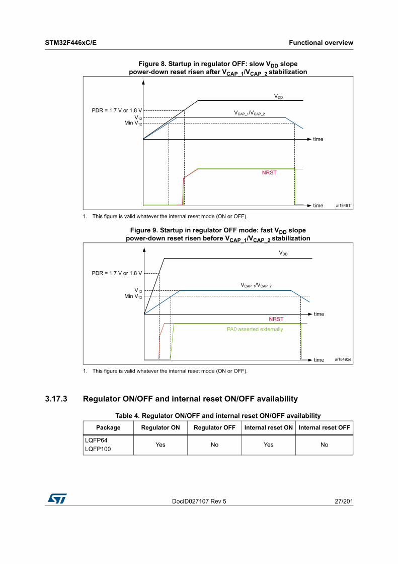
Figure 1. Compatible board design for LQFP100 package . . . . . . . . . . . . . . . . . . . . . . . . . . . . . . . . 14Figure 2. Compatible board for LQFP64 package . . . . . . . . . . . . . . . . . . . . . . . . . . . . . . . . . . . . . . . 15Figure 3. STM32F446xC/E block diagram. . . . . . . . . . . . . . . . . . . . . . . . . . . . . . . . . . . . . . . . . . . . . 16Figure 4. STM32F446xC/E and Multi-AHB matrix . . . . . . . . . . . . . . . . . . . . . . . . . . . . . . . . . . . . . . . 19Figure 5. VDDUSB connected to an external independent power supply . . . . . . . . . . . . . . . . . . . . . 23Figure 6. Power supply supervisor interconnection with internal reset OFF . . . . . . . . . . . . . . . . . . . 24Figure 7. Regulator OFF . . . . . . . . . . . . . . . . . . . . . . . . . . . . . . . . . . . . . . . . . . . . . . . . . . . . . . . . . . 26Figure 8. Startup in regulator OFF: slow VDD slope
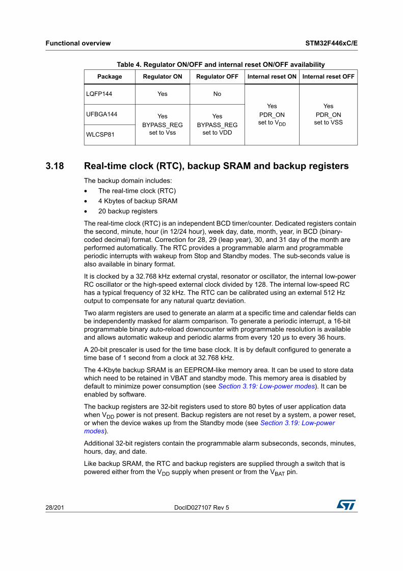
power-down reset risen after VCAP_1/VCAP_2 stabilization . . . . . . . . . . . . . . . . . . . . . . . . . 27Figure 9. Startup in regulator OFF mode: fast VDD slope
power-down reset risen before VCAP_1/VCAP_2 stabilization. . . . . . . . . . . . . . . . . . . . . . . . 27Figure 10. STM32F446xC/xE LQFP64 pinout . . . . . . . . . . . . . . . . . . . . . . . . . . . . . . . . . . . . . . . . . . . 41Figure 11. STM32F446xC/xE LQFP100 pinout . . . . . . . . . . . . . . . . . . . . . . . . . . . . . . . . . . . . . . . . . . 42Figure 12. STM32F446xC LQFP144 pinout . . . . . . . . . . . . . . . . . . . . . . . . . . . . . . . . . . . . . . . . . . . . 43Figure 13. STM32F446xC/xE WLCSP81 ballout . . . . . . . . . . . . . . . . . . . . . . . . . . . . . . . . . . . . . . . . . 44Figure 14. STM32F446xC/xE UFBGA144 ballout . . . . . . . . . . . . . . . . . . . . . . . . . . . . . . . . . . . . . . . . 45Figure 15. Memory map. . . . . . . . . . . . . . . . . . . . . . . . . . . . . . . . . . . . . . . . . . . . . . . . . . . . . . . . . . . . 67Figure 16. Pin loading conditions. . . . . . . . . . . . . . . . . . . . . . . . . . . . . . . . . . . . . . . . . . . . . . . . . . . . . 72Figure 17. Pin input voltage . . . . . . . . . . . . . . . . . . . . . . . . . . . . . . . . . . . . . . . . . . . . . . . . . . . . . . . . . 72Figure 18. Power supply scheme . . . . . . . . . . . . . . . . . . . . . . . . . . . . . . . . . . . . . . . . . . . . . . . . . . . . 73Figure 19. Current consumption measurement scheme . . . . . . . . . . . . . . . . . . . . . . . . . . . . . . . . . . . 74Figure 20. External capacitor CEXT . . . . . . . . . . . . . . . . . . . . . . . . . . . . . . . . . . . . . . . . . . . . . . . . . . . 79Figure 21. Typical VBAT current consumption
(RTC ON/backup RAM OFF and LSE in low power mode) . . . . . . . . . . . . . . . . . . . . . . . . 91Figure 22. Typical VBAT current consumption
(RTC ON/backup RAM OFF and LSE in high drive mode). . . . . . . . . . . . . . . . . . . . . . . . . 92Figure 23. High-speed external clock source AC timing diagram . . . . . . . . . . . . . . . . . . . . . . . . . . . 104Figure 24. Low-speed external clock source AC timing diagram. . . . . . . . . . . . . . . . . . . . . . . . . . . . 104Figure 25. Typical application with an 8 MHz crystal . . . . . . . . . . . . . . . . . . . . . . . . . . . . . . . . . . . . . 105Figure 26. Typical application with a 32.768 kHz crystal . . . . . . . . . . . . . . . . . . . . . . . . . . . . . . . . . . 106Figure 27. LACCHSI versus temperature . . . . . . . . . . . . . . . . . . . . . . . . . . . . . . . . . . . . . . . . . . . . . . 107Figure 28. ACCLSI versus temperature . . . . . . . . . . . . . . . . . . . . . . . . . . . . . . . . . . . . . . . . . . . . . . . 108Figure 29. PLL output clock waveforms in center spread mode . . . . . . . . . . . . . . . . . . . . . . . . . . . . 112Figure 30. PLL output clock waveforms in down spread mode . . . . . . . . . . . . . . . . . . . . . . . . . . . . . 112Figure 31. FT I/O input characteristics. . . . . . . . . . . . . . . . . . . . . . . . . . . . . . . . . . . . . . . . . . . . . . . . 120Figure 32. I/O AC characteristics definition . . . . . . . . . . . . . . . . . . . . . . . . . . . . . . . . . . . . . . . . . . . . 123Figure 33. Recommended NRST pin protection . . . . . . . . . . . . . . . . . . . . . . . . . . . . . . . . . . . . . . . . 124Figure 34. I2C bus AC waveforms and measurement circuit . . . . . . . . . . . . . . . . . . . . . . . . . . . . . . . 126Figure 35. FMPI2C timing diagram and measurement circuit . . . . . . . . . . . . . . . . . . . . . . . . . . . . . . 128Figure 36. SPI timing diagram - slave mode and CPHA = 0 . . . . . . . . . . . . . . . . . . . . . . . . . . . . . . . 130Figure 37. SPI timing diagram - slave mode and CPHA = 1 . . . . . . . . . . . . . . . . . . . . . . . . . . . . . . . 131Figure 38. SPI timing diagram - master mode . . . . . . . . . . . . . . . . . . . . . . . . . . . . . . . . . . . . . . . . . . 131Figure 39. I2S slave timing diagram (Philips protocol)(1) . . . . . . . . . . . . . . . . . . . . . . . . . . . . . . . . . . 135Figure 40. I2S master timing diagram (Philips protocol)(1) . . . . . . . . . . . . . . . . . . . . . . . . . . . . . . . . . 135Figure 41. SAI master timing waveforms . . . . . . . . . . . . . . . . . . . . . . . . . . . . . . . . . . . . . . . . . . . . . . 137Figure 42. SAI slave timing waveforms . . . . . . . . . . . . . . . . . . . . . . . . . . . . . . . . . . . . . . . . . . . . . . . 137Figure 43. USB OTG full speed timings: definition of data signal rise and fall time. . . . . . . . . . . . . . 138Figure 44. ULPI timing diagram . . . . . . . . . . . . . . . . . . . . . . . . . . . . . . . . . . . . . . . . . . . . . . . . . . . . . 140
DocID027107 Rev 5 7/201
STM32F446xC/E List of figures
7
Figure 45. ADC accuracy characteristics . . . . . . . . . . . . . . . . . . . . . . . . . . . . . . . . . . . . . . . . . . . . . . 144Figure 46. Typical connection diagram using the ADC . . . . . . . . . . . . . . . . . . . . . . . . . . . . . . . . . . . 145Figure 47. Power supply and reference decoupling (VREF+ not connected to VDDA). . . . . . . . . . . . . 146Figure 48. Power supply and reference decoupling (VREF+ connected to VDDA). . . . . . . . . . . . . . . . 147Figure 49. 12-bit buffered/non-buffered DAC. . . . . . . . . . . . . . . . . . . . . . . . . . . . . . . . . . . . . . . . . . . 150Figure 50. Asynchronous non-multiplexed SRAM/PSRAM/NOR read waveforms . . . . . . . . . . . . . . 152Figure 51. Asynchronous non-multiplexed SRAM/PSRAM/NOR write waveforms . . . . . . . . . . . . . . 154Figure 52. Asynchronous multiplexed PSRAM/NOR read waveforms. . . . . . . . . . . . . . . . . . . . . . . . 155Figure 53. Asynchronous multiplexed PSRAM/NOR write waveforms . . . . . . . . . . . . . . . . . . . . . . . 157Figure 54. Synchronous multiplexed NOR/PSRAM read timings . . . . . . . . . . . . . . . . . . . . . . . . . . . 159Figure 55. Synchronous multiplexed PSRAM write timings. . . . . . . . . . . . . . . . . . . . . . . . . . . . . . . . 161Figure 56. Synchronous non-multiplexed NOR/PSRAM read timings . . . . . . . . . . . . . . . . . . . . . . . . 163Figure 57. Synchronous non-multiplexed PSRAM write timings . . . . . . . . . . . . . . . . . . . . . . . . . . . . 164Figure 58. NAND controller waveforms for read access . . . . . . . . . . . . . . . . . . . . . . . . . . . . . . . . . . 166Figure 59. NAND controller waveforms for write access . . . . . . . . . . . . . . . . . . . . . . . . . . . . . . . . . . 166Figure 60. NAND controller waveforms for common memory read access . . . . . . . . . . . . . . . . . . . . 167Figure 61. NAND controller waveforms for common memory write access. . . . . . . . . . . . . . . . . . . . 167Figure 62. SDRAM read access waveforms (CL = 1) . . . . . . . . . . . . . . . . . . . . . . . . . . . . . . . . . . . . 168Figure 63. SDRAM write access waveforms . . . . . . . . . . . . . . . . . . . . . . . . . . . . . . . . . . . . . . . . . . . 170Figure 64. DCMI timing diagram . . . . . . . . . . . . . . . . . . . . . . . . . . . . . . . . . . . . . . . . . . . . . . . . . . . . 172Figure 65. SDIO high-speed mode . . . . . . . . . . . . . . . . . . . . . . . . . . . . . . . . . . . . . . . . . . . . . . . . . . 172Figure 66. SD default mode . . . . . . . . . . . . . . . . . . . . . . . . . . . . . . . . . . . . . . . . . . . . . . . . . . . . . . . . 173Figure 67. LQFP64-10x10 mm 64 pin low-profile quad flat package outline . . . . . . . . . . . . . . . . . . . 175Figure 68. LQFP64 Recommended footprint . . . . . . . . . . . . . . . . . . . . . . . . . . . . . . . . . . . . . . . . . . . 176Figure 69. LQFP64 marking example (package top view) . . . . . . . . . . . . . . . . . . . . . . . . . . . . . . . . . 177Figure 70. LQFP100, 14 x 14 mm 100-pin low-profile quad flat package outline . . . . . . . . . . . . . . . 178Figure 71. LQFP100 - 100-pin, 14 x 14 mm low-profile quad flat
recommended footprint . . . . . . . . . . . . . . . . . . . . . . . . . . . . . . . . . . . . . . . . . . . . . . . . . . . 179Figure 72. LQFP100 marking example (package top view) . . . . . . . . . . . . . . . . . . . . . . . . . . . . . . . . 180Figure 73. LQFP144, 20 x 20 mm, 144-pin low-profile quad flat package outline . . . . . . . . . . . . . . . 181Figure 74. LQFP144 recommended footprint . . . . . . . . . . . . . . . . . . . . . . . . . . . . . . . . . . . . . . . . . . 183Figure 75. LQFP144 marking example (package top view) . . . . . . . . . . . . . . . . . . . . . . . . . . . . . . . . 184Figure 76. UFBGA144 - 144-pin, 7 x 7 mm, 0.50 mm pitch, ultra fine pitch ball
grid array package outline . . . . . . . . . . . . . . . . . . . . . . . . . . . . . . . . . . . . . . . . . . . . . . . . 185Figure 77. UFBGA144 - 144-ball, 7 x 7 mm, 0.50 mm pitch, ultra fine pitch ball
grid array package recommended footprint . . . . . . . . . . . . . . . . . . . . . . . . . . . . . . . . . . . 186Figure 78. UQFP144 7 x 7 mm marking example (package top view). . . . . . . . . . . . . . . . . . . . . . . . 187Figure 79. UFBGA144 - 144-pin, 10 x 10 mm, 0.80 mm pitch, ultra fine pitch ball
grid array package outline . . . . . . . . . . . . . . . . . . . . . . . . . . . . . . . . . . . . . . . . . . . . . . . . 188Figure 80. UFBGA144 - 144-pin, 10 x 10 mm, 0.80 mm pitch, ultra fine pitch ball
grid array package recommended footprint . . . . . . . . . . . . . . . . . . . . . . . . . . . . . . . . . . . 189Figure 81. UQFP144 10 x 10 mm marking example (package top view). . . . . . . . . . . . . . . . . . . . . . 190Figure 82. WLCSP81 - 81-pin, 3.693 x 3.815 mm, 0.4 mm pitch wafer level chip scale
package outline. . . . . . . . . . . . . . . . . . . . . . . . . . . . . . . . . . . . . . . . . . . . . . . . . . . . . . . . . 191Figure 83. WLCSP81- 81-pin, 4.4084 x 3.7594 mm, 0.4 mm pitch wafer level chip scale
package recommended footprint . . . . . . . . . . . . . . . . . . . . . . . . . . . . . . . . . . . . . . . . . . . 192Figure 84. WLCSP81 10 x 10 mm marking example (package top view) . . . . . . . . . . . . . . . . . . . . . 193Figure 85. USB controller configured as peripheral-only and used in Full speed mode . . . . . . . . . . 196Figure 86. USB controller configured as host-only and used in full speed mode. . . . . . . . . . . . . . . . 196Figure 87. USB controller configured in dual mode and used in full speed mode . . . . . . . . . . . . . . . 197Figure 88. USB controller configured as peripheral, host, or dual-mode
and used in high speed mode. . . . . . . . . . . . . . . . . . . . . . . . . . . . . . . . . . . . . . . . . . . . . . 198
List of tables STM32F446xC/E
8/201 DocID027107 Rev 5
List of tables
Table 1. Device summary . . . . . . . . . . . . . . . . . . . . . . . . . . . . . . . . . . . . . . . . . . . . . . . . . . . . . . . . . . 1Table 2. STM32F446xC/E features and peripheral counts. . . . . . . . . . . . . . . . . . . . . . . . . . . . . . . . 13Table 3. Voltage regulator configuration mode versus device operating mode . . . . . . . . . . . . . . . . 25Table 4. Regulator ON/OFF and internal reset ON/OFF availability. . . . . . . . . . . . . . . . . . . . . . . . . 27Table 5. Voltage regulator modes in stop mode . . . . . . . . . . . . . . . . . . . . . . . . . . . . . . . . . . . . . . . . 29Table 6. Timer feature comparison. . . . . . . . . . . . . . . . . . . . . . . . . . . . . . . . . . . . . . . . . . . . . . . . . . 31Table 7. Comparison of I2C analog and digital filters . . . . . . . . . . . . . . . . . . . . . . . . . . . . . . . . . . . . 33Table 8. USART feature comparison . . . . . . . . . . . . . . . . . . . . . . . . . . . . . . . . . . . . . . . . . . . . . . . . 34Table 9. Legend/abbreviations used in the pinout table . . . . . . . . . . . . . . . . . . . . . . . . . . . . . . . . . . 46Table 10. STM32F446xx pin and ball descriptions. . . . . . . . . . . . . . . . . . . . . . . . . . . . . . . . . . . . . . . 46Table 11. Alternate function . . . . . . . . . . . . . . . . . . . . . . . . . . . . . . . . . . . . . . . . . . . . . . . . . . . . . . . . 59Table 12. STM32F446xC/E register boundary addresses . . . . . . . . . . . . . . . . . . . . . . . . . . . . . . . . . 68Table 13. Voltage characteristics . . . . . . . . . . . . . . . . . . . . . . . . . . . . . . . . . . . . . . . . . . . . . . . . . . . . 74Table 14. Current characteristics . . . . . . . . . . . . . . . . . . . . . . . . . . . . . . . . . . . . . . . . . . . . . . . . . . . . 75Table 15. Thermal characteristics. . . . . . . . . . . . . . . . . . . . . . . . . . . . . . . . . . . . . . . . . . . . . . . . . . . . 75Table 16. General operating conditions . . . . . . . . . . . . . . . . . . . . . . . . . . . . . . . . . . . . . . . . . . . . . . . 76Table 17. Limitations depending on the operating power supply range . . . . . . . . . . . . . . . . . . . . . . . 78Table 18. VCAP_1/VCAP_2 operating conditions . . . . . . . . . . . . . . . . . . . . . . . . . . . . . . . . . . . . . . . 79Table 19. Operating conditions at power-up/power-down (regulator ON) . . . . . . . . . . . . . . . . . . . . . 79Table 20. Operating conditions at power-up / power-down (regulator OFF). . . . . . . . . . . . . . . . . . . . 79Table 21. reset and power control block characteristics . . . . . . . . . . . . . . . . . . . . . . . . . . . . . . . . . . 80Table 22. Over-drive switching characteristics . . . . . . . . . . . . . . . . . . . . . . . . . . . . . . . . . . . . . . . . . . 81Table 23. Typical and maximum current consumption in Run mode, code with data processing
running from Flash memory (ART accelerator enabled except prefetch) or RAM. . . . . . . 83Table 24. Typical and maximum current consumption in Run mode, code with data processing
running from Flash memory (ART accelerator enabled with prefetch) or RAM . . . . . . . . . 84Table 25. Typical and maximum current consumption in Run mode, code with data processing
running from Flash memory (ART accelerator disabled) . . . . . . . . . . . . . . . . . . . . . . . . . . 85Table 26. Typical and maximum current consumption in Sleep mode . . . . . . . . . . . . . . . . . . . . . . . . 86Table 27. Typical and maximum current consumptions in Stop mode . . . . . . . . . . . . . . . . . . . . . . . . 89Table 28. Typical and maximum current consumptions in Standby mode . . . . . . . . . . . . . . . . . . . . . 90Table 29. Typical and maximum current consumptions in VBAT mode. . . . . . . . . . . . . . . . . . . . . . . . 91Table 30. Typical current consumption in Run mode, code with data processing
running from Flash memory or RAM, regulator ON (ART accelerator enabled except prefetch), VDD=1.7 V . . . . . . . . . . . . . . . . . . . . . . . . . . 93
Table 31. Typical current consumption in Run mode, code with data processing running from Flash memory, regulator OFF (ART accelerator enabled except prefetch). . . . . . . . 94
Table 32. Typical current consumption in Sleep mode, regulator ON, VDD=1.7 V . . . . . . . . . . . . . . 95Table 33. Typical current consumption in Sleep mode, regulator OFF. . . . . . . . . . . . . . . . . . . . . . . . 96Table 34. Switching output I/O current consumption . . . . . . . . . . . . . . . . . . . . . . . . . . . . . . . . . . . . . 97Table 35. Peripheral current consumption . . . . . . . . . . . . . . . . . . . . . . . . . . . . . . . . . . . . . . . . . . . . . 99Table 36. Low-power mode wakeup timings . . . . . . . . . . . . . . . . . . . . . . . . . . . . . . . . . . . . . . . . . . 102Table 37. High-speed external user clock characteristics. . . . . . . . . . . . . . . . . . . . . . . . . . . . . . . . . 103Table 38. Low-speed external user clock characteristics . . . . . . . . . . . . . . . . . . . . . . . . . . . . . . . . . 103Table 39. HSE 4-26 MHz oscillator characteristics . . . . . . . . . . . . . . . . . . . . . . . . . . . . . . . . . . . . . 105Table 40. LSE oscillator characteristics (fLSE = 32.768 kHz) . . . . . . . . . . . . . . . . . . . . . . . . . . . . . . 106Table 41. HSI oscillator characteristics . . . . . . . . . . . . . . . . . . . . . . . . . . . . . . . . . . . . . . . . . . . . . . 106Table 42. LSI oscillator characteristics . . . . . . . . . . . . . . . . . . . . . . . . . . . . . . . . . . . . . . . . . . . . . . 107
DocID027107 Rev 5 9/201
STM32F446xC/E List of tables
10
Table 43. Main PLL characteristics. . . . . . . . . . . . . . . . . . . . . . . . . . . . . . . . . . . . . . . . . . . . . . . . . . 108Table 44. PLLI2S (audio PLL) characteristics . . . . . . . . . . . . . . . . . . . . . . . . . . . . . . . . . . . . . . . . . 109Table 45. PLLISAI characteristics. . . . . . . . . . . . . . . . . . . . . . . . . . . . . . . . . . . . . . . . . . . . . . . . . . . 110Table 46. SSCG parameters constraint . . . . . . . . . . . . . . . . . . . . . . . . . . . . . . . . . . . . . . . . . . . . . . 110Table 47. Flash memory characteristics . . . . . . . . . . . . . . . . . . . . . . . . . . . . . . . . . . . . . . . . . . . . . . 112Table 48. Flash memory programming. . . . . . . . . . . . . . . . . . . . . . . . . . . . . . . . . . . . . . . . . . . . . . . 113Table 49. Flash memory programming with VPP . . . . . . . . . . . . . . . . . . . . . . . . . . . . . . . . . . . . . . . . . . . . . . . . . . 113Table 50. Flash memory endurance and data retention . . . . . . . . . . . . . . . . . . . . . . . . . . . . . . . . . . 114Table 51. EMS characteristics . . . . . . . . . . . . . . . . . . . . . . . . . . . . . . . . . . . . . . . . . . . . . . . . . . . . . 115Table 52. EMI characteristics . . . . . . . . . . . . . . . . . . . . . . . . . . . . . . . . . . . . . . . . . . . . . . . . . . . . . . 116Table 53. ESD absolute maximum ratings . . . . . . . . . . . . . . . . . . . . . . . . . . . . . . . . . . . . . . . . . . . . 116Table 54. Electrical sensitivities . . . . . . . . . . . . . . . . . . . . . . . . . . . . . . . . . . . . . . . . . . . . . . . . . . . . 117Table 55. I/O current injection susceptibility . . . . . . . . . . . . . . . . . . . . . . . . . . . . . . . . . . . . . . . . . . . 117Table 56. I/O static characteristics . . . . . . . . . . . . . . . . . . . . . . . . . . . . . . . . . . . . . . . . . . . . . . . . . . 118Table 57. Output voltage characteristics . . . . . . . . . . . . . . . . . . . . . . . . . . . . . . . . . . . . . . . . . . . . . 121Table 58. I/O AC characteristics . . . . . . . . . . . . . . . . . . . . . . . . . . . . . . . . . . . . . . . . . . . . . . . . . . . . 121Table 59. NRST pin characteristics . . . . . . . . . . . . . . . . . . . . . . . . . . . . . . . . . . . . . . . . . . . . . . . . . 123Table 60. TIMx characteristics . . . . . . . . . . . . . . . . . . . . . . . . . . . . . . . . . . . . . . . . . . . . . . . . . . . . . 124Table 61. I2C characteristics. . . . . . . . . . . . . . . . . . . . . . . . . . . . . . . . . . . . . . . . . . . . . . . . . . . . . . . 125Table 62. FMPI2C characteristics . . . . . . . . . . . . . . . . . . . . . . . . . . . . . . . . . . . . . . . . . . . . . . . . . . . 127Table 63. SPI dynamic characteristics . . . . . . . . . . . . . . . . . . . . . . . . . . . . . . . . . . . . . . . . . . . . . . . 129Table 64. QSPI dynamic characteristics in SDR Mode. . . . . . . . . . . . . . . . . . . . . . . . . . . . . . . . . . . 132Table 65. QSPI dynamic characteristics in DDR Mode . . . . . . . . . . . . . . . . . . . . . . . . . . . . . . . . . . 132Table 66. I2S dynamic characteristics . . . . . . . . . . . . . . . . . . . . . . . . . . . . . . . . . . . . . . . . . . . . . . . 133Table 67. SAI characteristics . . . . . . . . . . . . . . . . . . . . . . . . . . . . . . . . . . . . . . . . . . . . . . . . . . . . . . 136Table 68. USB OTG full speed startup time . . . . . . . . . . . . . . . . . . . . . . . . . . . . . . . . . . . . . . . . . . . 137Table 69. USB OTG full speed DC electrical characteristics . . . . . . . . . . . . . . . . . . . . . . . . . . . . . . 138Table 70. USB OTG full speed electrical characteristics . . . . . . . . . . . . . . . . . . . . . . . . . . . . . . . . . 139Table 71. USB HS DC electrical characteristics . . . . . . . . . . . . . . . . . . . . . . . . . . . . . . . . . . . . . . . . 139Table 72. USB HS clock timing parameters . . . . . . . . . . . . . . . . . . . . . . . . . . . . . . . . . . . . . . . . . . . 139Table 73. Dynamic characteristics: USB ULPI . . . . . . . . . . . . . . . . . . . . . . . . . . . . . . . . . . . . . . . . . 140Table 74. ADC characteristics . . . . . . . . . . . . . . . . . . . . . . . . . . . . . . . . . . . . . . . . . . . . . . . . . . . . . 141Table 75. ADC static accuracy at fADC = 18 MHz. . . . . . . . . . . . . . . . . . . . . . . . . . . . . . . . . . . . . . . 142Table 76. ADC static accuracy at fADC = 30 MHz. . . . . . . . . . . . . . . . . . . . . . . . . . . . . . . . . . . . . . . 143Table 77. ADC static accuracy at fADC = 36 MHz. . . . . . . . . . . . . . . . . . . . . . . . . . . . . . . . . . . . . . . 143Table 78. ADC dynamic accuracy at fADC = 18 MHz - limited test conditions . . . . . . . . . . . . . . . . . 143Table 79. ADC dynamic accuracy at fADC = 36 MHz - limited test conditions . . . . . . . . . . . . . . . . . 143Table 80. Temperature sensor characteristics . . . . . . . . . . . . . . . . . . . . . . . . . . . . . . . . . . . . . . . . . 147Table 81. Temperature sensor calibration values. . . . . . . . . . . . . . . . . . . . . . . . . . . . . . . . . . . . . . . 147Table 82. VBAT monitoring characteristics . . . . . . . . . . . . . . . . . . . . . . . . . . . . . . . . . . . . . . . . . . . . 148Table 83. internal reference voltage . . . . . . . . . . . . . . . . . . . . . . . . . . . . . . . . . . . . . . . . . . . . . . . . 148Table 84. Internal reference voltage calibration values . . . . . . . . . . . . . . . . . . . . . . . . . . . . . . . . . . 148Table 85. DAC characteristics . . . . . . . . . . . . . . . . . . . . . . . . . . . . . . . . . . . . . . . . . . . . . . . . . . . . . 148Table 86. Asynchronous non-multiplexed SRAM/PSRAM/NOR -
read timings . . . . . . . . . . . . . . . . . . . . . . . . . . . . . . . . . . . . . . . . . . . . . . . . . . . . . . . . . . . 153Table 87. Asynchronous non-multiplexed SRAM/PSRAM/NOR read -
NWAIT timings . . . . . . . . . . . . . . . . . . . . . . . . . . . . . . . . . . . . . . . . . . . . . . . . . . . . . . . . . 153Table 88. Asynchronous non-multiplexed SRAM/PSRAM/NOR write timings . . . . . . . . . . . . . . . . . 154Table 89. Asynchronous non-multiplexed SRAM/PSRAM/NOR write -
NWAIT timings . . . . . . . . . . . . . . . . . . . . . . . . . . . . . . . . . . . . . . . . . . . . . . . . . . . . . . . . . 155Table 90. Asynchronous multiplexed PSRAM/NOR read timings. . . . . . . . . . . . . . . . . . . . . . . . . . . 156Table 91. Asynchronous multiplexed PSRAM/NOR read-NWAIT timings . . . . . . . . . . . . . . . . . . . . 156
List of tables STM32F446xC/E
10/201 DocID027107 Rev 5
Table 92. Asynchronous multiplexed PSRAM/NOR write timings . . . . . . . . . . . . . . . . . . . . . . . . . . 158Table 93. Asynchronous multiplexed PSRAM/NOR write-NWAIT timings . . . . . . . . . . . . . . . . . . . . 158Table 94. Synchronous multiplexed NOR/PSRAM read timings . . . . . . . . . . . . . . . . . . . . . . . . . . . 160Table 95. Synchronous multiplexed PSRAM write timings. . . . . . . . . . . . . . . . . . . . . . . . . . . . . . . . 162Table 96. Synchronous non-multiplexed NOR/PSRAM read timings . . . . . . . . . . . . . . . . . . . . . . . . 163Table 97. Synchronous non-multiplexed PSRAM write timings . . . . . . . . . . . . . . . . . . . . . . . . . . . . 165Table 98. Switching characteristics for NAND Flash read cycles . . . . . . . . . . . . . . . . . . . . . . . . . . . 167Table 99. Switching characteristics for NAND Flash write cycles. . . . . . . . . . . . . . . . . . . . . . . . . . . 168Table 100. SDRAM read timings . . . . . . . . . . . . . . . . . . . . . . . . . . . . . . . . . . . . . . . . . . . . . . . . . . . . 169Table 101. LPSDR SDRAM read timings . . . . . . . . . . . . . . . . . . . . . . . . . . . . . . . . . . . . . . . . . . . . . . 169Table 102. SDRAM write timings . . . . . . . . . . . . . . . . . . . . . . . . . . . . . . . . . . . . . . . . . . . . . . . . . . . . 170Table 103. LPSDR SDRAM write timings. . . . . . . . . . . . . . . . . . . . . . . . . . . . . . . . . . . . . . . . . . . . . . 171Table 104. DCMI characteristics. . . . . . . . . . . . . . . . . . . . . . . . . . . . . . . . . . . . . . . . . . . . . . . . . . . . . 171Table 105. Dynamic characteristics: SD / MMC characteristics . . . . . . . . . . . . . . . . . . . . . . . . . . . . . 173Table 106. Dynamic characteristics: eMMC characteristics VDD = 1.7 V to 1.9 V. . . . . . . . . . . . . . . 174Table 107. RTC characteristics . . . . . . . . . . . . . . . . . . . . . . . . . . . . . . . . . . . . . . . . . . . . . . . . . . . . . 174Table 108. LQFP64 – 10 x 10 mm low-profile quad flat package mechanical data . . . . . . . . . . . . . . 175Table 109. LQPF100, 14 x 14 mm 100-pin low-profile quad flat
package mechanical data . . . . . . . . . . . . . . . . . . . . . . . . . . . . . . . . . . . . . . . . . . . . . . . . . 178Table 110. LQFP144, 20 x 20 mm, 144-pin low-profile quad flat package mechanical data . . . . . . . 182Table 111. UFBGA144 - 144-pin, 7 x 7 mm, 0.50 mm pitch, ultra fine pitch ball
grid array package mechanical data . . . . . . . . . . . . . . . . . . . . . . . . . . . . . . . . . . . . . . . . . 185Table 112. UFBGA144 recommended PCB design rules (0.50 mm pitch BGA) . . . . . . . . . . . . . . . . 186Table 113. UFBGA144 - 144-pin, 10 x 10 mm, 0.80 mm pitch, ultra fine pitch ball
grid array package mechanical data . . . . . . . . . . . . . . . . . . . . . . . . . . . . . . . . . . . . . . . . . 188Table 114. UFBGA144 recommended PCB design rules (0.80 mm pitch BGA) . . . . . . . . . . . . . . . . 189Table 115. WLCSP81- 81-pin, 3.693 x 3.815 mm, 0.4 mm pitch wafer level chip scale
package mechanical data . . . . . . . . . . . . . . . . . . . . . . . . . . . . . . . . . . . . . . . . . . . . . . . . . 191Table 116. WLCSP81 recommended PCB design rules (0.4 mm pitch) . . . . . . . . . . . . . . . . . . . . . . 192Table 117. Package thermal characteristics . . . . . . . . . . . . . . . . . . . . . . . . . . . . . . . . . . . . . . . . . . . . 194Table 118. Ordering information scheme . . . . . . . . . . . . . . . . . . . . . . . . . . . . . . . . . . . . . . . . . . . . . . 195Table 119. Document revision history . . . . . . . . . . . . . . . . . . . . . . . . . . . . . . . . . . . . . . . . . . . . . . . . 199
DocID027107 Rev 5 11/201
STM32F446xC/E Introduction
40
1 Introduction
This document provides the description of the STM32F446xC/E products.
The STM32F446xC/E document should be read in conjunction with the STM32F4xx reference manual.
For information on the Cortex®-M4 core, please refer to the Cortex®-M4 programming manual (PM0214), available from the www.st.com.
Description STM32F446xC/E
12/201 DocID027107 Rev 5
2 Description
The STM32F446xC/E devices are based on the high-performance ARM® Cortex®-M4 32-bit RISC core operating at a frequency of up to 180 MHz. The Cortex-M4 core features a Floating point unit (FPU) single precision which supports all ARM® single-precision data-processing instructions and data types. It also implements a full set of DSP instructions and a memory protection unit (MPU) which enhances application security.
The STM32F446xC/E devices incorporate high-speed embedded memories (Flash memory up to 512 Kbyte, up to 128 Kbyte of SRAM), up to 4 Kbytes of backup SRAM, and an extensive range of enhanced I/Os and peripherals connected to two APB buses, two AHB buses and a 32-bit multi-AHB bus matrix.
All devices offer three 12-bit ADCs, two DACs, a low-power RTC, twelve general-purpose 16-bit timers including two PWM timers for motor control, two general-purpose 32-bit timers.
They also feature standard and advanced communication interfaces.
• Up to four I2Cs;
• Four SPIs, three I2Ss full simplex. To achieve audio class accuracy, the I2S peripherals can be clocked via a dedicated internal audio PLL or via an external clock to allow synchronization;
• Four USARTs plus two UARTs;
• An USB OTG full-speed and an USB OTG high-speed with full-speed capability (with the ULPI), both with dedicated power rails allowing to use them throughout the entire power range;
• Two CANs;
• Two SAIs serial audio interfaces. To achieve audio class accuracy, the SAIs can be clocked via a dedicated internal audio PLL;
• An SDIO/MMC interface;
• Camera interface;
• HDMI-CEC;
• SPDIF Receiver (SPDIFRx);
• QuadSPI.
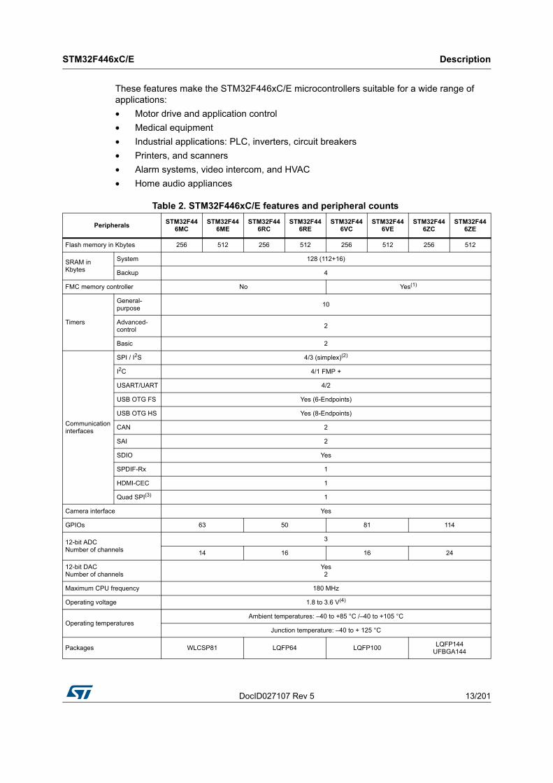
Advanced peripherals include an SDIO, a flexible memory control (FMC) interface, a camera interface for CMOS sensors. Refer to Table 2: STM32F446xC/E features and peripheral counts for the list of peripherals available on each part number.
The STM32F446xC/E devices operates in the –40 to +105 °C temperature range from a 1.7 to 3.6 V power supply.
The supply voltage can drop to 1.7 V with the use of an external power supply supervisor (refer to Section 3.16.2: Internal reset OFF). A comprehensive set of power-saving mode allows the design of low-power applications.
The STM32F446xC/E devices offer devices in 6 packages ranging from 64 pins to 144 pins. The set of included peripherals changes with the device chosen.
DocID027107 Rev 5 13/201
STM32F446xC/E Description
40
These features make the STM32F446xC/E microcontrollers suitable for a wide range of applications:
• Motor drive and application control
• Medical equipment
• Industrial applications: PLC, inverters, circuit breakers
• Printers, and scanners
• Alarm systems, video intercom, and HVAC
• Home audio appliances
Table 2. STM32F446xC/E features and peripheral counts
PeripheralsSTM32F44
6MCSTM32F44
6MESTM32F44
6RCSTM32F44
6RESTM32F44
6VCSTM32F44
6VESTM32F44
6ZCSTM32F44
6ZE
Flash memory in Kbytes 256 512 256 512 256 512 256 512
SRAM in Kbytes
System 128 (112+16)
Backup 4
FMC memory controller No Yes(1)
Timers
General-purpose
10
Advanced-control
2
Basic 2
Communication interfaces
SPI / I2S 4/3 (simplex)(2)
I2C 4/1 FMP +
USART/UART 4/2
USB OTG FS Yes (6-Endpoints)
USB OTG HS Yes (8-Endpoints)
CAN 2
SAI 2
SDIO Yes
SPDIF-Rx 1
HDMI-CEC 1
Quad SPI(3) 1
Camera interface Yes
GPIOs 63 50 81 114
12-bit ADCNumber of channels
3
14 16 16 24
12-bit DAC Number of channels
Yes2
Maximum CPU frequency 180 MHz
Operating voltage 1.8 to 3.6 V(4)
Operating temperaturesAmbient temperatures: –40 to +85 °C /–40 to +105 °C
Junction temperature: –40 to + 125 °C
Packages WLCSP81 LQFP64 LQFP100LQFP144
UFBGA144
Description STM32F446xC/E
14/201 DocID027107 Rev 5
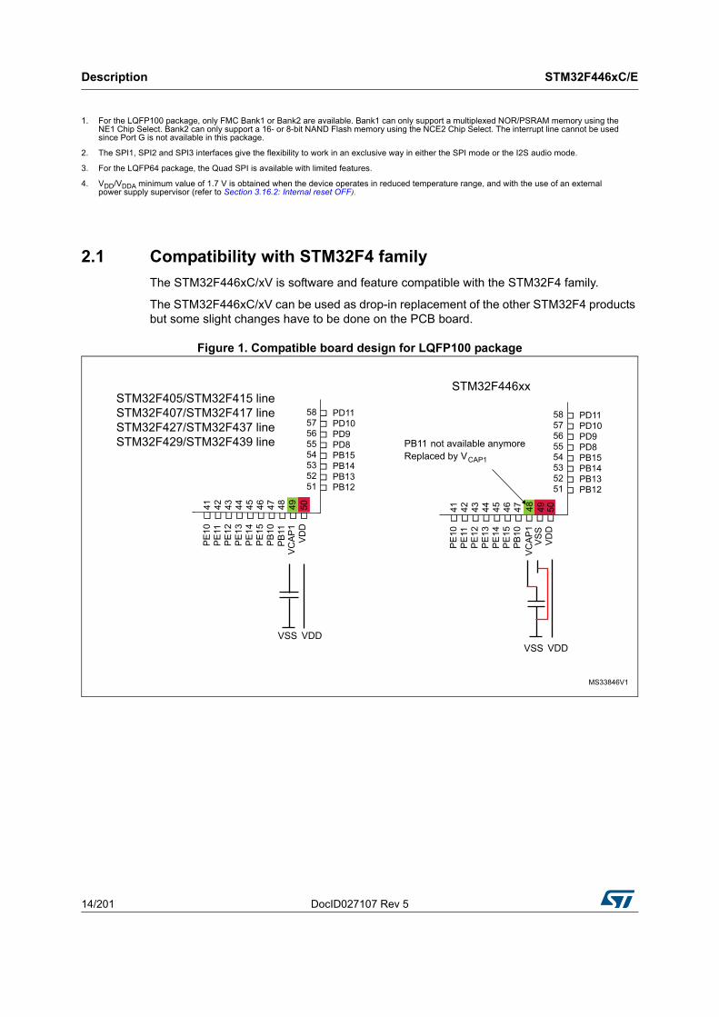
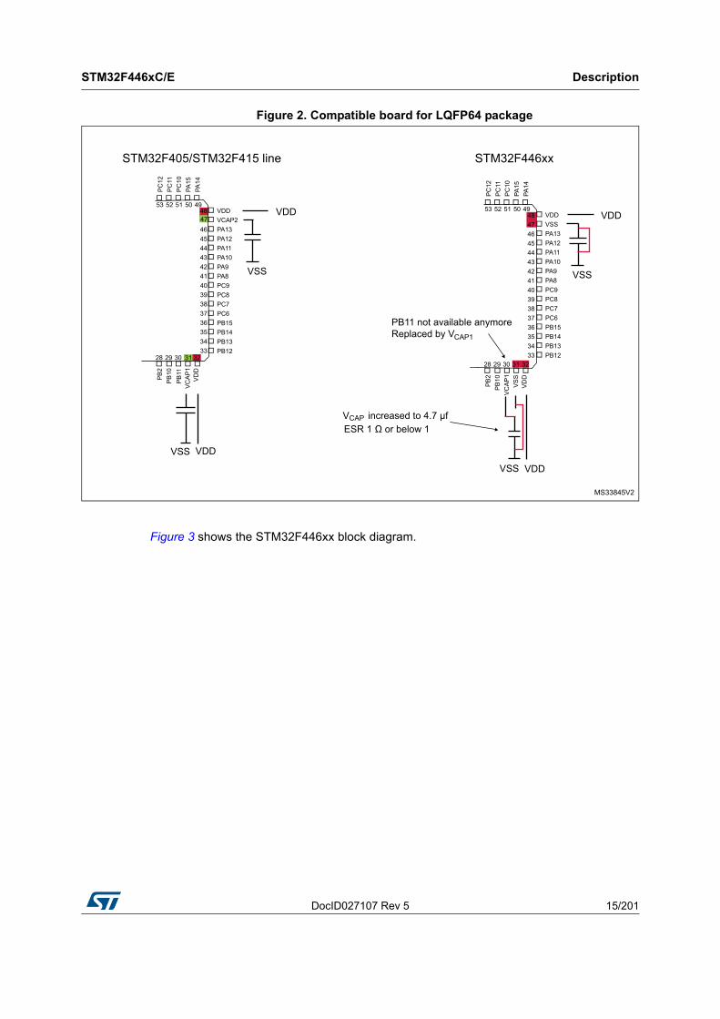
2.1 Compatibility with STM32F4 family
The STM32F446xC/xV is software and feature compatible with the STM32F4 family.
The STM32F446xC/xV can be used as drop-in replacement of the other STM32F4 products but some slight changes have to be done on the PCB board.
Figure 1. Compatible board design for LQFP100 package
1. For the LQFP100 package, only FMC Bank1 or Bank2 are available. Bank1 can only support a multiplexed NOR/PSRAM memory using the NE1 Chip Select. Bank2 can only support a 16- or 8-bit NAND Flash memory using the NCE2 Chip Select. The interrupt line cannot be used since Port G is not available in this package.
2. The SPI1, SPI2 and SPI3 interfaces give the flexibility to work in an exclusive way in either the SPI mode or the I2S audio mode.
3. For the LQFP64 package, the Quad SPI is available with limited features.
4. VDD/VDDA minimum value of 1.7 V is obtained when the device operates in reduced temperature range, and with the use of an external power supply supervisor (refer to Section 3.16.2: Internal reset OFF).
DocID027107 Rev 5 15/201
STM32F446xC/E Description
40
Figure 2. Compatible board for LQFP64 package
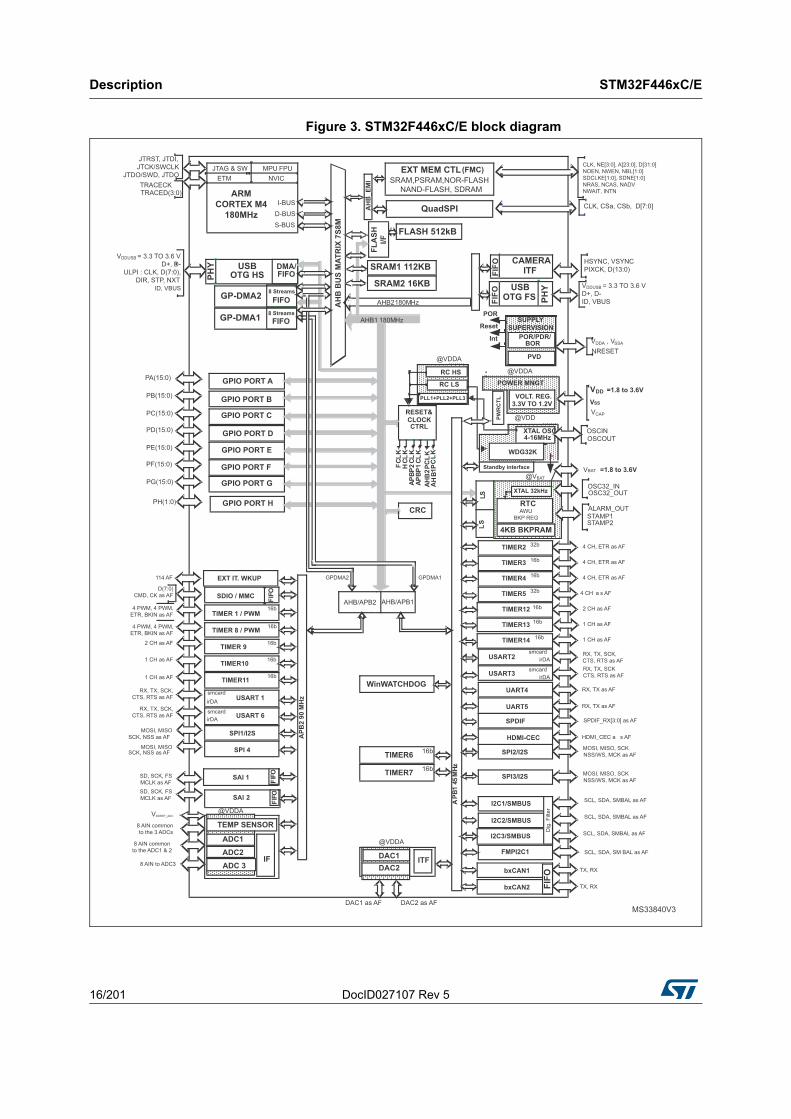
Figure 3 shows the STM32F446xx block diagram.
Description STM32F446xC/E
16/201 DocID027107 Rev 5
Figure 3. STM32F446xC/E block diagram
DocID027107 Rev 5 17/201
STM32F446xC/E Functional overview
40
3 Functional overview
3.1 ARM® Cortex®-M4 with FPU and embedded Flash and SRAM
The ARM® Cortex®-M4 with FPU processor is the latest generation of ARM processors for embedded systems. It was developed to provide a low-cost platform that meets the needs of MCU implementation, with a reduced pin count and low-power consumption, while delivering outstanding computational performance and an advanced response to interrupts.
The ARM® Cortex®-M4 with FPU core is a 32-bit RISC processor that features exceptional code-efficiency, delivering the high-performance expected from an ARM core in the memory size usually associated with 8- and 16-bit devices.
The processor supports a set of DSP instructions which allow efficient signal processing and complex algorithm execution.
Its single precision FPU (floating point unit) speeds up software development by using metalanguage development tools, while avoiding saturation.
The STM32F446xC/E family is compatible with all ARM tools and software.
Figure 3 shows the general block diagram of the STM32F446xC/E family.
Note: Cortex-M4 with FPU core is binary compatible with the Cortex-M3 core.
3.2 Adaptive real-time memory accelerator (ART Accelerator™)
The ART Accelerator™ is a memory accelerator which is optimized for STM32 industry-standard ARM® Cortex®-M4 with FPU processors. It balances the inherent performance advantage of the ARM® Cortex®-M4 with FPU over Flash memory technologies, which normally requires the processor to wait for the Flash memory at higher frequencies.
To release the processor full 225 DMIPS performance at this frequency, the accelerator implements an instruction prefetch queue and branch cache, which increases program execution speed from the 128-bit Flash memory. Based on CoreMark benchmark, the performance achieved thanks to the ART Accelerator is equivalent to 0 wait state program execution from Flash memory at a CPU frequency up to 180 MHz.
3.3 Memory protection unit
The memory protection unit (MPU) is used to manage the CPU accesses to memory to prevent one task to accidentally corrupt the memory or resources used by any other active task. This memory area is organized into up to 8 protected areas that can in turn be divided up into 8 subareas. The protection area sizes are between 32 bytes and the whole 4 gigabytes of addressable memory.
The MPU is especially helpful for applications where some critical or certified code has to be protected against the misbehavior of other tasks. It is usually managed by an RTOS (real-time operating system). If a program accesses a memory location that is prohibited by the MPU, the RTOS can detect it and take action. In an RTOS environment, the kernel can dynamically update the MPU area setting, based on the process to be executed.
The MPU is optional and can be bypassed for applications that do not need it.
Functional overview STM32F446xC/E
18/201 DocID027107 Rev 5
3.4 Embedded Flash memory
The devices embed a Flash memory of 512KB available for storing programs and data.
3.5 CRC (cyclic redundancy check) calculation unit
The CRC (cyclic redundancy check) calculation unit is used to get a CRC code from a 32-bit data word and a fixed generator polynomial.
Among other applications, CRC-based techniques are used to verify data transmission or storage integrity. In the scope of the EN/IEC 60335-1 standard, they offer a means of verifying the Flash memory integrity. The CRC calculation unit helps compute a software signature during runtime, to be compared with a reference signature generated at link-time and stored at a given memory location.
3.6 Embedded SRAM
All devices embed:
• Up to 128Kbytes of system SRAM.
RAM memory is accessed (read/write) at CPU clock speed with 0 wait states.
• 4 Kbytes of backup SRAM
This area is accessible only from the CPU. Its content is protected against possible unwanted write accesses, and is retained in Standby or VBAT mode.
3.7 Multi-AHB bus matrix
The 32-bit multi-AHB bus matrix interconnects all the masters (CPU, DMAs, USB HS) and the slaves Flash memory, RAM, QuadSPI, FMC, AHB and APB peripherals and ensures a seamless and efficient operation even when several high-speed peripherals work simultaneously.
DocID027107 Rev 5 19/201
STM32F446xC/E Functional overview
40
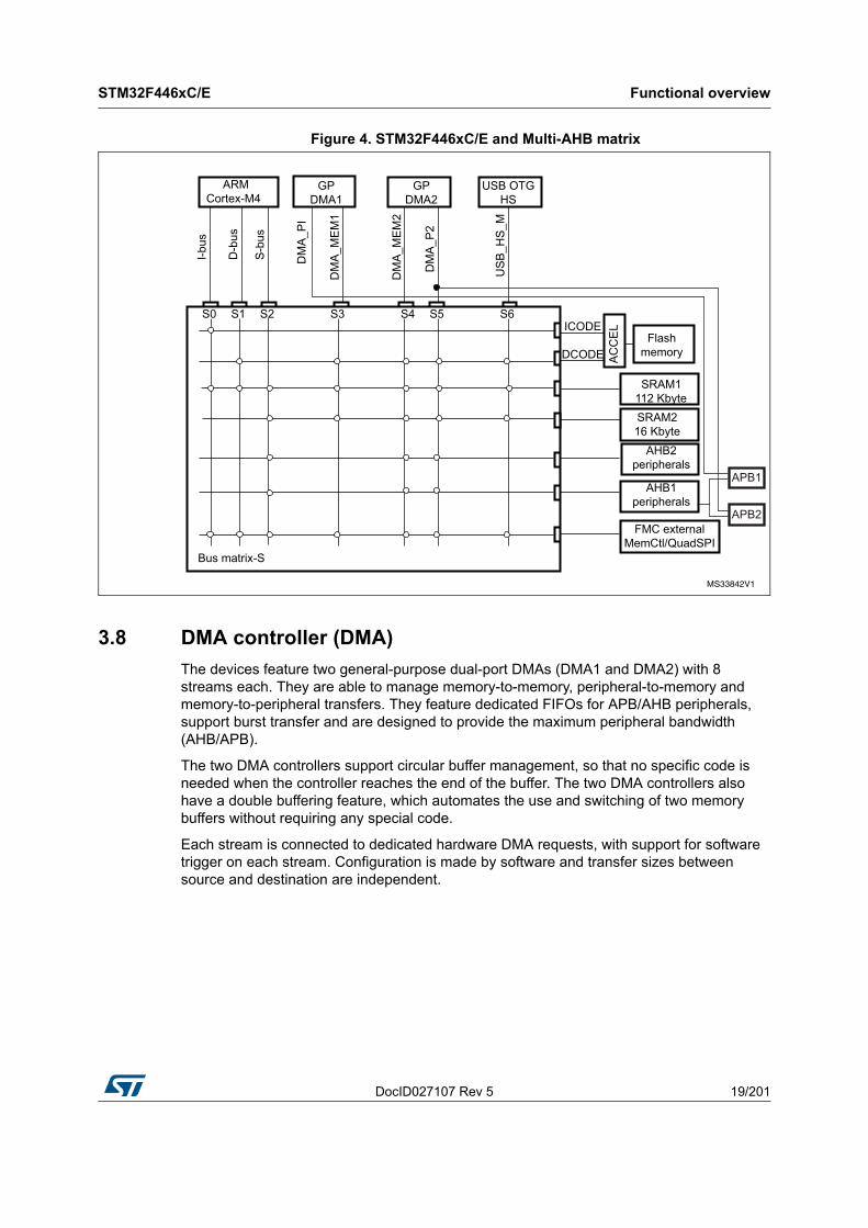
Figure 4. STM32F446xC/E and Multi-AHB matrix
3.8 DMA controller (DMA)
The devices feature two general-purpose dual-port DMAs (DMA1 and DMA2) with 8 streams each. They are able to manage memory-to-memory, peripheral-to-memory and memory-to-peripheral transfers. They feature dedicated FIFOs for APB/AHB peripherals, support burst transfer and are designed to provide the maximum peripheral bandwidth (AHB/APB).
The two DMA controllers support circular buffer management, so that no specific code is needed when the controller reaches the end of the buffer. The two DMA controllers also have a double buffering feature, which automates the use and switching of two memory buffers without requiring any special code.
Each stream is connected to dedicated hardware DMA requests, with support for software trigger on each stream. Configuration is made by software and transfer sizes between source and destination are independent.
Functional overview STM32F446xC/E
20/201 DocID027107 Rev 5
The DMA can be used with the main peripherals:
• SPI and I2S
• I2C
• USART
• General-purpose, basic and advanced-control timers TIMx
• DAC
• SDIO
• Camera interface (DCMI)
• ADC
• SAI1/SAI2
• SPDIF Receiver (SPDIFRx)
• QuadSPI
3.9 Flexible memory controller (FMC)
All devices embed an FMC. It has seven Chip Select outputs supporting the following modes: SDRAM/LPSDR SDRAM, SRAM, PSRAM, NOR Flash and NAND Flash. With the possibility to remap FMC bank 1 (NOR/PSRAM 1 and 2) and FMC SDRAM bank 1/2 in the Cortex-M4 code area.
Functionality overview:
• 8-,16-bit data bus width
• Read FIFO for SDRAM controller
• Write FIFO
• Maximum FMC_CLK/FMC_SDCLK frequency for synchronous accesses is 90 MHz.
LCD parallel interface
The FMC can be configured to interface seamlessly with most graphic LCD controllers. It supports the Intel 8080 and Motorola 6800 modes, and is flexible enough to adapt to specific LCD interfaces. This LCD parallel interface capability makes it easy to build cost-effective graphic applications using LCD modules with embedded controllers or high performance solutions using external controllers with dedicated acceleration.
3.10 Quad SPI memory interface (QUADSPI)
All devices embed a Quad SPI memory interface, which is a specialized communication interface targeting Single, Dual or Quad SPI flash memories. It can work in direct mode through registers, external flash status register polling mode and memory mapped mode. Up to 256 Mbytes external flash are memory mapped, supporting 8, 16 and 32-bit access. Code execution is supported. The opcode and the frame format are fully programmable. Communication can be either in Single Data Rate or Dual Data Rate.
DocID027107 Rev 5 21/201
STM32F446xC/E Functional overview
40
3.11 Nested vectored interrupt controller (NVIC)
The devices embed a nested vectored interrupt controller able to manage 16 priority levels, and handle up to 91 maskable interrupt channels plus the 16 interrupt lines of the Cortex®-M4 with FPU core.
• Closely coupled NVIC gives low-latency interrupt processing
• Interrupt entry vector table address passed directly to the core
• Allows early processing of interrupts
• Processing of late arriving, higher-priority interrupts
• Support tail chaining
• Processor state automatically saved
• Interrupt entry restored on interrupt exit with no instruction overhead
This hardware block provides flexible interrupt management features with minimum interrupt latency.
3.12 External interrupt/event controller (EXTI)
The external interrupt/event controller consists of 23 edge-detector lines used to generate interrupt/event requests. Each line can be independently configured to select the trigger event (rising edge, falling edge, both) and can be masked independently. A pending register maintains the status of the interrupt requests. The EXTI can detect an external line with a pulse width shorter than the Internal APB2 clock period. Up to 114 GPIOs can be connected to the 16 external interrupt lines.
3.13 Clocks and startup
On reset the 16 MHz internal RC oscillator is selected as the default CPU clock. The 16 MHz internal RC oscillator is factory-trimmed to offer 1% accuracy at 25 °C. The application can then select as system clock either the RC oscillator or an external 4-26 MHz clock source. This clock can be monitored for failure. If a failure is detected, the system automatically switches back to the internal RC oscillator and a software interrupt is generated (if enabled). This clock source is input to a PLL thus allowing to increase the frequency up to 180 MHz. Similarly, full interrupt management of the PLL clock entry is available when necessary (for example if an indirectly used external oscillator fails).
Several prescalers allow the configuration of the two AHB buses, the high-speed APB (APB2) and the low-speed APB (APB1) domains. The maximum frequency of the two AHB buses is 180 MHz while the maximum frequency of the high-speed APB domains is 90 MHz. The maximum allowed frequency of the low-speed APB domain is 45 MHz.
The devices embed a dedicated PLL (PLLI2S) and PLLSAI which allows to achieve audio class performance. In this case, the I2S master clock can generate all standard sampling frequencies from 8 kHz to 192 kHz.
Functional overview STM32F446xC/E
22/201 DocID027107 Rev 5
3.14 Boot modes
At startup, boot pins are used to select one out of three boot options:
• Boot from user Flash
• Boot from system memory
• Boot from embedded SRAM
The boot loader is located in system memory. It is used to reprogram the Flash memory through a serial (UART, I2C, CAN, SPI and USB) communication interface. Refer to application note AN2606 for details.
3.15 Power supply schemes
• VDD = 1.7 to 3.6 V: external power supply for I/Os and the internal regulator (when enabled), provided externally through VDD pins.
• VSSA, VDDA = 1.7 to 3.6 V: external analog power supplies for ADC, DAC, Reset blocks, RCs and PLL. VDDA and VSSA must be connected to VDD and VSS, respectively.
Note: VDD/VDDA minimum value of 1.7 V is obtained with the use of an external power supply supervisor (refer to Section 3.16.2: Internal reset OFF). Refer to Table 3: Voltage regulator configuration mode versus device operating mode to identify the packages supporting this option.
• VBAT = 1.65 to 3.6 V: power supply for RTC, external clock 32 kHz oscillator and backup registers (through power switch) when VDD is not present.
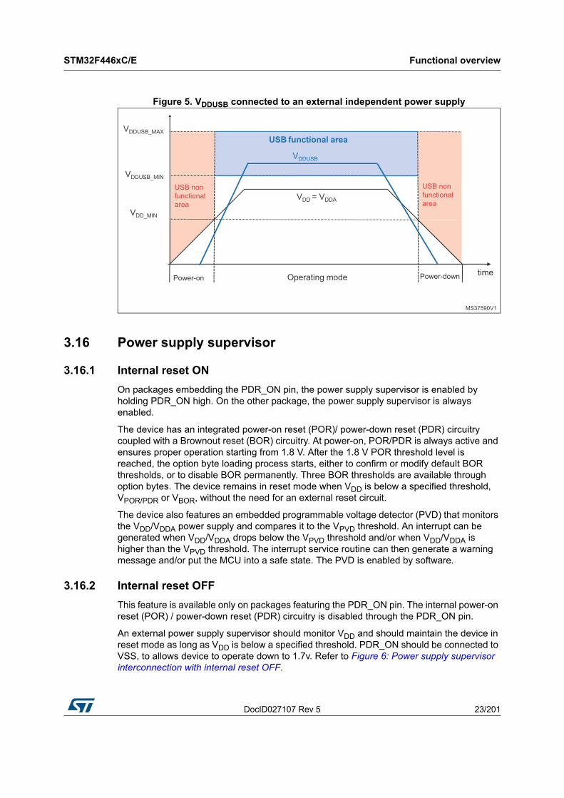
• VDDUSB can be connected either to VDD or an external independent power supply (3.0 to 3.6V) for USB transceivers. For example, when device is powered at 1.8V, an independent power supply 3.3V can be connected to VDDUSB. When the VDDUSB is connected to a separated power supply, it is independent from VDD or VDDA but it must be the last supply to be provided and the first to disappear. The following conditions VDDUSB must be respected:
– During power-on phase (VDD < VDD_MIN), VDDUSB should be always lower than VDD
– During power-down phase (VDD < VDD_MIN), VDDUSB should be always lower than VDD
– VDDUSB rising and falling time rate specifications must be respected.
– In operating mode phase, VDDUSB could be lower or higher than VDD:
– If USB (USB OTG_HS/OTG_FS) is used, the associated GPIOs powered by VDDUSB are operating between VDDUSB_MIN and VDDUSB_MAX.The VDDUSB supply both USB transceiver (USB OTG_HS and USB OTG_FS).
– If only one USB transceiver is used in the application, the GPIOs associated to the other USB transceiver are still supplied by VDDUSB.
– If USB (USB OTG_HS/OTG_FS) is not used, the associated GPIOs powered by VDDUSB are operating between VDD_MIN and VDD_MAX.
DocID027107 Rev 5 23/201
STM32F446xC/E Functional overview
40
Figure 5. VDDUSB connected to an external independent power supply
3.16 Power supply supervisor
3.16.1 Internal reset ON
On packages embedding the PDR_ON pin, the power supply supervisor is enabled by holding PDR_ON high. On the other package, the power supply supervisor is always enabled.
The device has an integrated power-on reset (POR)/ power-down reset (PDR) circuitry coupled with a Brownout reset (BOR) circuitry. At power-on, POR/PDR is always active and ensures proper operation starting from 1.8 V. After the 1.8 V POR threshold level is reached, the option byte loading process starts, either to confirm or modify default BOR thresholds, or to disable BOR permanently. Three BOR thresholds are available through option bytes. The device remains in reset mode when VDD is below a specified threshold, VPOR/PDR or VBOR, without the need for an external reset circuit.
The device also features an embedded programmable voltage detector (PVD) that monitors the VDD/VDDA power supply and compares it to the VPVD threshold. An interrupt can be generated when VDD/VDDA drops below the VPVD threshold and/or when VDD/VDDA is higher than the VPVD threshold. The interrupt service routine can then generate a warning message and/or put the MCU into a safe state. The PVD is enabled by software.
3.16.2 Internal reset OFF
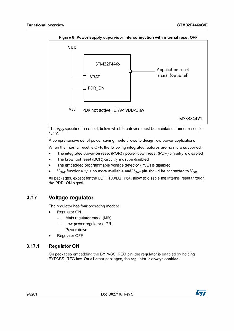
This feature is available only on packages featuring the PDR_ON pin. The internal power-on reset (POR) / power-down reset (PDR) circuitry is disabled through the PDR_ON pin.
An external power supply supervisor should monitor VDD and should maintain the device in reset mode as long as VDD is below a specified threshold. PDR_ON should be connected to VSS, to allows device to operate down to 1.7v. Refer to Figure 6: Power supply supervisor interconnection with internal reset OFF.
Functional overview STM32F446xC/E
24/201 DocID027107 Rev 5
Figure 6. Power supply supervisor interconnection with internal reset OFF
The VDD specified threshold, below which the device must be maintained under reset, is 1.7 V.
A comprehensive set of power-saving mode allows to design low-power applications.
When the internal reset is OFF, the following integrated features are no more supported:
• The integrated power-on reset (POR) / power-down reset (PDR) circuitry is disabled
• The brownout reset (BOR) circuitry must be disabled
• The embedded programmable voltage detector (PVD) is disabled
• VBAT functionality is no more available and VBAT pin should be connected to VDD.
All packages, except for the LQFP100/LQFP64, allow to disable the internal reset through the PDR_ON signal.
3.17 Voltage regulator
The regulator has four operating modes:
• Regulator ON
– Main regulator mode (MR)
– Low power regulator (LPR)
– Power-down
• Regulator OFF
3.17.1 Regulator ON
On packages embedding the BYPASS_REG pin, the regulator is enabled by holding BYPASS_REG low. On all other packages, the regulator is always enabled.
DocID027107 Rev 5 25/201
STM32F446xC/E Functional overview
40
There are three power modes configured by software when the regulator is ON:
• MR mode used in Run/sleep modes or in Stop modes
– In Run/Sleep mode
The MR mode is used either in the normal mode (default mode) or the over-drive mode (enabled by software). Different voltages scaling are provided to reach the best compromise between maximum frequency and dynamic power consumption. The over-drive mode allows operating at a higher frequency than the normal mode for a given voltage scaling.
– In Stop modes
The MR can be configured in two ways during stop mode:
MR operates in normal mode (default mode of MR in stop mode)
MR operates in under-drive mode (reduced leakage mode).
• LPR is used in the Stop modes:
The LP regulator mode is configured by software when entering Stop mode.
Like the MR mode, the LPR can be configured in two ways during stop mode:
– LPR operates in normal mode (default mode when LPR is ON)
– LPR operates in under-drive mode (reduced leakage mode).
• Power-down is used in Standby mode.
The Power-down mode is activated only when entering in Standby mode. The regulator output is in high impedance and the kernel circuitry is powered down, inducing zero consumption. The contents of the registers and SRAM are lost.
Refer to Table 3 for a summary of voltage regulator modes versus device operating modes.
Two external ceramic capacitors should be connected on VCAP_1 and VCAP_2 pin.
All packages have the regulator ON feature.
3.17.2 Regulator OFF
This feature is available only on packages featuring the BYPASS_REG pin. The regulator is disabled by holding BYPASS_REG high. The regulator OFF mode allows to supply externally a V12 voltage source through VCAP_1 and VCAP_2 pins.
Table 3. Voltage regulator configuration mode versus device operating mode(1)
1. ‘-’ means that the corresponding configuration is not available.
Voltage regulator configuration
Run mode Sleep mode Stop mode Standby mode
Normal mode MR MR MR or LPR -
Over-drive mode(2)
2. The over-drive mode is not available when VDD = 1.7 to 2.1 V.
MR MR - -
Under-drive mode - - MR or LPR -
Power-down mode
- - - Yes
Functional overview STM32F446xC/E
26/201 DocID027107 Rev 5
Since the internal voltage scaling is not managed internally, the external voltage value must be aligned with the targeted maximum frequency. The two 2.2 µF ceramic capacitors should be replaced by two 100 nF decoupling capacitors.
When the regulator is OFF, there is no more internal monitoring on V12. An external power supply supervisor should be used to monitor the V12 of the logic power domain. PA0 pin should be used for this purpose, and act as power-on reset on V12 power domain.
In regulator OFF mode, the following features are no more supported:
• PA0 cannot be used as a GPIO pin since it allows to reset a part of the V12 logic power domain which is not reset by the NRST pin.
• As long as PA0 is kept low, the debug mode cannot be used under power-on reset. As a consequence, PA0 and NRST pins must be managed separately if the debug connection under reset or pre-reset is required.
• The over-drive and under-drive modes are not available.
Figure 7. Regulator OFF
The following conditions must be respected:
• VDD should always be higher than VCAP_1 and VCAP_2 to avoid current injection between power domains.
• If the time for VCAP_1 and VCAP_2 to reach V12 minimum value is faster than the time for VDD to reach 1.7 V, then PA0 should be kept low to cover both conditions: until VCAP_1 and VCAP_2 reach V12 minimum value and until VDD reaches 1.7 V (see Figure 8).
• Otherwise, if the time for VCAP_1 and VCAP_2 to reach V12 minimum value is slower than the time for VDD to reach 1.7 V, then PA0 could be asserted low externally (see Figure 9).
• If VCAP_1 and VCAP_2 go below V12 minimum value and VDD is higher than 1.7 V, then a reset must be asserted on PA0 pin.
Note: The minimum value of V12 depends on the maximum frequency targeted in the application.
DocID027107 Rev 5 27/201
STM32F446xC/E Functional overview
40
Figure 8. Startup in regulator OFF: slow VDD slopepower-down reset risen after VCAP_1/VCAP_2 stabilization
1. This figure is valid whatever the internal reset mode (ON or OFF).
Figure 9. Startup in regulator OFF mode: fast VDD slopepower-down reset risen before VCAP_1/VCAP_2 stabilization
1. This figure is valid whatever the internal reset mode (ON or OFF).
3.17.3 Regulator ON/OFF and internal reset ON/OFF availability
Table 4. Regulator ON/OFF and internal reset ON/OFF availability
Package Regulator ON Regulator OFF Internal reset ON Internal reset OFF
LQFP64
LQFP100Yes No Yes No
Functional overview STM32F446xC/E
28/201 DocID027107 Rev 5
3.18 Real-time clock (RTC), backup SRAM and backup registers
The backup domain includes:
• The real-time clock (RTC)
• 4 Kbytes of backup SRAM
• 20 backup registers
The real-time clock (RTC) is an independent BCD timer/counter. Dedicated registers contain the second, minute, hour (in 12/24 hour), week day, date, month, year, in BCD (binary-coded decimal) format. Correction for 28, 29 (leap year), 30, and 31 day of the month are performed automatically. The RTC provides a programmable alarm and programmable periodic interrupts with wakeup from Stop and Standby modes. The sub-seconds value is also available in binary format.
It is clocked by a 32.768 kHz external crystal, resonator or oscillator, the internal low-power RC oscillator or the high-speed external clock divided by 128. The internal low-speed RC has a typical frequency of 32 kHz. The RTC can be calibrated using an external 512 Hz output to compensate for any natural quartz deviation.
Two alarm registers are used to generate an alarm at a specific time and calendar fields can be independently masked for alarm comparison. To generate a periodic interrupt, a 16-bit programmable binary auto-reload downcounter with programmable resolution is available and allows automatic wakeup and periodic alarms from every 120 µs to every 36 hours.
A 20-bit prescaler is used for the time base clock. It is by default configured to generate a time base of 1 second from a clock at 32.768 kHz.
The 4-Kbyte backup SRAM is an EEPROM-like memory area. It can be used to store data which need to be retained in VBAT and standby mode. This memory area is disabled by default to minimize power consumption (see Section 3.19: Low-power modes). It can be enabled by software.
The backup registers are 32-bit registers used to store 80 bytes of user application data when VDD power is not present. Backup registers are not reset by a system, a power reset, or when the device wakes up from the Standby mode (see Section 3.19: Low-power modes).
Additional 32-bit registers contain the programmable alarm subseconds, seconds, minutes, hours, day, and date.
Like backup SRAM, the RTC and backup registers are supplied through a switch that is powered either from the VDD supply when present or from the VBAT pin.
LQFP144 Yes No
Yes
PDR_ONset to VDD
Yes
PDR_ONset to VSS
UFBGA144 Yes
BYPASS_REGset to Vss
Yes
BYPASS_REGset to VDDWLCSP81
Table 4. Regulator ON/OFF and internal reset ON/OFF availability
Package Regulator ON Regulator OFF Internal reset ON Internal reset OFF
DocID027107 Rev 5 29/201
STM32F446xC/E Functional overview
40
3.19 Low-power modes
The devices support three low-power modes to achieve the best compromise between low power consumption, short startup time and available wakeup sources:
• Sleep mode
In Sleep mode, only the CPU is stopped. All peripherals continue to operate and can wake up the CPU when an interrupt/event occurs.
• Stop mode
The Stop mode achieves the lowest power consumption while retaining the contents of SRAM and registers. All clocks in the 1.2 V domain are stopped, the PLL, the HSI RC and the HSE crystal oscillators are disabled.
The voltage regulator can be put either in main regulator mode (MR) or in low-power mode (LPR). Both modes can be configured as follows (see Table 5: Voltage regulator modes in stop mode):
– Normal mode (default mode when MR or LPR is enabled)
– Under-drive mode.
The device can be woken up from the Stop mode by any of the EXTI line (the EXTI line source can be one of the 16 external lines, the PVD output, the RTC alarm / wakeup / tamper / time stamp events, the USB OTG FS/HS wakeup).
• Standby mode
The Standby mode is used to achieve the lowest power consumption. The internal voltage regulator is switched off so that the entire 1.2 V domain is powered off. The PLL, the HSI RC and the HSE crystal oscillators are also switched off. After entering Standby mode, the SRAM and register contents are lost except for registers in the backup domain and the backup SRAM when selected.
The device exits the Standby mode when an external reset (NRST pin), an IWDG reset, a rising edge on the WKUP pin, or an RTC alarm / wakeup / tamper /time stamp event occurs.
The standby mode is not supported when the embedded voltage regulator is bypassed and the 1.2 V domain is controlled by an external power.
3.20 VBAT operation
The VBAT pin allows to power the device VBAT domain from an external battery, an external supercapacitor, or from VDD when no external battery and an external supercapacitor are present.
VBAT operation is activated when VDD is not present.
The VBAT pin supplies the RTC, the backup registers and the backup SRAM.
Table 5. Voltage regulator modes in stop mode
Voltage regulator configuration
Main regulator (MR) Low-power regulator (LPR)
Normal mode MR ON LPR ON
Under-drive mode MR in under-drive mode LPR in under-drive mode
Functional overview STM32F446xC/E
30/201 DocID027107 Rev 5
Note: When the microcontroller is supplied from VBAT, external interrupts and RTC alarm/events do not exit it from VBAT operation.
When PDR_ON pin is not connected to VDD (Internal Reset OFF), the VBAT functionality is no more available and VBAT pin should be connected to VDD.
DocID027107 Rev 5 31/201
STM32F446xC/E Functional overview
40
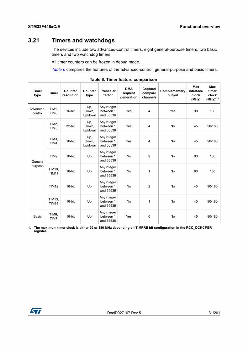
3.21 Timers and watchdogs
The devices include two advanced-control timers, eight general-purpose timers, two basic timers and two watchdog timers.
All timer counters can be frozen in debug mode.
Table 6 compares the features of the advanced-control, general-purpose and basic timers.
Table 6. Timer feature comparison
Timer type
TimerCounter
resolutionCounter
typePrescaler
factor
DMA request
generation
Capture/compare channels
Complementary output
Max interface
clock (MHz)
Max timer clock
(MHz)(1)
Advanced-control
TIM1, TIM8
16-bitUp,
Down, Up/down
Any integer between 1 and 65536
Yes 4 Yes 90 180
General purpose
TIM2, TIM5
32-bitUp,
Down, Up/down
Any integer between 1 and 65536
Yes 4 No 45 90/180
TIM3, TIM4
16-bitUp,
Down, Up/down
Any integer between 1 and 65536
Yes 4 No 45 90/180
TIM9 16-bit UpAny integer between 1 and 65536
No 2 No 90 180
TIM10, TIM11
16-bit UpAny integer between 1 and 65536
No 1 No 90 180
TIM12 16-bit UpAny integer between 1 and 65536
No 2 No 45 90/180
TIM13, TIM14
16-bit UpAny integer between 1 and 65536
No 1 No 45 90/180
BasicTIM6, TIM7
16-bit UpAny integer between 1 and 65536
Yes 0 No 45 90/180
1. The maximum timer clock is either 90 or 180 MHz depending on TIMPRE bit configuration in the RCC_DCKCFGR register.
Functional overview STM32F446xC/E
32/201 DocID027107 Rev 5
3.21.1 Advanced-control timers (TIM1, TIM8)
The advanced-control timers (TIM1, TIM8) can be seen as three-phase PWM generators multiplexed on 6 channels. They have complementary PWM outputs with programmable inserted dead times. They can also be considered as complete general-purpose timers. Their 4 independent channels can be used for:
• Input capture
• Output compare
• PWM generation (edge- or center-aligned modes)
• One-pulse mode output
If configured as standard 16-bit timers, they have the same features as the general-purpose TIMx timers. If configured as 16-bit PWM generators, they have full modulation capability (0-100%).
The advanced-control timer can work together with the TIMx timers via the Timer Link feature for synchronization or event chaining.
TIM1 and TIM8 support independent DMA request generation.
3.21.2 General-purpose timers (TIMx)
There are ten synchronized general-purpose timers embedded in the STM32F446xC/E devices (see Table 6 for differences).
• TIM2, TIM3, TIM4, TIM5
The STM32F446xC/E include 4 full-featured general-purpose timers: TIM2, TIM5, TIM3, and TIM4.The TIM2 and TIM5 timers are based on a 32-bit auto-reload up/downcounter and a 16-bit prescaler. The TIM3 and TIM4 timers are based on a 16-bit auto-reload up/downcounter and a 16-bit prescaler. They all feature 4 independent channels for input capture/output compare, PWM or one-pulse mode output. This gives up to 16 input capture/output compare/PWMs on the largest packages.
The TIM2, TIM3, TIM4, TIM5 general-purpose timers can work together, or with the other general-purpose timers and the advanced-control timers TIM1 and TIM8 via the Timer Link feature for synchronization or event chaining.
Any of these general-purpose timers can be used to generate PWM outputs.
TIM2, TIM3, TIM4, TIM5 all have independent DMA request generation. They are capable of handling quadrature (incremental) encoder signals and the digital outputs from 1 to 4 hall-effect sensors.
• TIM9, TIM10, TIM11, TIM12, TIM13, and TIM14
These timers are based on a 16-bit auto-reload upcounter and a 16-bit prescaler. TIM10, TIM11, TIM13, and TIM14 feature one independent channel, whereas TIM9 and TIM12 have two independent channels for input capture/output compare, PWM or one-pulse mode output. They can be synchronized with the TIM2, TIM3, TIM4, TIM5 full-featured general-purpose timers. They can also be used as simple time bases.
3.21.3 Basic timers TIM6 and TIM7
These timers are mainly used for DAC trigger and waveform generation. They can also be used as a generic 16-bit time base.
TIM6 and TIM7 support independent DMA request generation.
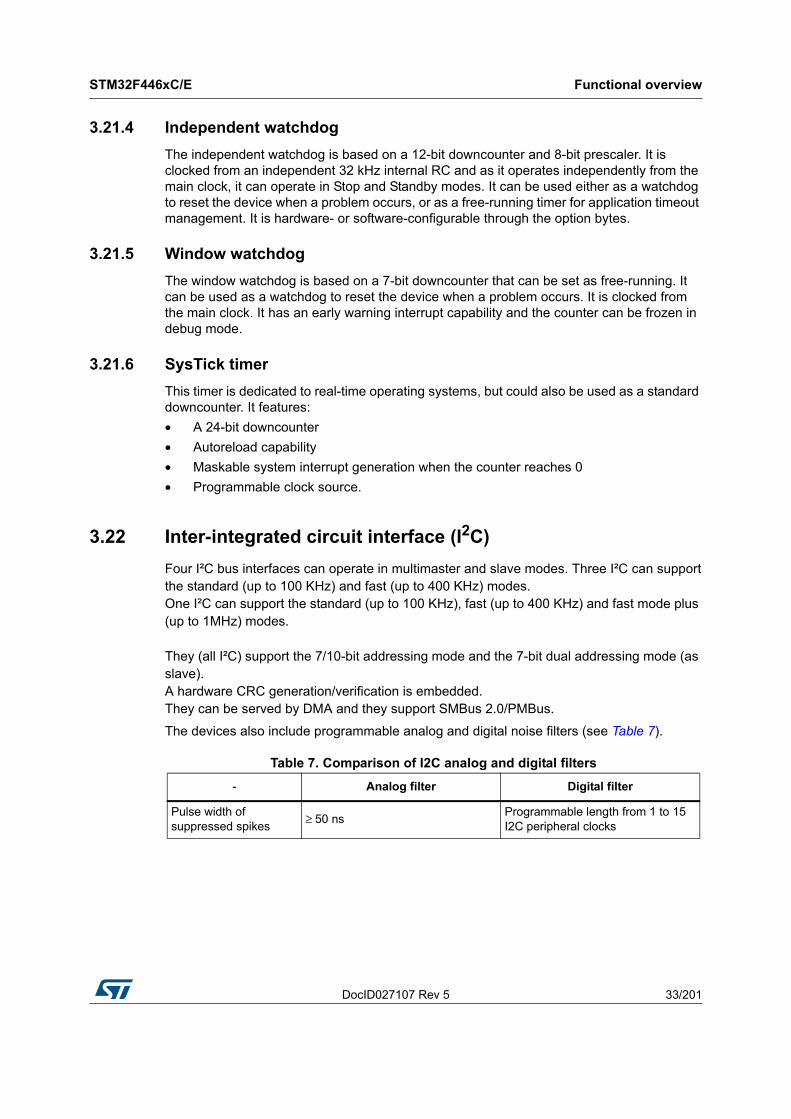
DocID027107 Rev 5 33/201
STM32F446xC/E Functional overview
40
3.21.4 Independent watchdog
The independent watchdog is based on a 12-bit downcounter and 8-bit prescaler. It is clocked from an independent 32 kHz internal RC and as it operates independently from the main clock, it can operate in Stop and Standby modes. It can be used either as a watchdog to reset the device when a problem occurs, or as a free-running timer for application timeout management. It is hardware- or software-configurable through the option bytes.
3.21.5 Window watchdog
The window watchdog is based on a 7-bit downcounter that can be set as free-running. It can be used as a watchdog to reset the device when a problem occurs. It is clocked from the main clock. It has an early warning interrupt capability and the counter can be frozen in debug mode.
3.21.6 SysTick timer
This timer is dedicated to real-time operating systems, but could also be used as a standard downcounter. It features:
• A 24-bit downcounter
• Autoreload capability
• Maskable system interrupt generation when the counter reaches 0
• Programmable clock source.
3.22 Inter-integrated circuit interface (I2C)
Four I²C bus interfaces can operate in multimaster and slave modes. Three I²C can supportthe standard (up to 100 KHz) and fast (up to 400 KHz) modes. One I²C can support the standard (up to 100 KHz), fast (up to 400 KHz) and fast mode plus (up to 1MHz) modes.
They (all I²C) support the 7/10-bit addressing mode and the 7-bit dual addressing mode (as slave).A hardware CRC generation/verification is embedded.They can be served by DMA and they support SMBus 2.0/PMBus.
The devices also include programmable analog and digital noise filters (see Table 7).
Table 7. Comparison of I2C analog and digital filters
- Analog filter Digital filter
Pulse width of suppressed spikes
≥ 50 nsProgrammable length from 1 to 15 I2C peripheral clocks
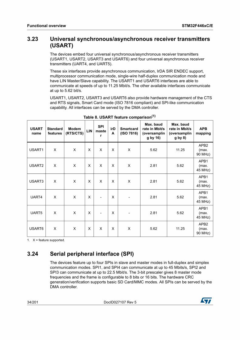
Functional overview STM32F446xC/E
34/201 DocID027107 Rev 5
3.23 Universal synchronous/asynchronous receiver transmitters (USART)
The devices embed four universal synchronous/asynchronous receiver transmitters (USART1, USART2, USART3 and USART6) and four universal asynchronous receiver transmitters (UART4, and UART5).
These six interfaces provide asynchronous communication, IrDA SIR ENDEC support, multiprocessor communication mode, single-wire half-duplex communication mode and have LIN Master/Slave capability. The USART1 and USART6 interfaces are able to communicate at speeds of up to 11.25 Mbit/s. The other available interfaces communicate at up to 5.62 bit/s.
USART1, USART2, USART3 and USART6 also provide hardware management of the CTS and RTS signals, Smart Card mode (ISO 7816 compliant) and SPI-like communication capability. All interfaces can be served by the DMA controller.
3.24 Serial peripheral interface (SPI)
The devices feature up to four SPIs in slave and master modes in full-duplex and simplex communication modes. SPI1, and SPI4 can communicate at up to 45 Mbits/s, SPI2 and SPI3 can communicate at up to 22.5 Mbit/s. The 3-bit prescaler gives 8 master mode frequencies and the frame is configurable to 8 bits or 16 bits. The hardware CRC generation/verification supports basic SD Card/MMC modes. All SPIs can be served by the DMA controller.
Table 8. USART feature comparison(1)
USART name
Standard features
Modem (RTS/CTS)
LINSPI
master
irDA
Smartcard (ISO 7816)
Max. baud rate in Mbit/s (oversamplin
g by 16)
Max. baud rate in Mbit/s (oversamplin
g by 8)
APB mapping
USART1 X X X X X X 5.62 11.25APB2 (max.
90 MHz)
USART2 X X X X X X 2.81 5.62APB1 (max.
45 MHz)
USART3 X X X X X X 2.81 5.62APB1 (max.
45 MHz)
UART4 X X X - X - 2.81 5.62APB1 (max.
45 MHz)
UART5 X X X - X - 2.81 5.62APB1 (max.
45 MHz)
USART6 X X X X X X 5.62 11.25APB2 (max.
90 MHz)
1. X = feature supported.
DocID027107 Rev 5 35/201
STM32F446xC/E Functional overview
40
The SPI interface can be configured to operate in TI mode for communications in master mode and slave mode.
3.25 HDMI (high-definition multimedia interface) consumer electronics control (CEC)
The devices embeds a HDMI-CEC controller that provides hardware support of consumer electronics control (CEC) (Appendix supplement 1 to the HDMI standard).This protocol provides high-level control functions between all audiovisual products in anenvironment. It is specified to operate at low speeds with minimum processing and memoryoverhead.
3.26 Inter-integrated sound (I2S)
Three standard I2S interfaces (multiplexed with SPI1, SPI2 and SPI3) are available. They can be operated in master or slave mode, in simplex communication modes, and can be configured to operate with a 16-/32-bit resolution as an input or output channel. Audio sampling frequencies from 8 kHz up to 192 kHz are supported. When either or both of the I2S interfaces is/are configured in master mode, the master clock can be output to the external DAC/CODEC at 256 times the sampling frequency.
All I2Sx can be served by the DMA controller.
3.27 SPDIF-RX Receiver Interface (SPDIFRX)
The SPDIF-RX peripheral, is designed to receive an S/PDIF flow compliant with IEC-60958 and IEC-61937. These standards support simple stereo streams up to high sample rate, and compressed multi-channel surround sound, such as those defined by Dolby or DTS (up to 5.1).
The main features of the SPDIF-RX are the following:
• Up to 4 inputs available
• Automatic symbol rate detection
• Maximum symbol rate: 12.288 MHz
• Stereo stream from 32 to 192 kHz supported
• Supports Audio IEC-60958 and IEC-61937, consumer applications
• Parity bit management
• Communication using DMA for audio samples
• Communication using DMA for control and user channel information
• Interrupt capabilities
The SPDIF-RX receiver provides all the necessary features to detect the symbol rate, and decode the incoming data stream.
The user can select the wanted SPDIF input, and when a valid signal will be available, the SPDIF-RX will re-sample the incoming signal, decode the Manchester stream, recognize frames, sub-frames and blocks elements. It delivers to the CPU decoded data, and associated status flags.
Functional overview STM32F446xC/E
36/201 DocID027107 Rev 5
The SPDIF-RX also offers a signal named spdifrx_frame_sync, which toggles at the S/PDIF sub-frame rate that will be used to compute the exact sample rate for clock drift algorithms.
3.28 Serial Audio interface (SAI)
The devices feature two serial audio interfaces (SAI1 and SAI2). Each serial audio interfaces based on two independent audio sub blocks which can operate as transmitter or receiver with their FIFO. Many audio protocols are supported by each block: I2S standards, LSB or MSB-justified, PCM/DSP, TDM, AC’97 and SPDIF output, supporting audio sampling frequencies from 8 kHz up to 192 kHz. Both sub blocks can be configured in master or in slave mode. The SAIs use a PLL to achieve audio class accuracy.
In master mode, the master clock can be output to the external DAC/CODEC at 256 times of the sampling frequency.
The two sub blocks can be configured in synchronous mode when full-duplex mode is required.
SAI1 and SA2 can be served by the DMA controller.
3.29 Audio PLL (PLLI2S)
The devices feature an additional dedicated PLL for audio I2S and SAI applications. It allows to achieve error-free I2S sampling clock accuracy without compromising on the CPU performance, while using USB peripherals.
The PLLI2S configuration can be modified to manage an I2S/SAI sample rate change without disabling the main PLL (PLL) used for CPU, USB and Ethernet interfaces.
The audio PLL can be programmed with very low error to obtain sampling rates ranging from 8 KHz to 192 KHz.
In addition to the audio PLL, a master clock input pin can be used to synchronize the I2S/SAI flow with an external PLL (or Codec output).
3.30 Serial Audio Interface PLL(PLLSAI)
An additional PLL dedicated to audio and USB is used for SAI1 and SAI2 peripheral in case the PLLI2S is programmed to achieve another audio sampling frequency (49.152 MHz or 11.2896 MHz) and the audio application requires both sampling frequencies simultaneously.
The PLLSAI is also used to generate the 48MHz clock for USB FS and SDIO in case the system PLL is programmed with factors not multiple of 48MHz.
3.31 Secure digital input/output interface (SDIO)
An SD/SDIO/MMC host interface is available, that supports MultiMediaCard System Specification Version 4.2 in three different databus modes: 1-bit (default), 4-bit and 8-bit.
The interface allows data transfer at up to 48 MHz, and is compliant with the SD Memory Card Specification Version 2.0.
DocID027107 Rev 5 37/201
STM32F446xC/E Functional overview
40
The SDIO Card Specification Version 2.0 is also supported with two different databus modes: 1-bit (default) and 4-bit.
The current version supports only one SD/SDIO/MMC4.2 card at any one time and a stack of MMC4.1 or previous.
3.32 Controller area network (bxCAN)
The two CANs are compliant with the 2.0A and B (active) specifications with a bitrate up to 1 Mbit/s. They can receive and transmit standard frames with 11-bit identifiers as well as extended frames with 29-bit identifiers. Each CAN has three transmit mailboxes, two receive FIFOS with 3 stages and 28 shared scalable filter banks (all of them can be used even if one CAN is used). 256 bytes of SRAM are allocated for each CAN.
3.33 Universal serial bus on-the-go full-speed (OTG_FS)
The devices embed an USB OTG full-speed device/host/OTG peripheral with integrated transceivers. The USB OTG FS peripheral is compliant with the USB 2.0 specification and with the OTG 1.0 specification. It has software-configurable endpoint setting and supports suspend/resume. The USB OTG full-speed controller requires a dedicated 48 MHz clock that is generated by a PLL connected to the HSE oscillator. The USB has dedicated power rails allowing its use throughout the entire power range. The major features are:
• Combined Rx and Tx FIFO size of 320 × 35 bits with dynamic FIFO sizing
• Supports the session request protocol (SRP) and host negotiation protocol (HNP)
• 6 bidirectional endpoints
• 12 host channels with periodic OUT support
• HNP/SNP/IP inside (no need for any external resistor)
• For OTG/Host modes, a power switch is needed in case bus-powered devices are connected
3.34 Universal serial bus on-the-go high-speed (OTG_HS)
The devices embed a USB OTG high-speed (up to 480 Mb/s) device/host/OTG peripheral. The USB OTG HS supports both full-speed and high-speed operations. It integrates the transceivers for full-speed operation (12 MB/s) and features a UTMI low-pin interface (ULPI) for high-speed operation (480 MB/s). When using the USB OTG HS in HS mode, an external PHY device connected to the ULPI is required.
The USB OTG HS peripheral is compliant with the USB 2.0 specification and with the OTG 1.0 specification. It has software-configurable endpoint setting and supports suspend/resume. The USB OTG full-speed controller requires a dedicated 48 MHz clock that is generated by a PLL connected to the HSE oscillator. The USB has dedicated power rails allowing its use throughout the entire power range.
Functional overview STM32F446xC/E
38/201 DocID027107 Rev 5
The major features are:
• Combined Rx and Tx FIFO size of 1 Kbit × 35 with dynamic FIFO sizing
• Supports the session request protocol (SRP) and host negotiation protocol (HNP)
• 8 bidirectional endpoints
• 16 host channels with periodic OUT support
• Internal FS OTG PHY support
• External HS or HS OTG operation supporting ULPI in SDR mode. The OTG PHY is connected to the microcontroller ULPI port through 12 signals. It can be clocked using the 60 MHz output.
• Internal USB DMA
• HNP/SNP/IP inside (no need for any external resistor)
• for OTG/Host modes, a power switch is needed in case bus-powered devices are connected
3.35 Digital camera interface (DCMI)
The devices embed a camera interface that can connect with camera modules and CMOS sensors through an 8-bit to 14-bit parallel interface, to receive video data. The camera interface can sustain a data transfer rate up to 94.5 Mbyte/s (in 14-bit mode) at 54 MHz.
Its features:
• Programmable polarity for the input pixel clock and synchronization signals
• Parallel data communication can be 8-, 10-, 12- or 14-bit
• Supports 8-bit progressive video monochrome or raw bayer format, YCbCr 4:2:2 progressive video, RGB 565 progressive video or compressed data (like JPEG)
• Supports continuous mode or snapshot (a single frame) mode
• Capability to automatically crop the image black & white.
3.36 General-purpose input/outputs (GPIOs)
Each of the GPIO pins can be configured by software as output (push-pull or open-drain, with or without pull-up or pull-down), as input (floating, with or without pull-up or pull-down) or as peripheral alternate function. Most of the GPIO pins are shared with digital or analog alternate functions. All GPIOs are high-current-capable and have speed selection to better manage internal noise, power consumption and electromagnetic emission.
The I/O configuration can be locked if needed by following a specific sequence in order to avoid spurious writing to the I/Os registers.
Fast I/O handling allowing maximum I/O toggling up to 90 MHz.
3.37 Analog-to-digital converters (ADCs)
Three 12-bit analog-to-digital converters are embedded and each ADC shares up to 16 external channels, performing conversions in the single-shot or scan mode. In scan mode, automatic conversion is performed on a selected group of analog inputs.
DocID027107 Rev 5 39/201
STM32F446xC/E Functional overview
40
Additional logic functions embedded in the ADC interface allow:
• Simultaneous sample and hold
• Interleaved sample and hold
The ADC can be served by the DMA controller. An analog watchdog feature allows very precise monitoring of the converted voltage of one, some or all selected channels. An interrupt is generated when the converted voltage is outside the programmed thresholds.
To synchronize A/D conversion and timers, the ADCs could be triggered by any of TIM1, TIM2, TIM3, TIM4, TIM5, or TIM8 timer.
3.38 Temperature sensor
The temperature sensor has to generate a voltage that varies linearly with temperature. The conversion range is between 1.7 V and 3.6 V. The temperature sensor is internally connected to the same input channel as VBAT, ADC1_IN18, which is used to convert the sensor output voltage into a digital value. When the temperature sensor and VBAT conversion are enabled at the same time, only VBAT conversion is performed.
As the offset of the temperature sensor varies from chip to chip due to process variation, the internal temperature sensor is mainly suitable for applications that detect temperature changes instead of absolute temperatures. If an accurate temperature reading is needed, then an external temperature sensor part should be used.
3.39 Digital-to-analog converter (DAC)
The two 12-bit buffered DAC channels can be used to convert two digital signals into two analog voltage signal outputs.
This dual digital Interface supports the following features:
• two DAC converters: one for each output channel
• 8-bit or 10-bit monotonic output
• left or right data alignment in 12-bit mode
• synchronized update capability
• noise-wave generation
• triangular-wave generation
• dual DAC channel independent or simultaneous conversions
• DMA capability for each channel
• external triggers for conversion
• input voltage reference VREF+
Eight DAC trigger inputs are used in the device. The DAC channels are triggered through the timer update outputs that are also connected to different DMA streams.
3.40 Serial wire JTAG debug port (SWJ-DP)
The ARM SWJ-DP interface is embedded, and is a combined JTAG and serial wire debug port that enables either a serial wire debug or a JTAG probe to be connected to the target.
Functional overview STM32F446xC/E
40/201 DocID027107 Rev 5
Debug is performed using 2 pins only instead of 5 required by the JTAG (JTAG pins could be re-use as GPIO with alternate function): the JTAG TMS and TCK pins are shared with SWDIO and SWCLK, respectively, and a specific sequence on the TMS pin is used to switch between JTAG-DP and SW-DP.
3.41 Embedded Trace Macrocell™
The ARM Embedded Trace Macrocell provides a greater visibility of the instruction and data flow inside the CPU core by streaming compressed data at a very high rate from the STM32F446xx through a small number of ETM pins to an external hardware trace port analyser (TPA) device. The TPA is connected to a host computer using USB, Ethernet, or any other high-speed channel. Real-time instruction and data flow activity can be recorded and then formatted for display on the host computer that runs the debugger software. TPA hardware is commercially available from common development tool vendors.
The Embedded Trace Macrocell operates with third party debugger software tools.
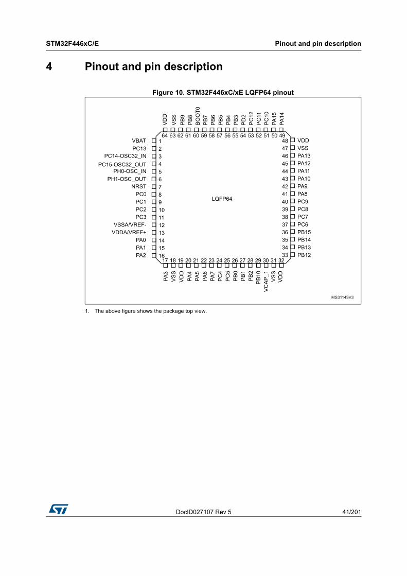
DocID027107 Rev 5 41/201
STM32F446xC/E Pinout and pin description
66
4 Pinout and pin description
Figure 10. STM32F446xC/xE LQFP64 pinout
1. The above figure shows the package top view.
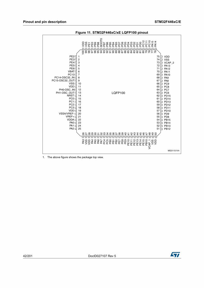
Pinout and pin description STM32F446xC/E
42/201 DocID027107 Rev 5
Figure 11. STM32F446xC/xE LQFP100 pinout
1. The above figure shows the package top view.
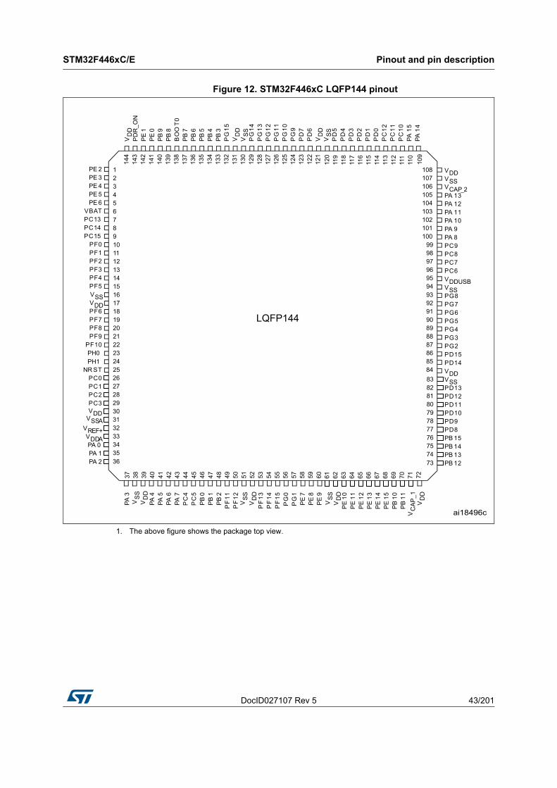
DocID027107 Rev 5 43/201
STM32F446xC/E Pinout and pin description
66
Figure 12. STM32F446xC LQFP144 pinout
1. The above figure shows the package top view.
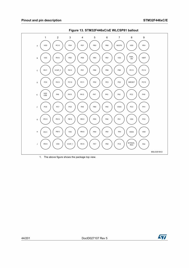
Pinout and pin description STM32F446xC/E
44/201 DocID027107 Rev 5
Figure 13. STM32F446xC/xE WLCSP81 ballout
1. The above figure shows the package top view.
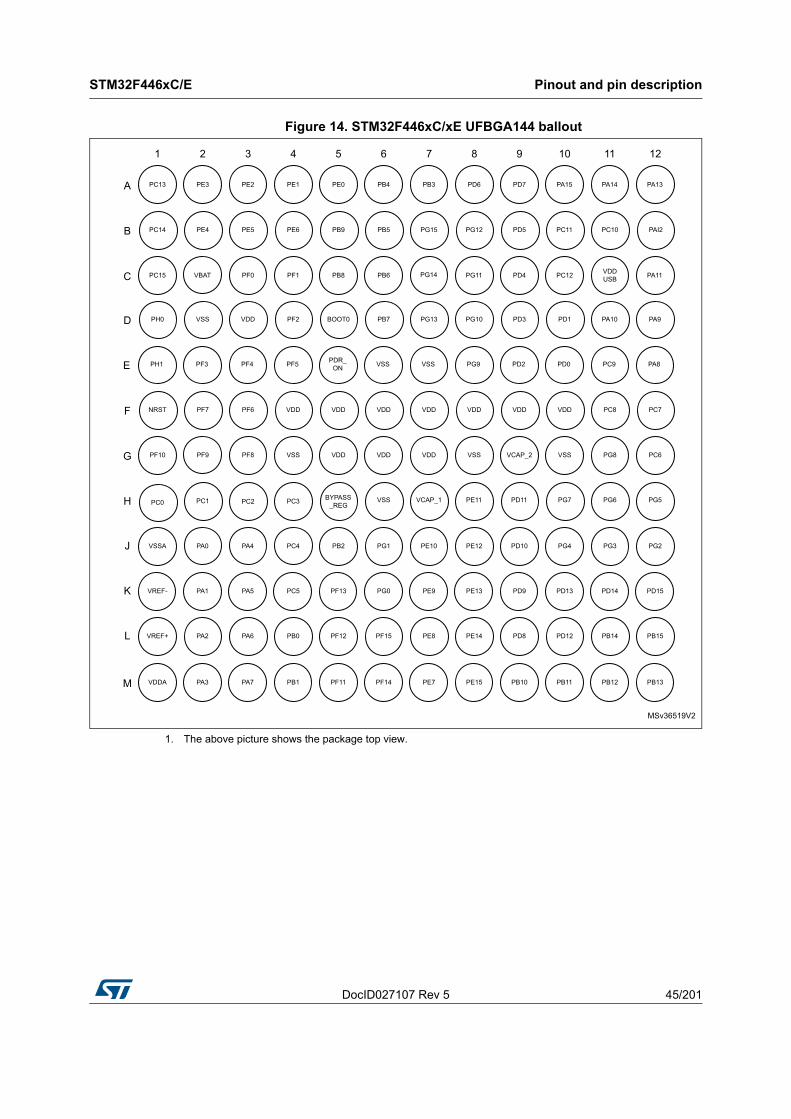
DocID027107 Rev 5 45/201
STM32F446xC/E Pinout and pin description
66
Figure 14. STM32F446xC/xE UFBGA144 ballout
1. The above picture shows the package top view.
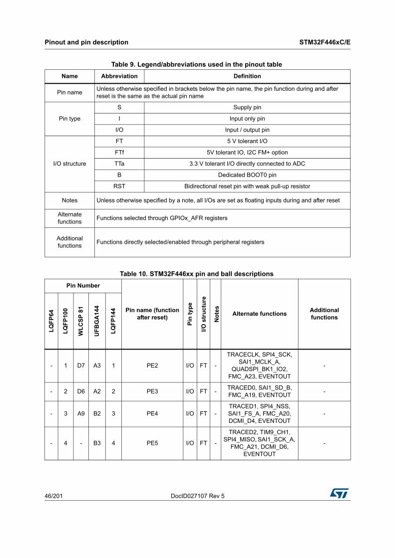
Pinout and pin description STM32F446xC/E
46/201 DocID027107 Rev 5
Table 9. Legend/abbreviations used in the pinout table
Name Abbreviation Definition
Pin nameUnless otherwise specified in brackets below the pin name, the pin function during and after reset is the same as the actual pin name
Pin type
S Supply pin
I Input only pin
I/O Input / output pin
I/O structure
FT 5 V tolerant I/O
FTf 5V tolerant IO, I2C FM+ option
TTa 3.3 V tolerant I/O directly connected to ADC
B Dedicated BOOT0 pin
RST Bidirectional reset pin with weak pull-up resistor
Notes Unless otherwise specified by a note, all I/Os are set as floating inputs during and after reset
Alternate functions
Functions selected through GPIOx_AFR registers
Additional functions
Functions directly selected/enabled through peripheral registers
Table 10. STM32F446xx pin and ball descriptions
Pin Number
Pin name (function after reset)
Pin
ty
pe
I/O s
tru
ctu
re
No
tes
Alternate functionsAdditional functions
LQ
FP
64
LQ
FP
100
WL
CS
P 8
1
UF
BG
A14
4
LQ
FP
144
- 1 D7 A3 1 PE2 I/O FT -
TRACECLK, SPI4_SCK, SAI1_MCLK_A,
QUADSPI_BK1_IO2, FMC_A23, EVENTOUT
-
- 2 D6 A2 2 PE3 I/O FT -TRACED0, SAI1_SD_B, FMC_A19, EVENTOUT
-
- 3 A9 B2 3 PE4 I/O FT -TRACED1, SPI4_NSS, SAI1_FS_A, FMC_A20, DCMI_D4, EVENTOUT
-
- 4 - B3 4 PE5 I/O FT -
TRACED2, TIM9_CH1, SPI4_MISO, SAI1_SCK_A,
FMC_A21, DCMI_D6, EVENTOUT
-
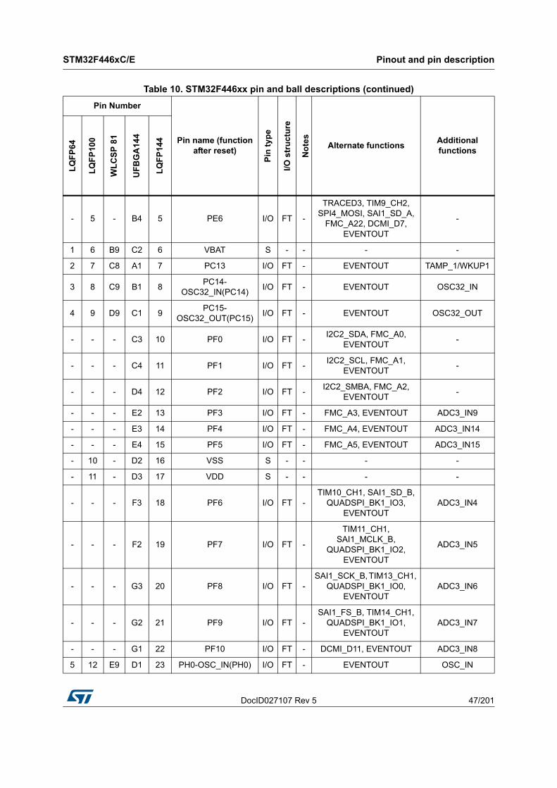
DocID027107 Rev 5 47/201
STM32F446xC/E Pinout and pin description
66
- 5 - B4 5 PE6 I/O FT -
TRACED3, TIM9_CH2, SPI4_MOSI, SAI1_SD_A,
FMC_A22, DCMI_D7, EVENTOUT
-
1 6 B9 C2 6 VBAT S - - - -
2 7 C8 A1 7 PC13 I/O FT - EVENTOUT TAMP_1/WKUP1
3 8 C9 B1 8PC14-
OSC32_IN(PC14)I/O FT - EVENTOUT OSC32_IN
4 9 D9 C1 9PC15-
OSC32_OUT(PC15)I/O FT - EVENTOUT OSC32_OUT
- - - C3 10 PF0 I/O FT -I2C2_SDA, FMC_A0,
EVENTOUT-
- - - C4 11 PF1 I/O FT -I2C2_SCL, FMC_A1,
EVENTOUT-
- - - D4 12 PF2 I/O FT -I2C2_SMBA, FMC_A2,
EVENTOUT-
- - - E2 13 PF3 I/O FT - FMC_A3, EVENTOUT ADC3_IN9
- - - E3 14 PF4 I/O FT - FMC_A4, EVENTOUT ADC3_IN14
- - - E4 15 PF5 I/O FT - FMC_A5, EVENTOUT ADC3_IN15
- 10 - D2 16 VSS S - - - -
- 11 - D3 17 VDD S - - - -
- - - F3 18 PF6 I/O FT -TIM10_CH1, SAI1_SD_B,
QUADSPI_BK1_IO3, EVENTOUT
ADC3_IN4
- - - F2 19 PF7 I/O FT -
TIM11_CH1, SAI1_MCLK_B,
QUADSPI_BK1_IO2, EVENTOUT
ADC3_IN5
- - - G3 20 PF8 I/O FT -SAI1_SCK_B, TIM13_CH1,
QUADSPI_BK1_IO0, EVENTOUT
ADC3_IN6
- - - G2 21 PF9 I/O FT -SAI1_FS_B, TIM14_CH1,
QUADSPI_BK1_IO1, EVENTOUT
ADC3_IN7
- - - G1 22 PF10 I/O FT - DCMI_D11, EVENTOUT ADC3_IN8
5 12 E9 D1 23 PH0-OSC_IN(PH0) I/O FT - EVENTOUT OSC_IN
Table 10. STM32F446xx pin and ball descriptions (continued)
Pin Number
Pin name (function after reset)
Pin
typ
e
I/O s
tru
ctu
re
No
tes
Alternate functionsAdditional functions
LQ
FP
64
LQ
FP
100
WL
CS
P 8
1
UF
BG
A14
4
LQ
FP
144
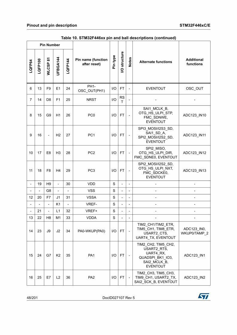
Pinout and pin description STM32F446xC/E
48/201 DocID027107 Rev 5
6 13 F9 E1 24PH1-
OSC_OUT(PH1)I/O FT - EVENTOUT OSC_OUT
7 14 D8 F1 25 NRST I/ORST
- - -
8 15 G9 H1 26 PC0 I/O FT -
SAI1_MCLK_B, OTG_HS_ULPI_STP,
FMC_SDNWE, EVENTOUT
ADC123_IN10
9 16 - H2 27 PC1 I/O FT -
SPI3_MOSI/I2S3_SD, SAI1_SD_A,
SPI2_MOSI/I2S2_SD, EVENTOUT
ADC123_IN11
10 17 E8 H3 28 PC2 I/O FT -SPI2_MISO,
OTG_HS_ULPI_DIR, FMC_SDNE0, EVENTOUT
ADC123_IN12
11 18 F8 H4 29 PC3 I/O FT -
SPI2_MOSI/I2S2_SD, OTG_HS_ULPI_NXT,
FMC_SDCKE0, EVENTOUT
ADC123_IN13
- 19 H9 - 30 VDD S - - - -
- - G8 - - VSS S - - - -
12 20 F7 J1 31 VSSA S - - - -
- - - K1 - VREF- S - - - -
- 21 - L1 32 VREF+ S - - - -
13 22 H8 M1 33 VDDA S - - - -
14 23 J9 J2 34 PA0-WKUP(PA0) I/O FT -
TIM2_CH1/TIM2_ETR, TIM5_CH1, TIM8_ETR,
USART2_CTS, UART4_TX, EVENTOUT
ADC123_IN0, WKUP0/TAMP_2
15 24 G7 K2 35 PA1 I/O FT -
TIM2_CH2, TIM5_CH2, USART2_RTS,
UART4_RX, QUADSPI_BK1_IO3,
SAI2_MCLK_B, EVENTOUT
ADC123_IN1
16 25 E7 L2 36 PA2 I/O FT -TIM2_CH3, TIM5_CH3,
TIM9_CH1, USART2_TX, SAI2_SCK_B, EVENTOUT
ADC123_IN2
Table 10. STM32F446xx pin and ball descriptions (continued)
Pin Number
Pin name (function after reset)
Pin
typ
e
I/O s
tru
ctu
re
No
tes
Alternate functionsAdditional functions
LQ
FP
64
LQ
FP
100
WL
CS
P 8
1
UF
BG
A14
4
LQ
FP
144
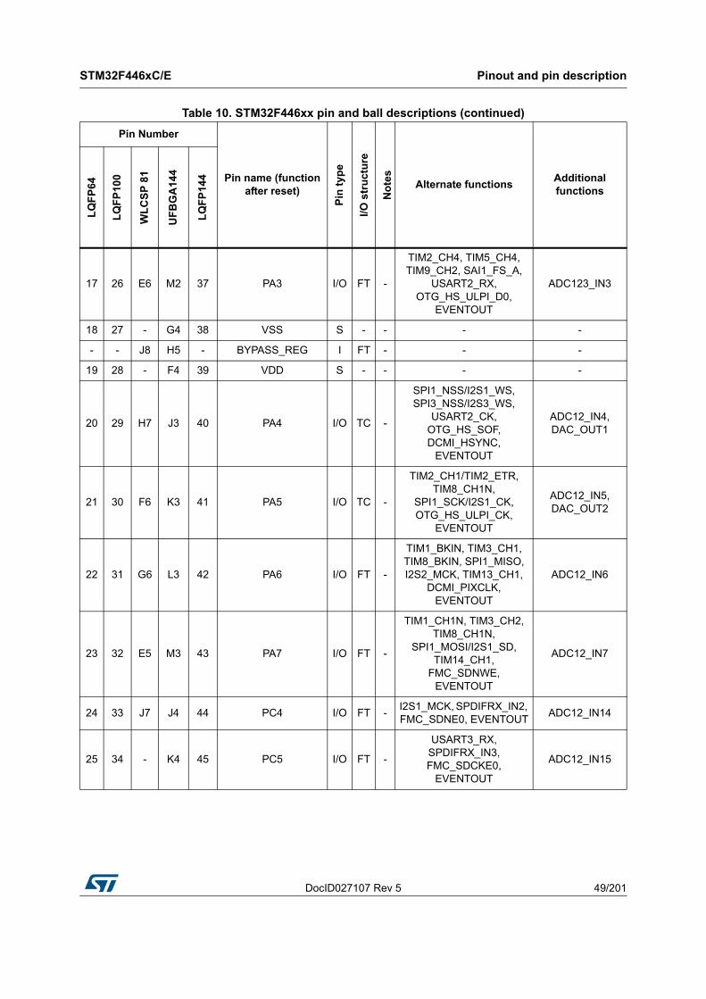
DocID027107 Rev 5 49/201
STM32F446xC/E Pinout and pin description
66
17 26 E6 M2 37 PA3 I/O FT -
TIM2_CH4, TIM5_CH4, TIM9_CH2, SAI1_FS_A,
USART2_RX, OTG_HS_ULPI_D0,
EVENTOUT
ADC123_IN3
18 27 - G4 38 VSS S - - - -
- - J8 H5 - BYPASS_REG I FT - - -
19 28 - F4 39 VDD S - - - -
20 29 H7 J3 40 PA4 I/O TC -
SPI1_NSS/I2S1_WS, SPI3_NSS/I2S3_WS,
USART2_CK, OTG_HS_SOF, DCMI_HSYNC,
EVENTOUT
ADC12_IN4, DAC_OUT1
21 30 F6 K3 41 PA5 I/O TC -
TIM2_CH1/TIM2_ETR, TIM8_CH1N,
SPI1_SCK/I2S1_CK, OTG_HS_ULPI_CK,
EVENTOUT
ADC12_IN5, DAC_OUT2
22 31 G6 L3 42 PA6 I/O FT -
TIM1_BKIN, TIM3_CH1, TIM8_BKIN, SPI1_MISO, I2S2_MCK, TIM13_CH1,
DCMI_PIXCLK, EVENTOUT
ADC12_IN6
23 32 E5 M3 43 PA7 I/O FT -
TIM1_CH1N, TIM3_CH2, TIM8_CH1N,
SPI1_MOSI/I2S1_SD, TIM14_CH1,
FMC_SDNWE, EVENTOUT
ADC12_IN7
24 33 J7 J4 44 PC4 I/O FT -I2S1_MCK, SPDIFRX_IN2, FMC_SDNE0, EVENTOUT
ADC12_IN14
25 34 - K4 45 PC5 I/O FT -
USART3_RX, SPDIFRX_IN3, FMC_SDCKE0,
EVENTOUT
ADC12_IN15
Table 10. STM32F446xx pin and ball descriptions (continued)
Pin Number
Pin name (function after reset)
Pin
typ
e
I/O s
tru
ctu
re
No
tes
Alternate functionsAdditional functions
LQ
FP
64
LQ
FP
100
WL
CS
P 8
1
UF
BG
A14
4
LQ
FP
144
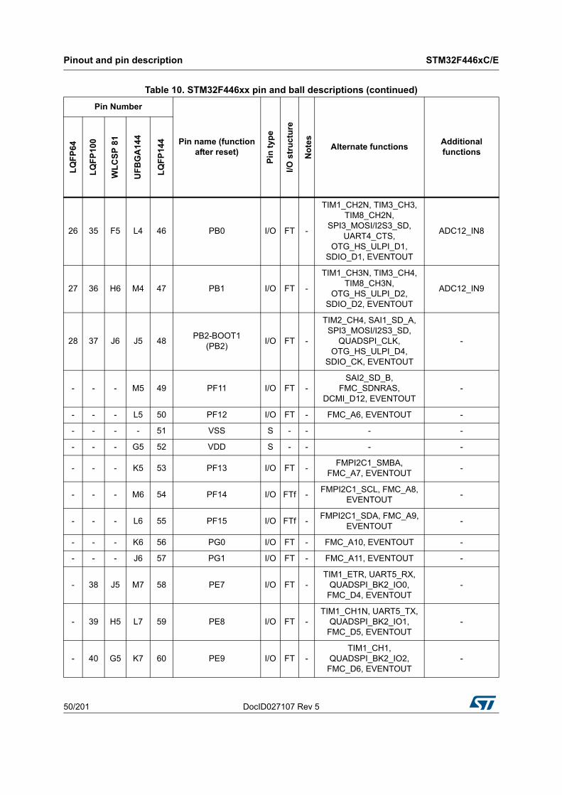
Pinout and pin description STM32F446xC/E
50/201 DocID027107 Rev 5
26 35 F5 L4 46 PB0 I/O FT -
TIM1_CH2N, TIM3_CH3, TIM8_CH2N,
SPI3_MOSI/I2S3_SD, UART4_CTS,
OTG_HS_ULPI_D1, SDIO_D1, EVENTOUT
ADC12_IN8
27 36 H6 M4 47 PB1 I/O FT -
TIM1_CH3N, TIM3_CH4, TIM8_CH3N,
OTG_HS_ULPI_D2, SDIO_D2, EVENTOUT
ADC12_IN9
28 37 J6 J5 48PB2-BOOT1
(PB2)I/O FT -
TIM2_CH4, SAI1_SD_A, SPI3_MOSI/I2S3_SD,
QUADSPI_CLK, OTG_HS_ULPI_D4,
SDIO_CK, EVENTOUT
-
- - - M5 49 PF11 I/O FT -SAI2_SD_B,
FMC_SDNRAS, DCMI_D12, EVENTOUT
-
- - - L5 50 PF12 I/O FT - FMC_A6, EVENTOUT -
- - - - 51 VSS S - - - -
- - - G5 52 VDD S - - - -
- - - K5 53 PF13 I/O FT -FMPI2C1_SMBA,
FMC_A7, EVENTOUT-
- - - M6 54 PF14 I/O FTf -FMPI2C1_SCL, FMC_A8,
EVENTOUT-
- - - L6 55 PF15 I/O FTf -FMPI2C1_SDA, FMC_A9,
EVENTOUT-
- - - K6 56 PG0 I/O FT - FMC_A10, EVENTOUT -
- - - J6 57 PG1 I/O FT - FMC_A11, EVENTOUT -
- 38 J5 M7 58 PE7 I/O FT -TIM1_ETR, UART5_RX,
QUADSPI_BK2_IO0, FMC_D4, EVENTOUT
-
- 39 H5 L7 59 PE8 I/O FT -TIM1_CH1N, UART5_TX,
QUADSPI_BK2_IO1, FMC_D5, EVENTOUT
-
- 40 G5 K7 60 PE9 I/O FT -TIM1_CH1,
QUADSPI_BK2_IO2, FMC_D6, EVENTOUT
-
Table 10. STM32F446xx pin and ball descriptions (continued)
Pin Number
Pin name (function after reset)
Pin
typ
e
I/O s
tru
ctu
re
No
tes
Alternate functionsAdditional functions
LQ
FP
64
LQ
FP
100
WL
CS
P 8
1
UF
BG
A14
4
LQ
FP
144
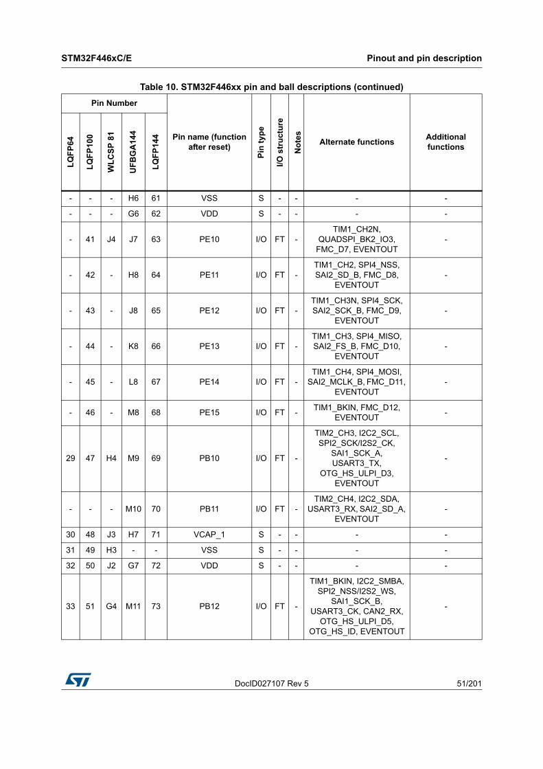
DocID027107 Rev 5 51/201
STM32F446xC/E Pinout and pin description
66
- - - H6 61 VSS S - - - -
- - - G6 62 VDD S - - - -
- 41 J4 J7 63 PE10 I/O FT -TIM1_CH2N,
QUADSPI_BK2_IO3, FMC_D7, EVENTOUT
-
- 42 - H8 64 PE11 I/O FT -TIM1_CH2, SPI4_NSS, SAI2_SD_B, FMC_D8,
EVENTOUT-
- 43 - J8 65 PE12 I/O FT -TIM1_CH3N, SPI4_SCK, SAI2_SCK_B, FMC_D9,
EVENTOUT-
- 44 - K8 66 PE13 I/O FT -TIM1_CH3, SPI4_MISO, SAI2_FS_B, FMC_D10,
EVENTOUT-
- 45 - L8 67 PE14 I/O FT -TIM1_CH4, SPI4_MOSI,
SAI2_MCLK_B, FMC_D11, EVENTOUT
-
- 46 - M8 68 PE15 I/O FT -TIM1_BKIN, FMC_D12,
EVENTOUT-
29 47 H4 M9 69 PB10 I/O FT -
TIM2_CH3, I2C2_SCL, SPI2_SCK/I2S2_CK,
SAI1_SCK_A, USART3_TX,
OTG_HS_ULPI_D3, EVENTOUT
-
- - - M10 70 PB11 I/O FT -TIM2_CH4, I2C2_SDA,
USART3_RX, SAI2_SD_A, EVENTOUT
-
30 48 J3 H7 71 VCAP_1 S - - - -
31 49 H3 - - VSS S - - - -
32 50 J2 G7 72 VDD S - - - -
33 51 G4 M11 73 PB12 I/O FT -
TIM1_BKIN, I2C2_SMBA, SPI2_NSS/I2S2_WS,
SAI1_SCK_B, USART3_CK, CAN2_RX,
OTG_HS_ULPI_D5, OTG_HS_ID, EVENTOUT
-
Table 10. STM32F446xx pin and ball descriptions (continued)
Pin Number
Pin name (function after reset)
Pin
typ
e
I/O s
tru
ctu
re
No
tes
Alternate functionsAdditional functions
LQ
FP
64
LQ
FP
100
WL
CS
P 8
1
UF
BG
A14
4
LQ
FP
144
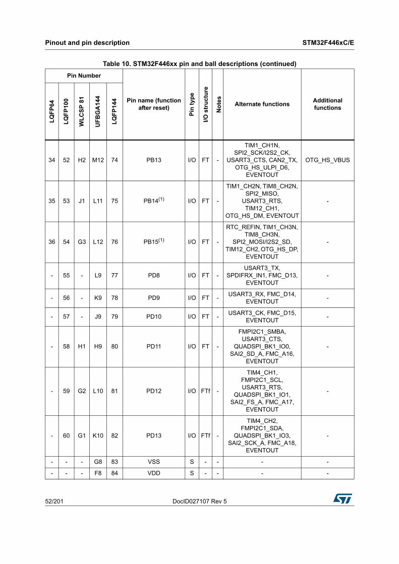
Pinout and pin description STM32F446xC/E
52/201 DocID027107 Rev 5
34 52 H2 M12 74 PB13 I/O FT -
TIM1_CH1N, SPI2_SCK/I2S2_CK,
USART3_CTS, CAN2_TX, OTG_HS_ULPI_D6,
EVENTOUT
OTG_HS_VBUS
35 53 J1 L11 75 PB14(1) I/O FT -
TIM1_CH2N, TIM8_CH2N, SPI2_MISO,
USART3_RTS, TIM12_CH1,
OTG_HS_DM, EVENTOUT
-
36 54 G3 L12 76 PB15(1) I/O FT -
RTC_REFIN, TIM1_CH3N, TIM8_CH3N,
SPI2_MOSI/I2S2_SD, TIM12_CH2, OTG_HS_DP,
EVENTOUT
-
- 55 - L9 77 PD8 I/O FT -USART3_TX,
SPDIFRX_IN1, FMC_D13, EVENTOUT
-
- 56 - K9 78 PD9 I/O FT -USART3_RX, FMC_D14,
EVENTOUT-
- 57 - J9 79 PD10 I/O FT -USART3_CK, FMC_D15,
EVENTOUT-
- 58 H1 H9 80 PD11 I/O FT -
FMPI2C1_SMBA, USART3_CTS,
QUADSPI_BK1_IO0, SAI2_SD_A, FMC_A16,
EVENTOUT
-
- 59 G2 L10 81 PD12 I/O FTf -
TIM4_CH1, FMPI2C1_SCL, USART3_RTS,
QUADSPI_BK1_IO1, SAI2_FS_A, FMC_A17,
EVENTOUT
-
- 60 G1 K10 82 PD13 I/O FTf -
TIM4_CH2, FMPI2C1_SDA,
QUADSPI_BK1_IO3, SAI2_SCK_A, FMC_A18,
EVENTOUT
-
- - - G8 83 VSS S - - - -
- - - F8 84 VDD S - - - -
Table 10. STM32F446xx pin and ball descriptions (continued)
Pin Number
Pin name (function after reset)
Pin
typ
e
I/O s
tru
ctu
re
No
tes
Alternate functionsAdditional functions
LQ
FP
64
LQ
FP
100
WL
CS
P 8
1
UF
BG
A14
4
LQ
FP
144
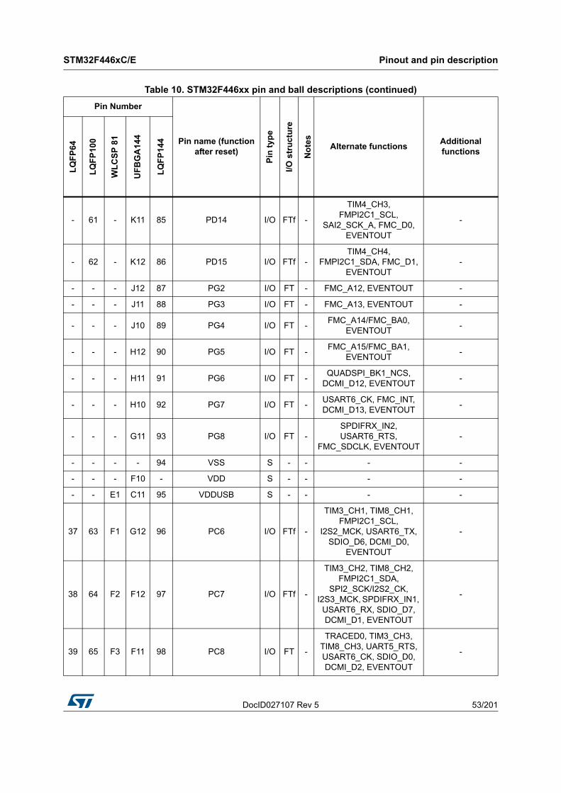
DocID027107 Rev 5 53/201
STM32F446xC/E Pinout and pin description
66
- 61 - K11 85 PD14 I/O FTf -
TIM4_CH3, FMPI2C1_SCL,
SAI2_SCK_A, FMC_D0, EVENTOUT
-
- 62 - K12 86 PD15 I/O FTf -TIM4_CH4,
FMPI2C1_SDA, FMC_D1, EVENTOUT
-
- - - J12 87 PG2 I/O FT - FMC_A12, EVENTOUT -
- - - J11 88 PG3 I/O FT - FMC_A13, EVENTOUT -
- - - J10 89 PG4 I/O FT -FMC_A14/FMC_BA0,
EVENTOUT-
- - - H12 90 PG5 I/O FT -FMC_A15/FMC_BA1,
EVENTOUT-
- - - H11 91 PG6 I/O FT -QUADSPI_BK1_NCS,
DCMI_D12, EVENTOUT-
- - - H10 92 PG7 I/O FT -USART6_CK, FMC_INT, DCMI_D13, EVENTOUT
-
- - - G11 93 PG8 I/O FT -SPDIFRX_IN2, USART6_RTS,
FMC_SDCLK, EVENTOUT-
- - - - 94 VSS S - - - -
- - - F10 - VDD S - - - -
- - E1 C11 95 VDDUSB S - - - -
37 63 F1 G12 96 PC6 I/O FTf -
TIM3_CH1, TIM8_CH1, FMPI2C1_SCL,
I2S2_MCK, USART6_TX, SDIO_D6, DCMI_D0,
EVENTOUT
-
38 64 F2 F12 97 PC7 I/O FTf -
TIM3_CH2, TIM8_CH2, FMPI2C1_SDA,
SPI2_SCK/I2S2_CK, I2S3_MCK, SPDIFRX_IN1,
USART6_RX, SDIO_D7, DCMI_D1, EVENTOUT
-
39 65 F3 F11 98 PC8 I/O FT -
TRACED0, TIM3_CH3, TIM8_CH3, UART5_RTS, USART6_CK, SDIO_D0, DCMI_D2, EVENTOUT
-
Table 10. STM32F446xx pin and ball descriptions (continued)
Pin Number
Pin name (function after reset)
Pin
typ
e
I/O s
tru
ctu
re
No
tes
Alternate functionsAdditional functions
LQ
FP
64
LQ
FP
100
WL
CS
P 8
1
UF
BG
A14
4
LQ
FP
144
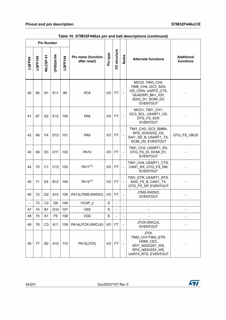
Pinout and pin description STM32F446xC/E
54/201 DocID027107 Rev 5
40 66 D1 E11 99 PC9 I/O FT -
MCO2, TIM3_CH4, TIM8_CH4, I2C3_SDA,
I2S_CKIN, UART5_CTS, QUADSPI_BK1_IO0, SDIO_D1, DCMI_D3,
EVENTOUT
-
41 67 E2 E12 100 PA8 I/O FT -
MCO1, TIM1_CH1, I2C3_SCL, USART1_CK,
OTG_FS_SOF, EVENTOUT
-
42 68 F4 D12 101 PA9 I/O FT -
TIM1_CH2, I2C3_SMBA, SPI2_SCK/I2S2_CK,
SAI1_SD_B, USART1_TX, DCMI_D0, EVENTOUT
OTG_FS_VBUS
43 69 E3 D11 102 PA10 I/O FT -TIM1_CH3, USART1_RX, OTG_FS_ID, DCMI_D1,
EVENTOUT-
44 70 C1 C12 103 PA11(1) I/O FT -TIM1_CH4, USART1_CTS, CAN1_RX, OTG_FS_DM,
EVENTOUT-
45 71 E4 B12 104 PA12(1) I/O FT -TIM1_ETR, USART1_RTS,
SAI2_FS_B, CAN1_TX, OTG_FS_DP, EVENTOUT
-
46 72 D2 A12 105 PA13(JTMS-SWDIO) I/O FT -JTMS-SWDIO,
EVENTOUT-
- 73 C2 G9 106 VCAP_2 S - - - -
47 74 B1 G10 107 VSS S - - - -
48 75 A1 F9 108 VDD S - - - -
49 76 C3 A11 109 PA14(JTCK-SWCLK) I/O FT -JTCK-SWCLK,
EVENTOUT-
50 77 B2 A10 110 PA15(JTDI) I/O FT -
JTDI, TIM2_CH1/TIM2_ETR,
HDMI_CEC, SPI1_NSS/I2S1_WS, SPI3_NSS/I2S3_WS,
UART4_RTS, EVENTOUT
-
Table 10. STM32F446xx pin and ball descriptions (continued)
Pin Number
Pin name (function after reset)
Pin
typ
e
I/O s
tru
ctu
re
No
tes
Alternate functionsAdditional functions
LQ
FP
64
LQ
FP
100
WL
CS
P 8
1
UF
BG
A14
4
LQ
FP
144
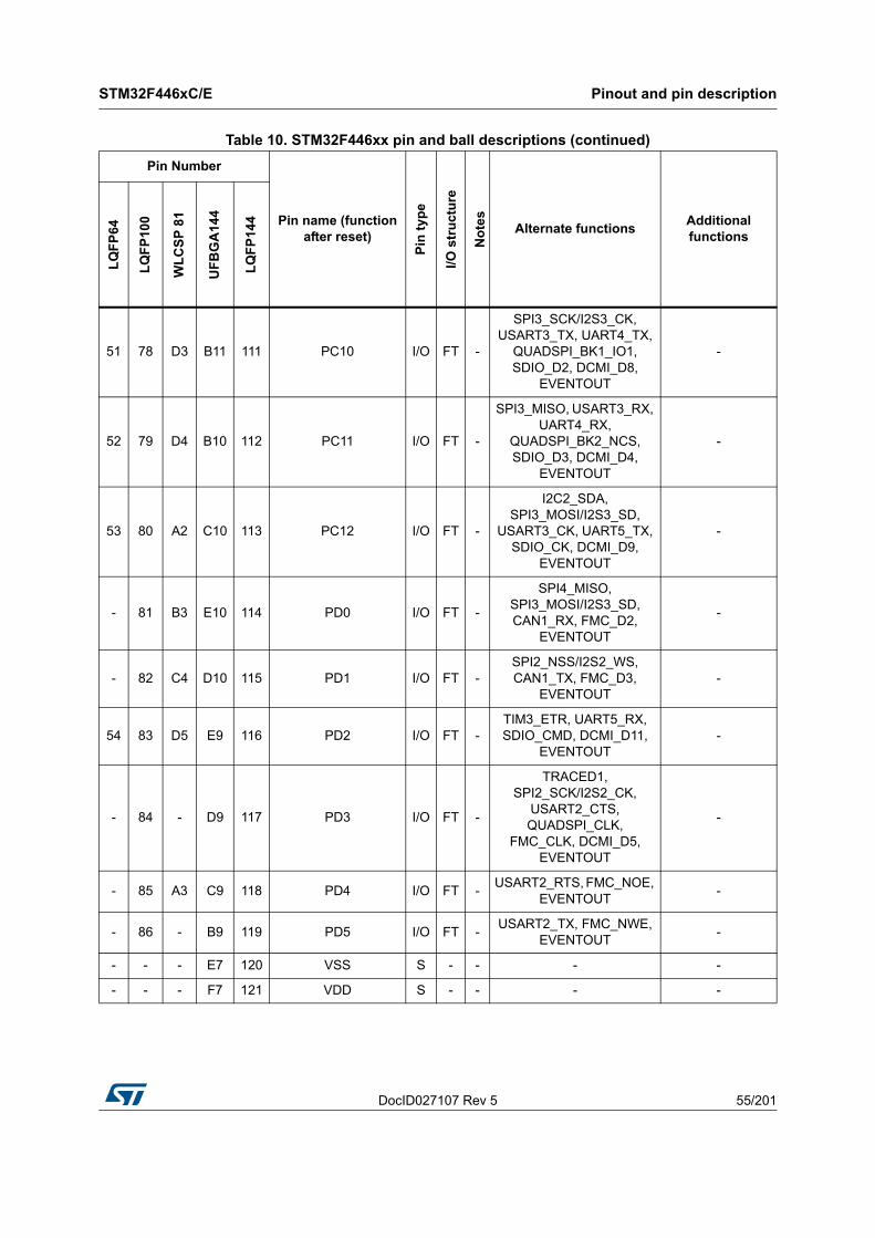
DocID027107 Rev 5 55/201
STM32F446xC/E Pinout and pin description
66
51 78 D3 B11 111 PC10 I/O FT -
SPI3_SCK/I2S3_CK, USART3_TX, UART4_TX,
QUADSPI_BK1_IO1, SDIO_D2, DCMI_D8,
EVENTOUT
-
52 79 D4 B10 112 PC11 I/O FT -
SPI3_MISO, USART3_RX, UART4_RX,
QUADSPI_BK2_NCS, SDIO_D3, DCMI_D4,
EVENTOUT
-
53 80 A2 C10 113 PC12 I/O FT -
I2C2_SDA, SPI3_MOSI/I2S3_SD,
USART3_CK, UART5_TX, SDIO_CK, DCMI_D9,
EVENTOUT
-
- 81 B3 E10 114 PD0 I/O FT -
SPI4_MISO, SPI3_MOSI/I2S3_SD, CAN1_RX, FMC_D2,
EVENTOUT
-
- 82 C4 D10 115 PD1 I/O FT -SPI2_NSS/I2S2_WS, CAN1_TX, FMC_D3,
EVENTOUT-
54 83 D5 E9 116 PD2 I/O FT -TIM3_ETR, UART5_RX, SDIO_CMD, DCMI_D11,
EVENTOUT-
- 84 - D9 117 PD3 I/O FT -
TRACED1, SPI2_SCK/I2S2_CK,
USART2_CTS, QUADSPI_CLK,
FMC_CLK, DCMI_D5, EVENTOUT
-
- 85 A3 C9 118 PD4 I/O FT -USART2_RTS, FMC_NOE,
EVENTOUT-
- 86 - B9 119 PD5 I/O FT -USART2_TX, FMC_NWE,
EVENTOUT-
- - - E7 120 VSS S - - - -
- - - F7 121 VDD S - - - -
Table 10. STM32F446xx pin and ball descriptions (continued)
Pin Number
Pin name (function after reset)
Pin
typ
e
I/O s
tru
ctu
re
No
tes
Alternate functionsAdditional functions
LQ
FP
64
LQ
FP
100
WL
CS
P 8
1
UF
BG
A14
4
LQ
FP
144
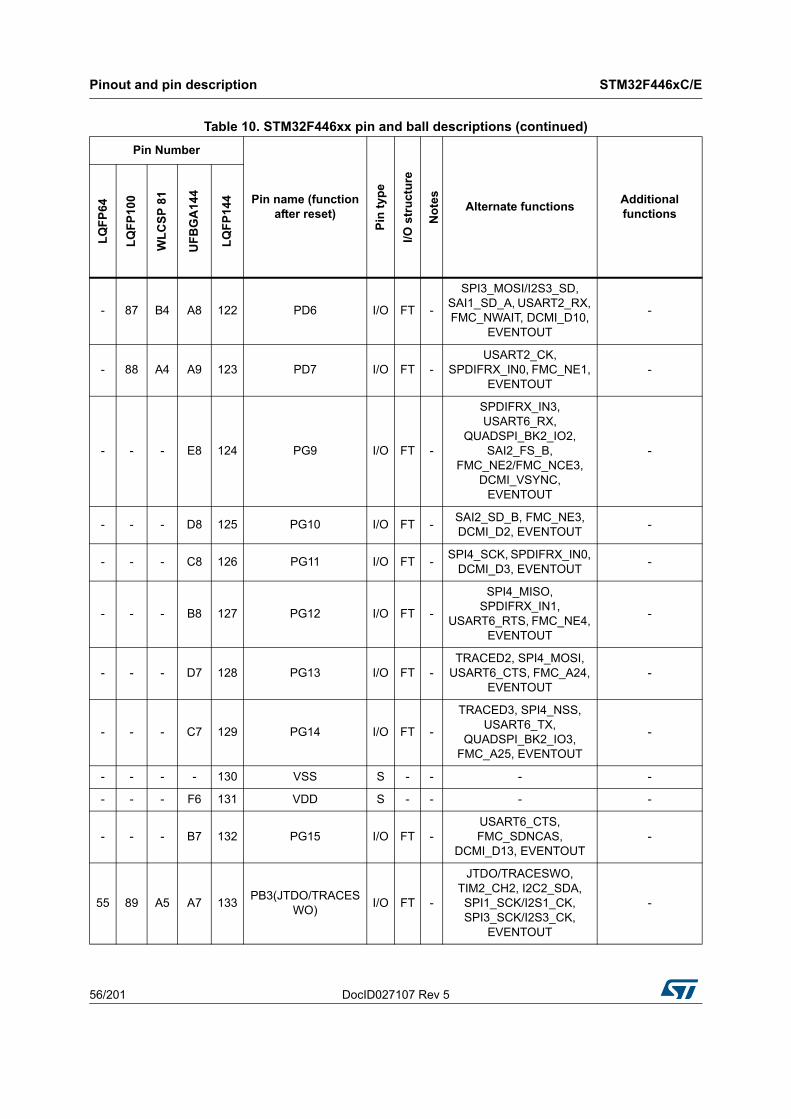
Pinout and pin description STM32F446xC/E
56/201 DocID027107 Rev 5
- 87 B4 A8 122 PD6 I/O FT -
SPI3_MOSI/I2S3_SD, SAI1_SD_A, USART2_RX, FMC_NWAIT, DCMI_D10,
EVENTOUT
-
- 88 A4 A9 123 PD7 I/O FT -USART2_CK,
SPDIFRX_IN0, FMC_NE1, EVENTOUT
-
- - - E8 124 PG9 I/O FT -
SPDIFRX_IN3, USART6_RX,
QUADSPI_BK2_IO2, SAI2_FS_B,
FMC_NE2/FMC_NCE3, DCMI_VSYNC,
EVENTOUT
-
- - - D8 125 PG10 I/O FT -SAI2_SD_B, FMC_NE3, DCMI_D2, EVENTOUT
-
- - - C8 126 PG11 I/O FT -SPI4_SCK, SPDIFRX_IN0,
DCMI_D3, EVENTOUT-
- - - B8 127 PG12 I/O FT -
SPI4_MISO, SPDIFRX_IN1,
USART6_RTS, FMC_NE4, EVENTOUT
-
- - - D7 128 PG13 I/O FT -TRACED2, SPI4_MOSI,
USART6_CTS, FMC_A24, EVENTOUT
-
- - - C7 129 PG14 I/O FT -
TRACED3, SPI4_NSS, USART6_TX,
QUADSPI_BK2_IO3, FMC_A25, EVENTOUT
-
- - - - 130 VSS S - - - -
- - - F6 131 VDD S - - - -
- - - B7 132 PG15 I/O FT -USART6_CTS, FMC_SDNCAS,
DCMI_D13, EVENTOUT-
55 89 A5 A7 133PB3(JTDO/TRACES
WO)I/O FT -
JTDO/TRACESWO, TIM2_CH2, I2C2_SDA, SPI1_SCK/I2S1_CK, SPI3_SCK/I2S3_CK,
EVENTOUT
-
Table 10. STM32F446xx pin and ball descriptions (continued)
Pin Number
Pin name (function after reset)
Pin
typ
e
I/O s
tru
ctu
re
No
tes
Alternate functionsAdditional functions
LQ
FP
64
LQ
FP
100
WL
CS
P 8
1
UF
BG
A14
4
LQ
FP
144
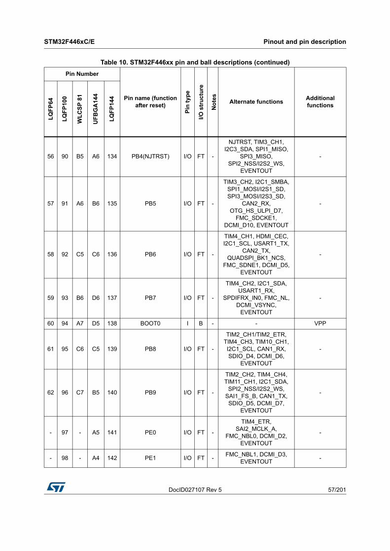
DocID027107 Rev 5 57/201
STM32F446xC/E Pinout and pin description
66
56 90 B5 A6 134 PB4(NJTRST) I/O FT -
NJTRST, TIM3_CH1, I2C3_SDA, SPI1_MISO,
SPI3_MISO, SPI2_NSS/I2S2_WS,
EVENTOUT
-
57 91 A6 B6 135 PB5 I/O FT -
TIM3_CH2, I2C1_SMBA, SPI1_MOSI/I2S1_SD, SPI3_MOSI/I2S3_SD,
CAN2_RX, OTG_HS_ULPI_D7,
FMC_SDCKE1, DCMI_D10, EVENTOUT
-
58 92 C5 C6 136 PB6 I/O FT -
TIM4_CH1, HDMI_CEC, I2C1_SCL, USART1_TX,
CAN2_TX, QUADSPI_BK1_NCS,
FMC_SDNE1, DCMI_D5, EVENTOUT
-
59 93 B6 D6 137 PB7 I/O FT -
TIM4_CH2, I2C1_SDA, USART1_RX,
SPDIFRX_IN0, FMC_NL, DCMI_VSYNC,
EVENTOUT
-
60 94 A7 D5 138 BOOT0 I B - - VPP
61 95 C6 C5 139 PB8 I/O FT -
TIM2_CH1/TIM2_ETR, TIM4_CH3, TIM10_CH1, I2C1_SCL, CAN1_RX, SDIO_D4, DCMI_D6,
EVENTOUT
-
62 96 C7 B5 140 PB9 I/O FT -
TIM2_CH2, TIM4_CH4, TIM11_CH1, I2C1_SDA,
SPI2_NSS/I2S2_WS, SAI1_FS_B, CAN1_TX, SDIO_D5, DCMI_D7,
EVENTOUT
-
- 97 - A5 141 PE0 I/O FT -
TIM4_ETR, SAI2_MCLK_A,
FMC_NBL0, DCMI_D2, EVENTOUT
-
- 98 - A4 142 PE1 I/O FT -FMC_NBL1, DCMI_D3,
EVENTOUT-
Table 10. STM32F446xx pin and ball descriptions (continued)
Pin Number
Pin name (function after reset)
Pin
typ
e
I/O s
tru
ctu
re
No
tes
Alternate functionsAdditional functions
LQ
FP
64
LQ
FP
100
WL
CS
P 8
1
UF
BG
A14
4
LQ
FP
144
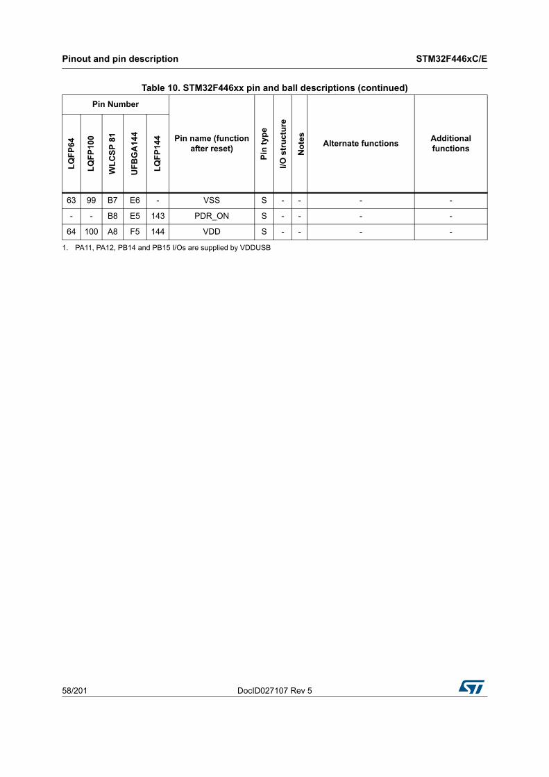
Pinout and pin description STM32F446xC/E
58/201 DocID027107 Rev 5
63 99 B7 E6 - VSS S - - - -
- - B8 E5 143 PDR_ON S - - - -
64 100 A8 F5 144 VDD S - - - -
1. PA11, PA12, PB14 and PB15 I/Os are supplied by VDDUSB
Table 10. STM32F446xx pin and ball descriptions (continued)
Pin Number
Pin name (function after reset)
Pin
typ
e
I/O s
tru
ctu
re
No
tes
Alternate functionsAdditional functions
LQ
FP
64
LQ
FP
100
WL
CS
P 8
1
UF
BG
A14
4
LQ
FP
144
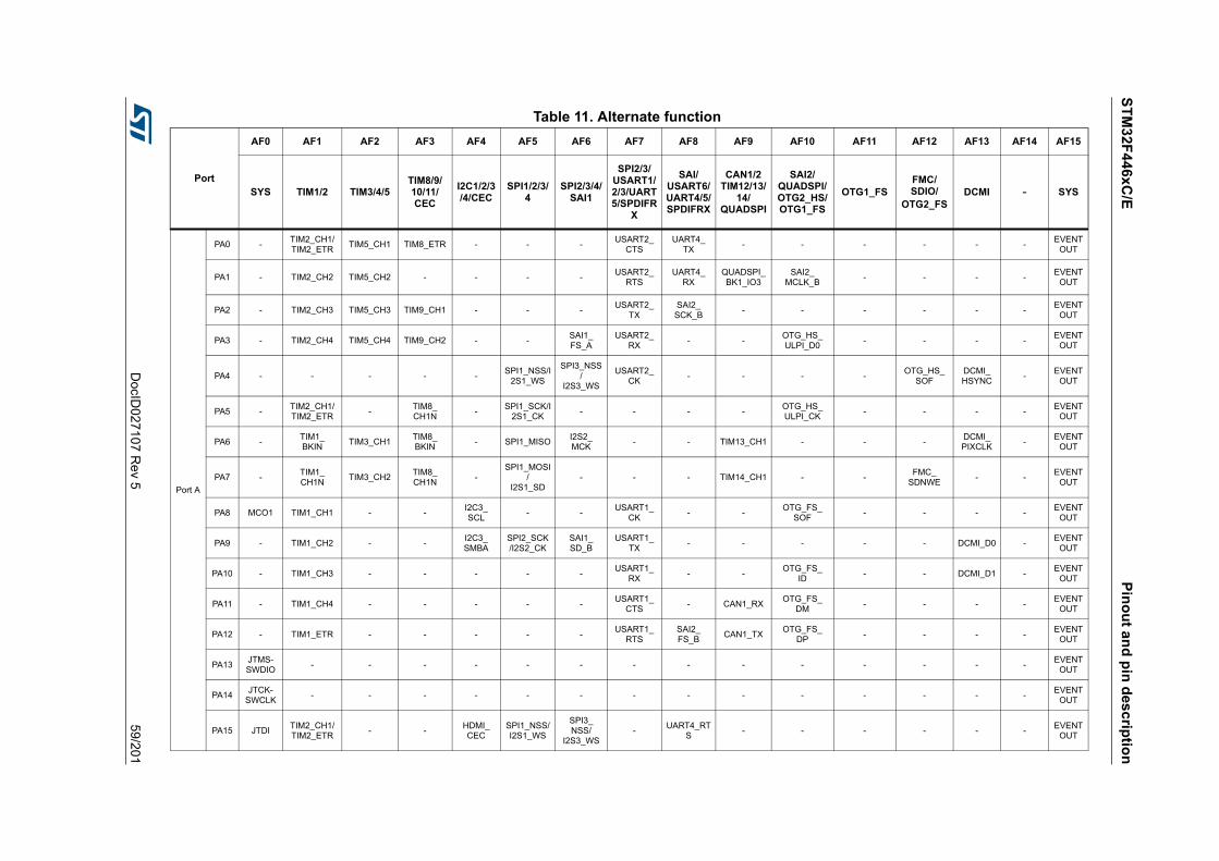
ST
M3
2F4
46xC
/EP
ino
ut a
nd
pin
des
crip
tion
DocID
027107 R
ev 5
59/201
Table 11. Alternate function
Port
AF0 AF1 AF2 AF3 AF4 AF5 AF6 AF7 AF8 AF9 AF10 AF11 AF12 AF13 AF14 AF15
SYS TIM1/2 TIM3/4/5TIM8/9/10/11/CEC
I2C1/2/3/4/CEC
SPI1/2/3/4
SPI2/3/4/SAI1
SPI2/3/USART1/2/3/UART5/SPDIFR
X
SAI/USART6/UART4/5/SPDIFRX
CAN1/2TIM12/13/
14/QUADSPI
SAI2/QUADSPI/OTG2_HS/OTG1_FS
OTG1_FSFMC/SDIO/
OTG2_FSDCMI - SYS
Port A
PA0 -TIM2_CH1/TIM2_ETR
TIM5_CH1 TIM8_ETR - - -USART2_
CTSUART4_
TX- - - - - -
EVENTOUT
PA1 - TIM2_CH2 TIM5_CH2 - - - -USART2_
RTSUART4_
RXQUADSPI_BK1_IO3
SAI2_MCLK_B
- - - -EVENT
OUT
PA2 - TIM2_CH3 TIM5_CH3 TIM9_CH1 - - -USART2_
TXSAI2_
SCK_B- - - - - -
EVENTOUT
PA3 - TIM2_CH4 TIM5_CH4 TIM9_CH2 - -SAI1_FS_A
USART2_RX
- -OTG_HS_ULPI_D0
- - - -EVENT
OUT
PA4 - - - - -SPI1_NSS/I
2S1_WS
SPI3_NSS/
I2S3_WS
USART2_CK
- - - -OTG_HS_
SOFDCMI_HSYNC
-EVENT
OUT
PA5 -TIM2_CH1/TIM2_ETR
-TIM8_CH1N
-SPI1_SCK/I
2S1_CK- - - -
OTG_HS_ULPI_CK
- - - -EVENT
OUT
PA6 -TIM1_BKIN
TIM3_CH1TIM8_BKIN
- SPI1_MISOI2S2_MCK
- - TIM13_CH1 - - -DCMI_PIXCLK
-EVENT
OUT
PA7 -TIM1_CH1N
TIM3_CH2TIM8_CH1N
-SPI1_MOSI
/I2S1_SD
- - - TIM14_CH1 - -FMC_
SDNWE- -
EVENTOUT
PA8 MCO1 TIM1_CH1 - -I2C3_SCL
- -USART1_
CK- -
OTG_FS_SOF
- - - -EVENT
OUT
PA9 - TIM1_CH2 - -I2C3_SMBA
SPI2_SCK/I2S2_CK
SAI1_SD_B
USART1_TX
- - - - - DCMI_D0 -EVENT
OUT
PA10 - TIM1_CH3 - - - - -USART1_
RX- -
OTG_FS_ID
- - DCMI_D1 -EVENT
OUT
PA11 - TIM1_CH4 - - - - -USART1_
CTS- CAN1_RX
OTG_FS_DM
- - - -EVENT
OUT
PA12 - TIM1_ETR - - - - -USART1_
RTSSAI2_FS_B
CAN1_TXOTG_FS_
DP- - - -
EVENTOUT
PA13JTMS-SWDIO
- - - - - - - - - - - - - -EVENT
OUT
PA14JTCK-
SWCLK- - - - - - - - - - - - - -
EVENTOUT
PA15 JTDITIM2_CH1/TIM2_ETR
- -HDMI_CEC
SPI1_NSS/I2S1_WS
SPI3_NSS/
I2S3_WS-
UART4_RTS
- - - - - -EVENT
OUT
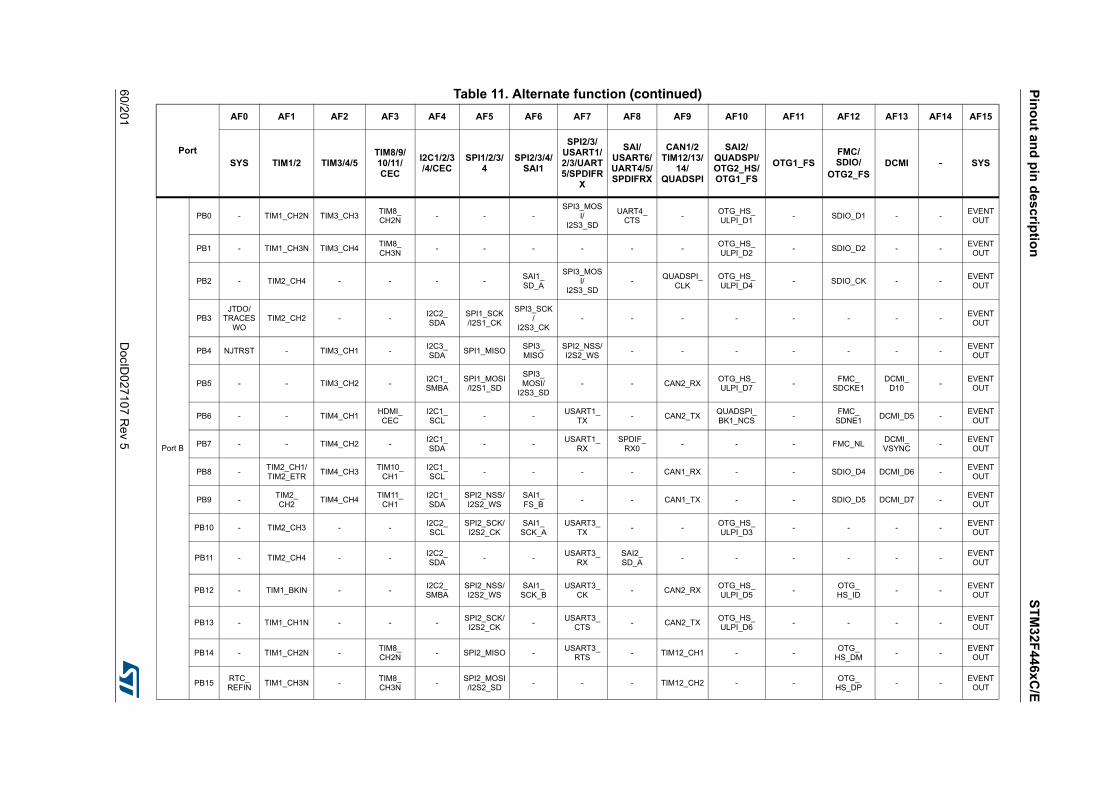
Pin
ou
t and
pin
de
scrip
tion
ST
M32
F44
6xC
/E
60/2
01D
ocID027
107 Re
v 5
Port B
PB0 - TIM1_CH2N TIM3_CH3TIM8_CH2N
- - -SPI3_MOS
I/I2S3_SD
UART4_CTS
-OTG_HS_ULPI_D1
- SDIO_D1 - -EVENT
OUT
PB1 - TIM1_CH3N TIM3_CH4TIM8_CH3N
- - - - - -OTG_HS_ULPI_D2
- SDIO_D2 - -EVENT
OUT
PB2 - TIM2_CH4 - - - -SAI1_SD_A
SPI3_MOSI/
I2S3_SD-
QUADSPI_CLK
OTG_HS_ULPI_D4
- SDIO_CK - -EVENT
OUT
PB3JTDO/
TRACESWO
TIM2_CH2 - -I2C2_SDA
SPI1_SCK/I2S1_CK
SPI3_SCK/
I2S3_CK- - - - - - - -
EVENTOUT
PB4 NJTRST - TIM3_CH1 -I2C3_SDA
SPI1_MISOSPI3_MISO
SPI2_NSS/I2S2_WS
- - - - - - -EVENT
OUT
PB5 - - TIM3_CH2 -I2C1_SMBA
SPI1_MOSI/I2S1_SD
SPI3_MOSI/
I2S3_SD- - CAN2_RX
OTG_HS_ULPI_D7
-FMC_
SDCKE1DCMI_
D10-
EVENTOUT
PB6 - - TIM4_CH1HDMI_CEC
I2C1_SCL
- -USART1_
TX- CAN2_TX
QUADSPI_BK1_NCS
-FMC_
SDNE1DCMI_D5 -
EVENTOUT
PB7 - - TIM4_CH2 -I2C1_SDA
- -USART1_
RXSPDIF_
RX0- - - FMC_NL
DCMI_VSYNC
-EVENT
OUT
PB8 -TIM2_CH1/TIM2_ETR
TIM4_CH3TIM10_
CH1I2C1_SCL
- - - - CAN1_RX - - SDIO_D4 DCMI_D6 -EVENT
OUT
PB9 -TIM2_CH2
TIM4_CH4TIM11_
CH1I2C1_SDA
SPI2_NSS/I2S2_WS
SAI1_FS_B
- - CAN1_TX - - SDIO_D5 DCMI_D7 -EVENT
OUT
PB10 - TIM2_CH3 - -I2C2_SCL
SPI2_SCK/I2S2_CK
SAI1_SCK_A
USART3_TX
- -OTG_HS_ULPI_D3
- - - -EVENT
OUT
PB11 - TIM2_CH4 - -I2C2_SDA
- -USART3_
RXSAI2_SD_A
- - - - - -EVENT
OUT
PB12 - TIM1_BKIN - -I2C2_SMBA
SPI2_NSS/I2S2_WS
SAI1_SCK_B
USART3_CK
- CAN2_RXOTG_HS_ULPI_D5
-OTG_HS_ID
- -EVENT
OUT
PB13 - TIM1_CH1N - - -SPI2_SCK/I2S2_CK
-USART3_
CTS- CAN2_TX
OTG_HS_ULPI_D6
- - - -EVENT
OUT
PB14 - TIM1_CH2N -TIM8_CH2N
- SPI2_MISO -USART3_
RTS- TIM12_CH1 - -
OTG_HS_DM
- -EVENT
OUT
PB15RTC_REFIN
TIM1_CH3N -TIM8_CH3N
-SPI2_MOSI/I2S2_SD
- - - TIM12_CH2 - -OTG_
HS_DP- -
EVENTOUT
Table 11. Alternate function (continued)
Port
AF0 AF1 AF2 AF3 AF4 AF5 AF6 AF7 AF8 AF9 AF10 AF11 AF12 AF13 AF14 AF15
SYS TIM1/2 TIM3/4/5TIM8/9/10/11/CEC
I2C1/2/3/4/CEC
SPI1/2/3/4
SPI2/3/4/SAI1
SPI2/3/USART1/2/3/UART5/SPDIFR
X
SAI/USART6/UART4/5/SPDIFRX
CAN1/2TIM12/13/
14/QUADSPI
SAI2/QUADSPI/OTG2_HS/OTG1_FS
OTG1_FSFMC/SDIO/
OTG2_FSDCMI - SYS
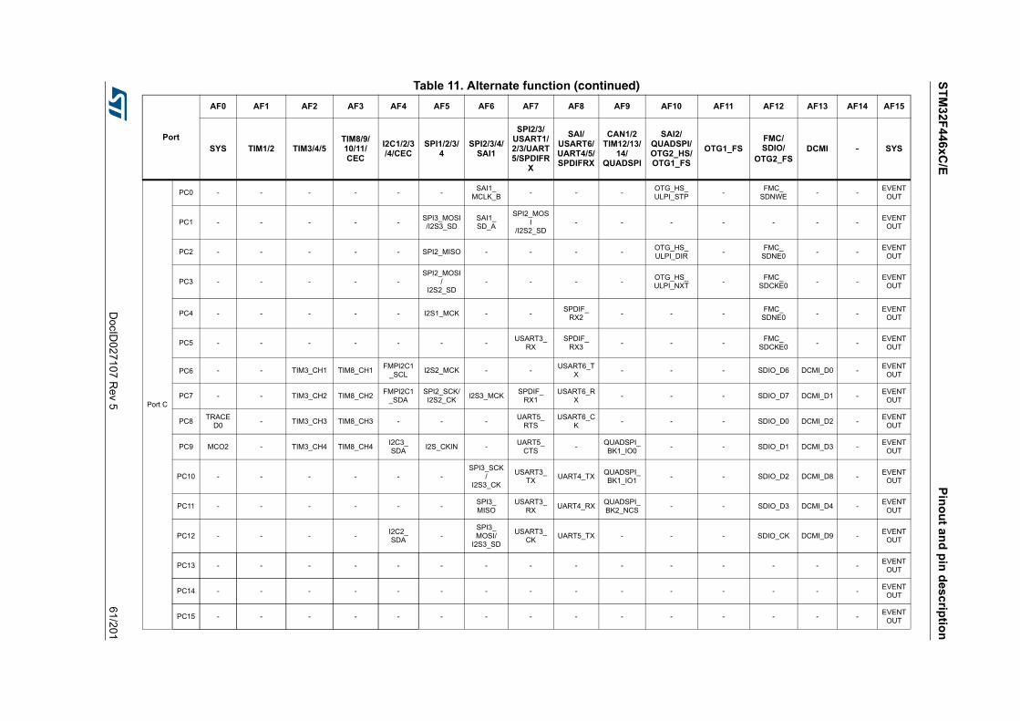
ST
M3
2F4
46xC
/EP
ino
ut a
nd
pin
des
crip
tion
DocID
027107 R
ev 5
61/201
Port C
PC0 - - - - - -SAI1_
MCLK_B- - -
OTG_HS_ULPI_STP
-FMC_
SDNWE- -
EVENTOUT
PC1 - - - - -SPI3_MOSI/I2S3_SD
SAI1_SD_A
SPI2_MOSI
/I2S2_SD- - - - - - -
EVENTOUT
PC2 - - - - - SPI2_MISO - - - -OTG_HS_ULPI_DIR
-FMC_
SDNE0- -
EVENTOUT
PC3 - - - - -SPI2_MOSI
/I2S2_SD
- - - -OTG_HS_ULPI_NXT
-FMC_
SDCKE0- -
EVENTOUT
PC4 - - - - - I2S1_MCK - -SPDIF_
RX2- - -
FMC_SDNE0
- -EVENT
OUT
PC5 - - - - - - -USART3_
RXSPDIF_
RX3- - -
FMC_SDCKE0
- -EVENT
OUT
PC6 - - TIM3_CH1 TIM8_CH1FMPI2C1
_SCLI2S2_MCK - -
USART6_TX
- - - SDIO_D6 DCMI_D0 -EVENT
OUT
PC7 - - TIM3_CH2 TIM8_CH2FMPI2C1
_SDASPI2_SCK/I2S2_CK
I2S3_MCKSPDIF_
RX1USART6_R
X- - - SDIO_D7 DCMI_D1 -
EVENTOUT
PC8TRACE
D0- TIM3_CH3 TIM8_CH3 - - -
UART5_RTS
USART6_CK
- - - SDIO_D0 DCMI_D2 -EVENT
OUT
PC9 MCO2 - TIM3_CH4 TIM8_CH4I2C3_SDA
I2S_CKIN -UART5_
CTS-
QUADSPI_BK1_IO0
- - SDIO_D1 DCMI_D3 -EVENT
OUT
PC10 - - - - - -SPI3_SCK
/I2S3_CK
USART3_TX
UART4_TXQUADSPI_BK1_IO1
- - SDIO_D2 DCMI_D8 -EVENT
OUT
PC11 - - - - - -SPI3_MISO
USART3_RX
UART4_RXQUADSPI_BK2_NCS
- - SDIO_D3 DCMI_D4 -EVENT
OUT
PC12 - - - -I2C2_SDA
-SPI3_MOSI/
I2S3_SD
USART3_CK
UART5_TX - - - SDIO_CK DCMI_D9 -EVENT
OUT
PC13 - - - - - - - - - - - - - - -EVENT
OUT
PC14 - - - - - - - - - - - - - - -EVENT
OUT
PC15 - - - - - - - - - - - - - - -EVENT
OUT
Table 11. Alternate function (continued)
Port
AF0 AF1 AF2 AF3 AF4 AF5 AF6 AF7 AF8 AF9 AF10 AF11 AF12 AF13 AF14 AF15
SYS TIM1/2 TIM3/4/5TIM8/9/10/11/CEC
I2C1/2/3/4/CEC
SPI1/2/3/4
SPI2/3/4/SAI1
SPI2/3/USART1/2/3/UART5/SPDIFR
X
SAI/USART6/UART4/5/SPDIFRX
CAN1/2TIM12/13/
14/QUADSPI
SAI2/QUADSPI/OTG2_HS/OTG1_FS
OTG1_FSFMC/SDIO/
OTG2_FSDCMI - SYS
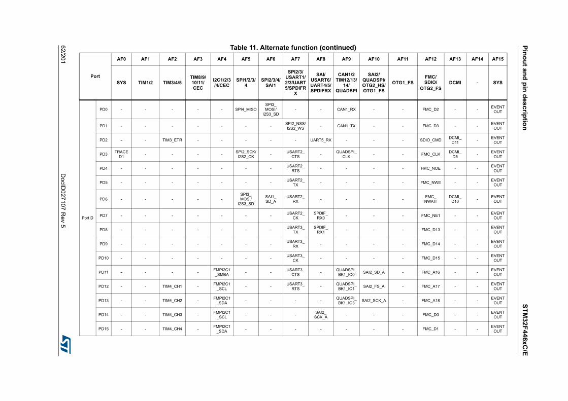
Pin
ou
t and
pin
de
scrip
tion
ST
M32
F44
6xC
/E
62/2
01D
ocID027
107 Re
v 5
Port D
PD0 - - - - - SPI4_MISOSPI3_MOSI/
I2S3_SD- - CAN1_RX - - FMC_D2 - -
EVENTOUT
PD1 - - - - - - -SPI2_NSS/I2S2_WS
- CAN1_TX - - FMC_D3 - -EVENT
OUT
PD2 - - TIM3_ETR - - - - - UART5_RX - - - SDIO_CMDDCMI_
D11-
EVENTOUT
PD3TRACE
D1- - - -
SPI2_SCK/I2S2_CK
-USART2_
CTS-
QUADSPI_CLK
- - FMC_CLKDCMI_
D5-
EVENTOUT
PD4 - - - - - - -USART2_
RTS- - - - FMC_NOE - -
EVENTOUT
PD5 - - - - - - -USART2_
TX- - - - FMC_NWE - -
EVENTOUT
PD6 - - - - -SPI3_MOSI/
I2S3_SD
SAI1_SD_A
USART2_RX
- - - -FMC_NWAIT
DCMI_D10
-EVENT
OUT
PD7 - - - - - - -USART2_
CKSPDIF_
RX0- - - FMC_NE1 - -
EVENTOUT
PD8 - - - - - - -USART3_
TXSPDIF_
RX1- - - FMC_D13 - -
EVENTOUT
PD9 - - - - - - -USART3_
RX- - - - FMC_D14 - -
EVENTOUT
PD10 - - - - - - -USART3_
CK- - - - FMC_D15 - -
EVENTOUT
PD11 - - - -FMPI2C1_SMBA
- -USART3_
CTS-
QUADSPI_BK1_IO0
SAI2_SD_A - FMC_A16 - -EVENT
OUT
PD12 - - TIM4_CH1 -FMPI2C1
_SCL- -
USART3_RTS
-QUADSPI_BK1_IO1
SAI2_FS_A - FMC_A17 - -EVENT
OUT
PD13 - - TIM4_CH2 -FMPI2C1
_SDA- - - -
QUADSPI_BK1_IO3
SAI2_SCK_A - FMC_A18 - -EVENT
OUT
PD14 - - TIM4_CH3 -FMPI2C1
_SCL- - -
SAI2_SCK_A
- - - FMC_D0 - -EVENT
OUT
PD15 - - TIM4_CH4 -FMPI2C1
_SDA- - - - - - - FMC_D1 - -
EVENTOUT
Table 11. Alternate function (continued)
Port
AF0 AF1 AF2 AF3 AF4 AF5 AF6 AF7 AF8 AF9 AF10 AF11 AF12 AF13 AF14 AF15
SYS TIM1/2 TIM3/4/5TIM8/9/10/11/CEC
I2C1/2/3/4/CEC
SPI1/2/3/4
SPI2/3/4/SAI1
SPI2/3/USART1/2/3/UART5/SPDIFR
X
SAI/USART6/UART4/5/SPDIFRX
CAN1/2TIM12/13/
14/QUADSPI
SAI2/QUADSPI/OTG2_HS/OTG1_FS
OTG1_FSFMC/SDIO/
OTG2_FSDCMI - SYS
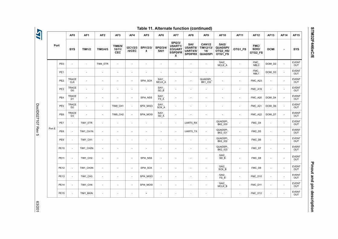
ST
M3
2F4
46xC
/EP
ino
ut a
nd
pin
des
crip
tion
DocID
027107 R
ev 5
63/201
Port E
PE0 - - TIM4_ETR - - - - - - -SAI2_
MCLK_A-
FMC_NBL0
DCMI_D2 -EVENT
OUT
PE1 - - - - - - - - - - - -FMC_NBL1
DCMI_D3 -EVENT
OUT
PE2TRACE
CLK- - - - SPI4_SCK
SAI1_MCLK_A
- -QUADSPI_BK1_IO2
- - FMC_A23 - -EVENT
OUT
PE3TRACE
D0- - - - -
SAI1_SD_B
- - - - - FMC_A19 - -EVENT
OUT
PE4TRACE
D1- - - - SPI4_NSS
SAI1_FS_A
- - - - - FMC_A20 DCMI_D4 -EVENT
OUT
PE5TRACE
D2- - TIM9_CH1 - SPI4_MISO
SAI1_SCK_A
- - - - - FMC_A21 DCMI_D6 -EVENT
OUT
PE6TRACE
D3- - TIM9_CH2 - SPI4_MOSI
SAI1_SD_A
- - - - - FMC_A22 DCMI_D7 -EVENT
OUT
PE7 - TIM1_ETR - - - - - - UART5_RX -QUADSPI_BK2_IO0
- FMC_D4 - -EVENT
OUT
PE8 - TIM1_CH1N - - - - - - UART5_TX -QUADSPI_BK2_IO1
- FMC_D5 - -EVENT
OUT
PE9 - TIM1_CH1 - - - - - - - -QUADSPI_BK2_IO2
- FMC_D6 - -EVENT
OUT
PE10 - TIM1_CH2N - - - - - - - -QUADSPI_BK2_IO3
- FMC_D7 - -EVENT
OUT
PE11 - TIM1_CH2 - - - SPI4_NSS - - - -SAI2_SD_B - FMC_D8 - -
EVENTOUT
PE12 - TIM1_CH3N - - - SPI4_SCK - - - -SAI2_
SCK_B- FMC_D9 - -
EVENTOUT
PE13 - TIM1_CH3 - - - SPI4_MISO - - - -SAI2_FS_B
- FMC_D10 - -EVENT
OUT
PE14 - TIM1_CH4 - - - SPI4_MOSI - - - -SAI2_
MCLK_B- FMC_D11 - -
EVENTOUT
PE15 - TIM1_BKIN - - - - - - - - - - FMC_D12 - -EVENT
OUT
Table 11. Alternate function (continued)
Port
AF0 AF1 AF2 AF3 AF4 AF5 AF6 AF7 AF8 AF9 AF10 AF11 AF12 AF13 AF14 AF15
SYS TIM1/2 TIM3/4/5TIM8/9/10/11/CEC
I2C1/2/3/4/CEC
SPI1/2/3/4
SPI2/3/4/SAI1
SPI2/3/USART1/2/3/UART5/SPDIFR
X
SAI/USART6/UART4/5/SPDIFRX
CAN1/2TIM12/13/
14/QUADSPI
SAI2/QUADSPI/OTG2_HS/OTG1_FS
OTG1_FSFMC/SDIO/
OTG2_FSDCMI - SYS
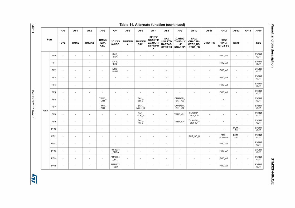
Pin
ou
t and
pin
de
scrip
tion
ST
M32
F44
6xC
/E
64/2
01D
ocID027
107 Re
v 5
Port F
PF0 - - - -I2C2_SDA
- - - - - - - FMC_A0 - -EVENT
OUT
PF1 - - - - I2C2_SCL
- - - - - - - FMC_A1 - -EVENT
OUT
PF2 - - - -I2C2_SMBA
- - - - - - - FMC_A2 - -EVENT
OUT
PF3 - - - - - - - - - - - - FMC_A3 - -EVENT
OUT
PF4 - - - - - - - - - - - - FMC_A4 - -EVENT
OUT
PF5 - - - - - - - - - - - - FMC_A5 - -EVENT
OUT
PF6 - - -TIM10_
CH1- -
SAI1_SD_B
- -QUADSPI_BK1_IO3
- - - - -EVENT
OUT
PF7 - - -TIM11_
CH1- -
SAI1_MCLK_B
- -QUADSPI_BK1_IO2
- - - - -EVENT
OUT
PF8 - - - - - -SAI1_
SCK_B- - TIM13_CH1
QUADSPI_BK1_IO0
- - - -EVENT
OUT
PF9 - - - - - -SAI1_FS_B
- - TIM14_CH1QUADSPI_BK1_IO1
- - - -EVENT
OUT
PF10 - - - - - - - - - - - - - DCMI_D11
-EVENT
OUT
PF11 - - - - - - - - - - SAI2_SD_B -FMC_
SDNRASDCMI_
D12-
EVENTOUT
PF12 - - - - - - - - - - - - FMC_A6 - -EVENT
OUT
PF13 - - - -FMPI2C1_SMBA
- - - - - - - FMC_A7 - -EVENT
OUT
PF14 - - - -FMPI2C1
_SCL- - - - - - - FMC_A8 - -
EVENTOUT
PF15 - - - -FMPI2C1
_SDA- - - - - - - FMC_A9 - -
EVENTOUT
Table 11. Alternate function (continued)
Port
AF0 AF1 AF2 AF3 AF4 AF5 AF6 AF7 AF8 AF9 AF10 AF11 AF12 AF13 AF14 AF15
SYS TIM1/2 TIM3/4/5TIM8/9/10/11/CEC
I2C1/2/3/4/CEC
SPI1/2/3/4
SPI2/3/4/SAI1
SPI2/3/USART1/2/3/UART5/SPDIFR
X
SAI/USART6/UART4/5/SPDIFRX
CAN1/2TIM12/13/
14/QUADSPI
SAI2/QUADSPI/OTG2_HS/OTG1_FS
OTG1_FSFMC/SDIO/
OTG2_FSDCMI - SYS
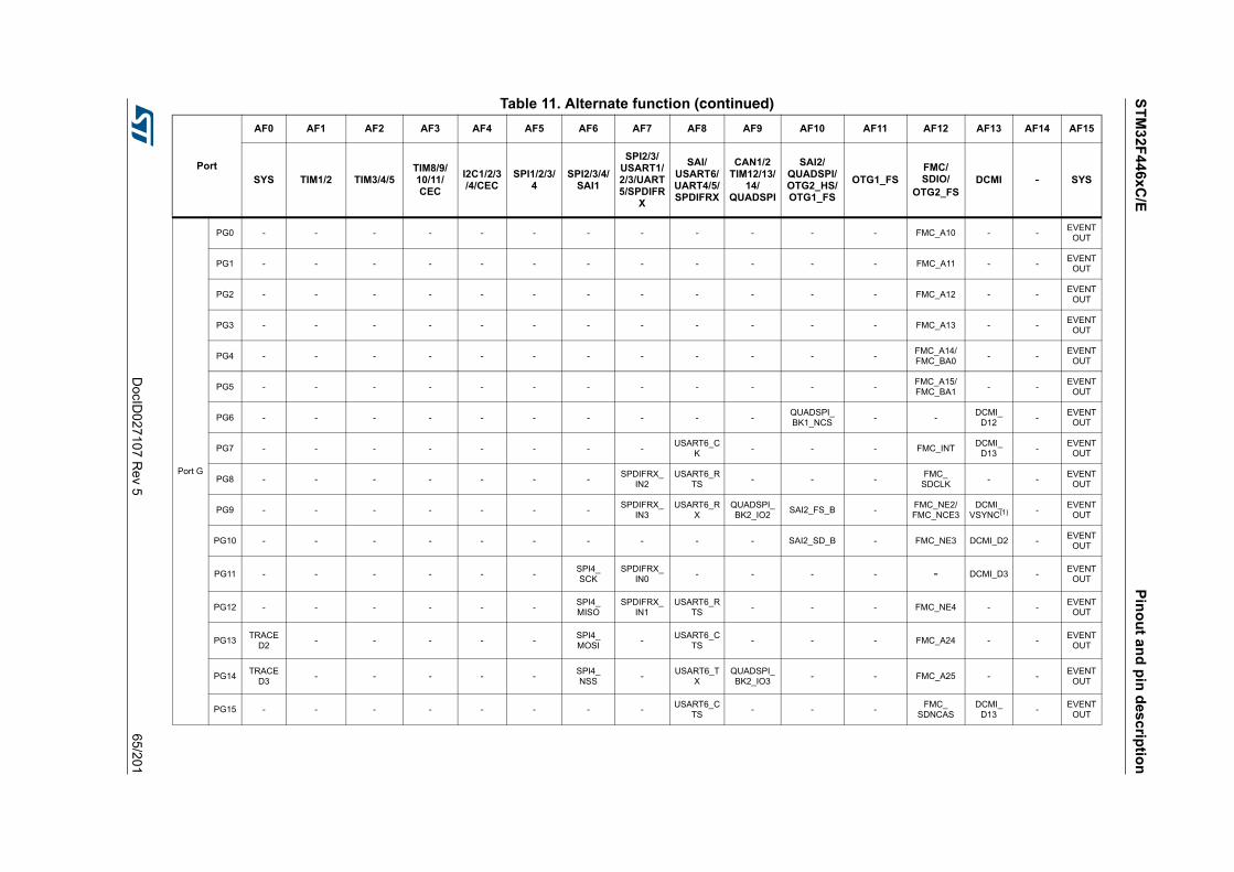
ST
M3
2F4
46xC
/EP
ino
ut a
nd
pin
des
crip
tion
DocID
027107 R
ev 5
65/201
Port G
PG0 - - - - - - - - - - - - FMC_A10 - -EVENT
OUT
PG1 - - - - - - - - - - - - FMC_A11 - -EVENT
OUT
PG2 - - - - - - - - - - - - FMC_A12 - -EVENT
OUT
PG3 - - - - - - - - - - - - FMC_A13 - -EVENT
OUT
PG4 - - - - - - - - - - - -FMC_A14/FMC_BA0
- -EVENT
OUT
PG5 - - - - - - - - - - - -FMC_A15/FMC_BA1
- -EVENT
OUT
PG6 - - - - - - - - - -QUADSPI_BK1_NCS
- -DCMI_
D12-
EVENTOUT
PG7 - - - - - - - -USART6_C
K- - - FMC_INT
DCMI_D13
-EVENT
OUT
PG8 - - - - - - -SPDIFRX_
IN2USART6_R
TS- - -
FMC_SDCLK
- -EVENT
OUT
PG9 - - - - - - -SPDIFRX_
IN3USART6_R
XQUADSPI_BK2_IO2
SAI2_FS_B -FMC_NE2/FMC_NCE3
DCMI_VSYNC(1) -
EVENTOUT
PG10 - - - - - - - - - - SAI2_SD_B - FMC_NE3 DCMI_D2 -EVENT
OUT
PG11 - - - - - -SPI4_SCK
SPDIFRX_IN0
- - - - - DCMI_D3 -EVENT
OUT
PG12 - - - - - -SPI4_MISO
SPDIFRX_IN1
USART6_RTS
- - - FMC_NE4 - -EVENT
OUT
PG13TRACE
D2- - - - -
SPI4_MOSI
-USART6_C
TS- - - FMC_A24 - -
EVENTOUT
PG14TRACE
D3- - - - -
SPI4_NSS
-USART6_T
XQUADSPI_BK2_IO3
- - FMC_A25 - -EVENT
OUT
PG15 - - - - - - - -USART6_C
TS- - -
FMC_SDNCAS
DCMI_D13
-EVENT
OUT
Table 11. Alternate function (continued)
Port
AF0 AF1 AF2 AF3 AF4 AF5 AF6 AF7 AF8 AF9 AF10 AF11 AF12 AF13 AF14 AF15
SYS TIM1/2 TIM3/4/5TIM8/9/10/11/CEC
I2C1/2/3/4/CEC
SPI1/2/3/4
SPI2/3/4/SAI1
SPI2/3/USART1/2/3/UART5/SPDIFR
X
SAI/USART6/UART4/5/SPDIFRX
CAN1/2TIM12/13/
14/QUADSPI
SAI2/QUADSPI/OTG2_HS/OTG1_FS
OTG1_FSFMC/SDIO/
OTG2_FSDCMI - SYS
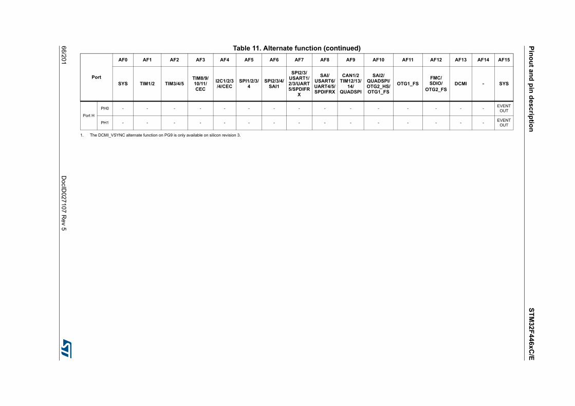
Pin
ou
t and
pin
de
scrip
tion
ST
M32
F44
6xC
/E
66/2
01D
ocID027
107 Re
v 5
Port H
PH0 - - - - - - - - - - - - - - -EVENT
OUT
PH1 - - - - - - - - - - - - - - -EVENT
OUT
1. The DCMI_VSYNC alternate function on PG9 is only available on silicon revision 3.
Table 11. Alternate function (continued)
Port
AF0 AF1 AF2 AF3 AF4 AF5 AF6 AF7 AF8 AF9 AF10 AF11 AF12 AF13 AF14 AF15
SYS TIM1/2 TIM3/4/5TIM8/9/10/11/CEC
I2C1/2/3/4/CEC
SPI1/2/3/4
SPI2/3/4/SAI1
SPI2/3/USART1/2/3/UART5/SPDIFR
X
SAI/USART6/UART4/5/SPDIFRX
CAN1/2TIM12/13/
14/QUADSPI
SAI2/QUADSPI/OTG2_HS/OTG1_FS
OTG1_FSFMC/SDIO/
OTG2_FSDCMI - SYS
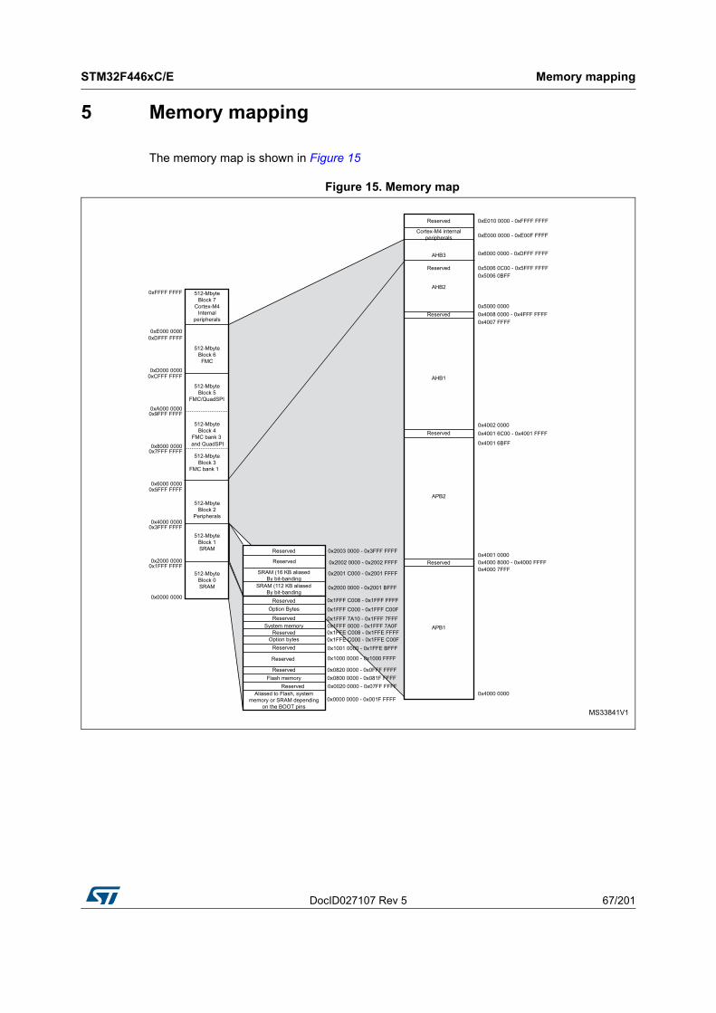
DocID027107 Rev 5 67/201
STM32F446xC/E Memory mapping
71
5 Memory mapping
The memory map is shown in Figure 15
Figure 15. Memory map
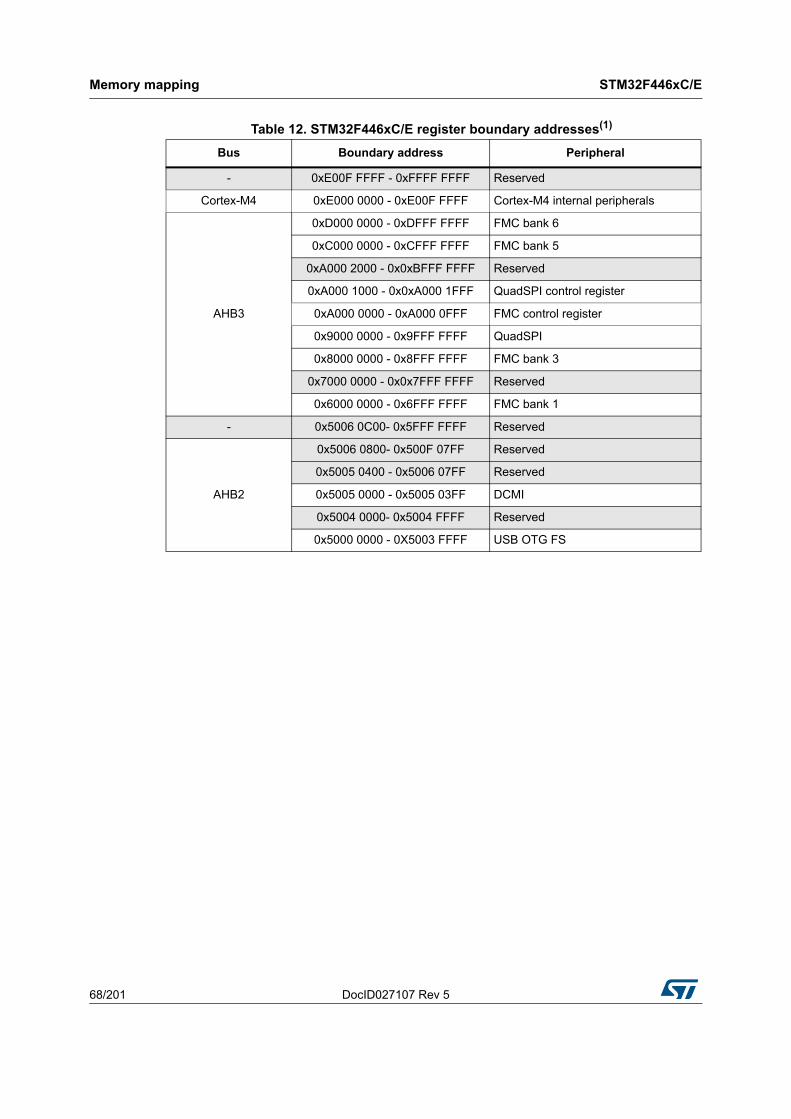
Memory mapping STM32F446xC/E
68/201 DocID027107 Rev 5
Table 12. STM32F446xC/E register boundary addresses(1)
Bus Boundary address Peripheral
- 0xE00F FFFF - 0xFFFF FFFF Reserved
Cortex-M4 0xE000 0000 - 0xE00F FFFF Cortex-M4 internal peripherals
AHB3
0xD000 0000 - 0xDFFF FFFF FMC bank 6
0xC000 0000 - 0xCFFF FFFF FMC bank 5
0xA000 2000 - 0x0xBFFF FFFF Reserved
0xA000 1000 - 0x0xA000 1FFF QuadSPI control register
0xA000 0000 - 0xA000 0FFF FMC control register
0x9000 0000 - 0x9FFF FFFF QuadSPI
0x8000 0000 - 0x8FFF FFFF FMC bank 3
0x7000 0000 - 0x0x7FFF FFFF Reserved
0x6000 0000 - 0x6FFF FFFF FMC bank 1
- 0x5006 0C00- 0x5FFF FFFF Reserved
AHB2
0x5006 0800- 0x500F 07FF Reserved
0x5005 0400 - 0x5006 07FF Reserved
0x5005 0000 - 0x5005 03FF DCMI
0x5004 0000- 0x5004 FFFF Reserved
0x5000 0000 - 0X5003 FFFF USB OTG FS
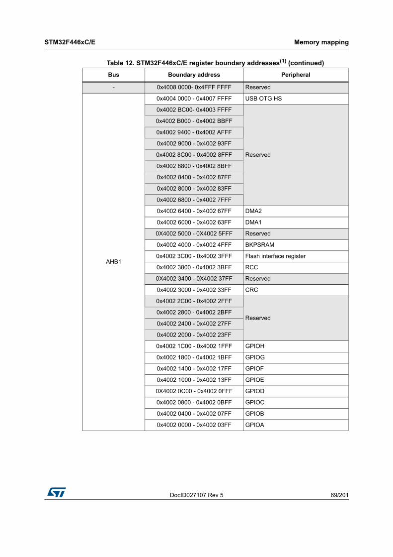
DocID027107 Rev 5 69/201
STM32F446xC/E Memory mapping
71
- 0x4008 0000- 0x4FFF FFFF Reserved
AHB1
0x4004 0000 - 0x4007 FFFF USB OTG HS
0x4002 BC00- 0x4003 FFFF
Reserved
0x4002 B000 - 0x4002 BBFF
0x4002 9400 - 0x4002 AFFF
0x4002 9000 - 0x4002 93FF
0x4002 8C00 - 0x4002 8FFF
0x4002 8800 - 0x4002 8BFF
0x4002 8400 - 0x4002 87FF
0x4002 8000 - 0x4002 83FF
0x4002 6800 - 0x4002 7FFF
0x4002 6400 - 0x4002 67FF DMA2
0x4002 6000 - 0x4002 63FF DMA1
0X4002 5000 - 0X4002 5FFF Reserved
0x4002 4000 - 0x4002 4FFF BKPSRAM
0x4002 3C00 - 0x4002 3FFF Flash interface register
0x4002 3800 - 0x4002 3BFF RCC
0X4002 3400 - 0X4002 37FF Reserved
0x4002 3000 - 0x4002 33FF CRC
0x4002 2C00 - 0x4002 2FFF
Reserved0x4002 2800 - 0x4002 2BFF
0x4002 2400 - 0x4002 27FF
0x4002 2000 - 0x4002 23FF
0x4002 1C00 - 0x4002 1FFF GPIOH
0x4002 1800 - 0x4002 1BFF GPIOG
0x4002 1400 - 0x4002 17FF GPIOF
0x4002 1000 - 0x4002 13FF GPIOE
0X4002 0C00 - 0x4002 0FFF GPIOD
0x4002 0800 - 0x4002 0BFF GPIOC
0x4002 0400 - 0x4002 07FF GPIOB
0x4002 0000 - 0x4002 03FF GPIOA
Table 12. STM32F446xC/E register boundary addresses(1) (continued)
Bus Boundary address Peripheral
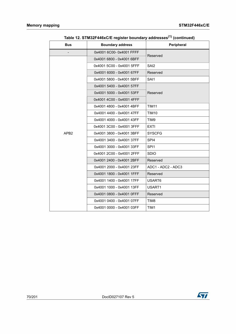
Memory mapping STM32F446xC/E
70/201 DocID027107 Rev 5
- 0x4001 6C00- 0x4001 FFFFReserved
APB2
0x4001 6800 - 0x4001 6BFF
0x4001 5C00 - 0x4001 5FFF SAI2
0x4001 6000 - 0x4001 67FF Reserved
0x4001 5800 - 0x4001 5BFF SAI1
0x4001 5400 - 0x4001 57FF
Reserved0x4001 5000 - 0x4001 53FF
0x4001 4C00 - 0x4001 4FFF
0x4001 4800 - 0x4001 4BFF TIM11
0x4001 4400 - 0x4001 47FF TIM10
0x4001 4000 - 0x4001 43FF TIM9
0x4001 3C00 - 0x4001 3FFF EXTI
0x4001 3800 - 0x4001 3BFF SYSCFG
0x4001 3400 - 0x4001 37FF SPI4
0x4001 3000 - 0x4001 33FF SPI1
0x4001 2C00 - 0x4001 2FFF SDIO
0x4001 2400 - 0x4001 2BFF Reserved
0x4001 2000 - 0x4001 23FF ADC1 - ADC2 - ADC3
0x4001 1800 - 0x4001 1FFF Reserved
0x4001 1400 - 0x4001 17FF USART6
0x4001 1000 - 0x4001 13FF USART1
0x4001 0800 - 0x4001 0FFF Reserved
0x4001 0400 - 0x4001 07FF TIM8
0x4001 0000 - 0x4001 03FF TIM1
Table 12. STM32F446xC/E register boundary addresses(1) (continued)
Bus Boundary address Peripheral
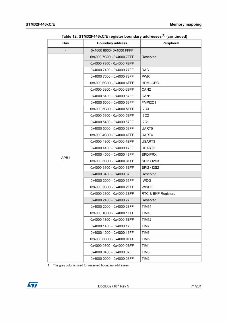
DocID027107 Rev 5 71/201
STM32F446xC/E Memory mapping
71
- 0x4000 8000- 0x4000 FFFF
Reserved
APB1
0x4000 7C00 - 0x4000 7FFF
0x4000 7800 - 0x4000 7BFF
0x4000 7400 - 0x4000 77FF DAC
0x4000 7000 - 0x4000 73FF PWR
0x4000 6C00 - 0x4000 6FFF HDMI-CEC
0x4000 6800 - 0x4000 6BFF CAN2
0x4000 6400 - 0x4000 67FF CAN1
0x4000 6000 - 0x4000 63FF FMPI2C1
0x4000 5C00 - 0x4000 5FFF I2C3
0x4000 5800 - 0x4000 5BFF I2C2
0x4000 5400 - 0x4000 57FF I2C1
0x4000 5000 - 0x4000 53FF UART5
0x4000 4C00 - 0x4000 4FFF UART4
0x4000 4800 - 0x4000 4BFF USART3
0x4000 4400 - 0x4000 47FF USART2
0x4000 4000 - 0x4000 43FF SPDIFRX
0x4000 3C00 - 0x4000 3FFF SPI3 / I2S3
0x4000 3800 - 0x4000 3BFF SPI2 / I2S2
0x4000 3400 - 0x4000 37FF Reserved
0x4000 3000 - 0x4000 33FF IWDG
0x4000 2C00 - 0x4000 2FFF WWDG
0x4000 2800 - 0x4000 2BFF RTC & BKP Registers
0x4000 2400 - 0x4000 27FF Reserved
0x4000 2000 - 0x4000 23FF TIM14
0x4000 1C00 - 0x4000 1FFF TIM13
0x4000 1800 - 0x4000 1BFF TIM12
0x4000 1400 - 0x4000 17FF TIM7
0x4000 1000 - 0x4000 13FF TIM6
0x4000 0C00 - 0x4000 0FFF TIM5
0x4000 0800 - 0x4000 0BFF TIM4
0x4000 0400 - 0x4000 07FF TIM3
0x4000 0000 - 0x4000 03FF TIM2
1. The grey color is used for reserved boundary addresses.
Table 12. STM32F446xC/E register boundary addresses(1) (continued)
Bus Boundary address Peripheral
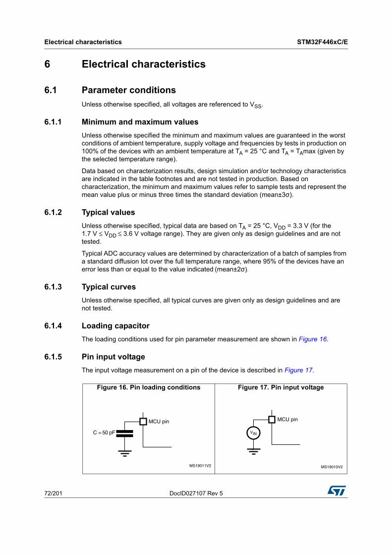
Electrical characteristics STM32F446xC/E
72/201 DocID027107 Rev 5
6 Electrical characteristics
6.1 Parameter conditions
Unless otherwise specified, all voltages are referenced to VSS.
6.1.1 Minimum and maximum values
Unless otherwise specified the minimum and maximum values are guaranteed in the worst conditions of ambient temperature, supply voltage and frequencies by tests in production on 100% of the devices with an ambient temperature at TA = 25 °C and TA = TAmax (given by the selected temperature range).
Data based on characterization results, design simulation and/or technology characteristics are indicated in the table footnotes and are not tested in production. Based on characterization, the minimum and maximum values refer to sample tests and represent the mean value plus or minus three times the standard deviation (mean±3σ).
6.1.2 Typical values
Unless otherwise specified, typical data are based on TA = 25 °C, VDD = 3.3 V (for the 1.7 V ≤ VDD ≤ 3.6 V voltage range). They are given only as design guidelines and are not tested.
Typical ADC accuracy values are determined by characterization of a batch of samples from a standard diffusion lot over the full temperature range, where 95% of the devices have an error less than or equal to the value indicated (mean±2σ).
6.1.3 Typical curves
Unless otherwise specified, all typical curves are given only as design guidelines and are not tested.
6.1.4 Loading capacitor
The loading conditions used for pin parameter measurement are shown in Figure 16.
6.1.5 Pin input voltage
The input voltage measurement on a pin of the device is described in Figure 17.
Figure 16. Pin loading conditions Figure 17. Pin input voltage
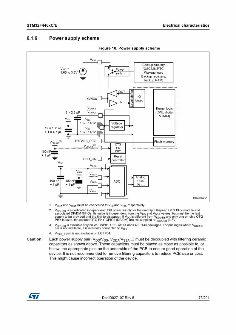
DocID027107 Rev 5 73/201
STM32F446xC/E Electrical characteristics
174
6.1.6 Power supply scheme
Figure 18. Power supply scheme
1. VDDA and VSSA must be connected to VDDand VSS, respectively.
2. VDDUSB is a dedicated independent USB power supply for the on-chip full-speed OTG PHY module and associated DP/DM GPIOs. Its value is independent from the VDD and VDDA values, but must be the last supply to be provided and the first to disappear. If VDD is different from VDDUSB and only one on-chip OTG PHY is used, the second OTG PHY GPIOs (DP/DM) are still supplied at VDDUSB (3.3V).
3. VDDUSB is available only on WLCSP81, UFBGA144 and LQFP144 packages. For packages where VDDUSB pin is not available, it is internally connected to VDD.
4. VCAP_2 pad is not available on LQFP64.
Caution: Each power supply pair (VDD/VSS, VDDA/VSSA...) must be decoupled with filtering ceramic capacitors as shown above. These capacitors must be placed as close as possible to, or below, the appropriate pins on the underside of the PCB to ensure good operation of the device. It is not recommended to remove filtering capacitors to reduce PCB size or cost. This might cause incorrect operation of the device.
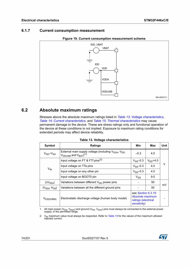
Electrical characteristics STM32F446xC/E
74/201 DocID027107 Rev 5
6.1.7 Current consumption measurement
Figure 19. Current consumption measurement scheme
6.2 Absolute maximum ratings
Stresses above the absolute maximum ratings listed in Table 13: Voltage characteristics, Table 14: Current characteristics, and Table 15: Thermal characteristics may cause permanent damage to the device. These are stress ratings only and functional operation of the device at these conditions is not implied. Exposure to maximum rating conditions for extended periods may affect device reliability.
Table 13. Voltage characteristics
Symbol Ratings Min Max Unit
VDD–VSSExternal main supply voltage (including VDDA, VDD, VDDUSB and VBAT)(1)
1. All main power (VDD, VDDA) and ground (VSS, VSSA) pins must always be connected to the external power supply, in the permitted range.
–0.3 4.0
V
VIN
Input voltage on FT & FTf pins(2)
2. VIN maximum value must always be respected. Refer to Table 14 for the values of the maximum allowed injected current.
VSS–0.3 VDD+4.0
Input voltage on TTa pins VSS–0.3 4.0
Input voltage on any other pin VSS–0.3 4.0
Input voltage on BOOT0 pin VSS 9.0
|ΔVDDx| Variations between different VDD power pins - 50mV
|VSSX −VSS| Variations between all the different ground pins - 50
VESD(HBM) Electrostatic discharge voltage (human body model)
see Section 6.3.15: Absolute maximum ratings (electrical sensitivity)
-
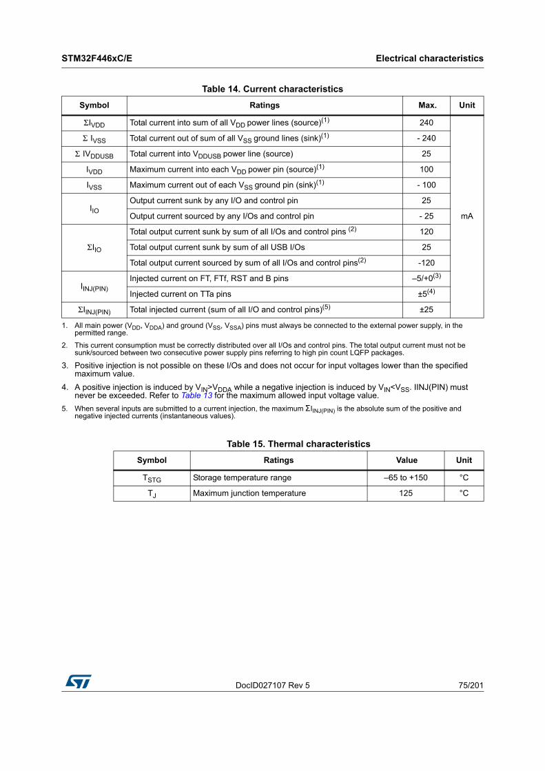
DocID027107 Rev 5 75/201
STM32F446xC/E Electrical characteristics
174
Table 14. Current characteristics
Symbol Ratings Max. Unit
ΣIVDD Total current into sum of all VDD power lines (source)(1) 240
mA
Σ IVSS Total current out of sum of all VSS ground lines (sink)(1) - 240
Σ IVDDUSB Total current into VDDUSB power line (source) 25
IVDD Maximum current into each VDD power pin (source)(1) 100
IVSS Maximum current out of each VSS ground pin (sink)(1) - 100
IIOOutput current sunk by any I/O and control pin 25
Output current sourced by any I/Os and control pin - 25
ΣIIO
Total output current sunk by sum of all I/Os and control pins (2) 120
Total output current sunk by sum of all USB I/Os 25
Total output current sourced by sum of all I/Os and control pins(2) -120
IINJ(PIN)
Injected current on FT, FTf, RST and B pins –5/+0(3)
Injected current on TTa pins ±5(4)
ΣIINJ(PIN) Total injected current (sum of all I/O and control pins)(5) ±25
1. All main power (VDD, VDDA) and ground (VSS, VSSA) pins must always be connected to the external power supply, in the permitted range.
2. This current consumption must be correctly distributed over all I/Os and control pins. The total output current must not be sunk/sourced between two consecutive power supply pins referring to high pin count LQFP packages.
3. Positive injection is not possible on these I/Os and does not occur for input voltages lower than the specified maximum value.
4. A positive injection is induced by VIN>VDDA while a negative injection is induced by VIN<VSS. IINJ(PIN) must never be exceeded. Refer to Table 13 for the maximum allowed input voltage value.
5. When several inputs are submitted to a current injection, the maximum ΣIINJ(PIN) is the absolute sum of the positive and negative injected currents (instantaneous values).
Table 15. Thermal characteristics
Symbol Ratings Value Unit
TSTG Storage temperature range –65 to +150 °C
TJ Maximum junction temperature 125 °C
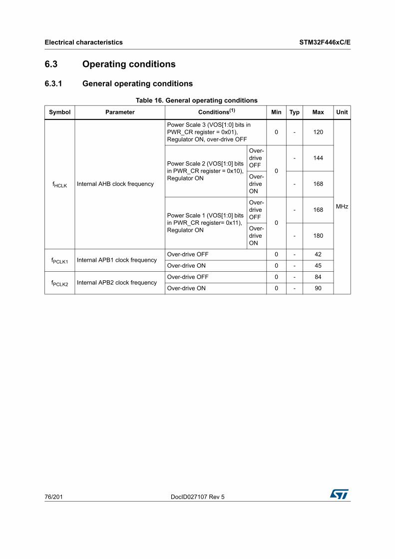
Electrical characteristics STM32F446xC/E
76/201 DocID027107 Rev 5
6.3 Operating conditions
6.3.1 General operating conditions
Table 16. General operating conditions
Symbol Parameter Conditions(1) Min Typ Max Unit
fHCLK Internal AHB clock frequency
Power Scale 3 (VOS[1:0] bits in PWR_CR register = 0x01), Regulator ON, over-drive OFF
0 - 120
MHz
Power Scale 2 (VOS[1:0] bits in PWR_CR register = 0x10), Regulator ON
Over-drive OFF
0
- 144
Over-drive ON
- 168
Power Scale 1 (VOS[1:0] bits in PWR_CR register= 0x11), Regulator ON
Over-drive OFF
0
- 168
Over-drive ON
- 180
fPCLK1 Internal APB1 clock frequencyOver-drive OFF 0 - 42
Over-drive ON 0 - 45
fPCLK2 Internal APB2 clock frequencyOver-drive OFF 0 - 84
Over-drive ON 0 - 90
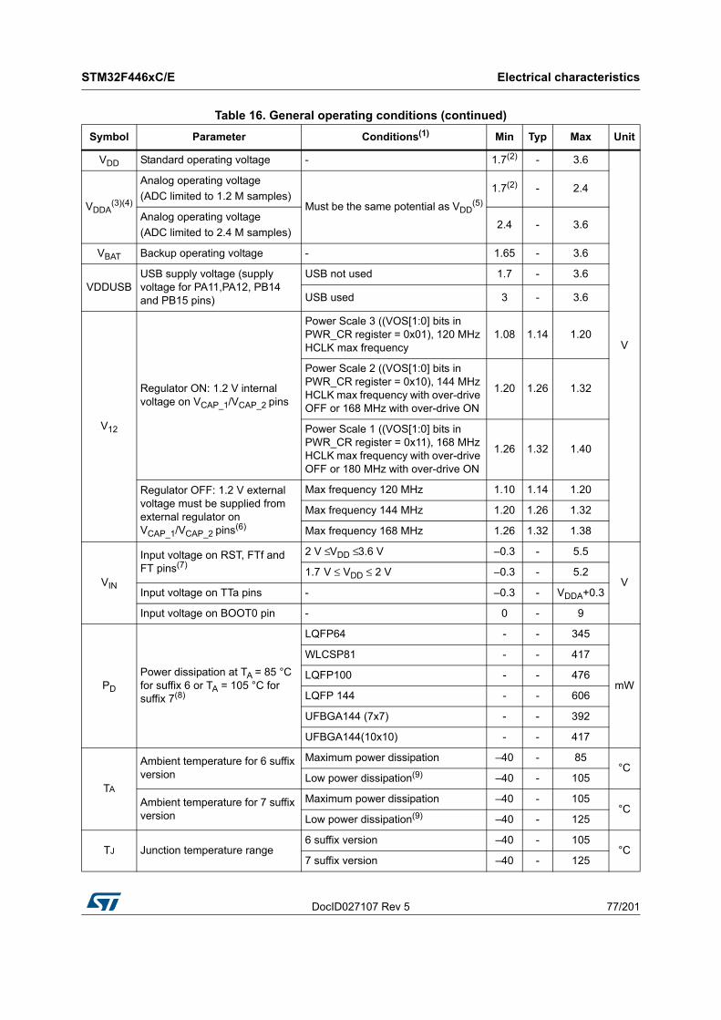
DocID027107 Rev 5 77/201
STM32F446xC/E Electrical characteristics
174
VDD Standard operating voltage - 1.7(2) - 3.6
V
VDDA(3)(4)
Analog operating voltage
(ADC limited to 1.2 M samples)Must be the same potential as VDD
(5)
1.7(2) - 2.4
Analog operating voltage
(ADC limited to 2.4 M samples)2.4 - 3.6
VBAT Backup operating voltage - 1.65 - 3.6
VDDUSBUSB supply voltage (supply voltage for PA11,PA12, PB14 and PB15 pins)
USB not used 1.7 - 3.6
USB used 3 - 3.6
V12
Regulator ON: 1.2 V internal voltage on VCAP_1/VCAP_2 pins
Power Scale 3 ((VOS[1:0] bits in PWR_CR register = 0x01), 120 MHz HCLK max frequency
1.08 1.14 1.20
Power Scale 2 ((VOS[1:0] bits in PWR_CR register = 0x10), 144 MHz HCLK max frequency with over-drive OFF or 168 MHz with over-drive ON
1.20 1.26 1.32
Power Scale 1 ((VOS[1:0] bits in PWR_CR register = 0x11), 168 MHz HCLK max frequency with over-drive OFF or 180 MHz with over-drive ON
1.26 1.32 1.40
Regulator OFF: 1.2 V external voltage must be supplied from external regulator on VCAP_1/VCAP_2 pins(6)
Max frequency 120 MHz 1.10 1.14 1.20
Max frequency 144 MHz 1.20 1.26 1.32
Max frequency 168 MHz 1.26 1.32 1.38
VIN
Input voltage on RST, FTf and FT pins(7)
2 V ≤ VDD ≤ 3.6 V –0.3 - 5.5
V1.7 V ≤ VDD ≤ 2 V –0.3 - 5.2
Input voltage on TTa pins - –0.3 - VDDA+0.3
Input voltage on BOOT0 pin - 0 - 9
PD
Power dissipation at TA = 85 °C for suffix 6 or TA = 105 °C for suffix 7(8)
LQFP64 - - 345
mW
WLCSP81 - - 417
LQFP100 - - 476
LQFP 144 - - 606
UFBGA144 (7x7) - - 392
UFBGA144(10x10) - - 417
TA
Ambient temperature for 6 suffix version
Maximum power dissipation –40 - 85°C
Low power dissipation(9) –40 - 105
Ambient temperature for 7 suffix version
Maximum power dissipation –40 - 105°C
Low power dissipation(9) –40 - 125
TJ Junction temperature range6 suffix version –40 - 105
°C7 suffix version –40 - 125
Table 16. General operating conditions (continued)
Symbol Parameter Conditions(1) Min Typ Max Unit
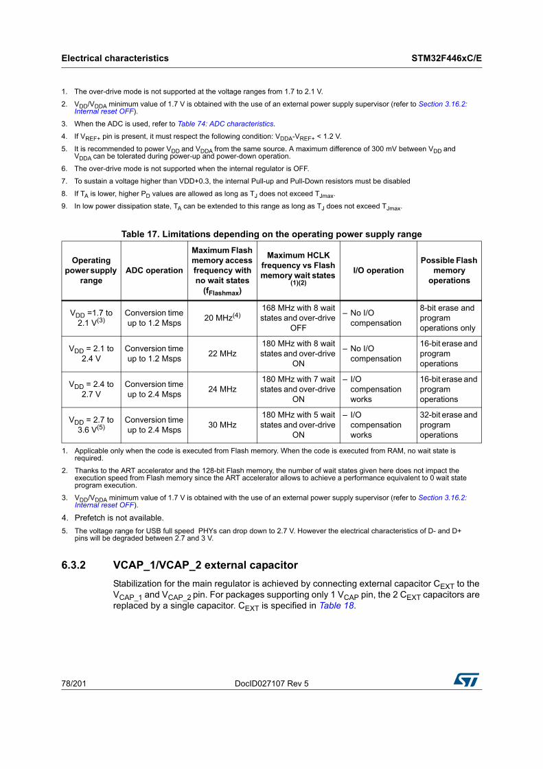
Electrical characteristics STM32F446xC/E
78/201 DocID027107 Rev 5
6.3.2 VCAP_1/VCAP_2 external capacitor
Stabilization for the main regulator is achieved by connecting external capacitor CEXT to the VCAP_1 and VCAP_2 pin. For packages supporting only 1 VCAP pin, the 2 CEXT capacitors are replaced by a single capacitor. CEXT is specified in Table 18.
1. The over-drive mode is not supported at the voltage ranges from 1.7 to 2.1 V.
2. VDD/VDDA minimum value of 1.7 V is obtained with the use of an external power supply supervisor (refer to Section 3.16.2: Internal reset OFF).
3. When the ADC is used, refer to Table 74: ADC characteristics.
4. If VREF+ pin is present, it must respect the following condition: VDDA-VREF+ < 1.2 V.
5. It is recommended to power VDD and VDDA from the same source. A maximum difference of 300 mV between VDD and VDDA can be tolerated during power-up and power-down operation.
6. The over-drive mode is not supported when the internal regulator is OFF.
7. To sustain a voltage higher than VDD+0.3, the internal Pull-up and Pull-Down resistors must be disabled
8. If TA is lower, higher PD values are allowed as long as TJ does not exceed TJmax.
9. In low power dissipation state, TA can be extended to this range as long as TJ does not exceed TJmax.
Table 17. Limitations depending on the operating power supply range
Operating power supply
rangeADC operation
Maximum Flash memory access frequency with no wait states
(fFlashmax)
Maximum HCLK frequency vs Flash memory wait states
(1)(2)
I/O operationPossible Flash
memory operations
VDD =1.7 to 2.1 V(3)
Conversion time up to 1.2 Msps
20 MHz(4)168 MHz with 8 wait states and over-drive
OFF
– No I/O compensation
8-bit erase and program operations only
VDD = 2.1 to 2.4 V
Conversion time up to 1.2 Msps
22 MHz180 MHz with 8 wait states and over-drive
ON
– No I/O compensation
16-bit erase and program operations
VDD = 2.4 to 2.7 V
Conversion time up to 2.4 Msps
24 MHz 180 MHz with 7 wait states and over-drive
ON
– I/O compensation works
16-bit erase and program operations
VDD = 2.7 to 3.6 V(5)
Conversion time up to 2.4 Msps
30 MHz180 MHz with 5 wait states and over-drive
ON
– I/O compensation works
32-bit erase and program operations
1. Applicable only when the code is executed from Flash memory. When the code is executed from RAM, no wait state is required.
2. Thanks to the ART accelerator and the 128-bit Flash memory, the number of wait states given here does not impact the execution speed from Flash memory since the ART accelerator allows to achieve a performance equivalent to 0 wait state program execution.
3. VDD/VDDA minimum value of 1.7 V is obtained with the use of an external power supply supervisor (refer to Section 3.16.2: Internal reset OFF).
4. Prefetch is not available.
5. The voltage range for USB full speed PHYs can drop down to 2.7 V. However the electrical characteristics of D- and D+ pins will be degraded between 2.7 and 3 V.
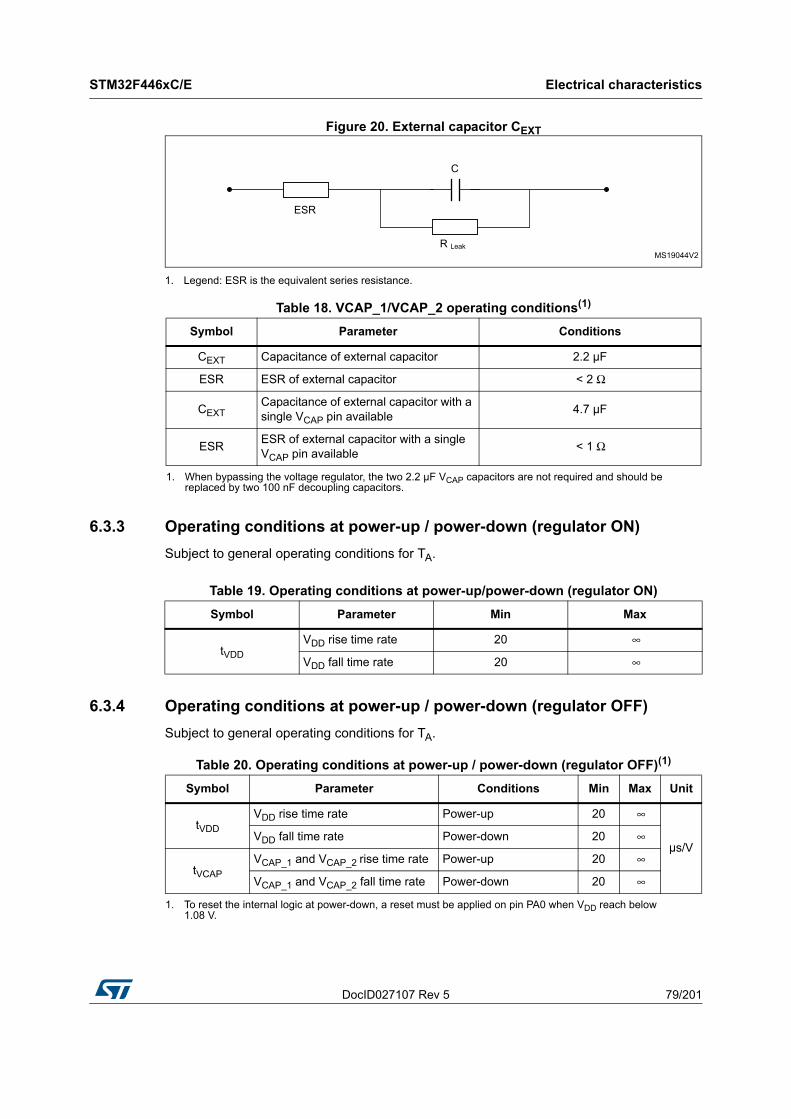
DocID027107 Rev 5 79/201
STM32F446xC/E Electrical characteristics
174
Figure 20. External capacitor CEXT
1. Legend: ESR is the equivalent series resistance.
6.3.3 Operating conditions at power-up / power-down (regulator ON)
Subject to general operating conditions for TA.
6.3.4 Operating conditions at power-up / power-down (regulator OFF)
Subject to general operating conditions for TA.
Table 18. VCAP_1/VCAP_2 operating conditions(1)
1. When bypassing the voltage regulator, the two 2.2 µF VCAP capacitors are not required and should be replaced by two 100 nF decoupling capacitors.
Symbol Parameter Conditions
CEXT Capacitance of external capacitor 2.2 µF
ESR ESR of external capacitor < 2 Ω
CEXTCapacitance of external capacitor with a single VCAP pin available
4.7 µF
ESRESR of external capacitor with a single VCAP pin available
< 1 Ω
Table 19. Operating conditions at power-up/power-down (regulator ON)
Symbol Parameter Min Max
tVDD
VDD rise time rate 20 ∞
VDD fall time rate 20 ∞
Table 20. Operating conditions at power-up / power-down (regulator OFF)(1)
1. To reset the internal logic at power-down, a reset must be applied on pin PA0 when VDD reach below 1.08 V.
Symbol Parameter Conditions Min Max Unit
tVDD
VDD rise time rate Power-up 20 ∞
µs/VVDD fall time rate Power-down 20 ∞
tVCAP
VCAP_1 and VCAP_2 rise time rate Power-up 20 ∞
VCAP_1 and VCAP_2 fall time rate Power-down 20 ∞
Electrical characteristics STM32F446xC/E
80/201 DocID027107 Rev 5
6.3.5 Reset and power control block characteristics
The parameters given in Table 21 are derived from tests performed under ambient temperature and VDD supply voltage conditions summarized in Table 16.
Table 21. reset and power control block characteristics
Symbol Parameter Conditions Min Typ Max Unit
VPVDProgrammable voltage detector level selection
PLS[2:0]=000 (rising edge) 2.09 2.14 2.19 V
PLS[2:0]=000 (falling edge) 1.98 2.04 2.08 V
PLS[2:0]=001 (rising edge) 2.23 2.30 2.37 V
PLS[2:0]=001 (falling edge) 2.13 2.19 2.25 V
PLS[2:0]=010 (rising edge) 2.39 2.45 2.51 V
PLS[2:0]=010 (falling edge) 2.29 2.35 2.39 V
PLS[2:0]=011 (rising edge) 2.54 2.60 2.65 V
PLS[2:0]=011 (falling edge) 2.44 2.51 2.56 V
PLS[2:0]=100 (rising edge) 2.70 2.76 2.82 V
PLS[2:0]=100 (falling edge) 2.59 2.66 2.71 V
PLS[2:0]=101 (rising edge) 2.86 2.93 2.99 V
PLS[2:0]=101 (falling edge) 2.65 2.84 3.02 V
PLS[2:0]=110 (rising edge) 2.96 3.03 3.10 V
PLS[2:0]=110 (falling edge) 2.85 2.93 2.99 V
PLS[2:0]=111 (rising edge) 3.07 3.14 3.21 V
PLS[2:0]=111 (falling edge) 2.95 3.03 3.09 V
VPVDhyst(1) PVD hysteresis - - 100 - mV
VPOR/PDRPower-on/power-down reset threshold
Falling edge 1.60 1.68 1.76 V
Rising edge 1.64 1.72 1.80 V
VPDRhyst(1) PDR hysteresis - - 40 - mV
VBOR1Brownout level 1 threshold
Falling edge 2.13 2.19 2.24 V
Rising edge 2.23 2.29 2.33 V
VBOR2Brownout level 2 threshold
Falling edge 2.44 2.50 2.56 V
Rising edge 2.53 2.59 2.63 V
VBOR3Brownout level 3 threshold
Falling edge 2.75 2.83 2.88 V
Rising edge 2.85 2.92 2.97 V
VBORhyst(1) BOR hysteresis - - 100 - mV
TRSTTEMPO(1)(2) POR reset temporization - 0.5 1.5 3.0 ms
DocID027107 Rev 5 81/201
STM32F446xC/E Electrical characteristics
174
6.3.6 Over-drive switching characteristics
When the over-drive mode switches from enabled to disabled or disabled to enabled, the system clock is stalled during the internal voltage set-up.
The over-drive switching characteristics are given in Table 22. They are sbject to general operating conditions for TA.
6.3.7 Supply current characteristics
The current consumption is a function of several parameters and factors such as the operating voltage, ambient temperature, I/O pin loading, device software configuration, operating frequencies, I/O pin switching rate, program location in memory and executed binary code.
The current consumption is measured as described in Figure 19: Current consumption measurement scheme.
All the run-mode current consumption measurements given in this section are performed with a reduced code that gives a consumption equivalent to CoreMark code.
IRUSH(1)
InRush current on voltage regulator power-on (POR or wakeup from Standby)
- - 160 200 mA
ERUSH(1)
InRush energy on voltage regulator power-on (POR or wakeup from Standby)
VDD = 1.7 V, TA = 105 °C, IRUSH = 171 mA for 31 µs
- - 5.4 µC
1. Guaranteed based on test during characterization.
2. The reset temporization is measured from the power-on (POR reset or wakeup from VBAT) to the instant when first instruction is read by the user application code.
Table 21. reset and power control block characteristics (continued)
Symbol Parameter Conditions Min Typ Max Unit
Table 22. Over-drive switching characteristics(1)
1. Guaranteed based on test during characterization.
Symbol Parameter Conditions Min Typ Max Unit
Tod_swenOver_drive switch enable time
HSI - 45 -
µs
HSE max for 4 MHz and min for 26 MHz
45 - 100
External HSE 50 MHz
- 40 -
Tod_swdisOver_drive switch disable time
HSI - 20 -
HSE max for 4 MHz and min for 26 MHz.
20 - 80
External HSE 50 MHz
- 15 -
Electrical characteristics STM32F446xC/E
82/201 DocID027107 Rev 5
Typical and maximum current consumption
The MCU is placed under the following conditions:
• All I/O pins are in input mode with a static value at VDD or VSS (no load).
• All peripherals are disabled except if it is explicitly mentioned.
• The Flash memory access time is adjusted both to fHCLK frequency and VDD range (see Table 17: Limitations depending on the operating power supply range).
• Regulator ON
• The voltage scaling and over-drive mode are adjusted to fHCLK frequency as follows:
– Scale 3 for fHCLK ≤ 120 MHz
– Scale 2 for 120 MHz < fHCLK ≤ 144 MHz
– Scale 1 for 144 MHz < fHCLK ≤ 180 MHz. The over-drive is only ON at 180 MHz.
• The system clock is HCLK, fPCLK1 = fHCLK/4, and fPCLK2 = fHCLK/2.
• External clock frequency is 8 MHz and PLL is ON when fHCLK is higher than 16 MHz.
• Flash is enabled except if explicitly mentioned as disable.
• The maximum values are obtained for VDD = 3.6 V and a maximum ambient temperature (TA), and the typical values for TA= 25 °C and VDD = 3.3 V unless otherwise specified.
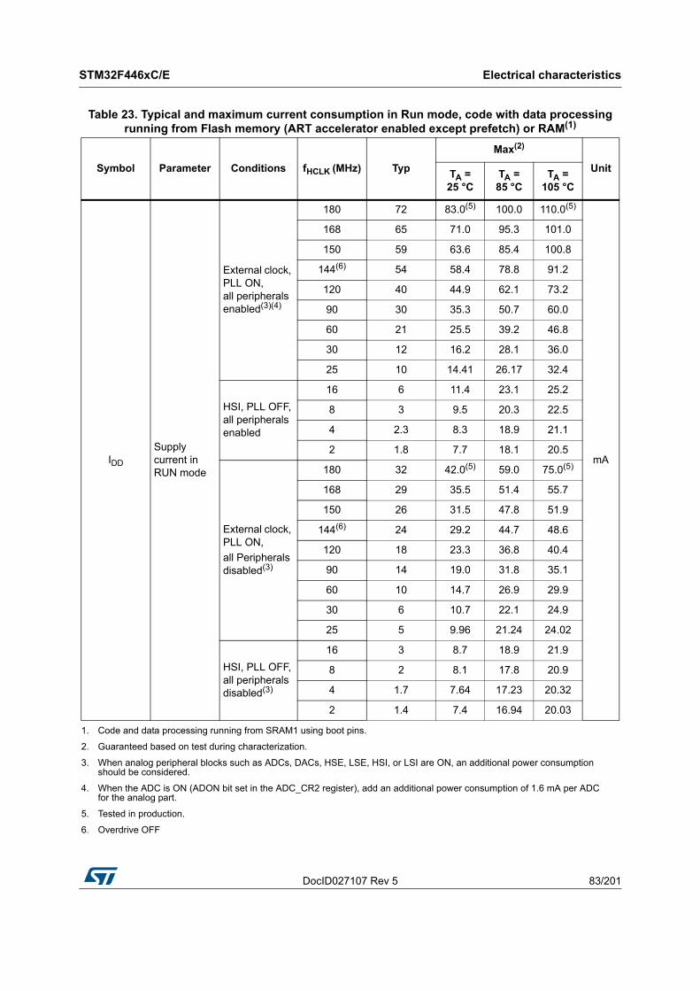
DocID027107 Rev 5 83/201
STM32F446xC/E Electrical characteristics
174
Table 23. Typical and maximum current consumption in Run mode, code with data processing running from Flash memory (ART accelerator enabled except prefetch) or RAM(1)
Symbol Parameter Conditions fHCLK (MHz) Typ
Max(2)
UnitTA = 25 °C
TA = 85 °C
TA = 105 °C
IDD
Supply current in RUN mode
External clock, PLL ON, all peripherals enabled(3)(4)
180 72 83.0(5) 100.0 110.0(5)
mA
168 65 71.0 95.3 101.0
150 59 63.6 85.4 100.8
144(6) 54 58.4 78.8 91.2
120 40 44.9 62.1 73.2
90 30 35.3 50.7 60.0
60 21 25.5 39.2 46.8
30 12 16.2 28.1 36.0
25 10 14.41 26.17 32.4
HSI, PLL OFF, all peripherals enabled
16 6 11.4 23.1 25.2
8 3 9.5 20.3 22.5
4 2.3 8.3 18.9 21.1
2 1.8 7.7 18.1 20.5
External clock, PLL ON,
all Peripherals disabled(3)
180 32 42.0(5) 59.0 75.0(5)
168 29 35.5 51.4 55.7
150 26 31.5 47.8 51.9
144(6) 24 29.2 44.7 48.6
120 18 23.3 36.8 40.4
90 14 19.0 31.8 35.1
60 10 14.7 26.9 29.9
30 6 10.7 22.1 24.9
25 5 9.96 21.24 24.02
HSI, PLL OFF, all peripherals disabled(3)
16 3 8.7 18.9 21.9
8 2 8.1 17.8 20.9
4 1.7 7.64 17.23 20.32
2 1.4 7.4 16.94 20.03
1. Code and data processing running from SRAM1 using boot pins.
2. Guaranteed based on test during characterization.
3. When analog peripheral blocks such as ADCs, DACs, HSE, LSE, HSI, or LSI are ON, an additional power consumption should be considered.
4. When the ADC is ON (ADON bit set in the ADC_CR2 register), add an additional power consumption of 1.6 mA per ADC for the analog part.
5. Tested in production.
6. Overdrive OFF
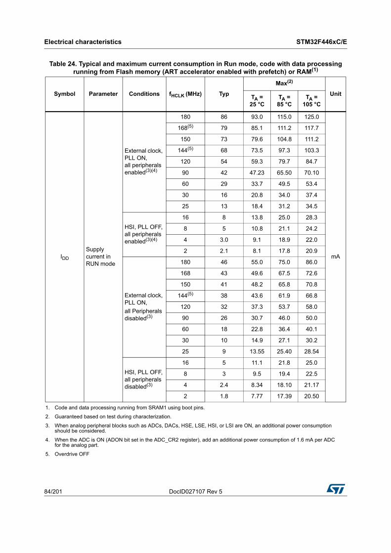
Electrical characteristics STM32F446xC/E
84/201 DocID027107 Rev 5
Table 24. Typical and maximum current consumption in Run mode, code with data processing running from Flash memory (ART accelerator enabled with prefetch) or RAM(1)
Symbol Parameter Conditions fHCLK (MHz) Typ
Max(2)
UnitTA = 25 °C
TA = 85 °C
TA = 105 °C
IDD
Supply current in RUN mode
External clock, PLL ON, all peripherals enabled(3)(4)
180 86 93.0 115.0 125.0
mA
168(5) 79 85.1 111.2 117.7
150 73 79.6 104.8 111.2
144(5) 68 73.5 97.3 103.3
120 54 59.3 79.7 84.7
90 42 47.23 65.50 70.10
60 29 33.7 49.5 53.4
30 16 20.8 34.0 37.4
25 13 18.4 31.2 34.5
HSI, PLL OFF, all peripherals enabled(3)(4)
16 8 13.8 25.0 28.3
8 5 10.8 21.1 24.2
4 3.0 9.1 18.9 22.0
2 2.1 8.1 17.8 20.9
External clock, PLL ON,
all Peripherals disabled(3)
180 46 55.0 75.0 86.0
168 43 49.6 67.5 72.6
150 41 48.2 65.8 70.8
144(5) 38 43.6 61.9 66.8
120 32 37.3 53.7 58.0
90 26 30.7 46.0 50.0
60 18 22.8 36.4 40.1
30 10 14.9 27.1 30.2
25 9 13.55 25.40 28.54
HSI, PLL OFF, all peripherals disabled(3)
16 5 11.1 21.8 25.0
8 3 9.5 19.4 22.5
4 2.4 8.34 18.10 21.17
2 1.8 7.77 17.39 20.50
1. Code and data processing running from SRAM1 using boot pins.
2. Guaranteed based on test during characterization.
3. When analog peripheral blocks such as ADCs, DACs, HSE, LSE, HSI, or LSI are ON, an additional power consumption should be considered.
4. When the ADC is ON (ADON bit set in the ADC_CR2 register), add an additional power consumption of 1.6 mA per ADC for the analog part.
5. Overdrive OFF
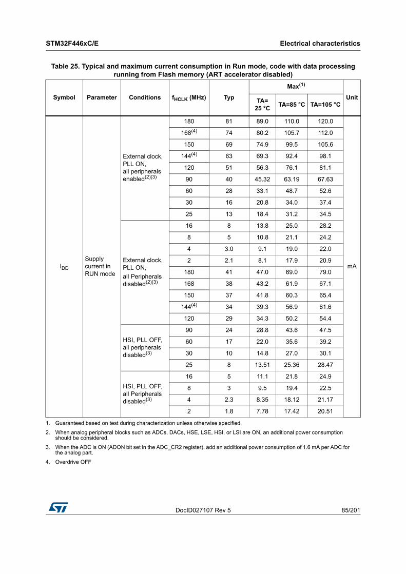
DocID027107 Rev 5 85/201
STM32F446xC/E Electrical characteristics
174
Table 25. Typical and maximum current consumption in Run mode, code with data processing running from Flash memory (ART accelerator disabled)
Symbol Parameter Conditions fHCLK (MHz) Typ
Max(1)
UnitTA= 25 °C
TA=85 °C TA=105 °C
IDD
Supply current in RUN mode
External clock, PLL ON, all peripherals enabled(2)(3)
180 81 89.0 110.0 120.0
mA
168(4) 74 80.2 105.7 112.0
150 69 74.9 99.5 105.6
144(4) 63 69.3 92.4 98.1
120 51 56.3 76.1 81.1
90 40 45.32 63.19 67.63
60 28 33.1 48.7 52.6
30 16 20.8 34.0 37.4
25 13 18.4 31.2 34.5
External clock, PLL ON,
all Peripherals disabled(2)(3)
16 8 13.8 25.0 28.2
8 5 10.8 21.1 24.2
4 3.0 9.1 19.0 22.0
2 2.1 8.1 17.9 20.9
180 41 47.0 69.0 79.0
168 38 43.2 61.9 67.1
150 37 41.8 60.3 65.4
144(4) 34 39.3 56.9 61.6
120 29 34.3 50.2 54.4
HSI, PLL OFF, all peripherals disabled(3)
90 24 28.8 43.6 47.5
60 17 22.0 35.6 39.2
30 10 14.8 27.0 30.1
25 8 13.51 25.36 28.47
HSI, PLL OFF, all Peripherals disabled(3)
16 5 11.1 21.8 24.9
8 3 9.5 19.4 22.5
4 2.3 8.35 18.12 21.17
2 1.8 7.78 17.42 20.51
1. Guaranteed based on test during characterization unless otherwise specified.
2. When analog peripheral blocks such as ADCs, DACs, HSE, LSE, HSI, or LSI are ON, an additional power consumption should be considered.
3. When the ADC is ON (ADON bit set in the ADC_CR2 register), add an additional power consumption of 1.6 mA per ADC for the analog part.
4. Overdrive OFF
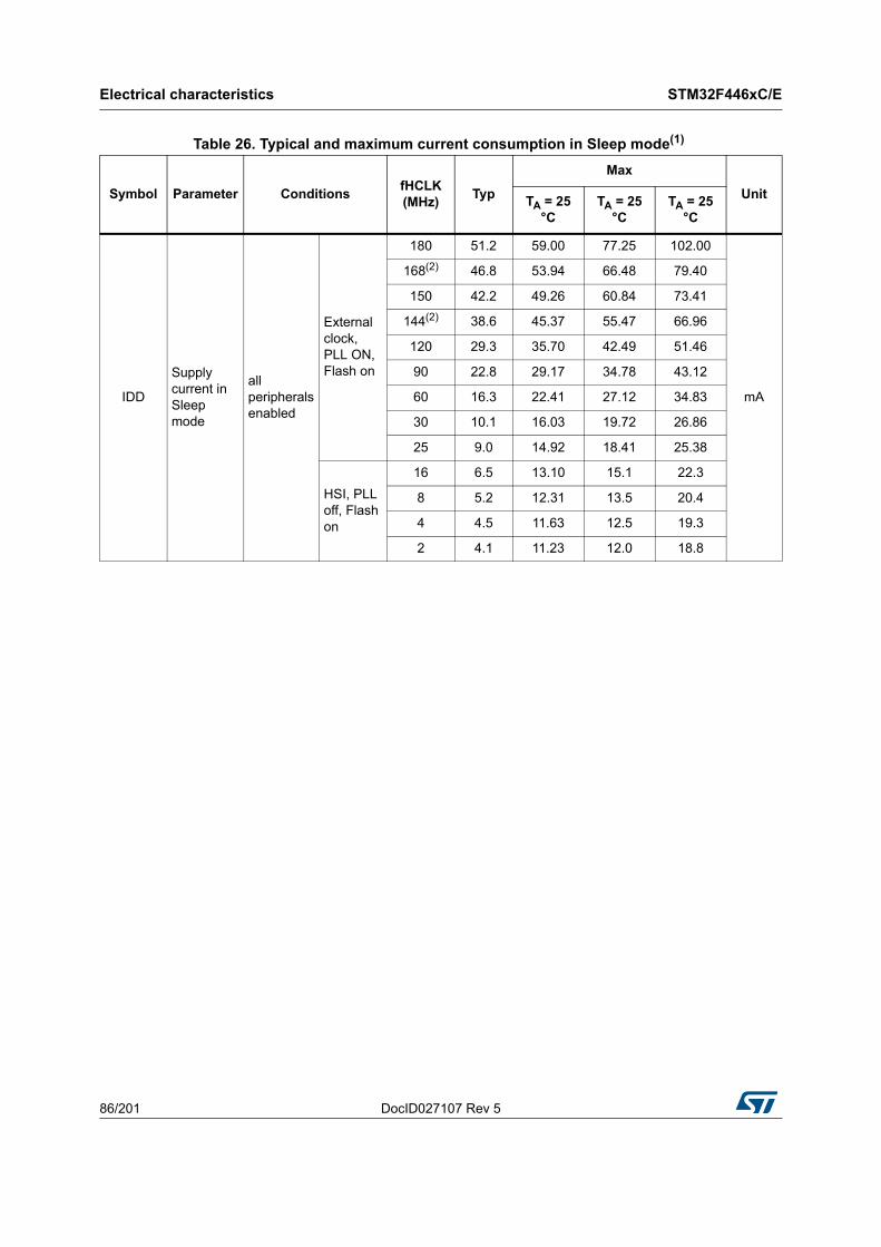
Electrical characteristics STM32F446xC/E
86/201 DocID027107 Rev 5
Table 26. Typical and maximum current consumption in Sleep mode(1)
Symbol Parameter ConditionsfHCLK (MHz)
Typ
Max
UnitTA = 25 °C
TA = 25 °C
TA = 25 °C
IDD
Supply current in Sleep mode
all peripherals enabled
External clock, PLL ON, Flash on
180 51.2 59.00 77.25 102.00
mA
168(2) 46.8 53.94 66.48 79.40
150 42.2 49.26 60.84 73.41
144(2) 38.6 45.37 55.47 66.96
120 29.3 35.70 42.49 51.46
90 22.8 29.17 34.78 43.12
60 16.3 22.41 27.12 34.83
30 10.1 16.03 19.72 26.86
25 9.0 14.92 18.41 25.38
HSI, PLL off, Flash on
16 6.5 13.10 15.1 22.3
8 5.2 12.31 13.5 20.4
4 4.5 11.63 12.5 19.3
2 4.1 11.23 12.0 18.8
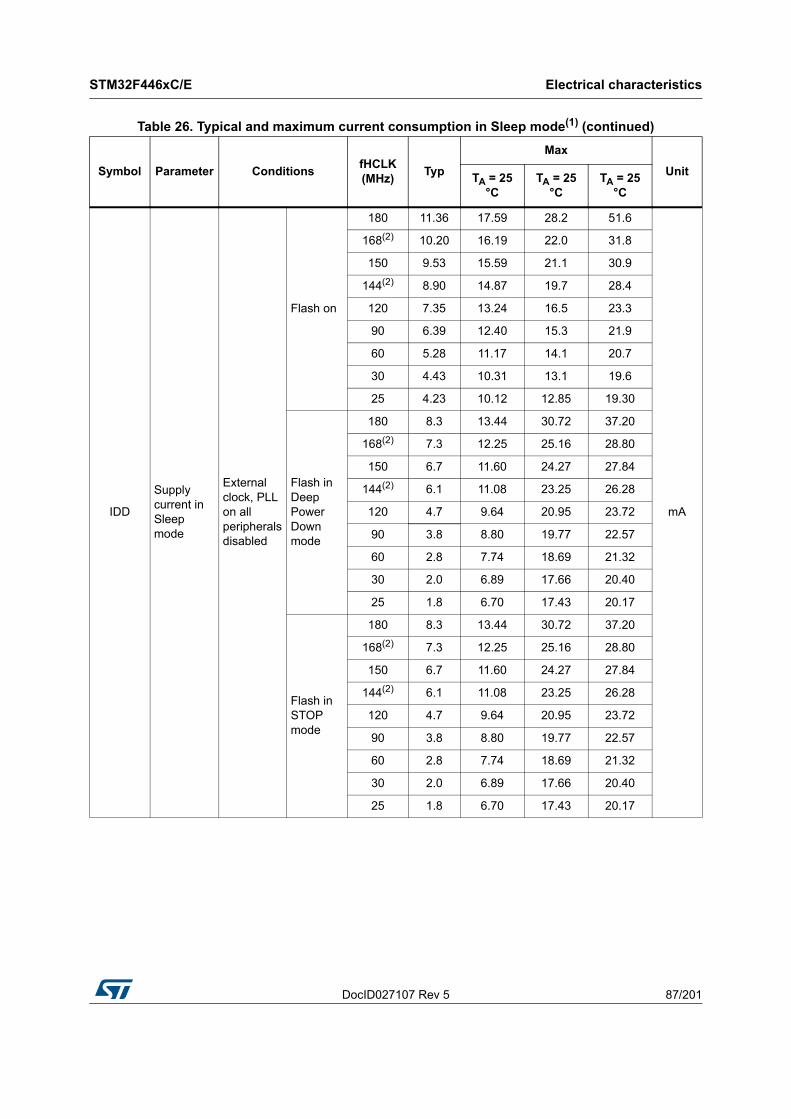
DocID027107 Rev 5 87/201
STM32F446xC/E Electrical characteristics
174
IDD
Supply current in Sleep mode
External clock, PLL on all peripherals disabled
Flash on
180 11.36 17.59 28.2 51.6
mA
168(2) 10.20 16.19 22.0 31.8
150 9.53 15.59 21.1 30.9
144(2) 8.90 14.87 19.7 28.4
120 7.35 13.24 16.5 23.3
90 6.39 12.40 15.3 21.9
60 5.28 11.17 14.1 20.7
30 4.43 10.31 13.1 19.6
25 4.23 10.12 12.85 19.30
Flash in Deep Power Down mode
180 8.3 13.44 30.72 37.20
168(2) 7.3 12.25 25.16 28.80
150 6.7 11.60 24.27 27.84
144(2) 6.1 11.08 23.25 26.28
120 4.7 9.64 20.95 23.72
90 3.8 8.80 19.77 22.57
60 2.8 7.74 18.69 21.32
30 2.0 6.89 17.66 20.40
25 1.8 6.70 17.43 20.17
Flash in STOP mode
180 8.3 13.44 30.72 37.20
168(2) 7.3 12.25 25.16 28.80
150 6.7 11.60 24.27 27.84
144(2) 6.1 11.08 23.25 26.28
120 4.7 9.64 20.95 23.72
90 3.8 8.80 19.77 22.57
60 2.8 7.74 18.69 21.32
30 2.0 6.89 17.66 20.40
25 1.8 6.70 17.43 20.17
Table 26. Typical and maximum current consumption in Sleep mode(1) (continued)
Symbol Parameter ConditionsfHCLK (MHz)
Typ
Max
UnitTA = 25
°CTA = 25
°CTA = 25
°C
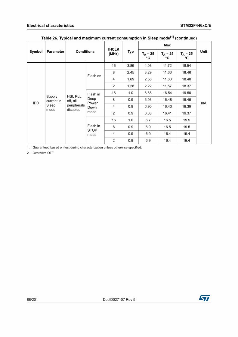
Electrical characteristics STM32F446xC/E
88/201 DocID027107 Rev 5
IDD
Supply current in Sleep mode
HSI, PLL off, all peripherals disabled
Flash on
16 3.89 4.93 11.72 18.54
mA
8 2.45 3.29 11.66 18.46
4 1.69 2.56 11.60 18.40
2 1.28 2.22 11.57 18.37
Flash in Deep Power Down mode
16 1.0 6.65 16.54 19.50
8 0.9 6.93 16.48 19.45
4 0.9 6.90 16.43 19.39
2 0.9 6.88 16.41 19.37
Flash in STOP mode
16 1.0 6.7 16.5 19.5
8 0.9 6.9 16.5 19.5
4 0.9 6.9 16.4 19.4
2 0.9 6.9 16.4 19.4
1. Guaranteed based on test during characterization unless otherwise specified.
2. Overdrive OFF
Table 26. Typical and maximum current consumption in Sleep mode(1) (continued)
Symbol Parameter ConditionsfHCLK (MHz)
Typ
Max
UnitTA = 25
°CTA = 25
°CTA = 25
°C
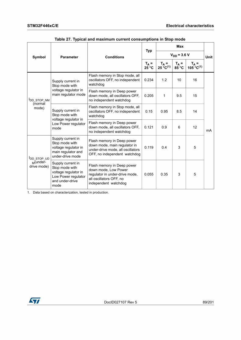
DocID027107 Rev 5 89/201
STM32F446xC/E Electrical characteristics
174
Table 27. Typical and maximum current consumptions in Stop mode
Symbol Parameter Conditions
TypMax
UnitVDD = 3.6 V
TA = 25 °C
TA = 25 °C(1)
TA = 85 °C
TA = 105 °C(1)
IDD_STOP_NM (normal mode)
Supply current in Stop mode with voltage regulator in main regulator mode
Flash memory in Stop mode, all oscillators OFF, no independent watchdog
0.234 1.2 10 16
mA
Flash memory in Deep power down mode, all oscillators OFF, no independent watchdog
0.205 1 9.5 15
Supply current in Stop mode with voltage regulator in Low Power regulator mode
Flash memory in Stop mode, all oscillators OFF, no independent watchdog
0.15 0.95 8.5 14
Flash memory in Deep power down mode, all oscillators OFF, no independent watchdog
0.121 0.9 6 12
IDD_STOP_UD
M(under-drive mode)
Supply current in Stop mode with voltage regulator in main regulator and under-drive mode
Flash memory in Deep power down mode, main regulator in under-drive mode, all oscillators OFF, no independent watchdog
0.119 0.4 3 5
Supply current in Stop mode with voltage regulator in Low Power regulator and under-drive mode
Flash memory in Deep power down mode, Low Power regulator in under-drive mode, all oscillators OFF, no independent watchdog
0.055 0.35 3 5
1. Data based on characterization, tested in production.
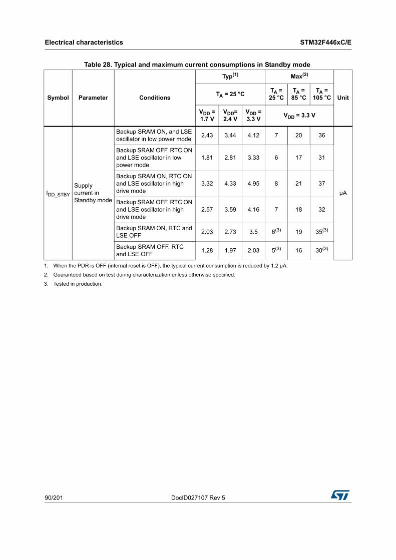
Electrical characteristics STM32F446xC/E
90/201 DocID027107 Rev 5
Table 28. Typical and maximum current consumptions in Standby mode
Symbol Parameter Conditions
Typ(1) Max(2)
UnitTA = 25 °C
TA = 25 °C
TA = 85 °C
TA = 105 °C
VDD = 1.7 V
VDD= 2.4 V
VDD = 3.3 V
VDD = 3.3 V
IDD_STBY
Supply current in Standby mode
Backup SRAM ON, and LSE oscillator in low power mode
2.43 3.44 4.12 7 20 36
µA
Backup SRAM OFF, RTC ON and LSE oscillator in low power mode
1.81 2.81 3.33 6 17 31
Backup SRAM ON, RTC ON and LSE oscillator in high drive mode
3.32 4.33 4.95 8 21 37
Backup SRAM OFF, RTC ON and LSE oscillator in high drive mode
2.57 3.59 4.16 7 18 32
Backup SRAM ON, RTC and LSE OFF
2.03 2.73 3.5 6(3) 19 35(3)
Backup SRAM OFF, RTC and LSE OFF
1.28 1.97 2.03 5(3) 16 30(3)
1. When the PDR is OFF (internal reset is OFF), the typical current consumption is reduced by 1.2 µA.
2. Guaranteed based on test during characterization unless otherwise specified.
3. Tested in production.
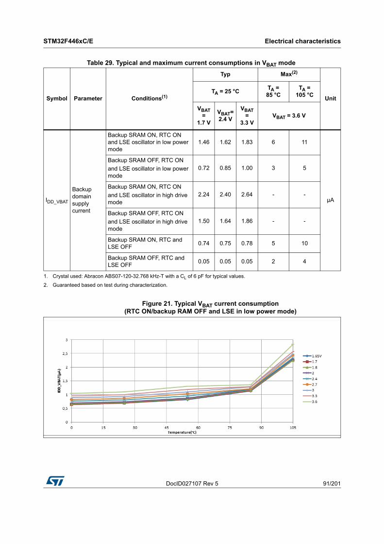
DocID027107 Rev 5 91/201
STM32F446xC/E Electrical characteristics
174
Figure 21. Typical VBAT current consumption(RTC ON/backup RAM OFF and LSE in low power mode)
Table 29. Typical and maximum current consumptions in VBAT mode
Symbol Parameter Conditions(1)
Typ Max(2)
UnitTA = 25 °C
TA = 85 °C
TA = 105 °C
VBAT =
1.7 V
VBAT= 2.4 V
VBAT =
3.3 VVBAT = 3.6 V
IDD_VBAT
Backup domain supply current
Backup SRAM ON, RTC ON and LSE oscillator in low power mode
1.46 1.62 1.83 6 11
µA
Backup SRAM OFF, RTC ON
and LSE oscillator in low power mode
0.72 0.85 1.00 3 5
Backup SRAM ON, RTC ON
and LSE oscillator in high drive mode
2.24 2.40 2.64 - -
Backup SRAM OFF, RTC ON
and LSE oscillator in high drive mode
1.50 1.64 1.86 - -
Backup SRAM ON, RTC and LSE OFF
0.74 0.75 0.78 5 10
Backup SRAM OFF, RTC and LSE OFF
0.05 0.05 0.05 2 4
1. Crystal used: Abracon ABS07-120-32.768 kHz-T with a CL of 6 pF for typical values.
2. Guaranteed based on test during characterization.
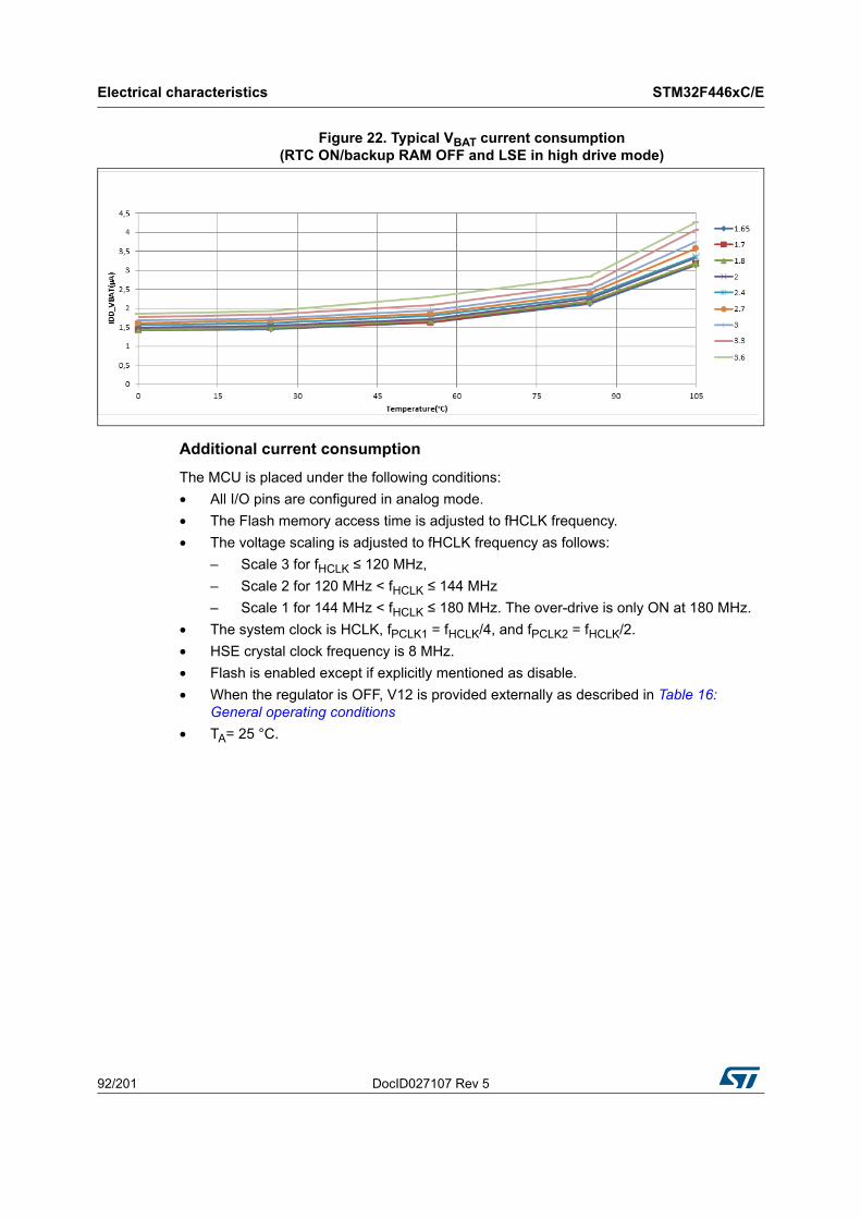
Electrical characteristics STM32F446xC/E
92/201 DocID027107 Rev 5
Figure 22. Typical VBAT current consumption(RTC ON/backup RAM OFF and LSE in high drive mode)
Additional current consumption
The MCU is placed under the following conditions:
• All I/O pins are configured in analog mode.
• The Flash memory access time is adjusted to fHCLK frequency.
• The voltage scaling is adjusted to fHCLK frequency as follows:
– Scale 3 for fHCLK ≤ 120 MHz,
– Scale 2 for 120 MHz < fHCLK ≤ 144 MHz
– Scale 1 for 144 MHz < fHCLK ≤ 180 MHz. The over-drive is only ON at 180 MHz.
• The system clock is HCLK, fPCLK1 = fHCLK/4, and fPCLK2 = fHCLK/2.
• HSE crystal clock frequency is 8 MHz.
• Flash is enabled except if explicitly mentioned as disable.
• When the regulator is OFF, V12 is provided externally as described in Table 16: General operating conditions
• TA= 25 °C.
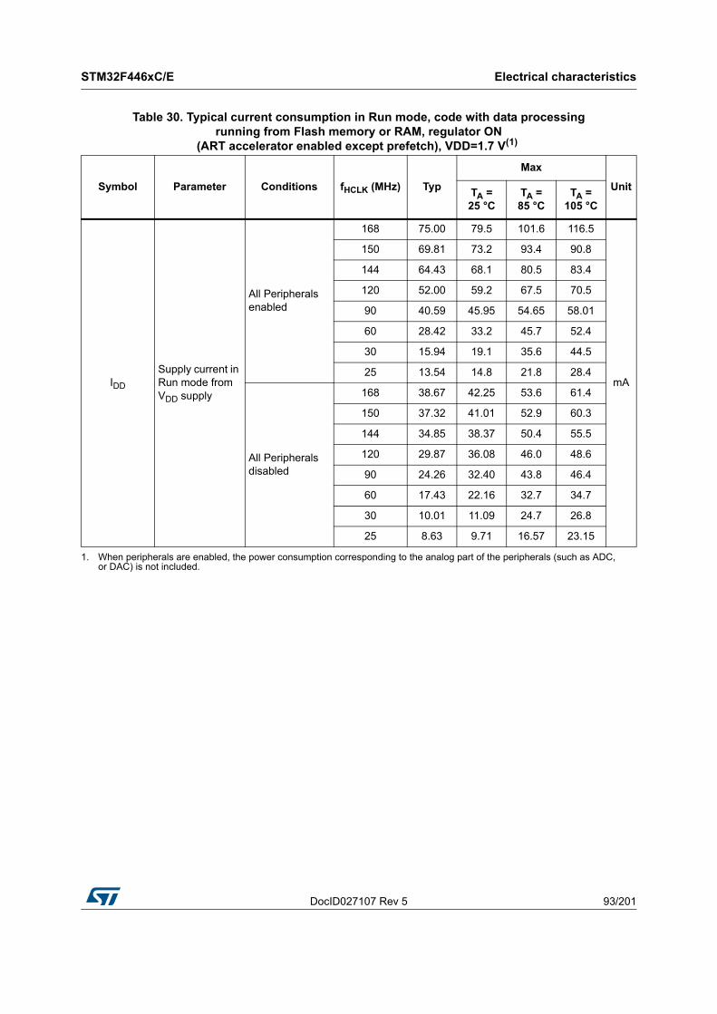
DocID027107 Rev 5 93/201
STM32F446xC/E Electrical characteristics
174
Table 30. Typical current consumption in Run mode, code with data processingrunning from Flash memory or RAM, regulator ON
(ART accelerator enabled except prefetch), VDD=1.7 V(1)
Symbol Parameter Conditions fHCLK (MHz) Typ
Max
UnitTA = 25 °C
TA = 85 °C
TA = 105 °C
IDD
Supply current in Run mode from VDD supply
All Peripherals enabled
168 75.00 79.5 101.6 116.5
mA
150 69.81 73.2 93.4 90.8
144 64.43 68.1 80.5 83.4
120 52.00 59.2 67.5 70.5
90 40.59 45.95 54.65 58.01
60 28.42 33.2 45.7 52.4
30 15.94 19.1 35.6 44.5
25 13.54 14.8 21.8 28.4
All Peripherals disabled
168 38.67 42.25 53.6 61.4
150 37.32 41.01 52.9 60.3
144 34.85 38.37 50.4 55.5
120 29.87 36.08 46.0 48.6
90 24.26 32.40 43.8 46.4
60 17.43 22.16 32.7 34.7
30 10.01 11.09 24.7 26.8
25 8.63 9.71 16.57 23.15
1. When peripherals are enabled, the power consumption corresponding to the analog part of the peripherals (such as ADC, or DAC) is not included.
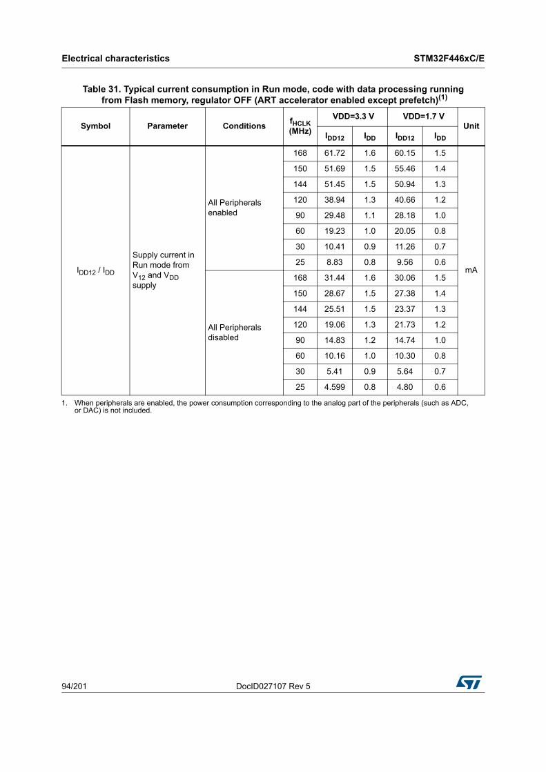
Electrical characteristics STM32F446xC/E
94/201 DocID027107 Rev 5
Table 31. Typical current consumption in Run mode, code with data processing running from Flash memory, regulator OFF (ART accelerator enabled except prefetch)(1)
Symbol Parameter ConditionsfHCLK (MHz)
VDD=3.3 V VDD=1.7 VUnit
IDD12 IDD IDD12 IDD
IDD12 / IDD
Supply current in Run mode from V12 and VDD supply
All Peripherals enabled
168 61.72 1.6 60.15 1.5
mA
150 51.69 1.5 55.46 1.4
144 51.45 1.5 50.94 1.3
120 38.94 1.3 40.66 1.2
90 29.48 1.1 28.18 1.0
60 19.23 1.0 20.05 0.8
30 10.41 0.9 11.26 0.7
25 8.83 0.8 9.56 0.6
All Peripherals disabled
168 31.44 1.6 30.06 1.5
150 28.67 1.5 27.38 1.4
144 25.51 1.5 23.37 1.3
120 19.06 1.3 21.73 1.2
90 14.83 1.2 14.74 1.0
60 10.16 1.0 10.30 0.8
30 5.41 0.9 5.64 0.7
25 4.599 0.8 4.80 0.6
1. When peripherals are enabled, the power consumption corresponding to the analog part of the peripherals (such as ADC, or DAC) is not included.
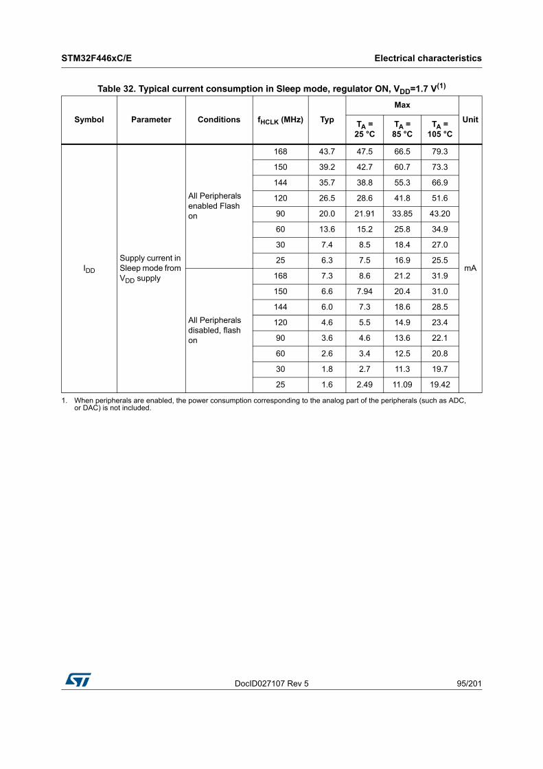
DocID027107 Rev 5 95/201
STM32F446xC/E Electrical characteristics
174
Table 32. Typical current consumption in Sleep mode, regulator ON, VDD=1.7 V(1)
Symbol Parameter Conditions fHCLK (MHz) Typ
Max
UnitTA = 25 °C
TA = 85 °C
TA = 105 °C
IDD
Supply current in Sleep mode from VDD supply
All Peripherals enabled Flash on
168 43.7 47.5 66.5 79.3
mA
150 39.2 42.7 60.7 73.3
144 35.7 38.8 55.3 66.9
120 26.5 28.6 41.8 51.6
90 20.0 21.91 33.85 43.20
60 13.6 15.2 25.8 34.9
30 7.4 8.5 18.4 27.0
25 6.3 7.5 16.9 25.5
All Peripherals disabled, flash on
168 7.3 8.6 21.2 31.9
150 6.6 7.94 20.4 31.0
144 6.0 7.3 18.6 28.5
120 4.6 5.5 14.9 23.4
90 3.6 4.6 13.6 22.1
60 2.6 3.4 12.5 20.8
30 1.8 2.7 11.3 19.7
25 1.6 2.49 11.09 19.42
1. When peripherals are enabled, the power consumption corresponding to the analog part of the peripherals (such as ADC, or DAC) is not included.
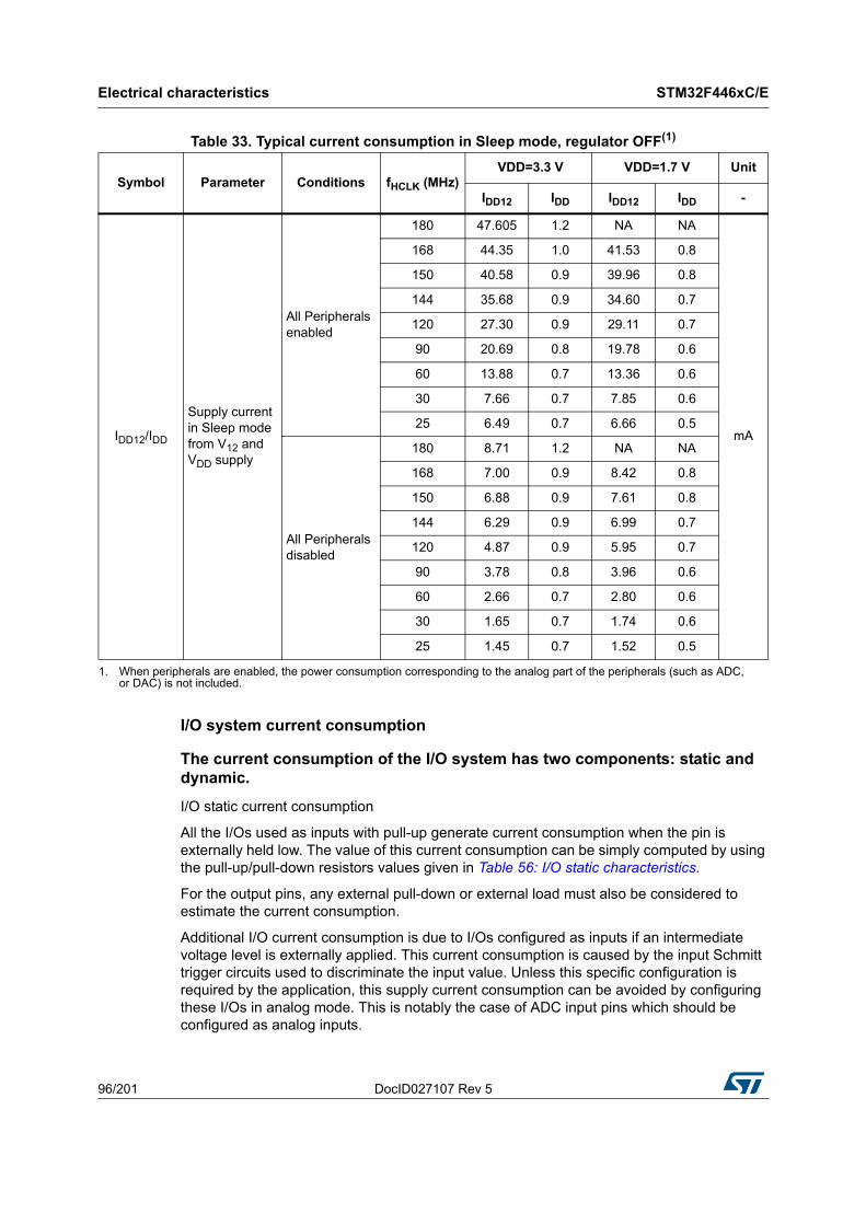
Electrical characteristics STM32F446xC/E
96/201 DocID027107 Rev 5
I/O system current consumption
The current consumption of the I/O system has two components: static and dynamic.
I/O static current consumption
All the I/Os used as inputs with pull-up generate current consumption when the pin is externally held low. The value of this current consumption can be simply computed by using the pull-up/pull-down resistors values given in Table 56: I/O static characteristics.
For the output pins, any external pull-down or external load must also be considered to estimate the current consumption.
Additional I/O current consumption is due to I/Os configured as inputs if an intermediate voltage level is externally applied. This current consumption is caused by the input Schmitt trigger circuits used to discriminate the input value. Unless this specific configuration is required by the application, this supply current consumption can be avoided by configuring these I/Os in analog mode. This is notably the case of ADC input pins which should be configured as analog inputs.
Table 33. Typical current consumption in Sleep mode, regulator OFF(1)
Symbol Parameter Conditions fHCLK (MHz) VDD=3.3 V VDD=1.7 V Unit
IDD12 IDD IDD12 IDD -
IDD12/IDD
Supply current in Sleep mode from V12 and VDD supply
All Peripherals enabled
180 47.605 1.2 NA NA
mA
168 44.35 1.0 41.53 0.8
150 40.58 0.9 39.96 0.8
144 35.68 0.9 34.60 0.7
120 27.30 0.9 29.11 0.7
90 20.69 0.8 19.78 0.6
60 13.88 0.7 13.36 0.6
30 7.66 0.7 7.85 0.6
25 6.49 0.7 6.66 0.5
All Peripherals disabled
180 8.71 1.2 NA NA
168 7.00 0.9 8.42 0.8
150 6.88 0.9 7.61 0.8
144 6.29 0.9 6.99 0.7
120 4.87 0.9 5.95 0.7
90 3.78 0.8 3.96 0.6
60 2.66 0.7 2.80 0.6
30 1.65 0.7 1.74 0.6
25 1.45 0.7 1.52 0.5
1. When peripherals are enabled, the power consumption corresponding to the analog part of the peripherals (such as ADC, or DAC) is not included.
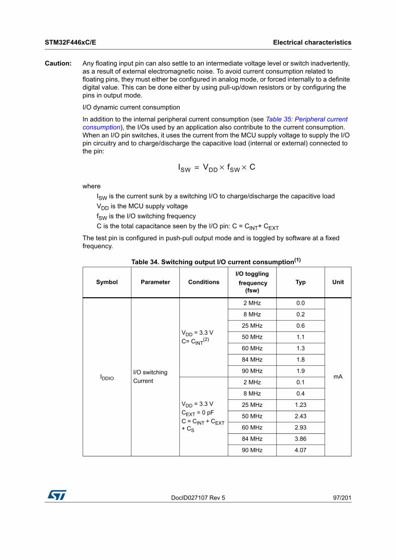
DocID027107 Rev 5 97/201
STM32F446xC/E Electrical characteristics
174
Caution: Any floating input pin can also settle to an intermediate voltage level or switch inadvertently, as a result of external electromagnetic noise. To avoid current consumption related to floating pins, they must either be configured in analog mode, or forced internally to a definite digital value. This can be done either by using pull-up/down resistors or by configuring the pins in output mode.
I/O dynamic current consumption
In addition to the internal peripheral current consumption (see Table 35: Peripheral current consumption), the I/Os used by an application also contribute to the current consumption. When an I/O pin switches, it uses the current from the MCU supply voltage to supply the I/O pin circuitry and to charge/discharge the capacitive load (internal or external) connected to the pin:
ISW VDD fSW C××=
where
ISW is the current sunk by a switching I/O to charge/discharge the capacitive load
VDD is the MCU supply voltage
fSW is the I/O switching frequency
C is the total capacitance seen by the I/O pin: C = CINT+ CEXT
The test pin is configured in push-pull output mode and is toggled by software at a fixed frequency.
Table 34. Switching output I/O current consumption(1)
Symbol Parameter ConditionsI/O toggling
frequency (fsw)
Typ Unit
IDDIOI/O switching
Current
VDD = 3.3 V
C= CINT(2)
2 MHz 0.0
mA
8 MHz 0.2
25 MHz 0.6
50 MHz 1.1
60 MHz 1.3
84 MHz 1.8
90 MHz 1.9
VDD = 3.3 V
CEXT = 0 pF
C = CINT + CEXT + CS
2 MHz 0.1
8 MHz 0.4
25 MHz 1.23
50 MHz 2.43
60 MHz 2.93
84 MHz 3.86
90 MHz 4.07
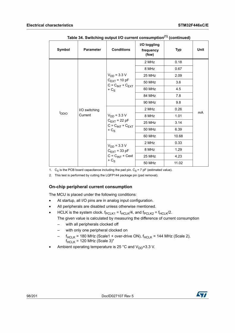
Electrical characteristics STM32F446xC/E
98/201 DocID027107 Rev 5
On-chip peripheral current consumption
The MCU is placed under the following conditions:
• At startup, all I/O pins are in analog input configuration.
• All peripherals are disabled unless otherwise mentioned.
• HCLK is the system clock. fPCLK1 = fHCLK/4, and fPCLK2 = fHCLK/2.
The given value is calculated by measuring the difference of current consumption
– with all peripherals clocked off
– with only one peripheral clocked on
– fHCLK = 180 MHz (Scale1 + over-drive ON), fHCLK = 144 MHz (Scale 2), fHCLK = 120 MHz (Scale 3)"
• Ambient operating temperature is 25 °C and VDD=3.3 V.
IDDIOI/O switching
Current
VDD = 3.3 V
CEXT = 10 pF
C = CINT + CEXT + CS
2 MHz 0.18
mA
8 MHz 0.67
25 MHz 2.09
50 MHz 3.6
60 MHz 4.5
84 MHz 7.8
90 MHz 9.8
VDD = 3.3 V
CEXT = 22 pF
C = CINT + CEXT + CS
2 MHz 0.26
8 MHz 1.01
25 MHz 3.14
50 MHz 6.39
60 MHz 10.68
VDD = 3.3 V
CEXT = 33 pF
C = CINT + Cext + CS
2 MHz 0.33
8 MHz 1.29
25 MHz 4.23
50 MHz 11.02
1. CS is the PCB board capacitance including the pad pin. CS = 7 pF (estimated value).
2. This test is performed by cutting the LQFP144 package pin (pad removal).
Table 34. Switching output I/O current consumption(1) (continued)
Symbol Parameter ConditionsI/O toggling
frequency (fsw)
Typ Unit
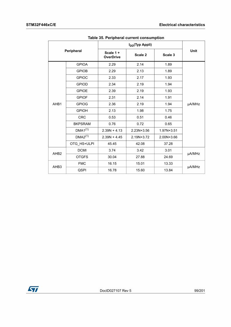
DocID027107 Rev 5 99/201
STM32F446xC/E Electrical characteristics
174
Table 35. Peripheral current consumption
Peripheral
IDD(Typ Appli)
UnitScale 1 + OverDrive
Scale 2 Scale 3
AHB1
GPIOA 2.29 2.14 1.89
µA/MHz
GPIOB 2.29 2.13 1.89
GPIOC 2.33 2.17 1.93
GPIOD 2.34 2.19 1.94
GPIOE 2.39 2.19 1.93
GPIOF 2.31 2.14 1.91
GPIOG 2.36 2.19 1.94
GPIOH 2.13 1.98 1.75
CRC 0.53 0.51 0.46
BKPSRAM 0.76 0.72 0.65
DMA1(1) 2.39N + 4.13 2.23N+3.56 1.97N+3.51
DMA2(1) 2.39N + 4.45 2.19N+3.72 2.00N+3.66
OTG_HS+ULPI 45.45 42.08 37.28
AHB2DCMI 3.74 3.42 3.01
µA/MHzOTGFS 30.04 27.88 24.69
AHB3FMC 16.15 15.01 13.33
µA/MHzQSPI 16.78 15.60 13.84
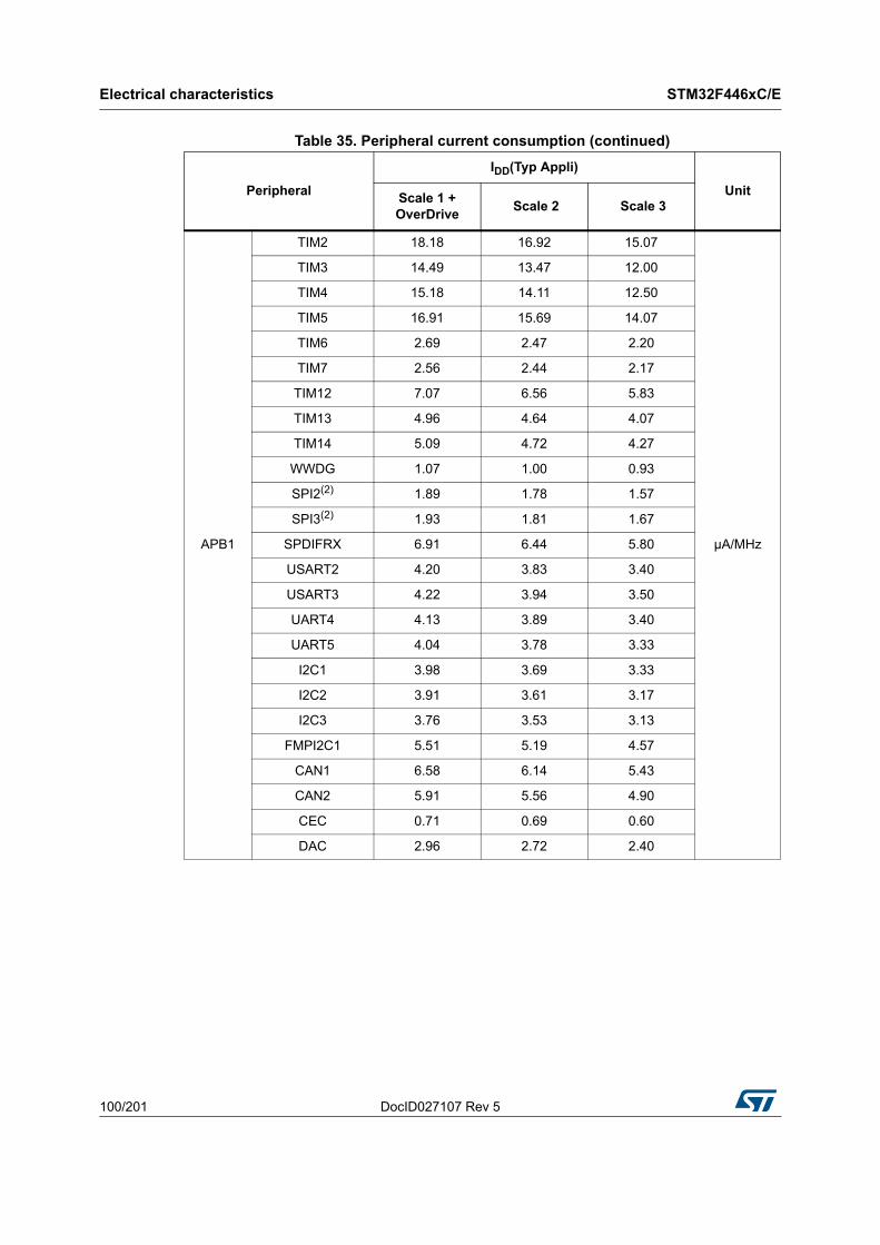
Electrical characteristics STM32F446xC/E
100/201 DocID027107 Rev 5
APB1
TIM2 18.18 16.92 15.07
µA/MHz
TIM3 14.49 13.47 12.00
TIM4 15.18 14.11 12.50
TIM5 16.91 15.69 14.07
TIM6 2.69 2.47 2.20
TIM7 2.56 2.44 2.17
TIM12 7.07 6.56 5.83
TIM13 4.96 4.64 4.07
TIM14 5.09 4.72 4.27
WWDG 1.07 1.00 0.93
SPI2(2) 1.89 1.78 1.57
SPI3(2) 1.93 1.81 1.67
SPDIFRX 6.91 6.44 5.80
USART2 4.20 3.83 3.40
USART3 4.22 3.94 3.50
UART4 4.13 3.89 3.40
UART5 4.04 3.78 3.33
I2C1 3.98 3.69 3.33
I2C2 3.91 3.61 3.17
I2C3 3.76 3.53 3.13
FMPI2C1 5.51 5.19 4.57
CAN1 6.58 6.14 5.43
CAN2 5.91 5.56 4.90
CEC 0.71 0.69 0.60
DAC 2.96 2.72 2.40
Table 35. Peripheral current consumption (continued)
Peripheral
IDD(Typ Appli)
UnitScale 1 + OverDrive
Scale 2 Scale 3
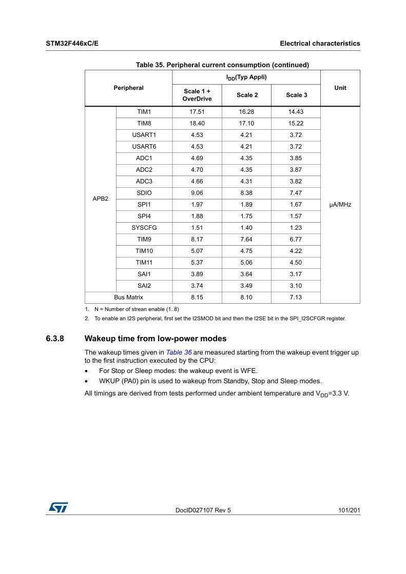
DocID027107 Rev 5 101/201
STM32F446xC/E Electrical characteristics
174
6.3.8 Wakeup time from low-power modes
The wakeup times given in Table 36 are measured starting from the wakeup event trigger up to the first instruction executed by the CPU:
• For Stop or Sleep modes: the wakeup event is WFE.
• WKUP (PA0) pin is used to wakeup from Standby, Stop and Sleep modes.
All timings are derived from tests performed under ambient temperature and VDD=3.3 V.
APB2
TIM1 17.51 16.28 14.43
µA/MHz
TIM8 18.40 17.10 15.22
USART1 4.53 4.21 3.72
USART6 4.53 4.21 3.72
ADC1 4.69 4.35 3.85
ADC2 4.70 4.35 3.87
ADC3 4.66 4.31 3.82
SDIO 9.06 8.38 7.47
SPI1 1.97 1.89 1.67
SPI4 1.88 1.75 1.57
SYSCFG 1.51 1.40 1.23
TIM9 8.17 7.64 6.77
TIM10 5.07 4.75 4.22
TIM11 5.37 5.06 4.50
SAI1 3.89 3.64 3.17
SAI2 3.74 3.49 3.10
Bus Matrix 8.15 8.10 7.13
1. N = Number of strean enable (1..8)
2. To enable an I2S peripheral, first set the I2SMOD bit and then the I2SE bit in the SPI_I2SCFGR register.
Table 35. Peripheral current consumption (continued)
Peripheral
IDD(Typ Appli)
UnitScale 1 + OverDrive
Scale 2 Scale 3
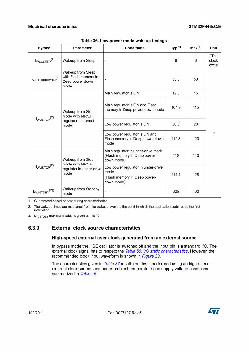
Electrical characteristics STM32F446xC/E
102/201 DocID027107 Rev 5
6.3.9 External clock source characteristics
High-speed external user clock generated from an external source
In bypass mode the HSE oscillator is switched off and the input pin is a standard I/O. The external clock signal has to respect the Table 56: I/O static characteristics. However, the recommended clock input waveform is shown in Figure 23.
The characteristics given in Table 37 result from tests performed using an high-speed external clock source, and under ambient temperature and supply voltage conditions summarized in Table 16.
Table 36. Low-power mode wakeup timings
Symbol Parameter Conditions Typ(1) Max(1) Unit
tWUSLEEP(2) Wakeup from Sleep - 6 6
CPU clock cycle
TWUSLEEPFDSM(1)
Wakeup from Sleep with Flash memory in Deep power down mode
- 33.5 50
µs
tWUSTOP(2)
Wakeup from Stop mode with MR/LP regulator in normal mode
Main regulator is ON 12.8 15
Main regulator is ON and Flash memory in Deep power down mode
104.9 115
Low power regulator is ON 20.6 28
Low power regulator is ON and Flash memory in Deep power down mode
112.8 120
tWUSTOP(2)
Wakeup from Stop mode with MR/LP regulator in Under-drive mode
Main regulator in under-drive mode (Flash memory in Deep power-down mode)
110 140
Low power regulator in under-drive mode
(Flash memory in Deep power-down mode)
114.4 128
tWUSTDBY(2)(3) Wakeup from Standby
mode- 325 400
1. Guaranteed based on test during characterization.
2. The wakeup times are measured from the wakeup event to the point in which the application code reads the first instruction.
3. tWUSTDBY maximum value is given at –40 °C.
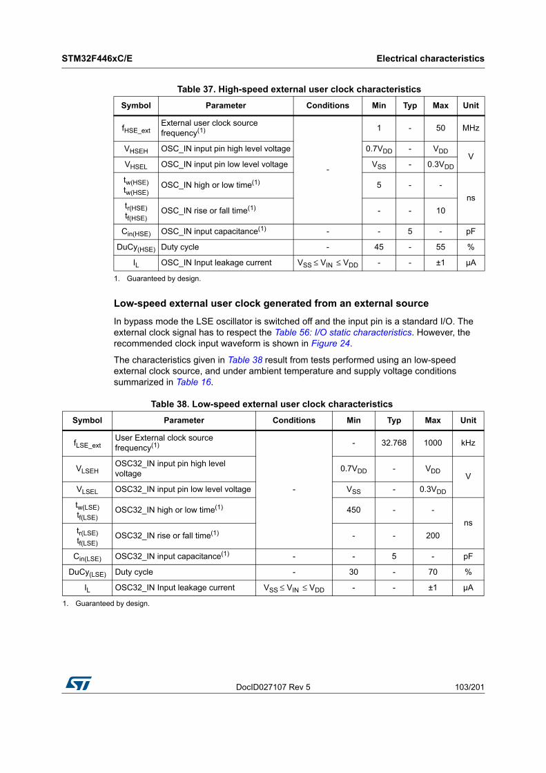
DocID027107 Rev 5 103/201
STM32F446xC/E Electrical characteristics
174
Low-speed external user clock generated from an external source
In bypass mode the LSE oscillator is switched off and the input pin is a standard I/O. The external clock signal has to respect the Table 56: I/O static characteristics. However, the recommended clock input waveform is shown in Figure 24.
The characteristics given in Table 38 result from tests performed using an low-speed external clock source, and under ambient temperature and supply voltage conditions summarized in Table 16.
Table 37. High-speed external user clock characteristics
Symbol Parameter Conditions Min Typ Max Unit
fHSE_extExternal user clock source frequency(1)
-
1 - 50 MHz
VHSEH OSC_IN input pin high level voltage 0.7VDD - VDDV
VHSEL OSC_IN input pin low level voltage VSS - 0.3VDD
tw(HSE)tw(HSE)
OSC_IN high or low time(1)
1. Guaranteed by design.
5 - -
nstr(HSE)tf(HSE)
OSC_IN rise or fall time(1) - - 10
Cin(HSE) OSC_IN input capacitance(1) - - 5 - pF
DuCy(HSE) Duty cycle - 45 - 55 %
IL OSC_IN Input leakage current VSS ≤ VIN ≤ VDD - - ±1 µA
Table 38. Low-speed external user clock characteristics
Symbol Parameter Conditions Min Typ Max Unit
fLSE_extUser External clock source frequency(1)
-
- 32.768 1000 kHz
VLSEHOSC32_IN input pin high level voltage
0.7VDD - VDDV
VLSEL OSC32_IN input pin low level voltage VSS - 0.3VDD
tw(LSE)tf(LSE)
OSC32_IN high or low time(1) 450 - -
nstr(LSE)tf(LSE)
OSC32_IN rise or fall time(1) - - 200
Cin(LSE) OSC32_IN input capacitance(1) - - 5 - pF
DuCy(LSE) Duty cycle - 30 - 70 %
IL OSC32_IN Input leakage current VSS ≤ VIN ≤ VDD - - ±1 µA
1. Guaranteed by design.
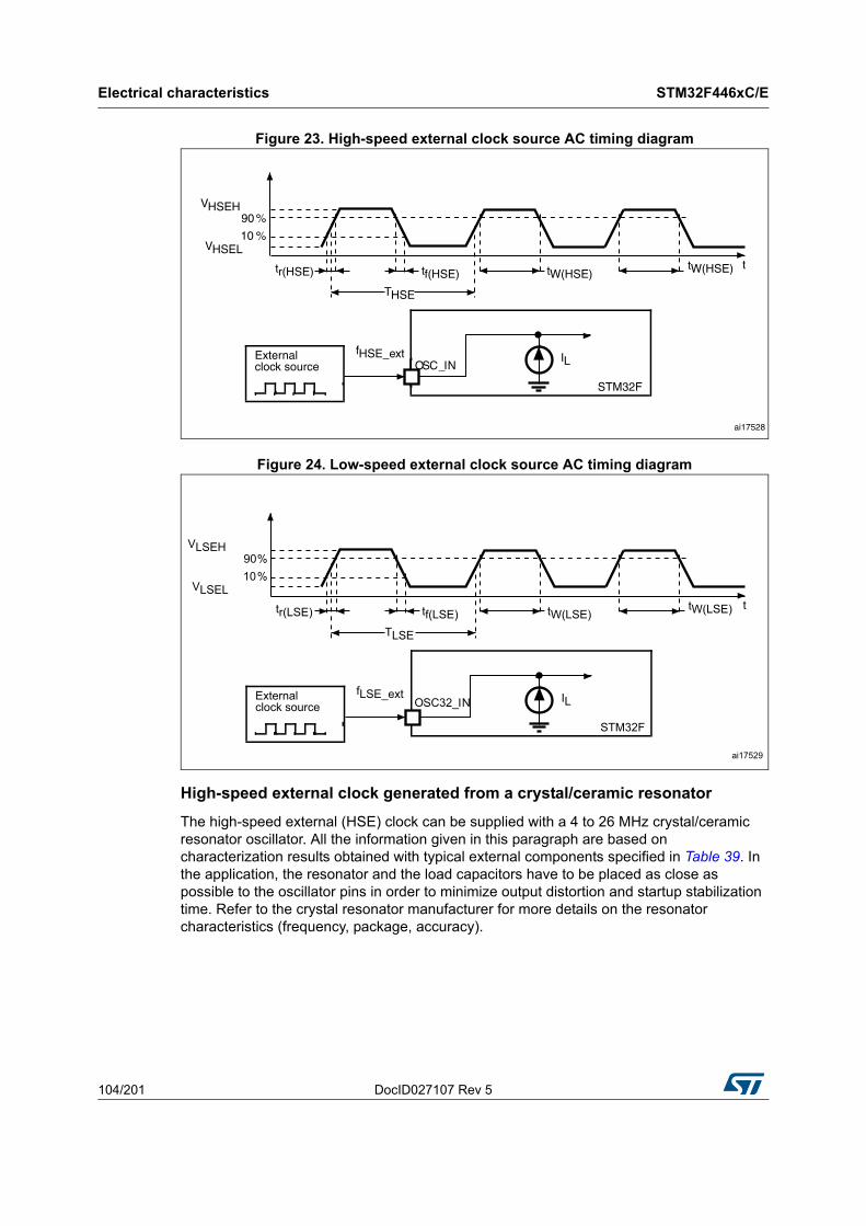
Electrical characteristics STM32F446xC/E
104/201 DocID027107 Rev 5
Figure 23. High-speed external clock source AC timing diagram
Figure 24. Low-speed external clock source AC timing diagram
High-speed external clock generated from a crystal/ceramic resonator
The high-speed external (HSE) clock can be supplied with a 4 to 26 MHz crystal/ceramic resonator oscillator. All the information given in this paragraph are based on characterization results obtained with typical external components specified in Table 39. In the application, the resonator and the load capacitors have to be placed as close as possible to the oscillator pins in order to minimize output distortion and startup stabilization time. Refer to the crystal resonator manufacturer for more details on the resonator characteristics (frequency, package, accuracy).
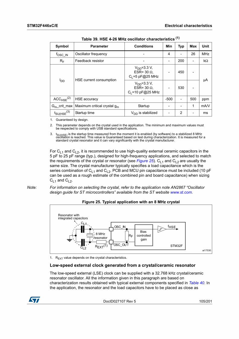
DocID027107 Rev 5 105/201
STM32F446xC/E Electrical characteristics
174
For CL1 and CL2, it is recommended to use high-quality external ceramic capacitors in the 5 pF to 25 pF range (typ.), designed for high-frequency applications, and selected to match the requirements of the crystal or resonator (see Figure 25). CL1 and CL2 are usually the same size. The crystal manufacturer typically specifies a load capacitance which is the series combination of CL1 and CL2. PCB and MCU pin capacitance must be included (10 pF can be used as a rough estimate of the combined pin and board capacitance) when sizing CL1 and CL2.
Note: For information on selecting the crystal, refer to the application note AN2867 “Oscillator design guide for ST microcontrollers” available from the ST website www.st.com.
Figure 25. Typical application with an 8 MHz crystal
1. REXT value depends on the crystal characteristics.
Low-speed external clock generated from a crystal/ceramic resonator
The low-speed external (LSE) clock can be supplied with a 32.768 kHz crystal/ceramic resonator oscillator. All the information given in this paragraph are based on characterization results obtained with typical external components specified in Table 40. In the application, the resonator and the load capacitors have to be placed as close as
Table 39. HSE 4-26 MHz oscillator characteristics (1)
1. Guaranteed by design.
Symbol Parameter Conditions Min Typ Max Unit
fOSC_IN Oscillator frequency - 4 - 26 MHz
RF Feedback resistor - - 200 - kΩ
IDD HSE current consumption
VDD=3.3 V, ESR= 30 Ω,
CL=5 pF@25 MHz- 450 -
µAVDD=3.3 V, ESR= 30 Ω,
CL=10 pF@25 MHz- 530 -
ACCHSE(2)
2. This parameter depends on the crystal used in the application. The minimum and maximum values must be respected to comply with USB standard specifications.
HSE accuracy - -500 - 500 ppm
Gm_crit_max Maximum critical crystal gm Startup - - 1 mA/V
tSU(HSE(3)
3. tSU(HSE) is the startup time measured from the moment it is enabled (by software) to a stabilized 8 MHz oscillation is reached. This value is Guaranteed based on test during characterization. It is measured for a standard crystal resonator and it can vary significantly with the crystal manufacturer.
Startup time VDD is stabilized - 2 - ms
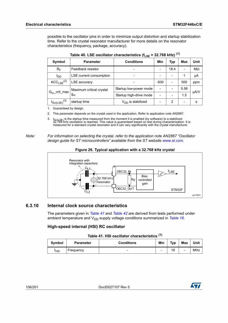
Electrical characteristics STM32F446xC/E
106/201 DocID027107 Rev 5
possible to the oscillator pins in order to minimize output distortion and startup stabilization time. Refer to the crystal resonator manufacturer for more details on the resonator characteristics (frequency, package, accuracy).
Note: For information on selecting the crystal, refer to the application note AN2867 “Oscillator design guide for ST microcontrollers” available from the ST website www.st.com.
Figure 26. Typical application with a 32.768 kHz crystal
6.3.10 Internal clock source characteristics
The parameters given in Table 41 and Table 42 are derived from tests performed under ambient temperature and VDD supply voltage conditions summarized in Table 16.
High-speed internal (HSI) RC oscillator
Table 40. LSE oscillator characteristics (fLSE = 32.768 kHz) (1)
1. Guaranteed by design.
Symbol Parameter Conditions Min Typ Max Unit
RF Feedback resistor - - 18.4 - MΩ
IDD LSE current consumption - - - 1 µA
ACCLSE(2)
2. This parameter depends on the crystal used in the application. Refer to application note AN2867.
LSE accuracy - -500 - 500 ppm
Gm_crit_maxMaximum critical crystal gm
Startup low-power mode - - 0.56µA/V
Startup high-drive mode - - 1.5
tSU(LSE)(3)
3. tSU(LSE) is the startup time measured from the moment it is enabled (by software) to a stabilized 32.768 kHz oscillation is reached. This value is guaranteed based on test during characterization. It is measured for a standard crystal resonator and it can vary significantly with the crystal manufacturer.
startup time VDD is stabilized - 2 - s
Table 41. HSI oscillator characteristics (1)
Symbol Parameter Conditions Min Typ Max Unit
fHSI Frequency - - 16 - MHz
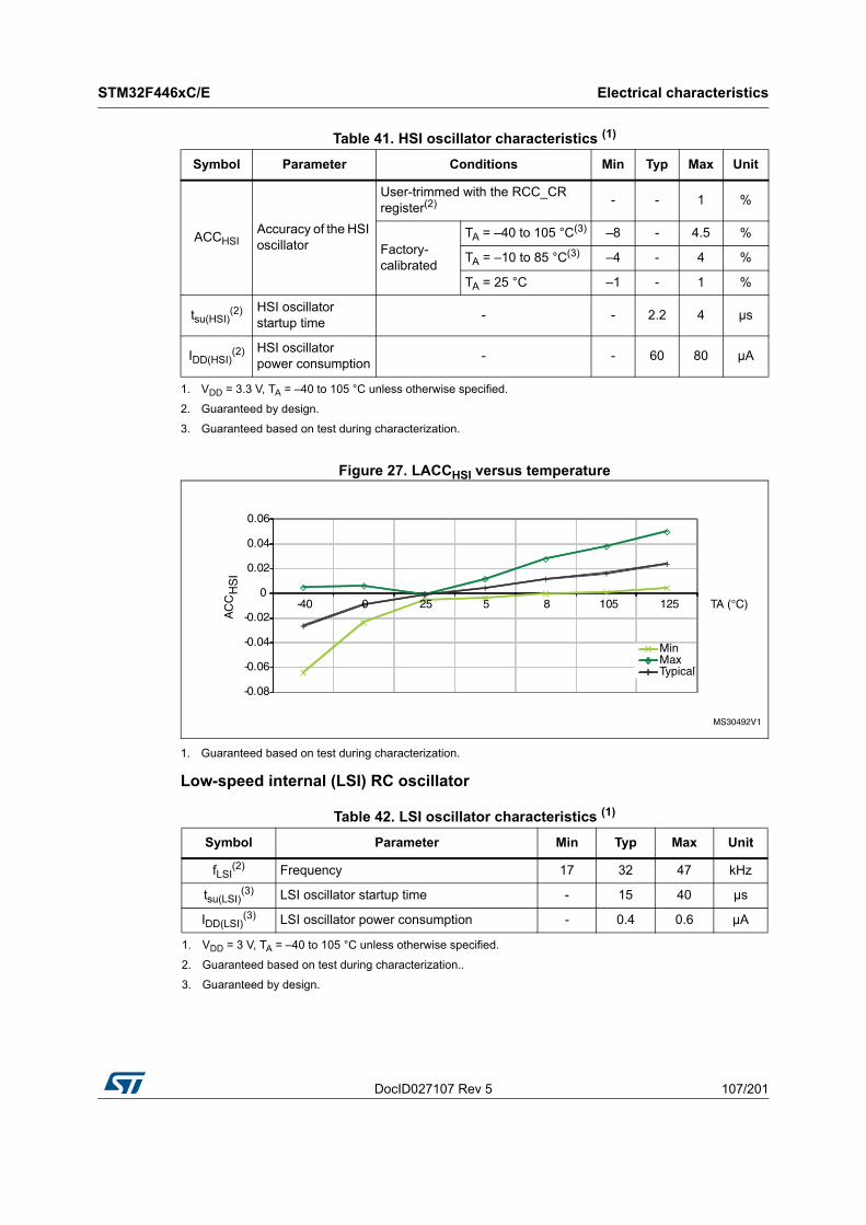
DocID027107 Rev 5 107/201
STM32F446xC/E Electrical characteristics
174
Figure 27. LACCHSI versus temperature
1. Guaranteed based on test during characterization.
Low-speed internal (LSI) RC oscillator
ACCHSIAccuracy of the HSI oscillator
User-trimmed with the RCC_CR register(2) - - 1 %
Factory-calibrated
TA = –40 to 105 °C(3) –8 - 4.5 %
TA = –10 to 85 °C(3) –4 - 4 %
TA = 25 °C –1 - 1 %
tsu(HSI)(2) HSI oscillator
startup time- - 2.2 4 µs
IDD(HSI)(2) HSI oscillator
power consumption- - 60 80 µA
1. VDD = 3.3 V, TA = –40 to 105 °C unless otherwise specified.
2. Guaranteed by design.
3. Guaranteed based on test during characterization.
Table 42. LSI oscillator characteristics (1)
1. VDD = 3 V, TA = –40 to 105 °C unless otherwise specified.
Symbol Parameter Min Typ Max Unit
fLSI(2)
2. Guaranteed based on test during characterization..
Frequency 17 32 47 kHz
tsu(LSI)(3)
3. Guaranteed by design.
LSI oscillator startup time - 15 40 µs
IDD(LSI)(3) LSI oscillator power consumption - 0.4 0.6 µA
Table 41. HSI oscillator characteristics (1)
Symbol Parameter Conditions Min Typ Max Unit
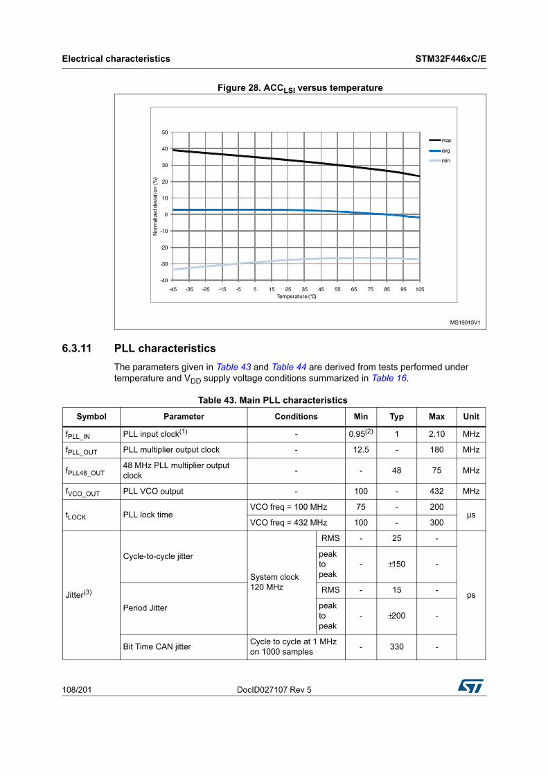
Electrical characteristics STM32F446xC/E
108/201 DocID027107 Rev 5
Figure 28. ACCLSI versus temperature
6.3.11 PLL characteristics
The parameters given in Table 43 and Table 44 are derived from tests performed under temperature and VDD supply voltage conditions summarized in Table 16.
Table 43. Main PLL characteristics
Symbol Parameter Conditions Min Typ Max Unit
fPLL_IN PLL input clock(1) - 0.95(2) 1 2.10 MHz
fPLL_OUT PLL multiplier output clock - 12.5 - 180 MHz
fPLL48_OUT48 MHz PLL multiplier output clock
- - 48 75 MHz
fVCO_OUT PLL VCO output - 100 - 432 MHz
tLOCK PLL lock timeVCO freq = 100 MHz 75 - 200
µsVCO freq = 432 MHz 100 - 300
Jitter(3)
Cycle-to-cycle jitter
System clock 120 MHz
RMS - 25 -
ps
peak to peak
- ±150 -
Period Jitter
RMS - 15 -
peak to peak
- ±200 -
Bit Time CAN jitterCycle to cycle at 1 MHz on 1000 samples
- 330 -
DocID027107 Rev 5 109/201
STM32F446xC/E Electrical characteristics
174
IDD(PLL)(4) PLL power consumption on VDD
VCO freq = 100 MHz
VCO freq = 432 MHz
0.15
0.45-
0.40
0.75mA
IDDA(PLL)(4) PLL power consumption on
VDDAVCO freq = 100 MHz
VCO freq = 432 MHz
0.30
0.55-
0.40
0.85mA
1. Take care of using the appropriate division factor M to obtain the specified PLL input clock values. The M factor is shared between PLL and PLLI2S.
2. Guaranteed by design.
3. The use of 2 PLLs in parallel could degraded the Jitter up to +30%.
4. Guaranteed based on test during characterization.
Table 43. Main PLL characteristics (continued)
Symbol Parameter Conditions Min Typ Max Unit
Table 44. PLLI2S (audio PLL) characteristics
Symbol Parameter Conditions Min Typ Max Unit
fPLLI2S_IN PLLI2S input clock(1) - 0.95(2) 1 2.10 MHz
fPLLI2S_OUT PLLI2S multiplier output clock - - - 216 MHz
fVCO_OUT PLLI2S VCO output - 100 - 432 MHz
tLOCK PLLI2S lock timeVCO freq = 100 MHz 75 - 200
µsVCO freq = 432 MHz 100 - 300
Jitter(3)
Master I2S clock jitter
Cycle to cycle at 12.288 MHz on 48KHz period, N=432, R=5
RMS - 90 - -
peak to
peak- ±280 - ps
Average frequency of 12.288 MHz
N = 432, R = 5
on 1000 samples
- 90 - ps
WS I2S clock jitterCycle to cycle at 48 KHz
on 1000 samples- 400 - ps
IDD(PLLI2S)(4) PLLI2S power consumption on
VDD
VCO freq = 100 MHz
VCO freq = 432 MHz
0.15
0.45-
0.40
0.75mA
IDDA(PLLI2S)(4) PLLI2S power consumption on
VDDA
VCO freq = 100 MHz
VCO freq = 432 MHz
0.30
0.55-
0.40
0.85mA
1. Take care of using the appropriate division factor M to have the specified PLL input clock values.
2. Guaranteed by design.
3. Value given with main PLL running.
4. Guaranteed based on test during characterization.
Electrical characteristics STM32F446xC/E
110/201 DocID027107 Rev 5
6.3.12 PLL spread spectrum clock generation (SSCG) characteristics
The spread spectrum clock generation (SSCG) feature allows to reduce electromagnetic interferences (see Table 52: EMI characteristics). It is available only on the main PLL.
Equation 1
The frequency modulation period (MODEPER) is given by the equation below:
MODEPER round fPLL_IN 4 fMod×( )⁄[ ]=
Table 45. PLLISAI characteristics
Symbol Parameter Conditions Min Typ Max Unit
fPLLSAI_IN PLLSAI input clock(1) - 0.95(2) 1 2.10 MHz
fPLLSAI_OUT PLLSAI multiplier output clock - - - 216 MHz
fVCO_OUT PLLSAI VCO output - 100 - 432 MHz
tLOCK PLLSAI lock timeVCO freq = 100 MHz 75 - 200
µsVCO freq = 432 MHz 100 - 300
Jitter(3)
Main SAI clock jitter
Cycle to cycle at 12.288 MHz on 48KHz period, N=432, R=5
RMS - 90 - -
peak to
peak- ±280 - ps
Average frequency of 12.288 MHz
N = 432, R = 5
on 1000 samples
- 90 - ps
FS clock jitterCycle to cycle at 48 KHz
on 1000 samples- 400 - ps
IDD(PLLSAI)(4) PLLSAI power consumption on
VDD
VCO freq = 100 MHz
VCO freq = 432 MHz
0.15
0.45-
0.40
0.75mA
IDDA(PLLSAI)(4) PLLSAI power consumption on
VDDA
VCO freq = 100 MHz
VCO freq = 432 MHz
0.30
0.55-
0.40
0.85mA
1. Take care of using the appropriate division factor M to have the specified PLL input clock values.
2. Guaranteed by design.
3. Value given with main PLL running.
4. Guaranteed based on test during characterization.
Table 46. SSCG parameters constraint
Symbol Parameter Min Typ Max(1) Unit
fMod Modulation frequency - - 10 KHz
md Peak modulation depth 0.25 - 2 %
MODEPER * INCSTEP - - - 215− 1 -
1. Guaranteed by design.
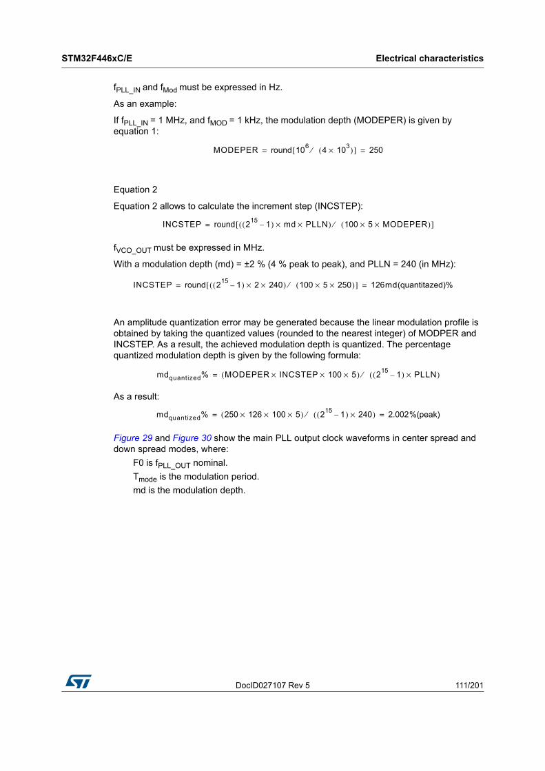
DocID027107 Rev 5 111/201
STM32F446xC/E Electrical characteristics
174
fPLL_IN and fMod must be expressed in Hz.
As an example:
If fPLL_IN = 1 MHz, and fMOD = 1 kHz, the modulation depth (MODEPER) is given by equation 1:
MODEPER round 106
4 103×( )⁄[ ] 250= =
Equation 2
Equation 2 allows to calculate the increment step (INCSTEP):
INCSTEP round 215
1–( ) md PLLN××( ) 100 5× MODEPER×( )⁄[ ]=
fVCO_OUT must be expressed in MHz.
With a modulation depth (md) = ±2 % (4 % peak to peak), and PLLN = 240 (in MHz):
INCSTEP round 215
1–( ) 2 240××( ) 100 5× 250×( )⁄[ ] 126md(quantitazed)%= =
An amplitude quantization error may be generated because the linear modulation profile is obtained by taking the quantized values (rounded to the nearest integer) of MODPER and INCSTEP. As a result, the achieved modulation depth is quantized. The percentage quantized modulation depth is given by the following formula:
mdquantized% MODEPER INCSTEP× 100× 5×( ) 215
1–( ) PLLN×( )⁄=
As a result:
mdquantized% 250 126× 100× 5×( ) 215
1–( ) 240×( )⁄ 2.002%(peak)= =
Figure 29 and Figure 30 show the main PLL output clock waveforms in center spread and down spread modes, where:
F0 is fPLL_OUT nominal.
Tmode is the modulation period.
md is the modulation depth.
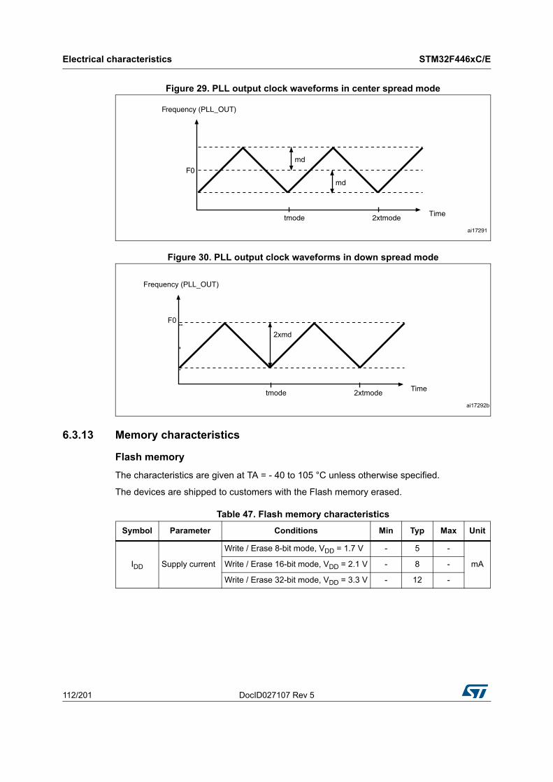
Electrical characteristics STM32F446xC/E
112/201 DocID027107 Rev 5
Figure 29. PLL output clock waveforms in center spread mode
Figure 30. PLL output clock waveforms in down spread mode
6.3.13 Memory characteristics
Flash memory
The characteristics are given at TA = - 40 to 105 °C unless otherwise specified.
The devices are shipped to customers with the Flash memory erased.
Table 47. Flash memory characteristics
Symbol Parameter Conditions Min Typ Max Unit
IDD Supply current
Write / Erase 8-bit mode, VDD = 1.7 V - 5 -
mAWrite / Erase 16-bit mode, VDD = 2.1 V - 8 -
Write / Erase 32-bit mode, VDD = 3.3 V - 12 -
DocID027107 Rev 5 113/201
STM32F446xC/E Electrical characteristics
174
Table 48. Flash memory programming
Symbol Parameter Conditions Min(1) Typ Max(1)
1. Guaranteed based on test during characterization.
Unit
tprog Word programming timeProgram/erase parallelism (PSIZE) = x 8/16/32
- 16 100(2)
2. The maximum programming time is measured after 100K erase operations.
µs
tERASE16KB Sector (16 KB) erase time
Program/erase parallelism (PSIZE) = x 8
- 400 800
msProgram/erase parallelism (PSIZE) = x 16
- 300 600
Program/erase parallelism (PSIZE) = x 32
- 250 500
tERASE64KB Sector (64 KB) erase time
Program/erase parallelism (PSIZE) = x 8
- 1200 2400
msProgram/erase parallelism (PSIZE) = x 16
- 700 1400
Program/erase parallelism (PSIZE) = x 32
- 550 1100
tERASE128KB Sector (128 KB) erase time
Program/erase parallelism (PSIZE) = x 8
- 2 4
sProgram/erase parallelism (PSIZE) = x 16
- 1.3 2.6
Program/erase parallelism (PSIZE) = x 32
- 1 2
tME Mass erase time
Program/erase parallelism (PSIZE) = x 8
- 8 16
sProgram/erase parallelism (PSIZE) = x 16
- 5.5 11
Program/erase parallelism (PSIZE) = x 32
- 8 16
Vprog Programming voltage
32-bit program operation 2.7 - 3.6 V
16-bit program operation 2.1 - 3.6 V
8-bit program operation 1.7 - 3.6 V
Table 49. Flash memory programming with VPP
Symbol Parameter Conditions Min(1) Typ Max(1) Unit
tprog Double word programming
TA = 0 to +40 °C
VDD = 3.3 V
VPP = 8.5 V
- 16 100(2) µs
tERASE16KB Sector (16 KB) erase time - 230 -
mstERASE64KB Sector (64 KB) erase time - 490 -
tERASE128KB Sector (128 KB) erase time - 875 -
tME Mass erase time - 3.5 - s
Vprog Programming voltage - 2.7 - 3.6 V
Electrical characteristics STM32F446xC/E
114/201 DocID027107 Rev 5
6.3.14 EMC characteristics
Susceptibility tests are performed on a sample basis during device characterization.
Functional EMS (electromagnetic susceptibility)
While a simple application is executed on the device (toggling 2 LEDs through I/O ports). the device is stressed by two electromagnetic events until a failure occurs. The failure is indicated by the LEDs:
• Electrostatic discharge (ESD) (positive and negative) is applied to all device pins until a functional disturbance occurs. This test is compliant with the IEC 61000-4-2 standard.
• FTB: A burst of fast transient voltage (positive and negative) is applied to VDD and VSS through a 100 pF capacitor, until a functional disturbance occurs. This test is compliant with the IEC 61000-4-4 standard.
A device reset allows normal operations to be resumed.
The test results are given in Table 51. They are based on the EMS levels and classes defined in application note AN1709.
VPP VPP voltage range - 7 - 9 V
IPPMinimum current sunk on the VPP pin
- 10 - - mA
tVPP(3) Cumulative time during
which VPP is applied- - - 1 hour
1. Guaranteed by design.
2. The maximum programming time is measured after 100K erase operations.
3. VPP should only be connected during programming/erasing.
Table 50. Flash memory endurance and data retention
Symbol ParameterConditions
ValueUnit
- - Min(1)
1. Guaranteed based on test during characterization.
NEND EnduranceTA = –40 to +85 °C (6 suffix versions)
TA = –40 to +105 °C (7 suffix versions)10 Kcycles
tRET Data retention
1 kcycle(2) at TA = 85 °C
2. Cycling performed over the whole temperature range.
30
Years1 kcycle(2) at TA = 105 °C 10
10 kcycles(2) at TA = 55 °C 20
Table 49. Flash memory programming with VPP (continued)
Symbol Parameter Conditions Min(1) Typ Max(1) Unit
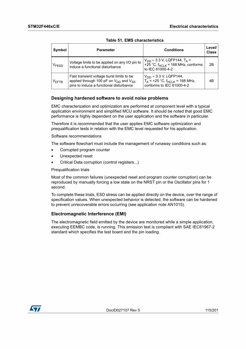
DocID027107 Rev 5 115/201
STM32F446xC/E Electrical characteristics
174
Designing hardened software to avoid noise problems
EMC characterization and optimization are performed at component level with a typical application environment and simplified MCU software. It should be noted that good EMC performance is highly dependent on the user application and the software in particular.
Therefore it is recommended that the user applies EMC software optimization and prequalification tests in relation with the EMC level requested for his application.
Software recommendations
The software flowchart must include the management of runaway conditions such as:
• Corrupted program counter
• Unexpected reset
• Critical Data corruption (control registers...)
Prequalification trials
Most of the common failures (unexpected reset and program counter corruption) can be reproduced by manually forcing a low state on the NRST pin or the Oscillator pins for 1 second.
To complete these trials, ESD stress can be applied directly on the device, over the range of specification values. When unexpected behavior is detected, the software can be hardened to prevent unrecoverable errors occurring (see application note AN1015).
Electromagnetic Interference (EMI)
The electromagnetic field emitted by the device are monitored while a simple application, executing EEMBC code, is running. This emission test is compliant with SAE IEC61967-2 standard which specifies the test board and the pin loading.
Table 51. EMS characteristics
Symbol Parameter ConditionsLevel/Class
VFESDVoltage limits to be applied on any I/O pin to induce a functional disturbance
VDD = 3.3 V, LQFP144, TA = +25 °C, fHCLK = 168 MHz, conforms to IEC 61000-4-2
2B
VEFTB
Fast transient voltage burst limits to be applied through 100 pF on VDD and VSS pins to induce a functional disturbance
VDD = 3.3 V, LQFP144, TA = +25 °C, fHCLK = 168 MHz, conforms to IEC 61000-4-2
4B
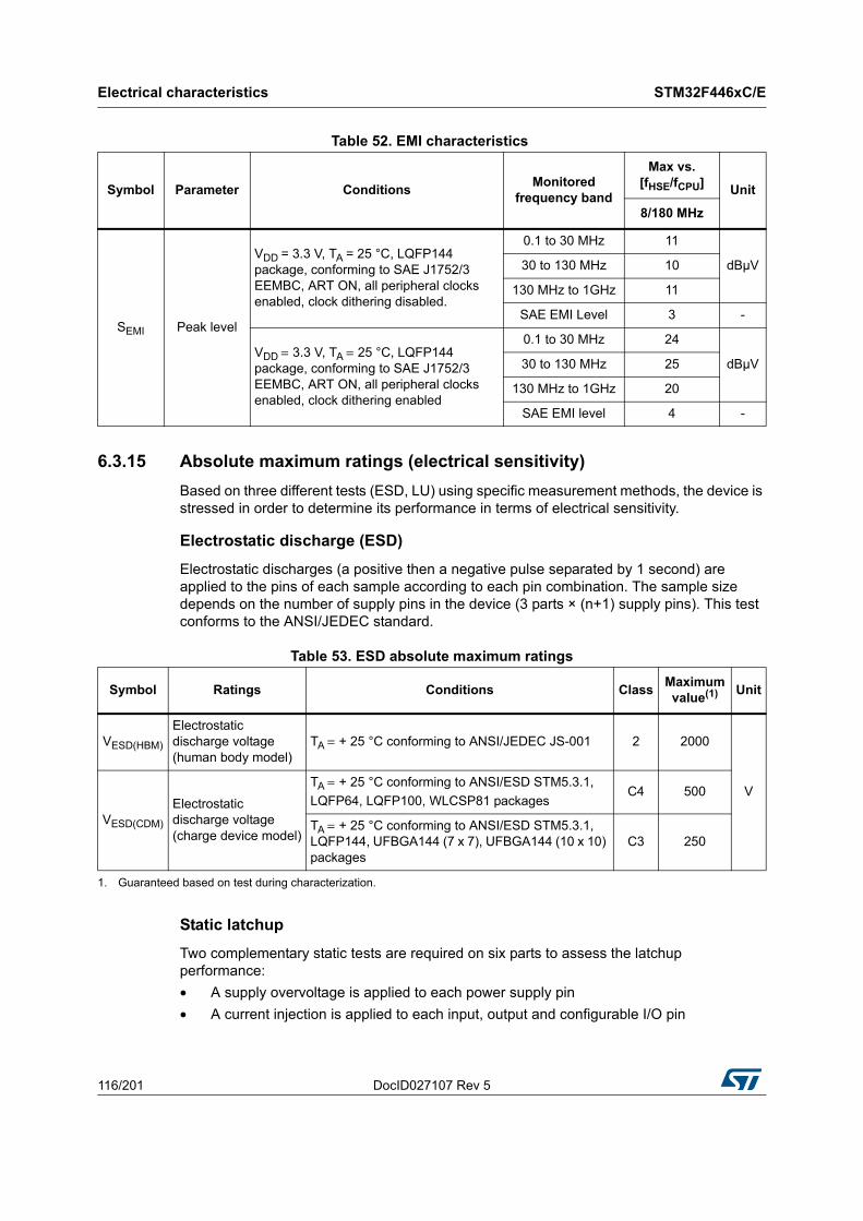
Electrical characteristics STM32F446xC/E
116/201 DocID027107 Rev 5
6.3.15 Absolute maximum ratings (electrical sensitivity)
Based on three different tests (ESD, LU) using specific measurement methods, the device is stressed in order to determine its performance in terms of electrical sensitivity.
Electrostatic discharge (ESD)
Electrostatic discharges (a positive then a negative pulse separated by 1 second) are applied to the pins of each sample according to each pin combination. The sample size depends on the number of supply pins in the device (3 parts × (n+1) supply pins). This test conforms to the ANSI/JEDEC standard.
Static latchup
Two complementary static tests are required on six parts to assess the latchup performance:
• A supply overvoltage is applied to each power supply pin
• A current injection is applied to each input, output and configurable I/O pin
Table 52. EMI characteristics
Symbol Parameter ConditionsMonitored
frequency band
Max vs. [fHSE/fCPU]
Unit
8/180 MHz
SEMI Peak level
VDD = 3.3 V, TA = 25 °C, LQFP144 package, conforming to SAE J1752/3 EEMBC, ART ON, all peripheral clocks enabled, clock dithering disabled.
0.1 to 30 MHz 11
dBµV30 to 130 MHz 10
130 MHz to 1GHz 11
SAE EMI Level 3 -
VDD = 3.3 V, TA = 25 °C, LQFP144 package, conforming to SAE J1752/3 EEMBC, ART ON, all peripheral clocks enabled, clock dithering enabled
0.1 to 30 MHz 24
dBµV30 to 130 MHz 25
130 MHz to 1GHz 20
SAE EMI level 4 -
Table 53. ESD absolute maximum ratings
Symbol Ratings Conditions ClassMaximum value(1) Unit
VESD(HBM)
Electrostatic discharge voltage (human body model)
TA = + 25 °C conforming to ANSI/JEDEC JS-001 2 2000
V
VESD(CDM)
Electrostatic discharge voltage (charge device model)
TA = + 25 °C conforming to ANSI/ESD STM5.3.1,
LQFP64, LQFP100, WLCSP81 packagesC4 500
TA = + 25 °C conforming to ANSI/ESD STM5.3.1, LQFP144, UFBGA144 (7 x 7), UFBGA144 (10 x 10) packages
C3 250
1. Guaranteed based on test during characterization.
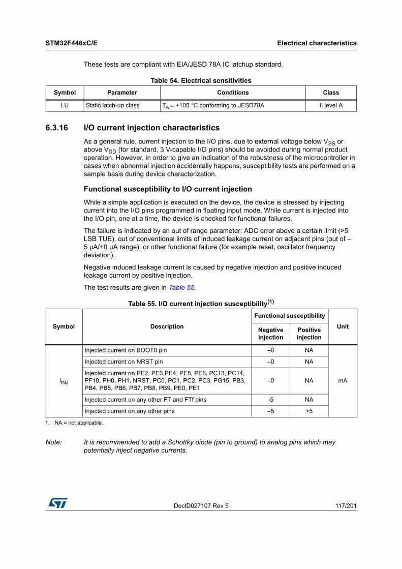
DocID027107 Rev 5 117/201
STM32F446xC/E Electrical characteristics
174
These tests are compliant with EIA/JESD 78A IC latchup standard.
6.3.16 I/O current injection characteristics
As a general rule, current injection to the I/O pins, due to external voltage below VSS or above VDD (for standard, 3 V-capable I/O pins) should be avoided during normal product operation. However, in order to give an indication of the robustness of the microcontroller in cases when abnormal injection accidentally happens, susceptibility tests are performed on a sample basis during device characterization.
Functional susceptibility to I/O current injection
While a simple application is executed on the device, the device is stressed by injecting current into the I/O pins programmed in floating input mode. While current is injected into the I/O pin, one at a time, the device is checked for functional failures.
The failure is indicated by an out of range parameter: ADC error above a certain limit (>5 LSB TUE), out of conventional limits of induced leakage current on adjacent pins (out of –5 µA/+0 µA range), or other functional failure (for example reset, oscillator frequency deviation).
Negative induced leakage current is caused by negative injection and positive induced leakage current by positive injection.
The test results are given in Table 55.
Note: It is recommended to add a Schottky diode (pin to ground) to analog pins which may potentially inject negative currents.
Table 54. Electrical sensitivities
Symbol Parameter Conditions Class
LU Static latch-up class TA = +105 °C conforming to JESD78A II level A
Table 55. I/O current injection susceptibility(1)
Symbol Description
Functional susceptibility
UnitNegative injection
Positive injection
IINJ
Injected current on BOOT0 pin –0 NA
mA
Injected current on NRST pin –0 NA
Injected current on PE2, PE3,PE4, PE5, PE6, PC13, PC14, PF10, PH0, PH1, NRST, PC0, PC1, PC2, PC3, PG15, PB3, PB4, PB5, PB6, PB7, PB8, PB9, PE0, PE1
–0 NA
Injected current on any other FT and FTf pins -5 NA
Injected current on any other pins –5 +5
1. NA = not applicable.
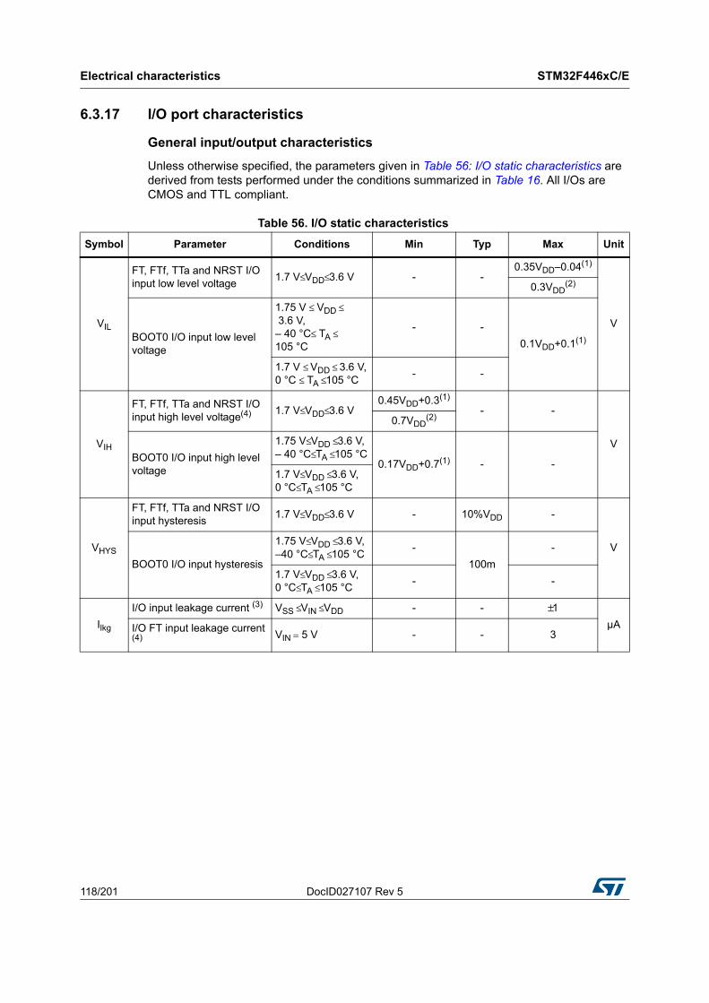
Electrical characteristics STM32F446xC/E
118/201 DocID027107 Rev 5
6.3.17 I/O port characteristics
General input/output characteristics
Unless otherwise specified, the parameters given in Table 56: I/O static characteristics are derived from tests performed under the conditions summarized in Table 16. All I/Os are CMOS and TTL compliant.
Table 56. I/O static characteristics
Symbol Parameter Conditions Min Typ Max Unit
VIL
FT, FTf, TTa and NRST I/O input low level voltage
1.7 V≤ VDD≤ 3.6 V - -0.35VDD–0.04(1)
V
0.3VDD(2)
BOOT0 I/O input low level voltage
1.75 V ≤ VDD ≤ 3.6 V, – 40 °C≤ TA ≤ 105 °C
- -
0.1VDD+0.1(1)
1.7 V ≤ VDD ≤ 3.6 V, 0 °C ≤ TA ≤ 105 °C
- -
VIH
FT, FTf, TTa and NRST I/O input high level voltage(4) 1.7 V≤ VDD≤ 3.6 V
0.45VDD+0.3(1)
- -
V
0.7VDD(2)
BOOT0 I/O input high level voltage
1.75 V≤ VDD ≤ 3.6 V, – 40 °C≤ TA ≤ 105 °C
0.17VDD+0.7(1) - -1.7 V≤ VDD ≤ 3.6 V, 0 °C≤ TA ≤ 105 °C
VHYS
FT, FTf, TTa and NRST I/O input hysteresis
1.7 V≤ VDD≤ 3.6 V - 10%VDD -
V
BOOT0 I/O input hysteresis
1.75 V≤ VDD ≤ 3.6 V, –40 °C≤ TA ≤ 105 °C
-
100m
-
1.7 V≤ VDD ≤ 3.6 V, 0 °C≤ TA ≤ 105 °C
- -
Ilkg
I/O input leakage current (3) VSS ≤ VIN ≤ VDD - - ±1µAI/O FT input leakage current
(4) VIN = 5 V - - 3
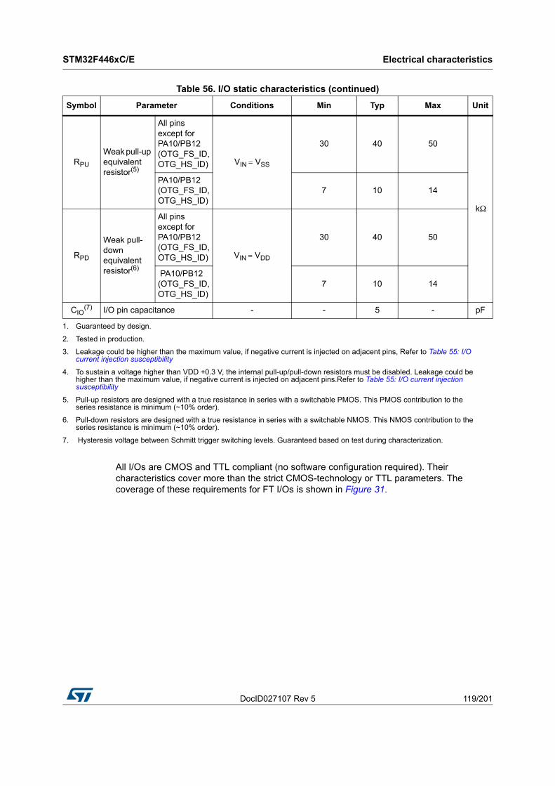
DocID027107 Rev 5 119/201
STM32F446xC/E Electrical characteristics
174
All I/Os are CMOS and TTL compliant (no software configuration required). Their characteristics cover more than the strict CMOS-technology or TTL parameters. The coverage of these requirements for FT I/Os is shown in Figure 31.
RPU
Weak pull-up equivalent resistor(5)
All pins except for PA10/PB12 (OTG_FS_ID,OTG_HS_ID) VIN = VSS
30 40 50
kΩ
PA10/PB12 (OTG_FS_ID,OTG_HS_ID)
7 10 14
RPD
Weak pull-down equivalent resistor(6)
All pins except for PA10/PB12 (OTG_FS_ID,OTG_HS_ID) VIN = VDD
30 40 50
PA10/PB12 (OTG_FS_ID,OTG_HS_ID)
7 10 14
CIO(7) I/O pin capacitance - - 5 - pF
1. Guaranteed by design.
2. Tested in production.
3. Leakage could be higher than the maximum value, if negative current is injected on adjacent pins, Refer to Table 55: I/O current injection susceptibility
4. To sustain a voltage higher than VDD +0.3 V, the internal pull-up/pull-down resistors must be disabled. Leakage could be higher than the maximum value, if negative current is injected on adjacent pins.Refer to Table 55: I/O current injection susceptibility
5. Pull-up resistors are designed with a true resistance in series with a switchable PMOS. This PMOS contribution to the series resistance is minimum (~10% order).
6. Pull-down resistors are designed with a true resistance in series with a switchable NMOS. This NMOS contribution to the series resistance is minimum (~10% order).
7. Hysteresis voltage between Schmitt trigger switching levels. Guaranteed based on test during characterization.
Table 56. I/O static characteristics (continued)
Symbol Parameter Conditions Min Typ Max Unit
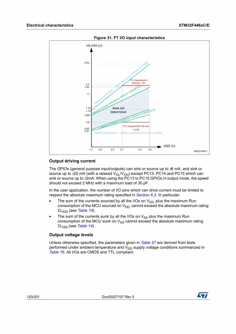
Electrical characteristics STM32F446xC/E
120/201 DocID027107 Rev 5
Figure 31. FT I/O input characteristics
Output driving current
The GPIOs (general purpose input/outputs) can sink or source up to ±8 mA, and sink or source up to ±20 mA (with a relaxed VOL/VOH) except PC13, PC14 and PC15 which can sink or source up to ±3mA. When using the PC13 to PC15 GPIOs in output mode, the speed should not exceed 2 MHz with a maximum load of 30 pF.
In the user application, the number of I/O pins which can drive current must be limited to respect the absolute maximum rating specified in Section 6.2. In particular:
• The sum of the currents sourced by all the I/Os on VDD, plus the maximum Run consumption of the MCU sourced on VDD, cannot exceed the absolute maximum rating ΣIVDD (see Table 14).
• The sum of the currents sunk by all the I/Os on VSS plus the maximum Run consumption of the MCU sunk on VSS cannot exceed the absolute maximum rating ΣIVSS (see Table 14).
Output voltage levels
Unless otherwise specified, the parameters given in Table 57 are derived from tests performed under ambient temperature and VDD supply voltage conditions summarized in Table 16. All I/Os are CMOS and TTL compliant.
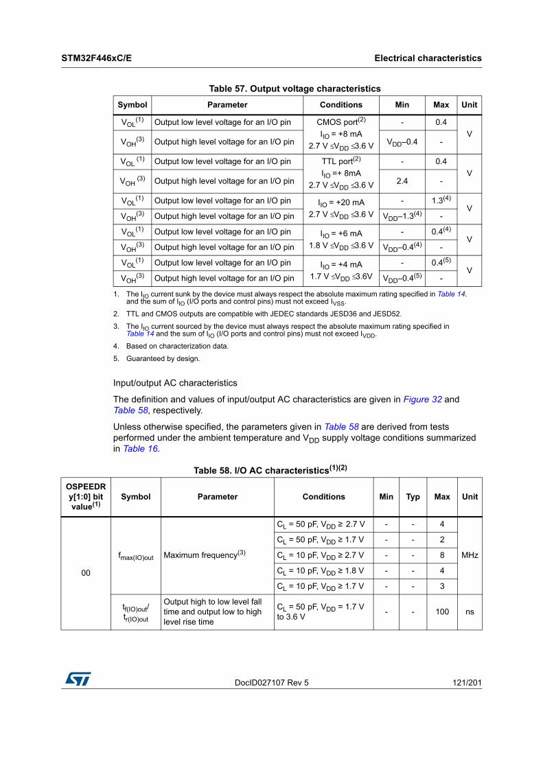
DocID027107 Rev 5 121/201
STM32F446xC/E Electrical characteristics
174
Input/output AC characteristics
The definition and values of input/output AC characteristics are given in Figure 32 and Table 58, respectively.
Unless otherwise specified, the parameters given in Table 58 are derived from tests performed under the ambient temperature and VDD supply voltage conditions summarized in Table 16.
Table 57. Output voltage characteristics
Symbol Parameter Conditions Min Max Unit
VOL(1)
1. The IIO current sunk by the device must always respect the absolute maximum rating specified in Table 14. and the sum of IIO (I/O ports and control pins) must not exceed IVSS.
Output low level voltage for an I/O pin CMOS port(2)
IIO = +8 mA
2.7 V ≤ VDD ≤ 3.6 V
2. TTL and CMOS outputs are compatible with JEDEC standards JESD36 and JESD52.
- 0.4
VVOH
(3)
3. The IIO current sourced by the device must always respect the absolute maximum rating specified in Table 14 and the sum of IIO (I/O ports and control pins) must not exceed IVDD.
Output high level voltage for an I/O pin VDD–0.4 -
VOL (1) Output low level voltage for an I/O pin TTL port(2)
IIO =+ 8mA
2.7 V ≤ VDD ≤ 3.6 V
- 0.4
VVOH
(3) Output high level voltage for an I/O pin 2.4 -
VOL(1) Output low level voltage for an I/O pin IIO = +20 mA
2.7 V ≤ VDD ≤ 3.6 V
- 1.3(4)
4. Based on characterization data.
VVOH
(3) Output high level voltage for an I/O pin VDD–1.3(4) -
VOL(1) Output low level voltage for an I/O pin IIO = +6 mA
1.8 V ≤ VDD ≤ 3.6 V
- 0.4(4)
VVOH
(3) Output high level voltage for an I/O pin VDD–0.4(4) -
VOL(1) Output low level voltage for an I/O pin IIO = +4 mA
1.7 V ≤ VDD ≤ 3.6V
- 0.4(5)
5. Guaranteed by design.
VVOH
(3) Output high level voltage for an I/O pin VDD–0.4(5) -
Table 58. I/O AC characteristics(1)(2)
OSPEEDRy[1:0] bit value(1)
Symbol Parameter Conditions Min Typ Max Unit
00
fmax(IO)out Maximum frequency(3)
CL = 50 pF, VDD ≥ 2.7 V - - 4
MHz
CL = 50 pF, VDD ≥ 1.7 V - - 2
CL = 10 pF, VDD ≥ 2.7 V - - 8
CL = 10 pF, VDD ≥ 1.8 V - - 4
CL = 10 pF, VDD ≥ 1.7 V - - 3
tf(IO)out/tr(IO)out
Output high to low level fall time and output low to high level rise time
CL = 50 pF, VDD = 1.7 V to 3.6 V
- - 100 ns
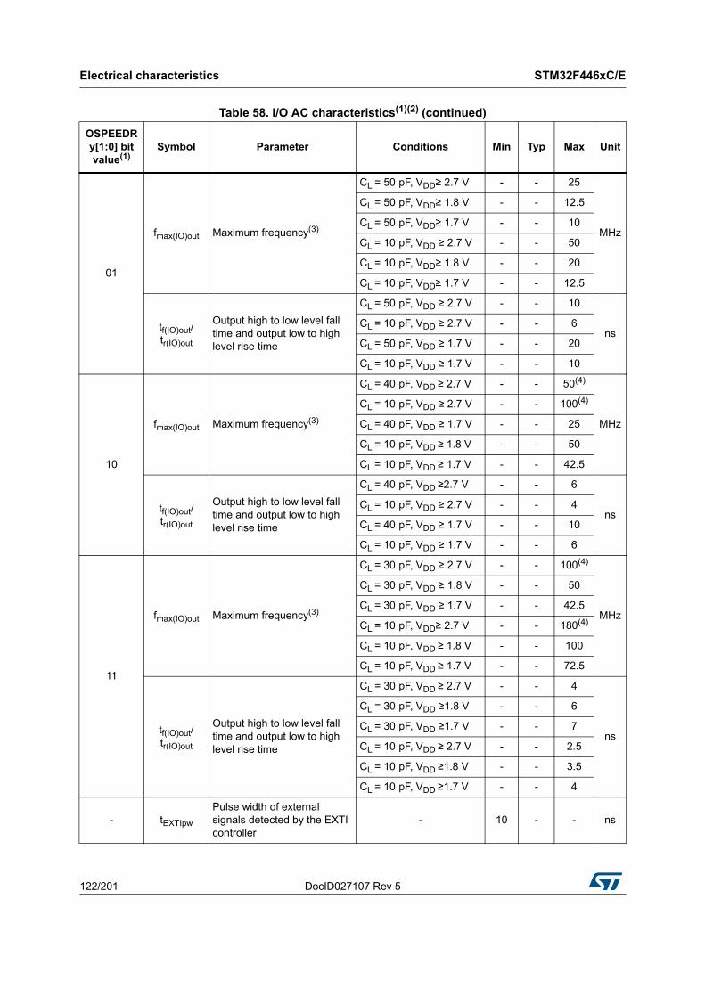
Electrical characteristics STM32F446xC/E
122/201 DocID027107 Rev 5
01
fmax(IO)out Maximum frequency(3)
CL = 50 pF, VDD≥ 2.7 V - - 25
MHz
CL = 50 pF, VDD≥ 1.8 V - - 12.5
CL = 50 pF, VDD≥ 1.7 V - - 10
CL = 10 pF, VDD ≥ 2.7 V - - 50
CL = 10 pF, VDD≥ 1.8 V - - 20
CL = 10 pF, VDD≥ 1.7 V - - 12.5
tf(IO)out/tr(IO)out
Output high to low level fall time and output low to high level rise time
CL = 50 pF, VDD ≥ 2.7 V - - 10
nsCL = 10 pF, VDD ≥ 2.7 V - - 6
CL = 50 pF, VDD ≥ 1.7 V - - 20
CL = 10 pF, VDD ≥ 1.7 V - - 10
10
fmax(IO)out Maximum frequency(3)
CL = 40 pF, VDD ≥ 2.7 V - - 50(4)
MHz
CL = 10 pF, VDD ≥ 2.7 V - - 100(4)
CL = 40 pF, VDD ≥ 1.7 V - - 25
CL = 10 pF, VDD ≥ 1.8 V - - 50
CL = 10 pF, VDD ≥ 1.7 V - - 42.5
tf(IO)out/tr(IO)out
Output high to low level fall time and output low to high level rise time
CL = 40 pF, VDD ≥2.7 V - - 6
nsCL = 10 pF, VDD ≥ 2.7 V - - 4
CL = 40 pF, VDD ≥ 1.7 V - - 10
CL = 10 pF, VDD ≥ 1.7 V - - 6
11
fmax(IO)out Maximum frequency(3)
CL = 30 pF, VDD ≥ 2.7 V - - 100(4)
MHz
CL = 30 pF, VDD ≥ 1.8 V - - 50
CL = 30 pF, VDD ≥ 1.7 V - - 42.5
CL = 10 pF, VDD≥ 2.7 V - - 180(4)
CL = 10 pF, VDD ≥ 1.8 V - - 100
CL = 10 pF, VDD ≥ 1.7 V - - 72.5
tf(IO)out/tr(IO)out
Output high to low level fall time and output low to high level rise time
CL = 30 pF, VDD ≥ 2.7 V - - 4
ns
CL = 30 pF, VDD ≥1.8 V - - 6
CL = 30 pF, VDD ≥1.7 V - - 7
CL = 10 pF, VDD ≥ 2.7 V - - 2.5
CL = 10 pF, VDD ≥1.8 V - - 3.5
CL = 10 pF, VDD ≥1.7 V - - 4
- tEXTIpw
Pulse width of external signals detected by the EXTI controller
- 10 - - ns
Table 58. I/O AC characteristics(1)(2) (continued)
OSPEEDRy[1:0] bit value(1)
Symbol Parameter Conditions Min Typ Max Unit
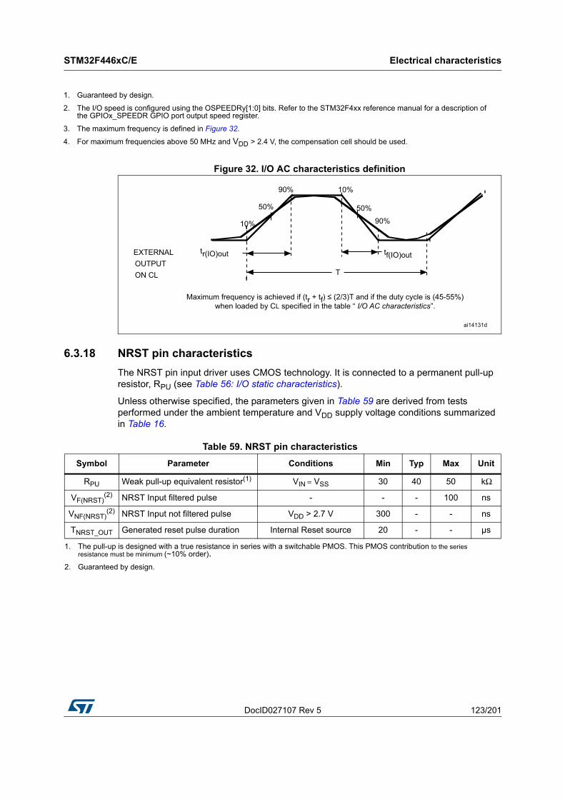
DocID027107 Rev 5 123/201
STM32F446xC/E Electrical characteristics
174
Figure 32. I/O AC characteristics definition
6.3.18 NRST pin characteristics
The NRST pin input driver uses CMOS technology. It is connected to a permanent pull-up resistor, RPU (see Table 56: I/O static characteristics).
Unless otherwise specified, the parameters given in Table 59 are derived from tests performed under the ambient temperature and VDD supply voltage conditions summarized in Table 16.
1. Guaranteed by design.
2. The I/O speed is configured using the OSPEEDRy[1:0] bits. Refer to the STM32F4xx reference manual for a description of the GPIOx_SPEEDR GPIO port output speed register.
3. The maximum frequency is defined in Figure 32.
4. For maximum frequencies above 50 MHz and VDD > 2.4 V, the compensation cell should be used.
Table 59. NRST pin characteristics
Symbol Parameter Conditions Min Typ Max Unit
RPU Weak pull-up equivalent resistor(1) VIN = VSS 30 40 50 kΩ
VF(NRST)(2) NRST Input filtered pulse - - - 100 ns
VNF(NRST)(2) NRST Input not filtered pulse VDD > 2.7 V 300 - - ns
TNRST_OUT Generated reset pulse duration Internal Reset source 20 - - µs
1. The pull-up is designed with a true resistance in series with a switchable PMOS. This PMOS contribution to the series resistance must be minimum (~10% order).
2. Guaranteed by design.
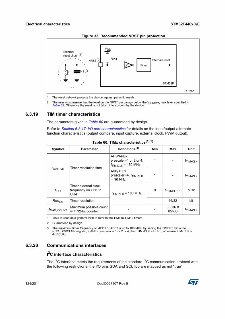
Electrical characteristics STM32F446xC/E
124/201 DocID027107 Rev 5
Figure 33. Recommended NRST pin protection
1. The reset network protects the device against parasitic resets.
2. The user must ensure that the level on the NRST pin can go below the VIL(NRST) max level specified in Table 59. Otherwise the reset is not taken into account by the device.
6.3.19 TIM timer characteristics
The parameters given in Table 60 are guaranteed by design.
Refer to Section 6.3.17: I/O port characteristics for details on the input/output alternate function characteristics (output compare, input capture, external clock, PWM output).
6.3.20 Communications interfaces
I2C interface characteristics
The I2C interface meets the requirements of the standard I2C communication protocol with the following restrictions: the I/O pins SDA and SCL too are mapped as not “true”
Table 60. TIMx characteristics(1)(2)
1. TIMx is used as a general term to refer to the TIM1 to TIM12 timers.
2. Guaranteed by design.
Symbol Parameter Conditions(3)
3. The maximum timer frequency on APB1 or APB2 is up to 180 MHz, by setting the TIMPRE bit in the RCC_DCKCFGR register, if APBx prescaler is 1 or 2 or 4, then TIMxCLK = HCKL, otherwise TIMxCLK = 4x PCLKx.
Min Max Unit
tres(TIM) Timer resolution time
AHB/APBx prescaler=1 or 2 or 4, fTIMxCLK = 180 MHz
1 - tTIMxCLK
AHB/APBx prescaler>4, fTIMxCLK
= 90 MHz1 - tTIMxCLK
fEXT
Timer external clock frequency on CH1 to CH4 fTIMxCLK = 180 MHz
0 fTIMxCLK/2 MHz
ResTIM Timer resolution - 16/32 bit
tMAX_COUNTMaximum possible count with 32-bit counter
- -65536 × 65536
tTIMxCLK
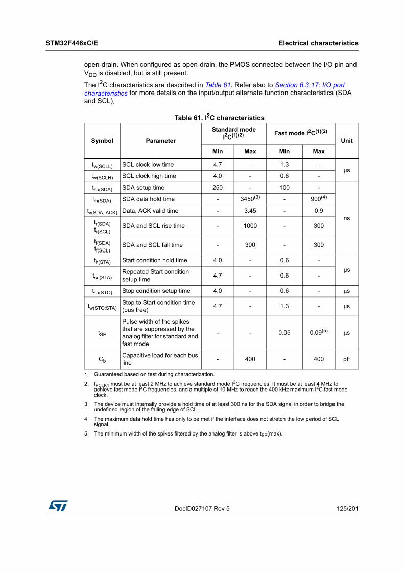
DocID027107 Rev 5 125/201
STM32F446xC/E Electrical characteristics
174
open-drain. When configured as open-drain, the PMOS connected between the I/O pin and VDD is disabled, but is still present.
The I2C characteristics are described in Table 61. Refer also to Section 6.3.17: I/O port characteristics for more details on the input/output alternate function characteristics (SDA and SCL).
Table 61. I2C characteristics
Symbol Parameter
Standard mode I2C(1)(2)
1. Guaranteed based on test during characterization.
Fast mode I2C(1)(2)
2. fPCLK1 must be at least 2 MHz to achieve standard mode I2C frequencies. It must be at least 4 MHz to achieve fast mode I2C frequencies, and a multiple of 10 MHz to reach the 400 kHz maximum I2C fast mode clock.
Unit
Min Max Min Max
tw(SCLL) SCL clock low time 4.7 - 1.3 -µs
tw(SCLH) SCL clock high time 4.0 - 0.6 -
tsu(SDA) SDA setup time 250 - 100 -
ns
th(SDA) SDA data hold time - 3450(3)
3. The device must internally provide a hold time of at least 300 ns for the SDA signal in order to bridge the undefined region of the falling edge of SCL.
- 900(4)
4. The maximum data hold time has only to be met if the interface does not stretch the low period of SCL signal.
tv(SDA, ACK) Data, ACK valid time - 3.45 - 0.9
tr(SDA)tr(SCL)
SDA and SCL rise time - 1000 - 300
tf(SDA)tf(SCL)
SDA and SCL fall time - 300 - 300
th(STA) Start condition hold time 4.0 - 0.6 -
µstsu(STA)
Repeated Start condition setup time
4.7 - 0.6 -
tsu(STO) Stop condition setup time 4.0 - 0.6 - μs
tw(STO:STA)Stop to Start condition time (bus free)
4.7 - 1.3 - μs
tSP
Pulse width of the spikes that are suppressed by the analog filter for standard and fast mode
- - 0.05 0.09(5)
5. The minimum width of the spikes filtered by the analog filter is above tSP(max).
μs
CbCapacitive load for each bus line
- 400 - 400 pF
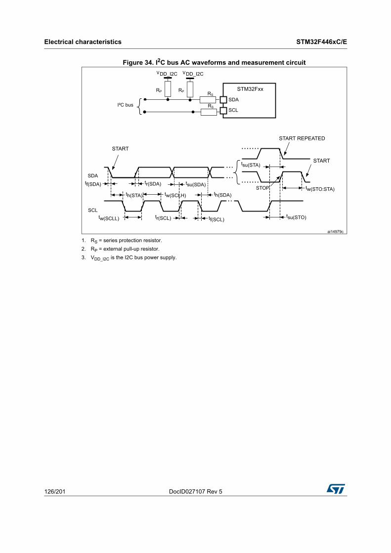
Electrical characteristics STM32F446xC/E
126/201 DocID027107 Rev 5
Figure 34. I2C bus AC waveforms and measurement circuit
1. RS = series protection resistor.
2. RP = external pull-up resistor.
3. VDD_I2C is the I2C bus power supply.
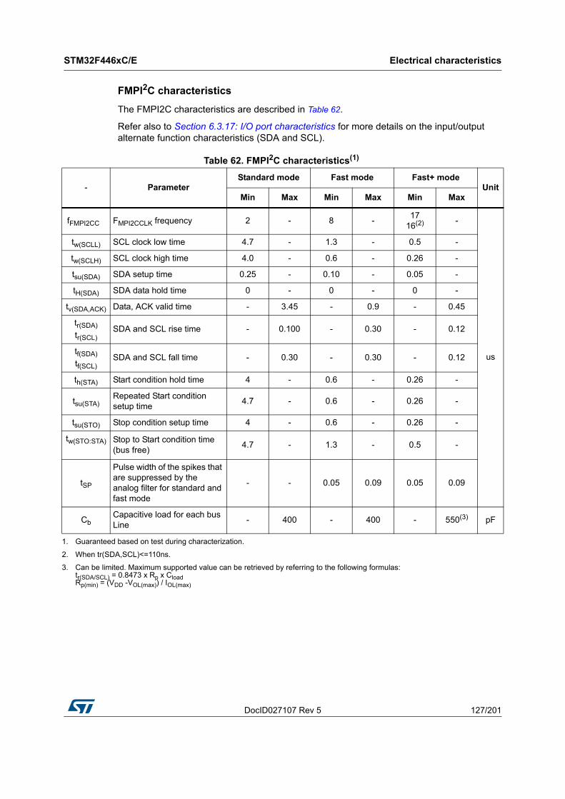
DocID027107 Rev 5 127/201
STM32F446xC/E Electrical characteristics
174
FMPI2C characteristics
The FMPI2C characteristics are described in Table 62.
Refer also to Section 6.3.17: I/O port characteristics for more details on the input/output alternate function characteristics (SDA and SCL).
Table 62. FMPI2C characteristics(1)
- ParameterStandard mode Fast mode Fast+ mode
UnitMin Max Min Max Min Max
fFMPI2CC FMPI2CCLK frequency 2 - 8 -17
16(2) -
us
tw(SCLL) SCL clock low time 4.7 - 1.3 - 0.5 -
tw(SCLH) SCL clock high time 4.0 - 0.6 - 0.26 -
tsu(SDA) SDA setup time 0.25 - 0.10 - 0.05 -
tH(SDA) SDA data hold time 0 - 0 - 0 -
tv(SDA,ACK) Data, ACK valid time - 3.45 - 0.9 - 0.45
tr(SDA)
tr(SCL)SDA and SCL rise time - 0.100 - 0.30 - 0.12
tf(SDA)
tf(SCL)SDA and SCL fall time - 0.30 - 0.30 - 0.12
th(STA) Start condition hold time 4 - 0.6 - 0.26 -
tsu(STA)Repeated Start condition setup time
4.7 - 0.6 - 0.26 -
tsu(STO) Stop condition setup time 4 - 0.6 - 0.26 -
tw(STO:STA) Stop to Start condition time (bus free)
4.7 - 1.3 - 0.5 -
tSP
Pulse width of the spikes that are suppressed by the analog filter for standard and fast mode
- - 0.05 0.09 0.05 0.09
CbCapacitive load for each bus Line
- 400 - 400 - 550(3) pF
1. Guaranteed based on test during characterization.
2. When tr(SDA,SCL)<=110ns.
3. Can be limited. Maximum supported value can be retrieved by referring to the following formulas: tr(SDA/SCL) = 0.8473 x Rp x Cload Rp(min) = (VDD -VOL(max)) / IOL(max)
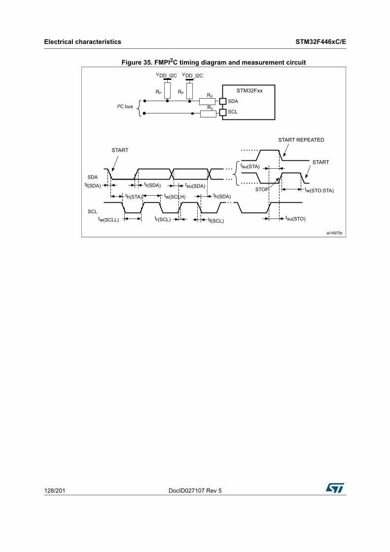
Electrical characteristics STM32F446xC/E
128/201 DocID027107 Rev 5
Figure 35. FMPI2C timing diagram and measurement circuit
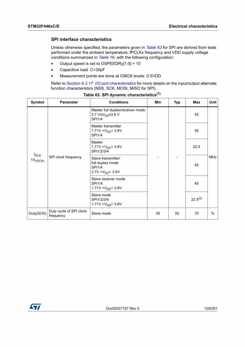
DocID027107 Rev 5 129/201
STM32F446xC/E Electrical characteristics
174
SPI interface characteristics
Unless otherwise specified, the parameters given in Table 63 for SPI are derived from tests performed under the ambient temperature, fPCLKx frequency and VDD supply voltage conditions summarized in Table 16, with the following configuration:
• Output speed is set to OSPEEDRy[1:0] = 10
• Capacitive load C=30pF
• Measurement points are done at CMOS levels: 0.5VDD
Refer to Section 6.3.17: I/O port characteristics for more details on the input/output alternate function characteristics (NSS, SCK, MOSI, MISO for SPI).
Table 63. SPI dynamic characteristics(1)
Symbol Parameter Conditions Min Typ Max Unit
fSCK
1/tc(SCK)SPI clock frequency
Master full duplex/receiver mode, 2.7 V≤VDD≤3.6 V SPI1/4
- -
45
MHz
Master transmitter 1.71V <VDD< 3.6V SPI1/4
45
Master 1.71V <VDD< 3.6V SPI1/2/3/4
22.5
Slave transmitter/ full duplex mode SPI1/4 2.7V <VDD< 3.6V
45
Slave receiver mode SPI1/4 1.71V <VDD< 3.6V
45
Slave mode SPI1/2/3/4 1.71V <VDD< 3.6V
22.5(2)
Duty(SCK)Duty cycle of SPI clock frequency
Slave mode 30 50 70 %
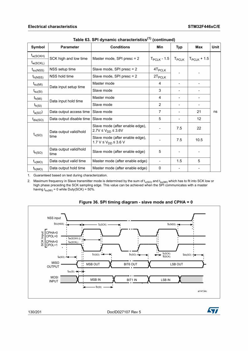
Electrical characteristics STM32F446xC/E
130/201 DocID027107 Rev 5
Figure 36. SPI timing diagram - slave mode and CPHA = 0
tw(SCKH)SCK high and low time Master mode, SPI presc = 2 TPCLK - 1.5 TPCLK TPCLK + 1.5
ns
tw(SCKL)
tsu(NSS) NSS setup time Slave mode, SPI presc = 2 4TPCLK- -
th(NSS) NSS hold time Slave mode, SPI presc = 2 2TPCLK
tsu(MI)Data input setup time
Master mode 4 - -
tsu(SI) Slave mode 3 - -
th(MI)Data input hold time
Master mode 4 - -
th(SI) Slave mode 2 - -
ta(SO) Data output access time Slave mode 7 - 21
tdis(SO) Data output disable time Slave mode 5 - 12
tv(SO)Data output valid/hold time
Slave mode (after enable edge), 2.7V ≤ VDD ≤ 3.6V
- 7.5 22
Slave mode (after enable edge), 1.7 V ≤ VDD ≤ 3.6 V
- 7.5 10.5
th(SO)Data output valid/hold time
Slave mode (after enable edge) 5 - -
tv(MO) Data output valid time Master mode (after enable edge) - 1.5 5
th(MO) Data output hold time Master mode (after enable edge) 0 - -
1. Guaranteed based on test during characterization.
2. Maximum frequency in Slave transmitter mode is determined by the sum of tv(SO) and tsu(MI) which has to fit into SCK low or high phase preceding the SCK sampling edge. This value can be achieved when the SPI communicates with a master having tsu(MI) = 0 while Duty(SCK) = 50%.
Table 63. SPI dynamic characteristics(1) (continued)
Symbol Parameter Conditions Min Typ Max Unit
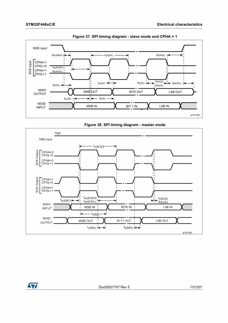
DocID027107 Rev 5 131/201
STM32F446xC/E Electrical characteristics
174
Figure 37. SPI timing diagram - slave mode and CPHA = 1
Figure 38. SPI timing diagram - master mode
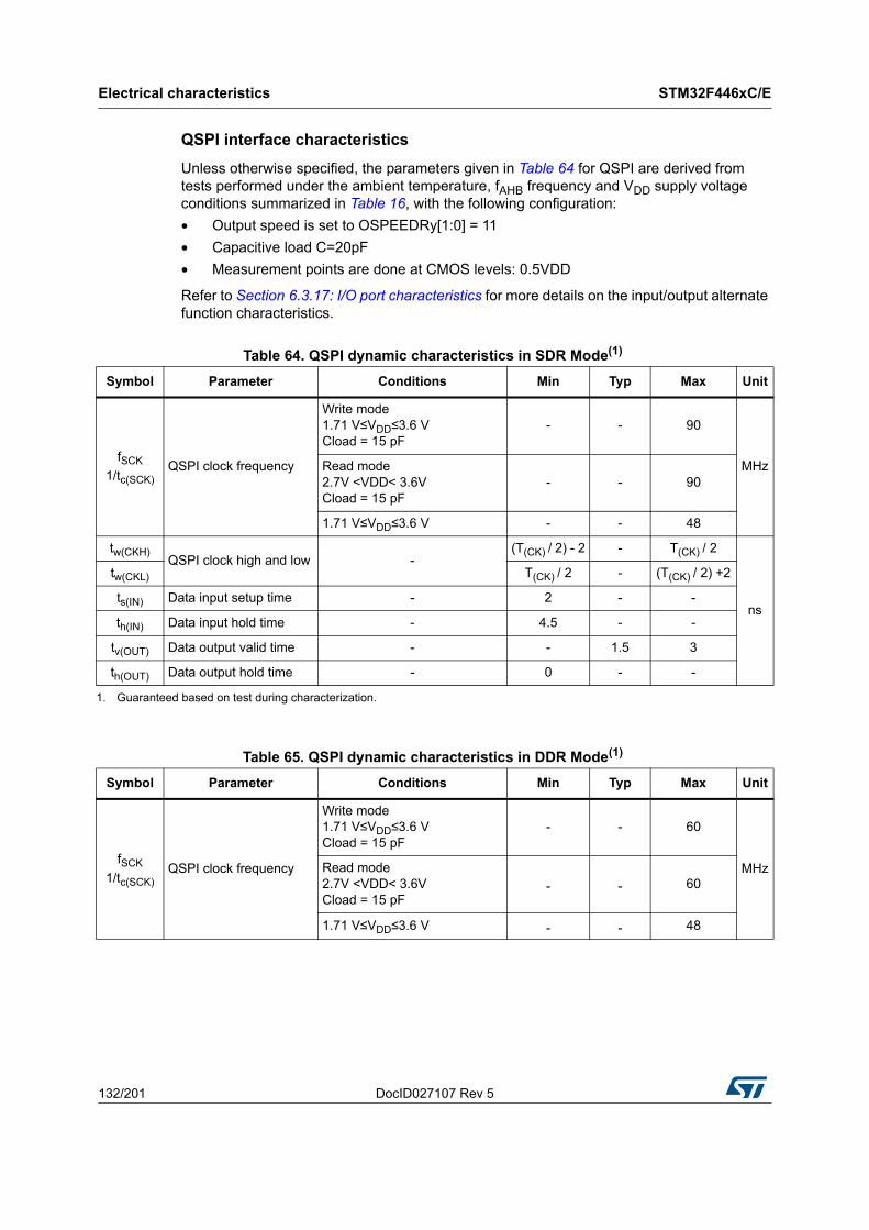
Electrical characteristics STM32F446xC/E
132/201 DocID027107 Rev 5
QSPI interface characteristics
Unless otherwise specified, the parameters given in Table 64 for QSPI are derived from tests performed under the ambient temperature, fAHB frequency and VDD supply voltage conditions summarized in Table 16, with the following configuration:
• Output speed is set to OSPEEDRy[1:0] = 11
• Capacitive load C=20pF
• Measurement points are done at CMOS levels: 0.5VDD
Refer to Section 6.3.17: I/O port characteristics for more details on the input/output alternate function characteristics.
Table 64. QSPI dynamic characteristics in SDR Mode(1)
Symbol Parameter Conditions Min Typ Max Unit
fSCK
1/tc(SCK)QSPI clock frequency
Write mode 1.71 V≤VDD≤3.6 V Cload = 15 pF
- - 90
MHzRead mode 2.7V <VDD< 3.6V Cload = 15 pF
- - 90
1.71 V≤VDD≤3.6 V - - 48
tw(CKH)QSPI clock high and low -
(T(CK) / 2) - 2 - T(CK) / 2
ns
tw(CKL) T(CK) / 2 - (T(CK) / 2) +2
ts(IN) Data input setup time - 2 - -
th(IN) Data input hold time - 4.5 - -
tv(OUT) Data output valid time - - 1.5 3
th(OUT) Data output hold time - 0 - -
1. Guaranteed based on test during characterization.
Table 65. QSPI dynamic characteristics in DDR Mode(1)
Symbol Parameter Conditions Min Typ Max Unit
fSCK
1/tc(SCK)QSPI clock frequency
Write mode 1.71 V≤VDD≤3.6 V Cload = 15 pF
- - 60
MHzRead mode 2.7V <VDD< 3.6V Cload = 15 pF
- - 60
1.71 V≤VDD≤3.6 V - - 48
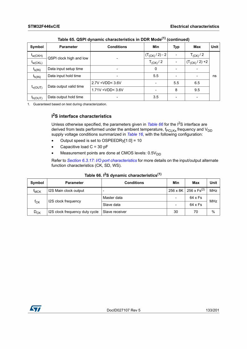
DocID027107 Rev 5 133/201
STM32F446xC/E Electrical characteristics
174
I2S interface characteristics
Unless otherwise specified, the parameters given in Table 66 for the I2S interface are derived from tests performed under the ambient temperature, fPCLKx frequency and VDD supply voltage conditions summarized in Table 16, with the following configuration:
• Output speed is set to OSPEEDRy[1:0] = 10
• Capacitive load C = 30 pF
• Measurement points are done at CMOS levels: 0.5VDD
Refer to Section 6.3.17: I/O port characteristics for more details on the input/output alternate function characteristics (CK, SD, WS).
tw(CKH)QSPI clock high and low -
(T(CK) / 2) - 2 - T(CK) / 2
ns
tw(CKL) T(CK) / 2 - (T(CK) / 2) +2
ts(IN) Data input setup time - 0 - -
th(IN) Data input hold time - 5.5 - -
tv(OUT) Data output valid time2.7V <VDD< 3.6V - 5.5 6.5
1.71V <VDD< 3.6V - 8 9.5
th(OUT) Data output hold time - 3.5 - -
1. Guaranteed based on test during characterization.
Table 65. QSPI dynamic characteristics in DDR Mode(1) (continued)
Symbol Parameter Conditions Min Typ Max Unit
Table 66. I2S dynamic characteristics(1)
Symbol Parameter Conditions Min Max Unit
fMCK I2S Main clock output - 256 x 8K 256 x Fs(2) MHz
fCK I2S clock frequency Master data - 64 x Fs
MHzSlave data - 64 x Fs
DCK I2S clock frequency duty cycle Slave receiver 30 70 %
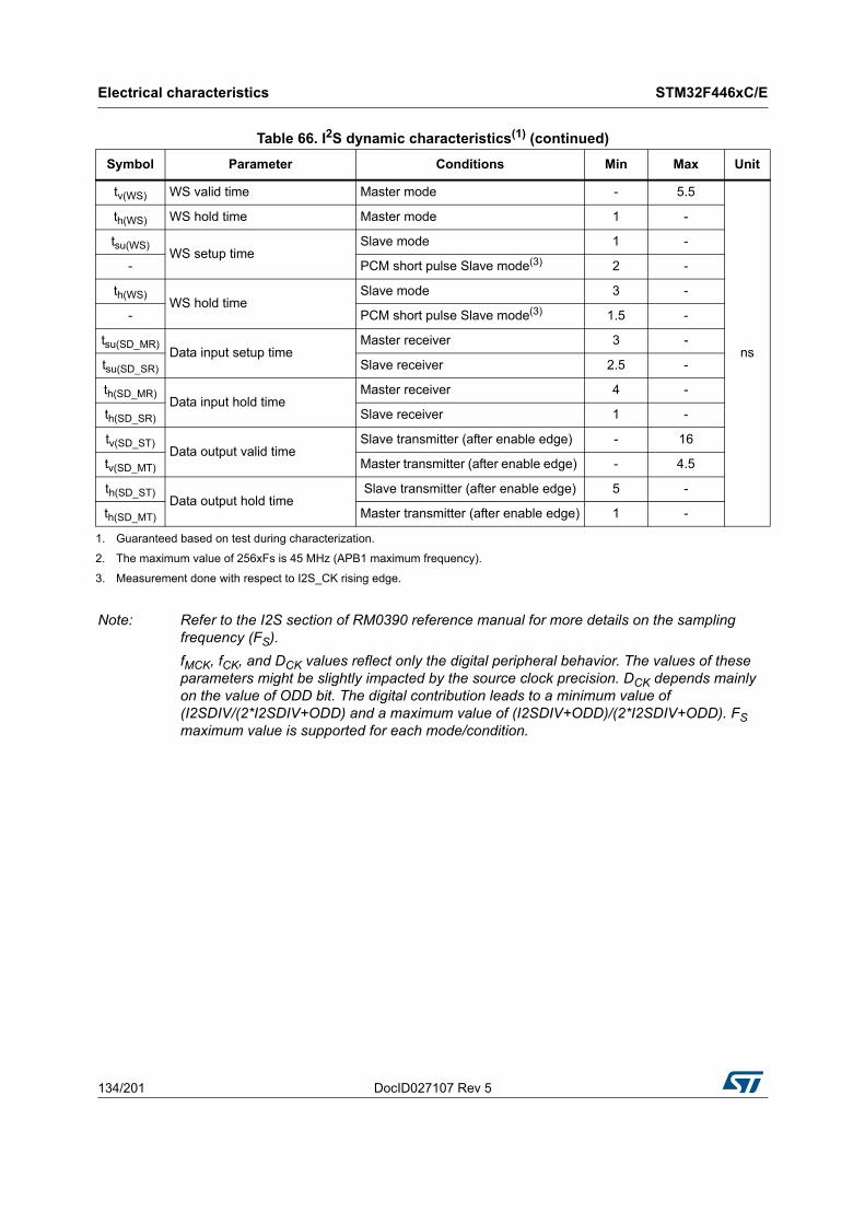
Electrical characteristics STM32F446xC/E
134/201 DocID027107 Rev 5
Note: Refer to the I2S section of RM0390 reference manual for more details on the sampling frequency (FS).
fMCK, fCK, and DCK values reflect only the digital peripheral behavior. The values of these parameters might be slightly impacted by the source clock precision. DCK depends mainly on the value of ODD bit. The digital contribution leads to a minimum value of (I2SDIV/(2*I2SDIV+ODD) and a maximum value of (I2SDIV+ODD)/(2*I2SDIV+ODD). FS maximum value is supported for each mode/condition.
tv(WS) WS valid time Master mode - 5.5
ns
th(WS) WS hold time Master mode 1 -
tsu(WS)WS setup time
Slave mode 1 -
- PCM short pulse Slave mode(3) 2 -
th(WS)WS hold time
Slave mode 3 -
- PCM short pulse Slave mode(3) 1.5 -
tsu(SD_MR)Data input setup time
Master receiver 3 -
tsu(SD_SR) Slave receiver 2.5 -
th(SD_MR)Data input hold time
Master receiver 4 -
th(SD_SR) Slave receiver 1 -
tv(SD_ST)Data output valid time
Slave transmitter (after enable edge) - 16
tv(SD_MT) Master transmitter (after enable edge) - 4.5
th(SD_ST)Data output hold time
Slave transmitter (after enable edge) 5 -
th(SD_MT) Master transmitter (after enable edge) 1 -
1. Guaranteed based on test during characterization.
2. The maximum value of 256xFs is 45 MHz (APB1 maximum frequency).
3. Measurement done with respect to I2S_CK rising edge.
Table 66. I2S dynamic characteristics(1) (continued)
Symbol Parameter Conditions Min Max Unit
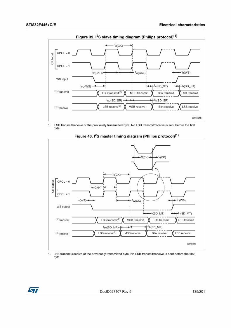
DocID027107 Rev 5 135/201
STM32F446xC/E Electrical characteristics
174
Figure 39. I2S slave timing diagram (Philips protocol)(1)
1. .LSB transmit/receive of the previously transmitted byte. No LSB transmit/receive is sent before the first byte.
Figure 40. I2S master timing diagram (Philips protocol)(1)
1. LSB transmit/receive of the previously transmitted byte. No LSB transmit/receive is sent before the first byte.
CK
Inpu
t CPOL = 0
CPOL = 1
tc(CK)
WS input
SDtransmit
SDreceive
tw(CKH) tw(CKL)
tsu(WS) tv(SD_ST) th(SD_ST)
th(WS)
tsu(SD_SR) th(SD_SR)
MSB receive Bitn receive LSB receive
MSB transmit Bitn transmit LSB transmit
ai14881b
LSB receive(2)
LSB transmit(2)
CK
out
put CPOL = 0
CPOL = 1
tc(CK)
WS output
SDreceive
SDtransmit
tw(CKH)
tw(CKL)
tsu(SD_MR)
tv(SD_MT) th(SD_MT)
th(WS)
th(SD_MR)
MSB receive Bitn receive LSB receive
MSB transmit Bitn transmit LSB transmit
ai14884b
tf(CK) tr(CK)
tv(WS)
LSB receive(2)
LSB transmit(2)
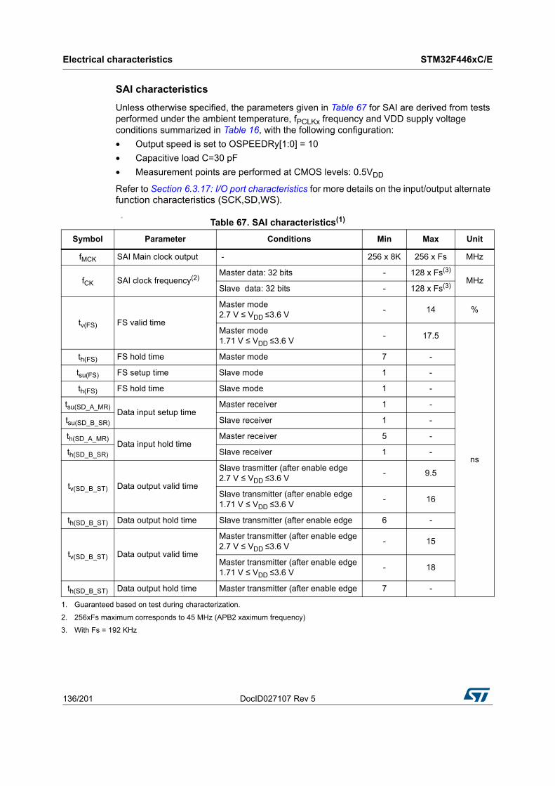
Electrical characteristics STM32F446xC/E
136/201 DocID027107 Rev 5
SAI characteristics
Unless otherwise specified, the parameters given in Table 67 for SAI are derived from tests performed under the ambient temperature, fPCLKx frequency and VDD supply voltage conditions summarized in Table 16, with the following configuration:
• Output speed is set to OSPEEDRy[1:0] = 10
• Capacitive load C=30 pF
• Measurement points are performed at CMOS levels: 0.5VDD
Refer to Section 6.3.17: I/O port characteristics for more details on the input/output alternate function characteristics (SCK,SD,WS).
(3)
Table 67. SAI characteristics(1)
Symbol Parameter Conditions Min Max Unit
fMCK SAI Main clock output - 256 x 8K 256 x Fs MHz
fCK SAI clock frequency(2)Master data: 32 bits - 128 x Fs(3)
MHzSlave data: 32 bits - 128 x Fs(3)
tv(FS) FS valid time
Master mode 2.7 V ≤ VDD ≤3.6 V
- 14 %
Master mode 1.71 V ≤ VDD ≤3.6 V
- 17.5
ns
th(FS) FS hold time Master mode 7 -
tsu(FS) FS setup time Slave mode 1 -
th(FS) FS hold time Slave mode 1 -
tsu(SD_A_MR)Data input setup time
Master receiver 1 -
tsu(SD_B_SR) Slave receiver 1 -
th(SD_A_MR)Data input hold time
Master receiver 5 -
th(SD_B_SR) Slave receiver 1 -
tv(SD_B_ST) Data output valid time
Slave trasmitter (after enable edge 2.7 V ≤ VDD ≤3.6 V
- 9.5
Slave transmitter (after enable edge 1.71 V ≤ VDD ≤3.6 V
- 16
th(SD_B_ST) Data output hold time Slave transmitter (after enable edge 6 -
tv(SD_B_ST) Data output valid time
Master transmitter (after enable edge 2.7 V ≤ VDD ≤3.6 V
- 15
Master transmitter (after enable edge 1.71 V ≤ VDD ≤3.6 V
- 18
th(SD_B_ST) Data output hold time Master transmitter (after enable edge 7 -
1. Guaranteed based on test during characterization.
2. 256xFs maximum corresponds to 45 MHz (APB2 xaximum frequency)
3. With Fs = 192 KHz
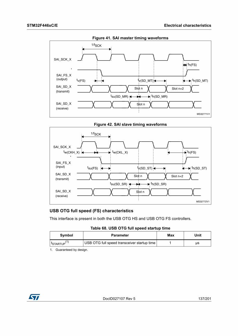
DocID027107 Rev 5 137/201
STM32F446xC/E Electrical characteristics
174
Figure 41. SAI master timing waveforms
Figure 42. SAI slave timing waveforms
USB OTG full speed (FS) characteristics
This interface is present in both the USB OTG HS and USB OTG FS controllers.
Table 68. USB OTG full speed startup time
Symbol Parameter Max Unit
tSTARTUP(1)
1. Guaranteed by design.
USB OTG full speed transceiver startup time 1 µs
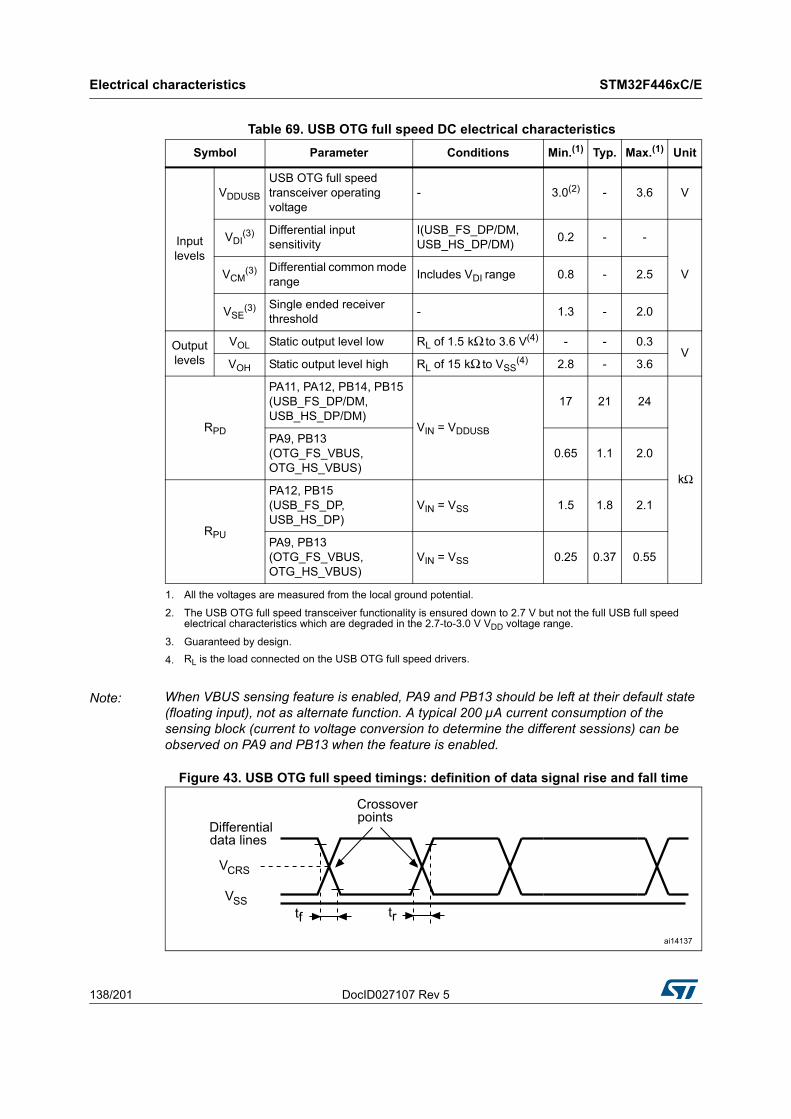
Electrical characteristics STM32F446xC/E
138/201 DocID027107 Rev 5
Note: When VBUS sensing feature is enabled, PA9 and PB13 should be left at their default state (floating input), not as alternate function. A typical 200 µA current consumption of the sensing block (current to voltage conversion to determine the different sessions) can be observed on PA9 and PB13 when the feature is enabled.
Figure 43. USB OTG full speed timings: definition of data signal rise and fall time
Table 69. USB OTG full speed DC electrical characteristics
Symbol Parameter Conditions Min.(1)
1. All the voltages are measured from the local ground potential.
Typ. Max.(1) Unit
Input levels
VDDUSB
USB OTG full speed transceiver operating voltage
- 3.0(2)
2. The USB OTG full speed transceiver functionality is ensured down to 2.7 V but not the full USB full speed electrical characteristics which are degraded in the 2.7-to-3.0 V VDD voltage range.
- 3.6 V
VDI(3)
3. Guaranteed by design.
Differential input sensitivity
I(USB_FS_DP/DM, USB_HS_DP/DM)
0.2 - -
VVCM(3) Differential common mode
rangeIncludes VDI range 0.8 - 2.5
VSE(3) Single ended receiver
threshold- 1.3 - 2.0
Output levels
VOL Static output level low RL of 1.5 kΩ to 3.6 V(4)
4. RL is the load connected on the USB OTG full speed drivers.
- - 0.3V
VOH Static output level high RL of 15 kΩ to VSS(4) 2.8 - 3.6
RPD
PA11, PA12, PB14, PB15 (USB_FS_DP/DM, USB_HS_DP/DM)
VIN = VDDUSB
17 21 24
kΩ
PA9, PB13 (OTG_FS_VBUS, OTG_HS_VBUS)
0.65 1.1 2.0
RPU
PA12, PB15 (USB_FS_DP, USB_HS_DP)
VIN = VSS 1.5 1.8 2.1
PA9, PB13 (OTG_FS_VBUS, OTG_HS_VBUS)
VIN = VSS 0.25 0.37 0.55
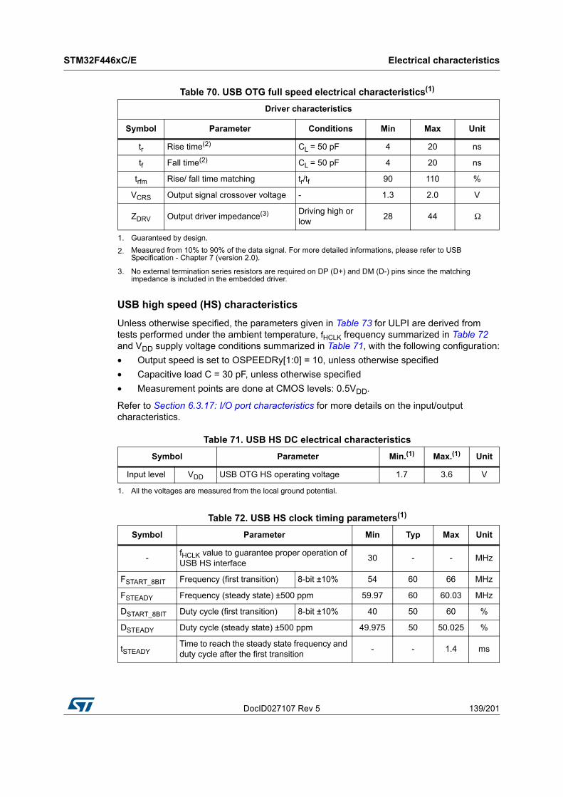
DocID027107 Rev 5 139/201
STM32F446xC/E Electrical characteristics
174
USB high speed (HS) characteristics
Unless otherwise specified, the parameters given in Table 73 for ULPI are derived from tests performed under the ambient temperature, fHCLK frequency summarized in Table 72 and VDD supply voltage conditions summarized in Table 71, with the following configuration:
• Output speed is set to OSPEEDRy[1:0] = 10, unless otherwise specified
• Capacitive load C = 30 pF, unless otherwise specified
• Measurement points are done at CMOS levels: 0.5VDD.
Refer to Section 6.3.17: I/O port characteristics for more details on the input/output characteristics.
Table 70. USB OTG full speed electrical characteristics(1)
1. Guaranteed by design.
Driver characteristics
Symbol Parameter Conditions Min Max Unit
tr Rise time(2)
2. Measured from 10% to 90% of the data signal. For more detailed informations, please refer to USB Specification - Chapter 7 (version 2.0).
CL = 50 pF 4 20 ns
tf Fall time(2) CL = 50 pF 4 20 ns
trfm Rise/ fall time matching tr/tf 90 110 %
VCRS Output signal crossover voltage - 1.3 2.0 V
ZDRV Output driver impedance(3)
3. No external termination series resistors are required on DP (D+) and DM (D-) pins since the matching impedance is included in the embedded driver.
Driving high or low
28 44 Ω
Table 71. USB HS DC electrical characteristics
Symbol Parameter Min.(1)
1. All the voltages are measured from the local ground potential.
Max.(1) Unit
Input level VDD USB OTG HS operating voltage 1.7 3.6 V
Table 72. USB HS clock timing parameters(1)
Symbol Parameter Min Typ Max Unit
-fHCLK value to guarantee proper operation of USB HS interface
30 - - MHz
FSTART_8BIT Frequency (first transition) 8-bit ±10% 54 60 66 MHz
FSTEADY Frequency (steady state) ±500 ppm 59.97 60 60.03 MHz
DSTART_8BIT Duty cycle (first transition) 8-bit ±10% 40 50 60 %
DSTEADY Duty cycle (steady state) ±500 ppm 49.975 50 50.025 %
tSTEADYTime to reach the steady state frequency and duty cycle after the first transition
- - 1.4 ms
Electrical characteristics STM32F446xC/E
140/201 DocID027107 Rev 5
Figure 44. ULPI timing diagram
CAN (controller area network) interface
Refer to Section 6.3.17: I/O port characteristics for more details on the input/output alternate function characteristics (CANx_TX and CANx_RX).
tSTART_DEV Clock startup time after the de-assertion of SuspendM
Peripheral - - 5.6ms
tSTART_HOST Host - - -
tPREPPHY preparation time after the first transition of the input clock
- - - µs
1. Guaranteed by design.
Table 72. USB HS clock timing parameters(1) (continued)
Symbol Parameter Min Typ Max Unit
Table 73. Dynamic characteristics: USB ULPI(1)
Symbol Parameter Conditions Min. Typ. Max. Unit
tSC Control in (ULPI_DIR, ULPI_NXT) setup time - 1 - -
ns
tHC Control in (ULPI_DIR, ULPI_NXT) hold time - 1.5 - -
tSD Data in setup time - 1.5 - -
tHD Data in hold time - 1.5 - -
tDC/tDD Data/control output delay
2.7 V < VDD < 3.6 V, CL = 20 pF
- 6 8.5
1.71 V < VDD < 3.6 V,
CL = 15 pF- 6 11.5
1. Guaranteed based on test during characterization.
DocID027107 Rev 5 141/201
STM32F446xC/E Electrical characteristics
174
6.3.21 12-bit ADC characteristics
Unless otherwise specified, the parameters given in Table 74 are derived from tests performed under the ambient temperature, fPCLK2 frequency and VDDA supply voltage conditions summarized in Table 16.
Table 74. ADC characteristics
Symbol Parameter Conditions Min Typ Max Unit
VDDA Power supply VDDA − VREF+ < 1.2 V
1.7(1) - 3.6 V
VREF+ Positive reference voltage 1.7(1) - VDDA V
fADC ADC clock frequencyVDDA = 1.7(1) to 2.4 V 0.6 15 18 MHz
VDDA = 2.4 to 3.6 V 0.6 30 36 MHz
fTRIG(2) External trigger frequency
fADC = 30 MHz, 12-bit resolution
- - 1764 kHz
- - - 17 1/fADC
VAIN Conversion voltage range(3) -0 (VSSA or VREF- tied to ground)
- VREF+ V
RAIN(2) External input impedance
See Equation 1 for details
- - 50 κΩ
RADC(2)(4) Sampling switch resistance - - - 6 κΩ
CADC(2) Internal sample and hold
capacitor - - 4 7 pF
tlat(2) Injection trigger conversion
latency
fADC = 30 MHz - - 0.100 µs
- - - 3(5) 1/fADC
tlatr(2) Regular trigger conversion
latency
fADC = 30 MHz - - 0.067 µs
- - - 2(5) 1/fADC
tS(2) Sampling time
fADC = 30 MHz 0.100 - 16 µs
- 3 - 480 1/fADC
tSTAB(2) Power-up time - - 2 3 µs
tCONV(2) Total conversion time (including
sampling time)
fADC = 30 MHz
12-bit resolution0.50 - 16.40 µs
fADC = 30 MHz
10-bit resolution0.43 - 16.34 µs
fADC = 30 MHz
8-bit resolution0.37 - 16.27 µs
fADC = 30 MHz
6-bit resolution0.30 - 16.20 µs
9 to 492 (tS for sampling +n-bit resolution for successive approximation)
1/fADC
Electrical characteristics STM32F446xC/E
142/201 DocID027107 Rev 5
Equation 1: RAIN max formula
The formula above (Equation 1) is used to determine the maximum external impedance allowed for an error below 1/4 of LSB. N = 12 (from 12-bit resolution) and k is the number of sampling periods defined in the ADC_SMPR1 register.
fS(2)
Sampling rate
(fADC = 30 MHz, and tS = 3 ADC cycles)
12-bit resolution
Single ADC- - 2 Msps
12-bit resolution
Interleave Dual ADC mode
- - 3.75 Msps
12-bit resolution
Interleave Triple ADC mode
- - 6 Msps
IVREF+(2)
ADC VREF DC current consumption in conversion mode
- - 300 500 µA
IVDDA(2)
ADC VDDA DC current consumption in conversion mode
- - 1.6 1.8 mA
1. VDDA minimum value of 1.7 V is obtained with the use of an external power supply supervisor (refer to Section 3.16.2: Internal reset OFF).
2. Guaranteed based on test during characterization.
3. VREF+ is internally connected to VDDA and VREF- is internally connected to VSSA.
4. RADC maximum value is given for VDD=1.7 V, and minimum value for VDD=3.3 V.
5. For external triggers, a delay of 1/fPCLK2 must be added to the latency specified in Table 74.
Table 74. ADC characteristics (continued)
Symbol Parameter Conditions Min Typ Max Unit
Table 75. ADC static accuracy at fADC = 18 MHz(1)
1. Better performance could be achieved in restricted VDD, frequency and temperature ranges.
Symbol Parameter Test conditions Typ Max(2)
2. Guaranteed based on test during characterization.
Unit
ET Total unadjusted error
fADC =18 MHz
VDDA = 1.7 to 3.6 V
VREF = 1.7 to 3.6 V
VDDA − VREF < 1.2 V
±3 ±4
LSBEO Offset error ±2 ±3
EG Gain error ±1 ±3
ED Differential linearity error ±1 ±2
EL Integral linearity error ±2 ±3
RAINk 0.5–( )
fADC CADC 2N 2+( )ln××
---------------------------------------------------------------- RADC–=
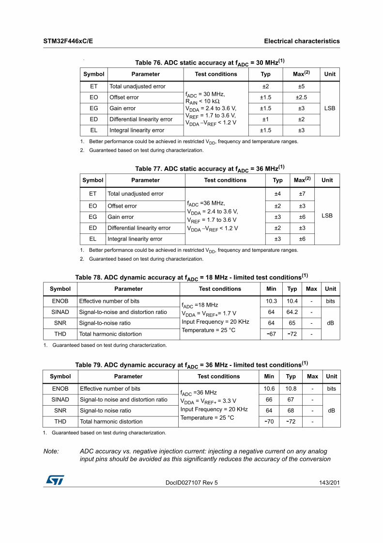
DocID027107 Rev 5 143/201
STM32F446xC/E Electrical characteristics
174
a
Note: ADC accuracy vs. negative injection current: injecting a negative current on any analog input pins should be avoided as this significantly reduces the accuracy of the conversion
Table 76. ADC static accuracy at fADC = 30 MHz(1)
1. Better performance could be achieved in restricted VDD, frequency and temperature ranges.
Symbol Parameter Test conditions Typ Max(2)
2. Guaranteed based on test during characterization.
Unit
ET Total unadjusted errorfADC = 30 MHz, RAIN < 10 kΩ, VDDA = 2.4 to 3.6 V, VREF = 1.7 to 3.6 V, VDDA − VREF < 1.2 V
±2 ±5
LSB
EO Offset error ±1.5 ±2.5
EG Gain error ±1.5 ±3
ED Differential linearity error ±1 ±2
EL Integral linearity error ±1.5 ±3
Table 77. ADC static accuracy at fADC = 36 MHz(1)
1. Better performance could be achieved in restricted VDD, frequency and temperature ranges.
Symbol Parameter Test conditions Typ Max(2)
2. Guaranteed based on test during characterization.
Unit
ET Total unadjusted error
fADC =36 MHz,
VDDA = 2.4 to 3.6 V,
VREF = 1.7 to 3.6 V
VDDA − VREF < 1.2 V
±4 ±7
LSB
EO Offset error ±2 ±3
EG Gain error ±3 ±6
ED Differential linearity error ±2 ±3
EL Integral linearity error ±3 ±6
Table 78. ADC dynamic accuracy at fADC = 18 MHz - limited test conditions(1)
Symbol Parameter Test conditions Min Typ Max Unit
ENOB Effective number of bitsfADC =18 MHz
VDDA = VREF+= 1.7 V
Input Frequency = 20 KHz
Temperature = 25 °C
10.3 10.4 - bits
SINAD Signal-to-noise and distortion ratio 64 64.2 -
dBSNR Signal-to-noise ratio 64 65 -
THD Total harmonic distortion -67 -72 -
1. Guaranteed based on test during characterization.
Table 79. ADC dynamic accuracy at fADC = 36 MHz - limited test conditions(1)
Symbol Parameter Test conditions Min Typ Max Unit
ENOB Effective number of bitsfADC =36 MHz
VDDA = VREF+ = 3.3 V
Input Frequency = 20 KHz
Temperature = 25 °C
10.6 10.8 - bits
SINAD Signal-to noise and distortion ratio 66 67 -
dBSNR Signal-to noise ratio 64 68 -
THD Total harmonic distortion -70 -72 -
1. Guaranteed based on test during characterization.
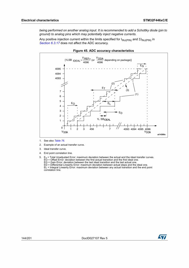
Electrical characteristics STM32F446xC/E
144/201 DocID027107 Rev 5
being performed on another analog input. It is recommended to add a Schottky diode (pin to ground) to analog pins which may potentially inject negative currents.
Any positive injection current within the limits specified for IINJ(PIN) and ΣIINJ(PIN) in Section 6.3.17 does not affect the ADC accuracy.
Figure 45. ADC accuracy characteristics
1. See also Table 76.
2. Example of an actual transfer curve.
3. Ideal transfer curve.
4. End point correlation line.
5. ET = Total Unadjusted Error: maximum deviation between the actual and the ideal transfer curves. EO = Offset Error: deviation between the first actual transition and the first ideal one. EG = Gain Error: deviation between the last ideal transition and the last actual one. ED = Differential Linearity Error: maximum deviation between actual steps and the ideal one. EL = Integral Linearity Error: maximum deviation between any actual transition and the end point correlation line.
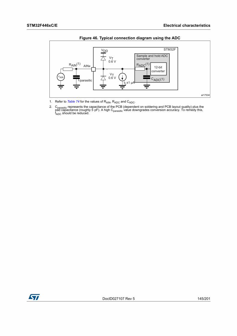
DocID027107 Rev 5 145/201
STM32F446xC/E Electrical characteristics
174
Figure 46. Typical connection diagram using the ADC
1. Refer to Table 74 for the values of RAIN, RADC and CADC.
2. Cparasitic represents the capacitance of the PCB (dependent on soldering and PCB layout quality) plus the pad capacitance (roughly 5 pF). A high Cparasitic value downgrades conversion accuracy. To remedy this, fADC should be reduced.
Electrical characteristics STM32F446xC/E
146/201 DocID027107 Rev 5
General PCB design guidelines
Power supply decoupling should be performed as shown in Figure 47 or Figure 48, depending on whether VREF+ is connected to VDDA or not. The 10 nF capacitors should be ceramic (good quality). They should be placed them as close as possible to the chip.
Figure 47. Power supply and reference decoupling (VREF+ not connected to VDDA)
1. VREF+ and VREF– inputs are both available on UFBGA144. VREF+ is also available on LQFP100, LQFP144, and WLCSP81. When VREF+ and VREF– are not available, they are internally connected to VDDA and VSSA.
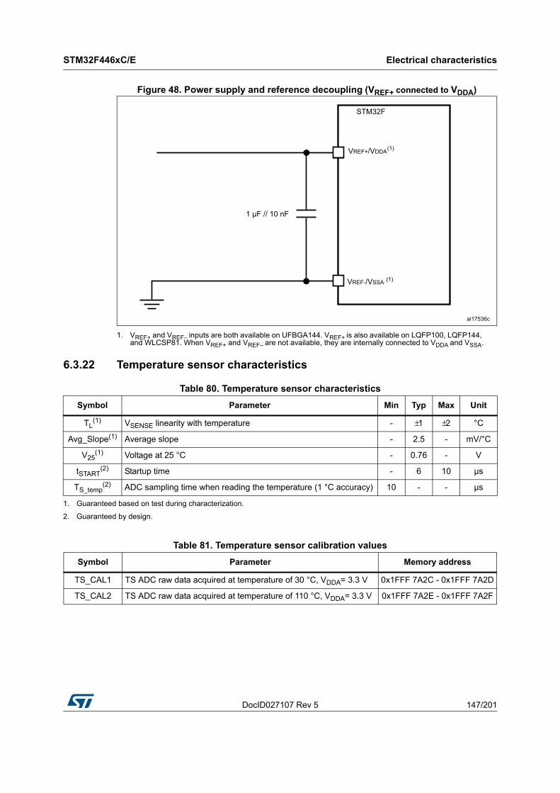
DocID027107 Rev 5 147/201
STM32F446xC/E Electrical characteristics
174
Figure 48. Power supply and reference decoupling (VREF+ connected to VDDA)
1. VREF+ and VREF– inputs are both available on UFBGA144. VREF+ is also available on LQFP100, LQFP144, and WLCSP81. When VREF+ and VREF– are not available, they are internally connected to VDDA and VSSA.
6.3.22 Temperature sensor characteristics
Table 80. Temperature sensor characteristics
Symbol Parameter Min Typ Max Unit
TL(1) VSENSE linearity with temperature - ±1 ±2 °C
Avg_Slope(1) Average slope - 2.5 - mV/°C
V25(1) Voltage at 25 °C - 0.76 - V
tSTART(2) Startup time - 6 10 µs
TS_temp(2) ADC sampling time when reading the temperature (1 °C accuracy) 10 - - µs
1. Guaranteed based on test during characterization.
2. Guaranteed by design.
Table 81. Temperature sensor calibration values
Symbol Parameter Memory address
TS_CAL1 TS ADC raw data acquired at temperature of 30 °C, VDDA= 3.3 V 0x1FFF 7A2C - 0x1FFF 7A2D
TS_CAL2 TS ADC raw data acquired at temperature of 110 °C, VDDA= 3.3 V 0x1FFF 7A2E - 0x1FFF 7A2F
Electrical characteristics STM32F446xC/E
148/201 DocID027107 Rev 5
6.3.23 VBAT monitoring characteristics
6.3.24 Reference voltage
The parameters given in Table 83 are derived from tests performed under ambient temperature and VDD supply voltage conditions summarized in Table 16.
6.3.25 DAC electrical characteristics
Table 82. VBAT monitoring characteristics
Symbol Parameter Min Typ Max Unit
R Resistor bridge for VBAT - 50 - KΩ
Q Ratio on VBAT measurement - 4 - -
Er(1) Error on Q –1 - +1 %
TS_vbat(2)(2) ADC sampling time when reading the VBAT
1 mV accuracy 5 - - µs
1. Guaranteed by design.
2. Shortest sampling time can be determined in the application by multiple iterations.
Table 83. internal reference voltage
Symbol Parameter Conditions Min Typ Max Unit
VREFINT Internal reference voltage –40 °C < TA < +105 °C 1.18 1.21 1.24 V
TS_vrefint(1) ADC sampling time when reading the
internal reference voltage- 10 - - µs
VRERINT_s(2) Internal reference voltage spread over the
temperature rangeVDD = 3V ± 10mV - 3 5 mV
TCoeff(2) Temperature coefficient - - 30 50 ppm/°C
tSTART(2) Startup time - - 6 10 µs
1. Shortest sampling time can be determined in the application by multiple iterations.
2. Guaranteed by design, not tested in production
Table 84. Internal reference voltage calibration values
Symbol Parameter Memory address
VREFIN_CAL Raw data acquired at temperature of 30 °C VDDA = 3.3 V 0x1FFF 7A2A - 0x1FFF 7A2B
Table 85. DAC characteristics
Symbol Parameter Min Typ Max Unit Comments
VDDA Analog supply voltage 1.7(1) - 3.6 V -
VREF+ Reference supply voltage 1.7(1) - 3.6 V VREF+ ≤ VDDA
VSSA Ground 0 - 0 V -
DocID027107 Rev 5 149/201
STM32F446xC/E Electrical characteristics
174
RLOAD(2) Resistive load with buffer
ON5 - - kΩ -
RO(2) Impedance output with
buffer OFF- - 15 kΩ
When the buffer is OFF, the Minimum resistive load between DAC_OUT and VSS to have a 1% accuracy is 1.5 MΩ
CLOAD(2) Capacitive load - - 50 pF
Maximum capacitive load at DAC_OUT pin (when the buffer is ON).
DAC_OUT min(2)
Lower DAC_OUT voltage with buffer ON
0.2 - - VIt gives the maximum output excursion of the DAC.
It corresponds to 12-bit input code (0x0E0) to (0xF1C) at VREF+ = 3.6 V and (0x1C7) to (0xE38) at VREF+ = 1.7 V
DAC_OUT max(2)
Higher DAC_OUT voltage with buffer ON
- -VDDA –
0.2 V
DAC_OUT min(2)
Lower DAC_OUT voltage with buffer OFF
- 0.5 - mVIt gives the maximum output excursion of the DAC.DAC_OUT
max(2)Higher DAC_OUT voltage with buffer OFF
- -VREF+ – 1LSB
V
IVREF+(4)
DAC DC VREF current consumption in quiescent mode (Standby mode)
- 170 240
µA
With no load, worst code (0x800) at VREF+ = 3.6 V in terms of DC consumption on the inputs
- 50 75With no load, worst code (0xF1C) at VREF+ = 3.6 V in terms of DC consumption on the inputs
IDDA(4)
DAC DC VDDA current consumption in quiescent mode(3)
- 280 380 µAWith no load, middle code (0x800) on the inputs
- 475 625 µAWith no load, worst code (0xF1C) at VREF+ = 3.6 V in terms of DC consumption on the inputs
DNL(4)Differential non linearity Difference between two consecutive code-1LSB)
- - ±0.5 LSBGiven for the DAC in 10-bit configuration.
- - ±2 LSBGiven for the DAC in 12-bit configuration.
INL(4)
Integral non linearity (difference between measured value at Code i and the value at Code i on a line drawn between Code 0 and last Code 1023)
- - ±1 LSBGiven for the DAC in 10-bit configuration.
- - ±4 LSBGiven for the DAC in 12-bit configuration.
Offset(4)
Offset error
(difference between measured value at Code (0x800) and the ideal value = VREF+/2)
- - ±10 mV Given for the DAC in 12-bit configuration
- - ±3 LSBGiven for the DAC in 10-bit at VREF+ = 3.6 V
- - ±12 LSBGiven for the DAC in 12-bit at VREF+ = 3.6 V
Table 85. DAC characteristics (continued)
Symbol Parameter Min Typ Max Unit Comments
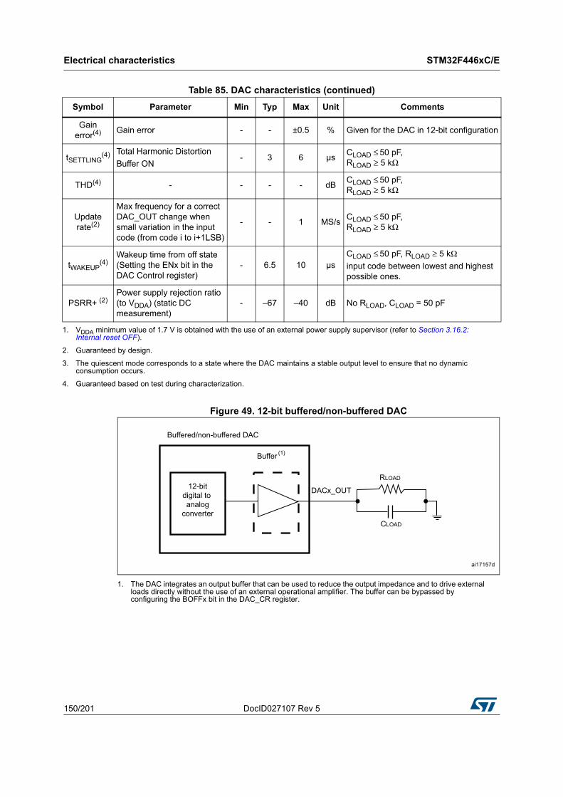
Electrical characteristics STM32F446xC/E
150/201 DocID027107 Rev 5
Figure 49. 12-bit buffered/non-buffered DAC
1. The DAC integrates an output buffer that can be used to reduce the output impedance and to drive external loads directly without the use of an external operational amplifier. The buffer can be bypassed by configuring the BOFFx bit in the DAC_CR register.
Gain error(4) Gain error - - ±0.5 % Given for the DAC in 12-bit configuration
tSETTLING(4) Total Harmonic Distortion
Buffer ON- 3 6 µs
CLOAD ≤ 50 pF, RLOAD ≥ 5 kΩ
THD(4) - - - - dBCLOAD ≤ 50 pF, RLOAD ≥ 5 kΩ
Update rate(2)
Max frequency for a correct DAC_OUT change when small variation in the input code (from code i to i+1LSB)
- - 1 MS/sCLOAD ≤ 50 pF, RLOAD ≥ 5 kΩ
tWAKEUP(4)
Wakeup time from off state (Setting the ENx bit in the DAC Control register)
- 6.5 10 µsCLOAD ≤ 50 pF, RLOAD ≥ 5 kΩinput code between lowest and highest possible ones.
PSRR+ (2)Power supply rejection ratio (to VDDA) (static DC measurement)
- –67 –40 dB No RLOAD, CLOAD = 50 pF
1. VDDA minimum value of 1.7 V is obtained with the use of an external power supply supervisor (refer to Section 3.16.2: Internal reset OFF).
2. Guaranteed by design.
3. The quiescent mode corresponds to a state where the DAC maintains a stable output level to ensure that no dynamic consumption occurs.
4. Guaranteed based on test during characterization.
Table 85. DAC characteristics (continued)
Symbol Parameter Min Typ Max Unit Comments
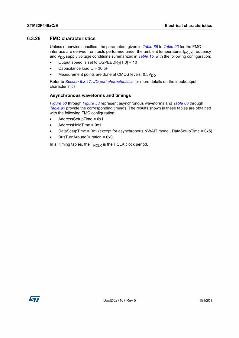
DocID027107 Rev 5 151/201
STM32F446xC/E Electrical characteristics
174
6.3.26 FMC characteristics
Unless otherwise specified, the parameters given in Table 86 to Table 93 for the FMC interface are derived from tests performed under the ambient temperature, fHCLK frequency and VDD supply voltage conditions summarized in Table 15, with the following configuration:
• Output speed is set to OSPEEDRy[1:0] = 10
• Capacitance load C = 30 pF
• Measurement points are done at CMOS levels: 0.5VDD
Refer to Section 6.3.17: I/O port characteristics for more details on the input/output characteristics.
Asynchronous waveforms and timings
Figure 50 through Figure 53 represent asynchronous waveforms and Table 86 through Table 93 provide the corresponding timings. The results shown in these tables are obtained with the following FMC configuration:
• AddressSetupTime = 0x1
• AddressHoldTime = 0x1
• DataSetupTime = 0x1 (except for asynchronous NWAIT mode , DataSetupTime = 0x5)
• BusTurnAroundDuration = 0x0
In all timing tables, the THCLK is the HCLK clock period.
Electrical characteristics STM32F446xC/E
152/201 DocID027107 Rev 5
Figure 50. Asynchronous non-multiplexed SRAM/PSRAM/NOR read waveforms
1. Mode 2/B, C and D only. In Mode 1, FMC_NADV is not used.
DocID027107 Rev 5 153/201
STM32F446xC/E Electrical characteristics
174
Table 86. Asynchronous non-multiplexed SRAM/PSRAM/NOR -read timings(1)(2)
1. CL = 30 pF.
2. Guaranteed based on test during characterization.
Symbol Parameter Min Max Unit
tw(NE) FMC_NE low time 2THCLK – 2 2 THCLK + 0.5
ns
tv(NOE_NE) FMC_NEx low to FMC_NOE low 0 1
tw(NOE) FMC_NOE low time 2THCLK - 1 2THCLK + 0.5
th(NE_NOE) FMC_NOE high to FMC_NE high hold time 0 -
tv(A_NE) FMC_NEx low to FMC_A valid - 0.5
th(A_NOE) Address hold time after FMC_NOE high 0 -
tv(BL_NE) FMC_NEx low to FMC_BL valid - 2
th(BL_NOE) FMC_BL hold time after FMC_NOE high 0 -
tsu(Data_NE) Data to FMC_NEx high setup time THCLK - 2 -
tsu(Data_NOE) Data to FMC_NOEx high setup time THCLK - 2 -
th(Data_NOE) Data hold time after FMC_NOE high 0 -
th(Data_NE) Data hold time after FMC_NEx high 0 -
tv(NADV_NE) FMC_NEx low to FMC_NADV low - 0
tw(NADV) FMC_NADV low time - THCLK +1
Table 87. Asynchronous non-multiplexed SRAM/PSRAM/NOR read - NWAIT timings(1)(2)
1. CL = 30 pF.
2. Guaranteed based on test during characterization.
Symbol Parameter Min Max Unit
tw(NE) FMC_NE low time 7THCLK + 1 7THCLK
ns
tw(NOE) FMC_NWE low time 5THCLK – 1 5THCLK + 1
tw(NWAIT) FMC_NWAIT low time THCLK – 0.5 -
tsu(NWAIT_NE) FMC_NWAIT valid before FMC_NEx high 5THCLK+ 1.5 -
th(NE_NWAIT)FMC_NEx hold time after FMC_NWAIT invalid
4THCLK + 1 -
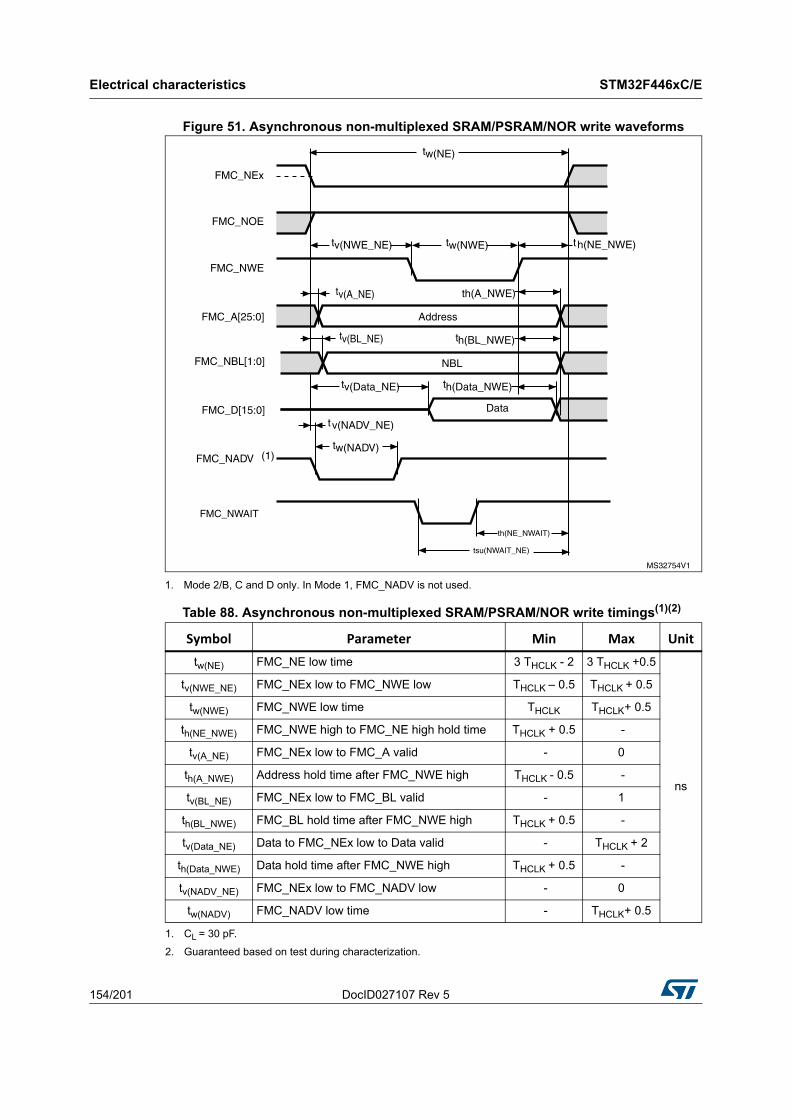
Electrical characteristics STM32F446xC/E
154/201 DocID027107 Rev 5
Figure 51. Asynchronous non-multiplexed SRAM/PSRAM/NOR write waveforms
1. Mode 2/B, C and D only. In Mode 1, FMC_NADV is not used.
Table 88. Asynchronous non-multiplexed SRAM/PSRAM/NOR write timings(1)(2)
1. CL = 30 pF.
2. Guaranteed based on test during characterization.
Symbol Parameter Min Max Unit
tw(NE) FMC_NE low time 3 THCLK - 2 3 THCLK +0.5
ns
tv(NWE_NE) FMC_NEx low to FMC_NWE low THCLK – 0.5 THCLK + 0.5
tw(NWE) FMC_NWE low time THCLK THCLK+ 0.5
th(NE_NWE) FMC_NWE high to FMC_NE high hold time THCLK + 0.5 -
tv(A_NE) FMC_NEx low to FMC_A valid - 0
th(A_NWE) Address hold time after FMC_NWE high THCLK - 0.5 -
tv(BL_NE) FMC_NEx low to FMC_BL valid - 1
th(BL_NWE) FMC_BL hold time after FMC_NWE high THCLK + 0.5 -
tv(Data_NE) Data to FMC_NEx low to Data valid - THCLK + 2
th(Data_NWE) Data hold time after FMC_NWE high THCLK + 0.5 -
tv(NADV_NE) FMC_NEx low to FMC_NADV low - 0
tw(NADV) FMC_NADV low time - THCLK+ 0.5
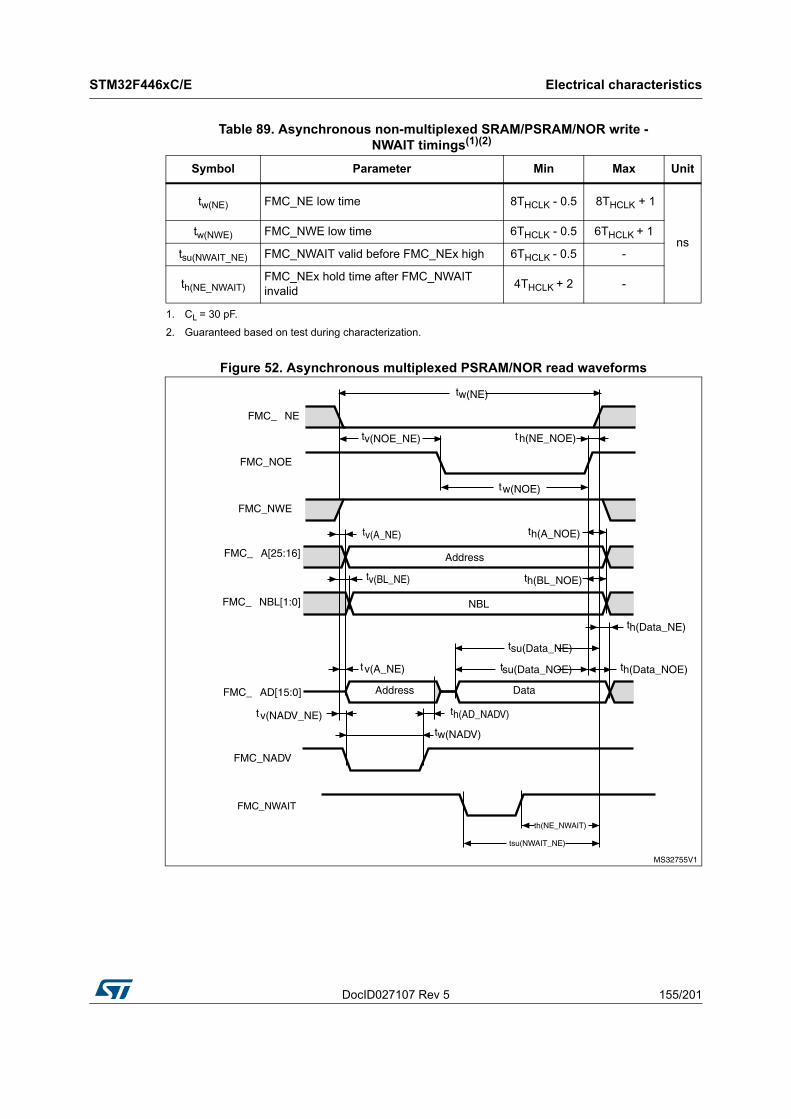
DocID027107 Rev 5 155/201
STM32F446xC/E Electrical characteristics
174
Figure 52. Asynchronous multiplexed PSRAM/NOR read waveforms
Table 89. Asynchronous non-multiplexed SRAM/PSRAM/NOR write - NWAIT timings(1)(2)
1. CL = 30 pF.
2. Guaranteed based on test during characterization.
Symbol Parameter Min Max Unit
tw(NE) FMC_NE low time 8THCLK - 0.5 8THCLK + 1
nstw(NWE) FMC_NWE low time 6THCLK - 0.5 6THCLK + 1
tsu(NWAIT_NE) FMC_NWAIT valid before FMC_NEx high 6THCLK - 0.5 -
th(NE_NWAIT)FMC_NEx hold time after FMC_NWAIT invalid
4THCLK + 2 -
Electrical characteristics STM32F446xC/E
156/201 DocID027107 Rev 5
Table 90. Asynchronous multiplexed PSRAM/NOR read timings(1)(2)
1. CL = 30 pF.
2. Guaranteed based on test during characterization.
Symbol Parameter Min Max Unit
tw(NE) FMC_NE low time 3THCLK – 2 3THCLK+0.5
ns
tv(NOE_NE) FMC_NEx low to FMC_NOE low 2THCLK – 0.5 2THCLK
ttw(NOE) FMC_NOE low time THCLK – 1 THCLK + 0.5
th(NE_NOE) FMC_NOE high to FMC_NE high hold time 0 -
tv(A_NE) FMC_NEx low to FMC_A valid - 2
tv(NADV_NE) FMC_NEx low to FMC_NADV low 0 2
tw(NADV) FMC_NADV low time THCLK – 0.5 THCLK + 0.5
th(AD_NADV)FMC_AD(address) valid hold time after FMC_NADV high)
0 -
th(A_NOE) Address hold time after FMC_NOE high THCLK – 0.5 -
th(BL_NOE) FMC_BL time after FMC_NOE high 0 -
tv(BL_NE) FMC_NEx low to FMC_BL valid - 2
tsu(Data_NE) Data to FMC_NEx high setup time THCLK + 1.5 -
tsu(Data_NOE) Data to FMC_NOE high setup time THCLK + 1 -
th(Data_NE) Data hold time after FMC_NEx high 0 -
th(Data_NOE) Data hold time after FMC_NOE high 0 -
Table 91. Asynchronous multiplexed PSRAM/NOR read-NWAIT timings(1)(2)
1. CL = 30 pF.
2. Guaranteed based on test during characterization.
Symbol Parameter Min Max Unit
tw(NE) FMC_NE low time 8THCLK - 1 8THCLK + 2
nstw(NOE) FMC_NWE low time 5THCLK – 1 5THCLK + 1
tsu(NWAIT_NE) FMC_NWAIT valid before FMC_NEx high 5THCLK + 1.5 -
th(NE_NWAIT)FMC_NEx hold time after FMC_NWAIT invalid
4THCLK + 1 -
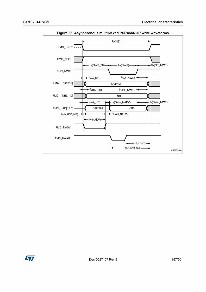
DocID027107 Rev 5 157/201
STM32F446xC/E Electrical characteristics
174
Figure 53. Asynchronous multiplexed PSRAM/NOR write waveforms
Electrical characteristics STM32F446xC/E
158/201 DocID027107 Rev 5
Synchronous waveforms and timings
Figure 54 through Figure 57 represent synchronous waveforms and Table 94 through Table 97 provide the corresponding timings. The results shown in these tables are obtained with the following FMC configuration:
• BurstAccessMode = FMC_BurstAccessMode_Enable;
• MemoryType = FMC_MemoryType_CRAM;
• WriteBurst = FMC_WriteBurst_Enable;
• CLKDivision = 1; (0 is not supported, see the STM32F446 reference manual: RM0390)
• DataLatency = 1 for NOR Flash; DataLatency = 0 for PSRAM
Table 92. Asynchronous multiplexed PSRAM/NOR write timings(1)(2)
1. CL = 30 pF.
2. Guaranteed based on test during characterization.
Symbol Parameter Min Max Unit
tw(NE) FMC_NE low time 4THCLK - 2 4THCLK+0.5
ns
tv(NWE_NE) FMC_NEx low to FMC_NWE low THCLK THCLK + 0.5
tw(NWE) FMC_NWE low time 2THCLK 2THCLK + 0.5
th(NE_NWE) FMC_NWE high to FMC_NE high hold time THCLK -
tv(A_NE) FMC_NEx low to FMC_A valid - 0
tv(NADV_NE) FMC_NEx low to FMC_NADV low 0.5 1
tw(NADV) FMC_NADV low time THCLK – 0.5 THCLK+ 0.5
th(AD_NADV)FMC_AD(adress) valid hold time after FMC_NADV high)
THCLK – 2 -
th(A_NWE) Address hold time after FMC_NWE high THCLK -
th(BL_NWE) FMC_BL hold time after FMC_NWE high THCLK–2 -
tv(BL_NE) FMC_NEx low to FMC_BL valid - 2
tv(Data_NADV) FMC_NADV high to Data valid - THCLK + 1.5
th(Data_NWE) Data hold time after FMC_NWE high THCLK + 0.5 -
Table 93. Asynchronous multiplexed PSRAM/NOR write-NWAIT timings(1)(2)
1. CL = 30 pF.
2. Guaranteed based on test during characterization.
Symbol Parameter Min Max Unit
tw(NE) FMC_NE low time 9THCLK 9THCLK + 0.5
nstw(NWE) FMC_NWE low time 7THCLK 7THCLK + 2
tsu(NWAIT_NE) FMC_NWAIT valid before FMC_NEx high 6THCLK + 1.5 -
th(NE_NWAIT)FMC_NEx hold time after FMC_NWAIT invalid
4THCLK – 1 -
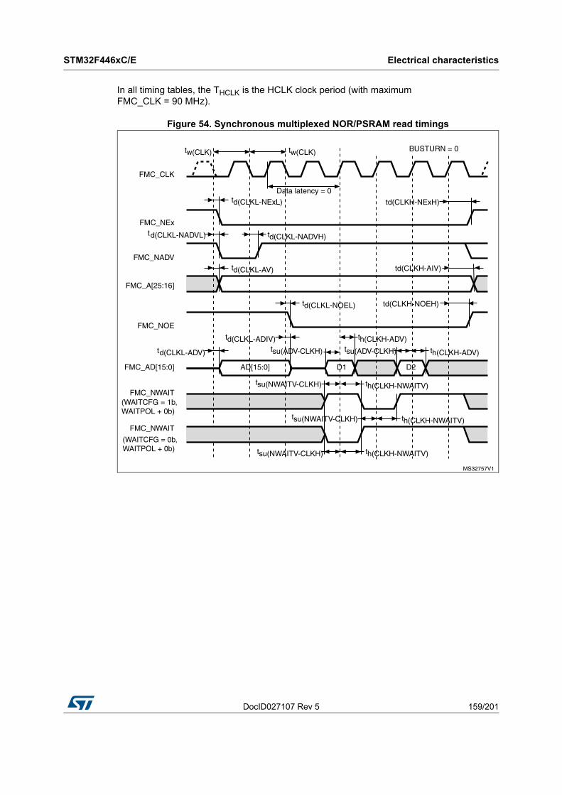
DocID027107 Rev 5 159/201
STM32F446xC/E Electrical characteristics
174
In all timing tables, the THCLK is the HCLK clock period (with maximum FMC_CLK = 90 MHz).
Figure 54. Synchronous multiplexed NOR/PSRAM read timings
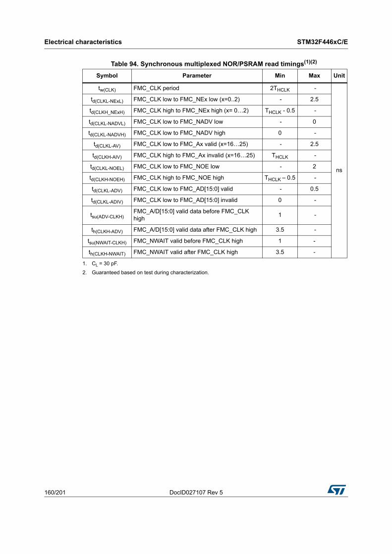
Electrical characteristics STM32F446xC/E
160/201 DocID027107 Rev 5
Table 94. Synchronous multiplexed NOR/PSRAM read timings(1)(2)
1. CL = 30 pF.
2. Guaranteed based on test during characterization.
Symbol Parameter Min Max Unit
tw(CLK) FMC_CLK period 2THCLK -
ns
td(CLKL-NExL) FMC_CLK low to FMC_NEx low (x=0..2) - 2.5
td(CLKH_NExH) FMC_CLK high to FMC_NEx high (x= 0…2) THCLK - 0.5 -
td(CLKL-NADVL) FMC_CLK low to FMC_NADV low - 0
td(CLKL-NADVH) FMC_CLK low to FMC_NADV high 0 -
td(CLKL-AV) FMC_CLK low to FMC_Ax valid (x=16…25) - 2.5
td(CLKH-AIV) FMC_CLK high to FMC_Ax invalid (x=16…25) THCLK -
td(CLKL-NOEL) FMC_CLK low to FMC_NOE low - 2
td(CLKH-NOEH) FMC_CLK high to FMC_NOE high THCLK – 0.5 -
td(CLKL-ADV) FMC_CLK low to FMC_AD[15:0] valid - 0.5
td(CLKL-ADIV) FMC_CLK low to FMC_AD[15:0] invalid 0 -
tsu(ADV-CLKH)FMC_A/D[15:0] valid data before FMC_CLK high
1 -
th(CLKH-ADV) FMC_A/D[15:0] valid data after FMC_CLK high 3.5 -
tsu(NWAIT-CLKH) FMC_NWAIT valid before FMC_CLK high 1 -
th(CLKH-NWAIT) FMC_NWAIT valid after FMC_CLK high 3.5 -
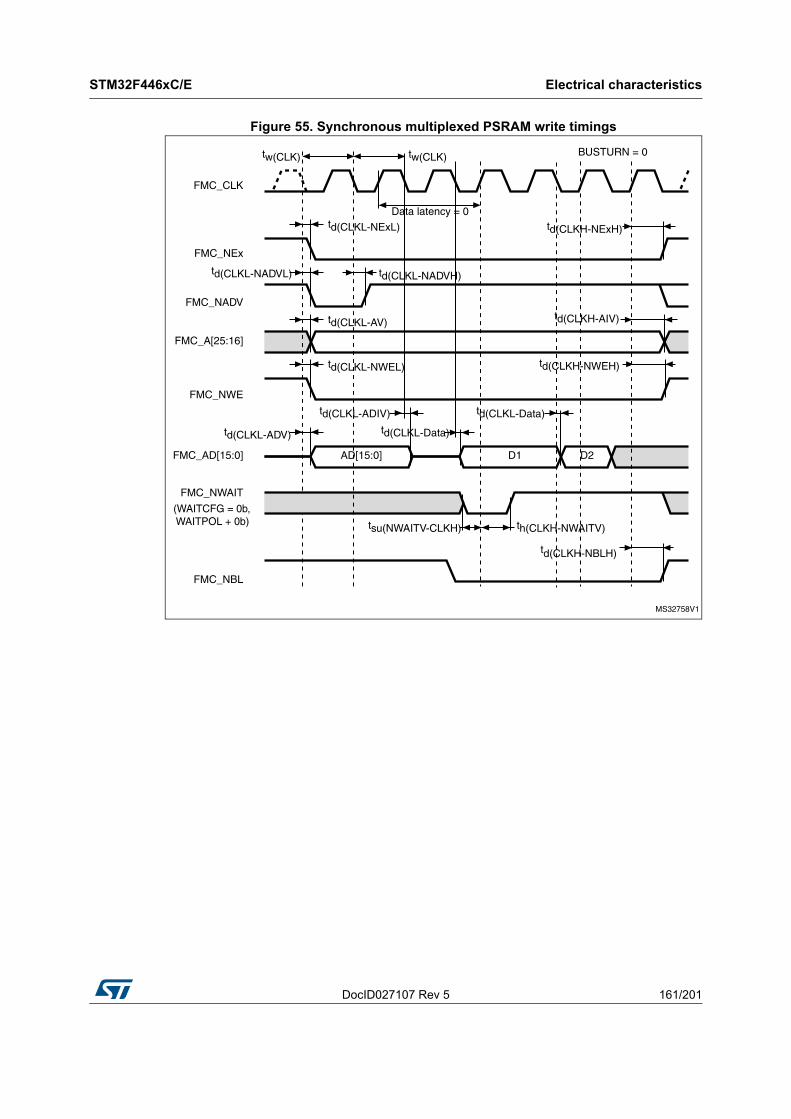
DocID027107 Rev 5 161/201
STM32F446xC/E Electrical characteristics
174
Figure 55. Synchronous multiplexed PSRAM write timings
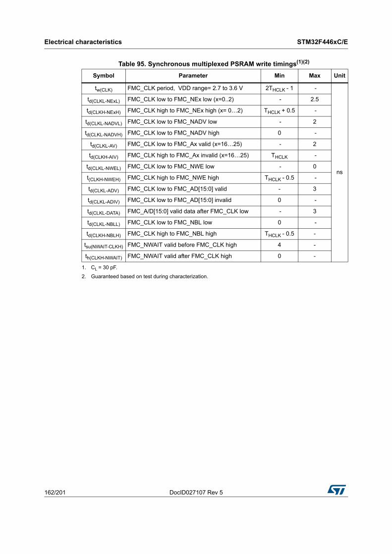
Electrical characteristics STM32F446xC/E
162/201 DocID027107 Rev 5
Table 95. Synchronous multiplexed PSRAM write timings(1)(2)
1. CL = 30 pF.
2. Guaranteed based on test during characterization.
Symbol Parameter Min Max Unit
tw(CLK) FMC_CLK period, VDD range= 2.7 to 3.6 V 2THCLK - 1 -
ns
td(CLKL-NExL) FMC_CLK low to FMC_NEx low (x=0..2) - 2.5
td(CLKH-NExH) FMC_CLK high to FMC_NEx high (x= 0…2) THCLK + 0.5 -
td(CLKL-NADVL) FMC_CLK low to FMC_NADV low - 2
td(CLKL-NADVH) FMC_CLK low to FMC_NADV high 0 -
td(CLKL-AV) FMC_CLK low to FMC_Ax valid (x=16…25) - 2
td(CLKH-AIV) FMC_CLK high to FMC_Ax invalid (x=16…25) THCLK -
td(CLKL-NWEL) FMC_CLK low to FMC_NWE low - 0
t(CLKH-NWEH) FMC_CLK high to FMC_NWE high THCLK - 0.5 -
td(CLKL-ADV) FMC_CLK low to FMC_AD[15:0] valid - 3
td(CLKL-ADIV) FMC_CLK low to FMC_AD[15:0] invalid 0 -
td(CLKL-DATA) FMC_A/D[15:0] valid data after FMC_CLK low - 3
td(CLKL-NBLL) FMC_CLK low to FMC_NBL low 0 -
td(CLKH-NBLH) FMC_CLK high to FMC_NBL high THCLK - 0.5 -
tsu(NWAIT-CLKH) FMC_NWAIT valid before FMC_CLK high 4 -
th(CLKH-NWAIT) FMC_NWAIT valid after FMC_CLK high 0 -
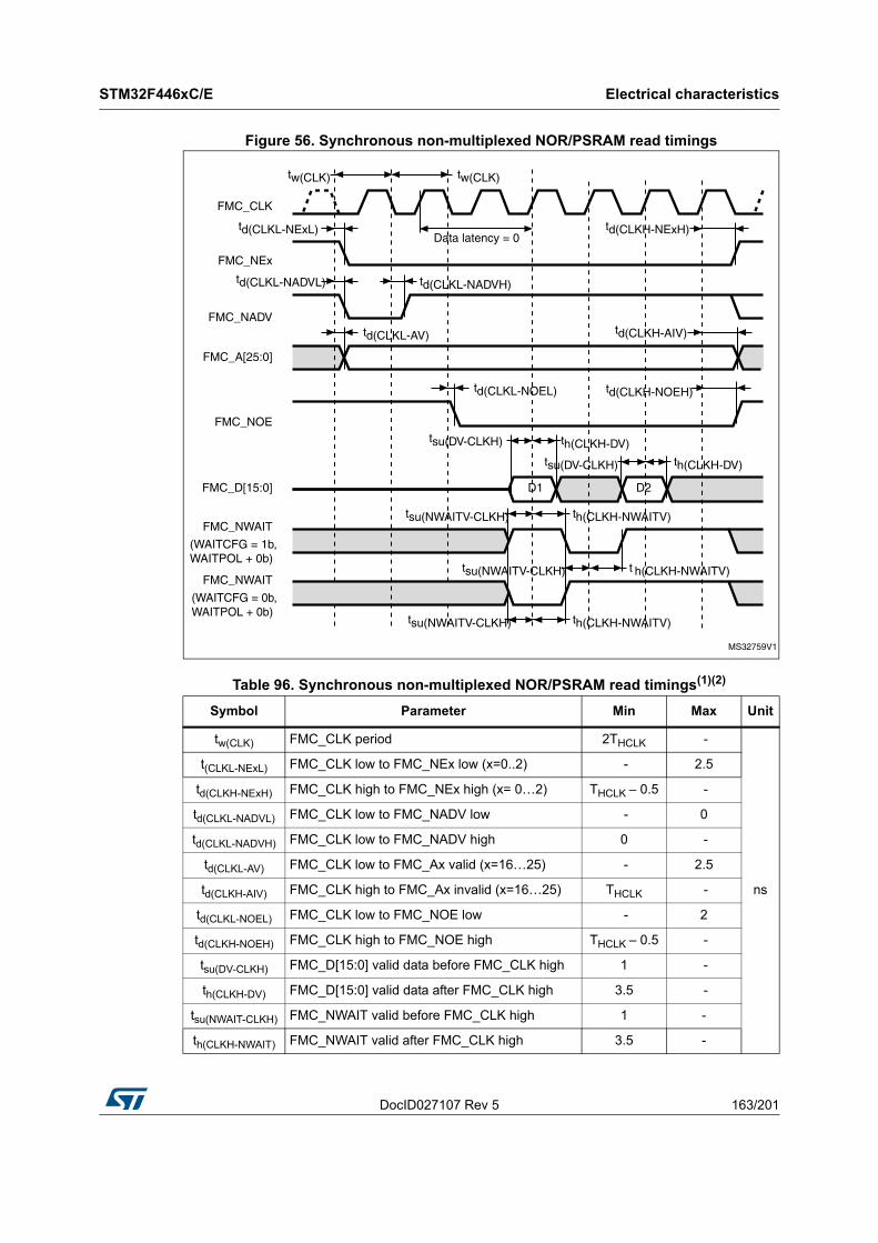
DocID027107 Rev 5 163/201
STM32F446xC/E Electrical characteristics
174
Figure 56. Synchronous non-multiplexed NOR/PSRAM read timings
Table 96. Synchronous non-multiplexed NOR/PSRAM read timings(1)(2)
Symbol Parameter Min Max Unit
tw(CLK) FMC_CLK period 2THCLK -
ns
t(CLKL-NExL) FMC_CLK low to FMC_NEx low (x=0..2) - 2.5
td(CLKH-NExH) FMC_CLK high to FMC_NEx high (x= 0…2) THCLK – 0.5 -
td(CLKL-NADVL) FMC_CLK low to FMC_NADV low - 0
td(CLKL-NADVH) FMC_CLK low to FMC_NADV high 0 -
td(CLKL-AV) FMC_CLK low to FMC_Ax valid (x=16…25) - 2.5
td(CLKH-AIV) FMC_CLK high to FMC_Ax invalid (x=16…25) THCLK -
td(CLKL-NOEL) FMC_CLK low to FMC_NOE low - 2
td(CLKH-NOEH) FMC_CLK high to FMC_NOE high THCLK – 0.5 -
tsu(DV-CLKH) FMC_D[15:0] valid data before FMC_CLK high 1 -
th(CLKH-DV) FMC_D[15:0] valid data after FMC_CLK high 3.5 -
tsu(NWAIT-CLKH) FMC_NWAIT valid before FMC_CLK high 1 -
th(CLKH-NWAIT) FMC_NWAIT valid after FMC_CLK high 3.5 -
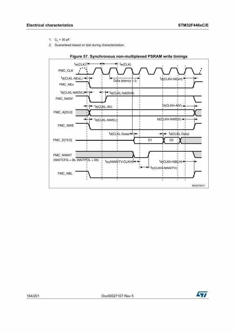
Electrical characteristics STM32F446xC/E
164/201 DocID027107 Rev 5
Figure 57. Synchronous non-multiplexed PSRAM write timings
1. CL = 30 pF.
2. Guaranteed based on test during characterization.
DocID027107 Rev 5 165/201
STM32F446xC/E Electrical characteristics
174
NAND controller waveforms and timings
Figure 58 through Figure 61 represent synchronous waveforms, and Table 98 and Table 99 provide the corresponding timings. The results shown in this table are obtained with the following FMC configuration:
• COM.FSMC_SetupTime = 0x01;
• COM.FMC_WaitSetupTime = 0x03;
• COM.FMC_HoldSetupTime = 0x02;
• COM.FMC_HiZSetupTime = 0x01;
• ATT.FMC_SetupTime = 0x01;
• ATT.FMC_WaitSetupTime = 0x03;
• ATT.FMC_HoldSetupTime = 0x02;
• ATT.FMC_HiZSetupTime = 0x01;
• Bank = FMC_Bank_NAND;
• MemoryDataWidth = FMC_MemoryDataWidth_16b;
• ECC = FMC_ECC_Enable;
• ECCPageSize = FMC_ECCPageSize_512Bytes;
• TCLRSetupTime = 0;
• TARSetupTime = 0.
In all timing tables, the THCLK is the HCLK clock period.
Table 97. Synchronous non-multiplexed PSRAM write timings(1)(2)
1. CL = 30 pF.
2. Guaranteed based on test during characterization.
Symbol Parameter Min Max Unit
tw(CLK) FMC_CLK period 2THCLK – 1 -
ns
td(CLKL-NExL) FMC_CLK low to FMC_NEx low (x=0..2) - 2.5
td(CLKH-NExH) FMC_CLK high to FMC_NEx high (x= 0…2) THCLK – 0.5 -
td(CLKL-NADVL) FMC_CLK low to FMC_NADV low - 2
td(CLKL-NADVH) FMC_CLK low to FMC_NADV high 0 -
td(CLKL-AV) FMC_CLK low to FMC_Ax valid (x=16…25) - 2
td(CLKH-AIV) FMC_CLK high to FMC_Ax invalid (x=16…25) 0 -
td(CLKL-NWEL) FMC_CLK low to FMC_NWE low - 3
td(CLKH-NWEH) FMC_CLK high to FMC_NWE high THCLK + 1 -
td(CLKL-Data) FMC_D[15:0] valid data after FMC_CLK low - 2.5
td(CLKL-NBLL) FMC_CLK low to FMC_NBL low 3 -
td(CLKH-NBLH) FMC_CLK high to FMC_NBL high THCLK + 1.5 -
tsu(NWAIT-CLKH) FMC_NWAIT valid before FMC_CLK high 1.5 -
th(CLKH-NWAIT) FMC_NWAIT valid after FMC_CLK high 0 -
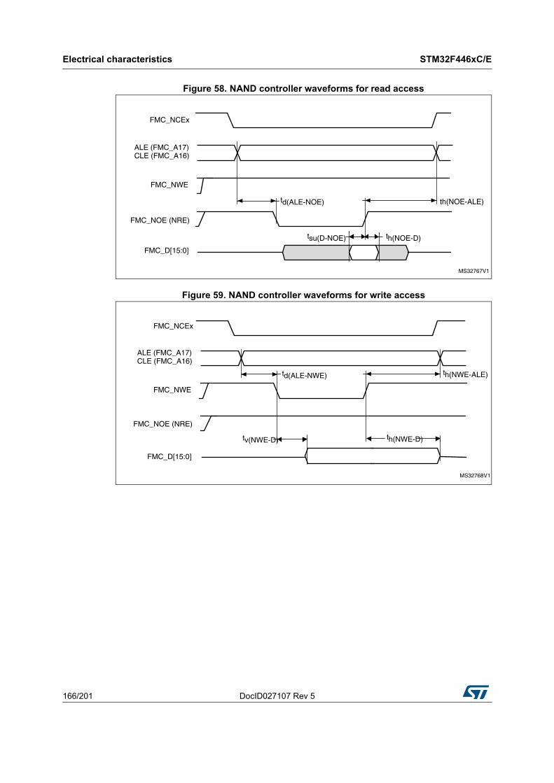
Electrical characteristics STM32F446xC/E
166/201 DocID027107 Rev 5
Figure 58. NAND controller waveforms for read access
Figure 59. NAND controller waveforms for write access
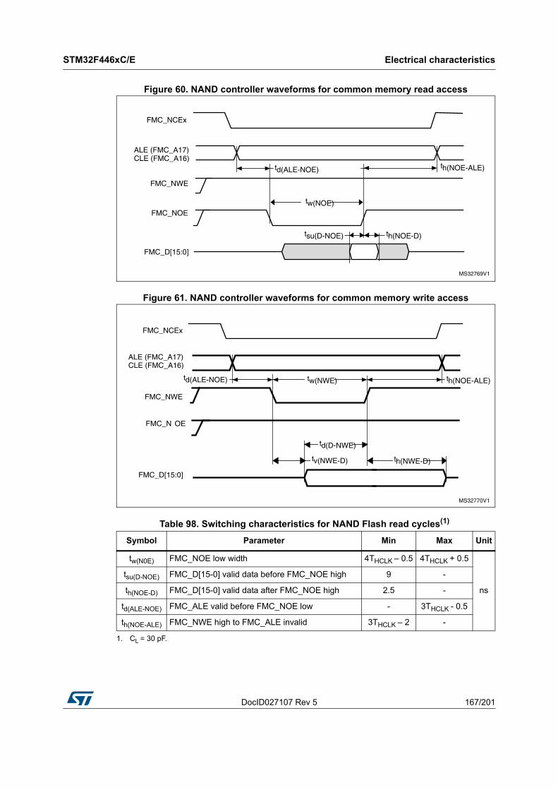
DocID027107 Rev 5 167/201
STM32F446xC/E Electrical characteristics
174
Figure 60. NAND controller waveforms for common memory read access
Figure 61. NAND controller waveforms for common memory write access
Table 98. Switching characteristics for NAND Flash read cycles(1)
1. CL = 30 pF.
Symbol Parameter Min Max Unit
tw(N0E) FMC_NOE low width 4THCLK – 0.5 4THCLK + 0.5
ns
tsu(D-NOE) FMC_D[15-0] valid data before FMC_NOE high 9 -
th(NOE-D) FMC_D[15-0] valid data after FMC_NOE high 2.5 -
td(ALE-NOE) FMC_ALE valid before FMC_NOE low - 3THCLK - 0.5
th(NOE-ALE) FMC_NWE high to FMC_ALE invalid 3THCLK – 2 -
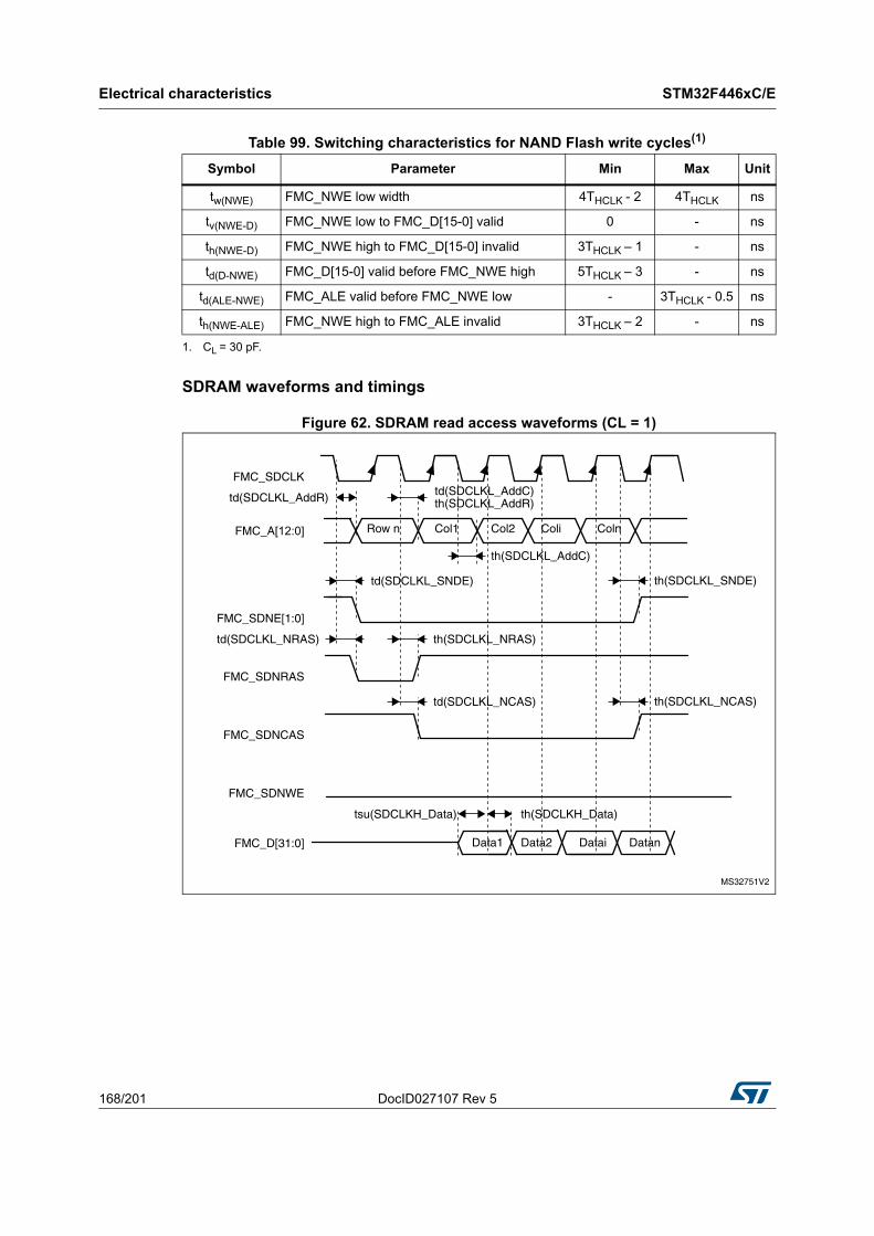
Electrical characteristics STM32F446xC/E
168/201 DocID027107 Rev 5
SDRAM waveforms and timings
Figure 62. SDRAM read access waveforms (CL = 1)
Table 99. Switching characteristics for NAND Flash write cycles(1)
1. CL = 30 pF.
Symbol Parameter Min Max Unit
tw(NWE) FMC_NWE low width 4THCLK - 2 4THCLK ns
tv(NWE-D) FMC_NWE low to FMC_D[15-0] valid 0 - ns
th(NWE-D) FMC_NWE high to FMC_D[15-0] invalid 3THCLK – 1 - ns
td(D-NWE) FMC_D[15-0] valid before FMC_NWE high 5THCLK – 3 - ns
td(ALE-NWE) FMC_ALE valid before FMC_NWE low - 3THCLK - 0.5 ns
th(NWE-ALE) FMC_NWE high to FMC_ALE invalid 3THCLK – 2 - ns
DocID027107 Rev 5 169/201
STM32F446xC/E Electrical characteristics
174
Table 100. SDRAM read timings(1)(2)
1. CL = 30 pF on data and address lines. CL=15pF on FMC_SDCLK.
2. Guaranteed based on test during characterization.
Symbol Parameter Min Max Unit
tw(SDCLK) FMC_SDCLK period 2THCLK-0.5 2THCLK+0.5
ns
tsu(SDCLKH _Data) Data input setup time 1 -
th(SDCLKH_Data) Data input hold time 4 -
td(SDCLKL_Add) Address valid time - 3
td(SDCLKL_ SDNE) Chip select valid time - 1.5
th(SDCLKL_SDNE) Chip select hold time 0 -
td(SDCLKL_SDNRAS) SDNRAS valid time - 1.5
th(SDCLKL_SDNRAS) SDNRAS hold time 0 -
td(SDCLKL_SDNCAS) SDNCAS valid time - 0.5
th(SDCLKL_SDNCAS) SDNCAS hold time 0 -
Table 101. LPSDR SDRAM read timings(1)(2)
1. CL = 10 pF.
2. Guaranteed based on test during characterization.
Symbol Parameter Min Max Unit
tw(SDCLK) FMC_SDCLK period 2THCLK - 0.5 2THCLK + 0.5
ns
tsu(SDCLKH _Data) Data input setup time 1 -
th(SDCLKH_Data) Data input hold time 5 -
td(SDCLKL_Add) Address valid time - 3
td(SDCLKL_ SDNE) Chip select valid time - 3
th(SDCLKL_SDNE) Chip select hold time 0 -
td(SDCLKL_SDNRAS) SDNRAS valid time - 2
th(SDCLKL_SDNRAS) SDNRAS hold time 0 -
td(SDCLKL_SDNCAS) SDNCAS valid time - 2
th(SDCLKL_SDNCAS) SDNCAS hold time 0 -
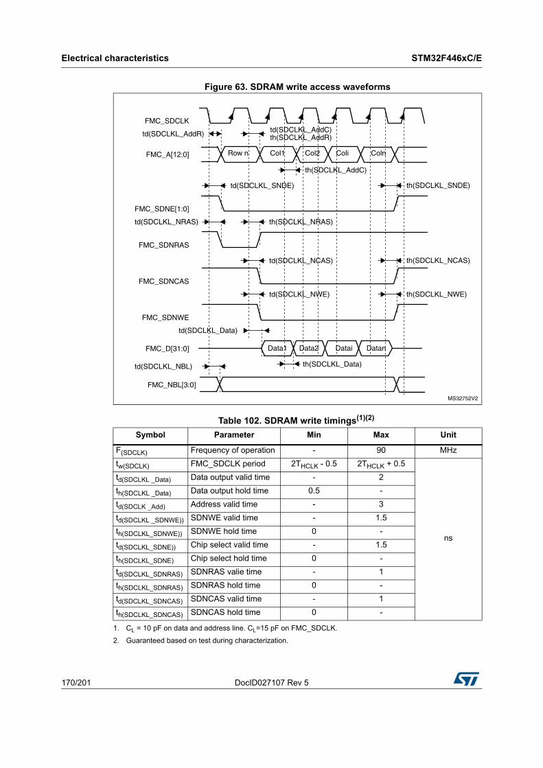
Electrical characteristics STM32F446xC/E
170/201 DocID027107 Rev 5
Figure 63. SDRAM write access waveforms
Table 102. SDRAM write timings(1)(2)
1. CL = 10 pF on data and address line. CL=15 pF on FMC_SDCLK.
2. Guaranteed based on test during characterization.
Symbol Parameter Min Max Unit
F(SDCLK) Frequency of operation - 90 MHz
tw(SDCLK) FMC_SDCLK period 2THCLK - 0.5 2THCLK + 0.5
ns
td(SDCLKL _Data) Data output valid time - 2
th(SDCLKL _Data) Data output hold time 0.5 -
td(SDCLK _Add) Address valid time - 3
td(SDCLKL _SDNWE)) SDNWE valid time - 1.5
th(SDCLKL_SDNWE)) SDNWE hold time 0 -
td(SDCLKL_SDNE)) Chip select valid time - 1.5
th(SDCLKL_SDNE) Chip select hold time 0 -
td(SDCLKL_SDNRAS) SDNRAS valie time - 1
th(SDCLKL_SDNRAS) SDNRAS hold time 0 -
td(SDCLKL_SDNCAS) SDNCAS valid time - 1
th(SDCLKL_SDNCAS) SDNCAS hold time 0 -
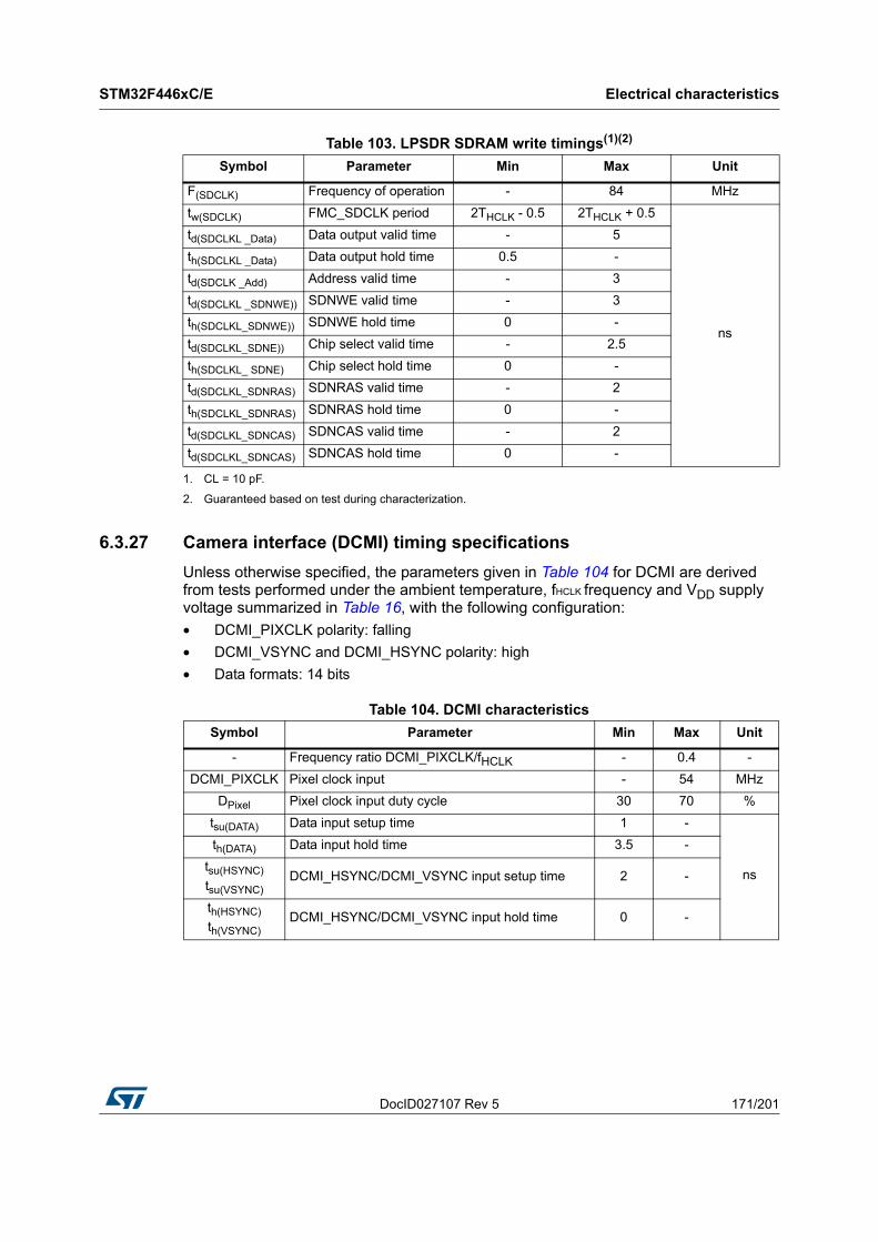
DocID027107 Rev 5 171/201
STM32F446xC/E Electrical characteristics
174
6.3.27 Camera interface (DCMI) timing specifications
Unless otherwise specified, the parameters given in Table 104 for DCMI are derived from tests performed under the ambient temperature, fHCLK frequency and VDD supply voltage summarized in Table 16, with the following configuration:
• DCMI_PIXCLK polarity: falling
• DCMI_VSYNC and DCMI_HSYNC polarity: high
• Data formats: 14 bits
Table 103. LPSDR SDRAM write timings(1)(2)
1. CL = 10 pF.
2. Guaranteed based on test during characterization.
Symbol Parameter Min Max Unit
F(SDCLK) Frequency of operation - 84 MHz
tw(SDCLK) FMC_SDCLK period 2THCLK - 0.5 2THCLK + 0.5
ns
td(SDCLKL _Data) Data output valid time - 5
th(SDCLKL _Data) Data output hold time 0.5 -
td(SDCLK _Add) Address valid time - 3
td(SDCLKL _SDNWE)) SDNWE valid time - 3
th(SDCLKL_SDNWE)) SDNWE hold time 0 -
td(SDCLKL_SDNE)) Chip select valid time - 2.5
th(SDCLKL_ SDNE) Chip select hold time 0 -
td(SDCLKL_SDNRAS) SDNRAS valid time - 2
th(SDCLKL_SDNRAS) SDNRAS hold time 0 -
td(SDCLKL_SDNCAS) SDNCAS valid time - 2
td(SDCLKL_SDNCAS) SDNCAS hold time 0 -
Table 104. DCMI characteristics
Symbol Parameter Min Max Unit
- Frequency ratio DCMI_PIXCLK/fHCLK - 0.4 -
DCMI_PIXCLK Pixel clock input - 54 MHz
DPixel Pixel clock input duty cycle 30 70 %
tsu(DATA) Data input setup time 1 -
ns
th(DATA) Data input hold time 3.5 -
tsu(HSYNC)
tsu(VSYNC)DCMI_HSYNC/DCMI_VSYNC input setup time 2 -
th(HSYNC)
th(VSYNC)DCMI_HSYNC/DCMI_VSYNC input hold time 0 -
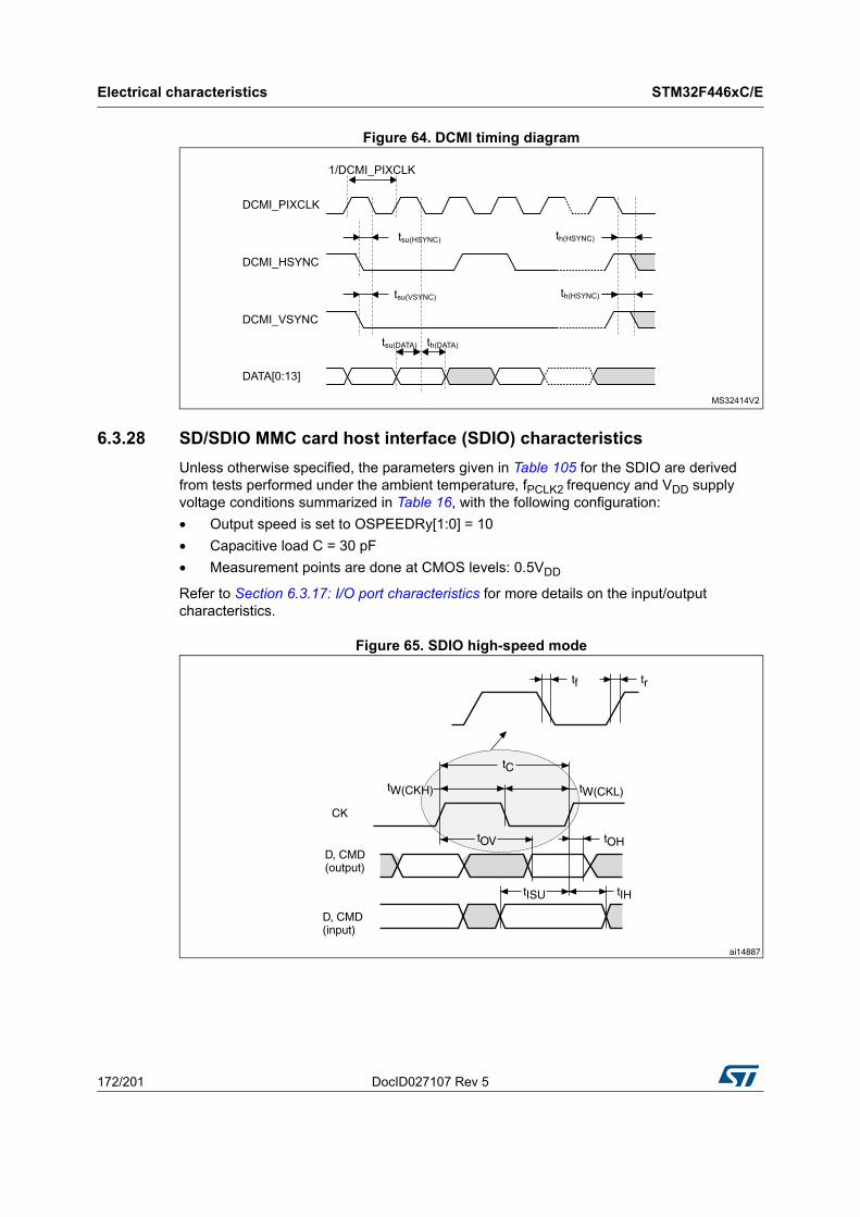
Electrical characteristics STM32F446xC/E
172/201 DocID027107 Rev 5
Figure 64. DCMI timing diagram
6.3.28 SD/SDIO MMC card host interface (SDIO) characteristics
Unless otherwise specified, the parameters given in Table 105 for the SDIO are derived from tests performed under the ambient temperature, fPCLK2 frequency and VDD supply voltage conditions summarized in Table 16, with the following configuration:
• Output speed is set to OSPEEDRy[1:0] = 10
• Capacitive load C = 30 pF
• Measurement points are done at CMOS levels: 0.5VDD
Refer to Section 6.3.17: I/O port characteristics for more details on the input/output characteristics.
Figure 65. SDIO high-speed mode
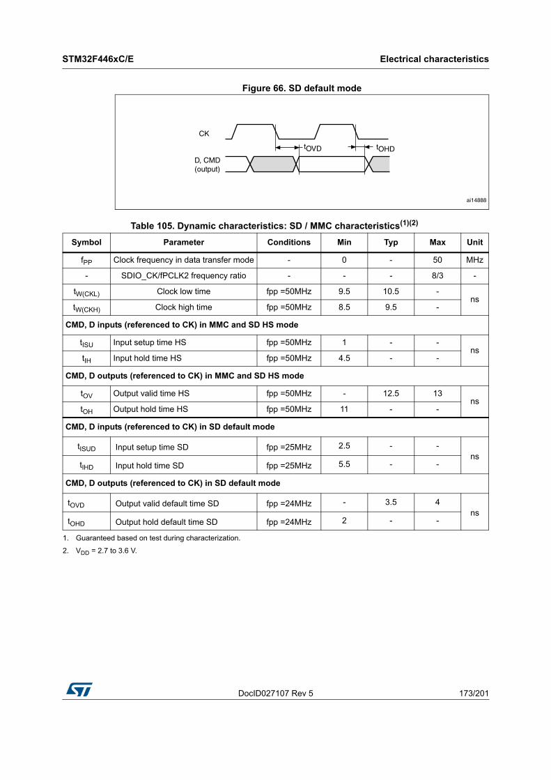
DocID027107 Rev 5 173/201
STM32F446xC/E Electrical characteristics
174
Figure 66. SD default mode
Table 105. Dynamic characteristics: SD / MMC characteristics(1)(2)
Symbol Parameter Conditions Min Typ Max Unit
fPP Clock frequency in data transfer mode - 0 - 50 MHz
- SDIO_CK/fPCLK2 frequency ratio - - - 8/3 -
tW(CKL) Clock low time fpp =50MHz 9.5 10.5 -ns
tW(CKH) Clock high time fpp =50MHz 8.5 9.5 -
CMD, D inputs (referenced to CK) in MMC and SD HS mode
tISU Input setup time HS fpp =50MHz 1 - -ns
tIH Input hold time HS fpp =50MHz 4.5 - -
CMD, D outputs (referenced to CK) in MMC and SD HS mode
tOV Output valid time HS fpp =50MHz - 12.5 13ns
tOH Output hold time HS fpp =50MHz 11 - -
CMD, D inputs (referenced to CK) in SD default mode
tISUD Input setup time SD fpp =25MHz 2.5 - -ns
tIHD Input hold time SD fpp =25MHz 5.5 - -
CMD, D outputs (referenced to CK) in SD default mode
tOVD Output valid default time SD fpp =24MHz - 3.5 4ns
tOHD Output hold default time SD fpp =24MHz 2 - -
1. Guaranteed based on test during characterization.
2. VDD = 2.7 to 3.6 V.
Electrical characteristics STM32F446xC/E
174/201 DocID027107 Rev 5
6.3.29 RTC characteristics
Table 106. Dynamic characteristics: eMMC characteristics VDD = 1.7 V to 1.9 V(1)(2)
Symbol Parameter Conditions Min Typ Max Unit
fPP Clock frequency in data transfer mode - 0 - 50 MHz
- SDIO_CK/fPCLK2 frequency ratio - - - 8/3 -
tW(CKL) Clock low time fpp =50MHz 9.5 10.5 -ns
tW(CKH) Clock high time fpp =50MHz 8.5 9.5 -
CMD, D inputs (referenced to CK) in eMMC mode
tISU Input setup time HS fpp =50MHz 0.5 - -ns
tIH Input hold time HS fpp =50MHz 7.5 - -
CMD, D outputs (referenced to CK) in eMMC mode
tOV Output valid time HS fpp =50MHz - 13.5 14.5ns
tOH Output hold time HS fpp =50MHz 12 - -
1. Guaranteed based on test during characterization.
2. VDD = 2.7 to 3.6 V.
Table 107. RTC characteristics
Symbol Parameter Conditions Min Max
- fPCLK1/RTCCLK frequency ratioAny read/write operation from/to an RTC register
4 -
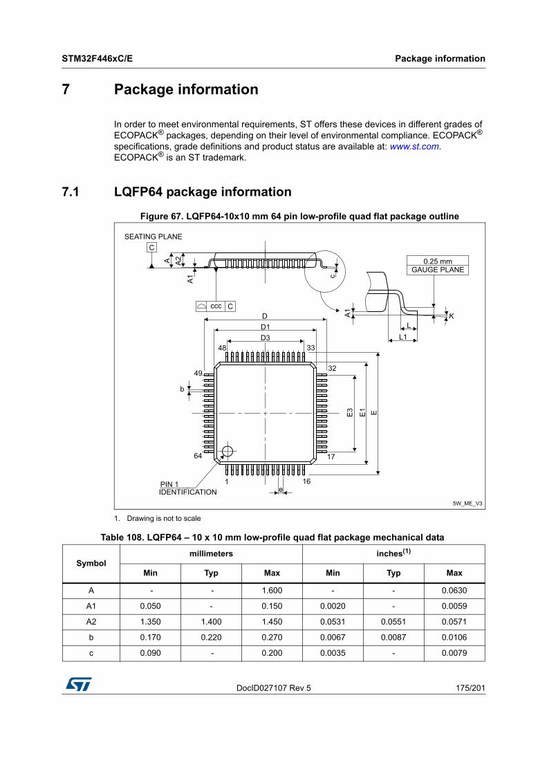
DocID027107 Rev 5 175/201
STM32F446xC/E Package information
198
7 Package information
In order to meet environmental requirements, ST offers these devices in different grades of ECOPACK® packages, depending on their level of environmental compliance. ECOPACK® specifications, grade definitions and product status are available at: www.st.com. ECOPACK® is an ST trademark.
7.1 LQFP64 package information
Figure 67. LQFP64-10x10 mm 64 pin low-profile quad flat package outline
1. Drawing is not to scale
Table 108. LQFP64 – 10 x 10 mm low-profile quad flat package mechanical data
Symbolmillimeters inches(1)
Min Typ Max Min Typ Max
A - - 1.600 - - 0.0630
A1 0.050 - 0.150 0.0020 - 0.0059
A2 1.350 1.400 1.450 0.0531 0.0551 0.0571
b 0.170 0.220 0.270 0.0067 0.0087 0.0106
c 0.090 - 0.200 0.0035 - 0.0079
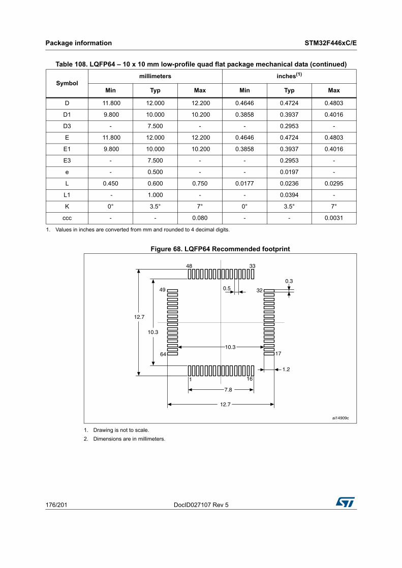
Package information STM32F446xC/E
176/201 DocID027107 Rev 5
Figure 68. LQFP64 Recommended footprint
1. Drawing is not to scale.
2. Dimensions are in millimeters.
D 11.800 12.000 12.200 0.4646 0.4724 0.4803
D1 9.800 10.000 10.200 0.3858 0.3937 0.4016
D3 - 7.500 - - 0.2953 -
E 11.800 12.000 12.200 0.4646 0.4724 0.4803
E1 9.800 10.000 10.200 0.3858 0.3937 0.4016
E3 - 7.500 - - 0.2953 -
e - 0.500 - - 0.0197 -
L 0.450 0.600 0.750 0.0177 0.0236 0.0295
L1 - 1.000 - - 0.0394 -
K 0° 3.5° 7° 0° 3.5° 7°
ccc - - 0.080 - - 0.0031
1. Values in inches are converted from mm and rounded to 4 decimal digits.
Table 108. LQFP64 – 10 x 10 mm low-profile quad flat package mechanical data (continued)
Symbolmillimeters inches(1)
Min Typ Max Min Typ Max
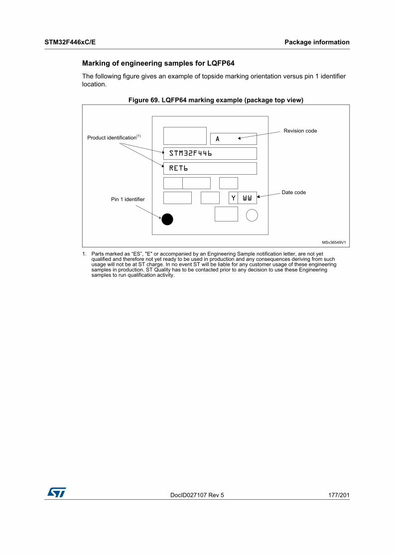
DocID027107 Rev 5 177/201
STM32F446xC/E Package information
198
Marking of engineering samples for LQFP64
The following figure gives an example of topside marking orientation versus pin 1 identifier location.
Figure 69. LQFP64 marking example (package top view)
1. Parts marked as “ES”, "E" or accompanied by an Engineering Sample notification letter, are not yet qualified and therefore not yet ready to be used in production and any consequences deriving from such usage will not be at ST charge. In no event ST will be liable for any customer usage of these engineering samples in production. ST Quality has to be contacted prior to any decision to use these Engineering samples to run qualification activity.
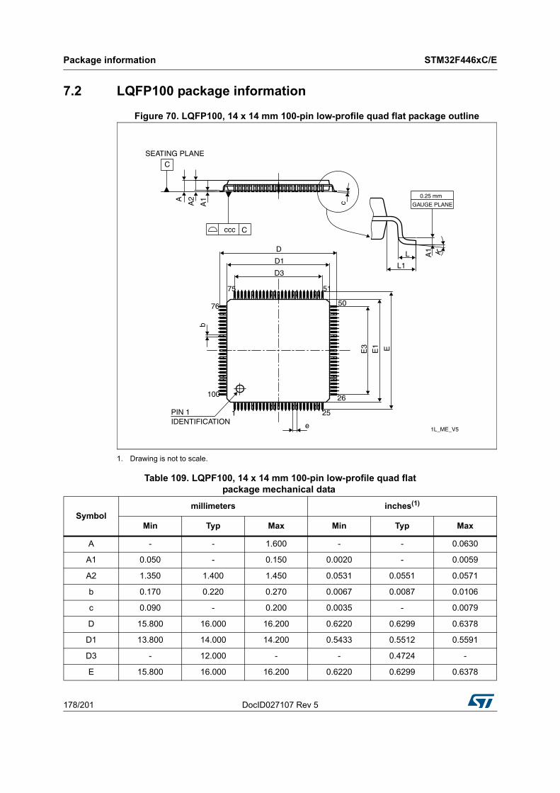
Package information STM32F446xC/E
178/201 DocID027107 Rev 5
7.2 LQFP100 package information
Figure 70. LQFP100, 14 x 14 mm 100-pin low-profile quad flat package outline
1. Drawing is not to scale.
Table 109. LQPF100, 14 x 14 mm 100-pin low-profile quad flat package mechanical data
Symbolmillimeters inches(1)
Min Typ Max Min Typ Max
A - - 1.600 - - 0.0630
A1 0.050 - 0.150 0.0020 - 0.0059
A2 1.350 1.400 1.450 0.0531 0.0551 0.0571
b 0.170 0.220 0.270 0.0067 0.0087 0.0106
c 0.090 - 0.200 0.0035 - 0.0079
D 15.800 16.000 16.200 0.6220 0.6299 0.6378
D1 13.800 14.000 14.200 0.5433 0.5512 0.5591
D3 - 12.000 - - 0.4724 -
E 15.800 16.000 16.200 0.6220 0.6299 0.6378
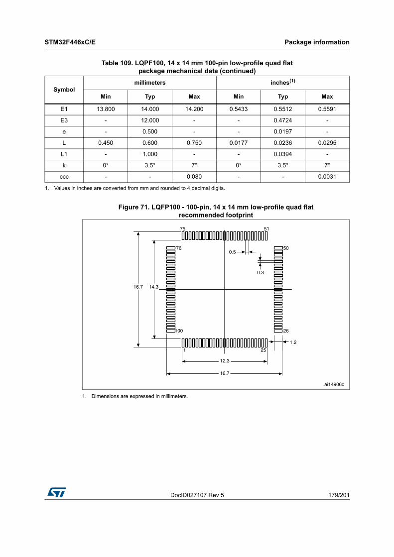
DocID027107 Rev 5 179/201
STM32F446xC/E Package information
198
Figure 71. LQFP100 - 100-pin, 14 x 14 mm low-profile quad flat recommended footprint
1. Dimensions are expressed in millimeters.
E1 13.800 14.000 14.200 0.5433 0.5512 0.5591
E3 - 12.000 - - 0.4724 -
e - 0.500 - - 0.0197 -
L 0.450 0.600 0.750 0.0177 0.0236 0.0295
L1 - 1.000 - - 0.0394 -
k 0° 3.5° 7° 0° 3.5° 7°
ccc - - 0.080 - - 0.0031
1. Values in inches are converted from mm and rounded to 4 decimal digits.
Table 109. LQPF100, 14 x 14 mm 100-pin low-profile quad flat package mechanical data (continued)
Symbolmillimeters inches(1)
Min Typ Max Min Typ Max
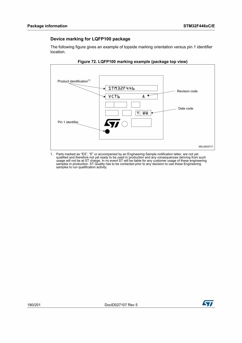
Package information STM32F446xC/E
180/201 DocID027107 Rev 5
Device marking for LQFP100 package
The following figure gives an example of topside marking orientation versus pin 1 identifier location.
Figure 72. LQFP100 marking example (package top view)
1. Parts marked as “ES”, “E” or accompanied by an Engineering Sample notification letter, are not yet qualified and therefore not yet ready to be used in production and any consequences deriving from such usage will not be at ST charge. In no event ST will be liable for any customer usage of these engineering samples in production. ST Quality has to be contacted prior to any decision to use these Engineering samples to run qualification activity.
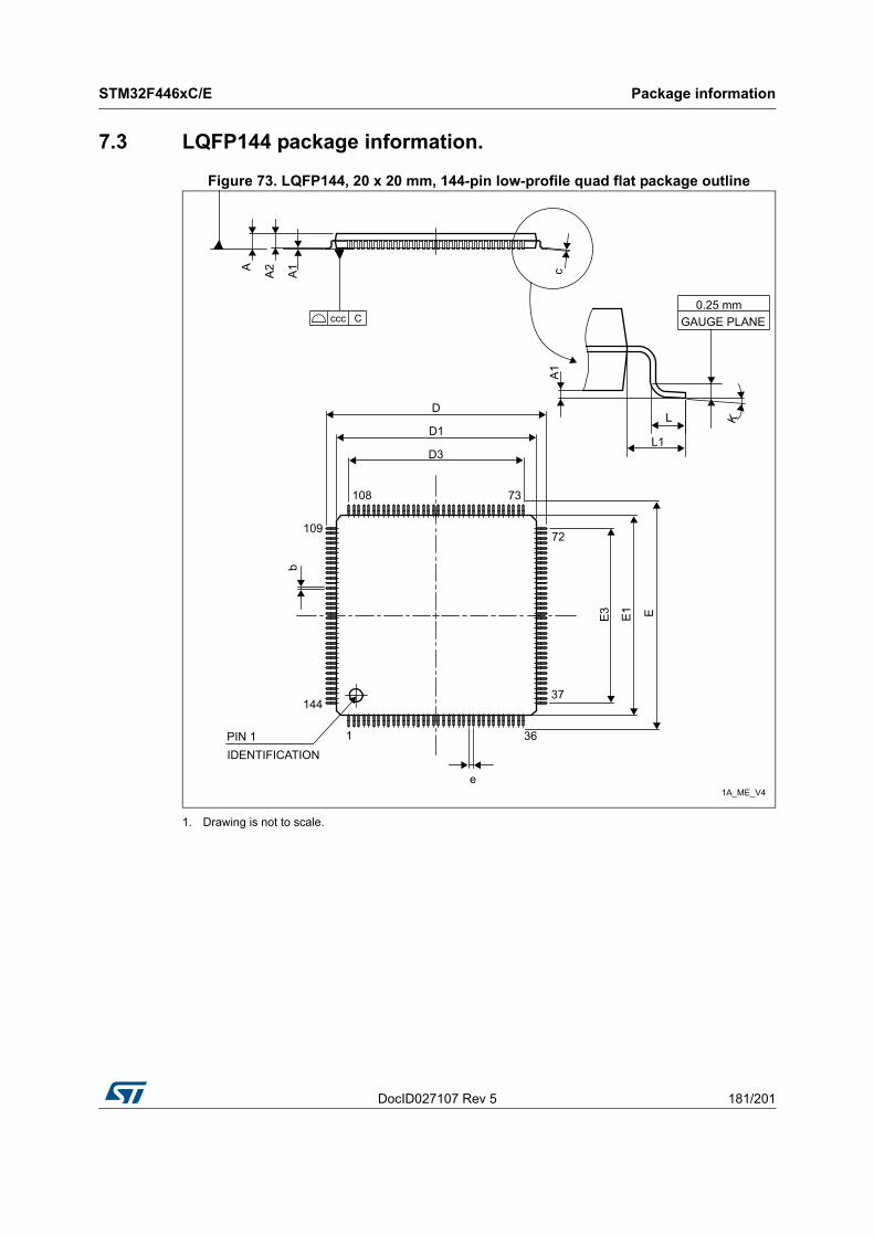
DocID027107 Rev 5 181/201
STM32F446xC/E Package information
198
7.3 LQFP144 package information.
Figure 73. LQFP144, 20 x 20 mm, 144-pin low-profile quad flat package outline
1. Drawing is not to scale.
Package information STM32F446xC/E
182/201 DocID027107 Rev 5
Table 110. LQFP144, 20 x 20 mm, 144-pin low-profile quad flat package mechanical data
Symbolmillimeters inches(1)
Min Typ Max Min Typ Max
A - - 1.600 - - 0.0630
A1 0.050 - 0.150 0.0020 - 0.0059
A2 1.350 1.400 1.450 0.0531 0.0551 0.0571
b 0.170 0.220 0.270 0.0067 0.0087 0.0106
c 0.090 - 0.200 0.0035 - 0.0079
D 21.800 22.000 22.200 0.8583 0.8661 0.874
D1 19.800 20.000 20.200 0.7795 0.7874 0.7953
D3 - 17.500 - - 0.689 -
E 21.800 22.000 22.200 0.8583 0.8661 0.8740
E1 19.800 20.000 20.200 0.7795 0.7874 0.7953
E3 - 17.500 - - 0.6890 -
e - 0.500 - - 0.0197 -
L 0.450 0.600 0.750 0.0177 0.0236 0.0295
L1 - 1.000 - - 0.0394 -
k 0° 3.5° 7° 0° 3.5° 7°
ccc - - 0.080 - - 0.0031
1. Values in inches are converted from mm and rounded to 4 decimal digits.
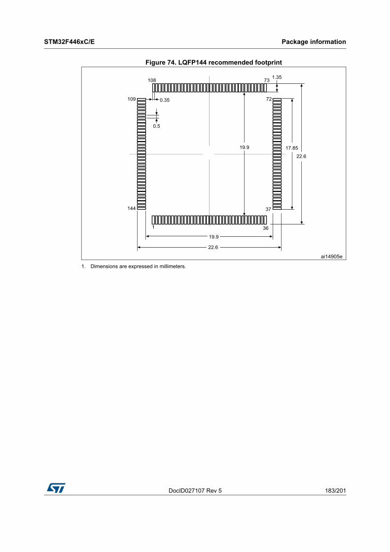
DocID027107 Rev 5 183/201
STM32F446xC/E Package information
198
Figure 74. LQFP144 recommended footprint
1. Dimensions are expressed in millimeters.
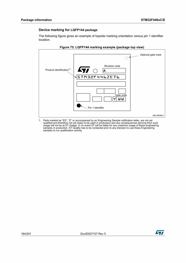
Package information STM32F446xC/E
184/201 DocID027107 Rev 5
Device marking for LQFP144 package
The following figure gives an example of topside marking orientation versus pin 1 identifier location.
Figure 75. LQFP144 marking example (package top view)
1. Parts marked as “ES”, “E” or accompanied by an Engineering Sample notification letter, are not yet qualified and therefore not yet ready to be used in production and any consequences deriving from such usage will not be at ST charge. In no event ST will be liable for any customer usage of these engineering samples in production. ST Quality has to be contacted prior to any decision to use these Engineering samples to run qualification activity.
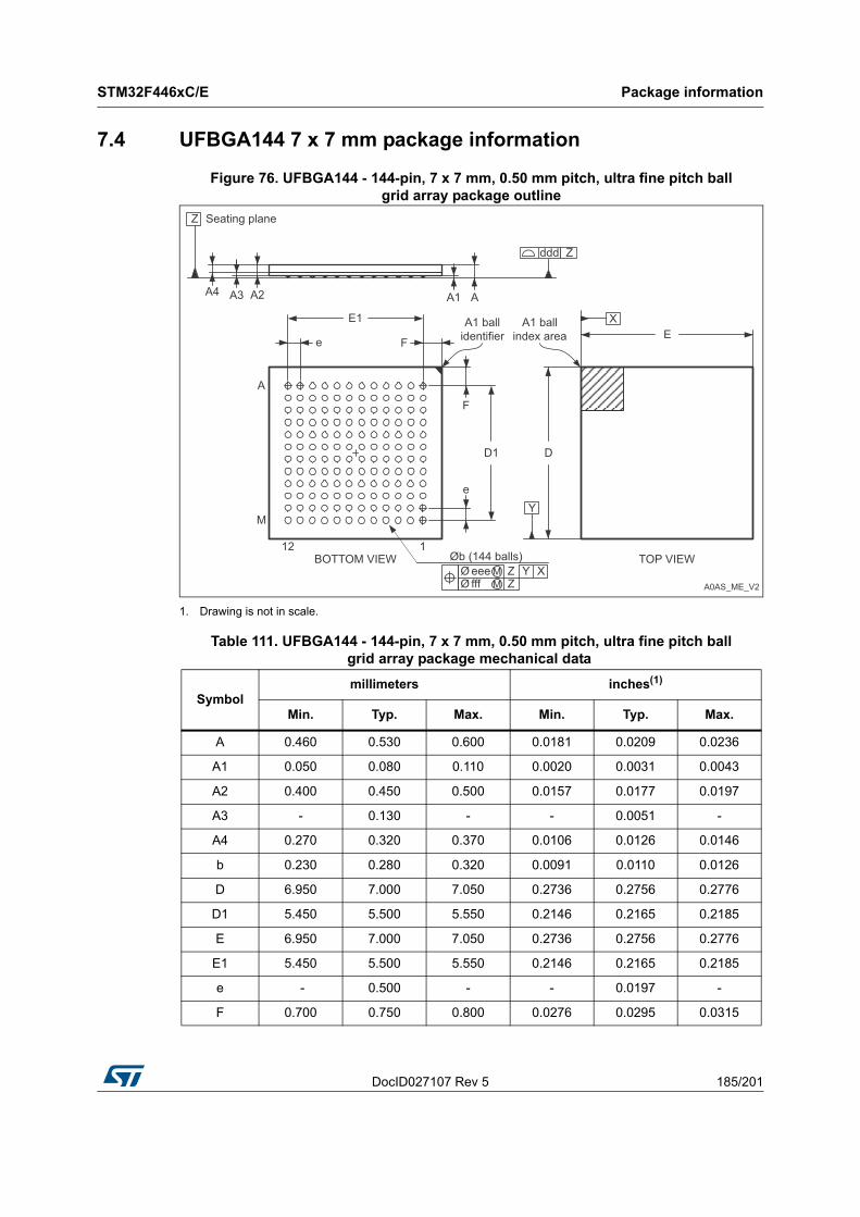
DocID027107 Rev 5 185/201
STM32F446xC/E Package information
198
7.4 UFBGA144 7 x 7 mm package information
Figure 76. UFBGA144 - 144-pin, 7 x 7 mm, 0.50 mm pitch, ultra fine pitch ballgrid array package outline
1. Drawing is not in scale.
Table 111. UFBGA144 - 144-pin, 7 x 7 mm, 0.50 mm pitch, ultra fine pitch ballgrid array package mechanical data
Symbolmillimeters inches(1)
Min. Typ. Max. Min. Typ. Max.
A 0.460 0.530 0.600 0.0181 0.0209 0.0236
A1 0.050 0.080 0.110 0.0020 0.0031 0.0043
A2 0.400 0.450 0.500 0.0157 0.0177 0.0197
A3 - 0.130 - - 0.0051 -
A4 0.270 0.320 0.370 0.0106 0.0126 0.0146
b 0.230 0.280 0.320 0.0091 0.0110 0.0126
D 6.950 7.000 7.050 0.2736 0.2756 0.2776
D1 5.450 5.500 5.550 0.2146 0.2165 0.2185
E 6.950 7.000 7.050 0.2736 0.2756 0.2776
E1 5.450 5.500 5.550 0.2146 0.2165 0.2185
e - 0.500 - - 0.0197 -
F 0.700 0.750 0.800 0.0276 0.0295 0.0315
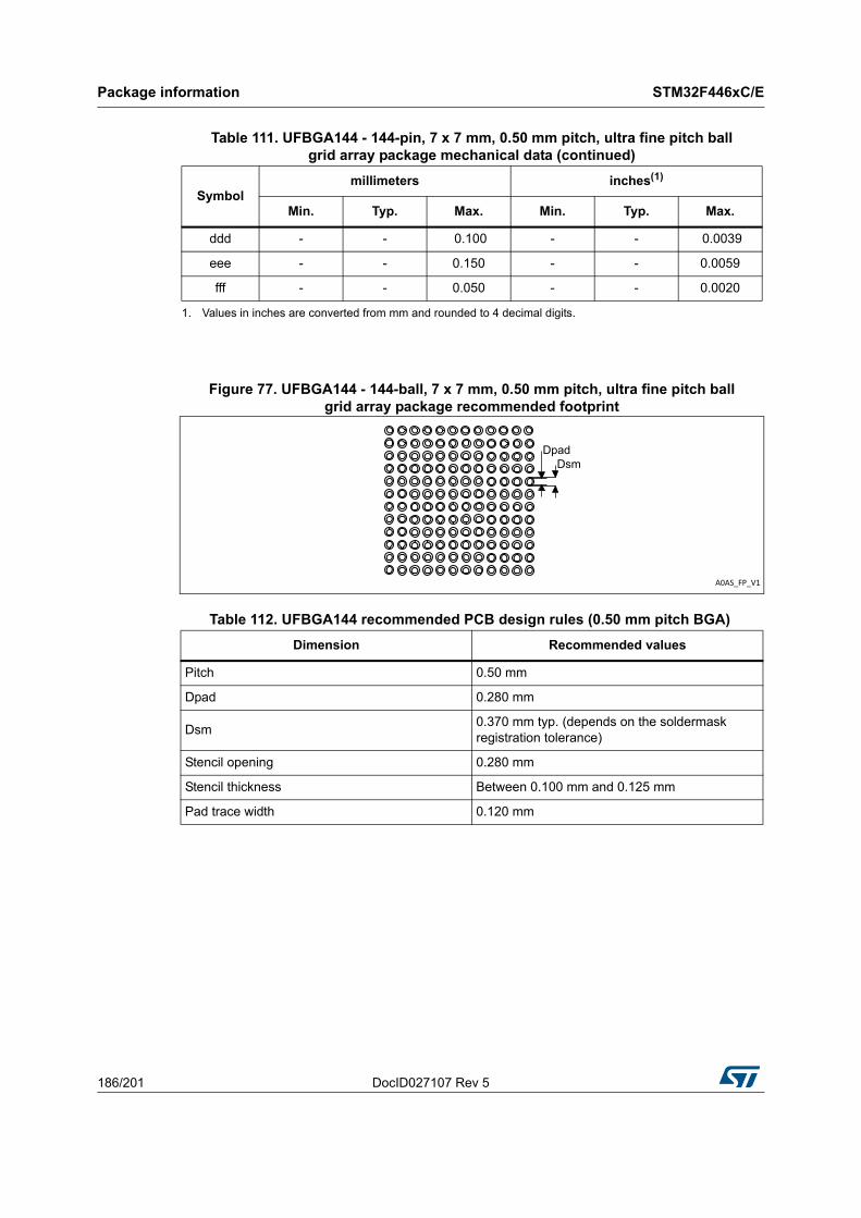
Package information STM32F446xC/E
186/201 DocID027107 Rev 5
Figure 77. UFBGA144 - 144-ball, 7 x 7 mm, 0.50 mm pitch, ultra fine pitch ball grid array package recommended footprint
ddd - - 0.100 - - 0.0039
eee - - 0.150 - - 0.0059
fff - - 0.050 - - 0.0020
1. Values in inches are converted from mm and rounded to 4 decimal digits.
Table 112. UFBGA144 recommended PCB design rules (0.50 mm pitch BGA)
Dimension Recommended values
Pitch 0.50 mm
Dpad 0.280 mm
Dsm0.370 mm typ. (depends on the soldermask registration tolerance)
Stencil opening 0.280 mm
Stencil thickness Between 0.100 mm and 0.125 mm
Pad trace width 0.120 mm
Table 111. UFBGA144 - 144-pin, 7 x 7 mm, 0.50 mm pitch, ultra fine pitch ballgrid array package mechanical data (continued)
Symbolmillimeters inches(1)
Min. Typ. Max. Min. Typ. Max.
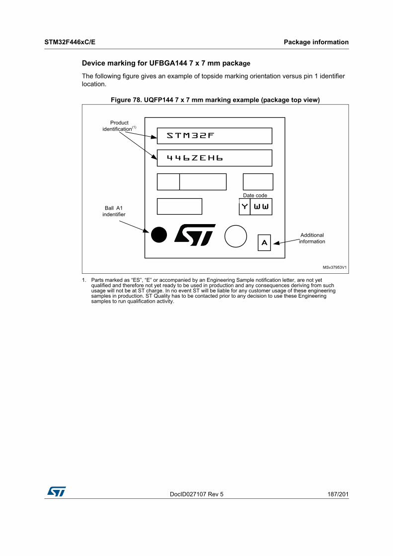
DocID027107 Rev 5 187/201
STM32F446xC/E Package information
198
Device marking for UFBGA144 7 x 7 mm package
The following figure gives an example of topside marking orientation versus pin 1 identifier location.
Figure 78. UQFP144 7 x 7 mm marking example (package top view)
1. Parts marked as “ES”, “E” or accompanied by an Engineering Sample notification letter, are not yet qualified and therefore not yet ready to be used in production and any consequences deriving from such usage will not be at ST charge. In no event ST will be liable for any customer usage of these engineering samples in production. ST Quality has to be contacted prior to any decision to use these Engineering samples to run qualification activity.
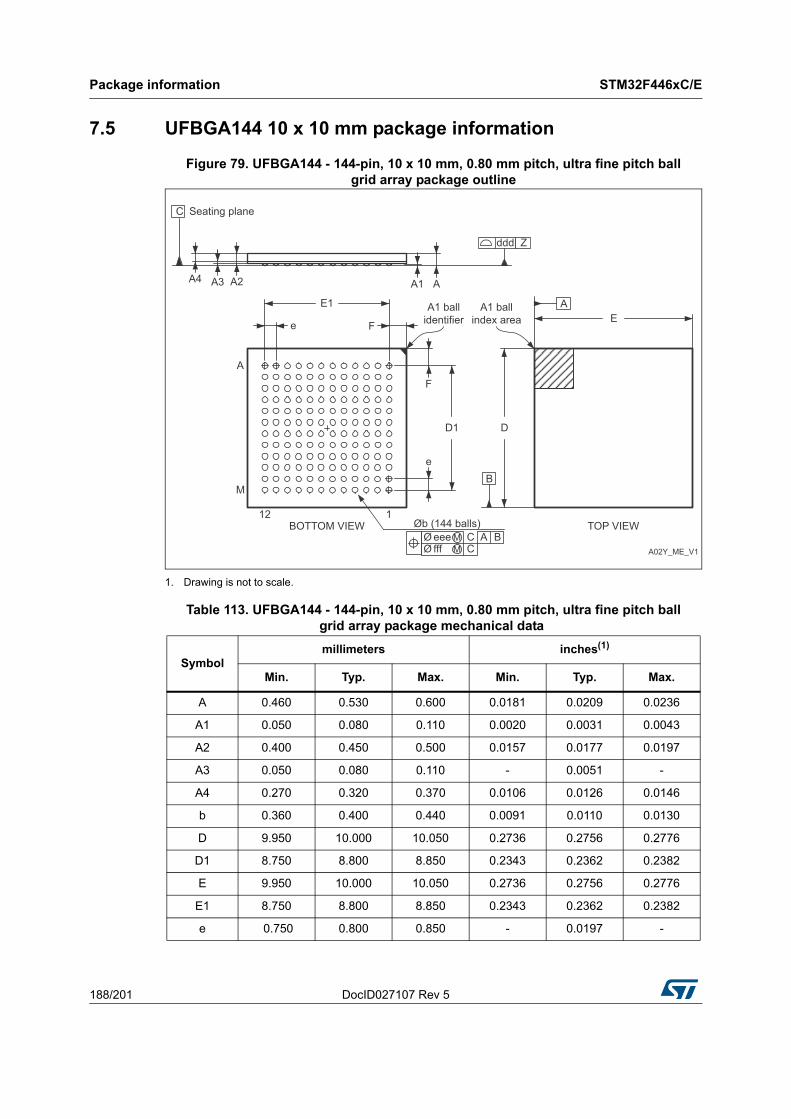
Package information STM32F446xC/E
188/201 DocID027107 Rev 5
7.5 UFBGA144 10 x 10 mm package information
Figure 79. UFBGA144 - 144-pin, 10 x 10 mm, 0.80 mm pitch, ultra fine pitch ball grid array package outline
1. Drawing is not to scale.
Table 113. UFBGA144 - 144-pin, 10 x 10 mm, 0.80 mm pitch, ultra fine pitch ball grid array package mechanical data
Symbolmillimeters inches(1)
Min. Typ. Max. Min. Typ. Max.
A 0.460 0.530 0.600 0.0181 0.0209 0.0236
A1 0.050 0.080 0.110 0.0020 0.0031 0.0043
A2 0.400 0.450 0.500 0.0157 0.0177 0.0197
A3 0.050 0.080 0.110 - 0.0051 -
A4 0.270 0.320 0.370 0.0106 0.0126 0.0146
b 0.360 0.400 0.440 0.0091 0.0110 0.0130
D 9.950 10.000 10.050 0.2736 0.2756 0.2776
D1 8.750 8.800 8.850 0.2343 0.2362 0.2382
E 9.950 10.000 10.050 0.2736 0.2756 0.2776
E1 8.750 8.800 8.850 0.2343 0.2362 0.2382
e 0.750 0.800 0.850 - 0.0197 -
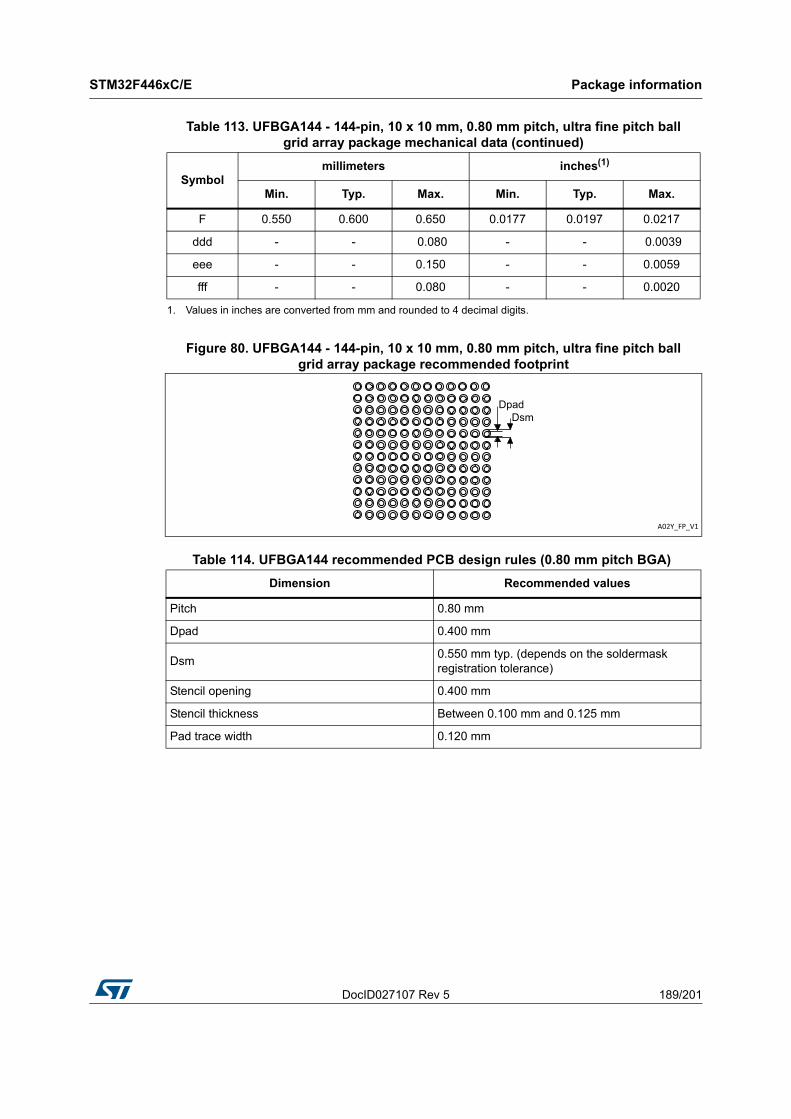
DocID027107 Rev 5 189/201
STM32F446xC/E Package information
198
Figure 80. UFBGA144 - 144-pin, 10 x 10 mm, 0.80 mm pitch, ultra fine pitch ball grid array package recommended footprint
F 0.550 0.600 0.650 0.0177 0.0197 0.0217
ddd - - 0.080 - - 0.0039
eee - - 0.150 - - 0.0059
fff - - 0.080 - - 0.0020
1. Values in inches are converted from mm and rounded to 4 decimal digits.
Table 114. UFBGA144 recommended PCB design rules (0.80 mm pitch BGA)
Dimension Recommended values
Pitch 0.80 mm
Dpad 0.400 mm
Dsm0.550 mm typ. (depends on the soldermask registration tolerance)
Stencil opening 0.400 mm
Stencil thickness Between 0.100 mm and 0.125 mm
Pad trace width 0.120 mm
Table 113. UFBGA144 - 144-pin, 10 x 10 mm, 0.80 mm pitch, ultra fine pitch ball grid array package mechanical data (continued)
Symbolmillimeters inches(1)
Min. Typ. Max. Min. Typ. Max.
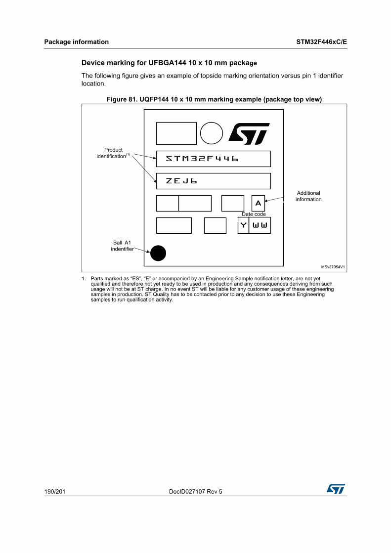
Package information STM32F446xC/E
190/201 DocID027107 Rev 5
Device marking for UFBGA144 10 x 10 mm package
The following figure gives an example of topside marking orientation versus pin 1 identifier location.
Figure 81. UQFP144 10 x 10 mm marking example (package top view)
1. Parts marked as “ES”, “E” or accompanied by an Engineering Sample notification letter, are not yet qualified and therefore not yet ready to be used in production and any consequences deriving from such usage will not be at ST charge. In no event ST will be liable for any customer usage of these engineering samples in production. ST Quality has to be contacted prior to any decision to use these Engineering samples to run qualification activity.
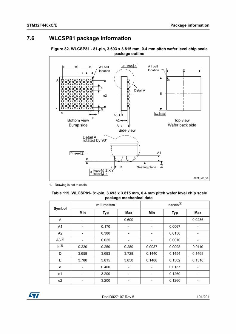
DocID027107 Rev 5 191/201
STM32F446xC/E Package information
198
7.6 WLCSP81 package information
Figure 82. WLCSP81 - 81-pin, 3.693 x 3.815 mm, 0.4 mm pitch wafer level chip scale package outline
1. Drawing is not to scale.
Table 115. WLCSP81- 81-pin, 3.693 x 3.815 mm, 0.4 mm pitch wafer level chip scale package mechanical data
Symbolmillimeters inches(1)
Min Typ Max Min Typ Max
A - - 0.600 - - 0.0236
A1 - 0.170 - - 0.0067 -
A2 - 0.380 - - 0.0150 -
A3(2) - 0.025 - - 0.0010 -
b(3) 0.220 0.250 0.280 0.0087 0.0098 0.0110
D 3.658 3.693 3.728 0.1440 0.1454 0.1468
E 3.780 3.815 3.850 0.1488 0.1502 0.1516
e - 0.400 - - 0.0157 -
e1 - 3.200 - - 0.1260 -
e2 - 3.200 - - 0.1260 -
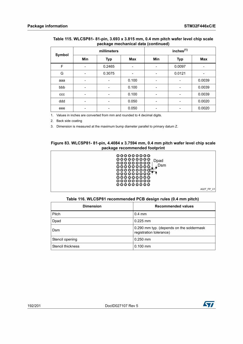
Package information STM32F446xC/E
192/201 DocID027107 Rev 5
Figure 83. WLCSP81- 81-pin, 4.4084 x 3.7594 mm, 0.4 mm pitch wafer level chip scalepackage recommended footprint
F - 0.2465 - - 0.0097 -
G - 0.3075 - - 0.0121 -
aaa - - 0.100 - - 0.0039
bbb - - 0.100 - - 0.0039
ccc - - 0.100 - - 0.0039
ddd - - 0.050 - - 0.0020
eee - - 0.050 - - 0.0020
1. Values in inches are converted from mm and rounded to 4 decimal digits.
2. Back side coating
3. Dimension is measured at the maximum bump diameter parallel to primary datum Z.
Table 116. WLCSP81 recommended PCB design rules (0.4 mm pitch)
Dimension Recommended values
Pitch 0.4 mm
Dpad 0.225 mm
Dsm0.290 mm typ. (depends on the soldermask registration tolerance)
Stencil opening 0.250 mm
Stencil thickness 0.100 mm
Table 115. WLCSP81- 81-pin, 3.693 x 3.815 mm, 0.4 mm pitch wafer level chip scale package mechanical data (continued)
Symbolmillimeters inches(1)
Min Typ Max Min Typ Max
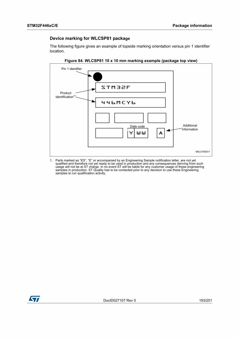
DocID027107 Rev 5 193/201
STM32F446xC/E Package information
198
Device marking for WLCSP81 package
The following figure gives an example of topside marking orientation versus pin 1 identifier location.
Figure 84. WLCSP81 10 x 10 mm marking example (package top view)
1. Parts marked as “ES”, “E” or accompanied by an Engineering Sample notification letter, are not yet qualified and therefore not yet ready to be used in production and any consequences deriving from such usage will not be at ST charge. In no event ST will be liable for any customer usage of these engineering samples in production. ST Quality has to be contacted prior to any decision to use these Engineering samples to run qualification activity.
Package information STM32F446xC/E
194/201 DocID027107 Rev 5
7.7 Thermal characteristics
The maximum chip-junction temperature, TJ max, in degrees Celsius, may be calculated using the following equation:
TJ max = TA max + (PD max x ΘJA)
Where:
• TA max is the maximum ambient temperature in ° C,
• ΘJA is the package junction-to-ambient thermal resistance, in ° C/W,
• PD max is the sum of PINT max and PI/O max (PD max = PINT max + PI/Omax),
• PINT max is the product of IDD and VDD, expressed in Watts. This is the maximum chip internal power.
PI/O max represents the maximum power dissipation on output pins where:
PI/O max = Σ (VOL × IOL) + Σ((VDD – VOH) × IOH),
taking into account the actual VOL / IOL and VOH / IOH of the I/Os at low and high level in the application.
Reference document
JESD51-2 Integrated Circuits Thermal Test Method Environment Conditions - Natural Convection (Still Air). Available from www.jedec.org.
Table 117. Package thermal characteristics
Symbol Parameter Value Unit
ΘJA
Thermal resistance junction-ambient LQFP64 - 10 × 10 mm
46
°C/W
Thermal resistance junction-ambient LQFP100 - 14 × 14 mm / 0.5 mm pitch
42
Thermal resistance junction-ambient LQFP144 - 20 × 20 mm / 0.5 mm pitch
33
Thermal resistance junction-ambient UFBGA144 - 7 × 7 mm / 0.5 mm pitch
51
Thermal resistance junction-ambient UFBGA144 - 10 × 10 mm / 0.8 mm pitch
48
Thermal resistance junction-ambient WLCSP81
48
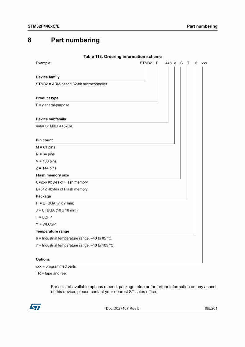
DocID027107 Rev 5 195/201
STM32F446xC/E Part numbering
198
8 Part numbering
For a list of available options (speed, package, etc.) or for further information on any aspect of this device, please contact your nearest ST sales office.
Table 118. Ordering information scheme
Example: STM32 F 446 V C T 6 xxx
Device family
STM32 = ARM-based 32-bit microcontroller
Product type
F = general-purpose
Device subfamily
446= STM32F446xC/E,
Pin count
M = 81 pins
R = 64 pins
V = 100 pins
Z = 144 pins
Flash memory size
C=256 Kbytes of Flash memory
E=512 Kbytes of Flash memory
Package
H = UFBGA (7 x 7 mm)
J = UFBGA (10 x 10 mm)
T = LQFP
Y = WLCSP
Temperature range
6 = Industrial temperature range, –40 to 85 °C.
7 = Industrial temperature range, –40 to 105 °C.
Options
xxx = programmed parts
TR = tape and reel
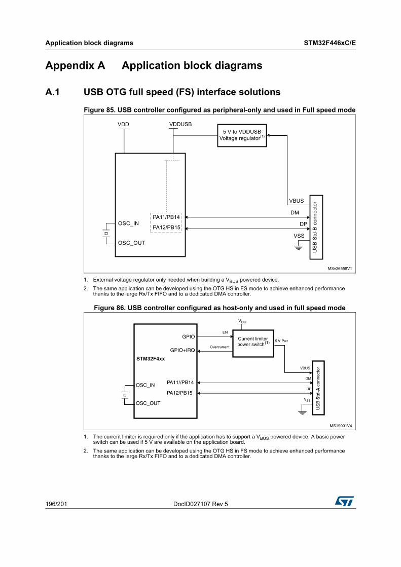
Application block diagrams STM32F446xC/E
196/201 DocID027107 Rev 5
Appendix A Application block diagrams
A.1 USB OTG full speed (FS) interface solutions
Figure 85. USB controller configured as peripheral-only and used in Full speed mode
1. External voltage regulator only needed when building a VBUS powered device.
2. The same application can be developed using the OTG HS in FS mode to achieve enhanced performance thanks to the large Rx/Tx FIFO and to a dedicated DMA controller.
Figure 86. USB controller configured as host-only and used in full speed mode
1. The current limiter is required only if the application has to support a VBUS powered device. A basic power switch can be used if 5 V are available on the application board.
2. The same application can be developed using the OTG HS in FS mode to achieve enhanced performance thanks to the large Rx/Tx FIFO and to a dedicated DMA controller.
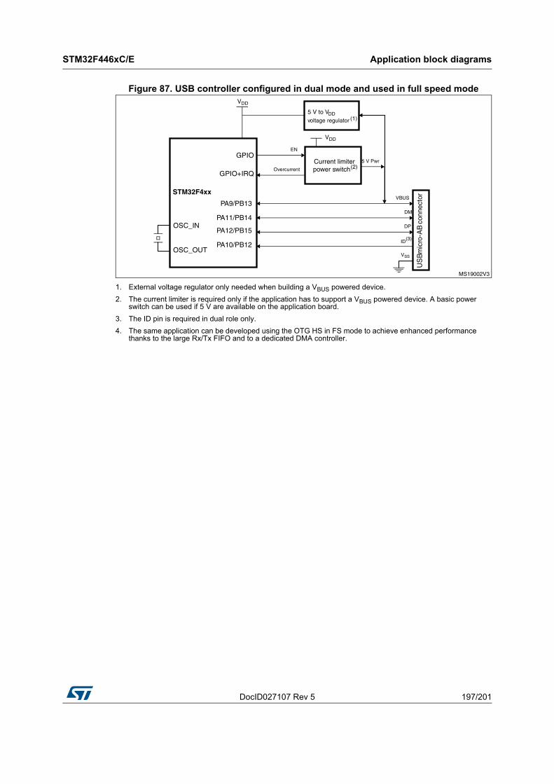
DocID027107 Rev 5 197/201
STM32F446xC/E Application block diagrams
198
Figure 87. USB controller configured in dual mode and used in full speed mode
1. External voltage regulator only needed when building a VBUS powered device.
2. The current limiter is required only if the application has to support a VBUS powered device. A basic power switch can be used if 5 V are available on the application board.
3. The ID pin is required in dual role only.
4. The same application can be developed using the OTG HS in FS mode to achieve enhanced performance thanks to the large Rx/Tx FIFO and to a dedicated DMA controller.
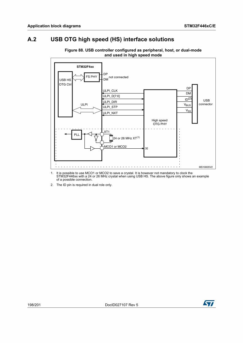
Application block diagrams STM32F446xC/E
198/201 DocID027107 Rev 5
A.2 USB OTG high speed (HS) interface solutions
Figure 88. USB controller configured as peripheral, host, or dual-modeand used in high speed mode
1. It is possible to use MCO1 or MCO2 to save a crystal. It is however not mandatory to clock the STM32F446xx with a 24 or 26 MHz crystal when using USB HS. The above figure only shows an example of a possible connection.
2. The ID pin is required in dual role only.
DocID027107 Rev 5 199/201
STM32F446xC/E Revision history
200
9 Revision history
Table 119. Document revision history
Date Revision Changes
17-Feb-2015 1 Initial release.
16-Mar-2015 2
Added note 2 inside Table 2
Updated Table 11, Table 23, Table 24, Table 25, Table 26, Table 30, Table 51, Table 52, Table 53, and Table 61
Added condition inside Typical and maximum current consumption and Additional current consumption
Added FMPI2C characteristics
Added Table 62 and Figure 35
29-May-2015 3
Updated:
– Section 6.3.15: Absolute maximum ratings (electrical sensitivity)
– Section 7: Package information
– Table 2: STM32F446xC/E features and peripheral counts
– Table 13: STM32F446xC/xE WLCSP81 ballout
– Figure 53: ESD absolute maximum ratings
– Figure 54: Synchronous multiplexed NOR/PSRAM read timings
Added:
– Figure 78: UQFP144 7 x 7 mm marking example (package top view),
– Figure 81: UQFP144 10 x 10 mm marking example (package top view),
– Figure 84: WLCSP81 10 x 10 mm marking example (package top view)
Revision history STM32F446xC/E
200/201 DocID027107 Rev 5
10-Aug-2015 4
Updated:
– Figure 14: STM32F446xC/xE UFBGA144 ballout
– Table 10: STM32F446xx pin and ball descriptions
– Table 18: VCAP_1/VCAP_2 operating conditions
– Section 3.15: Power supply schemes
– Section 6.3.2: VCAP_1/VCAP_2 external capacitor
Added:
– Figure 5: VDDUSB connected to an external independent power supply
– Notes 3 and 4 below Figure 18: Power supply scheme
03-Nov-2015 5
Updated:
– Introduction;
– Table 2: STM32F446xC/E features and peripheral counts
– Table 43: Main PLL characteristics
– Title of Table 45: PLLISAI characteristics
– Table 109: LQPF100, 14 x 14 mm 100-pin low-profile quad flat package mechanical data
– Table 118: Ordering information scheme
– Figure 10: STM32F446xC/xE LQFP64 pinout
– Figure 11: STM32F446xC/xE LQFP100 pinout
Added:
– Table 77: UFBGA144 - 144-ball, 7 x 7 mm, 0.50 mm pitch, ultra fine pitch ball grid array package recommended footprint
– Table 111: UFBGA144 - 144-pin, 7 x 7 mm, 0.50 mm pitch, ultra fine pitch ball grid array package mechanical data
Table 119. Document revision history (continued)
Date Revision Changes
DocID027107 Rev 5 201/201
STM32F446xC/E
201
IMPORTANT NOTICE – PLEASE READ CAREFULLY
STMicroelectronics NV and its subsidiaries (“ST”) reserve the right to make changes, corrections, enhancements, modifications, and improvements to ST products and/or to this document at any time without notice. Purchasers should obtain the latest relevant information on ST products before placing orders. ST products are sold pursuant to ST’s terms and conditions of sale in place at the time of order acknowledgement.
Purchasers are solely responsible for the choice, selection, and use of ST products and ST assumes no liability for application assistance or the design of Purchasers’ products.
No license, express or implied, to any intellectual property right is granted by ST herein.
Resale of ST products with provisions different from the information set forth herein shall void any warranty granted by ST for such product.
ST and the ST logo are trademarks of ST. All other product or service names are the property of their respective owners.
Information in this document supersedes and replaces information previously supplied in any prior versions of this document.
© 2015 STMicroelectronics – All rights reserved