Embed Size (px)
Citation preview
This is information on a product in full production.
September 2013 DocID023367 Rev 2 1/125
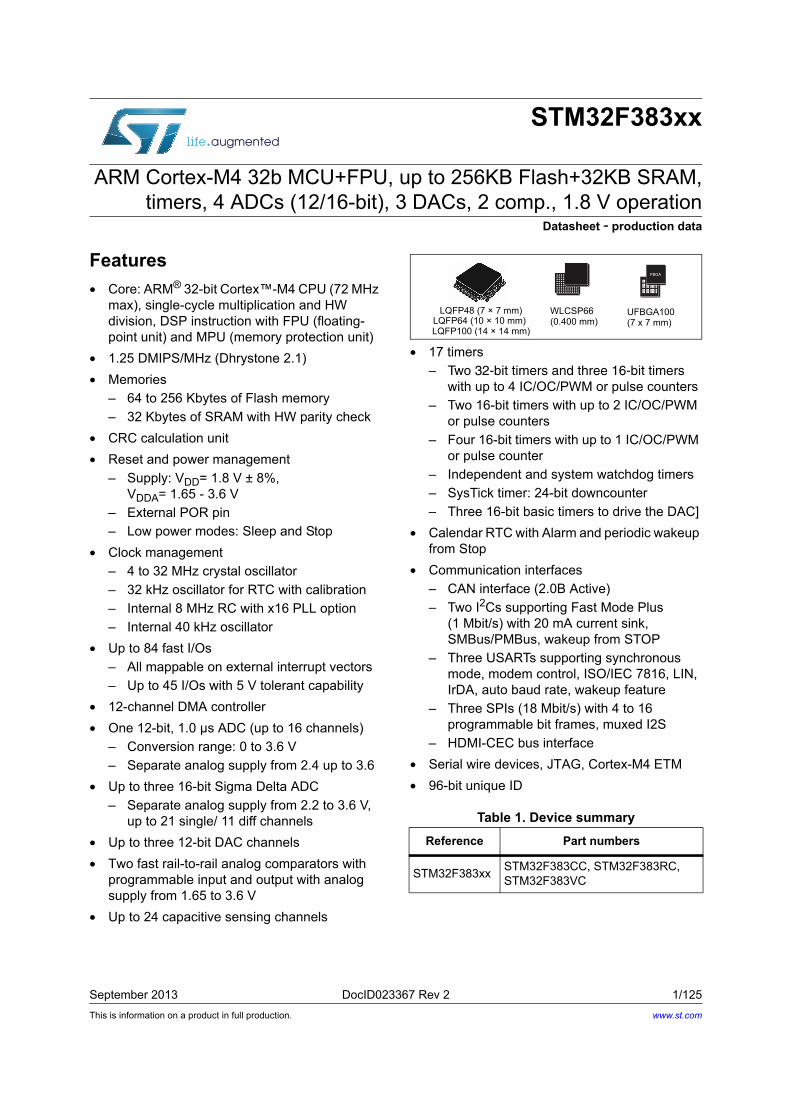
STM32F383xx
ARM Cortex-M4 32b MCU+FPU, up to 256KB Flash+32KB SRAM,timers, 4 ADCs (12/16-bit), 3 DACs, 2 comp., 1.8 V operation
Datasheet - production data
Features• Core: ARM® 32-bit Cortex™-M4 CPU (72 MHz
max), single-cycle multiplication and HW division, DSP instruction with FPU (floating-point unit) and MPU (memory protection unit)
• 1.25 DMIPS/MHz (Dhrystone 2.1)• Memories
– 64 to 256 Kbytes of Flash memory– 32 Kbytes of SRAM with HW parity check
• CRC calculation unit• Reset and power management
– Supply: VDD= 1.8 V ± 8%, VDDA= 1.65 - 3.6 V
– External POR pin– Low power modes: Sleep and Stop
• Clock management– 4 to 32 MHz crystal oscillator– 32 kHz oscillator for RTC with calibration– Internal 8 MHz RC with x16 PLL option– Internal 40 kHz oscillator
• Up to 84 fast I/Os– All mappable on external interrupt vectors– Up to 45 I/Os with 5 V tolerant capability
• 12-channel DMA controller• One 12-bit, 1.0 µs ADC (up to 16 channels)
– Conversion range: 0 to 3.6 V– Separate analog supply from 2.4 up to 3.6
• Up to three 16-bit Sigma Delta ADC– Separate analog supply from 2.2 to 3.6 V,
up to 21 single/ 11 diff channels• Up to three 12-bit DAC channels• Two fast rail-to-rail analog comparators with
programmable input and output with analog supply from 1.65 to 3.6 V
• Up to 24 capacitive sensing channels
• 17 timers– Two 32-bit timers and three 16-bit timers
with up to 4 IC/OC/PWM or pulse counters– Two 16-bit timers with up to 2 IC/OC/PWM
or pulse counters– Four 16-bit timers with up to 1 IC/OC/PWM
or pulse counter– Independent and system watchdog timers– SysTick timer: 24-bit downcounter– Three 16-bit basic timers to drive the DAC]
• Calendar RTC with Alarm and periodic wakeup from Stop
• Communication interfaces– CAN interface (2.0B Active)– Two I2Cs supporting Fast Mode Plus
(1 Mbit/s) with 20 mA current sink, SMBus/PMBus, wakeup from STOP
– Three USARTs supporting synchronous mode, modem control, ISO/IEC 7816, LIN, IrDA, auto baud rate, wakeup feature
– Three SPIs (18 Mbit/s) with 4 to 16 programmable bit frames, muxed I2S
– HDMI-CEC bus interface• Serial wire devices, JTAG, Cortex-M4 ETM• 96-bit unique ID
Table 1. Device summaryReference Part numbers
STM32F383xx STM32F383CC, STM32F383RC, STM32F383VC
LQFP64 (10 × 10 mm)LQFP100 (14 × 14 mm)
LQFP48 (7 × 7 mm)
FBGA
UFBGA100(7 x 7 mm)
WLCSP66(0.400 mm)
www.st.com
Contents STM32F383xx
2/125 DocID023367 Rev 2
Contents
1 Introduction . . . . . . . . . . . . . . . . . . . . . . . . . . . . . . . . . . . . . . . . . . . . . . . . 8
2 Description . . . . . . . . . . . . . . . . . . . . . . . . . . . . . . . . . . . . . . . . . . . . . . . . . 9
3 Functional overview . . . . . . . . . . . . . . . . . . . . . . . . . . . . . . . . . . . . . . . . 123.1 ARM® Cortex™-M4 core with embedded Flash and SRAM . . . . . . . . . . 12
3.2 Memory protection unit . . . . . . . . . . . . . . . . . . . . . . . . . . . . . . . . . . . . . . . 12
3.3 Embedded Flash memory . . . . . . . . . . . . . . . . . . . . . . . . . . . . . . . . . . . . 13
3.4 Cyclic redundancy check (CRC) calculation unit . . . . . . . . . . . . . . . . . . . 13
3.5 Embedded SRAM . . . . . . . . . . . . . . . . . . . . . . . . . . . . . . . . . . . . . . . . . . . 13
3.6 Boot modes . . . . . . . . . . . . . . . . . . . . . . . . . . . . . . . . . . . . . . . . . . . . . . . 13
3.7 Power management . . . . . . . . . . . . . . . . . . . . . . . . . . . . . . . . . . . . . . . . . 133.7.1 Power supply schemes . . . . . . . . . . . . . . . . . . . . . . . . . . . . . . . . . . . . . 13
3.7.2 Power supply supervisor . . . . . . . . . . . . . . . . . . . . . . . . . . . . . . . . . . . . 14
3.7.3 Low-power modes . . . . . . . . . . . . . . . . . . . . . . . . . . . . . . . . . . . . . . . . . 14
3.8 Clocks and startup . . . . . . . . . . . . . . . . . . . . . . . . . . . . . . . . . . . . . . . . . . 14
3.9 General-purpose input/outputs (GPIOs) . . . . . . . . . . . . . . . . . . . . . . . . . . 14
3.10 Direct memory access (DMA) . . . . . . . . . . . . . . . . . . . . . . . . . . . . . . . . . 15
3.11 Interrupts and events . . . . . . . . . . . . . . . . . . . . . . . . . . . . . . . . . . . . . . . . 153.11.1 Nested vectored interrupt controller (NVIC) . . . . . . . . . . . . . . . . . . . . . . 15
3.11.2 Extended interrupt/event controller (EXTI) . . . . . . . . . . . . . . . . . . . . . . 15
3.12 12-bit analog-to-digital converter (ADC) . . . . . . . . . . . . . . . . . . . . . . . . . . 163.12.1 Temperature sensor . . . . . . . . . . . . . . . . . . . . . . . . . . . . . . . . . . . . . . . . 16
3.12.2 Internal voltage reference (VREFINT) . . . . . . . . . . . . . . . . . . . . . . . . . . . 16
3.12.3 VBAT battery voltage monitoring . . . . . . . . . . . . . . . . . . . . . . . . . . . . . . . 16
3.13 16-bit sigma delta analog-to-digital converters (SDADC) . . . . . . . . . . . . . 17
3.14 Digital-to-analog converter (DAC) . . . . . . . . . . . . . . . . . . . . . . . . . . . . . . 17
3.15 Fast comparators (COMP) . . . . . . . . . . . . . . . . . . . . . . . . . . . . . . . . . . . . 18
3.16 Touch sensing controller (TSC) . . . . . . . . . . . . . . . . . . . . . . . . . . . . . . . . 18
3.17 Timers and watchdogs . . . . . . . . . . . . . . . . . . . . . . . . . . . . . . . . . . . . . . . 203.17.1 General-purpose timers (TIM2 to TIM5, TIM12 to TIM17, TIM19) . . . . . 21
3.17.2 Basic timers (TIM6, TIM7, TIM18) . . . . . . . . . . . . . . . . . . . . . . . . . . . . . 21

DocID023367 Rev 2 3/125
STM32F383xx Contents
4
3.17.3 Independent watchdog (IWDG) . . . . . . . . . . . . . . . . . . . . . . . . . . . . . . . 22
3.17.4 System window watchdog (WWDG) . . . . . . . . . . . . . . . . . . . . . . . . . . . 22
3.17.5 SysTick timer . . . . . . . . . . . . . . . . . . . . . . . . . . . . . . . . . . . . . . . . . . . . . 22
3.18 Real-time clock (RTC) and backup registers . . . . . . . . . . . . . . . . . . . . . . 22
3.19 Inter-integrated circuit interface (I2C) . . . . . . . . . . . . . . . . . . . . . . . . . . . . 23
3.20 Universal synchronous/asynchronous receiver transmitter (USART) . . . 24
3.21 Serial peripheral interface (SPI)/Inter-integrated sound interfaces (I2S) . 24
3.22 High-definition multimedia interface (HDMI) - consumer electronics control (CEC) . . . . . . . . . . . . . . . . . . . . . . . . . . . . . . . . . . . . 25
3.23 Controller area network (CAN) . . . . . . . . . . . . . . . . . . . . . . . . . . . . . . . . . 25
3.24 Serial wire JTAG debug port (SWJ-DP) . . . . . . . . . . . . . . . . . . . . . . . . . . 25
3.25 Embedded trace macrocell™ . . . . . . . . . . . . . . . . . . . . . . . . . . . . . . . . . . 26
4 Pinouts and pin description . . . . . . . . . . . . . . . . . . . . . . . . . . . . . . . . . . 27
5 Memory mapping . . . . . . . . . . . . . . . . . . . . . . . . . . . . . . . . . . . . . . . . . . . 48
6 Electrical characteristics . . . . . . . . . . . . . . . . . . . . . . . . . . . . . . . . . . . . 526.1 Parameter conditions . . . . . . . . . . . . . . . . . . . . . . . . . . . . . . . . . . . . . . . . 52
6.1.1 Minimum and maximum values . . . . . . . . . . . . . . . . . . . . . . . . . . . . . . . 52
6.1.2 Typical values . . . . . . . . . . . . . . . . . . . . . . . . . . . . . . . . . . . . . . . . . . . . 52
6.1.3 Typical curves . . . . . . . . . . . . . . . . . . . . . . . . . . . . . . . . . . . . . . . . . . . . 52
6.1.4 Loading capacitor . . . . . . . . . . . . . . . . . . . . . . . . . . . . . . . . . . . . . . . . . 52
6.1.5 Pin input voltage . . . . . . . . . . . . . . . . . . . . . . . . . . . . . . . . . . . . . . . . . . 52
6.1.6 Power supply scheme . . . . . . . . . . . . . . . . . . . . . . . . . . . . . . . . . . . . . . 53
6.1.7 Current consumption measurement . . . . . . . . . . . . . . . . . . . . . . . . . . . 54
6.2 Absolute maximum ratings . . . . . . . . . . . . . . . . . . . . . . . . . . . . . . . . . . . . 55
6.3 Operating conditions . . . . . . . . . . . . . . . . . . . . . . . . . . . . . . . . . . . . . . . . 576.3.1 General operating conditions . . . . . . . . . . . . . . . . . . . . . . . . . . . . . . . . . 57
6.3.2 Operating conditions at power-up / power-down . . . . . . . . . . . . . . . . . . 58
6.3.3 Embedded reference voltage . . . . . . . . . . . . . . . . . . . . . . . . . . . . . . . . . 59
6.3.4 Supply current characteristics . . . . . . . . . . . . . . . . . . . . . . . . . . . . . . . . 60
6.3.5 Wakeup time from low-power mode . . . . . . . . . . . . . . . . . . . . . . . . . . . 69
6.3.6 External clock source characteristics . . . . . . . . . . . . . . . . . . . . . . . . . . . 70
6.3.7 Internal clock source characteristics . . . . . . . . . . . . . . . . . . . . . . . . . . . 75
6.3.8 PLL characteristics . . . . . . . . . . . . . . . . . . . . . . . . . . . . . . . . . . . . . . . . 76

Contents STM32F383xx
4/125 DocID023367 Rev 2
6.3.9 Memory characteristics . . . . . . . . . . . . . . . . . . . . . . . . . . . . . . . . . . . . . 77
6.3.10 EMC characteristics . . . . . . . . . . . . . . . . . . . . . . . . . . . . . . . . . . . . . . . . 78
6.3.11 Electrical sensitivity characteristics . . . . . . . . . . . . . . . . . . . . . . . . . . . . 79
6.3.12 I/O current injection characteristics . . . . . . . . . . . . . . . . . . . . . . . . . . . . 80
6.3.13 I/O port characteristics . . . . . . . . . . . . . . . . . . . . . . . . . . . . . . . . . . . . . . 82
6.3.14 NRST and NPOR pins characteristics . . . . . . . . . . . . . . . . . . . . . . . . . . 86
6.3.15 Communications interfaces . . . . . . . . . . . . . . . . . . . . . . . . . . . . . . . . . . 88
6.3.16 12-bit ADC characteristics . . . . . . . . . . . . . . . . . . . . . . . . . . . . . . . . . . . 95
6.3.17 DAC electrical specifications . . . . . . . . . . . . . . . . . . . . . . . . . . . . . . . . . 98
6.3.18 Comparator characteristics . . . . . . . . . . . . . . . . . . . . . . . . . . . . . . . . . 100
6.3.19 Temperature sensor characteristics . . . . . . . . . . . . . . . . . . . . . . . . . . . 101
6.3.20 VBAT monitoring characteristics . . . . . . . . . . . . . . . . . . . . . . . . . . . . . . 102
6.3.21 Timer characteristics . . . . . . . . . . . . . . . . . . . . . . . . . . . . . . . . . . . . . . 102
6.3.22 CAN (controller area network) interface . . . . . . . . . . . . . . . . . . . . . . . 103
6.3.23 SDADC characteristics . . . . . . . . . . . . . . . . . . . . . . . . . . . . . . . . . . . . 103
7 Package characteristics . . . . . . . . . . . . . . . . . . . . . . . . . . . . . . . . . . . . 1107.1 Package mechanical data . . . . . . . . . . . . . . . . . . . . . . . . . . . . . . . . . . . .110
7.2 Thermal characteristics . . . . . . . . . . . . . . . . . . . . . . . . . . . . . . . . . . . . . .1197.2.1 Reference document . . . . . . . . . . . . . . . . . . . . . . . . . . . . . . . . . . . . . . 119
7.2.2 Selecting the product temperature range . . . . . . . . . . . . . . . . . . . . . . 120
8 Part numbering . . . . . . . . . . . . . . . . . . . . . . . . . . . . . . . . . . . . . . . . . . . 122
9 Revision history . . . . . . . . . . . . . . . . . . . . . . . . . . . . . . . . . . . . . . . . . . 123
DocID023367 Rev 2 5/125
STM32F383xx List of tables
6
List of tables
Table 1. Device summary . . . . . . . . . . . . . . . . . . . . . . . . . . . . . . . . . . . . . . . . . . . . . . . . . . . . . . . . . . 1Table 2. Device overview . . . . . . . . . . . . . . . . . . . . . . . . . . . . . . . . . . . . . . . . . . . . . . . . . . . . . . . . . 10Table 3. Capacitive sensing GPIOs available on STM32F383xx devices . . . . . . . . . . . . . . . . . . . . 18Table 4. No. of capacitive sensing channels available on STM32F383xx devices. . . . . . . . . . . . . . 19Table 5. Timer feature comparison. . . . . . . . . . . . . . . . . . . . . . . . . . . . . . . . . . . . . . . . . . . . . . . . . . 20Table 6. Comparison of I2C analog and digital filters . . . . . . . . . . . . . . . . . . . . . . . . . . . . . . . . . . . . 23Table 7. STM32F383xx I2C implementation. . . . . . . . . . . . . . . . . . . . . . . . . . . . . . . . . . . . . . . . . . . 23Table 8. STM32F383xx USART implementation . . . . . . . . . . . . . . . . . . . . . . . . . . . . . . . . . . . . . . . 24Table 9. STM32F383xx SPI/I2S implementation . . . . . . . . . . . . . . . . . . . . . . . . . . . . . . . . . . . . . . . 25Table 10. Legend/abbreviations used in the pinout table . . . . . . . . . . . . . . . . . . . . . . . . . . . . . . . . . . 32Table 11. STM32F383xx pin definitions . . . . . . . . . . . . . . . . . . . . . . . . . . . . . . . . . . . . . . . . . . . . . . . 33Table 12. Alternate functions for port PA . . . . . . . . . . . . . . . . . . . . . . . . . . . . . . . . . . . . . . . . . . . . . . 41Table 13. Alternate functions for port PB . . . . . . . . . . . . . . . . . . . . . . . . . . . . . . . . . . . . . . . . . . . . . . 43Table 14. Alternate functions for port PC . . . . . . . . . . . . . . . . . . . . . . . . . . . . . . . . . . . . . . . . . . . . . . 44Table 15. Alternate functions for port PD . . . . . . . . . . . . . . . . . . . . . . . . . . . . . . . . . . . . . . . . . . . . . . 45Table 16. Alternate functions for port PE . . . . . . . . . . . . . . . . . . . . . . . . . . . . . . . . . . . . . . . . . . . . . . 46Table 17. Alternate functions for port PF . . . . . . . . . . . . . . . . . . . . . . . . . . . . . . . . . . . . . . . . . . . . . . 47Table 18. STM32F383xx peripheral register boundary addresses. . . . . . . . . . . . . . . . . . . . . . . . . . . 49Table 19. Voltage characteristics . . . . . . . . . . . . . . . . . . . . . . . . . . . . . . . . . . . . . . . . . . . . . . . . . . . . 55Table 20. Current characteristics . . . . . . . . . . . . . . . . . . . . . . . . . . . . . . . . . . . . . . . . . . . . . . . . . . . . 56Table 21. Thermal characteristics. . . . . . . . . . . . . . . . . . . . . . . . . . . . . . . . . . . . . . . . . . . . . . . . . . . . 56Table 22. General operating conditions . . . . . . . . . . . . . . . . . . . . . . . . . . . . . . . . . . . . . . . . . . . . . . . 57Table 23. Operating conditions at power-up / power-down . . . . . . . . . . . . . . . . . . . . . . . . . . . . . . . . 58Table 24. Embedded internal reference voltage calibration values . . . . . . . . . . . . . . . . . . . . . . . . . . 59Table 25. Embedded internal reference voltage. . . . . . . . . . . . . . . . . . . . . . . . . . . . . . . . . . . . . . . . . 59Table 26. Typical and maximum current consumption from VDD supply at VDD = 1.8 V . . . . . . . . . . 60Table 27. Typical and maximum current consumption from VDDA supply . . . . . . . . . . . . . . . . . . . . . 62Table 28. Typical and maximum VDD consumption in Stop mode . . . . . . . . . . . . . . . . . . . . . . . . . . . 62Table 29. Typical and maximum VDDA consumption in Stop mode . . . . . . . . . . . . . . . . . . . . . . . . . . 62Table 30. Typical current consumption in Run mode, code with data processing running from Flash63Table 31. Typical current consumption in Sleep mode, code running from Flash or RAM. . . . . . . . . 65Table 32. Switching output I/O current consumption . . . . . . . . . . . . . . . . . . . . . . . . . . . . . . . . . . . . . 67Table 33. Peripheral current consumption . . . . . . . . . . . . . . . . . . . . . . . . . . . . . . . . . . . . . . . . . . . . . 68Table 34. Low-power mode wakeup timings . . . . . . . . . . . . . . . . . . . . . . . . . . . . . . . . . . . . . . . . . . . 70Table 35. High-speed external user clock characteristics. . . . . . . . . . . . . . . . . . . . . . . . . . . . . . . . . . 70Table 36. Low-speed external user clock characteristics . . . . . . . . . . . . . . . . . . . . . . . . . . . . . . . . . . 71Table 37. HSE oscillator characteristics . . . . . . . . . . . . . . . . . . . . . . . . . . . . . . . . . . . . . . . . . . . . . . . 72Table 38. LSE oscillator characteristics (fLSE = 32.768 kHz) . . . . . . . . . . . . . . . . . . . . . . . . . . . . . . . 74Table 39. HSI oscillator characteristics. . . . . . . . . . . . . . . . . . . . . . . . . . . . . . . . . . . . . . . . . . . . . . . . 75Table 40. LSI oscillator characteristics . . . . . . . . . . . . . . . . . . . . . . . . . . . . . . . . . . . . . . . . . . . . . . . . 76Table 41. PLL characteristics . . . . . . . . . . . . . . . . . . . . . . . . . . . . . . . . . . . . . . . . . . . . . . . . . . . . . . . 76Table 42. Flash memory characteristics . . . . . . . . . . . . . . . . . . . . . . . . . . . . . . . . . . . . . . . . . . . . . . . 77Table 43. Flash memory endurance and data retention . . . . . . . . . . . . . . . . . . . . . . . . . . . . . . . . . . . 77Table 44. EMS characteristics . . . . . . . . . . . . . . . . . . . . . . . . . . . . . . . . . . . . . . . . . . . . . . . . . . . . . . 78Table 45. EMI characteristics . . . . . . . . . . . . . . . . . . . . . . . . . . . . . . . . . . . . . . . . . . . . . . . . . . . . . . . 79Table 46. ESD absolute maximum ratings . . . . . . . . . . . . . . . . . . . . . . . . . . . . . . . . . . . . . . . . . . . . . 79Table 47. Electrical sensitivities . . . . . . . . . . . . . . . . . . . . . . . . . . . . . . . . . . . . . . . . . . . . . . . . . . . . . 80Table 48. I/O current injection susceptibility . . . . . . . . . . . . . . . . . . . . . . . . . . . . . . . . . . . . . . . . . . . . 81
List of tables STM32F383xx
6/125 DocID023367 Rev 2
Table 49. I/O static characteristics . . . . . . . . . . . . . . . . . . . . . . . . . . . . . . . . . . . . . . . . . . . . . . . . . . . 82Table 50. Output voltage characteristics . . . . . . . . . . . . . . . . . . . . . . . . . . . . . . . . . . . . . . . . . . . . . . 84Table 51. I/O AC characteristics . . . . . . . . . . . . . . . . . . . . . . . . . . . . . . . . . . . . . . . . . . . . . . . . . . . . . 85Table 52. NRST pin characteristics . . . . . . . . . . . . . . . . . . . . . . . . . . . . . . . . . . . . . . . . . . . . . . . . . . 86Table 53. NPOR pin characteristics . . . . . . . . . . . . . . . . . . . . . . . . . . . . . . . . . . . . . . . . . . . . . . . . . . 87Table 54. I2C characteristics . . . . . . . . . . . . . . . . . . . . . . . . . . . . . . . . . . . . . . . . . . . . . . . . . . . . . . . 88Table 55. I2C analog filter characteristics . . . . . . . . . . . . . . . . . . . . . . . . . . . . . . . . . . . . . . . . . . . . . . 89Table 56. SPI characteristics . . . . . . . . . . . . . . . . . . . . . . . . . . . . . . . . . . . . . . . . . . . . . . . . . . . . . . . 90Table 57. I2S characteristics. . . . . . . . . . . . . . . . . . . . . . . . . . . . . . . . . . . . . . . . . . . . . . . . . . . . . . . . 93Table 58. ADC characteristics . . . . . . . . . . . . . . . . . . . . . . . . . . . . . . . . . . . . . . . . . . . . . . . . . . . . . . 95Table 59. RSRC max for fADC = 14 MHz . . . . . . . . . . . . . . . . . . . . . . . . . . . . . . . . . . . . . . . . . . . . . . . 96Table 60. ADC accuracy . . . . . . . . . . . . . . . . . . . . . . . . . . . . . . . . . . . . . . . . . . . . . . . . . . . . . . . . . . 96Table 61. DAC characteristics . . . . . . . . . . . . . . . . . . . . . . . . . . . . . . . . . . . . . . . . . . . . . . . . . . . . . . 98Table 62. Comparator characteristics. . . . . . . . . . . . . . . . . . . . . . . . . . . . . . . . . . . . . . . . . . . . . . . . 100Table 63. Temperature sensor calibration values. . . . . . . . . . . . . . . . . . . . . . . . . . . . . . . . . . . . . . . 101Table 64. TS characteristics . . . . . . . . . . . . . . . . . . . . . . . . . . . . . . . . . . . . . . . . . . . . . . . . . . . . . . . 101Table 65. VBAT monitoring characteristics . . . . . . . . . . . . . . . . . . . . . . . . . . . . . . . . . . . . . . . . . . . . 102Table 66. TIMx characteristics . . . . . . . . . . . . . . . . . . . . . . . . . . . . . . . . . . . . . . . . . . . . . . . . . . . . . 102Table 67. IWDG min/max timeout period at 40 kHz (LSI) . . . . . . . . . . . . . . . . . . . . . . . . . . . . . . . . 102Table 68. WWDG min-max timeout value @72 MHz (PCLK). . . . . . . . . . . . . . . . . . . . . . . . . . . . . . 103Table 69. SDADC characteristics . . . . . . . . . . . . . . . . . . . . . . . . . . . . . . . . . . . . . . . . . . . . . . . . . . 103Table 70. VREFSD+ pin characteristics . . . . . . . . . . . . . . . . . . . . . . . . . . . . . . . . . . . . . . . . . . . . . . 109Table 71. UFBGA100 – ultra fine pitch ball grid array, 7 x 7 mm, 0.50 mm pitch, package
mechanical data . . . . . . . . . . . . . . . . . . . . . . . . . . . . . . . . . . . . . . . . . . . . . . . . . . . . . . . . 111Table 72. WLCSP66 – 0.400 mm pitch wafer level chip size package mechanical data . . . . . . . . . 112Table 73. LQPF100 – 14 x 14 mm low-profile quad flat package mechanical data . . . . . . . . . . . . . 113Table 74. LQFP64 – 10 x 10 mm low-profile quad flat package mechanical data . . . . . . . . . . . . . . 115Table 75. LQFP48 – 7 x 7 mm, low-profile quad flat package mechanical data. . . . . . . . . . . . . . . . 117Table 76. Package thermal characteristics . . . . . . . . . . . . . . . . . . . . . . . . . . . . . . . . . . . . . . . . . . . . 119Table 77. Ordering information scheme . . . . . . . . . . . . . . . . . . . . . . . . . . . . . . . . . . . . . . . . . . . . . . 122Table 78. Document revision history . . . . . . . . . . . . . . . . . . . . . . . . . . . . . . . . . . . . . . . . . . . . . . . . 123
DocID023367 Rev 2 7/125
STM32F383xx List of figures
7
List of figures
Figure 1. Block diagram . . . . . . . . . . . . . . . . . . . . . . . . . . . . . . . . . . . . . . . . . . . . . . . . . . . . . . . . . . . 11Figure 2. STM32F383xx LQFP48 pinout . . . . . . . . . . . . . . . . . . . . . . . . . . . . . . . . . . . . . . . . . . . . . 27Figure 3. STM32F383xx LQFP64 pinout . . . . . . . . . . . . . . . . . . . . . . . . . . . . . . . . . . . . . . . . . . . . . 28Figure 4. STM32F383xx LQFP100 pinout . . . . . . . . . . . . . . . . . . . . . . . . . . . . . . . . . . . . . . . . . . . . 29Figure 5. STM32F383xx BGA100 ballout . . . . . . . . . . . . . . . . . . . . . . . . . . . . . . . . . . . . . . . . . . . . 30Figure 6. STM32F383xx WLCSP66 ballout (bottom view). . . . . . . . . . . . . . . . . . . . . . . . . . . . . . . . . 31Figure 7. STM32F383xx memory map . . . . . . . . . . . . . . . . . . . . . . . . . . . . . . . . . . . . . . . . . . . . . . . 48Figure 8. Pin loading conditions. . . . . . . . . . . . . . . . . . . . . . . . . . . . . . . . . . . . . . . . . . . . . . . . . . . . . 52Figure 9. Pin input voltage . . . . . . . . . . . . . . . . . . . . . . . . . . . . . . . . . . . . . . . . . . . . . . . . . . . . . . . . . 52Figure 10. Power supply scheme . . . . . . . . . . . . . . . . . . . . . . . . . . . . . . . . . . . . . . . . . . . . . . . . . . . . 53Figure 11. Current consumption measurement scheme . . . . . . . . . . . . . . . . . . . . . . . . . . . . . . . . . . 54Figure 12. High-speed external clock source AC timing diagram . . . . . . . . . . . . . . . . . . . . . . . . . . . . 70Figure 13. Low-speed external clock source AC timing diagram. . . . . . . . . . . . . . . . . . . . . . . . . . . . . 71Figure 14. Typical application with an 8 MHz crystal . . . . . . . . . . . . . . . . . . . . . . . . . . . . . . . . . . . . . . 73Figure 15. Typical application with a 32.768 kHz crystal . . . . . . . . . . . . . . . . . . . . . . . . . . . . . . . . . . . 75Figure 16. HSI oscillator accuracy characterization results . . . . . . . . . . . . . . . . . . . . . . . . . . . . . . . . . 76Figure 17. TC and TTa I/O input characteristics . . . . . . . . . . . . . . . . . . . . . . . . . . . . . . . . . . . . . . . . . 83Figure 18. Five volt tolerant (FT and FTf) I/O input characteristics . . . . . . . . . . . . . . . . . . . . . . . . . . 83Figure 19. I/O AC characteristics definition . . . . . . . . . . . . . . . . . . . . . . . . . . . . . . . . . . . . . . . . . . . . . 86Figure 20. Recommended NRST pin protection . . . . . . . . . . . . . . . . . . . . . . . . . . . . . . . . . . . . . . . . . 87Figure 21. I2C bus AC waveforms and measurement circuit . . . . . . . . . . . . . . . . . . . . . . . . . . . . . . . . 89Figure 22. SPI timing diagram - slave mode and CPHA = 0 . . . . . . . . . . . . . . . . . . . . . . . . . . . . . . . . 91Figure 23. SPI timing diagram - slave mode and CPHA = 1(1) . . . . . . . . . . . . . . . . . . . . . . . . . . . . . . 91Figure 24. SPI timing diagram - master mode(1) . . . . . . . . . . . . . . . . . . . . . . . . . . . . . . . . . . . . . . . . . 92Figure 25. I2S slave timing diagram (Philips protocol)(1) . . . . . . . . . . . . . . . . . . . . . . . . . . . . . . . . . . . 94Figure 26. I2S master timing diagram (Philips protocol)(1) . . . . . . . . . . . . . . . . . . . . . . . . . . . . . . . . . . 94Figure 27. ADC accuracy characteristics . . . . . . . . . . . . . . . . . . . . . . . . . . . . . . . . . . . . . . . . . . . . . . . 97Figure 28. Typical connection diagram using the ADC . . . . . . . . . . . . . . . . . . . . . . . . . . . . . . . . . . . . 97Figure 29. 12-bit buffered /non-buffered DAC . . . . . . . . . . . . . . . . . . . . . . . . . . . . . . . . . . . . . . . . . . . 99Figure 30. UFBGA100 – ultra fine pitch ball grid array, 7 x 7 mm, 0.50 mm pitch,
package outline. . . . . . . . . . . . . . . . . . . . . . . . . . . . . . . . . . . . . . . . . . . . . . . . . . . . . . . . . 111Figure 31. WLCSP66 – 0.400 mm pitch wafer level chip size package outline . . . . . . . . . . . . . . . . . 112Figure 32. LQFP100 –14 x 14 mm 100-pin low-profile quad flat package outline . . . . . . . . . . . . . . . 113Figure 33. LQFP100 recommended footprint . . . . . . . . . . . . . . . . . . . . . . . . . . . . . . . . . . . . . . . . . . 114Figure 34. LQFP64 – 10 x 10 mm 64 pin low-profile quad flat package outline . . . . . . . . . . . . . . . . 115Figure 35. LQFP64 recommended footprint . . . . . . . . . . . . . . . . . . . . . . . . . . . . . . . . . . . . . . . . . . . 116Figure 36. LQFP48 – 7 x 7 mm, 48-pin low-profile quad flat package outline . . . . . . . . . . . . . . . . . . 117Figure 37. LQFP48 recommended footprint . . . . . . . . . . . . . . . . . . . . . . . . . . . . . . . . . . . . . . . . . . . 118Figure 38. LQFP64 PD max vs. TA . . . . . . . . . . . . . . . . . . . . . . . . . . . . . . . . . . . . . . . . . . . . . . . . . . 121
Introduction STM32F383xx
8/125 DocID023367 Rev 2
1 Introduction
This datasheet provides the ordering information and mechanical device characteristics of the STM32F383xx microcontrollers.
This STM32F383xx datasheet should be read in conjunction with the STM32F383xx reference manual. The reference manual is available from the STMicroelectronics website www.st.com.
For information on the Cortex™-M4 with FPU core, please refer to:• Cortex™-M4 with FPU Technical Reference Manual, available from the www.arm.com
website at the following address: http://infocenter.arm.com/help/index.jsp?topic=/com.arm.doc.subset.cortexm.m4/index.html
• STM32F3xxx and STM32F4xxx Cortex-M4 programming manual (PM0214) available from the www.st.com website at the following address: http://www.st.com/st-web-ui/static/active/en/resource/technical/document/programming_manual/DM00046982.pdf

DocID023367 Rev 2 9/125
STM32F383xx Description
47
2 Description
The STM32F383xx family is based on the high-performance ARM® Cortex™-M4 32-bit RISC core operating at a frequency of up to 72 MHz, and embedding a floating point unit (FPU), a memory protection unit (MPU) and an embedded trace macrocell (ETM). The family incorporates high-speed embedded memories (up to 256 Kbyte of Flash memory, up to 32 Kbytes of SRAM), and an extensive range of enhanced I/Os and peripherals connected to two APB buses.
The STM32F383xx devices offer one fast 12-bit ADC (1 Msps), up to three 16-bit Sigma delta ADCs, up to two comparators, up to two DACs (DAC1 with 2 channels and DAC2 with 1 channel), a low-power RTC, 9 general-purpose 16-bit timers, two general-purpose 32-bit timers, three basic timers.
They also feature standard and advanced communication interfaces: up to two I2Cs, three SPIs, all with muxed I2Ss, three USARTs and CAN.
The STM32F383xx family operates in the -40 to +85 °C and -40 to +105 °C temperature ranges from a 1.8 V ± 8% power supply. A comprehensive set of power-saving mode allows the design of low-power applications.
The STM32F383xx family offers devices in five packages ranging from 48 pins to 100 pins. The set of included peripherals changes with the device chosen.
Description STM32F383xx
10/125 DocID023367 Rev 2
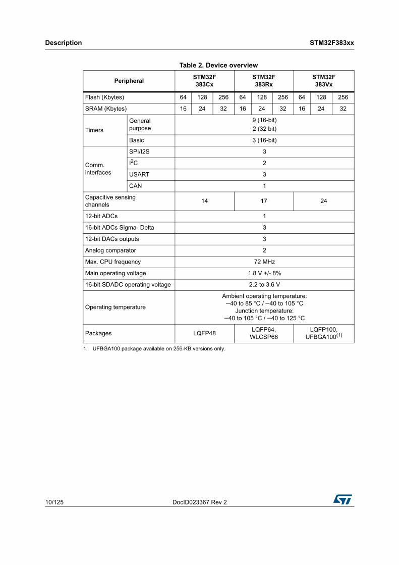
Table 2. Device overview
Peripheral STM32F383Cx
STM32F383Rx
STM32F383Vx
Flash (Kbytes) 64 128 256 64 128 256 64 128 256
SRAM (Kbytes) 16 24 32 16 24 32 16 24 32
TimersGeneralpurpose
9 (16-bit)2 (32 bit)
Basic 3 (16-bit)
Comm. interfaces
SPI/I2S 3
I2C 2
USART 3
CAN 1
Capacitive sensingchannels 14 17 24
12-bit ADCs 1
16-bit ADCs Sigma- Delta 3
12-bit DACs outputs 3
Analog comparator 2
Max. CPU frequency 72 MHz
Main operating voltage 1.8 V +/- 8%
16-bit SDADC operating voltage 2.2 to 3.6 V
Operating temperature
Ambient operating temperature: −40 to 85 °C / −40 to 105 °C
Junction temperature: −40 to 105 °C / −40 to 125 °C
Packages LQFP48 LQFP64,WLCSP66
LQFP100,UFBGA100(1)
1. UFBGA100 package available on 256-KB versions only.

DocID023367 Rev 2 11/125
STM32F383xx Description
47
Figure 1. Block diagram
1. AF: alternate function on I/O pins.2. Example given for STM32F383xx device.
PA[15:0]
EXT.IT
WWDG
NVIC
12-bit ADC
JTAG & SW
16 AINs
JTDIJTCK/SWCLKJTMS/SWDAT
JTRST
JTDONRESET
VDD=1.8V
XX AF
PB[15:14-10:0]
PC[15:0]
AHB to
CAN TX/CAN RX
MOSI,MISO,
SRAM
2x(8x16bit)
WKUP
fmax: 72 MHz
VSS
SCL,SDA,SMBAI2C2
VREF+
DMA1
TIM2
TIM3
XTAL OSC 4-32 MHz
XTAL 32kHz
OSCINOSCOUT
OSC32_OUTOSC32_IN
APB1
: F m
ax=
36 M
Hz
AHBPCLK
HCLKMANAGT
APBP1CLK
as AF
Flash up to 256KB
VDD18
POWER
Backup interface
as AF
Bus
Mat
rix
64 bit
Inte
rface
up to 32 KB
RTC
CORTEX M4 CPUIbus
Dbus
Pbus
obl
Flas
h
Trace Controller
USART1
USART2
SPI2/IS2
7 channels
Backupreg
SCL,SDA,SMBAI2C1 as AF
RX,TX, CTS, RTS,USART3
Temp sensor
VREF-
PD[15:0]
PE[15:0]
4 Channels, ETR
4 Channels, ETR
FCLK
RC LS
IWDG
@VDDIO
@VSW
SUPPLY
@VDDA
VDDAVSSA
VDD
SmartCard as AF
RX,TX, CTS, RTS,SmartCard as AF
RX,TX, CTS, RTS,SmartCard as AF
APB
2 : F
max
= 72
MH
z
NVIC
SPI1/I2S1MOSI,MISO,
SCK,NSS as AF
IF
@VDDA
SUPERVISIONReset
@VDDIO
AHB toAPB2 APB1
AWUANTI-TAMP
System
PF[7 bits]
SCK,NSS as AFMOSI,MISO,
2x(8x16bit)SPI3/I2S3 SCK,NSS as AF
RESET&CLOCKCTRL APBP2CLK
PLL
12-bit DAC1_OUT1IF
@VDDA
DAC1_OUT2 as AF
DAC1_OUT2 as AF
USARTCLKCECCLKADCCLK
SDADC
CRC
AHB
2
GPIO PORT A
GPIO PORT B
GPIO PORT C
GPIO PORT D
GPIO PORT E
GPIO PORT F
as AF
as AF
TIM 15
TIM 16
TIM 17
2 Channels,
1 Channels,
1 Channel,
1 Comp Channel,BRK as AF
1 Comp Channel,BRK as AF
1 Comp Channel,BRK as AF
HDMI CEC HDMI CEC as AF
DAC2_OUT1 as AF
TIM7
TIM6
TIM18
@VDDA
16-bit SDADC3
VREFSD+VREFSD-
IF
@VDDSD3
16-bit SDADC1 IF
@VDDSD12
16-bit SDADC2 IF
10 SDADC3 INs5 SDADC1 INs& 5 shared w/
5 SDADC2 INs.& 5 shared w/ SD1
VDDSD12VDDSD3
Touch Sensing Controller
8 Groups of4 channels max
TIM4 4 Channels, ETRas AF
TIM5 4 Channels, ETRas AF
bxCAN
DMA2
TIM 19 4 Channels, ETR
2 Channel, ETR
SRAM 512B
5 channels
TIM12
1 Channel as AFTIM13
TIM14 1 Channel as AF
as AF
VSSSD
SDADC2
as AF
as AF
1/2/3CLK
AH
B 1
: Fm
ax =
72
MH
z
12-bit DAC1_OUT2IF
12-bit DAC2_OUT1IF
NPOR
MS32158V1
COMP1
@VDD
COMP2
SYSCFG CTL
4 INs, 2 OUTs as AF
Functional overview STM32F383xx
12/125 DocID023367 Rev 2
3 Functional overview
3.1 ARM® Cortex™-M4 core with embedded Flash and SRAMThe ARM Cortex-M4 processor is the latest generation of ARM processors for embedded systems. It was developed to provide a low-cost platform that meets the needs of MCU implementation, with a reduced pin count and low-power consumption, while delivering outstanding computational performance and an advanced response to interrupts.
The ARM Cortex-M4 32-bit RISC processor features exceptional code-efficiency, delivering the high-performance expected from an ARM core in the memory size usually associated with 8- and 16-bit devices.
The processor supports a set of DSP instructions which allow efficient signal processing and complex algorithm execution.
Its single precision FPU speeds up software development by using metalanguage development tools, while avoiding saturation.
With its embedded ARM core, the STM32F383xx family is compatible with all ARM tools and software.
Figure 1 shows the general block diagram of the STM32F383xx family.
3.2 Memory protection unitThe memory protection unit (MPU) is used to separate the processing of tasks from the data protection. The MPU can manage up to 8 protection areas that can all be further divided up into 8 subareas. The protection area sizes are between 32 bytes and the whole 4 gigabytes of addressable memory.
The memory protection unit is especially helpful for applications where some critical or certified code has to be protected against the misbehavior of other tasks. It is usually managed by an RTOS (real-time operating system). If a program accesses a memory location that is prohibited by the MPU, the RTOS can detect it and take action. In an RTOS environment, the kernel can dynamically update the MPU area setting, based on the process to be executed.
The MPU is optional and can be bypassed for applications that do not need it.
The Cortex-M4 processor is a high performance 32-bit processor designed for the microcontroller market. It offers significant benefits to developers, including:• Outstanding processing performance combined with fast interrupt handling• Enhanced system debug with extensive breakpoint and trace capabilities• Efficient processor core, system and memories• Ultralow power consumption with integrated sleep modes• Platform security robustness with optional integrated memory protection unit (MPU).
With its embedded ARM core, the STM32F383xx devices are compatible with all ARM development tools and software.
DocID023367 Rev 2 13/125
STM32F383xx Functional overview
47
3.3 Embedded Flash memoryAll STM32F383xx devices feature up to 256 Kbytes of embedded Flash memory available for storing programs and data. The Flash memory access time is adjusted to the CPU clock frequency (0 wait state from 0 to 24 MHz, 1 wait state from 24 to 48 MHz and 2 wait states above).
3.4 Cyclic redundancy check (CRC) calculation unitThe CRC (cyclic redundancy check) calculation unit is used to get a CRC code using a configurable generator polynomial value and size.
Among other applications, CRC-based techniques are used to verify data transmission or storage integrity. In the scope of the EN/IEC 60335-1 standard, they offer a means of verifying the Flash memory integrity. The CRC calculation unit helps compute a signature of the software during runtime, to be compared with a reference signature generated at linktime and stored at a given memory location.
3.5 Embedded SRAMAll STM32F383xx devices feature up to 32 Kbytes of embedded SRAM with hardware parity check. The memory can be accessed in read/write at CPU clock speed with 0 wait states.
3.6 Boot modesAt startup, Boot0 pin and Boot1 option bit are used to select one of three boot options:• Boot from user Flash• Boot from system memory• Boot from embedded SRAM
The boot loader is located in system memory. It is used to reprogram the Flash memory by using USART1 (PA9/PA10), USART2 (PD5/PD6) or I2C (PB6/PB7).
3.7 Power management
3.7.1 Power supply schemes• VDD: external power supply for I/Os and core. It is provided externally through VDD pins,
and can be 1.8 V +/- 8%.• VDDA = 1.65 to 3.6 V:
– external analog power supplies for Reset blocks, RCs and PLL– supply voltage for 12-bit ADC, DACs and comparators (minimum voltage to be
applied to VDDA is 2.4 V when the 12-bit ADC and DAC are used).• VDDSD12 and VDDSD3 = 2.2 to 3.6 V: supply voltages for SDADC1/2 and SDADCD3
sigma delta ADCs. Independent from VDD/VDDA.• VBAT: must be always connected to VDD power supply.
Functional overview STM32F383xx
14/125 DocID023367 Rev 2
3.7.2 Power supply supervisorDevice power on reset is controlled through the external NPOR pin. The device remains in reset mode when NPOR is held low. NPOR pin has an internal pull-up resistor so the external driver can be open drain type.
To guarantee a proper power-on reset, the NPOR pin must be held low until VDD is stable.
When VDD is stable, the reset state can be exited by:• either putting the NPOR pin in high impedance. NPOR pin has an internal pull up.• or forcing the pin to high level by connecting it to VDDA.
3.7.3 Low-power modesThe STM32F383xx supports two low-power modes to achieve the best compromise between low power consumption, short startup time and available wakeup sources:• Sleep mode
In Sleep mode, only the CPU is stopped. All peripherals continue to operate and can wake up the CPU when an interrupt/event occurs.
• Stop modeStop mode achieves the lowest power consumption while retaining the content of SRAM and registers. All clocks in the 1.8 V domain are stopped, the PLL, the HSI RC and the HSE crystal oscillators are disabled. The device can be woken up from Stop mode by any of the EXTI line. The EXTI line source can be one of the 16 external lines, the PVD output, the USARTs, the I2Cs, the CEC and the RTC alarm.
3.8 Clocks and startupSystem clock selection is performed on startup, however the internal RC 8 MHz oscillator is selected as default CPU clock on reset. An external 4-32 MHz clock can be selected, in which case it is monitored for failure. If failure is detected, the system automatically switches back to the internal RC oscillator. A software interrupt is generated if enabled. Similarly, full interrupt management of the PLL clock entry is available when necessary (for example with failure of an indirectly used external oscillator).
Several prescalers allow to configure the AHB frequency, the high speed APB (APB2) and the low speed APB (APB1) domains. The maximum frequency of the AHB and the high speed APB domains is 72 MHz, while the maximum allowed frequency of the low speed APB domain is 36 MHz.
3.9 General-purpose input/outputs (GPIOs)Each of the GPIO pins can be configured by software as output (push-pull or open-drain), as input (with or without pull-up or pull-down) or as peripheral alternate function. Most of the GPIO pins are shared with digital or analog alternate functions. All GPIOs are high current capable except for analog inputs.
The I/Os alternate function configuration can be locked if needed following a specific sequence in order to avoid spurious writing to the I/Os registers.

DocID023367 Rev 2 15/125
STM32F383xx Functional overview
47
Do not reconfigure GPIO pins which are not present on 48 and 64 pin packages to the analog mode. Additional current consumption in the range of tens of µA per pin can be observed if VDDA is higher than VDDIO.
3.10 Direct memory access (DMA)The flexible 12-channel, general-purpose DMA is able to manage memory-to-memory, peripheral-to-memory and memory-to-peripheral transfers. The DMA controller supports circular buffer management, avoiding the generation of interrupts when the controller reaches the end of the buffer.
Each channel is connected to dedicated hardware DMA requests, with software trigger support for each channel. Configuration is done by software and transfer sizes between source and destination are independent.
The two DMAs can be used with the main peripherals: SPIs, I2Cs, USARTs, DACs, ADC, SDADCs, general-purpose timers.
3.11 Interrupts and events
3.11.1 Nested vectored interrupt controller (NVIC)The STM32F383xx devices embed a nested vectored interrupt controller (NVIC) able to handle up to 60 maskable interrupt channels and 16 priority levels.
The NVIC benefits are the following:• Closely coupled NVIC gives low latency interrupt processing• Interrupt entry vector table address passed directly to the core• Closely coupled NVIC core interface• Allows early processing of interrupts• Processing of late arriving higher priority interrupts• Support for tail chaining• Processor state automatically saved• Interrupt entry restored on interrupt exit with no instruction overhead
The NVIC hardware block provides flexible interrupt management features with minimal interrupt latency.
3.11.2 Extended interrupt/event controller (EXTI)The extended interrupt/event controller consists of 29 edge detector lines used to generate interrupt/event requests and wake-up the system. Each line can be independently configured to select the trigger event (rising edge, falling edge, both) and can be masked independently. A pending register maintains the status of the interrupt requests. The EXTI can detect an external line with a pulse width shorter than the internal clock period. Up to 84 GPIOs can be connected to the 16 external interrupt lines.

Functional overview STM32F383xx
16/125 DocID023367 Rev 2
3.12 12-bit analog-to-digital converter (ADC)The 12-bit analog-to-digital converter is based on a successive approximation register (SAR) architecture. It has up to 16 external channels (AIN15:0) and 3 internal channels (temperature sensor, voltage reference, VBAT voltage measurement) performing conversions in single-shot or scan modes. In scan mode, automatic conversion is performed on a selected group of analog inputs.
The ADC can be served by the DMA controller.
An analog watchdog feature allows very precise monitoring of the converted voltage of one, some or all selected channels. An interrupt is generated when the converted voltage is outside the programmed thresholds.
The events generated by the timers (TIMx) can be internally connected to the ADC start and injection trigger, respectively, to allow the application to synchronize A/D conversion and timers.
3.12.1 Temperature sensorThe temperature sensor (TS) generates a voltage VSENSE that varies linearly with temperature.
The temperature sensor is internally connected to the ADC_IN16 input channel which is used to convert the sensor output voltage into a digital value.
The sensor provides good linearity but it has to be calibrated to obtain good overall accuracy of the temperature measurement. As the offset of the temperature sensor varies from chip to chip due to process variation, the uncalibrated internal temperature sensor is suitable for applications that detect temperature changes only.
To improve the accuracy of the temperature sensor measurement, each device is individually factory-calibrated by ST. The temperature sensor factory calibration data are stored by ST in the system memory area, accessible in read-only mode. See Table 63: Temperature sensor calibration values on page 101.
3.12.2 Internal voltage reference (VREFINT)
The internal voltage reference (VREFINT) provides a stable (bandgap) voltage output for the ADC and Comparators. VREFINT is internally connected to the ADC_IN17 input channel. The precise voltage of VREFINT is individually measured for each part by ST during production test and stored in the system memory area. It is accessible in read-only mode.
3.12.3 VBAT battery voltage monitoring
This embedded hardware feature allows the application to measure the VBAT battery voltage using the internal ADC channel ADC_IN18. As the VBAT voltage may be higher than VDDA, and thus outside the ADC input range, the VBAT pin is internally connected to a divider by 2. As a consequence, the converted digital value is half the VBAT voltage.

DocID023367 Rev 2 17/125
STM32F383xx Functional overview
47
3.13 16-bit sigma delta analog-to-digital converters (SDADC)Up to three 16-bit sigma-delta analog-to-digital converters are embedded in the STM32F383xx. They have up to two separate supply voltages allowing the analog function voltage range to be independent from the STM32F383xx power supply. They share up to 21 input pins which may be configured in any combination of single-ended (up to 21) or differential inputs (up to 11).
The conversion speed is up to 16.6 ksps for each SDADC when converting multiple channels and up to 50 ksps per SDADC if single channel conversion is used. There are two conversion modes: single conversion mode or continuous mode, capable of automatically scanning any number of channels. The data can be automatically stored in a system RAM buffer, reducing the software overhead.
A timer triggering system can be used in order to control the start of conversion of the three SDADCs and/or the 12-bit fast ADC. This timing control is very flexible, capable of triggering simultaneous conversions or inserting a programmable delay between the ADCs.
Up to two external reference pins (VREFSD+, VREFSD-) and an internal 1.2/1.8 V reference can be used in conjunction with a programmable gain (x0.5 to x32) in order to fine-tune the input voltage range of the SDADC.
3.14 Digital-to-analog converter (DAC)The devices feature up to two 12-bit buffered DACs with three output channels that can be used to convert three digital signals into three analog voltage signal outputs. The internal structure is composed of integrated resistor strings and an amplifier in inverting configuration.
This digital Interface supports the following features:• Up to two DAC converters with three output channels:
– DAC1 with two output channels– DAC2 with one output channel.
• 8-bit or 10-bit monotonic output• Left or right data alignment in 12-bit mode• Synchronized update capability• Noise-wave generation• triangular-wave generation• Dual DAC channel independent or simultaneous conversions (DAC1 only)• DMA capability for each channel• External triggers for conversion
Functional overview STM32F383xx
18/125 DocID023367 Rev 2
3.15 Fast comparators (COMP)The STM32F383xx embeds up to 2 comparators with rail-to-rail inputs and high-speed output. The reference voltage can be internal or external (delivered by an I/O).
The threshold can be one of the following:• DACs channel outputs• External I/O• Internal reference voltage (VREFINT) or submultiple (1/4 VREFINT, 1/2 VREFINT and 3/4
VREFINT)
The comparators can be combined into a window comparator.
Both comparators can wake up the device from Stop mode and generate interrupts and breaks for the timers.
3.16 Touch sensing controller (TSC)The devices provide a simple solution for adding capacitive sensing functionality to any application. Capacitive sensing technology is able to detect the presence of a finger near an electrode which is protected from direct touch by a dielectric (glass, plastic, ...). The capacitive variation introduced by the finger (or any conductive object) is measured using a proven implementation based on a surface charge transfer acquisition principle. It consists of charging the electrode capacitance and then transferring a part of the accumulated charges into a sampling capacitor until the voltage across this capacitor has reached a specific threshold. To limit the CPU bandwidth usage this acquisition is directly managed by the hardware touch sensing controller and only requires few external components to operate.
The touch sensing controller is fully supported by the STMTouch touch sensing firmware library, which is free to use and allows touch sensing functionality to be implemented reliably in the end application.
Up to 24 touch sensing electrodes can be controlled by the TSC. The touch sensing I/Os are organized in 8 acquisition groups, with up to 4 I/Os in each group.
Table 3. Capacitive sensing GPIOs available on STM32F383xx devices
Group Capacitive sensing signal name Pin name Group Capacitive sensing
signal namePin
name
1
TSC_G1_IO1 PA0
5
TSC_G5_IO1 PB3
TSC_G1_IO2 PA1 TSC_G5_IO2 PB4
TSC_G1_IO3 PA2 TSC_G5_IO3 PB6
TSC_G1_IO4 PA3 TSC_G5_IO4 PB7
2
TSC_G2_IO1 PA4
6
TSC_G6_IO1 PB14
TSC_G2_IO2 PA5 TSC_G6_IO2 PB15
TSC_G2_IO3 PA6 TSC_G6_IO3 PD8
TSC_G2_IO4 PA7 TSC_G6_IO4 PD9
DocID023367 Rev 2 19/125
STM32F383xx Functional overview
47
3
TSC_G3_IO1 PC4
7
TSC_G7_IO1 PE2
TSC_G3_IO2 PC5 TSC_G7_IO2 PE3
TSC_G3_IO3 PB0 TSC_G7_IO3 PE4
TSC_G3_IO4 PB1 TSC_G7_IO4 PE5
4
TSC_G4_IO1 PA9
8
TSC_G8_IO1 PD12
TSC_G4_IO2 PA10 TSC_G8_IO2 PD13
TSC_G4_IO3 PA13 TSC_G8_IO3 PD14
TSC_G4_IO4 PA14 TSC_G8_IO4 PD15
Table 4. No. of capacitive sensing channels available on STM32F383xx devices
Analog I/O groupNumber of capacitive sensing channels
STM32F383Cx STM32F383Rx STM32F383Vx
G1 3 3 3
G2 2 3 3
G3 1 3 3
G4 3 3 3
G5 3 3 3
G6 2 2 3
G7 0 0 3
G8 0 0 3
Number of capacitive sensing channels 14 17 24
Table 3. Capacitive sensing GPIOs available on STM32F383xx devices (continued)
Group Capacitive sensing signal name Pin name Group Capacitive sensing
signal namePin
name

Functional overview STM32F383xx
20/125 DocID023367 Rev 2
3.17 Timers and watchdogsThe STM32F383xx includes two 32-bit and nine 16-bit general-purpose timers, three basic timers, two watchdog timers and a SysTick timer. The table below compares the features of the advanced control, general purpose and basic timers.
Table 5. Timer feature comparison
Timer type Timer Counter resolution
Counter type
Prescaler factor
DMA request generation
Capture/compare channels
Complemen-tary outputs
General-purpose
TIM2TIM5 32-bit Up, Down,
Up/Down
Any integer between 1 and 65536
Yes 4 0
General-purpose
TIM3, TIM4,TIM19
16-bit Up, Down, Up/Down
Any integer between 1 and 65536
Yes 4 0
General-purpose TIM12 16-bit Up
Any integer between 1 and 65536
No 2 0
General-purpose TIM15 16-bit Up
Any integer between 1 and 65536
Yes 2 1
General-purpose
TIM13,TIM14 16-bit Up
Any integer between 1 and 65536
No 1 0
General-purpose
TIM16,TIM17 16-bit Up
Any integer between 1 and 65536
Yes 1 1
BasicTIM6, TIM7,TIM18
16-bit UpAny integer between 1 and 65536
Yes 0 0

DocID023367 Rev 2 21/125
STM32F383xx Functional overview
47
3.17.1 General-purpose timers (TIM2 to TIM5, TIM12 to TIM17, TIM19)There are eleven synchronizable general-purpose timers embedded in the STM32F383xx (see Table 5 for differences). Each general-purpose timer can be used to generate PWM outputs, or act as a simple time base.• TIM2, 3, 4, 5 and 19
These five timers are full-featured general-purpose timers:– TIM2 and TIM5 have 32-bit auto-reload up/downcounters and 32-bit prescalers– TIM3, 4, and 19 have 16-bit auto-reload up/downcounters and 16-bit prescalersThese timers all feature 4 independent channels for input capture/output compare, PWM or one-pulse mode output. They can work together, or with the other general-purpose timers via the Timer Link feature for synchronization or event chaining.The counters can be frozen in debug mode.All have independent DMA request generation and support quadrature encoders.
• TIM12, 13, 14, 15, 16, 17These six timers general-purpose timers with mid-range features:They have 16-bit auto-reload upcounters and 16-bit prescalers.– TIM12 has 2 channels– TIM13 and TIM14 have 1 channel – TIM15 has 2 channels and 1 complementary channel– TIM16 and TIM17 have 1 channel and 1 complementary channelAll channels can be used for input capture/output compare, PWM or one-pulse mode output.The timers can work together via the Timer Link feature for synchronization or event chaining. The timers have independent DMA request generation.The counters can be frozen in debug mode.
3.17.2 Basic timers (TIM6, TIM7, TIM18)These timers are mainly used for DAC trigger generation. They can also be used as a generic 16-bit time base.

Functional overview STM32F383xx
22/125 DocID023367 Rev 2
3.17.3 Independent watchdog (IWDG)The independent watchdog is based on a 12-bit downcounter and 8-bit prescaler. It is clocked from an independent 40 kHz internal RC and as it operates independently from the main clock, it can operate in Stopmode. It can be used either as a watchdog to reset the device when a problem occurs, or as a free running timer for application timeout management. It is hardware or software configurable through the option bytes. The counter can be frozen in debug mode.
3.17.4 System window watchdog (WWDG)The system window watchdog is based on a 7-bit downcounter that can be set as free running. It can be used as a watchdog to reset the device when a problem occurs. It is clocked from the APB1 clock (PCLK1) derived from the main clock. It has an early warning interrupt capability and the counter can be frozen in debug mode.
3.17.5 SysTick timerThis timer is dedicated to real-time operating systems, but could also be used as a standard down counter. It features:• A 24-bit down counter• Autoreload capability• Maskable system interrupt generation when the counter reaches 0• Programmable clock source
3.18 Real-time clock (RTC) and backup registersThe RTC and the backup registers are supplied through VDDsupply pin. The backup registers are thirty two 32-bit registers used to store 128 bytes of user application data.
They are not reset by a system or power reset.
The RTC is an independent BCD timer/counter. Its main features are the following:• Calendar with subsecond, seconds, minutes, hours (12 or 24 format), week day, date,
month, year, in BCD (binary-coded decimal) format. • Automatic correction for 28th, 29th (leap year), 30th and 31st day of the month.• 2 programmable alarms with wake up from Stop mode capability. • Periodic wakeup unit with programmable resolution and period.• On-the-fly correction from 1 to 32767 RTC clock pulses. This can be used to
synchronize it with a master clock. • Digital calibration circuit with 1 ppm resolution, to compensate for quartz crystal
inaccuracy. • 3 anti-tamper detection pins with programmable filter. The MCU can be woken up from
Stop mode on tamper event detection.• Timestamp feature which can be used to save the calendar content. This function can
triggered by an event on the timestamp pin, or by a tamper event. The MCU can be woken up from Stop mode on timestamp event detection.
• Reference clock detection: a more precise second source clock (50 or 60 Hz) can be used to enhance the calendar precision.
DocID023367 Rev 2 23/125
STM32F383xx Functional overview
47
The RTC clock sources can be:• A 32.768 kHz external crystal• A resonator or oscillator• The internal low-power RC oscillator (typical frequency of 40 kHz) • The high-speed external clock divided by 32
3.19 Inter-integrated circuit interface (I2C)Up to two I2C bus interfaces can operate in multimaster and slave modes. They can support standard (up to 100 kHz), fast (up to 400 kHz) and fast mode + (up to 1 MHz) modes with 20 mA output drive. They support 7-bit and 10-bit addressing modes, multiple 7-bit slave addresses (2 addresses, 1 with configurable mask). They also include programmable analog and digital noise filters.
In addition, they provide hardware support for SMBUS 2.0 and PMBUS 1.1: ARP capability, Host notify protocol, hardware CRC (PEC) generation/verification, timeout verifications and ALERT protocol management. They also have a clock domain independent from the CPU clock, allowing the application to wake up the MCU from Stop mode on address match.
The I2C interfaces can be served by the DMA controller
Refer to Table 7 for the differences between I2C1 and I2C2.
Table 6. Comparison of I2C analog and digital filtersAnalog filter Digital filter
Pulse width of suppressed spikes ≥ 50 ns Programmable length from 1 to 15
I2C peripheral clocks
Benefits Available in Stop mode1. Extra filtering capability vs. standard requirements.2. Stable length
Drawbacks Variations depending on temperature, voltage, process
Wakeup from Stop on address match is not available when digital filter is enabled
Table 7. STM32F383xx I2C implementationI2C features(1)
1. X = supported.
I2C1 I2C2
7-bit addressing mode X X
10-bit addressing mode X X
Standard mode (up to 100 kbit/s) X X
Fast mode (up to 400 kbit/s) X X
Fast Mode Plus with 20mA output drive I/Os (up to 1 Mbit/s) X X
Independent clock X X
SMBus X X
Wakeup from STOP X X
Functional overview STM32F383xx
24/125 DocID023367 Rev 2
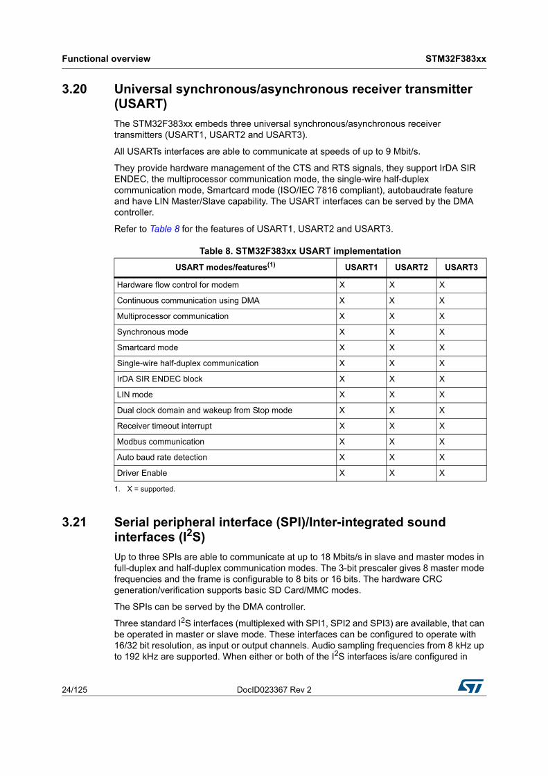
3.20 Universal synchronous/asynchronous receiver transmitter (USART)The STM32F383xx embeds three universal synchronous/asynchronous receiver transmitters (USART1, USART2 and USART3).
All USARTs interfaces are able to communicate at speeds of up to 9 Mbit/s.
They provide hardware management of the CTS and RTS signals, they support IrDA SIR ENDEC, the multiprocessor communication mode, the single-wire half-duplex communication mode, Smartcard mode (ISO/IEC 7816 compliant), autobaudrate feature and have LIN Master/Slave capability. The USART interfaces can be served by the DMA controller.
Refer to Table 8 for the features of USART1, USART2 and USART3.
3.21 Serial peripheral interface (SPI)/Inter-integrated sound interfaces (I2S)Up to three SPIs are able to communicate at up to 18 Mbits/s in slave and master modes in full-duplex and half-duplex communication modes. The 3-bit prescaler gives 8 master mode frequencies and the frame is configurable to 8 bits or 16 bits. The hardware CRC generation/verification supports basic SD Card/MMC modes.
The SPIs can be served by the DMA controller.
Three standard I2S interfaces (multiplexed with SPI1, SPI2 and SPI3) are available, that can be operated in master or slave mode. These interfaces can be configured to operate with 16/32 bit resolution, as input or output channels. Audio sampling frequencies from 8 kHz up to 192 kHz are supported. When either or both of the I2S interfaces is/are configured in
Table 8. STM32F383xx USART implementationUSART modes/features(1)
1. X = supported.
USART1 USART2 USART3
Hardware flow control for modem X X X
Continuous communication using DMA X X X
Multiprocessor communication X X X
Synchronous mode X X X
Smartcard mode X X X
Single-wire half-duplex communication X X X
IrDA SIR ENDEC block X X X
LIN mode X X X
Dual clock domain and wakeup from Stop mode X X X
Receiver timeout interrupt X X X
Modbus communication X X X
Auto baud rate detection X X X
Driver Enable X X X

DocID023367 Rev 2 25/125
STM32F383xx Functional overview
47
master mode, the master clock can be output to the external DAC/CODEC at 256 times the sampling frequency. All I2S interfaces can operate in half-duplex mode only.
Refer to Table 9 for the features between SPI1, SPI2 and SPI3.
3.22 High-definition multimedia interface (HDMI) - consumer electronics control (CEC)The device embeds a HDMI-CEC controller that provides hardware support for the Consumer Electronics Control (CEC) protocol (Supplement 1 to the HDMI standard).
This protocol provides high-level control functions between all audiovisual products in an environment. It is specified to operate at low speeds with minimum processing and memory overhead. It has a clock domain independent from the CPU clock, allowing the HDMI_CEC controller to wakeup the MCU from Stop mode on data reception.
3.23 Controller area network (CAN)The CAN is compliant with specifications 2.0A and B (active) with a bit rate up to 1 Mbit/s. It can receive and transmit standard frames with 11-bit identifiers as well as extended frames with 29-bit identifiers. It has three transmit mailboxes, two receive FIFOs with 3 stages and 14 scalable filter banks.
3.24 Serial wire JTAG debug port (SWJ-DP)The ARM SWJ-DP Interface is embedded, and is a combined JTAG and serial wire debug port that enables either a serial wire debug or a JTAG probe to be connected to the target.
The JTAG TMS and TCK pins are shared respectively with SWDIO and SWCLK and a specific sequence on the TMS pin is used to switch between JTAG-DP and SW-DP.
Table 9. STM32F383xx SPI/I2S implementationSPI features(1)
1. X = supported.
SPI1 SPI2 SPI3
Hardware CRC calculation X X X
Rx/Tx FIFO X X X
NSS pulse mode X X X
I2S mode X X X
TI mode X X X
I2S full-duplex mode
Functional overview STM32F383xx
26/125 DocID023367 Rev 2
3.25 Embedded trace macrocell™The ARM embedded trace macrocell provides a greater visibility of the instruction and data flow inside the CPU core by streaming compressed data at a very high rate from the STM32F383xx through a small number of ETM pins to an external hardware trace port analyzer (TPA) device. The TPA is connected to a host computer using USB, Ethernet, or any other high-speed channel. Real-time instruction and data flow activity can be recorded and then formatted for display on the host computer running debugger software. TPA hardware is commercially available from common development tool vendors. It operates with third party debugger software tools.
DocID023367 Rev 2 27/125
STM32F383xx Pinouts and pin description
47
4 Pinouts and pin description
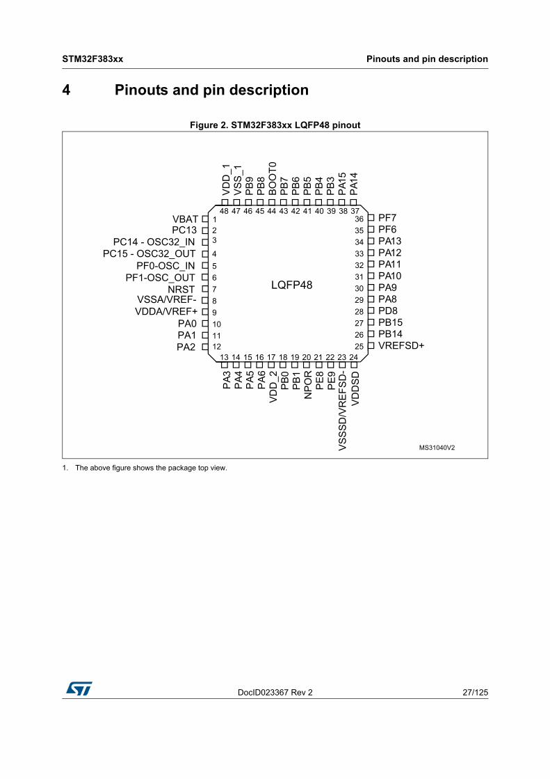
Figure 2. STM32F383xx LQFP48 pinout
1. The above figure shows the package top view.
48 47 46 45 44 43 42 41 40 39 38 37363534333231302928272625
13 14 15 16 21 22 23 2417 18 19 20
23
456 7 8 9 1011
VBAT
PC14 - OSC32_INPC15 - OSC32_OUT
NRSTVSSA/VREF-VDDA/VREF+
PA0PA1PA2
VD
D_1
VS
S_1
PB
9
PB
8
BO
OT0
PB
7
PB
6
PB
5P
B4
PB
3P
A15
PA1
4
PF7PF6PA13PA12PA11PA10PA9PA8PD8PB15PB14VREFSD+
PA3
PA4
PA 5
PA
6V
DD
_2PB
0PB
1N
PO
RP
E8
VS
SS
D/V
RE
FSD
-P
E9
VD
DS
D
PF0-OSC_INPF1-OSC_OUT
PC13
12
1
MS31040V2
LQFP48

Pinouts and pin description STM32F383xx
28/125 DocID023367 Rev 2
Figure 3. STM32F383xx LQFP64 pinout
1. The above figure shows the package top view.
64 63 62 61 60 59 58 57 56 55 54 53 52 51 50 4948474645444342414039383736353433
17 18 19 20 21 22 23 24 29 30 31 3225 26 27 28
123456 7 8 9 10111213141516
VBAT
PC14 - OSC32_INPC15 - OSC32_OUT
NRSTPC0PC1PC2PC3
VSSA/VREF-VDDA
PA0PA1PA2
VD
D_1
PB
9
PB
8
BO
OT0
PB
7
PB
6
PB
5
PB
4
PB
3
PD
2
PC
12P
C11
PC
10P
A15
PA1
4
PF7PF6PA13PA12PA11PA10PA9PA8PC9PC8PC7PC6PD8PB15PB14VREFSD+
PA
3V
RE
F+
VD
D_2 PA4
PA5
PA6
PA7
PC
4P
C5
PB0
PB1
NP
OR
PE
8
PF1 - OSC_OUTPF0 - OSC_IN
PC13
VS
S_1
PE
9V
SS
SD
/VR
EFS
D-
VD
DS
D
LQFP64
MS31041V2

DocID023367 Rev 2 29/125
STM32F383xx Pinouts and pin description
47
Figure 4. STM32F383xx LQFP100 pinout
100
99 98 97 96 95 94 93 92 91 90 89 88 87 86 85 84 83 82 81 80 79 78 77 76
12345678910111213141516171819202122232425
75747372717069686766656463626160595857565554535251
PE2PE3PE4PE5PE6VBAT
PC14 - OSC32_INPC15 - OSC32_OUT
PF9PF10
PF0-OSC_IN
NRSTPC0PC1PC2PC3PF2
VSSA/VREF-
VREF+VDDA
PA0PA1PA2
VDD_3VSS_3PF6PA13 PA12 PA11 PA10 PA9 PA8 PC9 PC8 PC7 PC6 PD15 PD14 PD13 PD12 PD11 PD10 PD9 PD8 PB15 PB14 VREFSD+ VDDSD3
PA3
PF4
VD
D_2 PA4
PA5
PA6
PA7
PC
4P
C5
PB
0P
B1
NP
OR
PE
7P
E8
PE
9P
E10
PE
11P
E12
PE
13P
E14
PE
15P
B10
VR
EFS
D-
VS
SS
DV
DD
SD
12
VD
D_1
VS
S_1
PE
1
PE
0
PB
9
PB
8
BO
OT0
P
B7
P
B6
P
B5
P
B4
P
B3
P
D7
P
D6
P
D5
P
D4
P
D3
P
D2
P
D1
P
D0
P
C12
P
C11
P
C10
PA
15
PA14
26 27 28 29 30 31 32 33 34 35 36 37 38 39 40 41 42 43 44 45 46 47 48 49 50
MS32161V1
LQFP100
PC13
PF1-OSC_OUT

Pinouts and pin description STM32F383xx
30/125 DocID023367 Rev 2
Figure 5. STM32F383xx BGA100 ballout
1. The above figure shows the package top view.
MS31121V2
A
B
E
D
C
F
G
H
J
K
L
M
PE3
PC15
PC14
PE4
PC0
PF2
VSSA/VREF-
VREF+
VDDA
PE1
PE5
PE2
PE6
VBAT
PF9
PF10
NRST
PC1
PC3
PA0
PA1
PB8
PE0
PB9
VSS_1
PF4
VDD_2
PC2
PA2
PA3
PA4
BOOT0
PB7
VDD_1
PA5
PA6
PA7
PD7
PB6
PB5
PC4
PC5
PB0
PD5
PD6
NPOR
PB1
PB4
PD4
PE8
PE7
PB3
PD3
PD2
PD9
PE10
PE9
PA15
PD1
PD0
PD8
PE12
PE11
PA14
PC12
PC11
PC8
PA9
PD15
PD12
PB15
PB10
PE13
PA13
PC10
PF6
PA8
PC7
PD14
PD11
PB14
VREFSD-
PE14
VSS_3
VDD_3
PA12
PA11
PA10
PC9
PC6
PD13
PD10
VREFSD+
VDDSD3
PE15
VSSSD
VDDSD12
PC13
PF0
PF1
DocID023367 Rev 2 31/125
STM32F383xx Pinouts and pin description
47
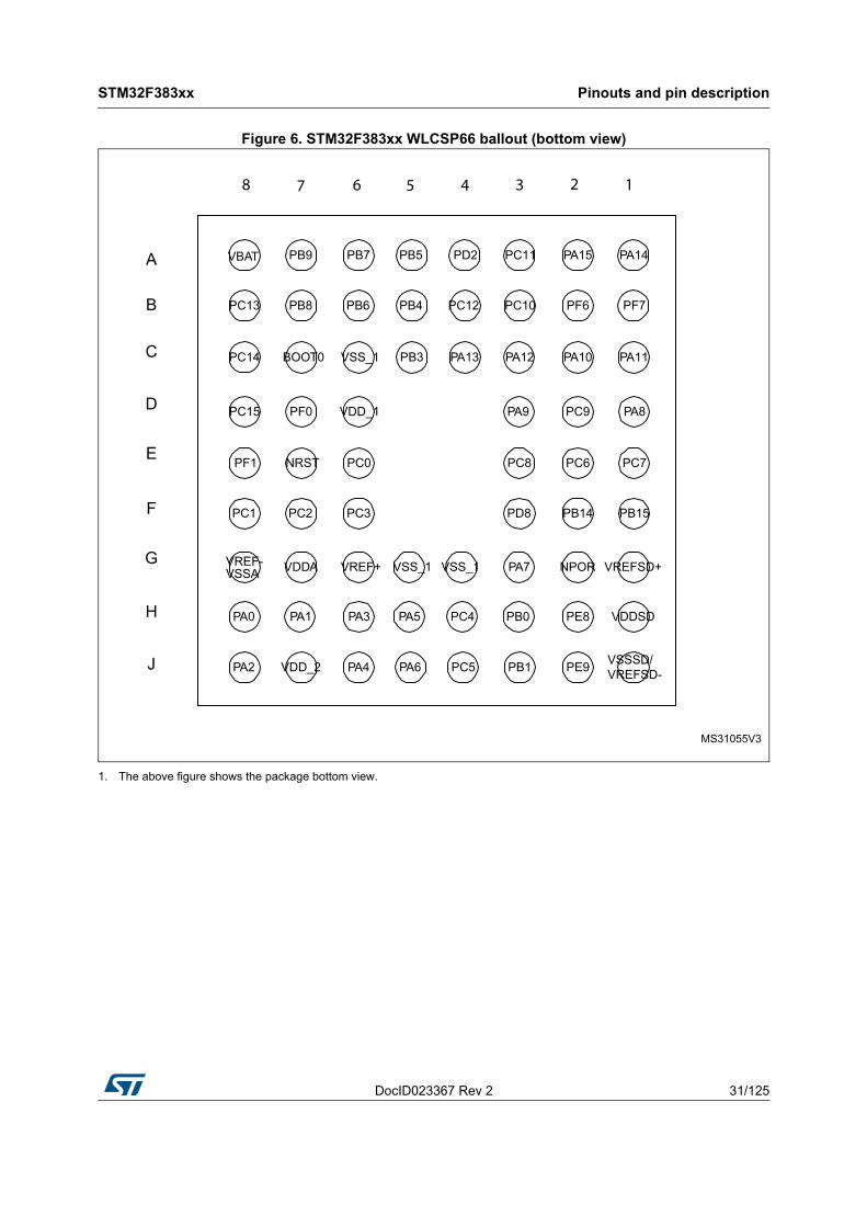
Figure 6. STM32F383xx WLCSP66 ballout (bottom view)
1. The above figure shows the package bottom view.
MS31055V3
A
B
E
D
C
F
G
H
J
VBAT
PF1
PC15
PC13
PA0
PA2
PB9
BOOT0
PB8
PF0
NRST
PC2
VDDA
PA1
VDD_2
PB7
PB6
VSS_1
PC0
PC3
VREF+
PA3
PB5
PB4
VDD_1
VSS_1
PA5
PA6
PD2
PC12
PA13
PC4
PC5
PC11
PC10
PA15
PF6
PA14
PF7
PA12
PA7
PB0
PB1
PC9
PC6
PA10
NPOR
PE8
PE9
PA11
PB15
VDDSD
VSSSD/VREFSD-
PB14
PA9
PC8
PD8
PA8
PC7
VREFSD+
PC14
PC1
VSSAVREF-
PA4
PB3
VSS_1

Pinouts and pin description STM32F383xx
32/125 DocID023367 Rev 2
Table 10. Legend/abbreviations used in the pinout tableName Abbreviation Definition
Pin name Unless otherwise specified in brackets below the pin name, the pin function during and after reset is the same as the actual pin name
Pin type
S Supply pin
I Input only pin
I/O Input / output pin
I/O structure
FT 5 V tolerant I/O
FTf 5 V tolerant I/O, FM+ capable
TTa 3.3 V tolerant I/O directly connected to ADC or SDADC
POR External power on reset pin with embedded weak pull-up resistor, powered from VDDA
TC Standard 3.3V I/O
B Dedicated BOOT0 pin
RST Bidirectional reset pin with embedded weak pull-up resistor
Notes Unless otherwise specified by a note, all I/Os are set as floating inputs during and after reset
Pin functions
Alternate functions Functions selected through GPIOx_AFR registers
Additional functions Functions directly selected/enabled through peripheral registers
DocID023367 Rev 2 33/125
STM32F383xx Pinouts and pin description
47
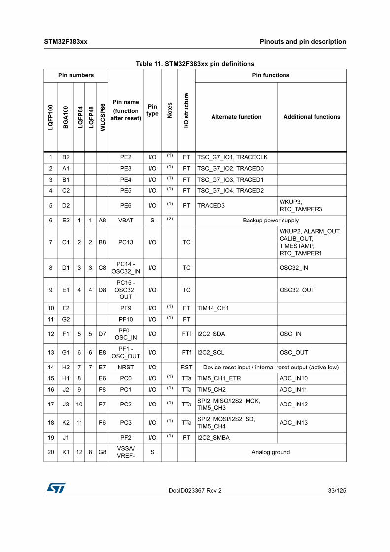
Table 11. STM32F383xx pin definitionsPin numbers
Pin name(function
after reset)
Pin type N
ote
s
I/O s
truc
ture
Pin functions
LQFP
100
BG
A10
0
LQFP
64
LQFP
48
WLC
SP66
Alternate function Additional functions
1 B2 PE2 I/O (1) FT TSC_G7_IO1, TRACECLK
2 A1 PE3 I/O (1) FT TSC_G7_IO2, TRACED0
3 B1 PE4 I/O (1) FT TSC_G7_IO3, TRACED1
4 C2 PE5 I/O (1) FT TSC_G7_IO4, TRACED2
5 D2 PE6 I/O (1) FT TRACED3 WKUP3, RTC_TAMPER3
6 E2 1 1 A8 VBAT S (2) Backup power supply
7 C1 2 2 B8 PC13 I/O TC
WKUP2, ALARM_OUT, CALIB_OUT, TIMESTAMP, RTC_TAMPER1
8 D1 3 3 C8 PC14 - OSC32_IN I/O TC OSC32_IN
9 E1 4 4 D8PC15 -
OSC32_OUT
I/O TC OSC32_OUT
10 F2 PF9 I/O (1) FT TIM14_CH1
11 G2 PF10 I/O (1) FT
12 F1 5 5 D7 PF0 - OSC_IN I/O FTf I2C2_SDA OSC_IN
13 G1 6 6 E8 PF1 - OSC_OUT I/O FTf I2C2_SCL OSC_OUT
14 H2 7 7 E7 NRST I/O RST Device reset input / internal reset output (active low)
15 H1 8 E6 PC0 I/O (1) TTa TIM5_CH1_ETR ADC_IN10
16 J2 9 F8 PC1 I/O (1) TTa TIM5_CH2 ADC_IN11
17 J3 10 F7 PC2 I/O (1) TTa SPI2_MISO/I2S2_MCK, TIM5_CH3 ADC_IN12
18 K2 11 F6 PC3 I/O (1) TTa SPI2_MOSI/I2S2_SD, TIM5_CH4 ADC_IN13
19 J1 PF2 I/O (1) FT I2C2_SMBA
20 K1 12 8 G8 VSSA/ VREF- S Analog ground
Pinouts and pin description STM32F383xx
34/125 DocID023367 Rev 2
9 VDDA/ VREF+ S (1) Analog power supply / Reference voltage for ADC,
COMP, DAC
21 M1 13 G7 VDDA S (1) Analog power supply
22 L1 17 G6 VREF+ S (1) Reference voltage for ADC, COMP, DAC
23 L2 14 10 H8 PA0 I/O TTa
USART2_CTS, TIM2_CH1_ETR, TIM5_CH1_ETR, TIM19_CH1, TSC_G1_IO1, COMP1_OUT
RTC_ TAMPER2, WKUP1, ADC_IN0, COMP1_INM
24 M2 15 11 H7 PA1 I/O TTa
SPI3_SCK/I2S3_CK,USART2_RTS, TIM2_CH2,TIM15_CH1N, TIM5_CH2,TIM19_CH2, TSC_G1_IO2, RTC_REF_IN
ADC_IN1, COMP1_INP
25 K3 16 12 J8 PA2 I/O TTa
COMP2_OUT, TSC_G1_IO3, SPI3_MISO/I2S3_MCK, USART2_TX, TIM2_CH3, TIM15_CH1, TIM5_CH3, TIM19_CH3
ADC_IN2,COMP2_INM
26 L3 18 13 H6 PA3 I/O TTa
SPI3_MOSI, I2S3_SD,USART2_RX, TIM2_CH4,TIM15_CH2, TIM5_CH4,TIM19_CH4, TSC_G1_IO4
ADC_IN3, COMP2_INP
27 E3 PF4 I/O (1) FT
28 H3 19 17 J7 VDD_2 S Digital power supply
29 M3 20 14 J6 PA4 I/O TTa
SPI1_NSS/I2S1_WS,SPI3_NSS/I2S3_WS, USART2_CK, TIM3_CH2,TIM12_CH1, TSC_G2_IO1, COMP1_OUT
ADC_IN4, DAC1_OUT1
30 K4 21 15 H5 PA5 I/O TTa
SPI1_SCK/I2S1_CK, CEC,TIM2_CH1_ETR, TIM14_CH1, TIM12_CH2, TSC_G2_IO2
ADC_IN5, DAC1_OUT2
31 L4 22 16 J5 PA6 I/O TTa
SPI1_MISO/I2S1_MCK,TIM3_CH1, TIM13_CH1, TIM16_CH1, COMP1_OUT,TSC_G2_IO3
ADC_IN6, DAC2_OUT1
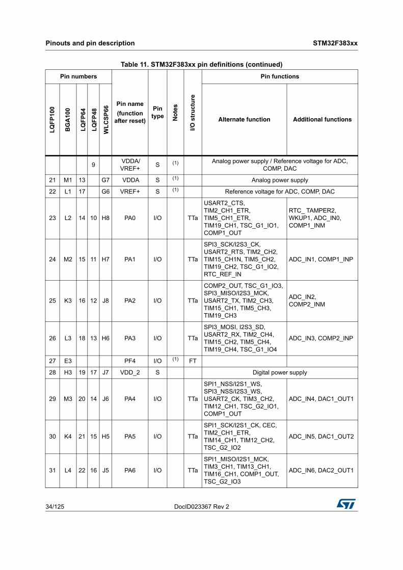
Table 11. STM32F383xx pin definitions (continued)Pin numbers
Pin name(function
after reset)
Pin type N
ote
s
I/O s
truc
ture
Pin functions
LQFP
100
BG
A10
0
LQFP
64
LQFP
48
WLC
SP66
Alternate function Additional functions
DocID023367 Rev 2 35/125
STM32F383xx Pinouts and pin description
47
32 M4 23 G3 PA7 I/O (1) TTa
SPI1_MOSI/I2S1_SD, TIM14_CH1, TIM17_CH1, TIM3_CH2, COMP2_OUT, TSC_G2_IO4
ADC_IN7
33 K5 24 H4 PC4 I/O (1) TTa USART1_TX, TIM13_CH1, TSC_G3_IO1 ADC_IN14
34 L5 25 J4 PC5 I/O (1) TTa USART1_RX, TSC_G3_IO2 ADC_IN15
35 M5 26 18 H3 PB0 I/O TTa SPI1_MOSI/I2S1_SD,TIM3_CH3, TSC_G3_IO3
ADC_IN8, SDADC1_AIN6P
36 M6 27 19 J3 PB1 I/O TTa TIM3_CH4, TSC_G3_IO4ADC_IN9, SDADC1_AIN5P, SDADC1_AIN6M
37 L6 28 20 G2 NPOR I (3) POR Power-on reset
38 M7 PE7 I/O (1)(4) TC
SDADC1_AIN3P,SDADC1_AIN4M,SDADC2_AIN5P, SDADC2_AIN6M
39 L7 29 21 H2 PE8 I/O (4) TC SDADC1_AIN8P,SDADC2_AIN8P
40 M8 30 22 J2 PE9 I/O (4) TC
SDADC1_AIN7P,SDADC1_AIN8M, SDADC2_AIN7P,SDADC2_AIN8M
41 L8 PE10 I/O(4)(1) TC SDADC1_AIN2P
42 M9 PE11 I/O (1)(4) TCSDADC1_AIN1P,SDADC1_AIN2M,SDADC2_AIN4P
43 L9 PE12 I/O (1)(4) TCSDADC1_AIN0P, SDADC2_AIN3P,SDADC2_AIN4M
44 M10 PE13 I/O (1)(4) TC SDADC1_AIN0M, SDADC2_AIN2P
45 M11 PE14 I/O (1)(4) TC SDADC2_AIN1P,SDADC2_AIN2M
46 M12 PE15 I/O (1)(4) TC USART3_RX SDADC2_AIN0P
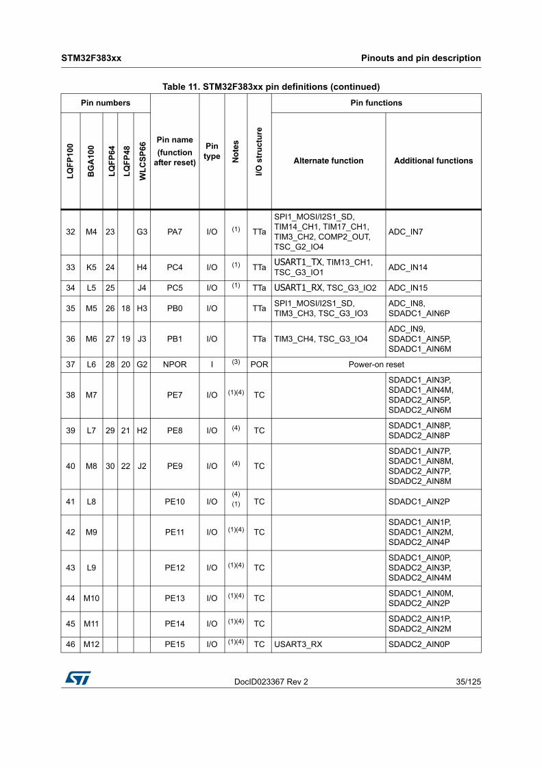
Table 11. STM32F383xx pin definitions (continued)Pin numbers
Pin name(function
after reset)
Pin type N
ote
s
I/O s
truc
ture
Pin functions
LQFP
100
BG
A10
0
LQFP
64
LQFP
48
WLC
SP66
Alternate function Additional functions
Pinouts and pin description STM32F383xx
36/125 DocID023367 Rev 2
47 L10 PB10 I/O (1)(4) TC SPI2_SCK/I2S2_CK, CEC, USART3_TX, TSC_SYNC
TIM2_CH3, SDADC2_AIN0M
48 L11 VREFSD- S (1) External reference voltage for SDADC1, SDADC2, SDADC3 (negative input)
49 F12 VSSSD S (1) SDADC1, SDADC2, SDADC3 ground
31 23 J1 VSSSD/ VREFSD- S
SDADC1, SDADC2, SDADC3 ground / External reference voltage for SDADC1, SDADC2, SDADC3
(negative input)
50 G12 VDDSD12 S (1) SDADC1 and SDADC2 power supply
32 24 H1 VDDSD S SDADC1, SDADC2, SDADC3 power supply
51 L12 VDDSD3 S (1) SDADC3 power supply
52 K12 33 25 G1 VREFSD+ S External reference voltage for SDADC1, SDADC2, SDADC3 (positive input)
53 K11 34 26 F2 PB14 I/O (5) TCSPI2_MISO/I2S2_MCK,USART3_RTS, TIM15_CH1, TIM12_CH1, TSC_G6_IO1
SDADC3_AIN8P
54 K10 35 27 F1 PB15 I/O (5) TC
SPI2_MOSI/I2S2_SD,TIM15_CH1N, TIM15_CH2, TIM12_CH2, TSC_G6_IO2, RTC_REFIN
SDADC3_AIN7P, SDADC3_AIN8M
55 K9 36 28 F3 PD8 I/O (5) TC SPI2_SCK/I2S2_CK, USART3_TX, TSC_G6_IO3 SDADC3_AIN6P
56 K8 PD9 I/O(5)(1) TC USART3_RX, TSC_G6_IO4 SDADC3_AIN5P,
SDADC3_AIN6M
57 J12 PD10 I/O (1)(5) TC USART3_CK SDADC3_AIN4P
58 J11 PD11 I/O (1)(5) TC USART3_CTS SDADC3_AIN3P, SDADC3_AIN4M
59 J10 PD12 I/O (1)(5) TC USART3_RTS, TIM4_CH1, TSC_G8_IO1 SDADC3_AIN2P
60 H12 PD13 I/O (1)(5) TC TIM4_CH2, TSC_G8_IO2 SDADC3_AIN1P, SDADC3_AIN2M
61 H11 PD14 I/O (1)(5) TC TIM4_CH3, TSC_G8_IO3 SDADC3_AIN0P
62 H10 PD15 I/O (1)(5) TC TIM4_CH4, TSC_G8_IO4 SDADC3_AIN0M
Table 11. STM32F383xx pin definitions (continued)Pin numbers
Pin name(function
after reset)
Pin type N
ote
s
I/O s
truc
ture
Pin functions
LQFP
100
BG
A10
0
LQFP
64
LQFP
48
WLC
SP66
Alternate function Additional functions

DocID023367 Rev 2 37/125
STM32F383xx Pinouts and pin description
47
63 E12 37 E2 PC6 I/O (1) FT SPI1_NSS/I2S1_WS, TIM3_CH1
64 E11 38 E1 PC7 I/O (1) FT SPI1_SCK/I2S1_CK, TIM3_CH2
65 E10 39 E3 PC8 I/O (1) FT SPI1_MISO/I2S1_MCK, TIM3_CH3
66 D12 40 D2 PC9 I/O (1) FT SPI1_MOSI/I2S1_SD,TIM3_CH4
67 D11 41 29 D1 PA8 I/O FT
SPI2_SCK/I2S2_CK,I2C2_SMBA, USART1_CK, TIM4_ETR, TIM5_CH1_ETR, CLK_CLKOUT
68 D10 42 30 D3 PA9 I/O FTf
SPI2_MISO/I2S2_MCK,I2C2_SCL, USART1_TX, TIM2_CH3, TIM15_BKIN,TIM13_CH1, TSC_G4_IO1
69 C12 43 31 C2 PA10 I/O FTf
SPI2_MOSI/I2S2_SD,I2C2_SDA, USART1_RX,TIM2_CH4, TIM17_BKIN, TIM14_CH1, TSC_G4_IO2
70 B12 44 32 C1 PA11 I/O FT
SPI2_NSS/I2S2_WS, SPI1_NSS/I2S1_WS, USART1_CTS, CAN_RX, TIM4_CH1, TIM5_CH2, COMP1_OUT
71 A12 45 33 C3 PA12 I/O FT
SPI1_SCK/I2S1_CK, USART1_RTS, CAN_TX, TIM16_CH1, TIM4_CH2, TIM5_CH3, COMP2_OUT
72 A11 46 34 C4 PA13 I/O FT
SPI1_MISO/I2S1_MCK,USART3_CTS, IR_OUT, TIM16_CH1N, TIM4_CH3,TIM5_CH4, G4_IO3, SWDIO-JTMS
73 C11 47 35 B2 PF6 I/O FTfSPI1_MOSI, I2S1_SD,USART3_RTS, TIM4_CH4, I2C2_SCL
74 F11 VSS_3 S (1) Ground
Table 11. STM32F383xx pin definitions (continued)Pin numbers
Pin name(function
after reset)
Pin type N
ote
s
I/O s
truc
ture
Pin functions
LQFP
100
BG
A10
0
LQFP
64
LQFP
48
WLC
SP66
Alternate function Additional functions
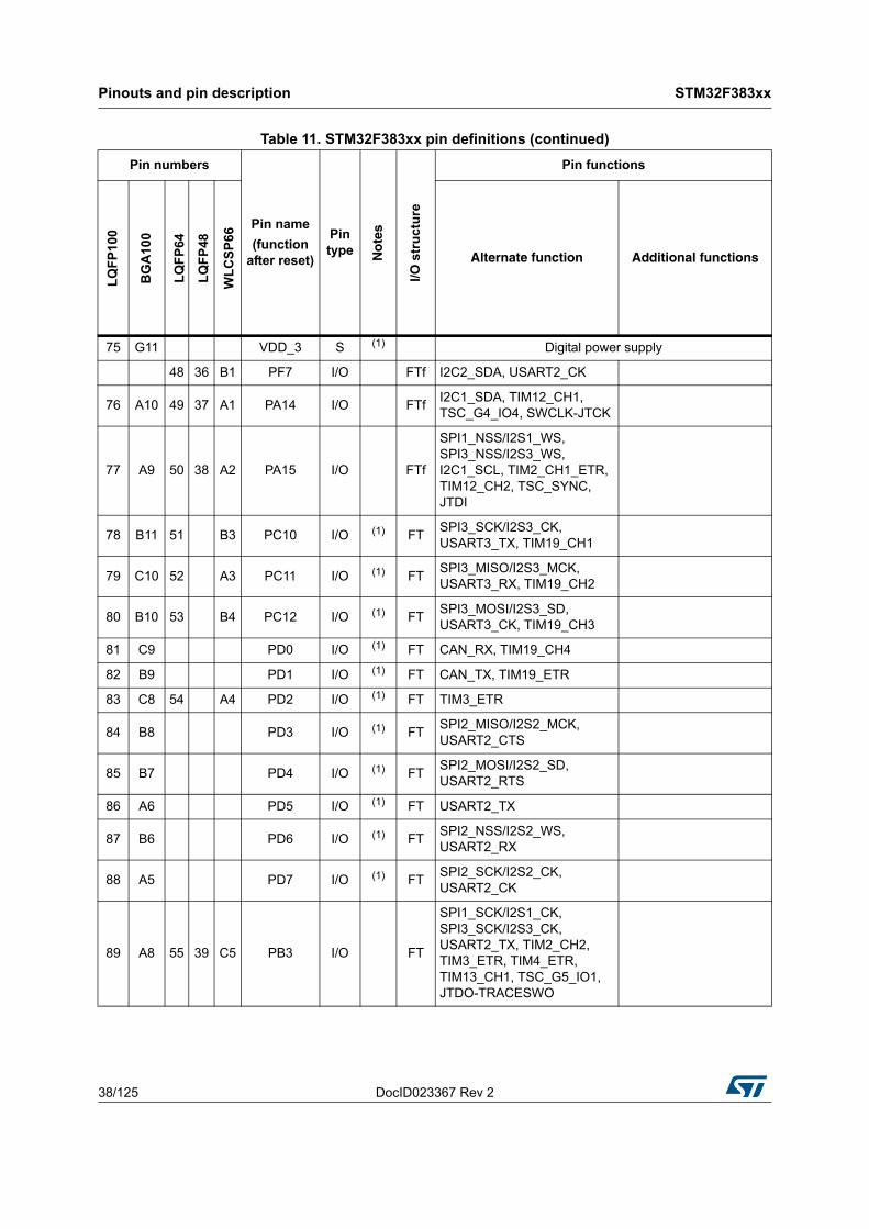
Pinouts and pin description STM32F383xx
38/125 DocID023367 Rev 2
75 G11 VDD_3 S (1) Digital power supply
48 36 B1 PF7 I/O FTf I2C2_SDA, USART2_CK
76 A10 49 37 A1 PA14 I/O FTf I2C1_SDA, TIM12_CH1, TSC_G4_IO4, SWCLK-JTCK
77 A9 50 38 A2 PA15 I/O FTf
SPI1_NSS/I2S1_WS, SPI3_NSS/I2S3_WS, I2C1_SCL, TIM2_CH1_ETR, TIM12_CH2, TSC_SYNC, JTDI
78 B11 51 B3 PC10 I/O (1) FT SPI3_SCK/I2S3_CK,USART3_TX, TIM19_CH1
79 C10 52 A3 PC11 I/O (1) FT SPI3_MISO/I2S3_MCK,USART3_RX, TIM19_CH2
80 B10 53 B4 PC12 I/O (1) FT SPI3_MOSI/I2S3_SD,USART3_CK, TIM19_CH3
81 C9 PD0 I/O (1) FT CAN_RX, TIM19_CH4
82 B9 PD1 I/O (1) FT CAN_TX, TIM19_ETR
83 C8 54 A4 PD2 I/O (1) FT TIM3_ETR
84 B8 PD3 I/O (1) FT SPI2_MISO/I2S2_MCK,USART2_CTS
85 B7 PD4 I/O (1) FT SPI2_MOSI/I2S2_SD,USART2_RTS
86 A6 PD5 I/O (1) FT USART2_TX
87 B6 PD6 I/O (1) FT SPI2_NSS/I2S2_WS,USART2_RX
88 A5 PD7 I/O (1) FT SPI2_SCK/I2S2_CK,USART2_CK
89 A8 55 39 C5 PB3 I/O FT
SPI1_SCK/I2S1_CK, SPI3_SCK/I2S3_CK, USART2_TX, TIM2_CH2, TIM3_ETR, TIM4_ETR, TIM13_CH1, TSC_G5_IO1, JTDO-TRACESWO
Table 11. STM32F383xx pin definitions (continued)Pin numbers
Pin name(function
after reset)
Pin type N
ote
s
I/O s
truc
ture
Pin functions
LQFP
100
BG
A10
0
LQFP
64
LQFP
48
WLC
SP66
Alternate function Additional functions

DocID023367 Rev 2 39/125
STM32F383xx Pinouts and pin description
47
90 A7 56 40 B5 PB4 I/O FT
SPI1_MISO/I2S1_MCK, SPI3_MISO/I2S3_MCK, USART2_RX, TIM162_CH1, TIM3_CH1, TIM17_BKIN, TIM15_CH1N, TSC_G5_IO2, NJTRST
91 C5 57 41 A5 PB5 I/O FT
SPI1_MOSI/I2S1_SD, SPI3_MOSI/I2S3_SD, I2C1_SMBA, USART2_CK, TIM16_BKIN, TIM3_CH2, TIM17_CH1, TIM19_ETR
92 B5 58 42 B6 PB6 I/O FTf
I2C1_SCL, USART1_TX, TIM16_CH1N, TIM3_CH3, TIM4_CH1, TIM19_CH1, TIM15_CH1, TSC_G5_IO3
93 B4 59 43 A6 PB7 I/O FTf
I2C1_SDA, USART1_RX,TIM17_CH1N, TIM3_CH4, TIM4_CH2, TIM19_CH2, TIM15_CH2, TSC_G5_IO4
94 A4 60 44 C7 BOOT0 I B Boot memory selection
95 A3 61 45 B7 PB8 I/O FTf
SPI2_SCK/I2S2_CK, I2C1_SCL, USART3_TX, CAN_RX, CEC, TIM16_CH1, TIM4_CH3, TIM19_CH3, COMP1_OUT, TSC_SYNC
96 B3 62 46 A7 PB9 I/O FTf
SPI2_NSS/I2S2_WS, I2C1_SDA, USART3_RX, CAN_TX, IR_OUT, TIM17_CH1, TIM4_CH4,TIM19_CH4, COMP2_OUT
97 C3 PE0 I/O (1) FT USART1_TX, TIM4_ETR
98 A2 PE1 I/O (1) FT USART1_RX
99 D3 63 47 C6 VSS_1 S Ground
G5 VSS_1 S (1) Ground
G4 VSS_1 S (1) Ground
100 C4 64 48 D6 VDD_1 S Digital power supply
Table 11. STM32F383xx pin definitions (continued)Pin numbers
Pin name(function
after reset)
Pin type N
ote
s
I/O s
truc
ture
Pin functions
LQFP
100
BG
A10
0
LQFP
64
LQFP
48
WLC
SP66
Alternate function Additional functions

Pinouts and pin description STM32F383xx
40/125 DocID023367 Rev 2
1. When using the small packages (48 and 64 pin packages), the GPIO pins which are not present on these packages, must not be configured in analog mode.
2. VBAT pin must be connected to VDD supply.
3. These pins are powered by VDDA.
4. These pins are powered by VDDSD12.
5. These pins are powered by VDDSD3.
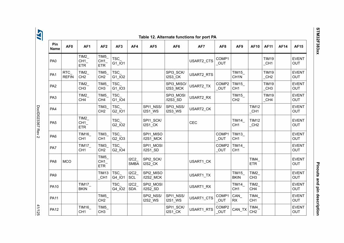
STM32F383xx
Pinouts and pin description
DocID
023367 Rev 2
41/125
Table 12. Alternate functions for port PAPin
Name AF0 AF1 AF2 AF3 AF4 AF5 AF6 AF7 AF8 AF9 AF10 AF11 AF14 AF15
PA0TIM2_CH1_ETR
TIM5_CH1_ETR
TSC_G1_IO1 USART2_CTS COMP1
_OUTTIM19_CH1
EVENTOUT
PA1 RTC_REFIN
TIM2_CH2
TIM5_CH2
TSC_G1_IO2
SPI3_SCK/ I2S3_CK USART2_RTS TIM15_
CH1NTIM19_CH2
EVENTOUT
PA2 TIM2_CH3
TIM5_CH3
TSC_G1_IO3
SPI3_MISO/ I2S3_MCK USART2_TX COMP2
_OUTTIM15_CH1
TIM19_CH3
EVENTOUT
PA3 TIM2_CH4
TIM5_CH4
TSC_G1_IO4
SPI3_MOSI /I2S3_SD USART2_RX TIM15_
CH2TIM19_CH4
EVENTOUT
PA4 TIM3_CH2
TSC_G2_IO1
SPI1_NSS/ I2S1_WS
SPI3_NSS/ I2S3_WS USART2_CK TIM12
_CH1EVENTOUT
PA5TIM2_CH1_ETR
TSC_G2_IO2
SPI1_SCK/ I2S1_CK CEC TIM14_
CH1TIM12_CH2
EVENTOUT
PA6 TIM16_CH1
TIM3_CH1
TSC_G2_IO3
SPI1_MISO /I2S1_MCK
COMP1_OUT
TIM13_CH1
EVENTOUT
PA7 TIM17_CH1
TIM3_CH2
TSC_G2_IO4
SPI1_MOSI /I2S1_SD
COMP2_OUT
TIM14_CH1
EVENTOUT
PA8 MCOTIM5_CH1_ETR
I2C2_SMBA
SPI2_SCK/ I2S2_CK USART1_CK TIM4_
ETREVENTOUT
PA9 TIM13_CH1
TSC_G4_IO1
I2C2_SCL
SPI2_MISO /I2S2_MCK USART1_TX TIM15_
BKINTIM2_CH3
EVENTOUT
PA10 TIM17_BKIN
TSC_G4_IO2
I2C2_SDA
SPI2_MOSI /I2S2_SD USART1_RX TIM14_
CH1TIM2_CH4
EVENTOUT
PA11 TIM5_CH2
SPI2_NSS/ I2S2_WS
SPI1_NSS/ I2S1_WS USART1_CTS COMP1
_OUTCAN_RX
TIM4_CH1
EVENTOUT
PA12 TIM16_CH1
TIM5_CH3
SPI1_SCK/ I2S1_CK USART1_RTS COMP2
_OUT CAN_TX TIM4_CH2
EVENTOUT
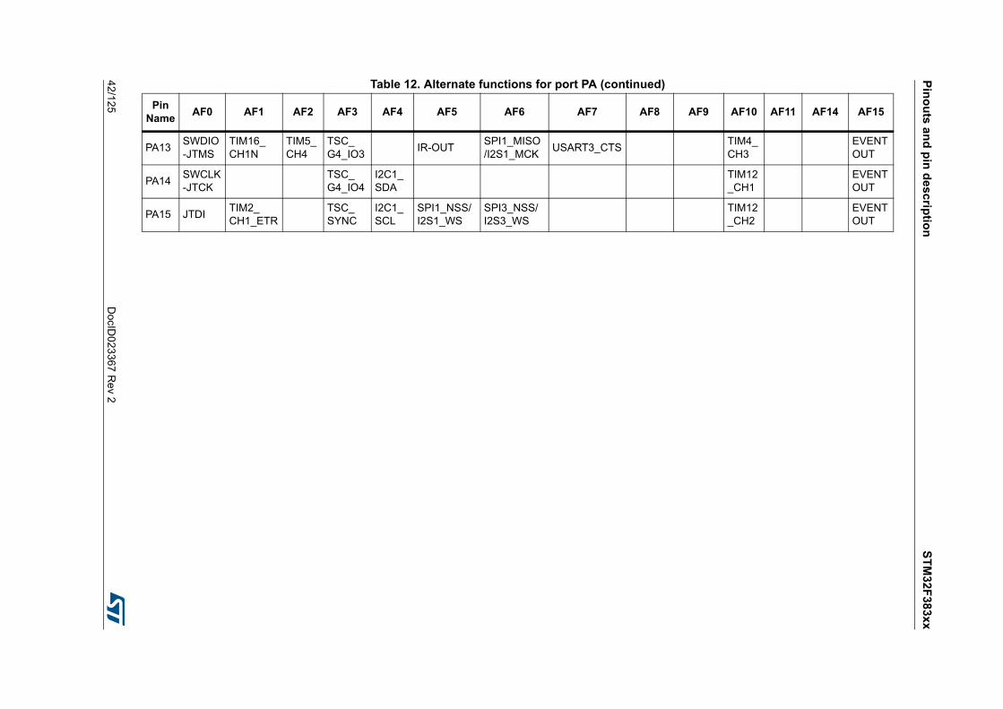
Pinouts and pin descriptionSTM
32F383xx
42/125D
ocID023367 R
ev 2
PA13 SWDIO-JTMS
TIM16_CH1N
TIM5_CH4
TSC_G4_IO3 IR-OUT SPI1_MISO
/I2S1_MCK USART3_CTS TIM4_CH3
EVENTOUT
PA14 SWCLK-JTCK
TSC_G4_IO4
I2C1_SDA
TIM12_CH1
EVENTOUT
PA15 JTDI TIM2_CH1_ETR
TSC_SYNC
I2C1_SCL
SPI1_NSS/ I2S1_WS
SPI3_NSS/ I2S3_WS
TIM12_CH2
EVENTOUT
Table 12. Alternate functions for port PA (continued)Pin
Name AF0 AF1 AF2 AF3 AF4 AF5 AF6 AF7 AF8 AF9 AF10 AF11 AF14 AF15
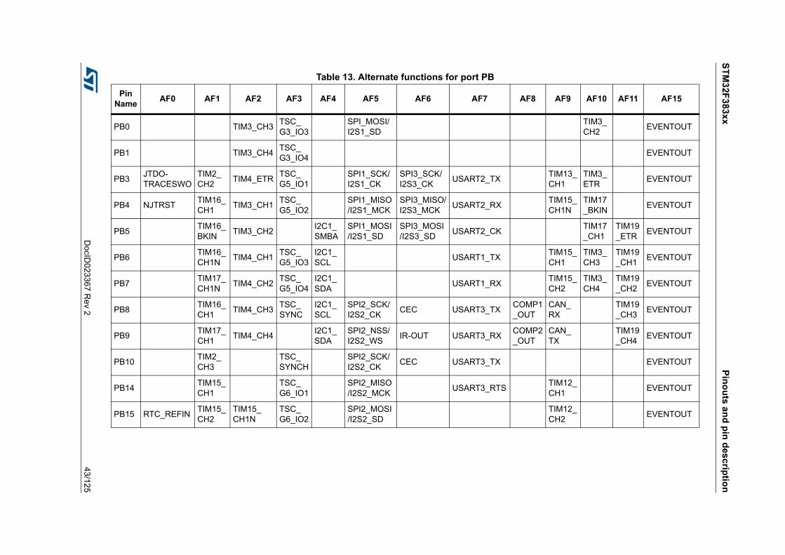
STM32F383xx
Pinouts and pin description
DocID
023367 Rev 2
43/125
Table 13. Alternate functions for port PBPin
Name AF0 AF1 AF2 AF3 AF4 AF5 AF6 AF7 AF8 AF9 AF10 AF11 AF15
PB0 TIM3_CH3 TSC_G3_IO3
SPI_MOSI/ I2S1_SD
TIM3_CH2 EVENTOUT
PB1 TIM3_CH4 TSC_G3_IO4 EVENTOUT
PB3 JTDO-TRACESWO
TIM2_CH2 TIM4_ETR TSC_
G5_IO1SPI1_SCK/ I2S1_CK
SPI3_SCK/ I2S3_CK USART2_TX TIM13_
CH1TIM3_ETR EVENTOUT
PB4 NJTRST TIM16_CH1 TIM3_CH1 TSC_
G5_IO2SPI1_MISO /I2S1_MCK
SPI3_MISO/ I2S3_MCK USART2_RX TIM15_
CH1NTIM17_BKIN EVENTOUT
PB5 TIM16_BKIN TIM3_CH2 I2C1_
SMBASPI1_MOSI /I2S1_SD
SPI3_MOSI /I2S3_SD USART2_CK TIM17
_CH1TIM19_ETR EVENTOUT
PB6 TIM16_CH1N TIM4_CH1 TSC_
G5_IO3I2C1_SCL USART1_TX TIM15_
CH1TIM3_CH3
TIM19_CH1 EVENTOUT
PB7 TIM17_CH1N TIM4_CH2 TSC_
G5_IO4I2C1_SDA USART1_RX TIM15_
CH2TIM3_CH4
TIM19_CH2 EVENTOUT
PB8 TIM16_CH1 TIM4_CH3 TSC_
SYNCI2C1_SCL
SPI2_SCK/ I2S2_CK CEC USART3_TX COMP1
_OUTCAN_RX
TIM19_CH3 EVENTOUT
PB9 TIM17_CH1 TIM4_CH4 I2C1_
SDASPI2_NSS/ I2S2_WS IR-OUT USART3_RX COMP2
_OUTCAN_TX
TIM19_CH4 EVENTOUT
PB10 TIM2_CH3
TSC_SYNCH
SPI2_SCK/ I2S2_CK CEC USART3_TX EVENTOUT
PB14 TIM15_CH1
TSC_G6_IO1
SPI2_MISO /I2S2_MCK USART3_RTS TIM12_
CH1 EVENTOUT
PB15 RTC_REFIN TIM15_CH2
TIM15_CH1N
TSC_G6_IO2
SPI2_MOSI /I2S2_SD
TIM12_CH2 EVENTOUT

Pinouts and pin descriptionSTM
32F383xx
44/125D
ocID023367 R
ev 2
Table 14. Alternate functions for port PCPin Name AF0 AF1 AF2 AF3 AF4 AF5 AF6 AF7
PC0 EVENTOUT TIM5_CH1_ETR
PC1 EVENTOUT TIM5_CH2
PC2 EVENTOUT TIM5_CH3 SPI2_MISO/I2S2_MCK
PC3 EVENTOUT TIM5_CH4 SPI2_MOSI/I2S2_SD
PC4 EVENTOUT TIM13_CH1 TSC_G3_IO1 USART1_TX
PC5 EVENTOUT TSC_G3_IO2 USART1_RX
PC6 EVENTOUT TIM3_CH1 SPI1_NSS/I2S1_WS
PC7 EVENTOUT TIM3_CH2 SPI1_SCK/I2S1_CK
PC8 EVENTOUT TIM3_CH3 SPI1_MISO/I2S1_MCK
PC9 EVENTOUT TIM3_CH4 SPI1_MOSI/I2S1_SD
PC10 EVENTOUT TIM19_CH1 SPI3_SCK/I2S3_CK USART3_TX
PC11 EVENTOUT TIM19_CH2 SPI3_MISO/I2S3_MCK USART3_RX
PC12 EVENTOUT TIM19_CH3 SPI3_MOSI/I2S3_SD USART3_CK
PC13
PC14
PC15
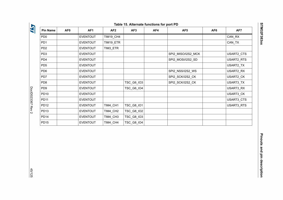
STM32F383xx
Pinouts and pin description
DocID
023367 Rev 2
45/125
Table 15. Alternate functions for port PDPin Name AF0 AF1 AF2 AF3 AF4 AF5 AF6 AF7
PD0 EVENTOUT TIM19_CH4 CAN_RX
PD1 EVENTOUT TIM19_ETR CAN_TX
PD2 EVENTOUT TIM3_ETR
PD3 EVENTOUT SPI2_MISO/I2S2_MCK USART2_CTS
PD4 EVENTOUT SPI2_MOSI/I2S2_SD USART2_RTS
PD5 EVENTOUT USART2_TX
PD6 EVENTOUT SPI2_NSS/I2S2_WS USART2_RX
PD7 EVENTOUT SPI2_SCK/I2S2_CK USART2_CK
PD8 EVENTOUT TSC_G6_IO3 SPI2_SCK/I2S2_CK USART3_TX
PD9 EVENTOUT TSC_G6_IO4 USART3_RX
PD10 EVENTOUT USART3_CK
PD11 EVENTOUT USART3_CTS
PD12 EVENTOUT TIM4_CH1 TSC_G8_IO1 USART3_RTS
PD13 EVENTOUT TIM4_CH2 TSC_G8_IO2
PD14 EVENTOUT TIM4_CH3 TSC_G8_IO3
PD15 EVENTOUT TIM4_CH4 TSC_G8_IO4
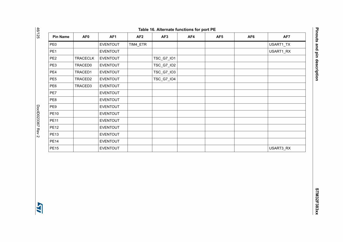
Pinouts and pin descriptionSTM
32F383xx
46/125D
ocID023367 R
ev 2
Table 16. Alternate functions for port PEPin Name AF0 AF1 AF2 AF3 AF4 AF5 AF6 AF7
PE0 EVENTOUT TIM4_ETR USART1_TX
PE1 EVENTOUT USART1_RX
PE2 TRACECLK EVENTOUT TSC_G7_IO1
PE3 TRACED0 EVENTOUT TSC_G7_IO2
PE4 TRACED1 EVENTOUT TSC_G7_IO3
PE5 TRACED2 EVENTOUT TSC_G7_IO4
PE6 TRACED3 EVENTOUT
PE7 EVENTOUT
PE8 EVENTOUT
PE9 EVENTOUT
PE10 EVENTOUT
PE11 EVENTOUT
PE12 EVENTOUT
PE13 EVENTOUT
PE14 EVENTOUT
PE15 EVENTOUT USART3_RX

STM32F383xx
Pinouts and pin description
DocID
023367 Rev 2
47/125
Table 17. Alternate functions for port PFPin Name AF0 AF1 AF2 AF3 AF4 AF5 AF6 AF7
PF0 I2C2_SDA
PF1 I2C2_SCL
PF2 EVENTOUT I2C2_SMBA
PF4 EVENTOUT
PF6 EVENTOUT TIM4_CH4 I2C2_SCL SPI1_MOSI/I2S1_SD USART3_RTS
PF7 EVENTOUT I2C2_SDA USART2_CK
PF9 EVENTOUT TIM14_CH1
PF10 EVENTOUT
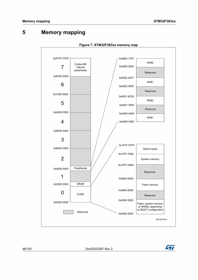
Memory mapping STM32F383xx
48/125 DocID023367 Rev 2
5 Memory mapping
Figure 7. STM32F383xx memory map
0xFFFF FFFF
0xE000 0000
0xC000 0000
0xA000 0000
0x8000 0000
0x6000 0000
0x4000 0000
0x2000 0000
0x0000 0000
0
1
2
3
4
5
6
7Cortex-M4
internal peripherals
Peripherals
SRAM
CODE
Option bytes
System memory
Flash memory
Flash, system memory or SRAM, depending
on BOOT configuration
AHB2
AHB1
APB2
APB1
0x4800 17FF
0x4800 0000
0x4002 43FF
0x4002 0000
0x4001 6C00
0x4001 0000
0x4000 A000
0x4000 0000
0x1FFF FFFF
0x1FFF F800
0x1FFF D800
0x0804 0000
0x0800 0000
0x0004 0000
0x0000 0000Reserved
MSv32159V1
Reserved
Reserved
Reserved
Reserved
Reserved
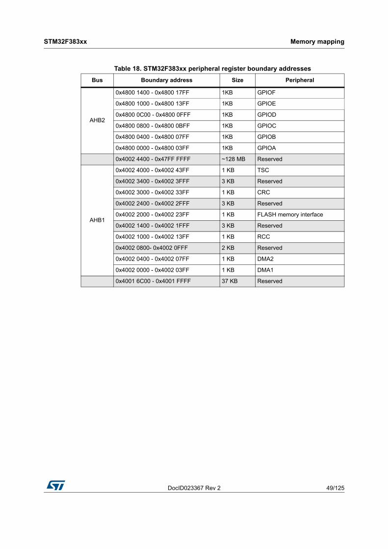
DocID023367 Rev 2 49/125
STM32F383xx Memory mapping
51
Table 18. STM32F383xx peripheral register boundary addressesBus Boundary address Size Peripheral
AHB2
0x4800 1400 - 0x4800 17FF 1KB GPIOF
0x4800 1000 - 0x4800 13FF 1KB GPIOE
0x4800 0C00 - 0x4800 0FFF 1KB GPIOD
0x4800 0800 - 0x4800 0BFF 1KB GPIOC
0x4800 0400 - 0x4800 07FF 1KB GPIOB
0x4800 0000 - 0x4800 03FF 1KB GPIOA
0x4002 4400 - 0x47FF FFFF ~128 MB Reserved
AHB1
0x4002 4000 - 0x4002 43FF 1 KB TSC
0x4002 3400 - 0x4002 3FFF 3 KB Reserved
0x4002 3000 - 0x4002 33FF 1 KB CRC
0x4002 2400 - 0x4002 2FFF 3 KB Reserved
0x4002 2000 - 0x4002 23FF 1 KB FLASH memory interface
0x4002 1400 - 0x4002 1FFF 3 KB Reserved
0x4002 1000 - 0x4002 13FF 1 KB RCC
0x4002 0800- 0x4002 0FFF 2 KB Reserved
0x4002 0400 - 0x4002 07FF 1 KB DMA2
0x4002 0000 - 0x4002 03FF 1 KB DMA1
0x4001 6C00 - 0x4001 FFFF 37 KB Reserved

Memory mapping STM32F383xx
50/125 DocID023367 Rev 2
APB2
0x4001 6800 - 0x4001 6BFF 1 KB SDADC3
0x4001 6400 - 0x4001 67FF 1 KB SDADC2
0x4001 6000 - 0x4001 63FF 1 KB SDADC1
0x4001 5C00 - 0x4001 5FFF 1 KB TIM19
0x4001 4C00 - 0x4001 5BFF 4 KB Reserved
0x4001 4800 - 0x4001 4BFF 1 KB TIM17
0x4001 4400 - 0x4001 47FF 1 KB TIM16
0x4001 4000 - 0x4001 43FF 1 KB TIM15
0x4001 3C00 - 0x4001 3FFF 1 KB Reserved
0x4001 3800 - 0x4001 3BFF 1 KB USART1
0x4001 3400 - 0x4001 37FF 1 KB Reserved
0x4001 3000 - 0x4001 33FF 1 KB SPI1/I2S1
0x4001 2800 - 0x4001 2FFF 1 KB Reserved
0x4001 2400 - 0x4001 27FF 1 KB ADC
0x4001 0800 - 0x4001 23FF 7 KB Reserved
0x4001 0400 - 0x4001 07FF 1 KB EXTI
0x4001 0000 - 0x4001 03FF 1 KB SYSCFG
0x4000 4000 - 0x4000 FFFF 24 KB Reserved
APB1
0x4000 9C00 – 0x4000 9FFF 1 KB TIM18
0x4000 9800 - 0x4000 9BFF 1 KB DAC2
0x4000 7C00 - 0x4000 97FF 8 KB Reserved
0x4000 7800 - 0x4000 7BFF 1 KB CEC
0x4000 7400 - 0x4000 77FF 1 KB DAC1
0x4000 7000 - 0x4000 73FF 1 KB PWR
0x4000 6800 - 0x4000 6FFF 2 KB Reserved
0x4000 6400 - 0x4000 67FF 1 KB CAN
0x4000 5C00 - 0x4000 63FF 2 KB Reserved
Table 18. STM32F383xx peripheral register boundary addresses (continued)Bus Boundary address Size Peripheral

DocID023367 Rev 2 51/125
STM32F383xx Memory mapping
51
APB1
0x4000 5800 - 0x4000 5BFF 1 KB I2C2
0x4000 5400 - 0x4000 57FF 1 KB I2C1
0x4000 4C00 - 0x4000 53FF 2 KB Reserved
0x4000 4800 - 0x4000 4BFF 1 KB USART3
0x4000 4400 - 0x4000 47FF 1 KB USART2
0x4000 4000 - 0x4000 43FF 1 KB Reserved
0x4000 3C00 - 0x4000 3FFF 1 KB SPI3/I2S3
0x4000 3800 - 0x4000 3BFF 1 KB SPI2/I2S2
0x4000 3400 - 0x4000 37FF 1 KB Reserved
0x4000 3000 - 0x4000 33FF 1 KB IWDG
0x4000 2C00 - 0x4000 2FFF 1 KB WWDG
0x4000 2800 - 0x4000 2BFF 1 KB RTC
0x4000 2400 - 0x4000 27FF 1 KB Reserved
0x4000 2000 - 0x4000 23FF 1 KB TIM14
0x4000 1C00 - 0x4000 1FFF 1 KB TIM13
0x4000 1800 - 0x4000 1BFF 1 KB TIM12
0x4000 1400 - 0x4000 17FF 1 KB TIM7
0x4000 1000 - 0x4000 13FF 1 KB TIM6
0x4000 0C00 - 0x4000 0FFF 1 KB TIM5
0x4000 0800 - 0x4000 0BFF 1 KB TIM4
0x4000 0400 - 0x4000 07FF 1 KB TIM3
0x4000 0000 - 0x4000 03FF 1 KB TIM2
Table 18. STM32F383xx peripheral register boundary addresses (continued)Bus Boundary address Size Peripheral

Electrical characteristics STM32F383xx
52/125 DocID023367 Rev 2
6 Electrical characteristics
6.1 Parameter conditionsUnless otherwise specified, all voltages are referenced to VSS.
6.1.1 Minimum and maximum valuesUnless otherwise specified, the minimum and maximum values are guaranteed in the worst conditions of ambient temperature, supply voltage and frequencies by tests in production on 100% of the devices with an ambient temperature at TA = 25 °C and TA = TAmax (given by the selected temperature range).
Data based on characterization results, design simulation and/or technology characteristics are indicated in the table footnotes and are not tested in production. Based on characterization, the minimum and maximum values refer to sample tests and represent the mean value plus or minus three times the standard deviation (mean±3σ).
6.1.2 Typical valuesUnless otherwise specified, typical data are based on TA = 25 °C, VDD =1.8 V, VDDA = VDDSDx = 3.3 V. They are given only as design guidelines and are not tested.
Typical ADC and SDADC accuracy values are determined by characterization of a batch of samples from a standard diffusion lot over the full temperature range, where 95% of the devices have an error less than or equal to the value indicated (mean±2σ).
6.1.3 Typical curvesUnless otherwise specified, all typical curves are given only as design guidelines and are not tested.
6.1.4 Loading capacitorThe loading conditions used for pin parameter measurement are shown in Figure 8.
6.1.5 Pin input voltageThe input voltage measurement on a pin of the device is described in Figure 9.
Figure 8. Pin loading conditions Figure 9. Pin input voltage
MS19210V1
C = 50 pF
MCU pin
MS19211V1
MCU pin
VIN
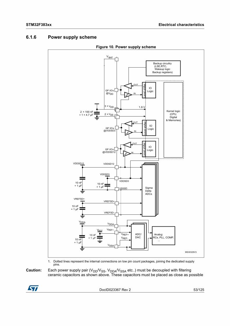
DocID023367 Rev 2 53/125
STM32F383xx Electrical characteristics
109
6.1.6 Power supply scheme
Figure 10. Power supply scheme
1. Dotted lines represent the internal connections on low pin count packages, joining the dedicated supply pins.
Caution: Each power supply pair (VDD/VSS, VDDA/VSSA etc..) must be decoupled with filtering ceramic capacitors as shown above. These capacitors must be placed as close as possible
MS30329V3
Analog: RCs, PLL, COMP,
...
GP I/Os
OUT
IN
Kernel logic (CPU, Digital
& Memories)
Backup circuitry(LSE,RTC,
Backup registers)Wakeup logic
2 × 100 nF+ 1 × 4.7 μF
VDDA
VSSA
ADC/DAC
Leve
l shi
fter
IOLogic
@VDD
10 nF+ 1 μF
VDDA
VREF+VREF-
VDD
VSS
3 ×
2 ×
SigmaDeltaADCs
10 nF+ 1 μF
VDDSD12 VDDSD12
VDDSD3
VDDSD3
VSSSD
10 nF+ 1 μF
VREFSD+
VREFSD-
10 nF+ 1 μF
VREFSD+
GP I/Os
OUT
IN
Leve
l shi
fter
IOLogic
GP I/Os
OUT
IN
Leve
l shi
fter
IOLogic
10 nF+ 1 μF
VREF REF+V
1.8 V
VBAT
@VDDSD3
@VDDSD12
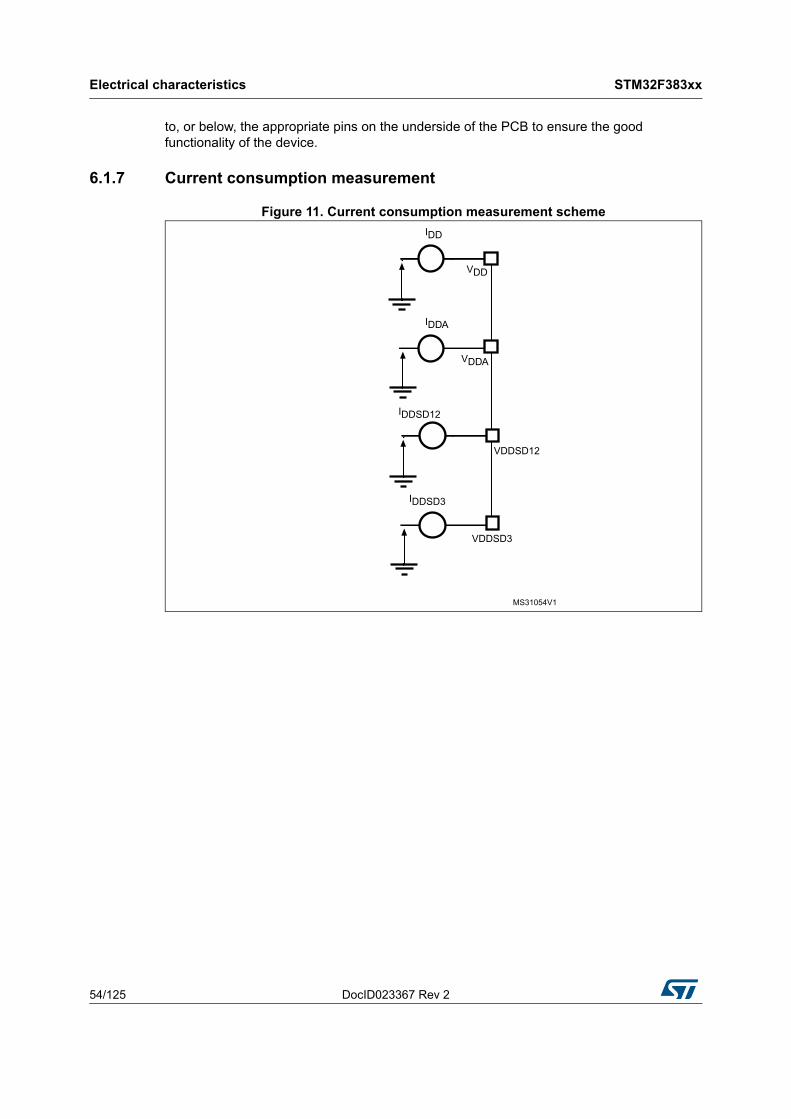
Electrical characteristics STM32F383xx
54/125 DocID023367 Rev 2
to, or below, the appropriate pins on the underside of the PCB to ensure the good functionality of the device.
6.1.7 Current consumption measurement
Figure 11. Current consumption measurement scheme
MS31054V1
VDD
VDDA
IDD
IDDA
VDDSD12
IDDSD12
IDDSD3
VDDSD3

DocID023367 Rev 2 55/125
STM32F383xx Electrical characteristics
109
6.2 Absolute maximum ratingsStresses above the absolute maximum ratings listed in Table 19: Voltage characteristics, Table 20: Current characteristics, and Table 21: Thermal characteristics may cause permanent damage to the device. These are stress ratings only and functional operation of the device at these conditions is not implied. Exposure to maximum rating conditions for extended periods may affect device reliability.
All main power (VDD, VDDSD12, VDDSD3 and VDDA) and ground (VSS, VSSSD, and VSSA) pins must always be connected to the external power supply, in the permitted range.
The following relationship must be respected between VDDA and VDD: VDDA must power on before or at the same time as VDD in the power up sequence. VDDA must be greater than or equal to VDD.
The following relationship must be respected between VDDA and VDDSD12: VDDA must power on before or at the same time as VDDSD12 or VDDSD3 in the power up sequence. VDDA must be greater than or equal to VDDSD12 or VDDSD3.
The following relationship must be respected between VDDSD12 and VDDSD3: VDDSD3 must power on before or at the same time as VDDSD12 in the power up sequence.After power up (VDDSD12 > Vrefint = 1.2 V) VDDSD3 can be higher or lower than VDDSD12.
Table 19. Voltage characteristics(1)
Symbol Ratings Min Max Unit
VDDA–VSS External main supply voltage (including VDDA, VDDSDx) − 0.3 4.0
V
VDD–VSS External supply voltage VDD − 0.3 1.95
VDD–VDDA Allowed voltage difference for VDD > VDDA - 0.4
VDDSDx – VDDA Allowed voltage difference for VDDSDx > VDDA - 0.4
VREFSD+ – VDDSD3
Allowed voltage difference for VREFSD+ > VDDSD3 - 0.4
VREF+ – VDDA Allowed voltage difference for VREF+ > VDDA - 0.4
VIN(2)
Input voltage on FT and FTf pins VSS − 0.3 VDD + 4.0
Input voltage on POR pins VSS − 0.3 VDDA + 4.0
Input voltage on TTa pins VSS − 0.3 4.0
Input voltage on TC pins on SDADCx channels inputs(3) VSS − 0.3 4.0
Input voltage on any other pin VSS − 0.3 4.0
|VSSX − VSS| Variations between all the different ground pins 50 mV
VESD(HBM) Electrostatic discharge voltage (human body model)see Section 6.3.11: Electrical sensitivity characteristics
1. All main power (VDD, VDDA) and ground (VSS, VSSA) pins must always be connected to the external power supply, in the permitted range.
2. VIN maximum must always be respected. Refer to Table 20: Current characteristics for the maximum allowed injected current values.
3. VDDSD12 is the external power supply for the PB10, and PE7 to PE15 I/O pins (the I/O pin ground is internally connected to VSS). VDDSD3 is the external power supply for PB14 to PB15 and PD8 to PD15 I/O pins (the I/O pin ground is internally connected to VSS).

Electrical characteristics STM32F383xx
56/125 DocID023367 Rev 2
The following relationship must be respected between VREFSD+ and VDDSD12, VDDSD3: VREFSD+ must be lower than VDDSD3. Depending on the SDADCx operation mode, there can be more constraints between VREFSD+, VDDSD12 and VDDSD3 which are described in reference manual RM0313.
Table 20. Current characteristicsSymbol Ratings Max. Unit
ΣIVDDTotal current into sum of all VDD_x and VDDSDx power lines (source)(1) 160
mA
ΣIVSSTotal current out of sum of all VSS_x and VSSSD ground lines (sink)(1) -160
IVDD(PIN) Maximum current into each VDD_x or VDDSDx power pin (source)(1) 100
IVSS(PIN) Maximum current out of each VSS_x or VSSSD ground pin (sink)(1) -100
IIO(PIN)Output current sunk by any I/O and control pin 25
Output current source by any I/O and control pin -25
ΣIIO(PIN)Total output current sunk by sum of all IOs and control pins(2) 80
Total output current sourced by sum of all IOs and control pins(2) -80
IINJ(PIN)
Injected current on FT, FTf, POR and B pins(3) -5/+0
Injected current on TC and RST pin(4) ± 5
Injected current on TTa pins(5) ± 5
ΣIINJ(PIN) Total injected current (sum of all I/O and control pins)(6) ± 25
1. VDDSD12 is the external power supply for the PB10, and PE7 to PE15 I/O pins (the I/O pin ground is internally connected to VSS). VDDSD3 is the external power supply for PB14 to PB15 and PD8 to PD15 I/O pins (the I/O pin ground is internally connected to VSS). VDD (VDD_x) is the external power supply for all remaining I/O pins (the I/O pin ground is internally connected to VSS).
2. This current consumption must be correctly distributed over all I/Os and control pins. The total output current must not be sunk/sourced between two consecutive power supply pins referring to high pin count LQFP packages.
3. Positive injection is not possible on these I/Os and does not occur for input voltages lower than the specified maximum value.
4. A positive injection is induced by VIN>VDD while a negative injection is induced by VIN < VSS. IINJ(PIN) must never be exceeded. Refer to Table 19: Voltage characteristics for the maximum allowed input voltage values.
5. A positive injection is induced by VIN>VDDA while a negative injection is induced by VIN < VSS. IINJ(PIN) must never be exceeded. Refer also to Table 19: Voltage characteristics for the maximum allowed input voltage values. Negative injection disturbs the analog performance of the device. See note (2) below Table 60.
6. When several inputs are submitted to a current injection, the maximum ΣIINJ(PIN) is the absolute sum of the positive and negative injected currents (instantaneous values).
Table 21. Thermal characteristicsSymbol Ratings Value Unit
TSTG Storage temperature range –65 to +150 °C
TJ Maximum junction temperature 150 °C

DocID023367 Rev 2 57/125
STM32F383xx Electrical characteristics
109
6.3 Operating conditions
6.3.1 General operating conditions
Table 22. General operating conditionsSymbol Parameter Conditions Min Max Unit
fHCLK Internal AHB clock frequency 0 72
MHzfPCLK1 Internal APB1 clock frequency 0 36
fPCLK2 Internal APB2 clock frequency 0 72
VDD Standard operating voltage Must have a potential equal to or lower than VDDA
1.65 1.95 V
VDDA(1)
Analog operating voltage(ADC and DAC used) Must have a potential equal
to or higher than VDD
2.4 3.6V
Analog operating voltage(ADC and DAC not used) 1.65 3.6
VDDSD12
VDDSD12 operating voltage(SDADC used) Must have a potential equal
to or lower than VDDA
2.2 3.6V
VDDSD12 operating voltage(SDADC not used) 1.65 3.6
VDDSD3
VDDSD3 operatin g voltage(SDADC used) Must have a potential equal
to or lower than VDDA
2.2 3.6V
VDDSD3 operating voltage(SDADC not used) 1.65 3.6
VREF+
Positive reference voltage (ADC and DAC used) Must have a potential equal
to or lower than VDDA
2.4 3.6V
Positive reference voltage (ADC and DAC not used) 1.65 3.6
VREFSD+SDADCx positive reference voltage
Must have a potential equal to or lower than any VDDSDx
1.1 3.6 V
VIN
Input voltage on FT, FTf and POR pins(2) - 0.3 5.2
V
Input voltage on TTa pins - 0.3 VDDA+ 0.3
Input voltage on TC pins on SDADCx channels inputs(3) - 0.3 VDDSDx
+ 0.3
Input voltage on BOOT0 pin 0 5.5
Input voltage on any other pin - 0.3 VDD+ 0.3

Electrical characteristics STM32F383xx
58/125 DocID023367 Rev 2
6.3.2 Operating conditions at power-up / power-downThe parameters given in Table 23 are derived from tests performed under the ambient temperature condition summarized in Table 22.
PD
Power dissipation at TA = 85 °C for suffix 6 or TA = 105 °C for suffix 7(4)
WLCSP66 376
mW
LQFP100 434
LQFP64 444
LQFP48 364
BGA100 338
TA
Ambient temperature for 6 suffix version
Maximum power dissipation –40 85°C
Low power dissipation(5) –40 105
Ambient temperature for 7 suffix version
Maximum power dissipation –40 105°C
Low power dissipation(5) –40 125
TJ Junction temperature range6 suffix version –40 105
°C7 suffix version –40 125
1. When the ADC is used, refer to Table 58: ADC characteristics.
2. To sustain a voltage higher than VDD+0.3 V, the internal pull-up/pull-down resistors must be disabled.
3. VDDSD12 is the external power supply for the PB10, and PE7 to PE15 I/O pins (the I/O pin ground is internally connected to VSS). VDDSD3 is the external power supply for PB14 to PB15 and PD8 to PD15 I/O pins (the I/O pin ground is internally connected to VSS).
4. If TA is lower, higher PD values are allowed as long as TJ does not exceed TJmax.
5. In low power dissipation state, TA can be extended to this range as long as TJ does not exceed TJmax.
Table 22. General operating conditions (continued)Symbol Parameter Conditions Min Max Unit
Table 23. Operating conditions at power-up / power-downSymbol Parameter Conditions Min Max Unit
tVDDVDD rise time rate 0 ∞
µs/VVDD fall time rate 20 ∞
tVDDAVDDA rise time rate 0 ∞VDDA fall time rate 20 ∞
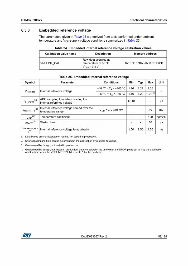
DocID023367 Rev 2 59/125
STM32F383xx Electrical characteristics
109
6.3.3 Embedded reference voltageThe parameters given in Table 25 are derived from tests performed under ambient temperature and VDD supply voltage conditions summarized in Table 22.
Table 24. Embedded internal reference voltage calibration valuesCalibration value name Description Memory address
VREFINT_CALRaw data acquired at temperature of 30 °CVDDA= 3.3 V
0x1FFF F7BA - 0x1FFF F7BB
Table 25. Embedded internal reference voltageSymbol Parameter Conditions Min Typ Max Unit
VREFINT Internal reference voltage–40 °C < TA < +105 °C 1.16 1.21 1.26
V–40 °C < TA < +85 °C 1.16 1.20 1.24(1)
TS_vrefint(2) ADC sampling time when reading the
internal reference voltage 17.10 - - µs
VREFINT_s(3) Internal reference voltage spread over the
temperature range VDD = 3 V ±10 mV - - 10 mV
TCoeff(3) Temperature coefficient - - 100 ppm/°C
tSTART(3) Startup time - - 10 µs
tVREFINT_RDY
(4) Internal reference voltage temporization 1.50 2.50 4.50 ms
1. Data based on characterization results, not tested in production.
2. Shortest sampling time can be determined in the application by multiple iterations.
3. Guaranteed by design, not tested in production.
4. Guaranteed by design, not tested in production. Latency between the time when the NPOR pin is set to 1 by the application and the time when the VREFINTRDYF bit is set to 1 by the hardware.

Electrical characteristics STM32F383xx
60/125 DocID023367 Rev 2
6.3.4 Supply current characteristicsThe current consumption is a function of several parameters and factors such as the operating voltage, ambient temperature, I/O pin loading, device software configuration, operating frequencies, I/O pin switching rate, program location in memory and executed binary code.The current consumption is measured as described in Figure 11: Current consumption measurement scheme.All Run-mode current consumption measurements given in this section are performed with a reduced code that gives a consumption equivalent to CoreMark code.
Typical and maximum current consumption
The MCU is placed under the following conditions:• All I/O pins are in input mode with a static value at VDD or VSS (no load)• All peripherals are disabled except when explicitly mentioned• The Flash memory access time is adjusted to the fHCLK frequency (0 wait state from 0
to 24 MHz, 1 wait state from 24 to 48 MHz and 2 wait states from 48 MHz to 72 MHz)• Prefetch in ON (reminder: this bit must be set before clock setting and bus prescaling)• When the peripherals are enabled fAPB1 = fAHB/2 , fAPB2 = fAHB• When fHCLK > 8 MHz PLL is ON and PLL inputs is equal to HSI/2 = 4 MHz (if internal
clock is used) or HSE = 8 MHz (if HSE bypass mode is used)
The parameters given in Table 26 to Table 31 are derived from tests performed under ambient temperature and supply voltage conditions summarized in Table 22.
Table 26. Typical and maximum current consumption from VDD supply at VDD = 1.8 V
Symbol Parameter Conditions fHCLK
All peripherals enabled All peripherals disabled
UnitTyp
Max @ TA(1)
TypMax @ TA
(1)
25 °C 85 °C 105 °C 25 °C 85 °C 105 °C
IDD
Supply current in Run mode, code executing from Flash
HSEbypass, PLL on
72 MHz 64.9 75.3 77.1 84.0 31.0 34.0 35.0 36.7
mA
64 MHz 58.3 67.0 68.7 74.4 27.8 30.4 31.2 32.7
48 MHz 44.8 50.5 52.0 55.5 21.3 23.1 23.9 24.8
32 MHz 30.7 33.9 35.1 36.7 14.6 15.8 16.4 17.1
24 MHz 23.4 25.6 26.6 27.5 11.3 12.1 12.7 13.3
HSE bypass, PLL off
8 MHz 8.1 8.9 9.3 9.9 4.0 4.4 4.8 5.3
1 MHz 1.3 1.7 2.0 2.5 0.9 1.2 1.6 2.0
HSI clock, PLL on
64 MHz 54.0 61.6 63.2 68.2 27.5 30.1 30.9 32.3
48 MHz 41.5 46.6 47.9 51.0 21.1 22.9 23.6 24.5
32 MHz 28.4 31.3 32.5 33.9 14.5 15.6 16.2 16.9
24 MHz 21.8 23.8 24.8 25.6 7.6 8.2 8.8 9.3
HSI clock, PLL off 8 MHz 7.7 8.4 8.9 9.5 4.0 4.4 4.8 5.3
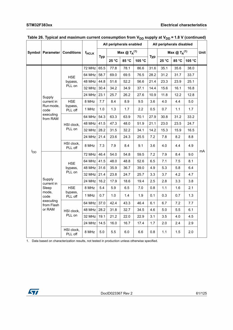
DocID023367 Rev 2 61/125
STM32F383xx Electrical characteristics
109
IDD
Supply current in Run mode, code executing from RAM
HSEbypass, PLL on
72 MHz 65.5 77.8 78.1 86.6 31.6 35.1 35.6 38.0
mA
64 MHz 58.7 69.0 69.5 76.5 28.2 31.2 31.7 33.7
48 MHz 44.8 51.6 52.2 56.6 21.4 23.3 23.9 25.1
32 MHz 30.4 34.2 34.9 37.1 14.4 15.6 16.1 16.8
24 MHz 23.1 25.7 26.2 27.6 10.9 11.8 12.2 12.8
HSE bypass, PLL off
8 MHz 7.7 8.4 8.9 9.5 3.6 4.0 4.4 5.0
1 MHz 1.0 1.3 1.7 2.2 0.5 0.7 1.1 1.7
HSI clock, PLL on
64 MHz 54.3 63.3 63.9 70.1 27.9 30.8 31.2 33.2
48 MHz 41.5 47.3 48.0 51.9 21.1 23.0 23.5 24.7
32 MHz 28.2 31.5 32.2 34.1 14.2 15.3 15.9 16.5
24 MHz 21.4 23.6 24.3 25.5 7.2 7.8 8.2 8.8
HSI clock, PLL off 8 MHz 7.3 7.9 8.4 9.1 3.6 4.0 4.4 4.9
Supply current in Sleep mode, code executing from Flash or RAM
HSEbypass, PLL on
72 MHz 46.4 54.0 54.8 59.5 7.2 7.9 8.4 9.0
64 MHz 41.5 48.0 48.8 52.6 6.5 7.1 7.5 8.1
48 MHz 31.6 35.9 36.7 39.0 4.9 5.3 5.8 6.4
32 MHz 21.4 23.8 24.7 25.7 3.3 3.7 4.2 4.7
24 MHz 16.2 17.9 18.6 19.4 2.5 2.8 3.3 3.8
HSE bypass, PLL off
8 MHz 5.4 5.9 6.5 7.0 0.8 1.1 1.6 2.1
1 MHz 0.7 1.0 1.4 1.9 0.1 0.3 0.7 1.3
HSI clock, PLL on
64 MHz 37.0 42.4 43.3 46.4 6.1 6.7 7.2 7.7
48 MHz 28.2 31.8 32.7 34.5 4.6 5.0 5.5 6.1
32 MHz 19.1 21.2 22.0 22.9 3.1 3.5 4.0 4.5
24 MHz 14.5 16.0 16.7 17.4 1.7 2.0 2.4 2.9
HSI clock, PLL off 8 MHz 5.0 5.5 6.0 6.6 0.8 1.1 1.5 2.0
1. Data based on characterization results, not tested in production unless otherwise specified.
Table 26. Typical and maximum current consumption from VDD supply at VDD = 1.8 V (continued)
Symbol Parameter Conditions fHCLK
All peripherals enabled All peripherals disabled
UnitTyp
Max @ TA(1)
TypMax @ TA
(1)
25 °C 85 °C 105 °C 25 °C 85 °C 105 °C

Electrical characteristics STM32F383xx
62/125 DocID023367 Rev 2
Table 27. Typical and maximum current consumption from VDDA supply
Symbol Parameter Conditions(1) fHCLK
VDDA= 2.4 V VDDA= 3.6 V
UnitTyp
Max @ TA(2)
TypMax @ TA
(2)
25 °C 85 °C 105 °C 25 °C 85 °C 105 °C
IDDA
Supply current in Run or Sleep mode, code executing from Flash or RAM
HSE bypass, PLL on
72 MHz 226 250 272 279 247 268 302 308
µA
64 MHz 200 223 245 250 218 240 267 273
48 MHz 150 172 189 194 163 182 207 210
32 MHz 103 122 137 139 111 130 147 148
24 MHz 80 99 109 111 86 102 117 117
HSE bypass, PLL off
8 MHz 1 3 3 3 1 3 3 4
1 MHz 1 3 3 4 1 3 4 4
HSI clock, PLL on
64 MHz 268 293 319 325 296 321 351 358
48 MHz 219 242 263 267 241 263 290 296
32 MHz 171 193 210 213 189 209 230 234
24 MHz 148 169 181 184 165 182 200 203
HSI clock, PLL off 8 MHz 68 84 86 87 80 93 95 97
1. Current consumption from the VDDA supply is independent of whether the peripherals are on or off. Furthermore when the PLL is off, IDDA is independent from the frequency.
2. Data based on characterization results, not tested in production unless otherwise specified.
Table 28. Typical and maximum VDD consumption in Stop mode
Symbol Parameter Conditions Typ@VDD(VDD=1.8 V, VDDA=3.3 V)
Max
UnitTA=25 °C
TA=85 °C
TA=105 °C
IDDSupply current in Stop mode All oscillators OFF 5.19 29.2 485.7 1052.2 µA
Table 29. Typical and maximum VDDA consumption in Stop mode
Symbol Parameter Conditions
Typ@VDDA (VDD= 1.8 V) Max(1)
Unit1.8 V 2.0 V 2.4 V 2.7 V 3.0 V 3.3 V 3.6 V TA=
25 °CTA=
85 °CTA=
105 °C
IDDA
Supply current in Stop mode
All oscillators OFF 0.74 0.76 0.78 0.81 0.86 0.92 1 8.8 10.1 11.6 µA
1. Data based on characterization results and tested in production.

DocID023367 Rev 2 63/125
STM32F383xx Electrical characteristics
109
Typical current consumption
The MCU is placed under the following conditions:• VDD = 1.8 V, VDDA = VDDSD12 = VDDSD3 = 3.3 V• All I/O pins are in analog input configuration• The Flash access time is adjusted to fHCLK frequency (0 wait states from 0 to 24 MHz,
1 wait state from 24 to 48 MHz and 2 wait states from 48 MHz to 72 MHz)• Prefetch is ON • When the peripherals are enabled, fAPB1 = fAHB/2, fAPB2 = fAHB• PLL is used for frequencies greater than 8 MHz• AHB prescaler of 2, 4, 8, 16 and 64 is used for the frequencies 4 MHz, 2 MHz, 1 MHz,
500 kHz and 125 kHz respectively
Table 30. Typical current consumption in Run mode, code with data processing running from Flash
Symbol Parameter Conditions fHCLK
Typ
UnitPeripherals enabled
Peripherals disabled
IDD
Supply current in Run mode from VDD supply
Running from HSE crystal clock 8 MHz,
code executing from Flash, PLL on
72 MHz 61.0 28.6
mA
64 MHz 54.7 25.7
48 MHz 42.0 20.0
32 MHz 28.5 13.7
24 MHz 21.8 10.5
16 MHz 14.6 7.3
Running from HSE crystal clock 8 MHz,
code executing from Flash, PLL off
8 MHz 7.5 3.8
4 MHz 4.3 2.2
2 MHz 2.5 1.4
1 MHz 1.6 1.0
500 kHz 1.2 0.8
125 kHz 0.9 0.6
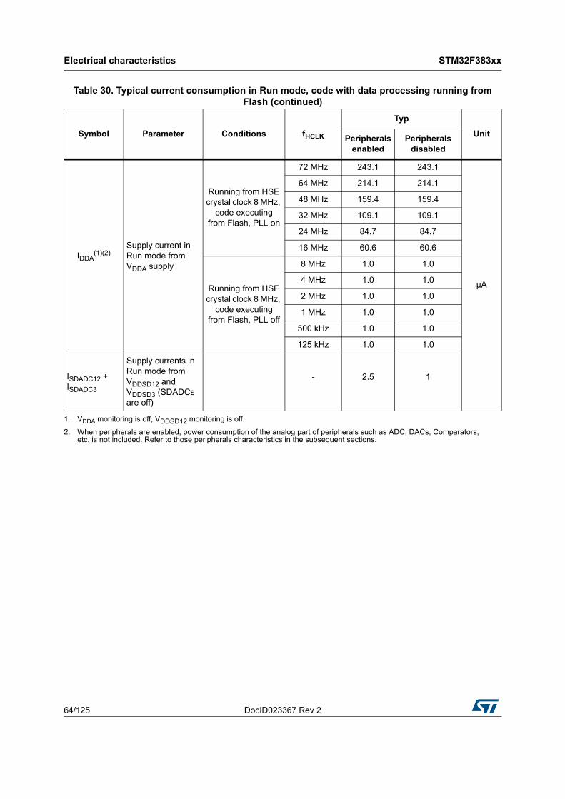
Electrical characteristics STM32F383xx
64/125 DocID023367 Rev 2
IDDA(1)(2)
Supply current in Run mode from VDDA supply
Running from HSE crystal clock 8 MHz,
code executing from Flash, PLL on
72 MHz 243.1 243.1
µA
64 MHz 214.1 214.1
48 MHz 159.4 159.4
32 MHz 109.1 109.1
24 MHz 84.7 84.7
16 MHz 60.6 60.6
Running from HSE crystal clock 8 MHz,
code executing from Flash, PLL off
8 MHz 1.0 1.0
4 MHz 1.0 1.0
2 MHz 1.0 1.0
1 MHz 1.0 1.0
500 kHz 1.0 1.0
125 kHz 1.0 1.0
ISDADC12 + ISDADC3
Supply currents in Run mode from VDDSD12 and VDDSD3 (SDADCs are off)
- 2.5 1
1. VDDA monitoring is off, VDDSD12 monitoring is off.
2. When peripherals are enabled, power consumption of the analog part of peripherals such as ADC, DACs, Comparators, etc. is not included. Refer to those peripherals characteristics in the subsequent sections.
Table 30. Typical current consumption in Run mode, code with data processing running from Flash (continued)
Symbol Parameter Conditions fHCLK
Typ
UnitPeripherals enabled
Peripherals disabled
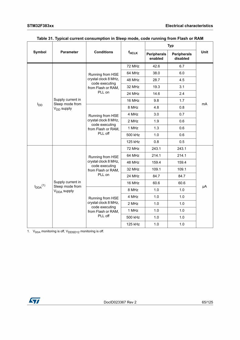
DocID023367 Rev 2 65/125
STM32F383xx Electrical characteristics
109
Table 31. Typical current consumption in Sleep mode, code running from Flash or RAM
Symbol Parameter Conditions fHCLK
Typ
UnitPeripherals enabled
Peripherals disabled
IDD
Supply current in Sleep mode from VDD supply
Running from HSE crystal clock 8 MHz,
code executing from Flash or RAM,
PLL on
72 MHz 42.6 6.7
mA
64 MHz 38.0 6.0
48 MHz 28.7 4.5
32 MHz 19.3 3.1
24 MHz 14.6 2.4
16 MHz 9.8 1.7
Running from HSE crystal clock 8 MHz,
code executing from Flash or RAM,
PLL off
8 MHz 4.8 0.8
4 MHz 3.0 0.7
2 MHz 1.9 0.6
1 MHz 1.3 0.6
500 kHz 1.0 0.6
125 kHz 0.8 0.5
IDDA(1)
Supply current in Sleep mode from VDDA supply
Running from HSE crystal clock 8 MHz,
code executing from Flash or RAM,
PLL on
72 MHz 243.1 243.1
µA
64 MHz 214.1 214.1
48 MHz 159.4 159.4
32 MHz 109.1 109.1
24 MHz 84.7 84.7
16 MHz 60.6 60.6
Running from HSE crystal clock 8 MHz,
code executing from Flash or RAM,
PLL off
8 MHz 1.0 1.0
4 MHz 1.0 1.0
2 MHz 1.0 1.0
1 MHz 1.0 1.0
500 kHz 1.0 1.0
125 kHz 1.0 1.0
1. VDDA monitoring is off, VDDSD12 monitoring is off.
Electrical characteristics STM32F383xx
66/125 DocID023367 Rev 2
I/O system current consumption
The current consumption of the I/O system has two components: static and dynamic.
I/O static current consumption
All the I/Os used as inputs with pull-up generate current consumption when the pin is externally held low. The value of this current consumption can be simply computed by using the pull-up/pull-down resistors values given in Table 49: I/O static characteristics.
For the output pins, any external pull-down or external load must also be considered to estimate the current consumption.
Additional I/O current consumption is due to I/Os configured as inputs if an intermediate voltage level is externally applied. This current consumption is caused by the input Schmitt trigger circuits used to discriminate the input value. Unless this specific configuration is required by the application, this supply current consumption can be avoided by configuring these I/Os in analog mode. This is notably the case of ADC and SDADC input pins which should be configured as analog inputs.
Caution: Any floating input pin can also settle to an intermediate voltage level or switch inadvertently, as a result of external electromagnetic noise. To avoid current consumption related to floating pins, they must either be configured in analog mode, or forced internally to a definite digital value. This can be done either by using pull-up/down resistors or by configuring the pins in output mode. Under reset conditions all I/Os are configured in input floating mode - so if some inputs do not have a defined voltage level then they can generate additional consumption. This consumption is visible on VDD supply and also on VDDSDx supply because some I/Os are powered from SDADCx supply (all I/Os which have SDADC analog input functionality).
I/O dynamic current consumption
In addition to the internal peripheral current consumption (see Table 33: Peripheral current consumption), the I/Os used by an application also contribute to the current consumption. When an I/O pin switches, it uses the current from the MCU supply voltage to supply the I/O pin circuitry and to charge/discharge the capacitive load (internal or external) connected to the pin:
whereISW is the current sunk by a switching I/O to charge/discharge the capacitive loadVDD is the MCU supply voltagefSW is the I/O switching frequencyC is the total capacitance seen by the I/O pin: C = CINT+ CEXT+ CSCS is the PCB board capacitance including the pad pin.
The test pin is configured in push-pull output mode and is toggled by software at a fixed frequency.
ISW VDD fSW C××=
DocID023367 Rev 2 67/125
STM32F383xx Electrical characteristics
109
Table 32. Switching output I/O current consumption
Symbol Parameter Conditions(1) I/O toggling frequency (fSW) Typ Unit
ISWI/O current
consumption
VDD = 1.8 VCext = 0 pF
C = CINT + CEXT+ CS
2 MHz 0.09
mA
4 MHz 0.17
8 MHz 0.34
18 MHz 0.79
36 MHz 1.50
48 MHz 2.06
VDD = 1.8 VCext = 10 pF
C = CINT + CEXT+ CS
2 MHz 0.13
4 MHz 0.26
8 MHz 0.50
18 MHz 1.18
36 MHz 2.27
48 MHz 3.03
VDD = 1.8 VCext = 22 pF
C = CINT + CEXT+ CS
2 MHz 0.18
4 MHz 0.36
8 MHz 0.69
18 MHz 1.60
36 MHz 3.27
VDD = 1.8 VCext = 33 pF
C = CINT + CEXT+ CS
2 MHz 0.23
mA
4 MHz 0.45
8 MHz 0.87
18 MHz 2.0
36 MHz 3.7
VDD = 1.8 VCext = 47 pF
C = CINT + CEXT+ CS
2 MHz 0.29
4 MHz 0.55
8 MHz 1.09
18 MHz 2.43
1. CS = 5 pF (estimated value).
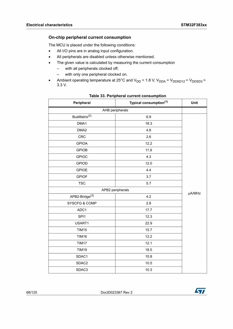
Electrical characteristics STM32F383xx
68/125 DocID023367 Rev 2
On-chip peripheral current consumption
The MCU is placed under the following conditions:• All I/O pins are in analog input configuration.• All peripherals are disabled unless otherwise mentioned.• The given value is calculated by measuring the current consumption
– with all peripherals clocked off;– with only one peripheral clocked on.
• Ambient operating temperature at 25°C and VDD = 1.8 V, VDDA = VDDSD12 = VDDSD3 = 3.3 V.
Table 33. Peripheral current consumptionPeripheral Typical consumption(1) Unit
AHB peripherals
BusMatrix(2) 6.9
µA/MHz
DMA1 18.3
DMA2 4.8
CRC 2.6
GPIOA 12.2
GPIOB 11.9
GPIOC 4.3
GPIOD 12.0
GPIOE 4.4
GPIOF 3.7
TSC 5.7
APB2 peripherals
APB2-Bridge(3) 4.2
SYSCFG & COMP 2.8
ADC1 17.7
SPI1 12.3
USART1 22.9
TIM15 15.7
TIM16 12.2
TIM17 12.1
TIM19 18.5
SDAC1 10.8
SDAC2 10.5
SDAC3 10.3
DocID023367 Rev 2 69/125
STM32F383xx Electrical characteristics
109
6.3.5 Wakeup time from low-power modeThe wakeup times given in Table 43 are measured from the wakeup event trigger to the first instruction executed by the CPU. The clock source used to wake up the device depends from the current operating mode:• Stop or sleep mode: the wakeup event is WFE.• The WKUP1 (PA0) pin is used to wakeup from stop and sleep modes.
All timings are derived from tests performed under ambient temperature and VDD supply voltage conditions summarized in Table 22.
APB1 peripherals
µA/MHz
APB1-Bridge(3) 6.9
TIM2 47.9
TIM3 36.8
TIM4 36.9
TIM5 45.5
TIM6 8.4
TIM7 8.2
TIM12 21.3
TIM13 14.2
TIM14 14.4
TIM18 10.1
WWDG 4.7
SPI2 24.3
SPI3 25.3
USART2 45.3
USART3 43.1
I2C1 14.0
I2C2 13.9
CAN 38.1
DAC2 7.7
PWR 5.4
DAC1 14.8
CEC 5.4
1. When peripherals are enabled, power consumption of the analog part of peripherals such as ADC, DACs, Comparators, etc. is not included. Refer to those peripherals characteristics in the subsequent sections.
2. The BusMatrix is automatically active when at least one master is ON (CPU, DMA1 or DMA2).
3. The APBx Bridge is automatically active when at least one peripheral is ON on the same Bus.
Table 33. Peripheral current consumption (continued)Peripheral Typical consumption(1) Unit

Electrical characteristics STM32F383xx
70/125 DocID023367 Rev 2
6.3.6 External clock source characteristics
High-speed external user clock generated from an external source
In bypass mode the HSE oscillator is switched off and the input pin is a standard GPIO.
The external clock signal has to respect the I/O characteristics in Section 6.3.13. However, the recommended clock input waveform is shown in Figure 12.
Figure 12. High-speed external clock source AC timing diagram
Table 34. Low-power mode wakeup timings
Symbol Parameter Conditions Typ @VDD = 1.8 V, VDDA = 3.3 V Max Unit
tWUSTOP Wakeup from Stop mode 3.6 5.21 µs
tWUSLEEP Wakeup from Sleep mode After WFE instruction 6CPU clock cycles
Table 35. High-speed external user clock characteristicsSymbol Parameter(1)
1. Guaranteed by design, not tested in production.
Conditions Min Typ Max Unit
fHSE_extUser external clock source frequency
CSS is on or PLL is used 1
8 32 MHzCSS is off, PLL not used 0
VHSEH OSC_IN input pin high level voltage 0.7 VDD VDDV
VHSEL OSC_IN input pin low level voltage VSS 0.3 VDD
tw(HSEH)tw(HSEL)
OSC_IN high or low time 15 - -ns
tr(HSE)tf(HSE)
OSC_IN rise or fall time - - 20
MS19214V2
VHSEH
tf(HSE)
90%10%
THSE
ttr(HSE)
VHSEL
tW(HSEH)
tW(HSEL)
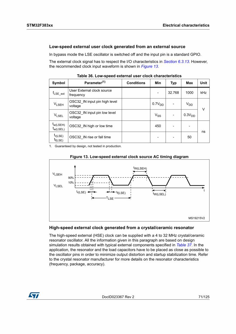
DocID023367 Rev 2 71/125
STM32F383xx Electrical characteristics
109
Low-speed external user clock generated from an external source
In bypass mode the LSE oscillator is switched off and the input pin is a standard GPIO.
The external clock signal has to respect the I/O characteristics in Section 6.3.13. However, the recommended clock input waveform is shown in Figure 13.
Figure 13. Low-speed external clock source AC timing diagram
High-speed external clock generated from a crystal/ceramic resonator
The high-speed external (HSE) clock can be supplied with a 4 to 32 MHz crystal/ceramic resonator oscillator. All the information given in this paragraph are based on design simulation results obtained with typical external components specified in Table 37. In the application, the resonator and the load capacitors have to be placed as close as possible to the oscillator pins in order to minimize output distortion and startup stabilization time. Refer to the crystal resonator manufacturer for more details on the resonator characteristics (frequency, package, accuracy).
Table 36. Low-speed external user clock characteristicsSymbol Parameter(1)
1. Guaranteed by design, not tested in production.
Conditions Min Typ Max Unit
fLSE_extUser External clock source frequency - 32.768 1000 kHz
VLSEHOSC32_IN input pin high level voltage 0.7VDD - VDD
VVLSEL
OSC32_IN input pin low level voltage VSS - 0.3VDD
tw(LSEH)tw(LSEL)
OSC32_IN high or low time 450 - -ns
tr(LSE)tf(LSE)
OSC32_IN rise or fall time - - 50
MS19215V2
VLSEH
tf(LSE)
90%10%
TLSE
ttr(LSE)
VLSEL
tW(LSEH)
tW(LSEL)
Electrical characteristics STM32F383xx
72/125 DocID023367 Rev 2
For CL1 and CL2, it is recommended to use high-quality external ceramic capacitors in the 5 pF to 20 pF range (typ.), designed for high-frequency applications, and selected to match the requirements of the crystal or resonator (see Figure 14). CL1 and CL2 are usually the same size. The crystal manufacturer typically specifies a load capacitance which is the series combination of CL1 and CL2. PCB and MCU pin capacitance must be included (10 pF can be used as a rough estimate of the combined pin and board capacitance) when sizing CL1 and CL2.
Note: For information on electing the crystal, refer to the application note AN2867 “Oscillator design guide for ST microcontrollers” available from the ST website www.st.com.
Table 37. HSE oscillator characteristicsSymbol Parameter Conditions(1)
1. Resonator characteristics given by the crystal/ceramic resonator manufacturer.
Min(2) Typ Max(2)
2. Guaranteed by design, not tested in production.
Unit
fOSC_IN Oscillator frequency 4 8 32 MHz
RF Feedback resistor - 200 - kΩ
IDD HSE current consumption
During startup(3)
3. This consumption level occurs during the first 2/3 of the tSU(HSE) startup time
- - 8.5
mA
VDD = 1.8 V, Rm= 30 Ω, CL= 10 pF@8 MHz - 0.4 -
VDD = 1.8 V, Rm= 45 Ω, CL= 10 pF@8 MHz - 0.5 -
VDD = 1.8 V, Rm= 30 Ω, CL=5 pF@32 MHz - 0.8 -
VDD = 1.8 V, Rm= 30 Ω, CL= 10 pF@32 MHz - 1 -
VDD = 1.8 V, Rm= 30 Ω, CL= 20 pF@32 MHz - 1.5 -
gm Oscillator transconductance Startup 10 - - mA/V
tSU(HSE)(4)
4. tSU(HSE) is the startup time measured from the moment it is enabled (by software) to a stabilized 8 MHz oscillation is reached. This value is measured for a standard crystal resonator and it can vary significantly with the crystal manufacturer
Startup time VDD is stabilized - 2 - ms
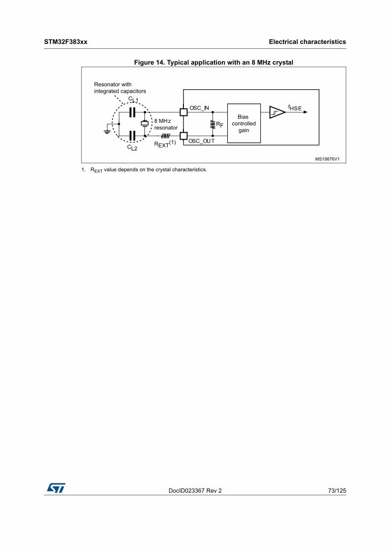
DocID023367 Rev 2 73/125
STM32F383xx Electrical characteristics
109
Figure 14. Typical application with an 8 MHz crystal
1. REXT value depends on the crystal characteristics.
MS19876V1
OSC_OUT
OSC_IN fHSE
CL1
RF8 MHzresonator
REXT(1) CL2
Resonator withintegrated capacitors
Bias controlled
gain

Electrical characteristics STM32F383xx
74/125 DocID023367 Rev 2
Low-speed external clock generated from a crystal resonator
The low-speed external (LSE) clock can be supplied with a 32.768 kHz crystal resonator oscillator. All the information given in this paragraph are based on design simulation results obtained with typical external components specified in Table 38. In the application, the resonator and the load capacitors have to be placed as close as possible to the oscillator pins in order to minimize output distortion and startup stabilization time. Refer to the crystal resonator manufacturer for more details on the resonator characteristics (frequency, package, accuracy).
Note: For information on selecting the crystal, refer to the application note AN2867 “Oscillator design guide for ST microcontrollers” available from the ST website www.st.com.
Table 38. LSE oscillator characteristics (fLSE = 32.768 kHz) Symbol Parameter Conditions(1) Min(2) Typ Max(2) Unit
IDD LSE current consumption
LSEDRV[1:0]=00 lower driving capability - 0.5 0.9
µA
LSEDRV[1:0]= 01 medium low driving capability - - 1
LSEDRV[1:0] = 10 medium high driving capability - - 1.3
LSEDRV[1:0]=11 higher driving capability - - 1.6
gmOscillator transconductance
LSEDRV[1:0]=00 lower driving capability 5 - -
µA/V
LSEDRV[1:0]= 01 medium low driving capability 8 - -
LSEDRV[1:0] = 10 medium high driving capability 15 - -
LSEDRV[1:0]=11 higher driving capability 25 - -
tSU(LSE)(3) Startup time VDD is stabilized - 2 - s
1. Refer to the note and caution paragraphs below the table, and to the application note AN2867 “Oscillator design guide for ST microcontrollers”.
2. Guaranteed by design, not tested in production.
3. tSU(LSE) is the startup time measured from the moment it is enabled (by software) to a stabilized 32.768 kHz oscillation is reached. This value is measured for a standard crystal and it can vary significantly with the crystal manufacturer
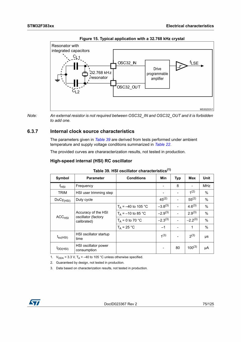
DocID023367 Rev 2 75/125
STM32F383xx Electrical characteristics
109
Figure 15. Typical application with a 32.768 kHz crystal
Note: An external resistor is not required between OSC32_IN and OSC32_OUT and it is forbidden to add one.
6.3.7 Internal clock source characteristicsThe parameters given in Table 39 are derived from tests performed under ambient temperature and supply voltage conditions summarized in Table 22.
The provided curves are chararacterization results, not tested in production.
High-speed internal (HSI) RC oscillator
MS30253V1
OSC32_OUT
OSC32_IN fLSE
CL1
32.768 kHzresonator
CL2
Resonator withintegrated capacitors
Drive programmable
amplifier
Table 39. HSI oscillator characteristics(1)
1. VDDA = 3.3 V, TA = –40 to 105 °C unless otherwise specified.
Symbol Parameter Conditions Min Typ Max Unit
fHSI Frequency - 8 - MHz
TRIM HSI user trimming step - - 1(2)
2. Guaranteed by design, not tested in production.
%
DuCy(HSI) Duty cycle 45(2) - 55(2) %
ACCHSI
Accuracy of the HSI oscillator (factory calibrated)
TA = –40 to 105 °C –3.8(3)
3. Data based on characterization results, not tested in production.
- 4.6(3) %
TA = –10 to 85 °C –2.9(3) - 2.9(3) %
TA = 0 to 70 °C –2.3(3) - –2.2(3) %
TA = 25 °C –1 - 1 %
tsu(HSI)HSI oscillator startup time 1(3) - 2(3) µs
IDD(HSI)HSI oscillator power consumption - 80 100(3) µA

Electrical characteristics STM32F383xx
76/125 DocID023367 Rev 2
Figure 16. HSI oscillator accuracy characterization results
Low-speed internal (LSI) RC oscillator
6.3.8 PLL characteristicsThe parameters given in Table 41 are derived from tests performed under ambient temperature and supply voltage conditions summarized in Table 22.
Table 40. LSI oscillator characteristics(1)
1. VDDA = 3.3 V, TA = –40 to 105 °C unless otherwise specified.
Symbol Parameter Min Typ Max Unit
fLSI Frequency 30 40 60 kHz
tsu(LSI)(2)
2. Guaranteed by design, not tested in production.
LSI oscillator startup time - - 85 µs
IDD(LSI)(2) LSI oscillator power consumption - 0.75 1.2 µA
MS30986V2
-5%
-4%
- 3%
- 2%
- 1%
0%
1%
2%
3%
4%
5%
-40 -20 0 20 40 60 80 100 120
MAX
MIN
TA [°C]
ACCHSI
Table 41. PLL characteristics
Symbol ParameterValue
UnitMin Typ Max
fPLL_INPLL input clock(1)
1. Take care of using the appropriate multiplier factors so as to have PLL input clock values compatible with the range defined by fPLL_OUT.
1(2) - 24(2) MHz
PLL input clock duty cycle 40(2) - 60(2) %
fPLL_OUT PLL multiplier output clock 16(2) - 72 MHz
tLOCK PLL lock time - - 200(2)
2. Guaranteed by design, not tested in production.
µs
Jitter Cycle-to-cycle jitter - - 300(2) ps

DocID023367 Rev 2 77/125
STM32F383xx Electrical characteristics
109
6.3.9 Memory characteristics
Flash memory
The characteristics are given at TA = –40 to 105 °C unless otherwise specified.
Table 42. Flash memory characteristicsSymbol Parameter Conditions Min Typ Max(1)
1. Guaranteed by design, not tested in production.
Unit
tprog 16-bit programming time TA = –40 to +105 °C 40 53.5 60 µs
tERASE Page (2 kB) erase time TA = –40 to +105 °C 20 - 40 ms
tME Mass erase time TA = –40 to +105 °C 20 - 40 ms
IDD Supply current Write mode - - 10 mA
Erase mode - - 12 mA
Table 43. Flash memory endurance and data retention
Symbol Parameter ConditionsValue
UnitMin(1)
1. Data based on characterization results, not tested in production.
NEND EnduranceTA = –40 to +85 °C (6 suffix versions)TA = –40 to +105 °C (7 suffix versions) 10 kcycles
tRET Data retention
1 kcycle(2) at TA = 85 °C
2. Cycling performed over the whole temperature range.
30
Years1 kcycle(2) at TA = 105 °C 10
10 kcycles(2) at TA = 55 °C 20

Electrical characteristics STM32F383xx
78/125 DocID023367 Rev 2
6.3.10 EMC characteristicsSusceptibility tests are performed on a sample basis during device characterization.
Functional EMS (electromagnetic susceptibility)
While a simple application is executed on the device (toggling 2 LEDs through I/O ports). the device is stressed by two electromagnetic events until a failure occurs. The failure is indicated by the LEDs:• Electrostatic discharge (ESD) (positive and negative) is applied to all device pins until
a functional disturbance occurs. This test is compliant with the IEC 61000-4-2 standard.• FTB: A Burst of Fast Transient voltage (positive and negative) is applied to VDD and
VSS through a 100 pF capacitor, until a functional disturbance occurs. This test is compliant with the IEC 61000-4-4 standard.
A device reset allows normal operations to be resumed.
The test results are given in Table 44. They are based on the EMS levels and classes defined in application note AN1709.
Designing hardened software to avoid noise problems
EMC characterization and optimization are performed at component level with a typical application environment and simplified MCU software. It should be noted that good EMC performance is highly dependent on the user application and the software in particular.
Therefore it is recommended that the user applies EMC software optimization and prequalification tests in relation with the EMC level requested for his application.
Software recommendations
The software flowchart must include the management of runaway conditions such as:• Corrupted program counter• Unexpected reset• Critical Data corruption (control registers...)
Prequalification trials
Most of the common failures (unexpected reset and program counter corruption) can be reproduced by manually forcing a low state on the NRST pin or the Oscillator pins for 1 second.
Table 44. EMS characteristics
Symbol Parameter Conditions Level/Class
VFESDVoltage limits to be applied on any I/O pin to induce a functional disturbance
VDD = 1.8 V, LQFP100, TA = +25 °C, fHCLK = 72 MHzconforms to IEC 61000-4-2
2B
VEFTB
Fast transient voltage burst limits to be applied through 100 pF on VDD and VSS pins to induce a functional disturbance
VDD = 1.8 V, LQFP100, TA = +25 °C, fHCLK = 72 MHzconforms to IEC 61000-4-4
4A
DocID023367 Rev 2 79/125
STM32F383xx Electrical characteristics
109
To complete these trials, ESD stress can be applied directly on the device, over the range of specification values. When unexpected behavior is detected, the software can be hardened to prevent unrecoverable errors occurring (see application note AN1015).
Electromagnetic Interference (EMI)
The electromagnetic field emitted by the device are monitored while a simple application is executed (toggling 2 LEDs through the I/O ports). This emission test is compliant with IEC 61967-2 standard which specifies the test board and the pin loading.
6.3.11 Electrical sensitivity characteristicsBased on three different tests (ESD, LU) using specific measurement methods, the device is stressed in order to determine its performance in terms of electrical sensitivity.
Electrostatic discharge (ESD)
Electrostatic discharges (a positive then a negative pulse separated by 1 second) are applied to the pins of each sample according to each pin combination. The sample size depends on the number of supply pins in the device (3 parts × (n+1) supply pins). This test conforms to the JESD22-A114/C101 standard.
Table 45. EMI characteristics
Symbol Parameter Conditions Monitoredfrequency band
Max vs. [fHSE/fHCLK]Unit
8/72 MHz
SEMI Peak level
VDD = 1.8 V, TA = 25 °C,LQFP100 packagecompliant with IEC 61967-2
0.1 to 30 MHz 16
dBµV30 to 130 MHz 20
130 MHz to 1 GHz 26
SAE EMI Level 4 -
Table 46. ESD absolute maximum ratings
Symbol Ratings Conditions Class Maximum value(1)
1. Data based on characterization results, not tested in production.
Unit
VESD(HBM)
Electrostatic discharge voltage (human body model)
TA = +25 °C, conforming to JESD22-A114
2 2000
VVESD(CD
M)
Electrostatic discharge voltage (charge device model)
TA = +25 °C, conforming to ANSI/ESD STM5.3.1, LQFP100, LQFP64, LQFP48 and BGA100 packages
II 500
TA = +25 °C, conforming to JESD22-C101, WLCSP66 package
II 250

Electrical characteristics STM32F383xx
80/125 DocID023367 Rev 2
Static latch-up
Two complementary static tests are required on six parts to assess the latch-up performance: • A supply overvoltage is applied to each power supply pin• A current injection is applied to each input, output and configurable I/O pin
These tests are compliant with EIA/JESD 78A IC latch-up standard.
6.3.12 I/O current injection characteristicsAs a general rule, current injection to the I/O pins, due to external voltage below VSS or above VDD (for standard, 3 V-capable I/O pins) should be avoided during normal product operation. However, in order to give an indication of the robustness of the microcontroller in cases when abnormal injection accidentally happens, susceptibility tests are performed on a sample basis during device characterization.
Functional susceptibility to I/O current injection
While a simple application is executed on the device, the device is stressed by injecting current into the I/O pins programmed in floating input mode. While current is injected into the I/O pin, one at a time, the device is checked for functional failures.
The failure is indicated by an out of range parameter: ADC error above a certain limit (higher than 5 LSB TUE), out of conventional limits of induced leakage current on adjacent pins (out of –5 µA/+0 µA range), or other functional failure (for example reset occurrence or oscillator frequency deviation).
The test results are given in Table 48.
Table 47. Electrical sensitivitiesSymbol Parameter Conditions Class
LU Static latch-up class TA = +105 °C conforming to JESD78A II level A

DocID023367 Rev 2 81/125
STM32F383xx Electrical characteristics
109
Note: It is recommended to add a Schottky diode (pin to ground) to analog pins which may potentially inject negative currents.
Table 48. I/O current injection susceptibility
Symbol Description
Functional susceptibility
UnitNegative injection
Positive injection
IINJ
Injected current on BOOT0 pin -0 NA
mA
Injected current on PC0 pin -0 +5
Injected current on TC type I/O pins on VDDSD12 power domain: PE7, PE8, PE9, PE10, PE11, PE12, PE13, PE14, PE15, PB10 with induced leakage current on other pins from this group less than -50 µA
-5 +5
Injected current on TC type I/O pins on VDDSD3 power domain: PB14, PB15, PD8, PD9, PD10, PD12, PD13, PD14, PD15 with induced leakage current on other pins from this group less than -50 µA
-5 +5
Injected current on TTa type pins: PA4, PA5, PA6 with induced leakage current on adjacent pins less than -10 µA -5 +5
Injected current NPOR pin and on any other FT and FTf pins -5 NA
Injected current on any other pins -5 +5
Electrical characteristics STM32F383xx
82/125 DocID023367 Rev 2
6.3.13 I/O port characteristics
General input/output characteristics
Unless otherwise specified, the parameters given in Table 49 are derived from tests performed under the conditions summarized in Table 22. All I/Os are CMOS and TTL compliant.
Table 49. I/O static characteristics (1)
Symbol Parameter Conditions Min Typ Max Unit
VILLow level input voltage
TC and TTa I/O - - 0.3VDD+0.07(2)
V
FT and FTf I/O - - 0.475VDD–0.2(2)
BOOT0 - - 0.3VDD–0.3(2)
All I/Os except BOOT0 pin - - 0.3VDD
VIHHigh level input voltage
TC and TTa I/O 0.445VDD+0.398(2) - -
FT and FTf I/O 0.5VDD+0.2(2) - -
BOOT0 0.2VDD+0.95(2) - -
All I/Os except BOOT0 pin 0.7VDD - -
VhysSchmitt trigger hysteresis
TC and TTa I/O - 200(2) -
mVFT and FTf I/O - 100(2) -
BOOT0 - 300(2) -
IlkgInput leakage current (3)
TC, FT, FTf and POR I/OTTa in digital modeVSS ≤ VIN ≤ VDD
- - ±0.1
µA
TTa in digital modeVDD ≤ VIN ≤ VDDA
- - 1
TTa in analog modeVSS ≤ VIN ≤ VDDA
- - ±0.2
FT and FTf I/O (3)
VDD ≤ VIN ≤ 5 V - - 10
PORVDDA ≤ VIN ≤ 5 V - - 10
RPU
Weak pull-up equivalent resistor(4)
VIN = VSS 25 40 55
kΩ
RPD
Weak pull-down equivalent resistor(4)
VIN = VDD 25 40 55
CIO I/O pin capacitance - 5 - pF
1. VDDSD12 is the external power supply for the PB10, and PE7 to PE15 I/O pins (the I/O pin ground is internally connected to VSS). VDDSD3 is the external power supply for PB14 to PB15 and PD8 to PD15 I/O pins (the I/O pin ground is internally connected to VSS). For those pins all VDD supply references in this table are related to their given VDDSDx power supply.
2. Data based on design simulation only. Not tested in production.
3. Leakage could be higher than maximum value, if negative current is injected on adjacent pins.
4. Pull-up and pull-down resistors are designed with a true resistance in series with a switchable PMOS/NMOS. This PMOS/NMOS contribution to the series resistance is minimal (~10% order).

DocID023367 Rev 2 83/125
STM32F383xx Electrical characteristics
109
Note: I/O pins are powered from VDD voltage except pins which can be used as SDADC inputs: - The PB10 and PE7 to PE15 I/O pins are powered from VDDSD12.- PB14 to PB15 and PD8 to PD15 I/O pins are powered from VDDSD3. All I/O pin ground is internally connected to VSS.VDD mentioned in the Table 49 represents power voltage for a given I/O pin (VDD or VDDSD12 or VDDSD3).
All I/Os are CMOS and TTL compliant (no software configuration required). Their characteristics cover more than the strict CMOS-technology parameters. The coverage of these requirements is shown in Figure 17 for standard I/Os, and in Figure 18 for 5 V tolerant I/Os.
Figure 17. TC and TTa I/O input characteristics
Figure 18. Five volt tolerant (FT and FTf) I/O input characteristics
Output driving current
The GPIOs (general purpose input/outputs) can sink or source up to ± 8 mA, and sink or source up to ± 20 mA (with a relaxed VOL/VOH).
MS31122V2
VDD (V)
VIHmin
VILmax
VIL/VIH (V)
1.65 1.95
CMOS standard requirements VIHmin = 0.7VDD
VILmax = 0.3VDD+0.07
1.8
CMOS standard requirements VILmax = 0.3VDD
VIHmin = 0.445VDD+0.398
Area not determined
0.5
0.7
0.9
1.1
1.3
Tested in production
Tested in production
Based on design simulations
Based on design simulations
MS31123V2
VDD (V)
VIHmin
VILmax
VIL/VIH (V)
1.65 1.95
CMOS standard requirements VIHmin = 0.7VDD
VILmax = 0.475VDD - 0.2
1.8
CMOS standard requirements VILmax = 0.3VDD
VIHmin = 0.5VDD+0.2
Area not determined
0.5
0.7
0.9
1.1
1.3 Tested in production
Tested in production
Based on design simulations
Based on design simulations
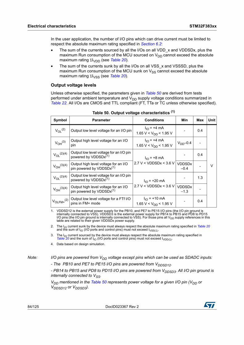
Electrical characteristics STM32F383xx
84/125 DocID023367 Rev 2
In the user application, the number of I/O pins which can drive current must be limited to respect the absolute maximum rating specified in Section 6.2:• The sum of the currents sourced by all the I/Os on all VDD_x and VDDSDx, plus the
maximum Run consumption of the MCU sourced on VDD cannot exceed the absolute maximum rating ΣIVDD (see Table 20).
• The sum of the currents sunk by all the I/Os on all VSS_x and VSSSD, plus the maximum Run consumption of the MCU sunk on VSS cannot exceed the absolute maximum rating ΣIVSS (see Table 20).
Output voltage levels
Unless otherwise specified, the parameters given in Table 50 are derived from tests performed under ambient temperature and VDD supply voltage conditions summarized in Table 22. All I/Os are CMOS and TTL compliant (FT, TTa or TC unless otherwise specified).
Note: I/O pins are powered from VDD voltage except pins which can be used as SDADC inputs: - The PB10 and PE7 to PE15 I/O pins are powered from VDDSD12.- PB14 to PB15 and PD8 to PD15 I/O pins are powered from VDDSD3. All I/O pin ground is internally connected to VSS.VDD mentioned in the Table 50 represents power voltage for a given I/O pin (VDD or VDDSD12 or VDDSD3).
Table 50. Output voltage characteristics (1)
1. VDDSD12 is the external power supply for the PB10, and PE7 to PE15 I/O pins (the I/O pin ground is internally connected to VSS). VDDSD3 is the external power supply for PB14 to PB15 and PD8 to PD15 I/O pins (the I/O pin ground is internally connected to VSS). For those pins all VDD supply references in this table are related to their given VDDSDx power supply.
Symbol Parameter Conditions Min Max Unit
VOL(2)
2. The IIO current sunk by the device must always respect the absolute maximum rating specified in Table 20 and the sum of IIO (I/O ports and control pins) must not exceed IVSS(Σ).
Output low level voltage for an I/O pinIIO = +4 mA
1.65 V < VDD < 1.95 V- 0.4
V
VOH(3)
3. The IIO current sourced by the device must always respect the absolute maximum rating specified in Table 20 and the sum of IIO (I/O ports and control pins) must not exceed IVDD(Σ).
Output high level voltage for an I/O pin
IIO = +4 mA1.65 V < VDD < 1.95 V
VDD–0.4 -
VOL(2)(4) Output low level voltage for an I/O pin
powered by VDDSDx(1) IIO = +8 mA2.7 V < VDDSDx < 3.6 V
- 0.4
VOH(3)(4) Output high level voltage for an I/O
pin powered by VDDSDx(1)VDDSDx
–0.4 -
VOL(2)(4)
4. Data based on design simulation.
Output low level voltage for an I/O pin powered by VDDSDx(1) IIO = +20 mA
2.7 V < VDDSDx < 3.6 V
- 1.3
VOH(3)(4) Output high level voltage for an I/O
pin powered by VDDSDx(1)VDDSDx
–1.3 -
VOLFM+(2) Output low level voltage for a FTf I/O
pins in FM+ modeIIO = +10 mA
1.65 V < VDD < 1.95 V- 0.4

DocID023367 Rev 2 85/125
STM32F383xx Electrical characteristics
109
Input/output AC characteristics
The definition and values of input/output AC characteristics are given in Figure 19 and Table 51, respectively.
Unless otherwise specified, the parameters given are derived from tests performed under ambient temperature and VDD supply voltage conditions summarized in Table 22.
Table 51. I/O AC characteristics(1) OSPEEDRy [1:0] value(1) Symbol Parameter Conditions Min Max Unit
x0
fmax(IO)out Maximum frequency(2) CL = 50 pF, VDD = 1.65 V to 1.95 V - 1 MHz
tf(IO)outOutput high to low level fall time
CL = 50 pF, VDD = 1.65 V to 1.95 V- 125(3)
nstr(IO)out
Output low to high level rise time - 125(3)
01
fmax(IO)out Maximum frequency(2) CL = 50 pF, VDD = 1.65 V to 1.95 V - 4 MHz
tf(IO)outOutput high to low level fall time
CL = 50 pF, VDD = 1.65 V to 1.95 V- 62.5
nstr(IO)out
Output low to high level rise time - 62.5
11
fmax(IO)out Maximum frequency(2)(3) CL = 50 pF, VDD = 1.65 V to 1.95 V - 10 MHz
tf(IO)outOutput high to low level fall time CL = 50 pF, VDD = 1.65 V to 1.95 V - 25
nstr(IO)out
Output low to high level rise time CL = 50 pF, VDD = 1.65 V to 1.95 V - 25
FM+ configuration
(4)
fmax(IO)out Maximum frequency(2)
CL = 50 pF, VDD = 1.65 V to 1.95 V
- 0.5 MHz
tf(IO)outOutput high to low level fall time - 16
nstr(IO)out
Output low to high level rise time - 44
tEXTIpw
Pulse width of external signals detected by the EXTI controller
10 - ns
1. The I/O speed is configured using the OSPEEDRx[1:0] bits. Refer to the RM0313 reference manual for a description of GPIO Port configuration register.
2. The maximum frequency is defined in Figure 19.
3. Guaranteed by design, not tested in production.
4. The I/O speed configuration is bypassed in FM+ I/O mode. Refer to the STM32F37xx and STM32F38xx reference manual RM0313 for a description of FM+ I/O mode configuration

Electrical characteristics STM32F383xx
86/125 DocID023367 Rev 2
Figure 19. I/O AC characteristics definition
6.3.14 NRST and NPOR pins characteristics
NRST pin characteristics
The NRST pin input driver uses CMOS technology. It is connected to a permanent pull-up resistor, RPU (see Table 49).
Unless otherwise specified, the parameters given in Table 52 are derived from tests performed under ambient temperature and VDD supply voltage conditions summarized in Table 22.
MS32132V1
T
10%
50%
90% 10%
50%
90%
EXTERNALOUTPUTON 50 pF
Maximum frequency is achieved if (t + t (≤ 2/3)T and if the duty cycle is (45-55%)when loaded by 50 pF
r f
r(IO)outt f(IO)outt
Table 52. NRST pin characteristics Symbol Parameter Conditions Min Typ Max Unit
VIL(NRST)(1) NRST Input low level voltage - - 0.3VDD + 0.07(1)
VVIH(NRST)
(1) NRST Input high level voltage 0.445VDD + 0.398(1) - -
Vhys(NRST)(1) NRST Schmitt trigger voltage
hysteresis - 200 - mV
RPU Weak pull-up equivalent resistor(2) VIN = VSS 25 40 55 kΩ
VF(NRST)(1) NRST Input filtered pulse - - 100 ns
VNF(NRST)(1) NRST Input not filtered pulse 700 - - ns
1. Guaranteed by design, not tested in production.
2. The pull-up is designed with a true resistance in series with a switchable PMOS. This PMOS contribution to the series resistance is minimal (~10% order).
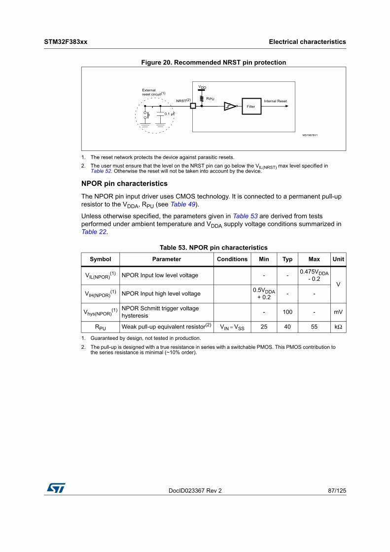
DocID023367 Rev 2 87/125
STM32F383xx Electrical characteristics
109
Figure 20. Recommended NRST pin protection
1. The reset network protects the device against parasitic resets.2. The user must ensure that the level on the NRST pin can go below the VIL(NRST) max level specified in
Table 52. Otherwise the reset will not be taken into account by the device.
NPOR pin characteristics
The NPOR pin input driver uses CMOS technology. It is connected to a permanent pull-up resistor to the VDDA, RPU (see Table 49).
Unless otherwise specified, the parameters given in Table 53 are derived from tests performed under ambient temperature and VDDA supply voltage conditions summarized in Table 22.
Table 53. NPOR pin characteristics Symbol Parameter Conditions Min Typ Max Unit
VIL(NPOR)(1)
1. Guaranteed by design, not tested in production.
NPOR Input low level voltage - - 0.475VDDA - 0.2
VVIH(NPOR)
(1) NPOR Input high level voltage 0.5VDDA + 0.2 - -
Vhys(NPOR)(1) NPOR Schmitt trigger voltage
hysteresis - 100 - mV
RPU Weak pull-up equivalent resistor(2)
2. The pull-up is designed with a true resistance in series with a switchable PMOS. This PMOS contribution to the series resistance is minimal (~10% order).
VIN = VSS 25 40 55 kΩ
MS19878V1
RPUNRST(2)
VDD
FilterInternal Reset
0.1 μF
Externalreset circuit(1)
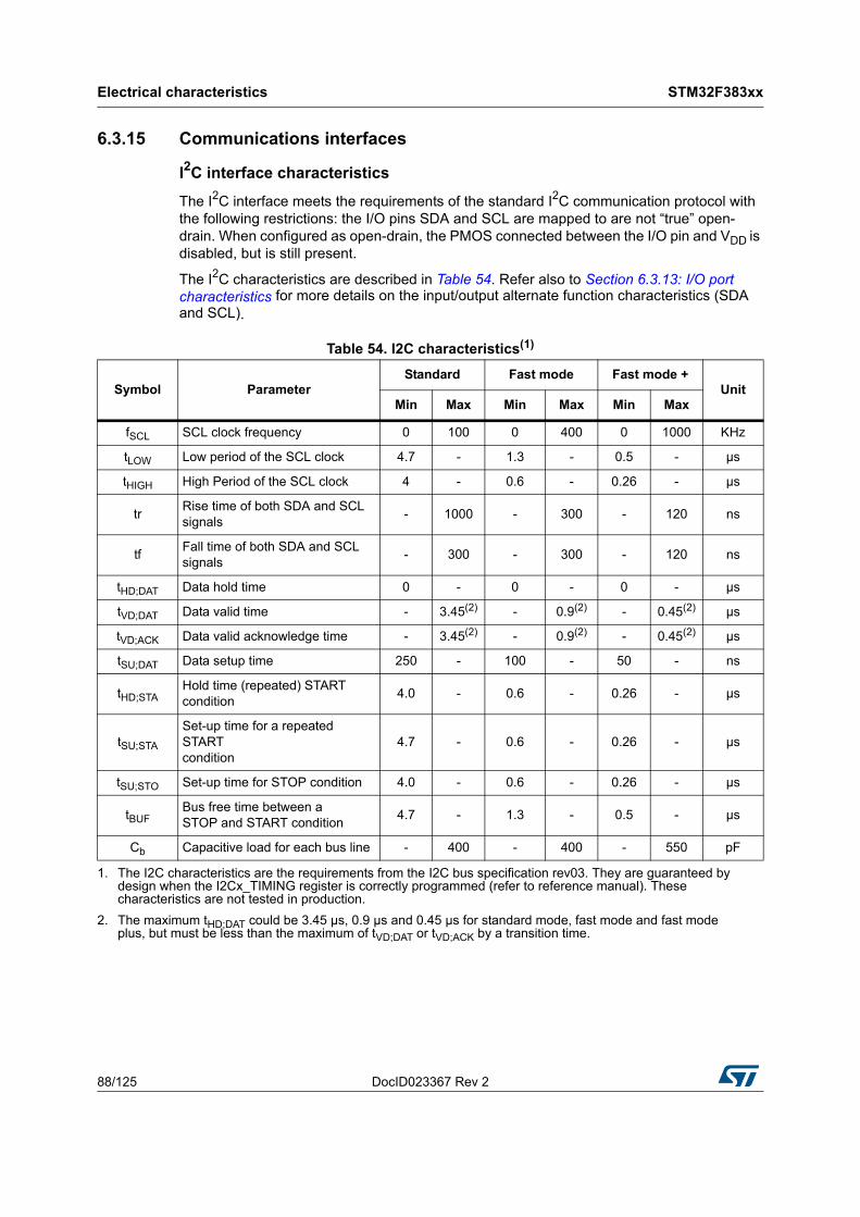
Electrical characteristics STM32F383xx
88/125 DocID023367 Rev 2
6.3.15 Communications interfaces
I2C interface characteristics
The I2C interface meets the requirements of the standard I2C communication protocol with the following restrictions: the I/O pins SDA and SCL are mapped to are not “true” open-drain. When configured as open-drain, the PMOS connected between the I/O pin and VDD is disabled, but is still present.
The I2C characteristics are described in Table 54. Refer also to Section 6.3.13: I/O port characteristics for more details on the input/output alternate function characteristics (SDA and SCL).
Table 54. I2C characteristics(1)
Symbol ParameterStandard Fast mode Fast mode +
UnitMin Max Min Max Min Max
fSCL SCL clock frequency 0 100 0 400 0 1000 KHz
tLOW Low period of the SCL clock 4.7 - 1.3 - 0.5 - µs
tHIGH High Period of the SCL clock 4 - 0.6 - 0.26 - µs
tr Rise time of both SDA and SCL signals - 1000 - 300 - 120 ns
tf Fall time of both SDA and SCL signals - 300 - 300 - 120 ns
tHD;DAT Data hold time 0 - 0 - 0 - µs
tVD;DAT Data valid time - 3.45(2) - 0.9(2) - 0.45(2) µs
tVD;ACK Data valid acknowledge time - 3.45(2) - 0.9(2) - 0.45(2) µs
tSU;DAT Data setup time 250 - 100 - 50 - ns
tHD;STAHold time (repeated) START condition 4.0 - 0.6 - 0.26 - µs
tSU;STA
Set-up time for a repeated START condition
4.7 - 0.6 - 0.26 - µs
tSU;STO Set-up time for STOP condition 4.0 - 0.6 - 0.26 - µs
tBUFBus free time between a STOP and START condition 4.7 - 1.3 - 0.5 - µs
Cb Capacitive load for each bus line - 400 - 400 - 550 pF
1. The I2C characteristics are the requirements from the I2C bus specification rev03. They are guaranteed by design when the I2Cx_TIMING register is correctly programmed (refer to reference manual). These characteristics are not tested in production.
2. The maximum tHD;DAT could be 3.45 µs, 0.9 µs and 0.45 µs for standard mode, fast mode and fast mode plus, but must be less than the maximum of tVD;DAT or tVD;ACK by a transition time.
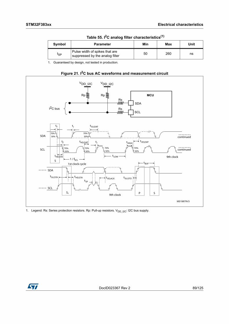
DocID023367 Rev 2 89/125
STM32F383xx Electrical characteristics
109
Figure 21. I2C bus AC waveforms and measurement circuit
1. Legend: Rs: Series protection resistors. Rp: Pull-up resistors. VDD_I2C: I2C bus supply.
Table 55. I2C analog filter characteristics(1)
1. Guaranteed by design, not tested in production.
Symbol Parameter Min Max Unit
tSPPulse width of spikes that are suppressed by the analog filter 50 260 ns
MS19879V3
Rs
I2C bus
Rp
Rs
VDD_I2C
MCU
SDA
SCL
Rp
VDD_I2C
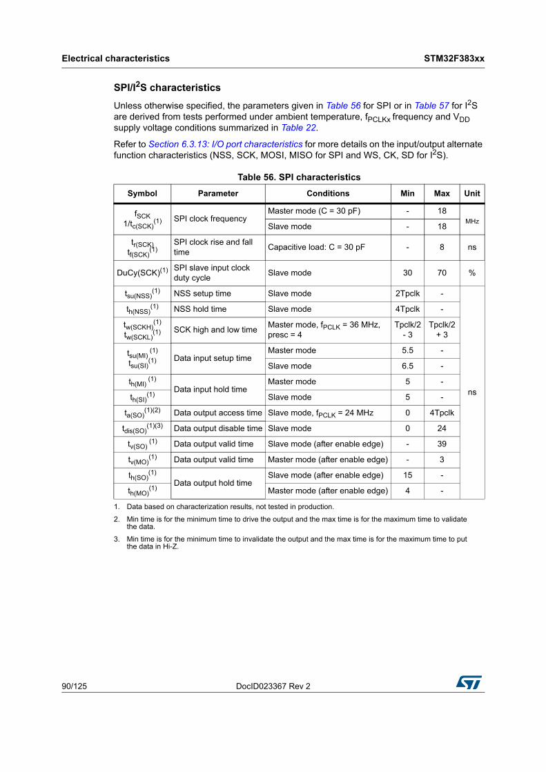
Electrical characteristics STM32F383xx
90/125 DocID023367 Rev 2
SPI/I2S characteristics
Unless otherwise specified, the parameters given in Table 56 for SPI or in Table 57 for I2S are derived from tests performed under ambient temperature, fPCLKx frequency and VDD supply voltage conditions summarized in Table 22.
Refer to Section 6.3.13: I/O port characteristics for more details on the input/output alternate function characteristics (NSS, SCK, MOSI, MISO for SPI and WS, CK, SD for I2S).
Table 56. SPI characteristicsSymbol Parameter Conditions Min Max Unit
fSCK1/tc(SCK)
(1) SPI clock frequencyMaster mode (C = 30 pF) - 18
MHzSlave mode - 18
tr(SCK)tf(SCK)
(1)SPI clock rise and fall time Capacitive load: C = 30 pF - 8 ns
DuCy(SCK)(1) SPI slave input clock duty cycle Slave mode 30 70 %
tsu(NSS)(1)
1. Data based on characterization results, not tested in production.
NSS setup time Slave mode 2Tpclk -
ns
th(NSS)(1) NSS hold time Slave mode 4Tpclk -
tw(SCKH)(1)
tw(SCKL)(1) SCK high and low time Master mode, fPCLK = 36 MHz,
presc = 4Tpclk/2
- 3Tpclk/2
+ 3
tsu(MI) (1)
tsu(SI)(1) Data input setup time
Master mode 5.5 -
Slave mode 6.5 -
th(MI) (1)
Data input hold timeMaster mode 5 -
th(SI)(1) Slave mode 5 -
ta(SO)(1)(2)
2. Min time is for the minimum time to drive the output and the max time is for the maximum time to validate the data.
Data output access time Slave mode, fPCLK = 24 MHz 0 4Tpclk
tdis(SO)(1)(3)
3. Min time is for the minimum time to invalidate the output and the max time is for the maximum time to put the data in Hi-Z.
Data output disable time Slave mode 0 24
tv(SO) (1) Data output valid time Slave mode (after enable edge) - 39
tv(MO)(1) Data output valid time Master mode (after enable edge) - 3
th(SO)(1)
Data output hold timeSlave mode (after enable edge) 15 -
th(MO)(1) Master mode (after enable edge) 4 -
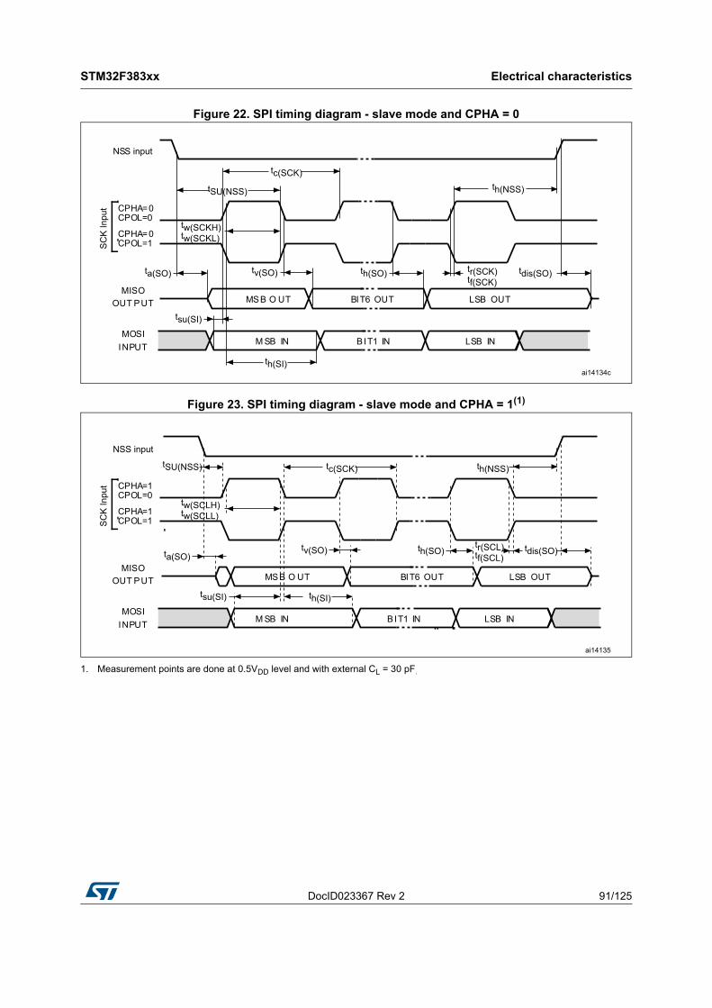
DocID023367 Rev 2 91/125
STM32F383xx Electrical characteristics
109
Figure 22. SPI timing diagram - slave mode and CPHA = 0
Figure 23. SPI timing diagram - slave mode and CPHA = 1(1)
1. Measurement points are done at 0.5VDD level and with external CL = 30 pF.
ai14134c
SC
K In
put CPHA=0
MOSIINPUT
MISOOUT PUT
CPHA=0
MSB O UT
M SB IN
BIT6 OUT
LSB IN
LSB OUT
CPOL=0
CPOL=1
BIT1 IN
NSS input
tSU(NSS)
tc(SCK)th(NSS)
ta(SO)
tw(SCKH)tw(SCKL)
tv(SO) th(SO) tr(SCK)tf(SCK)
tdis(SO)
tsu(SI)
th(SI)
ai14135
SC
K In
put CPHA=1
MOSIINPUT
MISOOUT PUT
CPHA=1
MSB O UT
M SB IN
BIT6 OUT
LSB IN
LSB OUT
CPOL=0
CPOL=1
BIT1 IN
tSU(NSS) tc(SCK) th(NSS)
ta(SO)
tw(SCLH)tw(SCLL)
tv(SO) th(SO)tr(SCL)tf(SCL)
tdis(SO)
tsu(SI) th(SI)
NSS input
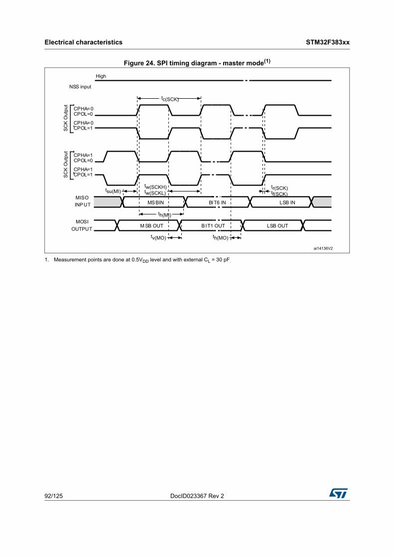
Electrical characteristics STM32F383xx
92/125 DocID023367 Rev 2
Figure 24. SPI timing diagram - master mode(1)
1. Measurement points are done at 0.5VDD level and with external CL = 30 pF.
ai14136V2
SC
K O
utpu
t
CPHA=0
MOSIOUTPUT
MISOINPUT
CPHA=0
MSBIN
M SB OUT
BIT6 IN
LSB OUT
LSB IN
CPOL=0
CPOL=1
BIT1 OUT
NSS input
tc(SCK)
tw(SCKH)tw(SCKL)
tr(SCK)tf(SCK)
th(MI)
High
SC
K O
utpu
t
CPHA=1
CPHA=1
CPOL=0
CPOL=1
tsu(MI)
tv(MO) th(MO)

DocID023367 Rev 2 93/125
STM32F383xx Electrical characteristics
109
Table 57. I2S characteristicsSymbol Parameter Conditions Min Max Unit
DuCy(SCK)(1) I2S slave input clock duty cycle Slave mode 30 70 %
fCK(1)
1/tc(CK)I2S clock frequency
Master mode (data: 16 bits, Audio frequency = 48 kHz) 1.528 1.539
MHzSlave mode 0 12.288
tr(CK)(1)
tf(CK)I2S clock rise and fall time Capacitive load CL = 30 pF - 8
ns
tv(WS) (1) WS valid time Master mode 4 -
th(WS) (1) WS hold time Master mode 4 -
tsu(WS) (1) WS setup time Slave mode 2 -
th(WS) (1) WS hold time Slave mode - -
tw(CKH) (1) I2S clock high time Master fPCLK= 16 MHz, audio
frequency = 48 kHz306 -
tw(CKL) (1) I2S clock low time 312 -
tsu(SD_MR) (1)
Data input setup timeMaster receiver 6 -
tsu(SD_SR) (1) Slave receiver 3 -
th(SD_MR)(1)
Data input hold timeMaster receiver 1.5 -
th(SD_SR) (1) Slave receiver 1.5 -
tv(SD_ST) (1) Data output valid time Slave transmitter
(after enable edge) - 16
th(SD_ST) (1) Data output hold time Slave transmitter
(after enable edge) 16 -
tv(SD_MT) (1) Data output valid time Master transmitter
(after enable edge) - 2
th(SD_MT) (1) Data output hold time Master transmitter
(after enable edge) 0 -
1. Data based on characterization results, not tested in production.
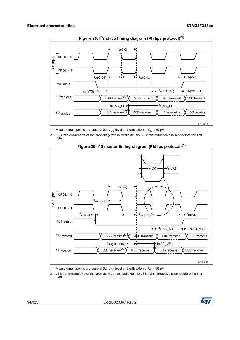
Electrical characteristics STM32F383xx
94/125 DocID023367 Rev 2
Figure 25. I2S slave timing diagram (Philips protocol)(1)
1. Measurement points are done at 0.5 VDD level and with external CL = 30 pF.2. LSB transmit/receive of the previously transmitted byte. No LSB transmit/receive is sent before the first
byte.
Figure 26. I2S master timing diagram (Philips protocol)(1)
1. Measurement points are done at 0.5 VDD level and with external CL = 30 pF.2. LSB transmit/receive of the previously transmitted byte. No LSB transmit/receive is sent before the first
byte.
CK
Inpu
t CPOL = 0
CPOL = 1
tc(CK)
WS input
SDtransmit
SDreceive
tw(CKH) tw(CKL)
tsu(WS) tv(SD_ST) th(SD_ST)
th(WS)
tsu(SD_SR) th(SD_SR)
MSB receive Bitn receive LSB receive
MSB transmit Bitn transmit LSB transmit
ai14881b
LSB receive(2)
LSB transmit(2)
CK
out
put
CPOL = 0
CPOL = 1
tc(CK)
WS output
SDreceive
SDtransmit
tw(CKH)
tw(CKL)
tsu(SD_MR)
tv(SD_MT) th(SD_MT)
th(WS)
th(SD_MR)
MSB receive Bitn receive LSB receive
MSB transmit Bitn transmit LSB transmit
ai14884b
tf(CK) tr(CK)
tv(WS)
LSB receive(2)
LSB transmit(2)

DocID023367 Rev 2 95/125
STM32F383xx Electrical characteristics
109
6.3.16 12-bit ADC characteristicsUnless otherwise specified, the parameters given in Table 58 are preliminary values derived from tests performed under ambient temperature, fPCLK2 frequency and VDDA supply voltage conditions summarized in Table 22.
Note: It is recommended to perform a calibration after each power-up.
Table 58. ADC characteristicsSymbol Parameter Conditions Min Typ Max Unit
VDDA Power supply 2.4 - 3.6 V
VREF+ Positive reference voltage 2.4 - VDDA V
IDDA(ADC)(1) Current consumption from VDDA VDDA = 3.3 V - 0.9 - mA
IVREF Current on the VREF input pin - 160(2) 220(2) µA
fADC ADC clock frequency 0.6 - 14 MHz
fS(3) Sampling rate 0.05 - 1 MHz
fTRIG(3) External trigger frequency
fADC = 14 MHz - - 823 kHz
- - 17 1/fADC
VAIN Conversion voltage range 0 (VSSA or VREF- tied to ground) - VREF+ V
RSRC(3) Signal source impedance See Equation 1 and
Table 59 for details - - 50 κΩ
RADC(3) Sampling switch resistance - - 1 κΩ
CADC(3) Internal sample and hold
capacitor - - 8 pF
tCAL(3) Calibration time
fADC = 14 MHz 5.9 µs
83 1/fADC
tlat(3) Injection trigger conversion
latencyfADC = 14 MHz - - 0.214 µs
- - 2(4) 1/fADC
tlatr(3) Regular trigger conversion
latencyfADC = 14 MHz - - 0.143 µs
- - 2(4) 1/fADC
tS(3) Sampling timefADC = 14 MHz 0.107 - 17.1 µs
1.5 - 239.5 1/fADC
tSTAB(3) Power-up time 0 0 1 µs
tCONV(3) Total conversion time (including
sampling time)
fADC = 14 MHz 1 - 18 µs
14 to 252 (tS for sampling +12.5 for successive approximation) 1/fADC
1. During conversion of the sampled value (12.5 x ADC clock period), an additional consumption of 100 µA on IDDA and 60 µA on IDD is present
2. Based on characterization, not tested in production.
3. Guaranteed by design, not tested in production.
4. For external triggers, a delay of 1/fPCLK2 must be added to the latency specified in Table 58

Electrical characteristics STM32F383xx
96/125 DocID023367 Rev 2
Equation 1: RSRC max formula
The formula above (Equation 1) is used to determine the maximum external signal source impedance allowed for an error below 1/4 of LSB. Here N = 12 (from 12-bit resolution).
Table 59. RSRC max for fADC = 14 MHz(1)
1. Guaranteed by design, not tested in production.
Ts (cycles) tS (µs) RSRC max (kΩ)
1.5 0.11 0.4
7.5 0.54 5.9
13.5 0.96 11.4
28.5 2.04 25.2
41.5 2.96 37.2
55.5 3.96 50
71.5 5.11 50
239.5 17.1 50
Table 60. ADC accuracy(1)(2) (3)
1. ADC DC accuracy values are measured after internal calibration.
Symbol Parameter Test conditions Typ Max(4) Unit
ET Total unadjusted error
fADC = 14 MHz, RSRC < 10 kΩ,VDDA = 3 V to 3.6 VTA = 25 °C
±1.3 ±3
LSB
EO Offset error ±1 ±2
EG Gain error ±0.5 ±1.5
ED Differential linearity error ±0.7 ±1
EL Integral linearity error ±0.8 ±1.5
ET Total unadjusted error
fADC = 14 MHz, RSRC < 10 kΩ,VDDA = 2.7 V to 3.6 VTA = -40 to 105 °C
±3.3 ±4
LSB
EO Offset error ±1.9 ±2.8
EG Gain error ±2.8 ±3
ED Differential linearity error ±0.7 ±1.3
EL Integral linearity error ±1.2 ±1.7
ET Total unadjusted error
fADC = 14 MHz, RSRC < 10 kΩ,VDDA = 2.4 V to 3.6 VTA = 25 °C
±3.3 ±4
LSB
EO Offset error ±1.9 ±2.8
EG Gain error ±2.8 ±3
ED Differential linearity error ±0.7 ±1.3
EL Integral linearity error ±1.2 ±1.7
RSRCTS
fADC CADC 2N 2+( )ln××-------------------------------------------------------------- RADC–<

DocID023367 Rev 2 97/125
STM32F383xx Electrical characteristics
109
Figure 27. ADC accuracy characteristics
Figure 28. Typical connection diagram using the ADC
1. Refer to Table 58 for the values of RSRC, RADC and CADC.2. Cparasitic represents the capacitance of the PCB (dependent on soldering and PCB layout quality) plus the
pad capacitance (roughly 7 pF). A high Cparasitic value will downgrade conversion accuracy. To remedy this, fADC should be reduced.
General PCB design guidelines
Power supply decoupling should be performed as shown in Figure 10. The 10 nF capacitor should be ceramic (good quality) and it should be placed as close as possible to the chip.
2. ADC accuracy vs. negative injection current: Injecting a negative current on any analog input pins should be avoided as this significantly reduces the accuracy of the conversion being performed on another analog input. It is recommended to add a Schottky diode (pin to ground) to analog pins which may potentially inject negative currents.Any positive injection current within the limits specified for IINJ(PIN) and ΣIINJ(PIN) in Section 6.3.13 does not affect the ADC accuracy.
3. Better performance may be achieved in restricted VDDA, frequency and temperature ranges.
4. Data based on characterization results, not tested in production.
EO
EG
1 LSBIDEAL
(1) Example of an actual transfer curve(2) The ideal transfer curve(3) End point correlation line
ET=Total Unadjusted Error: maximum deviationbetween the actual and the ideal transfer curves.EO=Offset Error: deviation between the first actualtransition and the first ideal one.EG=Gain Error: deviation between the last idealtransition and the last actual one.ED=Differential Linearity Error: maximum deviationbetween actual steps and the ideal one.EL=Integral Linearity Error: maximum deviationbetween any actual transition and the end pointcorrelation line.
4095
4094
4093
5
4
3
2
1
0
7
6
1 2 3 4 5 6 7 4093 4094 4095 4096
(1)
(2)ET
ED
EL
(3)
VDDAVSSA MS19880V1
MS32163V1
VDD
AINx
IL±1 μA
0.6 VVT
RSRC(1)
CparasiticSRC
0.6 VVT
RADC(1)12-bit
converter
CADC(1)
Sample and hold ADCconverter
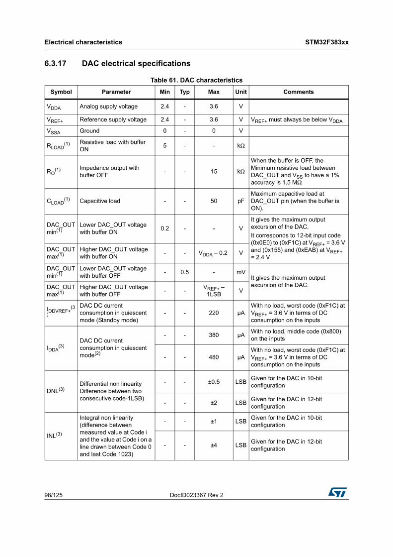
Electrical characteristics STM32F383xx
98/125 DocID023367 Rev 2
6.3.17 DAC electrical specifications
Table 61. DAC characteristicsSymbol Parameter Min Typ Max Unit Comments
VDDA Analog supply voltage 2.4 - 3.6 V
VREF+ Reference supply voltage 2.4 - 3.6 V VREF+ must always be below VDDA
VSSA Ground 0 - 0 V
RLOAD(1) Resistive load with buffer
ON 5 - - kΩ
RO(1) Impedance output with
buffer OFF - - 15 kΩ
When the buffer is OFF, the Minimum resistive load between DAC_OUT and VSS to have a 1% accuracy is 1.5 MΩ
CLOAD(1) Capacitive load - - 50 pF
Maximum capacitive load at DAC_OUT pin (when the buffer is ON).
DAC_OUT min(1)
Lower DAC_OUT voltage with buffer ON 0.2 - - V
It gives the maximum output excursion of the DAC.It corresponds to 12-bit input code (0x0E0) to (0xF1C) at VREF+ = 3.6 V and (0x155) and (0xEAB) at VREF+ = 2.4 V
DAC_OUT max(1)
Higher DAC_OUT voltage with buffer ON - - VDDA – 0.2 V
DAC_OUT min(1)
Lower DAC_OUT voltage with buffer OFF - 0.5 - mV
It gives the maximum output excursion of the DAC.DAC_OUT
max(1)Higher DAC_OUT voltage with buffer OFF - - VREF+ –
1LSB V
IDDVREF+(3
)
DAC DC current consumption in quiescent mode (Standby mode)
- - 220 µAWith no load, worst code (0xF1C) at VREF+ = 3.6 V in terms of DC consumption on the inputs
IDDA(3)
DAC DC current consumption in quiescent mode(2)
- - 380 µA With no load, middle code (0x800) on the inputs
- - 480 µAWith no load, worst code (0xF1C) at VREF+ = 3.6 V in terms of DC consumption on the inputs
DNL(3)Differential non linearity Difference between two consecutive code-1LSB)
- - ±0.5 LSB Given for the DAC in 10-bit configuration
- - ±2 LSB Given for the DAC in 12-bit configuration
INL(3)
Integral non linearity (difference between measured value at Code i and the value at Code i on a line drawn between Code 0 and last Code 1023)
- - ±1 LSB Given for the DAC in 10-bit configuration
- - ±4 LSB Given for the DAC in 12-bit configuration

DocID023367 Rev 2 99/125
STM32F383xx Electrical characteristics
109
Figure 29. 12-bit buffered /non-buffered DAC
1. The DAC integrates an output buffer that can be used to reduce the output impedance and to drive external loads directly without the use of an external operational amplifier. The buffer can be bypassed by configuring the BOFFx bit in the DAC_CR register.
Offset(3)
Offset error(difference between measured value at Code (0x800) and the ideal value = VREF+/2)
- - ±10 mV
- - ±3 LSB Given for the DAC in 10-bit at VREF+ = 3.6 V
- - ±12 LSB Given for the DAC in 12-bit at VREF+ = 3.6 V
Gain error(3) Gain error - - ±0.5 % Given for the DAC in 12bit
configuration
tSETTLING(
3)
Settling time (full scale: for a 10-bit input code transition between the lowest and the highest input codes when DAC_OUT reaches final value ±1LSB
- 3 4 µs CLOAD ≤ 50 pF, RLOAD ≥ 5 kΩ
Update rate(3)
Max frequency for a correct DAC_OUT change when small variation in the input code (from code i to i+1LSB)
- - 1 MS/s CLOAD ≤ 50 pF, RLOAD ≥ 5 kΩ
tWAKEUP(3)
Wakeup time from off state (Setting the ENx bit in the DAC Control register)
- 6.5 10 µsCLOAD ≤ 50 pF, RLOAD ≥ 5 kΩinput code between lowest and highest possible ones.
PSRR+ (1)Power supply rejection ratio (to VDDA) (static DC measurement
- -67 -40 dB No RLOAD, CLOAD = 50 pF
1. Guaranteed by design, not tested in production.
2. Quiescent mode refers to the state of the DAC keeping a steady value on the output, so no dynamic consumption is involved.
3. Guaranteed by characterization, not tested in production.
Table 61. DAC characteristics (continued)Symbol Parameter Min Typ Max Unit Comments
R LOAD
C LOAD
DACx_OUT
Buffer(1)
12-bit digital to analog converter
ai17157

Electrical characteristics STM32F383xx
100/125 DocID023367 Rev 2
6.3.18 Comparator characteristics
Table 62. Comparator characteristicsSymbol Parameter Conditions Min Typ Max(1) Unit
VDDA Analog supply voltage 1.65 - 3.6
VVINComparator input voltage range 0 - VDDA
VBG Scaler input voltage - 1.2 -
VSC Scaler offset voltage - ±5 ±10 mV
tS_SCScaler startup time from power down - - 0.1 ms
tSTART Comparator startup time Startup time to reach propagation delay specification - - 60 µs
tD
Propagation delay for 200 mV step with 100 mV overdrive
Ultra-low power mode - 2 4.5
µsLow power mode - 0.7 1.5
Medium power mode - 0.3 0.6
High speed modeVDDA ≥ 2.7 V - 50 100
ns VDDA < 2.7 V - 100 240
Propagation delay for full range step with 100 mV overdrive
Ultra-low power mode - 2 7
µsLow power mode - 0.7 2.1
Medium power mode - 0.3 1.2
High speed modeVDDA ≥ 2.7 V - 90 180
ns VDDA < 2.7 V - 110 300
Voffset Comparator offset error - ±4 ±10 mV
dVoffset/dT Offset error temperature coefficient - 18 - µV/°C
IDD(COMP)COMP current consumption
Ultra-low power mode - 1.2 1.5
µALow power mode - 3 5
Medium power mode - 10 15
High speed mode - 75 100
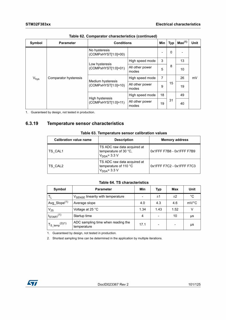
DocID023367 Rev 2 101/125
STM32F383xx Electrical characteristics
109
6.3.19 Temperature sensor characteristics
Vhys Comparator hysteresis
No hysteresis (COMPxHYST[1:0]=00) - 0 -
mV
Low hysteresis (COMPxHYST[1:0]=01)
High speed mode 38
13
All other power modes 5 10
Medium hysteresis (COMPxHYST[1:0]=10)
High speed mode 715
26
All other power modes 9 19
High hysteresis (COMPxHYST[1:0]=11)
High speed mode 1831
49
All other power modes 19 40
1. Guaranteed by design, not tested in production.
Table 62. Comparator characteristics (continued)Symbol Parameter Conditions Min Typ Max(1) Unit
Table 63. Temperature sensor calibration valuesCalibration value name Description Memory address
TS_CAL1TS ADC raw data acquired at temperature of 30 °C, VDDA= 3.3 V
0x1FFF F7B8 - 0x1FFF F7B9
TS_CAL2TS ADC raw data acquired at temperature of 110 °CVDDA= 3.3 V
0x1FFF F7C2 - 0x1FFF F7C3
Table 64. TS characteristicsSymbol Parameter Min Typ Max Unit
TL VSENSE linearity with temperature - ±1 ±2 °C
Avg_Slope(1) Average slope 4.0 4.3 4.6 mV/°C
V25 Voltage at 25 °C 1.34 1.43 1.52 V
tSTART(1)
1. Guaranteed by design, not tested in production.
Startup time 4 - 10 µs
TS_temp(2)(1)
2. Shortest sampling time can be determined in the application by multiple iterations.
ADC sampling time when reading the temperature 17.1 - - µs
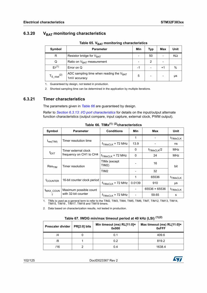
Electrical characteristics STM32F383xx
102/125 DocID023367 Rev 2
6.3.20 VBAT monitoring characteristics
6.3.21 Timer characteristicsThe parameters given in Table 66 are guaranteed by design.
Refer to Section 6.3.13: I/O port characteristics for details on the input/output alternate function characteristics (output compare, input capture, external clock, PWM output).
Table 65. VBAT monitoring characteristicsSymbol Parameter Min Typ Max Unit
R Resistor bridge for VBAT - 50 - KΩ
Q Ratio on VBAT measurement - 2 -
Er(1)
1. Guaranteed by design, not tested in production.
Error on Q -1 - +1 %
TS_vbat(2)
2. Shortest sampling time can be determined in the application by multiple iterations.
ADC sampling time when reading the VBAT1mV accuracy
5 - - µs
Table 66. TIMx(1) (2)characteristics
1. TIMx is used as a general term to refer to the TIM2, TIM3, TIM4, TIM5, TIM6, TIM7, TIM12, TIM13, TIM14, TIM15, TIM16 , TIM17, TIM18 and TIM19 timers.
2. Data based on characterization results, not tested in production.
Symbol Parameter Conditions Min Max Unit
tres(TIM) Timer resolution time1 - tTIMxCLK
fTIMxCLK = 72 MHz 13.9 - ns
fEXTTimer external clock frequency on CH1 to CH4
0 fTIMxCLK/2 MHz
fTIMxCLK = 72 MHz 0 24 MHz
ResTIM Timer resolutionTIMx (except TIM2) - 16
bitTIM2 - 32
tCOUNTER 16-bit counter clock period1 65536 tTIMxCLK
fTIMxCLK = 72 MHz 0.0139 910 µs
tMAX_COUNT
Maximum possible count with 32-bit counter
- 65536 × 65536 tTIMxCLK
fTIMxCLK = 72 MHz - 59.65 s
Table 67. IWDG min/max timeout period at 40 kHz (LSI) (1)(2)
Prescaler divider PR[2:0] bits Min timeout (ms) RL[11:0]= 0x000
Max timeout (ms) RL[11:0]= 0xFFF
/4 0 0.1 409.6
/8 1 0.2 819.2
/16 2 0.4 1638.4

DocID023367 Rev 2 103/125
STM32F383xx Electrical characteristics
109
6.3.22 CAN (controller area network) interfaceRefer to Section 6.3.13: I/O port characteristics for more details on the input/output alternate function characteristics (CAN_TX and CAN_RX).
6.3.23 SDADC characteristics
/32 3 0.8 3276.8
/64 4 1.6 6553.6
/128 5 3.2 13107.2
/256 7 6.4 26214.4
1. These timings are given for a 40 kHz clock but the microcontroller’s internal RC frequency can vary from 30 to 60 kHz. Moreover, given an exact RC oscillator frequency, the exact timings still depend on the phasing of the APB interface clock versus the LSI clock so that there is always a full RC period of uncertainty.
2. Data based on characterization results, not tested in production.
Table 68. WWDG min-max timeout value @72 MHz (PCLK)Prescaler WDGTB Min timeout value Max timeout value
1 0 0.05687 3.6409
2 1 0.1137 7.2817
4 2 0.2275 14.564
8 3 0.4551 29.127
Table 67. IWDG min/max timeout period at 40 kHz (LSI) (continued)(1)(2)
Prescaler divider PR[2:0] bits Min timeout (ms) RL[11:0]= 0x000
Max timeout (ms) RL[11:0]= 0xFFF
Table 69. SDADC characteristics (1)
Symbol Parameter Conditions Min Typ Max Unit Note
VDDSDxPower supply
Slow mode (fADC = 1.5 MHz) 2.2 - VDDAV
Fast mode (fADC = 6 MHz) 2.4 - VDDA
fADC
SDADC clock frequency
Slow mode (fADC = 1.5 MHz) 0.5 1.5 1.65MHz
Fast mode (fADC = 6 MHz) 0.5 6 6.3
VREFSD+Positive ref. voltage 1.1 - VDDSDx V
VREFSD-Negative ref. voltage - VSSA - V
IDDSDx
Supply current (VDDSDx = 3.3 V)
Fast mode (fADC = 6 MHz) - 800 1200
µA
Slow mode (fADC = 1.5 MHz) - - 600
Standby - - 200
Power down - - 2.5
SD_ADC off - - 1
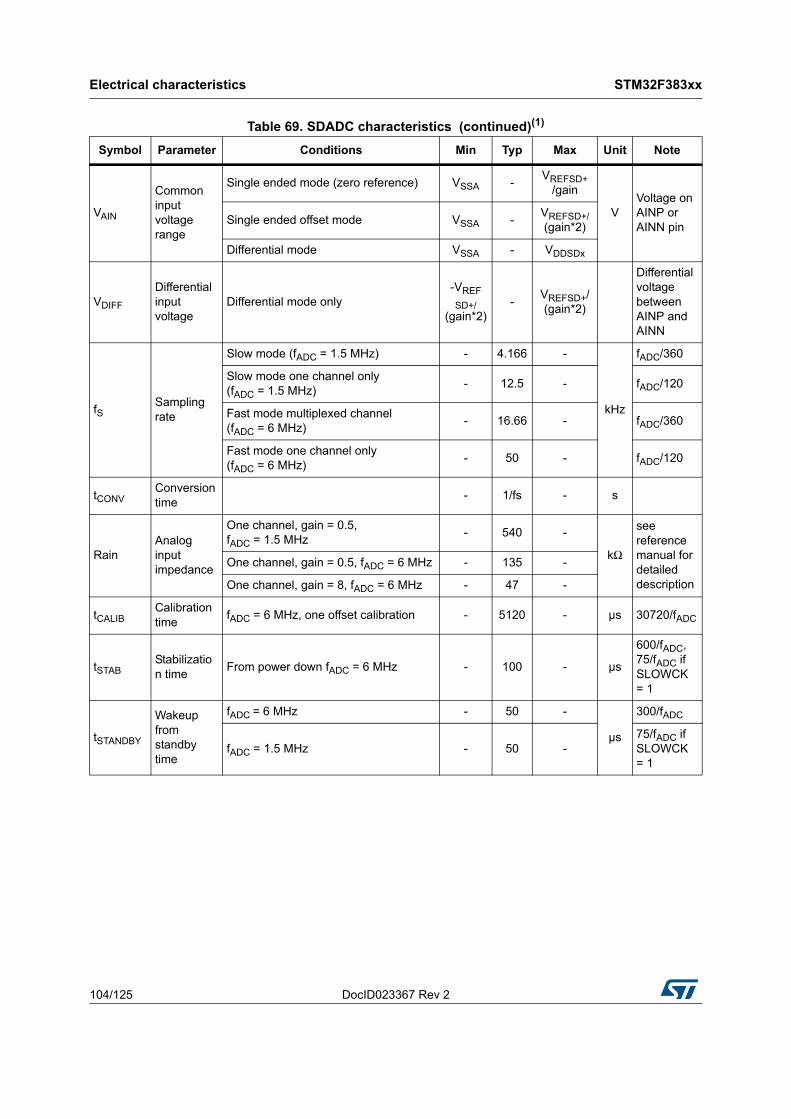
Electrical characteristics STM32F383xx
104/125 DocID023367 Rev 2
VAIN
Common input voltage range
Single ended mode (zero reference) VSSA - VREFSD+ /gain
VVoltage on AINP or AINN pinSingle ended offset mode VSSA - VREFSD+/
(gain*2)
Differential mode VSSA - VDDSDx
VDIFF
Differential input voltage
Differential mode only-VREFSD+/
(gain*2)- VREFSD+/
(gain*2)
Differential voltage between AINP and AINN
fSSampling rate
Slow mode (fADC = 1.5 MHz) - 4.166 -
kHz
fADC/360
Slow mode one channel only (fADC = 1.5 MHz) - 12.5 - fADC/120
Fast mode multiplexed channel (fADC = 6 MHz) - 16.66 - fADC/360
Fast mode one channel only(fADC = 6 MHz) - 50 - fADC/120
tCONVConversion time - 1/fs - s
RainAnalog input impedance
One channel, gain = 0.5, fADC = 1.5 MHz - 540 -
kΩ
see reference manual for detailed description
One channel, gain = 0.5, fADC = 6 MHz - 135 -
One channel, gain = 8, fADC = 6 MHz - 47 -
tCALIBCalibration time fADC = 6 MHz, one offset calibration - 5120 - µs 30720/fADC
tSTABStabilization time From power down fADC = 6 MHz - 100 - µs
600/fADC,75/fADC if SLOWCK = 1
tSTANDBY
Wakeup from standby time
fADC = 6 MHz - 50 -
µs
300/fADC
fADC = 1.5 MHz - 50 -75/fADC if SLOWCK = 1
Table 69. SDADC characteristics (continued)(1)
Symbol Parameter Conditions Min Typ Max Unit Note

DocID023367 Rev 2 105/125
STM32F383xx Electrical characteristics
109
EO Offset error
Diff
eren
tial m
ode ga
in =
1
fADC = 1.5 MHz
VDDSDx = 3.3
VREFSD+ = 3.3 - - 110
uV after offset calibration
fADC = 6 MHz
VREFSD+ = 1.2 - - 110
VREFSD+ = 3.3 - - 100
gain
= 8
fADC = 6 MHz
VREFSD+ = 1.2 - - 70
VREFSD+ = 3.3 - - 100
fADC = 1.5 MHz
VREFSD+ = 3.3 - - 90
Sing
le e
nded
mod
e
gain
= 1
VREFSD+ = 1.2 - - 2100
VREFSD+ = 3.3 - - 2000
gain
= 8
VREFSD+ = 1.2 - - 1500
VREFSD+ = 3.3 - - 1800
Dvoffsettemp
Offset drift with temperature
Differential or single ended mode, gain = 1, VDDSDx = 3.3 V - 10 15 uV/K
EG Gain error All gains, differential mode, single ended mode -2.4 -2.7 -3.1 %
EGT
Gain drift with temperature
gain = 1, differential mode, single ended mode - 0 - ppm/
K
Table 69. SDADC characteristics (continued)(1)
Symbol Parameter Conditions Min Typ Max Unit Note

Electrical characteristics STM32F383xx
106/125 DocID023367 Rev 2
ELIntegral linearity error
Diff
eren
tial m
ode
gain
= 1
VDDSDx = 3.3
VREFSD+ = 1.2 - - 16
LSB
VREFSD+ = 3.3 - - 14
gain
= 8
VREFSD+ = 1.2 - - 26
VREFSD+= 3.3 - - 14
Sing
le e
nded
mod
e
gain
= 1
VREFSD+ = 1.2 - - 31
VREFSD+= 3.3 - - 23
gain
= 8
VREFSD+= 1.2 - - 80
VREFSD+ = 3.3 - - 35
EDDifferential linearity error
Diff
eren
tial m
ode
gain
= 1
VDDSDx = 3.3
VREFSD+ = 1.2 - - 2.4
LSB
VREFSD+ = 3.3 - - 1.8
gain
= 8
VREFSD+= 1.2 - - 3.6
VREFSD+ = 3.3 - - 2.9
Sing
le e
nded
mod
e
gain
= 1
VREFSD+ = 1.2 - - 3.2
VREFSD+ = 3.3 - - 2.8
gain
= 8
VREFSD+= 1.2 - - 4.1
VREFSD+ = 3.3 - - 3.3
Table 69. SDADC characteristics (continued)(1)
Symbol Parameter Conditions Min Typ Max Unit Note

DocID023367 Rev 2 107/125
STM32F383xx Electrical characteristics
109
SNR(4) Signal to noise ratio
Diff
eren
tial m
ode ga
in =
1
fADC = 1.5 MHz
VDDSDx = 3.3
VREFSD+ = 3.3(2) 84 85 -
dB
fADC = 6 MHz
VREFSD+= 1.2(3) 86 88 -
VREFSD+ = 3.3 88 92 -
gain
= 8
fADC = 6 MHz
VREFSD+ = 1.2(3) 76 78 -
VREFSD+ = 3.3 82 86 -
fADC = 1.5 MHz
VREFSD+= 3.3(2) 76 80 -
Sing
le e
nded
mod
e
gain
= 1
fADC = 1.5MHz
VREFSD+ = 3.3 80 84 -
fADC = 6 MHz
VREFSD+ = 1.2(3) 77 81 -
VREFSD+ = 3.3 85 90 -
gain
= 8 fADC =
6 MHz
VREFSD+ = 1.2(3) 66 71 -
VREFSD+ = 3.3 74 78 -
Table 69. SDADC characteristics (continued)(1)
Symbol Parameter Conditions Min Typ Max Unit Note
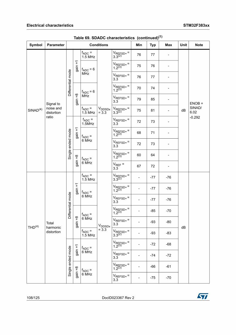
Electrical characteristics STM32F383xx
108/125 DocID023367 Rev 2
SINAD(4)
Signal to noise and distortion ratio
Diff
eren
tial m
ode ga
in =
1
fADC = 1.5 MHz
VDDSDx = 3.3
VREFSD+ = 3.3(2) 76 77 -
dB
ENOB = SINAD/6.02 -0.292
fADC = 6 MHz
VREFSD+ = 1.2(3) 75 76 -
VREFSD+ = 3.3 76 77 -
gain
=8
fADC = 6 MHz
VREFSD+ = 1.2(3) 70 74 -
VREFSD+ = 3.3 79 85 -
fADC = 1.5 MHz
VREFSD+ = 3.3(2) 75 81 -
Sing
le e
nded
mod
e
gain
=1
fADC = 1.5MHz
VREFSD+ = 3.3 72 73 -
fADC = 6 MHz
VREFSD+ = 1.2(3) 68 71 -
VREFSD+ = 3.3 72 73 -
gain
=8
fADC = 6 MHz
VREFSD+ = 1.2(3) 60 64 -
VREF = 3.3 67 72 -
THD(4)Total harmonic distortion
Diff
eren
tial m
ode ga
in =
1
fADC = 1.5 MHz
VDDSDx = 3.3
VREFSD+ = 3.3(2) - -77 -76
dB
fADC = 6 MHz
VREFSD+ = 1.2(3) - -77 -76
VREFSD+ = 3.3 - -77 -76
gain
=8
fADC = 6 MHz
VREFSD+ = 1.2(3) - -85 -70
VREFSD+ = 3.3 - -93 -80
fADC = 1.5 MHz
VREFSD+ = 3.3(2) - -93 -83
Sing
le e
nded
mod
e
gain
=1
fADC = 6 MHz
VREFSD+ = 1.2(3) - -72 -68
VREFSD+ = 3.3 - -74 -72
gain
=8
fADC = 6 MHz
VREFSD+ = 1.2(3) - -66 -61
VREFSD+ = 3.3 - -75 -70
Table 69. SDADC characteristics (continued)(1)
Symbol Parameter Conditions Min Typ Max Unit Note
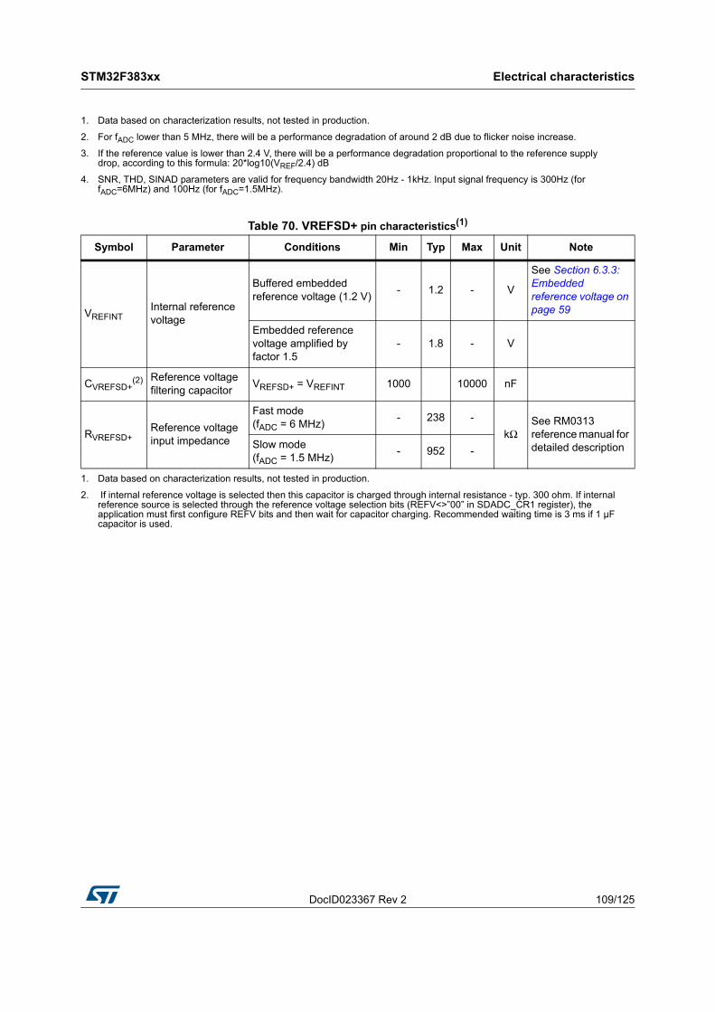
DocID023367 Rev 2 109/125
STM32F383xx Electrical characteristics
109
1. Data based on characterization results, not tested in production.
2. For fADC lower than 5 MHz, there will be a performance degradation of around 2 dB due to flicker noise increase.
3. If the reference value is lower than 2.4 V, there will be a performance degradation proportional to the reference supply drop, according to this formula: 20*log10(VREF/2.4) dB
4. SNR, THD, SINAD parameters are valid for frequency bandwidth 20Hz - 1kHz. Input signal frequency is 300Hz (for fADC=6MHz) and 100Hz (for fADC=1.5MHz).
Table 70. VREFSD+ pin characteristics(1)
Symbol Parameter Conditions Min Typ Max Unit Note
VREFINTInternal reference voltage
Buffered embedded reference voltage (1.2 V) - 1.2 - V
See Section 6.3.3: Embedded reference voltage on page 59
Embedded reference voltage amplified by factor 1.5
- 1.8 - V
CVREFSD+(2) Reference voltage
filtering capacitor VREFSD+ = VREFINT 1000 10000 nF
RVREFSD+Reference voltage input impedance
Fast mode (fADC = 6 MHz) - 238 -
kΩSee RM0313 reference manual for detailed descriptionSlow mode
(fADC = 1.5 MHz) - 952 -
1. Data based on characterization results, not tested in production.
2. If internal reference voltage is selected then this capacitor is charged through internal resistance - typ. 300 ohm. If internal reference source is selected through the reference voltage selection bits (REFV<>”00” in SDADC_CR1 register), the application must first configure REFV bits and then wait for capacitor charging. Recommended waiting time is 3 ms if 1 µF capacitor is used.
Package characteristics STM32F383xx
110/125 DocID023367 Rev 2
7 Package characteristics
7.1 Package mechanical dataIn order to meet environmental requirements, ST offers these devices in different grades of ECOPACK® packages, depending on their level of environmental compliance. ECOPACK® specifications, grade definitions and product status are available at: www.st.com. ECOPACK® is an ST trademark.

DocID023367 Rev 2 111/125
STM32F383xx Package characteristics
122
Figure 30. UFBGA100 – ultra fine pitch ball grid array, 7 x 7 mm, 0.50 mm pitch,package outline
1. Drawing is not to scale.
A1 ballpad corner
Top view Side view Bottom view
A1 ballpad corner
E
D
E1
e
FE
D1
FD
0.50
0.10
A1
AA2
1.75
1.75
0.10
Z
X
Y
A0C2_ME
b
Table 71. UFBGA100 – ultra fine pitch ball grid array, 7 x 7 mm, 0.50 mm pitch, packagemechanical data
Symbolmillimeters inches(1)
Min Typ Max Min Typ Max
A 0.46 0.53 0.6 0.0181 0.0209 0.0236
A1 0.06 0.08 0.1 0.0024 0.0031 0.0039
A2 0.4 0.45 0.5 0.0157 0.0177 0.0197
b 0.2 0.25 0.3 0.0079 0.0098 0.0118
D - 7 - - 0.2756 -
D1 - 5.5 - - 0.2165 -
E - 7 - - 0.2756 -
E1 - 5.5 - - 0.2165 -
e - 0.5 - - 0.0197 -
FD - 0.75 - - 0.0295 -
FE - 0.75 - - 0.0295 -
1. Values in inches are converted from mm and rounded to 4 decimal digits.

Package characteristics STM32F383xx
112/125 DocID023367 Rev 2
Figure 31. WLCSP66 – 0.400 mm pitch wafer level chip size package outline
1. Drawing is not to scale.
Bump sideSide view
Detail A
Wafer back side
A1 ball location
A1
Detail Arotated by 90 °C
eee
D
Seating plane
A2
A
b
E
e
e1
e
G
F
e2
A0R5_ME_V2
ABCDEFGHI
8 7 6 5 4 3 2 1
A1 balllocation
Table 72. WLCSP66 – 0.400 mm pitch wafer level chip size package mechanical data
Symbolmillimeters inches
Min Typ Max Min Typ Max
A 0.520 0.570 0.600 0.0205 0.0224 0.0236
A1 0.170 0.190 0.210 0.0067 0.0075 0.0083
A2 0.350 0.380 0.410 0.0138 0.0150 0.0161
b 0.245 0.270 0.295 0.0096 0.0106 0.0116
D 3.747 3.767 3.787 0.1475 0.1483 0.1491
E 4.209 4.229 4.249 0.1657 0.1665 0.1673
e - 0.400 - - 0.0157 -
e1 - 2.800 - - 0.1102 -
e2 - 3.200 - - 0.1260 -
F - 0.484 - - 0.0191 -
G - 0.515 - - 0.0203 -
eee - - 0.050 - - 0.0020

DocID023367 Rev 2 113/125
STM32F383xx Package characteristics
122
Figure 32. LQFP100 –14 x 14 mm 100-pin low-profile quad flat package outline
1. Drawing is not to scale.
eIDENTIFICATIONPIN 1
GAUGE PLANE0.25 mm
SEATINGPLANE
DD1D3
E3 E1 E
K
ccc C
C
1 25
26100
76
75 51
50
1L_ME_V4
A2A A1
L1L
c
b
A1
Table 73. LQPF100 – 14 x 14 mm low-profile quad flat package mechanical data
Symbolmillimeters inches(1)
Min Typ Max Min Typ Max
A - - 1.600 - - 0.0630
A1 0.050 - 0.150 0.0020 - 0.0059
A2 1.350 1.400 1.450 0.0531 0.0551 0.0571
b 0.170 0.220 0.270 0.0067 0.0087 0.0106
c 0.090 - 0.200 0.0035 - 0.0079
D 15.800 16.000 16.200 0.6220 0.6299 0.6378
D1 13.800 14.000 14.200 0.5433 0.5512 0.5591
D3 - 12.000 - - 0.4724 -
E 15.800 16.000 16.200 0.6220 0.6299 0.6378
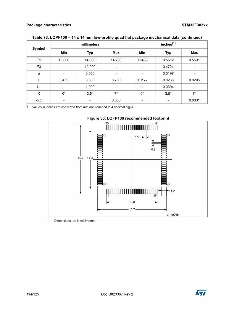
Package characteristics STM32F383xx
114/125 DocID023367 Rev 2
Figure 33. LQFP100 recommended footprint
1. Dimensions are in millimeters.
E1 13.800 14.000 14.200 0.5433 0.5512 0.5591
E3 - 12.000 - - 0.4724 -
e - 0.500 - - 0.0197 -
L 0.450 0.600 0.750 0.0177 0.0236 0.0295
L1 - 1.000 - - 0.0394 -
K 0° 3.5° 7° 0° 3.5° 7°
ccc - - 0.080 - - 0.0031
1. Values in inches are converted from mm and rounded to 4 decimal digits.
Table 73. LQPF100 – 14 x 14 mm low-profile quad flat package mechanical data (continued)
Symbolmillimeters inches(1)
Min Typ Max Min Typ Max
75 51
50760.5
0.3
16.7 14.3
100 26
12.3
25
1.2
16.7
1
ai14906b
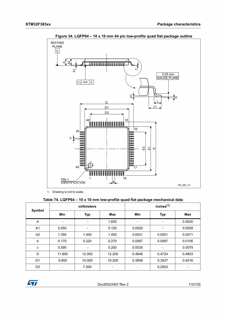
DocID023367 Rev 2 115/125
STM32F383xx Package characteristics
122
Figure 34. LQFP64 – 10 x 10 mm 64 pin low-profile quad flat package outline
1. Drawing is not to scale.
A1
A2A
SEATINGPLANE
ccc C
b
C
cA
1
LL1
K
GAUGE PLANE0.25 mm
IDENTIFICATIONPIN 1
D
D1
D3
e1 16
17
32
3348
49
64
E3 E1 E
5W_ME_V2
Table 74. LQFP64 – 10 x 10 mm low-profile quad flat package mechanical data
Symbolmillimeters inches(1)
Min Typ Max Min Typ Max
A - - 1.600 - - 0.0630
A1 0.050 - 0.150 0.0020 - 0.0059
A2 1.350 1.400 1.450 0.0531 0.0551 0.0571
b 0.170 0.220 0.270 0.0067 0.0087 0.0106
c 0.090 - 0.200 0.0035 - 0.0079
D 11.800 12.000 12.200 0.4646 0.4724 0.4803
D1 9.800 10.000 10.200 0.3858 0.3937 0.4016
D3 - 7.500 - - 0.2953 -
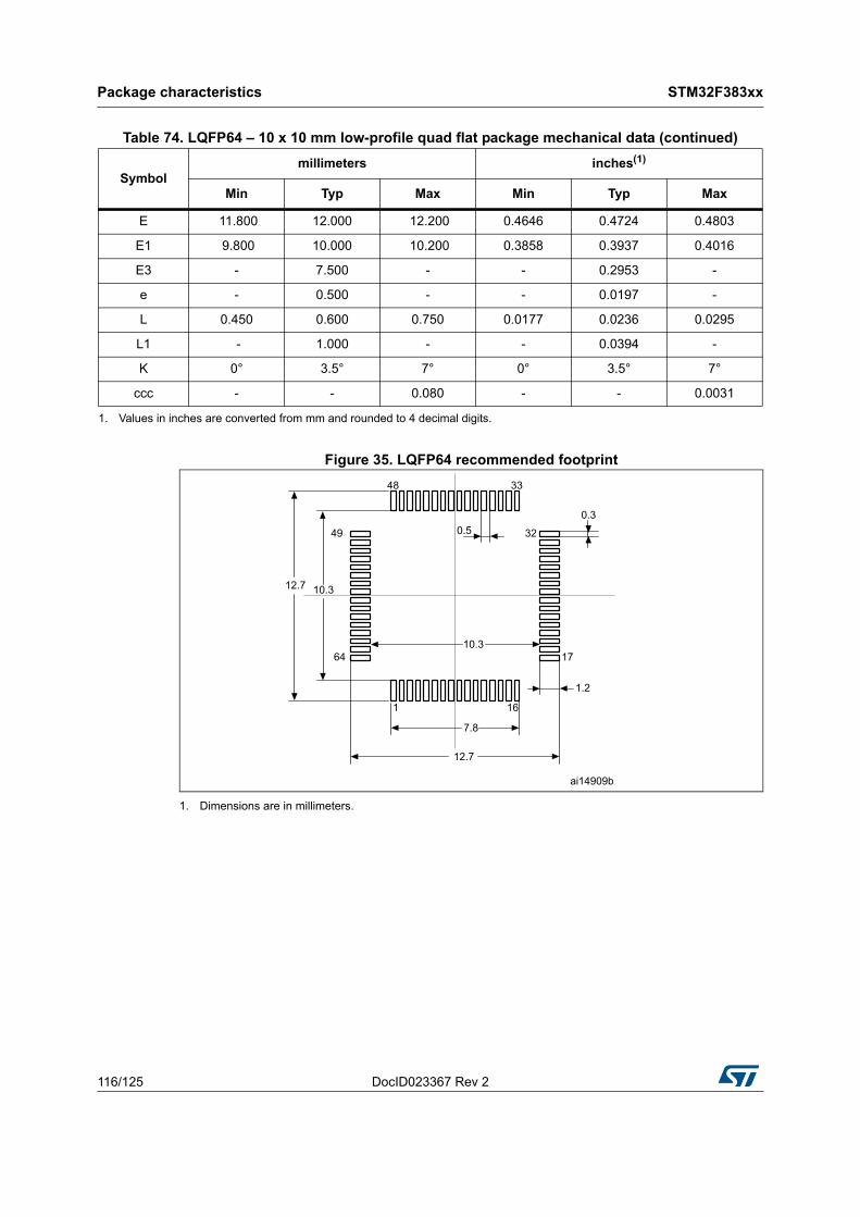
Package characteristics STM32F383xx
116/125 DocID023367 Rev 2
Figure 35. LQFP64 recommended footprint
1. Dimensions are in millimeters.
E 11.800 12.000 12.200 0.4646 0.4724 0.4803
E1 9.800 10.000 10.200 0.3858 0.3937 0.4016
E3 - 7.500 - - 0.2953 -
e - 0.500 - - 0.0197 -
L 0.450 0.600 0.750 0.0177 0.0236 0.0295
L1 - 1.000 - - 0.0394 -
K 0° 3.5° 7° 0° 3.5° 7°
ccc - - 0.080 - - 0.0031
1. Values in inches are converted from mm and rounded to 4 decimal digits.
Table 74. LQFP64 – 10 x 10 mm low-profile quad flat package mechanical data (continued)
Symbolmillimeters inches(1)
Min Typ Max Min Typ Max
48
3249
64 17
1 16
1.2
0.3
33
10.312.7
10.3
0.5
7.8
12.7
ai14909b

DocID023367 Rev 2 117/125
STM32F383xx Package characteristics
122
Figure 36. LQFP48 – 7 x 7 mm, 48-pin low-profile quad flat package outline
1. Drawing is not to scale.
5B_ME_V2
PIN 1IDENTIFICATION
ccc C
C
D3
0.25 mmGAUGE PLANE
b
A1
A A2
cA
1
L1LD
D1
E3 E1 E
e
121
13
24
2536
37
48
SEATINGPLANE
K
Table 75. LQFP48 – 7 x 7 mm, low-profile quad flat package mechanical data
Symbolmillimeters inches(1)
Min Typ Max Min Typ Max
A - - 1.600 - - 0.0630
A1 0.050 - 0.150 0.0020 - 0.0059
A2 1.350 1.400 1.450 0.0531 0.0551 0.0571
b 0.170 0.220 0.270 0.0067 0.0087 0.0106
c 0.090 - 0.200 0.0035 - 0.0079
D 8.800 9.000 9.200 0.3465 0.3543 0.3622
D1 6.800 7.000 7.200 0.2677 0.2756 0.2835
D3 - 5.500 - - 0.2165 -
E 8.800 9.000 9.200 0.3465 0.3543 0.3622
E1 6.800 7.000 7.200 0.2677 0.2756 0.2835
E3 - 5.500 - - 0.2165 -
e - 0.500 - - 0.0197 -
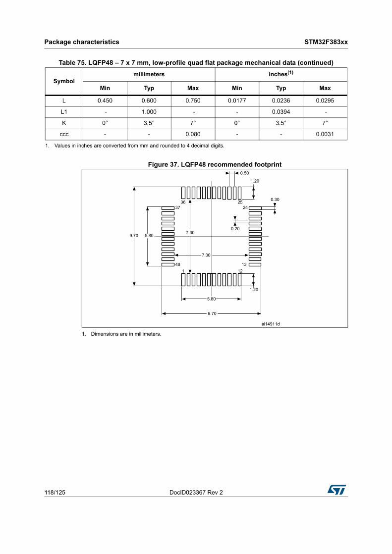
Package characteristics STM32F383xx
118/125 DocID023367 Rev 2
Figure 37. LQFP48 recommended footprint
1. Dimensions are in millimeters.
L 0.450 0.600 0.750 0.0177 0.0236 0.0295
L1 - 1.000 - - 0.0394 -
K 0° 3.5° 7° 0° 3.5° 7°
ccc - - 0.080 - - 0.0031
1. Values in inches are converted from mm and rounded to 4 decimal digits.
Table 75. LQFP48 – 7 x 7 mm, low-profile quad flat package mechanical data (continued)
Symbolmillimeters inches(1)
Min Typ Max Min Typ Max
9.70 5.80 7.30
12
24
0.20
7.30
1
3736
1.20
5.80
9.70
0.3025
1.20
0.50
ai14911d
1348
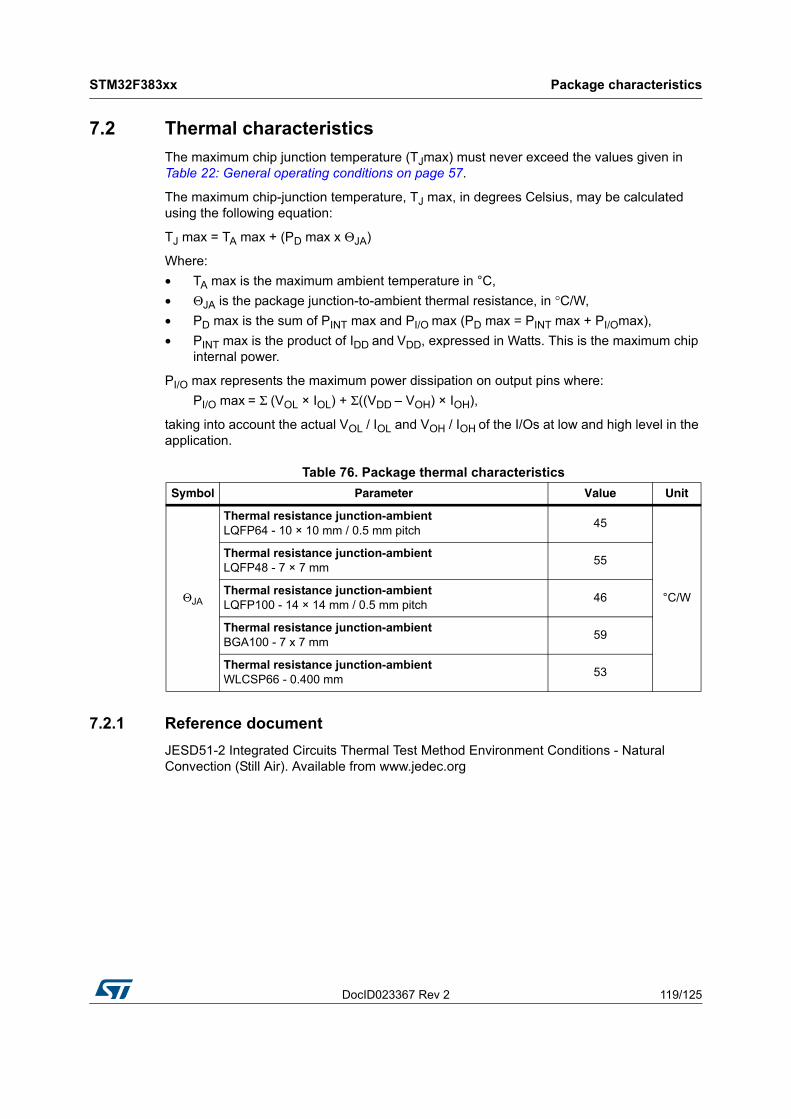
DocID023367 Rev 2 119/125
STM32F383xx Package characteristics
122
7.2 Thermal characteristicsThe maximum chip junction temperature (TJmax) must never exceed the values given in Table 22: General operating conditions on page 57.
The maximum chip-junction temperature, TJ max, in degrees Celsius, may be calculated using the following equation:
TJ max = TA max + (PD max x ΘJA)
Where:• TA max is the maximum ambient temperature in °C,• ΘJA is the package junction-to-ambient thermal resistance, in °C/W,• PD max is the sum of PINT max and PI/O max (PD max = PINT max + PI/Omax),• PINT max is the product of IDD and VDD, expressed in Watts. This is the maximum chip
internal power.
PI/O max represents the maximum power dissipation on output pins where:PI/O max = Σ (VOL × IOL) + Σ((VDD – VOH) × IOH),
taking into account the actual VOL / IOL and VOH / IOH of the I/Os at low and high level in the application.
7.2.1 Reference documentJESD51-2 Integrated Circuits Thermal Test Method Environment Conditions - Natural Convection (Still Air). Available from www.jedec.org
Table 76. Package thermal characteristicsSymbol Parameter Value Unit
ΘJA
Thermal resistance junction-ambientLQFP64 - 10 × 10 mm / 0.5 mm pitch 45
°C/W
Thermal resistance junction-ambientLQFP48 - 7 × 7 mm 55
Thermal resistance junction-ambientLQFP100 - 14 × 14 mm / 0.5 mm pitch 46
Thermal resistance junction-ambientBGA100 - 7 x 7 mm 59
Thermal resistance junction-ambientWLCSP66 - 0.400 mm 53
Package characteristics STM32F383xx
120/125 DocID023367 Rev 2
7.2.2 Selecting the product temperature rangeWhen ordering the microcontroller, the temperature range is specified in the ordering information scheme shown in Section 8: Part numbering.
Each temperature range suffix corresponds to a specific guaranteed ambient temperature at maximum dissipation and, to a specific maximum junction temperature.
As applications do not commonly use the STM32F383xx at maximum dissipation, it is useful to calculate the exact power consumption and junction temperature to determine which temperature range will be best suited to the application.
The following examples show how to calculate the temperature range needed for a given application.
Example 1: High-performance application
Assuming the following application conditions:Maximum ambient temperature TAmax = 82 °C (measured according to JESD51-2), IDDmax = 50 mA, VDD = 1.8 V, maximum 3 I/Os used at the same time in output at low level with IOL = 8 mA, VOL= 0.4 V and maximum 2 I/Os used at the same time in output at low level with IOL = 20 mA, VOL= 1.3 VPINTmax = 50 mA × 1.8 V= 90 mWPIOmax = 3 × 8 mA × 0.4 V + 2 × 20 mA × 1.3 V = 61.6 mWThis gives: PINTmax = 90 mW and PIOmax = 61.6 mW:PDmax = 90 + 61.6 = 151.6 mW
Thus: PDmax = 151.6 mW
Using the values obtained in Table 76 TJmax is calculated as follows:– For LQFP64, 45°C/W TJmax = 82 °C + (45°C/W × 151.6 mW) = 82 °C + 6.8 °C = 88.8 °C
This is within the range of the suffix 6 version parts (–40 < TJ < 105 °C).
In this case, parts must be ordered at least with the temperature range suffix 6 (see Section 8: Part numbering).
Example 2: High-temperature application
Using the same rules, it is possible to address applications that run at high ambient temperatures with a low dissipation, as long as junction temperature TJ remains within the specified range.
Assuming the following application conditions:Maximum ambient temperature TAmax = 115 °C (measured according to JESD51-2), IDDmax = 20 mA, VDD = 1.8 V, maximum 9 I/Os used at the same time in output at low level with IOL = 8 mA, VOL= 0.4 VPINTmax = 20 mA × 1.8 V= 36 mWPIOmax = 9 × 8 mA × 0.4 V = 28.8 mWThis gives: PINTmax = 36 mW and PIOmax = 28.8 mW:PDmax = 36+ 28.8 = 64.8 mW
Thus: PDmax = 64.8 mW
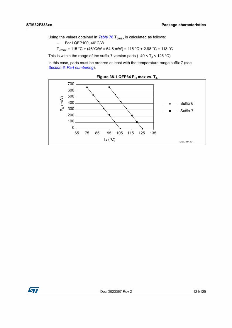
DocID023367 Rev 2 121/125
STM32F383xx Package characteristics
122
Using the values obtained in Table 76 TJmax is calculated as follows:– For LQFP100, 46°C/W TJmax = 115 °C + (46°C/W × 64.8 mW) = 115 °C + 2.98 °C = 118 °C
This is within the range of the suffix 7 version parts (–40 < TJ < 125 °C).
In this case, parts must be ordered at least with the temperature range suffix 7 (see Section 8: Part numbering).
Figure 38. LQFP64 PD max vs. TA
MSv32143V1
600
0
100200300400500
700
65 75 85 95 105 115 125 135
Suffix 6
Suffix 7PD (m
W)
TA (°C)
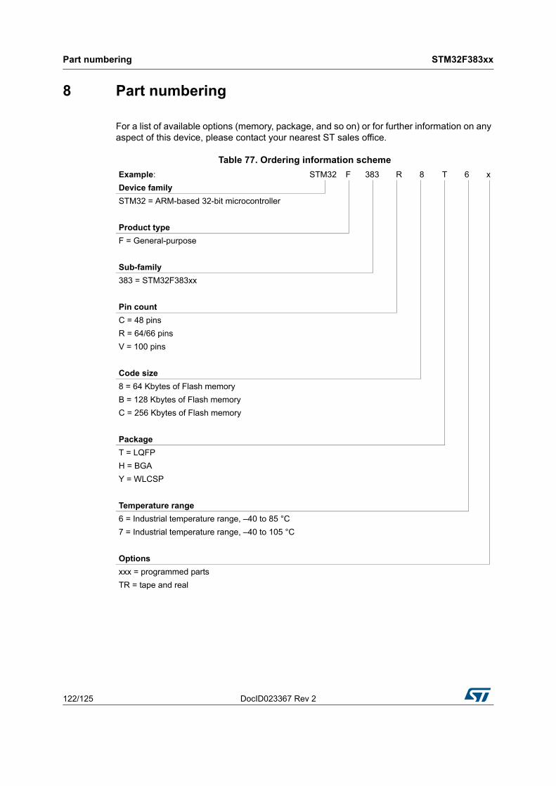
Part numbering STM32F383xx
122/125 DocID023367 Rev 2
8 Part numbering
For a list of available options (memory, package, and so on) or for further information on any aspect of this device, please contact your nearest ST sales office.
Table 77. Ordering information schemeExample: STM32 F 383 R 8 T 6 xDevice familySTM32 = ARM-based 32-bit microcontroller
Product typeF = General-purpose
Sub-family383 = STM32F383xx
Pin countC = 48 pinsR = 64/66 pinsV = 100 pins
Code size8 = 64 Kbytes of Flash memoryB = 128 Kbytes of Flash memoryC = 256 Kbytes of Flash memory
PackageT = LQFPH = BGAY = WLCSP
Temperature range6 = Industrial temperature range, –40 to 85 °C7 = Industrial temperature range, –40 to 105 °C
Optionsxxx = programmed partsTR = tape and real

DocID023367 Rev 2 123/125
STM32F383xx Revision history
124
9 Revision history
Table 78. Document revision historyDate Revision Changes
18-Jan-2013 1 Initial release.
19-Sep-2013 2
Replaced “Cortex-M4F” with “Cortex-M4” throughout the document.Removed part number STM32F382xx.Added “1.25 DMIPS/MHz (Dhrystone 2.1)” in Features.Removed all references to pin PB2.Updated Introduction.Added reference to the STMTouch touch sensing firmware library in Section 3.16: Touch sensing controller (TSC).Added “All I2S interfaces can operate in half-duplex mode only.” in Section 3.21: Serial peripheral interface (SPI)/Inter-integrated sound interfaces (I2S).Modified introduction of I2C interface characteristics.Added alternate function RTC_REFIN and removed additional function RTC_REF_CLK_IN to pins PA1 and PB15. Replaced alternate function JNTRST with NJTRST for pin PB4. Replaced alternate function TIM1_TX with USART1_TX for pin PC4 and TIM1_RX with USART1_RX for pin PC5. Added alternate functions TIM4_CH1 and TSC_G8_IO1 to pin PD12. Removed additional functions TIM4_CH1 and G8_IO1 from pin PD12.Added row “I2S full-duplex mode” to Table 9: STM32F383xx SPI/I2S implementation.In Table 12: Alternate functions for port PA: replaced alternate function JTMS-SWDIO with SWDIO-JTMS for pin PA13, and JTCK-SWCLK with SWCLK-JTCK for pin PA14.In Table 22: General operating conditions: added rows VREF+ and VREFSD+; changed minimum value of VDDSD12 (‘SDADC not used’ condition) from 2.0 to 1.65.Replaced table column heading "Typ@VDD (VDD = VDDA = 1.8 V)" with "Typ@VDD (VDD=1.8 V, VDDA=3.3 V)" in Table 28: Typical and maximum VDD consumption in Stop mode.Updated Table 29: Typical and maximum VDDA consumption in Stop mode.Added conditions for fHSE_ext in Table 35: High-speed external user clock characteristics.Added Min and Max values for ACCHISI in Table 39: HSI oscillator characteristics.Added COMP in Table 33: Peripheral current consumptionChanged VDDA value from 1.8 to 3.3 V in note(1) under Table 39: HSI oscillator characteristics and Table 40: LSI oscillator characteristics.

Revision history STM32F383xx
124/125 DocID023367 Rev 2
19-Sep-20132
(continued)
Modified condition for “FM+ configuration” in Table 51: I/O AC characteristics.Replaced reference "JESD22-C101" with "ANSI/ESD STM5.3.1" in Table 46: ESD absolute maximum ratings.Removed pins PB0 and PB1 in description of IINJ in Table 48: I/O current injection susceptibility.Updated Table 54: I2C characteristics.Replaced all occurrences of “gain/2” with “gain*2” in Table 69: SDADC characteristics.Corrected typo in Figure 19: I/O AC characteristics definition.Replaced Figure 21: I2C bus AC waveforms and measurement circuit.Added IDDA(ADC) and footnote 1 in Table 58: ADC characteristicsModified Figure 31: WLCSP66 – 0.400 mm pitch wafer level chip size package outline.Modified ambient operating temperature condition in On-chip peripheral current consumption.Modified wakeup pin information in Section 6.3.5: Wakeup time from low-power mode.
Table 78. Document revision history (continued)Date Revision Changes
DocID023367 Rev 2 125/125
STM32F383xx
125
Please Read Carefully:
Information in this document is provided solely in connection with ST products. STMicroelectronics NV and its subsidiaries (“ST”) reserve theright to make changes, corrections, modifications or improvements, to this document, and the products and services described herein at anytime, without notice.
All ST products are sold pursuant to ST’s terms and conditions of sale.
Purchasers are solely responsible for the choice, selection and use of the ST products and services described herein, and ST assumes noliability whatsoever relating to the choice, selection or use of the ST products and services described herein.
No license, express or implied, by estoppel or otherwise, to any intellectual property rights is granted under this document. If any part of thisdocument refers to any third party products or services it shall not be deemed a license grant by ST for the use of such third party productsor services, or any intellectual property contained therein or considered as a warranty covering the use in any manner whatsoever of suchthird party products or services or any intellectual property contained therein.
UNLESS OTHERWISE SET FORTH IN ST’S TERMS AND CONDITIONS OF SALE ST DISCLAIMS ANY EXPRESS OR IMPLIED WARRANTY WITH RESPECT TO THE USE AND/OR SALE OF ST PRODUCTS INCLUDING WITHOUT LIMITATION IMPLIED WARRANTIES OF MERCHANTABILITY, FITNESS FOR A PARTICULAR PURPOSE (AND THEIR EQUIVALENTS UNDER THE LAWS OF ANY JURISDICTION), OR INFRINGEMENT OF ANY PATENT, COPYRIGHT OR OTHER INTELLECTUAL PROPERTY RIGHT.
ST PRODUCTS ARE NOT DESIGNED OR AUTHORIZED FOR USE IN: (A) SAFETY CRITICAL APPLICATIONS SUCH AS LIFE SUPPORTING, ACTIVE IMPLANTED DEVICES OR SYSTEMS WITH PRODUCT FUNCTIONAL SAFETY REQUIREMENTS; (B) AERONAUTIC APPLICATIONS; (C) AUTOMOTIVE APPLICATIONS OR ENVIRONMENTS, AND/OR (D) AEROSPACE APPLICATIONS OR ENVIRONMENTS. WHERE ST PRODUCTS ARE NOT DESIGNED FOR SUCH USE, THE PURCHASER SHALL USE PRODUCTS AT PURCHASER’S SOLE RISK, EVEN IF ST HAS BEEN INFORMED IN WRITING OF SUCH USAGE, UNLESS A PRODUCT IS EXPRESSLY DESIGNATED BY ST AS BEING INTENDED FOR “AUTOMOTIVE, AUTOMOTIVE SAFETY OR MEDICAL” INDUSTRY DOMAINS ACCORDING TO ST PRODUCT DESIGN SPECIFICATIONS. PRODUCTS FORMALLY ESCC, QML OR JAN QUALIFIED ARE DEEMED SUITABLE FOR USE IN AEROSPACE BY THE CORRESPONDING GOVERNMENTAL AGENCY.
Resale of ST products with provisions different from the statements and/or technical features set forth in this document shall immediately voidany warranty granted by ST for the ST product or service described herein and shall not create or extend in any manner whatsoever, anyliability of ST.
ST and the ST logo are trademarks or registered trademarks of ST in various countries.Information in this document supersedes and replaces all information previously supplied.
The ST logo is a registered trademark of STMicroelectronics. All other names are the property of their respective owners.
© 2013 STMicroelectronics - All rights reserved
STMicroelectronics group of companies
Australia - Belgium - Brazil - Canada - China - Czech Republic - Finland - France - Germany - Hong Kong - India - Israel - Italy - Japan - Malaysia - Malta - Morocco - Philippines - Singapore - Spain - Sweden - Switzerland - United Kingdom - United States of America
www.st.com