Embed Size (px)
Citation preview
ARM DDI 0100I Copyright © 1996-1998, 2000, 2004, 2005 ARM Limited. All rights reserved. A3-1
Chapter A3 The ARM Instruction Set
This chapter describes the ARM® instruction set and contains the following sections:• Instruction set encoding on page A3-2• The condition field on page A3-3• Branch instructions on page A3-5• Data-processing instructions on page A3-7• Multiply instructions on page A3-10• Parallel addition and subtraction instructions on page A3-14• Extend instructions on page A3-16• Miscellaneous arithmetic instructions on page A3-17• Other miscellaneous instructions on page A3-18• Status register access instructions on page A3-19• Load and store instructions on page A3-21• Load and Store Multiple instructions on page A3-26• Semaphore instructions on page A3-28• Exception-generating instructions on page A3-29• Coprocessor instructions on page A3-30• Extending the instruction set on page A3-32.
The ARM Instruction Set
A3-2 Copyright © 1996-1998, 2000, 2004, 2005 ARM Limited. All rights reserved. ARM DDI 0100I
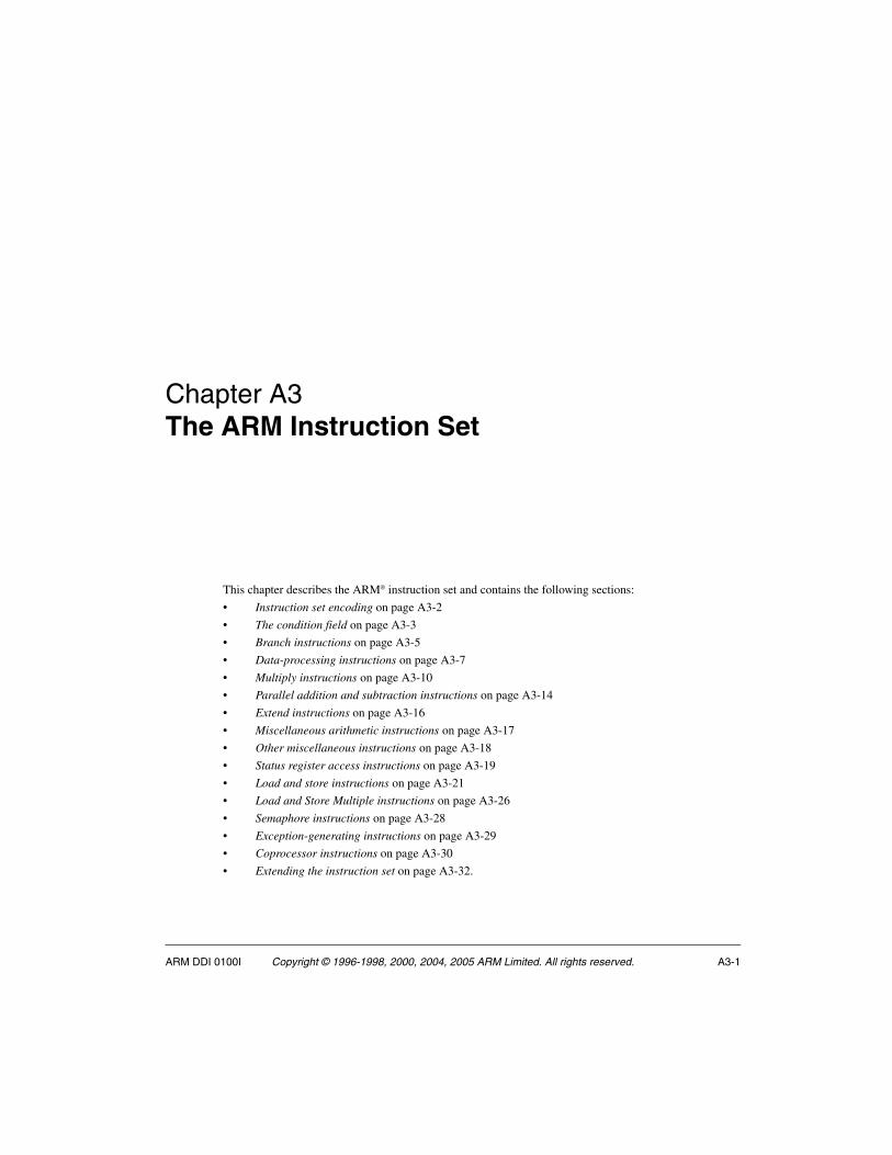
A3.1 Instruction set encoding
Figure A3-1 shows the ARM instruction set encoding.
All other bit patterns are UNPREDICTABLE or UNDEFINED. See Extending the instruction set on page A3-32 for a description of the cases where instructions are UNDEFINED.
An entry in square brackets, for example [1], indicates that more information is given after the figure.
Figure A3-1 ARM instruction set summary1. The cond field is not allowed to be 1111 in this line. Other lines deal with the cases where bits[31:28]
of the instruction are 1111.2. If the opcode field is of the form 10xx and the S field is 0, one of the following lines applies instead.3. If the cond field is 1111, this instruction is UNPREDICTABLE prior to ARMv5.4. The architecturally Undefined instruction uses a small number of these instruction encodings.
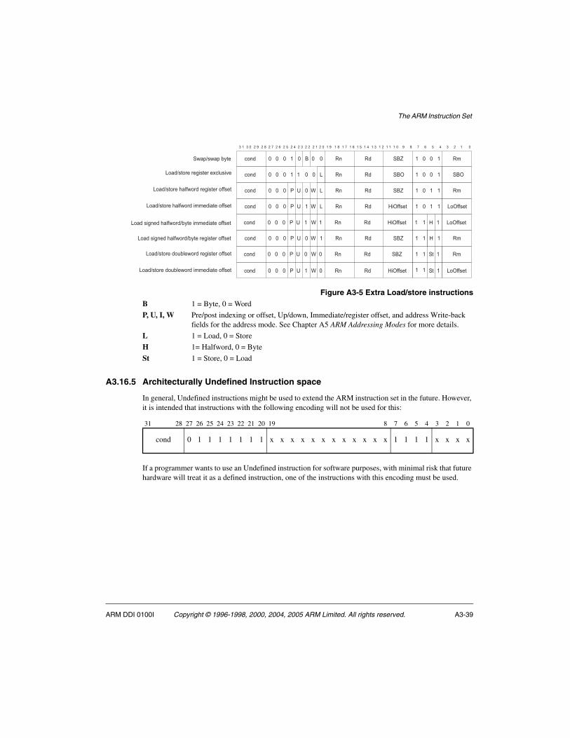
!"#"$%&'()**+,-$+..)/+"#)$*0+1# *0+1#(',/$234 5/5,67 7 7 '%('/) *0+1#$".'8,# 5.7
!"#"$%&'()**+,-$&)-+*#)&$*0+1#$294 *0+1#(',/$234 5/5,67 7 7 '%('/) 3 5.75*
!"#"$%&'()**+,-$+..)/+"#)$294 (',/$234 &'#"#) +..)/+"#)5/5,67 7 3 '%('/)
:,/)1+,)/$+,*#&8(#+', (',/$234 7 7 3 3 ; ; ; ;7 ; 7 7 ; ; ; ; ; ; ; ; ; ; ; ; ; ; ; ;
(',/$234 7 3 3 ;
; ; ; ;
; ; ; ; ; ; ; ; ; ; ; ; ; ; ; ; ; ; ; 3
<+*()==",)'8*$+,*#&8(#+',*>6))$?+-8&)$@ABC (',/$234 77 7 7 73 7 ; ;
(',/$234 77 7 7 33 7 ; ;
(',/$234 ;7 7 7 3; ; ; ;
<'D)$+..)/+"#)$#'$*#"#8*$&)-+*#)& (',/$234 5 6EF<"*G &'#"#) +..)/+"#)
H'"/I*#'&)$+..)/+"#)$'11*)# (',/$234 +..)/+"#)5/5,7 3 7 E:J HK
H'"/I*#'&)$&)-+*#)&$'11*)# (',/$234 5/5,7 3 3 E:J HK *0+1#$".'8,# *0+1# 5.7
; ; ; ; ; ; ; ;; ; ; ; ; ; ; ; ; ; ; ; ; ; ; ; ; ; ; ;
H'"/I*#'&)$.8=#+%=)
(',/$234
&)-+*#)&$=+*#5,3 7 7 6:J HK
E&",(0$",/$L&",(0$M+#0$=+,G (',/$234 9CBL+#$'11*)#
N'%&'()**'&$='"/I*#'&)$",/$/'8L=)&)-+*#)&$#&",*1)&* (',/$2A4 : O K H 5, N5/ (%P,8. QBL+#$'11*)#
N'%&'()**'&$&)-+*#)&$#&",*1)&* (',/$2A4 '%('/)3 5/N5, '%('/)9 3 N5.(%P,8.H
N'%&'()**'&$/"#"$%&'()**+,- (',/$2A4 '%('/)3 N5/N5, '%('/)9 7 N5.(%P,8.
6'1#M"&)$+,#)&&8%# (',/$234 *M+$,8.L)&
; ; ; ;; ; ; ; ; ; ; ; ; ; ; ; ; ; ;
; ; ; ;; ; ; ; ; ; ; ; ; ; ; ; 7 ; ;<+*()==",)'8*$+,*#&8(#+',*>6))$?+-8&)$@ABC
; ; ; ;; ; ; ; ; ; ; ; ; ; ; ; 3 ; ;<8=#+%=+)*>$6))$?+-8&)$@ABAR;#&"$='"/I*#'&)*>$6))$?+-8&)$@ABS
7 7 3 3 7 3 7
3 3 3
3 7 3 H
3 3 7 J
3 3 3 7
3 3 3 7
3 3 3 3
A 3 9 Q 9 T 9 S 9 C 9 A 9 9 9 3 9 7 3 U 3 Q 3 V 3 T 3 S 3 C 3 A 3 9 3 3 3 7 U Q V T S C A 9 3 7A 7 9 U 9 V
<)/+"$+,*#&8(#+',*$2C4>6))$?+-8&)$@AB9
:,(',/+#+',"=$+,*#&8(#+',*>6))$?+-8&)$@ABT
3
; ; ; ;
3333
(',/$234
7 3 3 3 3 3 3 3@&(0+#)(#8&"==W$8,/)1+,)/ ; ; ; ; ; ; ; ; ; ; ; ;
The ARM Instruction Set
ARM DDI 0100I Copyright © 1996-1998, 2000, 2004, 2005 ARM Limited. All rights reserved. A3-3
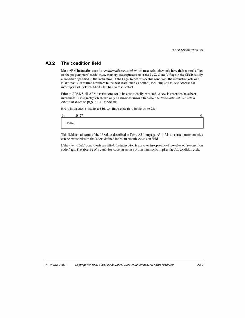
A3.2 The condition field
Most ARM instructions can be conditionally executed, which means that they only have their normal effect on the programmers’ model state, memory and coprocessors if the N, Z, C and V flags in the CPSR satisfy a condition specified in the instruction. If the flags do not satisfy this condition, the instruction acts as a NOP: that is, execution advances to the next instruction as normal, including any relevant checks for interrupts and Prefetch Aborts, but has no other effect.
Prior to ARMv5, all ARM instructions could be conditionally executed. A few instructions have been introduced subsequently which can only be executed unconditionally. See Unconditional instruction extension space on page A3-41 for details.
Every instruction contains a 4-bit condition code field in bits 31 to 28:
This field contains one of the 16 values described in Table A3-1 on page A3-4. Most instruction mnemonics can be extended with the letters defined in the mnemonic extension field.
If the always (AL) condition is specified, the instruction is executed irrespective of the value of the condition code flags. The absence of a condition code on an instruction mnemonic implies the AL condition code.
31 28 27 0
cond
The ARM Instruction Set
A3-4 Copyright © 1996-1998, 2000, 2004, 2005 ARM Limited. All rights reserved. ARM DDI 0100I
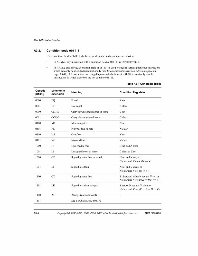
A3.2.1 Condition code 0b1111
If the condition field is 0b1111, the behavior depends on the architecture version:
• In ARMv4, any instruction with a condition field of 0b1111 is UNPREDICTABLE.
• In ARMv5 and above, a condition field of 0b1111 is used to encode various additional instructions which can only be executed unconditionally (see Unconditional instruction extension space on page A3-41). All instruction encoding diagrams which show bits[31:28] as cond only match instructions in which these bits are not equal to 0b1111.
Table A3-1 Condition codes
Opcode [31:28]
Mnemonic extension Meaning Condition flag state
0000 EQ Equal Z set
0001 NE Not equal Z clear
0010 CS/HS Carry set/unsigned higher or same C set
0011 CC/LO Carry clear/unsigned lower C clear
0100 MI Minus/negative N set
0101 PL Plus/positive or zero N clear
0110 VS Overflow V set
0111 VC No overflow V clear
1000 HI Unsigned higher C set and Z clear
1001 LS Unsigned lower or same C clear or Z set
1010 GE Signed greater than or equal N set and V set, orN clear and V clear (N == V)
1011 LT Signed less than N set and V clear, or N clear and V set (N != V)
1100 GT Signed greater than Z clear, and either N set and V set, or N clear and V clear (Z == 0,N == V)
1101 LE Signed less than or equal Z set, or N set and V clear, or N clear and V set (Z == 1 or N != V)
1110 AL Always (unconditional) -
1111 - See Condition code 0b1111 -
The ARM Instruction Set
ARM DDI 0100I Copyright © 1996-1998, 2000, 2004, 2005 ARM Limited. All rights reserved. A3-5
A3.3 Branch instructions
All ARM processors support a branch instruction that allows a conditional branch forwards or backwards up to 32MB. As the PC is one of the general-purpose registers (R15), a branch or jump can also be generated by writing a value to R15.
A subroutine call can be performed by a variant of the standard branch instruction. As well as allowing a branch forward or backward up to 32MB, the Branch with Link (BL) instruction preserves the address of the instruction after the branch (the return address) in the LR (R14).
In T variants of ARMv4 and above, the Branch and Exchange (BX) instruction copies the contents of a general-purpose register Rm to the PC (like a MOV PC,Rm instruction), with the additional functionality that if bit[0] of the transferred value is 1, the processor shifts to Thumb® state. Together with the corresponding Thumb instructions, this allows interworking branches between ARM and Thumb code.
Interworking subroutine calls can be generated by combining BX with an instruction to write a suitable return address to the LR, such as an immediately preceding MOV LR,PC instruction.
In ARMv5 and above, there are also two types of Branch with Link and Exchange (BLX) instruction:
• One type takes a register operand Rm, like a BX instruction. This instruction behaves like a BX instruction, and additionally writes the address of the next instruction into the LR. This provides a more efficient interworking subroutine call than a sequence of MOV LR,PC followed by BX Rm.
• The other type behaves like a BL instruction, branching backwards or forwards by up to 32MB and writing a return link to the LR, but shifts to Thumb state rather than staying in ARM state as BL does. This provides a more efficient alternative to loading the subroutine address into Rm followed by a BLX Rm instruction when it is known that a Thumb subroutine is being called and that the subroutine lies within the 32MB range.
A load instruction provides a way to branch anywhere in the 4GB address space (known as a long branch). A 32-bit value is loaded directly from memory into the PC, causing a branch. A long branch can be preceded by MOV LR,PC or another instruction that writes the LR to generate a long subroutine call. In ARMv5 and above, bit[0] of the value loaded by a long branch controls whether the subroutine is executed in ARM state or Thumb state, just like bit[0] of the value moved to the PC by a BX instruction. Prior to ARMv5, bits[1:0] of the value loaded into the PC are ignored, and a load into the PC can only be used to call a subroutine in ARM state.
In non-T variants of ARMv5, the instructions described above can cause an entry into Thumb state despite the fact that the Thumb instruction set is not present. This causes the instruction at the branch target to enter the Undefined Instruction exception. See The interrupt disable bits on page A2-14 for more details.
In ARMv6 and above, and in J variants of ARMv5, there is an additional Branch and Exchange Jazelle® instruction, see BXJ on page A4-21.
The ARM Instruction Set
A3-6 Copyright © 1996-1998, 2000, 2004, 2005 ARM Limited. All rights reserved. ARM DDI 0100I
A3.3.1 Examples
B label ; branch unconditionally to label
BCC label ; branch to label if carry flag is clear
BEQ label ; branch to label if zero flag is set
MOV PC, #0 ; R15 = 0, branch to location zero
BL func ; subroutine call to function
func ..MOV PC, LR ; R15=R14, return to instruction after the BLMOV LR, PC ; store the address of the instruction
; after the next one into R14 ready to returnLDR PC, =func ; load a 32-bit value into the program counter
A3.3.2 List of branch instructions
B, BL Branch, and Branch with Link. See B, BL on page A4-10.
BLX Branch with Link and Exchange. See BLX (1) on page A4-16 and BLX (2) on page A4-18.
BX Branch and Exchange Instruction Set. See BX on page A4-20.
BXJ Branch and change to Jazelle state. See BXJ on page A4-21.
The ARM Instruction Set
ARM DDI 0100I Copyright © 1996-1998, 2000, 2004, 2005 ARM Limited. All rights reserved. A3-7
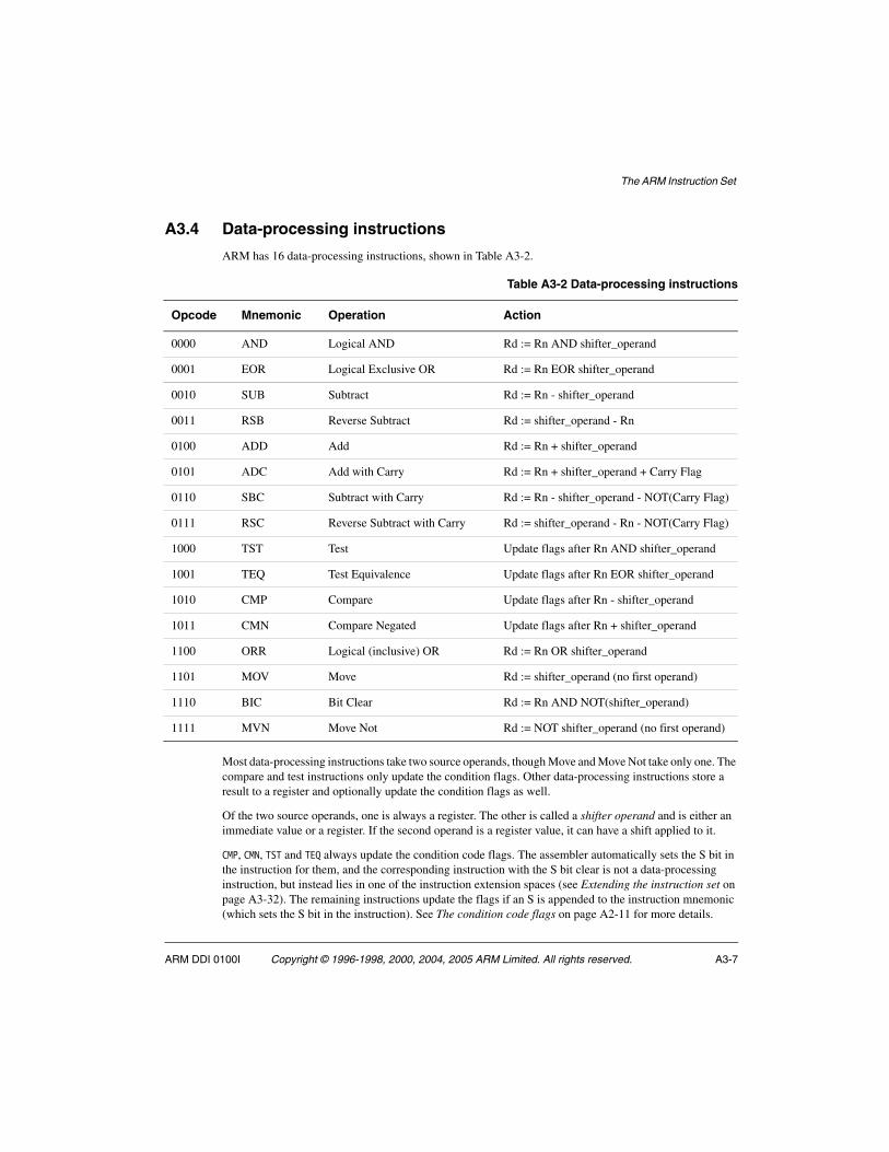
A3.4 Data-processing instructions
ARM has 16 data-processing instructions, shown in Table A3-2.
Most data-processing instructions take two source operands, though Move and Move Not take only one. The compare and test instructions only update the condition flags. Other data-processing instructions store a result to a register and optionally update the condition flags as well.
Of the two source operands, one is always a register. The other is called a shifter operand and is either an immediate value or a register. If the second operand is a register value, it can have a shift applied to it.
CMP, CMN, TST and TEQ always update the condition code flags. The assembler automatically sets the S bit in the instruction for them, and the corresponding instruction with the S bit clear is not a data-processing instruction, but instead lies in one of the instruction extension spaces (see Extending the instruction set on page A3-32). The remaining instructions update the flags if an S is appended to the instruction mnemonic (which sets the S bit in the instruction). See The condition code flags on page A2-11 for more details.
Table A3-2 Data-processing instructions
Opcode Mnemonic Operation Action
0000 AND Logical AND Rd := Rn AND shifter_operand
0001 EOR Logical Exclusive OR Rd := Rn EOR shifter_operand
0010 SUB Subtract Rd := Rn - shifter_operand
0011 RSB Reverse Subtract Rd := shifter_operand - Rn
0100 ADD Add Rd := Rn + shifter_operand
0101 ADC Add with Carry Rd := Rn + shifter_operand + Carry Flag
0110 SBC Subtract with Carry Rd := Rn - shifter_operand - NOT(Carry Flag)
0111 RSC Reverse Subtract with Carry Rd := shifter_operand - Rn - NOT(Carry Flag)
1000 TST Test Update flags after Rn AND shifter_operand
1001 TEQ Test Equivalence Update flags after Rn EOR shifter_operand
1010 CMP Compare Update flags after Rn - shifter_operand
1011 CMN Compare Negated Update flags after Rn + shifter_operand
1100 ORR Logical (inclusive) OR Rd := Rn OR shifter_operand
1101 MOV Move Rd := shifter_operand (no first operand)
1110 BIC Bit Clear Rd := Rn AND NOT(shifter_operand)
1111 MVN Move Not Rd := NOT shifter_operand (no first operand)
The ARM Instruction Set
A3-8 Copyright © 1996-1998, 2000, 2004, 2005 ARM Limited. All rights reserved. ARM DDI 0100I
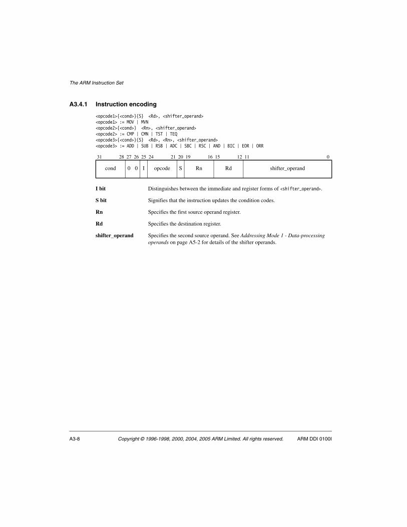
A3.4.1 Instruction encoding
<opcode1>{<cond>}{S} <Rd>, <shifter_operand><opcode1> := MOV | MVN<opcode2>{<cond>} <Rn>, <shifter_operand><opcode2> := CMP | CMN | TST | TEQ<opcode3>{<cond>}{S} <Rd>, <Rn>, <shifter_operand><opcode3> := ADD | SUB | RSB | ADC | SBC | RSC | AND | BIC | EOR | ORR
I bit Distinguishes between the immediate and register forms of <shifter_operand>.
S bit Signifies that the instruction updates the condition codes.
Rn Specifies the first source operand register.
Rd Specifies the destination register.
shifter_operand Specifies the second source operand. See Addressing Mode 1 - Data-processing operands on page A5-2 for details of the shifter operands.
31 28 27 26 25 24 21 20 19 16 15 12 11 0
cond 0 0 I opcode S Rn Rd shifter_operand
The ARM Instruction Set
ARM DDI 0100I Copyright © 1996-1998, 2000, 2004, 2005 ARM Limited. All rights reserved. A3-9
A3.4.2 List of data-processing instructions
ADC Add with Carry. See ADC on page A4-4.
ADD Add. See ADD on page A4-6.
AND Logical AND. See AND on page A4-8.
BIC Logical Bit Clear. See BIC on page A4-12.
CMN Compare Negative. See CMN on page A4-26.
CMP Compare. See CMP on page A4-28.
EOR Logical EOR. See EOR on page A4-32.
MOV Move. See MOV on page A4-68.
MVN Move Not. See MVN on page A4-82.
ORR Logical OR. See ORR on page A4-84.
RSB Reverse Subtract. See RSB on page A4-115.
RSC Reverse Subtract with Carry. See RSC on page A4-117.
SBC Subtract with Carry. See SBC on page A4-125.
SUB Subtract. See SUB on page A4-208.
TEQ Test Equivalence. See TEQ on page A4-228.
TST Test. See TST on page A4-230.
The ARM Instruction Set
A3-10 Copyright © 1996-1998, 2000, 2004, 2005 ARM Limited. All rights reserved. ARM DDI 0100I
A3.5 Multiply instructions
ARM has several classes of Multiply instruction:
Normal 32-bit x 32-bit, bottom 32-bit result
Long 32-bit x 32-bit, 64-bit result
Halfword 16-bit x 16-bit, 32-bit result
Word f halfword 32-bit x 16-bit, top 32-bit result
Most significant word
32-bit x 32-bit, top 32-bit result
Dual halfword dual 16-bit x 16-bit, 32-bit result.
All Multiply instructions take two register operands as the input to the multiplier. The ARM processor does not directly support a multiply-by-constant instruction because of the efficiency of shift and add, or shift and reverse subtract instructions.
A3.5.1 Normal multiply
There are two 32-bit x 32-bit Multiply instructions that produce bottom 32-bit results:MUL Multiplies the values of two registers together, truncates the result to 32 bits, and stores the
result in a third register. MLA Multiplies the values of two registers together, adds the value of a third register, truncates
the result to 32 bits, and stores the result in a fourth register. This can be used to perform multiply-accumulate operations.
Both Normal Multiply instructions can optionally set the N (Negative) and Z (Zero) condition code flags. No distinction is made between signed and unsigned variants. Only the least significant 32 bits of the result are stored in the destination register, and the sign of the operands does not affect this value.
A3.5.2 Long multiply
There are five 32-bit x 32-bit Multiply instructions that produce 64-bit results.
Two of the variants multiply the values of two registers together and store the 64-bit result in third and fourth registers. There are signed (SMULL) and unsigned (UMULL) variants. The signed variants produce a different result in the most significant 32 bits if either or both of the source operands is negative.
Two variants multiply the values of two registers together, add the 64-bit value from the third and fourth registers, and store the 64-bit result back into those registers (third and fourth). There are signed (SMLAL) and unsigned (UMLAL) variants. These instructions perform a long multiply and accumulate.
UMAAL multiplies the unsigned values of two registers together, adds the two unsigned 32-bit values from the third and fourth registers, and stores the 64-bit unsigned result back into those registers (third and fourth).
The ARM Instruction Set
ARM DDI 0100I Copyright © 1996-1998, 2000, 2004, 2005 ARM Limited. All rights reserved. A3-11
All the Long Multiply instructions except UMAAL can optionally set the N (Negative) and Z (Zero) condition code flags. UMAAL does not affect any flags.
UMAAL is available in ARMv6 and above.
A3.5.3 Halfword multiply
There are three signed 16-bit x 16-bit Multiply instructions that produce 32-bit results:
SMULxy Multiplies the 16-bit values of two half-registers together, and stores the signed 32-bit result in a third register.
SMLAxy Multiplies the 16-bit values of two half-registers together, adds the 32-bit value from a third register, and stores the signed 32-bit result in a fourth register.
SMLALxy Multiplies the 16-bit values of two half-registers together, adds the 64-bit value from a third and fourth register, and stores the 64-bit result back into those registers (third and fourth).
SMULxy and SMLALxy do not affect any flags. SMLAxy can set the Q flag if overflow occurs in the multiplication. The x and y designators indicate whether the top (T) or bottom (B) bits of the register is used as the operand.
They are available in ARMv5TE and above.
A3.5.4 Word u halfword multiply
There are two signed Multiply instructions that produce top 32-bit results:
SMULWy Multiplies the 32-bit value of one register with the 16-bit value of either halfword of a second register, and stores the top 32 bits of the signed 48-bit result in a third register.
SMLAWy Multiplies the 32-bit value of one register with the 16-bit value of either halfword of a second register, extracts the top 32 bits, adds the 32-bit value from a third register, and stores the signed 32-bit result in a fourth register.
SMLAWy sets the Q flag if overflow occurs in the multiplication. SMULWy does not affect any flags.
These instructions are available in ARMv5TE and above.
The ARM Instruction Set
A3-12 Copyright © 1996-1998, 2000, 2004, 2005 ARM Limited. All rights reserved. ARM DDI 0100I
A3.5.5 Most significant word multiply
There are three signed 32-bit x 32-bit Multiply instructions that produce top 32-bit results:
SMMUL Multiplies the 32-bit values of two registers together, and stores the top 32 bits of the signed 64-bit result in a third register.
SMMLA Multiplies the 32-bit values of two registers together, extracts the top 32 bits, adds the 32-bit value from a third register, and stores the signed 32-bit result in a fourth register.
SMMLS Multiplies the 32-bit value of two registers together, extracts the top 32 bits, subtracts this from a 32-bit value from a third register, and stores the signed 32-bit result in a fourth register.
These instructions do not affect any flags.
They are available in ARMv6 and above.
A3.5.6 Dual halfword multiply
There are six dual, signed 16-bit x 16-bit Multiply instructions:
SMUAD Multiplies the values of the top halfwords of two registers together, multiplies the values of the bottom halfwords of the same two registers together, adds the products, and stores the 32-bit result in a third register.
SMUSD Multiplies the values of the top halfwords of two registers together, multiplies the values of the bottom halfwords of the same two registers together, subtracts one product from the other, and stores the 32-bit result in a third register.
SMLAD Multiplies the 32-bit value of two registers together, extracts the top 32 bits, subtracts this from a 32-bit value from a third register, and stores the signed 32-bit result in a fourth register.
SMLSD Multiplies the 32-bit values of two registers together, extracts the top 32 bits, adds the 32-bit value from a third register, and stores the signed 32-bit result in a fourth register.
SMLALD Multiplies the 32-bit value of two registers together, extracts the top 32 bits, subtracts this from a 32-bit value from a third register, and stores the signed 32-bit result in a fourth register.
SMLSLD Multiplies the 32-bit value of two registers together, extracts the top 32 bits, subtracts this from a 32-bit value from a third register, and stores the signed 32-bit result in a fourth register.
SMUAD, SMLAD, and SMLSLD can set the Q flag if overflow occurs in the operation. All other instructions do not affect any flags.
They are available in ARMv6 and above.
The ARM Instruction Set
ARM DDI 0100I Copyright © 1996-1998, 2000, 2004, 2005 ARM Limited. All rights reserved. A3-13
A3.5.7 Examples
MUL R4, R2, R1 ; Set R4 to value of R2 multiplied by R1MULS R4, R2, R1 ; R4 = R2 x R1, set N and Z flagsMLA R7, R8, R9, R3 ; R7 = R8 x R9 + R3SMULL R4, R8, R2, R3 ; R4 = bits 0 to 31 of R2 x R3
; R8 = bits 32 to 63 of R2 x R3UMULL R6, R8, R0, R1 ; R8, R6 = R0 x R1UMLAL R5, R8, R0, R1 ; R8, R5 = R0 x R1 + R8, R5
A3.5.8 List of multiply instructionsMLA Multiply Accumulate. See MLA on page A4-66.MUL Multiply. See MUL on page A4-80.SMLA<x><y>
Signed halfword Multiply Accumulate. See SMLA<x><y> on page A4-141.SMLAD Signed halfword Multiply Accumulate, Dual. See SMLAD on page A4-144.SMLAL Signed Multiply Accumulate Long. See SMLAL on page A4-146.SMLAL<x><y>
Signed halfword Multiply Accumulate Long. See SMLAL<x><y> on page A4-148.SMLALD Signed halfword Multiply Accumulate Long, Dual. See SMLALD on page A4-150.SMLAW<y> Signed halfword by word Multiply Accumulate. See SMLAW<y> on page A4-152.SMLSD Signed halfword Multiply Subtract, Dual. See SMLAD on page A4-144.SMLSLD Signed halfword Multiply Subtract Long Dual. See SMLALD on page A4-150.SMMLA Signed Most significant word Multiply Accumulate. See SMMLA on page A4-158.SMMLS Signed Most significant word Multiply Subtract. See SMMLA on page A4-158.SMMUL Signed Most significant word Multiply. See SMMUL on page A4-162.SMUAD Signed halfword Multiply, Add, Dual. See SMUAD on page A4-164.SMUL<x><y>
Signed halfword Multiply. See SMUL<x><y> on page A4-166.SMULL Signed Multiply Long. See SMULL on page A4-168.SMULW<y> Signed halfword by word Multiply. See SMULW<y> on page A4-170.SMUSD Signed halfword Multiply, Subtract, Dual. See SMUSD on page A4-172.UMAAL Unsigned Multiply Accumulate significant Long. See UMAAL on page A4-247.UMLAL Unsigned Multiply Accumulate Long. See UMLAL on page A4-249.UMULL Unsigned Multiply Long. See UMULL on page A4-251.
The ARM Instruction Set
A3-14 Copyright © 1996-1998, 2000, 2004, 2005 ARM Limited. All rights reserved. ARM DDI 0100I
A3.6 Parallel addition and subtraction instructions
In addition to the normal data-processing and multiply instructions, ARMv6 introduces a set of parallel addition and subtraction instructions.
There are six basic instructions:
ADD16 Adds the top halfwords of two registers to form the top halfword of the result.
Adds the bottom halfwords of the same two registers to form the bottom halfword of the result.
ADDSUBX Does the following:1. Exchanges halfwords of the second operand register.2. Adds top halfwords and subtracts bottom halfwords.
SUBADDX Does the following:1. Exchanges halfwords of the second operand register.2. Subtracts top halfwords and adds bottom halfwords.
SUB16 Subtracts the top halfword of the first operand register from the top halfword of the second operand register to form the top halfword of the result.
Subtracts the bottom halfword of the second operand registers from the bottom halfword of the first operand register to form the bottom halfword of the result.
ADD8 Adds each byte of the second operand register to the corresponding byte of the first operand register to form the corresponding byte of the result.
SUB8 Subtracts each byte of the second operand register from the corresponding byte of the first operand register to form the corresponding byte of the result.
Each of the six instructions is available in the following variations, indicated by the prefixes shown:
S Signed arithmetic modulo 28 or 216. Sets the CPSR GE bits (see The GE[3:0] bits on page A2-13).
Q Signed saturating arithmetic.
SH Signed arithmetic, halving the results to avoid overflow.
U Unsigned arithmetic modulo 28 or 216. Sets the CPSR GE bits (see The GE[3:0] bits on page A2-13).
UQ Unsigned saturating arithmetic.
UH Unsigned arithmetic, halving the results to avoid overflow.
The ARM Instruction Set
ARM DDI 0100I Copyright © 1996-1998, 2000, 2004, 2005 ARM Limited. All rights reserved. A3-15
A3.6.1 List of parallel arithmetic instructionsQADD16 Dual 16-bit signed saturating addition. See QADD16 on page A4-94.QADD8 Quad 8-bit signed saturating addition. See QADD8 on page A4-95.QADDSUBX 16-bit exchange, signed saturating addition, subtraction. See QADDSUBX on page A4-97.QSUB16 Dual 16-bit signed saturating subtraction. See QSUB16 on page A4-104.QSUB8 Quad 8-bit signed saturating subtraction. See QSUB8 on page A4-105.QSUBADDX 16-bit exchange, signed saturating subtraction, addition. See QSUBADDX on page A4-107.SADD16 Dual 16-bit signed addition. See SADD16 on page A4-119.SADD8 Quad 8-bit signed addition. See SADD8 on page A4-121.SADDSUBX 16-bit exchange, signed addition, subtraction. See SADDSUBX on page A4-123.SSUB16 Dual 16-bit signed subtraction. See SSUB16 on page A4-180.SSUB8 Quad 8-bit signed subtraction. See SSUB8 on page A4-182.SSUBADDX 16-bit exchange, signed subtraction, addition. See SSUBADDX on page A4-184.SHADD16 Dual 16-bit signed half addition. See SHADD16 on page A4-130.SHADD8 Quad 8-bit signed half addition. See SHADD8 on page A4-131.SHADDSUBX 16-bit exchange, signed half addition, subtraction. See SHADDSUBX on page A4-133.SHSUB16 Dual 16-bit signed half subtraction. See SHSUB16 on page A4-135.SHSUB8 Quad 8-bit signed half subtraction. See SHSUB8 on page A4-137.SHSUBADDX 16-bit exchange, signed half subtraction, addition. See SHSUBADDX on page A4-139.UADD16 Dual 16-bit unsigned addition. See UADD16 on page A4-232.UADD8 Quad 8-bit unsigned addition. See UADD8 on page A4-233.UADDSUBX 16-bit exchange, unsigned addition, subtraction. See UADDSUBX on page A4-235.USUB16 Dual 16-bit unsigned subtraction. See USUB16 on page A4-269.USUB8 Quad 8-bit unsigned subtraction. See USUB8 on page A4-270.USUBADDX 16-bit exchange, unsigned subtraction, addition. See USUBADDX on page A4-272.UHADD16 Dual 16-bit unsigned half addition. See UHADD16 on page A4-237.UHADD8 Quad 8-bit unsigned half addition. See UHADD8 on page A4-238.UHADDSUBX 16-bit exchange, unsigned half addition, subtraction. See UHADDSUBX on page A4-240.UHSUB16 Dual 16-bit unsigned half subtraction. See UHSUB16 on page A4-242.UHSUB8 Quad 8-bit unsigned half subtraction. See UHSUB16 on page A4-242.UHSUBADDX 16-bit exchange, unsigned half subtraction, addition. See UHSUBADDX on page A4-245.UQADD16 Dual 16-bit unsigned saturating addition. See UQADD16 on page A4-253.UQADD8 Quad 8-bit unsigned saturating addition. See UQADD8 on page A4-254.UQADDSUBX 16-bit exchange, unsigned saturating addition, subtraction. See UQADDSUBX on
page A4-255.UQSUB16 Dual 16-bit unsigned saturating subtraction. See UQSUB16 on page A4-257.UQSUB8 Quad 8-bit unsigned saturating subtraction. See UQSUB8 on page A4-258.UQSUBADDX 16-bit exchange, unsigned saturating subtraction, addition. See UQSUBADDX on
page A4-259.
The ARM Instruction Set
A3-16 Copyright © 1996-1998, 2000, 2004, 2005 ARM Limited. All rights reserved. ARM DDI 0100I
A3.7 Extend instructions
ARMv6 and above provide several instructions for unpacking data by sign or zero extending bytes to halfwords or words, and halfwords to words. You can optionally add the result to the contents of another register. You can rotate the operand register by any multiple of 8 bits before extending.
There are six basic instructions:
XTAB16 Extend bits[23:16] and bits[7:0] of one register to 16 bits, and add corresponding halfwords to the values in another register.
XTAB Extend bits[7:0] of one register to 32 bits, and add to the value in another register.
XTAH Extend bits[15:0] of one register to 32 bits, and add to the value in another register.
XTB16 Extend bits[23:16] and bits[7:0] to 16 bits each.
XTB Extend bits[7:0] to 32 bits.
XTH Extend bits[15:0] to 32 bits.
Each of the six instructions is available in the following variations, indicated by the prefixes shown:
S Sign extension, with or without addition modulo 216 or 232.
U Zero (unsigned) extension, with or without addition modulo 216 or 232.
A3.7.1 List of sign/zero extend and add instructions
SXTAB16 Sign extend bytes to halfwords, add halfwords. See SXTAB16 on page A4-218.
SXTAB Sign extend byte to word, add. See SXTAB on page A4-216.
SXTAH Sign extend halfword to word, add. See SXTAH on page A4-220.
SXTB16 Sign extend bytes to halfwords. See SXTB16 on page A4-224.
SXTB Sign extend byte to word. See SXTB on page A4-222.
SXTH Sign extend halfword to word. See SXTH on page A4-226.
UXTAB16 Zero extend bytes to halfwords, add halfwords. See UXTAB16 on page A4-276.
UXTAB Zero extend byte to word, add. See UXTAB on page A4-274.
UXTAH Zero extend halfword to word, add. See UXTAH on page A4-278.
UXTB16 Zero extend bytes to halfwords. See UXTB16 on page A4-282.
UXTB Zero extend byte to word. See UXTB on page A4-280.
UXTH Zero extend halfword to word. See UXTH on page A4-284.
The ARM Instruction Set
ARM DDI 0100I Copyright © 1996-1998, 2000, 2004, 2005 ARM Limited. All rights reserved. A3-17
A3.8 Miscellaneous arithmetic instructions
ARMv5 and above include several miscellaneous arithmetic instructions.
A3.8.1 Count leading zeros
ARMv5 and above include a Count Leading Zeros (CLZ) instruction. This instruction returns the number of 0 bits at the most significant end of its operand before the first 1 bit is encountered (or 32 if its operand is 0). Two typical applications for this are:
• To determine how many bits the operand should be shifted left to normalize it, so that its most significant bit is 1. (This can be used in integer division routines.)
• To locate the highest priority bit in a bit mask.
For details see CLZ on page A4-25.
A3.8.2 Unsigned sum of absolute differences
ARMv6 introduces an Unsigned Sum of Absolute Differences (USAD8) instruction, and an Unsigned Sum of Absolute Differences and Accumulate (USADA8) instruction.
These instructions do the following:1. Take corresponding bytes from two registers.2. Find the absolute differences between the unsigned values of each pair of bytes.3. Sum the four absolute values.4. Optionally, accumulate the sum of the absolute differences with the value in a third register.
For details see USAD8 on page A4-261 and USADA8 on page A4-263.

The ARM Instruction Set
A3-18 Copyright © 1996-1998, 2000, 2004, 2005 ARM Limited. All rights reserved. ARM DDI 0100I
A3.9 Other miscellaneous instructions
ARMv6 and above provide several other miscellaneous instructions:
PKHBT (Pack Halfword Bottom Top) combines the bottom, least significant, halfword of its first operand with the top (most significant) halfword of its shifted second operand. The shift is a left shift, by any amount from 0 to 31.
See PKHBT on page A4-86.
PKHTB (Pack Halfword Top Bottom) combines the top, most significant, halfword of its first operand with the bottom (least significant) halfword of its shifted second operand. The shift is an arithmetic right shift, by any amount from 1 to 32.
See PKHTB on page A4-88.
REV (Byte-Reverse Word) reverses the byte order in a 32-bit register.
See REV on page A4-109.
REV16 (Byte-Reverse Packed Halfword) reverses the byte order in each 16-bit halfword of a 32-bit register.
See REV16 on page A4-110.
REVSH (Byte-Reverse Signed Halfword) reverses the byte order in the lower 16-bit halfword of a 32-bit register, and sign extends the result to 32-bits.
See REVSH on page A4-111.
SEL (Select) selects each byte of its result from either its first operand or its second operand, according to the values of the GE flags. The GE flags record the results of parallel additions or subtractions, see Parallel addition and subtraction instructions on page A3-14.
See SEL on page A4-127.
SSAT (Signed Saturate) saturates a signed value to a signed range. You can choose the bit position at which saturation occurs. You can apply a shift to the value before the saturation occurs.
See SSAT on page A4-176.
SSAT16 Saturates two 16-bit signed values to a signed range. You can choose the bit position at which saturation occurs.
See SSAT16 on page A4-178.
USAT (Unsigned Saturate) saturates a signed value to an unsigned range. You can choose the bit position at which saturation occurs. You can apply a shift to the value before the saturation occurs.
See USAT on page A4-265.
USAT16 Saturates two signed 16-bit values to an unsigned range. You can choose the bit position at which saturation occurs.
See USAT16 on page A4-267.
The ARM Instruction Set
ARM DDI 0100I Copyright © 1996-1998, 2000, 2004, 2005 ARM Limited. All rights reserved. A3-19
A3.10 Status register access instructions
There are two instructions for moving the contents of a program status register to or from a general-purpose register. Both the CPSR and SPSR can be accessed.
In addition, in ARMv6, there are several instructions that can write directly to specific bits, or groups of bits, in the CPSR.
Each status register is traditionally split into four 8-bit fields that can be individually written:
Bits[31:24] The flags field.
Bits[23:16] The status field.
Bits[15:8] The extension field.
Bits[7:0] The control field.
From ARMv6, the ARM architecture uses the status and extension fields. The usage model of the bit fields no longer reflects the byte-wide definitions. The revised categories are defined in Types of PSR bits on page A2-11.
A3.10.1 CPSR value
Altering the value of the CPSR has five uses:• sets the value of the condition code flags (and of the Q flag when it exists) to a known value• enables or disable interrupts• changes processor mode (for instance, to initialize stack pointers)• changes the endianness of load and store operations• changes the processor state (J and T bits).
Note The T and J bits must not be changed directly by writing to the CPSR, but only via the BX, BLX, or BXJ instructions, and in the implicit SPSR to CPSR moves in instructions designed for exception return. Attempts to enter or leave Thumb or Jazelle state by directly altering the T or J bits have UNPREDICTABLE consequences.
The ARM Instruction Set
A3-20 Copyright © 1996-1998, 2000, 2004, 2005 ARM Limited. All rights reserved. ARM DDI 0100I
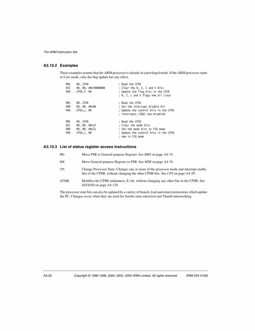
A3.10.2 Examples
These examples assume that the ARM processor is already in a privileged mode. If the ARM processor starts in User mode, only the flag update has any effect.
MRS R0, CPSR ; Read the CPSRBIC R0, R0, #0xF0000000 ; Clear the N, Z, C and V bits MSR CPSR_f, R0 ; Update the flag bits in the CPSR
; N, Z, C and V flags now all clear
MRS R0, CPSR ; Read the CPSR ORR R0, R0, #0x80 ; Set the interrupt disable bit MSR CPSR_c, R0 ; Update the control bits in the CPSR
; interrupts (IRQ) now disabled
MRS R0, CPSR ; Read the CPSR BIC R0, R0, #0x1F ; Clear the mode bitsORR R0, R0, #0x11 ; Set the mode bits to FIQ modeMSR CPSR_c, R0 ; Update the control bits in the CPSR
; now in FIQ mode
A3.10.3 List of status register access instructions
MRS Move PSR to General-purpose Register. See MRS on page A4-74.
MSR Move General-purpose Register to PSR. See MSR on page A4-76.
CPS Change Processor State. Changes one or more of the processor mode and interrupt enable bits of the CPSR, without changing the other CPSR bits. See CPS on page A4-29.
SETEND Modifies the CPSR endianness, E, bit, without changing any other bits in the CPSR. See SETEND on page A4-129.
The processor state bits can also be updated by a variety of branch, load and return instructions which update the PC. Changes occur when they are used for Jazelle state entry/exit and Thumb interworking.

The ARM Instruction Set
ARM DDI 0100I Copyright © 1996-1998, 2000, 2004, 2005 ARM Limited. All rights reserved. A3-21
A3.11 Load and store instructions
The ARM architecture supports two broad types of instruction which load or store the value of a single register, or a pair of registers, from or to memory:
• The first type can load or store a 32-bit word or an 8-bit unsigned byte.
• The second type can load or store a 16-bit unsigned halfword, and can load and sign extend a 16-bit halfword or an 8-bit byte. In ARMv5TE and above, it can also load or store a pair of 32-bit words.
A3.11.1 Addressing modes
In both types of instruction, the addressing mode is formed from two parts:• the base register• the offset.
The base register can be any one of the general-purpose registers (including the PC, which allows PC-relative addressing for position-independent code).
The offset takes one of three formats:
Immediate The offset is an unsigned number that can be added to or subtracted from the base register. Immediate offset addressing is useful for accessing data elements that are a fixed distance from the start of the data object, such as structure fields, stack offsets and input/output registers.
For the word and unsigned byte instructions, the immediate offset is a 12-bit number. For the halfword and signed byte instructions, it is an 8-bit number.
Register The offset is a general-purpose register (not the PC), that can be added to or subtracted from the base register. Register offsets are useful for accessing arrays or blocks of data.
Scaled register The offset is a general-purpose register (not the PC) shifted by an immediate value, then added to or subtracted from the base register. The same shift operations used for data-processing instructions can be used (Logical Shift Left, Logical Shift Right, Arithmetic Shift Right and Rotate Right), but Logical Shift Left is the most useful as it allows an array indexed to be scaled by the size of each array element.
Scaled register offsets are only available for the word and unsigned byte instructions.
The ARM Instruction Set
A3-22 Copyright © 1996-1998, 2000, 2004, 2005 ARM Limited. All rights reserved. ARM DDI 0100I
As well as the three types of offset, the offset and base register are used in three different ways to form the memory address. The addressing modes are described as follows:
Offset The base register and offset are added or subtracted to form the memory address.
Pre-indexed The base register and offset are added or subtracted to form the memory address. The base register is then updated with this new address, to allow automatic indexing through an array or memory block.
Post-indexed The value of the base register alone is used as the memory address. The base register and offset are added or subtracted and this value is stored back in the base register, to allow automatic indexing through an array or memory block.
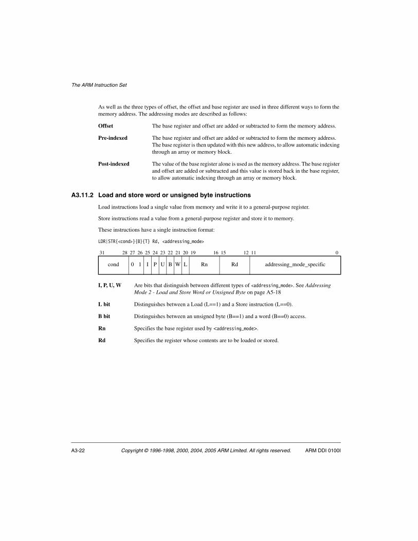
A3.11.2 Load and store word or unsigned byte instructions
Load instructions load a single value from memory and write it to a general-purpose register.
Store instructions read a value from a general-purpose register and store it to memory.
These instructions have a single instruction format:
LDR|STR{<cond>}{B}{T} Rd, <addressing_mode>
I, P, U, W Are bits that distinguish between different types of <addressing_mode>. See Addressing Mode 2 - Load and Store Word or Unsigned Byte on page A5-18
L bit Distinguishes between a Load (L==1) and a Store instruction (L==0).
B bit Distinguishes between an unsigned byte (B==1) and a word (B==0) access.
Rn Specifies the base register used by <addressing_mode>.
Rd Specifies the register whose contents are to be loaded or stored.
31 28 27 26 25 24 23 22 21 20 19 16 15 12 11 0
cond 0 1 I P U B W L Rn Rd addressing_mode_specific
The ARM Instruction Set
ARM DDI 0100I Copyright © 1996-1998, 2000, 2004, 2005 ARM Limited. All rights reserved. A3-23
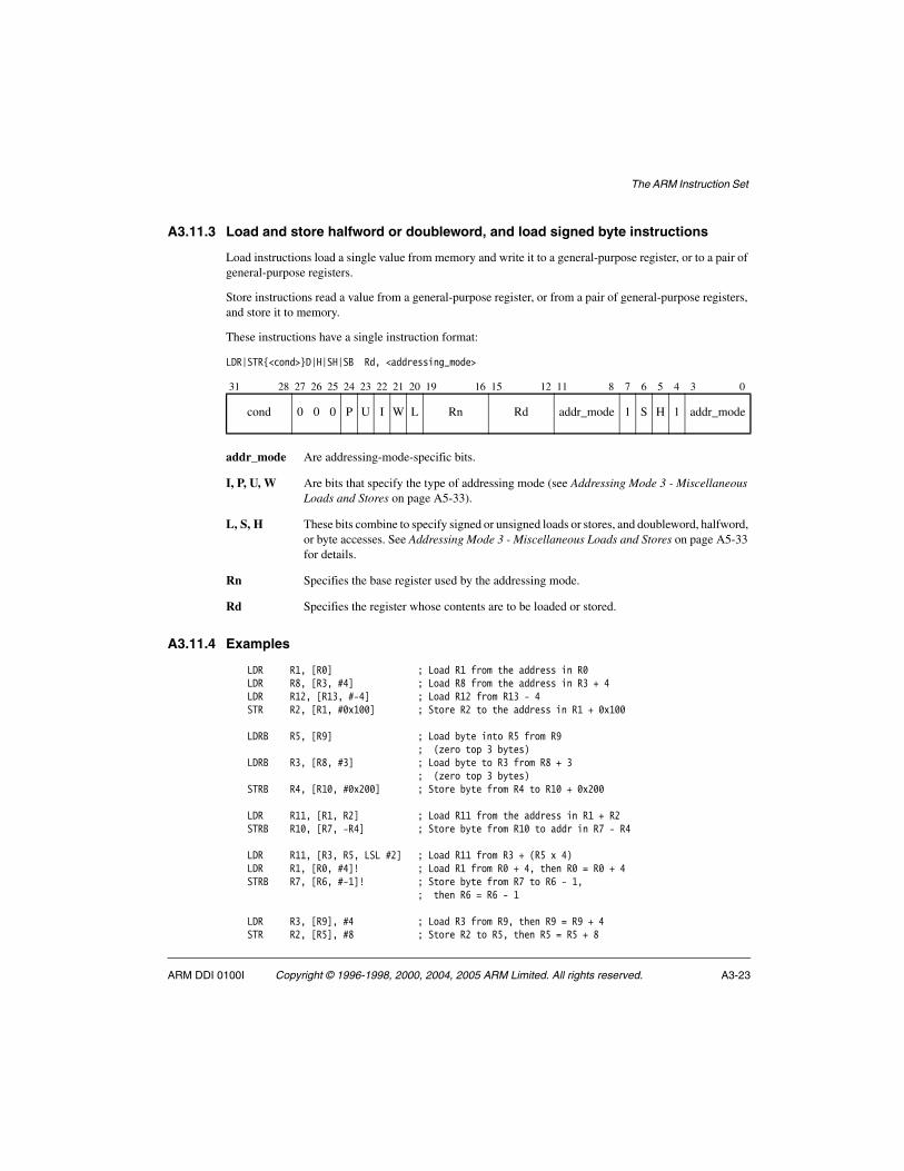
A3.11.3 Load and store halfword or doubleword, and load signed byte instructions
Load instructions load a single value from memory and write it to a general-purpose register, or to a pair of general-purpose registers.
Store instructions read a value from a general-purpose register, or from a pair of general-purpose registers, and store it to memory.
These instructions have a single instruction format:
LDR|STR{<cond>}D|H|SH|SB Rd, <addressing_mode>
addr_mode Are addressing-mode-specific bits.
I, P, U, W Are bits that specify the type of addressing mode (see Addressing Mode 3 - Miscellaneous Loads and Stores on page A5-33).
L, S, H These bits combine to specify signed or unsigned loads or stores, and doubleword, halfword, or byte accesses. See Addressing Mode 3 - Miscellaneous Loads and Stores on page A5-33 for details.
Rn Specifies the base register used by the addressing mode.
Rd Specifies the register whose contents are to be loaded or stored.
A3.11.4 Examples
LDR R1, [R0] ; Load R1 from the address in R0 LDR R8, [R3, #4] ; Load R8 from the address in R3 + 4LDR R12, [R13, #-4] ; Load R12 from R13 - 4STR R2, [R1, #0x100] ; Store R2 to the address in R1 + 0x100
LDRB R5, [R9] ; Load byte into R5 from R9 ; (zero top 3 bytes)
LDRB R3, [R8, #3] ; Load byte to R3 from R8 + 3 ; (zero top 3 bytes)
STRB R4, [R10, #0x200] ; Store byte from R4 to R10 + 0x200
LDR R11, [R1, R2] ; Load R11 from the address in R1 + R2 STRB R10, [R7, -R4] ; Store byte from R10 to addr in R7 - R4
LDR R11, [R3, R5, LSL #2] ; Load R11 from R3 + (R5 x 4)LDR R1, [R0, #4]! ; Load R1 from R0 + 4, then R0 = R0 + 4STRB R7, [R6, #-1]! ; Store byte from R7 to R6 - 1,
; then R6 = R6 - 1
LDR R3, [R9], #4 ; Load R3 from R9, then R9 = R9 + 4 STR R2, [R5], #8 ; Store R2 to R5, then R5 = R5 + 8
31 28 27 26 25 24 23 22 21 20 19 16 15 12 11 8 7 6 5 4 3 0
cond 0 0 0 P U I W L Rn Rd addr_mode 1 S H 1 addr_mode
The ARM Instruction Set
A3-24 Copyright © 1996-1998, 2000, 2004, 2005 ARM Limited. All rights reserved. ARM DDI 0100I
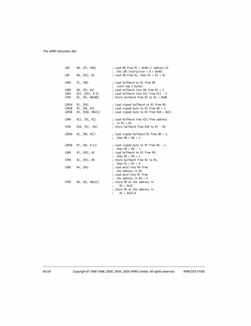
LDR R0, [PC, #40] ; Load R0 from PC + 0x40 (= address of; the LDR instruction + 8 + 0x40)
LDR R0, [R1], R2 ; Load R0 from R1, then R1 = R1 + R2
LDRH R1, [R0] ; Load halfword to R1 from R0 ; (zero top 2 bytes)
LDRH R8, [R3, #2] ; Load halfword into R8 from R3 + 2LDRH R12, [R13, #-6] ; Load halfword into R12 from R13 - 6STRH R2, [R1, #0x80] ; Store halfword from R2 to R1 + 0x80
LDRSH R5, [R9] ; Load signed halfword to R5 from R9LDRSB R3, [R8, #3] ; Load signed byte to R3 from R8 + 3LDRSB R4, [R10, #0xC1] ; Load signed byte to R4 from R10 + 0xC1
LDRH R11, [R1, R2] ; Load halfword into R11 from address; in R1 + R2
STRH R10, [R7, -R4] ; Store halfword from R10 to R7 - R4
LDRSH R1, [R0, #2]! ; Load signed halfword R1 from R0 + 2,; then R0 = R0 + 2
LDRSB R7, [R6, #-1]! ; Load signed byte to R7 from R6 - 1, ; then R6 = R6 - 1
LDRH R3, [R9], #2 ; Load halfword to R3 from R9, ; then R9 = R9 + 2
STRH R2, [R5], #8 ; Store halfword from R2 to R5, ; then R5 = R5 + 8
LDRD R4, [R9] ; Load word into R4 from ; the address in R9; Load word into R5 from; the address in R9 + 4
STRD R8, [R2, #0x2C] ; Store R8 at the address in; R2 + 0x2C; Store R9 at the address in; R2 + 0x2C+4
The ARM Instruction Set
ARM DDI 0100I Copyright © 1996-1998, 2000, 2004, 2005 ARM Limited. All rights reserved. A3-25
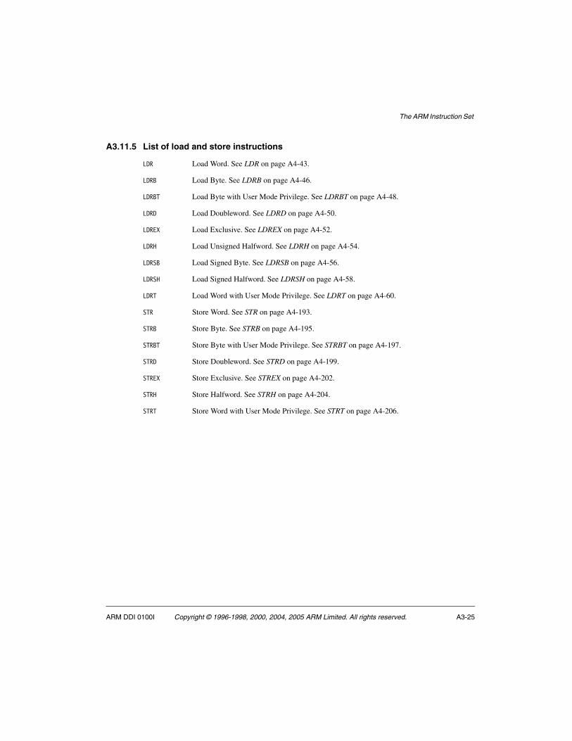
A3.11.5 List of load and store instructions
LDR Load Word. See LDR on page A4-43.
LDRB Load Byte. See LDRB on page A4-46.
LDRBT Load Byte with User Mode Privilege. See LDRBT on page A4-48.
LDRD Load Doubleword. See LDRD on page A4-50.
LDREX Load Exclusive. See LDREX on page A4-52.
LDRH Load Unsigned Halfword. See LDRH on page A4-54.
LDRSB Load Signed Byte. See LDRSB on page A4-56.
LDRSH Load Signed Halfword. See LDRSH on page A4-58.
LDRT Load Word with User Mode Privilege. See LDRT on page A4-60.
STR Store Word. See STR on page A4-193.
STRB Store Byte. See STRB on page A4-195.
STRBT Store Byte with User Mode Privilege. See STRBT on page A4-197.
STRD Store Doubleword. See STRD on page A4-199.
STREX Store Exclusive. See STREX on page A4-202.
STRH Store Halfword. See STRH on page A4-204.
STRT Store Word with User Mode Privilege. See STRT on page A4-206.
The ARM Instruction Set
A3-26 Copyright © 1996-1998, 2000, 2004, 2005 ARM Limited. All rights reserved. ARM DDI 0100I
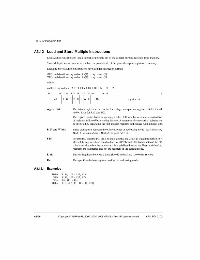
A3.12 Load and Store Multiple instructions
Load Multiple instructions load a subset, or possibly all, of the general-purpose registers from memory.
Store Multiple instructions store a subset, or possibly all, of the general-purpose registers to memory.
Load and Store Multiple instructions have a single instruction format:
LDM{<cond>}<addressing_mode> Rn{!}, <registers>{^}STM{<cond>}<addressing_mode> Rn{!}, <registers>{^}
where:
<addressing_mode> = IA | IB | DA | DB | FD | FA | ED | EA
register list The list of <registers> has one bit for each general-purpose register. Bit 0 is for R0, and bit 15 is for R15 (the PC).
The register syntax list is an opening bracket, followed by a comma-separated list of registers, followed by a closing bracket. A sequence of consecutive registers can be specified by separating the first and last registers in the range with a minus sign.
P, U, and W bits These distinguish between the different types of addressing mode (see Addressing Mode 4 - Load and Store Multiple on page A5-41).
S bit For LDMs that load the PC, the S bit indicates that the CPSR is loaded from the SPSR after all the registers have been loaded. For all STMs, and LDMs that do not load the PC, it indicates that when the processor is in a privileged mode, the User mode banked registers are transferred and not the registers of the current mode.
L bit This distinguishes between a Load (L==1) and a Store (L==0) instruction.
Rn This specifies the base register used by the addressing mode.
A3.12.1 Examples
STMFD R13!, {R0 - R12, LR}LDMFD R13!, {R0 - R12, PC}LDMIA R0, {R5 - R8}STMDA R1!, {R2, R5, R7 - R9, R11}
31 28 27 26 25 24 23 22 21 20 19 16 15 0
cond 1 0 0 P U S W L Rn register list
The ARM Instruction Set
ARM DDI 0100I Copyright © 1996-1998, 2000, 2004, 2005 ARM Limited. All rights reserved. A3-27
A3.12.2 List of Load and Store Multiple instructions
LDM Load Multiple. See LDM (1) on page A4-36.
LDM User Registers Load Multiple. See LDM (2) on page A4-38.
LDM Load Multiple with Restore CPSR. See LDM (3) on page A4-40.
STM Store Multiple. See STM (1) on page A4-189.
STM User Registers Store Multiple. See STM (2) on page A4-191.
The ARM Instruction Set
A3-28 Copyright © 1996-1998, 2000, 2004, 2005 ARM Limited. All rights reserved. ARM DDI 0100I
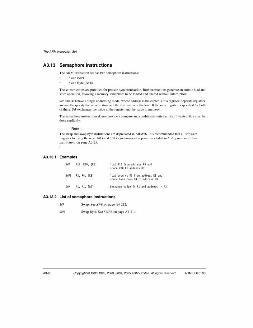
A3.13 Semaphore instructions
The ARM instruction set has two semaphore instructions:• Swap (SWP) • Swap Byte (SWPB).
These instructions are provided for process synchronization. Both instructions generate an atomic load and store operation, allowing a memory semaphore to be loaded and altered without interruption.
SWP and SWPB have a single addressing mode, whose address is the contents of a register. Separate registers are used to specify the value to store and the destination of the load. If the same register is specified for both of these, SWP exchanges the value in the register and the value in memory.
The semaphore instructions do not provide a compare and conditional write facility. If wanted, this must be done explicitly.
Note The swap and swap byte instructions are deprecated in ARMv6. It is recommended that all software migrates to using the new LDREX and STREX synchronization primitives listed in List of load and store instructions on page A3-25.
A3.13.1 Examples
SWP R12, R10, [R9] ; load R12 from address R9 and; store R10 to address R9
SWPB R3, R4, [R8] ; load byte to R3 from address R8 and; store byte from R4 to address R8
SWP R1, R1, [R2] ; Exchange value in R1 and address in R2
A3.13.2 List of semaphore instructions
SWP Swap. See SWP on page A4-212.
SWPB Swap Byte. See SWPB on page A4-214.
The ARM Instruction Set
ARM DDI 0100I Copyright © 1996-1998, 2000, 2004, 2005 ARM Limited. All rights reserved. A3-29
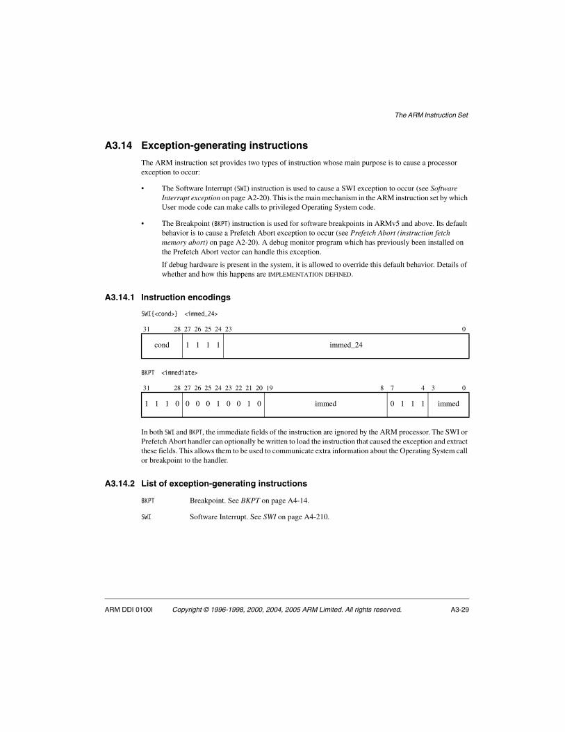
A3.14 Exception-generating instructions
The ARM instruction set provides two types of instruction whose main purpose is to cause a processor exception to occur:
• The Software Interrupt (SWI) instruction is used to cause a SWI exception to occur (see Software Interrupt exception on page A2-20). This is the main mechanism in the ARM instruction set by which User mode code can make calls to privileged Operating System code.
• The Breakpoint (BKPT) instruction is used for software breakpoints in ARMv5 and above. Its default behavior is to cause a Prefetch Abort exception to occur (see Prefetch Abort (instruction fetch memory abort) on page A2-20). A debug monitor program which has previously been installed on the Prefetch Abort vector can handle this exception.
If debug hardware is present in the system, it is allowed to override this default behavior. Details of whether and how this happens are IMPLEMENTATION DEFINED.
A3.14.1 Instruction encodings
SWI{<cond>} <immed_24>
BKPT <immediate>
In both SWI and BKPT, the immediate fields of the instruction are ignored by the ARM processor. The SWI or Prefetch Abort handler can optionally be written to load the instruction that caused the exception and extract these fields. This allows them to be used to communicate extra information about the Operating System call or breakpoint to the handler.
A3.14.2 List of exception-generating instructions
BKPT Breakpoint. See BKPT on page A4-14.
SWI Software Interrupt. See SWI on page A4-210.
31 28 27 26 25 24 23 0
cond 1 1 1 1 immed_24
31 28 27 26 25 24 23 22 21 20 19 8 7 4 3 0
1 1 1 0 0 0 0 1 0 0 1 0 immed 0 1 1 1 immed
The ARM Instruction Set
A3-30 Copyright © 1996-1998, 2000, 2004, 2005 ARM Limited. All rights reserved. ARM DDI 0100I
A3.15 Coprocessor instructions
The ARM instruction set provides three types of instruction for communicating with coprocessors. These allow:• the ARM processor to initiate a coprocessor data processing operation• ARM registers to be transferred to and from coprocessor registers• the ARM processor to generate addresses for the coprocessor Load and Store instructions.
The instruction set distinguishes up to 16 coprocessors with a 4-bit field in each coprocessor instruction, so each coprocessor is assigned a particular number.
Note One coprocessor can use more than one of the 16 numbers if a large coprocessor instruction set is required.
Coprocessors execute the same instruction stream as ARM, ignoring ARM instructions and coprocessor instructions for other coprocessors. Coprocessor instructions that cannot be executed by coprocessor hardware cause an Undefined Instruction exception, allowing software emulation of coprocessor hardware.
A coprocessor can partially execute an instruction and then cause an exception. This is useful for handling run-time-generated exceptions, like divide-by-zero or overflow. However, the partial execution is internal to the coprocessor and is not visible to the ARM processor. As far as the ARM processor is concerned, the instruction is held at the start of its execution and completes without exception if allowed to begin execution. Any decision on whether to execute the instruction or cause an exception is taken within the coprocessor before the ARM processor is allowed to start executing the instruction.
Not all fields in coprocessor instructions are used by the ARM processor. Coprocessor register specifiers and opcodes are defined by individual coprocessors. Therefore, only generic instruction mnemonics are provided for coprocessor instructions. Assembler macros can be used to transform custom coprocessor mnemonics into these generic mnemonics, or to regenerate the opcodes manually.
A3.15.1 Examples
CDP p5, 2, c12, c10, c3, 4 ; Coproc 5 data operation ; opcode 1 = 2, opcode 2 = 4; destination register is 12; source registers are 10 and 3
MRC p15, 5, R4, c0, c2, 3 ; Coproc 15 transfer to ARM register; opcode 1 = 5, opcode 2 = 3 ; ARM destination register = R4; coproc source registers are 0 and 2
MCR p14, 1, R7, c7, c12, 6 ; ARM register transfer to Coproc 14; opcode 1 = 1, opcode 2 = 6; ARM source register = R7; coproc dest registers are 7 and 12
LDC p6, CR1, [R4] ; Load from memory to coprocessor 6
The ARM Instruction Set
ARM DDI 0100I Copyright © 1996-1998, 2000, 2004, 2005 ARM Limited. All rights reserved. A3-31
; ARM register 4 contains the address; Load to CP reg 1
LDC p6, CR4, [R2, #4] ; Load from memory to coprocessor 6; ARM register R2 + 4 is the address; Load to CP reg 4
STC p8, CR8, [R2, #4]! ; Store from coprocessor 8 to memory; ARM register R2 + 4 is the address; after the transfer R2 = R2 + 4; Store from CP reg 8
STC p8, CR9, [R2], #-16 ; Store from coprocessor 8 to memory; ARM register R2 holds the address; after the transfer R2 = R2 - 16; Store from CP reg 9
A3.15.2 List of coprocessor instructions
CDP Coprocessor Data Operations. See CDP on page A4-23.
LDC Load Coprocessor Register. See LDC on page A4-34.
MCR Move to Coprocessor from ARM Register. See MCR on page A4-62.
MCRR Move to Coprocessor from two ARM Registers. See MCRR on page A4-64.
MRC Move to ARM Register from Coprocessor. See MRC on page A4-70.
MRRC Move to two ARM Registers from Coprocessor. See MRRC on page A4-72.
STC Store Coprocessor Register. See STC on page A4-186.
Note MCRR and MRRC are only available in ARMv5TE and above.
The ARM Instruction Set
A3-32 Copyright © 1996-1998, 2000, 2004, 2005 ARM Limited. All rights reserved. ARM DDI 0100I
A3.16 Extending the instruction set
Successive versions of the ARM architecture have extended the instruction set in a number of areas. This section describes the six areas where extensions have occurred, and where further extensions can occur in the future:• Media instruction space on page A3-33• Multiply instruction extension space on page A3-35• Control and DSP instruction extension space on page A3-36• Load/store instruction extension space on page A3-38• Architecturally Undefined Instruction space on page A3-39• Coprocessor instruction extension space on page A3-40• Unconditional instruction extension space on page A3-41.
Instructions in these areas which have not yet been allocated a meaning are either UNDEFINED or UNPREDICTABLE. To determine which, use the following rules:
1. The decode bits of an instruction are defined to be bits[27:20] and bits[7:4].
In ARMv5 and above, the result of ANDing bits[31:28] together is also a decode bit. This bit determines whether the condition field is 0b1111, which is used in ARMv5 and above to encode various instructions which can only be executed unconditionally. See Condition code 0b1111 on page A3-4 and Unconditional instruction extension space on page A3-41 for more information.
2. If the decode bits of an instruction are equal to those of a defined instruction, but the whole instruction is not a defined instruction, then the instruction is UNPREDICTABLE.
For example, suppose an instruction has:• bits[31:28] not equal to 0b1111• bits[27:20] equal to 0b00010000• bits[7:4] equal to 0b0000
but where:
• bit[11] of the instruction is 1.
Here, the instruction is in the control instruction extension space and has the same decode bits as an MRS instruction, but is not a valid MRS instruction because bit[11] of an MRS instruction should be zero. Using the above rule, this instruction is UNPREDICTABLE.
3. If the decode bits of an instruction are not equal to those of any defined instruction, then the instruction is UNDEFINED.
Rules 2 and 3 above apply separately to each ARM architecture version. As a result, the status of an instruction might differ between architecture versions. Usually, this happens because an instruction which was UNPREDICTABLE or UNDEFINED in an earlier architecture version becomes a defined instruction in a later version.
For the purposes of this section, all coprocessor instructions described in Chapter A4 ARM Instructions as appearing in a version of the architecture have been allocated. The definitions of any coprocessors using the coprocessor instructions determine the function of the instructions. Such coprocessors can define UNPREDICTABLE and UNDEFINED behaviours.
The ARM Instruction Set
ARM DDI 0100I Copyright © 1996-1998, 2000, 2004, 2005 ARM Limited. All rights reserved. A3-33
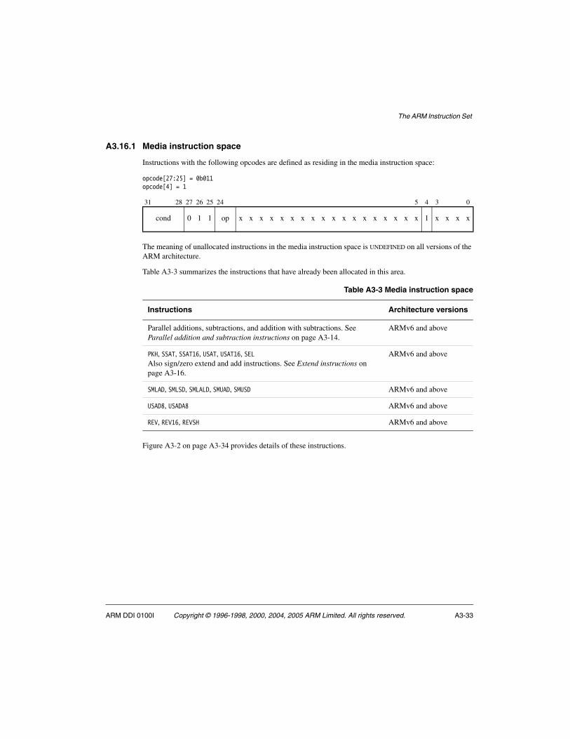
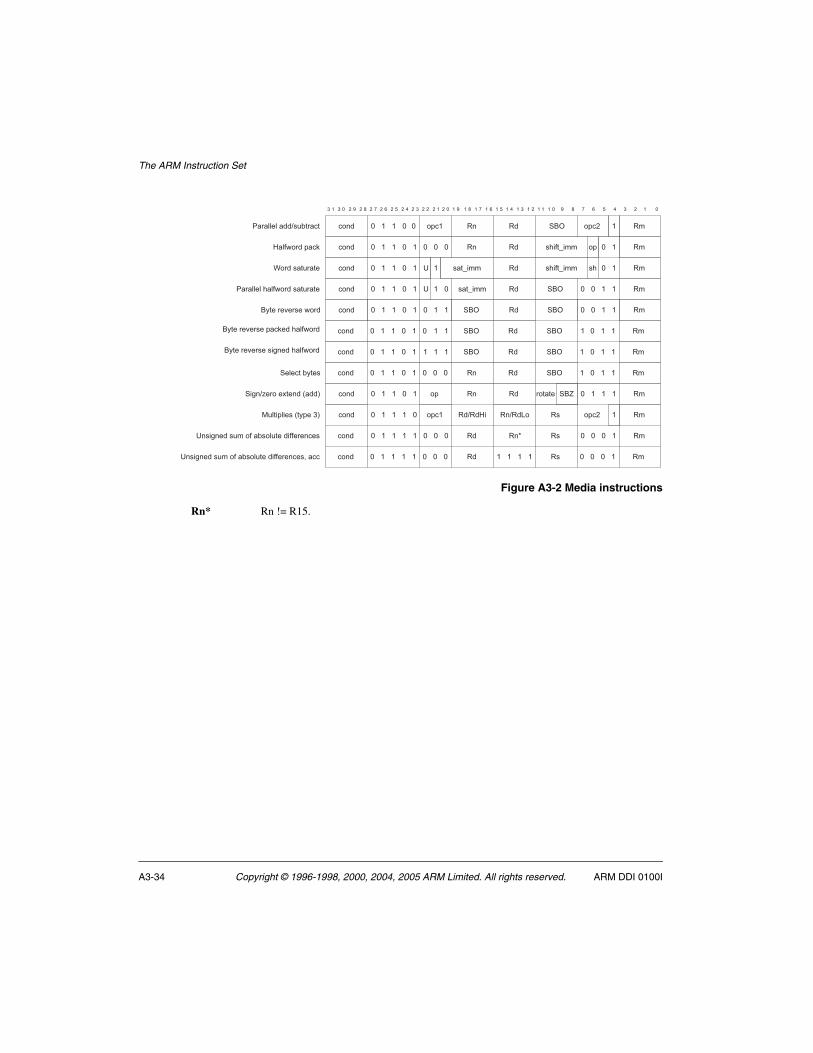
A3.16.1 Media instruction space
Instructions with the following opcodes are defined as residing in the media instruction space:
opcode[27:25] = 0b011opcode[4] = 1
The meaning of unallocated instructions in the media instruction space is UNDEFINED on all versions of the ARM architecture.
Table A3-3 summarizes the instructions that have already been allocated in this area.
Figure A3-2 on page A3-34 provides details of these instructions.
31 28 27 26 25 24 5 4 3 0
cond 0 1 1 op x x x x x x x x x x x x x x x x x x 1 x x x x
Table A3-3 Media instruction space
Instructions Architecture versions
Parallel additions, subtractions, and addition with subtractions. See Parallel addition and subtraction instructions on page A3-14.
ARMv6 and above
PKH, SSAT, SSAT16, USAT, USAT16, SELAlso sign/zero extend and add instructions. See Extend instructions on page A3-16.
ARMv6 and above
SMLAD, SMLSD, SMLALD, SMUAD, SMUSD ARMv6 and above
USAD8, USADA8 ARMv6 and above
REV, REV16, REVSH ARMv6 and above
The ARM Instruction Set
A3-34 Copyright © 1996-1998, 2000, 2004, 2005 ARM Limited. All rights reserved. ARM DDI 0100I
Figure A3-2 Media instructions
Rn* Rn != R15.
(',/ 7 3 3 7 7 '%(3 5, 5/ 6EF 5.'%(9 3J"&"==)=$"//I*8L#&"(#
(',/ 7 3 3 7 7 5, 5/ *0+1#P+.. 5.3X"=1M'&/$%"(G 3 7 7 7'%
(',/ 7 3 3 7 *"#P+.. 5/ *0+1#P+.. 5.3K'&/$*"#8&"#) 3 : 3 7*0
(',/ 7 3 3 7 *"#P+.. 5/ 5.3J"&"==)=$0"=1M'&/$*"#8&"#) 3 : 3 77 6EF 37
(',/ 7 3 3 7 5/ 5.3
6)=)(#$LW#)*
3 6EF 377
5,
(',/ 7 3 3 7 5/ 5.36+-,IY)&'$);#),/$Z"//[ 3 6E\ 375,'% &'#"#) 3
(',/ 7 3 3 7 5,I5/H' 5.<8=#+%=+)*$Z#W%)$A[ 3 '%(95/I5/X+ 5* 3'%(3
(',/ 7 3 3 3 5,] 5.:,*+-,)/$*8.$'1$"L*'=8#)$/+11)&),()* 3 5/ 5* 377 7 77 7
A 3 A 7 9 U 9 Q 9 V 9 T 9 S 9 C 9 A 9 9 9 3 9 7 3 U 3 Q 3 V 3 T 3 S 3 C 3 A 3 9 3 3 3 7 U Q V T S C A 9 3 7
(',/ 7 3 3 3 5.:,*+-,)/$*8.$'1$"L*'=8#)$/+11)&),()*^$"(( 3 5/ 5* 377 7 77 73 3 33
EW#)$&)D)&*)$M'&/
EW#)$&)D)&*)$%"(G)/$0"=1M'&/
EW#)$&)D)&*)$*+-,)/$0"=1M'&/
(',/ 7 3 3 7 5/ 5.33 6EF 377 3 3
(',/ 7 3 3 7 5/ 5.33 6EF 373
(',/ 7 3 3 7 5/ 5.33 7 6EF 377 7 3
3 6EF
6EF
6EF
73 3
333
The ARM Instruction Set
ARM DDI 0100I Copyright © 1996-1998, 2000, 2004, 2005 ARM Limited. All rights reserved. A3-35
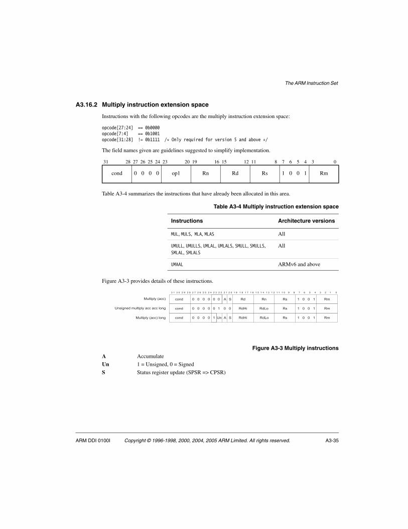
A3.16.2 Multiply instruction extension space
Instructions with the following opcodes are the multiply instruction extension space:
opcode[27:24] == 0b0000opcode[7:4] == 0b1001opcode[31:28] != 0b1111 /* Only required for version 5 and above */
The field names given are guidelines suggested to simplify implementation.
Table A3-4 summarizes the instructions that have already been allocated in this area.
Figure A3-3 provides details of these instructions.
Figure A3-3 Multiply instructionsA AccumulateUn 1 = Unsigned, 0 = SignedS Status register update (SPSR => CPSR)
31 28 27 26 25 24 23 20 19 16 15 12 11 8 7 6 5 4 3 0
cond 0 0 0 0 op1 Rn Rd Rs 1 0 0 1 Rm
Table A3-4 Multiply instruction extension space
Instructions Architecture versions
MUL, MULS, MLA, MLAS All
UMULL, UMULLS, UMLAL, UMLALS, SMULL, SMULLS, SMLAL, SMLALS
All
UMAAL ARMv6 and above
A 3 A 7 9 U 9 Q 9 V 9 T 9 S 9 C 9 A 9 9 9 3 9 7 3 U 3 Q 3 V 3 T 3 S 3 C 3 A 3 9 3 3 3 7 U Q V T S C A 9 3 7
<8=#+%=W$Z"(([
:,*+-,)/$.8=#+%=W$"(($"(($=',-
<8=#+%=W$Z"(([$=',- (',/ 5.6@:, 5/H'5/X+ 5*7 7 7 7 3 3 7 7 3
(',/ 5.777 7 7 7 7 3 5* 3 7 7 35/H'5/X+
(',/ 5.6@7 7 7 7 7 7 5*5,5/ 3 7 7 3
The ARM Instruction Set
A3-36 Copyright © 1996-1998, 2000, 2004, 2005 ARM Limited. All rights reserved. ARM DDI 0100I
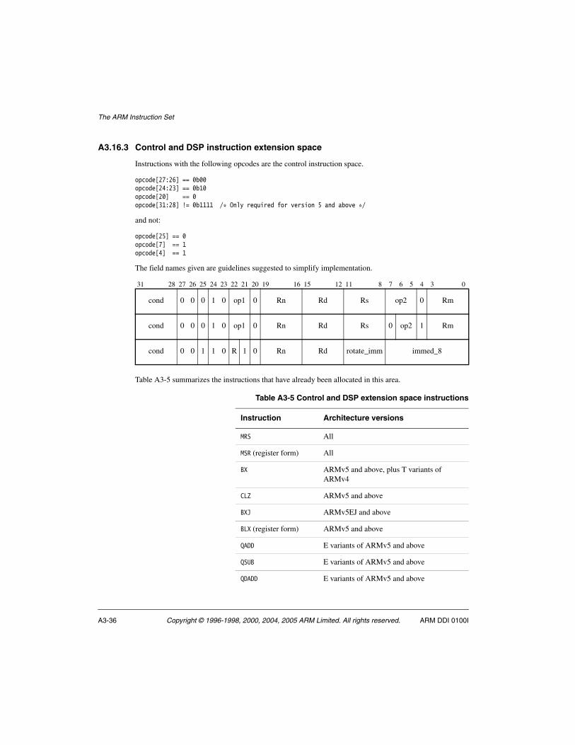
A3.16.3 Control and DSP instruction extension space
Instructions with the following opcodes are the control instruction space.
opcode[27:26] == 0b00opcode[24:23] == 0b10opcode[20] == 0opcode[31:28] != 0b1111 /* Only required for version 5 and above */
and not:
opcode[25] == 0opcode[7] == 1opcode[4] == 1
The field names given are guidelines suggested to simplify implementation.
Table A3-5 summarizes the instructions that have already been allocated in this area.
31 28 27 26 25 24 23 22 21 20 19 16 15 12 11 8 7 6 5 4 3 0
cond 0 0 0 1 0 op1 0 Rn Rd Rs op2 0 Rm
cond 0 0 0 1 0 op1 0 Rn Rd Rs 0 op2 1 Rm
cond 0 0 1 1 0 R 1 0 Rn Rd rotate_imm immed_8
Table A3-5 Control and DSP extension space instructions
Instruction Architecture versions
MRS All
MSR (register form) All
BX ARMv5 and above, plus T variants of ARMv4
CLZ ARMv5 and above
BXJ ARMv5EJ and above
BLX (register form) ARMv5 and above
QADD E variants of ARMv5 and above
QSUB E variants of ARMv5 and above
QDADD E variants of ARMv5 and above
The ARM Instruction Set
ARM DDI 0100I Copyright © 1996-1998, 2000, 2004, 2005 ARM Limited. All rights reserved. A3-37
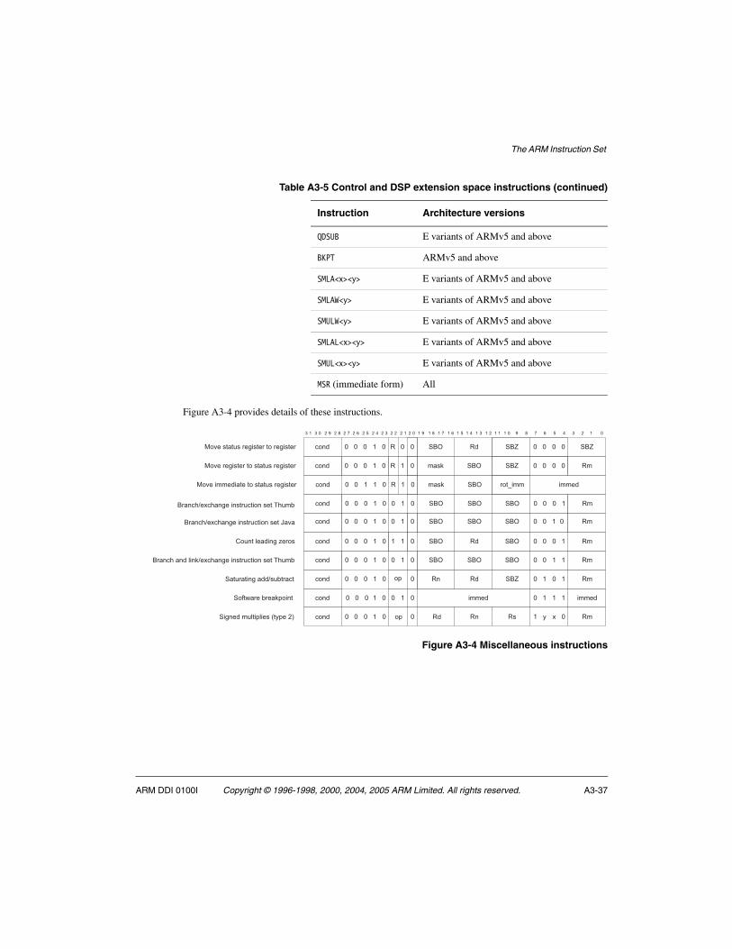
Figure A3-4 provides details of these instructions.
Figure A3-4 Miscellaneous instructions
QDSUB E variants of ARMv5 and above
BKPT ARMv5 and above
SMLA<x><y> E variants of ARMv5 and above
SMLAW<y> E variants of ARMv5 and above
SMULW<y> E variants of ARMv5 and above
SMLAL<x><y> E variants of ARMv5 and above
SMUL<x><y> E variants of ARMv5 and above
MSR (immediate form) All
Table A3-5 Control and DSP extension space instructions (continued)
Instruction Architecture versions
(',/ 7 7 7 3 7 3 77 +..)/ +..)/7 3 3 36'1#M"&)$L&)"G%'+,#
(',/ 7 7 7 3 7 3 77 6EF6EF 6EF 5.7 7 3 3E&",(0$",/$=+,GI);(0",-)$+,*#&8(#+',$*)#$_08.L
(',/ 7 7 7 3 7 7
(',/ 7 7 7 3 7 '% 7 5,5/ 5* 5.3 W ; 76+-,)/$.8=#+%=+)*$Z#W%)$9[
'% 5/5, 6E\ 5.7 3 7 36"#8&"#+,-$"//I*8L#&"(#
(',/ 7 7 7 3 7 3 73 5/6EF 6EF 5.7 7 7 3N'8,#$=)"/+,-$Y)&'*
E&",(0I);(0",-)$+,*#&8(#+',$*)#$`"D" (',/ 7 7 7 3 7 3 77 6EF6EF 6EF 5.7 7 73
E&",(0I);(0",-)$+,*#&8(#+',$*)#$_08.L (',/ 7 7 7 3 7 3 77 6EF6EF 6EF 5.7 7 7 3
A 3 A 7 9 U 9 Q 9 V 9 T 9 S 9 C 9 A 9 9 9 3 9 7 3 U 3 Q 3 V 3 T 3 S 3 C 3 A 3 9 3 3 3 7 U Q V T S C A 9 3 7
7<'D)$*#"#8*$&)-+*#)&$#'$&)-+*#)& (',/ 7 7 3 7 7 75 5/6EF 6E\ 6E\7 7 7 7
(',/ 7 7 3 7 3 75 6EF."*G 6E\ 5.7 7 7 7<'D)$&)-+*#)&$#'$*#"#8*$&)-+*#)&
(',/ 7 7 3 7 3 75 6EF."*G &'#P+.. +..)/<'D)$+..)/+"#)$#'$*#"#8*$&)-+*#)&
7
3

The ARM Instruction Set
A3-38 Copyright © 1996-1998, 2000, 2004, 2005 ARM Limited. All rights reserved. ARM DDI 0100I
A3.16.4 Load/store instruction extension space
Instructions with the following opcodes are the load/store instruction extension space:
opcode[27:25] == 0b000opcode[7] == 1opcode[4] == 1opcode[31:28] != 0b1111 /* Only required for version 5 and above */
and not:
opcode[24] == 0opcode[6:5] == 0
The field names given are guidelines suggested to simplify implementation.
Table A3-6 summarizes the instructions that have already been allocated in this area.
Figure A3-5 on page A3-39 provides details of these extra load/store instructions.
31 28 27 26 25 24 23 22 21 20 19 16 15 12 11 8 7 6 5 4 3 0
cond 0 0 0 P U B W L Rn Rd Rs 1 op1 1 Rm
Table A3-6 Load/store instructions
Instruction Architecture versions
SWP/SWPB All (deprecated in ARMv6)
LDREX ARMv6 and above
STREX ARMv6 and above
STRH All
LDRD E variants of ARMv5 and above, except ARMv5TExP
STRD E variants of ARMv5 and above, except ARMv5TExP
LDRH All
LDRSB All
LDRSH All
The ARM Instruction Set
ARM DDI 0100I Copyright © 1996-1998, 2000, 2004, 2005 ARM Limited. All rights reserved. A3-39
Figure A3-5 Extra Load/store instructionsB 1 = Byte, 0 = WordP, U, I, W Pre/post indexing or offset, Up/down, Immediate/register offset, and address Write-back
fields for the address mode. See Chapter A5 ARM Addressing Modes for more details.L 1 = Load, 0 = StoreH 1= Halfword, 0 = ByteSt 1 = Store, 0 = Load
A3.16.5 Architecturally Undefined Instruction space
In general, Undefined instructions might be used to extend the ARM instruction set in the future. However, it is intended that instructions with the following encoding will not be used for this:
If a programmer wants to use an Undefined instruction for software purposes, with minimal risk that future hardware will treat it as a defined instruction, one of the instructions with this encoding must be used.
A 3 A 7 9 U 9 Q 9 V 9 T 9 S 9 C 9 A 9 9 9 3 9 7 3 U 3 Q 3 V 3 T 3 S 3 C 3 A 3 9 3 3 3 7 U Q V T S C A 9 3 7
H'"/I*#'&)$0"=1M'&/$+..)/+"#)$'11*)# (',/ 5/5,7 7 7 3:J HK X+F11*)# 3 7 3 3 H'F11*)#
H'"/$*+-,)/$0"=1M'&/ILW#)$&)-+*#)&$'11*)#
6M"%I*M"%$LW#)
H'"/I*#'&)$0"=1M'&/$&)-+*#)&$'11*)#
H'"/I*#'&)$&)-+*#)&$);(=8*+D) (',/ 5/5,7 7 7 733 H7 3 7 7 36EF 6EF
(',/ 6E\ 5.5/5,7 7 7 E73 77 3 7 7 3
(',/ 5/5,7 7 7 7:J 3K 3 3 X 36E\ 5.
(',/ 5/5,7 7 7 7:J HK 3 7 3 36E\ 5.
H'"/$*+-,)/$0"=1M'&/ILW#)$+..)/+"#)$'11*)# (',/ 5/5,7 7 7 3:J 3K X+F11*)# 3 X 3 H'F11*)#3
H'"/I*#'&)$/'8L=)M'&/$+..)/+"#)$'11*)# (',/ 5/5,7 7 7 3:J 7K X+F11*)# 3 6# 3 H'F11*)#3
H'"/I*#'&)$/'8L=)M'&/$&)-+*#)&$'11*)# (',/ 5/5,7 7 7 7:J 7K 6E\ 3 6# 3 5.3
31 28 27 26 25 24 23 22 21 20 19 8 7 6 5 4 3 2 1 0
cond 0 1 1 1 1 1 1 1 x x x x x x x x x x x x 1 1 1 1 x x x x
The ARM Instruction Set
A3-40 Copyright © 1996-1998, 2000, 2004, 2005 ARM Limited. All rights reserved. ARM DDI 0100I
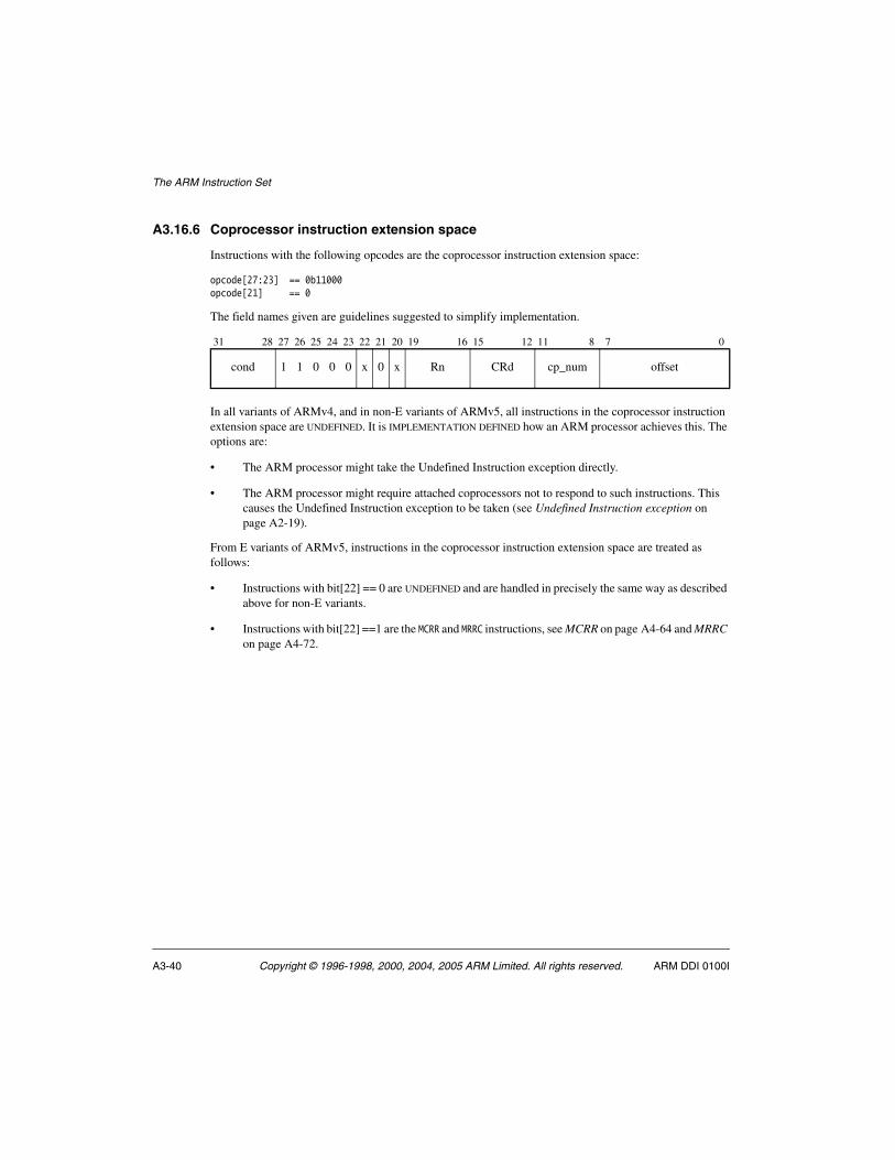
A3.16.6 Coprocessor instruction extension space
Instructions with the following opcodes are the coprocessor instruction extension space:
opcode[27:23] == 0b11000opcode[21] == 0
The field names given are guidelines suggested to simplify implementation.
In all variants of ARMv4, and in non-E variants of ARMv5, all instructions in the coprocessor instruction extension space are UNDEFINED. It is IMPLEMENTATION DEFINED how an ARM processor achieves this. The options are:
• The ARM processor might take the Undefined Instruction exception directly.
• The ARM processor might require attached coprocessors not to respond to such instructions. This causes the Undefined Instruction exception to be taken (see Undefined Instruction exception on page A2-19).
From E variants of ARMv5, instructions in the coprocessor instruction extension space are treated as follows:
• Instructions with bit[22] == 0 are UNDEFINED and are handled in precisely the same way as described above for non-E variants.
• Instructions with bit[22] ==1 are the MCRR and MRRC instructions, see MCRR on page A4-64 and MRRC on page A4-72.
31 28 27 26 25 24 23 22 21 20 19 16 15 12 11 8 7 0
cond 1 1 0 0 0 x 0 x Rn CRd cp_num offset
The ARM Instruction Set
ARM DDI 0100I Copyright © 1996-1998, 2000, 2004, 2005 ARM Limited. All rights reserved. A3-41
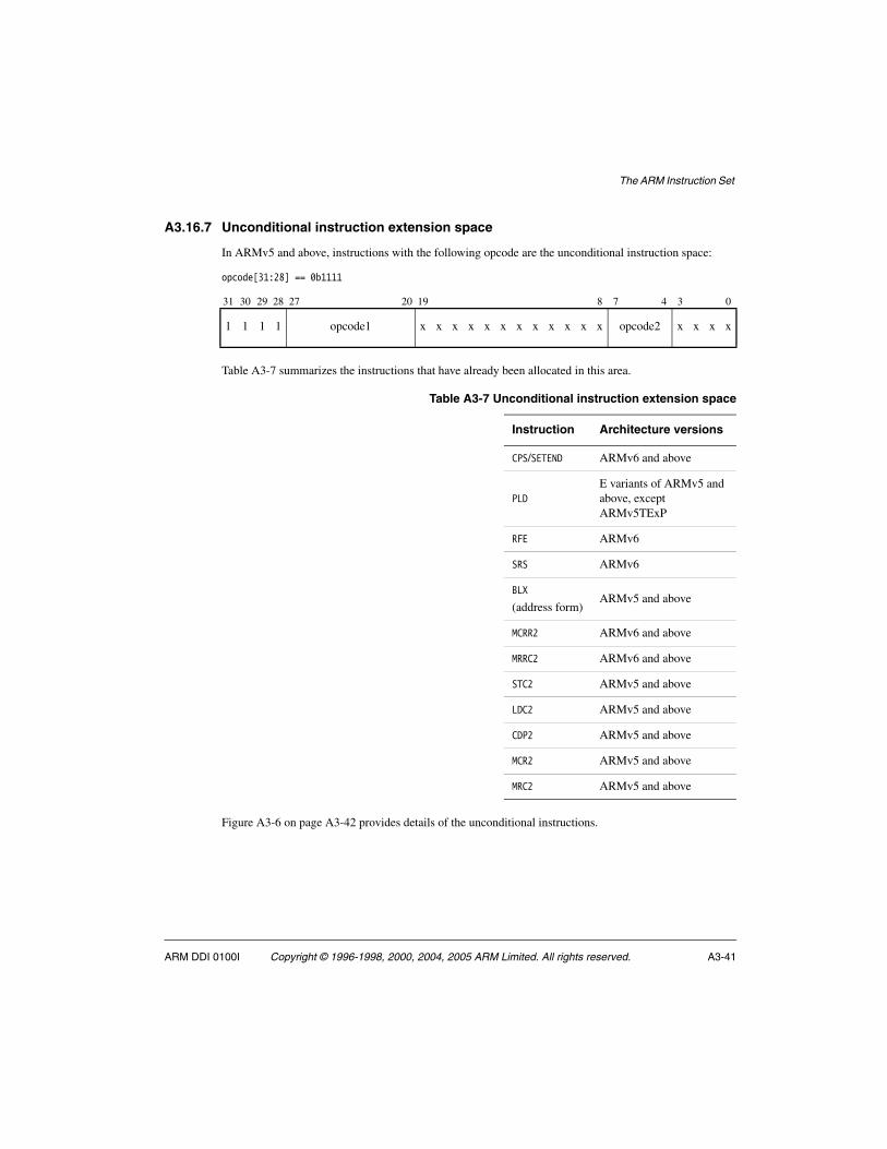
A3.16.7 Unconditional instruction extension space
In ARMv5 and above, instructions with the following opcode are the unconditional instruction space:
opcode[31:28] == 0b1111
Table A3-7 summarizes the instructions that have already been allocated in this area.
Figure A3-6 on page A3-42 provides details of the unconditional instructions.
31 30 29 28 27 20 19 8 7 4 3 0
1 1 1 1 opcode1 x x x x x x x x x x x x opcode2 x x x x
Table A3-7 Unconditional instruction extension space
Instruction Architecture versions
CPS/SETEND ARMv6 and above
PLDE variants of ARMv5 and above, except ARMv5TExP
RFE ARMv6
SRS ARMv6
BLX
(address form)ARMv5 and above
MCRR2 ARMv6 and above
MRRC2 ARMv6 and above
STC2 ARMv5 and above
LDC2 ARMv5 and above
CDP2 ARMv5 and above
MCR2 ARMv5 and above
MRC2 ARMv5 and above
The ARM Instruction Set
A3-42 Copyright © 1996-1998, 2000, 2004, 2005 ARM Limited. All rights reserved. ARM DDI 0100I
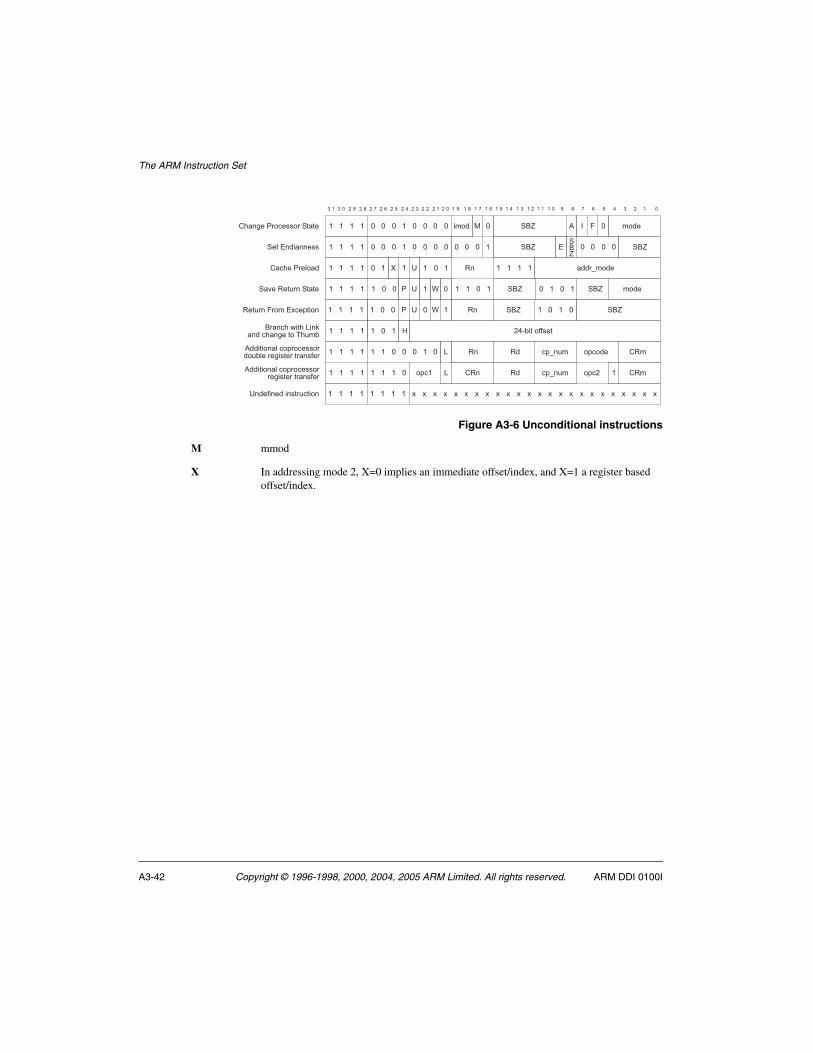
Figure A3-6 Unconditional instructions
M mmod
X In addressing mode 2, X=0 implies an immediate offset/index, and X=1 a register based offset/index.
A 3 A 7 9 U 9 Q 9 V 9 T 9 S 9 C 9 A 9 9 9 3 9 7 3 U 3 Q 3 V 3 T 3 S 3 C 3 A 3 9 3 3 3 7 U Q V T S C A 9 3 7
9CBL+#$'11*)#73 3
773 3
E&",(0$M+#0$H+,G",/$(0",-)$#'$_08.L
5,
7 3
5)#8&,$?&'.$R;()%#+',
6"D)$5)#8&,$6#"#) J7 73 7 7 3
7 7 7 3 7 7
@
6E\7 7 7 76)#$R,/+",,)**
N0",-)$J&'()**'&$6#"#) 7 7 7 3 7 7 7 +.'/ 6E\ .'/)3 3 3 3
3 3 3 3
3 3 3 3
3 3 3 3
3 3 3 3
7
7
7 7 7 7 3 6E\
7 a ? 7
R
<
6E\
3 33 7K: 6E\ 6E\ .'/)
J7 73 3K: 6E\ 6E\
3
7
X
3 3 3 3 3 3 3 3 ;; ;;;; ;;;; ;;;; ;; ;; ;;;; ;;:,/)1+,)/$+,*#&8(#+',
73 3 3 3 33 73 3 5, 3 3 3 3 "//&P.'/):N"(0)$J&)='"/
3 3 3 3
3 3 3 3
3 3 7 7
3 3 3 7
7 3 7 H@//+#+',"=$('%&'()**'&/'8L=)$&)-+*#)&$#&",*1)&
@//+#+',"=$('%&'()**'&&)-+*#)&$#&",*1)&
5, 5/ (%P,8. '%('/) N5.
3 N5.N5, 5/ (%P,8. '%(9'%(3
b
H