Embed Size (px)
Citation preview
ARM Laboratory Exercises™
For the ARM Evaluator-7T™ Board and theOKI ML67Q4000™ MCU Evaluation Board
Confidential - Draft - Preliminary
Copyright © 2003 ARM Limited. All rights reserved.DUI xxxx A-3a
ARM Laboratory ExercisesFor the ARM Evaluator-7T Board and theOKI ML67Q4000 MCU Evaluation Board
Copyright © 2003 ARM Limited. All rights reserved.
Release Information
Proprietary Notice
Words and logos marked with ® or ™ are registered trademarks or trademarks of ARM Limited in the EU and other countries, except as otherwise stated below in this proprietary notice. Other brands and names mentioned herein may be the trademarks of their respective owners.
Neither the whole nor any part of the information contained in, or the product described in, this document may be adapted or reproduced in any material form except with the prior written permission of the copyright holder.
The product described in this document is subject to continuous developments and improvements. All particulars of the product and its use contained in this document are given by ARM Limited in good faith. However, all warranties implied or expressed, including but not limited to implied warranties of merchantability, or fitness for purpose, are excluded.
This document is intended only to assist the reader in the use of the product. ARM Limited shall not be liable for any loss or damage arising from the use of any information in this document, or any error or omission in such information, or any incorrect use of the product.
Confidentiality Status
This document is Open Access. This document has no restriction on distribution.
Product Status
The information in this document is Final (information on a developed product).
Web Address
http://www.arm.com
Change history
Date Issue Change
September 11, 2003 A-1a 1st draft
September 30, 2003 A-1b New OKI board chapter.New float chapter.
September 30, 2003 A-1c New float chapter edits.
October 6, 2003 A-2a 2nd draft. Peripheral chapter edits.Float chapter edits.New chapter: Semihosting
October 24, 2003 A-3a 3rd draft. BH and JB edits.
ii Copyright © 2003 ARM Limited. All rights reserved. DUI xxxx A-3aConfidential - Draft - Preliminary
ContentsARM Laboratory Exercises For the ARM Evaluator-7T Board and theOKI ML67Q4000 MCU Evaluation Board
PrefaceAbout this document ..................................................................................... xiiFeedback ...................................................................................................... xv
Chapter 1 The ARM Programmer’s Model1.1 The ARM7TDMI .......................................................................................... 1-21.2 Memory formats .......................................................................................... 1-31.3 Data types ................................................................................................... 1-41.4 Processor modes ........................................................................................ 1-51.5 Processor states ......................................................................................... 1-61.6 The ARM register set .................................................................................. 1-71.7 Exercises .................................................................................................. 1-11
Chapter 2 ARM Instruction Set Fundamentals2.1 Introduction ................................................................................................. 2-22.2 Building a program ...................................................................................... 2-32.3 Viewing and changing information .............................................................. 2-72.4 Exercises .................................................................................................... 2-8
DUI xxxx A-3a Copyright © 2003 ARM Limited. All rights reserved. iiiConfidential - Draft - Preliminary
Contents
Chapter 3 Data Processing Operations3.1 Introduction ................................................................................................. 3-23.2 Condition code flags ................................................................................... 3-33.3 Addition and subtraction ............................................................................. 3-43.4 Multiplication ............................................................................................... 3-53.5 Shifts ........................................................................................................... 3-63.6 Data processing operations ........................................................................ 3-73.7 Single data transfer instructions ................................................................. 3-83.8 Compares and tests ................................................................................... 3-93.9 Logical operations .................................................................................... 3-103.10 Exercises .................................................................................................. 3-11
Chapter 4 Loads and Stores4.1 Introduction ................................................................................................. 4-24.2 Addressing modes of single-register loads and stores ............................... 4-34.3 Loading constants into registers ................................................................. 4-44.4 Loading addresses into registers ................................................................ 4-74.5 Exercises .................................................................................................. 4-10
Chapter 5 Conditional Execution and Loops5.1 Introduction ................................................................................................. 5-25.2 Execution conditions ................................................................................... 5-35.3 Implementing loop structures ..................................................................... 5-55.4 Using conditional execution ........................................................................ 5-75.5 Exercises .................................................................................................... 5-8
Chapter 6 Subroutines6.1 Introduction ................................................................................................. 6-26.2 The branch and link instruction ................................................................... 6-36.3 Load/store multiple instructions .................................................................. 6-46.4 Stacks ......................................................................................................... 6-66.5 Exercises .................................................................................................... 6-9
Chapter 7 Memory-mapped Peripherals (Evaluator 7T)7.1 Introduction ................................................................................................. 7-27.2 Example peripheral device ........................................................................ 7-37.3 Exceptions .................................................................................................. 7-47.4 Evaluator 7T peripherals ............................................................................ 7-87.5 Exercises .................................................................................................. 7-11
Chapter 8 Memory-mapped Peripherals (OKI ML674000)8.1 Introduction ................................................................................................. 8-28.2 Example peripheral device ........................................................................ 8-38.3 Exceptions .................................................................................................. 8-48.4 OKI ML674000 peripherals ........................................................................ 8-88.5 Exercises .................................................................................................. 8-15
iv Copyright © 2003 ARM Limited. All rights reserved. DUI xxxx A-3aConfidential - Draft - Preliminary
Contents
Chapter 9 Floating-point Computation9.1 Introduction ................................................................................................. 9-29.2 Floating-point data types - single-precision and double-precision .............. 9-39.3 Basic floating-point computations ............................................................... 9-59.4 Rounding modes ......................................................................................... 9-69.5 Algorithm for basic floating-point computation ............................................ 9-79.6 Floating-point multiplication ......................................................................... 9-89.7 Exercises .................................................................................................... 9-9
Chapter 10 Semihosting10.1 Introduction ............................................................................................... 10-210.2 SWI numbers ............................................................................................ 10-410.3 Semihosting implementation ..................................................................... 10-710.4 Exercises .................................................................................................. 10-8
DUI xxxx A-3a Copyright © 2003 ARM Limited. All rights reserved. vConfidential - Draft - Preliminary

Contents
vi Copyright © 2003 ARM Limited. All rights reserved. DUI xxxx A-3aConfidential - Draft - Preliminary
List of TablesARM Laboratory Exercises For the ARM Evaluator-7T Board and theOKI ML67Q4000 MCU Evaluation Board
Change history .............................................................................................................. iiTable 1-1 Processor modes ...................................................................................................... 1-5Table 1-2 Processor mode selection ....................................................................................... 1-10Table 4-1 Examples of creating constants with MOV and ROR ................................................ 4-4Table 5-1 Condition codes ........................................................................................................ 5-3Table 6-1 Stack addressing modes ........................................................................................... 6-6Table 7-1 Exception types ......................................................................................................... 7-5Table 7-2 Exception priority ....................................................................................................... 7-7Table 8-1 Exception types ......................................................................................................... 8-5Table 8-2 Exception priority ....................................................................................................... 8-7Table 8-3 Register access ......................................................................................................... 8-9Table 8-4 LCD controller connections ..................................................................................... 8-11Table 8-5 I/O register map in JTAG/debug mode ................................................................... 8-12Table 8-6 LCD controller instructions ...................................................................................... 8-14Table 9-1 Floating-point data format specifications ................................................................... 9-3Table 9-2 Rounding modes ....................................................................................................... 9-6Table 9-3 Codes for operand types ......................................................................................... 9-10Table 10-1 SWI numbers .......................................................................................................... 10-4Table 10-2 EnterSVC SWI entry values .................................................................................... 10-5
DUI xxxx A-3a Copyright © 2003 ARM Limited. All rights reserved. viiConfidential - Draft - Preliminary

List of Tables
viii Copyright © 2003 ARM Limited. All rights reserved. DUI xxxx A-3aConfidential - Draft - Preliminary
List of FiguresARM Laboratory Exercises For the ARM Evaluator-7T Board and theOKI ML67Q4000 MCU Evaluation Board
Figure 1-1 Little-endian data format ........................................................................................... 1-3Figure 1-2 ARM register set ....................................................................................................... 1-7Figure 1-3 ARM status register format ....................................................................................... 1-9Figure 2-1 Creating the project ................................................................................................... 2-4Figure 2-2 Creating the source file ............................................................................................. 2-5Figure 2-3 Using the Step icon to execute the ADD instruction ................................................. 2-6Figure 3-1 Barrel shifter operations ............................................................................................ 3-6Figure 6-1 ARM memory map .................................................................................................... 6-8Figure 7-1 Evaluator-7T memory map ........................................................................................ 7-8Figure 7-2 Flickering ................................................................................................................. 7-14Figure 8-1 LED bit mapping ........................................................................................................ 8-8Figure 8-2 Flickering ................................................................................................................. 8-16Figure 9-1 Floating-point data formats ....................................................................................... 9-4Figure 9-2 Single-precision data example .................................................................................. 9-4Figure 10-1 Semihosting overview ............................................................................................. 10-2
DUI xxxx A-3a Copyright © 2003 ARM Limited. All rights reserved. ixConfidential - Draft - Preliminary

List of Figures
x Copyright © 2003 ARM Limited. All rights reserved. DUI xxxx A-3aConfidential - Draft - Preliminary
Preface
This preface introduces the ARM Lab Manual. It contains the following sections:
• About this document on page xii
• Feedback on page xv.
DUI xxxx A-3a Copyright © 2003 ARM Limited. All rights reserved. xiConfidential - Draft - Preliminary
Preface
About this document
This manual provides exercises and examples for use by instructors and teaching assistants using an ARM hardware environment. The evaluation boards can serve as platforms for developing and testing software, learning about debugging tools, and teaching the ARM architecture. This manual does not cover every detail about assembly programming of ARM processors, but the exercises are intended as an introduction to many basic ARM programming principles.
Intended audience
The exercises in this manual were written by ARM engineers for computer architecture students. Each chapter contains material to assist the student in an independent study of the ARM architecture. However, the material can best be learned by a combination of short lectures from the lab instructor and hands-on experience.
Prerequisites
The exercises in this manual might be the student's first exposure to assembly programming. However, it is assumed that the student has a good understanding of digital logic and some high-level language skills.
Course relevance
The exercises in this manual are best suited to a junior-level or senior-level course on assembly programming, microprocessor system design, or computer architecture. Each chapter contains a number of exercises. Therefore, the instructor might wish to assign only some of the exercises for a particular topic, depending on the depth of the material being discussed.
• Chapter 1 The ARM Programmer’s Model introduces the ARM family of processors and shows features of ARM processors that are geared towards the programmer.
• Chapter 2 ARM Instruction Set Fundamentals introduces students to the simulation environment, basic ARM assembly language programming, and some of the programming techniques needed for subsequent chapters.
• Chapter 3 Data Processing Operations teaches students how to implement data processing instructions in the ARM.
• Chapter 4 Loads and Stores introduces data movement instructions.
• Chapter 5 Conditional Execution and Loops shows students how to use conditional execution, branches, and loops.
xii Copyright © 2003 ARM Limited. All rights reserved. DUI xxxx A-3aConfidential - Draft - Preliminary
Preface
• Chapter 6 Subroutines teaches the student how to write subroutines in ARM assembly, specifically using stacks, branching and linking, as well as the load and store multiple instructions.
• Chapter 7 Memory-mapped Peripherals (Evaluator 7T) introduces I/O in an ARM system, as well as exception handling and how to implement I/O in the ARM Evaluator-7T Board.
• Chapter 8 Memory-mapped Peripherals (OKI ML674000) introduces I/O in an ARM system, as well as exception handling and how to implement I/O in the Oki ML674000 MCU Evaluation Board.
• Chapter 9 Floating-point Computation deals with floating-point arithmetic in an ARM system.
• Chapter 10 Semihosting deals with semihosting SWIs, semihosting implementation, and adding SWI handlers in an ARM system.
Some of the chapters contain introductory material and can be assigned without the use of an evaluation board.
Additional material
For information about the ARM Evaluator-7T Board, see the ARM Evaluator -7T Board User Guide, available as a PDF document on the CD ROM. The Evaluator-7T Installation Guide comes with the board and provides information on the installation of the software and tools. If you are using the OKI ML67Q4000 MCU Evaluation Board, see the ML67Q4000 MCU Evaluation Board Quick Start Guide and User Manual, available as a PDF document.
Other valuable references include the following:
• Seal (ed.), ARM Architectural Reference Manual, 2nd Edition, Addison-Wesley. ISBN 0-201-73719-1
• Furber, ARM System-on-Chip Architecture, 2nd Edition, Addison-Wesley, 2000. ISBN 0-201-67519-6
• Atack and van Someren, The ARM RISC Chip, Addison-Wesley, 1993. ISBN 0-201-62410-9
• ADS Debug Target Guide (DUI 0058)
• ANSI/IEEE Std 754-1985, IEEE Standard for Binary Floating Point Arithmetic.
Information about ARM products and support can be found on the web page at http://www.arm.com
DUI xxxx A-3a Copyright © 2003 ARM Limited. All rights reserved. xiiiConfidential - Draft - Preliminary
Preface
Typographical conventions
The following typographical conventions are used in this book:
italic Introduces special terminology. Also denotes cross-references.
bold Denotes signal names. Also used for terms in descriptive lists, where appropriate.
monospace Denotes text that can be entered at the keyboard, such as commands, file and program names, and source code.
monospace Denotes a permitted abbreviation for a command or option. The underlined text can be entered instead of the full command or option name.
monospace italic Denotes arguments to commands and functions where the argument is to be replaced by a specific value.
monospace bold Denotes language keywords when used outside example code.
xiv Copyright © 2003 ARM Limited. All rights reserved. DUI xxxx A-3aConfidential - Draft - Preliminary
Preface
Feedback
ARM Limited welcomes feedback on the ARM Evaluator-7T Board, the OKI ML67Q4000 MCU Evaluator Board, and on the documentation.
Feedback on the ARM Evaluator-7T Board or OKI ML67Q4000 MCU Evaluator Board
If you have any comments or suggestions about the evaluator boards, contact your supplier giving:
• the product name
• a concise explanation of your comments.
Feedback on this document
If you have any comments on this document, send email to [email protected] giving:
• the document title
• the document number
• the page number(s) to which your comments refer
• a concise explanation of your comments.
General suggestions for additions and improvements are also welcome.
DUI xxxx A-3a Copyright © 2003 ARM Limited. All rights reserved. xvConfidential - Draft - Preliminary

Preface
xvi Copyright © 2003 ARM Limited. All rights reserved. DUI xxxx A-3aConfidential - Draft - Preliminary
Chapter 1 The ARM Programmer’s Model
This chapter introduces the ARM7TDMI processor and features of the ARM architecture that are of special interest to the programmer. It contains the following sections:
• The ARM7TDMI on page 1-2
• Memory formats on page 1-3
• Data types on page 1-4
• Processor modes on page 1-5
• Processor states on page 1-6
• The ARM register set on page 1-7
• Exercises on page 1-11.
DUI xxxx A-3a Copyright © 2003 ARM Limited. All rights reserved. 1-1Confidential - Draft - Preliminary
The ARM Programmer’s Model
1.1 The ARM7TDMI
The ARM Evaluator-7T Board and the OKI ML67Q4000 MCU Evaluation Board contain a microcontroller based on the 32-bit ARM7TDMI processor. This ARM processor
• provides on-chip support for debugging tools
• contains an enhanced multiplier for 64-bit operations
• runs at low voltages
• supports the 16-bit Thumb instruction set.
Because the ARM instruction set is common across the range of ARM processors, assembly code that runs on an ARM7 processor also runs on an ARM9 or ARM10 processor.
1-2 Copyright © 2003 ARM Limited. All rights reserved. DUI xxxx A-3aConfidential - Draft - Preliminary
The ARM Programmer’s Model
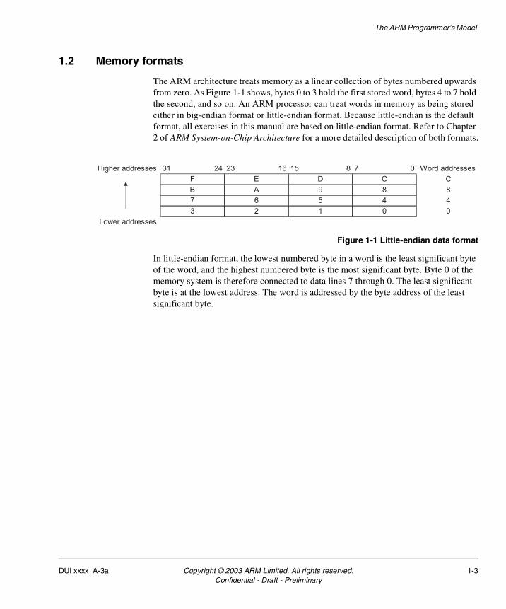
1.2 Memory formats
The ARM architecture treats memory as a linear collection of bytes numbered upwards from zero. As Figure 1-1 shows, bytes 0 to 3 hold the first stored word, bytes 4 to 7 hold the second, and so on. An ARM processor can treat words in memory as being stored either in big-endian format or little-endian format. Because little-endian is the default format, all exercises in this manual are based on little-endian format. Refer to Chapter 2 of ARM System-on-Chip Architecture for a more detailed description of both formats.
Figure 1-1 Little-endian data format
In little-endian format, the lowest numbered byte in a word is the least significant byte of the word, and the highest numbered byte is the most significant byte. Byte 0 of the memory system is therefore connected to data lines 7 through 0. The least significant byte is at the lowest address. The word is addressed by the byte address of the least significant byte.
3
6
2
5
1
4
0
4
0
Higher addresses
Lower addresses
31 24
F
23 16
E
15 8
D
7 0
C C
Word addresses
A 9 8 8
7
B
DUI xxxx A-3a Copyright © 2003 ARM Limited. All rights reserved. 1-3Confidential - Draft - Preliminary
The ARM Programmer’s Model
1.3 Data types
The ARM supports the following data types:
byte Eight bits.
halfword 16 bits. Halfwords must be aligned to two-byte boundaries.
word 32 bits. Words must be aligned to four-byte boundaries.
Load and store operations can transfer bytes, halfwords, and words to and from memory. For operations such as multiplies and adds, signed operands are assumed to be in two's complement format.
1-4 Copyright © 2003 ARM Limited. All rights reserved. DUI xxxx A-3aConfidential - Draft - Preliminary
The ARM Programmer’s Model
1.4 Processor modes
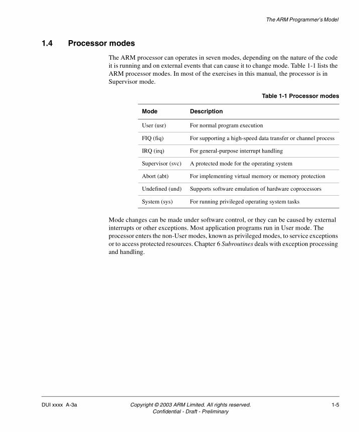
The ARM processor can operates in seven modes, depending on the nature of the code it is running and on external events that can cause it to change mode. Table 1-1 lists the ARM processor modes. In most of the exercises in this manual, the processor is in Supervisor mode.
Mode changes can be made under software control, or they can be caused by external interrupts or other exceptions. Most application programs run in User mode. The processor enters the non-User modes, known as privileged modes, to service exceptions or to access protected resources. Chapter 6 Subroutines deals with exception processing and handling.
Table 1-1 Processor modes
Mode Description
User (usr) For normal program execution
FIQ (fiq) For supporting a high-speed data transfer or channel process
IRQ (irq) For general-purpose interrupt handling
Supervisor (svc) A protected mode for the operating system
Abort (abt) For implementing virtual memory or memory protection
Undefined (und) Supports software emulation of hardware coprocessors
System (sys) For running privileged operating system tasks
DUI xxxx A-3a Copyright © 2003 ARM Limited. All rights reserved. 1-5Confidential - Draft - Preliminary
The ARM Programmer’s Model
1.5 Processor states
Thumb-aware processors, such as the ARM7TDMI, can be in one of two processor states:
ARM state Executes 32-bit word-aligned ARM instructions.
Thumb state Executes 16-bit halfword-aligned Thumb instructions. In Thumb state, the PC uses bit 1 to select between the alternate halfwords.
1-6 Copyright © 2003 ARM Limited. All rights reserved. DUI xxxx A-3aConfidential - Draft - Preliminary
The ARM Programmer’s Model
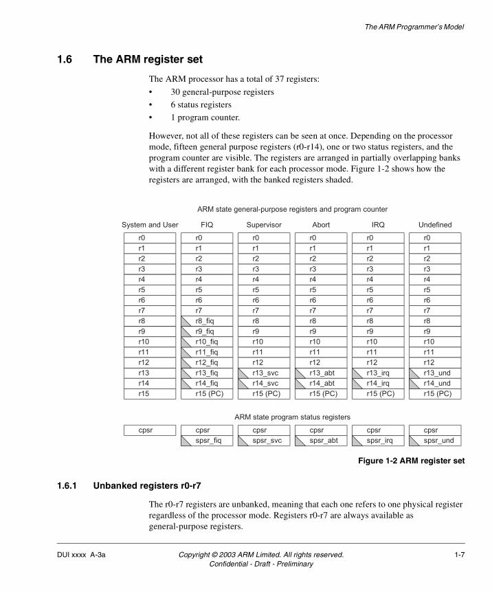
1.6 The ARM register set
The ARM processor has a total of 37 registers:
• 30 general-purpose registers
• 6 status registers
• 1 program counter.
However, not all of these registers can be seen at once. Depending on the processor mode, fifteen general purpose registers (r0-r14), one or two status registers, and the program counter are visible. The registers are arranged in partially overlapping banks with a different register bank for each processor mode. Figure 1-2 shows how the registers are arranged, with the banked registers shaded.
Figure 1-2 ARM register set
1.6.1 Unbanked registers r0-r7
The r0-r7 registers are unbanked, meaning that each one refers to one physical register regardless of the processor mode. Registers r0-r7 are always available as general-purpose registers.
r0
r1
r2
r3
r4
r5
r6
r7
r8
r9
r13
r14
r15
System and User
r0
r1
r2
r3
r4
r5
r6
r7
r8_fiq
r13_fiq
r14_fiq
r15 (PC)
FIQ
r0
r1
r2
r3
r4
r5
r6
r7
r8
r13_svc
r14_svc
r15 (PC)
Supervisor
r0
r1
r2
r3
r4
r5
r6
r7
r8
r13_abt
r14_abt
r15 (PC)
Abort
r0
r1
r2
r3
r4
r5
r6
r7
r8
r13_irq
r14_irq
r15 (PC)
IRQ
r0
r1
r2
r3
r4
r5
r6
r7
r8
r13_und
r14_und
r15 (PC)
Undefined
cpsr
ARM state general-purpose registers and program counter
ARM state program status registers
r10
r11
r12
r9_fiq
r10_fiq
r11_fiq
r12_fiq
r9
r10
r11
r12
r9
r10
r11
r12
r9
r10
r11
r12
r9
r10
r11
r12
cpsr cpsr cpsr cpsr cpsr
spsr_fiq spsr_svc spsr_abt spsr_irq spsr_und
DUI xxxx A-3a Copyright © 2003 ARM Limited. All rights reserved. 1-7Confidential - Draft - Preliminary
The ARM Programmer’s Model
1.6.2 Banked registers r8-r14
Registers r8-r14 are banked, meaning that the processor mode determines which physical register each one refers to.
r8-r12
Each of the r8-r12 registers has two banked registers. In Fast Interrupt mode, r<x> refers to physical register r<x>_fiq. In all other modes, r<8-12> refers to the physical register r<8-12>. In Fast Interrupt mode, banked registers r8_fiq-r12_fiq provide very fast interrupt processing without having to preserve register contents by storing them to memory. Registers r8_fiq-r12_fiq also preserve values across interrupt calls so that register contents do not have to be restored from memory.
Registers r8-r12 are also available as general-purpose registers.
r13
By convention, r13 is the Stack Pointer (SP). User mode and System mode use the same SP, and in those modes, r13 refers to physical register r13. To provide a separate SP for each of the other five modes, r13 has six banked registers. In the other five modes, r13 refers to physical registers r13_fiq, r13_svc, r13_abt, r13_irq, and r13_und.
Register r13 is also available as a general-purpose register.
r14
Register r14 is the Link Register (LR). LR contains the return address for a Branch and Link instruction or for an exception. User mode and System mode use the same LR, and in those modes, r14 refers to physical register r14. To provide a separate LR for each of the other five modes, r14 has six banked registers. In the other five modes, r14 refers to physical registers r14_fiq, r14_svc, r14_abt, r14_irq, and r14_und.
When not being used for a return address, r14 is also available as a general-purpose register.
1.6.3 r15
Register r15 holds the value in the Program Counter (PC). When you read r15 in ARM state, bits [1:0] are b00, and bits [31:2] contain the PC value plus eight. When you write r15 in ARM state, bits [1:0] are ignored, and bits [31:2] are written to the PC.
When you read r15 in Thumb state, bit [0] is 0, and bits [31:1] contain the PC value plus four. When you write r15 in Thumb state, bit [0] is ignored, and bits [31:1] are written to the PC.
1-8 Copyright © 2003 ARM Limited. All rights reserved. DUI xxxx A-3aConfidential - Draft - Preliminary
The ARM Programmer’s Model
Within certain restrictions, r15 is also available as a general-purpose register. See ARM Architecture Reference Manual.
1.6.4 Program status registers
The ARM processor has a Current Program Status Register (CPSR), and five Saved Program Status Registers (SPSRs) for use by exception handlers. The status registers contain:
• the condition code flags, which contain information about the most recently performed ALU operation
• control bits that enable and disable interrupts
• control bits that select the processor operating mode
• a control bit that selects the processor state.
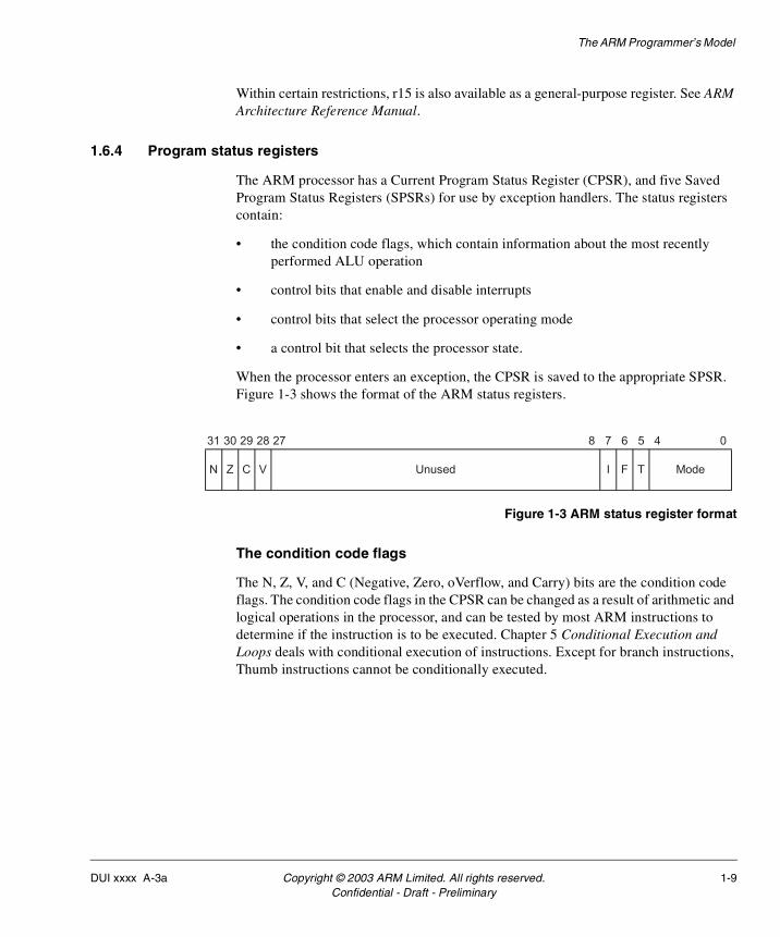
When the processor enters an exception, the CPSR is saved to the appropriate SPSR. Figure 1-3 shows the format of the ARM status registers.
Figure 1-3 ARM status register format
The condition code flags
The N, Z, V, and C (Negative, Zero, oVerflow, and Carry) bits are the condition code flags. The condition code flags in the CPSR can be changed as a result of arithmetic and logical operations in the processor, and can be tested by most ARM instructions to determine if the instruction is to be executed. Chapter 5 Conditional Execution and Loops deals with conditional execution of instructions. Except for branch instructions, Thumb instructions cannot be conditionally executed.
31 30 29 28
N Z C V
27 045678
I F TUnused Mode
DUI xxxx A-3a Copyright © 2003 ARM Limited. All rights reserved. 1-9Confidential - Draft - Preliminary
The ARM Programmer’s Model
The control bits
The bottom eight bits of a status register, I, F, T, and M[4:0], are known collectively as the control bits. These change when an exception occurs, and can be altered by software only when the processor is in a privileged mode.
Interrupt disable bits
The I and F bits are the interrupt disable bits. Setting I disables normal interrupts. Setting F disables fast interrupts.
State bit
The T bit is the processor state bit. When T is 0, the processor is in ARM state and is executing 32-bit ARM instructions. When T is a logic one, the processor is in Thumb state and is executing 16-bit Thumb instructions.
Mode bits
The M[4:0] bits are the mode bits. They determine the processor mode, as Table 1-2 shows. Not all combinations of the mode bits define a valid processor mode. Only those explicitly described can be used.
User mode and System mode do not have an SPSR, because they are not entered on any exception and therefore do not need a register in which to preserve the CPSR. In User mode or System mode, reads from the SPSR return an unpredictable value, and writes to the SPSR are ignored.
Table 1-2 Processor mode selection
M[4:0] Processor mode Accessible registers
b10000 User PC, r0-r14, CPSR
b10001 Fast Interrupt PC, r8_fiq-r14_fiq, r0-r7, CPSR, spsr_fiq
b10010 Interrupt PC, r13_irq, r14_irq, r0-r12, CPSR, spsr_irq
b10011 Supervisor PC, r13_svc, r14_svc, r0-r12, CPSR, spsr_svc
b10111 Abort PC, r13_abt, r14_abt, r0-r12, CPSR, spsr_abt
b11011 Undefined PC, r13_und, r14_und, r0-r12, CPSR, spsr_und
b11111 System PC, r0-r14, CPSR (Architecture 4 and above)
1-10 Copyright © 2003 ARM Limited. All rights reserved. DUI xxxx A-3aConfidential - Draft - Preliminary
The ARM Programmer’s Model
1.7 Exercises
These are easy.
1.7.1 Warm-up questions
1. What is the difference between an ARM processor mode and an ARM processor state?
2. Name the different modes and states of the ARM processor.
3. What register is used for the PC? The LR?
4. What is the normal usage of r13?
5. Which bit of the CPSR defines the state?
6. What is the difference between the boundary alignments of ARM vs Thumb instructions?
7. Explain how to disable IRQ and FIQ interrupts.
1.7.2 Endianness
Suppose that r0 = 0x12345678 and that this value is stored to memory with the instruction 'store r0 to memory location 0x4000.’ What value would r2 hold after the instruction 'load a byte from memory location 0x4000 into r2' when memory is organized as big-endian? What would r2 hold when memory is organized as little-endian?
DUI xxxx A-3a Copyright © 2003 ARM Limited. All rights reserved. 1-11Confidential - Draft - Preliminary

The ARM Programmer’s Model
1-12 Copyright © 2003 ARM Limited. All rights reserved. DUI xxxx A-3aConfidential - Draft - Preliminary
Chapter 2 ARM Instruction Set Fundamentals
This chapter introduces the simulation environment, ARM assembly language programming basics, and some of the operations necessary for subsequent exercises. It contains the following sections:
• Introduction on page 2-2
• Building a program on page 2-3
• Viewing and changing information on page 2-7
• Exercises on page 2-8.
DUI xxxx A-3a Copyright © 2003 ARM Limited. All rights reserved. 2-1Confidential - Draft - Preliminary
ARM Instruction Set Fundamentals
2.1 Introduction
This chapter teaches you how to compile and run assembly programs and some of the basic operations of the ARM core.
At this point, the hardware should have already been set up for you. Otherwise, consult the Evaluator-7T Installation Guide or the OKI ML67Q4000 Board User Guide for instructions on setting up the system. You should familiarize yourself with the CodeWarrior development tools and the ARM assembler, but for now, we'll begin by building a very simple project with a single source file.
Note
The instructions in this chapter are based on the ADS tool suite. If you are not using the ADS tool suite, you might have to make small changes to accommodate the tools that you are using.
2-2 Copyright © 2003 ARM Limited. All rights reserved. DUI xxxx A-3aConfidential - Draft - Preliminary
ARM Instruction Set Fundamentals
2.2 Building a program
The following assembler module contains a small set of instructions that call a simple subroutine and then return. The module begins with the AREA directive. The code itself follows the ENTRY directive and ends with an END statement.
AREA Lab1, CODE, READONLY ; name the blockENTRY ; mark first instruction
start MOV r0, #15 ; set up parametersMOV r1, #20BL firstfunc ; call subroutineMOV r0, #0x18 ;LDR r1, =0x20026 ;SWI 0x123456 ; terminate the program
firstfuncADD r0, r0, r1 ; r0 = r0 + r1MOV pc, lr ; return from subroutineEND ; mark the end of file
2.2.1 The AREA directive
An AREA is a chunk of data or code that is manipulated by the linker. A complete application consists of one or more AREAs. The assembler module given consists of a single AREA that is marked as being read-only.
2.2.2 The ENTRY directive
The first instruction to be executed within an application is marked by the ENTRY directive. An application can contain only a single ENTRY point. Therefore, in an application with multiple assembler modules, only one module contains an ENTRY directive.
2.2.3 General layout
The general form of lines in an assembler module is:
Label <white space> instruction <white space> ; comment
The label, instruction, and comment must be separated by at least one white space character such as a space or a tab. Because the instruction must be preceded by white space, it never starts in the first column, even if there is no label. All three sections of the line are optional, and the assembler also accepts blank lines to improve the clarity of the code.
DUI xxxx A-3a Copyright © 2003 ARM Limited. All rights reserved. 2-3Confidential - Draft - Preliminary
ARM Instruction Set Fundamentals
2.2.4 Creating the project
Use this procedure to create a project and give it a name.
1. Start Metrowerks CodeWarrior.
2. From the File menu, select New… The New dialog box appears
Figure 2-1 Creating the project
3. Click the Project tab.
4. Click on ARM Executable Image and enter Lab1 in the Project name field.
5. Click OK. This creates a project in the directory selected in Location. If your instructor designates areas to place your files, change the location accordingly.
6. Now create the source file. From the File menu, select New… The New dialog box appears again.
2-4 Copyright © 2003 ARM Limited. All rights reserved. DUI xxxx A-3aConfidential - Draft - Preliminary
ARM Instruction Set Fundamentals
7. Click on the File tab.
Figure 2-2 Creating the source file
8. Click on Text File and enter Lab1.s in the File name field.
9. Click on the Add to Project checkbox. The project name is in the Project field.
10. You want to debug the program, so in the Targets field, click on the DebugRel checkbox.
11. Click OK to create the new file.
A new window appears where you can enter and edit your program. Type in the sample program given above, noting that labels should start in the first column. When the file is complete, select File ⇒Save.
DUI xxxx A-3a Copyright © 2003 ARM Limited. All rights reserved. 2-5Confidential - Draft - Preliminary
ARM Instruction Set Fundamentals
Now the project needs to be built, compiling the source code and linking in any objects necessary, producing a binary image for the simulation environment. Select Project ⇒Make. This builds all the necessary files.
2.2.5 Running the program
Start the ARM Debugger. Select File ⇒Load image…. A dialog box appears where you can search for the folder called Lab1 in the directory you specified when you built the program using CodeWarrior. Inside of the Lab1 folder, you find another folder called Lab1_Data. Open this folder, and then open the folder called DebugRel. There you find a file called Lab1.axf, which is the file to be opened. Once the executable file is loaded, a window appears containing the source file you created.
You can set a breakpoint in your program to force the processor to stop before executing an instruction. In this way, you can examine register contents, memory values or flags while running your code. Double-click on the following line in your code:
ADD r0, r0, r1 ; r0 = r0 + r1
A dialog box appears indicating that you are about to set a breakpoint. Click OK. Now you see a red bar on the line you selected, indicating a breakpoint has been set there.
Start the program by selecting Execute ⇒Go. The program runs until it encounters the breakpoint you set. You can now examine and alter the register contents of the part. To see the register file, click on the View menu and select Registers ⇒Current Mode. By double-clicking on a particular register, you can change its value. Double-click on register r0 and change its value to 0x00001234. Then change register r1 to 0x87650000.
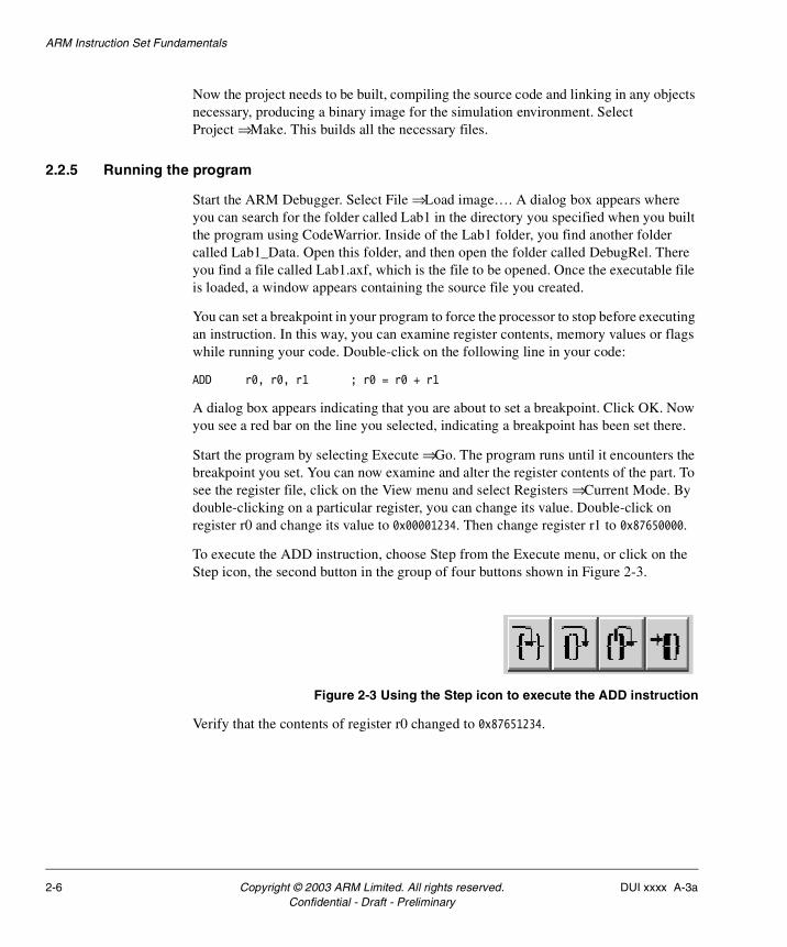
To execute the ADD instruction, choose Step from the Execute menu, or click on the Step icon, the second button in the group of four buttons shown in Figure 2-3.
Figure 2-3 Using the Step icon to execute the ADD instruction
Verify that the contents of register r0 changed to 0x87651234.
2-6 Copyright © 2003 ARM Limited. All rights reserved. DUI xxxx A-3aConfidential - Draft - Preliminary
ARM Instruction Set Fundamentals
2.3 Viewing and changing information
There are a few different views of information that are valuable in debugging your code. The register window contains all of the ARM register contents for any cycle you want to examine. Similarly, there is a memory contents window that you can use to view or alter the contents of a memory location.
Starting and stopping your code involves the setting of breakpoints and watchpoints. Set breakpoints on instructions where you want to stop the processor. You can then restart the core by selecting Execute ⇒Go. Watchpoints also stop the core, but you set watchpoints on data values that you want to monitor. For example, if the core accesses memory location 0x8000, and there is a watchpoint set there, the core stops when the instruction accessing that location completes. You can determine where breakpoints and watchpoints are set by bringing up those particular windows under the View menu.
DUI xxxx A-3a Copyright © 2003 ARM Limited. All rights reserved. 2-7Confidential - Draft - Preliminary
ARM Instruction Set Fundamentals
2.4 Exercises
These exercises give you a chance to compile, step through, and examine code.
2.4.1 Compiling, making, debugging, and running
Copy the code from Building a program on page 2-3 into CodeWarrior. There are separate functions in CodeWarrior to compile, make, debug and run a program. Experiment with all four and describe what each does.
2.4.2 Stepping and stepping in
Debug the code from Building a program on page 2-3. Instead of running the code, step all the way through the code using both the step method and the step in method. What is the difference between the two methods of stepping through the assembly code?
2.4.3 Data formats
Sometimes it is very useful to view registers in different formats to check results more efficiently. Run the code from Building a program on page 2-3. Upon completion, view the different formats of r0 and record your results. Specifically, view the data in hexadecimal, decimal, octal, binary, and ASCII.
2-8 Copyright © 2003 ARM Limited. All rights reserved. DUI xxxx A-3aConfidential - Draft - Preliminary
Chapter 3 Data Processing Operations
This chapter introduces the different types of data processing instructions available in the ARM core. It contains the following sections:
• Introduction on page 3-2
• Condition code flags on page 3-3
• Addition and subtraction on page 3-4
• Multiplication on page 3-5
• Shifts on page 3-6
• Data processing operations on page 3-7
• Single data transfer instructions on page 3-8
• Compares and tests on page 3-9
• Logical operations on page 3-10
• Exercises on page 3-11.
DUI xxxx A-3a Copyright © 2003 ARM Limited. All rights reserved. 3-1Confidential - Draft - Preliminary
Data Processing Operations
3.1 Introduction
The most fundamental operations that almost every assembly program uses are arithmetic operations, such as adding, subtracting, multiplying and dividing. In this chapter, we explore the basic instructions. Chapter 9 Floating-point Computation shows how more complex arithmetic operations can be performed with floating-point numbers.
3-2 Copyright © 2003 ARM Limited. All rights reserved. DUI xxxx A-3aConfidential - Draft - Preliminary
Data Processing Operations
3.2 Condition code flags
In large programs, data processing operations such as add, subtract, and shift, appear frequently for changing the value of a pointer to memory or modifying a counter. Graphics algorithms, speech compression routines, or digital filters might use these operations more heavily and depend on the ability to determine when the result of an add overflows or when a counter value reaches zero. The condition code flags indicate such events.
The Current Program Status Register (CPSR) contains the condition code flags:
N Indicates that the ALU operation produced a negative result.
Z Indicates that the ALU operation produced a result of zero.
C Indicates that the ALU operation produced a carry out.
V Indicates that the ALU operation produced an overflow.
The status outputs from the ALU are latched in the condition code flags only if the S bit is set in the instruction. So if you want the status flags to change for a MUL operation, for example, you must use the MULS instruction.
DUI xxxx A-3a Copyright © 2003 ARM Limited. All rights reserved. 3-3Confidential - Draft - Preliminary
Data Processing Operations
3.3 Addition and subtraction
The arithmetic instructions in the ARM instruction set include addition and subtraction operations, which perform addition, subtraction, and reverse subtraction, all with and without carry.
ADD r1, r2, r3 ; r1 = r2 + r3
ADC r1, r2, r3 ; r1 = r2 + r3 + C
SUB r1, r2, r3 ; r1 = r2 - r3
SUBC r1, r2, r3 ; r1 = r2 - r3 + C - 1
RSB r1, r2, r3 ; r1 = r3 - r2
RSC r1, r2, r3 ; r1 = r3 - r2 + C - 1
3-4 Copyright © 2003 ARM Limited. All rights reserved. DUI xxxx A-3aConfidential - Draft - Preliminary
Data Processing Operations
3.4 Multiplication
The ARM7TDMI core has dedicated logic for performing multiplication. Multiplication by a constant can be done with a shift and add instruction or a shift and reverse subtract instruction. Therefore, all of the multiply instructions take two register operands.
3.4.1 Multiply instructions
MUL and MLA produce 32-bit results. MUL multiplies the values in two registers, truncates the result to 32 bits, and stores the product in a third register. MLA multiplies two registers, adds the value of a third register to the product, truncates the results to 32 bits, and stores the result in a fourth register:
MUL r4, r2, r1 ; r4 = r2 × r1
MULS r4, r2, r1 ; r4 = r2 × r1, then set the N and Z flags
MLA r7, r8, r9, r3 ; r7 = r8 × r9 + r3
Both MUL and MLA can optionally set the N and Z condition code flags. There is no distinction between signed and unsigned multiplication. Only the least significant 32 bits of the result are stored in the destination register, and the sign of the operands does not affect this value.
3.4.2 Multiply long instructions
Multiply long instructions produce 64-bit results. They multiply the values of two registers and store the 64-bit result in a third and fourth register. SMULL and UMULL are signed and unsigned multiply long instructions:
SMULL r4, r8, r2, r3 ; r4 = bits 31-0 of r2 × r3; r8 = bits 63-32 of r2 × r3
UMULL r6, r8, r0, r1 ; {r6,r8} = r0 × r1
SMLAL and UMLAL are signed and unsigned multiply-long-and-accumulate instructions. They multiply the values of two registers, add the 64-bit value from a third and fourth register, and store the 64-bit result in the third and fourth registers:
SMLAL r3, r8, r2, r3 ; r3 = bits 31-0 of r2 × r3 + {r3,r8}; r8 = bits 63-32 of r2 × r3 + {r3,r8}
UMLAL r5, r8, r0, r1 ; {r5,r8} = r0 × r1 + {r5,r8}
All four multiply long instructions can optionally set the N and Z condition code flags. If any source operand is negative, the most significant 32 bits of the result are affected.
DUI xxxx A-3a Copyright © 2003 ARM Limited. All rights reserved. 3-5Confidential - Draft - Preliminary
Data Processing Operations
3.5 Shifts
The ARM core contains a barrel shifter which takes a value to be shifted or rotated, an amount to shift or rotate, and the type of shift or rotate. ARM instructions use the barrel shifter to perform comparatively complex operations in a single instruction. Instructions take no longer to execute by making use of the barrel shifter unless the amount to be shifted is specified by a register, in which case the instruction takes an extra cycle to complete.
The barrel shifter performs the following operations:
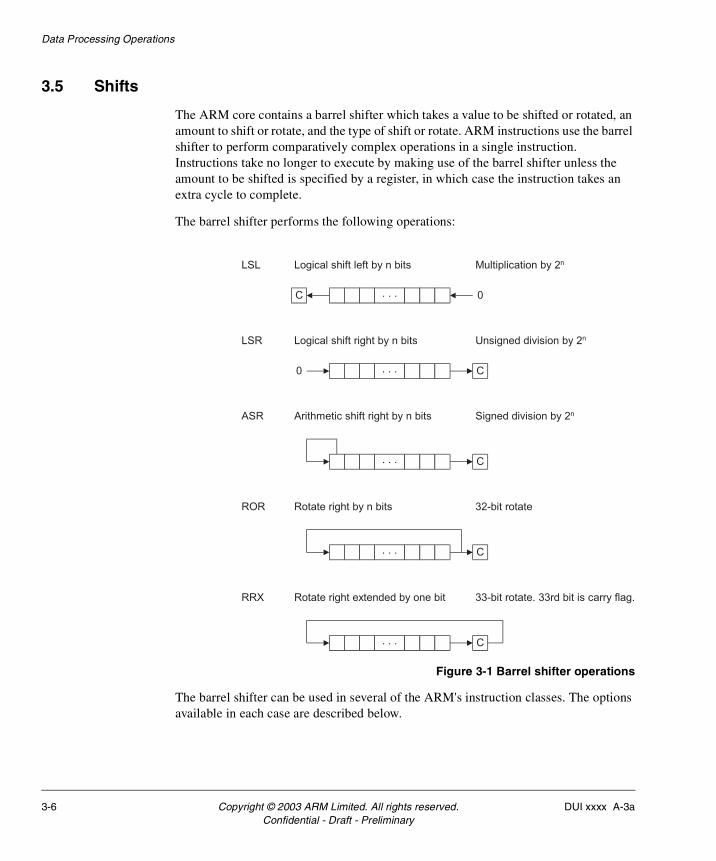
Figure 3-1 Barrel shifter operations
The barrel shifter can be used in several of the ARM's instruction classes. The options available in each case are described below.
C 0. . .
LSL Logical shift left by n bits Multiplication by 2n
LSR Logical shift right by n bits Unsigned division by 2n
0 C. . .
. . . C
. . . C
C. . .
ASR Arithmetic shift right by n bits Signed division by 2n
ROR Rotate right by n bits 32-bit rotate
RRX Rotate right extended by one bit 33-bit rotate. 33rd bit is carry flag.
3-6 Copyright © 2003 ARM Limited. All rights reserved. DUI xxxx A-3aConfidential - Draft - Preliminary
Data Processing Operations
3.6 Data processing operations
The last operand (the second for binary operations, and the first for unary operations) might be:
• An 8-bit constant rotated right (ROR) through an even number of positions, for example:
ADD r0, r1, #0xc5, ROR 10
This instruction adds the contents of register r1 to the value 0x31400000, then stores the result in register r0. The barrel shifter creates this operand by rotating 0xC5 by 10 bits to the right. The number of bits to shift the 8-bit value must be even. Not every 32-bit value can be created in this way, and there might be cases where you have to let the compiler find the best way to create an instruction.
• A register (optionally) shifted or rotated either by a 5-bit constant or by another register, for example:
SUB r0, r1, r2, LSR #10
This instruction shifts the contents of r2 to the right 10 positions, subtracts the shifted result from the value in r1, and stores the result in r0. Additional types of shifts are available, such as a logical shift to the left (LSL), an arithmetic shift to the right (ASR), and rotates (ROR and RRX).
DUI xxxx A-3a Copyright © 2003 ARM Limited. All rights reserved. 3-7Confidential - Draft - Preliminary
Data Processing Operations
3.7 Single data transfer instructions
The single data transfer instructions LDR and STR can also use the barrel shifter to create offsets for loads and stores. Although we'll examine data transfer instructions more closely in Chapter 4 Loads and Stores, here are a few examples. These examples make use of a base register, r0, plus an offset, which can be a register shifted by any 5-bit constant or an unshifted 12-bit constant.
STR r7, [r0], #10 ; post-indexed
LDR r2, [r0], r4, ASR #5 ; post-indexed
STR r3, [r0, r5, LSL #1] ; pre-indexed
LDR r6, [r0, r1, ROR #2]! ; pre-indexed + writeback
3-8 Copyright © 2003 ARM Limited. All rights reserved. DUI xxxx A-3aConfidential - Draft - Preliminary
Data Processing Operations
3.8 Compares and tests
There are four instructions which can be used to set the condition codes or test for a particular bit in a register.
CMP Compare. CMP subtracts an arithmetic value from a register value and updates the condition codes. You can use CMP to quickly check the contents of a register for a particular value, such as at the beginning or end of a loop.
CMN Compare Negative. CMN adds the negative of an arithmetic value to a register value and updates the condition codes. CMN can also quickly check register contents.
TST Test. TST logically ANDs an arithmetic value with a register value and updates the condition codes without affecting the V flag. You can use TST to determine if many bits of a register are all clear or if at least one bit of a register is set.
TEQ Test equivalence. TEQ logically exclusive-ORs an arithmetic value with a register value and updates the condition codes without affecting the V flag. You can use TEQ to determine if two values have the same sign.
DUI xxxx A-3a Copyright © 2003 ARM Limited. All rights reserved. 3-9Confidential - Draft - Preliminary
Data Processing Operations
3.9 Logical operations
ARM supports Boolean logic operations using two register operands. For example:
AND r1, r2, r3 ; r1 = r2 AND r3
ORR r1, r2, r3 ; r1 = r2 OR r3
EOR r1, r2, r3 ; r1 = r2 exclusive-OR r3
BIC r1, r2, r3 ; r1 = r2 AND r3
3-10 Copyright © 2003 ARM Limited. All rights reserved. DUI xxxx A-3aConfidential - Draft - Preliminary
Data Processing Operations
3.10 Exercises
Complete each of these exercises to practice using ARM data processing instructions and to learn how to use the barrel shifter, multiplier, and condition code flags:
• Signed and unsigned addition
• Multiplication
• Multiplication shortcuts on page 3-12
• Register-swap algorithm on page 3-12
• Signed multiplication on page 3-12
• Absolute value on page 3-12
• Division on page 3-12
• Gray codes on page 3-13.
3.10.1 Signed and unsigned addition
For the following values of A and B, predict the values of the N, Z, V and C flags produced by performing the operation A + B. Load these values into two ARM registers and modify the program created in Building a program on page 2-3 to perform an addition of the two registers. Using the debugger, record the flags after each addition and compare those results with your predictions. When the data values are signed numbers, what do the flags mean? Does their meaning change when the data values are unsigned numbers?
0xFFFF0000 0xFFFFFFFF 0x67654321 (A)+ 0x87654321 + 0x12345678 + 0x23110000 (B)
3.10.2 Multiplication
Change the ADD instruction in the example code from Building a program on page 2-3 to a MULS. Also change one of the operand registers so that the source registers are different from the destination register, as the convention for multiplication instructions requires. Put 0xFFFFFFFF and 0x80000000 into the source registers. Now rerun your program and check the result.
1. Does your result make sense? Why or why not?
2. Assuming that these two numbers are signed integers, is it possible to overflow in this case?
3. Why is there a need for two separate long multiply instructions, UMULL and SMULL? Give an example to support your answer.
DUI xxxx A-3a Copyright © 2003 ARM Limited. All rights reserved. 3-11Confidential - Draft - Preliminary
Data Processing Operations
3.10.3 Multiplication shortcuts
Assume that you have a microprocessor that takes up to eight cycles to perform a multiplication. To save cycles in your program, construct an ARM instruction that performs a multiplication by 32 in a single cycle.
3.10.4 Register-swap algorithm
The EOR instruction is a fast way to swap the contents of two registers without using an intermediate storage location such as a memory location or another register. Suppose two values A and B are to be exchanged. The following algorithm could be used:
A = A ⊕ B
B = A ⊕ B
A = A ⊕ B
Write the ARM code to implement the above algorithm, and test it with the values of A = 0xF631024C and B = 0x17539ABD. Show your instructor the contents before and after the program has run.
3.10.5 Signed multiplication
Assume that a signed long multiplication instruction is not available. Write a program that performs long multiplications, producing 64 bits of result. Use only the UMULL instruction and logical operations such as MVN to invert, XOR, and ORR. Run the program using the two operands –2 and –4 to verify.
3.10.6 Absolute value
Write ARM assembly to perform the function of absolute value. Register r0 contains the initial value, and r1 contains the absolute value. Try to use only two instructions, not counting the SWI to terminate the program.
3.10.7 Division
Write ARM assembly to perform the function of division. Registers r1 and r2 contain the dividend and divisor, r3 contains the quotient, and r5 contains the remainder. For this operation, you can either use a single shift-subtract algorithm or another more complicated one.
3-12 Copyright © 2003 ARM Limited. All rights reserved. DUI xxxx A-3aConfidential - Draft - Preliminary
Data Processing Operations
3.10.8 Gray codes
A Gray code is an ordering of 2n binary numbers such that only one bit changes from one entry to the next. One example of a 2-bit Gray code is b10 11 01 00. The spaces in this example are for readability. Write ARM assembly to turn a 2-bit Gray code held in r1 into a 3-bit Gray code in r2.
Note
The 2-bit Gray code occupies only bits [7:0] of r1, and the 3-bit Gray code occupies only bits [23:0] of r2. You can ignore the leading zeros.
One way to build an n-bit Gray code from an (n – 1)-bit Gray code is to prefix every (n – 1)-bit element of the code with 0. Then create the additional n-bit Gray code elements by reversing each (n – 1)-bit Gray code element and prefixing it with a one. For example, the 2-bit Gray code above becomes b010 011 001 000 101 111 110 100.
DUI xxxx A-3a Copyright © 2003 ARM Limited. All rights reserved. 3-13Confidential - Draft - Preliminary

Data Processing Operations
3-14 Copyright © 2003 ARM Limited. All rights reserved. DUI xxxx A-3aConfidential - Draft - Preliminary
Chapter 4 Loads and Stores
This chapter introduces the types of loads and stores available on the ARM core and some shortcuts for loading addresses and 32-bit values into registers. It contains the following sections:
• Introduction on page 4-2
• Addressing modes of single-register loads and stores on page 4-3
• Loading constants into registers on page 4-4
• Loading addresses into registers on page 4-7
• Exercises on page 4-10.
DUI xxxx A-3a Copyright © 2003 ARM Limited. All rights reserved. 4-1Confidential - Draft - Preliminary
Loads and Stores
4.1 Introduction
The ability to load and store data is fundamental in implementing any algorithm. The ARM core supports three basic types of data movement instructions:
Single-register loads and stores
This chapter explores various ways of moving data into registers from memory, loading constants and labels into registers, and working with the pseudo-instructions ADR and ADRL.
Multiple-register loads and stores
Chapter 6 Subroutines deals with multiple-register loads and stores as part of dealing with subroutines.
Single register swap instructions
These are rarely used in user-level programs and are not discussed in this manual.
4-2 Copyright © 2003 ARM Limited. All rights reserved. DUI xxxx A-3aConfidential - Draft - Preliminary
Loads and Stores
4.2 Addressing modes of single-register loads and stores
Load and store register instructions use three addressing modes:
• Pre-indexed addressing
• Post-indexed addressing
• Offset addressing.
These addressing modes use a base register and an offset specified in the instruction. The base register can be the PC.
4.2.1 Pre-indexed addressing
The pre-indexed form of a load or store instruction is:
LDR|STR{<cond>}{B} Rd, [Rn, <offset>]{!}
In pre-indexed addressing, the address of the data transfer is calculated by adding the offset to the value in the base register, Rn. The optional ! specifies writing the new address back into Rn at the end of the instruction. The optional B selects an unsigned byte transfer, but the default is word, so you don’t have to add anything in most cases.
4.2.2 Post-indexed addressing
The post-indexed form of a load or store instruction is:
LDR|STR{<cond>}{B}{T} Rd, [Rn], <offset>
In post-indexed addressing, the address of the data transfer is calculated from the unmodified value in the base register, Rn. Then the offset is added to the value in Rn and written back to Rn. The T flag is used for operating systems in memory management environments and is not used here.
4.2.3 Offset addressing
In offset addressing, the address of the data transfer is calculated by adding the offset to the value in the base register, Rn. The offset can be a register shifted by any 5-bit constant or an unshifted 12-bit constant. Offset addressing can use the barrel shifter to provide logical and arithmetic shifts of constants.
STR r7, [r0], #24 ; post-indexed
LDR r2, [r0], r4, ASR #4 ; post-indexed
STR r3, [r0, r5, LSL #3] ; pre-indexed
LDR r6, [r0, r1, ROR #6]! ; pre-indexed + writeback
DUI xxxx A-3a Copyright © 2003 ARM Limited. All rights reserved. 4-3Confidential - Draft - Preliminary
Loads and Stores
4.3 Loading constants into registers
All ARM instructions are 32 bits long, and because of the opcode size, you cannot store a 32-bit number in the instruction itself. Therefore, there is no single instruction that can load a 32-bit immediate constant into a register without performing a data load from memory.
Although a data load can place any 32-bit value in a register, there are more efficient ways to load many commonly used constants.
• Direct loading with MOV and MVN
• Direct loading with LDR Rd, =<numeric constant> on page 4-5.
4.3.1 Direct loading with MOV and MVN
You can use the MOV instruction to load 8-bit constant values directly into a register, giving a range of 0x0-0xFF. The MVN instruction loads the bitwise complements of these values, extending the range of load values to 0xFFFFFF00-0xFFFFFFFF.
You can construct even more constants by using MOV and MVN with the barrel shifter. These constants are 8-bit values rotated right through 0, 2, 4, …, 26, 28, or 30 positions. Table 4-1 shows some of the constants you can create by rotating the MOV constant.
You can therefore load constants directly into registers using instructions such as:
MOV r0, #0xFF ; r0 = 255
MOV r0, #0x1, 30 ; r0 = 1020
MOV r0, #0xFF, 28 ; r0 = 4080
MOV r0, #0x1, 26 ; r0 = 4096
However, converting a constant into this form is an onerous task. Fortunately, the assembler can do the conversions for you, and there is an even faster way to load a constant into a register without having to do any conversions at all!
Table 4-1 Examples of creating constants with MOV and ROR
Constant Range
0-255 0x0-0xFF with no rotate
256, 260, 264, …, 1012, 1016, 1020 0x100-0x3FC in steps of 4 by rotating right by 30 bits
1024, 1040, 1056, …, 4048, 4064, 4080 0x400-0xFF0 in steps of 16 by rotating right by 28 bits
4096, 4160, 4224, …, 16 192, 16 256, 16 320 0x1000-0x3FC0 in steps of 64 by rotating right by 26 bits
4-4 Copyright © 2003 ARM Limited. All rights reserved. DUI xxxx A-3aConfidential - Draft - Preliminary
Loads and Stores
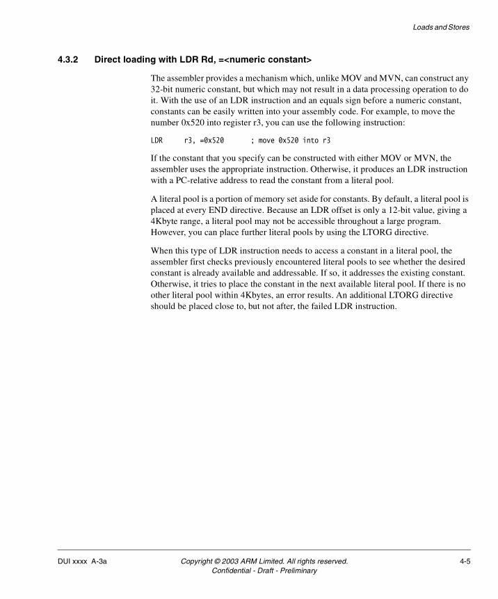
4.3.2 Direct loading with LDR Rd, =<numeric constant>
The assembler provides a mechanism which, unlike MOV and MVN, can construct any 32-bit numeric constant, but which may not result in a data processing operation to do it. With the use of an LDR instruction and an equals sign before a numeric constant, constants can be easily written into your assembly code. For example, to move the number 0x520 into register r3, you can use the following instruction:
LDR r3, =0x520 ; move 0x520 into r3
If the constant that you specify can be constructed with either MOV or MVN, the assembler uses the appropriate instruction. Otherwise, it produces an LDR instruction with a PC-relative address to read the constant from a literal pool.
A literal pool is a portion of memory set aside for constants. By default, a literal pool is placed at every END directive. Because an LDR offset is only a 12-bit value, giving a 4Kbyte range, a literal pool may not be accessible throughout a large program. However, you can place further literal pools by using the LTORG directive.
When this type of LDR instruction needs to access a constant in a literal pool, the assembler first checks previously encountered literal pools to see whether the desired constant is already available and addressable. If so, it addresses the existing constant. Otherwise, it tries to place the constant in the next available literal pool. If there is no other literal pool within 4Kbytes, an error results. An additional LTORG directive should be placed close to, but not after, the failed LDR instruction.
DUI xxxx A-3a Copyright © 2003 ARM Limited. All rights reserved. 4-5Confidential - Draft - Preliminary
Loads and Stores
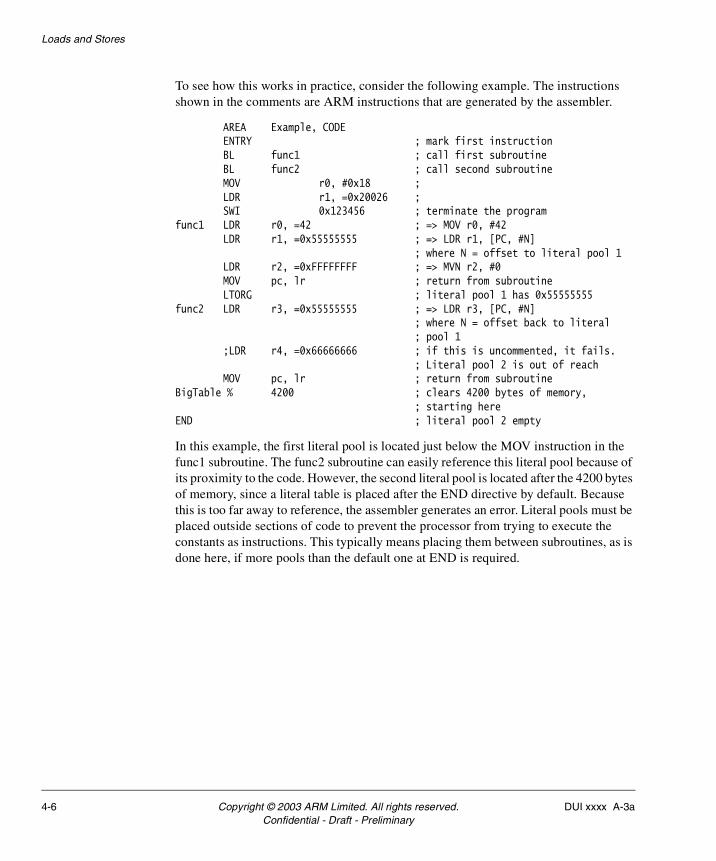
To see how this works in practice, consider the following example. The instructions shown in the comments are ARM instructions that are generated by the assembler.
AREA Example, CODEENTRY ; mark first instructionBL func1 ; call first subroutineBL func2 ; call second subroutineMOV r0, #0x18 ;LDR r1, =0x20026 ;SWI 0x123456 ; terminate the program
func1 LDR r0, =42 ; => MOV r0, #42LDR r1, =0x55555555 ; => LDR r1, [PC, #N]
; where N = offset to literal pool 1LDR r2, =0xFFFFFFFF ; => MVN r2, #0MOV pc, lr ; return from subroutineLTORG ; literal pool 1 has 0x55555555
func2 LDR r3, =0x55555555 ; => LDR r3, [PC, #N]; where N = offset back to literal; pool 1
;LDR r4, =0x66666666 ; if this is uncommented, it fails.; Literal pool 2 is out of reach
MOV pc, lr ; return from subroutineBigTable % 4200 ; clears 4200 bytes of memory,
; starting hereEND ; literal pool 2 empty
In this example, the first literal pool is located just below the MOV instruction in the func1 subroutine. The func2 subroutine can easily reference this literal pool because of its proximity to the code. However, the second literal pool is located after the 4200 bytes of memory, since a literal table is placed after the END directive by default. Because this is too far away to reference, the assembler generates an error. Literal pools must be placed outside sections of code to prevent the processor from trying to execute the constants as instructions. This typically means placing them between subroutines, as is done here, if more pools than the default one at END is required.
4-6 Copyright © 2003 ARM Limited. All rights reserved. DUI xxxx A-3aConfidential - Draft - Preliminary
Loads and Stores
4.4 Loading addresses into registers
It is often necessary to load a register with an address such as the location of a string constant within the code segment or the start location of a jump table. Absolute addressing cannot be used for this purpose, because ARM code is inherently relocatable, and there are limitations on the values that can be directly moved into a register. Instead, addresses must be expressed as offsets from the current PC value. A register can either be directly set by combining the current PC with the appropriate offset, or the address can be loaded from a literal pool.
4.4.1 The ADR and ADRL pseudo-instructions
You can use two pseudo-instructions, ADR and ADRL, to generate an address without performing a load from memory. ADR and ADRL accept a PC-relative expression, which is a label within the same code area, and calculate the offset required to reach that location.
ADR attempts to produce a single ADD or SUB instruction to load an address into a register in the same way that the LDR instruction previously discussed produces addresses. If the required address cannot be constructed in a single instruction, an error is raised. Typically, the offset range is 255 bytes for an offset to an address that is not word-aligned and 1020 bytes (255 words) for an offset to a word-aligned address. It is preferable to use ADR wherever possible, because:
• It results in shorter code. No storage space is required for addresses to be placed in the literal pool.
• The resulting code runs more quickly. A nonsequential fetch from memory to get the address from the literal pool is not required.
ADRL attempts to produce two data processing instructions to load an address into a register. Even if the ADRL can produce a single instruction to load the address, it produces a second, redundant instruction. This is a consequence of the strict, two-pass nature of the assembler. If the ADRL cannot construct the address using two instructions, an error is raised. In such cases, the LDR mechanism mentioned above is probably the best alternative. Typically, the range of an ADRL is 64Kbytes for an address that is not word-aligned and 256Kbytes for a word-aligned address.
DUI xxxx A-3a Copyright © 2003 ARM Limited. All rights reserved. 4-7Confidential - Draft - Preliminary
Loads and Stores
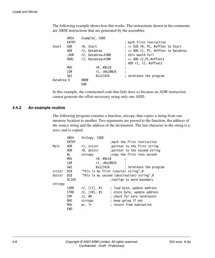
The following example shows how this works. The instructions shown in the comments are ARM instructions that are generated by the assembler.
AREA Example2, CODEENTRY ; mark first instruction
Start ADR r0, Start ; => SUB r0, PC, #offset to StartADR r1, DataArea ; => ADD r1, PC, #offset to DataArea;ADR r2, DataArea+4300 ; this would failADRL r3, DataArea+4300 ; => ADD r2,PC,#offset1
; ADD r2, r2, #offset2MOV r0, #0x18 ;LDR r1, =0x20026 ;SWI 0x123456 ; terminate the program
DataArea % 8000END
In this example, the commented code that fails does so because an ADR instruction cannot generate the offset necessary using only one ADD.
4.4.2 An example routine
The following program contains a function, strcopy, that copies a string from one memory location to another. Two arguments are passed to the function: the address of the source string and the address of the destination. The last character in the string is a zero, and is copied.
AREA StrCopy, CODEENTRY ;mark the first instruction
Main ADR r1, srcstr ;pointer to the first stringADR r0, dststr ;pointer to the second stringBL strcopy ;copy the first into secondMOV r0, #0x18 ;LDR r1, =0x20026 ;SWI 0x123456 ; terminate the program
srcstr DCB "This is my first (source) string",0dststr DCB "This is my second (destination) string",0
ALIGN ;realign to word boundarystrcopy
LDRB r2, [r1], #1 ; load byte, update addressSTRB r2, [r0], #1 ; store byte, update addressCMP r2, #0 ; check for zero terminatorBNE strcopy ; keep going if notMOV pc, lr ; return from subroutineEND
4-8 Copyright © 2003 ARM Limited. All rights reserved. DUI xxxx A-3aConfidential - Draft - Preliminary
Loads and Stores
ADR is used to load the addresses of the two strings into registers r0 and r1 for passing to strcopy. These two strings have been stored in memory using the assembler directive Define Constant Byte (DCB). The first string is 33 bytes long, so the ADR offset to the second is not word-aligned and is limited to 255 bytes, which is therefore in reach.
An auto-indexing address mode updates the address registers in the LDR instructions:
LDRB r2, [r1], #1
Auto-indexing replaces a sequence such as:
LDRB r2, [r1]ADD r1, r1, #1
DUI xxxx A-3a Copyright © 2003 ARM Limited. All rights reserved. 4-9Confidential - Draft - Preliminary
Loads and Stores
4.5 Exercises
Loads and stores appear in assembly code for many reasons. Try each of these exercises and see how many ways they are used in your own code.
4.5.1 Assignments with operands in memory
Assume an array of 25 words. A compiler associates variables x and y with registers r0 and r1, respectively. Assume that the base address for the array is located in r2. Translate this C statement/assignment using the post-indexed form:
x = array[5] + y
Now try writing it using the pre-indexed form.
4.5.2 Loads and stores
Assume an array of 25 words. A compiler associates y with r1. Assume that the base address for the array is located in r2. Translate this C statement/assignment using the post-indexed form:
array[10] = array[5] + y
Now try it using the pre-indexed form.
4.5.3 Array assignment
Write ARM assembly to perform the following array assignment in C:
for ( i = 0; i <= 10; i++) {a[i] = b[i] + c;}
Assume that r3 contains i, r4 contains c, a starting address of the array a in r1, and a starting address of the array b in r2.
4.5.4 Arrays and pointers
Consider the following two C procedures, which initialize an array to zero using a) indices, and b) pointers:
a) init_Indices (int a[], int s) {int i;for ( i = 0; i < s; i ++)
a[i] = 0; }b) init_Pointers (int *a, int s) {
int *p;for (p = &array[0]; p < &array[s]; p++)
*p = 0; }
4-10 Copyright © 2003 ARM Limited. All rights reserved. DUI xxxx A-3aConfidential - Draft - Preliminary
Loads and Stores
Convert these two procedures to ARM assembly. Put the starting address of the array in r1, s in r2, and i and p in r3. Assume that s > 0 and that you have an array of bytes.
4.5.5 The Fibonacci sequence
The Fibonacci sequence is an infinite sequence of numbers such that:
f(0) = 0f(1) = 1f(2) = 1f(3) = 2f(4) = 3f(5) = 5f(6) = 8...f(n) = f(n – 1) + f(n – 2).
Write an ARM assembly program that computes the first 12 numbers of the sequence and stores the sequence in memory locations 0x4000 to 0x400B. Assume everything can be in bytes, because f(12) is the first number of the sequence that falls out of the byte range. You must use a loop, and only f(0) and f(1) can be stored outside the loop.
4.5.6 The nth Fibonacci number
See The Fibonacci sequence and write ARM assembly to compute f(n). Start with r1 = n. At the end of the program, r0 = f(n).
DUI xxxx A-3a Copyright © 2003 ARM Limited. All rights reserved. 4-11Confidential - Draft - Preliminary

Loads and Stores
4-12 Copyright © 2003 ARM Limited. All rights reserved. DUI xxxx A-3aConfidential - Draft - Preliminary
Chapter 5 Conditional Execution and Loops
This chapter introduces conditional execution and demonstrate its advantages in loop structures and branch instructions. It contains the following sections:
• Introduction on page 5-2
• Execution conditions on page 5-3
• Implementing loop structures on page 5-5
• Using conditional execution on page 5-7
• Exercises on page 5-8.
DUI xxxx A-3a Copyright © 2003 ARM Limited. All rights reserved. 5-1Confidential - Draft - Preliminary
Conditional Execution and Loops
5.1 Introduction
Looping is a basic algorithmic structure used in sorting routines, filtering data or processing a large number of elements at once, such as arrays or stacks. Loops can be created by using the different types of branches available - Bcc or BLX - or by jumping directly to an address with a change of the program counter. The ARM architecture provides optimizations to reduce the number of cycles in a loop, and in some cases, remove branching altogether. In this lab, the idea of conditional execution is discussed along with different branching styles you can use in your own code. In general, it's best to build simpler routines until you've become familiar with the options available.
5-2 Copyright © 2003 ARM Limited. All rights reserved. DUI xxxx A-3aConfidential - Draft - Preliminary
Conditional Execution and Loops
5.2 Execution conditions
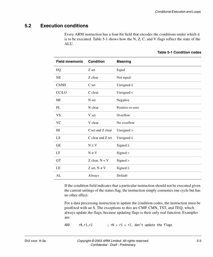
Every ARM instruction has a four-bit field that encodes the conditions under which it is to be executed. Table 5-1 shows how the N, Z, C, and V flags reflect the state of the ALU.
If the condition field indicates that a particular instruction should not be executed given the current settings of the status flag, the instruction simply consumes one cycle but has no other effect.
For a data processing instruction to update the condition codes, the instruction must be postfixed with an S. The exceptions to this are CMP, CMN, TST, and TEQ, which always update the flags, because updating flags is their only real function. Examples are:
ADD r0,r1,r2 ; r0 = r1 + r2, don't update the flags
Table 5-1 Condition codes
Field mnemonic Condition Meaning
EQ Z set Equal
NE Z clear Not equal
CS/HS C set Unsigned ≥
CC/LO C clear Unsigned <
MI N set Negative
PL N clear Positive or zero
VS V set Overflow
VC V clear No overflow
HI C set and Z clear Unsigned >
LS C clear and Z set Unsigned ≤
GE N ≥ V Signed ≥
LT N ≠ V Signed <
GT Z clear, N = V Signed >
LE Z set, N ≠ V Signed ≤
AL Always Default
DUI xxxx A-3a Copyright © 2003 ARM Limited. All rights reserved. 5-3Confidential - Draft - Preliminary
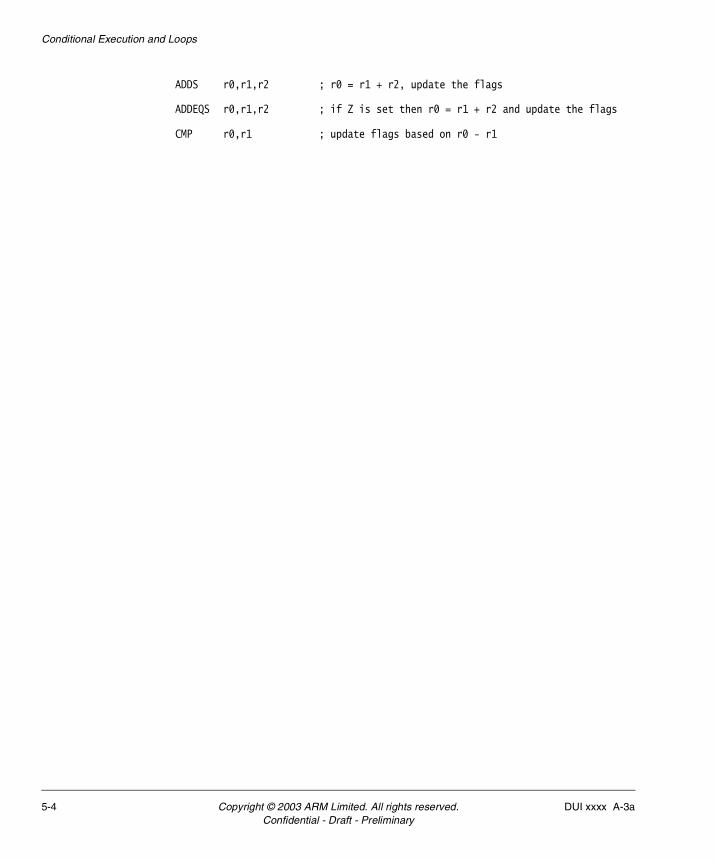
Conditional Execution and Loops
ADDS r0,r1,r2 ; r0 = r1 + r2, update the flags
ADDEQS r0,r1,r2 ; if Z is set then r0 = r1 + r2 and update the flags
CMP r0,r1 ; update flags based on r0 - r1
5-4 Copyright © 2003 ARM Limited. All rights reserved. DUI xxxx A-3aConfidential - Draft - Preliminary
Conditional Execution and Loops
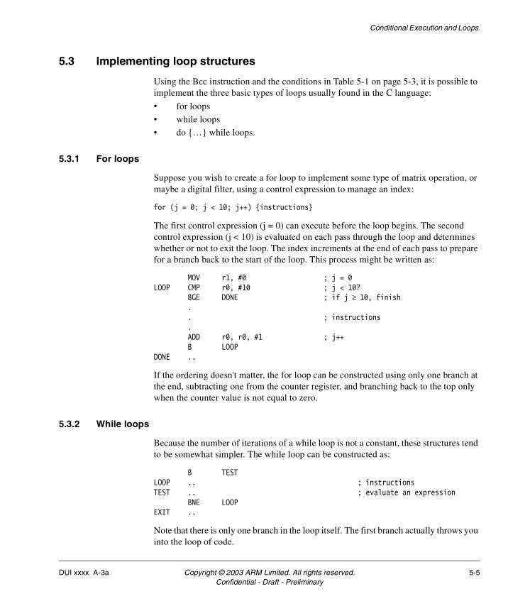
5.3 Implementing loop structures
Using the Bcc instruction and the conditions in Table 5-1 on page 5-3, it is possible to implement the three basic types of loops usually found in the C language:
• for loops
• while loops
• do {…} while loops.
5.3.1 For loops
Suppose you wish to create a for loop to implement some type of matrix operation, or maybe a digital filter, using a control expression to manage an index:
for (j = 0; j < 10; j++) {instructions}
The first control expression (j = 0) can execute before the loop begins. The second control expression (j < 10) is evaluated on each pass through the loop and determines whether or not to exit the loop. The index increments at the end of each pass to prepare for a branch back to the start of the loop. This process might be written as:
MOV r1, #0 ; j = 0LOOP CMP r0, #10 ; j < 10?
BGE DONE ; if j ≥ 10, finish.. ; instructions.ADD r0, r0, #1 ; j++B LOOP
DONE ..
If the ordering doesn't matter, the for loop can be constructed using only one branch at the end, subtracting one from the counter register, and branching back to the top only when the counter value is not equal to zero.
5.3.2 While loops
Because the number of iterations of a while loop is not a constant, these structures tend to be somewhat simpler. The while loop can be constructed as:
B TESTLOOP .. ; instructionsTEST .. ; evaluate an expression
BNE LOOPEXIT ..
Note that there is only one branch in the loop itself. The first branch actually throws you into the loop of code.
DUI xxxx A-3a Copyright © 2003 ARM Limited. All rights reserved. 5-5Confidential - Draft - Preliminary
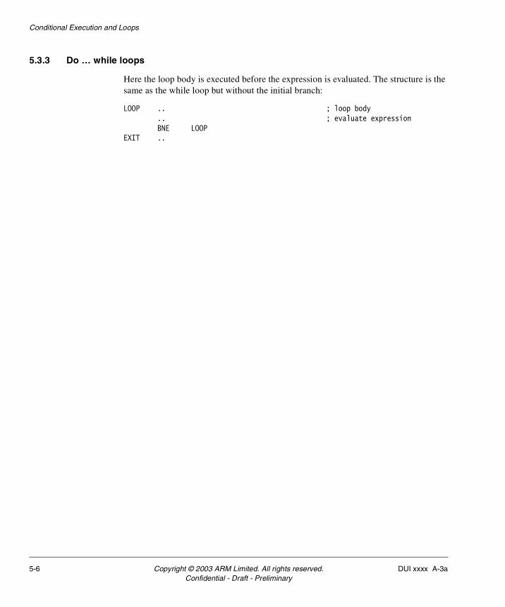
Conditional Execution and Loops
5.3.3 Do … while loops
Here the loop body is executed before the expression is evaluated. The structure is the same as the while loop but without the initial branch:
LOOP .. ; loop body.. ; evaluate expressionBNE LOOP
EXIT ..
5-6 Copyright © 2003 ARM Limited. All rights reserved. DUI xxxx A-3aConfidential - Draft - Preliminary
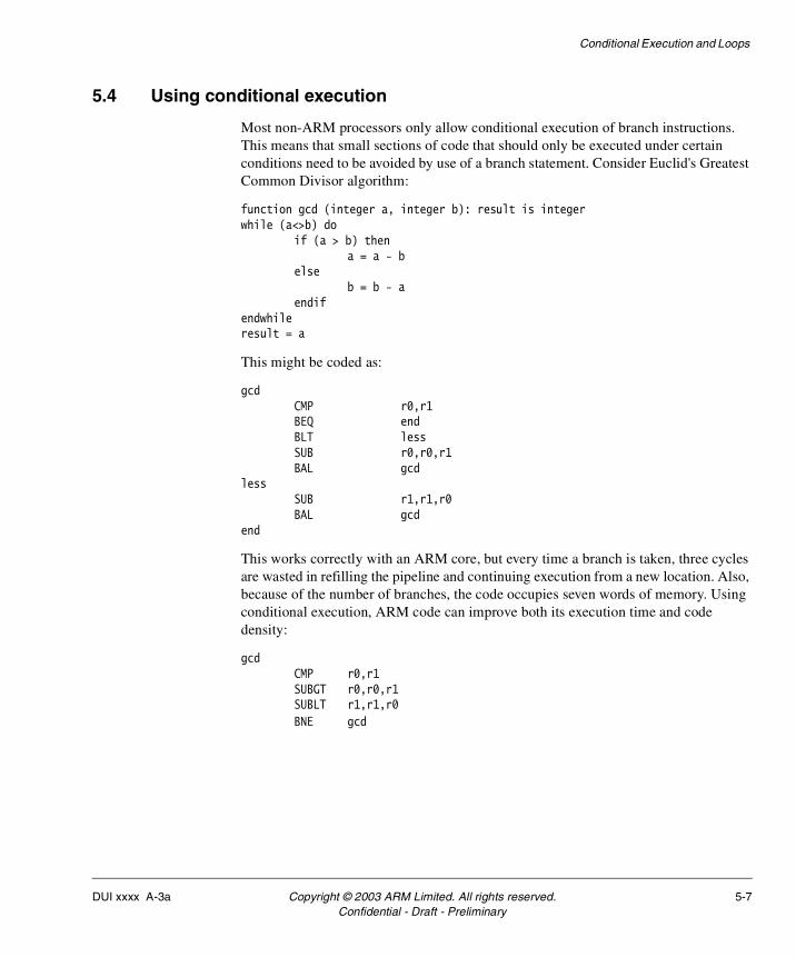
Conditional Execution and Loops
5.4 Using conditional execution
Most non-ARM processors only allow conditional execution of branch instructions. This means that small sections of code that should only be executed under certain conditions need to be avoided by use of a branch statement. Consider Euclid's Greatest Common Divisor algorithm:
function gcd (integer a, integer b): result is integerwhile (a<>b) do
if (a > b) thena = a - b
elseb = b - a
endifendwhileresult = a
This might be coded as:
gcdCMP r0,r1BEQ endBLT lessSUB r0,r0,r1BAL gcd
lessSUB r1,r1,r0BAL gcd
end
This works correctly with an ARM core, but every time a branch is taken, three cycles are wasted in refilling the pipeline and continuing execution from a new location. Also, because of the number of branches, the code occupies seven words of memory. Using conditional execution, ARM code can improve both its execution time and code density:
gcdCMP r0,r1SUBGT r0,r0,r1SUBLT r1,r1,r0BNE gcd
DUI xxxx A-3a Copyright © 2003 ARM Limited. All rights reserved. 5-7Confidential - Draft - Preliminary
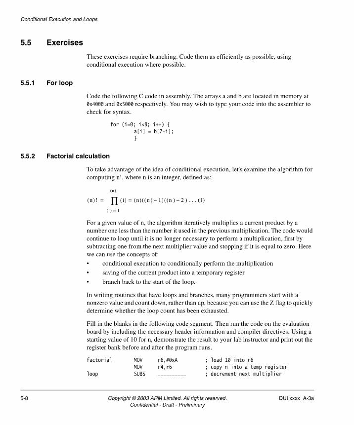
Conditional Execution and Loops
5.5 Exercises
These exercises require branching. Code them as efficiently as possible, using conditional execution where possible.
5.5.1 For loop
Code the following C code in assembly. The arrays a and b are located in memory at 0x4000 and 0x5000 respectively. You may wish to type your code into the assembler to check for syntax.
for (i=0; i<8; i++) {a[i] = b[7-i];}
5.5.2 Factorial calculation
To take advantage of the idea of conditional execution, let's examine the algorithm for computing n!, where n is an integer, defined as:
For a given value of n, the algorithm iteratively multiplies a current product by a number one less than the number it used in the previous multiplication. The code would continue to loop until it is no longer necessary to perform a multiplication, first by subtracting one from the next multiplier value and stopping if it is equal to zero. Here we can use the concepts of:
• conditional execution to conditionally perform the multiplication
• saving of the current product into a temporary register
• branch back to the start of the loop.
In writing routines that have loops and branches, many programmers start with a nonzero value and count down, rather than up, because you can use the Z flag to quickly determine whether the loop count has been exhausted.
Fill in the blanks in the following code segment. Then run the code on the evaluation board by including the necessary header information and compiler directives. Using a starting value of 10 for n, demonstrate the result to your lab instructor and print out the register bank before and after the program runs.
factorial MOV r6,#0xA ; load 10 into r6MOV r4,r6 ; copy n into a temp register
loop SUBS __________ ; decrement next multiplier
n( )! i( ) n( ) n ) 1–( ) n( ) 2–( ) . . . (1)(=
i( ) 1=
n( )
∏=
5-8 Copyright © 2003 ARM Limited. All rights reserved. DUI xxxx A-3aConfidential - Draft - Preliminary
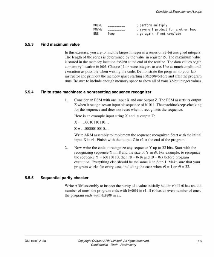
Conditional Execution and Loops
MULNE __________ ; perform multiplyMOVNE __________ ; save off product for another loopBNE loop ; go again if not complete
5.5.3 Find maximum value
In this exercise, you are to find the largest integer in a series of 32-bit unsigned integers. The length of the series is determined by the value in register r5. The maximum value is stored in the memory location 0x5000 at the end of the routine. The data values begin at memory location 0x5006. Choose 11 or more integers to use. Use as much conditional execution as possible when writing the code. Demonstrate the program to your lab instructor and print out the memory space starting at 0x5000 before and after the program runs. Be sure to include enough memory space to show all of your 32-bit integer values.
5.5.4 Finite state machines: a nonresetting sequence recognizer
1. Consider an FSM with one input X and one output Z. The FSM asserts its output Z when it recognizes an input bit sequence of b1011. The machine keeps checking for the sequence and does not reset when it recognizes the sequence.
Here is an example input string X and its output Z:
X = …0010110110…
Z = …0000010010…
Write ARM assembly to implement the sequence recognizer. Start with the initial input X in r1. Finish with the output Z in r2 at the end of the program.
2. Now write the code to recognize any sequence Y up to 32 bits. Start with the recognizing sequence Y in r8 and the size of Y in r9. For example, to recognize the sequence Y = b0110110, then r8 = 0x36 and r9 = 0x7 before program execution. Everything else should be the same is in Step 1. Make sure that your program works for every case, including the case when r9 = 1 or r9 = 32.
5.5.5 Sequential parity checker
Write ARM assembly to inspect the parity of a value initially held in r0. If r0 has an odd number of ones, the program ends with 0x0001 in r1. If r0 has an even number of ones, the program ends with 0x0000 in r1.
DUI xxxx A-3a Copyright © 2003 ARM Limited. All rights reserved. 5-9Confidential - Draft - Preliminary
Conditional Execution and Loops
5-10 Copyright © 2003 ARM Limited. All rights reserved. DUI xxxx A-3aConfidential - Draft - Preliminary
Chapter 6 Subroutines
This chapter introduces stacks, the branch and link instruction, and the load and store multiple instructions. It contains the following sections:
• Introduction on page 6-2
• The branch and link instruction on page 6-3
• Load/store multiple instructions on page 6-4
• Stacks on page 6-6
• Exercises on page 6-9.
DUI xxxx A-3a Copyright © 2003 ARM Limited. All rights reserved. 6-1Confidential - Draft - Preliminary
Subroutines
6.1 Introduction
Subroutines are regularly used to modularize a large task when a subprogram can be found in the same file as a calling routine. A common requirement in many programs is the ability to branch to a subroutine and then return to the original code sequence when the subroutine has completed.
6-2 Copyright © 2003 ARM Limited. All rights reserved. DUI xxxx A-3aConfidential - Draft - Preliminary
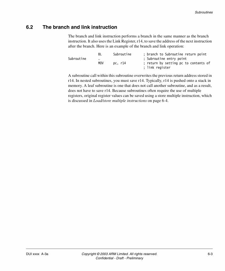
Subroutines
6.2 The branch and link instruction
The branch and link instruction performs a branch in the same manner as the branch instruction. It also uses the Link Register, r14, to save the address of the next instruction after the branch. Here is an example of the branch and link operation:
BL Subroutine ; branch to Subroutine return pointSubroutine … ; Subroutine entry point
MOV pc, r14 ; return by setting pc to contents of; link register
A subroutine call within this subroutine overwrites the previous return address stored in r14. In nested subroutines, you must save r14. Typically, r14 is pushed onto a stack in memory. A leaf subroutine is one that does not call another subroutine, and as a result, does not have to save r14. Because subroutines often require the use of multiple registers, original register values can be saved using a store multiple instruction, which is discussed in Load/store multiple instructions on page 6-4.
DUI xxxx A-3a Copyright © 2003 ARM Limited. All rights reserved. 6-3Confidential - Draft - Preliminary
Subroutines
6.3 Load/store multiple instructions
Moving large amounts of data is a common requirement in algorithms and subroutines. Often variables and registers must be saved before other routines potentially corrupt them. These exercises highlight the following aspects of data movement:
• Multiple vs single transfers
• The register list
• Load and store multiple addressing modes
• Base register writeback on page 6-5.
6.3.1 Multiple vs single transfers
The load multiple and store multiple instructions LDM and STM provide an efficient way of moving the contents of several registers to and from memory. The advantages of using a load multiple or store multiple instruction instead of a series of single data transfer instructions are:
• smaller code size
• only one instruction fetch
• only one register writeback cycle
• on uncached ARM processors, the first word in a multiple transfer is nonsequential, but subsequent words can be sequential and therefore faster.
6.3.2 The register list
The registers transferred by a load multiple or store multiple instruction are encoded in the instruction by one bit for each of the registers r0 to r15. A set bit indicates that the register is transferred, and a clear bit indicates that it is not transferred. Thus it is possible to transfer any subset of the registers in a single instruction.
The subset of registers to be transferred is specified by listing them in curly brackets. For example:
{r1, r4-r6, r8, r10}
6.3.3 Load and store multiple addressing modes
The base address for the transfer can be either incremented or decremented between register transfers, and either before or after each register transfer. Appending a suffix to the mnemonic controls the base address.
IA Increment after.
IB Increment before.
6-4 Copyright © 2003 ARM Limited. All rights reserved. DUI xxxx A-3aConfidential - Draft - Preliminary
Subroutines
DA Decrement after.
DB Decrement before.
For example, the following instruction stores a list of registers and increments the base address after each store:
STMIA r10, {r1, r3-r5, r8}
In all cases the lowest numbered register is transferred to or from the lowest memory address, and the highest numbered register to or from the highest address. The order in which the registers appear in the register list makes no difference. Also, the ARM processor always performs sequential memory accesses in increasing memory address order. Therefore a decrementing transfer actually performs a subtraction first and then increments the transfer address register by register.
6.3.4 Base register writeback
Unless specifically requested, the base register is not updated at the end of a multiple register transfer instruction. To specify register writeback, you must use the ! character. For example:
LDMDB r11!, {r9, r4-r7}
DUI xxxx A-3a Copyright © 2003 ARM Limited. All rights reserved. 6-5Confidential - Draft - Preliminary
Subroutines
6.4 Stacks
Stacks are an important part of any C program, and it is essential to know how to use the ARM processor to handle them. This section describes:
• Stack addressing modes
• Stacks in the use of memory for a C program on page 6-7
6.4.1 Stack addressing modes
The ARM has many addressing variations, one being a stack addressing mode. The need for this addressing mode is a direct result of the need to implement stacks in memory. A stack is a Last In First Out (LIFO) form of store. It supports a kind of memory allocation that uses an address to store data that is unknown when the program is compiled or assembled.
Load multiple and store multiple instructions can update the base register, which can be the stack pointer for stack operations. Therefore, these instructions provide single instruction push and pop operations for any number of registers. STM provides the push operation, and LDM provides the pop operation.
The load and store multiple instructions can be used with the different types of stack:
Ascending The stack grows upwards, starting from a low address and progressing to a higher address.
Descending The stack grows downwards, starting from a high address and progressing to a lower one.
Empty The stack pointer points to the next free space in the stack.
Full The stack pointer points to the last accessed item in the stack.
To make it easier for the programmer, special stack suffixes can be added to the LDM and STM instructions as Table 6-1 shows.
Table 6-1 Stack addressing modes
Name Stack Other
Pre-increment load LDMED LDMIB
Post-increment load LDMFD LDMIA
Pre-decrement load LDMEA LDMDB
Post-decrement load LDMFA LDMDA
6-6 Copyright © 2003 ARM Limited. All rights reserved. DUI xxxx A-3aConfidential - Draft - Preliminary
Subroutines
By convention, r13 is used as the system stack pointer (SP). In the examples that follow, r13 is used as the base pointer.
STMFA r13!, {r0-r5}; Push onto a full ascending stackLDMFA r13!, {r0-r5}; Pop from a full ascending stackSTMFD r13!, {r0-r5}; Push onto a full descending stackLDMFD r13!, {r0-r5}; Pop from a full descending stackSTMEA r13!, {r0-r5}; Push onto an empty ascending stackLDMEA r13!, {r0-r5}; Pop from an empty ascending stackSTMED r13!, {r0-r5}; Push onto an empty descending stackLDMED r13!, {r0-r5}; Pop from an empty descending stack
Note
The system stack is usually full descending.
6.4.2 Stacks in the use of memory for a C program
The memory of an ARM system is arranged as a linear set of logical addresses. A typical C program uses a fixed area of program memory where the application is stored and two data areas that grow dynamically when the compiler does not specify a maximum size. These two dynamic data areas are the stack and the heap. When a function call occurs, the stack allocates new space and allows placement of a back-tracking record and local, dynamic variables among other things. When a function return occurs, the stack space is recovered and reused for the next function call. The heap is a section of memory used to satisfy memory and new data structure requests by a program. Figure 6-1 on page 6-8 shows the model of the ARM C program address space.
Pre-increment store STMFA STMIB
Post-increment store STMEA STMIA
Pre-decrement store STMFD STMDB
Post-decrement store STMED STMDA
Table 6-1 Stack addressing modes
Name Stack Other
DUI xxxx A-3a Copyright © 2003 ARM Limited. All rights reserved. 6-7Confidential - Draft - Preliminary
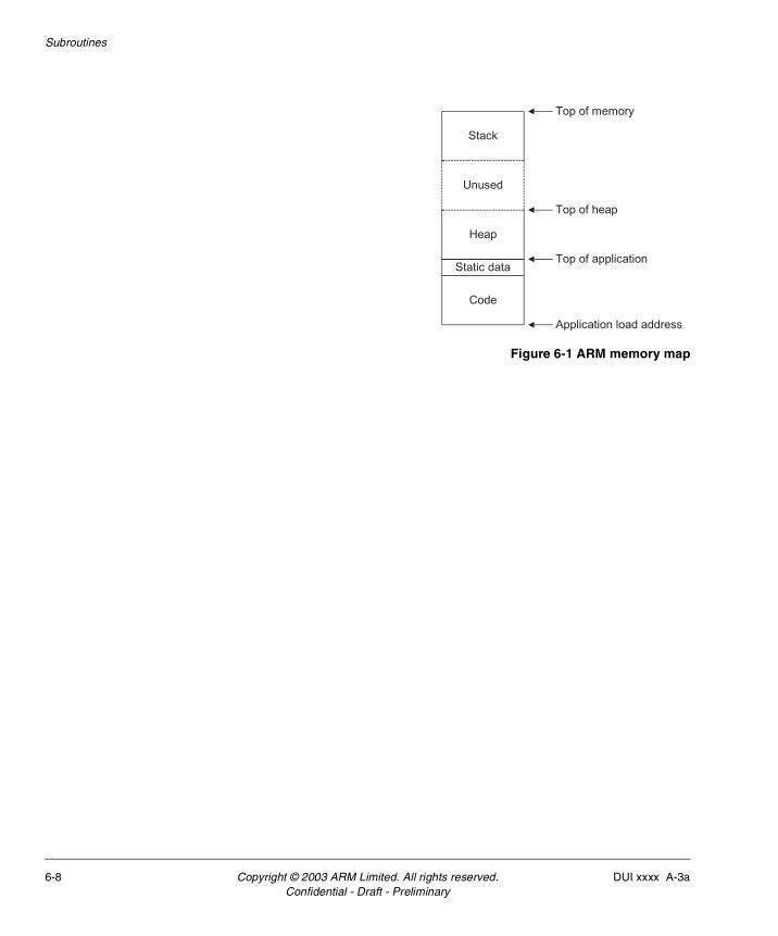
Subroutines
Figure 6-1 ARM memory map
Stack
Unused
Heap
Static data
Code
Application load address
Top of application
Top of heap
Top of memory
6-8 Copyright © 2003 ARM Limited. All rights reserved. DUI xxxx A-3aConfidential - Draft - Preliminary
Subroutines
6.5 Exercises
Try these exercises for practice in using stacks and subroutines:
• Transmission of arguments
• Bubble sorting
• Magic squares on page 6-10
• More stacks on page 6-10
• Least common multiple on page 6-10
• Congruent modulo n on page 6-10
• Vending machine on page 6-11.
6.5.1 Transmission of arguments
Write ARM assembly code to compute the function a = b × c + d. Write three separate programs that:
• transmit the arguments by way of registers with one subroutine, func1
• transmit the arguments by way of the addresses with one subroutine, func1
• transmit the arguments by way of the stack with two subroutines, func1 and func2, that demonstrate stack functionality.
6.5.2 Bubble sorting
1. Write ARM assembly code to perform an ascending bubble sort operation on a list located in memory. The length of the list is located at 0x4000 and the first element of the list is located at 0x4001. The sorted list must be stored back to the original array of memory locations starting at 0x4001. Assume an array of bytes.
2. Modify your code to utilize a full descending stack. Sorting must be done on the stack only. Once the stack is sorted, store the sorted stack back to the original array of memory locations starting at 0x4001.
The algorithm for the bubble sort is as follows:
a. Compare adjacent elements. If the first element is greater than the second, swap them.
b. Do this for each pair of adjacent elements, starting with the first two and ending with the last two. At this point the last element should be the greatest.
c. Repeat the steps for all elements except the last one.
d. Repeat this process for one fewer element each time, until you have no more pairs to compare.
DUI xxxx A-3a Copyright © 2003 ARM Limited. All rights reserved. 6-9Confidential - Draft - Preliminary
Subroutines
6.5.3 Magic squares
Write ARM assembly to check whether an N × N matrix is a magic square. A magic square is an N × N matrix in which the sum of the numbers in every row, column, or diagonal is N(N2 + 1)/2. All matrix entries are unique numbers from 1 to N2. For example, suppose you wanted to test a famous example of a magic square:
The matrix starts at location 0x4000 and ends at location (0x4000 + N2). Put the 16 in location 0x4000, 3 in 0x4001, 2 in 0x4002, 13 in 0x4003, 5 in 0x4004, …, and 1 in 0x400F. Put N in r1. Assume that everything is in bytes, which puts a constraint on N. Write the code so that, if the matrix is a magic square, r9 is set, and otherwise it is cleared. To test the algorithm, you can search the Internet for other magic square examples, such as Ben Franklin's own 8 × 8 magic square.
6.5.4 More stacks
Write ARM assembly to implement a push operation without the use of load/store multiple instructions. Write the code to handle bytes, half-words, and words. Use r0 to indicate the data type. A value of 1 in r0 indicates that a byte is to be pushed, 2 indicates a half-word, and 4 indicates a word. Put the data to push in r1.
6.5.5 Least common multiple
Write ARM assembly to implement the function LCM(a, b). Start with a in r1 and b in r2. Assume a and b are integers. At program completion, put LCM(a, b) in r4. You must use at least one subroutine. It would be a good idea to utilize the GCD routine from Using conditional execution on page 5-7. As a shortcut, it should be noted that LCM(a, b) × GCD(a, b) = a × b.
6.5.6 Congruent modulo n
Let n be a positive integer. Integers a and b are said to be congruent modulo n if they have the same remainder when divided by n. Write ARM assembly to implement the function congruent modulo n. It may be useful to utilize the divide routine from Division on page 3-12. Start with a in r1, b in r2, and n in r4. If a and b are congruent modulo n, set r10, otherwise clear r10.
16 3 2 13
5 10 11 8
9 6 7 12
4 15 14 1
6-10 Copyright © 2003 ARM Limited. All rights reserved. DUI xxxx A-3aConfidential - Draft - Preliminary
Subroutines
6.5.7 Vending machine
A vending machine has three sequences of inputs, each representing a type of coin. r0 is a sequence of inserted nickels, r1 is a sequence of inserted dimes, and r2 is a sequence of inserted quarters. The machine has two outputs, r3 and r4. r4 shall represent a sequence of change dispensed back to the customer. The machine only gives back change as nickels. r4 shall represent the sequence of dispensed products. So the customer inserts coins and the machine gives change back first before the product is dispensed. The product costs 25 cents. Write ARM assembly to implement the vending machine. Here is a sample case:
As you can see, every bit represents a time interval in which only one operation can occur, whether it is inserting a coin, receiving change, or receiving the product. This means there are some illegal input sequences, for example, two consecutive ones in r2. This is equivalent to someone inserting a quarter, not choosing a product, and inserting another quarter. It just makes no sense.
Inputs Nickels r0 10000000000000 . . .
Dimes r1 01000000000000 . . .
Quarters r2 00100000000000 . . .
Outputs Dispensed change sequence r3 00011100000000 . . .
Dispensed products r4 00000010000000 . . .
DUI xxxx A-3a Copyright © 2003 ARM Limited. All rights reserved. 6-11Confidential - Draft - Preliminary

Subroutines
6-12 Copyright © 2003 ARM Limited. All rights reserved. DUI xxxx A-3aConfidential - Draft - Preliminary

Chapter 7 Memory-mapped Peripherals (Evaluator 7T)
This chapter introduces the use of I/O in an ARM system, exception handling, and control of peripherals external to the ARM. It contains the following sections:
• Introduction on page 7-2
• Example peripheral device on page 7-3
• Exceptions on page 7-4
• Evaluator 7T peripherals on page 7-8
• Exercises on page 7-11.
DUI xxxx A-3a Copyright © 2003 ARM Limited. All rights reserved. 7-1Confidential - Draft - Preliminary
Memory-mapped Peripherals (Evaluator 7T)
7.1 Introduction
To be useful in a system, an embedded processor must be able to exchange information with the outside world and to process requests for input and output.
Memory-mapped, addressable peripheral registers and interrupt inputs enable you to implement input/output (I/O) functions in an ARM system. Keyboards, mice, scanners, printers, modems, and audio I/O are all examples of peripheral devices.
There are two categories of peripherals, tightly coupled and loosely coupled. Tightly coupled peripherals are connected to the processor via an internal bus. Loosely coupled peripherals are connected to the processor via an external bus, network, or port.
Interface devices link the external bus, network, or port with the internal bus and enable the processor to communicate with loosely-coupled peripherals. An interface device usually has a set of registers called peripheral registers. The processor performs I/O functions by reading from and writing to the peripheral registers. The information that is read or written is usually either data or configuration and control information.
The processor can use either I/O mapping or memory mapping to address the peripheral registers. In I/O mapping, the processor has separate instructions for I/O devices. In memory mapping, the peripheral registers are mapped into main memory space. We will see that memory mapping is much more flexible than I/O mapping.
The processor can service I/O devices by:
• continually reading the peripheral status registers to see when service is needed
• temporarily stopping a current task to service an interrupt request from a peripheral.
When a DMA controller is present, it can process service requests from peripheral devices without interrupting the processor.
7-2 Copyright © 2003 ARM Limited. All rights reserved. DUI xxxx A-3aConfidential - Draft - Preliminary
Memory-mapped Peripherals (Evaluator 7T)
7.2 Example peripheral device
An example of a peripheral device is a serial line controller. A device such as this contains a number of registers, each of which appears as a particular location in memory in a memory-mapped system. The register set of a serial line controller might include the following:
Write-only transmit data register
The transmit data register contains data to be transmitted by the processor.
Read-only receive data register
The receive data register contains data transmitted to the processor.
Read/write control register
The control register selects operational features of the serial line controller such as baud rate, transmission protocol, and word size.
Read/write interrupt enable register
This register determines which hardware operations can cause an interrupt.
Read only status register
This register indicates if read data is available and whether the write buffer is full.
Software must set up a peripheral device to receive data by having it generate an interrupt request when either data is available or an error is detected. The data is then copied into a buffer by the interrupt routine. The interrupt routine also checks for error conditions.
Memory-mapped peripheral registers behave differently from memory locations. Consecutive reads to the read data register from the example device above might return different results each time without the processor ever having written to that particular location. This is different from a normal memory location in that the read can be repeated consecutively with identical results. A read to a peripheral may clear the current value and the next value may be different. These locations are called read-sensitive locations.
DUI xxxx A-3a Copyright © 2003 ARM Limited. All rights reserved. 7-3Confidential - Draft - Preliminary
Memory-mapped Peripherals (Evaluator 7T)
7.3 Exceptions
The ARM processor generates exceptions to handle the following events that can occur during program execution:
• Reset
• Undefined Instruction
• Software Interrupt
• Prefetch Abort
• Data Abort
• IRQ
• FIQ.
ARM exceptions can be classified into three groups:
• Exceptions caused by execution of an instruction. These are Undefined Instruction, Software Interrupt, and Prefetch Abort exceptions.
• Exceptions that are a side-effect of instruction execution. These are Data Abort exceptions.
• Exceptions generated externally, unrelated to the instruction flow. These are Reset, IRQ, and FIQ exceptions.
7.3.1 Exception entry
Unless the exception is a Reset, the ARM processor finishes the current instruction and then vectors to the exception-handling code. A Reset terminates the current instruction immediately. A Prefetch Abort, Reset, IRQ, or FIQ usurp the next instruction in the current sequence. This is different from exceptions classified into group 1 as they are handled in sequence as they occur.
When an exception occurs, the processor performs the following actions in sequence:
1. The operating mode is switched to the operating mode corresponding to the particular exception.
2. The return address, which is the instruction following the exception entry instruction, is saved in the link register (r14) of the new mode.
3. The CPSR is copied into the SPSR of the new mode.
4. The appropriate interrupt disable bits are set. IRQs are disabled by setting bit 7 of the CPSR and FIQs are disabled by setting bit 6 of the CPSR.
7-4 Copyright © 2003 ARM Limited. All rights reserved. DUI xxxx A-3aConfidential - Draft - Preliminary

Memory-mapped Peripherals (Evaluator 7T)
5. The PC is forced to execute at the corresponding vector address given in the exception vector address table.
The corresponding vector address contains a branch to the corresponding exception handling routine. This is true for all exception vector addresses except FIQs, which can start immediately as it occupies the highest vector address.
The return address and stack pointer are held by the two banked registers in each of the privileged modes. The stack pointer can actually be used to save user registers that might be used by the exception handler. FIQ mode avoids the need to save user registers, giving better performance. This is accomplished by the FIQ mode having additional private registers.
7.3.2 Exception return
Once the exception has been handled, normal program execution is resumed. This requires that the exception handling code restore the exact user state when the exception occurred. To do this, the exception handler performs the following actions:
• The modified user registers are restored from the exception handler's stack.
• The CPSR is restored from the corresponding SPSR.
• The PC is restored to the relevant instruction address in the user instruction sequence.
The last two tasks cannot occur independently. If the CPSR is restored first, the banked r14 holding the return address cannot be accessed. If the PC is restored first, the exception handler loses control of the instruction sequence and the CPSR cannot be restored. Other difficulties can arise when instructions are fetched in the incorrect
Table 7-1 Exception types
Exception type Exception mode Vector address
Reset Supervisor 0x00000000
Undefined instruction Undefined 0x00000004
Software Interrupt (SWI) Supervisor 0x00000008
Prefetch Abort Abort 0x0000000C
Data Abort Abort 0x00000010
IRQ (interrupt) IRQ 0x00000018
FIQ (fast interrupt) FIQ 0x0000001C
DUI xxxx A-3a Copyright © 2003 ARM Limited. All rights reserved. 7-5Confidential - Draft - Preliminary

Memory-mapped Peripherals (Evaluator 7T)
operating mode. ARM provides two mechanisms which forces the last two steps to be executed in a single instruction. One is used when the banked link register (r14) holds the return address and the other is used when a stack holds the return address.
Use the following instructions when the return address in held in r14:
MOVS pc, r14
To return from a SWI or undefined instruction trap.
SUBS pc, r14, #4
To return from an IRQ, FIQ or prefetch abort:
SUBS pc, r14, #8
To return from a data abort to retry the data access:
You can see that the return instructions can modify the return address when necessary. An IRQ or FIQ exception handler must return to the instruction that was fetched but not executed. This is because the PC already progressed beyond the point where the exception was taken. A Prefetch Abort handler also returns to the instruction that caused the memory fault. A Data Abort handlers returns to retry the data transfer instruction that caused the exception.
Using the S suffix on the return instruction causes the return operation to copy the SPSR back to the CPSR.
If the exception handler copied the return address onto a stack, you can use one multiple register transfer instruction to restore user registers and the return address:
LDMFD r13!, {r0-r3, pc}^
The ^ indicates a special form of the instruction. The CPSR is restored at the same time that the PC is loaded from memory. Remember that the registers are loaded in increasing order.
7-6 Copyright © 2003 ARM Limited. All rights reserved. DUI xxxx A-3aConfidential - Draft - Preliminary
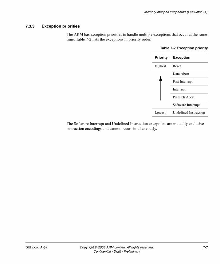
Memory-mapped Peripherals (Evaluator 7T)
7.3.3 Exception priorities
The ARM has exception priorities to handle multiple exceptions that occur at the same time. Table 7-2 lists the exceptions in priority order.
The Software Interrupt and Undefined Instruction exceptions are mutually exclusive instruction encodings and cannot occur simultaneously.
Table 7-2 Exception priority
Priority Exception
Highest Reset
Data Abort
Fast Interrupt
Interrupt
Prefetch Abort
Software Interrupt
Lowest Undefined Instruction
DUI xxxx A-3a Copyright © 2003 ARM Limited. All rights reserved. 7-7Confidential - Draft - Preliminary
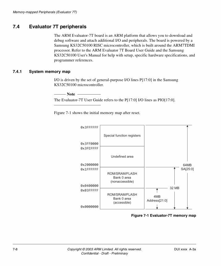
Memory-mapped Peripherals (Evaluator 7T)
7.4 Evaluator 7T peripherals
The ARM Evaluator-7T board is an ARM platform that allows you to download and debug software and attach additional I/O and peripherals. The board is powered by a Samsung KS32C50100 RISC microcontroller, which is built around the ARM7TDMI processor. Refer to the ARM Evaluator 7T Board User Guide and the Samsung KS32C50100 User's Manual for help with setup, specific hardware specifications, and programmer references.
7.4.1 System memory map
I/O is driven by the set of general-purpose I/O lines P[17:0] in the Samsung KS32C50100 microcontroller.
Note The Evaluator-7T User Guide refers to the P[17:0] I/O lines as PIO[17:0].
Figure 7-1 shows the initial memory map after reset.
Figure 7-1 Evaluator-7T memory map
Special function registers
Undefined area
ROM/SRAM/FLASH
Bank 0 area
(nonaccessible)
ROM/SRAM/FLASH
Bank 0 area
(accessible)
0x0000000
0x2000000
0x3FF0000
0x3FFFFFF
4MB
Address[21:0]
32 MB
64MB
SA[25:0]
0x03FFFFF
0x0400000
0x1FFFFFF
0x3FEFFFF
7-8 Copyright © 2003 ARM Limited. All rights reserved. DUI xxxx A-3aConfidential - Draft - Preliminary
Memory-mapped Peripherals (Evaluator 7T)
The memory locations 0x3FF0000-0x3FFFFFF contain the special function registers. Table 1-5 in the Samsung User's Manual has a complete list of the special function registers. The registers that are of concern in this lab are the I/O ports, IOPMOD, IOPCON, and IOPDATA.
IOPMOD The IOPMOD register configures the PIO[17:0] ports as outputs or inputs. IOPMOD is memory-mapped to location 0x3FF5000.
IOPCON The IOPCON register controls filtering, polarity, and level detection of the PIO[17:8] pins. Input filtering is necessary for exercises that use the user interrupt switch. IOPCON is memory-mapped to location 0x3FF5004.
IOPDATA The IOPDATA register is the data register for the PIO[17:0] pins. IOPDATA is memory-mapped to location 0x3FF5008.
INTMSK The INTMSK register is the interrupt mask register for the 21 KS32C50100 interrupt sources. In exercises that use the user interrupt switch, you have to enable external interrupt 0. INTMSK is memory-mapped to location 0x3FF4008.
7.4.2 Surface-mounted LEDs
The four user-programmable surface-mounted LEDs are labeled D1-D4. They are connected to a tristate buffer driven by the PIO[7:4] pins. Refer to the ARM Evaluator-7T Board User Guide for details of the architecture of the surface-mounted LEDs. To drive the LEDs, configure the PIO[7:4] pins as outputs by writing to bits [7:4] in the IOPMOD register. Then turn the LEDs on or off by writing to bits [7:4] in the IOPDATA register.
7.4.3 Seven-segment LED display
The seven-segment display is controlled by PIO[16:10] and two tristate buffers. The decimal point LED indicates that the power to the display is on. Refer to the ARM Evaluator-7T Board User Guide for the PIO[16:10]-to-LED-segment assignment. To drive the LEDs, configure the PIO[16:10] pins as outputs by writing to bits [16:10] of the IOPMOD register. Then turn the LEDs on or off by writing to bits [16:10] in the IOPDATA register.
7.4.4 Four-way DIP switch
The DIP contains four independent switches that are connected to PIO[3:0]. Flipping a switch ON ties the corresponding PIO input HIGH. Flipping a switch OFF ties the corresponding PIO input LOW. To configure PIO[3:0] as inputs, clear bits [3:0] of the IOPMOD register. You can read the current setting of the DIP switches from bits [3:0] of the IOPDATA register.
DUI xxxx A-3a Copyright © 2003 ARM Limited. All rights reserved. 7-9Confidential - Draft - Preliminary
Memory-mapped Peripherals (Evaluator 7T)
7.4.5 User interrupt switch
The user interrupt switch is labeled SW3 and is connected to PIO[8]. To use SW3 as an interrupt input INT0, set bit [3] in the IOPCON register and clear bit [0] of the INTMSK register. This allows you to trigger an interrupt by pressing SW3.
7-10 Copyright © 2003 ARM Limited. All rights reserved. DUI xxxx A-3aConfidential - Draft - Preliminary
Memory-mapped Peripherals (Evaluator 7T)
7.5 Exercises
Light up your life with these exercises.
• Displaying the hex digits in binary to the surface-mounted LEDs
• Displaying the contents of a memory location to the surface-mounted LEDs
• Displaying the contents of a memory location to the seven-segment display on page 7-12
• Displaying the contents of an array of memory location to the seven-segment display on page 7-12
• Displaying the value of the DIP switches to the surface-mounted LEDs on page 7-12
• Displaying the value of the DIP switches to the surface-mounted LEDs continuously on page 7-12
• Storing the value of the DIP switches to a memory location on page 7-12
• Displaying the value of the DIP switches to the seven-segment display on page 7-12
• Displaying the value of the DIP switches to the seven-segment display continuously on page 7-12
• Displaying an array of memory locations by multiplexing on page 7-13
• Counting DIP switch state changes on page 7-13
• Counting user interrupt switches to seven-segment display on page 7-13
• Counting user interrupt switches to surface-mounted LEDs on page 7-13
• Counting up to n on page 7-13
• Some light flickering on page 7-13.
7.5.1 Displaying the hex digits in binary to the surface-mounted LEDs
Write ARM assembly to flash the hex digits in binary form to the surface-mounted LEDs in ascending order. Now slightly modify the code to flash the digits in descending order. Make sure to use a delay so that the digits can be seen. The digits should not stop flashing.
7.5.2 Displaying the contents of a memory location to the surface-mounted LEDs
Write ARM assembly to inspect memory location 0x4000.
If the location contains a decimal number 0-15, display the contents in binary on the surface-mounted LEDs.
If the location holds any other value, blank the display. As an example, if 0x4000 contains 0xE, then turn on D1, D2, and D3, and turn off D4 to display b1110.
DUI xxxx A-3a Copyright © 2003 ARM Limited. All rights reserved. 7-11Confidential - Draft - Preliminary
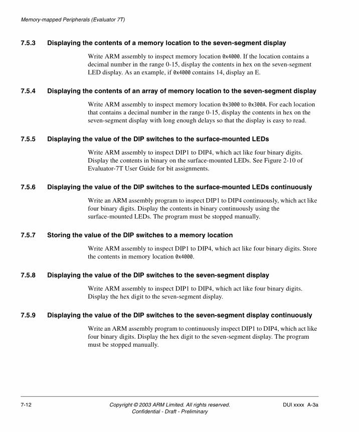
Memory-mapped Peripherals (Evaluator 7T)
7.5.3 Displaying the contents of a memory location to the seven-segment display
Write ARM assembly to inspect memory location 0x4000. If the location contains a decimal number in the range 0-15, display the contents in hex on the seven-segment LED display. As an example, if 0x4000 contains 14, display an E.
7.5.4 Displaying the contents of an array of memory location to the seven-segment display
Write ARM assembly to inspect memory location 0x3000 to 0x300A. For each location that contains a decimal number in the range 0-15, display the contents in hex on the seven-segment display with long enough delays so that the display is easy to read.
7.5.5 Displaying the value of the DIP switches to the surface-mounted LEDs
Write ARM assembly to inspect DIP1 to DIP4, which act like four binary digits. Display the contents in binary on the surface-mounted LEDs. See Figure 2-10 of Evaluator-7T User Guide for bit assignments.
7.5.6 Displaying the value of the DIP switches to the surface-mounted LEDs continuously
Write an ARM assembly program to inspect DIP1 to DIP4 continuously, which act like four binary digits. Display the contents in binary continuously using the surface-mounted LEDs. The program must be stopped manually.
7.5.7 Storing the value of the DIP switches to a memory location
Write ARM assembly to inspect DIP1 to DIP4, which act like four binary digits. Store the contents in memory location 0x4000.
7.5.8 Displaying the value of the DIP switches to the seven-segment display
Write ARM assembly to inspect DIP1 to DIP4, which act like four binary digits. Display the hex digit to the seven-segment display.
7.5.9 Displaying the value of the DIP switches to the seven-segment display continuously
Write an ARM assembly program to continuously inspect DIP1 to DIP4, which act like four binary digits. Display the hex digit to the seven-segment display. The program must be stopped manually.
7-12 Copyright © 2003 ARM Limited. All rights reserved. DUI xxxx A-3aConfidential - Draft - Preliminary
Memory-mapped Peripherals (Evaluator 7T)
7.5.10 Displaying an array of memory locations by multiplexing
1. Write ARM assembly to inspect DIP1 to DIP4, which act as a multiplexor. The multiplexor determines access to an array of memory locations starting at 0x4000 and ending at 0x400F. Continuously display the contents of the multiplexed memory location to the seven- segment display.
2. Now make slight modifications to the code so that the contents are displayed to the segment display and the surface-mounted LEDs.
7.5.11 Counting DIP switch state changes
Write ARM assembly to count the number of times DIP switch 4 changes state up to the hex digit F. Display the continuous count to the seven-segment display.
7.5.12 Counting user interrupt switches to seven-segment display
Write ARM assembly to count the number of times, up to 15, that you press the user interrupt push-button INT0. Display the continuous count in hex digits on the seven-segment display. In this part of the exercise, it is okay for the count to increment multiple times on one press. Make sure to introduce a delay so that the digits are human-readable even when one press produces multiple increments of the count.
Now modify your code so that the count increments only after a push followed by a release. In this part of the exercise, the count should not increment multiple times on one push.
7.5.13 Counting user interrupt switches to surface-mounted LEDs
Write ARM assembly to count the number of times, up to the hex digit F, that you press the user interrupt switch. Display the continuous count to the surface mounted LEDs.
7.5.14 Counting up to n
Write ARM assembly to flash digits 0 to n – 1 on the seven- segment display and the surface mounted LEDs. Start with the n value in r0.
7.5.15 Some light flickering
Write ARM assembly to perform delayed blinking of the seven-segment display in the sequence shown in Figure 7-2 on page 7-14.
DUI xxxx A-3a Copyright © 2003 ARM Limited. All rights reserved. 7-13Confidential - Draft - Preliminary
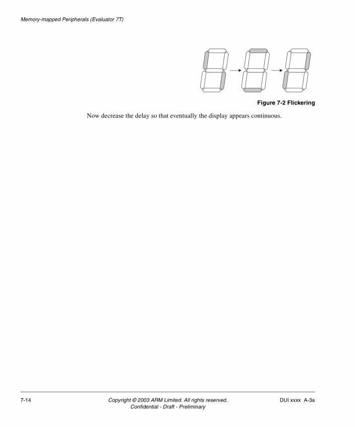
Memory-mapped Peripherals (Evaluator 7T)
Figure 7-2 Flickering
Now decrease the delay so that eventually the display appears continuous.
7-14 Copyright © 2003 ARM Limited. All rights reserved. DUI xxxx A-3aConfidential - Draft - Preliminary
Chapter 8 Memory-mapped Peripherals (OKI ML674000)
This chapter introduces the use of I/O in an ARM system, exception handling, and control of peripherals external to the ARM. It contains the following sections:
• Introduction on page 8-2
• Example peripheral device on page 8-3
• Exceptions on page 8-4
• OKI ML674000 peripherals on page 8-8
• Exercises on page 8-15.
DUI xxxx A-3a Copyright © 2003 ARM Limited. All rights reserved. 8-1Confidential - Draft - Preliminary

Memory-mapped Peripherals (OKI ML674000)
8.1 Introduction
To be useful in a system, an embedded processor must be able to exchange information with the outside world and to process requests for input and output.
Memory-mapped, addressable peripheral registers and interrupt inputs enable you to implement input/output (I/O) functions in an ARM system. Keyboards, mice, scanners, printers, modems, and audio I/O are all examples of peripheral devices.
There are two categories of peripherals, tightly coupled and loosely coupled. Tightly coupled peripherals are connected to the processor via an internal bus. Loosely coupled peripherals are connected to the processor via an external bus, network, or port.
Interface devices link the external bus, network, or port with the internal bus and enable the processor to communicate with loosely-coupled peripherals. An interface device usually has a set of registers called peripheral registers. The processor performs I/O functions by reading from and writing to the peripheral registers. The information that is read or written is usually either data or configuration and control information.
The processor can use either I/O mapping or memory mapping to address the peripheral registers. In I/O mapping, the processor has separate instructions for I/O devices. In memory mapping, the peripheral registers are mapped into main memory space. We will see that memory mapping is much more flexible than I/O mapping.
The processor can service I/O devices by:
• continually reading the peripheral status registers to see when service is needed
• temporarily stopping a current task to service an interrupt request from a peripheral.
When a DMA controller is present, it can process service requests from peripheral devices without interrupting the processor.
8-2 Copyright © 2003 ARM Limited. All rights reserved. DUI xxxx A-3aConfidential - Draft - Preliminary

Memory-mapped Peripherals (OKI ML674000)
8.2 Example peripheral device
An example of a peripheral device is a serial line controller. A device such as this contains a number of registers, each of which appears as a particular location in memory in a memory-mapped system. The register set of a serial line controller might include the following:
Write-only transmit data register
The transmit data register contains data to be transmitted by the processor.
Read-only receive data register
The receive data register contains data transmitted to the processor.
Read/write control register
The control register selects operational features of the serial line controller such as baud rate, transmission protocol, and word size.
Read/write interrupt enable register
This register determines which hardware operations can cause an interrupt.
Read only status register
This register indicates if read data is available and if the write buffer is full.
Software must set up a peripheral device to receive data by having it generate an interrupt request when either data is available or an error is detected. The data is then copied into a buffer by the interrupt routine. The interrupt routine also checks for error conditions.
A normal memory location can be read repeatedly and returns the same value until a new value is written to the register. Memory-mapped peripheral registers can be read-sensitive. This means that reading the register can change its contents. For example, reading a peripheral status register might be required to clear the flags in the register.
DUI xxxx A-3a Copyright © 2003 ARM Limited. All rights reserved. 8-3Confidential - Draft - Preliminary

Memory-mapped Peripherals (OKI ML674000)
8.3 Exceptions
The ARM processor generates exceptions to handle the following events that can occur during program execution:
• Reset
• Undefined Instruction
• Software Interrupt
• Prefetch Abort
• Data Abort
• IRQ
• FIQ.
ARM exceptions can be classified into three groups:
• Exceptions caused by the execution of an instruction. These are Undefined Instruction, Software Interrupt, and Prefetch Abort exceptions.
• Exceptions that are a side-effect of instruction execution. These are Data Abort exceptions.
• Exceptions generated externally, unrelated to the instruction flow. These are Reset, IRQ, and FIQ exceptions.
8.3.1 Exception entry
Unless the exception is Reset, the ARM processor finishes the current instruction and then vectors to the exception-handling code. A Reset terminates the current instruction immediately. A Prefetch Abort, Reset, IRQ, or FIQ usurp the next instruction in the current sequence. This is different from exceptions classified into group 1 as they are handled in sequence as they occur.
When an exception occurs, the processor performs the following actions in sequence:
1. The operating mode is switched to the operating mode corresponding to the particular exception.
2. The return address, which is the instruction following the exception entry instruction, is saved in the link register (r14) of the new mode.
3. The CPSR is copied into the SPSR of the new mode.
4. The appropriate interrupt disable bits are set. IRQs are disabled by setting bit 7 of the CPSR and FIQs are disabled by setting bit 6 of the CPSR.
8-4 Copyright © 2003 ARM Limited. All rights reserved. DUI xxxx A-3aConfidential - Draft - Preliminary
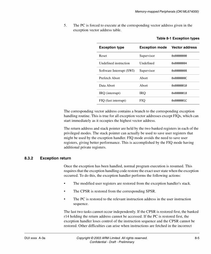
Memory-mapped Peripherals (OKI ML674000)
5. The PC is forced to execute at the corresponding vector address given in the exception vector address table.
The corresponding vector address contains a branch to the corresponding exception handling routine. This is true for all exception vector addresses except FIQs, which can start immediately as it occupies the highest vector address.
The return address and stack pointer are held by the two banked registers in each of the privileged modes. The stack pointer can actually be used to save user registers that might be used by the exception handler. FIQ mode avoids the need to save user registers, giving better performance. This is accomplished by the FIQ mode having additional private registers.
8.3.2 Exception return
Once the exception has been handled, normal program execution is resumed. This requires that the exception handling code restore the exact user state when the exception occurred. To do this, the exception handler performs the following actions:
• The modified user registers are restored from the exception handler's stack.
• The CPSR is restored from the corresponding SPSR.
• The PC is restored to the relevant instruction address in the user instruction sequence.
The last two tasks cannot occur independently. If the CPSR is restored first, the banked r14 holding the return address cannot be accessed. If the PC is restored first, the exception handler loses control of the instruction sequence and the CPSR cannot be restored. Other difficulties can arise when instructions are fetched in the incorrect
Table 8-1 Exception types
Exception type Exception mode Vector address
Reset Supervisor 0x00000000
Undefined instruction Undefined 0x00000004
Software Interrupt (SWI) Supervisor 0x00000008
Prefetch Abort Abort 0x0000000C
Data Abort Abort 0x00000010
IRQ (interrupt) IRQ 0x00000018
FIQ (fast interrupt) FIQ 0x0000001C
DUI xxxx A-3a Copyright © 2003 ARM Limited. All rights reserved. 8-5Confidential - Draft - Preliminary
Memory-mapped Peripherals (OKI ML674000)
operating mode. ARM provides two mechanisms which forces the last two steps to be executed in a single instruction. One is used when the banked link register (r14) holds the return address and the other is used when a stack holds the return address.
Use the following instructions when the return address in held in r14:
MOVS pc, r14
To return from a SWI or undefined instruction trap.
SUBS pc, r14, #4
To return from an IRQ, FIQ or prefetch abort:
SUBS pc, r14, #8
To return from a data abort to retry the data access:
You can see that the return instructions can modify the return address when necessary. An IRQ or FIQ exception handler must return to the instruction that was fetched but not executed. This is because the PC already progressed beyond the point where the exception was taken. A Prefetch Abort handler also returns to the instruction that caused the memory fault. A Data Abort handlers returns to retry the data transfer instruction that caused the exception.
Using the S suffix on the return instruction causes the return operation to copy the SPSR back to the CPSR.
If the exception handler copied the return address onto a stack, you can use one multiple register transfer instruction to restore user registers and the return address:
LDMFD r13!, {r0-r3, pc}^
The ^ indicates a special form of the instruction. The CPSR is restored at the same time that the PC is loaded from memory. Remember that the registers are loaded in increasing order.
8-6 Copyright © 2003 ARM Limited. All rights reserved. DUI xxxx A-3aConfidential - Draft - Preliminary
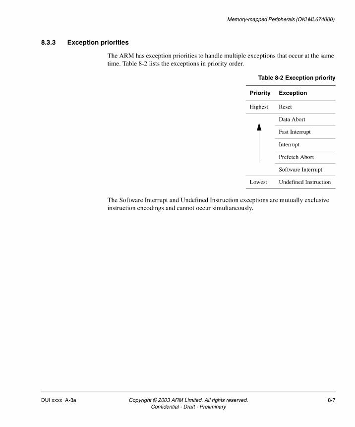
Memory-mapped Peripherals (OKI ML674000)
8.3.3 Exception priorities
The ARM has exception priorities to handle multiple exceptions that occur at the same time. Table 8-2 lists the exceptions in priority order.
The Software Interrupt and Undefined Instruction exceptions are mutually exclusive instruction encodings and cannot occur simultaneously.
Table 8-2 Exception priority
Priority Exception
Highest Reset
Data Abort
Fast Interrupt
Interrupt
Prefetch Abort
Software Interrupt
Lowest Undefined Instruction
DUI xxxx A-3a Copyright © 2003 ARM Limited. All rights reserved. 8-7Confidential - Draft - Preliminary
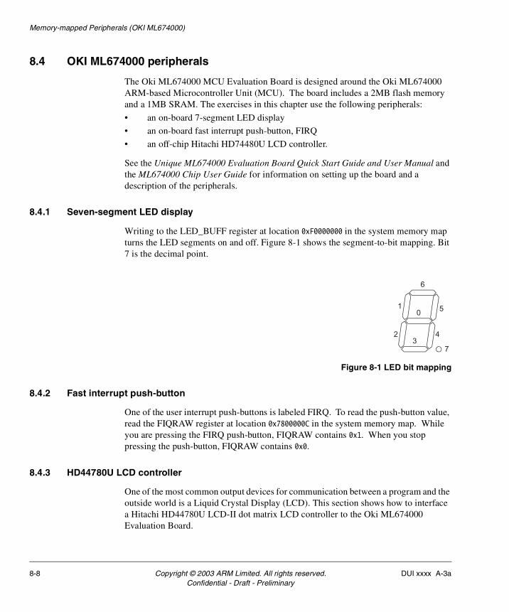
Memory-mapped Peripherals (OKI ML674000)
8.4 OKI ML674000 peripherals
The Oki ML674000 MCU Evaluation Board is designed around the Oki ML674000 ARM-based Microcontroller Unit (MCU). The board includes a 2MB flash memory and a 1MB SRAM. The exercises in this chapter use the following peripherals:
• an on-board 7-segment LED display
• an on-board fast interrupt push-button, FIRQ
• an off-chip Hitachi HD74480U LCD controller.
See the Unique ML674000 Evaluation Board Quick Start Guide and User Manual and the ML674000 Chip User Guide for information on setting up the board and a description of the peripherals.
8.4.1 Seven-segment LED display
Writing to the LED_BUFF register at location 0xF0000000 in the system memory map turns the LED segments on and off. Figure 8-1 shows the segment-to-bit mapping. Bit 7 is the decimal point.
Figure 8-1 LED bit mapping
8.4.2 Fast interrupt push-button
One of the user interrupt push-buttons is labeled FIRQ. To read the push-button value, read the FIQRAW register at location 0x7800000C in the system memory map. While you are pressing the FIRQ push-button, FIQRAW contains 0x1. When you stop pressing the push-button, FIQRAW contains 0x0.
8.4.3 HD44780U LCD controller
One of the most common output devices for communication between a program and the outside world is a Liquid Crystal Display (LCD). This section shows how to interface a Hitachi HD44780U LCD-II dot matrix LCD controller to the Oki ML674000 Evaluation Board.
6
5
43
2
10
7
8-8 Copyright © 2003 ARM Limited. All rights reserved. DUI xxxx A-3aConfidential - Draft - Preliminary
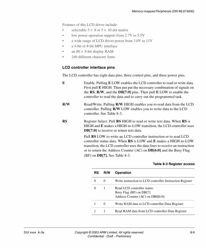
Memory-mapped Peripherals (OKI ML674000)
Features of this LCD driver include:
• selectable 5 × 8 or 5 × 10 dot matrix
• low power operation support from 2.7V to 5.5V
• a wide range of LCD driver power from 3.0V to 11V
• a 4-bit or 8-bit MPU interface
• an 80 × 8-bit display RAM
• 240 different character fonts.
LCD controller interface pins
The LCD controller has eight data pins, three control pins, and three power pins.
E Enable. Pulling E LOW enables the LCD controller to read or write data. First pull E HIGH. Then put put the necessary combination of signals on the RS, R/W, and the DB[7:0] pins. Then pull E LOW to enable the controller to read the data and to carry out the programmed task.
R/W Read/Write. Pulling R/W HIGH enables you to read data from the LCD controller. Pulling R/W LOW enables you to write data to the LCD controller. See Table 8-3.
RS Register Select. Pull RS HIGH to read or write text data. When RS is HIGH and E makes a HIGH-to-LOW transition, the LCD controller uses DB[7:0] to receive or return text data.
Pull RS LOW to write an LCD controller instruction or to read LCD controller status data. When RS is LOW and E makes a HIGH-to-LOW transition, the LCD controller uses the data lines to receive an instruction or to return the Address Counter (AC) on DB[6:0] and the Busy Flag (BF) on DB[7]. See Table 8-3.
Table 8-3 Register access
RS R/W Operation
0 0 Write instruction to LCD controller Instruction Register
0 1 Read LCD controller status:Busy Flag (BF) on DB[7]Address Counter (AC) on DB0[6:0]
1 0 Write RAM data to LCD controller Data Register
1 1 Read RAM data from LCD controller Data Register
DUI xxxx A-3a Copyright © 2003 ARM Limited. All rights reserved. 8-9Confidential - Draft - Preliminary
Memory-mapped Peripherals (OKI ML674000)
DB[7:0] The Data Bus.
VDD LCD controller power. Connect VDD to a power supply between 3.0V and 11V. You can use a standard 3V universal AC/DC adapter.
Note Connect the power pins carefully. If the LCD controller feels hot, or if the
display shows characters in the wrong location, check the power connections.
VSS LCD controller ground. Connect VSS to ground.
VO LCD contrast control. Connect to an adjustable power supply.
Connections
The Oki ML674000 Evaluation Board has a 26-pin header labeled J5. The pins are labeled 1-26. The ML674000 chip contains two 16-bit general-purpose ports, PIOA and PIOB.
Note
The 26-pin J5 header does not directly correspond to the GPIOA and GPIOB ports of the ML674000 MCU.
8-10 Copyright © 2003 ARM Limited. All rights reserved. DUI xxxx A-3aConfidential - Draft - Preliminary
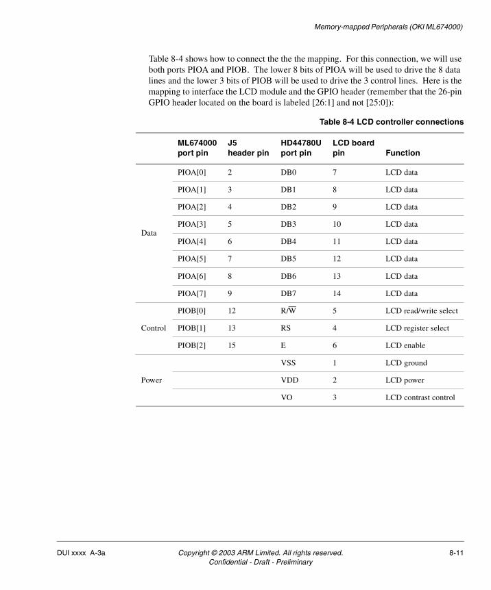
Memory-mapped Peripherals (OKI ML674000)
Table 8-4 shows how to connect the the the mapping. For this connection, we will use both ports PIOA and PIOB. The lower 8 bits of PIOA will be used to drive the 8 data lines and the lower 3 bits of PIOB will be used to drive the 3 control lines. Here is the mapping to interface the LCD module and the GPIO header (remember that the 26-pin GPIO header located on the board is labeled [26:1] and not [25:0]):
Table 8-4 LCD controller connections
ML674000port pin
J5header pin
HD44780Uport pin
LCD boardpin Function
Data
PIOA[0] 2 DB0 7 LCD data
PIOA[1] 3 DB1 8 LCD data
PIOA[2] 4 DB2 9 LCD data
PIOA[3] 5 DB3 10 LCD data
PIOA[4] 6 DB4 11 LCD data
PIOA[5] 7 DB5 12 LCD data
PIOA[6] 8 DB6 13 LCD data
PIOA[7] 9 DB7 14 LCD data
Control
PIOB[0] 12 R/W 5 LCD read/write select
PIOB[1] 13 RS 4 LCD register select
PIOB[2] 15 E 6 LCD enable
Power
VSS 1 LCD ground
VDD 2 LCD power
VO 3 LCD contrast control
DUI xxxx A-3a Copyright © 2003 ARM Limited. All rights reserved. 8-11Confidential - Draft - Preliminary
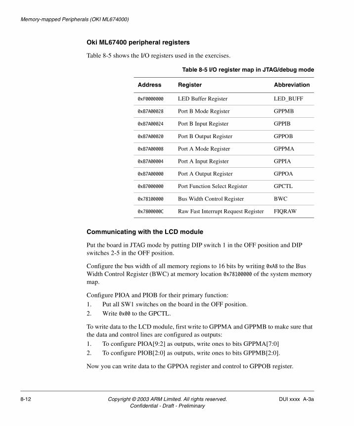
Memory-mapped Peripherals (OKI ML674000)
Oki ML67400 peripheral registers
Table 8-5 shows the I/O registers used in the exercises.
Communicating with the LCD module
Put the board in JTAG mode by putting DIP switch 1 in the OFF position and DIP switches 2-5 in the OFF position.
Configure the bus width of all memory regions to 16 bits by writing 0xA8 to the Bus Width Control Register (BWC) at memory location 0x78100000 of the system memory map.
Configure PIOA and PIOB for their primary function:
1. Put all SW1 switches on the board in the OFF position.
2. Write 0x00 to the GPCTL.
To write data to the LCD module, first write to GPPMA and GPPMB to make sure that the data and control lines are configured as outputs:
1. To configure PIOA[9:2] as outputs, write ones to bits GPPMA[7:0]
2. To configure PIOB[2:0] as outputs, write ones to bits GPPMB[2:0].
Now you can write data to the GPPOA register and control to GPPOB register.
Table 8-5 I/O register map in JTAG/debug mode
Address Register Abbreviation
0xF0000000 LED Buffer Register LED_BUFF
0xB7A00028 Port B Mode Register GPPMB
0xB7A00024 Port B Input Register GPPIB
0xB7A00020 Port B Output Register GPPOB
0xB7A00008 Port A Mode Register GPPMA
0xB7A00004 Port A Input Register GPPIA
0xB7A00000 Port A Output Register GPPOA
0xB7000000 Port Function Select Register GPCTL
0x78100000 Bus Width Control Register BWC
0x7800000C Raw Fast Interrupt Request Register FIQRAW
8-12 Copyright © 2003 ARM Limited. All rights reserved. DUI xxxx A-3aConfidential - Draft - Preliminary
Memory-mapped Peripherals (OKI ML674000)
To read from the LCD controller, use the same procedures, but write zeros to PIOA[9:2] and PIOB[2:0], and then read the GPPIA and GPPIB registers.
Busy flag (BF)
When BF = 1, the LCD controller is in the internal operation mode, and the next instruction is not accepted. When RS = 0 and R/W = 1, you can read BF on DB7. Before writing the next instruction, make sure that BF = 0. An easy way to make sure that BF = 0 is to introduce long delays between each instruction. Another, more difficult technique is to write a subroutine that checks the status of the busy flag after each instruction.
Address counter (AC)
The AC assigns addresses to both DDRAM and CGRAM. When an address of an instruction is written into the Instruction Register, the address information is sent from the IR to the AC. Selection of either DDRAM or CGRAM is also determined concurrently by the instruction. After writing to or reading from DDRAM or CGRAM, the AC is automatically incremented or decremented by 1. The AC contents are then output to DB0-DB6 when RS = 0 and R/W = 1.
Instructions
Table 8-6 on page 8-14 lists the LCD controller instructions.
DUI xxxx A-3a Copyright © 2003 ARM Limited. All rights reserved. 8-13Confidential - Draft - Preliminary
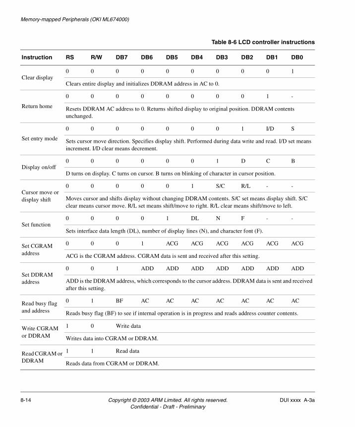
Memory-mapped Peripherals (OKI ML674000)
Table 8-6 LCD controller instructions
Instruction RS R/W DB7 DB6 DB5 DB4 DB3 DB2 DB1 DB0
Clear display0 0 0 0 0 0 0 0 0 1
Clears entire display and initializes DDRAM address in AC to 0.
Return home
0 0 0 0 0 0 0 0 1 -
Resets DDRAM AC address to 0. Returns shifted display to original position. DDRAM contents unchanged.
Set entry mode
0 0 0 0 0 0 0 1 I/D S
Sets cursor move direction. Specifies display shift. Performed during data write and read. I/D set means increment. I/D clear means decrement.
Display on/off0 0 0 0 0 0 1 D C B
D turns on display. C turns on cursor. B turns on blinking of character in cursor position.
Cursor move or display shift
0 0 0 0 0 1 S/C R/L - -
Moves cursor and shifts display without changing DDRAM contents. S/C set means display shift. S/C clear means cursor move. R/L set means shift/move to right. R/L clear means shift/move to left.
Set function0 0 0 0 1 DL N F - -
Sets interface data length (DL), number of display lines (N), and character font (F).
Set CGRAM address
0 0 0 1 ACG ACG ACG ACG ACG ACG
ACG is the CGRAM address. CGRAM data is sent and received after this setting.
Set DDRAM address
0 0 1 ADD ADD ADD ADD ADD ADD ADD
ADD is the DDRAM address, which corresponds to the cursor address. DDRAM data is sent and received after this setting.
Read busy flag and address
0 1 BF AC AC AC AC AC AC AC
Reads busy flag (BF) to see if internal operation is in progress and reads address counter contents.
Write CGRAM or DDRAM
1 0 Write data
Writes data into CGRAM or DDRAM.
Read CGRAM or DDRAM
1 1 Read data
Reads data from CGRAM or DDRAM.
8-14 Copyright © 2003 ARM Limited. All rights reserved. DUI xxxx A-3aConfidential - Draft - Preliminary
Memory-mapped Peripherals (OKI ML674000)
8.5 Exercises
Display your expertise with these exercises:
• Burning the flash memory
• Displaying the contents of a memory location
• Displaying the contents of an array of memory locations
• Counting up to n
• Some light flickering
• Counting user interrupts on page 8-16
• Writing an LCD driver on page 8-16.
8.5.1 Burning the flash memory
Follow the directions given in section 4.0 of the Unique ML674000 Board User Guide to run the test program through the bootloader. In this exercise, you first load the program into the on-board flash memory and then reset the board.
8.5.2 Displaying the contents of a memory location
Write ARM assembly to inspect memory location 0x4000. If the location contains a decimal number in the range 0-15, display the contents in hex on the seven-segment LED display. For example, if 0x4000 contains 14, show the character E on the seven-segment display.
8.5.3 Displaying the contents of an array of memory locations
Write ARM assembly to inspect memory locations 0x3000-0x300A. For each location that contains a decimal number in the range 0-15, display the contents in hex on the seven-segment LED display. Use delays to make the display easy to read.
8.5.4 Counting up to n
Write ARM assembly to display digits 0 to n – 1 on the seven- segment LED display. Start with the n value in r0.
8.5.5 Some light flickering
Write ARM assembly to perform delayed blinking of the seven-segment display in the sequence shown in Figure 8-2 on page 8-16.
DUI xxxx A-3a Copyright © 2003 ARM Limited. All rights reserved. 8-15Confidential - Draft - Preliminary
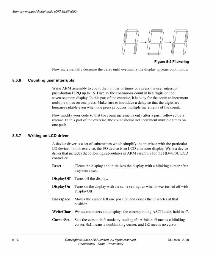
Memory-mapped Peripherals (OKI ML674000)
Figure 8-2 Flickering
Now incrementally decrease the delay until eventually the display appears continuous.
8.5.6 Counting user interrupts
Write ARM assembly to count the number of times you press the user interrupt push-button FIRQ up to 15. Display the continuous count in hex digits on the seven-segment display. In this part of the exercise, it is okay for the count to increment multiple times on one press. Make sure to introduce a delay so that the digits are human-readable even when one press produces multiple increments of the count.
Now modify your code so that the count increments only after a push followed by a release. In this part of the exercise, the count should not increment multiple times on one push.
8.5.7 Writing an LCD driver
A device driver is a set of subroutines which simplify the interface with the particular I/O device. In this exercise, the I/O device is an LCD character display. Write a device driver that includes the following subroutines in ARM assembly for the HD4470U LCD controller:
Reset Clears the display and initializes the display with a blinking cursor after a system reset.
DisplayOff Turns off the display.
DisplayOn Turns on the display with the same settings as when it was turned off with DisplayOff.
Backspace Moves the cursor left one position and erases the character at that position.
WriteChar Writes characters and displays the corresponding ASCII code, held in r7.
CursorSet Sets the cursor shift mode by reading r5. A 0x0 in r5 means a blinking cursor, 0x1 means a nonblinking cursor, and 0x2 means no cursor.
8-16 Copyright © 2003 ARM Limited. All rights reserved. DUI xxxx A-3aConfidential - Draft - Preliminary
Memory-mapped Peripherals (OKI ML674000)
CursorPos Sets the cursor position to row r11 and column r12.
Scroll Scrolls the current displayed characters to wrap around the display five complete times. The characters end up in the exact coordinates as they were before the scroll. Disable the cursor for a clean scroll.
DUI xxxx A-3a Copyright © 2003 ARM Limited. All rights reserved. 8-17Confidential - Draft - Preliminary
Memory-mapped Peripherals (OKI ML674000)
8-18 Copyright © 2003 ARM Limited. All rights reserved. DUI xxxx A-3aConfidential - Draft - Preliminary
Chapter 9 Floating-point Computation
This chapter introduces floating-point arithmetic. It rite subroutines to determine the characteristics of a floating-point number, then add, subtract and multiply floating-point numbers. It contains the following sections:
• Introduction on page 9-2
• Floating-point data types - single-precision and double-precision on page 9-3
• Basic floating-point computations on page 9-5
• Rounding modes on page 9-6
• Algorithm for basic floating-point computation on page 9-7
• Floating-point multiplication on page 9-8
• Exercises on page 9-9.
DUI xxxx A-3a Copyright © 2003 ARM Limited. All rights reserved. 9-1Confidential - Draft - Preliminary
Floating-point Computation
9.1 Introduction
Integer processing involves the manipulation of numbers in the range {0 . . . 2n – 1} for unsigned integers or {–2n – 1 . . . 2n – 1 – 1} for signed integers. The range of 32-bit unsigned integers is 0-4 294 967 291, or roughly 4.3 × 10⁹. In many scientific computations the range required is larger than 109, and if fractional data is included, the actual range may be much larger than integer operations can support. Computations involving thermodynamic processes, weather simulations, and nuclear physics use extremely small and extremely large numbers. In this lesson, the basic principles of floating-point computation are introduced, including the formats of the single-precision and double-precision data types, and the algorithm for addition, subtraction, and multiplication of floating-point operands.
9-2 Copyright © 2003 ARM Limited. All rights reserved. DUI xxxx A-3aConfidential - Draft - Preliminary
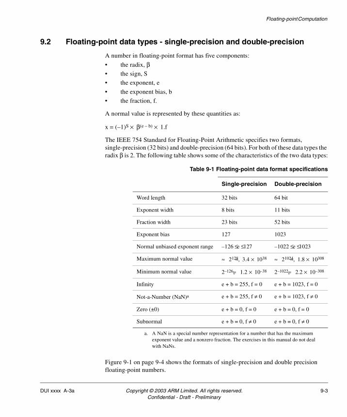
Floating-point Computation
9.2 Floating-point data types - single-precision and double-precision
A number in floating-point format has five components:
• the radix, β• the sign, S
• the exponent, e
• the exponent bias, b
• the fraction, f.
A normal value is represented by these quantities as:
x = (–1)S × β(e – b) × 1.f
The IEEE 754 Standard for Floating-Point Arithmetic specifies two formats, single-precision (32 bits) and double-precision (64 bits). For both of these data types the radix β is 2. The following table shows some of the characteristics of the two data types:
Figure 9-1 on page 9-4 shows the formats of single-precision and double precision floating-point numbers.
Table 9-1 Floating-point data format specifications
Single-precision Double-precision
Word length 32 bits 64 bit
Exponent width 8 bits 11 bits
Fraction width 23 bits 52 bits
Exponent bias 127 1023
Normal unbiased exponent range –126 ≤e ≤127 –1022 ≤e ≤1023
Maximum normal value ≈ 2128, ≈ 3.4 × 1038 ≈ 21024, ≈ 1.8 × 10308
Minimum normal value 2–126, ≈ 1.2 × 10–38 2–1022, ≈ 2.2 × 10–308
Infinity e + b = 255, f = 0 e + b = 1023, f = 0
Not-a-Number (NaN)a
a. A NaN is a special number representation for a number that has the maximum exponent value and a nonzero fraction. The exercises in this manual do not deal with NaNs.
e + b = 255, f ≠ 0 e + b = 1023, f ≠ 0
Zero (±0) e + b = 0, f = 0 e + b = 0, f = 0
Subnormal e + b = 0, f ≠ 0 e + b = 0, f ≠ 0
DUI xxxx A-3a Copyright © 2003 ARM Limited. All rights reserved. 9-3Confidential - Draft - Preliminary
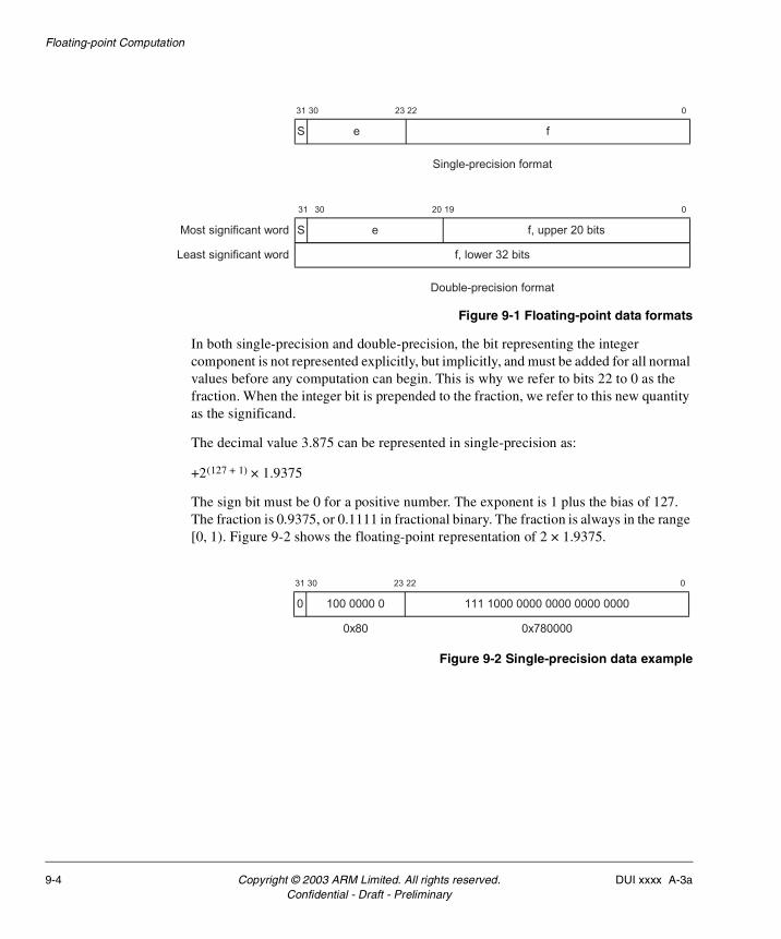
Floating-point Computation
Figure 9-1 Floating-point data formats
In both single-precision and double-precision, the bit representing the integer component is not represented explicitly, but implicitly, and must be added for all normal values before any computation can begin. This is why we refer to bits 22 to 0 as the fraction. When the integer bit is prepended to the fraction, we refer to this new quantity as the significand.
The decimal value 3.875 can be represented in single-precision as:
+2(127 + 1) × 1.9375
The sign bit must be 0 for a positive number. The exponent is 1 plus the bias of 127. The fraction is 0.9375, or 0.1111 in fractional binary. The fraction is always in the range [0, 1). Figure 9-2 shows the floating-point representation of 2 × 1.9375.
Figure 9-2 Single-precision data example
Double-precision format
Most significant word
Least significant word
31 30 20 19 0
S e f, upper 20 bits
f, lower 32 bits
Single-precision format
31 30 23 22 0
S e f
0x80
31 30 23 22 0
0 100 0000 0 111 1000 0000 0000 0000 0000
0x780000
9-4 Copyright © 2003 ARM Limited. All rights reserved. DUI xxxx A-3aConfidential - Draft - Preliminary
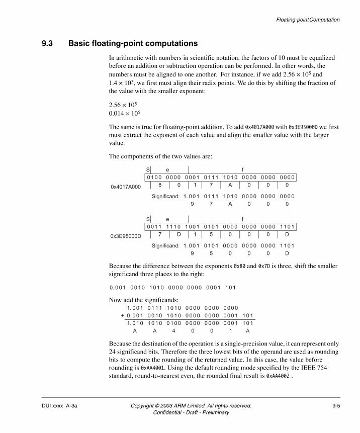
Floating-point Computation
9.3 Basic floating-point computations
In arithmetic with numbers in scientific notation, the factors of 10 must be equalized before an addition or subtraction operation can be performed. In other words, the numbers must be aligned to one another. For instance, if we add 2.56 × 10⁵ and 1.4 × 10³, we first must align their radix points. We do this by shifting the fraction of the value with the smaller exponent:
2.56 × 10⁵ 0.014 × 10⁵
The same is true for floating-point addition. To add 0x4017A000 with 0x3E95000D we first must extract the exponent of each value and align the smaller value with the larger value.
The components of the two values are:
Because the difference between the exponents 0x80 and 0x7D is three, shift the smaller significand three places to the right:
Now add the significands:
Because the destination of the operation is a single-precision value, it can represent only 24 significand bits. Therefore the three lowest bits of the operand are used as rounding bits to compute the rounding of the returned value. In this case, the value before rounding is 0xAA4001. Using the default rounding mode specified by the IEEE 754 standard, round-to-nearest even, the rounded final result is 0xAA4002 .
S e f
1 5 0 0 0 D7 D
0 0 0 0 0 0 0 0 1 1 0 1
0 0 0 0 0 0 0 01. 0 0 1Significand:
9 5 0 0 0 D
0 0 1 1 1 1 1 0 1 0 0 1 0 1 0 1 0 0 0 0
0 1 0 1 0 0 0 0 1 1 0 1
S e f
1 7 A 0 0 08 0
0 1 0 0 0 0 0 0 0 0 0 1 0 1 1 1 1 0 1 0 0 0 0 0 0 0 0 0 0 0 0 0
0 1 1 1 1 0 1 0 0 0 0 0 0 0 0 0 0 0 0 0Significand:
9 7 A 0 0 0
1. 0 0 1
0x4017A000
0x3E95000D
0 0 0 0 0 0 0 0 1 0 10 0 0 11 0 1 00. 0 0 1 0 0 1 0
0 0 0 0 0 0 0 0 1 0 10 0 0 11 0 1 00. 0 0 1
0 1 1 1 1 0 1 0 0 0 0 0 0 0 0 0 0 0 0 01. 0 0 1
0 0 1 0
1. 0 1 0 1 0 1 0 0 1 0 0 0 0 0 0 0 0 0 0 0 0 0 1 1 0 1
A A 4 0 0 1 A
+
DUI xxxx A-3a Copyright © 2003 ARM Limited. All rights reserved. 9-5Confidential - Draft - Preliminary
Floating-point Computation
9.4 Rounding modes
We define the bits shifted beyond the LSB of the larger operand as the round (R-bit) and sticky bit (S-bit). The round bit is the most significant of the rounding bits, while the sticky bit is the OR of the remaining bits.
Once these bits are defined, the four rounding modes mandated in the IEEE 754 standard can be defined.
Ulp stands for the unit in the last place, and is a measure of the deviation from the correct result. In the example in Basic floating-point computations on page 9-5, the ulp error is the deviation of 0xAA4002 from 0xAA4001A. Round-to-nearest-even mode guarantees a maximum error of no more than 0.5 ulps, and an average error of 0 ulps.
Table 9-2 Rounding modes
Rounding mode Rounding algorithm Average error Maximum error
Round-to-nearest-even if (LSB == 0)if (R-bit AND S-bit)
round upelse
if (R-bit)round up
0 0.5 ulp
Round-to-positive-infinity if (sign is positive)if (R-bit OR S-bit)
round up
0.5 ulp <1.0 ulp
Round-to-negative infinity if (sign is negative)if (R-bit OR S-bit)
round up
0.5 ulp <1.0 ulp
Round-to-zero Never round up 0.5 ulp <1.0 ulp
9-6 Copyright © 2003 ARM Limited. All rights reserved. DUI xxxx A-3aConfidential - Draft - Preliminary
Floating-point Computation
9.5 Algorithm for basic floating-point computation
The following is a sample algorithm for any two-operand floating-point operation:
1. Test the operands.
2. Remove the bias in the exponents.
3. If a special condition exists, deliver the result from a table of special conditions.
4. If no special condition exists, perform the operation to an equivalent infinite precision.
5. Round the result and test for exceptional conditions.
6. Restore the exponent bias and deliver the rounded result with condition and exception status bits.
An integral part of any floating-point emulation routine is classification, or separating the components of the operand into sign, unbiased exponent, and significand.
Floating-point multiplication on page 9-8 shows how the floating-point algorithm applies to multiplication.
DUI xxxx A-3a Copyright © 2003 ARM Limited. All rights reserved. 9-7Confidential - Draft - Preliminary
Floating-point Computation
9.6 Floating-point multiplication
An algorithm that performs a multiplication of two floating-point values must first identify and handle special operands. Some of the cases in which a special condition result could be read from a table and returned as the result are:
• a NaN and any other operand value results in a NaN
• an infinity and any other operand value except a NaN or a zero results in a signed infinity
• an infinity and a zero results in a NaN and sets the Invalid Exception Status bit
• a zero and any zero or normal value results in a signed zero.
When the input operands are characterized and the cases above are checked, the result is either known or a multiplication is required.
The algorithm for performing floating-point multiplication is:
1. Compute the sign as the XOR of the two sign bits.
2. Add the exponents with any bias removed.
3. Convert the fraction to a significand by making the integer bit explicit. For a normal value, the integer bit is a 1. For a subnormal value, the integer bit is a 0.
4. Multiply the two significands using integer multiplication but keeping the position of the decimal point known. Note that the result is either in the range [1.0, 2.0) or [2.0, 4.0).
5. If the result significand is in the [2.0, 4.0) range, normalize it and round it. Rounding can cause the result to overflow to 2.0, requiring another normalization step.
6. Modify the exponent to compensate for normalization.
7. Check the modified exponent for overflow or underflow.
8. If the result is in the normal or denormal range, return the result. If it is in the denormal range, set the Undeflow Exception Status bit, denormalize the result, and force the denormal exponent.
9. If the result is in the overflow or underflow range, return the default result and set the corresponding exception status bit.
9-8 Copyright © 2003 ARM Limited. All rights reserved. DUI xxxx A-3aConfidential - Draft - Preliminary
Floating-point Computation
9.7 Exercises
Turn on your mind and float downstream.
9.7.1 Convert single-precision floating-point to decimal
Convert the following single-precision floating-point numbers to decimal notation.
1. 0x42420000
2. 0xBDC00000
3. 0x7F240146
4. 0x02947FCD
9.7.2 Convert double-precision floating point to decimal
Convert the following double-precision floating-point numbers to decimal numbers.
1. 0x30840000_00000000
2. 0xD2168200_00000000
9.7.3 Convert decimal to single-precision and double-precision floating point
Convert the following decimal numbers to single-precision and double-precision floating-point numbers.
1. 58.4
2. –12.8 × 10⁻²⁴
9.7.4 Floating-point addition
1. Write a program in a high-level language such as C, C++, or Java to sum the following table of floating-point values in the order they are given. Perform the computation and write the results in both single-precision and double-precision.
350.75 400 345 971 0.7235 25 000.007.56 × 108 55.231 805 267.9
2. Run the program again, but sort the input data from smallest to largest before performing the summation.
DUI xxxx A-3a Copyright © 2003 ARM Limited. All rights reserved. 9-9Confidential - Draft - Preliminary
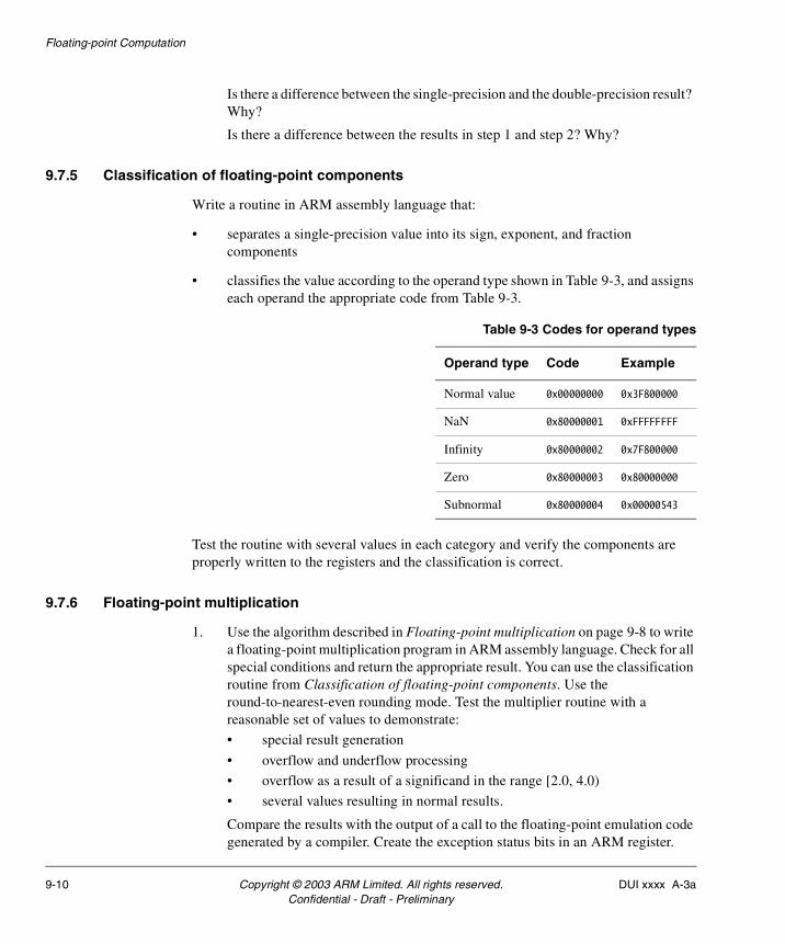
Floating-point Computation
Is there a difference between the single-precision and the double-precision result? Why?
Is there a difference between the results in step 1 and step 2? Why?
9.7.5 Classification of floating-point components
Write a routine in ARM assembly language that:
• separates a single-precision value into its sign, exponent, and fraction components
• classifies the value according to the operand type shown in Table 9-3, and assigns each operand the appropriate code from Table 9-3.
Test the routine with several values in each category and verify the components are properly written to the registers and the classification is correct.
9.7.6 Floating-point multiplication
1. Use the algorithm described in Floating-point multiplication on page 9-8 to write a floating-point multiplication program in ARM assembly language. Check for all special conditions and return the appropriate result. You can use the classification routine from Classification of floating-point components. Use the round-to-nearest-even rounding mode. Test the multiplier routine with a reasonable set of values to demonstrate:
• special result generation
• overflow and underflow processing
• overflow as a result of a significand in the range [2.0, 4.0)
• several values resulting in normal results.
Compare the results with the output of a call to the floating-point emulation code generated by a compiler. Create the exception status bits in an ARM register.
Table 9-3 Codes for operand types
Operand type Code Example
Normal value 0x00000000 0x3F800000
NaN 0x80000001 0xFFFFFFFF
Infinity 0x80000002 0x7F800000
Zero 0x80000003 0x80000000
Subnormal 0x80000004 0x00000543
9-10 Copyright © 2003 ARM Limited. All rights reserved. DUI xxxx A-3aConfidential - Draft - Preliminary
Floating-point Computation
2. Code your routine to respond to the rounding mode in another ARM register. Use the following codes:
• 00 = round-to-nearest-even
• 01 = round-to-positive-infinity
• 10 = round-to-negative-infinity
• 11 = round-to-zero.
Note to instructor: the use of the multiply algorithm here is arbitrary and can be replaced with floating-point addition or division, integer conversion, or conversion between single-precision and double-precision.
DUI xxxx A-3a Copyright © 2003 ARM Limited. All rights reserved. 9-11Confidential - Draft - Preliminary

Floating-point Computation
9-12 Copyright © 2003 ARM Limited. All rights reserved. DUI xxxx A-3aConfidential - Draft - Preliminary
Chapter 10 Semihosting
This chapter introduces semihosting SWI operations, semihosting implementation, and adding SWI handlers. It contains the following sections:
• Introduction on page 10-2
• SWI numbers on page 10-4
• Semihosting implementation on page 10-7
• Exercises on page 10-8.
DUI xxxx A-3a Copyright © 2003 ARM Limited. All rights reserved. 10-1Confidential - Draft - Preliminary
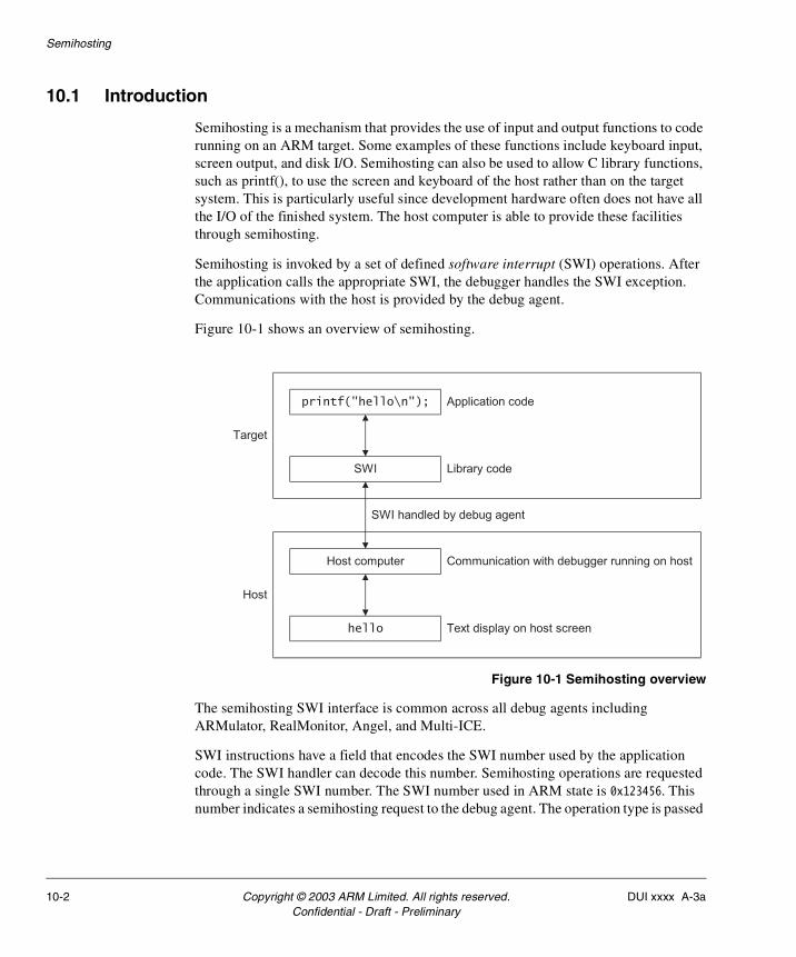
Semihosting
10.1 Introduction
Semihosting is a mechanism that provides the use of input and output functions to code running on an ARM target. Some examples of these functions include keyboard input, screen output, and disk I/O. Semihosting can also be used to allow C library functions, such as printf(), to use the screen and keyboard of the host rather than on the target system. This is particularly useful since development hardware often does not have all the I/O of the finished system. The host computer is able to provide these facilities through semihosting.
Semihosting is invoked by a set of defined software interrupt (SWI) operations. After the application calls the appropriate SWI, the debugger handles the SWI exception. Communications with the host is provided by the debug agent.
Figure 10-1 shows an overview of semihosting.
Figure 10-1 Semihosting overview
The semihosting SWI interface is common across all debug agents including ARMulator, RealMonitor, Angel, and Multi-ICE.
SWI instructions have a field that encodes the SWI number used by the application code. The SWI handler can decode this number. Semihosting operations are requested through a single SWI number. The SWI number used in ARM state is 0x123456. This number indicates a semihosting request to the debug agent. The operation type is passed
SWI handled by debug agent
Host computer
hello
Communication with debugger running on host
Text display on host screen
Host
Application codeprintf("hello\n");
SWI Library code
Target
10-2 Copyright © 2003 ARM Limited. All rights reserved. DUI xxxx A-3aConfidential - Draft - Preliminary
Semihosting
in r0 in order to distinguish between operations. All other parameters are passed in a block pointed to by r1. The result is returned in r0. It can be an actual return value or a pointer to a block of data. Assume that r0 will be corrupted, even if no result is returned.
The semihosting operation numbers used by ARM range from 0x00 to 0x31. All other numbers are either reserved for future use by ARM, reserved for user applications, or undefined and not used. If you are calling SWIs from assembly code, you can define the operation names with the EQU directive.
Changing the semihosting SWI number 0x123456 is not recommended because you must then change all the code in the system, including library code, to use the new SWI number and reconfigure the debugger to utilize the new number.
DUI xxxx A-3a Copyright © 2003 ARM Limited. All rights reserved. 10-3Confidential - Draft - Preliminary
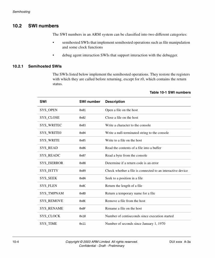
Semihosting
10.2 SWI numbers
The SWI numbers in an ARM system can be classified into two different categories:
• semihosted SWIs that implement semihosted operations such as file manipulation and some clock functions
• debug agent interaction SWIs that support interaction with the debugger.
10.2.1 Semihosted SWIs
The SWIs listed below implement the semihosted operations. They restore the registers with which they are called before returning, except for r0, which contains the return status.
Table 10-1 SWI numbers
SWI SWI number Description
SYS_OPEN 0x01 Open a file on the host
SYS_CLOSE 0x02 Close a file on the host
SYS_WRITEC 0x03 Write a character to the console
SYS_WRITE0 0x04 Write a null-terminated string to the console
SYS_WRITE 0x05 Write to a file on the host
SYS_READ 0x06 Read the contents of a file into a buffer
SYS_READC 0x07 Read a byte from the console
SYS_ISERROR 0x08 Determine if a return code is an error
SYS_ISTTY 0x09 Check whether a file is connected to an interactive device
SYS_SEEK 0x0A Seek to a position in a file
SYS_FLEN 0x0C Return the length of a file
SYS_TMPNAM 0x0D Return a temporary name for a file
SYS_REMOVE 0x0E Remove a file from the host
SYS_RENAME 0x0F Rename a file on the host
SYS_CLOCK 0x10 Number of centiseconds since execution started
SYS_TIME 0x11 Number of seconds since January 1, 1970
10-4 Copyright © 2003 ARM Limited. All rights reserved. DUI xxxx A-3aConfidential - Draft - Preliminary
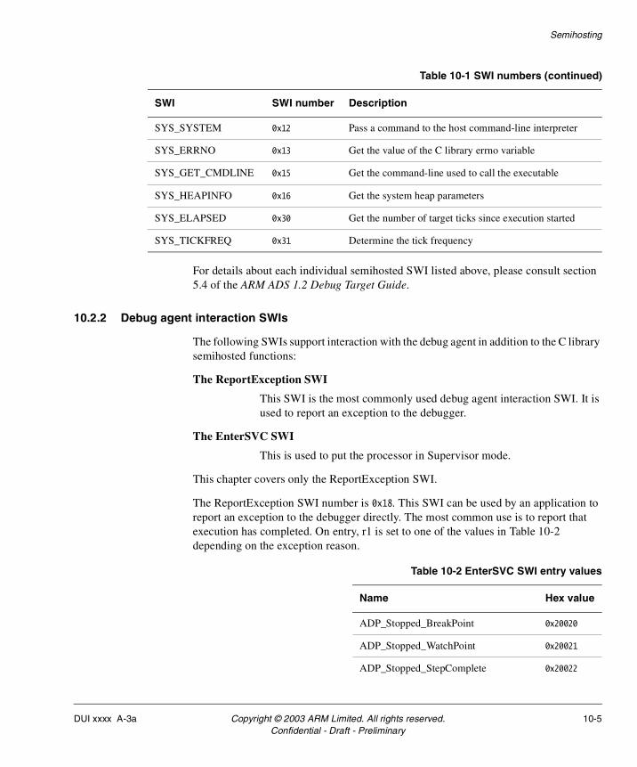
Semihosting
For details about each individual semihosted SWI listed above, please consult section 5.4 of the ARM ADS 1.2 Debug Target Guide.
10.2.2 Debug agent interaction SWIs
The following SWIs support interaction with the debug agent in addition to the C library semihosted functions:
The ReportException SWI
This SWI is the most commonly used debug agent interaction SWI. It is used to report an exception to the debugger.
The EnterSVC SWI
This is used to put the processor in Supervisor mode.
This chapter covers only the ReportException SWI.
The ReportException SWI number is 0x18. This SWI can be used by an application to report an exception to the debugger directly. The most common use is to report that execution has completed. On entry, r1 is set to one of the values in Table 10-2 depending on the exception reason.
SYS_SYSTEM 0x12 Pass a command to the host command-line interpreter
SYS_ERRNO 0x13 Get the value of the C library errno variable
SYS_GET_CMDLINE 0x15 Get the command-line used to call the executable
SYS_HEAPINFO 0x16 Get the system heap parameters
SYS_ELAPSED 0x30 Get the number of target ticks since execution started
SYS_TICKFREQ 0x31 Determine the tick frequency
Table 10-1 SWI numbers (continued)
SWI SWI number Description
Table 10-2 EnterSVC SWI entry values
Name Hex value
ADP_Stopped_BreakPoint 0x20020
ADP_Stopped_WatchPoint 0x20021
ADP_Stopped_StepComplete 0x20022
DUI xxxx A-3a Copyright © 2003 ARM Limited. All rights reserved. 10-5Confidential - Draft - Preliminary
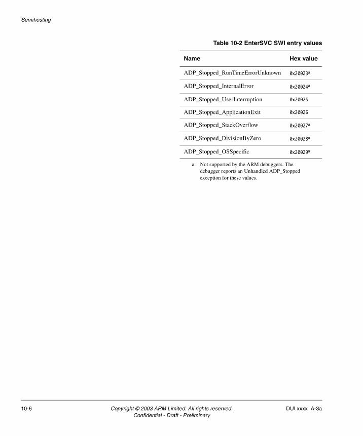
Semihosting
ADP_Stopped_RunTimeErrorUnknown 0x20023a
ADP_Stopped_InternalError 0x20024a
ADP_Stopped_UserInterruption 0x20025
ADP_Stopped_ApplicationExit 0x20026
ADP_Stopped_StackOverflow 0x20027a
ADP_Stopped_DivisionByZero 0x20028a
ADP_Stopped_OSSpecific 0x20029a
a. Not supported by the ARM debuggers. The debugger reports an Unhandled ADP_Stopped exception for these values.
Table 10-2 EnterSVC SWI entry values
Name Hex value
10-6 Copyright © 2003 ARM Limited. All rights reserved. DUI xxxx A-3aConfidential - Draft - Preliminary
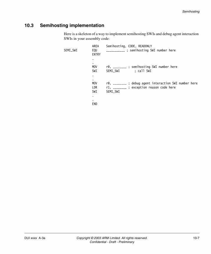
Semihosting
10.3 Semihosting implementation
Here is a skeleton of a way to implement semihosting SWIs and debug agent interaction SWIs in your assembly code:
AREA Semihosting, CODE, READONLY SEMI_SWI EQU ___________ ; semihosting SWI number here
ENTRY ……MOV r0, ________ ; semihosting SWI number here SWI SEMI_SWI ; call SWI… … MOV r0, ________ ; debug agent interaction SWI number hereLDR r1, ________ ; exception reason code hereSWI SEMI_SWI… … END
DUI xxxx A-3a Copyright © 2003 ARM Limited. All rights reserved. 10-7Confidential - Draft - Preliminary
Semihosting
10.4 Exercises
These exercises illustrate using the host monitor and host files.
10.4.1 Hello world
Write ARM assembly to output the string "Hello world" to the screen. The program must terminate normally using a debug agent interaction SWI.
10.4.2 Displaying sequences of characters using a menu
Write ARM assembly to display a menu and prompt the user to input a character from the keyboard. Put these items in the menu:
a | A Display the lowercase letters
b | B Display the uppercase letters
c | C Display the decimal digits
d | D Display the hexadecimal digits
e | E Exit
The program must terminate normally using a debug agent interaction SWI.
10.4.3 Reading from and writing to files
Write ARM assembly to read the text from a text file called infile.txt and write that text to a text file called outfile.txt. Make sure to open infile.txt for reading, open outfile.txt for writing, and close both files after performing the reading and writing. Reading and writing requires the use of a buffer. Use the SPACE directive to allocate the buffer space. See the ADS Debug Target Guide chapter on Semihosting for specific implementation of the semihosted SWIs. Terminate the program normally with a debug agent interaction SWI.
10-8 Copyright © 2003 ARM Limited. All rights reserved. DUI xxxx A-3aConfidential - Draft - Preliminary


![WJ]7T= - ee-ko.com](https://img.pdfslide.net/doc/110x75/61d6575594e9aa06f1700b53/wj7t-ee-kocom.jpg)