Embed Size (px)
Citation preview
ARM PrimeCell® Synchronous SerialPort (PL022)
Revision: r1p3
Technical Reference Manual
Copyright © 2000-2001, 2009, 2011. All rights reserved.ARM DDI 0194G (ID110411)
ARM PrimeCell Synchronous Serial Port (PL022)Technical Reference Manual
Copyright © 2000-2001, 2009, 2011. All rights reserved.
Release Information
Proprietary Notice
Words and logos marked with ® or ™ are registered trademarks or trademarks owned by ARM Limited, except as otherwise stated below in this proprietary notice. Other brands and names mentioned herein may be the trademarks of their respective owners.
Neither the whole nor any part of the information contained in, or the product described in, this document may be adapted or reproduced in any material form except with the prior written permission of the copyright holder.
The product described in this document is subject to continuous developments and improvements. All particulars of the product and its use contained in this document are given by ARM in good faith. However, all warranties implied or expressed, including but not limited to implied warranties of merchantability, or fitness for purpose, are excluded.
This document is intended only to assist the reader in the use of the product. ARM Limited shall not be liable for any loss or damage arising from the use of any information in this document, or any error or omission in such information, or any incorrect use of the product.
Confidentiality Status
This document is Non-Confidential. The right to use, copy and disclose this document may be subject to license restrictions in accordance with the terms of the agreement entered into by ARM and the party that ARM delivered this document to.
Product Status
The information in this document is final, that is for a developed product.
Web Address
http://www.arm.com
Change history
Date Issue Confidentiality Change
6 September 2000 A Non-Confidential First release
19 March 2001 B Non-Confidential Second release
15 June 2001 C Non-Confidential Third release
31 July 2001 D Non-Confidential Fourth release
30 January 2009 E Non-Confidential Unrestricted Access Fifth release
01 November 2011 F Non-Confidential Unrestricted Access Sixth release
04 November 2011 G Non-Confidential Unrestricted Access Seventh release
ARM DDI 0194G Copyright © 2000-2001, 2009, 2011. All rights reserved. iiID110411 Non-Confidential
ContentsARM PrimeCell Synchronous Serial Port (PL022) Technical Reference Manual
PrefaceAbout this book ........................................................................................................... viFeedback ..................................................................................................................... x
Chapter 1 Introduction1.1 About the ARM PrimeCell SSP (PL022) .................................................................. 1-21.2 Product revisions ..................................................................................................... 1-5
Chapter 2 Functional Overview2.1 PrimeCell SSP overview .......................................................................................... 2-22.2 PrimeCell SSP functional description ...................................................................... 2-32.3 PrimeCell SSP operation ......................................................................................... 2-6
Chapter 3 Programmer’s Model3.1 About the programmer’s model ............................................................................... 3-23.2 Summary of PrimeCell SSP registers ...................................................................... 3-33.3 Register descriptions ............................................................................................... 3-43.4 Interrupts ................................................................................................................ 3-20
Chapter 4 Programmer’s Model for Test4.1 PrimeCell SSP test harness overview ..................................................................... 4-24.2 Scan testing ............................................................................................................. 4-34.3 Test registers ........................................................................................................... 4-44.4 Integration testing of block inputs ............................................................................ 4-84.5 Integration testing of block outputs ........................................................................ 4-104.6 Integration test summary ....................................................................................... 4-13
ARM DDI 0194G Copyright © 2000-2001, 2009, 2011. All rights reserved. iiiID110411 Non-Confidential
Contents
Appendix A Signal DescriptionsA.1 AMBA APB signals .................................................................................................. A-2A.2 On-chip signals ........................................................................................................ A-3A.3 Signals to pads ........................................................................................................ A-4
Appendix B Revisions
ARM DDI 0194G Copyright © 2000-2001, 2009, 2011. All rights reserved. ivID110411 Non-Confidential
Preface
This preface introduces the ARM PrimeCell Synchronous Serial Port (PL022) Technical Reference Manual. It contains the following sections:• About this book on page vi• Feedback on page x.
ARM DDI 0194G Copyright © 2000-2001, 2009, 2011. All rights reserved. vID110411 Non-Confidential
Preface
About this bookThis book is for the ARM PrimeCell Synchronous Serial Port (PL022).
Product revision status
The rnpn identifier indicates the revision status of the product described in this book, where:rn Identifies the major revision of the product.pn Identifies the minor revision or modification status of the product.
Intended audience
This book is written for hardware and software engineers with experience and knowledge of implementing System-on-Chip (SoC) designs and, to enable designers to integrate the peripheral into a target system.
Using this book
This book is organized into the following chapters:
Chapter 1 Introduction Read this for an introduction to the PrimeCell Synchronous Serial Port (SSP) and its features.
Chapter 2 Functional Overview Read this for a description of the major functional blocks of the PrimeCell SSP.
Chapter 3 Programmer’s Model Read this for a description of the PrimeCell SSP registers and programming details.
Chapter 4 Programmer’s Model for Test Read this for a description of the logic in the PrimeCell SSP for integration testing.
Appendix A Signal Descriptions Read this for a description of the PrimeCell SSP signals.
Appendix B Revisions Read this for a description of the technical changes between released issues of this book.
Glossary
The ARM Glossary is a list of terms used in ARM documentation, together with definitions for those terms. The ARM Glossary does not contain terms that are industry standard unless the ARM meaning differs from the generally accepted meaning.
See ARM Glossary, http://infocenter.arm.com/help/topic/com.arm.doc.aeg0014-/index.html.
Conventions
Conventions that this book can use are described in:• Typographical on page vii• Timing diagrams on page vii
ARM DDI 0194G Copyright © 2000-2001, 2009, 2011. All rights reserved. viID110411 Non-Confidential
Preface
• Signals.
Typographical
The typographical conventions are:
italic Highlights important notes, introduces special terminology, denotes internal cross-references, and citations.
bold Highlights interface elements, such as menu names. Denotes signal names. Also used for terms in descriptive lists, where appropriate.
monospace Denotes text that you can enter at the keyboard, such as commands, file and program names, and source code.
monospace Denotes a permitted abbreviation for a command or option. You can enter the underlined text instead of the full command or option name.
monospace italic Denotes arguments to monospace text where the argument is to be replaced by a specific value.
monospace bold Denotes language keywords when used outside example code.
< and > Enclose replaceable terms for assembler syntax where they appear in code or code fragments. For example:MRC p15, 0 <Rd>, <CRn>, <CRm>, <Opcode_2>
Timing diagrams
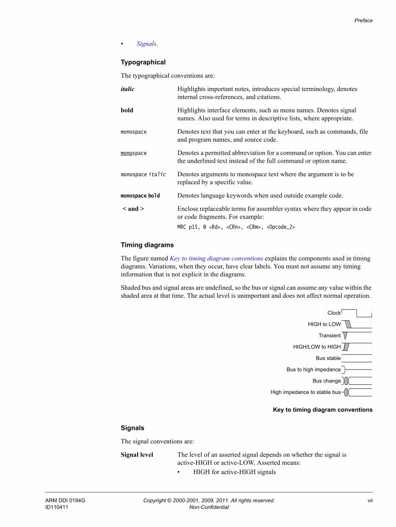
The figure named Key to timing diagram conventions explains the components used in timing diagrams. Variations, when they occur, have clear labels. You must not assume any timing information that is not explicit in the diagrams.
Shaded bus and signal areas are undefined, so the bus or signal can assume any value within the shaded area at that time. The actual level is unimportant and does not affect normal operation.
Key to timing diagram conventions
Signals
The signal conventions are:
Signal level The level of an asserted signal depends on whether the signal is active-HIGH or active-LOW. Asserted means:• HIGH for active-HIGH signals
Clock
HIGH to LOW
Transient
HIGH/LOW to HIGH
Bus stable
Bus to high impedance
Bus change
High impedance to stable bus
ARM DDI 0194G Copyright © 2000-2001, 2009, 2011. All rights reserved. viiID110411 Non-Confidential
Preface
• LOW for active-LOW signals.
Lower-case n At the start or end of a signal name denotes an active-LOW signal.
Prefix A Denotes global Advanced eXtensible Interface (AXI) signals.
Prefix AR Denotes AXI read address channel signals.
Prefix AW Denotes AXI write address channel signals.
Prefix B Denotes AXI write response channel signals.
Prefix C Denotes AXI low-power interface signals.
Prefix H Denotes Advanced High-performance Bus (AHB) signals.
Prefix P Denotes Advanced Peripheral Bus (APB) signals.
Prefix R Denotes AXI read data channel signals.
Prefix W Denotes AXI write data channel signals.
ARM DDI 0194G Copyright © 2000-2001, 2009, 2011. All rights reserved. viiiID110411 Non-Confidential
Preface
Additional reading
This section lists publications by ARM and by third parties.
See Infocenter, http://infocenter.arm.com, for access to ARM documentation.
ARM publications
This book contains information that is specific to this product. See the following documents for other relevant information:
• AMBA® Specification (Rev 2.0) (ARM IHI 00011)
• ARM PrimeCell Synchronous Serial Port (PL022) Integration Manual (PL022 INTM 0000)
• ARM PrimeCell Synchronous Serial Port (PL022) Design Manual (PL022 DDES 0000)
• ARM PrimeCell Synchronous Serial Port (PL020) Technical Reference Manual (ARM DDI 0141)
• ARM PrimeCell Synchronous Serial Port Master and Slave (PL021) Technical Reference Manual (ARM DDI 0171).
ARM DDI 0194G Copyright © 2000-2001, 2009, 2011. All rights reserved. ixID110411 Non-Confidential
Preface
FeedbackARM welcomes feedback on this product and its documentation.
Feedback on this product
If you have any comments or suggestions about this product, contact your supplier and give:
• The product name.
• The product revision or version.
• An explanation with as much information as you can provide. Include symptoms if appropriate.
Feedback on this book
If you have any comments on content then send an e-mail to [email protected]. Give:• the title• the number, ARM DDI 0194G• the page numbers to which your comments apply• a concise explanation of your comments.
ARM also welcomes general suggestions for additions and improvements.
Note ARM tests the PDF only in Adobe Acrobat and Acrobat Reader, and cannot guarantee the quality of the represented document when used with any other PDF reader.
ARM DDI 0194G Copyright © 2000-2001, 2009, 2011. All rights reserved. xID110411 Non-Confidential
Chapter 1 Introduction
This chapter introduces the ARM PrimeCell Synchronous Serial Port (PL022).
It contains the following sections:• About the ARM PrimeCell SSP (PL022) on page 1-2• Product revisions on page 1-5.
ARM DDI 0194G Copyright © 2000-2001, 2009, 2011. All rights reserved. 1-1ID110411 Non-Confidential
Introduction
1.1 About the ARM PrimeCell SSP (PL022)The PrimeCell Synchronous Serial Port (SSP) is an Advanced Microcontroller Bus Architecture (AMBA) slave block that connects to the Advanced Peripheral Bus (APB). The PrimeCell SSP is an AMBA compliant System-on-Chip (SoC) peripheral that is developed, tested, and licensed by ARM.
The PrimeCell SSP is a master or slave interface that enables synchronous serial communication with slave or master peripherals having one of the following:• a Motorola SPI-compatible interface• a Texas Instruments synchronous serial interface• a National Semiconductor Microwire interface.
In both master and slave configurations, the PrimeCell SSP performs:
• parallel-to-serial conversion on data written to an internal 16-bit wide, 8-location deep transmit FIFO
• serial-to-parallel conversion on received data, buffering it in a similar 16-bit wide, 8-location deep receive FIFO.
Interrupts are generated to:• request servicing of the transmit and receive FIFO• inform the system that a receive FIFO over-run has occurred• inform the system that data is present in the receive FIFO after an idle period has expired.
The following sections describe the features of the PrimeCell SSP:• Features of the PrimeCell SSP• SPI features on page 1-4• Microwire features on page 1-4• Texas Instruments synchronous serial interface features on page 1-4.
Note Because of changes in the programmer’s model, the PrimeCell SSP (PL022) is not backwards-compatible with the previous PrimeCell SSPMS (PL021) or PrimeCell SSP (PL020).
1.1.1 Features of the PrimeCell SSP
The PrimeCell SSP has the following features:
• Compliance to the AMBA Specification (Rev 2.0) for easy integration into SoC implementation.
• Master or slave operation.
• Programmable clock bit rate and prescale.
• Separate transmit and receive first-in, first-out memory buffers, 16 bits wide, 8 locations deep.
• Programmable choice of interface operation, SPI, Microwire, or TI synchronous serial.
• Programmable data frame size from 4 to 16 bits.
• Independent masking of transmit FIFO, receive FIFO, and receive overrun interrupts.
ARM DDI 0194G Copyright © 2000-2001, 2009, 2011. All rights reserved. 1-2ID110411 Non-Confidential
Introduction
• Internal loopback test mode available.
• Support for Direct Memory Access (DMA).
• Identification registers that uniquely identify the PrimeCell SSP. An operating system can use these to automatically configure itself.
Figure 1-1 shows a block diagram of the PrimeCell SSP.
Figure 1-1 PrimeCell SSP block diagram
Note For clarity, Figure 1-1 does not show the test logic.
RxFRdData[15:0]
Tx FIFO16 bits wide,8 locations
deep
Rx FIFO16 bits wide,8 locations
deep
AMBAAPB
interfacePADDR[11:2]
PWRITE
PSEL
PRESETn
PENABLE
PRDATA[15:0]
PWDATA[15:0]
PCLKPCLK
PCLK
PWDATAIn[15:0]
SSPRXINTR
PCLKRegister
blockClock
prescaler SSPCLKDIVSSPCLK
nSSPRST
SSPCLK
Tx/Rx params
SSPRORINTR
Transmit and receive logic
SSPRXD
SSPFSSIN
SSPCLKIN
nSSPCTLOE
SSPCLKOUT
SSPFSSOUT
SSPTXD
nSSPOE
FIFO status and
interruptgeneration
SSPRORINTR
SSPCLK
TxRdDataIn[15:0]
PCLK
SSPRXINTR
SSPRXDMASREQDMA
interfaceSSPRXDMABREQ
SSPTXDMASREQ
SSPTXDMABREQ
SSPTXDMACLR
SSPRXDMACLR
SSPRTINTR
SSPINTR
SSPTXINTR
SSPRTRINTR
Tx/Rx FIFO watermark levels
Prescale value
RxWrData[15:0]
DATAOUTDATAIN
SSPTXINTR
ARM DDI 0194G Copyright © 2000-2001, 2009, 2011. All rights reserved. 1-3ID110411 Non-Confidential
Introduction
1.1.2 Programmable parameters
You can program the following parameters:• master or slave mode• enabling of operation• frame format• communication baud rate• clock phase and polarity• data widths from 4 to 16 bits wide• interrupt masking.
1.1.3 SPI features
The features of the Motorola SPI-compatible interface are:• full duplex, four-wire synchronous transfers• programmable clock polarity and phase.
1.1.4 Microwire features
The National Semiconductor Microwire interface performs half-duplex transfers using an 8-bit control message.
1.1.5 Texas Instruments synchronous serial interface features
The features of the Texas Instruments synchronous serial interface are:• full-duplex, four-wire synchronous transfers• transmit data pin tristateable when not transmitting.
ARM DDI 0194G Copyright © 2000-2001, 2009, 2011. All rights reserved. 1-4ID110411 Non-Confidential
Introduction
1.2 Product revisionsThere is no product revision history available before version r1p3.
ARM DDI 0194G Copyright © 2000-2001, 2009, 2011. All rights reserved. 1-5ID110411 Non-Confidential
Chapter 2 Functional Overview
This chapter describes the major functional blocks of the ARM PrimeCell Synchronous Serial Port (PL022).
It contains the following sections:• PrimeCell SSP overview on page 2-2• PrimeCell SSP functional description on page 2-3• PrimeCell SSP operation on page 2-6.
ARM DDI 0194G Copyright © 2000-2001, 2009, 2011. All rights reserved. 2-1ID110411 Non-Confidential
Functional Overview
2.1 PrimeCell SSP overviewThe PrimeCell SSP is a master or slave interface for synchronous serial communication with peripheral devices that have Motorola SPI, National Semiconductor Microwire, or Texas Instruments synchronous serial interfaces.
The PrimeCell SSP performs serial-to-parallel conversion on data received from a peripheral device. The CPU accesses data, control, and status information through the AMBA APB interface. The transmit and receive paths are buffered with internal FIFO memories enabling up to eight 16-bit values to be stored independently in both transmit and receive modes. Serial data is transmitted on SSPTXD and received on SSPRXD.
The PrimeCell SSP includes a programmable bit rate clock divider and prescaler to generate the serial output clock, SSPCLKOUT, from the input clock, SSPCLK. Bit rates are supported to 2MHz and higher, subject to choice of frequency for SSPCLK, and the maximum bit rate is determined by peripheral devices.
You can use the control registers SSPCR0 and SSPCR1 to program the PrimeCell SSP operating mode, frame format, and size. See Control register 0, SSPCR0 on page 3-4 and Control register 1, SSPCR1 on page 3-5.
The following individually maskable interrupt outputs are generated:
• SSPTXINTR requests servicing of the transmit buffer
• SSPRXINTR requests servicing of the receive buffer
• SSPRORINTR indicates an overrun condition in the receive FIFO
• SSPRTINTR indicates that a timeout period expired while data was present in the receive FIFO.
A single combined interrupt, SSPINTR output, is asserted if any of the individual interrupts are asserted and unmasked.
In addition to the above interrupts, a set of DMA signals are provided for interfacing with a DMA controller.
Depending on the operating mode selected, the SSPFSSOUT output operates as:
• an active-HIGH frame synchronization output for Texas Instruments synchronous serial frame format
• an active-LOW slave select for SPI and Microwire.
ARM DDI 0194G Copyright © 2000-2001, 2009, 2011. All rights reserved. 2-2ID110411 Non-Confidential
Functional Overview
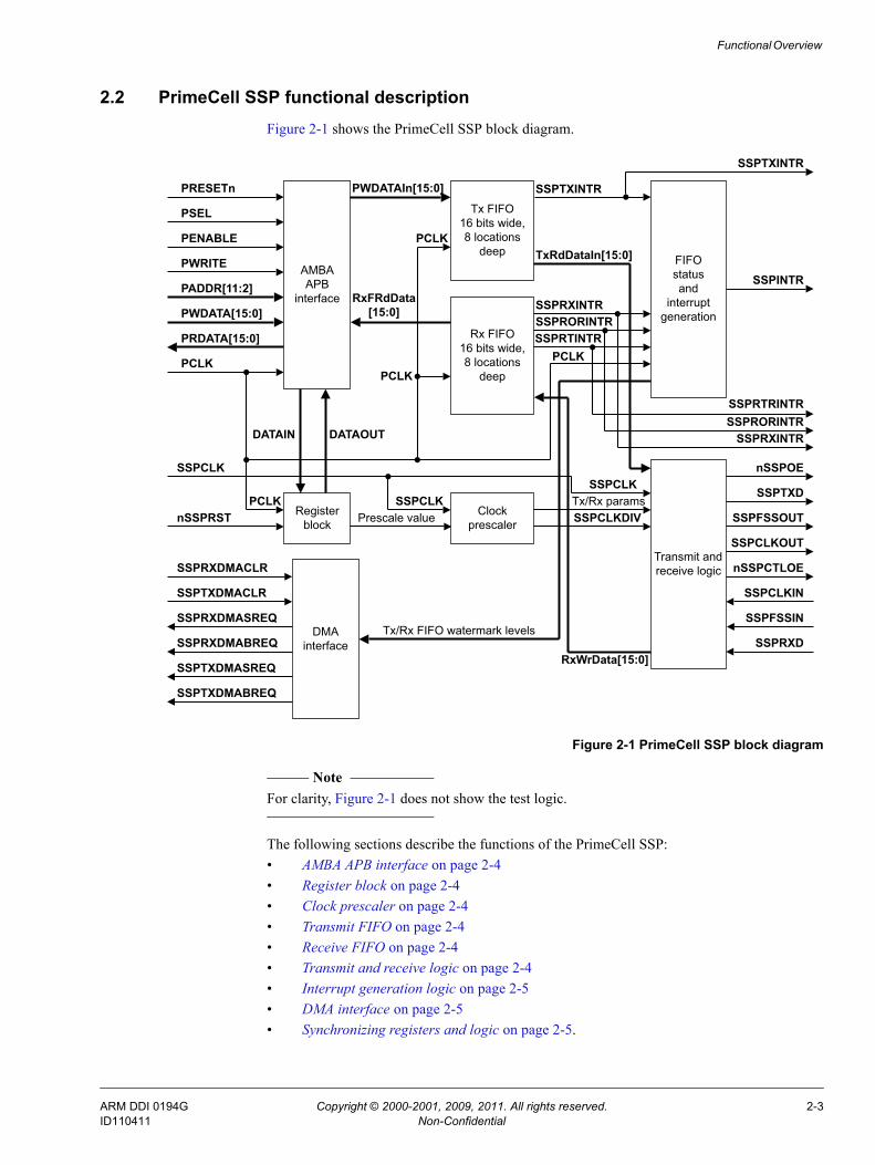
2.2 PrimeCell SSP functional descriptionFigure 2-1 shows the PrimeCell SSP block diagram.
Figure 2-1 PrimeCell SSP block diagram
Note For clarity, Figure 2-1 does not show the test logic.
The following sections describe the functions of the PrimeCell SSP:• AMBA APB interface on page 2-4• Register block on page 2-4• Clock prescaler on page 2-4• Transmit FIFO on page 2-4• Receive FIFO on page 2-4• Transmit and receive logic on page 2-4• Interrupt generation logic on page 2-5• DMA interface on page 2-5• Synchronizing registers and logic on page 2-5.
RxFRdData[15:0]
Tx FIFO16 bits wide,8 locations
deep
Rx FIFO16 bits wide,8 locations
deep
AMBAAPB
interfacePADDR[11:2]
PWRITE
PSEL
PRESETn
PENABLE
PRDATA[15:0]
PWDATA[15:0]
PCLKPCLK
PCLK
PWDATAIn[15:0]
SSPRXINTR
PCLKRegister
blockClock
prescaler SSPCLKDIVSSPCLK
nSSPRST
SSPCLK
Tx/Rx params
SSPRORINTR
Transmit and receive logic
SSPRXD
SSPFSSIN
SSPCLKIN
nSSPCTLOE
SSPCLKOUT
SSPFSSOUT
SSPTXD
nSSPOE
FIFO status and
interruptgeneration
SSPRORINTR
SSPCLK
TxRdDataIn[15:0]
PCLK
SSPRXINTR
SSPRXDMASREQDMA
interfaceSSPRXDMABREQ
SSPTXDMASREQ
SSPTXDMABREQ
SSPTXDMACLR
SSPRXDMACLR
SSPRTINTR
SSPINTR
SSPTXINTR
SSPRTRINTR
Tx/Rx FIFO watermark levels
Prescale value
RxWrData[15:0]
DATAOUTDATAIN
SSPTXINTR
ARM DDI 0194G Copyright © 2000-2001, 2009, 2011. All rights reserved. 2-3ID110411 Non-Confidential
Functional Overview
2.2.1 AMBA APB interface
The AMBA APB interface generates read and write decodes for accesses to status and control registers, and transmit and receive FIFO memories.
The AMBA APB is a local secondary bus that provides a low-power extension to the higher bandwidth AMBA Advanced High-performance Bus (AHB) within the AMBA system hierarchy. The AMBA APB groups narrow-bus peripherals to avoid loading the system bus and provides an interface using memory-mapped registers, that are accessed under programmed control.
2.2.2 Register block
The register block stores data written, or to be read, across the AMBA APB interface.
2.2.3 Clock prescaler
When configured as a master, an internal prescaler, comprising two free-running reloadable serially linked counters, provides the serial output clock SSPCLKOUT.
You can program the clock prescaler, using the SSPCPSR register, to divide SSPCLK by a factor of 2-254 in steps of two. By not utilizing the least significant bit of the SSPCPSR register, division by an odd number is not possible and this ensures that a symmetrical, equal mark space ratio, clock is generated. See Clock prescale register, SSPCPSR on page 3-8.
The output of the prescaler is divided again by a factor of 1-256, by programming the SSPCR0 control register, to give the final master output clock SSPCLKOUT.
2.2.4 Transmit FIFO
The common transmit FIFO is a 16-bit wide, 8-locations deep, First-In, First-Out (FIFO) memory buffer. CPU data written across the AMBA APB interface are stored in the buffer until read out by the transmit logic.
When configured as a master or a slave, parallel data is written into the transmit FIFO prior to serial conversion, and transmission to the attached slave or master respectively, through the SSPTXD pin.
2.2.5 Receive FIFO
The common receive FIFO is a 16-bit wide, 8-locations deep, first-in, first-out memory buffer. Received data from the serial interface are stored in the buffer until read out by the CPU across the AMBA APB interface.
When configured as a master or slave, serial data received through the SSPRXD pin is registered prior to parallel loading into the attached slave or master receive FIFO respectively.
2.2.6 Transmit and receive logic
When configured as a master, the clock to the attached slaves is derived from a divided-down version of SSPCLK through the prescaler operations that previous sections describe. The master transmit logic successively reads a value from its transmit FIFO and performs parallel to serial conversion on it. Then, the serial data stream and frame control signal, synchronized to SSPCLKOUT, are output through the SSPTXD pin to the attached slaves. The master receive logic performs serial to parallel conversion on the incoming synchronous SSPRXD data stream, extracting and storing values into its receive FIFO, for subsequent reading through the APB interface.
ARM DDI 0194G Copyright © 2000-2001, 2009, 2011. All rights reserved. 2-4ID110411 Non-Confidential
Functional Overview
When configured as a slave, the SSPCLKIN clock is provided by an attached master and used to time its transmission and reception sequences. The slave transmit logic, under control of the master clock, successively reads a value from its transmit FIFO, performs parallel to serial conversion, then outputs the serial data stream and frame control signal through the slave SSPTXD pin. The slave receive logic performs serial to parallel conversion on the incoming SSPRXD data stream, extracting and storing values into its receive FIFO, for subsequent reading through the APB interface.
2.2.7 Interrupt generation logic
The PrimeCell SSP generates four individual maskable, active-HIGH interrupts. A combined interrupt output is also generated as an OR function of the individual interrupt requests.
You can use the single combined interrupt with a system interrupt controller that provides another level of masking on a per-peripheral basis. This enables use of modular device drivers that always know where to find the interrupt source control register bits.
You can also use the individual interrupt requests with a system interrupt controller that provides masking for the outputs of each peripheral. In this way, a global interrupt controller service routine can read the entire set of sources from one wide register in the system interrupt controller. This is attractive where the time to read from the peripheral registers is significant compared to the CPU clock speed in a real-time system.
The peripheral supports both the above methods.
The transmit and receive dynamic data-flow interrupts, SSPTXINTR and SSPRXINTR, are separated from the status interrupts so that data can be read or written in response to the FIFO trigger levels.
2.2.8 DMA interface
The PrimeCell SSP provides an interface to connect to a DMA controller. See PrimeCell DMA interface on page 2-18 for details.
2.2.9 Synchronizing registers and logic
The PrimeCell SSP supports both asynchronous and synchronous operation of the clocks, PCLK and SSPCLK. Synchronization registers and handshaking logic have been implemented, and are active at all times. This has a minimal impact on performance or area. Synchronization of control signals is performed on both directions of data flow, that is:• from the PCLK to the SSPCLK domain• from the SSPCLK to the PCLK domain.
ARM DDI 0194G Copyright © 2000-2001, 2009, 2011. All rights reserved. 2-5ID110411 Non-Confidential
Functional Overview
2.3 PrimeCell SSP operationThe following sections describe the operation of the PrimeCell SSP:• Interface reset• Configuring the SSP• Enable PrimeCell SSP operation• Clock ratios on page 2-7• Programming the SSPCR0 Control Register on page 2-7• Programming the SSPCR1 Control Register on page 2-8• Frame format on page 2-8• Texas Instruments synchronous serial frame format on page 2-9• Motorola SPI frame format on page 2-10• Motorola SPI Format with SPO=0, SPH=0 on page 2-10• Motorola SPI Format with SPO=0, SPH=1 on page 2-11• Motorola SPI Format with SPO=1, SPH=0 on page 2-12• Motorola SPI Format with SPO=1, SPH=1 on page 2-14• National Semiconductor Microwire frame format on page 2-15• Examples of master and slave configurations on page 2-17• PrimeCell DMA interface on page 2-18.
2.3.1 Interface reset
The PrimeCell SSP is reset by the global reset signal, PRESETn, and a block-specific reset signal, nSSPRST. An external reset controller must use PRESETn to assert nSSPRST asynchronously and negate it synchronously to SSPCLK. PRESETn must be asserted LOW for a period long enough to reset the slowest block in the on-chip system, and then taken HIGH again. The PrimeCell SSP requires PRESETn to be asserted LOW for at least one period of PCLK.
Chapter 3 Programmer’s Model describes the values of the registers after reset.
2.3.2 Configuring the SSP
Following reset, the PrimeCell SSP logic is disabled and must be configured when in this state.
It is necessary to program control registers SSPCR0 and SSPCR1 to configure the peripheral as a master or slave operating under one of the following protocols:• Motorola SPI • Texas Instruments SSI • National Semiconductor.
The bit rate, derived from the external SSPCLK, requires the programming of the clock prescale register SSPCPSR. See Clock prescale register, SSPCPSR on page 3-8.
2.3.3 Enable PrimeCell SSP operation
You can either prime the transmit FIFO, by writing up to eight 16-bit values when the PrimeCell SSP is disabled, or permit the transmit FIFO service request to interrupt the CPU. Once enabled, transmission or reception of data begins on the transmit, SSPTXD, and receive, SSPRXD, pins.
ARM DDI 0194G Copyright © 2000-2001, 2009, 2011. All rights reserved. 2-6ID110411 Non-Confidential
Functional Overview
2.3.4 Clock ratios
There is a constraint on the ratio of the frequencies of PCLK to SSPCLK. The frequency of SSPCLK must be less than or equal to that of PCLK. This ensures that control signals from the SSPCLK domain to the PCLK domain are guaranteed to get synchronized before one frame duration:
FSSPCLK <= FPCLK.
In the slave mode of operation, the SSPCLKIN signal from the external master is double-synchronized and then delayed to detect an edge. It takes three SSPCLKs to detect an edge on SSPCLKIN. SSPTXD has less setup time to the falling edge of SSPCLKIN on which the master is sampling the line.
The setup and hold times on SSPRXD, with reference to SSPCLKIN, must be more conservative to ensure that it is at the right value when the actual sampling occurs within the SSPMS. To ensure correct device operation, SSPCLK must be at least 12 times faster than the maximum expected frequency of SSPCLKIN.
The frequency selected for SSPCLK must accommodate the desired range of bit clock rates. The ratio of minimum SSPCLK frequency to SSPCLKOUT maximum frequency in the case of the slave mode is 12, and for the master mode, it is two.
To generate a maximum bit rate of 1.8432Mbps in the master mode, the frequency of SSPCLK must be at least 3.6864MHz. With an SSPCLK frequency of 3.6864MHz, the SSPCPSR register must be programmed with a value of 2, and the SCR[7:0] field in the SSPCR0 register must be programmed with a value of 0.
To work with a maximum bit rate of 1.8432Mbps in the slave mode, the frequency of SSPCLK must be at least 22.12MHz. With an SSPCLK frequency of 22.12MHz, the SSPCPSR register can be programmed with a value of 12, and the SCR[7:0] field in the SSPCR0 register can be programmed with a value of 0. Similarly, the ratio of SSPCLK maximum frequency to SSPCLKOUT minimum frequency is 254 x 256. See Control register 0, SSPCR0 on page 3-4 and Clock prescale register, SSPCPSR on page 3-8.
The minimum frequency of SSPCLK is governed by the following equations, both of which must be satisfied:
FSSPCLK(min) => 2 x FSSPCLKOUT(max), for master mode
FSSPCLK(min) => 12 x FSSPCLKIN(max), for slave mode.
The maximum frequency of SSPCLK is governed by the following equations, both of which must be satisfied:
FSSPCLK(max) <= 254 x 256 x FSSPCLKOUT(min), for master mode
FSSPCLK(max) <= 254 x 256 x FSSPCLKIN(min), for slave mode.
2.3.5 Programming the SSPCR0 Control Register
See Control register 0, SSPCR0 on page 3-4 for more information on the bit assignment of this register.
The SSPCR0 register is used to:• program the serial clock rate• select one of the three protocols• select the data word size, where applicable.
ARM DDI 0194G Copyright © 2000-2001, 2009, 2011. All rights reserved. 2-7ID110411 Non-Confidential
Functional Overview
The Serial Clock Rate (SCR) value, in conjunction with the SSPCPSR clock prescale divisor value, CPSDVSR, is used to derive the PrimeCell SSP transmit and receive bit rate from the external SSPCLK.
The frame format is programmed through the FRF bits, and the data word size through the DSS bits.
Bit phase and polarity, applicable to Motorola SPI format only, are programmed through the SPH and SPO bits.
2.3.6 Programming the SSPCR1 Control Register
See Control register 1, SSPCR1 on page 3-5, for more information on the bit assignment of this register.
The SSPCR1 register is used to:• select master or slave mode• enable a loop back test feature• enable the PrimeCell SSP peripheral.
To configure the PrimeCell SSP as a master, clear the SSPCR1 register master or slave selection bit, MS, to 0. This is the default value on reset.
Setting the SSPCR1 register MS bit to 1 configures the PrimeCell SSP as a slave. When configured as a slave, enabling or disabling of the PrimeCell SSP SSPTXD signal is provided through the SSPCR1 slave mode SSPTXD output disable bit, SOD. You can use this in some multi-slave environments where masters might parallel broadcast.
To enable the operation of the PrimeCell SSP, set the Synchronous Serial Port Enable (SSE) bit to 1.
Bit rate generation
The serial bit rate is derived by dividing down the input clock, SSPCLK. The clock is first divided by an even prescale value CPSDVSR in the range 2-254, and is programmed in SSPCPSR. The clock is divided again by a value in the range 1-256, that is 1 + SCR, where SCR is the value programmed in SSPCR0.
The following equation defines the frequency of the output signal bit clock, SSPCLKOUT:
For example, if SSPCLK is 3.6864MHz, and CPSDVSR = 2, then SSPCLKOUT has a frequency range from 7.2kHz-1.8432MHz.
2.3.7 Frame format
Each data frame is between 4-16 bits long, depending on the size of data programmed, and is transmitted starting with the MSB. You can select the following basic frame types:• Texas Instruments synchronous serial• Motorola SPI• National Semiconductor Microwire.
CPSDVR x (1+SCR)
FSSPCLKFSSPCLKOUT =
ARM DDI 0194G Copyright © 2000-2001, 2009, 2011. All rights reserved. 2-8ID110411 Non-Confidential
Functional Overview
For all formats, the serial clock, SSPCLKOUT, is held inactive while the PrimeCell SSP is idle, and transitions at the programmed frequency only during active transmission or reception of data. The idle state of SSPCLKOUT is utilized to provide a receive timeout indication that occurs when the receive FIFO still contains data after a timeout period.
For Motorola SPI and National Semiconductor Microwire frame formats, the serial frame, SSPFSSOUT, pin is active-LOW, and is asserted, pulled-down, during the entire transmission of the frame.
For Texas Instruments synchronous serial frame format, the SSPFSSOUT pin is pulsed for one serial clock period, starting at its rising edge, prior to the transmission of each frame. For this frame format, both the PrimeCell SSP and the off-chip slave device drive their output data on the rising edge of SSPCLKOUT, and latch data from the other device on the falling edge.
Unlike the full-duplex transmission of the other two frame formats, the National Semiconductor Microwire format uses a special master-slave messaging technique, that operates at half-duplex. In this mode, when a frame begins, an 8-bit control message is transmitted to the off-chip slave. During this transmit, the SSS receives no incoming data. After the message has been sent, the off-chip slave decodes it and, after waiting one serial clock after the last bit of the 8-bit control message has been sent, responds with the requested data. The returned data can be 4-16 bits in length, making the total frame length in the range 13-25 bits.
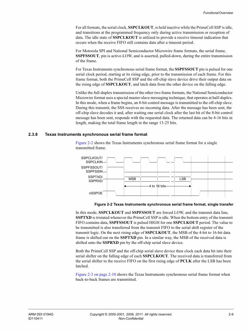
2.3.8 Texas Instruments synchronous serial frame format
Figure 2-2 shows the Texas Instruments synchronous serial frame format for a single transmitted frame.
Figure 2-2 Texas Instruments synchronous serial frame format, single transfer
In this mode, SSPCLKOUT and SSPFSSOUT are forced LOW, and the transmit data line, SSPTXD is tristated whenever the PrimeCell SSP is idle. When the bottom entry of the transmit FIFO contains data, SSPFSSOUT is pulsed HIGH for one SSPCLKOUT period. The value to be transmitted is also transferred from the transmit FIFO to the serial shift register of the transmit logic. On the next rising edge of SSPCLKOUT, the MSB of the 4-bit to 16-bit data frame is shifted out on the SSPTXD pin. In a similar way, the MSB of the received data is shifted onto the SSPRXD pin by the off-chip serial slave device.
Both the PrimeCell SSP and the off-chip serial slave device then clock each data bit into their serial shifter on the falling edge of each SSPCLKOUT. The received data is transferred from the serial shifter to the receive FIFO on the first rising edge of PCLK after the LSB has been latched.
Figure 2-3 on page 2-10 shows the Texas Instruments synchronous serial frame format when back-to-back frames are transmitted.
SSPCLKOUT/SSPCLKIN
nSSPOE
4 to 16 bits
SSPFSSOUT/SSPFSSIN
SSPTXD/SSPRXD MSB LSB
ARM DDI 0194G Copyright © 2000-2001, 2009, 2011. All rights reserved. 2-9ID110411 Non-Confidential
Functional Overview
Figure 2-3 Texas Instruments synchronous serial frame format, continuous transfer
2.3.9 Motorola SPI frame format
The Motorola SPI interface is a four-wire interface where the SSPFSSOUT signal behaves as a slave select. The main feature of the Motorola SPI format is that you can program the inactive state and phase of the SSPCLKOUT signal using the SPO and SPH bits of the SSPSCR0 control register. See Control register 0, SSPCR0 on page 3-4.
SPO, clock polarity
When the SPO clock polarity control bit is LOW, it produces a steady state LOW value on the SSPCLKOUT pin. If the SPO clock polarity control bit is HIGH, a steady state HIGH value is placed on the SSPCLKOUT pin when data is not being transferred.
SPH, clock phase
The SPH control bit selects the clock edge that captures data and enables it to change state. It has the most impact on the first bit transmitted by either permitting or not permitting a clock transition before the first data capture edge.
When the SPH phase control bit is LOW, data is captured on the first clock edge transition.
When the SPH clock phase control bit is HIGH, data is captured on the second clock edge transition.
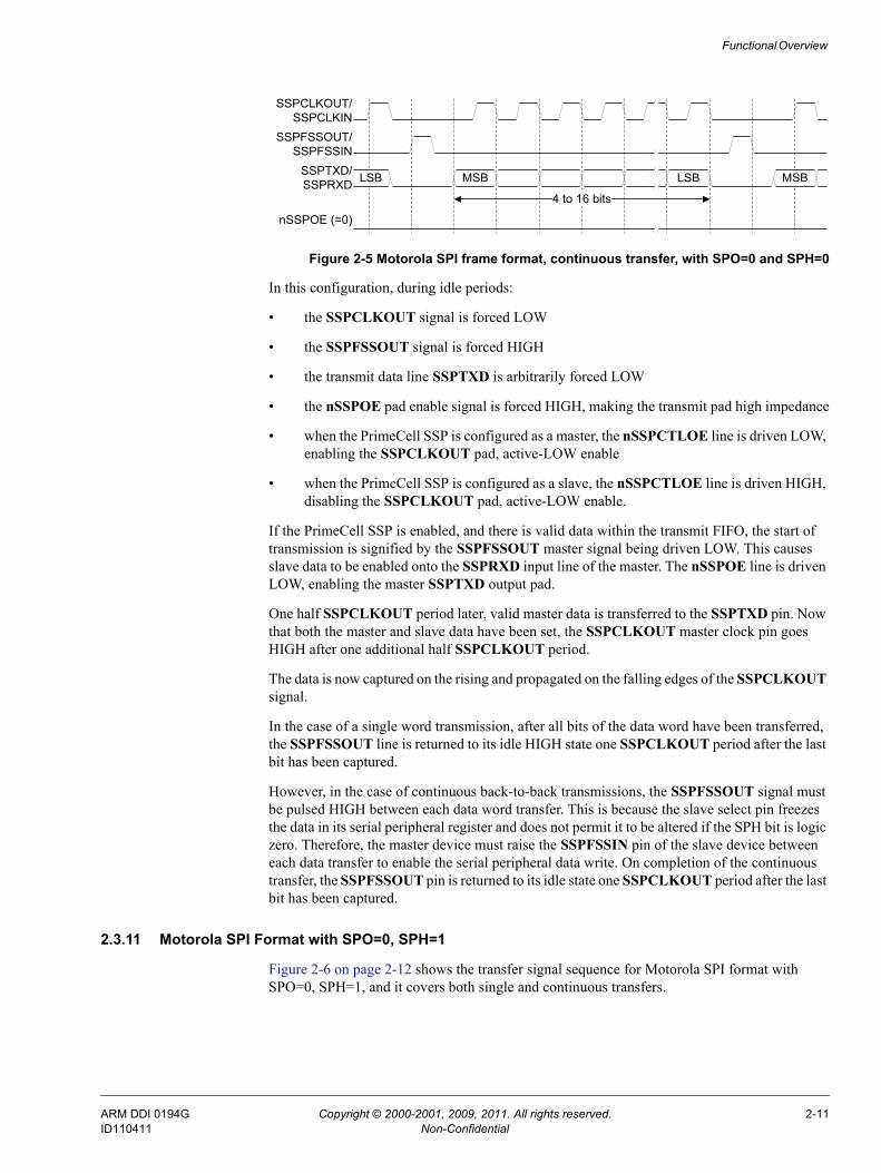
2.3.10 Motorola SPI Format with SPO=0, SPH=0
Figure 2-4 and Figure 2-5 on page 2-11 show single and continuous transmission signal sequences for Motorola SPI format with SPO=0, SPH=0. Figure 2-4 shows a single transmission signal sequence for Motorola SPI frame format with SPO=0, SPH=0.
Figure 2-4 Motorola SPI frame format, single transfer, with SPO=0 and SPH=0
Figure 2-5 on page 2-11 shows a continuous transmission signal sequence for Motorola SPI frame format with SPO=0, SPH=0.
SSPCLKOUT/SSPCLKIN
nSSPOE (=0)
SSPFSSOUT/SSPFSSIN
SSPTXD/SSPRXD MSB LSB
4 to 16 bits
4 to 16 bits
SSPCLKOUT/SSPCLKIN
nSSPOE
SSPFSSOUT/SSPFSSIN
SSPRXD Q
SSPTXD LSB
MSB LSB
MSB
ARM DDI 0194G Copyright © 2000-2001, 2009, 2011. All rights reserved. 2-10ID110411 Non-Confidential
Functional Overview
Figure 2-5 Motorola SPI frame format, continuous transfer, with SPO=0 and SPH=0
In this configuration, during idle periods:
• the SSPCLKOUT signal is forced LOW
• the SSPFSSOUT signal is forced HIGH
• the transmit data line SSPTXD is arbitrarily forced LOW
• the nSSPOE pad enable signal is forced HIGH, making the transmit pad high impedance
• when the PrimeCell SSP is configured as a master, the nSSPCTLOE line is driven LOW, enabling the SSPCLKOUT pad, active-LOW enable
• when the PrimeCell SSP is configured as a slave, the nSSPCTLOE line is driven HIGH, disabling the SSPCLKOUT pad, active-LOW enable.
If the PrimeCell SSP is enabled, and there is valid data within the transmit FIFO, the start of transmission is signified by the SSPFSSOUT master signal being driven LOW. This causes slave data to be enabled onto the SSPRXD input line of the master. The nSSPOE line is driven LOW, enabling the master SSPTXD output pad.
One half SSPCLKOUT period later, valid master data is transferred to the SSPTXD pin. Now that both the master and slave data have been set, the SSPCLKOUT master clock pin goes HIGH after one additional half SSPCLKOUT period.
The data is now captured on the rising and propagated on the falling edges of the SSPCLKOUT signal.
In the case of a single word transmission, after all bits of the data word have been transferred, the SSPFSSOUT line is returned to its idle HIGH state one SSPCLKOUT period after the last bit has been captured.
However, in the case of continuous back-to-back transmissions, the SSPFSSOUT signal must be pulsed HIGH between each data word transfer. This is because the slave select pin freezes the data in its serial peripheral register and does not permit it to be altered if the SPH bit is logic zero. Therefore, the master device must raise the SSPFSSIN pin of the slave device between each data transfer to enable the serial peripheral data write. On completion of the continuous transfer, the SSPFSSOUT pin is returned to its idle state one SSPCLKOUT period after the last bit has been captured.
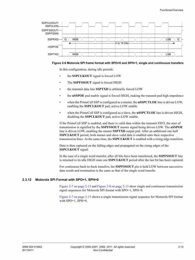
2.3.11 Motorola SPI Format with SPO=0, SPH=1
Figure 2-6 on page 2-12 shows the transfer signal sequence for Motorola SPI format with SPO=0, SPH=1, and it covers both single and continuous transfers.
SSPCLKOUT/SSPCLKIN
nSSPOE (=0)
SSPFSSOUT/SSPFSSIN
SSPTXD/SSPRXD MSB LSB MSB
4 to 16 bits
LSB
ARM DDI 0194G Copyright © 2000-2001, 2009, 2011. All rights reserved. 2-11ID110411 Non-Confidential
Functional Overview
Figure 2-6 Motorola SPI frame format with SPO=0 and SPH=1, single and continuous transfers
In this configuration, during idle periods:
• the SSPCLKOUT signal is forced LOW
• The SSPFSSOUT signal is forced HIGH
• the transmit data line SSPTXD is arbitrarily forced LOW
• the nSSPOE pad enable signal is forced HIGH, making the transmit pad high impedance
• when the PrimeCell SSP is configured as a master, the nSSPCTLOE line is driven LOW, enabling the SSPCLKOUT pad, active-LOW enable
• when the PrimeCell SSP is configured as a slave, the nSSPCTLOE line is driven HIGH, disabling the SSPCLKOUT pad, active-LOW enable.
If the PrimeCell SSP is enabled, and there is valid data within the transmit FIFO, the start of transmission is signified by the SSPFSSOUT master signal being driven LOW. The nSSPOE line is driven LOW, enabling the master SSPTXD output pad. After an additional one half SSPCLKOUT period, both master and slave valid data is enabled onto their respective transmission lines. At the same time, the SSPCLKOUT is enabled with a rising edge transition.
Data is then captured on the falling edges and propagated on the rising edges of the SSPCLKOUT signal.
In the case of a single word transfer, after all bits have been transferred, the SSPFSSOUT line is returned to its idle HIGH state one SSPCLKOUT period after the last bit has been captured.
For continuous back-to-back transfers, the SSPFSSOUT pin is held LOW between successive data words and termination is the same as that of the single word transfer.
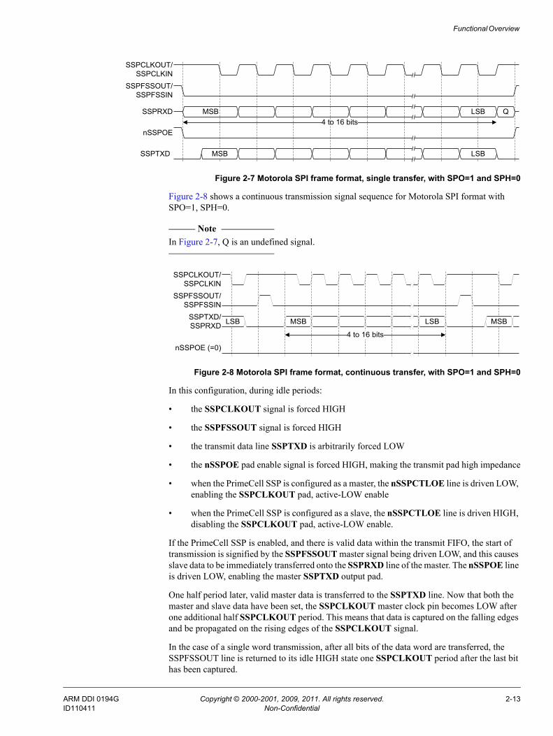
2.3.12 Motorola SPI Format with SPO=1, SPH=0
Figure 2-7 on page 2-13 and Figure 2-8 on page 2-13 show single and continuous transmission signal sequences for Motorola SPI format with SPO=1, SPH=0.
Figure 2-7 on page 2-13 shows a single transmission signal sequence for Motorola SPI format with SPO=1, SPH=0.
SSPCLKOUT/SSPCLKIN
nSSPOE
SSPFSSOUT/SSPFSSIN
SSPRXD
SSPTXD LSB
Q MSB QLSB
MSB
4 to 16 bits
ARM DDI 0194G Copyright © 2000-2001, 2009, 2011. All rights reserved. 2-12ID110411 Non-Confidential
Functional Overview
Figure 2-7 Motorola SPI frame format, single transfer, with SPO=1 and SPH=0
Figure 2-8 shows a continuous transmission signal sequence for Motorola SPI format with SPO=1, SPH=0.
Note In Figure 2-7, Q is an undefined signal.
Figure 2-8 Motorola SPI frame format, continuous transfer, with SPO=1 and SPH=0
In this configuration, during idle periods:
• the SSPCLKOUT signal is forced HIGH
• the SSPFSSOUT signal is forced HIGH
• the transmit data line SSPTXD is arbitrarily forced LOW
• the nSSPOE pad enable signal is forced HIGH, making the transmit pad high impedance
• when the PrimeCell SSP is configured as a master, the nSSPCTLOE line is driven LOW, enabling the SSPCLKOUT pad, active-LOW enable
• when the PrimeCell SSP is configured as a slave, the nSSPCTLOE line is driven HIGH, disabling the SSPCLKOUT pad, active-LOW enable.
If the PrimeCell SSP is enabled, and there is valid data within the transmit FIFO, the start of transmission is signified by the SSPFSSOUT master signal being driven LOW, and this causes slave data to be immediately transferred onto the SSPRXD line of the master. The nSSPOE line is driven LOW, enabling the master SSPTXD output pad.
One half period later, valid master data is transferred to the SSPTXD line. Now that both the master and slave data have been set, the SSPCLKOUT master clock pin becomes LOW after one additional half SSPCLKOUT period. This means that data is captured on the falling edges and be propagated on the rising edges of the SSPCLKOUT signal.
In the case of a single word transmission, after all bits of the data word are transferred, the SSPFSSOUT line is returned to its idle HIGH state one SSPCLKOUT period after the last bit has been captured.
4 to 16 bits
SSPCLKOUT/SSPCLKIN
nSSPOE
SSPFSSOUT/SSPFSSIN
SSPRXD
SSPTXD LSB
QMSB LSB
MSB
SSPCLKOUT/SSPCLKIN
nSSPOE (=0)
SSPFSSOUT/SSPFSSIN
SSPTXD/SSPRXD MSB LSBLSB MSB
4 to 16 bits
ARM DDI 0194G Copyright © 2000-2001, 2009, 2011. All rights reserved. 2-13ID110411 Non-Confidential
Functional Overview
However, in the case of continuous back-to-back transmissions, the SSPFSSOUT signal must be pulsed HIGH between each data word transfer. This is because the slave select pin freezes the data in its serial peripheral register and does not permit it to be altered if the SPH bit is logic zero. Therefore, the master device must raise the SSPFSSIN pin of the slave device between each data transfer to enable the serial peripheral data write. On completion of the continuous transfer, the SSPFSSOUT pin is returned to its idle state one SSPCLKOUT period after the last bit has been captured.
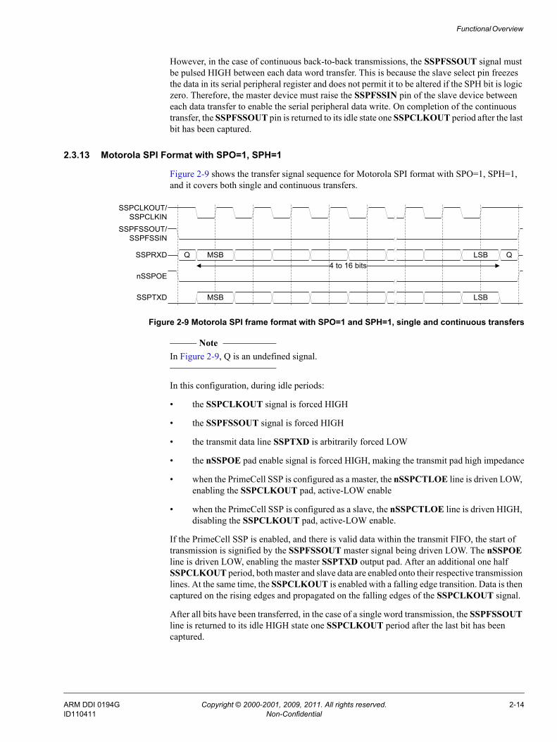
2.3.13 Motorola SPI Format with SPO=1, SPH=1
Figure 2-9 shows the transfer signal sequence for Motorola SPI format with SPO=1, SPH=1, and it covers both single and continuous transfers.
Figure 2-9 Motorola SPI frame format with SPO=1 and SPH=1, single and continuous transfers
Note In Figure 2-9, Q is an undefined signal.
In this configuration, during idle periods:
• the SSPCLKOUT signal is forced HIGH
• the SSPFSSOUT signal is forced HIGH
• the transmit data line SSPTXD is arbitrarily forced LOW
• the nSSPOE pad enable signal is forced HIGH, making the transmit pad high impedance
• when the PrimeCell SSP is configured as a master, the nSSPCTLOE line is driven LOW, enabling the SSPCLKOUT pad, active-LOW enable
• when the PrimeCell SSP is configured as a slave, the nSSPCTLOE line is driven HIGH, disabling the SSPCLKOUT pad, active-LOW enable.
If the PrimeCell SSP is enabled, and there is valid data within the transmit FIFO, the start of transmission is signified by the SSPFSSOUT master signal being driven LOW. The nSSPOE line is driven LOW, enabling the master SSPTXD output pad. After an additional one half SSPCLKOUT period, both master and slave data are enabled onto their respective transmission lines. At the same time, the SSPCLKOUT is enabled with a falling edge transition. Data is then captured on the rising edges and propagated on the falling edges of the SSPCLKOUT signal.
After all bits have been transferred, in the case of a single word transmission, the SSPFSSOUT line is returned to its idle HIGH state one SSPCLKOUT period after the last bit has been captured.
4 to 16 bits
SSPCLKOUT/SSPCLKIN
nSSPOE
SSPFSSOUT/SSPFSSIN
SSPRXD
SSPTXD LSB
Q MSB QLSB
MSB
ARM DDI 0194G Copyright © 2000-2001, 2009, 2011. All rights reserved. 2-14ID110411 Non-Confidential
Functional Overview
For continuous back-to-back transmissions, the SSPFSSOUT pin remains in its active-LOW state, until the final bit of the last word has been captured, and then returns to its idle state as the previous section describes.
For continuous back-to-back transfers, the SSPFSSOUT pin is held LOW between successive data words and termination is the same as that of the single word transfer.
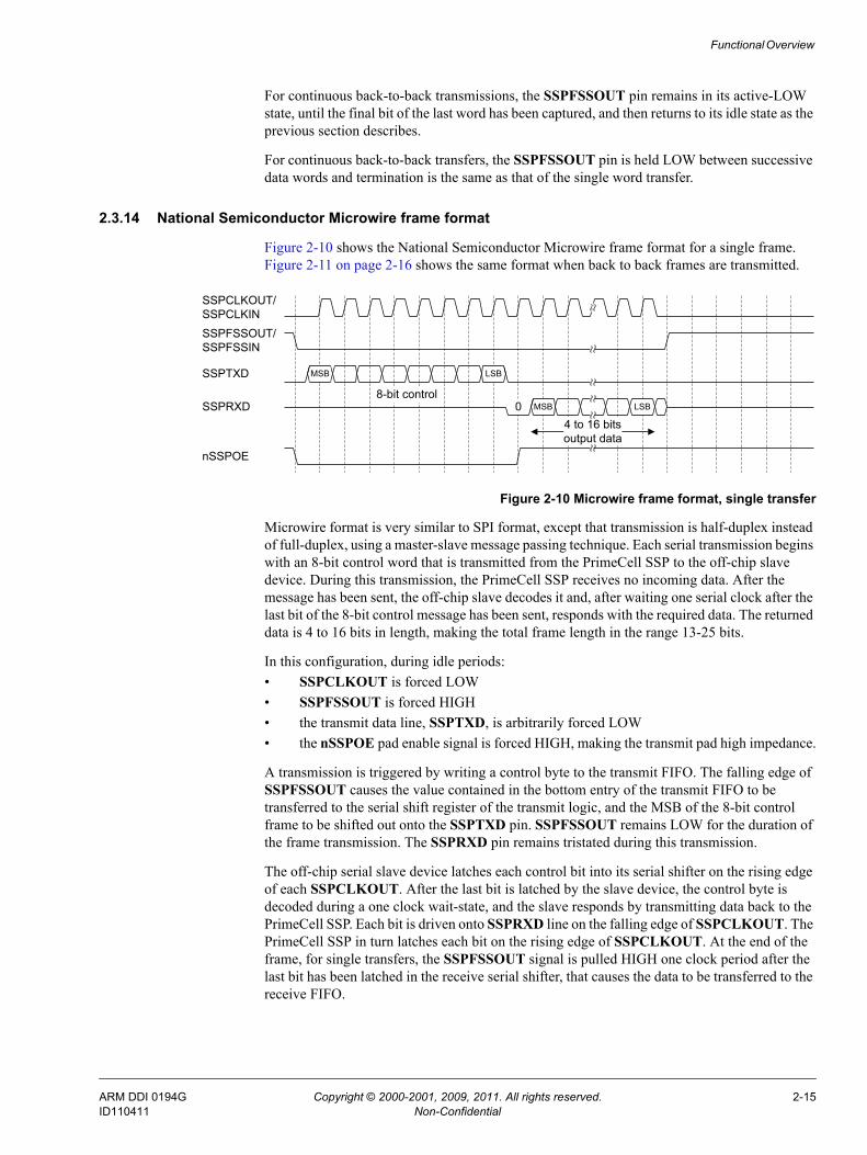
2.3.14 National Semiconductor Microwire frame format
Figure 2-10 shows the National Semiconductor Microwire frame format for a single frame. Figure 2-11 on page 2-16 shows the same format when back to back frames are transmitted.
Figure 2-10 Microwire frame format, single transfer
Microwire format is very similar to SPI format, except that transmission is half-duplex instead of full-duplex, using a master-slave message passing technique. Each serial transmission begins with an 8-bit control word that is transmitted from the PrimeCell SSP to the off-chip slave device. During this transmission, the PrimeCell SSP receives no incoming data. After the message has been sent, the off-chip slave decodes it and, after waiting one serial clock after the last bit of the 8-bit control message has been sent, responds with the required data. The returned data is 4 to 16 bits in length, making the total frame length in the range 13-25 bits.
In this configuration, during idle periods:• SSPCLKOUT is forced LOW• SSPFSSOUT is forced HIGH• the transmit data line, SSPTXD, is arbitrarily forced LOW• the nSSPOE pad enable signal is forced HIGH, making the transmit pad high impedance.
A transmission is triggered by writing a control byte to the transmit FIFO. The falling edge of SSPFSSOUT causes the value contained in the bottom entry of the transmit FIFO to be transferred to the serial shift register of the transmit logic, and the MSB of the 8-bit control frame to be shifted out onto the SSPTXD pin. SSPFSSOUT remains LOW for the duration of the frame transmission. The SSPRXD pin remains tristated during this transmission.
The off-chip serial slave device latches each control bit into its serial shifter on the rising edge of each SSPCLKOUT. After the last bit is latched by the slave device, the control byte is decoded during a one clock wait-state, and the slave responds by transmitting data back to the PrimeCell SSP. Each bit is driven onto SSPRXD line on the falling edge of SSPCLKOUT. The PrimeCell SSP in turn latches each bit on the rising edge of SSPCLKOUT. At the end of the frame, for single transfers, the SSPFSSOUT signal is pulled HIGH one clock period after the last bit has been latched in the receive serial shifter, that causes the data to be transferred to the receive FIFO.
SSPCLKOUT/ SSPCLKIN SSPFSSOUT/SSPFSSIN
LSBMSBSSPRXD
nSSPOE
4 to 16 bitsoutput data
SSPTXD MSB LSB
8-bit control0
ARM DDI 0194G Copyright © 2000-2001, 2009, 2011. All rights reserved. 2-15ID110411 Non-Confidential
Functional Overview
Note The off-chip slave device can tristate the receive line either on the falling edge of SSPCLKOUT after the LSB has been latched by the receive shifter, or when the SSPFSSOUT pin goes HIGH.
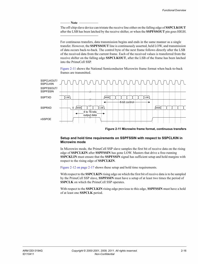
For continuous transfers, data transmission begins and ends in the same manner as a single transfer. However, the SSPFSSOUT line is continuously asserted, held LOW, and transmission of data occurs back-to-back. The control byte of the next frame follows directly after the LSB of the received data from the current frame. Each of the received values is transferred from the receive shifter on the falling edge SSPCLKOUT, after the LSB of the frame has been latched into the PrimeCell SSP.
Figure 2-11 shows the National Semiconductor Microwire frame format when back-to-back frames are transmitted.
Figure 2-11 Microwire frame format, continuous transfers
Setup and hold time requirements on SSPFSSIN with respect to SSPCLKIN in Microwire mode
In Microwire mode, the PrimeCell SSP slave samples the first bit of receive data on the rising edge of SSPCLKIN after SSPFSSIN has gone LOW. Masters that drive a free-running SSPCKLIN must ensure that the SSPFSSIN signal has sufficient setup and hold margins with respect to the rising edge of SSPCLKIN.
Figure 2-12 on page 2-17 shows these setup and hold time requirements.
With respect to the SSPCLKIN rising edge on which the first bit of receive data is to be sampled by the PrimeCell SSP slave, SSPFSSIN must have a setup of at least two times the period of SSPCLK on which the PrimeCell SSP operates.
With respect to the SSPCLKIN rising edge previous to this edge, SSPFSSIN must have a hold of at least one SSPCLK period.
8-bit control
SSPCLKOUT/ SSPCLKIN SSPFSSOUT/SSPFSSIN
LSBMSBSSPRXD
nSSPOE
4 to 16 bitsoutput data
SSPTXD MSB LSBLSB
MSB0
ARM DDI 0194G Copyright © 2000-2001, 2009, 2011. All rights reserved. 2-16ID110411 Non-Confidential
Functional Overview
Figure 2-12 Microwire frame format, SSPFSSIN input setup and hold requirements
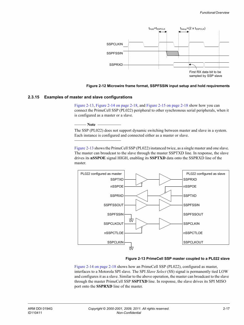
2.3.15 Examples of master and slave configurations
Figure 2-13, Figure 2-14 on page 2-18, and Figure 2-15 on page 2-18 show how you can connect the PrimeCell SSP (PL022) peripheral to other synchronous serial peripherals, when it is configured as a master or a slave.
Note The SSP (PL022) does not support dynamic switching between master and slave in a system. Each instance is configured and connected either as a master or slave.
Figure 2-13 shows the PrimeCell SSP (PL022) instanced twice, as a single master and one slave. The master can broadcast to the slave through the master SSPTXD line. In response, the slave drives its nSSPOE signal HIGH, enabling its SSPTXD data onto the SSPRXD line of the master.
Figure 2-13 PrimeCell SSP master coupled to a PL022 slave
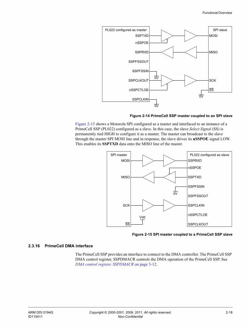
Figure 2-14 on page 2-18 shows how an PrimeCell SSP (PL022), configured as master, interfaces to a Motorola SPI slave. The SPI Slave Select (SS) signal is permanently tied LOW and configures it as a slave. Similar to the above operation, the master can broadcast to the slave through the master PrimeCell SSP SSPTXD line. In response, the slave drives its SPI MISO port onto the SSPRXD line of the master.
SSPCLKIN
SSPFSSIN
SSPRXD
First RX data bit to besampled by SSP slave
tSetup=(2 x tSSPCLK)tHold=tSSPCLK
PL022 configured as master
SSPTXD
SSPRXD
SSPFSSOUT
SSPFSSIN
SSPCLKOUT
SSPCLKIN
nSSPOE
nSSPCTLOE
PL022 configured as slave
SSPRXD
nSSPOE
SSPTXD
SSPFSSOUT
SSPFSSIN
SSPCLKOUT
nSSPCTLOE
SSPCLKIN0V
0V
ARM DDI 0194G Copyright © 2000-2001, 2009, 2011. All rights reserved. 2-17ID110411 Non-Confidential
Functional Overview
Figure 2-14 PrimeCell SSP master coupled to an SPI slave
Figure 2-15 shows a Motorola SPI configured as a master and interfaced to an instance of a PrimeCell SSP (PL022) configured as a slave. In this case, the slave Select Signal (SS) is permanently tied HIGH to configure it as a master. The master can broadcast to the slave through the master SPI MOSI line and in response, the slave drives its nSSPOE signal LOW. This enables its SSPTXD data onto the MISO line of the master.
Figure 2-15 SPI master coupled to a PrimeCell SSP slave
2.3.16 PrimeCell DMA interface
The PrimeCell SSP provides an interface to connect to the DMA controller. The PrimeCell SSP DMA control register, SSPDMACR controls the DMA operation of the PrimeCell SSP. See DMA control register, SSPDMACR on page 3-12.
PL022 configured as master
SSPTXD
SSPRXD
SSPFSSOUT
SSPFSSIN
SSPCLKOUT
SSPCLKIN
nSSPOE
nSSPCTLOE
SPI slave
MOSI
MISO
SCK
SS
0V
0V
0V
SPI master
MOSI
MISO
SCK
PL022 configured as slave
SSPRXD
nSSPOE
SSPTXD
SSPFSSOUT
SSPFSSIN
SSPCLKOUT
nSSPCTLOE
SSPCLKIN
0V
SS
Vdd
ARM DDI 0194G Copyright © 2000-2001, 2009, 2011. All rights reserved. 2-18ID110411 Non-Confidential
Functional Overview
Receive
The DMA interface includes the following signals, for receive:
SSPRXDMASREQ Single-character DMA transfer request, asserted by the SSP. This signal is asserted when the receive FIFO contains at least one character.
SSPRXDMABREQ Burst DMA transfer request, asserted by the SSP. This signal is asserted when the receive FIFO contains four or more characters.
SSPRXDMACLR DMA request clear, asserted by the DMA controller to clear the receive request signals. If DMA burst transfer is requested, the clear signal is asserted during the transfer of the last data in the burst.
Transmit
The DMA interface includes the following signals, for transmit:
SSPTXDMASREQ Single-character DMA transfer request, asserted by the SSP. This signal is asserted when there is at least one empty location in the transmit FIFO.
SSPTXDMABREQ Burst DMA transfer request, asserted by the SSP. This signal is asserted when the transmit FIFO contains four characters or fewer.
SSPTXDMACLR DMA request clear, asserted by the DMA controller, to clear the transmit request signals. If a DMA burst transfer is requested, the clear signal is asserted during the transfer of the last data in the burst.
The burst transfer and single transfer request signals are not mutually exclusive. They can both be asserted at the same time. For example, when there is more data than the watermark level of four in the receive FIFO, the burst transfer request, and the single transfer request, are asserted. When the amount of data left in the receive FIFO is less than the watermark level, the single request only is asserted. This is useful for situations where the number of characters left to be received in the stream is less than a burst.
For example, if 19 characters must be received, the DMA controller then transfers four bursts of four characters, and three single transfers to complete the stream.
Note For the remaining three characters, the PrimeCell SSP does not assert the burst request.
Each request signal remains asserted until the relevant DMA clear signal is asserted. After the request clear signal is deasserted, a request signal can become active again, depending on the conditions that previous sections describe. All request signals are deasserted if the PrimeCell SSP is disabled, or the DMA enable signal is cleared.
ARM DDI 0194G Copyright © 2000-2001, 2009, 2011. All rights reserved. 2-19ID110411 Non-Confidential
Functional Overview
Table 2-1 shows the trigger points for DMABREQ, for both the transmit and receive FIFOs.
Figure 2-16 shows the timing diagram for both a single transfer request, and a burst transfer request, with the appropriate DMA clear signal. The signals are all synchronous to PCLK.
Figure 2-16 DMA transfer waveforms
Table 2-1 DMA trigger points for the transmit and receive FIFOs
Burst length
Watermark level Transmit, number of empty locations Receive, number of filled locations
1/2 4 4
PCLK
DMASREQ
DMABREQ
DMACLR
ARM DDI 0194G Copyright © 2000-2001, 2009, 2011. All rights reserved. 2-20ID110411 Non-Confidential
Chapter 3 Programmer’s Model
This chapter describes the ARM PrimeCell Synchronous Serial Port (PL022) registers and provides details needed when programming the microcontroller.
It contains the following sections:• About the programmer’s model on page 3-2• Summary of PrimeCell SSP registers on page 3-3• Register descriptions on page 3-4• Interrupts on page 3-20.
ARM DDI 0194G Copyright © 2000-2001, 2009, 2011. All rights reserved. 3-1ID110411 Non-Confidential
Programmer’s Model
3.1 About the programmer’s modelThe following information applies to the Synchronous Serial Port (PL022) registers:
• The base address is not fixed, and can be different for any particular system implementation. The offset of each register from the base address is fixed.
• Do not attempt to access reserved or unused address locations. Attempting to access these locations can result in Unpredictable behavior.
• Unless otherwise stated in the accompanying text:— do not modify undefined register bits— ignore undefined register bits on reads— all register bits are reset to a logic 0 by a system or power-on reset.
• Access type in Table 3-1 on page 3-3 is described as follows:RW Read and write.RO Read only.WO Write only.
The following locations are reserved, and must not be used during normal operation:
• locations at offsets +0x028 to +0x07C and +0xFD0 to +0xFDC are reserved for possible future extensions
• locations at offsets +0x080 to +0x088 are reserved for test purposes.
ARM DDI 0194G Copyright © 2000-2001, 2009, 2011. All rights reserved. 3-2ID110411 Non-Confidential
Programmer’s Model
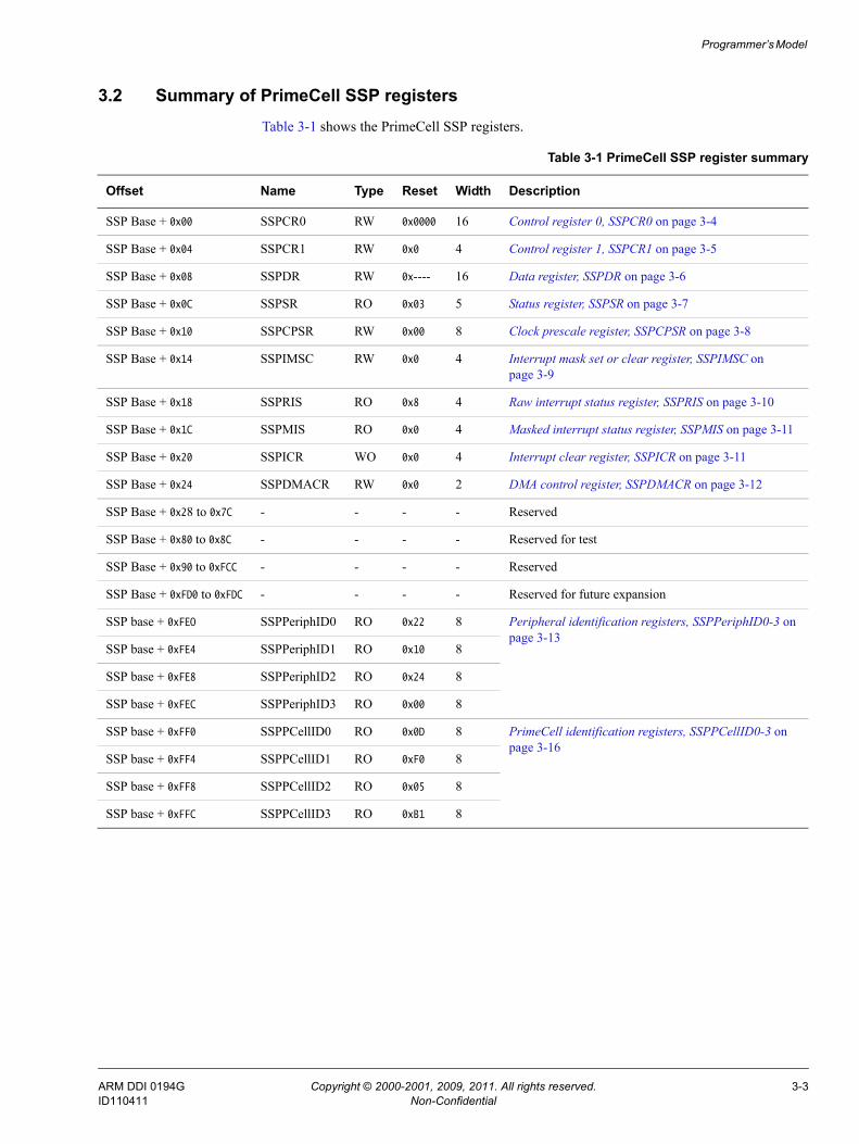
3.2 Summary of PrimeCell SSP registersTable 3-1 shows the PrimeCell SSP registers.
Table 3-1 PrimeCell SSP register summary
Offset Name Type Reset Width Description
SSP Base + 0x00 SSPCR0 RW 0x0000 16 Control register 0, SSPCR0 on page 3-4
SSP Base + 0x04 SSPCR1 RW 0x0 4 Control register 1, SSPCR1 on page 3-5
SSP Base + 0x08 SSPDR RW 0x---- 16 Data register, SSPDR on page 3-6
SSP Base + 0x0C SSPSR RO 0x03 5 Status register, SSPSR on page 3-7
SSP Base + 0x10 SSPCPSR RW 0x00 8 Clock prescale register, SSPCPSR on page 3-8
SSP Base + 0x14 SSPIMSC RW 0x0 4 Interrupt mask set or clear register, SSPIMSC on page 3-9
SSP Base + 0x18 SSPRIS RO 0x8 4 Raw interrupt status register, SSPRIS on page 3-10
SSP Base + 0x1C SSPMIS RO 0x0 4 Masked interrupt status register, SSPMIS on page 3-11
SSP Base + 0x20 SSPICR WO 0x0 4 Interrupt clear register, SSPICR on page 3-11
SSP Base + 0x24 SSPDMACR RW 0x0 2 DMA control register, SSPDMACR on page 3-12
SSP Base + 0x28 to 0x7C - - - - Reserved
SSP Base + 0x80 to 0x8C - - - - Reserved for test
SSP Base + 0x90 to 0xFCC - - - - Reserved
SSP Base + 0xFD0 to 0xFDC - - - - Reserved for future expansion
SSP base + 0xFEO SSPPeriphID0 RO 0x22 8 Peripheral identification registers, SSPPeriphID0-3 on page 3-13
SSP base + 0xFE4 SSPPeriphID1 RO 0x10 8
SSP base + 0xFE8 SSPPeriphID2 RO 0x24 8
SSP base + 0xFEC SSPPeriphID3 RO 0x00 8
SSP base + 0xFF0 SSPPCellID0 RO 0x0D 8 PrimeCell identification registers, SSPPCellID0-3 on page 3-16
SSP base + 0xFF4 SSPPCellID1 RO 0xF0 8
SSP base + 0xFF8 SSPPCellID2 RO 0x05 8
SSP base + 0xFFC SSPPCellID3 RO 0xB1 8
ARM DDI 0194G Copyright © 2000-2001, 2009, 2011. All rights reserved. 3-3ID110411 Non-Confidential
Programmer’s Model
3.3 Register descriptionsThis section describes the PrimeCell SSP registers. Table 3-1 on page 3-3 provides cross references to individual registers.
3.3.1 Control register 0, SSPCR0
The SSPCR0 Register characteristics are:
Purpose SSPCR0 is control register 0 and contains five bit fields that control various functions within the PrimeCell SSP.
Usage constraints There are no usage constraints.
Configurations Available in all SSP configurations.
Attributes See Table 3-1 on page 3-3.
Figure 3-1 shows the bit assignments.
Figure 3-1 SSPCR0 Register bit assignments
Table 3-2 shows the bit assignments.
FRF DSSSCR
15 8 7 0
SPOSPH
6 5 4 3
Table 3-2 SSPCR0 Register bit assignments
Bits Name Function
[15:8] SCR Serial clock rate. The value SCR is used to generate the transmit and receive bit rate of the PrimeCell SSP. The bit rate is:
where CPSDVSR is an even value from 2-254, programmed through the SSPCPSR register and SCR is a value from 0-255.
[7] SPH SSPCLKOUT phase, applicable to Motorola SPI frame format only. See Motorola SPI frame format on page 2-10.
CPSDVR x (1+SCR)
FSSPCLK
ARM DDI 0194G Copyright © 2000-2001, 2009, 2011. All rights reserved. 3-4ID110411 Non-Confidential
Programmer’s Model
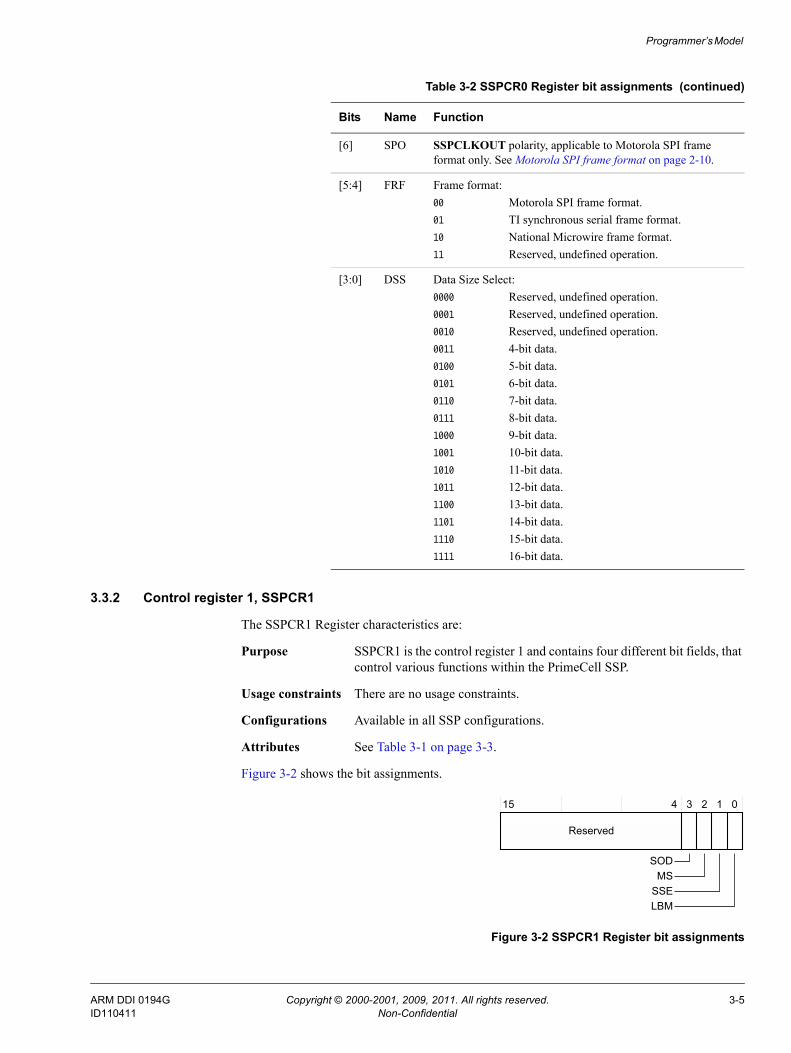
3.3.2 Control register 1, SSPCR1
The SSPCR1 Register characteristics are:
Purpose SSPCR1 is the control register 1 and contains four different bit fields, that control various functions within the PrimeCell SSP.
Usage constraints There are no usage constraints.
Configurations Available in all SSP configurations.
Attributes See Table 3-1 on page 3-3.
Figure 3-2 shows the bit assignments.
Figure 3-2 SSPCR1 Register bit assignments
[6] SPO SSPCLKOUT polarity, applicable to Motorola SPI frame format only. See Motorola SPI frame format on page 2-10.
[5:4] FRF Frame format:00 Motorola SPI frame format.01 TI synchronous serial frame format.10 National Microwire frame format.11 Reserved, undefined operation.
[3:0] DSS Data Size Select:0000 Reserved, undefined operation.0001 Reserved, undefined operation.0010 Reserved, undefined operation.0011 4-bit data.0100 5-bit data.0101 6-bit data.0110 7-bit data.0111 8-bit data.1000 9-bit data.1001 10-bit data.1010 11-bit data.1011 12-bit data.1100 13-bit data.1101 14-bit data.1110 15-bit data.1111 16-bit data.
Table 3-2 SSPCR0 Register bit assignments (continued)
Bits Name Function
Reserved
15 04 3 2 1
SODMS
SSELBM
ARM DDI 0194G Copyright © 2000-2001, 2009, 2011. All rights reserved. 3-5ID110411 Non-Confidential
Programmer’s Model
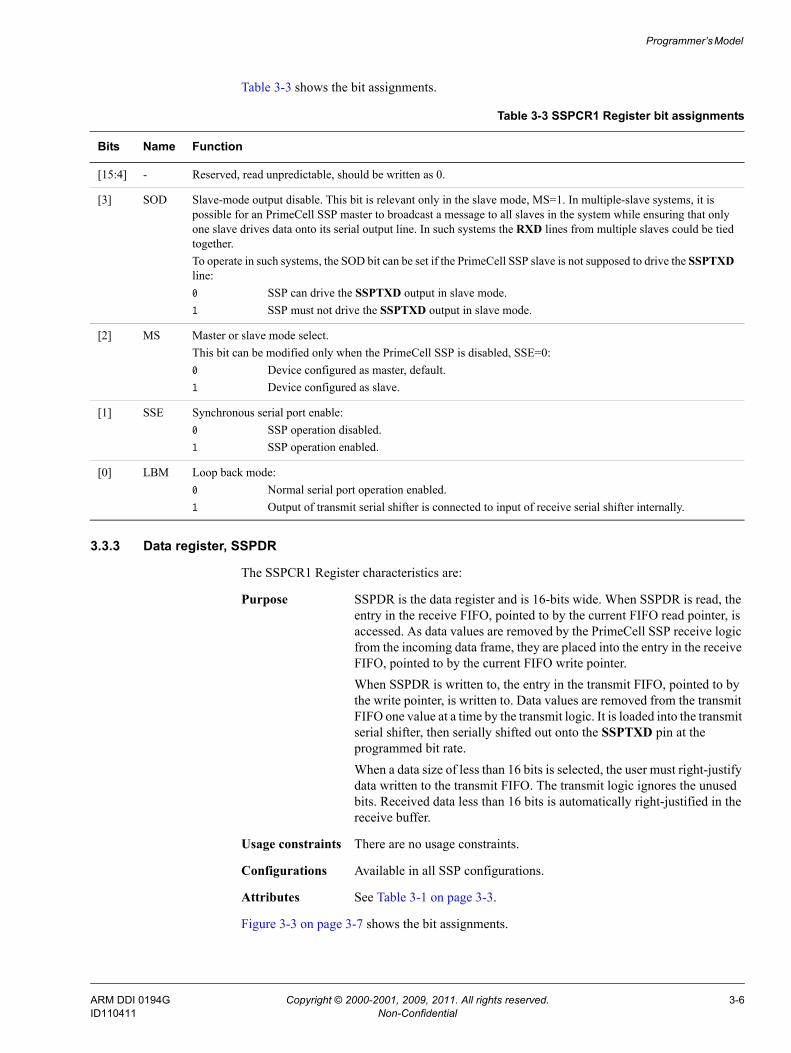
Table 3-3 shows the bit assignments.
3.3.3 Data register, SSPDR
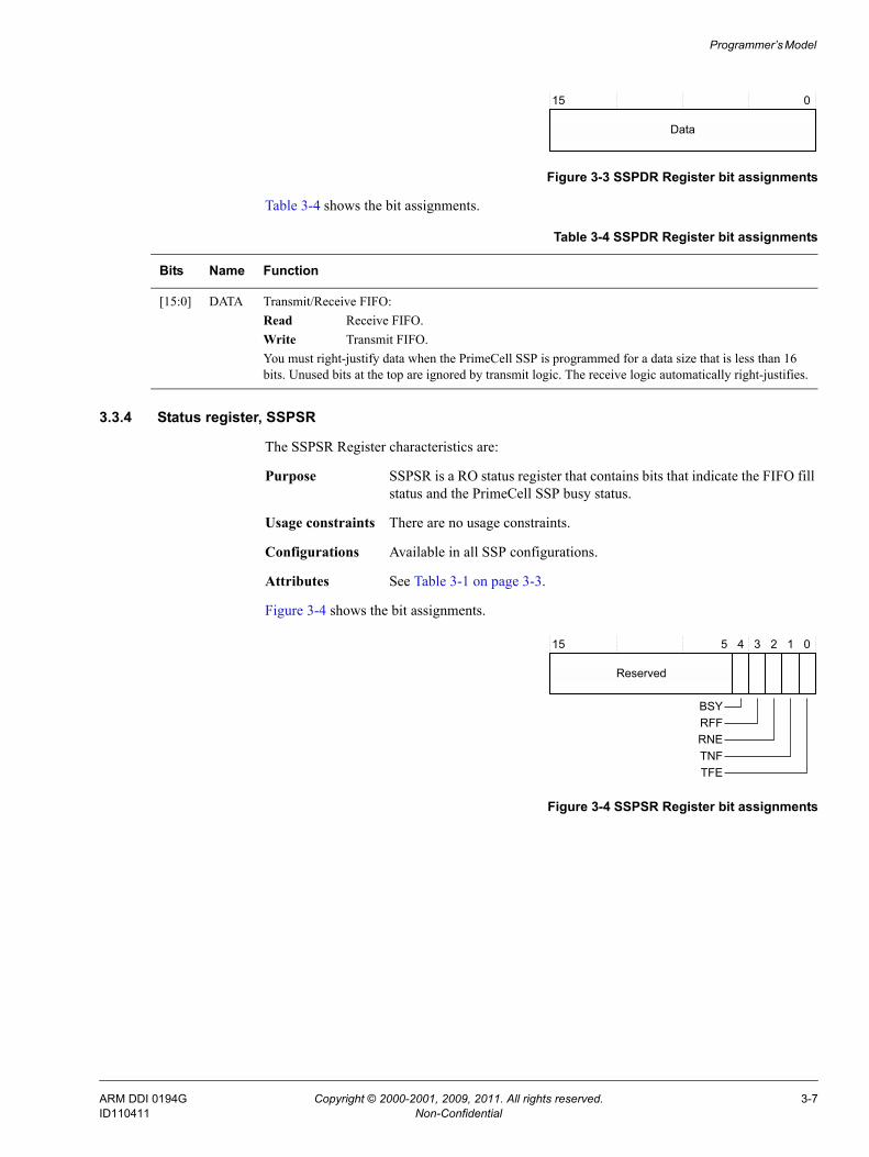
The SSPCR1 Register characteristics are:
Purpose SSPDR is the data register and is 16-bits wide. When SSPDR is read, the entry in the receive FIFO, pointed to by the current FIFO read pointer, is accessed. As data values are removed by the PrimeCell SSP receive logic from the incoming data frame, they are placed into the entry in the receive FIFO, pointed to by the current FIFO write pointer.When SSPDR is written to, the entry in the transmit FIFO, pointed to by the write pointer, is written to. Data values are removed from the transmit FIFO one value at a time by the transmit logic. It is loaded into the transmit serial shifter, then serially shifted out onto the SSPTXD pin at the programmed bit rate.When a data size of less than 16 bits is selected, the user must right-justify data written to the transmit FIFO. The transmit logic ignores the unused bits. Received data less than 16 bits is automatically right-justified in the receive buffer.
Usage constraints There are no usage constraints.
Configurations Available in all SSP configurations.
Attributes See Table 3-1 on page 3-3.
Figure 3-3 on page 3-7 shows the bit assignments.
Table 3-3 SSPCR1 Register bit assignments
Bits Name Function
[15:4] - Reserved, read unpredictable, should be written as 0.
[3] SOD Slave-mode output disable. This bit is relevant only in the slave mode, MS=1. In multiple-slave systems, it is possible for an PrimeCell SSP master to broadcast a message to all slaves in the system while ensuring that only one slave drives data onto its serial output line. In such systems the RXD lines from multiple slaves could be tied together.To operate in such systems, the SOD bit can be set if the PrimeCell SSP slave is not supposed to drive the SSPTXD line:0 SSP can drive the SSPTXD output in slave mode.1 SSP must not drive the SSPTXD output in slave mode.
[2] MS Master or slave mode select.This bit can be modified only when the PrimeCell SSP is disabled, SSE=0:0 Device configured as master, default.1 Device configured as slave.
[1] SSE Synchronous serial port enable:0 SSP operation disabled.1 SSP operation enabled.
[0] LBM Loop back mode:0 Normal serial port operation enabled.1 Output of transmit serial shifter is connected to input of receive serial shifter internally.
ARM DDI 0194G Copyright © 2000-2001, 2009, 2011. All rights reserved. 3-6ID110411 Non-Confidential
Programmer’s Model
Figure 3-3 SSPDR Register bit assignments
Table 3-4 shows the bit assignments.
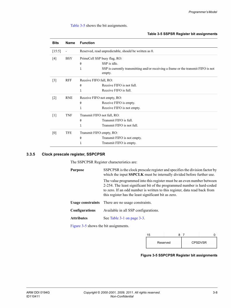
3.3.4 Status register, SSPSR
The SSPSR Register characteristics are:
Purpose SSPSR is a RO status register that contains bits that indicate the FIFO fill status and the PrimeCell SSP busy status.
Usage constraints There are no usage constraints.
Configurations Available in all SSP configurations.
Attributes See Table 3-1 on page 3-3.
Figure 3-4 shows the bit assignments.
Figure 3-4 SSPSR Register bit assignments
Data
15 0
Table 3-4 SSPDR Register bit assignments
Bits Name Function
[15:0] DATA Transmit/Receive FIFO:Read Receive FIFO.Write Transmit FIFO.You must right-justify data when the PrimeCell SSP is programmed for a data size that is less than 16 bits. Unused bits at the top are ignored by transmit logic. The receive logic automatically right-justifies.
Reserved
15 05 4 3 2 1
BSYRFFRNETNFTFE
ARM DDI 0194G Copyright © 2000-2001, 2009, 2011. All rights reserved. 3-7ID110411 Non-Confidential
Programmer’s Model
Table 3-5 shows the bit assignments.
3.3.5 Clock prescale register, SSPCPSR
The SSPCPSR Register characteristics are:
Purpose SSPCPSR is the clock prescale register and specifies the division factor by which the input SSPCLK must be internally divided before further use.The value programmed into this register must be an even number between 2-254. The least significant bit of the programmed number is hard-coded to zero. If an odd number is written to this register, data read back from this register has the least significant bit as zero.
Usage constraints There are no usage constraints.
Configurations Available in all SSP configurations.
Attributes See Table 3-1 on page 3-3.
Figure 3-5 shows the bit assignments.
Figure 3-5 SSPCPSR Register bit assignments
Table 3-5 SSPSR Register bit assignments
Bits Name Function
[15:5] - Reserved, read unpredictable, should be written as 0.
[4] BSY PrimeCell SSP busy flag, RO:0 SSP is idle.1 SSP is currently transmitting and/or receiving a frame or the transmit FIFO is not
empty.
[3] RFF Receive FIFO full, RO:0 Receive FIFO is not full.1 Receive FIFO is full.
[2] RNE Receive FIFO not empty, RO:0 Receive FIFO is empty.1 Receive FIFO is not empty.
[1] TNF Transmit FIFO not full, RO:0 Transmit FIFO is full.1 Transmit FIFO is not full.
[0] TFE Transmit FIFO empty, RO:0 Transmit FIFO is not empty.1 Transmit FIFO is empty.
CPSDVSRReserved
15 078
ARM DDI 0194G Copyright © 2000-2001, 2009, 2011. All rights reserved. 3-8ID110411 Non-Confidential
Programmer’s Model
Table 3-6 shows the bit assignments.
3.3.6 Interrupt mask set or clear register, SSPIMSC
The SSPIMSC Register characteristics are:
Purpose The SSPIMSC register is the interrupt mask set or clear register. It is a RW register.On a read this register gives the current value of the mask on the relevant interrupt. A write of 1 to the particular bit sets the mask, enabling the interrupt to be read. A write of 0 clears the corresponding mask.All the bits are cleared to 0 when reset.
Usage constraints There are no usage constraints.
Configurations Available in all SSP configurations.
Attributes See Table 3-1 on page 3-3.
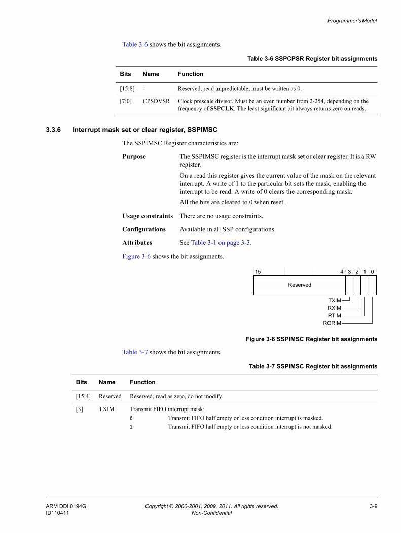
Figure 3-6 shows the bit assignments.
Figure 3-6 SSPIMSC Register bit assignments
Table 3-7 shows the bit assignments.
Table 3-6 SSPCPSR Register bit assignments
Bits Name Function
[15:8] - Reserved, read unpredictable, must be written as 0.
[7:0] CPSDVSR Clock prescale divisor. Must be an even number from 2-254, depending on the frequency of SSPCLK. The least significant bit always returns zero on reads.
Reserved
15 04 3 2 1
TXIMRXIMRTIM
RORIM
Table 3-7 SSPIMSC Register bit assignments
Bits Name Function
[15:4] Reserved Reserved, read as zero, do not modify.
[3] TXIM Transmit FIFO interrupt mask:0 Transmit FIFO half empty or less condition interrupt is masked.1 Transmit FIFO half empty or less condition interrupt is not masked.
ARM DDI 0194G Copyright © 2000-2001, 2009, 2011. All rights reserved. 3-9ID110411 Non-Confidential
Programmer’s Model
3.3.7 Raw interrupt status register, SSPRIS
The SSPRIS Register characteristics are:
Purpose The SSPRIS register is the raw interrupt status register. It is a RO register. On a read this register gives the current raw status value of the corresponding interrupt prior to masking. A write has no effect.
Usage constraints There are no usage constraints.
Configurations Available in all SSP configurations.
Attributes See Table 3-1 on page 3-3.
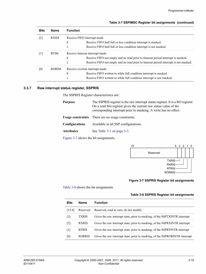
Figure 3-7 shows the bit assignments.
Figure 3-7 SSPRIS Register bit assignments
Table 3-8 shows the bit assignments.
[2] RXIM Receive FIFO interrupt mask:0 Receive FIFO half full or less condition interrupt is masked.1 Receive FIFO half full or less condition interrupt is not masked.
[1] RTIM Receive timeout interrupt mask:0 Receive FIFO not empty and no read prior to timeout period interrupt is masked.1 Receive FIFO not empty and no read prior to timeout period interrupt is not masked.
[0] RORIM Receive overrun interrupt mask:0 Receive FIFO written to while full condition interrupt is masked.1 Receive FIFO written to while full condition interrupt is not masked.
Table 3-7 SSPIMSC Register bit assignments (continued)
Bits Name Function
Reserved
15 04 3 2 1
TXRISRXRISRTRIS
RORRIS
Table 3-8 SSPRIS Register bit assignments
Bits Name Function
[15:4] Reserved Reserved, read as zero, do not modify
[3] TXRIS Gives the raw interrupt state, prior to masking, of the SSPTXINTR interrupt
[2] RXRIS Gives the raw interrupt state, prior to masking, of the SSPRXINTR interrupt
[1] RTRIS Gives the raw interrupt state, prior to masking, of the SSPRTINTR interrupt
[0] RORRIS Gives the raw interrupt state, prior to masking, of the SSPRORINTR interrupt
ARM DDI 0194G Copyright © 2000-2001, 2009, 2011. All rights reserved. 3-10ID110411 Non-Confidential
Programmer’s Model
3.3.8 Masked interrupt status register, SSPMIS
The SSPMIS Register characteristics are:
Purpose The SSPMIS register is the masked interrupt status register. It is a RO register. On a read this register gives the current masked status value of the corresponding interrupt. A write has no effect.
Usage constraints There are no usage constraints.
Configurations Available in all SSP configurations.
Attributes See Table 3-1 on page 3-3.
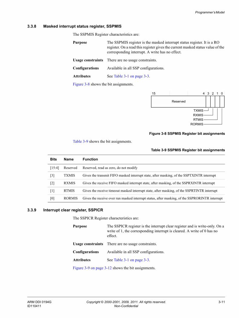
Figure 3-8 shows the bit assignments.
Figure 3-8 SSPMIS Register bit assignments
Table 3-9 shows the bit assignments.
3.3.9 Interrupt clear register, SSPICR
The SSPICR Register characteristics are:
Purpose The SSPICR register is the interrupt clear register and is write-only. On a write of 1, the corresponding interrupt is cleared. A write of 0 has no effect.
Usage constraints There are no usage constraints.
Configurations Available in all SSP configurations.
Attributes See Table 3-1 on page 3-3.
Figure 3-9 on page 3-12 shows the bit assignments.
Reserved
15 04 3 2 1
TXMISRXMISRTMIS
RORMIS
Table 3-9 SSPMIS Register bit assignments
Bits Name Function
[15:4] Reserved Reserved, read as zero, do not modify
[3] TXMIS Gives the transmit FIFO masked interrupt state, after masking, of the SSPTXINTR interrupt
[2] RXMIS Gives the receive FIFO masked interrupt state, after masking, of the SSPRXINTR interrupt
[1] RTMIS Gives the receive timeout masked interrupt state, after masking, of the SSPRTINTR interrupt
[0] RORMIS Gives the receive over run masked interrupt status, after masking, of the SSPRORINTR interrupt
ARM DDI 0194G Copyright © 2000-2001, 2009, 2011. All rights reserved. 3-11ID110411 Non-Confidential
Programmer’s Model
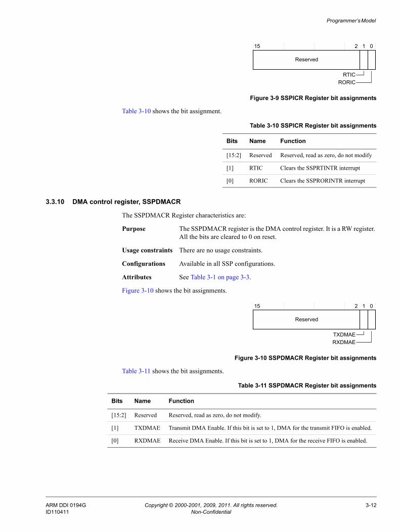
Figure 3-9 SSPICR Register bit assignments
Table 3-10 shows the bit assignment.
3.3.10 DMA control register, SSPDMACR
The SSPDMACR Register characteristics are:
Purpose The SSPDMACR register is the DMA control register. It is a RW register. All the bits are cleared to 0 on reset.
Usage constraints There are no usage constraints.
Configurations Available in all SSP configurations.
Attributes See Table 3-1 on page 3-3.
Figure 3-10 shows the bit assignments.
Figure 3-10 SSPDMACR Register bit assignments
Table 3-11 shows the bit assignments.
Reserved
15 02 1
RTICRORIC
Table 3-10 SSPICR Register bit assignments
Bits Name Function
[15:2] Reserved Reserved, read as zero, do not modify
[1] RTIC Clears the SSPRTINTR interrupt
[0] RORIC Clears the SSPRORINTR interrupt
Reserved
15 02 1
TXDMAERXDMAE
Table 3-11 SSPDMACR Register bit assignments
Bits Name Function
[15:2] Reserved Reserved, read as zero, do not modify.
[1] TXDMAE Transmit DMA Enable. If this bit is set to 1, DMA for the transmit FIFO is enabled.
[0] RXDMAE Receive DMA Enable. If this bit is set to 1, DMA for the receive FIFO is enabled.
ARM DDI 0194G Copyright © 2000-2001, 2009, 2011. All rights reserved. 3-12ID110411 Non-Confidential
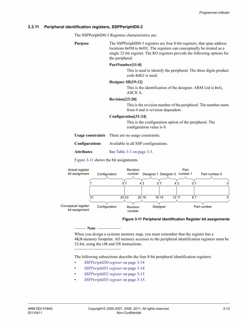
Programmer’s Model
3.3.11 Peripheral identification registers, SSPPeriphID0-3
The SSPPeriphID0-3 Registers characteristics are:
Purpose The SSPPeriphID0-3 registers are four 8-bit registers, that span address locations 0xFE0 to 0xFEC. The registers can conceptually be treated as a single 32-bit register. The RO registers provide the following options for the peripheral:PartNumber[11:0]
This is used to identify the peripheral. The three digits product code 0x022 is used.
Designer ID[19:12] This is the identification of the designer. ARM Ltd is 0x41, ASCII A.
Revision[23:20] This is the revision number of the peripheral. The number starts from 0 and is revision dependent.
Configuration[31:24] This is the configuration option of the peripheral. The configuration value is 0.
Usage constraints There are no usage constraints.
Configurations Available in all SSP configurations.
Attributes See Table 3-1 on page 3-3.
Figure 3-11 shows the bit assignments.
Figure 3-11 Peripheral identification Register bit assignments
Note When you design a systems memory map, you must remember that the register has a 4KB-memory footprint. All memory accesses to the peripheral identification registers must be 32-bit, using the LDR and STR instructions.
The following subsections describe the four 8-bit peripheral identification registers:• SSPPeriphID0 register on page 3-14• SSPPeriphID1 register on page 3-14• SSPPeriphID2 register on page 3-15• SSPPeriphID3 register on page 3-15.
31 24 23 20 19 16 15 12 11 8 7 0
Part number
Part number 1 Part number 0Designer 1 Designer 0
Designer
Revision numberConfiguration
7 00347034707
Configuration Revision number
Conceptual register bit assignment
Actual register bit assignment
ARM DDI 0194G Copyright © 2000-2001, 2009, 2011. All rights reserved. 3-13ID110411 Non-Confidential
Programmer’s Model
SSPPeriphID0 register
The SSPPeriphID0 Register characteristics are:
Purpose The SSPPeriphID0 register is hard-coded and the fields within the register determine the reset value.
Usage constraints There are no usage constraints.
Configurations Available in all SSP configurations.
Attributes See Table 3-1 on page 3-3.
Figure 3-12 shows the bit assignments.
Figure 3-12 SSPPeriphID0 Register bit assignments
Table 3-12 shows the bit assignments.
SSPPeriphID1 register
The SSPPeriphID1 Register characteristics are:
Purpose The SSPPeriphID1 register is hard-coded and the fields within the register determine the reset value.
Usage constraints There are no usage constraints.
Configurations Available in all SSP configurations.
Attributes See Table 3-1 on page 3-3.
Figure 3-13 shows the bit assignments.
Figure 3-13 SSPPeriphID1 Register bit assignments
PartNumber0Reserved
15 078
Table 3-12 SSPPeriphID0 Register bit assignments
Bits Name Description
[15:8] Reserved Reserved, read undefined must read as zeros
[7:0] PartNumber0 These bits read back as 0x22
Designer0Reserved
15 078 4 3
PartNumber1
ARM DDI 0194G Copyright © 2000-2001, 2009, 2011. All rights reserved. 3-14ID110411 Non-Confidential
Programmer’s Model
Table 3-13 shows the bit assignments.
SSPPeriphID2 register
The SSPPeriphID2 Register characteristics are:
Purpose The SSPPeriphID2 register is hard-coded and the fields within the register determine the reset value.
Usage constraints There are no usage constraints.
Configurations Available in all SSP configurations.
Attributes See Table 3-1 on page 3-3.
Figure 3-14 shows the bit assignments.
Figure 3-14 SSPPeriphID2 Register bit assignments
Table 3-14 shows the bit assignments.
SSPPeriphID3 register
The SSPPeriphID3 Register characteristics are:
Purpose The SSPPeriphID3 register is hard-coded and the fields within the register determine the reset value.
Usage constraints There are no usage constraints.
Configurations Available in all SSP configurations.
Attributes See Table 3-1 on page 3-3.
Figure 3-15 on page 3-16 shows the bit assignments.
Table 3-13 SSPPeriphID1 Register bit assignments
Bits Name Description
[15:8] Reserved Reserved, read undefined, must read as zeros
[7:4] Designer0 These bits read back as 0x1
[3:0] PartNumber1 These bits read back as 0x0
Designer1RevisionReserved
15 078 4 3
Table 3-14 SSPPeriphID2 Register bit assignments
Bits Name Description
[15:8] Reserved Reserved, read undefined, must read as zeros
[7:4] Revision These bits return the peripheral revision
[3:0] Designer1 These bits read back as 0x4
ARM DDI 0194G Copyright © 2000-2001, 2009, 2011. All rights reserved. 3-15ID110411 Non-Confidential
Programmer’s Model
Figure 3-15 SSPPeriphID3 Register bit assignments
Table 3-15 shows the bit assignments.
3.3.12 PrimeCell identification registers, SSPPCellID0-3
The SSPPCellID0-3 Registers characteristics are:
Purpose The SSPPCellID0-3 registers are four 8-bit wide registers, that span address locations 0xFF0-0xFFC. The registers can conceptually be treated as a 32-bit register. The register is used as a standard cross-peripheral identification system. The SSPPCellID register is set to 0xB105F00D.
Usage constraints There are no usage constraints.
Configurations Available in all SSP configurations.
Attributes See Table 3-1 on page 3-3.
Figure 3-16 shows the bit assignments.
Figure 3-16 PrimeCell identification Register bit assignments
The following subsections describe the four, 8-bit PrimeCell identification registers:• SSPPCellID0 register• SSPPCellID1 register on page 3-17• SSPPCellID2 register on page 3-18• SSPPCellID3 register on page 3-18.
SSPPCellID0 register
The SSPPCellID0 Register characteristics are:
Purpose The SSPPCellID0 register is hard-coded and the fields within the register determine the reset value.
ConfigurationReserved
15 078
Table 3-15 SSPPeriphID3 Register bit assignments
Bits Name Description
[15:8] Reserved Reserved, read undefined, must read as zeros
[7:0] Configuration These bits read back as 0x00
31 24 23 16 15 8 7 0
SSPPCellID0
SSPPCellID0SSPPCellID1
SSPPCellID1
SSPPCellID2SSPPCellID3
7 0070707
SSPPCellID3 SSPPCellID2Conceptual register bit assignment
Actual register bit assignment
ARM DDI 0194G Copyright © 2000-2001, 2009, 2011. All rights reserved. 3-16ID110411 Non-Confidential
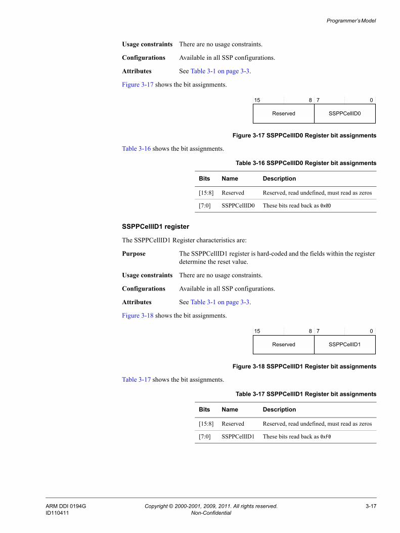
Programmer’s Model
Usage constraints There are no usage constraints.
Configurations Available in all SSP configurations.
Attributes See Table 3-1 on page 3-3.
Figure 3-17 shows the bit assignments.
Figure 3-17 SSPPCellID0 Register bit assignments
Table 3-16 shows the bit assignments.
SSPPCellID1 register
The SSPPCellID1 Register characteristics are:
Purpose The SSPPCellID1 register is hard-coded and the fields within the register determine the reset value.
Usage constraints There are no usage constraints.
Configurations Available in all SSP configurations.
Attributes See Table 3-1 on page 3-3.
Figure 3-18 shows the bit assignments.
Figure 3-18 SSPPCellID1 Register bit assignments
Table 3-17 shows the bit assignments.
SSPPCellID0Reserved
15 078
Table 3-16 SSPPCellID0 Register bit assignments
Bits Name Description
[15:8] Reserved Reserved, read undefined, must read as zeros
[7:0] SSPPCellID0 These bits read back as 0x0D
SSPPCellID1Reserved
15 078
Table 3-17 SSPPCellID1 Register bit assignments
Bits Name Description
[15:8] Reserved Reserved, read undefined, must read as zeros
[7:0] SSPPCellID1 These bits read back as 0xF0
ARM DDI 0194G Copyright © 2000-2001, 2009, 2011. All rights reserved. 3-17ID110411 Non-Confidential
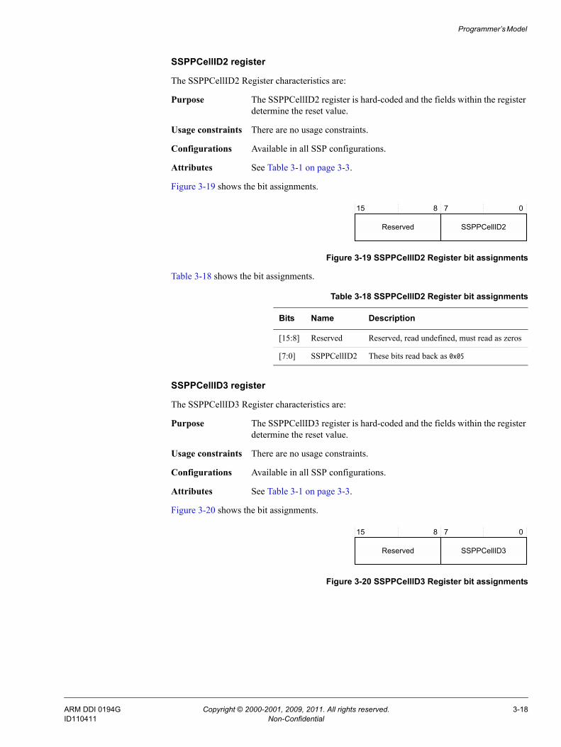
Programmer’s Model
SSPPCellID2 register
The SSPPCellID2 Register characteristics are:
Purpose The SSPPCellID2 register is hard-coded and the fields within the register determine the reset value.
Usage constraints There are no usage constraints.
Configurations Available in all SSP configurations.
Attributes See Table 3-1 on page 3-3.
Figure 3-19 shows the bit assignments.
Figure 3-19 SSPPCellID2 Register bit assignments
Table 3-18 shows the bit assignments.
SSPPCellID3 register
The SSPPCellID3 Register characteristics are:
Purpose The SSPPCellID3 register is hard-coded and the fields within the register determine the reset value.
Usage constraints There are no usage constraints.
Configurations Available in all SSP configurations.
Attributes See Table 3-1 on page 3-3.
Figure 3-20 shows the bit assignments.
Figure 3-20 SSPPCellID3 Register bit assignments
SSPPCellID2Reserved
15 078
Table 3-18 SSPPCellID2 Register bit assignments
Bits Name Description
[15:8] Reserved Reserved, read undefined, must read as zeros
[7:0] SSPPCellID2 These bits read back as 0x05
SSPPCellID3Reserved
15 078
ARM DDI 0194G Copyright © 2000-2001, 2009, 2011. All rights reserved. 3-18ID110411 Non-Confidential
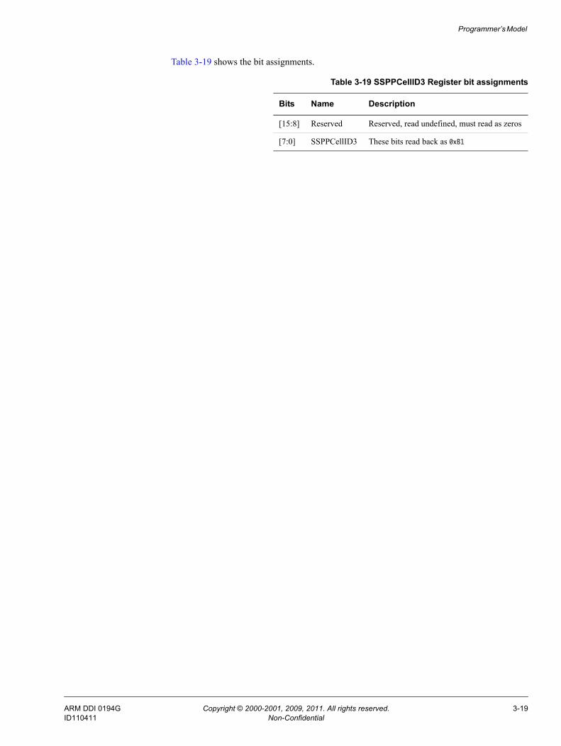
Programmer’s Model
Table 3-19 shows the bit assignments.
Table 3-19 SSPPCellID3 Register bit assignments
Bits Name Description
[15:8] Reserved Reserved, read undefined, must read as zeros
[7:0] SSPPCellID3 These bits read back as 0xB1
ARM DDI 0194G Copyright © 2000-2001, 2009, 2011. All rights reserved. 3-19ID110411 Non-Confidential
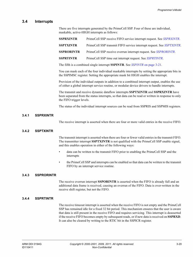
Programmer’s Model
3.4 InterruptsThere are five interrupts generated by the PrimeCell SSP. Four of these are individual, maskable, active-HIGH interrupts as follows:
SSPRXINTR PrimeCell SSP receive FIFO service interrupt request. See SSPRXINTR.
SSPTXINTR PrimeCell SSP transmit FIFO service interrupt request. See SSPTXINTR.
SSPRORINTR PrimeCell SSP receive overrun interrupt request. See SSPRORINTR.
SSPRTINTR PrimeCell SSP time out interrupt request. See SSPRTINTR.
The fifth is a combined single interrupt SSPINTR. See SSPINTR on page 3-21.
You can mask each of the four individual maskable interrupts by setting the appropriate bits in the SSPIMSC register. Setting the appropriate mask bit HIGH enables the interrupt.
Provision of the individual outputs in addition to a combined interrupt output, enables the use of either a global interrupt service routine, or modular device drivers to handle interrupts.
The transmit and receive dynamic dataflow interrupts SSPTXINTR and SSPRXINTR have been separated from the status interrupts, so that data can be read or written in response to only the FIFO trigger levels.
The status of the individual interrupt sources can be read from SSPRIS and SSPMIS registers.
3.4.1 SSPRXINTR
The receive interrupt is asserted when there are four or more valid entries in the receive FIFO.
3.4.2 SSPTXINTR
The transmit interrupt is asserted when there are four or fewer valid entries in the transmit FIFO. The transmitter interrupt SSPTXINTR is not qualified with the PrimeCell SSP enable signal, and this enables operation in either of the following ways:
• data can be written to the transmit FIFO prior to enabling the PrimeCell SSP and the interrupts
• the PrimeCell SSP and interrupts can be enabled so that data can be written to the transmit FIFO by an interrupt service routine.
3.4.3 SSPRORINTR
The receive overrun interrupt SSPORINTR is asserted when the FIFO is already full and an additional data frame is received, causing an overrun of the FIFO. Data is over-written in the receive shift register, but not the FIFO.
3.4.4 SSPRTINTR
The receive timeout interrupt is asserted when the receive FIFO is not empty and the PrimeCell SSP has remained idle for a fixed 32 bit period. This mechanism ensures that the user is aware that data is still present in the receive FIFO and requires servicing. This interrupt is deasserted if the receive FIFO becomes empty by subsequent reads, or if new data is received on SSPRXD. It can also be cleared by writing to the RTIC bit in the SSPICR register.
ARM DDI 0194G Copyright © 2000-2001, 2009, 2011. All rights reserved. 3-20ID110411 Non-Confidential
Programmer’s Model
3.4.5 SSPINTR
The interrupts are also combined into a single output SSPINTR, that is, an OR function of the individual masked sources. You can connect this output to the system interrupt controller to provide another level of masking on an individual per-peripheral basis.
The combined PrimeCell SSP interrupt is asserted if any of the four individual interrupts above are asserted and enabled.
ARM DDI 0194G Copyright © 2000-2001, 2009, 2011. All rights reserved. 3-21ID110411 Non-Confidential
Chapter 4 Programmer’s Model for Test
This chapter describes the additional logic for integration testing.
It contains the following sections:• PrimeCell SSP test harness overview on page 4-2• Scan testing on page 4-3• Test registers on page 4-4• Integration testing of block inputs on page 4-8• Integration testing of block outputs on page 4-10• Integration test summary on page 4-13.
ARM DDI 0194G Copyright © 2000-2001, 2009, 2011. All rights reserved. 4-1ID110411 Non-Confidential
Programmer’s Model for Test
4.1 PrimeCell SSP test harness overviewThe additional logic for integration vectors permits:• capture of input signals to the block• stimulation of the output signals.
The integration vectors provide a way of verifying that the PrimeCell SSP is correctly wired into a system. This is done by separately testing three groups of signals:
AMBA signals These are tested by checking the connections of all the address and data bits.
Primary input and output signals These are tested using a simple trickbox that can demonstrate the correct connection of the input and output signals to external pads.
Intra-chip signals, such as interrupt sources The tests for these signals are system-specific, and enable you to write the necessary tests. Additional logic is implemented enabling you to read and write to each intra-chip input and output signal.
The test registers control these test features. This enables you to test the PrimeCell SSP in isolation from the rest of the system using only transfers from the AMBA APB.
Off-chip test vectors are supplied using a 32-bit parallel External Bus Interface (EBI) and converted to internal AMBA bus transfers. The Test Interface Controller (TIC) AMBA bus master module controls the application of test vectors.
ARM DDI 0194G Copyright © 2000-2001, 2009, 2011. All rights reserved. 4-2ID110411 Non-Confidential
Programmer’s Model for Test
4.2 Scan testingThe PrimeCell SSP has been designed to simplify:• insertion of scan test cells• use of Automatic Test Pattern Generation (ATPG).
This is the recommended method of manufacturing test.
ARM DDI 0194G Copyright © 2000-2001, 2009, 2011. All rights reserved. 4-3ID110411 Non-Confidential
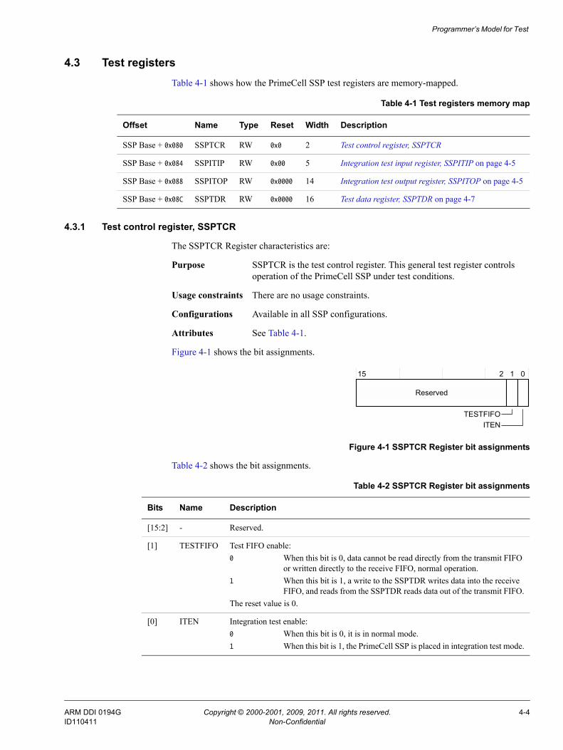
Programmer’s Model for Test
4.3 Test registersTable 4-1 shows how the PrimeCell SSP test registers are memory-mapped.
4.3.1 Test control register, SSPTCR
The SSPTCR Register characteristics are:
Purpose SSPTCR is the test control register. This general test register controls operation of the PrimeCell SSP under test conditions.
Usage constraints There are no usage constraints.
Configurations Available in all SSP configurations.
Attributes See Table 4-1.
Figure 4-1 shows the bit assignments.
Figure 4-1 SSPTCR Register bit assignments
Table 4-2 shows the bit assignments.
Table 4-1 Test registers memory map
Offset Name Type Reset Width Description
SSP Base + 0x080 SSPTCR RW 0x0 2 Test control register, SSPTCR
SSP Base + 0x084 SSPITIP RW 0x00 5 Integration test input register, SSPITIP on page 4-5
SSP Base + 0x088 SSPITOP RW 0x0000 14 Integration test output register, SSPITOP on page 4-5
SSP Base + 0x08C SSPTDR RW 0x0000 16 Test data register, SSPTDR on page 4-7
Reserved
15 02 1
TESTFIFOITEN
Table 4-2 SSPTCR Register bit assignments
Bits Name Description
[15:2] - Reserved.
[1] TESTFIFO Test FIFO enable:0 When this bit is 0, data cannot be read directly from the transmit FIFO
or written directly to the receive FIFO, normal operation.1 When this bit is 1, a write to the SSPTDR writes data into the receive
FIFO, and reads from the SSPTDR reads data out of the transmit FIFO.The reset value is 0.
[0] ITEN Integration test enable:0 When this bit is 0, it is in normal mode.1 When this bit is 1, the PrimeCell SSP is placed in integration test mode.
ARM DDI 0194G Copyright © 2000-2001, 2009, 2011. All rights reserved. 4-4ID110411 Non-Confidential
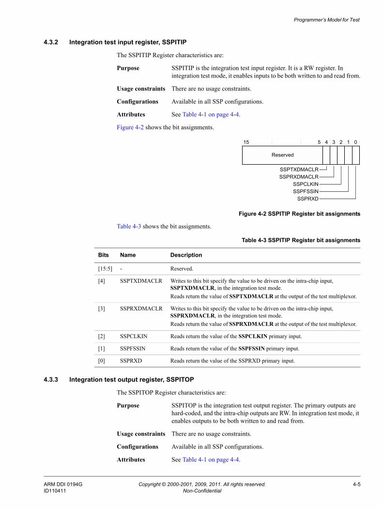
Programmer’s Model for Test
4.3.2 Integration test input register, SSPITIP
The SSPITIP Register characteristics are:
Purpose SSPITIP is the integration test input register. It is a RW register. In integration test mode, it enables inputs to be both written to and read from.
Usage constraints There are no usage constraints.
Configurations Available in all SSP configurations.
Attributes See Table 4-1 on page 4-4.
Figure 4-2 shows the bit assignments.
Figure 4-2 SSPITIP Register bit assignments
Table 4-3 shows the bit assignments.
4.3.3 Integration test output register, SSPITOP
The SSPITOP Register characteristics are:
Purpose SSPITOP is the integration test output register. The primary outputs are hard-coded, and the intra-chip outputs are RW. In integration test mode, it enables outputs to be both written to and read from.
Usage constraints There are no usage constraints.
Configurations Available in all SSP configurations.
Attributes See Table 4-1 on page 4-4.
Reserved
15 02 1
SSPTXDMACLRSSPRXDMACLR
345
SSPCLKINSSPFSSIN
SSPRXD
Table 4-3 SSPITIP Register bit assignments
Bits Name Description
[15:5] - Reserved.
[4] SSPTXDMACLR Writes to this bit specify the value to be driven on the intra-chip input, SSPTXDMACLR, in the integration test mode.Reads return the value of SSPTXDMACLR at the output of the test multiplexor.
[3] SSPRXDMACLR Writes to this bit specify the value to be driven on the intra-chip input, SSPRXDMACLR, in the integration test mode.Reads return the value of SSPRXDMACLR at the output of the test multiplexor.
[2] SSPCLKIN Reads return the value of the SSPCLKIN primary input.
[1] SSPFSSIN Reads return the value of the SSPFSSIN primary input.
[0] SSPRXD Reads return the value of the SSPRXD primary input.
ARM DDI 0194G Copyright © 2000-2001, 2009, 2011. All rights reserved. 4-5ID110411 Non-Confidential
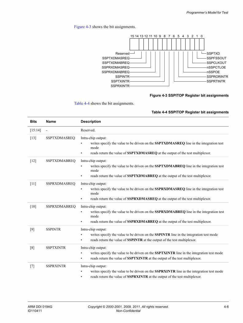
Programmer’s Model for Test
Figure 4-3 shows the bit assignments.
Figure 4-3 SSPITOP Register bit assignments
Table 4-4 shows the bit assignments.
15 02 1
ReservedSSPTXDMASREQ
345
SSPTXDMABREQSSPRXDMASREQSSPRXDMABREQ
67891011121314
SSPINTRSSPTXINTRSSPRXINTR
SSPTXDSSPFSSOUTSSPCLKOUTnSSPCTLOEnSSPOESSPRORINTRSSPRTINTR
Table 4-4 SSPITOP Register bit assignments
Bits Name Description
[15:14] - Reserved.
[13] SSPTXDMASREQ Intra-chip output:• writes specify the value to be driven on the SSPTXDMASREQ line in the integration test
mode• reads return the value of SSPTXDMASREQ at the output of the test multiplexor.
[12] SSPTXDMABREQ Intra-chip output:• writes specify the value to be driven on the SSPTXDMABREQ line in the integration test
mode• reads return the value of SSPTXDMABREQ at the output of the test multiplexor.
[11] SSPRXDMASREQ Intra-chip output:• writes specify the value to be driven on the SSPRXDMASREQ line in the integration test
mode• reads return the value of SSPRXDMASREQ at the output of the test multiplexor.
[10] SSPRXDMABREQ Intra-chip output:• writes specify the value to be driven on the SSPRXDMABREQ line in the integration test
mode• reads return the value of SSPRXDMABREQ at the output of the test multiplexor.
[9] SSPINTR Intra-chip output:• writes specify the value to be driven on the SSPINTR line in the integration test mode• reads return the value of SSPINTR at the output of the test multiplexor.
[8] SSPTXINTR Intra-chip output:• writes specify the value to be driven on the SSPTXINTR line in the integration test mode• reads return the value of SSPTXINTR at the output of the test multiplexor.
[7] SSPRXINTR Intra-chip output:• writes specify the value to be driven on the SSPRXINTR line in the integration test mode• reads return the value of SSPRXINTR at the output of the test multiplexor.
ARM DDI 0194G Copyright © 2000-2001, 2009, 2011. All rights reserved. 4-6ID110411 Non-Confidential
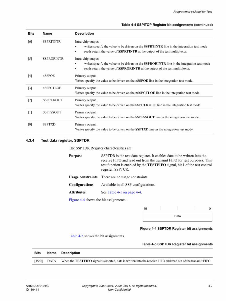
Programmer’s Model for Test
4.3.4 Test data register, SSPTDR
The SSPTDR Register characteristics are:
Purpose SSPTDR is the test data register. It enables data to be written into the receive FIFO and read out from the transmit FIFO for test purposes. This test function is enabled by the TESTFIFO signal, bit 1 of the test control register, SSPTCR.
Usage constraints There are no usage constraints.
Configurations Available in all SSP configurations.
Attributes See Table 4-1 on page 4-4.
Figure 4-4 shows the bit assignments.
Figure 4-4 SSPTDR Register bit assignments
Table 4-5 shows the bit assignments.
[6] SSPRTINTR Intra-chip output:• writes specify the value to be driven on the SSPRTINTR line in the integration test mode• reads return the value of SSPRTINTR at the output of the test multiplexor.
[5] SSPRORINTR Intra-chip output:• writes specify the value to be driven on the SSPRORINTR line in the integration test mode• reads return the value of SSPRORINTR at the output of the test multiplexor.
[4] nSSPOE Primary output.Writes specify the value to be driven on the nSSPOE line in the integration test mode.
[3] nSSPCTLOE Primary output.Writes specify the value to be driven on the nSSPCTLOE line in the integration test mode.
[2] SSPCLKOUT Primary output.Writes specify the value to be driven on the SSPCLKOUT line in the integration test mode.
[1] SSPFSSOUT Primary output.Writes specify the value to be driven on the SSPFSSOUT line in the integration test mode.
[0] SSPTXD Primary output.Writes specify the value to be driven on the SSPTXD line in the integration test mode.
Table 4-4 SSPITOP Register bit assignments (continued)
Bits Name Description
Data
15 0
Table 4-5 SSPTDR Register bit assignments
Bits Name Description
[15:0] DATA When the TESTFIFO signal is asserted, data is written into the receive FIFO and read out of the transmit FIFO
ARM DDI 0194G Copyright © 2000-2001, 2009, 2011. All rights reserved. 4-7ID110411 Non-Confidential
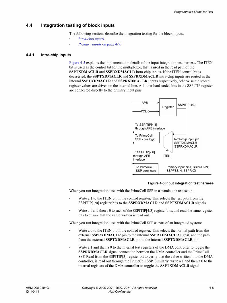
Programmer’s Model for Test
4.4 Integration testing of block inputsThe following sections describe the integration testing for the block inputs:• Intra-chip inputs• Primary inputs on page 4-9.
4.4.1 Intra-chip inputs
Figure 4-5 explains the implementation details of the input integration test harness. The ITEN bit is used as the control bit for the multiplexor, that is used in the read path of the SSPTXDMACLR and SSPRXDMACLR intra-chip inputs. If the ITEN control bit is deasserted, the SSPTXDMACLR and SSPRXDMACLR intra-chip inputs are routed as the internal SSPTXDMACLR and SSPRXDMACLR inputs respectively, otherwise the stored register values are driven on the internal line. All other hard-coded bits in the SSPITIP register are connected directly to the primary input pins.
Figure 4-5 Input integration test harness
When you run integration tests with the PrimeCell SSP in a standalone test setup:
• Write a 1 to the ITEN bit in the control register. This selects the test path from the SSPITIP[1:0] register bits to the SSPRXDMACLR and SSPTXDMACLR signals.
• Write a 1 and then a 0 to each of the SSPITIP[4:3] register bits, and read the same register bits to ensure that the value written is read out.
When you run integration tests with the PrimeCell SSP as part of an integrated system:
• Write a 0 to the ITEN bit in the control register. This selects the normal path from the external SSPRXDMACLR pin to the internal SSPRXDMACLR signal, and the path from the external SSPTXDMACLR pin to the internal SSPTXDMACLR pin.
• Write a 1 and then a 0 to the internal test registers of the DMA controller to toggle the SSPRXDMACLR signal connection between the DMA controller and the PrimeCell SSP. Read from the SSPITIP[3] register bit to verify that the value written into the DMA controller, is read out through the PrimeCell SSP. Similarly, write a 1 and then a 0 to the internal registers of the DMA controller to toggle the SSPTXDMACLR signal
SSPITIP[4:3]APB
PCLK
Intra-chip input pinSSPTXDMACLRSSPRXDMACLR
ITEN
To PrimeCell SSP core logic
To SSPITIP[4:3] through APB interface
Register
Primary input pins, SSPCLKIN, SSPFSSIN, SSPRXD
To PrimeCell SSP core logic
To SSPITIP[2:0] through APB interface
ARM DDI 0194G Copyright © 2000-2001, 2009, 2011. All rights reserved. 4-8ID110411 Non-Confidential
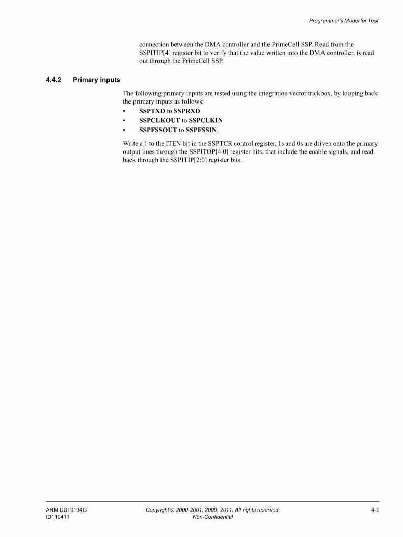
Programmer’s Model for Test
connection between the DMA controller and the PrimeCell SSP. Read from the SSPITIP[4] register bit to verify that the value written into the DMA controller, is read out through the PrimeCell SSP.
4.4.2 Primary inputs
The following primary inputs are tested using the integration vector trickbox, by looping back the primary inputs as follows:• SSPTXD to SSPRXD• SSPCLKOUT to SSPCLKIN• SSPFSSOUT to SSPFSSIN.
Write a 1 to the ITEN bit in the SSPTCR control register. 1s and 0s are driven onto the primary output lines through the SSPITOP[4:0] register bits, that include the enable signals, and read back through the SSPITIP[2:0] register bits.
ARM DDI 0194G Copyright © 2000-2001, 2009, 2011. All rights reserved. 4-9ID110411 Non-Confidential
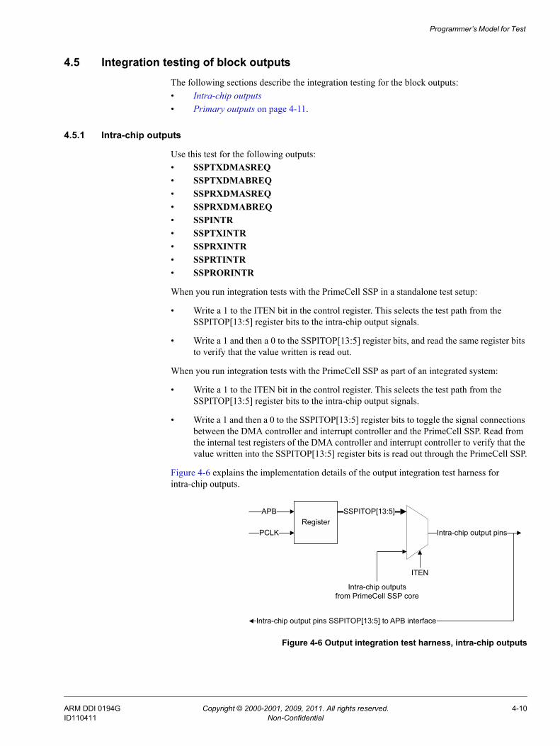
Programmer’s Model for Test
4.5 Integration testing of block outputsThe following sections describe the integration testing for the block outputs:• Intra-chip outputs• Primary outputs on page 4-11.
4.5.1 Intra-chip outputs
Use this test for the following outputs:• SSPTXDMASREQ• SSPTXDMABREQ• SSPRXDMASREQ• SSPRXDMABREQ• SSPINTR• SSPTXINTR• SSPRXINTR• SSPRTINTR• SSPRORINTR
When you run integration tests with the PrimeCell SSP in a standalone test setup:
• Write a 1 to the ITEN bit in the control register. This selects the test path from the SSPITOP[13:5] register bits to the intra-chip output signals.
• Write a 1 and then a 0 to the SSPITOP[13:5] register bits, and read the same register bits to verify that the value written is read out.
When you run integration tests with the PrimeCell SSP as part of an integrated system:
• Write a 1 to the ITEN bit in the control register. This selects the test path from the SSPITOP[13:5] register bits to the intra-chip output signals.
• Write a 1 and then a 0 to the SSPITOP[13:5] register bits to toggle the signal connections between the DMA controller and interrupt controller and the PrimeCell SSP. Read from the internal test registers of the DMA controller and interrupt controller to verify that the value written into the SSPITOP[13:5] register bits is read out through the PrimeCell SSP.
Figure 4-6 explains the implementation details of the output integration test harness for intra-chip outputs.
Figure 4-6 Output integration test harness, intra-chip outputs
Intra-chip outputs from PrimeCell SSP core
PCLKRegister
APB SSPITOP[13:5]
ITEN
Intra-chip output pins
Intra-chip output pins SSPITOP[13:5] to APB interface
ARM DDI 0194G Copyright © 2000-2001, 2009, 2011. All rights reserved. 4-10ID110411 Non-Confidential
Programmer’s Model for Test
4.5.2 Primary outputs
Integration testing of primary outputs and primary inputs is carried out using the integration vector trickbox. Use this test for the following outputs:• SSPTXD• SSPCLKOUT• SSPFSSOUT• nSSPCTLOE• nSSPOE.
Note Only the SSPTXD, SSPCLKOUT, and SSPFSSOUT signals are available at the output pads of a typical configuration. The nSSPOE and nSSPCTLOE signals are internal connections to the pad.
Verify the primary input and output pin connections as this section describes.
The primary outputs, SSPTXD, SSPCLKOUT, and SSPFSSOUT are directly connected to SSPRXD, SSPCLKIN, and SSPFSSIN respectively by the integration trickbox that Figure 4-7 shows.
Figure 4-7 Primary outputs routed to primary inputs
To test the nSSPOE and nSSPCTLOE connections, you can apply a weak pull-down to the tristate pins through the trickbox.
• All the primary outputs can be accessed through the SSPITOP register. Different data patterns are written to the output pins using the SSPITOP register.
• The looped-back data is read back through the SSPITIP register.
Figure 4-8 on page 4-12 shows implementation details of the output integration test harness in the case of primary outputs.
Integration vector trickbox
SSP PL022
SSPTXD
SSPFSSOUT
SSPCLKOUT
nSSPCTLOE
nSSPOE
SSPRXD
SSPFSSIN
SSPCLKIN
SSPFSSOUT
SSPCLKOUT
SSPTXD
Pads
ARM DDI 0194G Copyright © 2000-2001, 2009, 2011. All rights reserved. 4-11ID110411 Non-Confidential
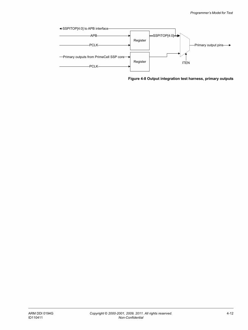
Programmer’s Model for Test
Figure 4-8 Output integration test harness, primary outputs
Primary outputs from PrimeCell SSP core
RegisterAPB SSPITOP[4:0]
ITEN
Primary output pins
SSPITOP[4:0] to APB interface
RegisterPCLK
PCLK
ARM DDI 0194G Copyright © 2000-2001, 2009, 2011. All rights reserved. 4-12ID110411 Non-Confidential
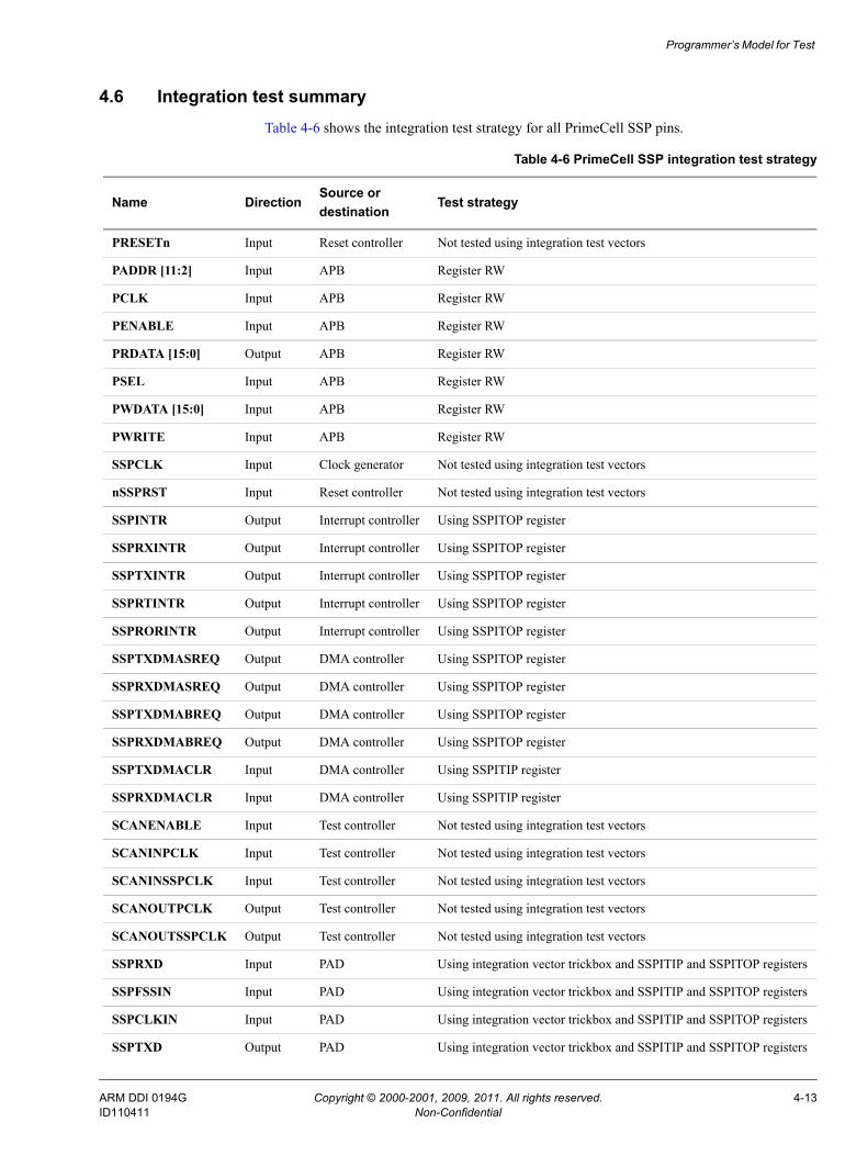
Programmer’s Model for Test
4.6 Integration test summaryTable 4-6 shows the integration test strategy for all PrimeCell SSP pins.
Table 4-6 PrimeCell SSP integration test strategy
Name DirectionSource ordestination
Test strategy
PRESETn Input Reset controller Not tested using integration test vectors
PADDR [11:2] Input APB Register RW
PCLK Input APB Register RW
PENABLE Input APB Register RW
PRDATA [15:0] Output APB Register RW
PSEL Input APB Register RW
PWDATA [15:0] Input APB Register RW
PWRITE Input APB Register RW
SSPCLK Input Clock generator Not tested using integration test vectors
nSSPRST Input Reset controller Not tested using integration test vectors
SSPINTR Output Interrupt controller Using SSPITOP register
SSPRXINTR Output Interrupt controller Using SSPITOP register
SSPTXINTR Output Interrupt controller Using SSPITOP register
SSPRTINTR Output Interrupt controller Using SSPITOP register
SSPRORINTR Output Interrupt controller Using SSPITOP register
SSPTXDMASREQ Output DMA controller Using SSPITOP register
SSPRXDMASREQ Output DMA controller Using SSPITOP register
SSPTXDMABREQ Output DMA controller Using SSPITOP register
SSPRXDMABREQ Output DMA controller Using SSPITOP register
SSPTXDMACLR Input DMA controller Using SSPITIP register
SSPRXDMACLR Input DMA controller Using SSPITIP register
SCANENABLE Input Test controller Not tested using integration test vectors
SCANINPCLK Input Test controller Not tested using integration test vectors
SCANINSSPCLK Input Test controller Not tested using integration test vectors
SCANOUTPCLK Output Test controller Not tested using integration test vectors
SCANOUTSSPCLK Output Test controller Not tested using integration test vectors
SSPRXD Input PAD Using integration vector trickbox and SSPITIP and SSPITOP registers
SSPFSSIN Input PAD Using integration vector trickbox and SSPITIP and SSPITOP registers
SSPCLKIN Input PAD Using integration vector trickbox and SSPITIP and SSPITOP registers
SSPTXD Output PAD Using integration vector trickbox and SSPITIP and SSPITOP registers
ARM DDI 0194G Copyright © 2000-2001, 2009, 2011. All rights reserved. 4-13ID110411 Non-Confidential
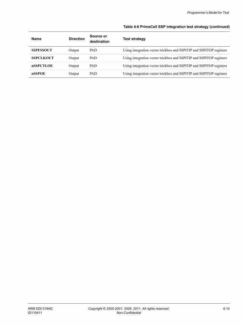
Programmer’s Model for Test
SSPFSSOUT Output PAD Using integration vector trickbox and SSPITIP and SSPITOP registers
SSPCLKOUT Output PAD Using integration vector trickbox and SSPITIP and SSPITOP registers
nSSPCTLOE Output PAD Using integration vector trickbox and SSPITIP and SSPITOP registers
nSSPOE Output PAD Using integration vector trickbox and SSPITIP and SSPITOP registers
Table 4-6 PrimeCell SSP integration test strategy (continued)
Name DirectionSource ordestination
Test strategy
ARM DDI 0194G Copyright © 2000-2001, 2009, 2011. All rights reserved. 4-14ID110411 Non-Confidential
Appendix A Signal Descriptions
This appendix describes the signals that interface with the ARM PrimeCell SSP (PL022).
It contains the following sections:• AMBA APB signals on page A-2• On-chip signals on page A-3• Signals to pads on page A-4.
ARM DDI 0194G Copyright © 2000-2001, 2009, 2011. All rights reserved. A-1ID110411 Non-Confidential
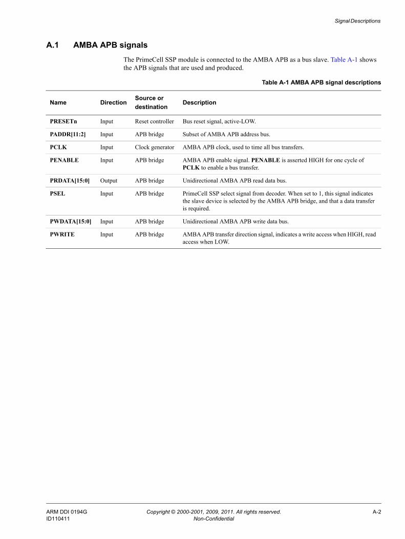
Signal Descriptions
A.1 AMBA APB signalsThe PrimeCell SSP module is connected to the AMBA APB as a bus slave. Table A-1 shows the APB signals that are used and produced.
Table A-1 AMBA APB signal descriptions
Name DirectionSource ordestination
Description
PRESETn Input Reset controller Bus reset signal, active-LOW.
PADDR[11:2] Input APB bridge Subset of AMBA APB address bus.
PCLK Input Clock generator AMBA APB clock, used to time all bus transfers.
PENABLE Input APB bridge AMBA APB enable signal. PENABLE is asserted HIGH for one cycle of PCLK to enable a bus transfer.
PRDATA[15:0] Output APB bridge Unidirectional AMBA APB read data bus.
PSEL Input APB bridge PrimeCell SSP select signal from decoder. When set to 1, this signal indicates the slave device is selected by the AMBA APB bridge, and that a data transfer is required.
PWDATA[15:0] Input APB bridge Unidirectional AMBA APB write data bus.
PWRITE Input APB bridge AMBA APB transfer direction signal, indicates a write access when HIGH, read access when LOW.
ARM DDI 0194G Copyright © 2000-2001, 2009, 2011. All rights reserved. A-2ID110411 Non-Confidential
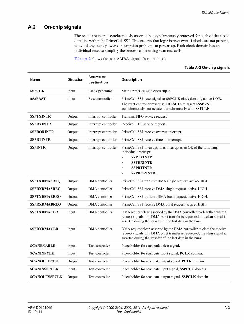
Signal Descriptions
A.2 On-chip signalsThe reset inputs are asynchronously asserted but synchronously removed for each of the clock domains within the PrimeCell SSP. This ensures that logic is reset even if clocks are not present, to avoid any static power consumption problems at power-up. Each clock domain has an individual reset to simplify the process of inserting scan test cells.
Table A-2 shows the non-AMBA signals from the block.
Table A-2 On-chip signals
Name DirectionSource ordestination
Description
SSPCLK Input Clock generator Main PrimeCell SSP clock input.
nSSPRST Input Reset controller PrimeCell SSP reset signal to SSPCLK clock domain, active-LOW.The reset controller must use PRESETn to assert nSSPRST asynchronously, but negate it synchronously with SSPCLK.
SSPTXINTR Output Interrupt controller Transmit FIFO service request.
SSPRXINTR Output Interrupt controller Receive FIFO service request.
SSPRORINTR Output Interrupt controller PrimeCell SSP receive overrun interrupt.
SSPRTINTR Output Interrupt controller PrimeCell SSP receive timeout interrupt.
SSPINTR Output Interrupt controller PrimeCell SSP interrupt. This interrupt is an OR of the following individual interrupts:• SSPTXINTR• SSPRXINTR• SSPRTINTR• SSPRORINTR.
SSPTXDMASREQ Output DMA controller PrimeCell SSP transmit DMA single request, active-HIGH.
SSPRXDMASREQ Output DMA controller PrimeCell SSP receive DMA single request, active-HIGH.
SSPTXDMABREQ Output DMA controller PrimeCell SSP transmit DMA burst request, active-HIGH.
SSPRXDMABREQ Output DMA controller PrimeCell SSP receive DMA burst request, active-HIGH.
SSPTXDMACLR Input DMA controller DMA request clear, asserted by the DMA controller to clear the transmit request signals. If a DMA burst transfer is requested, the clear signal is asserted during the transfer of the last data in the burst.
SSPRXDMACLR Input DMA controller DMA request clear, asserted by the DMA controller to clear the receive request signals. If a DMA burst transfer is requested, the clear signal is asserted during the transfer of the last data in the burst.
SCANENABLE Input Test controller Place holder for scan path select signal.
SCANINPCLK Input Test controller Place holder for scan data input signal, PCLK domain.
SCANOUTPCLK Output Test controller Place holder for scan data output signal, PCLK domain.
SCANINSSPCLK Input Test controller Place holder for scan data input signal, SSPCLK domain.
SCANOUTSSPCLK Output Test controller Place holder for scan data output signal, SSPCLK domain.
ARM DDI 0194G Copyright © 2000-2001, 2009, 2011. All rights reserved. A-3ID110411 Non-Confidential
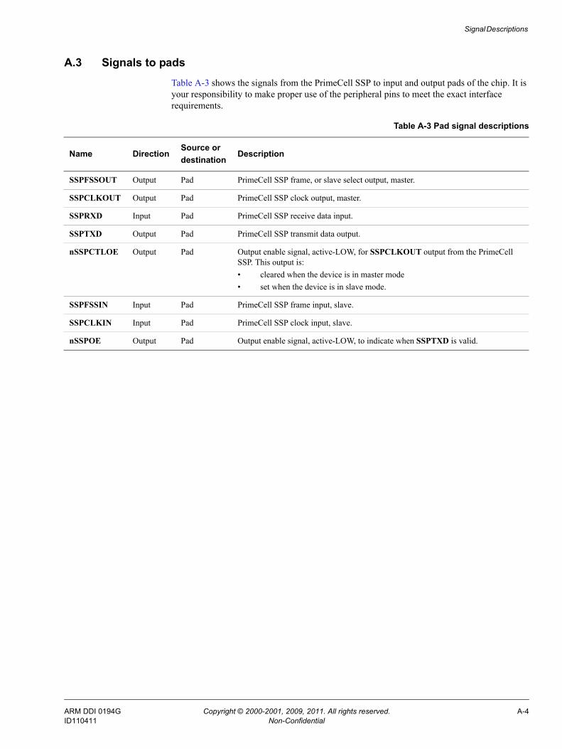
Signal Descriptions
A.3 Signals to padsTable A-3 shows the signals from the PrimeCell SSP to input and output pads of the chip. It is your responsibility to make proper use of the peripheral pins to meet the exact interface requirements.
Table A-3 Pad signal descriptions
Name DirectionSource ordestination
Description
SSPFSSOUT Output Pad PrimeCell SSP frame, or slave select output, master.
SSPCLKOUT Output Pad PrimeCell SSP clock output, master.
SSPRXD Input Pad PrimeCell SSP receive data input.
SSPTXD Output Pad PrimeCell SSP transmit data output.
nSSPCTLOE Output Pad Output enable signal, active-LOW, for SSPCLKOUT output from the PrimeCell SSP. This output is:• cleared when the device is in master mode• set when the device is in slave mode.
SSPFSSIN Input Pad PrimeCell SSP frame input, slave.
SSPCLKIN Input Pad PrimeCell SSP clock input, slave.
nSSPOE Output Pad Output enable signal, active-LOW, to indicate when SSPTXD is valid.
ARM DDI 0194G Copyright © 2000-2001, 2009, 2011. All rights reserved. A-4ID110411 Non-Confidential
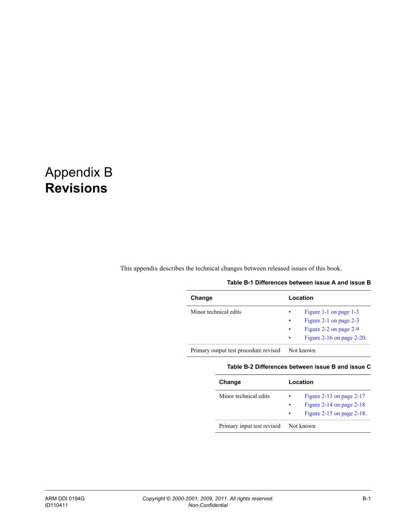
Appendix B Revisions
This appendix describes the technical changes between released issues of this book.
Table B-1 Differences between issue A and issue B
Change Location
Minor technical edits • Figure 1-1 on page 1-3• Figure 2-1 on page 2-3• Figure 2-2 on page 2-9• Figure 2-16 on page 2-20.
Primary output test procedure revised Not known
Table B-2 Differences between issue B and issue C
Change Location
Minor technical edits • Figure 2-13 on page 2-17• Figure 2-14 on page 2-18• Figure 2-15 on page 2-18.
Primary input test revised Not known
ARM DDI 0194G Copyright © 2000-2001, 2009, 2011. All rights reserved. B-1ID110411 Non-Confidential
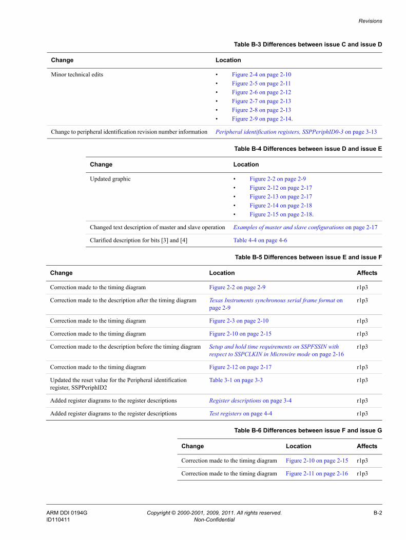
Revisions
Table B-3 Differences between issue C and issue D
Change Location
Minor technical edits • Figure 2-4 on page 2-10• Figure 2-5 on page 2-11• Figure 2-6 on page 2-12• Figure 2-7 on page 2-13• Figure 2-8 on page 2-13• Figure 2-9 on page 2-14.
Change to peripheral identification revision number information Peripheral identification registers, SSPPeriphID0-3 on page 3-13
Table B-4 Differences between issue D and issue E
Change Location
Updated graphic • Figure 2-2 on page 2-9• Figure 2-12 on page 2-17• Figure 2-13 on page 2-17• Figure 2-14 on page 2-18• Figure 2-15 on page 2-18.
Changed text description of master and slave operation Examples of master and slave configurations on page 2-17
Clarified description for bits [3] and [4] Table 4-4 on page 4-6
Table B-5 Differences between issue E and issue F
Change Location Affects
Correction made to the timing diagram Figure 2-2 on page 2-9 r1p3
Correction made to the description after the timing diagram Texas Instruments synchronous serial frame format on page 2-9
r1p3
Correction made to the timing diagram Figure 2-3 on page 2-10 r1p3
Correction made to the timing diagram Figure 2-10 on page 2-15 r1p3
Correction made to the description before the timing diagram Setup and hold time requirements on SSPFSSIN with respect to SSPCLKIN in Microwire mode on page 2-16
r1p3
Correction made to the timing diagram Figure 2-12 on page 2-17 r1p3
Updated the reset value for the Peripheral identification register, SSPPeriphID2
Table 3-1 on page 3-3 r1p3
Added register diagrams to the register descriptions Register descriptions on page 3-4 r1p3
Added register diagrams to the register descriptions Test registers on page 4-4 r1p3
Table B-6 Differences between issue F and issue G
Change Location Affects
Correction made to the timing diagram Figure 2-10 on page 2-15 r1p3
Correction made to the timing diagram Figure 2-11 on page 2-16 r1p3
ARM DDI 0194G Copyright © 2000-2001, 2009, 2011. All rights reserved. B-2ID110411 Non-Confidential