Embed Size (px)
Citation preview
ARM Processor Architecture
2
Outline
ARM processor coreMemory hierarchy
3
ARM Processor Core
4
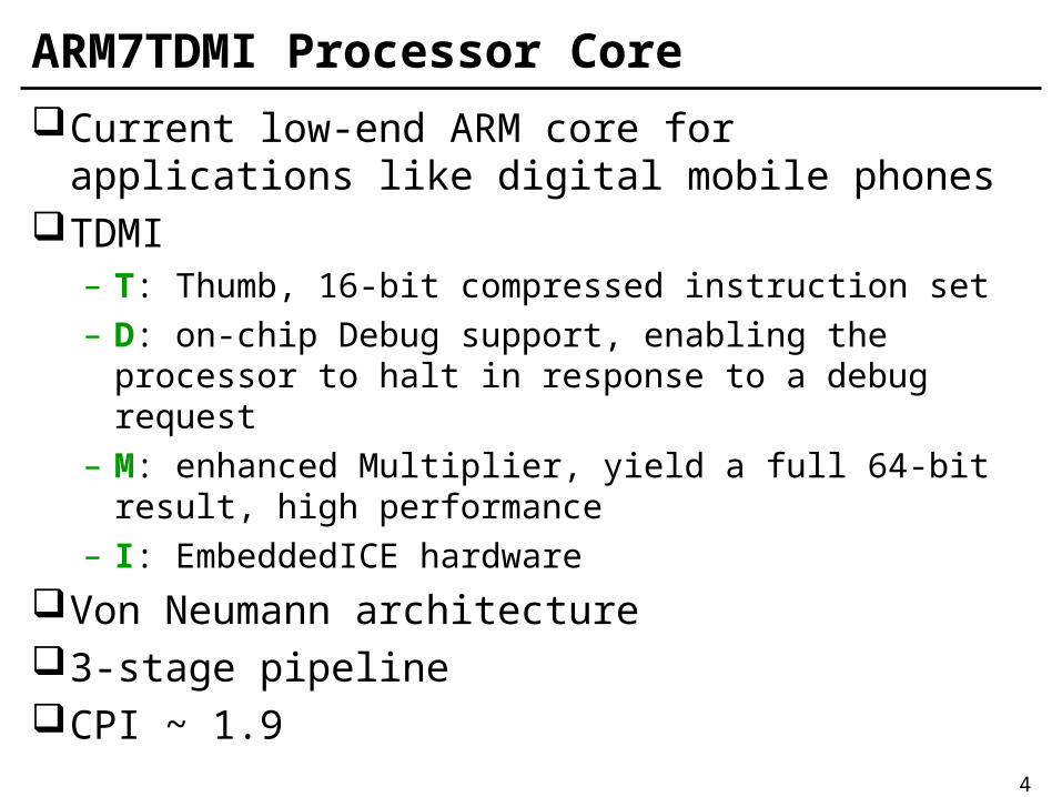
ARM7TDMI Processor Core
Current low-end ARM core for applications like digital mobile phones
TDMI– T: Thumb, 16-bit compressed instruction set– D: on-chip Debug support, enabling the processor to halt
in response to a debug request– M: enhanced Multiplier, yield a full 64-bit result, high
performance – I: EmbeddedICE hardware
Von Neumann architecture3-stage pipelineCPI ~ 1.9
5
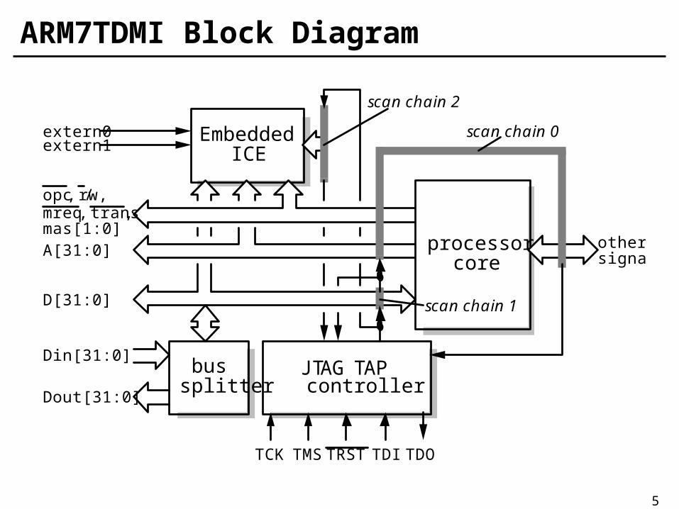
ARM7TDMI Block Diagram
JTAG TAPcontroller
Embedded
processorcore
TCK TMSTRST TDI TDO
D[31:0]
A[31:0]
opc, r/w,mreq, trans,mas[1:0]
othersignals
scan chain 0
scan chain 2
scan chain 1
extern0extern1 ICE
bussplitter
Din[31:0]
Dout[31:0]
6
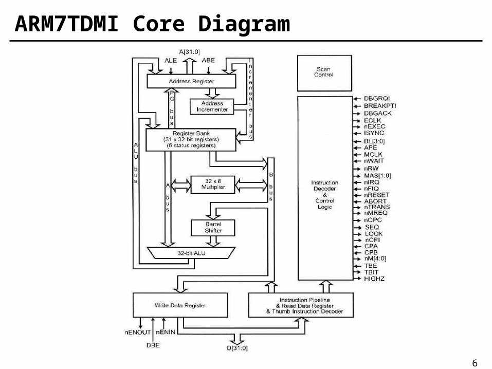
ARM7TDMI Core Diagram
7
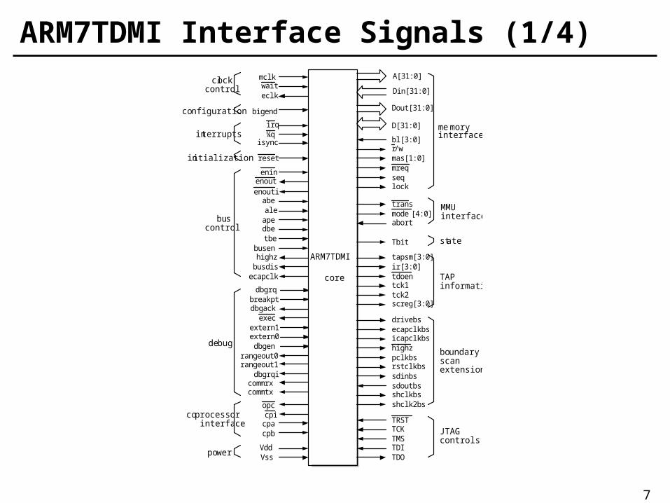
ARM7TDMI Interface Signals (1/4)
mreqseqlock
Dout[31:0]
D[31:0]
r/wmas[1:0]
mode[4:0]trans
abort
opccpi
cpacpb
memoryinterface
MMUinterface
coprocessorinterface
mclkwaiteclk
isync
bigend
enin
irq¼q
reset
enout
abe
VddVss
clockcontrol
configuration
interrupts
initialization
buscontrol
power
aleapedbe
dbgrqbreakptdbgack
debug
execextern1extern0
dbgen
bl[3:0]
TRSTTCKTMSTDI
JTAGcontrols
TDO
Tbit statetbe
rangeout0rangeout1
dbgrqicommrxcommtx
enouti
highzbusdis
ecapclk
busen
Din[31:0]
A[31:0]
ARM7TDMI
core
tapsm[3:0]ir[3:0]tdoentck1tck2screg[3:0]
TAPinformation
drivebsecapclkbsicapclkbshighzpclkbsrstclkbssdinbssdoutbsshclkbsshclk2bs
boundaryscanextension
8
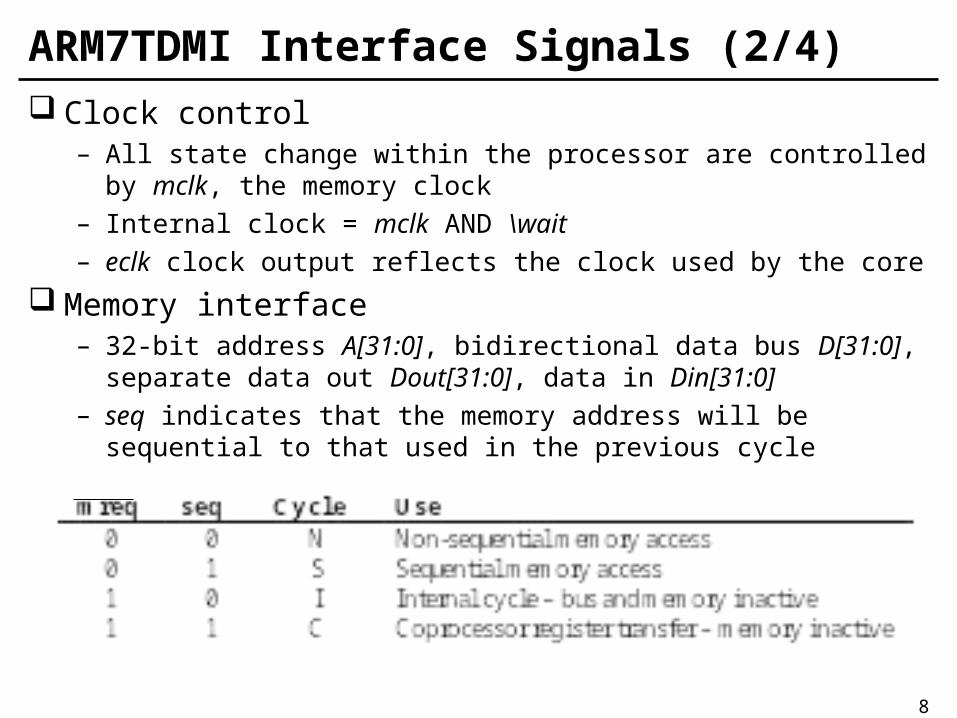
ARM7TDMI Interface Signals (2/4) Clock control
– All state change within the processor are controlled by mclk, the memory clock
– Internal clock = mclk AND \wait– eclk clock output reflects the clock used by the core
Memory interface– 32-bit address A[31:0], bidirectional data bus D[31:0], separate data
out Dout[31:0], data in Din[31:0]– seq indicates that the memory address will be sequential to that used
in the previous cycle
9
ARM7TDMI Interface Signals (3/4)– Lock indicates that the processor should keep the bus to ensure the
atomicity of the read and write phase of a SWAP instruction– \r/w, read or write– mas[1:0], encode memory access size – byte, half-word or word– bl[3:0], externally controlled enables on latches on each of the 4
bytes on the data input bus MMU interface
– \trans (translation control), 0: user mode, 1: privileged mode– \mode[4:0], bottom 5 bits of the CPSR (inverted)– Abort, disallow access
State– T bit, whether the processor is currently executing ARM or Thumb
instructions Configuration
– Bigend, big-endian or little-endian
10
ARM7TDMI Interface Signals (4/4) Interrupt
– \fiq, fast interrupt request, higher priority– \irq, normal interrupt request– isync, allow the interrupt synchronizer to be passed
Initialization– \reset, starts the processor from a known state, executing from
address 0000000016
ARM7TDMI characteristics
11
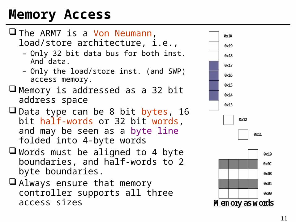
Memory Access The ARM7 is a Von Neumann,
load/store architecture, i.e.,– Only 32 bit data bus for both inst. And
data.– Only the load/store inst. (and SWP)
access memory. Memory is addressed as a 32 bit
address space Data type can be 8 bit bytes, 16 bit
half-words or 32 bit words, and may be seen as a byte line folded into 4-byte words
Words must be aligned to 4 byte boundaries, and half-words to 2 byte boundaries.
Always ensure that memory controller supports all three access sizes
12
ARM Memory Interface Sequential (S cycle)
– (nMREQ, SEQ) = (0, 1)– The ARM core requests a transfer to or from an address which is either the
same, or one word or one-half-word greater than the preceding address.
Non-sequential (N cycle)– (nMREQ, SEQ) = (0, 0)– The ARM core requests a transfer to or from an address which is unrelated to
the address used in the preceding address.
Internal (I cycle)– (nMREQ, SEQ) = (1, 0)– The ARM core does not require a transfer, as it performing an internal
function, and no useful prefetching can be performed at the same time
Coprocessor register transfer (C cycle)– (nMREQ, SEQ) = (1, 1)– The ARM core wished to use the data bus to communicate with a
coprocessor, but does not require any action by the memory system.
13
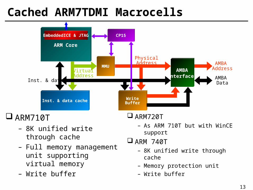
Cached ARM7TDMI Macrocells
ARM710T– 8K unified write through
cache– Full memory management
unit supporting virtual memory
– Write buffer
ARM720T– As ARM 710T but with WinCE
support
ARM 740T– 8K unified write through cache– Memory protection unit– Write buffer
AMBAInterface
Inst. & data cache
MMU
ARM Core
CP15EmbeddedICE & JTAG
WriteBuffer
AMBA Address
AMBA Data
VirtualAddress
PhysicalAddress
Inst. & data
14
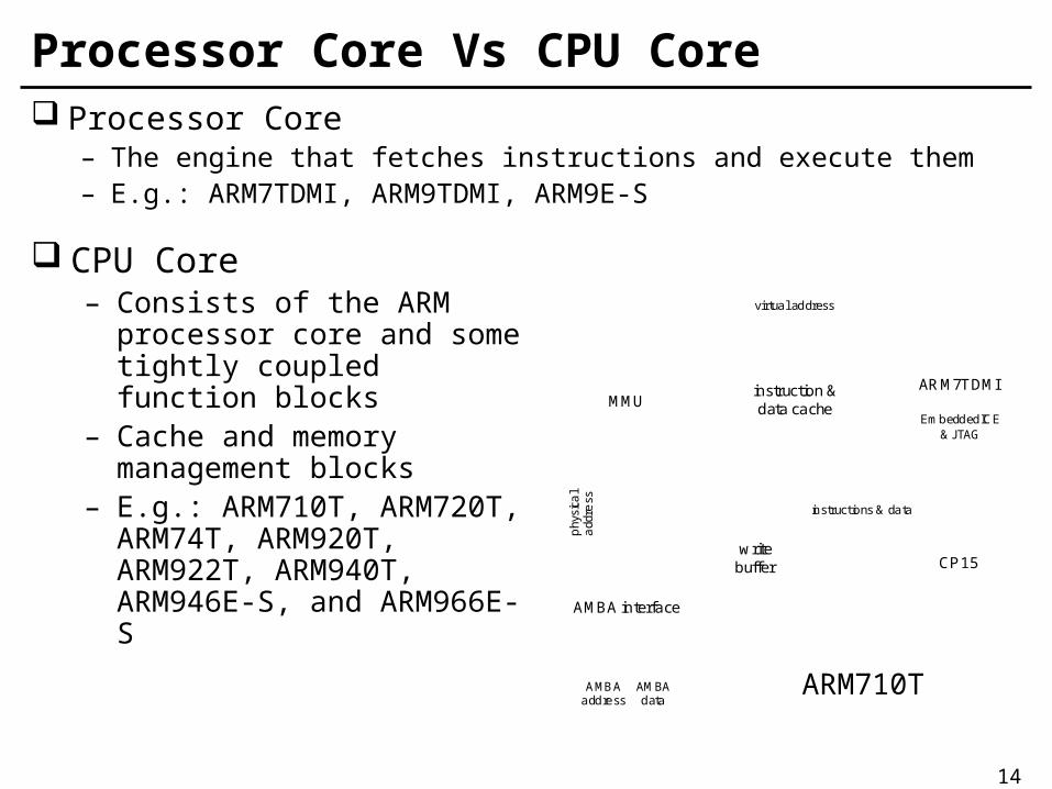
Processor Core Vs CPU Core Processor Core
– The engine that fetches instructions and execute them– E.g.: ARM7TDMI, ARM9TDMI, ARM9E-S
CPU Core– Consists of the ARM processor
core and some tightly coupled function blocks
– Cache and memory management blocks
– E.g.: ARM710T, ARM720T, ARM74T, ARM920T, ARM922T, ARM940T, ARM946E-S, and ARM966E-S
AMBAaddress
AMBAdata
instruction &data cache
AMBA interface
ARM7TDMI
EmbeddedICE& JTAG
virtual address
instruct ions & data
phy
sica
la
ddre
ss
CP15
MMU
writebuffer
ARM710T
15
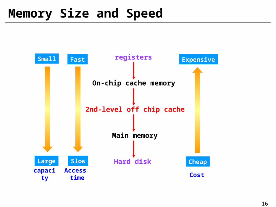
Memory Hierarchy
16
Memory Size and Speed
On-chip cache memory
registers
2nd-level off chip cache
Main memory
Hard diskAccess
timecapacity
Slow
Fast
Large
Small
Cost
Cheap
Expensive
17
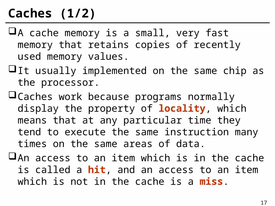
Caches (1/2)
A cache memory is a small, very fast memory that retains copies of recently used memory values.
It usually implemented on the same chip as the processor.
Caches work because programs normally display the property of locality, which means that at any particular time they tend to execute the same instruction many times on the same areas of data.
An access to an item which is in the cache is called a hit, and an access to an item which is not in the cache is a miss.
18
Caches (2/2)
A processor can have one of the following two organizations:– A unified cache
• This is a single cache for both instructions and data
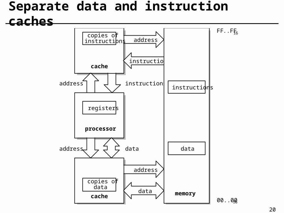
– Separate instruction and data caches• This organization is sometimes called a modified Harvard
architectures
19
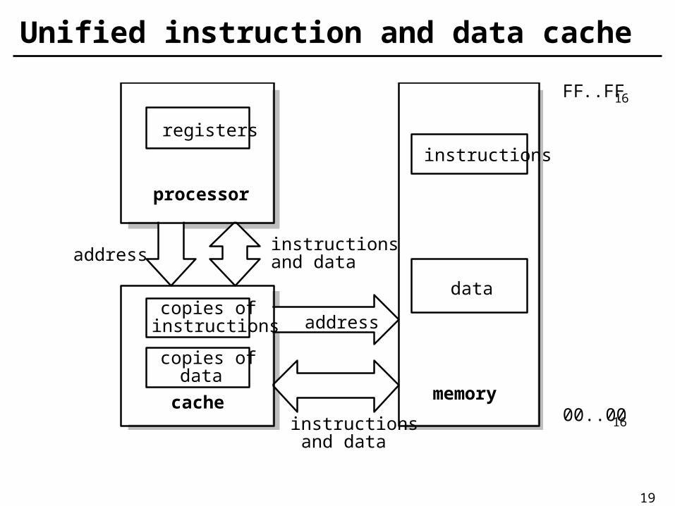
Unified instruction and data cache
address
instructionscache memory
copies of
instructions
data
00..0016
FF..FF16
instructions
copies ofdata
registers
processor
instructionsaddress
and data
and data
20
Separate data and instruction caches
address
datacache
00..0016
FF..FF16
copies ofdata
registers
processor
dataaddress
address
instructionsaddress
cache
copies ofinstructions
instructions
memory
instructions
data
21
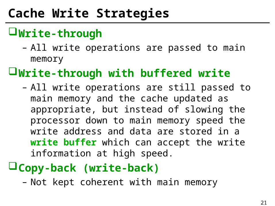
Cache Write Strategies
Write-through– All write operations are passed to main memory
Write-through with buffered write– All write operations are still passed to main memory and
the cache updated as appropriate, but instead of slowing the processor down to main memory speed the write address and data are stored in a write buffer which can accept the write information at high speed.
Copy-back (write-back)– Not kept coherent with main memory
22
Summary (1/2)
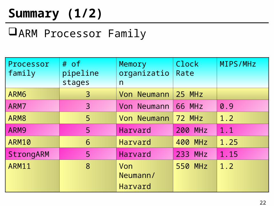
ARM Processor Family
Processor family
# of pipeline stages
Memory organization
Clock Rate MIPS/MHz
ARM6 3 Von Neumann 25 MHz
ARM7 3 Von Neumann 66 MHz 0.9
ARM8 5 Von Neumann 72 MHz 1.2
ARM9 5 Harvard 200 MHz 1.1
ARM10 6 Harvard 400 MHz 1.25
StrongARM 5 Harvard 233 MHz 1.15
ARM11 8 Von Neumann/
Harvard
550 MHz 1.2
23
Summary (2/2)
Memory hierarchy– Unified cache/Separate instruction and data cache– Write-through with buffered write