Embed Size (px)
Citation preview
ARM1156T2-S™
Revision: r0p4
Technical Reference Manual
Copyright © 2005-2007 ARM Limited. All rights reserved.ARM DDI 0338G
ARM1156T2-S Technical Reference Manual
Copyright © 2005-2007 ARM Limited. All rights reserved.
Release Information
Proprietary Notice
Words and logos marked with ® or ™ are registered trademarks or trademarks of ARM Limited in the EU and other countries, except as otherwise stated below in this proprietary notice. Other brands and names mentioned herein may be the trademarks of their respective owners.
Neither the whole nor any part of the information contained in, or the product described in, this document may be adapted or reproduced in any material form except with the prior written permission of the copyright holder.
The product described in this document is subject to continuous developments and improvements. All particulars of the product and its use contained in this document are given by ARM in good faith. However, all warranties implied or expressed, including but not limited to implied warranties of merchantability, or fitness for purpose, are excluded.
This document is intended only to assist the reader in the use of the product. ARM Limited shall not be liable for any loss or damage arising from the use of any information in this document, or any error or omission in such information, or any incorrect use of the product.
Figure 14-1 on page 14-2 reprinted with permission from IEEE Std. 1149.1-2001, IEEE Standard Test Access Port and Boundary-Scan Architecture by IEEE Std. The IEEE disclaims any responsibility or liability resulting from the placement and use in the described manner.
Confidentiality Status
This document is Non-Confidential. The right to use, copy and disclose this document may be subject to license restrictions in accordance with the terms of the agreement entered into by ARM and the party that ARM delivered this document to.
Change history
Date Issue Confidentiality Change
10 March 2005 A Confidential First release for r0p0.
10 October 2005 B Non-Confidential Second release for r0p0. Enhancement to text.
11 October 2005 C Non-Confidential Third release for r0p0. Enhancement to figures.
30 June 2006 D Confidential First release for R0p2.
30 June 2006 E Confidential Second release for r0p2. Enhancement to text.
31 May 2007 F Confidential First release for r0p4. Enhancement to text and Figures.
31 July 2007 G Non-Confidential Confidentiality changed to Non-Confidential. No change to contents.
ii Copyright © 2005-2007 ARM Limited. All rights reserved. ARM DDI 0338G
Product Status
The information in this document is final, that is for a developed product.
Web Address
http://www.arm.com
ARM DDI 0338G Copyright © 2005-2007 ARM Limited. All rights reserved. iii

iv Copyright © 2005-2007 ARM Limited. All rights reserved. ARM DDI 0338G
ContentsARM1156T2-S Technical Reference Manual
PrefaceAbout this manual ...................................................................................... xxivFeedback ................................................................................................... xxxi
Chapter 1 Introduction1.1 About the ARM1156T2-S processor ........................................................... 1-21.2 ARM1156T2-S architecture with Thumb-2 core technology ....................... 1-31.3 Components of the processor ..................................................................... 1-51.4 Power management .................................................................................. 1-191.5 Configurable options ................................................................................. 1-211.6 Pipeline stages .......................................................................................... 1-221.7 Typical pipeline operations ....................................................................... 1-241.8 About the architecture ............................................................................... 1-301.9 Product revisions ...................................................................................... 1-31
Chapter 2 Programmer’s Model2.1 About the programmer’s model ................................................................... 2-22.2 Processor operating states ......................................................................... 2-32.3 Operating modes ........................................................................................ 2-42.4 Data types ................................................................................................... 2-52.5 Memory formats .......................................................................................... 2-62.6 Registers ..................................................................................................... 2-8
ARM DDI 0338G Copyright © 2005-2007 ARM Limited. All rights reserved. v
Contents
2.7 The program status registers .................................................................... 2-122.8 Exceptions ................................................................................................ 2-202.9 Acceleration of execution environments ................................................... 2-40
Chapter 3 System Control Coprocessor3.1 About control coprocessor CP15 ................................................................ 3-23.2 System control processor registers .......................................................... 3-113.3 System control coprocessor reference data ........................................... 3-120
Chapter 4 Prefetch Unit4.1 About the prefetch unit ............................................................................... 4-24.2 Branch prediction ........................................................................................ 4-34.3 Return stack ............................................................................................... 4-64.4 Instruction Memory Barrier (IMB) instruction .............................................. 4-7
Chapter 5 Memory Protection Unit5.1 About the MPU ........................................................................................... 5-25.2 Enabling and disabling the MPU ................................................................ 5-75.3 Memory attributes and types .................................................................... 5-105.4 Memory region attributes .......................................................................... 5-195.5 Memory access control ............................................................................. 5-225.6 MPU aborts ............................................................................................... 5-235.7 Fault status and address .......................................................................... 5-255.8 MPU fault checking ................................................................................... 5-275.9 Debug event ............................................................................................. 5-30
Chapter 6 Unaligned and Mixed-Endian Data Access Support6.1 About unaligned and mixed-endian support ............................................... 6-26.2 Unaligned access support .......................................................................... 6-36.3 Unaligned data access specification .......................................................... 6-76.4 Operation of unaligned accesses ............................................................. 6-186.5 Mixed-endian access support ................................................................... 6-226.6 Instructions to reverse bytes in a general-purpose register ...................... 6-296.7 Instructions to change the CPSR E bit ..................................................... 6-30
Chapter 7 Level One Memory System7.1 About the level one memory system .......................................................... 7-27.2 Cache organization ..................................................................................... 7-37.3 Tightly-coupled memory ........................................................................... 7-127.4 TCM and cache interactions ..................................................................... 7-207.5 Peripheral port .......................................................................................... 7-247.6 Cache debug ............................................................................................ 7-257.7 Write Buffer ............................................................................................... 7-26
Chapter 8 Level Two Interface8.1 About the level two interface ...................................................................... 8-2
vi Copyright © 2005-2007 ARM Limited. All rights reserved. ARM DDI 0338G
Contents
8.2 Synchronization primitives .......................................................................... 8-68.3 AXI control signals in the processor ............................................................ 8-88.4 Instruction fetch interface transfers ........................................................... 8-168.5 Data read/write interface transfers ............................................................ 8-188.6 Peripheral interface transfers .................................................................... 8-458.7 Endianness ............................................................................................... 8-478.8 Locked access .......................................................................................... 8-49
Chapter 9 Clocking and Resets9.1 ARM1156T2-S clocking .............................................................................. 9-29.2 Reset ........................................................................................................... 9-39.3 Reset modes ............................................................................................... 9-4
Chapter 10 Power Control10.1 About power control .................................................................................. 10-210.2 Power management .................................................................................. 10-3
Chapter 11 Coprocessor Interface11.1 About the coprocessor interface ............................................................... 11-211.2 Coprocessor pipeline ................................................................................ 11-311.3 Token queue management ..................................................................... 11-1011.4 Token queues ......................................................................................... 11-1411.5 Data transfer ........................................................................................... 11-1811.6 Operations .............................................................................................. 11-2311.7 Multiple coprocessors ............................................................................. 11-26
Chapter 12 Vectored Interrupt Controller Port12.1 About the PL192 Vectored Interrupt Controller ......................................... 12-212.2 About the ARM1156T2-S VIC port ............................................................ 12-312.3 Timing of the VIC port ............................................................................... 12-612.4 Interrupt entry flowchart ............................................................................ 12-9
Chapter 13 Debug13.1 Debug systems ......................................................................................... 13-213.2 About the debug unit ................................................................................. 13-413.3 Debug registers ......................................................................................... 13-613.4 CP14 registers reset ............................................................................... 13-2413.5 CP14 debug instructions ......................................................................... 13-2513.6 Debug events .......................................................................................... 13-2813.7 Debug exception ..................................................................................... 13-3313.8 Debug state ............................................................................................. 13-3513.9 Debug communications channel ............................................................. 13-3913.10 Debugging in a cached system ............................................................... 13-4013.11 Monitor debug-mode debugging ............................................................. 13-4113.12 Halting debug-mode debugging .............................................................. 13-4713.13 External signals ....................................................................................... 13-49
ARM DDI 0338G Copyright © 2005-2007 ARM Limited. All rights reserved. vii
Contents
Chapter 14 Debug Test Access Port14.1 Debug Test Access Port and Halting debug-mode .................................. 14-214.2 Synchronizing RealView™ ICE ................................................................ 14-314.3 Entering Debug state ................................................................................ 14-414.4 Exiting Debug state .................................................................................. 14-514.5 The DBGTAP port and debug registers .................................................... 14-614.6 Debug registers ........................................................................................ 14-814.7 Using the Debug Test Access Port ......................................................... 14-2414.8 Debug sequences ................................................................................... 14-3414.9 Programming debug events ................................................................... 14-4814.10 Monitor debug-mode debugging ............................................................. 14-50
Chapter 15 Trace Interface Port15.1 About the ETM interface ........................................................................... 15-2
Chapter 16 Test Features16.1 About the test features ............................................................................. 16-216.2 Memory BIST ............................................................................................ 16-316.3 Power-On Test ....................................................................................... 16-1216.4 Running System Test ............................................................................. 16-13
Chapter 17 Cycle Timings and Interlock Behavior17.1 About cycle timings and interlock behavior .............................................. 17-317.2 Register interlock examples ..................................................................... 17-817.3 Data processing instructions .................................................................... 17-917.4 QADD, QDADD, QSUB, and QDSUB instructions ................................. 17-1217.5 ARMv6 media data-processing .............................................................. 17-1317.6 ARMv6 Sum of Absolute Differences ..................................................... 17-1517.7 Multiplies ................................................................................................. 17-1617.8 Branches ................................................................................................ 17-1817.9 Processor state updating instructions ..................................................... 17-1917.10 Single load and store instructions ........................................................... 17-2017.11 Load and Store Doubleword instructions ................................................ 17-2317.12 Load and Store Multiple instructions ...................................................... 17-2517.13 RFE and SRS instructions ...................................................................... 17-2817.14 Synchronization instructions ................................................................... 17-2917.15 Coprocessor instructions ........................................................................ 17-3017.16 SVC, BKPT, undefined, and prefetch aborted instructions ..................... 17-3117.17 CBZ, CBNZ, and IT instructions ............................................................. 17-3217.18 Bitfield instructions .................................................................................. 17-3317.19 NOP (CPS) instruction ............................................................................ 17-3417.20 Table branch instructions ....................................................................... 17-35
Chapter 18 AC Characteristics18.1 ARM1156T2-S timing diagrams ............................................................... 18-218.2 ARM1156T2-S timing parameters ............................................................ 18-3
viii Copyright © 2005-2007 ARM Limited. All rights reserved. ARM DDI 0338G
Contents
Appendix A Processor Signal DescriptionsA.1 Global signals ............................................................................................. A-2A.2 Configuration signals .................................................................................. A-3A.3 Interrupt signals (including VIC interface signals) ....................................... A-4A.4 AXI interface signals ................................................................................... A-5A.5 Instruction TCM Interface .......................................................................... A-10A.6 Data TCM Interface ................................................................................... A-11A.7 Coprocessor interface signals ................................................................... A-12A.8 Debug interface signals (including JTAG) ................................................. A-14A.9 ETM interface signals ............................................................................... A-15A.10 Test signals ............................................................................................... A-16
Glossary
ARM DDI 0338G Copyright © 2005-2007 ARM Limited. All rights reserved. ix

Contents
x Copyright © 2005-2007 ARM Limited. All rights reserved. ARM DDI 0338G
List of TablesARM1156T2-S Technical Reference Manual
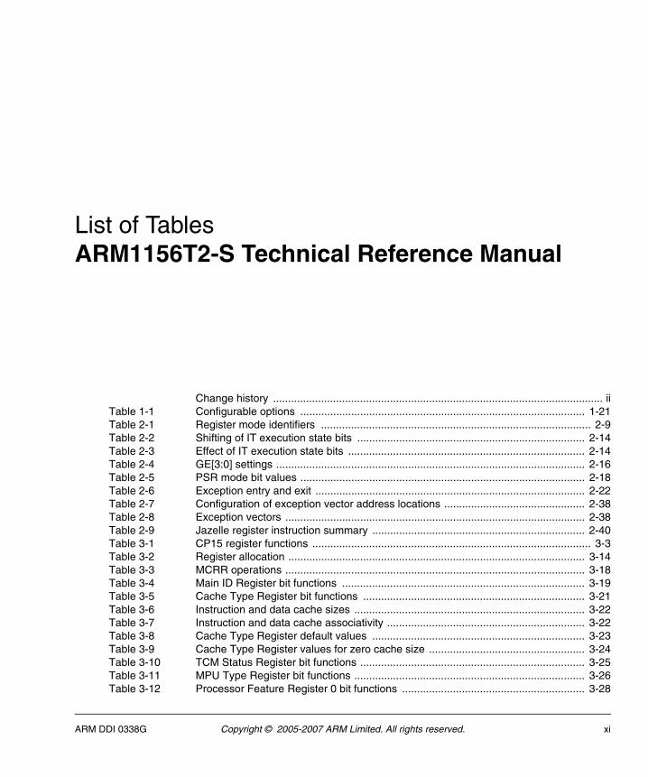
Change history .............................................................................................................. iiTable 1-1 Configurable options ............................................................................................... 1-21Table 2-1 Register mode identifiers .......................................................................................... 2-9Table 2-2 Shifting of IT execution state bits ............................................................................ 2-14Table 2-3 Effect of IT execution state bits ............................................................................... 2-14Table 2-4 GE[3:0] settings ....................................................................................................... 2-16Table 2-5 PSR mode bit values ............................................................................................... 2-18Table 2-6 Exception entry and exit .......................................................................................... 2-22Table 2-7 Configuration of exception vector address locations ............................................... 2-38Table 2-8 Exception vectors .................................................................................................... 2-38Table 2-9 Jazelle register instruction summary ....................................................................... 2-40Table 3-1 CP15 register functions ............................................................................................. 3-3Table 3-2 Register allocation ................................................................................................... 3-14Table 3-3 MCRR operations .................................................................................................... 3-18Table 3-4 Main ID Register bit functions ................................................................................. 3-19Table 3-5 Cache Type Register bit functions .......................................................................... 3-21Table 3-6 Instruction and data cache sizes ............................................................................. 3-22Table 3-7 Instruction and data cache associativity .................................................................. 3-22Table 3-8 Cache Type Register default values ....................................................................... 3-23Table 3-9 Cache Type Register values for zero cache size .................................................... 3-24Table 3-10 TCM Status Register bit functions ........................................................................... 3-25Table 3-11 MPU Type Register bit functions ............................................................................. 3-26Table 3-12 Processor Feature Register 0 bit functions ............................................................. 3-28
ARM DDI 0338G Copyright © 2005-2007 ARM Limited. All rights reserved. xi
List of Tables
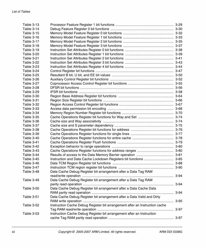
Table 3-13 Processor Feature Register 1 bit functions ............................................................. 3-29Table 3-14 Debug Feature Register 0 bit functions .................................................................. 3-30Table 3-15 Memory Model Feature Register 0 bit functions ..................................................... 3-32Table 3-16 Memory Model Feature Register 1 bit functions ..................................................... 3-33Table 3-17 Memory Model Feature Register 2 bit functions ..................................................... 3-35Table 3-18 Memory Model Feature Register 3 bit functions ..................................................... 3-37Table 3-19 Instruction Set Attributes Register 0 bit functions ................................................... 3-38Table 3-20 Instruction Set Attributes Register 1 bit functions ................................................... 3-39Table 3-21 Instruction Set Attributes Register 2 bit functions ................................................... 3-41Table 3-22 Instruction Set Attributes Register 3 bit functions ................................................... 3-43Table 3-23 Instruction Set Attributes Register 4 bit functions ................................................... 3-44Table 3-24 Control Register bit functions .................................................................................. 3-47Table 3-25 Resultant B bit, U bit, and EE bit values ................................................................. 3-50Table 3-26 Auxiliary Control Register bit functions ................................................................... 3-52Table 3-27 Coprocessor Access Control Register bit functions ................................................ 3-55Table 3-28 DFSR bit functions .................................................................................................. 3-56Table 3-29 IFSR bit functions ................................................................................................... 3-58Table 3-30 Region Base Address Register bit functions .......................................................... 3-64Table 3-31 Region Size Register bit functions .......................................................................... 3-66Table 3-32 Region Access Control Register bit functions ......................................................... 3-67Table 3-33 Access data permission bit encoding ..................................................................... 3-68Table 3-34 Memory Region Number Register bit functions ...................................................... 3-70Table 3-35 Cache Operations Register bit functions for Way and Set ..................................... 3-74Table 3-36 Cache size and Way associativity .......................................................................... 3-74Table 3-37 Cache size and S parameter dependency .............................................................. 3-75Table 3-38 Cache Operations Register bit functions for address ............................................. 3-76Table 3-39 Cache Operations Register functions for single lines ............................................. 3-77Table 3-40 Cache Operations Register functions for entire cache ........................................... 3-78Table 3-41 Cache Operations Register Flush functions ........................................................... 3-79Table 3-42 Exception behavior to range operations ................................................................. 3-80Table 3-43 Cache Operations Register functions for address ranges ...................................... 3-80Table 3-44 Results of access to the Data Memory Barrier operation ....................................... 3-81Table 3-45 Instruction and Data Cache Lockdown Registers bit functions ............................... 3-85Table 3-46 Data TCM Region Register bit functions ................................................................ 3-88Table 3-47 Instruction TCM region register bit functions .......................................................... 3-90Table 3-48 Data Cache Debug Register bit arrangement after a Data Tag RAM
read/write operation ................................................................................................ 3-94Table 3-49 Data Cache Debug Register bit arrangement after a Data Tag RAM
parity read operation ............................................................................................... 3-94Table 3-50 Data Cache Debug Register bit arrangement after a Data Cache Data
RAM parity read operation ...................................................................................... 3-94Table 3-51 Data Cache Debug Register bit arrangement after a Data Valid and Dirty
RAM write operation ............................................................................................... 3-95Table 3-52 Instruction Cache Debug Register bit arrangement after an Instruction cache
Tag RAM read/write operation ................................................................................ 3-97Table 3-53 Instruction Cache Debug Register bit arrangement after an Instruction
cache Tag RAM parity read operation .................................................................... 3-97
xii Copyright © 2005-2007 ARM Limited. All rights reserved. ARM DDI 0338G
List of Tables
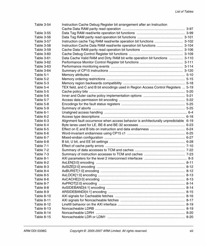
Table 3-54 Instruction Cache Debug Register bit arrangement after an InstructionCache Data RAM parity read operation .................................................................. 3-97
Table 3-55 Data Tag RAM read/write operation bit functions ................................................... 3-99Table 3-56 Data Tag RAM parity read operation bit functions ................................................ 3-101Table 3-57 Instruction cache Tag RAM read/write operation bit functions .............................. 3-102Table 3-58 Instruction Cache Data RAM read/write operation bit functions ............................ 3-104Table 3-59 Cache Data RAM parity read operation bit functions ............................................ 3-106Table 3-60 Cache Debug Control Register bit functions ......................................................... 3-109Table 3-61 Data Cache Valid RAM and Dirty RAM bit write operation bit functions ............... 3-110Table 3-62 Performance Monitor Control Register bit functions .............................................. 3-111Table 3-63 Performance monitoring events ............................................................................ 3-114Table 3-64 Summary of CP15 instructions .............................................................................. 3-120Table 5-1 Memory attributes ................................................................................................... 5-10Table 5-2 Memory ordering restrictions ................................................................................... 5-15Table 5-3 Memory region backwards compatibility ................................................................. 5-18Table 5-4 TEX field, and C and B bit encodings used in Region Access Control Registers ... 5-19Table 5-5 Cache policy bits ..................................................................................................... 5-20Table 5-6 Inner and Outer cache policy implementation options ............................................ 5-21Table 5-7 Access data permission bit encoding ...................................................................... 5-22Table 5-8 Encodings for the fault status registers ................................................................... 5-25Table 5-9 Summary of aborts .................................................................................................. 5-25Table 6-1 Unaligned access handling ....................................................................................... 6-4Table 6-2 Access type descriptions ......................................................................................... 6-18Table 6-3 Alignment fault occurrence when access behavior is architecturally unpredictable 6-19Table 6-4 Byte lanes used for LE, BE-8 and BE-32 accesses ................................................ 6-23Table 6-5 Effect on E and B bits on instruction and data endianness ..................................... 6-24Table 6-6 Word-invariant endianness using CP15 c1 ............................................................. 6-25Table 6-7 Mixed-endian configuration ..................................................................................... 6-27Table 6-8 B bit, U bit, and EE bit settings ................................................................................ 6-28Table 7-1 Effect of cache parity errors .................................................................................... 7-10Table 7-2 Summary of data accesses to TCM and caches ..................................................... 7-22Table 7-3 Summary of instruction accesses to TCM and caches ........................................... 7-23Table 8-1 AXI parameters for the level 2 interconnect interfaces ............................................. 8-3Table 8-2 AxLEN[3:0] encoding .............................................................................................. 8-11Table 8-3 AxSIZE[2:0] encoding ............................................................................................. 8-12Table 8-4 AxBURST[1:0] encoding ......................................................................................... 8-12Table 8-5 AxLOCK[1:0] encoding ............................................................................................ 8-13Table 8-6 AxCACHE[3:0] encoding ......................................................................................... 8-13Table 8-7 AxPROT[2:0] encoding ........................................................................................... 8-14Table 8-8 AxSIDEBAND[4:1] encoding ................................................................................... 8-14Table 8-9 ARSIDEBANDI[4:1] encoding ................................................................................. 8-15Table 8-10 AXI signals for Cacheable fetches .......................................................................... 8-16Table 8-11 AXI signals for Noncacheable fetches .................................................................... 8-17Table 8-12 Linefill behavior on the AXI interface ....................................................................... 8-19Table 8-13 Noncacheable LDRB ............................................................................................... 8-19Table 8-14 Noncacheable LDRH .............................................................................................. 8-20Table 8-15 Noncacheable LDR or LDM1 .................................................................................. 8-20
ARM DDI 0338G Copyright © 2005-2007 ARM Limited. All rights reserved. xiii
List of Tables
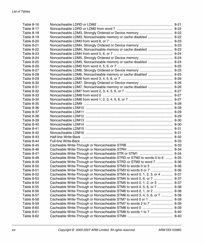
Table 8-16 Noncacheable LDRD or LDM2 ............................................................................... 8-21Table 8-17 Noncacheable LDRD or LDM2 from word 7 ........................................................... 8-22Table 8-18 Noncacheable LDM3, Strongly Ordered or Device memory ................................... 8-22Table 8-19 Noncacheable LDM3, Noncacheable memory or cache disabled .......................... 8-22Table 8-20 Noncacheable LDM3 from word 6, or 7 .................................................................. 8-23Table 8-21 Noncacheable LDM4, Strongly Ordered or Device memory ................................... 8-23Table 8-22 Noncacheable LDM4, Noncacheable memory or cache disabled .......................... 8-23Table 8-23 Noncacheable LDM4 from word 5, 6, or 7 .............................................................. 8-24Table 8-24 Noncacheable LDM5, Strongly Ordered or Device memory ................................... 8-24Table 8-25 Noncacheable LDM5, Noncacheable memory or cache disabled .......................... 8-24Table 8-26 Noncacheable LDM5 from word 4, 5, 6, or 7 .......................................................... 8-25Table 8-27 Noncacheable LDM6, Strongly Ordered or Device memory ................................... 8-25Table 8-28 Noncacheable LDM6, Noncacheable memory or cache disabled .......................... 8-25Table 8-29 Noncacheable LDM6 from word 3, 4, 5, 6, or 7 ...................................................... 8-26Table 8-30 Noncacheable LDM7, Strongly Ordered or Device memory ................................... 8-26Table 8-31 Noncacheable LDM7, Noncacheable memory or cache disabled .......................... 8-26Table 8-32 Noncacheable LDM7 from word 2, 3, 4, 5, 6, or 7 .................................................. 8-27Table 8-33 Noncacheable LDM8 from word 0 .......................................................................... 8-27Table 8-34 Noncacheable LDM8 from word 1, 2, 3, 4, 5, 6, or 7 .............................................. 8-27Table 8-35 Noncacheable LDM9 .............................................................................................. 8-28Table 8-36 Noncacheable LDM10 ............................................................................................ 8-28Table 8-37 Noncacheable LDM11 ............................................................................................ 8-29Table 8-38 Noncacheable LDM12 ............................................................................................ 8-29Table 8-39 Noncacheable LDM13 ............................................................................................ 8-30Table 8-40 Noncacheable LDM14 ............................................................................................ 8-30Table 8-41 Noncacheable LDM15 ............................................................................................ 8-31Table 8-42 Noncacheable LDM16 ............................................................................................ 8-31Table 8-43 Half-line Write-Back ................................................................................................ 8-32Table 8-44 Full-line Write-Back ................................................................................................. 8-33Table 8-45 Cacheable Write-Through or Noncacheable STRB ................................................ 8-33Table 8-46 Cacheable Write-Through or Noncacheable STRH ................................................ 8-34Table 8-47 Cacheable Write-Through or Noncacheable STR or STM1 ................................... 8-34Table 8-48 Cacheable Write-Through or Noncacheable STRD or STM2 to words 0 to 6 ........ 8-35Table 8-49 Cacheable Write-Through or Noncacheable STRD or STM2 to word 7 ................. 8-36Table 8-50 Cacheable Write-Through or Noncacheable STM3 to words 0 to 5 ....................... 8-36Table 8-51 Cacheable Write-Through or Noncacheable STM3 to words 6 or 7 ....................... 8-36Table 8-52 Cacheable Write-Through or Noncacheable STM4 to word 0, 1, 2, 3, or 4 ............ 8-37Table 8-53 Cacheable Write-Through or Noncacheable STM4 to word 5, 6, or 7 .................... 8-37Table 8-54 Cacheable Write-Through or Noncacheable STM5 to word 0, 1, 2, or 3 ................ 8-37Table 8-55 Cacheable Write-Through or Noncacheable STM5 to word 4, 5, 6, or 7 ................ 8-38Table 8-56 Cacheable Write-Through or Noncacheable STM6 to word 0, 1, or 2 .................... 8-38Table 8-57 Cacheable Write-Through or Noncacheable STM6 to word 3, 4, 5, 6, or 7 ............ 8-38Table 8-58 Cacheable Write-Through or Noncacheable STM7 to word 0 or 1 ......................... 8-39Table 8-59 Cacheable Write-Through or Noncacheable STM7 to words 2 to 7 ....................... 8-39Table 8-60 Cacheable Write-Through or Noncacheable STM8 to word 0 ................................ 8-39Table 8-61 Cacheable Write-Through or Noncacheable STM8 to words 1 to 7 ....................... 8-40Table 8-62 Cacheable Write-Through or Noncacheable STM9 ................................................ 8-40
xiv Copyright © 2005-2007 ARM Limited. All rights reserved. ARM DDI 0338G
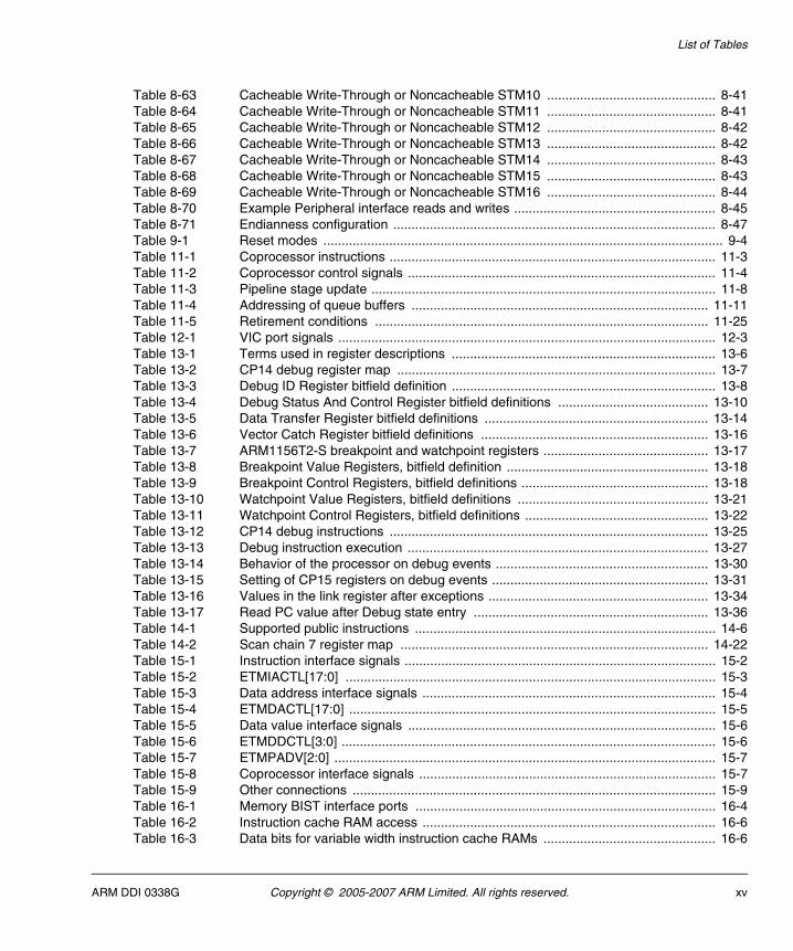
List of Tables
Table 8-63 Cacheable Write-Through or Noncacheable STM10 .............................................. 8-41Table 8-64 Cacheable Write-Through or Noncacheable STM11 .............................................. 8-41Table 8-65 Cacheable Write-Through or Noncacheable STM12 .............................................. 8-42Table 8-66 Cacheable Write-Through or Noncacheable STM13 .............................................. 8-42Table 8-67 Cacheable Write-Through or Noncacheable STM14 .............................................. 8-43Table 8-68 Cacheable Write-Through or Noncacheable STM15 .............................................. 8-43Table 8-69 Cacheable Write-Through or Noncacheable STM16 .............................................. 8-44Table 8-70 Example Peripheral interface reads and writes ....................................................... 8-45Table 8-71 Endianness configuration ........................................................................................ 8-47Table 9-1 Reset modes ............................................................................................................. 9-4Table 11-1 Coprocessor instructions ......................................................................................... 11-3Table 11-2 Coprocessor control signals .................................................................................... 11-4Table 11-3 Pipeline stage update .............................................................................................. 11-8Table 11-4 Addressing of queue buffers ................................................................................. 11-11Table 11-5 Retirement conditions ........................................................................................... 11-25Table 12-1 VIC port signals ....................................................................................................... 12-3Table 13-1 Terms used in register descriptions ........................................................................ 13-6Table 13-2 CP14 debug register map ....................................................................................... 13-7Table 13-3 Debug ID Register bitfield definition ........................................................................ 13-8Table 13-4 Debug Status And Control Register bitfield definitions ......................................... 13-10Table 13-5 Data Transfer Register bitfield definitions ............................................................. 13-14Table 13-6 Vector Catch Register bitfield definitions .............................................................. 13-16Table 13-7 ARM1156T2-S breakpoint and watchpoint registers ............................................. 13-17Table 13-8 Breakpoint Value Registers, bitfield definition ....................................................... 13-18Table 13-9 Breakpoint Control Registers, bitfield definitions ................................................... 13-18Table 13-10 Watchpoint Value Registers, bitfield definitions .................................................... 13-21Table 13-11 Watchpoint Control Registers, bitfield definitions .................................................. 13-22Table 13-12 CP14 debug instructions ....................................................................................... 13-25Table 13-13 Debug instruction execution .................................................................................. 13-27Table 13-14 Behavior of the processor on debug events .......................................................... 13-30Table 13-15 Setting of CP15 registers on debug events ........................................................... 13-31Table 13-16 Values in the link register after exceptions ............................................................ 13-34Table 13-17 Read PC value after Debug state entry ................................................................ 13-36Table 14-1 Supported public instructions .................................................................................. 14-6Table 14-2 Scan chain 7 register map .................................................................................... 14-22Table 15-1 Instruction interface signals ..................................................................................... 15-2Table 15-2 ETMIACTL[17:0] ..................................................................................................... 15-3Table 15-3 Data address interface signals ................................................................................ 15-4Table 15-4 ETMDACTL[17:0] .................................................................................................... 15-5Table 15-5 Data value interface signals .................................................................................... 15-6Table 15-6 ETMDDCTL[3:0] ...................................................................................................... 15-6Table 15-7 ETMPADV[2:0] ........................................................................................................ 15-7Table 15-8 Coprocessor interface signals ................................................................................. 15-7Table 15-9 Other connections ................................................................................................... 15-9Table 16-1 Memory BIST interface ports .................................................................................. 16-4Table 16-2 Instruction cache RAM access ................................................................................ 16-6Table 16-3 Data bits for variable width instruction cache RAMs ............................................... 16-6
ARM DDI 0338G Copyright © 2005-2007 ARM Limited. All rights reserved. xv
List of Tables
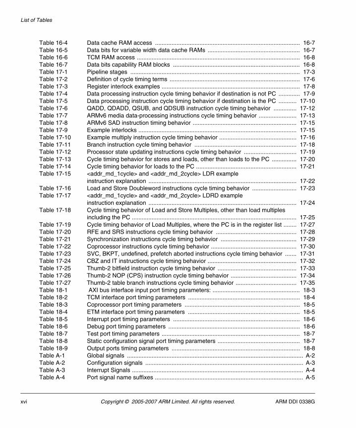
Table 16-4 Data cache RAM access ........................................................................................ 16-7Table 16-5 Data bits for variable width data cache RAMs ........................................................ 16-7Table 16-6 TCM RAM access ................................................................................................... 16-8Table 16-7 Data bits capability RAM blocks ............................................................................. 16-8Table 17-1 Pipeline stages ....................................................................................................... 17-3Table 17-2 Definition of cycle timing terms ............................................................................... 17-6Table 17-3 Register interlock examples .................................................................................... 17-8Table 17-4 Data processing instruction cycle timing behavior if destination is not PC ............. 17-9Table 17-5 Data processing instruction cycle timing behavior if destination is the PC ........... 17-10Table 17-6 QADD, QDADD, QSUB, and QDSUB instruction cycle timing behavior .............. 17-12Table 17-7 ARMv6 media data-processing instructions cycle timing behavior ....................... 17-13Table 17-8 ARMv6 SAD instruction timing behavior ............................................................... 17-15Table 17-9 Example interlocks ................................................................................................ 17-15Table 17-10 Example multiply instruction cycle timing behavior ............................................... 17-16Table 17-11 Branch instruction cycle timing behavior .............................................................. 17-18Table 17-12 Processor state updating instructions cycle timing behavior ................................ 17-19Table 17-13 Cycle timing behavior for stores and loads, other than loads to the PC ............... 17-20Table 17-14 Cycle timing behavior for loads to the PC ............................................................. 17-21Table 17-15 <addr_md_1cycle> and <addr_md_2cycle> LDR example
instruction explanation .......................................................................................... 17-22Table 17-16 Load and Store Doubleword instructions cycle timing behavior ........................... 17-23Table 17-17 <addr_md_1cycle> and <addr_md_2cycle> LDRD example
instruction explanation .......................................................................................... 17-24Table 17-18 Cycle timing behavior of Load and Store Multiples, other than load multiples
including the PC .................................................................................................... 17-25Table 17-19 Cycle timing behavior of Load Multiples, where the PC is in the register list ........ 17-27Table 17-20 RFE and SRS instructions cycle timing behavior ................................................. 17-28Table 17-21 Synchronization instructions cycle timing behavior .............................................. 17-29Table 17-22 Coprocessor instructions cycle timing behavior .................................................... 17-30Table 17-23 SVC, BKPT, undefined, prefetch aborted instructions cycle timing behavior ....... 17-31Table 17-24 CBZ and IT instructions cycle timing behavior ...................................................... 17-32Table 17-25 Thumb-2 bitfield instruction cycle timing behavior ................................................ 17-33Table 17-26 Thumb-2 NOP (CPS) instruction cycle timing behavior ........................................ 17-34Table 17-27 Thumb-2 table branch instructions cycle timing behavior ..................................... 17-35Table 18-1 AXI bus interface input port timing parameters: ..................................................... 18-3Table 18-2 TCM interface port timing parameters .................................................................... 18-4Table 18-3 Coprocessor port timing parameters ...................................................................... 18-5Table 18-4 ETM interface port timing parameters .................................................................... 18-5Table 18-5 Interrupt port timing parameters ............................................................................. 18-6Table 18-6 Debug port timing parameters ................................................................................ 18-6Table 18-7 Test port timing parameters .................................................................................... 18-7Table 18-8 Static configuration signal port timing parameters .................................................. 18-7Table 18-9 Output ports timing parameters .............................................................................. 18-8Table A-1 Global signals ........................................................................................................... A-2Table A-2 Configuration signals ................................................................................................ A-3Table A-3 Interrupt Signals ........................................................................................................ A-4Table A-4 Port signal name suffixes .......................................................................................... A-5
xvi Copyright © 2005-2007 ARM Limited. All rights reserved. ARM DDI 0338G
List of Tables
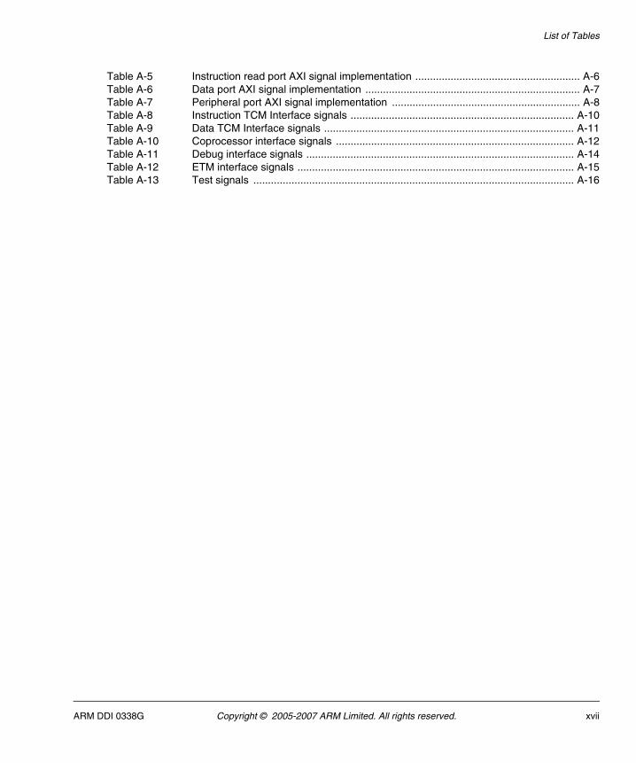
Table A-5 Instruction read port AXI signal implementation ........................................................ A-6Table A-6 Data port AXI signal implementation ......................................................................... A-7Table A-7 Peripheral port AXI signal implementation ................................................................ A-8Table A-8 Instruction TCM Interface signals ............................................................................ A-10Table A-9 Data TCM Interface signals ..................................................................................... A-11Table A-10 Coprocessor interface signals ................................................................................. A-12Table A-11 Debug interface signals ........................................................................................... A-14Table A-12 ETM interface signals .............................................................................................. A-15Table A-13 Test signals ............................................................................................................. A-16
ARM DDI 0338G Copyright © 2005-2007 ARM Limited. All rights reserved. xvii

List of Tables
xviii Copyright © 2005-2007 ARM Limited. All rights reserved. ARM DDI 0338G
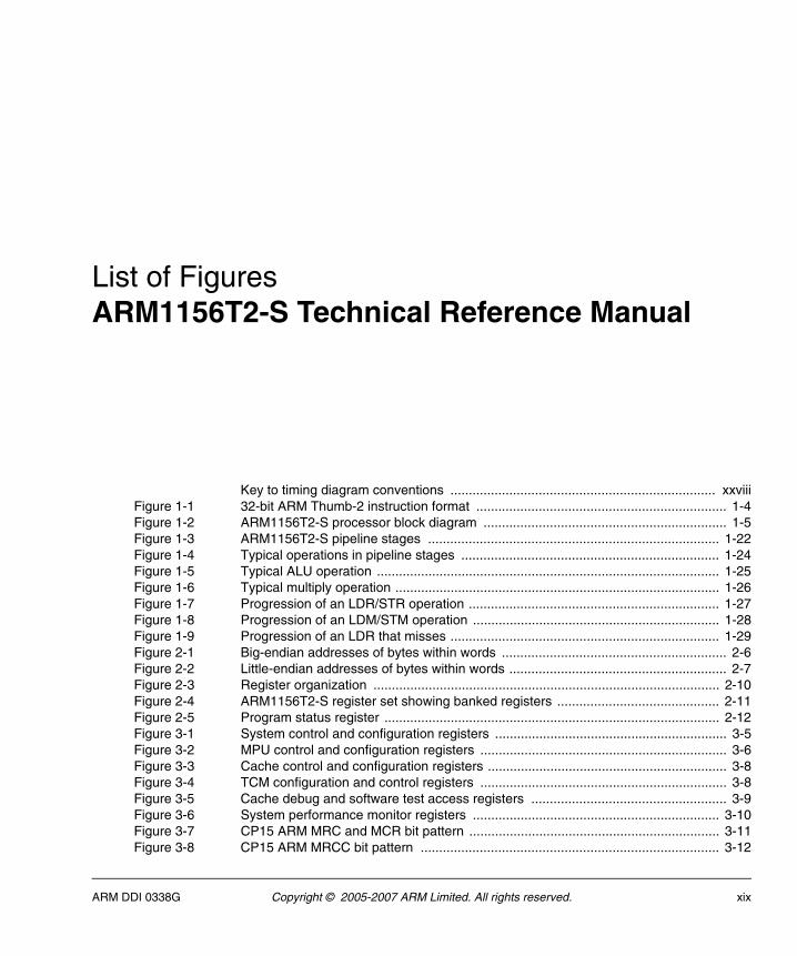
List of FiguresARM1156T2-S Technical Reference Manual
Key to timing diagram conventions ........................................................................ xxviiiFigure 1-1 32-bit ARM Thumb-2 instruction format .................................................................... 1-4Figure 1-2 ARM1156T2-S processor block diagram .................................................................. 1-5Figure 1-3 ARM1156T2-S pipeline stages ............................................................................... 1-22Figure 1-4 Typical operations in pipeline stages ...................................................................... 1-24Figure 1-5 Typical ALU operation ............................................................................................. 1-25Figure 1-6 Typical multiply operation ........................................................................................ 1-26Figure 1-7 Progression of an LDR/STR operation .................................................................... 1-27Figure 1-8 Progression of an LDM/STM operation ................................................................... 1-28Figure 1-9 Progression of an LDR that misses ......................................................................... 1-29Figure 2-1 Big-endian addresses of bytes within words ............................................................. 2-6Figure 2-2 Little-endian addresses of bytes within words ........................................................... 2-7Figure 2-3 Register organization .............................................................................................. 2-10Figure 2-4 ARM1156T2-S register set showing banked registers ............................................ 2-11Figure 2-5 Program status register ........................................................................................... 2-12Figure 3-1 System control and configuration registers ............................................................... 3-5Figure 3-2 MPU control and configuration registers ................................................................... 3-6Figure 3-3 Cache control and configuration registers ................................................................. 3-8Figure 3-4 TCM configuration and control registers ................................................................... 3-8Figure 3-5 Cache debug and software test access registers ..................................................... 3-9Figure 3-6 System performance monitor registers ................................................................... 3-10Figure 3-7 CP15 ARM MRC and MCR bit pattern .................................................................... 3-11Figure 3-8 CP15 ARM MRCC bit pattern ................................................................................. 3-12
ARM DDI 0338G Copyright © 2005-2007 ARM Limited. All rights reserved. xix
List of Figures
Figure 3-9 CP15 Thumb-2 MRC and MCR bit pattern ............................................................. 3-12Figure 3-10 CP15 Thumb-2 MCRR bit pattern ........................................................................... 3-12Figure 3-11 Main ID Register format .......................................................................................... 3-19Figure 3-12 Cache Type Register format ................................................................................... 3-20Figure 3-13 TCM Status Register format ................................................................................... 3-25Figure 3-14 MPU Type Register format ..................................................................................... 3-26Figure 3-15 Processor Feature Register 0 format ...................................................................... 3-27Figure 3-16 Processor Feature Register 1 format ...................................................................... 3-29Figure 3-17 Debug Feature Register 0 format ........................................................................... 3-30Figure 3-18 Memory Model Feature Register 0 format .............................................................. 3-31Figure 3-19 Memory Model Feature Register 1 format .............................................................. 3-33Figure 3-20 Memory Model Feature Register 2 format .............................................................. 3-35Figure 3-21 Memory Model Feature Register 3 format .............................................................. 3-36Figure 3-22 Instruction Set Attributes Register 0 format ............................................................ 3-38Figure 3-23 Instruction Set Attributes Register 1 format ............................................................ 3-39Figure 3-24 Instruction Set Attributes Register 2 format ............................................................ 3-41Figure 3-25 Instruction Set Attributes Register 3 format ............................................................ 3-42Figure 3-26 Instruction Set Attributes Register 4 format ............................................................ 3-44Figure 3-27 Control Register format ........................................................................................... 3-47Figure 3-28 Auxiliary Control Register format ............................................................................ 3-52Figure 3-29 Coprocessor Access Control Register format ......................................................... 3-54Figure 3-30 DFSR format ........................................................................................................... 3-56Figure 3-31 IFSR format ............................................................................................................ 3-58Figure 3-32 Region Base Address Register format ................................................................... 3-64Figure 3-33 Region Size Register .............................................................................................. 3-65Figure 3-34 Region Access Control Register ............................................................................. 3-67Figure 3-35 Memory Region Number Register format ............................................................... 3-70Figure 3-36 Cache operations registers ..................................................................................... 3-72Figure 3-37 Cache Operation Register format for Way and Set ................................................ 3-74Figure 3-38 Cache Operation Register format for the address .................................................. 3-75Figure 3-39 Cache Dirty Status Register format ........................................................................ 3-84Figure 3-40 Instruction and Data Cache Lockdown Registers format ........................................ 3-85Figure 3-41 Data TCM Region Register ..................................................................................... 3-88Figure 3-42 Instruction TCM Region Register format ................................................................ 3-90Figure 3-43 Format of the Process ID Register ......................................................................... 3-92Figure 3-44 Formats of the Data Cache Debug Register ........................................................... 3-93Figure 3-45 Formats of the Instruction Cache Debug Register .................................................. 3-96Figure 3-46 Data Tag RAM read/write operation format ............................................................ 3-99Figure 3-47 Tag RAM parity read operation format ................................................................. 3-101Figure 3-48 Instruction cache Tag RAM read/write operation format ...................................... 3-102Figure 3-49 Instruction Cache Data RAM read/write operation format .................................... 3-104Figure 3-50 Cache Data RAM parity read operation format ..................................................... 3-106Figure 3-51 Cache Debug Control Register format .................................................................. 3-109Figure 3-52 Data Cache Valid RAM and Dirty RAM bit write operation format ........................ 3-110Figure 3-53 Performance Monitor Control Register format ...................................................... 3-111Figure 5-1 MPU simplified block diagram .................................................................................. 5-2Figure 5-2 Overlapping memory regions .................................................................................... 5-5
xx Copyright © 2005-2007 ARM Limited. All rights reserved. ARM DDI 0338G
List of Figures
Figure 5-3 Overlay for stack protection ...................................................................................... 5-5Figure 5-4 Memory map behavior for data and instruction accesses when MPU is disabled .... 5-9Figure 5-5 Fault checking sequence ........................................................................................ 5-28Figure 6-1 Load unsigned byte ................................................................................................... 6-7Figure 6-2 Load signed byte ....................................................................................................... 6-8Figure 6-3 Store byte .................................................................................................................. 6-8Figure 6-4 Load unsigned halfword, little-endian ........................................................................ 6-9Figure 6-5 Load unsigned halfword, big-endian ......................................................................... 6-9Figure 6-6 Load signed halfword, little-endian .......................................................................... 6-10Figure 6-7 Load signed halfword, big-endian ........................................................................... 6-11Figure 6-8 Store halfword, little-endian ..................................................................................... 6-11Figure 6-9 Store halfword, big-endian ...................................................................................... 6-12Figure 6-10 Load word, little-endian ........................................................................................... 6-13Figure 6-11 Load word, big-endian ............................................................................................. 6-14Figure 6-12 Store word, little-endian .......................................................................................... 6-15Figure 6-13 Store word, big-endian ............................................................................................ 6-16Figure 7-1 Level one cache block diagram ................................................................................. 7-5Figure 7-2 TCM read access .................................................................................................... 7-15Figure 7-3 TCM write access .................................................................................................... 7-15Figure 7-4 Error generation on read ......................................................................................... 7-16Figure 7-5 Error correction on read .......................................................................................... 7-17Figure 7-6 Stall cycles on read accesses ................................................................................. 7-18Figure 7-7 Stall cycles on write accesses ................................................................................. 7-18Figure 8-1 Level two interconnect interfaces .............................................................................. 8-2Figure 8-2 Channel architecture of reads ................................................................................... 8-8Figure 8-3 Channel architecture of writes ................................................................................... 8-9Figure 8-4 Swizzling of data and strobes in BE-32 big-endian configuration ........................... 8-48Figure 9-1 Power-on reset .......................................................................................................... 9-4Figure 11-1 Core and coprocessor pipelines .............................................................................. 11-5Figure 11-2 Coprocessor pipeline and queues ........................................................................... 11-6Figure 11-3 Coprocessor pipeline .............................................................................................. 11-7Figure 11-4 Token queue buffers ............................................................................................. 11-10Figure 11-5 Queue reading and writing .................................................................................... 11-12Figure 11-6 Queue flushing ...................................................................................................... 11-13Figure 11-7 Instruction queue ................................................................................................... 11-14Figure 11-8 Coprocessor data transfer ..................................................................................... 11-18Figure 11-9 Instruction iteration for loads ................................................................................. 11-19Figure 11-10 Load data buffering ............................................................................................... 11-20Figure 12-1 Connection of a PL192 VIC to an ARM1156T2-S processor .................................. 12-3Figure 12-2 VIC port timing example .......................................................................................... 12-6Figure 12-3 Interrupt entry sequence ......................................................................................... 12-9Figure 13-1 Typical debug system ............................................................................................. 13-2Figure 13-2 Debug ID Register format ....................................................................................... 13-8Figure 13-3 Debug Status And Control Register format ........................................................... 13-10Figure 13-4 DTR format ............................................................................................................ 13-14Figure 13-5 Vector Catch Register format ................................................................................ 13-15Figure 13-6 Breakpoint Control Registers, format .................................................................... 13-18
ARM DDI 0338G Copyright © 2005-2007 ARM Limited. All rights reserved. xxi
List of Figures
Figure 13-7 Watchpoint Control Registers, format ................................................................... 13-22Figure 14-1 JTAG DBGTAP state machine diagram ................................................................. 14-2Figure 14-2 Clock synchronization ............................................................................................. 14-3Figure 14-3 Bypass register bit order ......................................................................................... 14-8Figure 14-4 Device ID code register bit order ............................................................................ 14-9Figure 14-5 Instruction register bit order .................................................................................. 14-10Figure 14-6 Scan chain select register bit order ...................................................................... 14-11Figure 14-7 Scan chain 0 bit order ........................................................................................... 14-12Figure 14-8 Scan chain 1 bit order ........................................................................................... 14-13Figure 14-9 Scan chain 4 bit order ........................................................................................... 14-15Figure 14-10 Scan chain 5 bit order, EXTEST selected ............................................................ 14-16Figure 14-11 Scan chain 5 bit order, INTEST selected .............................................................. 14-17Figure 14-12 Scan chain 6 bit order ........................................................................................... 14-19Figure 14-13 Scan chain 7 bit order ........................................................................................... 14-21Figure 14-14 Behavior of the ITRsel IR instruction .................................................................... 14-26Figure 15-1 ETMCPADDRESS format ....................................................................................... 15-8Figure 16-1 Traditional method interfacing memory BIST ......................................................... 16-3Figure 16-2 Processor Memory BIST interface .......................................................................... 16-4Figure 16-3 Pipelining of the MBIST interface ........................................................................... 16-5
xxii Copyright © 2005-2007 ARM Limited. All rights reserved. ARM DDI 0338G
Preface
This preface introduces the ARM1156T2-S™ r0p1 Technical Reference Manual (TRM). It contains the following sections:
• About this manual on page xxiv
• Feedback on page xxxi.
ARM DDI 0338G Copyright © 2005-2007 ARM Limited. All rights reserved. xxiii
Preface
About this manual
This is the technical reference manual for the ARM1156T2-S™ processor. In this manual the generic term processor means the ARM1156T2-S processor.
Product revision status
The rnpn identifier indicates the revision status of the product described in this manual, where:
rn Identifies the major revision of the product.
pn Identifies the minor revision or modification status of the product.
Intended audience
This manual has been written for hardware and software engineers implementing processor system designs. It provides information to enable designers to integrate the processor into a target system as quickly as possible.
Using this manual
This manual is organized into the following chapters:
Chapter 1 Introduction
Read this chapter for an introduction to the processor and descriptions of the major functional blocks.
Chapter 2 Programmer’s Model
Read this chapter for a description of the ARM1156T2-S registers and programming details.
Chapter 3 System Control Coprocessor
Read this chapter for a description of the ARM1156T2-S control coprocessor CP15 registers and programming details.
Chapter 4 Prefetch Unit
Read this chapter for a description of the functions of the ARM1156T2-S Prefetch Unit, including branch prediction and the return stack.
Chapter 5 Memory Protection Unit
Read this chapter for a description of the ARM1156T2-S Memory Protection Unit (MPU) and the access permissions process.
xxiv Copyright © 2005-2007 ARM Limited. All rights reserved. ARM DDI 0338G
Preface
Chapter 6 Unaligned and Mixed-Endian Data Access Support
Read this chapter for a description of the processor support for unaligned and mixed-endian data accesses.
Chapter 7 Level One Memory System
Read this chapter for a description of the ARM1156T2-S level one memory system, including caches, Tightly-Coupled Memory (TCM) and write buffer.
Chapter 8 Level Two Interface
Read this chapter for a description of the ARM1156T2-S level two memory interface and the peripheral port.
Chapter 9 Clocking and Resets
Read this chapter for a description of the ARM1156T2-S clocking modes and the reset signals.
Chapter 10 Power Control
Read this chapter for a description of the ARM1156T2-S power control facilities.
Chapter 11 Coprocessor Interface
Read this chapter for details of the ARM1156T2-S coprocessor interface.
Chapter 12 Vectored Interrupt Controller Port
Read this chapter for a description of the ARM1156T2-S Vectored Interrupt Controller (VIC) interface.
Chapter 13 Debug
Read this chapter for a description of the ARM1156T2-S debug support.
Chapter 14 Debug Test Access Port
Read this chapter for a description of the JTAG-based ARM1156T2-S Debug Test Access Port.
Chapter 15 Trace Interface Port
Read this chapter for a description of the Embedded Trace Macrocell (ETM) interface port.
Chapter 16 Test Features
Read this chapter for a description of the ARM1156T2-S test features.
ARM DDI 0338G Copyright © 2005-2007 ARM Limited. All rights reserved. xxv
Preface
Chapter 17 Cycle Timings and Interlock Behavior
Read this chapter for a description of the ARM1156T2-S instruction cycle timing and for details of instruction interlocks.
Chapter 18 AC Characteristics
Read this chapter for a description of the timing parameters applicable to the processor.
Appendix A Processor Signal Descriptions
Read this appendix for a description of the inputs and outputs of the processor.
xxvi Copyright © 2005-2007 ARM Limited. All rights reserved. ARM DDI 0338G
Preface
Conventions
Conventions that this manual can use are described in:
• Typographical
• Timing diagrams
• Signal naming on page xxviii
• Numbering on page xxix.
Typographical
The typographical conventions are:
italic Highlights important notes, introduces special terminology, denotes internal cross-references, and citations.
bold Highlights interface elements, such as menu names. Denotes ARM processor signal names. Also used for terms in descriptive lists, where appropriate.
monospace Denotes text that you can enter at the keyboard, such as commands, file and program names, and source code.
monospace Denotes a permitted abbreviation for a command or option. You can enter the underlined text instead of the full command or option name.
monospace italic Denotes arguments to monospace text where the argument is to be replaced by a specific value.
monospace bold Denotes language keywords when used outside example code.
< and > Angle brackets enclose replaceable terms for assembler syntax where they appear in code or code fragments. They appear in normal font in running text. For example:
• MRC p15, 0 <Rd>, <CRn>, <CRm>, <Opcode_2>
• The Opcode_2 value selects which register is accessed.
Timing diagrams
The figure named Key to timing diagram conventions on page xxviii explains the components used in timing diagrams. Variations, when they occur, have clear labels. You must not assume any timing information that is not explicit in the diagrams.
ARM DDI 0338G Copyright © 2005-2007 ARM Limited. All rights reserved. xxvii
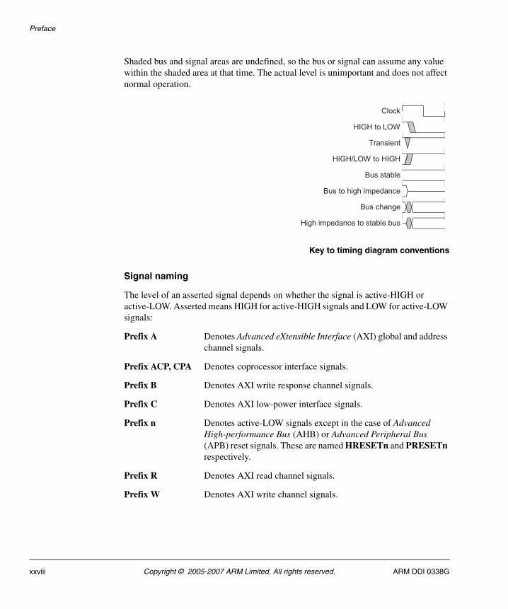
Preface
Shaded bus and signal areas are undefined, so the bus or signal can assume any value within the shaded area at that time. The actual level is unimportant and does not affect normal operation.
Key to timing diagram conventions
Signal naming
The level of an asserted signal depends on whether the signal is active-HIGH or active-LOW. Asserted means HIGH for active-HIGH signals and LOW for active-LOW signals:
Prefix A Denotes Advanced eXtensible Interface (AXI) global and address channel signals.
Prefix ACP, CPA Denotes coprocessor interface signals.
Prefix B Denotes AXI write response channel signals.
Prefix C Denotes AXI low-power interface signals.
Prefix n Denotes active-LOW signals except in the case of Advanced High-performance Bus (AHB) or Advanced Peripheral Bus (APB) reset signals. These are named HRESETn and PRESETn respectively.
Prefix R Denotes AXI read channel signals.
Prefix W Denotes AXI write channel signals.
Clock
HIGH to LOW
Transient
HIGH/LOW to HIGH
Bus stable
Bus to high impedance
Bus change
High impedance to stable bus
xxviii Copyright © 2005-2007 ARM Limited. All rights reserved. ARM DDI 0338G
Preface
Numbering
The Verilog numbering convention is:
<size in bits>’<base><number>
This is a Verilog method of abbreviating constant numbers. For example:
• ‘h7B4 is an unsized hexadecimal value.
• ‘o7654 is an unsized octal value.
• 8’d9 is an eight-bit wide decimal value of 9.
• 8’h3F is an eight-bit wide hexadecimal value of 0x3F. This is equivalent to b00111111.
• 8’b1111 is an eight-bit wide binary value of b00001111.
Further reading
This section lists publications by ARM Limited, and by third parties.
ARM periodically provides updates and corrections to its documentation. See http://www.arm.com for current errata sheets, addenda, and the ARM Frequently Asked Questions list.
ARM publications
This manual contains information that is specific to the ARM1156T2-S processor. Refer to the following documents for other relevant information:
• AMBA® Specification (ARM IHI 0011)
• AMBA® AXI Protocol Specification (ARM IHI 0022)
• ARM Architecture Reference Manual, ARMv7-A and ARMv7-R edition (ARM DDI 0406)
• ARM PrimeCell® Vectored Interrupt Controller (PL192) Technical Reference Manual (ARM DDI 0273)
• ARM1156T2-S and ARM1156T2-S Implementation and Sign-off Guide (ARM DII 0072)
• ARM1156T2-S and ARM1156T2-S Integration Manual (ARM DII 0073)
• CoreSight® ETM11 Technical Reference Manual (ARM DDI 0318)
• Embedded Trace Macrocell Architecture Specification (ARM IHI 0014)
• RealView™ Compilation Tools Developer Guide (ARM DUI 0203)
ARM DDI 0338G Copyright © 2005-2007 ARM Limited. All rights reserved. xxix
Preface
Other publications
This section lists relevant documents published by third parties:
• IEEE Standard for Binary Floating-Point Arithmetic specification 754-1985.
• IEEE Standard Test Access Port and Boundary-Scan Architecture specification 1149.1-1990(JTAG).
Figure 14-1 on page 14-2 is reprinted with permission IEEE Std. 1149.1-2001, IEEE Standard Test Access Port and Boundary-Scan Architecture Copyright 2001, by IEEE. The IEEE disclaims any responsibility or liability resulting from the placement and use in the described manner.
xxx Copyright © 2005-2007 ARM Limited. All rights reserved. ARM DDI 0338G
Preface
Feedback
ARM Limited welcomes feedback both on the ARM1156T2-S processor, and on the documentation.
Feedback on the product
If you have any comments or suggestions about this product, contact your supplier giving:
• the product name
• a concise explanation of your comments.
Feedback on this manual
If you have any comments on about this document, send email to [email protected] giving:
• the document title
• the document number
• the page number(s) to which your comments refer
• a concise explanation of your comments.
ARM Limited also welcomes general suggestions for additions and improvements.
ARM DDI 0338G Copyright © 2005-2007 ARM Limited. All rights reserved. xxxi

Preface
xxxii Copyright © 2005-2007 ARM Limited. All rights reserved. ARM DDI 0338G
Chapter 1 Introduction
This chapter introduces the ARM1156T2-S processors and their features. It contains the following sections:
• About the ARM1156T2-S processor on page 1-2
• ARM1156T2-S architecture with Thumb-2 core technology on page 1-3
• Components of the processor on page 1-5
• Power management on page 1-19
• Configurable options on page 1-21
• Pipeline stages on page 1-22
• Typical pipeline operations on page 1-24
• About the architecture on page 1-30
• Product revisions on page 1-31.
ARM DDI 0338G Copyright © 2005-2007 ARM Limited. All rights reserved. 1-1
Introduction
1.1 About the ARM1156T2-S processor
The ARM1156T2-S processor incorporates an integer unit that implements the ARM architecture v6. It supports the ARM and Thumb 2 instruction sets, and a range of Single Instruction, Multiple-Data (SIMD) DSP instructions that operate on 16-bit or 8-bit data values in 32-bit registers.
The ARM1156T2-S processor features:
• Thumb-2 core technology
• an integer unit with integral EmbeddedICE-RT logic
• a high-speed Advanced Microprocessor Bus Architecture (AMBA) Advanced eXtensible Interface (AXI) for level two interfaces supporting prioritized multiprocessor implementations
• a nine-stage pipeline
• branch prediction with return stack
• low interrupt latency
• external coprocessor interface and coprocessors CP14 and CP15
• optional Instruction and Data Memory Protection Units (MPUs)
• optional Instruction and data caches, including a non-blocking data cache with Hit-Under-Miss (HUM)
• 64-bit interface to both caches
• a bypassable write buffer
• level one Tightly-Coupled Memory (TCM) that can be used as a local RAM
• trace support
• JTAG-based debug.
Note The only difference between the ARM1156T2-S processor and the ARM1156T2-S processor is that the ARM1156T2-S processor includes a Vector Floating-Point (VFP) coprocessor.
1-2 Copyright © 2005-2007 ARM Limited. All rights reserved. ARM DDI 0338G
Introduction
1.2 ARM1156T2-S architecture with Thumb-2 core technology
The ARM1156T2-S processor supports:
• the 32-bit ARM instruction set used in ARM state
• the 16-bit and 32-bit Thumb-2 instruction set used in Thumb state.
1.2.1 The Thumb-2 instruction set
Thumb-2 is a superset of the Thumb instruction set. Thumb-2 introduces 32-bit instructions that are intermixed with the 16-bit instructions. The Thumb-2 instruction set covers almost all the functionality of the ARM instruction set. Thumb-2 is backwards compatible with the ARMv6 Thumb instruction set. Any code that you have compiled to run on the ARMv6 thumb instruction set runs on the Thumb-2 instruction set.
The most important difference between the Thumb-2 instruction set and the ARM instruction set is that most Thumb-2 instructions are unconditional, where as almost all ARM instructions can be conditional. However, Thumb-2 introduces a new conditional execution instruction, IT, that is a logical if-then-else function.
Thumb-2 has the performance close to or better than that of the ARM instruction set and has the code density of the original Thumb ISA.
In addition to the new 32-bit Thumb instructions, there are several new 16-bit Thumb instructions. Several new 32-bit ARM instructions are introduced at the same time.
The main enhancements are:
• 32-bit instructions added to the Thumb instruction set to:
— provide support for exception handling in Thumb state
— provide access to coprocessors
— include DSP and media instructions
— improve performance in cases where a single 16-bit instruction restricts functions available to the compiler.
• Addition of a 16-bit IT instruction that enables 1 - 4 following Thumb instructions to be conditional.
• Addition of 16-bit Compare and Branch on Zero (CBZ) and Compare and Branch on Non Zero (CBNZ) instructions to improve code size by replacing two-instruction sequence with a single instruction.
ARM DDI 0338G Copyright © 2005-2007 ARM Limited. All rights reserved. 1-3
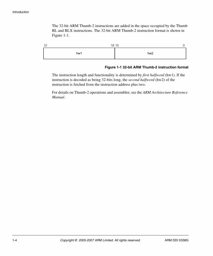
Introduction
The 32-bit ARM Thumb-2 instructions are added in the space occupied by the Thumb BL and BLX instructions. The 32-bit ARM Thumb-2 instruction format is shown in Figure 1-1.
Figure 1-1 32-bit ARM Thumb-2 instruction format
The instruction length and functionality is determined by first halfword (hw1). If the instruction is decoded as being 32-bits long, the second halfword (hw2) of the instruction is fetched from the instruction address plus two.
For details on Thumb-2 operations and assembler, see the ARM Architecture Reference Manual.
31 16 15 0
hw2hw1
1-4 Copyright © 2005-2007 ARM Limited. All rights reserved. ARM DDI 0338G
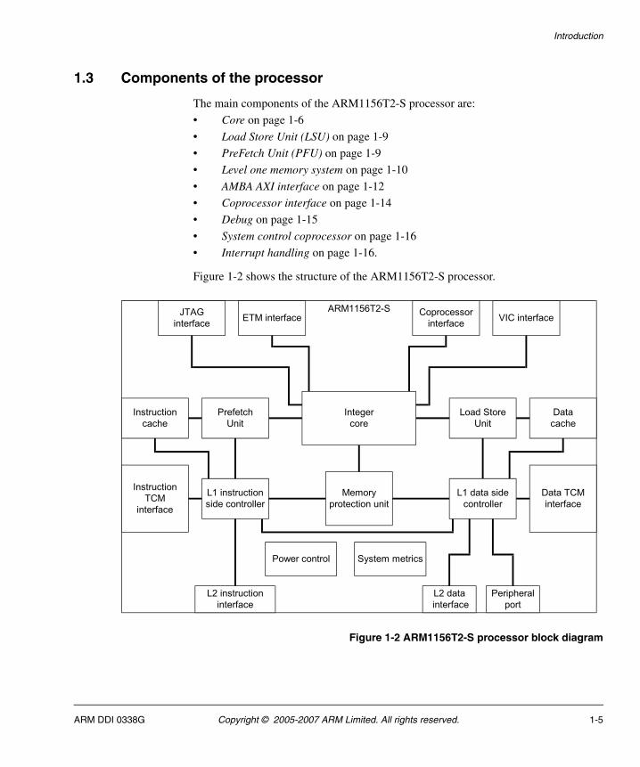
Introduction
1.3 Components of the processor
The main components of the ARM1156T2-S processor are:
• Core on page 1-6
• Load Store Unit (LSU) on page 1-9
• PreFetch Unit (PFU) on page 1-9
• Level one memory system on page 1-10
• AMBA AXI interface on page 1-12
• Coprocessor interface on page 1-14
• Debug on page 1-15
• System control coprocessor on page 1-16
• Interrupt handling on page 1-16.
Figure 1-2 shows the structure of the ARM1156T2-S processor.
Figure 1-2 ARM1156T2-S processor block diagram
ARM1156T2-S
L2 instruction
interface
Instruction
cache
Memory
protection unit
Load Store
Unit
Data
cache
Prefetch
Unit
Integer
core
Data TCM
interface
Instruction
TCM
interface
L1 instruction
side controller
Peripheral
port
L1 data side
controller
L2 data
interface
Power control System metrics
ETM interfaceJTAG
interface
Coprocessor
interfaceVIC interface
ARM DDI 0338G Copyright © 2005-2007 ARM Limited. All rights reserved. 1-5
Introduction
1.3.1 Core
The ARM1156T2-S processor is built around the ARM11 core in an ARM architecture v6 implementation that runs the 32-bit ARM and 16-bit and 32-bit Thumb-2 instruction sets. The processor contains EmbeddedICE-RT logic and a JTAG debug interface to enable hardware debuggers to access the processor. The following sections describe the core in more detail:
• Instruction sets
• Conditional execution
• Registers on page 1-7
• Modes and exceptions on page 1-7
• DSP instructions on page 1-7
• Media extensions on page 1-8
• Instruction cycle summary and interlocks on page 1-8
• Datapath on page 1-8.
Instruction sets
The instruction sets are divided into six categories:
• branch instructions
• data processing instructions
• status register transfer instructions
• load and store instructions
• coprocessor instructions
• exception-generating instructions.
Note Only load and store instructions can access data from memory.
Conditional execution
The processor conditionally executes all ARM instructions. You can decide if the condition code flags, Negative, Zero, Carry, and Overflow, are updated according to their result. A Thumb-2 instruction, If-Then (IT), is added to enable conditional execution. It enables 1 - 4 following Thumb instructions to be conditional, without using 4 bits on every instruction of ARM conditional execution.
1-6 Copyright © 2005-2007 ARM Limited. All rights reserved. ARM DDI 0338G
Introduction
Registers
The ARM1156T2-S core contains:
• 31 general-purpose 32-bit registers
• six dedicated 32-bit registers.
Note At any one time, 16 registers are visible. The remainder are banked registers used to speed up exception processing.
Modes and exceptions
The core provides a set of operating and exception modes, to support systems combining complex operating systems, user applications, and real-time demands. There are seven operating modes, five of which are exception processing modes:
• User
• System
• fast interrupt
• normal interrupt
• memory aborts
• Supervisor
• Undefined instruction.
DSP instructions
The ARM DSP instruction set extensions provide the following:
• 16-bit data operations
• saturating arithmetic
• MAC operations.
The processor executes multiply instructions using a single-cycle 32x16 implementation. The processor can perform 32x32, 32x16, and 16x16 multiply instructions.
ARM DDI 0338G Copyright © 2005-2007 ARM Limited. All rights reserved. 1-7
Introduction
Media extensions
The ARMv6 instruction set provides media instructions to complement the DSP instructions. The media instructions are divided into the following main groups:
• Additional multiplication instructions for handling 16-bit and 32-bit data, including dual-multiplication instructions that operate on both 16-bit halves of their source registers.
• Instructions to perform Single Instruction Multiple Data (SIMD) operations on pairs of 16-bit values held in a single register, or on quadruplets of 8-bit values held in a single register. The main operations supplied are addition and subtraction, selection, pack, and saturation.
• Instructions to extract bytes and halfwords from registers and zero-extend or sign-extend them. These include a parallel extraction of two bytes followed by extension of each byte to a halfword.
• Instructions to perform the unsigned Sum-of-Absolute-Differences (SAD) operation. This is used in MPEG motion estimation.
Instruction cycle summary and interlocks
Chapter 17 Cycle Timings and Interlock Behavior describes instruction cycles and gives examples of interlock timing.
Datapath
The datapath consists of a:
• Shift, ALU and Sat pipe
• MAC pipe
• load-store pipe, see Load Store Unit (LSU) on page 1-9.
Shift, ALU, and Sat pipe
The ALU, shift and Sat pipe executes most of the ALU operations, and includes a 32-bit barrel shiftier. It consists of three pipeline stages:
Shift The Shift stage contains the full barrel shiftier. All shifts, including those required by the LSU, are performed in this stage.
The saturating left shift, which doubles the value of an operand and saturates it, is implemented in the Shift stage.
ALU The ALU stage performs all arithmetic and logic operations, and generates the condition codes for instructions that set these operations.
1-8 Copyright © 2005-2007 ARM Limited. All rights reserved. ARM DDI 0338G
Introduction
The ALU stage consists of a logic unit, an arithmetic unit, and a flag generator. The pipeline logic evaluates the flag settings in parallel with the main adder in the ALU. The flag generator is enabled only on flag-setting operations.
The ALU stage separates the carry chains of the main adder enable 8 and 16-bit SIMD instructions for DSP operations.
Sat The Sat stage implements the saturation logic required by the various classes of DSP instructions.
MAC pipe
The MAC pipeline executes all of the enhanced multiply and multiply-accumulate instructions.
The MAC unit consists of a 32x16 multiplier plus an accumulate unit that is configured to calculate the sum of two 16x16 multiplies. The accumulate unit has its own dedicated single register read port for the accumulate operand.
To minimize power consumption, the processor only clocks each of the MAC and ALU stages when required.
Note For details on pipeline stages and instruction progression, see Pipeline stages on page 1-22
For details on system coprocessor programming, see Chapter 3 System Control Coprocessor
1.3.2 Load Store Unit (LSU)
The Load Store Unit (LSU) manages all load and store operations. The load-store pipeline decouples loads and stores from the MAC and ALU pipelines.
When the processor issues load multiple, LDM, and store multiple, STM, instructions to the load-store pipeline, other instructions run concurrently, subject to the requirements of supporting precise exceptions.
1.3.3 PreFetch Unit (PFU)
The PreFetch Unit (PFU) obtains instructions from the instruction cache, Instruction TCM (ITCM), or from external memory and predicts the outcome of branches in the instruction stream. For more details, see Chapter 4 Prefetch Unit.
ARM DDI 0338G Copyright © 2005-2007 ARM Limited. All rights reserved. 1-9
Introduction
Branch prediction
The branch predictor is a global type that uses history registers and a 256-entry Pattern History Table (PHT).
Return stack
The Prefetch Unit includes a three-entry return stack to accelerate returns from procedure calls. For each procedure call, the return address is pushed onto a hardware stack. When a procedure return is recognized, the address held in the return stack is popped, and is used by the prefetch unit as the predicted return address.
1.3.4 Level one memory system
The processor provides a level one memory system with the following features:
• separate instruction and data caches
• separate instruction and data RAM blocks
• 64-bit datapaths throughout the memory system
• 16 region memory protection unit that supports a wide range of memory sizes
• separate instruction-fetch, data-read/write interfaces, compatible with the AMBA AXI protocol
• 32-bit dedicated peripheral interface
• export of memory attributes for level two memory system.
The level one memory system is described in more detail in the following sections:
• Instruction and data caches
• Cache power management on page 1-11
• Memory Protection Unit on page 1-11
• Tightly Coupled Memories on page 1-12
• Error detection on page 1-12.
Instruction and data caches
The processor provides separate instruction and data caches. The cache has the following features:
• Independent configuration of the instruction and data cache during synthesis to sizes between 1KB and 64KB.
• Ability to select cache associativity (1KB - 1way, 2KB - 2way, and 4KB and above - 4way). You can lock each way independently.
• Ability to select pseudo-random or round-robin cache replacement policy.
1-10 Copyright © 2005-2007 ARM Limited. All rights reserved. ARM DDI 0338G
Introduction
• Eight word cache line length. Cache lines can be either write-back or write-through, determined by MPU entry
• Ability to disable each cache independently.
• Data cache misses that are non-blocking. The processor supports up to three outstanding data cache misses.
• Streaming of sequential data from LDM and LDRD operations, and sequential instruction fetches.
• Critical word first filling of the cache on a cache-miss.
• Implementation of all the cache RAM blocks, and the associated tag and valid RAM blocks using standard ASIC RAM compilers. This ensures optimum area and performance of your designs.
Cache power management
To reduce power consumption, the core uses sequential cache operations to reduce the number of full cache reads. If a cache read is sequential to the previous cache read, and the read is within the same cache line, only the data RAM set that was previously read is accessed. The core does not access Tag RAM during sequential cache operations.
To reduce unnecessary power consumption more, only the addressed words within a cache line are read at any time.
Memory Protection Unit
Because the ARM1156T2-S processor is targeted at embedded control applications, a small Memory Protection Unit (MPU) is used to provide memory attributes. There is an MPU for each of the instruction and data sides of the processor. The MPU has a maximum of 16 regions, each with a minimum resolution of 32 bytes. The regions can overlap with the highest numbered region having the highest priority. For more details, see Chapter 5 Memory Protection Unit.
The MPU is responsible for protection checking and memory attributes, some of which can be passed to an external level two memory system.
The MPU has the following features:
• matching of physical address
• checking of access permissions
• checking of memory attributes
• mapping of accesses to cache, TCM, peripheral port, or external memory.
ARM DDI 0338G Copyright © 2005-2007 ARM Limited. All rights reserved. 1-11
Introduction
Tightly Coupled Memories
Because some applications might not respond well to caching, configurable memory blocks are provided for Instruction and Data Tightly Coupled Memories (TCMs). These ensure high-speed access to code or data.
An Instruction TCM (ITCM) is typically used to hold interrupt or exception code that must be accessed at high speed, without any potential delay resulting from a cache miss.
A Data TCM (DTCM) is typically used to hold a block of data for intensive processing, such as audio or video processing. You can individually configure the ITCM and DTCM sizes with sizes of 0KB, 4KB, 8KB, 16KB, 32KB, 64KB, 128KB, or 256KB anywhere in the memory map. For flexibility in optimizing the TCM subsystem for performance, power, and RAM type, the TCMs are external to the processor. The INITRAM pin enables booting from the ITCM. Both the ITCM and DTCM support wait states. For more details, see Chapter 7 Level One Memory System.
Error detection
To increase the tolerance of memory faults you can include parity generation and checking logic for the caches and implement parity generation for the TCMs. For more details, see Cache parity errors on page 7-8 and TCM error detection signals on page 7-13.
Note For TCMs the parity generation and checking logic is external to the processor. This logic is not supplied as part of the core deliverables.
1.3.5 AMBA AXI interface
The bus interface provides high bandwidth between the processor, level two caches, on-chip RAM, peripherals, and interfaces to external memory.
Separate bus interfaces are provided for:
• instruction fetch, 64-bit data
• data read/write, 64-bit data
• peripheral access, 32-bit data.
All buses are multi-layer AXI compatible, enabling them to be merged in smaller systems. The signals on each port provide support to:
• shared-memory synchronization primitives
• level two cache
• bus transactions.
1-12 Copyright © 2005-2007 ARM Limited. All rights reserved. ARM DDI 0338G
Introduction
The ports support the following bus transactions:
Instruction fetch
Services instruction cache misses and noncacheable instruction fetches.
Data read/write
The data read services data cache misses and noncacheable data reads.
The data write services cache write-backs (including cache cleans), write-through, and noncacheable data.
Peripheral port
The peripheral port is a 32-bit AXI interface that provides direct access to local, non-shared peripherals without using bandwidth on the main AXI bus system. Accesses to regions of memory that are marked as device and non-shared are routed to the peripheral port instead of to the data read or data write ports.
For more details, see Chapter 8 Level Two Interface.
These ports enable several simultaneous outstanding transactions, providing high performance from level two memory systems that support parallelism, and for high utilization of pipelined and multi-page memories such as SDRAM.
The AMBA interface is described in more detail in the following sections:
• Bus clock
• Unaligned accesses
• Mixed-endian support on page 1-14
• Write buffer on page 1-14.
Bus clock
The bus interface ports operate synchronously to the CPU clock.
Unaligned accesses
The core supports unaligned data access. Words and halfwords can be aligned to any byte boundary, enabling access to compacted data structures with no software overhead. This is useful for multi-processor applications, pre-ARMv6 code support, and reducing memory space requirements.
The Bus Interface Unit (BIU) automatically generates multiple bus cycles for unaligned accesses.
ARM DDI 0338G Copyright © 2005-2007 ARM Limited. All rights reserved. 1-13
Introduction
Mixed-endian support
The core provides the option of switching between big and little-endian data access modes. This supports the sharing of data with big-endian systems, and improves handling of certain types of data.
Write buffer
All memory writes take place through the write buffer. The write buffer decouples the CPU pipeline from the system bus for external memory writes. Memory reads are checked for dependency against the write buffer contents.
1.3.6 Coprocessor interface
The ARM1156T2-S processor controls external coprocessors through the coprocessor interface. This interface supports all ARM coprocessor instructions:
• LDC
• LDCL
• STC
• STCL
• MRC
• MRRC
• MCR
• MCRR
• CDP.
Data for all loads to coprocessors is returned by the memory system in the order of the accesses in the program. HUM operation of the cache is suppressed for coprocessor instructions.
The external coprocessor interface assumes that all coprocessor instructions are executed in order.
Externally-connected coprocessors follow the early stages of the core pipeline to permit instructions and data to be passed between the two pipelines. The coprocessor runs one pipeline stage behind the core pipeline.
To prevent the coprocessor interface introducing critical paths, wait states can be inserted in external coprocessor operations. These wait states enable critical signals to be retimed.
Chapter 11 Coprocessor Interface describes the interface for on-chip coprocessors such as floating-point or other application-specific hardware acceleration units.
1-14 Copyright © 2005-2007 ARM Limited. All rights reserved. ARM DDI 0338G
Introduction
1.3.7 Debug
The debug coprocessor, CP14, implements a full range of debug features described in Chapter 13 Debug and Chapter 14 Debug Test Access Port.
The core provides extensive support for real-time debug and performance profiling.
The following sections describe debug in more detail:
• System performance monitoring
• ETM interface
• Real-time debug facilities.
System performance monitoring
This is a group of counters that you can configure to monitor the operation of the processor and memory system. For more details, see System performance monitor on page 3-10.
ETM interface
You can connect an external Embedded Trace Macrocell (ETM) unit to the processor for real-time code tracing of the core in an embedded system.
The ETM interface collects various processor signals and drives these signals from the core. The interface is unidirectional and runs at the full speed of the core. The ETM interface connects directly to the external ETM unit without any additional glue logic. You can disable the ETM interface for power saving. For more details, see Chapter 15 Trace Interface Port.
Real-time debug facilities
The ARM1156T2-S processor contains an EmbeddedICE-RT logic unit to provide real-time debug facilities. It has the following capabilities:
• up to six breakpoints
• up to two watchpoints
• Debug Communications Channel (DCC).
The EmbeddedICE-RT logic connects directly to the core and monitors the internal address and data buses. You can access the EmbeddedICE-RT logic in one of two ways:
• executing CP14 instructions
• through a JTAG-style interface and associated TAP controller.
ARM DDI 0338G Copyright © 2005-2007 ARM Limited. All rights reserved. 1-15
Introduction
The EmbeddedICE-RT logic supports two modes of debug operation:
Halting debug-mode
On a debug event, such as a breakpoint or watchpoint, the debug logic stops the core and forces the core into Debug state. This enables you to examine the internal state of the core, and the external state of the system, independently from other system activity. When the debugging process completes, the core and system state is restored, and normal program execution resumes.
Monitor debug-mode
On a debug event, the core generates a debug exception instead of entering Debug state, as in Halting debug-mode. The exception entry enables a debug monitor program to debug the processor while enabling critical interrupt service routines to operate on the processor. The debug monitor program can communicate with the debug host over the DCC or any other communications interface in the system.
1.3.8 System control coprocessor
The system control coprocessor provides configuration and control of the memory system and its associated functionality. Other system-level operation, such as memory barrier instructions, are also managed through the system control coprocessor.
For more details, see System control and configuration on page 3-5.
1.3.9 Interrupt handling
Interrupt handling in the ARM1156T2-S processor is compatible with previous ARM architectures, but has several additional features to improve interrupt performance for real-time applications.
Whether you have a have a VIC in your design or not, you must ensure that the nIRQ and nFIQ signals are LOW until the processor has started to execute the interrupt handler.
Interrupt handling is described in more detail in the following sections:
• VIC port on page 1-17
• Low interrupt latency configuration on page 1-17
• Interrupt latency configuration control on page 1-18
• Exception processing on page 1-18.
1-16 Copyright © 2005-2007 ARM Limited. All rights reserved. ARM DDI 0338G
Introduction
VIC port
The core has a dedicated port that enables an external interrupt controller, like the ARM PrimeCell Vectored Interrupt Controller (VIC), to supply a vector address along with an interrupt request (IRQ) signal. This provides faster interrupt entry but you can disable it for compatibility with earlier interrupt controllers.
Low interrupt latency configuration
This mode minimizes the worst-case interrupt latency of the processor, with a small reduction in peak performance, or instructions-per-cycle. You can tune the behavior of the core to suit the requirements of the application.
The low-latency configuration disables HUM operation of the cache. In low-latency mode, on receipt of an interrupt, the ARM1156T2-S processor:
• abandons any pending restartable memory operations
• restarts memory operations on return from the interrupt.
In low interrupt latency configuration, software must only use multi-word load/store instructions that are fully restartable. The software must not use multi-word load or store instructions on memory locations that produce side-effects for the type of access concerned.
The instructions that this currently applies to are:
ARM LDC, all forms of LDM, LDRD, and STC, and all forms of STM and STRD.
Thumb LDMIA, STMIA, PUSH, and POP.
Thumb2 LDC, all forms of LDM, LDRD, and STC, and all forms of STM and STRD.
To achieve optimum interrupt latency, memory locations accessed with these instructions must not have large numbers of wait-states associated with them. To minimize the interrupt latency, the following is recommended:
• multiple accesses to areas of memory marked as Device or Strongly Ordered must not be performed to slow areas of memory because these areas take many cycles to generate a response
• SWP operations must not be performed to slow areas of memory.
ARM DDI 0338G Copyright © 2005-2007 ARM Limited. All rights reserved. 1-17
Introduction
Interrupt latency configuration control
Configuration is through the system control coprocessor. To ensure that a change between normal and low interrupt latency configurations is synchronized correctly, you must use software systems that only change the configuration while interrupts are disabled.
Exception processing
The ARMv6 architecture contains exception processing, to reduce interrupt handler entry and exit time:
SRS Save return state to a specified stack frame.
RFE Return from exception.
CPS Change processor state.
For more details, see Instructions for exception handling on page 2-21.
1-18 Copyright © 2005-2007 ARM Limited. All rights reserved. ARM DDI 0338G
Introduction
1.4 Power management
The ARM1156T2-S processor includes several microarchitectural features to reduce energy consumption:
• Accurate branch and return prediction, reducing the number of incorrect instruction fetch and decode operations.
• Use of physically tagged caches, which reduce the number of cache flushes and refills, to save energy in the system.
• The caches use sequential access information to reduce the number of accesses to the Tag RAMs and to unmatched data RAMs.
• Extensive use of gated clocks and gates to disable inputs to unused functional blocks. Because of this, only the logic actively in use to perform a calculation consumes any dynamic power.
The ARM1156T2-S processor uses four levels of power management:
Run mode This mode is the normal mode of operation in which all of the functionality of the ARM1156T2-S processor is available.
Standby mode
This mode disables most of the clocks of the device, while keeping the device powered up. This reduces the power drawn to the static leakage current, plus a tiny clock power overhead required to enable the device to wake up from the standby mode. The transition from the standby mode to the run mode is caused by one of the following:
• an interrupt, either masked or unmasked
• a debug request, regardless of whether debug is enabled
• reset.
Shutdown mode
This mode has the entire device powered down. All state, including cache and TCM state, must be saved externally. The part is returned to the run state by the assertion of reset. This state saving is performed with interrupts disabled, and finishes with a DrainWriteBuffer operation. The ARM1156T2-S processor then communicates with the power controller that it is ready to be powered down.
ARM DDI 0338G Copyright © 2005-2007 ARM Limited. All rights reserved. 1-19
Introduction
Dormant mode
This mode enables the ARM1156T2-S processor to be powered down, while leaving the state of the caches and the TCM powered up and maintaining their state. Although software visibility of the valid bits is provided to enable implementation of dormant mode, the following are required for full implementation of dormant mode:
• modification of the RAM blocks to include an input clamp
• implementation of separate power domains.
Power management features are described in more detail in Chapter 10 Power Control.
1-20 Copyright © 2005-2007 ARM Limited. All rights reserved. ARM DDI 0338G
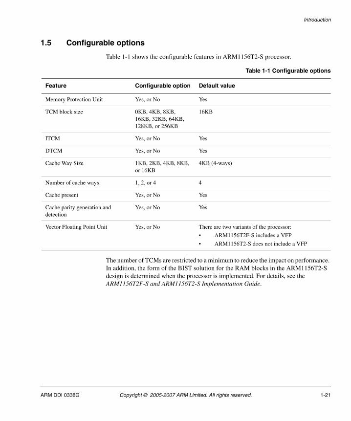
Introduction
1.5 Configurable options
Table 1-1 shows the configurable features in ARM1156T2-S processor.
The number of TCMs are restricted to a minimum to reduce the impact on performance. In addition, the form of the BIST solution for the RAM blocks in the ARM1156T2-S design is determined when the processor is implemented. For details, see the ARM1156T2F-S and ARM1156T2-S Implementation Guide.
Table 1-1 Configurable options
Feature Configurable option Default value
Memory Protection Unit Yes, or No Yes
TCM block size 0KB, 4KB, 8KB, 16KB, 32KB, 64KB, 128KB, or 256KB
16KB
ITCM Yes, or No Yes
DTCM Yes, or No Yes
Cache Way Size 1KB, 2KB, 4KB, 8KB, or 16KB
4KB (4-ways)
Number of cache ways 1, 2, or 4 4
Cache present Yes, or No Yes
Cache parity generation and detection
Yes, or No Yes
Vector Floating Point Unit Yes, or No There are two variants of the processor:
• ARM1156T2F-S includes a VFP
• ARM1156T2-S does not include a VFP
ARM DDI 0338G Copyright © 2005-2007 ARM Limited. All rights reserved. 1-21
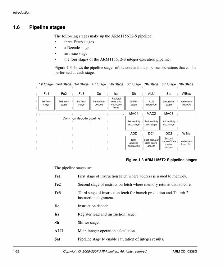
Introduction
1.6 Pipeline stages
The following stages make up the ARM1156T2-S pipeline:
• three Fetch stages
• a Decode stage
• an Issue stage
• the four stages of the ARM1156T2-S integer execution pipeline.
Figure 1-3 shows the pipeline stages of the core and the pipeline operations that can be performed at each stage.
Figure 1-3 ARM1156T2-S pipeline stages
The pipeline stages are:
Fe1 First stage of instruction fetch where address is issued to memory.
Fe2 Second stage of instruction fetch where memory returns data to core.
Fe3 Third stage of instruction fetch for branch prediction and Thumb-2 instruction alignment.
De Instruction decode.
Iss Register read and instruction issue.
Sh Shifter stage.
ALU Main integer operation calculation.
Sat Pipeline stage to enable saturation of integer results.
1st Stage 2nd Stage 3rd Stage 4th Stage 5th Stage 6th Stage 7th Stage 8th Stage 9th Stage
1st fetch
stage
Fe1 Fe2 De Iss
2nd fetch
stage
Instruction
decode
Register
read and
instruction
issue
Common decode pipeline
Fe3
3rd fetch
stage
Shifter
stage
Sh ALU
ALU
operation
Sat
Saturation
stage
1st multiply
acc. stage
MAC1 MAC2
2nd multiply
acc. stage
MAC3
3rd multiply
acc. stage
Data
address
calculation
ADD DC1
First stage of
data cache
access
DC2
Second
stage of data
cache
access
WBex
Writeback
Mul/ALU
WBls
Writeback
from LSU
1-22 Copyright © 2005-2007 ARM Limited. All rights reserved. ARM DDI 0338G
Introduction
WBex Write back of data from the multiply or main execution pipelines.
MAC1 First stage of the multiply-accumulate pipeline.
MAC2 Second stage of the multiply-accumulate pipeline.
MAC3 Third stage of the multiply-accumulate pipeline.
ADD Address generation stage.
DC1 First stage of data cache access.
DC2 Second stage of data cache access.
WBls Write back of data from the Load Store Unit.
By overlapping the various stages of operation, the ARM1156T2-S processor maximizes the clock rate achievable to execute each instruction. It delivers a throughput greater than one instruction for each cycle.
The Fetch stages can hold up to four instructions, where branch prediction is performed on instructions ahead of execution of earlier instructions.
The Issue and Decode stages can contain any instruction in parallel with a predicted branch.
The Execute, Memory, and Write stages can contain a predicted branch, an ALU or multiply instruction, a load/store multiple instruction, and a coprocessor instruction in parallel execution.
ARM DDI 0338G Copyright © 2005-2007 ARM Limited. All rights reserved. 1-23
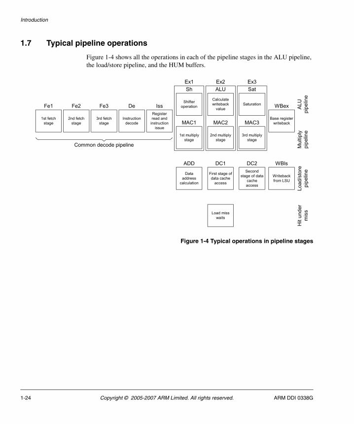
Introduction
1.7 Typical pipeline operations
Figure 1-4 shows all the operations in each of the pipeline stages in the ALU pipeline, the load/store pipeline, and the HUM buffers.
Figure 1-4 Typical operations in pipeline stages
1st fetch
stage
Fe1 Fe2 De Iss
MAC1 MAC2 MAC3
WBex
DC1 DC2
2nd fetch
stage
Instruction
decode
Register
read and
instruction
issue
1st multiply
stage
2nd multiply
stage
3rd multiply
stage
Base register
writeback
Data
address
calculation
First stage of
data cache
access
Second
stage of data
cache
access
Writeback
from LSU
Load miss
waits
ADD WBls
ALU
pip
elin
e
Load/s
tore
pip
elin
e
Hit
under
mis
s
Sh ALU Sat
Shifter
operation
Calculate
writeback
value
Saturation
Ex1 Ex2 Ex3
Common decode pipeline Mu
ltip
ly
pip
elin
e
Fe3
3rd fetch
stage
1-24 Copyright © 2005-2007 ARM Limited. All rights reserved. ARM DDI 0338G
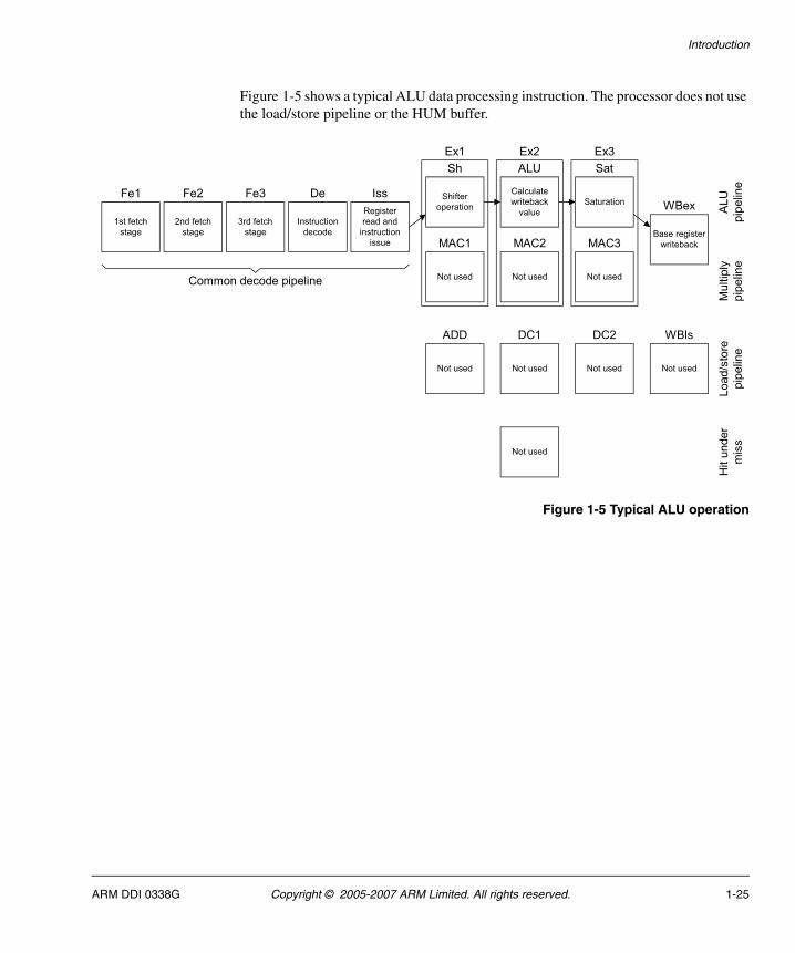
Introduction
Figure 1-5 shows a typical ALU data processing instruction. The processor does not use the load/store pipeline or the HUM buffer.
Figure 1-5 Typical ALU operation
MAC1 MAC2 MAC3
WBex
DC1 DC2
Not used Not used Not used
Base register
writeback
Not used Not used Not used Not used
Not used
ADD WBls
ALU
pip
elin
e
Load/s
tore
pip
elin
e
Hit
under
mis
s
Sh ALU Sat
Shifter
operation
Calculate
writeback
value
Saturation
Ex1 Ex2 Ex3
Mu
ltip
ly
pip
elin
e
1st fetch
stage
Fe1 Fe2 De Iss
2nd fetch
stage
Instruction
decode
Register
read and
instruction
issue
Common decode pipeline
Fe3
3rd fetch
stage
ARM DDI 0338G Copyright © 2005-2007 ARM Limited. All rights reserved. 1-25
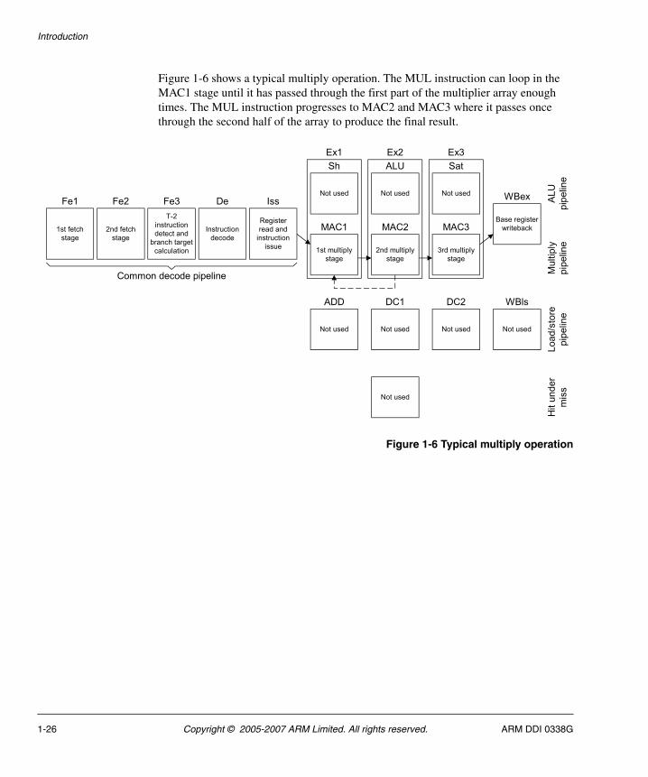
Introduction
Figure 1-6 shows a typical multiply operation. The MUL instruction can loop in the MAC1 stage until it has passed through the first part of the multiplier array enough times. The MUL instruction progresses to MAC2 and MAC3 where it passes once through the second half of the array to produce the final result.
Figure 1-6 Typical multiply operation
MAC1 MAC2 MAC3
WBex
DC1 DC2
1st multiply
stage
2nd multiply
stage
3rd multiply
stage
Base register
writeback
Not used Not used Not used Not used
Not used
ADD WBls
ALU
pip
elin
e
Load/s
tore
pip
elin
e
Hit
under
mis
s
Sh ALU Sat
Not used Not used Not used
Ex1 Ex2 Ex3
Mu
ltip
ly
pip
elin
e
1st fetch
stage
Fe1 Fe2 De Iss
2nd fetch
stage
Instruction
decode
Register
read and
instruction
issue
Common decode pipeline
Fe3
T-2
instruction
detect and
branch target
calculation
1-26 Copyright © 2005-2007 ARM Limited. All rights reserved. ARM DDI 0338G
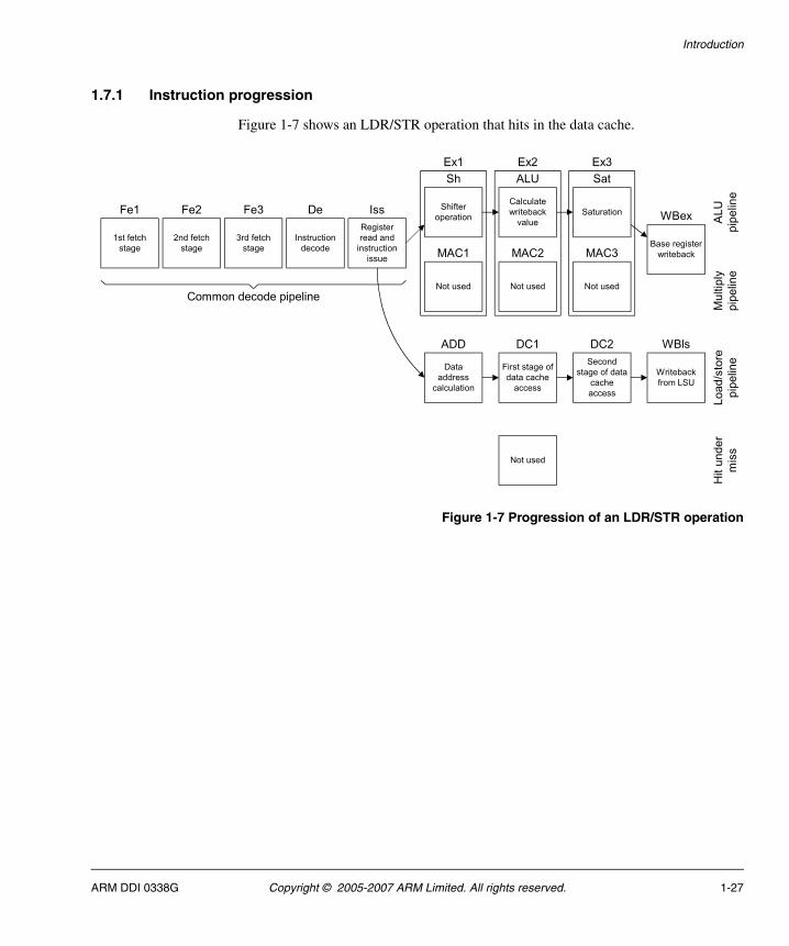
Introduction
1.7.1 Instruction progression
Figure 1-7 shows an LDR/STR operation that hits in the data cache.
Figure 1-7 Progression of an LDR/STR operation
MAC1 MAC2 MAC3
WBex
DC1 DC2
Not used Not used Not used
Base register
writeback
Data
address
calculation
First stage of
data cache
access
Second
stage of data
cache
access
Writeback
from LSU
Not used
ADD WBls
ALU
pip
elin
e
Load/s
tore
pip
elin
e
Hit
under
mis
s
Sh ALU Sat
Shifter
operation
Calculate
writeback
value
Saturation
Ex1 Ex2 Ex3
Mu
ltip
ly
pip
elin
e
1st fetch
stage
Fe1 Fe2 De Iss
2nd fetch
stage
Instruction
decode
Register
read and
instruction
issue
Common decode pipeline
Fe3
3rd fetch
stage
ARM DDI 0338G Copyright © 2005-2007 ARM Limited. All rights reserved. 1-27
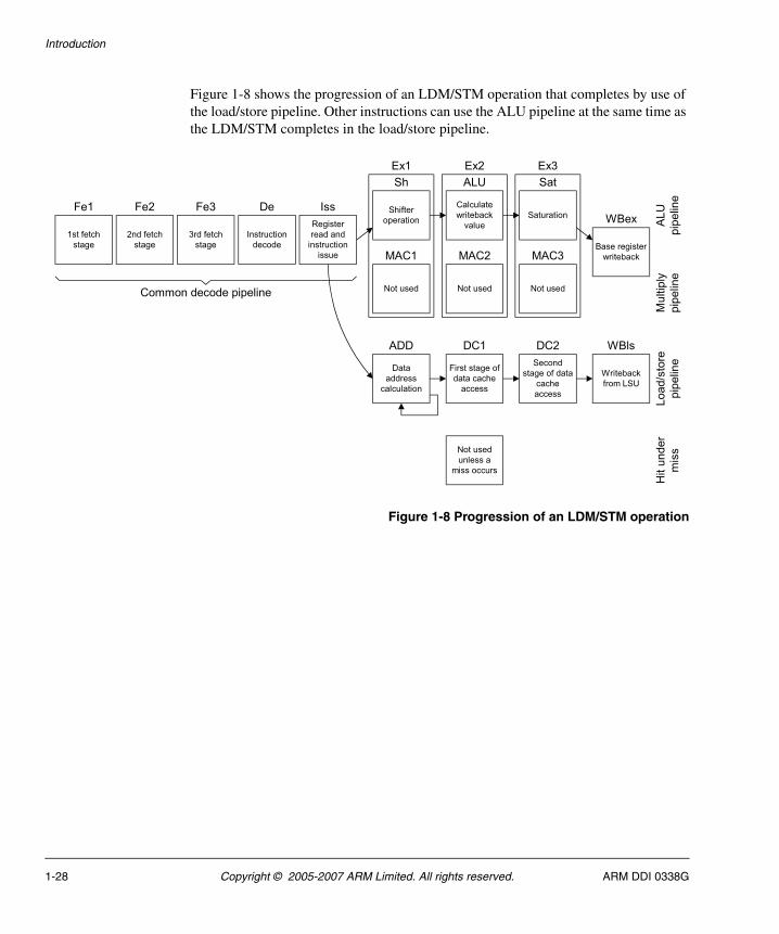
Introduction
Figure 1-8 shows the progression of an LDM/STM operation that completes by use of the load/store pipeline. Other instructions can use the ALU pipeline at the same time as the LDM/STM completes in the load/store pipeline.
Figure 1-8 Progression of an LDM/STM operation
MAC1 MAC2 MAC3
WBex
DC1 DC2
Not used Not used Not used
Base register
writeback
Data
address
calculation
First stage of
data cache
access
Second
stage of data
cache
access
Writeback
from LSU
Not used
unless a
miss occurs
ADD WBls
ALU
pip
elin
e
Load/s
tore
pip
elin
e
Hit
under
mis
s
Sh ALU Sat
Shifter
operation
Calculate
writeback
value
Saturation
Ex1 Ex2 Ex3
Mu
ltip
ly
pip
elin
e
1st fetch
stage
Fe1 Fe2 De Iss
2nd fetch
stage
Instruction
decode
Register
read and
instruction
issue
Common decode pipeline
Fe3
3rd fetch
stage
1-28 Copyright © 2005-2007 ARM Limited. All rights reserved. ARM DDI 0338G
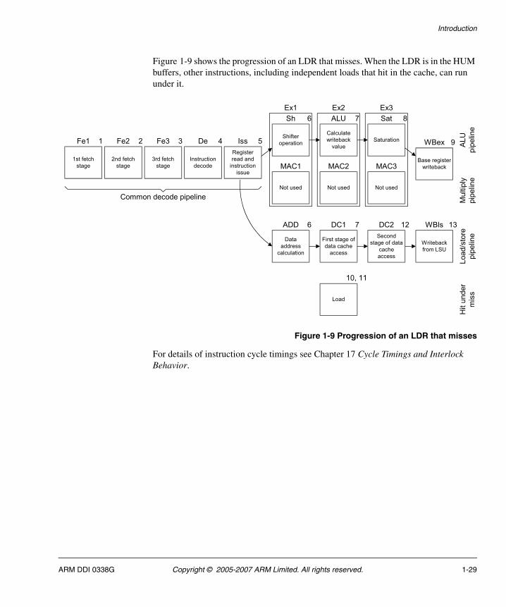
Introduction
Figure 1-9 shows the progression of an LDR that misses. When the LDR is in the HUM buffers, other instructions, including independent loads that hit in the cache, can run under it.
Figure 1-9 Progression of an LDR that misses
For details of instruction cycle timings see Chapter 17 Cycle Timings and Interlock Behavior.
MAC1 MAC2 MAC3
WBex
DC1 DC2
Not used Not used Not used
Base register
writeback
Data
address
calculation
First stage of
data cache
access
Second
stage of data
cache
access
Writeback
from LSU
Load
ADD WBls
ALU
pip
elin
e
Load/s
tore
pip
elin
e
Hit
under
mis
s
Sh ALU Sat
Shifter
operation
Calculate
writeback
value
Saturation
Ex1 Ex2 Ex3
Multip
ly
pip
elin
e
6
6
7
7
8
9
10, 11
12 13
2 3 4 5
1st fetch
stage
Fe2 De Iss
2nd fetch
stage
Instruction
decode
Register
read and
instruction
issue
Common decode pipeline
Fe3
3rd fetch
stage
Fe1 1
ARM DDI 0338G Copyright © 2005-2007 ARM Limited. All rights reserved. 1-29
Introduction
1.8 About the architecture
This processor is an implementation of the ARM architecture v6. For details on the ARM and Thumb 2 instruction sets, see the ARM Architecture Reference Manual.
Contact ARM Limited for complete descriptions of all instruction sets.
1-30 Copyright © 2005-2007 ARM Limited. All rights reserved. ARM DDI 0338G
Introduction
1.9 Product revisions
This manual is for revision r0p4 of the ARM1156T2F-S processor. See Product revision status on page xxiv for details of revision numbering.
There are no differences in functionality between the r0p0 and r0p4 product revisions of the processor.
ARM DDI 0338G Copyright © 2005-2007 ARM Limited. All rights reserved. 1-31

Introduction
1-32 Copyright © 2005-2007 ARM Limited. All rights reserved. ARM DDI 0338G
Chapter 2 Programmer’s Model
This chapter describes the ARM1156T2-S registers and provides information for programming the microprocessor. It contains the following sections:
• About the programmer’s model on page 2-2
• Processor operating states on page 2-3
• Data types on page 2-5
• Memory formats on page 2-6
• Operating modes on page 2-4
• Registers on page 2-8
• The program status registers on page 2-12
• Exceptions on page 2-20.
• Acceleration of execution environments on page 2-40.
ARM DDI 0338G Copyright © 2005-2007 ARM Limited. All rights reserved. 2-1
Programmer’s Model
2.1 About the programmer’s model
The ARM1156T2-S processor implements ARM architecture v6 with Thumb-2 extensions:
• 32-bit ARM instruction set
• 16-bit or 32-bit Thumb instruction set.
For more details on the ARM and Thumb-2 extensions instruction sets, see the ARM Architecture Reference Manual.
2-2 Copyright © 2005-2007 ARM Limited. All rights reserved. ARM DDI 0338G
Programmer’s Model
2.2 Processor operating states
The ARM1156T2-S processor has two operating states:
ARM state 32-bit, word-aligned ARM instructions are executed in this state.
Thumb state 32-bit and 16-bit halfword-aligned Thumb and Thumb-2 instructions.
Note Transition between ARM state and Thumb state does not affect the processor mode or the register contents.
2.2.1 Switching state
The operating state of the ARM1156T2-S processor can be switched between ARM state and Thumb state:
• Using the BX and BLX instructions, or by a load to the PC. Switching state is described in the ARM Architecture Reference Manual.
• Automatically on an exception. You can write an exception handler routine in ARM or Thumb code. For more details, see Exceptions on page 2-20.
2.2.2 Interworking ARM and Thumb state
The ARM1156T2-S processor enables you to mix ARM and Thumb code. For more details, see the chapter about interworking ARM and Thumb in the RealView Compilation Tools Developer Guide.
ARM DDI 0338G Copyright © 2005-2007 ARM Limited. All rights reserved. 2-3
Programmer’s Model
2.3 Operating modes
In each state there are seven modes of operation:
• User mode is the usual mode for the execution of ARM or Thumb programs, that is it is used for executing most application programs
• Fast interrupt (FIQ) mode is used for handling fast interrupts
• Interrupt (IRQ) mode is used for general-purpose interrupt handling
• Supervisor mode is a protected mode for the operating system
• Abort mode is entered after a data or instruction abort
• System mode is a privileged user mode for the operating system
• Undefined mode is entered when an undefined instruction exception occurs.
Modes other than User mode are collectively known as privileged modes. Privileged modes are used to service interrupts or exceptions, or to access protected resources.
2-4 Copyright © 2005-2007 ARM Limited. All rights reserved. ARM DDI 0338G
Programmer’s Model
2.4 Data types
The ARM1156T2-S processor supports the following data types:
• doubleword (64-bit)
• word (32-bit)
• halfword (16-bit)
• byte (8-bit).
Note • When any of these types are described as unsigned, the N-bit data value represents
a non-negative integer in the range 0 to +2N-1, using normal binary format.
• When any of these types are described as signed, the N-bit data value represents an integer in the range -2N-1 to +2N-1-1, using two’s complement format.
For best performance you must align these as follows:
• doubleword quantities must be aligned to eight-byte boundaries
• word quantities must be aligned to four-byte boundaries
• halfword quantities must be aligned to two-byte boundaries
• byte quantities can be placed on any byte boundary.
The ARM1156T2-S processor supports mixed-endian and unaligned access. For more details, see Chapter 6 Unaligned and Mixed-Endian Data Access Support.
Note You cannot use LDRD, LDM, LDC, STRD, STM, or STC instructions to access 32-bit quantities if they are not 32-bit aligned.
ARM DDI 0338G Copyright © 2005-2007 ARM Limited. All rights reserved. 2-5
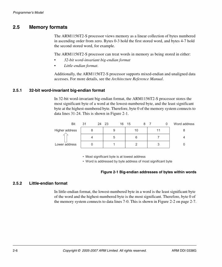
Programmer’s Model
2.5 Memory formats
The ARM1156T2-S processor views memory as a linear collection of bytes numbered in ascending order from zero. Bytes 0-3 hold the first stored word, and bytes 4-7 hold the second stored word, for example.
The ARM1156T2-S processor can treat words in memory as being stored in either:
• 32-bit word-invariant big-endian format
• Little-endian format.
Additionally, the ARM1156T2-S processor supports mixed-endian and unaligned data accesses. For more details, see the Architecture Reference Manual.
2.5.1 32-bit word-invariant big-endian format
In 32-bit word-invariant big-endian format, the ARM1156T2-S processor stores the most significant byte of a word at the lowest-numbered byte, and the least significant byte at the highest-numbered byte. Therefore, byte 0 of the memory system connects to data lines 31-24. This is shown in Figure 2-1.
Figure 2-1 Big-endian addresses of bytes within words
2.5.2 Little-endian format
In little-endian format, the lowest-numbered byte in a word is the least significant byte of the word and the highest-numbered byte is the most significant. Therefore, byte 0 of the memory system connects to data lines 7-0. This is shown in Figure 2-2 on page 2-7.
31 24 23 16 15 8 7 Word address0
4
0
8Higher address
Lower address
• Most significant byte is at lowest address
• Word is addressed by byte address of most significant byte
Bit
111098
7654
3210
2-6 Copyright © 2005-2007 ARM Limited. All rights reserved. ARM DDI 0338G
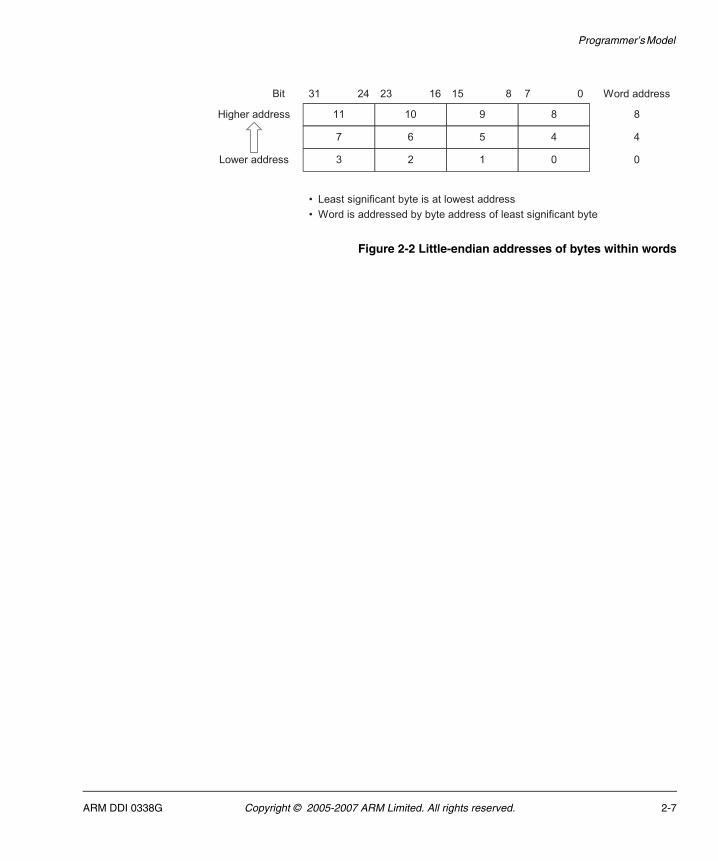
Programmer’s Model
Figure 2-2 Little-endian addresses of bytes within words
31 24 23 16 15 8 7 Word address0
4
0
8Higher address
Lower address
• Least significant byte is at lowest address
• Word is addressed by byte address of least significant byte
Bit
891011
4567
0123
ARM DDI 0338G Copyright © 2005-2007 ARM Limited. All rights reserved. 2-7
Programmer’s Model
2.6 Registers
The ARM1156T2-S processor has a total of 37 registers:
• 31 general-purpose 32-bit registers
• six 32-bit status registers.
These registers are not all accessible at the same time. The processor state and operating mode determine which registers are available to the programmer.
2.6.1 The register set
In the ARM1156T2-S processor the register set is used in both the ARM and Thumb states. Sixteen general registers and one or two status registers are accessible at any time. In privileged modes, mode-specific banked registers become available. Figure 2-3 on page 2-10 shows which registers are available in each mode.
The register set contains 16 directly-accessible registers, r0-r15. Another register, the Current Program Status Register (CPSR), contains condition code flags, status bits, and current mode bits. Registers r0-r13 are general-purpose registers used to hold either data or address values. Registers r14, r15, and the CPSR have the following special functions:
Link Register Register r14 is used as the subroutine Link Register (LR).
Register r14 receives the return address when a Branch with Link (BL or BLX) instruction is executed.
You can treat r14 as a general-purpose register at all other times. The corresponding banked registers r14_svc, r14_irq, r14_fiq, r14_abt, and r14_und are similarly used to hold the return values when interrupts and exceptions arise, or when BL or BLX instructions are executed within interrupt or exception routines.
Program Counter Register r15 holds the PC:
• in ARM state this is word-aligned
• in Thumb state this is either word or halfword-aligned.
Note There are special cases for reading R15:
• reading the address of the current instruction plus 4
• reading 0x00000000 (zero).
There are special cases for writing R15:
• causing a branch to the address that was written to R15
• ignoring the value that was written to R15
2-8 Copyright © 2005-2007 ARM Limited. All rights reserved. ARM DDI 0338G
Programmer’s Model
• writing bits [31:28] of the value that was written to R15 to the condition flags, and ignoring bits [27:0] (used for the MRC instruction only).
None of these special cases must be assumed unless it is explicitly stated in the instruction description. Instead, instructions with register fields equal to R15 must be treated as UNPREDICTABLE.
For more details, see the ARM Architecture Reference Manual.
In privileged modes, another register, the Saved Program Status Register (SPSR), is accessible. This contains the condition code flags, status bits, and current mode bits saved as a result of the exception that caused entry to the current mode.
Banked registers have a mode identifier that indicates which mode they relate to. These mode identifiers are listed in Table 2-1.
FIQ mode has seven banked registers mapped to r8–r14 (r8_fiq–r14_fiq). As a result many FIQ handlers do not have to save any registers.
The Supervisor, Abort, IRQ, and Undefined modes each have alternative mode-specific registers mapped to r13 and r14, permitting a private stack pointer and link register for each mode.
Figure 2-3 on page 2-10 shows the register set.
Table 2-1 Register mode identifiers
Mode Mode identifier
User usra
a. The usr identifier is usually omitted from register names. It is only used in descriptions where the User or System mode register is specifically accessed from another operating mode.
Fast interrupt fiq
Interrupt irq
Supervisor svc
Abort abt
System usra
Undefined und
ARM DDI 0338G Copyright © 2005-2007 ARM Limited. All rights reserved. 2-9
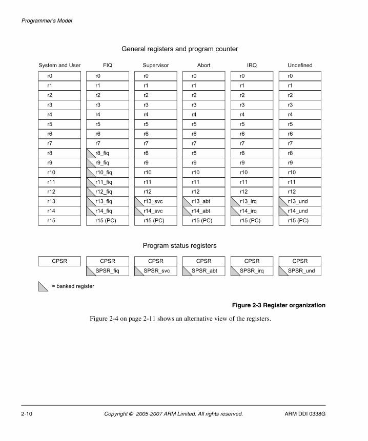
Programmer’s Model
Figure 2-3 Register organization
Figure 2-4 on page 2-11 shows an alternative view of the registers.
General registers and program counter
System and User
Program status registers
= banked register
Supervisor Abort IRQ Undefined
r0
r1
r2
r3
r4
r5
r6
r7
r8
r9
r10
r11
r12
r13
r14
r15
FIQ
r0
r1
r2
r3
r4
r5
r6
r7
r8_fiq
r9_fiq
r10_fiq
r11_fiq
r12_fiq
r13_fiq
r14_fiq
r15 (PC)
r0
r1
r2
r3
r4
r5
r6
r7
r8
r9
r10
r11
r12
r13_svc
r14_svc
r0
r1
r2
r3
r4
r5
r6
r7
r8
r9
r10
r11
r12
r13_abt
r14_abt
r0
r1
r2
r3
r4
r5
r6
r7
r8
r9
r10
r11
r12
r13_irq
r14_irq
r0
r1
r2
r3
r4
r5
r6
r7
r8
r9
r10
r11
r12
r13_und
r14_und
CPSR CPSR CPSR CPSR CPSR CPSR
SPSR_fiq SPSR_svc SPSR_abt SPSR_irq SPSR_und
r15 (PC) r15 (PC) r15 (PC) r15 (PC)
2-10 Copyright © 2005-2007 ARM Limited. All rights reserved. ARM DDI 0338G
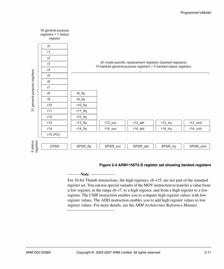
Programmer’s Model
Figure 2-4 ARM1156T2-S register set showing banked registers
Note For 16-bit Thumb instructions, the high registers, r8–r15, are not part of the standard register set. You can use special variants of the MOV instruction to transfer a value from a low register, in the range r0–r7, to a high register, and from a high register to a low register. The CMP instruction enables you to compare high register values with low register values. The ADD instruction enables you to add high register values to low register values. For more details, see the ARM Architecture Reference Manual.
16 general-purpose
registers + 1 status
register
r0
r1
r2
r3
r4
r5
r6
r7
r8
r9
r10
r11
r12
r13
r14
r8_fiq
r9_fiq
r10_fiq
r11_fiq
r12_fiq
r13_fiq
r14_fiq
r15 (PC)
r13_svc
r14_svc
r13_abt
r14_abt
r13_irq
r14_irq
r13_und
r14_und
CPSR SPSR_fiq SPSR_svc SPSR_abt SPSR_irq SPSR_und
31
genera
l-purp
ose
regsiters
20 mode-specific replacement registers (banked registers)
15 banked general-purpose registers + 5 banked status registers
6sta
tus
regis
ters
ARM DDI 0338G Copyright © 2005-2007 ARM Limited. All rights reserved. 2-11
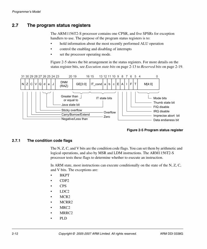
Programmer’s Model
2.7 The program status registers
The ARM1156T2-S processor contains one CPSR, and five SPSRs for exception handlers to use. The purpose of the program status registers is to:
• hold information about the most recently performed ALU operation
• control the enabling and disabling of interrupts
• set the processor operating mode.
Figure 2-5 shows the bit arrangement in the status registers. For more details on the status register bits, see Execution state bits on page 2-13 to Reserved bits on page 2-19.
Figure 2-5 Program status register
2.7.1 The condition code flags
The N, Z, C, and V bits are the condition code flags. You can set them by arithmetic and logical operations, and also by MSR and LDM instructions. The ARM1156T2-S processor tests these flags to determine whether to execute an instruction.
In ARM state, most instructions can execute conditionally on the state of the N, Z, C, and V bits. The exceptions are:
• BKPT
• CDP2
• CPS
• LDC2
• MCR2
• MCRR2
• MRC2
• MRRC2
• PLD
a b cedN
31 30 29 28 27 26 25 24 23 20 19 16 15 10 9 8 7 6 5 4 0
Z C V Q JDNM
(RAZ)GE[3:0] IT_cond E A I F T M[4:0]
Java state bit
Sticky overflowOverflow
Carry/Borrow/ExtendZero
Negative/Less than
Mode bits
Thumb state bit
FIQ disable
IRQ disable
Imprecise abort bit
Data endianess bit
Greater than
or equal toIT state bits
111213
2-12 Copyright © 2005-2007 ARM Limited. All rights reserved. ARM DDI 0338G
Programmer’s Model
• SETEND
• RFE
• SRS
• STC2.
In Thumb state, only the Branch instruction is conditional. Other instructions can be made conditional by placing then in the If-Then (IT) block. For more details about conditional execution, see the ARM Architecture Reference Manual.
2.7.2 The Q flag
The Sticky Overflow, Q, flag can be set by certain multiply and fractional arithmetic instructions:
• QADD
• QDADD
• QSUB
• QDSUB
• SMLAD
• SMLAxy
• SMLAWy
• SMLSD
• SMUAD
• SSAT
• SSAT16
• USAT
• USAT16.
The Q flag is sticky in that, when set by an instruction, it remains set until explicitly cleared by an MSR instruction writing to the CPSR. Instructions cannot execute conditionally on the status of the Q flag.
To determine the status of the Q flag you must read the PSR into a register and extract the Q flag from this. For details of how the Q flag is set and cleared, see individual instruction definitions in the ARM Architecture Reference Manual.
2.7.3 Execution state bits
The execution state bits consist of the If-Then state bits, IT, Java state bit, J, and Thumb state bit, T.
ARM DDI 0338G Copyright © 2005-2007 ARM Limited. All rights reserved. 2-13
Programmer’s Model
IT state bits
The IT_cond field encodes the base condition code for the current IT block, if any. It must contain b000 when no IT block is active.
The a, b, c, d, and e bits encode the number of instructions that are to be conditionally executed, and whether the condition for each is the base condition code or the inverse of the base condition code. They must contain b00000 when no IT block is active.
When an IT instruction is executed, these bits are set according to the condition in the instruction, and the Then and Else (T and E) parameters in the instruction.
During execution of an IT block, the a, b, c, d, and e bits are shifted:
• to reduce the number of instructions to be conditionally executed by one
• to move the next bit into position to form the least significant bit of the condition code.
Table 2-2 shows how the IT execution state bits operate.
Table 2-3 shows the effect of each state.
Table 2-2 Shifting of IT execution state bits
Old state New state
IT_cond a b c d e IT_cond a b c d e
cond_base P1 P2 P3 P4 1 cond_base P2 P3 P4 1 0
cond_base P1 P2 P3 1 0 cond_base P2 P3 1 0 0
cond_base P1 P2 1 0 0 cond_base P2 1 0 0 0
cond_base P1 1 0 0 0 b000 0 0 0 0 0
Table 2-3 Effect of IT execution state bits
Entry point for: IT_cond a b c d e Description
4-instruction IT block cond_base P1 P2 P3 P4 1 Next instruction has condition cond_base, P1
3-instruction IT block cond_base P1 P2 P3 1 0 Next instruction has condition cond_base, P1
2-instruction IT block cond_base P1 P2 1 0 0 Next instruction has condition cond_base, P1
1-instruction IT block cond_base P1 1 0 0 0 Next instruction has condition cond_base, P1
2-14 Copyright © 2005-2007 ARM Limited. All rights reserved. ARM DDI 0338G
Programmer’s Model
Note • The IT state bits return as zero if an MRS of the CPSR is executed within an IT
block in normal operation. In Debug state an MRS of the CPSR within an IT block return the IT state bits as shown in Table 2-2 on page 2-14 and Table 2-3 on page 2-14
• Writing the IT bits by MSR instructions is ignored.
In Debug state an MRS of the CPSR within an IT block return the IT state bits as shown in Table 2-2 on page 2-14 and Table 2-3 on page 2-14.
For more details, see the ARM Architecture Reference Manual.
J bit
This bit is set to 0 on reset. For information on its behavior, see Acceleration of execution environments on page 2-40.
T bit
The T bit reflects the operating state:
• when the T bit is set, the processor is executing in Thumb state
• when the T bit is clear, the processor is executing in ARM state.
Note Never use an MSR instruction to force a change to the state of the T bit in the CPSR. If an MSR instruction does try to modify this bit the result is architecturally Unpredictable. In the ARM1156T2-S processor this bit is not affected.
Invalid non-zero x 0 0 0 0 Unpredictable
Invalid bxxx 1 0 0 0 0 Unpredictable
Not in an IT block b000 0 0 0 0 0 Normal execution
Table 2-3 Effect of IT execution state bits (continued)
Entry point for: IT_cond a b c d e Description
ARM DDI 0338G Copyright © 2005-2007 ARM Limited. All rights reserved. 2-15
Programmer’s Model
2.7.4 Do Not Modify bits
Software must not modify the Do Not Modify (DNM), Read As Zero (RAZ) bits. These bits are:
• Readable, to preserve the state of the processor, for example, during process context switches
• Writable, to enable the processor to restore its state. To maintain compatibility with future ARM processors, and as good practice, you are strongly advised to use a read-modify-write strategy when you change the CPSR.
2.7.5 The GE[3:0] bits
Some of the SIMD instructions set GE[3:0] as greater-than-or-equal bits for individual halfwords or bytes of the result, as shown in Table 2-4.
Table 2-4 GE[3:0] settings
GE[3] GE[2] GE[1] GE[0]
Instruction A op B > C A op B > C A op B > C A op B > C
Signed
SADD16 [31:16] + [31:16] ≥ 0 [31:16] + [31:16] ≥ 0 [15:0] + [15:0] ≥ 0 [15:0] + [15:0] ≥ 0
SSUB16 [31:16] - [31:16] ≥ 0 [31:16] - [31:16] ≥ 0 [15:0] - [15:0] ≥ 0 [15:0] - [15:0] ≥ 0
SASX [31:16] + [15:0] ≥ 0 [31:16] + [15:0] ≥ 0 [15:0] - [31:16] ≥ 0 [15:0] - [31:16] ≥ 0
SSAX [31:16] - [15:0] ≥ 0 [31:16] - [15:0] ≥ 0 [15:0] + [31:16] ≥ 0 [15:0] + [31:16] ≥ 0
SADD8 [31:24] + [31:24] ≥ 0 [23:16] + [23:16] ≥ 0 [15:8] + [15:8] ≥ 0 [7:0] + [7:0] ≥ 0
SSUB8 [31:24] - [31:24] ≥ 0 [23:16] - [23:16] ≥ 0 [15:8] - [15:8] ≥ 0 [7:0] - [7:0] ≥ 0
Unsigned
UADD16 [31:16] + [31:16] ≥ 216 [31:16] + [31:16] ≥ 216 [15:0] + [15:0] ≥ 216 [15:0] + [15:0] ≥ 216
USUB16 [31:16] - [31:16] ≥ 0 [31:16] - [31:16] ≥ 0 [15:0] - [15:0] ≥ 0 [15:0] - [15:0] ≥ 0
UASX [31:16] + [15:0] ≥ 216 [31:16] + [15:0] ≥ 216 [15:0] - [31:16] ≥ 0 [15:0] - [31:16] ≥ 0
2-16 Copyright © 2005-2007 ARM Limited. All rights reserved. ARM DDI 0338G
Programmer’s Model
Note GE bit is 1 if A op B ≥ C, otherwise 0.
The SEL instruction uses GE[3:0] to select which source register supplies each byte of its result.
Note • For unsigned operations, the GE bits are determined by the usual ARM rules for
carries out of unsigned additions and subtractions, and so are carry-out bits.
• For signed operations, the rules for setting the GE bits are chosen so that they have the same sort of greater than or equal functionality as for unsigned operations.
2.7.6 The E bit
ARM and Thumb instructions are provided to set and clear the E bit. The E bit controls load/store endianness. For details of where the E bit is used, see the ARM Architecture Reference Manual.
Architecture versions prior to ARMv6 specify this bit as SBZ. This ensures no endianness reversal on loads or stores.
2.7.7 The A bit
The A bit is set automatically. It is used to disable imprecise Data Aborts. For more details of how to use the A bit see Imprecise Data Abort mask in the CPSR/SPSR on page 2-35.
USAX [31:16] - [15:0] ≥ 0 [31:16] - [15:0] ≥ 0 [15:0] + [31:16] ≥ 216 [15:0] + [31:16] ≥216
UADD8 [31:24] + [31:24] ≥ 28 [23:16] + [23:16] ≥ 28 [15:8] + [15:8] ≥ 28 [7:0] + [7:0] ≥ 28
USUB8 [31:24] - [31:24] ≥ 0 [23:16] - [23:16] ≥ 0 [15:8] - [15:8] ≥ 0 [7:0] - [7:0] ≥ 0
Table 2-4 GE[3:0] settings (continued)
GE[3] GE[2] GE[1] GE[0]
Instruction A op B > C A op B > C A op B > C A op B > C
ARM DDI 0338G Copyright © 2005-2007 ARM Limited. All rights reserved. 2-17
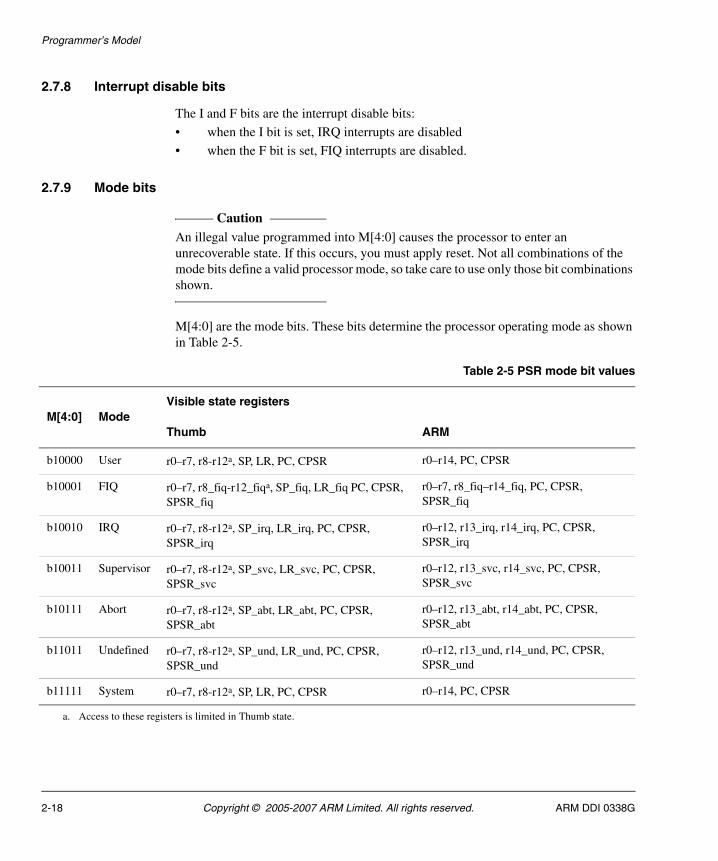
Programmer’s Model
2.7.8 Interrupt disable bits
The I and F bits are the interrupt disable bits:
• when the I bit is set, IRQ interrupts are disabled
• when the F bit is set, FIQ interrupts are disabled.
2.7.9 Mode bits
Caution An illegal value programmed into M[4:0] causes the processor to enter an unrecoverable state. If this occurs, you must apply reset. Not all combinations of the mode bits define a valid processor mode, so take care to use only those bit combinations shown.
M[4:0] are the mode bits. These bits determine the processor operating mode as shown in Table 2-5.
Table 2-5 PSR mode bit values
M[4:0] ModeVisible state registers
Thumb ARM
b10000 User r0–r7, r8-r12a, SP, LR, PC, CPSR r0–r14, PC, CPSR
b10001 FIQ r0–r7, r8_fiq-r12_fiqa, SP_fiq, LR_fiq PC, CPSR, SPSR_fiq
r0–r7, r8_fiq–r14_fiq, PC, CPSR, SPSR_fiq
b10010 IRQ r0–r7, r8-r12a, SP_irq, LR_irq, PC, CPSR, SPSR_irq
r0–r12, r13_irq, r14_irq, PC, CPSR, SPSR_irq
b10011 Supervisor r0–r7, r8-r12a, SP_svc, LR_svc, PC, CPSR, SPSR_svc
r0–r12, r13_svc, r14_svc, PC, CPSR, SPSR_svc
b10111 Abort r0–r7, r8-r12a, SP_abt, LR_abt, PC, CPSR, SPSR_abt
r0–r12, r13_abt, r14_abt, PC, CPSR, SPSR_abt
b11011 Undefined r0–r7, r8-r12a, SP_und, LR_und, PC, CPSR, SPSR_und
r0–r12, r13_und, r14_und, PC, CPSR, SPSR_und
b11111 System r0–r7, r8-r12a, SP, LR, PC, CPSR r0–r14, PC, CPSR
a. Access to these registers is limited in Thumb state.
2-18 Copyright © 2005-2007 ARM Limited. All rights reserved. ARM DDI 0338G
Programmer’s Model
2.7.10 Reserved bits
The remaining bits in the PSRs are unused, but are reserved. When changing a PSR flag or control bits, make sure that these reserved bits are not altered. You must ensure that your program does not rely on reserved bits containing specific values because future processors might use some or all of the reserved bits.
2.7.11 Modification of PSR bits by MSR instructions
In previous architecture versions, MSR instructions can modify the flags byte, bits [31:24], of the CPSR in any mode, but the other three bytes are only modifiable in privileged modes.
After the introduction of ARM architecture v6, however, each CPSR bit falls into one of the following categories:
• Bits that are freely modifiable from any mode, either directly by MSR instructions or by other instructions whose side-effects include writing the specific bit or writing the entire CPSR.
Bits in Figure 2-5 on page 2-12 that are in this category are N, Z, C, V, Q, GE[3:0], and E.
• Bits that must never be modified by an MSR instruction, and so must only be written as a side-effect of another instruction. If an MSR instruction does try to modify these bits the results are architecturally Unpredictable. In the ARM1156T2-S processor these bits are not affected.
The bits in Figure 2-5 on page 2-12 that are in this category are the execution state bits [24, 15:10, 5].
• Bits that can only be modified from privileged modes, and that are completely protected from modification by instructions while the processor is in User mode. The only way that these bits can be modified while the processor is in User mode is by entering a processor exception, as described in Exceptions on page 2-20.
Bits in Figure 2-5 on page 2-12 that are in this category are A, I, F, and M[4:0].
ARM DDI 0338G Copyright © 2005-2007 ARM Limited. All rights reserved. 2-19
Programmer’s Model
2.8 Exceptions
Exceptions occur whenever the normal flow of a program has to be halted temporarily. For example, to service an interrupt from a peripheral. Before attempting to handle an exception, the ARM1156T2-S processor preserves the current processor state so that the original program can resume when the handler routine has finished.
Exception priorities on page 2-38 describes how the exceptions are dealt with in the fixed order if two or more exceptions occur simultaneously.
This section provides details of the ARM1156T2-S exception handling:
• Exception entry and exit summary on page 2-22
• Entering an exception on page 2-23
• Leaving an exception on page 2-23.
Several enhancements are made in ARM architecture v6 to the exception model, mostly to improve interrupt latency, as follows:
• New instructions are added to give a choice of stack to use for storing the exception return state after exception entry, and to simplify changes of processor mode and the disabling and enabling of interrupts.
• The interrupt vector definitions on ARMv6 are changed to support the addition of hardware to prioritize the interrupt sources and to look up the start vector for the related interrupt handling routine.
• A low interrupt latency configuration is added in ARMv6. In terms of the instruction set architecture, it specifies that multi-access load/store instructions can be interrupted and then restarted after the interrupt has been processed:
ARM LDC, LDM, LDRD, STC, STM, and STRD,
Thumb LDC, LDM, LDRD, STC, STM, STRD, LDM, POP, and PUSH.
• Support for an imprecise Data Abort that behaves as an interrupt rather than as an abort, in that it occurs asynchronously relative to the instruction execution. Support involves the masking of a pending imprecise Data Abort at times when entry into Abort mode is deemed unrecoverable.
• Exception handling in ARM or Thumb state set by the TE Bit, bit [30], CP15 register c1. For more details, see c1, Control Register on page 3-47.
2.8.1 Changes to existing interrupt vectors
In ARMv5, the IRQ and FIQ exception vectors are fixed. Interrupt handlers typically have to start with an instruction sequence to determine the cause of the interrupt and branch to a routine to handle it.
2-20 Copyright © 2005-2007 ARM Limited. All rights reserved. ARM DDI 0338G
Programmer’s Model
On the ARM1156T2-S processor the IRQ exception can be determined directly from the value presented on the Vectored Interrupt Controller (VIC) port. The vector interrupt behavior is explicitly enabled when the VE bit in CP15 c1 is set. See Chapter 12 Vectored Interrupt Controller Port.
An example of a hardware block that can interface to the VIC port is the PrimeCell VIC (PL192), which is available from ARM Limited. This takes a set of inputs from various interrupt sources, prioritizes them, and presents the interrupt type of the highest-priority interrupt being requested and the address of its handler to the processor core. The VIC also masks any lower priority interrupts. Such hardware reduces the time taken to enter the handling routine for the required interrupt.
2.8.2 Instructions for exception handling
This section describes the instructions added to accelerate the handling of exceptions. Full details of these instructions are given in the ARM Architecture Reference Manual.
Note These instructions are available in both ARM and Thumb states.
Store Return State
The Store Return State (SRS) instruction stores r14_<current_mode> and spsr_<current_mode> to sequential addresses, and uses the banked version of r13 for a specified mode to supply the base address, and to write back to if you specify base register write-back. This enables an exception handler to store its return state on a stack other than the one automatically selected by its exception entry sequence.
The addressing mode used is a version of ARM addressing mode 4, see the ARM Architecture Reference Manual, modified to assume a {r14,SPSR} register list, rather than the use of a list specified by a bit mask in the instruction. This enables the SRS instruction to access stacks in a manner compatible with the normal use of STM instructions for stack accesses.
Return From Exception
The Return From Exception (RFE) instruction loads the PC and CPSR from sequential addresses. RFE returns the processor from an exception for which an SRS instruction has saved the return state, see Store Return State, and again uses a version of ARM addressing mode 4, modified this time to assume a {PC,CPSR} register list.
ARM DDI 0338G Copyright © 2005-2007 ARM Limited. All rights reserved. 2-21
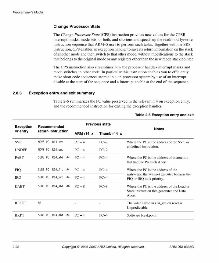
Programmer’s Model
Change Processor State
The Change Processor State (CPS) instruction provides new values for the CPSR interrupt masks, mode bits, or both, and shortens and speeds up the read/modify/write instruction sequence that ARMv5 uses to perform such tasks. Together with the SRS instruction, CPS enables an exception handler to save its return information on the stack of another mode and then switch to that other mode, without modifications to the stack that belongs to the original mode or any registers other than the new mode stack pointer.
The CPS instruction also streamlines how the processor handles interrupt masks and mode switches in other code. In particular this instruction enables you to efficiently make short code sequences atomic in a uniprocessor system by use of an interrupt disable at the start of the sequence and a interrupt enable at the end of the sequence.
2.8.3 Exception entry and exit summary
Table 2-6 summarizes the PC value preserved in the relevant r14 on exception entry, and the recommended instruction for exiting the exception handler.
Table 2-6 Exception entry and exit
Exception or entry
Recommended return instruction
Previous stateNotes
ARM r14_x Thumb r14_x
SVC MOVS PC, R14_svc PC + 4 PC+2 Where the PC is the address of the SVC or undefined instruction.
UNDEF MOVS PC, R14_und PC + 4 PC+2
PABT SUBS PC, R14_abt, #4 PC + 4 PC+4 Where the PC is the address of instruction that had the Prefetch Abort.
FIQ SUBS PC, R14_fiq, #4 PC + 4 PC+4 Where the PC is the address of the instruction that was not executed because the FIQ or IRQ took priority.IRQ SUBS PC, R14_irq, #4 PC + 4 PC+4
DABT SUBS PC, R14_abt, #8 PC + 8 PC+8 Where the PC is the address of the Load or Store instruction that generated the Data Abort.
RESET NA - - The value saved in r14_svc on reset is Unpredictable.
BKPT SUBS PC, R14_abt, #4 PC + 4 PC+4 Software breakpoint.
2-22 Copyright © 2005-2007 ARM Limited. All rights reserved. ARM DDI 0338G
Programmer’s Model
2.8.4 Entering an exception
When handling an exception the ARM1156T2-S processor:
1. Preserves the address of the next instruction in the appropriate LR. When the exception entry is from:
ARM state: The ARM1156T2-S processor writes the value of the PC into the LR, offset by a value (current PC + 4 or PC + 8 depending on the exception) that causes the program to resume from the correct place on return
Thumb state: The ARM1156T2-S processor writes the value of the PC into the LR, offset by a value (current PC + 2, PC + 4 or PC + 8 depending on the exception) that causes the program to resume from the correct place on return.
2. Copies the CPSR into the appropriate SPSR. Depending on the exception type, the processor might modify the IT execution state bits of the CPSR prior to this operation to facilitate a return from the exception.
3. Forces the CPSR mode bits to a value that depends on the exception and clears the IT execution state bits in the CPSR.
4. Forces the PC to fetch the next instruction from the relevant exception vector.
The ARM1156T2-S processor can also set the interrupt disable flags to prevent otherwise unmanageable nesting of exceptions.
ARM state or Thumb state can enter, handle, and exit exceptions. At reset the TEINIT pin controls the state used to manage exceptions.
2.8.5 Leaving an exception
When an exception has completed, the exception handler must move the LR, minus an offset to the PC. The offset varies according to the type of exception, as shown in Table 2-6 on page 2-22.
Typically the return instruction is an arithmetic or logical operation with the S bit set and rd = r15, so the core copies the SPSR back to the CPSR.
Note The action of restoring the CPSR from the SPSR:
• Automatically restores the T, A, I, and F bits to the value they held immediately prior to the exception.
ARM DDI 0338G Copyright © 2005-2007 ARM Limited. All rights reserved. 2-23
Programmer’s Model
• Normally resets the IT execution state bits to the values held immediately prior to the exception. If the exception handler wants to return to the following instruction these bits might have to be manually advanced to avoid applying the incorrect condition codes to that instruction. For more details of the IT instruction and Undefined instruction and an example exception handler code see the ARM Architecture Reference Manual.
Because SVC handlers are always expected to return after the SVC instruction the IT execution state bits are automatically advanced on exception entry prior to copying the CPSR into the SPSR.
2.8.6 Reset
When the nRESETIN signal is driven LOW a reset occurs, and the ARM1156T2-S processor abandons the executing instruction.
When nRESETIN is driven HIGH again the ARM1156T2-S processor:
1. Forces CPSR M[4:0] to b10011 (Supervisor mode), sets the A, I, and F bits in the CPSR. The E bit is set based on the state of the BIGENDINIT and UBITINIT pins. Other bits in the CPSR are indeterminate.
2. Forces the PC to fetch the next instruction from the reset vector address.
3. Reverts to ARM state or Thumb state depending on the state of the TEINIT pin, and resumes execution.
After reset, all register values except the PC and CPSR are indeterminate.
See Chapter 9 Clocking and Resets for more details of the reset behavior for the ARM1156T2-S processor.
2.8.7 Fast interrupt request
The Fast Interrupt Request (FIQ) is another exception source that reduces the execution time of the exception handler. In ARM state, FIQ mode has eight private registers to reduce, or even remove the requirement for register saving, minimizing the overhead of context switching.
An FIQ is externally generated by taking the nFIQ signal input LOW. You must ensure that the nFIQ input is held LOW until the processor acknowledges the interrupt request, from the software handler.
Irrespective of whether exception entry is from ARM state or Thumb state, an FIQ handler returns from the interrupt by executing:
2-24 Copyright © 2005-2007 ARM Limited. All rights reserved. ARM DDI 0338G
Programmer’s Model
SUBS PC,R14_fiq,#4
You can disable FIQ exceptions within a privileged mode by setting the CPSR F flag. When the F flag is clear, the ARM1156T2-S processor checks for a LOW level on the output of the nFIQ register at the end of each instruction.
Note The CPSR F flag cannot be set for the Non-maskable Interrupt (NMI).
FIQs and IRQs are disabled when an FIQ occurs. You can use nested interrupts but it is up to you to save any corruptible registers and to re-enable FIQs and interrupts.
2.8.8 Interrupt request
The IRQ exception is a normal interrupt caused by a LOW level on the nIRQ input. IRQ has a lower priority than FIQ, and is masked on entry to an FIQ sequence. You must ensure that the nIRQ input is held LOW until the processor acknowledges the interrupt request, either from the VIC interface or the software handler.
Irrespective of whether exception entry is from ARM state or Thumb state an IRQ handler returns from the interrupt by executing:
SUBS PC,R14_irq,#4
You can disable IRQ exceptions within a privileged mode by setting the CPSR I flag. When the I flag is clear, the ARM1156T2-S processor checks for a LOW level on the output of the nIRQ register at the end of each instruction.
IRQs are disabled when an IRQ occurs. You can use nested interrupts but it is up to you to save any corruptible registers and to re-enable IRQs.
2.8.9 Low interrupt latency configuration
The purpose of this configuration is to reduce the interrupt latency of the ARM1156T2-S processor. The FI bit, bit 21, in CP15 c1 is used to enable a low interrupt latency configuration.
This mode:
• disables Hit-Under-Miss (HUM) functionality
• abandons restartable external accesses so that the core can react to a pending interrupt faster than is normally the case
• detects low-latency interrupts as early as possible in the main pipeline.
ARM DDI 0338G Copyright © 2005-2007 ARM Limited. All rights reserved. 2-25
Programmer’s Model
To change between normal and low interrupt latency configurations the sequence to use is:
1. Drain Write Buffer.
2. Change FI Bit.
3. Drain Write Buffer with interrupt disabled.
This sequence ensures that the change is synchronous.
You must ensure that software systems only change the FI bit shortly after reset, while interrupts are disabled. To minimize the interrupt latency in low interrupt latency mode, avoid the use of multi-word load/store instructions to memory locations that are marked as Device or Strongly Ordered. Multi-word accesses to Device or Strongly Ordered memory are not restartable and therefore must complete before the processor can take an interrupt.
Non-device memory enables these instructions to be interruptible when in low interrupt latency configuration. If the instruction is interrupted before it is complete, the result might be that one or more of the words are accessed twice. This is inconsequential.
Note A similar requirement for instructions to be restartable already exists for unaligned and multi-word load/store instructions in normal configuration. This occurs when these instructions access memory locations that can abort in a recoverable way. If an abort occurs during an access to one of the words in the multi-word operation then the processor executes the abort handler. After the cause of the abort is fixed the abort handler returns to that instruction, and it is restarted. The effect is that multi-word load/store instruction can access the same word twice. Once before the abort was detected, and again when the instruction is restarted.
The requirement in this case is either:
• all side-effects are inconsequential
• the abort must either occur on the first word accessed or not at all.
The instructions that this rule currently applies to are:
• ARM instructions LDC, all forms of LDM, LDRD, STC, all forms of STM, STRD, and unaligned LDR, STR, LDRH, and STRH
• Thumb instructions LDMDB, LDMIA, PUSH, POP, STMDB, and STMIA, and unaligned LDR, LDMDB, STR, and STRH.
You are also advised that, to achieve the best possible interrupt latency, memory locations that these instructions access must not have large numbers of wait-states associated with them.
2-26 Copyright © 2005-2007 ARM Limited. All rights reserved. ARM DDI 0338G
Programmer’s Model
2.8.10 Interrupt latency example
This section gives an extended example to show how the combination of new facilities improves interrupt latency. The example is not necessarily entirely realistic, but illustrates the main points. The assumptions made are:
1. Vector Interrupt Controller (VIC) hardware exists to prioritize interrupts and to supply the address of the highest priority interrupt to the processor core on demand. In the ARMv5 system, the address is supplied in a memory-mapped I/O location, and loading it acts as an entering interrupt handler acknowledgement to the VIC. In the ARMv6 system, the address is loaded and the acknowledgement given automatically, as part of the interrupt entry sequence. In both systems, a store to a memory-mapped I/O location is used to send a finishing interrupt handler acknowledgement to the VIC.
2. The system has the following layers:
Real-time layer Contains handlers for a number of high-priority interrupts. These interrupts can be prioritized, and are assumed to be signaled to the processor core by means of the FIQ interrupt. Their handlers do not use the facilities supplied by the other two layers. This means that all memory they use must be locked down in the caches. It is possible to use additional code to make access to nonlocked memory possible, but this is not described in this example.
Architectural completion layer Contains Prefetch Abort, Data Abort and Undefined instruction handlers whose purpose is to give the illusion that the hardware is handling all memory requests and instructions on its own, without requiring software to handle cache misses, and near-exceptional floating-point operations, for example. This illusion is not available to the real-time layer, because the software handlers concerned take a significant number of cycles, and it is not reasonable to have every memory access to take large numbers of cycles. Instead, the memory concerned has to be locked down.
Non real-time layer Provides interrupt handlers for low-priority interrupts. These interrupts can also be prioritized, and are assumed to be signaled to the processor core using the IRQ interrupt.
ARM DDI 0338G Copyright © 2005-2007 ARM Limited. All rights reserved. 2-27
Programmer’s Model
3. The corresponding exception priority structure is as follows, from highest to lowest priority:
a. FIQ1 (highest priority FIQ)
b. FIQ2
c. ...
d. FIQm (lowest priority FIQ)
e. Data Abort
f. Prefetch Abort
g. Undefined instruction
h. SVC
i. IRQ1 (highest priority IRQ)
j. IRQ2
k. ...
l. IRQn (lowest priority IRQ)
The processor core prioritization handles most of the priority structure, but the VIC handles the priorities within each group of interrupts.
Note This list reflects the priorities that the handlers are subject to, and differs from the
priorities that the exception entry sequences are subject to. The latter priorities are presented in the ARM Architecture Reference Manual, and the difference occurs because simultaneous Data Abort and FIQ exceptions result in the sequence:
a. Data Abort entry sequence executed, updating r14_abt, SPSR_abt, PC, and CPSR.
b. FIQ entry sequence executed, updating r14_fiq, SPSR_fiq, PC, and CPSR.
c. FIQ handler executes to completion and returns.
d. Data Abort handler executes to completion and returns.
4. Stack and register usage is:
• The FIQ1 interrupt handler has exclusive use of r8_fiq to r12_fiq. In ARMv5, r13_fiq points to a memory area, that is mainly for use by the FIQ1 handler. However, a few words are used during entry for other FIQ handlers. In ARMv6, the FIQ1 interrupt handler has exclusive use of r13_fiq.
• The Undefined instruction, Prefetch Abort, Data Abort, and non-FIQ1 FIQ handlers use the stack pointed to by r13_abt. This stack is locked down in memory, and therefore of known, limited depth.
• All IRQ and SVC handlers use the stack pointed to by r13_svc. This stack does not have to be locked down in memory.
2-28 Copyright © 2005-2007 ARM Limited. All rights reserved. ARM DDI 0338G
Programmer’s Model
• The stack pointed to by r13_usr is used by the current process. This process can be privileged or unprivileged, and uses System or User mode accordingly.
5. Timings are roughly consistent with ARM10 timings, with the pipeline reload penalty being three cycles. It is assumed that pipeline reloads are combined to execute as quickly as reasonably possible, and in particular that:
• If an interrupt is detected during an instruction that has set a new value for the PC, after that value has been determined and written to the PC but before the resulting pipeline refill is completed, the pipeline refill is abandoned and the interrupt entry sequence started as soon as possible.
• Similarly, if an FIQ is detected during an exception entry sequence that does not disable FIQs, after the updates to r14, the SPSR, the CPSR, and the PC but before the pipeline refill has completed, the pipeline refill is abandoned and the FIQ entry sequence started as soon as possible.
FIQs in the example system in ARMv5
In ARMv5, all FIQ interrupts come through the same vector, at address 0x0000001C or 0xFFFF001C. To implement the above system, the code at this vector must get the address of the correct handler from the VIC, branch to it, and transfer to using r13_abt and the Abort mode stack if it is not the FIQ1 handler. The following code does, assuming that r8_fiq holds the address of the VIC:
FIQhandlerLDR PC, [R8,#HandlerAddress]
...FIQ1handler... Include code to process the interrupt ...
STR R0, [R8,#AckFinished]SUBS PC, R14, #4
...FIQ2handler
STMIA R13, {R0-R3}MOV R0, LRMRS R1, SPSRADD R2, R13, #8MRS R3, CPSRBIC R3, R3, #0x1FORR R3, R3, #0x1B ; = Abort mode numberMSR CPSR_c, R3STMFD R13!, {R0,R1}LDM R2, {R0,R1}STMFD R13!, {R0,R1}LDMDB R2, {R0,R1}BIC R3, R3, #0x40 ; = F bit
ARM DDI 0338G Copyright © 2005-2007 ARM Limited. All rights reserved. 2-29
Programmer’s Model
MSR CPSR_c, R3... FIQs are now re-enabled, with original R2, R3, R14, SPSR on stack... Include code to stack any more registers required, process the interrupt... and unstack extra registers
ADR R2, #VICaddressMRS R3, CPSRORR R3, R3, #0x40 ; = F bitMSR CPSR_c, R3STR R0, [R2,#AckFinished]LDR R14, [R13,#12] ; Original SPSR valueMSR SPSR_fsxc, R14LDMFD R13!, {R2,R3,R14}ADD R13, R13, #4SUBS PC, R14, #4
...
The major problem with this is the length of time that FIQs are disabled at the start of the lower priority FIQs. The worst-case interrupt latency for the FIQ1 interrupt occurs if a lower priority FIQ2 has fetched its handler address, and is approximately:
• 3 cycles for the pipeline refill after the LDR PC instruction fetches the handler address
• + 24 cycles to get to and execute the MSR instruction that re-enables FIQs
• + 3 cycles to re-enter the FIQ exception
• + 5 cycles for the LDR PC instruction at FIQhandler
• = 35 cycles.
Note FIQs must be disabled for the final store to acknowledge the end of the handler to the VIC. Otherwise, more badly timed FIQs, each occurring close to the end of the previous handler, can cause unlimited growth of the locked-down stack.
FIQs in the example system in ARMv6
Using the VIC and the new instructions, there is no longer any requirement for everything to go through the single FIQ vector, and the changeover to a different stack occurs much more smoothly. The code is:
FIQ1handler... Include code to process the interrupt ...
STR R0, [R8,#AckFinished]SUBS PC, R14, #4
...
2-30 Copyright © 2005-2007 ARM Limited. All rights reserved. ARM DDI 0338G
Programmer’s Model
FIQ2handlerSUB R14, R14, #4SRSFD R13_abt!CPSIE f, #0x1B ; = Abort modeSTMFD R13!, {R2,R3}
... FIQs are now re-enabled, with original R2, R3, R14, SPSR on stack
... Include code to stack any more registers required, process the interrupt
... and unstack extra registersLDMFD R13!, {R2,R3}ADR R14, #VICaddressCPSID fSTR R0, [R14,#AckFinished]RFEFD R13!
...
The worst-case interrupt latency for a FIQ1 now occurs if the FIQ1 occurs during an FIQ2 interrupt entry sequence, after it disables FIQs, and is approximately:
• 3 cycles for the pipeline refill for the FIQ2 exception entry sequence
• + 5 cycles to get to and execute the CPSIE instruction that re-enables FIQs
• + 3 cycles to re-enter the FIQ exception
• = 11 cycles.
Note In the ARMv5 system, the potential additional interrupt latency caused by a long LDM or STM being in progress when the FIQ is detected was only significant because the memory system could stretch its cycles considerably. Otherwise, it was dwarfed by the number of cycles lost because of FIQs being disabled at the start of a lower-priority interrupt handler. In ARMv6, this is still the case, but it is a lot closer.
Alternatives to the example system
Two alternatives to the design in FIQs in the example system in ARMv6 on page 2-30 are:
• The first alternative is not to reserve the FIQ registers for the FIQ1 interrupt, but instead either to:
— Share them out among the various FIQ handlers.
The first restricts the registers available to the FIQ1 handler and adds the software complication of managing a global allocation of FIQ registers to FIQ handlers. Also, because of the shortage of FIQ registers, it is not likely to be very effective if there are many FIQ handlers.
— Require the FIQ handlers to treat them as normal callee-save registers.
ARM DDI 0338G Copyright © 2005-2007 ARM Limited. All rights reserved. 2-31
Programmer’s Model
The second adds a number of cycles of loading important addresses and variable values into the registers to each FIQ handler before it can do any useful work. That is, it increases the effective FIQ latency by a similar number of cycles.
• The second alternative is to use IRQs for all but the highest priority interrupt, so that there is only one level of FIQ interrupt. This achieves very fast FIQ latency, 5-8 cycles, but at a cost to all the lower-priority interrupts that every exception entry sequence now disables them. You then have the following possibilities:
— None of the exception handlers in the architectural completion layer re-enable IRQs. In this case, all IRQs suffer from additional possible interrupt latency caused by those handlers, and so effectively are in the non real-time layer. In other words, this results in there only being one priority for interrupts in the real-time layer.
— All of the exception handlers in the architectural completion layer re-enable IRQs to permit IRQs to have real-time behavior. The problem in this case is that all IRQs can then occur during the processing of an exception in the architectural completion layer, and so they are all effectively in the real-time layer. In other words, this effectively means that there are no interrupts in the non real-time layer.
— All of the exception handlers in the architectural completion layer re-enable IRQs, but they also use additional VIC facilities to place a lower limit on the priority of IRQs that is taken. This permits IRQs at that priority or higher to be treated as being in the real-time layer, and IRQs at lower priorities to be treated as being in the non real-time layer. The price paid is some additional complexity in the software and in the VIC hardware.
Note For either of the last two options, the new instructions speed up the IRQ
re-enabling and the stack changes that are likely to be required.
2.8.11 Aborts
Aborts are generated by the memory system. An abort can be:
• an internal abort raised by the Memory Protection Unit (MPU)
• an external abort being raised from the AXI interfaces, by an AXI error response.
There are two types of abort:
• Prefetch Abort on page 2-33
• Data Abort on page 2-33.
2-32 Copyright © 2005-2007 ARM Limited. All rights reserved. ARM DDI 0338G
Programmer’s Model
Note IRQs are disabled when an abort occurs.
Prefetch Abort
A Prefetch Abort occurs when an unexpected condition occurs during a memory access to fetch an instruction. This is signaled with the Instruction Data as it enters the pipeline Decode stage.
When a Prefetch Abort occurs, the ARM1156T2-S processor marks the prefetched instruction as invalid, but does not take the exception until the instruction is to be executed. If the instruction is not executed, for example because a branch occurs while it is in the pipeline, the abort does not take place.
To determine the aborting address the abort handler must read the Instruction Fault Address Register (IFAR) in CP15. ARM limited recommends that you do not use the link address in R14 because 32-bit Thumb instructions do not have to be word aligned and can cause an abort on either half-word. This applies even if all of the code in the system does not use Thumb-2 instructions, because the BL and BLX instruction are both 32-bits long.
After dealing with the cause of the abort, the handler executes the following instruction irrespective of the processor operating state:
SUBS PC,R14_abt,#4
This action restores both the PC and the CPSR, and retries the aborted instruction.
Data Abort
A Data Abort occurs when an unexpected condition occurs during a memory access for data. Data Abort on the ARM1156T2-S processor can be precise or imprecise. Precise Data Aborts are those generated after performing an instruction side CP15 operation, and all those generated by the MPU:
• alignment faults
• background faults
• permission faults.
Data Aborts that occur because of watchpoints are imprecise in that the processor and system state presented to the abort handler is the processor and system state at the boundary of an instruction shortly after the instruction that caused the watchpoint (but before any following load/store instruction). Because the state that is presented is consistent with an instruction boundary, these aborts are restartable, even though they are imprecise.
ARM DDI 0338G Copyright © 2005-2007 ARM Limited. All rights reserved. 2-33
Programmer’s Model
Errors that cause externally generated Data Aborts, signaled by BRESPRW, RRESPRW or RESPP, might be precise or imprecise. Two separate FSR encodings indicate if the external abort is precise or imprecise.
External Data Aborts are precise if:
• all external aborts to loads when the CP15 Register 1 FI bit, bit 21, is set are precise
• all aborts to loads or stores to Strongly Ordered memory are precise
• all aborts to loads to the Program Counter or the CSPR are precise
• all aborts on the load part of a SWP are precise
• all other external aborts are imprecise.
External aborts are supported on cacheable locations. The abort is transmitted to the processor only if a word requested by the processor had an external abort.
Precise Data Aborts
A precise Data Abort is signaled when the abort exception enables the processor and system state presented to the abort handler to be consistent with the processor and system state when the aborting instruction was executed. With precise Data Aborts, the restarting of the processor after the cause of the abort has been rectified is straightforward.
The ARM1156T2-S processor implements the base restored Data Abort model, which differs from the base updated Data Abort model implemented by the ARM7TDMI-S.
With the base restored Data Abort model, when a Data Abort exception occurs during the execution of a memory access instruction, the base register is always restored by the processor hardware to the value it contained before the instruction was executed. This removes the requirement for the Data Abort handler to unwind any base register update, which might have been specified by the aborted instruction. This simplifies the software Data Abort handler. For more details, see the ARM Architecture Reference Manual.
After dealing with the cause of the abort, the handler executes the following return instruction irrespective of the processor operating state at the point of entry:
SUBS PC,R14_abt,#8
This restores both the PC and the CPSR, and retries the aborted instruction.
Imprecise Data Aborts
An imprecise Data Abort is signaled when the processor and system state presented to the abort handler cannot be guaranteed to be consistent with the processor and system state when the aborting instruction was issued.
2-34 Copyright © 2005-2007 ARM Limited. All rights reserved. ARM DDI 0338G
Programmer’s Model
2.8.12 Imprecise Data Abort mask in the CPSR/SPSR
An imprecise Data Abort caused, for example, by an External Error on a write that has been held in a Write Buffer, is asynchronous to the execution of the causing instruction and can occur many cycles after the instruction that caused the memory access has retired. For this reason, the imprecise Data Abort can occur at a time that the processor is in Abort mode because of a precise Data Abort, or can have live state in Abort mode, but be handling an interrupt.
To avoid the loss of the Abort mode state (r14 and SPSR_abt) in these cases, which leads to the processor entering an unrecoverable state, the existence of a pending imprecise Data Abort must be held by the system until a time when the Abort mode can safely be entered.
A mask is added into the CPSR to indicate that an imprecise Data Abort can be accepted. This bit is referred to as the A bit. The imprecise Data Abort causes a Data Abort to be taken when imprecise Data Aborts are not masked. When imprecise Data Aborts are masked, then the implementation is responsible for holding the presence of a pending imprecise Data Abort until the mask is cleared and the abort is taken.
The A bit is set automatically on entry into Abort Mode, IRQ, and FIQ Modes, and on Reset.
2.8.13 Supervisor Call instruction
You can use the Supervisor Call instruction (SVC) to enter Supervisor mode, usually to request a particular supervisor function.
Note Previously, the SVC instruction was called SWI, Software Interrupt.
The SVC handler reads the opcode to extract the SVC function number. A SVC handler returns by executing the following instruction, irrespective of the processor operating state:
MOVS PC, R14_svc
This action restores the PC and CPSR, and returns to the instruction following the SVC.
IRQs are disabled when a Supervisor Call occurs.
ARM DDI 0338G Copyright © 2005-2007 ARM Limited. All rights reserved. 2-35
Programmer’s Model
The processor modifies the IT execution state bits on exception entry so that the values that the processor writes into the SPSR are correct for the instruction following the SVC. This means that the SVC handler requires no special action to accommodate the IT instruction. For more details on the IT instruction, see the ARM Architecture Reference Manual.
2.8.14 Undefined instruction
When an instruction is encountered that neither the ARM1156T2-S processor, nor any coprocessor in the system, can handle the ARM1156T2-S processor takes the Undefined instruction trap. Software can use this mechanism to extend the ARM instruction set by emulating undefined coprocessor instructions. Coprocessors can also signal an imprecise exception using the Undefined instruction trap. In this case the exception handler restarts the instruction that caused the Undefined instruction trap. This means that the exception handler must be able to:
• Return after the instruction, if emulating instructions.
If the handler is required to return after the instruction which caused the undefined exception, it must:
— Advance the IT execution state bits in the SPSR before restoring SPSR to CPSR. This is so that the correct condition codes are applied to the next instruction on return. The pseudo-code for advancing the IT bits is:Cond = SPSR[15:12];Mask = SPSR[11,10,26,25];if (Mask != 0) {
Mask = Mask << 1;if (Mask == 0) {
Cond = 0;}
}SPSR[15:12] = Cond;SPSR[11,10,26,25] = Mask;
— Obtain the instruction that caused the undefined exception and to return correctly after it, exception handlers must also now be aware of the potential for both 16 and 32-bit instructions in Thumb state.
After testing the SPSR and determining the instruction was executed in Thumb state, the undefined handler must use the following pseudo-code or equivalent to obtain this information:addr = R14_undef - 2instr = Memory[addr,2]if (instr >> 11) > 28 { /* 32-bit instruction */
instr = (instr << 16) | Memory[addr+2,2]if (emulating, so return after instruction wanted) }
R14_undef += 2 // } // }
2-36 Copyright © 2005-2007 ARM Limited. All rights reserved. ARM DDI 0338G
Programmer’s Model
After this, instr holds the instruction (in the range 0x0000-0xE7FF for a 16-bit instruction, 0xE8000000-0xFFFFFFFF for a 32-bit instruction), and the exception can be returned from using a MOVS PC, R14 to return after it.
• Return before the instruction, if dealing with a coprocessor imprecise exception. For example, a VFP imprecise floating-point exception.
After emulating the failed instruction, the trap handler executes the following instruction, irrespective of the processor operating state:SUBS PC,R14_und, #2
This action restores the CPSR and returns to the next instruction after the undefined instruction.
IRQs are disabled when an undefined instruction trap occurs. For more details about undefined instructions, see the ARM Architecture Reference Manual.
2.8.15 Breakpoint instruction (BKPT)
A breakpoint (BKPT) instruction operates as though the instruction causes a Prefetch Abort.
A breakpoint instruction does not cause the ARM1156T2-S processor to take the Prefetch Abort exception until the instruction reaches the Execute stage of the pipeline. If the instruction is not executed, for example because a branch occurs while it is in the pipeline, the breakpoint does not take place.
After dealing with the breakpoint, the handler executes the following instruction irrespective of the processor operating state:
SUBS PC,R14_abt,#4
This action restores both the PC and the CPSR, and retries the breakpointed instruction.
Note If the EmbeddedICE-RT logic is configured into Halting debug-mode, a breakpoint instruction causes the ARM1156T2-S processor to enter Debug state. See Halting debug-mode debugging on page 13-47.
ARM DDI 0338G Copyright © 2005-2007 ARM Limited. All rights reserved. 2-37
Programmer’s Model
2.8.16 Exception vectors
You can configure the location of the exception vector addresses by setting the V bit in CP15 c1 Control Register as shown in Table 2-7.
Table 2-8 shows the exception vector addresses and entry conditions for the different exception types.
2.8.17 Exception priorities
When multiple exceptions arise at the same time, a fixed priority system determines the order that they are handled:
1. Reset (highest priority).
2. Precise Data Abort.
3. FIQ.
4. IRQ.
5. Prefetch Abort.
6. Imprecise Data Aborts.
Table 2-7 Configuration of exception vector address locations
Value of V bit Exception vector base location
0 0x00000000
1 0xFFFF0000
Table 2-8 Exception vectors
ExceptionOffset from vector base
Mode on entry
A bit on entry
F bit on entry
I bit on entry
Reset 0x00 Supervisor Disabled Disabled Disabled
Undefined instruction 0x04 Undefined Unchanged Unchanged Disabled
Software interrupt 0x08 Supervisor Unchanged Unchanged Disabled
Abort (prefetch) 0x0C Abort Disabled Unchanged Disabled
Abort (data) 0x10 Abort Disabled Unchanged Disabled
Reserved 0x14 Reserved - - -
IRQ 0x18 IRQ Disabled Unchanged Disabled
FIQ 0x1C FIQ Disabled Disabled Disabled
2-38 Copyright © 2005-2007 ARM Limited. All rights reserved. ARM DDI 0338G
Programmer’s Model
7. BKPT, undefined instruction, and SVC (lowest priority).
Some exceptions cannot occur together:
• The BKPT, or undefined instruction, and SVC exceptions are mutually exclusive. Each corresponds to a particular, non-overlapping, decoding of the current instruction.
• When FIQs are enabled, and a precise Data Abort occurs at the same time as an FIQ, the ARM1156T2-S processor enters the Data Abort handler, and proceeds immediately to the FIQ vector.
A normal return from the FIQ causes the Data Abort handler to resume execution.
Precise Data Aborts must have higher priority than FIQs to ensure that the transfer error does not escape detection. You must add the time for this exception entry to the worst-case FIQ latency calculations in a system that uses aborts to support virtual memory.
The FIQ handler must not access any memory that can generate a Data Abort, because the initial Data Abort exception condition is lost if this happens.
ARM DDI 0338G Copyright © 2005-2007 ARM Limited. All rights reserved. 2-39
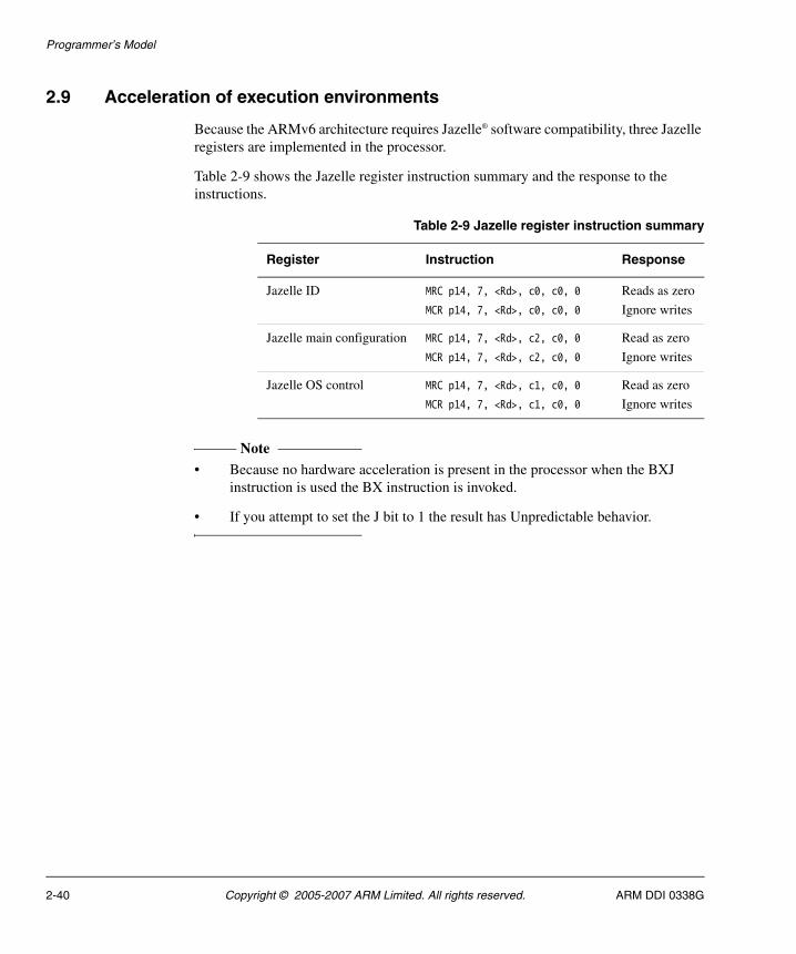
Programmer’s Model
2.9 Acceleration of execution environments
Because the ARMv6 architecture requires Jazelle® software compatibility, three Jazelle registers are implemented in the processor.
Table 2-9 shows the Jazelle register instruction summary and the response to the instructions.
Note • Because no hardware acceleration is present in the processor when the BXJ
instruction is used the BX instruction is invoked.
• If you attempt to set the J bit to 1 the result has Unpredictable behavior.
Table 2-9 Jazelle register instruction summary
Register Instruction Response
Jazelle ID MRC p14, 7, <Rd>, c0, c0, 0
MCR p14, 7, <Rd>, c0, c0, 0
Reads as zero
Ignore writes
Jazelle main configuration MRC p14, 7, <Rd>, c2, c0, 0
MCR p14, 7, <Rd>, c2, c0, 0
Read as zero
Ignore writes
Jazelle OS control MRC p14, 7, <Rd>, c1, c0, 0
MCR p14, 7, <Rd>, c1, c0, 0
Read as zero
Ignore writes
2-40 Copyright © 2005-2007 ARM Limited. All rights reserved. ARM DDI 0338G
Chapter 3 System Control Coprocessor
This chapter describes the purpose of the system control coprocessor, its structure, operation, and how to use it. It contains the following sections:
• About control coprocessor CP15 on page 3-2
• System control processor registers on page 3-11
• System control coprocessor reference data on page 3-120.
ARM DDI 0338G Copyright © 2005-2007 ARM Limited. All rights reserved. 3-1
System Control Coprocessor
3.1 About control coprocessor CP15
The section gives an overall view of the system control coprocessor. For reference data, see System control coprocessor reference data on page 3-120.
The purpose of the system control coprocessor, CP15, is to control and provide status information for the functions implemented in the ARM1156T2F-S processor. The main functions of the system control coprocessor are:
• overall system control and configuration
• optional cache configuration and management
• optional Tightly-Coupled Memory (TCM) configuration and management
• optional Memory Protection Unit (MPU) configuration and management
• debug accesses to the caches
• system performance monitoring.
The system control coprocessor appears as a set of 32-bit registers that you can write to and read from.
3.1.1 System control processor functional groups
The control processor uses these functional groups:
• System control and configuration on page 3-5
• MPU configuration and control on page 3-6
• Cache configuration and control on page 3-7
• Cache debug and software test access on page 3-9
• System performance monitor on page 3-10.
3-2 Copyright © 2005-2007 ARM Limited. All rights reserved. ARM DDI 0338G
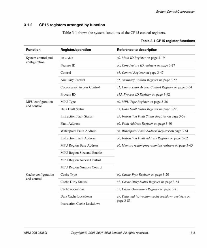
System Control Coprocessor
3.1.2 CP15 registers arranged by function
Table 3-1 shows the system functions of the CP15 control registers.
Table 3-1 CP15 register functions
Function Register/operation Reference to description
System control and configuration
ID codea c0, Main ID Register on page 3-19
Feature ID c0, Core feature ID registers on page 3-27
Control c1, Control Register on page 3-47
Auxiliary Control c1, Auxiliary Control Register on page 3-52
Coprocessor Access Control c1, Coprocessor Access Control Register on page 3-54
Process ID c13, Process ID Register on page 3-92
MPU configuration and control
MPU Type c0, MPU Type Register on page 3-26
Data Fault Status c5, Data Fault Status Register on page 3-56
Instruction Fault Status c5, Instruction Fault Status Register on page 3-58
Fault Address c6, Fault Address Register on page 3-60
Watchpoint Fault Address c6, Watchpoint Fault Address Register on page 3-61
Instruction Fault Address c6, Instruction Fault Address Register on page 3-62
MPU Region Base Address c6, Memory region programming registers on page 3-63
MPU Region Size and Enable
MPU Region Access Control
MPU Region Number Control
Cache configuration and control
Cache Type c0, Cache Type Register on page 3-20
Cache Dirty Status c7, Cache Dirty Status Register on page 3-84
Cache operations c7, Cache Operations Register on page 3-71
Data Cache Lockdown c9, Data and instruction cache lockdown registers on page 3-85
Instruction Cache Lockdown
ARM DDI 0338G Copyright © 2005-2007 ARM Limited. All rights reserved. 3-3
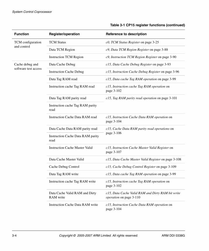
System Control Coprocessor
TCM configuration and control
TCM Status c0, TCM Status Register on page 3-25
Data TCM Region c9, Data TCM Region Register on page 3-88
Instruction TCM Region c9, Instruction TCM Region Register on page 3-90
Cache debug and software test access
Data Cache Debug c15, Data Cache Debug Register on page 3-93
Instruction Cache Debug c15, Instruction Cache Debug Register on page 3-96
Data Tag RAM read c15, Data cache Tag RAM operation on page 3-99
Instruction cache Tag RAM read c15, Instruction cache Tag RAM operation on page 3-102
Data Tag RAM parity read c15, Tag RAM parity read operation on page 3-101
Instruction cache Tag RAM parity read
Instruction Cache Data RAM read c15, Instruction Cache Data RAM operation on page 3-104
Data Cache Data RAM parity read c15, Cache Data RAM parity read operations on page 3-106
Instruction Cache Data RAM parity read
Instruction Cache Master Valid c15, Instruction Cache Master Valid Register on page 3-107
Data Cache Master Valid c15, Data Cache Master Valid Register on page 3-108
Cache Debug Control c15, Cache Debug Control Register on page 3-109
Data Tag RAM write c15, Data cache Tag RAM operation on page 3-99
Instruction cache Tag RAM write c15, Instruction cache Tag RAM operation on page 3-102
Data Cache Valid RAM and Dirty RAM write
c15, Data Cache Valid RAM and Dirty RAM bit write operation on page 3-110
Instruction Cache Data RAM write c15, Instruction Cache Data RAM operation on page 3-104
Table 3-1 CP15 register functions (continued)
Function Register/operation Reference to description
3-4 Copyright © 2005-2007 ARM Limited. All rights reserved. ARM DDI 0338G
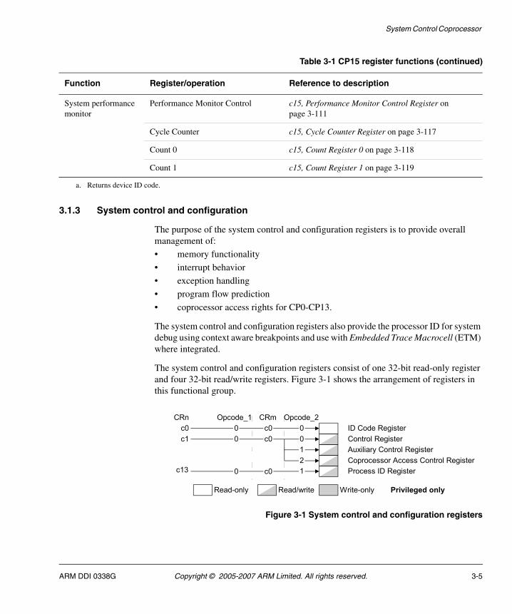
System Control Coprocessor
3.1.3 System control and configuration
The purpose of the system control and configuration registers is to provide overall management of:
• memory functionality
• interrupt behavior
• exception handling
• program flow prediction
• coprocessor access rights for CP0-CP13.
The system control and configuration registers also provide the processor ID for system debug using context aware breakpoints and use with Embedded Trace Macrocell (ETM) where integrated.
The system control and configuration registers consist of one 32-bit read-only register and four 32-bit read/write registers. Figure 3-1 shows the arrangement of registers in this functional group.
Figure 3-1 System control and configuration registers
System performance monitor
Performance Monitor Control c15, Performance Monitor Control Register on page 3-111
Cycle Counter c15, Cycle Counter Register on page 3-117
Count 0 c15, Count Register 0 on page 3-118
Count 1 c15, Count Register 1 on page 3-119
a. Returns device ID code.
Table 3-1 CP15 register functions (continued)
Function Register/operation Reference to description
CRn
c1
Coprocessor Access Control Register
Auxiliary Control Register
Control Register
1
2
0c00
c13 1c0 Process ID Register0
Opcode_2CRmOpcode_1
c0 ID Code Register0c00
Write-only Privileged onlyRead-only Read/write
ARM DDI 0338G Copyright © 2005-2007 ARM Limited. All rights reserved. 3-5
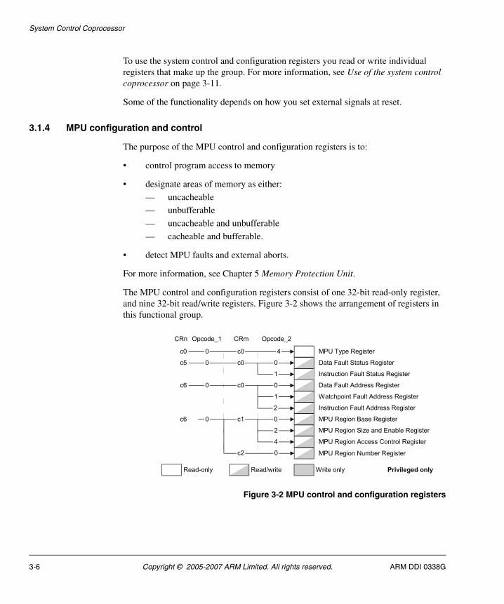
System Control Coprocessor
To use the system control and configuration registers you read or write individual registers that make up the group. For more information, see Use of the system control coprocessor on page 3-11.
Some of the functionality depends on how you set external signals at reset.
3.1.4 MPU configuration and control
The purpose of the MPU control and configuration registers is to:
• control program access to memory
• designate areas of memory as either:
— uncacheable
— unbufferable
— uncacheable and unbufferable
— cacheable and bufferable.
• detect MPU faults and external aborts.
For more information, see Chapter 5 Memory Protection Unit.
The MPU control and configuration registers consist of one 32-bit read-only register, and nine 32-bit read/write registers. Figure 3-2 shows the arrangement of registers in this functional group.
Figure 3-2 MPU control and configuration registers
4 MPU Type Registerc00c0
Opcode_2CRmCRn Opcode_1
1
1
2
Watchpoint Fault Address Register
Data Fault Address Register
Data Fault Status Register0
0
c0
c00
0c5
c6
2
4
0
MPU Region Size and Enable Register
MPU Region Base Register0c10c6
c2
MPU Region Access Control Register
MPU Region Number Register
Instruction Fault Address Register
Instruction Fault Status Register
Privileged onlyRead-only Read/write Write only
3-6 Copyright © 2005-2007 ARM Limited. All rights reserved. ARM DDI 0338G
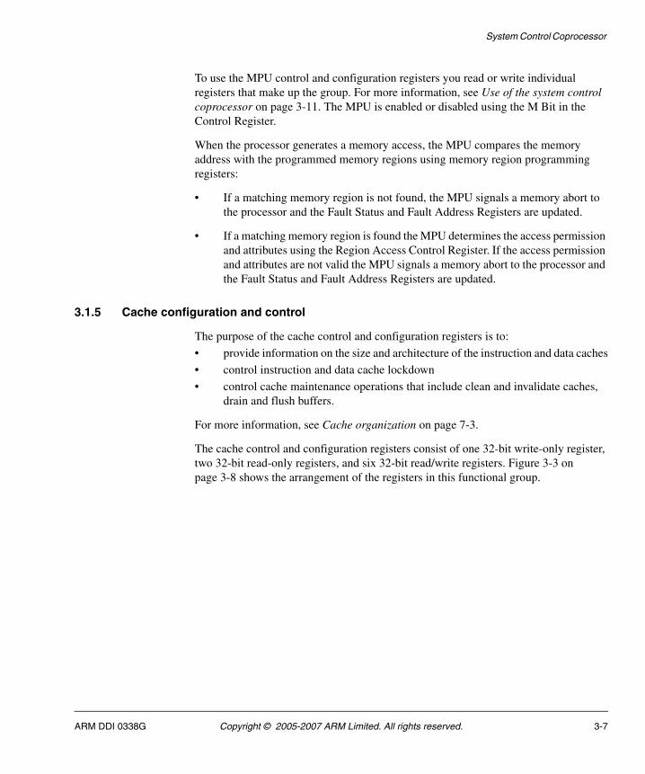
System Control Coprocessor
To use the MPU control and configuration registers you read or write individual registers that make up the group. For more information, see Use of the system control coprocessor on page 3-11. The MPU is enabled or disabled using the M Bit in the Control Register.
When the processor generates a memory access, the MPU compares the memory address with the programmed memory regions using memory region programming registers:
• If a matching memory region is not found, the MPU signals a memory abort to the processor and the Fault Status and Fault Address Registers are updated.
• If a matching memory region is found the MPU determines the access permission and attributes using the Region Access Control Register. If the access permission and attributes are not valid the MPU signals a memory abort to the processor and the Fault Status and Fault Address Registers are updated.
3.1.5 Cache configuration and control
The purpose of the cache control and configuration registers is to:
• provide information on the size and architecture of the instruction and data caches
• control instruction and data cache lockdown
• control cache maintenance operations that include clean and invalidate caches, drain and flush buffers.
For more information, see Cache organization on page 7-3.
The cache control and configuration registers consist of one 32-bit write-only register, two 32-bit read-only registers, and six 32-bit read/write registers. Figure 3-3 on page 3-8 shows the arrangement of the registers in this functional group.
ARM DDI 0338G Copyright © 2005-2007 ARM Limited. All rights reserved. 3-7
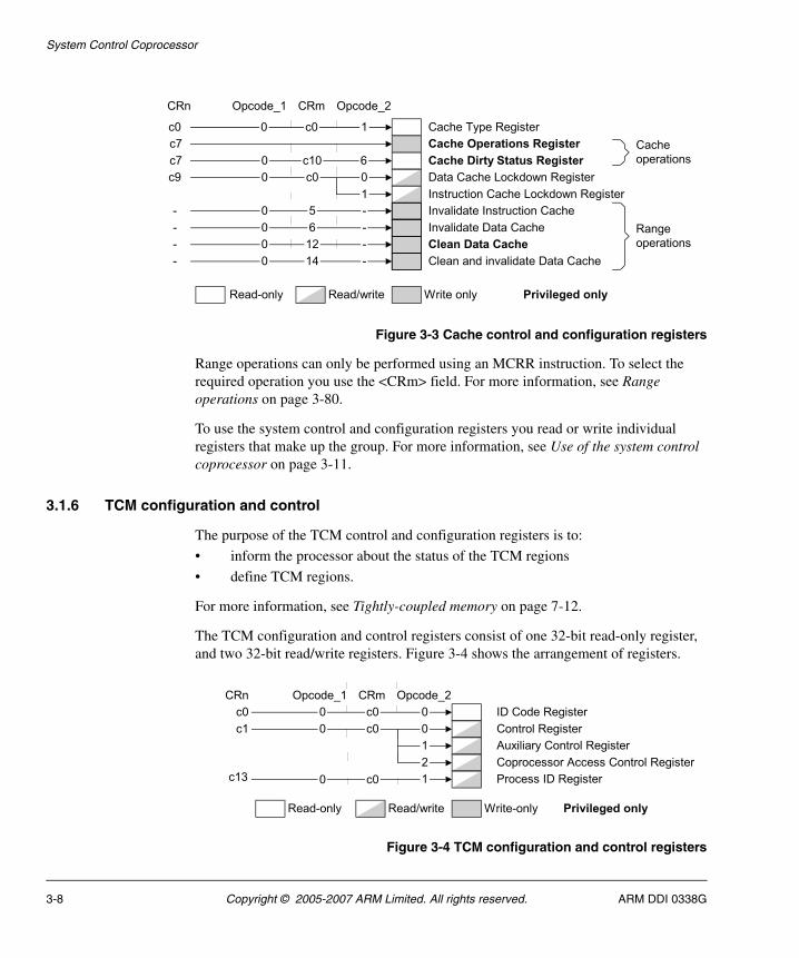
System Control Coprocessor
Figure 3-3 Cache control and configuration registers
Range operations can only be performed using an MCRR instruction. To select the required operation you use the <CRm> field. For more information, see Range operations on page 3-80.
To use the system control and configuration registers you read or write individual registers that make up the group. For more information, see Use of the system control coprocessor on page 3-11.
3.1.6 TCM configuration and control
The purpose of the TCM control and configuration registers is to:
• inform the processor about the status of the TCM regions
• define TCM regions.
For more information, see Tightly-coupled memory on page 7-12.
The TCM configuration and control registers consist of one 32-bit read-only register, and two 32-bit read/write registers. Figure 3-4 shows the arrangement of registers.
Figure 3-4 TCM configuration and control registers
Clean Data Cache
Read-only Read/write Write only
Opcode_2CRmOpcode_1
1c0 0 c0
Privileged only
Cache Type Register
CRn
c9 c0
1
0 0
Instruction Cache Lockdown Register
Data Cache Lockdown Register
c7 Cache Operations Register
- 50
- 60 Invalidate Data Cache
- 120
Range
operations
- 140 Clean and invalidate Data Cache
Invalidate Instruction Cache
c7 c10 Cache Dirty Status Register0 6
Cache
operations
-
-
-
-
CRn
c1
Coprocessor Access Control Register
Auxiliary Control Register
Control Register
1
2
0c00
c13 1c0 Process ID Register0
Opcode_2CRmOpcode_1
c0 ID Code Register0c00
Write-only Privileged onlyRead-only Read/write
3-8 Copyright © 2005-2007 ARM Limited. All rights reserved. ARM DDI 0338G
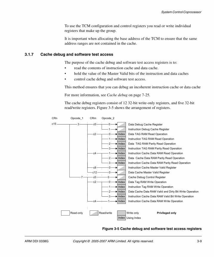
System Control Coprocessor
To use the TCM configuration and control registers you read or write individual registers that make up the group.
It is important when allocating the base address of the TCM to ensure that the same address ranges are not contained in the cache.
3.1.7 Cache debug and software test access
The purpose of the cache debug and software test access registers is to:
• read the contents of instruction cache and data cache.
• hold the value of the Master Valid bits of the instruction and data caches
• control cache debug and software test access.
This method ensures that you can debug an incoherent instruction cache or data cache
For more information, see Cache debug on page 7-25.
The cache debug registers consist of 12 32-bit write-only registers, and five 32-bit read/write registers. Figure 3-5 shows the arrangement of registers.
Figure 3-5 Cache debug and software test access registers
c15
Opcode_2CRmCRn Opcode_1
Privileged onlyRead-only Read/write Write only
Data Tag RAM Write Operation
1 Instruction Tag RAM Write Operation
1
Data TAG RAM Read Operation
Instruction Debug Cache Register
c2
Data Debug Cache Register
1
0
1 Instruction TAG RAM Read Operation
Instruction Cache Data RAM Read Operationc4 1
Instruction Cache Master Valid Register
Cache Debug Control Register07 c0
c8
c12
2 Data TAG RAM Parity Read Operation
3 Instruction TAG RAM Parity Read Operation
2 Data Cache Data RAM Parity Read Operation
3 Instruction Cache Data RAM Parity Read Operation
0c03
Data Cache Master Valid Register
Index
Index
Index
Index
Index
Index
0
0
Index
Instruction Cache Data RAM Write OperationIndex
Index
Index0c2
c4
3 Instruction Cache Data RAM Valid Bit Write OperationIndex
Index Using Index
2 Data Cache Data RAM Valid and Dirty Bit Write OperationIndex
ARM DDI 0338G Copyright © 2005-2007 ARM Limited. All rights reserved. 3-9
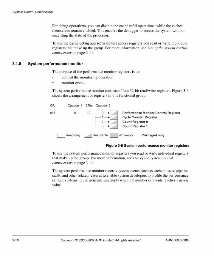
System Control Coprocessor
For debug operations, you can disable the cache refill operations, while the caches themselves remain enabled. This enables the debugger to access the system without unsettling the state of the processor.
To use the cache debug and software test access registers you read or write individual registers that make up the group. For more information, see Use of the system control coprocessor on page 3-11.
3.1.8 System performance monitor
The purpose of the performance monitor registers is to:
• control the monitoring operation
• monitor events.
The system performance monitor consists of four 32-bit read/write registers. Figure 3-6 shows the arrangement of registers in this functional group.
Figure 3-6 System performance monitor registers
To use the system performance monitor registers you read or write individual registers that make up the group. For more information, see Use of the system control coprocessor on page 3-11.
The system performance monitor records system events, such as cache misses, pipeline stalls, and other related features to enable system developers to profile the performance of their systems. It can generate interrupts when the number of events reaches a given value.
Opcode_2CRmCRn Opcode_1
c15
3
1
2
0 12 0
Count Register 1
Cycle Counter Register
Count Register 0
Performance Monitor Control Register
Read-only Read/write Write-only Privileged only
3-10 Copyright © 2005-2007 ARM Limited. All rights reserved. ARM DDI 0338G
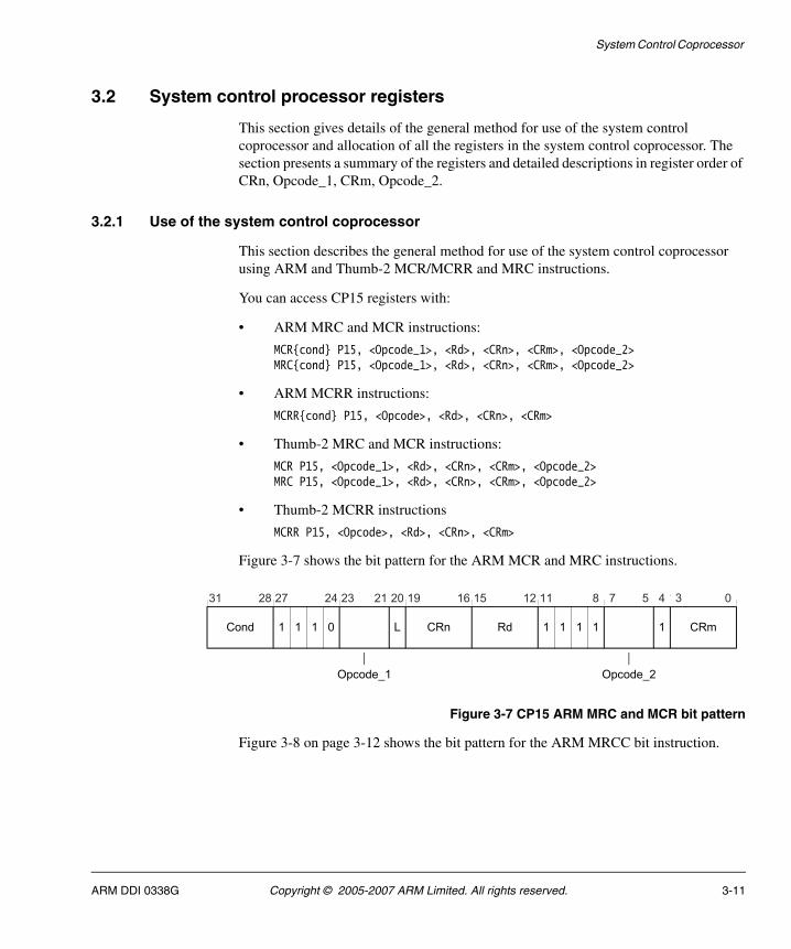
System Control Coprocessor
3.2 System control processor registers
This section gives details of the general method for use of the system control coprocessor and allocation of all the registers in the system control coprocessor. The section presents a summary of the registers and detailed descriptions in register order of CRn, Opcode_1, CRm, Opcode_2.
3.2.1 Use of the system control coprocessor
This section describes the general method for use of the system control coprocessor using ARM and Thumb-2 MCR/MCRR and MRC instructions.
You can access CP15 registers with:
• ARM MRC and MCR instructions:
MCR{cond} P15, <Opcode_1>, <Rd>, <CRn>, <CRm>, <Opcode_2>MRC{cond} P15, <Opcode_1>, <Rd>, <CRn>, <CRm>, <Opcode_2>
• ARM MCRR instructions:
MCRR{cond} P15, <Opcode>, <Rd>, <CRn>, <CRm>
• Thumb-2 MRC and MCR instructions:
MCR P15, <Opcode_1>, <Rd>, <CRn>, <CRm>, <Opcode_2>MRC P15, <Opcode_1>, <Rd>, <CRn>, <CRm>, <Opcode_2>
• Thumb-2 MCRR instructions
MCRR P15, <Opcode>, <Rd>, <CRn>, <CRm>
Figure 3-7 shows the bit pattern for the ARM MCR and MRC instructions.
Figure 3-7 CP15 ARM MRC and MCR bit pattern
Figure 3-8 on page 3-12 shows the bit pattern for the ARM MRCC bit instruction.
Cond
31 28 27 24 23 21 20 19 16 15 12 11 8 7 5 4 3 0
1 1 1 0 L CRn Rd 1 1 1 1 1 CRm
Opcode_1 Opcode_2
ARM DDI 0338G Copyright © 2005-2007 ARM Limited. All rights reserved. 3-11
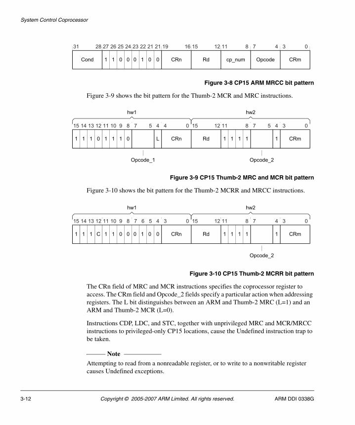
System Control Coprocessor
Figure 3-8 CP15 ARM MRCC bit pattern
Figure 3-9 shows the bit pattern for the Thumb-2 MCR and MRC instructions.
Figure 3-9 CP15 Thumb-2 MRC and MCR bit pattern
Figure 3-10 shows the bit pattern for the Thumb-2 MCRR and MRCC instructions.
Figure 3-10 CP15 Thumb-2 MCRR bit pattern
The CRn field of MRC and MCR instructions specifies the coprocessor register to access. The CRm field and Opcode_2 fields specify a particular action when addressing registers. The L bit distinguishes between an ARM and Thumb-2 MRC (L=1) and an ARM and Thumb-2 MCR (L=0).
Instructions CDP, LDC, and STC, together with unprivileged MRC and MCR/MRCC instructions to privileged-only CP15 locations, cause the Undefined instruction trap to be taken.
Note Attempting to read from a nonreadable register, or to write to a nonwritable register causes Undefined exceptions.
31 28 19 16 15 12 11 8 7 4 3 0
1 1 0 0 0 0 CRn Rd cp_num Opcode CRm10Cond
27 26 25 24 23 22 21 21
15 12 11 8 7 5 4 4 0 15 12 11 8 7 5 4 3 0
1 1 1 0 L CRn Rd 1 1 1 1 1 CRm1 1 1 0
9101314
hw1 hw2
Opcode_1 Opcode_2
1
15 12 3 0 15 12 11 8 7 4 3 0
1 1 0 0 0 0 CRn Rd 1 1 1 1 CRm10C1 11
11 10 9 8 7 6 5 41314
hw1 hw2
Opcode_2
3-12 Copyright © 2005-2007 ARM Limited. All rights reserved. ARM DDI 0338G
System Control Coprocessor
The Opcode, Opcode_1, Opcode_2, and CRm fields Should Be Zero in all instructions that access CP15, except when the values specified are used to select desired operations. Using other values results in Unpredictable behavior.
In all cases, reading from or writing any data values to any CP15 registers, including those fields specified as Unpredictable (UNP), Should Be One (SBO), or Should Be Zero (SBZ), does not cause any physical damage to the chip.
ARM DDI 0338G Copyright © 2005-2007 ARM Limited. All rights reserved. 3-13
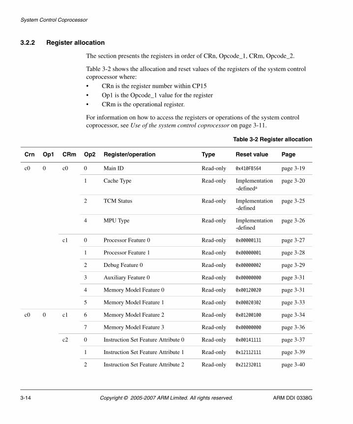
System Control Coprocessor
3.2.2 Register allocation
The section presents the registers in order of CRn, Opcode_1, CRm, Opcode_2.
Table 3-2 shows the allocation and reset values of the registers of the system control coprocessor where:
• CRn is the register number within CP15
• Op1 is the Opcode_1 value for the register
• CRm is the operational register.
For information on how to access the registers or operations of the system control coprocessor, see Use of the system control coprocessor on page 3-11.
Table 3-2 Register allocation
Crn Op1 CRm Op2 Register/operation Type Reset value Page
c0 0 c0 0 Main ID Read-only 0x410FB564 page 3-19
1 Cache Type Read-only Implementation-defineda
page 3-20
2 TCM Status Read-only Implementation-defined
page 3-25
4 MPU Type Read-only Implementation-defined
page 3-26
c1 0 Processor Feature 0 Read-only 0x00000131 page 3-27
1 Processor Feature 1 Read-only 0x00000001 page 3-28
2 Debug Feature 0 Read-only 0x00000002 page 3-29
3 Auxiliary Feature 0 Read-only 0x00000000 page 3-31
4 Memory Model Feature 0 Read-only 0x00120020 page 3-31
5 Memory Model Feature 1 Read-only 0x00020302 page 3-33
c0 0 c1 6 Memory Model Feature 2 Read-only 0x01200100 page 3-34
7 Memory Model Feature 3 Read-only 0x00000000 page 3-36
c2 0 Instruction Set Feature Attribute 0 Read-only 0x00141111 page 3-37
1 Instruction Set Feature Attribute 1 Read-only 0x12112111 page 3-39
2 Instruction Set Feature Attribute 2 Read-only 0x21232011 page 3-40
3-14 Copyright © 2005-2007 ARM Limited. All rights reserved. ARM DDI 0338G
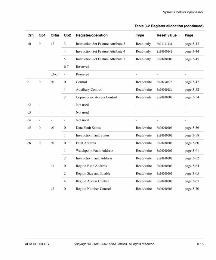
System Control Coprocessor
c0 0 c2 3 Instruction Set Feature Attribute 3 Read-only 0x01111131 page 3-42
4 Instruction Set Feature Attribute 4 Read-only 0x00000142 page 3-44
5 Instruction Set Feature Attribute 5 Read-only 0x00000000 page 3-45
6-7 Reserved - - -
c3-c7 - Reserved - - -
c1 0 c0 0 Control Read/write 0x00050078 page 3-47
1 Auxiliary Control Read/write 0x0000018b page 3-52
2 Coprocessor Access Control Read/write 0x00000000 page 3-54
c2 - - - Not used - - -
c3 - - - Not used - - -
c4 - - - Not used - - -
c5 0 c0 0 Data Fault Status Read/write 0x00000000 page 3-56
1 Instruction Fault Status Read/write 0x00000000 page 3-58
c6 0 c0 0 Fault Address Read/write 0x00000000 page 3-60
1 Watchpoint Fault Address Read/write 0x00000000 page 3-61
2 Instruction Fault Address Read/write 0x00000000 page 3-62
c1 0 Region Base Address Read/write 0x00000000 page 3-64
2 Region Size and Enable Read/write 0x00000000 page 3-65
4 Region Access Control Read/write 0x00000000 page 3-67
c2 0 Region Number Control Read/write 0x00000000 page 3-70
Table 3-2 Register allocation (continued)
Crn Op1 CRm Op2 Register/operation Type Reset value Page
ARM DDI 0338G Copyright © 2005-2007 ARM Limited. All rights reserved. 3-15
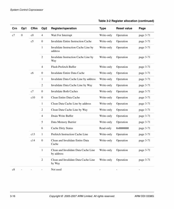
System Control Coprocessor
c7 0 c0 4 Wait For Interrupt Write-only Operation page 3-71
c5 0 Invalidate Entire Instruction Cache Write-only Operation page 3-71
1 Invalidate Instruction Cache Line by address
Write-only Operation page 3-71
2 Invalidate Instruction Cache Line by Way
Write-only Operation page 3-71
4 Flush Prefetch Buffer Write-only Operation page 3-71
c6 0 Invalidate Entire Data Cache Write-only Operation page 3-71
1 Invalidate Data Cache Line by address Write-only Operation page 3-71
2 Invalidate Data Cache Line by Way Write-only Operation page 3-71
c7 0 Invalidate Both Caches Write-only Operation page 3-71
c10 0 Clean Entire Data Cache Write-only Operation page 3-71
1 Clean Data Cache Line by address Write-only Operation page 3-71
2 Clean Data Cache Line by Way Write-only Operation page 3-71
4 Drain Write Buffer Write-only Operation page 3-71
5 Data Memory Barrier Write-only Operation page 3-71
6 Cache Dirty Status Read-only 0x00000000 page 3-71
c13 1 Prefetch Instruction Cache Line Write-only Operation page 3-71
c14 0 Clean and Invalidate Entire Data Cache
Write-only Operation page 3-71
1 Clean and Invalidate Data Cache Line by address
Write-only Operation page 3-71
2 Clean and Invalidate Data Cache Line by Way
Write-only Operation page 3-71
c8 - - - Not used - - -
Table 3-2 Register allocation (continued)
Crn Op1 CRm Op2 Register/operation Type Reset value Page
3-16 Copyright © 2005-2007 ARM Limited. All rights reserved. ARM DDI 0338G
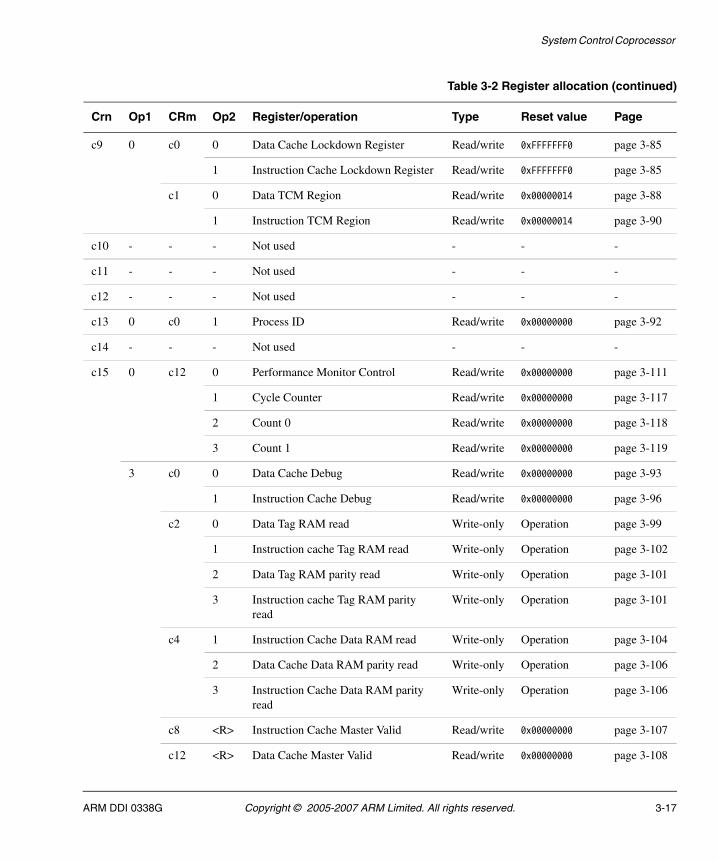
System Control Coprocessor
c9 0 c0 0 Data Cache Lockdown Register Read/write 0xFFFFFFF0 page 3-85
1 Instruction Cache Lockdown Register Read/write 0xFFFFFFF0 page 3-85
c1 0 Data TCM Region Read/write 0x00000014 page 3-88
1 Instruction TCM Region Read/write 0x00000014 page 3-90
c10 - - - Not used - - -
c11 - - - Not used - - -
c12 - - - Not used - - -
c13 0 c0 1 Process ID Read/write 0x00000000 page 3-92
c14 - - - Not used - - -
c15 0 c12 0 Performance Monitor Control Read/write 0x00000000 page 3-111
1 Cycle Counter Read/write 0x00000000 page 3-117
2 Count 0 Read/write 0x00000000 page 3-118
3 Count 1 Read/write 0x00000000 page 3-119
3 c0 0 Data Cache Debug Read/write 0x00000000 page 3-93
1 Instruction Cache Debug Read/write 0x00000000 page 3-96
c2 0 Data Tag RAM read Write-only Operation page 3-99
1 Instruction cache Tag RAM read Write-only Operation page 3-102
2 Data Tag RAM parity read Write-only Operation page 3-101
3 Instruction cache Tag RAM parity read
Write-only Operation page 3-101
c4 1 Instruction Cache Data RAM read Write-only Operation page 3-104
2 Data Cache Data RAM parity read Write-only Operation page 3-106
3 Instruction Cache Data RAM parity read
Write-only Operation page 3-106
c8 <R> Instruction Cache Master Valid Read/write 0x00000000 page 3-107
c12 <R> Data Cache Master Valid Read/write 0x00000000 page 3-108
Table 3-2 Register allocation (continued)
Crn Op1 CRm Op2 Register/operation Type Reset value Page
ARM DDI 0338G Copyright © 2005-2007 ARM Limited. All rights reserved. 3-17
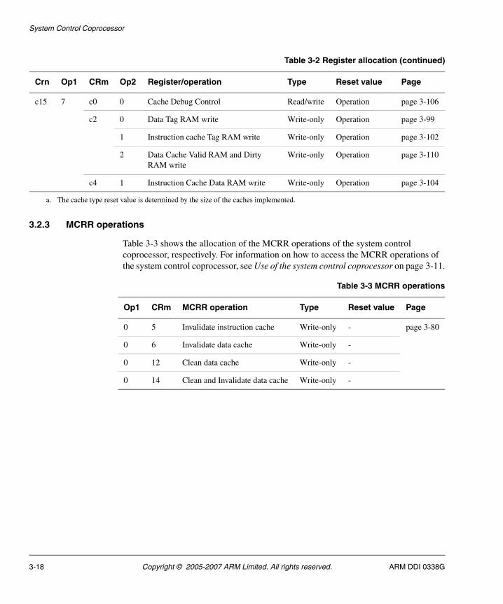
System Control Coprocessor
3.2.3 MCRR operations
Table 3-3 shows the allocation of the MCRR operations of the system control coprocessor, respectively. For information on how to access the MCRR operations of the system control coprocessor, see Use of the system control coprocessor on page 3-11.
c15 7 c0 0 Cache Debug Control Read/write Operation page 3-106
c2 0 Data Tag RAM write Write-only Operation page 3-99
1 Instruction cache Tag RAM write Write-only Operation page 3-102
2 Data Cache Valid RAM and Dirty RAM write
Write-only Operation page 3-110
c4 1 Instruction Cache Data RAM write Write-only Operation page 3-104
a. The cache type reset value is determined by the size of the caches implemented.
Table 3-2 Register allocation (continued)
Crn Op1 CRm Op2 Register/operation Type Reset value Page
Table 3-3 MCRR operations
Op1 CRm MCRR operation Type Reset value Page
0 5 Invalidate instruction cache Write-only - page 3-80
0 6 Invalidate data cache Write-only -
0 12 Clean data cache Write-only -
0 14 Clean and Invalidate data cache Write-only -
3-18 Copyright © 2005-2007 ARM Limited. All rights reserved. ARM DDI 0338G
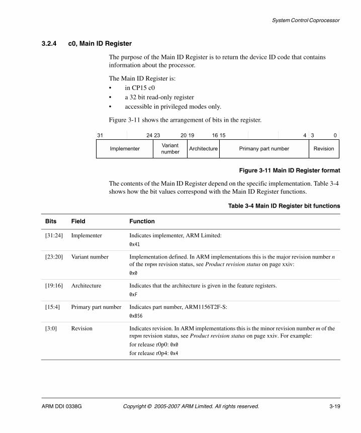
System Control Coprocessor
3.2.4 c0, Main ID Register
The purpose of the Main ID Register is to return the device ID code that contains information about the processor.
The Main ID Register is:
• in CP15 c0
• a 32 bit read-only register
• accessible in privileged modes only.
Figure 3-11 shows the arrangement of bits in the register.
Figure 3-11 Main ID Register format
The contents of the Main ID Register depend on the specific implementation. Table 3-4 shows how the bit values correspond with the Main ID Register functions.
Table 3-4 Main ID Register bit functions
Bits Field Function
[31:24] Implementer Indicates implementer, ARM Limited:
0x41
[23:20] Variant number Implementation defined. In ARM implementations this is the major revision number n of the rnpm revision status, see Product revision status on page xxiv:
0x0
[19:16] Architecture Indicates that the architecture is given in the feature registers.
0xF
[15:4] Primary part number Indicates part number, ARM1156T2F-S:
0xB56
[3:0] Revision Indicates revision. In ARM implementations this is the minor revision number m of the rnpm revision status, see Product revision status on page xxiv. For example:
for release r0p0: 0x0
for release r0p4: 0x4
ARM DDI 0338G Copyright © 2005-2007 ARM Limited. All rights reserved. 3-19
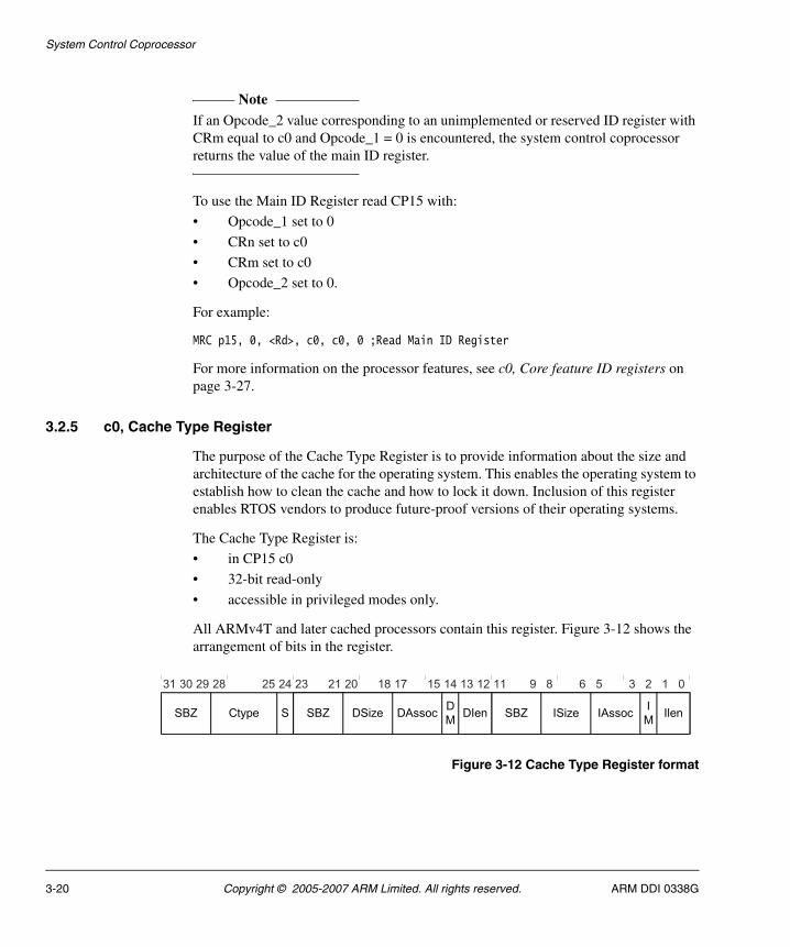
System Control Coprocessor
Note If an Opcode_2 value corresponding to an unimplemented or reserved ID register with CRm equal to c0 and Opcode_1 = 0 is encountered, the system control coprocessor returns the value of the main ID register.
To use the Main ID Register read CP15 with:
• Opcode_1 set to 0
• CRn set to c0
• CRm set to c0
• Opcode_2 set to 0.
For example:
MRC p15, 0, <Rd>, c0, c0, 0 ;Read Main ID Register
For more information on the processor features, see c0, Core feature ID registers on page 3-27.
3.2.5 c0, Cache Type Register
The purpose of the Cache Type Register is to provide information about the size and architecture of the cache for the operating system. This enables the operating system to establish how to clean the cache and how to lock it down. Inclusion of this register enables RTOS vendors to produce future-proof versions of their operating systems.
The Cache Type Register is:
• in CP15 c0
• 32-bit read-only
• accessible in privileged modes only.
All ARMv4T and later cached processors contain this register. Figure 3-12 shows the arrangement of bits in the register.
Figure 3-12 Cache Type Register format
SBZ
31 30 29 28 25 24 23 12 11 0
Ctype S SBZ ISize IAssocI
MIlenSBZ DSize DAssoc
D
MDIen
21 20 18 17 15 14 13 9 8 6 5 3 2 1
3-20 Copyright © 2005-2007 ARM Limited. All rights reserved. ARM DDI 0338G
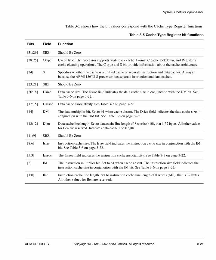
System Control Coprocessor
Table 3-5 shows how the bit values correspond with the Cache Type Register functions.
Table 3-5 Cache Type Register bit functions
Bits Field Function
[31:29] SBZ Should Be Zero
[28:25] Ctype Cache type. The processor supports write back cache, Format C cache lockdown, and Register 7 cache cleaning operations. The C type and S bit provide information about the cache architecture.
[24] S Specifies whether the cache is a unified cache or separate instruction and data caches. Always 1 because the ARM1156T2-S processor has separate instruction and data caches.
[23:21] SBZ Should Be Zero
[20:18] Dsize Data cache size. The Dsize field indicates the data cache size in conjunction with the DM bit. See Table 3-6 on page 3-22.
[17:15] Dassoc Data cache associativity. See Table 3-7 on page 3-22
[14] DM The data multiplier bit. Set to b1 when cache absent. The Dsize field indicates the data cache size in conjunction with the DM bit. See Table 3-6 on page 3-22.
[13:12] Dlen Data cache line length. Set to data cache line length of 8 words (b10), that is 32 bytes. All other values for Len are reserved. Indicates data cache line length.
[11:9] SBZ Should Be Zero
[8:6] Isize Instruction cache size. The Isize field indicates the instruction cache size in conjunction with the IM bit. See Table 3-6 on page 3-22.
[5:3] Iassoc The Iassoc field indicates the instruction cache associativity. See Table 3-7 on page 3-22.
[2] IM The instruction multiplier bit. Set to b1 when cache absent. The instruction size field indicates the instruction cache size in conjunction with the IM bit. See Table 3-6 on page 3-22.
[1:0] Ilen Instruction cache line length. Set to instruction cache line length of 8 words (b10), that is 32 bytes. All other values for Ilen are reserved.
ARM DDI 0338G Copyright © 2005-2007 ARM Limited. All rights reserved. 3-21
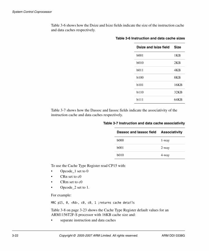
System Control Coprocessor
Table 3-6 shows how the Dsize and Isize fields indicate the size of the instruction cache and data caches respectively.
Table 3-7 shows how the Dassoc and Iassoc fields indicate the associativity of the instruction cache and data caches respectively.
To use the Cache Type Register read CP15 with:
• Opcode_1 set to 0
• CRn set to c0
• CRm set to c0
• Opcode_2 set to 1.
For example:
MRC p15, 0, <Rd>, c0, c0, 1 ;returns cache details
Table 3-8 on page 3-23 shows the Cache Type Register default values for an ARM1156T2F-S processor with 16KB cache size and:
• separate instruction and data caches
Table 3-6 Instruction and data cache sizes
Dsize and Isize field Size
b001 1KB
b010 2KB
b011 4KB
b100 8KB
b101 16KB
b110 32KB
b111 64KB
Table 3-7 Instruction and data cache associativity
Dassoc and Iassoc field Associativity
b000 1-way
b001 2-way
b010 4-way
3-22 Copyright © 2005-2007 ARM Limited. All rights reserved. ARM DDI 0338G
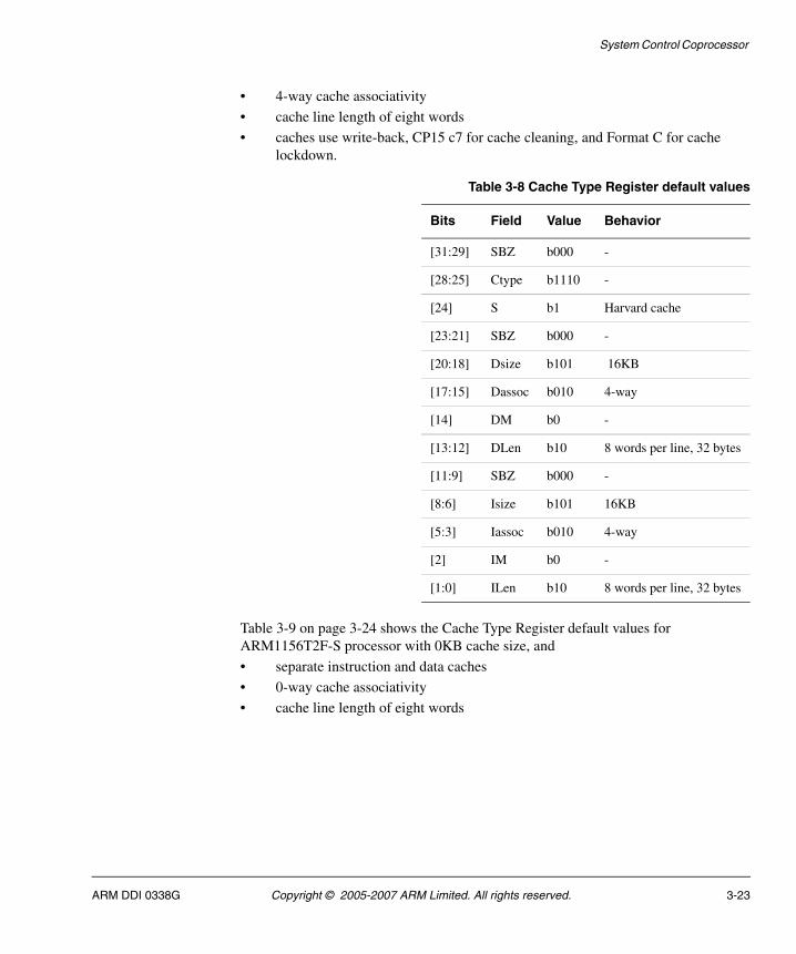
System Control Coprocessor
• 4-way cache associativity
• cache line length of eight words
• caches use write-back, CP15 c7 for cache cleaning, and Format C for cache lockdown.
Table 3-9 on page 3-24 shows the Cache Type Register default values for ARM1156T2F-S processor with 0KB cache size, and
• separate instruction and data caches
• 0-way cache associativity
• cache line length of eight words
Table 3-8 Cache Type Register default values
Bits Field Value Behavior
[31:29] SBZ b000 -
[28:25] Ctype b1110 -
[24] S b1 Harvard cache
[23:21] SBZ b000 -
[20:18] Dsize b101 16KB
[17:15] Dassoc b010 4-way
[14] DM b0 -
[13:12] DLen b10 8 words per line, 32 bytes
[11:9] SBZ b000 -
[8:6] Isize b101 16KB
[5:3] Iassoc b010 4-way
[2] IM b0 -
[1:0] ILen b10 8 words per line, 32 bytes
ARM DDI 0338G Copyright © 2005-2007 ARM Limited. All rights reserved. 3-23
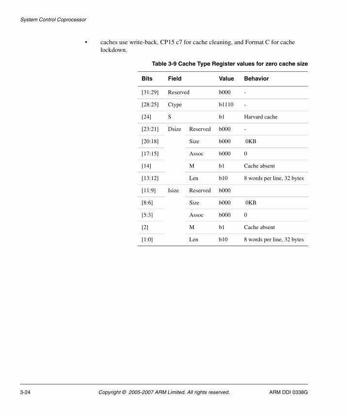
System Control Coprocessor
• caches use write-back, CP15 c7 for cache cleaning, and Format C for cache lockdown.
Table 3-9 Cache Type Register values for zero cache size
Bits Field Value Behavior
[31:29] Reserved b000 -
[28:25] Ctype b1110 -
[24] S b1 Harvard cache
[23:21] Dsize Reserved b000 -
[20:18] Size b000 0KB
[17:15] Assoc b000 0
[14] M b1 Cache absent
[13:12] Len b10 8 words per line, 32 bytes
[11:9] Isize Reserved b000
[8:6] Size b000 0KB
[5:3] Assoc b000 0
[2] M b1 Cache absent
[1:0] Len b10 8 words per line, 32 bytes
3-24 Copyright © 2005-2007 ARM Limited. All rights reserved. ARM DDI 0338G
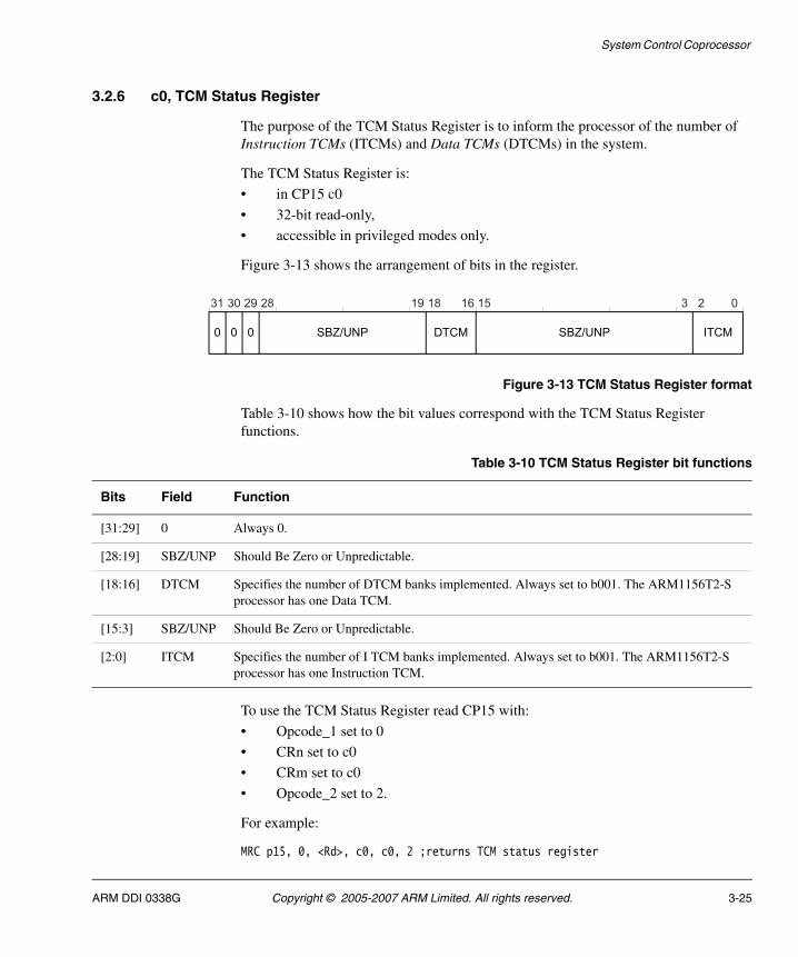
System Control Coprocessor
3.2.6 c0, TCM Status Register
The purpose of the TCM Status Register is to inform the processor of the number of Instruction TCMs (ITCMs) and Data TCMs (DTCMs) in the system.
The TCM Status Register is:
• in CP15 c0
• 32-bit read-only,
• accessible in privileged modes only.
Figure 3-13 shows the arrangement of bits in the register.
Figure 3-13 TCM Status Register format
Table 3-10 shows how the bit values correspond with the TCM Status Register functions.
To use the TCM Status Register read CP15 with:
• Opcode_1 set to 0
• CRn set to c0
• CRm set to c0
• Opcode_2 set to 2.
For example:
MRC p15, 0, <Rd>, c0, c0, 2 ;returns TCM status register
0
31 30 29 28 19 18 16 15 3 2 0
0 0 SBZ/UNP DTCM SBZ/UNP ITCM
Table 3-10 TCM Status Register bit functions
Bits Field Function
[31:29] 0 Always 0.
[28:19] SBZ/UNP Should Be Zero or Unpredictable.
[18:16] DTCM Specifies the number of DTCM banks implemented. Always set to b001. The ARM1156T2-S processor has one Data TCM.
[15:3] SBZ/UNP Should Be Zero or Unpredictable.
[2:0] ITCM Specifies the number of I TCM banks implemented. Always set to b001. The ARM1156T2-S processor has one Instruction TCM.
ARM DDI 0338G Copyright © 2005-2007 ARM Limited. All rights reserved. 3-25
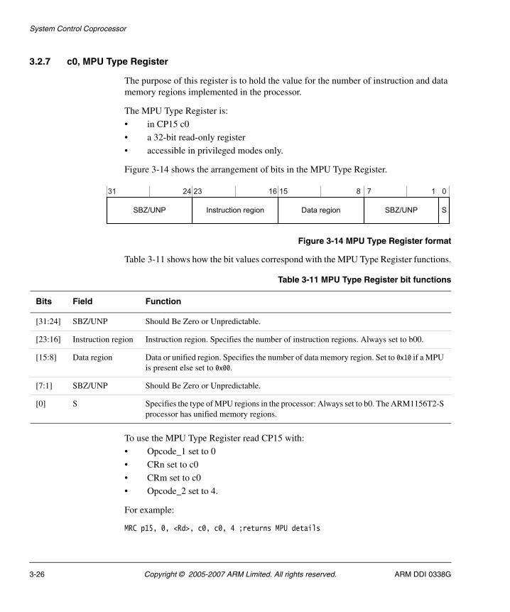
System Control Coprocessor
3.2.7 c0, MPU Type Register
The purpose of this register is to hold the value for the number of instruction and data memory regions implemented in the processor.
The MPU Type Register is:
• in CP15 c0
• a 32-bit read-only register
• accessible in privileged modes only.
Figure 3-14 shows the arrangement of bits in the MPU Type Register.
Figure 3-14 MPU Type Register format
Table 3-11 shows how the bit values correspond with the MPU Type Register functions.
To use the MPU Type Register read CP15 with:
• Opcode_1 set to 0
• CRn set to c0
• CRm set to c0
• Opcode_2 set to 4.
For example:
MRC p15, 0, <Rd>, c0, c0, 4 ;returns MPU details
Table 3-11 MPU Type Register bit functions
Bits Field Function
[31:24] SBZ/UNP Should Be Zero or Unpredictable.
[23:16] Instruction region Instruction region. Specifies the number of instruction regions. Always set to b00.
[15:8] Data region Data or unified region. Specifies the number of data memory region. Set to 0x10 if a MPU is present else set to 0x00.
[7:1] SBZ/UNP Should Be Zero or Unpredictable.
[0] S Specifies the type of MPU regions in the processor: Always set to b0. The ARM1156T2-S processor has unified memory regions.
3-26 Copyright © 2005-2007 ARM Limited. All rights reserved. ARM DDI 0338G
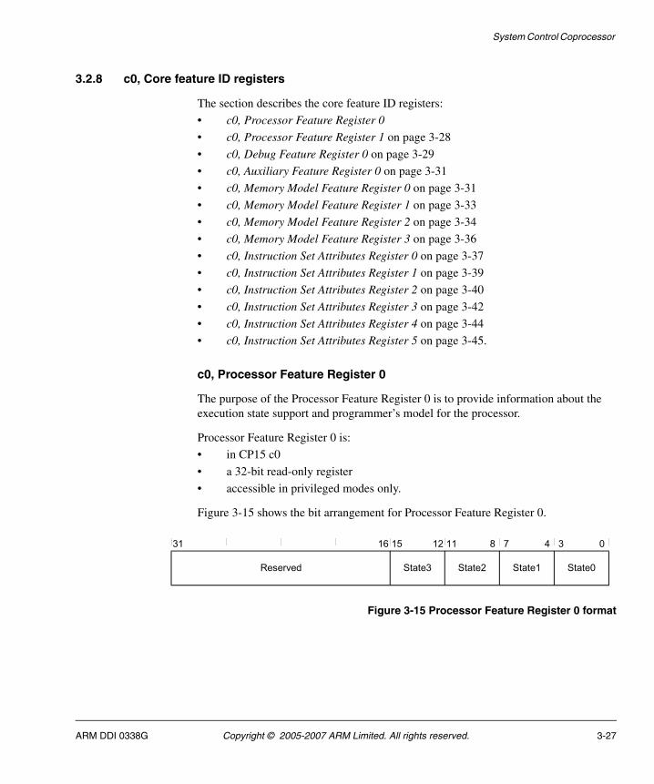
System Control Coprocessor
3.2.8 c0, Core feature ID registers
The section describes the core feature ID registers:
• c0, Processor Feature Register 0
• c0, Processor Feature Register 1 on page 3-28
• c0, Debug Feature Register 0 on page 3-29
• c0, Auxiliary Feature Register 0 on page 3-31
• c0, Memory Model Feature Register 0 on page 3-31
• c0, Memory Model Feature Register 1 on page 3-33
• c0, Memory Model Feature Register 2 on page 3-34
• c0, Memory Model Feature Register 3 on page 3-36
• c0, Instruction Set Attributes Register 0 on page 3-37
• c0, Instruction Set Attributes Register 1 on page 3-39
• c0, Instruction Set Attributes Register 2 on page 3-40
• c0, Instruction Set Attributes Register 3 on page 3-42
• c0, Instruction Set Attributes Register 4 on page 3-44
• c0, Instruction Set Attributes Register 5 on page 3-45.
c0, Processor Feature Register 0
The purpose of the Processor Feature Register 0 is to provide information about the execution state support and programmer’s model for the processor.
Processor Feature Register 0 is:
• in CP15 c0
• a 32-bit read-only register
• accessible in privileged modes only.
Figure 3-15 shows the bit arrangement for Processor Feature Register 0.
Figure 3-15 Processor Feature Register 0 format
Reserved State3
31 16 15 8 7 3 0
State2 State1 State0
41112
ARM DDI 0338G Copyright © 2005-2007 ARM Limited. All rights reserved. 3-27
System Control Coprocessor
Table 3-12 shows how the bit values correspond with the Processor Feature Register 0 functions.
The values in the Processor Feature Register 0 are implementation defined.
To use the Processor Feature Register 0 read CP15 with:
• Opcode_1 set to 0
• CRn set to c0
• CRm set to c1
• Opcode_2 set to 0.
For example:
MRC p15, 0, <Rd>, c0, c1, 0 Read Processor Feature Register 0
c0, Processor Feature Register 1
The purpose of the Processor Feature Register 1 is to provide information about the execution state support and programmer’s model for the processor.
Processor Feature Register 1 is:
• in CP15 c0
• a 32-bit read-only register
• accessible in privileged modes only.
Figure 3-16 on page 3-29 shows the bit arrangement for Processor Feature Register 1.
Table 3-12 Processor Feature Register 0 bit functions
Bits Field Function
[31:16] - Reserved.
UNP/SBZ.
[15:12] State3 Indicates support for Thumb-2™ execution environment.
This is set to 0x0, the ARM1156T2-S processor does not support the Thumb-2™ execution environment.
[11:8] State2 Indicates support for Java extension interface.
0x1, ARM1156T2F-S processors support Java.
[7:4] State1 Indicates type of Thumb encoding that the processor supports.
0x3, ARM1156T2F-S processors support Thumb and Thumb-2.
[3:0] State0 Indicates support for 32-bit ARM instruction set.
0x1, ARM1156T2F-S processors support 32-bit ARM instructions.
3-28 Copyright © 2005-2007 ARM Limited. All rights reserved. ARM DDI 0338G
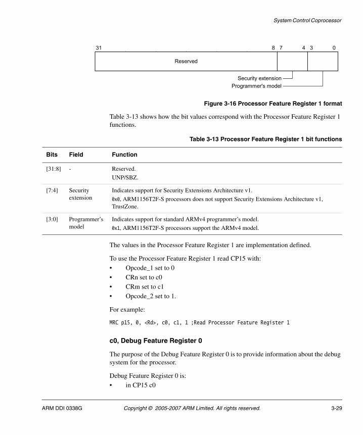
System Control Coprocessor
Figure 3-16 Processor Feature Register 1 format
Table 3-13 shows how the bit values correspond with the Processor Feature Register 1 functions.
The values in the Processor Feature Register 1 are implementation defined.
To use the Processor Feature Register 1 read CP15 with:
• Opcode_1 set to 0
• CRn set to c0
• CRm set to c1
• Opcode_2 set to 1.
For example:
MRC p15, 0, <Rd>, c0, c1, 1 ;Read Processor Feature Register 1
c0, Debug Feature Register 0
The purpose of the Debug Feature Register 0 is to provide information about the debug system for the processor.
Debug Feature Register 0 is:
• in CP15 c0
Reserved
31 7 3 048
Security extension
Programmer's model
Table 3-13 Processor Feature Register 1 bit functions
Bits Field Function
[31:8] - Reserved.
UNP/SBZ.
[7:4] Security extension
Indicates support for Security Extensions Architecture v1.
0x0, ARM1156T2F-S processors does not support Security Extensions Architecture v1, TrustZone.
[3:0] Programmer’s model
Indicates support for standard ARMv4 programmer’s model.
0x1, ARM1156T2F-S processors support the ARMv4 model.
ARM DDI 0338G Copyright © 2005-2007 ARM Limited. All rights reserved. 3-29
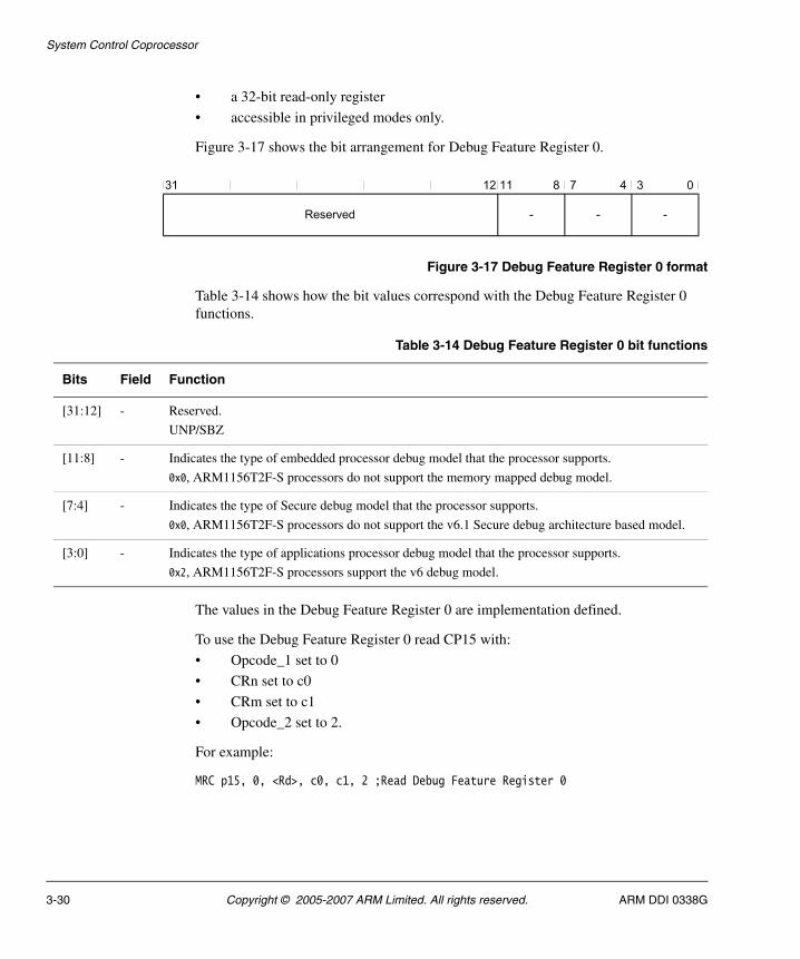
System Control Coprocessor
• a 32-bit read-only register
• accessible in privileged modes only.
Figure 3-17 shows the bit arrangement for Debug Feature Register 0.
Figure 3-17 Debug Feature Register 0 format
Table 3-14 shows how the bit values correspond with the Debug Feature Register 0 functions.
The values in the Debug Feature Register 0 are implementation defined.
To use the Debug Feature Register 0 read CP15 with:
• Opcode_1 set to 0
• CRn set to c0
• CRm set to c1
• Opcode_2 set to 2.
For example:
MRC p15, 0, <Rd>, c0, c1, 2 ;Read Debug Feature Register 0
Reserved
31 8 7 3 0
- - -
41112
Table 3-14 Debug Feature Register 0 bit functions
Bits Field Function
[31:12] - Reserved.
UNP/SBZ
[11:8] - Indicates the type of embedded processor debug model that the processor supports.
0x0, ARM1156T2F-S processors do not support the memory mapped debug model.
[7:4] - Indicates the type of Secure debug model that the processor supports.
0x0, ARM1156T2F-S processors do not support the v6.1 Secure debug architecture based model.
[3:0] - Indicates the type of applications processor debug model that the processor supports.
0x2, ARM1156T2F-S processors support the v6 debug model.
3-30 Copyright © 2005-2007 ARM Limited. All rights reserved. ARM DDI 0338G
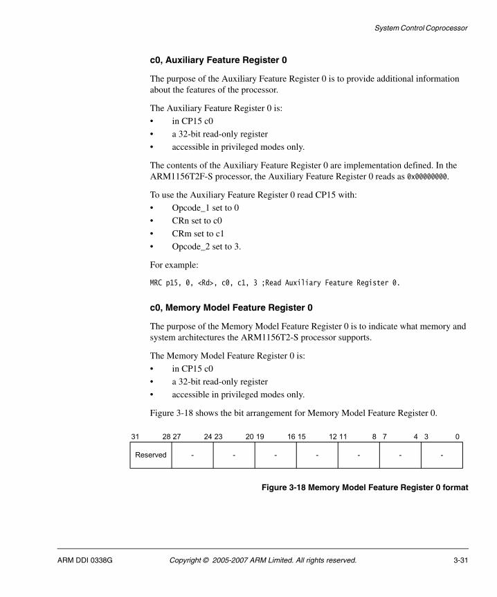
System Control Coprocessor
c0, Auxiliary Feature Register 0
The purpose of the Auxiliary Feature Register 0 is to provide additional information about the features of the processor.
The Auxiliary Feature Register 0 is:
• in CP15 c0
• a 32-bit read-only register
• accessible in privileged modes only.
The contents of the Auxiliary Feature Register 0 are implementation defined. In the ARM1156T2F-S processor, the Auxiliary Feature Register 0 reads as 0x00000000.
To use the Auxiliary Feature Register 0 read CP15 with:
• Opcode_1 set to 0
• CRn set to c0
• CRm set to c1
• Opcode_2 set to 3.
For example:
MRC p15, 0, <Rd>, c0, c1, 3 ;Read Auxiliary Feature Register 0.
c0, Memory Model Feature Register 0
The purpose of the Memory Model Feature Register 0 is to indicate what memory and system architectures the ARM1156T2-S processor supports.
The Memory Model Feature Register 0 is:
• in CP15 c0
• a 32-bit read-only register
• accessible in privileged modes only.
Figure 3-18 shows the bit arrangement for Memory Model Feature Register 0.
Figure 3-18 Memory Model Feature Register 0 format
---Reserved -
31 16 15 8 7 3 0
- - -
41112192023242728
ARM DDI 0338G Copyright © 2005-2007 ARM Limited. All rights reserved. 3-31
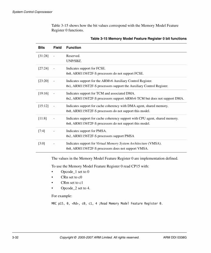
System Control Coprocessor
Table 3-15 shows how the bit values correspond with the Memory Model Feature Register 0 functions.
The values in the Memory Model Feature Register 0 are implementation defined.
To use the Memory Model Feature Register 0 read CP15 with:
• Opcode_1 set to 0
• CRn set to c0
• CRm set to c1
• Opcode_2 set to 4.
For example:
MRC p15, 0, <Rd>, c0, c1, 4 ;Read Memory Model Feature Register 0.
Table 3-15 Memory Model Feature Register 0 bit functions
Bits Field Function
[31:28] - Reserved.
UNP/SBZ.
[27:24] - Indicates support for FCSE.
0x0, ARM1156T2F-S processors do not support FCSE.
[23:20] - Indicates support for the ARMv6 Auxiliary Control Register.
0x1, ARM1156T2F-S processors support the Auxiliary Control Register.
[19:16] - Indicates support for TCM and associated DMA.
0x2, ARM1156T2F-S processors support ARMv6 TCM but does not support DMA.
[15:12] - Indicates support for cache coherency with DMA agent, shared memory.
0x0, ARM1156T2F-S processors do not support this model.
[11:8] - Indicates support for cache coherency support with CPU agent, shared memory.
0x0, ARM1156T2F-S processors do not support this model.
[7:4] - Indicates support for PMSA.
0x2, ARM1156T2F-S processors support PMSA
[3:0] - Indicates support for Virtual Memory System Architecture (VMSA).
0x0, ARM1156T2F-S processors does not support VMSA.
3-32 Copyright © 2005-2007 ARM Limited. All rights reserved. ARM DDI 0338G
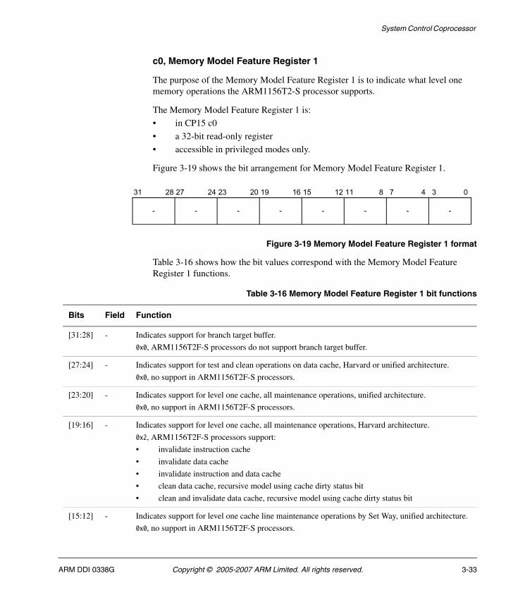
System Control Coprocessor
c0, Memory Model Feature Register 1
The purpose of the Memory Model Feature Register 1 is to indicate what level one memory operations the ARM1156T2-S processor supports.
The Memory Model Feature Register 1 is:
• in CP15 c0
• a 32-bit read-only register
• accessible in privileged modes only.
Figure 3-19 shows the bit arrangement for Memory Model Feature Register 1.
Figure 3-19 Memory Model Feature Register 1 format
Table 3-16 shows how the bit values correspond with the Memory Model Feature Register 1 functions.
---- -
31 16 15 8 7 3 0
- - -
41112192023242728
Table 3-16 Memory Model Feature Register 1 bit functions
Bits Field Function
[31:28] - Indicates support for branch target buffer.
0x0, ARM1156T2F-S processors do not support branch target buffer.
[27:24] - Indicates support for test and clean operations on data cache, Harvard or unified architecture.
0x0, no support in ARM1156T2F-S processors.
[23:20] - Indicates support for level one cache, all maintenance operations, unified architecture.
0x0, no support in ARM1156T2F-S processors.
[19:16] - Indicates support for level one cache, all maintenance operations, Harvard architecture.
0x2, ARM1156T2F-S processors support:
• invalidate instruction cache
• invalidate data cache
• invalidate instruction and data cache
• clean data cache, recursive model using cache dirty status bit
• clean and invalidate data cache, recursive model using cache dirty status bit
[15:12] - Indicates support for level one cache line maintenance operations by Set Way, unified architecture.
0x0, no support in ARM1156T2F-S processors.
ARM DDI 0338G Copyright © 2005-2007 ARM Limited. All rights reserved. 3-33
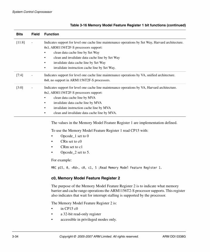
System Control Coprocessor
The values in the Memory Model Feature Register 1 are implementation defined.
To use the Memory Model Feature Register 1 read CP15 with:
• Opcode_1 set to 0
• CRn set to c0
• CRm set to c1
• Opcode_2 set to 5.
For example:
MRC p15, 0, <Rd>, c0, c1, 5 ;Read Memory Model Feature Register 1.
c0, Memory Model Feature Register 2
The purpose of the Memory Model Feature Register 2 is to indicate what memory barrier and cache range operations the ARM1156T2-S processor supports. This register also indicates that wait for interrupt stalling is supported by the processor.
The Memory Model Feature Register 2 is:
• in CP15 c0
• a 32-bit read-only register
• accessible in privileged modes only.
[11:8] - Indicates support for level one cache line maintenance operations by Set Way, Harvard architecture.
0x3, ARM1156T2F-S processors support:
• clean data cache line by Set Way
• clean and invalidate data cache line by Set Way
• invalidate data cache line by Set Way
• invalidate instruction cache line by Set Way.
[7:4] - Indicates support for level one cache line maintenance operations by VA, unified architecture.
0x0, no support in ARM1156T2F-S processors.
[3:0] - Indicates support for level one cache line maintenance operations by VA, Harvard architecture.
0x2, ARM1156T2F-S processors support:
• clean data cache line by MVA
• invalidate data cache line by MVA
• invalidate instruction cache line by MVA
• clean and invalidate data cache line by MVA.
Table 3-16 Memory Model Feature Register 1 bit functions (continued)
Bits Field Function
3-34 Copyright © 2005-2007 ARM Limited. All rights reserved. ARM DDI 0338G
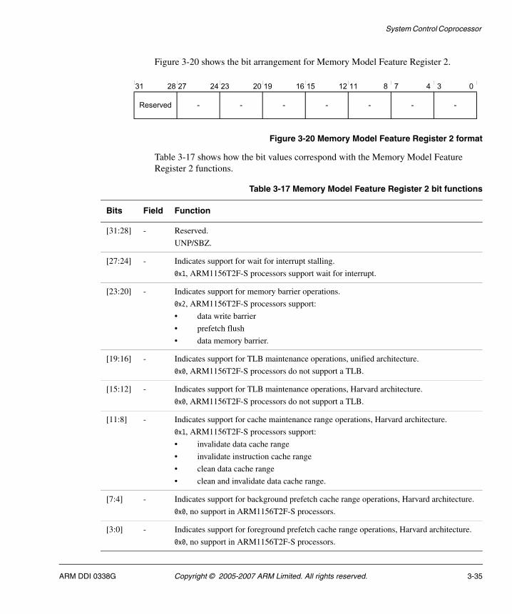
System Control Coprocessor
Figure 3-20 shows the bit arrangement for Memory Model Feature Register 2.
Figure 3-20 Memory Model Feature Register 2 format
Table 3-17 shows how the bit values correspond with the Memory Model Feature Register 2 functions.
---Reserved -
31 16 15 8 7 3 0
- - -
41112192023242728
Table 3-17 Memory Model Feature Register 2 bit functions
Bits Field Function
[31:28] - Reserved.
UNP/SBZ.
[27:24] - Indicates support for wait for interrupt stalling.
0x1, ARM1156T2F-S processors support wait for interrupt.
[23:20] - Indicates support for memory barrier operations.
0x2, ARM1156T2F-S processors support:
• data write barrier
• prefetch flush
• data memory barrier.
[19:16] - Indicates support for TLB maintenance operations, unified architecture.
0x0, ARM1156T2F-S processors do not support a TLB.
[15:12] - Indicates support for TLB maintenance operations, Harvard architecture.
0x0, ARM1156T2F-S processors do not support a TLB.
[11:8] - Indicates support for cache maintenance range operations, Harvard architecture.
0x1, ARM1156T2F-S processors support:
• invalidate data cache range
• invalidate instruction cache range
• clean data cache range
• clean and invalidate data cache range.
[7:4] - Indicates support for background prefetch cache range operations, Harvard architecture.
0x0, no support in ARM1156T2F-S processors.
[3:0] - Indicates support for foreground prefetch cache range operations, Harvard architecture.
0x0, no support in ARM1156T2F-S processors.
ARM DDI 0338G Copyright © 2005-2007 ARM Limited. All rights reserved. 3-35
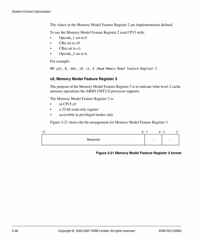
System Control Coprocessor
The values in the Memory Model Feature Register 2 are implementation defined.
To use the Memory Model Feature Register 2 read CP15 with:
• Opcode_1 set to 0
• CRn set to c0
• CRm set to c1
• Opcode_2 set to 6.
For example:
MRC p15, 0, <Rd>, c0, c1, 6 ;Read Memory Model Feature Register 2.
c0, Memory Model Feature Register 3
The purpose of the Memory Model Feature Register 3 is to indicate what level-2 cache memory operations the ARM1156T2-S processor supports.
The Memory Model Feature Register 3 is:
• in CP15 c0
• a 32-bit read-only register
• accessible in privileged modes only.
Figure 3-21 shows the bit arrangement for Memory Model Feature Register 3.
Figure 3-21 Memory Model Feature Register 3 format
Reserved
31 8 7 3 0
- -
4
3-36 Copyright © 2005-2007 ARM Limited. All rights reserved. ARM DDI 0338G
System Control Coprocessor
Table 3-18 shows how the bit values correspond with the Memory Model Feature Register 3 functions.
The values in the Memory Model Feature Register 3 are implementation defined.
To use the Memory Model Feature Register 3 read CP15 with:
• Opcode_1 set to 0
• CRn set to c0
• CRm set to c1
• Opcode_2 set to 7.
For example:
MRC p15, 0, <Rd>, c0, c1, 7 ;Read Memory Model Feature Register 3.
c0, Instruction Set Attributes Register 0
The purpose of the Instruction Set Attributes Register 0 is to provide information about the instruction set that the processor supports beyond the basic set.
The Instruction Set Attributes Register 0 is:
• in CP15 c0
• a 32-bit read-only register
• accessible in privileged modes only.
Figure 3-22 on page 3-38 shows the bit arrangement for Instruction Set Attributes Register 0.
Table 3-18 Memory Model Feature Register 3 bit functions
Bit Field Function
[31:8] - Reserved.
UNP/SBZ
[7:4] - Indicates support for level two cache line maintenance operations with VA, unified architecture.
0x0, no support in ARM1156T2F-S processors.
[3:0] - Indicates support for level two cache line maintenance operations with PA, unified architecture.
0x0, no support in ARM1156T2F-S processors.
ARM DDI 0338G Copyright © 2005-2007 ARM Limited. All rights reserved. 3-37
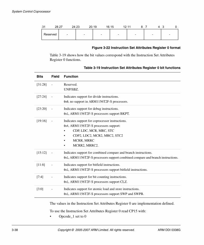
System Control Coprocessor
Figure 3-22 Instruction Set Attributes Register 0 format
Table 3-19 shows how the bit values correspond with the Instruction Set Attributes Register 0 functions.
The values in the Instruction Set Attributes Register 0 are implementation defined.
To use the Instruction Set Attributes Register 0 read CP15 with:
• Opcode_1 set to 0
---Reserved -
31 16 15 8 7 3 0
- - -
41112192023242728
Table 3-19 Instruction Set Attributes Register 0 bit functions
Bits Field Function
[31:28] - Reserved.
UNP/SBZ.
[27:24] - Indicates support for divide instructions.
0x0, no support in ARM1156T2F-S processors.
[23:20] - Indicates support for debug instructions.
0x1, ARM1156T2F-S processors support BKPT.
[19:16] - Indicates support for coprocessor instructions.
0x4, ARM1156T2F-S processors support:
• CDP, LDC, MCR, MRC, STC
• CDP2, LDC2, MCR2, MRC2, STC2
• MCRR, MRRC
• MCRR2, MRRC2.
[15:12] - Indicates support for combined compare and branch instructions.
0x1, ARM1156T2F-S processors support combined compare and branch instructions.
[11:8] - Indicates support for bitfield instructions.
0x1, ARM1156T2F-S processors support bitfield instructions.
[7:4] - Indicates support for bit counting instructions.
0x1, ARM1156T2F-S processors support CLZ.
[3:0] - Indicates support for atomic load and store instructions.
0x1, ARM1156T2F-S processors support SWP and SWPB.
3-38 Copyright © 2005-2007 ARM Limited. All rights reserved. ARM DDI 0338G
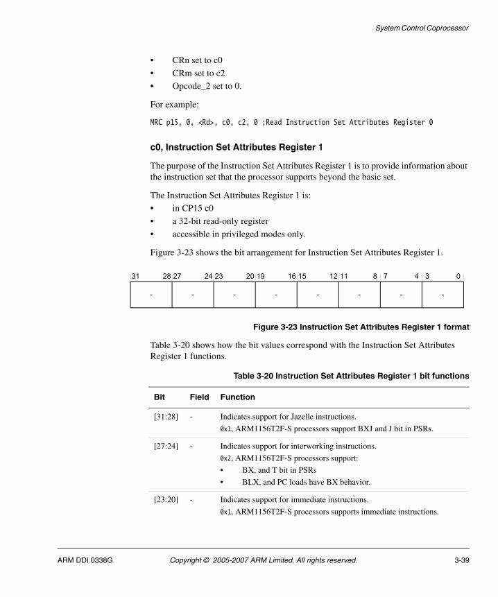
System Control Coprocessor
• CRn set to c0
• CRm set to c2
• Opcode_2 set to 0.
For example:
MRC p15, 0, <Rd>, c0, c2, 0 ;Read Instruction Set Attributes Register 0
c0, Instruction Set Attributes Register 1
The purpose of the Instruction Set Attributes Register 1 is to provide information about the instruction set that the processor supports beyond the basic set.
The Instruction Set Attributes Register 1 is:
• in CP15 c0
• a 32-bit read-only register
• accessible in privileged modes only.
Figure 3-23 shows the bit arrangement for Instruction Set Attributes Register 1.
Figure 3-23 Instruction Set Attributes Register 1 format
Table 3-20 shows how the bit values correspond with the Instruction Set Attributes Register 1 functions.
---- -
31 16 15 8 7 3 0
- - -
41112192023242728
Table 3-20 Instruction Set Attributes Register 1 bit functions
Bit Field Function
[31:28] - Indicates support for Jazelle instructions.
0x1, ARM1156T2F-S processors support BXJ and J bit in PSRs.
[27:24] - Indicates support for interworking instructions.
0x2, ARM1156T2F-S processors support:
• BX, and T bit in PSRs
• BLX, and PC loads have BX behavior.
[23:20] - Indicates support for immediate instructions.
0x1, ARM1156T2F-S processors supports immediate instructions.
ARM DDI 0338G Copyright © 2005-2007 ARM Limited. All rights reserved. 3-39
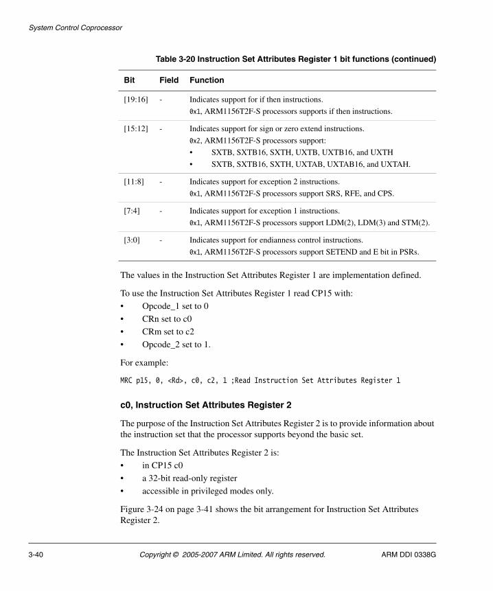
System Control Coprocessor
The values in the Instruction Set Attributes Register 1 are implementation defined.
To use the Instruction Set Attributes Register 1 read CP15 with:
• Opcode_1 set to 0
• CRn set to c0
• CRm set to c2
• Opcode_2 set to 1.
For example:
MRC p15, 0, <Rd>, c0, c2, 1 ;Read Instruction Set Attributes Register 1
c0, Instruction Set Attributes Register 2
The purpose of the Instruction Set Attributes Register 2 is to provide information about the instruction set that the processor supports beyond the basic set.
The Instruction Set Attributes Register 2 is:
• in CP15 c0
• a 32-bit read-only register
• accessible in privileged modes only.
Figure 3-24 on page 3-41 shows the bit arrangement for Instruction Set Attributes Register 2.
[19:16] - Indicates support for if then instructions.
0x1, ARM1156T2F-S processors supports if then instructions.
[15:12] - Indicates support for sign or zero extend instructions.
0x2, ARM1156T2F-S processors support:
• SXTB, SXTB16, SXTH, UXTB, UXTB16, and UXTH
• SXTB, SXTB16, SXTH, UXTAB, UXTAB16, and UXTAH.
[11:8] - Indicates support for exception 2 instructions.
0x1, ARM1156T2F-S processors support SRS, RFE, and CPS.
[7:4] - Indicates support for exception 1 instructions.
0x1, ARM1156T2F-S processors support LDM(2), LDM(3) and STM(2).
[3:0] - Indicates support for endianness control instructions.
0x1, ARM1156T2F-S processors support SETEND and E bit in PSRs.
Table 3-20 Instruction Set Attributes Register 1 bit functions (continued)
Bit Field Function
3-40 Copyright © 2005-2007 ARM Limited. All rights reserved. ARM DDI 0338G
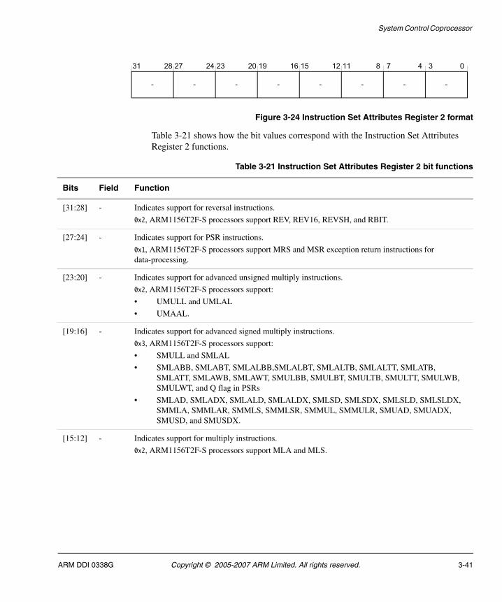
System Control Coprocessor
Figure 3-24 Instruction Set Attributes Register 2 format
Table 3-21 shows how the bit values correspond with the Instruction Set Attributes Register 2 functions.
---- -
31 16 15 8 7 3 0
- - -
41112192023242728
Table 3-21 Instruction Set Attributes Register 2 bit functions
Bits Field Function
[31:28] - Indicates support for reversal instructions.
0x2, ARM1156T2F-S processors support REV, REV16, REVSH, and RBIT.
[27:24] - Indicates support for PSR instructions.
0x1, ARM1156T2F-S processors support MRS and MSR exception return instructions for data-processing.
[23:20] - Indicates support for advanced unsigned multiply instructions.
0x2, ARM1156T2F-S processors support:
• UMULL and UMLAL
• UMAAL.
[19:16] - Indicates support for advanced signed multiply instructions.
0x3, ARM1156T2F-S processors support:
• SMULL and SMLAL
• SMLABB, SMLABT, SMLALBB,SMLALBT, SMLALTB, SMLALTT, SMLATB, SMLATT, SMLAWB, SMLAWT, SMULBB, SMULBT, SMULTB, SMULTT, SMULWB, SMULWT, and Q flag in PSRs
• SMLAD, SMLADX, SMLALD, SMLALDX, SMLSD, SMLSDX, SMLSLD, SMLSLDX, SMMLA, SMMLAR, SMMLS, SMMLSR, SMMUL, SMMULR, SMUAD, SMUADX, SMUSD, and SMUSDX.
[15:12] - Indicates support for multiply instructions.
0x2, ARM1156T2F-S processors support MLA and MLS.
ARM DDI 0338G Copyright © 2005-2007 ARM Limited. All rights reserved. 3-41
System Control Coprocessor
The values in the Instruction Set Attributes Register 2 are implementation defined.
To use the Instruction Set Attributes Register 2 read CP15 with:
• Opcode_1 set to 0
• CRn set to c0
• CRm set to c2
• Opcode_2 set to 2.
For example:
MRC p15, 0, <Rd>, c0, c2, 2 ;Read Instruction Set Attributes Register 2
c0, Instruction Set Attributes Register 3
The purpose of the Instruction Set Attributes Register 3 is to provide information about the instruction set that the processor supports beyond the basic set.
The Instruction Set Attributes Register 3 is:
• in CP15 c0
• a 32-bit read-only registers
• accessible in privileged modes only.
Figure 3-25 shows the bit arrangement for Instruction Set Attributes Register 3.
Figure 3-25 Instruction Set Attributes Register 3 format
[11:8] - Indicates support for multi-access interruptible instructions.
0x1, ARM1156T2F-S processors support restartable LDM and STM.
[7:4] - Indicates support for memory hint instructions.
0x1, ARM1156T2F-S processors support PLD.
[3:0] - Indicates support for load and store instructions.
0x1, ARM1156T2F-S processors support LDRD and STRD.
Table 3-21 Instruction Set Attributes Register 2 bit functions (continued)
Bits Field Function
---- -
31 16 15 8 7 3 0
- - -
41112192023242728
3-42 Copyright © 2005-2007 ARM Limited. All rights reserved. ARM DDI 0338G
System Control Coprocessor
Table 3-22 shows how the bit values correspond with the Instruction Set Attributes Register 3 functions.
The values in the Instruction Set Attributes Register 3 are implementation defined.
To use the Instruction Set Attributes Register 3 read CP15 with:
• Opcode_1 set to 0
• CRn set to c0
• CRm set to c2
• Opcode_2 set to 3.
Table 3-22 Instruction Set Attributes Register 3 bit functions
Bits Field Function
[31:28] - Indicates support for Thumb-2 execution environment extensions.
0x0, no support in ARM1156T2-S processors.
[27:24] - Indicates support for true NOP instructions.
0x1, ARM1156T2F-S processors support NOP32, NOP16 and the capability for additional NOP compatible hints.
[23:20] - Indicates support for Thumb copy instructions.
0x1, ARM1156T2F-S processors support Thumb MOV(3) low register ⇒ low register, and the CPY alias for Thumb MOV(3).
[19:16] - Indicates support for table branch instructions.
0x1, ARM1156T2F-S processors support table branch instructions.
[15:12] - Indicates support for synchronization primitive instructions.
0x1, ARM1156T2F-S processors support LDREX and STREX.
[11:8] - Indicates support for SVC instructions.
0x1, ARM1156T2F-S processors support SVC.
[7:4] - Indicates support for Single Instruction Multiple Data (SIMD) instructions.
0x3, ARM1156T2F-S processors support:
PKHBT, PKHTB, QADD16, QADD8, QASX, QSUB16, QSUB8, QSAX, SADD16, SADD8, SASX, SEL, SHADD16, SHADD8, SHASX, SHSUB16, SHSUB8, SHSAX, SSAT, SSAT16, SSUB16, SSUB8, SSAX, SXTB16, SXTB16, UADD16, UADD8, UASX, UHADD16, UHADD8, UHASX, UHSUB16, UHSUB8, UHSAX, UQADD16, UQADD8, UQASX, UQSUB16, UQSUB8, UQSAX, USAD8, USADA8, USAT, USAT16, USUB16, USUB8, USAX, UXTAB16, UXTB16, and the GE[3:0] bits in the PSRs.
[3:0] - Indicates support for saturate instructions.
0x1, ARM1156T2F-S processors support QADD, QDADD, QDSUB, QSUB and Q flag in PSRs.
ARM DDI 0338G Copyright © 2005-2007 ARM Limited. All rights reserved. 3-43
System Control Coprocessor
For example:
MRC p15, 0, <Rd>, c0, c2, 3 ;Read Instruction Set Attributes Register 3
c0, Instruction Set Attributes Register 4
The purpose of the Instruction Set Attributes Register 4 is to provide information about the instruction set that the processor supports beyond the basic set.
The Instruction Set Attributes Register 4 is:
• in CP15 c0
• a 32-bit read-only register
• accessible in privileged modes only.
Figure 3-26 shows the bit arrangement for Instruction Set Attributes Register 4.
Figure 3-26 Instruction Set Attributes Register 4 format
Table 3-23 shows how the bit values correspond with the Instruction Set Attributes Register 4 functions.
Reserved -
31 16 15 8 7 3 0
- - -
41112
Table 3-23 Instruction Set Attributes Register 4 bit functions
Bits Field Function
[31:16] - Reserved.
UNP/SBZ.
[15:12] - Indicates support for SMI instructions.
0x0, ARM1156T2F-S processors do not support SMI.
3-44 Copyright © 2005-2007 ARM Limited. All rights reserved. ARM DDI 0338G
System Control Coprocessor
The values in the Instruction Set Attributes Register 4 are implementation defined.
To use the Instruction Set Attributes Register 4 read CP15 with:
• Opcode_1 set to 0
• CRn set to c0
• CRm set to c2
• Opcode_2 set to 4.
For example:
MRC p15, 0, <Rd>, c0, c2, 4 ;Read Instruction Set Attributes Register 4
c0, Instruction Set Attributes Register 5
The purpose of the Instruction Set Attributes Register 5 is to provide additional information about the properties of the processor.
The Instruction Set Attributes Register 5 is:
• in CP15 c0
• a 32-bit read-only registers
• accessible in privileged modes only.
The contents of the Instruction Set Attributes Register 5 are implementation defined. In the ARM1156T2F-S processor, Instruction Set Attributes Register 5 is read as 0x00000000.
To use the Instruction Set Attributes Register 5 read CP15 with:
• Opcode_1 set to 0
[11:8] - Indicates support for writeback instructions.
0x1, ARM1156T2F-S processors support all defined writeback addressing modes.
[7:4] - Indicates support for with shift instructions.
0x4, ARM1156T2F-S processors support:
• shifts of loads and stores over the range LSL 0-3
• constant shift options
• register controlled shift options.
[3:0] - Indicates support for Unprivileged instructions.
0x2, ARM1156T2F-S processors support LDRBT, LDRT, STRBT, STRT, LDRHT, LDRSBT, LDRSHT, and STRHT.
Table 3-23 Instruction Set Attributes Register 4 bit functions (continued)
Bits Field Function
ARM DDI 0338G Copyright © 2005-2007 ARM Limited. All rights reserved. 3-45
System Control Coprocessor
• CRn set to c0
• CRm set toc2
• Opcode_2 set to 5.
For example:
MRC p15, 0, <Rd>, c0, c2, 5 ;Read Instruction Set Attribute Register 5.
3-46 Copyright © 2005-2007 ARM Limited. All rights reserved. ARM DDI 0338G
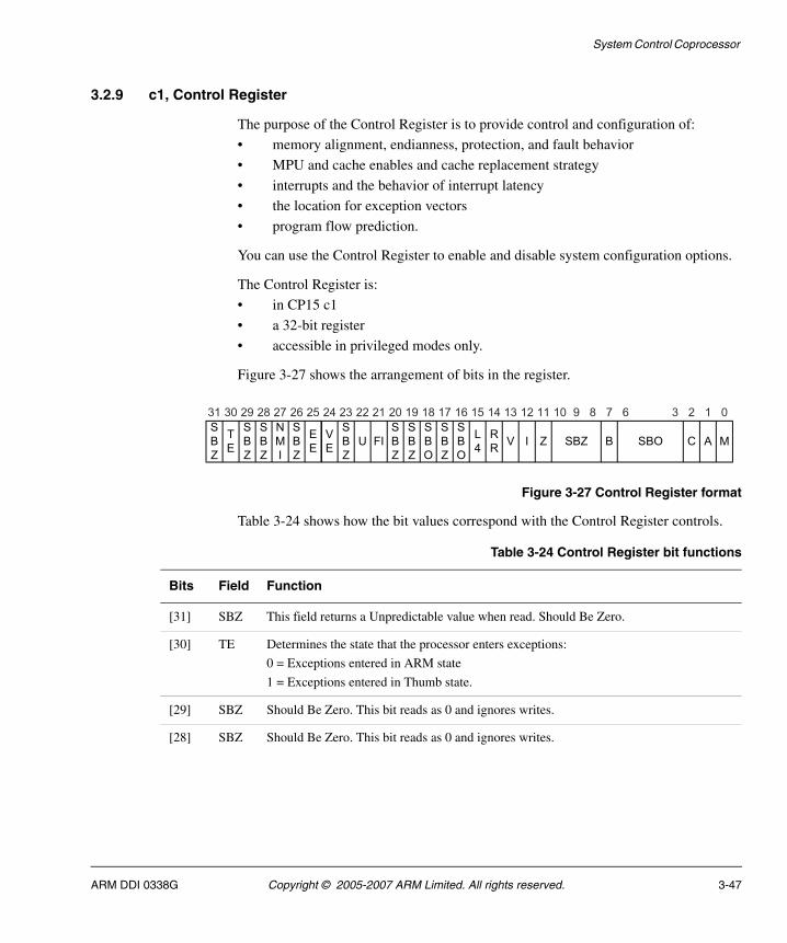
System Control Coprocessor
3.2.9 c1, Control Register
The purpose of the Control Register is to provide control and configuration of:
• memory alignment, endianness, protection, and fault behavior
• MPU and cache enables and cache replacement strategy
• interrupts and the behavior of interrupt latency
• the location for exception vectors
• program flow prediction.
You can use the Control Register to enable and disable system configuration options.
The Control Register is:
• in CP15 c1
• a 32-bit register
• accessible in privileged modes only.
Figure 3-27 shows the arrangement of bits in the register.
Figure 3-27 Control Register format
Table 3-24 shows how the bit values correspond with the Control Register controls.
S
B
Z
E
EM
31 25 24 23 22 21 20 19 18 17 16 15 14 13 12 11 10 9 8 7 6 3 2 1 0
V
E
S
B
Z
U FI
S
B
Z
S
B
O
S
B
Z
S
B
O
L
4
R
RV I Z SBZ B SBO C A
E
E
262728
N
M
I
S
B
Z
S
B
Z
S
B
Z
S
B
Z
T
E
30 29
Table 3-24 Control Register bit functions
Bits Field Function
[31] SBZ This field returns a Unpredictable value when read. Should Be Zero.
[30] TE Determines the state that the processor enters exceptions:
0 = Exceptions entered in ARM state
1 = Exceptions entered in Thumb state.
[29] SBZ Should Be Zero. This bit reads as 0 and ignores writes.
[28] SBZ Should Be Zero. This bit reads as 0 and ignores writes.
ARM DDI 0338G Copyright © 2005-2007 ARM Limited. All rights reserved. 3-47
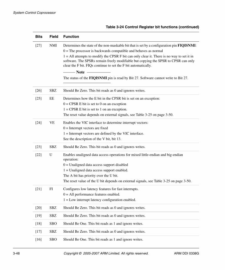
System Control Coprocessor
[27] NMI Determines the state of the non-maskable bit that is set by a configuration pin FIQISNMI:
0 = The processor is backwards compatible and behaves as normal
1 = All attempts to modify the CPSR F bit can only clear it. There is no way to set it in software. The SPSRs remain freely modifiable but copying the SPSR to CPSR can only clear the F bit. FIQs continue to set the F bit automatically.
Note The status of the FIQISNMI pin is read by Bit 27. Software cannot write to Bit 27.
[26] SBZ Should Be Zero. This bit reads as 0 and ignores writes.
[25] EE Determines how the E bit in the CPSR bit is set on an exception:
0 = CPSR E bit is set to 0 on an exception
1 = CPSR E bit is set to 1 on an exception.
The reset value depends on external signals, see Table 3-25 on page 3-50.
[24] VE Enables the VIC interface to determine interrupt vectors:
0 = Interrupt vectors are fixed
1 = Interrupt vectors are defined by the VIC interface.
See the description of the V bit, bit 13.
[23] SBZ Should Be Zero. This bit reads as 0 and ignores writes.
[22] U Enables unaligned data access operations for mixed little-endian and big-endian operation:
0 = Unaligned data access support disabled
1 = Unaligned data access support enabled.
The A bit has priority over the U bit.
The reset value of the U bit depends on external signals, see Table 3-25 on page 3-50.
[21] FI Configures low latency features for fast interrupts.
0 = All performance features enabled.
1 = Low interrupt latency configuration enabled.
[20] SBZ Should Be Zero. This bit reads as 0 and ignores writes.
[19] SBZ Should Be Zero. This bit reads as 0 and ignores writes.
[18] SBO Should Be One. This bit reads as 1 and ignore writes.
[17] SBZ Should Be Zero. This bit reads as 0 and ignores writes.
[16] SBO Should Be One. This bit reads as 1 and ignore writes.
Table 3-24 Control Register bit functions (continued)
Bits Field Function
3-48 Copyright © 2005-2007 ARM Limited. All rights reserved. ARM DDI 0338G
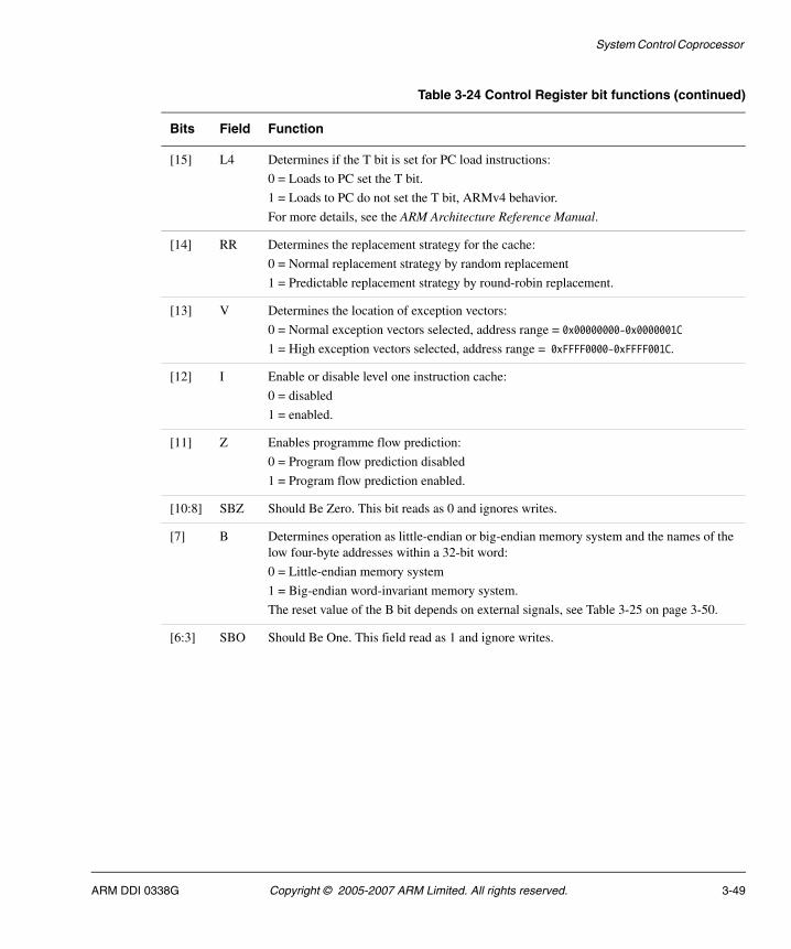
System Control Coprocessor
[15] L4 Determines if the T bit is set for PC load instructions:
0 = Loads to PC set the T bit.
1 = Loads to PC do not set the T bit, ARMv4 behavior.
For more details, see the ARM Architecture Reference Manual.
[14] RR Determines the replacement strategy for the cache:
0 = Normal replacement strategy by random replacement
1 = Predictable replacement strategy by round-robin replacement.
[13] V Determines the location of exception vectors:
0 = Normal exception vectors selected, address range = 0x00000000-0x0000001C
1 = High exception vectors selected, address range = 0xFFFF0000-0xFFFF001C.
[12] I Enable or disable level one instruction cache:
0 = disabled
1 = enabled.
[11] Z Enables programme flow prediction:
0 = Program flow prediction disabled
1 = Program flow prediction enabled.
[10:8] SBZ Should Be Zero. This bit reads as 0 and ignores writes.
[7] B Determines operation as little-endian or big-endian memory system and the names of the low four-byte addresses within a 32-bit word:
0 = Little-endian memory system
1 = Big-endian word-invariant memory system.
The reset value of the B bit depends on external signals, see Table 3-25 on page 3-50.
[6:3] SBO Should Be One. This field read as 1 and ignore writes.
Table 3-24 Control Register bit functions (continued)
Bits Field Function
ARM DDI 0338G Copyright © 2005-2007 ARM Limited. All rights reserved. 3-49
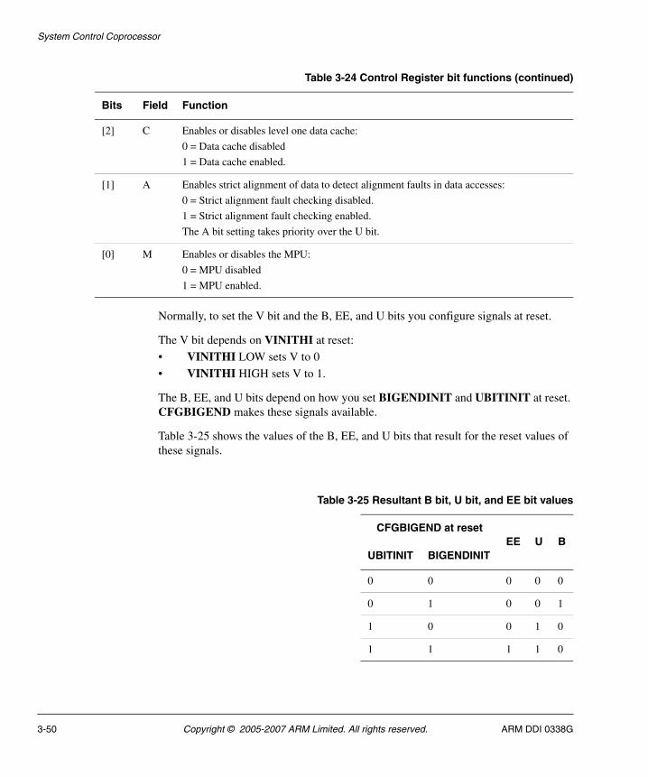
System Control Coprocessor
Normally, to set the V bit and the B, EE, and U bits you configure signals at reset.
The V bit depends on VINITHI at reset:
• VINITHI LOW sets V to 0
• VINITHI HIGH sets V to 1.
The B, EE, and U bits depend on how you set BIGENDINIT and UBITINIT at reset. CFGBIGEND makes these signals available.
Table 3-25 shows the values of the B, EE, and U bits that result for the reset values of these signals.
[2] C Enables or disables level one data cache:
0 = Data cache disabled
1 = Data cache enabled.
[1] A Enables strict alignment of data to detect alignment faults in data accesses:
0 = Strict alignment fault checking disabled.
1 = Strict alignment fault checking enabled.
The A bit setting takes priority over the U bit.
[0] M Enables or disables the MPU:
0 = MPU disabled
1 = MPU enabled.
Table 3-24 Control Register bit functions (continued)
Bits Field Function
Table 3-25 Resultant B bit, U bit, and EE bit values
CFGBIGEND at resetEE U B
UBITINIT BIGENDINIT
0 0 0 0 0
0 1 0 0 1
1 0 0 1 0
1 1 1 1 0
3-50 Copyright © 2005-2007 ARM Limited. All rights reserved. ARM DDI 0338G
System Control Coprocessor
These bits in the Control Register exhibit specific behavior:
A bit The A bit setting takes priority over the U bit. The Data Abort trap is taken if strict alignment is enabled and the data access is not aligned to the width of the accessed data item.
DT bit Use of this bit is deprecated in the ARM1156T2-S processor.
In ARMv6, the TCM blocks have individual enables that apply to each block. As a result, this bit is now redundant and Should Be One. See c9, Data TCM Region Register on page 3-88 for a description of the ARM1156T2F-S TCM enables.
IT bit Use of this bit is deprecated in the ARM1156T2-S processor.
In ARMv6, the TCM blocks have individual enables that apply to each block. As a result, this bit is now redundant and Should Be One. See c9, Instruction TCM Region Register on page 3-90 for a description of the ARM1156T2F-S TCM enables.
R bit This bit is not used in the ARM1156T2-S processor.
S bit This bit is not used in the ARM1156T2-S processor.
W bit The ARM1156T2F-S processor does not implement the write buffer enable because all memory writes take place through the Write Buffer.
To use the Control Register it is recommended that you use a read modify write technique. To use the Control Register read or write CP15 with:
• Opcode_1 set to 0
• CRn set to c1
• CRm set to c0
• Opcode_2 set to 0.
For example:
MRC p15, 0, <Rd>, c1, c0, 0 ;Read Control Register configuration dataMCR p15, 0, <Rd>, c1, c0, 0 ;Write Control Register configuration data
ARM DDI 0338G Copyright © 2005-2007 ARM Limited. All rights reserved. 3-51
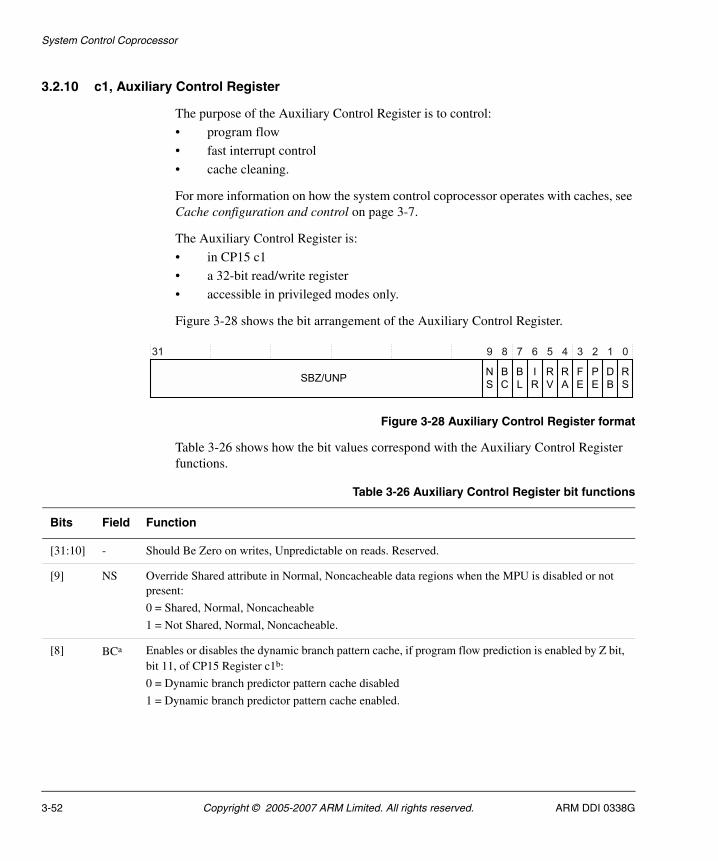
System Control Coprocessor
3.2.10 c1, Auxiliary Control Register
The purpose of the Auxiliary Control Register is to control:
• program flow
• fast interrupt control
• cache cleaning.
For more information on how the system control coprocessor operates with caches, see Cache configuration and control on page 3-7.
The Auxiliary Control Register is:
• in CP15 c1
• a 32-bit read/write register
• accessible in privileged modes only.
Figure 3-28 shows the bit arrangement of the Auxiliary Control Register.
Figure 3-28 Auxiliary Control Register format
Table 3-26 shows how the bit values correspond with the Auxiliary Control Register functions.
Table 3-26 Auxiliary Control Register bit functions
Bits Field Function
[31:10] - Should Be Zero on writes, Unpredictable on reads. Reserved.
[9] NS Override Shared attribute in Normal, Noncacheable data regions when the MPU is disabled or not present:
0 = Shared, Normal, Noncacheable
1 = Not Shared, Normal, Noncacheable.
[8] BCa Enables or disables the dynamic branch pattern cache, if program flow prediction is enabled by Z bit, bit 11, of CP15 Register c1b:
0 = Dynamic branch predictor pattern cache disabled
1 = Dynamic branch predictor pattern cache enabled.
3-52 Copyright © 2005-2007 ARM Limited. All rights reserved. ARM DDI 0338G
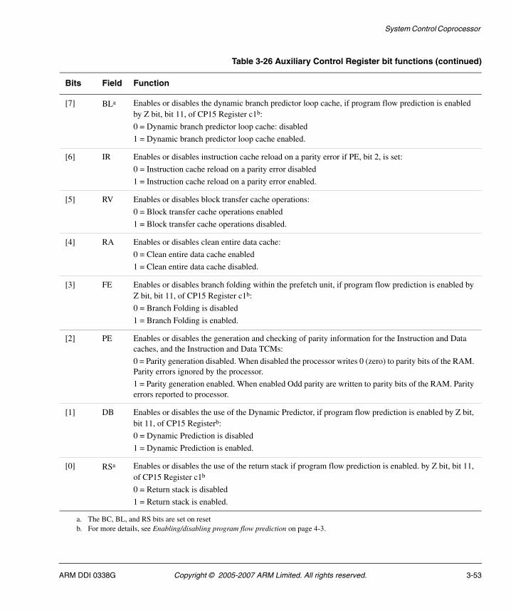
System Control Coprocessor
[7] BLa Enables or disables the dynamic branch predictor loop cache, if program flow prediction is enabled by Z bit, bit 11, of CP15 Register c1b:
0 = Dynamic branch predictor loop cache: disabled
1 = Dynamic branch predictor loop cache enabled.
[6] IR Enables or disables instruction cache reload on a parity error if PE, bit 2, is set:
0 = Instruction cache reload on a parity error disabled
1 = Instruction cache reload on a parity error enabled.
[5] RV Enables or disables block transfer cache operations:
0 = Block transfer cache operations enabled
1 = Block transfer cache operations disabled.
[4] RA Enables or disables clean entire data cache:
0 = Clean entire data cache enabled
1 = Clean entire data cache disabled.
[3] FE Enables or disables branch folding within the prefetch unit, if program flow prediction is enabled by Z bit, bit 11, of CP15 Register c1b:
0 = Branch Folding is disabled
1 = Branch Folding is enabled.
[2] PE Enables or disables the generation and checking of parity information for the Instruction and Data caches, and the Instruction and Data TCMs:
0 = Parity generation disabled. When disabled the processor writes 0 (zero) to parity bits of the RAM. Parity errors ignored by the processor.
1 = Parity generation enabled. When enabled Odd parity are written to parity bits of the RAM. Parity errors reported to processor.
[1] DB Enables or disables the use of the Dynamic Predictor, if program flow prediction is enabled by Z bit, bit 11, of CP15 Registerb:
0 = Dynamic Prediction is disabled
1 = Dynamic Prediction is enabled.
[0] RSa Enables or disables the use of the return stack if program flow prediction is enabled. by Z bit, bit 11, of CP15 Register c1b
0 = Return stack is disabled
1 = Return stack is enabled.
a. The BC, BL, and RS bits are set on resetb. For more details, see Enabling/disabling program flow prediction on page 4-3.
Table 3-26 Auxiliary Control Register bit functions (continued)
Bits Field Function
ARM DDI 0338G Copyright © 2005-2007 ARM Limited. All rights reserved. 3-53
System Control Coprocessor
To use the Auxiliary Control Register you must use a read modify write technique.
To access the Auxiliary Control Register read or write CP15 with:
• Opcode_1 set to 0
• CRn set to c1
• CRm set to c0
• Opcode_2 set to 1.
For example:
MRC p15, 0, <Rd>, c1, c0, 1 ;Read Auxiliary Control RegisterMCR p15, 0, <Rd>, c1, c0, 1 ;Write Auxiliary Control Register
ARM Limited recommends that you use a read modify write technique.
3.2.11 c1, Coprocessor Access Control Register
The purpose of the Coprocessor Access Control Register is to set access rights for the coprocessors CP0-CP13. This register has no effect on access to CP14, the debug control coprocessor, or CP15, the system control coprocessor. This register also provides a means for software to determine if any particular coprocessor, CP0-CP13, exists in the system.
The Coprocessor Access Control Register is:
• in CP15 c1
• a 32-bit read/write register
• accessible in privileged modes only.
Figure 3-29 shows the arrangement of bits in the register.
Figure 3-29 Coprocessor Access Control Register format
3-54 Copyright © 2005-2007 ARM Limited. All rights reserved. ARM DDI 0338G
System Control Coprocessor
Table 3-27 shows how the bit values correspond with the Coprocessor Access Control Register functions. Each pair of bits corresponds to the access rights for each coprocessor.
To use the Coprocessor Access Control Register read or write CP15 with:
• Opcode_1 set to 0
• CRn set to c1
• CRm set to c0
• Opcode_2 set to 2.
For example:
MRC p15, 0, <Rd>, c1, c0, 2 ;Read Coprocessor Access Control RegisterMCR p15, 0, <Rd>, c1, c0, 2 ;Write Coprocessor Access Control Register
You must execute an Instruction Memory Barrier (IMB) sequence immediately after an update of the Coprocessor Access Control Register, see Instruction Memory Barrier (IMB) instruction on page 4-7. You must not attempt to execute any instructions that are affected by the change of access rights between the IMB sequence and the register update.
To determine if any particular coprocessor exists in the system write the access bits for the coprocessor of interest with a value other than b00. If the coprocessor does not exist in the system the access rights remain set to b00.
Table 3-27 Coprocessor Access Control Register bit functions
Bits Field Function
[31:24] SBZ/UNP UNP when read. Write SBZ. Reserved
- cp<n>a Coprocessor access control:
b00 = Access denied. Attempts to access the corresponding coprocessor generate an Undefined exception.
b01 = Privileged access only.
b10 = Reserved.
b11 = Full access.
a. <n> is the coprocessor number between 0 and 13.
ARM DDI 0338G Copyright © 2005-2007 ARM Limited. All rights reserved. 3-55
System Control Coprocessor
3.2.12 c5, Data Fault Status Register
The purpose of the Data Fault Status Register (DFSR) is to hold the source of the last data fault.
The Data Fault Status Register is:
• in CP15 c5
• a 32-bit read/write register
• accessible in privileged modes only.
Figure 3-30 shows the bit arrangement in the DFSR.
Figure 3-30 DFSR format
Table 3-28 shows how the bit values correspond with the DFSR functions
S
AUNP/SBZ
31 4 3 0
SBZ/UNP Status
9
S
B
1011
R
W
1213
Table 3-28 DFSR bit functions
Bits Field Function
[31:13, 9:4] SBZ/UNP Should Be Zero or Unpredictable
[11] RW Indicates what type of access caused the abort.
0 = Abort caused by Read
1 =Abort caused by Write
Aborts on CP15 operations. This bit is set to 1.
[7:4] SBZ/UNP Should Be Zero or Unpredictable.
3-56 Copyright © 2005-2007 ARM Limited. All rights reserved. ARM DDI 0338G
System Control Coprocessor
To use the DFSR read or write CP15 with:
• Opcode_1 set to 0
• CRn set to c5
• CRm set to c0
• Opcode_2 set to 0.
For example:
MRC p15, 0, <Rd>, c5, c0, 0 ;Read Data Fault Status RegisterMCR p15, 0, <Rd>, c5, c0, 0 ;Write Data Fault Status Register
[12,10, 3:0] SA, SB, and Status Indicates the Type of fault generated:
b000001 = Alignment
b000000 = Background
b001101 = Permission
b001000 = Precise External Decoder Abort
b101000 = Precise External Slave Abort
b010110 = Imprecise External Decoder Abort
b110110 = Imprecise External Slave Abort
b011001 = Precise Parity Error Exception
b011000 = Imprecise Parity Error Exception
b000010 = Debug Event
For more details, see Fault status and address on page 5-25.
Table 3-28 DFSR bit functions (continued)
Bits Field Function
ARM DDI 0338G Copyright © 2005-2007 ARM Limited. All rights reserved. 3-57
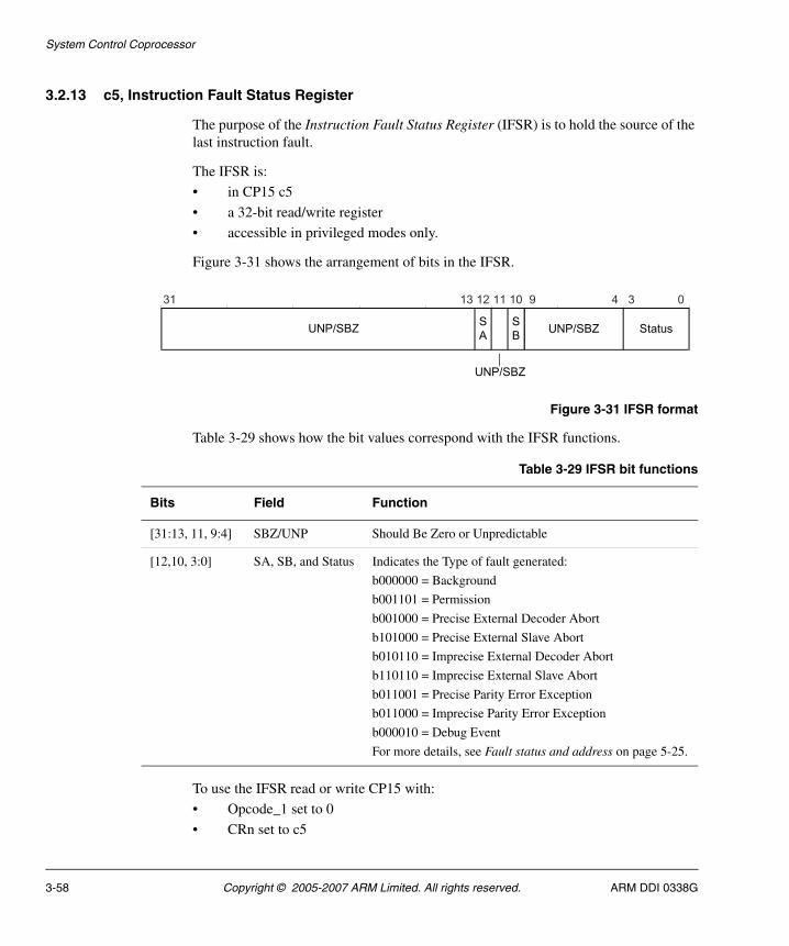
System Control Coprocessor
3.2.13 c5, Instruction Fault Status Register
The purpose of the Instruction Fault Status Register (IFSR) is to hold the source of the last instruction fault.
The IFSR is:
• in CP15 c5
• a 32-bit read/write register
• accessible in privileged modes only.
Figure 3-31 shows the arrangement of bits in the IFSR.
Figure 3-31 IFSR format
Table 3-29 shows how the bit values correspond with the IFSR functions.
To use the IFSR read or write CP15 with:
• Opcode_1 set to 0
• CRn set to c5
UNP/SBZ
31 3 0
StatusUNP/SBZ
491011
S
B
1213
UNP/SBZ
S
A
Table 3-29 IFSR bit functions
Bits Field Function
[31:13, 11, 9:4] SBZ/UNP Should Be Zero or Unpredictable
[12,10, 3:0] SA, SB, and Status Indicates the Type of fault generated:
b000000 = Background
b001101 = Permission
b001000 = Precise External Decoder Abort
b101000 = Precise External Slave Abort
b010110 = Imprecise External Decoder Abort
b110110 = Imprecise External Slave Abort
b011001 = Precise Parity Error Exception
b011000 = Imprecise Parity Error Exception
b000010 = Debug Event
For more details, see Fault status and address on page 5-25.
3-58 Copyright © 2005-2007 ARM Limited. All rights reserved. ARM DDI 0338G
System Control Coprocessor
• CRm set to c0
• Opcode_2 set to 1.
For example:
MRC p15, 0, <Rd>, c5, c0, 1 ;Read Instruction Fault Status RegisterMCR p15, 0, <Rd>, c5, c0, 1 ;Write Instruction Fault Status Register
ARM DDI 0338G Copyright © 2005-2007 ARM Limited. All rights reserved. 3-59
System Control Coprocessor
3.2.14 c6, Fault Address Register
The purpose of the Fault Address Register (FAR) is to hold the address of the fault when a precise abort occurs.
The FAR is:
• in CP15 c6
• a 32-bit read/write register
• accessible in privileged modes only.
To use the FAR read or write CP15 with:
• Opcode_1 set to 0
• CRn set to c6
• CRm set to c0.
• Opcode_2 set to 0.
For example:
MRC p15, 0, <Rd>, c6, c0, 0 ;Read Fault Address RegisterMCR p15, 0, <Rd>, c6, c0, 0 ;Write Fault Address Register
A write to c6 with Opcode_2 set to 0 sets the FAR to the value of the data written. This is useful for a debugger to restore the value of the FAR.
The ARM1156T2F-S processor also updates the FAR on debug exception entry because of watchpoints. This is architecturally Unpredictable. See Effect of a debug event on CP15 registers on page 13-31 for more details.
3-60 Copyright © 2005-2007 ARM Limited. All rights reserved. ARM DDI 0338G
System Control Coprocessor
3.2.15 c6, Watchpoint Fault Address Register
The purpose of the Watchpoint Fault Address Register (WFAR) is to hold the address of the instruction that causes the watchpoint.
The register WFAR is:
• in CP15 c6
• a 32-bit read/write register
• accessible in privileged modes only.
When a watchpoint occurs in:
• ARM state, the WFAR contains the address of the instruction causing it plus 0x8.
• Thumb state, the WFAR contains the address of the instruction causing it plus 0x4.
To use the Watchpoint Fault Address Register read or write CP15 with:
• Opcode_1 set to 0
• CRn set to c0
• CRm set to c6
• Opcode_2 set to 1.
For example:
MRC p15, 0, <Rd>, c0, c6, 1 ;Read Watchpoint Fault Address RegisterMCR p15, 0, <Rd>, c0, c6, 1 ;Write Watchpoint Fault Address Register
A write to CP15 c0 with Opcode_2 set to 1 sets the Watchpoint Fault Address Register to the value of the data written. This is useful for a debugger to restore the value of the Watchpoint Fault Address Register. For more information on debugging, see Chapter 13 Debug.
A read to CP15 c0 returns the Watchpoint Fault Address Register.
ARM DDI 0338G Copyright © 2005-2007 ARM Limited. All rights reserved. 3-61
System Control Coprocessor
3.2.16 c6, Instruction Fault Address Register
The purpose of the Instruction Fault Address Register (IFAR) is to hold the address of instruction that causes a prefetch abort.
The IFAR is:
• in CP15 c6
• a 32-bit read/write register
• accessible in privileged modes only.
To use the IFAR read or write CP15 with:
• Opcode_1 set to 0
• CRn set to c6
• CRm set to c0
• Opcode_2 set to 2.
For example:
MRC p15, 0, <Rd>, c6, c0, 2 ;Read Instruction Fault Address RegisterMCR p15, 0, <Rd>, c6, c0, 2 ;Write Instruction Fault Address Register
A write to c6 with Opcode_2 set to 0 sets the IFAR to the value of the data written. This is useful for a debugger to restore the value of the FAR.
The ARM1156T2F-S processor also updates the WFAR on debug exception entry because of watchpoints. This is architecturally Unpredictable. See Effect of a debug event on CP15 registers on page 13-31 for more details.
3-62 Copyright © 2005-2007 ARM Limited. All rights reserved. ARM DDI 0338G
System Control Coprocessor
3.2.17 c6, Memory region programming registers
The purpose of the memory region programming registers is to program the MPU regions.
There is one register that specifies which one of the 16 sets of region registers is to be accessed. Each region has its own register to specify:
• region base address
• region size and enable
• region access control.
Note • When the MPU is enabled:
— the MPU determines the access permissions for all accesses to memory, which includes the TCM. Therefore, you must ensure that the memory regions in the MPU are programmed to cover the complete TCM address space with the appropriate access permissions. You must define at least one of the 16 regions in the MPU.
— an access to an Undefined area of memory causes a background fault to be generated.
• For the TCM space the processor uses the access permissions but ignores the region attributes from MPU.
The location of the TCM base address is set by CP15 c9. For more details, see c9, Data TCM Region Register on page 3-88.
ARM DDI 0338G Copyright © 2005-2007 ARM Limited. All rights reserved. 3-63
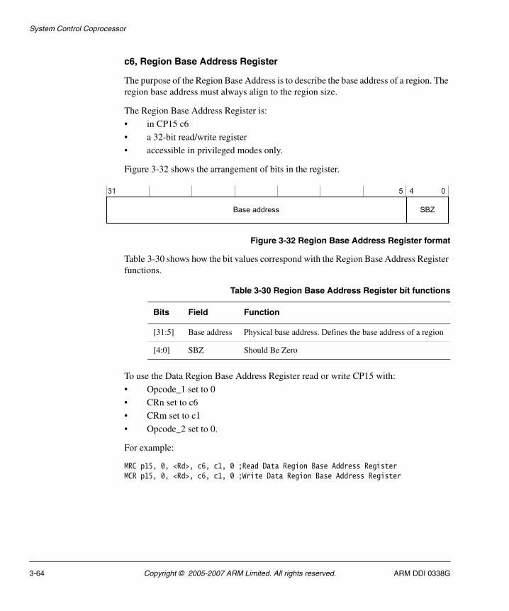
System Control Coprocessor
c6, Region Base Address Register
The purpose of the Region Base Address is to describe the base address of a region. The region base address must always align to the region size.
The Region Base Address Register is:
• in CP15 c6
• a 32-bit read/write register
• accessible in privileged modes only.
Figure 3-32 shows the arrangement of bits in the register.
Figure 3-32 Region Base Address Register format
Table 3-30 shows how the bit values correspond with the Region Base Address Register functions.
To use the Data Region Base Address Register read or write CP15 with:
• Opcode_1 set to 0
• CRn set to c6
• CRm set to c1
• Opcode_2 set to 0.
For example:
MRC p15, 0, <Rd>, c6, c1, 0 ;Read Data Region Base Address RegisterMCR p15, 0, <Rd>, c6, c1, 0 ;Write Data Region Base Address Register
Table 3-30 Region Base Address Register bit functions
Bits Field Function
[31:5] Base address Physical base address. Defines the base address of a region
[4:0] SBZ Should Be Zero
3-64 Copyright © 2005-2007 ARM Limited. All rights reserved. ARM DDI 0338G
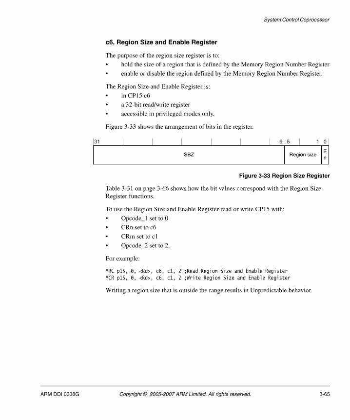
System Control Coprocessor
c6, Region Size and Enable Register
The purpose of the region size register is to:
• hold the size of a region that is defined by the Memory Region Number Register
• enable or disable the region defined by the Memory Region Number Register.
The Region Size and Enable Register is:
• in CP15 c6
• a 32-bit read/write register
• accessible in privileged modes only.
Figure 3-33 shows the arrangement of bits in the register.
Figure 3-33 Region Size Register
Table 3-31 on page 3-66 shows how the bit values correspond with the Region Size Register functions.
To use the Region Size and Enable Register read or write CP15 with:
• Opcode_1 set to 0
• CRn set to c6
• CRm set to c1
• Opcode_2 set to 2.
For example:
MRC p15, 0, <Rd>, c6, c1, 2 ;Read Region Size and Enable RegisterMCR p15, 0, <Rd>, c6, c1, 2 ;Write Region Size and Enable Register
Writing a region size that is outside the range results in Unpredictable behavior.
ARM DDI 0338G Copyright © 2005-2007 ARM Limited. All rights reserved. 3-65
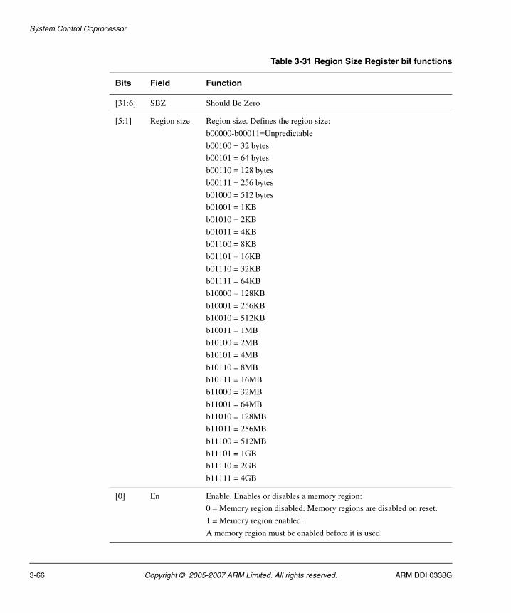
System Control Coprocessor
Table 3-31 Region Size Register bit functions
Bits Field Function
[31:6] SBZ Should Be Zero
[5:1] Region size Region size. Defines the region size:
b00000-b00011=Unpredictable
b00100 = 32 bytes
b00101 = 64 bytes
b00110 = 128 bytes
b00111 = 256 bytes
b01000 = 512 bytes
b01001 = 1KB
b01010 = 2KB
b01011 = 4KB
b01100 = 8KB
b01101 = 16KB
b01110 = 32KB
b01111 = 64KB
b10000 = 128KB
b10001 = 256KB
b10010 = 512KB
b10011 = 1MB
b10100 = 2MB
b10101 = 4MB
b10110 = 8MB
b10111 = 16MB
b11000 = 32MB
b11001 = 64MB
b11010 = 128MB
b11011 = 256MB
b11100 = 512MB
b11101 = 1GB
b11110 = 2GB
b11111 = 4GB
[0] En Enable. Enables or disables a memory region:
0 = Memory region disabled. Memory regions are disabled on reset.
1 = Memory region enabled.
A memory region must be enabled before it is used.
3-66 Copyright © 2005-2007 ARM Limited. All rights reserved. ARM DDI 0338G
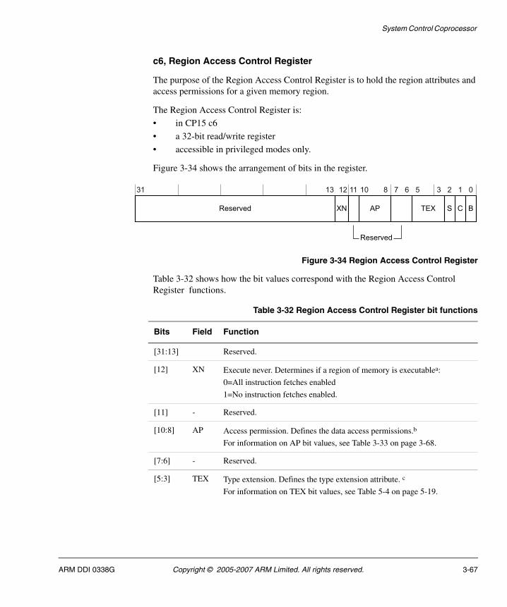
System Control Coprocessor
c6, Region Access Control Register
The purpose of the Region Access Control Register is to hold the region attributes and access permissions for a given memory region.
The Region Access Control Register is:
• in CP15 c6
• a 32-bit read/write register
• accessible in privileged modes only.
Figure 3-34 shows the arrangement of bits in the register.
Figure 3-34 Region Access Control Register
Table 3-32 shows how the bit values correspond with the Region Access Control Register functions.
Table 3-32 Region Access Control Register bit functions
Bits Field Function
[31:13] Reserved.
[12] XN Execute never. Determines if a region of memory is executablea:
0=All instruction fetches enabled
1=No instruction fetches enabled.
[11] - Reserved.
[10:8] AP Access permission. Defines the data access permissions.b
For information on AP bit values, see Table 3-33 on page 3-68.
[7:6] - Reserved.
[5:3] TEX Type extension. Defines the type extension attribute. c
For information on TEX bit values, see Table 5-4 on page 5-19.
ARM DDI 0338G Copyright © 2005-2007 ARM Limited. All rights reserved. 3-67
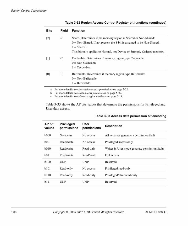
System Control Coprocessor
Table 3-33 shows the AP bits values that determine the permissions for Privileged and User data access.
[2] S Share. Determines if the memory region is Shared or Non-Shared:
0 = Non-Shared. If not present the S bit is assumed to be Non-Shared.
1 = Shared.
This bit only applies to Normal, not Device or Strongly Ordered memory.
[1] C Cacheable. Determines if memory region type Cacheable:
0 = Non-Cacheable
1 = Cacheable.
[0] B Bufferable. Determines if memory region type Bufferable:
0 = Non-Bufferable
1 = Bufferable.
a. For more details, see Instruction access permissions on page 5-22.b. For more details, see Data access permissions on page 5-22.c. For more details, see Memory region attributes on page 5-19.
Table 3-33 Access data permission bit encoding
AP bit values
Privileged permissions
User permissions
Description
b000 No access No access All accesses generate a permission fault
b001 Read/write No access Privileged access only
b010 Read/write Read-only Writes in User mode generate permission faults
b011 Read/write Read/write Full access
b100 UNP UNP Reserved
b101 Read-only No access Privileged read-only
b110 Read-only Read-only Privileged/User read-only
b111 UNP UNP Reserved
Table 3-32 Region Access Control Register bit functions (continued)
Bits Field Function
3-68 Copyright © 2005-2007 ARM Limited. All rights reserved. ARM DDI 0338G
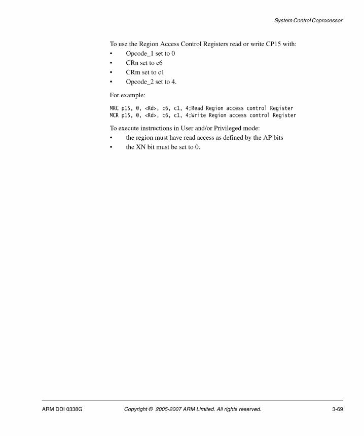
System Control Coprocessor
To use the Region Access Control Registers read or write CP15 with:
• Opcode_1 set to 0
• CRn set to c6
• CRm set to c1
• Opcode_2 set to 4.
For example:
MRC p15, 0, <Rd>, c6, c1, 4;Read Region access control RegisterMCR p15, 0, <Rd>, c6, c1, 4;Write Region access control Register
To execute instructions in User and/or Privileged mode:
• the region must have read access as defined by the AP bits
• the XN bit must be set to 0.
ARM DDI 0338G Copyright © 2005-2007 ARM Limited. All rights reserved. 3-69
System Control Coprocessor
c6, Memory Region Number Register
The memory region registers are multiple registers with one register for each memory region implemented. The value contained in the Memory Region Number Register determines which of the multiple registers is accessed.
The Memory Region Number Register is:
• in CP15 c6
• a 32-bit read/write register
• accessible in privileged modes only.
Figure 3-35 shows the arrangement of bits in the register.
Figure 3-35 Memory Region Number Register format
Table 3-34 shows how the bit values correspond with the Memory Region Number Register bits.
To use the Memory Region Number Registers read or write CP15 with:
• Opcode_1 set to 0
• CRn set to c6
• CRm set to c1
• Opcode_2 set to 0.
For example:
MRC p15, 0, <Rd>, c6, c2, 0 ;Read Memory Region Number RegisterMCR p15, 0, <Rd>, c6, c2, 0 ;Write Memory Region Number Register
Writing this register with a value of greater than or equal to the number of regions from the MPU Type Register, along with associated register bank accesses, are Unpredictable.
Table 3-34 Memory Region Number Register bit functions
Bits Field Function
[31:4] - Reserved.
[3:0] Region Defines the group of registers to be accessed. The number of regions supported is defined by the MPU Type Register in the range b0000 - b1111.
3-70 Copyright © 2005-2007 ARM Limited. All rights reserved. ARM DDI 0338G
System Control Coprocessor
3.2.18 c7, Cache Operations Register
The purpose of the Cache Operations Register is to:
• control these operations:
— clean and invalidate instruction and data caches, including range operations
— prefetch instruction cache line
— flush prefetch buffer
— flush branch target address cache
— drain write buffer
• implement the Data Memory Barrier (DMB) function
• implement the Wait For Interrupt clock control function.
Note Cache operations also depend on:
• the C, W, I and RR bits, see c1, Control Register on page 3-47.
• the RA and RV bits, see c1, Auxiliary Control Register on page 3-52.
The Cache Operations Register consists of one 32-bit register that performs 28 functions. Figure 3-36 on page 3-72 shows the arrangement of the 19 functions in this group that operate with the MCR and MRC instructions.
ARM DDI 0338G Copyright © 2005-2007 ARM Limited. All rights reserved. 3-71
System Control Coprocessor
Figure 3-36 Cache operations registers
Note • Writing the Cache Operations Registers with a combination of CRm and
Opcode_2 not listed in c7, Cache Operations Register on page 3-71 gives Unpredictable results.
• In the ARM1156T2-S processor, reading from write-only Cache Operations Registers, causes an Undefined instruction trap.
• If Opcode_1 = 0, these instructions are applied to the level one cache system. All other Opcode_1 values are reserved.
Privileged only
SBZ
Read-only Read/write
Should Be Zero
ADR
Index
using Address
Using Set/Way
Write only
Invalidate Both Caches
Invalidate Data Cache Line (using Address)
Invalidate Entire Data Cache
Wait For Interruptc7
Flush Prefetch Buffer
c6
c7
c0 4
c5 0 Invalidate Entire Instruction Cache
1
2 Invalidate Instruction Cache Line (using Set and Way)
4
0
1
2
0
c10
c13
c14
0
1
2
4
5
6
1
0
1
2
Cache Dirty Status Register
Clean Entire Data Cache
Clean Data Cache Line (using Address)
Clean Data Cache Line (using Set and Way)
Drain Write Buffer
Data Memory Barrier
Clean and Invalidate Entire Data Cache
Prefetch Instruction Cache Line
SBZ
SBZ
ADR
Index
SBZ
SBZ
ADR
Index
SBZ
SBZ
ADR
Index
SBZ
SBZ
ADR
SBZ
Clean and Invalidate Data Cache Line (using Address)ADR
Clean and Invalidate Data Cache Line (using Set and Way)Index
0
Opcode_2CRmCP15 Opcode_1
Invalidate Instruction Cache Line (using Address)
Invalidate Data Cache Line (using Set and Way)
3-72 Copyright © 2005-2007 ARM Limited. All rights reserved. ARM DDI 0338G
System Control Coprocessor
• All CP15 c7 operations can only be executed in a privileged mode of operation, except Drain Write Buffer, Flush Prefetch Buffer, and Data Memory Barrier. These can be operated in User mode. Attempting to execute a privileged instruction in User mode results in the Undefined instruction trap being taken.
There are three ways to use the Cache Operations Register:
• For the Cache Dirty Status Register, read the Cache Operations Register with the MRC instruction.
• For range operations use the MCRR instruction with the value of CRm to select the required operation.
• For all other operations use the MCR instruction to write to the Cache Operations Register with the combination of CRm and Opcode_2 to select the required operation
Depending on the operation you require set <Rd> for MCR instructions or <Rd> and <Rn> for MCRR instructions to:
— Physical address
— Way and Set
— Should Be Zero.
Invalidate, Clean, and Prefetch operations
The purposes of the invalidate, clean, and prefetch operations that the Cache Operations Register provide are to:
• Invalidate part or all of the data or instruction caches
• Clean part or all of the data cache
• Clean and Invalidate part or all of the data cache
• Prefetch code into the instruction cache.
The terms used to describe the invalidate, clean, and prefetch operations are as defined in the Caches and Write Buffers chapter of the ARM Architecture Reference Manual.
When it controls invalidate, clean, and prefetch operations the Cache Operations Register appears as a 32-bit register. There are three possible formats for the data in the register that depend on the specific operation:
• Way and Set format
• Physical Address
• SBZ.
ARM DDI 0338G Copyright © 2005-2007 ARM Limited. All rights reserved. 3-73
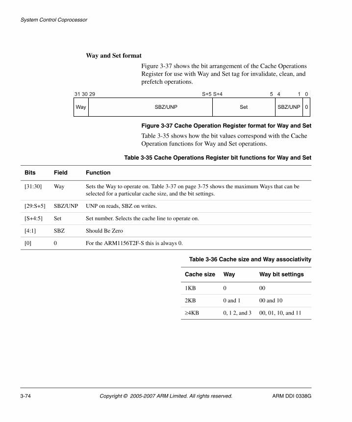
System Control Coprocessor
Way and Set format
Figure 3-37 shows the bit arrangement of the Cache Operations Register for use with Way and Set tag for invalidate, clean, and prefetch operations.
Figure 3-37 Cache Operation Register format for Way and Set
Table 3-35 shows how the bit values correspond with the Cache Operation functions for Way and Set operations.
Table 3-35 Cache Operations Register bit functions for Way and Set
Bits Field Function
[31:30] Way Sets the Way to operate on. Table 3-37 on page 3-75 shows the maximum Ways that can be selected for a particular cache size, and the bit settings.
[29:S+5] SBZ/UNP UNP on reads, SBZ on writes.
[S+4:5] Set Set number. Selects the cache line to operate on.
[4:1] SBZ Should Be Zero
[0] 0 For the ARM1156T2F-S this is always 0.
Table 3-36 Cache size and Way associativity
Cache size Way Way bit settings
1KB 0 00
2KB 0 and 1 00 and 10
≥4KB 0, 1 2, and 3 00, 01, 10, and 11
3-74 Copyright © 2005-2007 ARM Limited. All rights reserved. ARM DDI 0338G
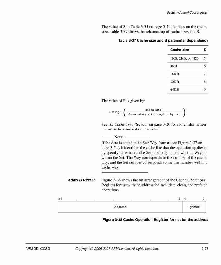
System Control Coprocessor
The value of S in Table 3-35 on page 3-74 depends on the cache size. Table 3-37 shows the relationship of cache sizes and S.
The value of S is given by:
See c0, Cache Type Register on page 3-20 for more information on instruction and data cache size.
Note If the data is stated to be Set/ Way format (see Figure 3-37 on
page 3-74), it identifies the cache line that the operation applies to by specifying which cache Set it belongs to and what its Way is within the Set. The Way corresponds to the number of the cache way, and the Set number corresponds to the line number within a cache way.
Address format Figure 3-38 shows the bit arrangement of the Cache Operations Register for use with the address for invalidate, clean, and prefetch operations.
Figure 3-38 Cache Operation Register format for the address
Table 3-37 Cache size and S parameter dependency
Cache size S
1KB, 2KB, or 4KB 5
8KB 6
16KB 7
32KB 8
64KB 9
Associativity x line length in bytes
cache sizeS = log
2 ( )
Address
31 5 4 0
Ignored
ARM DDI 0338G Copyright © 2005-2007 ARM Limited. All rights reserved. 3-75
System Control Coprocessor
Table 3-38 shows how the bit values correspond with the Cache Operation functions for Way and Set tag operations.
Note If the data is stated to be an address, it does not have to be cache
line aligned. This address is looked up in the cache for the particular operation. Invalidation and cleaning operations have no effect if they miss in the cache.
You can perform invalidate, clean, and prefetch operations on:
• single cache lines
• entire caches
• address ranges in cache, but not on prefetch address ranges.
Note • Clean, invalidate, and clean and invalidate operations apply
regardless of the lock applied to entries.
• A small number of CP15 c7 operations can be executed by code while in User mode. Attempting to execute a privileged operation in User mode using CP15 c7 results in an Undefined instruction trap being taken.
To determine if the cache is dirty use the Cache Dirty Status operation, see c7, Cache Dirty Status Register on page 3-84.
Single cache lines
There are two ways to perform invalidate or clean operations on cache lines:
• By use of Set/Way format
• By use of address.
Table 3-38 Cache Operations Register bit functions for address
Bits Field Function
[31:5] Address Holds the physical address of the cache line for the invalidate, clean, or prefetch operation.
[4:0] Ignored -
3-76 Copyright © 2005-2007 ARM Limited. All rights reserved. ARM DDI 0338G
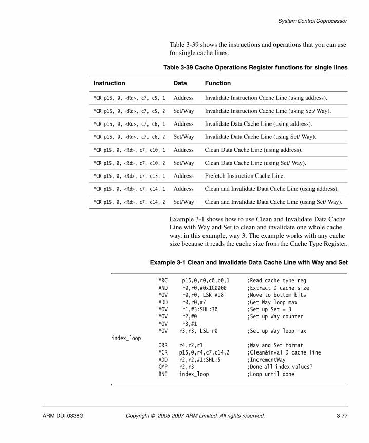
System Control Coprocessor
Table 3-39 shows the instructions and operations that you can use for single cache lines.
Example 3-1 shows how to use Clean and Invalidate Data Cache Line with Way and Set to clean and invalidate one whole cache way, in this example, way 3. The example works with any cache size because it reads the cache size from the Cache Type Register.
Example 3-1 Clean and Invalidate Data Cache Line with Way and Set
MRC p15,0,r0,c0,c0,1 ;Read cache type reg AND r0,r0,#0x1C0000 ;Extract D cache size MOV r0,r0, LSR #18 ;Move to bottom bits ADD r0,r0,#7 ;Get Way loop max MOV r1,#3:SHL:30 ;Set up Set = 3 MOV r2,#0 ;Set up Way counter MOV r3,#1 MOV r3,r3, LSL r0 ;Set up Way loop max
index_loopORR r4,r2,r1 ;Way and Set format MCR p15,0,r4,c7,c14,2 ;Clean&inval D cache line ADD r2,r2,#1:SHL:5 ;IncrementWayCMP r2,r3 ;Done all index values? BNE index_loop ;Loop until done
Table 3-39 Cache Operations Register functions for single lines
Instruction Data Function
MCR p15, 0, <Rd>, c7, c5, 1 Address Invalidate Instruction Cache Line (using address).
MCR p15, 0, <Rd>, c7, c5, 2 Set/Way Invalidate Instruction Cache Line (using Set/ Way).
MCR p15, 0, <Rd>, c7, c6, 1 Address Invalidate Data Cache Line (using address).
MCR p15, 0, <Rd>, c7, c6, 2 Set/Way Invalidate Data Cache Line (using Set/ Way).
MCR p15, 0, <Rd>, c7, c10, 1 Address Clean Data Cache Line (using address).
MCR p15, 0, <Rd>, c7, c10, 2 Set/Way Clean Data Cache Line (using Set/ Way).
MCR p15, 0, <Rd>, c7, c13, 1 Address Prefetch Instruction Cache Line.
MCR p15, 0, <Rd>, c7, c14, 1 Address Clean and Invalidate Data Cache Line (using address).
MCR p15, 0, <Rd>, c7, c14, 2 Set/Way Clean and Invalidate Data Cache Line (using Set/ Way).
ARM DDI 0338G Copyright © 2005-2007 ARM Limited. All rights reserved. 3-77
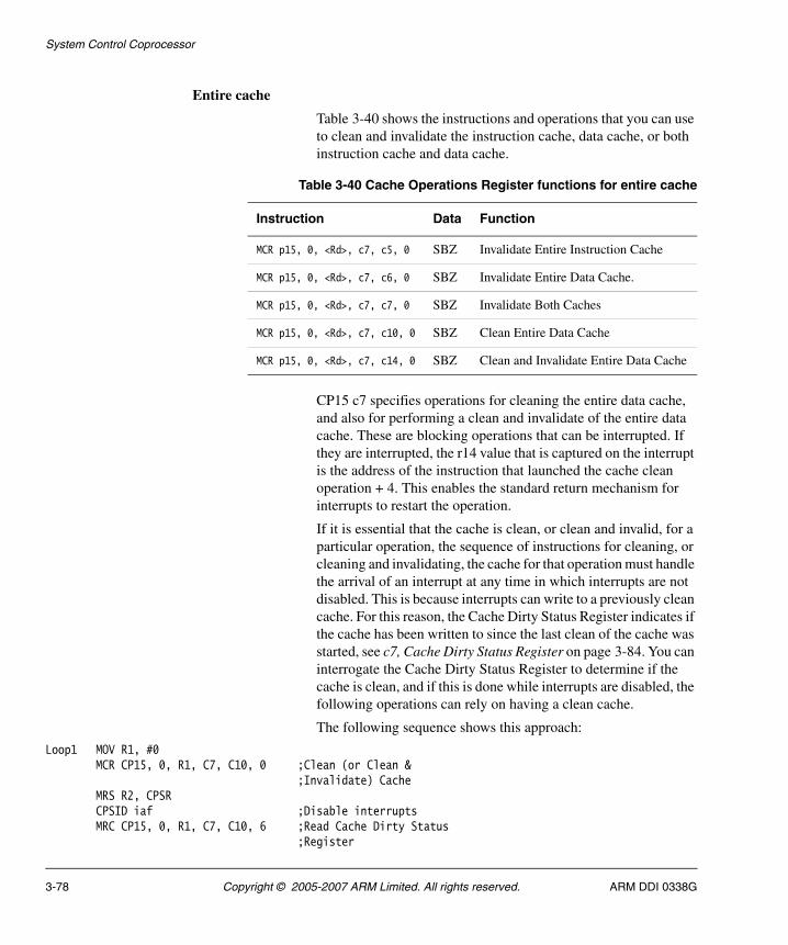
System Control Coprocessor
Entire cache
Table 3-40 shows the instructions and operations that you can use to clean and invalidate the instruction cache, data cache, or both instruction cache and data cache.
CP15 c7 specifies operations for cleaning the entire data cache, and also for performing a clean and invalidate of the entire data cache. These are blocking operations that can be interrupted. If they are interrupted, the r14 value that is captured on the interrupt is the address of the instruction that launched the cache clean operation + 4. This enables the standard return mechanism for interrupts to restart the operation.
If it is essential that the cache is clean, or clean and invalid, for a particular operation, the sequence of instructions for cleaning, or cleaning and invalidating, the cache for that operation must handle the arrival of an interrupt at any time in which interrupts are not disabled. This is because interrupts can write to a previously clean cache. For this reason, the Cache Dirty Status Register indicates if the cache has been written to since the last clean of the cache was started, see c7, Cache Dirty Status Register on page 3-84. You can interrogate the Cache Dirty Status Register to determine if the cache is clean, and if this is done while interrupts are disabled, the following operations can rely on having a clean cache.
The following sequence shows this approach:
Loop1 MOV R1, #0MCR CP15, 0, R1, C7, C10, 0 ;Clean (or Clean &
;Invalidate) CacheMRS R2, CPSRCPSID iaf ;Disable interruptsMRC CP15, 0, R1, C7, C10, 6 ;Read Cache Dirty Status
;Register
Table 3-40 Cache Operations Register functions for entire cache
Instruction Data Function
MCR p15, 0, <Rd>, c7, c5, 0 SBZ Invalidate Entire Instruction Cache
MCR p15, 0, <Rd>, c7, c6, 0 SBZ Invalidate Entire Data Cache.
MCR p15, 0, <Rd>, c7, c7, 0 SBZ Invalidate Both Caches
MCR p15, 0, <Rd>, c7, c10, 0 SBZ Clean Entire Data Cache
MCR p15, 0, <Rd>, c7, c14, 0 SBZ Clean and Invalidate Entire Data Cache
3-78 Copyright © 2005-2007 ARM Limited. All rights reserved. ARM DDI 0338G
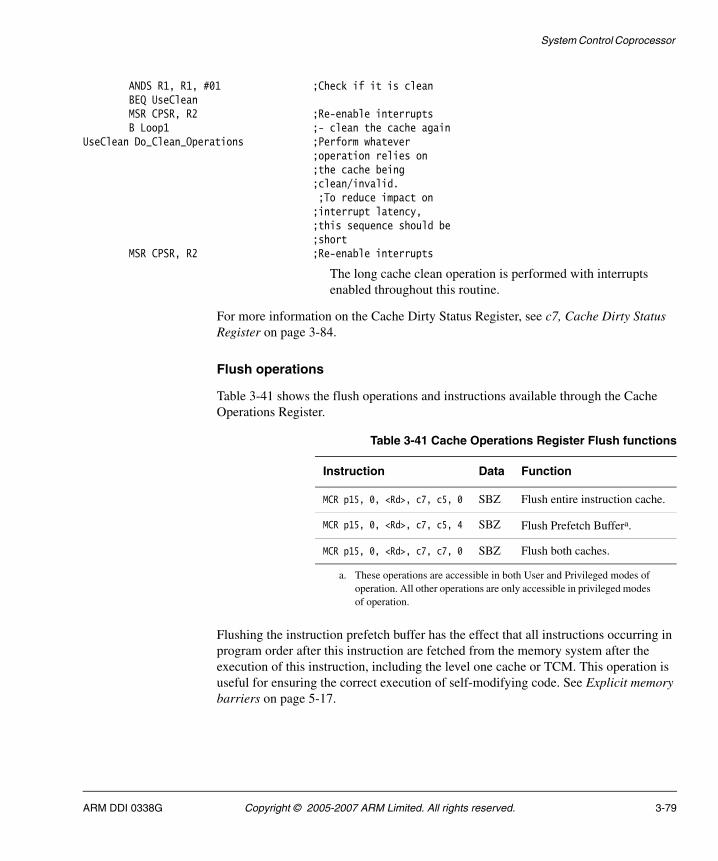
System Control Coprocessor
ANDS R1, R1, #01 ;Check if it is cleanBEQ UseCleanMSR CPSR, R2 ;Re-enable interruptsB Loop1 ;- clean the cache again
UseClean Do_Clean_Operations ;Perform whatever;operation relies on;the cache being;clean/invalid.
;To reduce impact on;interrupt latency,;this sequence should be;short
MSR CPSR, R2 ;Re-enable interrupts
The long cache clean operation is performed with interrupts enabled throughout this routine.
For more information on the Cache Dirty Status Register, see c7, Cache Dirty Status Register on page 3-84.
Flush operations
Table 3-41 shows the flush operations and instructions available through the Cache Operations Register.
Flushing the instruction prefetch buffer has the effect that all instructions occurring in program order after this instruction are fetched from the memory system after the execution of this instruction, including the level one cache or TCM. This operation is useful for ensuring the correct execution of self-modifying code. See Explicit memory barriers on page 5-17.
Table 3-41 Cache Operations Register Flush functions
Instruction Data Function
MCR p15, 0, <Rd>, c7, c5, 0 SBZ Flush entire instruction cache.
MCR p15, 0, <Rd>, c7, c5, 4 SBZ Flush Prefetch Buffera.
a. These operations are accessible in both User and Privileged modes of operation. All other operations are only accessible in privileged modes of operation.
MCR p15, 0, <Rd>, c7, c7, 0 SBZ Flush both caches.
ARM DDI 0338G Copyright © 2005-2007 ARM Limited. All rights reserved. 3-79
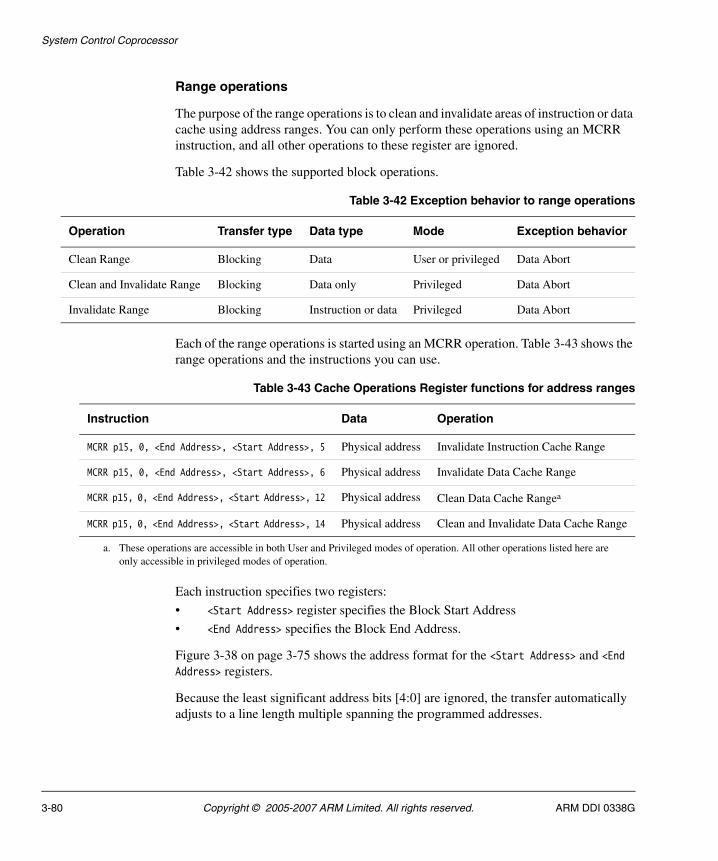
System Control Coprocessor
Range operations
The purpose of the range operations is to clean and invalidate areas of instruction or data cache using address ranges. You can only perform these operations using an MCRR instruction, and all other operations to these register are ignored.
Table 3-42 shows the supported block operations.
Each of the range operations is started using an MCRR operation. Table 3-43 shows the range operations and the instructions you can use.
Each instruction specifies two registers:
• <Start Address> register specifies the Block Start Address
• <End Address> specifies the Block End Address.
Figure 3-38 on page 3-75 shows the address format for the <Start Address> and <End Address> registers.
Because the least significant address bits [4:0] are ignored, the transfer automatically adjusts to a line length multiple spanning the programmed addresses.
Table 3-42 Exception behavior to range operations
Operation Transfer type Data type Mode Exception behavior
Clean Range Blocking Data User or privileged Data Abort
Clean and Invalidate Range Blocking Data only Privileged Data Abort
Invalidate Range Blocking Instruction or data Privileged Data Abort
Table 3-43 Cache Operations Register functions for address ranges
Instruction Data Operation
MCRR p15, 0, <End Address>, <Start Address>, 5 Physical address Invalidate Instruction Cache Range
MCRR p15, 0, <End Address>, <Start Address>, 6 Physical address Invalidate Data Cache Range
MCRR p15, 0, <End Address>, <Start Address>, 12 Physical address Clean Data Cache Rangea
MCRR p15, 0, <End Address>, <Start Address>, 14 Physical address Clean and Invalidate Data Cache Range
a. These operations are accessible in both User and Privileged modes of operation. All other operations listed here are only accessible in privileged modes of operation.
3-80 Copyright © 2005-2007 ARM Limited. All rights reserved. ARM DDI 0338G
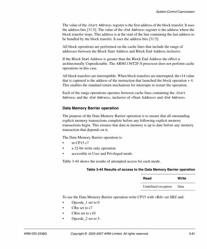
System Control Coprocessor
The value of the <Start Address> register is the first address of the block transfer. It uses the address bits [31:5]. The value of the <End Address> register is the address where the block transfer stops. This address is at the start of the line containing the last address to be handled by the block transfer. It uses the address bits [31:5].
All block operations are performed on the cache lines that include the range of addresses between the Block Start Address and Block End Address inclusive.
If the Block Start Address is greater than the Block End Address the effect is architecturally Unpredictable. The ARM1156T2F-S processor does not perform cache operations in this case.
All block transfers are interruptible. When block transfers are interrupted, the r14 value that is captured is the address of the instruction that launched the block operation + 4. This enables the standard return mechanism for interrupts to restart the operation.
Each of the range operations operates between cache lines containing the <Start Address> and the <End Address>, inclusive of <Start Address> and <End Address>.
Data Memory Barrier operation
The purpose of the Data Memory Barrier operation is to ensure that all outstanding explicit memory transactions complete before any following explicit memory transactions begin. This ensures that data in memory is up to date before any memory transaction that depends on it.
The Data Memory Barrier operation is:
• in CP15 c7
• a 32-bit write only operation
• accessible in User and Privileged mode.
Table 3-44 shows the results of attempted access for each mode.
To use the Data Memory Barrier operation write CP15 with <Rd> set SBZ and:
• Opcode_1 set to 0
• CRn set to c7
• CRm set to c10
• Opcode_2 set to 5.
Table 3-44 Results of access to the Data Memory Barrier operation
Read Write
Undefined exception Data
ARM DDI 0338G Copyright © 2005-2007 ARM Limited. All rights reserved. 3-81
System Control Coprocessor
For example:
MCR p15, 0, <Rd>, c7, c10, 5; Write Data Memory Barrier Register.
For more information, see Explicit memory barriers on page 5-17.
Drain Write Buffer operation
The purpose of the Drain Write Buffer operation is to ensure that all explicit memory transactions that occur in program order before this instruction are completed.
The Drain Write Buffer operation is:
• in CP15 c7
• 32-bit write only
• accessible in both User and Privileged modes.
To use the Drain Write Buffer operation write CP15 with <Rd> set SBZ and:
• Opcode_1 set to 0
• CRn set to c7
• CRm set to c10
• Opcode_2 set to 4.
For example:
MCR p15, 0, <Rd>, c7, c10, 4; Write Drain Write Buffer.
For more information, see Explicit memory barriers on page 5-17.
Note The W bit that normally enables the Write Buffer is not implemented in the ARM1156T2-S processor, see c1, Control Register on page 3-47.
This instruction acts as an explicit memory barrier. This instruction completes when all explicit memory transactions occurring in program order before this instruction are completed. No instructions occurring in program order after this instruction are executed until this instruction completes. Therefore, no explicit memory transactions occurring in program order after this instruction are started until this instruction completes. See Explicit memory barriers on page 5-17.
It can be used instead of Strongly Ordered memory when the timing of specific stores to the memory system has to be controlled. For example, when a store to an interrupt acknowledge location must be completed before interrupts are enabled.
Drain Write Buffer can be executed in both privileged and User modes of operation.
3-82 Copyright © 2005-2007 ARM Limited. All rights reserved. ARM DDI 0338G
System Control Coprocessor
Wait For Interrupt operation
The purpose of the Wait For Interrupt operation is to put the processor in to a low power state.
The Wait For Interrupt Register is:
• in CP15 c7
• 32-bit write only
• accessible only in privileged modes.
To use the Wait For Interrupt operation write CP15 with <Rd> set SBZ and:
• Opcode_1 set to 0
• CRn set to c7
• CRm set to c0
• Opcode_2 set to 4.
For example:
MCR p15, 0, <Rd>, c7, c0, 4; Wait For Interrupt.
This puts the processor into a low-power state and stops it executing more instructions until an interrupt, or debug request occurs, regardless of whether the interrupts are disabled by the masks in the CPSR. When an interrupt does occur, the MCR instruction completes and the IRQ or FIQ handler is entered as normal. The return link in r14_irq or r14_fiq contains the address of the MCR instruction plus 8, so that the normal instruction used for interrupt return (SUBS PC,R14,#4) returns to the instruction following the MCR.
ARM DDI 0338G Copyright © 2005-2007 ARM Limited. All rights reserved. 3-83
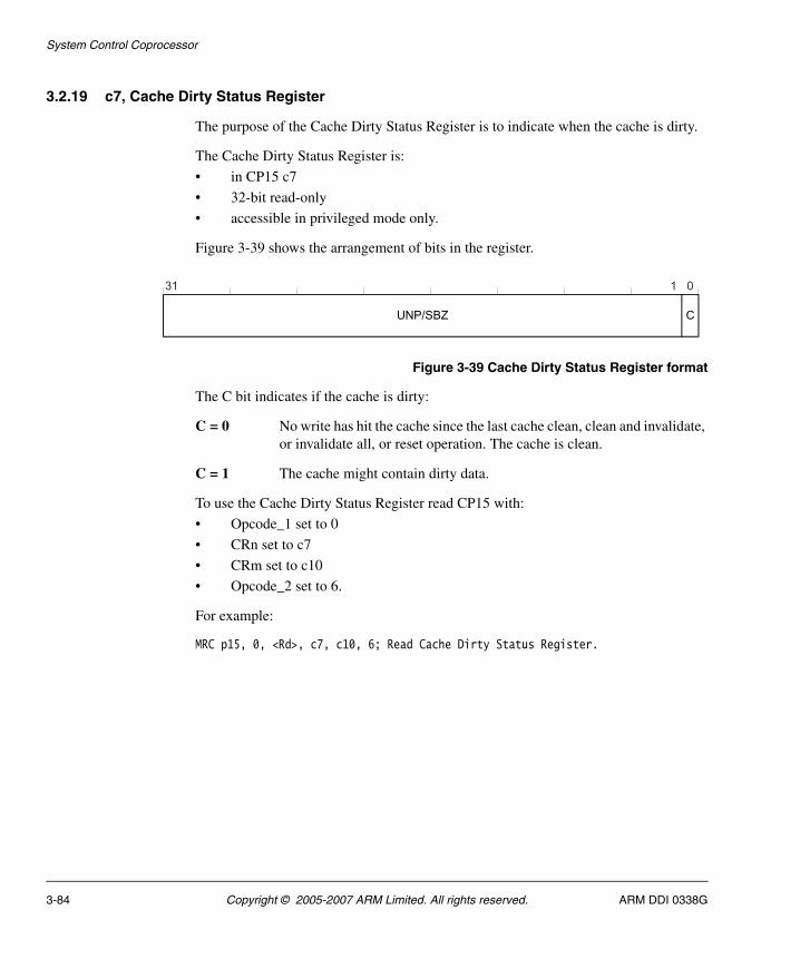
System Control Coprocessor
3.2.19 c7, Cache Dirty Status Register
The purpose of the Cache Dirty Status Register is to indicate when the cache is dirty.
The Cache Dirty Status Register is:
• in CP15 c7
• 32-bit read-only
• accessible in privileged mode only.
Figure 3-39 shows the arrangement of bits in the register.
Figure 3-39 Cache Dirty Status Register format
The C bit indicates if the cache is dirty:
C = 0 No write has hit the cache since the last cache clean, clean and invalidate, or invalidate all, or reset operation. The cache is clean.
C = 1 The cache might contain dirty data.
To use the Cache Dirty Status Register read CP15 with:
• Opcode_1 set to 0
• CRn set to c7
• CRm set to c10
• Opcode_2 set to 6.
For example:
MRC p15, 0, <Rd>, c7, c10, 6; Read Cache Dirty Status Register.
CUNP/SBZ
31 1 0
3-84 Copyright © 2005-2007 ARM Limited. All rights reserved. ARM DDI 0338G
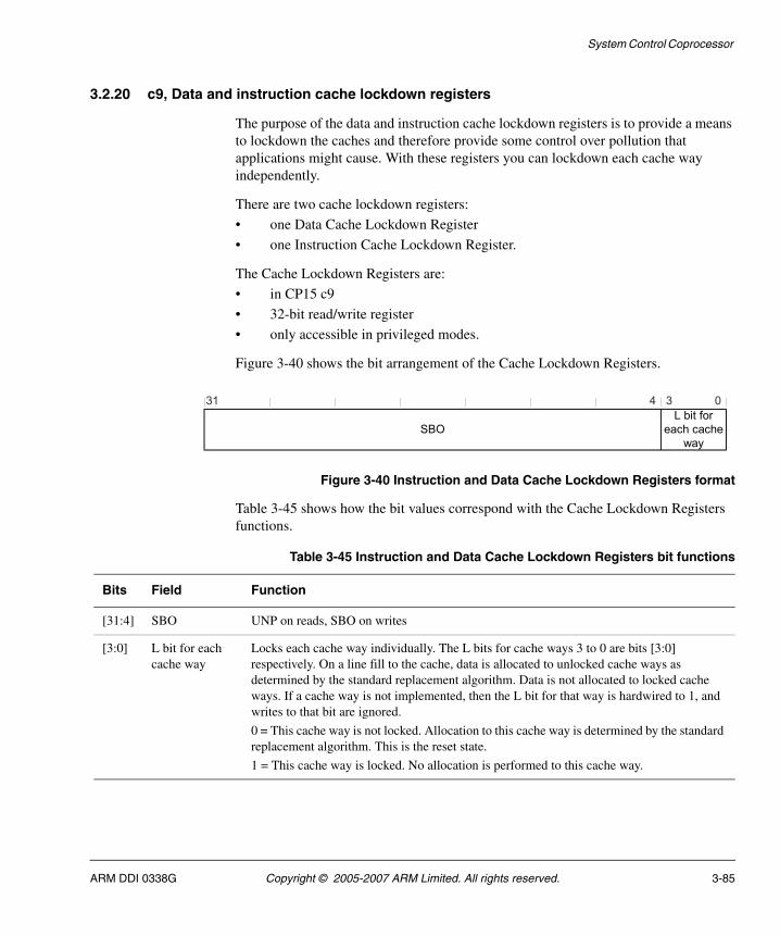
System Control Coprocessor
3.2.20 c9, Data and instruction cache lockdown registers
The purpose of the data and instruction cache lockdown registers is to provide a means to lockdown the caches and therefore provide some control over pollution that applications might cause. With these registers you can lockdown each cache way independently.
There are two cache lockdown registers:
• one Data Cache Lockdown Register
• one Instruction Cache Lockdown Register.
The Cache Lockdown Registers are:
• in CP15 c9
• 32-bit read/write register
• only accessible in privileged modes.
Figure 3-40 shows the bit arrangement of the Cache Lockdown Registers.
Figure 3-40 Instruction and Data Cache Lockdown Registers format
Table 3-45 shows how the bit values correspond with the Cache Lockdown Registers functions.
SBO
31 4 3 0
L bit for
each cache
way
Table 3-45 Instruction and Data Cache Lockdown Registers bit functions
Bits Field Function
[31:4] SBO UNP on reads, SBO on writes
[3:0] L bit for each cache way
Locks each cache way individually. The L bits for cache ways 3 to 0 are bits [3:0] respectively. On a line fill to the cache, data is allocated to unlocked cache ways as determined by the standard replacement algorithm. Data is not allocated to locked cache ways. If a cache way is not implemented, then the L bit for that way is hardwired to 1, and writes to that bit are ignored.
0 = This cache way is not locked. Allocation to this cache way is determined by the standard replacement algorithm. This is the reset state.
1 = This cache way is locked. No allocation is performed to this cache way.
ARM DDI 0338G Copyright © 2005-2007 ARM Limited. All rights reserved. 3-85
System Control Coprocessor
The data Cache Lockdown Register only supports the Format C method of lockdown. This method is a cache way based scheme that gives a traditional lockdown function to lock critical ways in the cache. For more information on cache lockdown methods, see the ARM Architecture Reference Manual.
A locking bit for each cache way determines if the normal cache allocation mechanisms, Random or Round-Robin, can access that cache way. For more information on the RR bit that controls the selection of Random or Round-Robin cache policy, see c1, Control Register on page 3-47.
ARM1156T2-S processors have 4, 2 or 1 way set-associativity cache. With all ways locked, the ARM1156T2-S processor behaves as if way 0 is locked and all other ways are unlocked.
To use the Instruction and Data Cache Lockdown Registers read or write CP15 with:
• Opcode_1 set to 0
• CRn set to c9
• CRm set to c0
• Opcode_2 set to:
— 0, for data cache
— 1, for instruction cache.
For example:
MRC p15, 0, <Rd>, c9, c0, 0 ;Read Data Cache Lockdown RegisterMCR p15, 0, <Rd>, c9, c0, 0 ;Write Data Cache Lockdown RegisterMRC p15, 0, <Rd>, c9, c0, 1 ;Read Instruction Cache Lockdown RegisterMCR p15, 0, <Rd>, c9, c0, 1 ;Write Instruction Cache Lockdown Register
The system must only change a Cache Lockdown Register when it is certain that all outstanding accesses that might cause a cache line fill are complete. For this reason, the processor must execute a Drain Write Buffer instruction before the Cache Lockdown Register changes, see Drain Write Buffer operation on page 3-82.
The following procedure for lock down into a data or instruction cache way i, with N cache ways, using Format C, ensures that only the target cache way i is locked down.
This is the architecturally defined method for locking data into caches:
1. Ensure that no processor exceptions can occur during the execution of this procedure, by disabling interrupts. If this is not possible, all code and data used by any exception handlers that can be called must meet the conditions specified in step 2.
3-86 Copyright © 2005-2007 ARM Limited. All rights reserved. ARM DDI 0338G
System Control Coprocessor
2. Ensure that all data used by the following code, apart from the data that is to be locked down, is either:
• in an uncacheable area of memory, including the TCM
• in an already locked cache way.
3. Ensure that the data to be locked down is in a Cacheable area of memory.
4. Ensure that the data to be locked down is not already in the cache, using cache Clean and/or Invalidate instructions as appropriate. See Invalidate, Clean, and Prefetch operations on page 3-73.
5. Enable allocation to the target cache way by writing to CP15 c9, with the CRm field set to 0, setting L equal to 0 for bit i and L equal to 1 for all other ways.
6. Ensure that the memory cache line is loaded into the cache by using an LDR instruction to load a word from the memory cache line, for each of the cache lines to be locked down in cache way i.
If an instruction cache is to be locked down, use the prefetch instruction cache line operation to fetch the memory cache line into the cache. Write CP15 with CRn set to c7, CRm set to c13, and opcode_2 set to 1.
7. Write to CP15 c9, CRm set to c0, setting L to 1 for bit i and restore all the other bits to the values they had before this routine was started.
ARM DDI 0338G Copyright © 2005-2007 ARM Limited. All rights reserved. 3-87
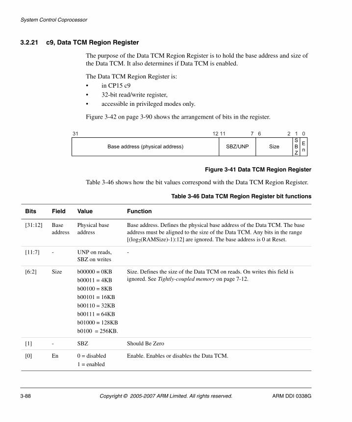
System Control Coprocessor
3.2.21 c9, Data TCM Region Register
The purpose of the Data TCM Region Register is to hold the base address and size of the Data TCM. It also determines if Data TCM is enabled.
The Data TCM Region Register is:
• in CP15 c9
• 32-bit read/write register,
• accessible in privileged modes only.
Figure 3-42 on page 3-90 shows the arrangement of bits in the register.
Figure 3-41 Data TCM Region Register
Table 3-46 shows how the bit values correspond with the Data TCM Region Register.
E
nBase address (physical address)
31 12 11 7 6 2 1 0
SBZ/UNP Size
S
B
Z
Table 3-46 Data TCM Region Register bit functions
Bits Field Value Function
[31:12] Base address
Physical base address
Base address. Defines the physical base address of the Data TCM. The base address must be aligned to the size of the Data TCM. Any bits in the range [(log2(RAMSize)-1):12] are ignored. The base address is 0 at Reset.
[11:7] - UNP on reads, SBZ on writes
-
[6:2] Size b00000 = 0KB
b00011 = 4KB
b00100 = 8KB
b00101 = 16KB
b00110 = 32KB
b00111 = 64KB
b01000 = 128KB
b0100 = 256KB.
Size. Defines the size of the Data TCM on reads. On writes this field is ignored. See Tightly-coupled memory on page 7-12.
[1] - SBZ Should Be Zero
[0] En 0 = disabled
1 = enabled
Enable. Enables or disables the Data TCM.
3-88 Copyright © 2005-2007 ARM Limited. All rights reserved. ARM DDI 0338G
System Control Coprocessor
To use the Data TCM Region Register read or write CP15 with:
• Opcode_1 set to 0
• CRn set to c9
• CRm set to c1
• Opcode_2 set to 0.
For example:
MRC p15, 0, <Rd>, c9, c1, 0; Read Data TCM Region RegisterMCR p15, 0, <Rd>, c9, c1, 0; Write Data TCM Region Register
ARM DDI 0338G Copyright © 2005-2007 ARM Limited. All rights reserved. 3-89
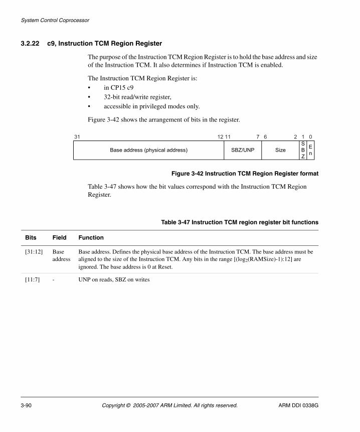
System Control Coprocessor
3.2.22 c9, Instruction TCM Region Register
The purpose of the Instruction TCM Region Register is to hold the base address and size of the Instruction TCM. It also determines if Instruction TCM is enabled.
The Instruction TCM Region Register is:
• in CP15 c9
• 32-bit read/write register,
• accessible in privileged modes only.
Figure 3-42 shows the arrangement of bits in the register.
Figure 3-42 Instruction TCM Region Register format
Table 3-47 shows how the bit values correspond with the Instruction TCM Region Register.
E
nBase address (physical address)
31 12 11 7 6 2 1 0
SBZ/UNP Size
S
B
Z
Table 3-47 Instruction TCM region register bit functions
Bits Field Function
[31:12] Base address
Base address. Defines the physical base address of the Instruction TCM. The base address must be aligned to the size of the Instruction TCM. Any bits in the range [(log2(RAMSize)-1):12] are ignored. The base address is 0 at Reset.
[11:7] - UNP on reads, SBZ on writes
3-90 Copyright © 2005-2007 ARM Limited. All rights reserved. ARM DDI 0338G
System Control Coprocessor
The value of the En bit at Reset depends on the INITRAM signal:
• INITRAM LOW sets En to 0
• INITRAM HIGH sets En to 1
When INITRAM is HIGH this enables the Instruction TCM directly from reset, with a Base address of 0x00000000. When the processor comes out of reset, it executes the instructions in the Instruction TCM instead of fetching instructions from external memory.
To use the Instruction TCM Region Register read or write CP15 with:
• Opcode_1 set to 0
• CRn set to c9
• CRm set to c1
• Opcode_2 set to 1.
For example:
MRC p15, 0, <Rd>, c9, c1, 1; Read Instruction TCM Region RegisterMCR p15, 0, <Rd>, c9, c1, 1; Write Instruction TCM Region Register
[6:2] Size Size. Defines the size of the Instruction TCM on reads.
On writes this field is ignored.
b00000 = 0KB
b00011 = 4KB
b00100 = 8KB
b00101 = 16KB
b00110 = 32KB
b00111 = 64KB
b01000 = 128KB
b01001 = 256KB.
For more information, see Tightly-coupled memory on page 7-12.
[1] SBZ Should Be Zero
[0] En Enable. Enables or disables the Instruction TCM.
0 = disabled
1 = enabled.
Table 3-47 Instruction TCM region register bit functions (continued)
Bits Field Function
ARM DDI 0338G Copyright © 2005-2007 ARM Limited. All rights reserved. 3-91
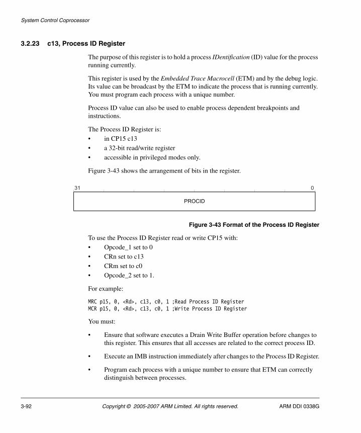
System Control Coprocessor
3.2.23 c13, Process ID Register
The purpose of this register is to hold a process IDentification (ID) value for the process running currently.
This register is used by the Embedded Trace Macrocell (ETM) and by the debug logic. Its value can be broadcast by the ETM to indicate the process that is running currently. You must program each process with a unique number.
Process ID value can also be used to enable process dependent breakpoints and instructions.
The Process ID Register is:
• in CP15 c13
• a 32-bit read/write register
• accessible in privileged modes only.
Figure 3-43 shows the arrangement of bits in the register.
Figure 3-43 Format of the Process ID Register
To use the Process ID Register read or write CP15 with:
• Opcode_1 set to 0
• CRn set to c13
• CRm set to c0
• Opcode_2 set to 1.
For example:
MRC p15, 0, <Rd>, c13, c0, 1 ;Read Process ID RegisterMCR p15, 0, <Rd>, c13, c0, 1 ;Write Process ID Register
You must:
• Ensure that software executes a Drain Write Buffer operation before changes to this register. This ensures that all accesses are related to the correct process ID.
• Execute an IMB instruction immediately after changes to the Process ID Register.
• Program each process with a unique number to ensure that ETM can correctly distinguish between processes.
PROCID
31 0
3-92 Copyright © 2005-2007 ARM Limited. All rights reserved. ARM DDI 0338G
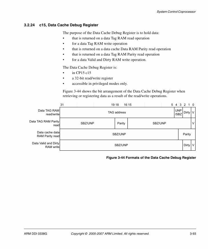
System Control Coprocessor
3.2.24 c15, Data Cache Debug Register
The purpose of the Data Cache Debug Register is to hold data:
• that is returned on a data Tag RAM read operation
• for a data Tag RAM write operation
• that is returned on a data cache Data RAM Parity read operation
• that is returned on a data Tag RAM Parity read operation
• for a data Valid and Dirty RAM write operation.
The Data Cache Debug Register is:
• in CP15 c15
• a 32-bit read/write register
• accessible in privileged modes only.
Figure 3-44 shows the bit arrangement of the Data Cache Debug Register when retrieving or registering data as a result of the read/write operations.
Figure 3-44 Formats of the Data Cache Debug Register
ARM DDI 0338G Copyright © 2005-2007 ARM Limited. All rights reserved. 3-93
System Control Coprocessor
Table 3-48 to shows how the bit values correspond with the Data Cache Debug Register functions as a result of Data Tag RAM read/write operation.
Table 3-49 shows how the bit values correspond with the Data Cache Debug Register functions as a result of Data Tag RAM parity read operation.
Table 3-50 shows how the bit values correspond with the Data Cache Debug Register functions as a result of a Data Cache Data RAM parity read operation.
Table 3-48 Data Cache Debug Register bit arrangement after a Data Tag RAMread/write operation
Bits Field Function
[31:5] Tag address Holds the Tag address for the cache way.
[4:3] SBZ/UNP Should Be Zero or Unpredictable.
[2:1] Dirty On a read holds the value of the Dirty bits from the data Tag RAM. On a write holds the value of the Dirty bits for the data Tag RAM.
[0] V On a read holds the value of the Valid bit from the data Tag RAM.
On a write holds the value of the Valid bit for the data Tag RAM.
Table 3-49 Data Cache Debug Register bit arrangement after a Data Tag RAMparity read operation
Bits Field Function
[31:19] SBZ/UNP Should Be Zero or Unpredictable
[18:16] Parity Holds the value of parity bits the Data Tag RAM
[15:1] SBZ/UNP Should Be Zero or Unpredictable
[0] V Holds the value of valid bit from the Data Tag RAM
Table 3-50 Data Cache Debug Register bit arrangement after a Data Cache DataRAM parity read operation
Bits Field Function
[31:4] SBZ/UNP Should Be Zero or Unpredictable
[3:0] Parity Holds the value of the parity bits from Data Cache Data RAM
3-94 Copyright © 2005-2007 ARM Limited. All rights reserved. ARM DDI 0338G
System Control Coprocessor
Table 3-51 shows how the bit values correspond with the Data Cache Debug Register functions as a result of a Data Valid and Dirty RAM write operation.
To use the Data Cache Debug Register read or write CP15 with:
MRC p15, 3, <Rd>, c15, c0, 0 ;Read Data Cache Debug RegisterMCR p15, 3, <Rd>, c15, c0, 0 ;Write Data Cache Debug Register
For read operations, data from the cache is transferred to the Data Cache Debug Register, which is then read by the relevant instruction.
For write operations, the data to the cache is written to the Data Cache Debug Register, The write operation instruction then writes the data to the cache.
Table 3-51 Data Cache Debug Register bit arrangement after a Data Valid and DirtyRAM write operation
Bits Field Function
[31:3] SBZ/UNP Should Be Zero or Unpredictable
[2:1] Dirty Holds the value of the Dirty bits for the Data Valid and Dirty RAM
[0] V Holds the value of the Valid bit for the Data Valid and Dirty RAM
ARM DDI 0338G Copyright © 2005-2007 ARM Limited. All rights reserved. 3-95
System Control Coprocessor
3.2.25 c15, Instruction Cache Debug Register
The purpose of the Instruction Cache Debug Register is to hold the data:
• that is returned on an Instruction cache Tag RAM read operation
• for an Instruction cache Tag RAM write operation
• that is returned on an Instruction cache Tag RAM Parity read operation
• that is returned on an Instruction Cache Data RAM read operation
• for an instruction write operation to the Cache Data RAM
• that is returned on an Instruction Cache Data RAM Parity read operation.
The Instruction Cache Debug Register is:
• in CP15 c15
• a 32-bit read-only register
• accessible in privileged modes only.
Figure 3-45 shows the bit arrangement of the Instruction Cache Debug Register when retrieving or registering data as a result of instruction cache debug and software access read/write operations.
Figure 3-45 Formats of the Instruction Cache Debug Register
3-96 Copyright © 2005-2007 ARM Limited. All rights reserved. ARM DDI 0338G
System Control Coprocessor
Table 3-52 shows how the bit values correspond with the Instruction Cache Debug Register functions as a result of Instruction cache Tag RAM read/write operation.
Table 3-53 shows how the bit values correspond with the Instruction Cache Debug Register functions as a result of Instruction cache Tag RAM Parity read operation.
Table 3-54 shows how the bit values correspond with the Instruction Cache Debug Register functions as a result of Instruction cache Tag RAM parity read operation.
To use the Instruction Cache Debug Register read or write CP15 with:
• Opcode_1 set to 3
• CRn set to c15
Table 3-52 Instruction Cache Debug Register bit arrangement after an Instruction cacheTag RAM read/write operation
Bits Field Function
[31:5] Tag address Contains the address of the instruction.
[4:0] SBZ/UNP Should Be Zero or Unpredictable.
[0] Valid When reading holds the value of valid bit from the Instruction cache Tag RAM.
When writing holds the value of valid bit for the Instruction cache Tag RAM
Table 3-53 Instruction Cache Debug Register bit arrangement after an Instructioncache Tag RAM parity read operation
Bit Field Function
[31:19] SBZ/UNP Should Be Zero or Unpredictable
[18:16] Parity Holds the value of Parity bits from the Instruction cache Tag RAM
[15:1] SBZ/UNP Should Be Zero or Unpredictable
[0] V Holds the value of valid bit from the Instruction cache Tag RAM
Table 3-54 Instruction Cache Debug Register bit arrangement after an InstructionCache Data RAM parity read operation
Bits Field Function
[31:4] SBZ/UNP Should Be Zero or Unpredictable
[3:0] Parity Holds the value of the parity bits from the parity bits
ARM DDI 0338G Copyright © 2005-2007 ARM Limited. All rights reserved. 3-97
System Control Coprocessor
• CRm set to c6
• Opcode_2 set to 3.
For example:
MRC p15, 3, <Rd>, c15, c0, 1 ;Read Instruction Cache Debug RegisterMCR p15, 3, <Rd>, c15, c0, 1 ;Write Instruction Cache Debug Register
For read operations, data from the cache or Instruction TCM is transferred to the Instruction Cache Debug register, which is then read by the relevant instruction.
For write operations, the data to the cache is written to the Instruction Cache Debug register, The write operation instruction then writes the data to the cache.
3-98 Copyright © 2005-2007 ARM Limited. All rights reserved. ARM DDI 0338G
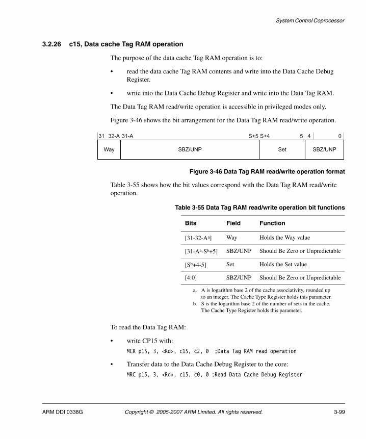
System Control Coprocessor
3.2.26 c15, Data cache Tag RAM operation
The purpose of the data cache Tag RAM operation is to:
• read the data cache Tag RAM contents and write into the Data Cache Debug Register.
• write into the Data Cache Debug Register and write into the Data Tag RAM.
The Data Tag RAM read/write operation is accessible in privileged modes only.
Figure 3-46 shows the bit arrangement for the Data Tag RAM read/write operation.
Figure 3-46 Data Tag RAM read/write operation format
Table 3-55 shows how the bit values correspond with the Data Tag RAM read/write operation.
To read the Data Tag RAM:
• write CP15 with:
MCR p15, 3, <Rd>, c15, c2, 0 ;Data Tag RAM read operation
• Transfer data to the Data Cache Debug Register to the core:
MRC p15, 3, <Rd>, c15, c0, 0 ;Read Data Cache Debug Register
Table 3-55 Data Tag RAM read/write operation bit functions
Bits Field Function
[31-32-Aa]
a. A is logarithm base 2 of the cache associativity, rounded up to an integer. The Cache Type Register holds this parameter.
Way Holds the Way value
[31-Aa-Sb+5]
b. S is the logarithm base 2 of the number of sets in the cache. The Cache Type Register holds this parameter.
SBZ/UNP Should Be Zero or Unpredictable
[Sb+4-5] Set Holds the Set value
[4:0] SBZ/UNP Should Be Zero or Unpredictable
ARM DDI 0338G Copyright © 2005-2007 ARM Limited. All rights reserved. 3-99
System Control Coprocessor
To write data to the Data Tag RAM:
• Transfer data to the Data Cache Debug Register:
MCR p15, 3, <Rd>, c15, c0, 0 ;Write Data Cache Debug Register
• write CP15 with:
For example:
MCR p15, 7, <Rd>, c15, c2, 0 ;Data Tag RAM write operation
3-100 Copyright © 2005-2007 ARM Limited. All rights reserved. ARM DDI 0338G
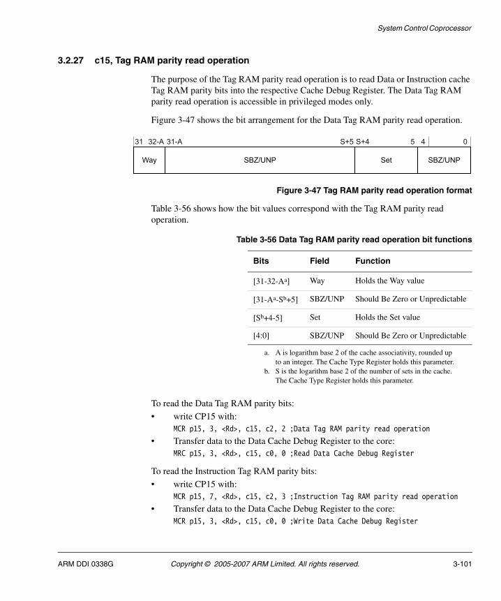
System Control Coprocessor
3.2.27 c15, Tag RAM parity read operation
The purpose of the Tag RAM parity read operation is to read Data or Instruction cache Tag RAM parity bits into the respective Cache Debug Register. The Data Tag RAM parity read operation is accessible in privileged modes only.
Figure 3-47 shows the bit arrangement for the Data Tag RAM parity read operation.
Figure 3-47 Tag RAM parity read operation format
Table 3-56 shows how the bit values correspond with the Tag RAM parity read operation.
To read the Data Tag RAM parity bits:
• write CP15 with:MCR p15, 3, <Rd>, c15, c2, 2 ;Data Tag RAM parity read operation
• Transfer data to the Data Cache Debug Register to the core:MRC p15, 3, <Rd>, c15, c0, 0 ;Read Data Cache Debug Register
To read the Instruction Tag RAM parity bits:
• write CP15 with:MCR p15, 7, <Rd>, c15, c2, 3 ;Instruction Tag RAM parity read operation
• Transfer data to the Data Cache Debug Register to the core:MCR p15, 3, <Rd>, c15, c0, 0 ;Write Data Cache Debug Register
Table 3-56 Data Tag RAM parity read operation bit functions
Bits Field Function
[31-32-Aa]
a. A is logarithm base 2 of the cache associativity, rounded up to an integer. The Cache Type Register holds this parameter.
Way Holds the Way value
[31-Aa-Sb+5]
b. S is the logarithm base 2 of the number of sets in the cache. The Cache Type Register holds this parameter.
SBZ/UNP Should Be Zero or Unpredictable
[Sb+4-5] Set Holds the Set value
[4:0] SBZ/UNP Should Be Zero or Unpredictable
ARM DDI 0338G Copyright © 2005-2007 ARM Limited. All rights reserved. 3-101
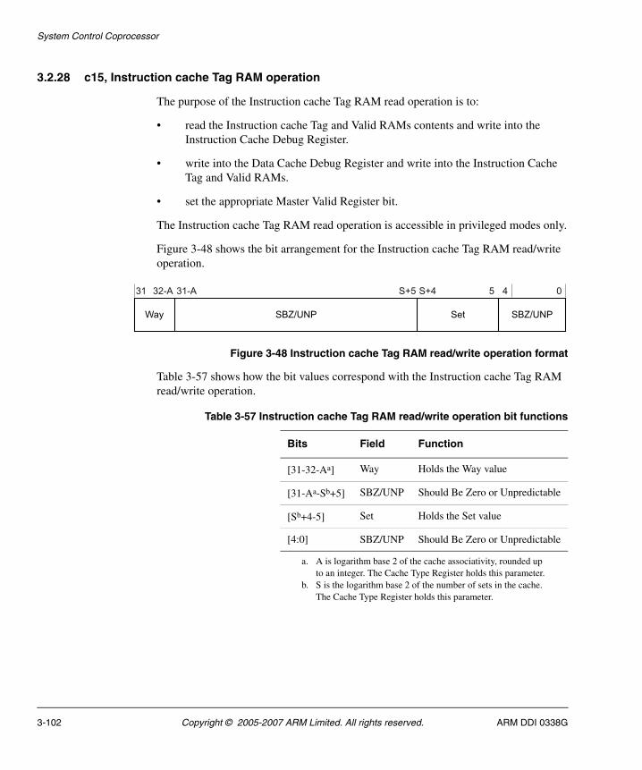
System Control Coprocessor
3.2.28 c15, Instruction cache Tag RAM operation
The purpose of the Instruction cache Tag RAM read operation is to:
• read the Instruction cache Tag and Valid RAMs contents and write into the Instruction Cache Debug Register.
• write into the Data Cache Debug Register and write into the Instruction Cache Tag and Valid RAMs.
• set the appropriate Master Valid Register bit.
The Instruction cache Tag RAM read operation is accessible in privileged modes only.
Figure 3-48 shows the bit arrangement for the Instruction cache Tag RAM read/write operation.
Figure 3-48 Instruction cache Tag RAM read/write operation format
Table 3-57 shows how the bit values correspond with the Instruction cache Tag RAM read/write operation.
Table 3-57 Instruction cache Tag RAM read/write operation bit functions
Bits Field Function
[31-32-Aa]
a. A is logarithm base 2 of the cache associativity, rounded up to an integer. The Cache Type Register holds this parameter.
Way Holds the Way value
[31-Aa-Sb+5]
b. S is the logarithm base 2 of the number of sets in the cache. The Cache Type Register holds this parameter.
SBZ/UNP Should Be Zero or Unpredictable
[Sb+4-5] Set Holds the Set value
[4:0] SBZ/UNP Should Be Zero or Unpredictable
3-102 Copyright © 2005-2007 ARM Limited. All rights reserved. ARM DDI 0338G
System Control Coprocessor
Note Because this operation sets the Master Valid Register bit, you must ensure that Tag RAM writes to previously uninitialized locations are in groups of eight made up from four Ways and two Set values. The Set values must be the same, except for the least significant bit, bit 5 of the operation format.
To read the Instruction cache Tag RAM:
• write CP15 with:
MCR p15, 3, <Rd>, c15, c2, 1 ;Instruction cache Tag RAM read operation
• Transfer data to the Instruction Cache Debug Register to the core:
MRC p15, 3, <Rd>, c15, c0, 1 ;Read Instruction Cache Debug Register
To write data to the Instruction cache Tag RAM:
• Transfer data to the Instruction Cache Debug Register:
MCR p15, 3, <Rd>, c15, c0, 1 ; Write Instruction Cache Debug Register
• write CP15 with:
MCR p15, 7, <Rd>, c15, c2, 1 ;Instruction cache Tag RAM write operation
ARM DDI 0338G Copyright © 2005-2007 ARM Limited. All rights reserved. 3-103
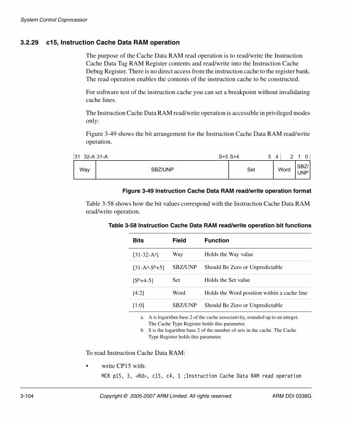
System Control Coprocessor
3.2.29 c15, Instruction Cache Data RAM operation
The purpose of the Cache Data RAM read operation is to read/write the Instruction Cache Data Tag RAM Register contents and read/write into the Instruction Cache Debug Register. There is no direct access from the instruction cache to the register bank. The read operation enables the contents of the instruction cache to be constructed.
For software test of the instruction cache you can set a breakpoint without invalidating cache lines.
The Instruction Cache Data RAM read/write operation is accessible in privileged modes only:
Figure 3-49 shows the bit arrangement for the Instruction Cache Data RAM read/write operation.
Figure 3-49 Instruction Cache Data RAM read/write operation format
Table 3-58 shows how the bit values correspond with the Instruction Cache Data RAM read/write operation.
To read Instruction Cache Data RAM:
• write CP15 with:
MCR p15, 3, <Rd>, c15, c4, 1 ;Instruction Cache Data RAM read operation
Table 3-58 Instruction Cache Data RAM read/write operation bit functions
Bits Field Function
[31-32-Aa]
a. A is logarithm base 2 of the cache associativity, rounded up to an integer. The Cache Type Register holds this parameter.
Way Holds the Way value
[31-Aa-Sb+5]
b. S is the logarithm base 2 of the number of sets in the cache. The Cache Type Register holds this parameter.
SBZ/UNP Should Be Zero or Unpredictable
[Sb+4-5] Set Holds the Set value
[4:2] Word Holds the Word position within a cache line
[1:0] SBZ/UNP Should Be Zero or Unpredictable
3-104 Copyright © 2005-2007 ARM Limited. All rights reserved. ARM DDI 0338G
System Control Coprocessor
• Transfer data to the Instruction Cache Debug Register to the core:
MRC p15, 3, <Rd>, c15, c0, 1 ;Read Instruction Cache Debug Register
To write Instruction Cache Data RAM:
• Transfer data to the Instruction Cache Debug Register from the core:
MCR p15, 3, <Rd>, c15, c0, 1 ;Write Instruction Cache Debug Register
• write CP15 with:
For example:
MCR p15, 7, <Rd>, c15, c4, 1 ;Instruction Cache Data RAM write operation
ARM DDI 0338G Copyright © 2005-2007 ARM Limited. All rights reserved. 3-105
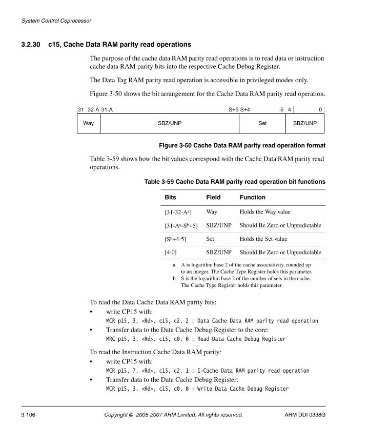
System Control Coprocessor
3.2.30 c15, Cache Data RAM parity read operations
The purpose of the cache data RAM parity read operations is to read data or instruction cache data RAM parity bits into the respective Cache Debug Register.
The Data Tag RAM parity read operation is accessible in privileged modes only.
Figure 3-50 shows the bit arrangement for the Cache Data RAM parity read operation.
Figure 3-50 Cache Data RAM parity read operation format
Table 3-59 shows how the bit values correspond with the Cache Data RAM parity read operations.
To read the Data Cache Data RAM parity bits:
• write CP15 with:MCR p15, 3, <Rd>, c15, c2, 2 ; Data Cache Data RAM parity read operation
• Transfer data to the Data Cache Debug Register to the core:MRC p15, 3, <Rd>, c15, c0, 0 ; Read Data Cache Debug Register
To read the Instruction Cache Data RAM parity:
• write CP15 with:MCR p15, 7, <Rd>, c15, c2, 1 ; I-Cache Data RAM parity read operation
• Transfer data to the Data Cache Debug Register:MCR p15, 3, <Rd>, c15, c0, 0 ; Write Data Cache Debug Register
Table 3-59 Cache Data RAM parity read operation bit functions
Bits Field Function
[31-32-Aa]
a. A is logarithm base 2 of the cache associativity, rounded up to an integer. The Cache Type Register holds this parameter.
Way Holds the Way value
[31-Aa-Sb+5]
b. S is the logarithm base 2 of the number of sets in the cache. The Cache Type Register holds this parameter.
SBZ/UNP Should Be Zero or Unpredictable
[Sb+4-5] Set Holds the Set value
[4:0] SBZ/UNP Should Be Zero or Unpredictable
3-106 Copyright © 2005-2007 ARM Limited. All rights reserved. ARM DDI 0338G
System Control Coprocessor
3.2.31 c15, Instruction Cache Master Valid Register
The purpose of this register is to mask the Valid bits held in the Instruction Valid RAM for the instruction cache. This enables the processor to perform a single cycle invalidation of the cache without the use of special resetable RAM cells.
The Instruction Cache Master Valid Register is:
• in CP15 c15
• a 32-bit read/write register
• accessible in privileged modes only.
The number of Master Valid bits is a function of the cache size. There is one Master Valid bit for each 8 cache lines:
For instance, there are 64 Master Valid bits for a 16KB cache. You can access Master Valid bits through 32-bit registers indexed using Opcode_2. The maximum number of 32-bit registers required for the largest cache size, 64K, is 8. Master Valid bits fill the registers from the LSB of the lowest numbered register upwards.
Unimplemented Valid bits are Unpredictable for reads and Should Be Zero or Preserved (SBZP) for writes.
To use the Instruction Cache Master Valid Register write CP15 with:
MRC p15, 3, <Rd>, c15, c8, {7-0} ;Read Instruction Cache Master ValidMCR p15, 3, <Rd>, c15, c8, {7-0} ;Write Instruction Cache Master Valid
The Opcode_2 field is the bank number in the range 7-0. The bank number that you use for capturing cache Master Valid bits is one less than the number of times 8KB divides into the cache size, or 0 if the cache size is less than 8KB.
MasterValid bits =Cache size
line length in bytes × 8
ARM DDI 0338G Copyright © 2005-2007 ARM Limited. All rights reserved. 3-107
System Control Coprocessor
3.2.32 c15, Data Cache Master Valid Register
The purpose of this register is to mask the Valid bits held in the Data Valid RAM for the data cache. This enables the processor to perform a single cycle invalidation of the cache without the use of special resetable RAM cells.
The Data Cache Master Valid Register is:
• in CP15 c15
• a 32-bit read/write register
• accessible in privileged modes only.
The number of Master Valid bits is a function of the cache size. There is one Master Valid bit for each 8 cache lines:
For instance, there are 64 Master Valid bits for a 16KB cache. You can access Master Valid bits through 32-bit registers indexed using Opcode_2. The maximum number of 32-bit registers required for the largest cache size, 64K, is 8. Master Valid bits fill the registers from the LSB of the lowest numbered register upwards.
Unimplemented Valid bits are Unpredictable for reads and Should Be Zero or Preserved (SBZP) for writes.
To use the Data Cache Master Valid Register write CP15 with:
MRC p15, 3, <Rd>, c15, c12, {7-0} ;Read Data Cache Master Valid RegisterMCR p15, 3, <Rd>, c15, c12, {7-0} ;Write Data Cache Master Valid Register
The Opcode_2 field is the bank number in the range 7-0. The bank number that you use for capturing cache Master Valid bits is one less than the number of times 8KB divides into the cache size, or 0 if the cache size is less than 8KB.
MasterValid bits =Cache size
line length in bytes × 8
3-108 Copyright © 2005-2007 ARM Limited. All rights reserved. ARM DDI 0338G
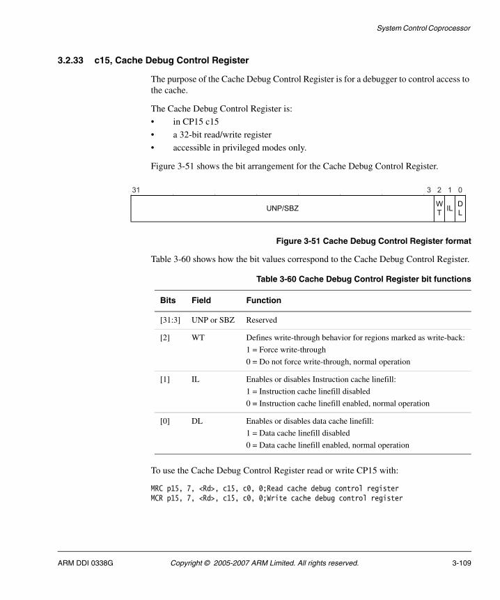
System Control Coprocessor
3.2.33 c15, Cache Debug Control Register
The purpose of the Cache Debug Control Register is for a debugger to control access to the cache.
The Cache Debug Control Register is:
• in CP15 c15
• a 32-bit read/write register
• accessible in privileged modes only.
Figure 3-51 shows the bit arrangement for the Cache Debug Control Register.
Figure 3-51 Cache Debug Control Register format
Table 3-60 shows how the bit values correspond to the Cache Debug Control Register.
To use the Cache Debug Control Register read or write CP15 with:
MRC p15, 7, <Rd>, c15, c0, 0;Read cache debug control registerMCR p15, 7, <Rd>, c15, c0, 0;Write cache debug control register
D
LUNP/SBZ
31 3 2 1 0
W
TIL
Table 3-60 Cache Debug Control Register bit functions
Bits Field Function
[31:3] UNP or SBZ Reserved
[2] WT Defines write-through behavior for regions marked as write-back:
1 = Force write-through
0 = Do not force write-through, normal operation
[1] IL Enables or disables Instruction cache linefill:
1 = Instruction cache linefill disabled
0 = Instruction cache linefill enabled, normal operation
[0] DL Enables or disables data cache linefill:
1 = Data cache linefill disabled
0 = Data cache linefill enabled, normal operation
ARM DDI 0338G Copyright © 2005-2007 ARM Limited. All rights reserved. 3-109
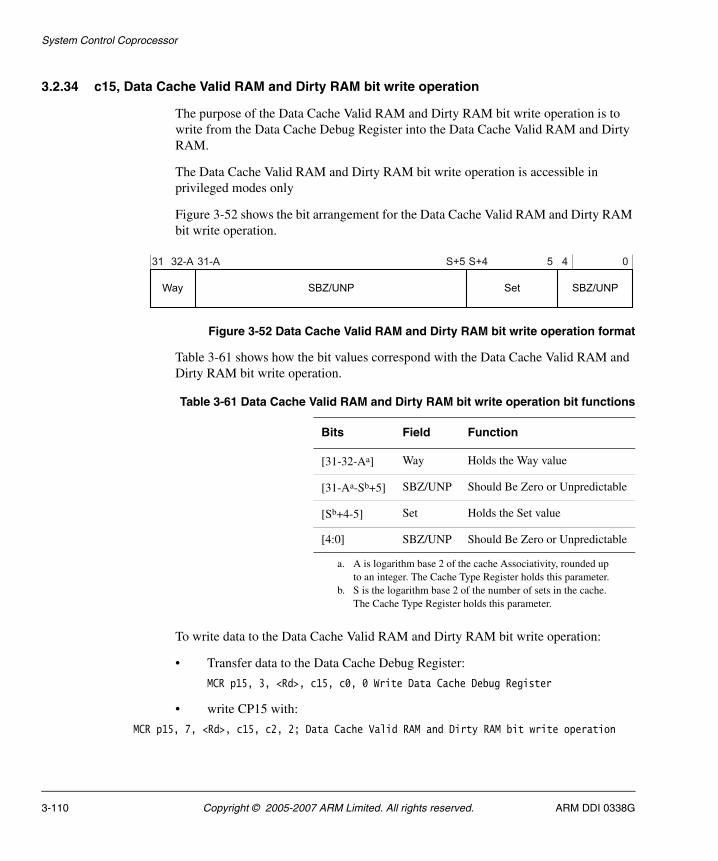
System Control Coprocessor
3.2.34 c15, Data Cache Valid RAM and Dirty RAM bit write operation
The purpose of the Data Cache Valid RAM and Dirty RAM bit write operation is to write from the Data Cache Debug Register into the Data Cache Valid RAM and Dirty RAM.
The Data Cache Valid RAM and Dirty RAM bit write operation is accessible in privileged modes only
Figure 3-52 shows the bit arrangement for the Data Cache Valid RAM and Dirty RAM bit write operation.
Figure 3-52 Data Cache Valid RAM and Dirty RAM bit write operation format
Table 3-61 shows how the bit values correspond with the Data Cache Valid RAM and Dirty RAM bit write operation.
To write data to the Data Cache Valid RAM and Dirty RAM bit write operation:
• Transfer data to the Data Cache Debug Register:
MCR p15, 3, <Rd>, c15, c0, 0 Write Data Cache Debug Register
• write CP15 with:
MCR p15, 7, <Rd>, c15, c2, 2; Data Cache Valid RAM and Dirty RAM bit write operation
Table 3-61 Data Cache Valid RAM and Dirty RAM bit write operation bit functions
Bits Field Function
[31-32-Aa]
a. A is logarithm base 2 of the cache Associativity, rounded up to an integer. The Cache Type Register holds this parameter.
Way Holds the Way value
[31-Aa-Sb+5]
b. S is the logarithm base 2 of the number of sets in the cache. The Cache Type Register holds this parameter.
SBZ/UNP Should Be Zero or Unpredictable
[Sb+4-5] Set Holds the Set value
[4:0] SBZ/UNP Should Be Zero or Unpredictable
3-110 Copyright © 2005-2007 ARM Limited. All rights reserved. ARM DDI 0338G
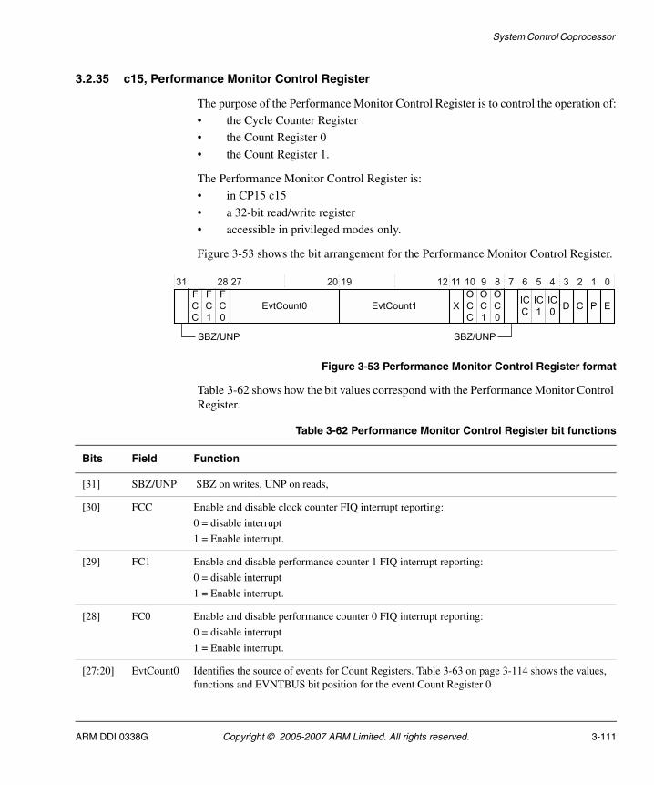
System Control Coprocessor
3.2.35 c15, Performance Monitor Control Register
The purpose of the Performance Monitor Control Register is to control the operation of:
• the Cycle Counter Register
• the Count Register 0
• the Count Register 1.
The Performance Monitor Control Register is:
• in CP15 c15
• a 32-bit read/write register
• accessible in privileged modes only.
Figure 3-53 shows the bit arrangement for the Performance Monitor Control Register.
Figure 3-53 Performance Monitor Control Register format
Table 3-62 shows how the bit values correspond with the Performance Monitor Control Register.
Table 3-62 Performance Monitor Control Register bit functions
Bits Field Function
[31] SBZ/UNP SBZ on writes, UNP on reads,
[30] FCC Enable and disable clock counter FIQ interrupt reporting:
0 = disable interrupt
1 = Enable interrupt.
[29] FC1 Enable and disable performance counter 1 FIQ interrupt reporting:
0 = disable interrupt
1 = Enable interrupt.
[28] FC0 Enable and disable performance counter 0 FIQ interrupt reporting:
0 = disable interrupt
1 = Enable interrupt.
[27:20] EvtCount0 Identifies the source of events for Count Registers. Table 3-63 on page 3-114 shows the values, functions and EVNTBUS bit position for the event Count Register 0
ARM DDI 0338G Copyright © 2005-2007 ARM Limited. All rights reserved. 3-111
System Control Coprocessor
[19:12] EvtCount1 Identifies the source of events for Count Registers. Table 3-63 on page 3-114 shows the values and the bit functions for the event Count Register 1
[11] X Enable Export of the events to the event bus to an external monitoring block, such as the ETM to trace events.
0 = Export disabled, EVNTBUS held at 0x0
1 = Export enabled, EVNTBUS driven by the events.
[10] OCC Cycle Counter Register overflow flag:
For reads:
0 = no overflow (reset value)
1 = overflow has occurred.
For writes:
0 = no effect
1 = clear this bit.
[9] OC1 Count Register 1 overflow flag.
For reads:
0 = no overflow (reset)
1 = overflow has occurred.
For writes:
0 = no effect
1 = clear this bit.
[8] OC0 Count Register 0 overflow flag:
For reads:
0 = no overflow (reset)
1 = overflow has occurred.
For writes:
0 = no effect
1 = clear this bit.
[7] SBZ/UNP SBZ on write, UNP on reads
[6] ICC Used to enable and disable Cycle Counter interrupt reporting:
0 = disable interrupt
1 = Enable interrupt.
Table 3-62 Performance Monitor Control Register bit functions (continued)
Bits Field Function
3-112 Copyright © 2005-2007 ARM Limited. All rights reserved. ARM DDI 0338G
System Control Coprocessor
The Performance Monitor Control Register:
• controls which events Count Register 0 and Count Register 1 count
• indicates which counter overflowed
• enables and disables the report of interrupts
• extends Cycle Count Register counting by six more bits, cycles between counter rollover = 238
• resets all counters to zero
• enables the entire performance monitoring mechanism.
[5] IC1 Enable and disable Cycle Counter 1 interrupt reporting:
0 = disable interrupt
1 = Enable interrupt.
[4] IC0 Enable and disable Count Register 0 interrupt reporting:
0 = disable interrupt
1 = Enable interrupt.
[3] D Cycle count divider:
1 = Counts every 64th processor clock cycle
0 = Counts every processor clock cycle.
[2] C Cycle Counter Register Reset:
1 = Reset the Cycle Counter Register to 0x0
0 = No action Reset on write, Unpredictable on read
[1] P Count Register 1 and Count Register 0 Reset:
1 = Reset both Count Registers to 0x0.
0 = No action Reset on write, Unpredictable on read.
[0] E Enable all counters:
1 = All counters enabled.
0 = All counters disabled.
Table 3-62 Performance Monitor Control Register bit functions (continued)
Bits Field Function
ARM DDI 0338G Copyright © 2005-2007 ARM Limited. All rights reserved. 3-113
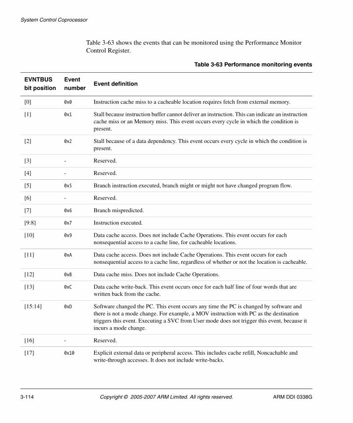
System Control Coprocessor
Table 3-63 shows the events that can be monitored using the Performance Monitor Control Register.
Table 3-63 Performance monitoring events
EVNTBUSbit position
Eventnumber
Event definition
[0] 0x0 Instruction cache miss to a cacheable location requires fetch from external memory.
[1] 0x1 Stall because instruction buffer cannot deliver an instruction. This can indicate an instruction cache miss or an Memory miss. This event occurs every cycle in which the condition is present.
[2] 0x2 Stall because of a data dependency. This event occurs every cycle in which the condition is present.
[3] - Reserved.
[4] - Reserved.
[5] 0x5 Branch instruction executed, branch might or might not have changed program flow.
[6] - Reserved.
[7] 0x6 Branch mispredicted.
[9:8] 0x7 Instruction executed.
[10] 0x9 Data cache access. Does not include Cache Operations. This event occurs for each nonsequential access to a cache line, for cacheable locations.
[11] 0xA Data cache access. Does not include Cache Operations. This event occurs for each nonsequential access to a cache line, regardless of whether or not the location is cacheable.
[12] 0xB Data cache miss. Does not include Cache Operations.
[13] 0xC Data cache write-back. This event occurs once for each half line of four words that are written back from the cache.
[15:14] 0xD Software changed the PC. This event occurs any time the PC is changed by software and there is not a mode change. For example, a MOV instruction with PC as the destination triggers this event. Executing a SVC from User mode does not trigger this event, because it incurs a mode change.
[16] - Reserved.
[17] 0x10 Explicit external data or peripheral access. This includes cache refill, Noncachable and write-through accesses. It does not include write-backs.
3-114 Copyright © 2005-2007 ARM Limited. All rights reserved. ARM DDI 0338G
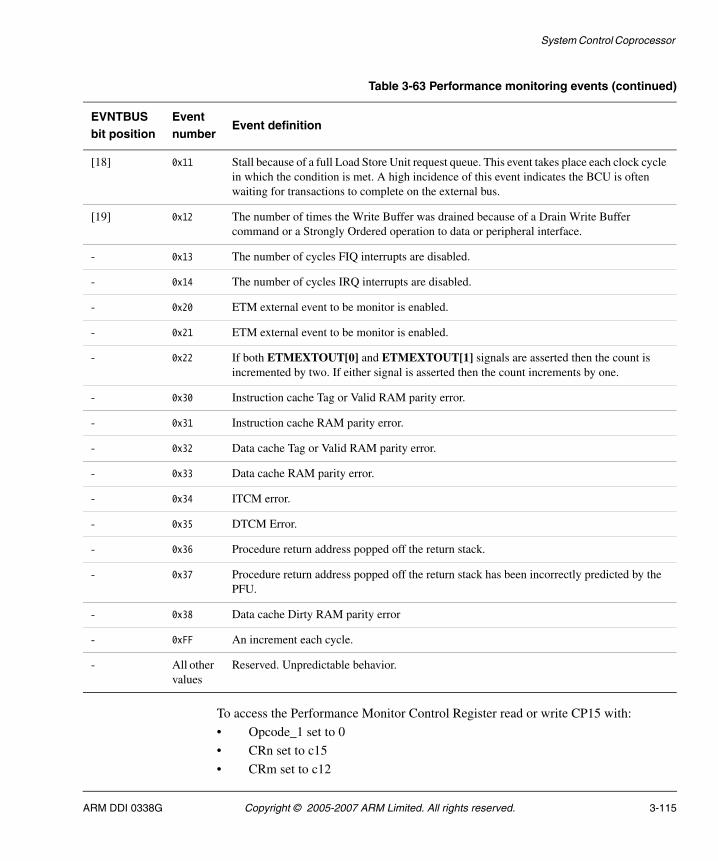
System Control Coprocessor
To access the Performance Monitor Control Register read or write CP15 with:
• Opcode_1 set to 0
• CRn set to c15
• CRm set to c12
[18] 0x11 Stall because of a full Load Store Unit request queue. This event takes place each clock cycle in which the condition is met. A high incidence of this event indicates the BCU is often waiting for transactions to complete on the external bus.
[19] 0x12 The number of times the Write Buffer was drained because of a Drain Write Buffer command or a Strongly Ordered operation to data or peripheral interface.
- 0x13 The number of cycles FIQ interrupts are disabled.
- 0x14 The number of cycles IRQ interrupts are disabled.
- 0x20 ETM external event to be monitor is enabled.
- 0x21 ETM external event to be monitor is enabled.
- 0x22 If both ETMEXTOUT[0] and ETMEXTOUT[1] signals are asserted then the count is incremented by two. If either signal is asserted then the count increments by one.
- 0x30 Instruction cache Tag or Valid RAM parity error.
- 0x31 Instruction cache RAM parity error.
- 0x32 Data cache Tag or Valid RAM parity error.
- 0x33 Data cache RAM parity error.
- 0x34 ITCM error.
- 0x35 DTCM Error.
- 0x36 Procedure return address popped off the return stack.
- 0x37 Procedure return address popped off the return stack has been incorrectly predicted by the PFU.
- 0x38 Data cache Dirty RAM parity error
- 0xFF An increment each cycle.
- All other values
Reserved. Unpredictable behavior.
Table 3-63 Performance monitoring events (continued)
EVNTBUSbit position
Eventnumber
Event definition
ARM DDI 0338G Copyright © 2005-2007 ARM Limited. All rights reserved. 3-115
System Control Coprocessor
• Opcode_2 set to 0.
For example:
MRC p15, 0, <Rd>, c15, c12, 0; Read Performance Monitor Control RegisterMCR p15, 0, <Rd>, c15, c12, 0; Write Performance Monitor Control Register
If this unit generates an interrupt, the ARM1156T2-S processor asserts the pin nPMUIRQ and nPMUFIQ as appropriate. You can route these pins to an external interrupt controller for prioritization and masking. This is the only mechanism by which the interrupt is signalled to the core.
You can only enable or disable the performance metrics interrupts nPMUIRQ and nPMUFIQ if the metrics counters are enabled, that is Performance Monitor Control Register bit [0] is set to 1.
Follow steps 1. and 2. to de-assert nPMUIRQ and nPMUFIQ:
1. Write to the Performance Monitor Control Register to clear the interrupt enable bit.
2. Write to the Performance Monitor Control Register to disable the counter.
There is a delay of three cycles between an enable of the counter and the start of the event counter. The information used to count events is taken from various pipeline stages. This means that the absolute counts recorded might vary because of pipeline effects. This has negligible effect except in cases where the counters are enabled for a very short time.
In addition to the two counters within the ARM1156T2-S processor, each of the events that Table 3-63 on page 3-114 shows is available on an external bus, EVNTBUS[19:0]. You can connect this bus to the ETM unit or other external trace hardware to enable the events to be monitored. If you do not want this functionality, set the X bit in the Performance Monitor Control Register to 0.
3-116 Copyright © 2005-2007 ARM Limited. All rights reserved. ARM DDI 0338G
System Control Coprocessor
3.2.36 c15, Cycle Counter Register
The purpose of the Cycle Counter Register is to count the core clock cycles.
The Cycle Counter Register:
• is in CP15 c15
• is a 32-bit counter
• can trigger an interrupt on overflow.
The Cycle Counter Register bits [31:0] contain the count value.
You can use it in conjunction with the Performance Monitor Control Register and the two Counter Registers to provide a variety of useful metrics that enable you to optimize system performance.
To access Cycle Counter Register read or write CP15 with:
• Opcode_1 set to 0
• CRn set to c15
• CRm set to c12
• Opcode_2 set to 1.
For Example:
MRC p15, 0, <Rd>, c15, c12, 1 ;Read Cycle Counter RegisterMCR p15, 0, <Rd>, c15, c12, 1 ;Write Cycle Counter Register
The value in the Cycle Counter Register is Unpredictable at Reset.
You can use the Performance Monitor Control Register to set the Cycle Counter Register to zero.
You can use the Performance Monitor Control Register to configure the Cycle Counter Register to count every 64th clock cycle.
ARM DDI 0338G Copyright © 2005-2007 ARM Limited. All rights reserved. 3-117
System Control Coprocessor
3.2.37 c15, Count Register 0
The purpose of the Count Register 0 is to count instances of an event that the Performance Monitor Control Register selects:
The Count Register 0:
• is in CP15 c15
• a 32-bit counter
• counts up and can trigger an interrupt on overflow.
Count Register 0 bits [31:0] contain the count value.
You can use this register in conjunction with the Performance Monitor Control Register, the Cycle Count Register, and Count Register 0 to provide a variety of useful metrics that enable you to optimize system performance.
To access Count Register 1 read or write CP15 with:
• Opcode_1 set to 0
• CRn set to c15
• CRm set to c12
• Opcode_2 set to 2.
For Example:
MRC p15, 0, <Rd>, c15, c12, 2 ;Read Count Register 0MCR p15, 0, <Rd>, c15, c12, 2 ;Write Count Register 0
The value in Count Register 0 is 0 at Reset.
You can use the Performance Monitor Control Register to set Count Register 0 to zero.
3-118 Copyright © 2005-2007 ARM Limited. All rights reserved. ARM DDI 0338G
System Control Coprocessor
3.2.38 c15, Count Register 1
The purpose of the Count Register 1 is to count instances of an event that the Performance Monitor Control Register selects.
The Count Register 1:
• is in CP15 c15
• a 32-bit counter
• counts up and can trigger an interrupt on overflow.
Count Register 1 bits [31:0] contain the count value.
You can use this register in conjunction with the Performance Monitor Control Register, the Cycle Count Register, and Count Register 0 to provide a variety of useful metrics that enable you to optimize system performance.
To access Count Register 1 read or write CP15 with:
• Opcode_1 set to 0
• CRn set to c15
• CRm set to c12
• Opcode_2 set to 3.
For Example:
MRC p15, 0, <Rd>, c15, c12, 3; Read Count Register 1MCR p15, 0, <Rd>, c15, c12, 3; Write Count Register 1
The value in Count Register 1 is 0 at Reset.
You can use the Performance Monitor Control Register to set Count Register 0 to zero.
ARM DDI 0338G Copyright © 2005-2007 ARM Limited. All rights reserved. 3-119
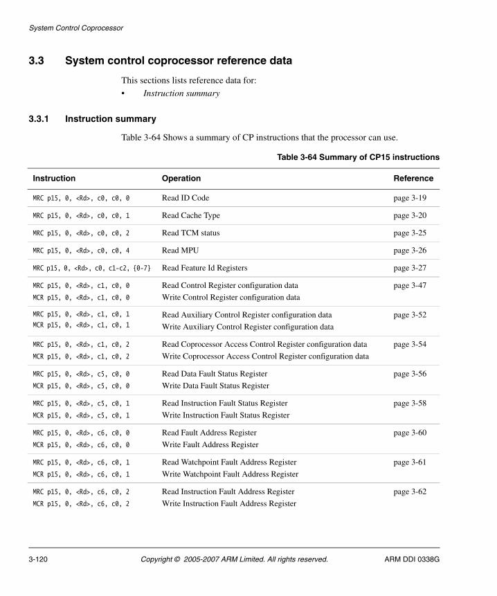
System Control Coprocessor
3.3 System control coprocessor reference data
This sections lists reference data for:
• Instruction summary
3.3.1 Instruction summary
Table 3-64 Shows a summary of CP instructions that the processor can use.
Table 3-64 Summary of CP15 instructions
Instruction Operation Reference
MRC p15, 0, <Rd>, c0, c0, 0 Read ID Code page 3-19
MRC p15, 0, <Rd>, c0, c0, 1 Read Cache Type page 3-20
MRC p15, 0, <Rd>, c0, c0, 2 Read TCM status page 3-25
MRC p15, 0, <Rd>, c0, c0, 4 Read MPU page 3-26
MRC p15, 0, <Rd>, c0, c1-c2, {0-7} Read Feature Id Registers page 3-27
MRC p15, 0, <Rd>, c1, c0, 0
MCR p15, 0, <Rd>, c1, c0, 0
Read Control Register configuration data
Write Control Register configuration data
page 3-47
MRC p15, 0, <Rd>, c1, c0, 1
MCR p15, 0, <Rd>, c1, c0, 1 Read Auxiliary Control Register configuration data
Write Auxiliary Control Register configuration data
page 3-52
MRC p15, 0, <Rd>, c1, c0, 2
MCR p15, 0, <Rd>, c1, c0, 2
Read Coprocessor Access Control Register configuration data
Write Coprocessor Access Control Register configuration data
page 3-54
MRC p15, 0, <Rd>, c5, c0, 0
MCR p15, 0, <Rd>, c5, c0, 0
Read Data Fault Status Register
Write Data Fault Status Register
page 3-56
MRC p15, 0, <Rd>, c5, c0, 1
MCR p15, 0, <Rd>, c5, c0, 1
Read Instruction Fault Status Register
Write Instruction Fault Status Register
page 3-58
MRC p15, 0, <Rd>, c6, c0, 0
MCR p15, 0, <Rd>, c6, c0, 0
Read Fault Address Register
Write Fault Address Register
page 3-60
MRC p15, 0, <Rd>, c6, c0, 1
MCR p15, 0, <Rd>, c6, c0, 1
Read Watchpoint Fault Address Register
Write Watchpoint Fault Address Register
page 3-61
MRC p15, 0, <Rd>, c6, c0, 2
MCR p15, 0, <Rd>, c6, c0, 2
Read Instruction Fault Address Register
Write Instruction Fault Address Register
page 3-62
3-120 Copyright © 2005-2007 ARM Limited. All rights reserved. ARM DDI 0338G
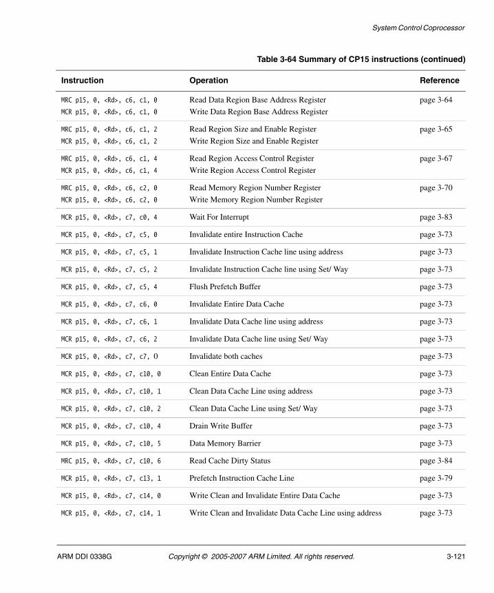
System Control Coprocessor
MRC p15, 0, <Rd>, c6, c1, 0
MCR p15, 0, <Rd>, c6, c1, 0
Read Data Region Base Address Register
Write Data Region Base Address Register
page 3-64
MRC p15, 0, <Rd>, c6, c1, 2
MCR p15, 0, <Rd>, c6, c1, 2
Read Region Size and Enable Register
Write Region Size and Enable Register
page 3-65
MRC p15, 0, <Rd>, c6, c1, 4
MCR p15, 0, <Rd>, c6, c1, 4
Read Region Access Control Register
Write Region Access Control Register
page 3-67
MRC p15, 0, <Rd>, c6, c2, 0
MCR p15, 0, <Rd>, c6, c2, 0
Read Memory Region Number Register
Write Memory Region Number Register
page 3-70
MCR p15, 0, <Rd>, c7, c0, 4 Wait For Interrupt page 3-83
MCR p15, 0, <Rd>, c7, c5, 0 Invalidate entire Instruction Cache page 3-73
MCR p15, 0, <Rd>, c7, c5, 1 Invalidate Instruction Cache line using address page 3-73
MCR p15, 0, <Rd>, c7, c5, 2 Invalidate Instruction Cache line using Set/ Way page 3-73
MCR p15, 0, <Rd>, c7, c5, 4 Flush Prefetch Buffer page 3-73
MCR p15, 0, <Rd>, c7, c6, 0 Invalidate Entire Data Cache page 3-73
MCR p15, 0, <Rd>, c7, c6, 1 Invalidate Data Cache line using address page 3-73
MCR p15, 0, <Rd>, c7, c6, 2 Invalidate Data Cache line using Set/ Way page 3-73
MCR p15, 0, <Rd>, c7, c7, 0 Invalidate both caches page 3-73
MCR p15, 0, <Rd>, c7, c10, 0 Clean Entire Data Cache page 3-73
MCR p15, 0, <Rd>, c7, c10, 1 Clean Data Cache Line using address page 3-73
MCR p15, 0, <Rd>, c7, c10, 2 Clean Data Cache Line using Set/ Way page 3-73
MCR p15, 0, <Rd>, c7, c10, 4 Drain Write Buffer page 3-73
MCR p15, 0, <Rd>, c7, c10, 5 Data Memory Barrier page 3-73
MRC p15, 0, <Rd>, c7, c10, 6 Read Cache Dirty Status page 3-84
MCR p15, 0, <Rd>, c7, c13, 1 Prefetch Instruction Cache Line page 3-79
MCR p15, 0, <Rd>, c7, c14, 0 Write Clean and Invalidate Entire Data Cache page 3-73
MCR p15, 0, <Rd>, c7, c14, 1 Write Clean and Invalidate Data Cache Line using address page 3-73
Table 3-64 Summary of CP15 instructions (continued)
Instruction Operation Reference
ARM DDI 0338G Copyright © 2005-2007 ARM Limited. All rights reserved. 3-121
System Control Coprocessor
MCR p15, 0, <Rd>, c7, c14, 2 Write Clean and Invalidate Data Cache Line using Set/ Way page 3-73
MRC p15, 0, <Rd>, c9, c0, 0
MCR p15, 0, <Rd>, c9, c0, 0
Read Data Cache Lockdown Register
Write Data Cache Lockdown Register
page 3-85
MRC p15, 0, <Rn>, c9, c0, 1
MCR p15, 0, <Rn>, c9, c0, 1
Read Instruction Cache Lockdown Register
Write Instruction Cache Lockdown Register
page 3-85
MRC p15, 0, <Rd>, c9, c1, 0
MCR p15, 0, <Rd>, c9, c1, 0
Read Data TCM Region Register
Write Data TCM Region Register
page 3-88
MRC p15, 0, <Rd>, c9, c1, 1
MCR p15, 0, <Rd>, c9, c1, 1
Read Instruction TCM Region Register
Write Instruction TCM Region Register
page 3-90
MRC p15, 0, <Rd>, c13, c0, 1
MCR p15, 0, <Rd>, c13, c0, 1
Read Process ID
Write Process ID
page 3-92
MRC p15, 0, <Rd>, c15, c12, 0
MCR p15, 0, <Rd>, c15, c12, 0
Read Performance Monitor Control Register
Write Performance Monitor Control Register
page 3-111
MRC p15, 0, <Rd>, c15, c12, 1
MCR p15, 0, <Rd>, c15, c12, 1
Read Cycle Counter Register
Write Cycle Counter Register
page 3-117
MRC p15, 0, <Rd>, c15, c12, 2
MCR p15, 0, <Rd>, c15, c12, 2
Read Count Register 0
Write Count Register 0
page 3-118
MRC p15, 0, <Rd>, c15, c12, 3
MCR p15, 0, <Rd>, c15, c12, 3
Read Count Register 1
Write Count Register 1
page 3-119
MRC p15, 3, <Rd>, c15, c0, 0
MCR p15, 3, <Rd>, c15, c0, 0
Read Data Cache Debug Register
Write Data Cache Debug Register
page 3-93
MRC p15, 3, <Rd>, c15, c0, 1
MCR p15, 3, <Rd>, c15, c0, 1
Read Instruction Cache Debug Register
Write Instruction Cache Debug Register
page 3-96
MCR p15, 3, <Rd>, c15, c2, 0 Data Tag RAM Read Operation page 3-99
MCR p15, 3, <Rd>, c15, c2, 1 Instruction cache Tag RAM Read Operation page 3-102
MCR p15, 3, <Rd>, c15, c2, 2 Data Tag RAM Parity Read Operation page 3-101
MCR p15, 3, <Rd>, c15, c2, 3 Instruction cache Tag RAM Parity Read Operation page 3-101
MCR p15, 3, <Rd>, c15, c4, 1 Instruction Cache Data RAM Read Operation page 3-104
MCR p15, 3, <Rd>, c15, c4, 2 Data Cache Data RAM Parity Read Operation page 3-106
Table 3-64 Summary of CP15 instructions (continued)
Instruction Operation Reference
3-122 Copyright © 2005-2007 ARM Limited. All rights reserved. ARM DDI 0338G
System Control Coprocessor
MCR p15, 3, <Rd>, c15, c4, 3 Instruction Cache Data RAM Parity Read Operation page 3-106
MRC p15, 3, <Rd>, c15, c8, <R>a
MCR p15, 3, <Rd>, c15, c8, <R>a
Read Instruction Cache Master Valid Register
Write Instruction Cache Master Valid Register
page 3-107
MRC p15, 3, <Rd>, c15, c12, <R>a
MCR p15, 3, <Rd>, c15, c12, <R>a
Read Data Cache Master Valid Register
Write Data Cache Master Valid Register
page 3-108
MCR p15, 7, <Rd>, c15, c0, 0
MRC p15, 7, <Rd>, c15, c0, 0
Read Cache Debug Control Register
Write Cache Debug Control Register
page 3-109
MCR p15, 7, <Rd>, c15, c2, 0 Write Data Tag RAM operation page 3-99
MCR p15, 7, <Rd>, c15, c2, 1 Write Instruction cache Tag RAM operation page 3-102
MCR p15, 7, <Rd>, c15, c2, 2 Write Data Valid RAM and Dirty RAM operation page 3-110
MCR p15, 7, <Rd>, c15, c4, 1 Write Instruction Cache Data RAM page 3-104
a. Register number
Table 3-64 Summary of CP15 instructions (continued)
Instruction Operation Reference
ARM DDI 0338G Copyright © 2005-2007 ARM Limited. All rights reserved. 3-123
System Control Coprocessor
3-124 Copyright © 2005-2007 ARM Limited. All rights reserved. ARM DDI 0338G
Chapter 4 Prefetch Unit
This chapter describes how the PreFetch Unit (PFU), in conjunction with the core, uses program flow prediction to locate branches in the instruction stream and the strategies used to determine if a branch is likely to be taken or not. It also describes the two architecturally-defined SVC functions the processor requires for backwards-compatibility with earlier architectures to flush the Prefetch Unit (PFU) buffers. It contains the following sections:
• About the prefetch unit on page 4-2
• Branch prediction on page 4-3
• Return stack on page 4-6
• Instruction Memory Barrier (IMB) instruction on page 4-7.
ARM DDI 0338G Copyright © 2005-2007 ARM Limited. All rights reserved. 4-1
Prefetch Unit
4.1 About the prefetch unit
The purpose of the PFU is to:
• Perform speculative fetch instructions ahead of the core by predicting the outcome of branch instructions.
• Detect Thumb-2 instructions and present these to the core as a single instruction. The Thumb-2 IT instruction is pre-processed by the PFU to aid the core in efficient implementation.
• Manage CP15 operations that involve the instruction cache, linefill operations, and LSU accesses into the Instruction TCM (ITCM). This is because the PFU drives the instruction cache and ITCM address buses. For details of CP15 instructions see Chapter 3 System Control Coprocessor.
The PFU fetches instructions from the memory system under the control of the core, and coprocessors. In ARM state the memory system can supply up to two instructions each cycle. In Thumb state the memory system can supply up to four instructions each cycle.
The PFU buffers up to five instructions in its FIFO. This reduces or eliminates stall cycles after a branch instruction, which increases the performance of the processor.
The PFU contains branch folding logic to reduce the average cycle time of a branch.
Program flow prediction occurs in the Prefetch Unit by:
• predicting the outcome of conditional branches using the Branch Predictor and, if they are predicted taken, calculating their destination address.
• predicting the destination of procedure returns using the Return Stack.
The core resolves the program flow predictions that the Prefetch Unit makes.
The PFU also handles the cache access multiplexing for:
• CP15 instruction handling
• data accesses to the Instruction TCM.
The PFU fetches the instruction stream as dictated by:
• the Program Counter
• the Branch Predictor
• procedure returns signaled by the Return Stack
• exceptions, instruction aborts, and interrupts signaled by the core.
4-2 Copyright © 2005-2007 ARM Limited. All rights reserved. ARM DDI 0338G
Prefetch Unit
4.2 Branch prediction
The processor uses branch prediction to reduce the core CPI loss that arises from the longer pipeline. To improve the branch prediction accuracy, the PFU uses dynamic techniques.
In ARM processors that have no PFU, the target of a branch is not known until the end of the Execute stage. At the Execute stage it is known whether or not the branch is taken. In ARM processors without a PFU, the best performance is obtained by predicting all branches as not taken and filling the pipeline with the instructions that follow the branch in the current sequential path. In this case an untaken branch requires one cycle and a taken branch requires three or more cycles.
Branch prediction enables the detection of branch instructions before they enter the core. This permits the use of a branch prediction scheme that closely models actual conditional branch core behavior.
The increased pipeline length of the ARM1156T2-S processor makes the performance penalty of any changes in program flow, such as branches or other updates to the PC, more significant than was the case on the ARM9E core. Therefore, a significant amount of hardware is dedicated to prediction of these changes. Two major classes of program flow are addressed in the ARM1156T2-S prediction scheme:
1. Branches, including BL, and BLX immediate, where the target address is a fixed offset from the program counter. The prediction amounts to an examination of the probability that a branch passes its condition codes.
2. Loads and Moves, writing to the PC, which can be identified as being likely to be a return from a procedure call. Two identifiable cases are:
• Loads to the PC from an address derived from r13, the stack pointer
• Moves to the PC derived from r14. the Link Register.
In these cases, if the calling operation can also be identified, the likely return address can be stored in a hardware implemented stack, termed a Return Stack (RS). Typical calling operations are BL and BLX instructions.
4.2.1 Enabling/disabling program flow prediction
To enable or disable program flow prediction you use the Z bit, bit 11, of CP15 Register c1. The Z bit is set to 0 on Reset. For more information see c1, Control Register on page 3-47. You can also control the return stack, the branch predictor, and branch folding using the Auxiliary Control Register. For more information see c1, Auxiliary Control Register on page 3-52.
ARM DDI 0338G Copyright © 2005-2007 ARM Limited. All rights reserved. 4-3
Prefetch Unit
4.2.2 Branch predictor
Branch prediction in the ARM1156T2-S processor is dynamic and is based around a Global History prediction scheme. In addition, there is extra logic to handle predictions that thrash and to predict the end of long loops.
The Global History scheme is an adaptive predictor that learns the behavior of branches during execution. In the case of the ARM1156T2-S processor it comprises multiple history tables and branch history registers that index into the tables. The history tables hold 1-bit hint values. The 1-bit hint indicates if a branch should be predicted taken or predicted not-taken based on the behavior of previous branches. In ARM state the history tables are configured as two global history tables, each of which have 256 entries. In Thumb state the history tables are configured as four global tables, each of which have 128 entries. The multiple history tables enable accurate prediction of the multiple instructions that can be supplied to the PFU from the memory system in each cycle.
For loops above a certain number of iterations the branch history is not large enough to learn the final pass through the loop in which the loop branch is not taken. The ARM1156T2-S processor uses extra logic to learn these special not-taken predictions by storing a small number of predictions against an extended branch history.
If multiple branch histories index into the same hint value this can cause thrashing in the history table and reduce accuracy of the branch predictor. Extra logic is used to detect these cases and provide some hysteresis for the hint value. This provides most of the advantages of having a 2-bit hint value in the history table at reduced cost.
Not all branches are detected by the branch predictor. This is because not all branch destinations can be statically calculated. For dynamic branches, the hint value predicts if the branch is taken or not.
The target address is calculated statically.
The core updates the history for each occurrence of a dynamic branch. The core schedules the update when the core resolves the branch.
Enabling the branch predictor
To enable the branch predictor the Z bit of the CP15 Control Register and the DB of the Auxiliary Control Register bits must be set to 1. When the branch predictor is disabled, conditional branches are predicted not taken. Unconditional branches are taken by the PFU, as normal.
4-4 Copyright © 2005-2007 ARM Limited. All rights reserved. ARM DDI 0338G
Prefetch Unit
Configuring the branch predictor
You can configure the branch predictor as follows:
• Prediction using the pattern history tables is always enabled when the Z and DB bits are set.
• You can enable or disable prediction using the dynamic branch predictor loop cache by setting or clearing the BL bit in the Auxiliary Control Register. If it is to be enabled the Z and DB bits must also be set.
• You can enable or disable prediction using the dynamic branch predictor pattern cache by setting or clearing the BC bit in the Auxiliary Control Register. If it is to be enabled the Z and DB bits must also be set.
4.2.3 Branch folding
Branch folding is a technique where, on the prediction of most branches, the branch instruction is completely removed from the instruction stream presented to the execution pipeline. Branch folding can significantly improve the performance of branches, taking the CPI for branches below 1.
The PFU performs branch folding for all predicted branches. The PFU does not perform branch folding for:
• BL and BLX instructions (to avoid losing the link)
• predicted branches onto predicted branches
• branches that are breakpointed
• branches that generate an abort when fetched.
4.2.4 Incorrect predictions and correction
The core resolves branches that the PFU makes at or before the Ex3 stage of the core pipeline. A misprediction causes the PFU to flush the pipeline, and fetch the correct instruction stream. If a branch is folded and mispredicted by the PFU, the instruction that follows the folded branch fails. To recover from an error whenever a potentially incorrect prediction is made, the PFU stores:
• a fall-through address in the case of a predicted taken branch instruction
• the branch target address in the case of a predicted not taken branch instruction.
The PFU passes the conditional part of any folded branch into the core. This enables the core to compare these bits with the processor flags and determine if the prediction was correct or not. If the prediction was incorrect, the core flushes the PFU and requests that prefetching begins from the stored recovery address.
For details on worst-case mispredict time see Branches on page 17-18.
ARM DDI 0338G Copyright © 2005-2007 ARM Limited. All rights reserved. 4-5
Prefetch Unit
4.3 Return stack
The purpose of the return stack is to predict procedural returns that are program flow changes such as loads, moves, and ALU operations. Only unconditional procedure returns are predicted.
The return stack consists of a three-entry circular buffer.
When the PFU predicts a procedure call instruction as taken the PFU pushes the return address onto the return stack. The instructions that the PFU recognizes as procedure calls are:
• for ARM instructions:
— BL immediate conditional
— BLX immediate unconditional
• for Thumb instructions:
— unconditional BL immediate and BLX immediate.
When the return stack detects an unconditional return instruction, the PFU issues an instruction fetch from the location at the top of the return stack, and pops the return stack. The instructions that the PFU recognizes as procedure returns are:
• for ARM and Thumb instructions:
— MOV pc, r14
• for ARM and Thumb 2 instructions:
— LDR pc
— LDM r13,{..pc..}
— BX r14
• for Thumb instructions:
— POP.
For conditional return instruction the PFU assumes that the condition code fails and the return instruction is not executed. The Return Stack is not popped. Return stack mispredictions can exist when:
• a conditional return instruction might pass its conditional code
• the return address might not be correct.
In addition, an empty return stack gives no prediction.
4-6 Copyright © 2005-2007 ARM Limited. All rights reserved. ARM DDI 0338G
Prefetch Unit
4.4 Instruction Memory Barrier (IMB) instruction
In some circumstances it is likely that the prefetch unit pipeline and the core pipeline contain out-of-date instructions. In these circumstances the core requires two Instruction Memory Barrier (IMB) instructions to flush the prefetch buffer. This maintains backwards compatibility with the ARM1020T.
To implement the two IMB instructions, you must include processor-specific code in the SVC handler:
IMB The IMB instruction flushes all information about all instructions.
IMBRange When only a small area of code is altered before being executed the IMBRange instruction can be used to efficiently and quickly flush any stored instruction information from addresses within a small range. By flushing only the required address range information, the rest of the information remains to provide improved system performance.
These instructions are implemented as calls to specific SVC numbers:
IMB SVC 0xF00000
IMBRange SVC 0xF00001.
4.4.1 Generic IMB use
Use SVC functions to provide a well-defined interface between code that is independent of the ARM processor implementation it is running on and code that is specific to the ARM processor implementation it is running on.
The implementation-independent code is provided with a function that is available on all processor implementations using the SVC interface, and that can be accessed by privileged and, where appropriate, non-privileged (User mode) code.
Using SVCs to implement the IMB instructions means that any code that is written now is compatible with any future processors, even if those processors implement IMB in different ways. This is achieved by changing the operating system SVC service routines for each of the IMB SVC numbers that differ from processor to processor.
4.4.2 ARM1020T or later IMB implementation
For ARM1020T or later processors, executing the SVC instruction is sufficient in itself to cause IMB operation. Also, for ARM1020T or later, both the IMB and the IMBRange instructions flush all stored information about the instruction stream.
ARM DDI 0338G Copyright © 2005-2007 ARM Limited. All rights reserved. 4-7
Prefetch Unit
This means that all IMB instructions can be implemented in the operating system by returning from the IMB or IMBRange service routine and that the service routines can be exactly the same. The following service routine code can be used:
IMB_SVC_handler IMBRange_SVC_handler
MOVS PC, R14_svc ; Return to the code after the SVC call
Note In new code, you are strongly encouraged to use the IMBRange instruction whenever the changed area of code is small, even if there is no distinction between it and the IMB instruction on ARM1156T2-S processors. Future processors might implement the IMBRange instruction in a much more efficient and faster manner, and code migrated from the ARM920T core is likely to benefit when executed on these processors.
4.4.3 Execution of IMB instructions
This section comprises three examples that show what can happen during the execution of IMB instructions. The pseudo code in the square brackets shows what happens to execute the IMB instruction (or IMBRange) in the SVC handler.
Example 4-1 shows how code that loads a program from a disk, and then branches to the entry point of that program, must execute an IMB instruction between loading the program and trying to execute it.
Example 4-1 Loading code from disk
IMB EQU 0xF00000..; code that loads program from disk..SVC IMB
[branch to IMB service routine][perform processor-specific operations to execute IMB][return to code].
MOV PC, entry_point_of_loaded_program..
4-8 Copyright © 2005-2007 ARM Limited. All rights reserved. ARM DDI 0338G
Prefetch Unit
Compiled BitBlt routines optimize large copy operations by constructing and executing a copying loop that has been optimized for the exact operation wanted. When writing such a routine an IMB is required between the code that constructs the loop and the actual execution of the constructed loop. This is shown in Example 4-2.
Example 4-2 Running BitBlt code
IMBRange EQU 0xF00001..; code that constructs loop code; load R0 with the start address of the constructed loop; load R1 with the end address of the constructed loopSVC IMBRange
[branch to IMBRange service routine][read registers R0 and R1 to set up address range parameters][perform processor-specific operations to execute IMBRange][within address range][return to code]
; start of loop code..
When writing a self-decompressing program, an IMB must be issued after the routine that decompresses the bulk of the code and before the decompressed code starts to be executed. This is shown in Example 4-3.
Example 4-3 Self-decompressing code
IMB EQU 0xF00000..
; copy and decompress bulk of codeSVC IMB
; start of decompressed code...
ARM DDI 0338G Copyright © 2005-2007 ARM Limited. All rights reserved. 4-9

Prefetch Unit
4-10 Copyright © 2005-2007 ARM Limited. All rights reserved. ARM DDI 0338G
Chapter 5 Memory Protection Unit
This chapter describes the Memory Protection Unit (MPU) and how it is used. It contains the following sections:
• About the MPU on page 5-2
• Enabling and disabling the MPU on page 5-7
• Memory attributes and types on page 5-10
• Memory region attributes on page 5-19
• Memory access control on page 5-22
• MPU aborts on page 5-23
• Fault status and address on page 5-25
• MPU fault checking on page 5-27
• Debug event on page 5-30.
ARM DDI 0338G Copyright © 2005-2007 ARM Limited. All rights reserved. 5-1
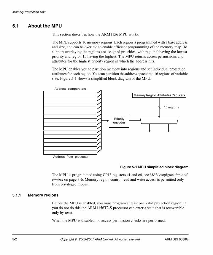
Memory Protection Unit
5.1 About the MPU
This section describes how the ARM1156 MPU works.
The MPU supports 16 memory regions. Each region is programmed with a base address and size, and can be overlaid to enable efficient programming of the memory map. To support overlaying the regions are assigned priorities, with region 0 having the lowest priority and region 15 having the highest. The MPU returns access permissions and attributes for the highest priority region in which the address hits.
The MPU enables you to partition memory into regions and set individual protection attributes for each region. You can partition the address space into 16 regions of variable size. Figure 5-1 shows a simplified block diagram of the MPU.
Figure 5-1 MPU simplified block diagram
The MPU is programmed using CP15 registers c1 and c6, see MPU configuration and control on page 3-6. Memory region control read and write access is permitted only from privileged modes.
5.1.1 Memory regions
Before the MPU is enabled, you must program at least one valid protection region. If you do not do this the ARM1156T2-S processor can enter a state that is recoverable only by reset.
When the MPU is disabled, no access permission checks are performed.
Priority
encoder
16 regions
Memory Region AttributesRegisters
Address comparators
Address from processor
5-2 Copyright © 2005-2007 ARM Limited. All rights reserved. ARM DDI 0338G
Memory Protection Unit
For more details on how to enable or disable the MPU, see Enabling and disabling the MPU on page 5-7.
You can partition the address space into a maximum of 16 regions. Each region is specified by the following:
• region base address
• region size
• region attributes
• region access permissions.
The ARM architecture uses constants known as inline literals to perform address calculations. These constants are automatically generated by the assembler and compiler and are stored inline with the instruction code. To ensure correct operation, instructions can only be executed from a memory region that has permission for data read access. For more details, see Memory access control on page 5-22.
You use CP15 register c6 to specify the:
• base address and region size properties
• region attributes.
Region base address
The base address defines the start of the memory region. You must align this to a region-sized boundary. For example, if a region size of 8KB is programmed for a given region, the base address must be a multiple of 8KB.
Note If the region is not aligned correctly, this results in Unpredictable behavior.
Region size
The region size is specified as a five-bit value, encoding a range of values from 32 Bytes (a cache-line length) to 4GB. The encoding is shown in Table 3-34 on page 3-70.
Region attributes
Each region has a number of attributes associated with it. These control how a memory access is performed when the processor core issues an address that falls within a given region. The attributes are:
• Memory Type (Strongly ordered, Device, or Normal)
• Shared/Non-Shared
• Non-Cacheable
ARM DDI 0338G Copyright © 2005-2007 ARM Limited. All rights reserved. 5-3
Memory Protection Unit
• Write-through Cacheable
• Write-back Cacheable.
The encoding is shown in Table 5-4 on page 5-19
Region access permissions
Each region has read/write access permissions for user and privileged modes.
For example, if a User mode application attempts to access a Privileged mode access only region a memory abort occurs.
The processor enters the abort exception mode and branches to Data Abort or Prefetch Abort accordingly.
5.1.2 Overlapping regions
You can program the MPU with two or more overlapping regions. When overlapping regions are programmed, a fixed priority scheme is applied to determine the overlapping region attributes that are applied to the memory access. Attributes for region 15 take highest priority, those for region 0 take lowest priority. See Memory attributes and types on page 5-10 for more details. For example:
Region 2 Is programmed to be 4KB in size, starting from address 0x3000 with AP [2:0] set to b110. (Privileged mode full access, User mode read-only.)
Region 1 Is programmed to be 16KB in size, starting from address 0x0000 with APn [2:0] set to b101. (Full user mode access only.)
When the processor performs a data write to address 0x3010 while in User mode, the address falls into both region 1 and region 2, as shown in Figure 5-2 on page 5-5. Because there is a clash, the attributes associated with region 2 are applied. Because User mode is read access, only for this region, a Data Abort occurs.
5-4 Copyright © 2005-2007 ARM Limited. All rights reserved. ARM DDI 0338G
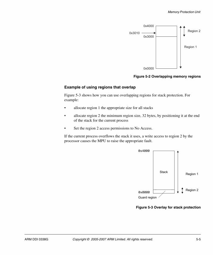
Memory Protection Unit
Figure 5-2 Overlapping memory regions
Example of using regions that overlap
Figure 5-3 shows how you can use overlapping regions for stack protection. For example:
• allocate region 1 the appropriate size for all stacks
• allocate region 2 the minimum region size, 32 bytes, by positioning it at the end of the stack for the current process
• Set the region 2 access permissions to No Access.
If the current process overflows the stack it uses, a write access to region 2 by the processor causes the MPU to raise the appropriate fault.
Figure 5-3 Overlay for stack protection
0x0000
Region 2
Region 1
0x3000
0x4000
0x3010
Stack
Guard region
Region 1
0x4000
0x0000Region 2
ARM DDI 0338G Copyright © 2005-2007 ARM Limited. All rights reserved. 5-5
Memory Protection Unit
5.1.3 Background regions
Overlapping regions increase the flexibility of how the regions can be mapped onto physical memory devices in the system. You can also use the overlapping properties to specify a background region. For example, you might have a number of physical memory areas sparsely distributed across the 4GB address space. If a programming error occurs therefore, it might be possible for the processor to issue an address that does not fall into any defined region.
If the address issued by the processor falls outside any of the defined regions, the ARM1156T2-S MPU is hard-wired to abort the access. You can override this behavior by programming region 0 to be a 4GB background region. In this way, if the address does not fall into any of the other 15 regions, the access is controlled by the attributes and access permissions you have specified for region 0.
5-6 Copyright © 2005-2007 ARM Limited. All rights reserved. ARM DDI 0338G
Memory Protection Unit
5.2 Enabling and disabling the MPU
Before the MPU is enabled, you must program at least one valid protection region. If you do not do this the ARM1156T2-S processor can enter a state that is recoverable only by reset.
When the MPU is disabled, no access permission checks are performed.
You can enable and disable the MPU by writing the M bit, bit 0, of the CP15 Control Register c1. On reset, this bit is cleared to 0, disabling the MPU.
5.2.1 Enabling the MPU
Before you enable the MPU you must:
1. Program all relevant CP15 registers. This includes setting up at least one memory region.
2. Clean and invalidate the data cache.
3. Invalidate the instruction caches.
When enabled, the behavior of the MPU is as follows:
• When the Load Store Unit or Prefetch Unit generates a memory access, the MPU compares the memory address with the programmed memory regions.
• If the address does not exist in a memory region, a background fault is signalled to the requesting block, along with status information to enable the Fault Status Register to be correctly formed.
• If a matching memory region is found, then the region information is used:
1. The access permission bits are used to determine if the access is permitted. If the access is not permitted the MPU signals a memory abort, otherwise the access is permitted to proceed. For more details on access permissions, see Memory access control on page 5-22.
2. The memory region attributes are used to determine if the access is cached, uncached or device and if it is shared, as described in Memory region attributes on page 5-19.
• If the address matches in multiple memory regions, then a fixed priority scheme selects the attributes for the highest numbered region.
Note Region 15 is highest priority and region 0 is lowest priority.
ARM DDI 0338G Copyright © 2005-2007 ARM Limited. All rights reserved. 5-7
Memory Protection Unit
5.2.2 Disabling the MPU
To disable the MPU:
1. Program all relevant CP15 registers. This includes setting up at least one memory region.
2. Clean the data cache.
3. Invalidate the instruction and data caches.
When the MPU is disabled:
• No memory access permission checks are performed, and no aborts are generated by the MPU.
• Data accesses to the lower 1.5GB of memory are managed as cacheable if the data cache is enabled by setting the C bit (bit 2) of CP15 register c1. Data accesses to the upper 2GB are treated as Noncacheable.
• All instruction accesses to the lower 2GB part of memory are treated as cacheable if the I bit (bit 12) of CP15 register 1 is set to 1. Accesses to the upper 2GB are treated as Noncacheable.
• Program flow prediction functions as normal, controlled by the state of the Z bit (bit 11) of CP15 register 1.
• All MPU and Cache CP15 operations work as normal when the MPU is disabled.
• Instruction and data prefetch operations work as normal. Data prefetch operations have no effect if the data cache is disabled. Instruction prefetch operations have no effect if the instruction cache is disabled.
• Accesses to the TCMs work as normal if one or both TCMs are enabled.
• The outer, or level two, memory attributes are the same as those for the inner, or level one, memory system.
Note If you change the MPU regions when the MPU is disabled, to prevent data loss, the data cache must be cleaned.
Figure 5-4 on page 5-9 shows the behavior of the memory map to data and instruction accesses and the address ranges when the MPU is disabled. This is also the default behavior of the memory map at reset.
5-8 Copyright © 2005-2007 ARM Limited. All rights reserved. ARM DDI 0338G
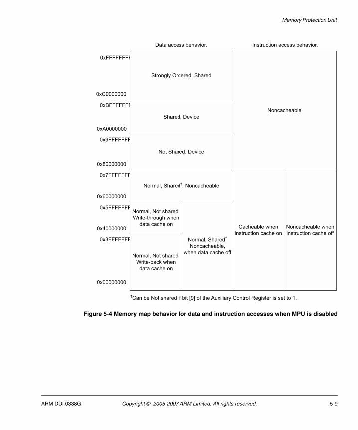
Memory Protection Unit
Figure 5-4 Memory map behavior for data and instruction accesses when MPU is disabled
ARM DDI 0338G Copyright © 2005-2007 ARM Limited. All rights reserved. 5-9
Memory Protection Unit
5.3 Memory attributes and types
The ARM1156T2-S processor provides a set of memory attributes that have characteristics that are suited to particular devices, including memory devices, that the memory map can contain. The memory attributes do not define the order that the regions of memory are accessed. There are three mutually exclusive main memory type attributes:
• Strongly Ordered
• Device
• Normal.
These are used to describe the memory regions. A summary of the memory attributes is shown in Table 5-1.
5.3.1 Normal memory attribute
The Normal memory attribute is defined on a per-region basis in the MPU and provides memory access orderings that are suitable for normal memory. This type of memory stores information without side effects. Normal memory can be writable or read-only.
Table 5-1 Memory attributes
Memory type attribute
Shared/ Non-Shared
Other attributes Description
Normal Shared Noncacheable/ Write-through Cacheable/ Write-back Cacheable
Designed to handle normal memory that is shared between several processors.
Non-Shared Noncacheable/ Write-through Cacheable/ Write-back Cacheable
Designed to handle normal memory that is used only by a single processor.
Device Shared - Designed to handle memory-mapped peripherals that are shared by several processors.
Non-Shared - Designed to handle memory-mapped peripherals that are used only by a single processor.
Strongly Ordered
- - All memory accesses to Strongly Ordered memory occur in program order. Some backwards compatibility constraints exist with ARMv5 instructions that change the CPSR interrupt masks (see Strongly Ordered memory attribute on page 5-14). All Strongly Ordered accesses are assumed to be shared.
5-10 Copyright © 2005-2007 ARM Limited. All rights reserved. ARM DDI 0338G
Memory Protection Unit
The behavior for:
• read-only normal memory is:
— two loads from a specific location return the same data for each load.
• writable normal memory, unless there is a change to the physical address mapping:
— a load from a specific location returns the most recently stored data at that location for the same processor
— two loads from a specific location, without a store in between, return the same data for each load.
This behavior describes most memory used in a system. In this section, writable normal memory and read-only normal memory are not distinguished.
Regions of memory with the Normal attribute can be Shared or Non-Shared, on a per-region basis in the MPU.
All explicit accesses to memory marked as Normal must correspond to the ordering requirements of accesses described in Ordering requirements for memory accesses on page 5-14. Accesses to Normal memory conform to the Weakly Ordered model of memory ordering. A description of this model is in standard texts describing memory ordering issues.
Shared Normal memory
The purpose of the Shared Normal memory attribute is to permit normal memory access by multiple processors or other system masters.
A region of memory marked as Shared Normal is one in which the effect of interposing a cache, or caches, on the memory system is entirely transparent. Implementations can use a variety of mechanisms to support this, from not caching accesses in shared regions to more complex hardware schemes for cache coherency for those regions. ARM1156T2-S processors do not cache shareable locations at level one.
In systems that implement a TCM, the regions of memory covered by the TCM are always Non-Shared. Marking an area of memory covered by the TCM as being Shared results in Unpredictable behavior.
Writes to Shared Normal memory might not be atomic. That is, all observers might not see the writes occurring at the same time. To preserve coherency where two writes are made to the same location, the order of those writes must be seen to be the same by all observers. Reads to Shared Normal memory that are aligned in memory to the size of the access are atomic.
ARM DDI 0338G Copyright © 2005-2007 ARM Limited. All rights reserved. 5-11
Memory Protection Unit
Non-Shared Normal memory
The Non-Shared Normal memory attribute describes normal memory that can be accessed only by a single processor.
A region of memory marked as Non-Shared Normal does not have any requirement to make the effect of a cache transparent.
Cacheable write-through, Cacheable write-back, and Noncacheable
In addition to marking a region of Normal memory as being Shared or Non-Shared, a region of memory marked as Normal can also be marked on a per-region basis in the MPU as being one of:
• Cacheable write-through
• Cacheable write-back
• Noncacheable.
This marking is independent of the marking of a region of memory as being Shared or Non-Shared, and indicates the required handling of the data region for reasons other than those to handle the requirements of shared data. As a result, it is acceptable for a region of memory that is marked as being Cacheable and Shared not to be held in the cache in an implementation that handles Shared regions as not caching the data.
5.3.2 Device memory attribute
The Device memory attribute is defined for memory locations where an access to the location can cause side effects, or where the value returned for a load can vary depending on the number of loads performed. Memory-mapped peripherals and I/O locations are typical examples of areas of memory that you must mark as Device. The marking of a region of memory as Device is performed on a per-region basis in the MPU.
Accesses to memory-mapped locations that have side effects that apply to memory of type Normal might require memory barriers to ensure correct execution. An example where this might be an issue is the programming of the control registers of a memory controller while accesses are being made to the memories controlled by the controller.
Instruction fetches must not be performed to areas of memory containing read-sensitive devices, because there is no ordering requirement between instruction fetches and explicit accesses. As a result, instruction fetches from such devices can result in Unpredictable behavior. Up to 64 bytes can be prefetched sequentially ahead of the current instruction being executed. To enable this, you must locate read-sensitive devices in memory in such a way to permit prefetching.
5-12 Copyright © 2005-2007 ARM Limited. All rights reserved. ARM DDI 0338G
Memory Protection Unit
Explicit accesses from the processor to regions of memory marked as Device occur in the size and order defined by the instruction. The number of location accesses is specified by the program. Accesses to regions of memory marked as Device are not restartable. Repeat accesses to such locations when there is only one access in the program are not possible in the ARM1156T2-S processor. An example of where a repeat access might be required is before and after an interrupt to enable the interrupt to abandon a slow access. These optimizations are not performed on regions of memory marked as Device.
In addition, address locations marked as Device are not held in a cache.
Shared and non-shared device memory
Regions of memory marked as Device can be characterized by the Shared attribute in the MPU. These memory regions can be marked as:
• Shared Device
• Non-Shared Device.
Explicit accesses to memory with each of the sets of attributes occur in program order relative to other explicit accesses to the same set of attributes.
All explicit accesses to memory marked as Device must correspond to the ordering requirements of accesses described in Ordering requirements for memory accesses on page 5-14.
In the ARM1156T2-S processor Non-Shared Device attribute is assigned to the peripheral Port and Shared Device attribute is assigned to the system bus. This enables predictable access times for local peripherals such as watchdog timers or interrupt controllers.
An example of an implementation where the Shared attribute is used to distinguish memory accesses is an implementation that supports a local bus for its private peripherals, while system peripherals are situated on the main system bus. Such a system can have more predictable access times for local peripherals such as watchdog timers or interrupt controllers.
For Shared Device memory, the data of a write is visible to all observers before the end of a Drain Write Buffer memory barrier. For Non-Shared Device memory, the data of a write is visible to the processor before the end of a Drain Write Buffer memory barrier (see Explicit memory barriers on page 5-17).
ARM DDI 0338G Copyright © 2005-2007 ARM Limited. All rights reserved. 5-13
Memory Protection Unit
5.3.3 Strongly Ordered memory attribute
Another memory attribute, Strongly Ordered, is defined on a per-region basis in the MPU. Accesses to memory marked as Strongly Ordered have a strong memory-ordering model with respect to all explicit memory accesses from that processor. An access to memory marked as Strongly Ordered acts as a memory barrier to all other explicit accesses from that processor, until the point at which the access is complete (that is, has changed the state of the target location or data has been returned). In addition, an access to memory marked as Strongly Ordered must complete before the end of a memory barrier (see Explicit memory barriers on page 5-17).
To maintain backwards compatibility with ARMv5 architecture, any ARMv5 instructions that implicitly or explicitly change the interrupt masks in the CSPR that appear in program order after a Strongly Ordered access must wait for the Strongly Ordered memory access to complete. These instructions are MSR with the control field mask bit set, and the flag setting variants of arithmetic and logical instructions whose destination register is r15, which copies the SPSR to CSPR. This requirement exists only for backwards compatibility with previous versions of the ARM architecture, and the behavior is deprecated in ARMv6. Programs must not rely on this behavior, but instead include an explicit memory barrier (see Explicit memory barriers on page 5-17) between the memory access and the following instruction.
The ARM1156T2-S processor does not require an explicit memory barrier in this situation, but for future compatibility it is recommended that programmers insert a memory barrier.
Explicit accesses from the processor to memory marked as Strongly Ordered occur at their program size, and the number of accesses that occur to such locations is the number that are specified by the program. Accesses to such locations are not repeated when there is only one access in the program. That is, the accesses from the processor to memory marked as Strongly Ordered are not restartable.
Address locations marked as Strongly Ordered are not held in a cache, and are treated as Shared memory locations.
For Strongly Ordered memory, the data and side effects of a write are visible to all observers before the end of a Drain Write Buffer memory barrier (see Explicit memory barriers on page 5-17).
5.3.4 Ordering requirements for memory accesses
The various memory types defined in this section have restrictions in the memory orderings that are permitted.
5-14 Copyright © 2005-2007 ARM Limited. All rights reserved. ARM DDI 0338G
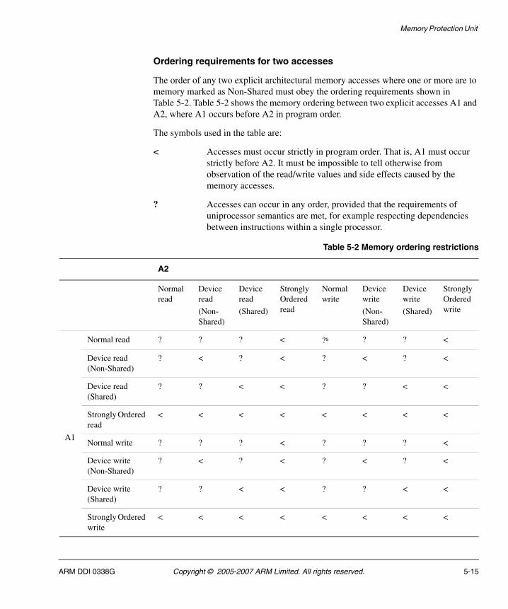
Memory Protection Unit
Ordering requirements for two accesses
The order of any two explicit architectural memory accesses where one or more are to memory marked as Non-Shared must obey the ordering requirements shown in Table 5-2. Table 5-2 shows the memory ordering between two explicit accesses A1 and A2, where A1 occurs before A2 in program order.
The symbols used in the table are:
< Accesses must occur strictly in program order. That is, A1 must occur strictly before A2. It must be impossible to tell otherwise from observation of the read/write values and side effects caused by the memory accesses.
? Accesses can occur in any order, provided that the requirements of uniprocessor semantics are met, for example respecting dependencies between instructions within a single processor.
Table 5-2 Memory ordering restrictions
A2
Normal read
Device read
(Non- Shared)
Device read
(Shared)
Strongly Ordered read
Normal write
Device write
(Non- Shared)
Device write
(Shared)
Strongly Ordered write
A1
Normal read ? ? ? < ?a ? ? <
Device read (Non-Shared)
? < ? < ? < ? <
Device read (Shared)
? ? < < ? ? < <
Strongly Ordered read
< < < < < < < <
Normal write ? ? ? < ? ? ? <
Device write (Non-Shared)
? < ? < ? < ? <
Device write (Shared)
? ? < < ? ? < <
Strongly Ordered write
< < < < < < < <
ARM DDI 0338G Copyright © 2005-2007 ARM Limited. All rights reserved. 5-15
Memory Protection Unit
There are no ordering requirements for implicit accesses to any type of memory.
Definition of program order of memory accesses
The program order of instruction execution is defined as the order of the instructions in the control flow trace. Two explicit memory accesses in an execution can either be:
Ordered Denoted by <. If the accesses are Ordered, then they must occur strictly in order.
Weakly Ordered Denoted by <=. If the accesses are Weakly Ordered, then they must occur in order or simultaneously.
The rules for determining this for two accesses A1 and A2 are:
1. If A1 and A2 are generated by two different instructions, then:
• A1 < A2 if the instruction that generates A1 occurs before the instruction that generates A2 in program order.
• A2 < A1 if the instruction that generates A2 occurs before the instruction that generates A1 in program order.
2. If A1 and A2 are generated by the same instruction, then:
• If A1 and A2 are the load and store generated by a SWP or SWPB instruction, then:
— A1 < A2 if A1 is the load and A2 is the store
— A2 < A1 if A2 is the load and A1 is the store.
• If A1 and A2 are two word loads generated by an LDC, LDRD, or LDM instruction, or two word stores generated by an STC, STRD, or STM instruction, but excluding LDM or STM instructions whose register list includes the PC, then:
— A1 <= A2 if the address of A1 is less than the address of A2
— A2 <= A1 if the address of A2 is less than the address of A1.
• If A1 and A2 are two word loads generated by an LDM instruction whose register list includes the PC or two word stores generated by an STM instruction whose register list includes the PC, then the program order of the memory operations is not defined.
Multiple load and store instructions (such as LDM, LDRD, STM, and STRD) generate multiple word accesses, each being a separate access to determine ordering.
a. ARM1156T2-S processor orders the normal read ahead of normal write.
5-16 Copyright © 2005-2007 ARM Limited. All rights reserved. ARM DDI 0338G
Memory Protection Unit
5.3.5 Explicit memory barriers
Two explicit memory barrier operations are described in this section:
• Data Memory Barrier
• Drain Write Buffer.
In addition, to ensure correct operation where the processor writes code, an explicit Flush Prefetch Buffer operation is provided.
These operations are implemented by writing to the CP15 Cache operation register c7. For details on how to use this register, see c7, Cache Operations Register on page 3-71.
Data Memory Barrier
This memory barrier ensures that all explicit memory transactions occurring in program order before this instruction are completed. No explicit memory transactions occurring in program order after this instruction are started until this instruction completes. Other instructions can complete out of order with the Data Memory Barrier instruction.
Drain Write Buffer
This memory barrier completes when all explicit memory transactions occurring in program order before this instruction are completed. No explicit memory transactions occurring in program order after this instruction are started until this instruction completes. In fact, no instructions occurring in program order until after the Drain Write Buffer complete.
For Shared memory, the data of a write is visible to all observers before the end of a Drain Write Buffer memory barrier.
For Strongly Ordered memory, the data and the side effects of a write are visible to all observers before the end of a Drain Write Buffer memory barrier.
For Non-Shared memory, the data of a write is visible to the processor before the end of a Drain Write Buffer memory barrier.
Flush Prefetch Buffer
The Flush Prefetch Buffer instruction flushes the pipeline in the processor, so that all instructions following the pipeline flush are fetched from memory, including the cache, after the instruction has been completed.
The Flush Prefetch Buffer is guaranteed to perform this function. Alternative methods of performing the same task, such as a branch instruction, can be optimized in the hardware to avoid the pipeline flush, for example, by using a branch predictor.
ARM DDI 0338G Copyright © 2005-2007 ARM Limited. All rights reserved. 5-17
Memory Protection Unit
Combining this with Drain Write Buffer, and potentially invalidating the instruction cache, ensures that any instructions written by the processor are executed.
The execution of a Drain Write Buffer instruction and the invalidation of the instruction cache and Flush Prefetch Buffer is the mechanism that guarantees the correct handling of the self-modifying code.
Memory synchronization primitives
Memory synchronization primitives exist to ensure synchronization between different processes, which might be running on the same processor or on different processors. You can use memory synchronization primitives in regions of memory marked as Shared and Non-Shared when the processes to be synchronized are running on the same processor. You must only use them in Shared areas of memory when the processes to be synchronized are running on different processors.
5.3.6 Backwards compatibility
The ARMv6 memory attributes are significantly different from those in previous versions of the architecture. Table 5-3 shows the interpretation of the earlier memory types in the light of this definition.
Table 5-3 Memory region backwards compatibility
Previous architectures ARMv6 attribute
NCNB (Noncacheable, Non Bufferable) Strongly Ordereda
a. Memory locations contained within the TCMs are treated as being Noncacheable, rather than Strongly Ordered or Shared Device.
NCB (Noncacheable, Bufferable) Shared Devicea
Write-through Cacheable, Bufferable Non-Shared Normal (Write-through cacheable)
Write-back Cacheable, Bufferable Non-Shared Normal (Write-back Cacheable)
5-18 Copyright © 2005-2007 ARM Limited. All rights reserved. ARM DDI 0338G
Memory Protection Unit
5.4 Memory region attributes
Each region has an associated set of memory region attributes. These control:
• accesses to the inner and outer caches
• how the write buffer is used
• if the memory region is shareable and must be kept coherent.
5.4.1 C and B bit, and type extension field encodings
The Region Access Control Registers use five bits to encode the memory region type. These are TEX[2:0], and the C and B bits. Table 5-4 shows the mapping of the Type Extension Field (TEX) and the Cacheable and Bufferable bits (C and B) to memory region type.
Additionally, the Region Access Control Registers contain the shared bit, S. This bit only applies to Normal, not Device or Strongly Ordered memory, and determines if the memory region is Shared (1), or Non-Shared (0).
Table 5-4 TEX field, and C and B bit encodings used in Region Access Control Registers
Attribute encodings
Description Memory type Region shareable?
TEX C B
b000 0 0 Strongly Ordered. Strongly Ordered Shareda
b000 0 1 Shared Device. Device Shareda
b000 1 0 Outer and Inner write-through,
No Allocate on Write.
Normal sb
b000 1 1 Outer and Inner write-back,
No Allocate on Write.
Normal sb
b001 0 0 Outer and Inner Noncacheable. Normal sb
b001 0 1 Reserved. Reserved Reserved
b001 1 0 Reserved. Reserved Reserved
b001 1 1 Reserved Reserved Reserved
b010 0 0 Non-Shared Device. Device Non-shareda
b010 0 1 Reserved. Reserved Reserved
ARM DDI 0338G Copyright © 2005-2007 ARM Limited. All rights reserved. 5-19
Memory Protection Unit
The Inner and Outer cache policy bits AA (C and B bits) and BB (TEX[1:0]) control the operation of memory accesses to the external memory. Table 5-5 indicates how the MPU and cache interpret the cache policy bits.
The terms Inner and Outer are applied to levels of caches that can be built in a system. Inner refers to the innermost caches, including level one. Outer refers to the outermost caches. The boundary between Inner and Outer caches is defined in the implementation of a cached system. Inner must always include level one. In a system with three levels of caches, an example is for the Inner attributes to apply to level one and level two, while the Outer attributes apply to level three. In a two-level system, it is envisaged that Inner always applies to level one and Outer to level two.
In ARM1156T2-S processors, Inner refers to level one and ACACHE shows the Outer Cacheable properties. The ASIDEBAND signals show the Inner Cacheable values. For an explanation of Strongly Ordered and Device see Memory attributes and types on page 5-10.
010 1 X Reserved. Reserved Reserved
011 X X Reserved. Reserved Reserved
1BB A A Cached memory:
BB = Outer policy
AA = Inner policy.
See Table 5-5.
Normal sb
a. Shared, regardless of the value of the S bit in the Region Access Control Registers.b. s is Shared if the value of the S bit in the Region Access Control Registers is 1, or Non-shared if the value of the S bit is 0.
Table 5-4 TEX field, and C and B bit encodings used in Region Access Control Registers (continued)
Attribute encodings
Description Memory type Region shareable?
TEX C B
Table 5-5 Cache policy bits
TEX[1:0] (BB) or CB (AA) bits Cache policy
b00 Noncacheable, Unbuffered.
b01 Write-back cached, Write Allocate, Buffered. Outer only.
b10 Write-through cached, No Allocate on Write, Buffered.
b11 Write-back cached, No Allocate on Write, Buffered.
5-20 Copyright © 2005-2007 ARM Limited. All rights reserved. ARM DDI 0338G
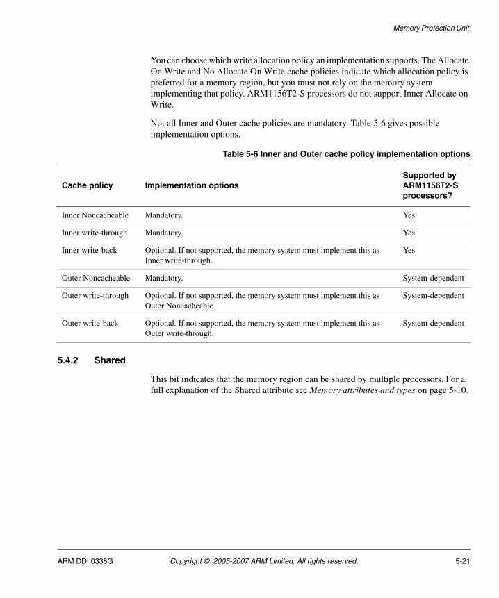
Memory Protection Unit
You can choose which write allocation policy an implementation supports. The Allocate On Write and No Allocate On Write cache policies indicate which allocation policy is preferred for a memory region, but you must not rely on the memory system implementing that policy. ARM1156T2-S processors do not support Inner Allocate on Write.
Not all Inner and Outer cache policies are mandatory. Table 5-6 gives possible implementation options.
5.4.2 Shared
This bit indicates that the memory region can be shared by multiple processors. For a full explanation of the Shared attribute see Memory attributes and types on page 5-10.
Table 5-6 Inner and Outer cache policy implementation options
Cache policy Implementation optionsSupported by ARM1156T2-S processors?
Inner Noncacheable Mandatory. Yes
Inner write-through Mandatory. Yes
Inner write-back Optional. If not supported, the memory system must implement this as Inner write-through.
Yes
Outer Noncacheable Mandatory. System-dependent
Outer write-through Optional. If not supported, the memory system must implement this as Outer Noncacheable.
System-dependent
Outer write-back Optional. If not supported, the memory system must implement this as Outer write-through.
System-dependent
ARM DDI 0338G Copyright © 2005-2007 ARM Limited. All rights reserved. 5-21
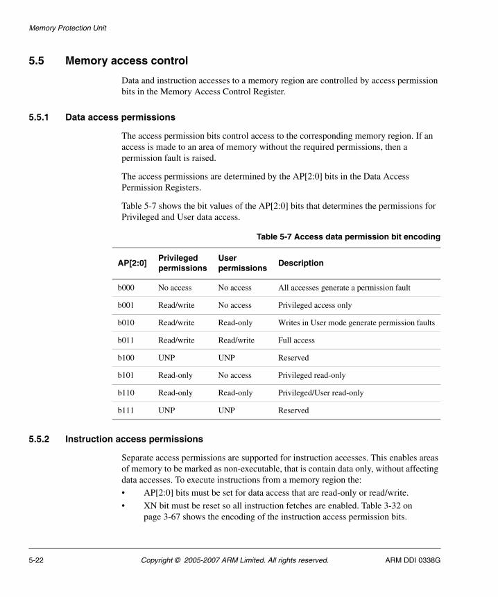
Memory Protection Unit
5.5 Memory access control
Data and instruction accesses to a memory region are controlled by access permission bits in the Memory Access Control Register.
5.5.1 Data access permissions
The access permission bits control access to the corresponding memory region. If an access is made to an area of memory without the required permissions, then a permission fault is raised.
The access permissions are determined by the AP[2:0] bits in the Data Access Permission Registers.
Table 5-7 shows the bit values of the AP[2:0] bits that determines the permissions for Privileged and User data access.
5.5.2 Instruction access permissions
Separate access permissions are supported for instruction accesses. This enables areas of memory to be marked as non-executable, that is contain data only, without affecting data accesses. To execute instructions from a memory region the:
• AP[2:0] bits must be set for data access that are read-only or read/write.
• XN bit must be reset so all instruction fetches are enabled. Table 3-32 on page 3-67 shows the encoding of the instruction access permission bits.
Table 5-7 Access data permission bit encoding
AP[2:0]Privileged permissions
User permissions
Description
b000 No access No access All accesses generate a permission fault
b001 Read/write No access Privileged access only
b010 Read/write Read-only Writes in User mode generate permission faults
b011 Read/write Read/write Full access
b100 UNP UNP Reserved
b101 Read-only No access Privileged read-only
b110 Read-only Read-only Privileged/User read-only
b111 UNP UNP Reserved
5-22 Copyright © 2005-2007 ARM Limited. All rights reserved. ARM DDI 0338G
Memory Protection Unit
5.6 MPU aborts
Mechanisms that can cause the ARM1156T2-S processor to take an exception because of a memory access are:
MPU fault The MPU detects a restriction and signals the processor.
Debug Abort Monitor debug-mode debug is enabled and a breakpoint or a watchpoint has been detected.
External abort The memory system signals an illegal or faulting memory access.
Collectively these are called aborts. Accesses that cause aborts are said to be aborted. If the memory request that aborts is an instruction fetch, a Prefetch Abort exception is raised if and when the processor attempts to execute the instruction corresponding to the aborted access. If the aborted access is a data access or a cache maintenance operation, a Data Abort exception is raised.
All Data Aborts, and aborts caused by cache maintenance operations, cause the Data Fault Status Register (DFSR) to be updated so that you can determine the cause of the abort.
For all aborts, excluding imprecise aborts, the Fault Address Register (FAR) is updated with the address that caused the abort. External Data Aborts and Parity Aborts can be imprecise and therefore the FAR does not contain the address of the abort. For more details on imprecise Data Aborts, see Imprecise Data Abort mask in the CPSR/SPSR on page 2-35.
For the precise value stored in the IFAR see c6, Instruction Fault Address Register on page 3-62.
Note The IFAR contains the physical address of the instruction that caused the abort.
For instruction aborts the value of r14 is used by the abort handler to determine the address that caused the abort.
5.6.1 External aborts
External memory errors are defined as those that occur in the memory system other than those that are detected by an MPU. External memory errors are expected to be extremely rare and are likely to be fatal to the running process. An example of an event that can cause an external memory error is an uncorrectable parity or ECC failure on a level two memory structure.
ARM DDI 0338G Copyright © 2005-2007 ARM Limited. All rights reserved. 5-23
Memory Protection Unit
The presence of a precise external abort is signaled in the Data or Instruction Fault Status Register.
The precise external abort model of VMSAv5 is not supported.
External abort on instruction fetch
Externally generated errors during an instruction prefetch are precise in nature, and are only recognized by the processor if it attempts to execute the instruction fetched from the location that caused the error. The resulting failure is reported in the Instruction Fault Status Register if no higher priority abort (including a Data Abort) has taken place.
The Fault Address Register is not updated on an external abort on instruction fetch.
External abort on data read/write
Externally generated errors during a data read or write can be imprecise. This means that r14_abt on entry into the abort handler on such an abort might not hold an address that is related to the instruction that caused the exception. Correspondingly, external aborts can be unrecoverable. See Aborts on page 2-32 for more details.
The Fault Address Register is not updated on an imprecise external abort on a data access.
5-24 Copyright © 2005-2007 ARM Limited. All rights reserved. ARM DDI 0338G
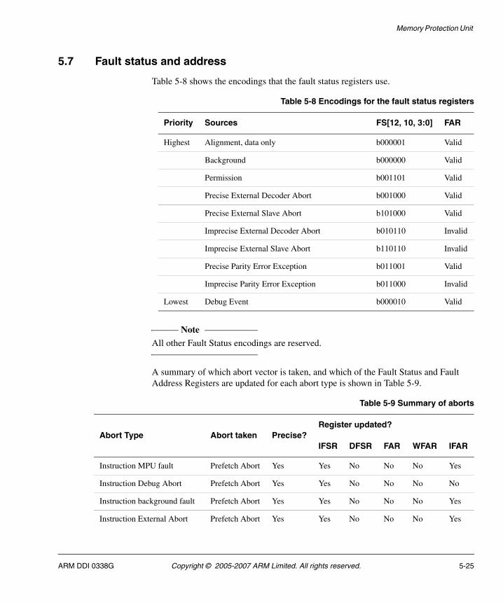
Memory Protection Unit
5.7 Fault status and address
Table 5-8 shows the encodings that the fault status registers use.
Note All other Fault Status encodings are reserved.
A summary of which abort vector is taken, and which of the Fault Status and Fault Address Registers are updated for each abort type is shown in Table 5-9.
Table 5-8 Encodings for the fault status registers
Priority Sources FS[12, 10, 3:0] FAR
Highest Alignment, data only b000001 Valid
Background b000000 Valid
Permission b001101 Valid
Precise External Decoder Abort b001000 Valid
Precise External Slave Abort b101000 Valid
Imprecise External Decoder Abort b010110 Invalid
Imprecise External Slave Abort b110110 Invalid
Precise Parity Error Exception b011001 Valid
Imprecise Parity Error Exception b011000 Invalid
Lowest Debug Event b000010 Valid
Table 5-9 Summary of aborts
Abort Type Abort taken Precise?Register updated?
IFSR DFSR FAR WFAR IFAR
Instruction MPU fault Prefetch Abort Yes Yes No No No Yes
Instruction Debug Abort Prefetch Abort Yes Yes No No No No
Instruction background fault Prefetch Abort Yes Yes No No No Yes
Instruction External Abort Prefetch Abort Yes Yes No No No Yes
ARM DDI 0338G Copyright © 2005-2007 ARM Limited. All rights reserved. 5-25
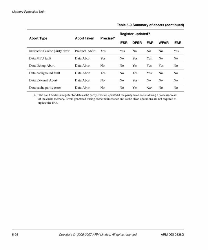
Memory Protection Unit
Instruction cache parity error Prefetch Abort Yes Yes No No No Yes
Data MPU fault Data Abort Yes No Yes Yes No No
Data Debug Abort Data Abort No No Yes Yes Yes No
Data background fault Data Abort Yes No Yes Yes No No
Data External Abort Data Abort No No Yes No No No
Data cache parity error Data Abort No No Yes Noa No No
a. The Fault Address Register for data cache parity errors is updated if the parity error occurs during a processor read of the cache memory. Errors generated during cache maintenance and cache clean operations are not required to update the FAR.
Table 5-9 Summary of aborts (continued)
Abort Type Abort taken Precise?Register updated?
IFSR DFSR FAR WFAR IFAR
5-26 Copyright © 2005-2007 ARM Limited. All rights reserved. ARM DDI 0338G
Memory Protection Unit
5.8 MPU fault checking
During the processing of a memory region, the MPU behaves differently because it is checking for faults. The MPU generates three types of fault:
• Alignment fault on page 5-28
• Background fault on page 5-29
• Permission fault on page 5-29.
Aborts that are detected by the MPU are taken before any external memory access takes place.
Alignment fault checking is enabled by the A bit in the Control Register CP15 c1. Alignment fault checking is independent of the MPU being enabled. Access permission faults are only generated when the MPU is enabled.
The access control mechanisms of the MPU detect the conditions that produce these faults. If a fault is detected as the result of a memory access, the MPU aborts the access and signals the fault condition to the processor. Status and address information about faults generated by data accesses are held in DFSR and FAR, see Fault status and address on page 5-25. Status information about faults generated by instruction fetches are held in IFSR.
An access violation for a given memory access inhibits any corresponding external access, and an abort is returned to the ARM1156T2-S processor.
5.8.1 Fault checking sequence
Figure 5-5 on page 5-28 shows the fault checking sequence for Memory Attributes Region.
ARM DDI 0338G Copyright © 2005-2007 ARM Limited. All rights reserved. 5-27
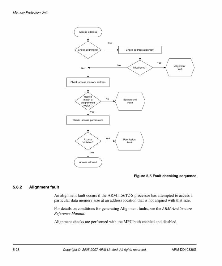
Memory Protection Unit
Figure 5-5 Fault checking sequence
5.8.2 Alignment fault
An alignment fault occurs if the ARM1156T2-S processor has attempted to access a particular data memory size at an address location that is not aligned with that size.
For details on conditions for generating Alignment faults, see the ARM Architecture Reference Manual.
Alignment checks are performed with the MPU both enabled and disabled.
Access address
Check alignment? Check address alignment
Misaligned?No
Yes
No Alignment
fault
Yes
Check access memory address
does it
match a
programmed
region ?
Background
Fault
Check access permissions
No
Yes
Access
Violation?
Permission
fault
Yes
No
Access allowed
5-28 Copyright © 2005-2007 ARM Limited. All rights reserved. ARM DDI 0338G
Memory Protection Unit
The alignment fault for doubleword load and store (LDRD, STRD) is strengthened:
• When U is set to 0 to trap if not aligned to an even word address. That is,
address bits [2:0] != 0.
• When U is set to 1 to trap if not aligned to a word boundary, That is, address bits [1:0] != 0.
5.8.3 Background fault
If the memory access address does not match one of the programmed memory regions, a background fault is generated.
5.8.4 Permission fault
The access permissions as defined in Memory Access Control are checked against the processor memory access. If the access is not enabled, an abort is signaled to the processor.
ARM DDI 0338G Copyright © 2005-2007 ARM Limited. All rights reserved. 5-29
Memory Protection Unit
5.9 Debug event
When Monitor debug-mode debug is enabled an abort can be taken caused by a breakpoint on an instruction access or a watchpoint on a data access. In both cases the memory system completes the access before the abort is taken. If an abort is taken when in Monitor debug-mode debug then the appropriate FSR (IFSR or DFSR) is updated to indicate a Debug Abort.
If a watchpoint is taken the WFAR is set to the address that caused the watchpoint. Watchpoints are not taken precisely because following instructions can run underneath load and store multiples. The debugger must read the WFAR to determine which instruction caused the debug event.
5-30 Copyright © 2005-2007 ARM Limited. All rights reserved. ARM DDI 0338G
Chapter 6 Unaligned and Mixed-Endian Data Access Support
This chapter describes the unaligned and mixed-endianness data access support for the ARM1156T2-S processor. It contains the following sections:
• About unaligned and mixed-endian support on page 6-2
• Unaligned access support on page 6-3
• Unaligned data access specification on page 6-7
• Operation of unaligned accesses on page 6-18
• Mixed-endian access support on page 6-22
• Instructions to reverse bytes in a general-purpose register on page 6-29
• Instructions to change the CPSR E bit on page 6-30.
ARM DDI 0338G Copyright © 2005-2007 ARM Limited. All rights reserved. 6-1
Unaligned and Mixed-Endian Data Access Support
6.1 About unaligned and mixed-endian support
The ARM1156T2-S processor executes the ARM architecture v6 instructions that support mixed-endian access in hardware, and assist unaligned data accesses. The extensions to ARMv6 that support unaligned and mixed-endian accesses include the following:
• CP15 register c1 has a U bit that enables unaligned support. This bit was specified as zero in previous architectures, and resets to zero for backwards compatibility.
• Architecturally defined unaligned word and halfword access specification for hardware implementation.
• Byte reverse instructions that operate on general-purpose register contents to support signed or unsigned halfword data values.
• Separate instruction and data endianness, with instructions fixed as little-endian format, naturally aligned, but with support for 32-bit word-invariant binary images and ROM.
• A PSR endian control flag, the E bit, cleared on reset and exception entry, that adds a byte-reverse operation to all entire instructions that read or write memory as data is loaded into and stored back out of the register file. In previous architectures this Program Status Register bit was specified as zero. It is not set in code written to conform to architectures before ARMv6.
• ARM and Thumb instructions to set and clear the E bit explicitly.
• A byte-invariant addressing scheme to support fine-grain big-endian and little-endian shared data structures, to conform to a shared memory standard.
The original ARM architecture was designed as little-endian. This provides a consistent address ordering of bits, bytes, words, cache lines, and pages, and is assumed by the documentation of instruction set encoding and memory and register bit significance. Subsequently, big-endian support was added to enable big-endian byte addressing of memory. A little-endian nomenclature is used for bit-ordering and byte addressing throughout this manual.
6-2 Copyright © 2005-2007 ARM Limited. All rights reserved. ARM DDI 0338G
Unaligned and Mixed-Endian Data Access Support
6.2 Unaligned access support
Instructions must always be aligned as follows:
• ARM 32-bit instructions must be word boundary aligned (Address [1:0] = b00)
• Thumb instructions must be halfword boundary aligned (Address [0] = 0).
Unaligned data access support is described in:
• Word-invariant mode support
• ARMv6 extensions
• Word-invariant mode and ARMv6 configurations on page 6-4
• Word-invariant data access in ARMv6 (U=0) on page 6-4
• Support for unaligned data access in ARMv6 (U=1) on page 6-5
• ARMv6 unaligned data access restrictions on page 6-5.
6.2.1 Word-invariant mode support
For ARM architectures prior to ARM architecture v6, data access to non-aligned word and halfword data was treated as aligned from the memory interface perspective. That is, the address is treated as truncated with Address[1:0] treated as zero for word accesses, and Address[0] treated as zero for halfword accesses.
Load single word ARM instructions are also architecturally defined to rotate right the word aligned data transferred by a non word-aligned access. See the ARM Architecture Reference Manual.
Alignment fault checking is specified for processors with architecturally compliant Memory Protection Units (MPUs), under control of CP15 Register c1 A bit, bit 1. When a transfer is not naturally aligned to the size of data transferred, a Data Abort is signaled with an Alignment fault status code. See the ARM Architecture Reference Manual for more details.
6.2.2 ARMv6 extensions
ARMv6 adds unaligned word and halfword load and store data access support. When enabled, one or more memory accesses are used to generate the required transfer of adjacent bytes transparently, apart from a potentially greater access time where the transaction crosses a word-boundary.
Note The memory management specification defines a programmable mechanism to enable unaligned access support. This is controlled and programmed using the CP15 register c1 U bit, bit 22.
ARM DDI 0338G Copyright © 2005-2007 ARM Limited. All rights reserved. 6-3
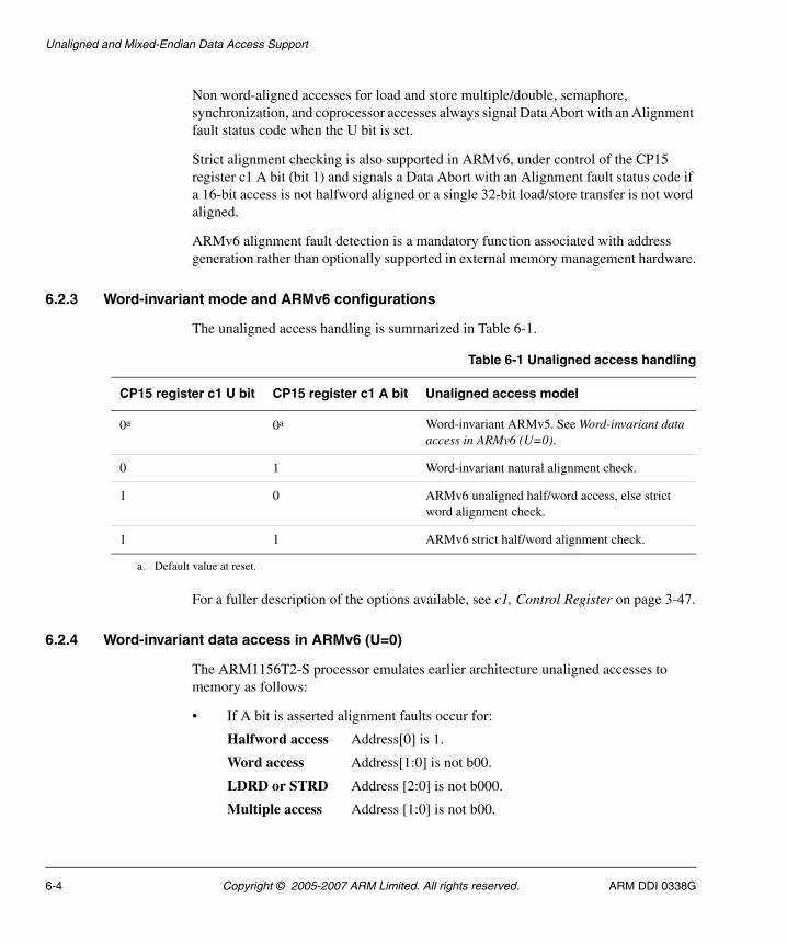
Unaligned and Mixed-Endian Data Access Support
Non word-aligned accesses for load and store multiple/double, semaphore, synchronization, and coprocessor accesses always signal Data Abort with an Alignment fault status code when the U bit is set.
Strict alignment checking is also supported in ARMv6, under control of the CP15 register c1 A bit (bit 1) and signals a Data Abort with an Alignment fault status code if a 16-bit access is not halfword aligned or a single 32-bit load/store transfer is not word aligned.
ARMv6 alignment fault detection is a mandatory function associated with address generation rather than optionally supported in external memory management hardware.
6.2.3 Word-invariant mode and ARMv6 configurations
The unaligned access handling is summarized in Table 6-1.
For a fuller description of the options available, see c1, Control Register on page 3-47.
6.2.4 Word-invariant data access in ARMv6 (U=0)
The ARM1156T2-S processor emulates earlier architecture unaligned accesses to memory as follows:
• If A bit is asserted alignment faults occur for:
Halfword access Address[0] is 1.
Word access Address[1:0] is not b00.
LDRD or STRD Address [2:0] is not b000.
Multiple access Address [1:0] is not b00.
Table 6-1 Unaligned access handling
CP15 register c1 U bit CP15 register c1 A bit Unaligned access model
0a 0a Word-invariant ARMv5. See Word-invariant data access in ARMv6 (U=0).
0 1 Word-invariant natural alignment check.
1 0 ARMv6 unaligned half/word access, else strict word alignment check.
1 1 ARMv6 strict half/word alignment check.
a. Default value at reset.
6-4 Copyright © 2005-2007 ARM Limited. All rights reserved. ARM DDI 0338G
Unaligned and Mixed-Endian Data Access Support
• If alignment faults are enabled and the access is not aligned then the Data Abort vector is entered with an Alignment fault status code.
• If no alignment fault is enabled, that is, if bit 1 of CP15 register c1, the A bit, is not set:
Byte access Memory interface uses full Address [31:0].
Halfword access Memory interface uses Address [31:1]. Address [0] asserted as 0.
Word access Memory interface uses Address [31:2]. Address [1:0] asserted as 0.
— ARM load data rotates the aligned read data and rotates this right by the byte-offset denoted by Address [1:0], see the ARM Architecture Reference Manual.
— ARM and Thumb load-multiple accesses always treated as aligned. No rotation of read data.
— ARM and Thumb store word and store multiple treated as aligned. No rotation of write data.
— ARM load and store doubleword operations treated as 64-bit aligned.
— Thumb load word data operations are Unpredictable if not word aligned.
— ARM and Thumb halfword data accesses are Unpredictable if not halfword aligned.
6.2.5 Support for unaligned data access in ARMv6 (U=1)
The ARM1156T2-S processor memory interfaces can generate unaligned low order byte address offsets only for halfword and single word load and store operations, and byte accesses unless the A bit is set. These accesses produce an alignment fault if the A bit is set, and for some of the cases described in ARMv6 unaligned data access restrictions.
If alignment faults are enabled and the access is not aligned then the Data Abort vector is entered with an Alignment Fault status code.
6.2.6 ARMv6 unaligned data access restrictions
The following restrictions apply for ARMv6 unaligned data access:
• Accesses are not guaranteed atomic. They might be synthesized out of a series of aligned operations in a shared memory system without guaranteeing locked transaction cycles.
• Unaligned accesses loading the PC produce an alignment trap.
ARM DDI 0338G Copyright © 2005-2007 ARM Limited. All rights reserved. 6-5
Unaligned and Mixed-Endian Data Access Support
• Accesses typically take a number of cycles to complete compared to a naturally aligned transfer. The real-time implications must be carefully analyzed and key data structures might require to have their alignment adjusted for optimum performance.
• Accesses can abort on either or both halves of an access where this occurs over a memory region boundary. The Data Abort handler must handle restartable aborts carefully after an Alignment fault status code is signaled.
As a result, shared memory schemes must not rely on seeing monotonic updates of non-aligned data of loads, stores, and swaps for data items greater than byte width. Unaligned access operations must not be used for accessing Device memory-mapped registers, and must be used with care in Shared memory structures that are protected by aligned semaphores or synchronization variables.
An Alignment fault occurs if unaligned accesses to Strongly Ordered or Device memory are attempted regardless of the setting of the A bit.
Swap and synchronization primitives, multiple-word or coprocessor access produce an alignment fault regardless of the setting of the A bit.
6-6 Copyright © 2005-2007 ARM Limited. All rights reserved. ARM DDI 0338G
Unaligned and Mixed-Endian Data Access Support
6.3 Unaligned data access specification
The architectural specification of unaligned data representations is defined in terms of bytes transferred between memory and register, regardless of bus width and bus endianness.
Little-endian data items are described using lower-case byte labeling bX…b0 (byte X to byte 0) and a pointer is always treated as pointing to the least significant byte of the addressed data.
Big-endian data items are described using upper-case byte labeling B0…BX (BYTE0 to BYTEX) and a pointer is always treated as pointing to the most significant byte of the addressed data.
6.3.1 Load unsigned byte, endian independent
The addressed byte is loaded from memory into the low eight bits of the general-purpose register and the upper 24 bits are zeroed (Figure 6-1).
Figure 6-1 Load unsigned byte
6.3.2 Load signed byte, endian independent
The addressed byte is loaded from the memory into the low eight bits of the general-purpose register and the sign bit is extended into the upper 24 bits of the register (Figure 6-2 on page 6-8).
b
Memory Register
31 23 15 7 0
Address
A[31:0]
7 0
0 0 0 b
ARM DDI 0338G Copyright © 2005-2007 ARM Limited. All rights reserved. 6-7
Unaligned and Mixed-Endian Data Access Support
Figure 6-2 Load signed byte
In Figure 6-2, se means b (bit 7) sign extension.
6.3.3 Store byte, endian independent
The low eight bits of the general-purpose register are stored into the addressed byte in memory (Figure 6-3).
Figure 6-3 Store byte
6.3.4 Load unsigned halfword, little-endian
The addressed byte-pair is loaded from memory into the low 16 bits of the general-purpose register, and the upper 16 bits are zeroed so that the least-significant addressed byte in memory appears in bits [7:0] of the ARM register (Figure 6-4 on page 6-9).
b
Memory Register
31 23 15 7 0
Address
A[31:0]
7 0
se se se b
Register
31 23 15 7 0
x x x b b
Memory
Address
A[31:0]
7 0
6-8 Copyright © 2005-2007 ARM Limited. All rights reserved. ARM DDI 0338G
Unaligned and Mixed-Endian Data Access Support
Figure 6-4 Load unsigned halfword, little-endian
If strict alignment fault checking is enabled and Address bit 0 is not zero, then a Data Abort is generated and the MPU returns an Alignment fault in the Fault Status Register.
6.3.5 Load unsigned halfword, big-endian
The addressed byte-pair is loaded from memory into the low 16 bits of the general-purpose register, and the upper 16 bits are zeroed so that the most-significant addressed byte in memory appears in bits [15:8] of the ARM register (Figure 6-5).
Figure 6-5 Load unsigned halfword, big-endian
If strict alignment fault checking is enabled and Address bit 0 is not zero, then a Data Abort is generated and the MPU returns an Alignment fault in the Fault Status Register.
b1
b0
Memory Register
31 23 15 7 0
Address
A[31:0]
7 0
0 0 b1 b0
+1 msbyte
lsbyte
B1
B0
Memory Register
31 23 15 7 0
Address
A[31:0]
7 0
0 0 B0 B1
+1 lsbyte
msbyte
ARM DDI 0338G Copyright © 2005-2007 ARM Limited. All rights reserved. 6-9
Unaligned and Mixed-Endian Data Access Support
6.3.6 Load signed halfword, little-endian
The addressed byte-pair is loaded from memory into the low 16-bits of the general-purpose register, so that the least-significant addressed byte in memory appears in bits [7:0] of the ARM register and the upper 16 bits are sign-extended from bit 15 (Figure 6-6).
Figure 6-6 Load signed halfword, little-endian
In Figure 6-6, se1 means bit 15 (b1 bit 7) sign extended.
If strict alignment fault checking is enabled and Address bit 0 is not zero, then a Data Abort is generated and the MPU returns an Alignment fault in the Fault Status Register.
6.3.7 Load signed halfword, big-endian
The addressed byte-pair is loaded from memory into the low 16-bits of the general-purpose register, so that the most significant addressed byte in memory appears in bits [15:8] of the ARM register and bits [31:16] replicate the sign bit in bit 15 (Figure 6-7 on page 6-11).
b1
b0
Memory Register
31 23 15 7 0
Address
A[31:0]
7 0
se1 se1 b1 b0
+1 msbyte
lsbyte
6-10 Copyright © 2005-2007 ARM Limited. All rights reserved. ARM DDI 0338G
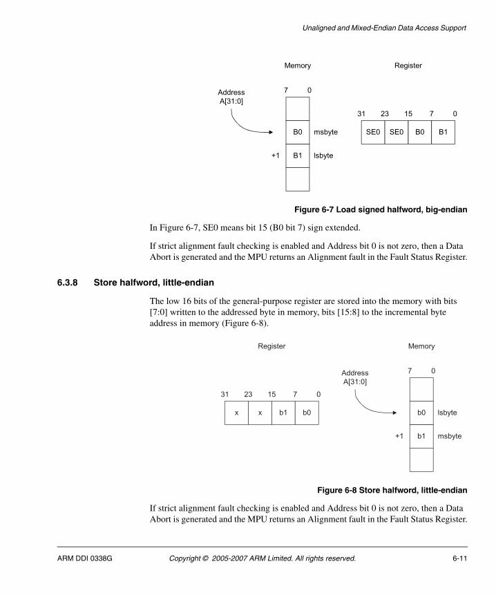
Unaligned and Mixed-Endian Data Access Support
Figure 6-7 Load signed halfword, big-endian
In Figure 6-7, SE0 means bit 15 (B0 bit 7) sign extended.
If strict alignment fault checking is enabled and Address bit 0 is not zero, then a Data Abort is generated and the MPU returns an Alignment fault in the Fault Status Register.
6.3.8 Store halfword, little-endian
The low 16 bits of the general-purpose register are stored into the memory with bits [7:0] written to the addressed byte in memory, bits [15:8] to the incremental byte address in memory (Figure 6-8).
Figure 6-8 Store halfword, little-endian
If strict alignment fault checking is enabled and Address bit 0 is not zero, then a Data Abort is generated and the MPU returns an Alignment fault in the Fault Status Register.
B1
B0
Memory Register
31 23 15 7 0
Address
A[31:0]
7 0
SE0 SE0 B0 B1
+1 lsbyte
msbyte
Register
31 23 15 7 0
x x b1 b0
b1
b0
Memory
Address
A[31:0]
7 0
+1 msbyte
lsbyte
ARM DDI 0338G Copyright © 2005-2007 ARM Limited. All rights reserved. 6-11
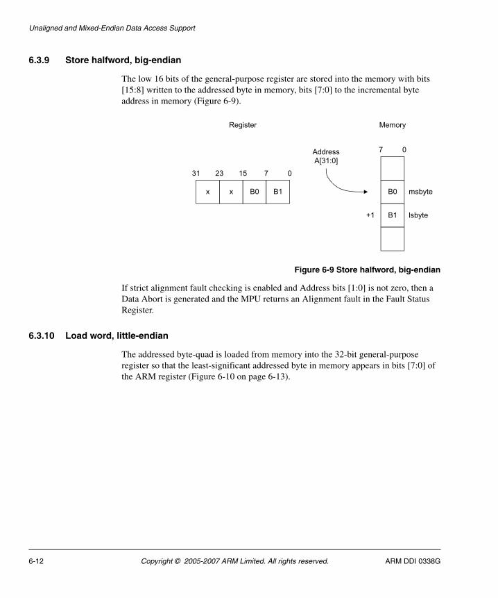
Unaligned and Mixed-Endian Data Access Support
6.3.9 Store halfword, big-endian
The low 16 bits of the general-purpose register are stored into the memory with bits [15:8] written to the addressed byte in memory, bits [7:0] to the incremental byte address in memory (Figure 6-9).
Figure 6-9 Store halfword, big-endian
If strict alignment fault checking is enabled and Address bits [1:0] is not zero, then a Data Abort is generated and the MPU returns an Alignment fault in the Fault Status Register.
6.3.10 Load word, little-endian
The addressed byte-quad is loaded from memory into the 32-bit general-purpose register so that the least-significant addressed byte in memory appears in bits [7:0] of the ARM register (Figure 6-10 on page 6-13).
Register
31 23 15 7 0
x x B0 B1
B1
B0
Memory
Address
A[31:0]
7 0
+1 lsbyte
msbyte
6-12 Copyright © 2005-2007 ARM Limited. All rights reserved. ARM DDI 0338G
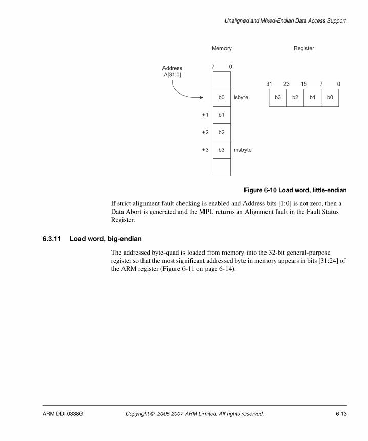
Unaligned and Mixed-Endian Data Access Support
Figure 6-10 Load word, little-endian
If strict alignment fault checking is enabled and Address bits [1:0] is not zero, then a Data Abort is generated and the MPU returns an Alignment fault in the Fault Status Register.
6.3.11 Load word, big-endian
The addressed byte-quad is loaded from memory into the 32-bit general-purpose register so that the most significant addressed byte in memory appears in bits [31:24] of the ARM register (Figure 6-11 on page 6-14).
b1
b0
Memory Register
31 23 15 7 0
Address
A[31:0]
7 0
b3 b2 b1 b0
b2
+1
msbyte
lsbyte
b3
+2
+3
ARM DDI 0338G Copyright © 2005-2007 ARM Limited. All rights reserved. 6-13
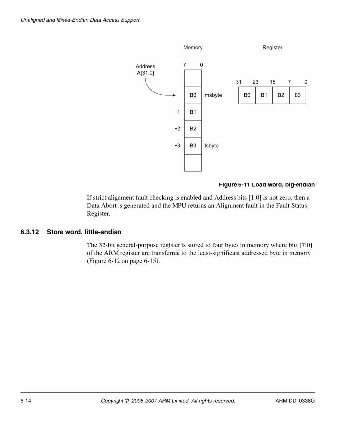
Unaligned and Mixed-Endian Data Access Support
Figure 6-11 Load word, big-endian
If strict alignment fault checking is enabled and Address bits [1:0] is not zero, then a Data Abort is generated and the MPU returns an Alignment fault in the Fault Status Register.
6.3.12 Store word, little-endian
The 32-bit general-purpose register is stored to four bytes in memory where bits [7:0] of the ARM register are transferred to the least-significant addressed byte in memory (Figure 6-12 on page 6-15).
B1
B0
Memory Register
31 23 15 7 0
Address
A[31:0]
7 0
B0 B1 B2 B3
B2
+1
lsbyte
msbyte
B3
+2
+3
6-14 Copyright © 2005-2007 ARM Limited. All rights reserved. ARM DDI 0338G
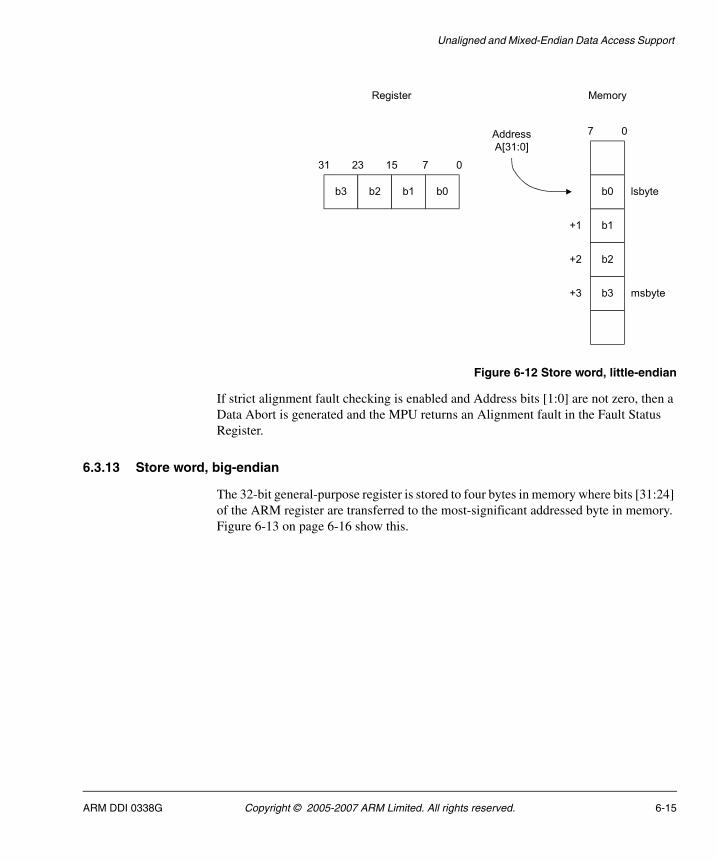
Unaligned and Mixed-Endian Data Access Support
Figure 6-12 Store word, little-endian
If strict alignment fault checking is enabled and Address bits [1:0] are not zero, then a Data Abort is generated and the MPU returns an Alignment fault in the Fault Status Register.
6.3.13 Store word, big-endian
The 32-bit general-purpose register is stored to four bytes in memory where bits [31:24] of the ARM register are transferred to the most-significant addressed byte in memory. Figure 6-13 on page 6-16 show this.
Register
31 23 15 7 0
b3 b2 b1 b0
b1
b0
Memory
Address
A[31:0]
7 0
b2
+1
msbyte
lsbyte
b3
+2
+3
ARM DDI 0338G Copyright © 2005-2007 ARM Limited. All rights reserved. 6-15
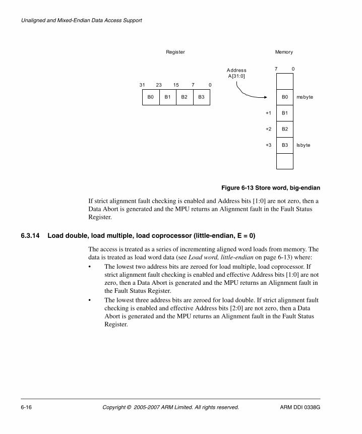
Unaligned and Mixed-Endian Data Access Support
Figure 6-13 Store word, big-endian
If strict alignment fault checking is enabled and Address bits [1:0] are not zero, then a Data Abort is generated and the MPU returns an Alignment fault in the Fault Status Register.
6.3.14 Load double, load multiple, load coprocessor (little-endian, E = 0)
The access is treated as a series of incrementing aligned word loads from memory. The data is treated as load word data (see Load word, little-endian on page 6-13) where:
• The lowest two address bits are zeroed for load multiple, load coprocessor. If strict alignment fault checking is enabled and effective Address bits [1:0] are not zero, then a Data Abort is generated and the MPU returns an Alignment fault in the Fault Status Register.
• The lowest three address bits are zeroed for load double. If strict alignment fault checking is enabled and effective Address bits [2:0] are not zero, then a Data Abort is generated and the MPU returns an Alignment fault in the Fault Status Register.
Register
31 23 15 7 0
B0 B1 B2 B3
B1
B0
Memory
Address
A[31:0]
7 0
B2
+1
lsbyte
msbyte
B3
+2
+3
6-16 Copyright © 2005-2007 ARM Limited. All rights reserved. ARM DDI 0338G
Unaligned and Mixed-Endian Data Access Support
6.3.15 Load double, load multiple, load coprocessor (big-endian, E=1)
The access is treated as a series of incrementing aligned word loads from memory. The data is treated as load word data (see Load word, big-endian on page 6-14) where:
• The lowest two address bits are zeroed for load multiple, load coprocessor. If strict alignment fault checking is enabled and effective Address bits [1:0] are not zero, then a Data Abort is generated and the MPU returns an Alignment fault in the Fault Status Register.
• The lowest three address bits are zeroed for load double. If strict alignment fault checking is enabled and effective Address bits [2:0] are not zero, then a Data Abort is generated and the MPU returns an Alignment fault in the Fault Status Register.
6.3.16 Store double, store multiple, store coprocessor (little-endian, E=0)
The access is treated as a series of incrementing aligned word stores to memory. The data is treated as store word data (see Store word, little-endian on page 6-15) where:
• The lowest two address bits are zeroed for load multiple, load coprocessor. If strict alignment fault checking is enabled and effective Address bits [1:0] are not zero, then a Data Abort is generated and the MPU returns an Alignment fault in the Fault Status Register.
• The lowest three address bits are zeroed for load double. If strict alignment fault checking is enabled and effective Address bits [2:0] are not zero, then a Data Abort is generated and the MPU returns an Alignment fault in the Fault Status Register.
6.3.17 Store double, store multiple, store coprocessor (big-endian, E=1)
The access is treated as a series of incrementing aligned word stores to memory. The data is treated as store word data (see Store word, big-endian on page 6-16) where:
• The lowest two address bits are zeroed for load multiple, load coprocessor. If strict alignment fault checking is enabled and effective Address bits [1:0] are not zero, then a Data Abort is generated and the MPU returns an Alignment fault in the Fault Status Register.
• The lowest three address bits are zeroed for load double. If strict alignment fault checking is enabled and effective Address bits [2:0] are not zero, then a Data Abort is generated and the MPU returns an Alignment fault in the Fault Status Register.
ARM DDI 0338G Copyright © 2005-2007 ARM Limited. All rights reserved. 6-17
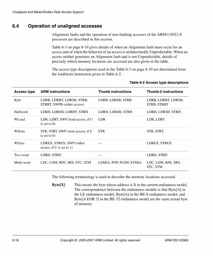
Unaligned and Mixed-Endian Data Access Support
6.4 Operation of unaligned accesses
Alignment faults and the operation of non-faulting accesses of the ARM1156T2-S processor are described in this section.
Table 6-3 on page 6-19 gives details of when an Alignment fault must occur for an access and of when the behavior of an access is architecturally Unpredictable. When an access neither generates an Alignment fault and is not Unpredictable, details of precisely which memory locations are accessed are also given in the table.
The access type descriptions used in the Table 6-3 on page 6-19 are determined from the load/store instruction given in Table 6-2.
The following terminology is used to describe the memory locations accessed:
Byte[X] This means the byte whose address is X in the current endianness model. The correspondence between the endianness models is that Byte[A] in the LE endianness model, Byte[A] in the BE-8 endianness model, and Byte[A EOR 3] in the BE-32 endianness model are the same actual byte of memory.
Table 6-2 Access type descriptions
Access type ARM instructions Thumb instructions Thumb-2 instructions
Byte LDRB, LDRBT, LDRSB, STRB, STRBT, SWPB (either access)
LDRB, LDRSB, STRB LDRB, LDRBT, LDRSB, STRB, STRBT
Halfword LDRH, LDRSH, LDRHT, STRH LDRH, LDRSH, STRH LDRH, LDRSH, STRH
WLoad LDR, LDRT, SWP (load access, if U is set to 0)
LDR LDR, LDRT
WStore STR, STRT, SWP (store access, if U is set to 0)
STR STR, STRT,
WSync LDREX, STREX, SWP (either access, if U is set to 1)
--- LDREX, STREX
Two-word LDRD, STRD --- LDRD, STRD
Multi-word LDC, LDM, RFE, SRS, STC, STM LDMIA, POP, PUSH, STMIA LDC, LDM, RFE, SRS, STC, STM
6-18 Copyright © 2005-2007 ARM Limited. All rights reserved. ARM DDI 0338G
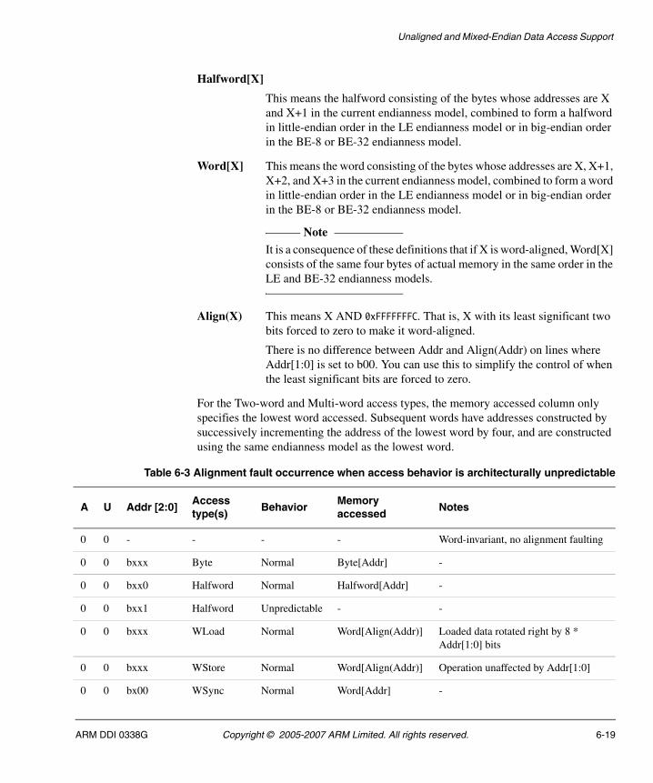
Unaligned and Mixed-Endian Data Access Support
Halfword[X]
This means the halfword consisting of the bytes whose addresses are X and X+1 in the current endianness model, combined to form a halfword in little-endian order in the LE endianness model or in big-endian order in the BE-8 or BE-32 endianness model.
Word[X] This means the word consisting of the bytes whose addresses are X, X+1, X+2, and X+3 in the current endianness model, combined to form a word in little-endian order in the LE endianness model or in big-endian order in the BE-8 or BE-32 endianness model.
Note It is a consequence of these definitions that if X is word-aligned, Word[X]
consists of the same four bytes of actual memory in the same order in the LE and BE-32 endianness models.
Align(X) This means X AND 0xFFFFFFFC. That is, X with its least significant two bits forced to zero to make it word-aligned.
There is no difference between Addr and Align(Addr) on lines where Addr[1:0] is set to b00. You can use this to simplify the control of when the least significant bits are forced to zero.
For the Two-word and Multi-word access types, the memory accessed column only specifies the lowest word accessed. Subsequent words have addresses constructed by successively incrementing the address of the lowest word by four, and are constructed using the same endianness model as the lowest word.
Table 6-3 Alignment fault occurrence when access behavior is architecturally unpredictable
A U Addr [2:0]Access type(s)
BehaviorMemory accessed
Notes
0 0 - - - - Word-invariant, no alignment faulting
0 0 bxxx Byte Normal Byte[Addr] -
0 0 bxx0 Halfword Normal Halfword[Addr] -
0 0 bxx1 Halfword Unpredictable - -
0 0 bxxx WLoad Normal Word[Align(Addr)] Loaded data rotated right by 8 * Addr[1:0] bits
0 0 bxxx WStore Normal Word[Align(Addr)] Operation unaffected by Addr[1:0]
0 0 bx00 WSync Normal Word[Addr] -
ARM DDI 0338G Copyright © 2005-2007 ARM Limited. All rights reserved. 6-19
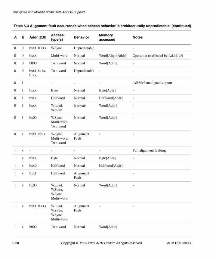
Unaligned and Mixed-Endian Data Access Support
0 0 bxx1, b x1x WSync Unpredictable -
0 0 bxxx Multi-word Normal Word[Align(Addr)] Operation unaffected by Addr[1:0]
0 0 b000 Two-word Normal Word[Addr] -
0 0 bxx1, bx1x, b1xx
Two-word Unpredictable - -
0 1 - - - - ARMv6 unaligned support
0 1 bxxx Byte Normal Byte[Addr] -
0 1 bxxx Halfword Normal Halfword[Addr] -
0 1 bxxx WLoad, WStore
Normala Word[Addr] -
0 1 bx00 WSync, Multi-word, Two-word
Normal Word[Addr] -
0 1 bxx1, bx1x WSync, Multi-word, Two-word
Alignment Fault
- -
1 x - - - - Full alignment faulting
1 x bxxx Byte Normal Byte[Addr] -
1 x bxx0 Halfword Normal Halfword[Addr] -
1 x bxx1 Halfword Alignment Fault
-
1 x bx00 WLoad, WStore, WSync, Multi-word
Normal Word[Addr] -
1 x bxx1, b x1x WLoad, WStore, WSync, Multi-word
Alignment Fault
- -
1 x b000 Two-word Normal Word[Addr]
Table 6-3 Alignment fault occurrence when access behavior is architecturally unpredictable (continued)
A U Addr [2:0]Access type(s)
BehaviorMemory accessed
Notes
6-20 Copyright © 2005-2007 ARM Limited. All rights reserved. ARM DDI 0338G
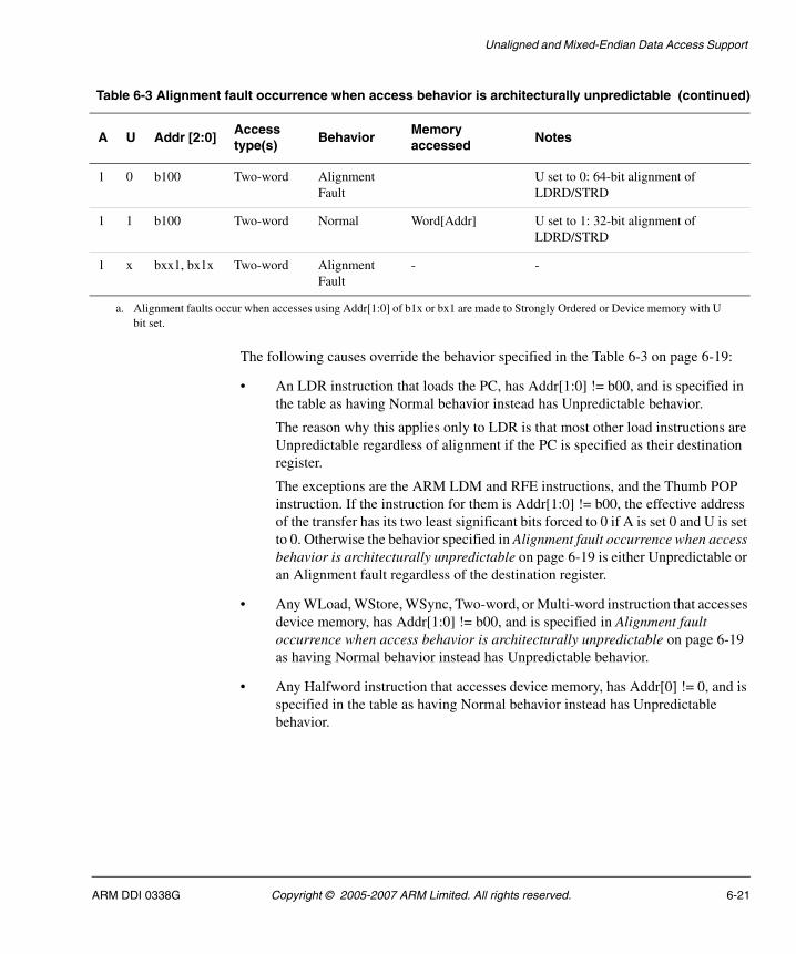
Unaligned and Mixed-Endian Data Access Support
The following causes override the behavior specified in the Table 6-3 on page 6-19:
• An LDR instruction that loads the PC, has Addr[1:0] != b00, and is specified in the table as having Normal behavior instead has Unpredictable behavior.
The reason why this applies only to LDR is that most other load instructions are Unpredictable regardless of alignment if the PC is specified as their destination register.
The exceptions are the ARM LDM and RFE instructions, and the Thumb POP instruction. If the instruction for them is Addr[1:0] != b00, the effective address of the transfer has its two least significant bits forced to 0 if A is set 0 and U is set to 0. Otherwise the behavior specified in Alignment fault occurrence when access behavior is architecturally unpredictable on page 6-19 is either Unpredictable or an Alignment fault regardless of the destination register.
• Any WLoad, WStore, WSync, Two-word, or Multi-word instruction that accesses device memory, has Addr[1:0] != b00, and is specified in Alignment fault occurrence when access behavior is architecturally unpredictable on page 6-19 as having Normal behavior instead has Unpredictable behavior.
• Any Halfword instruction that accesses device memory, has Addr[0] != 0, and is specified in the table as having Normal behavior instead has Unpredictable behavior.
1 0 b100 Two-word Alignment Fault
U set to 0: 64-bit alignment of LDRD/STRD
1 1 b100 Two-word Normal Word[Addr] U set to 1: 32-bit alignment of LDRD/STRD
1 x bxx1, bx1x Two-word Alignment Fault
- -
a. Alignment faults occur when accesses using Addr[1:0] of b1x or bx1 are made to Strongly Ordered or Device memory with U bit set.
Table 6-3 Alignment fault occurrence when access behavior is architecturally unpredictable (continued)
A U Addr [2:0]Access type(s)
BehaviorMemory accessed
Notes
ARM DDI 0338G Copyright © 2005-2007 ARM Limited. All rights reserved. 6-21
Unaligned and Mixed-Endian Data Access Support
6.5 Mixed-endian access support
Mixed-endian data access is described in:
• Word-invariant fixed instruction and data endianness on page 6-24
• ARMv6 support for mixed-endian data on page 6-25
• Instructions to change the CPSR E bit on page 6-30.
6.5.1 Differences between BE-32 and BE-8 buses
The differences between handling Word-Invariant, or BE-32, and Byte-Invariant, or BE-8, data buses are:
• In a BE-32, Word-Invariant, system, the representation of a 32-bit Word access is the same between a BE-32 access and a LE access to the same word address. However, the representation of the byte (and half-word) accesses on the bus is different.
• In a BE-8, Byte Invariant, system the representation of a byte access is the same between a BE-8 access and a LE access to the same byte address. However, the representation of the word (and half-word) accesses on the bus is different.
In BE-32 and BE-8 implementations of big-endian access, the lowest byte address corresponds to the most significant byte
Table 6-4 on page 6-23 shows:
• the effect of LE, BE-8 and BE-32 accesses on a 64 bit wide bus.
• the basic form that for Byte accesses, LE and BE-8 columns are the same, and for Word accesses LE and BE-32 columns are the same.
Note In both the BE-8 and the BE-32 cases, the byte access to address 0 (the lowest
address) corresponds to the most significant byte of the word access, so fitting the big-endian description.
6-22 Copyright © 2005-2007 ARM Limited. All rights reserved. ARM DDI 0338G
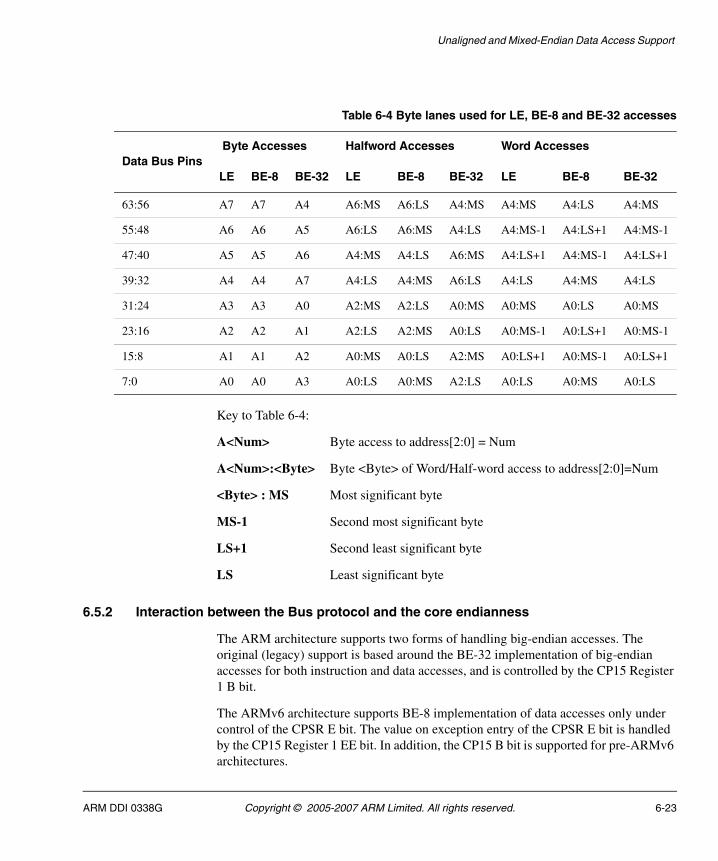
Unaligned and Mixed-Endian Data Access Support
Key to Table 6-4:
A<Num> Byte access to address[2:0] = Num
A<Num>:<Byte> Byte <Byte> of Word/Half-word access to address[2:0]=Num
<Byte> : MS Most significant byte
MS-1 Second most significant byte
LS+1 Second least significant byte
LS Least significant byte
6.5.2 Interaction between the Bus protocol and the core endianness
The ARM architecture supports two forms of handling big-endian accesses. The original (legacy) support is based around the BE-32 implementation of big-endian accesses for both instruction and data accesses, and is controlled by the CP15 Register 1 B bit.
The ARMv6 architecture supports BE-8 implementation of data accesses only under control of the CPSR E bit. The value on exception entry of the CPSR E bit is handled by the CP15 Register 1 EE bit. In addition, the CP15 B bit is supported for pre-ARMv6 architectures.
Table 6-4 Byte lanes used for LE, BE-8 and BE-32 accesses
Data Bus Pins Byte Accesses Halfword Accesses Word Accesses
LE BE-8 BE-32 LE BE-8 BE-32 LE BE-8 BE-32
63:56 A7 A7 A4 A6:MS A6:LS A4:MS A4:MS A4:LS A4:MS
55:48 A6 A6 A5 A6:LS A6:MS A4:LS A4:MS-1 A4:LS+1 A4:MS-1
47:40 A5 A5 A6 A4:MS A4:LS A6:MS A4:LS+1 A4:MS-1 A4:LS+1
39:32 A4 A4 A7 A4:LS A4:MS A6:LS A4:LS A4:MS A4:LS
31:24 A3 A3 A0 A2:MS A2:LS A0:MS A0:MS A0:LS A0:MS
23:16 A2 A2 A1 A2:LS A2:MS A0:LS A0:MS-1 A0:LS+1 A0:MS-1
15:8 A1 A1 A2 A0:MS A0:LS A2:MS A0:LS+1 A0:MS-1 A0:LS+1
7:0 A0 A0 A3 A0:LS A0:MS A2:LS A0:LS A0:MS A0:LS
ARM DDI 0338G Copyright © 2005-2007 ARM Limited. All rights reserved. 6-23
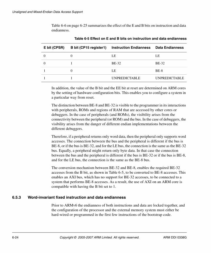
Unaligned and Mixed-Endian Data Access Support
Table 6-6 on page 6-25 summarizes the effect of the E and B bits on instruction and data endianness.
In addition, the value of the B bit and the EE bit at reset are determined on ARM cores by the setting of hardware configuration bits. This enables you to configure a system in a particular way from reset.
The distinction between BE-8 and BE-32 is visible to the programmer in its interactions with peripherals, ROMs and regions of RAM that are accessed by other cores or debuggers. In the case of peripherals (and ROMs), the visibility arises from the connectivity between the peripheral (or ROM) and the bus. In the case of debuggers, the visibility arises from the danger of different endian implementations between the different debuggers.
Therefore, if a peripheral returns only word data, then the peripheral only supports word accesses. The connection between the bus and the peripheral is different if the bus is BE-8, or if the bus is BE-32, and for the LE bus, the connection is the same as the BE-32 bus. Equally, a peripheral might return only byte data. In that case the connection between the bus and the peripheral is different if the bus is BE-32 or if the bus is BE-8, and for the LE bus, the connection is the same as the BE-8 bus.
The conversion mechanism between BE-32 and BE-8, enables the required BE-32 accesses from the B bit, as shown in Table 6-5, to be converted to BE-8 accesses. This enables an AXI bus, which has no support for BE-32 accesses, to be connected to a system that performs BE-8 accesses. As a result, the use of AXI on an ARM core is compatible with having the B bit set to 1.
6.5.3 Word-invariant fixed instruction and data endianness
Prior to ARMv6 the endianness of both instructions and data are locked together, and the configuration of the processor and the external memory system must either be hard-wired or programmed in the first few instructions of the bootstrap code.
Table 6-5 Effect on E and B bits on instruction and data endianness
E bit (CPSR) B bit (CP15 register1) Instruction Endianness Data Endianness
0 0 LE LE
0 1 BE-32 BE-32
1 0 LE BE-8
1 1 UNPREDICTABLE UNPREDICTABLE
6-24 Copyright © 2005-2007 ARM Limited. All rights reserved. ARM DDI 0338G
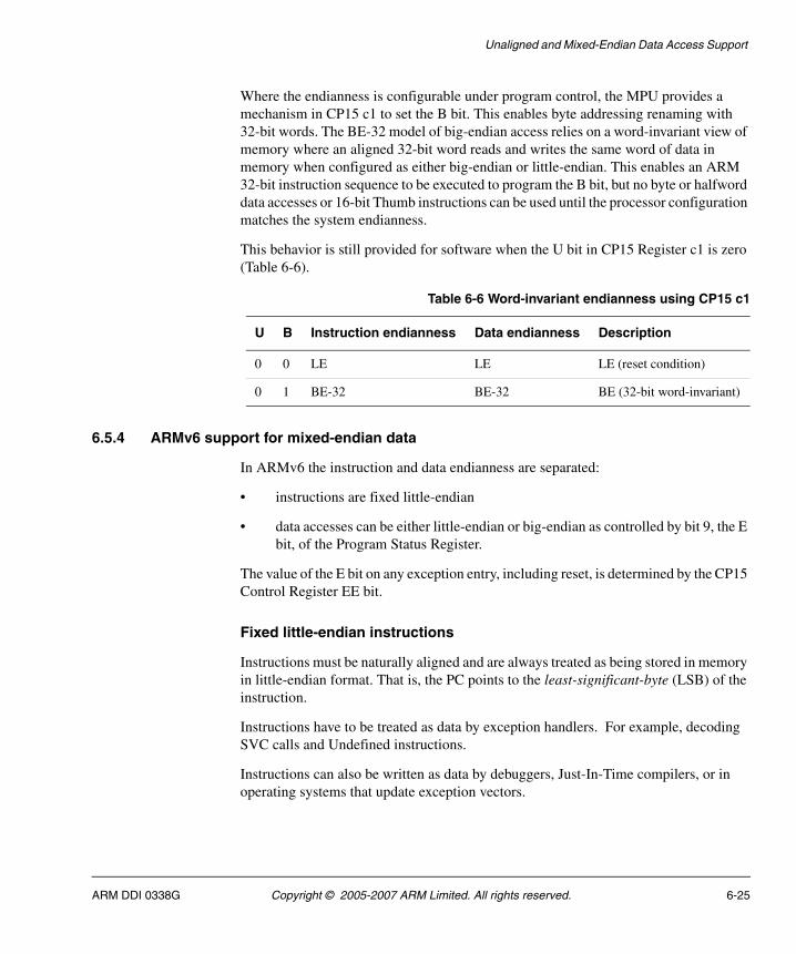
Unaligned and Mixed-Endian Data Access Support
Where the endianness is configurable under program control, the MPU provides a mechanism in CP15 c1 to set the B bit. This enables byte addressing renaming with 32-bit words. The BE-32 model of big-endian access relies on a word-invariant view of memory where an aligned 32-bit word reads and writes the same word of data in memory when configured as either big-endian or little-endian. This enables an ARM 32-bit instruction sequence to be executed to program the B bit, but no byte or halfword data accesses or 16-bit Thumb instructions can be used until the processor configuration matches the system endianness.
This behavior is still provided for software when the U bit in CP15 Register c1 is zero (Table 6-6).
6.5.4 ARMv6 support for mixed-endian data
In ARMv6 the instruction and data endianness are separated:
• instructions are fixed little-endian
• data accesses can be either little-endian or big-endian as controlled by bit 9, the E bit, of the Program Status Register.
The value of the E bit on any exception entry, including reset, is determined by the CP15 Control Register EE bit.
Fixed little-endian instructions
Instructions must be naturally aligned and are always treated as being stored in memory in little-endian format. That is, the PC points to the least-significant-byte (LSB) of the instruction.
Instructions have to be treated as data by exception handlers. For example, decoding SVC calls and Undefined instructions.
Instructions can also be written as data by debuggers, Just-In-Time compilers, or in operating systems that update exception vectors.
Table 6-6 Word-invariant endianness using CP15 c1
U B Instruction endianness Data endianness Description
0 0 LE LE LE (reset condition)
0 1 BE-32 BE-32 BE (32-bit word-invariant)
ARM DDI 0338G Copyright © 2005-2007 ARM Limited. All rights reserved. 6-25
Unaligned and Mixed-Endian Data Access Support
Mixed-endian data access
The operating system typically has a required endian representation of internal data structures, but applications and device drivers have to work with data shared with other processors (DSP interfaces) that might have fixed big-endian or little-endian data formatting.
A byte-invariant addressing mechanism is provided that enables the load/store architecture to be qualified by the CPSR E bit that provides byte reversing of big-endian data in to, and out of, the processor register bank transparently. This byte-invariant big-endian representation is called BE-8 in this document.
The effect on byte, halfword, word, and multi-word accesses of setting the CPSR E bit when the U bit enables unaligned support is described in Mixed-endian configuration supported on page 6-27.
Byte data access
The same physical byte in memory is accessed whether big-endian or little-endian:
• Unsigned byte load as described in Load unsigned byte, endian independent on page 6-7.
• Signed byte load as described in Load signed byte, endian independent on page 6-7.
• Byte store as described in Store byte, endian independent on page 6-8.
Halfword data access
The same two physical bytes in memory are accessed whether big-endian or little-endian. Big-endian halfword load data is byte-reversed as read into the processor register to ensure little-endian internal representation, and similarly is byte-reversed on store to memory:
• Unsigned halfword load as described in Load unsigned halfword, little-endian on page 6-8 (LE), and Load unsigned halfword, big-endian on page 6-9 (BE-8).
• Signed halfword load as described in Load signed halfword, little-endian on page 6-10 (LE), and Load signed halfword, big-endian on page 6-10 (BE-8).
• Halfword store as described in Store halfword, little-endian on page 6-11 (LE), and Store halfword, big-endian on page 6-12 (BE-8).
6-26 Copyright © 2005-2007 ARM Limited. All rights reserved. ARM DDI 0338G
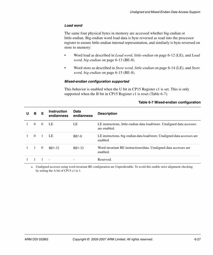
Unaligned and Mixed-Endian Data Access Support
Load word
The same four physical bytes in memory are accessed whether big-endian or little-endian. Big-endian word load data is byte reversed as read into the processor register to ensure little-endian internal representation, and similarly is byte-reversed on store to memory:
• Word load as described in Load word, little-endian on page 6-12 (LE), and Load word, big-endian on page 6-13 (BE-8).
• Word store as described in Store word, little-endian on page 6-14 (LE), and Store word, big-endian on page 6-15 (BE-8).
Mixed-endian configuration supported
This behavior is enabled when the U bit in CP15 Register c1 is set. This is only supported when the B bit in CP15 Register c1 is reset (Table 6-7).
Table 6-7 Mixed-endian configuration
U B EInstruction endianness
Data endianness
Description
1 0 0 LE LE LE instructions, little-endian data load/store. Unaligned data accesses are enabled.
1 0 1 LE BEa-8 LE instructions, big-endian data load/store. Unaligned data accesses are enabled.
1 1 0 BEa-32 BEa-32 Word-invariant BE instructions/data. Unaligned data accesses are enabled.
1 1 1 - - Reserved.
a. Unaligned accesses using word-invariant BE configuration are Unpredictable. To avoid this enable strict alignment checking by setting the A bit of CP15 c1 to 1.
ARM DDI 0338G Copyright © 2005-2007 ARM Limited. All rights reserved. 6-27
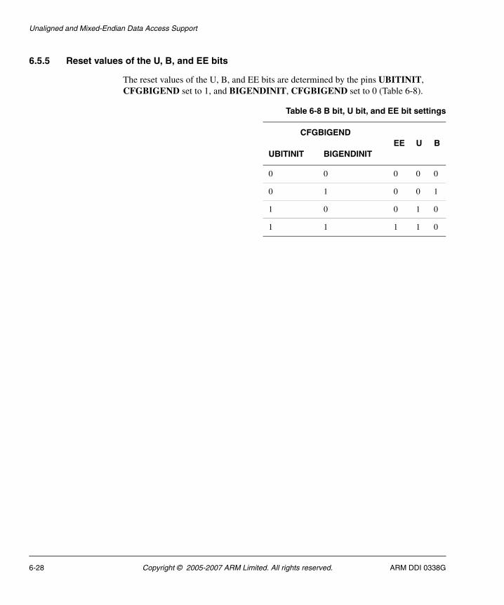
Unaligned and Mixed-Endian Data Access Support
6.5.5 Reset values of the U, B, and EE bits
The reset values of the U, B, and EE bits are determined by the pins UBITINIT, CFGBIGEND set to 1, and BIGENDINIT, CFGBIGEND set to 0 (Table 6-8).
Table 6-8 B bit, U bit, and EE bit settings
CFGBIGENDEE U B
UBITINIT BIGENDINIT
0 0 0 0 0
0 1 0 0 1
1 0 0 1 0
1 1 1 1 0
6-28 Copyright © 2005-2007 ARM Limited. All rights reserved. ARM DDI 0338G
Unaligned and Mixed-Endian Data Access Support
6.6 Instructions to reverse bytes in a general-purpose register
When an application or device driver has to interface to memory-mapped peripheral registers or shared-memory structures that are not the same endianness as that of the internal data structures, or the endianness of the Operating System, an efficient way of being able to explicitly transform the endianness of the data is required. The following new instructions are added to the ARM and Thumb instruction sets to provide this functionality:
• reverse word (4 bytes) register, for transforming big and little-endian 32-bit representations
• reverse halfword and sign-extend, for transforming signed 16-bit representations
• reverse packed halfwords in a register for transforming big- and little-endian 16-bit representations.
These instructions are described in About the architecture on page 1-30.
6.6.1 All load and store operations
All load and store instructions take account of the CPSR E bit. Data is transferred directly to registers when E = 0, and byte reversed if E = 1 for halfword, word, or multiple word transfers. The operation is:
When CPSR[<E bit>] = 1 then byte reverse load/store data
ARM DDI 0338G Copyright © 2005-2007 ARM Limited. All rights reserved. 6-29
Unaligned and Mixed-Endian Data Access Support
6.7 Instructions to change the CPSR E bit
ARM and Thumb instructions are provided to set and clear the E bit efficiently:
SETEND BE Sets the CPSR E bit
SETEND LE Resets the CPSR E bit.
These are specified as unconditional operations to minimize pipelined implementation complexity.
These instructions are described in About the architecture on page 1-30.
6-30 Copyright © 2005-2007 ARM Limited. All rights reserved. ARM DDI 0338G
Chapter 7 Level One Memory System
This chapter describes the ARM1156T2-S level one memory system. It contains the following sections:
• About the level one memory system on page 7-2
• Cache organization on page 7-3
• Tightly-coupled memory on page 7-12
• TCM and cache interactions on page 7-20
• Peripheral port on page 7-24
• Cache debug on page 7-25
• Write Buffer on page 7-26.
ARM DDI 0338G Copyright © 2005-2007 ARM Limited. All rights reserved. 7-1
Level One Memory System
7.1 About the level one memory system
The ARM1156T2-S level one memory system is implementation-defined. It can consist of:
• separate instruction and data caches in a Harvard arrangement
• separate Instruction and Data Tightly-Coupled Memory (TCM) areas
• a Write Buffer for accesses to level two memory.
In parallel with each of the caches is an area of dedicated RAM on both the instruction and data sides. These regions are referred to as TCM. You can implement 0 or 1 TCM on each of the instruction and data sides.
Each TCM has a dedicated base address that you can place anywhere in the physical address map, and does not have to be backed by memory implemented externally. The Instruction and Data TCMs have separate base addresses.
Access to both the instruction and data sides is handled by the MPU. The MPU is responsible for protection checking, address access permissions, and memory attributes, some of which can be passed to the level two memory system.
The MPU provides the facilities required by sophisticated operating systems to deliver protected memory environments. It also supports real-time tasks with features that provide predictable execution time. For more details, see Chapter 5 Memory Protection Unit.
7-2 Copyright © 2005-2007 ARM Limited. All rights reserved. ARM DDI 0338G
Level One Memory System
7.2 Cache organization
Each cache is implementation-defined and can be one, two or four-way set associative cache of configurable size. They are physically indexed and physically addressed. The cache sizes are configurable with sizes in the range of 1 to 64KB, but the maximum clock frequency might be affected if you increase the cache sizes beyond 16KB. Both the instruction cache and the data cache are capable of providing two words per cycle for all requesting sources.
The cache way size can be varied between 1KB and 16KB in powers of 2. A 1KB cache size must be implemented as a 1 way cache, and a 2KB cache must be implemented as a 2 way cache. All other cache sizes must be implemented as 4 way set associative. The cache line length is fixed at eight words (32 bytes).
The maximum cache way size that the processor supports is 16KB. The minimum cache way size that the processor supports is 1KB. You can disable instruction cache and data cache together or instruction cache and data cache individually.
Note If a cache is implemented within the ARM1156T2-S processor, way 0 must be present.
Write operations must occur after the Tag RAM reads and associated address comparisons have completed. A three-entry Write Buffer is included in the cache to enable the written words to be held until they can be written to cache. One or two words can be written in a single store operation. The addresses of these outstanding writes provide an additional input into the Tag RAM comparison for reads.
To avoid a critical path from the Tag RAM comparison to the enable signals for the data RAMs, there is a minimum of one cycle of latency between the determination of a hit to a particular way, and the start of writing to the data RAM of that way. This requires the Cache Write Buffer to be able to hold three entries, for back-to-back writes. Accesses that read the dirty bits must also check the Cache Write Buffer for pending writes that result in dirty bits being set. The cache dirty bits for the data cache are updated when the Cache Write Buffer data is written to the RAM. This requires the dirty bits to be held as a separate storage array (significantly, the tag arrays cannot be written, because the arrays are not accessed during the data RAM writes), but permits the dirty bits to be implemented as a small RAM.
The other main operations performed by the cache are cache line refills and write-back. These occur to particular cache ways, which are determined at the point of the detection of the cache miss by the victim selection logic.
ARM DDI 0338G Copyright © 2005-2007 ARM Limited. All rights reserved. 7-3
Level One Memory System
To reduce overall power consumption, the number of full cache reads is reduced by the sequential nature of many cache operations, especially on the instruction side. On a cache read that is sequential to the previous cache read, only the data RAM set that was previously read is accessed, if the read is within the same cache line. The Tag RAM is not accessed at all during this sequential operation.
Cache line refills can take several cycles. The cache line length is eight words.
The control of the level one memory system and the associated functionality, together with other system wide control attributes are handled through the system control coprocessor, CP15. This is described in Chapter 3 System Control Coprocessor.
Figure 7-1 on page 7-5 shows the block diagram of the cache subsystem. This figure does not show the cache refill paths.
7-4 Copyright © 2005-2007 ARM Limited. All rights reserved. ARM DDI 0338G
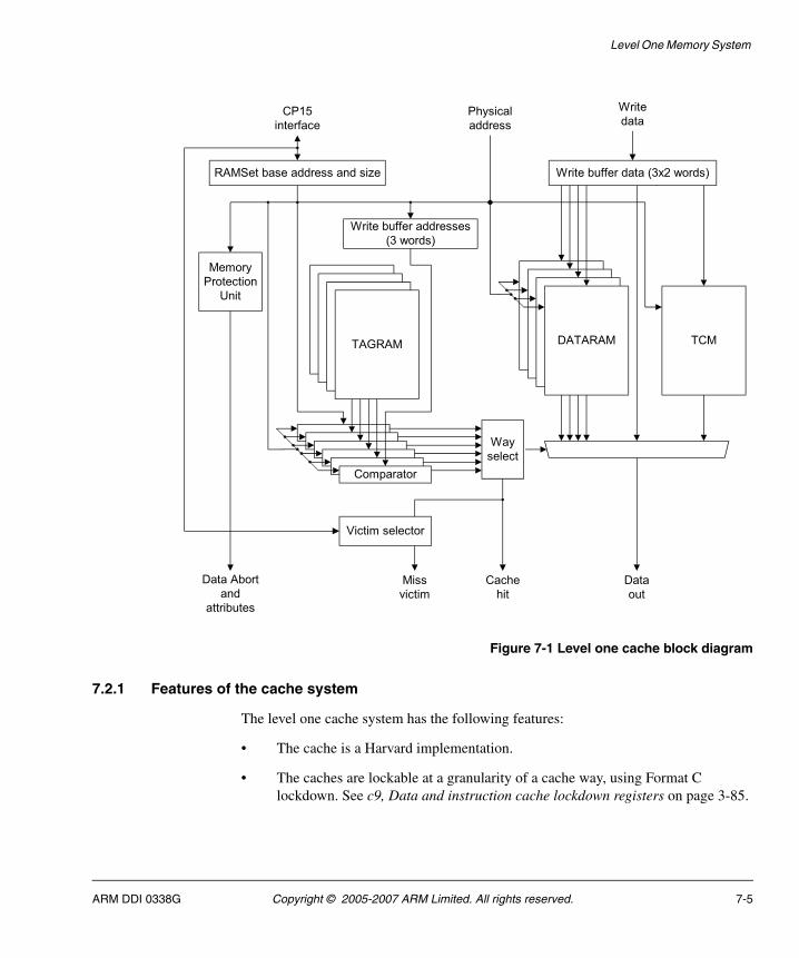
Level One Memory System
Figure 7-1 Level one cache block diagram
7.2.1 Features of the cache system
The level one cache system has the following features:
• The cache is a Harvard implementation.
• The caches are lockable at a granularity of a cache way, using Format C lockdown. See c9, Data and instruction cache lockdown registers on page 3-85.
DATARAMTAGRAM TCM
Comparator
Way
select
Write buffer data (3x2 words)
Write buffer addresses
(3 words)
Victim selector
Miss
victim
Cache
hit
Data
out
RAMSet base address and size
CP15
interface
Physical
address
Write
data
Memory
Protection
Unit
Data Abort
and
attributes
ARM DDI 0338G Copyright © 2005-2007 ARM Limited. All rights reserved. 7-5
Level One Memory System
• Cache replacement policies are Pseudo-Random or Round-Robin, as controlled by the RR bit in CP15 register c1. Round-Robin uses a single counter for all sets that selects the way used for replacement.
• Cache line allocation uses the cache replacement algorithm when all cache lines are valid. If one or more lines are invalid, then the invalid cache line with the lowest way number is allocated to in preference to replacing a valid cache line. This mechanism does not allocate to locked cache ways unless all cache ways are locked. See Cache miss handling when all ways are locked down on page 7-7.
• Cache lines can be either write-back or write-through, determined by the Memory Attribute.
• Only read allocation is supported.
• The cache can be disabled independently from the TCM, under control of the appropriate bits in CP15 c1.
• Data cache misses are nonblocking with a single outstanding data cache miss being supported.
• Streaming of sequential data from LDM and LDRD operations, and for sequential instruction fetches is supported.
7.2.2 Cache functional description
The cache and TCM exist to perform associative reads and writes on requested addresses. The steps involved in this for reads are as follows:
1. The lower bits of the address are used as the index for the tag and RAM blocks, including the TCM.
2. The physical addresses read from the Tag RAMs and the TCM base address register, and the Cache Write Buffer address registers, are compared with the physical address to form hit signals for each of the cache ways
3. The hit signals are used to select the data from the cache way that has a hit. Any bytes contained in both the data RAMs and the Cache Write Buffer entries are taken from the Cache Write Buffer. If two or three Cache Write Buffer entries are to the same bytes, the most recently written bytes are taken.
The steps for writes are as follows:
1. The lower bits of the address are used as the index for the tag blocks.
7-6 Copyright © 2005-2007 ARM Limited. All rights reserved. ARM DDI 0338G
Level One Memory System
2. The physical addresses read from the Tag RAMs and the TCM base address register are compared with the physical address from the core to form hit signals for each of the cache ways.
3. If a cache way, or the TCM, has recorded a hit, then the write data is written to an entry in the Cache Write Buffer, along with the cache way, or TCM, that it must take place to.
4. The contents of the Cache Write Buffer are held until a subsequent write or CP15 operation requires space in the Write Buffer. At this point the oldest entry in the Cache Write Buffer is written into the cache.
7.2.3 Cache control operations
The cache control operations that are supported by the ARM1156T2-S processor are described in c7, Cache Operations Register on page 3-71. ARM1156T2-S processors support all the block cache control operations in hardware.
7.2.4 Cache miss handling
A cache miss results in the requests required to do the line fill being made to the level two interface, with a write-back occurring if the line to be replaced contains dirty data.
The write-back data is transferred to the Write Buffer, which is arranged to handle this data as a sequential burst. Because of the requirement for nonblocking caches, additional write transactions can occur during the transfer of write-back data from the cache to the Write Buffer. These transactions do not interfere with the burst nature of the write-back data. The Write Buffer is responsible for handling the potential Read After Write (RAW) data hazards that might exist from a data cache line write-back. The caches perform critical word-first cache refilling. The internal bandwidth from the level two data read port to the data caches is eight bytes per cycle, and supports streaming.
Cache miss handling when all ways are locked down
The ARM architecture describes the behavior of the cache as being Unpredictable when all ways in the cache are locked down. However, for the ARM1156T2-S processor a cache miss is serviced as if Way 0 is not locked.
7.2.5 Cache disabled behavior
If the cache is disabled, then the cache is not accessed for reads or for writes. This ensures that maximum power savings can be achieved. It is therefore important that before the cache is disabled, all of the entries are cleaned to ensure that the external
ARM DDI 0338G Copyright © 2005-2007 ARM Limited. All rights reserved. 7-7
Level One Memory System
memory has been updated. In addition, if the cache is enabled with valid entries in it, then it is possible that the entries in the cache contain old data. Therefore the cache must be disabled with clean and invalid entries.
Cache maintenance operations can be performed even if the cache is disabled.
7.2.6 Unexpected hit behavior
An unexpected hit is where the cache reports a hit on a memory location that is marked as Noncacheable or Shared. The unexpected hit behavior is that these hits are ignored and a level two access occurs. The unexpected hit is ignored because the cache hit signal is qualified by the cacheability.
For writes, an unexpected cache hit does not result in the cache being updated. Therefore, writes appear to be Noncacheable accesses.
If a data access lies in the range of memory specified by the Instruction TCM or Data TCM, the access is made to that RAM rather than to level two memory. This applies to both writes and reads.
7.2.7 Cache parity errors
The purpose of cache parity error detection is to increase the tolerance of memory faults. The inclusion of the parity generation and checking logic for the caches and the Instruction TCM is a synthesis option. For more details, see the ARM1156T2F-S and ARM1156T2-S Implementation Guide.
Instruction cache Tag and Valid RAM parity error detection
The Instruction cache Tag and Valid RAM blocks are written on cache line fills and cache maintenance operations. During the write operations the parity data is generated and written to the RAM.
The Instruction cache Tag and Valid RAM blocks are read during cache lookups and cache maintenance operations. When the IR bit is set the detection of a parity error in the Instruction cache Tag RAMs causes a cache miss indication. This invalidates the current cache line, and cause its replacement from main memory. In this case the victim counter is over-ridden and the failing set is chosen as the victim. If the IR bit, bit 6 of c1, Auxiliary Control Register, is not set the detection of a parity error causes a Prefetch Abort.
7-8 Copyright © 2005-2007 ARM Limited. All rights reserved. ARM DDI 0338G
Level One Memory System
Instruction cache Data RAM parity error detection
The instruction cache RAM block is written to on cache line fills. When the IR bit is set the detection of a parity error instruction cache RAM block causes the cache line to be invalidated and refetched from main memory. If the IR bit, bit 6 of c1, Auxiliary Control Register, is not set the detection of a parity error causes a Prefetch Abort to be returned to the processor.
When the processor executes the instruction:
• the address of the parity error is stored in the Instruction Fault Address register.
• the Instruction Fault Status register is set to indicate the presence of a parity error.
Data cache Dirty RAM error detection
The Data cache Dirty RAM blocks are written to on line fills, stores that hit in the cache, and cache maintenance operations. If there is an error in the Dirty RAM, the cache line is treated as dirty.
Data cache TAG and Valid RAM parity error detection
The Data Tag RAM blocks are written on cache line fills and cache maintenance operations. During the write operations the parity data is generated and written to the RAM.
The detection of a parity error in the Data cache TAG and Valid RAM blocks causes a Data Abort to be generated. The Data Fault Address Register is updated with the failing address and Fault Status Register is updated to record a parity error.
The parity fault can be precise or imprecise. See Table 7-1 on page 7-10 for more information.
Data cache data RAM parity error detection
The data cache data RAM block is written to on cache line fills and stores that hit in the cache. The detection of a parity error in the data cache data RAM block causes a Data Abort to be returned to the processor.
The address of the data fault is stored in the Data Fault Address Register.
The Data Fault Status Register is set to indicate the presence of a parity error.
The parity fault can be precise or imprecise. See Table 7-1 on page 7-10 for more information.
ARM DDI 0338G Copyright © 2005-2007 ARM Limited. All rights reserved. 7-9
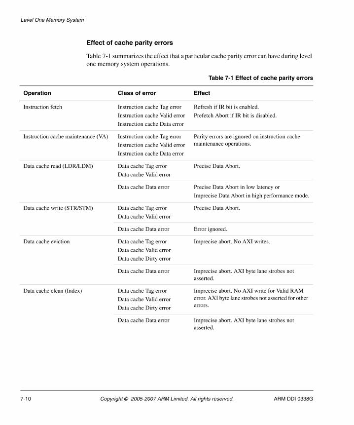
Level One Memory System
Effect of cache parity errors
Table 7-1 summarizes the effect that a particular cache parity error can have during level one memory system operations.
Table 7-1 Effect of cache parity errors
Operation Class of error Effect
Instruction fetch Instruction cache Tag error
Instruction cache Valid error
Instruction cache Data error
Refresh if IR bit is enabled.
Prefetch Abort if IR bit is disabled.
Instruction cache maintenance (VA) Instruction cache Tag error
Instruction cache Valid error
Instruction cache Data error
Parity errors are ignored on instruction cache maintenance operations.
Data cache read (LDR/LDM) Data cache Tag error
Data cache Valid error
Precise Data Abort.
Data cache Data error Precise Data Abort in low latency or
Imprecise Data Abort in high performance mode.
Data cache write (STR/STM) Data cache Tag error
Data cache Valid error
Precise Data Abort.
Data cache Data error Error ignored.
Data cache eviction Data cache Tag error
Data cache Valid error
Data cache Dirty error
Imprecise abort. No AXI writes.
Data cache Data error Imprecise abort. AXI byte lane strobes not asserted.
Data cache clean (Index) Data cache Tag error
Data cache Valid error
Data cache Dirty error
Imprecise abort. No AXI write for Valid RAM error. AXI byte lane strobes not asserted for other errors.
Data cache Data error Imprecise abort. AXI byte lane strobes not asserted.
7-10 Copyright © 2005-2007 ARM Limited. All rights reserved. ARM DDI 0338G
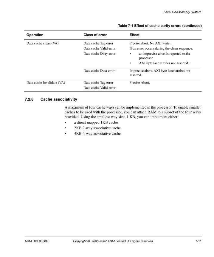
Level One Memory System
7.2.8 Cache associativity
A maximum of four cache ways can be implemented in the processor. To enable smaller caches to be used with the processor, you can attach RAM to a subset of the four ways provided. Using the smallest way size, 1 KB, you can implement either:
• a direct mapped 1KB cache
• 2KB 2-way associative cache
• 4KB 4-way associative cache.
Data cache clean (VA) Data cache Tag error
Data cache Valid error
Data cache Dirty error
Precise abort. No AXI write.
If an error occurs during the clean sequence:
• an imprecise abort is reported to the processor
• AXI byte lane strobes not asserted.
Data cache Data error Imprecise abort. AXI byte lane strobes not asserted.
Data cache Invalidate (VA) Data cache Tag error
Data cache Valid error
Precise Abort.
Table 7-1 Effect of cache parity errors (continued)
Operation Class of error Effect
ARM DDI 0338G Copyright © 2005-2007 ARM Limited. All rights reserved. 7-11
Level One Memory System
7.3 Tightly-coupled memory
The purpose of the Tightly-Coupled Memory (TCM) is to provide low-latency memory that the processor can use without the unpredictability that is a feature of caches.
You can use TCM to hold critical routines, such as interrupt handling routines or real-time tasks where the indeterminacy of a cache is highly undesirable. In addition you can use it to hold scratch pad data, data types whose locality properties are not well suited to caching, and critical data structures such as interrupt stacks.
The size of each TCM can be selected independently from a minimum of 4KB to a maximum of 256KB, in powers of 2. You can configure the TCM in several ways:
• one TCM on the instruction side and one on the data side
• one TCM on the either the instruction side or the data side only
• no TCM.
The TCM Status Register in CP15 c0 identifies the TCM options and TCM sizes that have been implemented, see c0, TCM Status Register on page 3-25.
The Data TCM is implemented in parallel with the data cache and the Instruction TCM is implemented in parallel with the instruction cache. Each TCM has a single movable base address, specified in CP15 register c9, (see c9, Data TCM Region Register on page 3-88 and c9, Instruction TCM Region Register on page 3-90).
The size of each TCM can be different to the size of a cache way, but forms a single contiguous area of memory. The entire level one memory system is shown in Figure 7-1 on page 7-5.
You can disable each TCM to avoid an access being made to it. This gives a reduction in the power consumption. You can disable each TCM independently from the enabling of the associated cache, as determined by CP15 register c9.
Disabling the TCM invalidates the base address, so there is no unexpected hit behavior for the TCM.
The TCM region overrides memory type attributes of the MPU and all addresses within the TCM space are treated as Normal, Non-Shared memory.
7.3.1 TCM behavior
TCM forms a continuous area of memory that is always valid if the TCM is enabled. TCM is used as part of the physical memory map of the system, and does not have to be backed by a level of external memory with the same physical addresses. For this reason, the TCM behaves differently from the caches for regions of memory that are marked as being write-through cacheable. In such regions, no external writes occur in the event of a write to memory locations contained in the TCM.
7-12 Copyright © 2005-2007 ARM Limited. All rights reserved. ARM DDI 0338G
Level One Memory System
7.3.2 Restriction on mappings
The TCMs are implemented in a physically indexed, physically addressed manner, giving the following behavior:
• the entries in the TCM do not have to be cleaned and/or invalidated by software
• aliases to the same physical address can exist in memory regions that are held in the TCM.
As a result, memory mapping restrictions for the TCM are less restrictive than for the cache, as described in Restrictions on accesses to different types of memory on page 6-26.
7.3.3 Restriction on attributes
The attributes that describe areas of memory that are handled by the TCM are ignored and access to the TCM is made, if the access permissions permit.
7.3.4 TCM error detection signals
Large SRAM arrays are susceptible to soft errors caused, for example, by alpha particle radiation. These errors can result in incorrect data being returned. You can use parity checking or some form of error detection and correction outside the ARM1156T2-S processor to detect these errors. Because of the frequency at which the processor operates a pause and repair scheme is supported. This scheme enables stall cycles to be inserted if an error is detected so that the appropriate time is given to correct the memory error.
To enable the ARM1156T2-S processor to support external error detection on the tightly-coupled memories there is one error signal for each of the TCM interfaces:
• DTCDATAERROR[7:0]• ITCDATAERROR[7:0]
DTCDATAERROR[7:0] and ITCDATAERROR[7:0] enable the ARM1156T2-S processor to be informed of error conditions during TCM read accesses. These signals are valid in the same clock cycle as the data returned from the TCM. DTCDATAERROR[7:0] and ITCDATAERROR[7:0] are ignored during write accesses.
Error detection is performed externally to the ARM1156T2-S processor. If error support is not required DTCDATAERROR[7:0] and ITCDATAERROR[7:0] must be tied LOW. For example, when using parity error detection, parity information must be generated for each byte because the ARM1156T2-S processor is capable of performing byte accesses.
ARM DDI 0338G Copyright © 2005-2007 ARM Limited. All rights reserved. 7-13
Level One Memory System
The ARM1156T2-S processor provides parity bits for each byte written to memory using ITCDATAPARITY[7:0] and DTCDATAPARITY[7:0]. Data is always read from the TCMs in 32-bit words and a parity error in any one byte must be returned to the core as an error. The ARM1156T2-S processor uses odd parity.
If an error is returned from the TCM interface, the relevant fault address and fault status registers are updated. For the Data TCM, an error might stall the processor for several clock cycles before the Data Abort handler is fetched.
For data reads from either Instruction TCM or Data TCM any error returned causes a Data Abort exception. The exception handler determines what corrective action, if any, to take.
For instruction fetches from the Instruction TCM any error returned causes a Prefetch Abort exception if the ARM1156T2-S processor tries to execute the returned instruction.
Note If all the data is returned from the TCM write buffer, DTCDATAERROR[7:0] is ignored. If only part of the data is returned from the TCM write buffer, DTCDATAERROR[7:0] is sampled. To prevent errors from uninitialized locations, memory must be initialized so that spurious read errors are not generated.
7.3.5 TCM accesses
This section provides examples of TCM read access, TCM write access, an error generation on read, and an error correction on read. It also provides examples on the effects of stall cycles.
TCM read access
Figure 7-2 on page 7-15 shows an example of a TCM read access. The processor drives the address and control to the memory on the rising edge of the processor clock. The processor clock is inverted to produce RAM clock. This signal drives the RAM block on its rising edge. This enables the processor to have a complete clock cycle for the memory access to the RAM block.
To align the data with the processor clock, a transparent latch opens at the end of the RAM access and the data is captured on the rising edge of the processor clock two cycles after the edge which started the transfer.
7-14 Copyright © 2005-2007 ARM Limited. All rights reserved. ARM DDI 0338G
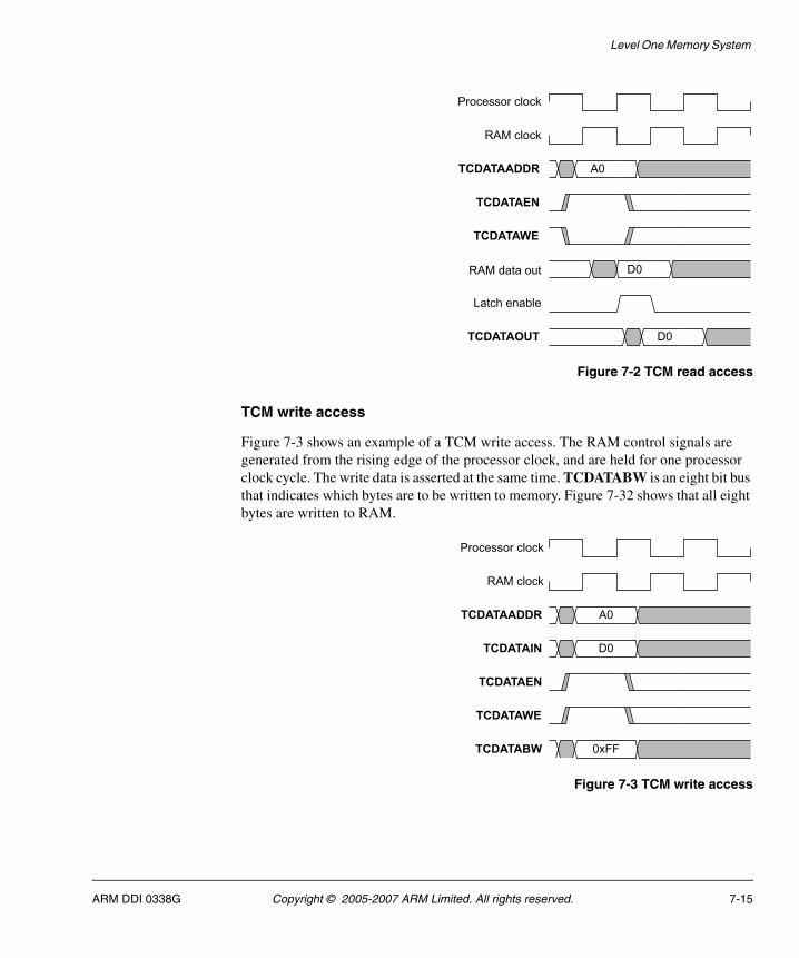
Level One Memory System
Figure 7-2 TCM read access
TCM write access
Figure 7-3 shows an example of a TCM write access. The RAM control signals are generated from the rising edge of the processor clock, and are held for one processor clock cycle. The write data is asserted at the same time. TCDATABW is an eight bit bus that indicates which bytes are to be written to memory. Figure 7-32 shows that all eight bytes are written to RAM.
Figure 7-3 TCM write access
ARM DDI 0338G Copyright © 2005-2007 ARM Limited. All rights reserved. 7-15
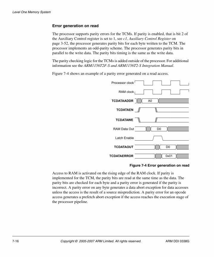
Level One Memory System
Error generation on read
The processor supports parity errors for the TCMs. If parity is enabled, that is bit 2 of the Auxiliary Control register is set to 1, see c1, Auxiliary Control Register on page 3-52, the processor generates parity bits for each byte written to the TCM. The processor implements an odd-parity scheme. The processor generates parity bits in parallel to the write data. The parity bits timing is the same as the write data.
The parity checking logic for the TCMs is added outside of the processor. For additional information see the ARM1156T2F-S and ARM1156T2-S Integration Manual.
Figure 7-4 shows an example of a parity error generated on a read access.
Figure 7-4 Error generation on read
Access to RAM is activated on the rising edge of the RAM clock. If parity is implemented for the TCM, the parity bits are read at the same time as the data. The parity bits are checked for each byte and a parity error is generated if the parity is incorrect. A parity error on any byte generates a data abort exception for data accesses unless the access is the result of a source misprediction. A parity error for an opcode access generates a prefetch abort exception if the access reaches the execution stage of the processor pipeline.
7-16 Copyright © 2005-2007 ARM Limited. All rights reserved. ARM DDI 0338G
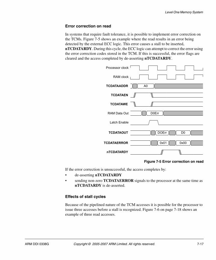
Level One Memory System
Error correction on read
In systems that require fault tolerance, it is possible to implement error correction on the TCMs. Figure 7-5 shows an example where the read results in an error being detected by the external ECC logic. This error causes a stall to be inserted, nTCDATARDY. During this cycle, the ECC logic can attempt to correct the error using the error correction codes stored in the TCM. If this is successful, the error flags are cleared and the access completed by de-asserting nTCDATARDY.
Figure 7-5 Error correction on read
If the error correction is unsuccessful, the access completes by:
• de-asserting nTCDATARDY• sending non-zero TCDATAERROR signals to the processor at the same time as
nTCDATARDY is de-asserted.
Effects of stall cycles
Because of the pipelined nature of the TCM accesses it is possible for the processor to issue three accesses before a stall is recognized. Figure 7-6 on page 7-18 shows an example of three read accesses.
ARM DDI 0338G Copyright © 2005-2007 ARM Limited. All rights reserved. 7-17
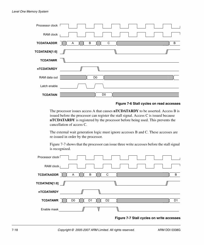
Level One Memory System
Figure 7-6 Stall cycles on read accesses
The processor issues access A that causes nTCDATARDY to be asserted. Access B is issued before the processor can register the stall signal. Access C is issued because nTCDATARDY is registered by the processor before being used. This prevents the cancellation of access C.
The external wait generation logic must ignore accesses B and C. These accesses are re-issued in order by the processor.
Figure 7-7 shows that the processor can issue three write accesses before the stall signal is recognized.
Figure 7-7 Stall cycles on write accesses
7-18 Copyright © 2005-2007 ARM Limited. All rights reserved. ARM DDI 0338G
Level One Memory System
The wait state generation logic must ignore the accesses when nTCDATARDY and a pipelined version of this signal are asserted.
Because there is a considerable delay before restarting the transactions when the processor initially registers the TCM interface outputs and the nTCDATARDY input, it is recommended that you do not use the stall mechanism as a wait state mechanism to support slow memories, with wait states for each access.
You can use the stall mechanism for infrequent events such as error correction or resolving arbitration clashes when an external DMA has access to the TCMs.
ARM DDI 0338G Copyright © 2005-2007 ARM Limited. All rights reserved. 7-19
Level One Memory System
7.4 TCM and cache interactions
In the event that a TCM and a cache both contain the requested address, it is architecturally Unpredictable which memory the instruction data is returned from. It is expected that such an event only arises from a failure to invalidate the cache when the base register of the TCM is changed, and so is clearly a programming error.
For a Harvard arrangement of caches and TCM, data reads and writes can access any Instruction TCM for both reads and writes. This ensures that accesses to literal pools, Undefined instructions, and SVC numbers are possible, and aids debugging. For this reason, an Instruction TCM must behave as a unified TCM, but can be optimized for instruction fetches.
You must not program an Instruction TCM to the same base address as a Data TCM and, if the two RAM blocks are different sizes, the regions in physical memory of the two RAM blocks must not be overlapped.
In these cases, code that is intended to be ported to other ARM platforms must not rely on the behavior of ARM1156T2-S processor.
7.4.1 Core access arbitration
Core accesses to both the Instruction TCM and the Data TCM can occur in parallel.
7.4.2 Instruction accesses to TCM
If the Instruction TCM and the instruction cache both contain the requested instruction address, the ARM1156T2-S processor returns data from the TCM. The instruction prefetch port of the ARM1156T2-S processor cannot access the Data TCM. If an instruction prefetch misses the Instruction TCM and instruction cache but hits the Data TCM, then the result is an access to the level two memory.
An Instruction Memory Barrier (IMB) must be inserted between a write to an Instruction TCM and the instructions being written being relied upon. For more details, see Instruction Memory Barrier (IMB) instruction on page 4-7.
7.4.3 Data accesses to TCMs
If the Data TCM and the data cache both contain the requested data address for a read, the ARM1156T2-S processor returns data from the Data TCM. For a write, the write occurs to the Data TCM. The majority of data accesses go to the data cache or to the Data TCM, but occasionally a data access reads or writes the Instruction TCM. Therefore this section describes data accesses to both TCMs.
7-20 Copyright © 2005-2007 ARM Limited. All rights reserved. ARM DDI 0338G
Level One Memory System
The Instruction TCM base address is read by the ARM1156T2-S processor data port as a possible source for data for all memory accesses. This increases the address comparisons associated with the data, compared with the number required for the instruction memory lookup, for the level one memory hit generation. This functionality is required for reading literal values and for debug purposes, such as setting software breakpoints.
SWP and other memory synchronization operations, such as load-exclusive and store-exclusive, to instruction TCM are not supported, and result in Unpredictable behavior.
To save power, the processor predicts whether each data access needs to access the Data TCM. This prediction assumes that a data access will hit the Data TCM only if the previous data access hit the Data TCM. On an incorrect prediction the data access restarts, incurring a penalty of two or more cycles.
Access to the Instruction TCM involves a delay of at least three cycles in the reading or writing of the data. This delay means the Instruction TCM access can be scheduled to take place only when the presence of a hit to the Instruction TCM is known. This saves power and avoids unnecessary delays being inserted into the instruction-fetch side. This delay is applied to all accesses in a multiple operation in the case of an LDM, an LDCL, an STM, or an STCL.
The resulting behavior is architecturally Unpredictable if:
• the Instruction TCM and Data TCM have the same base address
• the regions in physical memory of the two RAMs of differing sizes are overlapped.
If an access is made to a location which is covered by both an Instruction TCM and a Data TCM, then access is to the Instruction TCM only.
It is not required for instruction port(s) to be able to access the Data TCM. An attempt to access addresses in the range covered by a Data TCM from an instruction port does not result in an access to the Data TCM. In this case, the instruction is fetched from main memory. It is anticipated that such accesses can result in external aborts in some systems, because the address range might not be supported in main memory.
Table 7-2 on page 7-22 summarizes the results of data accesses to TCM and the cache. This also embodies the unexpected hit behavior for the cache described in Unexpected hit behavior on page 7-8.
ARM DDI 0338G Copyright © 2005-2007 ARM Limited. All rights reserved. 7-21
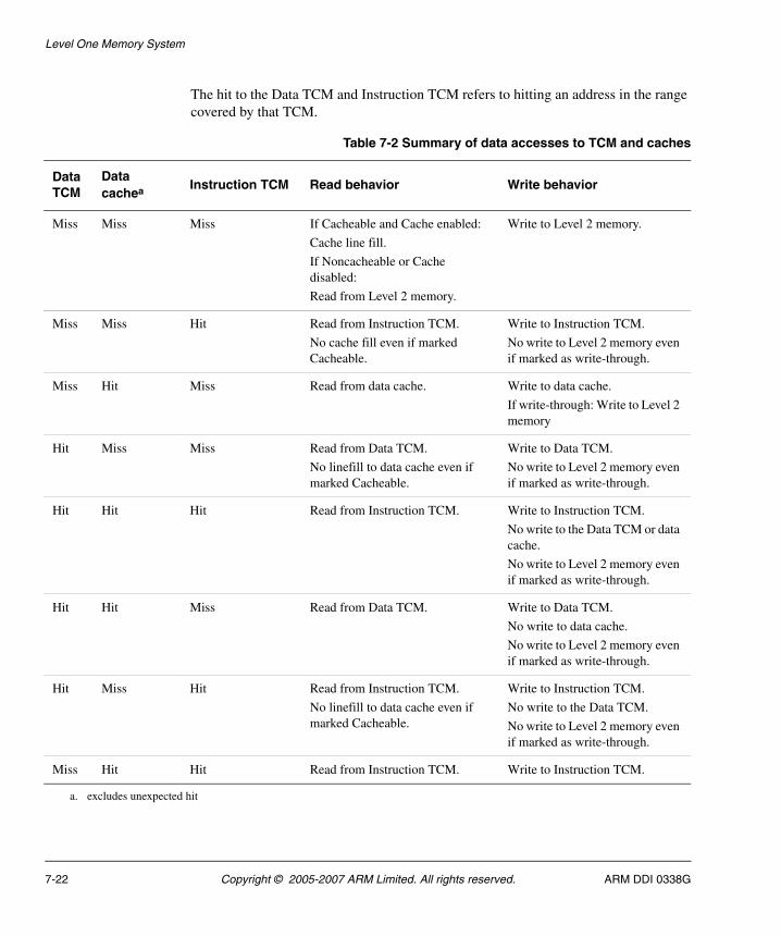
Level One Memory System
The hit to the Data TCM and Instruction TCM refers to hitting an address in the range covered by that TCM.
Table 7-2 Summary of data accesses to TCM and caches
Data TCM
Data cachea Instruction TCM Read behavior Write behavior
Miss Miss Miss If Cacheable and Cache enabled:
Cache line fill.
If Noncacheable or Cache disabled:
Read from Level 2 memory.
Write to Level 2 memory.
Miss Miss Hit Read from Instruction TCM.
No cache fill even if marked Cacheable.
Write to Instruction TCM.
No write to Level 2 memory even if marked as write-through.
Miss Hit Miss Read from data cache. Write to data cache.
If write-through: Write to Level 2 memory
Hit Miss Miss Read from Data TCM.
No linefill to data cache even if marked Cacheable.
Write to Data TCM.
No write to Level 2 memory even if marked as write-through.
Hit Hit Hit Read from Instruction TCM. Write to Instruction TCM.
No write to the Data TCM or data cache.
No write to Level 2 memory even if marked as write-through.
Hit Hit Miss Read from Data TCM. Write to Data TCM.
No write to data cache.
No write to Level 2 memory even if marked as write-through.
Hit Miss Hit Read from Instruction TCM.
No linefill to data cache even if marked Cacheable.
Write to Instruction TCM.
No write to the Data TCM.
No write to Level 2 memory even if marked as write-through.
Miss Hit Hit Read from Instruction TCM. Write to Instruction TCM.
a. excludes unexpected hit
7-22 Copyright © 2005-2007 ARM Limited. All rights reserved. ARM DDI 0338G
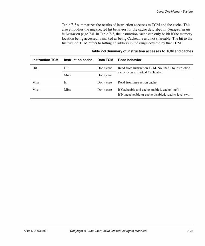
Level One Memory System
Table 7-3 summarizes the results of instruction accesses to TCM and the cache. This also embodies the unexpected hit behavior for the cache described in Unexpected hit behavior on page 7-8. In Table 7-3, the instruction cache can only be hit if the memory location being accessed is marked as being Cacheable and not shareable. The hit to the Instruction TCM refers to hitting an address in the range covered by that TCM.
Table 7-3 Summary of instruction accesses to TCM and caches
Instruction TCM Instruction cache Data TCM Read behavior
Hit Hit Don’t care Read from Instruction TCM. No linefill to instruction cache even if marked Cacheable.
Miss Don’t care
Miss Hit Don’t care Read from instruction cache.
Miss Miss Don’t care If Cacheable and cache enabled, cache linefill.
If Noncacheable or cache disabled, read to level two.
ARM DDI 0338G Copyright © 2005-2007 ARM Limited. All rights reserved. 7-23
Level One Memory System
7.5 Peripheral port
The peripheral port is accessed by memory locations whose attributes are Non-Shared Device. When the MPU is disabled a default memory region is used to access the peripheral port. This mapping only occurs while the MPU is disabled.
Peripheral port data accesses are to the Device and Non-Shared memory region.
If the region of memory mapped by this mechanism overlaps with the regions of memory that are contained within the TCMs, then the memory locations that are mapped as both TCM and Non-Shared Device are treated as TCM. Therefore, the overlapping region does not access the peripheral port.
7-24 Copyright © 2005-2007 ARM Limited. All rights reserved. ARM DDI 0338G
Level One Memory System
7.6 Cache debug
The debug architecture for the ARM1156T2-S processor is described in Chapter 13 Debug. The External Debug Interface is based on JTAG, and a described in Chapter 14 Debug Test Access Port. The debug architecture enables the cache debug to be defined by the implementation. This functionality is defined here. The debugger examines the contents of the instruction and data caches during debug operations. This is achieved in two stages:
1. Reading the Tag RAM entries for each cache location.
2. Reading the data values for those addresses.
The debugger determines which valid addresses are stored in the cache. This is done by reading the instruction and data cache Tag arrays using a CP15 instruction executed using the Instruction Transfer Register. The Instruction Transfer Register (ITR) is accessed using scan chain 4 as described in Scan chain 4, Instruction Transfer Register (ITR) on page 14-14. The debugger must do this for each entry of each set within the cache. This access is performed by an MCR that transfers from the ARM register the Set and Index of the required line in the Tag RAM array. The contents of the line are then returned to the Instruction or Data Debug Cache Register as appropriate.
ARM DDI 0338G Copyright © 2005-2007 ARM Limited. All rights reserved. 7-25
Level One Memory System
7.7 Write Buffer
All memory writes take place using the Write Buffer. To ensure that the Write Buffer is not drained on reads, the following features are implemented:
• The Write Buffer is a FIFO of outstanding writes to memory. It consists of a set of addresses and a set of data words (together with their size information).
• If a sequence of data words is contained in the Write Buffer, these are denoted as applying to the same address by the Write Buffer storing the size of the store multiple. This reduces the number of address entries that have to be stored in the Write Buffer.
• In addition to this, a separate FIFO of write-back addresses and data words is implemented. Having a separate structure avoids complications associated with performing an external write while the write-though is being handled.
• The address of a new read access is compared against the addresses in the Write Buffer. If a read is to a location that is already in the Write Buffer, the read is blocked until the Write Buffer has drained sufficiently far for that location to be no longer in the Write Buffer. The sequential marker only applies to words in the same 8 word (8 word aligned) block, and the address comparisons are based on 8 word aligned addresses.
The ordering of memory accesses is described in Ordering requirements for memory accesses on page 5-14.
7-26 Copyright © 2005-2007 ARM Limited. All rights reserved. ARM DDI 0338G
Chapter 8 Level Two Interface
The processor is designed to be used within larger chip designs using the Advanced Microcontroller Bus Architecture (AMBA) AXI protocol. The processor uses the level two interface as its interface to memory and peripherals. This chapter describes the features of the level two interface not covered in the AMBA AXI Protocol Specification
The chapter contains the following sections:
• About the level two interface on page 8-2
• Synchronization primitives on page 8-6
• AXI control signals in the processor on page 8-8
• Instruction fetch interface transfers on page 8-16
• Data read/write interface transfers on page 8-18
• Peripheral interface transfers on page 8-45
• Endianness on page 8-47
• Locked access on page 8-49.
ARM DDI 0338G Copyright © 2005-2007 ARM Limited. All rights reserved. 8-1
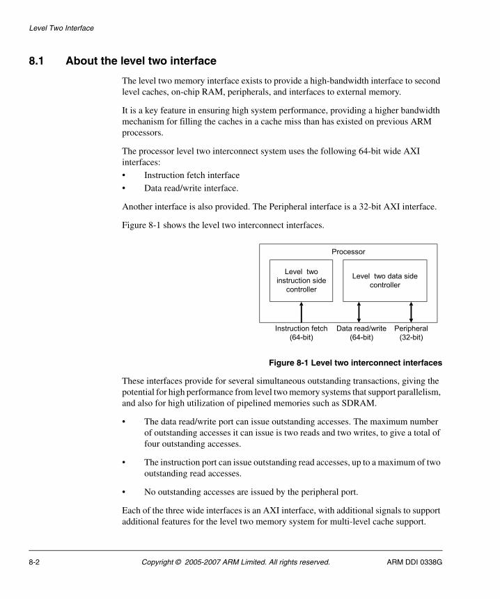
Level Two Interface
8.1 About the level two interface
The level two memory interface exists to provide a high-bandwidth interface to second level caches, on-chip RAM, peripherals, and interfaces to external memory.
It is a key feature in ensuring high system performance, providing a higher bandwidth mechanism for filling the caches in a cache miss than has existed on previous ARM processors.
The processor level two interconnect system uses the following 64-bit wide AXI interfaces:
• Instruction fetch interface
• Data read/write interface.
Another interface is also provided. The Peripheral interface is a 32-bit AXI interface.
Figure 8-1 shows the level two interconnect interfaces.
Figure 8-1 Level two interconnect interfaces
These interfaces provide for several simultaneous outstanding transactions, giving the potential for high performance from level two memory systems that support parallelism, and also for high utilization of pipelined memories such as SDRAM.
• The data read/write port can issue outstanding accesses. The maximum number of outstanding accesses it can issue is two reads and two writes, to give a total of four outstanding accesses.
• The instruction port can issue outstanding read accesses, up to a maximum of two outstanding read accesses.
• No outstanding accesses are issued by the peripheral port.
Each of the three wide interfaces is an AXI interface, with additional signals to support additional features for the level two memory system for multi-level cache support.
Processor
Level two
instruction side
controller
Level two data side
controller
Peripheral
(32-bit)
Data read/write
(64-bit)
Instruction fetch
(64-bit)
8-2 Copyright © 2005-2007 ARM Limited. All rights reserved. ARM DDI 0338G
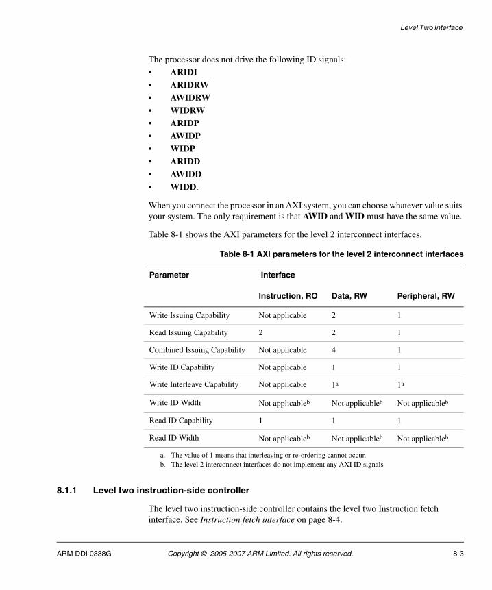
Level Two Interface
The processor does not drive the following ID signals:
• ARIDI• ARIDRW• AWIDRW• WIDRW• ARIDP• AWIDP• WIDP• ARIDD• AWIDD• WIDD.
When you connect the processor in an AXI system, you can choose whatever value suits your system. The only requirement is that AWID and WID must have the same value.
Table 8-1 shows the AXI parameters for the level 2 interconnect interfaces.
8.1.1 Level two instruction-side controller
The level two instruction-side controller contains the level two Instruction fetch interface. See Instruction fetch interface on page 8-4.
Table 8-1 AXI parameters for the level 2 interconnect interfaces
Parameter Interface
Instruction, RO Data, RW Peripheral, RW
Write Issuing Capability Not applicable 2 1
Read Issuing Capability 2 2 1
Combined Issuing Capability Not applicable 4 1
Write ID Capability Not applicable 1 1
Write Interleave Capability Not applicable 1a
a. The value of 1 means that interleaving or re-ordering cannot occur.
1a
Write ID Width Not applicableb
b. The level 2 interconnect interfaces do not implement any AXI ID signals
Not applicableb Not applicableb
Read ID Capability 1 1 1
Read ID Width Not applicableb Not applicableb Not applicableb
ARM DDI 0338G Copyright © 2005-2007 ARM Limited. All rights reserved. 8-3
Level Two Interface
The level two instruction-side controller handles all instruction-side cache misses including those for Noncacheable locations. It is responsible for the sequencing of cache operations for instruction cache linefills, making requests for the individual stores through the Prefetch Unit (PFU) to the instruction cache. The decoupling involved means that the level two instruction-side controller contains some buffering.
Instruction fetch interface
The Instruction fetch interface is a read-only interface that services the instruction cache on cache misses, including the fetching of instructions for the PU that are held in memory marked as Noncacheable. The interface is optimized for cache linefills rather than individual requests.
8.1.2 Level two data-side controller
The level two data-side controller is responsible for the level two:
• Data read/write interface
• Peripheral interface.
The level two data-side controller handles:
• All external access requests from the Load Store Unit, including cache misses, data Write-Through operations, and Noncacheable data.
• SWP instructions and semaphore operations. It schedules all reads and writes on the two interfaces, that are closely related.
The level two data-side controller also handles the Peripheral interface.
The level two data-side controller contains the Refill and Write-Back engines for the data cache. These make requests through the Load Store Unit for the individual cache operations that are required. The decoupling involved means that the level two data-side controller contains some buffering. The write buffer is an integral part of the level two data-side controller.
Data read/write interface
The Data read/write interface performs reads and swap reads. It services the data cache on cache misses, and reads Noncacheable locations.
The Data read/write interface performs writes and swap writes. It services the writes out of the Write Buffer. Multiple writes can be queued up as part of this interface.
8-4 Copyright © 2005-2007 ARM Limited. All rights reserved. ARM DDI 0338G
Level Two Interface
Peripheral interface
The Peripheral interface is a an AXI interface that services peripheral devices. The Peripheral interface is used for peripherals that are private to the processor, such as the Vectored Interrupt Controller or Watchdog Timer. Accesses to regions of memory that are marked as Device and Non-Shared are routed to the Peripheral interface in preference to the Data read/write interface.
Unaligned accesses and exclusive accesses are not supported by the peripheral port because they are not supported in Device memory. The order in which accesses are presented on the Peripheral interface, relative to those on the Data read/write interface is not defined, other than Strongly Ordered accesses. For this reason, the peripheral port is expected to be used to access a bus or memory system which is not accessible through the data read and data write ports. See Chapter 5 Memory Protection Unit and Peripheral port on page 7-24 to find out how to remap data accesses to a defined address region to the peripheral port
ARM DDI 0338G Copyright © 2005-2007 ARM Limited. All rights reserved. 8-5
Level Two Interface
8.2 Synchronization primitives
On previous architectures support for shared memory synchronization has been with the read-locked-write operations that swap register contents with memory, the SWP and SWPB instructions. These support basic busy and free semaphore mechanisms. For details of the swap instructions, and how to use them to implement semaphores, see the ARM Architecture Reference Manual.
ARMv6 and its extensions introduce support for more comprehensive shared-memory synchronization primitives that scale for multiple-processor system designs. Two instructions are introduced that support multiple-processor and shared-memory inter-process communication:
• load-exclusive, LDREX
• store-exclusive, STREX.
The exclusive-access instructions rely on the ability to tag a physical address as exclusive-access for a particular processor. This tag is later used to determine if an exclusive store to an address occurs.For non-shared memory regions, the LDREX and STREX instructions are presented to the ports as normal LDR or STR. If a processor does an STR on a memory region that it has already marked as exclusive, this does not clear the tag. However, if the region has been marked by another processor, an STR clears the tag. Other events might cause the tag to be cleared. In particular, for memory regions that are not shared, it is Unpredictable whether a store by another processor to a tagged physical address causes the tag to be cleared. An external abort on either a load-exclusive or store-exclusive puts the processor into Abort mode.
Note The processor has an internal monitor that keeps track of the state of the regions marked as Non-Shared. An external abort on a load-exclusive can leave internal monitor in its exclusive state and might affect your software. If it does you must ensure that a store-exclusive to an unused location is executed in your abort handler to clear the processor internal monitor to an open state.
8.2.1 Load-exclusive instruction
Load-exclusive performs a load from memory and causes the physical address of the access to be tagged as exclusive-access for the requesting processor. This causes any other physical address that has been tagged by the requesting processor to no longer be tagged as exclusive-access.
8-6 Copyright © 2005-2007 ARM Limited. All rights reserved. ARM DDI 0338G
Level Two Interface
8.2.2 Store-exclusive instruction
Store-exclusive performs a conditional store to memory. The store only takes place if the physical address is tagged as exclusive-access for the requesting processor. This operation returns a status value. If the store updates memory the return value is 0, otherwise it is 1. In both cases, the physical address is no longer tagged as exclusive-access for any processor.
8.2.3 Example of LDREX and STREX usage
This is an example of typical usage. Suppose you are trying to claim a lock:
Lock address LockAddrLock free 0x00Lock taken 0xFF
MOV R1, #0xFF ; load the ‘lock taken’ valuetry LDREX R0, [LockAddr] ; load the lock value
CMP R0, #0 ; is the lock free?STREXEQ R0, R1, [LockAddr] ; try and claim the lockCMPEQ R0, #0 ; did this succeed?BNE try ; no – try again
; yes – we have the lock
The typical case, where the lock is free and you have exclusive-access, is six instructions.
ARM DDI 0338G Copyright © 2005-2007 ARM Limited. All rights reserved. 8-7
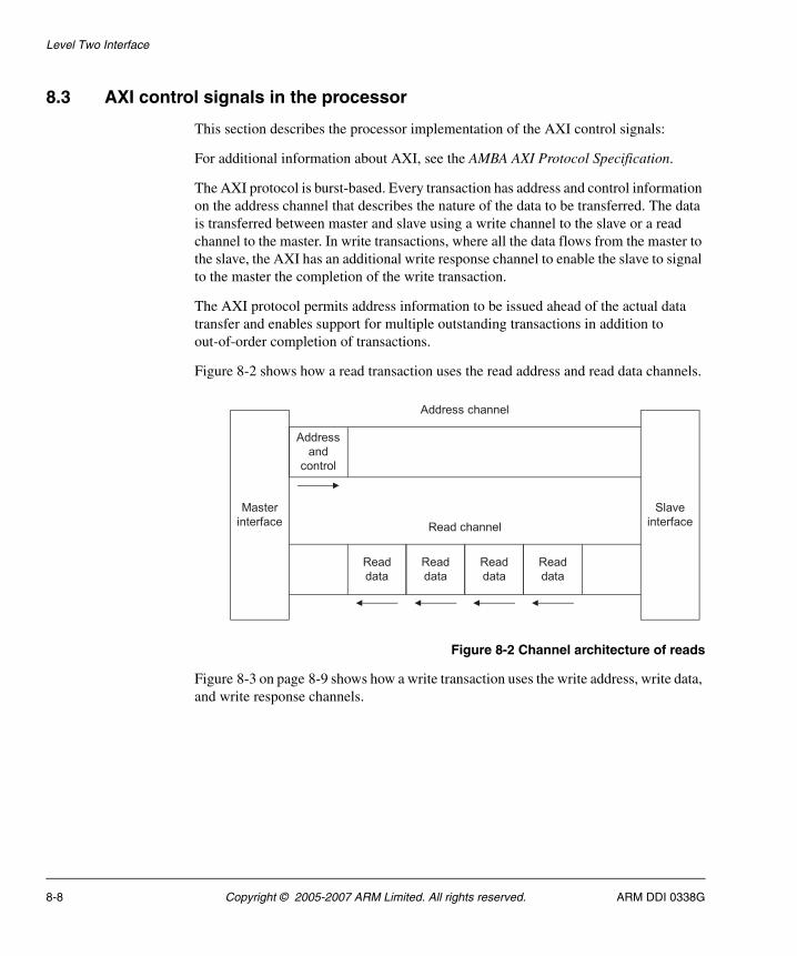
Level Two Interface
8.3 AXI control signals in the processor
This section describes the processor implementation of the AXI control signals:
For additional information about AXI, see the AMBA AXI Protocol Specification.
The AXI protocol is burst-based. Every transaction has address and control information on the address channel that describes the nature of the data to be transferred. The data is transferred between master and slave using a write channel to the slave or a read channel to the master. In write transactions, where all the data flows from the master to the slave, the AXI has an additional write response channel to enable the slave to signal to the master the completion of the write transaction.
The AXI protocol permits address information to be issued ahead of the actual data transfer and enables support for multiple outstanding transactions in addition to out-of-order completion of transactions.
Figure 8-2 shows how a read transaction uses the read address and read data channels.
Figure 8-2 Channel architecture of reads
Figure 8-3 on page 8-9 shows how a write transaction uses the write address, write data, and write response channels.
Master
interface
Slave
interface
Address
and
control
Address channel
Read
data
Read
data
Read
data
Read
data
Read channel
8-8 Copyright © 2005-2007 ARM Limited. All rights reserved. ARM DDI 0338G
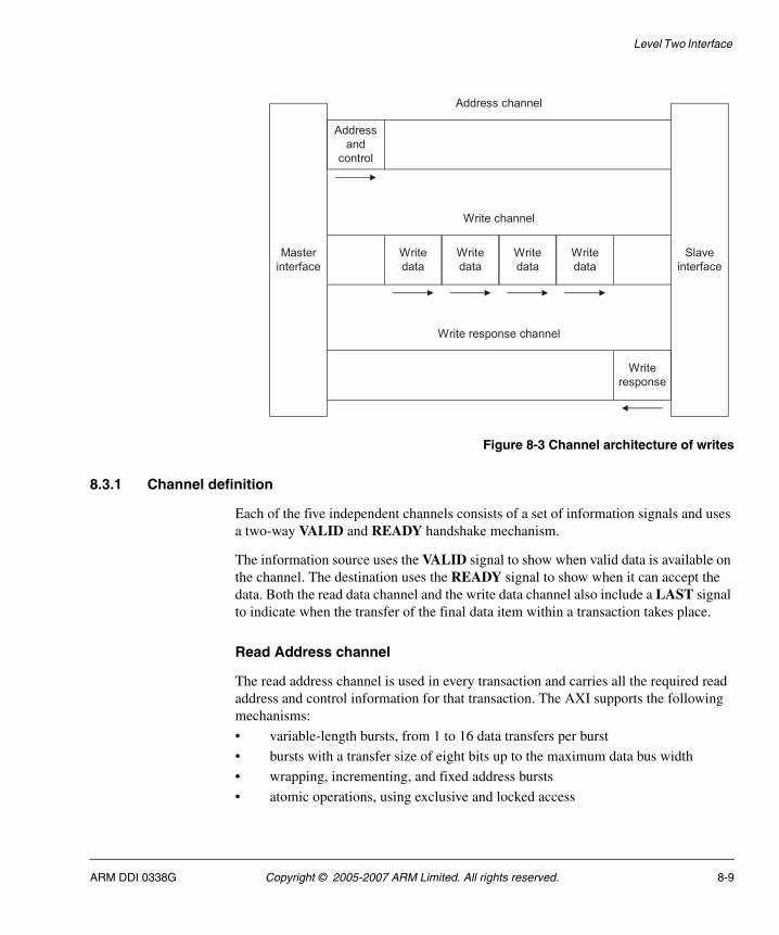
Level Two Interface
Figure 8-3 Channel architecture of writes
8.3.1 Channel definition
Each of the five independent channels consists of a set of information signals and uses a two-way VALID and READY handshake mechanism.
The information source uses the VALID signal to show when valid data is available on the channel. The destination uses the READY signal to show when it can accept the data. Both the read data channel and the write data channel also include a LAST signal to indicate when the transfer of the final data item within a transaction takes place.
Read Address channel
The read address channel is used in every transaction and carries all the required read address and control information for that transaction. The AXI supports the following mechanisms:
• variable-length bursts, from 1 to 16 data transfers per burst
• bursts with a transfer size of eight bits up to the maximum data bus width
• wrapping, incrementing, and fixed address bursts
• atomic operations, using exclusive and locked access
Master
interface
Slave
interface
Address
and
control
Address channel
Write
data
Write channel
Write
data
Write
data
Write
data
Write
response
Write response channel
ARM DDI 0338G Copyright © 2005-2007 ARM Limited. All rights reserved. 8-9
Level Two Interface
• system-level caching and buffering control
• Secure and privileged access.
Write address channel
The write address channel is used in every transaction and carries all the required write address and control information for that transaction. The AXI supports the following mechanisms:
• variable-length bursts, from 1 to 16 data transfers per burst
• bursts with a transfer size of eight bits up to the maximum data bus width
• wrapping, incrementing, and fixed address bursts
• atomic operations, using exclusive and locked access
• system-level caching and buffering control
• Secure and privileged access.
Read data channel
The read data channel conveys both the read data and any read response information from the slave back to the master. The read data channel includes:
• the data bus, that is 32 bits wide for the Peripheral port, and 64 bits wide for the Data read/write port and Instruction port
• a read response indicating the completion status of the read transaction.
Write data channel
The write data channel conveys the write data from the master to the slave and includes:
• the data bus, that is 32 bits wide for the Peripheral port, and 64 bits wide for the Data read/write port and Instruction port
• one byte lane strobe for every eight data bits, indicating the bytes of the data bus that are valid.
Write response channel
The write response channel provides a way for the slave to respond to write transactions. All write transactions use completion signaling.
Note The completion signal occurs once for each burst, not for each individual data transfer within the burst.
8-10 Copyright © 2005-2007 ARM Limited. All rights reserved. ARM DDI 0338G
Level Two Interface
8.3.2 Signal name suffixes
The signal name for each of the interfaces denotes the interface that it applies to. The signals have one of these suffixes:
I Instruction fetch interface.
RW Data read/write interface.
P Peripheral interface.
The second character in the signal name indicates if the data direction is a read, R, or write, W.
For example, AxSIZE[2:0] is called ARSIZEI[2:0] for reads in the Instruction fetch interface.
8.3.3 Address channel signals
The address channel control signals in the processor are:
• AxLEN[3:0]
• AxSIZE[2:0] on page 8-12
• AxBURST[1:0] on page 8-12
• AxLOCK[1:0] on page 8-13
• AxCACHE[3:0] on page 8-13
• AxPROT[2:0] on page 8-13
• AxSIDEBAND[4:0] on page 8-14.
AxLEN[3:0]
The AxLEN[3:0] signal indicates the number of transfers in a burst. Table 8-2 lists the values of AxLEN that the processor uses.
Table 8-2 AxLEN[3:0] encoding
AxLEN[3:0] Number of data transfers
b0000 1
b0001 2
b0010 3
b0011 4
b0100 5
ARM DDI 0338G Copyright © 2005-2007 ARM Limited. All rights reserved. 8-11
Level Two Interface
AxSIZE[2:0]
This signal indicates the size of each transfer. Table 8-3 lists the supported transfer sizes.
AxBURST[1:0]
The AxBURST[1:0] signals indicate a fixed, incrementing or wrapping burst. Table 8-4 lists the burst types that the ARM1156T2F-S processor supports.
The processor uses:
• Wrapping bursts for some cache line fills
• Incrementing bursts for accesses to Noncacheable memory, including instruction fetches.
b0101 6
b0110 7
b0111 8
Table 8-3 AxSIZE[2:0] encoding
AxSIZE[2:0] Bytes in transfer
b000 1
b001 2
b010 4
b011 8
Table 8-2 AxLEN[3:0] encoding (continued)
AxLEN[3:0] Number of data transfers
Table 8-4 AxBURST[1:0] encoding
AxBURST[2:0] Burst type Description
b00 Fixed Fixed address burst
b01 Incr Incrementing address burst
b10 Wrap Incrementing address burst that wraps to a lower address at the wrap boundary
8-12 Copyright © 2005-2007 ARM Limited. All rights reserved. ARM DDI 0338G
Level Two Interface
AxLOCK[1:0]
The AxLOCK[1:0] signal indicates the lock type of access. The processor supports all locked type accesses. The instruction port only generates Normal access types. The Data read/write port generates all access types, Normal, exclusive and locked access.
Table 8-5 lists the values of AxLOCK that the processor supports.
AxCACHE[3:0]
The AxCACHE[3:0] signals indicate the bufferable, cacheable, write-through, write-back, and allocate attributes of the transaction. These attributes are for the level two memory system. Table 8-6 lists the correspondence between the AxCACHE[3:0] encoding and cacheable attributes.
AxPROT[2:0]
The AxPROT[2:0] signal marks the protection level of the transaction, that is if the transaction is user or privileged, or secure.The signal also indicates if the transaction is a data access or an instruction access.
Table 8-5 AxLOCK[1:0] encoding
AxLOCK[1:0] Description
b00 Normal access
b01 Exclusive access
b10 Locked access
Table 8-6 AxCACHE[3:0] encoding
AxCACHE[3:0] Transaction attributes
b0000 Strongly ordered
b0001 Shared device or non-shared device
b0010 Outer Noncacheable
b0110 Outer write-through, no allocate on write
b0111 Outer write-back, no allocate on write
b1111 Outer write-back, write allocate.
ARM DDI 0338G Copyright © 2005-2007 ARM Limited. All rights reserved. 8-13
Level Two Interface
All transactions from the instruction port are marked as instruction accesses (ARPROTI[2] = 1).Transactions on the peripheral and data read/write ports are marked as data accesses.
Table 8-7 lists the supported values for AxPROT[2:0].
AxSIDEBAND[4:0]
The AxSIDEBAND[4:1] signals indicate the bufferable, cacheable, write-through, write-back, and allocate attributes of the level one memory. AxSIDEBAND[0] indicates the Shared attribute. Table 8-8 lists the correspondence between the AxSIDEBAND[4:1] encoding and the cacheable attributes for the read/write and Peripheral ports.
Table 8-7 AxPROT[2:0] encoding
Signal Description
AxPROT[2] 0 = Data access
1 = Instruction access
AxPROT[1] 0 = Always secure
AxPROT[0] 0 = User
1 = Privileged
Table 8-8 AxSIDEBAND[4:1] encoding
AxSIDEBAND[4:1] Transaction attributes
b0000 Strongly ordered
b0001 Shared device or non-shared device
b0010 Inner Noncacheable
b0110 Inner write-through, no allocate on write
8-14 Copyright © 2005-2007 ARM Limited. All rights reserved. ARM DDI 0338G
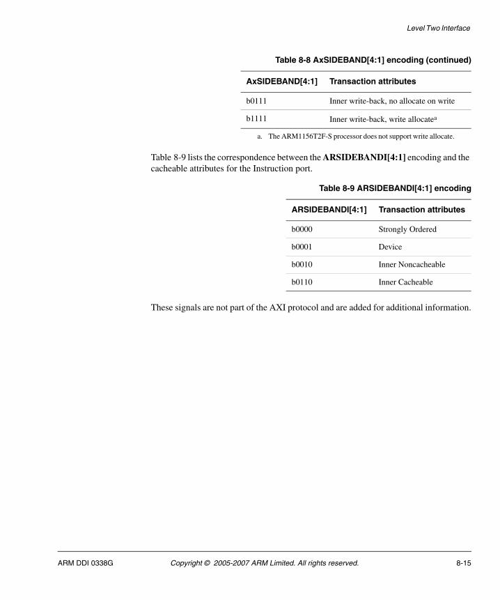
Level Two Interface
Table 8-9 lists the correspondence between the ARSIDEBANDI[4:1] encoding and the cacheable attributes for the Instruction port.
These signals are not part of the AXI protocol and are added for additional information.
b0111 Inner write-back, no allocate on write
b1111 Inner write-back, write allocatea
a. The ARM1156T2F-S processor does not support write allocate.
Table 8-9 ARSIDEBANDI[4:1] encoding
ARSIDEBANDI[4:1] Transaction attributes
b0000 Strongly Ordered
b0001 Device
b0010 Inner Noncacheable
b0110 Inner Cacheable
Table 8-8 AxSIDEBAND[4:1] encoding (continued)
AxSIDEBAND[4:1] Transaction attributes
ARM DDI 0338G Copyright © 2005-2007 ARM Limited. All rights reserved. 8-15
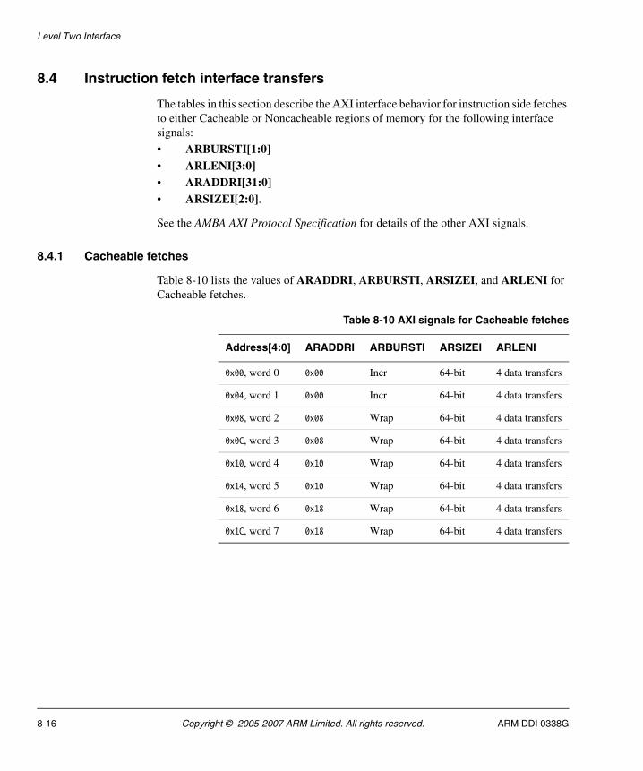
Level Two Interface
8.4 Instruction fetch interface transfers
The tables in this section describe the AXI interface behavior for instruction side fetches to either Cacheable or Noncacheable regions of memory for the following interface signals:
• ARBURSTI[1:0]• ARLENI[3:0]• ARADDRI[31:0]• ARSIZEI[2:0].
See the AMBA AXI Protocol Specification for details of the other AXI signals.
8.4.1 Cacheable fetches
Table 8-10 lists the values of ARADDRI, ARBURSTI, ARSIZEI, and ARLENI for Cacheable fetches.
Table 8-10 AXI signals for Cacheable fetches
Address[4:0] ARADDRI ARBURSTI ARSIZEI ARLENI
0x00, word 0 0x00 Incr 64-bit 4 data transfers
0x04, word 1 0x00 Incr 64-bit 4 data transfers
0x08, word 2 0x08 Wrap 64-bit 4 data transfers
0x0C, word 3 0x08 Wrap 64-bit 4 data transfers
0x10, word 4 0x10 Wrap 64-bit 4 data transfers
0x14, word 5 0x10 Wrap 64-bit 4 data transfers
0x18, word 6 0x18 Wrap 64-bit 4 data transfers
0x1C, word 7 0x18 Wrap 64-bit 4 data transfers
8-16 Copyright © 2005-2007 ARM Limited. All rights reserved. ARM DDI 0338G
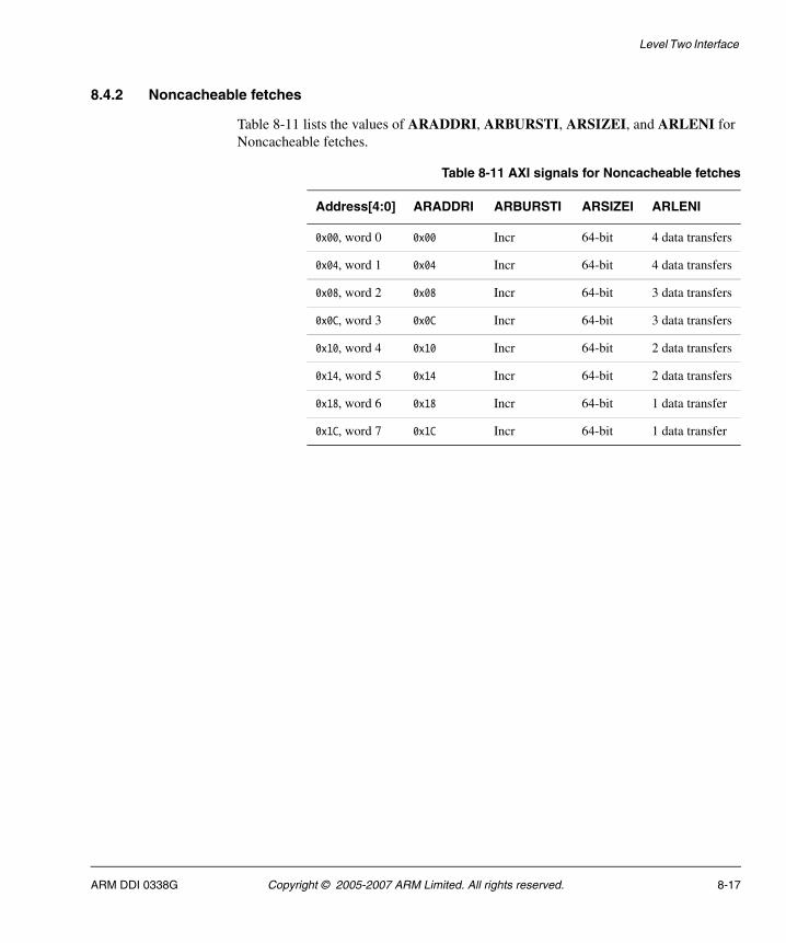
Level Two Interface
8.4.2 Noncacheable fetches
Table 8-11 lists the values of ARADDRI, ARBURSTI, ARSIZEI, and ARLENI for Noncacheable fetches.
Table 8-11 AXI signals for Noncacheable fetches
Address[4:0] ARADDRI ARBURSTI ARSIZEI ARLENI
0x00, word 0 0x00 Incr 64-bit 4 data transfers
0x04, word 1 0x04 Incr 64-bit 4 data transfers
0x08, word 2 0x08 Incr 64-bit 3 data transfers
0x0C, word 3 0x0C Incr 64-bit 3 data transfers
0x10, word 4 0x10 Incr 64-bit 2 data transfers
0x14, word 5 0x14 Incr 64-bit 2 data transfers
0x18, word 6 0x18 Incr 64-bit 1 data transfer
0x1C, word 7 0x1C Incr 64-bit 1 data transfer
ARM DDI 0338G Copyright © 2005-2007 ARM Limited. All rights reserved. 8-17
Level Two Interface
8.5 Data read/write interface transfers
The tables in this section describe the AXI interface behavior for Data read/write interface transfers for the following interface signals:
• AxBURSTRW[1:0]• AxLENRW[3:0]• AxSIZERW[2:0]• AxADDRRW[31:0]• WSTRBRW[7:0].
8.5.1 Linefills
A linefill comprises four accesses to the data cache if there is no external abort returned. In the event of an external abort, the doubleword and subsequent doublewords are not written into the data cache and the line is never marked as Valid. The four accesses are:
• Write Tag and data doubleword
• Write data doubleword
• Write data doubleword
• Write Valid = 1, Dirty = 0, and data doubleword.
The linefill can only progress to attempt to write a doubleword if it does not contain dirty data. This is determined in one of two ways:
• if the victim cache line is not valid, then there is no danger and the linefill progresses
• if the victim line is valid, a signal encodes the doublewords that are clean, either because they were not dirty or they have been cleaned.
The order of words written into the cache is critical-word first, wrapping at the upper cache line boundary.
Table 8-12 on page 8-19 lists the values of ARADDRRW, ARBURSTRW, ARSIZERW, and ARLENRW for linefills.
8-18 Copyright © 2005-2007 ARM Limited. All rights reserved. ARM DDI 0338G
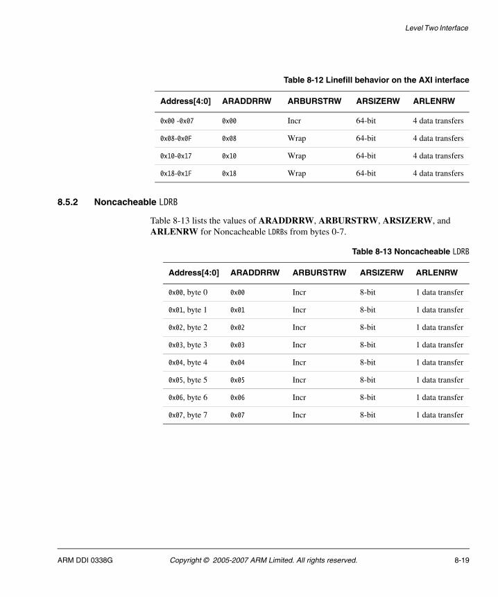
Level Two Interface
8.5.2 Noncacheable LDRB
Table 8-13 lists the values of ARADDRRW, ARBURSTRW, ARSIZERW, and ARLENRW for Noncacheable LDRBs from bytes 0-7.
Table 8-12 Linefill behavior on the AXI interface
Address[4:0] ARADDRRW ARBURSTRW ARSIZERW ARLENRW
0x00 -0x07 0x00 Incr 64-bit 4 data transfers
0x08-0x0F 0x08 Wrap 64-bit 4 data transfers
0x10-0x17 0x10 Wrap 64-bit 4 data transfers
0x18-0x1F 0x18 Wrap 64-bit 4 data transfers
Table 8-13 Noncacheable LDRB
Address[4:0] ARADDRRW ARBURSTRW ARSIZERW ARLENRW
0x00, byte 0 0x00 Incr 8-bit 1 data transfer
0x01, byte 1 0x01 Incr 8-bit 1 data transfer
0x02, byte 2 0x02 Incr 8-bit 1 data transfer
0x03, byte 3 0x03 Incr 8-bit 1 data transfer
0x04, byte 4 0x04 Incr 8-bit 1 data transfer
0x05, byte 5 0x05 Incr 8-bit 1 data transfer
0x06, byte 6 0x06 Incr 8-bit 1 data transfer
0x07, byte 7 0x07 Incr 8-bit 1 data transfer
ARM DDI 0338G Copyright © 2005-2007 ARM Limited. All rights reserved. 8-19
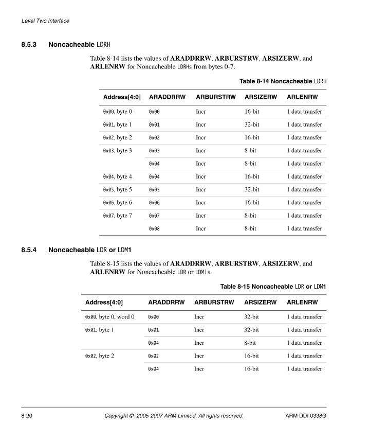
Level Two Interface
8.5.3 Noncacheable LDRH
Table 8-14 lists the values of ARADDRRW, ARBURSTRW, ARSIZERW, and ARLENRW for Noncacheable LDRHs from bytes 0-7.
8.5.4 Noncacheable LDR or LDM1
Table 8-15 lists the values of ARADDRRW, ARBURSTRW, ARSIZERW, and ARLENRW for Noncacheable LDR or LDM1s.
Table 8-14 Noncacheable LDRH
Address[4:0] ARADDRRW ARBURSTRW ARSIZERW ARLENRW
0x00, byte 0 0x00 Incr 16-bit 1 data transfer
0x01, byte 1 0x01 Incr 32-bit 1 data transfer
0x02, byte 2 0x02 Incr 16-bit 1 data transfer
0x03, byte 3 0x03 Incr 8-bit 1 data transfer
0x04 Incr 8-bit 1 data transfer
0x04, byte 4 0x04 Incr 16-bit 1 data transfer
0x05, byte 5 0x05 Incr 32-bit 1 data transfer
0x06, byte 6 0x06 Incr 16-bit 1 data transfer
0x07, byte 7 0x07 Incr 8-bit 1 data transfer
0x08 Incr 8-bit 1 data transfer
Table 8-15 Noncacheable LDR or LDM1
Address[4:0] ARADDRRW ARBURSTRW ARSIZERW ARLENRW
0x00, byte 0, word 0 0x00 Incr 32-bit 1 data transfer
0x01, byte 1 0x01 Incr 32-bit 1 data transfer
0x04 Incr 8-bit 1 data transfer
0x02, byte 2 0x02 Incr 16-bit 1 data transfer
0x04 Incr 16-bit 1 data transfer
8-20 Copyright © 2005-2007 ARM Limited. All rights reserved. ARM DDI 0338G
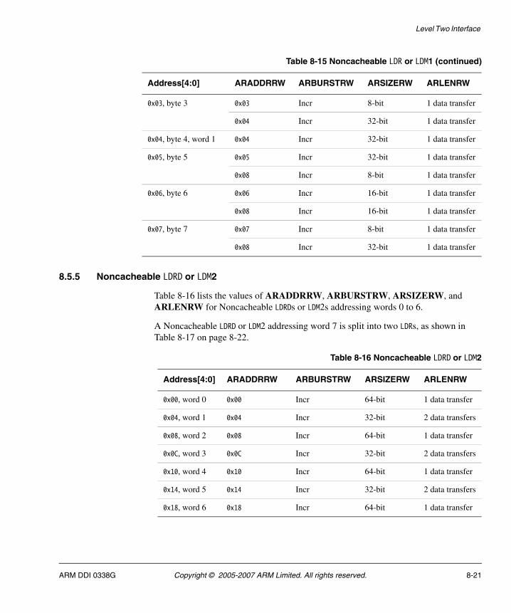
Level Two Interface
8.5.5 Noncacheable LDRD or LDM2
Table 8-16 lists the values of ARADDRRW, ARBURSTRW, ARSIZERW, and ARLENRW for Noncacheable LDRDs or LDM2s addressing words 0 to 6.
A Noncacheable LDRD or LDM2 addressing word 7 is split into two LDRs, as shown in Table 8-17 on page 8-22.
0x03, byte 3 0x03 Incr 8-bit 1 data transfer
0x04 Incr 32-bit 1 data transfer
0x04, byte 4, word 1 0x04 Incr 32-bit 1 data transfer
0x05, byte 5 0x05 Incr 32-bit 1 data transfer
0x08 Incr 8-bit 1 data transfer
0x06, byte 6 0x06 Incr 16-bit 1 data transfer
0x08 Incr 16-bit 1 data transfer
0x07, byte 7 0x07 Incr 8-bit 1 data transfer
0x08 Incr 32-bit 1 data transfer
Table 8-15 Noncacheable LDR or LDM1 (continued)
Address[4:0] ARADDRRW ARBURSTRW ARSIZERW ARLENRW
Table 8-16 Noncacheable LDRD or LDM2
Address[4:0] ARADDRRW ARBURSTRW ARSIZERW ARLENRW
0x00, word 0 0x00 Incr 64-bit 1 data transfer
0x04, word 1 0x04 Incr 32-bit 2 data transfers
0x08, word 2 0x08 Incr 64-bit 1 data transfer
0x0C, word 3 0x0C Incr 32-bit 2 data transfers
0x10, word 4 0x10 Incr 64-bit 1 data transfer
0x14, word 5 0x14 Incr 32-bit 2 data transfers
0x18, word 6 0x18 Incr 64-bit 1 data transfer
ARM DDI 0338G Copyright © 2005-2007 ARM Limited. All rights reserved. 8-21
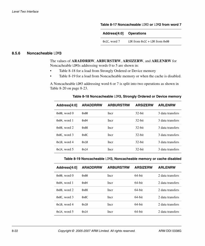
Level Two Interface
8.5.6 Noncacheable LDM3
The values of ARADDRRW, ARBURSTRW, ARSIZERW, and ARLENRW for Noncacheable LDM3s addressing words 0 to 5 are shown in:
• Table 8-18 for a load from Strongly Ordered or Device memory
• Table 8-19 for a load from Noncacheable memory or when the cache is disabled.
A Noncacheable LDM3 addressing word 6 or 7 is split into two operations as shown in Table 8-20 on page 8-23.
Table 8-17 Noncacheable LDRD or LDM2 from word 7
Address[4:0] Operations
0x1C, word 7 LDR from 0x1C + LDR from 0x00
Table 8-18 Noncacheable LDM3, Strongly Ordered or Device memory
Address[4:0] ARADDRRW ARBURSTRW ARSIZERW ARLENRW
0x00, word 0 0x00 Incr 32-bit 3 data transfers
0x04, word 1 0x04 Incr 32-bit 3 data transfers
0x08, word 2 0x08 Incr 32-bit 3 data transfers
0x0C, word 3 0x0C Incr 32-bit 3 data transfers
0x10, word 4 0x10 Incr 32-bit 3 data transfers
0x14, word 5 0x14 Incr 32-bit 3 data transfers
Table 8-19 Noncacheable LDM3, Noncacheable memory or cache disabled
Address[4:0] ARADDRRW ARBURSTRW ARSIZERW ARLENRW
0x00, word 0 0x00 Incr 64-bit 2 data transfers
0x04, word 1 0x04 Incr 64-bit 2 data transfers
0x08, word 2 0x08 Incr 64-bit 2 data transfers
0x0C, word 3 0x0C Incr 64-bit 2 data transfers
0x10, word 4 0x10 Incr 64-bit 2 data transfers
0x14, word 5 0x14 Incr 64-bit 2 data transfers
8-22 Copyright © 2005-2007 ARM Limited. All rights reserved. ARM DDI 0338G
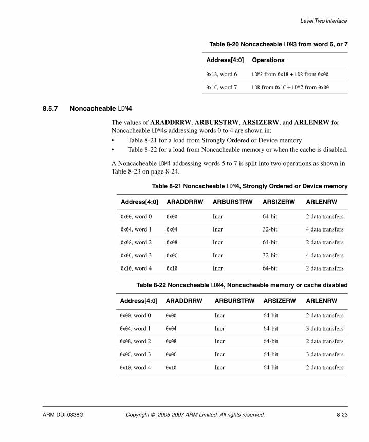
Level Two Interface
8.5.7 Noncacheable LDM4
The values of ARADDRRW, ARBURSTRW, ARSIZERW, and ARLENRW for Noncacheable LDM4s addressing words 0 to 4 are shown in:
• Table 8-21 for a load from Strongly Ordered or Device memory
• Table 8-22 for a load from Noncacheable memory or when the cache is disabled.
A Noncacheable LDM4 addressing words 5 to 7 is split into two operations as shown in Table 8-23 on page 8-24.
Table 8-20 Noncacheable LDM3 from word 6, or 7
Address[4:0] Operations
0x18, word 6 LDM2 from 0x18 + LDR from 0x00
0x1C, word 7 LDR from 0x1C + LDM2 from 0x00
Table 8-21 Noncacheable LDM4, Strongly Ordered or Device memory
Address[4:0] ARADDRRW ARBURSTRW ARSIZERW ARLENRW
0x00, word 0 0x00 Incr 64-bit 2 data transfers
0x04, word 1 0x04 Incr 32-bit 4 data transfers
0x08, word 2 0x08 Incr 64-bit 2 data transfers
0x0C, word 3 0x0C Incr 32-bit 4 data transfers
0x10, word 4 0x10 Incr 64-bit 2 data transfers
Table 8-22 Noncacheable LDM4, Noncacheable memory or cache disabled
Address[4:0] ARADDRRW ARBURSTRW ARSIZERW ARLENRW
0x00, word 0 0x00 Incr 64-bit 2 data transfers
0x04, word 1 0x04 Incr 64-bit 3 data transfers
0x08, word 2 0x08 Incr 64-bit 2 data transfers
0x0C, word 3 0x0C Incr 64-bit 3 data transfers
0x10, word 4 0x10 Incr 64-bit 2 data transfers
ARM DDI 0338G Copyright © 2005-2007 ARM Limited. All rights reserved. 8-23
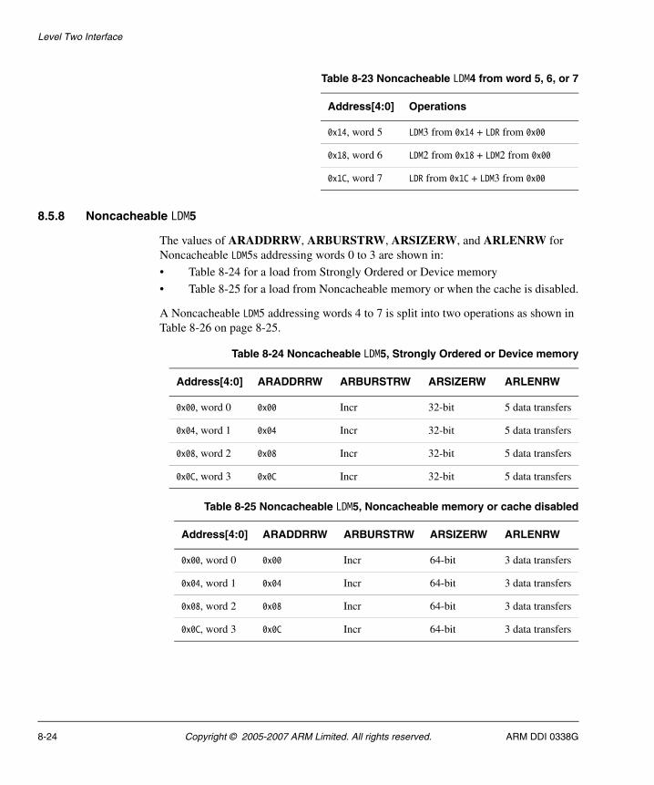
Level Two Interface
8.5.8 Noncacheable LDM5
The values of ARADDRRW, ARBURSTRW, ARSIZERW, and ARLENRW for Noncacheable LDM5s addressing words 0 to 3 are shown in:
• Table 8-24 for a load from Strongly Ordered or Device memory
• Table 8-25 for a load from Noncacheable memory or when the cache is disabled.
A Noncacheable LDM5 addressing words 4 to 7 is split into two operations as shown in Table 8-26 on page 8-25.
Table 8-23 Noncacheable LDM4 from word 5, 6, or 7
Address[4:0] Operations
0x14, word 5 LDM3 from 0x14 + LDR from 0x00
0x18, word 6 LDM2 from 0x18 + LDM2 from 0x00
0x1C, word 7 LDR from 0x1C + LDM3 from 0x00
Table 8-24 Noncacheable LDM5, Strongly Ordered or Device memory
Address[4:0] ARADDRRW ARBURSTRW ARSIZERW ARLENRW
0x00, word 0 0x00 Incr 32-bit 5 data transfers
0x04, word 1 0x04 Incr 32-bit 5 data transfers
0x08, word 2 0x08 Incr 32-bit 5 data transfers
0x0C, word 3 0x0C Incr 32-bit 5 data transfers
Table 8-25 Noncacheable LDM5, Noncacheable memory or cache disabled
Address[4:0] ARADDRRW ARBURSTRW ARSIZERW ARLENRW
0x00, word 0 0x00 Incr 64-bit 3 data transfers
0x04, word 1 0x04 Incr 64-bit 3 data transfers
0x08, word 2 0x08 Incr 64-bit 3 data transfers
0x0C, word 3 0x0C Incr 64-bit 3 data transfers
8-24 Copyright © 2005-2007 ARM Limited. All rights reserved. ARM DDI 0338G
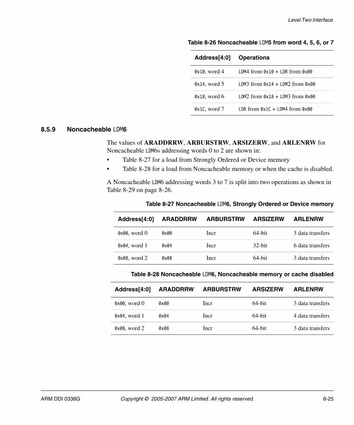
Level Two Interface
8.5.9 Noncacheable LDM6
The values of ARADDRRW, ARBURSTRW, ARSIZERW, and ARLENRW for Noncacheable LDM6s addressing words 0 to 2 are shown in:
• Table 8-27 for a load from Strongly Ordered or Device memory
• Table 8-28 for a load from Noncacheable memory or when the cache is disabled.
A Noncacheable LDM6 addressing words 3 to 7 is split into two operations as shown in Table 8-29 on page 8-26.
Table 8-26 Noncacheable LDM5 from word 4, 5, 6, or 7
Address[4:0] Operations
0x10, word 4 LDM4 from 0x10 + LDR from 0x00
0x14, word 5 LDM3 from 0x14 + LDM2 from 0x00
0x18, word 6 LDM2 from 0x18 + LDM3 from 0x00
0x1C, word 7 LDR from 0x1C + LDM4 from 0x00
Table 8-27 Noncacheable LDM6, Strongly Ordered or Device memory
Address[4:0] ARADDRRW ARBURSTRW ARSIZERW ARLENRW
0x00, word 0 0x00 Incr 64-bit 3 data transfers
0x04, word 1 0x04 Incr 32-bit 6 data transfers
0x08, word 2 0x08 Incr 64-bit 3 data transfers
Table 8-28 Noncacheable LDM6, Noncacheable memory or cache disabled
Address[4:0] ARADDRRW ARBURSTRW ARSIZERW ARLENRW
0x00, word 0 0x00 Incr 64-bit 3 data transfers
0x04, word 1 0x04 Incr 64-bit 4 data transfers
0x08, word 2 0x08 Incr 64-bit 3 data transfers
ARM DDI 0338G Copyright © 2005-2007 ARM Limited. All rights reserved. 8-25
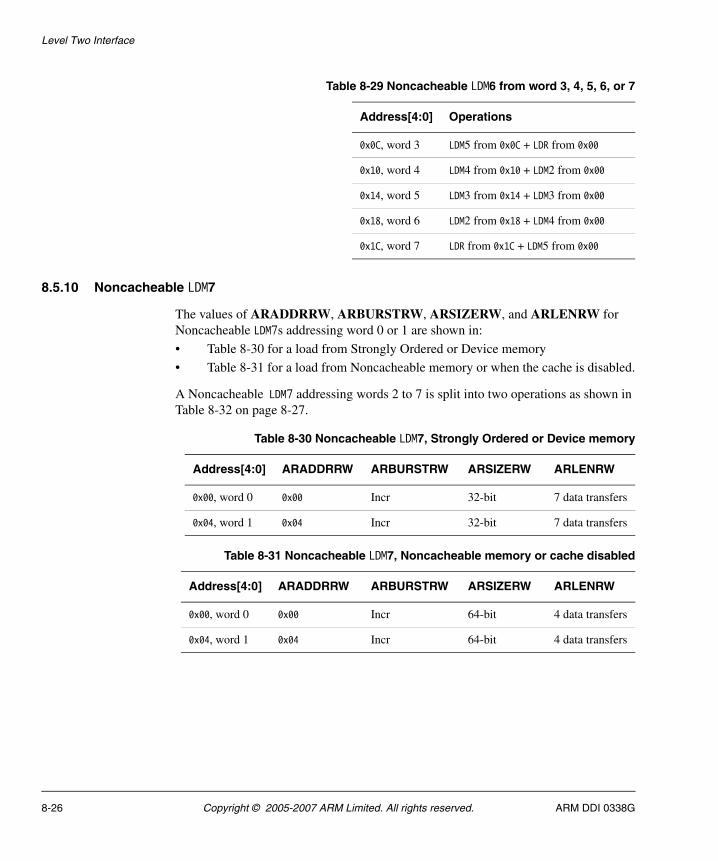
Level Two Interface
8.5.10 Noncacheable LDM7
The values of ARADDRRW, ARBURSTRW, ARSIZERW, and ARLENRW for Noncacheable LDM7s addressing word 0 or 1 are shown in:
• Table 8-30 for a load from Strongly Ordered or Device memory
• Table 8-31 for a load from Noncacheable memory or when the cache is disabled.
A Noncacheable LDM7 addressing words 2 to 7 is split into two operations as shown in Table 8-32 on page 8-27.
Table 8-29 Noncacheable LDM6 from word 3, 4, 5, 6, or 7
Address[4:0] Operations
0x0C, word 3 LDM5 from 0x0C + LDR from 0x00
0x10, word 4 LDM4 from 0x10 + LDM2 from 0x00
0x14, word 5 LDM3 from 0x14 + LDM3 from 0x00
0x18, word 6 LDM2 from 0x18 + LDM4 from 0x00
0x1C, word 7 LDR from 0x1C + LDM5 from 0x00
Table 8-30 Noncacheable LDM7, Strongly Ordered or Device memory
Address[4:0] ARADDRRW ARBURSTRW ARSIZERW ARLENRW
0x00, word 0 0x00 Incr 32-bit 7 data transfers
0x04, word 1 0x04 Incr 32-bit 7 data transfers
Table 8-31 Noncacheable LDM7, Noncacheable memory or cache disabled
Address[4:0] ARADDRRW ARBURSTRW ARSIZERW ARLENRW
0x00, word 0 0x00 Incr 64-bit 4 data transfers
0x04, word 1 0x04 Incr 64-bit 4 data transfers
8-26 Copyright © 2005-2007 ARM Limited. All rights reserved. ARM DDI 0338G
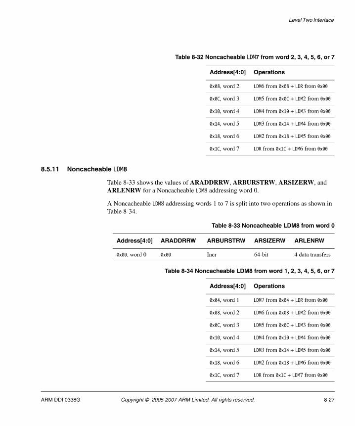
Level Two Interface
8.5.11 Noncacheable LDM8
Table 8-33 shows the values of ARADDRRW, ARBURSTRW, ARSIZERW, and ARLENRW for a Noncacheable LDM8 addressing word 0.
A Noncacheable LDM8 addressing words 1 to 7 is split into two operations as shown in Table 8-34.
Table 8-32 Noncacheable LDM7 from word 2, 3, 4, 5, 6, or 7
Address[4:0] Operations
0x08, word 2 LDM6 from 0x08 + LDR from 0x00
0x0C, word 3 LDM5 from 0x0C + LDM2 from 0x00
0x10, word 4 LDM4 from 0x10 + LDM3 from 0x00
0x14, word 5 LDM3 from 0x14 + LDM4 from 0x00
0x18, word 6 LDM2 from 0x18 + LDM5 from 0x00
0x1C, word 7 LDR from 0x1C + LDM6 from 0x00
Table 8-33 Noncacheable LDM8 from word 0
Address[4:0] ARADDRRW ARBURSTRW ARSIZERW ARLENRW
0x00, word 0 0x00 Incr 64-bit 4 data transfers
Table 8-34 Noncacheable LDM8 from word 1, 2, 3, 4, 5, 6, or 7
Address[4:0] Operations
0x04, word 1 LDM7 from 0x04 + LDR from 0x00
0x08, word 2 LDM6 from 0x08 + LDM2 from 0x00
0x0C, word 3 LDM5 from 0x0C + LDM3 from 0x00
0x10, word 4 LDM4 from 0x10 + LDM4 from 0x00
0x14, word 5 LDM3 from 0x14 + LDM5 from 0x00
0x18, word 6 LDM2 from 0x18 + LDM6 from 0x00
0x1C, word 7 LDR from 0x1C + LDM7 from 0x00
ARM DDI 0338G Copyright © 2005-2007 ARM Limited. All rights reserved. 8-27
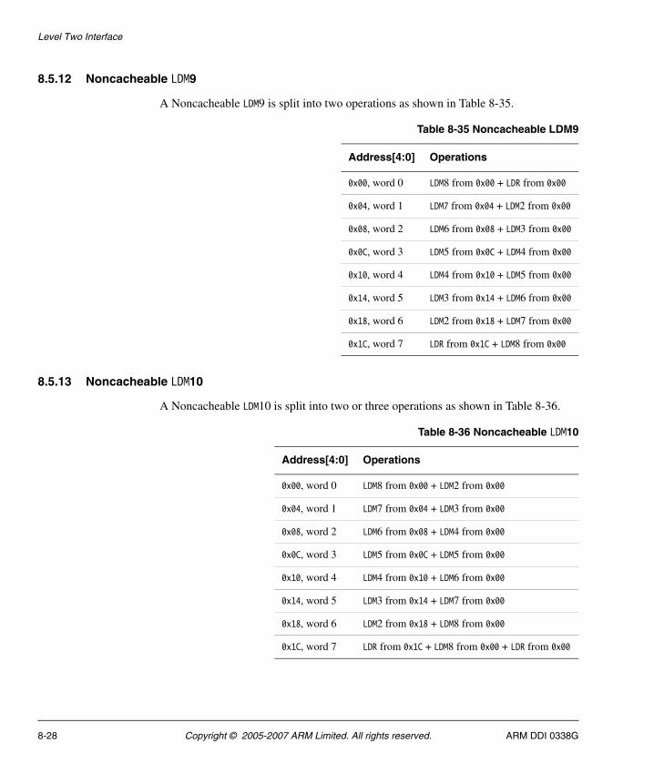
Level Two Interface
8.5.12 Noncacheable LDM9
A Noncacheable LDM9 is split into two operations as shown in Table 8-35.
8.5.13 Noncacheable LDM10
A Noncacheable LDM10 is split into two or three operations as shown in Table 8-36.
Table 8-35 Noncacheable LDM9
Address[4:0] Operations
0x00, word 0 LDM8 from 0x00 + LDR from 0x00
0x04, word 1 LDM7 from 0x04 + LDM2 from 0x00
0x08, word 2 LDM6 from 0x08 + LDM3 from 0x00
0x0C, word 3 LDM5 from 0x0C + LDM4 from 0x00
0x10, word 4 LDM4 from 0x10 + LDM5 from 0x00
0x14, word 5 LDM3 from 0x14 + LDM6 from 0x00
0x18, word 6 LDM2 from 0x18 + LDM7 from 0x00
0x1C, word 7 LDR from 0x1C + LDM8 from 0x00
Table 8-36 Noncacheable LDM10
Address[4:0] Operations
0x00, word 0 LDM8 from 0x00 + LDM2 from 0x00
0x04, word 1 LDM7 from 0x04 + LDM3 from 0x00
0x08, word 2 LDM6 from 0x08 + LDM4 from 0x00
0x0C, word 3 LDM5 from 0x0C + LDM5 from 0x00
0x10, word 4 LDM4 from 0x10 + LDM6 from 0x00
0x14, word 5 LDM3 from 0x14 + LDM7 from 0x00
0x18, word 6 LDM2 from 0x18 + LDM8 from 0x00
0x1C, word 7 LDR from 0x1C + LDM8 from 0x00 + LDR from 0x00
8-28 Copyright © 2005-2007 ARM Limited. All rights reserved. ARM DDI 0338G
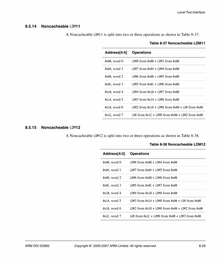
Level Two Interface
8.5.14 Noncacheable LDM11
A Noncacheable LDM11 is split into two or three operations as shown in Table 8-37.
8.5.15 Noncacheable LDM12
A Noncacheable LDM12 is split into two or three operations as shown in Table 8-38.
Table 8-37 Noncacheable LDM11
Address[4:0] Operations
0x00, word 0 LDM8 from 0x00 + LDM3 from 0x00
0x04, word 1 LDM7 from 0x04 + LDM4 from 0x00
0x08, word 2 LDM6 from 0x08 + LDM5 from 0x00
0x0C, word 3 LDM5 from 0x0C + LDM6 from 0x00
0x10, word 4 LDM4 from 0x10 + LDM7 from 0x00
0x14, word 5 LDM3 from 0x14 + LDM8 from 0x00
0x18, word 6 LDM2 from 0x18 + LDM8 from 0x00 + LDR from 0x00
0x1C, word 7 LDR from 0x1C + LDM8 from 0x00 + LDM2 from 0x00
Table 8-38 Noncacheable LDM12
Address[4:0] Operations
0x00, word 0 LDM8 from 0x00 + LDM4 from 0x00
0x04, word 1 LDM7 from 0x04 + LDM5 from 0x00
0x08, word 2 LDM6 from 0x08 + LDM6 from 0x00
0x0C, word 3 LDM5 from 0x0C + LDM7 from 0x00
0x10, word 4 LDM4 from 0x10 + LDM8 from 0x00
0x14, word 5 LDM3 from 0x14 + LDM8 from 0x00 + LDR from 0x00
0x18, word 6 LDM2 from 0x18 + LDM8 from 0x00 + LDM2 from 0x00
0x1C, word 7 LDR from 0x1C + LDM8 from 0x00 + LDM3 from 0x00
ARM DDI 0338G Copyright © 2005-2007 ARM Limited. All rights reserved. 8-29
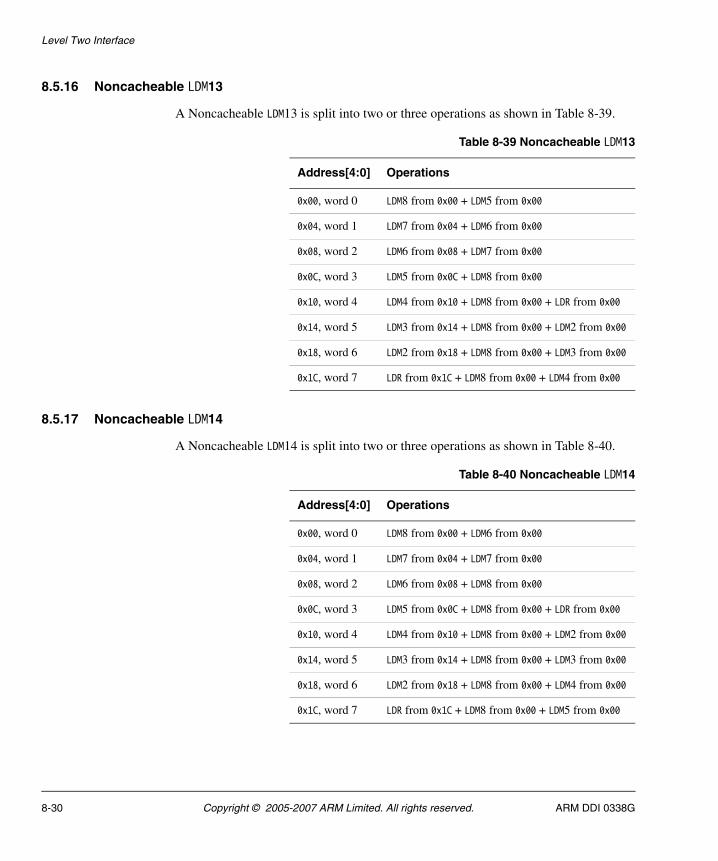
Level Two Interface
8.5.16 Noncacheable LDM13
A Noncacheable LDM13 is split into two or three operations as shown in Table 8-39.
8.5.17 Noncacheable LDM14
A Noncacheable LDM14 is split into two or three operations as shown in Table 8-40.
Table 8-39 Noncacheable LDM13
Address[4:0] Operations
0x00, word 0 LDM8 from 0x00 + LDM5 from 0x00
0x04, word 1 LDM7 from 0x04 + LDM6 from 0x00
0x08, word 2 LDM6 from 0x08 + LDM7 from 0x00
0x0C, word 3 LDM5 from 0x0C + LDM8 from 0x00
0x10, word 4 LDM4 from 0x10 + LDM8 from 0x00 + LDR from 0x00
0x14, word 5 LDM3 from 0x14 + LDM8 from 0x00 + LDM2 from 0x00
0x18, word 6 LDM2 from 0x18 + LDM8 from 0x00 + LDM3 from 0x00
0x1C, word 7 LDR from 0x1C + LDM8 from 0x00 + LDM4 from 0x00
Table 8-40 Noncacheable LDM14
Address[4:0] Operations
0x00, word 0 LDM8 from 0x00 + LDM6 from 0x00
0x04, word 1 LDM7 from 0x04 + LDM7 from 0x00
0x08, word 2 LDM6 from 0x08 + LDM8 from 0x00
0x0C, word 3 LDM5 from 0x0C + LDM8 from 0x00 + LDR from 0x00
0x10, word 4 LDM4 from 0x10 + LDM8 from 0x00 + LDM2 from 0x00
0x14, word 5 LDM3 from 0x14 + LDM8 from 0x00 + LDM3 from 0x00
0x18, word 6 LDM2 from 0x18 + LDM8 from 0x00 + LDM4 from 0x00
0x1C, word 7 LDR from 0x1C + LDM8 from 0x00 + LDM5 from 0x00
8-30 Copyright © 2005-2007 ARM Limited. All rights reserved. ARM DDI 0338G
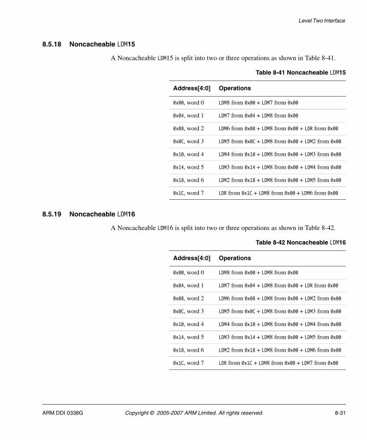
Level Two Interface
8.5.18 Noncacheable LDM15
A Noncacheable LDM15 is split into two or three operations as shown in Table 8-41.
8.5.19 Noncacheable LDM16
A Noncacheable LDM16 is split into two or three operations as shown in Table 8-42.
Table 8-41 Noncacheable LDM15
Address[4:0] Operations
0x00, word 0 LDM8 from 0x00 + LDM7 from 0x00
0x04, word 1 LDM7 from 0x04 + LDM8 from 0x00
0x08, word 2 LDM6 from 0x08 + LDM8 from 0x00 + LDR from 0x00
0x0C, word 3 LDM5 from 0x0C + LDM8 from 0x00 + LDM2 from 0x00
0x10, word 4 LDM4 from 0x10 + LDM8 from 0x00 + LDM3 from 0x00
0x14, word 5 LDM3 from 0x14 + LDM8 from 0x00 + LDM4 from 0x00
0x18, word 6 LDM2 from 0x18 + LDM8 from 0x00 + LDM5 from 0x00
0x1C, word 7 LDR from 0x1C + LDM8 from 0x00 + LDM6 from 0x00
Table 8-42 Noncacheable LDM16
Address[4:0] Operations
0x00, word 0 LDM8 from 0x00 + LDM8 from 0x00
0x04, word 1 LDM7 from 0x04 + LDM8 from 0x00 + LDR from 0x00
0x08, word 2 LDM6 from 0x08 + LDM8 from 0x00 + LDM2 from 0x00
0x0C, word 3 LDM5 from 0x0C + LDM8 from 0x00 + LDM3 from 0x00
0x10, word 4 LDM4 from 0x10 + LDM8 from 0x00 + LDM4 from 0x00
0x14, word 5 LDM3 from 0x14 + LDM8 from 0x00 + LDM5 from 0x00
0x18, word 6 LDM2 from 0x18 + LDM8 from 0x00 + LDM6 from 0x00
0x1C, word 7 LDR from 0x1C + LDM8 from 0x00 + LDM7 from 0x00
ARM DDI 0338G Copyright © 2005-2007 ARM Limited. All rights reserved. 8-31
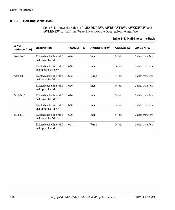
Level Two Interface
8.5.20 Half-line Write-Back
Table 8-43 shows the values of AWADDRRW, AWBURSTRW, AWSIZERW, and AWLENRW for half-line Write-Backs over the Data read/write interface.
Table 8-43 Half-line Write-Back
Writeaddress [4:0]
Description AWADDRRW AWBURSTRW AWSIZERW AWLENRW
0x00-0x07 Evicted cache line valid and lower half dirty
0x00 Incr 64-bit 2 data transfers
Evicted cache line valid and upper half dirty
0x10 Incr 64-bit 2 data transfers
0x08-0x0F Evicted cache line valid and lower half dirty
0x08 Wrap 64-bit 2 data transfers
Evicted cache line valid and upper half dirty
0x10 Incr 64-bit 2 data transfers
0x10-0x17 Evicted cache line valid and lower half dirty
0x00 Incr 64-bit 2 data transfers
Evicted cache line valid and upper half dirty
0x10 Incr 64-bit 2 data transfers
0x18-0x1F Evicted cache line valid and lower half dirty
0x00 Incr 64-bit 2 data transfers
Evicted cache line valid and upper half dirty
0x18 Wrap 64-bit 2 data transfers
8-32 Copyright © 2005-2007 ARM Limited. All rights reserved. ARM DDI 0338G
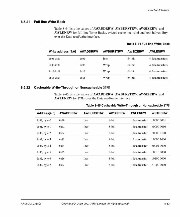
Level Two Interface
8.5.21 Full-line Write-Back
Table 8-44 lists the values of AWADDRRW, AWBURSTRW, AWSIZERW, and AWLENRW for full-line Write-Backs, evicted cache line valid and both halves dirty, over the Data read/write interface.
8.5.22 Cacheable Write-Through or Noncacheable STRB
Table 8-45 lists the values of AWADDRRW, AWBURSTRW, AWSIZERW, and AWLENRW for STRBs over the Data read/write interface.
Table 8-44 Full-line Write-Back
Write address [4:0] AWADDRRW AWBURSTRW AWSIZERW AWLENRW
0x00-0x07 0x00 Incr 64-bit 4 data transfers
0x08-0x0F 0x08 Wrap 64-bit 4 data transfers
0x10-0x17 0x10 Wrap 64-bit 4 data transfers
0x18-0x1F 0x18 Wrap 64-bit 4 data transfers
Table 8-45 Cacheable Write-Through or Noncacheable STRB
Address[4:0] AWADDRRW AWBURSTRW AWSIZERW AWLENRW WSTRBRW
0x00, byte 0 0x00 Incr 8-bit 1 data transfer b0000 0001
0x01, byte 1 0x01 Incr 8-bit 1 data transfer b0000 0010
0x02, byte 2 0x02 Incr 8-bit 1 data transfer b0000 0100
0x03, byte 3 0x03 Incr 8-bit 1 data transfer b0000 1000
0x04, byte 4 0x04 Incr 8-bit 1 data transfer b0001 0000
0x05, byte 5 0x05 Incr 8-bit 1 data transfer b0010 0000
0x06, byte 6 0x06 Incr 8-bit 1 data transfer b0100 0000
0x07, byte 7 0x07 Incr 8-bit 1 data transfer b1000 0000
ARM DDI 0338G Copyright © 2005-2007 ARM Limited. All rights reserved. 8-33
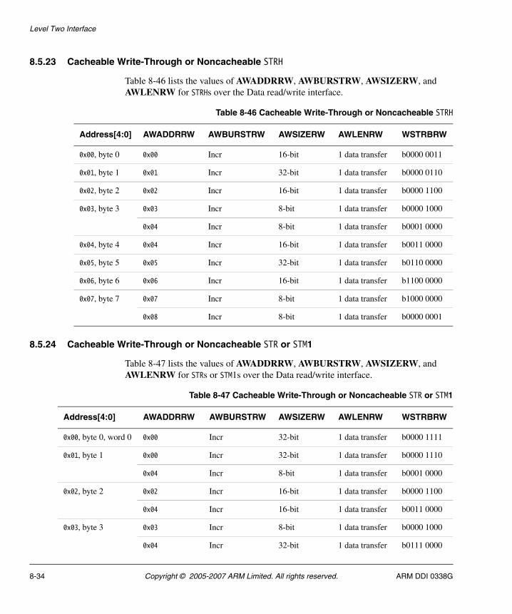
Level Two Interface
8.5.23 Cacheable Write-Through or Noncacheable STRH
Table 8-46 lists the values of AWADDRRW, AWBURSTRW, AWSIZERW, and AWLENRW for STRHs over the Data read/write interface.
8.5.24 Cacheable Write-Through or Noncacheable STR or STM1
Table 8-47 lists the values of AWADDRRW, AWBURSTRW, AWSIZERW, and AWLENRW for STRs or STM1s over the Data read/write interface.
Table 8-46 Cacheable Write-Through or Noncacheable STRH
Address[4:0] AWADDRRW AWBURSTRW AWSIZERW AWLENRW WSTRBRW
0x00, byte 0 0x00 Incr 16-bit 1 data transfer b0000 0011
0x01, byte 1 0x01 Incr 32-bit 1 data transfer b0000 0110
0x02, byte 2 0x02 Incr 16-bit 1 data transfer b0000 1100
0x03, byte 3 0x03 Incr 8-bit 1 data transfer b0000 1000
0x04 Incr 8-bit 1 data transfer b0001 0000
0x04, byte 4 0x04 Incr 16-bit 1 data transfer b0011 0000
0x05, byte 5 0x05 Incr 32-bit 1 data transfer b0110 0000
0x06, byte 6 0x06 Incr 16-bit 1 data transfer b1100 0000
0x07, byte 7 0x07 Incr 8-bit 1 data transfer b1000 0000
0x08 Incr 8-bit 1 data transfer b0000 0001
Table 8-47 Cacheable Write-Through or Noncacheable STR or STM1
Address[4:0] AWADDRRW AWBURSTRW AWSIZERW AWLENRW WSTRBRW
0x00, byte 0, word 0 0x00 Incr 32-bit 1 data transfer b0000 1111
0x01, byte 1 0x00 Incr 32-bit 1 data transfer b0000 1110
0x04 Incr 8-bit 1 data transfer b0001 0000
0x02, byte 2 0x02 Incr 16-bit 1 data transfer b0000 1100
0x04 Incr 16-bit 1 data transfer b0011 0000
0x03, byte 3 0x03 Incr 8-bit 1 data transfer b0000 1000
0x04 Incr 32-bit 1 data transfer b0111 0000
8-34 Copyright © 2005-2007 ARM Limited. All rights reserved. ARM DDI 0338G
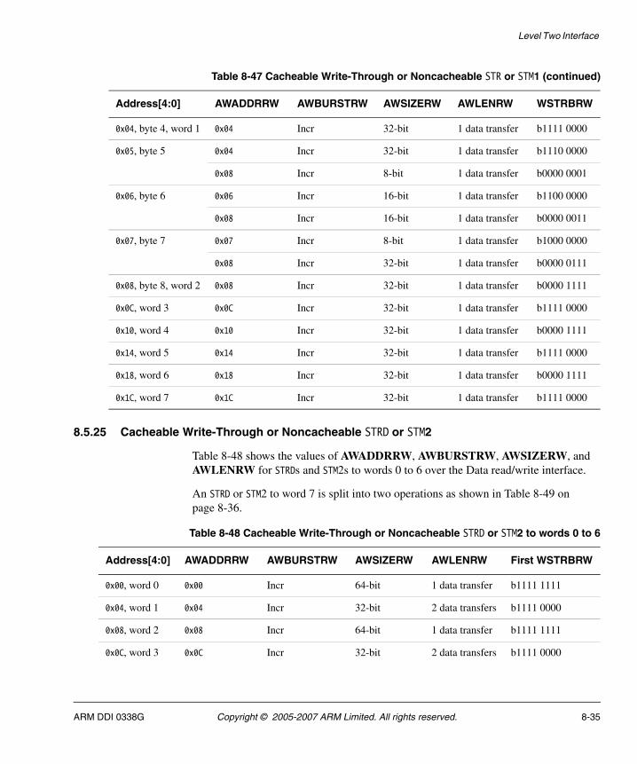
Level Two Interface
8.5.25 Cacheable Write-Through or Noncacheable STRD or STM2
Table 8-48 shows the values of AWADDRRW, AWBURSTRW, AWSIZERW, and AWLENRW for STRDs and STM2s to words 0 to 6 over the Data read/write interface.
An STRD or STM2 to word 7 is split into two operations as shown in Table 8-49 on page 8-36.
0x04, byte 4, word 1 0x04 Incr 32-bit 1 data transfer b1111 0000
0x05, byte 5 0x04 Incr 32-bit 1 data transfer b1110 0000
0x08 Incr 8-bit 1 data transfer b0000 0001
0x06, byte 6 0x06 Incr 16-bit 1 data transfer b1100 0000
0x08 Incr 16-bit 1 data transfer b0000 0011
0x07, byte 7 0x07 Incr 8-bit 1 data transfer b1000 0000
0x08 Incr 32-bit 1 data transfer b0000 0111
0x08, byte 8, word 2 0x08 Incr 32-bit 1 data transfer b0000 1111
0x0C, word 3 0x0C Incr 32-bit 1 data transfer b1111 0000
0x10, word 4 0x10 Incr 32-bit 1 data transfer b0000 1111
0x14, word 5 0x14 Incr 32-bit 1 data transfer b1111 0000
0x18, word 6 0x18 Incr 32-bit 1 data transfer b0000 1111
0x1C, word 7 0x1C Incr 32-bit 1 data transfer b1111 0000
Table 8-47 Cacheable Write-Through or Noncacheable STR or STM1 (continued)
Address[4:0] AWADDRRW AWBURSTRW AWSIZERW AWLENRW WSTRBRW
Table 8-48 Cacheable Write-Through or Noncacheable STRD or STM2 to words 0 to 6
Address[4:0] AWADDRRW AWBURSTRW AWSIZERW AWLENRW First WSTRBRW
0x00, word 0 0x00 Incr 64-bit 1 data transfer b1111 1111
0x04, word 1 0x04 Incr 32-bit 2 data transfers b1111 0000
0x08, word 2 0x08 Incr 64-bit 1 data transfer b1111 1111
0x0C, word 3 0x0C Incr 32-bit 2 data transfers b1111 0000
ARM DDI 0338G Copyright © 2005-2007 ARM Limited. All rights reserved. 8-35
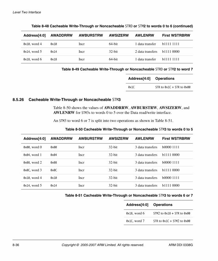
Level Two Interface
8.5.26 Cacheable Write-Through or Noncacheable STM3
Table 8-50 shows the values of AWADDRRW, AWBURSTRW, AWSIZERW, and AWLENRW for STM3s to words 0 to 5 over the Data read/write interface.
An STM3 to word 6 or 7 is split into two operations as shown in Table 8-51.
0x10, word 4 0x10 Incr 64-bit 1 data transfer b1111 1111
0x14, word 5 0x14 Incr 32-bit 2 data transfers b1111 0000
0x18, word 6 0x18 Incr 64-bit 1 data transfer b1111 1111
Table 8-48 Cacheable Write-Through or Noncacheable STRD or STM2 to words 0 to 6 (continued)
Address[4:0] AWADDRRW AWBURSTRW AWSIZERW AWLENRW First WSTRBRW
Table 8-49 Cacheable Write-Through or Noncacheable STRD or STM2 to word 7
Address[4:0] Operations
0x1C STR to 0x1C + STR to 0x00
Table 8-50 Cacheable Write-Through or Noncacheable STM3 to words 0 to 5
Address[4:0] AWADDRRW AWBURSTRW AWSIZERW AWLENRW First WSTRBRW
0x00, word 0 0x00 Incr 32-bit 3 data transfers b0000 1111
0x04, word 1 0x04 Incr 32-bit 3 data transfers b1111 0000
0x08, word 2 0x08 Incr 32-bit 3 data transfers b0000 1111
0x0C, word 3 0x0C Incr 32-bit 3 data transfers b1111 0000
0x10, word 4 0x10 Incr 32-bit 3 data transfers b0000 1111
0x14, word 5 0x14 Incr 32-bit 3 data transfers b1111 0000
Table 8-51 Cacheable Write-Through or Noncacheable STM3 to words 6 or 7
Address[4:0] Operations
0x18, word 6 STM2 to 0x18 + STR to 0x00
0x1C, word 7 STR to 0x1C + STM2 to 0x00
8-36 Copyright © 2005-2007 ARM Limited. All rights reserved. ARM DDI 0338G
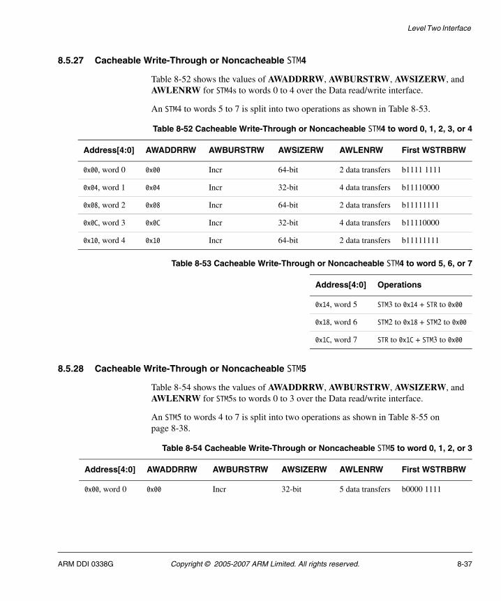
Level Two Interface
8.5.27 Cacheable Write-Through or Noncacheable STM4
Table 8-52 shows the values of AWADDRRW, AWBURSTRW, AWSIZERW, and AWLENRW for STM4s to words 0 to 4 over the Data read/write interface.
An STM4 to words 5 to 7 is split into two operations as shown in Table 8-53.
8.5.28 Cacheable Write-Through or Noncacheable STM5
Table 8-54 shows the values of AWADDRRW, AWBURSTRW, AWSIZERW, and AWLENRW for STM5s to words 0 to 3 over the Data read/write interface.
An STM5 to words 4 to 7 is split into two operations as shown in Table 8-55 on page 8-38.
Table 8-52 Cacheable Write-Through or Noncacheable STM4 to word 0, 1, 2, 3, or 4
Address[4:0] AWADDRRW AWBURSTRW AWSIZERW AWLENRW First WSTRBRW
0x00, word 0 0x00 Incr 64-bit 2 data transfers b1111 1111
0x04, word 1 0x04 Incr 32-bit 4 data transfers b11110000
0x08, word 2 0x08 Incr 64-bit 2 data transfers b11111111
0x0C, word 3 0x0C Incr 32-bit 4 data transfers b11110000
0x10, word 4 0x10 Incr 64-bit 2 data transfers b11111111
Table 8-53 Cacheable Write-Through or Noncacheable STM4 to word 5, 6, or 7
Address[4:0] Operations
0x14, word 5 STM3 to 0x14 + STR to 0x00
0x18, word 6 STM2 to 0x18 + STM2 to 0x00
0x1C, word 7 STR to 0x1C + STM3 to 0x00
Table 8-54 Cacheable Write-Through or Noncacheable STM5 to word 0, 1, 2, or 3
Address[4:0] AWADDRRW AWBURSTRW AWSIZERW AWLENRW First WSTRBRW
0x00, word 0 0x00 Incr 32-bit 5 data transfers b0000 1111
ARM DDI 0338G Copyright © 2005-2007 ARM Limited. All rights reserved. 8-37
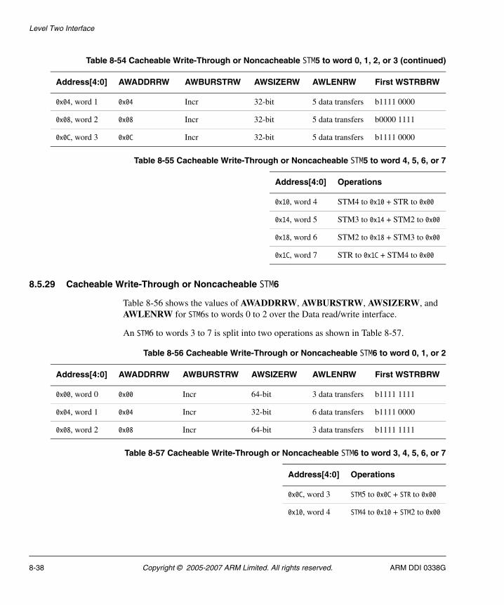
Level Two Interface
8.5.29 Cacheable Write-Through or Noncacheable STM6
Table 8-56 shows the values of AWADDRRW, AWBURSTRW, AWSIZERW, and AWLENRW for STM6s to words 0 to 2 over the Data read/write interface.
An STM6 to words 3 to 7 is split into two operations as shown in Table 8-57.
0x04, word 1 0x04 Incr 32-bit 5 data transfers b1111 0000
0x08, word 2 0x08 Incr 32-bit 5 data transfers b0000 1111
0x0C, word 3 0x0C Incr 32-bit 5 data transfers b1111 0000
Table 8-54 Cacheable Write-Through or Noncacheable STM5 to word 0, 1, 2, or 3 (continued)
Address[4:0] AWADDRRW AWBURSTRW AWSIZERW AWLENRW First WSTRBRW
Table 8-55 Cacheable Write-Through or Noncacheable STM5 to word 4, 5, 6, or 7
Address[4:0] Operations
0x10, word 4 STM4 to 0x10 + STR to 0x00
0x14, word 5 STM3 to 0x14 + STM2 to 0x00
0x18, word 6 STM2 to 0x18 + STM3 to 0x00
0x1C, word 7 STR to 0x1C + STM4 to 0x00
Table 8-56 Cacheable Write-Through or Noncacheable STM6 to word 0, 1, or 2
Address[4:0] AWADDRRW AWBURSTRW AWSIZERW AWLENRW First WSTRBRW
0x00, word 0 0x00 Incr 64-bit 3 data transfers b1111 1111
0x04, word 1 0x04 Incr 32-bit 6 data transfers b1111 0000
0x08, word 2 0x08 Incr 64-bit 3 data transfers b1111 1111
Table 8-57 Cacheable Write-Through or Noncacheable STM6 to word 3, 4, 5, 6, or 7
Address[4:0] Operations
0x0C, word 3 STM5 to 0x0C + STR to 0x00
0x10, word 4 STM4 to 0x10 + STM2 to 0x00
8-38 Copyright © 2005-2007 ARM Limited. All rights reserved. ARM DDI 0338G
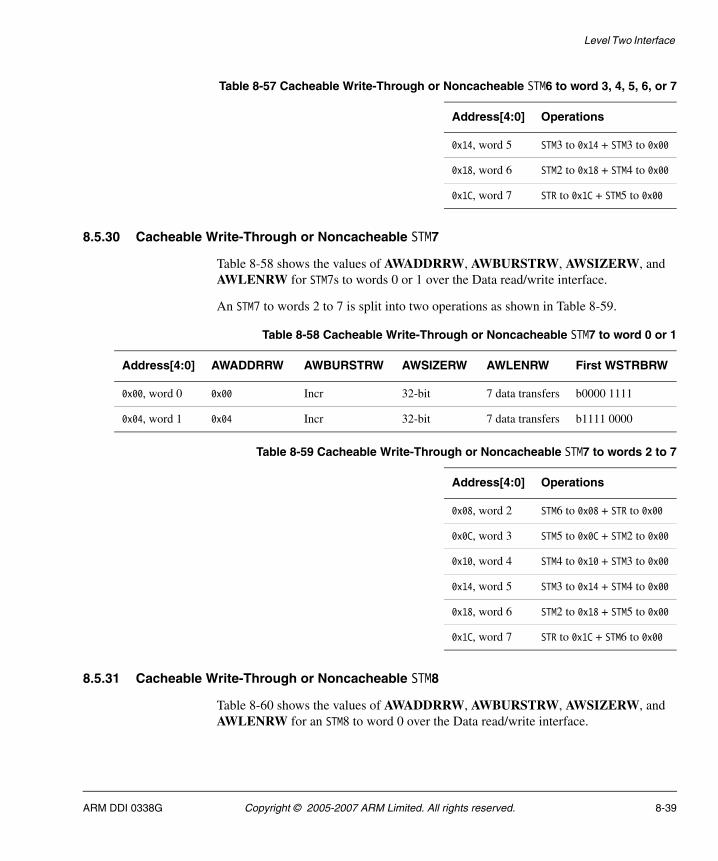
Level Two Interface
8.5.30 Cacheable Write-Through or Noncacheable STM7
Table 8-58 shows the values of AWADDRRW, AWBURSTRW, AWSIZERW, and AWLENRW for STM7s to words 0 or 1 over the Data read/write interface.
An STM7 to words 2 to 7 is split into two operations as shown in Table 8-59.
8.5.31 Cacheable Write-Through or Noncacheable STM8
Table 8-60 shows the values of AWADDRRW, AWBURSTRW, AWSIZERW, and AWLENRW for an STM8 to word 0 over the Data read/write interface.
0x14, word 5 STM3 to 0x14 + STM3 to 0x00
0x18, word 6 STM2 to 0x18 + STM4 to 0x00
0x1C, word 7 STR to 0x1C + STM5 to 0x00
Table 8-57 Cacheable Write-Through or Noncacheable STM6 to word 3, 4, 5, 6, or 7
Address[4:0] Operations
Table 8-58 Cacheable Write-Through or Noncacheable STM7 to word 0 or 1
Address[4:0] AWADDRRW AWBURSTRW AWSIZERW AWLENRW First WSTRBRW
0x00, word 0 0x00 Incr 32-bit 7 data transfers b0000 1111
0x04, word 1 0x04 Incr 32-bit 7 data transfers b1111 0000
Table 8-59 Cacheable Write-Through or Noncacheable STM7 to words 2 to 7
Address[4:0] Operations
0x08, word 2 STM6 to 0x08 + STR to 0x00
0x0C, word 3 STM5 to 0x0C + STM2 to 0x00
0x10, word 4 STM4 to 0x10 + STM3 to 0x00
0x14, word 5 STM3 to 0x14 + STM4 to 0x00
0x18, word 6 STM2 to 0x18 + STM5 to 0x00
0x1C, word 7 STR to 0x1C + STM6 to 0x00
ARM DDI 0338G Copyright © 2005-2007 ARM Limited. All rights reserved. 8-39
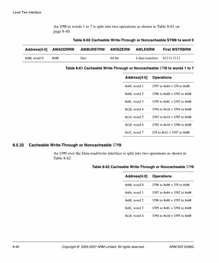
Level Two Interface
An STM8 to words 1 to 7 is split into two operations as shown in Table 8-61 on page 8-40.
8.5.32 Cacheable Write-Through or Noncacheable STM9
An STM9 over the Data read/write interface is split into two operations as shown in Table 8-62
Table 8-60 Cacheable Write-Through or Noncacheable STM8 to word 0
Address[4:0] AWADDRRW AWBURSTRW AWSIZERW AWLENRW First WSTRBRW
0x00, word 0 0x00 Incr 64-bit 4 data transfers b1111 1111
Table 8-61 Cacheable Write-Through or Noncacheable STM8 to words 1 to 7
Address[4:0] Operations
0x04, word 1 STM7 to 0x04 + STR to 0x00
0x08, word 2 STM6 to 0x08 + STM2 to 0x00
0x0C, word 3 STM5 to 0x0C + STM3 to 0x00
0x10, word 4 STM4 to 0x10 + STM4 to 0x00
0x14, word 5 STM3 to 0x14 + STM5 to 0x00
0x18, word 6 STM2 to 0x18 + STM6 to 0x00
0x1C, word 7 STR to 0x1C + STM7 to 0x00
Table 8-62 Cacheable Write-Through or Noncacheable STM9
Address[4:0] Operations
0x00, word 0 STM8 to 0x00 + STR to 0x00
0x04, word 1 STM7 to 0x04 + STM2 to 0x00
0x08, word 2 STM6 to 0x08 + STM3 to 0x00
0x0C, word 3 STM5 to 0x0C + STM4 to 0x00
0x10, word 4 STM4 to 0x10 + STM5 to 0x00
8-40 Copyright © 2005-2007 ARM Limited. All rights reserved. ARM DDI 0338G
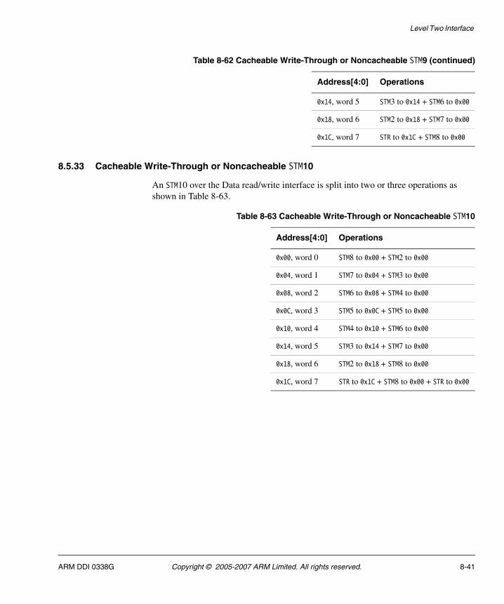
Level Two Interface
8.5.33 Cacheable Write-Through or Noncacheable STM10
An STM10 over the Data read/write interface is split into two or three operations as shown in Table 8-63.
0x14, word 5 STM3 to 0x14 + STM6 to 0x00
0x18, word 6 STM2 to 0x18 + STM7 to 0x00
0x1C, word 7 STR to 0x1C + STM8 to 0x00
Table 8-62 Cacheable Write-Through or Noncacheable STM9 (continued)
Address[4:0] Operations
Table 8-63 Cacheable Write-Through or Noncacheable STM10
Address[4:0] Operations
0x00, word 0 STM8 to 0x00 + STM2 to 0x00
0x04, word 1 STM7 to 0x04 + STM3 to 0x00
0x08, word 2 STM6 to 0x08 + STM4 to 0x00
0x0C, word 3 STM5 to 0x0C + STM5 to 0x00
0x10, word 4 STM4 to 0x10 + STM6 to 0x00
0x14, word 5 STM3 to 0x14 + STM7 to 0x00
0x18, word 6 STM2 to 0x18 + STM8 to 0x00
0x1C, word 7 STR to 0x1C + STM8 to 0x00 + STR to 0x00
ARM DDI 0338G Copyright © 2005-2007 ARM Limited. All rights reserved. 8-41
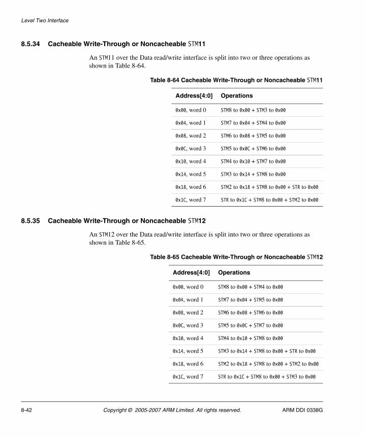
Level Two Interface
8.5.34 Cacheable Write-Through or Noncacheable STM11
An STM11 over the Data read/write interface is split into two or three operations as shown in Table 8-64.
8.5.35 Cacheable Write-Through or Noncacheable STM12
An STM12 over the Data read/write interface is split into two or three operations as shown in Table 8-65.
Table 8-64 Cacheable Write-Through or Noncacheable STM11
Address[4:0] Operations
0x00, word 0 STM8 to 0x00 + STM3 to 0x00
0x04, word 1 STM7 to 0x04 + STM4 to 0x00
0x08, word 2 STM6 to 0x08 + STM5 to 0x00
0x0C, word 3 STM5 to 0x0C + STM6 to 0x00
0x10, word 4 STM4 to 0x10 + STM7 to 0x00
0x14, word 5 STM3 to 0x14 + STM8 to 0x00
0x18, word 6 STM2 to 0x18 + STM8 to 0x00 + STR to 0x00
0x1C, word 7 STR to 0x1C + STM8 to 0x00 + STM2 to 0x00
Table 8-65 Cacheable Write-Through or Noncacheable STM12
Address[4:0] Operations
0x00, word 0 STM8 to 0x00 + STM4 to 0x00
0x04, word 1 STM7 to 0x04 + STM5 to 0x00
0x08, word 2 STM6 to 0x08 + STM6 to 0x00
0x0C, word 3 STM5 to 0x0C + STM7 to 0x00
0x10, word 4 STM4 to 0x10 + STM8 to 0x00
0x14, word 5 STM3 to 0x14 + STM8 to 0x00 + STR to 0x00
0x18, word 6 STM2 to 0x18 + STM8 to 0x00 + STM2 to 0x00
0x1C, word 7 STR to 0x1C + STM8 to 0x00 + STM3 to 0x00
8-42 Copyright © 2005-2007 ARM Limited. All rights reserved. ARM DDI 0338G
Level Two Interface
8.5.36 Cacheable Write-Through or Noncacheable STM13
An STM13 over the Data read/write interface is split into two or three operations as shown in Table 8-66.
8.5.37 Cacheable Write-Through or Noncacheable STM14
An STM14 over the Data read/write interface is split into two or three operations as shown in Table 8-67.
Table 8-66 Cacheable Write-Through or Noncacheable STM13
Address[4:0] Operations
0x00, word 0 STM8 to 0x00 + STM5 to 0x00
0x04, word 1 STM7 to 0x04 + STM6 to 0x00
0x08, word 2 STM6 to 0x08 + STM7 to 0x00
0x0C, word 3 STM5 to 0x0C + STM8 to 0x00
0x10, word 4 STM4 to 0x10 + STM8 to 0x00 + STR to 0x00
0x14, word 5 STM3 to 0x14 + STM8 to 0x00 + STM2 to 0x00
0x18, word 6 STM2 to 0x18 + STM8 to 0x00 + STM3 to 0x00
0x1C, word 7 STR to 0x1C + STM8 to 0x00 + STM4 to 0x00
Table 8-67 Cacheable Write-Through or Noncacheable STM14
Address[4:0] Operations
0x00, word 0 STM8 to 0x00 + STM6 to 0x00
0x04, word 1 STM7 to 0x04 + STM7 to 0x00
0x08, word 2 STM6 to 0x08 + STM8 to 0x00
0x0C, word 3 STM5 to 0x0C + STM8 to 0x00 + STR to 0x00
0x10, word 4 STM4 to 0x10 + STM8 to 0x00 + STM2 to 0x00
0x14, word 5 STM3 to 0x14 + STM8 to 0x00 + STM3 to 0x00
0x18, word 6 STM2 to 0x18 + STM8 to 0x00 + STM4 to 0x00
0x1C, word 7 STR to 0x1C + STM8 to 0x00 + STM5 to 0x00
ARM DDI 0338G Copyright © 2005-2007 ARM Limited. All rights reserved. 8-43
Level Two Interface
8.5.38 Cacheable Write-Through or Noncacheable STM15
An STM15 over the Data read/write interface is split into two or three operations as shown in Table 8-68.
8.5.39 Cacheable Write-Through or Noncacheable STM16
An STM15 over the Data read/write interface is split into two or three operations as shown in Table 8-69.
Table 8-68 Cacheable Write-Through or Noncacheable STM15
Address[4:0] Operations
0x00, word 0 STM8 to 0x00 + STM7 to 0x00
0x04, word 1 STM7 to 0x04 + STM8 to 0x00
0x08, word 2 STM6 to 0x08 + STM8 to 0x00 + STR to 0x00
0x0C, word 3 STM5 to 0x0C + STM8 to 0x00 + STM2 to 0x00
0x10, word 4 STM4 to 0x10 + STM8 to 0x00 + STM3 to 0x00
0x14, word 5 STM3 to 0x14 + STM8 to 0x00 + STM4 to 0x00
0x18, word 6 STM2 to 0x18 + STM8 to 0x00 + STM5 to 0x00
0x1C, word 7 STR to 0x1C + STM8 to 0x00 + STM6 to 0x00
Table 8-69 Cacheable Write-Through or Noncacheable STM16
Address[4:0] Operations
0x00, word 0 STM8 to 0x00 + STM8 to 0x00
0x04, word 1 STM7 to 0x04 + STM8 to 0x00 + STR to 0x00
0x08, word 2 STM6 to 0x08 + STM8 to 0x00 + STM2 to 0x00
0x0C, word 3 STM5 to 0x0C + STM8 to 0x00 + STM3 to 0x00
0x10, word 4 STM4 to 0x10 + STM8 to 0x00 + STM4 to 0x00
0x14, word 5 STM3 to 0x14 + STM8 to 0x00 + STM5 to 0x00
0x18, word 6 STM2 to 0x18 + STM8 to 0x00 + STM6 to 0x00
0x1C, word 7 STR to 0x1C + STM8 to 0x00 + STM7 to 0x00
8-44 Copyright © 2005-2007 ARM Limited. All rights reserved. ARM DDI 0338G
Level Two Interface
8.6 Peripheral interface transfers
The tables in this section describe the Peripheral interface behavior for reads and writes for the following interface signals:
• AxADDRP[31:0]• AxBURSTP[1:0]• AxSIZEP[2:0]• AxLENP[3:0]• WSTRBP[3:0], for write accesses.
See the AMBA AXI Protocol Specification for details of the other AXI signals.
Table 8-70 lists the values of AxADDRP, AxBURSTP, AxSIZEP, AxLENP, and WSTRBP for example Peripheral interface reads and writes.
Table 8-70 Example Peripheral interface reads and writes
Example transfer, read or write
AxADDRP AxBURSTP AxSIZEP AxLENP WSTRBP
Words 0-7 0x00 Incr 32-bit 2 data transfers b1111
0x04 b1111
0x08 Incr 32-bit 2 data transfers b1111
0x0C b1111
0x10 Incr 32-bit 2 data transfers b1111
0x14 b1111
0x18 Incr 32-bit 2 data transfers b1111
0x1C b1111
Words 0-3 0x00 Incr 32-bit 2 data transfers b1111
0x04 b1111
0x08 Incr 32-bit b1111
0x0C b1111
Words 0-2 0x00 Incr 32-bit 2 data transfers b1111
0x04 b1111
0x08 Incr 32-bit 1 data transfer b1111
ARM DDI 0338G Copyright © 2005-2007 ARM Limited. All rights reserved. 8-45
Level Two Interface
The peripheral port can only do incrementing bursts of 2 data transfers maximum. It does not support unaligned accesses.
Words 0-1 0x00 Incr 32-bit 2 data transfers b1111
0x04 b1111
Word 2 0x08 Incr 32-bit 1 data transfer b1111
Word 0, bytes 0 and 1 0x00 Incr 16-bit 1 data transfer b0011
Word 1, bytes 2 and 3 0x06 Incr 16-bit 1 data transfer b1100
Word 2, byte 3 0x0B Incr 8-bit 1 data transfer b1000
Table 8-70 Example Peripheral interface reads and writes (continued)
Example transfer, read or write
AxADDRP AxBURSTP AxSIZEP AxLENP WSTRBP
8-46 Copyright © 2005-2007 ARM Limited. All rights reserved. ARM DDI 0338G
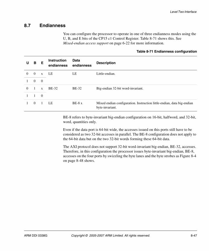
Level Two Interface
8.7 Endianness
You can configure the processor to operate in one of three endianness modes using the U, B, and E bits of the CP15 c1 Control Register. Table 8-71 shows this. See Mixed-endian access support on page 6-22 for more information.
BE-8 refers to byte-invariant big-endian configuration on 16-bit, halfword, and 32-bit, word, quantities only.
Even if the data port is 64-bit wide, the accesses issued on this ports still have to be considered as two 32-bit accesses in parallel. The BE-8 configuration does not apply to the 64-bit data but on the two 32-bit words forming these 64-bit data.
The AXI protocol does not support 32-bit word-invariant big-endian, BE-32, accesses. Therefore, in this configuration the processor issues byte-invariant big-endian, BE-8, accesses on the four ports by swizzling the byte lanes and the byte strobes as Figure 8-4 on page 8-48 shows.
Table 8-71 Endianness configuration
U B EInstruction endianness
Data endianness
Description
0 0 x LE LE Little-endian.
1 0 0
0 1 x BE-32 BE-32 Big-endian 32-bit word-invariant.
1 1 0
1 0 1 LE BE-8 x Mixed endian configuration. Instruction little-endian, data big-endian byte-invariant.
ARM DDI 0338G Copyright © 2005-2007 ARM Limited. All rights reserved. 8-47
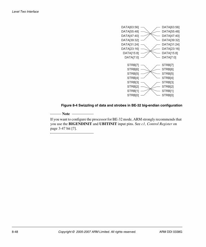
Level Two Interface
Figure 8-4 Swizzling of data and strobes in BE-32 big-endian configuration
Note If you want to configure the processor for BE-32 mode, ARM strongly recommends that you use the BIGENDINIT and UBITINIT input pins. See c1, Control Register on page 3-47 bit [7].
DATA[63:56]
DATA[55:48]
DATA[47:40]
DATA[39:32]
DATA[31:24]
DATA[23:16]
DATA[15:8]
DATA[7:0]
DATA[63:56]
DATA[55:48]
DATA[47:40]
DATA[39:32]
DATA[31:24]
DATA[23:16]
DATA[15:8]
DATA[7:0]
STRB[7]
STRB[6]
STRB[5]
STRB[4]
STRB[3]
STRB[2]
STRB[1]
STRB[0]
STRB[7]
STRB[6]
STRB[5]
STRB[4]
STRB[3]
STRB[2]
STRB[1]
STRB[0]
8-48 Copyright © 2005-2007 ARM Limited. All rights reserved. ARM DDI 0338G
Level Two Interface
8.8 Locked access
The AXI protocol specifies that, when a locked transaction occurs, the master must follow the locked transaction with an unlocked transaction to remove the lock of the interconnect. For ARM1156T2F-S processors, this implies that, in the case of an abort received on the read part of a SWP instruction, the Peripheral port or Data port issues a dummy write access with all byte strobes LOW at the same address as the read access and with AWLOCK = 00, normal transaction.
ARM DDI 0338G Copyright © 2005-2007 ARM Limited. All rights reserved. 8-49
Level Two Interface
8-50 Copyright © 2005-2007 ARM Limited. All rights reserved. ARM DDI 0338G
Chapter 9 Clocking and Resets
This chapter describes the clocking and reset options available for ARM1156T2-S processors. It contains the following sections:
• ARM1156T2-S clocking on page 9-2
• Reset on page 9-3
• Reset modes on page 9-4.
ARM DDI 0338G Copyright © 2005-2007 ARM Limited. All rights reserved. 9-1
Clocking and Resets
9.1 ARM1156T2-S clocking
The ARM1156T2-S processor has two functional clock inputs. Externally to the processor, you must connect together CLKIN and FREECLKIN.
For details on how the clock regions are implemented, see ARM1156T2F-S and ARM1156T2-S Implementation Guide.
For the purposes of this chapter, you can ignore FREECLKIN.
All clocks can be stopped indefinitely without loss of state.
You can preconfigure the ARM1156T2-S processor so that each clock region operates synchronously to the core clock region.
9-2 Copyright © 2005-2007 ARM Limited. All rights reserved. ARM DDI 0338G
Clocking and Resets
9.2 Reset
The ARM1156T2-S processor has the following reset inputs:
nRESETIN This signal is the main processor reset that initializes the majority of the ARM1156T2-S logic.
DBGnTRST This signal is the DBGTAP reset.
nPORESETIN This signal is the power-on reset that initializes the CP14 debug logic. See CP14 registers reset on page 13-24 for details.
All of these are active LOW signals that reset logic in the ARM1156T2-S processor. You must take care when designing the logic to drive these reset signals.
ARM DDI 0338G Copyright © 2005-2007 ARM Limited. All rights reserved. 9-3
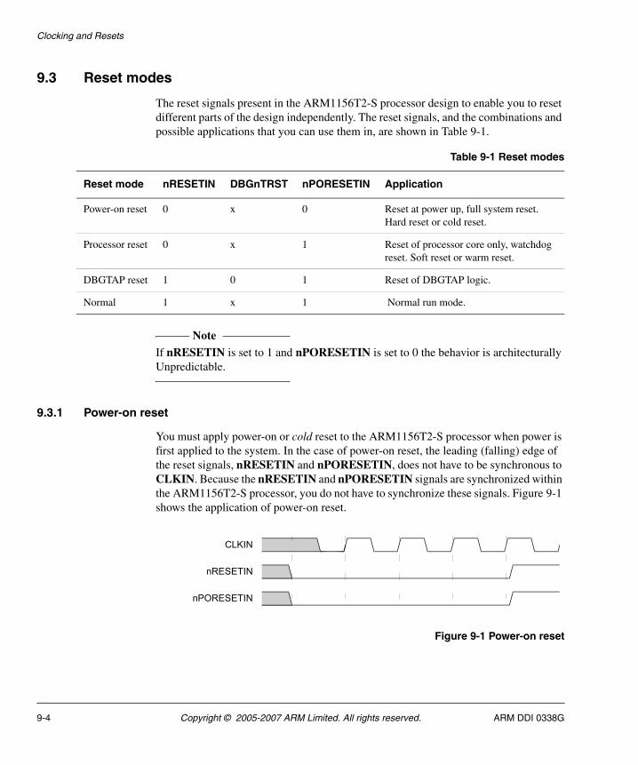
Clocking and Resets
9.3 Reset modes
The reset signals present in the ARM1156T2-S processor design to enable you to reset different parts of the design independently. The reset signals, and the combinations and possible applications that you can use them in, are shown in Table 9-1.
Note If nRESETIN is set to 1 and nPORESETIN is set to 0 the behavior is architecturally Unpredictable.
9.3.1 Power-on reset
You must apply power-on or cold reset to the ARM1156T2-S processor when power is first applied to the system. In the case of power-on reset, the leading (falling) edge of the reset signals, nRESETIN and nPORESETIN, does not have to be synchronous to CLKIN. Because the nRESETIN and nPORESETIN signals are synchronized within the ARM1156T2-S processor, you do not have to synchronize these signals. Figure 9-1 shows the application of power-on reset.
Figure 9-1 Power-on reset
Table 9-1 Reset modes
Reset mode nRESETIN DBGnTRST nPORESETIN Application
Power-on reset 0 x 0 Reset at power up, full system reset. Hard reset or cold reset.
Processor reset 0 x 1 Reset of processor core only, watchdog reset. Soft reset or warm reset.
DBGTAP reset 1 0 1 Reset of DBGTAP logic.
Normal 1 x 1 Normal run mode.
CLKIN
nRESETIN
nPORESETIN
9-4 Copyright © 2005-2007 ARM Limited. All rights reserved. ARM DDI 0338G
Clocking and Resets
It is recommended that you assert the reset signals for at least three CLKIN cycles to ensure correct reset behavior. Adopting a three-cycle reset eases the integration of other ARM parts into the system, for example, ARM9TDMI-based designs.
It is not necessary to assert DBGnTRST on power-up.
9.3.2 Processor reset
A processor or warm reset initializes the majority of the ARM1156T2-S processor, excluding the ARM1156T2-S DBGTAP controller and the EmbeddedICE-RT logic. Processor reset is typically used for resetting a system that has been operating for some time, for example, watchdog reset.
Because the nRESETIN signal is synchronized within the ARM1156T2-S processor, you do not have to synchronize this signal.
9.3.3 DBGTAP reset
DBGTAP reset initializes the state of the ARM1156T2-S DBGTAP controller. DBGTAP reset is typically used by the RealView™ ICE module for hot connection of a debugger to a system.
DBGTAP reset enables initialization of the DBGTAP controller without affecting the normal operation of the ARM1156T2-S processor.
Because the DBGnTRST signal is synchronized within the ARM1156T2-S processor, you do not have to synchronize this signal.
9.3.4 Normal operation
During normal operation, neither processor reset nor power-on reset is asserted. If the DBGTAP port is not being used, the value of DBGnTRST does not matter.
ARM DDI 0338G Copyright © 2005-2007 ARM Limited. All rights reserved. 9-5

Clocking and Resets
9-6 Copyright © 2005-2007 ARM Limited. All rights reserved. ARM DDI 0338G
Chapter 10 Power Control
This chapter describes the ARM1156T2-S power control functions. It contains the following sections:
• About power control on page 10-2
• Power management on page 10-3.
ARM DDI 0338G Copyright © 2005-2007 ARM Limited. All rights reserved. 10-1
Power Control
10.1 About power control
The features of the ARM1156T2-S processor that improve energy efficiency include:
• accurate branch and return prediction, reducing the number of incorrect instruction fetch and decode operations
• use of physically addressed caches, which reduces the number of cache flushes and refills, saving energy in the system
• the caches use sequential access information to reduce the number of accesses to the Tag RAMs and to unwanted Data RAMs.
In the ARM1156T2-S processor extensive use is also made of gated clocks and gates to disable inputs to unused functional blocks. Only the logic actively in use to perform a calculation consumes any dynamic power.
10-2 Copyright © 2005-2007 ARM Limited. All rights reserved. ARM DDI 0338G
Power Control
10.2 Power management
ARM1156T2-S processors support three levels of power management:
• Run mode
• Standby mode
• Shutdown mode on page 10-4
• plus partial support for a fourth level, Dormant mode on page 10-4.
10.2.1 Run mode
Run mode is the normal mode of operation in which all of the functionality of the processor is available.
10.2.2 Standby mode
Standby mode disables most of the clocks of the device, while keeping the design powered up. This reduces the power drawn to the static leakage current, plus a tiny clock power overhead required to enable the device to wake up from the standby mode.
The transition from Standby mode to Run mode is caused by the either:
• arrival of an interrupt, whether masked or unmasked
• a debug request, only when debug is enabled
• reset.
The debug request can be generated by an externally generated debug request, using the EDBGRQ pin on the ARM1156T2-S processor, or from a Debug Halt instruction issued to the ARM1156T2-S processor through the debug scan chains.
Entry into Standby Mode is performed by executing the Wait For Interrupt CP15 operation. To ensure that the memory system is not affected by the entry into the standby mode, the following operations are performed:
• A Drain Write Buffer operation ensures that all explicit memory accesses occurring in program order before the Wait For Interrupt have completed. This avoids any possible deadlocks that could be caused in a system where memory access triggers or enables an interrupt that the core is waiting for.
• Any other memory accesses that have been started at the time that the Wait For Interrupt instruction is executed are completed as normal. This ensures that the level two memory system does not see any disruption caused by the Wait For Interrupt.
ARM DDI 0338G Copyright © 2005-2007 ARM Limited. All rights reserved. 10-3
Power Control
Systems using the VIC interface must ensure that the VIC is not masking any interrupts that are required for restarting the ARM1156T2-S processor when in this mode of operation.
After the processor clocks have been stopped the signal STANDBYWFI is asserted to indicate that the ARM1156T2-S processor is in Standby mode.
10.2.3 Shutdown mode
Shutdown mode has the entire device powered down, and you must externally save all state, including cache and TCM state. The processor is returned to Run mode by asserting and deasserting nRESET. This state saving is performed with interrupts disabled, and finishes with a Drain Write Buffer operation. When all the state of the ARM1156T2-S processor is saved the ARM1156T2-S processor executes a Wait For Interrupt instruction. The signal STANDBYWFI is asserted to indicate that the processor can enter Shutdown mode.
10.2.4 Dormant mode
Dormant mode enables the core to be powered down, leaving the caches and the Tightly-Coupled Memory (TCM) powered up and maintaining their state.
The software visibility of the Valid bits is provided to enable an implementation to be extended for Dormant mode, but some hardware modification of the RAM blocks during implementation to include an input clamp is required for the full implementation of Dormant mode.
Considerations for Dormant mode
Dormant mode is partially supported on ARM1156T2-S processors, because care is required in implementing this on a standard synthesizable flow. The RAM blocks that are to remain powered up must be implemented on a separate power region, and there is a requirement to clamp all of the inputs to the RAMs to a known logic level (with the chip enable being held inactive). This clamping is not implemented in gates as part of the default synthesis flow because it contributes to a tight critical path.
Designers wanting to implement Dormant mode must add these clamps around the RAMs, either as explicit gates in the RAM power region, or as pull-down transistors that clamp the values while the core is powered down. The RAM blocks that must remain powered up in Dormant mode, if it is implemented, are:
• all Data RAMs associated with the cache and TCMs
• all Tag RAMs associated with the cache
• all Valid RAMs and Dirty RAMs associated with the cache.
10-4 Copyright © 2005-2007 ARM Limited. All rights reserved. ARM DDI 0338G
Power Control
Before entering Dormant mode, the state of the ARM1156T2-S processor, excluding the contents of the RAMs that remain powered up in dormant mode, must be saved to external memory. These state saving operations must ensure that the following occur:
• All ARM registers, including CPSR and SPSR registers are saved.
• All CP15 registers are saved.
• All debug-related state is saved.
• The Master Valid bits for the cache are saved. For more details, see Access to the cache valid bits. These are accessed using CP15 register c15 as described in c15, Instruction Cache Master Valid Register on page 3-107 and c15, Data Cache Master Valid Register on page 3-108.
• A Drain Write Buffer instruction is executed to ensure that all state saving has been completed.
A Wait For Interrupt CP15 operation is then executed, enabling the signal STANDBYWFI to indicate that the ARM1156T2-S processor can enter Dormant mode.
• On entry into Dormant mode, the Reset signal to the ARM1156T2-S processor must be asserted by the external power control mechanism.
To initiate the transition from Dormant mode to Run mode the external power controller must detect a request. When the request is received, the external power controller must assert and deassert the nRESET signal to the ARM1156T2-S processor until the power to the processor is restored. When power has been restored the core leaves reset and, by interrogating the external power control, can determine that the saved state must be restored.
10.2.5 Access to the cache valid bits
The cache master valid bits are used to provide the ability to mask the valid bits held in the valid RAM for the cache. By doing this, a single cycle invalidation of the cache can be performed without requiring special resetable RAM cells. The number of master valid bits is a function of the cache size. There are 64 Cache master valid bits for a 16Kbyte cache, and the number of bits scales linearly with cache size. The maximum number of 32-bit registers required for the largest cache size (64K) is 8. The registers fill from the LSB of the lowest numbered register upwards with these valid bits.
Unimplemented valid bits are Unpredictable for reads and Should Be Zero or Preserved (SBZP) for writes.
ARM DDI 0338G Copyright © 2005-2007 ARM Limited. All rights reserved. 10-5
Power Control
Modifying the values of the valid bits using this mechanism can have Unpredictable effects. The intended usage is for these registers only to be written while the cache is disabled, and the values to be written are the values that were previously read out.
For the instructions that access the cache valid bits see c15, Instruction Cache Master Valid Register on page 3-107 and c15, Data Cache Master Valid Register on page 3-108
10.2.6 Communication to the Power Management Controller
The powering up and powering down of the processor can be controlled by a Power Management Controller (PMC). The communication mechanism between the ARM1156T2-S processor and the PMC is a memory-mapped controller, which is accessed by the processor performing Strongly-Ordered accesses to it.
The STANDBYWFI signal from the ARM1156T2-S processor informs the PMC which powerdown mode to be in.
The STANDBYWFI signal can also be used to signal that the ARM1156T2-S processor is ready to have its power state changed. STANDBYWFI is asserted in response to a Wait For Interrupt operation.
10-6 Copyright © 2005-2007 ARM Limited. All rights reserved. ARM DDI 0338G

Chapter 11 Coprocessor Interface
This chapter describes the ARM1156T2-S coprocessor interface. It contains the following sections:
• About the coprocessor interface on page 11-2
• Coprocessor pipeline on page 11-3
• Token queue management on page 11-10
• Token queues on page 11-14
• Data transfer on page 11-18
• Operations on page 11-23
• Multiple coprocessors on page 11-26.
ARM DDI 0338G Copyright © 2005-2007 ARM Limited. All rights reserved. 11-1
Coprocessor Interface
11.1 About the coprocessor interface
The processor connects to on-chip coprocessors through an external coprocessor interface. All types of coprocessor instruction are supported.
The ARM instruction set supports the connection of 16 coprocessors, numbered 0-15, to an ARM processor. In ARM1156T2-S processors, the following coprocessor numbers are reserved:
CP10 VFP control
CP11 VFP control
CP14 Debug
CP15 System control.
You can use CP0-9, CP12, and CP13 for your own external coprocessors.
The ARM1156T2-S processor is designed to pass instructions to several coprocessors and exchange data with them. These coprocessors are intended to run in step with the core and are pipelined in a similar way to the core. Instructions are passed out of the Fetch stage of the core pipeline to the coprocessor and decoded. The decoded instruction is passed down its own pipeline. Coprocessor instructions can be canceled by the core if a condition code fails, or the entire coprocessor pipeline can be flushed in the event of a mispredicted branch. Load and store data are also required to pass between the core Logic Store Unit (LSU) and the coprocessor pipeline.
The coprocessor interface operates over a two-cycle delay. Any signal passing from the core to the coprocessor, or from the coprocessor to the core, is given a whole clock cycle to propagate from one to the other. This means that a signal crossing the interface is clocked out of a register on one side of the interface and clocked directly into another register on the other side. No combinatorial process must intervene. This constraint exists because the core and coprocessor can be placed a considerable distance apart and generous timing margins are necessary to cover signal propagation times. This delay in signal propagation makes it difficult to maintain pipeline synchronization, ruling out a tightly-coupled synchronization method.
ARM1156T2-S processors implement a token-based pipeline synchronization method that permits some slack between the two pipelines, while ensuring that the pipelines are correctly aligned for crucial transfers of information.
11-2 Copyright © 2005-2007 ARM Limited. All rights reserved. ARM DDI 0338G
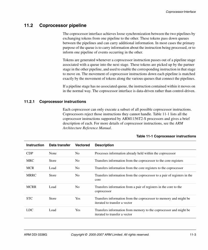
Coprocessor Interface
11.2 Coprocessor pipeline
The coprocessor interface achieves loose synchronization between the two pipelines by exchanging tokens from one pipeline to the other. These tokens pass down queues between the pipelines and can carry additional information. In most cases the primary purpose of the queue is to carry information about the instruction being processed, or to inform one pipeline of events occurring in the other.
Tokens are generated whenever a coprocessor instruction passes out of a pipeline stage associated with a queue into the next stage. These tokens are picked up by the partner stage in the other pipeline, and used to enable the corresponding instruction in that stage to move on. The movement of coprocessor instructions down each pipeline is matched exactly by the movement of tokens along the various queues that connect the pipelines.
If a pipeline stage has no associated queue, the instruction contained within it moves on in the normal way. The coprocessor interface is data-driven rather than control-driven.
11.2.1 Coprocessor instructions
Each coprocessor can only execute a subset of all possible coprocessor instructions. Coprocessors reject those instructions they cannot handle. Table 11-1 lists all the coprocessor instructions supported by ARM1156T2-S processors and gives a brief description of each. For more details of coprocessor instructions, see the ARM Architecture Reference Manual.
Table 11-1 Coprocessor instructions
Instruction Data transfer Vectored Description
CDP None No Processes information already held within the coprocessor
MRC Store No Transfers information from the coprocessor to the core registers
MCR Load No Transfers information from the core registers to the coprocessor
MRRC Store No Transfers information from the coprocessor to a pair of registers in the core
MCRR Load No Transfers information from a pair of registers in the core to the coprocessor
STC Store Yes Transfers information from the coprocessor to memory and might be iterated to transfer a vector
LDC Load Yes Transfers information from memory to the coprocessor and might be iterated to transfer a vector
ARM DDI 0338G Copyright © 2005-2007 ARM Limited. All rights reserved. 11-3
Coprocessor Interface
The coprocessor instructions fall into three groups:
• loads
• stores
• processing instructions.
The load and store instructions enable information to pass between the core and the coprocessor. Some of them might be vectored. This enables several values to be transferred in a single instruction. This typically involves the transfer of several words of data between a set of registers in the coprocessor and a contiguous set of locations in memory.
Other instructions, for example MCR and MRC, transfer data between core and coprocessor registers. The CDP instruction controls the execution of a specified operation on data already held within the coprocessor, writing the result back into a coprocessor register, or changing the state of the coprocessor in some other way. Opcode fields within the CDP instruction determine which operation is to be carried out.
The core pipeline handles both core and coprocessor instructions. The coprocessor, on the other hand, only deals with coprocessor instructions, so the coprocessor pipeline is likely to be empty for most of the time.
11.2.2 Coprocessor control
The coprocessor communicates with the core using several signals. Most of these signals control the synchronizing queues that connect the coprocessor pipeline to the core pipeline. The signals used for general coprocessor control are shown in Table 11-2.
Table 11-2 Coprocessor control signals
Signal Description
CLKIN This is the clock signal from the core.
RESET This is the reset signal from the core.
ACPNUM[3:0] This is the fixed number assigned to the coprocessor, and is in the range 0-13. Coprocessor numbers 10, 11, 14, and 15 are reserved for system control coprocessors.
ACPENABLE When set, enables the coprocessor to respond to signals from the core.
ACPPRIV When asserted, indicates that the core is in privileged mode. This might affect the execution of certain coprocessor instructions.
11-4 Copyright © 2005-2007 ARM Limited. All rights reserved. ARM DDI 0338G
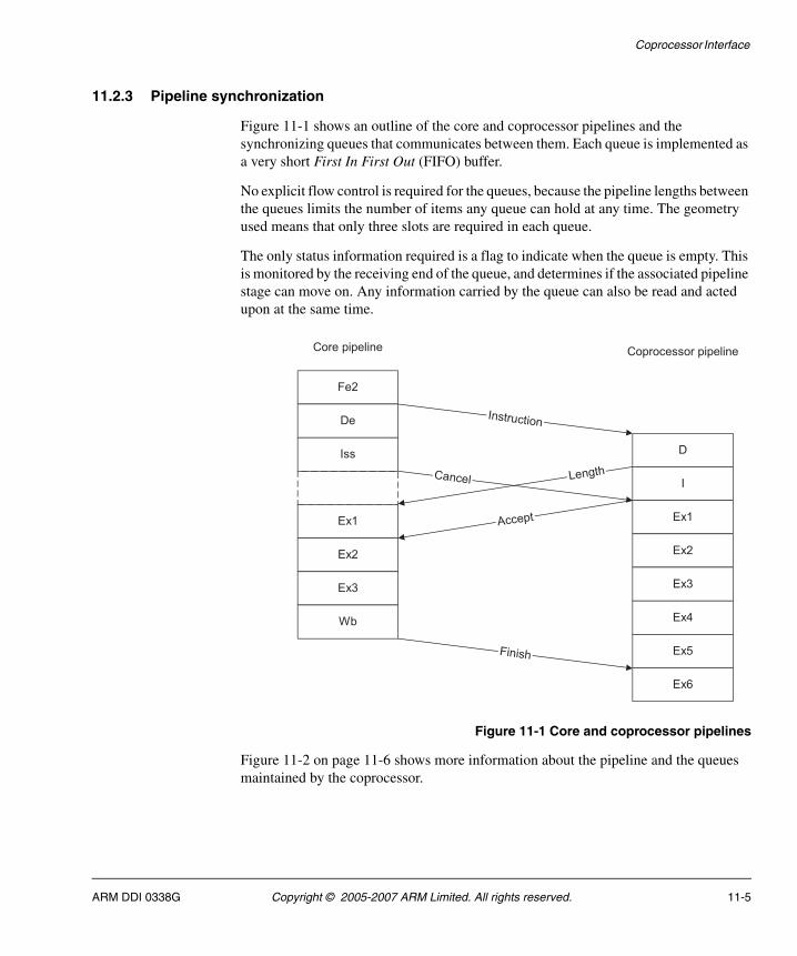
Coprocessor Interface
11.2.3 Pipeline synchronization
Figure 11-1 shows an outline of the core and coprocessor pipelines and the synchronizing queues that communicates between them. Each queue is implemented as a very short First In First Out (FIFO) buffer.
No explicit flow control is required for the queues, because the pipeline lengths between the queues limits the number of items any queue can hold at any time. The geometry used means that only three slots are required in each queue.
The only status information required is a flag to indicate when the queue is empty. This is monitored by the receiving end of the queue, and determines if the associated pipeline stage can move on. Any information carried by the queue can also be read and acted upon at the same time.
Figure 11-1 Core and coprocessor pipelines
Figure 11-2 on page 11-6 shows more information about the pipeline and the queues maintained by the coprocessor.
Fe2
Length
Core pipeline Coprocessor pipeline
De
Iss
Ex1
Ex2
Ex3
Wb
D
I
Ex1
Ex2
Ex3
Ex4
Ex5
Ex6
Instruction
LengthCancel
Accept
Finish
ARM DDI 0338G Copyright © 2005-2007 ARM Limited. All rights reserved. 11-5
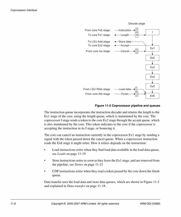
Coprocessor Interface
Figure 11-2 Coprocessor pipeline and queues
The instruction queue incorporates the instruction decoder and returns the length to the Ex1 stage of the core, using the length queue, which is maintained by the core. The coprocessor I stage sends a token to the core Ex2 stage through the accept queue, which is also maintained by the core. This token indicates to the core if the coprocessor is accepting the instruction in its I stage, or bouncing it.
The core can cancel an instruction currently in the coprocessor Ex1 stage by sending a signal with the token passed down the cancel queue. When a coprocessor instruction reads the Ex6 stage it might retire. How it retires depends on the instruction:
• Load instructions retire when they find load data available in the load data queue, see Loads on page 11-19
• Store instructions retire as soon as they leave the Ex1 stage, and are removed from the pipeline, see Stores on page 11-21
• CDP instructions retire when they read a token passed by the core down the finish queue.
Data transfer uses the load data and store data queues, which are shown in Figure 11-2 and explained in Data transfer on page 11-18.
I
Ex1
Ex2
Ex3
Ex4
Ex5
Ex6
Accept
Store data
D
Instruction
Length
Cancel
Load data
Finish
From core Fe2 stage
To core Fe1 stage
To LSU Add stage
From core Iss stage
To core Ex2 stage
From LSU Wbls stage
From core Wb stage
Decode stage
11-6 Copyright © 2005-2007 ARM Limited. All rights reserved. ARM DDI 0338G
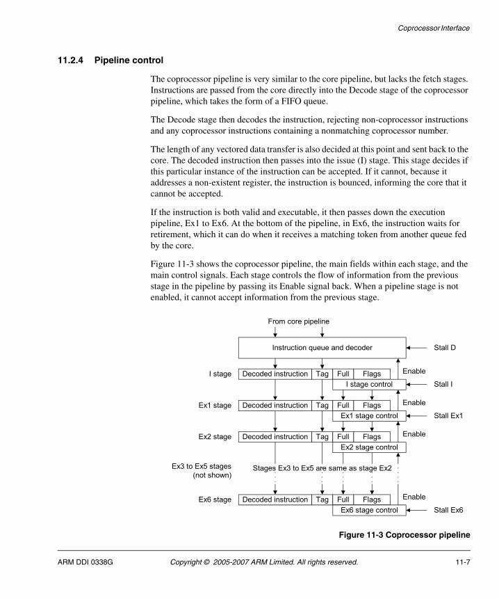
Coprocessor Interface
11.2.4 Pipeline control
The coprocessor pipeline is very similar to the core pipeline, but lacks the fetch stages. Instructions are passed from the core directly into the Decode stage of the coprocessor pipeline, which takes the form of a FIFO queue.
The Decode stage then decodes the instruction, rejecting non-coprocessor instructions and any coprocessor instructions containing a nonmatching coprocessor number.
The length of any vectored data transfer is also decided at this point and sent back to the core. The decoded instruction then passes into the issue (I) stage. This stage decides if this particular instance of the instruction can be accepted. If it cannot, because it addresses a non-existent register, the instruction is bounced, informing the core that it cannot be accepted.
If the instruction is both valid and executable, it then passes down the execution pipeline, Ex1 to Ex6. At the bottom of the pipeline, in Ex6, the instruction waits for retirement, which it can do when it receives a matching token from another queue fed by the core.
Figure 11-3 shows the coprocessor pipeline, the main fields within each stage, and the main control signals. Each stage controls the flow of information from the previous stage in the pipeline by passing its Enable signal back. When a pipeline stage is not enabled, it cannot accept information from the previous stage.
Figure 11-3 Coprocessor pipeline
Decoded instruction Tag Full Flags
I stage control
Decoded instruction Tag Full Flags
Ex1 stage control
Decoded instruction Tag Full Flags
Ex2 stage control
Decoded instruction Tag Full Flags
Ex6 stage control
Instruction queue and decoder
From core pipeline
I stage
Ex1 stage
Ex2 stage
Ex3 to Ex5 stages
(not shown)
Ex6 stage
Enable
Enable
Enable
Enable
Stall I
Stall Ex1
Stall Ex6
Stages Ex3 to Ex5 are same as stage Ex2
Stall D
ARM DDI 0338G Copyright © 2005-2007 ARM Limited. All rights reserved. 11-7
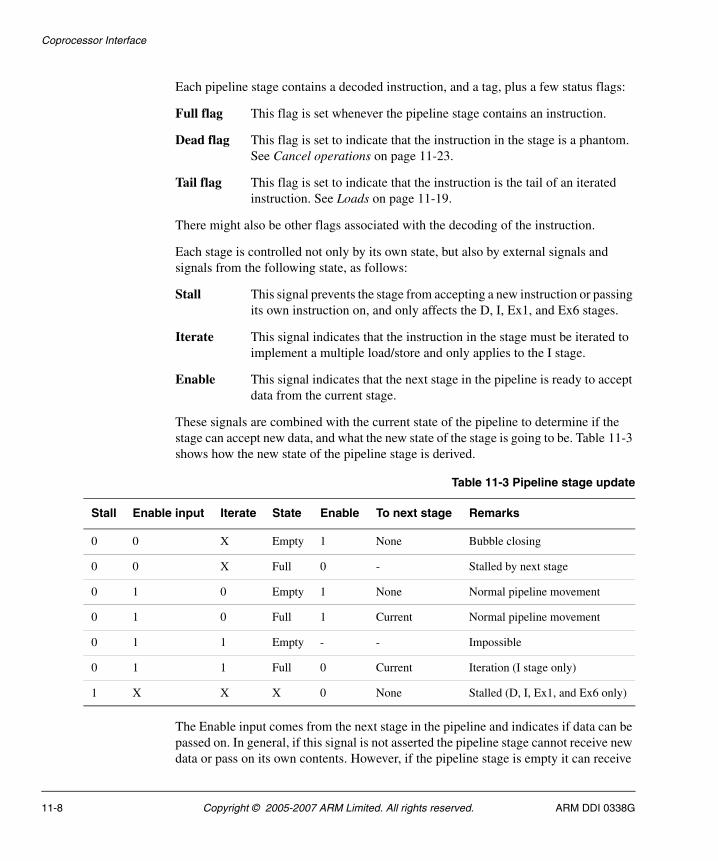
Coprocessor Interface
Each pipeline stage contains a decoded instruction, and a tag, plus a few status flags:
Full flag This flag is set whenever the pipeline stage contains an instruction.
Dead flag This flag is set to indicate that the instruction in the stage is a phantom. See Cancel operations on page 11-23.
Tail flag This flag is set to indicate that the instruction is the tail of an iterated instruction. See Loads on page 11-19.
There might also be other flags associated with the decoding of the instruction.
Each stage is controlled not only by its own state, but also by external signals and signals from the following state, as follows:
Stall This signal prevents the stage from accepting a new instruction or passing its own instruction on, and only affects the D, I, Ex1, and Ex6 stages.
Iterate This signal indicates that the instruction in the stage must be iterated to implement a multiple load/store and only applies to the I stage.
Enable This signal indicates that the next stage in the pipeline is ready to accept data from the current stage.
These signals are combined with the current state of the pipeline to determine if the stage can accept new data, and what the new state of the stage is going to be. Table 11-3 shows how the new state of the pipeline stage is derived.
The Enable input comes from the next stage in the pipeline and indicates if data can be passed on. In general, if this signal is not asserted the pipeline stage cannot receive new data or pass on its own contents. However, if the pipeline stage is empty it can receive
Table 11-3 Pipeline stage update
Stall Enable input Iterate State Enable To next stage Remarks
0 0 X Empty 1 None Bubble closing
0 0 X Full 0 - Stalled by next stage
0 1 0 Empty 1 None Normal pipeline movement
0 1 0 Full 1 Current Normal pipeline movement
0 1 1 Empty - - Impossible
0 1 1 Full 0 Current Iteration (I stage only)
1 X X X 0 None Stalled (D, I, Ex1, and Ex6 only)
11-8 Copyright © 2005-2007 ARM Limited. All rights reserved. ARM DDI 0338G
Coprocessor Interface
new data without passing any data on to the next stage. This is known as bubble closing, because it has the effect of filling up empty stages in the pipeline by enabling them to move on while lower stages are stalled.
11.2.5 Instruction tagging
It is sometimes necessary for the core to be able to identify instructions in the coprocessor pipeline. This is necessary for flushing (see Flush operations on page 11-24) so that the core can indicate to the coprocessor which instructions are to be flushed. The core therefore gives each instruction sent to the coprocessor a tag, which is drawn from a pool of values large enough so that all the tags in the pipeline at any moment are unique. Sixteen tags are sufficient to achieve this, requiring a four-bit tag field. Each time a tag is assigned to an instruction, the tag number is incremented modulo 16 to generate the next tag.
The flushing mechanism is simplified because successive coprocessor instructions have contiguous tags. The core manages this by only incrementing the tag number when the instruction passed to the coprocessor is a coprocessor instruction. This is done after sending the instruction, so the tag changes after a coprocessor instruction is sent, rather than before. It is not possible to increment the tag before sending the instruction because the core has not yet had time to decode the instruction to determine what kind of instruction it is. When the coprocessor Decode stage removes the non-coprocessor instructions, it is left with an instruction stream carrying contiguous tags.
The tags can also be used to verify that the sequence of tokens moving down the queues matches the sequence of instructions moving down the core and coprocessor pipelines.
11.2.6 Flush broadcast
If a branch has been mispredicted, it might be necessary for the core to flush both pipelines. Because this action potentially affects the entire pipeline, it is not passed across in a queue but is broadcast from the core to the coprocessor, subject to the same timing constraints as the queues. When the flush signal is received by the coprocessor, it causes the pipeline and the instruction queue to be cleared up to the instruction triggering the flush. This is explained in more detail in Flush operations on page 11-24.
ARM DDI 0338G Copyright © 2005-2007 ARM Limited. All rights reserved. 11-9
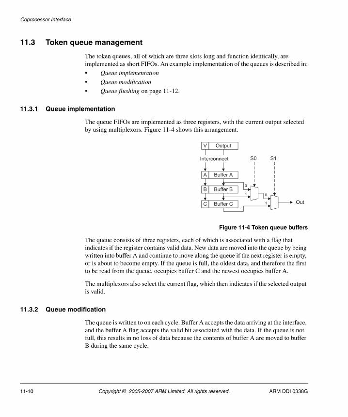
Coprocessor Interface
11.3 Token queue management
The token queues, all of which are three slots long and function identically, are implemented as short FIFOs. An example implementation of the queues is described in:
• Queue implementation
• Queue modification
• Queue flushing on page 11-12.
11.3.1 Queue implementation
The queue FIFOs are implemented as three registers, with the current output selected by using multiplexors. Figure 11-4 shows this arrangement.
Figure 11-4 Token queue buffers
The queue consists of three registers, each of which is associated with a flag that indicates if the register contains valid data. New data are moved into the queue by being written into buffer A and continue to move along the queue if the next register is empty, or is about to become empty. If the queue is full, the oldest data, and therefore the first to be read from the queue, occupies buffer C and the newest occupies buffer A.
The multiplexors also select the current flag, which then indicates if the selected output is valid.
11.3.2 Queue modification
The queue is written to on each cycle. Buffer A accepts the data arriving at the interface, and the buffer A flag accepts the valid bit associated with the data. If the queue is not full, this results in no loss of data because the contents of buffer A are moved to buffer B during the same cycle.
Buffer AA
Buffer BB
Buffer CC
OutputV
Interconnect
Out
S1S0
0
1 0
1
11-10 Copyright © 2005-2007 ARM Limited. All rights reserved. ARM DDI 0338G
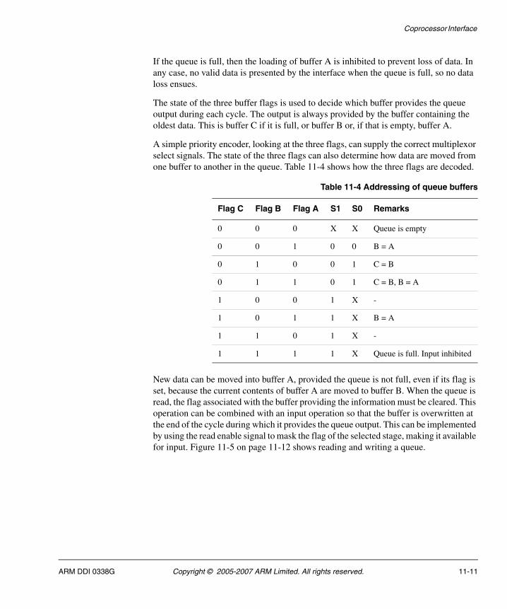
Coprocessor Interface
If the queue is full, then the loading of buffer A is inhibited to prevent loss of data. In any case, no valid data is presented by the interface when the queue is full, so no data loss ensues.
The state of the three buffer flags is used to decide which buffer provides the queue output during each cycle. The output is always provided by the buffer containing the oldest data. This is buffer C if it is full, or buffer B or, if that is empty, buffer A.
A simple priority encoder, looking at the three flags, can supply the correct multiplexor select signals. The state of the three flags can also determine how data are moved from one buffer to another in the queue. Table 11-4 shows how the three flags are decoded.
New data can be moved into buffer A, provided the queue is not full, even if its flag is set, because the current contents of buffer A are moved to buffer B. When the queue is read, the flag associated with the buffer providing the information must be cleared. This operation can be combined with an input operation so that the buffer is overwritten at the end of the cycle during which it provides the queue output. This can be implemented by using the read enable signal to mask the flag of the selected stage, making it available for input. Figure 11-5 on page 11-12 shows reading and writing a queue.
Table 11-4 Addressing of queue buffers
Flag C Flag B Flag A S1 S0 Remarks
0 0 0 X X Queue is empty
0 0 1 0 0 B = A
0 1 0 0 1 C = B
0 1 1 0 1 C = B, B = A
1 0 0 1 X -
1 0 1 1 X B = A
1 1 0 1 X -
1 1 1 1 X Queue is full. Input inhibited
ARM DDI 0338G Copyright © 2005-2007 ARM Limited. All rights reserved. 11-11
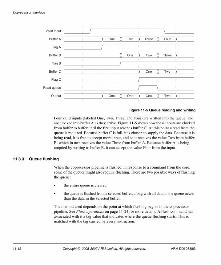
Coprocessor Interface
Figure 11-5 Queue reading and writing
Four valid inputs (labeled One, Two, Three, and Four) are written into the queue, and are clocked into buffer A as they arrive. Figure 11-5 shows how these inputs are clocked from buffer to buffer until the first input reaches buffer C. At this point a read from the queue is required. Because buffer C is full, it is chosen to supply the data. Because it is being read, it is free to accept more input, and so it receives the value Two from buffer B, which in turn receives the value Three from buffer A. Because buffer A is being emptied by writing to buffer B, it can accept the value Four from the input.
11.3.3 Queue flushing
When the coprocessor pipeline is flushed, in response to a command from the core, some of the queues might also require flushing. There are two possible ways of flushing the queue:
• the entire queue is cleared
• the queue is flushed from a selected buffer, along with all data in the queue newer than the data in the selected buffer.
The method used depends on the point at which flushing begins in the coprocessor pipeline. See Flush operations on page 11-24 for more details. A flush command has associated with it a tag value that indicates where the queue flushing starts. This is matched with the tag carried by every instruction.
One Two Three Four
One Two Three
One Two
One One One Two
Buffer A
Flag A
Buffer B
Flag B
Buffer C
Flag C
Read queue
Output
Valid input
11-12 Copyright © 2005-2007 ARM Limited. All rights reserved. ARM DDI 0338G
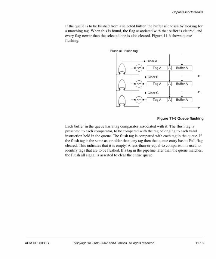
Coprocessor Interface
If the queue is to be flushed from a selected buffer, the buffer is chosen by looking for a matching tag. When this is found, the flag associated with that buffer is cleared, and every flag newer than the selected one is also cleared. Figure 11-6 shows queue flushing.
Figure 11-6 Queue flushing
Each buffer in the queue has a tag comparator associated with it. The flush tag is presented to each comparator, to be compared with the tag belonging to each valid instruction held in the queue. The flush tag is compared with each tag in the queue. If the flush tag is the same as, or older than, any tag then that queue entry has its Full flag cleared. This indicates that it is empty. A less-than-or-equal-to comparison is used to identify tags that are to be flushed. If a tag in the pipeline later than the queue matches, the Flush all signal is asserted to clear the entire queue.
<= Tag A A Buffer A
<= Tag A A Buffer A
<= Tag A A Buffer A
Clear B
Clear C
Clear A
Flush tagFlush all
ARM DDI 0338G Copyright © 2005-2007 ARM Limited. All rights reserved. 11-13
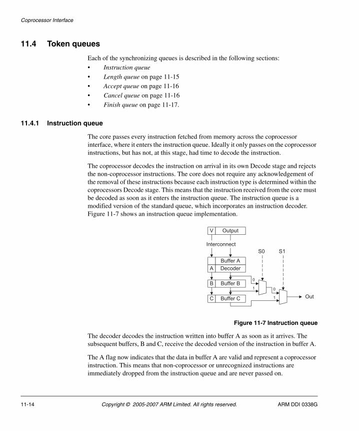
Coprocessor Interface
11.4 Token queues
Each of the synchronizing queues is described in the following sections:
• Instruction queue
• Length queue on page 11-15
• Accept queue on page 11-16
• Cancel queue on page 11-16
• Finish queue on page 11-17.
11.4.1 Instruction queue
The core passes every instruction fetched from memory across the coprocessor interface, where it enters the instruction queue. Ideally it only passes on the coprocessor instructions, but has not, at this stage, had time to decode the instruction.
The coprocessor decodes the instruction on arrival in its own Decode stage and rejects the non-coprocessor instructions. The core does not require any acknowledgement of the removal of these instructions because each instruction type is determined within the coprocessors Decode stage. This means that the instruction received from the core must be decoded as soon as it enters the instruction queue. The instruction queue is a modified version of the standard queue, which incorporates an instruction decoder. Figure 11-7 shows an instruction queue implementation.
Figure 11-7 Instruction queue
The decoder decodes the instruction written into buffer A as soon as it arrives. The subsequent buffers, B and C, receive the decoded version of the instruction in buffer A.
The A flag now indicates that the data in buffer A are valid and represent a coprocessor instruction. This means that non-coprocessor or unrecognized instructions are immediately dropped from the instruction queue and are never passed on.
Buffer A
Buffer BB
Buffer CC
OutputV
Interconnect
Out
S1S0
0
1 0
1
DecoderA
11-14 Copyright © 2005-2007 ARM Limited. All rights reserved. ARM DDI 0338G
Coprocessor Interface
The coprocessor must also compare the coprocessor number field in a coprocessor instruction and compare it with its own number, given by ACPNUM. If the number does not match, the instruction is invalid. The instruction queue provides an interface to the core through the following signals, which are all driven by the core:
ACPINSTRV This signal is asserted when valid data are available from the core. It must be clocked directly into the buffer A flag, unless the queue is full, in which case it is ignored.
ACPINSTR[31:0] This is the instruction being passed to the coprocessor from the core, and must be clocked into buffer A.
ACPINSTRT[3:0] This is the flush tag associated with the instruction in ACPINSTR, and must be clocked into the tag associated with buffer A.
The instruction queue feeds the issue stage of the coprocessor pipeline, providing a new input to the pipeline, in the form of a decoded instruction and its associated tag, whenever the queue is not empty.
11.4.2 Length queue
When a coprocessor has decoded an instruction it knows how long a vectored load/store operation is. This information is sent with the synchronizing token down the length queue, as the relevant instruction leaves the instruction queue to enter the issue stage of the pipeline. The length queue is maintained by the core and the coprocessor communicates with the queue using the following signals:
CPALENGTH[3:0]
This is the length of a vectored data transfer to or from the coprocessor. It is determined by the decoder in the instruction queue and asserted as the decoded instruction moves into the issue stage. If the current instruction does not represent a vectored data transfer, the length value is set to zero.
CPALENGTHT[3:0]
This is the tag associated with the instruction leaving the instruction queue, and is copied from the queue buffer supplying the instruction.
CPALENGTHHOLD
This is deasserted when the instruction queue is providing valid information to the core length queue. Otherwise, the signal is asserted to indicate that no valid data are available.
ARM DDI 0338G Copyright © 2005-2007 ARM Limited. All rights reserved. 11-15
Coprocessor Interface
11.4.3 Accept queue
The coprocessor must decide in the issue stage if it can accept an otherwise valid coprocessor instruction. It passes this information with the synchronizing token down the accept queue, as the relevant instruction passes from the issue stage to Ex1.
If an instruction cannot be accepted by the coprocessor it is said to have been bounced. If the coprocessor bounces an instruction it does not remove the instruction from its pipeline, but converts it to a phantom. This is explained in more detail in Bounce operations on page 11-23.
The accept queue is maintained by the core and the coprocessor communicates with the queue using the following signals, which are all driven by the coprocessor:
CPAACCEPT
This is set to indicate that the instruction leaving the coprocessor issue stage has been accepted.
CPAACCEPTT[3:0]
This is the tag associated with the instruction leaving the issue stage.
CPAACCEPTHOLD
This is deasserted when the issue stage is passing an instruction on to the Ex1 stage, whether it has been accepted or not. Otherwise, the signal is asserted to indicate that no valid data are available.
Note If no coprocessor is connected, the following signals must be driven LOW.
• CPALENGTHHOLD• CPAACCEPT• CPAACCEPTHOLD
11.4.4 Cancel queue
The core might want to cancel an instruction that it has already passed on to the coprocessor. This can happen if the instruction fails its condition codes, which requires the instruction to be removed from the instruction stream in both the core and the coprocessor.
The queue, which is a standard queue as described in Token queue management on page 11-10, is maintained by the coprocessor and is read by the coprocessor Ex1 stage.
11-16 Copyright © 2005-2007 ARM Limited. All rights reserved. ARM DDI 0338G
Coprocessor Interface
The cancel queue provides an interface to the core through the following signals, which are all driven by the core:
ACPCANCELV
This signal is asserted when valid data are available from the core. It must be clocked directly into the buffer A flag, unless the queue is full, in which case it is ignored.
ACPCANCEL
This is the cancel command being passed to the coprocessor from the core, and must be clocked into buffer A.
ACPCANCELT[3:0]
This is the flush tag associated with the cancel command, and must be clocked into the tag associated with buffer A.
The cancel queue is read by the coprocessor Ex1 stage, which acts on the value of the queued ACPCANCEL signal by removing the instruction from the Ex1 stage if the signal is set, and not passing it on to the Ex2 stage.
11.4.5 Finish queue
The finish queue maintains synchronism at the end of the pipeline by providing permission for CDP instructions in the coprocessor pipeline to retire. The queue, which is a standard queue as described in Token queue management on page 11-10, is maintained by the coprocessor and is read by the coprocessor Ex6 stage.
The finish queue provides an interface to the core using the ACPFINISHV signal, which is driven by the core.
This signal is asserted to indicate that the instruction in the coprocessor Ex6 stage can retire. It must be clocked directly into the buffer A flag, unless the queue is full, in which case it is ignored.
The finish queue is read by the coprocessor Ex6 stage, which can retire a CDP instruction if the finish queue is not empty.
ARM DDI 0338G Copyright © 2005-2007 ARM Limited. All rights reserved. 11-17
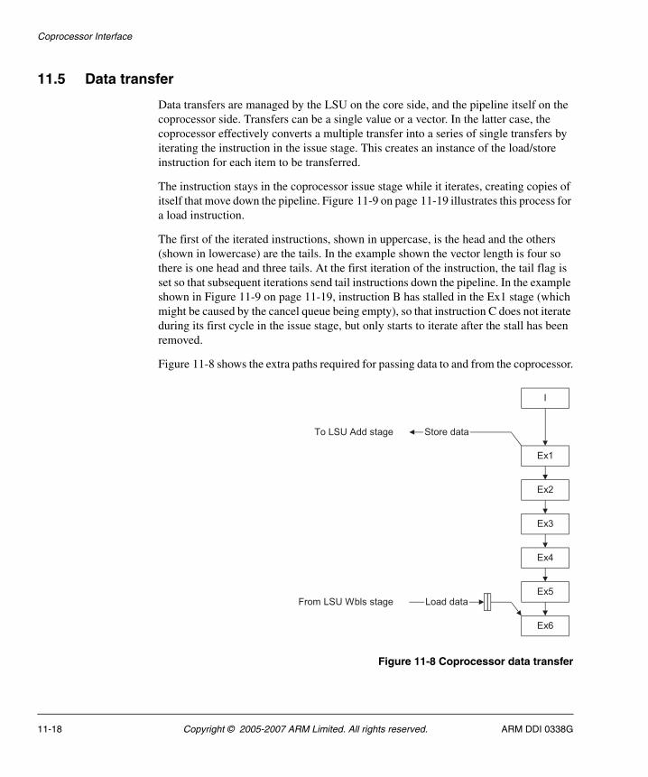
Coprocessor Interface
11.5 Data transfer
Data transfers are managed by the LSU on the core side, and the pipeline itself on the coprocessor side. Transfers can be a single value or a vector. In the latter case, the coprocessor effectively converts a multiple transfer into a series of single transfers by iterating the instruction in the issue stage. This creates an instance of the load/store instruction for each item to be transferred.
The instruction stays in the coprocessor issue stage while it iterates, creating copies of itself that move down the pipeline. Figure 11-9 on page 11-19 illustrates this process for a load instruction.
The first of the iterated instructions, shown in uppercase, is the head and the others (shown in lowercase) are the tails. In the example shown the vector length is four so there is one head and three tails. At the first iteration of the instruction, the tail flag is set so that subsequent iterations send tail instructions down the pipeline. In the example shown in Figure 11-9 on page 11-19, instruction B has stalled in the Ex1 stage (which might be caused by the cancel queue being empty), so that instruction C does not iterate during its first cycle in the issue stage, but only starts to iterate after the stall has been removed.
Figure 11-8 shows the extra paths required for passing data to and from the coprocessor.
Figure 11-8 Coprocessor data transfer
I
Ex1
Ex2
Ex3
Ex4
Ex5
Ex6
Store data
Load data
To LSU Add stage
From LSU Wbls stage
11-18 Copyright © 2005-2007 ARM Limited. All rights reserved. ARM DDI 0338G
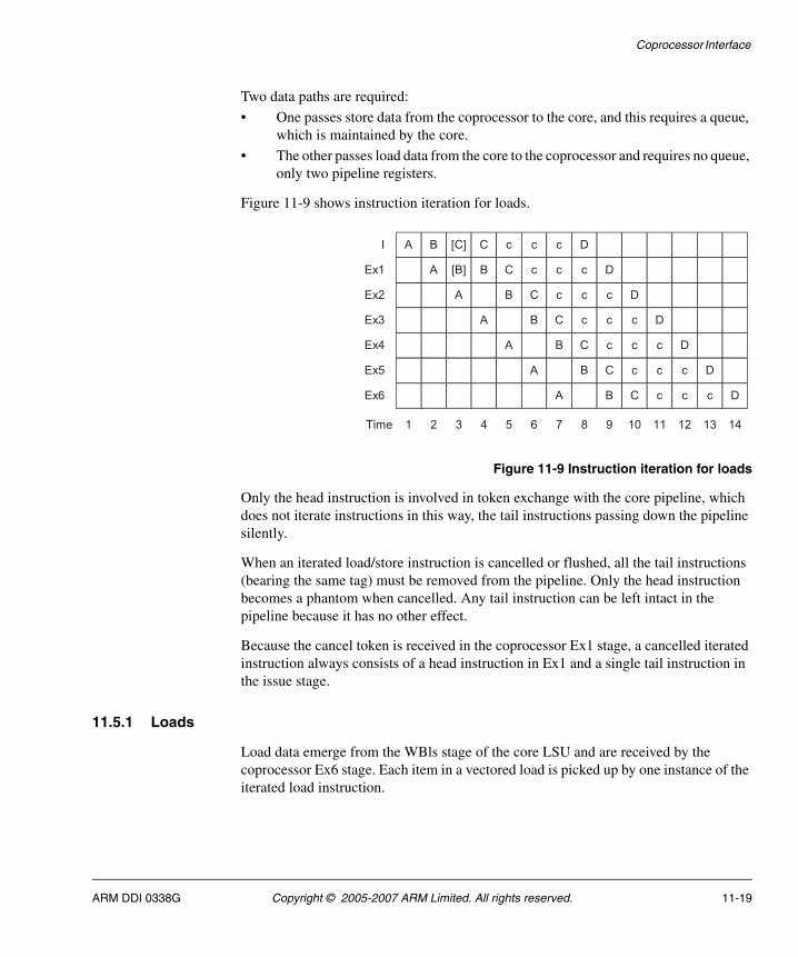
Coprocessor Interface
Two data paths are required:
• One passes store data from the coprocessor to the core, and this requires a queue, which is maintained by the core.
• The other passes load data from the core to the coprocessor and requires no queue, only two pipeline registers.
Figure 11-9 shows instruction iteration for loads.
Figure 11-9 Instruction iteration for loads
Only the head instruction is involved in token exchange with the core pipeline, which does not iterate instructions in this way, the tail instructions passing down the pipeline silently.
When an iterated load/store instruction is cancelled or flushed, all the tail instructions (bearing the same tag) must be removed from the pipeline. Only the head instruction becomes a phantom when cancelled. Any tail instruction can be left intact in the pipeline because it has no other effect.
Because the cancel token is received in the coprocessor Ex1 stage, a cancelled iterated instruction always consists of a head instruction in Ex1 and a single tail instruction in the issue stage.
11.5.1 Loads
Load data emerge from the WBls stage of the core LSU and are received by the coprocessor Ex6 stage. Each item in a vectored load is picked up by one instance of the iterated load instruction.
[C]BA C c c c D
[B]A B C c c c D
A B C c c c D
A B C c c c D
A B C c c c D
A B C c c c D
A B C c c c D
I
Ex1
Ex2
Ex3
Ex4
Ex5
Ex6
1 2 3 4 5 6 7 8 9 10 11 12 13 14Time
ARM DDI 0338G Copyright © 2005-2007 ARM Limited. All rights reserved. 11-19
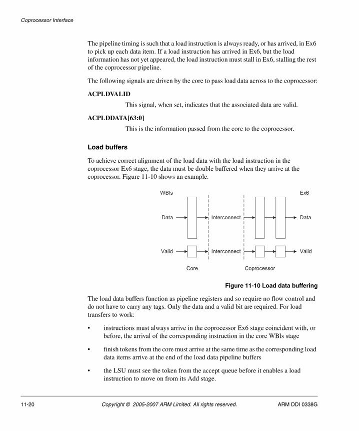
Coprocessor Interface
The pipeline timing is such that a load instruction is always ready, or has arrived, in Ex6 to pick up each data item. If a load instruction has arrived in Ex6, but the load information has not yet appeared, the load instruction must stall in Ex6, stalling the rest of the coprocessor pipeline.
The following signals are driven by the core to pass load data across to the coprocessor:
ACPLDVALID
This signal, when set, indicates that the associated data are valid.
ACPLDDATA[63:0]
This is the information passed from the core to the coprocessor.
Load buffers
To achieve correct alignment of the load data with the load instruction in the coprocessor Ex6 stage, the data must be double buffered when they arrive at the coprocessor. Figure 11-10 shows an example.
Figure 11-10 Load data buffering
The load data buffers function as pipeline registers and so require no flow control and do not have to carry any tags. Only the data and a valid bit are required. For load transfers to work:
• instructions must always arrive in the coprocessor Ex6 stage coincident with, or before, the arrival of the corresponding instruction in the core WBls stage
• finish tokens from the core must arrive at the same time as the corresponding load data items arrive at the end of the load data pipeline buffers
• the LSU must see the token from the accept queue before it enables a load instruction to move on from its Add stage.
Interconnect
InterconnectValid
Data
Valid
Data
WBls Ex6
Core Coprocessor
11-20 Copyright © 2005-2007 ARM Limited. All rights reserved. ARM DDI 0338G
Coprocessor Interface
Loads and flushes
If a flush does not involve the core WBls stage it cannot affect the load data buffers, and the load transfer completes normally. If a flush is initiated by an instruction in the core WBls stage, this is not a load instruction because load instructions cannot trigger a flush. Any coprocessor load instructions behind the flush point find themselves stalled if they get as far as the Ex6 stage, for the lack of a finish token, so no data transfers can have taken place. Any data in the load data buffers expires naturally during the flush dead period while the pipeline reloads.
Loads and cancels
If a load instruction is canceled both the head and any tails must be removed. Because the cancellation happens in the coprocessor Ex1 stage, no data transfers can have taken place and therefore no special measures are required to deal with load data.
Loads and retirement
When a load instruction reaches the bottom of the coprocessor pipeline it must find a data item at the end of the load data buffer. This applies to both head and tail instructions. Load instructions do not use finish queue.
11.5.2 Stores
Store data emerge from the coprocessor issue stage and are received by the core LSU DC1 stage. Each item of a vectored store is generated because the store instruction iterates in the coprocessor issue stage. The iterated store instructions then pass down the pipeline but have no more use, except to act as place markers for flushes and cancels.
The following signals control the transfer of store data across the coprocessor interface:
CPASTDATAV
This signal is asserted when valid data is available from the coprocessor.
CPASTDATAT[3:0]
This is the tag associated with the data being passed to the core.
CPASTDATA[63:0]
This is the information passed from the coprocessor to the core.
ARM DDI 0338G Copyright © 2005-2007 ARM Limited. All rights reserved. 11-21
Coprocessor Interface
ACPSTSTOP
This signal from the core prevents additional transfers from the coprocessor to the core, and is raised when the store queue, maintained by the core, can no longer accept any more data. When the signal is deasserted, data transfers can resume.
When ACPSTSTOP is asserted, the data previously placed onto CPASTDATA must be left there, until new data can be transferred. This enables the core to leave data on CPASTDATA until there is sufficient space in the store data queue.
Store data queue
Because the store data transfer can be stopped at any time by the LSU, a store data queue is required. Additionally, because store data vectors can be of arbitrary length, flow control is required. A queue length of three slots is sufficient to enable flow control to be used without loss of data.
Stores and flushes
When a store instruction is involved in a flush, the store data queue must be flushed by the core. Because the queue continues to fill for two cycles after the core notifies the coprocessor of the flush (because of the signal propagation delay) the core must delay for two cycles before carrying out the store data queue flush. The dead period after the flush extends sufficiently far to enable this to be done.
Stores and cancels
If the core cancels a store instruction, the coprocessor must ensure that it sends no store data for that instruction. It can achieve this by either:
• delaying the start of the store data until the corresponding cancel token has been received in the Ex1 stage
• looking ahead into the cancel queue and start the store data transfer when the correct token is seen.
Stores and retirement
Because store instructions do not use the finish token queue they are retired as soon as they leave the Ex1 stage of the pipeline.
11-22 Copyright © 2005-2007 ARM Limited. All rights reserved. ARM DDI 0338G
Coprocessor Interface
11.6 Operations
This section describes the various operations that can be performed and events that can take place.
11.6.1 Normal operation
In normal operation the core passes all instructions across to the coprocessor, and then increments the tag if the instruction was a coprocessor instruction. The coprocessor decodes the instruction and throws it away if it is not a coprocessor instruction or if it contains the wrong coprocessor number.
Each coprocessor instruction then passes down the pipeline, sending a token down the length queue as it moves into the issue stage. The instruction then moves into the Ex1 stage, sending a token down the accept queue, and remains there until it has received a token from the cancel queue.
If the cancel token does not request that the instruction is cancelled, and is not a Store instruction, it moves on to the Ex2 stage. The instruction then moves down the pipeline until it reaches the Ex6 stage. At this point it waits to receive a token from the finish queue, which enables it to retire, unless it is either:
• a store instruction, in which case it requires no token from the finish queue
• a load instruction, in which case it must wait until load data are available.
Store instruction are removed from the pipeline as soon as they leave the Ex1 stage.
Instructions with opcode[27:24] as b1100, b1101 or b1110 and where opcode[11:8] match the coprocessors number are treated as coprocessor instructions. Non-coprocessors instructions can be ignored, but coprocessor instructions must either be executed or bounced.
11.6.2 Cancel operations
When the coprocessor instruction reaches the Ex1 stage it looks for a token in the cancel queue. If the token indicates that the instruction is to be cancelled, it is removed from the pipeline and does not pass to Ex2. Any tail instruction in the I stage is also removed.
11.6.3 Bounce operations
The coprocessor can reject an instruction by bouncing it when it reaches the issue stage. This can happen to an instruction that has been accepted as a valid coprocessor instruction by the decoder, but that is found to be unexecutable by the issue stage, perhaps because it refers to a non-existent register or operation.
ARM DDI 0338G Copyright © 2005-2007 ARM Limited. All rights reserved. 11-23
Coprocessor Interface
When the bounced instruction leaves the issue stage to move into Ex1, the token sent down the accept queue has its bounce bit set. This causes the instruction to be removed from the core pipeline.
When the instruction moves into Ex1 it has its dead bit set, turning it into a phantom. This enables the instruction to remain in the pipeline to match tokens in the cancel queue.
The core posts a token for the bounced instruction before the coprocessor can bounce it, so the phantom is required to pick up the token for the bounced instruction. The instruction is otherwise inert, and has no other effect.
The core might already have decided to cancel the instruction being bounced. In this case, the cancel token causes the phantom to be removed from the pipeline. If the core does not cancel the phantom it continues to the bottom of the pipeline.
Any instruction that is identified as a coprocessor instruction must be bounced if the coprocessor cannot execute it. This includes instructions in the coprocessor extension space, where opcode[27:21] is set to b1100000, which must always be bounced.
11.6.4 Flush operations
A flush can be triggered by the core in any stage from issue to WBls inclusive. When this happens a broadcast signal is received by the coprocessor, passing it the tag associated with the instruction triggering the flush.
Because the tag is changed by the core after each new coprocessor instruction, the tag matches the first coprocessor instruction following the instruction causing the flush. The coprocessor must then find the first instruction that has a matching tag, working from the bottom of the pipeline upwards, and remove all instructions from that point upwards.
Unlike tokens passing down a queue, a flush signal has a fixed delay so that the timing relationship between a flush in the core and a flush in the coprocessor is known precisely.
Most of the token queues also require flushing and this can also be done using the tags attached to each instruction. If a match has been found before the stage at the receiving end of a token queue is passed, then the token queue is cleared.
Otherwise, it must be properly flushed by matching the tags in the queue. This operation must be performed on all the queues except the finish queue, which is updated in the normal way. Therefore, the coprocessor must flush the instruction and cancel queues.
11-24 Copyright © 2005-2007 ARM Limited. All rights reserved. ARM DDI 0338G
Coprocessor Interface
The flushing operation can be carried out by the coprocessor as soon as the flush signal is received. The flushing operation is simplified because the instruction and cancel queues cannot be performing any other operation. This means that flushing does not have to be combined with queue updates for these queues.
There is a single cycle following a flush in which nothing happens that affects the flushed queues, and this provides a good opportunity to carry out the queue flushing operation.
The following signals provide the flush broadcast signal from the core:
ACPFLUSH This signal is asserted when a flush is to be performed.
ACPFLUSHT[3:0]
This is the tag associated with the first instruction to be flushed.
11.6.5 Retirement operations
When an instruction reaches the bottom of the coprocessor pipeline it is retired. How it retires depends on the kind of instruction it is and if it is iterated, as shown in Table 11-5.
Table 11-5 lists the conditions for each coprocessor instruction:
• all store instructions retire unconditionally on leaving Ex1 because no token is required in the finish queue
• CDP instructions require a token in the finish queue
• all load instructions must pick up data from the load pipeline
• phantom load instructions retire unconditionally.
Table 11-5 Retirement conditions
Instruction Type Retirement conditions
CDP - Must find a token in the finish queue.
MRC Store No conditions. Immediate retirement on leaving Ex1.
MCR Load All load instructions must find data in the load data pipeline from the core.
MRRC Store No conditions. Immediate retirement on leaving Ex1.
MCRR Load All load instructions must find data in the load data pipeline from the core.
STC Store No conditions. Immediate retirement on leaving Ex1.
LDC Load Must find data in the load data pipeline from the core.
ARM DDI 0338G Copyright © 2005-2007 ARM Limited. All rights reserved. 11-25
Coprocessor Interface
11.7 Multiple coprocessors
There might be more than one coprocessor attached to the core, and so some means is required for dealing with multiple coprocessors. It is important, for reasons of economy, to ensure that as little of the coprocessor interface is duplicated. In particular, the coprocessors must share the length, accept, and store data queues, which are maintained by the core.
If these queues are to be shared, only one coprocessor can use the queues at any time. This is achieved by enabling only one coprocessor to be active at any time. This is not a serious limitation because only one coprocessor is in use at any time.
Typically, a processor is driven through driver software, which drives one coprocessor. Calls to the driver software, and returns from it, ensure that there are several core instructions between the use of one coprocessor and the use of a different coprocessor.
11.7.1 Interconnect considerations
If only one coprocessor is permitted to communicate with the core at any time, all coprocessors can share the coprocessor interface signals from the core. Signals from the coprocessors to the core can be ORed together, provided that every coprocessor holds its outputs to zero when it is inactive.
11.7.2 Coprocessor selection
Coprocessors are enabled by a signal ACPENABLE from the core. There are 12 of these signals, one for each coprocessor. Only one can be active at any time. In addition, instructions to the coprocessor include the coprocessor number, enabling coprocessors to reject instructions that do not match their own number. Core instructions are also rejected.
11.7.3 Coprocessor switching
When the core decodes a coprocessor instruction destined for a different coprocessor to that last addressed, it stalls this instruction until the previous coprocessor instruction has been retired. This ensures that all activity in the currently selected coprocessor has ceased.
The coprocessor selection is switched, disabling the last active coprocessor and activating the new coprocessor. The disabled coprocessor ignores the new coprocessor instruction. Therefore, the instruction is resent by the core, and is now accepted by the newly activated coprocessor.
11-26 Copyright © 2005-2007 ARM Limited. All rights reserved. ARM DDI 0338G
Coprocessor Interface
A coprocessor is disabled by the core by setting ACPENABLE LOW for the selected coprocessor. The coprocessor responds by ceasing all activity and setting all its output signals LOW.
When the coprocessor is enabled, which is signaled by setting ACPENABLE HIGH, it must immediately set the signals CPALENGTHHOLD and CPAACCEPTHOLD HIGH, and CPASTDATAV LOW, because the pipeline is empty at this point. The coprocessor can then start normal operation.
ARM DDI 0338G Copyright © 2005-2007 ARM Limited. All rights reserved. 11-27
Coprocessor Interface
11-28 Copyright © 2005-2007 ARM Limited. All rights reserved. ARM DDI 0338G
Chapter 12 Vectored Interrupt Controller Port
This chapter describes the ARM1156T2-S Vectored Interrupt Controller port. It contains the following sections:
• About the PL192 Vectored Interrupt Controller on page 12-2
• About the ARM1156T2-S VIC port on page 12-3
• Timing of the VIC port on page 12-6
• Interrupt entry flowchart on page 12-9.
ARM DDI 0338G Copyright © 2005-2007 ARM Limited. All rights reserved. 12-1
Vectored Interrupt Controller Port
12.1 About the PL192 Vectored Interrupt Controller
An interrupt controller is a peripheral that is used to handle multiple interrupt sources. Features usually found in an interrupt controller are:
• multiple interrupt request inputs, one for each interrupt source, and one interrupt request output for the processors interrupt request input
• software can mask out particular interrupt requests
• prioritization of interrupt sources for interrupt nesting.
In a system with an interrupt controller having the above features, software is still required to:
• determine which interrupt source is requesting service
• determine where the service routine for that interrupt source is loaded.
A Vectored Interrupt Controller (VIC) does both things in hardware. It supplies the starting address (vector address) of the service routine corresponding to the highest priority requesting interrupt source.
The PL192 VIC is an Advanced Microcontroller Bus Architecture (AMBA) compliant, System-on-Chip (SoC) peripheral that is developed, tested, and licensed by ARM Limited for use in ARM1156T2-S designs.
The ARM1156T2-S VIC port and the Peripheral Interface enable you to connect a PL192 VIC to an ARM1156T2-S processor. For more details the ARM PrimeCell Vectored Interrupt Controller (PL192) Technical Reference Manual.
12-2 Copyright © 2005-2007 ARM Limited. All rights reserved. ARM DDI 0338G
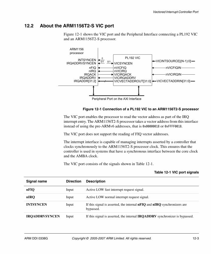
Vectored Interrupt Controller Port
12.2 About the ARM1156T2-S VIC port
Figure 12-1 shows the VIC port and the Peripheral Interface connecting a PL192 VIC and an ARM1156T2-S processor.
Figure 12-1 Connection of a PL192 VIC to an ARM1156T2-S processor
The VIC port enables the processor to read the vector address as part of the IRQ interrupt entry. The ARM1156T2-S processor takes a vector address from this interface instead of using the pre-ARMv6 addresses, that is 0x00000018 or 0xFFFF0018.
The VIC port does not support the reading of FIQ vector addresses.
The interrupt interface is capable of managing interrupts asserted by a controller that clocks synchronously to the ARM1156T2-S processor clock. This ensures that the controller is used in systems that have a synchronous interface between the core clock and the AMBA clock.
The VIC port consists of the signals shown in Table 12-1.
nFIQnIRQ
IRQADDRVIRQADDR[31:2] VICVECTADDROUT[31:0]
VICIRQADDRVVICIRQACKnVICIRQnVICFIQ
PL192 VIC
ARM1156
processor
nVICFIQIN
nVICIRQIN
VICINTSOURCE[(N-1):0]
VICVECTADDRIN[31:0]
Peripheral Port on the AXI Interface
VICSYNCEN
IRQACK
IRQADDRVSYNCENINTSYNCEN
0/1
0
0/1
Table 12-1 VIC port signals
Signal name Direction Description
nFIQ Input Active LOW fast interrupt request signal.
nIRQ Input Active LOW normal interrupt request signal.
INTSYNCEN Input If this signal is asserted, the internal nFIQ and nIRQ synchronizers are bypassed.
IRQADDRVSYNCEN Input If this signal is asserted, the internal IRQADDRV synchronizer is bypassed.
ARM DDI 0338G Copyright © 2005-2007 ARM Limited. All rights reserved. 12-3
Vectored Interrupt Controller Port
IRQACK is driven by the ARM1156T2-S processor to indicate to an external VIC that the processor wants to read the IRQADDR input.
IRQADDRV is driven by a VIC to tell the ARM1156T2-S processor that the address on the IRQADDR bus is valid and being held, and so it is safe for the processor to sample it.
IRQACK and IRQADDRV together implement a four-phase handshake between the ARM1156T2-S processor and a VIC. See Timing of the VIC port on page 12-6 for more details.
12.2.1 Synchronization of the VIC port signals
The peripheral port clock enable signal ACLKENP can run at any frequency, synchronously to the ARM1156T2-S processor clock signal.
nFIQ and nIRQ can be connected to either synchronous or asynchronous sources. Synchronizers are provided internally for the case of asynchronous sources. Pin INTSYNCEN is also provided to enable SoC designers to bypass the synchronizers if required. Similarly, a synchronizer is provided inside the ARM1156T2-S processor for the IRQADDRV signal. If this signal is known to be synchronous, the synchronizer can be bypassed by pulling IRQADDRVSYNCEN HIGH.
These signals enable SoC designers to reduce interrupt latency if it is known that the nFIQ, nIRQ, or IRQADDRV inputs are always driven by a synchronous source.
When connecting the PL192 VIC to the ARM1156T2-S processor, INTSYNCEN must be tied LOW regardless of the Peripheral Port clocking mode. This is because the PL192 nVICIRQ and nVICFIQ outputs are completely asynchronous, because there are combinational paths that cross this device through to these outputs. However, IRQADDRVSYNCEN must be set depending on the clocking mode.
IRQACK Output Active HIGH IRQ acknowledge.
IRQADDRV Input Active HIGH valid signal for the IRQ interrupt vector address. Indicates when IRQADDR is valid
IRQADDR[31:2] Input IRQ interrupt vector address. IRQADDR[31:2] holds the address of the first ARM or Thumb instruction in the IRQ handler.
Table 12-1 VIC port signals (continued)
Signal name Direction Description
12-4 Copyright © 2005-2007 ARM Limited. All rights reserved. ARM DDI 0338G
Vectored Interrupt Controller Port
12.2.2 Interrupt handler exit
The software acknowledges an IRQ interrupt handler exit to a VIC by issuing a write to the vector address register.
ARM DDI 0338G Copyright © 2005-2007 ARM Limited. All rights reserved. 12-5
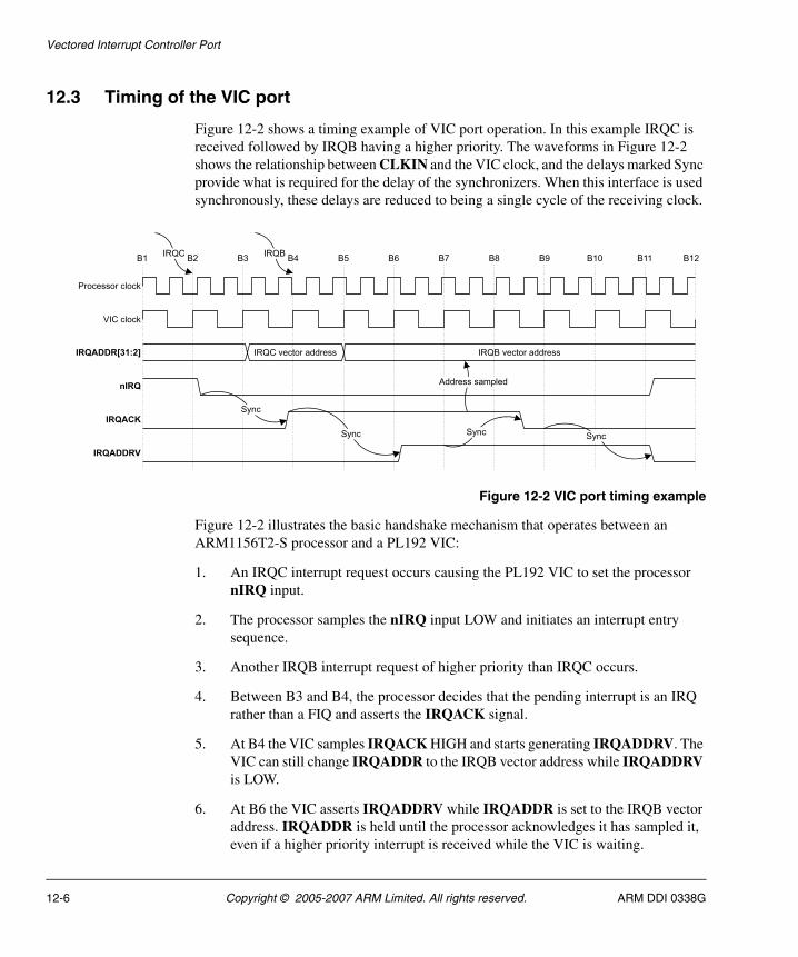
Vectored Interrupt Controller Port
12.3 Timing of the VIC port
Figure 12-2 shows a timing example of VIC port operation. In this example IRQC is received followed by IRQB having a higher priority. The waveforms in Figure 12-2 shows the relationship between CLKIN and the VIC clock, and the delays marked Sync provide what is required for the delay of the synchronizers. When this interface is used synchronously, these delays are reduced to being a single cycle of the receiving clock.
Figure 12-2 VIC port timing example
Figure 12-2 illustrates the basic handshake mechanism that operates between an ARM1156T2-S processor and a PL192 VIC:
1. An IRQC interrupt request occurs causing the PL192 VIC to set the processor nIRQ input.
2. The processor samples the nIRQ input LOW and initiates an interrupt entry sequence.
3. Another IRQB interrupt request of higher priority than IRQC occurs.
4. Between B3 and B4, the processor decides that the pending interrupt is an IRQ rather than a FIQ and asserts the IRQACK signal.
5. At B4 the VIC samples IRQACK HIGH and starts generating IRQADDRV. The VIC can still change IRQADDR to the IRQB vector address while IRQADDRV is LOW.
6. At B6 the VIC asserts IRQADDRV while IRQADDR is set to the IRQB vector address. IRQADDR is held until the processor acknowledges it has sampled it, even if a higher priority interrupt is received while the VIC is waiting.
12-6 Copyright © 2005-2007 ARM Limited. All rights reserved. ARM DDI 0338G
Vectored Interrupt Controller Port
7. Around B8 the processor samples the value of the IRQADDR input bus and deasserts IRQACK.
8. When the VIC samples IRQACK LOW, it stacks the priority of the IRQB interrupt and deasserts IRQADDRV. It also deasserts nIRQ if there are no higher priority interrupts pending.
9. When the processor samples IRQADDRV LOW, it knows it can sample the nIRQ input again. Therefore, if the VIC requires some time for deasserting nIRQ, it must ensure that IRQADDRV stays HIGH until nIRQ has been deasserted.
The clearing of the interrupt is handled in software by the interrupt handling routine. This enables multiple interrupt sources to share a single interrupt priority. In addition, the interrupt handling routine must communicate to the VIC that the interrupt currently being handled is complete, using the memory-mapped or coprocessor-mapped interface, to enable the interrupt masking to be unwound.
12.3.1 PL192 VIC timing
As its part of the handshake mechanism, the PL192 VIC:
1. Synchronizes IRQACK on its way in or bypasses the synchronizers if it is in synchronous mode.
2. Asserts IRQADDRV when an address is ready at IRQADDR, and holds that address until IRQACK is sampled LOW, even if higher priority interrupts come along.
3. Stacks the priority that corresponds to the vector address present at IRQADDR when it samples the IRQACK signal LOW (while IRQADDRV is HIGH).
4. Clears IRQADDRV so the processor can recognize another interrupt. If nIRQ is also to be deasserted at this point because there are no higher priority interrupts pending, it is deasserted before or at the same time as IRQADDRV to ensure that the processor does not take the same interrupt again.
12.3.2 Core timing
As its part of the handshake mechanism, the core:
1. Starts an interrupt entry sequence when it samples the nIRQ signal is LOW.
ARM DDI 0338G Copyright © 2005-2007 ARM Limited. All rights reserved. 12-7
Vectored Interrupt Controller Port
2. Determines if an FIQ or an IRQ is going to be taken. This happens after the interrupt entry sequence is started. If it decides that an IRQ is going to be taken, it starts the VIC port handshake by asserting IRQACK. If it decides that the interrupt is an FIQ, then it does not assert IRQACK and the VIC port handshake is not initiated.
3. Ignores the value of the nFIQ input until the IRQ interrupt entry sequence is completed if it has decided that the interrupt is an IRQ.
4. Samples the IRQADDR input bus when both IRQACK and IRQADDRV are sampled asserted. The interrupt entry sequence proceeds with this value of IRQADDR.
5. Ignores the nIRQ signal while IRQADDRV is HIGH. This gives the VIC time to deassert the nIRQ signal if there is no higher priority interrupt pending.
6. Ignores the nFIQ signal while IRQADDRV is HIGH.
12-8 Copyright © 2005-2007 ARM Limited. All rights reserved. ARM DDI 0338G
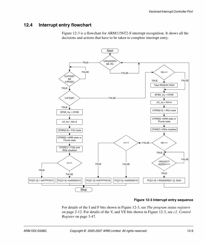
Vectored Interrupt Controller Port
12.4 Interrupt entry flowchart
Figure 12-3 is a flowchart for ARM1156T2-S interrupt recognition. It shows all the decisions and actions that have to be taken to complete interrupt entry.
Figure 12-3 Interrupt entry sequence
For details of the I and F bits shown in Figure 12-3, see The program status registers on page 2-12. For details of the V, and VE bits shown in Figure 12-3, see c1, Control Register on page 3-47.
TRUE
LR_fiq = RA+4
CPSR[4:0] = FIQ mode
CPSR[5] =ARM state or
Thumb state
CPSR[7] = FIQs and
IRQs disabled
SPSR_fiq = CPSR
V==1
FALSE
TRUE
FALSE
TRUE
TRUE
FALSE
!((nFIQ||F)
&&
(nIRQ||I))
!(nFIQ||F)
VE==1FALSEV==1
TRUE
PC[31:0] = IRQADDR[31:2], 0b00
TRUE
FALSE!IRQVECT
ADDRV==1
FALSE
TRUE
TRUE
Take IRQACK HIGH
LR_irq = RA+4
SPSR_irq = CPSR
CPSR[4:0] = IRQ mode
FALSE
CPSR[7] =IRQs disabled
CPSR[5] =ARM state or
Thumb state
VE==1
Stop
PC[31:0] =0x0000001CPC[31:0] = 0xFFFF001C PC[31:0] =0xFFFF0018 PC[31:0] =0x00000018
!(IRQADDRV
&& VE)
FALSE
Start
ARM DDI 0338G Copyright © 2005-2007 ARM Limited. All rights reserved. 12-9
Vectored Interrupt Controller Port
12-10 Copyright © 2005-2007 ARM Limited. All rights reserved. ARM DDI 0338G
Chapter 13 Debug
This chapter contains details of the ARM1156T2-S debug unit. These features assist the development of application software, operating systems, and hardware. This chapter contains the following sections:
• Debug systems on page 13-2
• About the debug unit on page 13-4
• Debug registers on page 13-6
• CP14 registers reset on page 13-24
• CP14 debug instructions on page 13-25
• Debug events on page 13-28
• Debug exception on page 13-33
• Debug state on page 13-35
• Debug communications channel on page 13-39
• Debugging in a cached system on page 13-40
• Monitor debug-mode debugging on page 13-41
• Halting debug-mode debugging on page 13-47
• External signals on page 13-49.
ARM DDI 0338G Copyright © 2005-2007 ARM Limited. All rights reserved. 13-1
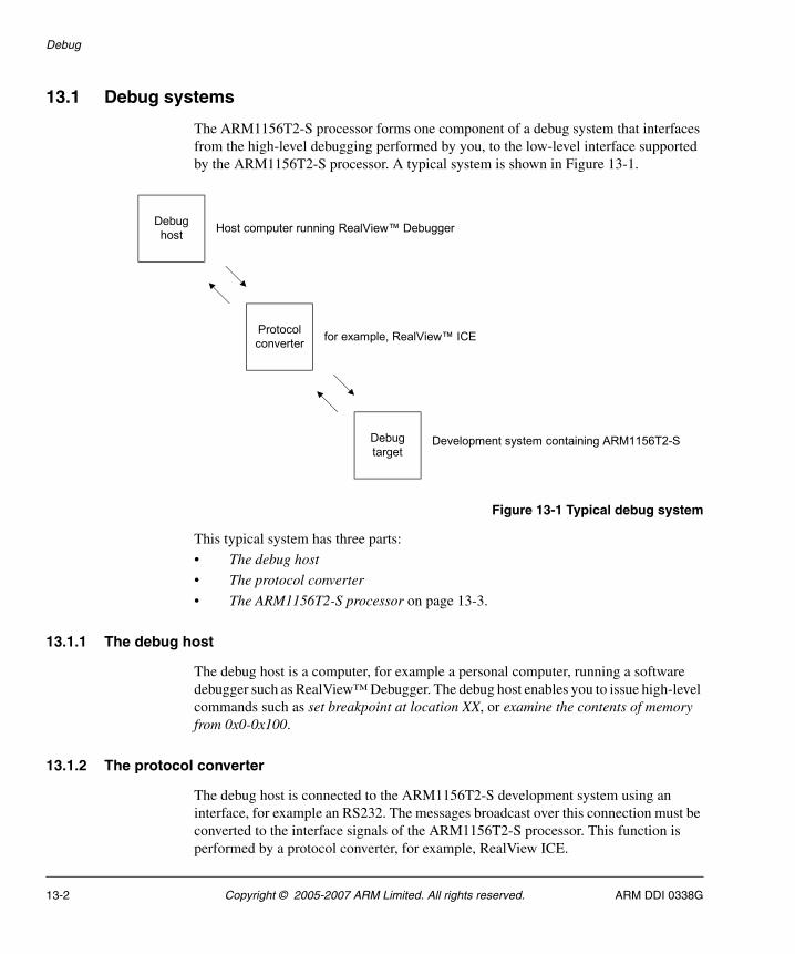
Debug
13.1 Debug systems
The ARM1156T2-S processor forms one component of a debug system that interfaces from the high-level debugging performed by you, to the low-level interface supported by the ARM1156T2-S processor. A typical system is shown in Figure 13-1.
Figure 13-1 Typical debug system
This typical system has three parts:
• The debug host
• The protocol converter
• The ARM1156T2-S processor on page 13-3.
13.1.1 The debug host
The debug host is a computer, for example a personal computer, running a software debugger such as RealView™ Debugger. The debug host enables you to issue high-level commands such as set breakpoint at location XX, or examine the contents of memory from 0x0-0x100.
13.1.2 The protocol converter
The debug host is connected to the ARM1156T2-S development system using an interface, for example an RS232. The messages broadcast over this connection must be converted to the interface signals of the ARM1156T2-S processor. This function is performed by a protocol converter, for example, RealView ICE.
Host computer running RealView™ DebuggerDebug
host
for example, RealView™ ICE
Development system containing ARM1156T2-SDebug
target
Protocol
converter
13-2 Copyright © 2005-2007 ARM Limited. All rights reserved. ARM DDI 0338G
Debug
13.1.3 The ARM1156T2-S processor
The ARM1156T2-S processor, with debug unit, is the lowest level of the system. The debug extensions enable you to:
• stall program execution
• examine its internal state and the state of the memory system
• resume program execution.
The debug host and the protocol converter are system-dependent.
ARM DDI 0338G Copyright © 2005-2007 ARM Limited. All rights reserved. 13-3
Debug
13.2 About the debug unit
The ARM1156T2-S debug unit assists in debugging software running on the ARM1156T2-S processor. You can use an ARM1156T2-S debug unit, in combination with a software debugger program, to debug:
• application software
• operating systems
• ARM processor based hardware systems.
The debug unit enables you to:
• stop program execution
• examine and alter processor and coprocessor state
• examine and alter memory and input/output peripheral state
• restart the processor core.
you can debug the ARM1156T2-S processor in the following ways:
• Halting debug-mode debugging
• Monitor debug-mode debugging on page 13-5
• Trace debugging. See Chapter 15 Trace Interface Port for interfacing with an ETM.
The ARM1156T2-S debug interface is based on the IEEE Standard Test Access Port and Boundary-Scan Architecture.
13.2.1 Halting debug-mode debugging
When the ARM1156T2-S debug unit is in Halting debug-mode, the processor halts when a debug event, such as a breakpoint, occurs. When the core is halted, an external host can examine and modify its state using the DBGTAP.
In Halting debug-mode you can examine and alter all processor state (processor registers), coprocessor state, memory, and input/output locations through the DBGTAP. This mode is intentionally invasive to program execution. Halting debug-mode requires:
• external hardware to control the DBGTAP
• a software debugger to provide the user interface to the debug hardware.
See CP14 c1, Debug Status and Control Register (DSCR) on page 13-9 to learn how to set the ARM1156T2-S debug unit into Halting debug-mode.
13-4 Copyright © 2005-2007 ARM Limited. All rights reserved. ARM DDI 0338G
Debug
13.2.2 Monitor debug-mode debugging
When the ARM1156T2-S debug unit is in Monitor debug-mode, the processor takes a Debug exception instead of halting. A special piece of software, a monitor target, can then take control to examine or alter the processor state. Monitor debug-mode is essential in real-time systems where the core cannot be halted to collect information. For example, engine controllers and servo mechanisms in hard drive controllers that cannot stop the code without physically damaging the components.
When debugging in Monitor debug-mode the processor stops execution of the current program and starts execution of a monitor target. The state of the processor is preserved in the same manner as all ARM exceptions (see the ARM Architecture Reference Manual on exceptions and exception priorities). The debug monitor target communicates with the debugger to access processor and coprocessor state, and to access memory contents and input/output peripherals. Monitor debug-mode requires a debug monitor program to interface between the debug hardware and the software debugger.
When debugging in Monitor debug-mode, you can program new debug events through CP14. This coprocessor is the software interface of all the debug resources such as the breakpoint and watchpoint registers. See CP14 c1, Debug Status and Control Register (DSCR) on page 13-9 to learn how to set the ARM1156T2-S debug unit into Monitor debug-mode.
13.2.3 Programming the debug unit
The ARM1156T2-S debug unit is programmed using CoProcessor 14 (CP14). CP14 provides:
• instruction address comparators for triggering breakpoints
• data address comparators for triggering watchpoints
• a bidirectional Debug Communication Channel (DCC)
• all other state information associated with ARM1156T2-S debug.
CP14 is accessed using coprocessor instructions in Monitor debug-mode, and certain debug scan chains in Halting debug-mode, see Chapter 14 Debug Test Access Port to learn how to access the ARM1156T2-S debug unit using scan chains.
ARM DDI 0338G Copyright © 2005-2007 ARM Limited. All rights reserved. 13-5
Debug
13.3 Debug registers
Table 13-1 shows definitions of terms used in register descriptions.
On a power-on reset, all the CP14 debug registers take the values indicated by the Reset value column in the register bitfield definition tables (Table 13-4 on page 13-10, Table 13-6 on page 13-16, Table 13-9 on page 13-18, Table 13-10 on page 13-21, and Table 13-11 on page 13-22). In these tables, - means an Undefined reset value.
13.3.1 Accessing debug registers
To access the CP14 debug registers you must set Opcode_1 and CRn to 0. The Opcode_2 and CRm fields of the coprocessor instructions are used to encode the CP14 debug register number, where the register number is {<Opcode2>, <CRm>}.
Table 13-2 on page 13-7 shows the CP14 debug register map. All of these registers are also accessible as scan chains from the DBGTAP.
Table 13-1 Terms used in register descriptions
Term Description
R Read-only. Written values are ignored. However, it is written as 0 or preserved by writing the same value previously read from the same fields on the same processor.
W Write-only. This bit cannot be read. Reads return an Unpredictable value.
RW Read or write.
C Cleared on read. This bit is cleared whenever the register is read.
UNP/SBZP Unpredictable or Should Be Zero or Preserved (SBZP). A read to this bit returns an Unpredictable value. It is written as 0 or preserved by writing the same value previously read from the same fields on the same processor. These bits are usually reserved for future expansion.
Core view This column defines the core access permission for a given bit.
External view This column defines the DBGTAP debugger view of a given bit.
Read/write attributes
This is used when the core and the DBGTAP debugger view are the same.
13-6 Copyright © 2005-2007 ARM Limited. All rights reserved. ARM DDI 0338G
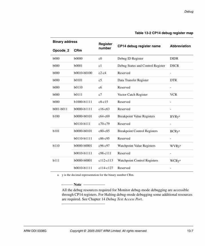
Debug
Note All the debug resources required for Monitor debug-mode debugging are accessible through CP14 registers. For Halting debug-mode debugging some additional resources are required. See Chapter 14 Debug Test Access Port.
Table 13-2 CP14 debug register map
Binary addressRegister number
CP14 debug register name AbbreviationOpcode_2 CRm
b000 b0000 c0 Debug ID Register DIDR
b000 b0001 c1 Debug Status and Control Register DSCR
b000 b0010-b0100 c2-c4 Reserved -
b000 b0101 c5 Data Transfer Register DTR
b000 b0110 c6 Reserved -
b000 b0111 c7 Vector Catch Register VCR
b000 b1000-b1111 c8-c15 Reserved -
b001-b011 b0000-b1111 c16-c63 Reserved -
b100 b0000-b0101 c64-c69 Breakpoint Value Registers BVRya
b0110-b111 c70-c79 Reserved -
b101 b0000-b0101 c80-c85 Breakpoint Control Registers BCRya
b0110-b1111 c86-c95 Reserved -
b110 b0000-b0001 c96-c97 Watchpoint Value Registers WVRya
b0010-b1111 c98-c111 Reserved -
b111 b0000-b0001 c112-c113 Watchpoint Control Registers WCRya
b0010-b1111 c114-c127 Reserved -
a. y is the decimal representation for the binary number CRm.
ARM DDI 0338G Copyright © 2005-2007 ARM Limited. All rights reserved. 13-7
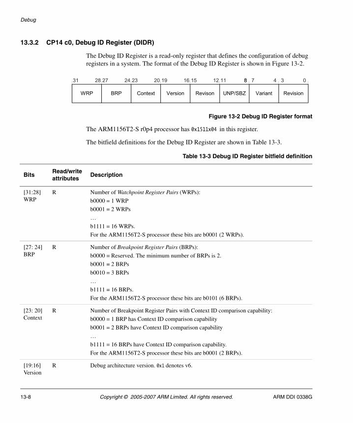
Debug
13.3.2 CP14 c0, Debug ID Register (DIDR)
The Debug ID Register is a read-only register that defines the configuration of debug registers in a system. The format of the Debug ID Register is shown in Figure 13-2.
Figure 13-2 Debug ID Register format
The ARM1156T2-S r0p4 processor has 0x1511x04 in this register.
The bitfield definitions for the Debug ID Register are shown in Table 13-3.
RevisonWRP
31 28 27 24 23 20 19 16 15 8 7 4 3 0
BRP Context Version UNP/SBZ Variant Revision
81112
Table 13-3 Debug ID Register bitfield definition
BitsRead/write attributes
Description
[31:28] WRP
R Number of Watchpoint Register Pairs (WRPs):
b0000 = 1 WRP
b0001 = 2 WRPs
…
b1111 = 16 WRPs.
For the ARM1156T2-S processor these bits are b0001 (2 WRPs).
[27: 24] BRP
R Number of Breakpoint Register Pairs (BRPs):
b0000 = Reserved. The minimum number of BRPs is 2.
b0001 = 2 BRPs
b0010 = 3 BRPs
…
b1111 = 16 BRPs.
For the ARM1156T2-S processor these bits are b0101 (6 BRPs).
[23: 20] Context
R Number of Breakpoint Register Pairs with Context ID comparison capability:
b0000 = 1 BRP has Context ID comparison capability
b0001 = 2 BRPs have Context ID comparison capability
…
b1111 = 16 BRPs have Context ID comparison capability.
For the ARM1156T2-S processor these bits are b0001 (2 BRPs).
[19:16] Version
R Debug architecture version. 0x1 denotes v6.
13-8 Copyright © 2005-2007 ARM Limited. All rights reserved. ARM DDI 0338G
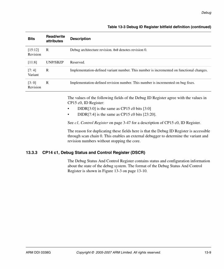
Debug
The values of the following fields of the Debug ID Register agree with the values in CP15 c0, ID Register:
• DIDR[3:0] is the same as CP15 c0 bits [3:0]
• DIDR[7:4] is the same as CP15 c0 bits [23:20].
See c1, Control Register on page 3-47 for a description of CP15 c0, ID Register.
The reason for duplicating these fields here is that the Debug ID Register is accessible through scan chain 0. This enables an external debugger to determine the variant and revision numbers without stopping the core.
13.3.3 CP14 c1, Debug Status and Control Register (DSCR)
The Debug Status And Control Register contains status and configuration information about the state of the debug system. The format of the Debug Status And Control Register is shown in Figure 13-3 on page 13-10.
[15:12] Revision
R Debug architecture revision. 0x0 denotes revision 0.
[11:8] UNP/SBZP Reserved.
[7: 4] Variant
R Implementation-defined variant number. This number is incremented on functional changes.
[3: 0] Revision
R Implementation-defined revision number. This number is incremented on bug fixes.
Table 13-3 Debug ID Register bitfield definition (continued)
BitsRead/write attributes
Description
ARM DDI 0338G Copyright © 2005-2007 ARM Limited. All rights reserved. 13-9
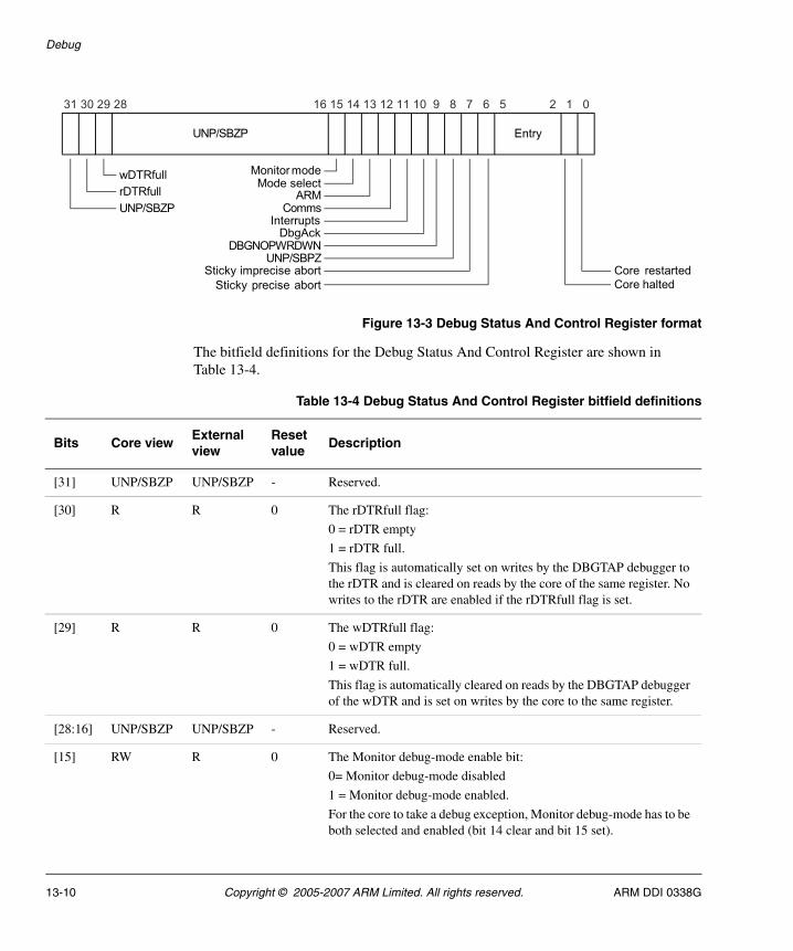
Debug
Figure 13-3 Debug Status And Control Register format
The bitfield definitions for the Debug Status And Control Register are shown in Table 13-4.
31 30 29 28 16 15 14 13 12 11 10 6 5 2 1 0
UNP/SBZP Entry
rDTRfull
wDTRfull
UNP/SBZP
Monitor modeMode select
ARM
DbgAckInterrupts
Comms
9 78
Sticky imprecise abortUNP/SBPZ
DBGNOPWRDWN
Core restarted
Core haltedSticky precise abort
Table 13-4 Debug Status And Control Register bitfield definitions
Bits Core viewExternal view
Reset value
Description
[31] UNP/SBZP UNP/SBZP - Reserved.
[30] R R 0 The rDTRfull flag:
0 = rDTR empty
1 = rDTR full.
This flag is automatically set on writes by the DBGTAP debugger to the rDTR and is cleared on reads by the core of the same register. No writes to the rDTR are enabled if the rDTRfull flag is set.
[29] R R 0 The wDTRfull flag:
0 = wDTR empty
1 = wDTR full.
This flag is automatically cleared on reads by the DBGTAP debugger of the wDTR and is set on writes by the core to the same register.
[28:16] UNP/SBZP UNP/SBZP - Reserved.
[15] RW R 0 The Monitor debug-mode enable bit:
0= Monitor debug-mode disabled
1 = Monitor debug-mode enabled.
For the core to take a debug exception, Monitor debug-mode has to be both selected and enabled (bit 14 clear and bit 15 set).
13-10 Copyright © 2005-2007 ARM Limited. All rights reserved. ARM DDI 0338G
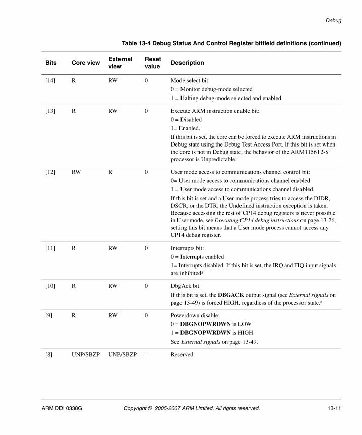
Debug
[14] R RW 0 Mode select bit:
0 = Monitor debug-mode selected
1 = Halting debug-mode selected and enabled.
[13] R RW 0 Execute ARM instruction enable bit:
0 = Disabled
1= Enabled.
If this bit is set, the core can be forced to execute ARM instructions in Debug state using the Debug Test Access Port. If this bit is set when the core is not in Debug state, the behavior of the ARM1156T2-S processor is Unpredictable.
[12] RW R 0 User mode access to communications channel control bit:
0= User mode access to communications channel enabled
1 = User mode access to communications channel disabled.
If this bit is set and a User mode process tries to access the DIDR, DSCR, or the DTR, the Undefined instruction exception is taken. Because accessing the rest of CP14 debug registers is never possible in User mode, see Executing CP14 debug instructions on page 13-26, setting this bit means that a User mode process cannot access any CP14 debug register.
[11] R RW 0 Interrupts bit:
0 = Interrupts enabled
1= Interrupts disabled. If this bit is set, the IRQ and FIQ input signals are inhibiteda.
[10] R RW 0 DbgAck bit.
If this bit is set, the DBGACK output signal (see External signals on page 13-49) is forced HIGH, regardless of the processor state.a
[9] R RW 0 Powerdown disable:
0 = DBGNOPWRDWN is LOW
1 = DBGNOPWRDWN is HIGH.
See External signals on page 13-49.
[8] UNP/SBZP UNP/SBZP - Reserved.
Table 13-4 Debug Status And Control Register bitfield definitions (continued)
Bits Core viewExternal view
Reset value
Description
ARM DDI 0338G Copyright © 2005-2007 ARM Limited. All rights reserved. 13-11
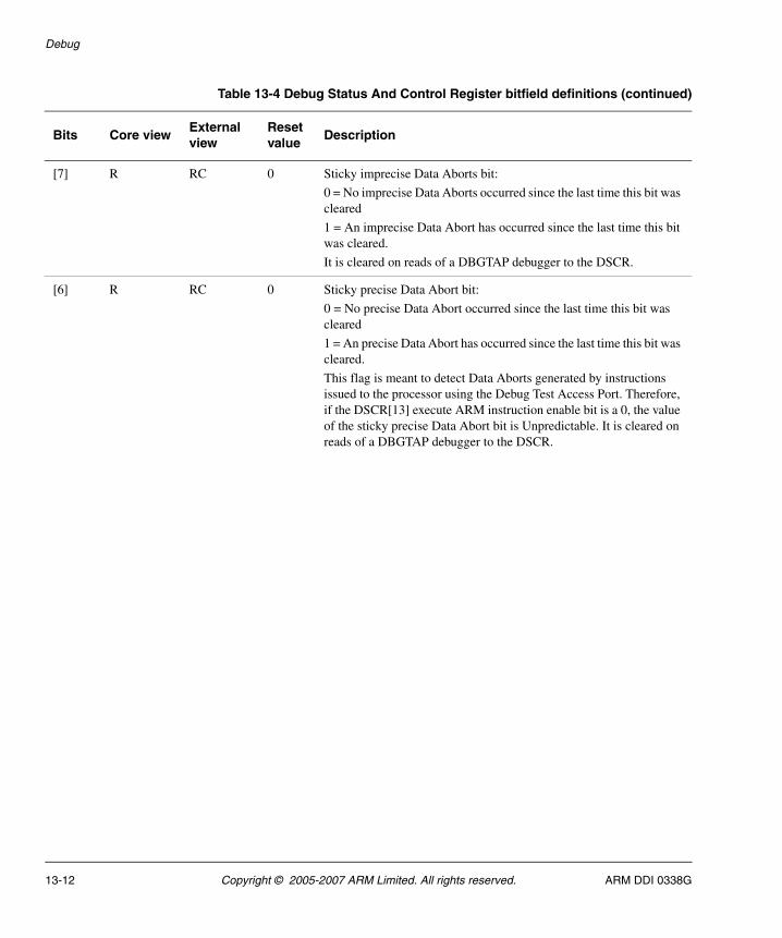
Debug
[7] R RC 0 Sticky imprecise Data Aborts bit:
0 = No imprecise Data Aborts occurred since the last time this bit was cleared
1 = An imprecise Data Abort has occurred since the last time this bit was cleared.
It is cleared on reads of a DBGTAP debugger to the DSCR.
[6] R RC 0 Sticky precise Data Abort bit:
0 = No precise Data Abort occurred since the last time this bit was cleared
1 = An precise Data Abort has occurred since the last time this bit was cleared.
This flag is meant to detect Data Aborts generated by instructions issued to the processor using the Debug Test Access Port. Therefore, if the DSCR[13] execute ARM instruction enable bit is a 0, the value of the sticky precise Data Abort bit is Unpredictable. It is cleared on reads of a DBGTAP debugger to the DSCR.
Table 13-4 Debug Status And Control Register bitfield definitions (continued)
Bits Core viewExternal view
Reset value
Description
13-12 Copyright © 2005-2007 ARM Limited. All rights reserved. ARM DDI 0338G
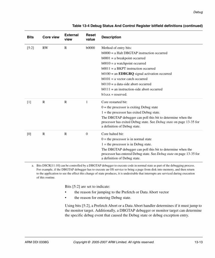
Debug
Bits [5:2] are set to indicate:
• the reason for jumping to the Prefetch or Data Abort vector
• the reason for entering Debug state.
Using bits [5:2], a Prefetch Abort or a Data Abort handler determines if it must jump to the monitor target. Additionally, a DBGTAP debugger or monitor target can determine the specific debug event that caused the Debug state or debug exception entry.
[5:2] RW R b0000 Method of entry bits:
b0000 = a Halt DBGTAP instruction occurred
b0001 = a breakpoint occurred
b0010 = a watchpoint occurred
b0011 = a BKPT instruction occurred
b0100 = an EDBGRQ signal activation occurred
b0101 = a vector catch occurred
b0110 = a data-side abort occurred
b0111 = an instruction-side abort occurred
b1xxx = reserved.
[1] R R 1 Core restarted bit:
0 = the processor is exiting Debug state
1 = the processor has exited Debug state.
The DBGTAP debugger can poll this bit to determine when the processor has exited Debug state. See Debug state on page 13-35 for a definition of Debug state.
[0] R R 0 Core halted bit:
0 = the processor is in normal state
1 = the processor is in Debug state.
The DBGTAP debugger can poll this bit to determine when the processor has entered Debug state. See Debug state on page 13-35 for a definition of Debug state.
a. Bits DSCR[11:10] can be controlled by a DBGTAP debugger to execute code in normal state as part of the debugging process. For example, if the DBGTAP debugger has to execute an OS service to bring a page from disk into memory, and then return to the application to see the effect this change of state produces, it is undesirable that interrupts are serviced during execution of this routine.
Table 13-4 Debug Status And Control Register bitfield definitions (continued)
Bits Core viewExternal view
Reset value
Description
ARM DDI 0338G Copyright © 2005-2007 ARM Limited. All rights reserved. 13-13
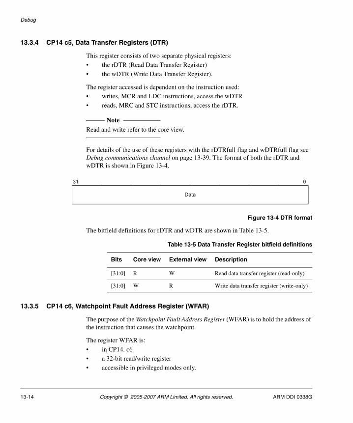
Debug
13.3.4 CP14 c5, Data Transfer Registers (DTR)
This register consists of two separate physical registers:
• the rDTR (Read Data Transfer Register)
• the wDTR (Write Data Transfer Register).
The register accessed is dependent on the instruction used:
• writes, MCR and LDC instructions, access the wDTR
• reads, MRC and STC instructions, access the rDTR.
Note Read and write refer to the core view.
For details of the use of these registers with the rDTRfull flag and wDTRfull flag see Debug communications channel on page 13-39. The format of both the rDTR and wDTR is shown in Figure 13-4.
Figure 13-4 DTR format
The bitfield definitions for rDTR and wDTR are shown in Table 13-5.
13.3.5 CP14 c6, Watchpoint Fault Address Register (WFAR)
The purpose of the Watchpoint Fault Address Register (WFAR) is to hold the address of the instruction that causes the watchpoint.
The register WFAR is:
• in CP14, c6
• a 32-bit read/write register
• accessible in privileged modes only.
Data
31 0
Table 13-5 Data Transfer Register bitfield definitions
Bits Core view External view Description
[31:0] R W Read data transfer register (read-only)
[31:0] W R Write data transfer register (write-only)
13-14 Copyright © 2005-2007 ARM Limited. All rights reserved. ARM DDI 0338G
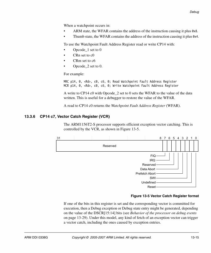
Debug
When a watchpoint occurs in:
• ARM state, the WFAR contains the address of the instruction causing it plus 0x8.
• Thumb state, the WFAR contains the address of the instruction causing it plus 0x4.
To use the Watchpoint Fault Address Register read or write CP14 with:
• Opcode_1 set to 0
• CRn set to c0
• CRm set to c6
• Opcode_2 set to 0.
For example:
MRC p14, 0, <Rd>, c0, c6, 0; Read Watchpoint Fault Address RegisterMCR p14, 0, <Rd>, c0, c6, 0; Write Watchpoint Fault Address Register
A write to CP14 c0 with Opcode_2 set to 0 sets the WFAR to the value of the data written. This is useful for a debugger to restore the value of the WFAR.
A read to CP14 c0 returns the Watchpoint Fault Address Register (WFAR).
13.3.6 CP14 c7, Vector Catch Register (VCR)
The ARM1156T2-S processor supports efficient exception vector catching. This is controlled by the VCR, as shown in Figure 13-5.
Figure 13-5 Vector Catch Register format
If one of the bits in this register is set and the corresponding vector is committed for execution, then a Debug exception or Debug state entry might be generated, depending on the value of the DSCR[15:14] bits (see Behavior of the processor on debug events on page 13-29). Under this model, any kind of fetch of an exception vector can trigger a vector catch, including the ones caused by exception entries.
ARM DDI 0338G Copyright © 2005-2007 ARM Limited. All rights reserved. 13-15
Debug
The update of the VCR might occur several instructions after the corresponding MCR instruction. It only takes effect by the next Instruction Memory Barrier (IMB).
Table 13-6 shows the bitfield definitions for the Vector Catch Register.
13.3.7 CP14 c64-c69, Breakpoint Value Registers (BVR)
Each BVR is associated with a BCR register. BCRy is the corresponding control register for BVRy.
A pair of breakpoint registers, BVRy/BCRy, is called a Breakpoint Register Pair (BRP). BVR0-5 are paired with BCR0-5 to make BRP0-5.
The BVR of a BRP is loaded with an instruction address and then its contents can be compared against the instruction address bus of the processor.
The breakpoint value contained in the BVR corresponds to either an instruction address or a Context ID. Breakpoints can be set on:
• an instruction address
• a Context ID
• an instruction address/Context ID pair.
Table 13-6 Vector Catch Register bitfield definitions
BitsNormal address
High vector address
DescriptionRead/write attributes
Reset value
[31:8] - - Reserved. UNP/SBZP -
[7] FIQ 0x0000001C 0xFFFF001C Vector catch enable, FIQ RW 0
[6] IRQ Most recenta IRQ address
Most recenta IRQ address
Vector catch enable, IRQ RW 0
[5] - - Reserved UNP/SBZP -
[4] Data Abort 0x00000010 0xFFFF0010 Vector catch enable, Data Abort RW 0
[3] Prefetch Abort
0x0000000C 0xFFFF000C Vector catch enable, Prefetch Abort RW 0
[2] SVC 0x00000008 0xFFFF0008 Vector catch enable, SVC RW 0
[1] Undefined 0x00000004 0xFFFF0004 Vector catch enable, Undefined Instruction RW 0
[0 Reset] 0x00000000 0xFFFF0000 Vector catch enable, Reset RW 0
a. You can configure the ARM1156T2-S processor so that the IRQ uses vector exceptions other than 0x00000018 and 0xFFFF0018. See Changes to existing interrupt vectors on page 2-20 for more details.
13-16 Copyright © 2005-2007 ARM Limited. All rights reserved. ARM DDI 0338G
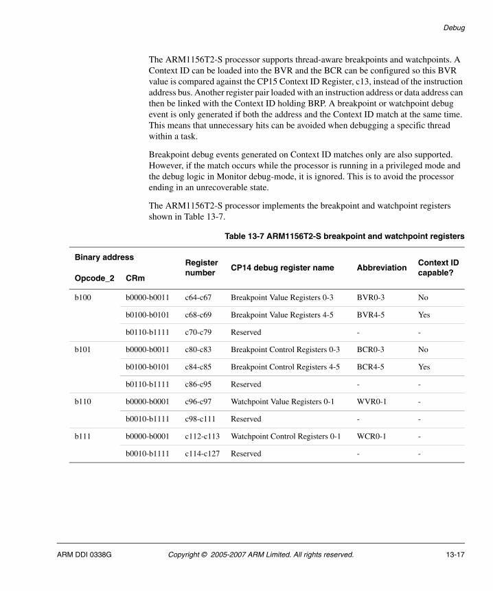
Debug
The ARM1156T2-S processor supports thread-aware breakpoints and watchpoints. A Context ID can be loaded into the BVR and the BCR can be configured so this BVR value is compared against the CP15 Context ID Register, c13, instead of the instruction address bus. Another register pair loaded with an instruction address or data address can then be linked with the Context ID holding BRP. A breakpoint or watchpoint debug event is only generated if both the address and the Context ID match at the same time. This means that unnecessary hits can be avoided when debugging a specific thread within a task.
Breakpoint debug events generated on Context ID matches only are also supported. However, if the match occurs while the processor is running in a privileged mode and the debug logic in Monitor debug-mode, it is ignored. This is to avoid the processor ending in an unrecoverable state.
The ARM1156T2-S processor implements the breakpoint and watchpoint registers shown in Table 13-7.
Table 13-7 ARM1156T2-S breakpoint and watchpoint registers
Binary addressRegister number
CP14 debug register name AbbreviationContext IDcapable?
Opcode_2 CRm
b100 b0000-b0011 c64-c67 Breakpoint Value Registers 0-3 BVR0-3 No
b0100-b0101 c68-c69 Breakpoint Value Registers 4-5 BVR4-5 Yes
b0110-b1111 c70-c79 Reserved - -
b101 b0000-b0011 c80-c83 Breakpoint Control Registers 0-3 BCR0-3 No
b0100-b0101 c84-c85 Breakpoint Control Registers 4-5 BCR4-5 Yes
b0110-b1111 c86-c95 Reserved - -
b110 b0000-b0001 c96-c97 Watchpoint Value Registers 0-1 WVR0-1 -
b0010-b1111 c98-c111 Reserved - -
b111 b0000-b0001 c112-c113 Watchpoint Control Registers 0-1 WCR0-1 -
b0010-b1111 c114-c127 Reserved - -
ARM DDI 0338G Copyright © 2005-2007 ARM Limited. All rights reserved. 13-17
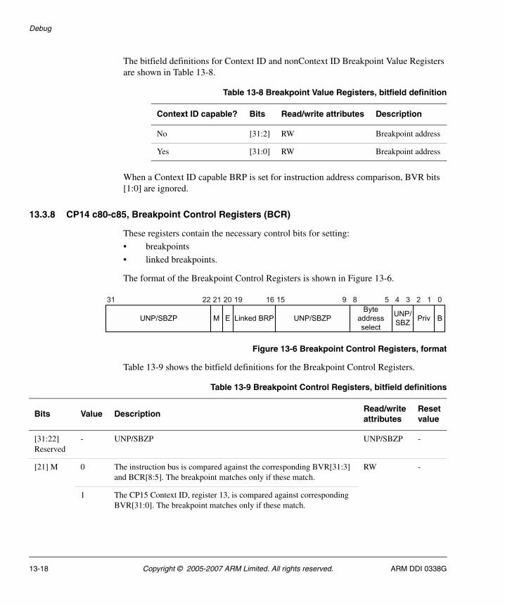
Debug
The bitfield definitions for Context ID and nonContext ID Breakpoint Value Registers are shown in Table 13-8.
When a Context ID capable BRP is set for instruction address comparison, BVR bits [1:0] are ignored.
13.3.8 CP14 c80-c85, Breakpoint Control Registers (BCR)
These registers contain the necessary control bits for setting:
• breakpoints
• linked breakpoints.
The format of the Breakpoint Control Registers is shown in Figure 13-6.
Figure 13-6 Breakpoint Control Registers, format
Table 13-9 shows the bitfield definitions for the Breakpoint Control Registers.
Table 13-8 Breakpoint Value Registers, bitfield definition
Context ID capable? Bits Read/write attributes Description
No [31:2] RW Breakpoint address
Yes [31:0] RW Breakpoint address
Table 13-9 Breakpoint Control Registers, bitfield definitions
Bits Value DescriptionRead/write attributes
Reset value
[31:22] Reserved
- UNP/SBZP UNP/SBZP -
[21] M 0 The instruction bus is compared against the corresponding BVR[31:3] and BCR[8:5]. The breakpoint matches only if these match.
RW -
1 The CP15 Context ID, register 13, is compared against corresponding BVR[31:0]. The breakpoint matches only if these match.
13-18 Copyright © 2005-2007 ARM Limited. All rights reserved. ARM DDI 0338G
Debug
[20] E 0 Link disabled. RW -
1 Link enabled.
[19:16] Linked BRP
- Indicate another BRP to link this one with. Linked BRP number. The binary number encoded here indicates another BRP to link this one with. If a BRP is linked with itself, it is Unpredictable if a breakpoint debug event is generated.
RW -
[15:9] Reserved
- - RW -
[8:5] Byte address select
b0000
bxxx1
bxx1x
bx1xx
b1xxx
The breakpoint never hits
The breakpoint hits if the byte at address:
BVR[31:2]:+0 is accessed
BVR[31:2]+1 is accessed
BVR[31:2]+2 is accessed
BVR[31:2]+3 is accessed
The BVR is programmed with a word address. You can use this field to program the breakpoint so it hits only if certain byte addresses are accessed.
This field must be set to b1111 when this BRP is programmed for Context ID comparison, that is BCR[22:20] set to b01x. Otherwise breakpoint or watchpoint debug events might not be generated as expected.
Note These are little-endian byte addresses. This ensures that a breakpoint is triggered regardless of the endianness of the instruction fetch.
For example, if a breakpoint is set on a certain Thumb instruction by doing BCR[8:5] = b0011, it is triggered if in little-endian and instruction address[1:0] is b00 or if big-endian and instruction address[1:0] is b10.
RW -
[4:3] - UNP/SBZP - -
Table 13-9 Breakpoint Control Registers, bitfield definitions (continued)
Bits Value DescriptionRead/write attributes
Reset value
ARM DDI 0338G Copyright © 2005-2007 ARM Limited. All rights reserved. 13-19
Debug
Note The BCR[8:5] and BCR[2:1] fields still apply when a BRP is set for Context ID comparison. See Setting breakpoints, watchpoints, and vector catch debug events on page 13-41 for more information on programming sequences for linked breakpoints and linked watchpoints.
The following rules apply to the ARM1156T2-S processor for breakpoint debug event generation:
• The update of a BVR or a BCR can take effect several instructions after the corresponding MCR. It takes effect by the next IMB.
• Updates of the CP15 Context ID Register c13, can take effect several instructions after the corresponding MCR. However, the write takes place by the end of the exception return. This is to ensure that a User mode process, switched in by a processor scheduler, can break at its first instruction.
• Any BRP holding an instruction address can be linked with any other one with Context ID capability. Several BRPs holding instruction addresses can be linked with the same Context ID capable one.
• If a BRP (holding an instruction address) is linked with one that is not configured for Context ID comparison and linking, it is Unpredictable whether a breakpoint debug event is generated or not. BCR[22:20] fields of the second BRP must be set to b011.
[2:1] Privileged mode control
b00
b01
b10
b11
Reserved
Privileged
User
Either
If this BRP is programmed for Context ID comparison and linking, BCR[22:20] is set b011, the BCR[2:1] field of the instruction address-holding BRP takes precedence and it is Undefined whether this field is included in the comparison or not. Therefore, it must be set to Privileged or User. The WCR[2:1] field of a WRP linked with this BRP also takes precedence over this field.
RW -
[0] B 0 Breakpoint disabled. RW 0
1 Breakpoint enabled.
Table 13-9 Breakpoint Control Registers, bitfield definitions (continued)
Bits Value DescriptionRead/write attributes
Reset value
13-20 Copyright © 2005-2007 ARM Limited. All rights reserved. ARM DDI 0338G
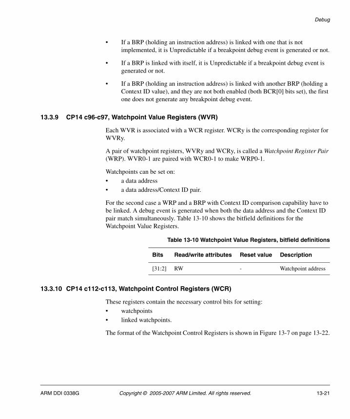
Debug
• If a BRP (holding an instruction address) is linked with one that is not implemented, it is Unpredictable if a breakpoint debug event is generated or not.
• If a BRP is linked with itself, it is Unpredictable if a breakpoint debug event is generated or not.
• If a BRP (holding an instruction address) is linked with another BRP (holding a Context ID value), and they are not both enabled (both BCR[0] bits set), the first one does not generate any breakpoint debug event.
13.3.9 CP14 c96-c97, Watchpoint Value Registers (WVR)
Each WVR is associated with a WCR register. WCRy is the corresponding register for WVRy.
A pair of watchpoint registers, WVRy and WCRy, is called a Watchpoint Register Pair (WRP). WVR0-1 are paired with WCR0-1 to make WRP0-1.
Watchpoints can be set on:
• a data address
• a data address/Context ID pair.
For the second case a WRP and a BRP with Context ID comparison capability have to be linked. A debug event is generated when both the data address and the Context ID pair match simultaneously. Table 13-10 shows the bitfield definitions for the Watchpoint Value Registers.
13.3.10 CP14 c112-c113, Watchpoint Control Registers (WCR)
These registers contain the necessary control bits for setting:
• watchpoints
• linked watchpoints.
The format of the Watchpoint Control Registers is shown in Figure 13-7 on page 13-22.
Table 13-10 Watchpoint Value Registers, bitfield definitions
Bits Read/write attributes Reset value Description
[31:2] RW - Watchpoint address
ARM DDI 0338G Copyright © 2005-2007 ARM Limited. All rights reserved. 13-21
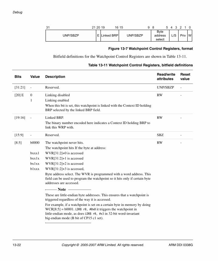
Debug
Figure 13-7 Watchpoint Control Registers, format
Bitfield definitions for the Watchpoint Control Registers are shown in Table 13-11.
Table 13-11 Watchpoint Control Registers, bitfield definitions
Bits Value DescriptionRead/write attributes
Reset value
[31:21] - Reserved. UNP/SBZP -
[20] E 0
1
Linking disabled
Linking enabled
When this bit is set, this watchpoint is linked with the Context ID holding BRP selected by the linked BRP field.
RW -
[19:16] - Linked BRP.
The binary number encoded here indicates a Context ID holding BRP to link this WRP with.
RW -
[15:9] - Reserved. SBZ -
[8:5] b0000
bxxx1
bxx1x
bx1xx
b1xxx
The watchpoint never hits.
The watchpoint hits If the byte at address:
WVR[31:2]+0 is accessed
WVR[31:2]+1 is accessed
WVR[31:2]+2 is accessed
WVR[31:2]+3 is accessed,
Byte address select. The WVR is programmed with a word address. This field can be used to program the watchpoint so it hits only if certain byte addresses are accessed.
Note These are little-endian byte addresses. This ensures that a watchpoint is triggered regardless of the way it is accessed.
For example, if a watchpoint is set on a certain byte in memory by doing WCR[8:5] = b0001. LDRB r0, #0x0 it triggers the watchpoint in little-endian mode, as does LDRB r0, #x3 in 32-bit word-invariant big-endian mode (B bit of CP15 c1 set).
RW -
13-22 Copyright © 2005-2007 ARM Limited. All rights reserved. ARM DDI 0338G
Debug
In addition to the rules for breakpoint debug event generation, see CP14 c80-c85, Breakpoint Control Registers (BCR) on page 13-18, the following rules apply to the ARM1156T2-S processor for watchpoint debug event generation:
• The update of a WVR or a WCR can take effect several instructions after the corresponding MCR. It only guaranteed to have taken effect by the next IMB.
• Any WRP can be linked with any BRP with Context ID comparison capability. Several BRPs (holding instruction addresses) and WRPs can be linked with the same Context ID capable BRP.
• If a WRP is linked with a BRP that is not configured for Context ID comparison and linking, it is Unpredictable if a watchpoint debug event is generated or not. BCR[22:20] fields of the BRP must be set to b111.
• If a WRP is linked with a BRP that is not implemented, it is Unpredictable if a watchpoint debug event is generated or not.
• If a WRP is linked with a BRP and they are not both enabled (BCR[0] and WCR[0] set), it does not generate a watchpoint debug event.
[4:3] b00
b01
b10
b11
Reserved
Load
Store
Either
Determines what type of access the watchpoint can act on. A SWP triggers on Load, Store, or Either. A load exclusive instruction, LDREX, triggers on Load or Either. A store exclusive instruction, STREX, triggers on Store or Either, whether it succeeded or not.
RW -
[2:1] b00
b01
b10
b11
Reserved
Privileged
User
Either
Determines what level of privilege the watchpoint acts on.
RW -
[0] 0
1
Watchpoint disabled
Watchpoint enabled.
RW 0
Table 13-11 Watchpoint Control Registers, bitfield definitions (continued)
Bits Value DescriptionRead/write attributes
Reset value
ARM DDI 0338G Copyright © 2005-2007 ARM Limited. All rights reserved. 13-23
Debug
13.4 CP14 registers reset
The CP14 debug registers are all reset by the ARM1156T2-S processor power-on reset signal, nPORESETIN, see Power-on reset on page 9-4.
This ensures that a vector catch set on the reset vector is taken when nRESETIN is deasserted. It also ensures that the DBGTAP debugger can be connected when the processor is running without clearing CP14 debug setting, because DBGnTRST does not reset these registers.
13-24 Copyright © 2005-2007 ARM Limited. All rights reserved. ARM DDI 0338G
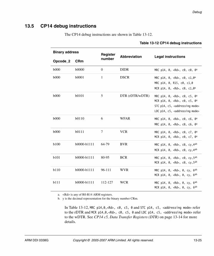
Debug
13.5 CP14 debug instructions
The CP14 debug instructions are shown in Table 13-12.
In Table 13-12, MRC p14,0,<Rd>, c0, c5, 0 and STC p14, c5, <addressing mode> refer to the rDTR and MCR p14,0,<Rd>, c0, c5, 0 and LDC p14, c5, <addressing mode> refer to the wDTR. See CP14 c5, Data Transfer Registers (DTR) on page 13-14 for more details.
Table 13-12 CP14 debug instructions
Binary addressRegister number
Abbreviation Legal instructionsOpcode_2 CRm
b000 b0000 0 DIDR MRC p14, 0, <Rd>, c0, c0, 0a
b000 b0001 1 DSCR MRC p14, 0, <Rd>, c0, c1,0a
MRC p14, 0, R15, c0, c1,0
MCR p14, 0, <Rd>, c0, c1,0a
b000 b0101 5 DTR (rDTR/wDTR) MRC p14, 0, <Rd>, c0, c5, 0a MCR p14, 0, <Rd>, c0, c5, 0a
STC p14, c5, <addressing mode>
LDC p14, c5, <addressing mode>
b000 b0110 6 WFAR MRC p14, 0, <Rd>, c0, c6, 0a
MRC p14, 0, <Rd>, c0, c6, 0a
b000 b0111 7 VCR MRC p14, 0, <Rd>, c0, c7, 0a MCR p14, 0, <Rd>, c0, c7, 0a
b100 b0000-b1111 64-79 BVR MRC p14, 0, <Rd>, c0, cy,4ab
MCR p14, 0, <Rd>, c0, cy,4ab
b101 b0000-b1111 80-95 BCR MRC p14, 0, <Rd>, c0, cy,5ab MCR p14, 0, <Rd>, c0, cy,5ab
b110 b0000-b1111 96-111 WVR MRC p14, 0, <Rd>, 0, cy, 6ab MCR p14, 0, <Rd>, 0, cy, 6ab
b111 b0000-b1111 112-127 WCR MRC p14, 0, <Rd>, 0, cy, 6ab MCR p14, 0, <Rd>, 0, cy, 6ab
a. <Rd> is any of R0-R14 ARM registers.b. y is the decimal representation for the binary number CRm.
ARM DDI 0338G Copyright © 2005-2007 ARM Limited. All rights reserved. 13-25
Debug
The MRC p14, 0, R15, c0, c1, 0 instruction sets the CPSR flags as follows:
• N flag = DSCR[31]. This is an Unpredictable value.
• Z flag = DSCR[30]. This is the value of the rDTRfull flag.
• C flag = DSCR[29]. This is the value of the wDTRfull flag.
• V flag = DSCR[28]. This is an Unpredictable value.
Instructions that follow the MRC instruction can be conditioned to these CPSR flags.
13.5.1 Executing CP14 debug instructions
If the core is in Debug state (see Debug state on page 13-35), you can execute any CP14 debug instruction regardless of the processor mode.
If the processor tries to execute a CP14 debug instruction that either is not in Table 13-12 on page 13-25, or is targeted to a reserved register, such as a non-implemented BVR, the Undefined instruction exception is taken.
You can access the DCC (read DIDR, read DSCR and read/write DTR) in User mode. All other CP14 debug instructions are privileged. If the processor tries to execute one of these in User mode, the Undefined instruction exception is taken.
If the User mode access to DCC disable bit, DSCR[12], is set, all CP14 debug instructions are considered as privileged, and all attempted User mode accesses to CP14 debug registers generate an Undefined instruction exception.
When DSCR bit 14 is set (Halting debug-mode selected and enabled), if the software running on the processor tries to access any register other than the DIDR, the DSCR, or the DTR, the core takes the Undefined instruction exception. The same thing happens if the core is not in any Debug mode (DSCR[15:14]=b00).
This lockout mechanism ensures that the software running on the core cannot modify the settings of a debug event programmed by the DBGTAP debugger.
Table 13-13 on page 13-27 shows the results of executing CP14 debug instructions.
13-26 Copyright © 2005-2007 ARM Limited. All rights reserved. ARM DDI 0338G
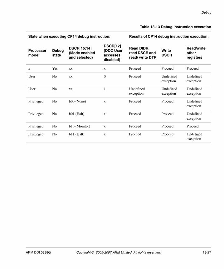
Debug
Table 13-13 Debug instruction execution
State when executing CP14 debug instruction: Results of CP14 debug instruction execution:
Processor mode
Debug state
DSCR[15:14] (Mode enabled and selected)
DSCR[12] (DCC User accesses disabled)
Read DIDR, read DSCR and read/ write DTR
Write DSCR
Read/write other registers
x Yes xx x Proceed Proceed Proceed
User No xx 0 Proceed Undefined exception
Undefined exception
User No xx 1 Undefined exception
Undefined exception
Undefined exception
Privileged No b00 (None) x Proceed Proceed Undefined exception
Privileged No b01 (Halt) x Proceed Proceed Undefined exception
Privileged No b10 (Monitor) x Proceed Proceed Proceed
Privileged No b11 (Halt) x Proceed Proceed Undefined exception
ARM DDI 0338G Copyright © 2005-2007 ARM Limited. All rights reserved. 13-27
Debug
13.6 Debug events
A debug event is any of the following:
• Software debug event
• External debug request signal on page 13-29
• Halt DBGTAP instruction on page 13-29.
13.6.1 Software debug event
A software debug event is any of the following:
• A watchpoint debug event. This occurs when:
— the data address present in the data bus matches the watchpoint value
— all the conditions of the WCR match
— the watchpoint is enabled
— the linked Context ID-holding BRP (if any) is enabled and its value matches the Context ID in CP15 c13.
• A breakpoint debug event. This occurs when:
— an instruction was fetched and the instruction address present in the instruction bus matched the breakpoint value
— at the same time the instruction was fetched, all the conditions of the BCR matched
— the breakpoint was enabled
— at the same time the instruction was fetched, the linked Context ID-holding BRP (if any) was enabled and its value matched the Context ID in CP15 c13
— the instruction is now committed for execution.
• A breakpoint debug event also occurs when:
— an instruction was fetched and the CP15 Context ID (register 13) matched the breakpoint value
— at the same time the instruction was fetched, all the conditions of the BCR matched
— the breakpoint was enabled
— the instruction is now committed for execution.
• A software breakpoint debug event. This occurs when a BKPT instruction is committed for execution.
13-28 Copyright © 2005-2007 ARM Limited. All rights reserved. ARM DDI 0338G
Debug
• A vector catch debug event. This occurs when:
— The instruction at a vector location was fetched. This includes any kind of prefetches, and ones caused by exception entries.
— At the same time the instruction was fetched, the corresponding bit of the VCR was set (vector catch enabled).
— The instruction is now committed for execution.
13.6.2 External debug request signal
The ARM1156T2-S processor has an external debug request input signal, EDBGRQ. When this signal is HIGH it causes the processor to enter Debug state when execution of the current instruction has completed. When this happens, the DSCR[5:2] method of entry bits are set to b0100.
This signal can be driven by the ETM to signal a trigger to the core. For example, if the processor is in Halting debug-mode and a memory permission fault occurs, an external Trace analyzer can collect trace information around this trigger event at the same time that the processor is stopped to examine its state. See the Chapter 15 Trace Interface Port for more details. A DBGTAP debugger can also drive this signal.
13.6.3 Halt DBGTAP instruction
The Halt mechanism is used by the Debug Test Access Port to force the core into Debug state. When this happens, the DSCR[5:2] method of entry bits are set to b0000.
13.6.4 Behavior of the processor on debug events
This section describes how the processor behaves on debug events while not in Debug state. See Debug state on page 13-35 for information on how the processor behaves while in Debug state.
When a software debug event occurs and Monitor debug-mode is selected and enabled then a Debug exception is taken. However, Prefetch Abort and Data Abort Vector catch debug events are ignored. This is to avoid the processor ending in an unrecoverable state on certain combinations of exceptions and vector catches. Unlinked Context ID breakpoint debug events are also ignored if the processor is running in a privileged mode and Monitor debug-mode is selected and enabled. The external debug request signal and the Halt DBGTAP instruction are ignored when Monitor debug-mode is selected and enabled.
When a debug event occurs and Halting debug-mode is selected and enabled then the processor enters Debug state.
ARM DDI 0338G Copyright © 2005-2007 ARM Limited. All rights reserved. 13-29
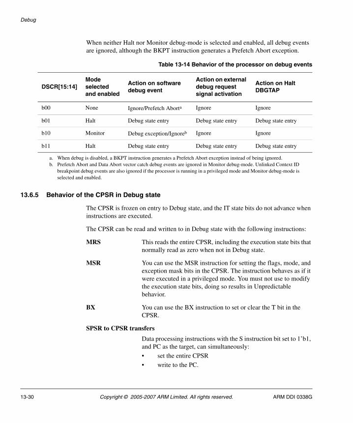
Debug
When neither Halt nor Monitor debug-mode is selected and enabled, all debug events are ignored, although the BKPT instruction generates a Prefetch Abort exception.
13.6.5 Behavior of the CPSR in Debug state
The CPSR is frozen on entry to Debug state, and the IT state bits do not advance when instructions are executed.
The CPSR can be read and written to in Debug state with the following instructions:
MRS This reads the entire CPSR, including the execution state bits that normally read as zero when not in Debug state.
MSR You can use the MSR instruction for setting the flags, mode, and exception mask bits in the CPSR. The instruction behaves as if it were executed in a privileged mode. You must not use to modify the execution state bits, doing so results in Unpredictable behavior.
BX You can use the BX instruction to set or clear the T bit in the CPSR.
SPSR to CPSR transfers
Data processing instructions with the S instruction bit set to 1’b1, and PC as the target, can simultaneously:
• set the entire CPSR
• write to the PC.
Table 13-14 Behavior of the processor on debug events
DSCR[15:14]Mode selected and enabled
Action on software debug event
Action on external debug request signal activation
Action on Halt DBGTAP
b00 None Ignore/Prefetch Aborta Ignore Ignore
b01 Halt Debug state entry Debug state entry Debug state entry
b10 Monitor Debug exception/Ignoreb Ignore Ignore
b11 Halt Debug state entry Debug state entry Debug state entry
a. When debug is disabled, a BKPT instruction generates a Prefetch Abort exception instead of being ignored.b. Prefetch Abort and Data Abort vector catch debug events are ignored in Monitor debug-mode. Unlinked Context ID
breakpoint debug events are also ignored if the processor is running in a privileged mode and Monitor debug-mode is selected and enabled.
13-30 Copyright © 2005-2007 ARM Limited. All rights reserved. ARM DDI 0338G
Debug
13.6.6 Effect of a debug event on CP15 registers
The four CP15 registers that can be set on a debug event are:
• Instruction Fault Status Register (IFSR)
• Data Fault Status Register (DFSR)
• Fault Address Register (FAR)
• Watchpoint Fault Address Register (WFAR).
They are set under the following circumstances:
• The IFSR is set whenever a breakpoint, software breakpoint, or vector catch debug event generates a Debug exception entry. It is set to indicate the cause for the Prefetch Abort vector fetch.
• The DFSR is set whenever a watchpoint debug event generates a Debug exception entry. It is set to indicate the cause for the Data Abort vector fetch.
• The ARM1156T2-S processor updates the FAR on debug exception entry because of watchpoints, although this is architecturally Unpredictable. It is set to the address that triggered the watchpoint.
• The WFAR is set whenever a watchpoint debug event generates either a Debug exception or Debug state entry. It is set to the address of the instruction that caused the Watchpoint debug event, plus an offset dependent on the processor state. These offsets are the same as the ones shown in Table 13-17 on page 13-36.
Table 13-15 shows the setting of CP15 registers on debug events.
Table 13-15 Setting of CP15 registers on debug events
Register
Debug exception taken caused by: Debug state entry caused by:
A breakpoint, software breakpoint, or vector catch debug event
A watchpoint debug event
A debug event other than a watchpoint
A watchpoint debug event
IFSR Cause of Prefetch Abort exception handler entry
Unchanged Unchanged Unchanged
DFSR Unchanged Cause of Data Abort exception handler entry
Unchanged Unchanged
ARM DDI 0338G Copyright © 2005-2007 ARM Limited. All rights reserved. 13-31
Debug
You must take care when setting a breakpoint or software breakpoint debug event inside the Prefetch Abort or Data Abort exception handlers, or when setting a watchpoint debug event on a data address that might be accessed by any of these handlers. These debug events overwrite the r14_abt, SPRS_abt and the CP15 registers listed in this section, leading to an unpredictable software behavior if the handlers did not have the chance of saving the registers.
FAR Unchanged Watchpointed address Unchanged Unchanged
WFAR Unchanged Addressa of the instruction causing the watchpoint debug event
Unchanged Addressa of the instruction causing the watchpoint debug event
a. Offset by 0x8 for ARM state and 0x4 for Thumb state.
Table 13-15 Setting of CP15 registers on debug events (continued)
Register
Debug exception taken caused by: Debug state entry caused by:
A breakpoint, software breakpoint, or vector catch debug event
A watchpoint debug event
A debug event other than a watchpoint
A watchpoint debug event
13-32 Copyright © 2005-2007 ARM Limited. All rights reserved. ARM DDI 0338G
Debug
13.7 Debug exception
When a Software debug event occurs and Monitor debug-mode is selected and enabled then a Debug exception is taken. Prefetch Abort and Data Abort Vector catch debug events are ignored though. Unlinked Context ID breakpoint debug events are also ignored if the processor is running in a privileged mode and Monitor debug-mode is selected and enabled. If the cause of the Debug exception is a watchpoint debug event, the processor performs the following actions:
• The DSCR[5:2] method of entry bits are set to indicate that a watchpoint occurred.
• The CP15 DFSR, FAR, and WFAR, are set as described in Effect of a debug event on CP15 registers on page 13-31.
• The same sequence of actions as in a Data Abort exception is performed. This includes setting the r14_abt, base register and destination registers to the same values as if this was a Data Abort.
The Data Abort handler is responsible for checking the DFSR or DSCR[5:2] bit to determine if the routine entry was caused by a debug exception or a Data Abort exception. On entry:
1. It must first check for the presence of a monitor target.
2. If present, the handler must disable the active watchpoints. This is necessary to prevent corruption of the FAR because of an unexpected watchpoint debug event whilst servicing a Data Abort exception.
3. If the cause is a Debug exception the Data Abort handler branches to the monitor target.
Note • the watchpointed address is in the FAR
• the address, offset by 0x8 for ARM state and 0x4 for Thumb state, of the instruction that caused the watchpoint debug event is in the WFAR
• the address of the instruction to restart at plus 0x08 is in the r14_abt register.
If the cause of the Debug exception is a breakpoint, software breakpoint or vector catch debug event, the processor performs the following actions:
• the DSCR[5:2] method of entry bits are set appropriately
• the CP15 IFSR register is set as described in Effect of a debug event on CP15 registers on page 13-31
• the same sequence of actions as in a Prefetch Abort exception is performed.
ARM DDI 0338G Copyright © 2005-2007 ARM Limited. All rights reserved. 13-33
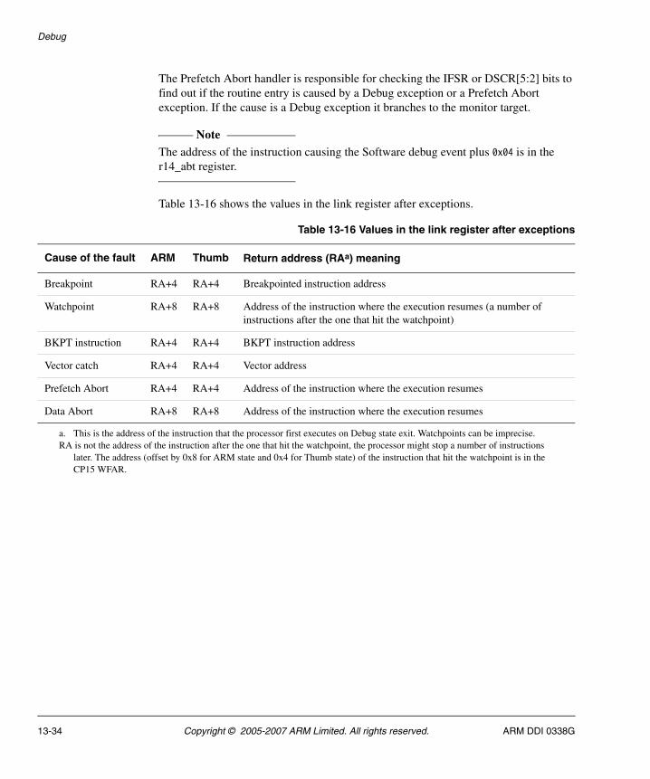
Debug
The Prefetch Abort handler is responsible for checking the IFSR or DSCR[5:2] bits to find out if the routine entry is caused by a Debug exception or a Prefetch Abort exception. If the cause is a Debug exception it branches to the monitor target.
Note The address of the instruction causing the Software debug event plus 0x04 is in the r14_abt register.
Table 13-16 shows the values in the link register after exceptions.
Table 13-16 Values in the link register after exceptions
Cause of the fault ARM Thumb Return address (RAa) meaning
Breakpoint RA+4 RA+4 Breakpointed instruction address
Watchpoint RA+8 RA+8 Address of the instruction where the execution resumes (a number of instructions after the one that hit the watchpoint)
BKPT instruction RA+4 RA+4 BKPT instruction address
Vector catch RA+4 RA+4 Vector address
Prefetch Abort RA+4 RA+4 Address of the instruction where the execution resumes
Data Abort RA+8 RA+8 Address of the instruction where the execution resumes
a. This is the address of the instruction that the processor first executes on Debug state exit. Watchpoints can be imprecise. RA is not the address of the instruction after the one that hit the watchpoint, the processor might stop a number of instructions
later. The address (offset by 0x8 for ARM state and 0x4 for Thumb state) of the instruction that hit the watchpoint is in the CP15 WFAR.
13-34 Copyright © 2005-2007 ARM Limited. All rights reserved. ARM DDI 0338G
Debug
13.8 Debug state
When the conditions in Behavior of the processor on debug events on page 13-29 are met then the processor switches to Debug state. While in Debug state, the processor behaves as follows:
• The DSCR[0] core halted bit is set.
• The DBGACK signal is asserted, see External signals on page 13-49.
• The DSCR[5:2] method of entry bits are set appropriately.
• The CP15 IFSR, DFSR, and FAR registers are set as described in Effect of a debug event on CP15 registers on page 13-31. The WFAR is set to an Unpredictable value.
• The processor is halted. The pipeline is flushed and no instructions are fetched.
• The processor does not change the execution mode. The CPSR is not altered.
• Interrupts and exceptions are treated as described in Interrupts on page 13-37 and Exceptions on page 13-37.
• Software debug events are ignored.
• The external debug request signal is ignored.
• Debug state entry request commands are ignored.
• There is a mechanism, using the Debug Test Access Port, where the core is forced to execute an ARM state instruction. This mechanism is enabled using DSCR[13] execute ARM instruction enable bit.
• The core executes the instruction as if it is in ARM state, regardless of the actual value of the T bit of the CPSR. If you do set both the J and T bits the behavior is Unpredictable.
• In this state the core can execute any ARM state instruction, as if in a privileged mode. For example, if the processor is in User mode then the MSR instruction updates the PSRs and all the CP14 debug instructions can be executed. However, the processor still accesses the register bank and memory as indicated by the CPSR mode bits. For example, if the processor is in User mode then it sees the User mode register bank, and accesses the memory without any privilege.
• In Debug state, the CP15 System Performance Monitor Registers do not count events. Therefore the debugger does not write events to the ETM. The Cycle Count Register, CCNT, stops counting in Debug state.
ARM DDI 0338G Copyright © 2005-2007 ARM Limited. All rights reserved. 13-35
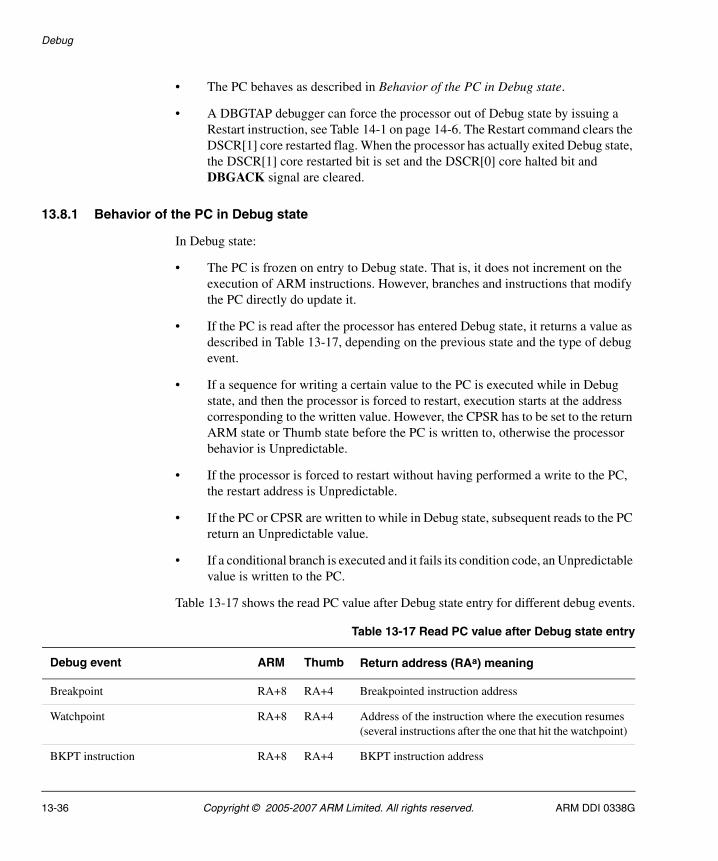
Debug
• The PC behaves as described in Behavior of the PC in Debug state.
• A DBGTAP debugger can force the processor out of Debug state by issuing a Restart instruction, see Table 14-1 on page 14-6. The Restart command clears the DSCR[1] core restarted flag. When the processor has actually exited Debug state, the DSCR[1] core restarted bit is set and the DSCR[0] core halted bit and DBGACK signal are cleared.
13.8.1 Behavior of the PC in Debug state
In Debug state:
• The PC is frozen on entry to Debug state. That is, it does not increment on the execution of ARM instructions. However, branches and instructions that modify the PC directly do update it.
• If the PC is read after the processor has entered Debug state, it returns a value as described in Table 13-17, depending on the previous state and the type of debug event.
• If a sequence for writing a certain value to the PC is executed while in Debug state, and then the processor is forced to restart, execution starts at the address corresponding to the written value. However, the CPSR has to be set to the return ARM state or Thumb state before the PC is written to, otherwise the processor behavior is Unpredictable.
• If the processor is forced to restart without having performed a write to the PC, the restart address is Unpredictable.
• If the PC or CPSR are written to while in Debug state, subsequent reads to the PC return an Unpredictable value.
• If a conditional branch is executed and it fails its condition code, an Unpredictable value is written to the PC.
Table 13-17 shows the read PC value after Debug state entry for different debug events.
Table 13-17 Read PC value after Debug state entry
Debug event ARM Thumb Return address (RAa) meaning
Breakpoint RA+8 RA+4 Breakpointed instruction address
Watchpoint RA+8 RA+4 Address of the instruction where the execution resumes (several instructions after the one that hit the watchpoint)
BKPT instruction RA+8 RA+4 BKPT instruction address
13-36 Copyright © 2005-2007 ARM Limited. All rights reserved. ARM DDI 0338G
Debug
13.8.2 Interrupts
Interrupts are ignored regardless of the value of the I and F bits of the CPSR, although these bits are not changed because of the Debug state entry.
13.8.3 Exceptions
Exceptions are handled as follows while in Debug state:
Reset This exception is taken as in a normal processor state, ARM or Thumb. This means the processor leaves Debug state as a result of the system reset.
Prefetch Abort
This exception cannot occur because no instructions are prefetched while in Debug state.
Debug This exception cannot occur because software debug events are ignored while in Debug state.
SVC and Undefined exceptions
If one of these exception occurs while in Debug state the behavior of the ARM1156T2-S processor is Unpredictable.
Data abort
When a Data Abort occurs in Debug state, the behavior of the core is as follows:
• The PC, CPSR, and SPSR_abt are set as for a normal processor state exception entry.
Vector catch RA+8 RA+4 Vector address
External debug request signal activation RA+8 RA+4 Address of the instruction where the execution resumes
Debug state entry request command RA+8 RA+4 Address of the instruction where the execution resumes
a. This is the address of the instruction that the processor first executes on Debug state exit. Watchpoints can be imprecise. RA is not the address of the instruction after the one that hit the watchpoint, the processor might stop a number of instructions later. The address (offset by 0x8 for ARM state and 0x4 for Thumb state) of the instruction that hit the watchpoint is in the CP15 WFAR.
Table 13-17 Read PC value after Debug state entry (continued)
Debug event ARM Thumb Return address (RAa) meaning
ARM DDI 0338G Copyright © 2005-2007 ARM Limited. All rights reserved. 13-37
Debug
• If the debugger has not written to the PC or the CPSR while in Debug state, R14_abt is set as described in the ARM Architecture Reference Manual.
• If the debugger has written to the PC or the CPSR while in Debug state, R14_abt is set to an Unpredictable value.
• The processor remains in Debug state and does not fetch the exception vector.
• The DFSR, and FAR are set as for a normal processor state exception entry.
• The DSCR[6] sticky precise Data Abort bit, or the DSCR[7] sticky imprecise Data Aborts bit are set.
• The DSCR[5:2] method of entry bits are set to b0110.
If it is an imprecise Data Abort and the debugger has not written to the PC or CPSR, R14_abt is set as described in the Architecture Reference Manual. Therefore the processor is in the same state as if the exception was taken on the instruction that was cancelled by the Debug state entry sequence. This is necessary because it is not possible to guarantee that the debugger reads the PC before an imprecise Data Abort exception is taken.
13.8.4 Behavior on the execution state bits in Debug state
In Debug state the execution state bits:
• are not advanced, and have no effect on executed instruction.
• are reset to 0 on branches
• are not altered on any data-processing instructions that write to the PC except when the S bit of the instruction is set
• are updated from SPSR on exception return instructions.
For more information see the ARM Architecture Reference Manual.
13-38 Copyright © 2005-2007 ARM Limited. All rights reserved. ARM DDI 0338G
Debug
13.9 Debug communications channel
There are two ways that a DBGTAP debugger can send data to or receive data from the core:
• The debug communications channel, when the core is not in Debug state. It is defined as the set of resources used for communicating between the DBGTAP debugger and a piece of software running on the core.
• The mechanism for forcing the core to execute ARM instructions, when the core is in Debug state. For details see Executing instructions in Debug state on page 14-24.
At the core side, the debug communications channel resources are:
• CP14 Debug Register c5 (DTR). Data coming from a DBGTAP debugger can be read by an MRC or STC instruction addressed to this register. The core can write to this register any data intended for the DBGTAP debugger, using an MCR or LDC instruction. Because the DTR comprises both a read (rDTR) and a write portion (wDTR), a data item written by the core can be held in this register at the same time as one written by the DBGTAP debugger.
• Some flags and control bits of CP14 Debug Register c1 (DSCR):
— User mode access to communications channel disable, DSCR[12]. If this bit is set, only privileged software is able to access the debug communications channel. That is, access the DSCR and the DTR.
— wDTRfull flag, DSCR bit 29. When clear, this flag indicates to the core that the wDTR is ready to receive data. It is automatically cleared on reads of the wDTR by the DBGTAP debugger, and is set on writes by the core to the same register. If this bit is set and the core attempts to write to the wDTR, the register contents are overwritten and the wDTRfull flag remains set.
— rDTRfull flag, DSCR bit 30. When set, this flag indicates to the core that there is data available to read at the rDTR. It is automatically set on writes to the rDTR by the DBGTAP debugger, and is cleared on reads by the core of the same register.
The DBGTAP debugger side of the debug communications channel is described in Monitor debug-mode debugging on page 14-50.
ARM DDI 0338G Copyright © 2005-2007 ARM Limited. All rights reserved. 13-39
Debug
13.10 Debugging in a cached system
Debugging must be non-intrusive in a cached system. In ARM1156T2-S systems, you can preserve the contents of the cache so the state of the target application is not altered, and to maintain memory coherency during debugging.
To preserve the contents of the level one cache, you can disable the instruction cache and data cache line fills so read misses from main memory do not update the caches. You can put the caches in this mode by programming the operation of the caches during debug using CP15 c15. See c15, Cache Debug Control Register on page 3-109. This facility is accessible from both the core and DBGTAP debugger sides.
In Debug state, the caches behave as follows, for memory coherency purposes:
• Cache reads behave as for normal operation.
• Writes are covered in Data cache writes.
• ARMv6 includes CP15 instructions for cleaning and invalidating the cache content, See c7, Cache Operations Register on page 3-71. These instructions enable you to reset the processor memory system to a known safe state, and are accessible from both the core and the DBGTAP debugger side.
13.10.1 Data cache writes
The problem with data cache writes is that, while debugging, you might want to write some instructions to memory, either some code to be debugged or a BKPT instruction. This poses coherency issues on the instruction cache.
In ARM1156T2-S systems, CP15 c15, the Cache Debug Control Register, enables you to use the following features:
• You can put the processor in a state where data writes work as if the cache is enabled and every region of memory is write-through. This facility is accessible from both the core and the DBGTAP debugger side. See c15, Data Cache Debug Register on page 3-93.
• ARMv6 architecture provides CP15 instructions for invalidating the instruction cache, described in c7, Cache Operations Register on page 3-71 to ensure that, after a write, there are no out-of-date words in the instruction cache.
13-40 Copyright © 2005-2007 ARM Limited. All rights reserved. ARM DDI 0338G
Debug
13.11 Monitor debug-mode debugging
Monitor debug-mode debugging is essential in real-time systems when the integer unit cannot be halted to collect information. Engine controllers and servo mechanisms in hard drive controllers are examples of systems that might not be able to stop the code without physically damaging components. These are typical systems that can be debugged using Monitor debug-mode.
For situations that can only tolerate a small intrusion into the instruction stream, Monitor debug-mode is ideal. Using this technique, code can be suspended with an exception long enough to save off state information and important variables. The code continues when the exception handler is finished. The Method Of Entry (MOE) bits in the DSCR can be read to determine what caused the exception.
When in Monitor debug-mode, all breakpoint and watchpoint registers can be read and written with MRC and MCR instructions from a privileged processing mode.
13.11.1 Entering the monitor target
No debug-mode is the selected default by on power-on reset. Monitor debug-mode must be selected after reset by setting DSCR[15}. When a software debug event occurs (as described in Software debug event on page 13-28) and Monitor debug-mode is selected and enabled, then a Debug exception is taken, although Prefetch Abort and Data Abort vector catch debug events are ignored. Debug exception entry is described in Debug exception on page 13-33. The Prefetch Abort handler can check the IFSR or the DSCR[5:2] bits, and the Data Abort handler can check the DFSR or the DSCR[5:2] bits, to find out the caused of the exception. If the cause was a Debug exception, the handler branches to the monitor target.
When the monitor target is running, it can determine and modify the processor state and new software debug events can be programmed.
13.11.2 Setting breakpoints, watchpoints, and vector catch debug events
When the monitor target is running, breakpoints, watchpoints, and vector catch debug events can be set. This can be done by executing MCR instructions to program the appropriate CP14 debug registers. The monitor target can only program these registers if the processor is in a privileged mode and Monitor debug-mode is selected and enabled, see Debug Status And Control Register bitfield definitions on page 13-10.
You can program a vector catch debug event using CP14 Debug Vector Catch Register.
ARM DDI 0338G Copyright © 2005-2007 ARM Limited. All rights reserved. 13-41
Debug
You can program a breakpoint debug event using CP14 debug breakpoint value registers and CP14 Debug Breakpoint Control Registers, see CP14 c64-c69, Breakpoint Value Registers (BVR) on page 13-16 and CP14 c80-c85, Breakpoint Control Registers (BCR) on page 13-18.
You can program a watchpoint debug event using CP14 Debug Watchpoint Value Registers and CP14 Debug Watchpoint Control Registers, see CP14 c96-c97, Watchpoint Value Registers (WVR) on page 13-21, and CP14 c112-c113, Watchpoint Control Registers (WCR) on page 13-21.
Setting a simple breakpoint on an instruction address
You can set a simple breakpoint on an instruction address as follows:
1. Read the BCR.
2. Clear the BCR[0] enable breakpoint bit in the read word and write it back to the BCR. Now the breakpoint is disabled.
3. Write the instruction address to the BVR register.
4. Write to the BCR with its fields set as follows:
• BCR[22:21] is set to b00 to indicate that the value loaded into BVR is for comparison against the instruction address bus.
• BCR[20] enable linking bit cleared, to indicate that this breakpoint is not to be linked.
• BCR[8:5] byte address select BCR field as required.
• BCR[2:1] privilege mode control BCR field as required.
• BCR[0] enable breakpoint bit set.
Note Any BVR can be compared against the instruction address bus.
Setting a simple breakpoint on a Context ID value
A simple breakpoint on a Context ID value can be set, using one of the Context ID capable BRPs, as follows:
1. Read the BCR.
2. Clear the BCR[0] enable breakpoint bit in the read word and write it back to the BCR. Now the breakpoint is disabled.
13-42 Copyright © 2005-2007 ARM Limited. All rights reserved. ARM DDI 0338G
Debug
3. Write the Context ID value to the BVR register.
4. Write to the BCR with its fields set as follows:
• BCR[22:21] set to b01 to indicate that the value loaded into BVR is for comparison against the CP15 Context ID Register c13.
• BCR[20] enable linking bit cleared, to indicate that this breakpoint is not to be linked.
• BCR[8:5] byte address select BCR field set to b1111.
• BCR[2:1] privilege mode control BCR field as required.
• BCR[0] enable breakpoint bit set.
Note Any BVR can be compared against the instruction address bus.
Setting a linked breakpoint
In the following sequence b is any of the breakpoint registers pairs with Context ID comparison capability, and a is any of the implemented breakpoints different from b. You can link instruction address holding and Context ID-holding breakpoints register pairs as follows:
1. Read the BCRa and BCRb.
2. Clear the BCRa[0] and BCRb[0] enable breakpoint bits in the read words and write them back to the BCRs. Now the breakpoints are disabled.
3. Write the instruction address to the BVRa register.
4. Write the Context ID to the BVRb register.
5. Write to the BCRb with its fields set as follows:
• BCRb[22:21] is set to b01 to indicate that the value loaded into BVRb is for comparison against the CP15 Context ID Register 13
• BCRb[20] enable linking bit, set
• BCRb[8:5] byte address select set to b1111
• BCRb[2:1] privilege mode control set to b11
• BCRb[0] enable breakpoint bit set.
6. Write to the BCRa with its fields set as follows:
• BCRa[22:21] is set to b00 to indicate that the value loaded into BVRa is for comparison against the instruction address bus
ARM DDI 0338G Copyright © 2005-2007 ARM Limited. All rights reserved. 13-43
Debug
• BCRa[20] enable linking bit set, to link this BRP with the one indicated by BCRa[19:16] (BRPb in this example)
• binary representation of b into BCR[19:6] linked BRP field
• BCRa[8:5] byte address select field as required
• BCRa[2:1] privilege mode control field as required
• BCRa[0] enable breakpoint set.
Setting a simple watchpoint
You can set a simple watchpoint as follows:
1. Read the WCR.
2. Clear the WCR[0] enable watchpoint bit in the read word and write it back to the WCR. Now the watchpoint is disabled.
3. Write the data address to the WVR register.
4. Write to the WCR with its fields set as follows:
• WCR[20] enable linking bit cleared, to indicate that this watchpoint is not to be linked
• WCR byte address select, load/store access, and privilege mode control fields as required
• WCR[0] enable watchpoint bit set.
Note Any WVR can be compared against the data address bus.
Setting a linked watchpoint
In the following sequence b is any of the BRPs with Context ID comparison capability. You can use any of the WRPs. You can link WRPs and Context ID-holding BRPs as follows:
1. Read the WCR and BCRb.
2. Clear the WCR[0] Enable Watchpoint and the BCRb[0] Enable breakpoint bits in the read words and write them back to the WCR and BCRb. Now the watchpoint and the breakpoint are disabled.
3. Write the data address to the WVR register.
4. Write the Context ID to the BVRb register.
13-44 Copyright © 2005-2007 ARM Limited. All rights reserved. ARM DDI 0338G
Debug
5. Write to the WCR with its fields set as follows:
• WCR[20] enable linking bit set, to link this WRP with the BRP indicated by WCR[19:16] (BRPb in this example)
• Binary representation of b into WCR[19:6] linked BRP field
• WCR byte address select, load/store access, and privilege mode control fields as required
• WCR[0] enable watchpoint bit set.
6. Write to the BCRb with its fields set as follows:
• BCRb[21] meaning of BVR bit set, to indicate that the value loaded into BVRb is to be compared against the CP15 Context ID Register.
• BCRb[20] enable linking bit, set
• BCRb[8:5] byte address select set to b1111
• BCRb[2:1] privilege mode control set to b11
• BCRb[0] enable breakpoint bit set.
13.11.3 Setting software breakpoint debug events (BKPT)
To set a software breakpoint on a particular physical address, the monitor target must perform the following steps:
1. Read memory location and save actual instruction.
2. Write BKPT instruction to the memory location.
3. Read memory location again to check that the BKPT instruction has been written.
4. If it has not been written, determine the reason.
Note Cache coherency issues might arise when writing a BKPT instruction. See Debugging in a cached system on page 13-40.
13.11.4 Using the debug communications channel
To read a word sent by a DBGTAP debugger:
1. Read the DSCR register.
2. If DSCR[30] rDTRfull flag is clear, then go to 1.
3. Read the word from the rDTR, CP14 Debug Register c5.
To write a word for a DBGTAP debugger:
1. Read the DSCR register.
ARM DDI 0338G Copyright © 2005-2007 ARM Limited. All rights reserved. 13-45
Debug
2. If DSCR[29] wDTRfull flag is set, then go to 1.
3. Write the word to the wDTR, CP14 Debug Register c5.
13-46 Copyright © 2005-2007 ARM Limited. All rights reserved. ARM DDI 0338G
Debug
13.12 Halting debug-mode debugging
Halting debug-mode is used to debug the processor using external hardware connected to the DBGTAP. The external hardware provides an interface to a DBGTAP debugger application. You can only select Halting debug-mode by setting the halt bit (bit 14) of the DSCR, which is only writable through the Debug Test Access Port. See Chapter 14 Debug Test Access Port.
In Halting debug-mode the processor stops executing instructions if one of the following events occurs:
• a breakpoint hits
• a watchpoint hits
• a BKPT instruction is executed
• the EDBGRQ signal is asserted
• a Halt instruction has been scanned into the DBGTAP instruction register
• an vector catch occurs.
When the processor is halted, it is controlled by sending instructions to the integer unit through the DBGTAP. Any valid instruction can be scanned into the processor, and the effect of the instruction upon the integer unit is as if it was executed under normal operation. Also accessible through the DBGTAP is a register to transfer data between CP14 and the DBGTAP debugger.
The integer unit is restarted by executing a DBGTAP Restart instruction.
13.12.1 Entering Debug state
When a debug event occurs and Halting debug-mode is selected and enabled then the processor enters Debug state as defined in Debug state on page 13-35.
When the core is in Debug state, the DBGTAP debugger can determine and modify the processor state and new debug events can be programmed.
13.12.2 Exiting Debug state
You can force the processor out of Debug state using the DBGTAP Restart instruction. See Exiting Debug state on page 14-5. The DSCR[1] core restarted bit indicates if the core has already returned to normal operation.
13.12.3 Programming debug events
In Halting debug-mode debugging you can program the following debug events:
• Setting breakpoints, watchpoints, and vector catch debug events on page 13-48
ARM DDI 0338G Copyright © 2005-2007 ARM Limited. All rights reserved. 13-47
Debug
• Setting software breakpoints (BKPT)
• Reading and writing to memory.
Setting breakpoints, watchpoints, and vector catch debug events
For setting breakpoints, watchpoints, and vector catch debug events when in Halting debug-mode, the debug host has to use the same CP14 debug registers and the same sequence of operations as in Monitor debug-mode debugging (see Setting breakpoints, watchpoints, and vector catch debug events on page 13-41). The only difference is that the CP14 debug registers are accessed using the DBGTAP scan chains, see The DBGTAP port and debug registers on page 14-6.
Note A DBGTAP debugger can access the CP14 debug registers whether the processor is in Debug state or not, so these debug events can be programmed when the processor is in ARM state or, Thumb state.
Setting software breakpoints (BKPT)
To set a software breakpoint, the DBGTAP debugger must perform the same steps as the monitor target (described in Setting breakpoints, watchpoints, and vector catch debug events on page 13-41). The difference is that CP14 debug registers are accessed using the DBGTAP scan chains, see Chapter 14 Debug Test Access Port.
Reading and writing to memory
See Debug sequences on page 14-34 for memory access sequences using the ARM1156T2-S Debug Test Access Port.
13-48 Copyright © 2005-2007 ARM Limited. All rights reserved. ARM DDI 0338G
Debug
13.13 External signals
The following external signals are used by debug:
DBGACK Debug acknowledge signal. The processor asserts this output signal to indicate the system has entered Debug state. See Debug state on page 13-35 for a definition of the Debug state.
DBGEN Debug enable signal. When this signal is LOW, DSCR[15:14] is read as 0 and the processor behaves as if in debug disabled mode.
EDBGRQ External debug request signal. As described in External debug request signal on page 13-29, this input signal forces the core into Debug state.
DBGNOPWRDWN
Powerdown disable signal generated from DSCR[9]. When this signal is HIGH, the system power controller is forced into Emulate mode. This is to avoid losing CP14 Debug state that can only be written through the DBGTAP. Therefore, DSCR[9] must only be set if Halting debug-mode debugging is necessary.
ARM DDI 0338G Copyright © 2005-2007 ARM Limited. All rights reserved. 13-49

Debug
13-50 Copyright © 2005-2007 ARM Limited. All rights reserved. ARM DDI 0338G
Chapter 14 Debug Test Access Port
This chapter introduces the Debug Test Access Port built into ARM1156T2-S processor. It contains the following sections:
• Debug Test Access Port and Halting debug-mode on page 14-2
• Synchronizing RealView™ ICE on page 14-3
• Entering Debug state on page 14-4
• Exiting Debug state on page 14-5
• The DBGTAP port and debug registers on page 14-6
• Debug registers on page 14-8
• Using the Debug Test Access Port on page 14-24
• Debug sequences on page 14-34
• Programming debug events on page 14-48
• Monitor debug-mode debugging on page 14-50.
ARM DDI 0338G Copyright © 2005-2007 ARM Limited. All rights reserved. 14-1
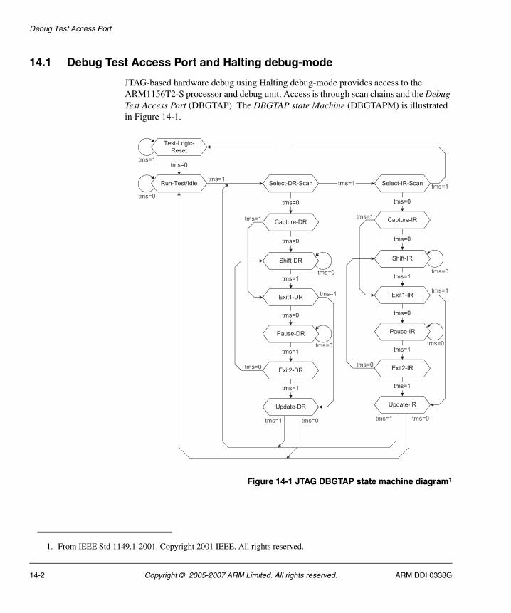
Debug Test Access Port
14.1 Debug Test Access Port and Halting debug-mode
JTAG-based hardware debug using Halting debug-mode provides access to the ARM1156T2-S processor and debug unit. Access is through scan chains and the Debug Test Access Port (DBGTAP). The DBGTAP state Machine (DBGTAPM) is illustrated in Figure 14-1.
Figure 14-1 JTAG DBGTAP state machine diagram1
1. From IEEE Std 1149.1-2001. Copyright 2001 IEEE. All rights reserved.
tms=1
tms=0
tms=1tms=1
tms=1 tms=0 tms=1 tms=0
tms=1
tms=1
tms=0
Run-Test/Idle
Test-Logic-
Reset
Select-DR-Scan Select-IR-Scantms=1
Capture-DR
tms=0
tms=0
tms=0
Capture-IR
tms=0
Shift-IR
Exit1-IR
tms=1
Pause-IR
tms=0
Exit2-IR
tms=1
Update-IR
tms=1
tms=0
Shift-DR
Exit1-DR
tms=1
Pause-DR
tms=0
Exit2-DR
tms=1
Update-DR
tms=1
tms=0tms=0
tms=1
tms=0 tms=0
tms=1
tms=0
14-2 Copyright © 2005-2007 ARM Limited. All rights reserved. ARM DDI 0338G
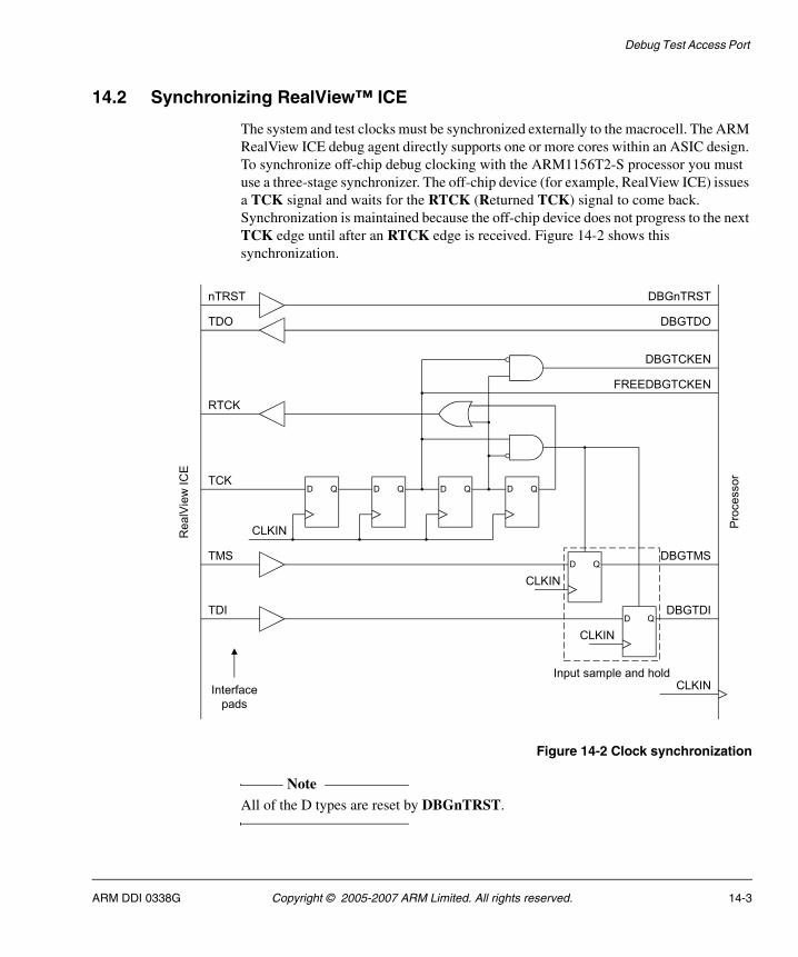
Debug Test Access Port
14.2 Synchronizing RealView™ ICE
The system and test clocks must be synchronized externally to the macrocell. The ARM RealView ICE debug agent directly supports one or more cores within an ASIC design. To synchronize off-chip debug clocking with the ARM1156T2-S processor you must use a three-stage synchronizer. The off-chip device (for example, RealView ICE) issues a TCK signal and waits for the RTCK (Returned TCK) signal to come back. Synchronization is maintained because the off-chip device does not progress to the next TCK edge until after an RTCK edge is received. Figure 14-2 shows this synchronization.
Figure 14-2 Clock synchronization
Note All of the D types are reset by DBGnTRST.
D Q D Q D Q D Q
D Q
D Q
CLKIN
CLKIN
Input sample and hold
Pro
cessor
RealV
iew
ICE
CLKIN
DBGTDI
DBGTMS
DBGTCKEN
DBGTDO
DBGnTRSTnTRST
TDO
RTCK
TCK
TMS
CLKIN
TDI
Interface
pads
FREEDBGTCKEN
ARM DDI 0338G Copyright © 2005-2007 ARM Limited. All rights reserved. 14-3
Debug Test Access Port
14.3 Entering Debug state
Halting debug-mode is enabled by writing a 1 to bit 14 of the DSCR, see CP14 c1, Debug Status and Control Register (DSCR) on page 13-9. This can only be done by a DBGTAP debugger hardware such as RealView ICE. When this mode is enabled the processor halts, instead of taking an exception in software, if one of the following events occurs:
• A vector catch occurs.
• A breakpoint hits.
• A watchpoint hits.
• A BKPT instruction is executed.
The processor halts regardless of the state of bit 14 of the DSCR when:
• A Halt instruction has been scanned in through the DBGTAP. The DBGTAP controller must pass through Run-Test/Idle to issue the Halt command to the ARM.
• EDBGRQ is asserted.
The core halted bit in the DSCR is set when Debug state is entered. At this point, the debugger determines why the integer unit was halted and preserves the processor state. The MSR instruction can be used to change modes and gain access to all banked registers in the machine. While in Debug state:
• the PC is not incremented
• interrupts are ignored
• all instructions are read from the Instruction Transfer Register (scan chain 4).
Debug state is described in Debug state on page 13-35.
14-4 Copyright © 2005-2007 ARM Limited. All rights reserved. ARM DDI 0338G
Debug Test Access Port
14.4 Exiting Debug state
To exit from Debug state, scan in the Restart instruction through the ARM1156T2-S DBGTAP. You might want to adjust the PC before restarting, depending on the way the integer unit entered Debug state. When the state machine enters the Run-Test/Idle state, normal operations resume. The delay, waiting until the state machine is in Run-Test/Idle, enables conditions to be set up in other devices in a multiprocessor system without taking immediate effect. When Run-Test/Idle state is entered, all the processors resume operation simultaneously. The core restarted bit is set when the Restart sequence is complete.
ARM DDI 0338G Copyright © 2005-2007 ARM Limited. All rights reserved. 14-5
Debug Test Access Port
14.5 The DBGTAP port and debug registers
The ARM1156T2-S DBGTAP controller is the part of the debug unit that enables access through the DBGTAP to the on-chip debug resources, such as breakpoint and watchpoint registers. The DBGTAP controller is based on the IEEE 1149.1 standard and supports:
• a Device ID Register
• a Bypass Register
• a five-bit Instruction Register
• a five-bit Scan Chain Select Register.
In addition, the public instructions listed in Table 14-1 are supported.
Table 14-1 Supported public instructions
Binary code Instruction Description
b00000 EXTEST This instruction connects the selected scan chain between DBGTDI and DBGTDO. When the instruction register is loaded with the EXTEST instruction, the debug scan chains can be written. See Scan chains on page 14-11.
b00001 - Reserved.
b00010 Scan_N Selects the Scan Chain Select Register (SCREG). This instruction connects SCREG between DBGTDI and DBGTDO. See Scan Chain Select Register (SCREG) on page 14-10.
b00011 - Reserved.
b00100 Restart Forces the processor to leave Debug state. This instruction is used to exit from Debug state. The processor restarts when the Run-Test/Idle state is entered.
b00101 - Reserved.
b00110 - Reserved.
b00111 - Reserved.
b01000 Halt Forces the processor to enter Debug state. This instruction is used to stop the integer unit and put it into Debug state.
b01001 - Reserved.
b01010-b01011 - Reserved.
b01100 INTEST This instruction connects the selected scan chain between DBGTDI and DBGTDO. When the instruction register is loaded with the INTEST instruction, the debug scan chains can be read. See Scan chains on page 14-11.
14-6 Copyright © 2005-2007 ARM Limited. All rights reserved. ARM DDI 0338G
Debug Test Access Port
Note Sample/Preload, Clamp, HighZ, and ClampZ instructions are not implemented because the ARM1156T2-S DBGTAP controller does not support the attachment of external boundary scan chains.
All unused DBGTAP controller instructions default to the Bypass instruction.
b01101-b11100 - Reserved.
b11101 ITRsel When this instruction is loaded into the IR (Update-DR state), the DBGTAP controller behaves as if IR=EXTEST and SCREG=4. The ITRsel instruction makes the DBGTAP controller behave as if EXTEST and scan chain 4 are selected. It can be used to speed up certain debug sequences. See Using the ITRsel IR instruction on page 14-25 for the effects of using this instruction.
b11110 IDcode See IEEE 1149.1. Selects the DBGTAP controller device ID code register.
The IDcode instruction connects the device identification register (or ID register) between DBGTDI and DBGTDO. The ID register is a 32-bit register that enables you to determine the manufacturer, part number, and version of a component using the DBGTAP.
See Device ID Code Register on page 14-9 for details of selecting and interpreting the ID register value.
b11111 Bypass See IEEE 1149.1. Selects the DBGTAP controller bypass register. The Bypass instruction connects a 1-bit shift register (the bypass register) between DBGTDI and DBGTDO. The first bit shifted out is a 0. All unused DBGTAP controller instruction codes default to the Bypass instruction. See Bypass Register on page 14-8.
Table 14-1 Supported public instructions (continued)
Binary code Instruction Description
ARM DDI 0338G Copyright © 2005-2007 ARM Limited. All rights reserved. 14-7
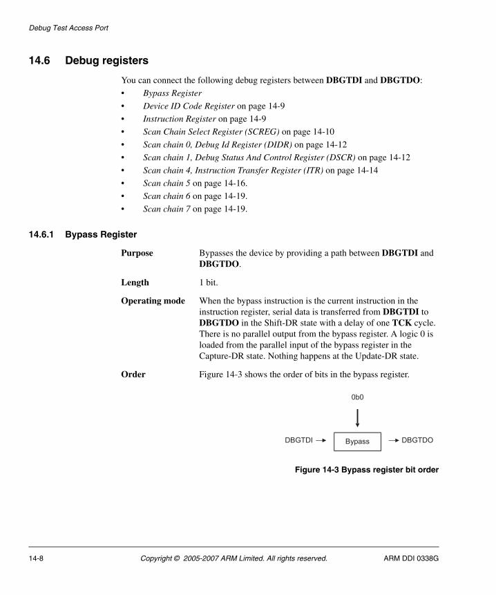
Debug Test Access Port
14.6 Debug registers
You can connect the following debug registers between DBGTDI and DBGTDO:
• Bypass Register
• Device ID Code Register on page 14-9
• Instruction Register on page 14-9
• Scan Chain Select Register (SCREG) on page 14-10
• Scan chain 0, Debug Id Register (DIDR) on page 14-12
• Scan chain 1, Debug Status And Control Register (DSCR) on page 14-12
• Scan chain 4, Instruction Transfer Register (ITR) on page 14-14
• Scan chain 5 on page 14-16.
• Scan chain 6 on page 14-19.
• Scan chain 7 on page 14-19.
14.6.1 Bypass Register
Purpose Bypasses the device by providing a path between DBGTDI and DBGTDO.
Length 1 bit.
Operating mode When the bypass instruction is the current instruction in the instruction register, serial data is transferred from DBGTDI to DBGTDO in the Shift-DR state with a delay of one TCK cycle. There is no parallel output from the bypass register. A logic 0 is loaded from the parallel input of the bypass register in the Capture-DR state. Nothing happens at the Update-DR state.
Order Figure 14-3 shows the order of bits in the bypass register.
Figure 14-3 Bypass register bit order
0b0
DBGTDI DBGTDOBypass
14-8 Copyright © 2005-2007 ARM Limited. All rights reserved. ARM DDI 0338G
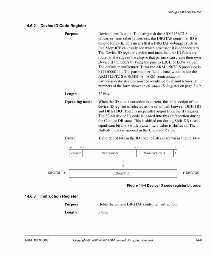
Debug Test Access Port
14.6.2 Device ID Code Register
Purpose Device identification. To distinguish the ARM1156T2-S processor from other processors, the DBGTAP controller ID is unique for each. This means that a DBGTAP debugger such as RealView ICE can easily see which processor it is connected to. The Device ID register version and manufacturer ID fields are routed to the edge of the chip so that partners can create their own Device ID numbers by tying the pins to HIGH or LOW values. The default manufacturer ID for the ARM1156T2-S processor is b11110000111. The part number field is hard-wired inside the ARM1156T2-S to 0x7B56. All ARM semiconductor partner-specific devices must be identified by manufacturer ID numbers of the form shown in c0, Main ID Register on page 3-19.
Length 32 bits.
Operating mode When the ID code instruction is current, the shift section of the device ID register is selected as the serial path between DBGTDI and DBGTDO. There is no parallel output from the ID register. The 32-bit device ID code is loaded into this shift section during the Capture-DR state. This is shifted out during Shift-DR (least significant bit first) while a don’t care value is shifted in. The shifted-in data is ignored in the Update-DR state.
Order The order of bits in the ID code register is shown in Figure 14-4.
Figure 14-4 Device ID code register bit order
14.6.3 Instruction Register
Purpose Holds the current DBGTAP controller instruction.
Length 5 bits.
DBGTDI DBGTDOData[31:0]
1Version
31 28 27 12 11 1 0
Part number Manufacturer ID
ARM DDI 0338G Copyright © 2005-2007 ARM Limited. All rights reserved. 14-9
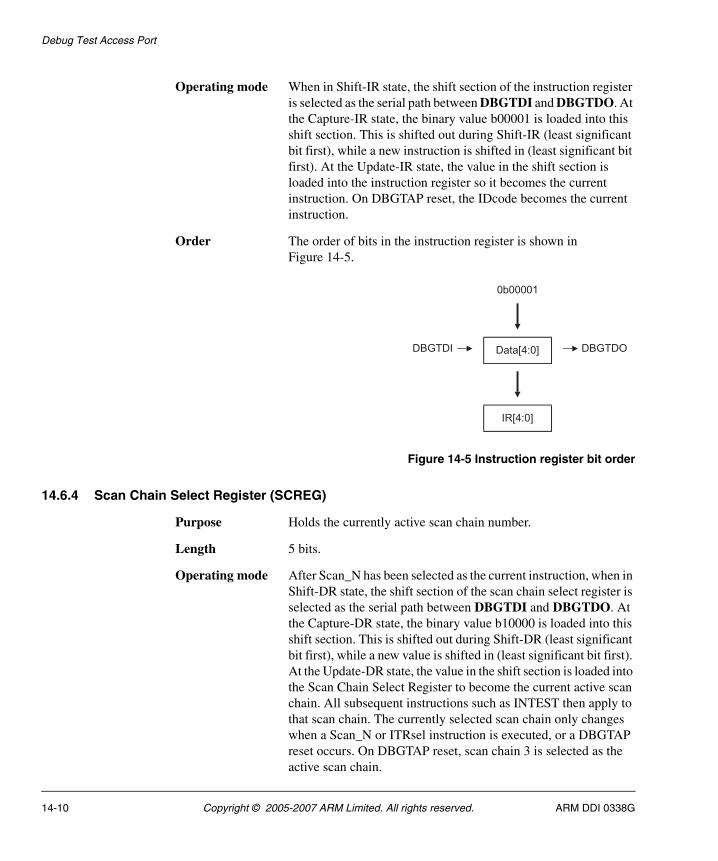
Debug Test Access Port
Operating mode When in Shift-IR state, the shift section of the instruction register is selected as the serial path between DBGTDI and DBGTDO. At the Capture-IR state, the binary value b00001 is loaded into this shift section. This is shifted out during Shift-IR (least significant bit first), while a new instruction is shifted in (least significant bit first). At the Update-IR state, the value in the shift section is loaded into the instruction register so it becomes the current instruction. On DBGTAP reset, the IDcode becomes the current instruction.
Order The order of bits in the instruction register is shown in Figure 14-5.
Figure 14-5 Instruction register bit order
14.6.4 Scan Chain Select Register (SCREG)
Purpose Holds the currently active scan chain number.
Length 5 bits.
Operating mode After Scan_N has been selected as the current instruction, when in Shift-DR state, the shift section of the scan chain select register is selected as the serial path between DBGTDI and DBGTDO. At the Capture-DR state, the binary value b10000 is loaded into this shift section. This is shifted out during Shift-DR (least significant bit first), while a new value is shifted in (least significant bit first). At the Update-DR state, the value in the shift section is loaded into the Scan Chain Select Register to become the current active scan chain. All subsequent instructions such as INTEST then apply to that scan chain. The currently selected scan chain only changes when a Scan_N or ITRsel instruction is executed, or a DBGTAP reset occurs. On DBGTAP reset, scan chain 3 is selected as the active scan chain.
0b00001
DBGTDI DBGTDOData[4:0]
IR[4:0]
14-10 Copyright © 2005-2007 ARM Limited. All rights reserved. ARM DDI 0338G
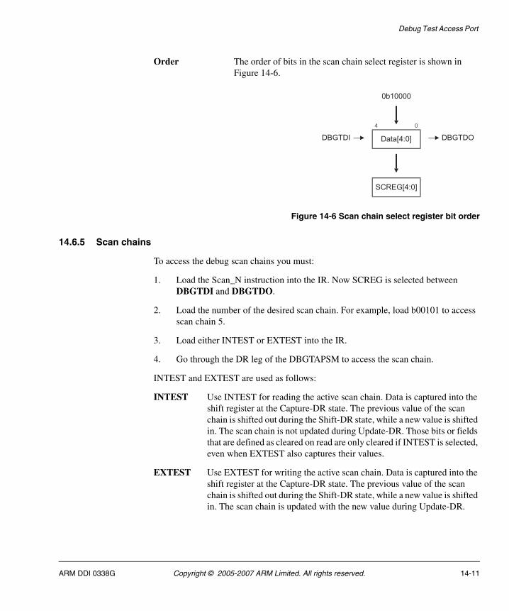
Debug Test Access Port
Order The order of bits in the scan chain select register is shown in Figure 14-6.
Figure 14-6 Scan chain select register bit order
14.6.5 Scan chains
To access the debug scan chains you must:
1. Load the Scan_N instruction into the IR. Now SCREG is selected between DBGTDI and DBGTDO.
2. Load the number of the desired scan chain. For example, load b00101 to access scan chain 5.
3. Load either INTEST or EXTEST into the IR.
4. Go through the DR leg of the DBGTAPSM to access the scan chain.
INTEST and EXTEST are used as follows:
INTEST Use INTEST for reading the active scan chain. Data is captured into the shift register at the Capture-DR state. The previous value of the scan chain is shifted out during the Shift-DR state, while a new value is shifted in. The scan chain is not updated during Update-DR. Those bits or fields that are defined as cleared on read are only cleared if INTEST is selected, even when EXTEST also captures their values.
EXTEST Use EXTEST for writing the active scan chain. Data is captured into the shift register at the Capture-DR state. The previous value of the scan chain is shifted out during the Shift-DR state, while a new value is shifted in. The scan chain is updated with the new value during Update-DR.
0b10000
DBGTDI DBGTDOData[4:0]
SCREG[4:0]
4 0
ARM DDI 0338G Copyright © 2005-2007 ARM Limited. All rights reserved. 14-11
Debug Test Access Port
Note There are some exceptions to this use of INTEST and EXTEST to control reading and writing the scan chain. These are noted in the relevant scan chain descriptions.
Scan chain 0, Debug Id Register (DIDR)
Purpose Debug.
Length 8 + 32 = 40 bits.
Description Debug identification. This scan chain accesses CP14 debug register 0, the debug ID register. Additionally, the eight most significant bits of this scan chain contain an implementer code. This field is hardwired to 0x41, the implementer code for ARM Limited, as specified in the ARM Architecture Reference Manual. This register is read-only. Therefore, EXTEST has the same effect as INTEST.
Order The order of bits in scan chain 0 is shown in Figure 14-7.
Figure 14-7 Scan chain 0 bit order
Scan chain 1, Debug Status And Control Register (DSCR)
Purpose Debug.
Length 32 bits.
Description This scan chain accesses CP14 register 1, the DSCR. This is mostly a read/write register, although certain bits are read-only for the Debug Test Access Port. See CP14 c1, Debug Status and Control Register (DSCR) on page 13-9 for details of DSCR bit definitions, and for read/write attributes for each bit. Those bits defined as cleared on read are only cleared if INTEST is selected.
Order The order of bits in scan chain 1 is shown in Figure 14-8 on page 14-13.
14-12 Copyright © 2005-2007 ARM Limited. All rights reserved. ARM DDI 0338G
Debug Test Access Port
Figure 14-8 Scan chain 1 bit order
The following DSCR bits affect the operation of other scan chains:
DSCR[30:29] rDTRfull and wDTRfull flags. These indicate the status of the rDTR and wDTR registers. They are copies of the rDTRempty (NOT rDTRfull) and wDTRfull bits that the DBGTAP debugger sees in scan chain 5.
DSCR[13] Execute ARM instruction enable bit. This bit enables the mechanism used for executing instructions in Debug state. It changes the behavior of the rDTR and wDTR registers, the sticky precise Data Abort bit, rDTRempty, wDTRfull, and InstCompl flags. See Scan chain 5 on page 14-16.
DSCR[6] Sticky precise Data Abort flag. If the core is in Debug state and the DSCR[13] execute ARM instruction enable bit is HIGH, then this flag is set on precise Data Aborts. See CP14 c1, Debug Status and Control Register (DSCR) on page 13-9.
Note Unlike DSCR[6], DSCR [7] sticky imprecise Data Aborts flag
does not affect the operation of the other scan chains.
DBGTDI DBGTDOData[31:0]
DSCR[31:0]
31 0
DSCR[31:0]
ARM DDI 0338G Copyright © 2005-2007 ARM Limited. All rights reserved. 14-13
Debug Test Access Port
Scan chain 4, Instruction Transfer Register (ITR)
Purpose Debug.
Length 1 + 32 = 33 bits.
Description This scan chain accesses the Instruction Transfer Register (ITR), used to send instructions to the core through the PreFetch Unit (PFU). It consists of 32 bits of information, plus an additional bit to indicate the completion of the instruction sent to the core (InstCompl). The InstCompl bit is read-only.
While in Debug state, an instruction loaded into the ITR can be issued to the core by making the DBGTAPSM go through the Run-Test/Idle state. The InstCompl flag is cleared when the instruction is issued to the core and set when the instruction completes.
For an instruction to be issued when going through Run-Test/Idle state, you must ensure the following conditions are met:
• The processor must be in Debug state.
• The DSCR[13] execute ARM instruction enable bit must be set. For details of the DSCR, see CP14 c1, Debug Status and Control Register (DSCR) on page 13-9.
• Scan chain 4 or 5 must be selected.
• INTEST or EXTEST must be selected.
• Ready flag must be captured set. That is, the last time the DBGTAPSM went through Capture-DR the InstCompl flag must have been set.
• The DSCR[6] sticky precise Data Abort flag must be clear. This flag is set on precise Data Aborts.
For an instruction to be loaded into the ITR when going through Update-DR, you must ensure the following conditions are met:
• The processor can be in any state.
• The value of DSCR[13] execute ARM instruction enable bit does not matter.
• Scan chain 4 must be selected.
• EXTEST must be selected.
• Ready flag must be captured set. That is, the last time the DBGTAPSM went through Capture-DR the InstCompl flag must have been set.
14-14 Copyright © 2005-2007 ARM Limited. All rights reserved. ARM DDI 0338G
Debug Test Access Port
• The value of DSCR[6] sticky precise Data Abort flag does not matter.
Order The order of bits in scan chain 4 is shown in Figure 14-9.
Figure 14-9 Scan chain 4 bit order
It is important to distinguish between the InstCompl flag and the Ready flag:
• The InstCompl flag signals the completion of an instruction.
• The Ready flag is the captured version of the InstCompl flag, captured at the Capture-DR state. The Ready flag conditions the execution of instructions and the update of the ITR.
The following points apply to the use of scan chain 4:
• When an instruction is issued to the core in Debug state, the PC is not incremented. It is only changed if the instruction being executed explicitly writes to the PC. For example, branch instructions and move to PC instructions.
• If CP14 debug register c5 is a source register for the instruction to be executed, the DBGTAP debugger must set up the data in the rDTR before issuing the coprocessor instruction to the core. See Scan chain 5 on page 14-16.
• Setting DSCR[13] the execute ARM instruction enable bit when the core is not in Debug state leads to Unpredictable behavior.
• The ITR is write-only. When going through the Capture-DR state, an Unpredictable value is loaded into the shift register.
DBGTDI DBGTDOData[31:0]
ITR[31:0]
32 31 0
InstCompl
Ready
ARM DDI 0338G Copyright © 2005-2007 ARM Limited. All rights reserved. 14-15
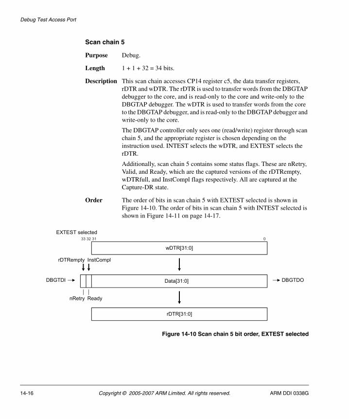
Debug Test Access Port
Scan chain 5
Purpose Debug.
Length 1 + 1 + 32 = 34 bits.
Description This scan chain accesses CP14 register c5, the data transfer registers, rDTR and wDTR. The rDTR is used to transfer words from the DBGTAP debugger to the core, and is read-only to the core and write-only to the DBGTAP debugger. The wDTR is used to transfer words from the core to the DBGTAP debugger, and is read-only to the DBGTAP debugger and write-only to the core.
The DBGTAP controller only sees one (read/write) register through scan chain 5, and the appropriate register is chosen depending on the instruction used. INTEST selects the wDTR, and EXTEST selects the rDTR.
Additionally, scan chain 5 contains some status flags. These are nRetry, Valid, and Ready, which are the captured versions of the rDTRempty, wDTRfull, and InstCompl flags respectively. All are captured at the Capture-DR state.
Order The order of bits in scan chain 5 with EXTEST selected is shown in Figure 14-10. The order of bits in scan chain 5 with INTEST selected is shown in Figure 14-11 on page 14-17.
Figure 14-10 Scan chain 5 bit order, EXTEST selected
DBGTDI DBGTDOData[31:0]
rDTR[31:0]
32 31 0
InstCompl
Ready
wDTR[31:0]
nRetry
33
rDTRempty
EXTEST selected
14-16 Copyright © 2005-2007 ARM Limited. All rights reserved. ARM DDI 0338G
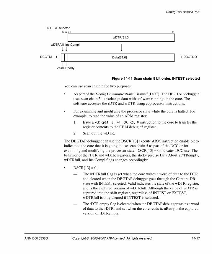
Debug Test Access Port
Figure 14-11 Scan chain 5 bit order, INTEST selected
You can use scan chain 5 for two purposes:
• As part of the Debug Communications Channel (DCC). The DBGTAP debugger uses scan chain 5 to exchange data with software running on the core. The software accesses the rDTR and wDTR using coprocessor instructions.
• For examining and modifying the processor state while the core is halted. For example, to read the value of an ARM register:
1. Issue a MCR cp14, 0, Rd, c0, c5, 0 instruction to the core to transfer the register contents to the CP14 debug c5 register.
2. Scan out the wDTR.
The DBGTAP debugger can use the DSCR[13] execute ARM instruction enable bit to indicate to the core that it is going to use scan chain 5 as part of the DCC or for examining and modifying the processor state. DSCR[13] = 0 indicates DCC use. The behavior of the rDTR and wDTR registers, the sticky precise Data Abort, rDTRempty, wDTRfull, and InstCompl flags changes accordingly:
• DSCR[13] = 0:
— The wDTRfull flag is set when the core writes a word of data to the DTR and cleared when the DBGTAP debugger goes through the Capture-DR state with INTEST selected. Valid indicates the state of the wDTR register, and is the captured version of wDTRfull. Although the value of wDTR is captured into the shift register, regardless of INTEST or EXTEST, wDTRfull is only cleared if INTEST is selected.
— The rDTR empty flag is cleared when the DBGTAP debugger writes a word of data to the rDTR, and set when the core reads it. nRetry is the captured version of rDTRempty.
DBGTDI DBGTDOData[31:0]
32 31 0
InstCompl
Ready
wDTR[31:0]
Valid
33
wDTRfull
INTEST selected
ARM DDI 0338G Copyright © 2005-2007 ARM Limited. All rights reserved. 14-17
Debug Test Access Port
— rDTR overwrite protection is controlled by the nRetry flag. If the nRetry flag is sampled clear, meaning that the rDTR is full, when going through the Capture-DR state, then the rDTR is not updated at the Update-DR state.
— The InstCompl flag is always set.
— The sticky precise Data Abort flag is Unpredictable. See CP14 c1, Debug Status and Control Register (DSCR) on page 13-9.
• DSCR[13] = 1:
— The wDTR Full flag behaves as if DSCR[13] is clear. However, the Ready flag can be used for handshaking in this mode.
— The rDTR Empty flag status behaves as if DSCR[13] is clear. However, the Ready flag can be used for handshaking in this mode.
— rDTR overwrite protection is controlled by the Ready flag. If the InstCompl flag is sampled clear when going through Capture-DR, then the rDTR is not updated at the Update-DR state. This prevents an instruction that uses the rDTR as a source operand from having it modified before it has time to complete.
— The InstCompl flag changes from 1 to 0 when an instruction is issued to the core, and from 0 to 1 when the instruction completes execution.
— The sticky precise Data Abort flag is set on precise Data Aborts.
The behavior of the rDTR and wDTR registers, the sticky precise Data Abort, rDTRempty, wDTRfull, and InstCompl flags when the core changes state is as follows:
• The DSCR[13] execute ARM instruction enable bit must be clear when the core is not in Debug state. Otherwise, the behavior of the rDTR and wDTR registers, and the flags, is Unpredictable.
• When the core enters Debug state, none of the registers and flags are altered.
• When the DSCR[13] execute ARM instruction enable bit is changed from 0 to 1:
1. None of the registers and flags are altered.
2. Ready flag can be used for handshaking.
• The InstCompl flag must be set when the DSCR[13] execute ARM instruction enable bit is changed from 1 to 0. Otherwise, the behavior of the core is Unpredictable. If the DSCR[13] flag is cleared correctly, none of the registers and flags are altered.
• When the core leaves Debug state, none of the registers and flags are altered.
14-18 Copyright © 2005-2007 ARM Limited. All rights reserved. ARM DDI 0338G
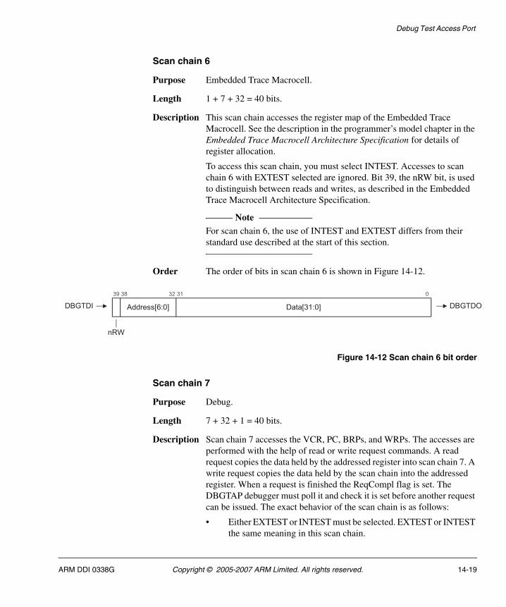
Debug Test Access Port
Scan chain 6
Purpose Embedded Trace Macrocell.
Length 1 + 7 + 32 = 40 bits.
Description This scan chain accesses the register map of the Embedded Trace Macrocell. See the description in the programmer’s model chapter in the Embedded Trace Macrocell Architecture Specification for details of register allocation.
To access this scan chain, you must select INTEST. Accesses to scan chain 6 with EXTEST selected are ignored. Bit 39, the nRW bit, is used to distinguish between reads and writes, as described in the Embedded Trace Macrocell Architecture Specification.
Note For scan chain 6, the use of INTEST and EXTEST differs from their
standard use described at the start of this section.
Order The order of bits in scan chain 6 is shown in Figure 14-12.
Figure 14-12 Scan chain 6 bit order
Scan chain 7
Purpose Debug.
Length 7 + 32 + 1 = 40 bits.
Description Scan chain 7 accesses the VCR, PC, BRPs, and WRPs. The accesses are performed with the help of read or write request commands. A read request copies the data held by the addressed register into scan chain 7. A write request copies the data held by the scan chain into the addressed register. When a request is finished the ReqCompl flag is set. The DBGTAP debugger must poll it and check it is set before another request can be issued. The exact behavior of the scan chain is as follows:
• Either EXTEST or INTEST must be selected. EXTEST or INTEST the same meaning in this scan chain.
DBGTDI DBGTDOAddress[6:0]
39 32 31 0
Data[31:0]
38
nRW
ARM DDI 0338G Copyright © 2005-2007 ARM Limited. All rights reserved. 14-19
Debug Test Access Port
Note For scan chain 7, the use of INTEST and EXTEST differs from the
standard use described at the start of this section.
• If the value captured by the Ready/nRW bit at the Capture-DR state is 1, the data that is being shifted in generates a request at the Update-DR state. The Address field indicates the register being accessed (see Table 14-2 on page 14-22), the Data field contains the data to be written and the Ready/nRW bit holds the read/write information (0=read and 1=write). If the request is a read, the Data field is ignored.
• When a request is placed, the Address and Data sections of the scan chain are frozen. That is, their contents are not shifted until the request is completed. This means that, if the value captured in the Ready/nRW field at the Capture-DR state is 0, the shifted-in data is ignored and the shifted-out value is all 0s.
• After a read request has been placed, if the DBGTAPSM goes through the Capture-DR state and a logic 1 is captured in the Ready/nRW field, this means that the shift register has also captured the requested register contents. Therefore, they are shifted out at the same time as the Ready/nRW bit. The Data field is corrupted as new data is shifted in.
• After a write request has been placed, if the DBGTAPSM goes through the Capture-DR state and a logic 1 is captured in the Ready/nRW field, this means that the requested write has completed successfully.
• If the Address field is all 0s (address of the NULL register) at the Update-DR state, then no request is generated.
• A request to a reserved register generates Unpredictable behavior.
Order The order of bits in scan chain 7 is shown in Figure 14-13 on page 14-21.
14-20 Copyright © 2005-2007 ARM Limited. All rights reserved. ARM DDI 0338G
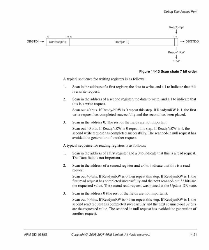
Debug Test Access Port
Figure 14-13 Scan chain 7 bit order
A typical sequence for writing registers is as follows:
1. Scan in the address of a first register, the data to write, and a 1 to indicate that this is a write request.
2. Scan in the address of a second register, the data to write, and a 1 to indicate that this is a write request.
Scan out 40 bits. If Ready/nRW is 0 repeat this step. If Ready/nRW is 1, the first write request has completed successfully and the second has been placed.
3. Scan in the address 0. The rest of the fields are not important.
Scan out 40 bits. If Ready/nRW is 0 repeat this step. If Ready/nRW is 1, the second write request has completed successfully. The scanned-in null request has avoided the generation of another request.
A typical sequence for reading registers is as follows:
1. Scan in the address of a first register and a 0 to indicate that this is a read request. The Data field is not important.
2. Scan in the address of a second register and a 0 to indicate that this is a read request.
Scan out 40 bits. If Ready/nRW is 0 then repeat this step. If Ready/nRW is 1, the first read request has completed successfully and the next scanned-out 32 bits are the requested value. The second read request was placed at the Update-DR state.
3. Scan in the address 0 (the rest of the fields are not important).
Scan out 40 bits. If Ready/nRW is 0 then repeat this step. If Ready/nRW is 1, the second read request has completed successfully and the next scanned-out 32 bits are the requested value. The scanned-in null request has avoided the generation of another request.
DBGTDI DBGTDOAddress[6:0]
39 33 32 1
Data[31:0]
Ready/nRW
0
nRW
ReqCompl
ARM DDI 0338G Copyright © 2005-2007 ARM Limited. All rights reserved. 14-21
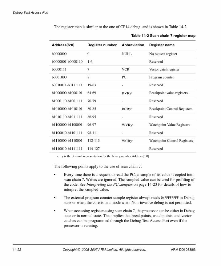
Debug Test Access Port
The register map is similar to the one of CP14 debug, and is shown in Table 14-2.
The following points apply to the use of scan chain 7:
• Every time there is a request to read the PC, a sample of its value is copied into scan chain 7. Writes are ignored. The sampled value can be used for profiling of the code. See Interpreting the PC samples on page 14-23 for details of how to interpret the sampled value.
• The external program counter sample register always reads 0xFFFFFFFF in Debug state or when the core is in a mode when Non-invasive debug is not permitted.
• When accessing registers using scan chain 7, the processor can be either in Debug state or in normal state. This implies that breakpoints, watchpoints, and vector catches can be programmed through the Debug Test Access Port even if the processor is running.
Table 14-2 Scan chain 7 register map
Address[6:0] Register number Abbreviation Register name
b0000000 0 NULL No request register
b0000001-b0000110 1-6 - Reserved
b0000111 7 VCR Vector catch register
b0001000 8 PC Program counter
b0010011-b0111111 19-63 - Reserved
b1000000-b1000101 64-69 BVRya
a. y is the decimal representation for the binary number Address[3:0]
Breakpoint value registers
b1000110-b1001111 70-79 - Reserved
b1010000-b1010101 80-85 BCRya Breakpoint Control Registers
b1010110-b1011111 86-95 - Reserved
b1100000-b1100001 96-97 WVRya Watchpoint Value Registers
b1100010-b1101111 98-111 - Reserved
b1110000-b1110001 112-113 WCRya Watchpoint Control Registers
b1110010-b1111111 114-127 - Reserved
14-22 Copyright © 2005-2007 ARM Limited. All rights reserved. ARM DDI 0338G
Debug Test Access Port
Interpreting the PC samples
The PC values read correspond to instructions committed for execution, including those that failed their condition code. However, these values are offset as described in Table 13-14 on page 13-30. These offsets are different for different processor states, so additional information is required:
• If a read request to the PC completes and Data[1:0] equals b00, the read value corresponds to an ARM state instruction whose 30 most significant bits of the offset address (instruction address + 8) are given in Data[31:2].
• If a read request to the PC completes and Data[0] equals b1, the read value corresponds to a Thumb state instruction whose 31 most significant bits of the offset address (instruction address + 4) are given in Data[31:1].
• If the PC is read while the processor is in Debug state, the result is 0xFFFFFFFF.
Scan chains 8-15
These scan chains are reserved.
Scan chains 16-31
These scan chains are unassigned.
14.6.6 Reset
The DBGTAP is reset either by asserting DBGnTRST, or by clocking it while DBGTAPSM is in the Test-Logic-Reset state. The processor, including CP14 debug logic, is not affected by these events. See Reset modes on page 9-4 and CP14 registers reset on page 13-24 for details.
ARM DDI 0338G Copyright © 2005-2007 ARM Limited. All rights reserved. 14-23
Debug Test Access Port
14.7 Using the Debug Test Access Port
This section contains the following subsections:
• Entering and leaving Debug state
• Executing instructions in Debug state
• Using the ITRsel IR instruction on page 14-25
• Transferring data between the host and the core on page 14-27
• Using the debug communications channel on page 14-27
• Target to host debug communications channel sequence on page 14-28
• Host to target debug communications channel on page 14-29
• Transferring data in Debug state on page 14-29
• Example sequences on page 14-30.
14.7.1 Entering and leaving Debug state
These debug sequences are described in detail in Debug sequences on page 14-34.
14.7.2 Executing instructions in Debug state
When the processor is in Debug state, it can be forced to execute ARM state instructions using the DBGTAP. Two registers are used for this purpose, the Instruction Transfer Register (ITR) and the Data Transfer Register (DTR). The ITR is used to insert an instruction into the processor pipeline. An ARM state instruction can be loaded into this register using scan chain number 4. When the instruction is loaded, and INTEST or EXTEST is selected, and scan chain 4 or 5 is selected, the instruction can be issued to the core by making the DBGTAPSM go through the Run-Test/Idle state, provided certain conditions are met (described in this section). This mechanism enables re-executing the same instruction over and over without having to reload it. The DTR can be used in conjunction with the ITR to transfer data in and out of the core. For example, to read out the value of an ARM register:
1. Issue an MCR p14, 0, Rd, c0, c5, 0 instruction to the core to transfer the <Rd> contents to the c5 register.
2. Scan out the wDTR.
The DSCR[13] execute ARM instruction enable bit controls the activation of the ARM instruction execution mechanism. If this bit is cleared, no instruction is issued to the core when the DBGTAPSM goes through Run-Test/Idle. Setting this bit while the core is not in Debug state leads to Unpredictable behavior. If the core is in Debug state and this bit is set, the Ready and the sticky precise Data Abort flags condition the updates
14-24 Copyright © 2005-2007 ARM Limited. All rights reserved. ARM DDI 0338G
Debug Test Access Port
of the ITR and the instruction issuing as described in Scan chain 4, Instruction Transfer Register (ITR) on page 14-14. As an example, this sequence stores out the contents of the ARM register r0:
1. Scan_N into the IR.
2. 1 into the SCREG.
3. INTEST into the IR.
4. Scan out the contents of the DSCR. This action clears the sticky precise Data Abort and sticky imprecise Data Abort flags.
5. EXTEST into the IR.
6. Scan in the previously read value with the DSCR[13] execute ARM instruction enable bit set.
7. Scan_N into the IR.
8. 4 into the SCREG.
9. EXTEST into the IR.
10. Scan the MCR p14, 0, R0, c0, c5, 0 instruction into the ITR.
11. Go through the Run-Test/Idle state of the DBGTAPSM.
12. Scan_N into the IR.
13. 5 into the SCREG.
14. INTEST into the IR.
15. Scan out 34 bits. The 33rd bit indicates if the instruction has completed. If the bit is clear, repeat this step again.
16. The least significant 32 bits hold the contents of r0.
14.7.3 Using the ITRsel IR instruction
When the ITRsel instruction is loaded into the IR, at the Update-IR state, the DBGTAP controller behaves as if EXTEST and scan chain 4 are selected, but SCREG retains its value. It can be used to speed up certain debug sequences.
Figure 14-14 on page 14-26 shows the effect of the ITRsel IR instruction.
ARM DDI 0338G Copyright © 2005-2007 ARM Limited. All rights reserved. 14-25
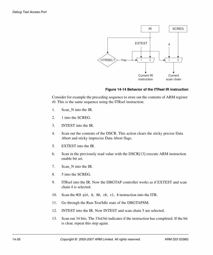
Debug Test Access Port
Figure 14-14 Behavior of the ITRsel IR instruction
Consider for example the preceding sequence to store out the contents of ARM register r0. This is the same sequence using the ITRsel instruction:
1. Scan_N into the IR.
2. 1 into the SCREG.
3. INTEST into the IR.
4. Scan out the contents of the DSCR. This action clears the sticky precise Data Abort and sticky imprecise Data Abort flags.
5. EXTEST into the IR.
6. Scan in the previously read value with the DSCR[13] execute ARM instruction enable bit set.
7. Scan_N into the IR.
8. 5 into the SCREG.
9. ITRsel into the IR. Now the DBGTAP controller works as if EXTEST and scan chain 4 is selected.
10. Scan the MCR p14, 0, R0, c0, c5, 0 instruction into the ITR.
11. Go through the Run-Test/Idle state of the DBGTAPSM.
12. INTEST into the IR. Now INTEST and scan chain 5 are selected.
13. Scan out 34 bits. The 33rd bit indicates if the instruction has completed. If the bit is clear, repeat this step again.
01=ITRSEL?
IR SCREG
EXTEST
01
4
Current IR
instruction
Current
scan chain
Yes
14-26 Copyright © 2005-2007 ARM Limited. All rights reserved. ARM DDI 0338G
Debug Test Access Port
14. The least significant 32 bits hold the contents of r0.
The number of steps has been reduced from 16 to 14. However, the bigger reduction comes when reading additional registers. Using the ITRsel instruction there are 6 extra steps (9 to 14), compared with 10 extra steps (7 to 16) in the first sequence.
14.7.4 Transferring data between the host and the core
There are two ways in which a DBGTAP debugger can send or receive data from the core:
• using the DCC, when the ARM1156T2-S processor is not in Debug state
• using the instruction execution mechanism described in Executing instructions in Debug state on page 14-24, when the core is in Debug state.
This is described in:
• Using the debug communications channel.
• Target to host debug communications channel sequence on page 14-28
• Host to target debug communications channel on page 14-29
• Transferring data in Debug state on page 14-29
• Example sequences on page 14-30.
14.7.5 Using the debug communications channel
The DCC is defined as the set of resources that the external DBGTAP debugger uses to communicate with a piece of software running on the core.
The DCC in the ARM1156T2-S processor is implemented using the two physically separate DTRs and a full/empty bit pair to augment each register, creating a bidirectional data port. One register can be read from the DBGTAP and is written from the processor. The other register is written from the DBGTAP and read by the processor. The full/empty bit pair for each register is automatically updated by the debug unit hardware, and is accessible to both the DBGTAP and to software running on the processor.
At the core side, the DCC resources are the following:
• CP14 debug register c5 (DTR). Data coming from a DBGTAP debugger can be read by an MRC or STC instruction addressed to this register. The core can write to this register any data intended for the DBGTAP debugger, using an MCR or LDC instruction. Because the DTR comprises both a read (rDTR) and a write portion (wDTR), a piece of data written by the core and another coming from the DBGTAP debugger can be held in this register at the same time.
ARM DDI 0338G Copyright © 2005-2007 ARM Limited. All rights reserved. 14-27
Debug Test Access Port
• Some flags and control bits at CP14 debug register c1 (DSCR):
DSCR[12] User mode access to DCC disable bit. If this bit is set, only privileged software can access the DCC. That is, access the DSCR and the DTR.
DSCR[29] The wDTRfull flag. When clear, this flag indicates to the core that the wDTR is ready to receive data from the core.
DSCR[30] The rDTRfull flag. When set, this flag indicates to the core that there is data available to read at the DTR.
At the DBGTAP side, the resources are the following:
• Scan chain 5 (see Scan chain 5 on page 14-16). The only part of this scan chain that it is not used for the DCC is the Ready flag. The rest of the scan chain is to be used in the following way:
rDTR When the DBGTAPSM goes through the Update-DR state with EXTEST and scan chain 5 selected, and the nRetry flag set, the contents of the Data field are loaded into the rDTR. This is how the DBGTAP debugger sends data to the software running on the core.
wDTR When the DBGTAPSM goes through the Capture-DR state with INTEST and scan chain 5 selected, the contents of the wDTR are loaded into the Data field of the scan chain. This is how the DBGTAP debugger reads the data sent by the software running on the core.
Valid flag When set, this flag indicates to the DBGTAP debugger that the contents of the wDTR that it has captured are valid.
nRetry flag When set, this flag indicates to the DBGTAP debugger that the scanned-in Data field has been successfully written into the rDTR at the Update-DR state.
14.7.6 Target to host debug communications channel sequence
The DBGTAP debugger can use the following sequence for receiving data from the core:
1. Scan_N into the IR.
2. 5 into the SCREG.
3. INTEST into the IR.
4. Scan out 34 bits of data. If the Valid flag is clear repeat this step again.
14-28 Copyright © 2005-2007 ARM Limited. All rights reserved. ARM DDI 0338G
Debug Test Access Port
5. The least significant 32 bits hold valid data.
6. Go to step 4 again for reading out more data.
14.7.7 Host to target debug communications channel
The DBGTAP debugger can use the following sequence for sending data to the core:
1. Scan_N into the IR.
2. 5 into the SCREG.
3. EXTEST into the IR.
4. Scan in 34 bits, the least significant 32 holding the word to be sent. At the same time, 34 bits were scanned out. If the nRetry flag is clear repeat this step again.
5. Now the data has been written into the rDTR. Go to step 4 again for sending in more data.
14.7.8 Transferring data in Debug state
When the core is in Debug state, the DBGTAP debugger can transfer data in and out of the core using the instruction execution facilities described in Executing instructions in Debug state on page 14-24 in addition to scan chain 5. You must ensure that the DSCR[13] execute ARM instruction enable bit is set for the instruction execution mechanism to work. When it is set, the interface for the DBGTAP debugger consists of the following:
• Scan chain 4 (see Scan chain 4, Instruction Transfer Register (ITR) on page 14-14). It is used for loading an instruction and for monitoring the status of the execution:
ITR When the DBGTAPSM goes through the Update-DR state with EXTEST and scan chain 4 selected, and the Ready flag set, the ITR is loaded with the least significant 32 bits of the scan chain.
InstCompl flag When clear, this flag indicates to the DBGTAP debugger that the last issued instruction has not yet completed execution. While Ready (captured version of InstCompl) is clear, no updates of the ITR and the rDTR occur and the instruction execution mechanism is disabled. No instruction is issued when going through Run-Test/Idle.
ARM DDI 0338G Copyright © 2005-2007 ARM Limited. All rights reserved. 14-29
Debug Test Access Port
• Scan chain 5 (see Scan chain 5 on page 14-16). It is used for writing in or reading out the data and for monitoring the state of the execution:
rDTR When the DBGTAPSM goes through the Update-DR state with EXTEST and scan chain 5 selected, and the Ready flag set, the contents of the Data field are loaded into the rDTR.
wDTR When the DBGTAPSM goes through the Capture-DR state with INTEST or EXTEST selected, the contents of the wDTR are loaded into the Data field of the scan chain.
InstCompl flag When clear, this flag indicates to the DBGTAP debugger that the last issued instruction has not yet completed execution. While Ready (captured version of InstCompl) is clear, no updates of the ITR and the rDTR occur and the instruction execution mechanism is disabled. No instruction is issued when going through Run-Test/Idle.
• Some flags and control bits at CP14 debug register c1 (DSCR):
DSCR[13] Execute ARM instruction enable bit. This bit must be set for the instruction execution mechanism to work.
Sticky precise Data Abort flag DSCR[6]. When set, this flag indicates to the DBGTAP debugger that a precise Data Abort occurred while executing an instruction in Debug state. While this bit is set, the instruction execution mechanism is disabled. When this flag is set InstCompl stays HIGH, and additional attempts to execute an instruction appear to succeed but do not execute.
Sticky imprecise Data Abort flag DSCR[7]. When set, this flag indicates to the DBGTAP debugger that an imprecise Data Abort occurred while executing an instruction in Debug state. This flag does not disable the Debug state instruction execution.
14.7.9 Example sequences
This section includes some example sequences to illustrate how to transfer data between the DBGTAP debugger and the core when it is in Debug state. The examples are related to accessing the processor memory.
14-30 Copyright © 2005-2007 ARM Limited. All rights reserved. ARM DDI 0338G
Debug Test Access Port
Target to host transfer
The DBGTAP debugger can use the following sequence for reading data from the processor memory system. The sequence assumes that the ARM register r0 contains a pointer to the address of memory at which the read has to start:
1. Scan_N into the IR.
2. 1 into the SCREG.
3. INTEST into the IR.
4. Scan out the contents of the DSCR. This clears the sticky precise Data Abort and sticky imprecise Data Abort flags.
5. Scan_N into the IR.
6. 4 into the SCREG.
7. EXTEST into the IR.
8. Scan in the LDC p14, c5, [R0], #4 instruction into the ITR.
9. Scan_N into the IR.
10. 5 into the SCREG.
11. INTEST into the IR.
12. Go through Run-Test/Idle state. The instruction loaded into the ITR is issued to the processor pipeline.
13. Scan out 34 bits of data. If the Ready flag is clear repeat this step again.
14. The instruction has completed execution. Store the least significant 32 bits.
15. Go to step 12 again for reading out more data.
16. Scan_N into the IR.
17. 1 into the SCREG.
18. INTEST into the IR.
19. Scan out the contents of the DSCR. This clears the sticky precise Data Abort and sticky imprecise Data Abort flags. If the sticky precise Data Abort is set, this means that during the sequence one of the instructions caused a precise Data Abort. All the instructions that follow are not executed. Register r0 points to the next word to be read, and after the cause for the abort has been fixed the sequence resumes at step 5.
ARM DDI 0338G Copyright © 2005-2007 ARM Limited. All rights reserved. 14-31
Debug Test Access Port
Note If the sticky imprecise Data Aborts flag is set, an imprecise Data Abort has
occurred and the sequence restarts at step 1 after the cause of the abort is fixed and r0 is reloaded.
Host to target transfer
The DBGTAP debugger can use the following sequence for writing data to the processor memory system. The sequence assumes that the ARM register r0 contains a pointer to the address of memory at which the write has to start:
1. Scan_N into the IR.
2. 1 into the SCREG.
3. INTEST into the IR.
4. Scan out the contents of the DSCR. This clears the sticky precise Data Abort and sticky imprecise Data Abort flags.
5. Scan_N into the IR.
6. 4 into the SCREG.
7. EXTEST into the IR.
8. Scan in the STC p14, c5, [R0], #4 instruction into the ITR.
9. Scan_N into the IR.
10. 5 into the SCREG.
11. EXTEST into the IR.
12. Scan in 34 bits, the least significant 32 holding the word to be sent. At the same time, 34 bits are scanned out. If the Ready flag is clear, repeat this step.
13. Go through Run-Test/Idle state.
14. Go to step 12 again for writing in more data.
15. Scan in 34 bits. All the values are don’t care. At the same time, 34 bits are scanned out. If the Ready flag is clear, repeat this step. The don’t care value is written into the rDTR (Update-DR state) after Ready is seen set (Capture-DR state). However, the STC instruction is not re-issued because the DBGTAPSM does not go through Run-Test/Idle.
14-32 Copyright © 2005-2007 ARM Limited. All rights reserved. ARM DDI 0338G
Debug Test Access Port
16. Scan_N into the IR.
17. 1 into the SCREG.
18. INTEST into the IR.
19. Scan out the contents of the DSCR. This clears the sticky precise Data Abort and sticky imprecise Data Abort flags. If the sticky precise Data Abort is set, this means that during the sequence one of the instructions caused a precise Data Abort. All the instructions that follow are not executed. Register r0 points to the next word to be written, and after the cause for the abort has been fixed the sequences resumes at step 5.
Note If the sticky imprecise Data Abort flag is set, an imprecise Data Abort has
occurred and the sequence restarts at step 1 after the cause of the abort is fixed and c0 is reloaded.
ARM DDI 0338G Copyright © 2005-2007 ARM Limited. All rights reserved. 14-33
Debug Test Access Port
14.8 Debug sequences
This section describes how to debug a program running on the ARM1156T2-S processor using a DBGTAP debugger device such as RealView ICE. In Halting debug-mode, the processor stops when a debug event occurs enabling the DBGTAP debugger to do the following:
1. Determine and modify the current state of the processor and memory.
2. Set up breakpoints, watchpoints, and vector catches.
3. Restart the processor.
You enable this mode by setting CP14 debug DSCR[14] bit, which can only be done by the DBGTAP debugger. From here it is assumed that the debug unit is in Halting debug-mode. Monitor debug-mode debugging is described in Monitor debug-mode debugging on page 14-50.
14.8.1 Debug macros
The debug code sequences in this section are written using a fixed set of macros. The mapping of each macro into a debug scan chain sequence is given in this section.
Scan_N <n>
Select scan chain register number <n>:
1. Scan the Scan_N instruction into the IR.
2. Scan the number <n> into the DR.
INTEST
1. Scan the INTEST instruction into the IR.
EXTEST
1. Scan the EXTEST instruction into the IR.
ITRsel
1. Scan the ITRsel instruction into the IR.
Restart
1. Scan the Restart instruction into the IR.
14-34 Copyright © 2005-2007 ARM Limited. All rights reserved. ARM DDI 0338G
Debug Test Access Port
2. Go to the DBGTAP controller Run-Test/Idle state so that the processor exits Debug state.
INST <instr> [stateout]
Go through Capture-DR, go to Shift-DR, scan in an ARM instruction to be read and executed by the core and scan out the Ready flag, go through Update-DR. The ITR (scan chain 4) and EXTEST must be selected when using this macro.
1. Scan in:
• Any value for the InstCompl flag. This bit is read-only.
• 32-bit assembled code of the instruction (instr) to be executed, for ITR[31:0].
2. The following data is scanned out:
• The value of the Ready flag, to be stored in stateout.
• 32 bits to be ignored. The ITR is write-only.
DATA <datain> [<stateout> [dataout]]
Go through Capture-DR, go to Shift-DR. Scan in a data item and scan out another one, go through Update-DR. Either the DTR (scan chain 5) or the DSCR (scan chain 1) must be selected when using this macro.
1. If scan chain 5 is selected, scan in:
• Any value for the nRetry or Valid flag. These bits are read-only.
• Any value for the InstCompl flag. This bit is read-only.
• 32-bit datain value for rDTR[31:0].
2. The following data is scanned out:
• The contents of wDTR[31:0], to be stored in dataout.
• If the DSCR[13] execute ARM instruction enable bit is set, the value of the Ready flag is stored in stateout.
• If the DSCR[13] execute ARM instruction enable bit is clear, the nRetry or Valid flag (depending on whether EXTEST or INTEST is selected) is stored in stateout.
3. If scan chain 1 is selected, scan in:
• 32-bit datain value for DSCR[31:0].
Stateout and dataout fields are not used in this case.
ARM DDI 0338G Copyright © 2005-2007 ARM Limited. All rights reserved. 14-35
Debug Test Access Port
DATAOUT <dataout>
1. Scan out a data value. DSCR (scan chain 1) and INTEST must be selected when using this macro.
2. If scan chain 1 is selected, scan out the contents of the DSCR, to be stored in dataout.
3. The scanned-in value is discarded, because INTEST is selected.
REQ <address> <data> <nR/W> [<stateout> [dataout]]
Go through Capture-DR, go to Shift-DR, scan in a request and scan out the result of the former one, go through Update-DR. Scan chain 7, and either INTEST or EXTEST, must be selected when using this macro.
1. Scan in:
• 7-bit address value for Address[6:0]
• 32-bit data value for Data[31:0]
• 1-bit nR/W value (0 for read and 1 for write) for the Ready/nRW field.
2. Scan out:
• the value of the Ready/nRW bit, to be stored in stateout
• the contents of the Data field, to be stored in dataout.
RTI
1. Go through Run-Test/Idle DBGTAPSM state. This forces the execution of the instruction currently loaded into the ITR, provided the execute ARM instruction enable bit (DSCR[13]) is set, the Ready flag was captured as set, and the sticky precise Data Abort flag is cleared.
14.8.2 General setup
You must setup the following control bits before DBGTAP debugging can take place:
• DSCR[14] Halt/Monitor debug-mode bit must be set to 1. It resets to 0 on power-up.
• DSCR[6] sticky precise Data Abort flag must be cleared down, so that aborts are not detected incorrectly immediately after startup.
14-36 Copyright © 2005-2007 ARM Limited. All rights reserved. ARM DDI 0338G
Debug Test Access Port
The DSCR must be read, the DSCR[14] bit set, and the new value written back. The action of reading the DSCR automatically clears the DSCR[6] sticky precise Data Abort flag. All individual breakpoints, watchpoints, and vector catches reset disabled on power-up.
14.8.3 Forcing the processor to halt
Scan the Halt instruction into the DBGTAP controller IR and go through Run-Test/Idle.
14.8.4 Entering Debug state
To enter Debug state you must:
1. Check whether the core has entered Debug state, as follows:
SCAN_N 1 ; select DSCRINTESTLOOP
DATAOUT readDSCRUNTIL readDSCR[0]==1 ; until Core Halted bit is set
2. Save DSCR, as follows:
DATAOUT readDSCRSave value in readDSCR
3. Save wDTR (in case it contains some data), as follows:
SCAN_N 5 ; select DTRINTESTDATA 0x00000000 Valid wDTRIf Valid==1 then Save value in wDTR
4. Set the DSCR[13] execute ARM instruction enable bit, so instructions can be issued to the core from now:
SCAN_N 1 ; select DSCREXTESTDATA modifiedDSCR ; modifiedDSCR equals readDSCR with bit
; DSCR[13] set
5. Before executing any instruction in Debug state you have to drain the write buffer. This ensures that no imprecise Data Aborts can return at a later point:
SCAN_N 4 ; select DTRINST MRC p14, 0, Rd, c5, c10, 0 ; drain write bufferLOOP
LOOPSCAN_N 4 ; select DTRRTIINST 0x0 Ready
ARM DDI 0338G Copyright © 2005-2007 ARM Limited. All rights reserved. 14-37
Debug Test Access Port
Until Ready == 1SCAN_N 1DATAOUT readDSCR
Until readDSCR[7]==1SCAN_N 4INST NOP ; NOP takes theRTI ; imprecise Data AbortsLOOP
INST 0 ReadyUntil Ready == 1SCAN_N 1DATAOUT readDSCR ; clears DSCR[7]
6. Store out r0. It is going to be used to save the rDTR. Use the standard sequence described in Reading a current mode ARM register in the range r0-r14 on page 14-40. Scan chain 5 and INTEST are now selected.
7. Save the rDTR and the rDTRempty bit in three steps:
a. The rDTRempty bit is the inverted version of DSCR[30] (saved in step 2). If DSCR[30] is clear (register empty) there is no requirement to read the rDTR, go to 7.
b. Transfer the contents of rDTR to r0:ITRSEL ; select the ITR and EXTESTINST MRC p14, 0, R0, c0, c5, 0 ; instruction to copy CP14’s debug
; register c5 into R0RTILOOP
INST 0x00000000 ReadyUNTIL Ready==1 ; wait until the instruction ends
c. Read r0 using the standard sequence described in Reading a current mode ARM register in the range r0-r14 on page 14-40.
8. Store out CPSR using the standard sequence described in Reading the CPSR/SPSR on page 14-41.
9. Store out PC using the standard sequence described Reading the PC on page 14-42.
10. Adjust the PC to enable you to resume execution later:
• subtract 0x8 from the stored value if the processor was in ARM state when entering Debug state
• subtract 0x4 from the stored value if the processor was in Thumb state when entering Debug state.
14-38 Copyright © 2005-2007 ARM Limited. All rights reserved. ARM DDI 0338G
Debug Test Access Port
These values are not dependent on the Debug state entry method, see Behavior of the PC in Debug state on page 13-36. The entry state can be determined by examining the T bit of the CPSR.
11. Cache and MPU preservation measures must also be taken here. This includes saving all the relevant CP15 registers using the standard coprocessor register reading sequence described in Coprocessor register reads and writes on page 14-46.
14.8.5 Leaving Debug state
To leave Debug state:
1. Restore standard ARM registers for all modes, except r0, PC, and CPSR.
2. Cache and MPU restoration must be done here. This includes writing the saved registers back to CP15.
3. Ensure that rDTR and wDTR are empty:
ITRSEL ; select the ITR and EXTESTINST MCR p14, 0, R0, c0, c5, 0 ; instruction to copy R0 into
; CP14 debug register c5RTILOOP
INST 0x00000000 ReadyUNTIL Ready==1 ; wait until the instruction endsSCAN_N 5INTESTDATA 0x0 Valid wDTR
4. If the wDTR did not contain any valid data on Debug state entry go to step 5. Otherwise, restore wDTRfull and wDTR (uses r0 as a temporary register) in two steps.
a. Load the saved wDTR contents into r0 using the standard sequence described in Writing a current mode ARM register in the range r0-r14 on page 14-41. Now scan chain 5 and EXTEST are selected
b. Transfer r0 into wDTR:ITRSEL ; select the ITR and EXTESTINST MCR p14, 0, R0, c0, c5, 0 ; instruction to copy R0 into
; CP14 debug register c5RTILOOP
INST 0x00000000 ReadyUNTIL Ready==1 ; wait until the instruction ends
ARM DDI 0338G Copyright © 2005-2007 ARM Limited. All rights reserved. 14-39
Debug Test Access Port
5. Restore CPSR using the standard CPSR writing sequence described in Writing the CPSR/SPSR on page 14-42.
6. Restore the PC using the standard sequence described in Writing the PC on page 14-42.
7. Restore r0 using the standard sequence described in Writing a current mode ARM register in the range r0-r14 on page 14-41. Now scan chain 5 and EXTEST are selected.
8. Restore the DSCR with the DSCR[13] execute ARM instruction enable bit clear, so no more instructions can be issued to the core:
SCAN_N 1 ; select DSCREXTESTDATA modifiedDSCR ; modifiedDSCR equals the saved contents
; of the DSCR with bit DSCR[13] clear
9. If the rDTR did not contain any valid data on Debug state entry go to step 10. Otherwise, restore the rDTR and rDTRempty flag:
SCAN_N 5 ; select DTREXTESTDATA Saved_rDTR ; rDTRempty bit is automatically cleared
; as a result of this action
10. Restart processor:
RESTART
11. Wait until the core is restarted:
SCAN_N 1 ; select DSCRINTESTLOOP DATAOUT readDSCRUNTIL readDSCR[1]==1 ; until Core Restarted bit is set
14.8.6 Reading a current mode ARM register in the range r0-r14
Use the following sequence to read a current mode ARM register in the range r0-r14:
SCAN_N 5 ; select DTRITRSEL ; select the ITR and EXTESTINST MCR p14, 0, Rd, c0, c5, 0 ; instruction to copy Rd into CP14 debug
; register c5RTIINTEST ; select the DTR and INTESTLOOP
DATA 0x00000000 Ready readDataUNTIL Ready==1 ; wait until the instruction ends
14-40 Copyright © 2005-2007 ARM Limited. All rights reserved. ARM DDI 0338G
Debug Test Access Port
Save value in readData
Note Register r15 cannot be read in this way because the effect of the required MCR is to take an Undefined exception.
14.8.7 Writing a current mode ARM register in the range r0-r14
Use the following sequence to write a current mode ARM register in the range r0-r14:
SCAN_N 5 ; select DTRITRSEL ; select the ITR and EXTESTINST MRC p14, 0, Rd, c0, c5, 0 ; instruction to copy CP14 debug
; register c5 into RdEXTEST; select the DTR and EXTEST
DATA Data2WriteRTILOOP
DATA 0x00000000 ReadyUNTIL Ready==1 ; wait until the instruction ends
Note Register r15 cannot be written in this way because the MRC instruction used would update the CPSR flags rather than the PC.
14.8.8 Reading the CPSR/SPSR
Here r0 is used as a temporary register:
1. Move the contents of CPSR/SPSR to r0.
SCAN_N 5 ; select DTRITRSEL ; select the ITR and EXTESTINST MRS R0,CPSR ; or SPSRRTILOOP
INST 0x00000000 ReadyUNTIL Ready==1 ; wait until the instruction ends
2. Perform the read of r0 using the standard sequence described in Reading a current mode ARM register in the range r0-r14 on page 14-40. Scan chain 5 and ITRsel are already selected.
ARM DDI 0338G Copyright © 2005-2007 ARM Limited. All rights reserved. 14-41
Debug Test Access Port
14.8.9 Writing the CPSR/SPSR
Here r0 is used as a temporary register:
1. Load the desired value into r0 using the standard sequence described in Writing a current mode ARM register in the range r0-r14 on page 14-41. Now scan chain 5 and EXTEST are selected.
2. Move the contents of r0 to CPRS/SPRS:
ITRSEL ; select the ITR and EXTESTINST MSR CPSR,R0 ; or SPSRRTILOOP
INST 0x00000000 ReadyUNTIL Ready==1 ; wait until the instruction ends
It is not a problem to write to the T bit because they have no effect in the execution of instructions while in Debug state.
The CPSR mode and control bits can be written in User mode when the core is in Debug state. This is essential so that the debugger can change mode and then get at the other banked registers.
14.8.10 Reading the PC
Here r0 is used as a temporary register:
1. Move the contents of the PC to r0:
ITRSEL ; select the ITR and EXTESTINST MOV R0,PCRTILOOP
INST 0x00000000 ReadyUNTIL Ready==1 ; wait until the instruction ends
2. Read the contents of r0 using the standard sequence described in Reading a current mode ARM register in the range r0-r14 on page 14-40.
14.8.11 Writing the PC
Here r0 is used as a temporary register:
1. Load r0 with the address to resume using the standard sequence described in Writing a current mode ARM register in the range r0-r14 on page 14-41. Now scan chain 5 and EXTEST are selected.
2. Move the contents of r0 to the PC:
14-42 Copyright © 2005-2007 ARM Limited. All rights reserved. ARM DDI 0338G
Debug Test Access Port
ITRSEL ; select the ITR and EXTESTINST MOV PC,R0RTILOOP
INST 0x00000000 ReadyUNTIL Ready==1 ; wait until the instruction ends
14.8.12 General notes about reading and writing memory
On the ARM1156T2-S processor, an abort occurring in Debug state causes an Abort exception entry sequence to start, and so changes mode to Abort mode, and writes to r14_abt and SPSR_abt. This means that the Abort mode registers must be saved before performing a Debug state memory access. The word-based read and write sequences are substantially more efficient than the halfword and byte sequences. This is because the ARM LDC and STC instructions always perform word accesses, and this can be used for efficient access to word width memory. Halfword and byte accesses must be done with a combination of loads or stores, and coprocessor register transfers, which is much less efficient. When writing data, the instruction cache might become incoherent. In those cases, either a line or the whole instruction cache must be invalidated. In particular, the instruction cache must be invalidated before setting a software breakpoint or downloading code.
14.8.13 Reading memory as words
This sequence is optimized for a long sequential read. This sequence assumes that r0 has been set to the address to load data from prior to running this sequence. r0 is post-incremented so that it can be used by successive reads of memory.
1. Load and issue the LDC instruction:
SCAN_N 5 ; select DTRITRSEL ; select the ITR and EXTESTINST LDC p14, c5, [R0], #4 ; load the content of the position of
; memory pointed by R0 into wDTR and; increment R0 by 4
RTI
2. The DTR is selected to read the data:
INTEST ; select the DTR and INTEST
3. This loop keeps on reading words, but it stops before the latest read. It is skipped if there is only one word to read:
FOR(i=1; i <= (Words2Read-1); i++) DO LOOP
DATA 0x00000000 Ready readData ; gets the result of; the previous read
RTI ; issues the next read
ARM DDI 0338G Copyright © 2005-2007 ARM Limited. All rights reserved. 14-43
Debug Test Access Port
UNTIL Ready==1 ; wait until the instruction ends Save value in readDataENDFOR
4. Wait for the last read to finish:
LOOPDATA 0x00000000 Ready readData
UNTIL Ready==1 ; wait until instruction endsSave value in readData
5. Now check whether an abort occurred:
SCAN_N 1 ; select DSCRINTESTDATAOUT DSCR ; this action clears the DSCR[6] flag
6. Scan out the contents of the DSCR. This clears the sticky precise Data Abort and sticky imprecise Data Abort flags. If the sticky precise Data Abort is set, this means that during the sequence one of the instructions caused a precise Data Abort. All the instructions that follow are not executed. Register r0 points to the next word to be written, and after the cause for the abort has been fixed the sequences resumes at step 1.
Note If the sticky imprecise Data Aborts flag is set, an imprecise Data Abort has
occurred and the sequence restarts at step 1 after the cause of the abort is fixed and r0 is reloaded.
14.8.14 Writing memory as words
This sequence is optimized for a long sequential write. This sequence assumes that r0 has been set to the address to store data to prior to running this sequence. Register r0 is post-incremented so that it can be used by successive writes to memory:
1. The instruction is loaded:
SCAN_N 5 ; select DTRITRSEL ; select the ITR and EXTESTINST STC p14, c5, [R0] ,#4 ; store the contents of rDTR into the
; position of memory pointed by R0 and; increment it by 4
EXTEST ; select the DTR and EXTEST
2. This loop writes all the words:
FOR (i=1; i <= Words2Write; i++) DOLOOP
DATA Data2Write Ready
14-44 Copyright © 2005-2007 ARM Limited. All rights reserved. ARM DDI 0338G
Debug Test Access Port
RTIUNTIL Ready==1 ; wait until instruction ends
ENDFOR
3. Wait for the last write to finish:
LOOPDATA 0x00000000 Ready
UNTIL Ready==1 ; wait until instruction ends
4. Check for aborts, as described in Reading memory as words on page 14-43.
14.8.15 Reading memory as halfwords or bytes
Steps 1. to 4. in Reading memory as words on page 14-43 cannot be used to transfer halfwords or bytes because LDC and STC instructions always transfer whole words. Two operations are required to complete a halfword or byte transfer, from memory to ARM register and from ARM register to CP14 debug register. Therefore, performance is decreased because the load instruction cannot be kept in the ITR. This sequence assumes that r0 has been set to the address to load data from prior to running the sequence. Register r0 is post-incremented so that it can be used by successive reads of memory. Register r1 is used as a temporary register:
1. Load and issue the LDRH or LDRB instruction:
ITRSEL ; select the ITR and EXTESTINST LDRH R1,[R0],#2 ; LDRB R1,[R0],#1 for byte readsRTILOOP
INST 0x00000000 ReadyUNTIL Ready==1 ; wait until instruction ends
2. Use the standard sequence described in Reading a current mode ARM register in the range r0-r14 on page 14-40 on register r1. Now scan chain 5 and INTEST are selected.
3. If there are more halfwords or bytes to be read go to 1.
4. Check for aborts, as described in Reading memory as words on page 14-43.
ARM DDI 0338G Copyright © 2005-2007 ARM Limited. All rights reserved. 14-45
Debug Test Access Port
14.8.16 Writing memory as halfwords/bytes
This sequence assumes that r0 has been set to the address to store data to prior to running this sequence. Register r0 is post-incremented so that it can be used by successive writes to memory. Register r1 is used as a temporary register:
1. Write the halfword/byte onto r1 using the standard sequence described in Writing a current mode ARM register in the range r0-r14 on page 14-41. Scan chain 5 and EXTEST are selected.
2. Write the contents of r1 to memory:
ITRSEL ; select the ITR and EXTESTINST STRH R1,[R0],#2 ; STRB R1,[R0],#1 for byte writesRTILOOP INST 0x00000000 ReadyUNTIL Ready==1 ; wait until instruction ends
3. If there are more halfwords or bytes to be read go to 1.
4. Now check for aborts as described in Reading memory as words on page 14-43.
14.8.17 Coprocessor register reads and writes
The ARM1156T2-S processor can execute coprocessor instructions while in Debug state. Therefore, the straightforward method to transfer data between a coprocessor and the DBGTAP debugger is using an ARM register temporarily. For this method to work, the coprocessor must be able to transfer all its registers to the core using coprocessor transfer instructions.
14.8.18 Reading coprocessor registers
1. Load the value into ARM register r0:
ITRSEL ; select the ITR and EXTESTINST MRC px, y, R0, ca, cb, zRTILOOP
INST 0x00000000 ReadyUNTIL Ready==1 ; wait until instruction ends
2. Use the standard sequence described in Reading a current mode ARM register in the range r0-r14 on page 14-40.
14-46 Copyright © 2005-2007 ARM Limited. All rights reserved. ARM DDI 0338G
Debug Test Access Port
14.8.19 Writing coprocessor registers
1. Write the value onto r0, using the standard sequence. See Writing a current mode ARM register in the range r0-r14 on page 14-41 for more details. Scan chain 5 and EXTEST are selected.
2. Transfer the contents of r0 to a coprocessor register:
ITRSEL ; select the ITR and EXTESTINST MCR px, y, 0, ca, cb, zRTILOOP
INST 0x00000000 ReadyUNTIL Ready==1 ; wait until instruction ends
ARM DDI 0338G Copyright © 2005-2007 ARM Limited. All rights reserved. 14-47
Debug Test Access Port
14.9 Programming debug events
The following operations are described:
• Reading registers using scan chain 7
• Writing registers using scan chain 7
• Setting breakpoints, watchpoints and vector catches on page 14-49
• Setting software breakpoints on page 14-49.
14.9.1 Reading registers using scan chain 7
A typical sequence for reading registers using scan chain 7 is as follows:
SCAN_N 7 ; select ITREXTESTREQ 1stAddr2Rd 0 0 ; read request for register 1stAddr2readFOR(i=2; i <= Words2Read; i++) DO
LOOPREQ itAADDR2Rd 0 0 Ready readData
; read request while waitingUNTIL Ready==1 ; wait until the previous request completesSave value in readData
ENDFORLOOP
REQ 0 0 0 Ready readData ; null request while waitingUNTIL Ready==1 ; wait until last request completesSave value in readData
14.9.2 Writing registers using scan chain 7
A typical sequence for writing to a register using scan chain 7 is as follows:
SCAN_N 7 ; select ITREXTESTREQ 1stAddr2Wr 1stData2Wr 0b1 ; write request for register 1stAddr2writeFOR(i=2; i <= Words2Write; i++) DO
LOOPREQ itAADDR2Wr ithData2Wr 1 Read
; write request while waitingUNTIL Ready==1 ; wait until the previous request completes
ENDFORLOOP
REQ 0 0 0 Ready ; null request while waitingUNTIL Ready==1 ; wait until last request completes
14-48 Copyright © 2005-2007 ARM Limited. All rights reserved. ARM DDI 0338G
Debug Test Access Port
14.9.3 Setting breakpoints, watchpoints and vector catches
You can program a vector catch debug event by writing to CP14 debug vector catch register.
You can program a breakpoint debug event by writing to CP14 debug 64-69 breakpoint value registers and CP14 debug 80-84 Breakpoint Control Registers.
You can program a watchpoint debug event by writing to CP14 debug 96-97 watchpoint value registers and CP14 debug 112-113 Watchpoint Control Registers.
Note An External Debugger can access the CP14 debug registers whether the processor is in Debug state or not, so these debug events can be programmed on-the-fly while the processor is in ARM state or Thumb state.
See Setting breakpoints, watchpoints, and vector catch debug events on page 13-41 for the sequences of register accesses required to program these software debug events. See Writing registers using scan chain 7 on page 14-48 to learn how to access CP14 debug registers using scan chain 7.
14.9.4 Setting software breakpoints
To set a software breakpoint on a certain physical address, a debugger must go through the following steps:
1. Read memory location and save actual instruction.
2. Write the BKPT instruction to the memory location.
3. Read memory location again to check that the BKPT instruction got written.
4. If it is not written, determine the reason.
All of these can be done using the previously described sequences.
Note Cache coherency issues might arise when writing a BKPT instruction. See Debugging in a cached system on page 13-40.
ARM DDI 0338G Copyright © 2005-2007 ARM Limited. All rights reserved. 14-49
Debug Test Access Port
14.10 Monitor debug-mode debugging
If DSCR[14] Halt/Monitor debug-mode bit is clear, then the processor takes an exception (rather than halting) when a software debug event occurs. See Halting debug-mode debugging on page 13-47 for details. When the exception is taken, the handler uses the DCC to transmit status information to, and receive commands from the host using a DBGTAP debugger. Monitor debug-mode is essential in real-time systems when the core cannot be halted to collect information.
14.10.1 Receiving data from the core
SCAN_N 5 ; select DTRINTESTFOREACH Data2Read
LOOPDATA 0x00000000 Valid readData
UNTIL Valid==1 ; wait until instruction endsSave value in readData
END
14.10.2 Sending data to the core
SCAN_N 5 ; select DTREXTESTFOREACH Data2Write
LOOPDATA Data2Write nRetry
UNTIL nRetry==1 ; wait until instruction endsEND
14-50 Copyright © 2005-2007 ARM Limited. All rights reserved. ARM DDI 0338G
Chapter 15 Trace Interface Port
This chapter gives a brief description of the Embedded Trace Macrocell (ETM) support for the ARM1156T2-S processor. It contains the following section:
• About the ETM interface on page 15-2.
ARM DDI 0338G Copyright © 2005-2007 ARM Limited. All rights reserved. 15-1
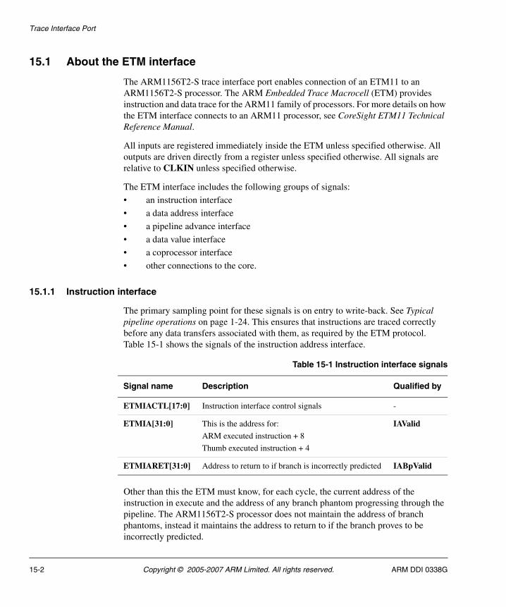
Trace Interface Port
15.1 About the ETM interface
The ARM1156T2-S trace interface port enables connection of an ETM11 to an ARM1156T2-S processor. The ARM Embedded Trace Macrocell (ETM) provides instruction and data trace for the ARM11 family of processors. For more details on how the ETM interface connects to an ARM11 processor, see CoreSight ETM11 Technical Reference Manual.
All inputs are registered immediately inside the ETM unless specified otherwise. All outputs are driven directly from a register unless specified otherwise. All signals are relative to CLKIN unless specified otherwise.
The ETM interface includes the following groups of signals:
• an instruction interface
• a data address interface
• a pipeline advance interface
• a data value interface
• a coprocessor interface
• other connections to the core.
15.1.1 Instruction interface
The primary sampling point for these signals is on entry to write-back. See Typical pipeline operations on page 1-24. This ensures that instructions are traced correctly before any data transfers associated with them, as required by the ETM protocol. Table 15-1 shows the signals of the instruction address interface.
Other than this the ETM must know, for each cycle, the current address of the instruction in execute and the address of any branch phantom progressing through the pipeline. The ARM1156T2-S processor does not maintain the address of branch phantoms, instead it maintains the address to return to if the branch proves to be incorrectly predicted.
Table 15-1 Instruction interface signals
Signal name Description Qualified by
ETMIACTL[17:0] Instruction interface control signals -
ETMIA[31:0] This is the address for:
ARM executed instruction + 8
Thumb executed instruction + 4
IAValid
ETMIARET[31:0] Address to return to if branch is incorrectly predicted IABpValid
15-2 Copyright © 2005-2007 ARM Limited. All rights reserved. ARM DDI 0338G
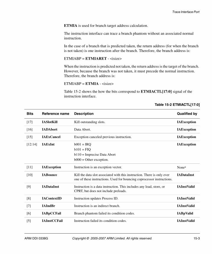
Trace Interface Port
ETMIA is used for branch target address calculation.
The instruction interface can trace a branch phantom without an associated normal instruction.
In the case of a branch that is predicted taken, the return address (for when the branch is not taken) is one instruction after the branch. Therefore, the branch address is:
ETMIABP = ETMIARET - <isize>
When the instruction is predicted not taken, the return address is the target of the branch. However, because the branch was not taken, it must precede the normal instruction. Therefore, the branch address is:
ETMIABP = ETMIA - <isize>
Table 15-2 shows the how the bits correspond to ETMIACTL[17:0] signal of the instruction interface.
Table 15-2 ETMIACTL[17:0]
Bits Reference name Description Qualified by
[17] IASlotKill Kill outstanding slots. IAException
[16] IADAbort Data Abort. IAException
[15] IAExCancel Exception canceled previous instruction. IAException
[12:14] IAExInt b001 = IRQ
b101 = FIQ
b110 = Imprecise Data Abort
b000 = Other exception.
IAException
[11] IAException Instruction is an exception vector. Nonea
[10] IABounce Kill the data slot associated with this instruction. There is only ever one of these instructions. Used for bouncing coprocessor instructions.
IADataInst
[9] IADataInst Instruction is a data instruction. This includes any load, store, or CPRT, but does not include preloads.
IAInstValid
[8] IAContextID Instruction updates Process ID. IAInstValid
[7] IAIndBr Instruction is an indirect branch. IAInstValid
[6] IABpCCFail Branch phantom failed its condition codes. IABpValid
[5] IAInstCCFail Instruction failed its condition codes. IAInstValid
ARM DDI 0338G Copyright © 2005-2007 ARM Limited. All rights reserved. 15-3
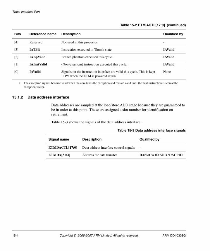
Trace Interface Port
15.1.2 Data address interface
Data addresses are sampled at the load/store ADD stage because they are guaranteed to be in order at this point. These are assigned a slot number for identification on retirement.
Table 15-3 shows the signals of the data address interface.
[4] Reserved Not used in this processor. -
[3] IATBit Instruction executed in Thumb state. IAValid
[2] IABpValid Branch phantom executed this cycle. IAValid
[1] IAInstValid (Non-phantom) instruction executed this cycle. IAValid
[0] IAValid Signals on the instruction interface are valid this cycle. This is kept LOW when the ETM is powered down.
None
a. The exception signals become valid when the core takes the exception and remain valid until the next instruction is seen at the exception vector.
Table 15-2 ETMIACTL[17:0] (continued)
Bits Reference name Description Qualified by
Table 15-3 Data address interface signals
Signal name Description Qualified by
ETMDACTL[17:0] Data address interface control signals -
ETMDA[31:3] Address for data transfer DASlot != 00 AND !DACPRT
15-4 Copyright © 2005-2007 ARM Limited. All rights reserved. ARM DDI 0338G
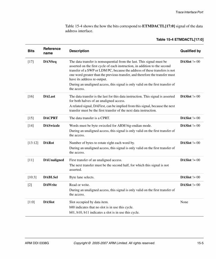
Trace Interface Port
Table 15-4 shows the how the bits correspond to ETMDACTL[17:0] signal of the data address interface.
Table 15-4 ETMDACTL[17:0]
BitsReference name
Description Qualified by
[17] DANSeq The data transfer is nonsequential from the last. This signal must be asserted on the first cycle of each instruction, in addition to the second transfer of a SWP or LDM PC, because the address of these transfers is not one word greater than the previous transfer, and therefore the transfer must have its address re-output.
During an unaligned access, this signal is only valid on the first transfer of the access.
DASlot != 00
[16] DALast The data transfer is the last for this data instruction. This signal is asserted for both halves of an unaligned access.
A related signal, DAFirst, can be implied from this signal, because the next transfer must be the first transfer of the next data instruction.
DASlot != 00
[15] DACPRT The data transfer is a CPRT. DASlot != 00
[14] DASwizzle Words must be byte swizzled for ARM big-endian mode.
During an unaligned access, this signal is only valid on the first transfer of the access.
DASlot != 00
[13:12] DARot Number of bytes to rotate right each word by.
During an unaligned access, this signal is only valid on the first transfer of the access.
DASlot != 00
[11] DAUnaligned First transfer of an unaligned access.
The next transfer must be the second half, for which this signal is not asserted.
DASlot != 00
[10:3] DABLSel Byte lane selects. DASlot != 00
[2] DAWrite Read or write.
During an unaligned access, this signal is only valid on the first transfer of the access.
DASlot != 00
[1:0] DASlot Slot occupied by data item.
b00 indicates that no slot is in use this cycle.
b01, b10, b11 indicates a slot is in use this cycle.
None
ARM DDI 0338G Copyright © 2005-2007 ARM Limited. All rights reserved. 15-5
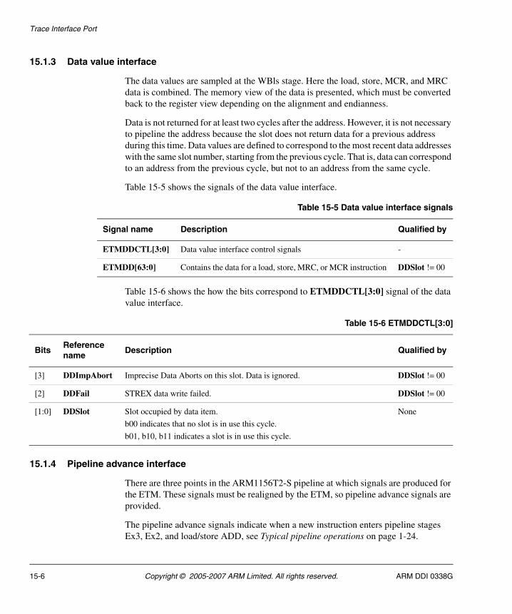
Trace Interface Port
15.1.3 Data value interface
The data values are sampled at the WBls stage. Here the load, store, MCR, and MRC data is combined. The memory view of the data is presented, which must be converted back to the register view depending on the alignment and endianness.
Data is not returned for at least two cycles after the address. However, it is not necessary to pipeline the address because the slot does not return data for a previous address during this time. Data values are defined to correspond to the most recent data addresses with the same slot number, starting from the previous cycle. That is, data can correspond to an address from the previous cycle, but not to an address from the same cycle.
Table 15-5 shows the signals of the data value interface.
Table 15-6 shows the how the bits correspond to ETMDDCTL[3:0] signal of the data value interface.
15.1.4 Pipeline advance interface
There are three points in the ARM1156T2-S pipeline at which signals are produced for the ETM. These signals must be realigned by the ETM, so pipeline advance signals are provided.
The pipeline advance signals indicate when a new instruction enters pipeline stages Ex3, Ex2, and load/store ADD, see Typical pipeline operations on page 1-24.
Table 15-5 Data value interface signals
Signal name Description Qualified by
ETMDDCTL[3:0] Data value interface control signals -
ETMDD[63:0] Contains the data for a load, store, MRC, or MCR instruction DDSlot != 00
Table 15-6 ETMDDCTL[3:0]
BitsReference name
Description Qualified by
[3] DDImpAbort Imprecise Data Aborts on this slot. Data is ignored. DDSlot != 00
[2] DDFail STREX data write failed. DDSlot != 00
[1:0] DDSlot Slot occupied by data item.
b00 indicates that no slot is in use this cycle.
b01, b10, b11 indicates a slot is in use this cycle.
None
15-6 Copyright © 2005-2007 ARM Limited. All rights reserved. ARM DDI 0338G
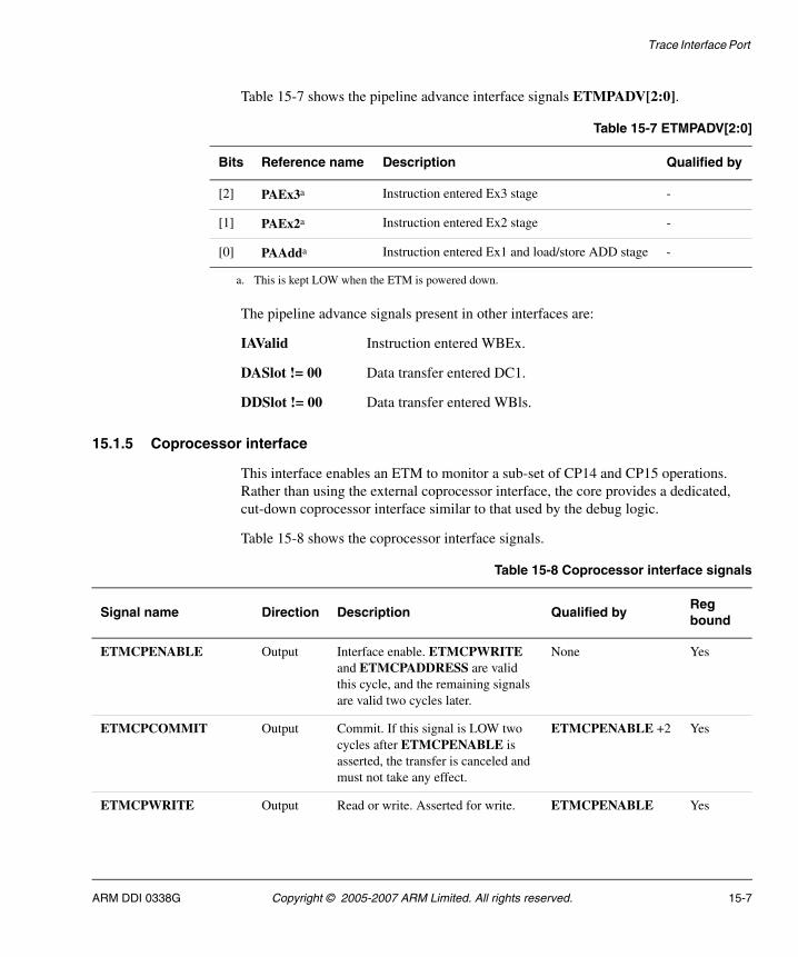
Trace Interface Port
Table 15-7 shows the pipeline advance interface signals ETMPADV[2:0].
The pipeline advance signals present in other interfaces are:
IAValid Instruction entered WBEx.
DASlot != 00 Data transfer entered DC1.
DDSlot != 00 Data transfer entered WBls.
15.1.5 Coprocessor interface
This interface enables an ETM to monitor a sub-set of CP14 and CP15 operations. Rather than using the external coprocessor interface, the core provides a dedicated, cut-down coprocessor interface similar to that used by the debug logic.
Table 15-8 shows the coprocessor interface signals.
Table 15-7 ETMPADV[2:0]
Bits Reference name Description Qualified by
[2] PAEx3a Instruction entered Ex3 stage -
[1] PAEx2a Instruction entered Ex2 stage -
[0] PAAdda Instruction entered Ex1 and load/store ADD stage -
a. This is kept LOW when the ETM is powered down.
Table 15-8 Coprocessor interface signals
Signal name Direction Description Qualified byReg bound
ETMCPENABLE Output Interface enable. ETMCPWRITE and ETMCPADDRESS are valid this cycle, and the remaining signals are valid two cycles later.
None Yes
ETMCPCOMMIT Output Commit. If this signal is LOW two cycles after ETMCPENABLE is asserted, the transfer is canceled and must not take any effect.
ETMCPENABLE +2 Yes
ETMCPWRITE Output Read or write. Asserted for write. ETMCPENABLE Yes
ARM DDI 0338G Copyright © 2005-2007 ARM Limited. All rights reserved. 15-7
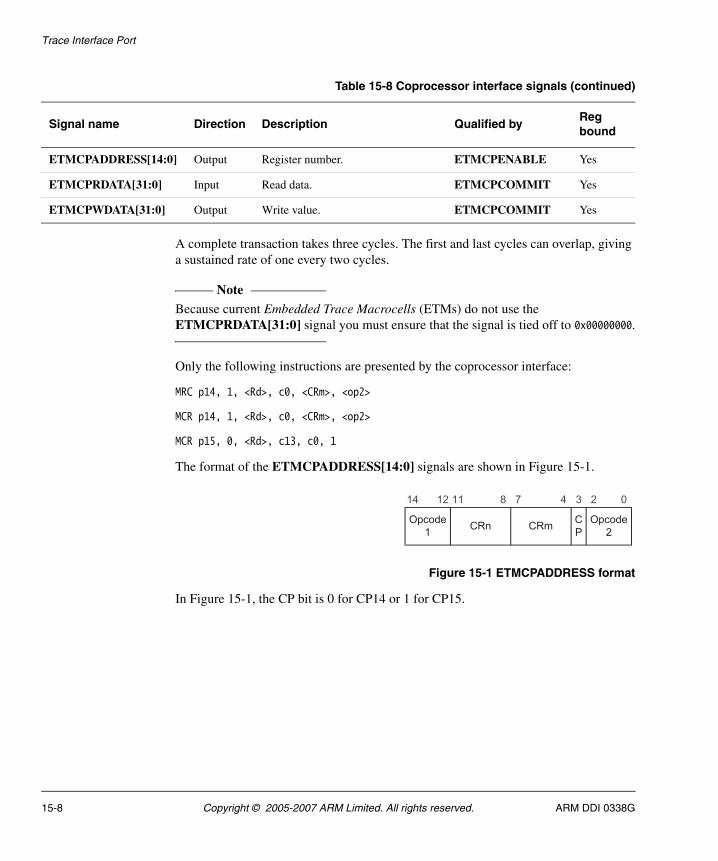
Trace Interface Port
A complete transaction takes three cycles. The first and last cycles can overlap, giving a sustained rate of one every two cycles.
Note Because current Embedded Trace Macrocells (ETMs) do not use the ETMCPRDATA[31:0] signal you must ensure that the signal is tied off to 0x00000000.
Only the following instructions are presented by the coprocessor interface:
MRC p14, 1, <Rd>, c0, <CRm>, <op2>
MCR p14, 1, <Rd>, c0, <CRm>, <op2>
MCR p15, 0, <Rd>, c13, c0, 1
The format of the ETMCPADDRESS[14:0] signals are shown in Figure 15-1.
Figure 15-1 ETMCPADDRESS format
In Figure 15-1, the CP bit is 0 for CP14 or 1 for CP15.
ETMCPADDRESS[14:0] Output Register number. ETMCPENABLE Yes
ETMCPRDATA[31:0] Input Read data. ETMCPCOMMIT Yes
ETMCPWDATA[31:0] Output Write value. ETMCPCOMMIT Yes
Table 15-8 Coprocessor interface signals (continued)
Signal name Direction Description Qualified byReg bound
14 12 11 8 7 4 3 2 0
Opcode
1CRn CRm
C
P
Opcode
2
15-8 Copyright © 2005-2007 ARM Limited. All rights reserved. ARM DDI 0338G
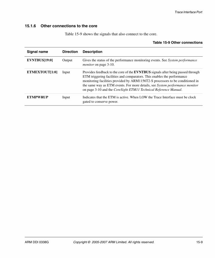
Trace Interface Port
15.1.6 Other connections to the core
Table 15-9 shows the signals that also connect to the core.
Table 15-9 Other connections
Signal name Direction Description
EVNTBUS[19:0] Output Gives the status of the performance monitoring events. See System performance monitor on page 3-10.
ETMEXTOUT[1:0] Input Provides feedback to the core of the EVNTBUS signals after being passed through ETM triggering facilities and comparators. This enables the performance monitoring facilities provided by ARM1156T2-S processors to be conditioned in the same way as ETM events. For more details, see System performance monitor on page 3-10 and the CoreSight ETM11 Technical Reference Manual.
ETMPWRUP Input Indicates that the ETM is active. When LOW the Trace Interface must be clock gated to conserve power.
ARM DDI 0338G Copyright © 2005-2007 ARM Limited. All rights reserved. 15-9
Trace Interface Port
15-10 Copyright © 2005-2007 ARM Limited. All rights reserved. ARM DDI 0338G

Chapter 16 Test Features
This chapter describes the test features of the processor. It contains the following sections:
• About the test features on page 16-2
• Memory BIST on page 16-3
• Power-On Test on page 16-12
• Running System Test on page 16-13.
ARM DDI 0338G Copyright © 2005-2007 ARM Limited. All rights reserved. 16-1
Test Features
16.1 About the test features
The processor test features are:
• memory Built-In Self Test (BIST)
• power-on (or key-on for automotive) test
• running system test.
Power-on test and running system test are of particular importance to applications where safety might be compromised through undetected faults. These faults can be accessed through the cache debug and software test access registers of CP15.
16-2 Copyright © 2005-2007 ARM Limited. All rights reserved. ARM DDI 0338G
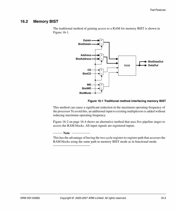
Test Features
16.2 Memory BIST
The traditional method of gaining access to a RAM for memory BIST is shown in Figure 16-1.
Figure 16-1 Traditional method interfacing memory BIST
This method can cause a significant reduction in the maximum operating frequency of the processor To avoid this, an additional input to existing multiplexors is added without reducing maximum operating frequency.
Figure 16-2 on page 16-4 shows an alternative method that uses five pipeline stages to access the RAM blocks. All input signals are registered inputs.
Note This has the advantage of having the two cycle register-to-register path that accesses the RAM blocks using the same path in memory BIST mode as in functional mode.
ARM DDI 0338G Copyright © 2005-2007 ARM Limited. All rights reserved. 16-3
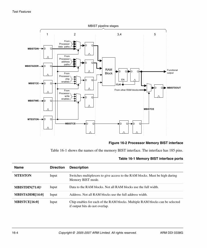
Test Features
Figure 16-2 Processor Memory BIST interface
Table 16-1 shows the names of the memory BIST interface. The interface has 185 pins.
Table 16-1 Memory BIST interface ports
Name Direction Description
MTESTON Input Switches multiplexors to give access to the RAM blocks. Must be high during Memory BIST mode.
MBISTDIN[71:0]a Input Data to the RAM blocks. Not all RAM blocks use the full width.
MBISTADDR[14:0] Input Address. Not all RAM blocks use the full address width.
MBISTCE[16:0] Input Chip enables for each of the RAM blocks. Multiple RAM blocks can be selected if output bits do not overlap.
16-4 Copyright © 2005-2007 ARM Limited. All rights reserved. ARM DDI 0338G
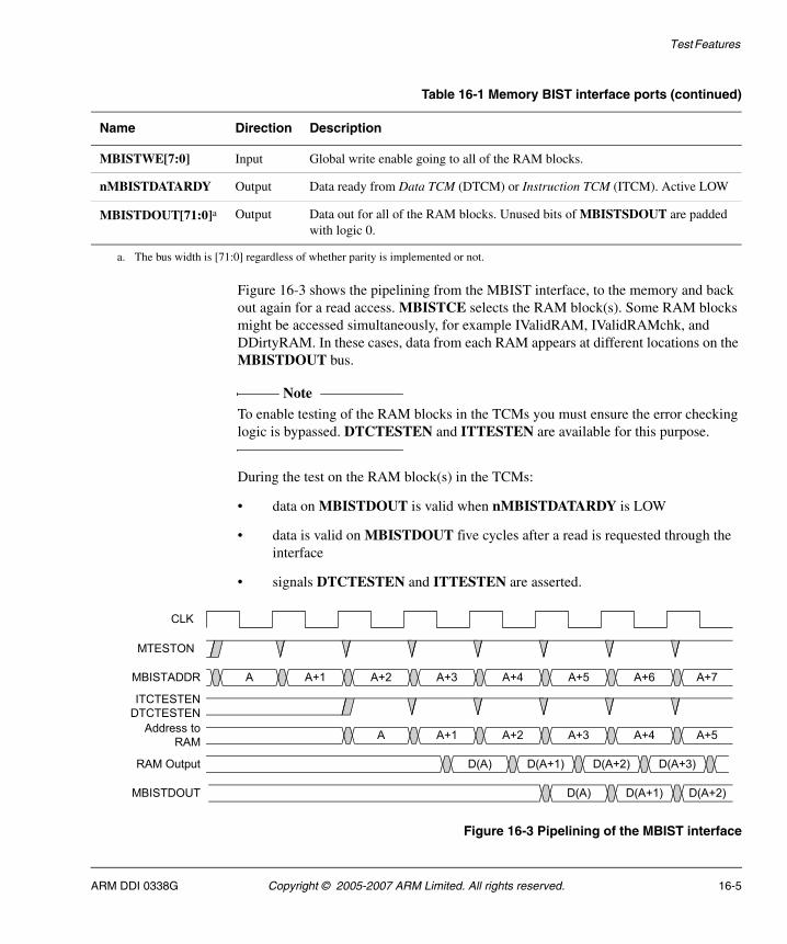
Test Features
Figure 16-3 shows the pipelining from the MBIST interface, to the memory and back out again for a read access. MBISTCE selects the RAM block(s). Some RAM blocks might be accessed simultaneously, for example IValidRAM, IValidRAMchk, and DDirtyRAM. In these cases, data from each RAM appears at different locations on the MBISTDOUT bus.
Note To enable testing of the RAM blocks in the TCMs you must ensure the error checking logic is bypassed. DTCTESTEN and ITTESTEN are available for this purpose.
During the test on the RAM block(s) in the TCMs:
• data on MBISTDOUT is valid when nMBISTDATARDY is LOW
• data is valid on MBISTDOUT five cycles after a read is requested through the interface
• signals DTCTESTEN and ITTESTEN are asserted.
Figure 16-3 Pipelining of the MBIST interface
MBISTWE[7:0] Input Global write enable going to all of the RAM blocks.
nMBISTDATARDY Output Data ready from Data TCM (DTCM) or Instruction TCM (ITCM). Active LOW
MBISTDOUT[71:0]a Output Data out for all of the RAM blocks. Unused bits of MBISTSDOUT are padded with logic 0.
a. The bus width is [71:0] regardless of whether parity is implemented or not.
Table 16-1 Memory BIST interface ports (continued)
Name Direction Description
CLK
MTESTON
RAM Output
MBISTDOUT
D(A) D(A+1) D(A+2) D(A+3)
D(A+2)
Address to
RAMA A+1 A+2 A+3 A+4 A+5
MBISTADDR
ITCTESTEN
DTCTESTEN
A A+1 A+2 A+3 A+4 A+6 A+7A+5
D(A+1)D(A)
ARM DDI 0338G Copyright © 2005-2007 ARM Limited. All rights reserved. 16-5
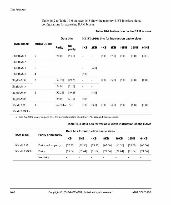
Test Features
Table 16-2 to Table 16-6 on page 16-8 show the memory BIST interface signal configurations for accessing RAM blocks.
Table 16-2 Instruction cache RAM access
RAM block MBISTCE bit
Data bits MBISTADDR bits for instruction cache sizes
ParityNo parity
1KB 2KB 4KB 8KB 16KB 32KB 64KB
IDataRAM3 7 [71:0] [63:0] - - [6:0] [7:0] [8:0] [9:0] [10:0]
IDataRAM2 6 - -
IDataRAM1 5 - [6:0]
IDataRAM0 4 [6:0]
ITagRAM3a 3 [52:28] [49:28] - - [4:0] [5:0] [6:0] [7:0] [8:0]
ITagRAM1a [24:0] [21:0] - -
ITagRAM2a 2 [52:28] [49:28] - [4:0]
ITagRAM0a [24:0] [21:0] [4:0]
IValidRAM 1 See Table 16-3 [3:0] [3:0] [3:0] [4:0] [5:0] [6:0] [7:0]
IValidRAMChk
a. See Tag RAM access on page 16-9 for more information about ITagRAM read and write accesses.
Table 16-3 Data bits for variable width instruction cache RAMs
RAM block Parity or no parityData bits for instruction cache sizes
1KB 2KB 4KB 8KB 16KB 32KB 64KB
IValidRAM Parity and no parity [57:56] [59:56] [63:56] [63:56] [63:56] [63:56] [63:56]
IValidRAMChk Parity [65:64] [67:64] [71:64] [71:64] [71:64] [71:64] [71:64]
No parity - - - - - - -
16-6 Copyright © 2005-2007 ARM Limited. All rights reserved. ARM DDI 0338G
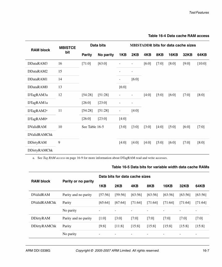
Test Features
Table 16-4 Data cache RAM access
RAM blockMBISTCE
bit
Data bits MBISTADDR bits for data cache sizes
Parity No parity 1KB 2KB 4KB 8KB 16KB 32KB 64KB
DDataRAM3 16 [71:0] [63:0] - - [6:0] [7:0] [8:0] [9:0] [10:0]
DDataRAM2 15 - -
DDataRAM1 14 - [6:0]
DDataRAM0 13 [6:0]
DTagRAM3a 12 [54:28] [51:28] - - [4:0] [5:0] [6:0] [7:0] [8:0]
DTagRAM1a [26:0] [23:0] - -
DTagRAM2a 11 [54:28] [51:28] - [4:0]
DTagRAM0a [26:0] [23:0] [4:0]
DValidRAM 10 See Table 16-5 [3:0] [3:0] [3:0] [4:0] [5:0] [6:0] [7:0]
DValidRAMChk
DDirtyRAM 9 [4:0] [4:0] [4:0] [5:0] [6:0] [7:0] [8:0]
DDirtyRAMChk
a. See Tag RAM access on page 16-9 for more information about DTagRAM read and write accesses.
Table 16-5 Data bits for variable width data cache RAMs
RAM block Parity or no parityData bits for data cache sizes
1KB 2KB 4KB 8KB 16KB 32KB 64KB
DValidRAM Parity and no parity [57:56] [59:56] [63:56] [63:56] [63:56] [63:56] [63:56]
DValidRAMChk Parity [65:64] [67:64] [71:64] [71:64] [71:64] [71:64] [71:64]
No parity - - - - - - -
DDirtyRAM Parity and no parity [1:0] [3:0] [7:0] [7:0] [7:0] [7:0] [7:0]
DDirtyRAMChk Parity [9:8] [11:8] [15:8] [15:8] [15:8] [15:8] [15:8]
No parity - - - - - - -
ARM DDI 0338G Copyright © 2005-2007 ARM Limited. All rights reserved. 16-7
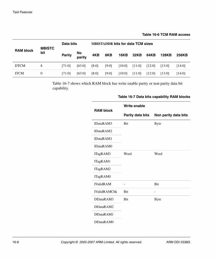
Test Features
Table 16-7 shows which RAM block has write enable parity or non parity data bit capability.
Table 16-6 TCM RAM access
RAM blockMBISTC bit
Data bits MBISTADDR bits for data TCM sizes
ParityNo parity
4KB 8KB 16KB 32KB 64KB 128KB 256KB
DTCM 8 [71:0] [63:0] [8:0] [9:0] [10:0] [11:0] [12:0] [13:0] [14:0]
ITCM 0 [71:0] [63:0] [8:0] [9:0] [10:0] [11:0] [12:0] [13:0] [14:0]
Table 16-7 Data bits capability RAM blocks
RAM blockWrite enable
Parity data bits Non parity data bits
IDataRAM3 Bit Byte
IDataRAM2
IDataRAM1
IDataRAM0
ITagRAM3 Word Word
ITagRAM1
ITagRAM2
ITagRAM0
IValidRAM - Bit
IValidRAMChk Bit -
DDataRAM3 Bit Byte
DDataRAM2
DDataRAM1
DDataRAM0
16-8 Copyright © 2005-2007 ARM Limited. All rights reserved. ARM DDI 0338G
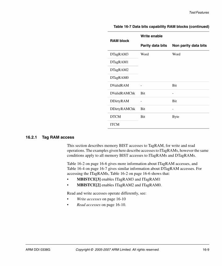
Test Features
16.2.1 Tag RAM access
This section describes memory BIST accesses to TagRAM, for write and read operations. The examples given here describe accesses to ITagRAMs, however the same conditions apply to all memory BIST accesses to ITagRAMs and DTagRAMs.
Table 16-2 on page 16-6 gives more information about ITagRAM accesses, and Table 16-4 on page 16-7 gives similar information about DTagRAM accesses. For accessing the ITagRAMs, Table 16-2 on page 16-6 shows that:
• MBISTCE[3] enables ITagRAM3 and ITagRAM1
• MBISTCE[2] enables ITagRAM2 and ITagRAM0.
Read and write accesses operate differently, see:
• Write accesses on page 16-10
• Read accesses on page 16-10.
DTagRAM3 Word Word
DTagRAM1
DTagRAM2
DTagRAM0
DValidRAM - Bit
DValidRAMChk Bit -
DDirtyRAM - Bit
DDirtyRAMChk Bit -
DTCM Bit Byte
ITCM
Table 16-7 Data bits capability RAM blocks (continued)
RAM blockWrite enable
Parity data bits Non parity data bits
ARM DDI 0338G Copyright © 2005-2007 ARM Limited. All rights reserved. 16-9
Test Features
Write accesses
When you write to the TagRAMs in memory BIST mode, the same data is driven from the data inputs to both of the enabled TagRAMs. For example, if you perform a memory BIST write with MBISTCE[3] set to 1, to enable ITagRAM3 and ITagRAM1:
• with parity, input data bits[24:0] are driven to both ITagRAM3 and ITagRAM1
• with no parity, input data bits[21:0] are driven to both ITagRAM3 and ITagRAM1.
Read accesses
When you read from the TagRAMs in memory BIST mode, the data from the two TagRAMs is read onto different regions of the data output bus. For example, if you perform a memory BIST read with MBISTCE[3] set to 1, to enable ITagRAM3 and ITagRAM1:
• with parity:
— data from ITagRAM3 is read onto data output bits[52:28]
— data from ITagRAM1 is read onto data output bits[24:0]
• with no parity:
— data from ITagRAM3 is read onto data output bits[49:28]
— data from ITagRAM1 is read onto data output bits[21:0].
16.2.2 ARM Memory BIST Controller
You can use the memory BIST interface described in this chapter with the ARM memory BIST controller. This provides the ability to test all of the RAM blocks in the processor using a variety of algorithms.
The ARM memory BIST controller does not support the use of nMBISTDATARDY. It cannot test variable latency RAM blocks that require the use of nITCDATARDY and nDTCDATARDY.
16.2.3 Third party tool support
If a third-party tool is used to create a memory BIST controller, instead of using the memory BIST controller supplied, you must be aware that:
• A five-stage pipeline is required to access the RAM blocks.
16-10 Copyright © 2005-2007 ARM Limited. All rights reserved. ARM DDI 0338G
Test Features
• Except for a few cases, you must access RAM blocks individually. Only RAM blocks without common data bits can be accessed at the same time. Also you can test the Cache Valid RAM blocks in conjunction with the Cache Tag RAM blocks (see Table 16-2 on page 16-6 and Table 16-4 on page 16-7).
• The entire MBISTDOUT interface is not always used. Only valid data bits must be compared by the chosen memory BIST controller.
ARM DDI 0338G Copyright © 2005-2007 ARM Limited. All rights reserved. 16-11
Test Features
16.3 Power-On Test
The requirements for power-on-test include the ability to detect that the major functional units are working at power-on. This includes the ability of testing the L1 memory under software control.
For the data cache a suitable test program is required that exercises all locations. CP15 operations are included to enable the data cache Tag and Valid RAM blocks to be initialized under software control.
For the instruction cache, it is necessary to initialize the cache contents with a test program using CP15 operations. The test program then enables reads from the cache to take place at a rate close to that of a normal application.
For more details, see Cache debug and software test access on page 3-9.
You can also use the Memory BIST ports to initialize the cache memories. In this mode the controller behaves like a DMA controller and initializes all memory locations. during this preload time you must ensure the core is not functional. You might have to reset the core after the preload.
For testing the Instruction and Data TCMs, similar methods can be used, whereby a test program and test data are loaded into the relevant TCM. When initialized the processor can switch to executing code from the Instruction TCM, with its data space within the Data TCM. No additional access features are required for TCM testing as both TCMs are accessible by the processor for data accesses.
16-12 Copyright © 2005-2007 ARM Limited. All rights reserved. ARM DDI 0338G
Test Features
16.4 Running System Test
Running system test can make use of similar methods as the power-on test. The current contents of the registers, cache and TCM memories can be stored into memory outside of the macrocell, and test code loaded into the cache in its place. At the completion of the test sequence the storage within the processor might be re-instated to the pretest values and normal operation resumed.
It is expected that run-time test is initiated by software, and that the data cache is cleaned before the test data is loaded into the cache.
ARM DDI 0338G Copyright © 2005-2007 ARM Limited. All rights reserved. 16-13

Test Features
16-14 Copyright © 2005-2007 ARM Limited. All rights reserved. ARM DDI 0338G
Chapter 17 Cycle Timings and Interlock Behavior
This chapter describes the cycle timings and interlock behavior of integer instructions on the ARM1156T2-S processor. This chapter contains the following sections:
• About cycle timings and interlock behavior on page 17-3
• Register interlock examples on page 17-8
• Data processing instructions on page 17-9
• QADD, QDADD, QSUB, and QDSUB instructions on page 17-12
• ARMv6 media data-processing on page 17-13
• ARMv6 Sum of Absolute Differences on page 17-15
• Multiplies on page 17-16
• Branches on page 17-18
• Processor state updating instructions on page 17-19
• Single load and store instructions on page 17-20
• Load and Store Doubleword instructions on page 17-23
• Load and Store Multiple instructions on page 17-25
• RFE and SRS instructions on page 17-28
• Synchronization instructions on page 17-29.
• Coprocessor instructions on page 17-30
• SVC, BKPT, undefined, and prefetch aborted instructions on page 17-31
ARM DDI 0338G Copyright © 2005-2007 ARM Limited. All rights reserved. 17-1
Cycle Timings and Interlock Behavior
• CBZ, CBNZ, and IT instructions on page 17-32
• Bitfield instructions on page 17-33
• NOP (CPS) instruction on page 17-34
• Table branch instructions on page 17-35.
17-2 Copyright © 2005-2007 ARM Limited. All rights reserved. ARM DDI 0338G
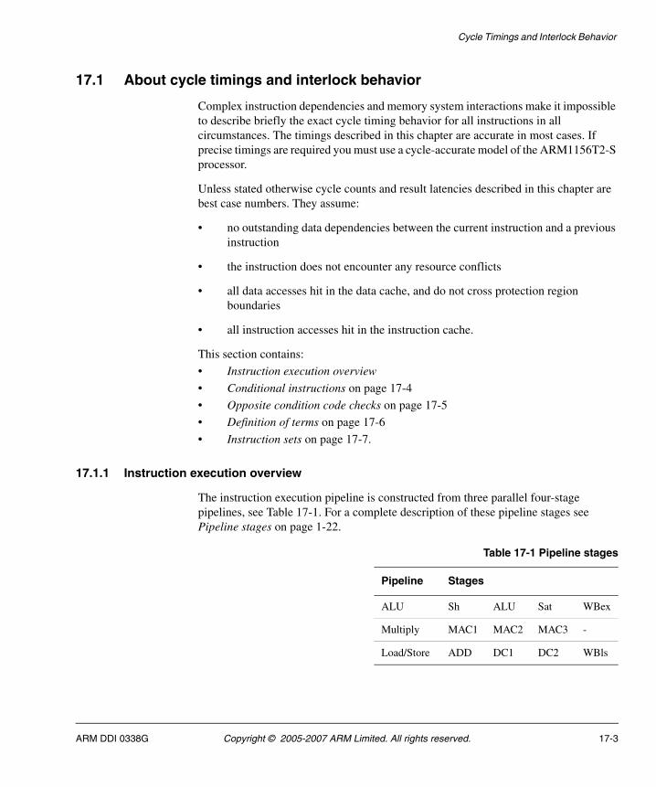
Cycle Timings and Interlock Behavior
17.1 About cycle timings and interlock behavior
Complex instruction dependencies and memory system interactions make it impossible to describe briefly the exact cycle timing behavior for all instructions in all circumstances. The timings described in this chapter are accurate in most cases. If precise timings are required you must use a cycle-accurate model of the ARM1156T2-S processor.
Unless stated otherwise cycle counts and result latencies described in this chapter are best case numbers. They assume:
• no outstanding data dependencies between the current instruction and a previous instruction
• the instruction does not encounter any resource conflicts
• all data accesses hit in the data cache, and do not cross protection region boundaries
• all instruction accesses hit in the instruction cache.
This section contains:
• Instruction execution overview
• Conditional instructions on page 17-4
• Opposite condition code checks on page 17-5
• Definition of terms on page 17-6
• Instruction sets on page 17-7.
17.1.1 Instruction execution overview
The instruction execution pipeline is constructed from three parallel four-stage pipelines, see Table 17-1. For a complete description of these pipeline stages see Pipeline stages on page 1-22.
Table 17-1 Pipeline stages
Pipeline Stages
ALU Sh ALU Sat WBex
Multiply MAC1 MAC2 MAC3 -
Load/Store ADD DC1 DC2 WBls
ARM DDI 0338G Copyright © 2005-2007 ARM Limited. All rights reserved. 17-3
Cycle Timings and Interlock Behavior
The ALU and multiply pipelines operate in a lock-step manner, causing all instructions in these pipelines to retire in order. The load/store pipeline is a decoupled pipeline enabling subsequent instructions in the ALU and multiply pipeline to complete underneath outstanding loads.
Extensive forwarding to the Sh, MAC1, ADD, ALU, MAC2, and DC1 stages enables many dependent instruction sequences to run without pipeline stalls. General forwarding occurs from the ALU, Sat, WBex and WBls pipeline stages. In addition, the multiplier contains an internal multiply accumulate forwarding path.
Most instructions do not require a register until the ALU stage. All result latencies are given as the number of cycles until the register is required by a following instruction in the ALU stage. The following sequence takes four cycles:
LDR R1, [R2] ;Result latency threeADD R3, R3, R1 ;Register R1 required by ALU
If a subsequent instruction requires the register at the start of the Sh, MAC1, or ADD stage then an extra cycle must be added to the result latency of the instruction producing the required register. Instructions that require a register at the start of these stages are specified by describing that register as an Early register. The following sequence, requiring an Early register, takes five cycles:
LDR R1, [R2] ;Result latency three plus oneADD R3, R3, R1 LSL#6 ;plus one because Register R1 is required by Sh
Finally, some instructions do not require a register until their second execution cycle. If a register is not required until the ALU, MAC2, or Dc1 stage for the second execution cycle, then a cycle can be subtracted from the result latency for the instruction producing the required register. If a register is not required until this later point, it is specified as a Late register. The following sequence where R1 is a Late register takes four cycles:
LDR R1, [R2] ;Result latency three minus oneADD R3,R1,R3,LSLR4 ;minus one because Register R1 is a Late register
;This ADD is a two issue cycle instruction
17.1.2 Conditional instructions
Most instructions execute in one or two cycles. If these instructions fail their condition codes then they take one and two cycles respectively.
17-4 Copyright © 2005-2007 ARM Limited. All rights reserved. ARM DDI 0338G
Cycle Timings and Interlock Behavior
Multiplies, MSR, and some CP14 and CP15 coprocessor instructions are the only instructions that require more than two cycles to execute. If one of these instructions fails its condition codes, then it takes a variable number of cycles to execute. The number of cycles is dependent on:
• the length of the operation
• the number of cycles between the setting of the flags and the start of the dependent instruction.
The worst-case number of cycles for a condition code failing multicycle instruction is five.
The following algorithm describes the number of cycles taken for a multi-cycle instruction that fails its condition-code:
Min(NonFailingCycleCount, Max(5 - FlagCycleDistance, 3))
Where:
Max (a,b) returns the maximum of the two values a,b.
Min (a,b) returns the minimum of the two values a,b.
NonFailingCycleCount
is the number of cycles that the failing instruction would have taken had it passed.
FlagCycDistance is the number of cycles between the instruction that sets the flags and the conditional instruction, including interlocking cycles. For example:
• The following sequence has a FlagCycleDistance of 0 because the instructions are back-to-back with no interlocks:ADDS R1, R2, R3MULEQ R4, R5, R6
• The following sequence has a FlagCycleDistance of one:ADDS R1, R2, R3MOV R0, R0MULEQ R4, R5, R6
17.1.3 Opposite condition code checks
If instruction A and instruction B both write the same register the pipeline must ensure that the register is written in the correct order. Therefore, interlocks might be required to correctly resolve this pipeline hazard.
ARM DDI 0338G Copyright © 2005-2007 ARM Limited. All rights reserved. 17-5
Cycle Timings and Interlock Behavior
The only useful sequences where two instructions write the same register without an instruction reading its value in between are when the two instructions have opposite sets of condition codes. The ARM1156T2-S processor optimizes these sequences to prevent unnecessary interlocks. For example:
• The following sequences take two cycles to execute:
ADDNE R1, R5, R6LDREQ R1, [R8]
LDREQ R1, [R8]ADDNE R1, R5, R6
• The following sequence also takes two cycles to execute, because the STR instruction does not store the value of R1 produced by the QDADDNE instruction:
QDADDNE R1, R5, R6STREQ R1, [R8]
17.1.4 Definition of terms
Table 17-2 gives descriptions of cycle timing terms used in this chapter.
Table 17-2 Definition of cycle timing terms
Term Description
Cycles This is the minimum number of cycles required by an instruction.
Result latency This is the number of cycles before the result of this instruction is available for a following instruction requiring the result at the start of the ALU, MAC2, and DC1 stage. This is the normal case. Exceptions to this mark the register as an Early register.
Note The result latency is the number of cycles from the first cycle of an instruction.
Register lock latency Applies to STM and STRD instructions only. This is the number of cycles that a register is write-locked for by this instruction, preventing subsequent instructions that want to write the register from starting. This lock is required to prevent a following instruction from writing to a register before it has been read.
Early register The specified register is required at the start of the Sh, MAC1, and ADD stage. For interlock calculations add one cycle to the result latency of the instruction producing this register.
Late register The specified register is not required until the start of the ALU, MAC2, and DC1 stage for the second execution. For interlock calculations subtract one cycle from the result latency of the instruction producing this register.
FlagsCycleDistance The number of cycles between an instruction that sets the flags and the conditional instruction.
17-6 Copyright © 2005-2007 ARM Limited. All rights reserved. ARM DDI 0338G
Cycle Timings and Interlock Behavior
17.1.5 Instruction sets
For any equivalent instruction, the cycle timing behavior is always the same whether it is an ARM, Thumb or Thumb-2 instruction.
Note Instructions from all instruction sets are listed, but some instructions and some register combinations or addressing modes might not be available in all instruction sets.
ARM DDI 0338G Copyright © 2005-2007 ARM Limited. All rights reserved. 17-7
Cycle Timings and Interlock Behavior
17.2 Register interlock examples
Table 17-3 shows register interlock examples using LDR and ADD instructions.
LDR instructions take one cycle, have a result latency of three, and require their base register as an Early register.
ADD instructions take one cycle and have a result latency of one.
Table 17-3 Register interlock examples
Instruction sequence Behavior
LDR R1, [R2]ADD R6, R5, R4
Takes two cycles because there are no register dependencies
ADD R1, R2, R3ADD R9, R6, R1
Takes two cycles because ADD instructions have a result latency of one
LDR R1, [R2]ADD R6, R5, R1
Takes four cycles because of the result latency of R1
ADD R2, R5, R6LDR R1, [R2]
Takes three cycles because of the use of the result of R2 as an Early register
LDR R1, [R2]LDR R5, [R1]
Takes five cycles because of the result latency and the use of the result of R1 as an Early register
17-8 Copyright © 2005-2007 ARM Limited. All rights reserved. ARM DDI 0338G
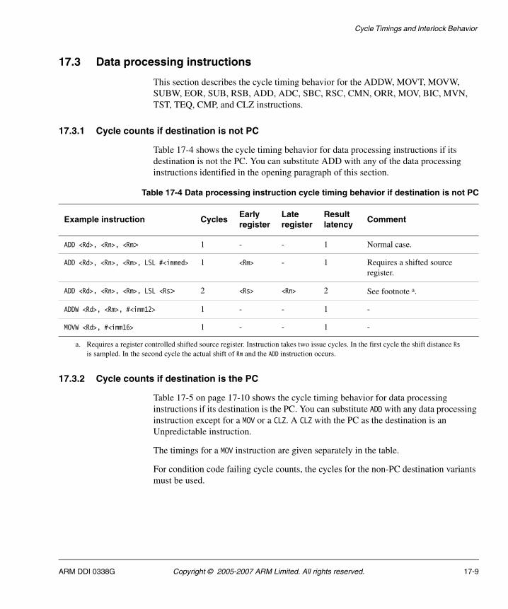
Cycle Timings and Interlock Behavior
17.3 Data processing instructions
This section describes the cycle timing behavior for the ADDW, MOVT, MOVW, SUBW, EOR, SUB, RSB, ADD, ADC, SBC, RSC, CMN, ORR, MOV, BIC, MVN, TST, TEQ, CMP, and CLZ instructions.
17.3.1 Cycle counts if destination is not PC
Table 17-4 shows the cycle timing behavior for data processing instructions if its destination is not the PC. You can substitute ADD with any of the data processing instructions identified in the opening paragraph of this section.
17.3.2 Cycle counts if destination is the PC
Table 17-5 on page 17-10 shows the cycle timing behavior for data processing instructions if its destination is the PC. You can substitute ADD with any data processing instruction except for a MOV or a CLZ. A CLZ with the PC as the destination is an Unpredictable instruction.
The timings for a MOV instruction are given separately in the table.
For condition code failing cycle counts, the cycles for the non-PC destination variants must be used.
Table 17-4 Data processing instruction cycle timing behavior if destination is not PC
Example instruction CyclesEarlyregister
Lateregister
Resultlatency
Comment
ADD <Rd>, <Rn>, <Rm> 1 - - 1 Normal case.
ADD <Rd>, <Rn>, <Rm>, LSL #<immed> 1 <Rm> - 1 Requires a shifted source register.
ADD <Rd>, <Rn>, <Rm>, LSL <Rs> 2 <Rs> <Rn> 2 See footnote a.
ADDW <Rd>, <Rm>, #<imm12> 1 - - 1 -
MOVW <Rd>, #<imm16> 1 - - 1 -
a. Requires a register controlled shifted source register. Instruction takes two issue cycles. In the first cycle the shift distance Rs is sampled. In the second cycle the actual shift of Rm and the ADD instruction occurs.
ARM DDI 0338G Copyright © 2005-2007 ARM Limited. All rights reserved. 17-9
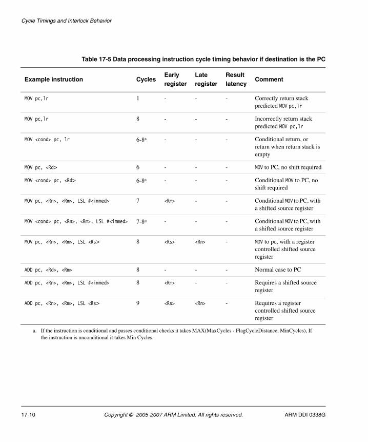
Cycle Timings and Interlock Behavior
Table 17-5 Data processing instruction cycle timing behavior if destination is the PC
Example instruction CyclesEarlyregister
Lateregister
Resultlatency
Comment
MOV pc,lr 1 - - - Correctly return stack predicted MOV pc,lr
MOV pc,lr 8 - - - Incorrectly return stack predicted MOV pc,lr
MOV <cond> pc, lr 6-8a - - - Conditional return, or return when return stack is empty
MOV pc, <Rd> 6 - - - MOV to PC, no shift required
MOV <cond> pc, <Rd> 6-8a - - - Conditional MOV to PC, no shift required
MOV pc, <Rn>, <Rm>, LSL #<immed> 7 <Rm> - - Conditional MOV to PC, with a shifted source register
MOV <cond> pc, <Rn>, <Rm>, LSL #<immed> 7-8a - - - Conditional MOV to PC, with a shifted source register
MOV pc, <Rn>, <Rm>, LSL <Rs> 8 <Rs> <Rn> - MOV to pc, with a register controlled shifted source register
ADD pc, <Rd>, <Rm> 8 - - - Normal case to PC
ADD pc, <Rn>, <Rm>, LSL #<immed> 8 <Rm> - - Requires a shifted source register
ADD pc, <Rn>, <Rm>, LSL <Rs> 9 <Rs> <Rn> - Requires a register controlled shifted source register
a. If the instruction is conditional and passes conditional checks it takes MAX(MaxCycles - FlagCycleDistance, MinCycles), If the instruction is unconditional it takes Min Cycles.
17-10 Copyright © 2005-2007 ARM Limited. All rights reserved. ARM DDI 0338G
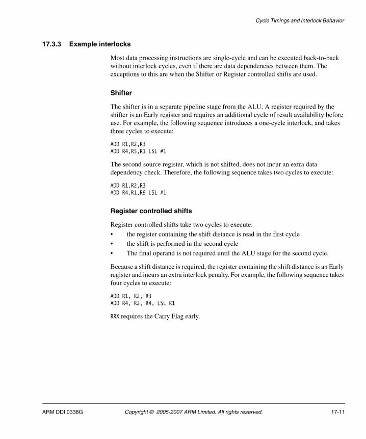
Cycle Timings and Interlock Behavior
17.3.3 Example interlocks
Most data processing instructions are single-cycle and can be executed back-to-back without interlock cycles, even if there are data dependencies between them. The exceptions to this are when the Shifter or Register controlled shifts are used.
Shifter
The shifter is in a separate pipeline stage from the ALU. A register required by the shifter is an Early register and requires an additional cycle of result availability before use. For example, the following sequence introduces a one-cycle interlock, and takes three cycles to execute:
ADD R1,R2,R3ADD R4,R5,R1 LSL #1
The second source register, which is not shifted, does not incur an extra data dependency check. Therefore, the following sequence takes two cycles to execute:
ADD R1,R2,R3ADD R4,R1,R9 LSL #1
Register controlled shifts
Register controlled shifts take two cycles to execute:
• the register containing the shift distance is read in the first cycle
• the shift is performed in the second cycle
• The final operand is not required until the ALU stage for the second cycle.
Because a shift distance is required, the register containing the shift distance is an Early register and incurs an extra interlock penalty. For example, the following sequence takes four cycles to execute:
ADD R1, R2, R3ADD R4, R2, R4, LSL R1
RRX requires the Carry Flag early.
ARM DDI 0338G Copyright © 2005-2007 ARM Limited. All rights reserved. 17-11
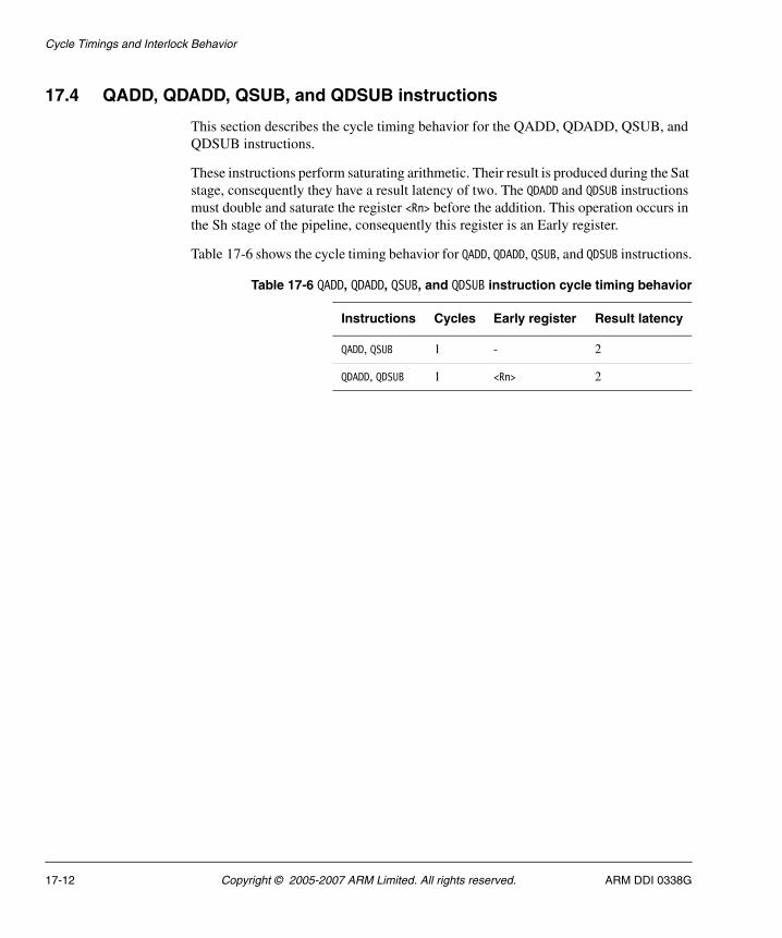
Cycle Timings and Interlock Behavior
17.4 QADD, QDADD, QSUB, and QDSUB instructions
This section describes the cycle timing behavior for the QADD, QDADD, QSUB, and QDSUB instructions.
These instructions perform saturating arithmetic. Their result is produced during the Sat stage, consequently they have a result latency of two. The QDADD and QDSUB instructions must double and saturate the register <Rn> before the addition. This operation occurs in the Sh stage of the pipeline, consequently this register is an Early register.
Table 17-6 shows the cycle timing behavior for QADD, QDADD, QSUB, and QDSUB instructions.
Table 17-6 QADD, QDADD, QSUB, and QDSUB instruction cycle timing behavior
Instructions Cycles Early register Result latency
QADD, QSUB 1 - 2
QDADD, QDSUB 1 <Rn> 2
17-12 Copyright © 2005-2007 ARM Limited. All rights reserved. ARM DDI 0338G
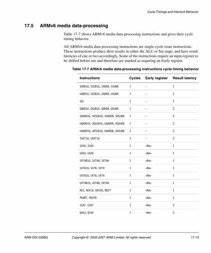
Cycle Timings and Interlock Behavior
17.5 ARMv6 media data-processing
Table 17-7 shows ARMv6 media data-processing instructions and gives their cycle timing behavior.
All ARMv6 media data-processing instructions are single-cycle issue instructions. These instructions produce their results in either the ALU or Sat stage, and have result latencies of one or two accordingly. Some of the instructions require an input register to be shifted before use and therefore are marked as requiring an Early register.
Table 17-7 ARMv6 media data-processing instructions cycle timing behavior
Instructions Cycles Early register Result latency
SADD16, SSUB16, SADD8, SSUB8 1 - 1
UADD16, USUB16, UADD8, USUB8 1 - 1
SEL 1 - 1
QADD16, QSUB16, QADD8, QSUB8 1 - 2
SHADD16, SHSUB16, SHADD8, SHSUB8 1 - 2
UQADD16, UQSUB16, UQADD8, UQSUB8 1 - 2
UHADD16, UHSUB16, UHADD8, UHSUB8 1 - 2
SSAT16, USAT16 1 - 2
SASX, SSAX 1 <Rm> 1
UASX, USAX 1 <Rm> 1
SXTAB16, SXTAB, SXTAH 1 <Rm> 1
SXTB16, SXTB, SXTH 1 <Rm> 1
UXTB16, UXTB, UXTH 1 <Rm> 1
UXTAB16, UXTAB, UXTAH 1 <Rm> 1
REV, REV16, REVSH, RBIT 1 <Rm> 1
PKHBT, PKHTB 1 <Rm> 1
SSAT, USAT 1 <Rm> 2
QASX, QSAX 1 <Rm> 2
ARM DDI 0338G Copyright © 2005-2007 ARM Limited. All rights reserved. 17-13
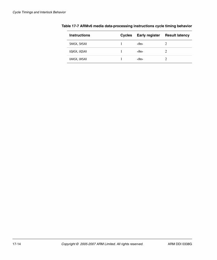
Cycle Timings and Interlock Behavior
SHASX, SHSAX 1 <Rm> 2
UQASX, UQSAX 1 <Rm> 2
UHASX, UHSAX 1 <Rm> 2
Table 17-7 ARMv6 media data-processing instructions cycle timing behavior
Instructions Cycles Early register Result latency
17-14 Copyright © 2005-2007 ARM Limited. All rights reserved. ARM DDI 0338G
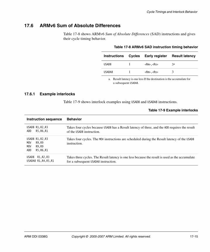
Cycle Timings and Interlock Behavior
17.6 ARMv6 Sum of Absolute Differences
Table 17-8 shows ARMv6 Sum of Absolute Differences (SAD) instructions and gives their cycle timing behavior.
17.6.1 Example interlocks
Table 17-9 shows interlock examples using USAD8 and USADA8 instructions.
Table 17-8 ARMv6 SAD instruction timing behavior
Instructions Cycles Early register Result latency
USAD8 1 <Rm>,<Rs> 3a
a. Result latency is one less If the destination is the accumulate for a subsequent USADA8.
USADA8 1 <Rm>,<Rs> 3
Table 17-9 Example interlocks
Instruction sequence Behavior
USAD8 R1,R2,R3 ADD R5,R6,R1
Takes four cycles because USAD8 has a Result latency of three, and the ADD requires the result of the USAD8 instruction.
USAD8 R1,R2,R3 MOV R9,R9MOV R9,R9ADD R5,R6,R1
Takes four cycles. The MOV instructions are scheduled during the Result latency of the USAD8 instruction.
USAD8 R1,R2,R3USADA8 R1,R4,R5,R1
Takes three cycles. The Result latency is one less because the result is used as the accumulate for a subsequent USADA8 instruction.
ARM DDI 0338G Copyright © 2005-2007 ARM Limited. All rights reserved. 17-15
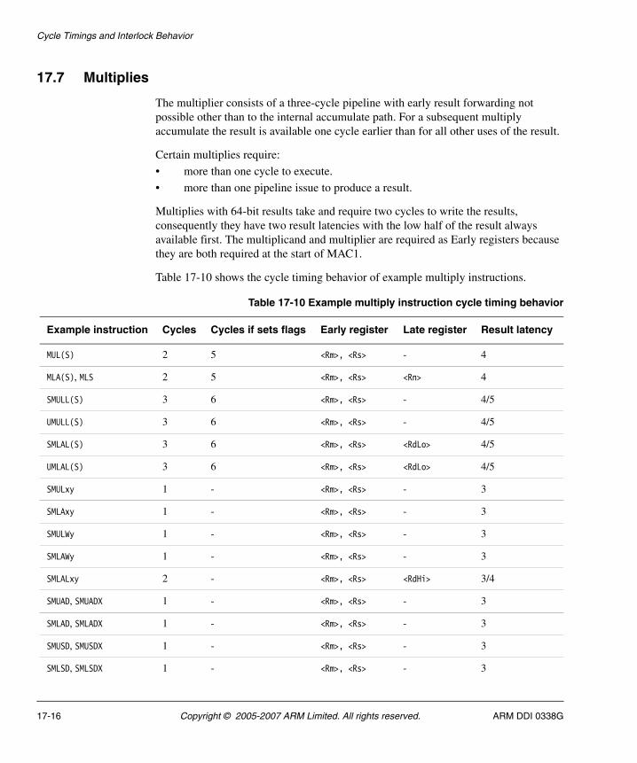
Cycle Timings and Interlock Behavior
17.7 Multiplies
The multiplier consists of a three-cycle pipeline with early result forwarding not possible other than to the internal accumulate path. For a subsequent multiply accumulate the result is available one cycle earlier than for all other uses of the result.
Certain multiplies require:
• more than one cycle to execute.
• more than one pipeline issue to produce a result.
Multiplies with 64-bit results take and require two cycles to write the results, consequently they have two result latencies with the low half of the result always available first. The multiplicand and multiplier are required as Early registers because they are both required at the start of MAC1.
Table 17-10 shows the cycle timing behavior of example multiply instructions.
Table 17-10 Example multiply instruction cycle timing behavior
Example instruction Cycles Cycles if sets flags Early register Late register Result latency
MUL(S) 2 5 <Rm>, <Rs> - 4
MLA(S), MLS 2 5 <Rm>, <Rs> <Rn> 4
SMULL(S) 3 6 <Rm>, <Rs> - 4/5
UMULL(S) 3 6 <Rm>, <Rs> - 4/5
SMLAL(S) 3 6 <Rm>, <Rs> <RdLo> 4/5
UMLAL(S) 3 6 <Rm>, <Rs> <RdLo> 4/5
SMULxy 1 - <Rm>, <Rs> - 3
SMLAxy 1 - <Rm>, <Rs> - 3
SMULWy 1 - <Rm>, <Rs> - 3
SMLAWy 1 - <Rm>, <Rs> - 3
SMLALxy 2 - <Rm>, <Rs> <RdHi> 3/4
SMUAD, SMUADX 1 - <Rm>, <Rs> - 3
SMLAD, SMLADX 1 - <Rm>, <Rs> - 3
SMUSD, SMUSDX 1 - <Rm>, <Rs> - 3
SMLSD, SMLSDX 1 - <Rm>, <Rs> - 3
17-16 Copyright © 2005-2007 ARM Limited. All rights reserved. ARM DDI 0338G
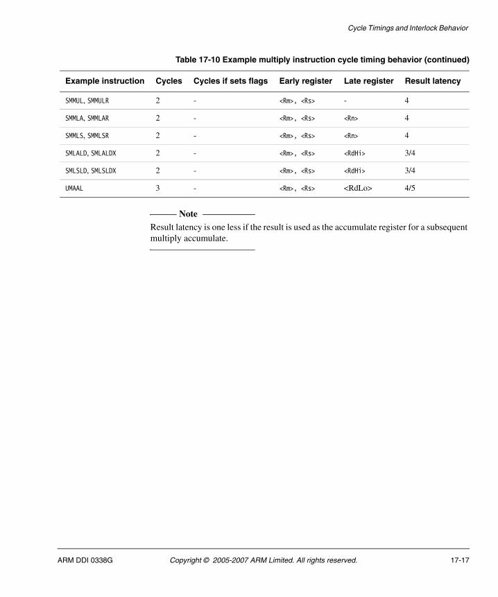
Cycle Timings and Interlock Behavior
Note Result latency is one less if the result is used as the accumulate register for a subsequent multiply accumulate.
SMMUL, SMMULR 2 - <Rm>, <Rs> - 4
SMMLA, SMMLAR 2 - <Rm>, <Rs> <Rn> 4
SMMLS, SMMLSR 2 - <Rm>, <Rs> <Rn> 4
SMLALD, SMLALDX 2 - <Rm>, <Rs> <RdHi> 3/4
SMLSLD, SMLSLDX 2 - <Rm>, <Rs> <RdHi> 3/4
UMAAL 3 - <Rm>, <Rs> <RdLo> 4/5
Table 17-10 Example multiply instruction cycle timing behavior (continued)
Example instruction Cycles Cycles if sets flags Early register Late register Result latency
ARM DDI 0338G Copyright © 2005-2007 ARM Limited. All rights reserved. 17-17
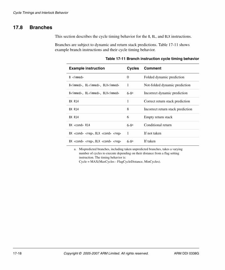
Cycle Timings and Interlock Behavior
17.8 Branches
This section describes the cycle timing behavior for the B, BL, and BLX instructions.
Branches are subject to dynamic and return stack predictions. Table 17-11 shows example branch instructions and their cycle timing behavior.
Table 17-11 Branch instruction cycle timing behavior
Example instruction Cycles Comment
B <immed> 0 Folded dynamic prediction
B<immed>, BL<immed>, BLX<immed> 1 Not-folded dynamic prediction
B<immed>, BL<immed>, BLX<immed> 6-8a
a. Mispredicted branches, including taken unpredicted branches, takes a varying number of cycles to execute depending on their distance from a flag setting instruction. The timing behavior is: Cycle = MAX(MaxCycles - FlagCycleDistance, MinCycles).
Incorrect dynamic prediction
BX R14 1 Correct return stack prediction
BX R14 8 Incorrect return stack prediction
BX R14 6 Empty return stack
BX <cond> R14 6-8a Conditional return
BX <cond> <reg>, BLX <cond> <reg> 1 If not taken
BX <cond> <reg>, BLX <cond> <reg> 6-8a If taken
17-18 Copyright © 2005-2007 ARM Limited. All rights reserved. ARM DDI 0338G
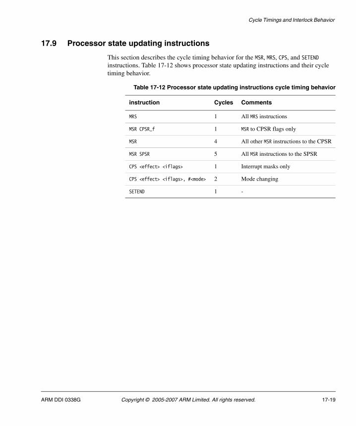
Cycle Timings and Interlock Behavior
17.9 Processor state updating instructions
This section describes the cycle timing behavior for the MSR, MRS, CPS, and SETEND instructions. Table 17-12 shows processor state updating instructions and their cycle timing behavior.
Table 17-12 Processor state updating instructions cycle timing behavior
instruction Cycles Comments
MRS 1 All MRS instructions
MSR CPSR_f 1 MSR to CPSR flags only
MSR 4 All other MSR instructions to the CPSR
MSR SPSR 5 All MSR instructions to the SPSR
CPS <effect> <iflags> 1 Interrupt masks only
CPS <effect> <iflags>, #<mode> 2 Mode changing
SETEND 1 -
ARM DDI 0338G Copyright © 2005-2007 ARM Limited. All rights reserved. 17-19
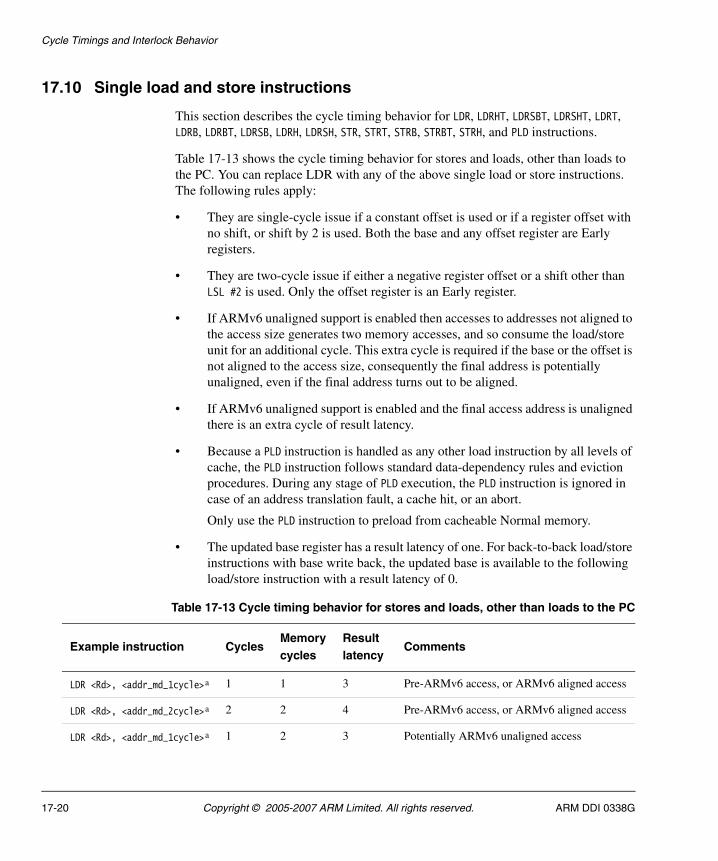
Cycle Timings and Interlock Behavior
17.10 Single load and store instructions
This section describes the cycle timing behavior for LDR, LDRHT, LDRSBT, LDRSHT, LDRT, LDRB, LDRBT, LDRSB, LDRH, LDRSH, STR, STRT, STRB, STRBT, STRH, and PLD instructions.
Table 17-13 shows the cycle timing behavior for stores and loads, other than loads to the PC. You can replace LDR with any of the above single load or store instructions. The following rules apply:
• They are single-cycle issue if a constant offset is used or if a register offset with no shift, or shift by 2 is used. Both the base and any offset register are Early registers.
• They are two-cycle issue if either a negative register offset or a shift other than LSL #2 is used. Only the offset register is an Early register.
• If ARMv6 unaligned support is enabled then accesses to addresses not aligned to the access size generates two memory accesses, and so consume the load/store unit for an additional cycle. This extra cycle is required if the base or the offset is not aligned to the access size, consequently the final address is potentially unaligned, even if the final address turns out to be aligned.
• If ARMv6 unaligned support is enabled and the final access address is unaligned there is an extra cycle of result latency.
• Because a PLD instruction is handled as any other load instruction by all levels of cache, the PLD instruction follows standard data-dependency rules and eviction procedures. During any stage of PLD execution, the PLD instruction is ignored in case of an address translation fault, a cache hit, or an abort.
Only use the PLD instruction to preload from cacheable Normal memory.
• The updated base register has a result latency of one. For back-to-back load/store instructions with base write back, the updated base is available to the following load/store instruction with a result latency of 0.
Table 17-13 Cycle timing behavior for stores and loads, other than loads to the PC
Example instruction CyclesMemorycycles
Resultlatency
Comments
LDR <Rd>, <addr_md_1cycle>a 1 1 3 Pre-ARMv6 access, or ARMv6 aligned access
LDR <Rd>, <addr_md_2cycle>a 2 2 4 Pre-ARMv6 access, or ARMv6 aligned access
LDR <Rd>, <addr_md_1cycle>a 1 2 3 Potentially ARMv6 unaligned access
17-20 Copyright © 2005-2007 ARM Limited. All rights reserved. ARM DDI 0338G
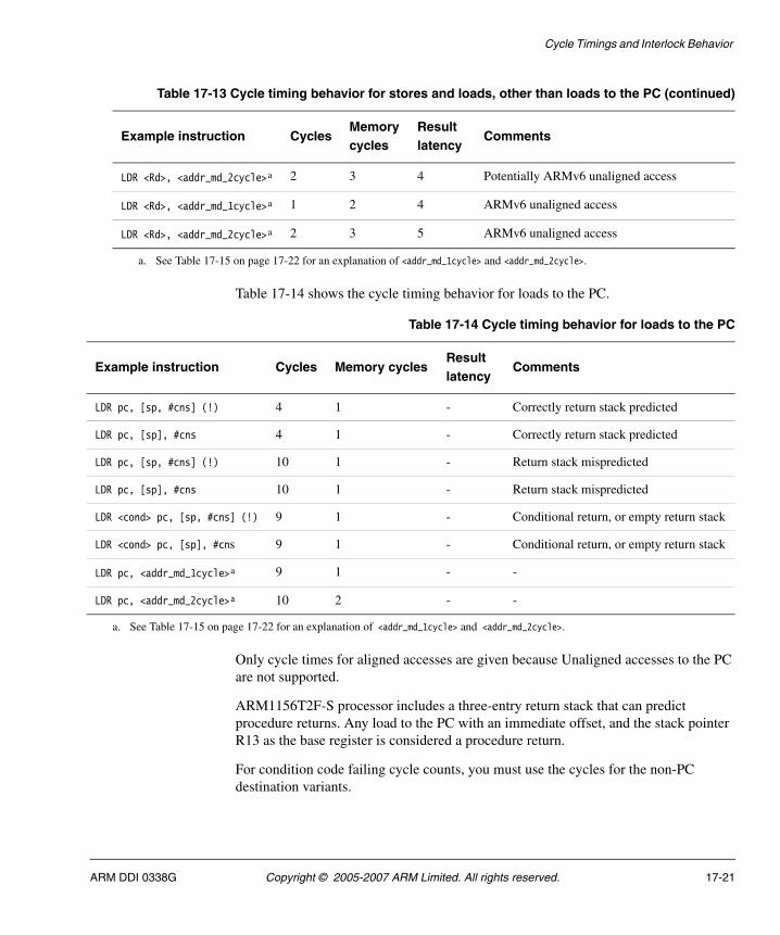
Cycle Timings and Interlock Behavior
Table 17-14 shows the cycle timing behavior for loads to the PC.
Only cycle times for aligned accesses are given because Unaligned accesses to the PC are not supported.
ARM1156T2F-S processor includes a three-entry return stack that can predict procedure returns. Any load to the PC with an immediate offset, and the stack pointer R13 as the base register is considered a procedure return.
For condition code failing cycle counts, you must use the cycles for the non-PC destination variants.
LDR <Rd>, <addr_md_2cycle>a 2 3 4 Potentially ARMv6 unaligned access
LDR <Rd>, <addr_md_1cycle>a 1 2 4 ARMv6 unaligned access
LDR <Rd>, <addr_md_2cycle>a 2 3 5 ARMv6 unaligned access
a. See Table 17-15 on page 17-22 for an explanation of <addr_md_1cycle> and <addr_md_2cycle>.
Table 17-13 Cycle timing behavior for stores and loads, other than loads to the PC (continued)
Example instruction CyclesMemorycycles
Resultlatency
Comments
Table 17-14 Cycle timing behavior for loads to the PC
Example instruction Cycles Memory cyclesResult latency
Comments
LDR pc, [sp, #cns] (!) 4 1 - Correctly return stack predicted
LDR pc, [sp], #cns 4 1 - Correctly return stack predicted
LDR pc, [sp, #cns] (!) 10 1 - Return stack mispredicted
LDR pc, [sp], #cns 10 1 - Return stack mispredicted
LDR <cond> pc, [sp, #cns] (!) 9 1 - Conditional return, or empty return stack
LDR <cond> pc, [sp], #cns 9 1 - Conditional return, or empty return stack
LDR pc, <addr_md_1cycle>a 9 1 - -
LDR pc, <addr_md_2cycle>a 10 2 - -
a. See Table 17-15 on page 17-22 for an explanation of <addr_md_1cycle> and <addr_md_2cycle>.
ARM DDI 0338G Copyright © 2005-2007 ARM Limited. All rights reserved. 17-21
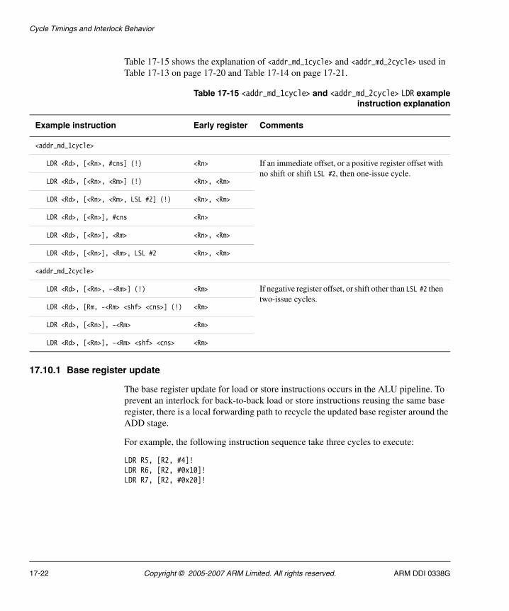
Cycle Timings and Interlock Behavior
Table 17-15 shows the explanation of <addr_md_1cycle> and <addr_md_2cycle> used in Table 17-13 on page 17-20 and Table 17-14 on page 17-21.
17.10.1 Base register update
The base register update for load or store instructions occurs in the ALU pipeline. To prevent an interlock for back-to-back load or store instructions reusing the same base register, there is a local forwarding path to recycle the updated base register around the ADD stage.
For example, the following instruction sequence take three cycles to execute:
LDR R5, [R2, #4]!LDR R6, [R2, #0x10]!LDR R7, [R2, #0x20]!
Table 17-15 <addr_md_1cycle> and <addr_md_2cycle> LDR exampleinstruction explanation
Example instruction Early register Comments
<addr_md_1cycle>
LDR <Rd>, [<Rn>, #cns] (!) <Rn> If an immediate offset, or a positive register offset with no shift or shift LSL #2, then one-issue cycle.
LDR <Rd>, [<Rn>, <Rm>] (!) <Rn>, <Rm>
LDR <Rd>, [<Rn>, <Rm>, LSL #2] (!) <Rn>, <Rm>
LDR <Rd>, [<Rn>], #cns <Rn>
LDR <Rd>, [<Rn>], <Rm> <Rn>, <Rm>
LDR <Rd>, [<Rn>], <Rm>, LSL #2 <Rn>, <Rm>
<addr_md_2cycle>
LDR <Rd>, [<Rn>, -<Rm>] (!) <Rm> If negative register offset, or shift other than LSL #2 then two-issue cycles.
LDR <Rd>, [Rm, -<Rm> <shf> <cns>] (!) <Rm>
LDR <Rd>, [<Rn>], -<Rm> <Rm>
LDR <Rd>, [<Rn>], -<Rm> <shf> <cns> <Rm>
17-22 Copyright © 2005-2007 ARM Limited. All rights reserved. ARM DDI 0338G
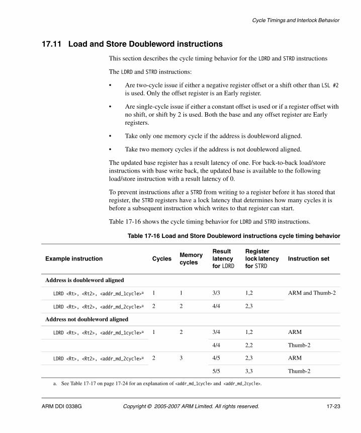
Cycle Timings and Interlock Behavior
17.11 Load and Store Doubleword instructions
This section describes the cycle timing behavior for the LDRD and STRD instructions
The LDRD and STRD instructions:
• Are two-cycle issue if either a negative register offset or a shift other than LSL #2 is used. Only the offset register is an Early register.
• Are single-cycle issue if either a constant offset is used or if a register offset with no shift, or shift by 2 is used. Both the base and any offset register are Early registers.
• Take only one memory cycle if the address is doubleword aligned.
• Take two memory cycles if the address is not doubleword aligned.
The updated base register has a result latency of one. For back-to-back load/store instructions with base write back, the updated base is available to the following load/store instruction with a result latency of 0.
To prevent instructions after a STRD from writing to a register before it has stored that register, the STRD registers have a lock latency that determines how many cycles it is before a subsequent instruction which writes to that register can start.
Table 17-16 shows the cycle timing behavior for LDRD and STRD instructions.
Table 17-16 Load and Store Doubleword instructions cycle timing behavior
Example instruction CyclesMemory cycles
Result latency for LDRD
Register lock latency for STRD
Instruction set
Address is doubleword aligned
LDRD <Rt>, <Rt2>, <addr_md_1cycle>a 1 1 3/3 1,2 ARM and Thumb-2
LDRD <Rt>, <Rt2>, <addr_md_2cycle>a 2 2 4/4 2,3
Address not doubleword aligned
LDRD <Rt>, <Rt2>, <addr_md_1cycle>a 1 2 3/4 1,2 ARM
4/4 2,2 Thumb-2
LDRD <Rt>, <Rt2>, <addr_md_2cycle>a 2 3 4/5 2,3 ARM
5/5 3,3 Thumb-2
a. See Table 17-17 on page 17-24 for an explanation of <addr_md_1cycle> and <addr_md_2cycle>.
ARM DDI 0338G Copyright © 2005-2007 ARM Limited. All rights reserved. 17-23
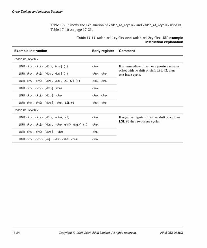
Cycle Timings and Interlock Behavior
Table 17-17 shows the explanation of <addr_md_1cycle> and <addr_md_2cycle> used in Table 17-16 on page 17-23.
Table 17-17 <addr_md_1cycle> and <addr_md_2cycle> LDRD exampleinstruction explanation
Example instruction Early register Comment
<addr_md_1cycle>
LDRD <Rt>, <Rt2> [<Rn>, #cns] (!) <Rn> If an immediate offset, or a positive register offset with no shift or shift LSL #2, then one-issue cycle.LDRD <Rt>, <Rt2> [<Rn>, <Rm>] (!) <Rn>, <Rm>
LDRD <Rt>, <Rt2> [<Rn>, <Rm>, LSL #2] (!) <Rn>, <Rm>
LDRD <Rt>, <Rt2> [<Rn>], #cns <Rn>
LDRD <Rt>, <Rt2> [<Rn>], <Rm> <Rn>, <Rm>
LDRD <Rt>, <Rt2> [<Rn>], <Rm>, LSL #2 <Rn>, <Rm>
<addr_md_2cycle>
LDRD <Rt>, <Rt2> [<Rn>, -<Rm>] (!) <Rm> If negative register offset, or shift other than LSL #2 then two-issue cycles.
LDRD <Rt>, <Rt2> [<Rm>, -<Rm> <shf> <cns>] (!) <Rm>
LDRD <Rt>, <Rt2> [<Rn>], -<Rm> <Rm>
LDRD <Rt>, <Rt2> [Rn], -<Rm> <shf> <cns> <Rm>
17-24 Copyright © 2005-2007 ARM Limited. All rights reserved. ARM DDI 0338G
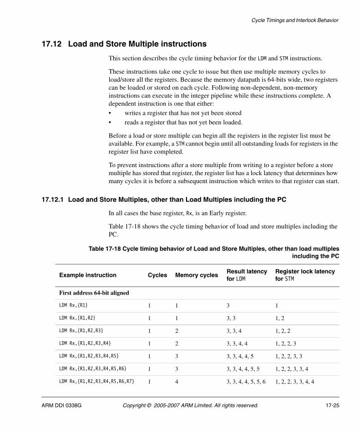
Cycle Timings and Interlock Behavior
17.12 Load and Store Multiple instructions
This section describes the cycle timing behavior for the LDM and STM instructions.
These instructions take one cycle to issue but then use multiple memory cycles to load/store all the registers. Because the memory datapath is 64-bits wide, two registers can be loaded or stored on each cycle. Following non-dependent, non-memory instructions can execute in the integer pipeline while these instructions complete. A dependent instruction is one that either:
• writes a register that has not yet been stored
• reads a register that has not yet been loaded.
Before a load or store multiple can begin all the registers in the register list must be available. For example, a STM cannot begin until all outstanding loads for registers in the register list have completed.
To prevent instructions after a store multiple from writing to a register before a store multiple has stored that register, the register list has a lock latency that determines how many cycles it is before a subsequent instruction which writes to that register can start.
17.12.1 Load and Store Multiples, other than Load Multiples including the PC
In all cases the base register, Rx, is an Early register.
Table 17-18 shows the cycle timing behavior of load and store multiples including the PC.
Table 17-18 Cycle timing behavior of Load and Store Multiples, other than load multiplesincluding the PC
Example instruction Cycles Memory cyclesResult latencyfor LDM
Register lock latencyfor STM
First address 64-bit aligned
LDM Rx,{R1} 1 1 3 1
LDM Rx,{R1,R2} 1 1 3, 3 1, 2
LDM Rx,{R1,R2,R3} 1 2 3, 3, 4 1, 2, 2
LDM Rx,{R1,R2,R3,R4} 1 2 3, 3, 4, 4 1, 2, 2, 3
LDM Rx,{R1,R2,R3,R4,R5} 1 3 3, 3, 4, 4, 5 1, 2, 2, 3, 3
LDM Rx,{R1,R2,R3,R4,R5,R6} 1 3 3, 3, 4, 4, 5, 5 1, 2, 2, 3, 3, 4
LDM Rx,{R1,R2,R3,R4,R5,R6,R7} 1 4 3, 3, 4, 4, 5, 5, 6 1, 2, 2, 3, 3, 4, 4
ARM DDI 0338G Copyright © 2005-2007 ARM Limited. All rights reserved. 17-25
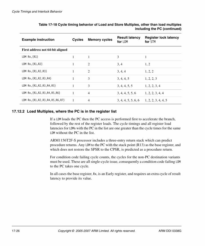
Cycle Timings and Interlock Behavior
17.12.2 Load Multiples, where the PC is in the register list
If a LDM loads the PC then the PC access is performed first to accelerate the branch, followed by the rest of the register loads. The cycle timings and all register load latencies for LDMs with the PC in the list are one greater than the cycle times for the same LDM without the PC in the list.
ARM1156T2F-S processor includes a three-entry return stack which can predict procedure returns. Any LDM to the PC with the stack point (R13) as the base register, and which does not restore the SPSR to the CPSR, is predicted as a procedure return.
For condition code failing cycle counts, the cycles for the non-PC destination variants must be used. These are all single-cycle issue, consequently a condition code failing LDM to the PC takes one cycle.
In all cases the base register, Rx, is an Early register, and requires an extra cycle of result latency to provide its value.
First address not 64-bit aligned
LDM Rx,{R1} 1 1 3 1
LDM Rx,{R1,R2} 1 2 3, 4 1, 2
LDM Rx,{R1,R2,R3} 1 2 3, 4, 4 1, 2, 2
LDM Rx,{R1,R2,R3,R4} 1 3 3, 4, 4, 5 1, 2, 2, 3
LDM Rx,{R1,R2,R3,R4,R5} 1 3 3, 4, 4, 5, 5 1, 2, 2, 3, 4
LDM Rx,{R1,R2,R3,R4,R5,R6} 1 4 3, 4, 4, 5, 5, 6 1, 2, 2, 3, 4, 4
LDM Rx,{R1,R2,R3,R4,R5,R6,R7} 1 4 3, 4, 4, 5, 5, 6, 6 1, 2, 2, 3, 4, 4, 5
Table 17-18 Cycle timing behavior of Load and Store Multiples, other than load multiplesincluding the PC (continued)
Example instruction Cycles Memory cyclesResult latencyfor LDM
Register lock latencyfor STM
17-26 Copyright © 2005-2007 ARM Limited. All rights reserved. ARM DDI 0338G
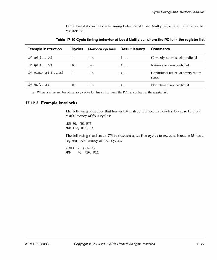
Cycle Timings and Interlock Behavior
Table 17-19 shows the cycle timing behavior of Load Multiples, where the PC is in the register list.
17.12.3 Example Interlocks
The following sequence that has an LDM instruction take five cycles, because R3 has a result latency of four cycles:
LDM R0, {R1-R7}ADD R10, R10, R3
The following that has an STM instruction takes five cycles to execute, because R6 has a register lock latency of four cycles:
STMIA R0, {R1-R7}ADD R6, R10, R11
Table 17-19 Cycle timing behavior of Load Multiples, where the PC is in the register list
Example instruction Cycles Memory cyclesa Result latency Comments
LDM sp!,{...,pc} 4 1+n 4, … Correctly return stack predicted
LDM sp!,{...,pc} 10 1+n 4, … Return stack mispredicted
LDM <cond> sp!,{...,pc} 9 1+n 4, … Conditional return, or empty return stack
LDM Rx,{...,pc} 10 1+n 4, … Not return stack predicted
a. Where n is the number of memory cycles for this instruction if the PC had not been in the register list.
ARM DDI 0338G Copyright © 2005-2007 ARM Limited. All rights reserved. 17-27
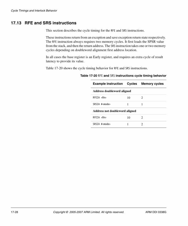
Cycle Timings and Interlock Behavior
17.13 RFE and SRS instructions
This section describes the cycle timing for the RFE and SRS instructions.
These instructions return from an exception and save exception return state respectively. The RFE instruction always requires two memory cycles. It first loads the SPSR value from the stack, and then the return address. The SRS instruction takes one or two memory cycles depending on doubleword alignment first address location.
In all cases the base register is an Early register, and requires an extra cycle of result latency to provide its value.
Table 17-20 shows the cycle timing behavior for RFE and SRS instructions.
Table 17-20 RFE and SRS instructions cycle timing behavior
Example instruction Cycles Memory cycles
Address doubleword aligned
RFEIA <Rn> 10 2
SRSIA #<mode> 1 1
Address not doubleword aligned
RFEIA <Rn> 10 2
SRSIA #<mode> 1 2
17-28 Copyright © 2005-2007 ARM Limited. All rights reserved. ARM DDI 0338G
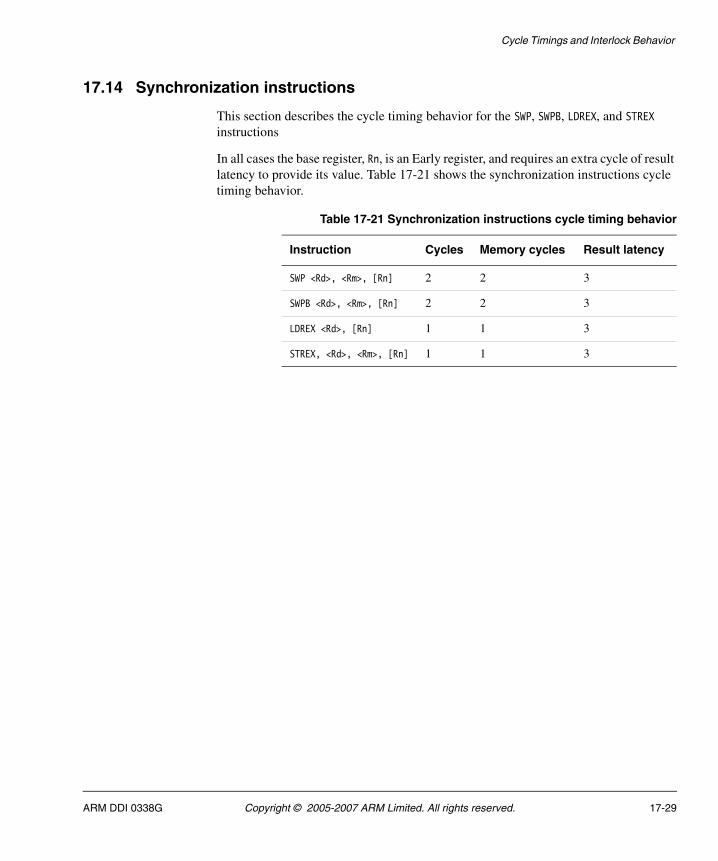
Cycle Timings and Interlock Behavior
17.14 Synchronization instructions
This section describes the cycle timing behavior for the SWP, SWPB, LDREX, and STREX instructions
In all cases the base register, Rn, is an Early register, and requires an extra cycle of result latency to provide its value. Table 17-21 shows the synchronization instructions cycle timing behavior.
Table 17-21 Synchronization instructions cycle timing behavior
Instruction Cycles Memory cycles Result latency
SWP <Rd>, <Rm>, [Rn] 2 2 3
SWPB <Rd>, <Rm>, [Rn] 2 2 3
LDREX <Rd>, [Rn] 1 1 3
STREX, <Rd>, <Rm>, [Rn] 1 1 3
ARM DDI 0338G Copyright © 2005-2007 ARM Limited. All rights reserved. 17-29
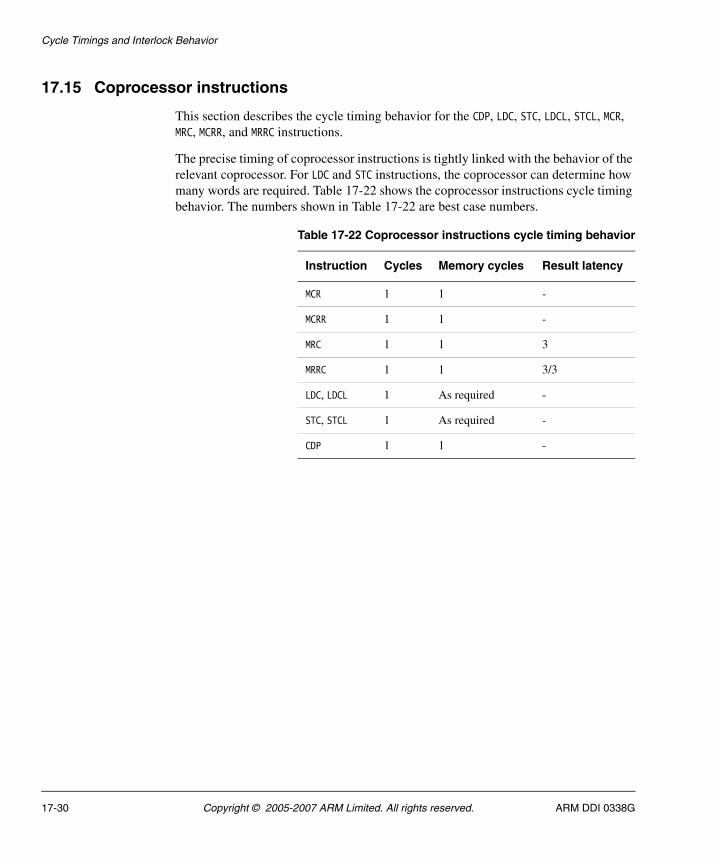
Cycle Timings and Interlock Behavior
17.15 Coprocessor instructions
This section describes the cycle timing behavior for the CDP, LDC, STC, LDCL, STCL, MCR, MRC, MCRR, and MRRC instructions.
The precise timing of coprocessor instructions is tightly linked with the behavior of the relevant coprocessor. For LDC and STC instructions, the coprocessor can determine how many words are required. Table 17-22 shows the coprocessor instructions cycle timing behavior. The numbers shown in Table 17-22 are best case numbers.
Table 17-22 Coprocessor instructions cycle timing behavior
Instruction Cycles Memory cycles Result latency
MCR 1 1 -
MCRR 1 1 -
MRC 1 1 3
MRRC 1 1 3/3
LDC, LDCL 1 As required -
STC, STCL 1 As required -
CDP 1 1 -
17-30 Copyright © 2005-2007 ARM Limited. All rights reserved. ARM DDI 0338G
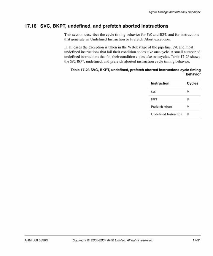
Cycle Timings and Interlock Behavior
17.16 SVC, BKPT, undefined, and prefetch aborted instructions
This section describes the cycle timing behavior for SVC and BKPT, and for instructions that generate an Undefined Instruction or Prefetch Abort exception.
In all cases the exception is taken in the WBex stage of the pipeline. SVC and most undefined instructions that fail their condition codes take one cycle. A small number of undefined instructions that fail their condition codes take two cycles. Table 17-23 shows the SVC, BKPT, undefined, and prefetch aborted instruction cycle timing behavior.
Table 17-23 SVC, BKPT, undefined, prefetch aborted instructions cycle timingbehavior
Instruction Cycles
SVC 9
BKPT 9
Prefetch Abort 9
Undefined Instruction 9
ARM DDI 0338G Copyright © 2005-2007 ARM Limited. All rights reserved. 17-31
Cycle Timings and Interlock Behavior
17.17 CBZ, CBNZ, and IT instructions
This section describes the cycle timing behavior for the CBZ, CBNZ, and IT instructions. Table 17-24 shows instruction cycle timing behavior for these instructions.
Table 17-24 CBZ and IT instructions cycle timing behavior
Example instructions Cycles Early register Late register Result latency Comment
CBZ <Rn>, <label> 1 - - - Correctly predicted
8 - - - Incorrectly predicted
CBNZ <Rn>, <label> 1 - - - Correctly predicted
8 - - - Incorrectly predicted
IT{<v>{<w>{<z>}}} <cond> 1 - - - -
0 - - - If folded out
17-32 Copyright © 2005-2007 ARM Limited. All rights reserved. ARM DDI 0338G
Cycle Timings and Interlock Behavior
17.18 Bitfield instructions
This section describes the cycle timing behavior for the BFC, BFI, SBFX, and UBFX instructions. Table 17-25 shows the bitfield instruction cycle timing behavior.
Table 17-25 Thumb-2 bitfield instruction cycle timing behavior
Example instructions CyclesEarly register
Late register
Result latency Comment
SBFX <cond> <Rd>, <Rm>, #<lsb>, #<width>
UBFX <cond> <Rd>,<Rn>,#<lsb>,#<width>
1 <Rm> - 1 -
BFI <cond> <Rd>, <Rn>, #<lsb>, #<width>
BFC <cond> <Rd>,#<lsb>,#<width>
2 <Rn>, <Rd> - 2 -
ARM DDI 0338G Copyright © 2005-2007 ARM Limited. All rights reserved. 17-33
Cycle Timings and Interlock Behavior
17.19 NOP (CPS) instruction
This section describes the cycle timing behavior for the NOP (CPS) instruction. Table 17-26 shows the NOP (CPS) instruction cycle timing behavior.
Table 17-26 Thumb-2 NOP (CPS) instruction cycle timing behavior
instruction Cycles Early register Late register Result latency Comment
NOP 1 - - - -
17-34 Copyright © 2005-2007 ARM Limited. All rights reserved. ARM DDI 0338G
Cycle Timings and Interlock Behavior
17.20 Table branch instructions
This section describes the cycle timing behavior for the TBB and TBH instructions. Table 17-27 shows the table branch instructions cycle timing behavior.
Table 17-27 Thumb-2 table branch instructions cycle timing behavior
Example instructions Cycles Comment
TBB <Rd>, <addr_md_1cycle>a
a. See Table 17-15 on page 17-22 for an explanation of <addr_md_1cycle> and <addr_md_2cycle>.
10 -
TBH <Rd>, <addr_md_2cycle>a 11 -
ARM DDI 0338G Copyright © 2005-2007 ARM Limited. All rights reserved. 17-35
Cycle Timings and Interlock Behavior
17-36 Copyright © 2005-2007 ARM Limited. All rights reserved. ARM DDI 0338G

Chapter 18 AC Characteristics
This chapter gives the timing parameters for the ARM1156T2-S processor. This chapter contains the following sections:
• ARM1156T2-S timing diagrams on page 18-2
• ARM1156T2-S timing parameters on page 18-3.
ARM DDI 0338G Copyright © 2005-2007 ARM Limited. All rights reserved. 18-1
AC Characteristics
18.1 ARM1156T2-S timing diagrams
The AMBA bus interface of the ARM1156T2-S processor conforms to the AMBA Specification. For the relevant timing diagrams, see the AMBA Specification.
18-2 Copyright © 2005-2007 ARM Limited. All rights reserved. ARM DDI 0338G
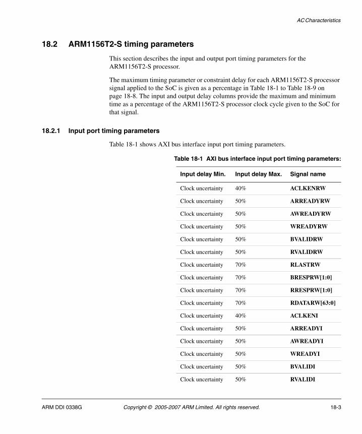
AC Characteristics
18.2 ARM1156T2-S timing parameters
This section describes the input and output port timing parameters for the ARM1156T2-S processor.
The maximum timing parameter or constraint delay for each ARM1156T2-S processor signal applied to the SoC is given as a percentage in Table 18-1 to Table 18-9 on page 18-8. The input and output delay columns provide the maximum and minimum time as a percentage of the ARM1156T2-S processor clock cycle given to the SoC for that signal.
18.2.1 Input port timing parameters
Table 18-1 shows AXI bus interface input port timing parameters.
Table 18-1 AXI bus interface input port timing parameters:
Input delay Min. Input delay Max. Signal name
Clock uncertainty 40% ACLKENRW
Clock uncertainty 50% ARREADYRW
Clock uncertainty 50% AWREADYRW
Clock uncertainty 50% WREADYRW
Clock uncertainty 50% BVALIDRW
Clock uncertainty 50% RVALIDRW
Clock uncertainty 70% RLASTRW
Clock uncertainty 70% BRESPRW[1:0]
Clock uncertainty 70% RRESPRW[1:0]
Clock uncertainty 70% RDATARW[63:0]
Clock uncertainty 40% ACLKENI
Clock uncertainty 50% ARREADYI
Clock uncertainty 50% AWREADYI
Clock uncertainty 50% WREADYI
Clock uncertainty 50% BVALIDI
Clock uncertainty 50% RVALIDI
ARM DDI 0338G Copyright © 2005-2007 ARM Limited. All rights reserved. 18-3
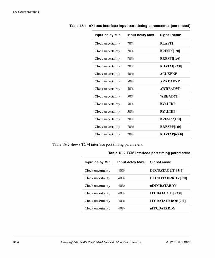
AC Characteristics
Table 18-2 shows TCM interface port timing parameters.
Clock uncertainty 70% RLASTI
Clock uncertainty 70% BRESPI[1:0]
Clock uncertainty 70% RRESPI[1:0]
Clock uncertainty 70% RDATAI[63:0]
Clock uncertainty 40% ACLKENP
Clock uncertainty 50% ARREADYP
Clock uncertainty 50% AWREADYP
Clock uncertainty 50% WREADYP
Clock uncertainty 50% BVALIDP
Clock uncertainty 50% RVALIDP
Clock uncertainty 70% BRESPP[1:0]
Clock uncertainty 70% RRESPP[1:0]
Clock uncertainty 70% RDATAP[63:0]
Table 18-2 TCM interface port timing parameters
Input delay Min. Input delay Max. Signal name
Clock uncertainty 40% DTCDATAOUT[63:0]
Clock uncertainty 40% DTCDATAERROR[7:0]
Clock uncertainty 40% nDTCDATARDY
Clock uncertainty 40% ITCDATAOUT[63:0]
Clock uncertainty 40% ITCDATAERROR[7:0]
Clock uncertainty 40% nITCDATARDY
Table 18-1 AXI bus interface input port timing parameters: (continued)
Input delay Min. Input delay Max. Signal name
18-4 Copyright © 2005-2007 ARM Limited. All rights reserved. ARM DDI 0338G
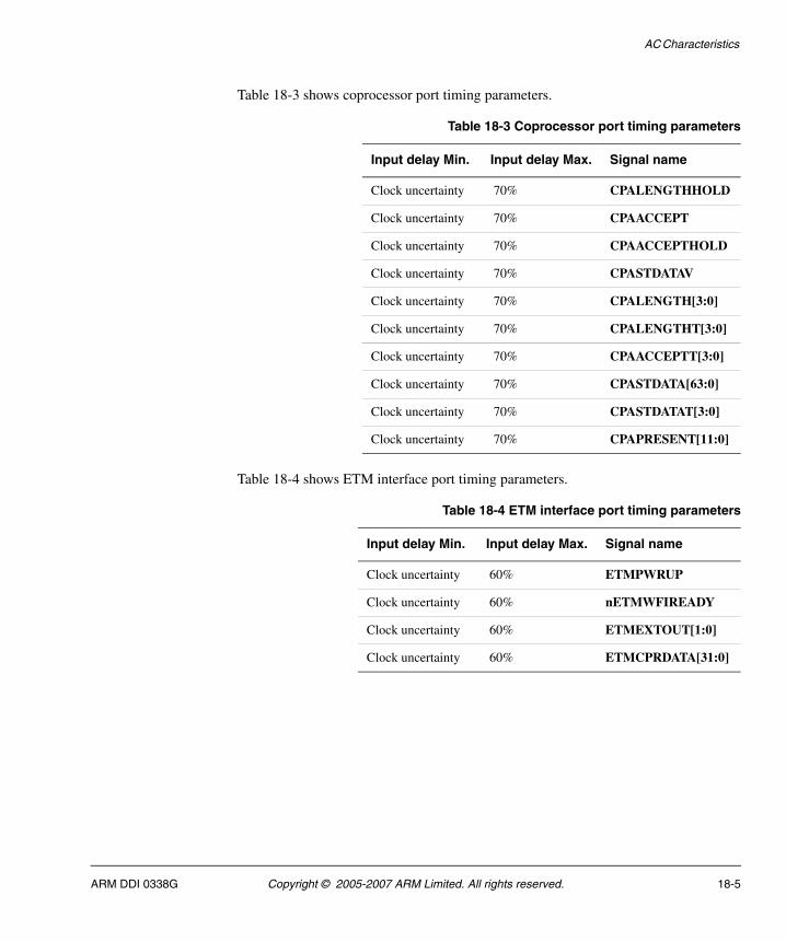
AC Characteristics
Table 18-3 shows coprocessor port timing parameters.
Table 18-4 shows ETM interface port timing parameters.
Table 18-3 Coprocessor port timing parameters
Input delay Min. Input delay Max. Signal name
Clock uncertainty 70% CPALENGTHHOLD
Clock uncertainty 70% CPAACCEPT
Clock uncertainty 70% CPAACCEPTHOLD
Clock uncertainty 70% CPASTDATAV
Clock uncertainty 70% CPALENGTH[3:0]
Clock uncertainty 70% CPALENGTHT[3:0]
Clock uncertainty 70% CPAACCEPTT[3:0]
Clock uncertainty 70% CPASTDATA[63:0]
Clock uncertainty 70% CPASTDATAT[3:0]
Clock uncertainty 70% CPAPRESENT[11:0]
Table 18-4 ETM interface port timing parameters
Input delay Min. Input delay Max. Signal name
Clock uncertainty 60% ETMPWRUP
Clock uncertainty 60% nETMWFIREADY
Clock uncertainty 60% ETMEXTOUT[1:0]
Clock uncertainty 60% ETMCPRDATA[31:0]
ARM DDI 0338G Copyright © 2005-2007 ARM Limited. All rights reserved. 18-5
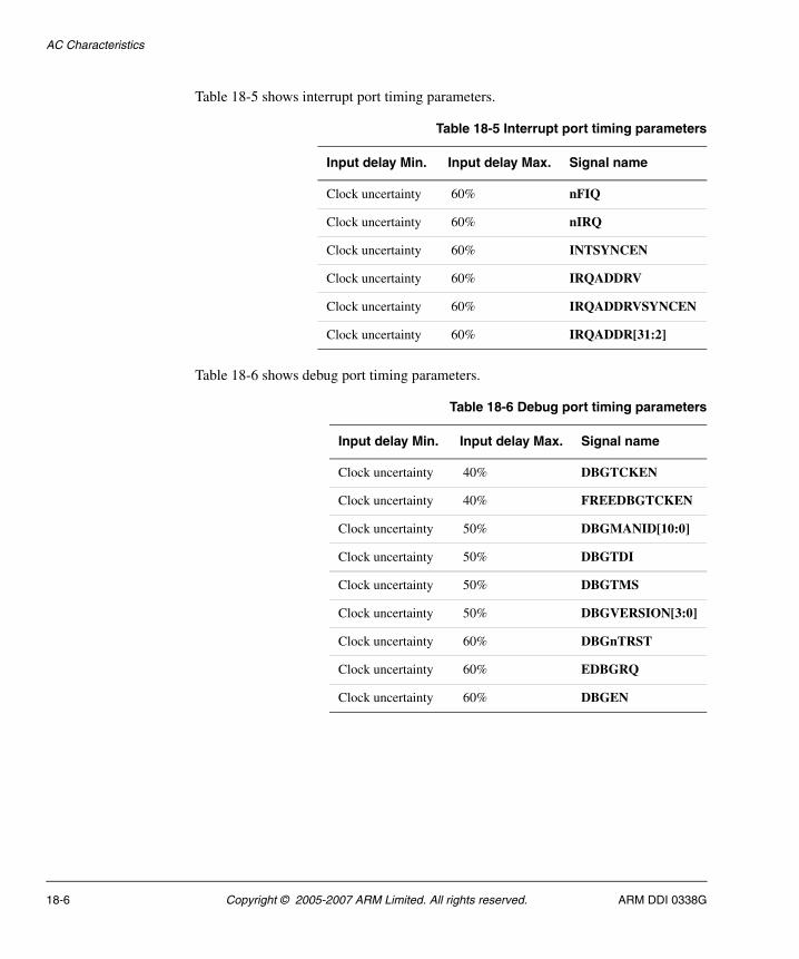
AC Characteristics
Table 18-5 shows interrupt port timing parameters.
Table 18-6 shows debug port timing parameters.
Table 18-5 Interrupt port timing parameters
Input delay Min. Input delay Max. Signal name
Clock uncertainty 60% nFIQ
Clock uncertainty 60% nIRQ
Clock uncertainty 60% INTSYNCEN
Clock uncertainty 60% IRQADDRV
Clock uncertainty 60% IRQADDRVSYNCEN
Clock uncertainty 60% IRQADDR[31:2]
Table 18-6 Debug port timing parameters
Input delay Min. Input delay Max. Signal name
Clock uncertainty 40% DBGTCKEN
Clock uncertainty 40% FREEDBGTCKEN
Clock uncertainty 50% DBGMANID[10:0]
Clock uncertainty 50% DBGTDI
Clock uncertainty 50% DBGTMS
Clock uncertainty 50% DBGVERSION[3:0]
Clock uncertainty 60% DBGnTRST
Clock uncertainty 60% EDBGRQ
Clock uncertainty 60% DBGEN
18-6 Copyright © 2005-2007 ARM Limited. All rights reserved. ARM DDI 0338G
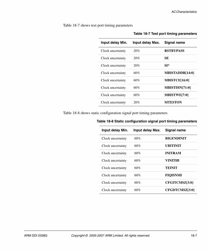
AC Characteristics
Table 18-7 shows test port timing parameters
Table 18-8 shows static configuration signal port timing parameters
Table 18-7 Test port timing parameters
Input delay Min. Input delay Max. Signal name
Clock uncertainty 20% RSTBYPASS
Clock uncertainty 20% SE
Clock uncertainty 20% SI*
Clock uncertainty 60% MBISTADDR[14:0]
Clock uncertainty 60% MBISTCE[16:0]
Clock uncertainty 60% MBISTDIN[71:0]
Clock uncertainty 60% MBISTWE[7:0]
Clock uncertainty 20% MTESTON
Table 18-8 Static configuration signal port timing parameters
Input delay Min. Input delay Max. Signal name
Clock uncertainty 60% BIGENDINIT
Clock uncertainty 60% UBITINIT
Clock uncertainty 60% INITRAM
Clock uncertainty 60% VINITHI
Clock uncertainty 60% TEINIT
Clock uncertainty 60% FIQISNMI
Clock uncertainty 60% CFGITCMSZ[3:0]
Clock uncertainty 60% CFGDTCMSZ[3:0]
ARM DDI 0338G Copyright © 2005-2007 ARM Limited. All rights reserved. 18-7
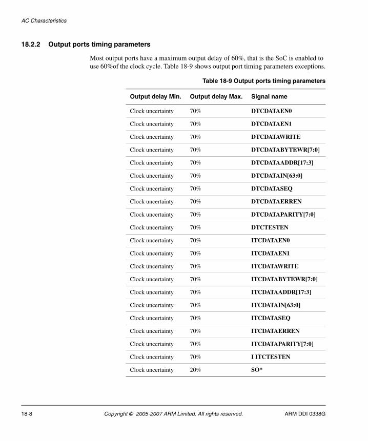
AC Characteristics
18.2.2 Output ports timing parameters
Most output ports have a maximum output delay of 60%, that is the SoC is enabled to use 60%of the clock cycle. Table 18-9 shows output port timing parameters exceptions.
Table 18-9 Output ports timing parameters
Output delay Min. Output delay Max. Signal name
Clock uncertainty 70% DTCDATAEN0
Clock uncertainty 70% DTCDATAEN1
Clock uncertainty 70% DTCDATAWRITE
Clock uncertainty 70% DTCDATABYTEWR[7:0]
Clock uncertainty 70% DTCDATAADDR[17:3]
Clock uncertainty 70% DTCDATAIN[63:0]
Clock uncertainty 70% DTCDATASEQ
Clock uncertainty 70% DTCDATAERREN
Clock uncertainty 70% DTCDATAPARITY[7:0]
Clock uncertainty 70% DTCTESTEN
Clock uncertainty 70% ITCDATAEN0
Clock uncertainty 70% ITCDATAEN1
Clock uncertainty 70% ITCDATAWRITE
Clock uncertainty 70% ITCDATABYTEWR[7:0]
Clock uncertainty 70% ITCDATAADDR[17:3]
Clock uncertainty 70% ITCDATAIN[63:0]
Clock uncertainty 70% ITCDATASEQ
Clock uncertainty 70% ITCDATAERREN
Clock uncertainty 70% ITCDATAPARITY[7:0]
Clock uncertainty 70% I ITCTESTEN
Clock uncertainty 20% SO*
18-8 Copyright © 2005-2007 ARM Limited. All rights reserved. ARM DDI 0338G
Appendix A Processor Signal Descriptions
This appendix lists and describes the processor signals. It contains the following sections:
• Global signals on page A-2
• Configuration signals on page A-3
• Interrupt signals (including VIC interface signals) on page A-4
• AXI interface signals on page A-5
• Instruction TCM Interface on page A-10
• Data TCM Interface on page A-11
• Coprocessor interface signals on page A-12
• Debug interface signals (including JTAG) on page A-14
• ETM interface signals on page A-15
• Test signals on page A-16.
Note The output signals shown in Table A-1 on page A-2 to Table A-13 on page A-16 are set to 0 on reset unless otherwise stated.
ARM DDI 0338G Copyright © 2005-2007 ARM Limited. All rights reserved. A-1
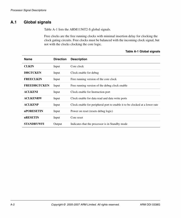
Processor Signal Descriptions
A.1 Global signals
Table A-1 lists the ARM1156T2-S global signals.
Free clocks are the free running clocks with minimal insertion delay for clocking the clock gating circuits. Free clocks must be balanced with the incoming clock signal, but not with the clocks clocking the core logic.
Table A-1 Global signals
Name Direction Description
CLKIN Input Core clock
DBGTCKEN Input Clock enable for debug
FREECLKIN Input Free running version of the core clock
FREEDBGTCKEN Input Free running version of the debug clock enable
ACLKENI Input Clock enable for Instruction port
ACLKENRW Input Clock enable for data read and data write ports
ACLKENP Input Clock enable for peripheral port to enable it to be clocked at a lower rate
nPORESETIN Input Power on reset (resets debug logic)
nRESETIN Input Core reset
STANDBYWFI Output Indicates that the processor is in Standby mode
A-2 Copyright © 2005-2007 ARM Limited. All rights reserved. ARM DDI 0338G
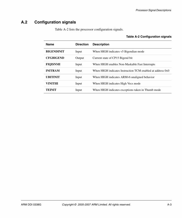
Processor Signal Descriptions
A.2 Configuration signals
Table A-2 lists the processor configuration signals.
Table A-2 Configuration signals
Name Direction Description
BIGENDINIT Input When HIGH indicates v5 Bigendian mode
CFGBIGEND Output Current state of CP15 Bigend bit
FIQISNMI Input When HIGH enables Non-Maskable Fast Interrupts
INITRAM Input When HIGH indicates Instruction TCM enabled at address 0x0
UBITINIT Input When HIGH indicates ARMv6 unaligned behavior
VINITHI Input When HIGH indicates High Vecs mode
TEINIT Input When HIGH indicates exceptions taken in Thumb mode
ARM DDI 0338G Copyright © 2005-2007 ARM Limited. All rights reserved. A-3
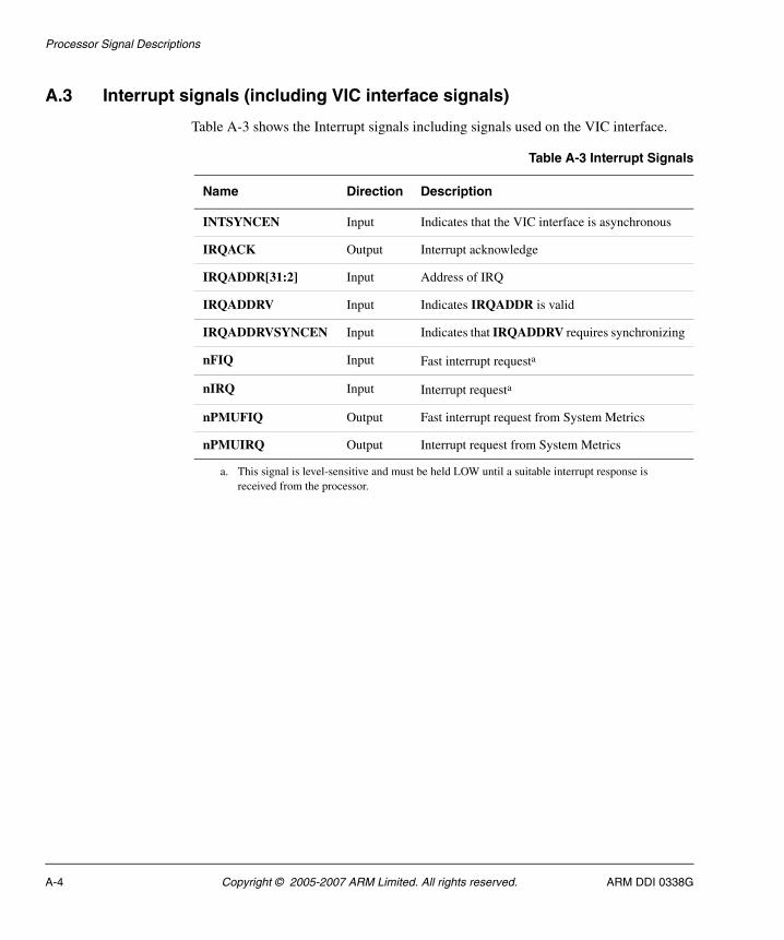
Processor Signal Descriptions
A.3 Interrupt signals (including VIC interface signals)
Table A-3 shows the Interrupt signals including signals used on the VIC interface.
Table A-3 Interrupt Signals
Name Direction Description
INTSYNCEN Input Indicates that the VIC interface is asynchronous
IRQACK Output Interrupt acknowledge
IRQADDR[31:2] Input Address of IRQ
IRQADDRV Input Indicates IRQADDR is valid
IRQADDRVSYNCEN Input Indicates that IRQADDRV requires synchronizing
nFIQ Input Fast interrupt requesta
a. This signal is level-sensitive and must be held LOW until a suitable interrupt response is received from the processor.
nIRQ Input Interrupt requesta
nPMUFIQ Output Fast interrupt request from System Metrics
nPMUIRQ Output Interrupt request from System Metrics
A-4 Copyright © 2005-2007 ARM Limited. All rights reserved. ARM DDI 0338G
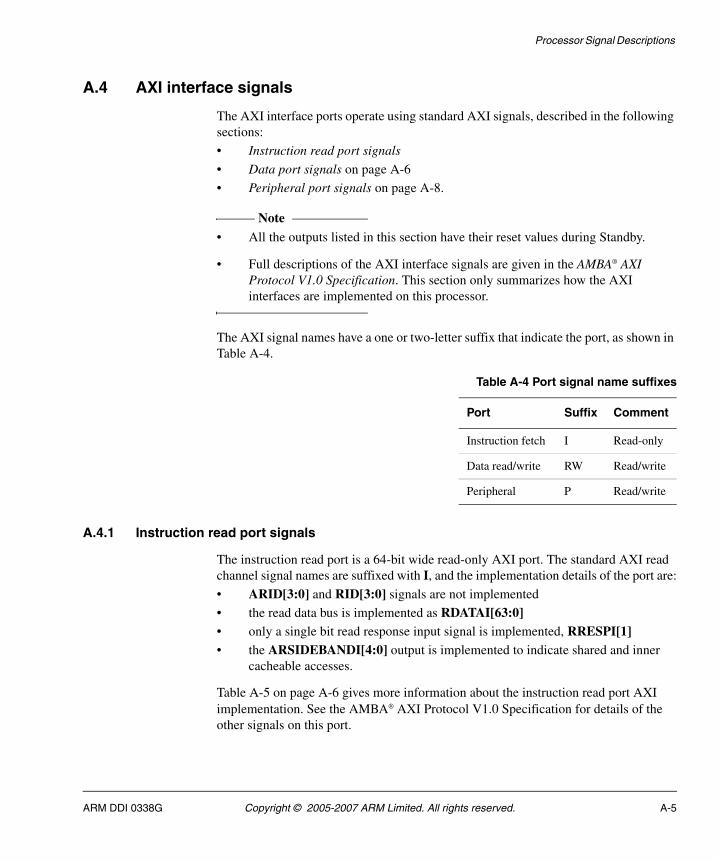
Processor Signal Descriptions
A.4 AXI interface signals
The AXI interface ports operate using standard AXI signals, described in the following sections:
• Instruction read port signals
• Data port signals on page A-6
• Peripheral port signals on page A-8.
Note • All the outputs listed in this section have their reset values during Standby.
• Full descriptions of the AXI interface signals are given in the AMBA® AXI Protocol V1.0 Specification. This section only summarizes how the AXI interfaces are implemented on this processor.
The AXI signal names have a one or two-letter suffix that indicate the port, as shown in Table A-4.
A.4.1 Instruction read port signals
The instruction read port is a 64-bit wide read-only AXI port. The standard AXI read channel signal names are suffixed with I, and the implementation details of the port are:
• ARID[3:0] and RID[3:0] signals are not implemented
• the read data bus is implemented as RDATAI[63:0]• only a single bit read response input signal is implemented, RRESPI[1]• the ARSIDEBANDI[4:0] output is implemented to indicate shared and inner
cacheable accesses.
Table A-5 on page A-6 gives more information about the instruction read port AXI implementation. See the AMBA® AXI Protocol V1.0 Specification for details of the other signals on this port.
Table A-4 Port signal name suffixes
Port Suffix Comment
Instruction fetch I Read-only
Data read/write RW Read/write
Peripheral P Read/write
ARM DDI 0338G Copyright © 2005-2007 ARM Limited. All rights reserved. A-5
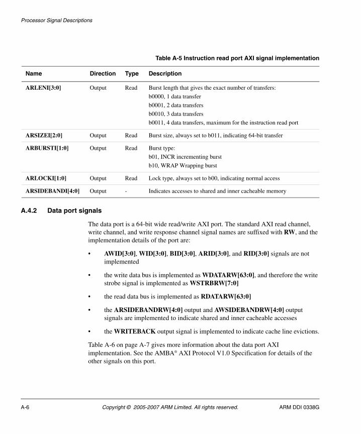
Processor Signal Descriptions
A.4.2 Data port signals
The data port is a 64-bit wide read/write AXI port. The standard AXI read channel, write channel, and write response channel signal names are suffixed with RW, and the implementation details of the port are:
• AWID[3:0], WID[3:0], BID[3:0], ARID[3:0], and RID[3:0] signals are not implemented
• the write data bus is implemented as WDATARW[63:0], and therefore the write strobe signal is implemented as WSTRBRW[7:0]
• the read data bus is implemented as RDATARW[63:0]
• the ARSIDEBANDRW[4:0] output and AWSIDEBANDRW[4:0] output signals are implemented to indicate shared and inner cacheable accesses
• the WRITEBACK output signal is implemented to indicate cache line evictions.
Table A-6 on page A-7 gives more information about the data port AXI implementation. See the AMBA® AXI Protocol V1.0 Specification for details of the other signals on this port.
Table A-5 Instruction read port AXI signal implementation
Name Direction Type Description
ARLENI[3:0] Output Read Burst length that gives the exact number of transfers:
b0000, 1 data transfer
b0001, 2 data transfers
b0010, 3 data transfers
b0011, 4 data transfers, maximum for the instruction read port
ARSIZEI[2:0] Output Read Burst size, always set to b011, indicating 64-bit transfer
ARBURSTI[1:0] Output Read Burst type:
b01, INCR incrementing burst
b10, WRAP Wrapping burst
ARLOCKI[1:0] Output Read Lock type, always set to b00, indicating normal access
ARSIDEBANDI[4:0] Output - Indicates accesses to shared and inner cacheable memory
A-6 Copyright © 2005-2007 ARM Limited. All rights reserved. ARM DDI 0338G
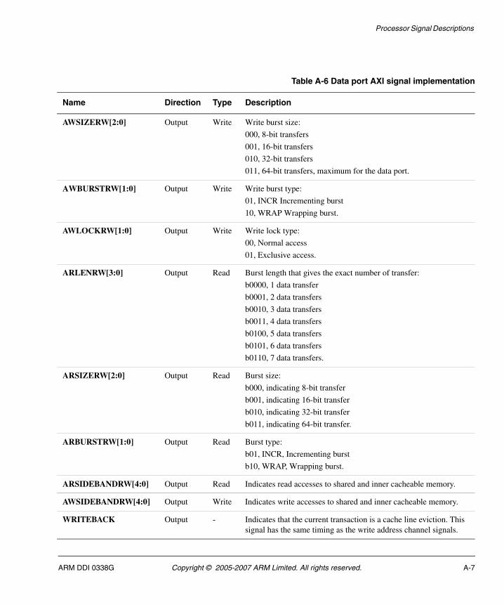
Processor Signal Descriptions
Table A-6 Data port AXI signal implementation
Name Direction Type Description
AWSIZERW[2:0] Output Write Write burst size:
000, 8-bit transfers
001, 16-bit transfers
010, 32-bit transfers
011, 64-bit transfers, maximum for the data port.
AWBURSTRW[1:0] Output Write Write burst type:
01, INCR Incrementing burst
10, WRAP Wrapping burst.
AWLOCKRW[1:0] Output Write Write lock type:
00, Normal access
01, Exclusive access.
ARLENRW[3:0] Output Read Burst length that gives the exact number of transfer:
b0000, 1 data transfer
b0001, 2 data transfers
b0010, 3 data transfers
b0011, 4 data transfers
b0100, 5 data transfers
b0101, 6 data transfers
b0110, 7 data transfers.
ARSIZERW[2:0] Output Read Burst size:
b000, indicating 8-bit transfer
b001, indicating 16-bit transfer
b010, indicating 32-bit transfer
b011, indicating 64-bit transfer.
ARBURSTRW[1:0] Output Read Burst type:
b01, INCR, Incrementing burst
b10, WRAP, Wrapping burst.
ARSIDEBANDRW[4:0] Output Read Indicates read accesses to shared and inner cacheable memory.
AWSIDEBANDRW[4:0] Output Write Indicates write accesses to shared and inner cacheable memory.
WRITEBACK Output - Indicates that the current transaction is a cache line eviction. This signal has the same timing as the write address channel signals.
ARM DDI 0338G Copyright © 2005-2007 ARM Limited. All rights reserved. A-7
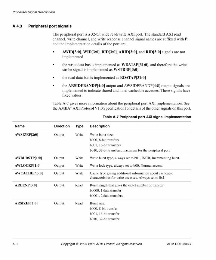
Processor Signal Descriptions
A.4.3 Peripheral port signals
The peripheral port is a 32-bit wide read/write AXI port. The standard AXI read channel, write channel, and write response channel signal names are suffixed with P, and the implementation details of the port are:
• AWID[3:0], WID[3:0], BID[3:0], ARID[3:0], and RID[3:0] signals are not implemented
• the write data bus is implemented as WDATAP[31:0], and therefore the write strobe signal is implemented as WSTRBP[3:0]
• the read data bus is implemented as RDATAP[31:0]
• the ARSIDEBANDP[4:0] output and AWSIDEBANDP[4:0] output signals are implemented to indicate shared and inner cacheable accesses. These signals have fixed values.
Table A-7 gives more information about the peripheral port AXI implementation. See the AMBA® AXI Protocol V1.0 Specification for details of the other signals on this port.
Table A-7 Peripheral port AXI signal implementation
Name Direction Type Description
AWSIZEP[2:0] Output Write Write burst size:
b000, 8-bit transfers
b001, 16-bit transfers
b010, 32-bit transfers, maximum for the peripheral port.
AWBURSTP[1:0] Output Write Write burst type, always set to b01, INCR, Incrementing burst.
AWLOCKP[1:0] Output Write Write lock type, always set to b00, Normal access.
AWCACHEP[3:0] Output Write Cache type giving additional information about cacheable characteristics for write accesses. Always set to 0x1.
ARLENP[3:0] Output Read Burst length that gives the exact number of transfer:
b0000, 1 data transfer
b0001, 2 data transfers.
ARSIZEP[2:0] Output Read Burst size:
b000, 8-bit transfer
b001, 16-bit transfer
b010, 32-bit transfer.
A-8 Copyright © 2005-2007 ARM Limited. All rights reserved. ARM DDI 0338G
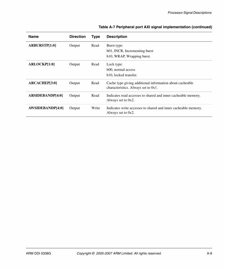
Processor Signal Descriptions
ARBURSTP[1:0] Output Read Burst type:
b01, INCR, Incrementing burst
b10, WRAP, Wrapping burst.
ARLOCKP[1:0] Output Read Lock type:
b00, normal access
b10, locked transfer.
ARCACHEP[3:0] Output Read Cache type giving additional information about cacheable characteristics. Always set to 0x1.
ARSIDEBANDP[4:0] Output Read Indicates read accesses to shared and inner cacheable memory. Always set to 0x2.
AWSIDEBANDP[4:0] Output Write Indicates write accesses to shared and inner cacheable memory. Always set to 0x2.
Table A-7 Peripheral port AXI signal implementation (continued)
Name Direction Type Description
ARM DDI 0338G Copyright © 2005-2007 ARM Limited. All rights reserved. A-9
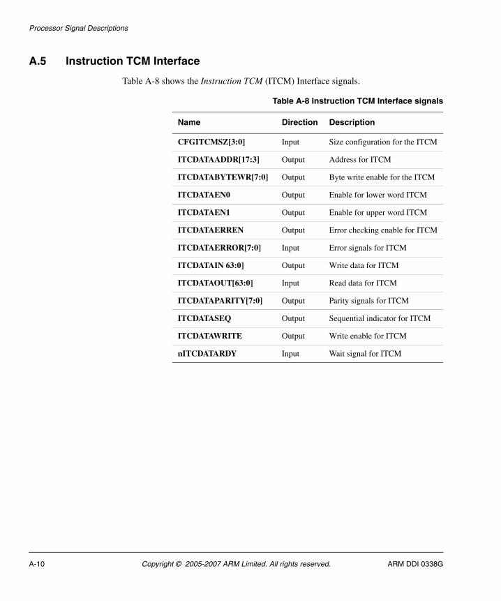
Processor Signal Descriptions
A.5 Instruction TCM Interface
Table A-8 shows the Instruction TCM (ITCM) Interface signals.
Table A-8 Instruction TCM Interface signals
Name Direction Description
CFGITCMSZ[3:0] Input Size configuration for the ITCM
ITCDATAADDR[17:3] Output Address for ITCM
ITCDATABYTEWR[7:0] Output Byte write enable for the ITCM
ITCDATAEN0 Output Enable for lower word ITCM
ITCDATAEN1 Output Enable for upper word ITCM
ITCDATAERREN Output Error checking enable for ITCM
ITCDATAERROR[7:0] Input Error signals for ITCM
ITCDATAIN 63:0] Output Write data for ITCM
ITCDATAOUT[63:0] Input Read data for ITCM
ITCDATAPARITY[7:0] Output Parity signals for ITCM
ITCDATASEQ Output Sequential indicator for ITCM
ITCDATAWRITE Output Write enable for ITCM
nITCDATARDY Input Wait signal for ITCM
A-10 Copyright © 2005-2007 ARM Limited. All rights reserved. ARM DDI 0338G
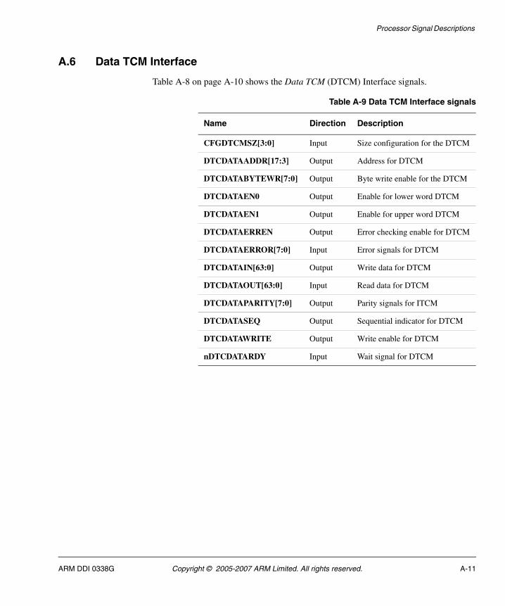
Processor Signal Descriptions
A.6 Data TCM Interface
Table A-8 on page A-10 shows the Data TCM (DTCM) Interface signals.
Table A-9 Data TCM Interface signals
Name Direction Description
CFGDTCMSZ[3:0] Input Size configuration for the DTCM
DTCDATAADDR[17:3] Output Address for DTCM
DTCDATABYTEWR[7:0] Output Byte write enable for the DTCM
DTCDATAEN0 Output Enable for lower word DTCM
DTCDATAEN1 Output Enable for upper word DTCM
DTCDATAERREN Output Error checking enable for DTCM
DTCDATAERROR[7:0] Input Error signals for DTCM
DTCDATAIN[63:0] Output Write data for DTCM
DTCDATAOUT[63:0] Input Read data for DTCM
DTCDATAPARITY[7:0] Output Parity signals for ITCM
DTCDATASEQ Output Sequential indicator for DTCM
DTCDATAWRITE Output Write enable for DTCM
nDTCDATARDY Input Wait signal for DTCM
ARM DDI 0338G Copyright © 2005-2007 ARM Limited. All rights reserved. A-11
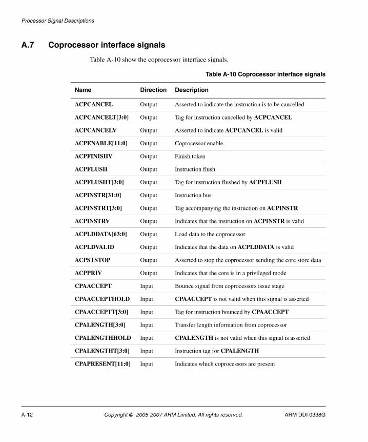
Processor Signal Descriptions
A.7 Coprocessor interface signals
Table A-10 show the coprocessor interface signals.
Table A-10 Coprocessor interface signals
Name Direction Description
ACPCANCEL Output Asserted to indicate the instruction is to be cancelled
ACPCANCELT[3:0] Output Tag for instruction cancelled by ACPCANCEL
ACPCANCELV Output Asserted to indicate ACPCANCEL is valid
ACPENABLE[11:0] Output Coprocessor enable
ACPFINISHV Output Finish token
ACPFLUSH Output Instruction flush
ACPFLUSHT[3:0] Output Tag for instruction flushed by ACPFLUSH
ACPINSTR[31:0] Output Instruction bus
ACPINSTRT[3:0] Output Tag accompanying the instruction on ACPINSTR
ACPINSTRV Output Indicates that the instruction on ACPINSTR is valid
ACPLDDATA[63:0] Output Load data to the coprocessor
ACPLDVALID Output Indicates that the data on ACPLDDATA is valid
ACPSTSTOP Output Asserted to stop the coprocessor sending the core store data
ACPPRIV Output Indicates that the core is in a privileged mode
CPAACCEPT Input Bounce signal from coprocessors issue stage
CPAACCEPTHOLD Input CPAACCEPT is not valid when this signal is asserted
CPAACCEPTT[3:0] Input Tag for instruction bounced by CPAACCEPT
CPALENGTH[3:0] Input Transfer length information from coprocessor
CPALENGTHHOLD Input CPALENGTH is not valid when this signal is asserted
CPALENGTHT[3:0] Input Instruction tag for CPALENGTH
CPAPRESENT[11:0] Input Indicates which coprocessors are present
A-12 Copyright © 2005-2007 ARM Limited. All rights reserved. ARM DDI 0338G
Processor Signal Descriptions
Note If no coprocessor is connected, the following signals must be driven LOW:
• CPALENGTHHOLD• CPAACCEPT• CPAACCEPTHOLD.
CPASTDATA[63:0] Input Coprocessor store data
CPASTDATAT[3:0] Input Tag accompanying the data on CPASTDATA
CPASTDATAV Input Indicates that the store data is valid
Table A-10 Coprocessor interface signals (continued)
Name Direction Description
ARM DDI 0338G Copyright © 2005-2007 ARM Limited. All rights reserved. A-13
Processor Signal Descriptions
A.8 Debug interface signals (including JTAG)
Table A-11 lists the debug interface signals including JTAG.
Table A-11 Debug interface signals
Name Direction Description
COMMRX Output Communications channel receive
COMMTX Output Communications channel transmit
DBGACK Output Debug Acknowledge
DBGEN Input Debug enable
DBGMANID[10:0] Input Customer field for JTAGID manufacturer field
DBGNOPWRDWN Output Debugger has requested that system is not powered down
DBGnTDOEN Output Debug nTDOEN
DBGnTRST Input Debug nTRST
DBGTDI Input Debug TDI
DBGTDO Output Debug TDO
DBGTMS Input Debug TMS
DBGVERSION[3:0] Input Customer field for JTAGID version field
EDBGRQ Input External debug request
A-14 Copyright © 2005-2007 ARM Limited. All rights reserved. ARM DDI 0338G
Processor Signal Descriptions
A.9 ETM interface signals
Table A-12 shows the ETM interface signals.
Table A-12 ETM interface signals
Name Direction Description
ETMCPADDRESS[14:0] Output Coprocessor CP14 address.
ETMCPCOMMIT Output Coprocessor CP14 commit.
ETMCPENABLE Output Coprocessor CP14 interface enable.
ETMCPRDATA[31:0] Input Coprocessor CP14 read data.
ETMCPWDATA[31:0] Output Coprocessor CP14 write data.
ETMCPWRITE Output Coprocessor CP14 write control.
ETMDA[31:3] Output ETM data address.
ETMDACTL[17:0] Output ETM data control (address phase).
ETMDD[63:0] Output ETM data.
ETMDDCTL[3:0] Output ETM data control (data phase).
ETMEXTOUT[1:0] Input ETM External event to be monitored.
ETMIA[31:0] Output ETM instruction address.
ETMIACTL[17:0] Output ETM Instruction control.
ETMIARET[31:0] Output ETM Instruction return address.
ETMPADV[2:0] Output ETM pipeline advance.
ETMPWRUP Input When HIGH indicates that ETM is powered up.
EVNTBUS[19:0] Output System metrics event bus.
nETMWFIREADY Input When HIGH indicates ETM can accept Wait For Interrupt.
WFIPENDING Output Indicates a pending Wait For Interrupt. Handshakes with nETMWFIREADY.
ARM DDI 0338G Copyright © 2005-2007 ARM Limited. All rights reserved. A-15
Processor Signal Descriptions
A.10 Test signals
Table A-13 shows the test signals.
Table A-13 Test signals
Name Direction Description
DTCTESTEN Output Test enable for Data TDM
ITCTESEN Output Test enable for Instruction TDM
MBISTADDR[14:0] Input Memory Built In Self Test (MBIST) address
MBISTCE[16:0] Input MBIST chip enable
MBISTDIN[71:0] Input MBIST data in
MBISTDOUT[71:0] Output MBIST data out
MBISTWE[7:0] Input MBIST byte write enables
MTESTON Input MBIST test is enabled
nMBISTDATARDY Output TCM wait signal when MBIST is run
nVALFIQ Output Request for a Fast Interrupt
nVALIRQ Output Request for an Interrupt
nVALRESET Output Request for a reset
RSTBYPASS Input Bypass pipelined reset
SE Input Scan Enable
VALEDBGREQ Output Request for an external debug request
A-16 Copyright © 2005-2007 ARM Limited. All rights reserved. ARM DDI 0338G
Glossary
This glossary describes some of the terms and abbreviations used in this manual. Where terms can have several meanings, the meaning presented here is intended.
Abort A mechanism that indicates to a core that the value associated with a memory access is invalid. An abort can be caused by the external or internal memory system as a result of attempting to access invalid instruction or data memory. An abort is classified as either a Prefetch or Data Abort, and an internal or External Abort.
See also Data Abort, External Abort and Prefetch Abort.
Abort model An abort model is the defined behavior of an ARM processor in response to a Data Abort exception. Different abort models behave differently with regard to load and store instructions that specify base register write-back.
Addressing modes A mechanism, shared by many different instructions, for generating values used by the instructions. For four of the ARM addressing modes, the values generated are memory addresses (which is the traditional role of an addressing mode). A fifth addressing mode generates values to be used as operands by data-processing instructions.
Advanced eXtensible Interface (AXI)This is a bus protocol that supports separate address/control and data phases, unaligned data transfers using byte strobes, burst-based transactions with only start address issued, separate read and write data channels to enable low-cost DMA, ability to issue multiple
ARM DDI 0338G Copyright © 2005-2007 ARM Limited. All rights reserved. Glossary-1
Glossary
outstanding addresses, out-of-order transaction completion, and easy addition of register stages to provide timing closure. The AXI protocol also includes optional extensions to cover signaling for low-power operation.
AXI is targeted at high performance, high clock frequency system designs and includes a number of features that make it very suitable for high speed sub-micron interconnect.
Advanced High-performance Bus (AHB)The AMBA Advanced High-performance Bus system connects embedded processors such as an ARM core to high-performance peripherals, DMA controllers, on-chip memory, and interfaces. It is a high-speed, high-bandwidth bus that supports multi-master bus management to maximize system performance.
See also Advanced Microcontroller Bus Architecture.
Advanced Microcontroller Bus Architecture (AMBA)AMBA is the ARM open standard for multi-master on-chip buses, capable of running with multiple masters and slaves. It is an on-chip bus specification that details a strategy for the interconnection and management of functional blocks that make up a System-on-Chip (SoC). It aids in the development of embedded processors with one or more CPUs or signal processors and multiple peripherals. AMBA complements a reusable design methodology by defining a common backbone for SoC modules. AHB, APB, and AXI conform to this standard.
Advanced Peripheral Bus (APB)The AMBA Advanced Peripheral Bus is a simpler bus protocol than AHB. It is designed for use with ancillary or general-purpose peripherals such as timers, interrupt controllers, UARTs, and I/O ports. Connection to the main system bus is through a system-to-peripheral bus bridge that helps to reduce system power consumption.
See also Advanced High-performance Bus.
AHB See Advanced High-performance Bus.
Aligned A data item stored at an address that is divisible by the number of bytes that defines the data size is said to be aligned. Aligned words and halfwords have addresses that are divisible by four and two respectively. The terms word-aligned and halfword-aligned therefore stipulate addresses that are divisible by four and two respectively.
AMBA See Advanced Microcontroller Bus Architecture.
APB See Advanced Peripheral Bus.
Application Specific Integrated Circuit (ASIC)An integrated circuit that has been designed to perform a specific application function. It can be custom-built or mass-produced.
Glossary-2 Copyright © 2005-2007 ARM Limited. All rights reserved. ARM DDI 0338G
Glossary
Architecture The organization of hardware and/or software that characterizes a processor and its attached components, and enables devices with similar characteristics to be grouped together when describing their behavior, for example, Harvard architecture, instruction set architecture, ARMv6 architecture.
ARM instruction A word that specifies an operation for an ARM processor to perform. ARM instructions must be word-aligned.
ARM state A processor that is executing ARM (32-bit) word-aligned instructions is operating in ARM state.
ASIC See Application Specific Integrated Circuit.
AXI See Advanced eXstensible Interface.
Banked registers Those physical registers whose use is defined by the current processor mode. The banked registers are r8 to r14.
Base register A register specified by a load/store instruction that is used to hold the base value for the instruction’s address calculation. Depending on the instruction and its addressing mode, an offset can be added to or subtracted from the base register value to form the virtual address that is sent to memory.
Base register write-backUpdating the contents of the base register used in an instruction target address calculation so that the modified address is changed to the next higher or lower sequential address in memory. This means that it is not necessary to fetch the target address for successive instruction transfers and enables faster burst accesses to sequential memory.
Beat Alternative word for an individual transfer within a burst. For example, an INCR4 burst comprises four beats.
See also Burst.
BE-8 Big-endian view of memory in a byte-invariant system.
See also BE-32, LE, Byte-invariant and Word-invariant.
BE-32 Big-endian view of memory in a word-invariant system.
See also BE-8, LE, Byte-invariant and Word-invariant.
Big-endian Byte ordering scheme in which bytes of decreasing significance in a data word are stored at increasing addresses in memory.
See also Little-endian and Endianness.
ARM DDI 0338G Copyright © 2005-2007 ARM Limited. All rights reserved. Glossary-3
Glossary
Big-endian memory Memory in which:- a byte or halfword at a word-aligned address is the most significant byte or halfword within the word at that address - a byte at a halfword-aligned address is the most significant byte within the halfword at that address.
See also Little-endian memory.
Block address An address that comprises a tag, an index, and a word field. The tag bits identify the way that contains the matching cache entry for a cache hit. The index bits identify the set being addressed. The word field contains the word address that can be used to identify specific words, halfwords, or bytes within the cache entry.
See also Cache terminology diagram on the last page of this glossary.
Boundary scan chainA boundary scan chain is made up of serially-connected devices that implement boundary scan technology using a standard JTAG TAP interface. Each device contains at least one TAP controller containing shift registers that form the chain connected between TDI and TDO, through which test data is shifted. Processors can contain several shift registers to enable you to access selected parts of the device.
Branch folding Branch folding is a technique where, on the prediction of most branches, the branch instruction is completely removed from the instruction stream presented to the execution pipeline. Branch folding can significantly improve the performance of branches, taking the CPI for branches below one.
Branch phantom The condition codes of a predicted taken branch.
Branch prediction The process of predicting if conditional branches are to be taken or not in pipelined processors. Successfully predicting if branches are to be taken enables the processor to prefetch the instructions following a branch before the condition is fully resolved. Branch prediction can be done in software or by using custom hardware. Branch prediction techniques are categorized as static, in which the prediction decision is decided before run time, and dynamic, in which the prediction decision can change during program execution.
Breakpoint A breakpoint is a mechanism provided by debuggers to identify an instruction at which program execution is to be halted. Breakpoints are inserted by the programmer to enable inspection of register contents, memory locations, variable values at fixed points in the program execution to test that the program is operating correctly. Breakpoints are removed after the program is successfully tested.
See also Watchpoint.
Burst A group of transfers to consecutive addresses. Because the addresses are consecutive, there is no requirement to supply an address for any of the transfers after the first one. This increases the speed at which the group of transfers can occur. Bursts over AHB or
Glossary-4 Copyright © 2005-2007 ARM Limited. All rights reserved. ARM DDI 0338G
Glossary
AXI buses are controlled using the xBURST signals to specify if transfers are single, four-beat, eight-beat, or 16-beat bursts, and to specify how the addresses are incremented.
See also Beat.
Byte An 8-bit data item.
Byte invariant In a byte-invariant system, the address of each byte of memory remains unchanged when switching between little-endian and big-endian operation. When a data item larger than a byte is loaded from or stored to memory, the bytes making up that data item are arranged into the correct order depending on the endianness of the memory access. The ARM architecture supports byte-invariant systems in ARMv6 and later versions. When byte-invariant support is selected, unaligned halfword and word memory accesses are also supported. Multi-word accesses are expected to be word-aligned.
See also Word-invariant.
Byte lane strobe An AHB signal, HBSTRB, that is used for unaligned or mixed-endian data accesses to determine which byte lanes are active in a transfer. One bit of HBSTRB corresponds to eight bits of the data bus.
Byte swizzling The reverse ordering of bytes in a word.
Cache A block of on-chip or off-chip fast access memory locations, situated between the processor and main memory, used for storing and retrieving copies of often used instructions and/or data. This is done to greatly increase the average speed of memory accesses and so improve processor performance.
See also Cache terminology diagram on the last page of this glossary.
Cache contention When the number of frequently-used memory cache lines that use a particular cache set exceeds the set-associativity of the cache. In this case, main memory activity increases and performance decreases.
Cache hit A memory access that can be processed at high speed because the instruction or data that it addresses is already held in the cache.
Cache line The basic unit of storage in a cache. It is always a power of two words in size (usually four or eight words), and is required to be aligned to a suitable memory boundary.
See also Cache terminology diagram on the last page of this glossary.
Cache line index The number associated with each cache line in a cache set. Within each cache set, the cache lines are numbered from 0 to (set associativity) -1.
See also Cache terminology diagram on the last page of this glossary.
ARM DDI 0338G Copyright © 2005-2007 ARM Limited. All rights reserved. Glossary-5
Glossary
Cache lockdown To fix a line in cache memory so that it cannot be overwritten. Cache lockdown enables critical instructions and/or data to be loaded into the cache so that the cache lines containing them are not subsequently reallocated. This ensures that all subsequent accesses to the instructions/data concerned are cache hits, and therefore complete as quickly as possible.
See also Cache terminology diagram on the last page of this glossary.
Cache miss A memory access that cannot be processed at high speed because the instruction/data it addresses is not in the cache and a main memory access is required.
Cache set A cache set is a group of cache lines (or blocks). A set contains all the ways that can be addressed with the same index. The number of cache sets is always a power of two. All sets are accessed in parallel during a cache look-up.
See also Cache terminology diagram on the last page of this glossary.
Cache set associativityThe maximum number of cache lines that can be held in a cache set.
See also Set-associative cache and Cache terminology diagram on the last page of this glossary.
Cache way A group of cache lines (or blocks). It is 2 to the power of the number of index bits in size.
See also Cache terminology diagram on the last page of this glossary.
Cast out See Victim.
Clean A cache line that has not been modified while it is in the cache is said to be clean. To clean a cache is to write dirty cache entries into main memory. If a cache line is clean, it is not written on a cache miss because the next level of memory contains the same data as the cache.
See also Dirty.
Clock gating Gating a clock signal for a macrocell with a control signal (such as PWRDOWN) and using the modified clock that results to control the operating state of the macrocell.
Clocks Per Instruction (CPI)See Cycles Per Instruction (CPI).
Coherency See Memory coherency.
Glossary-6 Copyright © 2005-2007 ARM Limited. All rights reserved. ARM DDI 0338G
Glossary
Cold reset Also known as power-on reset. Starting the processor by turning power on. Turning power off and then back on again clears main memory and many internal settings. Some program failures can lock up the processor and require a cold reset to enable the system to be used again. In other cases, only a warm reset is required.
See also Warm reset.
Communications channelThe hardware used for communicating between the software running on the processor, and an external host, using the debug interface. When this communication is for debug purposes, it is called the Debug Communications Channel. In an ARMv6 compliant core, the communications channel includes the Data Transfer Register, some bits of the Data Status and Control Register, and the external debug interface controller, such as the DBGTAP controller in the case of the JTAG interface.
Condition field A 4-bit field in an instruction that is used to specify a condition under which the instruction can execute.
Conditional executionIf the condition code flags indicate that the corresponding condition is true when the instruction starts executing, it executes normally. Otherwise, the instruction does nothing.
Context The environment that each process operates in for a multitasking operating system. In ARM processors, this is limited to mean the physical address range that it can access in memory and the associated memory access permissions.
Control bits The bottom eight bits of a Program Status Register (PSR). The control bits change when an exception arises and can be altered by software only when the processor is in a privileged mode.
Coprocessor A processor that supplements the main processor. It carries out additional functions that the main processor cannot perform. Usually used for floating-point math calculations, signal processing, or memory management.
Copy back See Write-back.
Core A core is that part of a processor that contains the ALU, the datapath, the general-purpose registers, the Program Counter, and the instruction decode and control circuitry.
Core module In the context of an ARM Integrator, a core module is an add-on development board that contains an ARM processor and local memory. Core modules can run standalone, or can be stacked onto Integrator motherboards.
Core reset See Warm reset.
CPI See Cycles per instruction.
ARM DDI 0338G Copyright © 2005-2007 ARM Limited. All rights reserved. Glossary-7
Glossary
CPSR See Current Program Status Register.
Current Program Status Register (CPSR)The register that holds the current operating processor status.
Cycles Per instruction (CPI)Cycles per instruction (or clocks per instruction) is a measure of the number of computer instructions that can be performed in one clock cycle. This figure of merit can be used to compare the performance of different CPUs that implement the same instruction set against each other. The lower the value, the better the performance.
CoreSight The infrastructure for monitoring, tracing, and debugging a complete system on chip.
Data Abort An indication from a memory system to the core of an attempt to access an illegal data memory location. An exception must be taken if the processor attempts to use the data that caused the abort.
See also Abort, External Abort, and Prefetch Abort.
Data cache A block of on-chip fast access memory locations, situated between the processor and main memory, used for storing and retrieving copies of often used data. This is done to greatly increase the average speed of memory accesses and so improve processor performance.
DBGTAP See Debug Test Access Port.
Debugger A debugging system that includes a program, used to detect, locate, and correct software faults, together with custom hardware that supports software debugging.
Debug Test Access Port (DBGTAP)The collection of four mandatory and one optional terminals that form the input/output and control interface to a JTAG boundary-scan architecture. The mandatory terminals are DBGTDI, DBGTDO, DBGTMS, and TCK. The optional terminal is TRST.
Dirty A cache line in a write-back cache that has been modified while it is in the cache is said to be dirty. A cache line is marked as dirty by setting the dirty bit. If a cache line is dirty, it must be written to memory on a cache miss because the next level of memory contains data that has not been updated. The process of writing dirty data to main memory is called cache cleaning.
See also Clean.
DNM See Do Not Modify.
Glossary-8 Copyright © 2005-2007 ARM Limited. All rights reserved. ARM DDI 0338G
Glossary
Do Not Modify (DNM)In Do Not Modify fields, the value must not be altered by software. DNM fields read as Unpredictable values, and must only be written with the same value read from the same field on the same processor. DNM fields are sometimes followed by RAZ or RAO in parentheses to show which way the bits should read for future compatibility, but programmers must not rely on this behavior.
Doubleword A 64-bit data item. The contents are taken as being an unsigned integer unless otherwise stated.
EmbeddedICE logic An on-chip logic block that provides TAP-based debug support for ARM processor cores. It is accessed through the TAP controller on the ARM core using the JTAG interface.
Embedded Trace Macrocell (ETM)A hardware macrocell that, when connected to a processor core, outputs instruction and data trace information on a trace port. The ETM provides processor driven trace through a trace port compliant to the ATB protocol.
EmbeddedICE-RT The JTAG-based hardware provided by debuggable ARM processors to aid debugging in real-time.
Endianness Byte ordering. The scheme that determines the order in which successive bytes of a data word are stored in memory. An aspect of the system’s memory mapping.
See also Little-endian and Big-endian
ETM See Embedded Trace Macrocell.
Event 1 (Simple) An observable condition that can be used by an ETM to control aspects of a trace.
2 (Complex) A boolean combination of simple events that is used by an ETM to control aspects of a trace.
Exception A fault or error event that is considered serious enough to require that program execution is interrupted. Examples include attempting to perform an invalid memory access, external interrupts, and undefined instructions. When an exception occurs, normal program flow is interrupted and execution is resumed at the corresponding exception vector. This contains the first instruction of the interrupt handler to deal with the exception.
Exception service routineSee Interrupt handler.
Exception vector See Interrupt vector.
ARM DDI 0338G Copyright © 2005-2007 ARM Limited. All rights reserved. Glossary-9
Glossary
Exponent The component of a floating-point number that normally signifies the integer power to which two is raised in determining the value of the represented number.
External Abort An indication from an external memory system to a core that the value associated with a memory access is invalid. An external abort is caused by the external memory system as a result of attempting to access invalid memory.
See also See also Abort, Data Abort and Prefetch Abort
Halfword A 16-bit data item.
Halting debug-mode One of two mutually exclusive debug modes. In Halting debug-mode all processor execution halts when a breakpoint or watchpoint is encountered. All processor state, coprocessor state, memory and input/output locations can be examined and altered by the JTAG interface.
See also Monitor debug-mode.
High vectors Alternative locations for exception vectors. The high vector address range is near the top of the address space, rather than at the bottom.
Hit-Under-Miss (HUM)A buffer that enables program execution to continue, even though there has been a data miss in the cache.
Host A computer that provides data and other services to another computer. Especially, a computer providing debugging services to a target being debugged.
HUM See Hit-Under-Miss.
IGN See Ignore.
Ignore (IGN) Must ignore memory writes.
IMB See Instruction Memory Barrier.
Implementation-definedMeans that the behavior is not architecturally defined, but should be defined and documented by individual implementations.
Implementation-specificMeans that the behavior is not architecturally defined, and does not have to be documented by individual implementations. Used when there are a number of implementation options available and the option chosen does not affect software compatibility.
Glossary-10 Copyright © 2005-2007 ARM Limited. All rights reserved. ARM DDI 0338G
Glossary
Instruction cache A block of on-chip fast access memory locations, situated between the processor and main memory, used for storing and retrieving copies of often used instructions. This is done to greatly increase the average speed of memory accesses and so improve processor performance.
Instruction Memory Barrier (IMB)An operation to ensure that the prefetch buffer is flushed of all out-of-date instructions.
Intermediate result An internal format used to store the result of a calculation before rounding. This format can have a larger exponent field and fraction field than the destination format.
Interrupt handler A program to which control of the processor is passed when an interrupt occurs.
Interrupt vector One of a number of fixed addresses in low memory, or in high memory if high vectors are configured, that contains the first instruction of the corresponding interrupt handler.
Invalidate To mark a cache line as being not valid by clearing the valid bit. This must be done whenever the line does not contain a valid cache entry. For example, after a cache flush all lines are invalid.
Joint Test Action Group (JTAG)The name of the organization that developed standard IEEE 1149.1. This standard defines a boundary-scan architecture used for in-circuit testing of integrated circuit devices. It is commonly known by the initials JTAG.
JTAG See Joint Test Action Group.
LE Little endian view of memory in both byte-invariant and word-invariant systems. See also Byte-invariant, Word-invariant.
Line See Cache line.
Little-endian Byte ordering scheme in which bytes of increasing significance in a data word are stored at increasing addresses in memory.
See also Big-endian and Endianness.
Little-endian memoryMemory in which: - a byte or halfword at a word-aligned address is the least significant byte or halfword within the word at that address - a byte at a halfword-aligned address is the least significant byte within the halfword at that address.
See also Big-endian memory.
Load/store architectureA processor architecture where data-processing operations only operate on register contents, not directly on memory contents.
ARM DDI 0338G Copyright © 2005-2007 ARM Limited. All rights reserved. Glossary-11
Glossary
Load Store Unit (LSU)The part of a processor that handles load and store transfers.
LSU See Load Store Unit.
Macrocell A complex logic block with a defined interface and behavior. A typical VLSI system comprises several macrocells (such as a processor, an ETM, and a memory block) plus application-specific logic.
Memory coherency A memory is coherent if the value read by a data read or instruction fetch is the value that was most recently written to that location. Memory coherency is made difficult when there are multiple possible physical locations that are involved, such as a system that has main memory, a write buffer and a cache.
Memory Protection Unit (MPU)Hardware that controls access permissions to blocks of memory. Unlike an MMU, an MPU does not translate virtual addresses to physical addresses.
Microprocessor See Processor.
Miss See Cache miss.
Monitor debug-modeOne of two mutually exclusive debug modes. In Monitor debug-mode the processor enables a software abort handler provided by the debug monitor or operating system debug task. When a breakpoint or watchpoint is encountered, this enables vital system interrupts to continue to be serviced while normal program execution is suspended.
See also Halting debug-mode.
MPU See Memory Protection Unit.
Penalty The number of cycles in which no useful Execute stage pipeline activity can occur because the instruction flow is different from that assumed or predicted.
Power-on reset See Cold reset.
Prefetching In pipelined processors, the process of fetching instructions from memory to fill up the pipeline before the preceding instructions have finished executing. Prefetching an instruction does not mean that the instruction has to be executed.
Prefetch Abort An indication from a memory system to the core that an instruction has been fetched from an illegal memory location. An exception must be taken if the processor attempts to execute the instruction. A Prefetch Abort can be caused by the external or internal memory system as a result of attempting to access invalid instruction memory.
See also Data Abort, External Abort and Abort.
Glossary-12 Copyright © 2005-2007 ARM Limited. All rights reserved. ARM DDI 0338G
Glossary
Processor A contraction of microprocessor. A processor includes the CPU or core, plus additional components such as memory, and interfaces. These are combined as a single macrocell, that can be fabricated on an integrated circuit.
Read Reads are defined as memory operations that have the semantics of a load. That is, the ARM instructions LDM, LDRD, LDC, LDR, LDRT, LDRSH, LDRH, LDRSB, LDRB, LDRBT, LDREX, RFE, STREX, SWP, and SWPB, and the Thumb instructions LDM, LDR, LDRSH, LDRH, LDRSB, LDRB, and POP.
RealView ICE RealView ICE is a system for debugging embedded processor cores that uses a JTAG interface.
Region A partition of instruction or data memory space.
Reserved A field in a control register or instruction format is reserved if the field is to be defined by the implementation, or produces Unpredictable results if the contents of the field are not zero. These fields are reserved for use in future extensions of the architecture or are implementation-specific. All reserved bits not used by the implementation must be written as 0 and are to be read as 0.
Saved Program Status Register (SPSR)The register that holds the CPSR of the task immediately before the exception occurred that caused the switch to the current mode.
SBO See Should Be One.
SBZ See Should Be Zero.
Scan chain See Boundary scan chain.
Set See Cache set.
Set-associative cacheIn a set-associative cache, lines can only be placed in the cache in locations that correspond to the modulo division of the memory address by the number of sets. If there are n ways in a cache, the cache is termed n-way set-associative. The set-associativity can be any number greater than or equal to 1 and is not restricted to being a power of two.
Should Be One (SBO)Should be written as 1 (or all 1s for bitfields) by software. Writing a 0 produces Unpredictable results.
Should Be Zero (SBZ)Should be written as 0 (or all 0s for bitfields) by software. Writing a 1 produces Unpredictable results.
ARM DDI 0338G Copyright © 2005-2007 ARM Limited. All rights reserved. Glossary-13
Glossary
Should Be Zero or Preserved (SBZP)Should be written as 0 (or all 0s for bitfields) by software, or preserved by writing the same value back that has been previously read from the same field on the same processor.
SPSR See Saved Program Status Register
Synchronization primitiveThe memory synchronization primitive instructions are those instructions that are used to ensure memory synchronization. That is, the LDREX, STREX, SWP, and SWPB instructions.
Tag The upper portion of a block address used to identify a cache line within a cache. The block address from the CPU is compared with each tag in a set in parallel to determine if the corresponding line is in the cache. If it is, it is said to be a cache hit and the line can be fetched from cache. If the block address does not correspond to any of the tags, it is said to be a cache miss and the line must be fetched from the next level of memory.
See also Cache terminology diagram on the last page of this glossary.
TAP See Debug test access port.
Thumb state A processor that is executing Thumb (16-bit) halfword aligned instructions is operating in Thumb state.
Tightly coupled memory (TCM)An area of low latency memory that provides predictable instruction execution or data load timing in cases where deterministic performance is required. TCMs are suited to holding: - critical routines (such as for interrupt handling) - scratchpad data - data types whose locality is not suited to caching - critical data structures (such as interrupt stacks).
Tiny A nonzero result or value that is between the positive and negative minimum normal values for the destination precision.
Trace port A port on a device, such as a processor or ASIC, used to output trace information.
Unaligned A data item stored at an address that is not divisible by the number of bytes that defines the data size is said to be unaligned. For example, a word stored at an address that is not divisible by four.
Undefined Indicates an instruction that generates an Undefined instruction trap. See the ARM Architecture Reference Manual for more information on ARM exceptions.
UNP See Unpredictable.
Unpredictable The result of an instruction or control register field value that cannot be relied upon. Unpredictable instructions or results must not represent security holes, or halt or hang the processor, or any parts of the system.
Glossary-14 Copyright © 2005-2007 ARM Limited. All rights reserved. ARM DDI 0338G
Glossary
Victim A cache line, selected to be discarded to make room for a replacement cache line that is required as a result of a cache miss. The way in which the victim is selected for eviction is processor-specific. A victim is also known as a cast out.
Warm reset Also known as a core reset. Initializes the majority of the processor excluding the debug controller and debug logic. This type of reset is useful if you are using the debugging features of a processor.
Watchpoint A watchpoint is a mechanism provided by debuggers to halt program execution when the data contained by a particular memory address is changed. Watchpoints are inserted by the programmer to enable inspection of register contents, memory locations, and variable values when memory is written to test that the program is operating correctly. Watchpoints are removed after the program is successfully tested. See also Breakpoint.
Way See Cache way.
WB See Write-back.
Word A 32-bit data item.
Word-invariant In a word-invariant system, the address of each byte of memory changes when switching between little-endian and big-endian operation, in such a way that the byte with address A in one endianness has address A EOR 3 in the other endianness. As a result, each aligned word of memory always consists of the same four bytes of memory in the same order, regardless of endianness. The change of endianness occurs because of the change to the byte addresses, not because the bytes are rearranged. The ARM architecture supports word-invariant systems in ARMv3 and later versions. When word-invariant support is selected, the behavior of load or store instructions that are given unaligned addresses is instruction-specific, and is in general not the expected behavior for an unaligned access. It is recommended that word-invariant systems should use the endianness that produces the desired byte addresses at all times, apart possibly from very early in their reset handlers before they have set up the endianness, and that this early part of the reset handler should use only aligned word memory accesses.
See also Byte-invariant.
Write Writes are defined as operations that have the semantics of a store. That is, the ARM instructions SRS, STM, STRD, STC, STRT, STRH, STRB, STRBT, STREX, SWP, and SWPB, and the Thumb instructions STM, STR, STRH, STRB, and PUSH.
Write-back (WB) In a write-back cache, data is only written to main memory when it is forced out of the cache on line replacement following a cache miss. Otherwise, writes by the processor only update the cache. (Also known as copyback).
Write buffer A block of high-speed memory, arranged as a FIFO buffer, between the data cache and main memory, whose purpose is to optimize stores to main memory.
ARM DDI 0338G Copyright © 2005-2007 ARM Limited. All rights reserved. Glossary-15
Glossary
Write completion The memory system indicates to the processor that a write has been completed at a point in the transaction where the memory system is able to guarantee that the effect of the write is visible to all processors in the system. This is not the case if the write is associated with a memory synchronization primitive, or is to a Device or Strongly Ordered region. In these cases the memory system might only indicate completion of the write when the access has affected the state of the target, unless it is impossible to distinguish between having the effect of the write visible and having the state of target updated. This stricter requirement for some types of memory ensures that any side-effects of the memory access can be guaranteed by the processor to have taken place. You can use this to prevent the starting of a subsequent operation in the program order until the side-effects are visible.
Write-through (WT) In a write-through cache, data is written to main memory at the same time as the cache is updated.
WT See Write-through.
Cache terminology diagramThe diagram below illustrates the following cache terminology:
• block address
• cache line
• cache set
• cache way
• index
• tag.
Glossary-16 Copyright © 2005-2007 ARM Limited. All rights reserved. ARM DDI 0338G
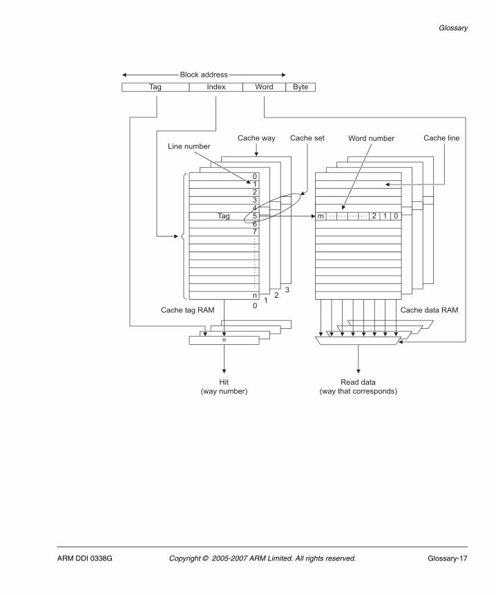
Glossary
TagTag
Tag
Tag Index Word
Hit
(way number)
Read data
(way that corresponds)
=
3
1
Tag
0
0
21
34567
n
Byte
Cache way Cache set
m 12 0
Cache line
2
Block address
Line numberWord number
Cache tag RAM Cache data RAM
ARM DDI 0338G Copyright © 2005-2007 ARM Limited. All rights reserved. Glossary-17

Glossary
Glossary-18 Copyright © 2005-2007 ARM Limited. All rights reserved. ARM DDI 0338G

![Librería Thrust - Argentina.gob.ar · [koltona@gpgpu-fisica clase_thrust]$ nvcc xxxxx.cu [koltona@gpgpu-fisica clase_thrust]$ qsub submit.sh [koltona@gpgpu-fisica ejemplos]$ more](https://img.pdfslide.net/doc/110x75/5f0f52177e708231d4439434/librera-thrust-koltonagpgpu-fisica-clasethrust-nvcc-xxxxxcu-koltonagpgpu-fisica.jpg)


![Feb 18th, 2019 - W&M · 2021. 7. 5. · qsub: waiting for job 120423.cp00.hpc.vims.edu to start qsub: job 120423.cp00.hpc.vims.edu ready 1 [pt01] Using the Batch System HPC uses Torque](https://img.pdfslide.net/doc/110x75/61331097dfd10f4dd73ad906/feb-18th-2019-wm-2021-7-5-qsub-waiting-for-job-to-start-qsub-job.jpg)