Embed Size (px)
Citation preview
ARM922T(Rev 0)
Technical Reference Manual
Copyright © 2000, 2001 ARM Limited. All rights reserved.ARM DDI 0184B
ARM922TTechnical Reference Manual
Copyright © 2000, 2001 ARM Limited. All rights reserved.
Release Information
Proprietary Notice
Words and logos marked with ® or ™ are registered trademarks or trademarks owned by ARM Limited, except as otherwise stated below in this proprietary notice. Other brands and names mentioned herein may be the trademarks of their respective owners.
Neither the whole nor any part of the information contained in, or the product described in, this document may be adapted or reproduced in any material form except with the prior written permission of the copyright holder.
The product described in this document is subject to continuous developments and improvements. All particulars of the product and its use contained in this document are given by ARM in good faith. However, all warranties implied or expressed, including but not limited to implied warranties of merchantability, or fitness for purpose, are excluded.
This document is intended only to assist the reader in the use of the product. ARM Limited shall not be liable for any loss or damage arising from the use of any information in this document, or any error or omission in such information, or any incorrect use of the product.
Figure 9-5 on page 9-12 reprinted with permission IEEE Std 1149.1-1990, IEEE Standard Test Access Port and Boundary-Scan Architecture Copyright 2000, by IEEE. The IEEE disclaims any responsibility or liability resulting from the placement and use in the described manner.
Confidentiality Status
This document is Non-Confidential. The right to use, copy and disclose this document may be subject to license restrictions in accordance with the terms of the agreement entered into by ARM and the party that ARM delivered this document to.
Product Status
The information in this document is final, that is for a developed product.
Web Address
http://www.arm.com
Change history
Date Issue Change
5th September 2000 A First release
18th April 2001 B Second release
ii Copyright © 2000, 2001 ARM Limited. All rights reserved. ARM DDI 0184B
ContentsARM922T Technical Reference Manual
PrefaceAbout this document .................................................................................... xviFurther reading ............................................................................................. xxFeedback ..................................................................................................... xxi
Chapter 1 Introduction1.1 About the ARM922T ................................................................................... 1-21.2 Processor functional block diagram ............................................................ 1-3
Chapter 2 Programmer’s Model2.1 About the programmer’s model ................................................................... 2-22.2 About the ARM9TDMI programmer’s model ............................................... 2-32.3 CP15 register map summary ...................................................................... 2-5
Chapter 3 Memory Management Unit3.1 About the MMU ........................................................................................... 3-23.2 MMU program accessible registers ............................................................. 3-43.3 Address translation ..................................................................................... 3-63.4 MMU faults and CPU aborts ..................................................................... 3-213.5 Fault address and fault status registers .................................................... 3-223.6 Domain access control .............................................................................. 3-233.7 Fault checking sequence .......................................................................... 3-25
ARM DDI 0184B Copyright © 2000, 2001 ARM Limited. All rights reserved. iii
Contents
3.8 External aborts ......................................................................................... 3-283.9 Interaction of the MMU and caches .......................................................... 3-29
Chapter 4 Caches, Write Buffer, and Physical Address TAG (PA TAG) RAM4.1 About the caches and write buffer .............................................................. 4-24.2 ICache ........................................................................................................ 4-44.3 DCache and write buffer ............................................................................. 4-94.4 Cache coherence ..................................................................................... 4-174.5 Cache cleaning when lockdown is in use ................................................. 4-204.6 Implementation notes ............................................................................... 4-214.7 Physical address TAG RAM ..................................................................... 4-224.8 Drain write buffer ...................................................................................... 4-234.9 Wait for interrupt ....................................................................................... 4-24
Chapter 5 Clock Modes5.1 About ARM922T clocking ........................................................................... 5-25.2 FastBus mode ............................................................................................ 5-35.3 Synchronous mode ..................................................................................... 5-45.4 Asynchronous mode ................................................................................... 5-6
Chapter 6 Bus Interface Unit6.1 About the ARM922T bus interface ............................................................. 6-26.2 Unidirectional AMBA ASB interface ............................................................ 6-36.3 Fully-compliant AMBA ASB interface ......................................................... 6-56.4 AMBA AHB interface ................................................................................ 6-206.5 Level 2 cache support and performance analysis .................................... 6-22
Chapter 7 Coprocessor Interface7.1 About the ARM922T coprocessor interface ................................................ 7-27.2 LDC/STC .................................................................................................... 7-57.3 MCR/MRC .................................................................................................. 7-97.4 Interlocked MCR ....................................................................................... 7-117.5 CDP .......................................................................................................... 7-137.6 Privileged instructions ............................................................................... 7-157.7 Busy-waiting and interrupts ...................................................................... 7-17
Chapter 8 Trace Interface Port8.1 About the ETM interface ............................................................................. 8-2
Chapter 9 Debug Support9.1 About debug ............................................................................................... 9-29.2 Debug systems ........................................................................................... 9-39.3 Debug interface signals .............................................................................. 9-59.4 Scan chains and JTAG interface .............................................................. 9-119.5 The JTAG state machine .......................................................................... 9-129.6 Test data registers .................................................................................... 9-19
iv Copyright © 2000, 2001 ARM Limited. All rights reserved. ARM DDI 0184B
Contents
9.7 ARM922T core clocks ............................................................................... 9-429.8 Clock switching during debug ................................................................... 9-439.9 Clock switching during test ........................................................................ 9-449.10 Determining the core state and system state ............................................ 9-459.11 Exit from debug state ................................................................................ 9-489.12 The behavior of the program counter during debug .................................. 9-519.13 EmbeddedICE macrocell .......................................................................... 9-549.14 Vector catching ......................................................................................... 9-629.15 Single-stepping ......................................................................................... 9-639.16 Debug communications channel ............................................................... 9-64
Chapter 10 TrackingICE10.1 About TrackingICE .................................................................................... 10-210.2 Timing requirements ................................................................................. 10-310.3 TrackingICE outputs ................................................................................. 10-4
Chapter 11 AMBA Test Interface11.1 About the AMBA test interface .................................................................. 11-211.2 Entering and exiting AMBA Test ............................................................... 11-311.3 Functional test ........................................................................................... 11-411.4 Burst operations ...................................................................................... 11-1111.5 PA TAG RAM test ................................................................................... 11-1211.6 Cache test ............................................................................................... 11-1511.7 MMU test ................................................................................................. 11-19
Chapter 12 Instruction Cycle Summary and Interlocks12.1 About the instruction cycle summary ........................................................ 12-212.2 Instruction cycle times ............................................................................... 12-312.3 Interlocks ................................................................................................... 12-6
Chapter 13 AC Characteristics13.1 ARM922T timing diagrams ........................................................................ 13-213.2 ARM922T timing parameters .................................................................. 13-1613.3 Timing definitions for the ARM922T Trace Interface Port ....................... 13-26
Appendix A Signal DescriptionsA.1 AMBA signals .............................................................................................. A-2A.2 Coprocessor interface signals ..................................................................... A-5A.3 JTAG and TAP controller signals ................................................................ A-7A.4 Debug signals ........................................................................................... A-10A.5 Miscellaneous signals ............................................................................... A-12A.6 ARM922T Trace Interface Port signals ..................................................... A-13
Appendix B CP15 Test RegistersB.1 About the test registers ............................................................................... B-2B.2 Test state register ....................................................................................... B-3
ARM DDI 0184B Copyright © 2000, 2001 ARM Limited. All rights reserved. v
Contents
B.3 Cache test registers and operations ........................................................... B-8B.4 MMU test registers and operations ........................................................... B-17B.5 StrongARM backwards compatibility operations ...................................... B-29
Glossary
vi Copyright © 2000, 2001 ARM Limited. All rights reserved. ARM DDI 0184B
List of TablesARM922T Technical Reference Manual
Change history .............................................................................................................. iiTable 2-1 ARM9TDMI implementation options ......................................................................... 2-3Table 2-2 CP15 register map .................................................................................................... 2-5Table 2-3 Address types in ARM922T ...................................................................................... 2-6Table 2-4 CP15 abbreviations ................................................................................................... 2-6Table 2-5 Register 0, ID code ................................................................................................... 2-8Table 2-6 Cache type register format ........................................................................................ 2-9Table 2-7 Cache size encoding (M=0) .................................................................................... 2-10Table 2-8 Cache associativity encoding (M=0) ....................................................................... 2-11Table 2-9 Line length encoding ............................................................................................... 2-11Table 2-10 Control register 1 bit functions ................................................................................ 2-12Table 2-11 Clocking modes ....................................................................................................... 2-13Table 2-12 Register 2, translation table base ............................................................................ 2-14Table 2-13 Register 3, domain access control .......................................................................... 2-14Table 2-14 Fault status register ................................................................................................. 2-16Table 2-15 Function descriptions register 7 .............................................................................. 2-17Table 2-16 Cache operations register 7 .................................................................................... 2-18Table 2-17 TLB operations register 8 ........................................................................................ 2-19Table 2-18 Accessing the cache lockdown register 9 ............................................................... 2-22Table 2-19 Accessing the TLB lockdown register 10 ................................................................ 2-22Table 3-1 CP15 register functions ............................................................................................. 3-4Table 3-2 Level one descriptor bits ........................................................................................... 3-9Table 3-3 Interpreting level one descriptor bits [1:0] ............................................................... 3-10
ARM DDI 0184B Copyright © 2000, 2001 ARM Limited. All rights reserved. vii
List of Tables
Table 3-4 Section descriptor bits ............................................................................................ 3-11Table 3-5 Coarse page table descriptor bits ........................................................................... 3-12Table 3-6 Fine page table descriptor bits ................................................................................ 3-13Table 3-7 Level two descriptor bits ......................................................................................... 3-16Table 3-8 Interpreting page table entry bits [1:0] .................................................................... 3-16Table 3-9 Priority encoding of fault status ............................................................................... 3-22Table 3-10 Interpreting access control bits in domain access control register ......................... 3-23Table 3-11 Interpreting access permission (AP) bits ................................................................ 3-24Table 4-1 DCache and write buffer configuration ................................................................... 4-11Table 5-1 Clock selection for external memory accesses ......................................................... 5-4Table 6-1 Relationship between bidirectional and unidirectional ASB interface ....................... 6-3Table 6-2 ARM922T input/output timing ................................................................................... 6-4Table 6-3 AMBA ASB transfer types ......................................................................................... 6-6Table 6-4 Burst transfers .......................................................................................................... 6-7Table 6-5 Use of WRITEOUT signal ......................................................................................... 6-7Table 6-6 Noncached LDR and fetch ...................................................................................... 6-11Table 6-7 Data eviction of 4 or 8 words .................................................................................. 6-17Table 6-8 ARM922T supported bus access types .................................................................. 6-22Table 7-1 Handshake encoding ................................................................................................ 7-8Table 9-1 Public instructions ................................................................................................... 9-14Table 9-2 ID code register ...................................................................................................... 9-20Table 9-3 Scan chain number allocation ................................................................................. 9-23Table 9-4 Scan chain 0 bit order ............................................................................................. 9-25Table 9-5 Scan chain 1 bit function ......................................................................................... 9-28Table 9-6 Scan chain 2 bit function ......................................................................................... 9-29Table 9-7 Scan chain 15 format and access modes ............................................................... 9-32Table 9-8 Scan chain 15 physical access mode bit format ..................................................... 9-33Table 9-9 Physical access mapping to CP15 registers ........................................................... 9-33Table 9-10 Scan chain 15 interpreted access mode bit format ................................................. 9-34Table 9-11 Interpreted access mapping to CP15 registers ....................................................... 9-35Table 9-12 Interpreted access mapping to the MMU ................................................................ 9-36Table 9-13 Interpreted access mapping to the caches ............................................................. 9-36Table 9-14 Scan chain 4 format ................................................................................................ 9-39Table 9-15 ARM9TDMI EmbeddedICE macrocell register map ............................................... 9-54Table 9-16 Watchpoint control register, data comparison bit functions .................................... 9-57Table 9-17 Watchpoint control register for instruction comparison bit functions ....................... 9-59Table 9-18 Debug status register bit functions ......................................................................... 9-60Table 9-19 Debug comms control register bit functions ............................................................ 9-65Table 10-1 ARM922T in TrackingICE mode ............................................................................. 10-4Table 11-1 AMBA test modes ................................................................................................... 11-3Table 11-2 AMBA functional test locations ............................................................................... 11-4Table 11-3 Construction of A922Inputs location ....................................................................... 11-5Table 11-4 Construction of A922Status1 location ..................................................................... 11-6Table 11-5 Construction of A922Status2 location ..................................................................... 11-7Table 11-6 Burst locations ...................................................................................................... 11-11Table 11-7 PA TAG RAM locations ........................................................................................ 11-12Table 11-8 Construction of data pattern write data ................................................................. 11-12
viii Copyright © 2000, 2001 ARM Limited. All rights reserved. ARM DDI 0184B
List of Tables
Table 11-9 Cache test locations .............................................................................................. 11-15Table 11-10 CAM write data ...................................................................................................... 11-15Table 11-11 CAM match write data ........................................................................................... 11-16Table 11-12 CAM match read data ........................................................................................... 11-16Table 11-13 Invalidate by VA write data .................................................................................... 11-16Table 11-14 Lockdown victim and base data ............................................................................ 11-17Table 11-15 MMU test locations ................................................................................................ 11-19Table 11-16 Invalidate by VA data ............................................................................................ 11-19Table 11-17 Match write data .................................................................................................... 11-20Table 11-18 CAM data .............................................................................................................. 11-20Table 11-19 CAM data Size_C encoding .................................................................................. 11-20Table 11-20 RAM1 data ............................................................................................................ 11-21Table 11-21 RAM1 data access permission bits ....................................................................... 11-21Table 11-22 RAM2 data ............................................................................................................ 11-22Table 11-23 RAM2 data Size_R2 encoding .............................................................................. 11-22Table 12-1 Symbols used in tables ........................................................................................... 12-3Table 12-2 Instruction cycle bus times ...................................................................................... 12-3Table 12-3 Data bus instruction times ....................................................................................... 12-4Table 13-1 ARM922T timing parameters ................................................................................ 13-16Table 13-2 ARM922T Trace Interface Port timing definitions ................................................. 13-26Table A-1 AMBA signals ............................................................................................................ A-2Table A-2 Coprocessor interface signals ................................................................................... A-5Table A-3 JTAG and TAP controller signals .............................................................................. A-7Table A-4 Debug signals ......................................................................................................... A-10Table A-5 Miscellaneous signals ............................................................................................. A-12Table A-6 Trace signals ........................................................................................................... A-13Table B-1 Test state register ..................................................................................................... B-3Table B-2 Clocking mode selection ........................................................................................... B-5Table B-3 Register 7 operations ................................................................................................ B-8Table B-4 Register 9 operations ................................................................................................ B-8Table B-5 Register 15 operations .............................................................................................. B-9Table B-6 CP15 MCR and MRC instructions ............................................................................. B-9Table B-7 Register 7, 9, and 15 operations ............................................................................. B-10Table B-8 Write cache victim and lockdown operations .......................................................... B-14Table B-9 TTB register operations ........................................................................................... B-17Table B-10 DAC register operations .......................................................................................... B-18Table B-11 FSR register operations .......................................................................................... B-18Table B-12 FAR register operations .......................................................................................... B-19Table B-13 Register 8 operations .............................................................................................. B-19Table B-14 Register 10 operations ............................................................................................ B-19Table B-15 CAM, RAM1, and RAM2 register 15 operations ..................................................... B-19Table B-16 Register 2, 3, 5, 6, 8, 10, and 15 operations ........................................................... B-20Table B-17 CAM memory region size ........................................................................................ B-23Table B-18 Access permission bit setting .................................................................................. B-24Table B-19 Miss and fault encoding .......................................................................................... B-24Table B-20 RAM2 memory region size ...................................................................................... B-25Table B-21 Write TLB lockdown operations .............................................................................. B-26
ARM DDI 0184B Copyright © 2000, 2001 ARM Limited. All rights reserved. ix
List of Tables
x Copyright © 2000, 2001 ARM Limited. All rights reserved. ARM DDI 0184B
List of FiguresARM922T Technical Reference Manual
Key to timing diagram conventions ............................................................................ xixFigure 1-1 ARM922T functional block diagram .......................................................................... 1-3Figure 2-1 CP15 MRC and MCR bit pattern ............................................................................... 2-7Figure 2-2 Cache type register format ........................................................................................ 2-8Figure 2-3 Dsize and Isize field format ....................................................................................... 2-9Figure 2-4 Register 7 MVA format ............................................................................................ 2-19Figure 2-5 Register 7 index format ........................................................................................... 2-19Figure 2-6 Register 8 MVA format ............................................................................................ 2-20Figure 2-7 Register 9 ................................................................................................................ 2-21Figure 2-8 Register 10 .............................................................................................................. 2-23Figure 2-9 Register 13 .............................................................................................................. 2-24Figure 2-10 Address mapping using CP15 Register 13 ............................................................. 2-25Figure 3-1 Translation table base register .................................................................................. 3-6Figure 3-2 Translating page tables ............................................................................................. 3-7Figure 3-3 Accessing translation table level one descriptors ..................................................... 3-8Figure 3-4 Level one descriptor .................................................................................................. 3-9Figure 3-5 Section descriptor ................................................................................................... 3-11Figure 3-6 Coarse page table descriptor .................................................................................. 3-12Figure 3-7 Fine page table descriptor ....................................................................................... 3-13Figure 3-8 Section translation ................................................................................................... 3-14Figure 3-9 Level two descriptor ................................................................................................ 3-15Figure 3-10 Large page translation from a coarse page table .................................................... 3-17Figure 3-11 Small page translation from a coarse page table .................................................... 3-18
ARM DDI 0184B Copyright © 2000, 2001 ARM Limited. All rights reserved. xi
List of Figures
Figure 3-12 Tiny page translation from a fine page table ........................................................... 3-19Figure 3-13 Domain access control register format ................................................................... 3-23Figure 3-14 Sequence for checking faults .................................................................................. 3-25Figure 4-1 Addressing the 8KB ICache ...................................................................................... 4-5Figure 5-1 ARM922T clocking .................................................................................................... 5-2Figure 5-2 Synchronous mode FCLK to BCLK zero phase delay .............................................. 5-5Figure 5-3 Synchronous mode FCLK to BCLK one phase delay ............................................... 5-5Figure 5-4 Asynchronous mode FCLK to BCLK zero cycle delay .............................................. 5-6Figure 5-5 Asynchronous mode FCLK to BCLK one cycle delay ............................................... 5-7Figure 6-1 Output buffer for bidirectional signals ....................................................................... 6-5Figure 6-2 Output buffer for unidirectional signals ..................................................................... 6-5Figure 6-3 Instruction fetch after reset ..................................................................................... 6-10Figure 6-4 Example LDR from address 0x108 ......................................................................... 6-11Figure 6-5 Example LDM of 5 words from 0x108 ..................................................................... 6-12Figure 6-6 Example nonbuffered STR ..................................................................................... 6-13Figure 6-7 Example nonbuffered STM ..................................................................................... 6-14Figure 6-8 Example linefill from 0x100 ..................................................................................... 6-15Figure 6-9 Example 4-word data eviction ................................................................................. 6-16Figure 6-10 Example swap operation ........................................................................................ 6-18Figure 7-1 ARM922T coprocessor clocking ............................................................................... 7-3Figure 7-2 ARM922T LDC/STC cycle timing ............................................................................. 7-5Figure 7-3 ARM922T MCR/MRC transfer timing ....................................................................... 7-9Figure 7-4 ARM922T interlocked MCR .................................................................................... 7-12Figure 7-5 ARM922T late canceled CDP ................................................................................. 7-14Figure 7-6 ARM922T privileged instructions ............................................................................ 7-15Figure 7-7 ARM922T busy waiting and interrupts .................................................................... 7-18Figure 9-1 Typical debug system ............................................................................................... 9-3Figure 9-2 Breakpoint timing ...................................................................................................... 9-5Figure 9-3 Watchpoint entry with data processing instruction .................................................... 9-8Figure 9-4 Watchpoint entry with branch ................................................................................... 9-9Figure 9-5 Test access port (TAP) controller state transitions ................................................. 9-12Figure 9-6 External scan chain multiplexor .............................................................................. 9-22Figure 9-7 Write back physical address format ........................................................................ 9-40Figure 9-8 Clock switching on entry to debug state ................................................................. 9-43Figure 9-9 Debug exit sequence .............................................................................................. 9-49Figure 9-10 Debug state entry ................................................................................................... 9-50Figure 9-11 ARM9TDMI EmbeddedICE macrocell overview ..................................................... 9-56Figure 9-12 Watchpoint control register for data comparison .................................................... 9-57Figure 9-13 Watchpoint control register for instruction comparison ........................................... 9-58Figure 9-14 Debug control register ............................................................................................ 9-60Figure 9-15 Debug status register .............................................................................................. 9-60Figure 9-16 Vector catch register ............................................................................................... 9-61Figure 9-17 Debug comms control register ................................................................................ 9-64Figure 10-1 Using TrackingICE .................................................................................................. 10-2Figure 11-1 AMBA functional test state machine ....................................................................... 11-9Figure 11-2 Write data format .................................................................................................. 11-13Figure 12-1 Single load interlock timing ..................................................................................... 12-6
xii Copyright © 2000, 2001 ARM Limited. All rights reserved. ARM DDI 0184B
List of Figures
Figure 12-2 Two cycle load interlock .......................................................................................... 12-7Figure 12-3 LDM interlock .......................................................................................................... 12-8Figure 12-4 LDM dependent interlock ........................................................................................ 12-9Figure 13-1 ARM922T FCLK timed coprocessor interface ......................................................... 13-2Figure 13-2 ARM922T BCLK timed coprocessor interface ........................................................ 13-3Figure 13-3 ARM922T FCLK related signal timing ..................................................................... 13-4Figure 13-4 ARM922T BCLK related signal timing ..................................................................... 13-5Figure 13-5 ARM922T SDOUTBS to TDO relationship .............................................................. 13-5Figure 13-6 ARM922T nTRST to other signals relationship ....................................................... 13-6Figure 13-7 ARM922T JTAG output signal timing ...................................................................... 13-7Figure 13-8 ARM922T JTAG input signal timing ........................................................................ 13-8Figure 13-9 ARM922T FCLK related debug output timing ......................................................... 13-8Figure 13-10 ARM922T BCLK related debug output timing ......................................................... 13-9Figure 13-11 ARM922T TCK related debug output timing ......................................................... 13-10Figure 13-12 ARM922T EDBGRQ to DBGRQI relationship ....................................................... 13-10Figure 13-13 ARM922T DBGEN to output relationship .............................................................. 13-11Figure 13-14 ARM922T BCLK related Trace Interface Port timing ............................................ 13-11Figure 13-15 ARM922T FCLK related Trace Interface Port timing ............................................. 13-12Figure 13-16 ARM922T BnRES timing ....................................................................................... 13-12Figure 13-17 ARM922T ASB slave transfer timing ..................................................................... 13-13Figure 13-18 ARM922T ASB master transfer timing .................................................................. 13-14Figure 13-19 ARM922T ASB master transfer timing .................................................................. 13-15Figure B-1 CP15 MRC and MCR bit pattern ............................................................................... B-2Figure B-2 Rd format, CAM read .............................................................................................. B-12Figure B-3 Rd format, CAM write .............................................................................................. B-12Figure B-4 Rd format, RAM read .............................................................................................. B-12Figure B-5 Rd format, RAM write .............................................................................................. B-12Figure B-6 Rd format, CAM match RAM read .......................................................................... B-13Figure B-7 Data format, CAM read ........................................................................................... B-13Figure B-8 Data format, RAM read ........................................................................................... B-13Figure B-9 Data format, CAM match RAM read ....................................................................... B-13Figure B-10 Rd format, write I or D cache victim and lockdown base ......................................... B-14Figure B-11 Rd format, write I or D cache victim ........................................................................ B-14Figure B-12 Rd format, CAM write and data format, CAM read .................................................. B-23Figure B-13 Rd format, RAM1 write ............................................................................................ B-23Figure B-14 Data format, RAM1 read ......................................................................................... B-24Figure B-15 Rd format, RAM2 write and data format, RAM2 read .............................................. B-25Figure B-16 Rd format, write I or D TLB lockdown ..................................................................... B-26
ARM DDI 0184B Copyright © 2000, 2001 ARM Limited. All rights reserved. xiii

List of Figures
xiv Copyright © 2000, 2001 ARM Limited. All rights reserved. ARM DDI 0184B
Preface
This preface introduces the ARM922T processor and its reference documentation. It contains the following sections:
• About this document on page xvi
• Further reading on page xx
• Feedback on page xxi.
ARM DDI 0184B Copyright © 2000, 2001 ARM Limited. All rights reserved. xv
Preface
About this document
This document is the technical reference manual for the ARM922T.
Intended audience
This document has been written for hardware and software engineers who want to design or develop products based upon the ARM922T processor. It assumes no prior knowledge of ARM products.
Using this manual
This document is organized into the following chapters:
Chapter 1 Introduction
Read this chapter for an introduction to the ARM922T.
Chapter 2 Programmer’s Model
Read this chapter for a description of the programmer’s model for the ARM922T.
Chapter 3 Memory Management Unit
Read this chapter for a description of the memory management unit and the memory interface, including descriptions of the instruction and data interfaces.
Chapter 4 Caches, Write Buffer, and Physical Address TAG (PA TAG) RAM
Read this chapter for descriptions of cache, write buffer, and PA TAG RAM operation.
Chapter 5 Clock Modes
Read this chapter for a description of the processor clock modes.
Chapter 6 Bus Interface Unit
Read this chapter for a description of the bus interface unit and the AMBA ASB and AHB interface.
Chapter 7 Coprocessor Interface
Read this chapter for a description of the ARM922T coprocessor interface.
xvi Copyright © 2000, 2001 ARM Limited. All rights reserved. ARM DDI 0184B
Preface
Chapter 8 Trace Interface Port
Read this chapter for a description of the Trace Interface Port of the ARM922T.
Chapter 9 Debug Support
Read this chapter for a description of the debug interface.
Chapter 10 TrackingICE
Read this chapter for a description of how the ARM922T uses TrackingICE mode.
Chapter 11 AMBA Test Interface
Read this chapter for a description of the AMBA test interface.
Chapter 12 Instruction Cycle Summary and Interlocks
Read this chapter for details of instruction cycle times. This chapter contains timing diagrams for interlock timing.
Chapter 13 AC Characteristics
Read this chapter for a description of the timing parameters used in the ARM922T.
Appendix A Signal Descriptions
Read this chapter for a detailed description of the signals used in the ARM922T.
Appendix B CP15 Test Registers
Read this chapter for a detailed description of the CP15 test register used in the ARM922T.
ARM DDI 0184B Copyright © 2000, 2001 ARM Limited. All rights reserved. xvii
Preface
Typographical conventions
The following typographical conventions are used in this book:
bold Highlights ARM processor signal names, and interface elements, such as menu names and buttons. Also used for terms in descriptive lists, where appropriate.
italic Highlights special terminology, cross-references, and citations.
typewriter Denotes text that can be entered at the keyboard, such as commands, file and program names, and source code.
typewriter Denotes a permitted abbreviation for a command or option. The underlined text may be entered instead of the full command or option name.
typewriter italic
Denotes arguments to commands or functions, where the argument is to be replaced by a specific value.
typewriter bold
Denotes language keywords when used outside example code.
xviii Copyright © 2000, 2001 ARM Limited. All rights reserved. ARM DDI 0184B
Preface
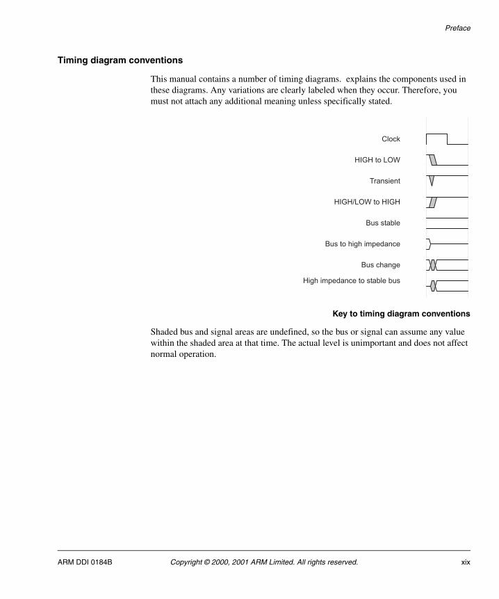
Timing diagram conventions
This manual contains a number of timing diagrams. explains the components used in these diagrams. Any variations are clearly labeled when they occur. Therefore, you must not attach any additional meaning unless specifically stated.
Key to timing diagram conventions
Shaded bus and signal areas are undefined, so the bus or signal can assume any value within the shaded area at that time. The actual level is unimportant and does not affect normal operation.
Clock
Bus stable
HIGH to LOW
Transient
Bus to high impedance
Bus change
HIGH/LOW to HIGH
High impedance to stable bus
ARM DDI 0184B Copyright © 2000, 2001 ARM Limited. All rights reserved. xix
Preface
Further reading
This section lists publications by ARM Limited, and by third parties.
If you would like further information on ARM products, or if you have questions not answered by this document, please contact [email protected] or visit our web site at http://www.arm.com.
ARM publications
This document contains information that is specific to the ARM922T. Refer to the following documents for other relevant information:
• ARM Architecture Reference Manual (ARM DDI 0100)
• ARM9TDMI Data Sheet (ARM DDI 0029).
Other publications
This section lists relevant documents published by third parties.
• IEEE Std. 1149.1- 1990, Standard Test Access Port and Boundary-Scan Architecture.
xx Copyright © 2000, 2001 ARM Limited. All rights reserved. ARM DDI 0184B
Preface
Feedback
ARM Limited welcomes feedback both on the ARM922T, and on the documentation.
Feedback on the ARM922T
If you have any comments or suggestions about this product, please contact your supplier giving:
• the product name
• a concise explanation of your comments.
Feedback on the ARM922T Technical Reference Manual
If you have any comments about this document, please send email to [email protected] giving:
• the document title
• the document number
• the page number(s) to which your comments refer
• a concise explanation of your comments.
General suggestions for additions and improvements are also welcome.
ARM DDI 0184B Copyright © 2000, 2001 ARM Limited. All rights reserved. xxi
Preface
xxii Copyright © 2000, 2001 ARM Limited. All rights reserved. ARM DDI 0184B
Chapter 1 Introduction
This chapter introduces the ARM922T processor. It contains the following sections:
• About the ARM922T on page 1-2
• Processor functional block diagram on page 1-3.
ARM DDI 0184B Copyright © 2000, 2001 ARM Limited. All rights reserved. 1-1
Introduction
1.1 About the ARM922T
The ARM922T processor is a member of the ARM9TDMI family of general-purpose microprocessors, which includes:
• ARM9TDMI (core)
• ARM940T (core plus 4K and 4K caches and protection unit)
• ARM920T (core plus 16K and 16K caches and MMU)
• ARM922T (core plus 8K and 8K caches and MMU).
The ARM9TDMI processor core is a Harvard architecture device implemented using a five-stage pipeline consisting of Fetch, Decode, Execute, Memory, and Write stages. It can be provided as a standalone core that can be embedded into more complex devices. The standalone core has a simple bus interface that allows you to design your own caches and memory systems around it.
The ARM9TDMI family of microprocessors supports both the 32-bit ARM and 16-bit Thumb instruction sets, allowing you to trade off between high performance and high code density.
The ARM922T processor is a Harvard cache architecture processor that is targeted at multiprogrammer applications where full memory management, high performance, and low power are all-important. The separate instruction and data caches in this design are 8KB each in size, with an 8-word line length. The ARM922T implements an enhanced ARM architecture v4 MMU to provide translation and access permission checks for instruction and data addresses.
The ARM922T processor supports the ARM debug architecture and includes logic to assist in both hardware and software debug. The ARM922T also includes support for coprocessors, exporting the instruction and data buses along with simple handshaking signals.
The ARM922T interface to the rest of the system is over unified address and data buses. This interface enables implementation of either an Advanced Microcontroller Bus Architecture (AMBA) Advanced System Bus (ASB) or Advanced High-performance Bus (AHB) bus scheme either as a fully-compliant AMBA bus master, or as a slave for production test. The ARM922T also has a Tracking ICE mode which allows an approach similar to a conventional ICE mode of operation.
The ARM922T processor supports the addition of an Embedded Trace Macrocell (ETM) for real-time tracing of instructions and data.
1-2 Copyright © 2000, 2001 ARM Limited. All rights reserved. ARM DDI 0184B
Introduction
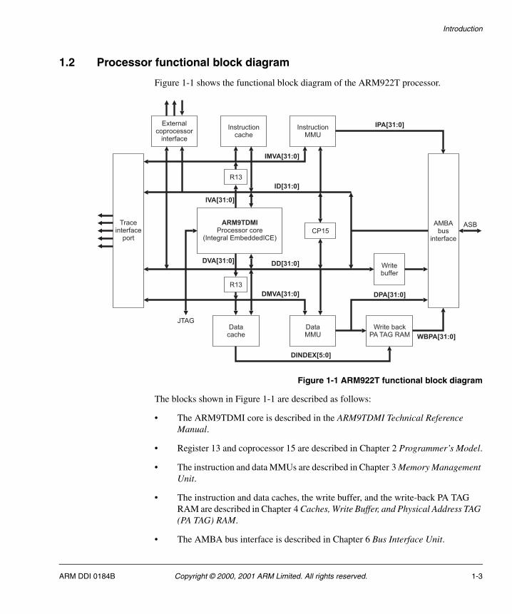
1.2 Processor functional block diagram
Figure 1-1 shows the functional block diagram of the ARM922T processor.
Figure 1-1 ARM922T functional block diagram
The blocks shown in Figure 1-1 are described as follows:
• The ARM9TDMI core is described in the ARM9TDMI Technical Reference Manual.
• Register 13 and coprocessor 15 are described in Chapter 2 Programmer’s Model.
• The instruction and data MMUs are described in Chapter 3 Memory Management Unit.
• The instruction and data caches, the write buffer, and the write-back PA TAG RAM are described in Chapter 4 Caches, Write Buffer, and Physical Address TAG (PA TAG) RAM.
• The AMBA bus interface is described in Chapter 6 Bus Interface Unit.
Externalcoprocessor
interface
ARM9TDMIProcessor core
(Integral EmbeddedICE)
Writebuffer
ID[31:0]
IMVA[31:0]
WBPA[31:0]
DPA[31:0]
IPA[31:0]
ASB
Write backPA TAG RAM
CP15
R13
IVA[31:0]
DVA[31:0]
JTAG
DD[31:0]
Instructioncache
InstructionMMU
DataMMU
Datacache
R13
DINDEX[5:0]
Traceinterface
port
AMBAbus
interface
DMVA[31:0]
ARM DDI 0184B Copyright © 2000, 2001 ARM Limited. All rights reserved. 1-3
Introduction
• The external coprocessor interface is described in Chapter 7 Coprocessor Interface.
• The trace interface port is described in Chapter 8 Trace Interface Port.
1-4 Copyright © 2000, 2001 ARM Limited. All rights reserved. ARM DDI 0184B
Chapter 2 Programmer’s Model
This chapter describes the ARM922T registers and provides details required when programming the microprocessor. It contains the following sections:
• About the programmer’s model on page 2-2
• About the ARM9TDMI programmer’s model on page 2-3
• CP15 register map summary on page 2-5.
ARM DDI 0184B Copyright © 2000, 2001 ARM Limited. All rights reserved. 2-1
Programmer’s Model
2.1 About the programmer’s model
The ARM922T processor incorporates the ARM9TDMI integer core, which implements the ARM architecture v4T. It executes the ARM and Thumb instruction sets, and includes EmbeddedICE JTAG software debug features.
The programmer’s model of the ARM922T consists of the programmer’s model of the ARM9TDMI core (see About the ARM9TDMI programmer’s model on page 2-3) with the following additions and modifications:
• The ARM922T incorporates two coprocessors:
— CP14, which allows software access to the debug communications channel. You can access the registers defined in CP14 using MCR and MRC instructions. These are described in Debug communications channel on page 9-64.
— The system control coprocessor, CP15, which provides additional registers that are used to configure and control the caches, MMU, protection system, the clocking mode, and other system options of the ARM922T, such as big or little-endian operation. You can access the registers defined in CP15 using MCR and MRC instructions. These are described in CP15 register map summary on page 2-5.
• The ARM922T processor also features an external coprocessor interface that allows the attachment of a closely-coupled coprocessor on the same chip, for example, a floating-point unit. You can access registers and operations provided by any coprocessors attached to the external coprocessor interface using appropriate coprocessor instructions.
• Memory accesses for instruction fetches and data loads and stores can be cached or buffered. Cache and write buffer configuration and operation is described in detail in Chapter 4 Caches, Write Buffer, and Physical Address TAG (PA TAG) RAM.
• The MMU page tables that reside in main memory describe the virtual to physical address mapping, access permissions, and cache and write buffer configuration. These are created by the operating system software and accessed automatically by the ARM922T MMU hardware whenever an access causes a TLB miss.
• The ARM922T processor has a Trace Interface Port that allows the use of Trace hardware and tools for real-time tracing of instructions and data.
2-2 Copyright © 2000, 2001 ARM Limited. All rights reserved. ARM DDI 0184B
Programmer’s Model
2.2 About the ARM9TDMI programmer’s model
The ARM9TDMI processor core implements ARM architecture v4T, and executes the ARM 32-bit instruction set and the compressed Thumb 16-bit instruction set. The programmer’s model is fully described in the ARM Architecture Reference Manual. The ARM9TDMI Technical Reference Manual gives implementation details, including instruction execution cycle times.
ARMv4T specifies a small number of implementation options. The options selected in the ARM9TDMI implementation are listed in Table 2-1. For comparison, the options selected for the ARM7TDMI implementation are also shown.
The ARM9TDMI core is code-compatible with the ARM7TDMI, with two exceptions:
• The ARM9TDMI core implements the base restored Data Abort model. This significantly simplifies the software Data Abort handler.
• The ARM9TDMI core fully implements the instruction set extension spaces added to the ARM (32-bit) instruction set in ARMv4 and ARMv4T.
These differences are explained in more detail in the following sections:
• Data Abort model
• Instruction set extension spaces on page 2-4.
2.2.1 Data Abort model
The base restored Data Abort model differs from the base updated Data Abort model implemented by ARM7TDMI.
The difference in the Data Abort models affects only a very small section of operating system code, the Data Abort handler. It does not affect user code. With the base restored Data Abort model, when a Data Abort exception occurs during the execution of a memory access instruction, the base register is always restored by the processor hardware to the value the register contained before the instruction was executed. This removes the requirement for the Data Abort handler to unwind any base register update that might have been specified by the aborted instruction.
Table 2-1 ARM9TDMI implementation options
Processor core
ArchitectureData Abort model
Value stored by direct STR, STRT, and STM of PC
ARM7TDMI ARMv4T Base updated Address of instruction + 12
ARM9TDMI ARMv4T Base restored Address of instruction + 12
ARM DDI 0184B Copyright © 2000, 2001 ARM Limited. All rights reserved. 2-3
Programmer’s Model
2.2.2 Instruction set extension spaces
All ARM processors implement the undefined instruction space as one of the entry mechanisms for the undefined instruction exception. That is, ARM instructions with opcode[27:25] = 0b011 and opcode[4] = 0b1 are undefined on all ARM processors including the ARM9TDMI and ARM7TDMI.
ARMv4 and ARMv4T also introduce a number of instruction set extension spaces to the ARM instruction set. These are:
• arithmetic instruction extension space
• control instruction extension space
• coprocessor instruction extension space
• load/store instruction extension space.
Instructions in these spaces are undefined, and cause an undefined instruction exception. The ARM9TDMI fully implements all the instruction set extension spaces defined in ARMv4T as undefined instructions, allowing emulation of future instruction set additions.
2-4 Copyright © 2000, 2001 ARM Limited. All rights reserved. ARM DDI 0184B
Programmer’s Model
2.3 CP15 register map summary
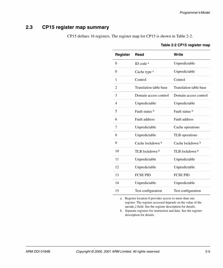
CP15 defines 16 registers. The register map for CP15 is shown in Table 2-2.
Table 2-2 CP15 register map
Register Read Write
0 ID code a
a. Register location 0 provides access to more than one register. The register accessed depends on the value of the opcode_2 field. See the register description for details.
Unpredictable
0 Cache type a Unpredictable
1 Control Control
2 Translation table base Translation table base
3 Domain access control Domain access control
4 Unpredictable Unpredictable
5 Fault status b
b. Separate registers for instruction and data. See the register description for details.
Fault status b
6 Fault address Fault address
7 Unpredictable Cache operations
8 Unpredictable TLB operations
9 Cache lockdown b Cache lockdown b
10 TLB lockdown b TLB lockdown b
11 Unpredictable Unpredictable
12 Unpredictable Unpredictable
13 FCSE PID FCSE PID
14 Unpredictable Unpredictable
15 Test configuration Test configuration
ARM DDI 0184B Copyright © 2000, 2001 ARM Limited. All rights reserved. 2-5
Programmer’s Model
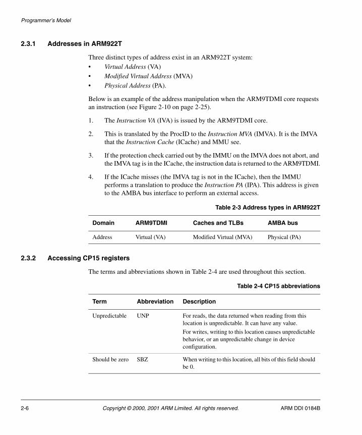
2.3.1 Addresses in ARM922T
Three distinct types of address exist in an ARM922T system:
• Virtual Address (VA)
• Modified Virtual Address (MVA)
• Physical Address (PA).
Below is an example of the address manipulation when the ARM9TDMI core requests an instruction (see Figure 2-10 on page 2-25).
1. The Instruction VA (IVA) is issued by the ARM9TDMI core.
2. This is translated by the ProcID to the Instruction MVA (IMVA). It is the IMVA that the Instruction Cache (ICache) and MMU see.
3. If the protection check carried out by the IMMU on the IMVA does not abort, and the IMVA tag is in the ICache, the instruction data is returned to the ARM9TDMI.
4. If the ICache misses (the IMVA tag is not in the ICache), then the IMMU performs a translation to produce the Instruction PA (IPA). This address is given to the AMBA bus interface to perform an external access.
2.3.2 Accessing CP15 registers
The terms and abbreviations shown in Table 2-4 are used throughout this section.
Table 2-3 Address types in ARM922T
Domain ARM9TDMI Caches and TLBs AMBA bus
Address Virtual (VA) Modified Virtual (MVA) Physical (PA)
Table 2-4 CP15 abbreviations
Term Abbreviation Description
Unpredictable UNP For reads, the data returned when reading from this location is unpredictable. It can have any value.
For writes, writing to this location causes unpredictable behavior, or an unpredictable change in device configuration.
Should be zero SBZ When writing to this location, all bits of this field should be 0.
2-6 Copyright © 2000, 2001 ARM Limited. All rights reserved. ARM DDI 0184B
Programmer’s Model
In all cases, reading from, or writing any data values to any CP15 registers, including those fields specified as unpredictable or should be zero, does not cause any permanent damage.
All CP15 register bits that are defined and contain state, are set to zero by BnRES except the V bit in register 1, which takes the value of macrocell input VINITHI when BnRES is asserted.
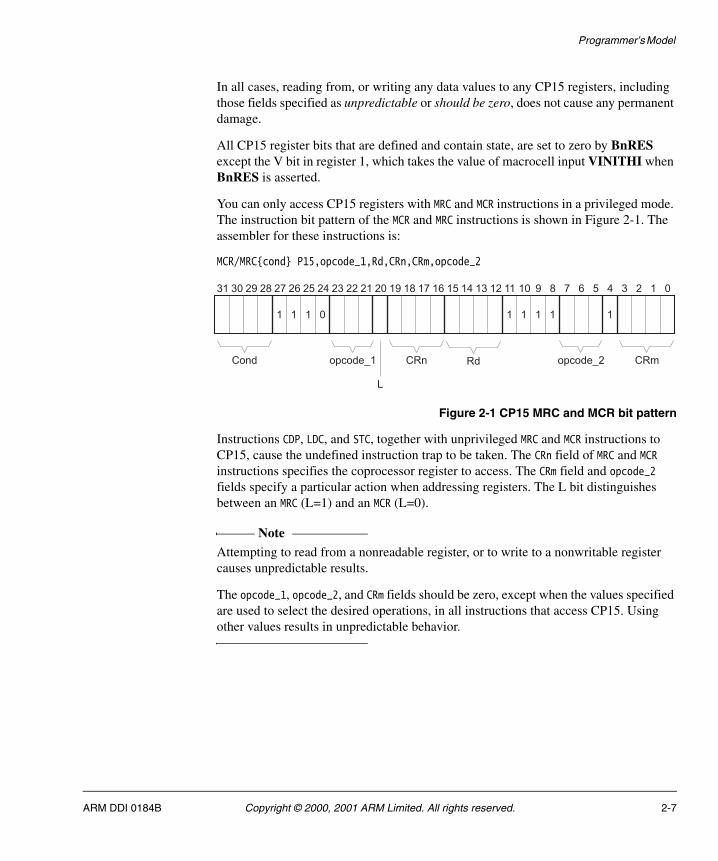
You can only access CP15 registers with MRC and MCR instructions in a privileged mode. The instruction bit pattern of the MCR and MRC instructions is shown in Figure 2-1. The assembler for these instructions is:
MCR/MRC{cond} P15,opcode_1,Rd,CRn,CRm,opcode_2
Figure 2-1 CP15 MRC and MCR bit pattern
Instructions CDP, LDC, and STC, together with unprivileged MRC and MCR instructions to CP15, cause the undefined instruction trap to be taken. The CRn field of MRC and MCR instructions specifies the coprocessor register to access. The CRm field and opcode_2 fields specify a particular action when addressing registers. The L bit distinguishes between an MRC (L=1) and an MCR (L=0).
Note Attempting to read from a nonreadable register, or to write to a nonwritable register causes unpredictable results.
The opcode_1, opcode_2, and CRm fields should be zero, except when the values specified are used to select the desired operations, in all instructions that access CP15. Using other values results in unpredictable behavior.
31 30 29 28 27 26 25 24 23 22 21 20 19 18 17 16 15 14 13 12 11 10 9 8 7 6 5 4 3 2 1 0
1 1 1 0 1 1 1 1 1
CRmopcode_2RdCRn
L
opcode_1Cond
ARM DDI 0184B Copyright © 2000, 2001 ARM Limited. All rights reserved. 2-7
Programmer’s Model
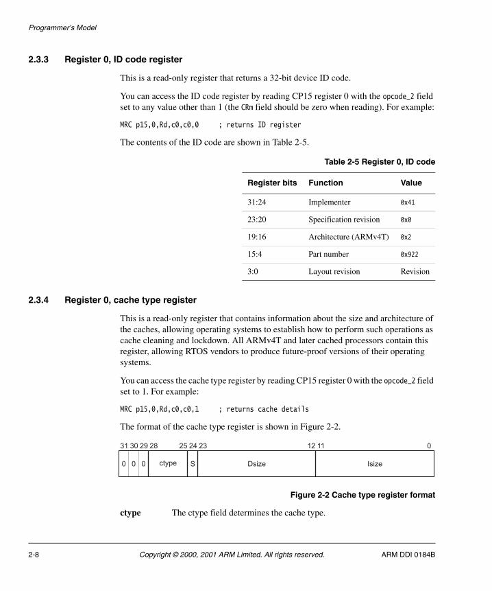
2.3.3 Register 0, ID code register
This is a read-only register that returns a 32-bit device ID code.
You can access the ID code register by reading CP15 register 0 with the opcode_2 field set to any value other than 1 (the CRm field should be zero when reading). For example:
MRC p15,0,Rd,c0,c0,0 ; returns ID register
The contents of the ID code are shown in Table 2-5.
2.3.4 Register 0, cache type register
This is a read-only register that contains information about the size and architecture of the caches, allowing operating systems to establish how to perform such operations as cache cleaning and lockdown. All ARMv4T and later cached processors contain this register, allowing RTOS vendors to produce future-proof versions of their operating systems.
You can access the cache type register by reading CP15 register 0 with the opcode_2 field set to 1. For example:
MRC p15,0,Rd,c0,c0,1 ; returns cache details
The format of the cache type register is shown in Figure 2-2.
Figure 2-2 Cache type register format
ctype The ctype field determines the cache type.
Table 2-5 Register 0, ID code
Register bits Function Value
31:24 Implementer 0x41
23:20 Specification revision 0x0
19:16 Architecture (ARMv4T) 0x2
15:4 Part number 0x922
3:0 Layout revision Revision
31 30 29 28 25 24 23 12 11 0
0 0 0 ctype S Dsize Isize
2-8 Copyright © 2000, 2001 ARM Limited. All rights reserved. ARM DDI 0184B
Programmer’s Model
S bit Specifies whether the cache is a unified cache or separate instruction and data caches.
Dsize Specifies the size, line length, and associativity of the data cache.
Isize Specifies the size, line length, and associativity of the instruction cache.
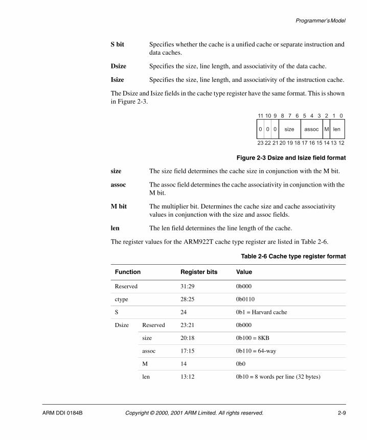
The Dsize and Isize fields in the cache type register have the same format. This is shown in Figure 2-3.
Figure 2-3 Dsize and Isize field format
size The size field determines the cache size in conjunction with the M bit.
assoc The assoc field determines the cache associativity in conjunction with the M bit.
M bit The multiplier bit. Determines the cache size and cache associativity values in conjunction with the size and assoc fields.
len The len field determines the line length of the cache.
The register values for the ARM922T cache type register are listed in Table 2-6.
11 10 9 8 7 6 5 4 3 2 1 0
0 0 0 size assoc M len
23 22 21 20 19 18 17 16 15 14 13 12
Table 2-6 Cache type register format
Function Register bits Value
Reserved 31:29 0b000
ctype 28:25 0b0110
S 24 0b1 = Harvard cache
Dsize Reserved 23:21 0b000
size 20:18 0b100 = 8KB
assoc 17:15 0b110 = 64-way
M 14 0b0
len 13:12 0b10 = 8 words per line (32 bytes)
ARM DDI 0184B Copyright © 2000, 2001 ARM Limited. All rights reserved. 2-9
Programmer’s Model
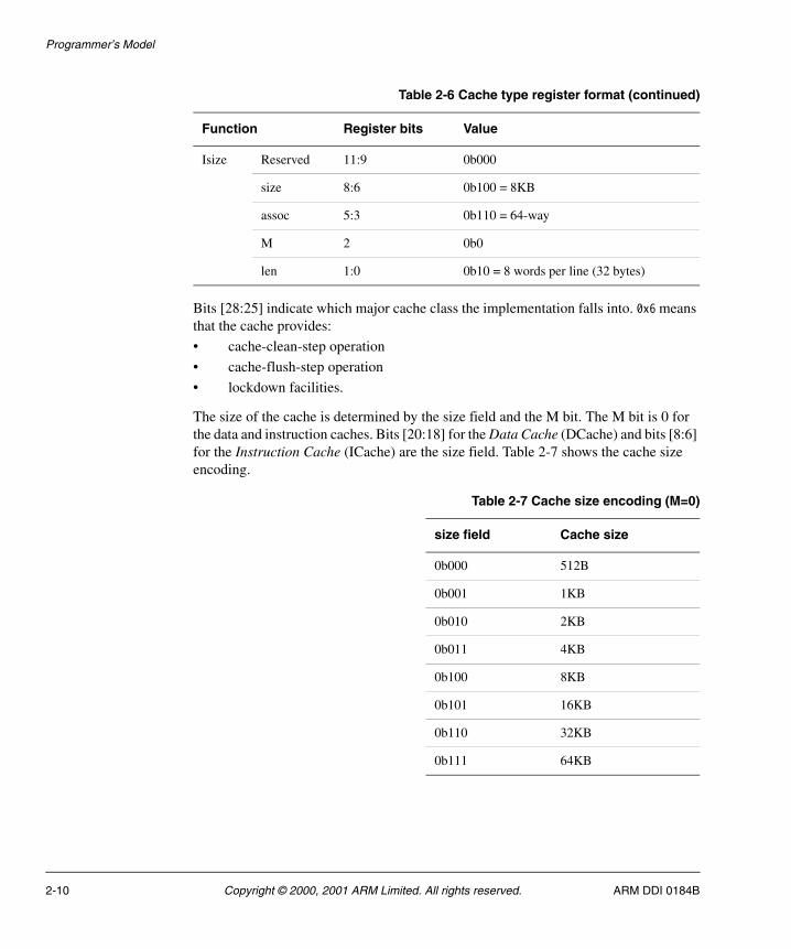
Bits [28:25] indicate which major cache class the implementation falls into. 0x6 means that the cache provides:
• cache-clean-step operation
• cache-flush-step operation
• lockdown facilities.
The size of the cache is determined by the size field and the M bit. The M bit is 0 for the data and instruction caches. Bits [20:18] for the Data Cache (DCache) and bits [8:6] for the Instruction Cache (ICache) are the size field. Table 2-7 shows the cache size encoding.
Isize Reserved 11:9 0b000
size 8:6 0b100 = 8KB
assoc 5:3 0b110 = 64-way
M 2 0b0
len 1:0 0b10 = 8 words per line (32 bytes)
Table 2-7 Cache size encoding (M=0)
size field Cache size
0b000 512B
0b001 1KB
0b010 2KB
0b011 4KB
0b100 8KB
0b101 16KB
0b110 32KB
0b111 64KB
Table 2-6 Cache type register format (continued)
Function Register bits Value
2-10 Copyright © 2000, 2001 ARM Limited. All rights reserved. ARM DDI 0184B
Programmer’s Model
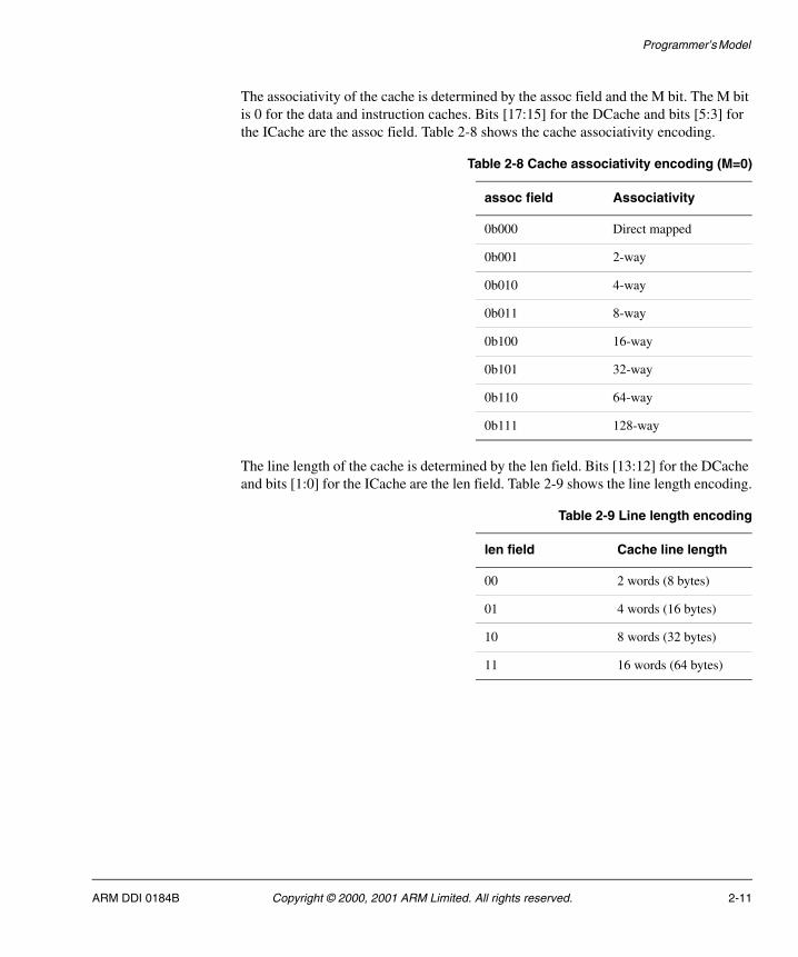
The associativity of the cache is determined by the assoc field and the M bit. The M bit is 0 for the data and instruction caches. Bits [17:15] for the DCache and bits [5:3] for the ICache are the assoc field. Table 2-8 shows the cache associativity encoding.
The line length of the cache is determined by the len field. Bits [13:12] for the DCache and bits [1:0] for the ICache are the len field. Table 2-9 shows the line length encoding.
Table 2-8 Cache associativity encoding (M=0)
assoc field Associativity
0b000 Direct mapped
0b001 2-way
0b010 4-way
0b011 8-way
0b100 16-way
0b101 32-way
0b110 64-way
0b111 128-way
Table 2-9 Line length encoding
len field Cache line length
00 2 words (8 bytes)
01 4 words (16 bytes)
10 8 words (32 bytes)
11 16 words (64 bytes)
ARM DDI 0184B Copyright © 2000, 2001 ARM Limited. All rights reserved. 2-11
Programmer’s Model
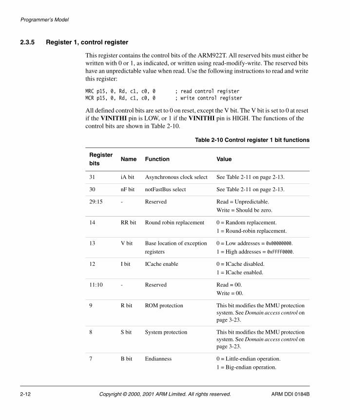
2.3.5 Register 1, control register
This register contains the control bits of the ARM922T. All reserved bits must either be written with 0 or 1, as indicated, or written using read-modify-write. The reserved bits have an unpredictable value when read. Use the following instructions to read and write this register:
MRC p15, 0, Rd, c1, c0, 0 ; read control registerMCR p15, 0, Rd, c1, c0, 0 ; write control register
All defined control bits are set to 0 on reset, except the V bit. The V bit is set to 0 at reset if the VINITHI pin is LOW, or 1 if the VINITHI pin is HIGH. The functions of the control bits are shown in Table 2-10.
Table 2-10 Control register 1 bit functions
Registerbits
Name Function Value
31 iA bit Asynchronous clock select See Table 2-11 on page 2-13.
30 nF bit notFastBus select See Table 2-11 on page 2-13.
29:15 - Reserved Read = Unpredictable.
Write = Should be zero.
14 RR bit Round robin replacement 0 = Random replacement.
1 = Round-robin replacement.
13 V bit Base location of exception
registers
0 = Low addresses = 0x00000000.
1 = High addresses = 0xFFFF0000.
12 I bit ICache enable 0 = ICache disabled.
1 = ICache enabled.
11:10 - Reserved Read = 00.
Write = 00.
9 R bit ROM protection This bit modifies the MMU protection system. See Domain access control on page 3-23.
8 S bit System protection This bit modifies the MMU protection system. See Domain access control on page 3-23.
7 B bit Endianness 0 = Little-endian operation.
1 = Big-endian operation.
2-12 Copyright © 2000, 2001 ARM Limited. All rights reserved. ARM DDI 0184B
Programmer’s Model
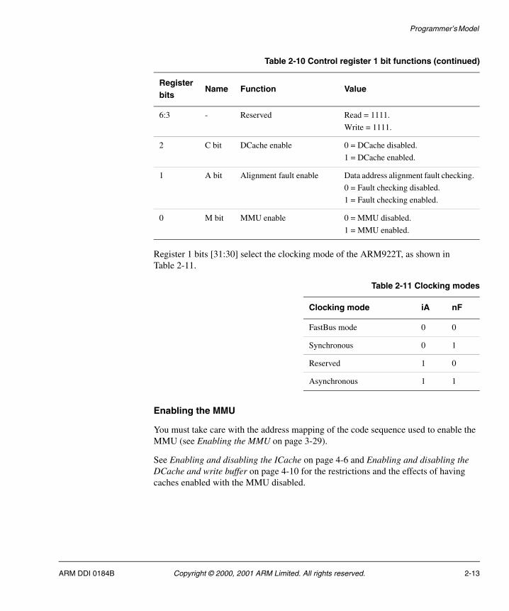
Register 1 bits [31:30] select the clocking mode of the ARM922T, as shown in Table 2-11.
Enabling the MMU
You must take care with the address mapping of the code sequence used to enable the MMU (see Enabling the MMU on page 3-29).
See Enabling and disabling the ICache on page 4-6 and Enabling and disabling the DCache and write buffer on page 4-10 for the restrictions and the effects of having caches enabled with the MMU disabled.
6:3 - Reserved Read = 1111.
Write = 1111.
2 C bit DCache enable 0 = DCache disabled.
1 = DCache enabled.
1 A bit Alignment fault enable Data address alignment fault checking.
0 = Fault checking disabled.
1 = Fault checking enabled.
0 M bit MMU enable 0 = MMU disabled.
1 = MMU enabled.
Table 2-11 Clocking modes
Clocking mode iA nF
FastBus mode 0 0
Synchronous 0 1
Reserved 1 0
Asynchronous 1 1
Table 2-10 Control register 1 bit functions (continued)
Registerbits
Name Function Value
ARM DDI 0184B Copyright © 2000, 2001 ARM Limited. All rights reserved. 2-13
Programmer’s Model
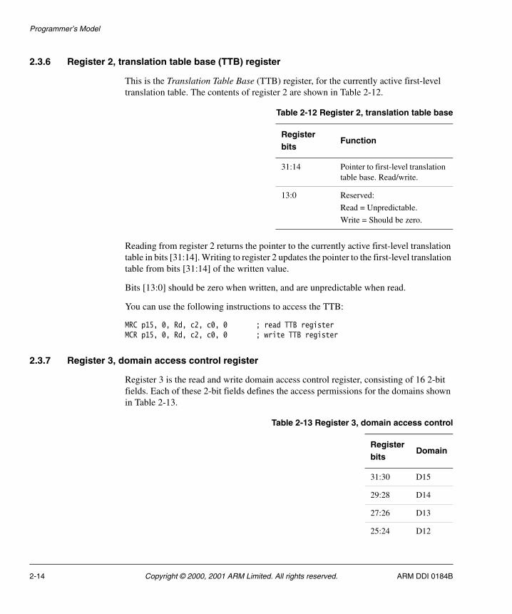
2.3.6 Register 2, translation table base (TTB) register
This is the Translation Table Base (TTB) register, for the currently active first-level translation table. The contents of register 2 are shown in Table 2-12.
Reading from register 2 returns the pointer to the currently active first-level translation table in bits [31:14]. Writing to register 2 updates the pointer to the first-level translation table from bits [31:14] of the written value.
Bits [13:0] should be zero when written, and are unpredictable when read.
You can use the following instructions to access the TTB:
MRC p15, 0, Rd, c2, c0, 0 ; read TTB registerMCR p15, 0, Rd, c2, c0, 0 ; write TTB register
2.3.7 Register 3, domain access control register
Register 3 is the read and write domain access control register, consisting of 16 2-bit fields. Each of these 2-bit fields defines the access permissions for the domains shown in Table 2-13.
Table 2-12 Register 2, translation table base
Registerbits
Function
31:14 Pointer to first-level translation table base. Read/write.
13:0 Reserved:
Read = Unpredictable.
Write = Should be zero.
Table 2-13 Register 3, domain access control
Registerbits
Domain
31:30 D15
29:28 D14
27:26 D13
25:24 D12
2-14 Copyright © 2000, 2001 ARM Limited. All rights reserved. ARM DDI 0184B
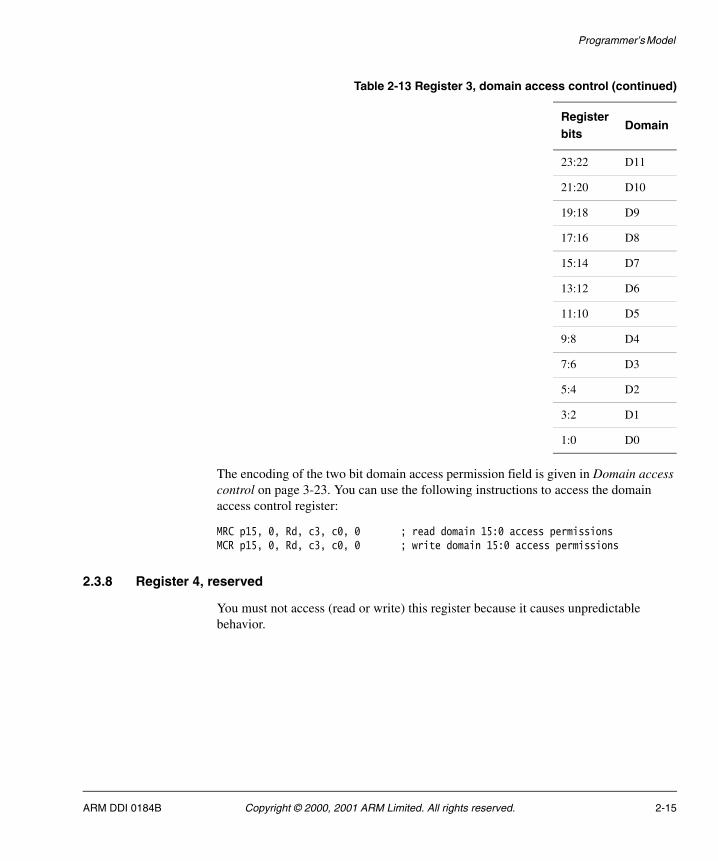
Programmer’s Model
The encoding of the two bit domain access permission field is given in Domain access control on page 3-23. You can use the following instructions to access the domain access control register:
MRC p15, 0, Rd, c3, c0, 0 ; read domain 15:0 access permissionsMCR p15, 0, Rd, c3, c0, 0 ; write domain 15:0 access permissions
2.3.8 Register 4, reserved
You must not access (read or write) this register because it causes unpredictable behavior.
23:22 D11
21:20 D10
19:18 D9
17:16 D8
15:14 D7
13:12 D6
11:10 D5
9:8 D4
7:6 D3
5:4 D2
3:2 D1
1:0 D0
Table 2-13 Register 3, domain access control (continued)
Registerbits
Domain
ARM DDI 0184B Copyright © 2000, 2001 ARM Limited. All rights reserved. 2-15
Programmer’s Model
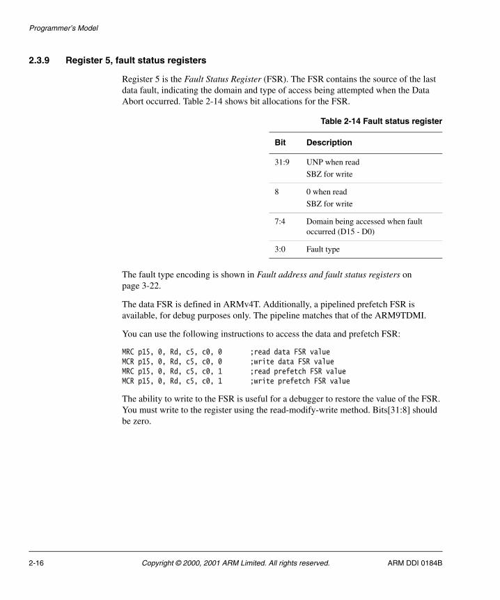
2.3.9 Register 5, fault status registers
Register 5 is the Fault Status Register (FSR). The FSR contains the source of the last data fault, indicating the domain and type of access being attempted when the Data Abort occurred. Table 2-14 shows bit allocations for the FSR.
The fault type encoding is shown in Fault address and fault status registers on page 3-22.
The data FSR is defined in ARMv4T. Additionally, a pipelined prefetch FSR is available, for debug purposes only. The pipeline matches that of the ARM9TDMI.
You can use the following instructions to access the data and prefetch FSR:
MRC p15, 0, Rd, c5, c0, 0 ;read data FSR valueMCR p15, 0, Rd, c5, c0, 0 ;write data FSR valueMRC p15, 0, Rd, c5, c0, 1 ;read prefetch FSR valueMCR p15, 0, Rd, c5, c0, 1 ;write prefetch FSR value
The ability to write to the FSR is useful for a debugger to restore the value of the FSR. You must write to the register using the read-modify-write method. Bits[31:8] should be zero.
Table 2-14 Fault status register
Bit Description
31:9 UNP when read
SBZ for write
8 0 when read
SBZ for write
7:4 Domain being accessed when fault occurred (D15 - D0)
3:0 Fault type
2-16 Copyright © 2000, 2001 ARM Limited. All rights reserved. ARM DDI 0184B
Programmer’s Model
2.3.10 Register 6, fault address register
Register 6 is the Fault Address Register (FAR). This contains the MVA of the access being attempted when the last fault occurred. The FAR is only updated for data faults, not for prefetch faults. (You can find the address for a prefetch fault in R14.)
You can use the following instructions to access the FAR:
MRC p15, 0, Rd, c6, c0, 0 ;read FAR dataMCR p15, 0, Rd, c6, c0, 0 ;write FAR data
The ability to write to the FAR is provided to allow a debugger to restore a previous state.
2.3.11 Register 7, cache operations register
Register 7 is a write-only register used to manage the ICache and DCache.
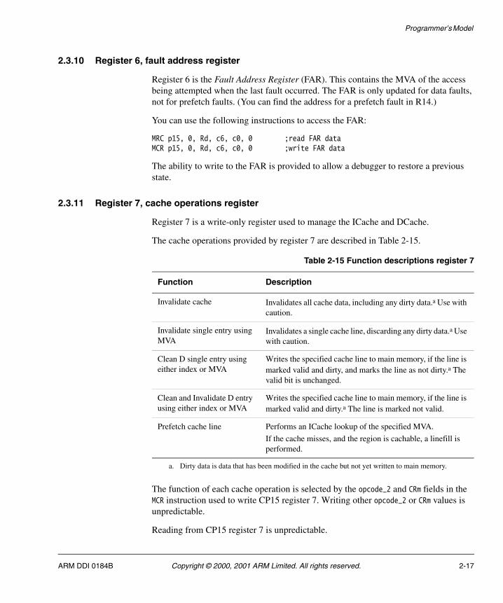
The cache operations provided by register 7 are described in Table 2-15.
The function of each cache operation is selected by the opcode_2 and CRm fields in the MCR instruction used to write CP15 register 7. Writing other opcode_2 or CRm values is unpredictable.
Reading from CP15 register 7 is unpredictable.
Table 2-15 Function descriptions register 7
Function Description
Invalidate cache Invalidates all cache data, including any dirty data.a Use with caution.
a. Dirty data is data that has been modified in the cache but not yet written to main memory.
Invalidate single entry using MVA
Invalidates a single cache line, discarding any dirty data.a Use with caution.
Clean D single entry using either index or MVA
Writes the specified cache line to main memory, if the line is marked valid and dirty, and marks the line as not dirty.a The valid bit is unchanged.
Clean and Invalidate D entry using either index or MVA
Writes the specified cache line to main memory, if the line is marked valid and dirty.a The line is marked not valid.
Prefetch cache line Performs an ICache lookup of the specified MVA.
If the cache misses, and the region is cachable, a linefill is performed.
ARM DDI 0184B Copyright © 2000, 2001 ARM Limited. All rights reserved. 2-17
Programmer’s Model
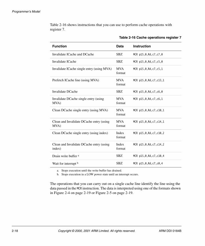
Table 2-16 shows instructions that you can use to perform cache operations with register 7.
The operations that you can carry out on a single cache line identify the line using the data passed in the MCR instruction. The data is interpreted using one of the formats shown in Figure 2-4 on page 2-19 or Figure 2-5 on page 2-19.
Table 2-16 Cache operations register 7
Function Data Instruction
Invalidate ICache and DCache SBZ MCR p15,0,Rd,c7,c7,0
Invalidate ICache SBZ MCR p15,0,Rd,c7,c5,0
Invalidate ICache single entry (using MVA) MVA format
MCR p15,0,Rd,c7,c5,1
Prefetch ICache line (using MVA) MVA format
MCR p15,0,Rd,c7,c13,1
Invalidate DCache SBZ MCR p15,0,Rd,c7,c6,0
Invalidate DCache single entry (using MVA)
MVA format
MCR p15,0,Rd,c7,c6,1
Clean DCache single entry (using MVA) MVA format
MCR p15,0,Rd,c7,c10,1
Clean and Invalidate DCache entry (using MVA)
MVA format
MCR p15,0,Rd,c7,c14,1
Clean DCache single entry (using index) Index format
MCR p15,0,Rd,c7,c10,2
Clean and Invalidate DCache entry (using index)
Index format
MCR p15,0,Rd,c7,c14,2
Drain write buffer a
a. Stops execution until the write buffer has drained.
SBZ MCR p15,0,Rd,c7,c10,4
Wait for interrupt b
b. Stops execution in a LOW power state until an interrupt occurs.
SBZ MCR p15,0,Rd,c7,c0,4
2-18 Copyright © 2000, 2001 ARM Limited. All rights reserved. ARM DDI 0184B
Programmer’s Model
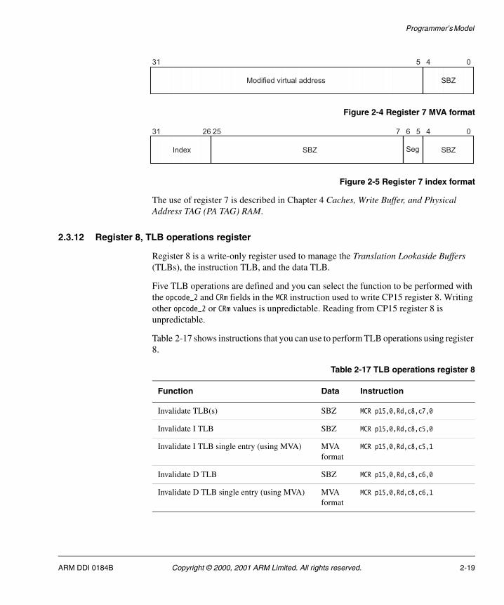
Figure 2-4 Register 7 MVA format
Figure 2-5 Register 7 index format
The use of register 7 is described in Chapter 4 Caches, Write Buffer, and Physical Address TAG (PA TAG) RAM.
2.3.12 Register 8, TLB operations register
Register 8 is a write-only register used to manage the Translation Lookaside Buffers (TLBs), the instruction TLB, and the data TLB.
Five TLB operations are defined and you can select the function to be performed with the opcode_2 and CRm fields in the MCR instruction used to write CP15 register 8. Writing other opcode_2 or CRm values is unpredictable. Reading from CP15 register 8 is unpredictable.
Table 2-17 shows instructions that you can use to perform TLB operations using register 8.
31 5 4 0
Modified virtual address SBZ
31 26 25 67 5 4 0
Index SBZ SBZSeg
Table 2-17 TLB operations register 8
Function Data Instruction
Invalidate TLB(s) SBZ MCR p15,0,Rd,c8,c7,0
Invalidate I TLB SBZ MCR p15,0,Rd,c8,c5,0
Invalidate I TLB single entry (using MVA) MVA format
MCR p15,0,Rd,c8,c5,1
Invalidate D TLB SBZ MCR p15,0,Rd,c8,c6,0
Invalidate D TLB single entry (using MVA) MVA format
MCR p15,0,Rd,c8,c6,1
ARM DDI 0184B Copyright © 2000, 2001 ARM Limited. All rights reserved. 2-19
Programmer’s Model
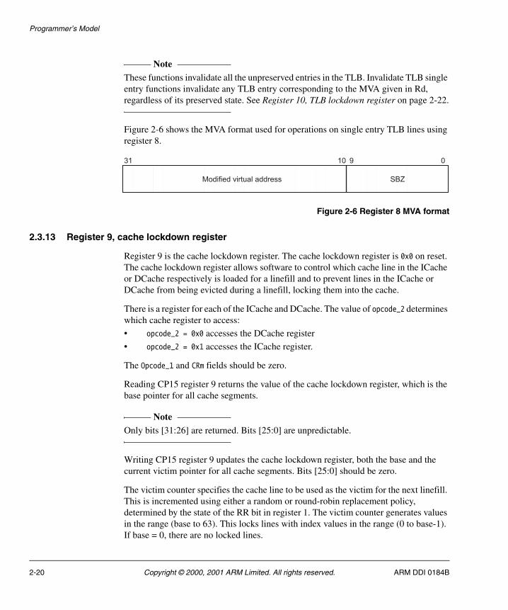
Note These functions invalidate all the unpreserved entries in the TLB. Invalidate TLB single entry functions invalidate any TLB entry corresponding to the MVA given in Rd, regardless of its preserved state. See Register 10, TLB lockdown register on page 2-22.
Figure 2-6 shows the MVA format used for operations on single entry TLB lines using register 8.
Figure 2-6 Register 8 MVA format
2.3.13 Register 9, cache lockdown register
Register 9 is the cache lockdown register. The cache lockdown register is 0x0 on reset. The cache lockdown register allows software to control which cache line in the ICache or DCache respectively is loaded for a linefill and to prevent lines in the ICache or DCache from being evicted during a linefill, locking them into the cache.
There is a register for each of the ICache and DCache. The value of opcode_2 determines which cache register to access:
• opcode_2 = 0x0 accesses the DCache register
• opcode_2 = 0x1 accesses the ICache register.
The Opcode_1 and CRm fields should be zero.
Reading CP15 register 9 returns the value of the cache lockdown register, which is the base pointer for all cache segments.
Note Only bits [31:26] are returned. Bits [25:0] are unpredictable.
Writing CP15 register 9 updates the cache lockdown register, both the base and the current victim pointer for all cache segments. Bits [25:0] should be zero.
The victim counter specifies the cache line to be used as the victim for the next linefill. This is incremented using either a random or round-robin replacement policy, determined by the state of the RR bit in register 1. The victim counter generates values in the range (base to 63). This locks lines with index values in the range (0 to base-1). If base = 0, there are no locked lines.
31 10 9 0
Modified virtual address SBZ
2-20 Copyright © 2000, 2001 ARM Limited. All rights reserved. ARM DDI 0184B
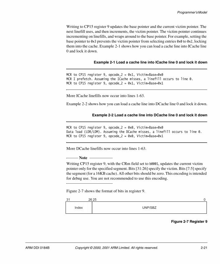
Programmer’s Model
Writing to CP15 register 9 updates the base pointer and the current victim pointer. The next linefill uses, and then increments, the victim pointer. The victim pointer continues incrementing on linefills, and wraps around to the base pointer. For example, setting the base pointer to 0x3 prevents the victim pointer from selecting entries 0x0 to 0x2, locking them into the cache. Example 2-1 shows how you can load a cache line into ICache line 0 and lock it down.
Example 2-1 Load a cache line into ICache line 0 and lock it down
MCR to CP15 register 9, opcode_2 = 0x1, Victim=Base=0x0MCR I prefetch. Assuming the ICache misses, a linefill occurs to line 0.MCR to CP15 register 9, opcode_2 = 0x1, Victim=Base=0x1
More ICache linefills now occur into lines 1-63.
Example 2-2 shows how you can load a cache line into DCache line 0 and lock it down.
Example 2-2 Load a cache line into DCache line 0 and lock it down
MCR to CP15 register 9, opcode_2 = 0x0, Victim=Base=0x0Data load (LDR/LDM). Assuming the DCache misses, a linefill occurs to line 0.MCR to CP15 register 9, opcode_2 = 0x0, Victim=Base=0x1
More DCache linefills now occur into lines 1-63.
Note Writing CP15 register 9, with the CRm field set to b0001, updates the current victim pointer only for the specified segment. Bits [31:26] specify the victim. Bits [7:5] specify the segment (for a 16KB cache). All other bits should be zero. This encoding is intended for debug use. You are not recommended to use this encoding.
Figure 2-7 shows the format of bits in register 9.
Figure 2-7 Register 9
31 26 25 0
Index UNP/SBZ
ARM DDI 0184B Copyright © 2000, 2001 ARM Limited. All rights reserved. 2-21
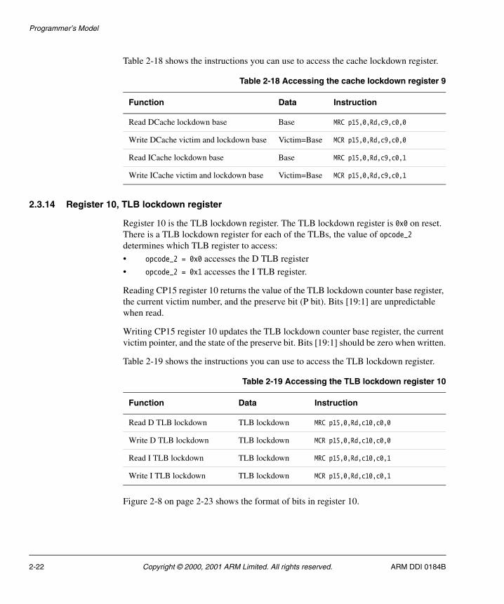
Programmer’s Model
Table 2-18 shows the instructions you can use to access the cache lockdown register.
2.3.14 Register 10, TLB lockdown register
Register 10 is the TLB lockdown register. The TLB lockdown register is 0x0 on reset. There is a TLB lockdown register for each of the TLBs, the value of opcode_2 determines which TLB register to access:
• opcode_2 = 0x0 accesses the D TLB register
• opcode_2 = 0x1 accesses the I TLB register.
Reading CP15 register 10 returns the value of the TLB lockdown counter base register, the current victim number, and the preserve bit (P bit). Bits [19:1] are unpredictable when read.
Writing CP15 register 10 updates the TLB lockdown counter base register, the current victim pointer, and the state of the preserve bit. Bits [19:1] should be zero when written.
Table 2-19 shows the instructions you can use to access the TLB lockdown register.
Figure 2-8 on page 2-23 shows the format of bits in register 10.
Table 2-18 Accessing the cache lockdown register 9
Function Data Instruction
Read DCache lockdown base Base MRC p15,0,Rd,c9,c0,0
Write DCache victim and lockdown base Victim=Base MCR p15,0,Rd,c9,c0,0
Read ICache lockdown base Base MRC p15,0,Rd,c9,c0,1
Write ICache victim and lockdown base Victim=Base MCR p15,0,Rd,c9,c0,1
Table 2-19 Accessing the TLB lockdown register 10
Function Data Instruction
Read D TLB lockdown TLB lockdown MRC p15,0,Rd,c10,c0,0
Write D TLB lockdown TLB lockdown MCR p15,0,Rd,c10,c0,0
Read I TLB lockdown TLB lockdown MRC p15,0,Rd,c10,c0,1
Write I TLB lockdown TLB lockdown MCR p15,0,Rd,c10,c0,1
2-22 Copyright © 2000, 2001 ARM Limited. All rights reserved. ARM DDI 0184B
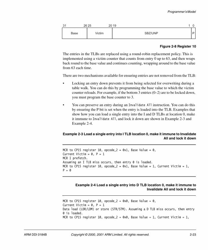
Programmer’s Model
Figure 2-8 Register 10
The entries in the TLBs are replaced using a round-robin replacement policy. This is implemented using a victim counter that counts from entry 0 up to 63, and then wraps back round to the base value and continues counting, wrapping around to the base value from 63 each time.
There are two mechanisms available for ensuring entries are not removed from the TLB:
• Locking an entry down prevents it from being selected for overwriting during a table walk. You can do this by programming the base value to which the victim counter reloads. For example, if the bottom 3 entries (0–2) are to be locked down, you must program the base counter to 3.
• You can preserve an entry during an Invalidate All instruction. You can do this by ensuring the P bit is set when the entry is loaded into the TLB. Examples that show how you can load a single entry into the I and D TLBs at location 0, make it immune to Invalidate All, and lock it down are shown in Example 2-3 and Example 2-4.
Example 2-3 Load a single entry into I TLB location 0, make it immune to InvalidateAll and lock it down
MCR to CP15 register 10, opcode_2 = 0x1, Base Value = 0,Current Victim = 0, P = 1MCR I prefetch.Assuming an I TLB miss occurs, then entry 0 is loaded.MCR to CP15 register 10, opcode_2 = 0x1, Base Value = 1, Current Victim = 1,P = 0
Example 2-4 Load a single entry into D TLB location 0, make it immune toInvalidate All and lock it down
MCR to CP15 register 10, opcode_2 = 0x0, Base Value = 0,Current Victim = 0, P = 1Data load (LDR/LDM) or store (STR/STM). Assuming a D TLB miss occurs, then entry 0 is loaded.MCR to CP15 register 10, opcode_2 = 0x0, Base Value = 1, Current Victim = 1,
31 26 25 20 19 1 0
Base SBZ/UNP PVictim
ARM DDI 0184B Copyright © 2000, 2001 ARM Limited. All rights reserved. 2-23
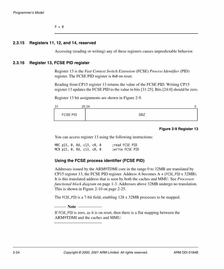
Programmer’s Model
P = 0
2.3.15 Registers 11, 12, and 14, reserved
Accessing (reading or writing) any of these registers causes unpredictable behavior.
2.3.16 Register 13, FCSE PID register
Register 13 is the Fast Context Switch Extension (FCSE) Process Identifier (PID) register. The FCSE PID register is 0x0 on reset.
Reading from CP15 register 13 returns the value of the FCSE PID. Writing CP15 register 13 updates the FCSE PID to the value in bits [31:25]. Bits [24:0] should be zero.
Register 13 bit assignments are shown in Figure 2-9.
Figure 2-9 Register 13
You can access register 13 using the following instructions:
MRC p15, 0, Rd, c13, c0, 0 ;read FCSE PIDMCR p15, 0, Rd, c13, c0, 0 ;write FCSE PID
Using the FCSE process identifier (FCSE PID)
Addresses issued by the ARM9TDMI core in the range 0 to 32MB are translated by CP15 register 13, the FCSE PID register. Address A becomes A + (FCSE_PID x 32MB). It is this translated address that is seen by both the caches and MMU. See Processor functional block diagram on page 1-3. Addresses above 32MB undergo no translation. This is shown in Figure 2-10 on page 2-25.
The FCSE_PID is a 7-bit field, enabling 128 x 32MB processes to be mapped.
Note If FCSE_PID is zero, as it is on reset, then there is a flat mapping between the ARM9TDMI and the caches and MMU.
31 25 24 0
FCSE PID SBZ
2-24 Copyright © 2000, 2001 ARM Limited. All rights reserved. ARM DDI 0184B
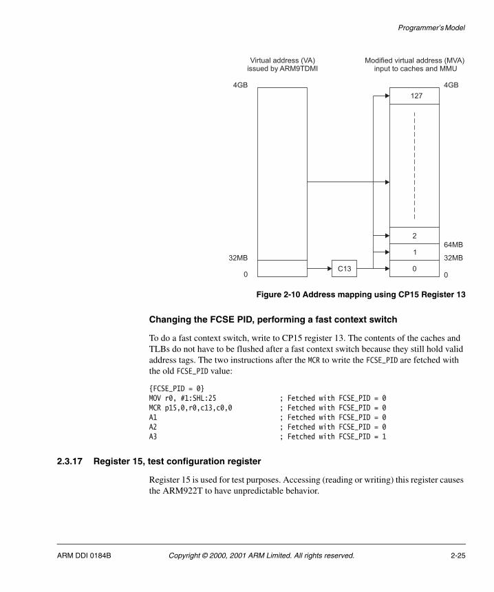
Programmer’s Model
Figure 2-10 Address mapping using CP15 Register 13
Changing the FCSE PID, performing a fast context switch
To do a fast context switch, write to CP15 register 13. The contents of the caches and TLBs do not have to be flushed after a fast context switch because they still hold valid address tags. The two instructions after the MCR to write the FCSE_PID are fetched with the old FCSE_PID value:
{FCSE_PID = 0}MOV r0, #1:SHL:25 ; Fetched with FCSE_PID = 0MCR p15,0,r0,c13,c0,0 ; Fetched with FCSE_PID = 0A1 ; Fetched with FCSE_PID = 0A2 ; Fetched with FCSE_PID = 0A3 ; Fetched with FCSE_PID = 1
2.3.17 Register 15, test configuration register
Register 15 is used for test purposes. Accessing (reading or writing) this register causes the ARM922T to have unpredictable behavior.
0
1
2
127
C13
Virtual address (VA)issued by ARM9TDMI
Modified virtual address (MVA)input to caches and MMU
0
4GB
0
32MB
4GB
32MB
64MB
ARM DDI 0184B Copyright © 2000, 2001 ARM Limited. All rights reserved. 2-25

Programmer’s Model
2-26 Copyright © 2000, 2001 ARM Limited. All rights reserved. ARM DDI 0184B
Chapter 3 Memory Management Unit
This chapter describes the Memory Management Unit (MMU). It contains the following sections:
• About the MMU on page 3-2
• MMU program accessible registers on page 3-4
• Address translation on page 3-6
• MMU faults and CPU aborts on page 3-21
• Fault address and fault status registers on page 3-22
• Domain access control on page 3-23
• Fault checking sequence on page 3-25
• External aborts on page 3-28
• Interaction of the MMU and caches on page 3-29.
ARM DDI 0184B Copyright © 2000, 2001 ARM Limited. All rights reserved. 3-1
Memory Management Unit
3.1 About the MMU
The ARM922T processor implements an enhanced ARM architecture v4 MMU to provide translation and access permission checks for the instruction and data address ports of the ARM9TDMI core. The MMU is controlled from a single set of two-level page tables stored in main memory, that are enabled by the M bit in CP15 register 1, providing a single address translation and protection scheme. You can independently lock and flush the instruction and data TLBs in the MMU.
The MMU features are:
• standard ARMv4 MMU mapping sizes, domains, and access protection scheme
• mapping sizes are 1MB (sections), 64KB (large pages), 4KB (small pages), and 1KB (tiny pages)
• access permissions for sections
• access permissions for large pages and small pages can be specified separately for each quarter of the page (these quarters are called subpages)
• 16 domains implemented in hardware
• 64 entry instruction TLB and 64 entry data TLB
• hardware page table walks
• round-robin replacement algorithm (also called cyclic)
• invalidate whole TLB, using CP15 register 8
• invalidate TLB entry, selected by MVA, using CP15 register 8
• independent lockdown of instruction TLB and data TLB, using CP15 register 10.
3.1.1 Access permissions and domains
For large and small pages, access permissions are defined for each subpage (1KB for small pages, 16KB for large pages). Sections and tiny pages have a single set of access permissions.
All regions of memory have an associated domain. A domain is the primary access control mechanism for a region of memory. It defines the conditions necessary for an access to proceed. The domain determines if:
• the access permissions are used to qualify the access
• the access is unconditionally allowed to proceed
• the access is unconditionally aborted.
3-2 Copyright © 2000, 2001 ARM Limited. All rights reserved. ARM DDI 0184B
Memory Management Unit
In the latter two cases, the access permission attributes are ignored.
There are 16 domains. These are configured using the domain access control register.
3.1.2 Translated entries
Each TLB caches 64 translated entries. During CPU memory accesses, the TLB provides the protection information to the access control logic.
If the TLB contains a translated entry for the MVA, the access control logic determines if access is permitted:
• if access is permitted and an off-chip access is required, the MMU outputs the appropriate physical address corresponding to the MVA
• if access is permitted and an off-chip access is not required, the cache services the access
• if access is not permitted, the MMU signals the CPU core to abort.
If a TLB misses (it does not contain an entry for the VA) the translation table walk hardware is invoked to retrieve the translation information from a translation table in physical memory. When retrieved, the translation information is written into the TLB, possibly overwriting an existing value.
The entry to be written is chosen by cycling sequentially through the TLB locations. To enable use of TLB locking features, you can specify the location to write using CP15 register 10, TLB lockdown.
When the MMU is turned off, as happens on reset, no address mapping occurs and all regions are marked as noncachable and nonbufferable. See About the caches and write buffer on page 4-2.
ARM DDI 0184B Copyright © 2000, 2001 ARM Limited. All rights reserved. 3-3
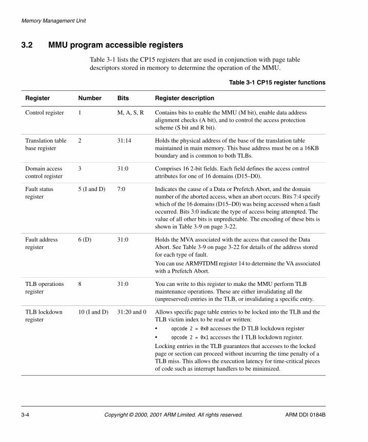
Memory Management Unit
3.2 MMU program accessible registers
Table 3-1 lists the CP15 registers that are used in conjunction with page table descriptors stored in memory to determine the operation of the MMU.
Table 3-1 CP15 register functions
Register Number Bits Register description
Control register 1 M, A, S, R Contains bits to enable the MMU (M bit), enable data address alignment checks (A bit), and to control the access protection scheme (S bit and R bit).
Translation table base register
2 31:14 Holds the physical address of the base of the translation table maintained in main memory. This base address must be on a 16KB boundary and is common to both TLBs.
Domain access control register
3 31:0 Comprises 16 2-bit fields. Each field defines the access control attributes for one of 16 domains (D15–D0).
Fault status register
5 (I and D) 7:0 Indicates the cause of a Data or Prefetch Abort, and the domain number of the aborted access, when an abort occurs. Bits 7:4 specify which of the 16 domains (D15–D0) was being accessed when a fault occurred. Bits 3:0 indicate the type of access being attempted. The value of all other bits is unpredictable. The encoding of these bits is shown in Table 3-9 on page 3-22.
Fault address register
6 (D) 31:0 Holds the MVA associated with the access that caused the Data Abort. See Table 3-9 on page 3-22 for details of the address stored for each type of fault.
You can use ARM9TDMI register 14 to determine the VA associated with a Prefetch Abort.
TLB operations register
8 31:0 You can write to this register to make the MMU perform TLB maintenance operations. These are either invalidating all the (unpreserved) entries in the TLB, or invalidating a specific entry.
TLB lockdown register
10 (I and D) 31:20 and 0 Allows specific page table entries to be locked into the TLB and the TLB victim index to be read or written:
• opcode 2 = 0x0 accesses the D TLB lockdown register
• opcode 2 = 0x1 accesses the I TLB lockdown register.
Locking entries in the TLB guarantees that accesses to the locked page or section can proceed without incurring the time penalty of a TLB miss. This allows the execution latency for time-critical pieces of code such as interrupt handlers to be minimized.
3-4 Copyright © 2000, 2001 ARM Limited. All rights reserved. ARM DDI 0184B
Memory Management Unit
All the CP15 MMU registers, except register 8, contain state. You can read them using MRC instructions, and write them using MCR instructions. Registers 5 and 6 are also written by the MMU during a Data Abort. Writing to Register 8 causes the MMU to perform a TLB operation, to manipulate TLB entries. This register cannot be read. The Instruction TLB (I TLB) and Data TLB (D TLB) both have a copy of register 10. The opcode_2 field in the CP15 instruction is used to determine the one accessed.
CP15 is described in Chapter 2 Programmer’s Model, with details of register formats and the coprocessor instructions you can use to access them.
ARM DDI 0184B Copyright © 2000, 2001 ARM Limited. All rights reserved. 3-5
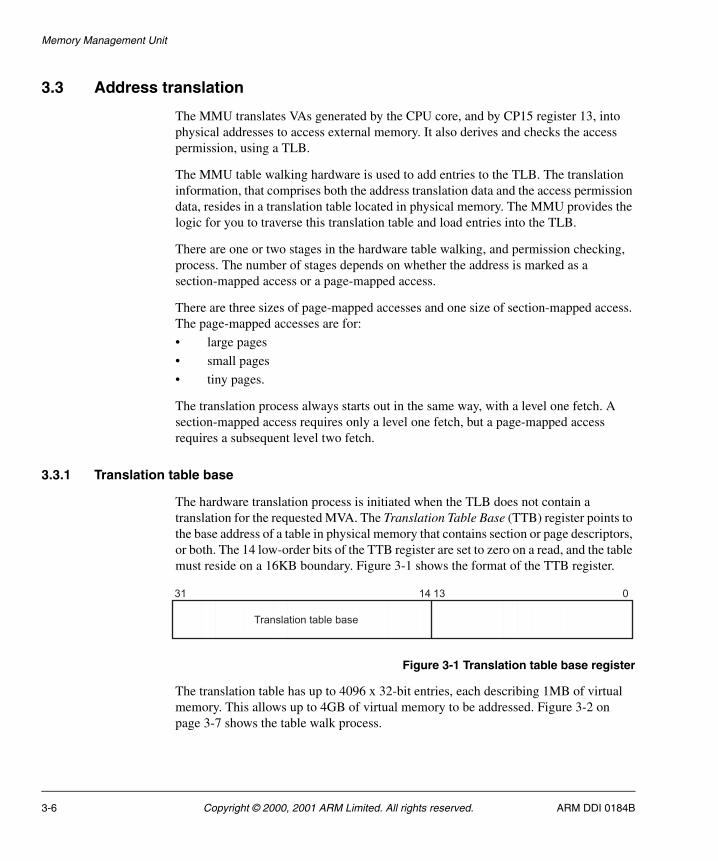
Memory Management Unit
3.3 Address translation
The MMU translates VAs generated by the CPU core, and by CP15 register 13, into physical addresses to access external memory. It also derives and checks the access permission, using a TLB.
The MMU table walking hardware is used to add entries to the TLB. The translation information, that comprises both the address translation data and the access permission data, resides in a translation table located in physical memory. The MMU provides the logic for you to traverse this translation table and load entries into the TLB.
There are one or two stages in the hardware table walking, and permission checking, process. The number of stages depends on whether the address is marked as a section-mapped access or a page-mapped access.
There are three sizes of page-mapped accesses and one size of section-mapped access. The page-mapped accesses are for:
• large pages
• small pages
• tiny pages.
The translation process always starts out in the same way, with a level one fetch. A section-mapped access requires only a level one fetch, but a page-mapped access requires a subsequent level two fetch.
3.3.1 Translation table base
The hardware translation process is initiated when the TLB does not contain a translation for the requested MVA. The Translation Table Base (TTB) register points to the base address of a table in physical memory that contains section or page descriptors, or both. The 14 low-order bits of the TTB register are set to zero on a read, and the table must reside on a 16KB boundary. Figure 3-1 shows the format of the TTB register.
Figure 3-1 Translation table base register
The translation table has up to 4096 x 32-bit entries, each describing 1MB of virtual memory. This allows up to 4GB of virtual memory to be addressed. Figure 3-2 on page 3-7 shows the table walk process.
31 14 13 0
Translation table base
3-6 Copyright © 2000, 2001 ARM Limited. All rights reserved. ARM DDI 0184B
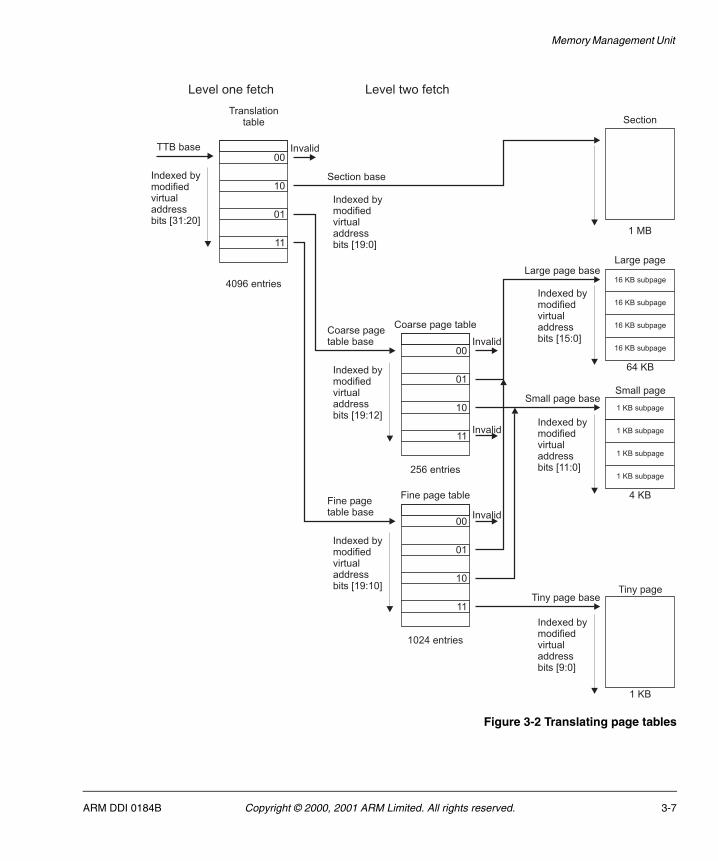
Memory Management Unit
Figure 3-2 Translating page tables
Translationtable
4096 entries
TTB base
Indexed bymodifiedvirtualaddressbits [31:20]
Level one fetch
Section
1 MB
Indexed bymodifiedvirtualaddressbits [19:0]
Section base
Coarse page table
256 entries
Fine page table
1024 entries
Indexed bymodifiedvirtualaddressbits [19:12]
Indexed bymodifiedvirtualaddressbits [19:10]
Coarse pagetable base
Fine pagetable base
Level two fetch
Large page
64 KB
Small page
4 KB
Tiny page
1 KB
Large page base
Indexed bymodifiedvirtualaddressbits [15:0]
Indexed bymodifiedvirtualaddressbits [11:0]
Indexed bymodifiedvirtualaddressbits [9:0]
00
01
10
11
Invalid
00
10
01
11
00
10
01
11
1 KB subpage
1 KB subpage
1 KB subpage
1 KB subpage
16 KB subpage
16 KB subpage
16 KB subpage
16 KB subpage
Small page base
Tiny page base
Invalid
Invalid
Invalid
ARM DDI 0184B Copyright © 2000, 2001 ARM Limited. All rights reserved. 3-7
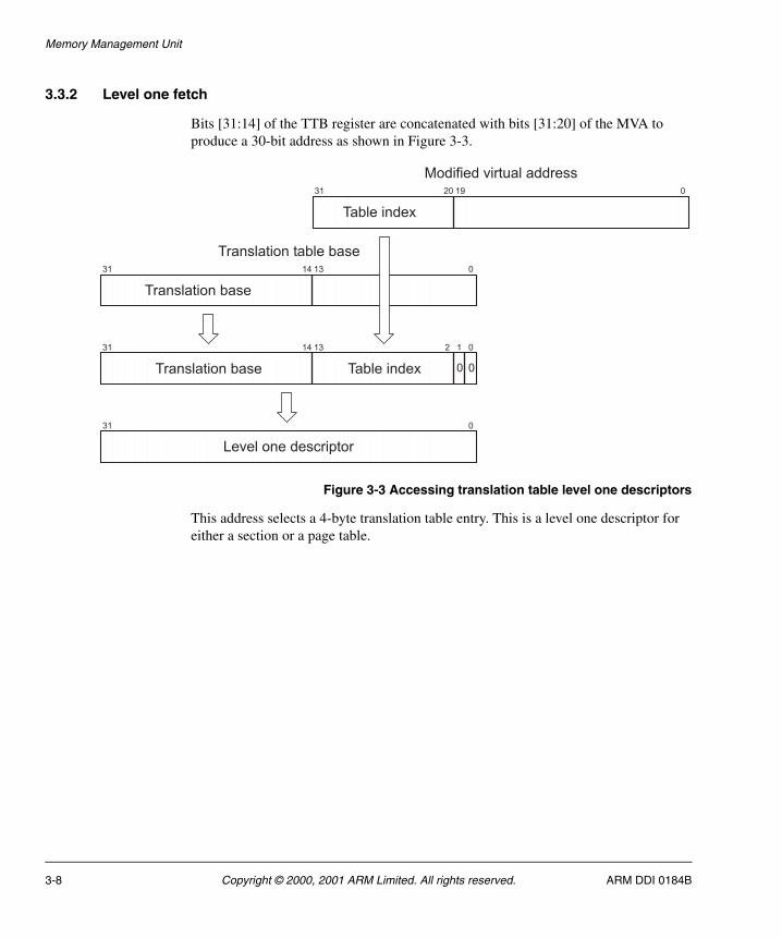
Memory Management Unit
3.3.2 Level one fetch
Bits [31:14] of the TTB register are concatenated with bits [31:20] of the MVA to produce a 30-bit address as shown in Figure 3-3.
Figure 3-3 Accessing translation table level one descriptors
This address selects a 4-byte translation table entry. This is a level one descriptor for either a section or a page table.
31 20 19 0
Table index
31 14 13 0
Translation base
31 14 13 2 1 0
0 0Table indexTranslation base
31 0
Level one descriptor
Modified virtual address
Translation table base
3-8 Copyright © 2000, 2001 ARM Limited. All rights reserved. ARM DDI 0184B
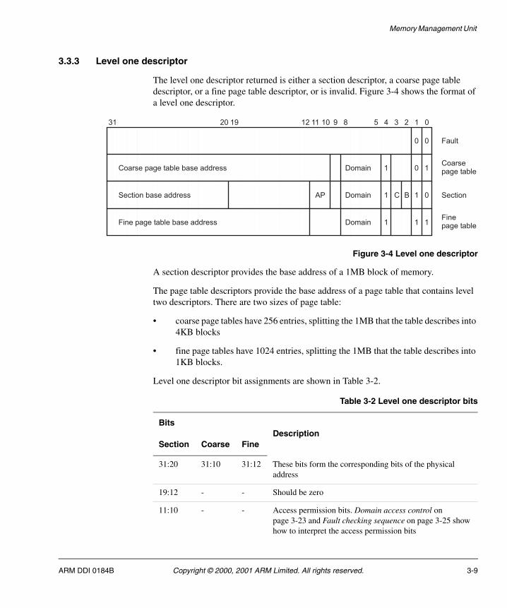
Memory Management Unit
3.3.3 Level one descriptor
The level one descriptor returned is either a section descriptor, a coarse page table descriptor, or a fine page table descriptor, or is invalid. Figure 3-4 shows the format of a level one descriptor.
Figure 3-4 Level one descriptor
A section descriptor provides the base address of a 1MB block of memory.
The page table descriptors provide the base address of a page table that contains level two descriptors. There are two sizes of page table:
• coarse page tables have 256 entries, splitting the 1MB that the table describes into 4KB blocks
• fine page tables have 1024 entries, splitting the 1MB that the table describes into 1KB blocks.
Level one descriptor bit assignments are shown in Table 3-2.
31 20 19 12 11 10 9 8 5 4 3 2 1 0
0 0
Coarse page table base address Domain 1 0 1
Section base address AP Domain 1 C B 1 0
Fine page table base address Domain 1 1 1
Fault
Coarsepage table
Section
Finepage table
Table 3-2 Level one descriptor bits
BitsDescription
Section Coarse Fine
31:20 31:10 31:12 These bits form the corresponding bits of the physical address
19:12 - - Should be zero
11:10 - - Access permission bits. Domain access control on page 3-23 and Fault checking sequence on page 3-25 show how to interpret the access permission bits
ARM DDI 0184B Copyright © 2000, 2001 ARM Limited. All rights reserved. 3-9
Memory Management Unit
The two least significant bits of the level one descriptor indicate the descriptor type as shown in Table 3-3.
9 9 11:9 Should be zero
8:5 8:5 8:5 Domain control bits
4 4 4 Must be 1
3:2 - - These bits, C and B, indicate whether the area of memory mapped by this page is treated as write-back cachable, write-through cachable, noncached buffered, or noncached nonbuffered
- 3:2 3:2 Should be zero
1:0 1:0 1:0 These bits indicate the page size and validity and are interpreted as shown in Table 3-3
Table 3-3 Interpreting level one descriptor bits [1:0]
Value Meaning Description
0 0 Invalid Generates a section translation fault
0 1 Coarse page table Indicates that this is a coarse page table descriptor
1 0 Section Indicates that this is a section descriptor
1 1 Fine page table Indicates that this is a fine page table descriptor
Table 3-2 Level one descriptor bits (continued)
BitsDescription
Section Coarse Fine
3-10 Copyright © 2000, 2001 ARM Limited. All rights reserved. ARM DDI 0184B
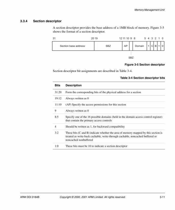
Memory Management Unit
3.3.4 Section descriptor
A section descriptor provides the base address of a 1MB block of memory. Figure 3-5 shows the format of a section descriptor.
Figure 3-5 Section descriptor
Section descriptor bit assignments are described in Table 3-4.
SBZ
31 20 19 12 11 10 9 8 5 4 3 2 1 0
Section base address AP Domain 1 C B 1 0SBZ
Table 3-4 Section descriptor bits
Bits Description
31:20 Form the corresponding bits of the physical address for a section
19:12 Always written as 0
11:10 (AP) Specify the access permissions for this section
9 Always written as 0
8:5 Specify one of the 16 possible domains (held in the domain access control register) that contain the primary access controls
4 Should be written as 1, for backward compatibility
3:2 These bits (C and B) indicate whether the area of memory mapped by this section is treated as write-back cachable, write-through cachable, noncached buffered or noncached nonbuffered
1:0 These bits must be 10 to indicate a section descriptor
ARM DDI 0184B Copyright © 2000, 2001 ARM Limited. All rights reserved. 3-11
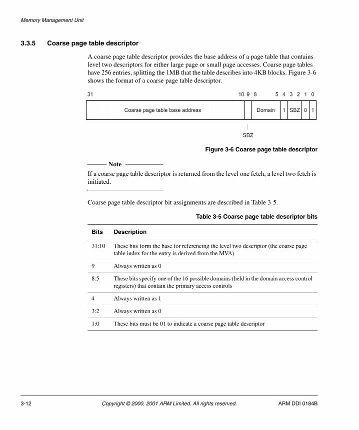
Memory Management Unit
3.3.5 Coarse page table descriptor
A coarse page table descriptor provides the base address of a page table that contains level two descriptors for either large page or small page accesses. Coarse page tables have 256 entries, splitting the 1MB that the table describes into 4KB blocks. Figure 3-6 shows the format of a coarse page table descriptor.
Figure 3-6 Coarse page table descriptor
Note If a coarse page table descriptor is returned from the level one fetch, a level two fetch is initiated.
Coarse page table descriptor bit assignments are described in Table 3-5.
31 10 9 8 5 4 3 2 1 0
Coarse page table base address Domain 1 0 1SBZ
SBZ
Table 3-5 Coarse page table descriptor bits
Bits Description
31:10 These bits form the base for referencing the level two descriptor (the coarse page table index for the entry is derived from the MVA)
9 Always written as 0
8:5 These bits specify one of the 16 possible domains (held in the domain access control registers) that contain the primary access controls
4 Always written as 1
3:2 Always written as 0
1:0 These bits must be 01 to indicate a coarse page table descriptor
3-12 Copyright © 2000, 2001 ARM Limited. All rights reserved. ARM DDI 0184B
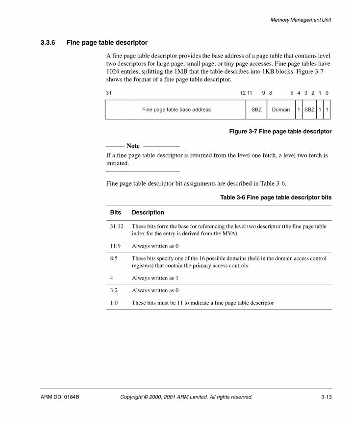
Memory Management Unit
3.3.6 Fine page table descriptor
A fine page table descriptor provides the base address of a page table that contains level two descriptors for large page, small page, or tiny page accesses. Fine page tables have 1024 entries, splitting the 1MB that the table describes into 1KB blocks. Figure 3-7 shows the format of a fine page table descriptor.
Figure 3-7 Fine page table descriptor
Note If a fine page table descriptor is returned from the level one fetch, a level two fetch is initiated.
Fine page table descriptor bit assignments are described in Table 3-6.
31 12 11 9 8 5 4 3 2 1 0
Fine page table base address Domain 1 1 1SBZ SBZ
Table 3-6 Fine page table descriptor bits
Bits Description
31:12 These bits form the base for referencing the level two descriptor (the fine page table index for the entry is derived from the MVA)
11:9 Always written as 0
8:5 These bits specify one of the 16 possible domains (held in the domain access control registers) that contain the primary access controls
4 Always written as 1
3:2 Always written as 0
1:0 These bits must be 11 to indicate a fine page table descriptor
ARM DDI 0184B Copyright © 2000, 2001 ARM Limited. All rights reserved. 3-13
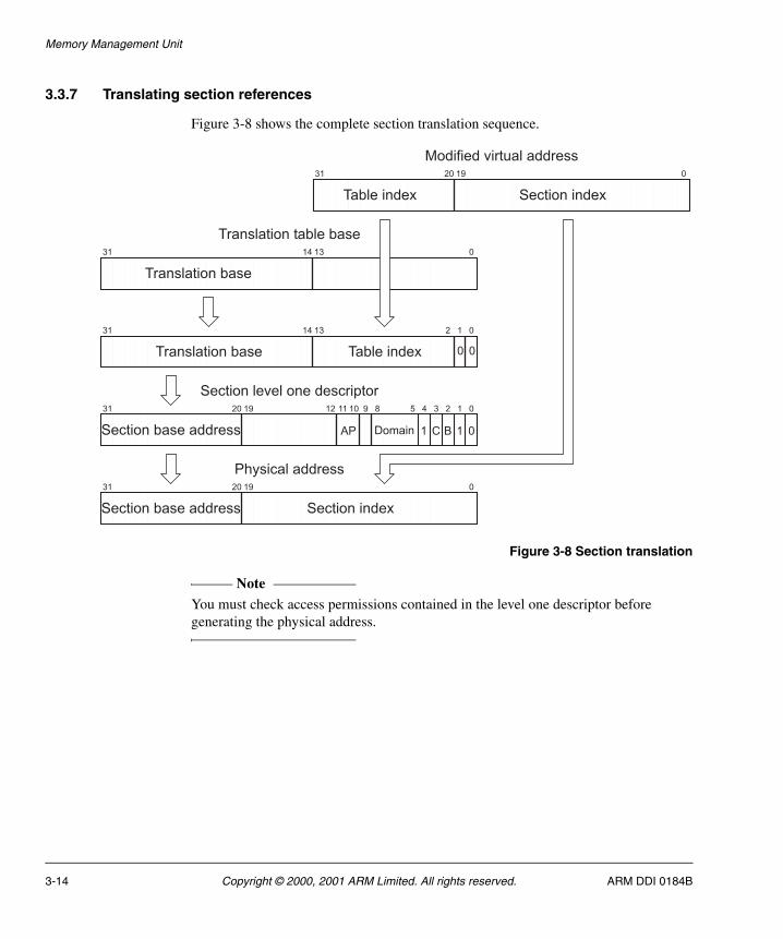
Memory Management Unit
3.3.7 Translating section references
Figure 3-8 shows the complete section translation sequence.
Figure 3-8 Section translation
Note You must check access permissions contained in the level one descriptor before generating the physical address.
31 14 13 0
Translation base
31 14 13 2 1 0
0 0Table indexTranslation base
Modified virtual address
Translation table base
31 20 19 0
Table index Section index
31 20 19 0
Section indexSection base address
Section level one descriptor
Physical address
31 20 19 0
Section base address AP Domain 1 C B 1 0
2 134589101112
3-14 Copyright © 2000, 2001 ARM Limited. All rights reserved. ARM DDI 0184B
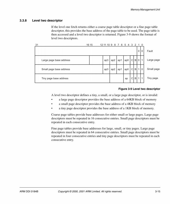
Memory Management Unit
3.3.8 Level two descriptor
If the level one fetch returns either a coarse page table descriptor or a fine page table descriptor, this provides the base address of the page table to be used. The page table is then accessed and a level two descriptor is returned. Figure 3-9 shows the format of level two descriptors.
Figure 3-9 Level two descriptor
A level two descriptor defines a tiny, a small, or a large page descriptor, or is invalid:
• a large page descriptor provides the base address of a 64KB block of memory
• a small page descriptor provides the base address of a 4KB block of memory
• a tiny page descriptor provides the base address of a 1KB block of memory.
Coarse page tables provide base addresses for either small or large pages. Large page descriptors must be repeated in 16 consecutive entries. Small page descriptors must be repeated in each consecutive entry.
Fine page tables provide base addresses for large, small, or tiny pages. Large page descriptors must be repeated in 64 consecutive entries. Small page descriptors must be repeated in four consecutive entries and tiny page descriptors must be repeated in each consecutive entry.
31 12 11 10 9 8 5 4 3 2 1 0
0 0
Large page base address 0 1
Small page base address C B 1 0
Tiny page base address 1 1
Fault
Large page
Small page
Tiny page
7 616 15
BC
C Bap0
ap0
ap
ap1ap2ap3
ap1ap2ap3
ARM DDI 0184B Copyright © 2000, 2001 ARM Limited. All rights reserved. 3-15
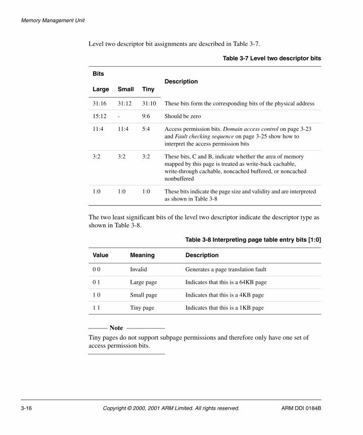
Memory Management Unit
Level two descriptor bit assignments are described in Table 3-7.
The two least significant bits of the level two descriptor indicate the descriptor type as shown in Table 3-8.
Note Tiny pages do not support subpage permissions and therefore only have one set of access permission bits.
Table 3-7 Level two descriptor bits
BitsDescription
Large Small Tiny
31:16 31:12 31:10 These bits form the corresponding bits of the physical address
15:12 - 9:6 Should be zero
11:4 11:4 5:4 Access permission bits. Domain access control on page 3-23 and Fault checking sequence on page 3-25 show how to interpret the access permission bits
3:2 3:2 3:2 These bits, C and B, indicate whether the area of memory mapped by this page is treated as write-back cachable, write-through cachable, noncached buffered, or noncached nonbuffered
1:0 1:0 1:0 These bits indicate the page size and validity and are interpreted as shown in Table 3-8
Table 3-8 Interpreting page table entry bits [1:0]
Value Meaning Description
0 0 Invalid Generates a page translation fault
0 1 Large page Indicates that this is a 64KB page
1 0 Small page Indicates that this is a 4KB page
1 1 Tiny page Indicates that this is a 1KB page
3-16 Copyright © 2000, 2001 ARM Limited. All rights reserved. ARM DDI 0184B
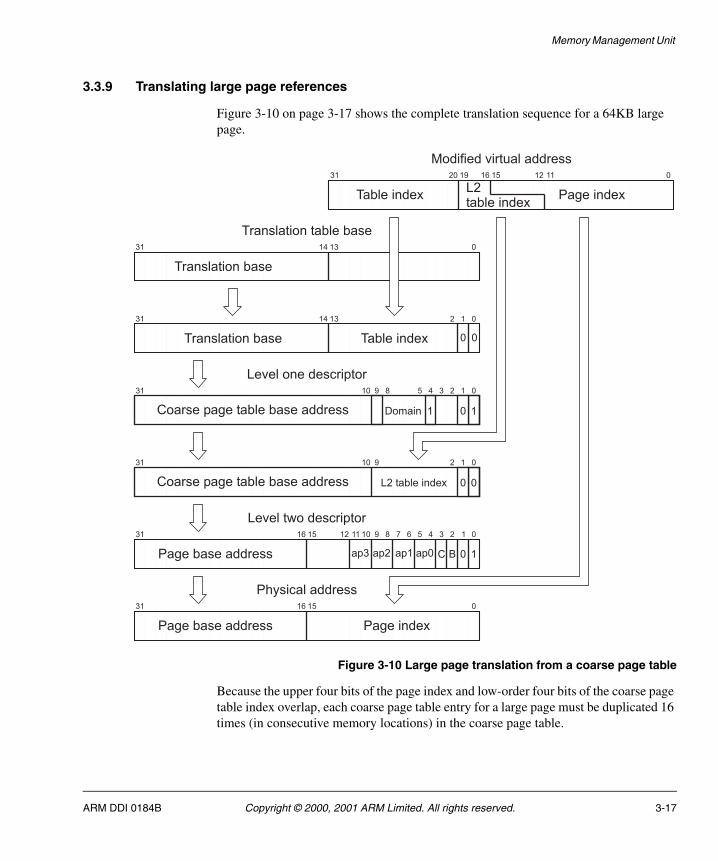
Memory Management Unit
3.3.9 Translating large page references
Figure 3-10 on page 3-17 shows the complete translation sequence for a 64KB large page.
Figure 3-10 Large page translation from a coarse page table
Because the upper four bits of the page index and low-order four bits of the coarse page table index overlap, each coarse page table entry for a large page must be duplicated 16 times (in consecutive memory locations) in the coarse page table.
31 14 13 0
Translation base
31 14 13 2 1 0
0 0Table indexTranslation base
Modified virtual address
Translation table base
31 20 19 0
Table index Page index
Level one descriptor
Physical address
31 0
Coarse page table base address Domain 1 1
2 13458910
L2table index
16 15 12 11
31 16 15 0
Page indexPage base address
Level two descriptor
31 0
Coarse page table base address L2 table index 0
2 1910
31 16 15 0
ap3Page base address
0
0
ap2 ap1 ap0 10C B
123456789101112
ARM DDI 0184B Copyright © 2000, 2001 ARM Limited. All rights reserved. 3-17
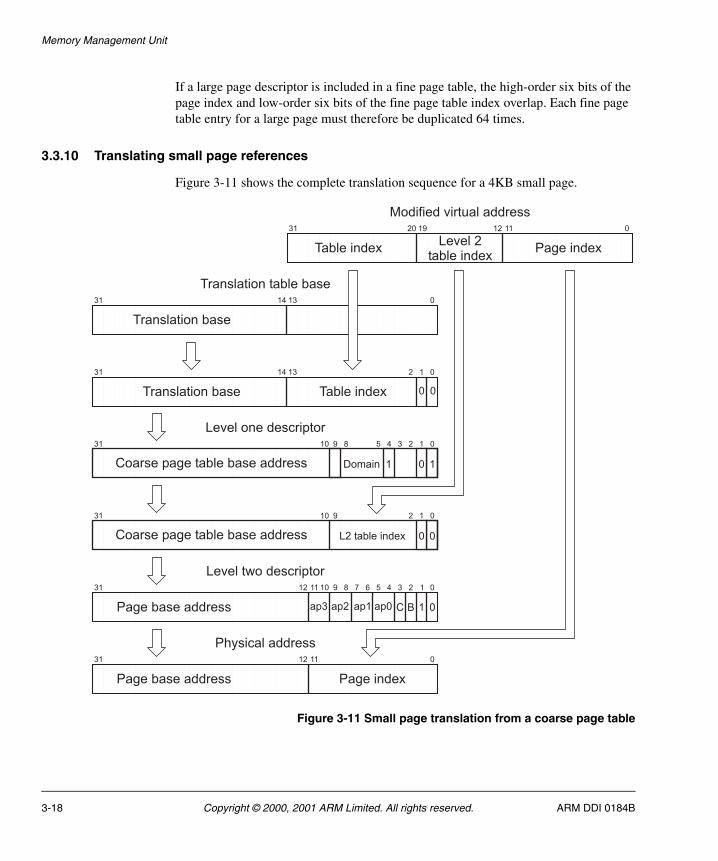
Memory Management Unit
If a large page descriptor is included in a fine page table, the high-order six bits of the page index and low-order six bits of the fine page table index overlap. Each fine page table entry for a large page must therefore be duplicated 64 times.
3.3.10 Translating small page references
Figure 3-11 shows the complete translation sequence for a 4KB small page.
Figure 3-11 Small page translation from a coarse page table
31 14 13 0
Translation base
31 14 13 2 1 0
0 0Table indexTranslation base
Modified virtual address
Translation table base
31 20 19 0
Table index Page index
Level one descriptor
Physical address
31 0
Coarse page table base address Domain 1 1
2 13458910
Level 2table index
12 11
31 0
Page indexPage base address
Level two descriptor
31 0
Coarse page table base address L2 table index 0
2 1910
31 0
ap3Page base address
0
0
ap2 ap1 ap0 01C B
123456789101112
1112
3-18 Copyright © 2000, 2001 ARM Limited. All rights reserved. ARM DDI 0184B
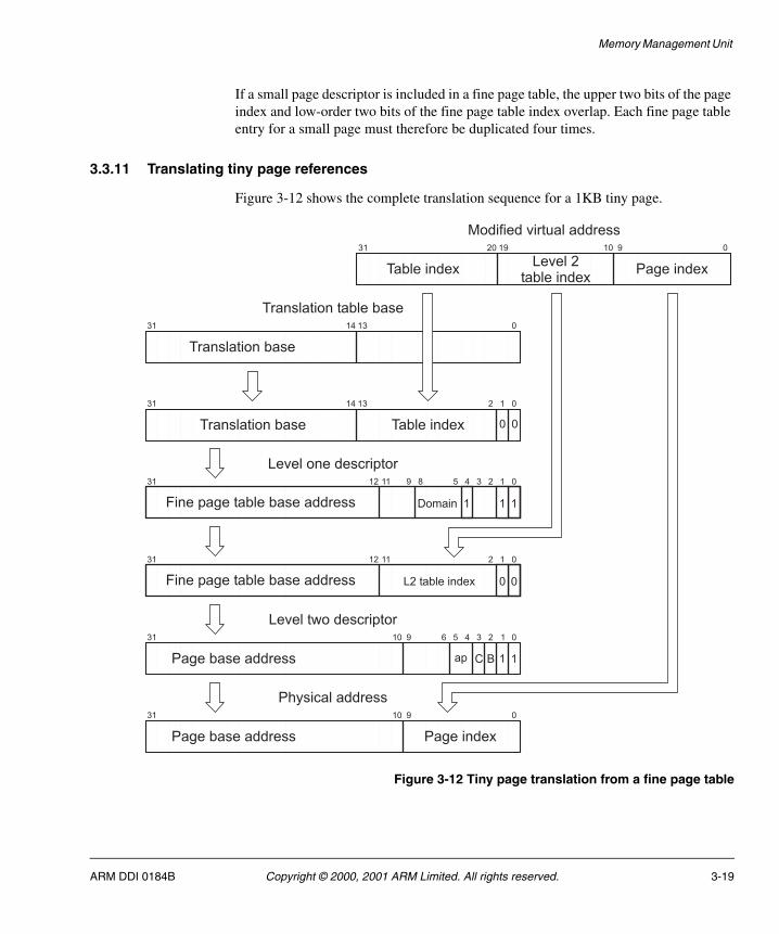
Memory Management Unit
If a small page descriptor is included in a fine page table, the upper two bits of the page index and low-order two bits of the fine page table index overlap. Each fine page table entry for a small page must therefore be duplicated four times.
3.3.11 Translating tiny page references
Figure 3-12 shows the complete translation sequence for a 1KB tiny page.
Figure 3-12 Tiny page translation from a fine page table
31 14 13 0
Translation base
31 14 13 2 1 0
0 0Table indexTranslation base
Modified virtual address
Translation table base
31 20 19 0
Table index Page index
Level one descriptor
Physical address
31 0
Fine page table base address Domain 1 1
2 13458911
Level 2table index
10 9
31 0
Page indexPage base address
Level two descriptor
31 0
Fine page table base address L2 table index 0
2 1
31 0
Page base address
1
0
ap 11C B
123456910
12
1112
910
ARM DDI 0184B Copyright © 2000, 2001 ARM Limited. All rights reserved. 3-19
Memory Management Unit
Page translation involves one additional step beyond that of a section translation. The level one descriptor is the fine page table descriptor and this is used to point to the level one descriptor.
Note The domain specified in the level one description and access permissions specified in the level one description together determine whether the access has permissions to proceed. See section Domain access control on page 3-23 for details.
3.3.12 Subpages
You can define access permissions for subpages of small and large pages. If, during a page walk, a small or large page has a non-identical subpage permission, only the subpage being accessed is written into the TLB. For example, a 16KB (large page) subpage entry is written into the TLB if the subpage permission differs, and a 64KB entry is put in the TLB if the subpage permissions are identical.
When you use subpage permissions, and the page entry then has to be invalidated, you must invalidate all four subpages separately.
3-20 Copyright © 2000, 2001 ARM Limited. All rights reserved. ARM DDI 0184B
Memory Management Unit
3.4 MMU faults and CPU aborts
The MMU generates an abort on the following types of faults:
• alignment faults (data accesses only)
• translation faults
• domain faults
• permission faults.
In addition, an external abort can be raised by the external system. This can happen only for access types that have the core synchronized to the external system:
• noncachable loads
• nonbufferable writes.
Alignment fault checking is enabled by the A bit in CP15 register 1. Alignment fault checking is not affected by whether or not the MMU is enabled. Translation, domain, and permission faults are only generated when the MMU is enabled.
The access control mechanisms of the MMU detect the conditions that produce these faults. If a fault is detected as a result of a memory access, the MMU aborts the access and signals the fault condition to the CPU core. The MMU retains status and address information about faults generated by the data accesses in the fault status register and fault address register (see Fault address and fault status registers on page 3-22). The MMU does not retain status about faults generated by instruction fetches.
An access violation for a given memory access inhibits any corresponding external access, with an abort returned to the CPU core.
ARM DDI 0184B Copyright © 2000, 2001 ARM Limited. All rights reserved. 3-21
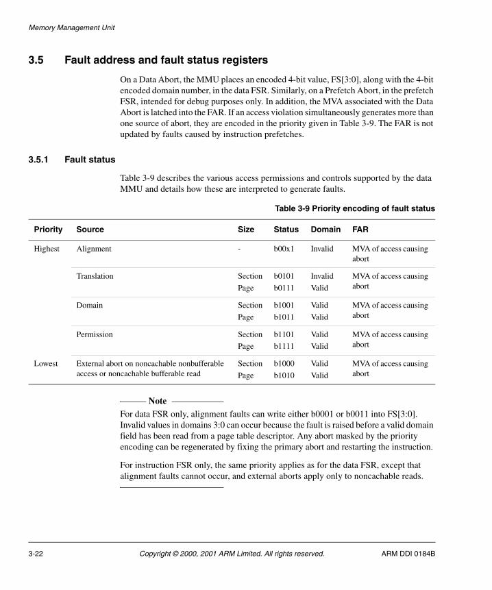
Memory Management Unit
3.5 Fault address and fault status registers
On a Data Abort, the MMU places an encoded 4-bit value, FS[3:0], along with the 4-bit encoded domain number, in the data FSR. Similarly, on a Prefetch Abort, in the prefetch FSR, intended for debug purposes only. In addition, the MVA associated with the Data Abort is latched into the FAR. If an access violation simultaneously generates more than one source of abort, they are encoded in the priority given in Table 3-9. The FAR is not updated by faults caused by instruction prefetches.
3.5.1 Fault status
Table 3-9 describes the various access permissions and controls supported by the data MMU and details how these are interpreted to generate faults.
Note For data FSR only, alignment faults can write either b0001 or b0011 into FS[3:0]. Invalid values in domains 3:0 can occur because the fault is raised before a valid domain field has been read from a page table descriptor. Any abort masked by the priority encoding can be regenerated by fixing the primary abort and restarting the instruction.
For instruction FSR only, the same priority applies as for the data FSR, except that alignment faults cannot occur, and external aborts apply only to noncachable reads.
Table 3-9 Priority encoding of fault status
Priority Source Size Status Domain FAR
Highest Alignment - b00x1 Invalid MVA of access causing abort
Translation Section
Page
b0101
b0111
Invalid
Valid
MVA of access causing abort
Domain Section
Page
b1001
b1011
Valid
Valid
MVA of access causing abort
Permission Section
Page
b1101
b1111
Valid
Valid
MVA of access causing abort
Lowest External abort on noncachable nonbufferable access or noncachable bufferable read
Section
Page
b1000
b1010
Valid
Valid
MVA of access causing abort
3-22 Copyright © 2000, 2001 ARM Limited. All rights reserved. ARM DDI 0184B
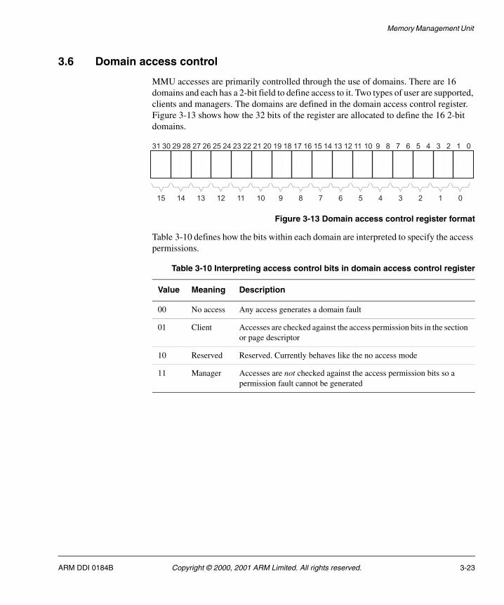
Memory Management Unit
3.6 Domain access control
MMU accesses are primarily controlled through the use of domains. There are 16 domains and each has a 2-bit field to define access to it. Two types of user are supported, clients and managers. The domains are defined in the domain access control register. Figure 3-13 shows how the 32 bits of the register are allocated to define the 16 2-bit domains.
Figure 3-13 Domain access control register format
Table 3-10 defines how the bits within each domain are interpreted to specify the access permissions.
31 30 29 28 27 26 25 24 23 22 21 20 19 18 17 16 15 14 13 12 11 10 9 8 7 6 5 4 3 2 1 0
15 14 13 12 11 10 9 8 7 6 5 4 3 2 1 0
Table 3-10 Interpreting access control bits in domain access control register
Value Meaning Description
00 No access Any access generates a domain fault
01 Client Accesses are checked against the access permission bits in the section or page descriptor
10 Reserved Reserved. Currently behaves like the no access mode
11 Manager Accesses are not checked against the access permission bits so a permission fault cannot be generated
ARM DDI 0184B Copyright © 2000, 2001 ARM Limited. All rights reserved. 3-23
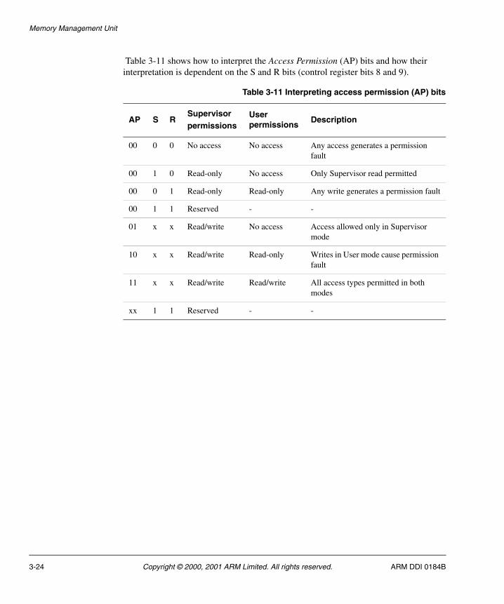
Memory Management Unit
Table 3-11 shows how to interpret the Access Permission (AP) bits and how their interpretation is dependent on the S and R bits (control register bits 8 and 9).
Table 3-11 Interpreting access permission (AP) bits
AP S RSupervisorpermissions
User permissions
Description
00 0 0 No access No access Any access generates a permission fault
00 1 0 Read-only No access Only Supervisor read permitted
00 0 1 Read-only Read-only Any write generates a permission fault
00 1 1 Reserved - -
01 x x Read/write No access Access allowed only in Supervisor mode
10 x x Read/write Read-only Writes in User mode cause permission fault
11 x x Read/write Read/write All access types permitted in both modes
xx 1 1 Reserved - -
3-24 Copyright © 2000, 2001 ARM Limited. All rights reserved. ARM DDI 0184B
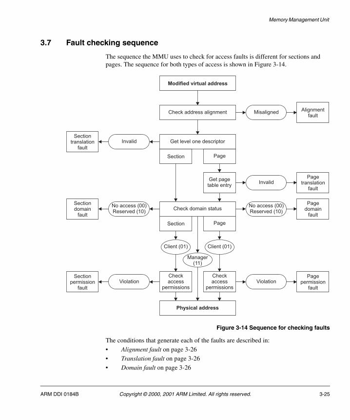
Memory Management Unit
3.7 Fault checking sequence
The sequence the MMU uses to check for access faults is different for sections and pages. The sequence for both types of access is shown in Figure 3-14.
Figure 3-14 Sequence for checking faults
The conditions that generate each of the faults are described in:
• Alignment fault on page 3-26
• Translation fault on page 3-26
• Domain fault on page 3-26
Modified virtual address
Check address alignment Misaligned Alignmentfault
Get level one descriptorInvalidSection
translationfault
Section Page
Get pagetable entry
Check domain status
Section Page
InvalidPage
translationfault
No access (00)Reserved (10)
Pagedomain
fault
Sectiondomain
fault
No access (00)Reserved (10)
Client (01) Client (01)
Manager(11)
Checkaccess
permissions
Checkaccess
permissions
Physical address
ViolationPage
permissionfault
ViolationSection
permissionfault
ARM DDI 0184B Copyright © 2000, 2001 ARM Limited. All rights reserved. 3-25
Memory Management Unit
• Permission fault on page 3-27.
3.7.1 Alignment fault
If alignment fault is enabled (A bit in CP15 register 1 set), the MMU generates an alignment fault on any data word access, if the address is not word-aligned, or on any halfword access, if the address is not halfword-aligned, irrespective of whether the MMU is enabled or not. An alignment fault is not generated on any instruction fetch, nor on any byte access.
Note If the access generates an alignment fault, the access sequence aborts without reference to more permission checks.
3.7.2 Translation fault
There are two types of translation fault:
Section A section translation fault is generated if the level one descriptor is marked as invalid. This happens if bits [1:0] of the descriptor are both 0.
Page A page translation fault is generated if the level one descriptor is marked as invalid. This happens if bits [1:0] of the descriptor are both 0.
3.7.3 Domain fault
There are two types of domain fault:
Section The level one descriptor holds the 4-bit domain field, which selects one of the 16 2-bit domains in the domain access control register. The two bits of the specified domain are then checked for access permissions as described in Table 3-11 on page 3-24. The domain is checked when the level one descriptor is returned.
Page The level one descriptor holds the 4-bit domain field, which selects one of the 16 2-bit domains in the domain access control register. The two bits of the specified domain are then checked for access permissions as described in Table 3-11 on page 3-24. The domain is checked when the level one descriptor is returned.
If the specified access is either no access (00) or reserved (10) then either a section domain fault or page domain fault occurs.
3-26 Copyright © 2000, 2001 ARM Limited. All rights reserved. ARM DDI 0184B
Memory Management Unit
3.7.4 Permission fault
If the 2-bit domain field returns 01 (client) then access permissions are checked as follows:
Section If the level one descriptor defines a section-mapped access, the AP bits of the descriptor define whether or not the access is allowed, according to Table 3-11 on page 3-24. Their interpretation is dependent on the setting of the S and R bits (control register bits 8 and 9). If the access is not allowed, a section permission fault is generated.
Large page or small page
If the level one descriptor defines a page-mapped access and the level two descriptor is for a large or small page, four access permission fields (ap3-ap0) are specified, each corresponding to one quarter of the page. For small pages ap3 is selected by the top 1KB of the page and ap0 is selected by the bottom 1KB of the page. For large pages, ap3 is selected by the top 16KB of the page and ap0 is selected by the bottom 16KB of the page. The selected AP bits are then interpreted in exactly the same way as for a section (see Table 3-11 on page 3-24). The only difference is that the fault generated is a page permission fault.
Tiny page If the level one descriptor defines a page-mapped access and the level two descriptor is for a tiny page, the AP bits of the level one descriptor define whether or not the access is allowed in the same way as for a section. The fault generated is a page permission fault.
ARM DDI 0184B Copyright © 2000, 2001 ARM Limited. All rights reserved. 3-27
Memory Management Unit
3.8 External aborts
In addition to the MMU-generated aborts, the ARM922T can be externally aborted by the AMBA bus. This can be used to flag an error on an external memory access. However, not all accesses can be aborted in this way and the Bus Interface Unit (BIU) ignores external aborts that cannot be handled.
The following accesses can be aborted:
• noncached reads
• unbuffered writes
• read-lock-write sequence, to noncachable memory.
In the case of a read-lock-write (SWP) sequence, if the read aborts the write is always attempted.
3-28 Copyright © 2000, 2001 ARM Limited. All rights reserved. ARM DDI 0184B
Memory Management Unit
3.9 Interaction of the MMU and caches
The MMU is enabled and disabled using bit 0 of the CP15 control register as described in:
• Enabling the MMU
• Disabling the MMU.
3.9.1 Enabling the MMU
To enable the MMU:
1. Program the TTB and domain access control registers.
2. Program level 1 and level 2 page tables as required.
3. Enable the MMU by setting bit 0 in the control register.
You must take care if the translated address differs from the untranslated address because several instructions following the enabling of the MMU might have been prefetched with the MMU off (using physical = VA - flat translation).
In this case, enabling the MMU can be considered as a branch with delayed execution. A similar situation occurs when the MMU is disabled. Consider the following code sequence:
MRCp15, 0, R1, c1, C0, 0 ; Read control registerORR R1, #0x1MCR p15,0,R1,C1, C0,0 ; Enable MMUSFetch FlatFetch FlatFetch Translated
You can enable the ICache and DCache simultaneously with the MMU using a single MCR instruction.
3.9.2 Disabling the MMU
To disable the MMU, clear bit 0 in the control register. The data cache must be disabled prior to, or at the same time as, the MMU is disabled by clearing bit 2 of the control register. See Enabling the MMU regarding prefetch effects.
Note If the MMU is enabled, then disabled and subsequently re-enabled, the contents of the TLBs are preserved. If these are now invalid, you must invalidate the TLBs before re-enabling the MMU. See Register 8, TLB operations register on page 2-19.
ARM DDI 0184B Copyright © 2000, 2001 ARM Limited. All rights reserved. 3-29
Memory Management Unit
3-30 Copyright © 2000, 2001 ARM Limited. All rights reserved. ARM DDI 0184B
Chapter 4 Caches, Write Buffer, and Physical Address TAG (PA TAG) RAM
This chapter describes the Instruction Cache (ICache), Data Cache (DCache), write buffer, and Physical Address (PA) TAG RAM. It contains the following sections:
• About the caches and write buffer on page 4-2
• ICache on page 4-4
• DCache and write buffer on page 4-9
• Cache coherence on page 4-17
• Cache cleaning when lockdown is in use on page 4-20
• Implementation notes on page 4-21
• Physical address TAG RAM on page 4-22
• Drain write buffer on page 4-23
• Wait for interrupt on page 4-24.
ARM DDI 0184B Copyright © 2000, 2001 ARM Limited. All rights reserved. 4-1
Caches, Write Buffer, and Physical Address TAG (PA TAG) RAM
4.1 About the caches and write buffer
The ARM922T level-one memory system includes an Instruction Cache (ICache), a Data Cache (DCache), a write buffer, and a Physical Address (PA) TAG RAM to reduce the effect of main memory bandwidth and latency on performance.
The ARM922T implements separate 8KB instruction and 8KB data caches (ICache and DCache).
The caches have the following features:
• Virtually-addressed 64-way associative cache.
• 8 words per line (32 bytes per line) with one valid bit and two dirty bits per line, allowing half-line write-backs.
• Write-through and write-back cache operation (write-back caches are also known as copy-back caches), selected per memory region by the C and B bits in the MMU translation tables (for data cache only).
• Pseudo-random or round-robin replacement, selectable using the RR bit in CP15 register 1.
• Low-power CAM-RAM implementation.
• Caches independently lockable with granularity of 1/64th of cache, which is 32 words (128 bytes).
• To avoid TLB misses during write-back data eviction, and to reduce interrupt latency, the physical address corresponding to each data cache entry is stored in the PA TAG RAM for use during cache line write-backs, in addition to the VA TAG stored in the cache CAMs. This means that the MMU is not involved in cache write-back operations, removing the possibility of TLB misses related to the write-back address.
• Cache maintenance operations to provide efficient cleaning of the entire data cache, and to provide efficient cleaning and invalidation of small regions of virtual memory. The latter allows ICache coherency to be efficiently maintained when small code changes occur, for example self-modifying code and changes to exception vectors.
The write buffer:
• has a 16-word data buffer
• has a 4-address address buffer
4-2 Copyright © 2000, 2001 ARM Limited. All rights reserved. ARM DDI 0184B
Caches, Write Buffer, and Physical Address TAG (PA TAG) RAM
• can be drained under software control, using a CP15 MCR instruction (see Drain write buffer on page 4-23).
The ARM922T can be drained under software control and put into a low-power state until an interrupt occurs, using a CP15 MCR instruction (see Wait for interrupt on page 4-24).
ARM DDI 0184B Copyright © 2000, 2001 ARM Limited. All rights reserved. 4-3
Caches, Write Buffer, and Physical Address TAG (PA TAG) RAM
4.2 ICache
The ARM922T includes an 8KB ICache. The ICache has 256 lines of 32 bytes (8 words), arranged as a 64-way set-associative cache and uses MVAs, translated by CP15 register 13 (see Address translation on page 3-6), from the ARM9TDMI core.
The ICache implements allocate-on-read-miss. Random or round-robin replacement can be selected under software control using the RR bit (CP15 register 1, bit 14). Random replacement is selected at reset.
Instructions can also be locked in the ICache so that they cannot be overwritten by a linefill. This operates with a granularity of 1/64th of the cache, which is 32 words (128 bytes).
All instruction accesses are subject to MMU permission and translation checks. Instruction fetches that are aborted by the MMU do not cause linefills or instruction fetches to appear on the AMBA ASB interface.
Note For clarity, the I bit (bit 12 in CP15 register 1) is called the Icr bit throughout the following text. The C bit from the MMU translation table descriptor corresponding to the address being accessed is called the Ctt bit.
4.2.1 ICache organization
The ICache is organized as four segments, each containing 64 lines, and each line containing eight words. The position of the line within the segment is a number from 0 to 63. This is called the index. A line in the cache can be uniquely identified by its segment and index. The index is independent of the MVA. The segment is selected by bits [6:5] of the MVA.
Bits [4:2] of the MVA specify the word within a cache line that is accessed. For halfword operations, bit [1] of the MVA specifies the halfword that is accessed within the word. For byte operations, bits [1:0] specify the byte within the word that is accessed.
Bits [31:7] of the MVA of each cache line are called the TAG. The MVA TAG is stored in the cache, along with the 8-words of data, when the line is loaded by a linefill.
Cache lookups compare bits [31:7] of the MVA of the access with the stored TAG to determine whether the access is a hit or miss. The cache is therefore said to be virtually addressed. The logical model of the 8KB ICache is shown in Figure 4-1 on page 4-5.
4-4 Copyright © 2000, 2001 ARM Limited. All rights reserved. ARM DDI 0184B
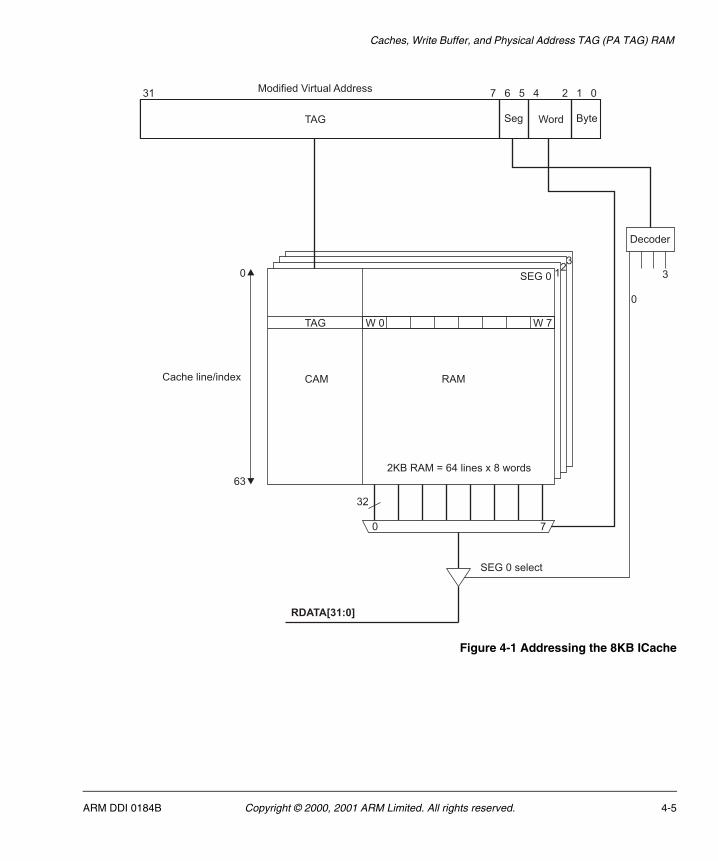
Caches, Write Buffer, and Physical Address TAG (PA TAG) RAM
Figure 4-1 Addressing the 8KB ICache
31
TAG
67 5 4 2 1 0
Word ByteSeg
TAG W 0 W 7
CAM RAM
Decoder
0 7
32
RDATA[31:0]
Cache line/index
SEG 0 select
2KB RAM = 64 lines x 8 words
63
0 SEG 0
32
1
Modified Virtual Address
3
0
ARM DDI 0184B Copyright © 2000, 2001 ARM Limited. All rights reserved. 4-5
Caches, Write Buffer, and Physical Address TAG (PA TAG) RAM
4.2.2 Enabling and disabling the ICache
On reset, the ICache entries are all invalidated and the ICache is disabled.
You can enable the ICache by writing 1 to the Icr bit, and disable it by writing 0 to the Icr bit.
When the ICache is disabled, the cache contents are ignored and all instruction fetches appear on the AMBA ASB interface as separate nonsequential accesses. The ICache is usually used with the MMU enabled. In this case the Ctt in the relevant MMU translation table descriptor indicates whether an area of memory is cachable.
If the cache is disabled after having been enabled, all cache contents are ignored. All instruction fetches appear on the AMBA ASB interface as separate nonsequential accesses and the cache is not updated. If the cache is subsequently re-enabled its contents are unchanged. If the contents are no longer coherent with main memory, you must invalidate the ICache before you re-enable it (see Register 7, cache operations register on page 2-17).
If the cache is enabled with the MMU disabled, all instruction fetches are treated as cachable. No protection checks are made, and the physical address is flat-mapped to the modified virtual address.
You can enable the MMU and ICache simultaneously by writing a 1 to the M bit, and a 1 to the Icr bit in CP15 register 1, with a single MCR instruction.
Note ARM922T implements a nonsequential access on the AMBA ASB interface as an A-TRAN cycle followed by an S-TRAN cycle. It does not produce N-TRAN cycles. A linefill appears as an A-TRAN cycle followed by an S-TRAN cycle.
4.2.3 ICache operation
If the ICache is disabled, each instruction fetch results in a separate nonsequential memory access on the AMBA ASB interface, giving very low bus and memory performance. Therefore, you must enable the ICache as soon as possible after reset.
If the ICache is enabled, an ICache lookup is performed for each instruction fetch regardless of the setting of the Ctt bit in the relevant MMU translation table descriptor:
• If the required instruction is found in the cache, the lookup is called a cache hit. If the instruction fetch is a cache hit and Ctt=1, indicating a cachable region of memory, then the instruction is returned from the cache to the ARM9TDMI CPU core.
4-6 Copyright © 2000, 2001 ARM Limited. All rights reserved. ARM DDI 0184B
Caches, Write Buffer, and Physical Address TAG (PA TAG) RAM
• If the required instruction is not found in the cache, the lookup is called a cache miss. If it is a cache miss and Ctt=1, then an eight-word linefill is performed, possibly replacing another entry. The entry to be replaced, called the victim, is chosen from the entries that are not locked, using either a random or round-robin replacement policy.If Ctt=0, indicating a noncachable region of memory, then a single nonsequential memory access appears on the AMBA ASB interface.
Note If Ctt=0, indicating a noncachable region of memory, then the cache lookup results in a cache miss. The only way that it can result in a cache hit is if software has changed the value of the Ctt bit in the MMU translation table descriptor without invalidating the cache contents. This is a programming error. The behavior in this case is architecturally unpredictable and varies between implementations.
4.2.4 ICache replacement algorithm
The ICache and DCache replacement algorithm is selected by the RR bit in the CP15 control register (CP15 register 1, bit 14). Random replacement is selected at reset. Setting the RR bit to 1 selects round-robin replacement. Round-robin replacement means that entries are replaced sequentially in each cache segment.
4.2.5 ICache lockdown
You can lock instructions into the ICache, causing the ICache to guarantee a hit, and provide optimum and predictable execution time. If you enable the ICache, an ICache lookup is performed for each instruction fetch. If the ICache misses and the Ctt=1 then an eight-word linefill is performed. The entry to be replaced is selected by the victim pointer. You can lock instructions into the ICache by controlling the victim pointer, and forcing prefetches to the ICache. You lock instructions in the ICache by first ensuring the code to be locked is not already in the cache. You can ensure this by invalidating either the whole ICache or specific lines:
MCR p15, 0, Rd, c7, c5, 0 ; Invalidate ICacheMCR p15, 0, Rd, c7, c5, 1 ; Invalidate ICache line using MVA
You can then use a short software routine to load the instructions into the ICache. The software routine must either be noncachable, or already in the ICache but not in an ICache line about to be overwritten. You must enable the MMU to ensure that any TLB misses that occur while loading the instructions cause a page table walk. The software routine operates by writing to CP15 register 9 to force the victim pointer to a specific ICache line and by using the prefetch ICache line operation to force the ICache to perform a lookup. This misses, assuming the code has been invalidated, and an 8-word linefill is performed loading the cache line into the entry specified by the victim pointer.
ARM DDI 0184B Copyright © 2000, 2001 ARM Limited. All rights reserved. 4-7
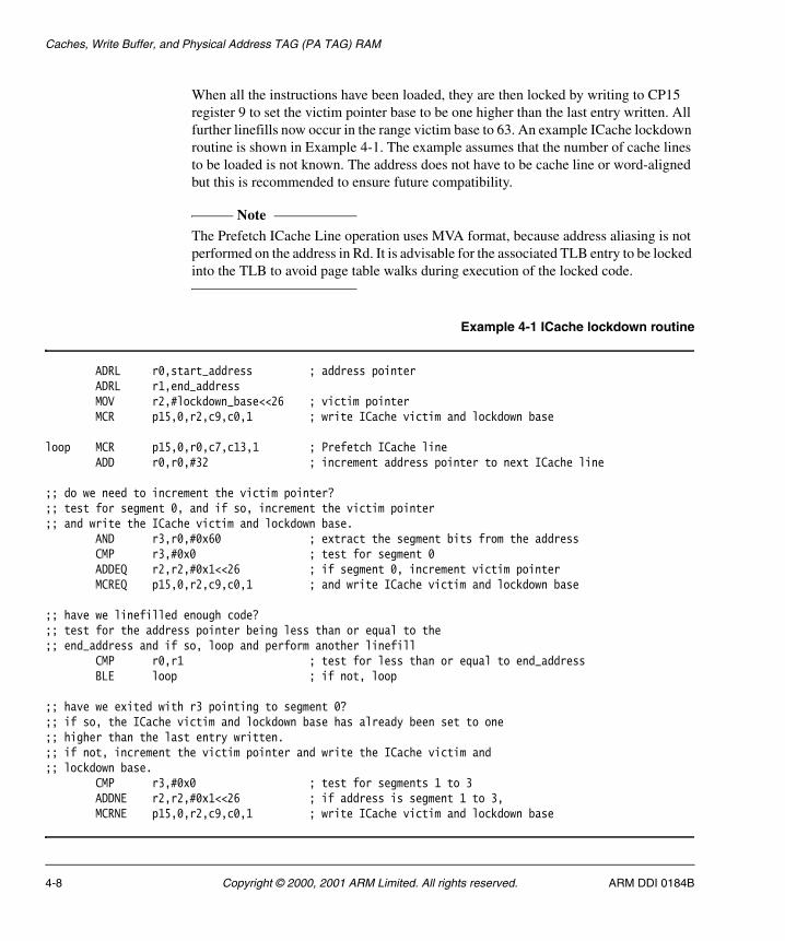
Caches, Write Buffer, and Physical Address TAG (PA TAG) RAM
When all the instructions have been loaded, they are then locked by writing to CP15 register 9 to set the victim pointer base to be one higher than the last entry written. All further linefills now occur in the range victim base to 63. An example ICache lockdown routine is shown in Example 4-1. The example assumes that the number of cache lines to be loaded is not known. The address does not have to be cache line or word-aligned but this is recommended to ensure future compatibility.
Note The Prefetch ICache Line operation uses MVA format, because address aliasing is not performed on the address in Rd. It is advisable for the associated TLB entry to be locked into the TLB to avoid page table walks during execution of the locked code.
Example 4-1 ICache lockdown routine
ADRL r0,start_address ; address pointerADRL r1,end_addressMOV r2,#lockdown_base<<26 ; victim pointerMCR p15,0,r2,c9,c0,1 ; write ICache victim and lockdown base
loop MCR p15,0,r0,c7,c13,1 ; Prefetch ICache lineADD r0,r0,#32 ; increment address pointer to next ICache line
;; do we need to increment the victim pointer?;; test for segment 0, and if so, increment the victim pointer;; and write the ICache victim and lockdown base.
AND r3,r0,#0x60 ; extract the segment bits from the addressCMP r3,#0x0 ; test for segment 0ADDEQ r2,r2,#0x1<<26 ; if segment 0, increment victim pointerMCREQ p15,0,r2,c9,c0,1 ; and write ICache victim and lockdown base
;; have we linefilled enough code?;; test for the address pointer being less than or equal to the;; end_address and if so, loop and perform another linefill
CMP r0,r1 ; test for less than or equal to end_addressBLE loop ; if not, loop
;; have we exited with r3 pointing to segment 0?;; if so, the ICache victim and lockdown base has already been set to one;; higher than the last entry written.;; if not, increment the victim pointer and write the ICache victim and;; lockdown base.
CMP r3,#0x0 ; test for segments 1 to 3ADDNE r2,r2,#0x1<<26 ; if address is segment 1 to 3,MCRNE p15,0,r2,c9,c0,1 ; write ICache victim and lockdown base
4-8 Copyright © 2000, 2001 ARM Limited. All rights reserved. ARM DDI 0184B
Caches, Write Buffer, and Physical Address TAG (PA TAG) RAM
4.3 DCache and write buffer
The ARM922T includes an 8KB DCache and a write buffer to reduce the effect of main memory bandwidth and latency on data access performance. The DCache has 256 lines of 32 bytes (8-words), arranged as a 64-way set-associative cache and uses MVAs translated by CP15 register 13 (see Address translation on page 3-6) from the ARM9TDMI CPU core. The write buffer can hold up to 16 words of data and four separate addresses. The operations of the DCache and the write buffer are closely connected.
The DCache supports write-through and write-back memory regions, controlled by the C and B bits in each section and page descriptor within the MMU translation tables. For clarity, these bits are called Ctt and Btt in the following text. For details see DCache and write buffer operation on page 4-10.
Each DCache line has two dirty bits, one for the first four words of the line, the other for the last four words, and a single virtual TAG address and valid bit for the entire 8-word line. The physical address from which each line is loaded is stored in the PA TAG RAM and is used when writing modified lines back to memory.
When a store hits in the DCache, if the memory region is write-back, the associated dirty bit is set marking the appropriate half-line as being modified. If the cache line is replaced due to a linefill, or if the line is the target of a DCache clean operation, the dirty bits are used to decide whether the whole, half, or none of the line is written back to memory. The line is written back to the same physical address from which it was loaded, regardless of any changes to the MMU translation tables.
The DCache implements allocate-on-read-miss. Random or round-robin replacement can be selected under software control by the RR bit (CP15 register 1, bit 14). Random replacement is selected at reset. A linefill always loads a complete 8-word line.
Data can also be locked in the DCache so that it cannot be overwritten by a linefill. This operates with a granularity of 1/64 th of the cache, which is 32 words (128 bytes).
All data accesses are subject to MMU permission and translation checks. Data accesses that are aborted by the MMU do not cause linefills or data accesses to appear on the AMBA ASB interface.
For clarity, the C bit (bit 2 in CP15 register 1) is called the Ccr bit throughout the following text.
ARM DDI 0184B Copyright © 2000, 2001 ARM Limited. All rights reserved. 4-9
Caches, Write Buffer, and Physical Address TAG (PA TAG) RAM
4.3.1 Enabling and disabling the DCache and write buffer
On reset, the DCache entries are invalidated and the DCache is disabled, and the write buffer contents are discarded.
There is no explicit write buffer enable bit implemented in ARM922T. The write buffer is used in the following ways:
• You can enable the DCache by writing 1 to the Ccr bit, and disable it by writing 0 to the Ccr bit.
• You must only enable the DCache when the MMU is enabled. This is because the MMU translation tables define the cache and write buffer configuration for each memory region.
• If the DCache is disabled after having been enabled, the cache contents are ignored and all data accesses appear on the AMBA ASB interface as separate nonsequential accesses and the cache is not updated. If the cache is subsequently re-enabled its contents are unchanged. Depending on the software system design, you might have to clean the cache after it is disabled, and invalidate it before you re-enable it. See Cache coherence on page 4-17.
• You can enable or disable the MMU and DCache simultaneously with a single MCR that changes the M bit and the C bit in the control register (CP15 register 1).
4.3.2 DCache and write buffer operation
The DCache and write buffer configuration of each memory region is controlled by the Ctt and Btt bits in each section and page descriptor in the MMU translation tables. You can modify the configuration using the DCache enable bit in the CP15 control register. This is called Ccr.
If the DCache is enabled, a DCache lookup is performed for each data access initiated by the ARM9TDMI CPU core, regardless of the value of the Ctt bit in the relevant MMU translation table descriptor. If the required data is found, the lookup is called a cache hit. If the required data is not found, the lookup is called a cache miss. In this context a data access means any type of load (read), store (write), or swap instruction, including LDR, LDRB, LDRH, LDM, LDC, STR, STRB, STRH, STC, SWP, and SWPB.
Accesses appear on the AMBA ASB interface in program order but the ARM9TDMI CPU core can continue executing at full speed, reading instructions and data from the caches, and writing to the DCache and write buffer, while buffered writes are being written to memory through the AMBA ASB interface.
4-10 Copyright © 2000, 2001 ARM Limited. All rights reserved. ARM DDI 0184B
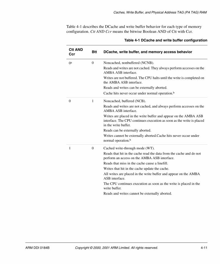
Caches, Write Buffer, and Physical Address TAG (PA TAG) RAM
Table 4-1 describes the DCache and write buffer behavior for each type of memory configuration. Ctt AND Ccr means the bitwise Boolean AND of Ctt with Ccr.
Table 4-1 DCache and write buffer configuration
Ctt AND Ccr
Btt DCache, write buffer, and memory access behavior
0a 0 Noncached, nonbuffered (NCNB).
Reads and writes are not cached. They always perform accesses on the AMBA ASB interface.
Writes are not buffered. The CPU halts until the write is completed on the AMBA ASB interface.
Reads and writes can be externally aborted.
Cache hits never occur under normal operation.b
0 1 Noncached, buffered (NCB).
Reads and writes are not cached, and always perform accesses on the AMBA ASB interface.
Writes are placed in the write buffer and appear on the AMBA ASB interface. The CPU continues execution as soon as the write is placed in the write buffer.
Reads can be externally aborted.
Writes cannot be externally aborted.Cache hits never occur under normal operation.b
1 0 Cached write-through mode (WT).
Reads that hit in the cache read the data from the cache and do not perform an access on the AMBA ASB interface.
Reads that miss in the cache cause a linefill.
Writes that hit in the cache update the cache.
All writes are placed in the write buffer and appear on the AMBA ASB interface.
The CPU continues execution as soon as the write is placed in the write buffer.
Reads and writes cannot be externally aborted.
ARM DDI 0184B Copyright © 2000, 2001 ARM Limited. All rights reserved. 4-11
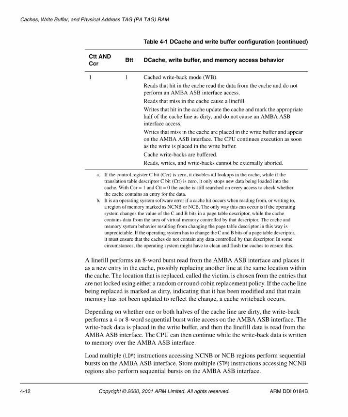
Caches, Write Buffer, and Physical Address TAG (PA TAG) RAM
A linefill performs an 8-word burst read from the AMBA ASB interface and places it as a new entry in the cache, possibly replacing another line at the same location within the cache. The location that is replaced, called the victim, is chosen from the entries that are not locked using either a random or round-robin replacement policy. If the cache line being replaced is marked as dirty, indicating that it has been modified and that main memory has not been updated to reflect the change, a cache writeback occurs.
Depending on whether one or both halves of the cache line are dirty, the write-back performs a 4 or 8-word sequential burst write access on the AMBA ASB interface. The write-back data is placed in the write buffer, and then the linefill data is read from the AMBA ASB interface. The CPU can then continue while the write-back data is written to memory over the AMBA ASB interface.
Load multiple (LDM) instructions accessing NCNB or NCB regions perform sequential bursts on the AMBA ASB interface. Store multiple (STM) instructions accessing NCNB regions also perform sequential bursts on the AMBA ASB interface.
1 1 Cached write-back mode (WB).
Reads that hit in the cache read the data from the cache and do not perform an AMBA ASB interface access.
Reads that miss in the cache cause a linefill.
Writes that hit in the cache update the cache and mark the appropriate half of the cache line as dirty, and do not cause an AMBA ASB interface access.
Writes that miss in the cache are placed in the write buffer and appear on the AMBA ASB interface. The CPU continues execution as soon as the write is placed in the write buffer.
Cache write-backs are buffered.
Reads, writes, and write-backs cannot be externally aborted.
a. If the control register C bit (Ccr) is zero, it disables all lookups in the cache, while if the translation table descriptor C bit (Ctt) is zero, it only stops new data being loaded into the cache. With Ccr = 1 and Ctt = 0 the cache is still searched on every access to check whether the cache contains an entry for the data.
b. It is an operating system software error if a cache hit occurs when reading from, or writing to, a region of memory marked as NCNB or NCB. The only way this can occur is if the operating system changes the value of the C and B bits in a page table descriptor, while the cache contains data from the area of virtual memory controlled by that descriptor. The cache and memory system behavior resulting from changing the page table descriptor in this way is unpredictable. If the operating system has to change the C and B bits of a page table descriptor, it must ensure that the caches do not contain any data controlled by that descriptor. In some circumstances, the operating system might have to clean and flush the caches to ensure this.
Table 4-1 DCache and write buffer configuration (continued)
Ctt AND Ccr
Btt DCache, write buffer, and memory access behavior
4-12 Copyright © 2000, 2001 ARM Limited. All rights reserved. ARM DDI 0184B
Caches, Write Buffer, and Physical Address TAG (PA TAG) RAM
The sequential burst is split into two bursts if it crosses a 1KB boundary. This is because the smallest MMU protection and mapping size is 1KB, so the memory regions on each side of the 1KB boundary can have different properties.
This means that sequential accesses generated by ARM922T do not cross a 1KB boundary. This can be exploited to simplify memory interface design. For example, a simple page-mode DRAM controller can perform a page-mode access for each sequential access, provided the DRAM page size is 1KB or larger.
See also Cache coherence on page 4-17.
4.3.3 DCache organization
The DCache is organized as four segments, each containing 64 lines, and each line containing eight words. The position of the line within the segment is a number from 0 to 63. This is called the index. A line in the cache can be uniquely identified by its segment and index. The index is independent of the MVA. The segment is selected by bits [6:5] of the MVA.
Bits [4:2] of the MVA specify which word within a cache line is accessed. For halfword operations, bit [1] of the MVA specifies which halfword is accessed within the word. For byte operations, bits [1:0] specify which byte within the word is accessed.
Bits [31:7] of the MVA of each cache line are called the TAG. The MVA TAG is stored in the cache, along with the eight words of data, when the line is loaded by a linefill.
Cache lookups compare bits [31:7] of the MVA of the access with the stored TAG to determine whether the access is a hit or miss. The cache is therefore said to be virtually addressed.
The DCache logical model is the same as for the ICache. See Addressing the 8KB ICache on page 4-5.
4.3.4 DCache replacement algorithm
The DCache and ICache replacement algorithm is selected by the RR bit in the CP15 control register (CP15 register 1, bit 14). Random replacement is selected at reset. Setting the RR bit to 1 selects round-robin replacement. Round-robin replacement means that entries are replaced sequentially in each segment.
ARM DDI 0184B Copyright © 2000, 2001 ARM Limited. All rights reserved. 4-13
Caches, Write Buffer, and Physical Address TAG (PA TAG) RAM
4.3.5 Swap instructions
Swap instruction (SWP or SWPB) behavior is dependent on whether the memory region is cachable or noncachable.
Swap instructions to cachable regions of memory are useful for implementing semaphores or other synchronization primitives in multithreaded uniprocessor software systems.
Swap instructions to noncachable memory regions are useful for synchronization between two bus masters in a multi-master bus system. This can be two processors, or one processor and a DMA controller.
When a swap instruction accesses a cachable region of memory (write-through or write-back), the DCache and write buffer behavior is the same as having a load followed by a store according to the normal rules described. The BLOK pin is not asserted during the execution of the instruction. It is guaranteed that no interrupt can occur between the load and store portions of the swap.
When a swap instruction accesses a noncachable (NCB or NCNB) region of memory, the write buffer is drained, and a single word or byte is read from the AMBA ASB interface. The write portion of the swap is then treated as nonbufferable, regardless of the value of Btt, and the processor is stalled until the write is completed on the AMBA ASB interface. The BLOK pin is asserted to indicate that you can treat the read and write as an atomic operation on the bus.
Like all other data accesses, a swap to a noncachable region that hits in the cache indicates a programming error.
4.3.6 DCache lockdown
You can lock data into the DCache, causing the DCache to guarantee a hit, and provide optimum and predictable execution time. If you enable the DCache, a DCache lookup is performed for each load. If the DCache misses and the Ctt=1 then an eight-word linefill is performed. The entry to be replaced is selected by the victim pointer. You can lock data into the DCache by controlling the victim pointer, and forcing loads to the DCache. You lock data in the DCache by first ensuring the data to be locked is not already in the cache. You can ensure this by cleaning and invalidating either the whole DCache or specific lines. Example 4-2 on page 4-15 shows DCache invalidate and clean operations that you can perform to do this.
4-14 Copyright © 2000, 2001 ARM Limited. All rights reserved. ARM DDI 0184B
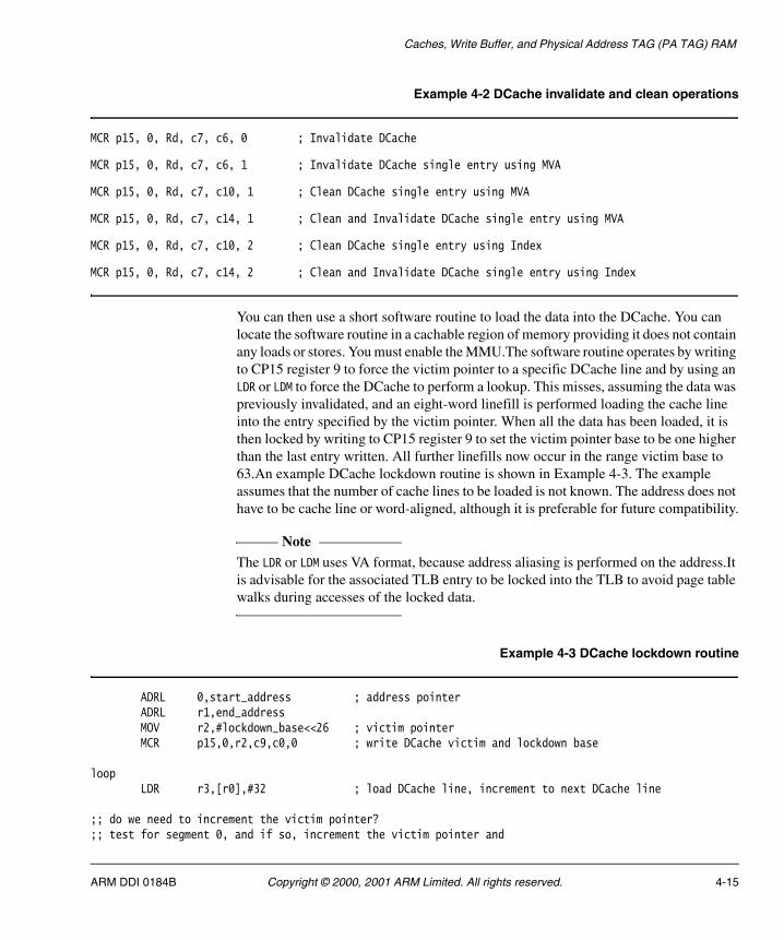
Caches, Write Buffer, and Physical Address TAG (PA TAG) RAM
Example 4-2 DCache invalidate and clean operations
MCR p15, 0, Rd, c7, c6, 0 ; Invalidate DCache
MCR p15, 0, Rd, c7, c6, 1 ; Invalidate DCache single entry using MVA
MCR p15, 0, Rd, c7, c10, 1 ; Clean DCache single entry using MVA
MCR p15, 0, Rd, c7, c14, 1 ; Clean and Invalidate DCache single entry using MVA
MCR p15, 0, Rd, c7, c10, 2 ; Clean DCache single entry using Index
MCR p15, 0, Rd, c7, c14, 2 ; Clean and Invalidate DCache single entry using Index
You can then use a short software routine to load the data into the DCache. You can locate the software routine in a cachable region of memory providing it does not contain any loads or stores. You must enable the MMU.The software routine operates by writing to CP15 register 9 to force the victim pointer to a specific DCache line and by using an LDR or LDM to force the DCache to perform a lookup. This misses, assuming the data was previously invalidated, and an eight-word linefill is performed loading the cache line into the entry specified by the victim pointer. When all the data has been loaded, it is then locked by writing to CP15 register 9 to set the victim pointer base to be one higher than the last entry written. All further linefills now occur in the range victim base to 63.An example DCache lockdown routine is shown in Example 4-3. The example assumes that the number of cache lines to be loaded is not known. The address does not have to be cache line or word-aligned, although it is preferable for future compatibility.
Note The LDR or LDM uses VA format, because address aliasing is performed on the address.It is advisable for the associated TLB entry to be locked into the TLB to avoid page table walks during accesses of the locked data.
Example 4-3 DCache lockdown routine
ADRL 0,start_address ; address pointerADRL r1,end_addressMOV r2,#lockdown_base<<26 ; victim pointerMCR p15,0,r2,c9,c0,0 ; write DCache victim and lockdown base
loopLDR r3,[r0],#32 ; load DCache line, increment to next DCache line
;; do we need to increment the victim pointer?;; test for segment 0, and if so, increment the victim pointer and
ARM DDI 0184B Copyright © 2000, 2001 ARM Limited. All rights reserved. 4-15
Caches, Write Buffer, and Physical Address TAG (PA TAG) RAM
;; write the ICache victim and lockdown base.AND r3,r0,#0x60 ; extract the segment bits from the addressCMP r3,#0x0 ; test for segment 0ADDEQ r2,r2,#0x1<<26 ; if segment 0, increment victim pointerMCREQ p15,0,r2,c9,c0,0 ; and write DCache victim and lockdown base
;; have we linefilled enough code?;; test for the address pointer being less than or equal to the end_address;; and if so, loop and perform another linefill
CMP r0,r1 ; test for less than or equal to end_address,BLE loop ; if not, loop
;; have we exited with r3 pointing to segment 0?;; if so, the ICache victim and lockdown base has already been set to one;; higher than the last entry written.;; if not, increment the victim pointer and write the ICache victim and;; lockdown base.
CMP r3,#0x0 ; test for segments 1 to 3ADDNE r2,r2,#0x1<<26 ; if address is segment 1 to 3,MCRNE p15,0,r2,c9,c0,0 ; write DCache victim and lockdown base
4-16 Copyright © 2000, 2001 ARM Limited. All rights reserved. ARM DDI 0184B
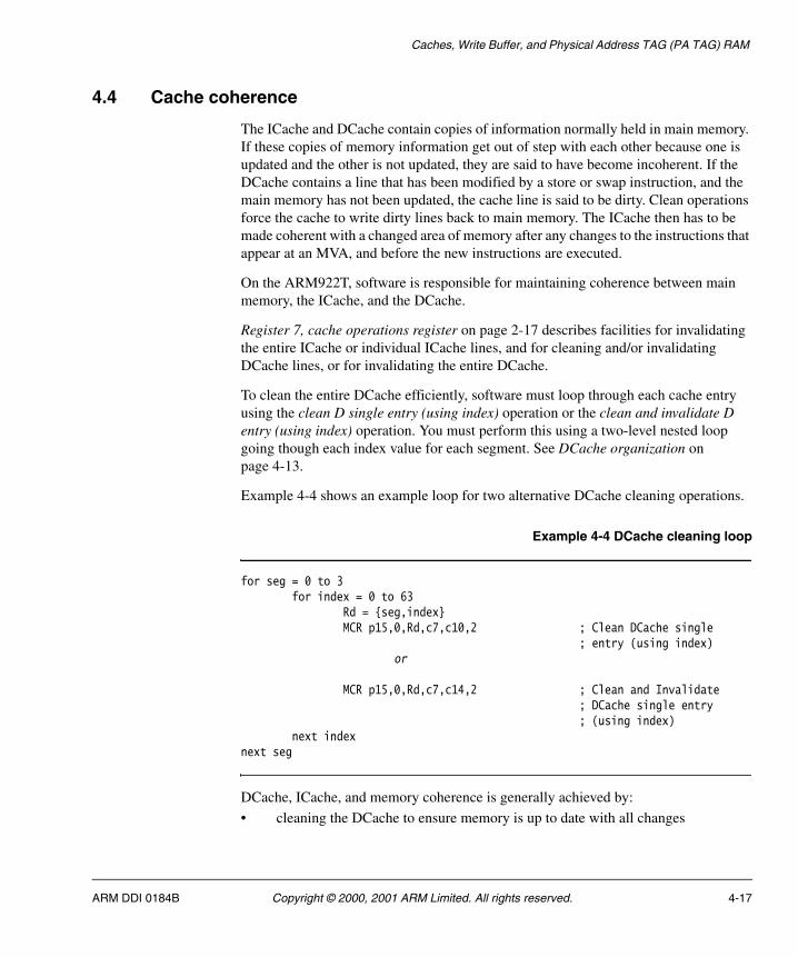
Caches, Write Buffer, and Physical Address TAG (PA TAG) RAM
4.4 Cache coherence
The ICache and DCache contain copies of information normally held in main memory. If these copies of memory information get out of step with each other because one is updated and the other is not updated, they are said to have become incoherent. If the DCache contains a line that has been modified by a store or swap instruction, and the main memory has not been updated, the cache line is said to be dirty. Clean operations force the cache to write dirty lines back to main memory. The ICache then has to be made coherent with a changed area of memory after any changes to the instructions that appear at an MVA, and before the new instructions are executed.
On the ARM922T, software is responsible for maintaining coherence between main memory, the ICache, and the DCache.
Register 7, cache operations register on page 2-17 describes facilities for invalidating the entire ICache or individual ICache lines, and for cleaning and/or invalidating DCache lines, or for invalidating the entire DCache.
To clean the entire DCache efficiently, software must loop through each cache entry using the clean D single entry (using index) operation or the clean and invalidate D entry (using index) operation. You must perform this using a two-level nested loop going though each index value for each segment. See DCache organization on page 4-13.
Example 4-4 shows an example loop for two alternative DCache cleaning operations.
Example 4-4 DCache cleaning loop
for seg = 0 to 3for index = 0 to 63
Rd = {seg,index}MCR p15,0,Rd,c7,c10,2 ; Clean DCache single
; entry (using index)or
MCR p15,0,Rd,c7,c14,2 ; Clean and Invalidate; DCache single entry; (using index)
next indexnext seg
DCache, ICache, and memory coherence is generally achieved by:
• cleaning the DCache to ensure memory is up to date with all changes
ARM DDI 0184B Copyright © 2000, 2001 ARM Limited. All rights reserved. 4-17
Caches, Write Buffer, and Physical Address TAG (PA TAG) RAM
• invalidating the ICache to ensure that the ICache is forced to re-fetch instructions from memory.
Software can minimize the performance penalties of cleaning and invalidating caches by:
• Cleaning only small portions of the DCache when only a small area of memory has to be made coherent, for example, when updating an exception vector entry. Use Clean DCache single entry (using MVA) or Clean and Invalidate DCache single entry (using MVA).
• Invalidating only small portions of the ICache when only a small number of instructions are modified, for example, when updating an exception vector entry. Use Invalidate ICache single entry (using MVA).
• Not invalidating the ICache in situations where it is known that the modified area of memory cannot be in the cache, for example, when mapping a new page into the currently running process.
Situations that necessitate cache cleaning and invalidating include:
• Writing instructions to a cachable area of memory using STR or STM instructions, for example:
— self-modifying code
— JIT compilation
— copying code from another location
— downloading code using the EmbeddedICE JTAG debug features
— updating an exception vector entry.
• Another bus master, such as a DMA controller, modifying a cachable area main memory.
• Turning the MMU on or off.
• Changing the virtual-to-physical mappings, or Ctt, or Btt, or protection information, in the MMU page tables. The DCache must be cleaned, and both caches invalidated, before the cache and write buffer configuration of an area of memory is changed by modifying Ctt or Btt in the MMU translation table descriptor. This is not necessary if it is known that the caches cannot contain any entries from the area of memory whose translation table descriptor is being modified.
• Turning the ICache or DCache on, if its contents are no longer coherent.
4-18 Copyright © 2000, 2001 ARM Limited. All rights reserved. ARM DDI 0184B
Caches, Write Buffer, and Physical Address TAG (PA TAG) RAM
Changing the FCSE PID in CP15 register 13 does not change the contents of the cache or memory, and does not affect the mapping between cache entries and physical memory locations. It only changes the mapping between ARM9TDMI addresses and cache entries. This means that changing the FCSE PID does not lead to any coherency issues. No cache cleaning or cache invalidation is required when the FCSE PID is changed.
The software design must also consider that the pipelined design of the ARM9TDMI core means that it fetches three instructions ahead of the current execution point. So, for example, the three instructions following an MCR that invalidates the ICache, have already been read from the ICache before it is invalidated.
ARM DDI 0184B Copyright © 2000, 2001 ARM Limited. All rights reserved. 4-19
Caches, Write Buffer, and Physical Address TAG (PA TAG) RAM
4.5 Cache cleaning when lockdown is in use
The Clean DCache single entry (using index) and Clean and Invalidate DCache entry (using index) operations can leave the victim pointer set to the index value used by the operation. In some circumstances, if DCache locking is in use, this can leave the victim pointer in the locked region, leading to locked data being evicted from the cache. You can move the victim pointer outside the locked region by implementing the cache loop, enclosed by the reading and writing of the base and victim pointer:
MRC p15, 0, Rd, c9, c0, 0 ; Read D Cache Base into RdIndex Clean or Index Clean and Invalidate loopsMCR p15, 0, Rd, c9, c0, 0 ; Write D Cache Base and Victim from Rd
Clean DCache single entry (using MVA) and Clean and Invalidate DCache entry (using MVA) operations do not move the victim pointer, so you do not have to reposition the victim pointer after using these operations.
4-20 Copyright © 2000, 2001 ARM Limited. All rights reserved. ARM DDI 0184B
Caches, Write Buffer, and Physical Address TAG (PA TAG) RAM
4.6 Implementation notes
This section describes the behavior of the ARM922T implementation in areas that are architecturally unpredictable. For portability to other ARM implementations, software must not depend on this behavior.
A read from a noncachable (NCB or NCNB) region that unexpectedly hits in the cache still reads the required data from the AMBA ASB interface. The contents of the cache are ignored, and the cache contents are not modified. This includes the read portion of a swap (SWP or SWPB) instruction.
A write to a noncachable (NCB or NCNB) region that unexpectedly hits in the cache updates the cache and still causes an access on the AMBA ASB interface. This includes the write portion of a swap instruction.
There are two test interfaces to both the DCache and ICache:
• debug interface
• AMBA test interface.
ARM DDI 0184B Copyright © 2000, 2001 ARM Limited. All rights reserved. 4-21
Caches, Write Buffer, and Physical Address TAG (PA TAG) RAM
4.7 Physical address TAG RAM
The ARM922T implements a Physical Address (PA) TAG RAM in order to perform write-backs from the DCache.
A write-back occurs when dirty data, that is about to be overwritten by linefill data, comes from a memory region that is marked as a write-back region. This data is written back to main memory to maintain memory coherency.
Note Dirty data is data that has been modified in the cache, but not updated in main memory.
When a line is written into the data cache, the PA TAG is written into the PA TAG RAM. If this line has to be written back to main memory, the PA TAG RAM is read and the physical address is used by the AMBA ASB interface to perform the write-back.
The PA TAG RAM array for an 8KB DCache comprises four segments x 64 rows per segment x 26 bits per row. There are two test interfaces to the PA TAG RAM:
• debug interface, see Scan chain 4 - debug access to the PA TAG RAM on page 9-39
• AMBA test interface, see PA TAG RAM test on page 11-12.
4-22 Copyright © 2000, 2001 ARM Limited. All rights reserved. ARM DDI 0184B
Caches, Write Buffer, and Physical Address TAG (PA TAG) RAM
4.8 Drain write buffer
You can drain the write buffer under software control, so that further instructions are not executed until the write buffer is drained, using the following methods:
• store to nonbufferable memory
• load from noncachable memory
• MCR drain write buffer:
MCR p15,0,Rd,c7,c10,4
The write buffer is also drained before performing the following less controllable activities, which you must consider as implementation-defined:
• fetch from noncachable memory
• DCache linefill
• ICache linefill.
ARM DDI 0184B Copyright © 2000, 2001 ARM Limited. All rights reserved. 4-23
Caches, Write Buffer, and Physical Address TAG (PA TAG) RAM
4.9 Wait for interrupt
You can place the ARM922T into a low power state by executing the CP15 MCR wait for interrupt:
MCR p15,0,Rd,c7,c0,4
Execution of this MCR causes the write buffer to drain and the ARM922T is put into a state where it will resume execution of code after either an interrupt or a debug request. When the interrupt occurs the MCR instruction completes and the FIQ or IRQ handler is entered as normal. The return link in R14_fiq or R14_irq contains the address of the MCR instruction plus 8, so that the normal instruction used for interrupt return returns to the instruction following the MCR:
SUBS pc,r14,#4
4-24 Copyright © 2000, 2001 ARM Limited. All rights reserved. ARM DDI 0184B
Chapter 5 Clock Modes
This chapter describes the different clocking modes available on the ARM922T. It contains the following sections:
• About ARM922T clocking on page 5-2
• FastBus mode on page 5-3
• Synchronous mode on page 5-4
• Asynchronous mode on page 5-6.
ARM DDI 0184B Copyright © 2000, 2001 ARM Limited. All rights reserved. 5-1
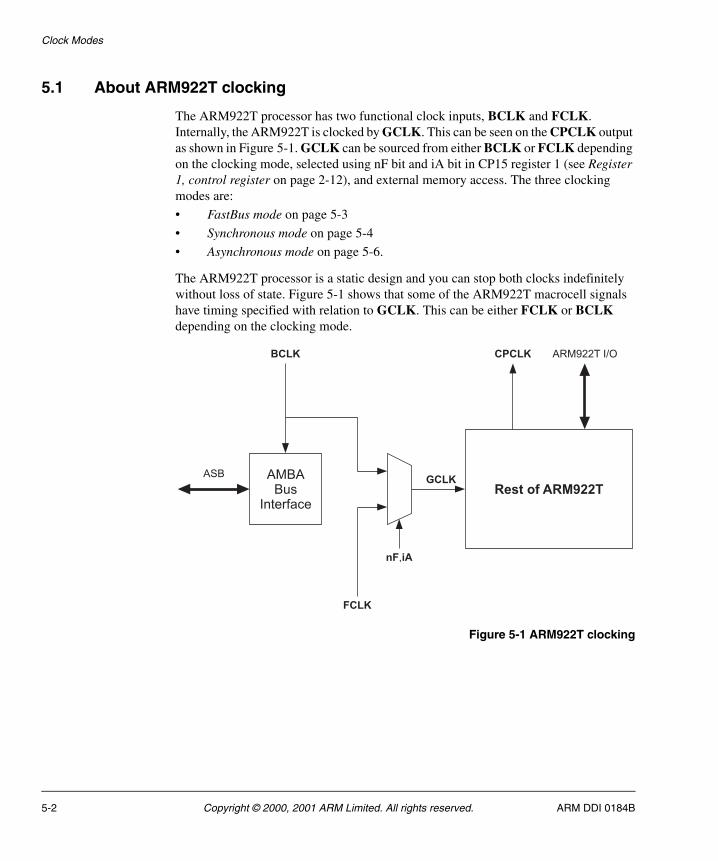
Clock Modes
5.1 About ARM922T clocking
The ARM922T processor has two functional clock inputs, BCLK and FCLK. Internally, the ARM922T is clocked by GCLK. This can be seen on the CPCLK output as shown in Figure 5-1. GCLK can be sourced from either BCLK or FCLK depending on the clocking mode, selected using nF bit and iA bit in CP15 register 1 (see Register 1, control register on page 2-12), and external memory access. The three clocking modes are:
• FastBus mode on page 5-3
• Synchronous mode on page 5-4
• Asynchronous mode on page 5-6.
The ARM922T processor is a static design and you can stop both clocks indefinitely without loss of state. Figure 5-1 shows that some of the ARM922T macrocell signals have timing specified with relation to GCLK. This can be either FCLK or BCLK depending on the clocking mode.
Figure 5-1 ARM922T clocking
nF iA,
GCLK
CPCLK ARM922T I/O
Rest of ARM922TAMBABus
Interface
ASB
BCLK
FCLK
5-2 Copyright © 2000, 2001 ARM Limited. All rights reserved. ARM DDI 0184B
Clock Modes
5.2 FastBus mode
In FastBus mode GCLK is sourced from BCLK. The FCLK input is ignored. This means that BCLK is used to control the AMBA ASB interface and the internal ARM922T processor core.
On reset, the ARM922T processor is put into FastBus mode and operates using BCLK. A typical use for FastBus mode is to execute startup code while configuring a PLL under software control to produce FCLK at a higher frequency. When the PLL has stabilized and locked, you can switch the ARM922T processor to synchronous or asynchronous clocking using FCLK for normal operation.
ARM DDI 0184B Copyright © 2000, 2001 ARM Limited. All rights reserved. 5-3
Clock Modes
5.3 Synchronous mode
In this mode of operation GCLK is sourced from BCLK or FCLK. There are three restrictions apply to BCLK and FCLK:
• FCLK must have a higher frequency than BCLK
• FCLK must be an integer multiple of the BCLK frequency
• FCLK must be HIGH whenever there is a BCLK transition.
BCLK is used to control the AMBA ASB interface, and FCLK is used to control the internal ARM922T processor core. When an external memory access is required the core either continues to clock using FCLK or is switched to BCLK, as shown in Table 5-1. This is the same as for asynchronous mode.
The penalty in switching from FCLK to BCLK and from BCLK to FCLK is symmetric, from zero to one phase of the clock to which the core is re-synchronizing. That is, switching from FCLK to BCLK has a penalty of between zero and one BCLK phase, and switching back from BCLK to FCLK has a penalty of between zero and one FCLK phase.
Figure 5-2 on page 5-5 shows an example zero BCLK phase delay when switching from FCLK to BCLK in synchronous mode.
Table 5-1 Clock selection for external memory accesses
External memory access operation GCLK =
Buffered write FCLK
Nonbuffered write BCLK
Page walk, cachable read (linefill), noncachable read BCLK
5-4 Copyright © 2000, 2001 ARM Limited. All rights reserved. ARM DDI 0184B
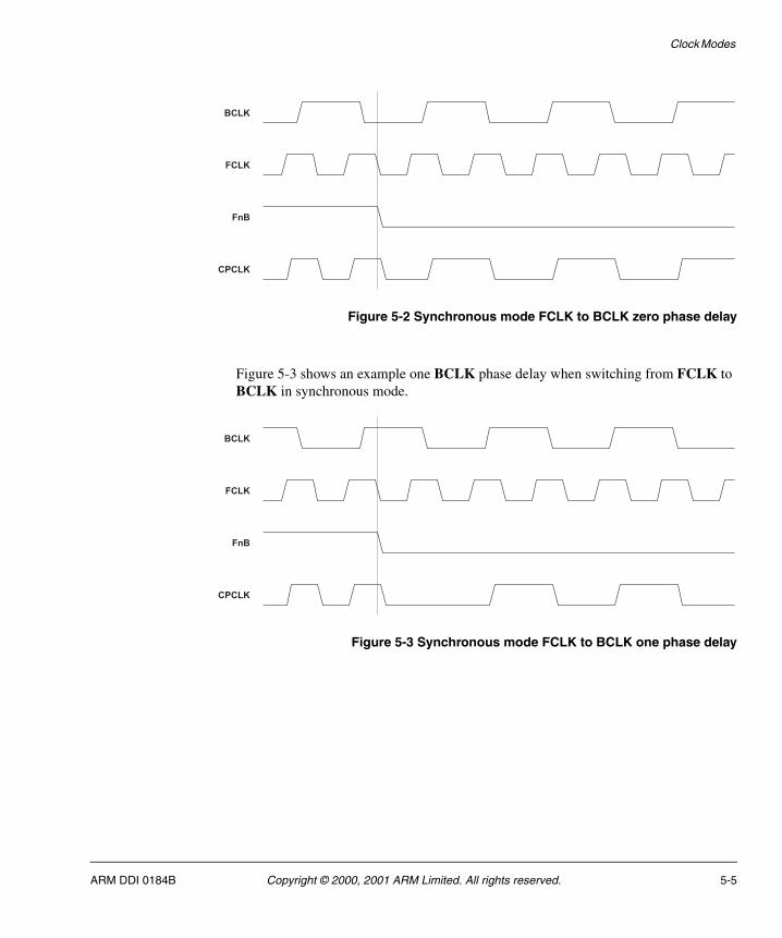
Clock Modes
Figure 5-2 Synchronous mode FCLK to BCLK zero phase delay
Figure 5-3 shows an example one BCLK phase delay when switching from FCLK to BCLK in synchronous mode.
Figure 5-3 Synchronous mode FCLK to BCLK one phase delay
BCLK
FCLK
FnB
CPCLK
BCLK
FCLK
FnB
CPCLK
ARM DDI 0184B Copyright © 2000, 2001 ARM Limited. All rights reserved. 5-5
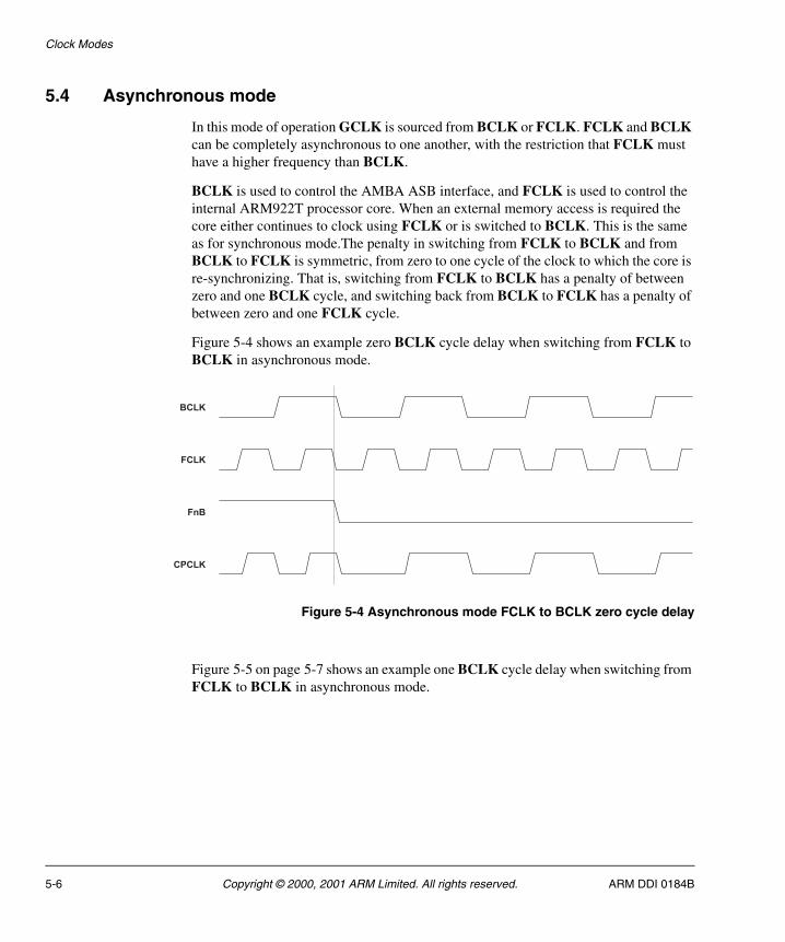
Clock Modes
5.4 Asynchronous mode
In this mode of operation GCLK is sourced from BCLK or FCLK. FCLK and BCLK can be completely asynchronous to one another, with the restriction that FCLK must have a higher frequency than BCLK.
BCLK is used to control the AMBA ASB interface, and FCLK is used to control the internal ARM922T processor core. When an external memory access is required the core either continues to clock using FCLK or is switched to BCLK. This is the same as for synchronous mode.The penalty in switching from FCLK to BCLK and from BCLK to FCLK is symmetric, from zero to one cycle of the clock to which the core is re-synchronizing. That is, switching from FCLK to BCLK has a penalty of between zero and one BCLK cycle, and switching back from BCLK to FCLK has a penalty of between zero and one FCLK cycle.
Figure 5-4 shows an example zero BCLK cycle delay when switching from FCLK to BCLK in asynchronous mode.
Figure 5-4 Asynchronous mode FCLK to BCLK zero cycle delay
Figure 5-5 on page 5-7 shows an example one BCLK cycle delay when switching from FCLK to BCLK in asynchronous mode.
BCLK
FCLK
FnB
CPCLK
5-6 Copyright © 2000, 2001 ARM Limited. All rights reserved. ARM DDI 0184B
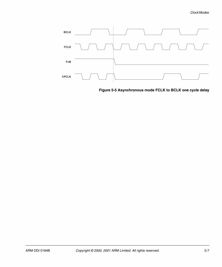
Clock Modes
Figure 5-5 Asynchronous mode FCLK to BCLK one cycle delay
BCLK
FCLK
FnB
CPCLK
ARM DDI 0184B Copyright © 2000, 2001 ARM Limited. All rights reserved. 5-7

Clock Modes
5-8 Copyright © 2000, 2001 ARM Limited. All rights reserved. ARM DDI 0184B
Chapter 6 Bus Interface Unit
This chapter describes the ARM922T bus interface. It contains the following sections:
• About the ARM922T bus interface on page 6-2
• Unidirectional AMBA ASB interface on page 6-3
• Fully-compliant AMBA ASB interface on page 6-5
• AMBA AHB interface on page 6-20
• Level 2 cache support and performance analysis on page 6-22.
ARM DDI 0184B Copyright © 2000, 2001 ARM Limited. All rights reserved. 6-1
Bus Interface Unit
6.1 About the ARM922T bus interface
The AMBA Specification (Rev 2.0) defines two high-performance system buses:
• the Advanced High-performance Bus (AHB)
• the Advanced System Bus (ASB).
The ARM922T processor has been designed with a unidirectional ASB interface, plus the necessary extra control signals to enable efficient implementation of both the AHB and ASB interface. With no additional logic, you can use the unidirectional ASB interface in single master systems where the ARM922T is the master. With the addition of tristate drivers, the ARM922Tprocessor implements a full ASB interface, either as an ASB bus master, or as a slave for production test. With the addition of a synthesizable wrapper, the ARM922T processor implements a full AHB interface, either as an AHB bus master, or as a slave for production test. The wrapper introduces no speed penalties, no performance penalties on reads, no performance penalties on buffered writes, and minimal performance penalty on nonbuffered writes. The MCR drain write buffer requires an additional instruction to operate in a predictable manner. See AMBA AHB interface on page 6-20 for details.
In this section the following abbreviations are used:
NCNB Noncachable and nonbufferable
NCB Noncachable and bufferable
NC Noncachable
WT Cachable and write-through
WB Cachable and write-back.
6-2 Copyright © 2000, 2001 ARM Limited. All rights reserved. ARM DDI 0184B
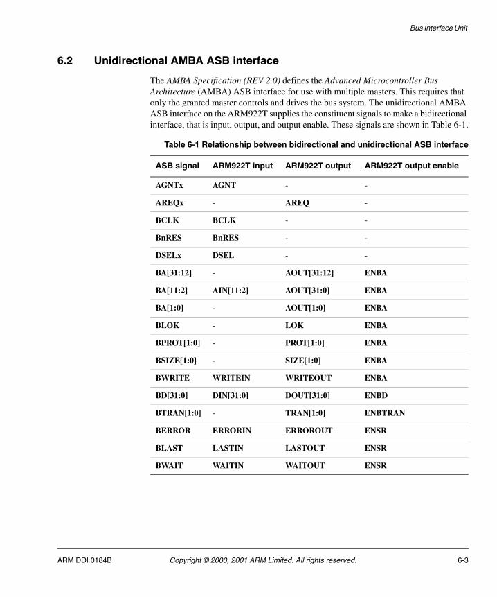
Bus Interface Unit
6.2 Unidirectional AMBA ASB interface
The AMBA Specification (REV 2.0) defines the Advanced Microcontroller Bus Architecture (AMBA) ASB interface for use with multiple masters. This requires that only the granted master controls and drives the bus system. The unidirectional AMBA ASB interface on the ARM922T supplies the constituent signals to make a bidirectional interface, that is input, output, and output enable. These signals are shown in Table 6-1.
Table 6-1 Relationship between bidirectional and unidirectional ASB interface
ASB signal ARM922T input ARM922T output ARM922T output enable
AGNTx AGNT - -
AREQx - AREQ -
BCLK BCLK - -
BnRES BnRES - -
DSELx DSEL - -
BA[31:12] - AOUT[31:12] ENBA
BA[11:2] AIN[11:2] AOUT[31:0] ENBA
BA[1:0] - AOUT[1:0] ENBA
BLOK - LOK ENBA
BPROT[1:0] - PROT[1:0] ENBA
BSIZE[1:0] - SIZE[1:0] ENBA
BWRITE WRITEIN WRITEOUT ENBA
BD[31:0] DIN[31:0] DOUT[31:0] ENBD
BTRAN[1:0] - TRAN[1:0] ENBTRAN
BERROR ERRORIN ERROROUT ENSR
BLAST LASTIN LASTOUT ENSR
BWAIT WAITIN WAITOUT ENSR
ARM DDI 0184B Copyright © 2000, 2001 ARM Limited. All rights reserved. 6-3
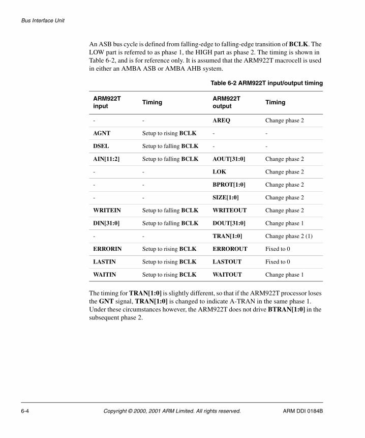
Bus Interface Unit
An ASB bus cycle is defined from falling-edge to falling-edge transition of BCLK. The LOW part is referred to as phase 1, the HIGH part as phase 2. The timing is shown in Table 6-2, and is for reference only. It is assumed that the ARM922T macrocell is used in either an AMBA ASB or AMBA AHB system.
The timing for TRAN[1:0] is slightly different, so that if the ARM922T processor loses the GNT signal, TRAN[1:0] is changed to indicate A-TRAN in the same phase 1. Under these circumstances however, the ARM922T does not drive BTRAN[1:0] in the subsequent phase 2.
Table 6-2 ARM922T input/output timing
ARM922T input
TimingARM922T output
Timing
- - AREQ Change phase 2
AGNT Setup to rising BCLK - -
DSEL Setup to falling BCLK - -
AIN[11:2] Setup to falling BCLK AOUT[31:0] Change phase 2
- - LOK Change phase 2
- - BPROT[1:0] Change phase 2
- - SIZE[1:0] Change phase 2
WRITEIN Setup to falling BCLK WRITEOUT Change phase 2
DIN[31:0] Setup to falling BCLK DOUT[31:0] Change phase 1
- - TRAN[1:0] Change phase 2 (1)
ERRORIN Setup to rising BCLK ERROROUT Fixed to 0
LASTIN Setup to rising BCLK LASTOUT Fixed to 0
WAITIN Setup to rising BCLK WAITOUT Change phase 1
6-4 Copyright © 2000, 2001 ARM Limited. All rights reserved. ARM DDI 0184B
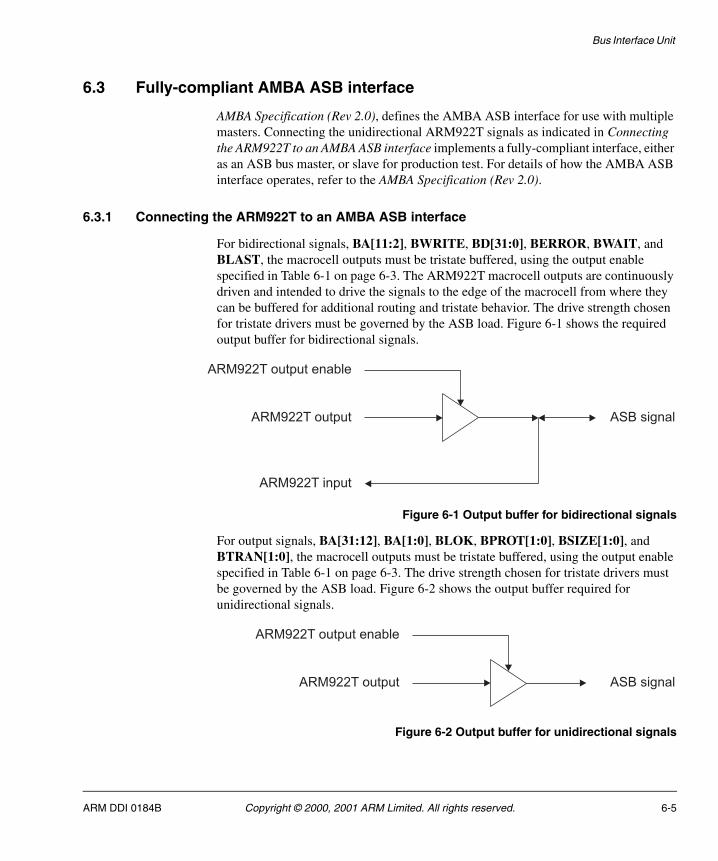
Bus Interface Unit
6.3 Fully-compliant AMBA ASB interface
AMBA Specification (Rev 2.0), defines the AMBA ASB interface for use with multiple masters. Connecting the unidirectional ARM922T signals as indicated in Connecting the ARM922T to an AMBA ASB interface implements a fully-compliant interface, either as an ASB bus master, or slave for production test. For details of how the AMBA ASB interface operates, refer to the AMBA Specification (Rev 2.0).
6.3.1 Connecting the ARM922T to an AMBA ASB interface
For bidirectional signals, BA[11:2], BWRITE, BD[31:0], BERROR, BWAIT, and BLAST, the macrocell outputs must be tristate buffered, using the output enable specified in Table 6-1 on page 6-3. The ARM922T macrocell outputs are continuously driven and intended to drive the signals to the edge of the macrocell from where they can be buffered for additional routing and tristate behavior. The drive strength chosen for tristate drivers must be governed by the ASB load. Figure 6-1 shows the required output buffer for bidirectional signals.
Figure 6-1 Output buffer for bidirectional signals
For output signals, BA[31:12], BA[1:0], BLOK, BPROT[1:0], BSIZE[1:0], and BTRAN[1:0], the macrocell outputs must be tristate buffered, using the output enable specified in Table 6-1 on page 6-3. The drive strength chosen for tristate drivers must be governed by the ASB load. Figure 6-2 shows the output buffer required for unidirectional signals.
Figure 6-2 Output buffer for unidirectional signals
ARM922T input
ARM922T output
ARM922T output enable
ASB signal
ARM922T output
ARM922T output enable
ASB signal
ARM DDI 0184B Copyright © 2000, 2001 ARM Limited. All rights reserved. 6-5
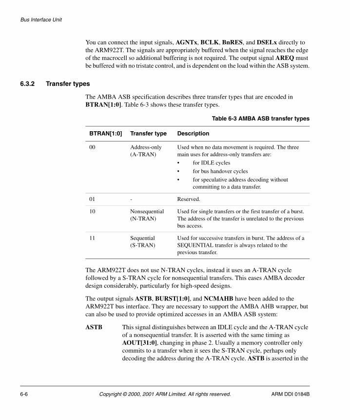
Bus Interface Unit
You can connect the input signals, AGNTx, BCLK, BnRES, and DSELx directly to the ARM922T. The signals are appropriately buffered when the signal reaches the edge of the macrocell so additional buffering is not required. The output signal AREQ must be buffered with no tristate control, and is dependent on the load within the ASB system.
6.3.2 Transfer types
The AMBA ASB specification describes three transfer types that are encoded in BTRAN[1:0]. Table 6-3 shows these transfer types.
The ARM922T does not use N-TRAN cycles, instead it uses an A-TRAN cycle followed by a S-TRAN cycle for nonsequential transfers. This eases AMBA decoder design considerably, particularly for high-speed designs.
The output signals ASTB, BURST[1:0], and NCMAHB have been added to the ARM922T bus interface. They are necessary to support the AMBA AHB wrapper, but can also be used to provide optimized accesses in an AMBA ASB system:
ASTB This signal distinguishes between an IDLE cycle and the A-TRAN cycle of a nonsequential transfer. It is asserted with the same timing as AOUT[31:0], changing in phase 2. Usually a memory controller only commits to a transfer when it sees the S-TRAN cycle, perhaps only decoding the address during the A-TRAN cycle. ASTB is asserted in the
Table 6-3 AMBA ASB transfer types
BTRAN[1:0] Transfer type Description
00 Address-only (A-TRAN)
Used when no data movement is required. The three main uses for address-only transfers are:
• for IDLE cycles
• for bus handover cycles
• for speculative address decoding without committing to a data transfer.
01 - Reserved.
10 Nonsequential (N-TRAN)
Used for single transfers or the first transfer of a burst. The address of the transfer is unrelated to the previous bus access.
11 Sequential (S-TRAN)
Used for successive transfers in burst. The address of a SEQUENTIAL transfer is always related to the previous transfer.
6-6 Copyright © 2000, 2001 ARM Limited. All rights reserved. ARM DDI 0184B
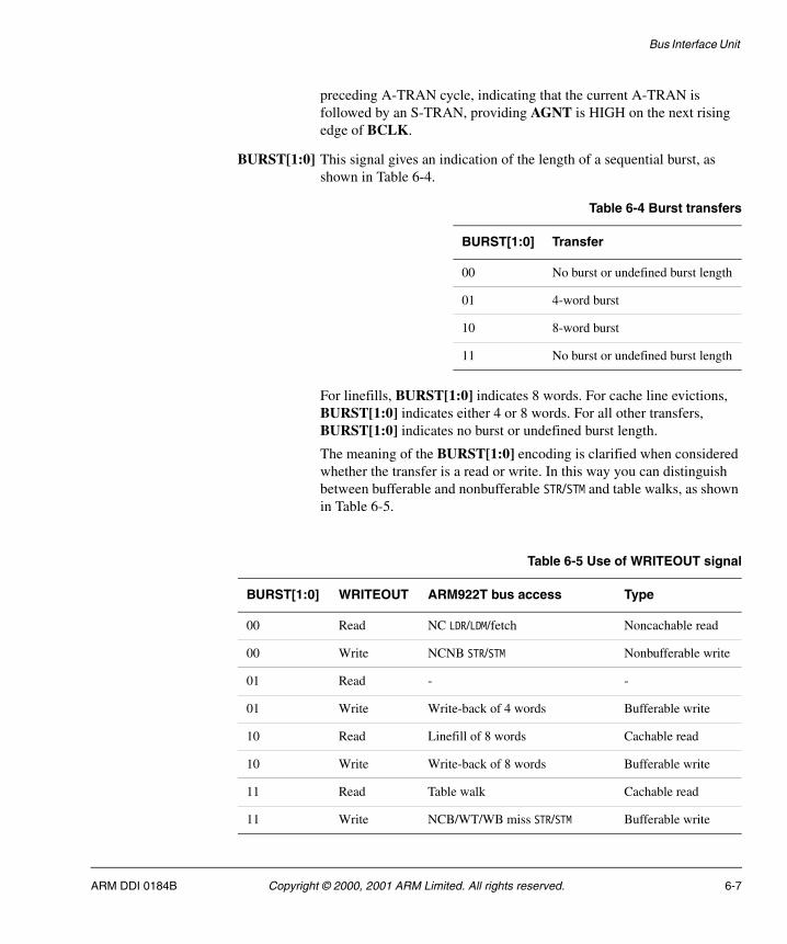
Bus Interface Unit
preceding A-TRAN cycle, indicating that the current A-TRAN is followed by an S-TRAN, providing AGNT is HIGH on the next rising edge of BCLK.
BURST[1:0] This signal gives an indication of the length of a sequential burst, as shown in Table 6-4.
For linefills, BURST[1:0] indicates 8 words. For cache line evictions, BURST[1:0] indicates either 4 or 8 words. For all other transfers, BURST[1:0] indicates no burst or undefined burst length.
The meaning of the BURST[1:0] encoding is clarified when considered whether the transfer is a read or write. In this way you can distinguish between bufferable and nonbufferable STR/STM and table walks, as shown in Table 6-5.
Table 6-4 Burst transfers
BURST[1:0] Transfer
00 No burst or undefined burst length
01 4-word burst
10 8-word burst
11 No burst or undefined burst length
Table 6-5 Use of WRITEOUT signal
BURST[1:0] WRITEOUT ARM922T bus access Type
00 Read NC LDR/LDM/fetch Noncachable read
00 Write NCNB STR/STM Nonbufferable write
01 Read - -
01 Write Write-back of 4 words Bufferable write
10 Read Linefill of 8 words Cachable read
10 Write Write-back of 8 words Bufferable write
11 Read Table walk Cachable read
11 Write NCB/WT/WB miss STR/STM Bufferable write
ARM DDI 0184B Copyright © 2000, 2001 ARM Limited. All rights reserved. 6-7
Bus Interface Unit
The BURST[1:0] signals change in phase 2 and are asserted in the phase when ASTB is asserted. BURST[1:0] then remains unchanged until the next transfer.
NCMAHB This signal indicates for noncached load multiples whether more words are requested as part of the current burst transfer. When HIGH this indicates more words are requested. When LOW, on the last S-TRAN of the burst, this indicates that the current transfer is the last word of the burst. It is asserted in phase 2 and is only valid if AGNT remains asserted throughout the transfer.
The following timing diagrams show the types of transfer that can be initiated by the ARM922T rev0:
• Instruction fetch after reset on page 6-10
• Example LDR from address 0x108 on page 6-11
• Example LDM of 5 words from 0x108 on page 6-12
• Example nonbuffered STR on page 6-13
• Example nonbuffered STM on page 6-14
• Example linefill from 0x100 on page 6-15
• Example 4-word data eviction on page 6-16
• Example swap operation on page 6-18.
Where the AREQ and AGNT signals and the responses from the ASB slave are not shown in these diagrams, it is assumed that AGNT is asserted and the ASB slave response is DONE.
Different slave responses and bus master handover are covered in the AMBA Specification (Rev 2.0). It is assumed that you are using the ARM922T macrocell within a multi-master ASB system, so unidirectional ASB timing diagrams are not provided.
6.3.3 Instruction fetch after reset
The general operation of the AMBA ASB during reset is described in the AMBA Specification (Rev 2.0). The reset signal, BnRES, is active LOW, and can be asserted asynchronously to guarantee the bus is in a safe state. During reset, the following actions occur on the bus:
• The arbiter grants the default bus master.
• The default bus master must:
— drive BTRAN to indicate an ADDRESS-ONLY transfer
— drive BLOK LOW to allow arbitration
— drive BA, BWRITE, BSIZE, and BPROT to any value
6-8 Copyright © 2000, 2001 ARM Limited. All rights reserved. ARM DDI 0184B
Bus Interface Unit
— tristate BD.
• All other bus masters must tristate shared bus signals, BA, BD, BWRITE, BTRAN, BSIZE, BPROT, and BLOK.
• The decoder must:
— deassert all slave select signals, DSELx
— provide the appropriate transfer response.
• All slaves must tristate shared bus signals.
You must hold BnRES LOW for a minimum of five BCLK cycles to ensure complete reset of the ARM922T processor. You must deassert BnRES during the BCLK LOW phase.
Figure 6-3 on page 6-10 shows the default bus master during reset to be the TIC controller. After reset, the ARM922T processor is made the default bus master, so there is a handover phase when BA, BWRITE, BSIZE, BPROT, and BLOK are not driven, but BTRAN is driven with ADDRESS-ONLY. The ARM920T continues as the default bus master without requesting the bus, so it must:
• drive BTRAN to indicate an ADDRESS-ONLY transfer
• drive BLOK LOW to allow arbitration
• drive BA, BWRITE, BSIZE, and BPROT to any value
• Tristate BD.
The ARM922T processor then requests use of the bus and, because it is already granted the bus, starts the first ADDRESS-ONLY cycle that is not an IDLE cycle, indicated by ASTB. The first instruction fetch continues from then.
ARM DDI 0184B Copyright © 2000, 2001 ARM Limited. All rights reserved. 6-9
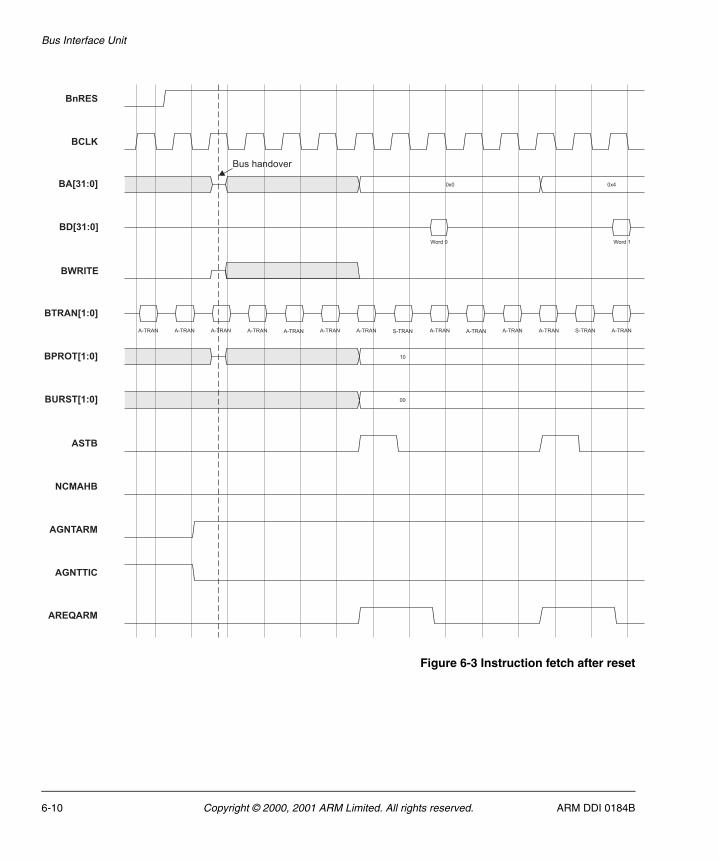
Bus Interface Unit
Figure 6-3 Instruction fetch after reset
00
10
BCLK
BWRITE
BA[31:0]
BD[31:0]
BPROT[1:0]
BTRAN[1:0]
BURST[1:0]
ASTB
NCMAHB
A-TRAN A-TRAN A-TRAN A-TRAN A-TRANA-TRAN A-TRAN A-TRAN S-TRAN A-TRAN
0x0
BnRES
Word 0
Bus handover
AGNTARM
AGNTTIC
AREQARM
0x4
A-TRAN A-TRAN A-TRANS-TRAN
Word 1
6-10 Copyright © 2000, 2001 ARM Limited. All rights reserved. ARM DDI 0184B
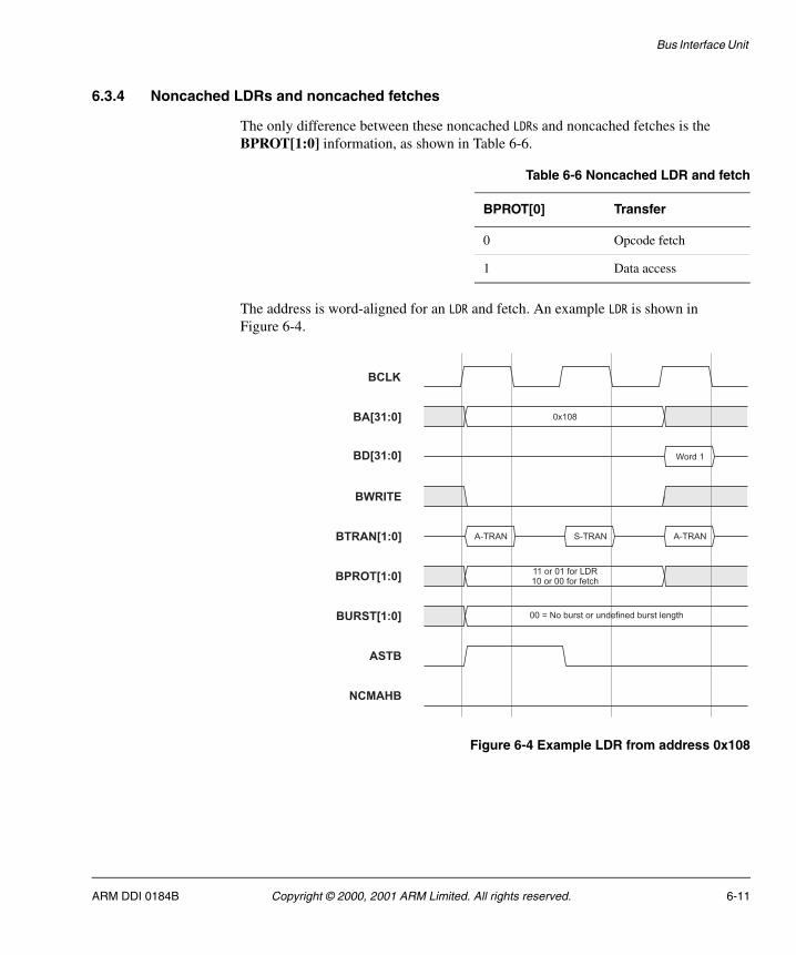
Bus Interface Unit
6.3.4 Noncached LDRs and noncached fetches
The only difference between these noncached LDRs and noncached fetches is the BPROT[1:0] information, as shown in Table 6-6.
The address is word-aligned for an LDR and fetch. An example LDR is shown in Figure 6-4.
Figure 6-4 Example LDR from address 0x108
Table 6-6 Noncached LDR and fetch
BPROT[0] Transfer
0 Opcode fetch
1 Data access
00 = No burst or undefined burst length
11 or 01 for LDR10 or 00 for fetch
BCLK
BA[31:0]
BD[31:0]
0x108
Word 1
BTRAN[1:0]
BWRITE
A-TRANA-TRAN S-TRAN
BPROT[1:0]
BURST[1:0]
ASTB
NCMAHB
ARM DDI 0184B Copyright © 2000, 2001 ARM Limited. All rights reserved. 6-11
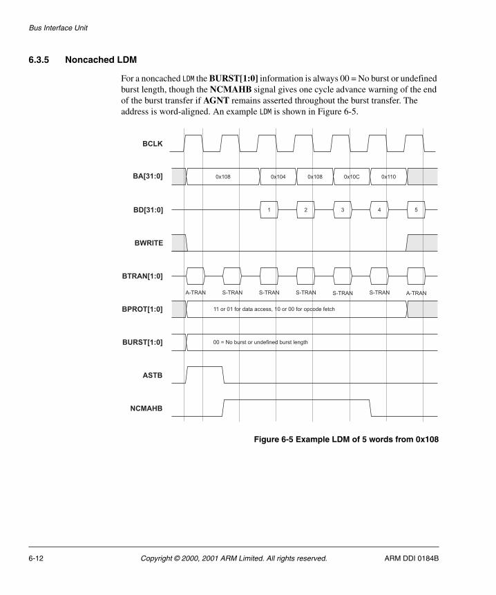
Bus Interface Unit
6.3.5 Noncached LDM
For a noncached LDM the BURST[1:0] information is always 00 = No burst or undefined burst length, though the NCMAHB signal gives one cycle advance warning of the end of the burst transfer if AGNT remains asserted throughout the burst transfer. The address is word-aligned. An example LDM is shown in Figure 6-5.
Figure 6-5 Example LDM of 5 words from 0x108
BCLK
BWRITE
BA[31:0]
BD[31:0]
BPROT[1:0]
0x104
BTRAN[1:0]
0x108 0x10C0x108
4 5
S-TRAN S-TRAN S-TRAN S-TRAN A-TRANA-TRAN S-TRAN
11 or 01 for data access, 10 or 00 for opcode fetch
BURST[1:0] 00 = No burst or undefined burst length
ASTB
NCMAHB
0x110
321
6-12 Copyright © 2000, 2001 ARM Limited. All rights reserved. ARM DDI 0184B
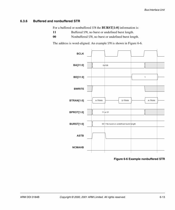
Bus Interface Unit
6.3.6 Buffered and nonbuffered STR
For a buffered or nonbuffered STR the BURST[1:0] information is:
11 Buffered STR, no burst or undefined burst length.
00 Nonbuffered STR, no burst or undefined burst length.
The address is word-aligned. An example STR is shown in Figure 6-6.
Figure 6-6 Example nonbuffered STR
BCLK
BWRITE
BA[31:0]
BD[31:0]
BPROT[1:0]
BTRAN[1:0]
1
0x108
S-TRAN A-TRANA-TRAN
11 or 01
BURST[1:0] 00 = No burst or undefined burst length
ASTB
NCMAHB
ARM DDI 0184B Copyright © 2000, 2001 ARM Limited. All rights reserved. 6-13
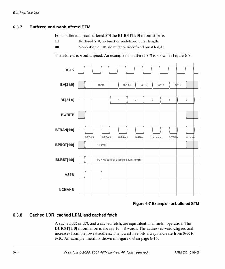
Bus Interface Unit
6.3.7 Buffered and nonbuffered STM
For a buffered or nonbuffered STM the BURST[1:0] information is:
11 Buffered STM, no burst or undefined burst length.
00 Nonbuffered STM, no burst or undefined burst length.
The address is word-aligned. An example nonbuffered STM is shown in Figure 6-7.
Figure 6-7 Example nonbuffered STM
6.3.8 Cached LDR, cached LDM, and cached fetch
A cached LDR or LDM, and a cached fetch, are equivalent to a linefill operation. The BURST[1:0] information is always 10 = 8 words. The address is word-aligned and increases from the lowest address. The lowest five bits always increase from 0x00 to 0x1C. An example linefill is shown in Figure 6-8 on page 6-15.
BCLK
BWRITE
BA[31:0]
BD[31:0]
BPROT[1:0]
0x10C
BTRAN[1:0]
1 2 3
0x110 0x114 0x1180x108
4 5
S-TRAN S-TRAN S-TRAN S-TRAN A-TRANA-TRAN S-TRAN
11 or 01
BURST[1:0] 00 = No burst or undefined burst length
ASTB
NCMAHB
6-14 Copyright © 2000, 2001 ARM Limited. All rights reserved. ARM DDI 0184B
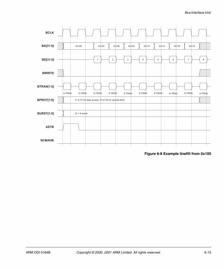
Bus Interface Unit
Figure 6-8 Example linefill from 0x100
BCLK
BWRITE
BA[31:0]
BD[31:0]
BPROT[1:0]
0x104
BTRAN[1:0]
1 2 3
0x108 0x10C0x100
4 5
S-TRAN S-TRAN S-TRAN S-TRAN A-TRANA-TRAN S-TRAN
11 or 01 for data access, 10 or 00 for opcode fetch
BURST[1:0] 10 = 8 words
ASTB
NCMAHB
0x110 0x114 0x118 0x11C
6 7 8
S-TRAN S-TRAN S-TRAN
ARM DDI 0184B Copyright © 2000, 2001 ARM Limited. All rights reserved. 6-15
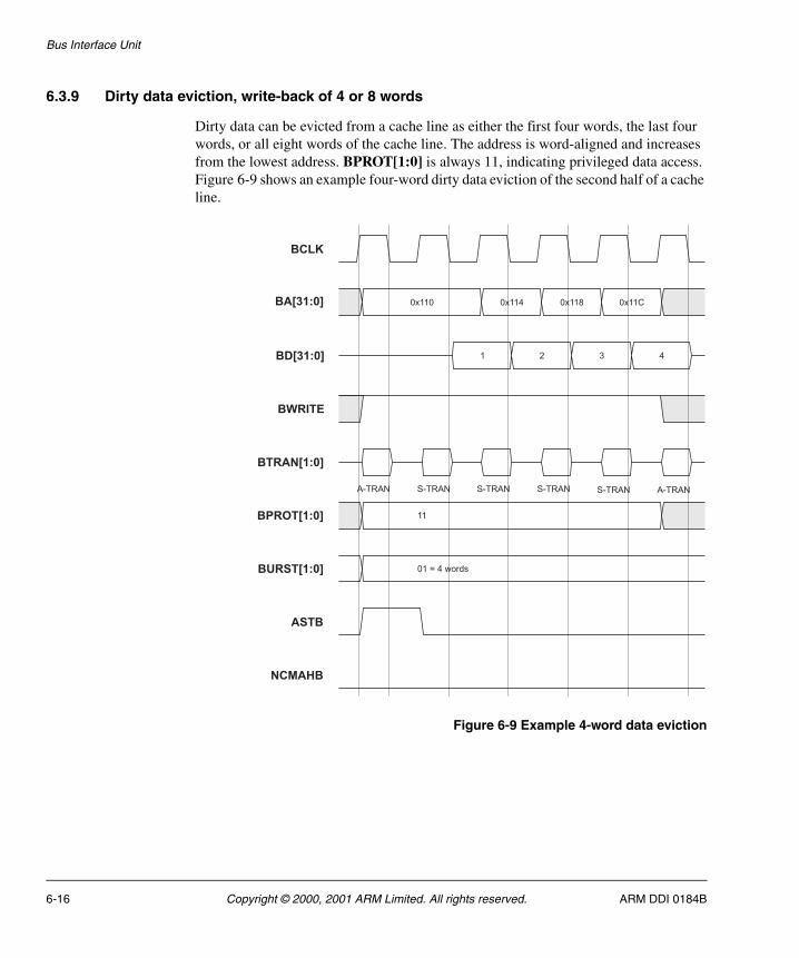
Bus Interface Unit
6.3.9 Dirty data eviction, write-back of 4 or 8 words
Dirty data can be evicted from a cache line as either the first four words, the last four words, or all eight words of the cache line. The address is word-aligned and increases from the lowest address. BPROT[1:0] is always 11, indicating privileged data access. Figure 6-9 shows an example four-word dirty data eviction of the second half of a cache line.
Figure 6-9 Example 4-word data eviction
BCLK
BWRITE
BA[31:0]
BD[31:0]
BPROT[1:0]
0x114
BTRAN[1:0]
1 2 3
0x118 0x11C0x110
4
S-TRAN S-TRAN S-TRAN A-TRANA-TRAN S-TRAN
11
BURST[1:0] 01 = 4 words
ASTB
NCMAHB
6-16 Copyright © 2000, 2001 ARM Limited. All rights reserved. ARM DDI 0184B
Bus Interface Unit
The allowable combinations are listed in Table 6-7.
6.3.10 Swap
The swap operation is implemented as a single read transfer followed by a single write transfer. The BLOK signal is asserted so that the write transfer is locked to the preceding read transfer. This must be used by the arbiter to ensure that no other bus master is given access to the bus between the read and write transfers. An example swap operation is shown in Figure 6-10 on page 6-18.
Table 6-7 Data eviction of 4 or 8 words
Data evicted BURST[1:0] Lowest 5 bits of the address
First 4 words 01 0x00 to 0x0C
Last 4 words 01 0x10 to 0x1C
All 8 words 10 0x00 to 0x1C
ARM DDI 0184B Copyright © 2000, 2001 ARM Limited. All rights reserved. 6-17
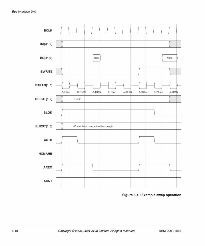
Bus Interface Unit
Figure 6-10 Example swap operation
BCLK
BWRITE
BA[31:0]
BD[31:0]
BPROT[1:0]
BTRAN[1:0]
Write
A-TRAN A-TRAN A-TRAN A-TRANA-TRAN S-TRAN
11 or 01
BURST[1:0] 00 = No burst or undefined burst length
NCMAHB
A-TRAN S-TRAN
Read
AREQ
AGNT
BLOK
ASTB
6-18 Copyright © 2000, 2001 ARM Limited. All rights reserved. ARM DDI 0184B
Bus Interface Unit
6.3.11 Page walk
A page walk is identical to a noncached LDR on the ASB. That is, a single word read. The BURST[1:0] encoding is always 11. For a page walk caused by an opcode fetch, BPROT[1:0] = 10. For a page walk caused by a data operation, BPROT[1:0] = 11. The page walk is always privileged.
6.3.12 AMBA ASB slave transfers
You can test the ARM922T processor as an individual module within an AMBA system, responding only to transfers from the AMBA ASB. In this mode of operation the ARM922T processor is never granted the ASB as a bus master, and responds as an ASB slave, detecting the assertion of DSEL. This is described in detail in the AMBA Specification (Rev 2.0).
ARM DDI 0184B Copyright © 2000, 2001 ARM Limited. All rights reserved. 6-19
Bus Interface Unit
6.4 AMBA AHB interface
The AMBA Specification (Rev 2.0) defines the AMBA AHB interface for use with multiple masters. With the addition of a synthesizable wrapper, the ARM922T implements a full AHB interface, either as an AHB bus master, or as a slave for production test. This is delivered as synthesizable RTL, with synthesis scripts. Contact ARM for details of how to obtain this information. The interface uses ASTB, BURST[1:0], and NCMAHB signals in addition to the unidirectional ASB signals. This allows an efficient implementation that has:
• no speed penalty
• no cycle penalties for read transfers
• no cycle penalties for buffered write transfers
• one cycle penalty for every nonbuffered write transfer
• swaps incur one cycle penalty on the read transfer and one cycle penalty on the write transfer
• the MCR drain write buffer instruction, MCR p15, 0, Rd, c7, c10, 4, drains the write buffer to the AHB wrapper.
In the case of the MCR drain write buffer the write transfers appear as buffered, so the ARM922T processor continues execution before the last write transfer is completed on the AHB.
An example of how this might be a problem is if the last STR to the write buffer was to clear an interrupt source prior to enabling interrupts to the ARM9TDMI core, then the following sequence might result in an interrupt being returned to the ARM9TDMI core before the interrupt is cleared:
Buffered STR to clear interruptMCR drain write bufferEnable interrupts.
There are three solutions:
1. For a non write-sensitive address. Issue the STR twice. The first STR completes before the second STR enters the AHB wrapper, guaranteeing the interrupt is cleared before the interrupts are enabled:
Buffered STR to clear interruptBuffered STR to clear interruptMCR drain write bufferEnable interrupts.
2. For a write-sensitive address. Issue any other buffered STR to a non write-sensitive address. This must be to a NCB or WT region to ensure the STR is committed to the write buffer:
Buffered STR to clear interrupt
6-20 Copyright © 2000, 2001 ARM Limited. All rights reserved. ARM DDI 0184B
Bus Interface Unit
Buffered STR to a non write-sensitive addressMCR drain write bufferEnable interrupts.
3. Issue a read on the AHB before enabling the interrupts. This must be from a noncachable region to ensure the read appears on the AHB:
Buffered STR to clear interruptMCR drain write bufferNon-cachable LDR or fetchEnable interrupts.
ARM DDI 0184B Copyright © 2000, 2001 ARM Limited. All rights reserved. 6-21
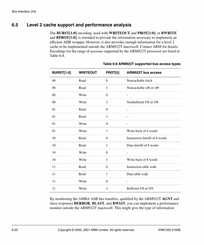
Bus Interface Unit
6.5 Level 2 cache support and performance analysis
The BURST[1:0] encoding, used with WRITEOUT and PROT[1:0], or BWRITE and BPROT[1:0], is intended to provide the information necessary to implement an efficient AHB wrapper. However, it also provides enough information for a level 2 cache to be implemented outside the ARM922T macrocell. Contact ARM for details. Encodings for the range of accesses supported by the ARM922T processor are listed in Table 6-8.
By monitoring the AMBA ASB bus transfers, qualified by the ARM922T AGNT and slave responses BERROR, BLAST, and BWAIT, you can implement a performance monitor outside the ARM922T macrocell. This might give the type of information
Table 6-8 ARM922T supported bus access types
BURST[1:0] WRITEOUT PROT[0] ARM922T bus access
00 Read 0 Noncachable fetch
00 Read 1 Noncachable LDR or LDM
00 Write 0 -
00 Write 1 Nonbuffered STR or STM
01 Read 0 -
01 Read 1 -
01 Write 0 -
01 Write 1 Write-back of 4 words
10 Read 0 Instruction linefill of 8 words
10 Read 1 Data linefill of 8 words
10 Write 0 -
10 Write 1 Write-back of 8 words
11 Read 0 Instruction table walk
11 Read 1 Data table walk
11 Write 0 -
11 Write 1 Buffered STR or STM
6-22 Copyright © 2000, 2001 ARM Limited. All rights reserved. ARM DDI 0184B
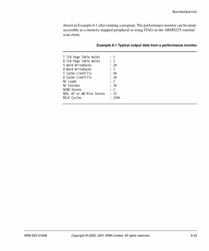
Bus Interface Unit
shown in Example 6-1 after running a program. The performance monitor can be made accessible as a memory mapped peripheral or using JTAG on the ARM922T external scan chain.
Example 6-1 Typical output data from a performance monitor
I TLB Page Table Walks : 1D TLB Page Table Walks : 14 Word Writebacks : 108 Word Writebacks : 5I Cache Linefills : 48D Cache Linefills : 28NC Loads : 2NC Fetches : 38NCNB Stores : 2NCB, WT or WB Miss Stores : 13BCLK Cycles : 1594
ARM DDI 0184B Copyright © 2000, 2001 ARM Limited. All rights reserved. 6-23
Bus Interface Unit
6-24 Copyright © 2000, 2001 ARM Limited. All rights reserved. ARM DDI 0184B
Chapter 7 Coprocessor Interface
This chapter describes the ARM922T coprocessor interface. It contains the following sections:
• About the ARM922T coprocessor interface on page 7-2
• LDC/STC on page 7-5
• MCR/MRC on page 7-9
• Interlocked MCR on page 7-11
• CDP on page 7-13
• Privileged instructions on page 7-15
• Busy-waiting and interrupts on page 7-17.
ARM DDI 0184B Copyright © 2000, 2001 ARM Limited. All rights reserved. 7-1
Coprocessor Interface
7.1 About the ARM922T coprocessor interface
The ARM922T processor supports the connection of on-chip coprocessors through an external coprocessor interface. All types of coprocessor instruction are supported.
The ARM922T coprocessor interface allows you to attach specially designed coprocessor hardware to the ARM922T. Example uses include:
• attachment of accelerators for floating-point math, DSP, 3-D graphics, encryption, or decryption
• the ARM instruction set supports the connection of 16 coprocessors, numbered 0 to 15, to an ARM processor.
7.1.1 Internal coprocessors
The ARM922T processor contains two internal coprocessors:
• CP14 for debug control
• CP15 for memory system control and test control.
This means that coprocessors attached externally to the ARM922T processor cannot be assigned coprocessor numbers 15 or 14. Other coprocessor numbers have been allocated by ARM for internal usage. Contact ARM for a full list of reserved coprocessor numbers.
The register map of CP15 is described in CP15 register map summary on page 2-5. The functionality of CP14 is described in Debug communications channel on page 9-64.
7.1.2 External coprocessors
Coprocessors determine the instructions they have to execute by using a pipeline follower in the coprocessor. As each instruction arrives from memory, it enters both the ARM pipeline and the coprocessor pipeline. To avoid a critical path for the instruction being latched by the coprocessor, the coprocessor pipeline must operate one clock phase behind the ARM922T pipeline. The ARM922T then informs the coprocessor when instructions move from Decode into Execute, and whether the instruction has to be executed.
To enable coprocessors to continue doing coprocessor data operations while the ARM922T pipeline is stalled (for instance waiting for a cache linefill to occur), the coprocessor must monitor a clock CPCLK, and a clock stall signal nCPWAIT. If nCPWAIT is LOW on the rising edge of CPCLK, the ARM922T pipeline is stalled and the coprocessor pipeline must not advance.
7-2 Copyright © 2000, 2001 ARM Limited. All rights reserved. ARM DDI 0184B
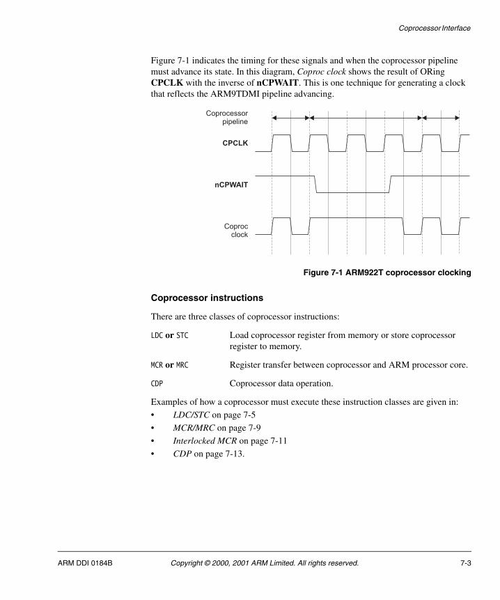
Coprocessor Interface
Figure 7-1 indicates the timing for these signals and when the coprocessor pipeline must advance its state. In this diagram, Coproc clock shows the result of ORing CPCLK with the inverse of nCPWAIT. This is one technique for generating a clock that reflects the ARM9TDMI pipeline advancing.
Figure 7-1 ARM922T coprocessor clocking
Coprocessor instructions
There are three classes of coprocessor instructions:
LDC or STC Load coprocessor register from memory or store coprocessor register to memory.
MCR or MRC Register transfer between coprocessor and ARM processor core.
CDP Coprocessor data operation.
Examples of how a coprocessor must execute these instruction classes are given in:
• LDC/STC on page 7-5
• MCR/MRC on page 7-9
• Interlocked MCR on page 7-11
• CDP on page 7-13.
CPCLK
Coprocclock
nCPWAIT
Coprocessorpipeline
ARM DDI 0184B Copyright © 2000, 2001 ARM Limited. All rights reserved. 7-3
Coprocessor Interface
7.1.3 Enabling and disabling the external coprocessor interface buses
The ARM922T macrocell has the CPEN input, coprocessor enable.
When tied LOW, the CPID and CPDOUT buses are held stable. When tied HIGH, the CPID and CPDOUT buses are enabled. This is meant as a power saving feature and is intended to be used statically within an embedded system.
7-4 Copyright © 2000, 2001 ARM Limited. All rights reserved. ARM DDI 0184B
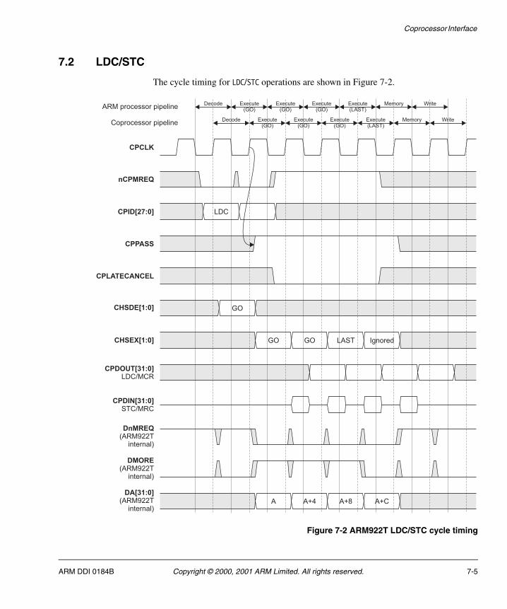
Coprocessor Interface
7.2 LDC/STC
The cycle timing for LDC/STC operations are shown in Figure 7-2.
Figure 7-2 ARM922T LDC/STC cycle timing
A A+4 A+8 A+C
DA[31:0](ARM922T
internal)
GO GO LAST Ignored
GO
CPCLK
nCPMREQ
CPID[27:0]
CHSDE[1:0]
CHSEX[1:0]
CPDOUT[31:0]LDC/MCR
CPPASS
CPLATECANCEL
LDC
CPDIN[31:0]STC/MRC
DnMREQ(ARM922T
internal)
DMORE(ARM922T
internal)
Decode Execute(GO)
Execute(GO)
Execute(GO)
Execute(LAST)
Memory Write
Decode Execute(GO)
Execute(GO)
Execute(GO)
Execute(LAST)
Memory Write
Coprocessor pipeline
ARM processor pipeline
ARM DDI 0184B Copyright © 2000, 2001 ARM Limited. All rights reserved. 7-5
Coprocessor Interface
In Figure 7-2 on page 7-5, four words of data are transferred. The number of words transferred is determined by how the coprocessor drives the CHSDE[1:0] and CHSEX[1:0] buses.
As with all other instructions, the ARM922T processor core performs the main instruction decode off the rising edge of the clock during the Decode stage. From this, the ARM9TDMI CPU core commits to executing the instruction, and so performs an instruction Fetch. The coprocessor instruction pipeline keeps in step with the ARM922T by monitoring CPMREQ, a latched copy of the ARM9TDMI instruction memory request signal InMREQ. Whenever nCPMREQ is LOW, an instruction Fetch is occurring and CPID is updated with the fetched instruction in the next cycle. This means that the instruction currently on CPID enters the Decode stage of the coprocessor pipeline, and that the instruction in the Decode stage of the coprocessor pipeline enters its Execute stage.
During the Execute stage, the condition codes are combined with the flags to determine whether the instruction can be executed or not. The output CPPASS is asserted (HIGH) if the instruction in the Execute stage of the coprocessor pipeline:
• is a coprocessor instruction
• has passed its condition codes.
If a coprocessor instruction busy-waits, CPPASS is asserted on every cycle until the coprocessor instruction is executed. If an interrupt occurs during busy-waiting, CPPASS is driven LOW, and the coprocessor stops execution of the coprocessor instruction.
Another output, CPLATECANCEL, is used to cancel a coprocessor instruction when the instruction preceding it caused a Data Abort. This is valid on the rising edge of CPCLK on the cycle after the first Execute cycle of the coprocessor instructions. CPLATECANCEL is only asserted during the first Memory cycle of the execution of coprocessor instructions.
On the falling edge of the clock, the ARM922T processor core examines the coprocessor handshake signals CHSDE[1:0] or CHSEX[1:0]:
• if a new instruction is entering the Execute stage in the next cycle, it examines CHSDE[1:0]
• if the coprocessor instruction currently in Execute requires another Execute cycle, it examines CHSEX[1:0].
7-6 Copyright © 2000, 2001 ARM Limited. All rights reserved. ARM DDI 0184B
Coprocessor Interface
The handshake signals encode one of four states:
ABSENT If there is no coprocessor attached that can execute the coprocessor instruction, the handshake signals indicate the ABSENT state. In this case, the ARM9TDMI processor core takes the undefined instruction exception.
WAIT If there is a coprocessor attached that can execute the instruction but not immediately, the coprocessor handshake signals must be driven to indicate that the ARM9TDMI processor core must stall until the coprocessor can catch up. This is known as the busy-wait condition.
In this case, the ARM9TDMI processor core loops in an IDLE state, waiting for CHSEX[1:0] to be driven to another state, or for an interrupt to occur. If CHSEX[1:0] changes to ABSENT, the undefined instruction exception is taken. If CHSEX[1:0] changes to GO or LAST, the instruction proceeds as described below.
If an interrupt occurs, the ARM9TDMI processor core is forced out of the busy-wait state. This is indicated to the coprocessor by the CPPASS signal going LOW. The instruction is restarted at a later date. Therefore the coprocessor must not commit to the instruction (change any of the coprocessor states) until it has seen CPPASS go HIGH, and the handshake signals indicate the GO or LAST condition.
GO The GO state indicates that the coprocessor can execute the instruction immediately, and that it requires another cycle of execution. Both the ARM9TDMI processor core and the coprocessor must also consider the state of the CPPASS signal before actually committing to the instruction. For an LDC or STC instruction, the coprocessor instruction must drive the handshake signals with GO when two or more words still have to be transferred. When only one more word is required, the coprocessor must drive the handshake signals with the LAST condition.
In phase 2 of the Execute stage, the ARM9TDMI processor core outputs the address for the LDC/STC. Also in this phase, DnMREQ is driven LOW, indicating to the memory system that a memory access is required at the data end of the device. The timing for the data on CPDOUT[31:0] for an LDC, and CPDIN[31:0] for an STC, is as shown in Figure 7-2 on page 7-5.
LAST An LDC or STC can be used for more than one item of data. If this is the case, possibly after busy waiting, the coprocessor must drive the coprocessor handshake signals with a number of GO states and, in the penultimate cycle, with LAST. The LAST indicating that the next transfer is the final one. If there is only one transfer, the sequence is [WAIT,[WAIT,...]],LAST.
ARM DDI 0184B Copyright © 2000, 2001 ARM Limited. All rights reserved. 7-7
Coprocessor Interface
7.2.1 Coprocessor handshake encoding
Table 7-1 shows how the handshake signals CHSDE[1:0] and CHSEX[1:0] are encoded.
If you do not attach a coprocessor to the ARM922T, then the handshake signals must be driven with ABSENT.
If you attach multiple coprocessors to the interface, the handshaking signals can be combined by ANDing bit 1, and ORing bit 0. In the case of two coprocessors that have handshaking signals CHSDE1, CHSEX1 and CHSDE2, CHSEX2 respectively:
CHSDE[1]<= CHSDE1[1] AND CHSDE2[1]
CHSDE[0]<= CHSDE1[0] OR CHSDE2[0]
CHSEX[1]<= CHSEX1[1] AND CHSEX2[1]
CHSEX[0]<= CHSEX1[0] OR CHSEX2[0].
Consequently, if the coprocessor does not recognize a coprocessor instruction, it must drive CHSDE[1:0] and CHSEX[1:0] with ABSENT.
Table 7-1 Handshake encoding
State [1:0]
ABSENT 10
WAIT 00
GO 01
LAST 11
7-8 Copyright © 2000, 2001 ARM Limited. All rights reserved. ARM DDI 0184B
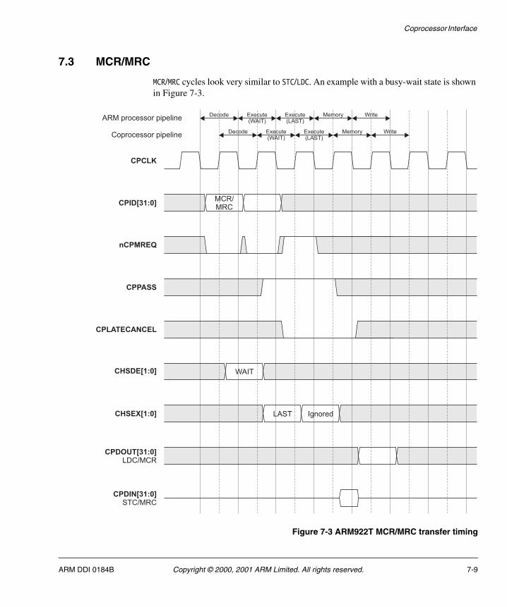
Coprocessor Interface
7.3 MCR/MRC
MCR/MRC cycles look very similar to STC/LDC. An example with a busy-wait state is shown in Figure 7-3.
Figure 7-3 ARM922T MCR/MRC transfer timing
LAST Ignored
WAIT
CPCLK
nCPMREQ
CPID[31:0]
CHSDE[1:0]
CHSEX[1:0]
CPDOUT[31:0]LDC/MCR
CPPASS
CPLATECANCEL
MCR/MRC
CPDIN[31:0]STC/MRC
Decode Execute(WAIT)
Execute(LAST)
Memory Write
Decode Execute(WAIT)
Execute(LAST)
Memory Write
Coprocessor pipeline
ARM processor pipeline
ARM DDI 0184B Copyright © 2000, 2001 ARM Limited. All rights reserved. 7-9
Coprocessor Interface
In Figure 7-3 on page 7-9, first nCPMREQ is driven LOW to denote that the instruction on CPID is entering the Decode stage of the pipeline. The coprocessor decodes the new instruction and drives CHSDE[1:0] as required.
In the next cycle nCPMREQ is driven LOW to denote that the instruction has now been issued to the Execute stage. If the condition codes pass, and the instruction is to be executed, the CPPASS signal is driven HIGH and the CHSDE[1:0] handshake bus is examined (it is ignored in all other cases).
For any successive Execute cycles the CHSEX[1:0] handshake bus is examined. When the LAST condition is observed, the instruction is committed. In the case of an MCR, the CPDOUT[31:0] bus is driven with the register data. In the case of an MRC, CPDIN[31:0] is sampled at the end of the ARM922T Memory stage and written to the destination register during the next cycle.
For an MCR or MRC, with no busy-wait states, the coprocessor drives CHSDE[1:0] with LAST. This commits the instruction for execution in the next cycle. The value on CHSEX[1:0] is ignored.
7-10 Copyright © 2000, 2001 ARM Limited. All rights reserved. ARM DDI 0184B
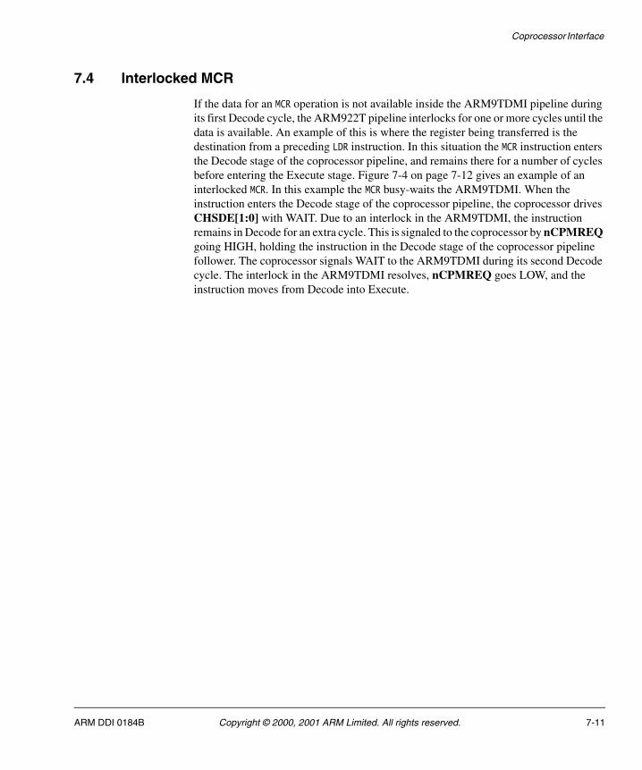
Coprocessor Interface
7.4 Interlocked MCR
If the data for an MCR operation is not available inside the ARM9TDMI pipeline during its first Decode cycle, the ARM922T pipeline interlocks for one or more cycles until the data is available. An example of this is where the register being transferred is the destination from a preceding LDR instruction. In this situation the MCR instruction enters the Decode stage of the coprocessor pipeline, and remains there for a number of cycles before entering the Execute stage. Figure 7-4 on page 7-12 gives an example of an interlocked MCR. In this example the MCR busy-waits the ARM9TDMI. When the instruction enters the Decode stage of the coprocessor pipeline, the coprocessor drives CHSDE[1:0] with WAIT. Due to an interlock in the ARM9TDMI, the instruction remains in Decode for an extra cycle. This is signaled to the coprocessor by nCPMREQ going HIGH, holding the instruction in the Decode stage of the coprocessor pipeline follower. The coprocessor signals WAIT to the ARM9TDMI during its second Decode cycle. The interlock in the ARM9TDMI resolves, nCPMREQ goes LOW, and the instruction moves from Decode into Execute.
ARM DDI 0184B Copyright © 2000, 2001 ARM Limited. All rights reserved. 7-11
Coprocessor Interface
Figure 7-4 ARM922T interlocked MCR
LAST Ignored
WAIT/Ignored
CPCLK
nCPMREQ
CPID[31:0]
CHSDE[1:0]
CHSEX[1:0]
CPDOUT[31:0]LDC/MCR
CPPASS
CPLATECANCEL
MCR/MRC
CPDIN[31:0]STC/MRC
Decode Decode Execute(WAIT)
Execute(LAST)
Memory
Decode(interlock)
Decode Execute(WAIT)
Memory Write
Coprocessor pipeline
ARM processor pipeline
WAIT
Execute(LAST)
Write
7-12 Copyright © 2000, 2001 ARM Limited. All rights reserved. ARM DDI 0184B
Coprocessor Interface
7.5 CDP
CDPs normally execute in a single cycle. Like all other instructions, nCPMREQ is driven LOW to signal when an instruction is entering the Decode and then the Execute stage of the pipeline:
• if the instruction is to be executed, the CPPASS signal is driven HIGH during phase 2 of the Execute stage
• if the coprocessor can execute the instruction immediately it drives CHSDE[1:0] with LAST
• if the instruction requires a busy-wait cycle, the coprocessor drives CHSDE[1:0] with WAIT and then CHSEX[1:0] with LAST.
Figure 7-5 on page 7-14 shows a CDP that is canceled due to the previous instruction causing a Data Abort. The CDP instruction enters the Execute stage of the pipeline, and is signaled to execute by CPPASS. In the following phase CPLATECANCEL is asserted. This causes the coprocessor to terminate execution of the CDP instruction, and for it to cause no state changes to the coprocessor.
ARM DDI 0184B Copyright © 2000, 2001 ARM Limited. All rights reserved. 7-13
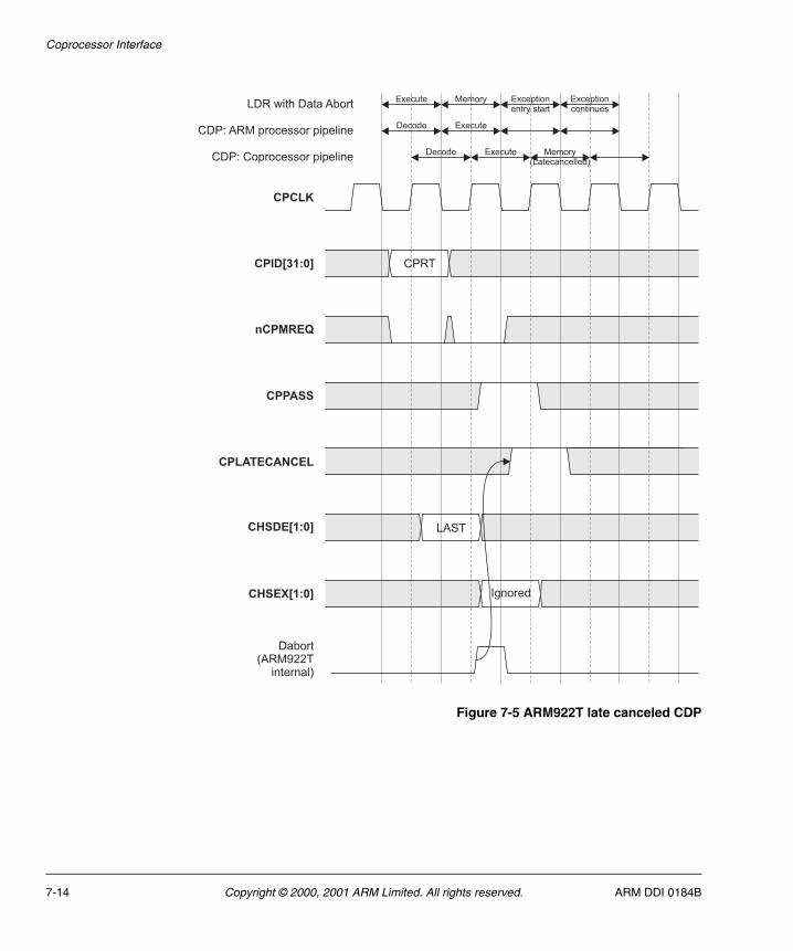
Coprocessor Interface
Figure 7-5 ARM922T late canceled CDP
Ignored
LAST
CPCLK
nCPMREQ
CPID[31:0]
CHSDE[1:0]
CHSEX[1:0]
CPPASS
CPLATECANCEL
CPRT
Dabort(ARM922T
internal)
Decode Execute Memory(Latecancelled)
Decode Execute
CDP: Coprocessor pipeline
CDP: ARM processor pipeline
Execute Memory Exceptionentry start
ExceptioncontinuesLDR with Data Abort
7-14 Copyright © 2000, 2001 ARM Limited. All rights reserved. ARM DDI 0184B
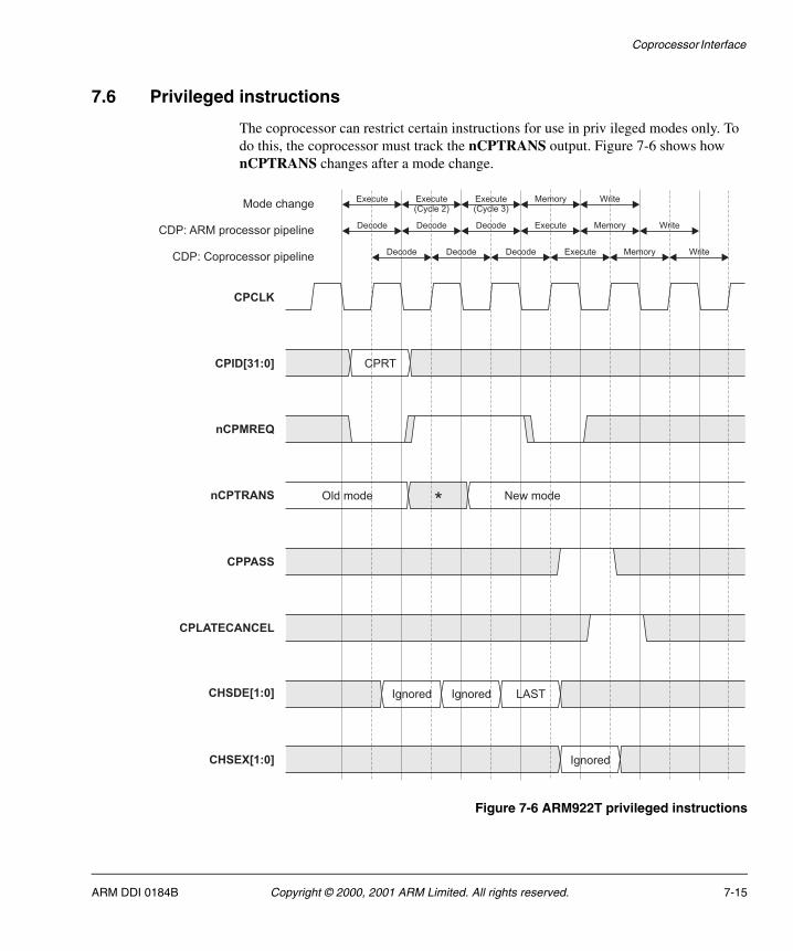
Coprocessor Interface
7.6 Privileged instructions
The coprocessor can restrict certain instructions for use in priv ileged modes only. To do this, the coprocessor must track the nCPTRANS output. Figure 7-6 shows how nCPTRANS changes after a mode change.
Figure 7-6 ARM922T privileged instructions
Ignored
Ignored
CPCLK
nCPMREQ
CPID[31:0]
CHSDE[1:0]
CHSEX[1:0]
CPPASS
CPLATECANCEL
CPRT
Decode Decode Decode Execute Memory
Decode Decode Decode Memory Write
CDP: Coprocessor pipeline
CDP: ARM processor pipeline
Ignored
Execute
Write
nCPTRANS Old mode New mode
LAST
Execute Execute(Cycle 2)
Execute(Cycle 3)
WriteMode change
Memory
*
ARM DDI 0184B Copyright © 2000, 2001 ARM Limited. All rights reserved. 7-15
Coprocessor Interface
In Figure 7-6 on page 7-15 the mode change (marked with an asterisk) occurs as follows:
• For mode changes that do not use an MSR. The mode changes after the first execute cycle.
• For mode changes that use an MSR. The mode changes after the second execute cycle.
Note The first two CHSDE[1:0] responses are ignored by the ARM922T because it is only the final CHSDE[1:0] response, as the instruction moves from Decode into Execute, that is relevant. This allows the coprocessor to change its response as nCPTRANS changes.
7-16 Copyright © 2000, 2001 ARM Limited. All rights reserved. ARM DDI 0184B
Coprocessor Interface
7.7 Busy-waiting and interrupts
The coprocessor is permitted to stall (or busy-wait) the processor during the execution of a coprocessor instruction if, for example, it is still busy with an earlier coprocessor instruction. To do so, the coprocessor associated with the Decode stage instruction must drive WAIT in CHSDE[1:0]. When the instruction concerned enters the Execute stage of the pipeline, the coprocessor can drive WAIT onto CHSEX[1:0] for as many cycles as required to keep the instruction in the busy-wait loop.
For interrupt latency reasons the coprocessor can be interrupted while busy-waiting, causing the instruction to be abandoned. Abandoning execution is achieved through CPPASS. The coprocessor must monitor the state of CPPASS during every busy-wait cycle. If it is HIGH, the instruction must still be executed. If it is LOW, the instruction must be abandoned. Figure 7-7 on page 7-18 shows a busy-waited coprocessor instruction being abandoned due to an interrupt.
ARM DDI 0184B Copyright © 2000, 2001 ARM Limited. All rights reserved. 7-17
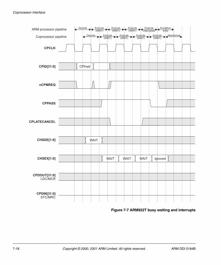
Coprocessor Interface
Figure 7-7 ARM922T busy waiting and interrupts
WAIT WAIT
WAIT
CPCLK
nCPMREQ
CPID[31:0]
CHSDE[1:0]
CHSEX[1:0]
CPDOUT[31:0]LDC/MCR
CPPASS
CPLATECANCEL
CPInstr
CPDIN[31:0]STC/MRC
Decode Execute(WAIT)
Execute(WAIT)
Execute(WAIT)
Execute(WAIT)
Decode Execute(WAIT)
Execute(WAIT)
Execute(WAIT)
Executeinterrupted
Coprocessor pipeline
ARM processor pipeline
WAIT Ignored
Exceptionentry
Abandoned
7-18 Copyright © 2000, 2001 ARM Limited. All rights reserved. ARM DDI 0184B
Chapter 8 Trace Interface Port
This chapter gives a brief description of the Embedded Trace Macrocell (ETM) support for the ARM922T processor. It contains the following section:
• About the ETM interface on page 8-2.
ARM DDI 0184B Copyright © 2000, 2001 ARM Limited. All rights reserved. 8-1
Trace Interface Port
8.1 About the ETM interface
The ARM922T trace interface port enables simple connection of an ETM9 to an ARM922T Rev 0. The ARM9 Embedded Trace Macrocell (ETM9) provides instruction and data trace for the ARM9TDMI family of processors.
The interface is made up as follows:
• ETMPWRDOWN input to the ARM922T
• ETMCLOCK output to the ETM9
• ETMnWAIT output to the ETM9
• ETM<signal> outputs to the ETM9.
When ETMPWRDOWN is HIGH, the ETMCLOCK output and the ETM<signal> outputs are held stable. When ETMPWRDOWN is LOW, the ETMCLOCK and ETM<signal> outputs are enabled. This enables system power to be reduced when the ETM9 is not used. When the ETM9 is incorporated within a system, the ARM debug tools control ETMPWRDOWN, automatically setting the signal LOW at the start of a debug session. If the ETM9 is not incorporated within a system, then ETMPWRDOWN must be tied HIGH.
The ETMCLOCK output to the ETM9 is used by the ETM9 to sample the ETM<signal> outputs on the rising edge of ETMCLOCK, when ETMnWAIT is HIGH. ETMnWAIT is the nWAIT input signal to the ARM9TDMI, so this allows cycle-accurate tracing using ETMCLOCK. The ETMCLOCK signal is never stretched.
The ETM<signal> outputs are registered so that they can be sampled on the rising edge of ETMCLOCK.
The ETM<signal> timing is shown in Timing definitions for the ARM922T Trace Interface Port on page 13-26 and signal descriptions in ARM922T Trace Interface Port signals on page A-13.
The ETM9 (Rev1) Technical Reference Manual contains details of how to integrate an ETM9 with an ARM922T Rev 0, including the pin correlation.
8-2 Copyright © 2000, 2001 ARM Limited. All rights reserved. ARM DDI 0184B
Chapter 9 Debug Support
This chapter describes the debug support for the ARM922T, including the EmbeddedICE macrocell. It contains the following sections:
• About debug on page 9-2
• Debug systems on page 9-3
• Debug interface signals on page 9-5
• Scan chains and JTAG interface on page 9-11
• The JTAG state machine on page 9-12
• Test data registers on page 9-19
• ARM922T core clocks on page 9-42
• Clock switching during debug on page 9-43
• Clock switching during test on page 9-44
• Determining the core state and system state on page 9-45
• Exit from debug state on page 9-48
• The behavior of the program counter during debug on page 9-51
• EmbeddedICE macrocell on page 9-54
• Vector catching on page 9-62
• Single-stepping on page 9-63
• Debug communications channel on page 9-64.
ARM DDI 0184B Copyright © 2000, 2001 ARM Limited. All rights reserved. 9-1
Debug Support
9.1 About debug
Debug support is implemented using the ARM9TDMI CPU core embedded within the ARM922T. Throughout this chapter therefore, ARM9TDMI refers to this core.
The ARM922T debug interface is based on IEEE Std. 1149.1- 1990, Standard Test Access Port and Boundary-Scan Architecture. See this standard for an explanation of the terms used in this chapter and for a description of the TAP controller states.
The ARM922T contains hardware extensions for advanced debugging features. These are intended to ease the development of application software, operating systems, and the hardware itself.
The debug extensions allow the core to be stopped by one of the following:
• a given instruction fetch (breakpoint)
• a data access (watchpoint)
• asynchronously by a debug request.
When this happens, the ARM922T is said to be in debug state. At this point, you can examine the internal state of the core and the external state of the system. When examination is complete, you can restore the core and system state and resume program execution.
The ARM922T is forced into debug state either by a request on one of the external debug interface signals, or by an internal functional unit known as the EmbeddedICE macrocell. When in debug state, the core isolates itself from the memory system. You can then examine the core can while all other system activity continues as normal.
You can examine the internal state of the ARM922T using a JTAG-style serial interface. This allows instructions to be serially inserted into the pipeline of the core without using the external data bus. Therefore, when in debug state, you can insert a store-multiple (STM) into the instruction pipeline to export the contents of the ARM9TDMI registers. This data can be serially shifted out without affecting the rest of the system.
9-2 Copyright © 2000, 2001 ARM Limited. All rights reserved. ARM DDI 0184B
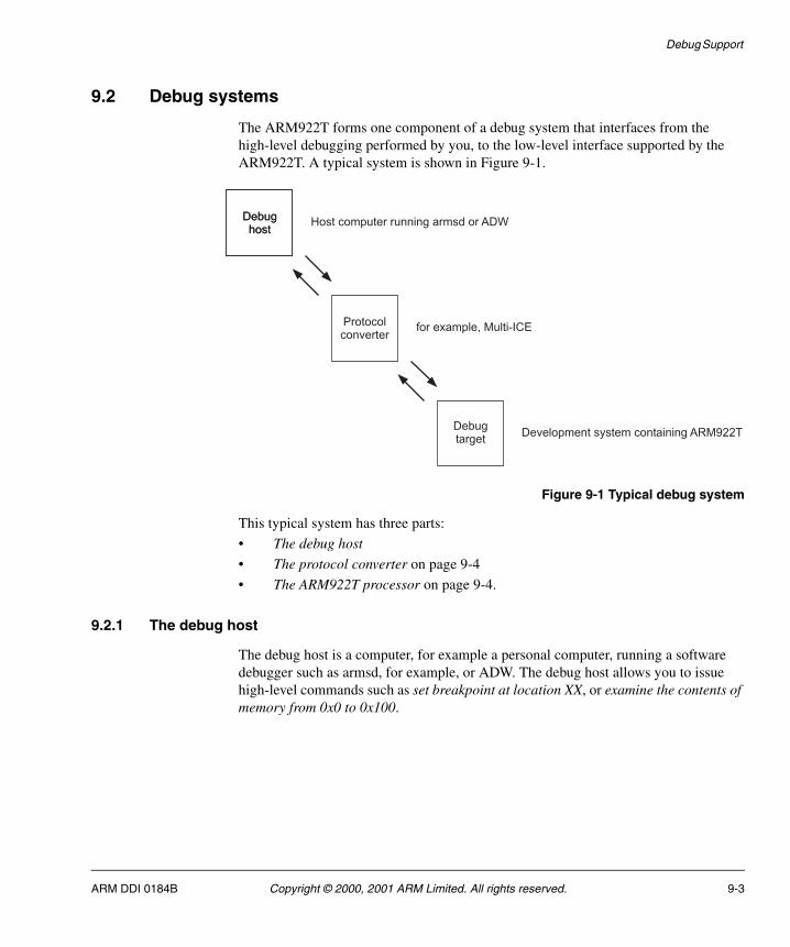
Debug Support
9.2 Debug systems
The ARM922T forms one component of a debug system that interfaces from the high-level debugging performed by you, to the low-level interface supported by the ARM922T. A typical system is shown in Figure 9-1.
Figure 9-1 Typical debug system
This typical system has three parts:
• The debug host
• The protocol converter on page 9-4
• The ARM922T processor on page 9-4.
9.2.1 The debug host
The debug host is a computer, for example a personal computer, running a software debugger such as armsd, for example, or ADW. The debug host allows you to issue high-level commands such as set breakpoint at location XX, or examine the contents of memory from 0x0 to 0x100.
Host computer running armsd or ADWDebughost
Protocolconverter
Debughost
Debugtarget
for example, Multi-ICE
Development system containing ARM922T
ARM DDI 0184B Copyright © 2000, 2001 ARM Limited. All rights reserved. 9-3
Debug Support
9.2.2 The protocol converter
The debug host is connected to the ARM922T development system using an interface (an RS232, for example). The messages broadcast over this connection must be converted to the interface signals of the ARM922T. This function is performed by a protocol converter, for example, Multi-ICE.
9.2.3 The ARM922T processor
The ARM922T processor, with hardware debug extensions, is the lowest level of the system. The debug extensions allow you to:
• stall the core from program execution
• examine its internal state and the state of the memory system
• resume program execution.
The debug host and the protocol converter are system-dependent.
9-4 Copyright © 2000, 2001 ARM Limited. All rights reserved. ARM DDI 0184B
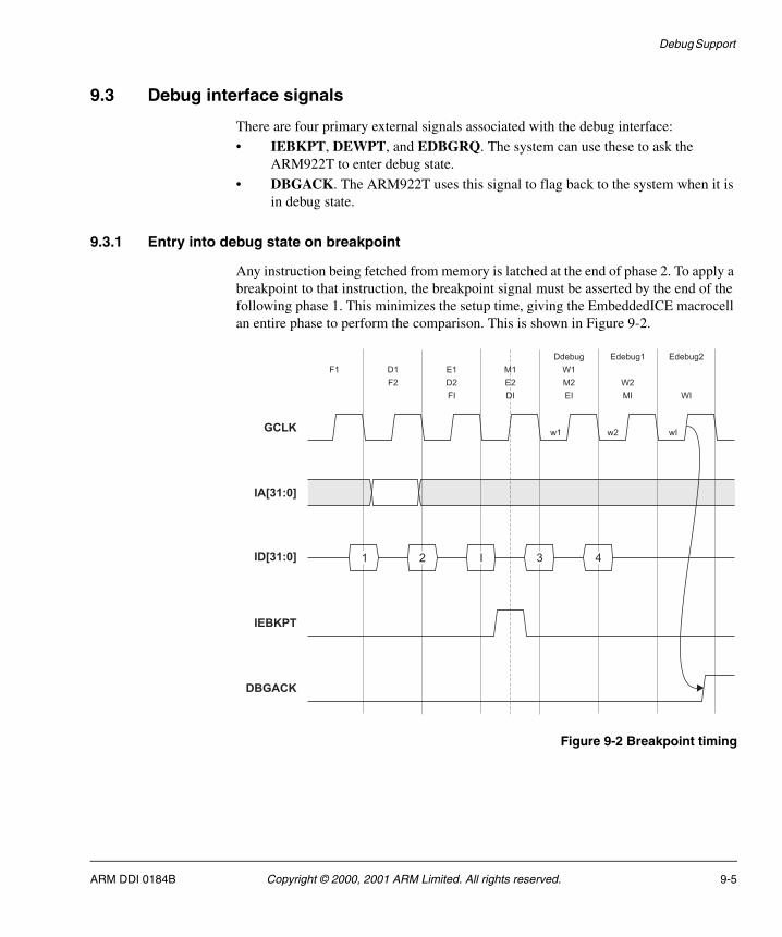
Debug Support
9.3 Debug interface signals
There are four primary external signals associated with the debug interface:
• IEBKPT, DEWPT, and EDBGRQ. The system can use these to ask the ARM922T to enter debug state.
• DBGACK. The ARM922T uses this signal to flag back to the system when it is in debug state.
9.3.1 Entry into debug state on breakpoint
Any instruction being fetched from memory is latched at the end of phase 2. To apply a breakpoint to that instruction, the breakpoint signal must be asserted by the end of the following phase 1. This minimizes the setup time, giving the EmbeddedICE macrocell an entire phase to perform the comparison. This is shown in Figure 9-2.
Figure 9-2 Breakpoint timing
GCLK
IA[31:0]
IEBKPT
DBGACK
w1
D1 E1
Edebug2Edebug1Ddebug
ID[31:0] 1 I 42 3
w2 wI
M1 W1F1
F2 D2 E2 M2 W2
FI DI EI MI WI
ARM DDI 0184B Copyright © 2000, 2001 ARM Limited. All rights reserved. 9-5
Debug Support
You can build external logic, such as additional breakpoint comparators, to extend the functionality of the EmbeddedICE macrocell. You must apply the external logic output to the IEBKPT input. This signal is ORed with the internally generated breakpoint signal before being applied to the ARM922T core control logic.
A breakpointed instruction is allowed to enter the Execute stage of the pipeline, but any state change as a result of the instruction is prevented. All writes from previous instructions complete as normal.
The Decode cycle of the debug entry sequence occurs during the Execute cycle of the breakpointed instruction. The latched breakpoint signal forces the processor to start the debug sequence.
9.3.2 Breakpoints and exceptions
A breakpointed instruction might have a Prefetch Abort associated with it. If so, the Prefetch Abort takes priority and the breakpoint is ignored. (If there is a Prefetch Abort, instruction data might be invalid, the breakpoint might have been data-dependent, and as the data might be incorrect, the breakpoint might have been triggered incorrectly.)
SWI and undefined instructions are treated in the same way as any other instruction that might have a breakpoint set on it. Therefore, the breakpoint takes priority over the SWI or undefined instruction.
On an instruction boundary, if there is a breakpointed instruction and an interrupt (IRQ or FIQ), the interrupt is taken and the breakpointed instruction is discarded. When the interrupt has been serviced, the execution flow is returned to the original program. This means that the instruction that has been breakpointed is fetched again, and if the breakpoint is still set, the processor enters debug state when it reaches the Execute stage of the pipeline.
When the processor has entered debug state, it is important that additional interrupts do not affect the instructions executed. For this reason, as soon as the processor enters debug state, interrupts are disabled, although the state of the I and F bits in the Program Status Register (PSR) are not affected.
9-6 Copyright © 2000, 2001 ARM Limited. All rights reserved. ARM DDI 0184B
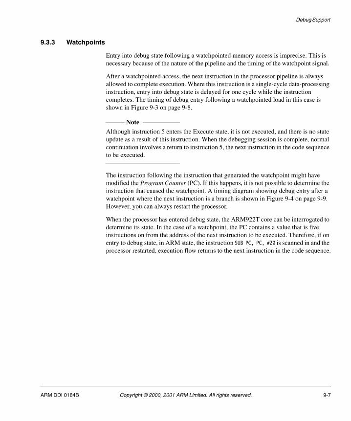
Debug Support
9.3.3 Watchpoints
Entry into debug state following a watchpointed memory access is imprecise. This is necessary because of the nature of the pipeline and the timing of the watchpoint signal.
After a watchpointed access, the next instruction in the processor pipeline is always allowed to complete execution. Where this instruction is a single-cycle data-processing instruction, entry into debug state is delayed for one cycle while the instruction completes. The timing of debug entry following a watchpointed load in this case is shown in Figure 9-3 on page 9-8.
Note Although instruction 5 enters the Execute state, it is not executed, and there is no state update as a result of this instruction. When the debugging session is complete, normal continuation involves a return to instruction 5, the next instruction in the code sequence to be executed.
The instruction following the instruction that generated the watchpoint might have modified the Program Counter (PC). If this happens, it is not possible to determine the instruction that caused the watchpoint. A timing diagram showing debug entry after a watchpoint where the next instruction is a branch is shown in Figure 9-4 on page 9-9. However, you can always restart the processor.
When the processor has entered debug state, the ARM922T core can be interrogated to determine its state. In the case of a watchpoint, the PC contains a value that is five instructions on from the address of the next instruction to be executed. Therefore, if on entry to debug state, in ARM state, the instruction SUB PC, PC, #20 is scanned in and the processor restarted, execution flow returns to the next instruction in the code sequence.
ARM DDI 0184B Copyright © 2000, 2001 ARM Limited. All rights reserved. 9-7
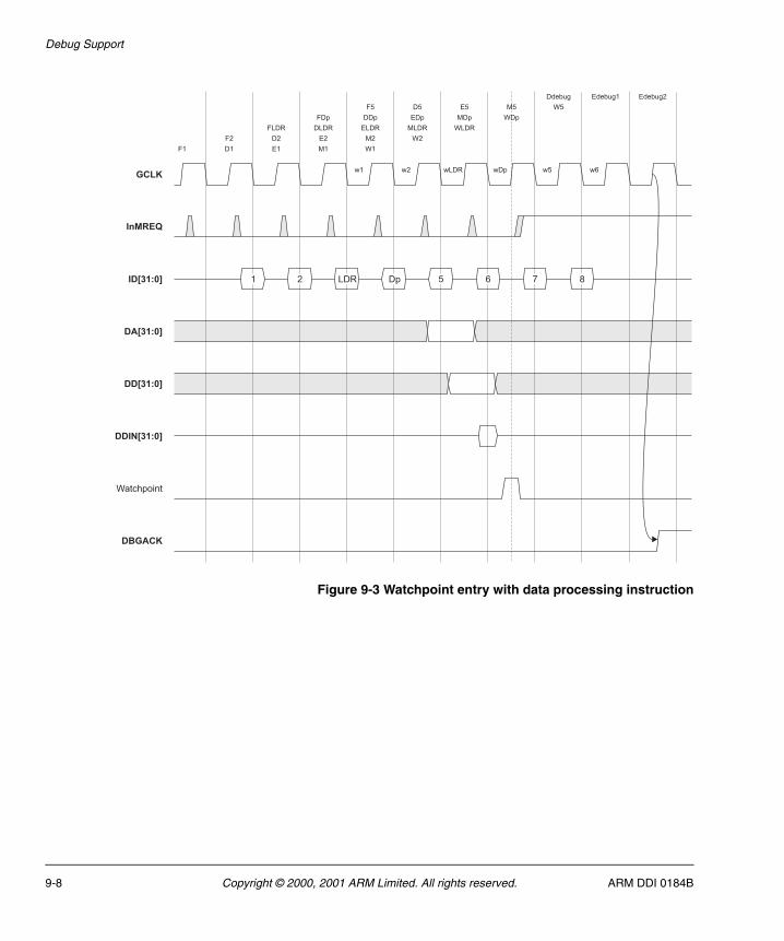
Debug Support
Figure 9-3 Watchpoint entry with data processing instruction
DD[31:0]
GCLK
InMREQ
ID[31:0]
DA[31:0]
1 2 LDR Dp 5 6 7 8
DDIN[31:0]
Watchpoint
DBGACK
E1F1 D1 W1M1
D2F2 M2E2
ELDRFLDR DLDR WLDRMLDR
DDpFDp MDpEDp
E5F5 D5 W5M5
W2
WDp
Ddebug Edebug2Edebug1
wLDRw1 w2 w5wDp w6
9-8 Copyright © 2000, 2001 ARM Limited. All rights reserved. ARM DDI 0184B
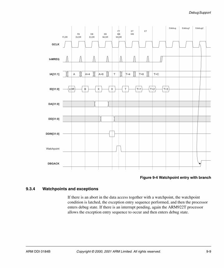
Debug Support
Figure 9-4 Watchpoint entry with branch
9.3.4 Watchpoints and exceptions
If there is an abort in the data access together with a watchpoint, the watchpoint condition is latched, the exception entry sequence performed, and then the processor enters debug state. If there is an interrupt pending, again the ARM922T processor allows the exception entry sequence to occur and then enters debug state.
DD[31:0]
GCLK
InMREQ
IA[31:1]
DA[31:0]
A+4 T T+8
DDIN[31:0]
Watchpoint
DBGACK
ELDRFLDR DLDR WLDRMLDR
DBFB MBEB
FT ETDT
Ddebug
WB
Edebug1
A A+8 T+4 T+C
ID[31:0] LDR B X X T T+1 T+2 T+3
Edebug2
ARM DDI 0184B Copyright © 2000, 2001 ARM Limited. All rights reserved. 9-9
Debug Support
9.3.5 Debug request
A debug request can take place through the EmbeddedICE macrocell or by asserting the EDBGRQ signal. The request is synchronized and passed to the processor. Debug request takes priority over any pending interrupt. Following synchronization, the core enters debug state when the instruction at the Execute stage of the pipeline has completely finished executing (when Memory and Write stages of the pipeline have completed). While waiting for the instruction to finish executing, no more instructions are issued to the Execute stage of the pipeline.
9.3.6 Actions of the ARM922T in debug state
When the ARM922T is in debug state, both memory interfaces indicate internal cycles. This allows the rest of the memory system to ignore the ARM9TDMI core and function as normal. Because the rest of the system continues operation, the ARM9TDMI core ignores aborts and interrupts.
The BIGEND signal must not be changed by the system while in debug state. If it changes there might be a synchronization problem, and the ARM922T processor (as seen by the programmer) changes without the knowledge of the debugger. The BnRES signal must also be held stable during debug. If the system applies reset to the ARM922T processor (BnRES is driven LOW), the state of the ARM922T changes without the knowledge of the debugger.
When instructions are executed in debug state, the ARM9TDMI core changes asynchronously to the memory system outputs (except for InMREQ, ISEQ, DnMREQ, and DSEQ that change synchronously from GCLK). For example, every time a new instruction is scanned into the pipeline, the instruction address bus changes. If the instruction is a load or store operation, the data address bus changes as the instruction executes. Although this is asynchronous, it does not affect the system, because both interfaces indicate internal cycles. You must take care when designing the memory controller to ensure that this does not become a problem.
9-10 Copyright © 2000, 2001 ARM Limited. All rights reserved. ARM DDI 0184B
Debug Support
9.4 Scan chains and JTAG interface
There are six scan chains inside the ARM922T processor. These allow testing, debugging, and programming of the EmbeddedICE macrocell watchpoint units. The scan chains are controlled by a JTAG-style Test Access Port (TAP) controller. In addition, support is provided for an optional seventh scan chain. This is intended to be used for an external boundary scan chain around the pads of a packaged device. The signals provided for this scan chain are described in Scan chain 3 on page 9-30.
The six scan chains of the ARM922Tprocessor are called scan chain 0, 1, 2, 3, 4, and 15.
Note The ARM922T TAP controller supports 32 scan chains. Scan chains 0 to 15 have been reserved for use by ARM. Any extension scan chains must be implemented in the remaining space. The SCREG[4:0] signals indicate the scan chain being accessed.
ARM DDI 0184B Copyright © 2000, 2001 ARM Limited. All rights reserved. 9-11
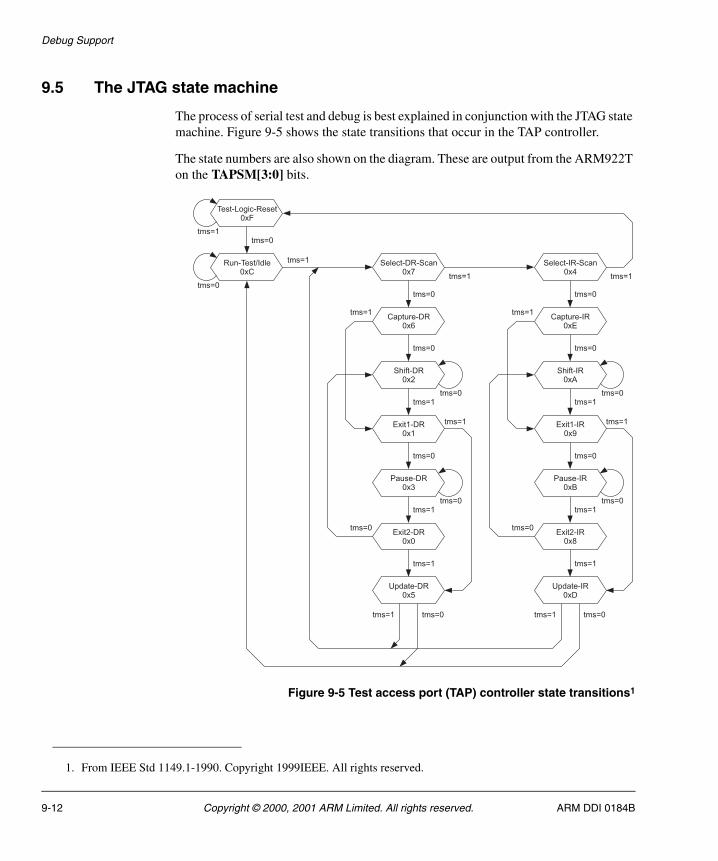
Debug Support
9.5 The JTAG state machine
The process of serial test and debug is best explained in conjunction with the JTAG state machine. Figure 9-5 shows the state transitions that occur in the TAP controller.
The state numbers are also shown on the diagram. These are output from the ARM922T on the TAPSM[3:0] bits.
Figure 9-5 Test access port (TAP) controller state transitions1
1. From IEEE Std 1149.1-1990. Copyright 1999IEEE. All rights reserved.
Select-DR-Scan0x7
Capture-DR0x6
Shift-DR0x2
Exit1-DR0x1
Pause-DR0x3
Exit2-DR0x0
Update-DR0x5
Run-Test/Idle0xC
Test-Logic-Reset0xF
tms=0
tms=0
tms=1
tms=0
tms=1
tms=1
Select-IR-Scan0x4
Capture-IR0xE
Shift-IR0xA
Exit1-IR0x9
Pause-IR0xB
Exit2-IR0x8
Update-IR0xD
tms=0
tms=0
tms=1
tms=0
tms=1
tms=1
tms=0 tms=0
tms=0 tms=0
tms=1
tms=0
tms=1tms=0
tms=1
tms=1
tms=0
tms=1 tms=1
tms=1 tms=0 tms=1 tms=0
tms=1
tms=1
tms=0
9-12 Copyright © 2000, 2001 ARM Limited. All rights reserved. ARM DDI 0184B
Debug Support
9.5.1 Reset
The JTAG interface includes a state-machine controller, the TAP controller. To force the TAP controller into the correct state after power-up of the device, a reset pulse must be applied to the nTRST signal, or the JTAG state machine must be cycled through the test logic reset state. Before the JTAG interface can be used, nTRST must be driven LOW, and then HIGH again. If you do not intend using the boundary scan interface, you can tie the nTRST input permanently LOW.
Note A clock on TCK is not required to reset the device.
The action of reset is as follows:
1. System mode is selected. The boundary scan chain cells do not intercept any of the signals passing between the external system and the core.
2. The IDCODE instruction is selected. If the TAP controller is put into the SHIFT-DR state and TCK is pulsed, the contents of the ID register are clocked out of TDO.
9.5.2 Pullup resistors
The IEEE 1149.1 standard effectively requires TDI and TMS to have internal pullup resistors. In order to minimize static current draw, these resistors are not fitted to the ARM9TDMI core. Accordingly, the four inputs to the test interface (the TDO, TDI, and TMS signals, plus TCK) must all be driven to valid logic levels to achieve normal circuit operation.
9.5.3 Instruction register
The instruction register is four bits in length. There is no parity bit. The fixed value loaded into the instruction register during the CAPTURE-IR controller state is 0001.
ARM DDI 0184B Copyright © 2000, 2001 ARM Limited. All rights reserved. 9-13
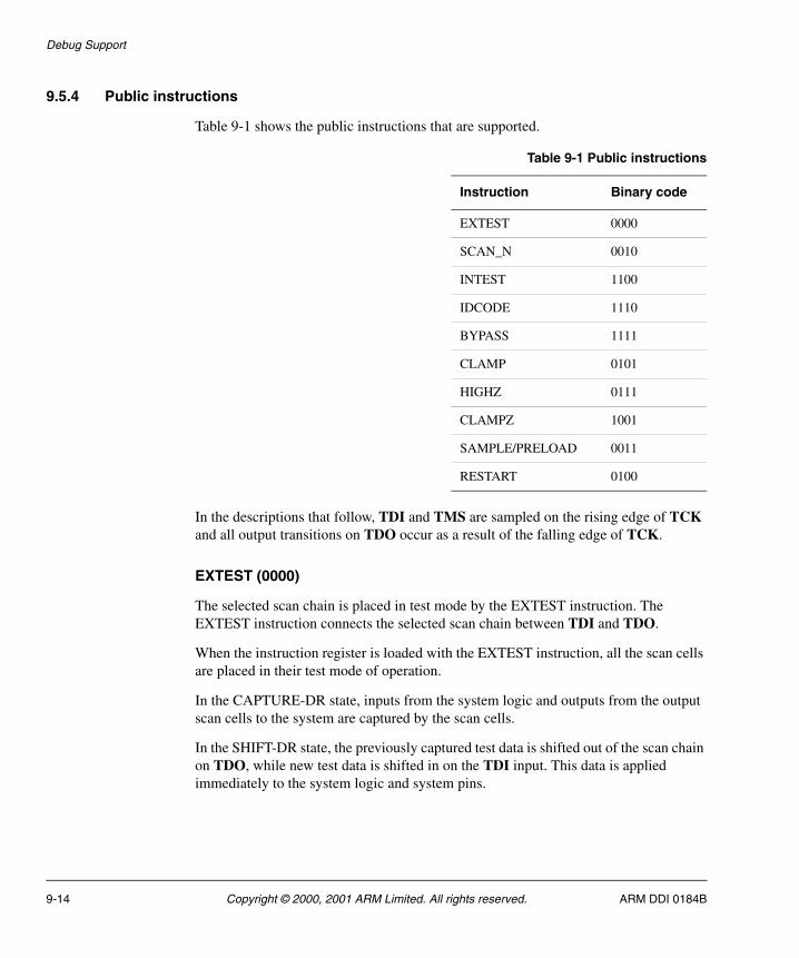
Debug Support
9.5.4 Public instructions
Table 9-1 shows the public instructions that are supported.
In the descriptions that follow, TDI and TMS are sampled on the rising edge of TCK and all output transitions on TDO occur as a result of the falling edge of TCK.
EXTEST (0000)
The selected scan chain is placed in test mode by the EXTEST instruction. The EXTEST instruction connects the selected scan chain between TDI and TDO.
When the instruction register is loaded with the EXTEST instruction, all the scan cells are placed in their test mode of operation.
In the CAPTURE-DR state, inputs from the system logic and outputs from the output scan cells to the system are captured by the scan cells.
In the SHIFT-DR state, the previously captured test data is shifted out of the scan chain on TDO, while new test data is shifted in on the TDI input. This data is applied immediately to the system logic and system pins.
Table 9-1 Public instructions
Instruction Binary code
EXTEST 0000
SCAN_N 0010
INTEST 1100
IDCODE 1110
BYPASS 1111
CLAMP 0101
HIGHZ 0111
CLAMPZ 1001
SAMPLE/PRELOAD 0011
RESTART 0100
9-14 Copyright © 2000, 2001 ARM Limited. All rights reserved. ARM DDI 0184B
Debug Support
SCAN_N (0010)
This instruction connects the scan path select register between TDI and TDO.
During the CAPTURE-DR state, the fixed value 10000 is loaded into the register.
During the SHIFT-DR state, the ID number of the desired scan path is shifted into the scan path select register.
In the UPDATE-DR state, the scan register of the selected scan chain is connected between TDI and TDO, and remains connected until a subsequent SCAN_N instruction is issued. On reset, scan chain 3 is selected by default. The scan path select register is five bits long in this implementation, although no finite length is specified.
INTEST (1100)
The selected scan chain is placed in test mode by the INTEST instruction. The INTEST instruction connects the selected scan chain between TDI and TDO.
When the instruction register is loaded with the INTEST instruction, all the scan cells are placed in their test mode of operation.
In the CAPTURE-DR state, the value of the data applied from the core logic to the output scan cells, and the value of the data applied from the system logic to the input scan cells is captured.
In the SHIFT-DR state, the previously captured test data is shifted out of the scan chain on the TDO pin, while new test data is shifted in on the TDI pin.
IDCODE (1110)
The IDCODE instruction connects the device identification register (or ID register) between TDI and TDO. The ID register is a 32-bit register that allows the manufacturer, part number, and version of a component to be determined through the TAP. The ID register is loaded from the TAPID[31:0] input bus. This must be tied to a constant value that represents the unique JTAG IDCODE for the device.
When the instruction register is loaded with the IDCODE instruction, all the scan cells are placed in their normal (system) mode of operation.
In the CAPTURE-DR state, the device identification code is captured by the ID register.
In the SHIFT-DR state, the previously captured device identification code is shifted out of the ID register on the TDO pin, while data is shifted in on the TDI pin into the ID register.
In the UPDATE-DR state, the ID register is unaffected.
ARM DDI 0184B Copyright © 2000, 2001 ARM Limited. All rights reserved. 9-15
Debug Support
BYPASS (1111)
The BYPASS instruction connects a 1-bit shift register (the bypass register) between TDI and TDO.
When the BYPASS instruction is loaded into the instruction register, all the scan cells are placed in their normal (system) mode of operation. This instruction has no effect on the system pins.
In the CAPTURE-DR state, a logic 0 is captured by the bypass register.
In the SHIFT-DR state, test data is shifted into the bypass register on TDI and out on TDO after a delay of one TCK cycle. The first bit shifted out is a zero.
The bypass register is not affected in the UPDATE-DR state.
Note All unused instruction codes default to the BYPASS instruction.
CLAMP (0101)
This instruction connects a 1-bit shift register (the bypass register) between TDI and TDO.
When the CLAMP instruction is loaded into the instruction register, the state of all the output signals is defined by the values previously loaded into the currently-loaded scan chain.
Note This instruction must only be used when scan chain 0 is the currently selected scan chain.
In the CAPTURE-DR state, a logic 0 is captured by the bypass register.
In the SHIFT-DR state, test data is shifted into the bypass register on TDI and out on TDO after a delay of one TCK cycle. The first bit shifted out is a zero.
The bypass register is not affected in the UPDATE-DR state.
9-16 Copyright © 2000, 2001 ARM Limited. All rights reserved. ARM DDI 0184B
Debug Support
HIGHZ (0111)
This instruction connects a 1-bit shift register (the bypass register) between TDI and TDO.
When the HIGHZ instruction is loaded into the instruction register and scan chain 0 is selected, all ARM922T outputs are driven to the high impedance state and the external HIGHZ signal is driven HIGH. This is as if the signal TBE had been driven LOW.
In the CAPTURE-DR state, a logic 0 is captured by the bypass register. In the SHIFT-DR state, test data is shifted into the bypass register on TDI and out on TDO after a delay of one TCK cycle. The first bit shifted out is a zero.
The bypass register is not affected in the UPDATE-DR state.
CLAMPZ (1001)
This instruction connects a 1-bit shift register (the bypass register) between TDI and TDO.
When the CLAMPZ instruction is loaded into the instruction register and scan chain 0 is selected, all the 3-state outputs (as described above) are placed in their inactive state, but the data supplied to the outputs is derived from the scan cells. The purpose of this instruction is to ensure that, during production test, each output can be disabled when its data value is either a logic 0 or logic 1.
In the CAPTURE-DR state, a logic 0 is captured by the bypass register.
In the SHIFT-DR state, test data is shifted into the bypass register on TDI and out on TDO after a delay of one TCK cycle. The first bit shifted out is a zero.
The bypass register is not affected in the UPDATE-DR state.
SAMPLE/PRELOAD (0011)
When the instruction register is loaded with the SAMPLE/PRELOAD instruction, all the scan cells of the selected scan chain are placed in the normal mode of operation.
In the CAPTURE-DR state, a snapshot of the signals of the boundary scan is taken on the rising edge of TCK. Normal system operation is unaffected.
In the SHIFT-DR state, the sampled test data is shifted out of the boundary scan on the TDO pin, while new data is shifted in on the TDI pin to preload the boundary scan parallel input latch. This data is not applied to the system logic or system pins while the SAMPLE/PRELOAD instruction is active.
ARM DDI 0184B Copyright © 2000, 2001 ARM Limited. All rights reserved. 9-17
Debug Support
This instruction must be used to preload the boundary scan register with known data prior to selecting INTEST or EXTEST instructions.
RESTART (0100)
This instruction is used to restart the processor on exit from debug state. The RESTART instruction connects the bypass register between TDI and TDO and the TAP controller behaves as if the BYPASS instruction is loaded. The processor resynchronizes back to the memory system when the RUN-TEST/IDLE state is entered.
9-18 Copyright © 2000, 2001 ARM Limited. All rights reserved. ARM DDI 0184B
Debug Support
9.6 Test data registers
You can connect the following test data registers between TDI and TDO:
• Bypass register
• ARM922T device identification (ID) code register
• Instruction register on page 9-20
• Scan chain select register on page 9-20
• Scan chains 0, 1, 2, and 3 on page 9-24
• Scan chain 6 on page 9-31
• Scan chains 4 and 15, the ARM922T memory system on page 9-31.
9.6.1 Bypass register
Purpose Bypasses the device during scan testing by providing a path between TDI and TDO.
Length 1 bit.
Operating mode When the BYPASS instruction is the current instruction in the instruction register, serial data is transferred from TDI to TDO in the SHIFT-DR state with a delay of one TCK cycle. There is no parallel output from the bypass register. A logic 0 is loaded from the parallel input of the bypass register in CAPTURE-DR state.
9.6.2 ARM922T device identification (ID) code register
Purpose Reads the 32-bit device identification code. No programmable supplementary identification code is provided.
Length 32 bits.
Operating mode When the IDCODE instruction is current, the ID register is selected as the serial path between TDI and TDO. There is no parallel output from the ID register. The 32-bit identification code is loaded into the register from the parallel inputs of the TAPID[31:0] input bus during the CAPTURE-DR state.
ARM DDI 0184B Copyright © 2000, 2001 ARM Limited. All rights reserved. 9-19
Debug Support
The IEEE format of the ID register is shown in Table 9-2.
The TAPID[31:0] pins allow you to set this value when the macrocell is instantiated in a design.
9.6.3 Instruction register
Purpose Changes the current TAP instruction.
Length 4 bits.
Operating mode When in SHIFT-IR state, the instruction register is selected as the serial path between TDI and TDO.
During the CAPTURE-IR state, the value b0001 is loaded into this register. This is shifted out during SHIFT-IR (least significant bit first), while a new instruction is shifted in (least significant bit first). During the UPDATE-IR state, the value in the instruction register becomes the current instruction. On reset, IDCODE becomes the current instruction.
9.6.4 Scan chain select register
Purpose Changes the current active scan chain.
Length 5 bits.
Operating mode After SCAN_N has been selected as the current instruction, when in SHIFT-DR state, the scan chain select register is selected as the serial path between TDI and TDO.
During the CAPTURE-DR state, the value b10000 is loaded into this register. This is shifted out during SHIFT-DR, least significant bit first, while a new value is shifted in, least significant bit first.
Table 9-2 ID code register
Bits Function Value
31:28 Specification revision 0x0
27:12 Product code 0x0922
11:1 Manufacturer Default = 0b11110000111
0 IEEE standard specified 0b1
9-20 Copyright © 2000, 2001 ARM Limited. All rights reserved. ARM DDI 0184B
Debug Support
During the UPDATE-DR state, the value in the register selects a scan chain to become the currently active scan chain. All additional instructions such as INTEST then apply to that scan chain.
The currently selected scan chain only changes when a SCAN_N instruction is executed, or a reset occurs. On reset, scan chain 3 is selected as the active scan chain.
The number of the currently selected scan chain is reflected on the SCREG[4:0] output bus. You can use the TAP controller to drive external scan chains in addition to those within the ARM922T macrocell. The external scan chain must be assigned a number and control signals for it, and can be derived from SCREG[4:0], IR[3:0], TAPSM[3:0], TCK1, and TCK2.
The list of scan chain numbers allocated by ARM are shown in Table 9-3 on page 9-23. An external scan chain can take any other number. The serial data stream applied to the external scan chain is made present on SDIN. The serial data back from the scan chain must be presented to the TAP controller on the SDOUTBS input.
The scan chain present between SDIN and SDOUTBS is connected between TDI and TDO whenever scan chain 3 is selected, or when any of the unassigned scan chain numbers is selected. If there is more than one external scan chain, you must build a multiplexor externally to apply the desired scan chain output to SDOUTBS. You can control the multiplexor by decoding SCREG[4:0]. The structure is shown in Figure 9-6 on page 9-22.
ARM DDI 0184B Copyright © 2000, 2001 ARM Limited. All rights reserved. 9-21
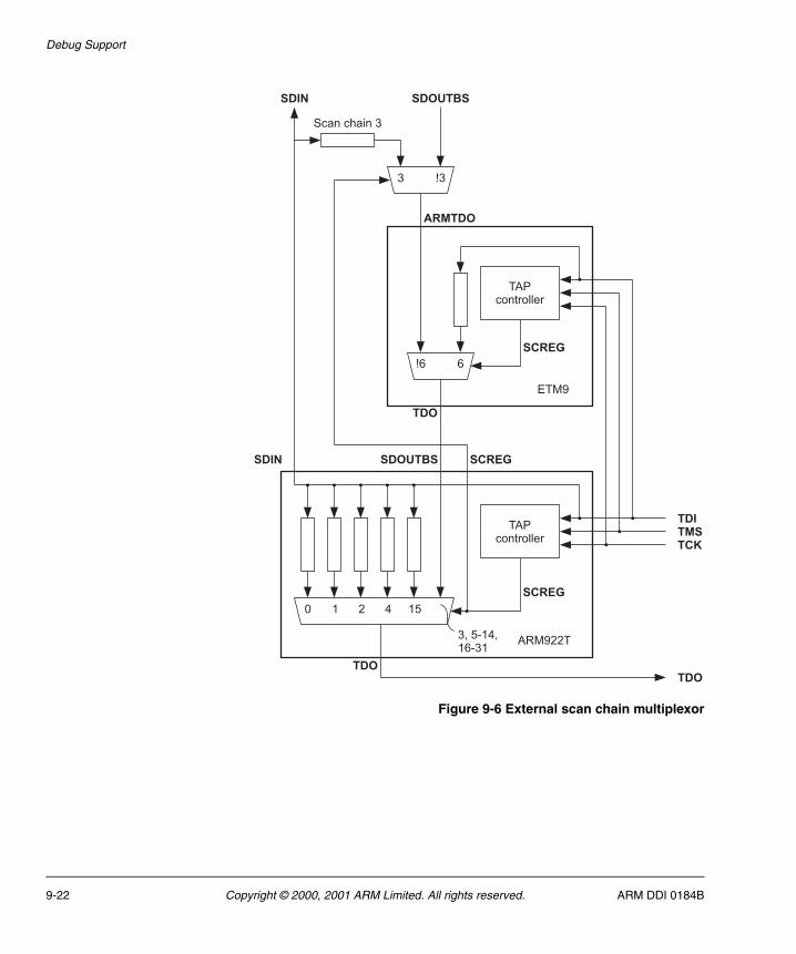
Debug Support
Figure 9-6 External scan chain multiplexor
TAPcontroller
TAPcontroller
TDITMSTCK
SDOUTBS
ARMTDO
SCREG
SCREG
ARM922T
ETM9
TDO
TDO
TDO
6!6
0 1 2 4 15
3, 5-14,16-31
3 !3
SCREG
Scan chain 3
SDOUTBSSDIN
SDIN
9-22 Copyright © 2000, 2001 ARM Limited. All rights reserved. ARM DDI 0184B
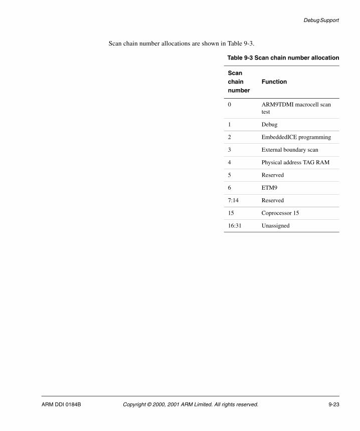
Debug Support
Scan chain number allocations are shown in Table 9-3.
Table 9-3 Scan chain number allocation
Scanchainnumber
Function
0 ARM9TDMI macrocell scan test
1 Debug
2 EmbeddedICE programming
3 External boundary scan
4 Physical address TAG RAM
5 Reserved
6 ETM9
7:14 Reserved
15 Coprocessor 15
16:31 Unassigned
ARM DDI 0184B Copyright © 2000, 2001 ARM Limited. All rights reserved. 9-23
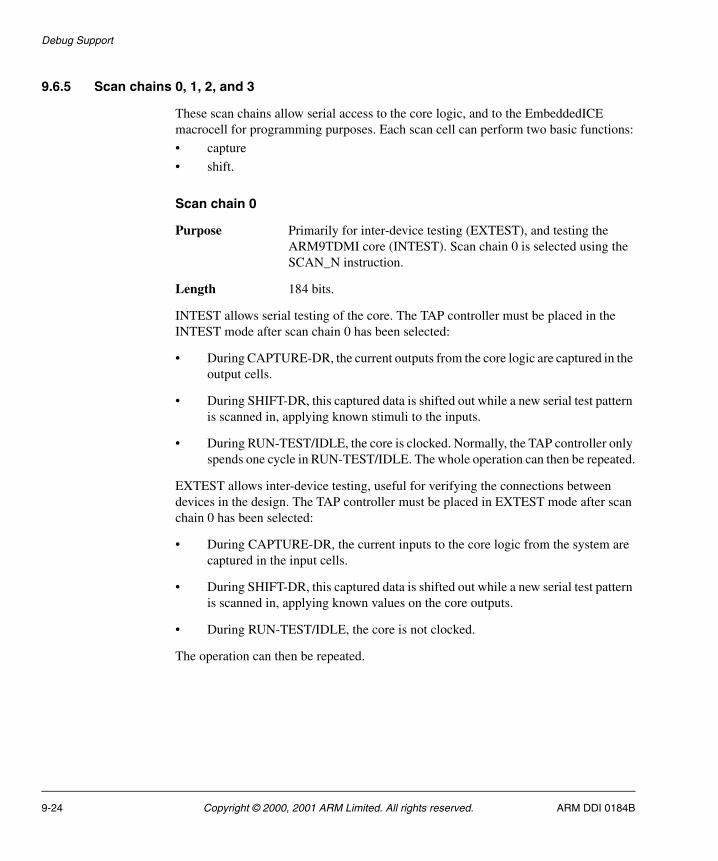
Debug Support
9.6.5 Scan chains 0, 1, 2, and 3
These scan chains allow serial access to the core logic, and to the EmbeddedICE macrocell for programming purposes. Each scan cell can perform two basic functions:
• capture
• shift.
Scan chain 0
Purpose Primarily for inter-device testing (EXTEST), and testing the ARM9TDMI core (INTEST). Scan chain 0 is selected using the SCAN_N instruction.
Length 184 bits.
INTEST allows serial testing of the core. The TAP controller must be placed in the INTEST mode after scan chain 0 has been selected:
• During CAPTURE-DR, the current outputs from the core logic are captured in the output cells.
• During SHIFT-DR, this captured data is shifted out while a new serial test pattern is scanned in, applying known stimuli to the inputs.
• During RUN-TEST/IDLE, the core is clocked. Normally, the TAP controller only spends one cycle in RUN-TEST/IDLE. The whole operation can then be repeated.
EXTEST allows inter-device testing, useful for verifying the connections between devices in the design. The TAP controller must be placed in EXTEST mode after scan chain 0 has been selected:
• During CAPTURE-DR, the current inputs to the core logic from the system are captured in the input cells.
• During SHIFT-DR, this captured data is shifted out while a new serial test pattern is scanned in, applying known values on the core outputs.
• During RUN-TEST/IDLE, the core is not clocked.
The operation can then be repeated.
9-24 Copyright © 2000, 2001 ARM Limited. All rights reserved. ARM DDI 0184B
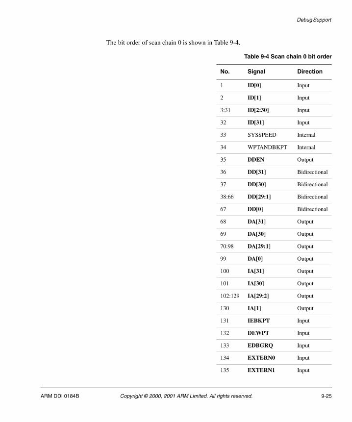
Debug Support
The bit order of scan chain 0 is shown in Table 9-4.
Table 9-4 Scan chain 0 bit order
No. Signal Direction
1 ID[0] Input
2 ID[1] Input
3:31 ID[2:30] Input
32 ID[31] Input
33 SYSSPEED Internal
34 WPTANDBKPT Internal
35 DDEN Output
36 DD[31] Bidirectional
37 DD[30] Bidirectional
38:66 DD[29:1] Bidirectional
67 DD[0] Bidirectional
68 DA[31] Output
69 DA[30] Output
70:98 DA[29:1] Output
99 DA[0] Output
100 IA[31] Output
101 IA[30] Output
102:129 IA[29:2] Output
130 IA[1] Output
131 IEBKPT Input
132 DEWPT Input
133 EDBGRQ Input
134 EXTERN0 Input
135 EXTERN1 Input
ARM DDI 0184B Copyright © 2000, 2001 ARM Limited. All rights reserved. 9-25
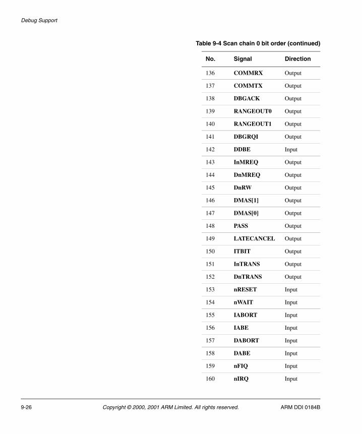
Debug Support
136 COMMRX Output
137 COMMTX Output
138 DBGACK Output
139 RANGEOUT0 Output
140 RANGEOUT1 Output
141 DBGRQI Output
142 DDBE Input
143 InMREQ Output
144 DnMREQ Output
145 DnRW Output
146 DMAS[1] Output
147 DMAS[0] Output
148 PASS Output
149 LATECANCEL Output
150 ITBIT Output
151 InTRANS Output
152 DnTRANS Output
153 nRESET Input
154 nWAIT Input
155 IABORT Input
156 IABE Input
157 DABORT Input
158 DABE Input
159 nFIQ Input
160 nIRQ Input
Table 9-4 Scan chain 0 bit order (continued)
No. Signal Direction
9-26 Copyright © 2000, 2001 ARM Limited. All rights reserved. ARM DDI 0184B
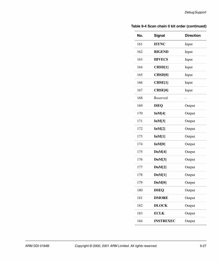
Debug Support
161 ISYNC Input
162 BIGEND Input
163 HIVECS Input
164 CHSD[1] Input
165 CHSD[0] Input
166 CHSE[1] Input
167 CHSE[0] Input
168 Reserved -
169 ISEQ Output
170 InM[4] Output
171 InM[3] Output
172 InM[2] Output
173 InM[1] Output
174 InM[0] Output
175 DnM[4] Output
176 DnM[3] Output
177 DnM[2] Output
178 DnM[1] Output
179 DnM[0] Output
180 DSEQ Output
181 DMORE Output
182 DLOCK Output
183 ECLK Output
184 INSTREXEC Output
Table 9-4 Scan chain 0 bit order (continued)
No. Signal Direction
ARM DDI 0184B Copyright © 2000, 2001 ARM Limited. All rights reserved. 9-27
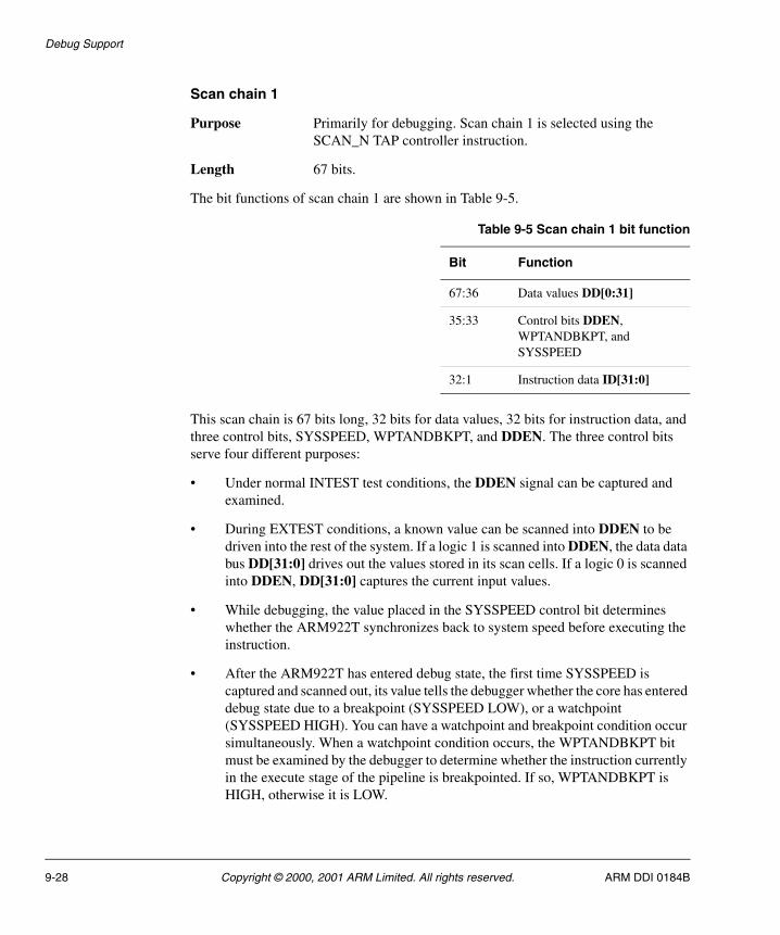
Debug Support
Scan chain 1
Purpose Primarily for debugging. Scan chain 1 is selected using the SCAN_N TAP controller instruction.
Length 67 bits.
The bit functions of scan chain 1 are shown in Table 9-5.
This scan chain is 67 bits long, 32 bits for data values, 32 bits for instruction data, and three control bits, SYSSPEED, WPTANDBKPT, and DDEN. The three control bits serve four different purposes:
• Under normal INTEST test conditions, the DDEN signal can be captured and examined.
• During EXTEST conditions, a known value can be scanned into DDEN to be driven into the rest of the system. If a logic 1 is scanned into DDEN, the data data bus DD[31:0] drives out the values stored in its scan cells. If a logic 0 is scanned into DDEN, DD[31:0] captures the current input values.
• While debugging, the value placed in the SYSSPEED control bit determines whether the ARM922T synchronizes back to system speed before executing the instruction.
• After the ARM922T has entered debug state, the first time SYSSPEED is captured and scanned out, its value tells the debugger whether the core has entered debug state due to a breakpoint (SYSSPEED LOW), or a watchpoint (SYSSPEED HIGH). You can have a watchpoint and breakpoint condition occur simultaneously. When a watchpoint condition occurs, the WPTANDBKPT bit must be examined by the debugger to determine whether the instruction currently in the execute stage of the pipeline is breakpointed. If so, WPTANDBKPT is HIGH, otherwise it is LOW.
Table 9-5 Scan chain 1 bit function
Bit Function
67:36 Data values DD[0:31]
35:33 Control bits DDEN, WPTANDBKPT, and SYSSPEED
32:1 Instruction data ID[31:0]
9-28 Copyright © 2000, 2001 ARM Limited. All rights reserved. ARM DDI 0184B
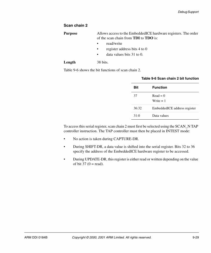
Debug Support
Scan chain 2
Purpose Allows access to the EmbeddedICE hardware registers. The order of the scan chain from TDI to TDO is:
• read/write
• register address bits 4 to 0
• data values bits 31 to 0.
Length 38 bits.
Table 9-6 shows the bit functions of scan chain 2.
To access this serial register, scan chain 2 must first be selected using the SCAN_N TAP controller instruction. The TAP controller must then be placed in INTEST mode:
• No action is taken during CAPTURE-DR.
• During SHIFT-DR, a data value is shifted into the serial register. Bits 32 to 36 specify the address of the EmbeddedICE hardware register to be accessed.
• During UPDATE-DR, this register is either read or written depending on the value of bit 37 (0 = read).
Table 9-6 Scan chain 2 bit function
Bit Function
37 Read = 0
Write = 1
36:32 EmbeddedICE address register
31:0 Data values
ARM DDI 0184B Copyright © 2000, 2001 ARM Limited. All rights reserved. 9-29
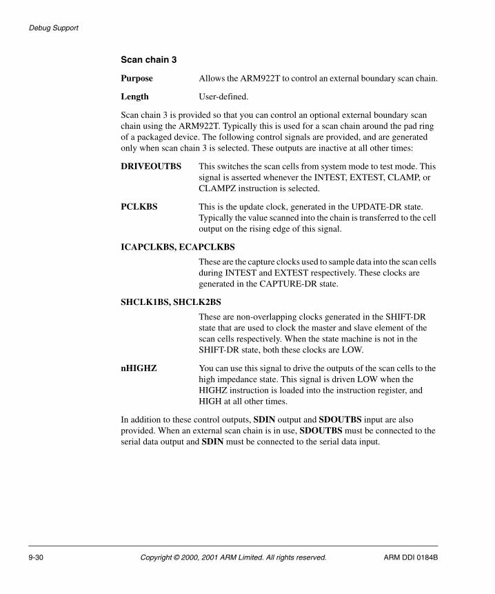
Debug Support
Scan chain 3
Purpose Allows the ARM922T to control an external boundary scan chain.
Length User-defined.
Scan chain 3 is provided so that you can control an optional external boundary scan chain using the ARM922T. Typically this is used for a scan chain around the pad ring of a packaged device. The following control signals are provided, and are generated only when scan chain 3 is selected. These outputs are inactive at all other times:
DRIVEOUTBS This switches the scan cells from system mode to test mode. This signal is asserted whenever the INTEST, EXTEST, CLAMP, or CLAMPZ instruction is selected.
PCLKBS This is the update clock, generated in the UPDATE-DR state. Typically the value scanned into the chain is transferred to the cell output on the rising edge of this signal.
ICAPCLKBS, ECAPCLKBS
These are the capture clocks used to sample data into the scan cells during INTEST and EXTEST respectively. These clocks are generated in the CAPTURE-DR state.
SHCLK1BS, SHCLK2BS
These are non-overlapping clocks generated in the SHIFT-DR state that are used to clock the master and slave element of the scan cells respectively. When the state machine is not in the SHIFT-DR state, both these clocks are LOW.
nHIGHZ You can use this signal to drive the outputs of the scan cells to the high impedance state. This signal is driven LOW when the HIGHZ instruction is loaded into the instruction register, and HIGH at all other times.
In addition to these control outputs, SDIN output and SDOUTBS input are also provided. When an external scan chain is in use, SDOUTBS must be connected to the serial data output and SDIN must be connected to the serial data input.
9-30 Copyright © 2000, 2001 ARM Limited. All rights reserved. ARM DDI 0184B
Debug Support
9.6.6 Scan chain 6
Purpose You use scan chain 6 to program the registers in the ETM9.
Length The chain length is 40 bits, comprising:
• a 32-bit data field
• a 7-bit address field
• a read/write bit.
To write an ETM9 register:
• the data to be written is placed in the data field
• the register address is in the address field
• the read/write bit is set to 1.
To read an ETM9 register:
• the data field is ignored
• the register address is in the address field
• the read/write bit is set to 0.
The ETM9 registers are read or written when the TAP controller enters the UPDATE-DR state.
For more details of the ETM9 registers, see the ETM9 (Rev1) Technical Reference Manual.
9.6.7 Scan chains 4 and 15, the ARM922T memory system
On entry to debug state, the debugger must extract and save the state of CP15. It is advisable that the caches and MMUs are then switched off to prevent any debug accesses to memory altering their state. At this point, the debugger can non-invasively determine the state of the memory system. When in debug state, the debugger can see the state of the ARM922T memory system. This includes:
• CP15
• caches
• MMU
• PA TAG RAM.
Scan chains 4 and 15 are reserved for this use.
ARM DDI 0184B Copyright © 2000, 2001 ARM Limited. All rights reserved. 9-31
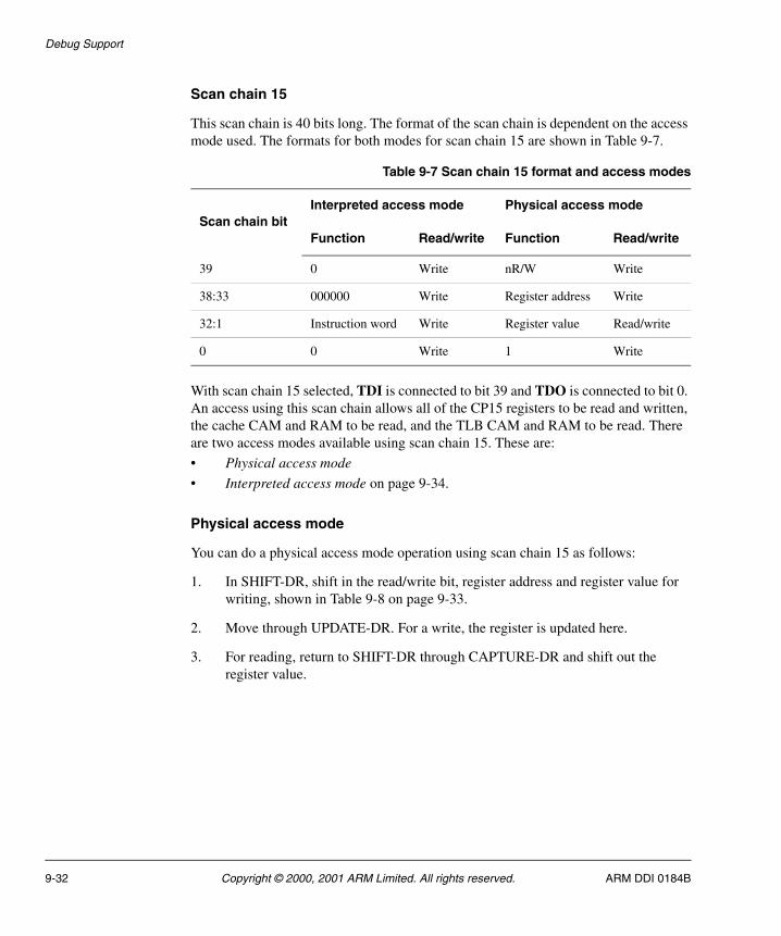
Debug Support
Scan chain 15
This scan chain is 40 bits long. The format of the scan chain is dependent on the access mode used. The formats for both modes for scan chain 15 are shown in Table 9-7.
With scan chain 15 selected, TDI is connected to bit 39 and TDO is connected to bit 0. An access using this scan chain allows all of the CP15 registers to be read and written, the cache CAM and RAM to be read, and the TLB CAM and RAM to be read. There are two access modes available using scan chain 15. These are:
• Physical access mode
• Interpreted access mode on page 9-34.
Physical access mode
You can do a physical access mode operation using scan chain 15 as follows:
1. In SHIFT-DR, shift in the read/write bit, register address and register value for writing, shown in Table 9-8 on page 9-33.
2. Move through UPDATE-DR. For a write, the register is updated here.
3. For reading, return to SHIFT-DR through CAPTURE-DR and shift out the register value.
Table 9-7 Scan chain 15 format and access modes
Scan chain bitInterpreted access mode Physical access mode
Function Read/write Function Read/write
39 0 Write nR/W Write
38:33 000000 Write Register address Write
32:1 Instruction word Write Register value Read/write
0 0 Write 1 Write
9-32 Copyright © 2000, 2001 ARM Limited. All rights reserved. ARM DDI 0184B
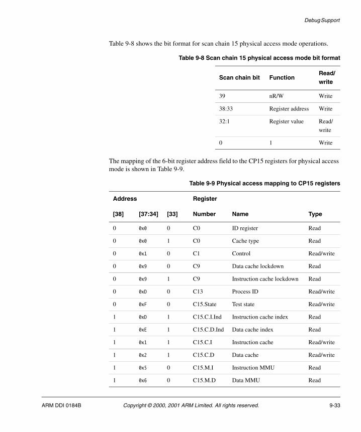
Debug Support
Table 9-8 shows the bit format for scan chain 15 physical access mode operations.
The mapping of the 6-bit register address field to the CP15 registers for physical access mode is shown in Table 9-9.
Table 9-8 Scan chain 15 physical access mode bit format
Scan chain bit FunctionRead/write
39 nR/W Write
38:33 Register address Write
32:1 Register value Read/
write
0 1 Write
Table 9-9 Physical access mapping to CP15 registers
Address Register
[38] [37:34] [33] Number Name Type
0 0x0 0 C0 ID register Read
0 0x0 1 C0 Cache type Read
0 0x1 0 C1 Control Read/write
0 0x9 0 C9 Data cache lockdown Read
0 0x9 1 C9 Instruction cache lockdown Read
0 0xD 0 C13 Process ID Read/write
0 0xF 0 C15.State Test state Read/write
1 0xD 1 C15.C.I.Ind Instruction cache index Read
1 0xE 1 C15.C.D.Ind Data cache index Read
1 0x1 1 C15.C.I Instruction cache Read/write
1 0x2 1 C15.C.D Data cache Read/write
1 0x5 0 C15.M.I Instruction MMU Read
1 0x6 0 C15.M.D Data MMU Read
ARM DDI 0184B Copyright © 2000, 2001 ARM Limited. All rights reserved. 9-33
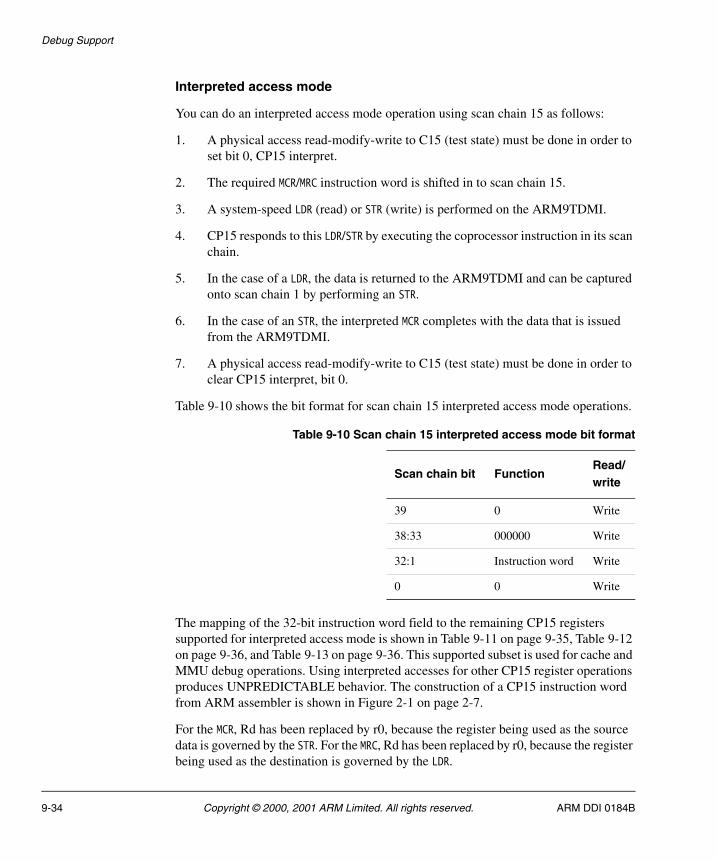
Debug Support
Interpreted access mode
You can do an interpreted access mode operation using scan chain 15 as follows:
1. A physical access read-modify-write to C15 (test state) must be done in order to set bit 0, CP15 interpret.
2. The required MCR/MRC instruction word is shifted in to scan chain 15.
3. A system-speed LDR (read) or STR (write) is performed on the ARM9TDMI.
4. CP15 responds to this LDR/STR by executing the coprocessor instruction in its scan chain.
5. In the case of a LDR, the data is returned to the ARM9TDMI and can be captured onto scan chain 1 by performing an STR.
6. In the case of an STR, the interpreted MCR completes with the data that is issued from the ARM9TDMI.
7. A physical access read-modify-write to C15 (test state) must be done in order to clear CP15 interpret, bit 0.
Table 9-10 shows the bit format for scan chain 15 interpreted access mode operations.
The mapping of the 32-bit instruction word field to the remaining CP15 registers supported for interpreted access mode is shown in Table 9-11 on page 9-35, Table 9-12 on page 9-36, and Table 9-13 on page 9-36. This supported subset is used for cache and MMU debug operations. Using interpreted accesses for other CP15 register operations produces UNPREDICTABLE behavior. The construction of a CP15 instruction word from ARM assembler is shown in Figure 2-1 on page 2-7.
For the MCR, Rd has been replaced by r0, because the register being used as the source data is governed by the STR. For the MRC, Rd has been replaced by r0, because the register being used as the destination is governed by the LDR.
Table 9-10 Scan chain 15 interpreted access mode bit format
Scan chain bit FunctionRead/write
39 0 Write
38:33 000000 Write
32:1 Instruction word Write
0 0 Write
9-34 Copyright © 2000, 2001 ARM Limited. All rights reserved. ARM DDI 0184B
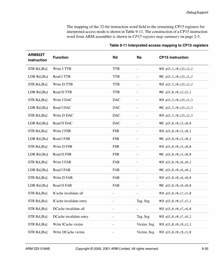
Debug Support
The mapping of the 32-bit instruction word field to the remaining CP15 registers for interpreted access mode is shown in Table 9-11. The construction of a CP15 instruction word from ARM assembler is shown in CP15 register map summary on page 2-5.
Table 9-11 Interpreted access mapping to CP15 registers
ARM922Tinstruction
Function Rd Ra CP15 instruction
STR Rd,[Ra] Write I TTB TTB - MCR p15,5,r0,c15,c1,2
LDR Rd,[Ra] Read I TTB TTB - MRC p15,5,r0,c15,c1,2
STR Rd,[Ra] Write D TTB TTB - MCR p15,5,r0,c15,c2,2
LDR Rd,[Ra] Read D TTB TTB - MRC p15,0,r0,c2,c2,2
STR Rd,[Ra] Write I DAC DAC - MCR p15,5,r0,c15,c1,3
LDR Rd,[Ra] Read I DAC DAC - MRC p15,5,r0,c15,c1,3
STR Rd,[Ra] Write D DAC DAC - MCR p15,5,r0,c15,c2,3
LDR Rd,[Ra] Read D DAC DAC - MRC p15,0,r0,c3,c0,0
STR Rd,[Ra] Write I FSR FSR - MCR p15,0,r0,c5,c0,1
LDR Rd,[Ra] Read I FSR FSR - MRC p15,0,r0,c5,c0,1
STR Rd,[Ra] Write D FSR FSR - MCR p15,0,r0,c5,c0,0
LDR Rd,[Ra] Read D FSR FSR - MRC p15,0,r0,c5,c0,0
STR Rd,[Ra] Write I FAR FAR - MCR p15,0,r0,c6,c0,1
LDR Rd,[Ra] Read I FAR FAR - MRC p15,0,r0,c6,c0,1
STR Rd,[Ra] Write D FAR FAR - MCR p15,0,r0,c6,c0,0
LDR Rd,[Ra] Read D FAR FAR - MRC p15,0,r0,c6,c0,0
STR Rd,[Ra] ICache invalidate all - - MCR p15,0,r0,c7,c5,0
STR Rd,[Ra] ICache invalidate entry - Tag, Seg MCR p15,0,r0,c7,c5,1
STR Rd,[Ra] DCache invalidate all - - MCR p15,0,r0,c7,c6,0
STR Rd,[Ra] DCache invalidate entry - Tag, Seg MCR p15,0,r0,c7,c6,1
STR Rd,[Ra] Write ICache victim - Victim, Seg MCR p15,0,r0,c9,c1,1
STR Rd,[Ra] Write DCache victim - Victim, Seg MCR p15,0,r0,c9,c1,0
ARM DDI 0184B Copyright © 2000, 2001 ARM Limited. All rights reserved. 9-35
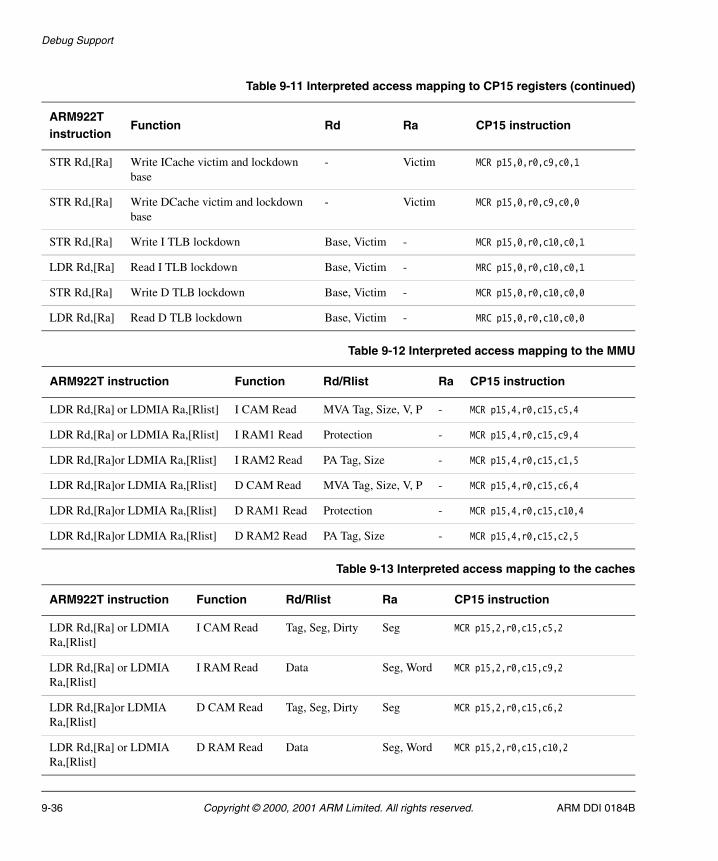
Debug Support
STR Rd,[Ra] Write ICache victim and lockdown base
- Victim MCR p15,0,r0,c9,c0,1
STR Rd,[Ra] Write DCache victim and lockdown base
- Victim MCR p15,0,r0,c9,c0,0
STR Rd,[Ra] Write I TLB lockdown Base, Victim - MCR p15,0,r0,c10,c0,1
LDR Rd,[Ra] Read I TLB lockdown Base, Victim - MRC p15,0,r0,c10,c0,1
STR Rd,[Ra] Write D TLB lockdown Base, Victim - MCR p15,0,r0,c10,c0,0
LDR Rd,[Ra] Read D TLB lockdown Base, Victim - MRC p15,0,r0,c10,c0,0
Table 9-12 Interpreted access mapping to the MMU
ARM922T instruction Function Rd/Rlist Ra CP15 instruction
LDR Rd,[Ra] or LDMIA Ra,[Rlist] I CAM Read MVA Tag, Size, V, P - MCR p15,4,r0,c15,c5,4
LDR Rd,[Ra] or LDMIA Ra,[Rlist] I RAM1 Read Protection - MCR p15,4,r0,c15,c9,4
LDR Rd,[Ra]or LDMIA Ra,[Rlist] I RAM2 Read PA Tag, Size - MCR p15,4,r0,c15,c1,5
LDR Rd,[Ra]or LDMIA Ra,[Rlist] D CAM Read MVA Tag, Size, V, P - MCR p15,4,r0,c15,c6,4
LDR Rd,[Ra]or LDMIA Ra,[Rlist] D RAM1 Read Protection - MCR p15,4,r0,c15,c10,4
LDR Rd,[Ra]or LDMIA Ra,[Rlist] D RAM2 Read PA Tag, Size - MCR p15,4,r0,c15,c2,5
Table 9-13 Interpreted access mapping to the caches
ARM922T instruction Function Rd/Rlist Ra CP15 instruction
LDR Rd,[Ra] or LDMIA Ra,[Rlist]
I CAM Read Tag, Seg, Dirty Seg MCR p15,2,r0,c15,c5,2
LDR Rd,[Ra] or LDMIA Ra,[Rlist]
I RAM Read Data Seg, Word MCR p15,2,r0,c15,c9,2
LDR Rd,[Ra]or LDMIA Ra,[Rlist]
D CAM Read Tag, Seg, Dirty Seg MCR p15,2,r0,c15,c6,2
LDR Rd,[Ra] or LDMIA Ra,[Rlist]
D RAM Read Data Seg, Word MCR p15,2,r0,c15,c10,2
Table 9-11 Interpreted access mapping to CP15 registers (continued)
ARM922Tinstruction
Function Rd Ra CP15 instruction
9-36 Copyright © 2000, 2001 ARM Limited. All rights reserved. ARM DDI 0184B
Debug Support
Debug access to the MMU
This is achieved through scan chain 1 and 15, using the physical access and interpreted access modes. The following steps explain how to read the Data TLB
1. Physical access: Read-modify-write cp15, register 1, to turn off both the caches and MMU.
2. Physical access: Read-modify-write cp15, register 15, to set MMU test and CP15 interpret mode.
3. Interpreted access: LDR Rd,[Ra]. MCR = Read D TLB lockdown. This will read the Base and Victim to Rd.
4. Physical access: Read-modify-write CP15 register 15 to clear CP 15 interpret mode.
5. STR of Rd loaded in step (3). Capture on scan chain 1 and shift out.
6. Physical access: read-modify-write CP15 register 15 to set CP15 interpret mode.
7. Interpreted access: STR Rd,[Ra]. MCR = Write D TLB lockdown, where Rd = Base[read in (3)], Victim[=0].
8. Interpreted access: 8 word LDM, LDMIA Ra,[Rlist]. MCR = D CAM Read. The CAM Read will increment the victim pointer on every access, so this will read entries 0-7.
9. Physical access: Read-modify-write CP15 register 15 to clear CP 15 interpret mode.
10. 8 word STM of the values loaded in step (6). Capture these on scan chain 1 and shift out. These 8 values are the CAM Tag for entries 0-7.
11. Physical access: read-modify-write CP15 register 15 to set CP15 interpret mode.
12. Repeat steps (8) to (11) eight times to read entries 0-63.
13. Interpreted access: STR Rd,[Ra]. MCR = Write D TLB lockdown, where Rd = Base[read in step (3)], Victim[=0].
14. Interpreted access: LDR Rd,[Ra]. MCR = D RAM1 Read. The RAM1 Read will increment the victim pointer on every access as MMU test in cp15, register 15, Test State register has been set.
15. Interpreted access: LDR Rd,[Ra]. MCR = D RAM2 Read. This uses a pipelined version of the last RAM1 read.
ARM DDI 0184B Copyright © 2000, 2001 ARM Limited. All rights reserved. 9-37
Debug Support
16. Physical access: Read-modify-write CP15 register 15 to clear CP 15 interpret mode.
17. 2 word STM of the values loaded in steps (10) and (11). Capture these on scan chain 1 and shift out. These 2 values are RAM1 and RAM2 from entry 0.
18. Physical access: read-modify-write CP15 register 15 to set CP15 interpret mode.
19. Repeat steps (14) to (18) 64 times to read RAM1 and RAM2 entries 0-63.
20. Interpreted access: STR Rd,[Ra]. MCR = Write D TLB lockdown, where Rd = Base[read in step (3)], Victim[read in step (3)].
21. Physical access: Read-modify-write cp15, register 15, to clear MMU test and CP15 interpret mode.
22. Physical access: Read-modify-write cp15, register 1, to turn on (restore state of) both the caches and MMU.
Debug access to the caches
This is achieved through scan chain 1 and 15, using the physical access and interpreted access modes. The following steps explain how to read the DCache. They assume you are trying to read the contents of segment 2 of the DCache.
1. Physical access: Read-modify-write cp15, register 1, to turn off both the caches and MMU.
2. Physical access: Read-modify-write cp15, register 15, to set CP15 interpret mode.
3. Interpreted access: LDR Rd,[Ra]. MCR = D CAM Read, where Ra = Seg2. This will cause the current victim for segment 2 to be read into C15.C.D.Ind.
4. Physical access: Read C15.C.D.Ind which contains the victim of segment 2.
5. Interpreted access: STR Rd,[Ra]. MCR = Write DCache victim, where Ra = Victim0, Seg2. This sets the victim counter to 0 for segment 2, and configures the counter to increment after a CAM read or write. The Base remains unchanged.
6. Interpreted access: 8 word LDM, LDMIA Ra,[Rlist]. MCR = D RAM Read, where Ra = seg2, word0. The LDMIA will increment the word part of the address and move across the cache line from word0 to word7.
7. Interpreted access: LDR Rd,[Ra]. MCR = D CAM Read, where Ra = Seg2.
8. Physical access: Read-modify-write cp15, register 15, to clear CP15 interpret mode.
9-38 Copyright © 2000, 2001 ARM Limited. All rights reserved. ARM DDI 0184B
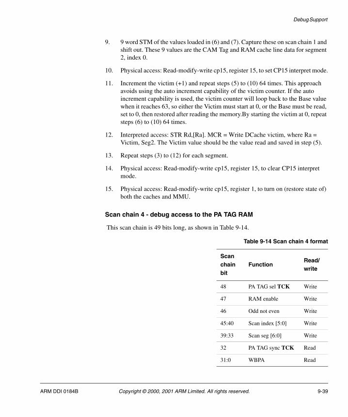
Debug Support
9. 9 word STM of the values loaded in (6) and (7). Capture these on scan chain 1 and shift out. These 9 values are the CAM Tag and RAM cache line data for segment 2, index 0.
10. Physical access: Read-modify-write cp15, register 15, to set CP15 interpret mode.
11. Increment the victim (+1) and repeat steps (5) to (10) 64 times. This approach avoids using the auto increment capability of the victim counter. If the auto increment capability is used, the victim counter will loop back to the Base value when it reaches 63, so either the Victim must start at 0, or the Base must be read, set to 0, then restored after reading the memory.By starting the victim at 0, repeat steps (6) to (10) 64 times.
12. Interpreted access: STR Rd,[Ra]. MCR = Write DCache victim, where Ra = Victim, Seg2. The Victim value should be the value read and saved in step (5).
13. Repeat steps (3) to (12) for each segment.
14. Physical access: Read-modify-write cp15, register 15, to clear CP15 interpret mode.
15. Physical access: Read-modify-write cp15, register 1, to turn on (restore state of) both the caches and MMU.
Scan chain 4 - debug access to the PA TAG RAM
This scan chain is 49 bits long, as shown in Table 9-14.
Table 9-14 Scan chain 4 format
Scanchainbit
FunctionRead/write
48 PA TAG sel TCK Write
47 RAM enable Write
46 Odd not even Write
45:40 Scan index [5:0] Write
39:33 Scan seg [6:0] Write
32 PA TAG sync TCK Read
31:0 WBPA Read
ARM DDI 0184B Copyright © 2000, 2001 ARM Limited. All rights reserved. 9-39
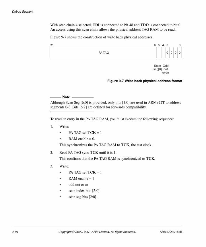
Debug Support
With scan chain 4 selected, TDI is connected to bit 48 and TDO is connected to bit 0. An access using this scan chain allows the physical address TAG RAM to be read.
Figure 9-7 shows the construction of write back physical addresses.
Figure 9-7 Write back physical address format
Note Although Scan Seg [6:0] is provided, only bits [1:0] are used in ARM922T to address segments 0-3. Bits [6:2] are defined for forwards compatibility.
To read an entry in the PA TAG RAM, you must execute the following sequence:
1. Write:
• PA TAG sel TCK = 1
• RAM enable = 0.
This synchronizes the PA TAG RAM to TCK, the test clock.
2. Read PA TAG sync TCK until it is 1.
This confirms that the PA TAG RAM is synchronized to TCK.
3. Write:
• PA TAG sel TCK = 1
• RAM enable = 1
• odd not even
• scan index bits [5:0]
• scan seg bits [2:0].
31 6 5 4 3 0
PA TAG 0 0 0 0
Scanseg[0]
Oddnot
even
9-40 Copyright © 2000, 2001 ARM Limited. All rights reserved. ARM DDI 0184B
Debug Support
4. Go through the UPDATE-DR state of the ARM922T TAP controller three times. The most efficient way of doing this, after doing the write in step 3 is to go through the following sequence. This avoids rewriting the values in step 3 on each iteration:
a. EXIT1-DR
b. UPDATE-DR
c. SELECT-DR-SCAN
d. CAPTURE-DR
e. Repeat (a) to (d) x 2
f. SHIFT-DR.
The PA TAG RAM requires three clock cycles to perform the read. Its clock is cycled in UPDATE-DR, and therefore this state must be passed through three times.
5. Read the Write Back Physical Address (WBPA).
6. Write:
• PA TAG sel TCK = 0
• RAM enable = 0.
Resynchronize the PA TAG RAM to the system clock.
7. Read PA TAG sync TCK until it is 0. This confirms that resynchronization has occurred.
You must repeat this sequence of steps (1 to 7) for the four segments, corresponding to the four DCache segments, and the 64 entries per segment, corresponding to the 64 entries in each DCache segment.
ARM DDI 0184B Copyright © 2000, 2001 ARM Limited. All rights reserved. 9-41
Debug Support
9.7 ARM922T core clocks
The ARM9TDMI core has two clocks:
• the memory clock GCLK• an internally TCK generated clock, DCLK.
During normal operation, the core is clocked by GCLK, and internal logic holds DCLK LOW. When the ARM922T is in the debug state, the core is clocked by DCLK under control of the TAP state machine, and GCLK can free run. The selected clock is output on the ECLK signal for use by the external system.
Note When the core is being debugged and is running from DCLK, nWAIT has no effect.
The two cases where the clocks switch are:
• during debugging
• during testing.
9-42 Copyright © 2000, 2001 ARM Limited. All rights reserved. ARM DDI 0184B
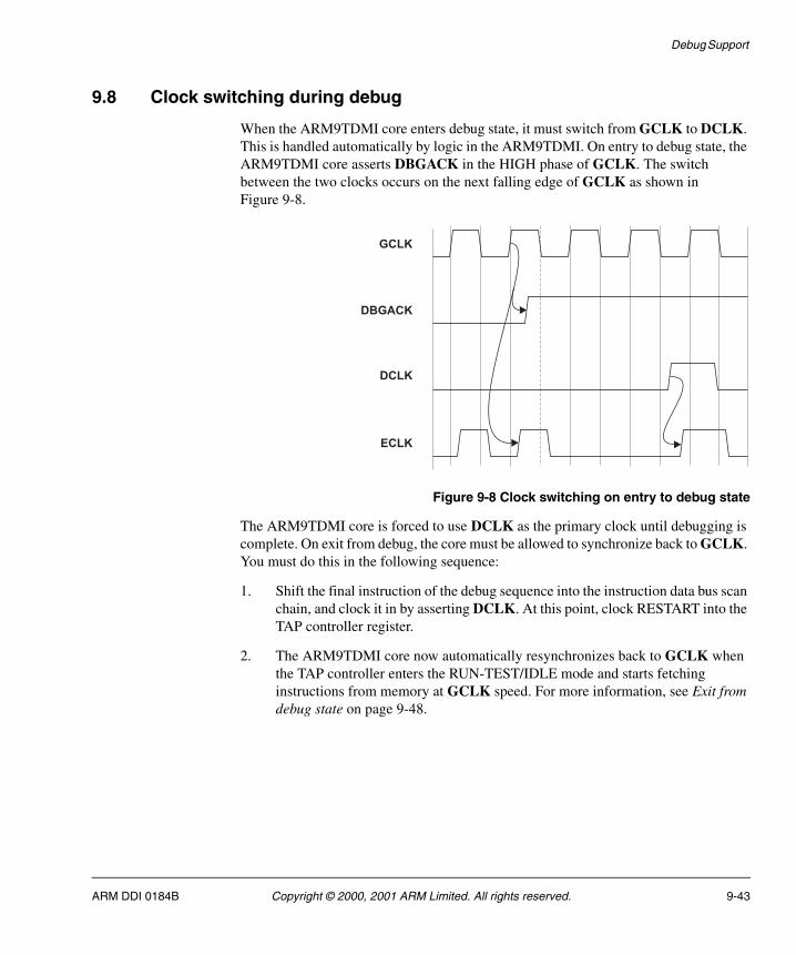
Debug Support
9.8 Clock switching during debug
When the ARM9TDMI core enters debug state, it must switch from GCLK to DCLK. This is handled automatically by logic in the ARM9TDMI. On entry to debug state, the ARM9TDMI core asserts DBGACK in the HIGH phase of GCLK. The switch between the two clocks occurs on the next falling edge of GCLK as shown in Figure 9-8.
Figure 9-8 Clock switching on entry to debug state
The ARM9TDMI core is forced to use DCLK as the primary clock until debugging is complete. On exit from debug, the core must be allowed to synchronize back to GCLK. You must do this in the following sequence:
1. Shift the final instruction of the debug sequence into the instruction data bus scan chain, and clock it in by asserting DCLK. At this point, clock RESTART into the TAP controller register.
2. The ARM9TDMI core now automatically resynchronizes back to GCLK when the TAP controller enters the RUN-TEST/IDLE mode and starts fetching instructions from memory at GCLK speed. For more information, see Exit from debug state on page 9-48.
GCLK
DBGACK
ECLK
DCLK
ARM DDI 0184B Copyright © 2000, 2001 ARM Limited. All rights reserved. 9-43
Debug Support
9.9 Clock switching during test
Under serial test conditions, when test patterns are being applied to the core through the JTAG interface, the ARM9TDMI core must be clocked using DCLK. Entry into test is less automatic than debug and some care must be taken.
On the way into test, GCLK must be held LOW. You can now use the TAP controller to perform serial testing on the ARM9TDMI core. If scan chain 0 and INTEST are selected, DCLK is generated while the state machine is in RUN-TEST/IDLE state.
During EXTEST, DCLK is not generated.
On exit from test, you must select RESTART as the TAP controller instruction. When this is done, you can allow GCLK to resume. After INTEST testing, you must take care to ensure that the core is in a sensible state before switching back. The safest way to do this is either:
• select RESTART and then cause a system reset
• insert MOV PC,#0 into the instruction pipeline before switching back.
9-44 Copyright © 2000, 2001 ARM Limited. All rights reserved. ARM DDI 0184B
Debug Support
9.10 Determining the core state and system state
When the ARM9TDMI core is in debug state, you can examine the core state and system state. You can do this by forcing load and store multiples into the pipeline.
Before you can examine the core state and system state, the debugger must first determine whether the processor entered debug from Thumb state or ARM state. You can do this by examining bit 4 of the EmbeddedICE macrocell debug status register. If this is HIGH, the core is in Thumb state. If it is LOW, the core is in ARM state.
9.10.1 Determining the core state
If the processor has entered debug state from Thumb state, it is easiest for the debugger to force the core back into ARM state. When this is done, the debugger can execute the same sequence of instructions to determine the processor state.
To force the processor into ARM state, the following sequence of Thumb instructions can be executed on the core:
STR R0, [R1] ; Save R0 before useMOV R0, PC ; Copy PC into R0STR R0, [R1] ; Save the PC in R0BX PC ; Jump into ARM stateMOV R8, R8 ; NOP (no operation)MOV R8, R8 ; NOP
The above use of R1 as the base register for stores is for illustration only. You can use any register.
Because all Thumb instructions are only 16 bits long, you can duplicate the instruction in the instruction data bus bits, when shifting them into scan chain 1. For example, the encoding for BX R0 is 0x4700. Therefore, if 0x47004700 is shifted into the 32 bits of the instruction data bus of scan chain 1, the debugger does not have to remember the half of the bus that the processor expects to read instructions from.
From this point, you can determine the processor state by the following series of steps of ARM instructions.
When the processor is in ARM state, typically the first instruction executed is:
STM R0, {R0-R15}
This causes the contents of the registers to be made visible on the data data bus. These values can then be sampled and shifted out.
ARM DDI 0184B Copyright © 2000, 2001 ARM Limited. All rights reserved. 9-45
Debug Support
After determining the values in the current bank of registers, you might want to access the banked registers. This can only be done by changing mode. Normally, a mode change can only occur if the core is already in a privileged mode. However, while in debug state, a mode change can occur from any mode into any other mode.
Note The debugger must restore the original mode before exiting debug state.
For example, assume that the debugger has been asked to return the state of the User mode and FIQ mode registers, and debug state has been entered in Supervisor mode.
The instruction sequence might be:
STMIA R0, {R0-R15} ; Save current registersMRS R0, CPSRSTR R0, [R0] ; Save CPSR to determine current modeBIC R0, R0, #0x1F ; Clear mode bitsORR R0, R0, #0x10 ; Select USER modeMSR CPSR, R0 ; Enter USER modeSTMIA R0, {R13-R14} ; Save registers not previously visibleORR R0, R0, #0x01 ; Select FIQ modeMSR CPSR, R0 ; Enter FIQ modeSTMIA R0, {R8-R14} ; Save banked FIQ registers
All these instructions are said to execute at debug speed. Debug speed is much slower than system speed because, between each core clock, 67 scan clocks occur in order to shift in an instruction or shift out data. Executing instructions more slowly than usual is fine for accessing the core state because the ARM922T is fully static. However, you cannot use this same method for determining the state of the rest of the system.
While in debug state, only the following instructions can be inserted into the instruction pipeline for execution:
• all data processing operations
• all load, store, load multiple, and store multiple instructions
• MSR and MRS.
9-46 Copyright © 2000, 2001 ARM Limited. All rights reserved. ARM DDI 0184B
Debug Support
9.10.2 Determining system state
To meet the dynamic timing requirements of the memory system, any attempt to access system state must occur synchronously. Therefore, you must force the ARM9TDMI core to synchronize back to system speed. The 33rd bit of scan chain 1, SYSSPEED, controls this.
You can place a legal debug instruction in the instruction data bus of scan chain 1 with bit 33 (the SYSSPEED bit) LOW. This instruction is then executed at debug speed. To execute an instruction at system speed, a NOP (such as MOV R0, R0) must be scanned in as the next instruction with bit 33 set HIGH.
After the system speed instructions have been scanned into the instruction data bus and clocked into the pipeline, you must load the RESTART instruction into the TAP controller. This causes the ARM9TDMI automatically to resynchronize back to GCLK when the TAP controller enters RUN-TEST/IDLE state, and execute the instruction at system speed. Debug state is re-entered after the instruction completes execution, when the processor switches itself back to the internally generated DCLK. When the instruction has completed, DBGACK is HIGH. At this point INTEST can be selected in the TAP controller, and debugging can resume.
To determine whether a system speed instruction has completed, the debugger must look at SYSCOMP (bit 3 of the debug status register). To access memory, the ARM9TDMI must access memory through the data data bus interface, as this access can be stalled indefinitely by nWAIT. Therefore, the only way to determine whether the memory access has completed is to examine the SYSCOMP bit. When this bit is HIGH the instruction has completed.
The state of the system memory can be passed to the debug host by using system speed load multiples and debug store multiples.
9.10.3 Instructions that can have the SYSSPEED bit set
The only valid instructions to set this bit for are:
• loads
• stores
• load multiple
• store multiple.
When the ARM9TDMI returns to debug state after a system speed access, the SYSSPEED bit is set HIGH.
ARM DDI 0184B Copyright © 2000, 2001 ARM Limited. All rights reserved. 9-47
Debug Support
9.11 Exit from debug state
Leaving debug state involves restoring the internal state of the ARM9TDMI core, causing a branch to the next instruction to be executed, and synchronizing back to GCLK. After restoring the internal state, you must load a branch instruction into the pipeline. For details on calculating the branch, see The behavior of the program counter during debug on page 9-51.
Use bit 33 of scan chain 1 to force the ARM9TDMI core to resynchronize back to GCLK. The penultimate instruction in the debug sequence is a branch to the instruction where execution is to resume. This is scanned in with bit 33 set LOW. The core is then clocked to load the branch into the pipeline. The final instruction that you must scan in is a NOP (such as MOV R0, R0), with bit 33 set HIGH. You must the clock the core to load this instruction into the pipeline. Now, select the RESTART instruction in the TAP controller. When the state machine enters the RUN-TEST/IDLE state, the scan chain reverts back to system mode and clock resynchronization to GCLK occurs within the ARM9TDMI. Normal operation resumes, with instructions being fetched from memory.
The delay, until the state machine is in RUN-TEST/IDLE state, allows you to set up conditions in other devices in a multiprocessor system without taking immediate effect. Then, when RUN-TEST/IDLE state is entered, all the processors resume operation simultaneously.
The function of DBGACK is to tell the rest of the system when the ARM9TDMI core is in debug state. You can use this to inhibit peripherals such as watchdog timers that have real-time characteristics. Also, you can use DBGACK to mask out memory accesses that are caused by the debugging process. For example, when the ARM9TDMI enters debug state after a breakpoint, the instruction pipeline contains the breakpointed instruction plus two other instructions that have been prefetched. On entry to debug state, the pipeline is flushed. So, on exit from debug state, the pipeline must be refilled to its previous state. Therefore, because of the debugging process, more memory accesses occur than are normally expected. You can inhibit any system peripheral that might be sensitive to the number of memory accesses by using DBGACK.
Note DBGACK can only be used in this way using breakpoints. It does not mask the correct number of memory accesses after a watchpoint.
For example, consider a peripheral that merely counts the number of instruction fetches. This device must return the same answer after a program has run both with and without debugging. Figure 9-9 on page 9-49 shows the behavior of the ARM9TDMI core on exit from debug state.
9-48 Copyright © 2000, 2001 ARM Limited. All rights reserved. ARM DDI 0184B
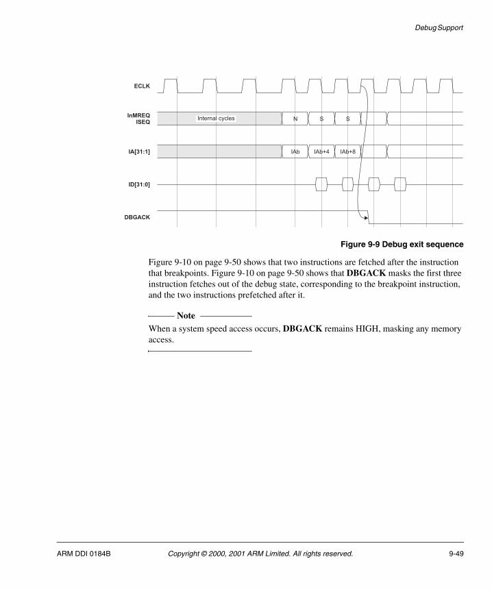
Debug Support
Figure 9-9 Debug exit sequence
Figure 9-10 on page 9-50 shows that two instructions are fetched after the instruction that breakpoints. Figure 9-10 on page 9-50 shows that DBGACK masks the first three instruction fetches out of the debug state, corresponding to the breakpoint instruction, and the two instructions prefetched after it.
Note When a system speed access occurs, DBGACK remains HIGH, masking any memory access.
IAb IAb+4 IAb+8
ID[31:0]
ECLK
InMREQISEQ
IA[31:1]
DBGACK
N S SInternal cycles
ARM DDI 0184B Copyright © 2000, 2001 ARM Limited. All rights reserved. 9-49
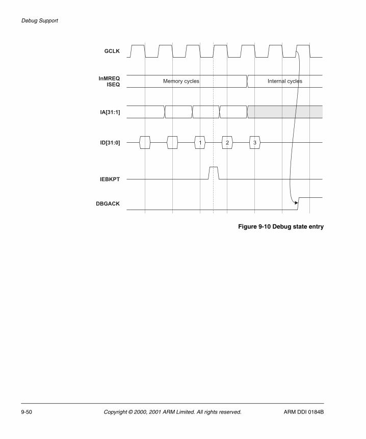
Debug Support
Figure 9-10 Debug state entry
GCLK
ID[31:0]
InMREQISEQ
IA[31:1]
DBGACK
Memory cycles Internal cycles
IEBKPT
1 2 3
9-50 Copyright © 2000, 2001 ARM Limited. All rights reserved. ARM DDI 0184B
Debug Support
9.12 The behavior of the program counter during debug
To force the ARM9TDMI core to branch back to the place where program flow is interrupted by debug, the debugger must keep track of what happens to the PC. There are six cases:
• Breakpoint
• Watchpoint
• Watchpoint with another exception on page 9-52
• Watchpoint and breakpoint on page 9-52
• Debug request on page 9-52
• System speed accesses on page 9-53.
In each case the same equation is used to determine where to resume execution.
9.12.1 Breakpoint
Entry to debug state from a breakpointed instruction advances the PC by 16 bytes in ARM state, or 8 bytes in Thumb state. Each instruction executed in debug state advances the PC by one address. The normal way to exit from debug state after a breakpoint is to remove the breakpoint, and branch back to the previously breakpointed address.
For example, if the ARM9TDMI core entered debug state from a breakpoint set on a given address and two debug speed instructions were executed, a branch of 7 addresses must occur (four for debug entry, plus two for the instructions, plus one for the final branch). The following sequence shows ARM instructions scanned into scan chain 1. This is Most Significant Bit (MSB) first, so the first digit represents the value to be scanned into the SYSSPEED bit, followed by the instruction.
0 EAFFFFF9 ; B -7 addresses (two’s complement)1 E1A00000 ; NOP (MOV R0, R0), SYSSPEED bit is set
For small branches, the final branch can be replaced witha subtract, with the PC as the destination. For example, SUB PC, PC, #28 for ARM code.
9.12.2 Watchpoint
You can return to program execution after entering debug state from a watchpoint in the same way as the procedure described in Breakpoint above. Debug entry adds four addresses to the PC, and every instruction adds one address. Because the instruction after the one that caused the watchpoint has executed, execution resumes at the following instruction.
ARM DDI 0184B Copyright © 2000, 2001 ARM Limited. All rights reserved. 9-51
Debug Support
9.12.3 Watchpoint with another exception
If a watchpoint access simultaneously causes a Data Abort, the ARM9TDMI core enters debug state in abort mode. Entry into debug is held off until the core has changed into abort mode, and fetched the instruction from the abort vector.
A similar sequence is followed when an interrupt, or any other exception, occurs during a watchpointed memory access. The ARM9TDMI core enters debug state in the mode of the exception, and so the debugger must check to see whether this happened. The debugger can deduce whether an exception occurred by looking at the current and previous mode, (in the CPSR and SPSR), and the value of the PC. If an exception did take place, you must have the choice to service the exception before debugging or not.
For example, suppose an abort occurred on a watchpoint access, and ten instructions had been executed to determine this. You can use the following sequence to return to program execution:
0 EAFFFFF1; B -15 addresses (two’s complement)1 E1A00000; NOP (MOV R0, R0), SYSSPEED bit is set
This forces a branch back to the abort vector, causing theinstructions at that location to be refetched and executed. After the abort service routine, the instruction that caused the abort and watchpoint is re-executed. This causes the watchpoint to be generated and the ARM9TDMI enters debug state again.
9.12.4 Watchpoint and breakpoint
It is possible to have a watchpoint and breakpoint condition occurring simultaneously. This can happen when an instruction causes a watchpoint, and the following instruction has been breakpointed. The same calculation must be performed as for Breakpoint on page 9-51 to determine where to resume. In this case, it is at the breakpoint instruction, because this has not been executed.
9.12.5 Debug request
Entry into debug state as a result of a debug request is similar to a breakpoint and, as for breakpoint entry to debug state, adds four addresses to the PC, and every instruction executed in debug state adds one.
For example, the following sequence handles a situation where a debug request has been invoked, followed by a decision to return to program execution immediately:
0 EAFFFFFB; B -5 addresses (two’s complement)1 E1A00000; NOP (MOV R0, R0), SYSSPEED bit is set
This restores the PC, and restarts the program from the next instruction.
9-52 Copyright © 2000, 2001 ARM Limited. All rights reserved. ARM DDI 0184B
Debug Support
9.12.6 System speed accesses
If a system speed access is performed during debug state, the value of the PC is increased by five addresses. Because system speed instructions access the memory system, it is possible for aborts to take place. If an abort occurs during a system speed memory access, the ARM9TDMI core enters abort mode before returning to debug state.
This is similar to an aborted watchpoint. However, the problem is much harder to fix because the abort is not caused by an instruction in the main program, and the PC does not point to the instruction that caused the abort. An abort handler usually looks at the PC to determine the instruction that caused the abort, and therefore the abort address. In this case, the value of the PC is invalid, but the debugger knows the address of the location being accessed. Therefore the debugger can be written to help the abort handler fix the memory system.
9.12.7 Summary of return address calculations
The calculation of the branch return address can be summarized as:
-(4 + N +5S)
Where N is the number of debug speed instructionsexecuted (including the final branch), and S is the number of system speed instructions executed.
ARM DDI 0184B Copyright © 2000, 2001 ARM Limited. All rights reserved. 9-53
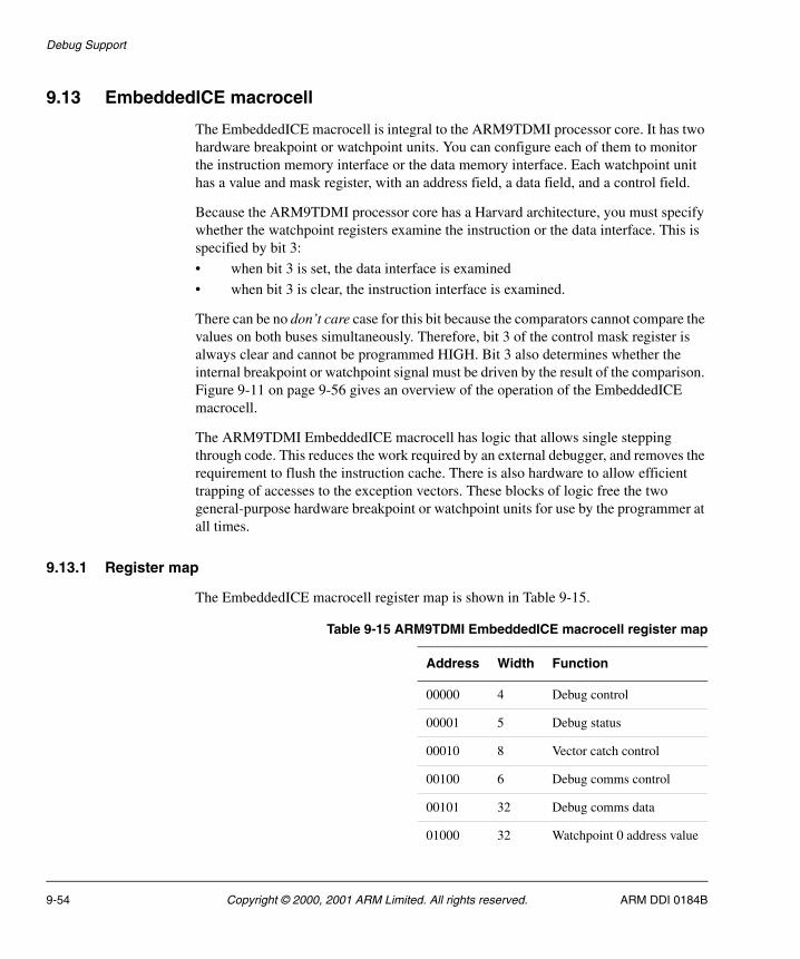
Debug Support
9.13 EmbeddedICE macrocell
The EmbeddedICE macrocell is integral to the ARM9TDMI processor core. It has two hardware breakpoint or watchpoint units. You can configure each of them to monitor the instruction memory interface or the data memory interface. Each watchpoint unit has a value and mask register, with an address field, a data field, and a control field.
Because the ARM9TDMI processor core has a Harvard architecture, you must specify whether the watchpoint registers examine the instruction or the data interface. This is specified by bit 3:
• when bit 3 is set, the data interface is examined
• when bit 3 is clear, the instruction interface is examined.
There can be no don’t care case for this bit because the comparators cannot compare the values on both buses simultaneously. Therefore, bit 3 of the control mask register is always clear and cannot be programmed HIGH. Bit 3 also determines whether the internal breakpoint or watchpoint signal must be driven by the result of the comparison. Figure 9-11 on page 9-56 gives an overview of the operation of the EmbeddedICE macrocell.
The ARM9TDMI EmbeddedICE macrocell has logic that allows single stepping through code. This reduces the work required by an external debugger, and removes the requirement to flush the instruction cache. There is also hardware to allow efficient trapping of accesses to the exception vectors. These blocks of logic free the two general-purpose hardware breakpoint or watchpoint units for use by the programmer at all times.
9.13.1 Register map
The EmbeddedICE macrocell register map is shown in Table 9-15.
Table 9-15 ARM9TDMI EmbeddedICE macrocell register map
Address Width Function
00000 4 Debug control
00001 5 Debug status
00010 8 Vector catch control
00100 6 Debug comms control
00101 32 Debug comms data
01000 32 Watchpoint 0 address value
9-54 Copyright © 2000, 2001 ARM Limited. All rights reserved. ARM DDI 0184B
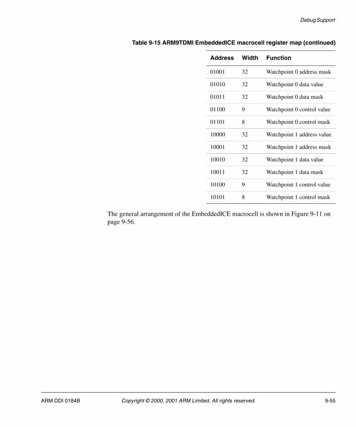
Debug Support
The general arrangement of the EmbeddedICE macrocell is shown in Figure 9-11 on page 9-56.
01001 32 Watchpoint 0 address mask
01010 32 Watchpoint 0 data value
01011 32 Watchpoint 0 data mask
01100 9 Watchpoint 0 control value
01101 8 Watchpoint 0 control mask
10000 32 Watchpoint 1 address value
10001 32 Watchpoint 1 address mask
10010 32 Watchpoint 1 data value
10011 32 Watchpoint 1 data mask
10100 9 Watchpoint 1 control value
10101 8 Watchpoint 1 control mask
Table 9-15 ARM9TDMI EmbeddedICE macrocell register map (continued)
Address Width Function
ARM DDI 0184B Copyright © 2000, 2001 ARM Limited. All rights reserved. 9-55
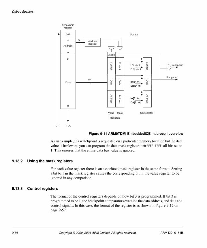
Debug Support
Figure 9-11 ARM9TDMI EmbeddedICE macrocell overview
As an example, if a watchpoint is requested on a particular memory location but the data value is irrelevant, you can program the data mask register to 0xFFFF_FFFF, all bits set to 1. This ensures that the entire data bus value is ignored.
9.13.2 Using the mask registers
For each value register there is an associated mask register in the same format. Setting a bit to 1 in the mask register causes the corresponding bit in the value register to be ignored in any comparison.
9.13.3 Control registers
The format of the control registers depends on how bit 3 is programmed. If bit 3 is programmed to be 1, the breakpoint comparators examine the data address, and data and control signals. In this case, the format of the register is as shown in Figure 9-12 on page 9-57.
0
31
0
4
Rangeout
Enable
5
Breakpoint
Scan chainregister
TDI TDO
Update
Value Mask Comparator
IA[31:0]
Registers
Ad
dre
ss
Da
taC
on
trol
Ad
dre
ss
Da
taC
on
trol
Ad
dre
ss
Da
taC
on
trol
Addressdecoder
32
R/W
DA[31:0]
ID[31:0]
DD[31:0]
I Control
D Control
Address
Data
9-56 Copyright © 2000, 2001 ARM Limited. All rights reserved. ARM DDI 0184B
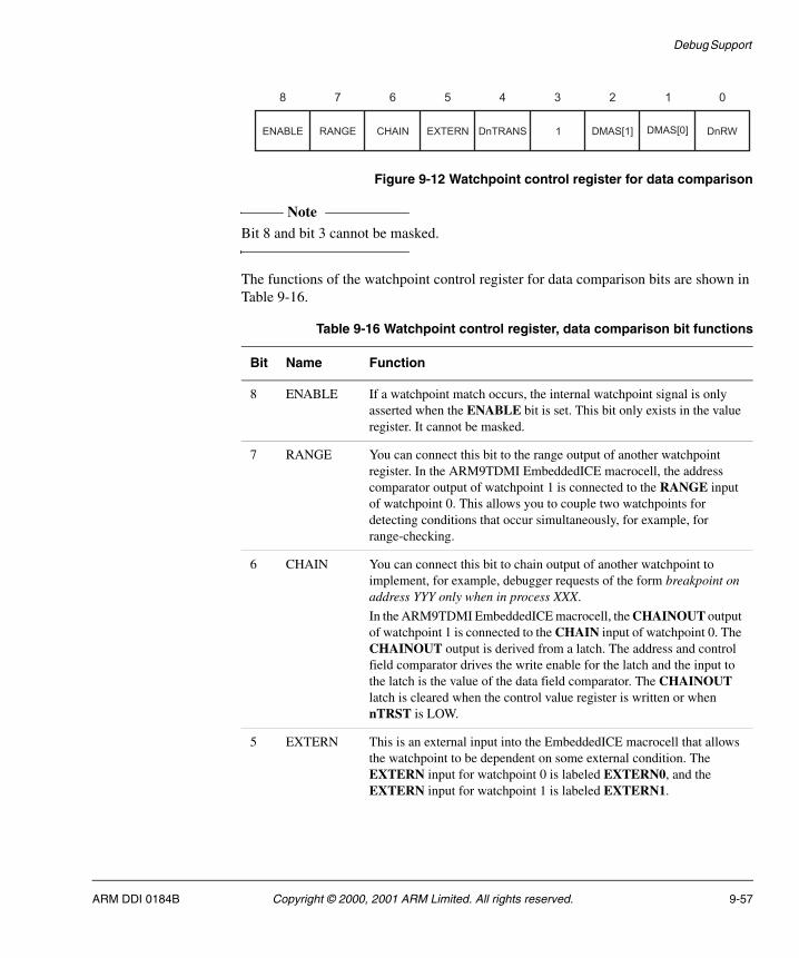
Debug Support
Figure 9-12 Watchpoint control register for data comparison
Note Bit 8 and bit 3 cannot be masked.
The functions of the watchpoint control register for data comparison bits are shown in Table 9-16.
7 6 5 4 3 2 1 0
ENABLE RANGE CHAIN EXTERN DnTRANS 1 DMAS[1] DnRWDMAS[0]
8
Table 9-16 Watchpoint control register, data comparison bit functions
Bit Name Function
8 ENABLE If a watchpoint match occurs, the internal watchpoint signal is only asserted when the ENABLE bit is set. This bit only exists in the value register. It cannot be masked.
7 RANGE You can connect this bit to the range output of another watchpoint register. In the ARM9TDMI EmbeddedICE macrocell, the address comparator output of watchpoint 1 is connected to the RANGE input of watchpoint 0. This allows you to couple two watchpoints for detecting conditions that occur simultaneously, for example, for range-checking.
6 CHAIN You can connect this bit to chain output of another watchpoint to implement, for example, debugger requests of the form breakpoint on address YYY only when in process XXX.
In the ARM9TDMI EmbeddedICE macrocell, the CHAINOUT output of watchpoint 1 is connected to the CHAIN input of watchpoint 0. The CHAINOUT output is derived from a latch. The address and control field comparator drives the write enable for the latch and the input to the latch is the value of the data field comparator. The CHAINOUT latch is cleared when the control value register is written or when nTRST is LOW.
5 EXTERN This is an external input into the EmbeddedICE macrocell that allows the watchpoint to be dependent on some external condition. The EXTERN input for watchpoint 0 is labeled EXTERN0, and the EXTERN input for watchpoint 1 is labeled EXTERN1.
ARM DDI 0184B Copyright © 2000, 2001 ARM Limited. All rights reserved. 9-57
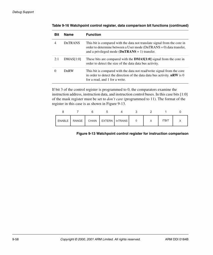
Debug Support
If bit 3 of the control register is programmed to 0, the comparators examine the instruction address, instruction data, and instruction control buses. In this case bits [1:0] of the mask register must be set to don’t care (programmed to 11). The format of the register in this case is as shown in Figure 9-13.
Figure 9-13 Watchpoint control register for instruction comparison
4 DnTRANS This bit is compared with the data not translate signal from the core in order to determine between a User mode (DnTRANS = 0) data transfer, and a privileged mode (DnTRANS = 1) transfer.
2:1 DMAS[1:0] These bits are compared with the DMAS[1:0] signal from the core in order to detect the size of the data data bus activity.
0 DnRW This bit is compared with the data not read/write signal from the core in order to detect the direction of the data data bus activity. nRW is 0 for a read, and 1 for a write.
Table 9-16 Watchpoint control register, data comparison bit functions (continued)
Bit Name Function
7 6 5 4 3 2 1 0
ENABLE RANGE CHAIN EXTERN InTRANS 0 X XITBIT
8
9-58 Copyright © 2000, 2001 ARM Limited. All rights reserved. ARM DDI 0184B
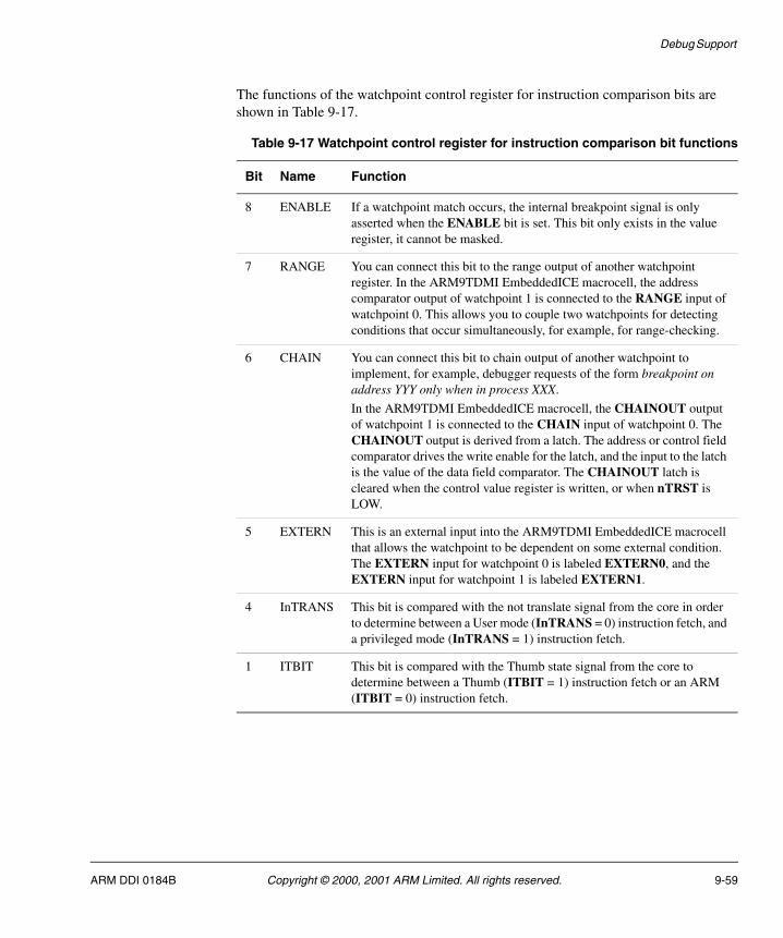
Debug Support
The functions of the watchpoint control register for instruction comparison bits are shown in Table 9-17.
Table 9-17 Watchpoint control register for instruction comparison bit functions
Bit Name Function
8 ENABLE If a watchpoint match occurs, the internal breakpoint signal is only asserted when the ENABLE bit is set. This bit only exists in the value register, it cannot be masked.
7 RANGE You can connect this bit to the range output of another watchpoint register. In the ARM9TDMI EmbeddedICE macrocell, the address comparator output of watchpoint 1 is connected to the RANGE input of watchpoint 0. This allows you to couple two watchpoints for detecting conditions that occur simultaneously, for example, for range-checking.
6 CHAIN You can connect this bit to chain output of another watchpoint to implement, for example, debugger requests of the form breakpoint on address YYY only when in process XXX.
In the ARM9TDMI EmbeddedICE macrocell, the CHAINOUT output of watchpoint 1 is connected to the CHAIN input of watchpoint 0. The CHAINOUT output is derived from a latch. The address or control field comparator drives the write enable for the latch, and the input to the latch is the value of the data field comparator. The CHAINOUT latch is cleared when the control value register is written, or when nTRST is LOW.
5 EXTERN This is an external input into the ARM9TDMI EmbeddedICE macrocell that allows the watchpoint to be dependent on some external condition. The EXTERN input for watchpoint 0 is labeled EXTERN0, and the EXTERN input for watchpoint 1 is labeled EXTERN1.
4 InTRANS This bit is compared with the not translate signal from the core in order to determine between a User mode (InTRANS = 0) instruction fetch, and a privileged mode (InTRANS = 1) instruction fetch.
1 ITBIT This bit is compared with the Thumb state signal from the core to determine between a Thumb (ITBIT = 1) instruction fetch or an ARM (ITBIT = 0) instruction fetch.
ARM DDI 0184B Copyright © 2000, 2001 ARM Limited. All rights reserved. 9-59
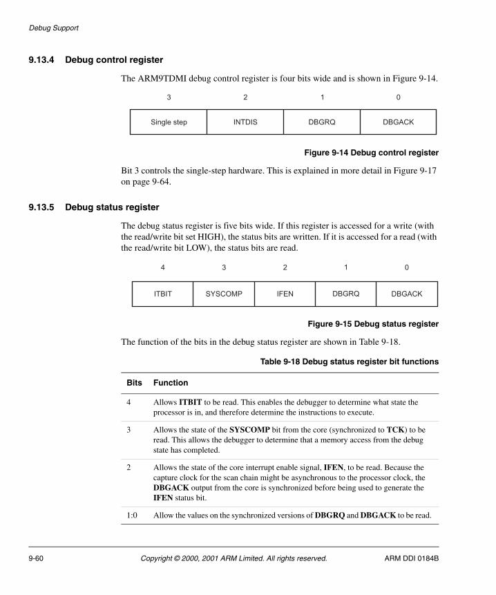
Debug Support
9.13.4 Debug control register
The ARM9TDMI debug control register is four bits wide and is shown in Figure 9-14.
Figure 9-14 Debug control register
Bit 3 controls the single-step hardware. This is explained in more detail in Figure 9-17 on page 9-64.
9.13.5 Debug status register
The debug status register is five bits wide. If this register is accessed for a write (with the read/write bit set HIGH), the status bits are written. If it is accessed for a read (with the read/write bit LOW), the status bits are read.
Figure 9-15 Debug status register
The function of the bits in the debug status register are shown in Table 9-18.
3 2 1 0
Single step INTDIS DBGRQ DBGACK
7 6 5 4 3 2 1 08ITBIT SYSCOMP IFEN DBGRQ DBGACK
4 3 2 1 0
Table 9-18 Debug status register bit functions
Bits Function
4 Allows ITBIT to be read. This enables the debugger to determine what state the processor is in, and therefore determine the instructions to execute.
3 Allows the state of the SYSCOMP bit from the core (synchronized to TCK) to be read. This allows the debugger to determine that a memory access from the debug state has completed.
2 Allows the state of the core interrupt enable signal, IFEN, to be read. Because the capture clock for the scan chain might be asynchronous to the processor clock, the DBGACK output from the core is synchronized before being used to generate the IFEN status bit.
1:0 Allow the values on the synchronized versions of DBGRQ and DBGACK to be read.
9-60 Copyright © 2000, 2001 ARM Limited. All rights reserved. ARM DDI 0184B
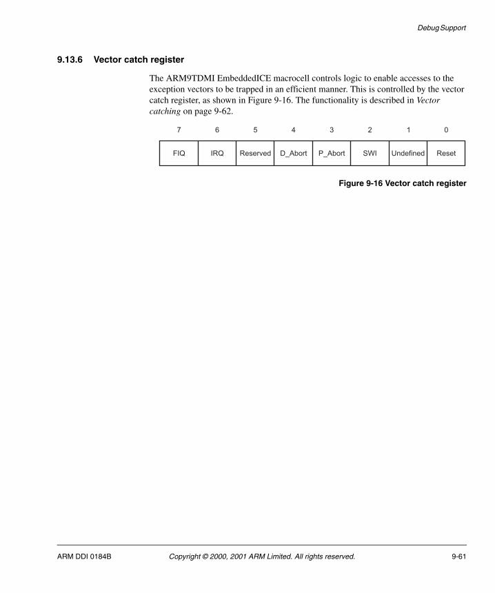
Debug Support
9.13.6 Vector catch register
The ARM9TDMI EmbeddedICE macrocell controls logic to enable accesses to the exception vectors to be trapped in an efficient manner. This is controlled by the vector catch register, as shown in Figure 9-16. The functionality is described in Vector catching on page 9-62.
Figure 9-16 Vector catch register
7 6 5 4 3 2 1 0
FIQ IRQ Reserved D_Abort P_Abort SWI Undefined Reset
ARM DDI 0184B Copyright © 2000, 2001 ARM Limited. All rights reserved. 9-61
Debug Support
9.14 Vector catching
The ARM9TDMI EmbeddedICE macrocell contains logic that allows efficient trapping of fetches from the vectors during exceptions. This is controlled by the vector catch register. If one of the bits in this register is set HIGH and the corresponding exception occurs, the processor enters debug state as if a breakpoint has been set on an instruction fetch from the relevant exception vector.
For example, if the processor executes a SWI instruction while bit 2 of the vector catch register is set, the ARM9TDMI core fetches an instruction from location 0x8. The vector catch hardware detects this access and forces the ARM9TDMI CPU core to enter debug state.
The behavior of the hardware is independent of the watchpoint comparators, leaving them free for general use. The vector catch register is sensitive only to fetches from the vectors during exception entry. Therefore, if code branches to an address within the vectors during normal operation, and the corresponding bit in the vector catch register is set, the processor is not forced to enter debug state.
9-62 Copyright © 2000, 2001 ARM Limited. All rights reserved. ARM DDI 0184B
Debug Support
9.15 Single-stepping
The ARM9TDMI EmbeddedICE macrocell contains logic that allows efficient single-stepping through code. This leaves the macrocell watchpoint comparators free for general use.
This function is enabled by setting bit 3 of the debug control register. You must only alter the state of this bit while the processor is in debug state. If the processor exits debug state and this bit is HIGH, the processor fetches an instruction, executes it, and then immediately re-enters debug state. This happens independently of the watchpoint comparators. If a system-speed data access is performed while in debug state, the debugger must ensure that the control bit is clear first.
ARM DDI 0184B Copyright © 2000, 2001 ARM Limited. All rights reserved. 9-63
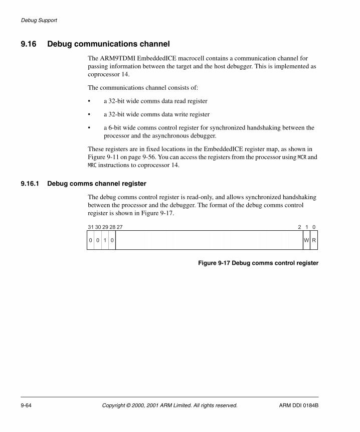
Debug Support
9.16 Debug communications channel
The ARM9TDMI EmbeddedICE macrocell contains a communication channel for passing information between the target and the host debugger. This is implemented as coprocessor 14.
The communications channel consists of:
• a 32-bit wide comms data read register
• a 32-bit wide comms data write register
• a 6-bit wide comms control register for synchronized handshaking between the processor and the asynchronous debugger.
These registers are in fixed locations in the EmbeddedICE register map, as shown in Figure 9-11 on page 9-56. You can access the registers from the processor using MCR and MRC instructions to coprocessor 14.
9.16.1 Debug comms channel register
The debug comms control register is read-only, and allows synchronized handshaking between the processor and the debugger. The format of the debug comms control register is shown in Figure 9-17.
Figure 9-17 Debug comms control register
31 30 29 28 27 2 1 0
R0 W00 1
9-64 Copyright © 2000, 2001 ARM Limited. All rights reserved. ARM DDI 0184B
Debug Support
The function of each register bit is described in Table 9-19.
From the perspective of the debugger, the registers are accessed using the scan chain in the usual way. From the processor, these registers are accessed using coprocessor register transfer instructions. You can use the following instructions:
MRC p14, 0, Rd, C0, C0; Returns the debug comms control register into Rd.
MCR p14, 0, Rn, C1, C0; Writes the value in Rn to the comms data write register.
MRC p14, 0, Rd, C1, C0; Returns the debug data read register into Rd.
Note The Thumb instruction set does not support coprocessors so the ARM9TDMI must be operated in ARM state to access the debug comms channel.
Table 9-19 Debug comms control register bit functions
Bits Function
31:28 Contain a fixed pattern that denotes the EmbeddedICE macrocell version number, in this case 0b0010.
27:2 Unused.
1 Denotes, as seen by the processor, whether the comms data write register is free. If, as seen by the processor, the comms data write register is free (W=0), new data can be written. If it is not free (W=1), the processor must poll until W=0. If, as seen by the debugger, W=1, some new data has been written that can then be scanned out.
0 Denotes whether there is some new data in the comms data read register. If, as seen by the processor, R=1, there is some new data that can be read using an MRC instruction. If, as seen by the debugger, R=0, the comms data read register is free and new data can be placed there through the scan chain. If R=1, this denotes that data previously placed there through the scan chain has not been collected by the processor, and so the debugger must wait.
ARM DDI 0184B Copyright © 2000, 2001 ARM Limited. All rights reserved. 9-65
Debug Support
9.16.2 Communications using the comms channel
There are two methods of communicating using the comms channel:
• transmitting
• receiving.
Sending a message to the debugger and Receiving a message from the debugger detail their usage.
Sending a message to the debugger
When the processor wishes to send a message to the debugger, it must check that the comms data write register is free for use by finding out if the W bit of the debug comms control register is clear:
• If the W bit is set, previously written data has not been read by the debugger. The processor must continue to poll the control register until the W bit is clear.
• If W bit is clear, the comms data write register is clear.
When the W bit is clear, a message can be written by a register transfer to coprocessor 14. As the data transfer occurs from the processor to the comms data write register, the W bit is set in the debug comms control register.
The debugger sees a synchronized version of both the R and W bit when it polls the debug comms control register through the JTAG interface. When the debugger sees the W bit is set, it can read the comms data write register and scan the data out. The action of reading this data register clears the debug comms control register W bit. At this point, the communications process can begin again.
As an alternative to polling, the debug comms channel can be interrupt driven by connecting the ARM922T COMMRX and COMMTX signals to the systems interrupt controller.
Receiving a message from the debugger
Message transfer from the debugger to the processor is similar to sending a message to the debugger. In this case, the debugger polls the R bit of the debug comms control register:
• if the R bit is LOW, the comms data read register is free, and data can be placed there for the processor to read
• if the R bit is set, previously deposited data has not yet been collected, so the debugger must wait.
9-66 Copyright © 2000, 2001 ARM Limited. All rights reserved. ARM DDI 0184B
Debug Support
When the comms data read register is free, data can be written using the JTAG interface. The action of this write sets the R bit in the debug comms control register.
When the processor polls this register, it sees a GCLK synchronized version. If the R bit is set, there is data waiting to be collected. You can read this data read using an MRC instruction to coprocessor 14. The action of this load clears the R bit in the debug comms control register. When the debugger polls this register and sees that the R bit is clear, the data has been taken, and the process can now be repeated.
ARM DDI 0184B Copyright © 2000, 2001 ARM Limited. All rights reserved. 9-67

Debug Support
9-68 Copyright © 2000, 2001 ARM Limited. All rights reserved. ARM DDI 0184B
Chapter 10 TrackingICE
This chapter describes how the ARM922T processor uses TrackingICE mode. It contains the following sections:
• About TrackingICE on page 10-2
• Timing requirements on page 10-3
• TrackingICE outputs on page 10-4.
ARM DDI 0184B Copyright © 2000, 2001 ARM Limited. All rights reserved. 10-1
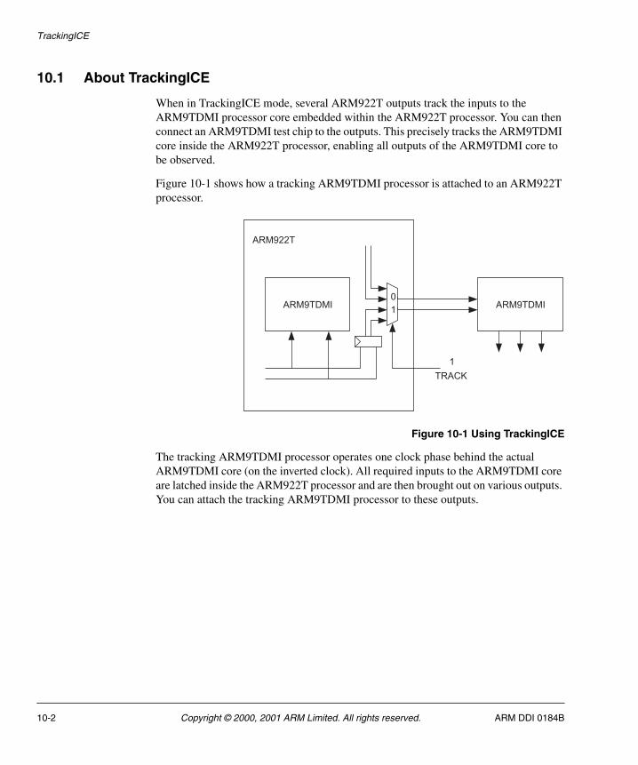
TrackingICE
10.1 About TrackingICE
When in TrackingICE mode, several ARM922T outputs track the inputs to the ARM9TDMI processor core embedded within the ARM922T processor. You can then connect an ARM9TDMI test chip to the outputs. This precisely tracks the ARM9TDMI core inside the ARM922T processor, enabling all outputs of the ARM9TDMI core to be observed.
Figure 10-1 shows how a tracking ARM9TDMI processor is attached to an ARM922T processor.
Figure 10-1 Using TrackingICE
The tracking ARM9TDMI processor operates one clock phase behind the actual ARM9TDMI core (on the inverted clock). All required inputs to the ARM9TDMI core are latched inside the ARM922T processor and are then brought out on various outputs. You can attach the tracking ARM9TDMI processor to these outputs.
0
1
ARM922T
1
TRACK
ARM9TDMIARM9TDMI
10-2 Copyright © 2000, 2001 ARM Limited. All rights reserved. ARM DDI 0184B
TrackingICE
10.2 Timing requirements
To enable the ARM9TDMI processor core to be tracked correctly, all inputs must be synchronous to the ARM9TDMI processor clock. These inputs include TCK, that in tracking mode is latched on the falling edge of GCLK before it is driven onto the ARM922T tracking outputs. All other TCK relative signals, TDI, TMS, and SDOUTBS, are latched on rising GCLK before they are driven onto the ARM922T tracking outputs.
ARM DDI 0184B Copyright © 2000, 2001 ARM Limited. All rights reserved. 10-3
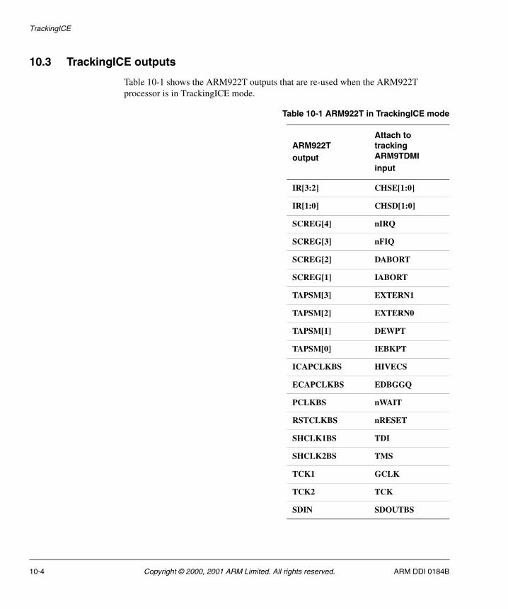
TrackingICE
10.3 TrackingICE outputs
Table 10-1 shows the ARM922T outputs that are re-used when the ARM922T processor is in TrackingICE mode.
Table 10-1 ARM922T in TrackingICE mode
ARM922Toutput
Attach to tracking ARM9TDMIinput
IR[3:2] CHSE[1:0]
IR[1:0] CHSD[1:0]
SCREG[4] nIRQ
SCREG[3] nFIQ
SCREG[2] DABORT
SCREG[1] IABORT
TAPSM[3] EXTERN1
TAPSM[2] EXTERN0
TAPSM[1] DEWPT
TAPSM[0] IEBKPT
ICAPCLKBS HIVECS
ECAPCLKBS EDBGGQ
PCLKBS nWAIT
RSTCLKBS nRESET
SHCLK1BS TDI
SHCLK2BS TMS
TCK1 GCLK
TCK2 TCK
SDIN SDOUTBS
10-4 Copyright © 2000, 2001 ARM Limited. All rights reserved. ARM DDI 0184B
TrackingICE
The remaining input connections to the ARM9TDMI core are:
• ID bus attaches to the CPID bus
• DD bus attaches to the CPDOUT bus
• BIGEND input attaches to the BIGENDOUT.
These can still be attached to a coprocessor when the ARM922T is in tracking mode. The only difference in behavior is that CPDOUT mirrors the ARM922T DD bus on every cycle, not only for coprocessor data transfers. The following conditions apply:
• The ISYNC and nTRST inputs must be common between the ARM922T and the tracking ARM9TDMI.
• IABE and DABE of the tracking ARM9TDMI must be HIGH so that the address outputs can be observed.
• DDBE of the tracking ARM9TDMI must be LOW to prevent a drive clash on the bidirectional DD bus. It is not necessary for the tracking ARM9TDMI to drive the DD bus because CPDOUT is driven with the data from all memory access cycles.
ARM DDI 0184B Copyright © 2000, 2001 ARM Limited. All rights reserved. 10-5
TrackingICE
10-6 Copyright © 2000, 2001 ARM Limited. All rights reserved. ARM DDI 0184B
Chapter 11 AMBA Test Interface
This chapter examines the ARM922T AMBA test interface. It contains the following sections:
• About the AMBA test interface on page 11-2
• Entering and exiting AMBA Test on page 11-3
• Functional test on page 11-4
• Burst operations on page 11-11
• PA TAG RAM test on page 11-12
• Cache test on page 11-15
• MMU test on page 11-19.
ARM DDI 0184B Copyright © 2000, 2001 ARM Limited. All rights reserved. 11-1
AMBA Test Interface
11.1 About the AMBA test interface
You can use the ARM922T processor as an AMBA Revision D compliant ASB slave for AMBA testing. The address space of the ARM922T Slave State Machine (SSM) is from <base> to <base + 0xFFF>, word-aligned. The base address is specific to the implementation of the AMBA decoder. In this chapter <base> is assumed to be 0x0. Operation of the SSM is address mapped. This chapter explains the address mapping of AIN for ARM922T AMBA test.
11-2 Copyright © 2000, 2001 ARM Limited. All rights reserved. ARM DDI 0184B
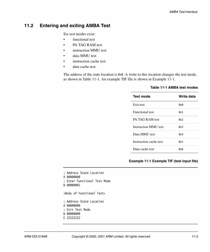
AMBA Test Interface
11.2 Entering and exiting AMBA Test
Six test modes exist:
• functional test
• PA TAG RAM test
• instruction MMU test
• data MMU test
• instruction cache test
• data cache test.
The address of the state location is 0x0. A write to this location changes the test mode, as shown in Table 11-1. An example TIF file is shown in Example 11-1.
Example 11-1 Example TIF (test input file)
; Address State LocationA 00000000; Enter Functional Test ModeW 00000001
<Body of Functional Test>
; Address State LocationA 00000000; Exit Test ModeW 00000000E ZZZZZZZZ
Table 11-1 AMBA test modes
Test mode Write data
Exit test 0x0
Functional test 0x1
PA TAG RAM test 0x2
Instruction MMU test 0x3
Data MMU test 0x4
Instruction cache test 0x5
Data cache test 0x6
ARM DDI 0184B Copyright © 2000, 2001 ARM Limited. All rights reserved. 11-3
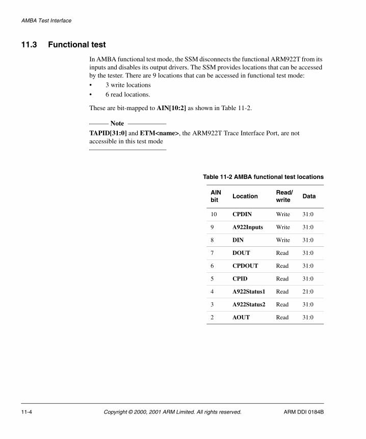
AMBA Test Interface
11.3 Functional test
In AMBA functional test mode, the SSM disconnects the functional ARM922T from its inputs and disables its output drivers. The SSM provides locations that can be accessed by the tester. There are 9 locations that can be accessed in functional test mode:
• 3 write locations
• 6 read locations.
These are bit-mapped to AIN[10:2] as shown in Table 11-2.
Note TAPID[31:0] and ETM<name>, the ARM922T Trace Interface Port, are not accessible in this test mode
Table 11-2 AMBA functional test locations
AIN bit
LocationRead/write
Data
10 CPDIN Write 31:0
9 A922Inputs Write 31:0
8 DIN Write 31:0
7 DOUT Read 31:0
6 CPDOUT Read 31:0
5 CPID Read 31:0
4 A922Status1 Read 21:0
3 A922Status2 Read 31:0
2 AOUT Read 31:0
11-4 Copyright © 2000, 2001 ARM Limited. All rights reserved. ARM DDI 0184B
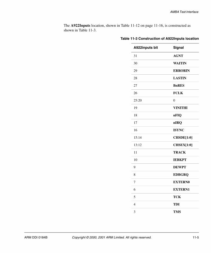
AMBA Test Interface
The A922Inputs location, shown in Table 11-12 on page 11-16, is constructed as shown in Table 11-3.
Table 11-3 Construction of A922Inputs location
A922inputs bit Signal
31 AGNT
30 WAITIN
29 ERRORIN
28 LASTIN
27 BnRES
26 FCLK
25:20 0
19 VINITHI
18 nFIQ
17 nIRQ
16 ISYNC
15:14 CHSDE[1:0]
13:12 CHSEX[1:0]
11 TRACK
10 IEBKPT
9 DEWPT
8 EDBGRQ
7 EXTERN0
6 EXTERN1
5 TCK
4 TDI
3 TMS
ARM DDI 0184B Copyright © 2000, 2001 ARM Limited. All rights reserved. 11-5
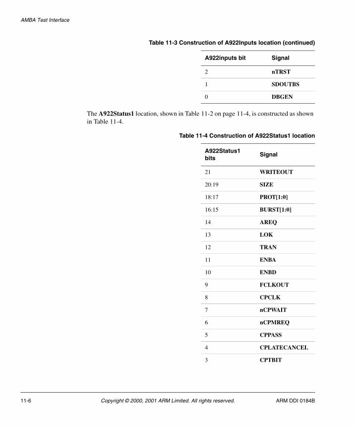
AMBA Test Interface
The A922Status1 location, shown in Table 11-2 on page 11-4, is constructed as shown in Table 11-4.
2 nTRST
1 SDOUTBS
0 DBGEN
Table 11-4 Construction of A922Status1 location
A922Status1 bits
Signal
21 WRITEOUT
20:19 SIZE
18:17 PROT[1:0]
16:15 BURST[1:0]
14 AREQ
13 LOK
12 TRAN
11 ENBA
10 ENBD
9 FCLKOUT
8 CPCLK
7 nCPWAIT
6 nCPMREQ
5 CPPASS
4 CPLATECANCEL
3 CPTBIT
Table 11-3 Construction of A922Inputs location (continued)
A922inputs bit Signal
11-6 Copyright © 2000, 2001 ARM Limited. All rights reserved. ARM DDI 0184B
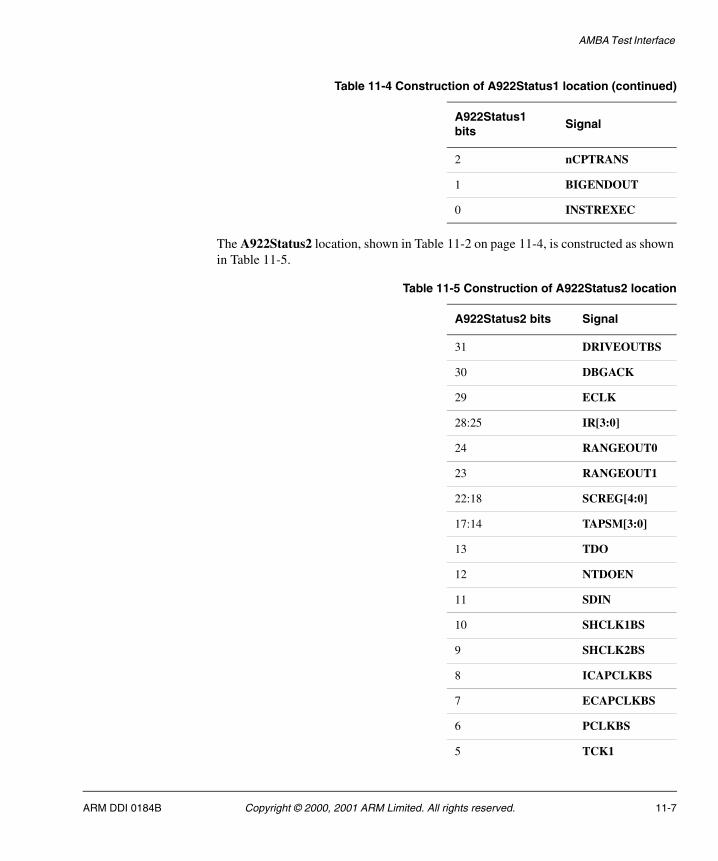
AMBA Test Interface
The A922Status2 location, shown in Table 11-2 on page 11-4, is constructed as shown in Table 11-5.
2 nCPTRANS
1 BIGENDOUT
0 INSTREXEC
Table 11-5 Construction of A922Status2 location
A922Status2 bits Signal
31 DRIVEOUTBS
30 DBGACK
29 ECLK
28:25 IR[3:0]
24 RANGEOUT0
23 RANGEOUT1
22:18 SCREG[4:0]
17:14 TAPSM[3:0]
13 TDO
12 NTDOEN
11 SDIN
10 SHCLK1BS
9 SHCLK2BS
8 ICAPCLKBS
7 ECAPCLKBS
6 PCLKBS
5 TCK1
Table 11-4 Construction of A922Status1 location (continued)
A922Status1 bits
Signal
ARM DDI 0184B Copyright © 2000, 2001 ARM Limited. All rights reserved. 11-7
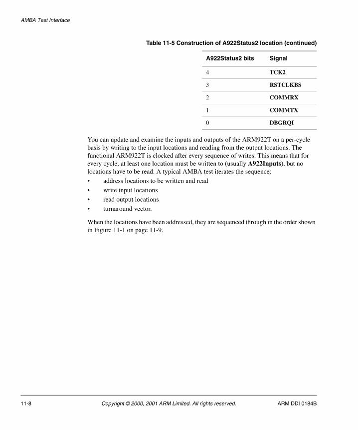
AMBA Test Interface
You can update and examine the inputs and outputs of the ARM922T on a per-cycle basis by writing to the input locations and reading from the output locations. The functional ARM922T is clocked after every sequence of writes. This means that for every cycle, at least one location must be written to (usually A922Inputs), but no locations have to be read. A typical AMBA test iterates the sequence:
• address locations to be written and read
• write input locations
• read output locations
• turnaround vector.
When the locations have been addressed, they are sequenced through in the order shown in Figure 11-1 on page 11-9.
4 TCK2
3 RSTCLKBS
2 COMMRX
1 COMMTX
0 DBGRQI
Table 11-5 Construction of A922Status2 location (continued)
A922Status2 bits Signal
11-8 Copyright © 2000, 2001 ARM Limited. All rights reserved. ARM DDI 0184B
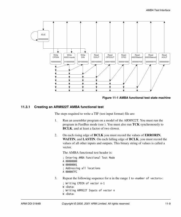
AMBA Test Interface
Figure 11-1 AMBA functional test state machine
11.3.1 Creating an ARM922T AMBA functional test
The steps required to write a TIF (test input format) file are:
1. Run an assembler program on a model of the ARM922T. You must run the program in FastBus mode (see ). You must also run TCK synchronously to BCLK, and at least a factor of two slower.
2. On each rising edge of BCLK you must record the values of ERRORIN, WAITIN, and LASTIN. On each falling edge of BCLK, you must record the values of all other inputs and outputs. This binary string of values is called a vector.
The AMBA functional test header is:
; Entering AMBA Functional Test ModeA 00000000W 00000001; Addressing all locationsA 000007FC
3. Repeat the following sequence for n in the range 1 to <number of vectors>:
; Writing CPDIN of vector n-1W <Data>; Writing ARM922T Inputs of vector nW <Data>
WriteCPDIN
100000000
IDLE
000000000
WriteA920 inputs
010000000
WriteDIN
001000000
ReadDOUT
000100000
ReadCPDOUT
000010000
ReadCPID
000001000
ReadA920Status1
000000100
ReadA920Status2
000000010
ReadAOUT
000000001
ARM DDI 0184B Copyright © 2000, 2001 ARM Limited. All rights reserved. 11-9
AMBA Test Interface
; Writing DIN of vector n-1W <Data>; Clocking ARM922T; Reading DOUT of vector nR <Data> FFFFFFFF; Reading CPID of vector nR <Data> FFFFFFFF; Reading CPDOUT of vector nR <Data> FFFFFFFF; Reading ARM922T Status Location 1 of vector n-1R <Data> 003FFCFF; Reading ARM922T Status Location 2 of vector n-1R <Data> 003FFCFF; Reading AOUT of vector nR <Data> FFFFFFFF
The AMBA functional test footer is:
; ARM922T Exiting AMBA Functional Test ModeA 00000000W 00000000A ZZZZZZZZE ZZZZZZZZ
For each write and read, <Data> is an8-character hexadecimal value. For the buses CPDIN, DIN, DOUT, CPID, CPDOUT, and AOUT this is the vector value. For the ARM922Tinputs location the data is constructed as shown in Table 11-3 on page 11-5. For the A922status1 and A922status2 locations, the read data is constructed as shown in Table 11-4 on page 11-6 and Table 11-5 on page 11-7. Vector number zero does not exist in the vector file, so on the first iteration you must write CPDIN as zero and you must give both status locations a mask value of zero. For more information see the AMBA Specification (Rev 2.0).
Note If DOUT has the same value on two or more successive vectors, the mask value for the second and subsequent reads must be zero. It is recommended that you mask out FCLKOUT and CPCLK in each status1 read.
11-10 Copyright © 2000, 2001 ARM Limited. All rights reserved. ARM DDI 0184B
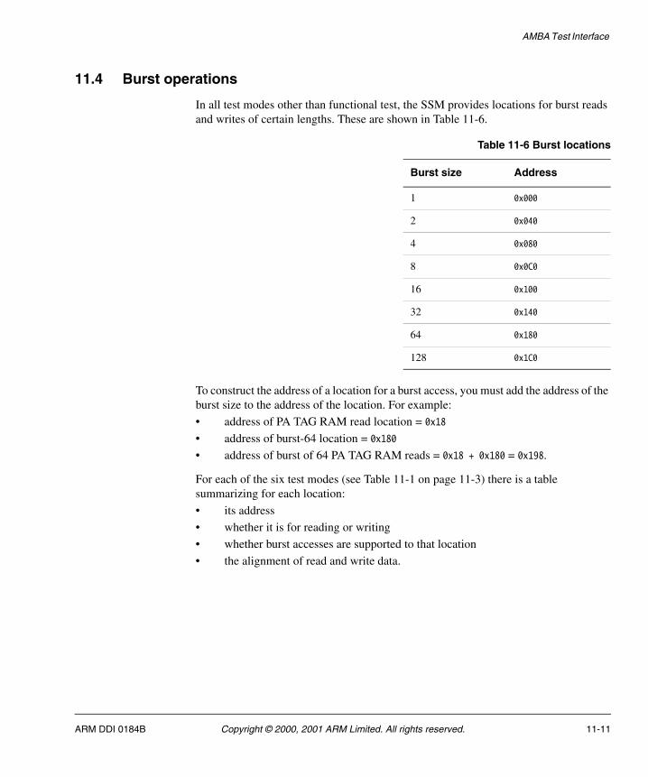
AMBA Test Interface
11.4 Burst operations
In all test modes other than functional test, the SSM provides locations for burst reads and writes of certain lengths. These are shown in Table 11-6.
To construct the address of a location for a burst access, you must add the address of the burst size to the address of the location. For example:
• address of PA TAG RAM read location = 0x18
• address of burst-64 location = 0x180
• address of burst of 64 PA TAG RAM reads = 0x18 + 0x180 = 0x198.
For each of the six test modes (see Table 11-1 on page 11-3) there is a table summarizing for each location:
• its address
• whether it is for reading or writing
• whether burst accesses are supported to that location
• the alignment of read and write data.
Table 11-6 Burst locations
Burst size Address
1 0x000
2 0x040
4 0x080
8 0x0C0
16 0x100
32 0x140
64 0x180
128 0x1C0
ARM DDI 0184B Copyright © 2000, 2001 ARM Limited. All rights reserved. 11-11
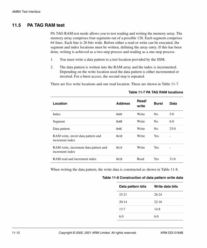
AMBA Test Interface
11.5 PA TAG RAM test
PA TAG RAM test mode allows you to test reading and writing the memory array. The memory array comprises four segments out of a possible 128. Each segment comprises 64 lines. Each line is 26 bits wide. Before either a read or write can be executed, the segment and index locations must be written, defining the array entry. If this has been done, writing is achieved as a two-step process and reading as a one-step process.
1. You must write a data pattern to a test location provided by the SSM.
2. The data pattern is written into the RAM array and the index is incremented. Depending on the write location used the data pattern is either incremented or inverted. For a burst access, the second step is repeated.
There are five write locations and one read location. These are shown in Table 11-7.
When writing the data pattern, the write data is constructed as shown in Table 11-8.
Table 11-7 PA TAG RAM locations
Location AddressRead/write
Burst Data
Index 0x04 Write No 5:0
Segment 0x08 Write No 6:0
Data pattern 0x0C Write No 25:0
RAM write, invert data pattern and increment index
0x10 Write Yes -
RAM write, increment data pattern and increment index
0x14 Write Yes -
RAM read and increment index 0x18 Read Yes 31:6
Table 11-8 Construction of data pattern write data
Data pattern bits Write data bits
25:21 28:24
20:14 22:16
13:7 14:8
6:0 6:0
11-12 Copyright © 2000, 2001 ARM Limited. All rights reserved. ARM DDI 0184B
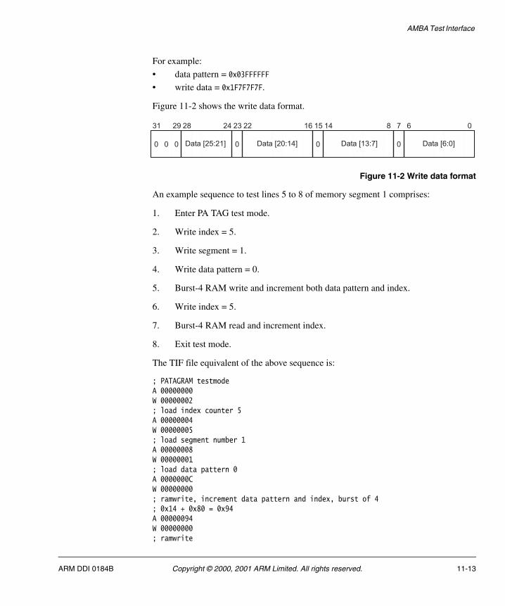
AMBA Test Interface
For example:
• data pattern = 0x03FFFFFF
• write data = 0x1F7F7F7F.
Figure 11-2 shows the write data format.
Figure 11-2 Write data format
An example sequence to test lines 5 to 8 of memory segment 1 comprises:
1. Enter PA TAG test mode.
2. Write index = 5.
3. Write segment = 1.
4. Write data pattern = 0.
5. Burst-4 RAM write and increment both data pattern and index.
6. Write index = 5.
7. Burst-4 RAM read and increment index.
8. Exit test mode.
The TIF file equivalent of the above sequence is:
; PATAGRAM testmodeA 00000000W 00000002; load index counter 5A 00000004W 00000005; load segment number 1A 00000008W 00000001; load data pattern 0A 0000000CW 00000000; ramwrite, increment data pattern and index, burst of 4; 0x14 + 0x80 = 0x94A 00000094W 00000000; ramwrite
31 29 28 24 23 22 16 15 14 8 7 6 0
0 Data [13:7] Data [6:0]00Data [20:14]Data [25:21]000
ARM DDI 0184B Copyright © 2000, 2001 ARM Limited. All rights reserved. 11-13
AMBA Test Interface
W 00000000; ramwriteW 00000000; ramwriteW 00000000; load index counter 5. Segment is unchanged at 1.A 00000004W 00000005; ramread, increment index, burst of 4; 0x18 + 0x80 = 0x98A 00000098R 00000000 FFFFFFC0; ramreadR 00000040 FFFFFFC0; ramreadR 00000080 FFFFFFC0; ramreadR 000000C0 FFFFFFC0A ZZZZZZZZ; Exit Test ModeA 00000000W 00000000; Exiting Test ModeE ZZZZZZZZ.
11-14 Copyright © 2000, 2001 ARM Limited. All rights reserved. ARM DDI 0184B
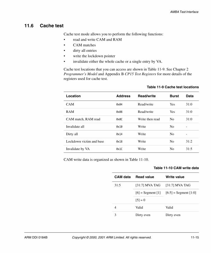
AMBA Test Interface
11.6 Cache test
Cache test mode allows you to perform the following functions:
• read and write CAM and RAM
• CAM matches
• dirty all entries
• write the lockdown pointer
• invalidate either the whole cache or a single entry by VA.
Cache test locations that you can access are shown in Table 11-9. See Chapter 2 Programmer’s Model and Appendix B CP15 Test Registers for more details of the registers used for cache test.
CAM write data is organized as shown in Table 11-10.
Table 11-9 Cache test locations
Location Address Read/write Burst Data
CAM 0x04 Read/write Yes 31:0
RAM 0x08 Read/write Yes 31:0
CAM match, RAM read 0x0C Write then read No 31:0
Invalidate all 0x10 Write No -
Dirty all 0x14 Write No -
Lockdown victim and base 0x18 Write No 31:2
Invalidate by VA 0x1C Write No 31:5
Table 11-10 CAM write data
CAM data Read value Write value
31:5 [31:7] MVA TAG [31:7] MVA TAG
[6] = Segment [1] [6:5] = Segment [1:0]
[5] = 0
4 Valid Valid
3 Dirty even Dirty even
ARM DDI 0184B Copyright © 2000, 2001 ARM Limited. All rights reserved. 11-15
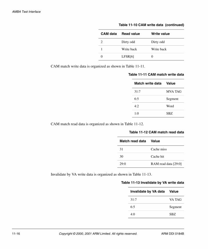
AMBA Test Interface
CAM match write data is organized as shown in Table 11-11.
CAM match read data is organized as shown in Table 11-12.
Invalidate by VA write data is organized as shown in Table 11-13.
2 Dirty odd Dirty odd
1 Write back Write back
0 LFSR[6] 0
Table 11-11 CAM match write data
Match write data Value
31:7 MVA TAG
6:5 Segment
4:2 Word
1:0 SBZ
Table 11-12 CAM match read data
Match read data Value
31 Cache miss
30 Cache hit
29:0 RAM read data [29:0]
Table 11-13 Invalidate by VA write data
Invalidate by VA data Value
31:7 VA TAG
6:5 Segment
4:0 SBZ
Table 11-10 CAM write data (continued)
CAM data Read value Write value
11-16 Copyright © 2000, 2001 ARM Limited. All rights reserved. ARM DDI 0184B
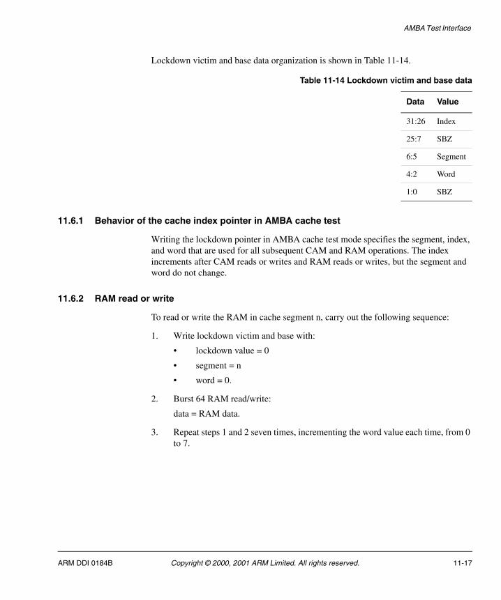
AMBA Test Interface
Lockdown victim and base data organization is shown in Table 11-14.
11.6.1 Behavior of the cache index pointer in AMBA cache test
Writing the lockdown pointer in AMBA cache test mode specifies the segment, index, and word that are used for all subsequent CAM and RAM operations. The index increments after CAM reads or writes and RAM reads or writes, but the segment and word do not change.
11.6.2 RAM read or write
To read or write the RAM in cache segment n, carry out the following sequence:
1. Write lockdown victim and base with:
• lockdown value = 0
• segment = n
• word = 0.
2. Burst 64 RAM read/write:
data = RAM data.
3. Repeat steps 1 and 2 seven times, incrementing the word value each time, from 0 to 7.
Table 11-14 Lockdown victim and base data
Data Value
31:26 Index
25:7 SBZ
6:5 Segment
4:2 Word
1:0 SBZ
ARM DDI 0184B Copyright © 2000, 2001 ARM Limited. All rights reserved. 11-17
AMBA Test Interface
11.6.3 CAM read or write
To read or write the CAM in cache segment n, carry out the following sequence:
1. Write lockdown victim and base with:
• lockdown value = 0
• segment = n.
2. Burst 64 CAM read or write:
TAG, segment, valid, dirty even, dirty odd, write back = CAM data.
11.6.4 CAM match, RAM read
To match on a VA and read out the corresponding RAM entry, carry out the following sequence:
1. Address the match location.
2. Write VA comprising:
• VA TAG
• segment
• word.
3. Read:
• cache hit
• cache miss
• RAM data.
11-18 Copyright © 2000, 2001 ARM Limited. All rights reserved. ARM DDI 0184B
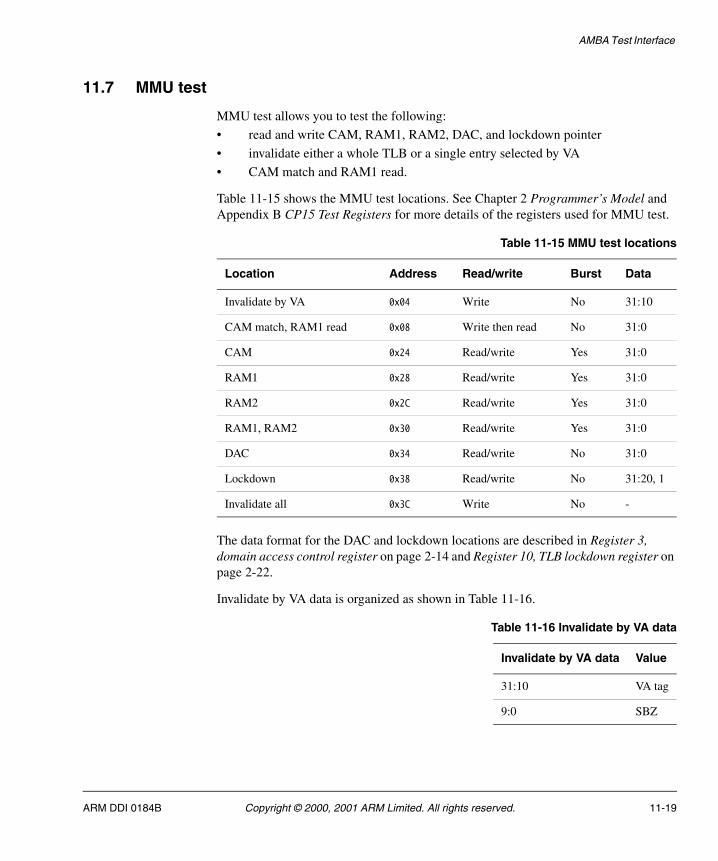
AMBA Test Interface
11.7 MMU test
MMU test allows you to test the following:
• read and write CAM, RAM1, RAM2, DAC, and lockdown pointer
• invalidate either a whole TLB or a single entry selected by VA
• CAM match and RAM1 read.
Table 11-15 shows the MMU test locations. See Chapter 2 Programmer’s Model and Appendix B CP15 Test Registers for more details of the registers used for MMU test.
The data format for the DAC and lockdown locations are described in Register 3, domain access control register on page 2-14 and Register 10, TLB lockdown register on page 2-22.
Invalidate by VA data is organized as shown in Table 11-16.
Table 11-15 MMU test locations
Location Address Read/write Burst Data
Invalidate by VA 0x04 Write No 31:10
CAM match, RAM1 read 0x08 Write then read No 31:0
CAM 0x24 Read/write Yes 31:0
RAM1 0x28 Read/write Yes 31:0
RAM2 0x2C Read/write Yes 31:0
RAM1, RAM2 0x30 Read/write Yes 31:0
DAC 0x34 Read/write No 31:0
Lockdown 0x38 Read/write No 31:20, 1
Invalidate all 0x3C Write No -
Table 11-16 Invalidate by VA data
Invalidate by VA data Value
31:10 VA tag
9:0 SBZ
ARM DDI 0184B Copyright © 2000, 2001 ARM Limited. All rights reserved. 11-19
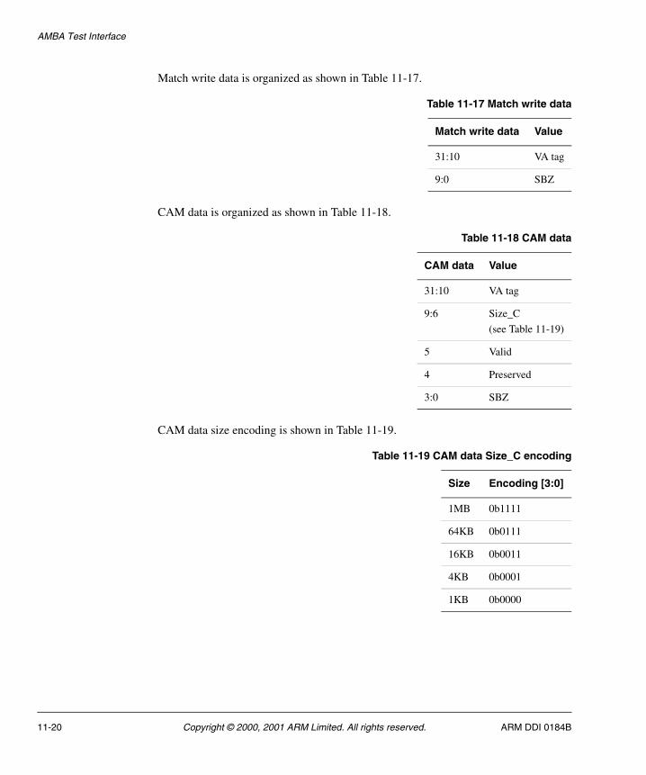
AMBA Test Interface
Match write data is organized as shown in Table 11-17.
CAM data is organized as shown in Table 11-18.
CAM data size encoding is shown in Table 11-19.
Table 11-17 Match write data
Match write data Value
31:10 VA tag
9:0 SBZ
Table 11-18 CAM data
CAM data Value
31:10 VA tag
9:6 Size_C
(see Table 11-19)
5 Valid
4 Preserved
3:0 SBZ
Table 11-19 CAM data Size_C encoding
Size Encoding [3:0]
1MB 0b1111
64KB 0b0111
16KB 0b0011
4KB 0b0001
1KB 0b0000
11-20 Copyright © 2000, 2001 ARM Limited. All rights reserved. ARM DDI 0184B
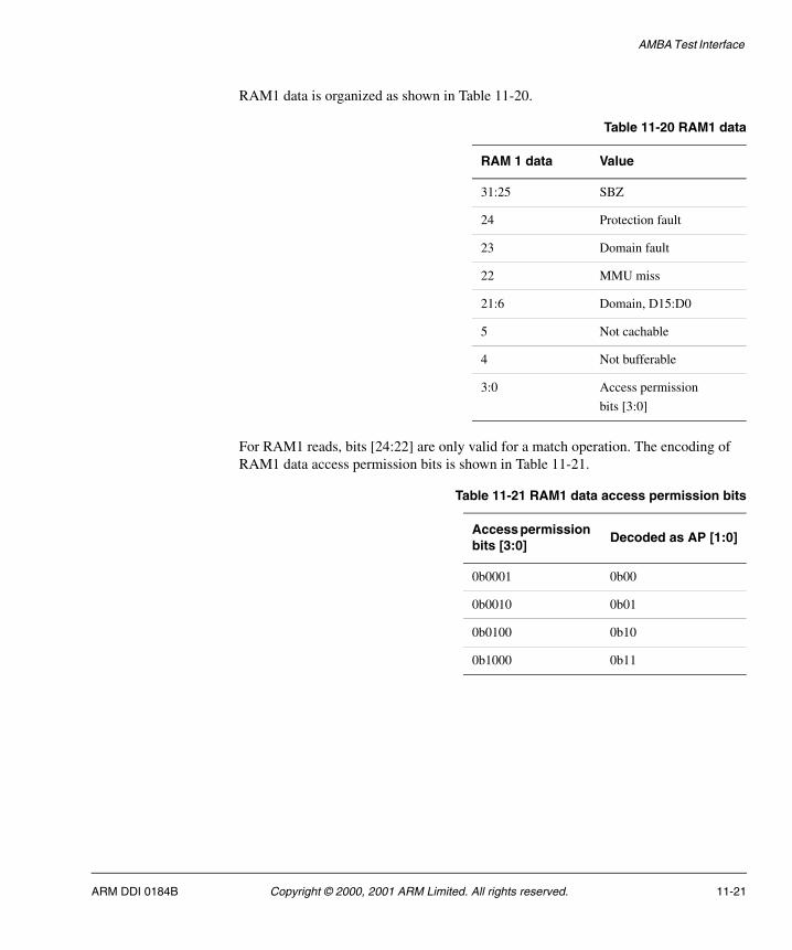
AMBA Test Interface
RAM1 data is organized as shown in Table 11-20.
For RAM1 reads, bits [24:22] are only valid for a match operation. The encoding of RAM1 data access permission bits is shown in Table 11-21.
Table 11-20 RAM1 data
RAM 1 data Value
31:25 SBZ
24 Protection fault
23 Domain fault
22 MMU miss
21:6 Domain, D15:D0
5 Not cachable
4 Not bufferable
3:0 Access permission
bits [3:0]
Table 11-21 RAM1 data access permission bits
Access permission bits [3:0]
Decoded as AP [1:0]
0b0001 0b00
0b0010 0b01
0b0100 0b10
0b1000 0b11
ARM DDI 0184B Copyright © 2000, 2001 ARM Limited. All rights reserved. 11-21
AMBA Test Interface
RAM2 data is organized as shown in Table 11-22.
The encoding of RAM2 data size bits is shown in Table 11-23.
11.7.1 Behavior of the TLB Index pointer in AMBA MMU test
Auto-increment is enabled for CAM and RAM1 reads and writes.
11.7.2 Indexing the RAM2 array
The index pointer to the RAM2 array is a pipelined version of the CAM and RAM1 index pointer. This means that to read from index n in the RAM2 array, you must first perform an access to index n in either the CAM or RAM1. Because of this, the composite location RAM1, RAM2 at address 0x30, and the Burst-128 location at address 0x1C0 are supported.
Table 11-22 RAM2 data
RAM 2 data Value
31:10 Physical address TAG
9:6 Size_R2
5:0 SBZ
Table 11-23 RAM2 data Size_R2 encoding
Size_R2 Encoding [3:0]
1MB 0b1111
64KB 0b0111
16KB 0b0011
4KB 0b0000
1KB 0b0001
11-22 Copyright © 2000, 2001 ARM Limited. All rights reserved. ARM DDI 0184B
Chapter 12 Instruction Cycle Summary and Interlocks
This chapter gives the instruction cycle times and shows the timing diagrams for interlock timing. It contains the following sections:
• About the instruction cycle summary on page 12-2
• Instruction cycle times on page 12-3
• Interlocks on page 12-6.
ARM DDI 0184B Copyright © 2000, 2001 ARM Limited. All rights reserved. 12-1
Instruction Cycle Summary and Interlocks
12.1 About the instruction cycle summary
All signals quoted in this chapter are ARM9TDMI signals, and are internal to the ARM922T. In all cases it is assumed that all accesses are from cached regions of memory.
If an instruction causes an external access, either when prefetching instructions or when accessing data, the instruction takes more cycles to complete execution. The additional number of cycles is dependent on the system implementation.
12-2 Copyright © 2000, 2001 ARM Limited. All rights reserved. ARM DDI 0184B
Instruction Cycle Summary and Interlocks
12.2 Instruction cycle times
Table 12-1 shows a key to the symbols used in tables in this section.
Table 12-2 summarizes the ARM922T instruction cycle counts and bus activity when executing the ARM instruction set.
Table 12-1 Symbols used in tables
Symbol Meaning
b The number of busy-wait states during coprocessor accesses
m Is in the range 0 to 3, depending on early termination (see Multiplier cycle counts on page 12-5)
n The number of words transferred in an LDM/STM/LDC/STC
C Coprocessor register transfer (C-cycle)
I Internal cycle (I-cycle)
N Nonsequential cycle (N-cycle)
S Sequential cycle (S-cycle)
Table 12-2 Instruction cycle bus times
Instruction CyclesInstruction bus
Data bus Comment
Data Op 1 1S 1I Normal case
Data Op 2 1S+1I 2I With register controlled shift
LDR 1 1S 1N Normal case, not loading PC
LDR 2 1S+1I 1N+1I Not loading PC and following instruction uses loaded word (1 cycle load-use interlock)
LDR 3 1S+2I 1N+2I Loaded byte, halfword, or unaligned word used by following instruction (2 cycle load-use interlock)
LDR 5 2S+2I+1N 1N+4I PC is destination register
STR 1 1S 1N All cases
LDM 2 1S+1I 1S+1I Loading 1 Register, not the PC
ARM DDI 0184B Copyright © 2000, 2001 ARM Limited. All rights reserved. 12-3
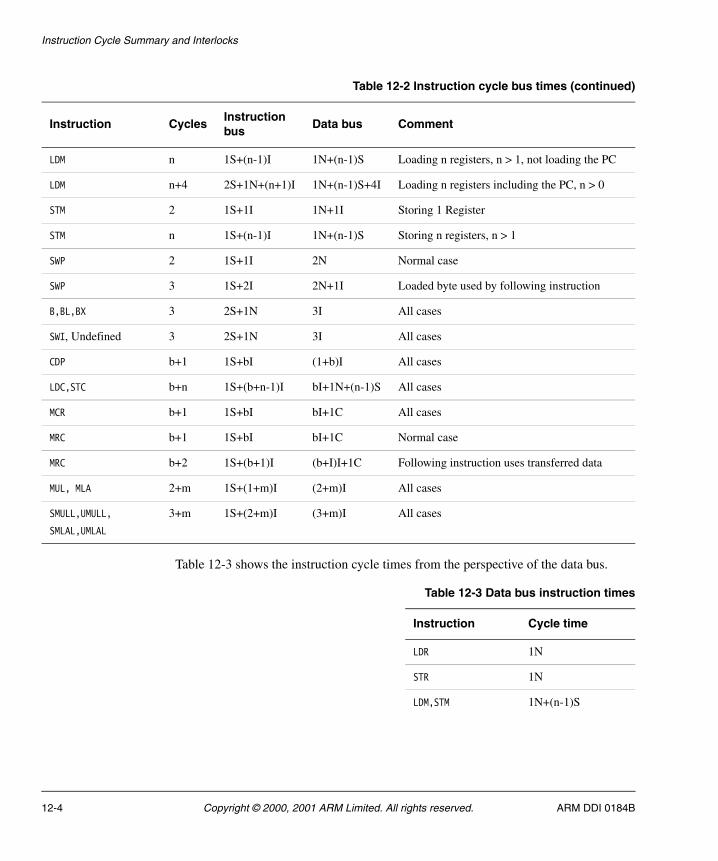
Instruction Cycle Summary and Interlocks
Table 12-3 shows the instruction cycle times from the perspective of the data bus.
LDM n 1S+(n-1)I 1N+(n-1)S Loading n registers, n > 1, not loading the PC
LDM n+4 2S+1N+(n+1)I 1N+(n-1)S+4I Loading n registers including the PC, n > 0
STM 2 1S+1I 1N+1I Storing 1 Register
STM n 1S+(n-1)I 1N+(n-1)S Storing n registers, n > 1
SWP 2 1S+1I 2N Normal case
SWP 3 1S+2I 2N+1I Loaded byte used by following instruction
B,BL,BX 3 2S+1N 3I All cases
SWI, Undefined 3 2S+1N 3I All cases
CDP b+1 1S+bI (1+b)I All cases
LDC,STC b+n 1S+(b+n-1)I bI+1N+(n-1)S All cases
MCR b+1 1S+bI bI+1C All cases
MRC b+1 1S+bI bI+1C Normal case
MRC b+2 1S+(b+1)I (b+I)I+1C Following instruction uses transferred data
MUL, MLA 2+m 1S+(1+m)I (2+m)I All cases
SMULL,UMULL,
SMLAL,UMLAL
3+m 1S+(2+m)I (3+m)I All cases
Table 12-2 Instruction cycle bus times (continued)
Instruction CyclesInstruction bus
Data bus Comment
Table 12-3 Data bus instruction times
Instruction Cycle time
LDR 1N
STR 1N
LDM,STM 1N+(n-1)S
12-4 Copyright © 2000, 2001 ARM Limited. All rights reserved. ARM DDI 0184B
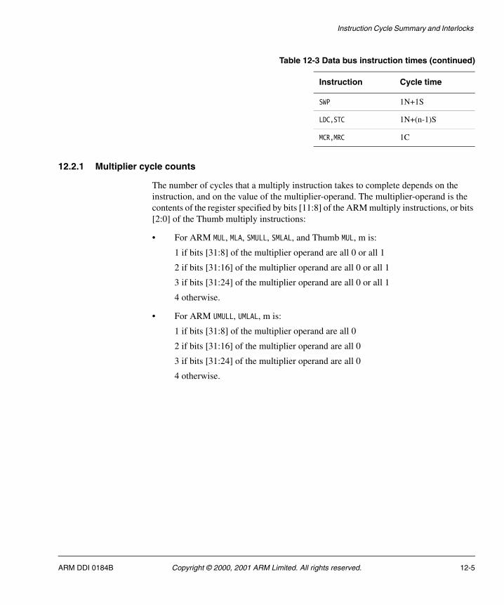
Instruction Cycle Summary and Interlocks
12.2.1 Multiplier cycle counts
The number of cycles that a multiply instruction takes to complete depends on the instruction, and on the value of the multiplier-operand. The multiplier-operand is the contents of the register specified by bits [11:8] of the ARM multiply instructions, or bits [2:0] of the Thumb multiply instructions:
• For ARM MUL, MLA, SMULL, SMLAL, and Thumb MUL, m is:
1 if bits [31:8] of the multiplier operand are all 0 or all 1
2 if bits [31:16] of the multiplier operand are all 0 or all 1
3 if bits [31:24] of the multiplier operand are all 0 or all 1
4 otherwise.
• For ARM UMULL, UMLAL, m is:
1 if bits [31:8] of the multiplier operand are all 0
2 if bits [31:16] of the multiplier operand are all 0
3 if bits [31:24] of the multiplier operand are all 0
4 otherwise.
SWP 1N+1S
LDC,STC 1N+(n-1)S
MCR,MRC 1C
Table 12-3 Data bus instruction times (continued)
Instruction Cycle time
ARM DDI 0184B Copyright © 2000, 2001 ARM Limited. All rights reserved. 12-5
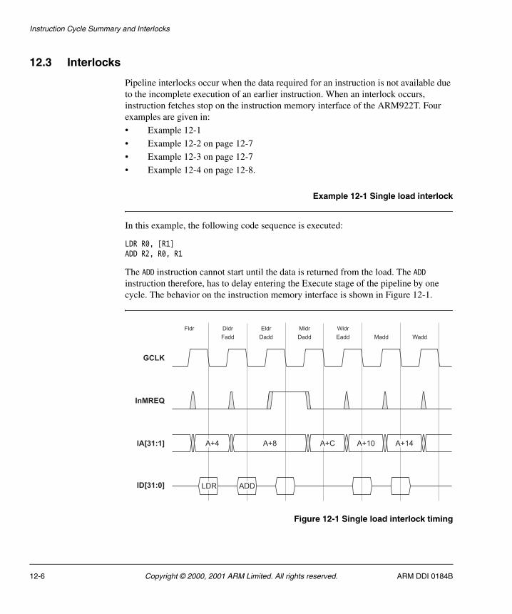
Instruction Cycle Summary and Interlocks
12.3 Interlocks
Pipeline interlocks occur when the data required for an instruction is not available due to the incomplete execution of an earlier instruction. When an interlock occurs, instruction fetches stop on the instruction memory interface of the ARM922T. Four examples are given in:
• Example 12-1
• Example 12-2 on page 12-7
• Example 12-3 on page 12-7
• Example 12-4 on page 12-8.
Example 12-1 Single load interlock
In this example, the following code sequence is executed:
LDR R0, [R1]ADD R2, R0, R1
The ADD instruction cannot start until the data is returned from the load. The ADD instruction therefore, has to delay entering the Execute stage of the pipeline by one cycle. The behavior on the instruction memory interface is shown in Figure 12-1.
Figure 12-1 Single load interlock timing
GCLK
InMREQ
IA[31:1]
Dldr Eldr
ID[31:0]
A+4
Mldr WldrFldr
Dadd Dadd Eadd Madd WaddFadd
LDR ADD
A+10 A+14A+CA+8
12-6 Copyright © 2000, 2001 ARM Limited. All rights reserved. ARM DDI 0184B
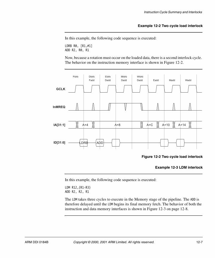
Instruction Cycle Summary and Interlocks
Example 12-2 Two cycle load interlock
In this example, the following code sequence is executed:
LDRB R0, [R1,#1]ADD R2, R0, R1
Now, because a rotation must occur on the loaded data, there is a second interlock cycle. The behavior on the instruction memory interface is shown in Figure 12-2.
Figure 12-2 Two cycle load interlock
Example 12-3 LDM interlock
In this example, the following code sequence is executed:
LDM R12,{R1-R3}ADD R2, R2, R1
The LDM takes three cycles to execute in the Memory stage of the pipeline. The ADD is therefore delayed until the LDM begins its final memory fetch. The behavior of both the instruction and data memory interfaces is shown in Figure 12-3 on page 12-8.
GCLK
InMREQ
IA[31:1]
Dldrb Eldrb
ID[31:0]
A+4
Mldrb WldrbFldrb
Dadd Dadd Eadd Madd WaddFadd
LDRB ADD
A+10 A+14A+CA+8
Dadd
ARM DDI 0184B Copyright © 2000, 2001 ARM Limited. All rights reserved. 12-7
Instruction Cycle Summary and Interlocks
Figure 12-3 LDM interlock
Example 12-4 LDM dependent interlock
In this example, the following code sequence is executed:
LDM R12,{R1-R3}ADD R4, R3, R1
The code is the same code as in example 3, but in this instance the ADD instruction uses R3. Due to the nature of load multiples, the lowest register specified is transferred first, and the highest specified register last. Because the ADD is dependent on R3, there must be another cycle of interlock while R3 is loaded. The behavior on the instruction and data memory interface is shown in Figure 12-4 on page 12-9.
GCLK
InMREQ
IA[31:1]
Dldmb Eldmb
ID[31:0]
IA+4
Mldmb WldmbFldmb
Dadd Dadd Eadd Madd WaddFadd
LDM ADD
IA+10 IA+14IA+CIA+8
Dadd
DnMREQ
DA[31:0] DA+4 DA+8DA
DD[31:0]
MldmbMldmb
R1 R2 R3
12-8 Copyright © 2000, 2001 ARM Limited. All rights reserved. ARM DDI 0184B
Instruction Cycle Summary and Interlocks
Figure 12-4 LDM dependent interlock
GCLK
InMREQ
IA[31:1]
Dldmb Eldmb
ID[31:0]
IA+4
Mldmb WldmbFldmb
Dadd Dadd Dadd Eadd MaddFadd
LDM ADD
IA+10 IA+14IA+CIA+8
Dadd
DnMREQ
DA[31:0] DA+4 DA+8DA
DD[31:0]
MldmbMldmb
R1 R2 R3
Wadd
ARM DDI 0184B Copyright © 2000, 2001 ARM Limited. All rights reserved. 12-9
Instruction Cycle Summary and Interlocks
12-10 Copyright © 2000, 2001 ARM Limited. All rights reserved. ARM DDI 0184B
Chapter 13 AC Characteristics
This chapter gives the timing diagrams and timing parameters for the ARM922T. It contains the following sections:
• ARM922T timing diagrams on page 13-2
• ARM922T timing parameters on page 13-16
• Timing definitions for the ARM922T Trace Interface Port on page 13-26.
ARM DDI 0184B Copyright © 2000, 2001 ARM Limited. All rights reserved. 13-1
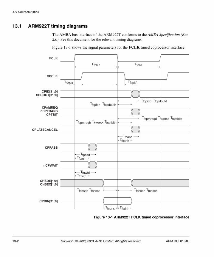
AC Characteristics
13.1 ARM922T timing diagrams
The AMBA bus interface of the ARM922T conforms to the AMBA Specification (Rev 2.0). See this document for the relevant timing diagrams.
Figure 13-1 shows the signal parameters for the FCLK timed coprocessor interface.
Figure 13-1 ARM922T FCLK timed coprocessor interface
FCLK
CPCLK
CPID[31:0]CPDOUT[31:0]
CPnMREQnCPTRANS
CPTBIT
CPLATECANCEL
CPPASS
nCPWAIT
CHSDE[1:0]CHSEX[1:0]
CPDIN[31:0]
Tfcpkr fcpkfT
fcpiddT
fcpmreqdT
fcandT
fcanhT
fpashTfpasdT
fnwtdT
fnwthT
fcdnsT
fchsdhT
fcdnhT
Tfclkh Tfclkl
fcpdoutdT
fcpidhT fcpdouthT
ftransdT fcptbitdT
fcpmreqhT ftranshT fcptbithT
fchsehTfchsdsT fchsesT
13-2 Copyright © 2000, 2001 ARM Limited. All rights reserved. ARM DDI 0184B
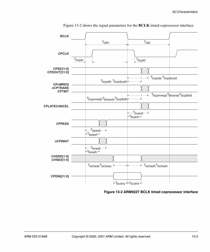
AC Characteristics
Figure 13-2 shows the signal parameters for the BCLK timed coprocessor interface.
Figure 13-2 ARM922T BCLK timed coprocessor interface
BCLK
CPCLK
CPID[31:0]CPDOUT[31:0]
CPnMREQnCPTRANS
CPTBIT
CPLATECANCEL
CPPASS
nCPWAIT
CHSDE[1:0]CHSEX[1:0]
CPDIN[31:0]
TbcpkfbcpkrT
bcandT
bcanhT
bpasdT
bpashT
bnwtdT
bnwthT
bcdnsT bcdnhT
bcpiddT
bcpmreqdT
bchsdhT
Tclkh Tclkl
bcpdoutdT
bcpidhT bcpdouthT
btransdT bcptbitdT
bcpmreqhT btranshT bcptbithT
bchsehTbchsdsT bchsesT
ARM DDI 0184B Copyright © 2000, 2001 ARM Limited. All rights reserved. 13-3
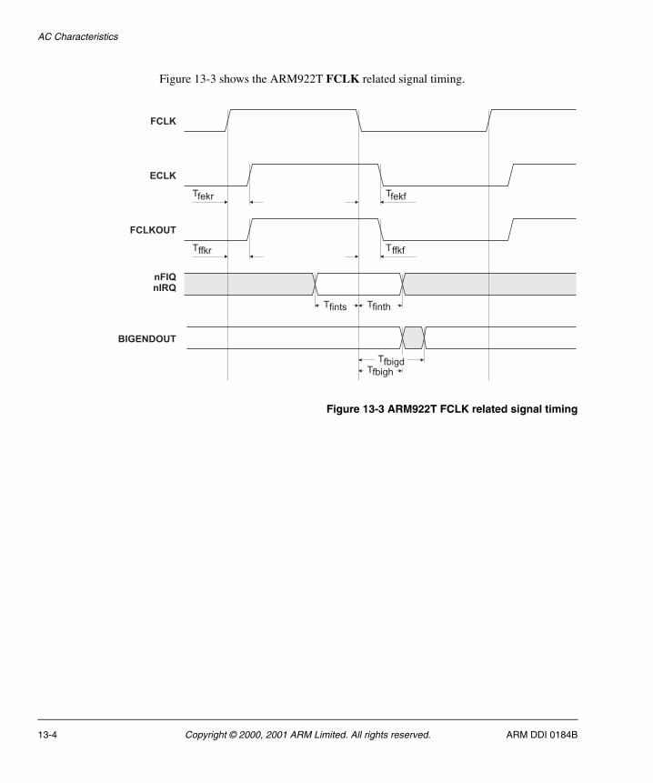
AC Characteristics
Figure 13-3 shows the ARM922T FCLK related signal timing.
Figure 13-3 ARM922T FCLK related signal timing
FCLK
ECLK
BIGENDOUT
nFIQnIRQ
fints
FCLKOUT
fekrT fekfT
ffkrT ffkfT
finthTT
fbigdT
fbighT
13-4 Copyright © 2000, 2001 ARM Limited. All rights reserved. ARM DDI 0184B
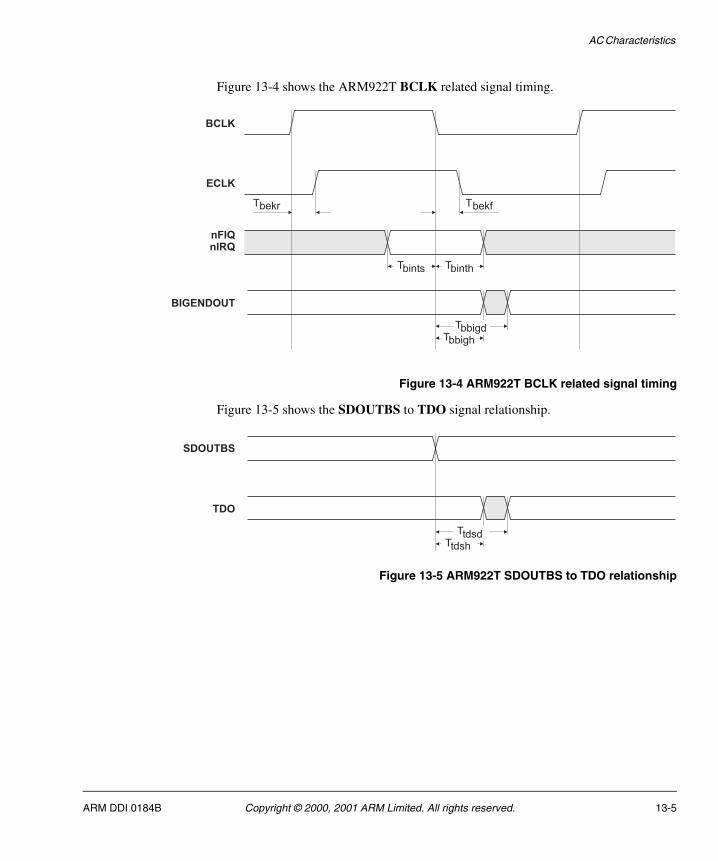
AC Characteristics
Figure 13-4 shows the ARM922T BCLK related signal timing.
Figure 13-4 ARM922T BCLK related signal timing
Figure 13-5 shows the SDOUTBS to TDO signal relationship.
Figure 13-5 ARM922T SDOUTBS to TDO relationship
BCLK
ECLK
BIGENDOUT
nFIQnIRQ
bekrT bekfT
bbigdT
bbighT
binthTbintsT
TDO
SDOUTBS
tdsdT
tdshT
ARM DDI 0184B Copyright © 2000, 2001 ARM Limited. All rights reserved. 13-5
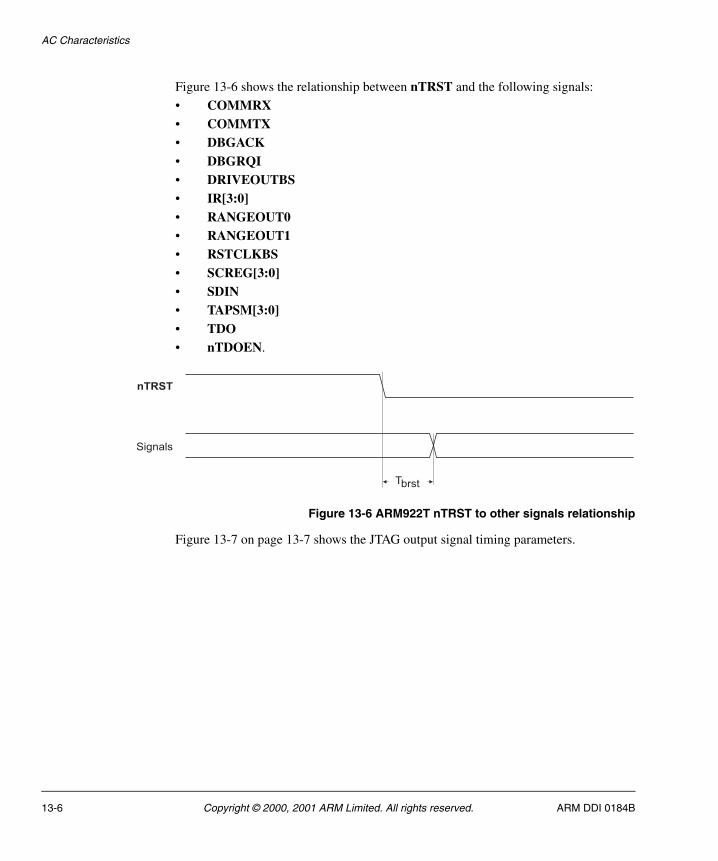
AC Characteristics
Figure 13-6 shows the relationship between nTRST and the following signals:
• COMMRX• COMMTX• DBGACK• DBGRQI• DRIVEOUTBS• IR[3:0]• RANGEOUT0• RANGEOUT1• RSTCLKBS• SCREG[3:0]• SDIN• TAPSM[3:0]• TDO• nTDOEN.
Figure 13-6 ARM922T nTRST to other signals relationship
Figure 13-7 on page 13-7 shows the JTAG output signal timing parameters.
Signals
nTRST
brstT
13-6 Copyright © 2000, 2001 ARM Limited. All rights reserved. ARM DDI 0184B
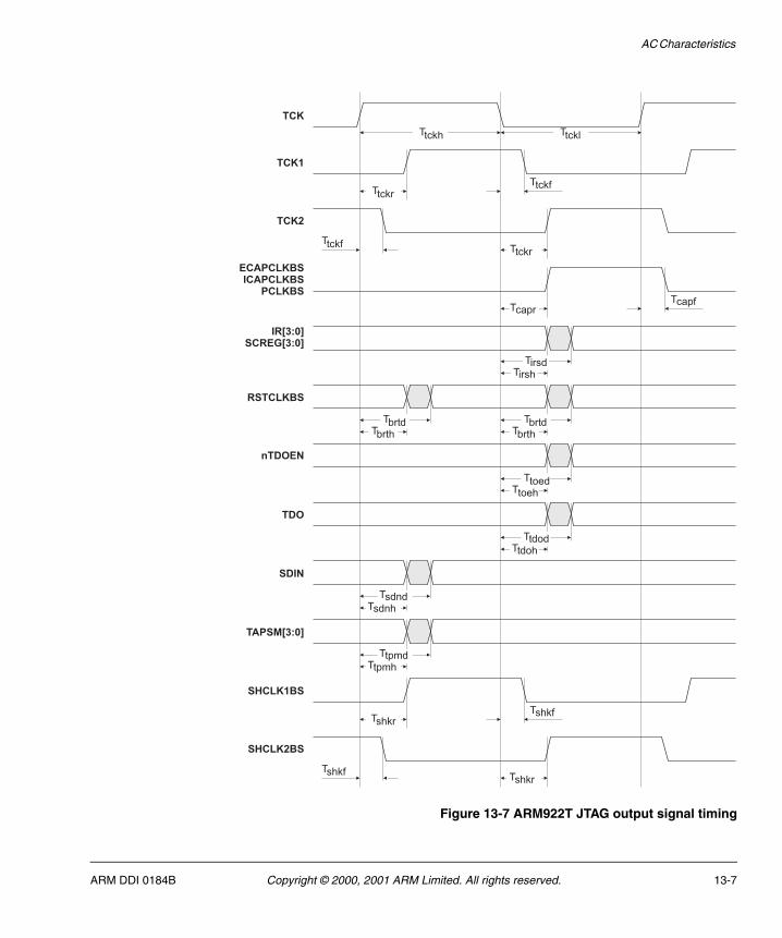
AC Characteristics
Figure 13-7 ARM922T JTAG output signal timing
TCK
TCK1
TCK2
IR[3:0]SCREG[3:0]
RSTCLKBS
SDIN
TAPSM[3:0]
ECAPCLKBSICAPCLKBS
PCLKBS
nTDOEN
TDO
SHCLK2BS
SHCLK1BS
tckfT
tckrTtckfT
tckrT
capfTcaprT
irsdT
irshT
brtdT
brthT
toedT
toehT
tdodT
tdohT
sdndT
sdnhT
tpmdT
tpmhT
shkfT
shkrTshkfT
shkrT
tckhT tcklT
brtdT
brthT
ARM DDI 0184B Copyright © 2000, 2001 ARM Limited. All rights reserved. 13-7
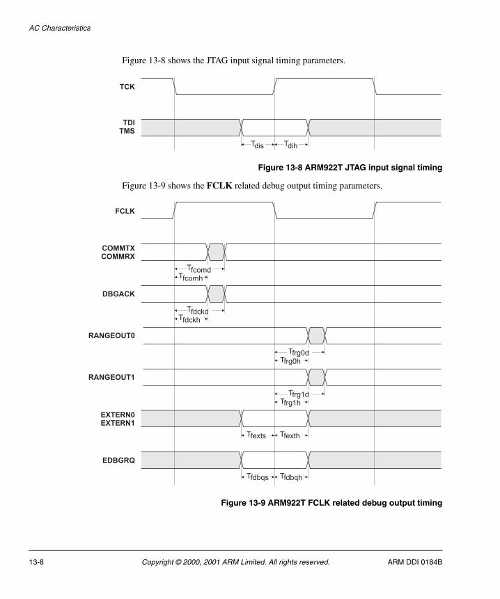
AC Characteristics
Figure 13-8 shows the JTAG input signal timing parameters.
Figure 13-8 ARM922T JTAG input signal timing
Figure 13-9 shows the FCLK related debug output timing parameters.
Figure 13-9 ARM922T FCLK related debug output timing
TCK
TDITMS
dihTdisT
FCLK
COMMTXCOMMRX
DBGACK
EXTERN0EXTERN1
EDBGRQ
RANGEOUT0
RANGEOUT1
fcomdT
fcomhT
fdckdT
fdckhT
frg0dT
frg0hT
frg1dT
frg1hT
fexthTfextsT
fdbqhTfdbqsT
13-8 Copyright © 2000, 2001 ARM Limited. All rights reserved. ARM DDI 0184B
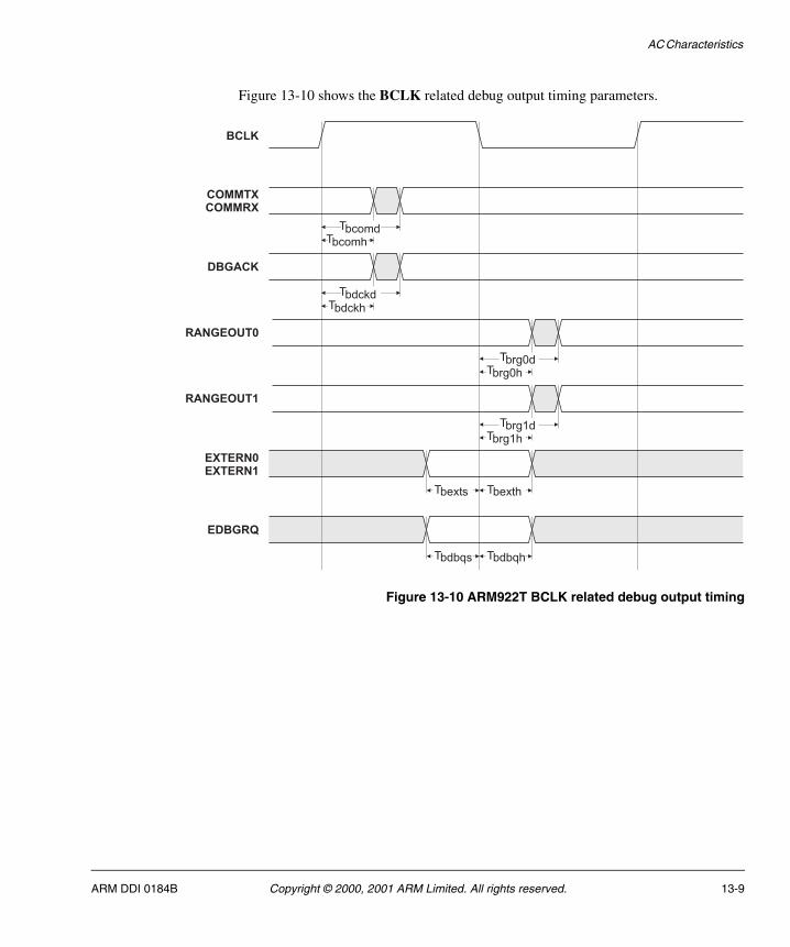
AC Characteristics
Figure 13-10 shows the BCLK related debug output timing parameters.
Figure 13-10 ARM922T BCLK related debug output timing
BCLK
COMMTXCOMMRX
DBGACK
EXTERN0EXTERN1
EDBGRQ
RANGEOUT0
RANGEOUT1
bcomdT
bcomhT
bdckdT
bdckhT
brg0dT
brg0hT
brg1dT
brg1hT
bextsT
bdbqhTbdbqsT
bexthT
ARM DDI 0184B Copyright © 2000, 2001 ARM Limited. All rights reserved. 13-9
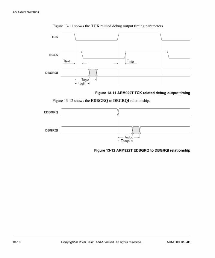
AC Characteristics
Figure 13-11 shows the TCK related debug output timing parameters.
Figure 13-11 ARM922T TCK related debug output timing
Figure 13-12 shows the EDBGRQ to DBGRQI relationship.
Figure 13-12 ARM922T EDBGRQ to DBGRQI relationship
TCK
ECLK
DBGRQI
tekfT
dgidT
dgihT
tekrT
DBGRQI
EDBGRQ
edqdT
edqhT
13-10 Copyright © 2000, 2001 ARM Limited. All rights reserved. ARM DDI 0184B
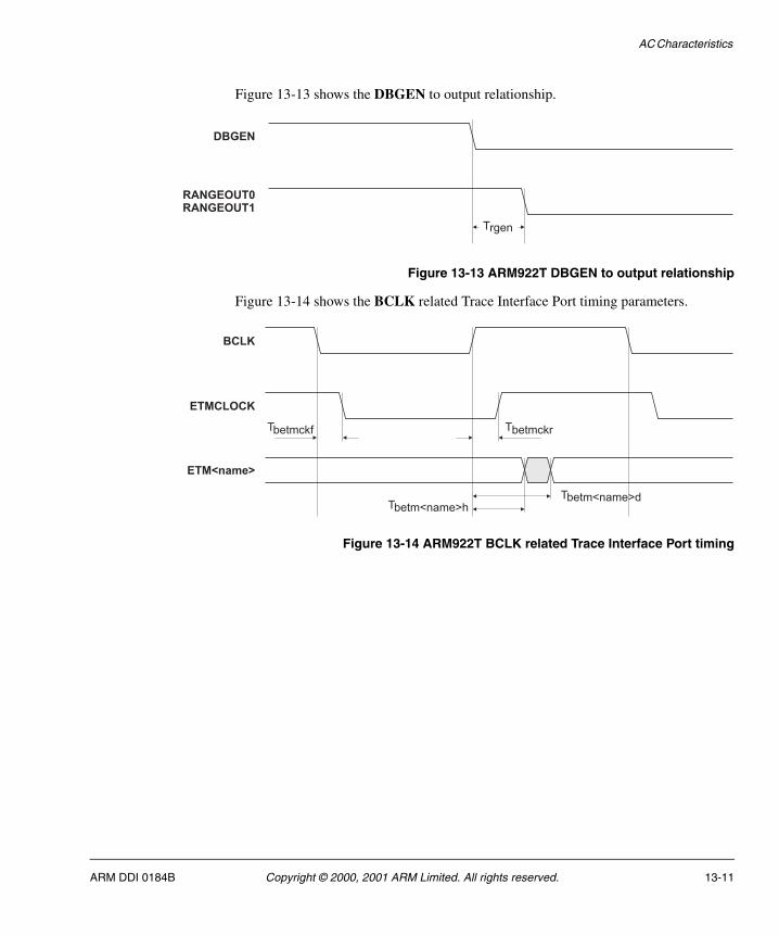
AC Characteristics
Figure 13-13 shows the DBGEN to output relationship.
Figure 13-13 ARM922T DBGEN to output relationship
Figure 13-14 shows the BCLK related Trace Interface Port timing parameters.
Figure 13-14 ARM922T BCLK related Trace Interface Port timing
RANGEOUT0RANGEOUT1
DBGEN
rgenT
BCLK
ETMCLOCK
ETM<name>
betmckfT betmckrT
betm<name>dTbetm<name>hT
ARM DDI 0184B Copyright © 2000, 2001 ARM Limited. All rights reserved. 13-11
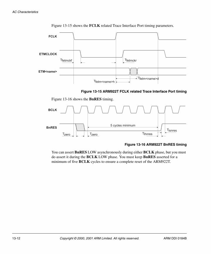
AC Characteristics
Figure 13-15 shows the FCLK related Trace Interface Port timing parameters.
Figure 13-15 ARM922T FCLK related Trace Interface Port timing
Figure 13-16 shows the BnRES timing.
Figure 13-16 ARM922T BnRES timing
You can assert BnRES LOW asynchronously during either BCLK phase, but you must de-assert it during the BCLK LOW phase. You must keep BnRES asserted for a minimum of five BCLK cycles to ensure a complete reset of the ARM922T.
FCLK
ETMCLOCK
ETM<name>
fetmckfT fetmckrT
fetm<name>dT
fetm<name>hT
BCLK
BnRES
ihnresTzeroT zeroTisnresT
5 cycles minimum
13-12 Copyright © 2000, 2001 ARM Limited. All rights reserved. ARM DDI 0184B
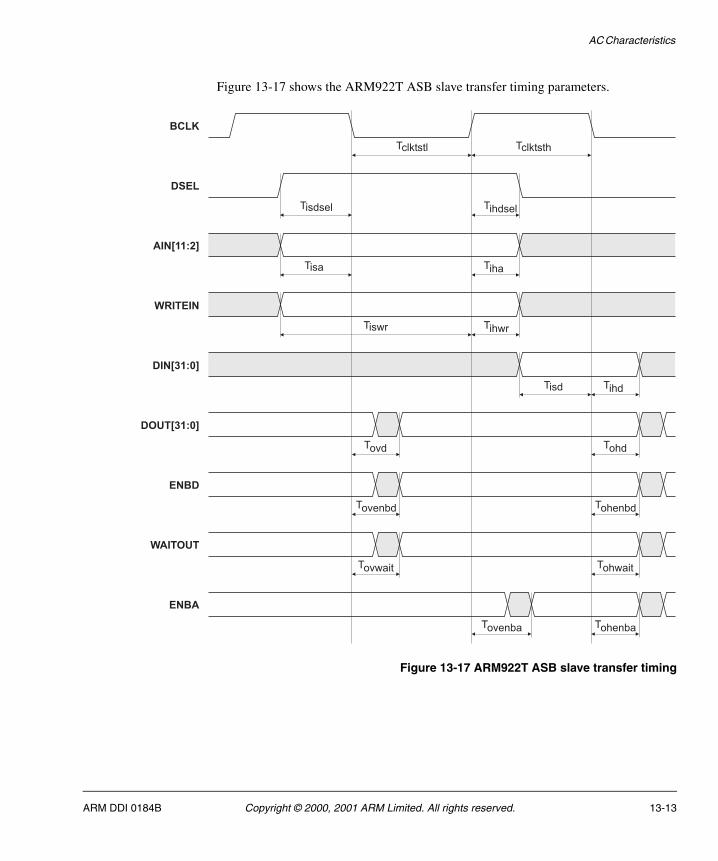
AC Characteristics
Figure 13-17 shows the ARM922T ASB slave transfer timing parameters.
Figure 13-17 ARM922T ASB slave transfer timing
BCLK
DSEL
DOUT[31:0]
isdselT ihdselT
AIN[11:2]
WRITEIN
DIN[31:0]
ENBD
WAITOUT
ENBA
isaT ihaT
iswrT ihwrT
ihdTisdT
ohdT
ohenbdT
ohwaitT
ohenbaTovenbaT
ovwaitT
ovenbdT
ovdT
clktstlT clktsthT
ARM DDI 0184B Copyright © 2000, 2001 ARM Limited. All rights reserved. 13-13
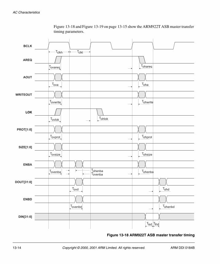
AC Characteristics
Figure 13-18 and Figure 13-19 on page 13-15 show the ARM922T ASB master transfer timing parameters.
Figure 13-18 ARM922T ASB master transfer timing
ovdT ohdT
BCLK
AREQ
WRITEOUT
LOK
SIZE[1:0]
ENBA
AOUT
PROT[1:0]
ENBD
DOUT[31:0]
ovareqT ohareqT
ohaTovaT
ovwriteT
ovprotT
LOK
ovlokT ohlokT
ovsizeT
ovenbaTovenbaT
ohwriteT
ohprotT
ohsizeT
ohenbaT
ovenbdT ohenbdT
ihdT
DIN[31:0]
ohenbaT
isdT
clkhT clklT
13-14 Copyright © 2000, 2001 ARM Limited. All rights reserved. ARM DDI 0184B
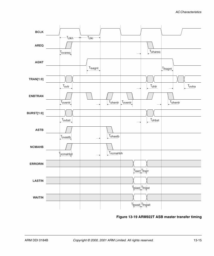
AC Characteristics
Figure 13-19 ARM922T ASB master transfer timing
ihwaitTiswaitT
ihlastTislastT
iherrTiserrT
BCLK
AREQ
AGNT
ENBTRAN
NCMAHB
ERRORIN
TRAN[1:0]
ASTB
WAITIN
LASTIN
ovareqT ohareqT
ihagntTisagntT
ohtrTovtrT
ovbstT
BURST[1:0]
oventrT ohentrT
ohbstT
ovastbT ohastbT
ncmahbdT ncmahbhT
ovtraT
oventrT ohentrT
clkhT clklT
ARM DDI 0184B Copyright © 2000, 2001 ARM Limited. All rights reserved. 13-15
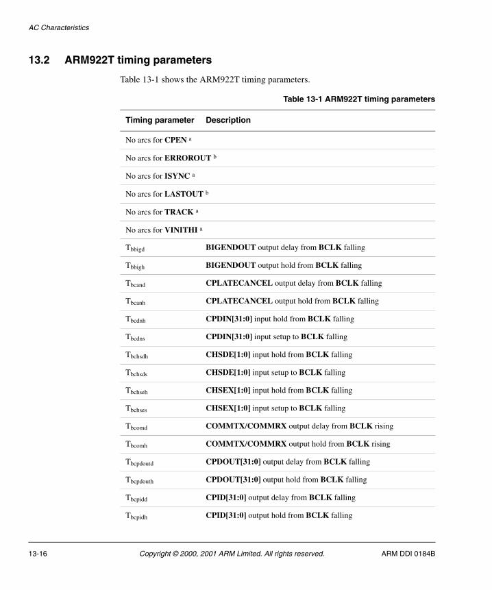
AC Characteristics
13.2 ARM922T timing parameters
Table 13-1 shows the ARM922T timing parameters.
Table 13-1 ARM922T timing parameters
Timing parameter Description
No arcs for CPEN a
No arcs for ERROROUT b
No arcs for ISYNC a
No arcs for LASTOUT b
No arcs for TRACK a
No arcs for VINITHI a
Tbbigd BIGENDOUT output delay from BCLK falling
Tbbigh BIGENDOUT output hold from BCLK falling
Tbcand CPLATECANCEL output delay from BCLK falling
Tbcanh CPLATECANCEL output hold from BCLK falling
Tbcdnh CPDIN[31:0] input hold from BCLK falling
Tbcdns CPDIN[31:0] input setup to BCLK falling
Tbchsdh CHSDE[1:0] input hold from BCLK falling
Tbchsds CHSDE[1:0] input setup to BCLK falling
Tbchseh CHSEX[1:0] input hold from BCLK falling
Tbchses CHSEX[1:0] input setup to BCLK falling
Tbcomd COMMTX/COMMRX output delay from BCLK rising
Tbcomh COMMTX/COMMRX output hold from BCLK rising
Tbcpdoutd CPDOUT[31:0] output delay from BCLK falling
Tbcpdouth CPDOUT[31:0] output hold from BCLK falling
Tbcpidd CPID[31:0] output delay from BCLK falling
Tbcpidh CPID[31:0] output hold from BCLK falling
13-16 Copyright © 2000, 2001 ARM Limited. All rights reserved. ARM DDI 0184B
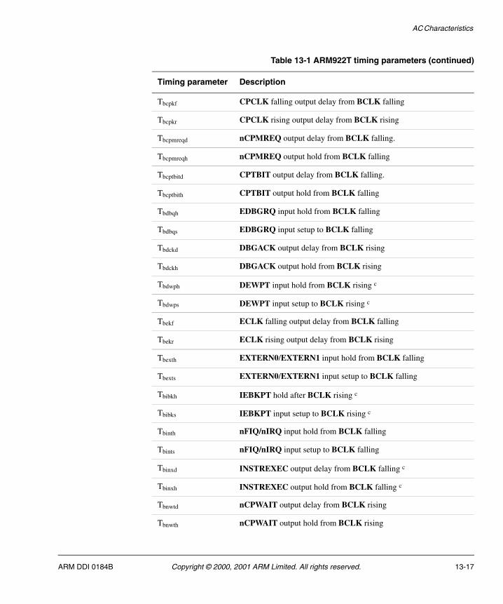
AC Characteristics
Tbcpkf CPCLK falling output delay from BCLK falling
Tbcpkr CPCLK rising output delay from BCLK rising
Tbcpmreqd nCPMREQ output delay from BCLK falling.
Tbcpmreqh nCPMREQ output hold from BCLK falling
Tbcptbitd CPTBIT output delay from BCLK falling.
Tbcptbith CPTBIT output hold from BCLK falling
Tbdbqh EDBGRQ input hold from BCLK falling
Tbdbqs EDBGRQ input setup to BCLK falling
Tbdckd DBGACK output delay from BCLK rising
Tbdckh DBGACK output hold from BCLK rising
Tbdwph DEWPT input hold from BCLK rising c
Tbdwps DEWPT input setup to BCLK rising c
Tbekf ECLK falling output delay from BCLK falling
Tbekr ECLK rising output delay from BCLK rising
Tbexth EXTERN0/EXTERN1 input hold from BCLK falling
Tbexts EXTERN0/EXTERN1 input setup to BCLK falling
Tbibkh IEBKPT hold after BCLK rising c
Tbibks IEBKPT input setup to BCLK rising c
Tbinth nFIQ/nIRQ input hold from BCLK falling
Tbints nFIQ/nIRQ input setup to BCLK falling
Tbinxd INSTREXEC output delay from BCLK falling c
Tbinxh INSTREXEC output hold from BCLK falling c
Tbnwtd nCPWAIT output delay from BCLK rising
Tbnwth nCPWAIT output hold from BCLK rising
Table 13-1 ARM922T timing parameters (continued)
Timing parameter Description
ARM DDI 0184B Copyright © 2000, 2001 ARM Limited. All rights reserved. 13-17
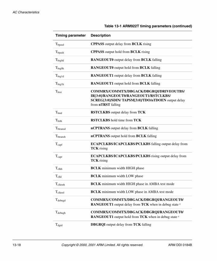
AC Characteristics
Tbpasd CPPASS output delay from BCLK rising
Tbpash CPPASS output hold from BCLK rising
Tbrg0d RANGEOUT0 output delay from BCLK falling
Tbrg0h RANGEOUT0 output hold from BCLK falling
Tbrg1d RANGEOUT1 output delay from BCLK falling
Tbrg1h RANGEOUT1 output hold from BCLK falling
Tbrst COMMRX/COMMTX/DBGACK/DBGRQI/DRIVEOUTBS/ IR[3:0]/RANGEOUT0/RANGEOUT1/RSTCLKBS/ SCREG[3:0]/SDIN/ TAPSM[3:0]/TDO/nTDOEN output delay from nTRST falling
Tbrtd RSTCLKBS output delay from TCK
Tbrth RSTCLKBS hold time from TCK
Tbtransd nCPTRANS output delay from BCLK falling
Tbtransh nCPTRANS output hold from BCLK falling
Tcapf ECAPCLKBS/ICAPCLKBS/PCLKBS falling output delay from TCK rising
Tcapr ECAPCLKBS/ICAPCLKBS/PCLKBS rising output delay from TCK rising
Tclkh BCLK minimum width HIGH phase
Tclkl BCLK minimum width LOW phase
Tclktsth BCLK minimum width HIGH phase in AMBA test mode
Tclktstl BCLK minimum width LOW phase in AMBA test mode
Tdebugd COMMRX/COMMTX/DBGACK/DBGRQI/RANGEOUT0/ RANGEOUT1 output delay from TCK when in debug state c
Tdebugh COMMRX/COMMTX/DBGACK/DBGRQI/RANGEOUT0/ RANGEOUT1 output hold from TCK when in debug state c
Tdgid DBGRQI output delay from TCK falling
Table 13-1 ARM922T timing parameters (continued)
Timing parameter Description
13-18 Copyright © 2000, 2001 ARM Limited. All rights reserved. ARM DDI 0184B
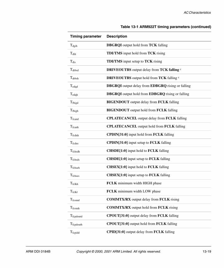
AC Characteristics
Tdgih DBGRQI output hold from TCK falling
Tdih TDI/TMS input hold from TCK rising
Tdis TDI/TMS input setup to TCK rising
Tdrbsd DRIVEOUTBS output delay from TCK falling c
Tdrbsh DRIVEOUTBS output hold from TCK falling c
Tedqd DBGRQI output delay from EDBGRQ rising or falling
Tedqh DBGRQI output hold from EDBGRQ rising or falling
Tfbigd BIGENDOUT output delay from FCLK falling
Tfbigh BIGENDOUT output hold from FCLK falling
Tfcand CPLATECANCEL output delay from FCLK falling
Tfcanh CPLATECANCEL output hold from FCLK falling
Tfcdnh CPDIN[31:0] input hold from FCLK falling
Tfcdns CPDIN[31:0] input setup to FCLK falling
Tfchsdh CHSDE[1:0] input hold to FCLK falling
Tfchsds CHSDE[1:0] input setup to FCLK falling
Tfchseh CHSEX[1:0] input hold to FCLK falling
Tfchses CHSEX[1:0] input setup to FCLK falling
Tfclkh FCLK minimum width HIGH phase
Tfclkl FCLK minimum width LOW phase
Tfcomd COMMTX/RX output delay from FCLK rising
Tfcomh COMMTX/RX output hold from FCLK rising
Tfcpdoutd CPOUT[31:0] output delay from FCLK falling
Tfcpdouth CPOUT[31:0] output hold from FCLK falling
Tfcpidd CPID[31:0] output delay from FCLK falling
Table 13-1 ARM922T timing parameters (continued)
Timing parameter Description
ARM DDI 0184B Copyright © 2000, 2001 ARM Limited. All rights reserved. 13-19
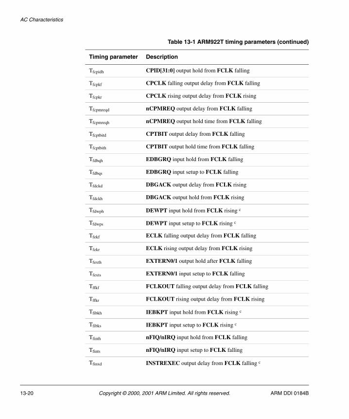
AC Characteristics
Tfcpidh CPID[31:0] output hold from FCLK falling
Tfcpkf CPCLK falling output delay from FCLK falling
Tfcpkr CPCLK rising output delay from FCLK rising
Tfcpmreqd nCPMREQ output delay from FCLK falling
Tfcpmreqh nCPMREQ output hold time from FCLK falling
Tfcptbitd CPTBIT output delay from FCLK falling
Tfcptbith CPTBIT output hold time from FCLK falling
Tfdbqh EDBGRQ input hold from FCLK falling
Tfdbqs EDBGRQ input setup to FCLK falling
Tfdckd DBGACK output delay from FCLK rising
Tfdckh DBGACK output hold from FCLK rising
Tfdwph DEWPT input hold from FCLK rising c
Tfdwps DEWPT input setup to FCLK rising c
Tfekf ECLK falling output delay from FCLK falling
Tfekr ECLK rising output delay from FCLK rising
Tfexth EXTERN0/1 output hold after FCLK falling
Tfexts EXTERN0/1 input setup to FCLK falling
Tffkf FCLKOUT falling output delay from FCLK falling
Tffkr FCLKOUT rising output delay from FCLK rising
Tfibkh IEBKPT input hold from FCLK rising c
Tfibks IEBKPT input setup to FCLK rising c
Tfinth nFIQ/nIRQ input hold from FCLK falling
Tfints nFIQ/nIRQ input setup to FCLK falling
Tfinxd INSTREXEC output delay from FCLK falling c
Table 13-1 ARM922T timing parameters (continued)
Timing parameter Description
13-20 Copyright © 2000, 2001 ARM Limited. All rights reserved. ARM DDI 0184B
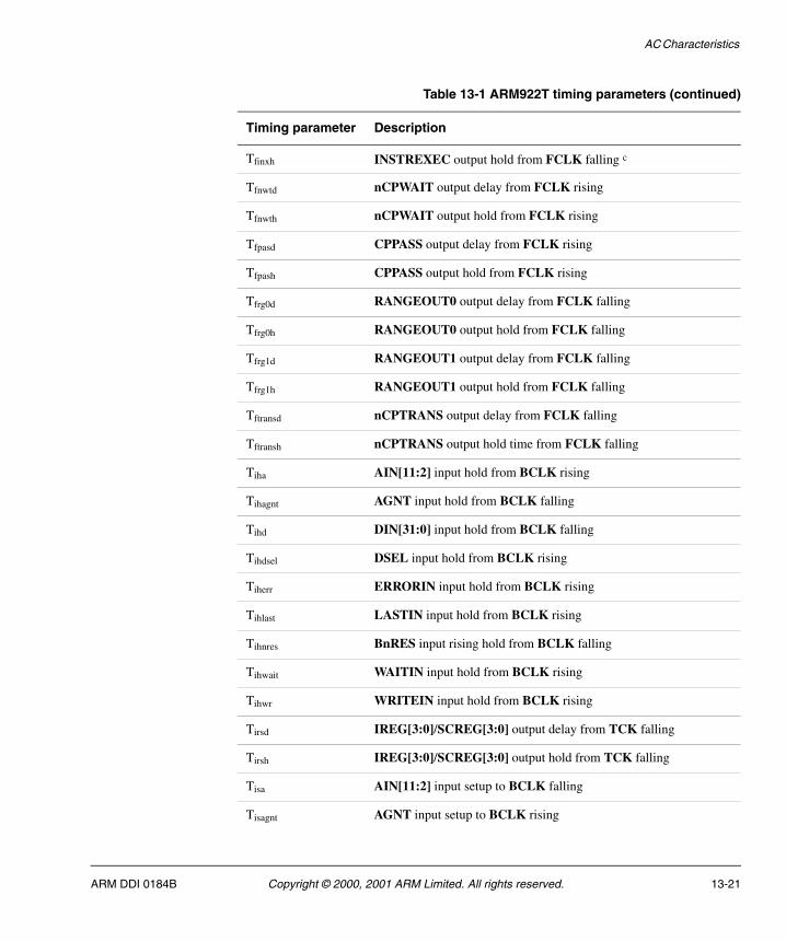
AC Characteristics
Tfinxh INSTREXEC output hold from FCLK falling c
Tfnwtd nCPWAIT output delay from FCLK rising
Tfnwth nCPWAIT output hold from FCLK rising
Tfpasd CPPASS output delay from FCLK rising
Tfpash CPPASS output hold from FCLK rising
Tfrg0d RANGEOUT0 output delay from FCLK falling
Tfrg0h RANGEOUT0 output hold from FCLK falling
Tfrg1d RANGEOUT1 output delay from FCLK falling
Tfrg1h RANGEOUT1 output hold from FCLK falling
Tftransd nCPTRANS output delay from FCLK falling
Tftransh nCPTRANS output hold time from FCLK falling
Tiha AIN[11:2] input hold from BCLK rising
Tihagnt AGNT input hold from BCLK falling
Tihd DIN[31:0] input hold from BCLK falling
Tihdsel DSEL input hold from BCLK rising
Tiherr ERRORIN input hold from BCLK rising
Tihlast LASTIN input hold from BCLK rising
Tihnres BnRES input rising hold from BCLK falling
Tihwait WAITIN input hold from BCLK rising
Tihwr WRITEIN input hold from BCLK rising
Tirsd IREG[3:0]/SCREG[3:0] output delay from TCK falling
Tirsh IREG[3:0]/SCREG[3:0] output hold from TCK falling
Tisa AIN[11:2] input setup to BCLK falling
Tisagnt AGNT input setup to BCLK rising
Table 13-1 ARM922T timing parameters (continued)
Timing parameter Description
ARM DDI 0184B Copyright © 2000, 2001 ARM Limited. All rights reserved. 13-21
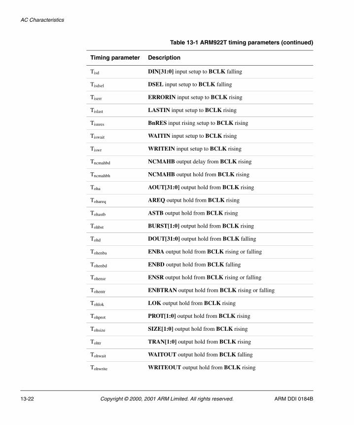
AC Characteristics
Tisd DIN[31:0] input setup to BCLK falling
Tisdsel DSEL input setup to BCLK falling
Tiserr ERRORIN input setup to BCLK rising
Tislast LASTIN input setup to BCLK rising
Tisnres BnRES input rising setup to BCLK rising
Tiswait WAITIN input setup to BCLK rising
Tiswr WRITEIN input setup to BCLK rising
Tncmahbd NCMAHB output delay from BCLK rising
Tncmahbh NCMAHB output hold from BCLK rising
Toha AOUT[31:0] output hold from BCLK rising
Tohareq AREQ output hold from BCLK rising
Tohastb ASTB output hold from BCLK rising
Tohbst BURST[1:0] output hold from BCLK rising
Tohd DOUT[31:0] output hold from BCLK falling
Tohenba ENBA output hold from BCLK rising or falling
Tohenbd ENBD output hold from BCLK falling
Tohensr ENSR output hold from BCLK rising or falling
Tohentr ENBTRAN output hold from BCLK rising or falling
Tohlok LOK output hold from BCLK rising
Tohprot PROT[1:0] output hold from BCLK rising
Tohsize SIZE[1:0] output hold from BCLK rising
Tohtr TRAN[1:0] output hold from BCLK rising
Tohwait WAITOUT output hold from BCLK falling
Tohwrite WRITEOUT output hold from BCLK rising
Table 13-1 ARM922T timing parameters (continued)
Timing parameter Description
13-22 Copyright © 2000, 2001 ARM Limited. All rights reserved. ARM DDI 0184B
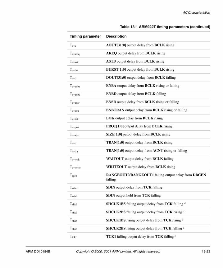
AC Characteristics
Tova AOUT[31:0] output delay from BCLK rising
Tovareq AREQ output delay from BCLK rising
Tovastb ASTB output delay from BCLK rising
Tovbst BURST[1:0] output delay from BCLK rising
Tovd DOUT[31:0] output delay from BCLK falling
Tovenba ENBA output delay from BCLK rising or falling
Tovenbd ENBD output delay from BCLK falling
Tovensr ENSR output delay from BCLK rising or falling
Toventr ENBTRAN output delay from BCLK rising or falling
Tovlok LOK output delay from BCLK rising
Tovprot PROT[1:0] output delay from BCLK rising
Tovsize SIZE[1:0] output delay from BCLK rising
Tovtr TRAN[1:0] output delay from BCLK rising
Tovtra TRAN[1:0] output delay from AGNT rising or falling
Tovwait WAITOUT output delay from BCLK falling
Tovwrite WRITEOUT output delay from BCLK rising
Trgen RANGEOUT0/RANGEOUT1 falling output delay from DBGEN falling
Tsdnd SDIN output delay from TCK falling
Tsdnh SDIN output hold from TCK falling
Tshkf SHCLK1BS falling output delay from TCK falling d
Tshkf SHCLK2BS falling output delay from TCK rising d
Tshkr SHCLK1BS rising output delay from TCK rising d
Tshkr SHCLK2BS rising output delay from TCK falling d
Ttckf TCK1 falling output delay from TCK falling e
Table 13-1 ARM922T timing parameters (continued)
Timing parameter Description
ARM DDI 0184B Copyright © 2000, 2001 ARM Limited. All rights reserved. 13-23
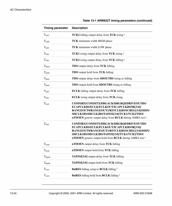
AC Characteristics
Ttckf TCK2 falling output delay from TCK rising e
Ttckh TCK minimum width HIGH phase
Ttckl TCK minimum width LOW phase
Ttckr TCK1 rising output delay from TCK rising e
Ttckr TCK2 rising output delay from TCK falling e
Ttdod TDO output delay from TCK falling
Ttdoh TDO output hold from TCK falling
Ttdsd TDO output delay from SDOUTBS rising or falling
Ttdsh TDO output hold from SDOUTBS rising or falling
Ttekf ECLK falling output delay from TCK falling
Ttekr ECLK rising output delay from TCK rising
Tticd COMMRX/COMMTX/DBGACK/DBGRQI/DRIVEOUTBS/ ECAPCLKBS/ECLK/FCLKOUT/ICAPCLKBS/IR[3:0]/ RANGEOUT0/RANGEOUT1/RSTCLKBS/SCREG[3:0]/SDIN/ SHCLK1BS/SHCLK2BS/TAPSM[3:0]/TCK1/TCK2/TDO/ nTDOEN generic output delay from BCLK during AMBA test c
Ttich COMMRX/COMMTX/DBGACK/DBGRQI/DRIVEOUTBS/ ECAPCLKBS/ECLK/FCLKOUT/ICAPCLKBS/IR[3:0]/ RANGEOUT0/RANGEOUT1/RSTCLKBS/SCREG[3:0]/SDIN/ SHCLK1BS/SHCLK2BS/TAPSM[3:0]/TCK1/TCK2/TDO/ nTDOEN generic output hold from BCLK during AMBA test c
Ttoed nTDOEN output delay from TCK falling
Ttoeh nTDOEN output hold from TCK falling
Ttpmd TAPSM[3:0] output delay from TCK falling
Ttpmh TAPSM[3:0] output hold from TCK falling
Tzero BnRES falling setup to BCLK falling f
Tzero BnRES falling hold from BCLK falling f
Table 13-1 ARM922T timing parameters (continued)
Timing parameter Description
13-24 Copyright © 2000, 2001 ARM Limited. All rights reserved. ARM DDI 0184B
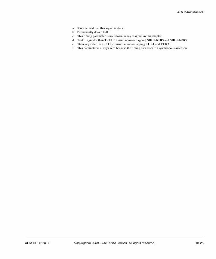
AC Characteristics
a. It is assumed that this signal is static.b. Permanently driven to 0.c. This timing parameter is not shown in any diagram in this chapter.d. Tshkr is greater than Tshkf to ensure non-overlapping SHCLK1BS and SHCLK2BS.e. Ttckr is greater than Ttckf to ensure non-overlapping TCK1 and TCK2.f. This parameter is always zero because the timing arcs refer to asynchronous assertion.
ARM DDI 0184B Copyright © 2000, 2001 ARM Limited. All rights reserved. 13-25
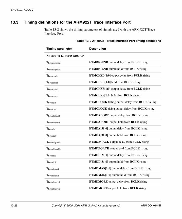
AC Characteristics
13.3 Timing definitions for the ARM922T Trace Interface Port
Table 13-2 shows the timing parameters of signals used with the ARM922T Trace Interface Port.
Table 13-2 ARM922T Trace Interface Port timing definitions
Timing parameter Description
No arcs for ETMPWRDOWN -
Tbetmbigendd ETMBIGEND output delay from BCLK rising
Tbetmbigendh ETMBIGEND output hold from BCLK rising
Tbetmchsdd ETMCHSD[1:0] output delay from BCLK rising
Tbetmchsdh ETMCHSD[1:0] hold from BCLK rising
Tbetmchsed ETMCHSE[1:0] output delay from BCLK rising
Tbetmchseh ETMCHSE[1:0] hold from BCLK rising
Tbetmckf ETMCLOCK falling output delay from BCLK falling
Tbetmckr ETMCLOCK rising output delay from BCLK rising
Tbetmdabortd ETMDABORT output delay from BCLK rising
Tbetmdaborth ETMDABORT output hold from BCLK rising
Tbetmdad ETMDA[31:0] output delay from BCLK rising
Tbetmdah ETMDA[31:0] output hold from BCLK rising
Tbetmdbgackd ETMDBGACK output delay from BCLK rising
Tbetmdbgackh ETMDBGACK output hold from BCLK rising
Tbetmddd ETMDD[31:0] output delay from BCLK rising
Tbetmddh ETMDD[31:0] output hold from BCLK rising
Tbetmdmasd ETMDMAS[1:0] output delay from BCLK rising
Tbetmdmash ETMDMAS[1:0] output hold from BCLK rising
Tbetmdmored ETMDMORE output delay from BCLK rising
Tbetmdmoreh ETMDMORE output hold from BCLK rising
13-26 Copyright © 2000, 2001 ARM Limited. All rights reserved. ARM DDI 0184B
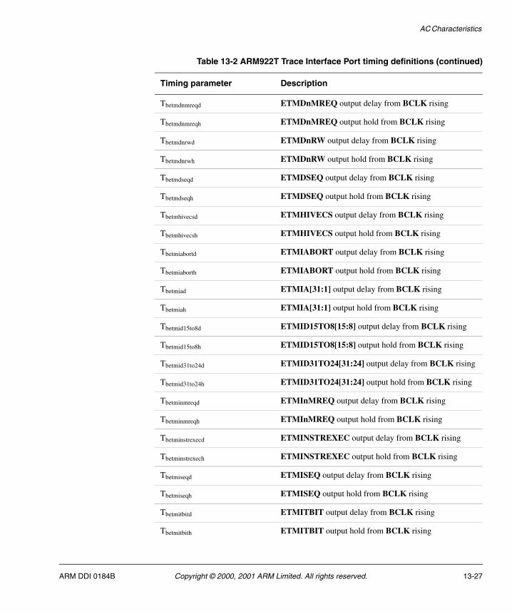
AC Characteristics
Tbetmdnmreqd ETMDnMREQ output delay from BCLK rising
Tbetmdnmreqh ETMDnMREQ output hold from BCLK rising
Tbetmdnrwd ETMDnRW output delay from BCLK rising
Tbetmdnrwh ETMDnRW output hold from BCLK rising
Tbetmdseqd ETMDSEQ output delay from BCLK rising
Tbetmdseqh ETMDSEQ output hold from BCLK rising
Tbetmhivecsd ETMHIVECS output delay from BCLK rising
Tbetmhivecsh ETMHIVECS output hold from BCLK rising
Tbetmiabortd ETMIABORT output delay from BCLK rising
Tbetmiaborth ETMIABORT output hold from BCLK rising
Tbetmiad ETMIA[31:1] output delay from BCLK rising
Tbetmiah ETMIA[31:1] output hold from BCLK rising
Tbetmid15to8d ETMID15TO8[15:8] output delay from BCLK rising
Tbetmid15to8h ETMID15TO8[15:8] output hold from BCLK rising
Tbetmid31to24d ETMID31TO24[31:24] output delay from BCLK rising
Tbetmid31to24h ETMID31TO24[31:24] output hold from BCLK rising
Tbetminmreqd ETMInMREQ output delay from BCLK rising
Tbetminmreqh ETMInMREQ output hold from BCLK rising
Tbetminstrexecd ETMINSTREXEC output delay from BCLK rising
Tbetminstrexech ETMINSTREXEC output hold from BCLK rising
Tbetmiseqd ETMISEQ output delay from BCLK rising
Tbetmiseqh ETMISEQ output hold from BCLK rising
Tbetmitbitd ETMITBIT output delay from BCLK rising
Tbetmitbith ETMITBIT output hold from BCLK rising
Table 13-2 ARM922T Trace Interface Port timing definitions (continued)
Timing parameter Description
ARM DDI 0184B Copyright © 2000, 2001 ARM Limited. All rights reserved. 13-27
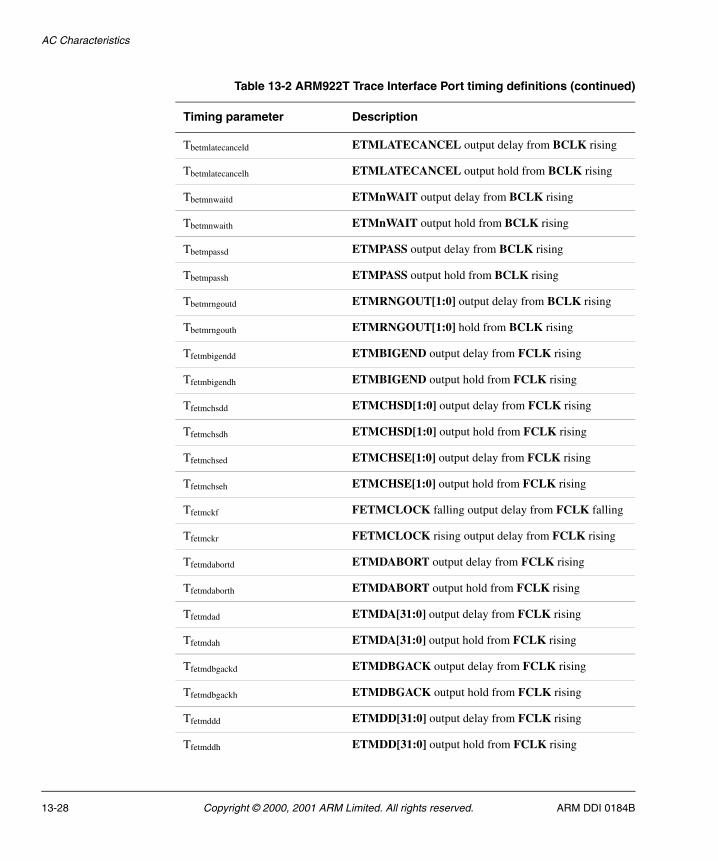
AC Characteristics
Tbetmlatecanceld ETMLATECANCEL output delay from BCLK rising
Tbetmlatecancelh ETMLATECANCEL output hold from BCLK rising
Tbetmnwaitd ETMnWAIT output delay from BCLK rising
Tbetmnwaith ETMnWAIT output hold from BCLK rising
Tbetmpassd ETMPASS output delay from BCLK rising
Tbetmpassh ETMPASS output hold from BCLK rising
Tbetmrngoutd ETMRNGOUT[1:0] output delay from BCLK rising
Tbetmrngouth ETMRNGOUT[1:0] hold from BCLK rising
Tfetmbigendd ETMBIGEND output delay from FCLK rising
Tfetmbigendh ETMBIGEND output hold from FCLK rising
Tfetmchsdd ETMCHSD[1:0] output delay from FCLK rising
Tfetmchsdh ETMCHSD[1:0] output hold from FCLK rising
Tfetmchsed ETMCHSE[1:0] output delay from FCLK rising
Tfetmchseh ETMCHSE[1:0] output hold from FCLK rising
Tfetmckf FETMCLOCK falling output delay from FCLK falling
Tfetmckr FETMCLOCK rising output delay from FCLK rising
Tfetmdabortd ETMDABORT output delay from FCLK rising
Tfetmdaborth ETMDABORT output hold from FCLK rising
Tfetmdad ETMDA[31:0] output delay from FCLK rising
Tfetmdah ETMDA[31:0] output hold from FCLK rising
Tfetmdbgackd ETMDBGACK output delay from FCLK rising
Tfetmdbgackh ETMDBGACK output hold from FCLK rising
Tfetmddd ETMDD[31:0] output delay from FCLK rising
Tfetmddh ETMDD[31:0] output hold from FCLK rising
Table 13-2 ARM922T Trace Interface Port timing definitions (continued)
Timing parameter Description
13-28 Copyright © 2000, 2001 ARM Limited. All rights reserved. ARM DDI 0184B
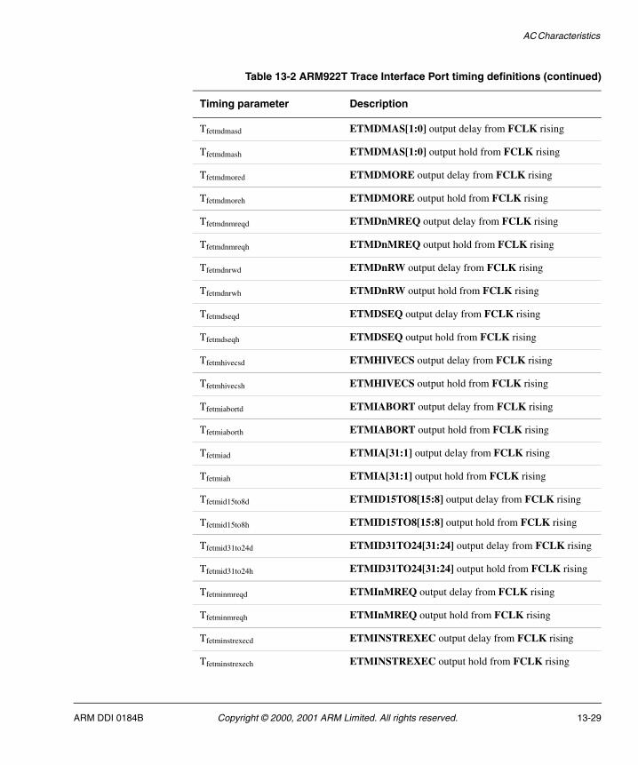
AC Characteristics
Tfetmdmasd ETMDMAS[1:0] output delay from FCLK rising
Tfetmdmash ETMDMAS[1:0] output hold from FCLK rising
Tfetmdmored ETMDMORE output delay from FCLK rising
Tfetmdmoreh ETMDMORE output hold from FCLK rising
Tfetmdnmreqd ETMDnMREQ output delay from FCLK rising
Tfetmdnmreqh ETMDnMREQ output hold from FCLK rising
Tfetmdnrwd ETMDnRW output delay from FCLK rising
Tfetmdnrwh ETMDnRW output hold from FCLK rising
Tfetmdseqd ETMDSEQ output delay from FCLK rising
Tfetmdseqh ETMDSEQ output hold from FCLK rising
Tfetmhivecsd ETMHIVECS output delay from FCLK rising
Tfetmhivecsh ETMHIVECS output hold from FCLK rising
Tfetmiabortd ETMIABORT output delay from FCLK rising
Tfetmiaborth ETMIABORT output hold from FCLK rising
Tfetmiad ETMIA[31:1] output delay from FCLK rising
Tfetmiah ETMIA[31:1] output hold from FCLK rising
Tfetmid15to8d ETMID15TO8[15:8] output delay from FCLK rising
Tfetmid15to8h ETMID15TO8[15:8] output hold from FCLK rising
Tfetmid31to24d ETMID31TO24[31:24] output delay from FCLK rising
Tfetmid31to24h ETMID31TO24[31:24] output hold from FCLK rising
Tfetminmreqd ETMInMREQ output delay from FCLK rising
Tfetminmreqh ETMInMREQ output hold from FCLK rising
Tfetminstrexecd ETMINSTREXEC output delay from FCLK rising
Tfetminstrexech ETMINSTREXEC output hold from FCLK rising
Table 13-2 ARM922T Trace Interface Port timing definitions (continued)
Timing parameter Description
ARM DDI 0184B Copyright © 2000, 2001 ARM Limited. All rights reserved. 13-29
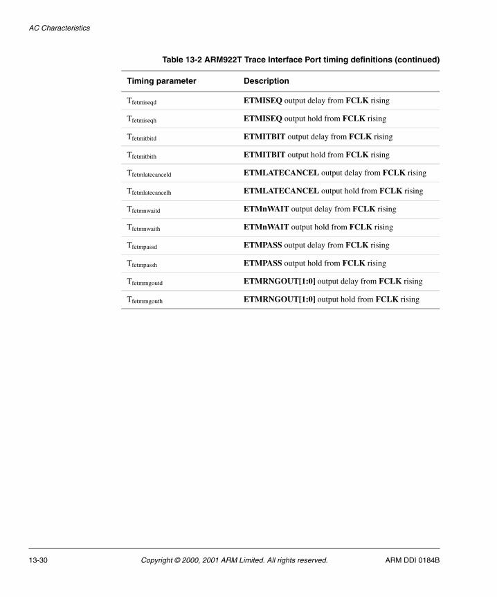
AC Characteristics
Tfetmiseqd ETMISEQ output delay from FCLK rising
Tfetmiseqh ETMISEQ output hold from FCLK rising
Tfetmitbitd ETMITBIT output delay from FCLK rising
Tfetmitbith ETMITBIT output hold from FCLK rising
Tfetmlatecanceld ETMLATECANCEL output delay from FCLK rising
Tfetmlatecancelh ETMLATECANCEL output hold from FCLK rising
Tfetmnwaitd ETMnWAIT output delay from FCLK rising
Tfetmnwaith ETMnWAIT output hold from FCLK rising
Tfetmpassd ETMPASS output delay from FCLK rising
Tfetmpassh ETMPASS output hold from FCLK rising
Tfetmrngoutd ETMRNGOUT[1:0] output delay from FCLK rising
Tfetmrngouth ETMRNGOUT[1:0] output hold from FCLK rising
Table 13-2 ARM922T Trace Interface Port timing definitions (continued)
Timing parameter Description
13-30 Copyright © 2000, 2001 ARM Limited. All rights reserved. ARM DDI 0184B
Appendix A Signal Descriptions
This appendix describes the ARM922T signals. It contains the following sections:
• AMBA signals on page A-2
• Coprocessor interface signals on page A-5
• JTAG and TAP controller signals on page A-7
• Debug signals on page A-10
• Miscellaneous signals on page A-12
• ARM922T Trace Interface Port signals on page A-13.
ARM DDI 0184B Copyright © 2000, 2001 ARM Limited. All rights reserved. A-1
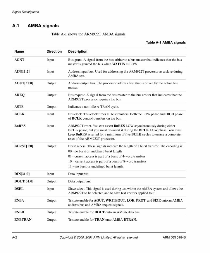
Signal Descriptions
A.1 AMBA signals
Table A-1 shows the ARM922T AMBA signals.
Table A-1 AMBA signals
Name Direction Description
AGNT Input Bus grant. A signal from the bus arbiter to a bus master that indicates that the bus master is granted the bus when WAITIN is LOW.
AIN[11:2] Input Address input bus. Used for addressing the ARM922T processor as a slave during AMBA test.
AOUT[31:0] Output Address output bus. The processor address bus, that is driven by the active bus master.
AREQ Output Bus request. A signal from the bus master to the bus arbiter that indicates that the ARM922T processor requires the bus.
ASTB Output Indicates a non-idle A-TRAN cycle.
BCLK Input Bus clock. This clock times all bus transfers. Both the LOW phase and HIGH phase of BCLK control transfers on the bus.
BnRES Input ARM922T reset. You can assert BnRES LOW asynchronously during either BCLK phase, but you must de-assert it during the BCLK LOW phase. You must keep BnRES asserted for a minimum of five BCLK cycles to ensure a complete reset of the ARM922T processor.
BURST[1:0] Output Burst access. These signals indicate the length of a burst transfer. The encoding is:
00 =no burst or undefined burst length
01= current access is part of a burst of 4-word transfers
10 = current access is part of a burst of 8-word transfers
11 = no burst or undefined burst length.
DIN[31:0] Input Data input bus.
DOUT[31:0] Output Data output bus.
DSEL Input Slave select. This signal is used during test within the AMBA system and allows the ARM922T to be selected and to have test vectors applied to it.
ENBA Output Tristate enable for AOUT, WRITEOUT, LOK, PROT, and SIZE onto an AMBA address bus and AMBA request signals.
ENBD Output Tristate enable for DOUT onto an AMBA data bus.
ENBTRAN Output Tristate enable for TRAN onto AMBA BTRAN.
A-2 Copyright © 2000, 2001 ARM Limited. All rights reserved. ARM DDI 0184B
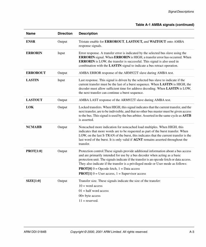
Signal Descriptions
ENSR Output Tristate enable for ERROROUT, LASTOUT, and WAITOUT onto AMBA response signals.
ERRORIN Input Error response. A transfer error is indicated by the selected bus slave using the ERRORIN signal. When ERRORIN is HIGH, a transfer error has occurred. When ERRORIN is LOW, the transfer is successful. This signal is also used in combination with the LASTIN signal to indicate a bus retract operation.
ERROROUT Output AMBA ERROR response of the ARM922T slave during AMBA test.
LASTIN Input Last response. This signal is driven by the selected bus slave to indicate if the current transfer must be the last of a burst sequence. When LASTIN is HIGH, the decoder must allow sufficient time for address decoding. When LASTIN is LOW, the next transfer can continue a burst sequence.
LASTOUT Output AMBA LAST response of the ARM922T slave during AMBA test.
LOK Output Locked transfers. When HIGH, this signal indicates that the current transfer, and the next transfer, are to be indivisible, and that no other bus master must be given access to the bus. This signal is used by the bus arbiter. Asserted in the same cycle as ASTB is asserted.
NCMAHB Output Noncached more indication for noncached load multiples. When HIGH, this indicates that more words are to be requested as part of the burst transfer. When LOW, on the last S-TRAN of the burst, this indicates that the current transfer is the last word of the burst. It is only valid if AGNT remains asserted throughout the transfer.
PROT[1:0] Output Protection control.These signals provide additional information about a bus access and are primarily intended for use by a bus decoder when acting as a basic protection unit. The signals indicate if the transfer is an opcode fetch or data access. They also indicate if the transfer is a privileged mode or User mode as follows:
PROT[0] 0 = Opcode fetch, 1 = Data access
PROT[1] 0 = User access, 1 = Supervisor access
SIZE[1:0] Output Transfer size. These signals indicate the size of the transfer:
10 = word access
01 = half word access
00= byte access
11 = reserved.
Table A-1 AMBA signals (continued)
Name Direction Description
ARM DDI 0184B Copyright © 2000, 2001 ARM Limited. All rights reserved. A-3
Signal Descriptions
A.1.1 AMBA bus specification
The ARM922T processor has a unidirectional AMBA-compatible bus interface. See the AMBA Specification (Rev 2.0) for full details.
TRAN[1:0] Output Transfer type. These signals indicate the type of the next transaction:
00 = an address-only transfer
01 = a nonsequential transfer
11 = a sequential transfer
01 reserved.
WAITIN Input Wait response. This signal is driven by the selected bus slave to indicate if the current transfer can complete. If WAITIN is HIGH, another bus cycle is required. If WAITIN is LOW, the transfer completes in the current bus cycle.
WAITOUT Output AMBA WAIT response of the ARM922T slave during AMBA test.
WRITEIN Input Transfer direction.When HIGH, this signal indicates a write transfer. When LOW, a read transfer.
WRITEOUT Output Transfer direction.When HIGH, this signal indicates a write transfer. When LOW, a read transfer.
Table A-1 AMBA signals (continued)
Name Direction Description
A-4 Copyright © 2000, 2001 ARM Limited. All rights reserved. ARM DDI 0184B
Signal Descriptions
A.2 Coprocessor interface signals
Table A-2 shows the ARM922T coprocessor interface signals.
Table A-2 Coprocessor interface signals
Name Direction Description
CHSDE[1:0] Input Coprocessor handshake decode. The handshake signals from the Decode stage of the coprocessor pipeline follower.
CHSEX[1:0] Input Coprocessor handshake execute. The handshake signals from the Execute stage of the coprocessor pipeline follower.
CPCLK Output Coprocessor clock. This clock controls the operation of the coprocessor interface.
CPDOUT[31:0] Output Coprocessor data out. The coprocessor data bus for transferring MCR and LDC data to the coprocessor.
CPDIN[31:0] Input Coprocessor data in. The coprocessor data bus for transferring MRC and STC data from the coprocessor to the ARM922T.
CPEN Input Coprocessor data out enable. When tied LOW, the CPID and CPDOUT buses are held stable. When tied HIGH, the CPID and CPDOUT buses are enabled. It is expected that this pin is used statically.
CPID[31:0] Output Coprocessor instruction data. This is the coprocessor instruction data bus used for transferring instructions to the pipeline follower in the coprocessor.
CPLATECANCEL Output Coprocessor late cancel. When a coprocessor instruction is being executed, if this signal is HIGH during the first Memory cycle, the coprocessor instruction must be canceled without having updated the coprocessor state.
nCPMREQ Output Not coprocessor memory request. When LOW on a rising CPCLK edge and nCPWAIT LOW, the instruction on CPID enters the Decode stage of the coprocessor pipeline follower. The second instruction previously in the Decode stage of the pipeline follower enters its Execute stage.
CPPASS Output Coprocessor pass. This signal indicates that there is a coprocessor instruction in the Execute stage of the pipeline, and it must be executed.
ARM DDI 0184B Copyright © 2000, 2001 ARM Limited. All rights reserved. A-5
Signal Descriptions
For more information on the coprocessor interface see Chapter 7 Coprocessor Interface.
CPTBIT Output Coprocessor Thumb bit. If HIGH, the coprocessor interface is in Thumb state.
nCPTRANS Output Not coprocessor translate. When LOW, the coprocessor interface is in a nonprivileged mode. When HIGH, the coprocessor interface is in a privileged mode. The coprocessor samples this signal on every cycle when determining the coprocessor response.
nCPWAIT Output Not coprocessor wait. The coprocessor clock CPCLK is qualified by nCPWAIT to allow the ARM922T processor to control the transfer of data on the coprocessor interface. nCPWAIT changes while CPCLK is HIGH.
Table A-2 Coprocessor interface signals (continued)
Name Direction Description
A-6 Copyright © 2000, 2001 ARM Limited. All rights reserved. ARM DDI 0184B
Signal Descriptions
A.3 JTAG and TAP controller signals
Table A-3 shows the ARM922T JTAG and TAP controller signals.
Table A-3 JTAG and TAP controller signals
Name Direction Description
DRIVEOUTBS Output Boundary scan cell enable. This signal controls the multiplexors in the scan cells of an external boundary scan chain. This signal changes in the UPDATE-IR state when scan chain 3 is selected, and either the INTEST, EXTEST, CLAMP, or CLAMPZ instruction is loaded. If you do not connect an external boundary scan chain, you must leave this output unconnected.
ECAPCLKBS Output Extest capture clock for boundary scan. This is a TCK2 wide pulse generated when the TAP controller state machine is in the CAPTURE-DR state, the current instruction is EXTEST, and scan chain 3 is selected. This signal captures the chip-level inputs during EXTEST. If you do not connect an external boundary scan chain, you must leave this output unconnected.
ICAPCLKBS Output Intest capture clock. This is a TCK2 wide pulse generated when the TAP controller state machine is in the CAPTURE-DR state, the current instruction is INTEST, and scan chain 3 is selected. This signal captures the chip-level outputs during INTEST. If you do not connect an external boundary scan chain, you must leave this output unconnected.
IR[3:0] Output Tap controller instruction register. These four bits reflect the current instruction loaded into the TAP controller instruction register. The bits change on the falling edge of TCK when the state machine is in the UPDATE-IR state.
PCLKBS Output Boundary scan update clock. This is a TCK2 wide pulse generated when the TAP controller state machine is in the UPDATE-DR state, and scan chain 3 is selected. This signal is used by an external boundary scan chain as the update clock. If you do not connect an external boundary scan chain, you must leave this output unconnected.
RSTCLKBS Output Boundary scan reset clock. This signal denotes that either the TAP controller state machine is in the RESET state, or that nTRST has been asserted. You can use this to reset external boundary scan cells.
SCREG[4:0] Output Scan chain register. These five bits reflect the ID number of the scan chain currently selected by the TAP controller. These bits change on the falling edge of TCK when the TAP state machine is in the UPDATE-DR state.
SDIN Output Boundary scan serial input data. This signal contains the serial data to be applied to an external scan chain, and is valid around the falling edge of TCK.
SDOUTBS Input Boundary scan serial output data. This is the serial data out of the boundary scan chain (or other external scan chain). It must be set up to the rising edge of TCK. If you do not connect an external boundary scan chain, you must tie this input LOW.
ARM DDI 0184B Copyright © 2000, 2001 ARM Limited. All rights reserved. A-7
Signal Descriptions
SHCLK1BS Output Boundary scan shift clock phase 1. This control signal eases the connection of an external boundary scan chain. SHCLK1BS clocks the master half of the external scan cells. When in the SHIFT-DR state of the state machine and scan chain 3 is selected, SHCLK1BS follows TCK1. When not in the SHIFT-DR state, or when scan chain 3 is not selected, this clock is LOW. If you do not connect an external boundary scan chain, you must leave this output unconnected.
SHCLK2BS Output Boundary scan shift clock phase 2. This control signal eases the connection of an external boundary scan chain. SHCLK2BS clocks the slave half of the external scan cells. When in the SHIFT-DR state of the state machine and scan chain 3 is selected, SHCLK2BS follows TCK2. When not in the SHIFT-DR state, or when scan chain 3 is not selected, this clock is LOW. If you do not connect an external boundary scan chain, you must leave this output unconnected.
TAPID[31:0] Input This is the ARM922T device identification (ID) code test data register, accessible from the scan chains. You must tie this to an appropriate value when you instantiate the device:
31:28 Functionality revision
27:12 Product code
11:1 Manufacturer identity
0 IEEE specified = 1.
TAPSM[3:0] Output TAP controller state machine. This bus reflects the current state of the TAP controller state machine. These bits change off the rising edge of TCK.
TCK Input Test clock. The JTAG clock (the test clock).
TCK1 Output TCK, phase 1. TCK1 is HIGH when TCK is HIGH, although there is a slight phase lag due to the internal clock non-overlap.
TCK2 Output TCK, Phase 2. TCK2 is HIGH when TCK is LOW, although there is a slight phase lag due to the internal clock non-overlap.
TDI Input Test data input. JTAG serial input.
TDO Output Test data output. JTAG serial output.
Table A-3 JTAG and TAP controller signals (continued)
Name Direction Description
A-8 Copyright © 2000, 2001 ARM Limited. All rights reserved. ARM DDI 0184B
Signal Descriptions
nTDOEN Output Not TDO enable. When HIGH, this signal denotes that serial data is being driven out on the TDO output. nTDOEN is normally used as an output enable for a TDO pin in a packaged part.
TMS Input Test mode select. TMS selects the state that the TAP controller state machine must change to.
nTRST Input Not test reset. Active LOW reset signal for the boundary scan logic. This pin must be pulsed or driven LOW to achieve normal device operation, in addition to the normal device reset (BnRES).
Table A-3 JTAG and TAP controller signals (continued)
Name Direction Description
ARM DDI 0184B Copyright © 2000, 2001 ARM Limited. All rights reserved. A-9
Signal Descriptions
A.4 Debug signals
Table A-4 shows the ARM922T debug signals.
Table A-4 Debug signals
Name Direction Description
COMMRX Output Communications channel receive. When HIGH, this signal denotes that the comms channel receive buffer contains data waiting to be read by the processor core.
COMMTX Output Communications channel transmit. When HIGH, this signal denotes that the comms channel transmit buffer is empty.
DBGACK Output Debug acknowledge. When HIGH, this signal indicates the ARM is in debug state.
DBGEN Input Debug enable. This input signal allows the debug features of the ARM922T to be disabled. This signal must be LOW only when debugging is not required.
DBGRQI Output Internal debug request. This signal represents the debug request signal that is presented to the processor core. This is a combination of EDBGRQ, as presented to the ARM922T processor, and bit 1 of the debug control register.
DEWPT Input External watchpoint. This signal allows external data watchpoints to be implemented.
ECLK Output External clock output.
EDBGRQ Input External debug request. When driven HIGH, this causes the processor to enter debug state when execution of the current instruction has completed.
EXTERN0 Input External input 0. This is an input to watchpoint unit 0 of the EmbeddedICE logic in the processor, and allows breakpoints or watchpoints to be dependent on an external condition.
EXTERN1 Input External input 1. This is an input to watchpoint unit 1 of the EmbeddedICE logic in the processor, and allows breakpoints or watchpoints to be dependent on an external condition.
IEBKPT Input External breakpoint. This signal allows an external instruction breakpoints to be implemented.
INSTREXEC Output Instruction executed. Indicates that in the previous cycle, the instruction in the Execute stage of the pipeline passed its condition codes, and has been executed.
A-10 Copyright © 2000, 2001 ARM Limited. All rights reserved. ARM DDI 0184B
Signal Descriptions
RANGEOUT0 Output EmbeddedICE rangeout 0. This signal indicates that the EmbeddedICE watchpoint unit 0 has matched the conditions currently present on the address, data, and control buses. This signal is independent of the state of the watchpoint unit enable control bit.
RANGEOUT1 Output EmbeddedICE rangeout 1. This signal indicates that the EmbeddedICE watchpoint unit 1 has matched the conditions currently present on the address, data, and control buses. This signal is independent of the state of the watchpoint unit enable control bit.
TRACK Input Enable TrackingICE mode. Driving this signal HIGH places the ARM922T processor into tracking mode for debugging purposes.
Table A-4 Debug signals (continued)
Name Direction Description
ARM DDI 0184B Copyright © 2000, 2001 ARM Limited. All rights reserved. A-11
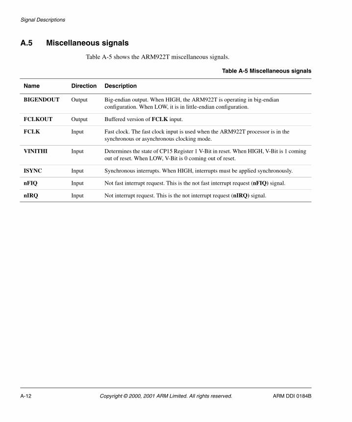
Signal Descriptions
A.5 Miscellaneous signals
Table A-5 shows the ARM922T miscellaneous signals.
Table A-5 Miscellaneous signals
Name Direction Description
BIGENDOUT Output Big-endian output. When HIGH, the ARM922T is operating in big-endian configuration. When LOW, it is in little-endian configuration.
FCLKOUT Output Buffered version of FCLK input.
FCLK Input Fast clock. The fast clock input is used when the ARM922T processor is in the synchronous or asynchronous clocking mode.
VINITHI Input Determines the state of CP15 Register 1 V-Bit in reset. When HIGH, V-Bit is 1 coming out of reset. When LOW, V-Bit is 0 coming out of reset.
ISYNC Input Synchronous interrupts. When HIGH, interrupts must be applied synchronously.
nFIQ Input Not fast interrupt request. This is the not fast interrupt request (nFIQ) signal.
nIRQ Input Not interrupt request. This is the not interrupt request (nIRQ) signal.
A-12 Copyright © 2000, 2001 ARM Limited. All rights reserved. ARM DDI 0184B
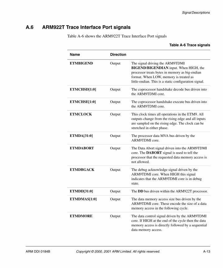
Signal Descriptions
A.6 ARM922T Trace Interface Port signals
Table A-6 shows the ARM922T Trace Interface Port signals
Table A-6 Trace signals
Name Direction
ETMBIGEND Output The signal driving the ARM9TDMI BIGEND/BIGENDIAN input. When HIGH, the processor treats bytes in memory as big-endian format. When LOW, memory is treated as little-endian. This is a static configuration signal.
ETMCHSD[1:0] Output The coprocessor handshake decode bus driven into the ARM9TDMI core.
ETMCHSE[1:0] Output The coprocessor handshake execute bus driven into the ARM9TDMI core.
ETMCLOCK Output This clock times all operations in the ETM9. All outputs change from the rising edge and all inputs are sampled on the rising edge. The clock can be stretched in either phase.
ETMDA[31:0] Output The processor data MVA bus driven by the ARM9TDMI core.
ETMDABORT Output The Data Abort signal driven into the ARM9TDMI core. The DABORT signal is used to tell the processor that the requested data memory access is not allowed.
ETMDBGACK Output The debug acknowledge signal driven by the ARM9TDMI core. When HIGH this signal indicates that the ARM9TDMI core is in debug state.
ETMDD[31:0] Output The DD bus driven within the ARM922T processor.
ETMDMAS[1:0] Output The data memory access size bus driven by the ARM9TDMI core. These encode the size of a data memory access in the following cycle.
ETMDMORE Output The data control signal driven by the ARM9TDMI core. If HIGH at the end of the cycle then the data memory access is directly followed by a sequential data memory access.
ARM DDI 0184B Copyright © 2000, 2001 ARM Limited. All rights reserved. A-13
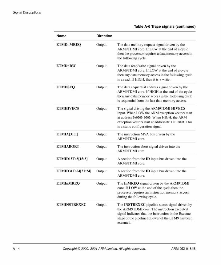
Signal Descriptions
ETMDnMREQ Output The data memory request signal driven by the ARM9TDMI core. If LOW at the end of a cycle then the processor requires a data memory access in the following cycle.
ETMDnRW Output The data read/write signal driven by the ARM9TDMI core. If LOW at the end of a cycle then any data memory access in the following cycle is a read. If HIGH, then it is a write.
ETMDSEQ Output The data sequential address signal driven by the ARM9TDMI core. If HIGH at the end of the cycle then any data memory access in the following cycle is sequential from the last data memory access.
ETMHIVECS Output The signal driving the ARM9TDMI HIVECS input. When LOW the ARM exception vectors start at address 0x0000 0000. When HIGH, the ARM exception vectors start at address 0xFFFF 0000. This is a static configuration signal.
ETMIA[31:1] Output The instruction MVA bus driven by the ARM9TDMI core.
ETMIABORT Output The instruction abort signal driven into the ARM9TDMI core.
ETMID15To8[15:8] Output A section from the ID input bus driven into the ARM9TDMI core.
ETMID31To24[31:24] Output A section from the ID input bus driven into the ARM9TDMI core.
ETMInMREQ Output The InMREQ signal driven by the ARM9TDMI core. If LOW at the end of the cycle then the processor requires an instruction memory access during the following cycle.
ETMINSTREXEC Output The INSTREXEC pipeline status signal driven by the ARM9TDMI core. The instruction executed signal indicates that the instruction in the Execute stage of the pipeline follower of the ETM9 has been executed.
Table A-6 Trace signals (continued)
Name Direction
A-14 Copyright © 2000, 2001 ARM Limited. All rights reserved. ARM DDI 0184B
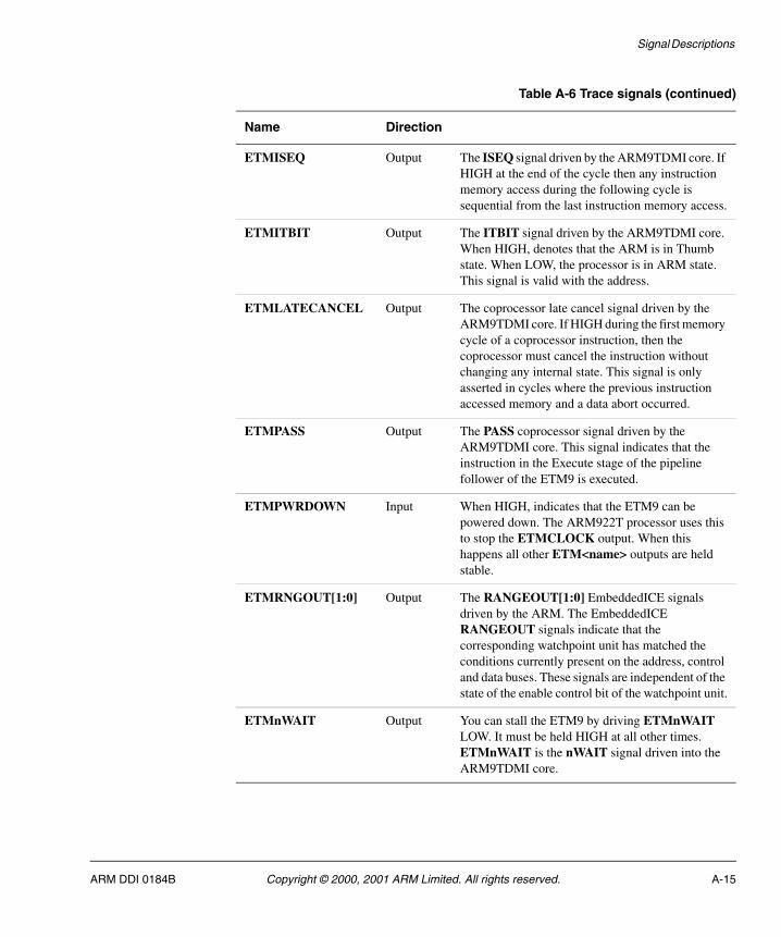
Signal Descriptions
ETMISEQ Output The ISEQ signal driven by the ARM9TDMI core. If HIGH at the end of the cycle then any instruction memory access during the following cycle is sequential from the last instruction memory access.
ETMITBIT Output The ITBIT signal driven by the ARM9TDMI core. When HIGH, denotes that the ARM is in Thumb state. When LOW, the processor is in ARM state. This signal is valid with the address.
ETMLATECANCEL Output The coprocessor late cancel signal driven by the ARM9TDMI core. If HIGH during the first memory cycle of a coprocessor instruction, then the coprocessor must cancel the instruction without changing any internal state. This signal is only asserted in cycles where the previous instruction accessed memory and a data abort occurred.
ETMPASS Output The PASS coprocessor signal driven by the ARM9TDMI core. This signal indicates that the instruction in the Execute stage of the pipeline follower of the ETM9 is executed.
ETMPWRDOWN Input When HIGH, indicates that the ETM9 can be powered down. The ARM922T processor uses this to stop the ETMCLOCK output. When this happens all other ETM<name> outputs are held stable.
ETMRNGOUT[1:0] Output The RANGEOUT[1:0] EmbeddedICE signals driven by the ARM. The EmbeddedICE RANGEOUT signals indicate that the corresponding watchpoint unit has matched the conditions currently present on the address, control and data buses. These signals are independent of the state of the enable control bit of the watchpoint unit.
ETMnWAIT Output You can stall the ETM9 by driving ETMnWAIT LOW. It must be held HIGH at all other times. ETMnWAIT is the nWAIT signal driven into the ARM9TDMI core.
Table A-6 Trace signals (continued)
Name Direction
ARM DDI 0184B Copyright © 2000, 2001 ARM Limited. All rights reserved. A-15
Signal Descriptions
A-16 Copyright © 2000, 2001 ARM Limited. All rights reserved. ARM DDI 0184B
Appendix B CP15 Test Registers
This appendix describes the ARM922T CP15 test registers. It contains the following sections:
• About the test registers on page B-2
• Test state register on page B-3
• Cache test registers and operations on page B-8
• MMU test registers and operations on page B-17.
• StrongARM backwards compatibility operations on page B-29.
ARM DDI 0184B Copyright © 2000, 2001 ARM Limited. All rights reserved. B-1
CP15 Test Registers
B.1 About the test registers
The ARM922T coprocessor 15 (CP15), register 15 (c15) is used to provide additional device-specific test operations. You can use it to access and control the following:
• Test state register on page B-3
• Cache test registers and operations on page B-8
• MMU test registers and operations on page B-17
• StrongARM backwards compatibility operations on page B-29.
You must only use these operations for test. The ARM Architecture Reference Manual describes this register as implementation defined.
The format of the CP15 test operations is:
MCR/MRC p15,opcode_1,Rd,c15,CRm,opcode_2
Figure B-1 CP15 MRC and MCR bit pattern
The L bit distinguishes between an MCR (L = 1) and an MRC (L = 0).
31 30 29 28 27 26 25 24 23 22 21 20 19 18 17 16 15 14 13 12 11 10 9 8 7 6 5 4 3 2 1 0
1 1 1 0 1 1 1 1 1
CRmopcode_2RdCRn
L
opcode_1Cond
B-2 Copyright © 2000, 2001 ARM Limited. All rights reserved. ARM DDI 0184B
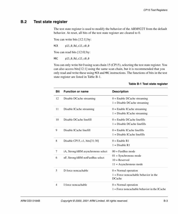
CP15 Test Registers
B.2 Test state register
The test state register is used to modify the behavior of the ARM922T from the default behavior. At reset, all bits of the test state register are cleared to 0.
You can write bits [12:1] by:
MCR p15,0,Rd,c15,c0,0
You can read bits [12:0] by:
MRC p15,0,Rd,c15,c0,0
You can only write bit 0 using scan chain 15 (CP15), selecting the test state register. You can also access bits[12:1] using the same scan chain, but it is recommended that you only read and write these using MCR and MRC instructions. The functions of bits in the test state register are listed in Table B-1.
Table B-1 Test state register
Bit Function or name Description
12 Disable DCache streaming 0 = Enable DCache streaming
1 = Disable DCache streaming
11 Disable ICache streaming 0 = Enable ICache streaming
1 = Disable ICache streaming
10 Disable DCache linefill 0 = Enable DCache linefills
1 = Disable DCache linefills
9 Disable ICache linefill 0 = Enable ICache linefills
1 = Disable ICache linefills
8 Disable CP15, c1, bits[31:30] 0 = Enable R1
1 = Disable R1
7 iA, StrongARM asynchronous select 00 = FastBus mode
01 = Synchronous mode
10 = Reserved
11 = Asynchronous mode
6 nF, StrongARM notFastBus select
5 D force noncachable 0 = Normal operation
1 = Force noncachable behavior in the DCache
4 I force noncachable 0 = Normal operation
1 = Force noncachable behavior in the ICache
ARM DDI 0184B Copyright © 2000, 2001 ARM Limited. All rights reserved. B-3
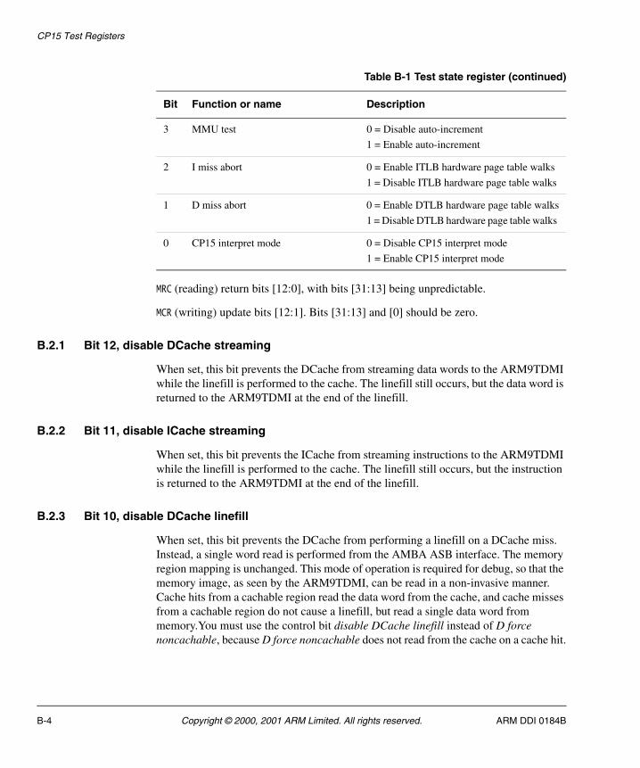
CP15 Test Registers
MRC (reading) return bits [12:0], with bits [31:13] being unpredictable.
MCR (writing) update bits [12:1]. Bits [31:13] and [0] should be zero.
B.2.1 Bit 12, disable DCache streaming
When set, this bit prevents the DCache from streaming data words to the ARM9TDMI while the linefill is performed to the cache. The linefill still occurs, but the data word is returned to the ARM9TDMI at the end of the linefill.
B.2.2 Bit 11, disable ICache streaming
When set, this bit prevents the ICache from streaming instructions to the ARM9TDMI while the linefill is performed to the cache. The linefill still occurs, but the instruction is returned to the ARM9TDMI at the end of the linefill.
B.2.3 Bit 10, disable DCache linefill
When set, this bit prevents the DCache from performing a linefill on a DCache miss. Instead, a single word read is performed from the AMBA ASB interface. The memory region mapping is unchanged. This mode of operation is required for debug, so that the memory image, as seen by the ARM9TDMI, can be read in a non-invasive manner. Cache hits from a cachable region read the data word from the cache, and cache misses from a cachable region do not cause a linefill, but read a single data word from memory.You must use the control bit disable DCache linefill instead of D force noncachable, because D force noncachable does not read from the cache on a cache hit.
3 MMU test 0 = Disable auto-increment
1 = Enable auto-increment
2 I miss abort 0 = Enable ITLB hardware page table walks
1 = Disable ITLB hardware page table walks
1 D miss abort 0 = Enable DTLB hardware page table walks
1 = Disable DTLB hardware page table walks
0 CP15 interpret mode 0 = Disable CP15 interpret mode
1 = Enable CP15 interpret mode
Table B-1 Test state register (continued)
Bit Function or name Description
B-4 Copyright © 2000, 2001 ARM Limited. All rights reserved. ARM DDI 0184B
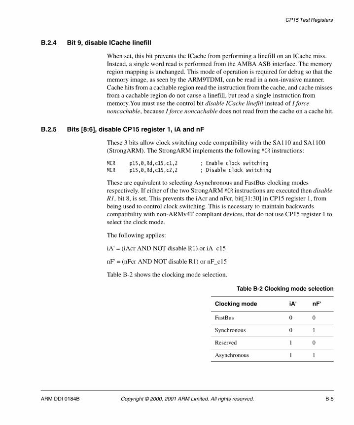
CP15 Test Registers
B.2.4 Bit 9, disable ICache linefill
When set, this bit prevents the ICache from performing a linefill on an ICache miss. Instead, a single word read is performed from the AMBA ASB interface. The memory region mapping is unchanged. This mode of operation is required for debug so that the memory image, as seen by the ARM9TDMI, can be read in a non-invasive manner. Cache hits from a cachable region read the instruction from the cache, and cache misses from a cachable region do not cause a linefill, but read a single instruction from memory.You must use the control bit disable ICache linefill instead of I force noncachable, because I force noncachable does not read from the cache on a cache hit.
B.2.5 Bits [8:6], disable CP15 register 1, iA and nF
These 3 bits allow clock switching code compatibility with the SA110 and SA1100 (StrongARM). The StrongARM implements the following MCR instructions:
MCR p15,0,Rd,c15,c1,2 ; Enable clock switchingMCR p15,0,Rd,c15,c2,2 ; Disable clock switching
These are equivalent to selecting Asynchronous and FastBus clocking modes respectively. If either of the two StrongARM MCR instructions are executed then disable R1, bit 8, is set. This prevents the iAcr and nFcr, bit[31:30] in CP15 register 1, from being used to control clock switching. This is necessary to maintain backwards compatibility with non-ARMv4T compliant devices, that do not use CP15 register 1 to select the clock mode.
The following applies:
iA' = (iAcr AND NOT disable R1) or iA_c15
nF' = (nFcr AND NOT disable R1) or nF_c15
Table B-2 shows the clocking mode selection.
Table B-2 Clocking mode selection
Clocking mode iA' nF'
FastBus 0 0
Synchronous 0 1
Reserved 1 0
Asynchronous 1 1
ARM DDI 0184B Copyright © 2000, 2001 ARM Limited. All rights reserved. B-5
CP15 Test Registers
B.2.6 Bit 5, D force noncachable
The cachable behavior for a memory region is determined by the AND of the DCache enable in CP15 register 1 and the cachable bit of the MMU page table entry:
C = Ccr AND Ctt
Setting the D force noncachable bit effectively forces the C=0. This means all memory accesses are treated as single memory accesses on the AMBA ASB interface. A write that hits in the cache updates the cache. A read that hits in the cache is ignored, and the data read from the AMBA ASB interface does not update the cache.
B.2.7 Bit 4, I force noncachable
The cachable behavior for a memory region is determined by the AND of the ICache enable in CP15 register 1 and the cachable bit of the MMU page table entry:
C = Icr AND Ctt
Setting the I force noncachable bit effectively forces the C=0. This means all memory accesses are treated as single memory accesses on the AMBA ASB interface. A read that hits in the cache is ignored, and the instruction from the AMBA ASB interface does not update the cache.
B.2.8 Bit 3, MMU test
Setting the MMU test bit enables auto-increment of the TLB index pointer in both MMUs on CAM and RAM1 reads and writes. If this bit is not set, the TLB index pointer only increments on RAM1 writes.
B.2.9 Bit 2, I miss abort
When ITLB page table walks are disabled, the ITLB miss causes an Instruction Abort and indicates a translation fault in the IFSR. The Instruction Abort handler then has to use a CP15 MCR instruction to write a page table entry to the instruction TLB.It is a requirement that the ICache and MMU is enabled when you disable hardware page table walks, otherwise the behavior is unpredictable.
B.2.10 Bit 1, D miss abort
When DTLB page table walks are disabled, the DTLB miss causes a Data Abort and indicates a translation fault in the DFSR. The Data Abort handler then has to use a CP15 MCR instruction to write a page table entry to the data TLB.It is a requirement that the DCache and MMU is enabled when you disable hardware page table walks, otherwise the behavior is unpredictable.
B-6 Copyright © 2000, 2001 ARM Limited. All rights reserved. ARM DDI 0184B
CP15 Test Registers
B.2.11 Bit 0, CP15 interpret mode
This bit is only writable using scan chain 15, selecting register c15.State. This accesses the whole test state register. Therefore this bit must be written using read-modify-write.
Interpreted mode allows interpreted accesses to take place within the ARM922T memory system. To do this, the required MCR or MRC instruction word must be shifted into scan chain 15. A system speed LDR (read) or STR (write) can then be performed on the ARM9TDMI. CP15 will interpret the LDR or STR by executing the MCR or MRC instruction held in scan chain 15. In the case of an LDR, the data is returned to the ARM9TDMI. In the case of a STR, the interpreted MCR or MRC completes with the data from the ARM9TDMI. You can exit interpreted mode by performing a read-modify-write to scan chain 15, register c15.State to reset bit 0 to 0.
ARM DDI 0184B Copyright © 2000, 2001 ARM Limited. All rights reserved. B-7
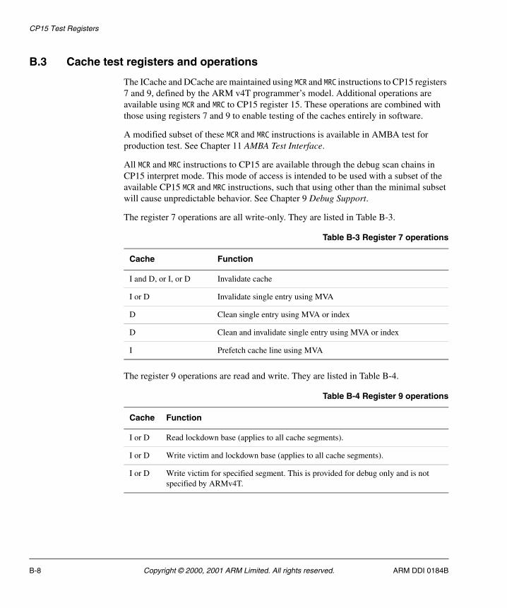
CP15 Test Registers
B.3 Cache test registers and operations
The ICache and DCache are maintained using MCR and MRC instructions to CP15 registers 7 and 9, defined by the ARM v4T programmer’s model. Additional operations are available using MCR and MRC to CP15 register 15. These operations are combined with those using registers 7 and 9 to enable testing of the caches entirely in software.
A modified subset of these MCR and MRC instructions is available in AMBA test for production test. See Chapter 11 AMBA Test Interface.
All MCR and MRC instructions to CP15 are available through the debug scan chains in CP15 interpret mode. This mode of access is intended to be used with a subset of the available CP15 MCR and MRC instructions, such that using other than the minimal subset will cause unpredictable behavior. See Chapter 9 Debug Support.
The register 7 operations are all write-only. They are listed in Table B-3.
The register 9 operations are read and write. They are listed in Table B-4.
Table B-3 Register 7 operations
Cache Function
I and D, or I, or D Invalidate cache
I or D Invalidate single entry using MVA
D Clean single entry using MVA or index
D Clean and invalidate single entry using MVA or index
I Prefetch cache line using MVA
Table B-4 Register 9 operations
Cache Function
I or D Read lockdown base (applies to all cache segments).
I or D Write victim and lockdown base (applies to all cache segments).
I or D Write victim for specified segment. This is provided for debug only and is not specified by ARMv4T.
B-8 Copyright © 2000, 2001 ARM Limited. All rights reserved. ARM DDI 0184B
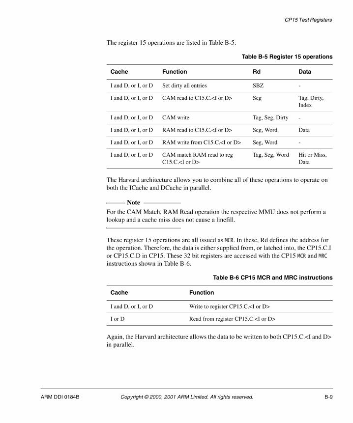
CP15 Test Registers
The register 15 operations are listed in Table B-5.
The Harvard architecture allows you to combine all of these operations to operate on both the ICache and DCache in parallel.
Note For the CAM Match, RAM Read operation the respective MMU does not perform a lookup and a cache miss does not cause a linefill.
These register 15 operations are all issued as MCR. In these, Rd defines the address for the operation. Therefore, the data is either supplied from, or latched into, the CP15.C.I or CP15.C.D in CP15. These 32 bit registers are accessed with the CP15 MCR and MRC instructions shown in Table B-6.
Again, the Harvard architecture allows the data to be written to both CP15.C.<I and D> in parallel.
Table B-5 Register 15 operations
Cache Function Rd Data
I and D, or I, or D Set dirty all entries SBZ -
I and D, or I, or D CAM read to C15.C.<I or D> Seg Tag, Dirty, Index
I and D, or I, or D CAM write Tag, Seg, Dirty -
I and D, or I, or D RAM read to C15.C.<I or D> Seg, Word Data
I and D, or I, or D RAM write from C15.C.<I or D> Seg, Word -
I and D, or I, or D CAM match RAM read to reg C15.C.<I or D>
Tag, Seg, Word Hit or Miss, Data
Table B-6 CP15 MCR and MRC instructions
Cache Function
I and D, or I, or D Write to register CP15.C.<I or D>
I or D Read from register CP15.C.<I or D>
ARM DDI 0184B Copyright © 2000, 2001 ARM Limited. All rights reserved. B-9
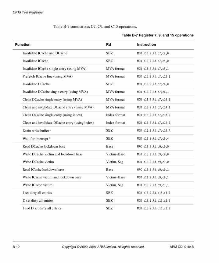
CP15 Test Registers
Table B-7 summarizes C7, C9, and C15 operations.
Table B-7 Register 7, 9, and 15 operations
Function Rd Instruction
Invalidate ICache and DCache SBZ MCR p15,0,Rd,c7,c7,0
Invalidate ICache SBZ MCR p15,0,Rd,c7,c5,0
Invalidate ICache single entry (using MVA) MVA format MCR p15,0,Rd,c7,c5,1
Prefetch ICache line (using MVA) MVA format MCR p15,0,Rd,c7,c13,1
Invalidate DCache SBZ MCR p15,0,Rd,c7,c6,0
Invalidate DCache single entry (using MVA) MVA format MCR p15,0,Rd,c7,c6,1
Clean DCache single entry (using MVA) MVA format MCR p15,0,Rd,c7,c10,1
Clean and invalidate DCache entry (using MVA) MVA format MCR p15,0,Rd,c7,c14,1
Clean DCache single entry (using index) Index format MCR p15,0,Rd,c7,c10,2
Clean and invalidate DCache entry (using index) Index format MCR p15,0,Rd,c7,c14,2
Drain write buffer a SBZ MCR p15,0,Rd,c7,c10,4
Wait for interrupt b SBZ MCR p15,0,Rd,c7,c0,4
Read DCache lockdown base Base MRC p15,0,Rd,c9,c0,0
Write DCache victim and lockdown base Victim=Base MCR p15,0,Rd,c9,c0,0
Write DCache victim Victim, Seg MCR p15,0,Rd,c9,c1,0
Read ICache lockdown base Base MRC p15,0,Rd,c9,c0,1
Write ICache victim and lockdown base Victim=Base MCR p15,0,Rd,c9,c0,1
Write ICache victim Victim, Seg MCR p15,0,Rd,c9,c1,1
I set dirty all entries SBZ MCR p15,2,Rd,c15,c1,0
D set dirty all entries SBZ MCR p15,2,Rd,c15,c2,0
I and D set dirty all entries SBZ MCR p15,2,Rd,c15,c3,0
B-10 Copyright © 2000, 2001 ARM Limited. All rights reserved. ARM DDI 0184B
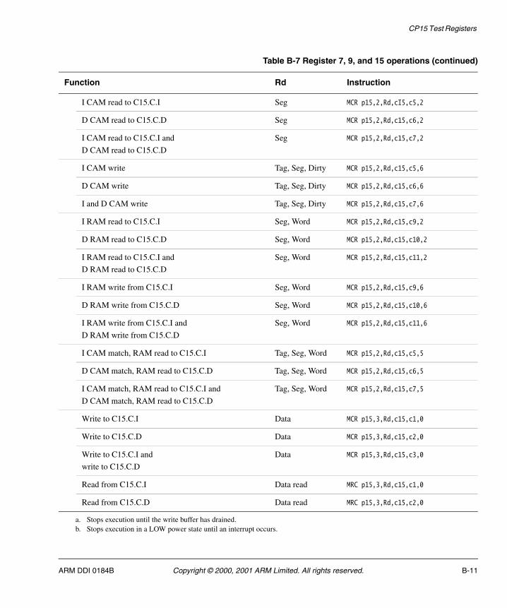
CP15 Test Registers
I CAM read to C15.C.I Seg MCR p15,2,Rd,cI5,c5,2
D CAM read to C15.C.D Seg MCR p15,2,Rd,c15,c6,2
I CAM read to C15.C.I and
D CAM read to C15.C.D
Seg MCR p15,2,Rd,c15,c7,2
I CAM write Tag, Seg, Dirty MCR p15,2,Rd,c15,c5,6
D CAM write Tag, Seg, Dirty MCR p15,2,Rd,c15,c6,6
I and D CAM write Tag, Seg, Dirty MCR p15,2,Rd,c15,c7,6
I RAM read to C15.C.I Seg, Word MCR p15,2,Rd,c15,c9,2
D RAM read to C15.C.D Seg, Word MCR p15,2,Rd,c15,c10,2
I RAM read to C15.C.I and
D RAM read to C15.C.D
Seg, Word MCR p15,2,Rd,c15,c11,2
I RAM write from C15.C.I Seg, Word MCR p15,2,Rd,c15,c9,6
D RAM write from C15.C.D Seg, Word MCR p15,2,Rd,c15,c10,6
I RAM write from C15.C.I and
D RAM write from C15.C.D
Seg, Word MCR p15,2,Rd,c15,c11,6
I CAM match, RAM read to C15.C.I Tag, Seg, Word MCR p15,2,Rd,c15,c5,5
D CAM match, RAM read to C15.C.D Tag, Seg, Word MCR p15,2,Rd,c15,c6,5
I CAM match, RAM read to C15.C.I and
D CAM match, RAM read to C15.C.D
Tag, Seg, Word MCR p15,2,Rd,c15,c7,5
Write to C15.C.I Data MCR p15,3,Rd,c15,c1,0
Write to C15.C.D Data MCR p15,3,Rd,c15,c2,0
Write to C15.C.I and
write to C15.C.D
Data MCR p15,3,Rd,c15,c3,0
Read from C15.C.I Data read MRC p15,3,Rd,c15,c1,0
Read from C15.C.D Data read MRC p15,3,Rd,c15,c2,0
a. Stops execution until the write buffer has drained.b. Stops execution in a LOW power state until an interrupt occurs.
Table B-7 Register 7, 9, and 15 operations (continued)
Function Rd Instruction
ARM DDI 0184B Copyright © 2000, 2001 ARM Limited. All rights reserved. B-11
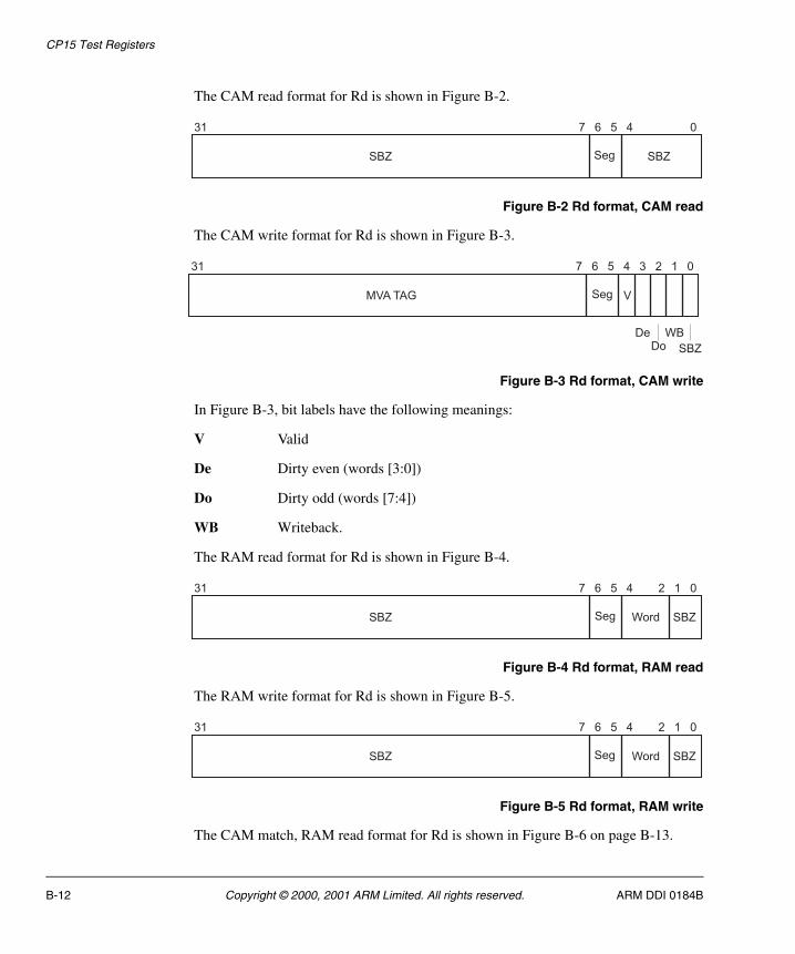
CP15 Test Registers
The CAM read format for Rd is shown in Figure B-2.
Figure B-2 Rd format, CAM read
The CAM write format for Rd is shown in Figure B-3.
Figure B-3 Rd format, CAM write
In Figure B-3, bit labels have the following meanings:
V Valid
De Dirty even (words [3:0])
Do Dirty odd (words [7:4])
WB Writeback.
The RAM read format for Rd is shown in Figure B-4.
Figure B-4 Rd format, RAM read
The RAM write format for Rd is shown in Figure B-5.
Figure B-5 Rd format, RAM write
The CAM match, RAM read format for Rd is shown in Figure B-6 on page B-13.
31 67 5 4 0
SBZ Seg SBZ
31 67 5 4 0
MVA TAG Seg
SBZ
3 2 1
V
DeDo
WB
31 67 5 4 0
SBZ Seg SBZ
2 1
Word
31 67 5 4 0
SBZ Seg SBZ
2 1
Word
B-12 Copyright © 2000, 2001 ARM Limited. All rights reserved. ARM DDI 0184B
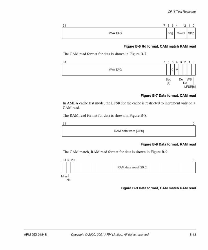
CP15 Test Registers
Figure B-6 Rd format, CAM match RAM read
The CAM read format for data is shown in Figure B-7.
Figure B-7 Data format, CAM read
In AMBA cache test mode, the LFSR for the cache is restricted to increment only on a CAM read.
The RAM read format for data is shown in Figure B-8.
Figure B-8 Data format, RAM read
The CAM match, RAM read format for data is shown in Figure B-9.
Figure B-9 Data format, CAM match RAM read
31 67 5 4 0
MVA TAG Seg SBZ
2 1
Word
31 7 5 4 0
MVA TAG
Seg[1]
LFSR[6]
3 2 1
V
DeDo
WB
6
0
31 0
RAM data word [31:0]
31 30 29 0
Miss
RAM data word [29:0]
Hit
ARM DDI 0184B Copyright © 2000, 2001 ARM Limited. All rights reserved. B-13
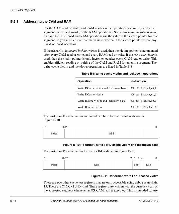
CP15 Test Registers
B.3.1 Addressing the CAM and RAM
For the CAM read or write, and RAM read or write operations you must specify the segment, index, and word (for the RAM operations). See Addressing the 8KB ICache on page 4-5. The CAM and RAM operations use the value in the victim pointer for that segment, so you must ensure that the value is written in the victim pointer before any CAM or RAM operation.
If the MCR write victim and lockdown base is used, then the victim pointer is incremented after every CAM read or write, and every RAM read or write. If the MCR write victim is used, then the victim pointer is only incremented after every CAM read or write. This enables efficient reading or writing of the CAM and RAM for an entire segment. The write cache victim and lockdown operations are listed in Table B-8.
The write I or D cache victim and lockdown base format for Rd is shown in Figure B-10.
Figure B-10 Rd format, write I or D cache victim and lockdown base
The write I or D cache victim format for Rd is shown in Figure B-11.
Figure B-11 Rd format, write I or D cache victim
There are two other cache test registers that are only accessible using debug scan chain 15. These are C15.C.<I or D>.Ind. These registers are written with the current victim of the addressed segment whenever an MCR CAM read is executed. This is intended for use
Table B-8 Write cache victim and lockdown operations
Operation Instruction
Write DCache victim and lockdown base MCR p15,0,Rd,c9,c0,0
Write DCache victim MCR p15,0,Rd,c9,c1,0
Write ICache victim and lockdown base MCR p15,0,Rd,c9,c0,1
Write ICache victim MCR p15,0,Rd,c9,c1,1
31 26 25 0
SBZIndex
31 26 25 67 5 4 0
SBZSegSBZIndex
B-14 Copyright © 2000, 2001 ARM Limited. All rights reserved. ARM DDI 0184B
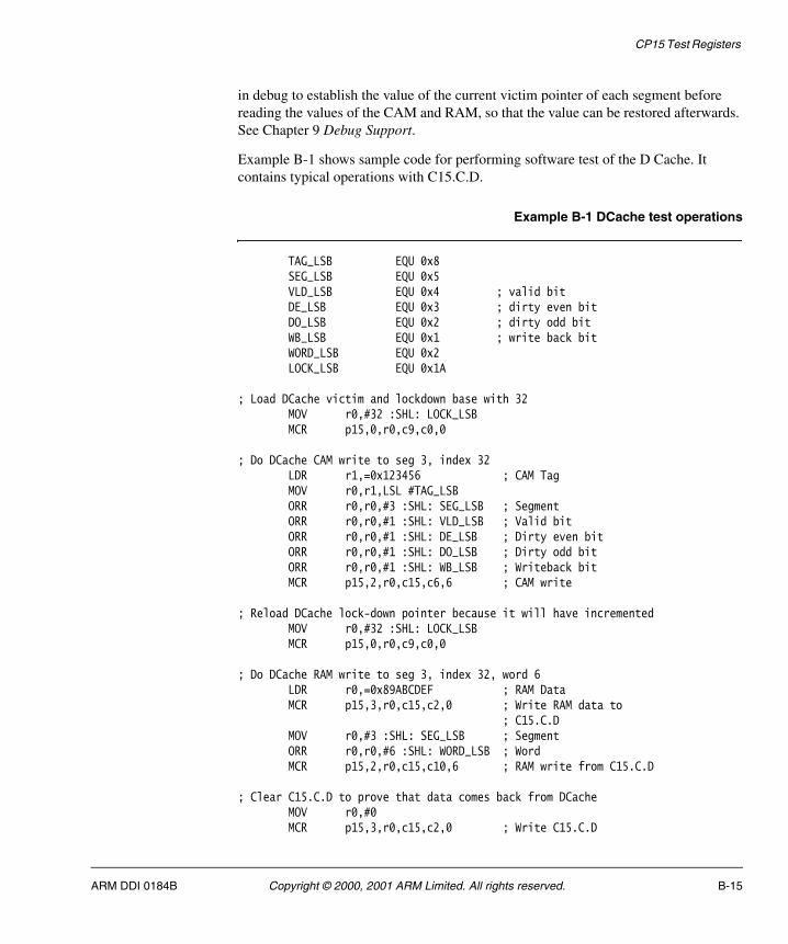
CP15 Test Registers
in debug to establish the value of the current victim pointer of each segment before reading the values of the CAM and RAM, so that the value can be restored afterwards. See Chapter 9 Debug Support.
Example B-1 shows sample code for performing software test of the D Cache. It contains typical operations with C15.C.D.
Example B-1 DCache test operations
TAG_LSB EQU 0x8SEG_LSB EQU 0x5VLD_LSB EQU 0x4 ; valid bitDE_LSB EQU 0x3 ; dirty even bitDO_LSB EQU 0x2 ; dirty odd bitWB_LSB EQU 0x1 ; write back bitWORD_LSB EQU 0x2LOCK_LSB EQU 0x1A
; Load DCache victim and lockdown base with 32MOV r0,#32 :SHL: LOCK_LSBMCR p15,0,r0,c9,c0,0
; Do DCache CAM write to seg 3, index 32LDR r1,=0x123456 ; CAM TagMOV r0,r1,LSL #TAG_LSBORR r0,r0,#3 :SHL: SEG_LSB ; SegmentORR r0,r0,#1 :SHL: VLD_LSB ; Valid bitORR r0,r0,#1 :SHL: DE_LSB ; Dirty even bitORR r0,r0,#1 :SHL: DO_LSB ; Dirty odd bitORR r0,r0,#1 :SHL: WB_LSB ; Writeback bitMCR p15,2,r0,c15,c6,6 ; CAM write
; Reload DCache lock-down pointer because it will have incrementedMOV r0,#32 :SHL: LOCK_LSBMCR p15,0,r0,c9,c0,0
; Do DCache RAM write to seg 3, index 32, word 6LDR r0,=0x89ABCDEF ; RAM DataMCR p15,3,r0,c15,c2,0 ; Write RAM data to
; C15.C.DMOV r0,#3 :SHL: SEG_LSB ; SegmentORR r0,r0,#6 :SHL: WORD_LSB ; WordMCR p15,2,r0,c15,c10,6 ; RAM write from C15.C.D
; Clear C15.C.D to prove that data comes back from DCacheMOV r0,#0MCR p15,3,r0,c15,c2,0 ; Write C15.C.D
ARM DDI 0184B Copyright © 2000, 2001 ARM Limited. All rights reserved. B-15
CP15 Test Registers
; Do a CAM match, RAM read to C15.C.DLDR r1,=0x123456MOV r0,r1,LSL #TAG_LSB ; TAGORR r0,r0,#3 :SHL: SEG_LSB ; SegmentORR r0,r0,#6 :SHL: WORD_LSB ; WordMCR p15,2,r0,c15,c6,5 ; CAM match, RAM read
; Read C15.C.D and compare with expected data.; Note that the top 2 bits of the RAM Data returned from the CAM match; give the Hit and Miss information [31:30] = [Miss,Hit]
MRC p15,3,r0,c15,c2,0 ; Read C15.C.D
; Check the CAM match for a hitMOV r2,#0xC0000000 ; Mask bits [31:30]AND r2,r2,r0MOV r3,#0x80000000 ; HitCMP r2,r3BNE Fail
; Check the RAM dataMOV r0,r0,LSL #2 ; Remove bits [31:30]LDR r1,=0x89ABCDEF ; Expected dataMOV r1,r1,LSL #2 ; Remove bits [31:30]CMP r0,r1BNE FailTEST_PASS
Fail TEST_FAILEND
B.3.2 Testing the LFSR
There is an 8-bit LFSR in both the DCache and ICache that is used to provide the pseudo-random sequence to increment the segment victim counters in random mode. This is the default setting of the RR bit in CP15 register 1, bit 14.
The LFSR is tested in a controlled manner in AMBA cache test mode. In this mode the LFSR is reset to its seed value by performing an MCR invalidate all, and is incremented once by performing a CAM read. For each CAM read, bit 6 of bits[7:0] is sampled onto bit 0 of the CAM read data.
The by-product of this is that LFSR[6] is sampled for any CAM read, but the LFSR is clocked freely when not in AMBA cache test mode. See Chapter 11 AMBA Test Interface.
B-16 Copyright © 2000, 2001 ARM Limited. All rights reserved. ARM DDI 0184B
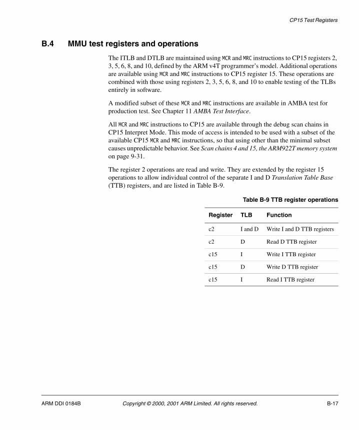
CP15 Test Registers
B.4 MMU test registers and operations
The ITLB and DTLB are maintained using MCR and MRC instructions to CP15 registers 2, 3, 5, 6, 8, and 10, defined by the ARM v4T programmer’s model. Additional operations are available using MCR and MRC instructions to CP15 register 15. These operations are combined with those using registers 2, 3, 5, 6, 8, and 10 to enable testing of the TLBs entirely in software.
A modified subset of these MCR and MRC instructions are available in AMBA test for production test. See Chapter 11 AMBA Test Interface.
All MCR and MRC instructions to CP15 are available through the debug scan chains in CP15 Interpret Mode. This mode of access is intended to be used with a subset of the available CP15 MCR and MRC instructions, so that using other than the minimal subset causes unpredictable behavior. See Scan chains 4 and 15, the ARM922T memory system on page 9-31.
The register 2 operations are read and write. They are extended by the register 15 operations to allow individual control of the separate I and D Translation Table Base (TTB) registers, and are listed in Table B-9.
Table B-9 TTB register operations
Register TLB Function
c2 I and D Write I and D TTB registers
c2 D Read D TTB register
c15 I Write I TTB register
c15 D Write D TTB register
c15 I Read I TTB register
ARM DDI 0184B Copyright © 2000, 2001 ARM Limited. All rights reserved. B-17
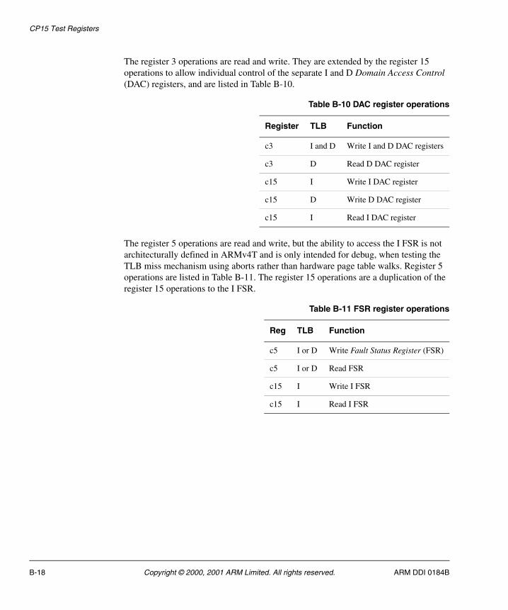
CP15 Test Registers
The register 3 operations are read and write. They are extended by the register 15 operations to allow individual control of the separate I and D Domain Access Control (DAC) registers, and are listed in Table B-10.
The register 5 operations are read and write, but the ability to access the I FSR is not architecturally defined in ARMv4T and is only intended for debug, when testing the TLB miss mechanism using aborts rather than hardware page table walks. Register 5 operations are listed in Table B-11. The register 15 operations are a duplication of the register 15 operations to the I FSR.
Table B-10 DAC register operations
Register TLB Function
c3 I and D Write I and D DAC registers
c3 D Read D DAC register
c15 I Write I DAC register
c15 D Write D DAC register
c15 I Read I DAC register
Table B-11 FSR register operations
Reg TLB Function
c5 I or D Write Fault Status Register (FSR)
c5 I or D Read FSR
c15 I Write I FSR
c15 I Read I FSR
B-18 Copyright © 2000, 2001 ARM Limited. All rights reserved. ARM DDI 0184B
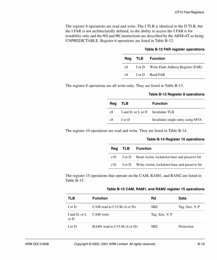
CP15 Test Registers
The register 6 operations are read and write. The I TLB is identical to the D TLB, but the I FAR is not architecturally defined, so the ability to access the I FAR is for testability only and the MCR and MRC instructions are described by the ARMv4T as being UNPREDICTABLE. Register 6 operations are listed in Table B-12.
The register 8 operations are all write-only. They are listed in Table B-13.
The register 10 operations are read and write. They are listed in Table B-14.
The register 15 operations that operate on the CAM, RAM1, and RAM2 are listed in Table B-15.
Table B-12 FAR register operations
Reg TLB Function
c6 I or D Write Fault Address Register (FAR)
c6 I or D Read FAR
Table B-13 Register 8 operations
Reg TLB Function
c8 I and D, or I, or D Invalidate TLB
c8 I or D Invalidate single entry using MVA
Table B-14 Register 10 operations
Reg TLB Function
c10 I or D Read victim, lockdown base and preserve bit
c10 I or D Write victim, lockdown base and preserve bit
Table B-15 CAM, RAM1, and RAM2 register 15 operations
TLB Function Rd Data
I or D CAM read to C15.M.<I or D> SBZ Tag, Size, V, P
I and D, or I, or D
CAM write Tag, Size, V, P
I or D RAM1 read to C15.M.<I or D> SBZ Protection
ARM DDI 0184B Copyright © 2000, 2001 ARM Limited. All rights reserved. B-19
CP15 Test Registers
While the ARM922T memory system is a Harvard architecture, the TLBs are accessed using CData. This means the write operations can be combined to operate on both the I TLB and D TLB in parallel.
Note Setting the CP15 register 15 test status register MMU test bit (bit 3) enables auto-increment of the TLB index pointer in both MMUs on CAM and RAM1 reads and writes. If this bit is not set, the TLB index pointer only increments on RAM1 writes.
For the CAM match, RAM1 read operation a TLB miss will not cause a page walk.
These register 15 operations are all issued as MCR, which means that the read and match operations have to be latched into the CP15.M.I or CP15.M.D in CP15. These are 32-bit registers that are read with the following CP15 MRC instruction:
Read from register CP15.M.<I or D>
Table B-16 summarizes C2, C3, C5, C6, C8, C10, and C15 operations.
I and D, or I, or D
RAM1 write Protection
I or D RAM2 read to C15.M.<I or D> SBZ PA Tag, Size
I and D, or I, or D
RAM2 write PA Tag, Size PA Tag, Size
I or D CAM match RAM1 read to C15.M.<I or D>
MVA Fault, Miss, Protection
Table B-16 Register 2, 3, 5, 6, 8, 10, and 15 operations
Function Rd Instruction
Read TTB register TTB MRC p15,0,Rd,c2,c0,0
Write TTB register TTB MCR p15,0,Rd,c2,c0,0
Read domain 15:0 access control
DAC MRC p15,0,Rd,c3,c0,0
Write domain 15:0 access control
DAC MCR p15,0,Rd,c3,c0,0
Table B-15 CAM, RAM1, and RAM2 register 15 operations (continued)
TLB Function Rd Data
B-20 Copyright © 2000, 2001 ARM Limited. All rights reserved. ARM DDI 0184B
CP15 Test Registers
Read data FSR value FSR MRC p15,0,Rd,c5,c0,0
Write data FSR value FSR MCR p15,0,Rd,c5,c0,0
Read prefetch FSR value a FSR MRC p15,0,Rd,c5,c0,1
Write prefetch FSR value a FSR MCR p15,0,Rd,c5,c0,1
Read D FAR FAR MRC p15,0,Rd,c6,c0,0
Write D FAR FAR MCR p15,0,Rd,c6,c0,0
Read I FAR a FAR MRC p15,0,Rd,c6,c0,1
Write I FAR a FAR MCR p15,0,Rd,c6,c0,1
Invalidate TLB(s) SBZ MCR p15,0,Rd,c8,c7,0
Invalidate I TLB SBZ MCR p15,0,Rd,c8,c5,0
Invalidate I TLB single entry (using MVA)
MVA format MCR p15,0,Rd,c8,c5,1
Invalidate D TLB SBZ MCR p15,0,Rd,c8,c6,0
Invalidate D TLB single entry (using MVA)
MVA format MCR p15,0,Rd,c8,c6,1
Read D TLB lockdown TLB lockdown MRC p15,0,Rd,c10,c0,0
Write D TLB lockdown TLB lockdown MCR p15,0,Rd,c10,c0,0
Read I TLB lockdown TLB lockdown MRC p15,0,Rd,c10,c0,1
Write I TLB lockdown TLB lockdown MCR p15,0,Rd,c10,c0,1
Read I TTB TTB MRC p15,5,Rd,c15,c1,2
Write I TTB TTB MCR p15,5,Rd,c15,c1,2
Write D TTB TTB MCR p15,5,Rd,c15,c2,2
Read I DAC DAC MRC p15,5,Rd,c15,c1,3
Write I DAC DAC MCR p15,5,Rd,c15,c1,3
Write D DAC DAC MCR p15,5,Rd,c15,c2,3
Table B-16 Register 2, 3, 5, 6, 8, 10, and 15 operations (continued)
Function Rd Instruction
ARM DDI 0184B Copyright © 2000, 2001 ARM Limited. All rights reserved. B-21
CP15 Test Registers
Read prefetch FSR value FSR MRC p15,5,Rd,c15,c1,5
Write prefetch FSR value FSR MCR p15,5,Rd,c15,c1,5
D CAM read to C15.M.D SBZ MCR p15,4,Rd,c15,c6,4
I CAM read to C15.M.I SBZ MCR p15,4,Rd,c15,c5,4
D CAM write Tag, Size, V, P MCR p15,4,Rd,c15,c6,0
I CAM write Tag, Size, V, P MCR p15,4,Rd,c15,c5,0
D and I CAM write Tag, Size, V, P MCR p15,4,Rd,c15,c7,0
D RAM1 read to C15.M.D SBZ MCR p15,4,Rd,c15,c10,4
I RAM 1 read to C15.M.I SBZ MCR p15,4,Rd,c15,c9,4
D RAM1 write Protection MCR p15,4,Rd,c15,c10,0
I RAM 1 write Protection MCR p15,4,Rd,c15,c9,0
D and I RAM1 write Protection MCR p15,4,Rd,c15,c11,0
D RAM2 read to C15.M.D SBZ MCR p15,4,Rd,c15,c2,5
I RAM2 read to C15.M.I SBZ MCR p15,4,Rd,c15,c1,5
D RAM2 write PA Tag, Size MCR p15,4,Rd,c15,c2,1
I RAM2 write PA Tag, Size MCR p15,4,Rd,c15,c1,1
D and I RAM2 write PA Tag, Size MCR p15,4,Rd,c15,c3,1
D CAM match, RAM1 read to C15.M.D
MVA MCR p15,4,Rd,c15,c14,4
I CAM match, RAM1 read to C15.M.I
MVA MCR p15,4,Rd,c15,c13,4
Read C15.M.D Data MRC p15,4,Rd,c15,c2,6
Read C15.M.I Data MRC p15,4,Rd,c15,c1,6
a. These MCR and MRC instructions are not architecturally defined in ARMv4T, and are only intended for testability. Their behavior is described by ARMv4T as being UNPREDICTABLE.
Table B-16 Register 2, 3, 5, 6, 8, 10, and 15 operations (continued)
Function Rd Instruction
B-22 Copyright © 2000, 2001 ARM Limited. All rights reserved. ARM DDI 0184B
CP15 Test Registers
Figure B-12 on page B-23 shows the format of Rd for CAM writes and data for CAM reads.
Figure B-12 Rd format, CAM write and data format, CAM read
In Figure B-12, V is the Valid bit, P is the Preserve bit, and SIZE_C sets the memory region size. The allowed values of SIZE_C are shown in Table B-17.
Figure B-13 shows the format of Rd for RAM1 writes.
Figure B-13 Rd format, RAM1 write
In Figure B-13, AP[3:0] determines the setting of the access permission bits for a memory region. The allowed values are listed in Table B-18.
31 910 5 4 0
MVA TAG SIZE_C
3
P
6
V SBZ
Table B-17 CAM memory region size
SIZE_C[3:0] Memory region size
0b1111 1MB
0b0111 64KB
0b0011 16KB
0b0001 4KB
0b0000 1KB
31 22 21 6 5 4 3 0
APSBZ DOMAIN (one hot encoding) nBnC
D15 D0
ARM DDI 0184B Copyright © 2000, 2001 ARM Limited. All rights reserved. B-23
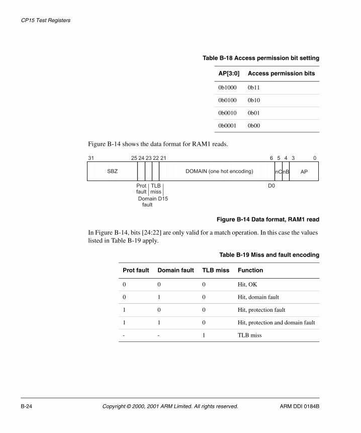
CP15 Test Registers
Figure B-14 shows the data format for RAM1 reads.
Figure B-14 Data format, RAM1 read
In Figure B-14, bits [24:22] are only valid for a match operation. In this case the values listed in Table B-19 apply.
Table B-18 Access permission bit setting
AP[3:0] Access permission bits
0b1000 0b11
0b0100 0b10
0b0010 0b01
0b0001 0b00
31 22 21 6 5 4 3 0
APSBZ DOMAIN (one hot encoding) nBnC
232425
Protfault
TLBmiss
Domainfault
D15
D0
Table B-19 Miss and fault encoding
Prot fault Domain fault TLB miss Function
0 0 0 Hit, OK
0 1 0 Hit, domain fault
1 0 0 Hit, protection fault
1 1 0 Hit, protection and domain fault
- - 1 TLB miss
B-24 Copyright © 2000, 2001 ARM Limited. All rights reserved. ARM DDI 0184B
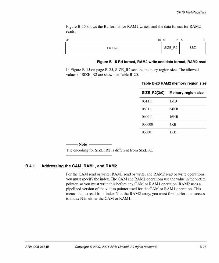
CP15 Test Registers
Figure B-15 shows the Rd format for RAM2 writes, and the data format for RAM2 reads.
Figure B-15 Rd format, RAM2 write and data format, RAM2 read
In Figure B-15 on page B-25, SIZE_R2 sets the memory region size. The allowed values of SIZE_R2 are shown in Table B-20.
Note The encoding for SIZE_R2 is different from SIZE_C.
B.4.1 Addressing the CAM, RAM1, and RAM2
For the CAM read or write, RAM1 read or write, and RAM2 read or write operations, you must specify the index. The CAM and RAM1 operations use the value in the victim pointer, so you must write this before any CAM or RAM1 operation. RAM2 uses a pipelined version of the victim pointer used for the CAM or RAM1 operation. This means that to read from index N in the RAM2 array, you must first perform an access to index N in either the CAM or RAM1.
31 910 5 0
PA TAG SIZE_R2
6
SBZ
Table B-20 RAM2 memory region size
SIZE_R2[3:0] Memory region size
0b1111 1MB
0b0111 64KB
0b0011 16KB
0b0000 4KB
0b0001 1KB
ARM DDI 0184B Copyright © 2000, 2001 ARM Limited. All rights reserved. B-25
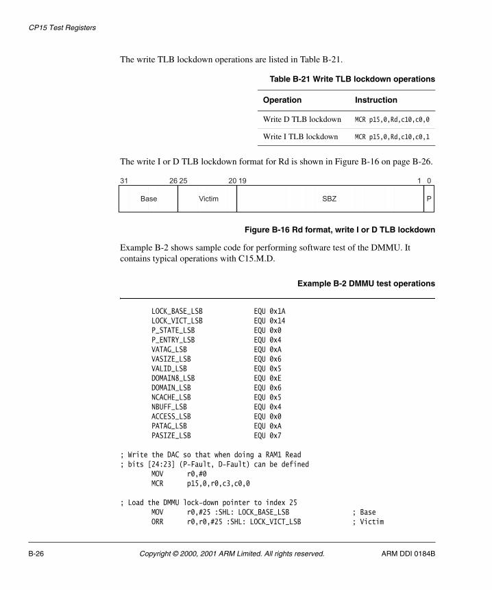
CP15 Test Registers
The write TLB lockdown operations are listed in Table B-21.
The write I or D TLB lockdown format for Rd is shown in Figure B-16 on page B-26.
Figure B-16 Rd format, write I or D TLB lockdown
Example B-2 shows sample code for performing software test of the DMMU. It contains typical operations with C15.M.D.
Example B-2 DMMU test operations
LOCK_BASE_LSB EQU 0x1ALOCK_VICT_LSB EQU 0x14P_STATE_LSB EQU 0x0P_ENTRY_LSB EQU 0x4VATAG_LSB EQU 0xAVASIZE_LSB EQU 0x6VALID_LSB EQU 0x5DOMAIN8_LSB EQU 0xEDOMAIN_LSB EQU 0x6NCACHE_LSB EQU 0x5NBUFF_LSB EQU 0x4ACCESS_LSB EQU 0x0PATAG_LSB EQU 0xAPASIZE_LSB EQU 0x7
; Write the DAC so that when doing a RAM1 Read; bits [24:23] (P-Fault, D-Fault) can be defined
MOV r0,#0MCR p15,0,r0,c3,c0,0
; Load the DMMU lock-down pointer to index 25MOV r0,#25 :SHL: LOCK_BASE_LSB ; BaseORR r0,r0,#25 :SHL: LOCK_VICT_LSB ; Victim
Table B-21 Write TLB lockdown operations
Operation Instruction
Write D TLB lockdown MCR p15,0,Rd,c10,c0,0
Write I TLB lockdown MCR p15,0,Rd,c10,c0,1
31 26 25 20 19 1 0
Base Victim PSBZ
B-26 Copyright © 2000, 2001 ARM Limited. All rights reserved. ARM DDI 0184B
CP15 Test Registers
ORR r0,r0,#0 :SHL: P_STATE_LSB ; PreserveMCR p15,0,r0,c10,c0,0
; CAM write to index 25LDR r0,=0xAAAAAMOV r0,r0,LSL #VATAG_LSB ; MVA TagORR r0,r0,#1 :SHL: VASIZE_LSB ; Size_CORR r0,r0,#1 :SHL: VALID_LSB ; ValidORR r0,r0,#1 :SHL: P_ENTRY_LSB ; PreserveMCR p15,4,r0,c15,c6,0
; RAM2 write to index 25; The RAM2 location pointed to for reads and writes; is whichever CAM and RAM1 location was last read or written.
LDR r0,=0x55555MOV r0,r0,LSL #PATAG_LSB ; PATAGORR r0,r0,#3 :SHL: PASIZE_LSB ; Size_R2MCR p15,4,r0,c15,c2,1
; As CP15 register 15, Test Status Register, MMU Test (bit 3) is not set,; the victim pointer will only increment after the RAM1 write.; So RAM1 write to index 25 (Victim increments to 26 after the write)
MOV r0,#0ORR r0,r0,#0 :SHL: DOMAIN8_LSB ; Upper 8 domainsORR r0,r0,#1 :SHL: DOMAIN_LSB ; Lower 8 domainsORR r0,r0,#1 :SHL: NCACHE_LSB ; nCORR r0,r0,#1 :SHL: NBUFF_LSB ; nBORR r0,r0,#8 :SHL: ACCESS_LSBMCR p15,4,r0,c15,c10,0
; Load the DMMU lock-down pointer to index 25MOV r0,#25 :SHL: LOCK_BASE LSB ; BaseORR r0,r0,#25 :SHL: LOCK_VICT_LSB ; VictimORR r0,r0,#0 :SHL: P_STATE_LSB ; PreserveMCR p15,0,r0,c10,c0,0
; RAM1 read to C15.M.DMCR p15,4,r0,c15,c10,4
; Read C15.M.D to r1MRC p15,4,r1,c15,c2,6
; RAM2 read to C15.M.DMCR p15,4,r0,c15,c2,5
; Read C15.M.D to r3MRC p15,4,r3,c15,c2,6
; CAM match, RAM1 read to C15.M.DLDR r0,=0xAAAAA
ARM DDI 0184B Copyright © 2000, 2001 ARM Limited. All rights reserved. B-27
CP15 Test Registers
MOV r0,r0,LSL #VATAG_LSBMCR p15,4,r0,c15,c14,4
; Read C15.M.D to r2MRC p15,4,r2,c15,c2,6
; Compare match value to read value and RAM2 read value to write valueLDR r4,=0x55555 ; Expected RAM2 PA TagMOV r4,r4,LSL #PATAG_LSBORR r4,r4,#3 :SHL: PASIZE_LSBCMP r1,r2 ; Compare RAM1 read with
; CAM match, RAM1 readCMPEQ r3,r4 ; Compare RAM2 read with
; expected RAM2BNE FailTEST_PASS
Fail TEST_FAILEND
B-28 Copyright © 2000, 2001 ARM Limited. All rights reserved. ARM DDI 0184B
CP15 Test Registers
B.5 StrongARM backwards compatibility operations
The following MCR instructions are supported to provide clock switching and MCR wait for interrupt compatibility with SA110 and SA1100 (StrongARM).
MCR p15,0,Rd,c15,c1,2 ; Enable clock switching
This is equivalent to Asynchronous clocking mode.
MCR p15,0,Rd,c15,c2,2 ; Disable clock switching
This is equivalent to FastBus clocking mode.
MCR p15,0,Rd,c15,c8,2 ; Wait for interrupt
This is equivalent to MCR p15,0,Rd,c7,c0,4.
These three MCR instructions must not be used and are deprecated in ARM architectures after v4T.
ARM DDI 0184B Copyright © 2000, 2001 ARM Limited. All rights reserved. B-29

CP15 Test Registers
B-30 Copyright © 2000, 2001 ARM Limited. All rights reserved. ARM DDI 0184B
Glossary
This glossary describes some of the terms used in this manual. Where terms can have several meanings, the meaning presented here is intended.
Abort A mechanism that indicates to a core that it should halt execution of an attempted illegal memory access. An abort can be caused by the external or internal memory system as a result of attempting to access invalid instruction or data memory. An abort is classified as either a prefetch abort, a data abort, or an external abort. See also Data abort, External abort and Prefetch abort.
Abort model An abort model is the defined behavior of an ARM processor in response to a Data Abort exception. Different abort models behave differently with regard to load and store instructions that specify base register writeback.
ALU See Arithmetic Logic Unit.
Application Specific Integrated Circuit
An integrated circuit that has been designed to perform a specific application function. It can be custom-built or mass-produced.
Arithmetic Logic Unit
The part of a processor core that performs arithmetic and logic operations.
ARM state A processor that is executing ARM (32-bit) word-aligned instructions is operating in ARM state.
ASIC See Application Specific Integrated Circuit.
ARM DDI 0184B Copyright © 2000, 2001 ARM Limited. All rights reserved. Glossary-1
Glossary
Banked registers Those physical registers whose use is defined by the current processor mode. The banked registers are R8 to R14.
Base register A register specified by a load or store instruction that is used to hold the base value for the instruction’s address calculation.
Big-endian Byte ordering scheme in which bytes of decreasing significance in a data word are stored at increasing addresses in memory. See also Little-endian and Endianness.
Breakpoint A breakpoint is a mechanism provided by debuggers to identify an instruction at which program execution is to be halted. Breakpoints are inserted by the programmer to allow inspection of register contents, memory locations, variable values at fixed points in the program execution to test that the program is operating correctly. Breakpoints are removed after the program is successfully tested. See also Watchpoint.
Byte An 8-bit data item.
Cache A block of on-chip or off-chip fast access memory locations, situated between the processor and main memory, used for storing and retreiving copies of often used instructions and/or data. This is done to greatly reduce the average speed of memory accesses and so to increase processor performance.
Cache contention When the number of frequently-used memory cache lines that use a particular cache set exceeds the set-associativity of the cache. In this case, main memory activity increases and performance decreases.
Cache hit A memory access that can be processed at high speed because the instruction or data that it addresses is already held in the cache.
Cache line index The number associated with each cache line in a cache set. Within each cache set, the cache lines are numbered from 0 to (set associativity) -1.
Cache lockdown To fix a line in cache memory so that it cannot be overwritten. Cache lockdown allows critical instructions and/or data to be loaded into the cache so that the cache lines containing them will not subsequently be reallocated. This ensures that all subsequent accesses to the instructions/data concerned are cache hits, and therefore complete as quickly as possible.
Cache miss A memory access that cannot be processed at high speed because the instruction/data it addresses is not in the cache and a main memory access is required.
CAM See Content addressable memory.
Central Processing Unit
The part of a processor that contains the ALU, the registers, and the instruction decode logic and control circuitry. Also commonly known as the processor core.
Clock gating Gating a clock signal for a macrocell with a control signal (such as PWRDOWN) and using the modified clock that results to control the operating state of the macrocell.
Glossary-2 Copyright © 2000, 2001 ARM Limited. All rights reserved. ARM DDI 0184B
Glossary
Condition field A 4-bit field in an instruction that is used to specify a codition under which the instruction can execute.
Content addressable memory
Memory that is identified by its contents. Content addressable memory is used in CAM-RAM architecture caches to store the tags for cache entries.
Coprocessor A processor that supplements the main CPU. It carries out additional functions that the main CPU cannot perform. Usually used for floating-point math calculations, signal processing, or memory management.
CPU See Central Processing Unit.
Data Abort An indication from a memory system to a core that it should halt execution of an attempted illegal memory access. A data abort is attempting to access invalid data memory. See also Abort, External abort and Prefetch abort.
Data cache See DCache.
DCache A block of on-chip fast access memory locations, situated between the processor and main memory, used for storing and retreiving copies of often used data. This is done to greatly reduce the average speed of memory accesses and so to increase processor performance.
Debugger A debugging system that includes a program, used to detect, locate, and correct software faults, together with custom hardware that supports software debugging.
Domain A collection of sections, large pages and small pages of memory, which can have their access permissions switched rapidly by writing to the Domain Access Control Register (CP15 register 3).
Double word A 64-bit data item. The contents are taken as being an unsigned integer unless otherwise stated.
EmbeddedICE The additional JTAG-based hardware provided by debuggable ARM processors to aid debugging.
Endianness Byte ordering. The scheme that determines the order in which successive bytes of a data word are stored in memory. See also Little-endian and Big-endian.
Exception vector One of a number of fixed addresses in low memory, or in high memory if high vectors are configured, that contains the first instruction of the corresponding interrupt service routine.
External abort An indication from an external memory system to a core that it should halt execution of an attempted illegal memory access. An external abort is caused by the external memory system as a result of attempting to access invalid memory. See also Abort, Data abort and Prefetch abort
ARM DDI 0184B Copyright © 2000, 2001 ARM Limited. All rights reserved. Glossary-3
Glossary
Halfword A 16-bit data item.
ICache A block of on-chip fast access memory locations, situated between the processor and main memory, used for storing and retreiving copies of often used instructions. This is done to greatly reduce the average speed of memory accesses and so to increase processor performance.
Instruction cache See ICache.
Joint Test Action Group
The name of the organization that developed standard IEEE 1149.1. This standard defines a boundary-scan architecture used for in-circuit testing of integrated circuit devices. It is commonly known by the initials JTAG.
JTAG See Joint Test Action Group.
Little-endian Byte ordering scheme in which bytes of increasing significance in a data word are stored at increasing addresses in memory. See also Big-endian and Endianness.
Macrocell A complex logic block with a defined interface and behavior. A typical VLSI system will comprise several macrocells (such as an ARM9E-S, an ETM9, and a memory block) plus application-specific logic.
Prefetch abort An indication from a memory system to a core that it should halt execution of an attempted illegal memory access. A prefetch abort can be caused by the external or internal memory system as a result of attempting to access invalid instruction memory. See also Data abort, External abort and Abort
Processor A contraction of microprocessor. A processor includes the CPU or core, plus additional components such as memory, and interfaces. These are combined as a single macrocell, that can be fabricated on an integrated circuit.
Region A partition of instruction or data memory space.
Register A temporary storage location used to hold binary data until it is ready to be used.
SBO See Should be one.
SBZ See Should be zero.
SCREG The currently selected scan chain number in an ARM TAP controller.
Should be one Should be written as 1 (or all 1s for bit fields) by software. Writing a 0 will produce UNPREDICTABLE results.
Should be zero Should be written as 0 (or all 0s for bit fields) by software. Writing a 1 will produce UNPREDICTABLE results.
Tag bits The index or key field of a CAM entry.
TAP See Test access port.
Glossary-4 Copyright © 2000, 2001 ARM Limited. All rights reserved. ARM DDI 0184B
Glossary
Test Access Port The collection of four mandatory and one optional terminals that form the input/output and control interface to a JTAG boundary-scan architecture. The mandatory terminals are TDI, TDO, TMS, and TCK. The optional terminal is TRST.
Thumb state A processor that is executing Thumb (16-bit) half-word aligned instructions is operating in Thumb state
UNDEFINED An instruction that generates an undefined instruction exception.
UNPREDICTABLE For reads, the data returned when reading from this location is unpredictable. It can have any value. For writes, writing to this location causes unpredictable behavior, or an unpredictable change in device configuration. UNPREDICTABLE instructions must not halt or hang the processor, or any part of the system.
Watchpoint A watchpoint is a mechanism provided by debuggers to halt program execution when the data contained by a particular memory address is changed. Watchpoints are inserted by the programmer to allow inspection of register contents, memory locations, and variable values when memory is written to test that the program is operating correctly. Watchpoints are removed after the program is successfully tested. See also Breakpoint.
Word A 32-bit data item.
ARM DDI 0184B Copyright © 2000, 2001 ARM Limited. All rights reserved. Glossary-5
Glossary
Glossary-6 Copyright © 2000, 2001 ARM Limited. All rights reserved. ARM DDI 0184B
Index
AABSENT 7-7Access permission 3-2
bits 3-24Address 2-6
translation 3-6AHB interface 6-20Alignment faults 3-21AMBA signals A-2AMBA test
burst operations 11-11cache test mode 11-15entering and exiting 11-3functional test mode 11-4interface 11-2MMU test mode 11-19modes 11-3PA TAG RAM test mode 11-12
ARM7TDMI code compatibility 2-3ARM9TDMI 1-2
implementation options 2-3ARM920T 1-2
ARM922T 1-2bus interface 6-2clocking 5-2connecting to ASB interface 6-5
ARM940T 1-2ASB 6-3, 6-5
interface, fully compliant 6-5slave transfers 6-19
BBase restored data abort model 2-3Base updated data abort model 2-3Bidirectional signals 6-5Block diagram, functional 1-3Breakpoint 9-5, 9-51
and exception 9-6timing 9-5
Buffer 6-5Buffered STM 6-14Buffered STR 6-13Burst transfers 6-7
Bus interface 6-2Busy-wait
abandoned 7-17interrupted 7-17
Bypass register 9-19
CCache
associativity encoding 2-11cleaning 4-20coherence 4-17lockdown register 2-20operations register 2-17size encoding 2-10test mode, AMBA 11-15test register B-8type register 2-8
Cachedfetch 6-14LDM 6-14LDR 6-14
ARM DDI 0184B Copyright © 2000, 2001 ARM Limited. All rights reserved. Index-1
Index
CDP 7-13Clock switching 9-43, B-5, B-29Clocking modes 2-13Clocks
DCLK 9-42GCLK 9-42internally TCK generated clock
9-42memory clock 9-42
Coarse page table descriptor 3-12Code compatibility 2-3Coherence, cache 4-17Comms channel 9-66Control register 2-12Coprocessor
clocking 7-3external 7-2handshake encoding 7-8instructions 7-3
Coprocessor instructionsprivileged modes 7-15
Coprocessor interface 7-2signals A-5
CPU aborts 3-21CP14 2-2, 7-2CP15 2-2, 7-2
accessing registers 2-6debug access 9-33interpreted access 9-34MRC and MCR bit pattern 2-7register map 2-5test registers B-2
DData Abort model 2-3DCache
enabling and disabling 4-10operation 4-10organization 4-4, 4-13replacement algorithm 4-13
Debugcomms control register 9-64communications 9-66communications channel 9-64control register 9-60debug scan chain 9-28entered from ARM state 9-45
entered from Thumb state 9-45hardware extensions 9-2instruction register 9-13interface standard 9-2request 9-10, 9-52scan chains 9-24signals A-10speed 9-46state 9-10status register 9-60system 9-3
Debug stateactions of ARM922T 9-10breakpoint and exception 9-6entry on breakpoint 9-5entry on debug request 9-10entry on watchpoint 9-7exit from 9-48watchpoint and exception 9-9
Descriptorcoarse page table 3-12fine page table 3-13level one 3-9level two 3-15section 3-11
Device ID code register 9-19Dirty data eviction 6-16Domain 3-2
access control 3-23access control register 2-14faults 3-21, 3-26
EEmbeddedICE 9-54
accessing hardware registers 9-29control registers 9-56macrocell 9-1mask registers 9-56register map 9-54single stepping 9-63
EmbeddedICE watchpoint unitsdebugging 9-11programming 9-11testing 9-11
ETM interface 8-2Extension space 2-4External
aborts 3-28coprocessors 7-2scan chains 9-21
FFAR 2-17, 3-22Fast context switch 2-25FastBus mode 5-3Fault
address register 2-17, 3-22domain 3-26permission 3-27status register 2-16, 3-22translation 3-26
Fine page table descriptor 3-13FSR 2-16, 3-22Functional block diagram 1-3Functional test 11-4
GGO 7-7
HHandshake signals 7-7Harvard architecture 1-2
IICache
operation 4-6replacement algorithm 4-7
ID code register 2-8Implementation options 2-3Instruction cycle
counts and bus activity 12-3data bus instruction times 12-4
Instruction set extension spaces 2-4Interlocked MCR 7-11Interlocks 12-6
LDM dependent timing 12-8LDM timing 12-7single load timing 12-6
Index-2 Copyright © 2000, 2001 ARM Limited. All rights reserved. ARM DDI 0184B
Index
two cycle load timing 12-7
JJTAG
and TAP controller signals A-7interface 9-11state machine 9-12
LLarge page references, translating 3-17LAST 7-7LDC 7-5Level one
descriptor 3-9descriptor, accessing 3-8fetch 3-8
Level twocache support 6-22
Level two|descriptor 3-15
LFSR testing B-16Line length encoding 2-11
MMCR 7-9
interlocked 7-11Memory management unit 3-2Miscellaneous signals A-12MMU 3-2
enabling 2-13enabling and disabling 3-29faults 3-21registers 3-4
MMU testmode 11-19registers B-17
Modified virtual address 2-6MRC 7-9MVA 2-6
NNonbuffered STM 6-14Nonbuffered STR 6-13Noncached fetches 6-11Noncached LDM 6-12Noncached LDRs 6-11
OOptions, implementation 2-3
PPA 2-6PA TAG RAM 4-22
debug access 9-39Page tables 3-7Page walk 6-19PC
behavior during debug 9-51return calculation in debug 9-53
Performance analysis 6-22Permission faults 3-21, 3-27Physical address 2-6
TAG RAM 4-22Pipeline interlocks 12-6Privileged instructions 7-15Process ID register 2-24Processor state, determining 9-45
RRegister
bypass 9-19cache lockdown 2-20cache operations 2-17cache test B-8cache type 2-8control 2-12device ID code 9-19domain access control 2-14fault address 2-17, 3-22fault status 2-16, 3-22ID code 2-8map, CP15 2-5
MMU test B-17process ID 2-24scan chain select 9-20TAP instruction 9-20test B-2test configuration 2-25test state B-3TLB lockdown 2-22translation lookaside buffer 2-19translation table base 2-14, 3-6
Reset, test 9-13
SScan chain 9-11, 9-24
controlling external 9-30external 9-21multiplexor, external 9-22number allocation 9-23select register 9-20
Scan chain 0 9-24Scan chain 1 9-28Scan chain 15 9-31, 9-32Scan chain 2 9-29Scan chain 3 9-30Scan chain 4 9-31, 9-39Scan chain 6 9-31Section
descriptor 3-11references, translating 3-14
Serial test and debug 9-12Signals
AMBA A-2coprocessor interface A-5debug A-10handshake 7-7JTAG and TAP controller A-7miscellaneous A-12trace interface port A-13
Single stepping 9-63Slave transfers 6-19Small page references, translating 3-18STC 7-5StrongARM B-29Subpages 3-20Swap 6-17Swap instructions 4-14Synchronous mode 5-4
ARM DDI 0184B Copyright © 2000, 2001 ARM Limited. All rights reserved. Index-3
Index
SYSPEED bit 9-47System speed
access 9-53instructions 9-47
TTAP controller 9-12TAP instruction register 9-20Test
configuration register 2-25data registers 9-19interface, AMBA 11-2registers B-2reset 9-13state register B-3
Timingdiagrams 13-2parameters 13-16
Tiny page references, translating 3-19TLB lockdown register 2-22TLB operations register 2-19Trace interface port signals A-13TrackingICE 10-2
outputs 10-4Transfer types, ASB 6-6Translating page tables 3-7Translation faults 3-21, 3-26Translation lookaside buffer lockdown
register 2-22Translation lookaside buffer operations
register 2-19Translation table base 3-6
register 2-14TTB 3-6
register 2-14
UUnidirectional signals 6-6
VVA 2-6Vector catch register 9-61Vector catching 9-62
Virtual address 2-6
WWAIT 7-7Watchpoint 9-9, 9-51
and breakpoint 9-52and exception 9-52control register 9-57, 9-59timing 9-7
Write bufferenabling and disabling 4-10operation 4-10
Write-back 6-16
Index-4 Copyright © 2000, 2001 ARM Limited. All rights reserved. ARM DDI 0184B