Embed Size (px)
Citation preview
Jos Benschop & Wolfgang Rupp
Eindhoven, 24 April 2013
ASML-Zeiss, a successful partnership enabling Moore’s law
Agenda
• Introduction
• Integrated Circuit
• Lithography
• Optical lithography
• Co-development
• Summary
28 April 2013
public
Slide 2
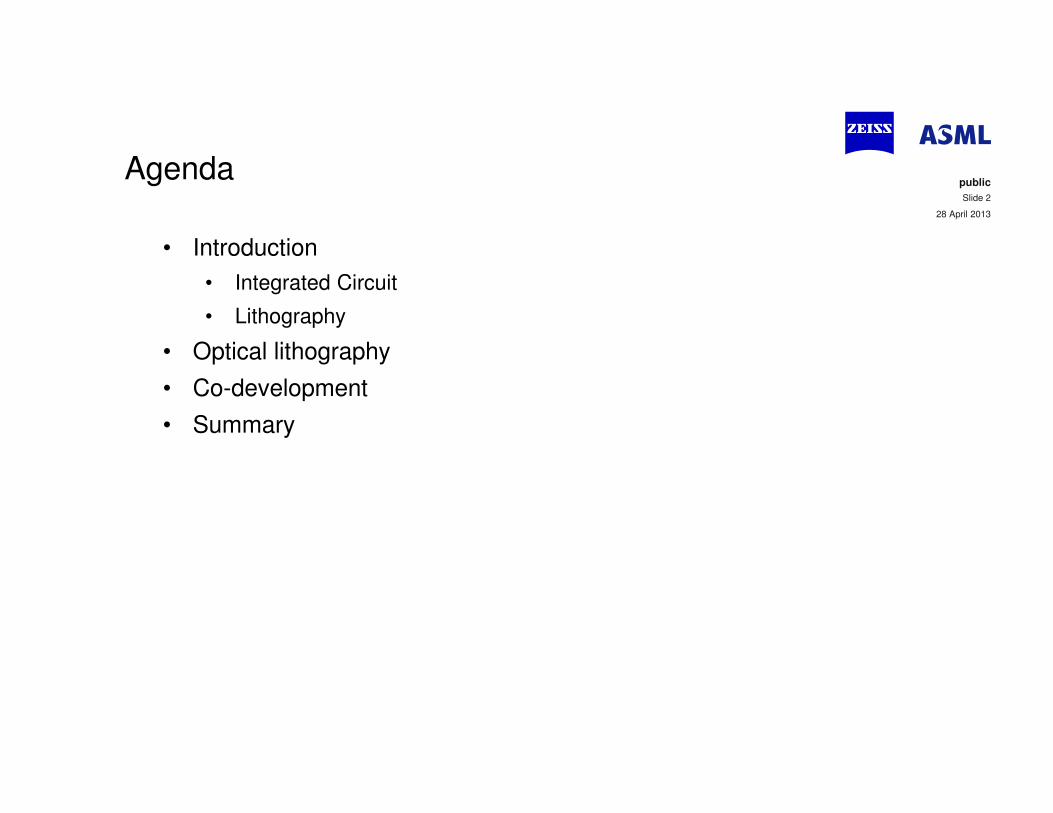
How it all got started...
1947
The Point contact transistor
Bell Labs
1958
The First IC
Texas Instruments
1961
The First Planar IC
Fairchild
28 April 2013
public
Slide 3
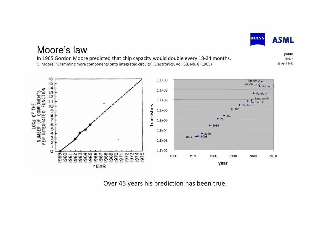
Moore’s lawIn 1965 Gordon Moore predicted that chip capacity would double every 18-24 months. G. Moore, ”Cramming more components onto integrated circuits”, Electronics, Vol. 38, Nb. 8 (1965)
Itanium 2
(9 MB core)Itanium 2
Pentium 4
Pentium III
Pentium IIPentium
486
386286
8086
808080084004
1.E+02
1.E+03
1.E+04
1.E+05
1.E+06
1.E+07
1.E+08
1.E+09
1960 1970 1980 1990 2000 2010
year
tra
nsi
sto
rs
Over 45 years his prediction has been true.
28 April 2013
public
Slide 4
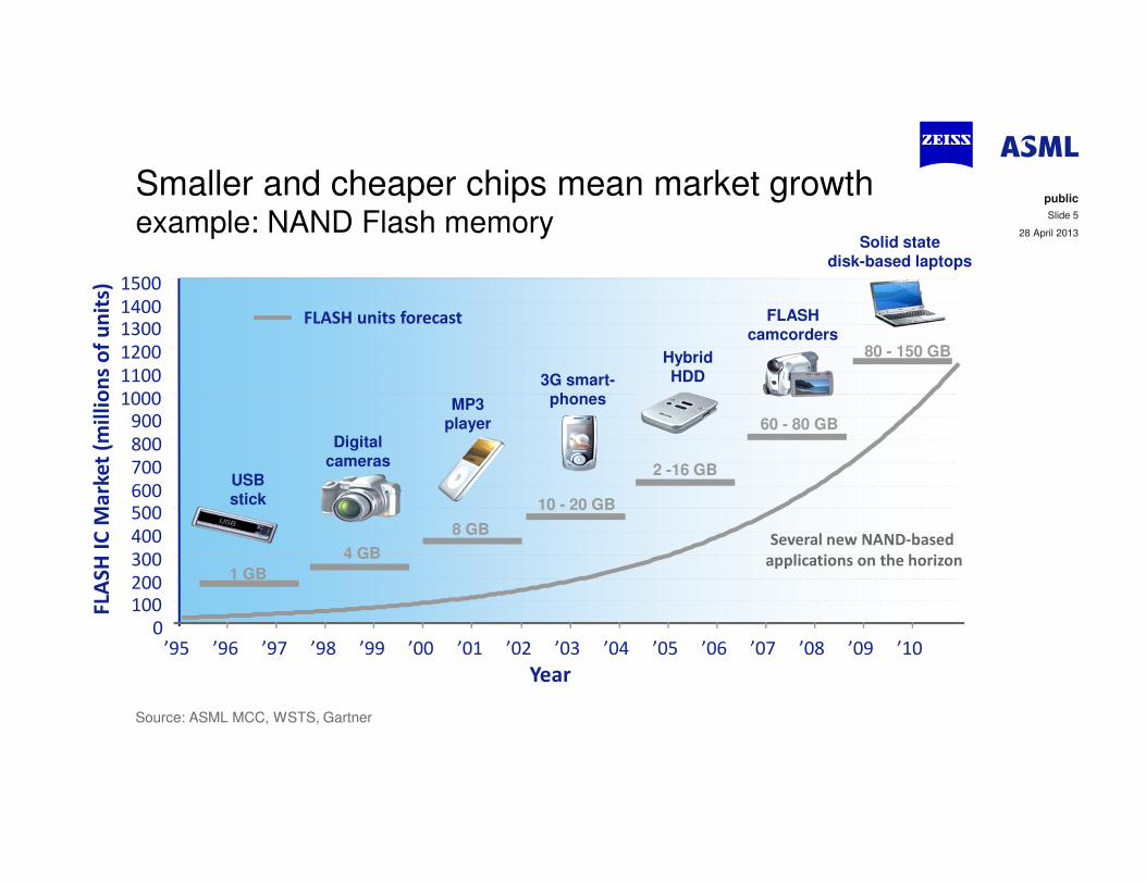
Smaller and cheaper chips mean market growthexample: NAND Flash memory
Source: ASML MCC, WSTS, Gartner
1 GB
USB stick
4 GB
Digital cameras
8 GB
MP3 player
10 - 20 GB
60 - 80 GB
Hybrid HDD
FLASH camcorders
Solid state disk-based laptops
2 -16 GB
80 - 150 GB
0
100200
300
400
500600
700
800
9001000
1100
1200
13001400
1500
’95 ’96 ’97 ’98 ’99 ’00 ’01 ’02 ’03 ’04 ’05 ’06 ’07 ’08 ’09 ’10
Year
FLA
SH
IC
Ma
rke
t (m
illi
on
s o
f u
nit
s)
FLASH units forecast
Several new NAND-based
applications on the horizon
3G smart-phones
28 April 2013
public
Slide 5
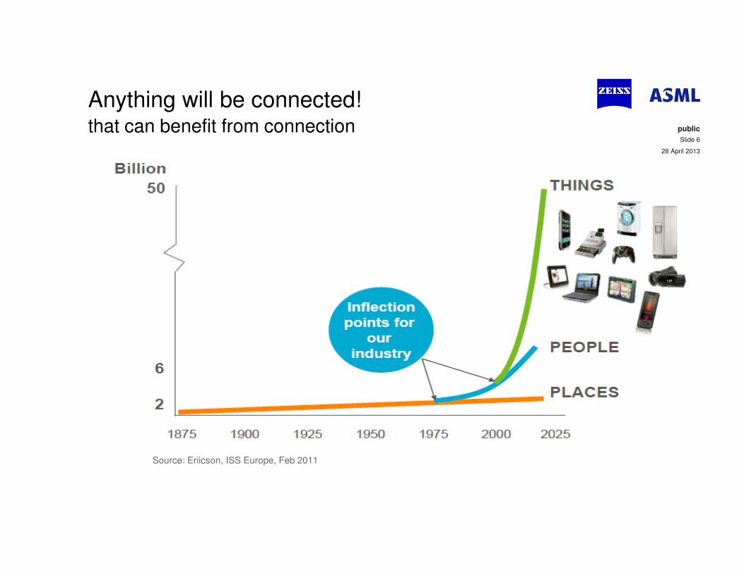
Anything will be connected!that can benefit from connection
Source: Eriicson, ISS Europe, Feb 2011
28 April 2013
public
Slide 6
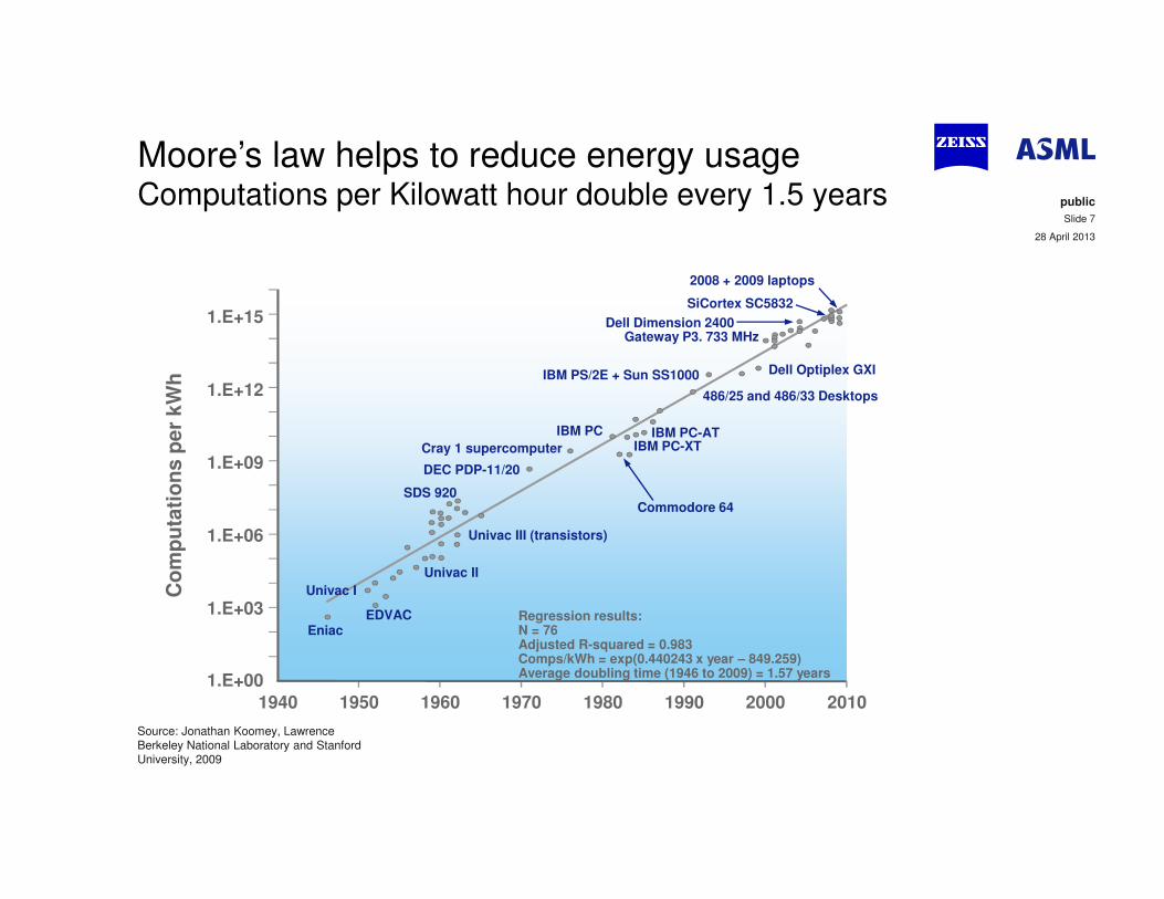
Moore’s law helps to reduce energy usageComputations per Kilowatt hour double every 1.5 years
Source: Jonathan Koomey, Lawrence Berkeley National Laboratory and Stanford University, 2009
Dell Optiplex GXI
486/25 and 486/33 Desktops
IBM PC-ATIBM PC-XT
Commodore 64
DEC PDP-11/20
Cray 1 supercomputer
IBM PC
SDS 920
Univac I
EniacEDVAC
Univac II
Univac III (transistors)
Regression results:N = 76Adjusted R-squared = 0.983Comps/kWh = exp(0.440243 x year – 849.259)Average doubling time (1946 to 2009) = 1.57 years
IBM PS/2E + Sun SS1000
Gateway P3. 733 MHzDell Dimension 2400
SiCortex SC5832
2008 + 2009 laptops
1.E+15
1.E+12
1.E+09
1.E+06
1.E+03
1.E+00
Co
mp
uta
tio
ns p
er
kW
h
1940 1950 1960 1970 1980 1990 2000 2010
28 April 2013
public
Slide 7
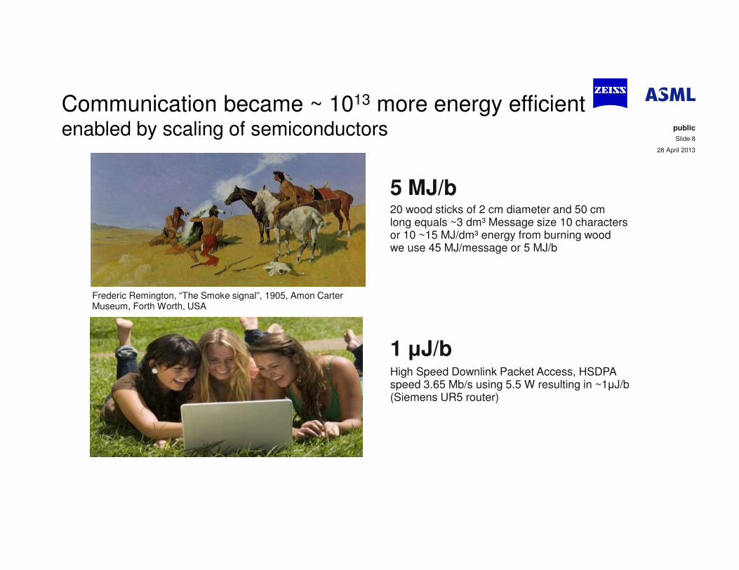
Communication became ~ 1013 more energy efficientenabled by scaling of semiconductors
Frederic Remington, “The Smoke signal”, 1905, Amon Carter Museum, Forth Worth, USA
5 MJ/b20 wood sticks of 2 cm diameter and 50 cm long equals ~3 dm³ Message size 10 characters or 10 ~15 MJ/dm³ energy from burning wood we use 45 MJ/message or 5 MJ/b
High Speed Downlink Packet Access, HSDPA speed 3.65 Mb/s using 5.5 W resulting in ~1µJ/b (Siemens UR5 router)
1 µJ/b
28 April 2013
public
Slide 8

Agenda
• Introduction
• Integrated Circuit
• Lithography
• Optical lithography
• Co-development
• Summary
28 April 2013
public
Slide 9
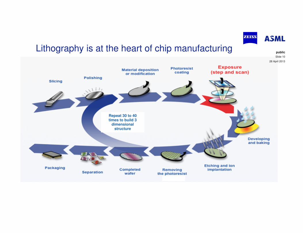
Lithography is at the heart of chip manufacturing
Repeat 30 to 40 times to build 3
dimensional structure
28 April 2013
public
Slide 10
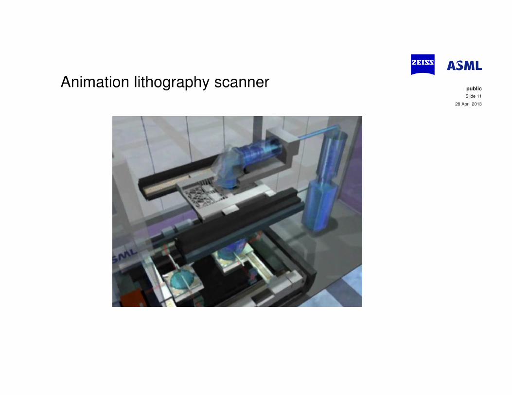
Animation lithography scanner28 April 2013
public
Slide 11
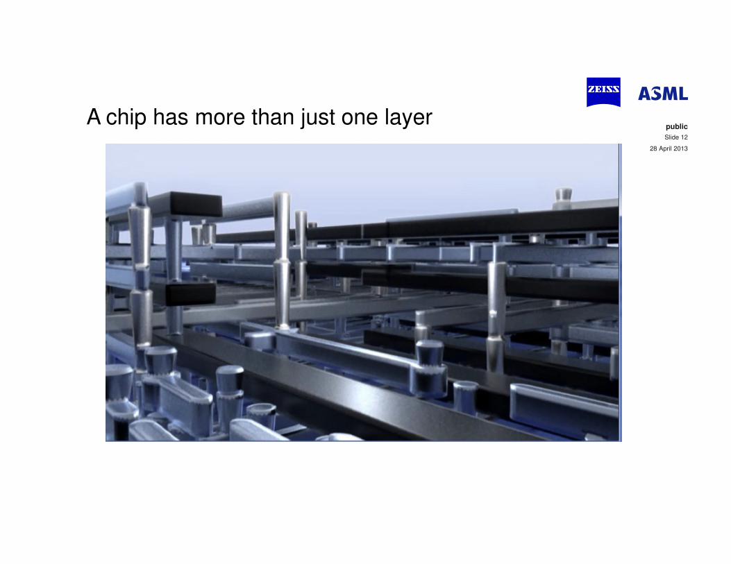
A chip has more than just one layer 28 April 2013
public
Slide 12
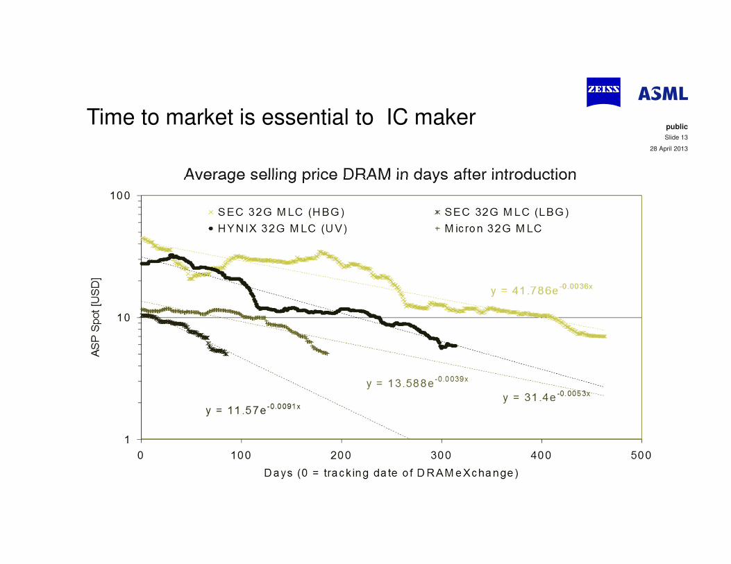
Time to market is essential to IC maker
Average selling price DRAM in days after introduction
28 April 2013
public
Slide 13
Agenda
• Introduction
• Optical lithography
• Past
• Present
• Future
• Co-development
• Summary
28 April 2013
public
Slide 14
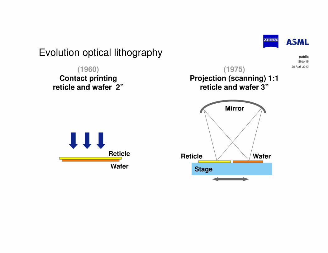
Evolution optical lithography
Stage
Reticle
Wafer
Reticle Wafer
Mirror
(1960)
Contact printingreticle and wafer 2”
(1975)
Projection (scanning) 1:1reticle and wafer 3”
28 April 2013
public
Slide 15
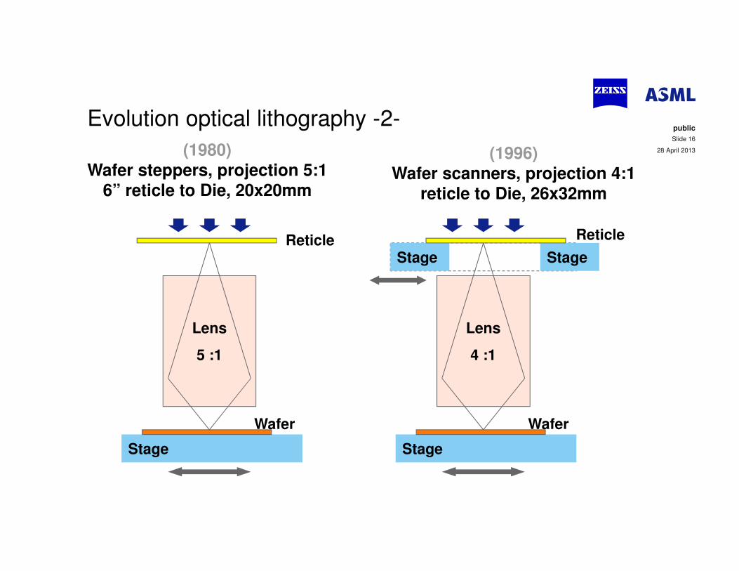
Evolution optical lithography -2-
Stage
Reticle
Wafer
Lens
5 :1
Stage
Reticle
Wafer
Lens
4 :1
Stage Stage
(1980)Wafer steppers, projection 5:1
6” reticle to Die, 20x20mm
(1996)
Wafer scanners, projection 4:1
reticle to Die, 26x32mm
28 April 2013
public
Slide 16
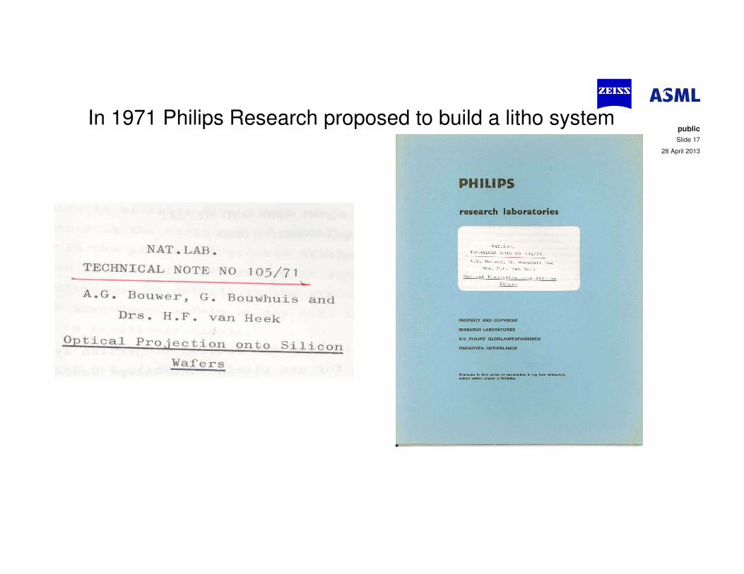
In 1971 Philips Research proposed to build a litho system
28 April 2013
public
Slide 17
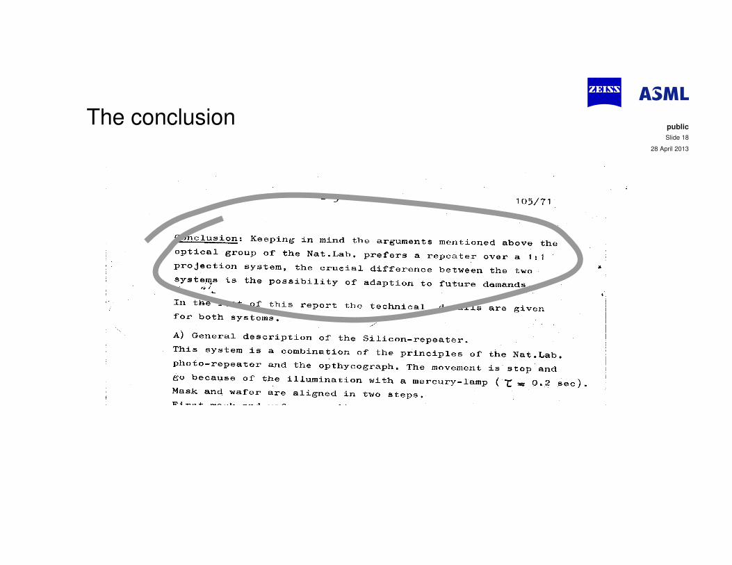
The conclusion28 April 2013
public
Slide 18
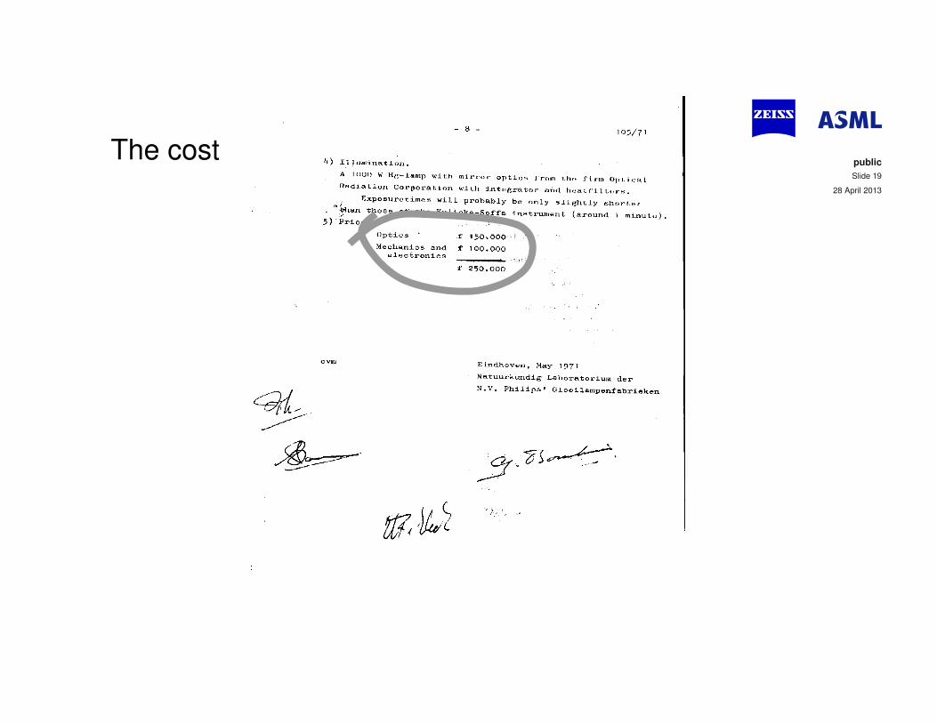
The cost28 April 2013
public
Slide 19
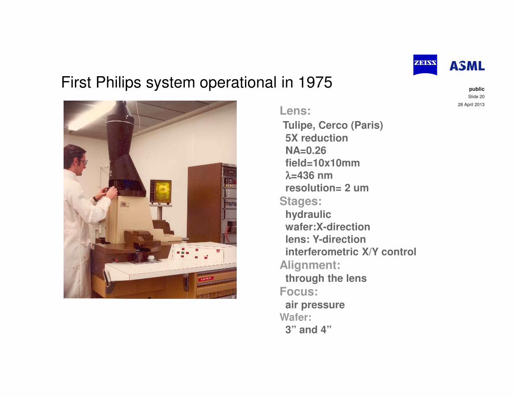
First Philips system operational in 1975
Lens:
Tulipe, Cerco (Paris)
5X reduction
NA=0.26
field=10x10mm
λλλλ=436 nm
resolution= 2 um
Stages:hydraulic
wafer:X-direction
lens: Y-direction
interferometric X/Y control
Alignment:through the lens
Focus:air pressure
Wafer:
3” and 4”
28 April 2013
public
Slide 20
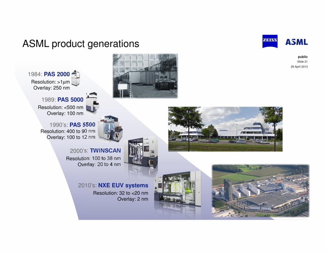
ASML product generations
1984: PAS 2000
Resolution: >1µm
Overlay: 250 nm
1989: PAS 5000
Resolution: <500 nm
Overlay: 100 nm
1990’s: PAS 5500 Resolution: 400 to 90 nm
Overlay: 100 to 12 nm
2000’s: TWINSCAN
Resolution: 100 to 38 nm
Overlay: 20 to 4 nm
2010’s: NXE EUV systems
Resolution: 32 to <20 nm
Overlay: 2 nm
28 April 2013
public
Slide 21
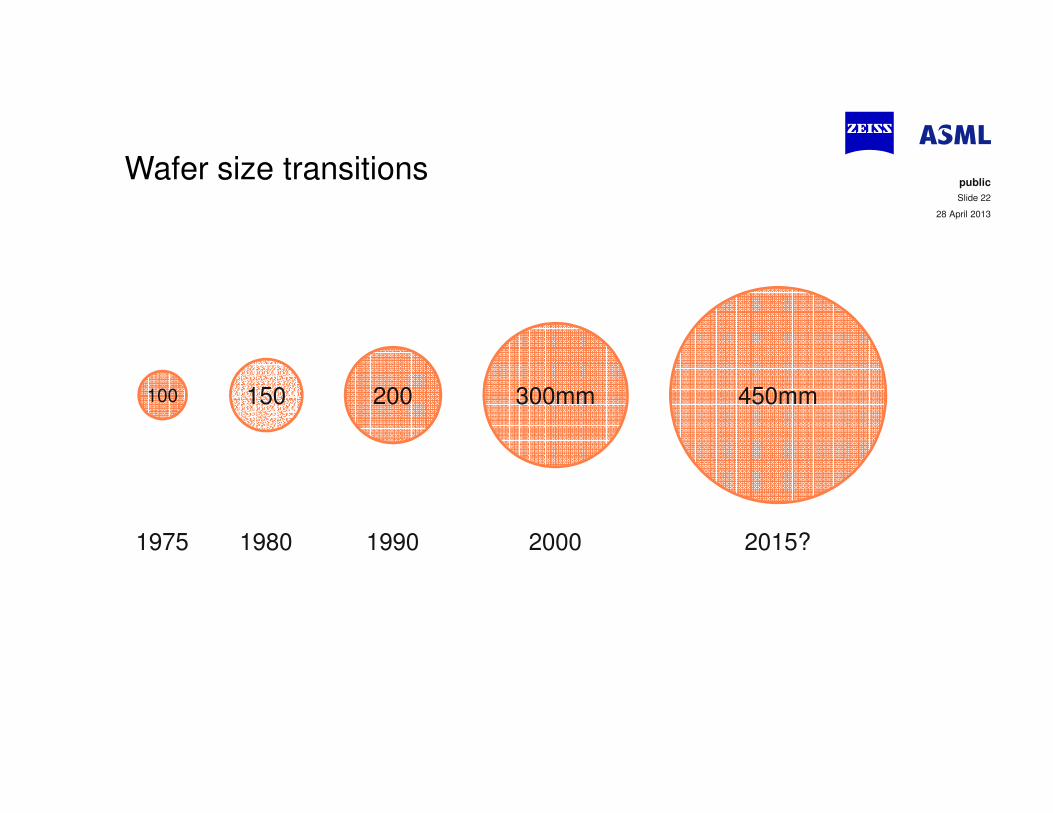
Wafer size transitions
200 300mm 450mm150100
1975 1980 1990 2000 2015?
28 April 2013
public
Slide 22
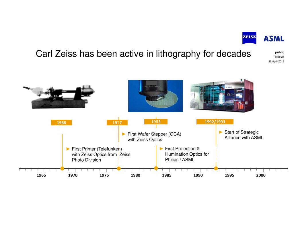
Carl Zeiss has been active in lithography for decades
1965 1970 1975 1980 1985 1990 1995 2000
1977
► First Printer (Telefunken)
with Zeiss Optics from Zeiss
Photo Division
1983
► Start of Strategic
Alliance with ASML
1992/1993
► First Projection &
Illumination Optics for
Philips / ASML
► First Wafer Stepper (GCA)
with Zeiss Optics
1968
28 April 2013
public
Slide 23
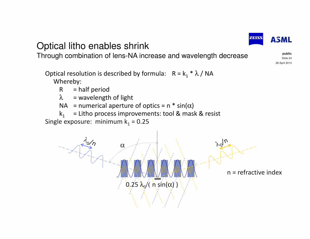
Optical litho enables shrinkThrough combination of lens-NA increase and wavelength decrease
Optical resolution is described by formula: R = k1 * λ / NA
Whereby:
R = half period
λ = wavelength of light
NA = numerical aperture of optics = n * sin(α)
k1 = Litho process improvements: tool & mask & resist
Single exposure: minimum k1 = 0.25
α
0.25 λ0/( n sin(α) )
n = refractive index
28 April 2013
public
Slide 24
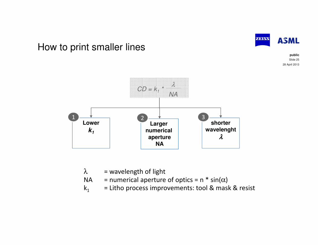
How to print smaller lines
28 April 2013
public
Slide 25
CD = k1 * λ
NA
Larger numericalaperture
NA
Lower
k1
shorterwavelenght
λλλλ
321
λ = wavelength of light
NA = numerical aperture of optics = n * sin(α)
k1 = Litho process improvements: tool & mask & resist
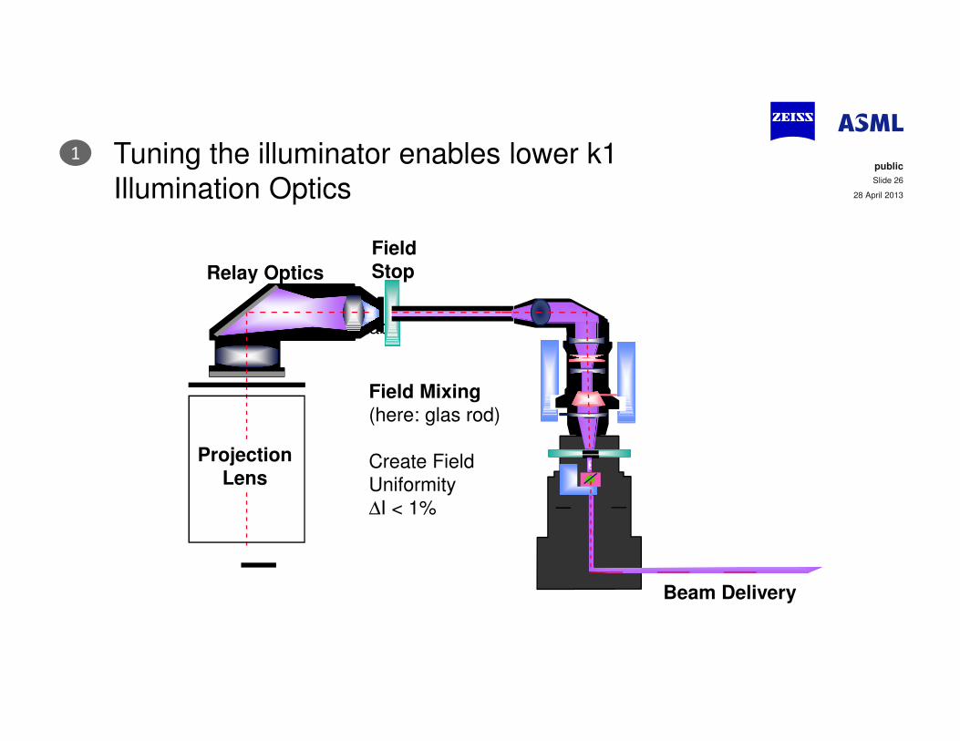
Tuning the illuminator enables lower k1
Illumination Optics
Glasstab
Projection
Lens
Field
StopRelay Optics
Field Mixing
(here: glas rod)
Create Field
Uniformity
∆I < 1%
Beam Delivery
28 April 2013
public
Slide 26
1
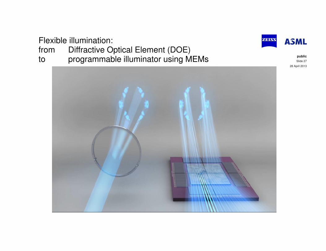
Flexible illumination:from Diffractive Optical Element (DOE) to programmable illuminator using MEMs
28 April 2013
public
Slide 27
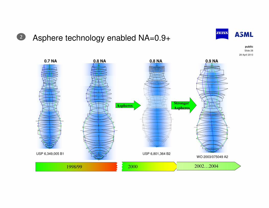
Asphere technology enabled NA=0.9+
1998/99 2000 2002…2004
USP 6,801,364 B2
0.9 NA
Aspheres
USP 6,349,005 B1
0.8 NA0.7 NA 0.8 NA
WO 2003/075049 A2
Stronger
Aspheres
28 April 2013
public
Slide 28
2
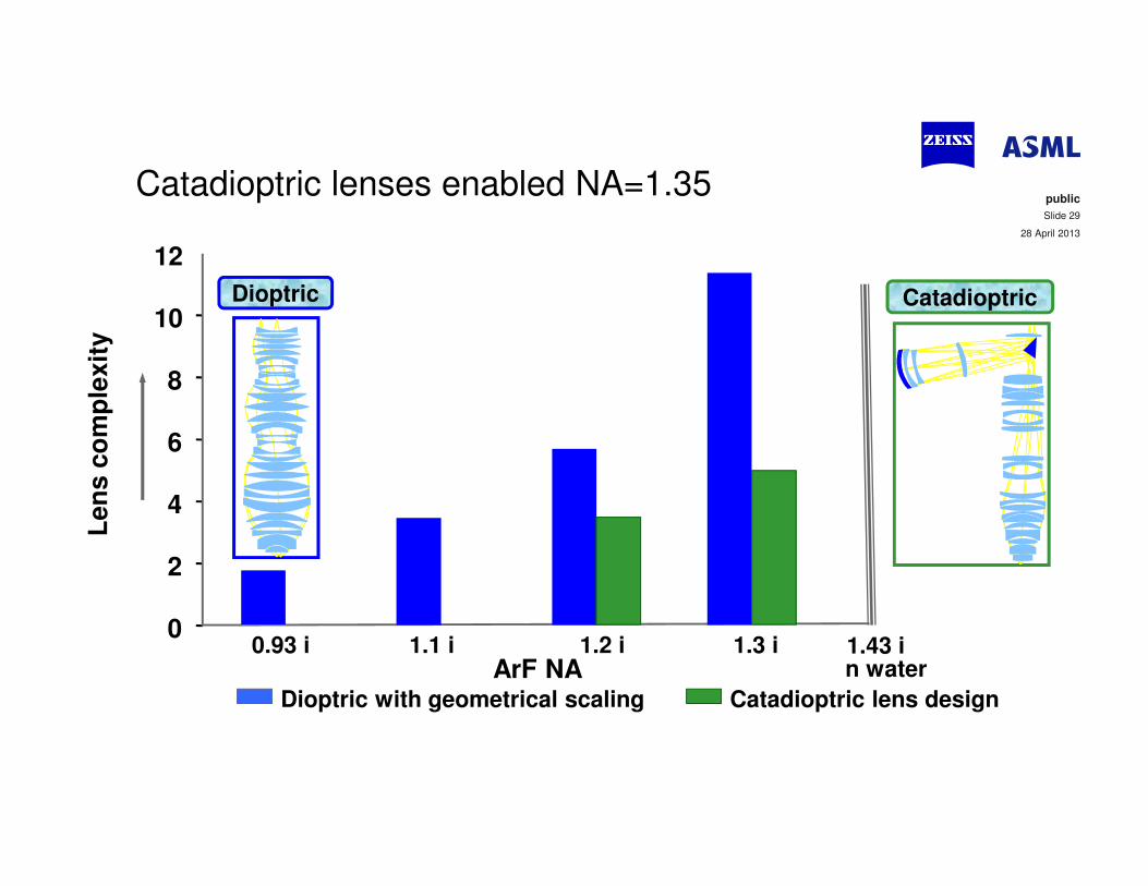
Catadioptric lenses enabled NA=1.35
n waterArF NA
0
2
4
6
8
10
12
Dioptric with geometrical scaling
0.93 i 1.1 i 1.2 i 1.3 i
Len
sco
mp
lexit
y
1.43 i
Dioptric
Catadioptric lens design
Catadioptric
28 April 2013
public
Slide 29
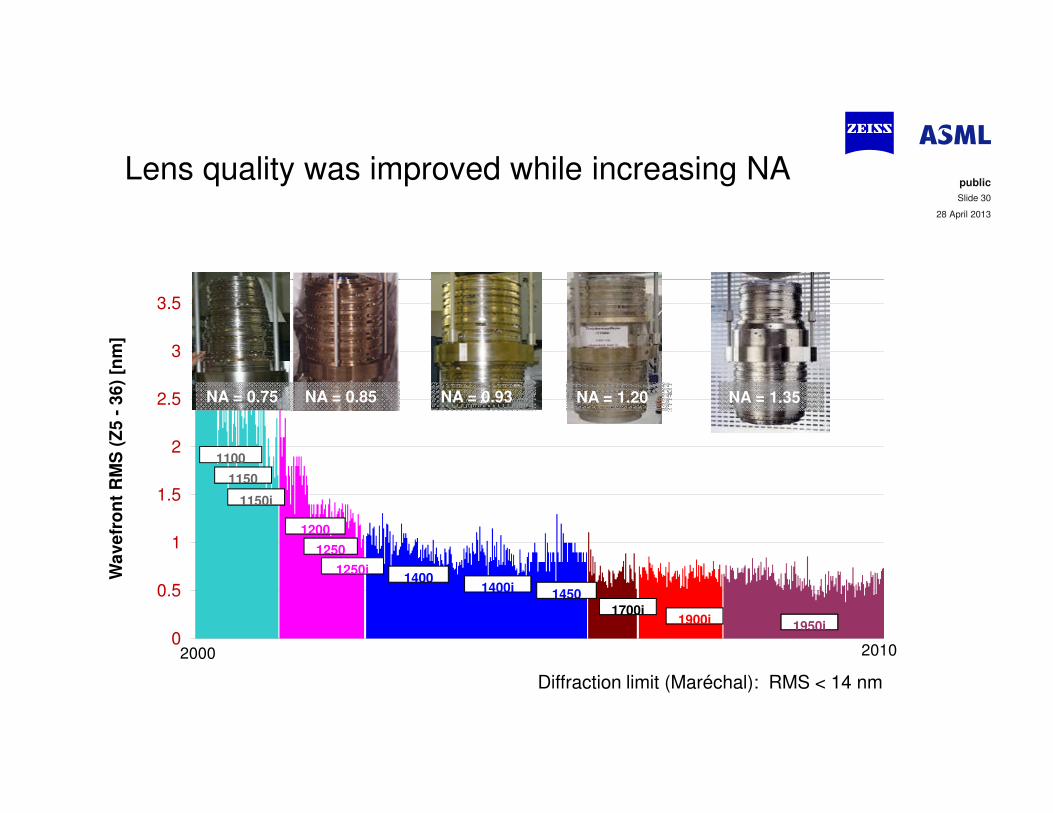
Lens quality was improved while increasing NA
0
0.5
1
1.5
2
2.5
3
3.5
Wa
ve
fro
nt
RM
S (
Z5
-3
6)
[nm
]
1100
1150
1150i
1250i
1250
1200
14001400i
1700i 1900i
1950i
1450
Diffraction limit (Maréchal): RMS < 14 nm
2000 2010
NA = 0.85 NA = 0.93NA = 0.75 NA = 1.20 NA = 1.35
28 April 2013
public
Slide 30
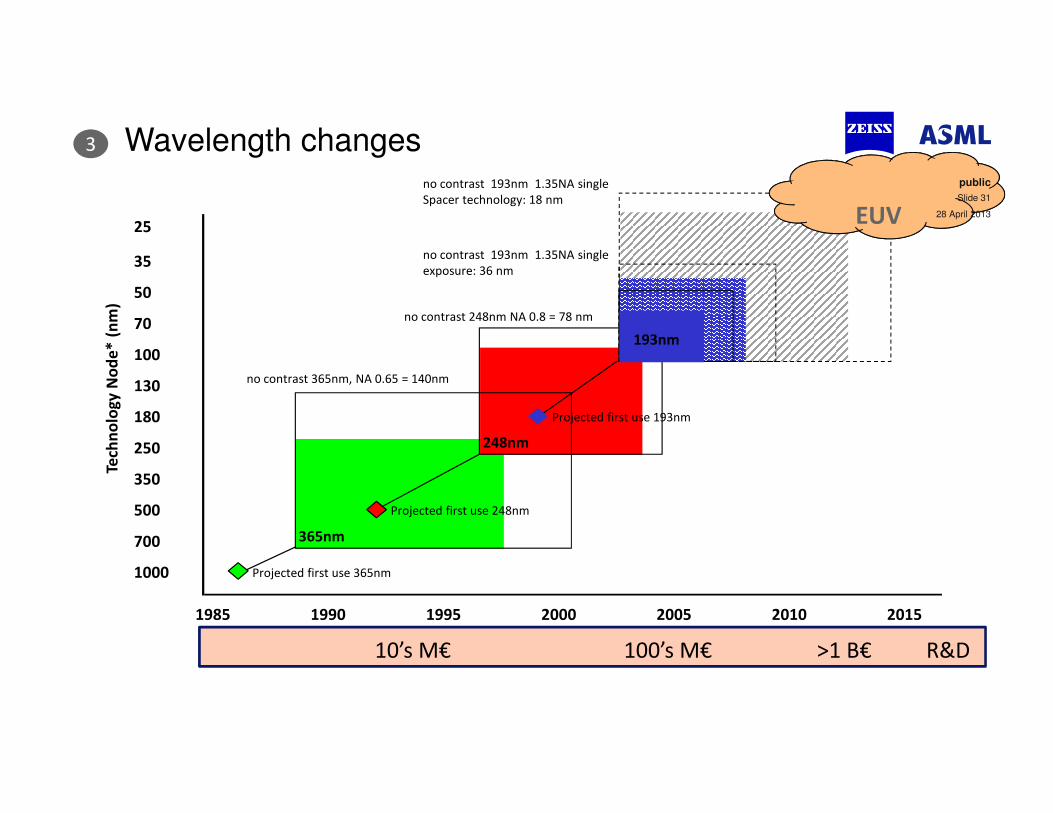
no contrast 193nm 1.35NA single
Spacer technology: 18 nm
Wavelength changes
25
35
50
70
100
130
180
250
350
500
700
1000
1985 1990 1995 2000 2005 2010 2015
Tech
no
log
y N
od
e*
(n
m)
365nm
Projected first use 365nm
Projected first use 248nm
no contrast 248nm NA 0.8 = 78 nm
248nm
no contrast 365nm, NA 0.65 = 140nm
no contrast 193nm 1.35NA single
exposure: 36 nm
Projected first use 193nm
193nm
EUVEUV
10’s M€ 100’s M€ >1 B€ R&D
28 April 2013
public
Slide 31
3
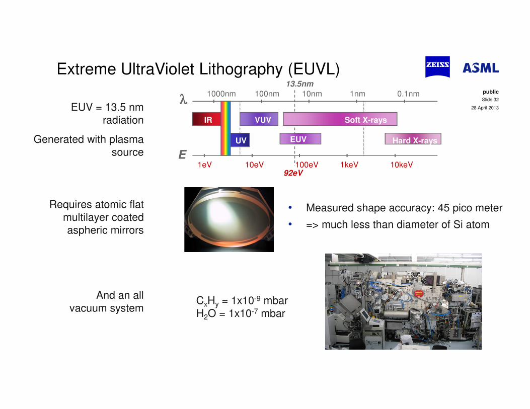
1000nm 100nm 10nm 1nm 0.1nm
1eV 10eV 100eV 1keV 10keV
13.5nm
92eV
IR VUV Soft X-rays
UV EUV Hard X-rays
λλλλ
E
EUV = 13.5 nm
radiation
Generated with plasma
source
Extreme UltraViolet Lithography (EUVL)
Requires atomic flat
multilayer coated
aspheric mirrors
And an all
vacuum system
• Measured shape accuracy: 45 pico meter
• => much less than diameter of Si atom
CxHy = 1x10⁻⁹ mbar
H2O = 1x10⁻⁷ mbar
28 April 2013
public
Slide 32
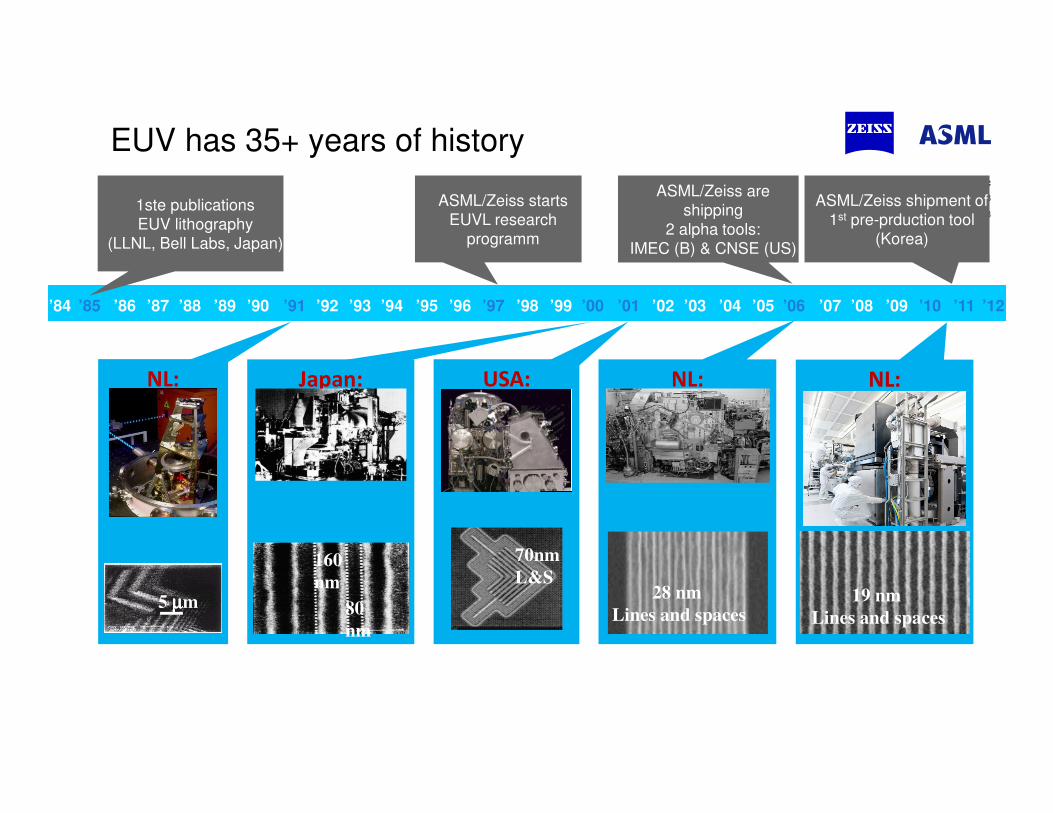
USA:
40 nm hp
70nm
L&S
Japan:
80
nm
160
nm40 nm hp
NL:
28 nm
Lines and spaces
40 nm hp
NL:
19 nm
Lines and spaces
’85 ’91 ’97 ’00 ’01 ’06 ’10’86 ’87’84 ’88 ’89 ’90 ’92 ’93 ’94 ’95 ’96
NL:
5 µµµµm
’98 ’99 ’02 ’03 ’04 ’05 ’07 ’08 ’09 ’11 ’12
EUV has 35+ years of history
28 April 2013
public
Slide 331ste publications
EUV lithography
(LLNL, Bell Labs, Japan)
ASML/Zeiss starts
EUVL research
programm
ASML/Zeiss shipment of
1st pre-prduction tool
(Korea)
ASML/Zeiss are
shipping
2 alpha tools:
IMEC (B) & CNSE (US)
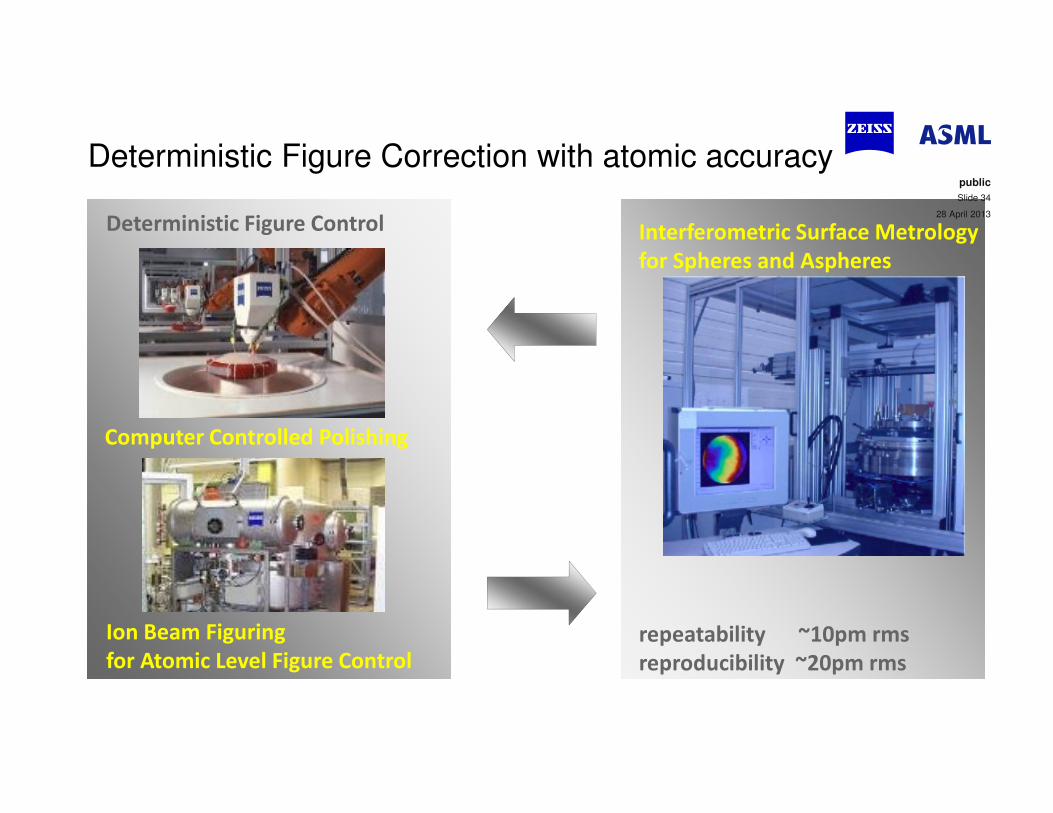
Deterministic Figure Correction with atomic accuracy
Interferometric Surface Metrology
for Spheres and Aspheres
repeatability ~10pm rms
reproducibility ~20pm rms
Ion Beam Figuring
for Atomic Level Figure Control
Computer Controlled Polishing
Deterministic Figure Control28 April 2013
public
Slide 34
EUV – Flare Becomes Essential
2004
MS
FR
[n
m r
ms]
2005 2006 2007 2008 2009 2010 2011 2012
0.30
0.25
0.20
0.15
0.10
0.05
0
ADT
3100
3300
Today:
< 6% flare on
system level
Today:
< 6% flare on
system level
28 April 2013
public
Slide 35
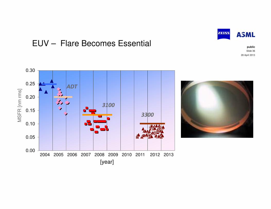
EUV – Flare Becomes Essential 28 April 2013
public
Slide 36
ADT
3100
3300
2004 2005 2006 2007 2008 2009 2010 2011 2012 2013
MS
FR
[nm
rms]
[year]
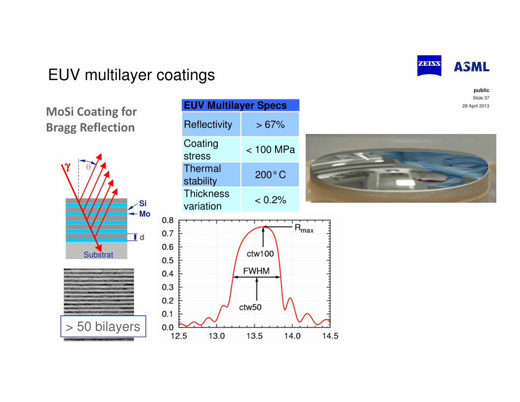
EUV multilayer coatings
Mo
Si
Substrat
θ
d
γγγγ
> 50 bilayers
Reflectivity > 67%
Coating
stress< 100 MPa
Thermal
stability200° C
Thickness
variation< 0.2%
EUV Multilayer SpecsMoSi Coating for
Bragg Reflection
28 April 2013
public
Slide 37
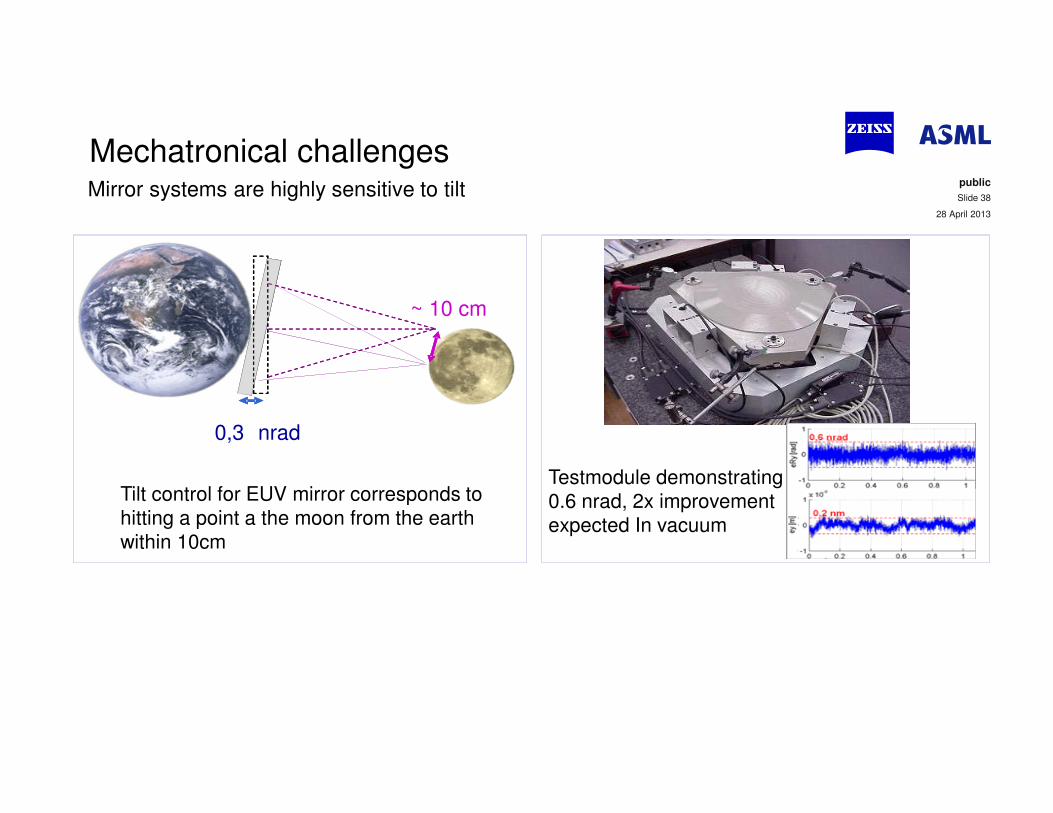
Mirror systems are highly sensitive to tilt
Mechatronical challenges
28 April 2013
public
Slide 38
Tilt control for EUV mirror corresponds to
hitting a point a the moon from the earth
within 10cm
0,3 nrad
~ 10 cm
Testmodule demonstrating
0.6 nrad, 2x improvement
expected In vacuum
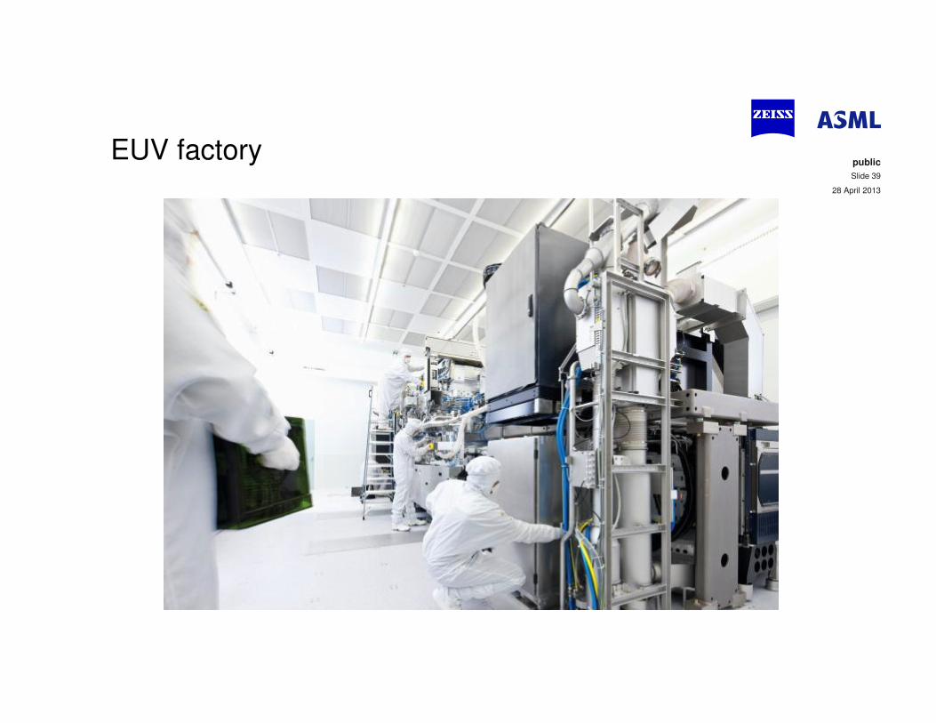
EUV factory28 April 2013
public
Slide 39
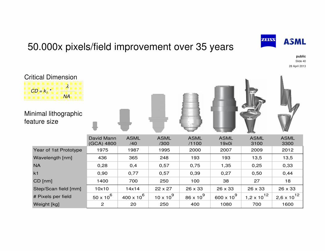
CD = k1 * λ
NA
50.000x pixels/field improvement over 35 years
David Mann
(GCA) 4800
ASML
/40
ASML
/300
ASML
/1100
ASML
19x0i
ASML
3100
ASML
3300
Year of 1st Prototype 1975 1987 1995 2000 2007 2009 2012
Wavelength [nm] 436 365 248 193 193 13,5 13,5
NA 0,28 0,4 0,57 0,75 1,35 0,25 0,33
k1 0,90 0,77 0,57 0,39 0,27 0,50 0,44
CD [nm] 1400 700 250 100 38 27 18
Step/Scan field [mm] 10x10 14x14 22 x 27 26 x 33 26 x 33 26 x 33 26 x 33
# Pixels per field 50 x 106
400 x 106
10 x 109
86 x 109
600 x 109
1,2 x 10¹²
2,6 x 10¹²
Weight [kg] 2 20 250 400 1080 700 1600
Critical Dimension
Minimal lithographic
feature size
28 April 2013
public
Slide 40

Agenda
• Introduction
• Optical lithography
• Co-development
• Summary
28 April 2013
public
Slide 41
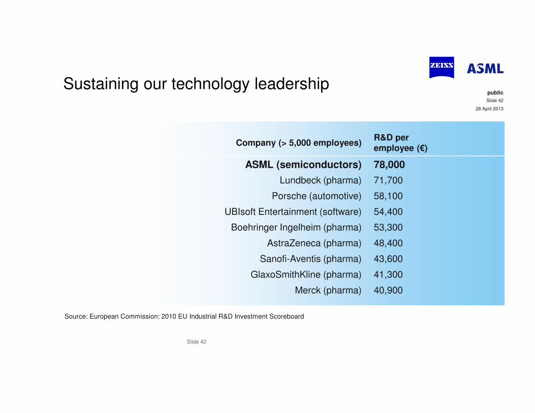
Sustaining our technology leadership
Slide 42
Company (> 5,000 employees)R&D per
employee (€)
ASML (semiconductors) 78,000
Lundbeck (pharma) 71,700
Porsche (automotive) 58,100
UBIsoft Entertainment (software) 54,400
Boehringer Ingelheim (pharma) 53,300
AstraZeneca (pharma) 48,400
Sanofi-Aventis (pharma) 43,600
GlaxoSmithKline (pharma) 41,300
Merck (pharma) 40,900
Source: European Commission: 2010 EU Industrial R&D Investment Scoreboard
28 April 2013
public
Slide 42
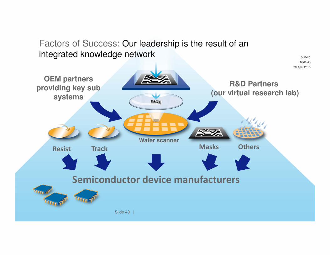
Factors of Success: Our leadership is the result of an
integrated knowledge network
Slide 43 |
Resist Track
Semiconductor device manufacturers
Wafer scanner
R&D Partners (our virtual research lab)
OEM partners
providing key sub
systems
OthersMasks
28 April 2013
public
Slide 43
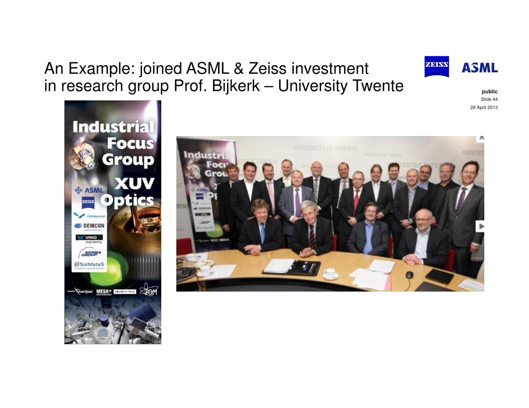
An Example: joined ASML & Zeiss investment in research group Prof. Bijkerk – University Twente
28 April 2013
public
Slide 44
ASML / Zeiss: two companies – one business
Frequent communication at all levels
• Board of management: Joined Management Meetings 3x/year
• Roadmap Meeting 6x/year
• Overall program reviews:
Interface Meeting (technical) 5x/year
Operations Meeting (operational) 5x/year
Commercial Meeting (commercially) 5x/year
• Project Meetings > 10x/year
• Close alignment of project milestones between ASML and Zeiss
28 April 2013
public
Slide 45
Executive summary
28 April 2013
public
Slide 46