Embed Size (px)
Citation preview
Assembly Considerations for
Linear Technology mModuleTM
BGA Packages
September 2016
1
• Package Construction
• PCB Design Guidelines
• Moisture Sensitivity, Pack, Ship & Bake
• Board Assembly Process – Screen Print
• Stencil Design
• Solder Paste, Key Process Parameters
– Reflow Profile
– Removal and Rework
• FAQs
Outline
2
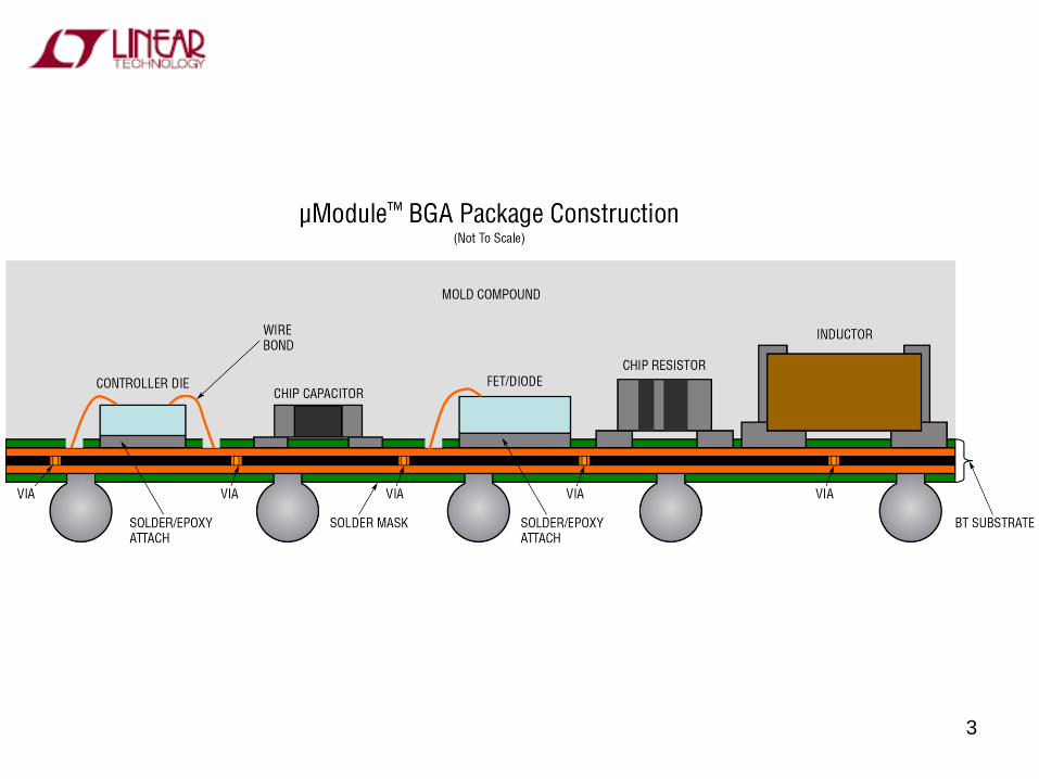
3
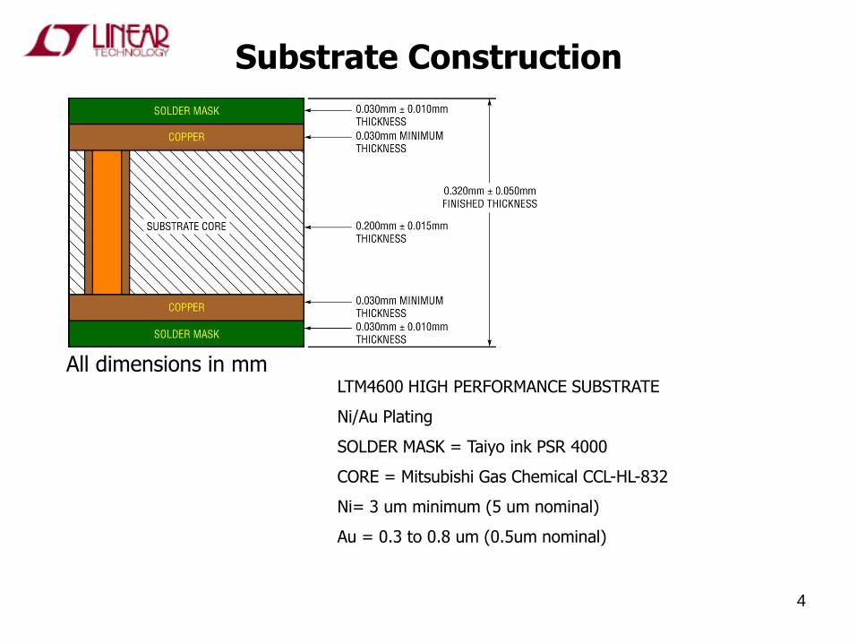
Substrate Construction
LTM4600 HIGH PERFORMANCE SUBSTRATE
Ni/Au Plating
SOLDER MASK = Taiyo ink PSR 4000
CORE = Mitsubishi Gas Chemical CCL-HL-832
Ni= 3 um minimum (5 um nominal)
Au = 0.3 to 0.8 um (0.5um nominal)
All dimensions in mm
4
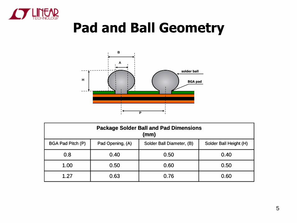
Pad and Ball Geometry
A
B
P
H
solder ball
BGA pad
0.60
0.50
0.40
Solder Ball Height (H)
0.760.631.27
0.600.501.00
0.500.400.8
Solder Ball Diameter, (B)Pad Opening, (A)BGA Pad Pitch (P)
Package Solder Ball and Pad Dimensions
(mm)
0.60
0.50
0.40
Solder Ball Height (H)
0.760.631.27
0.600.501.00
0.500.400.8
Solder Ball Diameter, (B)Pad Opening, (A)BGA Pad Pitch (P)
Package Solder Ball and Pad Dimensions
(mm)
5
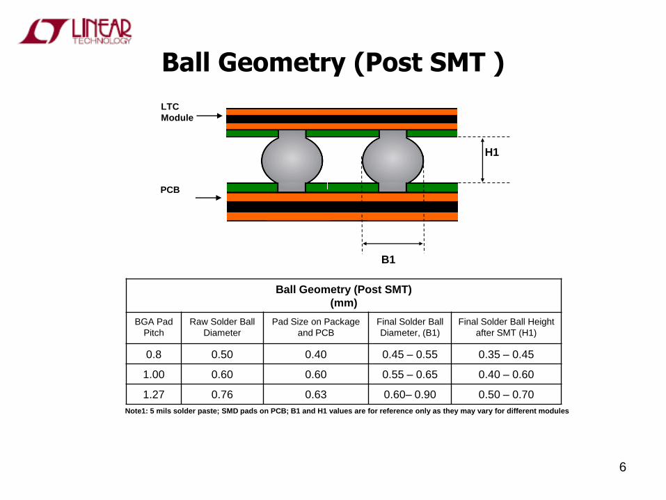
Ball Geometry (Post SMT )
B1
H1
LTC
Module
PCB
Ball Geometry (Post SMT)
(mm)
BGA Pad
Pitch
Raw Solder Ball
Diameter
Pad Size on Package
and PCB
Final Solder Ball
Diameter, (B1)
Final Solder Ball Height
after SMT (H1)
0.8 0.50 0.40 0.45 – 0.55 0.35 – 0.45
1.00 0.60 0.60 0.55 – 0.65 0.40 – 0.60
1.27 0.76 0.63 0.60– 0.90 0.50 – 0.70
Note1: 5 mils solder paste; SMD pads on PCB; B1 and H1 values are for reference only as they may vary for different modules
6
PCB Design Guidelines
• mModule BGA – All pads are solder mask defined (SMD)
• SMD vs NSMD pads on PCB – NSMD pads preferred for signal pins
– SMD OK to use
• PCB Pad Layout (SMD Pads) – Recommend using planes with SMD pads (same size as Package Pad opening)
– Vias between pads (on the planes) on top layer
• Non solder mask defined (NSMD) pads – Recommended Pad Layout
• Pad finish on PCB – OSP, ENIG recommended
– Immersion Ag • Check for any dendritic growth with moisture
– Immersion Sn • Oxidation issues
7
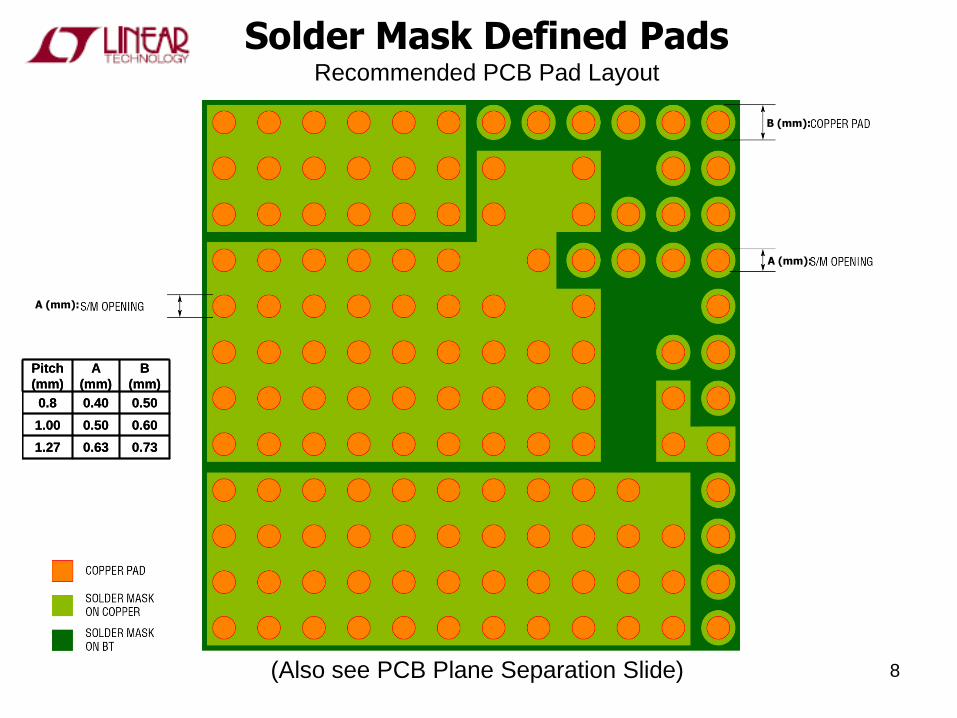
Solder Mask Defined Pads Recommended PCB Pad Layout
(Also see PCB Plane Separation Slide)
A (mm):
A (mm):
B (mm):
B
(mm)
0.73
0.60
0.50
A
(mm)
0.631.27
0.501.00
0.400.8
Pitch
(mm)
B
(mm)
0.73
0.60
0.50
A
(mm)
0.631.27
0.501.00
0.400.8
Pitch
(mm)
8
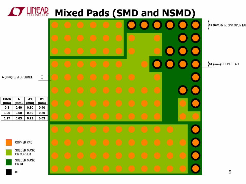
Mixed Pads (SMD and NSMD)
B1 (mm):
A1 (mm):
A (mm):
B1
(mm)
0.63
0.50
0.40
A1
(mm)
0.730.631.27
0.600.501.00
0.500.400.8
A
(mm)
Pitch
(mm)
B1
(mm)
0.63
0.50
0.40
A1
(mm)
0.730.631.27
0.600.501.00
0.500.400.8
A
(mm)
Pitch
(mm)
9
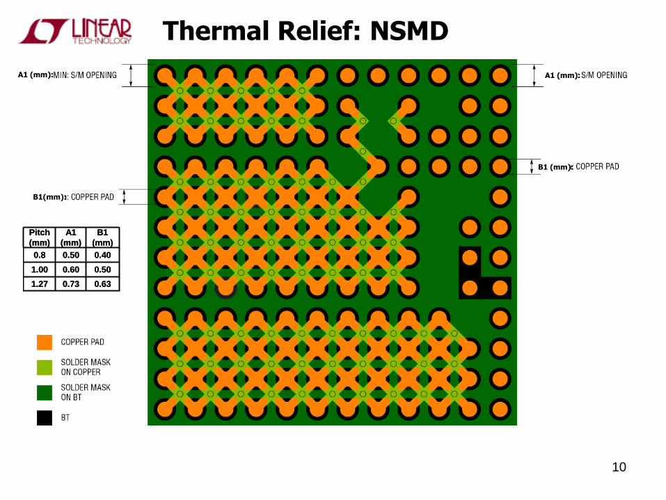
Thermal Relief: NSMD
A1 (mm):
B1 (mm):
A1 (mm):
B1(mm):
B1
(mm)
0.63
0.50
0.40
A1
(mm)
0.731.27
0.601.00
0.500.8
Pitch
(mm)
B1
(mm)
0.63
0.50
0.40
A1
(mm)
0.731.27
0.601.00
0.500.8
Pitch
(mm)
10
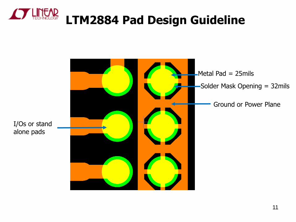
LTM2884 Pad Design Guideline
I/Os or stand alone pads
Metal Pad = 25mils
Ground or Power Plane
11
Solder Mask Opening = 32mils
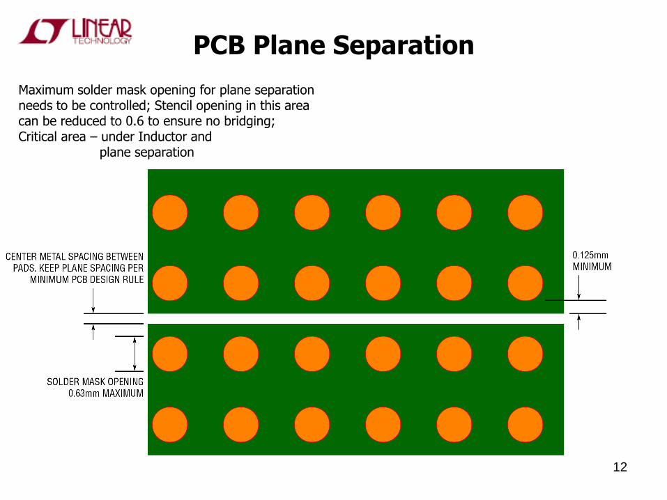
PCB Plane Separation
Maximum solder mask opening for plane separation needs to be controlled; Stencil opening in this area can be reduced to 0.6 to ensure no bridging; Critical area – under Inductor and plane separation
12
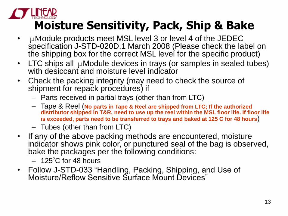
Moisture Sensitivity, Pack, Ship & Bake • mModule products meet MSL level 3 or level 4 of the JEDEC
specification J-STD-020D.1 March 2008 (Please check the label on the shipping box for the correct MSL level for the specific product)
• LTC ships all mModule devices in trays (or samples in sealed tubes) with desiccant and moisture level indicator
• Check the packing integrity (may need to check the source of shipment for repack procedures) if – Parts received in partial trays (other than from LTC)
– Tape & Reel (No parts in Tape & Reel are shipped from LTC; If the authorized distributor shipped in T&R, need to use up the reel within the MSL floor life. If floor life is exceeded, parts need to be transferred to trays and baked at 125 C for 48 hours)
– Tubes (other than from LTC)
• If any of the above packing methods are encountered, moisture indicator shows pink color, or punctured seal of the bag is observed, bake the packages per the following conditions: – 125
oC for 48 hours
• Follow J-STD-033 “Handling, Packing, Shipping, and Use of Moisture/Reflow Sensitive Surface Mount Devices”
13
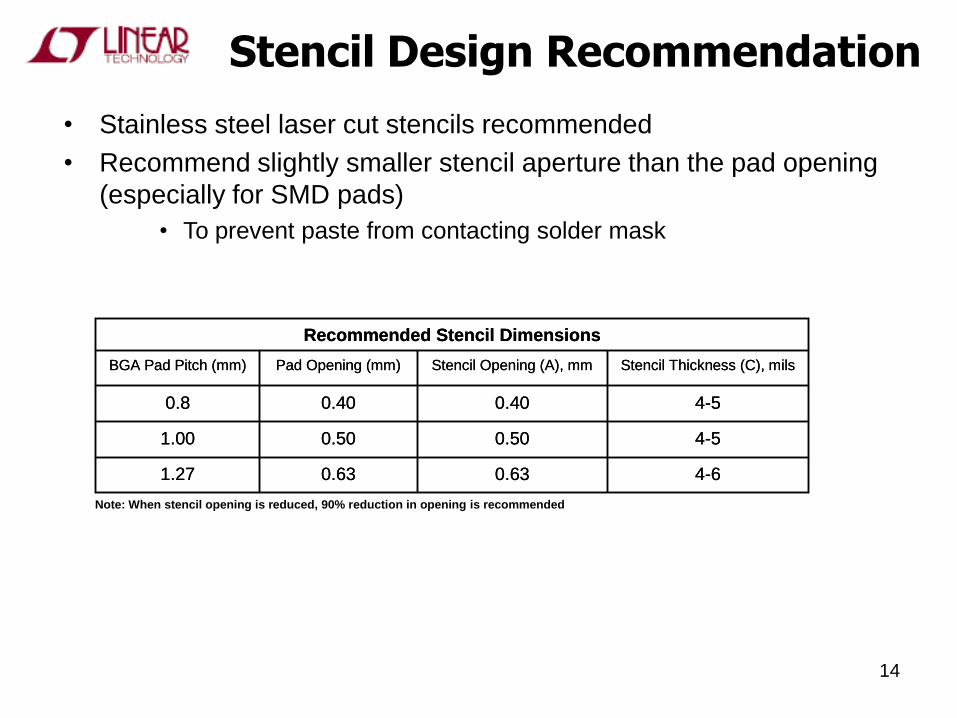
Stencil Design Recommendation
• Stainless steel laser cut stencils recommended
• Recommend slightly smaller stencil aperture than the pad opening
(especially for SMD pads)
• To prevent paste from contacting solder mask
4-6
4-5
4-5
Stencil Thickness (C), mils
0.630.631.27
0.500.501.00
0.400.400.8
Stencil Opening (A), mmPad Opening (mm)BGA Pad Pitch (mm)
Recommended Stencil Dimensions
4-6
4-5
4-5
Stencil Thickness (C), mils
0.630.631.27
0.500.501.00
0.400.400.8
Stencil Opening (A), mmPad Opening (mm)BGA Pad Pitch (mm)
Recommended Stencil Dimensions
Note: When stencil opening is reduced, 90% reduction in opening is recommended
14
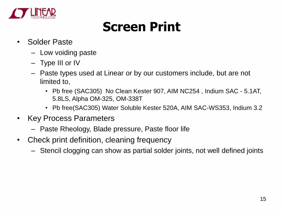
Screen Print • Solder Paste
– Low voiding paste
– Type III or IV
– Paste types used at Linear or by our customers include, but are not
limited to,
• Pb free (SAC305) No Clean Kester 907, AIM NC254 , Indium SAC - 5.1AT,
5.8LS, Alpha OM-325, OM-338T
• Pb free(SAC305) Water Soluble Kester 520A, AIM SAC-WS353, Indium 3.2
• Key Process Parameters
– Paste Rheology, Blade pressure, Paste floor life
• Check print definition, cleaning frequency
– Stencil clogging can show as partial solder joints, not well defined joints
15
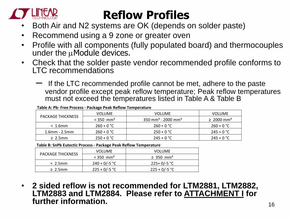
Reflow Profiles • Both Air and N2 systems are OK (depends on solder paste)
• Recommend using a 9 zone or greater oven
• Profile with all components (fully populated board) and thermocouples under the mModule devices.
• Check that the solder paste vendor recommended profile conforms to LTC recommendations
– If the LTC recommended profile cannot be met, adhere to the paste vendor profile except peak reflow temperature; Peak reflow temperatures must not exceed the temperatures listed in Table A & Table B
• 2 sided reflow is not recommended for LTM2881, LTM2882, LTM2883 and LTM2884. Please refer to ATTACHMENT I for further information.
16
Table A: Pb- Free Process - Package Peak Reflow Temperature
PACKAGE THICKNESS VOLUME VOLUME VOLUME
< 350 mm³ 350 mm³ - 2000 mm³ ≥ 2000 mm³
< 1.6mm 260 + 0 °C 260 + 0 °C 260 + 0 °C
1.6mm - 2.5mm 260 + 0 °C 250 + 0 °C 245 + 0 °C
≥ 2.5mm 250 + 0 °C 245 + 0 °C 245 + 0 °C
Table B: SnPb Eutectic Process - Package Peak Reflow Temperature
PACKAGE THICKNESS VOLUME VOLUME
< 350 mm³ ≥ 350 mm³
< 2.5mm 240 + 0/-5 °C 225+ 0/-5 °C
≥ 2.5mm 225 + 0/-5 °C 225 + 0/-5 °C
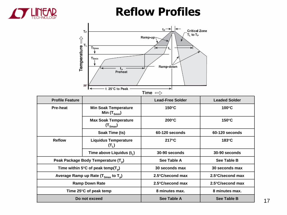
Reflow Profiles
Profile Feature Lead-Free Solder Leaded Solder
Pre-heat Min Soak Temperature
Min (TSmin)
150°C 100°C
Max Soak Temperature
(TSmax)
200°C 150°C
Soak Time (ts) 60-120 seconds 60-120 seconds
Reflow Liquidus Temperature
(TL)
217°C 183°C
Time above Liquidus (tL) 30-90 seconds 30-90 seconds
Peak Package Body Temperature (Tp) See Table A See Table B
Time within 5°C of peak temp(Tp) 30 seconds max 30 seconds max
Average Ramp up Rate (TSmax to Tp) 2.5°C/second max 2.5°C/second max
Ramp Down Rate 2.5°C/second max 2.5°C/second max
Time 25°C of peak temp 8 minutes max. 8 minutes max.
Do not exceed See Table A See Table B 17
Solder Joint Voiding
• LTC/IPC recommends using a 25% maximum void criteria for solder joints
• If the recommended LTC or paste vendor profile results in >25% voiding, then use a soak profile during reflow (Profile with Thermocouple underneath the BGA) – For Pb free paste, ramp to 180
oC to 200
oC and stay
at 200oC to 210
oC for 90 to 110 sec
– For Sn/Pb paste ramp to 150oC and stay for 90 to 110
sec
– If the above soak times are outside the range of the paste vendor recommended profile, keep the soak time to the maximum allowed per the paste vendor
18
Rework Component Removal (mModule device)
• Determine the failure mode from the board and at what operation the defect(s) occurred
– After assembly • Is it opens or shorts?
– Opens : Check solder joint quality, partial joint, no joint, cold solder
– Shorts : X ray to check (Pad design, stencil design)
• Electrical test
– No output : Check output caps next to the module
– Shorting
» Need X-ray to verify short location internal or external to package
» X-ray checks need to be done on the board
• Remove the component from the board within 168 hrs (MSL3 products) or 72 hrs (MSL4 products) of the moisture barrier bag opening prior to assembly or after baking the PC board assembly for 24 hours 125
oC
– If this step is not followed, there is a possibility of delamination of the mold compound from the substrate (solder mask)
• If the part is heated above 245 deg C, the internal solder in the module will melt and may spread through the delaminated areas
• If the part was baked properly, the solder does not spread and is held within the pad
19
Rework Component Removal (mModule device)
• Use a BGA rework station capable of profiling the top and bottom of Module
– Handheld heat guns or IR-only rework stations should not be used
– Use appropriate heat shielding of sensitive components in proximity to the mModules
– The profile is done with a thermocouple on top of the part and another at the bottom of the part (close to the solder joints)
• Maximum temperature for top of package = 245oC
• Maximum bottom temperature (at solder joint) = 230oC to 245
oC
– Keep the bottom temperature as low as possible and increased time to melt the solder for package removal
– Note: maximum top/bottom temperatures for Sn/Pb BGA can be set to 220
oC
– Ensure that the solder has reached above the liquidus temperature
– If the solder is not completely molten, the PCB pads may be lifted during removal
20
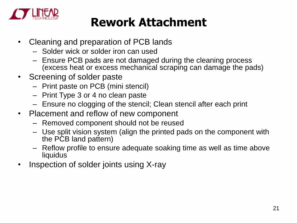
Rework Attachment
• Cleaning and preparation of PCB lands – Solder wick or solder iron can used
– Ensure PCB pads are not damaged during the cleaning process (excess heat or excess mechanical scraping can damage the pads)
• Screening of solder paste – Print paste on PCB (mini stencil)
– Print Type 3 or 4 no clean paste
– Ensure no clogging of the stencil; Clean stencil after each print
• Placement and reflow of new component – Removed component should not be reused
– Use split vision system (align the printed pads on the component with the PCB land pattern)
– Reflow profile to ensure adequate soaking time as well as time above liquidus
• Inspection of solder joints using X-ray
21
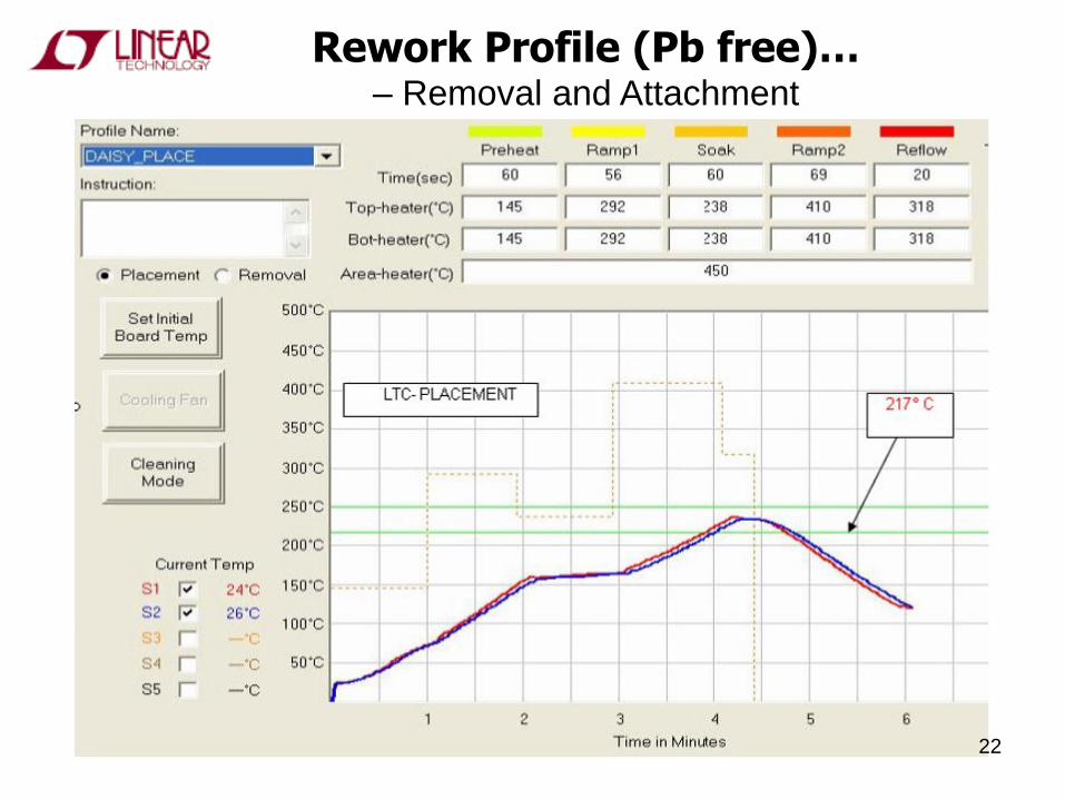
Rework Profile (Pb free)…
– Removal and Attachment
22
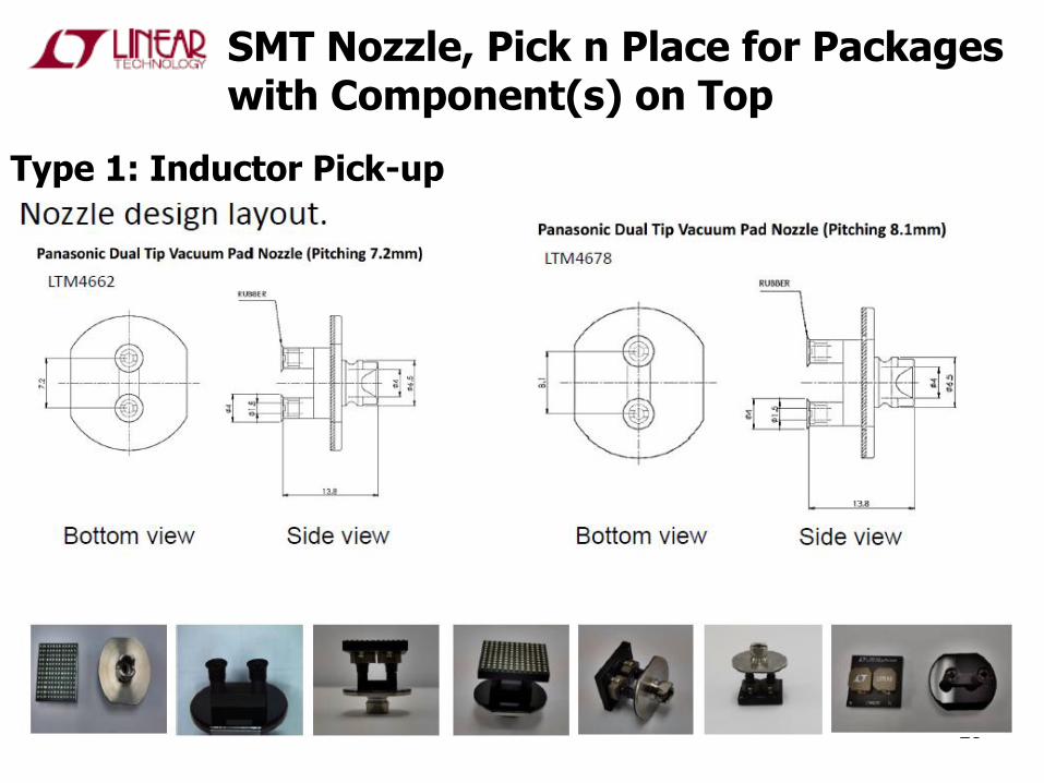
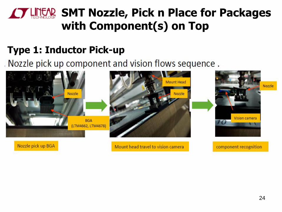
SMT Nozzle, Pick n Place for Packages with Component(s) on Top
23
Type 1: Inductor Pick-up
24
Type 1: Inductor Pick-up
SMT Nozzle, Pick n Place for Packages with Component(s) on Top
Bottom view Side view
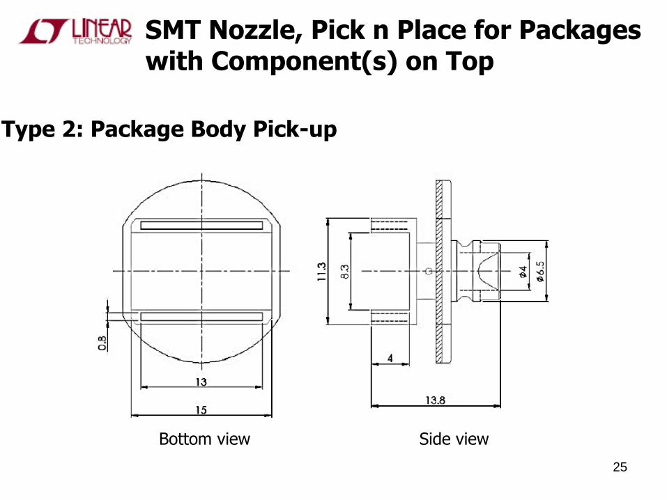
Type 2: Package Body Pick-up
Bottom view Side view
SMT Nozzle, Pick n Place for Packages with Component(s) on Top
25
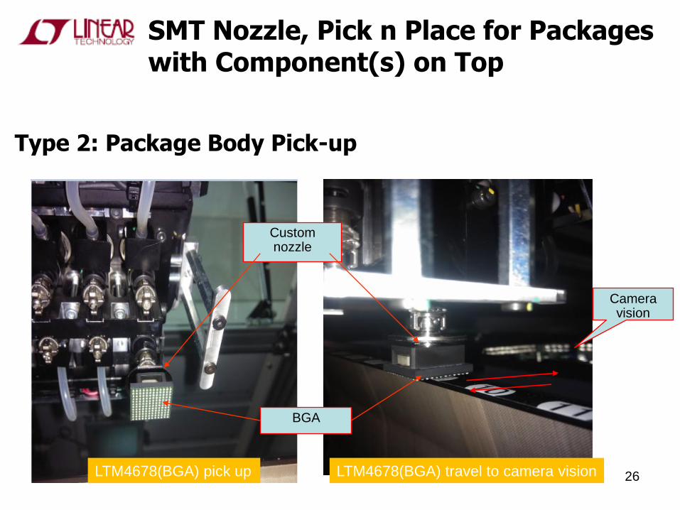
LTM4678(BGA) pick up LTM4678(BGA) travel to camera vision
Camera vision
Custom nozzle
BGA
Type 2: Package Body Pick-up
SMT Nozzle, Pick n Place for Packages with Component(s) on Top
26
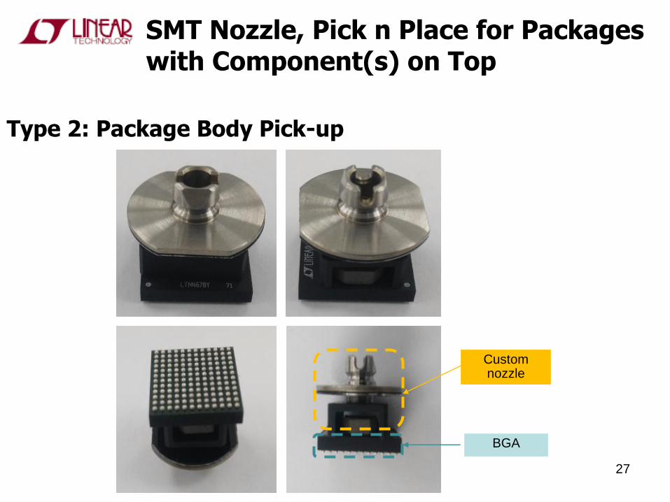
Custom nozzle
BGA
Type 2: Package Body Pick-up
SMT Nozzle, Pick n Place for Packages with Component(s) on Top
27
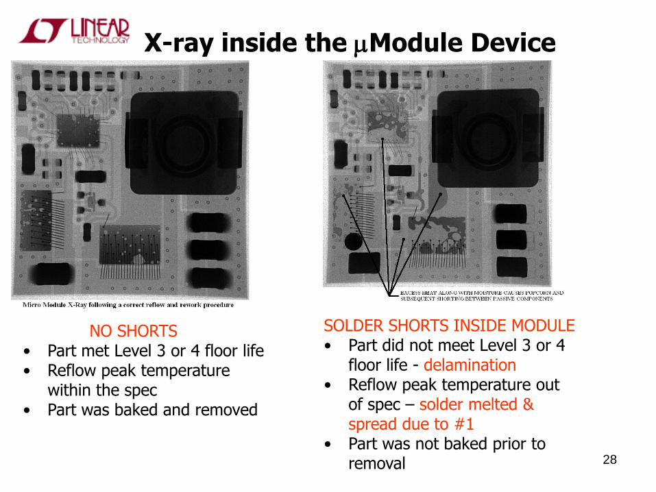
X-ray inside the mModule Device
NO SHORTS • Part met Level 3 or 4 floor life • Reflow peak temperature
within the spec • Part was baked and removed
SOLDER SHORTS INSIDE MODULE • Part did not meet Level 3 or 4
floor life - delamination • Reflow peak temperature out
of spec – solder melted & spread due to #1
• Part was not baked prior to removal 28
FAQs 1. What is the stencil opening, thickness?
• See Stencil design page
2. What type of paste to use? • Both no clean and water soluble are OK; Type III or IV
3. Can the PCB be cleaned effectively? • Yes; Both inline and rotary aqueous systems have been used to clean
effectively
4. How to inspect for the solder joints? • 5DX is an effective method to check for solder joint shorts; Endoscope used
for inspection of peripheral joints
5. Can the μModule product be used on both sides of the PCB? • Yes, provided the total exposure time (out of bag to 2nd reflow) is less than 168
hrs (for MSL3 products) or 72 hrs (for MSL4 products)
6. Parts are shorting (Vin to Gnd or Vout to Gnd) • Check for solder joint shorts (check the schematic with the pin configuration)
• Check inside the module to see if any solder spreading has occurred as shown in the prior slide
29
FAQs
6. How to prevent shorting inside the module? • Check the floor life of the parts (From out of sealed bag to reflow); If over 168
hours (MSL3) or over 72 hours (MSL4) , parts need to be baked for 48 hrs at
125oC
• Was the bag not sealed or moisture indicator showing pink color? – Bake
parts for 48 hrs at 125oC
• Was the reflow peak temperature greater than the peak temp for the module
size (refer to the Table on slide titled “ mModule MSL Rating”)? If yes, redo
profile to bring the peak temperature below the spec level for the package
• Did the shorting happen after rework (removal)?
• PCB must to be baked for 24 hours at 125oC
• Heat gun should not be used for removal
– If heat gun was used, temperature may be excessive
• Profile the rework station and remove component
7. Can the removed module be reused? • We do not recommend the reuse of the module after removal. Use a fresh part
to replace
30
ATTACHEMENT I Second Side Reflow
The suitability of BGA devices for second side (inverted) reflow during PCB manufacturing is primarily
based on the components weight versus the surface tension created by the total number of device
balls. During second side reflow the BGA balls are in tension and must support the devices weight plus
additional acceleration factors such as equipment vibration, air flow, etc.
Due to these variables a safety factor must be applied to the ideal calculated weight.
The industry rule of thumb for maximum weight per ball in compression, with a 2X safety margin,
averages to approximately 50mg/ball.
Linear Technology has verified this recommendation using computational fluid dynamic analysis and by
actual reflow experiments. Analysis was also performed with the BGA devices in tension resulting in a
25mg/ball recommendation with a 2x safety margin.
Figure 1 shows the BGA ball height versus force exerted on the ball, for both compression and tension
when the solder ball is in a liquid state. The ends of any particular curve represent the limiting case,
balls collapse and most likely short to adjacent balls in compression or the device falls off the board in
tension. Plots for both the ideal and a 2X safety margin case are displayed.
Linear Technology recommends that the suitability of all LGA and BGA µModule devices be evaluated
for second side reflow with consideration towards the PCB assembly equipment and process. If a
devices data sheet specifically indicates it is not suitable for second side reflow, then it has been
determined that either the number of balls is insufficient to support the devices weight in tension and
compression or there is sufficient risk of assembly problems with the devices weight and manufacturing
uncertainties. An assembly house may optionally choose to use epoxy or under-fill to secure devices
when performing a second side reflow on these LTC devices. 31
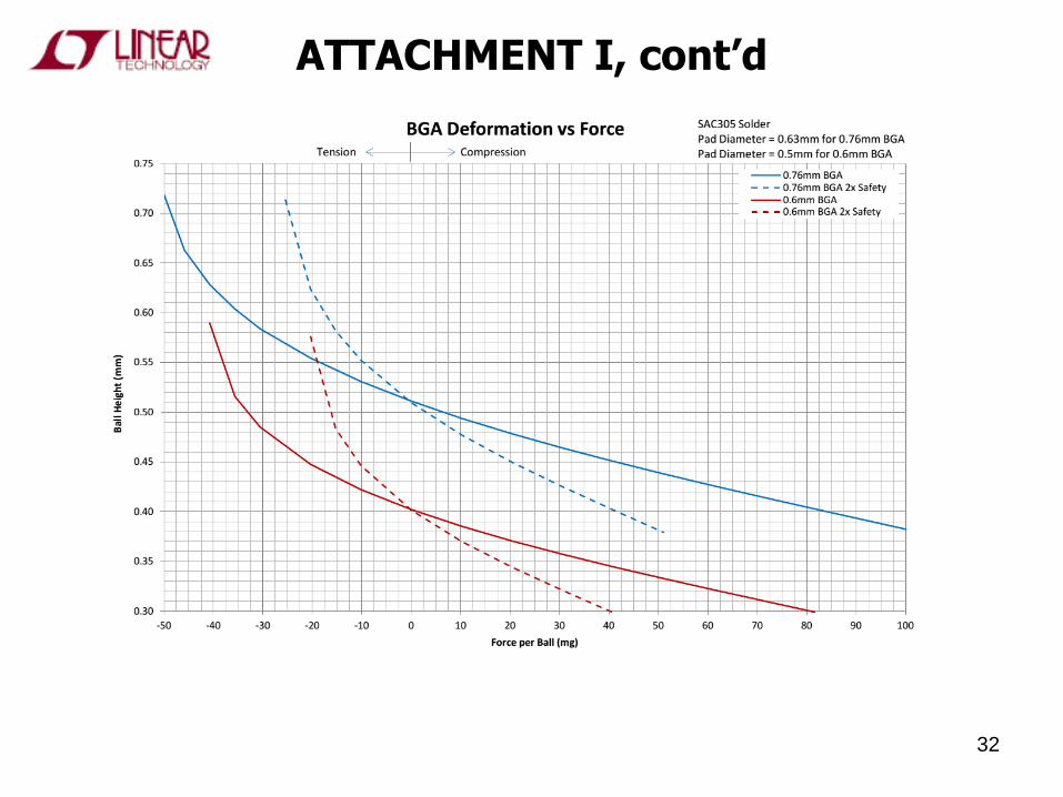
ATTACHMENT I, cont’d
32