Embed Size (px)
Citation preview
IPC-A-610CAmendment 1
Acceptability of
Electronic Assemblies
ASSOCIATION CONNECTINGELECTRONICS INDUSTRIES ®
2215 Sanders Road, Northbrook, IL 60062-6135Tel. 847.509.9700 Fax 847.509.9798
www.ipc.org
IPC-A-610CAmendment 1November 2001 A standard developed by IPC
In keeping with the U.S. Department of Defense acquisition reform principle of relying on performance requirements when-ever practicable, and then relying on contractors to meet those requirements, this standardhas not been ‘‘adopted.’’ How-ever, it is recommended as a reference to be used in the establishment and evaluation of design and process requirements.The adoption notice of the IPC-HDBK-001 is reprinted below to better identify the Department’s intent to use ANSI/J-STD-001, IPC-HDBK-001, and IPC-A-610 when evaluating electronic manufacturing strategies, processes, and management.
‘‘IPC-HDBK-001, ‘‘Handbook and Guide to the Requirements for Soldered Electrical and Electronic Assembliesto Supplement ANSI/J-STD-001B’’ was adopted on July 19, 2001, for use by the Department of Defense (DoD).Department of Defense policy is to rely on performance based requirements whenever practicable and to notrequire standard management approaches or manufacturing processes in solicitations and contracts. By establish-ing performance requirements and then relying on contractors to meet those requirements we enable innovationand allow contractors to meet our needs at the lowest cost. Nevertheless Defense program managers and con-tract oversight personnel must have an understanding of the underlying management, engineering, and manufac-turing processes at work so they can evaluate and monitor contractor processes. DoD activities may use thishandbook and its associated documents when evaluating electronic manufacturing strategies, processes, andmanagement.’’
The Principles ofStandardization
In May 1995 the IPC’s Technical Activities Executive Committee adopted Principles ofStandardization as a guiding principle of IPC’s standardization efforts.
Standards Should:• Show relationship to Design for Manufacturability (DFM) and Design for the
Environment (DFE)• Minimize time to market• Contain simple (simplified) language• Just include spec information• Focus on end product performance• Include a feedback system on use and problems for future improvement
Standards Should Not:• Inhibit innovation• Increase time-to-market• Keep people out• Increase cycle time• Tell you how to make something• Contain anything that cannot be defended with data
Notice IPC Standards and Publications are designed to serve the public interest through eliminatingmisunderstandings between manufacturers and purchasers, facilitating interchangeability andimprovement of products, and assisting the purchaser in selecting and obtaining with minimumdelay the proper product for his particular need. Existence of such Standards and Publicationsshall not in any respect preclude any member or nonmember of IPC from manufacturing or sell-ing products not conforming to such Standards and Publication, nor shall the existence of suchStandards and Publications preclude their voluntary use by those other than IPC members,whether the standard is to be used either domestically or internationally.
Recommended Standards and Publications are adopted by IPC without regard to whether theiradoption may involve patents on articles, materials, or processes. By such action, IPC does notassume any liability to any patent owner, nor do they assume any obligation whatever to partiesadopting the Recommended Standard or Publication. Users are also wholly responsiblefor protecting themselves against all claims of liabilities for patent infringement.
©Copyright 2001. IPC, Northbrook, Illinois. All rights reserved under both international and Pan-American copyright conventions. Permissionis hereby granted to print and make electronic copies and freely distribute IPC-A-610C Amendment 1.
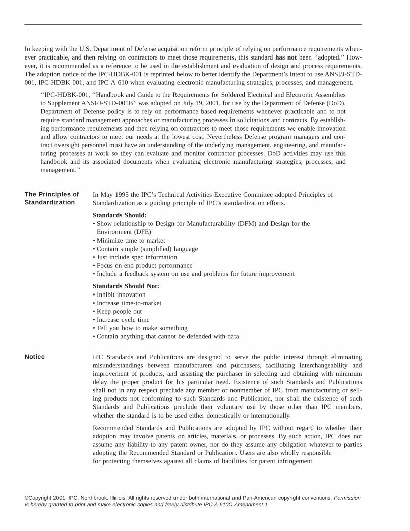
1.4.5 Electrical Clearance
The minimum spacing between non-common uninsulatedconductors (e.g., patterns, materials, hardware, residue) isreferred to as ‘‘minimum electrical clearance’’ throughout thisdocument and is defined in the applicable design standard oron the approved or controlled documentation. Insulatingmaterial must provide sufficient electrical isolation. In theabsence of a known design standard use Appendix A (derivedfrom IPC-2221). Any violation of minimum electricalclearance as a result of nonconformance to defined cri-teria of IPC-A-610 is a defect condition.
Care must be taken during acceptability inspections to ensureproduct integrity at all times. Table 3-4 provides general guid-ance.
Moisture sensitive components (as classified by IPC/JEDECJ-STD-020 or equivalent documented procedure) should behandled in a manner consistent with J-STD-033 or an equiva-lent documented procedure.
Defect - Class 1,2,3
• Cable tied with improper hitch or knot. This tie mayeventu-
ally loosen.
Figure 4-52
This amendment is only to be used in conjunction with IPC-A-610 Revision C, January 2000. This amendment doesNOT constitute authorization to make ‘‘pen and ink’’ changes or notations to the published IPC-A-610 Revision C.
Foreword
1November 2001
3.4.1 Handling – Guidelines
4.4.5 Component Mounting – Cable Ties, Tie Wraps, Spot Ties
4.2.1 Hardware Mounting – Electrical Clearance (1.4.5)
Acceptable - Class 1,2,3
• Wires exiting connector are positioned as they would be atinstallation.
• All wires are dressed with even bends to prevent stress atcontact connections.
• Shortest wires are in direct line with center axis of cable.
Note: The number of wires with no slack is limited to sevenor fewer for round or multiple-rowed rectangular connectorsand eight or fewer for dual contact-rowed rectangular con-nectors.
Acceptable - Class 1,2,3
• Component in contact with board on at least one sideand/or surface.
Note: When documented on an approved assembly drawing,a component may be either side mounted or end mounted.The side or surface of the body, or at least one point of anyirregularly configured component (such as certain pocketbookcapacitors), needs to be in full contact with the printed board.The body should be bonded or otherwise secured to theboard to prevent damage when vibration and shock forcesare applied.
Acceptable - Class 1,2
• Components with a coating meniscus can be mounted withthe meniscus into the holes provided they meet the require-ments of 6.3.4.3.
Process Indicator - Class 3
• Coating meniscus is into the plated-through hole (must meetthe requirements of 6.3.4.3).
Defect - Class 1,2,3
• Connection does not meet the requirements of 6.3.4.3when soldered.
Figure 5-16
Figure 4-55
Figure 5-32
This amendment is only to be used in conjunction with IPC-A-610 Revision C, January 2000. This amendment doesNOT constitute authorization to make ‘‘pen and ink’’ changes or notations to the published IPC-A-610 Revision C.
4.4.7 Component Mounting – Wire Dress for Terminations toConnectors Without Strain/Stress Relief
2 November 2001
5.2.3 Mounting – Horizontal – Radial Leaded
5.2.6.2 Mounting – Vertical – Radial Leaded – Component Meniscus
Defect - Class 1,2,3
• No stress relief
Acceptable - Class 1,2,3------------------------------------
• Leads are formed to provide stress relief.--------------------------------------------------------------
Acceptable - Class 1,2,3
• Leads are formed to provide stress relief.
Note: Prepped components such as this one usually cannotmeet the maximum spacing requirements of a straight-leggedvertical - radial leaded component. See 5.2.6. Maximumspace between component and board surface is determinedby considering design limitations and product use environ-ments. The component preparation equipment and manufac-turer’s suggested component lead bend specifications andcapabilities determine limitation. This may require change intooling to meet requirements for end use.
Figure 5-54
Figure 5-55
This amendment is only to be used in conjunction with IPC-A-610 Revision C, January 2000. This amendment doesNOT constitute authorization to make ‘‘pen and ink’’ changes or notations to the published IPC-A-610 Revision C.
5.3.2.1 Lead Forming – Stress Relief – Supported Holes
3November 2001
Defect - Class 1,2,3
A. Wire is stretched taut between the terminals.B. Does not meet bend radius requirements. See Table 5-3.C. Bends are kinked.
Table 6-1 Lead Protrusion
Class 1 Class 2 Class 3
(L) min.1 End is discernible in solder2
(L) max. No dangerof shorts
2.5 mm[0.0984 in]
1.5 mm[0.0591 in]
Note 1. For single-sided boards, lead or wire protrusion (L), is at least 0.5mm [0.020 in] for Class 1 and 2. There must be sufficient protrusionfor Class 3 to clinch.
Note 2. For plated-through hole boards greater than 2.3 mm [0.0906 in]thick, components with pre-established lead lengths, (DIPs, sockets),lead protrusion may not be discernible.
Defect - Class 1,2,3
• Lead not discernible due to bent lead.
• Solder not wetted to lead or land.
• Solder coverage does not comply with Table 6-2.
Figure 5-108
Figure 6-17
This amendment is only to be used in conjunction with IPC-A-610 Revision C, January 2000. This amendment doesNOT constitute authorization to make ‘‘pen and ink’’ changes or notations to the published IPC-A-610 Revision C.
5.5.3 Terminals – Stress Relief Lead/Wire Bend
4 November 2001
6.2 Lead Protrusion
6.3.4.1 PTH Mounted Components - Solder Conditions
Acceptable - Class 1,2,3
• Wire/lead outline is discernible with a smooth flow of solderon wire/lead and terminal. Individual strands may be dis-cernible.
• No evidence of sharp edges, solder points, icicles, or inclu-sions (foreign material).
• Balled solder connection does not exceed specified heightrequirements and meets all acceptable criteria for ball sol-dering.
Defect - Class 1,2,3
• Discernable sharp edges, solder points, icicles, orinclusions (foreign material).
• Balled solder connection does not comply with heightor profile (shape) requirements.
Acceptable - Class 1,2,3
• Solder connection has an egg-shaped, spherical or ovalprofile that follows the contour of wire wrap.
• No evidence of sharp edges, solder points, icicles, inclu-sions (foreign material) or wire strands.
• Insulation clearance one wire diameter maximum.
• Balled solder connection does not exceed specified heightrequirements and meets all acceptable criteria for ball sol-dering.
Defect - Class 1,2,3
• Discernable sharp edges, solder points, icicles, orinclusions (foreign material).
• Insulation clearance greater than one wire diameter.
• Balled solder connection does not comply with heightor profile (shape) requirements.
Figure 6-79
Figure 6-82
This amendment is only to be used in conjunction with IPC-A-610 Revision C, January 2000. This amendment doesNOT constitute authorization to make ‘‘pen and ink’’ changes or notations to the published IPC-A-610 Revision C.
6.8.1.2 High Voltage - Terminals - Bottom Terminations
5November 2001
6.8.2.1 High Voltage - Solder Cups - Wires/Leads
Acceptable - Class 1,2,3
• Solder connection has an egg-shaped, spherical or ovalprofile.
• No evidence of sharp edges, solder points, icicles or inclu-sions (foreign material).
• Balled solder connection does not exceed specified heightrequirements and meets all acceptable criteria for ball sol-dering.
Defect - Class 1,2,3
• Discernable sharp edges, solder points, icicles, orinclusions (foreign material).
• Insulation clearance greater than one wire diameter.
• Balled solder connection does not comply with heightor profile (shape) requirements.
Acceptable - Class 1,2,3
• All sharp edges of the component lead are completely cov-ered with a continuous smooth rounded layer of solderforming a solder ball.
• Straight-through leads facilitate ball soldering.
• Balled solder connection does not exceed specified heightrequirements.
Defect - Class 1,2,3
• Discernable sharp edges, solder points, icicles, orinclusions (foreign material).
• Balled solder connection does not comply with heightor profile (shape) requirements.
Figure 6-83
Figure 6-87
This amendment is only to be used in conjunction with IPC-A-610 Revision C, January 2000. This amendment doesNOT constitute authorization to make ‘‘pen and ink’’ changes or notations to the published IPC-A-610 Revision C.
6.8.2.2 High Voltage - Solder Cups - Unused
6 November 2001
6.8.4 High Voltage - Through-Hole Connections
Acceptable - Class 1,2,3
• All sharp edges of the terminal’s radial split are completelycovered with a continuous smooth layer of solder forming aballed solder connection.
• Balled solder connection not exceed specified heightrequirements.
Defect - Class 1,2,3
• Discernable sharp edges, solder points, icicles, orinclusions (foreign material).
• Balled solder connection does not comply with heightor profile (shape) requirements.
Hand printing may include marking with indelible pen ormechanical etcher.
Acceptable - As agreed by user and supplier
• When nicks and tears occur as a result of tie-in tabs tofacilitate circuit removal, the extent of these imperfections donot exceed the requirements agreed to by user and supplier.
Defect - Class 1,2,3
• Nicks, tears, haloing or imperfections more than 50%of the distance from the edge to the nearest conductoror 2.5 mm [0.0984 in], whichever is less, or in excessof that specified in procurement documentation.
• Edge to conductor spacing does not comply withspecified requirements.
Figure 6-89
Figure 10-24
This amendment is only to be used in conjunction with IPC-A-610 Revision C, January 2000. This amendment doesNOT constitute authorization to make ‘‘pen and ink’’ changes or notations to the published IPC-A-610 Revision C.
6.8.5 High Voltage - Flared Flange Terminals
7November 2001
8.1 Etched Marking (Including Hand Printing)
10.3 Flexible and Rigid-Flex Printed Wiring
Acceptable - Class 1,2,3
• Slight discoloration
Note: Discoloration of the solder resist due to removal/repairof components is acceptable.
Defect - Class 1,2,3
• Solder resist does not comply with 9.2, 9.2.1, 9.2.2, or9.2.3.
Discrete wiring refers to a substrate or base upon which dis-crete wiring techniques are used to obtain electronic intercon-nections.
Separate visual criteria for each type is depicted in this sec-tion.
Discrete Wiring Acceptability Guidelines
The routing and terminating of discrete wires to form point-to-point electrical connections by use of special machines ortools, may be employed to replace or supplement printedconductors on board assemblies. Application may be in pla-nar, two-dimensional or three-dimensional configurations. Asummary of various discrete wiring techniques has beendocumented in the IPC Technical Report, IPC-TR-474, AnOverview of Discrete Wiring Techniques. This subject is alsocovered by IPC-DW-425, Design and End Product Require-ments for Discrete Wiring Boards, and IPC-DW-426, Guide-lines for Acceptability of Discrete Wiring Assemblies.
This section defines the criteria for acceptability of intercon-nections produced by some of the important discrete wiringprocesses in electronic assemblies. The illustrations are pre-sented to depict particular characteristics of the techniques.They are classified in the following categories:
1. Semi-Permanent Connections2. Permanent Connections
Further definition of the classification for each discrete wiringtechnique described herein may be found in the IPC-TR-474.
Figure 10-25
11 Discrete Wiring
This amendment is only to be used in conjunction with IPC-A-610 Revision C, January 2000. This amendment doesNOT constitute authorization to make ‘‘pen and ink’’ changes or notations to the published IPC-A-610 Revision C.
10.4 Solder Resist Discoloration
8 November 2001
Discrete Wiring Acceptability Requirements
For this requirement, countable turns are those turns ofbare wire in intimate contact with the corners of the ter-minals starting at the first contact of bare wire with aterminal corner and ending at the last contact of barewire with a terminal corner (see Table 11-1).
A modified wrap is required for Class 3. It has an addi-tional amount of insulated wire wrapped to contact atleast three corners of the terminal.
Target - Class 1,2,3
• One half (50%) more turn than the minimum shown inTable 11-1.
Acceptable - Class 1,2
• Countable turns meet the requirements of Table 11-1.
Acceptable - Class 3
• Countable turns meet the requirements of Table 11-1and there is an additional amount of insulated wirewrapped to contact at least three corners of the termi-nal.
Table 11-1 Minimum Turns of Bare Wire
Wire Gauge Turns
30 7
28 7
26 6
24 5
22 5
20 4
18 4
The target condition is a half (50%) turn more than that shown------------------------------------------------------------------------in the table. A modified wrap is required for Class 3. It has an------------------------------------------------------------------------additional amount of insulated wire wrapped to contact at------------------------------------------------------------------------least three corners of the terminal.----------------------------------------
Maximum turns of bare and insulated wire is governed only by------------------------------------------------------------------------tooling configuration and space available on the terminal.-------------------------------------------------------------------
Note: Maximum turns of bare and insulated wire is gov-erned only by tooling configuration and space availableon the terminal.
Defect - Class 1,2,3
• Number of countable turns does not comply with Table11-1.
Figure 11-1
This amendment is only to be used in conjunction with IPC-A-610 Revision C, January 2000. This amendment doesNOT constitute authorization to make ‘‘pen and ink’’ changes or notations to the published IPC-A-610 Revision C.
11.1.1 Solderless Wrap – Number of Turns
9November 2001
Target - Class 1,2,3
• Wire routed shortest route.
• Wire does not pass over or under component.
• Wire does not pass over land patterns or vias used as testpoints.
Acceptable - Class 1Process Indicator - Class 2,3
• Insufficient slack in wire to allow relocation from landsduring component replacement.
Minimum fillet height (F) requirements are not specified forClass 1,2,3. However, a properly wetted fillet is evident.
Defect - Class 1,2,3
• No properly wetted fillet.
Acceptable - Class 1,2,3
• Properly wetted fillet evident.
Defect - Class 1,2,3
• No properly wetted fillet.
Figure 11-25
Figure 12-9
Figure 12-10
This amendment is only to be used in conjunction with IPC-A-610 Revision C, January 2000. This amendment doesNOT constitute authorization to make ‘‘pen and ink’’ changes or notations to the published IPC-A-610 Revision C.
11.2.2.1 Jumper Wires - Wire Routing - Component Side
10 November 2001
12.2.1.6 Chip Components – Bottom OnlyTerminations, Minimum Fillet Height (F)
12.2.1.7 Chip Components – Bottom OnlyTerminations, Solder Thickness (G)
Target - Class 1,2,3
• Side joint length equals length of component termination.
Acceptable - Class 1,2,3
• Side joint length is not required. However, a properly wettedfillet is evident.
Defect - Class 1,2,3
• No properly wetted fillet.
Acceptable - Class 1,2,3
• Properly wetted fillet evident.
Defect - Class 1,2,3
• No properly wetted fillet.
Figure 12-23
Figure 12-29
This amendment is only to be used in conjunction with IPC-A-610 Revision C, January 2000. This amendment doesNOT constitute authorization to make ‘‘pen and ink’’ changes or notations to the published IPC-A-610 Revision C.
12.2.2.4 Chip Components - Rectangular or Square EndComponents - 1, 3 or 5 Side Termination, Side Joint Length (D)
11November 2001
12.2.2.7 Chip Components - Rectangular or Square EndComponents - 1, 3 or 5 Side Termination, Solder Thickness (G)
Target - Class 1,2,3
• Side joint length (D) is equal to the length of component ter-mination (T) or land length (S), whichever is less.
Acceptable - Class 1
• Side joint length (D) exhibits a properly wetted fillet.
Acceptable - Class 2
• Side joint length (D) is minimum 50% length of componenttermination (T) or land length (S), whichever is less.
Acceptable - Class 3
• Side joint length (D) is minimum 75% length of componenttermination (T) or land length (S), whichever is less.
Defect - Class 1
• Side joint length (D) does not exhibit a properly wetted fillet.
Defect - Class 2
• Side joint length (D) is less than 50% length of componenttermination (T) or land length (S), whichever is less.
Defect - Class 3
• Side joint length (D) is less than 75% length of componenttermination (T) or land length (S) whichever is less.
Acceptable - Class 1,2,3
• Properly wetted fillet evident.
Defect - Class 1,2,3
• No properly wetted fillet.
Figure 12-40, Figure 12-41
Figure 12-46
This amendment is only to be used in conjunction with IPC-A-610 Revision C, January 2000. This amendment doesNOT constitute authorization to make ‘‘pen and ink’’ changes or notations to the published IPC-A-610 Revision C.
12.2.3.4 Cylindrical End Cap Termination, Side Joint Length (D)
12 November 2001
12.2.3.7 Cylindrical End Cap Termination, Solder Thickness (G)
Acceptable - Class 1
• A properly wetted fillet is evident.
Acceptable - Class 2,3
• Minimum fillet height (F) is the solder thickness (G) (notshown) plus 25% castellation height (H).
Defect - Class 1
• A properly wetted fillet is not evident.
Defect - Class 2,3
• Minimum fillet height (F) is less than solder thickness (G) (notshown) plus 25% castellation height (H).
Acceptable - Class 1,2,3
• Properly wetted fillet evident.
Defect - Class 1,2,3
• No properly wetted fillet.
Acceptable - Class 1,2,3
• Properly wetted fillet evident.
Defect - Class 1,2,3
• No properly wetted fillet.
Figure 12-54
Figure 12-55
Figure 12-56
Figure 12-81
This amendment is only to be used in conjunction with IPC-A-610 Revision C, January 2000. This amendment doesNOT constitute authorization to make ‘‘pen and ink’’ changes or notations to the published IPC-A-610 Revision C.
12.2.4.6 Leadless Chip Carriers withCastellated Terminations, Minimum Fillet Height (F)
13November 2001
12.2.4.7 Leadless Chip Carriers withCastellated Terminations, Solder Thickness (G)
12.2.5.7 Flat Ribbon, L, and Gull WingLeads, Solder Thickness (G)
Acceptable - Class 1,2,3
• Properly wetted fillet evident.
Defect - Class 1,2,3
• No properly wetted fillet.
Acceptable - Class 1,2,3
• Properly wetted fillet evident.
Defect - Class 1,2,3
• No properly wetted fillet.
Acceptable - Class 1,2
• Properly wetted fillet evident.
Defect - Class 1,2,3
• No properly wetted fillet.
Figure 12-88
Figure 12-110
Figure 12-117
This amendment is only to be used in conjunction with IPC-A-610 Revision C, January 2000. This amendment doesNOT constitute authorization to make ‘‘pen and ink’’ changes or notations to the published IPC-A-610 Revision C.
12.2.6.7 Round or Flattened (Coined) Leads, Solder Thickness (G)
14 November 2001
12.2.8.7 Butt/I Joints, Solder Thickness (G)
12.2.7.7 J Leads, Solder Thickness (G)
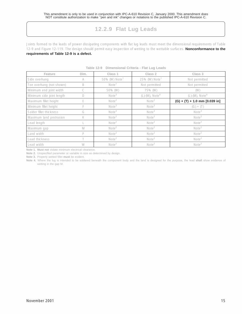
Joints formed to the leads of power dissipating components with flat lug leads must meet the dimensional requirements of Table12-9 and Figure 12-119. The design should permit easy inspection of wetting to the wettable surfaces. Nonconformance to therequirements of Table 12-9 is a defect.
Table 12-9 Dimensional Criteria - Flat Lug Leads
Feature Dim. Class 1 Class 2 Class 3
Side overhang A 50% (W) Note1 25% (W) Note1 Not permitted
Toe overhang (not shown) B Note1 Not permitted Not permitted
Minimum end joint width C 50% (W) 75% (W) (W)
Minimum side joint length D Note3 (L)-(M), Note4 (L)-(M), Note4
Maximum fillet height E Note2 Note2 (G) + (T) + 1.0 mm [0.039 in]
Minimum fillet height F Note3 Note3 (G) + (T)
Solder fillet thickness G Note3 Note3 Note3
Maximum land protrusion K Note2 Note2 Note2
Lead length L Note2 Note2 Note2
Maximum gap M Note2 Note2 Note2
Land width P Note2 Note2 Note2
Lead thickness T Note2 Note2 Note2
Lead width W Note2 Note2 Note2
Note 1. Must not violate minimum electrical clearance.Note 2. Unspecified parameter or variable in size as determined by design.Note 3. Properly wetted fillet must be evident.Note 4. Where the lug is intended to be soldered beneath the component body and the land is designed for the purpose, the lead shall show evidence of
wetting in the gap M.
This amendment is only to be used in conjunction with IPC-A-610 Revision C, January 2000. This amendment doesNOT constitute authorization to make ‘‘pen and ink’’ changes or notations to the published IPC-A-610 Revision C.
12.2.9 Flat Lug Leads
15November 2001
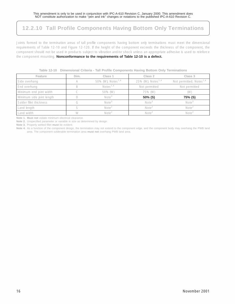
Joints formed to the termination areas of tall profile components having bottom only terminations must meet the dimensionalrequirements of Table 12-10 and Figure 12-120. If the height of the component exceeds the thickness of the component, thecomponent should not be used in products subject to vibration and/or shock unless an appropriate adhesive is used to reinforcethe component mounting. Nonconformance to the requirements of Table 12-10 is a defect.
Table 12-10 Dimensional Criteria - Tall Profile Components Having Bottom Only Terminations
Feature Dim. Class 1 Class 2 Class 3
Side overhang A 50% (W); Notes1,4 25% (W); Notes1,4 Not permitted; Notes1,4
End overhang B Notes1,4 Not permitted Not permitted
Minimum end joint width C 50% (W) 75% (W) (W)
Minimum side joint length D Note3 50% (S) 75% (S)
Solder fillet thickness G Note3 Note3 Note3
Land length S Note2 Note2 Note2
Land width W Note2 Note2 Note2
Note 1. Must not violate minimum electrical clearance.Note 2. Unspecified parameter or variable in size as determined by design.Note 3. Properly wetted fillet must be evident.Note 4. As a function of the component design, the termination may not extend to the component edge, and the component body may overhang the PWB land
area. The component solderable termination area must not overhang PWB land area.
This amendment is only to be used in conjunction with IPC-A-610 Revision C, January 2000. This amendment doesNOT constitute authorization to make ‘‘pen and ink’’ changes or notations to the published IPC-A-610 Revision C.
12.2.10 Tall Profile Components Having Bottom Only Terminations
16 November 2001
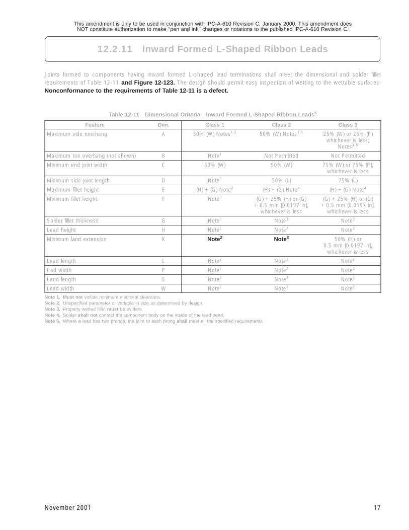
Joints formed to components having inward formed L-shaped lead terminations shall meet the dimensional and solder filletrequirements of Table 12-11 and Figure 12-123. The design should permit easy inspection of wetting to the wettable surfaces.Nonconformance to the requirements of Table 12-11 is a defect.
Table 12-11 Dimensional Criteria - Inward Formed L-Shaped Ribbon Leads 5
Feature Dim. Class 1 Class 2 Class 3
Maximum side overhang A 50% (W) Notes1,5 50% (W) Notes1,5 25% (W) or 25% (P)whichever is less;
Notes1,5
Maximum toe overhang (not shown) B Note1 Not Permitted Not Permitted
Minimum end joint width C 50% (W) 50% (W) 75% (W) or 75% (P),whichever is less
Minimum side joint length D Note3 50% (L) 75% (L)
Maximum fillet height E (H) + (G) Note4 (H) + (G) Note4 (H) + (G) Note4
Minimum fillet height F Note3 (G) + 25% (H) or (G)+ 0.5 mm [0.0197 in],
whichever is less
(G) + 25% (H) or (G)+ 0.5 mm [0.0197 in],
whichever is less
Solder fillet thickness G Note3 Note3 Note3
Lead height H Note2 Note2 Note2
Minimum land extension K Note2 Note2 50% (H) or0.5 mm [0.0197 in],
whichever is less
Lead length L Note2 Note2 Note2
Pad width P Note2 Note2 Note2
Land length S Note2 Note2 Note2
Lead width W Note2 Note2 Note2
Note 1. Must not violate minimum electrical clearance.Note 2. Unspecified parameter or variable in size as determined by design.Note 3. Properly wetted fillet must be evident.Note 4. Solder shall not contact the component body on the inside of the lead bend.Note 5. Where a lead has two prongs, the joint to each prong shall meet all the specified requirements.
This amendment is only to be used in conjunction with IPC-A-610 Revision C, January 2000. This amendment doesNOT constitute authorization to make ‘‘pen and ink’’ changes or notations to the published IPC-A-610 Revision C.
12.2.11 Inward Formed L-Shaped Ribbon Leads
17November 2001
Acceptable - Class 1Process Indicator - Class 2,3
• More than five solder balls/splashes (0.13 mm [0.00512 in]or less) per 600 mm 2 [0.93 in 2].
Defect - Class 1,2,3
• Solder balls violate minimum electrical clearance.
• Solder balls not entrapped or encapsulated (e.g., no-cleanresidue, conformal coating), or not attached to a metal sur-face.
Note: Entrapped/encapsulated/attached is intended to meannormal service environment of the product will not cause asolder ball to become dislodged.
Figure 12-152
This amendment is only to be used in conjunction with IPC-A-610 Revision C, January 2000. This amendment doesNOT constitute authorization to make ‘‘pen and ink’’ changes or notations to the published IPC-A-610 Revision C.
12.4.10 SMT Soldering Anomalies – Solder Balls/Solder Fines
18 November 2001
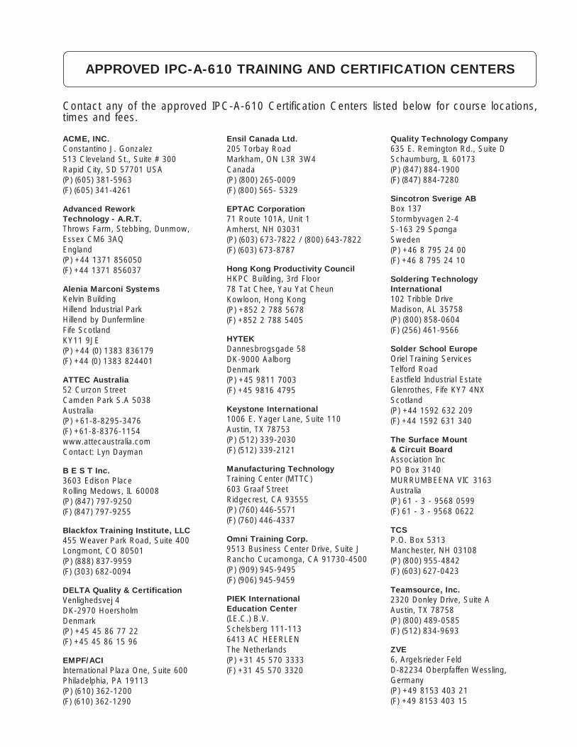
Contact any of the approved IPC-A-610 Certification Centers listed below for course locations,times and fees.
ACME, INC.Constantino J. Gonzalez513 Cleveland St., Suite # 300Rapid City, SD 57701 USA(P) (605) 381-5963(F) (605) 341-4261
Advanced ReworkTechnology - A.R.T.Throws Farm, Stebbing, Dunmow,Essex CM6 3AQEngland(P) +44 1371 856050(F) +44 1371 856037
Alenia Marconi SystemsKelvin BuildingHillend Industrial ParkHillend by DunfermlineFife ScotlandKY11 9JE(P) +44 (0) 1383 836179(F) +44 (0) 1383 824401
ATTEC Australia52 Curzon StreetCamden Park S.A 5038Australia(P) +61-8-8295-3476(F) +61-8-8376-1154www.attecaustralia.comContact: Lyn Dayman
B E S T Inc.3603 Edison PlaceRolling Medows, IL 60008(P) (847) 797-9250(F) (847) 797-9255
Blackfox Training Institute, LLC455 Weaver Park Road, Suite 400Longmont, CO 80501(P) (888) 837-9959(F) (303) 682-0094
DELTA Quality & CertificationVenlighedsvej 4DK-2970 HoersholmDenmark(P) +45 45 86 77 22(F) +45 45 86 15 96
EMPF/ACIInternational Plaza One, Suite 600Philadelphia, PA 19113(P) (610) 362-1200(F) (610) 362-1290
Ensil Canada Ltd.205 Torbay RoadMarkham, ON L3R 3W4Canada(P) (800) 265-0009(F) (800) 565- 5329
EPTAC Corporation71 Route 101A, Unit 1Amherst, NH 03031(P) (603) 673-7822 / (800) 643-7822(F) (603) 673-8787
Hong Kong Productivity CouncilHKPC Building, 3rd Floor78 Tat Chee, Yau Yat CheunKowloon, Hong Kong(P) +852 2 788 5678(F) +852 2 788 5405
HYTEKDannesbrogsgade 58DK-9000 AalborgDenmark(P) +45 9811 7003(F) +45 9816 4795
Keystone International1006 E. Yager Lane, Suite 110Austin, TX 78753(P) (512) 339-2030(F) (512) 339-2121
Manufacturing TechnologyTraining Center (MTTC)603 Graaf StreetRidgecrest, CA 93555(P) (760) 446-5571(F) (760) 446-4337
Omni Training Corp.9513 Business Center Drive, Suite JRancho Cucamonga, CA 91730-4500(P) (909) 945-9495(F) (906) 945-9459
PIEK InternationalEducation Center(I.E.C.) B.V.Schelsberg 111-1136413 AC HEERLENThe Netherlands(P) +31 45 570 3333(F) +31 45 570 3320
Quality Technology Company635 E. Remington Rd., Suite DSchaumburg, IL 60173(P) (847) 884-1900(F) (847) 884-7280
Sincotron Sverige ABBox 137Stormbyvagen 2-4S-163 29 SpσngaSweden(P) +46 8 795 24 00(F) +46 8 795 24 10
Soldering TechnologyInternational102 Tribble DriveMadison, AL 35758(P) (800) 858-0604(F) (256) 461-9566
Solder School EuropeOriel Training ServicesTelford RoadEastfield Industrial EstateGlenrothes, Fife KY7 4NXScotland(P) +44 1592 632 209(F) +44 1592 631 340
The Surface Mount& Circuit BoardAssociation IncPO Box 3140MURRUMBEENA VIC 3163Australia(P) 61 - 3 - 9568 0599(F) 61 - 3 - 9568 0622
TCSP.O. Box 5313Manchester, NH 03108(P) (800) 955-4842(F) (603) 627-0423
Teamsource, Inc.2320 Donley Drive, Suite AAustin, TX 78758(P) (800) 489-0585(F) (512) 834-9693
ZVE6, Argelsrieder FeldD-82234 Oberpfaffen Wessling,Germany(P) +49 8153 403 21(F) +49 8153 403 15
APPROVED IPC-A-610 TRAINING AND CERTIFICATION CENTERS

This Page Intentionally Left Blank
Standard Improvement Form IPC-A-610CThe purpose of this form is to provide theTechnical Committee of IPC with inputfrom the industry regarding usage ofthe subject standard.
Individuals or companies are invited tosubmit comments to IPC. All commentswill be collected and dispersed to theappropriate committee(s).
If you can provide input, please completethis form and return to:
IPC2215 Sanders RoadNorthbrook, IL 60062-6135Fax 847 509.9798
1. I recommend changes to the following:
Requirement, paragraph number
Test Method number , paragraph number
The referenced paragraph number has proven to be:
Unclear Too Rigid In Error
Other
2. Recommendations for correction:
3. Other suggestions for document improvement:
Submitted by:
Name Telephone
Company E-mail
Address
City/State/Zip Date
ASSOCIATION CONNECTINGELECTRONICS INDUSTRIES ®
ASSOCIATION CONNECTINGELECTRONICS INDUSTRIES
2215 Sanders Road, Northbrook, IL 60062-6135Tel. 847.509.9700 Fax 847.509.9798
www.ipc.org
®
ISBN #1-580982-94-8